

Page 1
22029200303
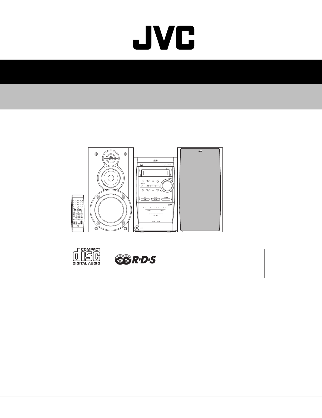
UX-J60
SERVICE MANUAL
MICRO COMPONENT SYSTEM
UX-J60
RM-SUXJ60R REMOTE CONTROL
SP-UXJ60
SP-UXJ60CA-UXJ60
Area Suffix
B -------------------------- U.K.
E ------- Continental Europe
EN --------- Northern Europe
TABLE OF CONTENTS
1 Important Safety Precautions . . . . . . . . . . . . . . . . . . . . . . . . . . . . . . . . . . . . . . . . . . . . . . . . . . . . . . . . . . . 1-2
2 Disassembly method . . . . . . . . . . . . . . . . . . . . . . . . . . . . . . . . . . . . . . . . . . . . . . . . . . . . . . . . . . . . . . . . . . 1-6
3 Adjustment. . . . . . . . . . . . . . . . . . . . . . . . . . . . . . . . . . . . . . . . . . . . . . . . . . . . . . . . . . . . . . . . . . . . . . . . . . 1-19
4 Description of major ICs. . . . . . . . . . . . . . . . . . . . . . . . . . . . . . . . . . . . . . . . . . . . . . . . . . . . . . . . . . . . . . . 1-25
COPYRIGHT © 2003 VICTOR COMPANY OF JAPAN, LTD.
No.22029
2003/03
Page 2
UX-J60
Important Safety Precautions
1.1 Safety Precautions
(1) This design of this product contains special hardware and
many circuits and components specially for safety purposes.
For continued protection, no changes should be made to the
original design unless authorized in writing by the manufacturer. Replacement parts must be identical to those
used in the original circuits. Services should be performed by qualified personnel only.
(2) Alterations of the design or circuitry of the product should
not be made. Any design alterations of the product should
not be made. Any design alterations or additions will void
the manufacturers warranty and will further relieve the
manufacture of responsibility for personal injury or property
damage resulting therefrom.
(3) Many electrical and mechanical parts in the products have
special safety-related characteristics. These characteristics are often not evident from visual inspection nor can the
protection afforded by them necessarily be obtained by using replacement components rated for higher voltage, wattage, etc. Replacement parts which have these special safety
characteristics are identified in the Parts List of Service Manual. Electrical components having such features are identified by shading on the schematics and by ( ) on the
Parts List in the Service Manual. The use of a substitute replacement which does not have the same safety characteristics as the recommended replacement parts shown in the
Parts List of Service Manual may create shock, fire, or other hazards.
(4) The leads in the products are routed and dressed with ties,
clamps, tubings, barriers and the like to be separated from
live parts, high temperature parts, moving parts and/or
sharp edges for the prevention of electric shock and fire
hazard. When service is required, the original lead routing
and dress should be observed, and it should be confirmed
that they have been returned to normal, after reassembling.
(5) Leakage shock hazard testing)
After reassembling the product, always perform an isolation
check on the exposed metal parts of the product (antenna
terminals, knobs, metal cabinet, screw heads, headphone
jack, control shafts, etc.) to be sure the product is safe to
operate without danger of electrical shock.
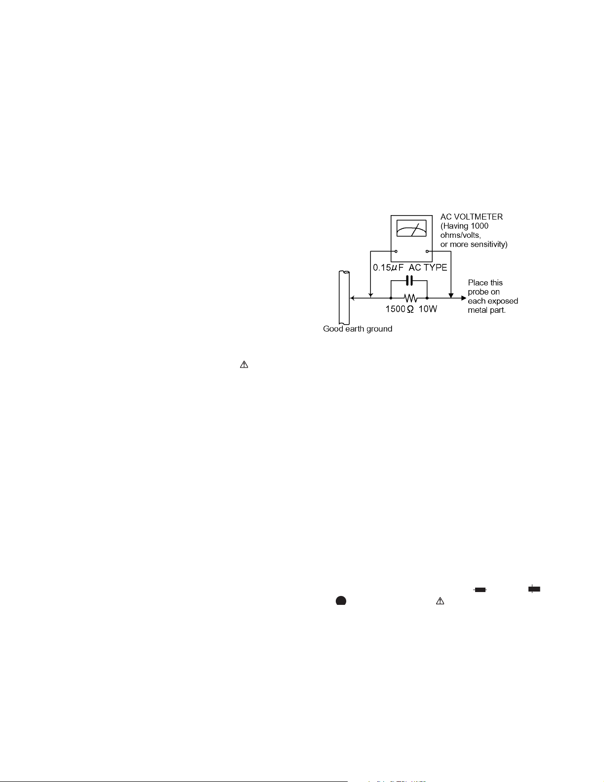
Do not use a line isolation transformer during this check.
• Plug the AC line cord directly into the AC outlet. Using a
"Leakage Current Tester", measure the leakage current
from each exposed metal parts of the cabinet, particularly any exposed metal part having a return path to the
chassis, to a known good earth ground. Any leakage current must not exceed 0.5mA AC (r.m.s.).
• Alternate check method
Plug the AC line cord directly into the AC outlet. Use an AC
voltmeter having, 1,000 ohms per volt or more sensitivity in
the following manner. Connect a 1,500 ohm 10W resistor
paralleled by a 0.15 µF AC-type capacitor between an
SECTION 1
exposed metal part and a known good earth ground.
Measure the AC voltage across the resistor with the AC
voltmeter.
Move the resistor connection to each exposed metal part,
particularly any exposed metal part having a return path to
the chassis, and measure the AC voltage across the resistor.
Now, reverse the plug in the AC outlet and repeat each
measurement. Voltage measured any must not exceed 0.75
V AC (r.m.s.). This corresponds to 0.5 mA AC (r.m.s.).
1.2 Warning
(1) This equipment has been designed and manufactured to
meet international safety standards.
(2) It is the legal responsibility of the repairer to ensure that
these safety standards are maintained.
(3) Repairs must be made in accordance with the relevant
safety standards.
(4) It is essential that safety critical components are replaced
by approved parts.
(5) If mains voltage selector is provided, check setting for local
voltage.
1.3 Caution
Burrs formed during molding may be left over on some parts
of the chassis.
Therefore, pay attention to such burrs in the case of preforming repair of this system.
1.4 Critical parts for safety
In regard with component parts appearing on the silk-screen
printed side (parts side) of the PWB diagrams, the parts that are
printed over with black such as the resistor ( ), diode ( )
and ICP ( ) or identified by the " " mark nearby are critical
for safety.
When replacing them, be sure to use the parts of the same type
and rating as specified by the manufacturer. (Except the JC version)
1-2 (No.22029)
Page 3
1.5 Safety Precautions (U.K only)
(1) This design of this product contains special hardware and many circuits and components specially for safety purposes. For con-
tinued protection, no changes should be made to the original design unless authorized in writing by the manufacturer. Replacement parts must be identical to those used in the original circuits.
(2) Any unauthorised design alterations or additions will void the manufacturer's guarantee; furthermore the manufacturer cannot
accept responsibility for personal injury or property damage resulting therefrom.
(3) Essential safety critical components are identified by ( ) on the Parts List and by shading on the schematics, and must never
be replaced by parts other than those listed in the manual. Please note however that many electrical and mechanical parts in
the product have special safety related characteristics. These characteristics are often not evident from visual inspection. Parts
other than specified by the manufacturer may not have the same safety characteristics as the recommended replacement parts
shown in the Parts List of the Service Manual and may create shock, fire, or other hazards.
(4) The leads in the products are routed and dressed with ties, clamps, tubings, barriers and the like to be separated from live parts,
high temperature parts, moving parts and/or sharp edges for the prevention of electric shock and fire hazard. When service is
required, the original lead routing and dress should be observed, and it should be confirmed that they have been returned to
normal, after re-assembling.
1.5.1 Warning
(1) Service should be performed by qualified personnel only.
(2) This equipment has been designed and manufactured to meet international safety standards.
(3) It is the legal responsibility of the repairer to ensure that these safety standards are maintained.
(4) Repairs must be made in accordance with the relevant safety standards.
(5) It is essential that safety critical components are replaced by approved parts.
(6) If mains voltage selector is provided, check setting for local voltage.
UX-J60
Burrs formed during molding may be left over on some parts of the chassis. Therefore,
pay attention to such burrs in the case of preforming repair of this system.
(No.22029)1-3
Page 4
UX-J60
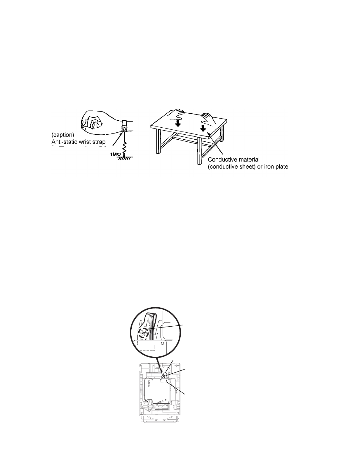
1.6 Preventing static electricity
Electrostatic discharge (ESD), which occurs when static electricity stored in the body, fabric, etc. is discharged,
can destroy the laser diode in the traverse unit (optical pickup). Take care to prevent this when performing repairs.
1.6.1 Grounding to prevent damage by static electricity
Static electricity in the work area can destroy the optical pickup (laser diode) in devices such as CD players.
Be careful to use proper grounding in the area where repairs are being performed.
(1) Ground the workbench
Ground the workbench by laying conductive material (such as a conductive sheet) or an iron plate over it before placing the
traverse unit (optical pickup) on it.
(2) Ground yourself
Use an anti-static wrist strap to release any static electricity built up in your body.
(3) Handling the optical pickup
• In order to maintain quality during transport and before installation, both sides of the laser diode on the replacement optical
pickup are shorted. After replacement, return the shorted parts to their original condition.
(Refer to the text.)
• Do not use a tester to check the condition of the laser diode in the optical pickup. The tester's internal power source can easily
destroy the laser diode.
1.7 Handling the traverse unit (optical pickup)
(1) Do not subject the traverse unit (optical pickup) to strong shocks, as it is a sensitive, complex unit.
(2) Cut off the shorted part of the flexible cable using nippers, etc. after replacing the optical pickup. For specific details, refer to the replace-
ment procedure in the text. Remove the anti-static pin when replacing the traverse unit. Be careful not to take too long a time
when attaching it to the connector.
(3) Handle the flexible cable carefully as it may break when subjected to strong force.
(4) I t is not possible to adjust the semi-fixed resistor that adjusts the laser power. Do not turn it.
1.8 Attention when traverse unit is decomposed
*Please refer to "Disassembly method" in the text for the CD pickup unit.
• Apply solder to the short land sections before the flexible wire is disconnected from the connector CN101 on the CD servo board.
(If the flexible wire is disconnected without applying solder, the CD pickup may be destroyed by static electricity.)
• In the assembly, be sure to remove solder from the short land sections after connecting the flexible wire.
Shorting round
1-4 (No.22029)
Flexible wire
Shorting round
CN601 on
mechanism
board
Page 5
1.9 Important for laser products
(1) CLASS 1 LASER PRODUCT
(2) DANGER : Invisible laser radiation when open and inter
lock failed or defeated. Avoid direct exposure to beam.
(3) CAUTION : There are no serviceable parts inside the
Laser Unit. Do not disassemble the Laser Unit. Replace the
complete Laser Unit if it malfunctions.
(4) CAUTION : The compact disc player uses invisible laser
radiation and is equipped with safety switches which
prevent emission of radiation when the drawer is open and
the safety interlocks have failed or are de feated.
It is dangerous to defeat the safety switches.
UX-J60
(5) CAUTION : If safety switches malfunction, the laser is able
to function.
(6) CAUTION : Use of controls, adjustments or performance of
procedures other than those specified herein may result in
hazardous radiation exposure.
CAUTION
Please use enough caution not to see the beam directly
or touch it in case of anadjustment or operation check.
VARNING
Osynlig laserstrålning är denna del är öppnad och spårren är
urkopplad. Betrakta ej strålen.
VARO
Avattaessa ja suojalukitus ohitettaessa olet alttiina näkymättömälle lasersäteilylle. Älä katso säteeseen.
REPRODUCTION AND POSITION OF LABELS
ADVARSEL
Usynlig laserstråling ved åbning, når sikkerhedsafbrydere er
ude af funktion. Undgå udsasttelse for stråling.
ADVARSEL
Usynlig laserstråling ved åpning, når sikkerhetsbryteren er avslott. unngå utsettelse for stråling.
Caution label
(No.22029)1-5
Page 6
UX-J60
r
A
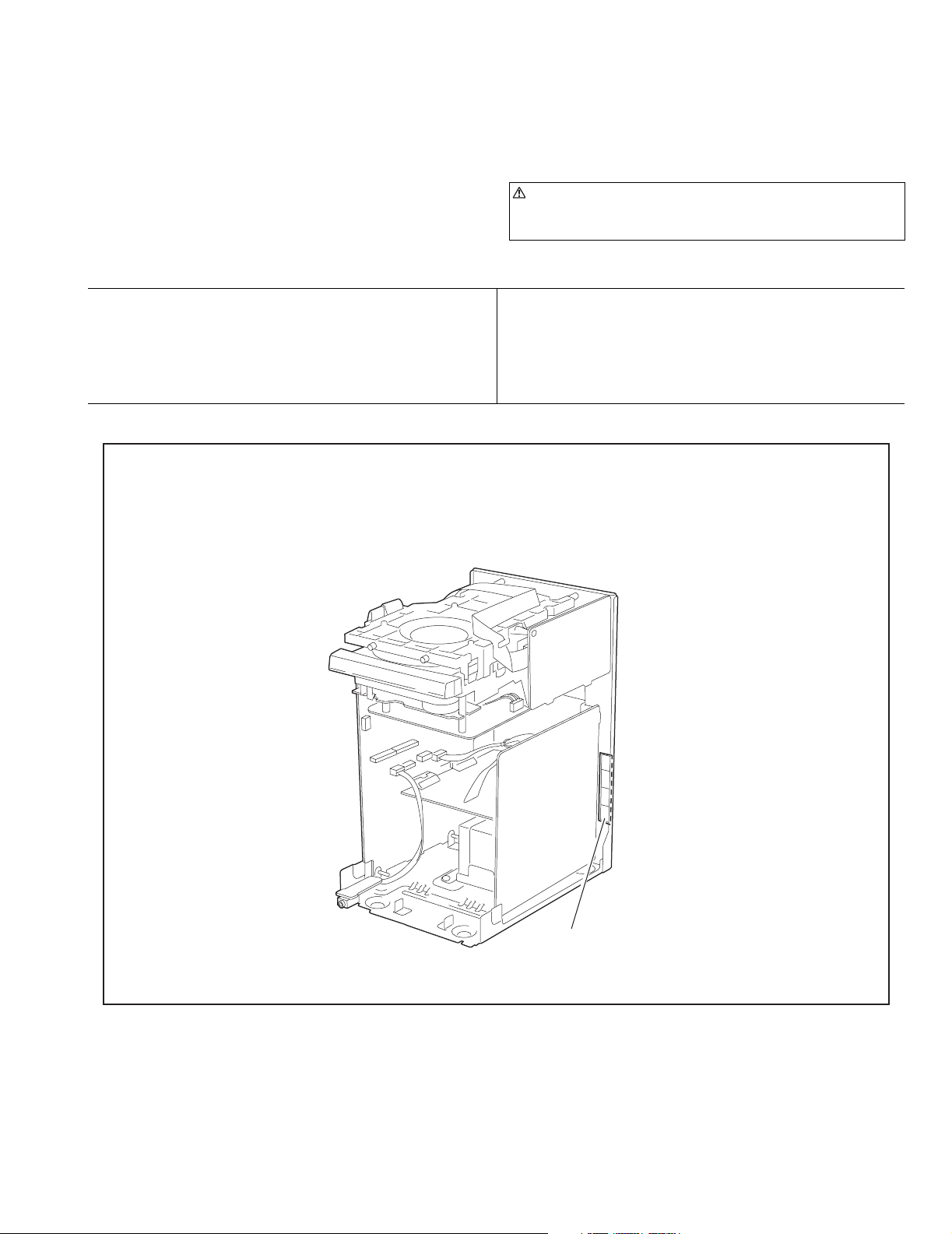
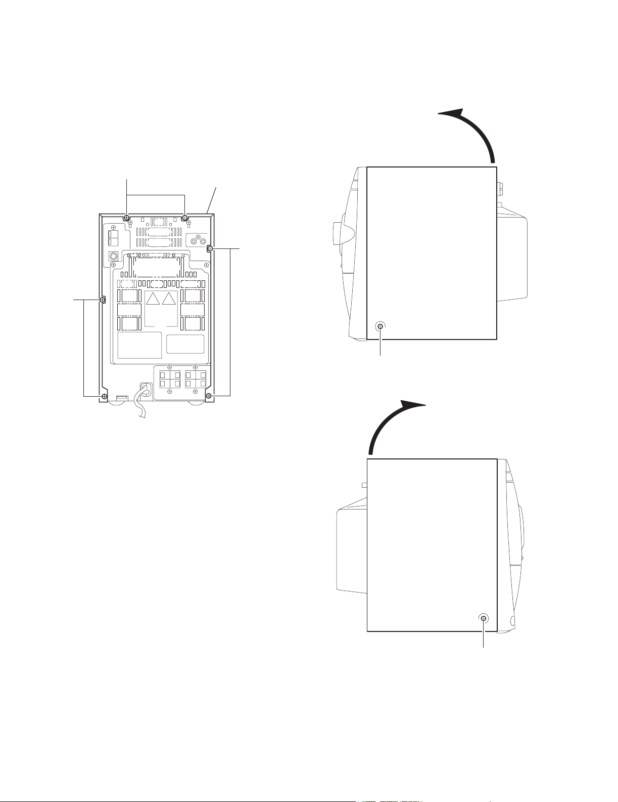
2.1 Main body
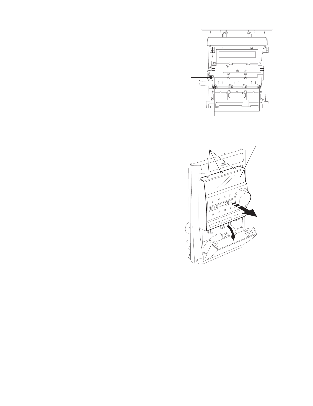
2.1.1 Removing the metal cover
(See Fig.1~3)
(1) Remove the six screws A on the back of the main body.
(2) Remove the two screws B on each side and remove the
metal cover in the direction of the arrow.
SECTION 2
Disassembly method
A
Metal cove
A
B
Fig.2
Fig.1
B
Fig.3
1-6 (No.22029)
Page 7
2.1.2 Removing the rear cover
r
(See Fig.4)
(1) Remove the two screws C attaching the rear cover.
UX-J60
C
Rear cove
Fig.4
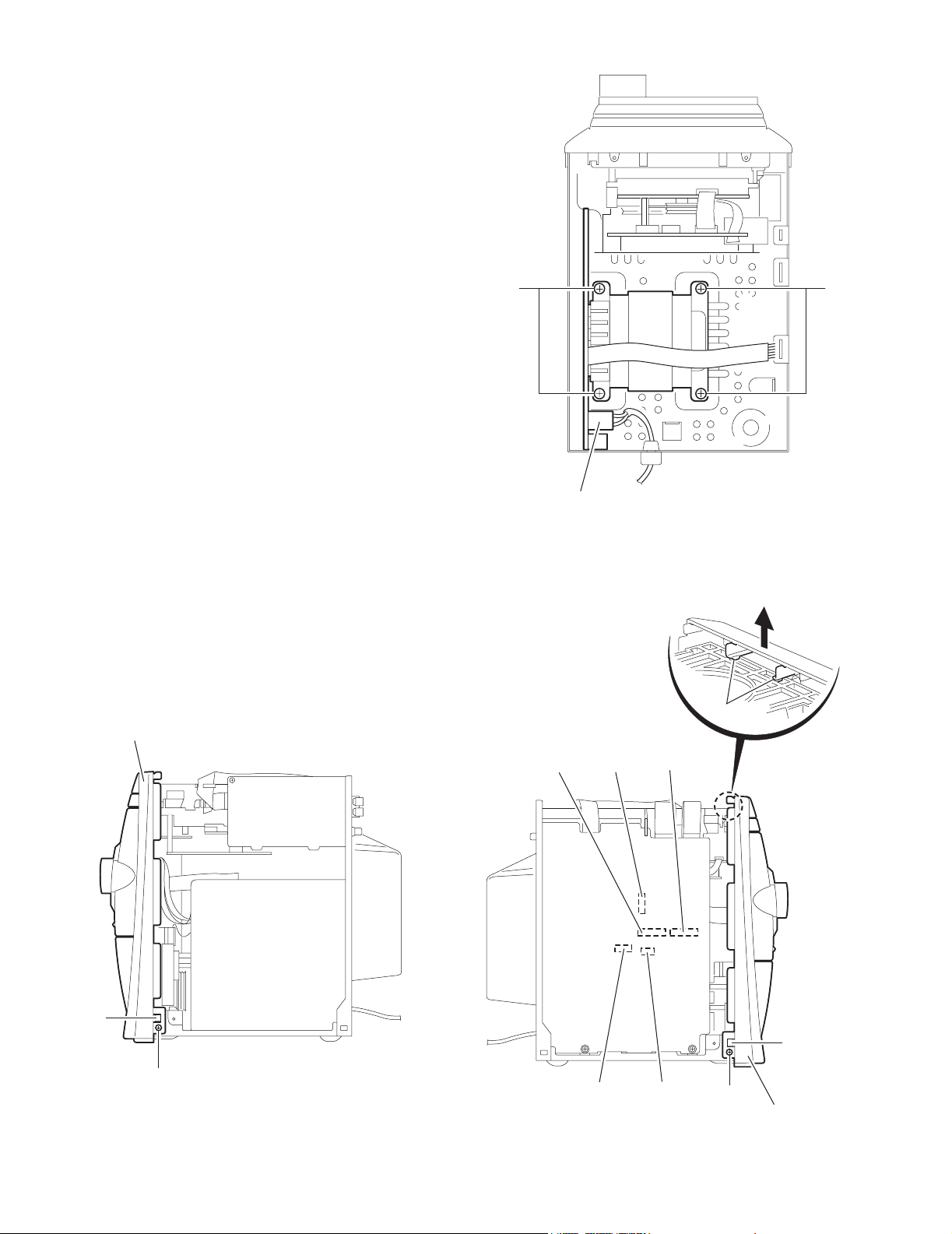
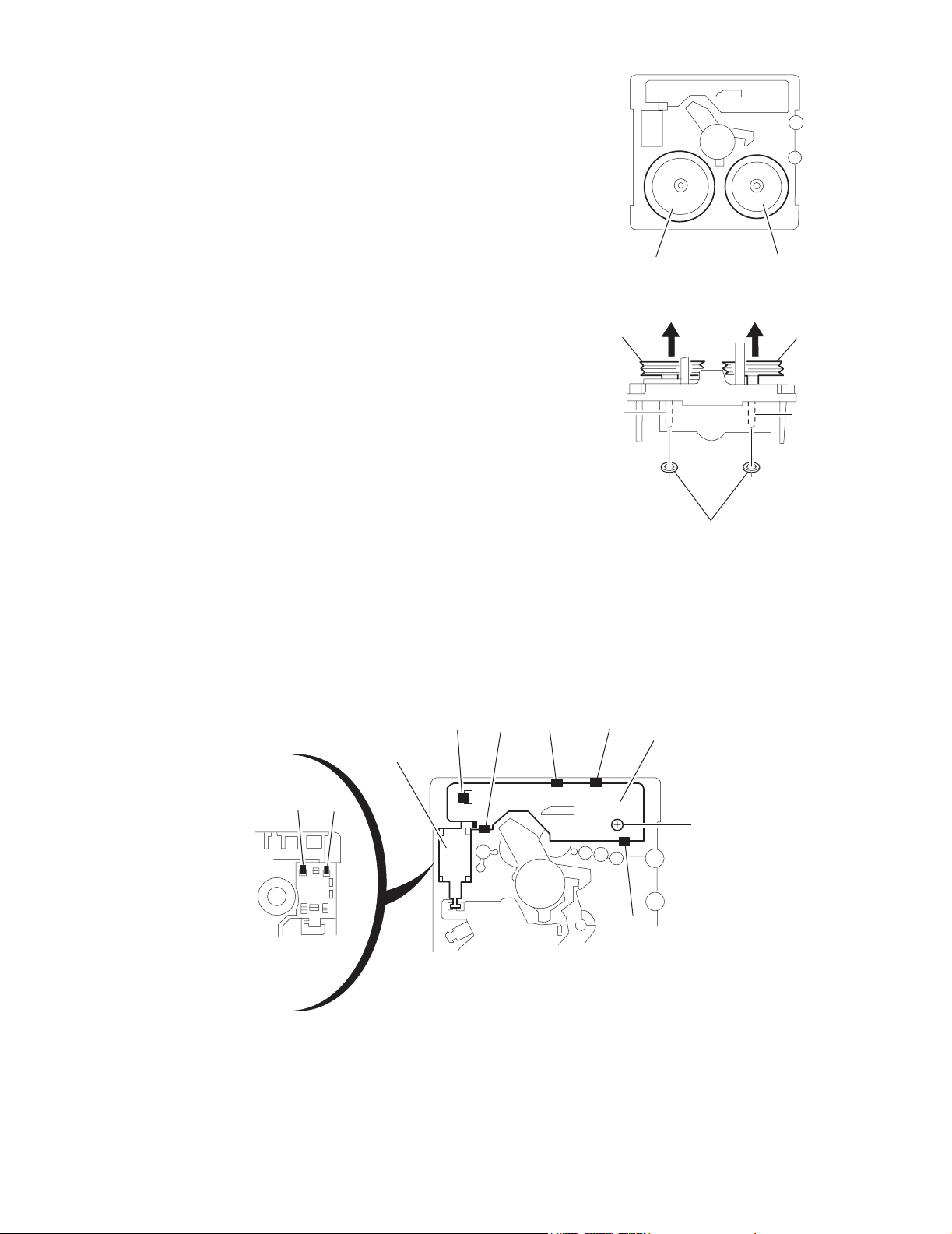
2.1.3 Removing the rear panel / fan assembly
(See Fig.5, 6)
• Prior to performing the following procedure, remove the metal
cover and the rear cover.
(1) Remove the eleven screws D attaching the rear panel. Re-
lease the two joints a on the rear side and the two joints
b on each side.
(2) Remove the two screws E attaching the fan bracket and
release the two joints c on the rear panel, and remove.
(3) Disconnect the wire from the connector CN916 on the main
board.
DD
a
Rear panel
EE
cc
Fan assembly
D
Main board
CN916
Fig.6
D
b
Fig.5
D
b
(No.22029)1-7
Page 8
UX-J60
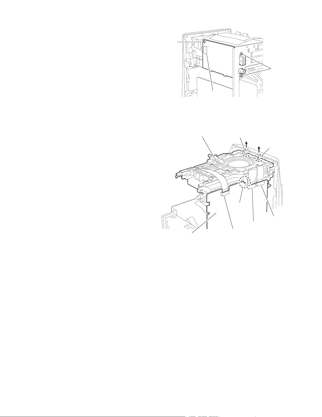
2.1.4 Removing the tuner board
(See Fig.7)
• Prior to performing the following procedure, remove the metal
cover.
(1) Disconnect the card wire from the connector CN1 on the
tuner board.
(2) Remove the two screws F on the rear side and the screw
G in the side.
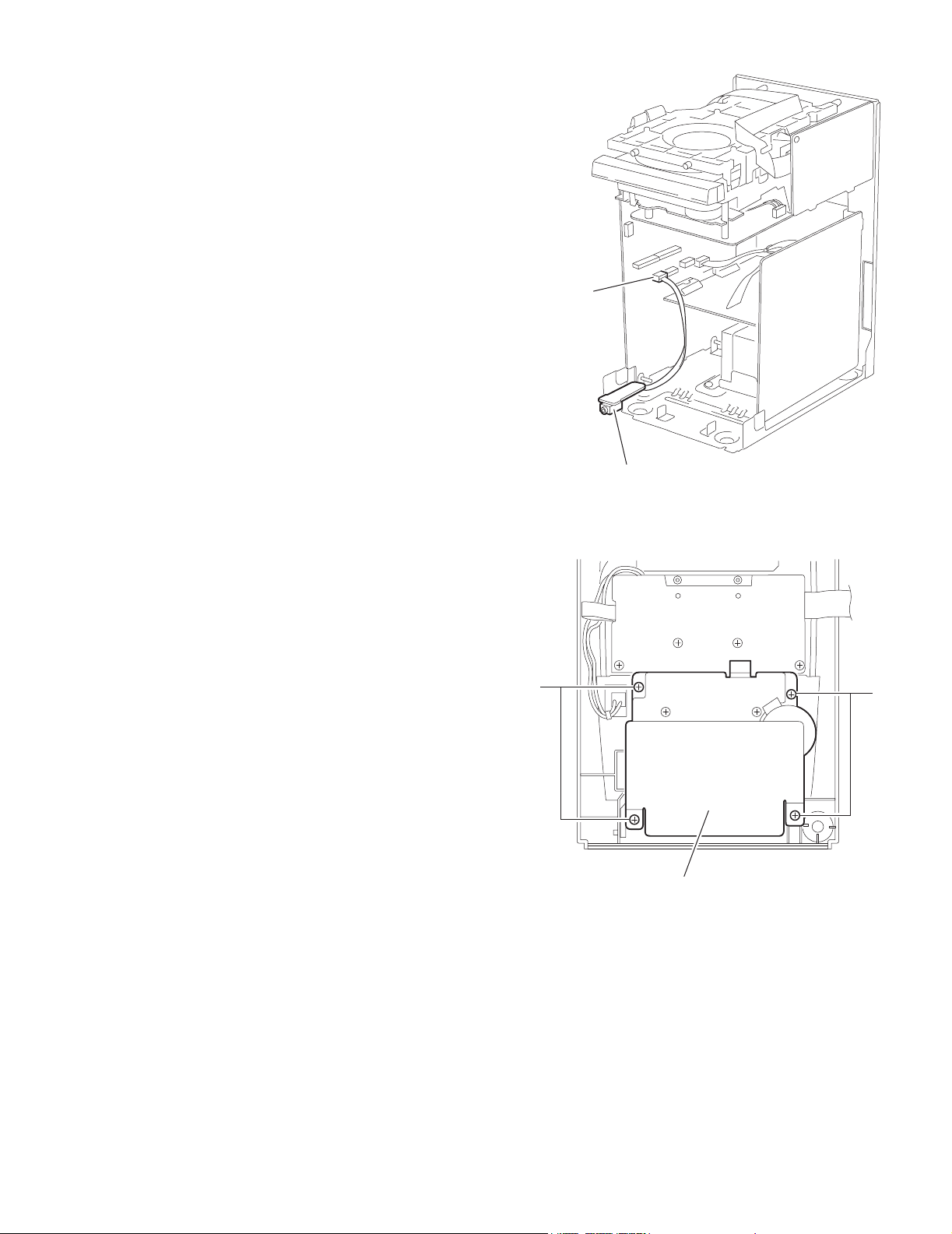
2.1.5 Removing the CD-R/RW mechanism assembly
(See Fig.8)
• Prior to performing the following procedure, remove the metal
cover, the rear cover, the rear panel and the tuner board.
(1) Disconnect the card wire from the connector CN903,
CN902 and CN904 on the main board.
(2) Pull the joint d in the direction of the arrow and remove the
CD-R/RW mechanism assembly backward while releasing
the joint e .
G
Tuner board
CN1
Fig.7
CD-R/RW mechanism assembly
F
d
d
Main board
e
CN903
CN904
CN902
Fig.8
1-8 (No.22029)
Page 9
UX-J60
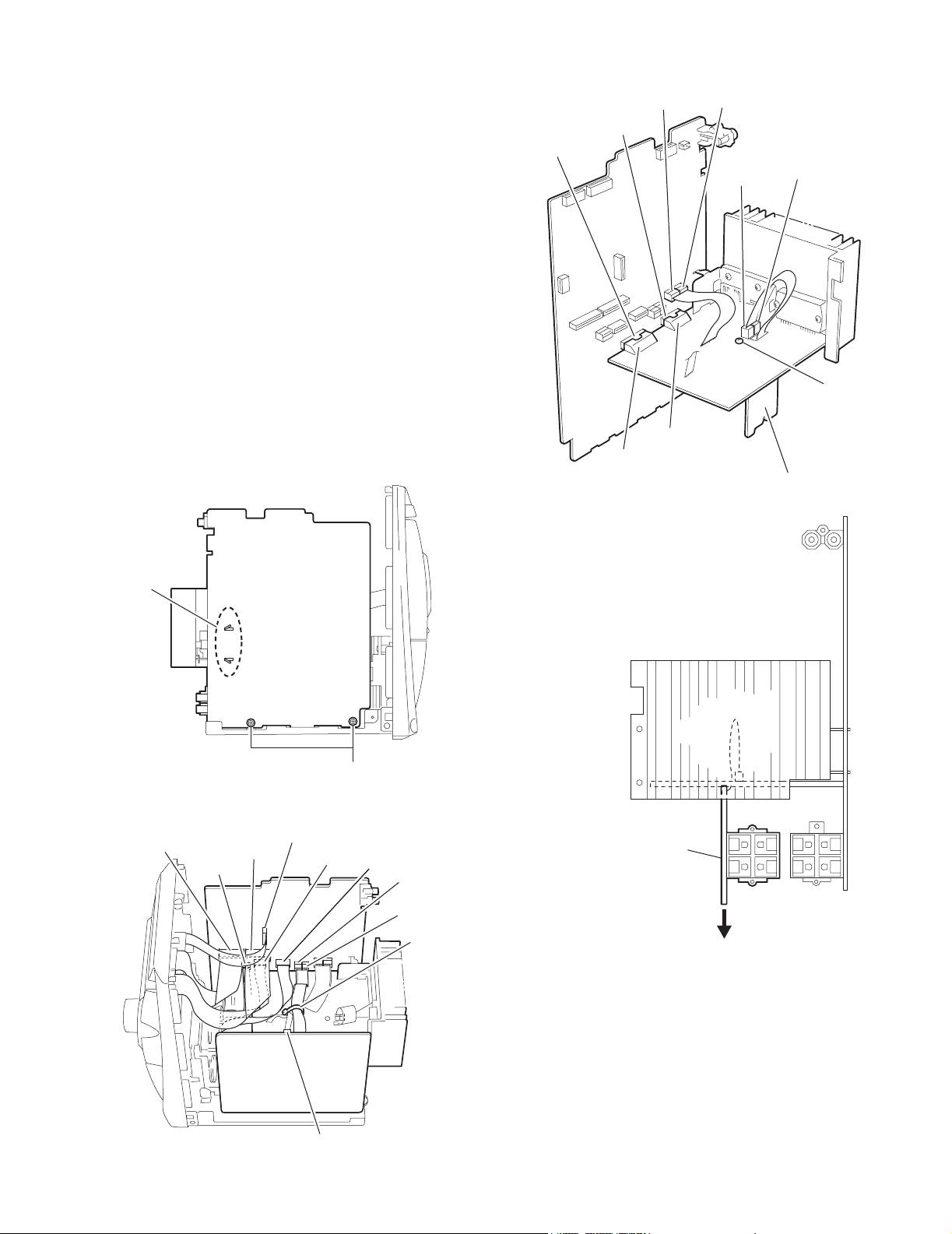
2.1.6 Removing the main board / the heat sink board / the
speaker jack board
(See Fig.9~12)
• Prior to performing the following procedure, remove the metal
cover, the rear cover, the rear panel, the tuner board and the
CD-R/RW mechanism assembly.
(1) Remove the two screws H attaching the main board.
(2) Disconnect the card wire from the connector CN900,
CN901, CN930, CN931 and CN932, and disconnect the
flat wire from the connector CN913, CN917 and CN918 on
the main board.
(3) Remove the band and disconnect the flat wire from the
connector CN951 on the power transformer assembly, and
then remove the main board / the heat sink board / the
speaker jack board from the body.
(4) Release the two joints f of the main board and disconnect
the connector CN944 and CN945 of the heat sink board
from the connector CN912 and CN911 of the main board
respectively, and disconnect the flat wire from the connector CN914 and CN915, and remove.
(5) Remove the screw I attaching the speaker jack board and
disconnect the flat wire from the connector CN946 and
CN947 on the heat sink board, and then remove the speaker jack board.
CN912
CN911
CN944
CN915
CN945
Main board
CN914
Heat sink board
CN946
Speaker jack board
Fig.11
CN947
I
f
CN930
CN913
CN931
Fig.9
Main board
CN932
CN901
H
CN900
CN917
CN918
Band
Speaker jack board
Fig.12
Power transformer assembly
CN951
Fig.10
(No.22029)1-9
Page 10
UX-J60
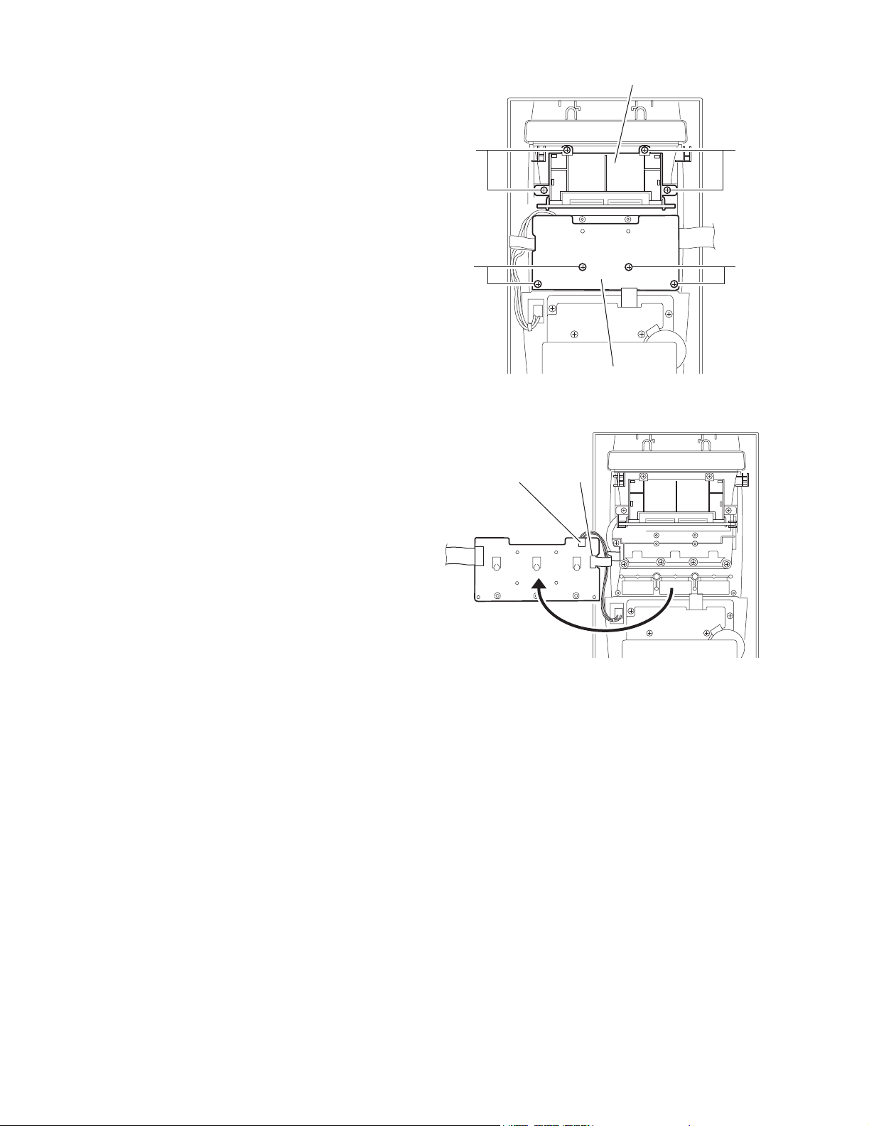
2.1.7 Removing the power transformer assembly
(See Fig.13)
• Prior to performing the following procedure, remove the metal
cover, the rear cover, the rear panel, the CD-R/RW mechanism assembly and the main board.
(1) Disconnect the power cord from the connector J1000 on
the power transformer assembly.
(2) Remove the four screws J .
JJ
2.1.8 Removing the front panel assembly
(See Fig.14,15)
• Prior to performing the following procedure, remove the metal
cover.
(1) Remove the two screws K on each side. Release the two
joints g on the both sides and lift the front panel assembly
to release the joint h .
(2) Disconnect the card wire from the connector CN900,
CN901, CN930, CN931 and CN932 on the main board.
Front panel assembly
Powe transformer assembly
J1000
Fig.13
h
Main board
CN932CN931 CN930
g
1-10 (No.22029)
K
Fig.14
CN900
CN901
Fig.15
g
K
Front panel assembly
Page 11
2.1.9 Removing the phones board
(See Fig.16)
• Prior to performing procedure, remove the metal cover and the
front panel assembly.
(1) Disconnect the flat wire from the connector CN913 on the
main board.
UX-J60
Mian board
CN913
2.1.10 Removing the cassette mechanism assembly
(See Fig.17)
• Prior to performing the following procedure, remove the metal
cover and the front panel assembly.
(1) Remove the four screws L attaching the cassette mecha-
nism assembly.
Phones board
Fig.16
L
Cassette mechanism assembly
Fig.17
L
(No.22029)1-11
Page 12
UX-J60
2.1.11 Removing the switch board
(See Fig.18,19)
• Prior to performing the following procedure, remove the metal
cover and the front panel assembly.
(1) Remove the four screws M attaching the switch board.
(2) Move the switch board in the direction of the arrow to dis-
connect the wire from the connector CN762 and the card
wire from the connector CN761.
2.1.12 Remove the LCD board assembly
(See Fig.18)
• Prior to performing the following procedure, remove the metal
cover and the front panel assembly.
(1) Remove the four screws N attaching the LCD board as-
sembly.
M
Switch board
CN762 CN761
LCD board assembly
NN
M
Switch board
Fig.18
Fig.19
1-12 (No.22029)
Page 13
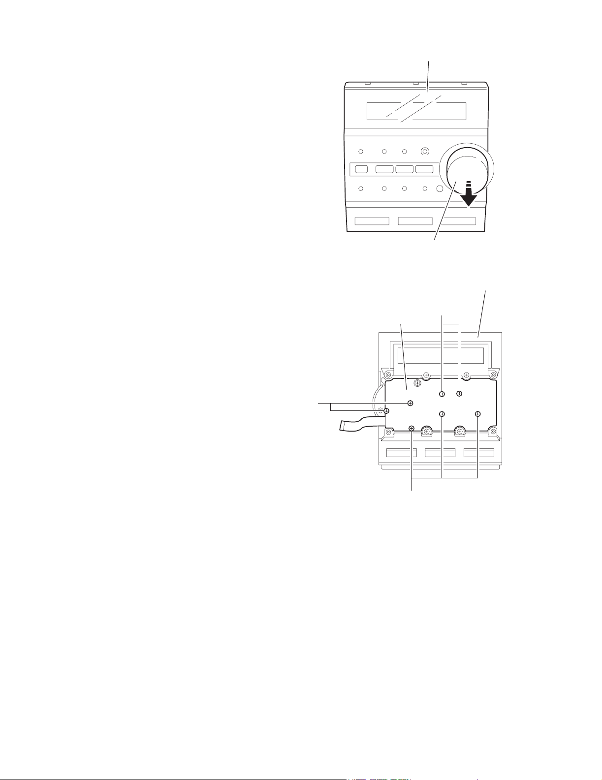
2.1.13 Removing the control panel assembly
(See Fig.20,21)
• Prior to performing the following procedure, remove the metal
cover, the front assembly, the switch board and the LCD board
assembly.
(1) Remove the three screws O attaching the control panel as-
sembly.
(2) Release the three joints i and open the cassette door
while pressing the cassette door, and then remove the control panel assembly in the direction of the arrow.
UX-J60
O
O
Fig.20
i
Cotrol panel assembly
Fig.21
(No.22029)1-13
Page 14
UX-J60
2.1.14 Remiving the control board
(See Fig.22,23)
• Prior to performing the following procedure, remove the metal
cover, the front panel assembly, the switch board, the LCD
board assembly and the control panel assembly.
(1) Pull out the volume knob.
(2) Remove the seven screws P attaching the control board.
Control panel assembly
Volume knob
Fig.22
Control panel assembly
P
Control board
P
P
Fig.23
1-14 (No.22029)
Page 15
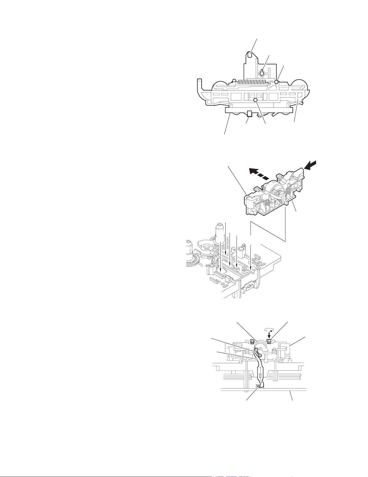
2.2 Cassette mechanism assembly
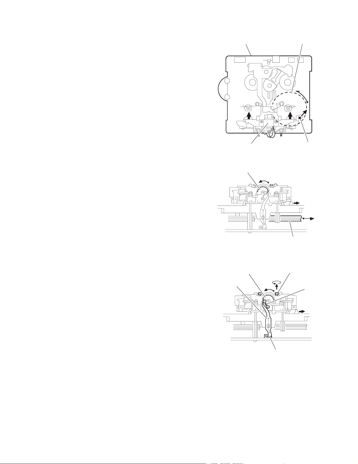
2.2.1 Removing the Play/Record & Clear head
(See Fig.1~3)
(1) While moving the trigger arm on the right side of the head
mount in the direction of the arrow, turn the flywheel R
counterclockwise until the head mount comes ahead and
clicks.
(2) The head turns counterclockwise as you turn the flywheel
R counterclockwise (See Fig.2 and 3).
(3) Disconnect the flexible wire from connector CN31 on the
head amplifier & mechanism control board.
(4) Remove the spring from the back of the head.
(5) Loosen the azimuth screw for reversing attaching the head.
(6) Remove the head on the front side of the head mount.
Cassette mechanism assembly
Fig.1
Head
UX-J60
Fly wheelR
Trigger armHead mount
Flexible wire
Fly wheel R
Fig.2
Azimuth screw
Head
for reversing
Spring
CN31
Head amplifer & mecha control board
Fig.3
(No.22029)1-15
Page 16
UX-J60
2.2.2 Removing the head amplifier & mechanism control board
(See Fig.4)
(1) Turn over the cassette mechanism assembly and remove
the three screws A attaching the head amplifier & mechanism control board.
(2) Disconnect the flexible wire from connector CN31 on the
head amplifier & mechanism control board.
(3) Disconnect connector CN32 of the head amplifier & mech-
anism control board from connector CN1 on the reel pulse
board.REFERENCE: If necessary, unsolder the 4-pin wire
soldered to the main motor.
2.2.3 Removing the main motor
(See Fig.4~7)
(1) Remove the two screws B .
(2) Half raise the motor and remove the capstan belt from the
motor pulley.
ATTENTION:
Be careful to keep the capstan belt from grease. When reassembling, refer to Fig.6 and 7 for attaching the capstan belt.
Head amplifier & mecha control board
Main motor assembly
Capstan belt
Fig.5
Main motor assembly
CN31
Flexible wire
A
AA
Fig.4
CN32
4pin wire
B
Main motor assembly
Motor pulley
Capstan belt
Fig.6
Main motor assembly
Fly wheel
1-16 (No.22029)
Capstan belt
Motor pulley
Fig.7
Page 17
2.2.4 Removing the flywheel
(See Fig.8, 9)
• Prior to performing the following procedure, remove the head
amplifier & mechanism control board and the main motor assembly.
(1) From the front side of the cassette mechanism, remove the
slit washers attaching the capstan shaft L and R. Pull out
the flywheels backward.
UX-J60
Fly wheel R Fly wheel L
Fig.8
Fly wheel R
Capstan shaft R Capstan shaft L
Slit washer
Fig.9
2.2.5 Removing the reel pulse board and solenoid
(See Fig.10)
• Prior to performing the following procedure, remove the head amplifier & mechanism control board.
(1) Remove the screw C.
(2) Release the tab a, b, c, d and e retaining the reel pulse board.
(3) Release the tab f and g attaching the solenoid on the reel pulse board.
(4) The reel pulse board and the solenoid come off.
d
Reel pulse board
Solenoid
a
bc
Fly wheel L
g
f
C
e
Fig.10
(No.22029)1-17
Page 18
UX-J60
r
r
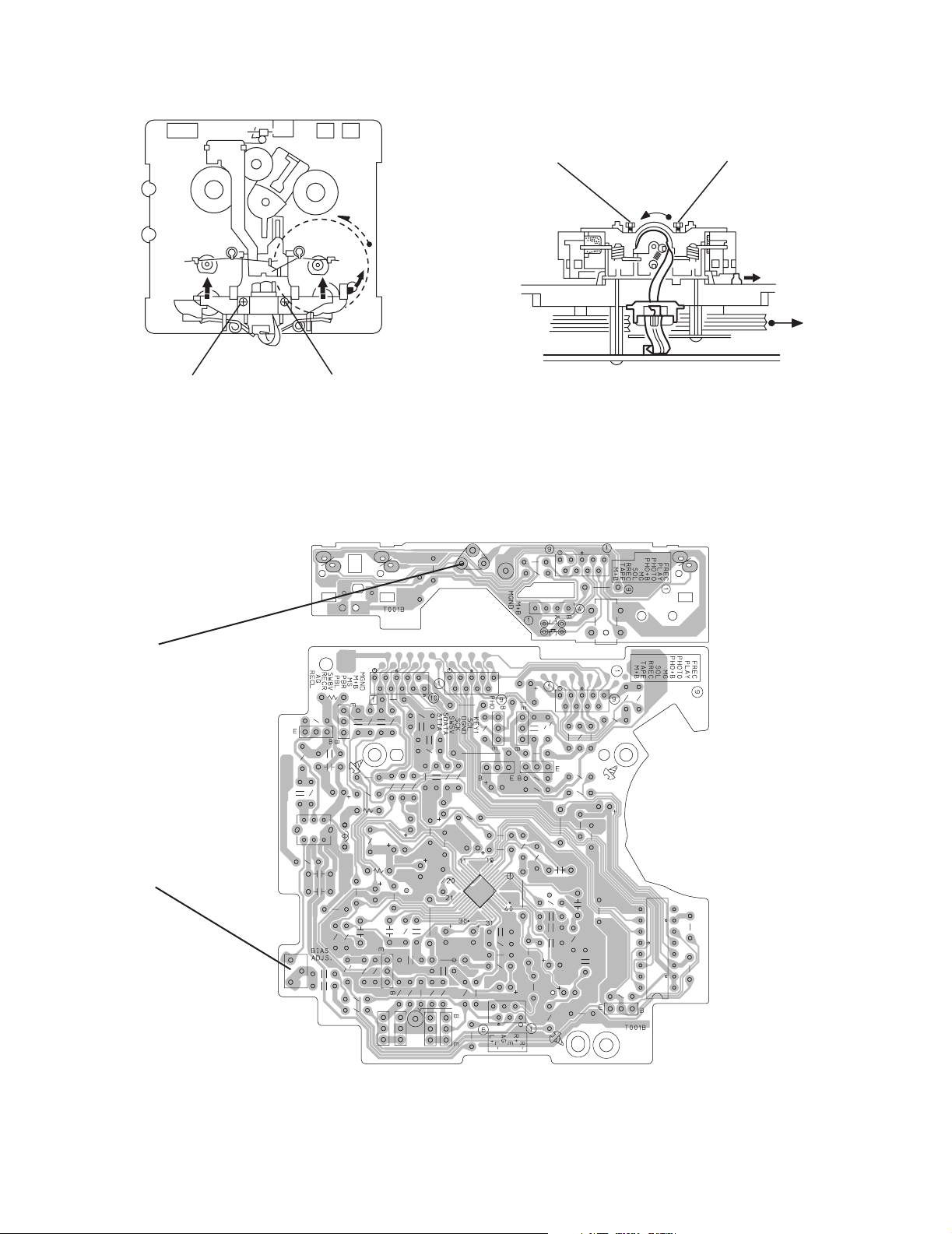
2.2.6 Reattaching the Play/ Record & Clear head
(See Fig.11~13)
(1) Reattaching the head mount assembly.
a) Change front of the direction cover of the head
mount assembly to the left (Turn the head forward).
b) Fit the bosses O', P', Q', U' and V' on the head mount
assembly to the holes P and V, the slots O, U and Q
of the mechanism sub assembly (See Fig.11 to 13).
CAUTION:
To remove the head mount assembly, turn the direction
cover to the left to disengage the gear. If the gear can not
be disengaged easily, push up the boss Q' slightly and
raise the rear side of the head mounts slightly to return
the direction lever to the reversing side.
(2) Tighten the azimuth screw for reversing.
(3) Reattach the spring from the back of the Play/ Record &
Clear head.
(4) Connect the flexible wire to connector CN31 on the head
amplifier & mechanism control board.
U' Q'
Head mount assembly
Head mount assembly
O'
Fig.11
P'
P'
V'
V'
Direction cove
Spring
Flexible wire
V
O
P
Q
Head
Direction cove
U
Fig.12
Azimuth screw for reversing
Head mount
1-18 (No.22029)
CN31
Fig.13
Head amplifier &
mechanism control board
Page 19
3.1 Adjustment method
V
V
a
)
e
t
F
r
8
t
e
UX-J60
SECTION 3
Adjustment
Measurement Instruments Required for
Adjustment
1. Low frequency oscillator
This oscillator should have a capacity to output
0dBs to 600 at an oscillation frequency of
50Hz-20kHz.
2. Attenuator impedance : 600
3. Electronic voltmeter
4. Distortion meter
5. Frequency counter
6. Wow & flutter meter
7. Test tape
VT703L : Head azimuth
VT712 : Tape speed and running unevenness
(3kHz)
VT724 : Reference level (1kHz)
8. Blank tape
TYPE : AC-225
TYPE : AC-514
9. Torque gauge : For play and back tension
FWD(TW2111A), REV(TW2121a) and
FF/REW(TW2231A)
10. Test disc: CTS-1000
Measurement conditions
Power supply voltage
AC 230V ~ , 50Hz
Reference output : Speaker : 0.775V/4
: Headphone : 0.077V/32
Reference frequency and
input level ------------------------------ 1kHz, AUX : -8dBs
Measurement output terminal ------- at Speaker J3002
Load resistance --------------------------- 4
Radio Input signal
AM frequency --------------------------------------- 400Hz
AM modulation ---------------------------------------- 30%
FM frequency --------------------------------------- 400Hz
FM frequency deviation ------------------------ 22.5kHz
Tuner section
FM tuning range: 87.5MHz~108.00MHz
AM tuning range: 522kHz~1,629kHz
Voltage applied to tuner +B : DC5.7
VT : DC 12
Reference measurement
output 26.1mV(0.28V)/3
Input positions AM : Standard loop antenn
FM : TP1 (hot) and TP2 (GND
Standard measurement position of volume
Function switch to Tap
Beat cut switch to Cu
Super Bass/Active hyper Bass to OF
Bass Treble to Cente
Adjustment of main volume to reference output
VOL : 2
Precautions for measurement
1. Apply 30pF and 33k to the IF sweeper output
side and 0.082 F and 100k in series to the
sweeper input side.
2. The IF sweeper output level should be made as
low as possible within the adjustable range.
3. Since the IF sweeper is a fixed device, there is no
need to adjust this sweeper.
4. Since a ceramic oscillator is used, there is no need
to perform any MIX adjustment.
5. Since a fixed coil is used, there is no need to adjus
the FM tracking.
6. The input and output earth systems are separated.
In case of simultaneously measuring the voltage in
both of the input and output systems with an
electronic voltmeter for two channels, therefore, the
earth should be connected particularly carefully.
7. In the case of BTL connection amp., the minus
terminal of speaker is not for earthing. Therefore, b
sure not to connect any other earth terminal to this
terminal. This system is of an BTL system.
8. For connecting a dummy resistor when measuring
the output, use the wire with a greater code size.
9. Whenever any mixed tape is used, use the band
pass filter (DV-12).
(No.22029)1-19
Page 20
UX-J60
3.2 Cassette mechanism adjustment
Head azinuth
adjustment screw
(Forward side)
Mecha control board
Head azinuth
adjustment screw
(Reverse side)
SW1
SW2
Head azinuth
adjustment screw
(Forward side)
Head azinuth
adjustment screw
(Reverse side)
CN31
R/P head, Erase head
P1
D1
VR37
R371
CN1
FW100
SW5
Motor speed
VR37
BIAS adjust
VR31
C308
R327
VR31
R313
Q302
R315
C316
C319
C221
R314
L301
C121
C314
R104
Q305
C313
D340
C310
R304
R310
C107
L303
R102
R121
R221
R303
R335
R353
R339
R108
C113
R302
Q343
C301
C103
C207
R301
Q342
C105
C205
C304
R208
C106
R101
C104
R306
R106
Q344
CN34
C306
R344
R105
C102
R205
R110
Q345
R345
C307
R336
C340
C206
R346
R206
W1
R107
Q346
R305
C110
R210
C300
C341
R109
R372
Q372
C371
CN33
IC32
R116
C109
CN31
Q371
C101
C374
R376
R216
Q375
C376
R204
R201
C202
C204
C201
CN32
C203
R202
C210
R340
C331
R342
R347
Q347
SW6
R343
R341
IC33
IC1
D375
Q376
R338
R375
R337
C213
C342
C209
W1
R207
1-20 (No.22029)
Page 21
3.2.1 Mechanism section
t
W
t
t
UX-J60
Item Condition Measurement method Ref.value
Head
azimuth
Test tape
: VT703L (8kHz)
Output terminal
: Speaker out
1.Playback the test tape VT703L (8kHz).
2.Adjust to maximum output level by azimuth
adjustment screw for forward side and reverse
side.
Maximum
output
3.This adjustment is adjust by adjustment screw
of forward side and adjustment screw of reverse
side.
Tape speed
Test tap
: VT712 (3kHz)
Output terminal
Playback the test tape VT712 (3kHz) at end of
forward side,adjust to 2,940~3,90Hz indication
of frequency counter by VR37.
2,940 ~
3,090Hz
: Speaker out or
Headphone out
Adjustmen
position
Only adjus
at changed
head
VR37
Item Condition Measurement method Ref.value
Tape speed
diviation at
FWD/REV
Test tape
: VT712 (3kHz)
Output terminal
Playback the test tape VT712 (3kHz) at end
of forward and reverse, tape speed deviation
should be less than 6.0Hz.
Leass than
6.0Hz
: Speaker out or
Headphone out
ow & Flutter Playback the test tape VT712 (3kHz) at
Test tape
: VT712 (3kHz)
Output terminal
start of forward and reverse,Wow & Flutter
are should be less than 0.25%(WRMS).
Less than
0.25%
(WRMS)
: Speaker out or
Headphone out
Adjustmen
position
VR31
(No.22029)1-21
Page 22
UX-J60
R
t
3.2.2 Electrical adjustment
Item Condition Measurement method Ref.value
Recording
BIAS
adjustment
Forward or Reverse
Test tape
:AC-514 TYPE
:AC-225 TYPE
Output terminal
Recording head
1.Set the test tape(AC-514 TYPE and
AC-225 TYPE ), then make REC/PAUSE
condition.
2.Connect 100 to recording head by series,
then connect to VTVM for measurement the
current.
AC-225
:4.20 A
AC-514
:4.0 A
3.After setting, start the recording by release
the PAUSE, in this time bias current adjust
to next fig. by VR31 for Lch and VR32 for
Rch.
4.0 A (TYPE ) and 4.20 A (TYPE ).
R/P
playback
frequency
response
Reference frequency
: 1kHz / 10kHz
(Reference: -20dB)
Test tape
: AC-514 TYPE
Input terminal
: OSC IN
1.Set the test tape (AC-514 TYPE ), then
make REC/PAUSE condition.
2.Release the PAUSE, then start recording
the 1kHz and 10kHz of reference frequency
from oscillator.
3.Playback the recorded position, 1kHz and
10kHz output deviation should -1dB 2dB
Output
deviation
1kHz/10kHz
:-1dB 2dB
to readjust by VR31 for Lch and VR32 for
Rch.
Adjustment
position
VR31
VR31
3.2.3 Electrical response confirmation
Item Condition Measurement method Ref.value
ecording
bias
current
Forward or Reverse
Test tape
: TYPE (AC-514)
Measurement
terminal
: BIAS test point on
printed circuit board
Erase
current
(reference
value)
Forward or Reverse
Rec condition
Test tape
: AC-514 TYPE
: AC-225 TYPE
Measurement
terminal
: Both side of Erase
head
1.Change BIAS1 and 2, confirm the frequency
should be change.
2.Set the test tape (AC-514 TYPE ), then
make REC/PAUSE condition.
3.Confirm the frequency should 100Hz 6kHz
at BIAS test point on printed circuit board.
1.Set the test tape (AC-514 TYPE and
AC-225 TYPE ), then make REC/PAUSE
condition.
2.Release the PAUSE to REC condition,
connect 1W to ERASE head by series, then
confirm the erase current at both side of
erase head.
Adjustmen
position
100 kHz
6 kHz
TYPE
: 120 mA
TYPE
: 75 mA
1-22 (No.22029)
Page 23
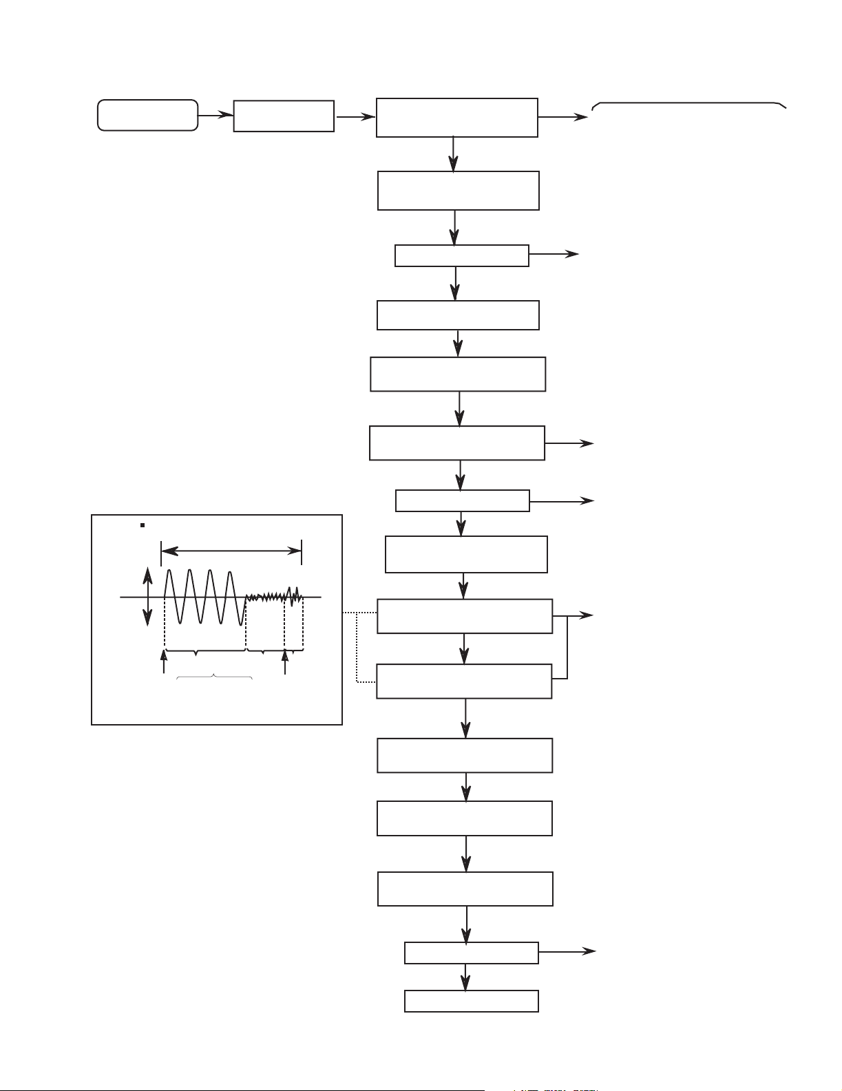
3.3 Flow of functional operation until TOC read (CD)
Power ON
Power Key
Slider turns REST
SW ON.
Automatic tuning
of TE offset
UX-J60
Check Point
Check that the voltage at the pin 5
of CN801 is 0V?
VREF
Tracking error waveform at TOC reading
pin 20 of
IC601(TE)
Approx
1.7V
Tracking
servo
Disc start
to rotate
off
Automatic measurement
of TE amplitude and
automatic tuning of
TE balance
Approx.1sec
Tracking
servo ON
Disc to be
braked to stop
TOC reading
finishes
500mv/div
2ms/div
Fig.1
Laser ON
Detection of disc
Automatic tuning of
Focus offset
Automatic measurement of
Focus S-curve amplitude
Disc is rotated
Focus servo ON
(Tracking servo ON)
Automatic measurement of
Tracking error amplitude
Automatic tuning of
Tracking error balance
Check that the voltage at the
pin2 of IC601 is 4.4V?
Confirm that the Focus error
S-cuve, ie at the pin23 of
IC601 is approx.2Vp-p
Confirm that the siganl from
pin 5,6 of IC801 is a 2V
accelerated pulse with approx.
700ms.
Confirm the waveform of
the Tracking error signal
at the pin20 of IC601
(See fig-1)
Automatic tuning of
Focus error balance
Automatic tuning of
Focus error gain
Automatic tuning of
Tracking error gain
TOC reading
Play a disc
Confirm the eye-pattern
at the lead of TP1
(No.22029)1-23
Page 24
UX-J60
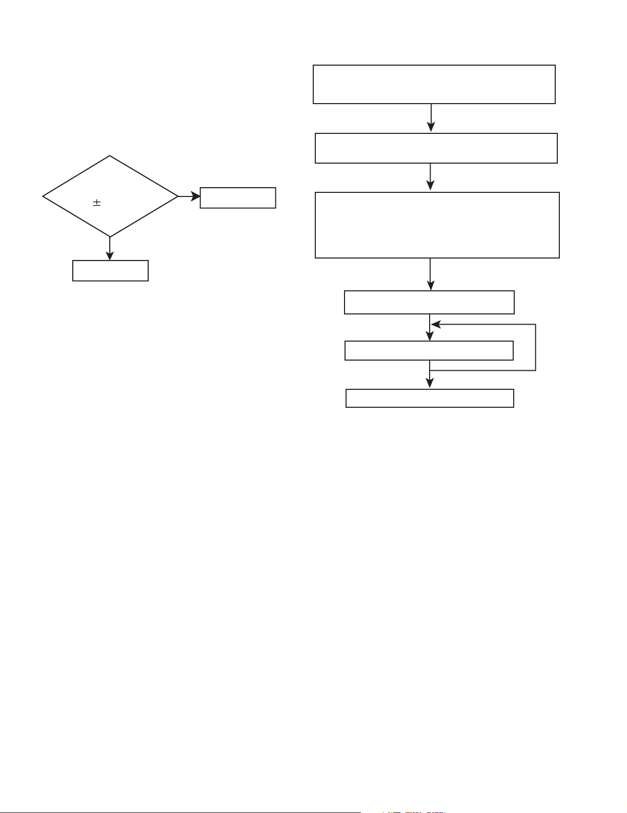
3.4 Maintenance of laser pickup (CD)
(1) Cleaning the pick up lens
Before you replace the pick up, please try to clean the lens
with a alcohol soaked cotton swab.
(2) Life of the laser diode
When the life of the laser diode has expired, the following
symptoms will appear.
• The level of RF output (EFM output: ampli tude of eye
pattern) will be low.
Is the level of
RFOUT under
1.25V 0.22Vp-p?
NO
Replace it.
YES
O.K
(3) Semi-fixed resistor on the APC PC board
The semi-fixed resistor on the APC printed circuit board
which is attached to the pickup is used to adjust the laser
power.Since this adjustment should be performed to match
the characteristics of the whole optical block, do not touch
the semi-fixed resistor.
If the laser power is lower than the specified value,the laser
diode is almost worn out, and the laser pickup should be replaced. If the semi-fixed resistor is adjusted while the pickup is functioning normally, the laser pickup may be
damaged due to excessive current.
3.5 Replacement of laser pickup (CD)
Turn off the power switch and, disconnect the
power cord from the ac outlet.
Replace the pickup with a normal one.(Refer
to "Pickup Removal" on the previous page)
Plug the power cord in, and turn the power on.
At this time, check that the laser emits for
about 3seconds and the objective lens moves
up and down.
Note: Do not observe the laser beam directly.
Play a disc.
Check the eye-pattern at TP1.
Finish.
1-24 (No.22029)
Page 25

Description of major ICs
4.1 AN22000A-W (IC601) : RF & SERVO AMP
• Terminal layout
• Block diagram
RFOUT
RF_EQ
32
31
30
29
27
28
AMP
AMP
AMP
AMP17GCA BCA
+
-
ACBDPDF
323130292827262524232221201918
123456789
LD
PD
PDE
TBAL
RFN
VCC
RFIN
CAGC
RFOUT
624754 8
RFIN
AGC
NRFDET
GCA BCA
GCA BCA
GCA BCA
FBAL
GCTRL
FEOUT
FEN
10111213141516
ARF
CEA
CBDO
3TOUT
11 12
BDO
TEN
TEOUT
BDO
COFTR
SUBT
SUBT
TEBPF
OFTR
VDET
VREF
17
GND
RFDET
13 14
OFTR
3TENV
VDET
SECTION 4
9
10
15
22
-
+
-
+
-
+
23
21
20
19
18
2
LD
• Pin function
Pin
Symbol I/O Function
No.
1 PD I APC Amp. input terminal
2 LD O APC Amp. output terminal
3 VCC - Power supply terminal
4 RFN I RF adder Amp. inverting input terminal
5 RFOUT O RF adder Amp. output terminal
6 RFIN I AGC input terminal
7 CAGC I Input terminal for AGC loop filter capacitor
8 ARF O AGC output terminal
9 CEA I Capacitor connecting terminal
for HPF-Amp.
10 3TOUT O 3 TENV output terminal
11 CBDO I Capacitor connecting terminal for envelope
detection on the darkness side
12 BDO O BDO output terminal
13 COFTR I Capacitor connecting terminal for envelope
detection on the light side
14 OFTR O OFTR output terminal
15 NRFDET O NRFDET output terminal
16 GND - Ground
17 VREF O VREF output terminal
18 VDET O VDET output terminal
19 TEBPF I VDET output terminal
20 TEOUT O TE Amp. output terminal
21 TEN I TE Amp. inverting input terminal
22 FEN I FE Amp. inverting input terminal
23 FEOUT O FE Amp. output terminal
24 GCTL O GCTL & APC terminal
25 FBAL O FBAL control terminal
26 TBAL O TBAL control terminal
27 E I Tracking signal input terminal 1
28 F I Tracking signal input terminal 2
29 D I Focus signal input terminal 4
30 B I Focus signal input terminal 3
31 C I Focus signal input terminal 2
32 A I Focus signal input terminal 1
UX-J60
GCTL26TBAL
25 16 3
FBAL
PD
1
(No.22029)1-25
Page 26

UX-J60
4.2 HA12238F (IC32) : R/P Equalizer
• Pin layout
PB-NF1(L)
TEST 2
RIP
PBIN(l)
REC Return
GND
PBIN(R)
NC
TEST 3
PB-NF1(R)
31
32
33
34
35
36
37
38
39
40
PB-NF2(L)
PB-EQ(L)
30
29
+
Return SW
Return SW
+
-
EQ OUT(L)
TAI(L)
28
27
MUTE
MUTE
NC
PB OUT(L)
26
25
REC IN(L)
ALC(L)
24
23
NC
22
EQ
EQ
REC OUT(L)
21
ALC
TEST
20
(Open for nomal use)
19
Iraf
18
GND
ALC DET
17
16
Vcc
REC MUTE OFF/ON
15
MUTO ON/OFF
14
REC RETURN ON/OFF
13
TEST 4
12
ALC ON/OFF
11
1
2
PB-EQ(R)
PB-NF2(R)
3
4
TAI(R)
EQOUT(R)
5
6
NC
PB OUT(R)
7
8
ARC(R)
REC IN(R)
9
10
NC
REC OUT(R)
1-26 (No.22029)
Page 27

• Pin function
Pin No. Symbol Function
1 PB-NF2(R) PB EQ feed back
2 PB-EQ(R) NAB output
3 EQOUT(R) EQ output
4 TAI(R) Tape input
5 PBOUT(R) PB output
6 NC NC pin
7 REC IN(R) REC-EQ input
8 ALC(R) ALC(R) signal out put
9 NC NC pin
10 REC OUT(R) REC output
11 ALC ON/OFF Mode control input
12 TEST4 TEST pin
13 REC Return ON/OFF Mode control input
14 MUTE ON/OFF Mode control input
15 REC Return ON/OFF Mode control input
16 Vcc Vcc Pin
17 ALC DET ALC detection signal out put
18 GND GND pin
19 I REF Equalizer reference current input
20 Test mode Test modepin
21 REC OUT(L) REC output
22 NC NC pin
23 ALC(L) ALC(L) signal out put
24 REC IN(L) REC-EQ input
25 NC NC pin
26 PBOUT(L) PB output
27 TAI(L) Tape input
28 EQOUT(L) EQ output
29 PB-EQ(L) NAB output
30 PB-NF2(L) PB EQ feed back
31 PB-NF1(L) PB EQ feed back
32 TEST2 TEST pin
33 RIP Ripple fillter
34 PBIN(L) PB input
35 REC-RETURN REC Return
36 GND GND pin
37 PBIN(R) PB input
38 NC NC pin
39 TEST3 TEST pin
40 PB-NF1(R) PB EQ feed back
UX-J60
(No.22029)1-27
Page 28

UX-J60
4.3 GP1UM261XK (IC750) : Receiver
• Pin layout
Vout
• Block diagram
GND
Vcc
4.4 HA17758A (IC902,IC944) : Dual Operational Amp
• Pin layout
8
7
6
5
VCC
Vout2
Vin(-)2
Vin(+)2
Vout1
Vin(-)1
Vin(+)1
VEE
1
1
- +
2
2
+ -
3
4
B.P.F.LimiterAmp
Demodulator
Integrator
Comparator
GND Vdd Vout
1-28 (No.22029)
Page 29

4.5 KIA7810API (IC942) : Regulater
• Pin Layout
• Block Diagram
UX-J60
1
R23R17R22
INPUT
Z1
R12
R11
Q12
Q13
R18
Q2
Q18
Q11R1
R2
R3
Q17
Q1
Q3
Q4
Q19
Q6
R7
Q14
Q5
Q19
C1
Q7
Q9 Q8
Q9
Q11-1
R10
R15
Q10
Q15
R14
R16
R20
R21
Q16
3
OUTPUT
R13
R4
R5 R6 R8
2
COMMON(GND)
(No.22029)1-29
Page 30

UX-J60
4.6 KIA78R08PI (IC943) :Regulater
• Pin Layout
• Block Diagram
1 2
V1N
V1N
Control
OUTPUT ON/OFF
4
BANDGAP
REFERENCE
CONTROL
ASO
PROTECTION
OVER HEAT
PROTECTION
3
GND
VO
-
+
1-30 (No.22029)
Page 31

4.7 KIA78S06P-T (IC932) : Regulator
•Pin layout
1 2 3
• Block diagram
UX-J60
3 INPUT
Z1
Q14
Q1
R9
Q16
Q2 Q7
R11 R10
R1
Q4
Q3
Q6
Q5
R4
Q11
C1
Q10
R2
Q9
Q8
R3
4.8 LB1641 (IC802) : DC Motor driver
•Pin layout •Truth table
1
GND
OUT1
P1
VZ
IN1
IN2
VCC1
VCC2
P2
OUT2
2
3
4
5
6
7
8
9
10
Input Output Mode
IN1 IN2 OUT1 OUT2
0000 Brake
1 0 1 0 CLOCKWISE
0 1 0 1 COUNTER-CLOCKWISE
1100 Brake
Q12
R8
Q13
R7R5R6
1 OUTPUT
2 COMMON
(No.22029)1-31
Page 32

UX-J60
4.9 LA1838 (IC1): FM AM IF AMP&detector, FM MPX Decoder
• Block Diagram
30
ALC
BUFF
FM
S-METER
FM IF
1
29
AM
OSC
S-CLRVE
PM
DET
2
28
REG
AM
MIX
SD
COMP
AM/FM
IF-BUFF
3
27
FM
RF.AMP
AM IF
4
26
AGC
AM
S-METER
GND
25
24
DET
TUNING
DRIVE
5
6
STEREO
DRIVE
7
22
23
P-DET
VCC
89
VCO
384KHz
21
DECODER
ANIT-BIRDIE
STEREO
5N
SW
10
20
FF
38k
11
18
19
MUTE
FF
/
19k
2
12 13
FF
19k
17 16
/LS
14
PILOT
DET
15
• Pin Function
Pin No. Symbol I/O Function
1 FM IN I This is an input terminal of FM IF signal.
2 AM MIX O This is an out put terminal for AM mixer.
3 FM IF I Bypass of FM IF
4 AM IF I Input of AM IF Signal.
5 GND - This is the device ground terminal.
6
7
TUNED
STEREO
O When the set is tunning,this terminal becomes "L".
O Stereo indicator output. Stereo "L", Mono: "H"
8 VCC - This is the power supply terminal.
9 FM DET - FM detect transformer.
10 AM SD - This is a terminal of AM ceramic filter.
11 FM VSM O Adjust FM SD sensitivity.
12 AM VSM O Adjust AM SD sensitivity.
13 MUTE I/O When the signal of IF REQ of IC121(LC72131) appear, the signal of FM/AM IF output. //Muting
control input.
14
15
FM/AM
MONO/ST
I Change over the FM/AM input. "H" :FM, "L" : AM
O Stereo : "H", Mono: "L"
16 L OUT O Left channel signal output.
17 R OUT O Right channel signal output.
18 L IN I Input terminal of the Left channel post AMP.
19 R IN I Input terminal of the Right channel post AMP.
20 RO O Mpx Right channel signal output.
21 LO O Mpx Left channel signal output.
22 MPX IN I Mpx input terminal
23 FM OUT O FM detection output.
24 AM DET O AM detection output.
25 AM AGC I This is an AGC voltage input terminal for AM
26 AFC - This is an output terminal of voltage for FM-AFC.
27 AM RF I AM RF signal input.
28 REG O Register value between pin 26 and pin28 besides the frequency width of the input signal.
29 AM OSC - This is a terminal of AM Local oscillation circuit.
30 OSC BUFFER O AM Local oscillation Signal output.
1-32 (No.22029)
Page 33

4.10 LA6541-X (IC801) : Servo driver
• Pin layout & Block diagram
Vcc Vref Vin4 Vg4 Vo8 Vo7
24 23
22
21
11k
ohm
UX-J60
20
19
Gnd
Vcc
Vo6 Vo5 Vg3 Vin3 Cd Res
18
17 16
15
14
13
11k
ohm
- +
- +
Level
shift
Level
shift
B T L
driver
B T L
driver
11k
ohm
1
Vcc Mute Vin1 Vg1 Vo1 Vo2 Vo3 Vo4 Vg2 Vin2 Reg
2
3456
Gnd
78 9101112
• Pin function
Pin No. Symbol Description
1 Vcc Power supply (Shorted to pin 24)
2 Mute All BTL amplifier outputs ON/OFF
3 Vin1 BTL AMP 1 input pin
4 Vg1 BTL AMP 1 input pin (For gain adjustment)
5 Vo1 BTL AMP 1 input pin (Non inverting side)
6 Vo2 BTL AMP 1 input pin (Inverting side)
7 Vo3 BTL AMP 2 input pin (Inverting side)
8 Vo4 BTL AMP 2 input pin (Non inverting side)
9 Vg2 BTL AMP 2 input pin (For gain adjustment)
10 Vin2 BTL AMP 2 input pin
11 Reg Out External transistor collector (PNP) connection. 5V power supply output
12 Reg In External transistor (PNP) base connection
13 Res
Reset output
14 Cd Reset output delay time setting (Capacitor connected externally)
15 Vin3 BTL AMP 3 input pin
16 Vg3 BTL AMP 3 input pin (For gain adjustment)
17 Vo5 BTL AMP 3 output pin (Non inverting side)
18 Vo6 BTL AMP 3 output pin (Inverting side)
19 Vo7 BTL AMP 4 output pin (Inverting side)
20 Vo8 BTL AMP 4 output pin (Non inverting side)
21 Vg4 BTL AMP 4 output pin (For gain adjustment)
22 Vin4 BTL AMP 4 output pin
23 Vref Level shift circuit's reference voltage application
24 Vcc Power supply (Shorted to pin 1)
B T L
driver
B T L
driver
Level
shift
Level
shift
11k
ohm
out
RESET
Regulator
Reg
In
(No.22029)1-33
Page 34

UX-J60
4.11 LC72136N (IC2) : PLL frequency synthesizer
• Pin layout
1
XT
FM/AM
CE
DI
CLOCK
DO
FM/ST/VCO
AM/FM
SDIN
2
3
4
5
6
7
8
9
10
11
22
21
20
19
18
17
16
15
14
13
12
XT
GND
LPFOUT
LPFIN
PD
VCC
FMIN
AMIN
IFCONT
IFIN
• Block diagram
1
22
16
15
3
4
5
6
17
21
1/2
C
I/F
2B
Power
on
Reset
Data Shift Register & Latch
782
• Pin function
Pin
No.
Symbol I/O Function
1 XT I X'tal oscillator connect (75kHz)
2FM
/AM O LOW:FM mode
3 CE I When data output/input for 4pin(input)
and 6pin(output): H
4 DI I Input for receive the serial data from
controller
5 CLOCK I Sync signal input use
6 DO O Data output for Controller Output port
7 FM/ST/VCO O Low: MW mode
8AM
/FM O Open state after the power on reset
9 LW I/O Input/output port
10 MW I/O Input/output port
11 SDIN I/O Data input/output
12 IFIN I IF counter signal input
Reference
Driver
Swallow Counter
Swallow Counter
1/16,1/17 4bit
1/16,1/17 4bit
12bit
Programmable
DriverS
Phase
Detector
Charge Pump
Unlock
Detector
Universal
Counter
11
13
Pin
Symbol I/O Function
No.
18
19
20
12
13 IFCONT O IF signal output
14 - Not use
15 AMIN I AM Local OSC signal output
16 FMIN I FM Local OSC signal input
17 VCC - Power suplly(VDD=4.5-5.5V)
When power ON:Reset circuit move
18 PD O PLL charge pump output (H: Local
OSC frequency Height than Reference frequency.L: Low Agreement:
Height impedance)
19 LPFIN I Input for active lowpassfilter of PLL
20 LPFOUT O Output for active lowpassfilter of PLL
21 GND - Connected to GND
22 XT
I X'tal oscillator(75KHz)
1-34 (No.22029)
Page 35

4.12 LC72723(IC3): RDS demodulation
/
•Pin layout
UX-J60
VREF
MPXIN
Vdda
Vssa
FLOUT
CIN
TES
XOUT
• Block Diagram
1
2
3
4
5
6
7
8
+5V
Vdda
Vssa
MPXIN
TEST
RDS-ID/READY
16
RDCL
15
RDDA
14
RST
13
MODE
12
Vddd
11
Vssd
10
XIN
9
REFERENCE
VOLTAGE
ANTI ALIASING
FILTER
TEST
VREF
57kHz
(SCF)
BPF
FLOUT
SMOOTHING
FILTER
CLK(4.332MHz)
OSC
VREF
CIN
+
PLL
(57kHz)
-
CLOCK
RECOVERY
(1187.5Hz)
DATA
DECODER
RAM
(128-bits)
RDS-ID
DETECT
Vddd
Vssd
RDDA
RDCL
MODE
RST
RDS-ID
READY
+5V
XIN
XOUT
• Pin functions
Pin No. Symbol I/O Function
1 VREF O Reference voltage output (Vdda/2)
2 MPXIN I Baseband (multiplexed) signal input
3 Vdda - Analog power supply (+5V)
4 Vssa - Analog ground
5 FLOUT O Subcarrier input (filter output)
6 CIN I Subcarrier input (comparator input)
7 TEST I Test input
8 XOUT O Crystal oscillator output (4.332MHz)
9 XIN I Crystal oscillator input (exeternal reference input)
10 Vssd - Digtal ground
11 Vddd - Digtal power supply
12 MODE I Read mode setting (0:master, 1:slave)
13 RST I RDS-ID/RAM reset (positive polarity)
14 RDDA O RDS data output
15 RDCL I/O RDS clock output (master mode)/RDS clock input (slave mode)
16 RDS-ID/READY O RDS-ID/READY output (negative polarity)
(No.22029)1-35
Page 36

UX-J60
4.13 LC75345M-X (IC901) : E.volume
• Pin layout
36 35 34 33 32 31 30 29 28 27 26 25 24 23 22 21 20 19
• Block diagram
CL
DI
VDD
CE
ROPOUT
RINM
VSS
OPOUT
LSELO
RINP
LINM
LVRIN
ROOUT
RSB
LINP
LOUT
LTRE
RBASS2
RBASS1
LSB
LBASS2
RTRE
RVRIN
LTRE
LBASS1
LBASS1
RSELOR5R4
LVRIN
LSELO
LBASS2
LSB
L5
R3
L4
LOUT
R2
L3
R1
L2
Vref
181716151413121110987654321
L1
L5
L4
L3
L2
L1
Vref
R1
R2
R3
R4
R5
14
15
16
17 18
19
20
21
22 23
24
13
12
11
LVref
RVref
CONTROL
CIRCUIT
LOGIC
CIRCUIT
CONTROL
CIRCUIT
10
9
8
CCB
INTERFACE
7
6
LINP
5
LINM
LOPOUT
34
VSS
2
CE
1
DI
36
CL
35
VDD
34
ROPOUT
33
RINM
32
RINP
1-36 (No.22029)
25
RESLO
26
RVRIN
27
RTRE
28
RBASS1
29
RBASS2RSB
30
31
ROUT
Page 37

• Pin function
Pin No. Symbol Function
1 DI Serial data and clock input pin for control.
2 CE Chip enable pin.
3 VSS Ground pin.
4 LOPOUT Output pin of general-purpose operation amplifier.
5 LINM Non-inverted input pin of general-purpuse operation amplifier.
6 LINP Non-inverted input pin of general-purpuse operation amplifier.
7 LOUT ATT + equalizer output pin.
8 LSB Capacitor and resistor connection pin comprising filters for bass and super-bass band.
9 LBASS2 Capacitor and resistor connection pin comprising filters for bass and super-bass band.
10 LBASS1 Capacitor and resistor connection pin comprising filters for bass and super-bass band.
11 LTRE Capacitor and resistor connection pin comprising treble band filter.
12 LVRIN Volume input pin.
13 LSELO Input selector output pin.
14 L5 Input signal pin.
15 L4 Input signal pin.
16 L3 Input signal pin.
17 L2 Input signal pin.
18 L1 Input signal pin.
19 Vref 0.5 x VDD voltage generation block for analog ground.
20 R1 Input signal pin.
21 R2 Input signal pin.
22 R3 Input signal pin.
23 R4 Input signal pin.
24 R5 Input signal pin.
25 RSELO Input selector output pin.
26 RVRIN Volume input pin.
27 RTRE Capacitor connection pin comprising treble band filter.
28 RBASS1 Capacitor and resistor connection pin comprising filter for bass and super-bass band.
29 RBASS2 Capacitor and resistor connection pin comprising filter for bass and super-bass band.
30 RSB Capacitor and resistor connection pin comprising filter for bass and super-bass band.
31 ROUT ATT + equalizer output pin.
32 RINP Non inverted input pin of general-purpose operation amplifier.
33 RINM Non inverted input pin of general purpose operation amplifier.
34 ROPOUT Output pin of general-purpose operation amplifier.
35 VDD Supply pin.
36 CL Serial data and clock input pin for control.
UX-J60
(No.22029)1-37
Page 38

UX-J60
4.14 MN101C57DFB (IC931) : System micon
• Pin Layout
75 ~ 51
76 ~ 100
50 ~ 26
1 ~ 25
• Pin function
Pin No. Symbol I/O Function
1~3 VLC1~VLC3 - LCD BIAS VOLTAGE
4,5 NC - -
6 MLD O CD command ready signal
7 MDATA O CD data
8 MCLK O CD data clock
9 _XRST O CD reset
10 STAT I CD status input port
11 VSS - GROUND
12 OSC1 - MAIN OSC
13 OSC2 - MAIN OSC
14 MMOD - GROUND(10k ohm pull down)
15 XI - SUB OSC(Not use, connect to Vss)
16 XO - SUB OSC(Not use, open)
17 VDD - 5V
18 NRST - RESET
19 VDD - 5V
20 SDATA I/O Serial Data(Vol & Tape IC/Tuner)
21 _MPX I FM Stereo Detection ('L'=STEREO)
22 SCK O Serial Clock(Vol IC/Tape IC)
23 PERIOD O Tuner PLL Strobe(TUST/CE)
24 QRIN I Q-code/RDS data input(SUBQ/RDDA)
25 SQCK O Q-code serial clock
26 VOLCE O Volume Chip Enable
27 _AHB O Active Hyper Bass('L'=ON)
28 _SPKMUTE O Speaker mute
29 F_TU O Tuner Function ('H'=TUNER)
30 F_CD O CD Function ('H'=CD)
31 _SURR O SURROUND IC
32 SMUTE O System mute
33 RDSCK I RDS clock
34 BLKCK I Block clock input port
35 FLAG I Error Correction Count
36 _PROTR I Protector
37 _REM I Remote control input
38 BUP I Back up power detect('H'=BACKUP)
39 VDD - 5V
40 VREF+ - 5V
1-38 (No.22029)
Page 39

Pin No. Symbol I/O Function
41 DOOR_RST I REST/CLOSE switch detect port
42 SAFETY0 I Irregular voltage detection 0
43 TAPE1 I Tape Switch 0
44 TAPE0 I Tape Switch 1
45 SAFETY1 I Irregular voltage detection 1
46 STTA O Tape IC Strobe
47 BCTL O Switched 5V control('H'=5Víoff)
48 CDSAFETY I CD safety voltage detect port
49 VREF- - GROUND
50 REEL I Tape End Detection
51 LEDCTL O Power Standby LED control(POUT)
52 KEY1 I Unit Key input 1
53 KEY0 I Unit Key input 0
54 VOLM I Volume Minus
55 VOLP I Volume Plus
56~72 SEG17~SEG33 O SEGMENT OUTPUT
73,74 LED1,LED2 O Back light color control(DIMCTL)
75,76 SEG34,SEG0 O SEGMENT OUTPUT
77 MODEL I Model detection
78 CLOSE O Motor driver for door close
79 OPEN O Motor driver for door open
80 MUTE O BTL mute control port
81~96 SEG1~SEG16 O SEGMENT OUTPUT
97~100 COM3~COM0 - LCD BIAS GROUND
UX-J60
(No.22029)1-39
Page 40

UX-J60
A
R
4.15 MN662748RPMFA (IC651) : Digital servo & Digital signal processer
• Pin layout
20 ~ 1
• Block diagram
LRCKIN(MSEL)
BCLK(SSEL)
SRDATAIN
(PSEL)
IOSEL
CLVS
CRC
BLKCK
CLDCK
SBCK
SUBC
DEMPH
RESY
FLAG6(RESY)
SSEL
SQCK
SUBQ
AVDD2
AVDD2
PCK
EFM
PLLF
DSLF
IREF
DRF
ARF
RSEL
PSEL
MLD
MCLK
MDATA
CK384(EFM)
VCOF
BYTCK
SMCK
FCLK
CSEL
MSEL
X2
X1
ÊSTAT
21
~
40
41 ~ 60
DIGITAL
DEEMPHSIS
SUB
CODE
BUFFER
DSL.
PLL
VCO
VCO
ITUNING
GENERATION
PITCH
CONTROL
80
~
61
8TIMES
OVER SAMPUNC
DIGITAL FILTER
EFM
DEMODULATION
SYNC
INTERPOLATION
SUBCODE
DEMODULATION
MICRO
COMPUTER
INTERFACE
A/D
COVERTER
1BIT
DAC
LOGIC
S
16k
SRAM
CIRC
ERROR
CORRECTION
DEINTERLEVE
CLV
SERVO
INPUT
PEM
(R)
PEM
(L)
D/A
CONVERTER
OUTPUT
DIGITAL
AUDIO
INTERFASE
DIGITAL
AUDIO
INTERFASE
INTER POLATION
SOFT MUTING DIGITAL
ATTENUATION
PEAK DETECTIVE
AUTO CUE
PORT
SERVO
TIMING GENERATOR
AVSS1
AVDD1
OUTR
OUTL
FLAG
IPFLAG
TX
ECM
PC
LRCK
SRDAT
BCLK
DMUTE
TRKV
KICK
VREF
TRVST
ECS
TVD
TRD
FOD
TBAL
FBAL
TOFS
TES
/TLOCK
/FLOCK
PLAY
LDON
WVEL
SENSE
1-40 (No.22029)
D
/
D
V
V
V
R
V
S
D
D
S
S
S
D
D
T
S
1
1
F
/
E
T
E
S
T
R
T
F
E
E
N
V
T
R
C
R
S
B
V
D
D
O
E
T
/
R
F
D
E
O
F
T
Page 41

• Pin function
Pin
Symbol I/O Function
No.
1 BCLK O Not used
2 LRCK O Not used
3 SRDATA O Not used
4 DVDD1 - Power supply (Digital)
5 DVSS1 - Connected to GND
6 TX O Digital audio interface output
7 MCLK I CPU command clock signal input
(Data is latched at signal's rising point)
8 MDATA I CPU command data input
9 MLD I CPU command load signal input
10 SENSE O Sense signal output
11 FLOCK O Focus lock signal output Active :Low
12 TLOCK O Tracking lock signal output Active :Low
13 BLKCK O sub-code/block/clock signal output
14 SQCK I Outside clock for sub-code Q resister in-
put
15 SUBQ O Sub-code Q -code output
16 DMUTE Connected to GND
17 STATUS O "Status signal
(CRC,CUE,CLVS,TTSTOP,ECLV,ECLV
,SQOK)"
18 RST I Reset signal input (L:Reset)
19 SMCK - Not used
20 PMCK - Not used
21 TRV O Traverse enforced output
22 TVD O Traverse drive output
23 PC - Not used
24 ECM O Spindle motor drive signal (Enforced
mode output) 3-State
25 ECS O "Spindle motor drive signal (Servo error
signal output)"
26 KICK O Kick pulse output
27 TRD O Tracking drive output
28 FOD O Focus drive output
29 VREF I "Reference voltage input pin for D/A out-
put block (TVD,FOD,FBA,TBAL)"
30 FBAL O Focus Balance adjust signal output
31 TBAL O Tracking Balance adjust signal output
32 FE I Focus error signal input (Analog input)
33 TE I Tracking error signal input (Analog input)
34 RF ENV I RF envelope signal input (Analog input)
35 VDET I Vibration detect signal input (H:detect)
36 OFT I Off track signal input (H:off track)
37 TRCRS I Track cross signal input
38 RFDET I RF detect signal input (L:detect)
39 BDO I BDO input pin (L:detect)
Pin
Symbol I/O Function
No.
40 LDON I Laser ON signal output (H:on)
42 TES O Tracking error shunt signal output
(H:shunt)
41 PLAY - Not used
43 WVEL - Not used
44 ARF I RF signal input
45 IREF I Reference current input pin
46 DRF I Bias pin for DSL
47 DSLF I/O Loop filter pin for DSL
48 PLLF I/O Loop filter pin for PLL
49 VCOF - Not used
50 AVDD2 - Power supply (Analog)
51 AVSS2 - Connected to GND (Analog)
52 EFM - Not used
53 PCK - Not used
54 PDO - Not used
55 SUBC - Not used
56 SBCK - Not used
57 VSS - "Connected to GND (for X'tal oscillation
circuit)"
58 XI I Input of 16.9344MHz X'tal oscillation cir-
cuit
59 X2 O Output of X'tal oscillation circuit
60 VDD - Power supply (for X'tal oscillation circuit)
61 BYTCK - Not used
62 CLDCK - Not used
63 FLAG - Not used
64 IPPLAG - Not used
65 FLAG - Not used
66 CLVS - Not used
67 CRC - Not used
68 DEMPH - Not used
69 RESY - Not used
70 IOSEL - pull up
71 TEST - pull up
72 AVDD1 - Power supply (Digital)
73 OUT L O Lch audio output
74 AVSS1 - Connected to GND
75 OUT R O Rch audio output
76 RSEL - pull up
77 CSEL - Connected to GND
78 PSEL - Connected to GND
79 MSEL - Connected to GND
80 SSEL - Pull up
UX-J60
(No.22029)1-41
Page 42

UX-J60
4.16 STK432-070 (IC940) : 2ch AF power amp
• Pin Layout
• Block Diagram
8
9
15
R13
TR15
TR16
R14
14
TR14
TR9
TR11
C2 R11
TR12
R8
TR10
R12
TR13
R10
R9
11
10
6
7
12
TR7 TR8
R7
1-42 (No.22029)
R6
TR5
TR4
TR6
R5
R4R3C1
D1
TR2
R1
R2TR3
TR1
412
5
13
SUB
Page 43

UX-J60
(No.22029)1-43
Page 44

UX-J60
VICTOR COMPANY OF JAPAN, LIMITED
AV & MULTIMEDIA COMPANY AUDIO/VIDEO SYSTEMS CATEGORY 10-1,1chome,Ohwatari-machi,Maebashi-city,371-8543,Japan
(No.22029)
Printed in Japan
200303WPC
Page 45

SCHEMATIC DIAGRAMS
MICRO COMPONENT SYSTEM
UX-J60
CD-ROM No.SML200303
UX-J60
RM-SUXJ60R REMOTE CONTROL
Contents
Block diagram --------------------------------------------------------------------- 2-1
Standard schematic diagrams ------------------------------------------------ 2-2
Printed circuit boards ------------------------------------------------------ 2-9~11
SP-UXJ60
SP-UXJ60CA-UXJ60
Area Suffix
B -------------------------- U.K.
E ------- Continental Europe
EN --------- Northern Europe
COPYRIGHT 2003 VICTOR COMPANY OF JAPAN, LTD.
No.22029SCH
Mar. 2003
Page 46

UX-J60
In regard with component parts appearing on the silk-screen pr inted side (par ts side) of
the PWB diagrams, the parts that are printed over with black such as the resistor ( ),
diode ( ) and ICP ( ) or identified by the " " mark nearby are critical for safety.
(This regulation does not correspond to J and C version.)
Page 47

Block diagram
UX-J60
IFOUT
5
FM/AM
J1
TU1
FM RF
ANT
AM RF
L1
OSCOUT
AMRF
AFC
AMOSC
& OSC
CN31
4
HEAD
RP MECHA
L+,L–
R+,R–
FW100
M
REEL
PULSE
CN32
CN42
IC2
PLL
CK,CE,DATA
MOTOR
SOLENOID
MUTE/IFOUT
FM/AM,SDIN
ST/MONO
AMOSC
HEAD
SWITCH
DRIVE
DRIVE
FM DET
AM DET
SWITCH
SOLENOID
FM OUT
RDS
IC1
LOUT
ROUT
IC32
PB/REC
IC33
PORT
MS,PBL,PBR
RECL,RECR
STTA,SDATA
SCK
AMP
EXTENSION
SOL,KEY1,PLAY,PHOTO
3
A,B,C,D
CN601
E,F,LD,PD
CD
PICKUP
LM+,LM–
M
2
OPEN/CLOSE
SWITCH
CLOSE SW
OPEN SW
CN505
T+,T–
F+,F–
CN606
IC801
IC601
RF & SERVO
AMP
OFT,BDO
ARF,RFENV
LDON,TBAL
FBAL,FE
TE,GCTRL
/RFDET,VDET
FCS/SP/FE/TR
CN801
BTL DRIVER
TRD,FOD,ECM,ECS
TVD,TRV,KICK
FEED
MOTOR
SPINDLE
MOTOR
REST
FM+
FM–
SM+
SM–
/REST
SWITCH
IC802
LOADING
MOTOR
DRIVER
DRMUTE
IC651
DSP
CLOSE SW
OPEN SW
/RST,STAT,
SUBQ,SQCK
BLKCK,MLD,
MDATA,MCLK
FLAG
OUTL,OUTR
1
IC3
RDCL
RDDA
STEREO
CLOSE
OPEN
CN902
CN1
CN900 CN901
CN34 CN33
CN903
CN651CN652
CN904
TUL,TUR
TUDATA, CK
TUST/CE
MPX
RDSCLK
RDDA
RECL,RECR
PBL,PBR
SCK,SDATA
REEL,TAPE1
SAFETY1
SCK,SDATA
STTA
TUNER
SWITCH
FTUSW
SDATA
SCK
VOLCE
IC931
MICOM
CDL,CDR
JA940 CN913
SPK OUT
LED LCD
LED1
LED2
S19 to S34
CN730CN731
CN930CN931
BASS
CTRL
LED1
LED2
TAPE0-IN
KEY0
KEY1
VOLP
VOLM
FW500
COM0 to COM3
S1 to S18
IC901
VOL/HPF
IC902
LPF
TAPE0-OUT
STBY
SPKMUTE
CN918
POUT
J900 CN912
L,R
PRT
LOUT,ROUT
SIGL,SIGR
CN911
POUT
FCD,SMUTE
/SAFETY0
CN914
SURR SURR
SUBSIG
+L,+R
CN760
KEY1
CN932
FW950
AUX IN
PROTECT OR
LOUT,ROUT
SIGL,SIGR
POUT
REGULATOR
FW946CN945CN944
SUBSIG
+L,+R
S7601 to S7603
KEY MATRIX
KEY0,KEY1,LEDCTL
VOLM,VOLP,/REM
LED1
LED2
LED
T1001
TRANS
T1000
TRANS
DIODE
BRIDGE
CN951
FW945
SUBWOOFER
IC942,IC943
CN761
FILTER
IC940
CN750
J1000
L1000
LINE
IC944
SURROUND
POWER
LEDCTL
KEY0
KEY1
KEY
MATRIX
AC INPUT
–R,+R
–L,+L
IC941
AMP
LED
FW947
CN946
IC750
REMOCON
/REM
VOLM
VOLP
JS751
VOL
JA942
J5000
HEADPHONE
CN762
DOOR LATCH
ABC DEFGH
2-1
Page 48

UX-J60
UX-J60
Standard schematic diagrams
Primary section
5
QUM156-16DGZ4
FW950
VL
INHB
STBY
POUT
VLGND
D.GND
CN951
QGD2504C1-03Z
VH
-VH
A.GND
QUM156-16DGZ4
FW950
VL
POUT
STBY
INHB
D.GND
VLGND
CN951
QGD2504C1-03Z
VH
-VH
A.GND
QUM156-16DGZ4
FW950
VL
POUT
INHB
STBY
D.GND
VLGND
CN951
QGD2504C1-03Z
VH
-VH
A.GND
0.1u
F1001
D1012
1SS119-041-T2
F1000
D1002
0.1u
C1002
!
D1000
!
6A10E2
R1003
10K
!
!
L1000
QQR1145-001
6A10E2
D1003
0.1u
C1003
!
6A10E2
D1001
0.1u
C1001
!
6A10E2
QGA7901C1-02
T1000
!
!
J1000
QQT0390-002
Q1000
2SC2785/FE/-T
KTC1027/OY/-T
MTZJ6.2C-T2
470/6.3
1000/25
R1001
Q1001
D1011
0.0047
C1010
C1011
C1005
!
3.3K
C1009
R1002
820
D1009
1N4003S-T5
T1001
QQT0253-012
!
D1006
C1007
0.1u1N5401-TM
!
1N5401-TM
D1004
C1004
0.1u
!!
!
F1004
!
!
RY940
OSK0124-001
D1008
1SS119-041-T2
QCZ9105-472
C1008
R1004 D1012 R1003
4.7K
4.7K
C1012
D1013
10/50
MTZJ5.1B-T2
Q1002
KTC3199/GL/-T
C1006
D1005
0.1u
F1003
R1005
D1007
0.1u
1N5401-TM
!
C1000
1N5401-TM
!
0.1u
F1001
1SS119-041-T2
D1002
C1002
0.1u
!
D1000
6A10E2
10K
F1000
!
!
3.3M
R1000
6A10E2
D1003
0.1u
C1003
!
6A10E2
D1001
0.1u
C1001
!!
6A10E2
3.3K
R1001
Q1000
2SC2785/FE/-T
Q1001
KTC1027/OY/-T
D1011
0.0047
MTZJ6.2C-T2
C1010
R1002
470/6.3
C1011
1000/25
J1000
QGA7901C1-02
T1000
QQT0390-001
!
!
C1005
!
C1009
820
D1009
1N4003S-T5
T1001
QQT0253-002
!
D1006
0.1u
C1006
!
D1005
0.1u
1N5401-TM
F1003
D1008
1SS119-041-T2
R1004
4.7K
Q1002
4.7K
R1005
C1012
KTC3199/GL/-T
1N5401-TM
C1004
!
RY940
C1007
0.1u
F1004
OSK0124-001
D1013
10/50
!
0.1u
D1004
!!
QCZ9105-472
C1008
MTZJ5.1B-T2
D1007
1N5401-TM
1N5401-TM
!
!
C1000
1SS119-041-T2
D1002
C1002
0.1u
!
D1000
0.1u
6A10E2
F1001
D1012
R1003
10K
F1000
!
!
L1000
6A10E2
C1001
QQR1145-001
C1003
0.1u
0.1u
D1001
!!
QGA7901C1-02
!
6A10E2
D1003
6A10E2
T1000
QQT0390-002
!
!
J1000
D1006
0.1u
C1006
D1005
0.1u
C1005
1N5401-TM
!
D1009
T1001
QQT0253-002
!
1N4003S-T5
Q1002
KTC3199/GL/-T
F1003
D1008
R1004
4.7K
4.7K
R1005
3.3K
R1001
Q1000
4
2SC2785/FE/-T
KTC1027/OY/-T
MTZJ6.2C-T2
470/6.3
1000/25
Q1001
D1011
C1009
0.0047
C1010
R1002
820
C1011
!
1SS119-041-T2
C1012
1N5401-TM
!
!
RY940
C1004
OSK0124-001
10/50
0.1u
C1007
D1007
1N5401-TM
!
D1004
0.1u
C1000
!!
1N5401-TM
!
F1004
!
C1008
QCZ9105-472
D1013
MTZJ5.1B-T2
3
FW950
QUM156-16DGZ4
VL
VLGND
STBY
INHB
D.GND
POUT
C1006
D1005
0.1u
C1005
1N5401-TM 0.1u
2.2
!
1N4003S-T5
Q1002
KTC3199/GL/-T
!
F1003
D1008
1SS119-041-T2
!
RY940
!
OSK0124-001
C1008
QCZ9105-472
R1004
4.7K
4.7K
R1005
C1012
D1013
10/50
3.3K
R1001
Q1000
2SC2785/FE/-T
Q1001
KTC1027/OY/-T
D1011
2
C1009
0.0047
C1010
MTZJ6.2C-T2
R1002
820
470/6.3
D1014
Q1003
2SD1266/P/
MTZJ11C-T2
C1014
0.0047
R1010
R1012
10K
R1011
8.2K
C1011
1000/25
D1009
T1001
QQT0370-011
!
1
CN951
QGD2504C1-03Z
VH
-VH
A.GND
D1006
!
0.1u
C1007
1N5401-TM
D1004
0.1u
C1004
!!
!
F1004
D1012 R1003
1SS119-041-T2
MTZJ5.1B-T2
D1007
!
1N5401-TM
1N5401-TM
!
C1002
D1000
0.1u
!
C1000
6A10E2
F1001
T1000
!
F1002
10K
D1002
0.1u
!
6A10E2
C1001
QQT0390-003
!
C1003
0.1u
S1000
QSW0812-001
F1000
0.1u
D1001
!
!
!
QGA7901C1-02
6A10E2
D1003
6A10E2
!
R1001
Q1000
2SC2785/FE/-T
KTC1027/OY/-T
D1011
MTZJ6.2C-T2
C1010
470/6.3
C1011
1000/25
!
J1000
FW950
QUM156-16DGZ4
C1005
!
3.3K
Q1001
C1009
0.0047
R1002
820
D1009
1N4003S-T5
Q1002
T1001
QQT0253-002
!
D.GND
0.1u
F1003
KTC3199/GL/-T
VL
POUT
INHB
STBY
VLGND
D1006
0.1u
C1006
!
1N5401-TM
D1005
C1004
1N5401-TM
!
!
RY940
D1008
1SS119-041-T2
R1004
4.7K
4.7K
C1012
R1005
10/50
0.1u
F1004
OSK0124-001
D1013
A.GND
C1007
!
VH
0.1u
D1004
!!
C1008
QCZ9105-472
MTZJ5.1B-T2
-VH
D1007
1N5401-TM
CN951
QGD2504C1-03Z
1N5401-TM
!
C1000
!
1SS119-041-T2
D1002
0.1u
!
C1002
D1000
0.1u
6A10E2
F1001
D1012
R1003
10K
F1000
!
!
6A10E2
L1000
QQR1145-001
D1003
0.1u
!
C1003
6A10E2
D1001
0.1u
C1001
!!
6A10E2
R1001
Q1000
2SC2785/FE/-T
KTC1027/OY/-T
D1011
MTZJ6.2C-T2
470/6.3
1000/25
C1010
C1011
QGA7901C1-02
J1000
T1000
QQT0390-002
!
!
FW950
QUM156-16DGZ4
C1005
!
3.3K
Q1001
C1009
0.0047
R1002
820
D1009
1N4003S-T5
Q1002
T1001
QQT0253-002
!
D.GND
0.1u
F1003
KTC3199/GL/-T
VL
STBY
POUT
INHB
VLGND
D1006
0.1u
C1006
!
D1005
C1004
1N5401-TM
!
!
RY940
D1008
1SS119-041-T2
R1004
4.7K
4.7K
C1012
R1005
10/50
1N5401-TM
F1004
OSK0124-001
D1013
A.GND
C1007
0.1u
!
C1008
MTZJ5.1B-T2
VH
0.1u
D1004
!!
QCZ9105-472
-VH
D1007
1N5401-TM
CN951
QGD2504C1-03Z
1N5401-TM
!
C1000
!
1SS119-041-T2
D1002
0.1u
C1002
!
D1000
0.1u
6A10E2
F1001
D1012
R1003
10K
F1000
!
!
L1000
QQR1145-001
6A10E2
D1003
0.1u
C1003
!
6A10E2
D1001
0.1u
C1001
!!
6A10E2
T1000
QQT0390-005
!
!
QGA7901C1-02
J1000
Parts are safety assurance parts.
When replacing those parts make
sure to use the specified one.
ABC DEFGH
2-2
Page 49

Audio output / EXT input section
UX-J60
CN918
QGD2504C1-03Z
CN917
QGD2504C1-03Z
QGD2504C1-03Z
QGD2504C1-03Z
QGD2504C1-03Z
680
R2803
8200/25
KTC3199/GL/-T
Q2800
680
680
1.5K
R2815
R2816
R2800
R2813
!
1K( 1/4W)
Q2222
KRC104M-T
820( 1/4W)
R2138
820( 1/4W)
R2038
10K
R2216
680
R2802
620
R2801
R2817
R2814
1K( 1/4W)
4.7/50
MTZJ24C-T2
1K( 1/4W)
!
!
R2806
1K( 1/4W)
!
620
330( 1/4W)
100/16
C2228
QSK0109-001
RY901
D2800
R2807
R2804
10k
R2805
10k
R2061
R2161
330( 1/4W)
100/16
C2061
C2161
R2132
820( 1/4W)
Q2217
KRA102M-T
D2804
820( 1/4W)
B2094
L2800
QQR0797-002
C2822
0.047
C2824
0.047
4.7
QNB0117-001
C2820
QQR0797-002
L2801
B2091
Q2219
R2039
0.0022
C2823
C2821
0.0022
B2096
VERSION
L2501
L2500
VERSION
Q2220
B2095
2.2K
2SC3576-JVC-T
B2093
B2090
D2805
2.2K
R2139
2SC3576-JVC-T
R2032
JA940
R2820
0.047
C2825
7
0.047
4.
R2821
10/50
0.01
C2502
C2500
CN913
QGD2504C1-04Z
FW500
C2211
0.01
D2200
D2201
QUM154-15DGZ4
K5022
QQR0621-001Z
L5033
QQL231K-470Y
B5033
B5022
B5030
L503
QQL231K-470Y
0
0.01
C5010
J5000
QNS0170-001
0.01
C5011
C2160
22/16
22/16
C2060
R2830
1.5k
R2834
MTZJ4.3B-T2
SPKMUTE
QGB2510J1-08
QGB2510J1-10
CN911
330p
C2506
SAFETY0
R2160
43K
43K
R2060
R2833
220k
100
D2830
C2832
22/16
C2833
100/10
C2830
IC902
HA17558A
220k
R2832
0.1
C2835
C2834
0.033
22/16
1.8K
C2836
R2835
R2836
2.2K
CN912
E
D
330p
C2508
FC
POUT
SMUT
C2507
330p
22k
0.33
R2831
C2831
0.1
10K
100K
R2837
R2838
C2837
22/16
CN914
CN915
PRT
CN919
SURR
27K
C2200
R2200
CN916
5
KTA1267/YG/-T
L3500
QQL231K-4R7Y
R3500
1K
100K
R3502
47/25
C3500
4
330p
C2509
QNN0215-001
J900
R2000
30K
220P
C2000
220P
C2100
R2100
30K
3
2
QGA2501C1-02
1.8K
6.2K
R2116
C2119
Q3500
C3501
10/16
10K
R3501
Q3501
KRC104M-T
A
R2001
R2101
1N4003S-T5
30K
30K
D2204
9.1K
R2108
9.1K
QQR0621-001Z
K2200
AUXL
AUXR
R2007
R2006
RECL
2.2K
6.2K
R2008
D2203
NI
470/10
C2214
R2106
R2107
6.2K
RECR
2.2K
B2227
R2207
AHB
51K
10/16
51K
R2812
PBR
PBL
0.27
1K
100/16
C2222
0.1
C2223
C2213
10/16
0.082
1.8K
R2117
C2117
22/16
100
2.2K
R2221
R2222
2.2K
R2224
1.8K
R2017
0.082
C2018 C2118
0.27
1K
C2019
R2016
6.2K
SCK
SDAT
VOLCE
4.7K
R2114
D2205
D2206
47K
47K
R2115
R2015
Q2209
T
2SC3576-JVC-
C2808
Q2830
47K
T
D2801
R2811
2SC3576-JVC-
D2802
Q2211
2SC2001/LK/-T
470
R2218
0.1
C2236
R2141
R2111
R2110
2.2K
7.5K
7.5K
R2113
R2112
0.1
0.18
0.18
0.047
C2113
C2116
C2114
C2115
22/16
C2017
0.18
0.18
0.047
C2015
C2016
C2014
7.5K
R2012
R2013
R2011
2.2K
4.7K
R2014
120K
R2208
Q2210
2SC3576-JVC-
1/50
20K
R2810
C2221
100/10
CDR
PBR
TUR
AUXR
RECR
C2106
R2140
1.8K
0.0027
10/35
0.1
C2111
C2112
0.1
0.1
C2012
C2013
7.5K
R2010
T
330K
C2809
C2105
C2108
C2107
4.7/50
4.7/50
C2110
10/35
4.7/50
C2109
10/50
68K
R2147
0.0033
C2126
IC901
LC75345M-X
0.0033
C2026
0.0027
10/35
10/35
C2011
C2010
1.8K
R2040
R2041
1.8K
RECL
L
390K
R2228
R2809
0.001
C2501
22/16
C2215
68K
R2047
4.7/50
4.7/50
10/50
4.7/50
C2009
C2008
C2007
C2006
C2005
10K 10K
PBL
TU
CDL
AUXL
D2701
C2701
1/50
C2239
0.18
15K
R2808
0.001
R2500 R2501
56K
R2702
1/50
C2702
R2712
R2703
3K
C2503
56K
SMUTE
CDL
SCK
TUR
SDATA
FCD
TUL
FTUNER
PRT
AHB
POUT
SURR
VOLCE
SPKMUTE
SMUTE
SAFETY0
VLGND
CDR
TUNER SIGNAL
CD SIGNAL
TAPE SIGNAL
MAIN SIGNAL
1
Parts are safety assurance parts.
When replacing those parts make
sure to use the specified one.
ABC DEFGH
2-3
Page 50

UX-J60
ع
LCD / System / Key control section
CDMG
SW10V
CD+B
CDL
AGND
CDR
DGND
VSS
/SPKMUTE
R7136
2.2K
COM2
FTURNER
R7153
1K
COM3
STBY
47K
2.2K
R7075
R7076
R7079
CDR
CDLCD+B
VREF
PRT
/SAFETY0
REST
TAPE0
TAPE1
SMUTE
R7135
1K
S14
OSC1
R7166
X7001
BLKCL
RDSCLK
R7132
1K
S13
S12S0S11
1M
18P
C7001
QAX0711-002Z
BUP
FLAG
R7130
10K
R7165
R7129
2.2K
2.2K
MN101C57DFB
S9S8S7
S10
OSC2
BCTL
R7110
R7106
R7117
R7164
10K
100K
100K
QQL231K-4R7Y
R7131
R7105
R7109
R7111
L7003
R7116
R7159
2.2K 10K
2.2K
2.2K
2.2K
2.2K
2.2K
IC931
S6
NI
R7800
R7002
10K
D7002
C7008
FCD
SURR
R7133
R7138
1K
1K
S15
S16
18P
C7002
STTA
SAFETY1
R7107
R7145
2.2K
2.2K
S1S2S3S4S5
2.2K
R7160
MUTE
R7157
Q7001
KTA1267/YG/-T
R7003
330
2200/6.3
D7071
QRIN
STAT
RST
SQCK
MCLK
MDATA
MLD
BLKCL
SCD
82K
0.001
56K
0.001
2.2K
QQR0621-001Z
S0
10K
R7801
R7004
10K
2.2/50
Q7002
R7119
C7110
R7108
C7145
R7146
2.2K
2.2K
2.2K
2.2K
2.2K
2.2k
2.2k
RESET
QQL231K-100Y
KRC111M-T
REEL
R7147
R7149
R7151
82K
10K
10K
R7113
R7115
10K
10K
R7158
12K
R7140
R7114
R7112
R7150
R7148
S17
S18
S19
S20
S21
S22
S23
S24
S25
S26
S27
S28
S29
S30
S31
S32
S33
R7200
R7202
S34
S18
S17
VOLP
L7002
QQL231K-470Y
L7001
D7004
C7010
10/50
R7005
D7003
10K
BCTL
K7002
R7118
2.2K
1K
1K
R7154
R7156
OPEN
CLOSE
10K
10K
R7155
C7009
MG
SW10VSLC
SDATA
SCK
TU9V
TUL
TUGND
RECL
SW8V
PBL
RECR
PBR
AGNDSLC
FCD
TUR
PRT
POUT
AHB
SURR
VOLCE
SPKMUTE
SMUTE
SAFETY0
VLGND
SW5V
5
/AHB
PRT
/SPKMUTE
SMUTE
/SAFETY0
FTUSW
SQCK
QRIN
SCK
MMOD
OSC2
OSC1
MDATA
POUT
SURR
/AHB
VOLCE
PBMUTE
C7159
0.01
R7163
10K
C7161
100P
R7128
R7137
2.2K
R7121
R7123
47K
47K
1K
R7124
2.2K
R7152
1K
R7120
2.2K
R7127
1K
R7122
R7126
47K
10K
150P
R7802
150P
100P
R7125
C7063
C7121
C7123
STAT
RST
MCLK
MLD
REEL
C7143
R7104
C7101
C7102
C7104
QQR0621-001Z
R7134C7134
R7143
R7142
100P
R7141
R7144
33K
33K
R7103
0.1
0.1
0.1
R7102
33K
FTURNER
K7001
2.2K
1K
0.01
C7126
1K100P
1K
1K
1K
2.2K
COM1
COM0
100/10
0.001
0.01
C7005
C7004
C7003
VOLCE
FCD
CN900
QGF1201C3-10
TUST/CE
Q7063
KRA111M-T
KRC111M-T
Q7064
SAFETY1
TUST/CE
47
R7063
TAPE1
SDATA
RDSCLK
MMOD
STTA
FTUSW
MPX
SDATA
RESET
SCK
MPX
QRIN
4
3
2
NI
CN799
CN901
QGF1205C1-09
CN902
VERSION
D7062
R7064
10K
2.2K
R7162
KRC111M-T
C7061
150P
Q7061
D7061
KRC111M-T
1K
R7062
Q7062
82K
R7041
2SC2785/FE/-T
Q7041
390K
R7042
C7041
100K
R7043
0.01
LEDCTL
D7010
22K
FLAG
KEY1
KEY0
VOLM
VOLP
MUTE
CN904
QGF1205F1-16
POUT
100K
R7006
Q7003
2SC2785/FE/-T
UX-J60
R2503R2502
11
CDR CDLCD+B
Q7031
2SC2785/FE/-T
KTA1271/OY/-T
KTA1271/OY/-T
BUP
STBY
D7007
MTZJ5.1B-T2
47K
R7007
33K
R7008
91K
R7077
REST
KTC3199/GL/-T
Q7200
47/16
C7200C7202
47/16
Q7202
KTC3199/GL/-T
MTZJ6.2C-T2
CN903
QGF1205F1-13
1K
R7078
0.001
C2505
WJM0249-001A
S18
S17
S16
S15
S14
S13
S12
S11
S10
S9
S8
S7
S6
S5
S4
S3
S2
S1
S0
COM3
COM2
COM1
COM0
S19
S20
S21
S22
S23
S24
S25
S26
S27
S28
S29
S30
S31
S32
S33
S34
LED1
LEDGND
LED2
CN760
QGF1205F1-13
CN730
QGF1205F1-23
QGF1205F1-19
C7600
QLD0261-001
S1S2S3S4S5S6S7S8S9
COM1
COM2
COM3
COM0
CN731
160
R7501
Q7500
KRC111M-T
D7503
D7501
SPR-39MVWF
D7502
R7510
1K
0.01
C7510
S7510
S7520
R7520
1.8K
CN750
QGF1016F3-09
CN761
QGF1016F3-09
R7601 R7602
R7600
1K
1.2K1K
0.01
S7601
S7602
47/16
C7501
0.001
C7503
S7512
S7511
S7522
S7521
R7521
R7522
2.2K
2.7K
S7603
DI730
S10
S11
S12
S13
S14
S15
S16
S17
D7306
130
R7304
R7303
IC750
GP1UM261XK
0.01
C7507
R7513R7512R7511
R7514 R7515 R7516
2.2K 2.7K 3.9K
1.8K1.2K1K
S7514
S7513
S7523
C7520
R7523
3.9K
120 120 120
R7614
S18
S19
S20
S21
S22
LO568NRB2-80Q LO568NRB2-80QLO568NRB2-80Q
D7308
150
120
0.01
C7504
C7502
S7515
0.01
R7524
150 150150
R7613
R7616
D7608 D7610D7606
LO568NRB2-80Q LO568NRB2-80QLO568NRB2-80Q
S23
R7305
S24
JS751
QSW0993-001
0.01
R7517
S7516
R7615
S25
S26
S27
120
R7306
5.6K
R7618
S34
S28
S29
S30
S31
S32
S33
D7310
120
180
R7308
R7307
R7518
0.01
S7517
C7511
R7617
S18
S17
S16
S15
OPEN
CLOSE
Q7201
0.01
C7201
D7200
MTZJ2.4B-T2
470470
R7201R7203
0.01
C7203
D7202
Q7204
D7008
MTZJ2.4B-T2
K7003
QQR0621-001Z
D7005
D7009
D7006
KIA78S06P-T
IC932
C7012
C7011
0.1
100/16
0.001
C2504
S14
S13
S12
S11
S10
S9
S8
S7
CN930
S6
QGF1205C1-23
S5
S4
S3
S2
S1
S0
COM3
COM2
COM1
COM0
S19
LED1
S20
S21
S22
S23
S24
S25
S26
S27
S28
CN931
S29
QGF1205C1-19
S30
S31
S32
S33
S34
LED1
LEDGND
LED2
LED2
CN932
QGF1205C1-13
LED2
LED1
/REM
LEDCTL
VOLP
VOLM
KEY0
KEY1
CN762
QSW0920-001
1
TUNER SIGNAL
CD SIGNAL
QGA2001F1-02
TAPE SIGNAL
ABC DEFGH
2-4
Page 51

CD servo control section
UX-J60
5
0.047
C824
2200P
R643
560K
C641
R642
15K
C610
C617
330P
4.7K
82K
4.7K
C643
C621
TP1
0.027
Q801
2SA952/LK/-T
39K
3.9K
9.1K
51K
820P
C622
1
/RFDET
C823
220/10
TBAL
FBAL
GCTRL
FE
TE
RFENV
KICK
STAT
SUBQ
BLKCK
SQCK
VDET
LDON
0.047
NC
R668
TP2
OFT
BDO
ARF
TRD
FOD
ECM
ECS
TVD
TRV
TRV
TVD
ECM
ECS
KICK
TRD
FOD
FBAL
TBAL
FE
TE
RFENV
VDET
OFT
/RFDET
BDO
LDON
ARF
R667
D601
R682
1K
C676
0.1/16
R661
39K
R683
1M
4.7
1SS355-X
C679
C661
100/6.3
RST
1K
1K
1K
1K
1K
C653
0.1/16
C654 C672
150P
470P
NI
C680
0.1/16
OUT_L
OUT_R
R651
68K
R662
0.022
C663
R652
0.022
C664
120K
R663
24K24K
R695R696
R653
R685
1.5M
R684
R655
68k
R656
R664
R691
0.0022
R692
150P150P150P
IC651
MN662748RPM
330
C665
1K
C693
0.0022
C694
1K
R657
C670
C671
NI
680K
C668
0.33
R601
270K
R602
680K
62K
C604
0.022
C603
C602
0.0022
C624
R631
2.2
C631
10/16
LA6541-X
IC801
AN22000A
IC601
D602
1SS355-X
NI
NI
47K
1/10
C623
DRMUTE
0.022
C619
33P
390P
C812
SM- T+
T-
390P
C814
SM+
0.22
C613
R647
1
R613R612
4.7K8.2K
F
E
C
A
D
B
R618
15K
4
CN601
QGF1016F1-16
QGF1016F1-16
R610
22K
R615
4.7K
R605
4.7K
R616
4.7K
R606
4.7K
R611
22K
R636
91
W601
R634
C632
1/16
12
3
CN606
CN505
QGF1201F1-05
QGF1201F1-05
C833
SM+
SMFM+
FMREST
0.1
MTZJ5.6B-T2
D831
C832
CLOSE
OPEN
0.01
L831
LMCloseSW
OpenSW
LM+
2
E406783-001
E406783-001
ESB110-005
QGA2001F1-06
CN801
QGA2001C1-06
R619
100/16
15K
C831
R621
R620
560K
C633
0.022
R635
120
R632
10
LB1641
R831
10
QQL244K-100Z
C601
0.1
560K
100/6.3
Q631
2SA1037AK/RS/-X
IC802
R823
R824
R822
R607
0.027
C614
0
C611 C612
NI
C620
R617
4.7K
F+
F-
C801
390P
R801
C811
2.7K
390P
C813
FM+
FM-
R603
43K
0.0047
C615
C607
0.0068
C802
C605
C606
56P
0.0047
390P
R604
270K
0.01
C616
1
1/50
R821
0
R641
180K
C642
4700P
2.2M
R648
R812
3.3K
C815
1/50
R803
R804
R802
C821 C822
1/10 220/10
R808
R807
R805
R806
MLD
MDATA
R658
R669
0.047
C667
R701
NJM4580E-W
R705
5.6K
NJM4580E-W
R702
MCLK
000
R659
5.6K
1
820
IC652
IC652
820
100
R654
R703
R681
C681
R704
2.7K
0.33
10K
C691
W605
QJP001-031200
270
R665
QAX0413-001Z
X651
C651
12P
390P
C695
0.047
R706 R707
2K 6.8K
C696
C692
390P
10K
C652
12P
10/16
R709
220/10
C669
R708
C655
OUT_R
OUT_L
R710
C699
220/10
0.1/16
100
0.1/16
C656
100
C657
220
220/10
GCTRL
C677
OUTL
OUTR
B603
B614
0.1/16
R670
100
C673
220/10
R666
CN651
0.1/16
QGF1201F1-16
C658
CN652
QGF1201F1-13
STAT
RST
SQCK
SUBQ
MCLK
MDATA
MLD
REST
BLKCK
DRMUTE
220
OUTR
OUTL
CloseSW
OpenSW
OPEN
CLOSE
1
CD SIGNAL
ABC DEFGH
2-5
Page 52

Cassette mechanism control section
UX-J60
UX-J60
IC1
5
SW5
SW1
SW2
QSW0832-001
QSW0832-001
VR37
Q347
KRC107M-T
C371
QSW0832-001
R338
3.3K
R337
3.3K
4.7/25
D340
MTZJ5.1B-T
2.2K
R303
R302
2.2K
Q342
KRA111M-T
R306
4.7K
R344
4.7K
R345
4.7K
C301
R346
4.7K
100/10
R301
4
QAH0101-001
C220
QGF1205F1-06
CN31
C120
4.7P
4.7P
Q343
2SC3576-JVC-T
Q344
2SC3576-JVC-T
Q345
2SC3576-JVC-T
Q346
2SC3576-JVC-T
220
R207
9.1K
R107
9.1K
C209
R216
R116
C109
1K
4.7/25
1K
4.7/25
0.0068
0.0068
C110
C210
C101
820P
C201
820P
1/50V
47/50V
47/50V
C104
220p
C340
C341
C342
C204
220p
0.01
C202
0.01
C102
R102
R101
HA12237F
R201
R202
R104
5.1K
5.1K
0.1
0.1
C113
C106
2.2/50V
C103
IC32
C203
0.1
C213
C206
2.2/50V
0.1
5.1K
5.1K
R204
3
QVP0008-203Z
C121
R121
15K
330P
C221
R221
15K
330P
TP100
R327
470K
2
VR31
0.0047
C319
0.022
C316
L301
QQR1118-001
100/10
C313
2.2K
R106
11K
R206
11K
2.2K
L303
VQP0033-100Z
1.5
C314
R105
R205
100K
100K
C105
C205
R313
390P
390P
Q302
2SK2001
2.2
R310
4.7
2SK2001
10
Q305
C310
R339
R336
22K
100K
R353
R315
R210
10k
100
0.022
C304
10/16V
R335
2.2K
C306
R314
C308
0.0015
220/10V
15K
C107
1/50V
C207
270P
270P
C300
R110
10k
R208
27K
R108
27K
R304
R305
Q371
Q372
KRC107M-T
FW100
R371
12K
QVP0077-103Z
KTA1271/OY/-T
1K
R372
IC33
CD4094BC
MSI-5U2LWA
RECL
PBL
100
10K
C307
RECR
PBR
0.001
KTC3199/GL/-T
Q375
Q376
R375
2SB562/C/
150
C376
R376
0.01
D375
MTZJ5.1B-T
4.7K
SW6
QSW0859-001
QGF1205F1-09
QGF1205F1-09
R340
680
R347
SG-105F3
CN42
CN32
10K
1SR139-400-T2
24K
R342
C374
100/10
22/16
C331
VKZ3174-00B
D1
12K
R341
18K
R343
CN34
QGF1201F3-10
1
Parts are safety assurance parts.
When replacing those parts make
sure to use the specified one.
CN33
QGF1205F1-09
TAPE SIGNAL
ABC DEFGH
2-6
Page 53

UX-J60
Tuner section
5
TU1
QAU0160-001
R5
1SS133-T2
4
D1
J1
QNB0014-001
D2
1SS133-T2
C10
12P
L3
4.7
1SS133-T2
D3
D4
1SS133-T2
C1
0.022
56
C3
10/16
CF1
QAX0420-001
R4
330
R3
220K
Q1
C2
R2
C4
R6
12
0.01
2SC2814/4-5/-X
0.01
330
100/10
C25
C15
12P
C16
12P
3
C9
0.001
X1
IC2
QAX0402-001
150P
C22
150P
C23
150P
C24
0.0039
R23
1.8K
R10
2.2K
LC72136N
C17
C18
0.47/50
22/16
C52
C53
0.27
C51
1/50
C57
0.001
R41
3.3K
LA1838
IC1
CF2
QAX0458-001Z
C54
0.047
C20
1000P
C19
0.047
R26
2.2K
R25
R22
4.7K
1K
1K
1K
R18
R19
R20
330
R21
5.6K
Q5
DTA114YKA-X
R24
10K
T1
QQR0793-001
C48
0.0022
C49
470P
C50
C58
0.047
22/16
C32
0.047
C31
22/16
0
R60
C60
R40
39k
C47
C46
1/50
0.022
C33
0.047
47
R34C34
0.022
0.047
C35
R38
C45
10/16
39K
C44
10/16
R39
39K
C43
0.0018
C42
0.0018
C41
10/16
C40
10/16
R37
10K
R36
3.3K
C38
1/50
0.22/50
C37
1/50
5.6k
R35
C39
C36
1/50
10K
R70
C73
C21
L1
QQR0796-002
C12
C13
0.047
R13
10K
R15
3.3K
C11
0.1
2
12P
R14
100K
R16
4.7K
C14
R17
100/10
68( 1/4W) FR
C7
0.001
R29
10K
R27
R28
10K
10K
C6
0.001
D11
1SS133-T2
5.6V
LOUT
STEREO
CE
9V
CK
DATA
GND
ROUT
RDDA
RDCL
D.GND
CN1
QGF1205F1-13
0.022
R33
CF3
QAX0610-001Z
330
1K
1K
1K
R71
R72
R73
LC72723
10/50
IC3
330P
C76
C74
C72
0.1
560P
C75
C30
100/10
R32
1K
C26
0.01
C27
0.01
C59
R31
0.001
1K
L70
100
C70
0.1
22P
X70
QAX0263-001Z
C71
22P
Parts are safety assurance parts.
1
When replacing those parts make
sure to use the specified one.
TUNER SIGNAL
ABC DEFGH
2-7
Page 54

UX-J60
UX-J60
Power / Multi regulator section
IC941
2.2K
R4102
10/35
C4111
6.8K
QUY158-075Y
3.9K
LA4663
C4109
10/50
C4112
100/25
2.2/50
B4043
QUY158-100Y
C4113
0.001
C4110
0.022
R4109
2.2
2.2
R4103
0.22
C4102
CN944
QGB2510K2-10
C4103
C4115
0.01
R4104
!
C4002
C4006C4007
R4411
R4408
10/50
0.01
0.01
0.022
220K
C4003
10/50
C4036
2.2K
10/16
C4402
C4408
R4406
C4000
100P
100K
R4002
100K
R4003
C4404
22/16
0.0039
R4407
3.3K
R4000
R4401
2.2M
R4412
R4410
C4401
1/50
2.2K
220K
4.7K
R4001
4.7K
Q4502
2SC3576-JVC-T
Q4503
2SC3576-JVC-T
R4503
2.2K
IC944
HA17558A
R4400
1M
R4502
2.2K
Q4400
2SK301/PQ/-T
2.2
R4105
C4104
0.22
2.2
2.2
R4106
0.22
0.22
C4105
C4035
0.022
R4036
4.7
R4037
3.9K
R4413
B4034
QUY158-075Y
FW946
QUM159-12DGZ4
R4414
100
1.5K
!
D4402
MTZJ5.1B-T2
Q4401
KRC111M-T
QUY158-050Y
C4407
R4409
100/10
1K
R4415
B4008
C4405
22/16
33K
R4402
C4406
10/16
C4403
C4410
22K
C4409
22/16
0.0039
10/25
5
R4501
4
IC943
KIA78R08PI
!
IC942
KIA7810API
2.2K
R4500
2.2K
Q4504
KRA111M-T
Q4500
2SC3576-JVC-T
C4500
220/10
Q4501
2SC3576-JVC-T
B4024
!
QUY158-075Y
C4108
C4100 C4101
0.0015 0.0015
100/25
C4106
10/35
R4107
3.9K
R4100
C4114
C4107
6.8K
R4108
0.01
B4033
R4101
3
10/50
C4202
D4201
!
10/16
QGB2510K2-08
C4203
2
MTZJ11B-T2
CN945
R4204
R4200
10K
0.33
R4201
10/50
C4200
0.33
D4202
C4201
10/16
D4200
!
R4203
MTZJ11B-T2
10K
R4202
10K
B4011
QUY158-050Y
C4008
1K
R4012
R4010
C4010
47/50
820
82K
10P
C4014
C4012
IC940
C4030
R4014
10
0.1
0.1
C4037
2200/50
FW945
QUM153-12DGZ4
47/50
R4030
R4008
STK432-070
R4004
D4002
MTZJ12B-T2
!
R4031
100
33K
10
L4000
2200/50
0.22
R4006
0.39
Q4000
KTA1268/GL/-T
C4038
R4016
0.22
C4016
0.022
C4001
22/25
0.22
R4011
C4011
47/50
820
Q4302
R4304
C4033
82K
10P
C4015C4013
R4310
43K
R4311
43K
R4305
1.2K
120K
R4015
0.10.1
10
R4033
100P
2202.2K
0.39
Q4001
R4308
43K
R4309
43K
QUY150-050Y
47/16
C4017
0.022
KTA1268/GL/-T
10K
R4017
C4304
Q4306
KRA109M-T
Q4300
100K
R4307
R4019
D4001
R4021
10/25
Q4303
KRA109M-T
Q4301
Q4304
KRA109M-T
C4303
KTA1267/YG/-T
Q4307
KRC109M-T
22/50
D4300
CN946CN947
QGD2504C1-03ZQGD2504C1-03Z
FW947
QUM156-12DGZ4
D4004
!
MTZJ24C-T2
C4018
RY400
QSK0109-001
C4019
B4203
QUY150-050Y
L4002
QQR0797-002
0.1
B4202
QUY150-050Y
B4201
QUY150-050Y
0.1
L4003
QQR0797-002
B4200
QUY150-050Y
C4020
C4021
0.0033
0.0033
JA942
QNB0172-001
47/50
10
R4009
L4001
10
Q4305
KRA109M-T
10/25
C4305
R4306
10K
KTC3199/GL/-T
4.7K
R4038
B4013
C4302
0.22
R4007
R4005
D4003
!
MTZJ12B-T2
R4032
C4032
100
10/50
C4031
10/50
220
R4018
C4009
D4000
R4302
R4303
R4020
R4300
10K
100K
R4013
2.2K
82K
100K
R4301
KTC3199/GL/-T
C4301
10K
MAIN SIGNAL
Parts are safety assurance parts.
When replacing those parts make
sure to use the specified one.
1
ABC DEFGH
2-8
Page 55

UX-J60
Printed circuit boards
Sub switch board
B1135
R1002
D1011
D1000
D1002
B1122
B1126
Q1001
C1009
C1011
B1141
S7603
R1010
B1142
C1001
C1003
R1012
B1143
CN762
CN761
Q1003
R1011
B1144
R1001
CN951
D1014
C1014
FW950
Power trans board
D1001
D1003
B4201
C4019
B4200
RY400
C4200
C4031
L4002
B4020
C4114
W4000
B4017
R4030
C4018
B4021
C4113
R4006
R4004
B4032
R4007
R4005
R4011
B5000
C4202
B4000
C4100
C4101
W4001
C4115
R4018
IC940
B4203
FW947
C5010
C5011
D4201
R4102
C4109
IC942
IC943
IC941
B4001
B4202
C4021
C4020
B4204
J5000
JA942
Z1009
B1210
B1192
Z1008
B1220
CN760
B1170
Z1007
B1161
Z1001
B7605
D7606
R7613
C7600
R7600
S1000
D7604
Z1004
Z1005
B1133
B1160
Z1006
D7605
R7614
S7601
B1190
T1000
Z1000
B7600
B1221
B7604
B1200
B7603
C1004
D7602 D7600
D7608
R7615
R7601
L1000
B1130
B1131
B1182
D7603
B7601
R7616
S7602
Z1002
C1008
T1001
D1004
D1012
C1005
C1012
R1005
B1203
D1005
R1004
C1006
Q1002
D1013
D1006
B7602
J1000
Z1003
RY940
B1134
C1007
R1003
D7601
B1125
R7618
C1002
R1000
D1007
R7617
R7602
B1124
C1010
C1000
D7610
EP940
D1008
D1009
B1123
Q1000
B1132
Switch board
5
4
3
2
1
S7523
S7514
R7514
R7511
D7502
S7513
Power amp board
R7523
C7520
Q4001
C4017
R7512
R7513
R4303
D4300
C4303
C4302
Q4300
R4017
R4302
C4038
R7524
R7308
R4304
R4300
B4051
D4001
S7515
R7307
B7303
B4012
B7302
R4306
C4301
R4307
R4016
R4305
S7522
S7512
R7306
R4301
B4048
B4100
FW945
Q4301
B4013
D4000
S7521
R7516
R7521
R7522
R7515
D7501
Q7500
S7511
C7511
S7516
R7510
C7501
S7510
LCD board
CN730 CN731
R7305
B7312
Q4302
Q4000
C4016
D7310
B4071
R4020
B4090
B4091
Q4306
B4111
B4101
B4060
Q4305
C4305
R4021
B4049
R4308
R4309
B4029
R4022
R4406
Q4304
C4037
B4009
Q4307
DI730
Q4400
R4310
B4045
B4044
D7308
CN944
B4011
C4409
R4400
C4401
B4008
Q4303
R4311
C4410
S7520
R7517
C7510
C4406
C4304
B4034
Q4401
R4415
B4050
R4412
R4401
B4004
C4405
R4037
C4035
B4080
B4014
B4081
S7517
B7310
D4402
R4023
B4025
B4018
R4036
R7518
C4407
R4409
B4046
B4047
B4015
B4092
R7520
R4402
B4006
W4001
B4016
FW946
B4093
C7507
D7306
R4413
C4403
R4502
C4036
R4503
B7501
R4410
B4028
R4000
C7503
R4414
Q4502
IC750
B4043
C4110
C4103
B7502
B4024
R4109
C4006
R4002
R7501
D7503
R4407
C4105
B4094
IC944
C4002
R4003
Q4503
C7502
C7504
B4005
C4000
B7304
B7301
B7300
R4408
C4402
C4102
B4110
R4001
B7500
R7304
R4101
C4012
C4007
R7303
R4100
JS751
C4003
C4408
R4108
B4042
R4106
C4014
B4030
B4031
C4001
CN750
CN945
R4201
R4204
R4203
R4411
R4103
C4033
C4013
R4504
C4500
CN946
R4014
D4003
R4013
R4202
B4033
B4070
Q4500
R4107
R4032
C4404
B4003
B4041
L4000
C4032
C4015
D4202
Q4501
B4072
Q4504
R4501
R4008
R4015
B4205
L4003
Speaker board
D4004
EP400
Headphone board
L5033
FW500
K5022
L5030
C4201
B4040
D4200
C4203
R4200
C4108
D4002
R4500
C4111
C4104
R4104
L4001
C4009
R4105
C4010
C4030
B4082
CN947
R4010
C4106
C4107
C4112
B4061
C4008
R4009
B4002
R4033
B4022
R4012
R4031
R4019
C4011
ABC DEFGH
2-9
Page 56

UX-J60
R2100
R2101
C3500
R2040
R2805
R3502
D2804
L3500
C2106
C2008
C2010
R2106
Q2830
C2825
C2824
C2100
R2140
B
B
B
C2213
R2821
R2820
C2509
C2501
R2000
C2009
C2823
B2092
B2093
C2822
C2000
R2001
R2141
R2107
C2821
C2820
C2108
C2215
C2109
C2110
R2047
D2801
R2812
R2207
D2205
R2115
R2015
D2206
R2208
R2811
B2091
L2800
B2094
CN916
B
C2808
D2805
C3501
PP3
C2007
C2011
C2026
C2809
R2010
R2147
C2111
C2506
L2801
B
Q3500
R2002
C2012
C2126
R2810
D2802
C2239
R3501
Q3501
C2112
CN914
R2102
R2011
R2200
C2107
C2013
R2017
RY901
C2221
B
R2228
C2701
CN902
R2003
R2117
C2113
CN915
R2809
R2703
C2005
C2014
C2018
Q2211
C2236
R2110
R2218
R2016
C2016
C2118
C2114
CN911
C2105
C2015
R2837
D2701
IC901
R2111
CN919
C2500
C7061
R2222
C2019
C2017
C2116
C2115
C2702
Q2222
R2103
R2012
C2502
R2800
Q7062
Q7061
R2224
R2013
CN918
Q2800
C2117
C2119
C2222
R2112
R2113
D2800
B
R7062
C2160
R2221
R2116
R7121
C2060
R2501
R7128
R7123
C2507
C2200
R7163
B
B
D2830
R2712
R2702
B
R7125
R2830
C2223
B
R2060
R2160
C2833
R2801
D7061
R7063
C2832
R2803
B
R2838
R7132
R2834
R2802
R7152
Q7063
R2833
IC902
R2836
R2806
R2807
Q7064
K2200
R2814
R7164
R7162
R7153
R7108
C7145
C2830
C2836
CN917
R2813
D7062
R7147
R7146
R7167
C2831
R2831
C2834
R2832
C2835
C2837
R2835
CN900 CN901
R2108
D2204
R2104
C2508
R2816
R2815
R2817
R7106
R7064
B
CN912
R7115
R7113
R7151
R7149
C2503
R7107
R7145
C7110
B
R7111
R2202
R2201
C7123
C7063
C7121
R7129
C2214
D2203
R2008
R2004
R7135
L7003
R7105
CN932
B
R2216
R7118
R7159
Q7031
Q2202
C2228
Q2201
Q2200
R7110
K7003
R2132
CN904
R7120
R7138
D2220
C2212
R2138
R2161
R2061
R2038
Q2219 B
R7133
R7043
Q2217
Main board Tuner board
C7134
C7041
B
R2139
R2039
C7143
R7136
B
R7109
R7158
K7002
R7042
Q7041
Q2220
D2200
R7137
R2032
D2201
R7134
R7116
R7140
C2161
C2061
1
C2211
R7114
R7112
R7150
R7148
R7131
CN931
R7041
C7012
IC932
D7006
D7008
C7011
R7143
R7124
R7122
R7127
B
D7071
R7142
R7141
L2501 [B2096]
D7010
D7009
D7005
D7004
R7144
CN913
C7008
C7010
R7076
L2500 [B2095]
R7075
R7130
R7165
C7161
Q7201
R7093
Q7092
R7092
Q7204
B
C7009
C2504
R7104
R7166
R7154
R7156
R7160
R7003
B
Q7002
R7079
R7103
C7002
CN930
Q7001
D7002
R7004
R7005
C7104
C7005
X7001
B
C7102
Q7200
C7203
D7202
L7001
R7007
R7008
D7003
J900
5
R3500
R2041
R2007
R2006
4
C2006
R2500
3
Q2209
R2114
2
R2014
R2808
Q2210
R2804
JA940
1
R7119
C7101
IC931
B
B
R7002
R7077
R7102
B
R7006
R7078
R7117
C7001
R7802
Q7202
D7007
UX-J60
CN903
R7155
R7157
R7801
C2505
C7126
K7001
R7800
L7002
R7202
R7200
B
B
C7200
Q7091
C7202
R2503
B
R2502
Q7003
C7159
C7004
C7003
R7126
D7200
C7201
R7203
R7201
CN799
R7091
C70
C71
R72
R73
CN1
CN3
C8
B71
C72
X70
C27
C6
C25
C73
C75
C74
R70
R71
C26
C59
B61
B59
B60
C23
C24
B57
C7
R17
R16
C14
C17
R23
C9
C45
R38
C76
IC3
B70
C39
R31
R32
L70
R37
C38
C37
R27
C22
R29
C16
X1
C15
R22
C18
R39
B63
C43
C41
C40
C42
C34
R35
C36
R21
R36
B56
R28
R20
R19
R18
R10
C19
D11
C47
C44
R60
C60
R34
C35
CF3
IC2
R26
C50
B66
R40
C46
C49
C33
R33
C30
R25
C20
C51
C48
C58
C31
C21
T1
C57
B64
B51
B52
R24
B67
C56
L2
B65
C53
C52
R41
C54
C32
CF1
B49
C55
B39
IC1
B46
B43
B34
CF2
Q2
B42
R11
Q1
R6
R4
C2
R2
R3
C4
C11
B58
B48
R15
B31
L1
B32
B33
C12
B35
B45
R30
B37
Q5
C3
TU1
C1
R5
B47
B44
R13
D4
L3
D3
C10
R14
C13
B36
B41
Q4
J1
Q3
B40
R12
D1
Cassette mecha (switch) board
SW1
SW2
D1
VR37
P1
R371
IC1
CN1
FW100
SW6
SW5
Cassette mecha board
CN33
C308
R327
VR31
R313
Q302
R315
C316
C319
R314
C221
L301
C121
C314
R104
Q305
C313
D340
C310
R304
R310
C107
L303
R102
R121
R221
R303
R108
R335
R353
R339
C113
Q343
R302
C301
C103
C207
R301
Q342
C304
R208
C105
C205
C106
R106
R101
C104
R306
CN34
C306
Q344
R105
C102
R344
R205
R110
Q345
R345
C307
R336
C340
C206
R346
R206
W1
R107
Q346
R305
C341
C110
R210
C300
R109
R372
Q372
C371
R116
IC32
C109
CN31
Q371
C101
C374
R376
R216
Q375
C376
R204
C202
R201
C204
C201
W1
C342
D375
R375
C213
R207
Q376
CN32
R338
R337
R202
C209
C203
C210
R340
C331
R342
R347
Q347
R343
R341
IC33
ABC DEFGH
2-10
Page 57

UX-J60
CD servo control board
5
R708
R684
B614
C661
R710
C699
R709
R661
R668
R704
IC652
C692
R702
C695
B604
C694
R706
R707
C696
C691
R703
B603
C693
CN606
B618
B617
R831
L831
C841
C831
D831
C832
C833
IC802
R666
C677
R695
R696
C673
R665
C656
B601
R692
R691
R705
R701
X651
R681
C652
R670
R667
C651
D601
C681
C669
C680
C668
R686
C667
C679
R669
C665
R685
R664
R663
C664
4
R662
C655
R659
C813
C812
R657
IC651
R658
R807
R653
R808
R824
R822
C653
R656
B611
R823
R655
C654
R651
R652
R601
R602
C676
R682
B613
C641
R643
C610
R683
C643
R642
R604
R641
C612
C642
R603
C606
C607
B619
C605
CN652
C658
C672
C671
C670
C657
B602
CN651
3
B612
R805
R806
C824
Q801
R654
R821
R607
C602
C617
R621
C663
R648
C614
IC601
C616
C615
C601
R620
R605
R619
B615
R618
B616
C633
C603
C604
C621
D602
R611
C623
R615
R610
C624
C632
R616
R606
C613
C631
R617
R647
C611
R612
R632
C620
C622
C619
R613
Q631
R631
CN801
R634
R635
B608
IC801
2
W605
C842
R813
C823
R802
C801
R801
C811
C816
C814
B606
B609
B607
B605
R636
CN601
W600
R804
R803
C815
R812
C802
C821
C822
1
A
BC
D
2-11
Page 58

UX-J60
VICTOR COMPANY OF JAPAN, LIMITED
AV & MULTIMEDIA COMPANY AUDIO/VIDEO SYSYTEM CATEGORY 10-1,1chome,Ohwatari-machi,Maebashi-city,371-8543,Japan
(No.22029SCH)
Printed in Japan
200303
Page 59

PARTS LIST
[ UX-J60 ]
* All printed circuit boards and its assemblies are not available as service parts.
UX-J60
Area suffix
B ------------------------------- U.K.
E ----------- Continental Europe
EN ------------ Northern Europe
- Contents -
Exploded view of general assembly and parts list (Block No.M1)
Speaker assembly and parts list (Block No.M2)
CD loading base assembly and parts list (Block No.MD)
Cassette mechanism assembly and parts list (Block No.MP)
Electrical parts list (Block No.01~06)
Packing materials and accessories parts list (Block No.M3,M5)
3- 3
3- 6
3- 7
3- 9
3-11
3-20
3-1
Page 60

UX-J60
< MEMO >
3-2
Page 61

UX-J60
Exploded view of general assembly and parts list
88
B
17
E
88
1
c
d
5
26
18
17
30
37
65
86
5
87
4
A
11
8
3
4
7
90
3
2
6
21
10
9
14
c
14
16
87
16
21
103
a
23
15
15
1
26
22
D
25
29
2
27
93
C
24
F
65
1
F
b
28
D
12
13
Block No.
88
44
88
88
88
89
53
102
e
55
f
31
43
54
33
94
36
48
46
47
20
55
M
17
g
84
M
1
M
n
76
76
91
73
80
79
56
45
48
l
k
G
72
m
71
48
69
63
H
49
I
J
n
85
e
77
83
81
G
82
75
82
81
74
o
63
r
q
K
100
h
g
f
78
d
61
i
104
c
68
92
B
2
B
1
I
Tuner
board
m
70
60
99
s
106
52
51
q
q
o
p
62
108
109
K
A
58
59
E
107
67
s
64
59
64
64
66
57
64
B
2
19
19
17
96
41
42
40
41
39
j
J
40
101
i
38
r
H
b
105
j
20
97
98
l
k
a
34
35
h
95
33
33
50
33
32
AB CD E F G
3-3
Page 62

UX-J60
UX-J60
Parts list (General assembly)
Item
A
1 GV10123-001A
2 GV40077-002A JVC BADGE 1
3 GV40367-001A
4 GV40366-001A
5 GV30398-002A
6 GV20196-002A
7 GV20195-002A
8 GV30390-002A
9 GV30391-001A FRONT LENS B 1
10 GV30389-003A
11 GV30393-002A
12 QSW0920-001
13 WJM0249-001A
14 QYSDSF2608Z
15 QYSDSF2608Z
16 QYSDSF2608Z SCREW 5 PWB/F.PLATE
17 QYSDSF2608Z
18 QYSDSF2608Z
19 QYSDSF2608Z SCREW 2 LCD HOL./F.PANEL
20 QYSDSF2608Z
21 QYSDSF2608Z
22 GV40412-001A
23 GV40413-001A
24 GV40416-001A
25 GV40416-002A
26 GV40435-001A SUPPORT SPACER 2 STICK AT F.PANE
27 GV10124-003A
28 GV40277-001A
29 VKY4180-401
30 GV40034-001A
31 --------------------
32 GV40369-001A
33 QYSBSF3012Z SCREW 4 SLC./F.PANEL
34 GV30124-002A
35 GV40170-003A
36 GV40414-001A
37 VKW5258-003
38 ------------------
39 E406293-001
40 GV40196-001A INSULATOR 2
41 GV40196-002A
42 KSM-213CCMJ
43 GV10102-002A CLAMPER BASE 1
44 VYH7313-005
45 E306836-223SS
46 VYH1240-001
47 GV30202-001A
48 QYSBSF3008Z
Parts number Parts name Area
FRONT PANEL
REMOTE LENS
STANDBY LENS
FUNC.BTTN.ASSY.
CONTROL BUTTON
FRONT PLATE
FRONT LENS A
VOLUME ORNAMENT
LCD COVER
PUCH LOCK SW
E-SI C WIRE C-F
SCREW
SCREW
SCREW
SCREW
SCREW
SCREW
OPAQUE SHEET
OPAQUE SHEET B
MIRROR SHEET
MIRROR SHEET
CASSETTE DOOR
DOOR SPRING
CASSETTE SPRING
DAMPER ASSY
CASSETTE MECHA
SPRING HOLDER
TRANS SHIELD
SPACER
EJECT SAFETY
TORSION SPRING
LOAD.BASE ASSY.
SPECIAL SCREW
INSULATOR
CD MECHA ASSY.
MAGNET
CD YOKE
TRAY
CD CLAMPER
SCREW
Q'ty
1
1
1
1
1
1
1
1
1
1
1
TO PUSH LOCK SW
2
F.LENS A/F.PLAT
2
F.LENS B/F.PLAT
4
F.PLATE/F.PANEL
1
VOL.OR./F.PLATE
4
LED PWB/F.PANEL
2
VOL.OR./PWB
1
1
1
1
1
1
2
1
1
1
1
1
SLC(MOTOR)/T.SH
1
1
1
1
CD MECHA/LOAD.B
2
1
1
1
1
1
4
CLAMP.BASE/LOAD
Description
Block No. M1MM
Parts list (General assembly)
Item
A
49 QYSBSF3008Z
50 QYSBSF3008Z SCREW 2 CD BRD/LOAD.ASS
51 QYSDSF2608Z
52 GV40122-003A
53 GV30392-002A
54 GV40368-001A
55 GV40411-001A
56 GV40211-001A
57 QQT0390-002 POWER TRANSF
58 GV10103-002A
59 GV40312-002A
60 GV30395-002A
61 QYSBSF3016Z
62 QYSBSF3016Z
63 QYSBSFG3016Z
64 QYSBST4006Z T.SCREW 4 TRANS/CHA.BASE
65 QYSSST3008Z
66 QMPK200-200-JD
67 QZW0033-001
68 GV30414-001A
69 GV40170-003A
70 QYSBSF3008Z
71 GV30349-011A
72 GV10104-011A
73 GV10105-012A REAR COVER 1
74 QYSBSGY3008E
75 QYSBSGY3008E
76 QYSBSGY3010E
77 QYSBSGY3008E
78 QYSBSGY3008E
79 QYSBSGY3008E
80 QYSBSGY3008E SPECIAL SCREW 1 R.PANEL/GROUND
81 QYSBSGY3008E
82 QYSBSGY3008E
83 GV30456-001A
84 QAR0124-003
85 GV40427-001A
86 GV10106-003A/S/
87 QYSDSG3006M T.SCREW 2 M.COVER/C.BASE
88 QYSBSGY3008E
89 GV30397-001A
90 GV30396-001A VOLUME KNOB 1
91 GV30428-001A
92 LV41843-001A
93 GV40168-005A
94 QUQH12-0914AJ
95 QUQH12-1018AJ
Parts number Parts name Area
SCREW
SCREW
SPACER
LCD HOLDER
LCD LENS
LED HOLDER
EARTH PLATE
BOTTOM CHASSIS
FOOT SPACER
HEAT SINK
SCREW
SCREW
SCREW
SCREW
POWER CORD
QMPN150-200-JC POWER CORD B
STRAIN RELIEF
IC HOLDER
SPACER
SCREW
SPACER
REAR PANEL
SPECIAL SCREW
SPECIAL SCREW
SPECIAL SCREW
SPECIAL SCREW
SPECIAL SCREW
SPECIAL SCREW
SPECIAL SCREW
SPECIAL SCREW
FAN BRACKET
FAN MOTOR
SPK BARRIER
METAL COVER
SPECIAL SCREW
CD FITTING
RATING LABEL
LASER CAUTION
SHEET
CARD WIRE
CARD WIRE
Q'ty
1
CD TRAY STOPPER
1
TUNER/C.BASE AS
1
SCREW/TUNER PWB
1
1
3
FOR LEDS
1
1 T1000
1
4
CHAS.BASE FOOT
1
2
IC HOL./H.SINK
2
POWER IC/H.SINK
2
PWB BRD/CHA.BAS
2
F.PANEL/C.BASE
1
1
1
1
1
FOR C2200
1
AT EARTH PLATE
1
1
1
ANT.TEM/R.PANEL
1
AUX.TEM/R.PANEL
2
R.COVER/R.PANEL
2
SPEAKER/R.PANEL
2
2ND.SPK/R.PANEL
2
R.PANEL/H.SINK
2
R.PNL/C.BASE AS
2
FAN / R.PANEL
1
1
1
AT MAIN SPK
1
6
M.COVER/R.PANEL
1
1
1
1
STICK AT FRONT
1
FC 33
1
FC 34
Block No. M1MM
Description
E,EN
3-4
Page 63

UX-J60
Parts list (General assembly)
Item
A
96 QUQH12-0507BJ
97 QUQH12-1314BJ FLAT WIRE 1 FC652
98 QUQH12-1614BJ
99 QUQH12-1332BJ
100 QUQH12-1922AJ
101 QUQH12-2317AJ
102 QUQH12-1316AJ
103 QUQH10-0910BJ
104 QUQ110-1609AJ FFC WIRE 1 FC601
105 QJJ010-060801
106 QMF51W2-1R25-J8
107 QMF51W2-5R0-J8
108 QMF51W2-4R0-J8
109 QMF51W2-4R0-J8
Parts number Parts name Area
CARD WIRE
FLAT WIRE
FLAT WIRE
FLAT WIRE
FLAT WIRE
FLAT WIRE
FLAT WIRE
SIN CR C-C WIRE
FUSE
FUSE
FUSE
FUSE
Q'ty
1
1
1
1
1
1
1
1
1
1
1
1
Block No. M1MM
Description
FC606
FC651
FC 1
FC731
FC730
FC760
FC750
W 801
F1000
F1001
F1003
F1004
3-5
Page 64

UX-J60
Speaker assembly and parts list
(SP-UXJ60E)
10
11
11
Block No.
M
M
2
M
7
7
2
9
9
3
9
7
7
9
1
4
5
Parts list (Speaker)
Item
A
1 300J0XJ601300
2 302J0XJ600400 TWEETER 2
3 305J0XJ600800
4 J200XJ6000G10
5 J200XJ6010G10
6 J201XJ6000G10
7 23040129010
8 411N84025AB1
9 411P84016AB1 SCREW 12
10 60000J60E00
11 41180210400
12 21302UXP510
Parts number Parts name Area
SUB WOOFER
MID RANGE
F.PANEL ASSY
F.PANEL ASSY
C.FRAME ASSY
CATCHING HOLDER
SCREW
SPEC LABEL
LEG CUSHION
BADGE JVC
6
8
12
8
8
Block No. M2MM
Q'ty
2
2
2
(TOP)
2
(BOTTOM)
2
8
8
2
8
2
Description
3-6
Page 65

CD loading base assembly and parts list
LOAD-JEM-2M
Grease
= G-474C
= EBS0006-009B
13
12
9
17
UX-J60
D
Block No.
Apply grease to groove
and support convex.
7
M
FIG A
M
M
14
11
18
10
4
15
6
2
FIG A
8
1
5
13
13
Dimension gap for motor pulley
6
2
3
16
6.9 0.2mm
3-7
Page 66

UX-J60
Parts list (CD loading mechanism)
Item
A
1 VYH1238-001
2 MMN-6F1LB8K MOTOR 1
3 QGF1201F3-05
4 QSW0472-001
5 QYSPSPT2640Z
6 E75984-221SS
7 E75950-002
8 E75985-221SS
9 E75986-221SS C.D GEAR (2) 1 PBT
10 E75987-221SS
11 E307162-331SS
12 E307252-331SS
13 E65923-003
14 VYH7787-001
15 QYSBSF3008Z
16 E307179-222SM E.BASE ASS'Y 1
17 E60912-005SS
18 VMW1329-102
Parts number Parts name Area
LODING BASE
CONNECTOR
SWITCH
MINI SCREW
C.D M.PULLEY
BELT
C.D GEAR (1)
C.D GEAR (3)
LEVER
CAM PLATE
TAPPING SCREW
LEAF SPRING
TAPPING SCREW
SPEED NUT
PRINTED BOARD
Q'ty
1
1
1
2
1
1
1
1
1
1
3
1
1
1
1
Block No. MDMM
Description
CN505
S851
3-8
Page 67

Cassette mechanism assembly and parts list
UX-J60
Grease
= EM-30L
=UD-24
=LEN-320M
=MOBIL-1
34
SLC-S302M
8
3
13
27
Block No.
15
2
14
9
16
11
12
23
2
3
10
4
7
M
M
P
M
6
5
1
29
C
1
The lower side
5
6
26
24
31
Switch board
30
25
22
17
C
36
11
18
21
28
A
B
19
20
A
33
33
32
0.1
_
+
0.15 mm
8.7
32
B
35
Head amplifier
board
35
3-9
Page 68

UX-J60
Parts list (Cassette mechanism)
Item
A
1 VKS1165-00L
2 VKS2274-002 REEL GEAR 2
3 VKW5286-002
4 VKS5559-001
5 VKS5595-002
6 VKS5560-003
7 LV42013-001A
8 SLC-PP3SVM
9 VKY3149-002 CASSETTE SP. 1
10 LV31786-001A
11 VKS1166-004
12 VKW5279-002
13 VKW5280-001
14 LV41584-001A
15 LV41585-003A
16 QYSBSF2005Z T.SCREW 1
17 VKS5603-00G
18 VKS3785-001MM
19 VKW5284-002 SWING SPRING 1
20 VKS2278-003
21 VKW5301-001
22 VKW5266-001
23 WDL214025
24 QYSBSF2005Z
25 VKS3786-00G
26 VKF3205-00B F.WHEEL ASSY(R) 1
27 WDL183425
28 VKF3207-00C
29 WDL173525-6
30 VKZ3174-00B
31 LV42836-001A
32 MSI-5U2LWA
33 VKR4761-003 MOTOR PULLEY 1
34 QYSPSP2604Z
35 QYSBSF2608Z
36 QUQH12-0906BF
Parts number Parts name Area
CHASSIS B. ASSY
B.T. SPRING
PLAY IDLE GEAR
BLIND
FR IDLE GEAR
EARTH SPRING
HEAD MOUNT ASSY
PLAY SW LEVER
CONTROL CAM
HEAD BASE SP(R)
HEAD BASE SP(L)
BRAKE(R)
BRAKE(L)
MAIN PULLEY ASY
FR ARM
TRIGGER ARM
FR SPRING
ELEVATOR SPRING
WASHER
T.SCREW
CLUTCH ASS'Y
SLIT WASHER
F.WHEEL ASSY(L)
SLIT WASHER
DC SOLENOID
CAPSTAN BELT
D.C.MOTOR ASS'Y
SCREW
T.SCREW
WIER
Q'ty
1
2
1
1
1
1
1
1
1
1
1
1
1
1
1
1
1
1
1
1
1
1
1
1
1
1
1
2
3
FOR P.W.B.
1
FC32
Block No. MPMM
Description
3-10
Page 69

UX-J60
)
)
)
)
Electrical parts list (Main board)
Item
A
CN900 QGF1201C3-10 CONNECTOR
CN901 QGF1205C1-09 CONNECTOR
CN902 QGF1205F1-13 CONNECTOR
CN903 QGF1205F1-13 CONNECTOR
CN904 QGF1205F1-16 CONNECTOR
CN911 QGB2510J1-08 CONNECTOR
CN912 QGB2510J1-10 CONNECTOR
CN913 QGD2504C1-04Z SOCKET
CN914 QGD2504C1-03Z SOCKET
CN915 QGD2504C1-03Z SOCKET
CN916 QGA2501C1-02 2P CONNECTOR
CN917 QGD2504C1-03Z SOCKET
CN918 QGD2504C1-03Z SOCKET
CN919 QGD2504C1-03Z SOCKET
CN930 QGF1205C1-23 CONNECTOR
CN931 QGF1205C1-19 CONNECTOR
CN932 QGF1205C1-13 CONNECTOR
C2000 QCBB1HK-221Y C CAPACITOR
C2005 QETC1HM-475Z E CAPACITOR
C2006 QETC1HM-475Z E CAPACITOR
C2007 QTE1H28-106Z E CAPACITOR
C2008 QETC1HM-475Z E CAPACITOR
C2009 QTE1V06-106Z E CAPACITOR
C2010 QTE1V06-106Z E CAPACITOR
C2011 QFLC1HJ-272Z M CAPACITOR
C2012 QFLC1HJ-104Z M CAPACITOR
C2013 QFLC1HJ-104Z M CAPACITOR
C2014 QFVJ1HJ-184Z MF CAPACITOR
C2015 QFVJ1HJ-184Z MF CAPACITOR
C2016 QFVJ1HJ-473Z MF CAPACITOR
C2017 QETC1CM-226Z E CAPACITOR
C2018 QFVJ1HJ-823Z MF CAPACITOR
C2019 QFVJ1HJ-274Z MF CAPACITOR
C2026 QFLC1HJ-332Z M CAPACITOR
C2060 QETC1CM-226Z E CAPACITOR
C2061 QETC1CM-107Z E CAPACITOR
C2100 QCBB1HK-221Y C CAPACITOR
C2105 QETC1HM-475Z E CAPACITOR
C2106 QETC1HM-475Z E CAPACITOR
C2107 QTE1H28-106Z E CAPACITOR
C2108 QETC1HM-475Z E CAPACITOR
C2109 QTE1V06-106Z E CAPACITOR
C2110 QTE1V06-106Z E CAPACITOR
C2111 QFLC1HJ-272Z M CAPACITOR
C2112 QFLC1HJ-104Z M CAPACITOR
C2113 QFLC1HJ-104Z M CAPACITOR
C2114 QFVJ1HJ-184Z MF CAPACITOR
C2115 QFVJ1HJ-184Z MF CAPACITOR
C2116 QFVJ1HJ-473Z MF CAPACITOR
C2117 QETC1CM-226Z E CAPACITOR
C2118 QFVJ1HJ-823Z MF CAPACITOR
C2119 QFVJ1HJ-274Z MF CAPACITOR
C2126 QFLC1HJ-332Z M CAPACITOR
C2160 QETC1CM-226Z E CAPACITOR
C2161 QETC1CM-107Z E CAPACITOR
C2200 QETM1EM-828 E CAPACITOR
C2211 QDYB1CM-103Y C CAPACITOR
C2213 QETN1CM-106Z E CAPACITOR
C2214 QETN1AM-477Z E CAPACITOR
C2215 QETN1CM-226Z E CAPACITOR
C2221 QETN1AM-107Z E CAPACITOR
C2222 QETN1CM-107Z E CAPACITOR
C2223 QFLC1HJ-104Z M CAPACITOR
C2228 QETN1HM-475Z E CAPACITOR
C2236 QFLM1HJ-104Z M CAPACITOR
C2239 QETN1HM-105Z E CAPACITOR
Parts number Parts name Area
Block No. 01
Remarks
SLC
SLC
*TURNER
CD
CD
POWER AMP
POWER AMP
H/PHONE
POWER AMP(J60
POWER AMP(J60
FAN
TRANSFORMER
TRANSFORMER
POWER AMP(J60
TO FRONT PANEL
TO FRONT PANEL
TO FRONT PANEL
220PF 10% 50V
TUL
PBL
CDL
AUXL
RECL
2700PF 5% 50V
.10MF 5% 50V
.10MF 5% 50V
.18MF 5% 50V
.18MF 5% 50V
.047MF 5% 50V
22MF 20% 16V
.082MF 5% 50V
.27MF 5% 50V
3300PF 5% 50V
22MF 20% 16V
220PF 10% 50V
TUR
PBR
CDR
AUXR
RECR
2700PF 5% 50V
.10MF 5% 50V
.10MF 5% 50V
.18MF 5% 50V
.18MF 5% 50V
.047MF 5% 50V
22MF 20% 16V
.082MF 5% 50V
.27MF 5% 50V
3300PF 5% 50V
22MF 20% 16V
FILTER CAPACITO
EMC CAP
10MF 20% 16V
470MF 20% 10V
22MF 20% 16V
100MF 20% 10V
100MF 20% 16V
.10MF 5% 50V
4.7MF 20% 50V
.10MF 5% 50V
1.0MF 20% 50V
Item
A
C2500 QETN1HM-106Z E CAPACITOR
C2501 QDGB1HK-102Y C CAPACITOR
C2502 QDGB1HK-103Y C CAPACITOR
C2503 QDGB1HK-102Y C CAPACITOR
C2504 QDGB1HK-102Y C CAPACITOR
C2505 QDGB1HK-102Y C CAPACITOR
C2506 QCBB1HK-331Y C CAPACITOR
C2507 QCBB1HK-331Y C CAPACITOR
C2508 QCBB1HK-331Y C CAPACITOR
C2509 QCBB1HK-331Y C CAPACITOR
C2701 QFVJ1HJ-184Z MF CAPACITOR
C2702 QETN1HM-105Z E CAPACITOR
C2808 QETN1CM-106Z E CAPACITOR
C2809 QETN1HM-105Z E CAPACITOR
C2820 QCBB1HK-222Y C CAPACITOR
C2821 QCBB1HK-222Y C CAPACITOR
C2822 QCBB1HK-473Y C CAPACITOR
C2823 QCBB1HK-473Y C CAPACITOR
C2824 QCBB1HK-473Y C CAPACITOR
C2825 QCBB1HK-473Y C CAPACITOR
C2830 QFVJ1HJ-334Z MF CAPACITOR
C2831 QFLC1HJ-104Z M CAPACITOR
C2832 QETC1CM-226Z E CAPACITOR
C2833 QETC1AM-107Z E CAPACITOR
C2834 QFLC1HJ-333Z M CAPACITOR
C2835 QFLC1HJ-104Z M CAPACITOR
C2836 QETC1CM-226Z E CAPACITOR
C2837 QETC1CM-226Z E CAPACITOR
C3500 QETN1EM-476Z E CAPACITOR
C3501 QETN1CM-106Z E CAPACITOR
C7001 QCSB1HJ-180Y C CAPACITOR
C7002 QCSB1HJ-180Y C CAPACITOR
C7003 QDGB1HK-102Y C CAPACITOR
C7004 QETN1AM-107Z E CAPACITOR
C7005 QDYB1CM-103Y C CAPACITOR
C7008 QETN0JM-228Z E CAPACITOR
C7009 QETN1HM-225Z E CAPACITOR
C7010 QETN1HM-106Z E CAPACITOR
C7011 QETN1CM-107Z E CAPACITOR
C7012 QCFB1HZ-104Y C CAPACITOR
C7041 QDYB1CM-103Y C CAPACITOR
C7061 QCBB1HK-151Y C CAPACITOR
C7063 QCBB1HK-151Y C CAPACITOR
C7101 QCFB1HZ-104Y C CAPACITOR
C7102 QCFB1HZ-104Y C CAPACITOR
C7104 QCFB1HZ-104Y C CAPACITOR
C7110 QDGB1HK-102Y C CAPACITOR
C7121 QCBB1HK-101Y C CAPACITOR
C7123 QCBB1HK-151Y C CAPACITOR
C7126 QDYB1CM-103Y C CAPACITOR
C7134 QCBB1HK-101Y C CAPACITOR
C7143 QCBB1HK-101Y C CAPACITOR
C7145 QDGB1HK-102Y C CAPACITOR
C7159 QDYB1CM-103Y C CAPACITOR
C7161 QCBB1HK-101Y C CAPACITOR
C7200 QETN1CM-476Z E CAPACITOR
C7201 QDYB1CM-103Y C CAPACITOR
C7202 QETN1CM-476Z E CAPACITOR
C7203 QDYB1CM-103Y C CAPACITOR
D2200 1SS119-041-T2 SI DIODE
D2201 1SS119-041-T2 SI DIODE
D2204 1N4003S-T5 SI DIODE
D2205 1SS119-041-T2 SI DIODE
D2206 1SS119-041-T2 SI DIODE
D2701 1SS119-041-T2 SI DIODE
D2800 MTZJ24C-T2 Z DIODE
A
Parts number Parts name Area
Remarks
EMC
EMC
EMC
EMC
EMC
330PF 10% 50V
330PF 10% 50V
330PF 10% 50V
330PF 10% 50V
.18MF 5% 50V
1.0MF 20% 50V
2200PF 10% 50V
2200PF 10% 50V
.047MF 10% 50V
.047MF 10% 50V
.047MF 10% 50V
.047MF 10% 50V
.33MF 5% 50V
.10MF 5% 50V
22MF 20% 16V
100MF 20% 10V
.033MF 5% 50V
.10MF 5% 50V
22MF 20% 16V
22MF 20% 16V
47MF 20% 25V
10MF 20% 16V
18PF 5% 50V
18PF 5% 50V
100MF 20% 10V
2200MF 20% 6.3V
2.2MF 20% 50V
10MF 20% 50V
100MF 20% 16V
.10MF +80:-20%
150PF 10% 50V
150PF 10% 50V
.10MF +80:-20%
.10MF +80:-20%
.10MF +80:-20%
100PF 10% 50V
150PF 10% 50V
100PF 10% 50V
100PF 10% 50V
100PF 10% 50V
FREEWHEEL DIODE
FREEWHEEL DIODE
SW10V (SLC
3-11
Page 70

UX-J60
Q
Q
Q
Q
Q
Q
Q
Q
Q
Q
Q
Q
Q
Q
Q
Q
Q
Q
Q
Q
Q
Q
Q
Q
Electrical parts list (Main board)
Item
A
D2801 1SS119-041-T2 SI DIODE
D2802 1SS119-041-T2 SI DIODE
D2804 1SS119-041-T2 SI DIODE
D2805 1SS119-041-T2 SI DIODE
D2830 MTZJ4.3B-T2 ZENER DIODE
D7002 1SS119-041-T2 SI DIODE
D7003 1SS119-041-T2 SI DIODE
D7004 1SS119-041-T2 SI DIODE
D7005 1SS119-041-T2 SI DIODE
D7006 1SS119-041-T2 SI DIODE
D7007 MTZJ5.1B-T2 ZENER DIODE
D7008 MTZJ6.2C-T2 ZENER DIODE
D7009 1SS119-041-T2 SI DIODE
D7010 1SS119-041-T2 SI DIODE
D7061 1SS119-041-T2 SI DIODE
D7062 1SS119-041-T2 SI DIODE
D7071 1SS119-041-T2 SI DIODE
D7200 MTZJ2.4B-T2 Z.DIODE
D7202 MTZJ2.4B-T2 Z.DIODE
IC901 LC75345M-X IC
IC902 HA17558A IC
IC931 MN101C57DFB I.C(MICRO-PROC)
IC932 KIA78S06P-T IC
IH901 VYH7653-003 IC HOLDER
IH931 VYH7653-001 IC HOLDER
J 900 QNN0215-001 PIN JACK
JA940 QNB0117-001 SPK TERMINAL
K2200 QQR0621-001Z FERRITE BEADS
K7001 QQR0621-001Z FERRITE BEADS
K7002 QQR0621-001Z FERRITE BEADS
K7003 QQR0621-001Z FERRITE BEADS
L2500 QQL231K-820Y INDUCTOR
L2501 QQL231K-820Y INDUCTOR
L2800 QQR0797-002 INDUCTOR
L2801 QQR0797-002 INDUCTOR
L3500 QQL231K-4R7Y INDUCTOR
L7001 QQL231K-100Y INDUCTOR
L7002 QQL231K-470Y INDUCTOR
L7003 QQL231K-4R7Y INDUCTOR
PP 3 QZW0038-001 WIRE CLAMP
R2107 QRE141J-622Y C RESISTOR
R2108 QRE141J-912Y C RESISTOR
R2110 QRE141J-752Y C RESISTOR
R2111 QRE141J-752Y C RESISTOR
R2112 QRE141J-222Y C RESISTOR
R2113 QRE141J-102Y C RESISTOR
R2114 QRE141J-472Y C RESISTOR
Parts number Parts name Area
2209 2SC3576-JVC-T TRANSISTOR
2210 2SC3576-JVC-T TRANSISTOR
2211 2SC2001/LK/-T TRANSISTOR
2217 KRA102M-T D.TRANSISTOR
2219 2SC3576-JVC-T TRANSISTOR
2220 2SC3576-JVC-T TRANSISTOR
2222 KRC104M-T D.TRANSISTOR
2800 KTC3199/GL/-T TRANSISTOR
2830 2SC3576-JVC-T TRANSISTOR
3500 KTA1267/YG/-T TRANSISTOR
3501 KRC104M-T D.TRANSISTOR
7001 KTA1267/YG/-T TRANSISTOR
7002 KRC111M-T TRANSISTOR
7003 2SC2785/FE/-T TRANSISTOR
7031 2SC2785/FE/-T TRANSISTOR
7041 2SC2785/FE/-T TRANSISTOR
7061 KRC111M-T TRANSISTOR
7062 KRC111M-T TRANSISTOR
7063 KRA111M-T D.TRANSISTOR
Block No. 01
Remarks
SPK F/B TO FAN
SPK F/B TO FAN
RESET
BACK UP
US5V
RDDA
SAFETY1
SYSTEM MICOM
US6V REG
IC HOLDER
US5V
AVDD & VDD
AVREF
MAIN AHB
MAIN AHB
SW5V
RESET SW
BACKUP CONT
POUT SW
PHOTO BUFFER
TUNER SW
TUNER SW
TUNER 5.6V
PBREC
PBMUTE
7.5K 5% 1/4W
7.5K 5% 1/4W
2.2K 5% 1/4W
1.0K 5% 1/4W
4.7K 5% 1/4W
Item
A
R2115 QRE141J-473Y C RESISTOR
R2116 QRE141J-622Y C RESISTOR
R2117 QRE141J-182Y C RESISTOR
R2132 QRJ146J-821X UNF C RESISTOR
R2138 QRJ146J-821X UNF C RESISTOR
R2139 QRE141J-222Y C RESISTOR
R2140 QRE141J-182Y C RESISTOR
R2141 QRE141J-182Y C RESISTOR
R2147 QRE141J-683Y C RESISTOR
R2160 QRE141J-433Y C RESISTOR
R2161 QRJ146J-331X UNF C RESISTOR
R2200 QRE141J-273Y C RESISTOR
R2207 QRE141J-513Y C RESISTOR
R2208 QRE141J-124Y C RESISTOR
R2216 QRE141J-103Y C RESISTOR
R2218 QRE141J-471Y C RESISTOR
R2221 QRE141J-101Y C RESISTOR
R2222 QRE141J-222Y C RESISTOR
R2224 QRE141J-222Y C RESISTOR
R2228 QRE141J-394Y C RESISTOR
R2500 QRE141J-103Y C RESISTOR
R2501 QRE141J-103Y C RESISTOR
R2502 QRE141J-1R0Y C RESISTOR
R2503 QRE141J-1R0Y C RESISTOR
R2702 QRE141J-563Y C RESISTOR
R2703 QRE141J-302Y C RESISTOR
R2712 QRE141J-563Y C RESISTOR
R2800 QRE141J-152Y C RESISTOR
R2801 QRE141J-621Y C RESISTOR
R2802 QRE141J-681Y C RESISTOR
R2803 QRE141J-681Y C RESISTOR
R2804 QRE141J-103Y C RESISTOR
R2805 QRE141J-103Y C RESISTOR
R2806 QRJ146J-102X UNF C RESISTOR
A
R2807 QRJ146J-102X UNF C RESISTOR
A
R2808 QRE141J-153Y C RESISTOR
R2809 QRE141J-334Y C RESISTOR
R2810 QRE141J-203Y C RESISTOR
R2811 QRE141J-473Y C RESISTOR
R2812 QRE141J-513Y C RESISTOR
R2813 QRJ146J-102X UNF C RESISTOR
A
R2814 QRJ146J-102X UNF C RESISTOR
A
R2815 QRE141J-681Y C RESISTOR
R2816 QRE141J-681Y C RESISTOR
R2817 QRE141J-621Y C RESISTOR
R2820 QRE141J-4R7Y C RESISTOR
R2821 QRE141J-4R7Y C RESISTOR
R2830 QRE141J-152Y C RESISTOR
R2831 QRE141J-223Y C RESISTOR
R2832 QRE141J-224Y C RESISTOR
R2833 QRE141J-224Y C RESISTOR
R2834 QRE141J-101Y C RESISTOR
R2835 QRE141J-182Y C RESISTOR
RY901 QSK0109-001 RELAY
R2000 QRE141J-303Y C RESISTOR
R2001 QRE141J-303Y C RESISTOR
R2006 QRE141J-222Y C RESISTOR
R2007 QRE141J-622Y C RESISTOR
R2008 QRE141J-912Y C RESISTOR
R2010 QRE141J-752Y C RESISTOR
R2011 QRE141J-752Y C RESISTOR
Parts number Parts name Area
7064 KRC111M-T TRANSISTOR
7200 KTC3199/GL/-T TRANSISTOR
7201 KTA1271/OY/-T TRANSISTOR
7202 KTC3199/GL/-T TRANSISTOR
7204 KTA1271/OY/-T TRANSISTOR
Remarks
47K 5% 1/4W
6.2K 5% 1/4W
1.8K 5% 1/4W
820 5% 1/4W
820 5% 1/4W
2.2K 5% 1/4W
1.8K 5% 1/4W
1.8K 5% 1/4W
*BY MODEL
43K 5% 1/4W
FILTER CAPACITO
51K 5% 1/4W
120K 5% 1/4W
10K 5% 1/4W
470 5% 1/4W
VDD
SCK
SDATA
390K 5% 1/4W
SIGL
SIGR
CD 8V
CD 8V
56K 5% 1/4W
3.0K 5% 1/4W
56K 5% 1/4W
1.5K 5% 1/4W
620 5% 1/4W
680 5% 1/4W
680 5% 1/4W
SPK F/B TO FAN
SPK F/B TO FAN
1.0K 5% 1/4W
1.0K 5% 1/4W
1.0K 5% 1/4W
1.0K 5% 1/4W
680 5% 1/4W
680 5% 1/4W
620 5% 1/4W
4.7 5% 1/4W
4.7 5% 1/4W
1.5K 5% 1/4W
22K 5% 1/4W
220K 5% 1/4W
220K 5% 1/4W
100 5% 1/4W
1.8K 5% 1/4W
TUNER 5.6V
30K 5% 1/4W
30K 5% 1/4W
PBREC
PBREC
PBMUTE
7.5K 5% 1/4W
7.5K 5% 1/4W
3-12
Page 71

UX-J60
Electrical parts list (Main board)
Item
A
R2012 QRE141J-222Y C RESISTOR
R2013 QRE141J-102Y C RESISTOR
R2014 QRE141J-472Y C RESISTOR
R2015 QRE141J-473Y C RESISTOR
R2016 QRE141J-622Y C RESISTOR
R2017 QRE141J-182Y C RESISTOR
R2032 QRJ146J-821X UNF C RESISTOR
R2038 QRJ146J-821X UNF C RESISTOR
R2039 QRE141J-222Y C RESISTOR
R2040 QRE141J-182Y C RESISTOR
R2041 QRE141J-182Y C RESISTOR
R2047 QRE141J-683Y C RESISTOR
R2060 QRE141J-433Y C RESISTOR
R2061 QRJ146J-331X UNF C RESISTOR
R2100 QRE141J-303Y C RESISTOR
R2101 QRE141J-303Y C RESISTOR
R2106 QRE141J-222Y C RESISTOR
R2836 QRE141J-222Y C RESISTOR
R2837 QRE141J-103Y C RESISTOR
R2838 QRE141J-104Y C RESISTOR
R3500 QRE141J-102Y C RESISTOR
R3501 QRE141J-103Y C RESISTOR
R3502 QRE141J-104Y C RESISTOR
R7002 QRE141J-103Y C RESISTOR
R7003 QRE141J-331Y C RESISTOR
R7004 QRE141J-103Y C RESISTOR
R7005 QRE141J-103Y C RESISTOR
R7006 QRE141J-104Y C RESISTOR
R7007 QRE141J-473Y C RESISTOR
R7008 QRE141J-333Y C RESISTOR
R7041 QRE141J-823Y C RESISTOR
R7042 QRE141J-394Y C RESISTOR
R7043 QRE141J-104Y C RESISTOR
R7062 QRE141J-102Y C RESISTOR
R7063 QRE141J-470Y C RESISTOR
R7064 QRE141J-103Y C RESISTOR
R7075 QRE141J-222Y C RESISTOR
R7076 QRE141J-473Y C RESISTOR
R7077 QRE141J-913Y C RESISTOR
R7078 QRE141J-102Y C RESISTOR
R7079 QRE141J-223Y C RESISTOR
R7102 QRE141J-333Y C RESISTOR
R7103 QRE141J-333Y C RESISTOR
R7104 QRE141J-333Y C RESISTOR
R7105 QRE141J-222Y C RESISTOR
R7106 QRE141J-104Y C RESISTOR
R7107 QRE141J-222Y C RESISTOR
R7108 QRE141J-563Y C RESISTOR
R7109 QRE141J-222Y C RESISTOR
R7110 QRE141J-103Y C RESISTOR
R7111 QRE141J-222Y C RESISTOR
R7112 QRE141J-222Y C RESISTOR
R7113 QRE141J-103Y C RESISTOR
R7114 QRE141J-222Y C RESISTOR
R7115 QRE141J-103Y C RESISTOR
R7116 QRE141J-222Y C RESISTOR
R7117 QRE141J-103Y C RESISTOR
R7118 QRE141J-222Y C RESISTOR
R7119 QRE141J-823Y C RESISTOR
R7120 QRE141J-102Y C RESISTOR
R7121 QRE141J-473Y C RESISTOR
R7122 QRE141J-102Y C RESISTOR
R7123 QRE141J-473Y C RESISTOR
R7124 QRE141J-102Y C RESISTOR
R7125 QRE141J-473Y C RESISTOR
R7126 QRE141J-102Y C RESISTOR
Parts number Parts name Area
Block No. 01
Remarks
2.2K 5% 1/4W
1.0K 5% 1/4W
4.7K 5% 1/4W
47K 5% 1/4W
6.2K 5% 1/4W
1.8K 5% 1/4W
820 5% 1/4W
820 5% 1/4W
2.2K 5% 1/4W
1.8K 5% 1/4W
1.8K 5% 1/4W
*BY MODEL
43K 5% 1/4W
30K 5% 1/4W
30K 5% 1/4W
PBREC
2.2K 5% 1/4W
10K 5% 1/4W
100K 5% 1/4W
1.0K 5% 1/4W
10K 5% 1/4W
100K 5% 1/4W
10K 5% 1/4W
330 5% 1/4W
10K 5% 1/4W
10K 5% 1/4W
100K 5% 1/4W
47K 5% 1/4W
33K 5% 1/4W
82K 5% 1/4W
390K 5% 1/4W
100K 5% 1/4W
1.0K 5% 1/4W
47 5% 1/4W
10K 5% 1/4W
2.2K 5% 1/4W
47K 5% 1/4W
91K 5% 1/4W
1.0K 5% 1/4W
22K 5% 1/4W
33K 5% 1/4W
33K 5% 1/4W
33K 5% 1/4W
2.2K 5% 1/4W
100K 5% 1/4W
2.2K 5% 1/4W
56K 5% 1/4W
2.2K 5% 1/4W
10K 5% 1/4W
2.2K 5% 1/4W
2.2K 5% 1/4W
10K 5% 1/4W
2.2K 5% 1/4W
10K 5% 1/4W
2.2K 5% 1/4W
10K 5% 1/4W
2.2K 5% 1/4W
82K 5% 1/4W
1.0K 5% 1/4W
47K 5% 1/4W
1.0K 5% 1/4W
47K 5% 1/4W
1.0K 5% 1/4W
47K 5% 1/4W
1.0K 5% 1/4W
Item
A
R7127 QRE141J-222Y C RESISTOR
R7128 QRE141J-222Y C RESISTOR
R7129 QRE141J-222Y C RESISTOR
R7130 QRE141J-103Y C RESISTOR
R7131 QRE141J-222Y C RESISTOR
R7132 QRE141J-102Y C RESISTOR
R7133 QRE141J-102Y C RESISTOR
R7134 QRE141J-102Y C RESISTOR
R7135 QRE141J-102Y C RESISTOR
R7136 QRE141J-222Y C RESISTOR
R7137 QRE141J-222Y C RESISTOR
R7138 QRE141J-102Y C RESISTOR
R7140 QRE141J-222Y C RESISTOR
R7141 QRE141J-102Y C RESISTOR
R7142 QRE141J-102Y C RESISTOR
R7143 QRE141J-102Y C RESISTOR
R7144 QRE141J-222Y C RESISTOR
R7145 QRE141J-222Y C RESISTOR
R7146 QRE141J-222Y C RESISTOR
R7147 QRE141J-823Y C RESISTOR
R7148 QRE141J-222Y C RESISTOR
R7149 QRE141J-103Y C RESISTOR
R7150 QRE141J-222Y C RESISTOR
R7151 QRE141J-103Y C RESISTOR
R7152 QRE141J-222Y C RESISTOR
R7153 QRE141J-102Y C RESISTOR
R7154 QRE141J-102Y C RESISTOR
R7155 QRE141J-103Y C RESISTOR
R7156 QRE141J-102Y C RESISTOR
R7157 QRE141J-103Y C RESISTOR
R7158 QRE141J-123Y C RESISTOR
R7159 QRE141J-222Y C RESISTOR
R7160 QRE141J-222Y C RESISTOR
R7162 QRE141J-222Y C RESISTOR
R7163 QRE141J-103Y C RESISTOR
R7164 QRE141J-104Y C RESISTOR
R7165 QRE141J-222Y C RESISTOR
R7166 QRE141J-105Y C RESISTOR
R7200 QRE141J-222Y C RESISTOR
R7201 QRE141J-471Y C RESISTOR
R7202 QRE141J-222Y C RESISTOR
R7203 QRE141J-471Y C RESISTOR
R7801 QRE141J-103Y C RESISTOR
R7802 QRE141J-103Y C RESISTOR
X7001 QAX0711-002Z CRYSTAL
Parts number Parts name Area
Remarks
2.2K 5% 1/4W
2.2K 5% 1/4W
2.2K 5% 1/4W
10K 5% 1/4W
2.2K 5% 1/4W
1.0K 5% 1/4W
1.0K 5% 1/4W
1.0K 5% 1/4W
1.0K 5% 1/4W
2.2K 5% 1/4W
2.2K 5% 1/4W
1.0K 5% 1/4W
2.2K 5% 1/4W
1.0K 5% 1/4W
1.0K 5% 1/4W
1.0K 5% 1/4W
2.2K 5% 1/4W
2.2K 5% 1/4W
2.2K 5% 1/4W
82K 5% 1/4W
2.2K 5% 1/4W
10K 5% 1/4W
2.2K 5% 1/4W
10K 5% 1/4W
2.2K 5% 1/4W
1.0K 5% 1/4W
1.0K 5% 1/4W
10K 5% 1/4W
1.0K 5% 1/4W
10K 5% 1/4W
12K 5% 1/4W
2.2K 5% 1/4W
2.2K 5% 1/4W
2.2K 5% 1/4W
10K 5% 1/4W
100K 5% 1/4W
CD ERROR FLAG
XTAL SPEC
LED1 & DIMMER
MODEL DETECT
FLASH MICON
MAIN CLOCK(8MHZ
3-13
Page 72

UX-J60
Electrical parts list (Power board)
Item
A
CN730 QGF1205F1-23 CONNECTOR
CN731 QGF1205F1-19 CONNECTOR
CN750 QGF1016F3-09 CONNECTOR
CN760 QGF1205F1-13 CONNECTOR
CN761 QGF1016F3-09 CONNECTOR
CN762 QGA2001F1-02 CONNECTOR
CN944 QGB2510K2-10 CONNECTOR
CN945 QGB2510K2-08 CONNECTOR
CN946 QGD2504C1-03Z SOCKET
CN947 QGD2504C1-03Z SOCKET
CN951 QGD2504C1-03Z SOCKET
C1000 QFLC1HJ-104Z M CAPACITOR
C1001 QFLC1HJ-104Z M CAPACITOR
C1002 QFLC1HJ-104Z M CAPACITOR
C1003 QFLC1HJ-104Z M CAPACITOR
C1004 QFLC2AJ-104Z M CAPACITOR
C1005 QFLC2AJ-104Z M CAPACITOR
C1006 QFLC2AJ-104Z M CAPACITOR
C1007 QFLC2AJ-104Z M CAPACITOR
C1008 QCZ9105-472 C.CAPACITOR
A
C1009 QFLC1HJ-472Z M CAPACITOR
C1010 EETC0JM-477ZJC C.CAPACITOR
C1011 QETB1EM-108 E CAPACITOR
C1012 EETC1HM-106ZJC E CAPACITOR
C4000 QCBB1HK-101Y C CAPACITOR
C4001 QCBB1HK-101Y C CAPACITOR
C4002 QETC1HM-106Z E CAPACITOR
C4003 QETC1HM-106Z E CAPACITOR
C4006 QCBB1HK-103Y C CAPACITOR
C4007 QCBB1HK-103Y C CAPACITOR
C4008 QETC1HM-476Z E CAPACITOR
C4009 QETC1HM-476Z E CAPACITOR
C4010 QCSB1HJ-100Y C CAPACITOR
C4011 QCSB1HJ-100Y C CAPACITOR
C4012 QFLC1HJ-104Z M CAPACITOR
C4013 QFLC1HJ-104Z M CAPACITOR
C4014 QFLC1HJ-104Z M CAPACITOR
C4015 QFLC1HJ-104Z M CAPACITOR
C4016 FQCF31HZ-223Z D.CAPACITOR
C4017 FQCF31HZ-223Z D.CAPACITOR
C4018 QCFB1HZ-104Y C CAPACITOR
C4019 QCFB1HZ-104Y C CAPACITOR
C4020 QDXB1CM-332Y C CAPACITOR
C4021 QDXB1CM-332Y C CAPACITOR
C4030 QETN1HM-476Z E CAPACITOR
C4031 QETC1HM-106Z E CAPACITOR
C4032 QETC1HM-106Z E CAPACITOR
C4033 QETN1HM-476Z E CAPACITOR
C4035 FQCF31HZ-223Z D.CAPACITOR
C4036 QFLC1HJ-223Z M CAPACITOR
C4037 QEZ0570-228 E CAPACITOR
C4038 QEZ0570-228 E CAPACITOR
C4100 QDXB1CM-152Y C CAPACITOR
C4101 QDXB1CM-152Y C CAPACITOR
C4102 QFVJ1HJ-224Z MF CAPACITOR
C4103 QFVJ1HJ-224Z MF CAPACITOR
C4104 QFVJ1HJ-224Z MF CAPACITOR
C4105 QFVJ1HJ-224Z MF CAPACITOR
C4106 QTE1V06-106Z E CAPACITOR
C4107 QTE1V06-106Z E CAPACITOR
C4108 QETC1EM-107Z E CAPACITOR
C4109 EETC1HM-106ZJC E CAPACITOR
C4110 QFLC1HJ-223Z M CAPACITOR
C4111 EETC1HM-225ZJC E CAPACITOR
C4112 QETC1EM-107Z E CAPACITOR
C4113 QDGB1HK-102Y C CAPACITOR
Parts number Parts name Area
Block No. 02
Remarks
.10MF 5% 50V
.10MF 5% 50V
.10MF 5% 50V
.10MF 5% 50V
.10MF 5% 100V
.10MF 5% 100V
.10MF 5% 100V
.10MF 5% 100V
4700PF
4700PF 5% 50V
1000MF 20% 25V
100PF 10% 50V
100PF 10% 50V
10MF 20% 50V
10MF 20% 50V
.010MF 10% 50V
.010MF 10% 50V
47MF 20% 50V
47MF 20% 50V
10PF 5% 50V
10PF 5% 50V
.10MF 5% 50V
.10MF 5% 50V
.10MF 5% 50V
.10MF 5% 50V
.10MF +80:-20%
.10MF +80:-20%
47MF 20% 50V
10MF 20% 50V
10MF 20% 50V
47MF 20% 50V
.022MF 5% 50V
2200MF
2200MF
.22MF 5% 50V
.22MF 5% 50V
.22MF 5% 50V
.22MF 5% 50V
100MF 20% 25V
.022MF 5% 50V
100MF 20% 25V
Item
A
C4114 QDYB1CM-103Y C CAPACITOR
C4115 QDYB1CM-103Y C CAPACITOR
C4200 QETN1HM-106Z E CAPACITOR
C4201 QETN1CM-106Z E CAPACITOR
C4202 QETN1CM-106Z E CAPACITOR
C4203 QETN1HM-106Z E CAPACITOR
C4301 QETC1EM-226Z E CAPACITOR
C4302 QETC1CM-476Z E CAPACITOR
C4303 QETC1HM-226Z E CAPACITOR
C4304 QENC1EM-106Z NP E CAPACITOR
C4305 QENC1EM-106Z NP E CAPACITOR
C4401 QETC1HM-105Z E CAPACITOR
C4402 QETC1CM-106Z E CAPACITOR
C4403 QETC1CM-106Z E CAPACITOR
C4404 QETC1CM-226Z E CAPACITOR
C4405 QETC1CM-226Z E CAPACITOR
C4406 QETC1CM-226Z E CAPACITOR
C4407 QETC1AM-107Z E CAPACITOR
C4408 QFLC1HJ-392Z M CAPACITOR
C4409 QFLC1HJ-392Z M CAPACITOR
C4410 QETC1EM-106Z E CAPACITOR
C4500 QETC1AM-227Z E CAPACITOR
C5010 QDYB1CM-103Y C CAPACITOR
C5011 QDYB1CM-103Y C CAPACITOR
C7501 QEKC1CM-476Z E CAPACITOR
C7502 QDYB1CM-103Y C CAPACITOR
C7503 QDGB1HK-102Y C CAPACITOR
C7504 QDYB1CM-103Y C CAPACITOR
C7507 QDYB1CM-103Y C CAPACITOR
C7510 QDYB1CM-103Y C CAPACITOR
C7511 QDYB1CM-103Y C CAPACITOR
C7520 QDYB1CM-103Y C CAPACITOR
C7600 QDYB1CM-103Y C CAPACITOR
DI730 QLD0261-001 LCD MODULE
D1000 6A10E2 SI DIODE
A
D1001 6A10E2 SI DIODE
A
D1002 6A10E2 SI DIODE
A
D1003 6A10E2 SI DIODE
A
D1004 1N5401-TM DIODE
A
D1005 1N5401-TM DIODE
A
D1006 1N5401-TM DIODE
A
D1007 1N5401-TM DIODE
A
D1008 1SS119-041-T2 SI DIODE
D1009 1N4003S-T5 SI DIODE
D1011 MTZJ6.2C-T2 ZENER DIODE
D1012 1SS119-041-T2 SI DIODE
D1013 MTZJ5.1B-T2 ZENER DIODE
D4000 1SS119-041-T2 SI DIODE
D4001 1SS119-041-T2 SI DIODE
D4002 MTZJ12B-T2 ZENER DIODE
A
D4003 MTZJ12B-T2 ZENER DIODE
A
D4004 MTZJ24C-T2 Z DIODE
A
D4200 MTZJ11B-T2 ZENER DIODE
A
D4201 MTZJ11B-T2 ZENER DIODE
A
D4202 1SS119-041-T2 SI DIODE
D4300 1SS119-041-T2 SI DIODE
D4402 MTZJ5.1B-T2 ZENER DIODE
A
D7306 LO568NRB2-80Q LED
D7308 LO568NRB2-80Q LED
D7310 LO568NRB2-80Q LED
D7501 1SS119-041-T2 SI DIODE
D7502 SPR-39MVWF LED
D7503 1SS119-041-T2 SI DIODE
D7606 LO568NRB2-80Q LED
D7608 LO568NRB2-80Q LED
D7610 LO568NRB2-80Q LED
Parts number Parts name Area
Remarks
10MF 20% 50V
10MF 20% 16V
10MF 20% 16V
10MF 20% 50V
22MF 20% 25V
47MF 20% 16V
22MF 20% 50V
1.0MF 20% 50V
10MF 20% 16V
10MF 20% 16V
22MF 20% 16V
22MF 20% 16V
22MF 20% 16V
100MF 20% 10V
3900PF 5% 50V
3900PF 5% 50V
10MF 20% 25V
220MF 20% 10V
47MF 20% 16V
LCD DISPLAY
STANDBY LED
3-14
Page 73

UX-J60
Q
Q
Q
Q
Q
Q
Q
Q
Q
Q
Q
Q
Q
Q
Q
Q
Q
Q
Q
Q
Q
Electrical parts list (Power board)
Item
A
EP400 E409182-001SM GRAND TERMINAL
EP940 E409182-001SM GRAND TERMINAL
FW500 QUM154-15DGZ4 PARA RIBON WIRE
FW945 QUM153-12DGZ4 PARA RIBON WIRE
FW946 QUM159-12DGZ4 FLAT WIRE
FW947 QUM156-12DGZ4 PARA RIBON WIRE
FW950 QUM156-16DGZ4 PARA RIBON WIRE
IC750 GP1UM261XK IR DETECT UNIT
IC940 STK432-070 IC(HYBRID)
A
IC941 LA4663 IC
A
IC942 KIA7810API I.C(MONO-ANA)
A
IC943 KIA78R08PI IC
A
IC944 HA17558A IC
JA942 QNB0172-001 SPK TERMINAL
JS751 QSW0993-001 ROTARY ENCODER
J1000 QGA7901C1-02 CONNECTOR
J5000 QNS0170-001 JACK
K5022 QQR0621-001Z FERRITE BEADS
L1000 QQR1145-001 LINE FILTER
L4000 QQLZ035-R39 INDUCTOR
L4001 QQLZ035-R39 INDUCTOR
L4002 QQR0797-002 INDUCTOR
L4003 QQR0797-002 INDUCTOR
L5030 QQL231K-470Y INDUCTOR
L5033 QQL231K-470Y INDUCTOR
RY400 QSK0109-001 RELAY
RY940 QSK0124-001 RELAY
A
R1001 QRE141J-332Y C RESISTOR
R1002 QRE141J-821Y C RESISTOR
R1003 QRE141J-103Y C RESISTOR
R1004 QRE141J-472Y C RESISTOR
R1005 QRE141J-472Y C RESISTOR
R4000 QRE141J-472Y C RESISTOR
R4001 QRE141J-472Y C RESISTOR
R4002 QRE141J-104Y C RESISTOR
R4003 QRE141J-104Y C RESISTOR
R4004 QRT01DJ-R22X MF RESISTOR
R4005 QRT01DJ-R22X MF RESISTOR
R4006 QRT01DJ-R22X MF RESISTOR
R4007 QRT01DJ-R22X MF RESISTOR
R4008 QRJ146J-100X UNF C RESISTOR
A
R4009 QRJ146J-100X UNF C RESISTOR
A
R4010 QRE141J-823Y C RESISTOR
R4011 QRE141J-823Y C RESISTOR
R4012 FQRJ143J-821X UNF.C.RESISTOR
Parts number Parts name Area
1000 2SC2785/FE/-T TRANSISTOR
1001 KTC1027/OY/-T TRANSISTOR
1002 KTC3199/GL/-T TRANSISTOR
4000 KTA1268/GL/-T TRANSISTOR
4001 KTA1268/GL/-T TRANSISTOR
4300 KTC3199/GL/-T TRANSISTOR
4301 KTA1267/YG/-T TRANSISTOR
4302 KTC3199/GL/-T TRANSISTOR
4303 KRA109M-T D.TRANSISTOR
4304 KRA109M-T D.TRANSISTOR
4305 KRA109M-T D.TRANSISTOR
4306 KRA109M-T D.TRANSISTOR
4307 KRC109M-T D.TRANSISTOR
4400 2SK301/PQ/-T FET
4401 KRC111M-T TRANSISTOR
4500 2SC3576-JVC-T TRANSISTOR
4501 2SC3576-JVC-T TRANSISTOR
4502 2SC3576-JVC-T TRANSISTOR
4503 2SC3576-JVC-T TRANSISTOR
4504 KRA111M-T D.TRANSISTOR
7500 KRC111M-T TRANSISTOR
Block No. 02
Remarks
POUT/LEDCTRL
3.3K 5% 1/4W
820 5% 1/4W
10K 5% 1/4W
4.7K 5% 1/4W
4.7K 5% 1/4W
4.7K 5% 1/4W
4.7K 5% 1/4W
100K 5% 1/4W
100K 5% 1/4W
5% 1/1W
5% 1/1W
5% 1/1W
5% 1/1W
10 5% 1/4W
10 5% 1/4W
82K 5% 1/4W
82K 5% 1/4W
Item
A
R4013 FQRJ143J-821X UNF.C.RESISTOR
R4014 FQRJ143J-100X UNF.C.RESISTOR
R4015 FQRJ143J-100X UNF.C.RESISTOR
R4016 QRE141J-103Y C RESISTOR
R4017 QRE141J-103Y C RESISTOR
R4018 QRE141J-221Y C RESISTOR
R4019 QRE141J-221Y C RESISTOR
R4020 QRE141J-222Y C RESISTOR
R4021 QRE141J-222Y C RESISTOR
R4030 QRE141J-333Y C RESISTOR
R4031 QRJ146J-101X UNF C RESISTOR
R4032 QRJ146J-101X UNF C RESISTOR
R4033 QRJ146J-100X UNF C RESISTOR
R4036 QRZ9006-4R7X F RESISTOR
A
R4037 QRE141J-392Y C RESISTOR
R4100 QRE141J-392Y C RESISTOR
R4101 QRE141J-392Y C RESISTOR
R4102 QRE141J-222Y C RESISTOR
R4103 QRE141J-2R2Y C RESISTOR
R4104 QRE141J-2R2Y C RESISTOR
R4105 QRE141J-2R2Y C RESISTOR
R4106 QRE141J-2R2Y C RESISTOR
R4107 QRE141J-682Y C RESISTOR
R4108 QRE141J-682Y C RESISTOR
R4109 QRE141J-2R2Y C RESISTOR
R4200 QRE141J-103Y C RESISTOR
R4201 QRT01DJ-R33X MF RESISTOR
R4202 QRE141J-103Y C RESISTOR
R4203 QRE141J-103Y C RESISTOR
R4204 QRT01DJ-R33X MF RESISTOR
R4300 QRE141J-823Y C RESISTOR
R4301 QRE141J-104Y C RESISTOR
R4302 QRE141J-103Y C RESISTOR
R4303 QRE141J-104Y C RESISTOR
R4304 QRE141J-124Y C RESISTOR
R4305 QRE141J-122Y C RESISTOR
R4306 QRE141J-103Y C RESISTOR
R4307 QRE141J-104Y C RESISTOR
R4308 QRE141J-433Y C RESISTOR
R4309 QRE141J-433Y C RESISTOR
R4310 QRE141J-433Y C RESISTOR
R4311 QRE141J-433Y C RESISTOR
R4400 QRE141J-105Y C RESISTOR
R4401 QRE141J-225Y C RESISTOR
R4402 QRE141J-223Y C RESISTOR
R4406 QRE141J-332Y C RESISTOR
R4407 QRE141J-102Y C RESISTOR
R4408 QRE141J-224Y C RESISTOR
R4409 QRE141J-102Y C RESISTOR
R4410 QRE141J-224Y C RESISTOR
R4411 QRE141J-222Y C RESISTOR
R4412 QRE141J-222Y C RESISTOR
R4413 QRE141J-152Y C RESISTOR
R4414 QRE141J-101Y C RESISTOR
R4415 QRE141J-333Y C RESISTOR
R4500 QRE141J-222Y C RESISTOR
R4501 QRE141J-222Y C RESISTOR
R4502 QRE141J-222Y C RESISTOR
R4503 QRE141J-222Y C RESISTOR
R7303 QRE141J-131Y C RESISTOR
R7304 QRE141J-121Y C RESISTOR
R7305 QRE141J-151Y C RESISTOR
R7306 QRE141J-121Y C RESISTOR
R7307 QRE141J-181Y C RESISTOR
R7308 QRE141J-121Y C RESISTOR
R7501 QRE141J-161Y C RESISTOR
Parts number Parts name Area
Remarks
10K 5% 1/4W
10K 5% 1/4W
220 5% 1/4W
220 5% 1/4W
2.2K 5% 1/4W
2.2K 5% 1/4W
33K 5% 1/4W
100 5% 1/4W
100 5% 1/4W
10 5% 1/4W
4.7 1/4W
3.9K 5% 1/4W
3.9K 5% 1/4W
3.9K 5% 1/4W
2.2K 5% 1/4W
2.2 5% 1/4W
2.2 5% 1/4W
2.2 5% 1/4W
2.2 5% 1/4W
6.8K 5% 1/4W
6.8K 5% 1/4W
2.2 5% 1/4W
10K 5% 1/4W
5% 1/1W
10K 5% 1/4W
10K 5% 1/4W
5% 1/1W
82K 5% 1/4W
100K 5% 1/4W
10K 5% 1/4W
100K 5% 1/4W
120K 5% 1/4W
1.2K 5% 1/4W
10K 5% 1/4W
100K 5% 1/4W
1.0M 5% 1/4W
2.2M 5% 1/4W
22K 5% 1/4W
3.3K 5% 1/4W
1.0K 5% 1/4W
220K 5% 1/4W
1.0K 5% 1/4W
220K 5% 1/4W
2.2K 5% 1/4W
2.2K 5% 1/4W
1.5K 5% 1/4W
100 5% 1/4W
33K 5% 1/4W
2.2K 5% 1/4W
2.2K 5% 1/4W
160 5% 1/4W
3-15
Page 74

UX-J60
Electrical parts list (Power board)
Item
A
R7510 QRE141J-102Y C RESISTOR
R7511 QRE141J-102Y C RESISTOR
R7512 QRE141J-122Y C RESISTOR
R7513 QRE141J-182Y C RESISTOR
R7514 QRE141J-222Y C RESISTOR
R7515 QRE141J-272Y C RESISTOR
R7516 QRE141J-392Y C RESISTOR
R7517 QRE141J-562Y C RESISTOR
R7518 QRE141J-273Y C RESISTOR
R7520 QRE141J-182Y C RESISTOR
R7521 QRE141J-222Y C RESISTOR
R7522 QRE141J-272Y C RESISTOR
R7523 QRE141J-392Y C RESISTOR
R7600 QRE141J-102Y C RESISTOR
R7601 QRE141J-102Y C RESISTOR
R7602 QRE141J-122Y C RESISTOR
R7613 QRE141J-151Y C RESISTOR
R7614 QRE141J-121Y C RESISTOR
R7615 QRE141J-151Y C RESISTOR
R7616 QRE141J-121Y C RESISTOR
R7617 QRE141J-151Y C RESISTOR
R7618 QRE141J-121Y C RESISTOR
S7510 QSW0825-001Z TACT SWITCH
S7511 QSW0825-001Z TACT SWITCH
S7512 QSW0825-001Z TACT SWITCH
S7513 QSW0825-001Z TACT SWITCH
S7514 QSW0825-001Z TACT SWITCH
S7515 QSW0825-001Z TACT SWITCH
S7516 QSW0825-001Z TACT SWITCH
S7517 QSW0825-001Z TACT SWITCH
S7520 QSW0825-001Z TACT SWITCH
S7521 QSW0825-001Z TACT SWITCH
S7522 QSW0825-001Z TACT SWITCH
S7523 QSW0825-001Z TACT SWITCH
S7601 QSW0825-001Z TACT SWITCH
S7602 QSW0825-001Z TACT SWITCH
S7603 QSW0825-001Z TACT SWITCH
T1001 QQT0253-002 POWER TRANS
A
W4000 QUB220-04DMHP WIRE
Z1000 QNG0003-001Z FUSE CLIP
Z1001 QNG0003-001Z FUSE CLIP
Z1002 QNG0003-001Z FUSE CLIP
Z1003 QNG0003-001Z FUSE CLIP
Z1006 QNG0003-001Z FUSE CLIP
Z1007 QNG0003-001Z FUSE CLIP
Z1008 QNG0003-001Z FUSE CLIP
Z1009 QNG0003-001Z FUSE CLIP
Parts number Parts name Area
Block No. 02
Remarks
1.0K 5% 1/4W
1.0K 5% 1/4W
1.2K 5% 1/4W
1.8K 5% 1/4W
2.2K 5% 1/4W
2.7K 5% 1/4W
3.9K 5% 1/4W
5.6K 5% 1/4W
27K 5% 1/4W
1.8K 5% 1/4W
2.2K 5% 1/4W
2.7K 5% 1/4W
3.9K 5% 1/4W
1.0K 5% 1/4W
1.0K 5% 1/4W
1.2K 5% 1/4W
3-16
Page 75

UX-J60
Q
Q
Electrical parts list (CD amp. board)
Item
A
C 601 NCB31CK-104X C CAPACITOR
C 602 NCB31HK-222X C CAPACITOR
C 603 NCB31HK-223X C CAPACITOR
C 604 NCB31HK-223X C CAPACITOR
C 605 NCS31HJ-391X C CAPACITOR
C 606 NCS31HJ-560X C CAPACITOR
C 610 NCB31CK-273X C CAPACITOR
C 612 QERF1HM-105Z E CAPACITOR
C 613 NCB31AK-224X C CAPACITOR
C 614 NCB31CK-273X C CAPACITOR
C 615 NCB31HK-472X C CAPACITOR
C 616 NCB31HK-103X C CAPACITOR
C 617 NCS31HJ-331X C CAPACITOR
C 619 NCS31HJ-330X C CAPACITOR
C 621 NCF31AZ-105X C CAPACITOR
C 622 NCB31CK-473X C CAPACITOR
C 623 NCF31AZ-105X C CAPACITOR
C 624 QERF0JM-107Z E CAPACITOR
C 631 QERF1CM-106Z E CAPACITOR
C 632 NCF31AZ-105X C CAPACITOR
C 633 NCB31HK-223X C CAPACITOR
C 641 NCB31CK-473X C CAPACITOR
C 642 NCB31HK-472X C CAPACITOR
C 643 NCS31HJ-821X C CAPACITOR
C 651 NCS31HJ-120X C CAPACITOR
C 652 NCS31HJ-120X C CAPACITOR
C 653 NCB31CK-104X C CAPACITOR
C 654 NCS31HJ-151X C CAPACITOR
C 655 NCB31CK-104X C CAPACITOR
C 656 NCB31CK-104X C CAPACITOR
C 657 QERF1AM-227Z E CAPACITOR
C 658 NCB31CK-104X C CAPACITOR
C 661 NCS31HJ-471X C CAPACITOR
C 663 NCB31HK-223X C CAPACITOR
C 664 NCB31HK-223X C CAPACITOR
C 665 NCB31AK-334X C CAPACITOR
C 669 QERF1AM-227Z E CAPACITOR
C 670 NCS31HJ-151X C CAPACITOR
C 671 NCS31HJ-151X C CAPACITOR
C 672 NCS31HJ-151X C CAPACITOR
C 673 QERF1AM-227Z E CAPACITOR
C 676 NCB31CK-104X C CAPACITOR
C 677 NCB31CK-104X C CAPACITOR
C 679 QERF0JM-107Z E CAPACITOR
C 680 NCB31CK-104X C CAPACITOR
C 681 NCB31AK-334X C CAPACITOR
C 693 NCB31HK-222X C CAPACITOR
C 694 NCB31HK-222X C CAPACITOR
C 801 NCB31HK-682X C CAPACITOR
C 802 NCB31HK-472X C CAPACITOR
C 811 NCS31HJ-391X C CAPACITOR
C 812 NCS31HJ-391X C CAPACITOR
C 813 NCS31HJ-391X C CAPACITOR
C 814 NCS31HJ-391X C CAPACITOR
C 821 NCF31AZ-105X C CAPACITOR
C 822 QERF1AM-227Z E CAPACITOR
C 823 QERF1AM-227Z E CAPACITOR
C 824 NCB31HK-222X C CAPACITOR
C 831 QEKJ1CM-107Z E CAPACITOR
C 832 NCB31HK-103X C CAPACITOR
C 833 NCB31CK-104X C CAPACITOR
CN601 QGF1016F1-16 CONNECTOR
CN606 QGF1205F1-05 CONNECTOR
CN651 QGF1205F1-16 CONNECTOR
CN652 QGF1205F1-13 CONNECTOR
CN801 QGA2001C1-06 6P PLUG ASSY
Parts number Parts name Area
Block No. 03
Remarks
1.0MF 20% 50V
100MF 20% 6.3V
10MF 20% 16V
220MF 20% 10V
220MF 20% 10V
220MF 20% 10V
100MF 20% 6.3V
220MF 20% 10V
220MF 20% 10V
100MF 20% 16V
Item
A
D 601 MA111-X DIODE
D 602 MA111-X DIODE
D 831 DZ5.6BSB-T2 ZENER DIODE
IC601 AN22000A-W I.C
IC651 MN662748RPMFA IC
IC801 LA6541-X IC
IC802 LB1641 IC
L 831 QQL244K-100Z INDUCTOR
R 601 NRSA63J-27 4X MG RESISTOR
R 602 NRSA63J-68 4X MG RESISTOR
R 603 NRSA63J-43 3X MG RESISTOR
R 604 NRSA63J-27 4X MG RESISTOR
R 605 NRSA63J-47 2X MG RESISTOR
R 606 NRSA63J-47 2X MG RESISTOR
R 607 NRSA63J-62 3X MG RESISTOR
R 610 NRSA63J-22 3X MG RESISTOR
R 611 NRSA63J-22 3X MG RESISTOR
R 612 NRSA63J-82 2X MG RESISTOR
R 613 NRSA63J-47 2X MG RESISTOR
R 615 NRSA63J-47 2X MG RESISTOR
R 616 NRSA63J-47 2X MG RESISTOR
R 617 NRSA63J-47 2X MG RESISTOR
R 631 NRSA63J-2R2X MG RESISTOR
R 632 NRSA63J-10 0X MG RESISTOR
R 634 NRSA63J-12 0X MG RESISTOR
R 635 NRSA63J-12 1X MG RESISTOR
R 636 NRSA63J-91 0X MG RESISTOR
R 641 NRSA63J-18 4X MG RESISTOR
R 642 NRSA63J-56 4X MG RESISTOR
R 643 NRSA63J-15 3X MG RESISTOR
R 647 NRSA63J-0R0X MG RESISTOR
R 651 NRSA63J-10 2X MG RESISTOR
R 652 NRSA63J-10 2X MG RESISTOR
R 653 NRSA63J-10 2X MG RESISTOR
R 654 NRSA63J-10 1X MG RESISTOR
R 655 NRSA63J-10 2X MG RESISTOR
R 656 NRSA63J-10 2X MG RESISTOR
R 657 NRSA63J-0R0X MG RESISTOR
R 658 NRSA63J-0R0X MG RESISTOR
R 659 NRSA63J-0R0X MG RESISTOR
R 661 NRSA63J-39 3X MG RESISTOR
R 662 NRSA63J-68 3X MG RESISTOR
R 663 NRSA63J-12 4X MG RESISTOR
R 664 NRSA63J-33 1X MG RESISTOR
R 665 NRSA63J-27 1X MG RESISTOR
R 666 NRSA63J-22 1X MG RESISTOR
R 667 NRSA63J-4R7X MG RESISTOR
R 670 NRSA63J-10 1X MG RESISTOR
R 681 NRSA63J-27 2X MG RESISTOR
R 682 NRSA63J-10 2X MG RESISTOR
R 683 NRSA63J-10 5X MG RESISTOR
R 684 NRSA63J-15 5X MG RESISTOR
R 691 NRSA63J-10 2X MG RESISTOR
R 692 NRSA63J-10 2X MG RESISTOR
R 801 NRSA63J-27 2X MG RESISTOR
R 802 NRSA63J-47 2X MG RESISTOR
R 803 NRSA63J-47 2X MG RESISTOR
R 804 NRSA63J-82 3X MG RESISTOR
R 805 NRSA63J-91 2X MG RESISTOR
R 806 NRSA63J-51 3X MG RESISTOR
R 807 NRSA63J-39 2X MG RESISTOR
R 808 NRSA63J-39 3X MG RESISTOR
R 821 NRSA63J-0R0X MG RESISTOR
R 822 NRSA63J-47 3X MG RESISTOR
R 831 QRE141J-100Y C RESISTOR
X 651 QAX0413-001Z CRYSTAL
Parts number Parts name Area
631 2SB709A/QR/-X TRANSISTOR
801 KTA1271/OY/-T TRANSISTOR
Remarks
10 5% 1/4W
3-17
Page 76

UX-J60
Q
Q
Electrical parts list (Tuner board)
Item
A
C 1 NCB21HK-223X C CAPACITOR
C 2 NCB21HK-103X C CAPACITOR
C 3 EETC1CM-106ZJC E.CAPACITOR
C 4 NCB21HK-103X C CAPACITOR
C 6 NCB21HK-222X C CAPACITOR
C 7 NCB21HK-102X C CAPACITOR
C 8 NCB21HK-102X C CAPACITOR
C 9 NCB21HK-102X C CAPACITOR
C 10 NRSA02J-0R0X MG RESISTOR
C 11 NCB21HK-104X C CAPACITOR
C 12 NCB21HK-473X C CAPACITOR
C 13 NCS21HJ-100X C CAPACITOR
C 14 QEKC1AM-107Z E CAPACITOR
C 15 NCS21HJ-120X C CAPACITOR
C 16 NCS21HJ-120X C CAPACITOR
C 17 NCB21HK-392X C CAPACITOR
C 18 QEQ61HM-474Z NP E CAPACITOR
C 19 NCB21HK-473X C CAPACITOR
C 20 NCB21HK-102X C CAPACITOR
C 21 NCB21HK-223X C CAPACITOR
C 22 NCS21HJ-151X C CAPACITOR
C 23 NCS21HJ-151X C CAPACITOR
C 24 NCS21HJ-151X C CAPACITOR
C 25 QEKC1AM-107Z E CAPACITOR
C 26 NCB21HK-103X C CAPACITOR
C 27 NCB21HK-103X C CAPACITOR
C 30 EEKC1CM-107ZJC E CAPACITOR
C 31 EEKC1CM-226ZJC E CAPACITOR
C 32 NCB21HK-473X C CAPACITOR
C 33 NCB21HK-473X C CAPACITOR
C 34 NCB21HK-223X C CAPACITOR
C 35 NCB21HK-473X C CAPACITOR
C 36 EEKC1HM-105ZJC E CAPACITOR
C 37 EEKC1HM-105ZJC E CAPACITOR
C 38 EETC1HM-224ZJC E CAPACITOR
C 39 EETC1HM-105ZJC E CAPACITOR
C 40 QETN1CM-106Z E CAPACITOR
C 41 QETN1CM-106Z E CAPACITOR
C 42 NCB21HK-182X C CAPACITOR
C 43 NCB21HK-182X C CAPACITOR
C 44 QETN1CM-106Z E CAPACITOR
C 45 QETN1CM-106Z E CAPACITOR
C 46 NCB21HK-223X C CAPACITOR
C 47 EETC1HM-105ZJC E CAPACITOR
C 48 NCB21HK-222X C CAPACITOR
C 49 NCS21HJ-471X C CAPACITOR
C 50 EEKC1CM-226ZJC E CAPACITOR
C 51 EEKC1HM-105ZJC E CAPACITOR
C 52 QFVJ1HJ-274Z MF CAPACITOR
C 53 EETC1CM-226ZJC E CAPACITOR
C 54 NCB21HK-473X C CAPACITOR
C 57 NCB21HK-102X C CAPACITOR
C 58 NCB21HK-473X C CAPACITOR
C 59 NCB21HK-102X C CAPACITOR
C 70 NCS21HJ-220X C CAPACITOR
C 71 NCS21HJ-220X C CAPACITOR
C 72 NCB21HK-561X C CAPACITOR
C 73 NCB21HK-104X C CAPACITOR
C 74 NCB21HK-104X C CAPACITOR
C 75 EETC1HM-106ZJC E.CAPACITOR
C 76 NCB21HK-331X C CAPACITOR
CF 1 QAX0420-001 C FILTER
CF 2 QAX0458-001Z C FILTER
CF 3 QAX0610-001Z C DISCRIMINATOR
CN 1 QGF1205F1-13 CONNECTOR
D 1 1SS133-T2 SI DIODE
D 2 1SS133-T2 SI DIODE
D 3 1SS133-T2 SI DIODE
Parts number Parts name Area
Block No. 04
Remarks
100MF 20% 10V
.47MF 20% 50V
100MF 20% 10V
10MF 20% 16V
10MF 20% 16V
10MF 20% 16V
10MF 20% 16V
.27MF 5% 50V
Item
A
D 4 1SS133-T2 SI DIODE
D 11 1SS133-T2 SI DIODE
FL100 GV40364-013A FUSE LABEL
FL101 GV40364-020A FUSE LABEL
FL103 GV40364-019A FUSE LABEL
FL104 GV40364-019A FUSE LABEL
IC 1 LA1838 IC
IC 2 LC72136N IC
IC 3 LC72723 IC(RDS)
J 1 QNB0014-001 ANT TERMINAL
L 1 QQR0796-003 COIL BLOCK
L 70 QQL231K-101Y INDUCTOR
R 2 NRSA02J-331X MG RESISTOR
R 3 NRSA02J-224X MG RESISTOR
R 4 NRSA02J-331X MG RESISTOR
R 5 NRSA02J-560X MG RESISTOR
R 6 NRSA02J-120X MG RESISTOR
R 10 NRSA02J-222X MG RESISTOR
R 13 NRSA02J-103X MG RESISTOR
R 14 NRSA02J-104X MG RESISTOR
R 15 NRSA02J-332X MG RESISTOR
R 16 NRSA02J-472X MG RESISTOR
R 17 QRZ9005-680X F RESISTOR
A
R 18 NRSA02J-102X MG RESISTOR
R 19 NRSA02J-102X MG RESISTOR
R 20 NRSA02J-102X MG RESISTOR
R 21 NRSA02J-562X MG RESISTOR
R 22 NRSA02J-472X MG RESISTOR
R 23 NRSA02J-182X MG RESISTOR
R 24 NRSA02J-103X MG RESISTOR
R 25 NRSA02J-331X MG RESISTOR
R 26 NRSA02J-222X MG RESISTOR
R 27 NRSA02J-103X MG RESISTOR
R 28 NRSA02J-103X MG RESISTOR
R 29 NRSA02J-103X MG RESISTOR
R 31 NRSA02J-102X MG RESISTOR
R 32 NRSA02J-102X MG RESISTOR
R 33 NRSA02J-331X MG RESISTOR
R 34 NRSA02J-470X MG RESISTOR
R 35 NRSA02J-562X MG RESISTOR
R 36 NRSA02J-332X MG RESISTOR
R 37 NRSA02J-103X MG RESISTOR
R 38 NRSA02J-393X MG RESISTOR
R 39 NRSA02J-393X MG RESISTOR
R 40 NRSA02J-393X MG RESISTOR
R 41 NRSA02J-332X MG RESISTOR
R 60 NRSA02J-0R0X MG RESISTOR
R 72 NRSA02J-102X MG RESISTOR
R 73 NRSA02J-102X MG RESISTOR
T 1 QQR0793-001 IFT
TU 1 QAU0160-001 FRONT END
X 1 QAX0402-001 CRYSTAL
X 70 QAX0263-001Z CRYSTAL
Parts number Parts name Area
1 2SC2814/4-5/-X TRANSISTOR
5 KRA107S-X TRANSISTOR
Electrical parts list (Head amplifier board)
Item
A
CN 1 QGF1205F1-09 CONNECTOR
D 1 1SR139-400-T2 SI DIODE
IC 1 SG-105F3-BB,C PHOTO SENSER
P 1 QNZ0104-001 POST PIN
SW 1 QSW0832-001 LEAF SWITCH
SW 2 QSW0832-001 LEAF SWITCH
SW 5 QSW0832-001 LEAF SWITCH
SW 6 QSW0859-001 SW
Parts number Parts name Area
Remarks
68 1/4W
Block No. 05
Remarks
3-18
Page 77

UX-J60
Q
Q
Q
Q
Q
Q
Q
Q
Q
Q
Q
Q
Electrical parts list (Cassette switch board)
Item
A
C 101 QDGB1HK-821Y C CAPACITOR
C 102 QDYB1CM-103Y C CAPACITOR
C 103 QFLA1HJ-104Z TF CAPACITOR
C 104 QCBB1HK-221Y C CAPACITOR
C 105 QCBB1HK-391Y C CAPACITOR
C 106 QERF1HM-225Z E CAPACITOR
C 107 QCBB1HK-271Y C CAPACITOR
C 109 QEKJ1EM-475Z E CAPACITOR
C 110 QDYB1CM-682Y C CAPACITOR
C 113 QFLA1HJ-104Z TF CAPACITOR
C 120 QCSB1HK-4R7Y C CAPACITOR
C 121 QCBB1HK-331Y C CAPACITOR
C 201 QDGB1HK-821Y C CAPACITOR
C 202 QDYB1CM-103Y C CAPACITOR
C 203 QFLA1HJ-104Z TF CAPACITOR
C 204 QCBB1HK-221Y C CAPACITOR
C 205 QCBB1HK-391Y C CAPACITOR
C 206 QERF1HM-225Z E CAPACITOR
C 207 QCBB1HK-271Y C CAPACITOR
C 209 QEKJ1EM-475Z E CAPACITOR
C 210 QDYB1CM-682Y C CAPACITOR
C 213 QFLA1HJ-104Z TF CAPACITOR
C 220 QCSB1HK-4R7Y C CAPACITOR
C 221 QCBB1HK-331Y C CAPACITOR
C 300 QEKJ1HM-105Z E CAPACITOR
C 301 QEKJ1AM-107Z E CAPACITOR
C 304 QEKJ1CM-106Z E CAPACITOR
C 306 QETJ1AM-227Z E CAPACITER
C 307 QDGB1HK-102Y C CAPACITOR
C 308 QDXB1CM-152Y C CAPACITOR
C 310 QCBB1HK-223Y C CAPACITOR
C 313 QEKJ1AM-107Z E CAPACITOR
C 314 QCFB1HZ-105Y C CAPACITOR
C 316 QFG32AJ-223Z PP CAPACITOR
C 319 QFLC1HJ-472Z M CAPACITOR
C 331 QEKJ1CM-476Z E CAPACITOR
C 340 QEKJ1CM-476Z E CAPACITOR
C 341 QEKJ1HM-105Z E CAPACITOR
C 342 QEKJ1CM-476Z E CAPACITOR
C 371 QEKJ1EM-475Z E CAPACITOR
C 374 QEKJ1AM-107Z E CAPACITOR
C 376 QDYB1CM-103Y C CAPACITOR
CN 31 QGF1205F1-06 CONNECTOR
CN 32 QGF1205F1-09 CONNECTOR
CN 33 QGF1205F1-09 CONNECTOR
CN 34 QGF1201F3-10 CONNECTOR
D 340 MTZJ5.1B-T2 ZENER DIODE
D 375 MTZJ5.1B-T2 ZENER DIODE
FW100 QUM024-07A2Z3 FLAT WIRE
H 32 GV40397-001A IC HOLDER
IC 32 HA12238F IC
IC 33 CD4094BC IC
L 301 QQR1118-002 BIAS COIL
L 303 QQL244K-100Z INDUCTOR
Parts number Parts name Area
302 2SC2001/K/-T TRANSISTOR
305 2SC2001/K/-T TRANSISTOR
342 KRA111M-T D.TRANSISTOR
343 2SC3576-J VC-T TRANSISTOR
344 2SC3576-J VC-T TRANSISTOR
345 2SC3576-J VC-T TRANSISTOR
346 2SC3576-J VC-T TRANSISTOR
347 KRC107M-T D.TRANSISTOR
371 KTA1271/OY/-T TRANSISTOR
372 KRC107M-T D.TRANSISTOR
375 2SB562/C/-T TRANSISTOR
376 KTC3199/GL/-T TRANSISTOR
Block No. 06
Remarks
.10MF 5% 50V
220PF 10% 50V
390PF 10% 50V
2.2MF 20% 50V
270PF 10% 50V
4.7MF 20% 25V
.10MF 5% 50V
4.7PF 10% 50V
330PF 10% 50V
.10MF 5% 50V
220PF 10% 50V
390PF 10% 50V
2.2MF 20% 50V
270PF 10% 50V
4.7MF 20% 25V
.10MF 5% 50V
4.7PF 10% 50V
330PF 10% 50V
1.0MF 20% 50V
100MF 20% 10V
10MF 20% 16V
220MF 20% 10V
.022MF 10% 50V
100MF 20% 10V
1.0MF +80:-20%
.022MF 5% 100V
4700PF 5% 50V
47MF 20% 16V
47MF 20% 16V
1.0MF 20% 50V
47MF 20% 16V
4.7MF 20% 25V
100MF 20% 10V
Item
A
R 101 QRE141J-512Y C RESISTOR
R 102 QRE141J-512Y C RESISTOR
R 104 QRE141J-222Y C RESISTOR
R 105 QRE141J-104Y C RESISTOR
R 106 QRE141J-113Y C RESISTOR
R 107 QRE141J-912Y C RESISTOR
R 108 QRE141J-273Y C RESISTOR
R 110 QRE141J-103Y C RESISTOR
R 116 QRE141J-102Y C RESISTOR
R 121 QRE141J-153Y C RESISTOR
R 201 QRE141J-512Y C RESISTOR
R 202 QRE141J-512Y C RESISTOR
R 204 QRE141J-222Y C RESISTOR
R 205 QRE141J-104Y C RESISTOR
R 206 QRE141J-113Y C RESISTOR
R 207 QRE141J-912Y C RESISTOR
R 208 QRE141J-273Y C RESISTOR
R 210 QRE141J-103Y C RESISTOR
R 216 QRE141J-102Y C RESISTOR
R 221 QRE141J-153Y C RESISTOR
R 301 QRE141J-221Y C RESISTOR
R 302 QRE141J-222Y C RESISTOR
R 303 QRE141J-222Y C RESISTOR
R 304 QRJ146J-101X UNF C RESISTOR
R 305 QRE141J-103Y C RESISTOR
R 306 QRE141J-472Y C RESISTOR
R 310 QRJ146J-4R7X UNF C RESISTOR
A
R 313 QRE141J-2R2Y C RESISTOR
R 314 QRE141J-153Y C RESISTOR
R 315 QRE141J-101Y C RESISTOR
R 327 QRE141J-474Y C RESISTOR
R 335 QRE141J-222Y C RESISTOR
R 336 QRE141J-223Y C RESISTOR
R 337 QRE141J-332Y C RESISTOR
R 338 QRE141J-392Y C RESISTOR
R 339 QRE141J-104Y C RESISTOR
R 340 QRE141J-681Y C RESISTOR
R 341 QRE141J-123Y C RESISTOR
R 342 QRE141J-243Y C RESISTOR
R 343 QRE141J-183Y C RESISTOR
R 344 QRE141J-472Y C RESISTOR
R 345 QRE141J-472Y C RESISTOR
R 346 QRE141J-472Y C RESISTOR
R 347 QRE141J-103Y C RESISTOR
R 353 QRJ146J-100X UNF C RESISTOR
A
R 371 QRE141J-123Y C RESISTOR
R 372 QRE141J-102Y C RESISTOR
R 375 QRE141J-151Y C RESISTOR
R 376 QRE141J-472Y C RESISTOR
VR 31 QVP0008-203Z SEMI V RESISTOR
VR 37 QVP0077-103Z SEMI V RESISTOR
Parts number Parts name Area
Remarks
5.1K 5% 1/4W
5.1K 5% 1/4W
2.2K 5% 1/4W
100K 5% 1/4W
11K 5% 1/4W
9.1K 5% 1/4W
27K 5% 1/4W
10K 5% 1/4W
1.0K 5% 1/4W
15K 5% 1/4W
5.1K 5% 1/4W
5.1K 5% 1/4W
2.2K 5% 1/4W
100K 5% 1/4W
11K 5% 1/4W
9.1K 5% 1/4W
27K 5% 1/4W
10K 5% 1/4W
1.0K 5% 1/4W
15K 5% 1/4W
220 5% 1/4W
2.2K 5% 1/4W
2.2K 5% 1/4W
100 5% 1/4W
10K 5% 1/4W
4.7K 5% 1/4W
4.7 5% 1/4W
2.2 5% 1/4W
15K 5% 1/4W
100 5% 1/4W
470K 5% 1/4W
2.2K 5% 1/4W
22K 5% 1/4W
3.3K 5% 1/4W
3.9K 5% 1/4W
100K 5% 1/4W
680 5% 1/4W
12K 5% 1/4W
24K 5% 1/4W
18K 5% 1/4W
4.7K 5% 1/4W
4.7K 5% 1/4W
4.7K 5% 1/4W
10K 5% 1/4W
10 5% 1/4W
12K 5% 1/4W
1.0K 5% 1/4W
150 5% 1/4W
4.7K 5% 1/4W
3-19
Page 78

UX-J60
Packing materials and accessories parts list
P5
A1~A9
P2
P8
P7
Block No.
Block No.
M
M
3
M
M
5
M
M
P9
P6
P4
A10
P3
3-20
P1
Page 79

UX-J60
Parts list (Packing)
Item
A
P 1 GV20220-001A
P 2 GV10137-001A CUSHION (FRONT) 1 (UPPER SIDE)
P 3 GV10138-001A
P 4 QPC05006515P
P 5 QPC02503515P
P 6 70012007810
P 7 71525007500
P 8 720T0XJ6000
P 9 720B0XJ6000 POLYFOAM(BTTM) 1
Parts number Parts name Area
CARTON ASSY.
CUSHION (REAR)
POLY BAG
POLY BAG
POLY BAG
MIRAMAT SHEET
POLYFOAM(TOP)
Q'ty
1
1
1
1
2
2
1
Parts list (Accessories)
Item
A
A 1 GVT0102-006A
A 2 QAL0457-001
A 3 QAL0014-001
A 4 RM-SUXJ60R
A 5 ----------------
A 6 BT-54013-5 W.CARD 1
A 7 VNA3000-204
A 8 QAM0339-001
A 9 QAM0340-001
A 10 UXJ60E-SPBOX
Parts number Parts name Area
INST.BOOK
GVT0102-007A INST.BOOK EN1 DAN,FIN,SWE
GVT0102-007A
GVT0102-008A
INST.BOOK
INST.BOOK
ANT.WIRE
AM LOOP ANT
W.LESS REMOCON
BATTERY
REGIST.CARD
SPEAKER CORD
SPEAKER CORD
SPK WITH BOX
Q'ty
1
1
1
1
1
1
2
1
2
2
2
Description
(BOTTOM SIDE)
FOR INST
Description
GER,FRE,DUT
GER,FRE,SPA,ITA
ENG
FM ANT
AM ANT
FOR REMOCON
FOR MAIN SPK
FOR SUBWOOFER
Block No. M3MM
Block No. M5MM
E
EN
B
B
3-21
 Loading...