

Page 1

SERVICE MANUAL
MICRO COMPONENT SYSTEM
MB52220064
UX-G33B,UX-G33E,UX-G33EN,
UX-G33EV,UX-G30B,UX-G30E,
UX-G30EN,UX-G30EV
Lead free solder used in the board (material : Sn-Ag-Cu, melting point : 219 Centigrade)
1 PRECAUTION. . . . . . . . . . . . . . . . . . . . . . . . . . . . . . . . . . . . . . . . . . . . . . . . . . . . . . . . . . . . . . . . . . . . . . . . . 1-3
2 SPECIFIC SERVICE INSTRUCTIONS . . . . . . . . . . . . . . . . . . . . . . . . . . . . . . . . . . . . . . . . . . . . . . . . . . . . . . 1-7
3 DISASSEMBLY . . . . . . . . . . . . . . . . . . . . . . . . . . . . . . . . . . . . . . . . . . . . . . . . . . . . . . . . . . . . . . . . . . . . . . . 1-8
4 ADJUSTMENT . . . . . . . . . . . . . . . . . . . . . . . . . . . . . . . . . . . . . . . . . . . . . . . . . . . . . . . . . . . . . . . . . . . . . . . 1-19
5 TROUBLE SHOOTING. . . . . . . . . . . . . . . . . . . . . . . . . . . . . . . . . . . . . . . . . . . . . . . . . . . . . . . . . . . . . . . . . 1-20
COPYRIGHT © 2006 Victor Company of Japan, Limited
TABLE OF CONTENTS
No.MB522
2006/4
Page 2

SPECIFICATION
Amplifier section Output Power 60 W (30 W + 30 W) at 6Ω (10% THD)
Speakers/Impedance 6Ω - 16Ω
Audio Input AUX LVL 1 500 mV/50 kΩ
AUX LVL 2 250 mV/50 kΩ
AUX LVL 3 125 mV/50 kΩ
Tuner section FM tuning range 87.50 MHz - 108.00 MHz
AM (MW) tuning range 522 kHz - 1 629 kHz
CD player section Dynamic range 88 dB
Signal-to-noise ratio 93 dB
Wow and flutter Immeasurable
Speakers Speaker units 10 cm cone × 1 + 1.5 cm dome × 1
Impedance 6Ω
Dimensions (approx.) 140 mm × 231 mm × 195 mm (W/H/D)
Mass (approx.) 1.7 kg each
General Power requirement AC 230 V , 50 Hz
Power consumption 60 W (at operation)
11 W (on standby/display on)
0.95 W (on standby/display off)
Dimensions (approx.) 165 mm × 231 mm × 328 mm (W/H/D)
Mass (approx.) 4.1 kg
Design and specifications are subject to change without notice.
1-2 (No.MB522)
Page 3

SECTION 1
PRECAUTION
1.1 Safety Precautions
(1) This design of this product contains special hardware and
many circuits and components specially for safety purposes. For continued protection, no changes should be made
to the original design unless authorized in writing by the
manufacturer. Replacement parts must be identical to
those used in the original circuits. Services should be performed by qualified personnel only.
(2) Alterations of the design or circuitry of the product should
not be made. Any design alterations of the product should
not be made. Any design alterations or additions will void
the manufacturers warranty and will further relieve the
manufacture of responsibility for personal injury or property
damage resulting therefrom.
(3) Many electrical and mechanical parts in the products have
special safety-related characteristics. These characteristics are often not evident from visual inspection nor can the
protection afforded by them necessarily be obtained by using replacement components rated for higher voltage, wattage, etc. Replacement parts which have these special
safety characteristics are identified in the Parts List of Service Manual. Electrical components having such features
are identified by shading on the schematics and by ( ) on
the Parts List in the Service Manual. The use of a substitute
replacement which does not have the same safety characteristics as the recommended replacement parts shown in
the Parts List of Service Manual may create shock, fire, or
other hazards.
(4) The leads in the products are routed and dressed with ties,
clamps, tubings, barriers and the like to be separated from
live parts, high temperature parts, moving parts and/or
sharp edges for the prevention of electric shock and fire
hazard. When service is required, the original lead routing
and dress should be observed, and it should be confirmed
that they have been returned to normal, after reassembling.
(5) Leakage shock hazard testing
After reassembling the product, always perform an isolation check on the exposed metal parts of the product (antenna terminals, knobs, metal cabinet, screw heads,
headphone jack, control shafts, etc.) to be sure the product
is safe to operate without danger of electrical shock.Do not
use a line isolation transformer during this check.
• Plug the AC line cord directly into the AC outlet. Using a
"Leakage Current Tester", measure the leakage current
from each exposed metal parts of the cabinet, particularly any exposed metal part having a return path to the
chassis, to a known good earth ground. Any leakage current must not exceed 0.5mA AC (r.m.s.).
• Alternate check method
Plug the AC line cord directly into the AC outlet. Use an
AC voltmeter having, 1,000Ω per volt or more sensitivity
in the following manner. Connect a 1,500Ω 10W resistor
paralleled by a 0.15µF AC-type capacitor between an ex-
posed metal part and a known good earth ground.
Measure the AC voltage across the resistor with the AC
voltmeter.
Move the resistor connection to each exposed metal
part, particularly any exposed metal part having a return
path to the chassis, and measure the AC voltage across
the resistor. Now, reverse the plug in the AC outlet and
repeat each measurement. Voltage measured any must
not exceed 0.75 V AC (r.m.s.). This corresponds to 0.5
mA AC (r.m.s.).
AC VOLTMETER
(Having 1000
ohms/volts,
or more sensitivity)
0.15 F AC TYPE
Place this
probe on
1500 10W
Good earth ground
1.2 Warning
(1) This equipment has been designed and manufactured to
meet international safety standards.
(2) It is the legal responsibility of the repairer to ensure that
these safety standards are maintained.
(3) Repairs must be made in accordance with the relevant
safety standards.
(4) It is essential that safety critical components are replaced
by approved parts.
(5) If mains voltage selector is provided, check setting for local
voltage.
1.3 Caution
Burrs formed during molding may be left over on some parts
of the chassis.
Therefore, pay attention to such burrs in the case of preforming repair of this system.
1.4 Critical parts for safety
In regard with component parts appearing on the silk-screen
printed side (parts side) of the PWB diagrams, the parts that are
printed over with black such as the resistor ( ), diode ( )
and ICP ( ) or identified by the " " mark nearby are critical
for safety. When replacing them, be sure to use the parts of the
same type and rating as specified by the manufacturer.
(This regulation dose not Except the J and C version)
each exposed
metal part.
(No.MB522)1-3
Page 4

1.5 Safety Precautions (U.K only)
(1) This design of this product contains special hardware and many circuits and components specially for safety purposes. For con-
tinued protection, no changes should be made to the original design unless authorized in writing by the manufacturer. Replacement parts must be identical to those used in the original circuits.
(2) Any unauthorised design alterations or additions will void the manufacturer's guarantee; furthermore the manufacturer cannot
accept responsibility for personal injury or property damage resulting therefrom.
(3) Essential safety critical components are identified by ( ) on the Parts List and by shading on the schematics, and must never
be replaced by parts other than those listed in the manual. Please note however that many electrical and mechanical parts in
the product have special safety related characteristics. These characteristics are often not evident from visual inspection. Parts
other than specified by the manufacturer may not have the same safety characteristics as the recommended replacement parts
shown in the Parts List of the Service Manual and may create shock, fire, or other hazards.
(4) The leads in the products are routed and dressed with ties, clamps, tubings, barriers and the like to be separated from live parts,
high temperature parts, moving parts and/or sharp edges for the prevention of electric shock and fire hazard. When service is
required, the original lead routing and dress should be observed, and it should be confirmed that they have been returned to
normal, after re-assembling.
1.5.1 Warning
(1) Service should be performed by qualified personnel only.
(2) This equipment has been designed and manufactured to meet international safety standards.
(3) It is the legal responsibility of the repairer to ensure that these safety standards are maintained.
(4) Repairs must be made in accordance with the relevant safety standards.
(5) It is essential that safety critical components are replaced by approved parts.
(6) If mains voltage selector is provided, check setting for local voltage.
Burrs formed during molding may be left over on some parts of the chassis. Therefore,
pay attention to such burrs in the case of preforming repair of this system.
1-4 (No.MB522)
Page 5

1.6 Preventing static electricity
Electrostatic discharge (ESD), which occurs when static electricity stored in the body, fabric, etc. is discharged, can destroy the laser
diode in the traverse unit (optical pickup). Take care to prevent this when performing repairs.
1.6.1 Grounding to prevent damage by static electricity
Static electricity in the work area can destroy the optical pickup (laser diode) in devices such as laser products.
Be careful to use proper grounding in the area where repairs are being performed.
(1) Ground the workbench
Ground the workbench by laying conductive material (such as a conductive sheet) or an iron plate over it before placing the
traverse unit (optical pickup) on it.
(2) Ground yourself
Use an anti-static wrist strap to release any static electricity built up in your body.
(caption)
Anti-static wrist strap
1M
Conductive material
(conductive sheet) or iron palate
(3) Handling the optical pickup
• In order to maintain quality during transport and before installation, both sides of the laser diode on the replacement optical
pickup are shorted. After replacement, return the shorted parts to their original condition.
(Refer to the text.)
• Do not use a tester to check the condition of the laser diode in the optical pickup. The tester's internal power source can easily
destroy the laser diode.
1.7 Handling the traverse unit (optical pickup)
(1) Do not subject the traverse unit (optical pickup) to strong shocks, as it is a sensitive, complex unit.
(2) Cut off the shorted part of the flexible cable using nippers, etc. after replacing the optical pickup. For specific details, refer to the
replacement procedure in the text. Remove the anti-static pin when replacing the traverse unit. Be careful not to take too long a
time when attaching it to the connector.
(3) Handle the flexible cable carefully as it may break when subjected to strong force.
(4) I t is not possible to adjust the semi-fixed resistor that adjusts the laser power. Do not turn it.
1.8 Attention when traverse unit is decomposed
*Please refer to "Disassembly method" in the text for the pickup unit.
• Apply solder to the short land sections before the flexible wire is disconnected from the connecto on the servo board. (If the flexible
wire is disconnected without applying solder, the pickup may be destroyed by static electricity.)
• In the assembly, be sure to remove solder from the short land sections after connecting the flexible wire.
Short land section
Pickup connector Card wire
(No.MB522)1-5
Page 6

1.9 Important for laser products
1.9 Important for laser products
1.CLASS 1 LASER PRODUCT
2.DANGER : Invisible laser radiation when open and inter
lock failed or defeated. Avoid direct exposure to beam.
3.CAUTION : There are no serviceable parts inside the
Laser Unit. Do not disassemble the Laser Unit. Replace
the complete Laser Unit if it malfunctions.
4.CAUTION : The CD,MD and DVD player uses invisible
laser radiation and is equipped with safety switches which
prevent emission of radiation when the drawer is open and
the safety interlocks have failed or are defeated. It is
dangerous to defeat the safety switches.
CAUTION : VISIBLE AND / OR INVISIBLE CLASS 1M
LASER RADIATION WHEN OPEN.
DO NOT STARE INTO BEAM OR VIEW
DIRECTLY WITH OPTICAL INSTRUMENTS.
VARNING : SYNLIG OCH / ELLR OSYNLIG LASERSTRALING,
KLASS 1M, NAR DENNA DEL AR OPPNAD.
STIRRA EJ IN I STRALEN OCH BETRAKTA
EJ STRALEN MED OPTISKA INSTRUMENT.
AVISO : RADIACION LASER DE CLASE 1M VISIBLE Y/O
INVISIBLE CUANDO ESTA ABIERTO.
NO MIRAR FIJAMENTE EL HAZ NI OBSERVAR
DIRECTAMENTE CON INSTRUMENTAL OPTICO.
5.CAUTION : If safety switches malfunction, the laser is able
to function.
6.CAUTION : Use of controls, adjustments or performance of
procedures other than those specified here in may result in
hazardous radiation exposure.
!
Please use enough caution not to
see the beam directly or touch it
in case of an adjustment or operation
check.
ADVARSEL : SYNLIC OG / ELLER USYNLIG KLASSE
1M-LASERSTRALING VED ABNING.
SE IKKE IND I STRALEN-HELLER IKKE
MED OPTISKE INSTRUMENTER.
VARO! : AVAT TA E S SA OLET ALT TIINA NAKYVALLE JA / TAI
NAKYMAT TOMALLE LUOKAN 1M LASERSATEILYLLE.
ALA KATSO SUORAAN SATEESEEN TAI TARKASTELE
SITA OPTISEN LAIT TEEN LAPI.
ATTENTION : RAYONNEMENT LASER VISIBLE ET / OU INVISIBLE
DE CLASSE 1M UNE FOIS OUVERT.
NE PAS FIXER LE FAISCEAU NI REGARDER
DIRECTEMENT AVEC DES INSTRUMENTS OPTIQUES.
REPRODUCTION AND POSITION OF LABELS
WARNING LABEL
CLASS 1
LASER PRODUCT
1-6 (No.MB522)
Page 7

SECTION 2
SPECIFIC SERVICE INSTRUCTIONS
This service manual does not describe SPECIFIC SERVICE INSTRUCTIONS.
(No.MB522)1-7
Page 8

SECTION 3
DISASSEMBLY
3.1 Main body section
3.1.1 Removing the side cover
(See Figs.1 and 2)
(1) From the rear side of the main body, remove the four
screws A attaching the side cover. (See Fig.1.)
(2) From the bottom side of the main body, remove the two
screws B attaching the side covers. (See Fig.2.)
(3) Remove the both side covers in the direction of the arrow.
(See Fig.2.)
Side cover
A A
B
Fig.1
B
Fig.2
1-8 (No.MB522)
Page 9

3.1.2 Removing the top cover
r
(See Figs.3 and 4)
• Remove the side covers.
(1) From the rear side of the main body, remove the screw C
attaching the top cover. (See Fig.3.)
(2) From the both side of the main body, remove the two
screws D attaching the top cover. (See Fig.4.)
(3) Remove the top cover in the direction of the arrow. (See
Fig.4.)
3.1.3 Removing the front panel assembly
(See Fig. 4)
• Remove the top cover and side covers.
(1) From the right side of the main body, disconnect the card
wire from the connector CN400
board.
(2) From the both side of the main body, release the claws a of
the front panel assembly and then remove the front panel
assembly.
3.1.4 Removing the tuner
(See Figs.4 and 5)
• Remove the top cover and side covers.
(1) From the right side of the main body, disconnect the card
wire from the connector CN405
Fig.4.)
(2) Remove the two screws E attaching the tuner to the rear
panel. (See Fig.5.)
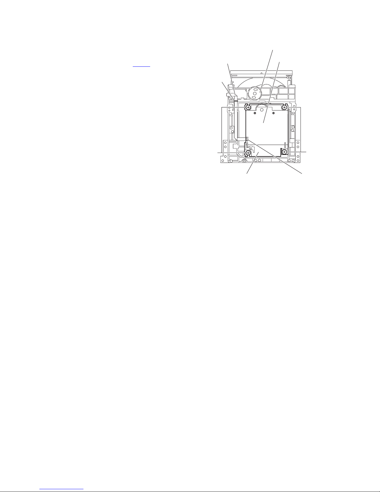
3.1.5 Removing the heat sink
(See Figs.5 and 6)
• Remove the top cover and side covers.
(1) From the rear side of the main body, remove the screw F
attaching the rear cover. (See Fig.5.)
(2) Release the joint sections b and remove the rear cover.
(See Fig.6.)
(3) Remove the two screws G and four screws H attaching the
heat sink. (See Fig.6.)
(4) Remove the heat sink from the rear panel.
and CN401 on the micon
on the micon board. (See
D
a
E
Top cover
Fig.4
F
Tuner
CN405
Micon boardCN400 CN401
Rear cove
C
Top cover
Fig.3
Fig.5
Rear panel Heat sink
H
b
H
b
Fig.6
b
G
b
(No.MB522)1-9
Page 10

3.1.6 Removing the rear panel
(See Fig.7)
• Remove the top cover, side covers, tuner, rear cover and heat
sink.
(1) From the rear side of the main body, remove the screw J
and two screws K attaching the rear panel.
(2) From the both side of the main body, release the joint sec-
tions c and remove the rear panel.
3.1.7 Removing the main board
(See Figs.7 and 8)
• Remove the top cover, side covers, rear cover and heat sink.
(1) From the rear side of the main body, remove the two
screws K attaching the micon board to the rear panel. (See
Fig.7.)
(2) From the right side of the main body, remove the two
screws (M and M') attaching the micon board to the main
body. (See Fig.8.)
Reference:
When attaching the screw M', attach the earth wire with
it.
(3) Disconnect the card wires from the connectors (CN400
, CN405, CN406) on the micon board. (See Fig.8.)
CN401
(4) Disconnect the connectors (CN402, CN403) on the micon
board from the power amplifier board. (See Fig.8.)
Note:
When removing the micon board, take care not to break
the claw of the connector on it.
(5) Remove the micon board from the main body.
Rear panel
K
,
C
Micon board
CN401
J
Fig.7
CN406
C
CN405
3.1.8 Removing the power amplifier board
(See Fig.9)
• Remove the top cover, side covers, tuner, heat sink, rear panel
and micon board.
(1) From the top side of the main body, remove the screw N at-
taching the power amplifier board to the main body.
(2) Disconnect the connector CN150
board from the trans board.
(3) Remove the power amplifier board from the main body.
1-10 (No.MB522)
on the power amplifier
CN403
CN400
Power amplifier board
M' M
Fig.8
CN150
Fig.9
CN402
Trans board
N
Page 11

3.1.9 Removing the power supply board and power transformer
(See Figs. 10 and 11)
• Remove the top cover, side covers, tuner, heat sink, rear pan-
el, micon board and power amplifier board.
(1) From the top side of the main body, disconnect the power
cord connector CN900
(2) Remove the three screws P attaching the power transform-
er from the main body. (See Fig.10.)
(3) From the left side of the main body, remove the screw Q
and then remove the trans board and power transformer.
(See Fig.11.)
on the trans board. (See Fig.10.)
Trans board
Power cord
Fig.10
Trans board
CN900
P
3.1.10 Removing the DVD mechanism assembly
(See Fig. 12)
• Remove the top cover, side covers, front panel assembly, tun-
er, heat sink, rear panel, micon board and power amplifier
board.
From the top side of the main body, remove the screw R attaching the DVD mechanism assembly and then remove the DVD
mechanism assembly from the bottom chassis.
Fig.11
DVD mechanism assmbly
Fig.12
Q
R
(No.MB522)1-11
Page 12

3.1.11 Removing the jack board
(See Fig.13)
• Remove the top cover, side covers, front panel assembly, tun-
er, heat sink, rear panel, micon board, power amplifier board
and DVD mechanism assembly.
(1) From the top side of the main body, remove the two screws
S attaching the jack board on the bottom chassis.
(2) Remove the jack board from the bottom chassis.
3.1.12 Removing the switch board
(See Figs.14 and 15)
• Remove the top cover, side covers and front panel assembly.
(1) From the front side of the front panel assembly, pull out the
volume knob in the direction of the arrow. (See Fig.14.)
(2) From the inside of the front panel assembly, remove the six
screws (T and T') attaching the switch board. (See Fig.15.)
Reference:
When attaching the screw T', attach the earth wire with it.
(3) Remove the switch board while releasing the claws d in the
direction of the arrow. (See Fig.15.)
Jack board
S
Fig.13
Volume knob
T'
Fig.14
Switch board
d
T
Fig.15
1-12 (No.MB522)
Page 13

3.2 CD mechanism assembly
• Remove the CD mechanism assembly from main body.
3.2.1 Removing the CD cover
(See Fig.1)
(1) Remove the two screws A attaching the CD cover from bot-
tom side of CD mechanism assembly.
(2) Lift up the CD cover from disengage boss a of the CD
mechanism assembly.
(3) Slide the CD cover to direction of the arrow and remove the
CD cover from fixing part of b.
(4) Remove the CD cover.
Boss a
A
Fixing part b
3.2.2 Removing the tray assembly
(See Fig.2 and 3)
• Remove the CD cover.
(1) Press slide cam and pull out the tray assembly to direction
of the arrow from right side of CD mechanism assembly.
(See Fig.2)
(2) Remove the two screws B attaching the tray assembly
from upper side of CD mechanism. (See Fig.3)
(3) Remove the bussing of the tray assembly from boss c of
the CD mechanism assembly and remove the tray assembly. (See Fig.3)
Fig.1
Fig.2
Boss
CD cover
c
Bussing
Boss a
A
CD mechanism assembly
Tray assembly CD mechanism assembly
Slide cam
Boss c
B
Fixing part b
Tray assemblyCD mechanism assembly
Fig.3
(No.MB522)1-13
Page 14
3.2.3 Removing the traverse mechanism assembly
(See Fig.4)
(1) Remove the four screws C attaching the traverse mecha-
nism assembly from bottom side of CD mechanism assembly.
(2) Disconnect the card wire from connector CN602
servo board and then take out the traverse mechanism assembly and CD servo board together.
Reference:
When reattaching the traverse mechanism assembly, the card
wire should through the part d.
of the CD
Card wire
d
CD mechanism assembly
CD servo board
C
Traverse mechanism assembly
Fig.4
C
CN602
1-14 (No.MB522)
Page 15

3.2.4 Removing the CD servo board
(See Fig.5 and 6)
• Remove the traverse mechanism assembly.
(1) Remove the two screws D attaching the CD servo board
from bottom side of traverse mechanism assembly. (See
Fig.5)
(2) Remove the solder from solder part e of the CD servo
board. (See Fig.5)
(3) Remove the yellow wire from solder part f of the CD servo
board. (See Fig.5)
(4) Remove the white wire from solder part h of the CD servo
board. (See Fig.5)
(5) Remove the CD servo board to upper side, disengage the
hook c to direction of the arrow 1 then turn over the CD ser-
vo board. (See Fig.5)
(6) Solder to short land part j of pickup. (See Fig.6)
(7) Release the lock of connector CN601
row 2 and disengage the card wire. (See Fig.6)
Caution:
• Solder to short land part j of the pickup then disconnect the
card wire from connector CN601
disconnect the card wire before soldering, pickup is make
sure destroyed by static electricity. (See Fig.6)
• When reattaching the CD servo board, connect the card wire
to connector CN601
land part j of the pickup.
and then remove the solder of short
to direction of the ar-
of the CD servo board. If
CN601
Hook h
Solder part e
Yellow wire
DD
White wire
Solder
part f
Solder
㧝㧝
Traverse mechanism assemblyCD servo board
Fig.5
CD servo board
part g
Hook h
Pickup
Short land part j
CN601
22
Traverse mechanism assembly
Fig.6
(No.MB522)1-15
Page 16

3.2.5 Removing the pickup
(See Fig.7 to 9)
• Remove the traverse mechanism assembly.
(1) Remove the one screw E attaching the plate from upper
side of traverse mechanism assembly. (See Fig.7)
(2) Remove the plate from fixing part k then take out the plate.
(See Fig.7)
(3) Remove the two screws F attaching the LEAD spring and
then take out the LEAD spring. (See Fig.8)
(4) Take out the feed gear, and then remove the shaft of pick-
up from part m of the traverse mechanism assembly. (See
Fig.8)
(5) Remove the pickup from part n of the traverse mechanism
assembly and then take out pickup with shaft. (See Fig.8)
(6) Release the shaft from pickup. (See Fig.8)
(7) Solder the short land part p of the pickup. (See Fig.9)
(8) Release the lock of the connector to direction of the arrow,
and then disconnect the card wire. (See Fig9)
Caution:
• Solder to short land part p of the pickup then disconnect the
card wire from connector. If disconnect the card wire before
soldering, pickup is make sure destroyed by static electricity.
(See Fig.9)
• When reattaching the pickup, connect the card wire to con-
nector and then remove the solder from short land part p.
(See Fig.9)
Feed gear Shaft LEAD spring
Pickup
Short land part p
F
Part m
Fig.8
Part m
3.2.6 Attaching the pickup
(See Fig.7 to 10)
• Please refer the "Removing the pickup".
(1) Connect the card wire to connector of pickup, and then re-
move the solder from short land part p of the pickup. (See
Fig.9)
(2) Attach the shaft to pickup. (See Fig.8)
(3) Fit the pickup to part n of the traverse mechanism and then
attach the end of the shaft to part k. (See Fig.8)
(4) Attach the LEAD spring and feed gear. (See Fig.8)
(5) Attach the plate. (See Fig. 7)
(6) One turn the LEAD gear to direction of the arrow 1 and fully
shift to direction of the arrow 2. (See Fig.10)
Plate
Fixing part k
E
Pickup Connector Card wire
Fig.9
LEAD gear
1
2
Traverse mechanism assembly
Fig.10
Pickup
Traverse mechanism assembly
Fig.7
1-16 (No.MB522)
Page 17

3.2.7 Removing the feed motor
(See Fig.11 to 13)
• Remove the traverse mechanism.
(1) Remove the yellow wire from solder part q of the CD servo
board from upper side of traverse mechanism. (See Fig.11)
(2) Remove the white wire from solder part r of the CD servo
board. (See Fig.11)
(3) Remove the one screw G attaching the plate. (See Fig.12)
(4) Disengage the plate from fixing part s and take out the
plate. (See Fig.12)
(5) Remove the feed gear and take out the feed motor. (See
Fig13)
Reference:
When attaching the feed motor, the wire has to through the
part t of the traverse mechanism assembly. (See Fig.13)
Fixing part s
G
Yellow wire
White wire
Soldered part q
Soldered part r
Traverse mechanism assemblyCD servo board
Fig.11
Plate
Traverse mechanism assembly
Fig.12
Feed gear Feed motor
Traverse mechanism assembly
Fig.13
part t
(No.MB522)1-17
Page 18

3.2.8 Removing the switch board
(See Fig.14)
(1) Disconnect the card wire from CN1
from bottom side of CD mechanism assembly.
(2) Remove the wire from solder part u of the switch board.
(3) Remove the one screw H attaching the switch board to CD
mechanism assembly.
(4) Lift up the switch board by pushing the hook v of CD mech-
anism assembly and take out it from part w.
Reference:
• After attach the switch board to CD mechanism assembly,
wire hooked to part x.
•Hook u of the CD mechanism assembly, it have to bond
lock.
3.2.9 Removing the motor
(See Fig.14 and 15)
• Remove the tray assembly.
(1) Remove the wire from solder part u of the switch board
from bottom side of CD mechanism assembly.
(2) Remove the belt of motor pulley from upper side of CD
mechanism assembly. (See Fig.15)
Caution:
Belt should not apply grease.
(3) Remove the two screws J attaching the motor to CD mech-
anism assembly and take out the motor from bottom side
of CD mechanism assembly. (See Fig.15)
Reference:
After motor attached to CD mechanism assembly, wire should
hook to part w. (See Fog.14)
of the switch board
Switch board Wire
Solder
part u
CN1
Part w
H
CD mechanism assembly
J
Hook v
Part w
Fig.14
CD mechanism assembly
Belt
Fig.15
Motor pulley
1-18 (No.MB522)
Page 19

SECTION 4
ADJUSTMENT
4.1 Test mode
Step Special key function Keys Description
1 Cold start
Clock fast forward
2 (remocon)
Volume change
3 (remocon)
Version display
4
FL display test
5
Safety info display
6 (Unit)
(remocon)
A.STANDBY + SET + DISPLAY
A.STANDBY + SET + FM MODE/ PLAY MODE
A.STANDBY + SET + SOUND TURBO
(remocon)
A.STANDBY + SET + AHB PRO
(remocon)
A.STANDBY + SET + BASS/TREBLE
SOUND TURBO + STOP
1. Restore factory setting at next AC Power ON.
Volume level: 12
First source at Power ON: CD
Sound Turbo: Enable
AHB Pro: Disable
FM Preset Channel: restore to factory setting
Clock/ Timer: Clear
Dimmer: restore to factory setting
2. FL display: COLD during key pressed.
1. Clock minute fast increase by 1 every seconds.
(Clock starts from 0:00 if not preset)
2. Pressed again to stop clock fast running.
3. During:
Power Standby: OK
Power ON: OK
ECO mode: OK
Safety trigger: OK
1. Volume level changes from 40 > 21 > Vol MIN > 40
2. During:
Power Standby: OK (unit will turn ON)
Power ON: OK
ECO mode: OK
Safety trigger: OK
1. Display ROM version for 5 seconds.
2. Example: 37R06107
Digit 1 and 2: ROM version = 37
Digit 3 and 4: ROM Correction version = 0
Digit 5: ROM issue year = 2006
Digit 6: ROM issue month = January
(1: Jan, 2: Feb, 3: Mar, 4: Apr, 5: May, 6: June,
7: July, 8: Aug, 9: Sept, A: Oct, B: Nov, C: Dec)
Digit 7 and 8: ROM issue day = 7
3. During:
Power Standby: NG
Power ON: OK
ECO mode: NG
Safety trigger: NG
1. All FL segments will blink at 500ms interval.
2. During:
Power Standby: OK
Power ON: OK
ECO mode (Pressing DIMMER key at Power Standby): NG
Safety trigger: NG
3. Press any key (except SOUND TURBO) on the unit or
CANCEL key (remocon) will exit test mode."
1. Safety Information display. During safety trigger,
safety info is display for 2 sec and return to ECO mode.
2. Safety Information display:
NO SAFTY: No Safety triggered.
SFTY- VH: Power IC NG
SFTY-REG: Power Regulator NG
SFTY-ALP: tape module NG
SFTY- CD: CD module NG
SFTY-PRT: Power AMP Protector NG
3. During:
Power Standby: OK
Power ON: NG
ECO mode: OK (FL turns ON for 2sec then turns OFF)
Safety trigger: OK (FL turns ON for 2sec then turns OFF)
4. For version 36, there is no backup of safety information.
It shows only current safety condition.
5. For version 37, last safety information is backup.
(No.MB522)1-19
Page 20

SECTION 5
TROUBLE SHOOTING
5.1 Maintenance of laser pickup (CD)
(1) Cleaning the pick up lens
Before you replace the pick up, please try to clean the lens
with a alcohol soaked cotton swab.
(2) Life of the laser diode
When the life of the laser diode has expired, the following
symptoms will appear.
• The level of RF output (EFM output : ampli tude of eye
pattern) will below.
Is the level of
RFOUT under
1.25V 0.22Vp-p?
NO
Replace it.
YES
O.K
(3) Semi-fixed resistor on the APC PC board
The semi-fixed resistor on the APC printed circuit board
which is attached to the pickup is used to adjust the laser
power. Since this adjustment should be performed to
match the characteristics of the whole optical block, do not
touch the semi-fixed resistor.
If the laser power is lower than the specified value, the laser diode is almost worn out, and the laser pickup should
be replaced.
If the semi-fixed resistor is adjusted while the pickup is
functioning normally, the laser pickup may be damaged
due to excessive current.
5.2 Replacement of laser pickup (CD)
Turn off the power switch and, disconnect the
power cord from the ac outlet.
Replace the pickup with a normal one.(Refer
to "Pickup Removal" on the previous page)
Plug the power cord in, and turn the power on.
At this time, check that the laser emits for
about 3seconds and the objective lens moves
up and down.
Note: Do not observe the laser beam directly.
Play a disc.
Check the eye-pattern at TP1.
Finish.
1-20 (No.MB522)
Page 21

(No.MB522)1-21
Page 22

Victor Company of Japan, Limited
Audio/Video Systems Category 10-1,1chome,Ohwatari-machi,Maebashi-city,371-8543,Japan
(No.MB522)
Printed in Japan
VPT
Page 23

PARTS LIST
UX-G33B,UX-G33E,UX-G33EN,UX-G33EV
UX-G30B,UX-G30E,UX-G30EN,UX-G30EV
* All printed circuit boards and its assemblies are not available as service parts.
- Contents -
Exploded view of general assembly and parts list (Block No.M1)
Speaker assembly and parts list (Block No.M2)
CD mechanism assembly and parts list (Block No.MB)
CD loading base assembly and parts list (Block No.MD)
Electrical parts list (Block No.01~04)
Packing materials and accessories parts list (Block No.M3)
MB522
3-2
3-5
3-6
3-8
3-10
3-14
3-1
Page 24

Exploded view of general assembly and parts list
1
Block No.
4
M
M
1
M
9
K
55
7
L
Trans board
10
6
Switch board
K
1
56
L
10
2
3
4
54
48
5
f
a
16
19
43
50
42
8
44
D
40
B
15
38
Cover board
26
c
41
Jack board
C
17
47
14
A
C
J
3-2
Page 25

37
F
25
G
24
H
18
F
D
36
34
G
27
E
H
29
45
25
L
b
49
28
33
32
31
52
d
51
20
A
Power amplifier board
30
35
53
58
50
e
57
13
B
46
B
E
40
12
23
b
d
41
e
a
J
11
22
c
f
Micon board
39
21
J
3-3
Page 26

General Assembly
Block No. [M][1][M][M]
Symbol No. Part No. Part Name Description Local
1 GV20428-001A FRONT PNL.ASSY.
2 QYSDSF2608ZA TAP SCREW M2.6 x 8mm(x4)
3 GV30832-003A FL LENS G33B,G33E,G33EN,G33EV
3 GV30832-001A FL LENS G30B,G30E,G30EN,G30EV
4 GV30833-001A FRONT BTN.ASSY
5 GV30835-001A VOL.RING LENS
6 GV40678-001A FL SCREEN
7 QYSDSF2608ZA TAP SCREW M2.6 x 8mm(x6)
8 GV40313-002A FELT SPACER (x2)
9 GV10293-001A TOP COVER A
10 QYSBSG3010ZA TAP SCREW M3 x 10mm(x2)
11 GV10295-001A BOTTOM CHASSIS
12 GV30840-001A SUPPORT BRACKET
13 QYSBST3006ZA TAP SCREW M3 x 6mm
14 GV30349-025A SPACER
15 GV30349-038A SPACER
16 QYSBSG3010ZA TAP SCREW M3 x 10mm
17 QYSBST3006ZA TAP SCREW M3 x 6mm(x2)
18 QYSBST4006ZA TAP SCREW M4 x 6mm(x3)
19 QYSBST3006ZA TAP SCREW M3 x 6mm(x2)
20 QYSBST3006ZA TAP SCREW M3 x 6mm
21 QYSBST3006ZA TAP SCREW M3 x 6mm(x2)
22 GV40313-002A FELT SPACER (x2)
23 QZW0033-001 STRAIN RELIEF
24 GV30967-001A TRANS SHIELD
25 LV30225-0R3A SPACER (x2)
26 E3400-431 SPECER
27 GV20399-010A REAR PANEL G33B,G33E,G33EN
27 GV20399-011A REAR PANEL G33EV
27 GV20399-001A REAR PANEL G30B,G30E,G30EN
27 GV20399-002A REAR PANEL G30EV
28 QAU0413-001 TUNER
29 QYSBSGY3008EA TAP SCREW M3 x 8mm(x2)
30 GV30841-002A HEAT SINK
31 QYSBSGY3008EA TAP SCREW M3 x 8mm(x4)
32 QYSBSGY3008EA TAP SCREW M3 x 8mm
33 QYSBSGY3008EA TAP SCREW M3 x 8mm(x2)
34 QYSBSGY3008EA TAP SCREW M3 x 8mm
35 QYSBSG3020ZA TAP SCREW M3 x 20mm(x2)
36 GV20400-001A REAR COVER
37 QYSBSGY3008EA TAP SCREW M3 x 8mm
38 GV10296-001A SIDE PANEL L
39 GV10297-001A SIDE PANEL R
40 QYSBSGY3008EA TAP SCREW M3 x 8mm(x2)
41 QYSBSGY3008EA TAP SCREW M3 x 8mm(x2)
42 QYSBST3006ZA TAP SCREW M3 x 6mm(x2)
43 GV30837-001A VOLUME KNOB
44 GV30838-001A TRAY FITTING
45 GV30893-001A NUMBER LABEL
46 QMPN150-200-JC POWER CORD(EU) 2m BLACK G33B,G30B
46 QMPK200-200-JD POWER CORD(EU) 2m BLACK
47 QUQU12-1011BJ-E FFC WIRE 10pin 11cm
48 QUQU12-1413BJ-E FFC WIRE 14pin 13cm
49 QUQU12-1511BJ-E FFC WIRE 15pin 11cm
50 QUR110-1718AJ-E FFC WIRE
51 QQT0500-002 POWER TRANSF
52 QMF51W2-R80-J8 FUSE 0.8A AC250V
53 QMF51W2-1R6-J8 FUSE 1.6A AC250V
54 GV30836-001A VOL.LENS HOLDER
55 LV43659-001A FL HOLDER (x2)
56 LV30225-0M9A SPACER (x2)
57 GV30842-001A IC BRACKET
58 QYSBSG3010ZA TAP SCREW M3 x 10mm(x2)
G33E,G33EN,G33EV,G30E,G30EN,G30EV
3-4
Page 27

Speaker assembly and parts list
1
2
Block No.
M
M
M
2
3
3
The parts without symbol number are not service.
Speaker
Block No. [M][2][M][M]
Symbol No. Part No. Part Name Description Local
1 SPUXG33E-SPBOX SPK WITH BOX (x2) G33B,G33E,G33EN,G33EV
1 SPUXG30E-SPBOX SPK WITH BOX (x2) G30B,G30E,G30EN,G30EV
2 J201-XG3302G-50 SPK NET ASSY (x2) G33B,G33E,G33EN,G33EV
2 J201-XG3001G-50 SPK NET ASSY (x2) G30B,G30E,G30EN,G30EV
3 441-910102-00 RUBBER CUSHION (x8)
3-5
Page 28

CD mechanism assembly and parts list
FTU-JS1-1M
7
0.1mm
2
3
Block No.
A
M
3.5mm
B
0.1mm
M
M
1
18mm
13
Grease
JVG-31N
JVS-1003
FL-7750E
8
12.0mm 0.1mm
12
13
12
7
6
4
9
5
20
17
a
10
11
16
11
10
15
A
6
14
8
< Back side >
18
19
3-6
a
The parts without symbol number are not service.
Page 29

CD mechanism
Symbol No. Part No. Part Name Description Local
1 QAL0750-001 CD PICK UP
2 LV34564-001A RACK ARM
3 QYSPSPT1720MA SCREW M1.7 x 2mm(x2)
4 LV31744-001A P.S.SPRING
5 QYSPSGT1425MA TAP SCREW M1.4 x 2.5mm
6 LV10855-002A TM CHASSIS
7 LV43468-001A T.T ASSY
8 QAR0302-001 SPINDLE MOTOR
9 VKZ4743-002 SPECIAL SCREW (x2)
10 LV40157-001A SCREW SHAFT
11 LV43651-001A SS GEAR
12 LV43650-001A F MOTOR GEAR
13 QAR0303-001 FEED MOTOR
14 QYSPSPT2030MA SCREW M2 x 3mm
15 LV34565-002A F MIDDLE GEAR
16 LV34563-001A SHAFT HOLDER
17 QYSPSFT1740ZA TAP SCREW M1.7 x 4mm
18 QYSBSF2006ZA TAP SCREW M2 x 6mm(x2)
19 LV30225-073A SPACER
20 QUQ105-1506BB-E FFC WIRE 15pin 6cm
Block No. [M][B][M][M]
3-7
Page 30

CD loading based assembly and parts listt
Grease
JVS-1003
JVG-450
20
19
26
FMU-MS1-1M
Block No.
M
D
M
M
15
h
< Back side >
4
18
14
2
3
11
h
13
1
15
17
10
9
j
0.10mm
7.75mm
Backside
12
7
8
6
CD loading switch board
g
5
j
23
25
21
g
24
23
22
23
22
c
e
27
d
3-8
e
f
c
23
d
21
f
The parts without symbol number are not service.
16
Page 31

CD loading base
Symbol No. Part No. Part Name Description Local
1 LV11065-004A LOADER SUB ASSY
2 E407140-001SS C.D ROLLER
3 E407149-001SS RUBBER TUBE
4 LV10979-002A TRAY
5 LV35499-001A SHAFT GUIDE
6 LV44022-001A SHAFT
7 QYSSSF2008ZA TAP SCREW M2 x 8mm
8 QYSDSF2008ZA TAP SCREW M2 x 8mm(x2)
9 QAR0197-001 MOTOR
9 or QAR0280-001 LOADING MOTOR
10 LV43844-002A MOTOR PULLEY
11 QYSPSPU1730ZA SCREW M1.7 x 3mm(x2)
12 QYSDSF2008ZA TAP SCREW M2 x 8mm
13 LV43974-001A BELT
14 LV21852-003A CLAMPER BASE
15 QYSDSF2008ZA TAP SCREW M2 x 8mm(x2)
16 LV41741-004A SPECIAL SCREW
17 LV34586-002A CD CLAMPER
18 LV42930-003A P.C.MAGNET
18 or LV41118-003A P.C.MAGNET
19 LV43848-001A YOKE
20 LV43958-001A SPECIAL SCREW
21 LE40900-003A INSULATOR (x2)
22 LE40900-004A INSULATOR (x2)
23 LV44044-001A SPECIAL SCREW (x4)
24 LV43805-001A FFC
25 VYSH101-034 SPACER
26 LV44603-001A LASER CATION
27 ------------ CD TRAMECHA UNI
Block No. [M][D][M][M]
3-9
Page 32

Electrical parts list
Micon board
Block No. [0][1]
Symbol No.
IC200 KIA78R33PI IC
IC220 LC75345M-X IC
IC400 MN101C49GFB1 MASK ROM
IC401 BR24L02F-W-X IC(DIGITAL)
IC500 PT6315 IC
IC501 GP1UM271XKVF IR DETECT UNIT
IC565 RC4558D-X IC
IC566 RC4558D-X IC
Q2000 KRC102S-X DIGI TRANSISTOR
Q2001 KRC102S-X DIGI TRANSISTOR
Q2100 KTA1504/YG/-X TRANSISTOR
Q2101 KRC102S-X DIGI TRANSISTOR
Q2300 KTC3875/YG/-X TRANSISTOR
Q2301 KTC3875/YG/-X TRANSISTOR
Q2400 KTC2875-X CHIP TR.
Q2401 KTC2875-X CHIP TR.
Q2402 KRA102S-X DIGI TRANSISTOR
Q4000 KRC111S-X TRANSISTOR
Q4001 KTC3875/YG/-X TRANSISTOR
Q4200 KRC102S-X DIGI TRANSISTOR
Q5000 KRC102S-X DIGI TRANSISTOR
Q5660 KRC109S-X TRANSISTOR
D2000 1SS133-T2 SI DIODE
D2300 1SS133-T2 SI DIODE
D2301 1SS133-T2 SI DIODE
D2302 1SS133-T2 SI DIODE
D4000 1SS133-T2 SI DIODE
D4001 1SS133-T2 SI DIODE
D4002 MTZJ5.1B-T2 Z DIODE
D4003 1SS133-T2 SI DIODE
D4004 1SS133-T2 SI DIODE
D4005 1SS133-T2 SI DIODE
D4006 1N4003S-T5 SI DIODE
D4007 1N4003S-T5 SI DIODE
D4008 1N4003S-T5 SI DIODE
D4009 1N4003S-T5 SI DIODE
D4201 MTZJ10B-T2 Z DIODE
D4203 1SS133-T2 SI DIODE
D4204 1SS133-T2 SI DIODE
D5002 SLI-343URC-W-T LED
D5200 SELU1E54CM-P LED
D5205 1SS133-T2 SI DIODE
D5206 1SS133-T2 SI DIODE
D5600 1SS133-T2 SI DIODE
D5601 1SS133-T2 SI DIODE
D5660 1SS133-T2 SI DIODE
C2000 QETN1AM-227Z E CAPACITOR 220uF 10V M
C2001 QETN1AM-227Z E CAPACITOR 220uF 10V M
C2002 NCB31HK-103X C CAPACITOR 0.01uF 50V K
C2004 NCB31HK-103X C CAPACITOR 0.01uF 50V K
C2101 NCB31HK-561X C CAPACITOR 560pF 50V K
C2102 NCB31HK-561X C CAPACITOR 560pF 50V K
C2103 NCB31HK-103X C CAPACITOR 0.01uF 50V K
C2200 QETN1CM-107Z E CAPACITOR 100uF 16V M
C2202 QFLC1HJ-104Z M CAPACITOR 0.1uF 50V J
C2203 QETN1HM-226Z E CAPACITOR 22uF 50V M
C2204 QFLC1HJ-104Z M CAPACITOR 0.1uF 50V J
C2205 QFVF1HJ-184Z MF CAPACITOR 0.18uF 50V J
C2206 QFVF1HJ-184Z MF CAPACITOR 0.18uF 50V J
C2207 QFLC1HJ-104Z M CAPACITOR 0.1uF 50V J
C2208 QFLC1HJ-104Z M CAPACITOR 0.1uF 50V J
C2209 QFLC1HJ-272Z M CAPACITOR 2700pF 50V J
C2213 QETN1HM-475Z E CAPACITOR 4.7uF 50V M
C2214 QETN1HM-106Z E CAPACITOR 10uF 50V M
C2216 QETN1HM-475Z E CAPACITOR 4.7uF 50V M
C2217 QETN1CM-107Z E CAPACITOR 100uF 16V M
C2218 QETN1HM-475Z E CAPACITOR 4.7uF 50V M
C2220 QETN1HM-106Z E CAPACITOR 10uF 50V M
C2221 QETN1HM-475Z E CAPACITOR 4.7uF 50V M
Part No. Part Name Description Local
Symbol No.
C2225 QFLC1HJ-272Z M CAPACITOR 2700pF 50V J
C2226 QFLC1HJ-104Z M CAPACITOR 0.1uF 50V J
C2227 QFLC1HJ-104Z M CAPACITOR 0.1uF 50V J
C2228 QFVF1HJ-184Z MF CAPACITOR 0.18uF 50V J
C2229 QFVF1HJ-184Z MF CAPACITOR 0.18uF 50V J
C2230 QFLC1HJ-104Z M CAPACITOR 0.1uF 50V J
C2231 QETN1HM-226Z E CAPACITOR 22uF 50V M
C2232 QFLC1HJ-104Z M CAPACITOR 0.1uF 50V J
C2300 QETN1HM-106Z E CAPACITOR 10uF 50V M
C2301 QETN1HM-105Z E CAPACITOR 1uF 50V M
C2302 NCB31AK-154X C CAPACITOR 0.15uF 10V K
C2310 QETN1HM-105Z E CAPACITOR 1uF 50V M
C2400 QETN1HM-475Z E CAPACITOR 4.7uF 50V M
C2600 NCB31HK-392X C CAPACITOR 3900pF 50V K
C2601 NCB31HK-392X C CAPACITOR 3900pF 50V K
C2604 NCB31HK-392X C CAPACITOR 3900pF 50V K
C2605 NCB31HK-392X C CAPACITOR 3900pF 50V K
C4001 NCB31HK-103X C CAPACITOR 0.01uF 50V K
C4002 NCB31HK-103X C CAPACITOR 0.01uF 50V K
C4003 NCB31HK-103X C CAPACITOR 0.01uF 50V K
C4004 NDC31HJ-150X C CAPACITOR 15pF 50V J
C4005 NDC31HJ-150X C CAPACITOR 15pF 50V J
C4006 NCB31HK-103X C CAPACITOR 0.01uF 50V K
C4007 QETN1CM-107Z E CAPACITOR 100uF 16V M
C4008 QETN0JM-228Z E CAPACITOR 2200uF 6.3V M
C4009 QETN1HM-226Z E CAPACITOR 22uF 50V M
C4010 QETN1HM-475Z E CAPACITOR 4.7uF 50V M
C4011 QETN1CM-107Z E CAPACITOR 100uF 16V M
C5000 NCB31HK-103X C CAPACITOR 0.01uF 50V K
C5001 NCB31HK-103X C CAPACITOR 0.01uF 50V K
C5004 NCB31HK-103X C CAPACITOR 0.01uF 50V K
C5009 NCB31HK-103X C CAPACITOR 0.01uF 50V K
C5010 QEKC1AM-476Z E CAPACITOR 47uF 10V M
C5012 NCB31CK-104X C CAPACITOR 0.1uF 16V K
C5200 NCB31HK-103X C CAPACITOR 0.01uF 50V K
C5500 NCB31HK-103X C CAPACITOR 0.01uF 50V K
C5502 NCB31HK-102X C CAPACITOR 1000pF 50V K
C5503 NCB31HK-102X C CAPACITOR 1000pF 50V K
C5602 NCB31HK-222X C CAPACITOR 2200pF 50V K
C5660 QETN1HM-225Z E CAPACITOR 2.2uF 50V M
C5661 QETN1HM-225Z E CAPACITOR 2.2uF 50V M
C5662 QETN1EM-476Z E CAPACITOR 47uF 25V M
C5663 QETN1EM-476Z E CAPACITOR 47uF 25V M
C5664 QETN1HM-106Z E CAPACITOR 10uF 50V M
R2000 NRSA63J-103X MG RESISTOR 10kΩ 1/16W J
R2001 NRSA63J-472X MG RESISTOR 4.7k
R2002 NRSA63J-472X MG RESISTOR 4.7k
R2003 NRSA63J-104X MG RESISTOR 100k
R2101 NRSA63J-203X MG RESISTOR 20kΩ 1/16W J
R2102 NRSA63J-203X MG RESISTOR 20k
R2106 NRSA63J-103X MG RESISTOR 10k
R2107 NRSA63J-102X MG RESISTOR 1kΩ 1/16W J
R2202 NRSA63J-302X MG RESISTOR 3k
R2203 NRSA63J-222X MG RESISTOR 2.2kΩ 1/16W J
R2204 NRSA63J-752X MG RESISTOR 7.5k
R2205 NRSA63J-752X MG RESISTOR 7.5k
R2208 NRSA63J-103X MG RESISTOR 10kΩ 1/16W J
R2209 NRSA63J-154X MG RESISTOR 150k
R2210 NRSA63J-154X MG RESISTOR 150k
R2211 NRSA63J-103X MG RESISTOR 10kΩ 1/16W J
R2214 NRSA63J-752X MG RESISTOR 7.5k
R2215 NRSA63J-752X MG RESISTOR 7.5k
R2216 NRSA63J-222X MG RESISTOR 2.2kΩ 1/16W J
R2217 NRSA63J-302X MG RESISTOR 3k
R2300 NRSA63J-113X MG RESISTOR 11k
R2301 NRSA63J-513X MG RESISTOR 51k
R2302 NRSA63J-473X MG RESISTOR 47k
R2303 NRSA63J-473X MG RESISTOR 47kΩ 1/16W J
R2304 NRSA63J-113X MG RESISTOR 11k
R2305 NRSA63J-124X MG RESISTOR 120k
R2306 NRSA63J-334X MG RESISTOR 330kΩ 1/16W J
R2307 NRSA63J-362X MG RESISTOR 3.6k
R2308 NRSA63J-563X MG RESISTOR 56k
R2309 NRSA63J-563X MG RESISTOR 56kΩ 1/16W J
R2400 QRJ146J-821X UNF C RESISTOR 820
Part No. Part Name Description Local
Ω
1/16W J
Ω
1/16W J
Ω
1/16W J
Ω
1/16W J
Ω
1/16W J
Ω
1/16W J
Ω
1/16W J
Ω
1/16W J
Ω
1/16W J
Ω
1/16W J
Ω
1/16W J
Ω
1/16W J
Ω
1/16W J
Ω
1/16W J
Ω
1/16W J
Ω
1/16W J
Ω
1/16W J
Ω
1/16W J
Ω
1/16W J
Ω
1/16W J
Ω
1/4W J
3-10
Page 33

Symbol No.
Part No. Part Name Description Local
Symbol No.
Part No. Part Name Description Local
R2401 QRJ146J-821X UNF C RESISTOR 820Ω 1/4W J
R2402 QRJ146J-821X UNF C RESISTOR 820Ω 1/4W J
R2403 QRJ146J-821X UNF C RESISTOR 820Ω 1/4W J
R2404 NRSA63J-103X MG RESISTOR 10kΩ 1/16W J
R2405 NRSA63J-103X MG RESISTOR 10kΩ 1/16W J
R4002 NRSA63J-103X MG RESISTOR 10k
R4008 NRSA63J-222X MG RESISTOR 2.2k
R4009 NRSA63J-222X MG RESISTOR 2.2kΩ 1/16W J
R4010 NRSA63J-103X MG RESISTOR 10kΩ 1/16W J
R4011 NRSA63J-103X MG RESISTOR 10kΩ 1/16W J
R4014 NRSA63J-222X MG RESISTOR 2.2kΩ 1/16W J
R4015 NRSA63J-472X MG RESISTOR 4.7kΩ 1/16W J
R4016 NRSA63J-222X MG RESISTOR 2.2kΩ 1/16W J
R4017 NRSA63J-222X MG RESISTOR 2.2kΩ 1/16W J
R4018 NRSA63J-222X MG RESISTOR 2.2kΩ 1/16W J
R4020 NRSA63J-103X MG RESISTOR 10kΩ 1/16W J
R4023 NRSA63J-103X MG RESISTOR 10kΩ 1/16W J
R4024 NRSA63J-103X MG RESISTOR 10kΩ 1/16W J
R4025 NRSA63J-222X MG RESISTOR 2.2kΩ 1/16W J
R4026 NRSA63J-222X MG RESISTOR 2.2kΩ 1/16W J
R4027 NRSA63J-222X MG RESISTOR 2.2k
R4028 NRSA63J-222X MG RESISTOR 2.2k
R4029 NRSA63J-222X MG RESISTOR 2.2kΩ 1/16W J
R4030 NRSA63J-103X MG RESISTOR 10kΩ 1/16W J
R4031 NRSA63J-102X MG RESISTOR 1kΩ 1/16W J
R4032 NRSA63J-222X MG RESISTOR 2.2kΩ 1/16W J
R4033 NRSA63J-103X MG RESISTOR 10kΩ 1/16W J
R4036 NRSA63J-102X MG RESISTOR 1kΩ 1/16W J
R4037 NRSA63J-102X MG RESISTOR 1kΩ 1/16W J
R4038 NRSA63J-102X MG RESISTOR 1kΩ 1/16W J
R4039 NRSA63J-104X MG RESISTOR 100kΩ 1/16W J
R4040 NRSA63J-102X MG RESISTOR 1kΩ 1/16W J
R4041 NRSA63J-102X MG RESISTOR 1kΩ 1/16W J
R4043 NRSA63J-203X MG RESISTOR 20kΩ 1/16W J
R4044 NRSA63J-222X MG RESISTOR 2.2kΩ 1/16W J
R4046 NRSA63J-222X MG RESISTOR 2.2kΩ 1/16W J
R4047 NRSA63J-103X MG RESISTOR 10kΩ 1/16W J
R4052 NRSA63J-222X MG RESISTOR 2.2kΩ 1/16W J
R4053 NRSA63J-222X MG RESISTOR 2.2kΩ 1/16W J
R4054 NRSA63J-222X MG RESISTOR 2.2kΩ 1/16W J
R4055 NRSA63J-222X MG RESISTOR 2.2kΩ 1/16W J
R4056 NRSA63J-103X MG RESISTOR 10kΩ 1/16W J
R4060 NRSA63J-103X MG RESISTOR 10kΩ 1/16W J
R4061 NRSA63J-331X MG RESISTOR 330Ω 1/16W J
R4062 NRSA63J-103X MG RESISTOR 10kΩ 1/16W J
R4063 NRSA63J-103X MG RESISTOR 10kΩ 1/16W J
R4064 NRSA63J-104X MG RESISTOR 100kΩ 1/16W J
R4065 NRSA63J-473X MG RESISTOR 47kΩ 1/16W J
R4066 NRSA63J-333X MG RESISTOR 33kΩ 1/16W J
R4067 NRSA63J-102X MG RESISTOR 1k
R4068 NRSA63J-103X MG RESISTOR 10kΩ 1/16W J
R4070 NRSA63J-103X MG RESISTOR 10k
R4071 NRSA63J-103X MG RESISTOR 10k
R4072 NRSA63J-103X MG RESISTOR 10kΩ 1/16W J
R4073 NRSA63J-103X MG RESISTOR 10k
R4083 NRSA63J-222X MG RESISTOR 2.2k
R4200 NRSA63J-103X MG RESISTOR 10kΩ 1/16W J
R4203 NRSA63J-473X MG RESISTOR 47k
R4204 NRSA63J-153X MG RESISTOR 15kΩ 1/16W J
R5000 NRSA63J-823X MG RESISTOR 82k
R5002 NRSA63J-102X MG RESISTOR 1k
R5100 NRSA63J-911X MG RESISTOR 910Ω 1/16W J
R5101 NRSA63J-242X MG RESISTOR 2.4k
R5102 NRSA63J-392X MG RESISTOR 3.9k
R5103 NRSA63J-682X MG RESISTOR 6.8kΩ 1/16W J
R5104 NRSA63J-153X MG RESISTOR 15k
R5105 NRSA63J-911X MG RESISTOR 910
R5106 NRSA63J-242X MG RESISTOR 2.4k
R5107 NRSA63J-392X MG RESISTOR 3.9k
R5108 NRSA63J-682X MG RESISTOR 6.8kΩ 1/16W J
R5109 NRSA63J-153X MG RESISTOR 15k
R5200 NRSA63J-470X MG RESISTOR 47
R5202 NRSA63J-104X MG RESISTOR 100kΩ 1/16W J
R5204 NRSA63J-331X MG RESISTOR 330
R5501 NRSA63J-102X MG RESISTOR 1k
R5600 NRSA63J-102X MG RESISTOR 1kΩ 1/16W J
R5601 NRSA63J-243X MG RESISTOR 24k
R5602 NRSA63J-303X MG RESISTOR 30k
Ω
1/16W J
Ω
1/16W J
Ω
1/16W J
Ω
1/16W J
Ω
1/16W J
Ω
1/16W J
Ω
1/16W J
Ω
1/16W J
Ω
1/16W J
Ω
1/16W J
Ω
1/16W J
Ω
1/16W J
Ω
1/16W J
Ω
1/16W J
Ω
1/16W J
Ω
1/16W J
Ω
1/16W J
Ω
1/16W J
Ω
1/16W J
Ω
1/16W J
Ω
1/16W J
Ω
1/16W J
Ω
1/16W J
Ω
1/16W J
R5603 NRSA63J-243X MG RESISTOR 24kΩ 1/16W J
R5604 NRSA63J-303X MG RESISTOR 30kΩ 1/16W J
R5662 NRSA63J-104X MG RESISTOR 100kΩ 1/16W J
R5663 NRSA63J-104X MG RESISTOR 100kΩ 1/16W J
R5664 NRSA63J-472X MG RESISTOR 4.7kΩ 1/16W J
R5665 NRSA63J-472X MG RESISTOR 4.7k
R5666 NRSA63J-472X MG RESISTOR 4.7k
R5667 NRSA63J-472X MG RESISTOR 4.7kΩ 1/16W J
R5668 NRSA63J-224X MG RESISTOR 220kΩ 1/16W J
R5669 NRSA63J-104X MG RESISTOR 100kΩ 1/16W J
R5671 NRSA63J-103X MG RESISTOR 10kΩ 1/16W J
R5672 NRSA63J-562X MG RESISTOR 5.6kΩ 1/16W J
CN400 QGF1205F2-10 CONNECTOR FFC/FPC (1-10)
CN401 QGF1205F2-14 CONNECTOR FFC/FPC (1-14)
CN402 QGB2510J1-11 CONNECTOR B-B (1-11)
CN403 QGB2510J1-10 CONNECTOR B-B (1-10)
CN405 QGF1205F2-15 CONNECTOR FFC/FPC (1-15)
CN406 QGF1036C2-17 CONNECTOR FFC/FPC (1-17)
CN500 QGF1205F2-14 CONNECTOR FFC/FPC (1-14)
CN550 QGF1205C2-10 CONNECTOR FFC/FPC (1-10)
DI500 QLF0165-001 FL TUBE
EP550 QNZ0136-001Z EARTH PLATE
EP560 QNZ0136-001Z EARTH PLATE
J2600 QNB0292-001 SPK TERMINAL
J5500 QNS0173-001 JACK
J5600 QNS0173-001 JACK
JS500 QSW1059-001 JOG VOLUME
K2000 QQR0621-001Z COIL
PP560 QZW0112-001 WIRE CLAMP
S5100 QSW0683-001Z PUSH SW I.M
S5101 QSW0683-001Z PUSH SW I.M
S5102 QSW0683-001Z PUSH SW I.M
S5103 QSW0683-001Z PUSH SW I.M
S5104 QSW0683-001Z PUSH SW I.M
S5105 QSW0683-001Z PUSH SW I.M
S5106 QSW0683-001Z PUSH SW I.M
S5107 QSW0683-001Z PUSH SW I.M
S5108 QSW0683-001Z PUSH SW I.M
S5109 QSW0683-001Z PUSH SW I.M
X4000 QAX0711-002Z CRYSTAL 8.000000MHz
Ω
1/16W J
Ω
1/16W J
Power board
Block No. [0][2]
Symbol No.
IC110 KIA278R12PI-U/P IC
IC120 KIA7809API IC
IC150 STK432-050-E IC(HYBRID)
IC951 KIA7805API IC
Q950 KTC3875/YG/-X TRANSISTOR
Q1000 KTA1267/YG/-T TRANSISTOR
Q1250 KTC3875/YG/-X TRANSISTOR
Q1251 KRA102S-X DIGI TRANSISTOR
Q1500 KTA1504/YG/-X TRANSISTOR
Q1501 KTA1504/YG/-X TRANSISTOR
Q1502 KTC3875/YG/-X TRANSISTOR
Q1600 KTC3875/YG/-X TRANSISTOR
Q1601 KTA1504/YG/-X TRANSISTOR
Q1650 KRA102S-X DIGI TRANSISTOR
Q1651 KTC2875-X CHIP TR.
Q1652 KTC2875-X CHIP TR.
Q1850 KTC3875/YG/-X TRANSISTOR
D900 1N5402M-20 SI DIODE
D901 1N5402M-20 SI DIODE
D902 1N5402M-20 SI DIODE
D903 1N5402M-20 SI DIODE
D950 1N4003S-T5 SI DIODE
D951 1N4003S-T5 SI DIODE
D952 1N4003S-T5 SI DIODE
D953 1N4003S-T5 SI DIODE
Part No. Part Name Description Local
3-11
Page 34

Symbol No.
Part No. Part Name Description Local
Symbol No.
Part No. Part Name Description Local
D954 1SS133-T2 SI DIODE
D955 1N4003S-T5 SI DIODE
D956 1SS133-T2 SI DIODE
D1000 1N4003S-T5 SI DIODE
D1001 MTZJ22A-T2 Z DIODE
D1002 MTZJ5.6B-T2 Z DIODE
D1250 1SS133-T2 SI DIODE
D1401 2A02-M DIODE
D1402 2A02-M DIODE
D1403 2A02-M DIODE
D1404 2A02-M DIODE
D1500 MTZJ9.1B-T2 Z DIODE
D1501 1SS133-T2 SI DIODE
D1502 1SS133-T2 SI DIODE
D1503 MTZJ9.1B-T2 Z DIODE
D1600 1SS133-T2 SI DIODE
D1851 1SS133-T2 SI DIODE
C904 QFNC2AJ-104Z M CAPACITOR 0.1uF 100V J
C911 QCZ9105-472 C CAPACITOR 4700pF 250V M
C950 QETN1EM-227Z E CAPACITOR 220uF 25V M
C952 QETN1CM-107Z E CAPACITOR 100uF 16V M
C1000 QETN1VM-227Z E CAPACITOR 220uF 35V M
C1001 NCB31HK-103X C CAPACITOR 0.01uF 50V K
C1002 QETN1HM-226Z E CAPACITOR 22uF 50V M
C1003 QETN1HM-475Z E CAPACITOR 4.7uF 50V M
C1100 QETN1EM-227Z E CAPACITOR 220uF 25V M
C1200 QETN1CM-107Z E CAPACITOR 100uF 16V M
C1250 QETM1VM-228 E CAPACITOR 2200uF 35V M
C1251 QETM1VM-228 E CAPACITOR 2200uF 35V M
C1252 QETM1EM-228 E CAPACITOR 2200uF 25V M
C1406 QFLC1HJ-104Z M CAPACITOR 0.1uF 50V J
C1500 NDC31HJ-560X C CAPACITOR 56pF 50V J
C1501 QTE1V06-106Z E CAPACITOR 10uF 35V
C1502 NCB31HK-471X C CAPACITOR 470pF 50V K
C1503 NCB31HK-471X C CAPACITOR 470pF 50V K
C1504 QTE1V06-106Z E CAPACITOR 10uF 35V
C1505 QETN1HM-106Z E CAPACITOR 10uF 50V M
C1506 QETN1VM-476Z E CAPACITOR 47uF 35V M
C1507 NDC31HJ-5R0X C CAPACITOR 5pF 50V J
C1508 QFVF1HJ-684Z MF CAPACITOR 0.68uF 50V J
C1509 QFVF1HJ-684Z MF CAPACITOR 0.68uF 50V J
C1514 QETN1HM-106Z E CAPACITOR 10uF 50V M
C1515 QFVF1HJ-684Z MF CAPACITOR 0.68uF 50V J
C1516 QFVF1HJ-684Z MF CAPACITOR 0.68uF 50V J
C1517 NDC31HJ-5R0X C CAPACITOR 5pF 50V J
C1518 QETN1VM-476Z E CAPACITOR 47uF 35V M
C1519 NDC31HJ-560X C CAPACITOR 56pF 50V J
C1520 QETN1HM-226Z E CAPACITOR 22uF 50V M
C1600 QETN1VM-476Z E CAPACITOR 47uF 35V M
C1601 QETN1HM-226Z E CAPACITOR 22uF 50V M
C1650 QETN1HM-475Z E CAPACITOR 4.7uF 50V M
Ω
R1000 QRJ146J-332X UNF C RESISTOR 3.3k
R1250 NRSA63J-103X MG RESISTOR 10k
R1251 NRSA63J-223X MG RESISTOR 22k
R1500 NRSA63J-563X MG RESISTOR 56kΩ 1/16W J
R1501 NRSA63J-102X MG RESISTOR 1k
R1502 NRSA63J-102X MG RESISTOR 1kΩ 1/16W J
R1503 NRSA63J-182X MG RESISTOR 1.8kΩ 1/16W J
R1504 NRSA63J-182X MG RESISTOR 1.8kΩ 1/16W J
R1505 NRSA63J-102X MG RESISTOR 1kΩ 1/16W J
R1506 NRSA63J-102X MG RESISTOR 1k
R1507 NRSA63J-563X MG RESISTOR 56k
R1508 NRSA63J-563X MG RESISTOR 56kΩ 1/16W J
R1509 QRJ146J-182X UNF C RESISTOR 1.8k
R1510 QRJ146J-2R2X UNF C RESISTOR 2.2Ω 1/4W J
R1511 QRJ146J-2R2X UNF C RESISTOR 2.2
R1512 NRSA63J-333X MG RESISTOR 33k
R1513 QRT01DJ-R22X MF RESISTOR 0.22Ω 1W J
R1514 QRJ146J-101X UNF C RESISTOR 100
R1515 NRSA63J-221X MG RESISTOR 220
R1516 NRSA63J-103X MG RESISTOR 10kΩ 1/16W J
R1517 NRSA63J-222X MG RESISTOR 2.2k
R1518 NRSA63J-221X MG RESISTOR 220
R1519 QRT01DJ-R22X MF RESISTOR 0.22Ω 1W J
R1520 QRJ146J-101X UNF C RESISTOR 100
R1521 NRSA63J-222X MG RESISTOR 2.2k
1/4W J
Ω
1/16W J
Ω
1/16W J
Ω
1/16W J
Ω
1/16W J
Ω
1/16W J
Ω
1/4W J
Ω
1/4W J
Ω
1/16W J
Ω
1/4W J
Ω
1/16W J
Ω
1/16W J
Ω
1/16W J
Ω
1/4W J
Ω
1/16W J
R1522 NRSA63J-103X MG RESISTOR 10kΩ 1/16W J
R1523 QRJ146J-100X UNF C RESISTOR 10Ω 1/4W J
R1524 QRJ146J-2R2X UNF C RESISTOR 2.2Ω 1/4W J
R1525 QRJ146J-2R2X UNF C RESISTOR 2.2Ω 1/4W J
R1526 NRSA63J-563X MG RESISTOR 56kΩ 1/16W J
R1527 QRJ146J-182X UNF C RESISTOR 1.8k
R1528 NRSA63J-472X MG RESISTOR 4.7k
R1529 NRSA63J-124X MG RESISTOR 120kΩ 1/16W J
R1530 NRSA63J-103X MG RESISTOR 10kΩ 1/16W J
R1531 NRSA63J-104X MG RESISTOR 100kΩ 1/16W J
R1532 NRSA63J-103X MG RESISTOR 10kΩ 1/16W J
R1533 NRSA63J-104X MG RESISTOR 100kΩ 1/16W J
R1534 NRSA63J-823X MG RESISTOR 82kΩ 1/16W J
R1600 NRSA63J-104X MG RESISTOR 100kΩ 1/16W J
R1601 NRSA63J-302X MG RESISTOR 3kΩ 1/16W J
R1652 NRSA63J-103X MG RESISTOR 10kΩ 1/16W J
R1653 NRSA63J-103X MG RESISTOR 10kΩ 1/16W J
R1851 NRSA63J-302X MG RESISTOR 3kΩ 1/16W J
L1500 QQLZ035-R39 COIL 0.39uH
L1501 QQLZ035-R39 COIL 0.39uH
T950 QQT0253-013 POWER TRANSF
CN150 QGB2510K2-13 CONNECTOR B-B (1-13)
CN151 QGB2510K2-10 CONNECTOR B-B (1-10)
CN152 QGB2510K2-11 CONNECTOR B-B (1-11)
CN900 QGA7901C1-02 CONNECTOR W-B (1-2)
CN901 QGB2510J1-13 CONNECTOR B-B (1-13)
EP150 QNZ0136-001Z EARTH PLATE
FT140 QNG0003-001Z FUSE CLIP
FT141 QNG0003-001Z FUSE CLIP
FT901 QNG0003-001Z FUSE CLIP
FT902 QNG0003-001Z FUSE CLIP
HS110 GV40620-006A HEAT SINK
RY185 QSK0127-001 RELAY
RY950 QSK0129-002 RELAY
Ω
1/4W J
Ω
1/16W J
CD servo board
Block No. [0][3]
Symbol No.
IC201 BR24L08FV-W-X IC
IC251 MN101C61GNA1 IC
IC601 AN22002A-W IC
IC651 MN6627934CH IC
IC671 A42L2604V-45F IC
IC681 SN74AHC1G32DC-X IC
IC682 SN74LV08APW-X IC
IC801 LA6575H-X IC
Q291 2SB1424/QR/-W TRANSISTOR
Q631 2SA1037AK/RS/-X TRANSISTOR
Q851 2SB1424/QR/-W TRANSISTOR
C201 NCB31CK-104X C CAPACITOR 0.1uF 16V K
C251 NCB31CK-104X C CAPACITOR 0.1uF 16V K
C252 QEKJ0JM-476Z E CAPACITOR 47uF 6.3V M
C253 NCB31CK-104X C CAPACITOR 0.1uF 16V K
C259 NDC31HJ-101X C CAPACITOR 100pF 50V J
C291 QERF0JM-226Z E CAPACITOR 22uF 6.3V M
C603 NCB31CK-104X C CAPACITOR 0.1uF 16V K
C604 NCB31CK-104X C CAPACITOR 0.1uF 16V K
C605 NDC31HJ-391X C CAPACITOR 390pF 50V J
C606 NDC31HJ-560X C CAPACITOR 56pF 50V J
C609 NDC31HJ-470X C CAPACITOR 47pF 50V J
C610 NCB31CK-563X C CAPACITOR 0.056uF 16V K
C611 NCB31CK-104X C CAPACITOR 0.1uF 16V K
C612 NCB31CK-104X C CAPACITOR 0.1uF 16V K
C614 NCB31CK-393X C CAPACITOR 0.039uF 16V K
C615 NCB31HK-272X C CAPACITOR 2700pF 50V K
C616 NCB31HK-182X C CAPACITOR 1800pF 50V K
C621 NCB31CK-104X C CAPACITOR 0.1uF 16V K
C622 QEKJ0JM-107Z E CAPACITOR 100uF 6.3V M
Part No. Part Name Description Local
3-12
Page 35

Symbol No.
Part No. Part Name Description Local
Symbol No.
Part No. Part Name Description Local
C623 NCB31CK-104X C CAPACITOR 0.1uF 16V K
C624 QEKJ0JM-107Z E CAPACITOR 100uF 6.3V M
C631 QEKJ1CM-106Z E CAPACITOR 10uF 16V M
C632 NCB31CK-104X C CAPACITOR 0.1uF 16V K
C633 NCB31EK-223X C CAPACITOR 0.022uF 25V K
C641 NDC31HJ-680X C CAPACITOR 68pF 50V J
C651 QEKJ0JM-107Z E CAPACITOR 100uF 6.3V M
C652 NCB31CK-104X C CAPACITOR 0.1uF 16V K
C653 NCB31CK-104X C CAPACITOR 0.1uF 16V K
C654 NCB31CK-104X C CAPACITOR 0.1uF 16V K
C655 NCB31CK-104X C CAPACITOR 0.1uF 16V K
C656 NCB31CK-104X C CAPACITOR 0.1uF 16V K
C657 NCS31HJ-681X C CAPACITOR 680pF 50V J
C658 NCB31CK-104X C CAPACITOR 0.1uF 16V K
C659 NCB31EK-223X C CAPACITOR 0.022uF 25V K
C661 NCB31HK-102X C CAPACITOR 1000pF 50V K
C662 NCB31CK-823X C CAPACITOR 0.082uF 16V K
C663 NCB31CK-104X C CAPACITOR 0.1uF 16V K
C664 QERF0JM-476Z E CAPACITOR 47uF 6.3V M
C665 NCB31CK-104X C CAPACITOR 0.1uF 16V K
C666 QEKJ0JM-107Z E CAPACITOR 100uF 6.3V M
C667 NCB31CK-104X C CAPACITOR 0.1uF 16V K
C669 NCB31HK-222X C CAPACITOR 2200pF 50V K
C672 NCB31HK-222X C CAPACITOR 2200pF 50V K
C673 QEKJ1CM-106Z E CAPACITOR 10uF 16V M
C674 NCB31CK-104X C CAPACITOR 0.1uF 16V K
C675 NDC31HJ-100X C CAPACITOR 10pF 50V J
C676 NDC31HJ-100X C CAPACITOR 10pF 50V J
C677 NCB31CK-104X C CAPACITOR 0.1uF 16V K
C678 QEKJ0JM-107Z E CAPACITOR 100uF 6.3V M
C681 NCB31CK-103X C CAPACITOR 0.01uF 16V K
C690 NCB31CK-104X C CAPACITOR 0.1uF 16V K
C801 NCB31CK-104X C CAPACITOR 0.1uF 16V K
C802 QERF1AM-227Z E CAPACITOR 220uF 10V M
C803 NCB31AK-474X C CAPACITOR 0.47uF 10V K
C804 NCB31CK-183X C CAPACITOR 0.018uF 16V K
C805 NCB31HK-222X C CAPACITOR 2200pF 50V K
C806 NCB31HK-152X C CAPACITOR 1500pF 50V K
C850 NCB21CK-105X C CAPACITOR 1uF 16V K
C851 QEKJ1CM-107Z E CAPACITOR 100uF 16V M
R253 NRSA63J-103X MG RESISTOR 10kΩ 1/16W J
R255 NRSA63J-102X MG RESISTOR 1kΩ 1/16W J
R256 NRSA63J-102X MG RESISTOR 1kΩ 1/16W J
R258 NRSA63J-102X MG RESISTOR 1kΩ 1/16W J
R259 NRSA63J-103X MG RESISTOR 10kΩ 1/16W J
R265 NRSA63J-103X MG RESISTOR 10kΩ 1/16W J
R267 NRSA63J-102X MG RESISTOR 1kΩ 1/16W J
R271 NRSA63J-102X MG RESISTOR 1kΩ 1/16W J
R274 NRSA63J-102X MG RESISTOR 1k
R278 NRSA63J-102X MG RESISTOR 1kΩ 1/16W J
R285 NRSA63J-102X MG RESISTOR 1k
R286 NRSA63J-102X MG RESISTOR 1k
R287 NRSA63J-102X MG RESISTOR 1kΩ 1/16W J
R288 NRSA63J-102X MG RESISTOR 1k
R293 NRSA63J-473X MG RESISTOR 47k
R294 NRSA63J-473X MG RESISTOR 47kΩ 1/16W J
R295 NRSA63J-473X MG RESISTOR 47k
R296 NRSA63J-103X MG RESISTOR 10kΩ 1/16W J
R297 NRSA63J-122X MG RESISTOR 1.2k
R298 NRSA63J-103X MG RESISTOR 10k
R601 NRSA63J-562X MG RESISTOR 5.6kΩ 1/16W J
R602 NRSA63J-392X MG RESISTOR 3.9k
R603 NRSA63J-473X MG RESISTOR 47k
R604 NRSA63J-274X MG RESISTOR 270kΩ 1/16W J
R605 NRSA63J-0R0X MG RESISTOR 0
R606 NRSA63J-0R0X MG RESISTOR 0
R607 NRSA63J-473X MG RESISTOR 47k
R608 NRSA63J-473X MG RESISTOR 47k
R611 NRSA63J-562X MG RESISTOR 5.6kΩ 1/16W J
R613 NRSA63J-472X MG RESISTOR 4.7k
R617 NRSA63J-152X MG RESISTOR 1.5k
R631 NRSA63J-2R2X MG RESISTOR 2.2Ω 1/16W J
R632 NRSA63J-3R9X MG RESISTOR 3.9
R634 NRSA63J-3R9X MG RESISTOR 3.9
R635 NRSA63J-100X MG RESISTOR 10Ω 1/16W J
R636 NRSA63J-151X MG RESISTOR 150
R651 NRSA63J-472X MG RESISTOR 4.7k
Ω
1/16W J
Ω
1/16W J
Ω
1/16W J
Ω
1/16W J
Ω
1/16W J
Ω
1/16W J
Ω
1/16W J
Ω
1/16W J
Ω
1/16W J
Ω
1/16W J
Ω
1/16W J
Ω
1/16W J
Ω
1/16W J
Ω
1/16W J
Ω
1/16W J
Ω
1/16W J
Ω
1/16W J
Ω
1/16W J
Ω
1/16W J
Ω
1/16W J
R652 NRSA63J-0R0X MG RESISTOR 0Ω 1/16W J
R653 NRSA63J-222X MG RESISTOR 2.2kΩ 1/16W J
R654 NRSA63J-823X MG RESISTOR 82kΩ 1/16W J
R655 NRSA63J-105X MG RESISTOR 1MΩ 1/16W J
R656 NRSA63J-104X MG RESISTOR 100kΩ 1/16W J
R657 NRSA63J-821X MG RESISTOR 820
R658 NRSA63J-0R0X MG RESISTOR 0
R659 NRSA63J-153X MG RESISTOR 15kΩ 1/16W J
R661 NRSA63J-153X MG RESISTOR 15kΩ 1/16W J
R662 NRSA02J-101X MG RESISTOR 100Ω 1/10W J
R664 NRSA63J-0R0X MG RESISTOR 0Ω 1/16W J
R665 NRSA63J-681X MG RESISTOR 680Ω 1/16W J
R666 NRSA63J-561X MG RESISTOR 560Ω 1/16W J
R667 NRSA63J-681X MG RESISTOR 680Ω 1/16W J
R668 NRSA63J-561X MG RESISTOR 560Ω 1/16W J
R669 NRSA63J-102X MG RESISTOR 1kΩ 1/16W J
R671 NRSA63J-333X MG RESISTOR 33kΩ 1/16W J
R672 NRSA63J-102X MG RESISTOR 1kΩ 1/16W J
R673 NRSA63J-102X MG RESISTOR 1kΩ 1/16W J
R674 NRSA63J-102X MG RESISTOR 1kΩ 1/16W J
R675 NRSA63J-102X MG RESISTOR 1k
R676 NRSA63J-0R0X MG RESISTOR 0
R678 NRSA63J-0R0X MG RESISTOR 0Ω 1/16W J
R679 NRSA63J-0R0X MG RESISTOR 0Ω 1/16W J
R681 NRSA63J-103X MG RESISTOR 10kΩ 1/16W J
R682 NRSA63J-391X MG RESISTOR 390Ω 1/16W J
R801 NRSA63J-472X MG RESISTOR 4.7kΩ 1/16W J
R802 NRSA63J-222X MG RESISTOR 2.2kΩ 1/16W J
R803 NRSA63J-562X MG RESISTOR 5.6kΩ 1/16W J
R805 NRSA63J-222X MG RESISTOR 2.2kΩ 1/16W J
R806 NRSA63J-222X MG RESISTOR 2.2kΩ 1/16W J
R807 NRSA63J-562X MG RESISTOR 5.6kΩ 1/16W J
R809 NRSA63J-223X MG RESISTOR 22kΩ 1/16W J
R811 NRSA63J-153X MG RESISTOR 15kΩ 1/16W J
R812 NRSA63J-102X MG RESISTOR 1kΩ 1/16W J
R814 NRSA63J-183X MG RESISTOR 18kΩ 1/16W J
R815 NRSA63J-153X MG RESISTOR 15kΩ 1/16W J
R816 NRSA63J-562X MG RESISTOR 5.6kΩ 1/16W J
R821 NRSA63J-473X MG RESISTOR 47kΩ 1/16W J
R851 NRSA63J-333X MG RESISTOR 33kΩ 1/16W J
R852 NRSA63J-333X MG RESISTOR 33kΩ 1/16W J
CN601 QGF0527F2-15W CONNECTOR FFC/FPC (1-15)
CN602 QGF1036F1-05 CONNECTOR FFC/FPC (1-5)
CN651 QGF1036F1-17 CONNECTOR FFC/FPC (1-17)
K251 NQR0007-002X FERRITE BEADS
K252 NQR0007-002X FERRITE BEADS
K654 NQR0007-002X FERRITE BEADS
SW601 QSW1047-002 PUSH SWITCH
X251 QAX0684-001Z C RESONATOR 8.38MHz
X651 NAX0476-001X CRYSTAL 33.8688MHz
Ω
1/16W J
Ω
1/16W J
Ω
1/16W J
Ω
1/16W J
CD loading switch board
Block No. [0][4]
Symbol No.
CN1 QGF1016F3-05 CONNECTOR FFC/FPC (1-5)
S1 QSW1074-001 DETECT SWITCH
Part No. Part Name Description Local
3-13
Page 36

Packing materials and accessories parts list
No additional / supplemental order of WARRANTY CARDs are available.
P6
A4
Block No.
A1,A2,A3,
A5,A6,A7,A8
M
3
M
M
P7
P9
P8
P5
P2
P3
P8
A9
P4
P1
3-14
Page 37

Packing and Accessories
Block No. [M][3][M][M]
Symbol No. Part No. Part Name Description Local
A 1 GVT0171-001A INST BOOK ENG G33B,G30B
A 1 GVT0171-002A INST BOOK GER FRE DUT ITA G33E,G30E
A 1 GVT0171-003A INST BOOK SWE FIN DAN SPA POR G33EN,G30EN
A 1 GVT0171-004A INST BOOK CZE POL HUN G33EV,G30EV
A 2 QAL0014-003 AM LOOP ANT
A 3 QAL0457-001 ANT.WIRE
A 4 RM-SUXG30R REMOCON UNIT
A 5 ------------ BATTERY (x2)
A 6 ------------ WARRANTY CARD BT-54028-1
A 7 GV30898-001A I.B. LABEL
A 8 VNA3000-204 REGIST CARD G33B,G30B
A 9 GV30892-001A COMPUTER LABEL
P 1 GV20439-004A CARTON ASSY G33B,G33E,G33EN,G33EV
P 1 GV20401-004A CARTON ASSY G30B,G30E,G30EN,G30EV
P 2 GV10299-001A CUSHION UPPER
P 3 GV10298-001A CUSHION BOTTOM
P 4 GV30852-001A CARTON SPACER
P 5 QPC05006515P POLY BAG 50cm x 65cm
P 6 QPC02503515P POLY BAG 25cm x 35cm
P 7 700-120104-10 POLY BAG (x2)
P 8 720-PUXG30-00 CUSHION (x2)
P 9 715-220008-00 MIRAMAT SHEET (x2)
3-15
Page 38

SCHEMATIC DIAGRAMS
MICRO COMPONENT SYSTEM
UX-G33B,UX-G33E,UX-G33EN
UX-G33EV,UX-G30B,UX-G30E
UX-G30EN,UX-G30EV
CD-ROM No.SML200604
Lead free solder used in the board (material : Sn-Ag-Cu, melting point : 219 Centigrade)
Contents
Block diagrams
Standard schematic diagrams
Printed circuit boards
COPYRIGHT 2006 Victor Company of Japan, Limited.
2-1
2-2
2-7 to 9
No.MB522SCH
2006/4
Page 39

In regard with component parts appearing on the silk-screen printed side (parts side) of the PWB diagrams, the
parts that are printed over with black such as the resistor ( ), diode ( ) and ICP ( ) or identified by the " "
mark nearby are critical for safety.
Page 40

2-1
Block diagram
CN403
PICKUP
FOCUSING
COIL
TRACKING
COIL
CN601 CN602
CN1
IC251
UNIT
MICON
A+C, B+D, E, F
MD, LD
LD+/-
IC601
RF & SERVO
AMP
OPEN, CLOSE
FM+/-
IC801
FOCUS, SPINDLE
FEED, TRACKING
LOADING BTL
DRIVER
T+/-, F+/-
TBAL, FBAL, FE, TE
GCTL, RFENV, OFT
BDO, ARF, /RFDET
CD servo control section System control section
Main amplifier section
FWD
REV
DRMUTE
CN001
LOADING
MOTOR
S1
TRAY
SWITCH
M601
SPINDLE
MOTOR
FEED
MOTOR
SW601
REST
SWITCH
SM+/-
IC651
DSP
IC201
EEPROM
TRD
FOD
FEED
SPINDLE
E2PSDA
E2PSCL
CN651
CN406
CN405 J2600
CN151
CN901
CN150
CN152
CN402
CN401
OUTL
OUTR
MON,
XTCK
TXTD
DQSY
/RST_DSP
STAT
BLKCK
MLD
MDATA
MCLK
FLAG
TXDO
RXDO
/RESET
REST
IC671
DRAM
AD0 to AD10
D0 to D3
/CAS
/RAS
/DCAS
/DRAS
CASCNT
RASCNT
/WE
/DWE
WECNT
IC682
IC681
CN400
CN900
DIDT
DICK
DICS
KEY0
KEY1
VOL1
VOL2
LED-CTL
REMOCON
AUXL, AUXR
AUXSW, HPSW, QP-LINK
CN500
FL & Key switch section
DIDT
DICK
DICS
F+/-
S5100 to S5109
KEY MATRIX
FKEY0
FKEY1
Q5000,D5002
STANDBY LED
LED-CTL
IC501
REMOCON
REMOCON
JS500
ENCODER
VOLM
VOLP
IC500
FL DRIVER
DI500
FL DISPLAY
D520
DIMMER LED
ILLUM_CTL
ILUM_LED
ILUM_DIM
P1 to P16
G1 to G10
J5500 J5600
IC566,Q560
QP LINK
IC565
AUX AMP.
CN550
Headphone & AUX out section
QP-LINK
AUXL
AUXR
AUXSW
HPL
HPR
HPSW
HEADPHONE
AUX OUT
D955
IC951
US5.6V REG.
D950 to D953
DIODE
BRIDGE
D901 to D903
DIODE
BRIDGE
Trans section
POUT-RELAY
POUT-RELAY
SPK-RELAY
/PRT
SMUTE
SMUTE
CDL
CDR
S2UDT(RXDO)
CPURST(/RESET)
TUL, TUR
TXDO
U2SDT/RX
LIN
RIN
LIN, RIN
VOL-DATA
VOL-CE
VOL-CLK
/AHB
OUTL
OUTR
SPK-RELAY
OUTL
OUTR
LOUT
ROUT
S1, S2
S2
S2
F+/+VH
-VH
F+/-
F+/-
/PRT
FTU
TUCE
TUDIN
TUCLK
TUDOUT
RDSCUT
RDSCLK
RDSDATA
T950
POWER
TRANS.
T900
POWER
TRANS.
IC150
POWER
AMP.
Q1650 to Q1652
SYSTEM MUTE
Q2000 to Q2001
LEVEL
CONVERTER
Q2100,Q2101
RDS SWITCH
RY950
RELAY
RY185,Q1850
SPK RELAY
Q1600,Q1601
PROTECTOR
AC IN
12V
US5.6V
IC110
12V REG.
12V
IC120
9V REG.
9V
5V
IC400
MICON
IC220
E.VOLUME
& HPF
Q2300,Q2301
AHB
SPEAKER
TUNER
UNIT
IC401
EEPROM
Q4000
RESET
EEP-SDA
EEP-SCL
HP-L, HP-R
LOUT, ROUT
Q2400 to Q2402
HP MUTE
FCD
IC200
3.3V REG.
3.3V
RESET
Page 41

2-2
Parts are safety assurance parts.
When replacing those parts make
sure to use the specified one.
Trans section
Standard schematic diagrams
CN901
D959
D955
C950
D958
CN901
IC951
CN901
RY950
C911
D955
T900
IC951
RY950
D951
D957
IC951
C911
T900
D955
T900
D951
F900
T950
D956
RY950
D903
D900
D901
T950
D956
D950
CN900
T950
CN900
D956
CN900
Q950
Q950
Q950
D952
D952
D953
D953
D903
D900
D901
D903
D900
D901
C950
D950
C903
C901
C900
LF900
B915
B914
B934
B913
B915
B914
B914
B915
C950
D950
C903
C901
S900
C900
C901
C903
C900
D951
D953
D952
R958
C951
C951
C951
F901
Q951
D954
C952
R957
C911
C952
R956
D954
C956
D954
C904
C952
D902
F900
C904
C904
F900
D902
D902
C902
C902
C902
QGB2510J1-13
1N4003S-T5
1N4003S-T5
220/100
1N4003S-T5
QGB2510J1-13
KIA7805API
QGB2510J1-13
QSK0129-002
0.0047
1N4003S-T5
QQT0500-002
KIA7805API
QSK0129-002
1N4003S-T5
MTZJ10B-T2
KIA7805API
0.0047
QQT0500-004
1N4003S-T5
QQT0500-003
1N4003S-T5
QMF51W2-1R6-J8
QQT0370-012
1SS133-T2
QSK0129-002
1N5402M-20
1N5402M-20
1N5402M-20
QQT0253-013
1SS133-T2
1N4003S-T5
QGA7901C1-02
QQT0253-002
QGA7901C1-02
1SS133-T2
QGA7901C1-02
KTC3875/YG/-X
KTC3875/YG/-X
KTC3875/YG/-X
1N4003S-T5
1N4003S-T5
1N4003S-T5
1N4003S-T5
1N5402M-20
1N5402M-20
1N5402M-20
1N5402M-20
1N5402M-20
1N5402M-20
220/25
1N4003S-T5
NI
NI
NI
QQR1321-001
220/25
1N4003S-T5
NI
NI
QSW0812-001
NI
NI
NI
NI
1N4003S-T5
1N4003S-T5
1N4003S-T5
15k
NI
NI
NI
QMMF51W2-0R8-J8
KTC2026/Y/
1SS133-T2
100/16
15k
0.0047
100/16
15k
1SS133-T2
0.0047
1SS133-T2
0.1/100
100/16
1N5402M-20
QMF51W2-R80-J8
0.1/100
0.1/100
QMF51W2-R80-J8
1N5402M-20
1N5402M-20
NI
NI
NI
!
!
!
!
!
!
!
!
!
!
!
!
!
!
!
!
!
!
!
!
!
!
!
!
!
!
!
!
!
!
!
!
!
!
!
!
!
!
!
!
!
Page 42

2-3
Parts are safety assurance parts.
When replacing those parts make
sure to use the specified one.
Amplifier section
IC150
D1261
C1500
F1400
C1507
C1517
D1250
C1501
C1504
C1100
D1404
R1502
R1505
R1851
Q1600
R1514
R1526
R1508
IC120
Q1850
D1500
IC110
C1510 C1513
R1000
R1520
CN151
EP150
R1530
R1529
R1531
R1533
R1534
C1520
R1532
Q1502
C1250
C1251
Q1251
RY185
D1260
D1401
R1251
C1200
D1402
D1000
D1851
D1001
CN152
C1000
C1402
R1260
C1001
R1653 R1652
C1650
Q1652
C1002
C1404
C1401
C1003
D1002
CN150
D1503
R1501
R1506
C1252
C1502C1503
C1519
R1524
R1525
R1510R1511
D1403
C1518
C1506
R1513
R1519
C1505
C1514
R1518
R1521
R1522
R1517
R1516
R1500R1507
D1501
D1502
L1500
L1501
Q1500
Q1601
R1601
R1512
R1515
Q1501
C1600
C1601
D1600
R1600
Q1250
R1250
R1523
R1509
R1527
C1406
Q1651
Q1650
Q1000
C1403
R1528
R1503
C1515C1516
C1508
C1509
R1504
STK432-050-E
NI
56p/50
T1.6AL,250V
5p/50 5p/50
10/35
10/35
220/25
2A02-M
1K
1K
3K
KTC3875/YG/-X
100
56K56K
KIA7809API
KTC3875/YG/-X
MTZJ9.1B-T2
KIA278R12PI-U/P
NI NI
3.3K
100
QGB2510K2-10
QNZ0136-001Z
10K
120K
100K
100K
82K
22/50
10K
KTC3875/YG/-X
2200/35
2200/35
KRA102S-X
QSK0127-001
NI
2A02-M
22K
100/16
2A02-M
1N4003S-T5
MTZJ22A-T2
QGB2510K2-11
220/35
NI
NI
0.01/50
10K 10K
4.7/50
2SD2114K/VW/-X
22/50
NI
NI
4.7/50
MTZJ5.6B-T2
QGB2510K2-13
MTZJ9.1B-T2
1K
1K
2200/25
470P/50
470P/50
56p/50
2.2
2.2
2.2
2.2
2A02-M
47/35
47/35
0.22
0.22
10/50
10/50
2202.2K
10K
2.2K
10K
56K56K
QQLZ035-R39
QQLZ035-R39
KTA1504/YG/-X
KTA1504/YG/-X
3K
33K
220
KTA1504/YG/-X
47/35
22/50
100K
KTC3875/YG/-X
10K
10
1.8K
1.8K
0.1/50
2SD2114K/VW/-X
KRA102S-X
KTA1267/YG/-T
NI
4.7K
1.8k
0.68/500.68/50
0.68/50
0.68/50
1.8k
!
!
!
!
!
!
!
!
!
!
!
!
!
!
!
Page 43

2-4
Micon section
C2224
Q2100
D4001
R4048 R4038
CN407
R4071
R4049 R4037
R4036
C2212
B2000
R2101
R4029
C2232
R2102
B2001
B2015
D4006
IC401
CN401
R4028
R4000
Q2006
R2009
R2010
D2000
CN406
J2600
R4204
B2033
R4031
R4032
Q2401
R2404
CN403
K2000
R2405
Q2402
C2400
Q2400
R4041
IC200
R4024
R4023
R4034
B2036
IC400
R4052
R4053
R4054
R4055
CN405
R4030
R2302
D4500
R2303
R2301
R2305
D2300
D2301
C2603
C2602
R2209
R4067
R4026
R2210
R2106
R2107
R4022
R4083
CN400
R4033
D2302
R4073
R4072
R4005
R4060
R4047
C4001
C4003
R4065
R4025
R4027
CN404
D4203
R4200
R4057
R4050
D4204
D4007D4008
R4040
R4001
R4002
R4039
CN402
D4009
C2310
R2308
R2309
R4056
C2211
C2210
C2209
C2208
R4068
C2207
C2205
X4000
C2206
C2204
C4004
C4005
R2601
R4046
C2202
C2225
C2226
C2227
C2228
C2229
C2230
C4009
Q2000
Q4000
Q2001
Q4001
Q2007
C2302
C2103
C2003
R2001
R2002R2003
C2001
D4003
C2002
R2208
B2025
C2102
R4007
R4004
R4062
R4061
C4008
R2211
C2101
C2222
C4011
C2000
C2217
C2223
R2000
C2218
IC220
R2215
R2204
R2217
R2202
R2300
R2216
R2203
R4044
R4070
R2401
C4002
R2304
C2231
C2203
Q2301
Q2300
R2400
R2403R2402
C2300
C2600
C2004
C2601
C2200
C2215
R2306
C2301
C2219
R2214
Q2101
R2205
C2213
R2600
R2307
C2604
C2605
R4064
R4066
D4002
R4063
D4004
C4010
C4006
C4007
D4000
C2216
C2221
R4058
C2214
R4059
D4202
R4020
R4018
R4017
R4016
R4010
R4014
R4011
Q4200
R4009
R4008
D4201
C2220
C2240
R4203
R4043
B2305
D4005
R4015
NI
*
* 1K
QGF1210G1-06
*
* 1K
1K
NI
*
20K
*
0.1/50
20K
BR24L02F-W-X
QGF1205F2-14
*
NI
QGF1036C2-17
QNB0292-001
15K
QUY150-050Y
1K
2.2K
2SD2114K/VW/-X
10K
QGB2510J1-10
**
10K
KRA102S-X
4.7/50
2SD2114K/VW/-X
1K
KIA78R33PI
10K
10K
*
QUY150-050Y
MN101C49GFB
2.2K
2.2K
2.2K
2.2K
*
10K
47K*47K
51K
120K
NI
NI
150K
1K
2.2K
150K
*
*
NI
*
QGF1205F2-10
10K
10K
10K
*
10K
10K
0.01/50
0.01/50
47K
2.2K
2.2K
*
10K
*
*
1K
*
*
100K
QGB2510J1-11
1/50
56K
56K
10K
*
*
0.0027/50
0.1/50
10K
0.1/50
0.18
QAX0711-002Z
0.18
0.1/50
15p/50
15p/50
NI
2.2K
0.1/50
0.0027/50
0.1/50
0.1/50
0.18
0.18
0.1/50
22/50
KRC102S-X
KRC111S-X
KRC102S-X
KTC3875/YG/-X
0.15/10
0.01/50
4.7K
4.7K
100K
220/10
0.01/50
10K
QUY150-050Y
*
*
*
10K
330
2200/6.3
10K
*
*
100/16
220/10
100/16
*
10K
4.7/50
LC75345M-X
7.5K
7.5K
3K
3K
11K
2.2K
2.2K
2.2K
10K
0.01/50
11K
22/50
22/50
KTC3875/YG/-X
KTC3875/YG/-X
10/50
*
0.01/50
*
100/16
*
330K
1/50
*
7.5K
*
7.5K
4.7/50
NI
3.6K
*
*
100K
33K
MTZJ5.1B-T2
10K
4.7/50
0.01/50
100/16
4.7/50
4.7/50
*
10/50
*
NI
2.2K
2.2K
2.2K
2.2K
10K
2.2K
10K
KRC102S-X
2.2K
2.2K
MTZJ10B-T2
10/50
NI
47K
20K
4.7K
RECB
TUCE
TUDIN
TUCLK
ENDSW
RECH
RDSCUT
RDSDATA
RECR
RMUTE
TUR
TUDOUT
RESET
PBL
ALPSKEY1
FCD
SAFETYALPS
MOTOR
PBMUTE
PBR
SOL1
RECH
TUL
RMUTE
BUP
ALPSKEY1
RECB
TUDOUT
PBMUTE
RDSCLK
RECL
RDSCLK
TUDIN
RDSDATA
TUCE
TUCLK
ENDSW
CDL
SAFETYREG
RDSCUT
AUXSW
SAFETYREG
S2UDT
CPURST
CPURST
PBL
AUXR
RECR
RECL
CDR
MOTOR
SOL1
CDR
AUXL
FCD
TUR
TUL
CDL
PBR
HPSW
SAFETYALPS
HPSW
S2UDT
AUXSW
AUXL
AUXR
RESET
BUP
Page 44

2-5
Front section
C5004
IC500
B5532
IC565
R5101R5102
C5011
D5002
S5101S5102
Q5000
R5602
R5601
J5500
R5604
S5100
J5600
C5003
C5001
R5200
C5000
C5600
C5601
C5504
C5503
CN550
R5600
R5109 R5108
C5009
C5005
C5002
EP560
IC566
CN500
D5601
DI500
C5660
R5202
R5107 R5106
S5108
C5200
S5107
S5106
C5661
S5105
R5100
D5200
R5103
S5103
R5501
R5603
R5607
R5605
R5662
R5663
R5104
R5105
C5662
S5104
S5109
IC501
C5663
R5664
R5665
R5667
R5666
R5669
R5660
R5668
C5664
D5660
R5661
JS500
R5672
R5671
C5012
R5000
C5006
C5007
C5500
D5600
R5001
C5008
D5206
C5502
R5002
C5602
R5204
C5010
D5205
Q5660
R5001
C5501
R5673
R5674
0.01/50
PT6315
0
RC4558D-X
2.4k3.9k
NI
SLI-343URC-W-T
QSW0683-001ZQSW0683-001Z
KRC102S-X
30k
24k
QNS0173-001
30k
QSW0683-001Z
QNS0173-001
NI
0.01/50
47
0.01/50
NI
NI
NI
0.001/50
QGF1205C2-10
1k
15k 6.8k
0.01/50
NI
NI
QNZ0136-001Z
RC4558D-X
QGF1205F2-14
QLF0165-001
2.2/50
100k
3.9k 2.4k
QSW0683-001Z
0.01/50
QSW0683-001Z QSW0683-001Z
2.2/50
QSW0683-001Z
910
SELU1E54CM-P
6.8k
QSW0683-001Z
1k
24k
NI
NI
100K
100K
15k
910
47/25
QSW0683-001Z
QSW0683-001Z
GP1UM271XKVF
47/25
4.7K
4.7K
4.7K
4.7K
100K
NI
220K
10/50
NI
QSW1059-001
5.6k
NI
NI
10k
0.1/16
82kNINI
0.01/50
NI
NI
0.001/50
1k
0.0022/50
330
47/10
KRC109S-X
NI
NI
P16
REMOCON
DICK
DIDT
DICS
G2
G3
G4
G5
G6
G7
G8
G9
G10
P8
P9
P10
P11
P12
P13
P14
P15
REMOCON
DICKP6DICS
DIDT
P5P7P8
P9
P16
P15G1P14
P13P1P12
P11
P2
P3
P10
P4P5P6
P7
P4
P3
G10
G9G8G7G6G5G4G3G2G1
P1
P2
S1
CN1
QSW1074-001
QGF1016F3-05
Loader section
Page 45

2-6
CD section
IC251
IC651
IC671
R271
R674
CN001
R682
C609
R267
C255
R274
K250
C608
C681
C641
C201
R631
C631
Q631
C691
R632
R635
R634
C632
C690
R815
R806
C633
K252
CN601
R604
C603
C604
CN602
CN651
C851
R602
R601
C602C601
Q851
C850
Q652
K253
K251
R608
R607
C643
R636
K654
R667
R665 R666
R668
C668
C671
C669
C672
R662
X251
Q291
R298
C291
R258
C251 C252
R672
R675
TP601
D601
CN653
R678
C651
C652
D652
TP653
R606
C654
C607
C663
C003
C657
R659
R661
R653
R651
R652
C002
C656
VR001
R285
R286
R287
R288
TP622
X651
C675
C676
C001
R669
R671
TP623
R673
C674
R617
C617
R676
R814
C801
R809
R801
R805
C802
TP2
M601
TP1
R802
R811
TP61
TP62
TP63
TP64
SW601
IC601
IC201
R852
R254
IC801
R296
C673
R278
C621
C660
C614
C615
C611
C612
C623
C624
R655
C610
C606
R851
C605
R603
R259
R265
C813
C655
IC681
IC682
C666
C665
R297
R253
C253
R255
R256
C259
Q654
C653
R619
R683
C622
C678
C677
R605
C667
R658
C664
R657
C661
C662
R656
C659
R654
C658
D654
R679
D655
R681
R618
R293
R294
R295
R664
R813
R807
C805
R803
R812
R816
R613
R611
R804
C803
R817
C806
C261
R808
C804
C256
C814
R821
C839
C616
MN101C61GNA1
MN6627934CH
A42L2604V-45L
1k
1k
390
47P
1k
NI
1k
NI
NI
0.01/16
68p
0.1/16
2.2
10/16
2SA1037AK/RS/-X
NI
3.9
10
3.9
0.1/16
0.1/16
15k
2.2k
0.022
NQR0007-002X
QGF0527F2-15W
270K
0.1/16
0.1/16
QGF1036F1-05
QGF1036F1-17
100/16
3.9k
5.6k
NINI
2SB1424/QR/-W
1/16
NI
NI
NQR0007-002X
47k
47k
NI
150
NQR0007-002X
680
680 560
560
NI
NI
0.0022
0.0022
100
QAX0684-001Z
2SB1424/QR/-W
10k
22/6.3
1k
0.1/16 47/6.3
1k
1k
NI
NI
0
100/6.3
0.1/16
NI
0
0.1/16
NI
0.1/16
0.1
680p
15k
15k
2.2k
4.7k
0
1
0.1/16
1k
1k
1k
1k
1k
NAX0476-001X
10p
10p
0.1
1k
33k
1k
0.1/16
1.5k
NI
0
18k
0.1/16
22k
4.7k
2.2k
220/10
2.2k
15k
QSW1047-001
AN22002A-W
BR24L08FV-W-X
33k
NI
LA6575H-X
10k
10/16
1k
0.1/16
NI
0.039/16
0.0027
0.1/16
0.1/16
0.1/16
100/6.3
1M
0.056/16
56P
33k
390P
47K
10k
10k
NI
HDU-110
0.1/16
SN74AHC1G32DC-X
SN74LV08APW-X
100/6.3
0.1/16
1.2k
10k
0.1/16
1k
1k
100p
NI
0.1/16
NI
NI
100/6.3
100/6.3
0.1/16
0
0.1/16
0
47/6.3
820
1000p
0.082
100k
0.022
82k
0.1/16
NI
0
NI
10k
NI
47k
47k
47k
0
NI
5.6k
0.0022
5.6k1K5.6k
4.7k
5.6k
NI
0.47
NI
0.0015
NI
NI
0.018/16
NI
NI
47k
NI
0.0018
FLAG
RXD0
TXD0
TX
TBAL
/RFDET
BDO
OUTL
FE
RFENV
FBAL
DRMUTE
OUTR
A+C
OUTL
B+D
OUTR
E
F
F-
F+
T+
T-
ARF
FWD
E
F
REV
MCLK
MDATA
SM-
MLD
MLD
STAT
TXTCK
TXTD
TXTCK
TXTD
DQSY
DQSY
FEED
SPINDLE
FOD
OPEN
SM+
CLOSE
GCTL
REST
GCTL
BDO
/RFDET
OFT
RFENV
TE
FE
FBAL
TBAL
BLKCK
BLKCK
/RST_DSP
/RST_DSP
FLAG
MON
TX
MON
FM+
REST
OFT
OPEN
FOD
FEED
TRD
FM-
A+C
TE
SPINDLE
LD-
CLOSE
LD+
B+D
TRD
RASCNT
CASCNT
WECNT
ARF
TXD0
RXD0
DRMUTE
MCLK
MDATA
FWD
STAT
REV
D3
D2
/DRAS
AD9
AD8
AD7
AD6
AD5
AD4AD3
AD2
AD1
AD0
AD10
/DCAS
/DWE
D1
D0
AD3
AD2
AD1
AD0
AD9
AD4
AD5
AD6
AD7
AD8
AD10
/DCAS
D3
D2
/DRAS
/DWE
D1
D0
RASCNT
CASCNT
WECNT
T-T+F-
F+
SM-
SM+
FM-
FM+
LD-
LD+
Page 46

2-7
Printed circuit boards
C904
D958
D955
D957
C911
CN900
R958
Q950
HS951
R956
D950
D953
D951
D952
D954
R957
FT901
FT902
FT911 FT912
LF901
R910
RY950
S900
C950
T950
HS950
C956
D956
CN901
D959
T900
D902
D900
D901
D903
Q951
IC951
C951
C952
C1000
C1001
C1002
C1003
C1100
C1200
C1250
C1251
C1252
C1500
C1501
C1502
C1503
C1504
C1505
C1506
C1507
C1508
C1509
C1510
C1513
C1514
C1515
C1516
C1517
C1518
C1519
C1520
C1600
C1601
C1650
CN151
CN152
D1000
D1001
D1002
D1250
D1500
D1501
D1502
D1503
D1600
D1851
IC110
IC120
IC150
L1500
L1501
Q1000
Q1500
Q1501
Q1502
Q1600
Q1601
Q1650
Q1651
Q1652
Q1850
R1000
R1500
R1501 R1502
R1503
R1504
R1505
R1506
R1507
R1508
R1509
R1510
R1511
R1512
R1513
R1514
R1515
R1516
R1517
R1518
R1519
R1520
R1521
R1522
R1523
R1524
R1525
R1526
R1527
R1528
R1529
R1530
R1531
R1532
R1533
R1534
R1600
R1601
Q1851
R1652
R1653
R1851
RY185
EP150
HS110
Q1251
FT140
FT141
Q1250
R1250 R1251
B1852
PP150
D1404
D1403
D1402
D1401
C1405
C1402
C1406
CN150
D1261
R1260
D1260
Trans board
(Power amplifier board)
(Power supply board)
Lead free solder used in the board (material : Sn-Ag-Cu, melting point : 219 Centigrade)
Page 47

2-8
Main board
(Main board) (Switch board)
(Jack board)
Lead free solder used in the board (material : Sn-Ag-Cu, melting point : 219 Centigrade)
C2000
C2101
C2102
C2200
C2202
C2203
C2204
R4204
CN406
C2207
C2208
C2209
C2210
C2211
C2212
C2213
C2214
C2215
C2216
C2217
C2218
C2219
C2220
C2221
C2222
C2223
C2224
C2225
C2226
C2227
C2103
C2230
C2231
C2232
C2001
C2240
C2300
C2301
C2302
C2310
C2400
C2600
C2601
C2602
C2603
C2604
C2605
C4001
C4002
C4003
C4004
C4005
C4006
C4007
C4008
C4009
C4010
C4011
CN402
CN403
CN404
C2002
D4002
D4004
D2000
D4006
D4007
D4008
D4009
W400
D4202
D4201
D4500
IC200
IC220
IC400
IC401
CN401
Q2000
Q2001
Q2300
Q2301
Q2400
Q2401
Q2402
Q4000
Q4001
Q4200
R2000
R2001
R2002
R2003
Q2101
R2202
R2203
R2204
R2205
R2208
R2209
R2210
R2211
R2101
R2214
R2215
R2216
R2217
R2102
R2300
R2301
R2302
R2303
R2304
R2305
R2306
R2307
R2308
R2309
R2400
R2401
R2402
R2403
R2404
R2405
R2600
R2601
R4000
R4001
R4002
R4004
R4005
R4007
R4008
R4009
R4010
R4011
R4014
R4015
R4016
R4017
R4018
D4000
R4020
R4022
R4023
R4024
R4025
R4026
R4027
R4028
R4029
R4030
R4031
R4032
R4033
R4034
R4036
R4037
R4038
R4039
R4040
R4041
R4043
R4044
CN400
R4046
R4047
R4048
R4049
R4050
R4052
R4053
R4054
R4055
R4056
R4057
R4058
R4059
R4060
R4061
R4062
R4063
R4064
R4065
R4066
R4067
R4068
R4070
R4200
D4203
D4204
R4203
X4000
C2206
C2205
C2228
C2229
Q2100
D4005
D2301
D2300
D2302
K2000
J2600
R2107
B2824
B2825
C2004
D4001
D4003
R2106
C2003
R4071
CN405
R4072
R4073
R4083
CN407
R2009
R2010
Q2006
Q2007
C5000
C5001
C5002
C5003
C5004
C5005
C5006
C5007
C5008
C5009
C5010
C5011
C5012
C5200
CN500
D5206
IC500
IC501
JS500
Q5000
R5000
R5001
R5002
D5200
R5100
R5101
R5102
R5103
R5104
R5105
R5106
R5107
R5108
R5109
R5200
R5202
R5204
S5100
S5101
S5102
S5103
S5104
S5105
S5106
S5107
S5108
S5109
BK500
BK501
DI500
D5002
D5205
C5500
C5501
C5502
C5503
C5504
C5600
C5601
C5602
R5600
J5500
J5600
K5502
R5605
R5501
D5600
R5601
R5602
R5603
R5604
D5660
IC565
D5601
EP560
EP550
IC566
C5660
C5661
C5664
C5663
C5662
R5660
R5661
R5662
R5663
R5664
R5665
R5666
R5667
R5668
R5669
R5672
Q5660
R5671
R5607
CN550
R5673
R5674
PP560
Page 48

CD board
forward side
Lead free solder used in the board (material : Sn-Ag-Cu, melting point : 219 Centigrade)
C631
C617
R606
C623
C610
R602
R601
R618
C607
C604
C603
IC671
IC682
R605
R604
IC681
C606
C653
CN602
D652
R678
D654
R679
C651
C660
C656
C654
R659
R661
C624
IC601
C605
R651
C681
R603
C659
C622
C661
C616
C662
R619
R636
R657
C615
R607
R608
C652
C614
R654
R611
C608
C611
R613
CN601
C601
C602
C658
C675
Q654
R683
R656
R655
C678
C664
X651
C291
C666
R682
R297
K250
CN651
SW601
C839
C676
M601
C255
C251
R672
R256
C802
R665
X251
R255
R667
R668
C671
C261
R293
R294
R295
C851
R259
R852
C673
C252
R666
R296
R851
C668
R265
R676
C672
C256
C669
R673
Q851
R803
K253
R816
R801
R805
R807
R809
R812
IC251
C805
C201
C813
R815
R804
R808
IC201
R814
C814
C803
C804
R817
R806
R802
R278
C253
C806
R813
R274
R811
R271
C259
Reverse side
TP653
CN653
TP61
TP62
R254
R671
K252
R285
R253
CN651
X251
R821
R286
C673
C252
IC801
C802
C851
R258
C801
K654
K251
C666
C665
R681
SW601
C291
C667
R669
C850
C674
R298
R662
M601
TP64
C664
IC651
R664
C678
R674
Q291
R658
D655
C632
R634
C677
R288
C663
R675
R631
D601
R632
Q631
R287
R267
TP2
TP601
R653
C609
C622
C624
CN602
R652
C655
C612
Q652
R617
C643
TP622
C641
C633
C621
TP623
R635
C631
TP1
C657
C651
C691
C690
TP63
Loader board
Lead free solder used in the board (material : Sn-Ag-Cu, melting point : 219 Centigrade)
CN1
S1
2-9
Page 49

Victor Company of Japan, Limited
Audio/Video Systems Category 10-1,1chome,Ohwatari-machi,Maebashi-city,371-8543,Japan
(No.MB522SCH)
Printed in Japan
VPT
 Loading...