

Page 1
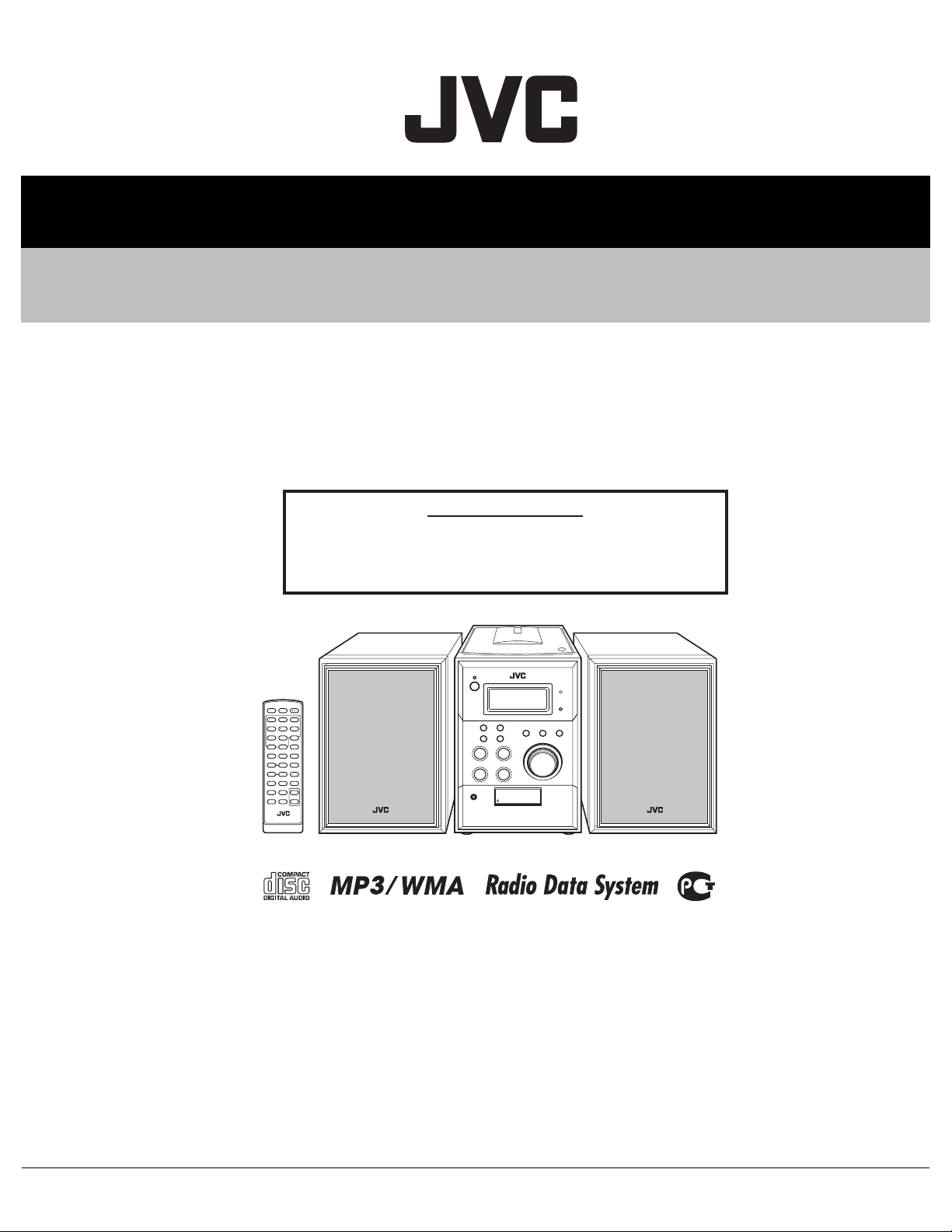
SERVICE MANUAL
MICRO COMPONENT SYSTEM
MB63420079SERVICE MANUAL
UX-G28B, UX-G28E, UX-G28EN,
UX-G28EV
SERVICE POLICY
No service part is available for this model.
Exchange only.
SP-UXG28SP-UXG28 CA-UXG28
EV only
COPYRIGHT © 2007 Victor Company of Japan, Limited
Lead free solder used in the board (material : Sn-Ag-Cu, melting point : 219 Centigrade)
TABLE OF CONTENTS
1 PRECAUTION. . . . . . . . . . . . . . . . . . . . . . . . . . . . . . . . . . . . . . . . . . . . . . . . . . . . . . . . . . . . . . . . . . . . . . . . . 1-3
2 SPECIFIC SERVICE INSTRUCTIONS . . . . . . . . . . . . . . . . . . . . . . . . . . . . . . . . . . . . . . . . . . . . . . . . . . . . . . 1-6
3 DISASSEMBLY . . . . . . . . . . . . . . . . . . . . . . . . . . . . . . . . . . . . . . . . . . . . . . . . . . . . . . . . . . . . . . . . . . . . . . . 1-7
4 ADJUSTMENT . . . . . . . . . . . . . . . . . . . . . . . . . . . . . . . . . . . . . . . . . . . . . . . . . . . . . . . . . . . . . . . . . . . . . . . 1-12
5 TROUBLESHOOTING . . . . . . . . . . . . . . . . . . . . . . . . . . . . . . . . . . . . . . . . . . . . . . . . . . . . . . . . . . . . . . . . . 1-13
COPYRIGHT © 2007 Victor Company of Japan, Limited
No.MB634
2007/9
Page 2

SPECIFICATION
Amplifier section Output Power 8 W per channel min. RMS driven into 4 Ω at 1 kHz with no more than 10% total harmonic
distortion. (IEC268-3)
Speakers/Impedance 4 Ω - 8 Ω
Terminals AUX IN Input sensitivity/Impedance (250mV/50kΩ):USB Ver.2.0 (Full Speed)
Compatible device Mass Storage Class
Compatible File System FAT16, FAT32
Bus Power supply Max 5V/500mA
Tuner section FM tuning range 87.50 MHz - 108.00 MHz
AM (MW) tuning range 522 kHz - 1 629 kHz
CD player section Dynamic range 70 dB
Signal-to-noise ratio 70 dB
General Power requirement AC 230 V , 50 Hz
Power consumption 32 W (at operation)
0.7 W (on standby)
Dimensions (approx.) 144 mm × 212 mm × 254 mm (W/H/D)
Mass (approx.) 2.5 kg
Speakers Type 1-way Bass reflex
Speaker units 10 cm cone × 1
Impedance 4 Ω
Dimensions (approx.) 136 mm × 212 mm × 178 mm (W/H/D)
Mass (approx.) 1.3 kg each
Design and specifications are subject to change without notice.
1-2 (No.MB634)
Page 3
SECTION 1
PRECAUTION
1.1 Safety Precautions
(1) This design of this product contains special hardware and
many circuits and components specially for safety purposes. For continued protection, no changes should be made
to the original design unless authorized in writing by the
manufacturer. Replacement parts must be identical to
those used in the original circuits. Services should be performed by qualified personnel only.
(2) Alterations of the design or circuitry of the product should
not be made. Any design alterations of the product should
not be made. Any design alterations or additions will void
the manufacturers warranty and will further relieve the
manufacture of responsibility for personal injury or property
damage resulting therefrom.
(3) Many electrical and mechanical parts in the products have
special safety-related characteristics. These characteristics are often not evident from visual inspection nor can the
protection afforded by them necessarily be obtained by using replacement components rated for higher voltage, wattage, etc. Replacement parts which have these special
safety characteristics are identified in the Parts List of Service Manual. Electrical components having such features
are identified by shading on the schematics and by ( ) on
the Parts List in the Service Manual. The use of a substitute
replacement which does not have the same safety characteristics as the recommended replacement parts shown in
the Parts List of Service Manual may create shock, fire, or
other hazards.
(4) The leads in the products are routed and dressed with ties,
clamps, tubings, barriers and the like to be separated from
live parts, high temperature parts, moving parts and/or
sharp edges for the prevention of electric shock and fire
hazard. When service is required, the original lead routing
and dress should be observed, and it should be confirmed
that they have been returned to normal, after reassembling.
(5) Leakage shock hazard testing
After reassembling the product, always perform an isolation check on the exposed metal parts of the product (antenna terminals, knobs, metal cabinet, screw heads,
headphone jack, control shafts, etc.) to be sure the product
is safe to operate without danger of electrical shock.Do not
use a line isolation transformer during this check.
• Plug the AC line cord directly into the AC outlet. Using a
"Leakage Current Tester", measure the leakage current
from each exposed metal parts of the cabinet, particularly any exposed metal part having a return path to the
chassis, to a known good earth ground. Any leakage current must not exceed 0.5mA AC (r.m.s.).
• Alternate check method
Plug the AC line cord directly into the AC outlet. Use an
AC voltmeter having, 1,000Ω per volt or more sensitivity
in the following manner. Connect a 1,500Ω 10W resistor
paralleled by a 0.15µF AC-type capacitor between an ex-
posed metal part and a known good earth ground.
Measure the AC voltage across the resistor with the AC
voltmeter.
Move the resistor connection to each exposed metal
part, particularly any exposed metal part having a return
path to the chassis, and measure the AC voltage across
the resistor. Now, reverse the plug in the AC outlet and
repeat each measurement. Voltage measured any must
not exceed 0.75 V AC (r.m.s.). This corresponds to 0.5
mA AC (r.m.s.).
AC VOLTMETER
(Having 1000
ohms/volts,
or more sensitivity)
0.15 F AC TYPE
Place this
probe on
1500 10W
Good earth ground
1.2 Warning
(1) This equipment has been designed and manufactured to
meet international safety standards.
(2) It is the legal responsibility of the repairer to ensure that
these safety standards are maintained.
(3) Repairs must be made in accordance with the relevant
safety standards.
(4) It is essential that safety critical components are replaced
by approved parts.
(5) If mains voltage selector is provided, check setting for local
voltage.
1.3 Caution
Burrs formed during molding may be left over on some parts
of the chassis.
Therefore, pay attention to such burrs in the case of preforming repair of this system.
1.4 Critical parts for safety
In regard with component parts appearing on the silk-screen
printed side (parts side) of the PWB diagrams, the parts that are
printed over with black such as the resistor ( ), diode ( )
and ICP ( ) or identified by the " " mark nearby are critical
for safety. When replacing them, be sure to use the parts of the
same type and rating as specified by the manufacturer.
(This regulation dose not Except the J and C version)
each exposed
metal part.
(No.MB634)1-3
Page 4
1.5 Safety Precautions (U.K only)
(1) This design of this product contains special hardware and many circuits and components specially for safety purposes. For con-
tinued protection, no changes should be made to the original design unless authorized in writing by the manufacturer. Replacement parts must be identical to those used in the original circuits.
(2) Any unauthorised design alterations or additions will void the manufacturer's guarantee; furthermore the manufacturer cannot
accept responsibility for personal injury or property damage resulting therefrom.
(3) Essential safety critical components are identified by ( ) on the Parts List and by shading on the schematics, and must never
be replaced by parts other than those listed in the manual. Please note however that many electrical and mechanical parts in
the product have special safety related characteristics. These characteristics are often not evident from visual inspection. Parts
other than specified by the manufacturer may not have the same safety characteristics as the recommended replacement parts
shown in the Parts List of the Service Manual and may create shock, fire, or other hazards.
(4) The leads in the products are routed and dressed with ties, clamps, tubings, barriers and the like to be separated from live parts,
high temperature parts, moving parts and/or sharp edges for the prevention of electric shock and fire hazard. When service is
required, the original lead routing and dress should be observed, and it should be confirmed that they have been returned to
normal, after re-assembling.
1.5.1 Warning
(1) Service should be performed by qualified personnel only.
(2) This equipment has been designed and manufactured to meet international safety standards.
(3) It is the legal responsibility of the repairer to ensure that these safety standards are maintained.
(4) Repairs must be made in accordance with the relevant safety standards.
(5) It is essential that safety critical components are replaced by approved parts.
(6) If mains voltage selector is provided, check setting for local voltage.
Burrs formed during molding may be left over on some parts of the chassis. Therefore,
pay attention to such burrs in the case of preforming repair of this system.
1-4 (No.MB634)
Page 5
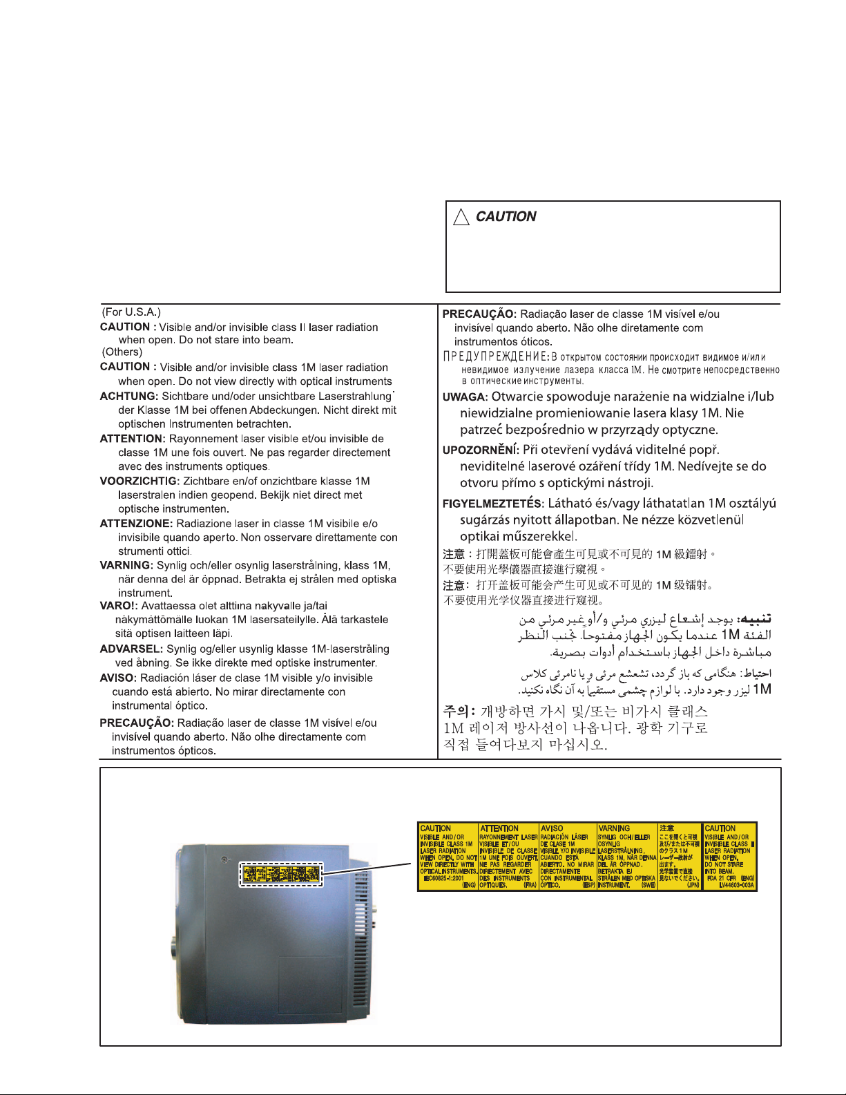
1.6 Important for laser products
1.CLASS 1 LASER PRODUCT
2.CAUTION :
(For U.S.A.) Visible and/or invisible class II laser radiation
when open. Do not stare into beam.
(Others) Visible and/or invisible class 1M laser radiation
when open. Do not view directly with optical instruments.
3.CAUTION : Visible and/or invisible laser radiation when
open and inter lock failed or defeated. Avoid direct
exposure to beam.
4.CAUTION : This laser product uses visible and/or invisible
laser radiation and is equipped with safety switches which
prevent emission of radiation when the drawer is open and
the safety interlocks have failed or are defeated. It is
dangerous to defeat the safety switches.
5.CAUTION : If safety switches malfunction, the laser is able
to function.
6.CAUTION : Use of controls, adjustments or performance of
procedures other than those specified here in may result in
hazardous radiation exposure.
!
Please use enough caution not to
see the beam directly or touch it
in case of an adjustment or operation
check.
REPRODUCTION AND POSITION OF LABELS and PRINT
WARNING LABEL and PRINT
(No.MB634)1-5
Page 6

SECTION 2
SPECIFIC SERVICE INSTRUCTIONS
This service manual does not describe SPECIFIC SERVICE INSTRUCTIONS.
1-6 (No.MB634)
Page 7

SECTION 3
DISASSEMBLY
3.1 Main body
3.1.1 Removing the REAR COVER (See Fig.1 to 4)
(1) Remove the two screws A attaching the both side of REAR
COVER. (See Fig.1)
(2) Remove the two screws B attaching the REAR COVER.
(See Fig.2)
(3) Remove the two screws C, two screws D and two screws
E attaching the REAR COVER. (See Fig.3)
(4) Disconnect the connector wire from MAIN BOARD assem-
bly connected to connector CN1102
BOARD assembly. (See Fig.4)
of the POWER
A
D
C
E
Fig.1
B
Fig.2
Fig.3
CN1102
Fig.4
(No.MB634)1-7
Page 8

3.1.2 Removing the POWER BOARD assembly (See Fig.5)
(1) Disconnect the connector wire from POWER TRANS-
FORMER connected to connector CN1101
the POWER BOARD assembly.
(2) Disconnect the POWER CORD connected to connector
CN1104
(3) Remove the three screws F attaching the POWER BOARD
assembly.
3.1.3 Removing the TUNER PACK (See Fig.6, 7)
(1) Remove the two screws G attaching the TUNER PACK.
(See Fig.6)
(2) Disconnect the card wire from MAIN BOARD assembly
connected to connector of TUNER PACK. (See Fig.7)
of the POWER BOARD assembly.
and CN1103 of
F
CN1104 CN1103 CN1101
Fig.5
G
1-8 (No.MB634)
Fig.6
connector
Fig.7
Page 9

3.1.4 Removing the MAIN BOARD assembly (See Fig.8 to 11)
(1) Disconnect the card wire from MAIN BOARD assembly
connected to connector CN710
bly. (See Fig.8)
(2) Disconnect the connector wire from DOOR SWITCH con-
nected to connector CN404
bly. (See Fig.9)
(3) Disconnect the connector wire from CONTROL BOARD
assembly connected to connector CN403
BOARD assembly. (See Fig.9)
(4) Disconnect the connector wire from USB BOARD assem-
bly connected to connector CN302
assembly. (See Fig.9)
(5) Remove the two screws H attaching the MAIN BOARD as-
sembly. (See Fig.9)
(6) Disconnect the connector wire from MAIN BOARD assem-
bly connected to connector CN702
sembly. (See Fig.10)
(7) Remove the solder the soldering earth wire from MAIN
BOARD assembly soldering to USB BOARD assembly.
(See Fig11)
CN710
of the CD BOARD assem-
of the MAIN BOARD assem-
of the MAIN
of the MAIN BOARD
of the CD BOARD as-
CN702
Fig.10
solder
CN404
Fig.8
H
Fig.11
CN302 CN403
Fig.9
(No.MB634)1-9
Page 10

3.1.5 Removing the USB BOARD assembly (See Fig.12, 13)
(1) Disconnect the connector wire from USB BOARD assem-
bly connected to connector CN703
sembly. (See Fig.12)
(2) Remove the two screws J attaching the USB BOARD as-
sembly. (See Fig.13)
of the CD BOARD as-
CN703
Fig.12
1-10 (No.MB634)
J
Fig.13
Page 11

3.1.6 Removing the CD MECHANISM assembly (See Fig.14)
(1) Remove the four screws K attaching the CD MECHANISM
assembly.
3.1.7 Removing the CD DOOR assembly (See Fig.15)
(1) Remove the two screws L attaching the CD DOOR assem-
bly.
K
K
Fig.14
L
Fig.15
(No.MB634)1-11
Page 12

3.1.8 Removing the FRONT BOARD assembly (See Fig.16)
(1) Remove the VOLUME KNOB.
(2) Remove the eight screws M attaching the FRONT BOARD
assembly.
M
M
Fig.16
SECTION 4
ADJUSTMENT
This service manual does not describe ADJUSTMENT.
1-12 (No.MB634)
Page 13

5.1 BLOCK DIAGRAM
SECTION 5
TROUBLESHOOTING
FM ANT. AM ANT.
IC701 74HC4094
DISC
PICKUP
SPINDLE
MOTOR
SLED
MOTOR
CD DOOR
LEAF SW
LCD
LCD DRIVER
IC705 HT1622
KEY
USB
REMOTE
SENSOR
M
M
IC712
KS161622
SDRAM
IC903
SA9614
MOTOR/ACTUATOR
DRIVER
IC711
SST39FV800A
FLASH MEMORY
IC710
TS2501
(SA9259)IC902
CD+8V
Q911
764
3.3V
1.8V
IC714
1117-18 1117-33
IC901
SC9641
CD+8V
IC716
IC707
ATMEGA8
+3.3V
R-OUT
IC713
L-OUT
CE2711
3.3V
+5V
STANDBY
CD+8V
IC704
7805
IC702(3.3V)
1117-33
TU+9V
IC501 SC7314
SIGNAL SLECT SW.
VOL CONTROL
+9V
+9V
IC401
7809
Q407
B1185F
FM/AM/RDS TUNER BOARD
L-OUT
R-OUT
LA4638IC301
POWER AMP
VCC
RECTIFIER
STANDBY
Q404
B772
RECTIFIER
JK302
HEADPHONE
SMALL
TRANSFORMER
Q1101
Q1102
POWER
TRANSFORMER
AUX IN
R.SPK OUTPUT
L.SPK OUTPUT
AC INPUT
RELAY
(No.MB634)1-13
Page 14

< MEMO >
(No.MB634)1-14
Page 15

5.2 STANDARD SCHEMATIC DIAGRAMS
5.2.1 Main section
DGND
22
A15
21
A14
20
19
A12
18
17
16
A9
15
A8
14
D20
13
D21
12
D17
11
D16
CN705
10
D15
9
TO CN710 (CD PWB)
B7
8
B2
TU-DO
7
B8
6
B9
5
AD2
4
AD0
3
HC4094-3V3
2
DGND
1
AUX-L
4
AGND
3
AUX-R
2
CN302
AGND
1
TO CN603 (USB PWB)
R-OUT
1
AGND
2
L-OUT
3
DGND
4
+5V
5
CN407
DGND
6
+8V
TO CN702 (CD PWB)
7
L703
CD DOOR SW
TO CN404 (MAIN PWB)
RDS-CLK
IR/IN
JOG1
HC4094-CLK
HC4094-DATA
RDS-DATA
MCU-SCL
12C-SCL
12C-SDA
MCU-SDA
HC4094-STRB
CD-SW
JOG2
OR
R717
JMP16
CD-SW
R758
2K2
R443
1K
2K2
3.5x9-237-T
DGND
M16
M66
M19
M22
M23
M65
M54
M35
M36
M37
M10
M15
M09
M08
M01
M67
M63
M68
M69
M64
M65
M06
M67
1
2
R405 22
M06
M63
M49
M48
M50
M10
M23
M22
M55
M42
M35
M36
R603
C604
M68
270P
R604
36K
M69
C605
270P
M65
M64
M06
R503
M45
M47
R504
M43
M42
M44
M55
M67
R766
10K
M63
M09
TO CD DOOR SW
36K
R518
R517
1K
R723
CN404
2K
2K
33K
33K
1
CD-SW
R602
C602
R605
C603
C537
4K7
R510
DGND
2
102
102
CD-L
C506
1uF
CD-R
15k
15k
102
102
C536
C517
102M
TO CN704 (CONTROL PWB)
3
2
1
LCD/RD
LCD/WR
VCC3.3V
LCD/DATA
M58
M17
M34
M33
47
R735
104
C701
R738
DGND
2K2
R737
2K2
R736
2K2
R722
R701
R702
R733
R732
R715
R716
DGND
AGND
C503
R502
1uF
47K
R508
C526
390P47K
C525
390P
3K9
R507
102M
C507
3K9
R509
TU-L
TU-R
4K7
R511
C518
102M
R428
4.7 1/4W
1000uF/16V
104
C787
C704
4
LED+5V
M43
102M
C519
CN403
5
JMP96
M58
4.7uF
C606
4.7uF
9
8
7
6
AD2
DGND
3.5x9-237-T
AD0
M01
M67
JOG1
R706 1K
M19
11
13
12
10
IR
AD6
JOG2
1K
TIMER-LED
R724
M56
M02
M08
M59
16 15 14 13 12 11 10 9
0E
Q5
74HC4094
SCL
Q6
IC701
Q1
VDD
STR
SDA
1K
1K
1K
2K2
2K2
100
100
100P
100P
C505
C601
104
C523
C504
C522
1uF
C521
1uF
104
C524
8
13
9
14
10
15
11
16
AUX L
AUX R
TAP E L
TAP E R
CD L
CD R
TUNER L
TUNER R
25
DGND
VDD
1
SDA
GND
26
2
22uF
4.7uF
C512
27
SCL
IC501
SC7314
CREF
28
C520
4.7uF
OUT(R)
OUT(L)
C502
C501
100uF
100
R501
Q407
D406
IN4148
IN4148
104
1000uF/16V
Q406
D405
C410
C412
R418
470 1/8W
Q7
Q2
18
IN(R)
IN(L)
B1185F
C9014
104M
C510
C513
12
17
LOUD(R)
LOUD(L)
765
104M
104M
C508
C516
C411
220uF/16V
Q8
Q3
5K6
R734
104M
20
BIN(R)
BOUT(R)
OUT R
OUT L
BIN(L)
BOUT(L)
22
C509 124M
R505
R425
2.2(1/2W)
10K
R422
NC
Q4
DGND
MUTE
R506
C511
124M
3
19
TREBLE(R)
TREBLE(L)
4
21
C515
R420
470 1/8W
4K7
R419
TO TUNER MODULE
3
2
1
TU-L
TU-R
DGND
M47
M45
NC
GND
87654321
5K6
272M
C514
24
23
272M
5K6
AGND
Q405
C8550
8V2
ZD403
4
TU-CE
TU+9V
OR
R761
M44
1uF
C309
1uF
CN504
6
5
TU-DI
TU-CL
OR
OR
R760
R759
M48
M49
C320
104
C532
R424
4.7(1/4W)
4K7
R417
8
7
TU-DO
OR
R762
M50
M15
R304C304
4K7
22uF/16V
DGND
100uF
C404
IN4148
D408
IN4148
2K7
100uF
R416
C409
9
10
RDS-DATA
M54
R316 2K2
R303
4K7
IC704 7805
1
OUT
2
D407
10K
R421
11
RDS-CLK
47
R765 1K
R516
M16
M06
R301
R302
R-CH
IN
GND
NC
C407
C9014
Q408
10K
R515
4K7
4K7
R401
3
2.2 1W
Q401
8550
AGND
L-CH
C334
C333
R411
470
M43
M34
M33
102102
R306 R305
4K7
R410
OR
9014
Q403
MAIN PWB
Q302
2SD19362SD1936
Q301
C301
0.1uF
C405
100uF/16V
VCC
CER318
C302
0.1uF
VCC
L707
10uH
104
47uF
C705
DGND
C702
104
C725
IN1DCPRE-GND
CEL308
3.5x9-237-T
1k
CEL309
3.5x9-237-T
CER317
1k
C305 C306 CEC327
IC401 7809
1
OUT
IN
GND
2
104
C414
R413
2K2
C408
100uF
102
C784
1k
R317
100uF
C308
3
X702
32.768K
C717
DGND
104
102
C785
C720
R704
15K
C327
470P560P3323324K7
R414
24P
104
C719
100uF/16V
15K
STBY
C314
Q402
C718 24P
3K6
R315
R412
2K2
9014
8
PB7
7
PB6
6
VCC
5
GND
4
VCC
3
GND
2
PD4
PD3
1
D413
IN4148
ON-TIME
1k
R318
102
33uF
C307
C331
Q404
B772
9
10
PD5
PD6
IC707
Atmega8
PD1
PD2
31
32
M56
IC301
LA4628
IN2
1uF
470P
560P
C328
CEC328
11
1213141516
PB0
PB1
PB2
PD7
AVCC
ADC6
AREF
GND
ADC7
PD0
PC6
PC5
PC4
3029282726
M65
M37
POP
87654321
C313
154M
2.2
R311
C317
17
PB3
PB4
18
PB5
19
20
21
22
PC0
23
PC1
24
PC3
PC2
25
D410
D701
M17
M66
+OUT2
C312
R310
IN4148
IN4148
R513
R512
R514
M56
-OUT2
9
154M
2.2
4K7
R415
R705
10
102
102
C703
C722
DGND
3K9
3K9
3K9
+OUT1
PWR-GND2
C311
R309
R423
OR
1
104
100uF
C533
C406
VCC
M43
PWR-GND1
154M
2.2
IC702
LM1117(3V3)
OUT
DGND
2
-OUT1
C310R308
154M
2.2
ZD401ORR409
3
IN
VCC
R793
M60
VCC
1413121110
10K
M59
10K
R792
M [00:80]
M02
M40
M01
102
C332
C319
220uF/16V
DGND
10
2K2
R731
M60
M40
IN4148
D404
271 271
C401
R
426
D401
R320
L306
10T
R319
L305
10T
L307
3.5x9-237-T
C321C322
C402 104
3300uF/25V
1K
IN4001
L302
4.7uH/2A
L302
4.7uH/2A
C329
L303
4.7uH/2A
L304
4.7uH/2A
R313
47
47
R312
47
47
C335 C336
682 682
102
C330
102
103
C324
1
2
3
4
5
6
7
102
C325
102
103
C326
C323
3.5x9-237-T
JK302
102
102
L308
R-WOOFER
40HM 8-15W
L-WOOFER
40HM 8-15W
+12V
DGND
PCON
+6.5V
1
2
3
CN401
4
TO CN1102 (RECTIFIER PWB)
1-15
Page 16

5.2.2 Front section
DGND
1
D+
2
D-
3
CN602
USB+5V
4
TO CN703 (CD PWB)
SEBG160808U300MT
L604
SEBG160808U300MT
L605
SEBG160808U300MT
L602
SEBG160808U300MT
L603
C610
1P
100uF/6.3V
C611
1P
C612
102
4
GND
3
D+
2
D-
1
VCC
GND
GND
5
6
C609
JK601
TIMER-LED
CN704 TO CN403 (MAIN PWB)
LCD/DATA
JOG2
AD6
JOG1
AD0
AD2
DGND
LED+5V
VCC3.3V
LCD/WR
LCD/RD
13
12
11
10
IR
9
8
7
6
5
4
3
2
1
SS338AL
D702
IN4148
SW713
ON/STAND BY
SW706
RESET UP/F-SKIP
SW709
USB/PLAY
SW702
SLEEP/CLOCK
SW705
PRESET DN/B-SKIP
RE701
R790
100
R743
27K
R752
8.2K
R742
12K
R746
1K
C712
C711
C713
R744
47uF
104
104
100
C714
10P
VR701
C709
C708
R755
2.2K
R753
82K
R754
27K
R751
5.6K
R750
8K2
R756
3K6
R749
47K
NC
4K7
4K7
R781
R780
C716
100P
100P
SW707
TUNER/BAND
SW711
TU-DN
SW710
CD/PLAY
SW701
TIMER
SW703
STOP
SW708
TU-UP
SW712
MEMORY
1uF
C715
R795
1K
Q703
8550
Q701
8550
R739
R741
1K
R740
1K
R747
C710
2.7K
100104
R796
1K
TIMER LIGHT
Q702
9014
R782
150
64
SEG31
63
SEG30
62
SEG29
61
SEG28
60
SEG27
59
SEG26
58
SEG25
57
SEG24
56
SEG23
55
SEG22
54
SEG21
53
SEG20
52
NC
R794
2k7
LED703
STAND BY
LED702
R789
4K7
10K
R745
1
CS
NC
RD
WR
NCNCNC
SEG19
51
1
REPEAT 1 GROUP RANDOM PROG. RDS NEWS INFO
SLEEP HBS JAZZ ROCK POP CLASSIC ST MONO
8765432
9
11
1213141516
10
17181920212223
TAP EUSBCDMP3WMATRACK
LCD701
C788
104
LED701
BACK LIGHT
6K8
R748
8765432
9
11
171819
1213141516
10
T1T2T3
VSS
OSCI
DATA
HT1622
SEG17
SEG18
IRQ
VDD
VLCD
IC705
SEG16
SEG15
SEG14
44454647484950
43
BZNCBZ
SEG13
SEG12
4140393837
42
SEG11
SEG10
SEG9
SEG8
COM0
SEG7
36
COM2
COM1
COM3
COM4
COM5
COM6
COM7
SEG0
SEG1
SEG2
SEG3
SEG4
SEG5
SEG6
NCNCNC
353433
NC
20
21
22
23
24
25
26
27
28
29
30
31
32
REC
KHz
MHz
DGND
L-OUT
1
AGND
2
R-OUT
CN603
3
4
AGND
C608
200P
R608
NC
TO CN302 (MAIN PWB)
25
24
AGND
200P
C607
NC
R607
L606
47uH
47uH
L607 R611
L608
47uH
R612
USB PWB
1K
1K
DGND
JK602
AC INPUT
Q1101
9014
NC
+12V
1
DGND
2
P-CON
3
+6.5V
CN1102
4
TO CN401 (MAIN PWB)
DGND
R1101
10K
C111 3
R1102
Q1102
9015
C1107
1K
104
104
C1105
C1106
R1103
47
D1105
IN4148
D1109
IN4001
C1108 1000uF/25V
473
C111 2
6800uF/25V
473
C1101
473
C1104
473
C1109
D111 2
IN4001
D111 0
C1111
D1101
IN5401
D1104
IN5401
IN4001
473
C111 0
D1111
C1102
C1103
473
473
473
IN4001
D1102
IN5401
D1103
IN5401
PT1101
1
2
F1101
T6.3A L 250V
T1101
TR1
TRANSFORMER
4
3
C111 4
103/500V
3
4
L1101
F1102
T400mA L 250V
2
1
AC 230V IN
2
1
2
1
RECTIFIER PWB
DGND
CONTROL PWB
1-16
Page 17

5.2.3 CD section (1/2)
TO: 4 OF 4
XD[0:100]
CD-BCK
XD11
CD-LRCK
XD10
CD-PCMD
XD12
XA8
XA4
XA9
XA10
XA[0:21]
1K
R939
R940
100R
R944
4.7K
Q913
8050
C950
100UF/10V
CER2 10K
C952
104P
10UF/10V
C951
R934
100R
R935
100R
C956
323130292827262524232221201918
33
34
35
36
37
38
39
40
41
42
43
44
45
46
47
48
ACK
DATA7
DATA6
DATA5
DATA4
DATA3
DATA2
DATA1
DATA0
TEST
REST
VDDA
VSSO
VDDO
VREF
R
CL16
MCLOK
DATA_IN
SCLK_IN
NC/ACLK
DATA/WR
STB/RD
IC901
SC9641
CRCLL
RAD
FOC
SLED
495051525354555657585960616263
VSSP
C949
100UF/10V
100R
100R
R937
R936
NC
ERR
WCLK_IN
DATA_OUT
SCLK_OUT
OVER_FLOW
BCLOK
MOTO
VDDP
100R
R938
MUTE
MUTE
WCLK_OUT
VDD
GND
TRAY_SW
R946
R945
16.9344MHz
R942
330R
17
CRIN
VDDA2
CROUT
VSSA2
RFREF
RFIN
ID ATA
VAD E
VCOM
LDON
VDDA1
VSSA1
SLED_SW
64
1K
1K
SLED_SW
R941
100K
Y900
22P
C943
16
15
14
13
12
11
10
9
8
E
7
F
6
D
5
C
4
A
3
B
2
1
SW903
22P
C944
C958
104P
C948
104P
C947
22P
R943
22K
104P
C945
C946
223P
R918
1K
C923
C915
560P
104P
R921
3K
220P
C900
220P
C901
220P
C902
220P
C903
IN4148
C930
104P
220P
C904
R930
D901
2.2R
R900
R901
R902
R903
R904
R905
220P
C905
USB5V
CD_VCC
R926
22K
104P
C932
R924
10K
10K
10K
10K
10K
10K
22K
C961
R923
5.6K
R919
12K
104P
220P
C906
C933
47UF/16V
C926
104P
220P
C907
C957
100UF/10V
C934
104P
R922
5.6K
220P
C927
R920
12K
C924
102P
220P
C908
22K
R925
220P
C909
C935
102P
C936
102P
R907
R908
R909
R910
R911
R912
220P
C910
220P
C912
68K
13K
13K
13K
13K
68K
2
1
MOTOR
Sled
15
OUT5B
16
OUT5A
17
OUT3A
18
OUT3B
19
IN3A
20
LDCTL
21
VCC2
22
VCC1
23
VREF
24
IN4B
25
IN4A
26
OUT4B
27
OUT4A
28
GND3
U902
SA9259
IN5B
GND1
OUT2A
OUT2B
IN2A
IN5A
GND
MUTE
REO
REG
IN1B
IN1A
OUT1B
OUT1A
C925
14
13
12
10
104P
R928
2.2R
C941
104P
C939
104P
C942
47UF
2.2K
TO DA11 MMV
R929
C940
100UF
1
MOTOR
Spindle
2
11
9
8
7
6
5
4
3
2
1
12K
R927
C928
47UF/16V
R906
10R
C955
104P
82R
R913
C929
100UF/10V
Q911
2SB764
FOCRADRAD+
FOC+
MON
VR
LD
GND
F
C
B
A
D
E
RF VCC
VCOM
CN904
16
15
14
13
12
11
10
9
8
7
6
5
4
3
2
1
R947
150K
C919
100U/10V
R949
R961
1M
1K
104C971
NC
R976
104C962
103C918
NC
R977
R962
68K
R1
NC
104P
C917
U903
104P
NC1
VREF
GND
PD2
PD1
SA9614
MON
LD
LTH
8
7
6
5
4
3
2
1
33KR914
33KR915
33KR916
33KR917
L910
10UH
C
Q912
B
8550
104P
C913
E
75K
R960
C921
10R
R950
9
NC2
10
RFM
11
RFO
12
RFI
13
RFTC
14
AGC
15
LDON
16
VDD
R948
4K3
C764
10P
C920
100UF/10V
1-17
Page 18

5.2.4 CD section (2/2)
XC[01:20]
XC01
XC02
XC03
XC08
VDD3.3D
XC05
XC06
XC07
XC02
NC
*
C726
R763
VDD3.3D
L720
10UK
VSS3D_0
VSS3D_1
VSS3D_2
IC710
nWE
nOE59SD_CKE/GPIO_B0
58
100P
C728
XC02
XC03
1
88
55
110
120
VSS3D_3
VSS3D_4
VSS2D_0
VSS2D_1
VSS2D_2
VSS2D_3
GND
EXTERNAL
INTERRUPT
SD_CLK44SD_nCS/GPIO_B146EXIN0/GPIO_A12
56
121
100
1K
R704
R764
104
C704
330
R703
XC06
XC05
XC07
XE51
XE52
8
25
868580
VSS2D_4
VSS2D_5
VSS_ADC_0
VSS_ADC_1
GSIO &
SYSTEM
CONFIG
USB
INTERFACE
UART
INTERFACE
AD
CONVERTER
EXIN1/GPIO_A13
EXIN2/GPIO_A14
EXIN3/GPIO_A15
ADIN0
828384
122
123
124
L705
2K5/100MHz
100P
C702
R702
102
20P
C753
C703
XE33
XE50
XE33
79
GPIO_A0/SDO_0
VSS_PLL_0
VSS_PLL_1
GPIO_A1/SCK_0/CBCLK
GPIO_A2/FRM_0/CLRCK
GPIO_A3/SDI__0/CDAI
GPIO_A4/SDO_1
GPIO_A5/SCK1
GPIO_A6/FRM_1
GPIO_A7/SDI_1
BW0/GPIO_A8/SDO_2
BW1/GPIO_A9/SCK_2
GPIO_A10/FRM_2
GPIO_A11/SDI_2
USB D+/GPIO_B26
USB D-/GPIO_B27
USB HD+/GPIO_B28
USB HD-/GPIO_B29
UART_TXD/GPIO_B8
UART_RXD/GPIO_B9
BM0/GPIO_B21/BCLK
BM1/GPIO_B22/LRCK
GPIO_B23/MCLK
BM2/GPIO_B24/DAO
GPIO_B25/DAI
CODEC
INTERFACE
ADIN2
ADIN4
nRESET
RDAEY/MODE0
727398
10K
300uH
CER110K
R757
C713
100P
L704300uH
10K
R745
VDD3.3D
XE59
XE[0:100]
XE49
104
105
106
107
108
111
113
114
115
116
117
118
51
52
53
54
60
61
62
63
66
67
68
90
GPIO_D15
GPIO_D16
91
GPIO_D17
92
GPIO_D18
93
GPIO_D19
94
GPIO_D20
95
GPIO_D21
96
SYSTEM
MODE1
CONFIG
R735
100K
R734
IC715
23
MAX809
RST
100K
102
C758
R768
XC08
XE57
R733
47K
100PC761
10K
GND
1
47K
R767
VCC
R760
4.7K
R718
4.7K
R744
R732
OR
XE53
XE54
XE55
XE56
7
71778197654532
119
109
VDD_COR_0
VDD_COR_1
+1.8V
XTIN
XTOUT
XFILT
707869
1K
R713
C730 350P
VDD_COR_2
244187
VDD_OSC
VDDA_PLL
VDD_COR_3
VDD_COR_4
VDD_COR_5
+1.8V +3.3V
MEMORY CONTROL
nCS0/ND_nOE0/GPIO_B2
nCS1/ND_nOE1/GPIO_B3
nCS2/ND_nOE2/GPIO_B4
nCS3/ND_nOE3/GPIO_B5
495048
47
1K
100P
C729
R712
XC01
XE26
XE13
XE49
VDDA_ADC
TS2501
ND_nWE/GPIO_B7
57
XE58
89
33
76
64
16
XA0
25
DQ0
R758 47K
24
23
22
21
20
19
18
8
7
6
5
4
3
2
1
48
17
16
9
26
11
28
47
12
10
A0
A1
A2
A3
A4
A5
A6
A7
A8
A9
A10
A11
A12
A13
A14
A15
A16
A17
A18
A19
CE
WE
OE
BYTE
RST
DQ15/A-1
DQ1
DQ2
DQ3
DQ4
DQ5
DQ6
DQ7
DQ8
DQ9
SST39VF800A
DQ10
DQ11
DQ12
DQ13
IC711
DQ14
RY/BY
VCC
I-VPP
I-WP#
GND1
GND2
XA1
XA2
XA3
XA4
XA5
XA6
XA7
XA8
XA9
XA10
XA11
XA12
XA13
XA14
XA15
XA16
XA17
XA18
XA19
XA[0:21]
10K
XA0
21
A0
22
XA1
A1
23
XA2
A2
24
XA3
A3
27
XA4
A4
28
XA5
A5
29
XA6
A6
30
XA7
A7
31
XA8
A8
32
XA9
A9
20
XA10
A10
BA/A11
CLK
CKE
CS
RAS
CAS
WE
DQML
DQMH
NC1
NC2
VSS1
VSS2
DQ10
DQ11
DQ12
DQ13
DQ14
DQ15
IC712
VCC1
M12L16161A
VCC2
VCCQ1
VCCQ2
VCCQ3
VCCQ4
VSSQ1
VSSQ2
VSSQ3
VSSQ4
XA13
XA16
XA15
XA21
XA20
19
35
34
18
17
16
15
14
36
33
37
26
50
XD0
29
XD1
31
XD2
33
XD3
35
XD4
XD10
XD11
XD12
XD13
XD14
XD15
XD5
XD6
XD7
XD8
XD9
XD0
XD1
XD2
XD3
XD4
XD5
XD6
XD7
XD8
XD9
XD10
XD11
XD12
XD13
XD14
XD15
XD[0:15]
XD0
XD1
XD2
XD3
XD4
XD5
XD6
XD7
XD8
XD9
XD10
XD11
XD12
XD13
XD14
XD15
XA0
XA1
XA2
XA3
XA4
XA5
XA6
XA7
XA8
XA9
XA10
XA11
XA12
XA13
XA14
XA15
XA16
XA17
XA18
XA19
XA20
XA21
C731
17
18
19
20
21
22
23
26
27
28
29
30
31
34
35
36
37
38
39
40
42
43
125
126
127
128
2
3
4
5
6
9
10
11
12
13
14
15
R739
100K
X700
12MHz
22P
38
40
42
44
30
32
34
36
39
41
43
45
15
37
13
14
27
46
2
DQ0
3
DQ1
5
DQ2
6
DQ3
8
DQ4
9
DQ5
11
DQ6
12
DQ7
39
DQ8
40
DQ9
42
43
45
46
48
49
1
25
7
13
38
44
4
10
41
47
112
AX0
VDDIO_0
VDDIO_1
VDD3_USB
AX1
AX2
AX3
AX4
AX5
AX6
AX7
AX8
AX9
AX10
AX11
AX12
AX13/SD_BAO
AX14/SD_AB1
AX15/SD_nCAS
AX16/ND_ALE/SD_nRAS
AX17/ND_CLE
AX18
AX19
AX20/DQM1
AX21/DQM0
XD0
XD1
XD2
XD3
XD4
XD5
XD6
XD7
XD8
XD9
XD10
XD11
XD12
XD13
XD14
XD15
TDI
99
TMS
100
R738
C732
TJAG
100
22P
+2.7V
ADDRESS BUS
DATA BUS
TDO
nTRST
TCK
102
101
103
VDDIO_2
VDDIO_3
CLOCK
XIN
74
PKG1
560K
CER3
XOUT
75
XD30
1K
47K
R754
R755
C737
100P
XD60
XD10
XD11
XD12
XD27
XD15
XD16
XD17
XD18
XD9
XD1
XD28
XD29
XD31
XD[0:100]
XD32
R729 1K
1
DAO
R727 1K
2
BCLK
R728 1K
3
R731
LRBLK
4
MCLK
47K
NC
*
R766
100P
C738
R721 1K
47K
47K
R730
100P
C739
1K
R743
R_OUT
IC713 CE2711
AGND
L_OUT
8
7
VCC
6
5
C757
R765
100
+
104
C748
220uF
AGND
R759
Q723
B772
100
4K7
R769
Q722
8050
R752 2K2
R748
R749
VDD3.3D
R753
2K2
AGND
56
56
R750
C763
15K
350P
C762
R751
350P
USB+5V
15K
DGND
DGND
L_OUT
AGND
R_OUT
DGND
+8V
+5V
D-
D+
7
6
5
4
CN702
3
2
1
4
3
2
CN703
1
TO CN602 (USB PWB)
+
C954
C953
470uF/16V
TO CN407 (MAIN PWB)
104
CD_VCC
VDD3.3D
VDD1.8D
USB5V
DGND
1
HC4094-3V3
2
AD0
3
AD2
4
B9 JOG2
5
B8 CD-SW
6
B2 TU-DO
7
B7 HC4094-STRB
8
D15 MCU-SDA
9
D16 I2C-SDA
10
D17 I2C-SCL
11
CN710
D20 RDS-DATA
12
D21 MCU-SCL
13
TO CN705 (MAIN PWB)
A8 HC4094-DATA
14
A9 HX4094-CLK
15
A10 LINE-DET
16
17
A12 JOG1
18
19
A14 IR/IN
20
A15 RDS-CLK
21
DGND
22
VDD3.3D
XE34
XE[0:100]
XE50
XE33
XE59
1K
R716
XD32
100P
C708
XE52
1K
C712
100P
VDD3.3D
XD31
XD18
XD30
XD9
XD1
XD[0:100]
102
C740
R746 1K
47K
R717
VDD3.3D
100P
100P
C705
100P
C706
C756
R707 1K
R710 1K
47K
R709
VDD3.3D
R708
XE55
XE56
10K
XE49
XE58
XE57
XE56
XE55
XE54
XE53
VDD3.3D
8
VCC
GND GND
7
6
SCL
5
SDA
104
C741
GND
GND
IC916
AM24LC02
GND
104
C742
1
2
3
4
C743
104
104
C745
C746
10K
10K
102
R736
R737
C378
VDD3.3D
104
104
C747
104P
C720
C721
104
C723
104
C724
1K
R715
R714
C711
100P
VDD1.8D
47K
47K
R725
TO: 4 OF 4
XD[0:100]
XD28
XD29
104
104
104
C755
C725
XE13
XE26
TO: 4 OF 4
XE [0:100]
R726
R723
OR
R724
OR
R720
OR
R722
OR
XA10
XA04
XA08
XA09
104
C749
TO: 3 OF 4 XA[0:21]
C750
104
104
C751
C752
104
104
C754
IC714 IC716
AMS1117(1.8V)
2121
VOUT VIN
GND
3
+
C736
100uF
+
C735
CW1117(3.3V)
VOUT VIN
3
100uF
GND
+
104
C734
47uF
C733
1-18
Page 19

< MEMO >
Page 20

Victor company of Japan, Limited
Audio/Video Systems category 10-1,1chome,Ohwatari-machi,Maebashi-city,371-8543,Japan
(No.MB634)
Printed in Japan
VPT
 Loading...