

Page 1
SERVICE MANUAL
MB748<Rev.002>201012SERVICE MANUAL
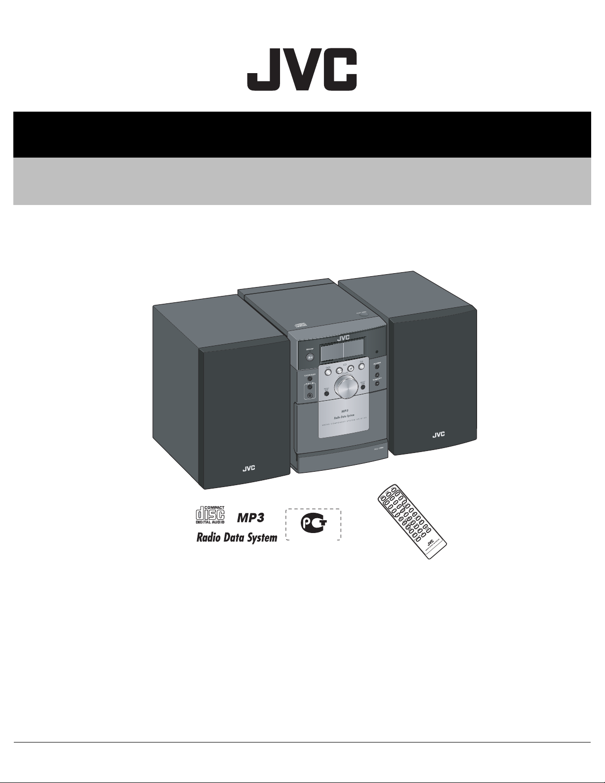
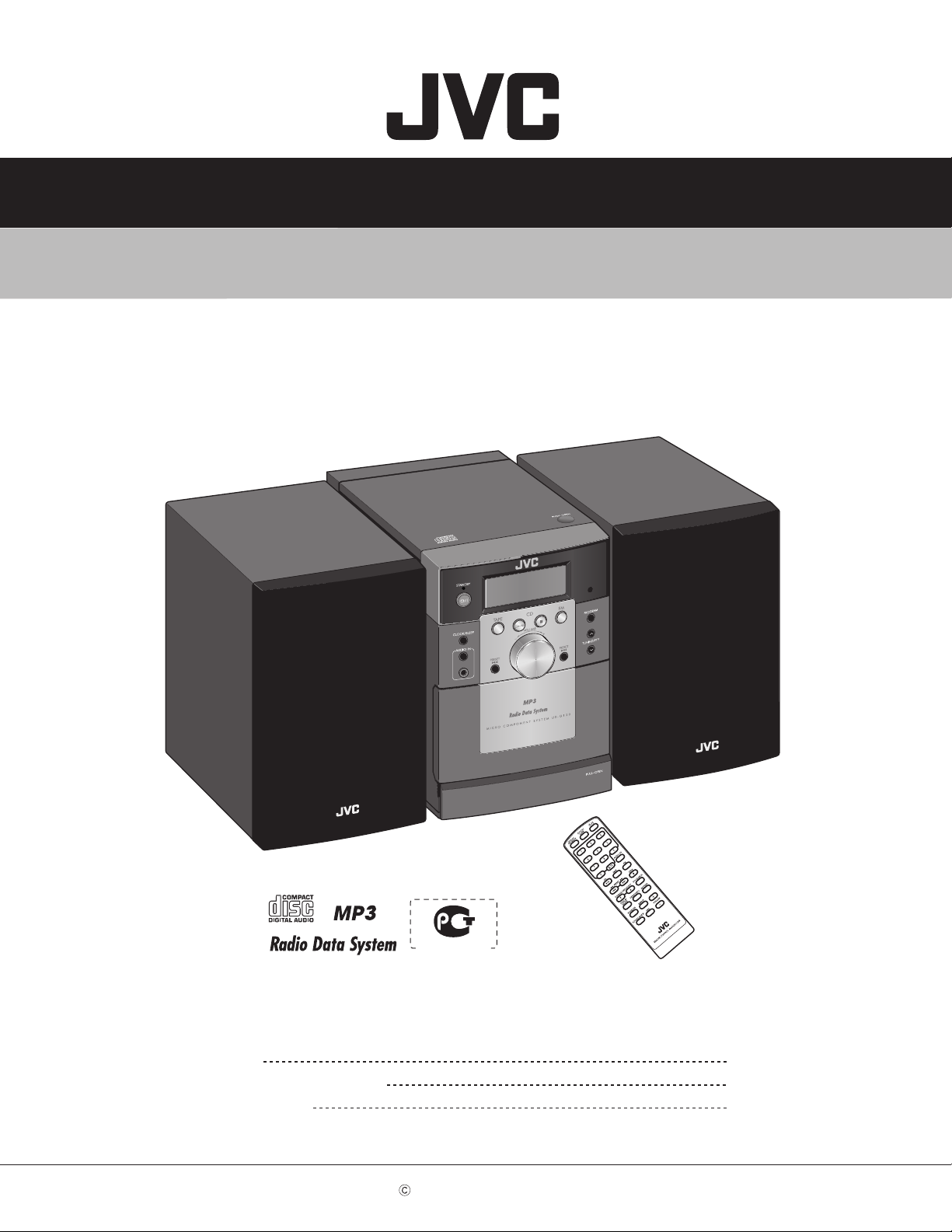
UX-G120E, UX-G120EY
MICRO COMPONENT SYSTEM
SP-UXG120
CA-UXG120
SP-UXG120
For Russian
COPYRIGHT © 2010 Victor Company of Japan, Limited
Lead free solder used in the board (material : Sn-Ag-Cu, melting point : 219 Centigrade)
Lead free solder used in the board (material : Sn-Cu, melting point : 230 Centigrade)
TABLE OF CONTENTS
1 PRECAUTION. . . . . . . . . . . . . . . . . . . . . . . . . . . . . . . . . . . . . . . . . . . . . . . . . . . . . . . . . . . . . . . . . . . . . . . . . 1-3
2 SPECIFIC SERVICE INSTRUCTIONS . . . . . . . . . . . . . . . . . . . . . . . . . . . . . . . . . . . . . . . . . . . . . . . . . . . . . . 1-6
3 DISASSEMBLY . . . . . . . . . . . . . . . . . . . . . . . . . . . . . . . . . . . . . . . . . . . . . . . . . . . . . . . . . . . . . . . . . . . . . . . 1-6
4 ADJUSTMENT . . . . . . . . . . . . . . . . . . . . . . . . . . . . . . . . . . . . . . . . . . . . . . . . . . . . . . . . . . . . . . . . . . . . . . . . 1-9
5 TROUBLESHOOTING . . . . . . . . . . . . . . . . . . . . . . . . . . . . . . . . . . . . . . . . . . . . . . . . . . . . . . . . . . . . . . . . . . 1-9
COPYRIGHT © 2011 Victor Company of Japan, Limited
No.MB748<Rev.002>
2011/1
Page 2
SPECIFICATION
Main unit
Amplifier section
Output Power
Speakers/Impedance 4 Ω - 8 Ω
Terminal
AUDIO IN Input sensitivity/Impedance
FM tuner section
Tuning range 87.50 MHz - 108.00 MHz
CD player section
Dynamic range 60 dB
Signal-to-noise ratio 60 dB
Wow and flutter Immeasurable
Cassette deck section
Frequency response Normal (type I) 125 Hz - 8 kHz
General
Power requirement AC 230 V , 50 Hz
Power consumption 23 W (at operation)
Dimensions (approx.) 140 mm × 209 mm × 208 mm (W×H×D)
Mass (approx.) 2.2 kg
Type 1-way Bass reflex
Speaker units 8 cm cone × 1
Impedance 4 Ω
Dimensions (approx.) 135 mm × 209 mm × 175 mm (W×H×D)
Mass (approx.) 1.2 kg each
3 W per channel, min. RMS,driven into 4 Ω at 1 kHz with no more than 10% total harmonic distortion.
(IEC268-3)
500 mV / 50 kΩ
Wow and flutter 0.35% (WRMS)
1. 00 W or less (on standby)
Speakers
• Design and specifications are subject to change without notice.
1-2 (No.MB748<Rev.002>)
Page 3
SECTION 1
PRECAUTION
1.1 Safety Precautions
(1) This design of this product contains special hardware and
many circuits and components specially for safety purposes. For continued protection, no changes should be made
to the original design unless authorized in writing by the
manufacturer. Replacement parts must be identical to
those used in the original circuits. Services should be performed by qualified personnel only.
(2) Alterations of the design or circuitry of the product should
not be made. Any design alterations of the product should
not be made. Any design alterations or additions will void
the manufacturers warranty and will further relieve the
manufacture of responsibility for personal injury or property
damage resulting therefrom.
(3) Many electrical and mechanical parts in the products have
special safety-related characteristics. These characteristics are often not evident from visual inspection nor can the
protection afforded by them necessarily be obtained by using replacement components rated for higher voltage, wattage, etc. Replacement parts which have these special
safety characteristics are identified in the Parts List of Service Manual. Electrical components having such features
are identified by shading on the schematics and by ( ) on
the Parts List in the Service Manual. The use of a substitute
replacement which does not have the same safety characteristics as the recommended replacement parts shown in
the Parts List of Service Manual may create shock, fire, or
other hazards.
(4) The leads in the products are routed and dressed with ties,
clamps, tubings, barriers and the like to be separated from
live parts, high temperature parts, moving parts and/or
sharp edges for the prevention of electric shock and fire
hazard. When service is required, the original lead routing
and dress should be observed, and it should be confirmed
that they have been returned to normal, after reassembling.
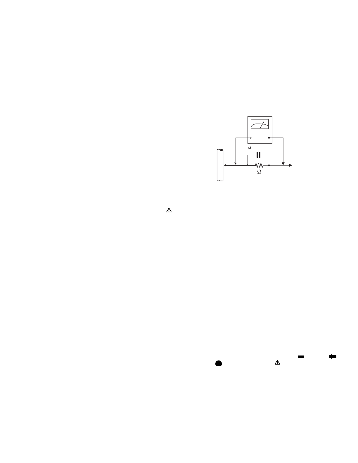
(5) Leakage shock hazard testing
After reassembling the product, always perform an isolation check on the exposed metal parts of the product (antenna terminals, knobs, metal cabinet, screw heads,
headphone jack, control shafts, etc.) to be sure the product
is safe to operate without danger of electrical shock.Do not
use a line isolation transformer during this check.
• Plug the AC line cord directly into the AC outlet. Using a
"Leakage Current Tester", measure the leakage current
from each exposed metal parts of the cabinet, particularly any exposed metal part having a return path to the
chassis, to a known good earth ground. Any leakage current must not exceed 0.5mA AC (r.m.s.).
• Alternate check method
Plug the AC line cord directly into the AC outlet. Use an
AC voltmeter having, 1,000Ω per volt or more sensitivity
in the following manner. Connect a 1,500Ω 10W resistor
paralleled by a 0.15µF AC-type capacitor between an ex-
posed metal part and a known good earth ground.
Measure the AC voltage across the resistor with the AC
voltmeter.
Move the resistor connection to each exposed metal
part, particularly any exposed metal part having a return
path to the chassis, and measure the AC voltage across
the resistor. Now, reverse the plug in the AC outlet and
repeat each measurement. Voltage measured any must
not exceed 0.75 V AC (r.m.s.). This corresponds to 0.5
mA AC (r.m.s.).
AC VOLTMETER
(Having 1000
ohms/volts,
or more sensitivity)
0.15 F AC TYPE
Place this
probe on
1500 10W
Good earth ground
1.2 Warning
(1) This equipment has been designed and manufactured to
meet international safety standards.
(2) It is the legal responsibility of the repairer to ensure that
these safety standards are maintained.
(3) Repairs must be made in accordance with the relevant
safety standards.
(4) It is essential that safety critical components are replaced
by approved parts.
(5) If mains voltage selector is provided, check setting for local
voltage.
1.3 Caution
Burrs formed during molding may be left over on some parts
of the chassis.
Therefore, pay attention to such burrs in the case of preforming repair of this system.
1.4 Critical parts for safety
In regard with component parts appearing on the silk-screen
printed side (parts side) of the PWB diagrams, the parts that are
printed over with black such as the resistor ( ), diode ( )
and ICP ( ) or identified by the " " mark nearby are critical
for safety. When replacing them, be sure to use the parts of the
same type and rating as specified by the manufacturer.
(This regulation dose not Except the J and C version)
each exposed
metal part.
(No.MB748<Rev.002>)1-3
Page 4
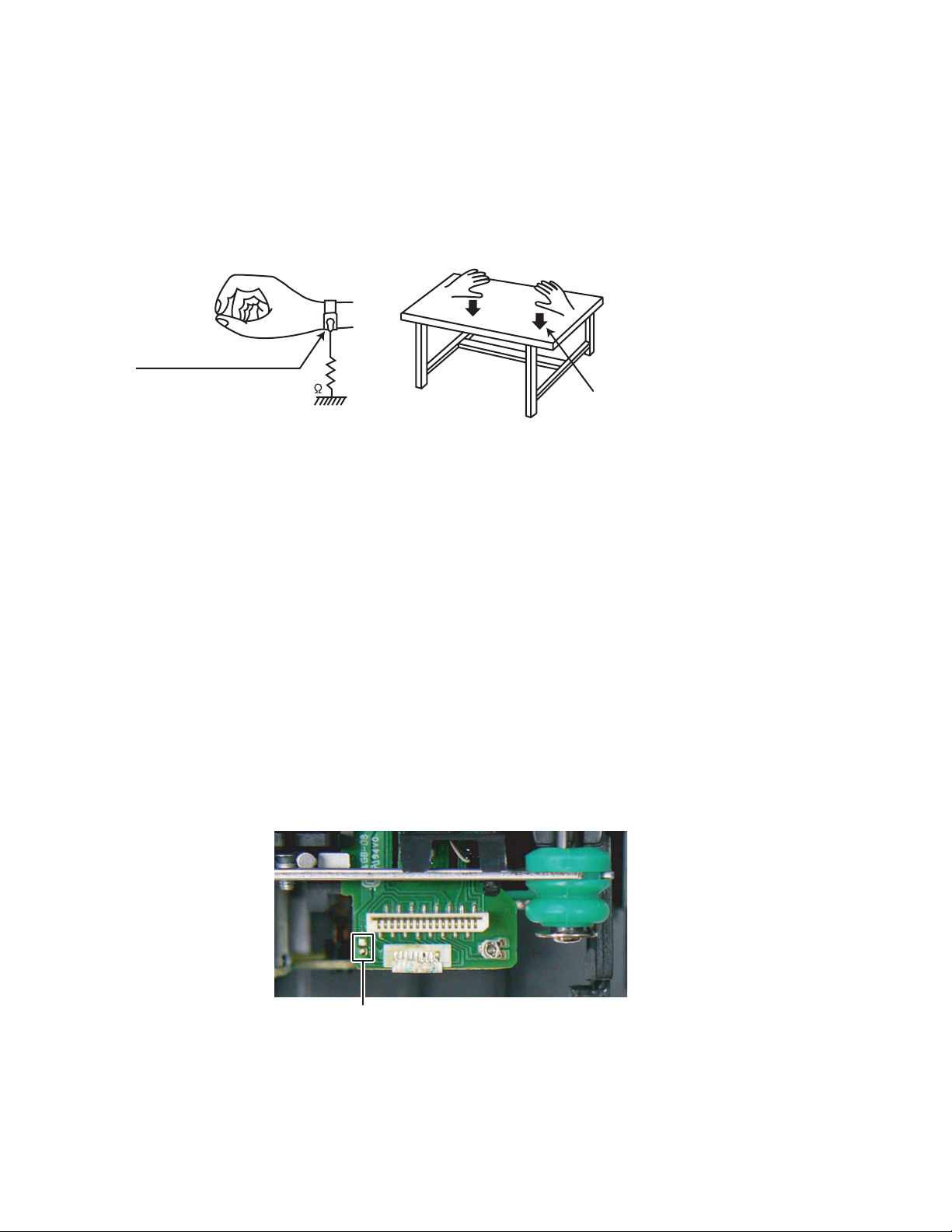
1.5 Preventing static electricity
Electrostatic discharge (ESD), which occurs when static electricity stored in the body, fabric, etc. is discharged, can destroy the laser
diode in the traverse unit (optical pickup). Take care to prevent this when performing repairs.
1.5.1 Grounding to prevent damage by static electricity
Static electricity in the work area can destroy the optical pickup (laser diode) in devices such as laser products.
Be careful to use proper grounding in the area where repairs are being performed.
(1) Ground the workbench
Ground the workbench by laying conductive material (such as a conductive sheet) or an iron plate over it before placing the
traverse unit (optical pickup) on it.
(2) Ground yourself
Use an anti-static wrist strap to release any static electricity built up in your body.
(caption)
Anti-static wrist strap
1M
Conductive material
(conductive sheet) or iron palate
(3) Handling the optical pickup
• In order to maintain quality during transport and before installation, both sides of the laser diode on the replacement optical
pickup are shorted. After replacement, return the shorted parts to their original condition.
(Refer to the text.)
• Do not use a tester to check the condition of the laser diode in the optical pickup. The tester's internal power source can easily
destroy the laser diode.
1.6 Handling the traverse unit (optical pickup)
(1) Do not subject the traverse unit (optical pickup) to strong shocks, as it is a sensitive, complex unit.
(2) Cut off the shorted part of the flexible cable using nippers, etc. after replacing the optical pickup. For specific details, refer to the
replacement procedure in the text. Remove the anti-static pin when replacing the traverse unit. Be careful not to take too long a
time when attaching it to the connector.
(3) Handle the flexible cable carefully as it may break when subjected to strong force.
(4) I t is not possible to adjust the semi-fixed resistor that adjusts the laser power. Do not turn it.
1.7 Attention when traverse unit is decomposed
*Please refer to "Disassembly method" in the text for the pickup unit.
• Apply solder to the short land sections before the card wire is disconnected from the connector on the servo board. (If the card wire
is disconnected without applying solder, the pickup may be destroyed by static electricity.)
• In the assembly, be sure to remove solder from the short land sections after connecting the card wire.
1-4 (No.MB748<Rev.002>)
Solder short
Page 5
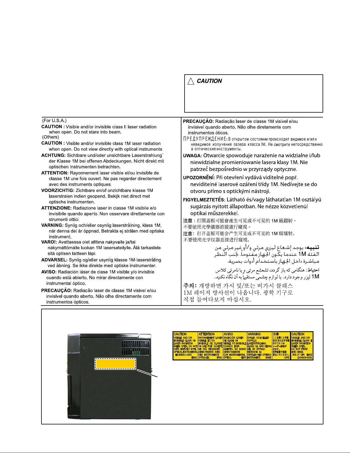
1.CLASS 1 LASER PRODUCT
2.CAUTION :
(For U.S.A.) Visible and/or invisible class II laser radiation
when open. Do not stare into beam.
(Others) Visible and/or invisible class 1M laser radiation
when open. Do not view directly with optical instruments.
3.CAUTION : Visible and/or invisible laser radiation when
open and inter lock failed or defeated. Avoid direct
exposure to beam.
4.CAUTION : This laser product uses visible and/or invisible
laser radiation and is equipped with safety switches which
prevent emission of radiation when the drawer is open and
the safety interlocks have failed or are defeated. It is
dangerous to defeat the safety switches.
5.CAUTION : If safety switches malfunction, the laser is able
to function.
6.CAUTION : Use of controls, adjustments or performance of
procedures other than those specified here in may result in
hazardous radiation exposure.
!
Please use enough caution not to
see the beam directly or touch it
in case of an adjustment or operation
check.
REPRODUCTION AND POSITION OF LABELS and PRINT
WARNING LABEL and PRINT
Put on to inside
(No.MB748<Rev.002>)1-5
Page 6
SECTION 2
SPECIFIC SERVICE INSTRUCTIONS
This service manual does not describe SPECIFIC SERVICE INSTRUCTIONS.
SECTION 3
DISASSEMBLY
3.1 Main body
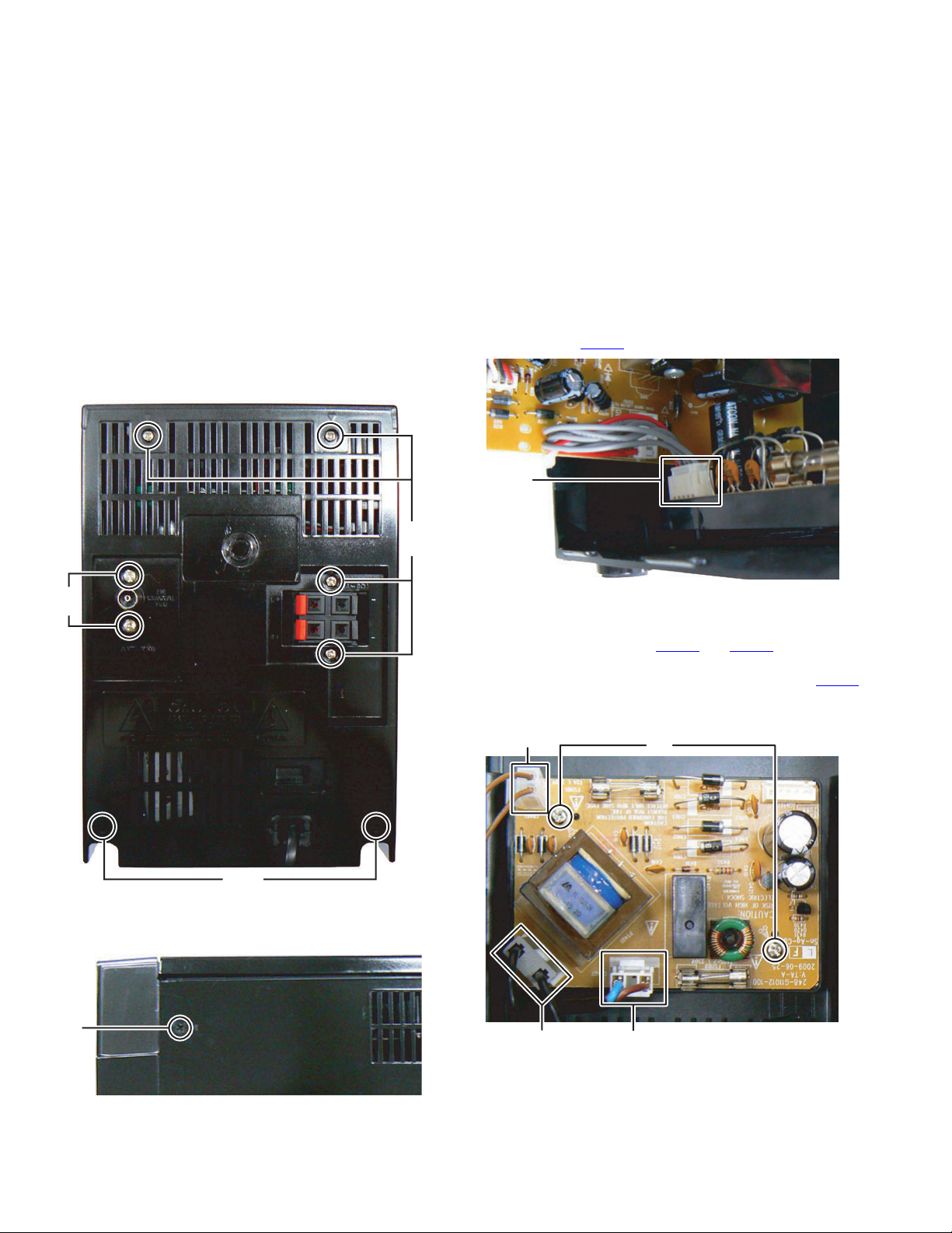
3.1.1 Removing the Rear cover (See Fig.1, 2, 3)
(1) Remove the four screws A, two screws B and two screws
C attaching the Rear cover. (See Fig.1)
B
A
(3) Disconnect the connector wire form Main board connected
to connector CN402
CN402
3.1.2 Removing the Rectifier board (See Fig.4)
(1) Disconnect the connector wires from Power transformer
connected to connectors CN401
er board.
(2) Disconnect the power cord connected to connector CN407
of the Rectifier board.
(3) Remove the two screws E attaching the Rectifier board.
CN401
of the Rectifier board. (See Fig.3)
Fig.3
and CN406 of the Rectifi-
E
C
Fig.1
(2) Remove the two screws D attaching the both side of the
Rear cover. (See Fig.2)
D
Fig.2
1-6 (No.MB748<Rev.002>)
CN406
CN407
Fig.4
Page 7
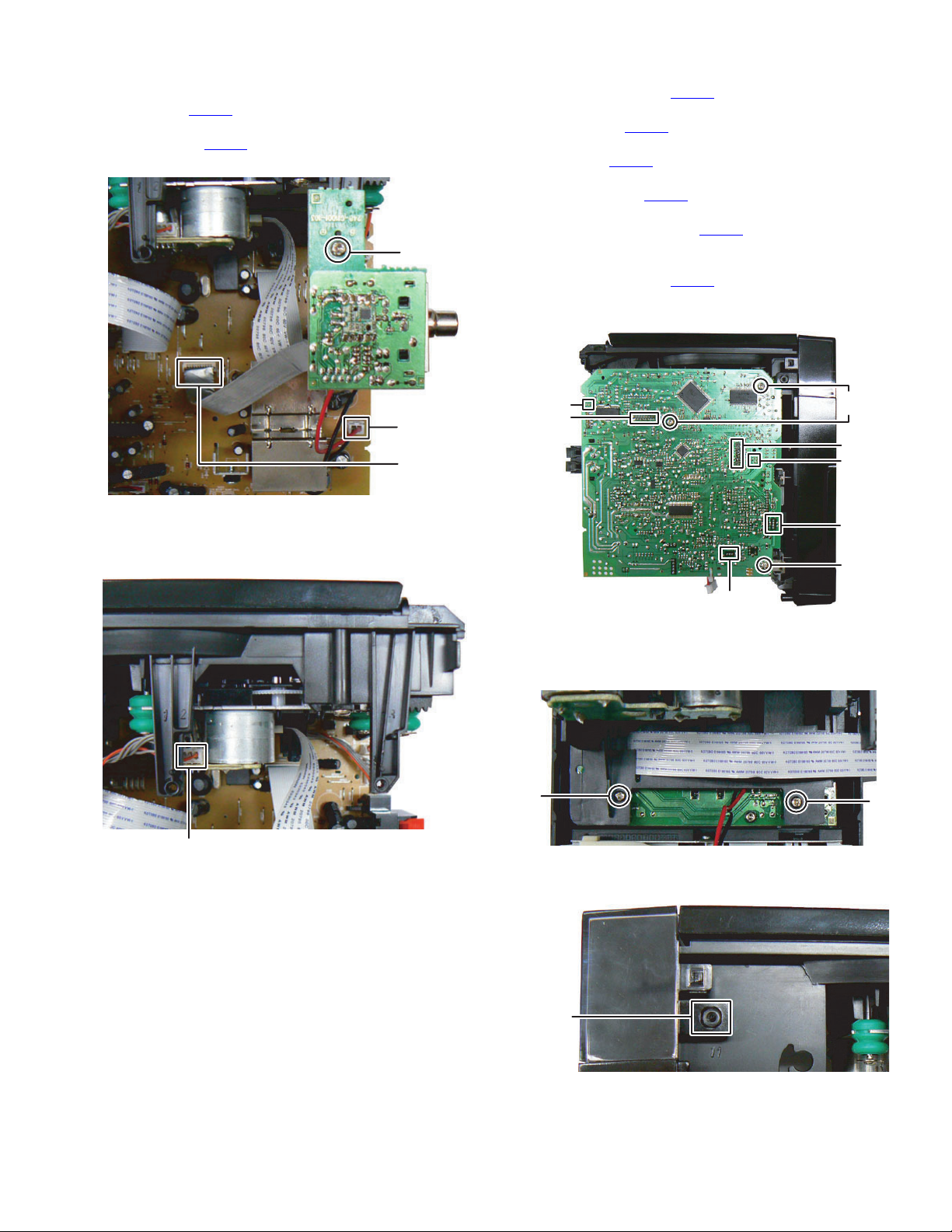
3.1.3 Removing the Tuner pack (See Fig.5)
(1) Disconnect the card wire from Tuner pack connected to
connector CN102
(2) Disconnect the connector wire from Tuner pack connected
to connector CN703
(3) Remove the one screw F attaching the Tuner pack.
of the Main board.
of the Main board.
F
(2) Disconnect the connector wire from CD door switch con-
nected to connector CN702
(3) Disconnect the card wire from CD mechanism connected
to connector CN903 of the Main board. (See Fig.7)
(4) Disconnect the card wire from Control board connected to
connector CN701
(5) Disconnect the connector wire from Control board connect-
ed to connector CN705
(6) Disconnect the connector wire form Cassette mechanism
connected to connector CN301 of the Main board. (See
Fig.7)
(7) Disconnect the shield wire from Cassette mechanism con-
nected to connector CN201
(8) Remove the three screws G attaching the Main board.
(See Fig.7)
of the Main board. (See Fig.7)
of the Main board. (See Fig.7)
of the Main board. (See Fig.7)
of the Main board. (See Fig.7)
CN703
CN102
Fig.5
3.1.4 Removing the Main board (See Fig.6, 7)
(1) Disconnect the connector wire from Main board connected
to connector of the CD mechanism. (See Fig.6)
CONNECTOR
Fig.6
CN702
CN903
G
CN701
CN705
CN201
G
CN301
Fig.7
3.1.5 Removing the Front cabinet (See Fig.8, 9)
(1) Remove the two screws H attaching the CD tray. (See
Fig.8)
H
Fig.8
(2) Disengage two hooks a engaged both side of the Front
cabinet. (See Fig.9)
H
hook a
Fig.9
(No.MB748<Rev.002>)1-7
Page 8
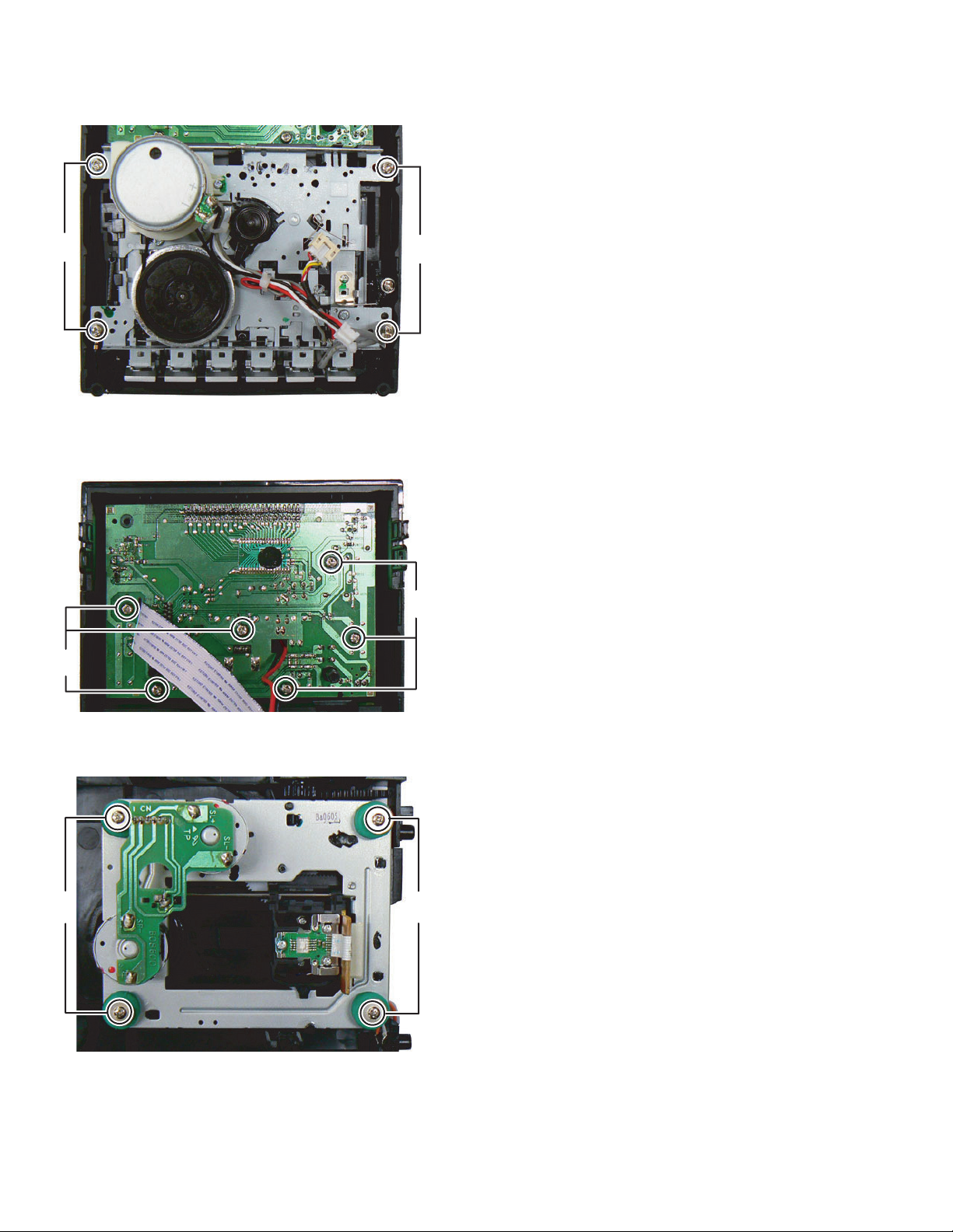
3.1.6 Removing the Cassette mechanism (See Fig.10)
(1) Remove the four screws J attaching the Cassette mecha-
nism.
J
Fig.10
3.1.7 Removing the Control board (See Fig.11)
(1) Remove the Volume knob.
(2) Remove the six screws K attaching the Control board.
K
J
K
Fig.11
3.1.8 Removing the CD mechanism (See Fig.12)
(1) Remove the four screws L attaching the CD mechanism.
Fig.12
LL
1-8 (No.MB748<Rev.002>)
Page 9

SECTION 4
ADJUSTMENT
This service manual does not describe ADJUSTMENT.
SECTION 5
TROUBLESHOOTING
This service manual does not describe TROUBLESHOOTING.
(No.MB748<Rev.002>)1-9
Page 10

Victor Company of Japan, Limited
Personal AV Operation 10-1,1chome,Ohwatari-machi,Maebashi-city,371-8543,Japan
(No.MB748<Rev.002>)
Printed in Japan
VSE
Page 11
SCHEMATIC DIAGRAMS
MICRO COMPONENT SYSTEM
UX-G120E, UX-G120EY
Lead free solder used in the board (material : Sn-Ag-Cu, melting point : 219 Centigrade)
Contents
Block diagrams
Standard schematic diagrams
Printed circuit boards
COPYRIGHT 2011 Victor Company of Japan, Limited.
For Russian
2-1
2-2
2-8 to 10
No.MB748SCH<Rev.002>
2011/1
Page 12

In regard with component parts appearing on the silk-screen printed side (parts side) of the PWB diagrams, the
parts that are printed over with black such as the resistor ( ), diode ( ) and ICP ( ) or identified by the " "
mark nearby are critical for safety.
Page 13

Block diagram
FM ANT
R/P Head L CH
IC101
FM/PLL/TUNER/RDS IC
IC904
1117M/3.3V
Q450
Q451
Tuner
VCC Switch
R/P Switch
Y1 32.768KHz
+13.5V
VCC
TUNER/RCH
TUNER/LCH
TAPE/RCH
TAPE/LCH
REC/RCH
REC/LCH
REC/RCH
REC/LCH
IC501
SIGNAL SELECT SW.
EQ./ E.VOL.
+7.2V
VCC
IC702
MCU
AUX/RCH
AUX/LCH
AUX/IN JACK
CD/RCH
CD/LCH
MAIN/RCH
MAIN/LCH
JK0710
MAIN/RCH
MAIN/LCH
+7.2V
VCC
Q904
CD VCC
CD/RCH
CD/LCH
X901
16.9344MHz
IC301
Power AMP.
Spindle Motor
M
IC905
DSP & DAC
Sled Motor
M
IC901
BTL.Power AMP.4CH
CD MECH
SANYO DA11
IC902
L.Speaker
R/P Head R CH
Erase Head
Cassette Motor
AC
Bias
IC201
Preamplifier For Double/
Cassette Tape Recorder
Q457, Q453
Ta pe
VCC Switch
7.2V
VCC
KEY
IC701
LCD DRIVE IC
LCD DISPLAY
IR
+7.2V
VCC
Q460
Regulator
Q456
VCC Switch
IC702
MCU
3.3V Regulator
+13.5V
VCC
Q421
Q420
Relay Driver
RY401
Relay
RECTIFIER
RECTIFIER
Main Power Transformer
Standby Transformer
R.Speaker
+13.5V
VCC
AC INPUT
M
12V
D209
D211
D210
CASS LF
Switch
+13.5V
VCC
CD DOOR
Leaf SW.
BACKLIGHT LED
Q0710
Backlight
2-1
Page 14

Standard schematic diagrams
<Rectifier section>
FS1101
CN401
To Main section
CN302
CN402
+13.5V
GND
GND
S13.5V
P-CON
C1106
C1107
R430
C1102
C1101
Q421
R431
Q420
D1102
D1101
C1104
C1103
C419
D1104
D1103
C420
D411
C415
C416
D410
D412
C418
C417
D413
R432
CN406
RY401
D414
PT401
L401
FS1102
!
Parts are safety assurance parts.
When replacing those parts make
sure to use the specified one.
CN407
2-2
Page 15

<Main section>
To This sheet
To This sheet
P-CON
MAIN-L
V+7V
A-MUTE
MAIN-R
Q301
ZD451
R315
Q305
R320
R312
R308
C315
R311
R309
R324
Q308
P-CON
Q302
Q303
C792 VP301
R316
R314
R310
Q304
R313
C2
R325
Q309
R323
C314
R321
R304
C321
C306
C308
C304
R306
C307
C309
R307
C320
C303
R305
C324
Q306
R322
IC301
C325
VP302
D208 D207 D206 D202 D205
C310
Q204
ZD201
R260
R261
C316
C323
Q205
Q203
R259
R258
C318
R317
C302
C301
R318
C332
C305
C317
C716
+13.5V
C322
L301
L302
JK301
C331
C311
To This sheet
To CD section
To Control
section CN0710
To Tuner section
CN102
To Control
section CN711
CN701
CN703
CN704
CD-RESET
TX
RX
CD3.3V
TIMER
P-CON
DATA
KEY2
KEY1
VOL+
VCMCU
VOL-
AUX-R
AUX-L
GND-POWER
VCMCU
IF-REQ
IF-OUT
IF-IN
IF-CLK
CD_SW
TIMER
R914
R922
IR
CS
WR
R912
VCC
SCL
To This
sheet
To This sheet
CN702
R739
R910
C733
R913
R911
CD_SW
R709
C902
IIC-SCL
IIC-SDA
C763
VC25
C918
C791
GND_POWER
VCMCU
C788
R776
To This sheet
IIC-CLOCK
IIC-DATA
C726
C725
R527
AUX-R
R514
AUX-L
PLAY-RCH
PLAY-LCH
CD-R
CD-L
R503
TUNER-R
To This sheet
TUNER-L
R504
To Tuner section CN101
C501
R506
C503
R727
R728
C517
To This sheet
R708
R707
R782
R765
R781
C741
C749
A-MUTE
P-CD
VOL-
R749
R753
VOL+
R734
To This sheet
KEY2
KEY1
DATA
CS
WR
SYNC-REC
TAPE-DET
TU-VCC
TU-RESET
IIC-CLOCK
IIC-DATA
TU-RDS
To This sheet
To This sheet
To This sheet
R745
VCMCU
TU-VCC
To This sheet
R751
VC25
R722
R720
R721
C708
R746
NSRST
VCMCU
R705
R740
C731
R741
R777
R774
R775
C920
C709
R787
C710
IR
R736
VC25
C732
R730
R724
R723
C715
C714
IC702
R731
R715
R716
R909
CS
WR
DATA
C790
D710
R738
C719
C717
R786
C745
C746
C747
C748
R718
R717
C724
R780
KEY1
KEY2
R752
R732
R733
R748
R755
R704
R756
R713
C723
C789
CN102
To This sheet
C466
C454
P-TU
VCC-MCU
TAPE-VCC
To This sheet
To This sheet
TAPE-DET
CD-VCC
P-TU
P-CON
Q705
P-CD
To This sheet
VCMCU
IIC_SDA
IIC_SCL
TUNER-R
Q703
C951
llC-CLOCK
To Main (Cassette)
V+7V
IC904
Q451
R474
R470
D453
R471
C412
R452
C451
R461
IC703
Q450
R473
R472
Q457
R451
D452
Q453
C532
R450
R453
Q452
R469
D450
Q458
R468
R467
VCMCU
C730
section
V+7V
+5V
D+5.6V
V+7V
IC705
C728
GND_POWER
TUNER-L
L450
C743
R735
R706
C465
VCMCU
To This sheet
llC-DATA
TU-VCC
TU-RESET
TU-RDS
To This sheet
R505
To Main (Cassette)
section
Q460
R459
C468
C727
Q455
C469
R460
D709
C742
L702
C713
R524
R525
C522
C523
R507
R522
C521
C508
C529
R540
C530
R541
C531
R542
C524
R530
C525
R531
C526
R532
C527
R533
C528
R534
R509
V+7V
REC-RCH
+13.2V
R458
Q456
R464
R454
C729
R466
C467
R465
C461
C740
ZD701
R761
R760
R759
C735
R762
ZD452
R475
ZD450
C534
C505
C510
Q459
R463
Q454
R457
R462
Q706
R757
R754
D708
+13.5V
D701
S13.5V
+13.5V
S13.5V
To This sheet
R456
P-CON
C533
R455
MCUVCC
R521
C519
IC501
C520
R517
+13.5V
P-CON
CN302
C511
R512
C514
C512
To This sheet
REC-LCH
C516
C515
R516
C504
C502
C535
R510
C545
R511
C506
R515
C513
C507
R513
C509
To Rectifier section
CN402
To Main (Cassette) section
R501
MAIN-L
To This sheet
MAIN-R
R502
2-3
Page 16

<Main (Cassette) section>
To Main section
L / CH.
CN201
REC-LCH
R202
R214
R208
C208
SW201-D
C207
R203
R207
R218
R211
C204
CE202
REC-VCC
L202
L204
R226
IC201-B
D201
C214
C220
CE206
R234
OP1
C218
R225
C217
CE203
R227
C215
SW201-E
R231
R232
R241
C225
Q201
PLAY_LCH
R238
R / CH.
To Main section
T_MUTE
Q307
D213
S-VCC
R256
REC-VCC
REC-RCH
To Main section
+13.2V
P-TAPE
C313
R201
R255
C312
R257
R220
D203
D204
R209
C209
D209
SW201-C
D210
C245
D211
C206
C319
CE201
R210
C246
C205
R204
R206
R217
CN301
R223
+11V
M+
GND
IC201-A
L201
L203
CE205
+11V
M+
GND
C213
C222
CE207
R221
OP2
C223
R235
R224
C216
A_MUTE
To this sheet
C224
TAPE-VCC
REC-VCC
CE204
R222
TAPE-VCC
C221
SW201-F
SW201-B
R240
D212
R230
R228
R233
CE801
R215
R242
Q802
C212
C226
R219
SYNC
R212
C210
Q202
R239
T801
SW201-A
C201
PLAY_RCH
AC/BIAS
To this sheet
A_MUTE
2-4
CE208
R236
Page 17

<Control section>
JK0710
VP702
L-CH
R-CH
GND
R0758
SW710
VOL-
C0711
SW712
C0710
R0764
SW714
R0761
VR0710
L712
L710
L711
SW716
C0713
C0712
R0766
SW718
R0762
R0711
R0710
R0760
SW720
VOL+
C0714
SW722
C0715
R0763
R0759
R0712
SW719
SW711
IR
R0713
R0757
C0717
A-L
A-R
SW0723
VP701
C0724
GND_POWER
R0765
KEY2
REM710
C0716
SW715
R0714
SW724
D+5V
KEY1
C0752
R0730
C703
GND_POWER
X701
C0751
R0731
C0750
R0732
C704
C0749
R0733
C0748
R0734
C0747
R0735
C0746
R0736
C0745
R0737
C0744
R0738
C0743
R0739
C0742
R0740
C0741
R0741
C0740
R0742
C0739
R0743
C0738
IC701
C0737
R0744
LCD710
C0736
R0745
C0735
R0746
C0734
R0747
C0733
R0748
VCMCU
R0749
C0731
R0750
R0751
C0730
R0752
C0732
To This sheet
To Main section
C0726
C0729
R0753
C0720
C0728
R0754
C0727
R0755
TIMER
P-CON
KEY2
KEY1
VOL+
AUX-R
IR
CS
WR
DATE
VCC
SCL
VOL-
AUX-L
CN0710
To Main section
CN701
LED712
Q0712
C0718
D-GNDD-GND
R0717
R0718
R0715
R0716
D+5V
P-CON
D-GND
R0720
LED710
R0719
Q0710
D-GND D-GND
D+5V
P-CON
R0729
To Main section
CN704
CN711
IQR
R701
R0723
C0719
D-GND
C0725
R0725
R0726
R0727
R0728
ZD0710
C0722
C0721
C0723
D-GND
CS
WR
DATA
D+5V
To This sheet
2-5
Page 18

<Tuner section>
To Main section
CN703
D101
CN102
IC101
JK101
VP101
D102
C110 C109
CF101
D103
C105
X101
R106
C104
R108
C113
C102
R102
C101
C120
C116
C117
C106
C114
C115
R117
R119
R118
R104 R105
R116
R109
R120
CN101
To Main section
CN102
R107
R103
C103
C112
2-6
Page 19

<CD section>
C968
R920
D903
To This sheet
GND
CE905
C949 C948
CD+7V
C465
M33V
CE904
VCC_8V
GND
Q904
D904
R943
HAVC
C990
C909
C910
C913
C916
GND
C924
3V3SD
To This sheet
R905
Q901
C999
GND
C905
TC1
To This sheet
R908
M33V
R945
R942
VCC_8V
R954
SLED+
SLED-
GND
VREF_16
XSLEGP
XSPINDLE
To This sheet
To This sheet
To This
sheet
TC9
3.3V
3.3V
X901
R941
R940
FOCUS+
FOCUS-
R939
R938
R102
R953
To This sheet
RESETJ
VREF
CE902
RF_1V8
PA_1V8
R950
IC901
XFOCUS
XTRACK
C907
C937
GND
TRACK
GNDGND
L901
C911
TC17
GND
R101
R917
C963
MDI
LDO
TPI
TNI
C908
C914
C939
C
B
D
A
C915
TT+
R100
R999
C947
GND
SPINSPIN+
C901
SEV_3V3
GND
C912
GND
GND
C950
To This sheet
C946
LINE_R
LINE_L
To This
sheet
XTRACK
VREF_16
XFOCUS
GNDGND
AUD_3V3
VREF_16
To This sheet
To This sheet
VREF_16
GND
VREF_16
XSPINDLE
MUTE34
XSLEGP
VREF_16
C925
GND
To This sheet
3V3SD
C934
CE920
C917
1V8SD
3V3SD
R906
IC905
Q908
C938 0.1U
GND
R937
1V8SD 3V3SD
C926
R965
L907
C989
To This sheet
LD
C904
C921
GND
3V3SD
LDO
To This sheet
LIMIT
3V3SD
GND
GND
T+
T-
FOCUS+
FOCUS-
To This sheet
TPI
C
B
A
D
TNI
3V3SD
HAVC
R907
R919
FOCUS-
FOCUS+
R944
L905
R971
L908
R972
R973
R976
MDI
T+
T-
LD
C988
MUTE
RA4
RA5
RA6
RA7
GND
MUTE34
LIMIT
To This sheet
RESETJ
C919
R904
RX
TX
R952
MD
C906
To This sheet
To This sheet
DOOR
3.3V
To This sheet
To This sheet
1V8SD
RA8
To This sheet
RA9
RA11
RCKE
RLCK
RD3
RD2
RD1
RD0
To This sheet
RD4
RD5
RD6
RD7
UDQM
To This sheet
LDQM
RCSJ
RWEJ
RCASJ
RRASJ
To This sheet
RA10
RA0
RA1
RA2
RA3
To Main section
F_CLK
F_CS
To This sheet
F_DI
F_DO
T+
T-
FOCUS+
FOCUS-
FT+
TF+
MD
VR
LD
GND
PICK UP
F
C
B
A
D
E
VCC
VC
CN903
To This sheet
To This sheet
To This sheet
R119
RA1
R120
RA2
R962
RA3
R925
RA5
R924
RA6
MUTE
F_CS
F_DI
R921
3V3SD
LINE_L
LINE_R
GND
To This sheet
To This sheet
M33V
PG_18
R934
R933
3V3SD
3VV3SD
R918
Q910
LDQM
RWEJ
RCASJ
RRASJ
RCSJ
RA11
RA10
RA0
RA1
RA2
RA3
Q903
AUD_3V3
R967
GND
RD0
RD1
RD2
RD3
RD4
RD5
RD6
RD7
C992
CE908
CE907
C927
C996
C997
C998
R932
RD0
RD1
RD2
RD3
RD4
RD5
RD6
RD7
CE903
1V8SD
1V8SD
Q905
IC903
SDVCC
L902
L906
R948
R928
L903
L904
R961
R947
C903
3V3SD
C991
R949
C929
R929
C928
IC902
RCKE
R903
To This sheet
3V3SD
3V3SD
D901
To This sheet
R946
R977
CE906
CE911
3V3SD
F_CLK
F_DO
R978
AUDIO output
LDQM
RCSJ
RD7
RD6
RD5
RD4
RD3
RD2
RD1
RD0
UDQM
RCLK
RA9
RA8
RA7
RA6
RA5
RA4
SDVCC
SDVCC
16D_CKE
16D_CKE
AUD_3V3
SEV_3V3
CE909
RF_1V8
PA_1V8
R930
SPIN+
SPIN-
SLED+
SLED-
LIMIT
To This sheet
AUDIO_L
AUDIO_R
To This sheet
To This sheet
To This sheet
To This sheet
Q310
SPIN+
SPINSLED+
SLEDLIMIT1
LIMIT2
CN901
AMUTE
2-7
Page 20

Printed circuit boards
<Main board>
(Lead free solder used in the board (material : Sn-Ag-Cu, melting point : 219 Centigrade))
(forward side)
JW235
C467
JMP916
CN302
JMP929
JMP240
JMP237
C533
JMP937
JMP241
Q460
D904
JMP930
C534
C535
C989
JMP931
C545
CE906
JMP932
C990
C466
JMP267
D701
JMP229
C315
D708
JMP913
D453
JMP252
JW929
JMP232
C321
JMP253
C320
Q908
C468
JMP933
CN903
C728
C316
C740
C988
C325
D903
D709
JMP928
C324
JMP262
JMP922
CE903
JMP934
D902
ZD701
C727
JMP265
JMP242
ZD451
C323
JMP263
CN707
CE907
CN201
JMP926
SW201
JMP911
CN704
CE920
CE908
JMP266
CE901
CN705
JMP246
JMP256
JMP925
CE909
T801
D901
JMP912
JMP228
JMP917
CE202
CE201
CE204
JMP903
JMP235
CE203
Q802
JMP909
CN701
JMP270
CE208
CN301
JMP910
JMP906
IC201
JMP904
JMP236
CE206
CE205
CE801
JMP245
D211
D210
JMP238
JMP257
JMP919
JMP918
JMP939
D212
D213
D201
JMP258
JMP231
JMP233
JMP247
CE207
D203
CN706
D710
D204
C319
CE902
JMP248
JMP249
D209
JMP239
C313
JMP250
Q459
ZD452
CE911
L901
JMP222
JMP234
D454
C763
JMP244
D452
ZD450
X901
JMP268
CN102
JW236
JMP259
D451
JMP927
D450
JMP216
JMP260
JMP225
Q903
CE905
JMP223
C314
IC301
JMP936
JMP935
C465
JMP921
JMP923
C318
JMP251
JMP255
C322
Q452
JMP254
JMP924
JMP243
JMP215
JMP261
ZD201
Q904
JMP938
L301
JK301
C317
(reverse side)
R919
C917
C999
C919
C732
C904
C938
C934
JW911
JW910
IC905
C901
TC9
TC1
C907
R958
C912
JW2
R911
JW1
R717
R775
R742
C454
R901
C522
C520
R509
Q456
R730
C531
R460
TC17
R733
R459
R465
JW244
Q455
R504
R513
R464
C911
R950
R512
JW206
C525
R454
R455
R457
C908
R748
IC702
C529
R522
C508
R462
C519
C909
R780
R732
R741
R908
R456
C910
C913
C916
L903
R752
JW234
C745
R781
C527
Q454
C915
R705
R738
C461
R765
R785
R452
C731
JW246
JW228
JW227
C746
R708
R514
R503
R527
Q457
R451
Q453
R786
R740
L904
C532
R453
R707
R475
C937
C733
C741
R718
R782
R505
C523
R463
R466
C747
C512
R784
C503
IC903
JW27
R727
R728
R783
C528
C513
JW241
R506
C501
C521
R507
C510
R476
C748
C511
C514
JW242
C515
C526
R534
C750
C709
C710
C708
C714
C715
R736
R521
C524
R530
R532
R450
C788
C517
C920
R256
Q307
R542
C246
C926
JW230
R709
R257
R240
R531
C992
R973
C921
R540
R220
R976
R909
C991
R533
R239
R921
R541
C412
R731
R715
R716
R724
R723
C717
C719
C530
R916
R946
R238
Q201
R255
R972
IC902
L908
C903
C790
C724
R756
R755
JW233
R213
R235
JMP940
R922
C723
JW224
R229
C245
Q202
R914
R234
C226
C225
R913
JMP227
R242
R241
C223
C222
C221
JP207
R230
C726
C224
C220
C218
R912
R915
C217
R221
C216
R222
R236
R224
R223
Q310
R233
R232
R231
R219
R704
JW913
C725
R212
C210
R215
2731
R971
R787
R713
R721
R722
R720
R228
C212
C789
R903
R214
R930
C213
R746
C214
R217
C215
R227
R226
R225
L204
R218
L203
JW912
R933
R211
L202
L201
R210
R209
C209
C792
Q910
C208
R208
R207
C207
C201
C206
R948
R949
C929
R978
R932
R206
R967
R925
R924
R923
R961
R947
R962
C927
R934
Q905
R928
R929
C928
R977
VP301
R202
R201
JP204
L902
R204
C205
C204
R203
C925
R926
C2
R927
R904
JW904
C469
JW213
R317
R319
Q203
Q204
R918
R940
C947
R468
R467
C949
JW6
JW231
R323
JW965
R953
C963
R954
R941
R999
R100
C950
R942
R945
JW223
Q705
R461
C713
L702
C744
Q308
R315
JW4
CE904
CN702
IC901
JW901
JW902
C924
JW914
R937
CN901
Q205
C331
C311
VP302
C716
R316
R321
R322
R314
R320
C948
C332
C305
Q305
Q306
C451
C951
Q301
C301
C302
R258
R259
R261
Q458
R469
Q309
C310
R260
R754
JW903
JMP226
L302
CN703
C742
D208
D205
D202
D206
D207
Q451
R324
R473
R472
C906
R304
C304
R102
L905
R325
C729
JW905
IC705
C743
C502
C306
R917
R757
R474
R907
C308
C735
R510
C968
R920
R943
R905
Q901
L906
JW906
JMP230
R734
C307
Q303
R761
C914
R706
R751
R501
JW909
R906
L907
R735
R308
R944
C939
R952
C905
JW3
C791
C918
C902
R910
R777
R776
R774
R737
JMP264
Q703
R745
L450
C749
R524
R525
R313
Q304
Q302
IC501
C516
C507
C505
R312
R311
R517
R515
R310
C509
R458
JW243
R939
R516
R305
C309
R502
R762
R938
JMP15
R470
C504
Q450
C506
R306
R760
C730
C946
Q706
R753
R309
R511
JW907
R749
C303
R307
R759
R101
JW908
R739
IC703
JW229
R471
IC904
<Tuner board>
(Lead free solder used in the board (material : Sn-Ag-Cu, melting point : 219 Centigrade))
(forward side)
J104
CN102
D101
D102
CN101
J103
C120
X101
J105
CF101
J106
JK101
248-G11001-105
V:TA-A
2009-06-25
H=0.8mm
(reverse side)
C113
C106
R118
R119
C115
C117
R120
R110
R116
R117
C114
C116
R108
R109
C110
C107
D103
VP101
C108
C111
C112
R107
C109
R106
R101
IC101
C103
C102
C101
R102
R103
R104
C104
C105
R105
2-8
Page 21

<Rectifier board>
(Lead free solder used in the board (material : Sn-Ag-Cu, melting point : 219 Centigrade))
(forward side)
C420
C1107
R431
Q420
R430
CN402
L401
D1101
Q421
C419
D1104
D1102
C1106
D1103
FS1102
R432
CN407
PT401
RY401
D414
C1104
C1102
C1103
C1101
C418
D413
D411
C416
FS1101
CN406
D412
C417
CN401
D410
C415
(reverse side)
2-9
Page 22

<Control board>
(Lead free solder used in the board (material : Sn-Ag-Cu, melting point : 219 Centigrade))
(forward side)
LED710
LCD710
SW710
LED711
SW724
SW711
JMP715
JMP716
JK0710
L710
L711
L712
X701
SW722
SW0723
C704
JMP702
C703
JMP707
JMP701
SW718
JMP706
CN711
C0725
ZD0710
VR0710
JMP1
SW715
JMP705
JW701
JMP712
JMP713
SW714
SW719
C0726
CN0710
SW712
SW716
SW720
LED712
C0724
REM710
(reverse side)
Q0712
C0718
R0714
R0761
R0762
R0718
C0716
R0717
C0717
R0755
R0715
R0716
R0756
C0723
C0721
C0722
JW703
C0727
R0753
R0754
R0768
JW705
VP703
C0728
C0729
R0752
R0751
VP701
VP702
C0731
C0730
R0750
R0763
C0732
C0733
C0734
R0749
R0748
C0735
C0736
R0747
C0737
R0745
R0746
C0738
R0744
R0764
C0720
R0725
R0726
R0727
R0765
R0766
R0723
C0719
C0714
C0715
R0728
R0712
R0713
IC701
C701
C0739
R0743
C702
R0710
R0711
C0740
C0741
R0741
R0742
C0742
R0740
R0739
R701
C0743
C0744
R0738
R0760
C0712
C0713
R0757
C0745
C0746
R0759
C0747
R0737
R0736
C0749
C0748
R0735
R0734
C0750
C0751
R0733
R0732
R0758
C0752
R0731
R0730
Q0710
R0721
C0711
R0719
R0729
R0720
JW702
R0722
Q0711
C0710
2-10
Page 23

< MEMO >
Page 24

Victor Company of Japan, Limited
Home Entertainment Business Division Personal AV Operation
(No.MB748SCH<Rev.002>)
Printed in Japan
VSE
Page 25

PARTS LIST
UX-G120E, UX-G120EY
MODEL MARK
AUX-G120E
UX-G120EY
B
- Contents -
Exploded view of general assembly and parts list (Block No.M1)
Electrical parts list (Block No.01~04)
Packing materials and accessories parts list (Block No.M3)
3- 2
3- 5
3- 12
MB748PAR<Rev.002>
3-1
Page 26

Exploded view of general assembly and parts list
E
E
9
3
4
4
Main board
68
68
69
Block No.
B
M MM1
F
20
51
76
4
74
a
C
80
D
81
82
Control board
54
56
17
12
14
11
8
10
9
1
13
4
25
15
52
16
19
38
a
3
54
D
E
E
56
54
2
3-2
48
48
21
53
5
7
2
6
Page 27

The parts without symbol number are not service.
32
44
70
31
A
35
67
63
55
65
64
73
71
36
63
70
61
62
79
72
55
35
77
37
77
35
77
35
A
62
66
6
45
Rectifier board
33
30
78
C
26
58
29
Tuner board
28
60
47
B
59
59
23
F
75
24
24
4
24
57
57
57
57
The parts without symbol number are not service.
3-3
Page 28

General Assembly
Symbol No. Part No. Part Name Description Local
1 5S1-029000-000 CASS DOOR COVER
2 5S1-009000-000 CASS KNOB COVER
3 539-121100-000 CASS DOOR GEAR
4 539-121200-000 GEAR HOLER
5 766-728800-000 CASS DOOR SPRING
6 5S1-010000-000 CASS KNOB
7 463-380000-000 CASS KNOB COVER PANEL
8 5S1-074000-000 DISPLAY LENS
9 5S1-020400-000 VOL KNOB COVER
10 5S1-007000-000 VOL KNOB
11 5S1-001000-000 FRONT CABINET
12 5S1-025000-000 POWER KNOB
13 5S1-008000-000 FUNCTION KNOB
14 220-110000-000 LED
15 466-088031-000 BLACK LIGHT PLATE
16 514-080500-000 LCD BACK LIGHT
17 5S1-031000-000 DISPLAY BRACKET
19 5S1-044000-000 LED COVER
20 408-200100-008 METAL BRACKET
21 5S1-013000-000 CASS DOOR BRACKET
23 356-110003-091 CD DECK MECHANISM
24 458-328840-220 RUBBER SILICON (BLACK) HARDNESS(x4)
25 766-DV1480-000 CASS KNOB DOOR SPRING
26 217-200035-050 LEAF SWITCH
28 539-121200-000 GEAR HOLER
29 539-121100-000 CASS DOOR GEAR
30 514-047000-000 CD TRAY
31 846-209000-000 CD DOOR LOCK
32 5S1-049000-000 CD DOOR
33 479-770000-000 DOOR SPRING
35 458-120023-000 RUBBER FOOT 12.0x2.3mm(x4)
36 530-026200-000 POVER LINGE HOLDER
37 5S1-002000-000 BACK CABINET
38 156-482133-034 CASS DECK
44 152-402328-000 POWER TRANSF PT1101 230V
45 473-300160-150 CD MAGNET RING
46 500-100000-000 RECORDENG BKT
47 500-995231-000 CD MECHNISM COVER
48 458-350040-000 RUBBER FOOT (x2)
49 500-276110-000 CD CHUCK M
51 238-130100-602 SCREW 3x10mm PB
52 238-130100-632 SCREW 3x10mm PWB
53 238-130080-602 SCREW 3x8mm PB(x3)
54 238-130100-602 SCREW 3x10mm PB(x3)
55 238-130080-102 SCREW 3x8mm KB(x2)
56 238-130080-602 SCREW 3x8mm PB(x6)
57 238-126080-631 SCREW 2.6x8mm PWA(x4)
58 238-120060-602 SCREW 2x6mm PB BLK
59 238-130100-602 SCREW 3x10mm PB(x2)
60 238-130100-632 SCREW 3x10mm PWB
61 238-130080-602 SCREW 3x8mm PB
62 238-130080-602 SCREW 3x8mm PB(x2)
63 238-130250-602 SCREW 3x25mm PB(x2)
64 238-130080-602 SCREW 3x8mm PB(x2)
65 238-130100-602 SCREW 3x10mm PB(x2)
66 238-120060-202 SCREW 2x6mm BB
67 238-130100-602 SCREW 3x10mm PB(x2)
68 238-130080-602 SCREW 3x8mm PB(x2)
69 238-130060-202A SCREW 3x6mm BB
70 238-130200-632 SCREW 3x20mm PWB(x2)
71 151-230000-200 POWER CORD SET
71 or 151-230230-002 POWER CORD SET (BLACK) VDE APPR
72 222-220090-350 FERRITE BEAD
73 898-G12000-020 RATING LABEL B
73 898-G12000-010 RATING LABEL A
74 235-180200-110 FFC CABLE 18PINS
75 235-160150-110 FFC WIRE 16PINS
76 235-105150-112 FFC CABLE 10PINS
77 238-130080-602 SCREW 3x8mm PB(x3)
78 406-050090-000 FUSE HOLDER (x2)
79 406-050090-000 FUSE HOLDER (x2)
80 408-600350-080 HEAT SINK
81 408-360230-120 HEAT SINK
82 238-130080-202A SCREW 3x8mm BB
Block No. [M][1][M][M]
3-4
Page 29

Electrical parts list
Main board
Block No. [0][1]
Symbol No.
IC201 210-007323-014 IC AN7323
IC301 210-003602-012 IC BF3602GP
IC501 310-007314-100 IC SC7314
IC702 310-006812-132 IC CA6812
IC703 310-002402-100 IC AT24C02(256X8) 1.8V
IC705 310-001117-133 IC APL1117
IC901 310-009258-128 IC SA9258PH (3V3)
IC902 310-121616-101 IC
IC903 310-002510-000 IC EN25P10
IC904 310-001117-133 IC APL1117
IC905 310-005671-000 CHIP IC M5671
Q201 307-009014-030 TRANSISTOR 9014C
Q202 307-009014-030 TRANSISTOR 9014C
Q203 307-008050-030 TRANSISTOR 8050C/D
Q204 307-008050-030 TRANSISTOR 8050C/D
Q205 307-003401-003 TRANSISTOR
Q301 307-008550-020 TRANSISTOR 8550B/C
Q302 307-009014-030 TRANSISTOR 9014C
Q303 307-009014-030 TRANSISTOR 9014C
Q304 307-009014-030 TRANSISTOR 9014C
Q305 307-009014-030 TRANSISTOR 9014C
Q306 307-009014-030 TRANSISTOR 9014C
Q307 307-009014-030 TRANSISTOR 9014C
Q308 307-009014-030 TRANSISTOR 9014C
Q309 307-008550-020 TRANSISTOR 8550B/C
Q310 307-009014-030 TRANSISTOR 9014C
Q450 307-009014-030 TRANSISTOR 9014C
Q451 307-008550-020 TRANSISTOR 8550B/C
Q452 207-008550-020 TRANSISTOR 8550B/C
Q453 307-009014-030 TRANSISTOR 9014C
Q454 307-009014-030 TRANSISTOR 9014C
Q455 307-008050-030 TRANSISTOR 8050C/D
Q456 307-008050-030 TRANSISTOR 8050C/D
Q457 307-008550-020 TRANSISTOR 8550B/C
Q458 307-008050-030 TRANSISTOR 8050C/D
Q459 207-008550-020 TRANSISTOR 8550B/C
Q460 207-000772-250 TRANSISTOR B772Y
Q703 307-009015-013 TRANSISTOR
Q705 307-009015-013 TRANSISTOR
Q706 307-008050-030 TRANSISTOR 8050C/D
Q802 207-000337-000 TRANSISTOR BC337-25
Q901 307-008050-030 TRANSISTOR 8050C/D
Q903 207-008550-020 TRANSISTOR 8550B/C
Q904 207-190764-040 TRANSISTOR 2SB-764-D
Q905 307-008550-020 TRANSISTOR 8550B/C
Q908 207-008550-020 TRANSISTOR 8550B/C
Q910 307-008050-030 TRANSISTOR 8050C/D
D201 206-104148-000 DIODE IN-4148
D202 206-304001-000 RECTIFIER IN-4001
D203 206-104148-000 DIODE IN-4148
D204 206-104148-000 DIODE IN-4148
D205 206-304001-000 RECTIFIER IN-4001
D206 206-304001-000 RECTIFIER IN-4001
D207 206-304001-000 RECTIFIER IN-4001
D208 206-304001-000 RECTIFIER IN-4001
D209 206-304001-000 RECTIFIER IN-4001
D210 206-304001-000 RECTIFIER IN-4001
D211 206-304001-000 RECTIFIER IN-4001
D212 206-104148-000 DIODE IN-4148
D213 206-104148-000 DIODE IN-4148
D450 206-104148-000 DIODE IN-4148
D452 206-104148-000 DIODE IN-4148
D453 206-104148-000 DIODE IN-4148
D701 206-304001-000 RECTIFIER IN-4001
D708 206-304001-000 RECTIFIER IN-4001
D709 206-304001-000 RECTIFIER IN-4001
D710 206-104148-000 DIODE IN-4148
D901 206-104148-000 DIODE IN-4148
D903 206-104148-000 DIODE IN-4148
D904 206-104148-000 DIODE IN-4148
Part No. Part Name Description Local
Symbol No.
C2 302-321025-550 C CAPACITOR 0.001uF/50V
C201 302-318215-550 C CAPACITOR 820pF/50V
C204 302-323321-150 C CAPACITOR 0.0033uF/50V
C205 302-323321-150 C CAPACITOR 0.0033uF/50V
C206 302-222022-250 C CAPACITOR 0.0020uF/50V
C207 302-222022-250 C CAPACITOR 0.0020uF/50V
C208 302-331035-550 C CAPACITOR 0.01uF/50V
C209 302-331035-550 C CAPACITOR 0.01uF/50V
C210 302-323321-150 C CAPACITOR 0.0033uF/50V
C212 302-324725-550 C CAPACITOR 0.047F/50V
C215 302-333335-550 C CAPACITOR 0.033uF/50V
C216 302-331035-550 C CAPACITOR 0.01uF/50V
C217 302-331035-550 C CAPACITOR 0.01uF/50V
C218 302-332235-550 C CAPACITOR 0.022uF/50V
C221 302-333335-550 C CAPACITOR 0.033uF/50V
C223 302-332235-550 C CAPACITOR 0.022uF/50V
C224 302-331035-550 C CAPACITOR 0.01uF/50V
C225 302-326821-150 C CAPACITOR 0.0068uF/50V
C226 302-326821-150 C CAPACITOR 0.0068uF/50V
C245 302-331035-550 C CAPACITOR 0.01uF/50V
C246 302-331035-550 C CAPACITOR 0.01uF/50V
C301 302-341541-150 C CAPACITOR 0.15uF/50V
C302 302-341541-150 C CAPACITOR 0.15uF/50V
C303 302-311015-550 C CAPACITOR 100pF/50V
C304 302-311015-550 C CAPACITOR 100pF/50V
C305 302-324725-550 C CAPACITOR 0.047F/50V
C306 302-351055-550 C CAPACITOR 1uF/50V
C307 302-321025-550 C CAPACITOR 0.001uF/50V
C308 302-351055-550 C CAPACITOR 1uF/50V
C309 302-321025-550 C CAPACITOR 0.001uF/50V
C310 302-341045-550 C CAPACITOR 0.1uF/50V
C311 302-332235-550 C CAPACITOR 0.022uF/50V
C313 004-072272-216 E CAPACITOR 220uF/16V
C314 004-064762-225 E CAPACITOR 47uF/25V
C315 004-061062-225 E CAPACITOR 10uF/25V
C316 004-071072-225 E CAPACITOR 100uF/25V
C317 004-081082-216 E CAPACITOR 1000uF/16V
C318 004-081082-216 E CAPACITOR 1000uF/16V
C319 004-074772-225 E CAPACITOR 470uF/25V
C320 004-071072-225 E CAPACITOR 100uF/25V
C321 004-071072-225 E CAPACITOR 100uF/25V
C322 004-083382-225 E CAPACITOR 3300uF/25V
C323 004-071072-225 E CAPACITOR 100uF/25V
C324 004-072272-225 E CAPACITOR 220uF/25V
C325 004-071072-225 E CAPACITOR 100uF/25V
C331 302-332235-550 C CAPACITOR 0.022uF/50V
C332 302-324725-550 C CAPACITOR 0.047F/50V
C412 302-341045-550 C CAPACITOR 0.1uF/50V
C451 302-341045-550 C CAPACITOR 0.1uF/50V
C454 302-341045-550 C CAPACITOR 0.1uF/50V
C461 302-321025-550 C CAPACITOR 0.001uF/50V
C465 004-081082-216 E CAPACITOR 1000uF/16V
C466 004-072272-216 E CAPACITOR 220uF/16V
C467 004-064762-216 E CAPACITOR 47uF/16V
C468 004-081082-216 E CAPACITOR 1000uF/16V
C469 302-341045-550 C CAPACITOR 0.1uF/50V
C501 302-311015-550 C CAPACITOR 100pF/50V
C502 302-313315-550 C CAPACITOR 330pF/50V
C503 302-311015-550 C CAPACITOR 100pF/50V
C504 302-311015-550 C CAPACITOR 100pF/50V
C505 302-321025-550 C CAPACITOR 0.001uF/50V
C506 302-313315-550 C CAPACITOR 330pF/50V
C507 302-322725-550 C CAPACITOR 0.027uF/50V
C508 302-311015-550 C CAPACITOR 100pF/50V
C509 302-311015-550 C CAPACITOR 100pF/50V
C510 302-351055-550 C CAPACITOR 1uF/50V
C511 302-351055-550 C CAPACITOR 1uF/50V
C512 302-341241-150 C CAPACITOR 0.12uF/50V
C513 302-341241-150 C CAPACITOR 0.12uF/50V
C514 302-341241-150 C CAPACITOR 0.12uF/50V
C515 302-341241-150 C CAPACITOR 0.12uF/50V
C516 302-322725-550 C CAPACITOR 0.027uF/50V
C517 302-321025-550 C CAPACITOR 0.001uF/50V
C519 302-351055-550 C CAPACITOR 1uF/50V
C520 302-351055-550 C CAPACITOR 1uF/50V
Part No. Part Name Description Local
3-5
Page 30

Symbol No.
Part No. Part Name Description Local
Symbol No.
Part No. Part Name Description Local
C521 302-311015-550 C CAPACITOR 100pF/50V
C522 302-312215-550 C CAPACITOR 220pF/50V
C523 302-312215-550 C CAPACITOR 220pF/50V
C524 302-351055-550 C CAPACITOR 1uF/50V
C525 302-351055-550 C CAPACITOR 1uF/50V
C526 302-351055-550 C CAPACITOR 1uF/50V
C527 302-351055-550 C CAPACITOR 1uF/50V
C528 302-351055-550 C CAPACITOR 1uF/50V
C529 302-351055-550 C CAPACITOR 1uF/50V
C530 302-351055-550 C CAPACITOR 1uF/50V
C531 302-351055-550 C CAPACITOR 1uF/50V
C532 302-341045-550 C CAPACITOR 0.1uF/50V
C533 004-064762-216 E CAPACITOR 47uF/16V
C534 004-071072-216 E CAPACITOR 100uF/16V
C535 004-054752-250 E CAPACITOR 4.7uF/50V
C545 004-054752-250 E CAPACITOR 4.7uF/50V
C708 302-308205-550 C CAPACITOR 82pF/50V
C709 302-308205-550 C CAPACITOR 82pF/50V
C710 302-308205-550 C CAPACITOR 82pF/50V
C713 302-341045-550 C CAPACITOR 0.1uF/50V
C714 302-311015-550 C CAPACITOR 100pF/50V
C715 302-311015-550 C CAPACITOR 100pF/50V
C716 302-308205-550 C CAPACITOR 82pF/50V
C717 302-311015-550 C CAPACITOR 100pF/50V
C719 302-311015-550 C CAPACITOR 100pF/50V
C723 302-311015-550 C CAPACITOR 100pF/50V
C724 302-311015-550 C CAPACITOR 100pF/50V
C725 302-311015-550 C CAPACITOR 100pF/50V
C726 302-311015-550 C CAPACITOR 100pF/50V
C727 004-072272-225 E CAPACITOR 220uF/25V
C728 004-072272-216 E CAPACITOR 220uF/16V
C729 302-341045-550 C CAPACITOR 0.1uF/50V
C730 302-321025-550 C CAPACITOR 0.001uF/50V
C731 302-351055-550 C CAPACITOR 1uF/50V
C732 302-321025-550 C CAPACITOR 0.001uF/50V
C733 302-321025-550 C CAPACITOR 0.001uF/50V
C735 302-341045-550 C CAPACITOR 0.1uF/50V
C740 004-072272-216 E CAPACITOR 220uF/16V
C741 302-321025-550 C CAPACITOR 0.001uF/50V
C742 004-072272-225 E CAPACITOR 220uF/25V
C743 302-321025-550 C CAPACITOR 0.001uF/50V
C744 301-300005-016 RESISTOR 0
C745 302-303005-550 C CAPACITOR 30pF/50V
C746 302-303305-550 C CAPACITOR 33pF/50V
C747 302-303305-550 C CAPACITOR 33pF/50V
C748 302-321025-550 C CAPACITOR 0.001uF/50V
C749 302-321025-550 C CAPACITOR 0.001uF/50V
C763 004-081082-210 E CAPACITOR 1000uF/10V
C788 302-341045-550 C CAPACITOR 0.1uF/50V
C789 302-341045-550 C CAPACITOR 0.1uF/50V
C790 302-341045-550 C CAPACITOR 0.1uF/50V
C791 302-341045-550 C CAPACITOR 0.1uF/50V
C792 302-341045-550 C CAPACITOR 0.1uF/50V
C901 302-351055-550 C CAPACITOR 1uF/50V
C902 302-308205-550 C CAPACITOR 82pF/50V
C903 302-341045-550 C CAPACITOR 0.1uF/50V
C904 302-341045-550 C CAPACITOR 0.1uF/50V
C905 302-341045-550 C CAPACITOR 0.1uF/50V
C906 302-341045-550 C CAPACITOR 0.1uF/50V
C907 302-341045-550 C CAPACITOR 0.1uF/50V
C908 302-341045-550 C CAPACITOR 0.1uF/50V
C909 302-341045-550 C CAPACITOR 0.1uF/50V
C910 302-341045-550 C CAPACITOR 0.1uF/50V
C911 302-341045-550 C CAPACITOR 0.1uF/50V
C912 302-341045-550 C CAPACITOR 0.1uF/50V
C913 302-302205-550 C CAPACITOR 22pF/50V
C914 302-341045-550 C CAPACITOR 0.1uF/50V
C915 302-341045-550 C CAPACITOR 0.1uF/50V
C916 302-302205-550 C CAPACITOR 22pF/50V
C917 302-341045-550 C CAPACITOR 0.1uF/50V
C918 302-308205-550 C CAPACITOR 82pF/50V
C919 302-331035-550 C CAPACITOR 0.01uF/50V
C920 302-308205-550 C CAPACITOR 82pF/50V
C921 302-341045-550 C CAPACITOR 0.1uF/50V
C924 302-341045-550 C CAPACITOR 0.1uF/50V
C925 302-341045-550 C CAPACITOR 0.1uF/50V
C926 302-341045-550 C CAPACITOR 0.1uF/50V
C927 302-341045-550 C CAPACITOR 0.1uF/50V
Ω
1/16W
C928 302-321025-550 C CAPACITOR 0.001uF/50V
C929 302-321025-550 C CAPACITOR 0.001uF/50V
C934 302-341045-550 C CAPACITOR 0.1uF/50V
C937 302-341045-550 C CAPACITOR 0.1uF/50V
C938 302-341045-550 C CAPACITOR 0.1uF/50V
C939 302-341045-550 C CAPACITOR 0.1uF/50V
C946 302-341045-550 C CAPACITOR 0.1uF/50V
C947 302-331035-550 C CAPACITOR 0.01uF/50V
C948 302-341045-550 C CAPACITOR 0.1uF/50V
C949 302-341045-550 C CAPACITOR 0.1uF/50V
C950 302-331035-550 C CAPACITOR 0.01uF/50V
C951 302-341045-550 C CAPACITOR 0.1uF/50V
C963 302-334735-550 C CAPACITOR 0.047uF/50V
C968 302-261062-206 C CAPACITOR 10uF/6.3V
C988 004-074772-216 E CAPACITOR 470uF/16V
C989 004-064762-216 E CAPACITOR 47uF/16V
C990 004-071072-216 E CAPACITOR 100uF/16V
C991 302-341045-550 C CAPACITOR 0.1uF/50V
C992 302-341045-550 C CAPACITOR 0.1uF/50V
C996 302-161062-216 C CAPACITOR 10UF/16V
C997 302-161062-216 C CAPACITOR 10UF/16V
C998 302-161062-216 C CAPACITOR 10UF/16V
C999 302-351055-550 C CAPACITOR 1uF/50V
TC1 302-161062-206 C CAPACITOR 10uF/6.3V
TC9 302-161062-206 C CAPACITOR 10uF/6.3V
TC17 302-161062-206 C CAPACITOR 10uF/6.3V
Ω
R100 301-300005-016 RESISTOR 0
R101 301-321025-016 RESISTOR 1k
R102 301-300005-016 RESISTOR 0
R201 301-318215-016 RESISTOR 820
R202 301-318215-016 RESISTOR 820
R203 301-331235-016 RESISTOR 12k
R204 301-331235-016 RESISTOR 12k
R206 301-312215-016 RESISTOR 220
R207 301-312215-016 RESISTOR 220
R208 301-314715-016 RESISTOR 470
R209 301-314715-016 RESISTOR 470
R210 301-301805-016 RESISTOR 18
R211 301-301805-016 RESISTOR 18
R212 301-335635-016 RESISTOR 56k
R213 301-300005-016 RESISTOR 0
R214 301-345645-016 RESISTOR 560k
R215 301-303305-016 RESISTOR 33
R217 301-312215-016 RESISTOR 220
R218 301-312215-016 RESISTOR 220
R219 301-311515-016 RESISTOR 150
R220 301-345645-016 RESISTOR 560k
R221 301-235635-018 RESISTOR 56k
R222 301-324725-016 RESISTOR 4.7k
R223 301-335635-016 RESISTOR 56k
R224 301-300005-016 RESISTOR 0
R225 301-300005-016 RESISTOR 0
R226 301-335635-016 RESISTOR 56k
R227 301-324725-016 RESISTOR 4.7k
R228 301-314715-016 RESISTOR 470
R230 301-311515-016 RESISTOR 150
R231 301-314715-016 RESISTOR 470
R232 301-326825-016 RESISTOR 6.8k
R233 301-326825-016 RESISTOR 6.8k
R234 301-354755-016 RESISTOR 4.7MΩ 1/16W
R235 301-311015-016 RESISTOR 100
R236 301-332735-016 RESISTOR 27k
R238 301-331035-016 RESISTOR 10k
R239 301-331035-016 RESISTOR 10k
R240 301-331035-016 RESISTOR 10k
R241 301-332735-016 RESISTOR 27k
R242 301-332735-016 RESISTOR 27k
R255 301-334735-016 RESISTOR 47k
R256 301-331235-016 RESISTOR 12k
R257 301-324725-016 RESISTOR 4.7k
R258 301-331035-016 RESISTOR 10k
R259 301-312715-016 RESISTOR 270
R260 301-324725-016 RESISTOR 4.7k
R261 301-321825-016 RESISTOR 1.8k
R304 301-315615-016 RESISTOR 560
R305 301-315615-016 RESISTOR 560
R306 301-326825-016 RESISTOR 6.8k
1/16W
Ω
Ω
1/16W
Ω
Ω
Ω
Ω
Ω
Ω
Ω
Ω
Ω
Ω
Ω
Ω
1/16W
Ω
Ω
Ω
Ω
Ω
Ω
Ω
1/16W
Ω
1/16W
Ω
Ω
Ω
Ω
Ω
Ω
Ω
Ω
Ω
Ω
Ω
Ω
Ω
Ω
Ω
Ω
Ω
1/16W
1/16W
1/16W
1/16W
1/16W
1/16W
1/16W
1/16W
1/16W
1/16W
1/16W
1/16W
Ω
1/16W
1/16W
1/16W
1/16W
1/16W
Ω
1/16W
1/16W
Ω
1/16W
1/16W
1/16W
Ω
1/16W
1/16W
1/16W
1/16W
Ω
Ω
1/16W
1/16W
1/16W
1/16W
1/16W
1/16W
1/16W
1/16W
1/16W
Ω
1/16W
1/16W
1/16W
Ω
1/16W
Ω
1/16W
1/16W
1/16W
Ω
3-6
Page 31

Symbol No.
Part No. Part Name Description Local
Symbol No.
Part No. Part Name Description Local
R307 301-326825-016 RESISTOR 6.8k
R308 301-321025-016 RESISTOR 1kΩ 1/16W
R309 301-321025-016 RESISTOR 1k
R310 301-325625-016 RESISTOR 5.6k
R311 301-322225-016 RESISTOR 2.2k
R312 301-322225-016 RESISTOR 2.2k
R313 301-325625-016 RESISTOR 5.6k
R314 301-331035-016 RESISTOR 10k
R315 301-300005-016 RESISTOR 0
R316 301-334735-016 RESISTOR 47k
R317 301-300221-116 RESISTOR 2.2
R318 301-300221-116 RESISTOR 2.2
R320 301-321225-016 RESISTOR 1.2k
R321 301-321525-016 RESISTOR 1.5k
R322 301-331835-016 RESISTOR 18k
R323 301-331035-016 RESISTOR 10k
R324 301-341045-016 RESISTOR 100k
R325 301-342245-016 RESISTOR 220k
R450 301-321025-016 RESISTOR 1k
R451 301-331035-016 RESISTOR 10k
R452 301-331035-016 RESISTOR 10k
R453 301-331035-016 RESISTOR 10k
R454 301-321225-016 RESISTOR 1.2k
R455 301-331035-016 RESISTOR 10k
R456 301-334735-016 RESISTOR 47k
R457 301-321525-016 RESISTOR 1.5k
R458 301-334735-016 RESISTOR 47k
R459 301-322725-016 RESISTOR 2.7k
R460 301-327525-016 RESISTOR 7.5k
R461 301-331035-016 RESISTOR 10k
R462 301-321525-016 RESISTOR 1.5k
R463 301-334735-016 RESISTOR 47k
R464 301-321225-016 RESISTOR 1.2k
R465 301-321225-016 RESISTOR 1.2k
R466 301-321225-016 RESISTOR 1.2k
R467 301-314715-016 RESISTOR 470
R468 301-334735-016 RESISTOR 47k
R469 301-334735-016 RESISTOR 47k
R470 301-331035-016 RESISTOR 10k
R471 301-331035-016 RESISTOR 10k
R472 301-334735-016 RESISTOR 47k
R473 301-321025-016 RESISTOR 1k
R474 301-311015-016 RESISTOR 100
R475 301-301005-016 RESISTOR 10
R476 301-300005-016 RESISTOR 0
R501 301-341045-016 RESISTOR 100k
R502 301-341045-016 RESISTOR 100k
R503 301-321025-016 RESISTOR 1k
R504 301-321025-016 RESISTOR 1k
R505 301-326825-016 RESISTOR 6.8k
R506 301-326825-016 RESISTOR 6.8k
R507 301-332235-016 RESISTOR 22kΩ 1/16W
R509 301-301005-016 RESISTOR 10
R510 301-338235-016 RESISTOR 82k
R511 301-338235-016 RESISTOR 82k
R512 301-325625-016 RESISTOR 5.6kΩ 1/16W
R513 301-325625-016 RESISTOR 5.6k
R514 301-325625-016 RESISTOR 5.6k
R515 301-322225-016 RESISTOR 2.2k
R516 301-322225-016 RESISTOR 2.2k
R517 301-311015-016 RESISTOR 100
R521 301-311015-016 RESISTOR 100
R522 301-332235-016 RESISTOR 22k
R524 301-321025-016 RESISTOR 1k
R525 301-321025-016 RESISTOR 1k
R527 301-325625-016 RESISTOR 5.6k
R530 301-322225-016 RESISTOR 2.2k
R531 301-322225-016 RESISTOR 2.2k
R532 301-322225-016 RESISTOR 2.2k
R533 301-322225-016 RESISTOR 2.2k
R534 301-322225-016 RESISTOR 2.2k
R540 301-322225-016 RESISTOR 2.2k
R541 301-322225-016 RESISTOR 2.2k
R542 301-322225-016 RESISTOR 2.2k
R704 301-334735-016 RESISTOR 47k
R705 301-321025-016 RESISTOR 1k
R706 301-315615-016 RESISTOR 560
R709 301-300005-016 RESISTOR 0
Ω
Ω
1/16W
Ω
Ω
Ω
Ω
Ω
Ω
1/16W
Ω
Ω
Ω
Ω
Ω
Ω
Ω
Ω
1/16W
Ω
Ω
Ω
Ω
Ω
Ω
Ω
Ω
Ω
Ω
Ω
Ω
Ω
Ω
Ω
Ω
Ω
Ω
Ω
Ω
Ω
Ω
Ω
1/16W
Ω
Ω
1/16W
Ω
1/16W
Ω
1/16W
Ω
1/16W
Ω
Ω
Ω
1/16W
Ω
Ω
Ω
Ω
Ω
Ω
Ω
Ω
Ω
Ω
1/16W
Ω
1/16W
Ω
Ω
Ω
Ω
Ω
Ω
Ω
Ω
Ω
Ω
Ω
1/16W
Ω
Ω
1/16W
1/16W
1/16W
1/16W
1/16W
1/16W
1/16W
1/16W
1/16W
1/16W
1/16W
1/16W
1/16W
Ω
1/16W
Ω
1/16W
1/16W
1/16W
1/16W
1/16W
1/16W
1/16W
1/16W
1/16W
1/16W
1/16W
1/16W
1/16W
1/16W
1/16W
1/16W
1/16W
1/16W
1/16W
1/16W
1/16W
1/16W
1/16W
1/16W
Ω
1/16W
Ω
1/16W
1/16W
1/16W
1/16W
1/16W
1/16W
1/16W
1/16W
1/16W
1/16W
1/16W
1/16W
1/16W
1/16W
1/16W
1/16W
1/16W
1/16W
1/16W
R713 301-334735-016 RESISTOR 47kΩ 1/16W
R715 301-311015-016 RESISTOR 100
R716 301-311015-016 RESISTOR 100
R717 301-300005-016 RESISTOR 0
R718 301-311015-016 RESISTOR 100
R720 301-331035-016 RESISTOR 10k
R721 301-331035-016 RESISTOR 10k
R722 301-331035-016 RESISTOR 10k
R723 301-311015-016 RESISTOR 100
R724 301-311015-016 RESISTOR 100
R727 301-331035-016 RESISTOR 10k
R728 301-331035-016 RESISTOR 10k
R730 301-300005-016 RESISTOR 0
R731 301-311015-016 RESISTOR 100
R732 301-311015-016 RESISTOR 100
R733 301-311015-016 RESISTOR 100
R734 301-331035-016 RESISTOR 10k
R735 301-331035-016 RESISTOR 10k
R736 301-311015-016 RESISTOR 100
R737 301-300005-016 RESISTOR 0
R738 301-331035-016 RESISTOR 10k
R739 301-311015-016 RESISTOR 100
R740 301-341045-016 RESISTOR 100k
R741 301-311015-016 RESISTOR 100
R742 301-300005-016 RESISTOR 0
R745 301-300005-016 RESISTOR 0
R746 301-334735-016 RESISTOR 47k
R748 301-311015-016 RESISTOR 100
R749 301-331035-016 RESISTOR 10k
R751 301-312215-016 RESISTOR 220
R752 301-311015-016 RESISTOR 100
R753 301-331035-016 RESISTOR 10k
R754 301-311015-016 RESISTOR 100
R755 301-321025-016 RESISTOR 1k
R756 301-321025-016 RESISTOR 1k
R757 301-312215-016 RESISTOR 220
R759 301-302205-016 RESISTOR 22
R760 301-302205-016 RESISTOR 22
R761 301-302205-016 RESISTOR 22
R762 301-302205-016 RESISTOR 22
R774 301-321025-016 RESISTOR 1k
R775 301-321025-016 RESISTOR 1k
R776 301-331035-016 RESISTOR 10k
R777 301-331035-016 RESISTOR 10k
R780 301-311015-016 RESISTOR 100
R781 301-311015-016 RESISTOR 100
R786 301-323325-016 RESISTOR 3.3k
R787 301-331835-016 RESISTOR 18k
R903 301-303305-016 RESISTOR 33
R904 301-341045-016 RESISTOR 100k
R905 301-324725-016 RESISTOR 4.7k
R906 301-301505-016 RESISTOR 15
R907 301-331035-016 RESISTOR 10k
R908 301-341045-016 RESISTOR 100k
R909 301-311015-016 RESISTOR 100
R910 301-311015-016 RESISTOR 100
R911 301-311015-016 RESISTOR 100
R912 301-321025-016 RESISTOR 1k
R913 301-321025-016 RESISTOR 1k
R914 301-341045-016 RESISTOR 100k
R915 301-300005-016 RESISTOR 0
R916 301-300005-016 RESISTOR 0
R917 301-300005-016 RESISTOR 0
R918 301-334735-016 RESISTOR 47k
R919 301-331035-016 RESISTOR 10k
R920 301-314715-016 RESISTOR 470
R921 301-331035-016 RESISTOR 10k
R922 301-341045-016 RESISTOR 100k
R925 301-324725-016 RESISTOR 4.7k
R928 301-331035-016 RESISTOR 10k
R929 301-341245-016 RESISTOR 120k
R930 301-324725-016 RESISTOR 4.7k
R932 301-321025-016 RESISTOR 1k
R933 301-331035-016 RESISTOR 10k
R934 301-331035-016 RESISTOR 10k
R937 301-341045-016 RESISTOR 100k
R939 301-324725-016 RESISTOR 4.7k
R940 301-300005-016 RESISTOR 0
Ω
Ω
Ω
1/16W
Ω
Ω
Ω
Ω
Ω
Ω
Ω
Ω
Ω
1/16W
Ω
Ω
Ω
Ω
Ω
Ω
Ω
1/16W
Ω
Ω
Ω
Ω
1/16W
Ω
1/16W
Ω
Ω
Ω
Ω
Ω
Ω
Ω
Ω
Ω
Ω
Ω
Ω
Ω
Ω
Ω
Ω
Ω
Ω
Ω
Ω
Ω
Ω
Ω
Ω
Ω
Ω
Ω
Ω
Ω
Ω
1/16W
Ω
1/16W
Ω
1/16W
Ω
Ω
Ω
Ω
Ω
Ω
Ω
Ω
Ω
1/16W
1/16W
1/16W
1/16W
1/16W
1/16W
1/16W
1/16W
1/16W
1/16W
1/16W
1/16W
1/16W
1/16W
1/16W
1/16W
1/16W
1/16W
1/16W
Ω
1/16W
1/16W
1/16W
1/16W
1/16W
1/16W
1/16W
1/16W
1/16W
1/16W
1/16W
1/16W
1/16W
1/16W
1/16W
1/16W
1/16W
1/16W
1/16W
1/16W
1/16W
1/16W
Ω
1/16W
1/16W
1/16W
Ω
1/16W
Ω
1/16W
1/16W
1/16W
Ω
1/16W
1/16W
1/16W
1/16W
1/16W
1/16W
Ω
1/16W
1/16W
1/16W
1/16W
1/16W
Ω
1/16W
Ω
1/16W
1/16W
Ω
1/16W
Ω
1/16W
1/16W
1/16W
1/16W
Ω
1/16W
Ω
1/16W
3-7
Page 32

Symbol No.
Part No. Part Name Description Local
Symbol No.
Part No. Part Name Description Local
R943 301-332235-016 RESISTOR 22kΩ 1/16W
R944 301-331035-016 RESISTOR 10k
R945 301-300005-016 RESISTOR 0
R946 301-331035-016 RESISTOR 10k
R947 301-341045-016 RESISTOR 100k
R948 301-331035-016 RESISTOR 10k
R949 301-341245-016 RESISTOR 120k
R950 301-300105-016 RESISTOR 1
R952 301-300005-016 RESISTOR 0
R954 301-325125-016 RESISTOR 5.1k
R958 301-300005-016 RESISTOR 0
R961 301-331035-016 RESISTOR 10k
R965 301-331035-016 RESISTOR 10k
R967 301-331035-016 RESISTOR 10k
R971 301-314715-016 RESISTOR 470
R972 301-321025-016 RESISTOR 1k
R973 301-321025-016 RESISTOR 1k
R976 301-321025-016 RESISTOR 1k
R977 301-336835-016 RESISTOR 68k
R978 301-336835-016 RESISTOR 68k
R999 301-300005-016 RESISTOR 0Ω 1/16W
L201 326-120153-312 CER INDUCTOR 15uH
L202 326-120153-312 CER INDUCTOR 15uH
L203 326-120153-312 CER INDUCTOR 15uH
L204 326-120153-312 CER INDUCTOR 15uH
L301 226-000470-002 CHOKE COIL 33uH
L302 226-000470-002 CHOKE COIL 33uH
L450 326-110104-312 CER INDUCTOR 100uH
L702 326-110104-312 CER INDUCTOR 100uH
L901 226-003300-001 CHOKE COIL 33uH
L902 326-230300-202 FERRITE BEAD 300
L903 326-230300-202 FERRITE BEAD 300
L904 326-230300-202 FERRITE BEAD 300
L905 326-230300-202 FERRITE BEAD 300
L906 326-230300-202 FERRITE BEAD 300
L907 326-230300-202 FERRITE BEAD 300
L908 301-321025-016 RESISTOR 1k
T801 209-220400-007 TRANSF 7mm Black
CE201 004-071072-216 E CAPACITOR 100uF/16V
CE202 004-071072-216 E CAPACITOR 100uF/16V
CE203 004-062262-216 E CAPACITOR 22uF/16V
CE204 004-062262-216 E CAPACITOR 22uF/16V
CE205 004-061062-225 E CAPACITOR 10uF/25V
CE206 004-062262-216 E CAPACITOR 22uF/16V
CE207 004-072272-216 E CAPACITOR 220uF/16V
CE208 004-061062-225 E CAPACITOR 10uF/25V
CE801 004-072272-216 E CAPACITOR 220uF/16V
CE902 004-072272-216 E CAPACITOR 220uF/16V
CE903 004-072272-216 E CAPACITOR 220uF/16V
CE904 004-072272-216 E CAPACITOR 220uF/16V
CE905 004-061062-225 E CAPACITOR 10uF/25V
CE906 004-071072-216 E CAPACITOR 100uF/16V
CE907 004-061062-225 E CAPACITOR 10uF/25V
CE908 004-061062-225 E CAPACITOR 10uF/25V
CE909 004-071072-216 E CAPACITOR 100uF/16V
CE911 004-071072-216 E CAPACITOR 100uF/16V
CE920 004-061062-225 E CAPACITOR 10uF/25V
CN102 232-100160-312 FFC CONNECTOR 10PINS
CN201 233-040200-020 CONNECTOR 4PINS 2.0mm
CN301 233-030200-020 CONNECTOR 3PINS
CN302 244-E05225-090 WIRE 5PINS 90mm
CN701 232-180190-310 FFC CONNECTOR 18PINS
CN702 233-020200-020 CONNECTOR 2 PINS 2.0mm
CN703 233-020200-025 CONNECTOR 2PINS
CN704 233-020200-025 CONNECTOR 2PINS
CN901 244-A06180-320 WIRE 6PINS 2.0mm
CN903 232-160190-310 FFC CONNECTOR 16PINS
JK301 242-200408-288 SPK TERMINAL
JMP15 301-100005-014 RESISTOR 0
JMP227 301-100005-014 RESISTOR 0
JMP230 301-100005-014 RESISTOR 0
JMP264 301-100005-014 RESISTOR 0
JMP940 301-100005-014 RESISTOR 0
JP204 301-100005-014 RESISTOR 0
JP207 301-100005-014 RESISTOR 0
JW1 301-100005-014 RESISTOR 0
Ω
Ω
1/16W
Ω
Ω
Ω
1/16W
Ω
1/16W
Ω
Ω
1/16W
Ω
Ω
Ω
Ω
Ω
1/16W
Ω
1/16W
Ω
1/16W
Ω
Ω
Ω
Ω
Ω
Ω
Ω
Ω
Ω
1/16W
Ω
1/4W
Ω
1/4W
Ω
1/4W
Ω
1/4W
Ω
1/4W
Ω
1/4W
Ω
1/4W
Ω
1/4W
1/16W
1/16W
Ω
1/16W
1/16W
Ω
1/16W
1/16W
1/16W
1/16W
1/16W
1/16W
100MHz
100MHz
100MHz
100MHz
100MHz
100MHz
JW2 301-100005-014 RESISTOR 0Ω 1/4W
JW3 301-100005-014 RESISTOR 0
JW4 301-100005-014 RESISTOR 0
JW6 301-100005-014 RESISTOR 0
JW27 301-100005-014 RESISTOR 0
JW206 301-100005-014 RESISTOR 0
JW213 301-100005-014 RESISTOR 0
JW223 301-100005-014 RESISTOR 0
JW224 301-100005-014 RESISTOR 0
JW227 301-100005-014 RESISTOR 0
JW228 301-100005-014 RESISTOR 0
JW229 301-100005-014 RESISTOR 0
JW230 301-100005-014 RESISTOR 0
JW231 301-100005-014 RESISTOR 0
JW233 301-100005-014 RESISTOR 0
JW234 301-100005-014 RESISTOR 0
JW241 301-100005-014 RESISTOR 0
JW242 301-100005-014 RESISTOR 0
JW243 301-100005-014 RESISTOR 0
JW244 301-100005-014 RESISTOR 0
JW246 301-100005-014 RESISTOR 0
JW901 301-100005-014 RESISTOR 0
JW902 301-100005-014 RESISTOR 0
JW903 301-100005-014 RESISTOR 0
JW904 301-100005-014 RESISTOR 0
JW905 301-100005-014 RESISTOR 0
JW906 301-100005-014 RESISTOR 0
JW907 301-100005-014 RESISTOR 0
JW908 301-100005-014 RESISTOR 0
JW909 301-100005-014 RESISTOR 0
JW910 301-100005-014 RESISTOR 0
JW911 301-100005-014 RESISTOR 0
JW912 301-100005-014 RESISTOR 0
JW913 301-100005-014 RESISTOR 0
JW914 301-100005-014 RESISTOR 0
SW201 218-662205-007 RECORDING SW
VP301 326-230000-202 COIL
VP302 326-230000-202 COIL
X901 229-169344-002 CRYSTAL 16.9344 MHz
ZD201 206-200100-102 Z DIODE 10V 1/2W
ZD450 206-200051-102 Z DIODE 5.1V 1/2W
ZD451 206-200043-102 Z DIODE 4.3V 1/2W
ZD452 206-200121-102 Z DIODE 12V 1/2W
ZD701 206-200056-102 Z DIODE 5.6V 1/2W
Ω
Ω
Ω
Ω
Ω
Ω
Ω
Ω
Ω
Ω
Ω
Ω
Ω
Ω
Ω
Ω
Ω
Ω
Ω
Ω
Ω
Ω
Ω
Ω
Ω
Ω
Ω
Ω
Ω
Ω
Ω
Ω
Ω
Ω
1/4W
1/4W
1/4W
1/4W
1/4W
1/4W
1/4W
1/4W
1/4W
1/4W
1/4W
1/4W
1/4W
1/4W
1/4W
1/4W
1/4W
1/4W
1/4W
1/4W
1/4W
1/4W
1/4W
1/4W
1/4W
1/4W
1/4W
1/4W
1/4W
1/4W
1/4W
1/4W
1/4W
1/4W
Control board
Block No. [0][2]
Symbol No.
IC701 310-006803-123 IC CA6803
Q0710 307-008550-020 TRANSISTOR 8550B/C
Q0712 307-009014-030 TRANSISTOR 9014C
C703 003-902201-150 C CAPACITOR 22pF/50V
C704 003-902201-150 C CAPACITOR 22pF/50V
C0710 302-332235-550 C CAPACITOR 0.022uF/50V
C0711 302-332235-550 C CAPACITOR 0.022uF/50V
C0712 302-351055-550 C CAPACITOR 1uF/50V
C0713 302-351055-550 C CAPACITOR 1uF/50V
C0714 302-312215-550 C CAPACITOR 220pF/50V
C0715 302-312215-550 C CAPACITOR 220pF/50V
C0716 302-341045-550 C CAPACITOR 0.1uF/50V
C0717 302-301005-550 C CAPACITOR 10pF/50V
C0718 302-341045-550 C CAPACITOR 0.1uF/50V
C0719 302-341045-550 C CAPACITOR 0.1uF/50V
C0720 302-341045-550 C CAPACITOR 0.1uF/50V
C0721 302-304705-550 C CAPACITOR 47pF/50V
C0722 302-304705-550 C CAPACITOR 47pF/50V
C0723 302-304705-550 C CAPACITOR 47pF/50V
C0724 004-164762-216 E CAPACITOR 47uF/16V
C0725 004-064762-216 E CAPACITOR 47uF/16V
C0726 004-064762-216 E CAPACITOR 47uF/16V
Part No. Part Name Description Local
3-8
Page 33

Symbol No.
Part No. Part Name Description Local
Symbol No.
Part No. Part Name Description Local
C0727 302-311015-550 C CAPACITOR 100pF/50V
C0728 302-311015-550 C CAPACITOR 100pF/50V
C0729 302-311015-550 C CAPACITOR 100pF/50V
C0730 302-311015-550 C CAPACITOR 100pF/50V
C0731 302-311015-550 C CAPACITOR 100pF/50V
C0732 302-311015-550 C CAPACITOR 100pF/50V
C0733 302-311015-550 C CAPACITOR 100pF/50V
C0734 302-311015-550 C CAPACITOR 100pF/50V
C0735 302-311015-550 C CAPACITOR 100pF/50V
C0736 302-311015-550 C CAPACITOR 100pF/50V
C0737 302-311015-550 C CAPACITOR 100pF/50V
C0738 302-311015-550 C CAPACITOR 100pF/50V
C0739 302-311015-550 C CAPACITOR 100pF/50V
C0740 302-311015-550 C CAPACITOR 100pF/50V
C0741 302-311015-550 C CAPACITOR 100pF/50V
C0742 302-311015-550 C CAPACITOR 100pF/50V
C0743 302-311015-550 C CAPACITOR 100pF/50V
C0744 302-311015-550 C CAPACITOR 100pF/50V
C0745 302-311015-550 C CAPACITOR 100pF/50V
C0746 302-311015-550 C CAPACITOR 100pF/50V
C0747 302-311015-550 C CAPACITOR 100pF/50V
C0748 302-311015-550 C CAPACITOR 100pF/50V
C0749 302-311015-550 C CAPACITOR 100pF/50V
C0750 302-311015-550 C CAPACITOR 100pF/50V
C0751 302-311015-550 C CAPACITOR 100pF/50V
C0752 302-311015-550 C CAPACITOR 100pF/50V
Ω
Ω
Ω
Ω
Ω
1/16W
Ω
Ω
Ω
Ω
Ω
Ω
1/16W
Ω
1/16W
Ω
1/16W
Ω
1/16W
Ω
1/16W
Ω
1/16W
Ω
1/16W
Ω
1/16W
Ω
1/16W
Ω
1/16W
Ω
1/16W
Ω
1/16W
Ω
1/16W
Ω
1/16W
Ω
1/16W
Ω
1/16W
Ω
1/16W
Ω
1/16W
Ω
1/16W
Ω
1/16W
Ω
1/16W
Ω
1/16W
Ω
1/16W
Ω
1/16W
Ω
1/16W
Ω
1/16W
Ω
1/16W
Ω
1/16W
Ω
Ω
1/16W
Ω
1/16W
Ω
1/16W
Ω
1/16W
Ω
Ω
1/16W
Ω
1/16W
1/16W
1/16W
Ω
1/16W
Ω
1/16W
Ω
1/16W
1/16W
1/16W
1/16W
1/16W
1/16W
1/16W
Ω
1/16W
1/16W
R701 301-313315-016 RESISTOR 330
R0710 301-327525-016 RESISTOR 7.5k
R0711 301-327525-016 RESISTOR 7.5k
R0712 301-326825-016 RESISTOR 6.8k
R0713 301-326825-016 RESISTOR 6.8k
R0714 301-304705-016 RESISTOR 47Ω 1/16W
R0715 301-334735-016 RESISTOR 47k
R0716 301-324725-016 RESISTOR 4.7k
R0717 301-312215-016 RESISTOR 220
R0718 301-312215-016 RESISTOR 220
R0719 301-300005-016 RESISTOR 0
R0720 301-324725-016 RESISTOR 4.7k
R0723 301-322225-016 RESISTOR 2.2k
R0723 301-324725-016 RESISTOR 4.7k
R0725 301-311015-016 RESISTOR 100
R0726 301-311015-016 RESISTOR 100
R0727 301-311015-016 RESISTOR 100
R0728 301-311015-016 RESISTOR 100
R0729 301-331035-016 RESISTOR 10k
R0730 301-321025-016 RESISTOR 1k
R0731 301-321025-016 RESISTOR 1k
R0732 301-321025-016 RESISTOR 1k
R0733 301-321025-016 RESISTOR 1k
R0734 301-321025-016 RESISTOR 1k
R0735 301-321025-016 RESISTOR 1k
R0736 301-321025-016 RESISTOR 1k
R0737 301-321025-016 RESISTOR 1k
R0738 301-321025-016 RESISTOR 1k
R0739 301-321025-016 RESISTOR 1k
R0740 301-321025-016 RESISTOR 1k
R0741 301-321025-016 RESISTOR 1k
R0742 301-321025-016 RESISTOR 1k
R0743 301-321025-016 RESISTOR 1k
R0744 301-321025-016 RESISTOR 1k
R0745 301-321025-016 RESISTOR 1k
R0746 301-321025-016 RESISTOR 1k
R0747 301-321025-016 RESISTOR 1k
R0748 301-321025-016 RESISTOR 1k
R0749 301-321025-016 RESISTOR 1k
R0750 301-321025-016 RESISTOR 1k
R0751 301-321025-016 RESISTOR 1k
R0752 301-321025-016 RESISTOR 1k
R0753 301-321025-016 RESISTOR 1k
R0754 301-321025-016 RESISTOR 1k
R0755 301-321025-016 RESISTOR 1k
R0756 301-300005-016 RESISTOR 0
R0757 301-322025-016 RESISTOR 2k
R0758 301-331835-016 RESISTOR 18k
R0759 301-322025-016 RESISTOR 2k
R0760 301-324725-016 RESISTOR 4.7k
R0761 301-331035-016 RESISTOR 10k
R0762 301-323325-016 RESISTOR 3.3kΩ 1/16W
R0763 301-323325-016 RESISTOR 3.3k
R0764 301-331035-016 RESISTOR 10k
R0765 301-319135-016 RESISTOR 910
R0766 301-326825-016 RESISTOR 6.8k
R0768 301-300005-016 RESISTOR 0Ω 1/16W
VR0710 270-121524-123 POTARY ENCODER
L710 221-045030-014 FERRITE BEAD
L711 221-045030-014 FERRITE BEAD
L712 221-045030-014 FERRITE BEAD
CN711 244-A02205-150 WIRE 2PINS
CN0710 232-180190-210 FFC CONNECTOR 18PINS
JK0710 240-003528-000 PHONE JACK CKX-3.5-28(BLACK)
JW702 301-100005-014 RESISTOR 0
JW703 301-100005-014 RESISTOR 0
JW705 301-100005-014 RESISTOR 0
LCD710 220-000125-026 LCD DISPLAY 3.3V 26P
LED710 227-080300-800 LED RED
LED712 227-080500-042 LED WHITE
REM710 206-100338-112 DIODE 3.3V
SW710 217-060650-500 TACT SWITCH
SW711 217-060650-500 TACT SWITCH
SW712 217-060650-500 TACT SWITCH
SW714 217-060650-500 TACT SWITCH
SW715 217-060650-500 TACT SWITCH
SW716 217-060650-500 TACT SWITCH
SW718 217-060650-500 TACT SWITCH
SW719 217-060650-500 TACT SWITCH
SW720 217-060650-500 TACT SWITCH
SW722 217-060650-500 TACT SWITCH
SW724 217-060650-500 TACT SWITCH
SW0723 217-060650-500 TACT SWITCH
VP701 326-230000-202 COIL
VP702 326-230000-202 COIL
X701 229-327680-292 CRYSTAL 32.768KHz
Ω
1/4W
Ω
1/4W
Ω
1/4W
Ω
1/16W
Ω
1/16W
Ω
1/16W
Ω
Rectifier board
Block No. [0][3]
Symbol No.
Q420 207-009014-030 TRANSISTOR ALL MODEL
Q421 207-008550-020 TRANSISTOR 8550B/C
D410 206-304001-000 RECTIFIER IN-4001
D411 206-304001-000 RECTIFIER IN-4001
D412 206-304001-000 RECTIFIER IN-4001
D413 206-304001-000 RECTIFIER IN-4001
D414 206-104148-000 DIODE IN-4148
D1101 206-305393-000 RECTIFIER IN-5393
D1102 206-305393-000 RECTIFIER IN-5393
D1103 206-305393-000 RECTIFIER IN-5393
D1104 206-305393-000 RECTIFIER IN-5393
C415 003-034738-250 C CAPACITOR 0.047uF/50V
C416 003-034738-250 C CAPACITOR 0.047uF/50V
C417 003-034738-250 C CAPACITOR 0.047uF/50V
C418 003-034738-250 C CAPACITOR 0.047uF/50V
C419 003-041048-250 C CAPACITOR 0.1uF/50V
C420 004-081082-225 E CAPACITOR 1000uF/25V
C1101 003-034738-250 C CAPACITOR 0.047uF/50V
C1102 003-034738-250 C CAPACITOR 0.047uF/50V
C1103 003-034738-250 C CAPACITOR 0.047uF/50V
C1104 003-034738-250 C CAPACITOR 0.047uF/50V
C1106 003-041048-250 C CAPACITOR 0.1uF/50V
C1107 004-083382-225 E CAPACITOR 3300uF/25V
R430 001-031035-018 RESISTOR 10K
R431 001-021025-018 RESISTOR 1K
R432 201-002200-145 RESISTOR 22
L401 226-054000-000 CHOKE COIL 540uH
Part No. Part Name Description Local
Ω
1/8W
Ω
1/8W
Ω
1/4W
3-9
Page 34

Symbol No.
CN201 234-200804-150 CONN WIRE 4PINS
CN301 234-368803-150 WIRE 3PINS
CN401 233-020080-040 CONNECTOR 2PINS 4.0mm
CN402 233-050200-025 CONNECTOR 5PINS
CN406 410-020180-100 CONTACT PIN A2361W 2 PINS S35
CN407 233-023961-040 CONNECTOR 2PINS
FS1101 231-902200-253 FUSE FS1101 2A 250V
FS1102 231-901400-259 FUSE T400 mAL 250V
PT401 152-402328-000 POWER TRANSF PT1101 230V
RY401 280-320610-040 RELAY HRM3-DC6V
Part No. Part Name Description Local
Tuner board
Block No. [0][4]
Symbol No.
IC101 310-004705-120 IC
D101 206-104148-000 DIODE IN-4148
D102 206-104148-000 DIODE IN-4148
D103 306-000099-003 TRANSISTOR Bav99
C101 302-402205-550 C CAPACITOR 22pF/50V
C102 302-441041-150 C CAPACITOR 0.1uF/50V
C103 302-441041-150 C CAPACITOR 0.1uF/50V
C104 302-402205-550 C CAPACITOR 22pF/50V
C105 302-402205-550 C CAPACITOR 22pF/50V
C106 302-341045-550 C CAPACITOR 0.1uF/50V
C109 302-303005-550 C CAPACITOR 30pF/50V
C110 302-303005-550 C CAPACITOR 30pF/50V
C112 302-321025-550 C CAPACITOR 0.001uF/50V
C113 302-306805-550 C CAPACITOR 68pF/50V
C114 302-351055-550 C CAPACITOR 1uF/50V
C115 302-351055-550 C CAPACITOR 1uF/50V
C116 302-331035-550 C CAPACITOR 0.01uF/50V
C117 302-331035-550 C CAPACITOR 0.01uF/50V
C120 004-071072-210 E CAPACITOR 100uF/10V
R101 301-300005-016 RESISTOR 0
R102 301-301005-016 RESISTOR 10
R103 301-434735-016 RESISTOR 47k
R104 301-431035-016 RESISTOR 10k
R105 301-431035-016 RESISTOR 10k
R106 301-321025-016 RESISTOR 1kΩ 1/16W
R107 301-300005-016 RESISTOR 0
R108 301-311015-016 RESISTOR 100
R109 301-311015-016 RESISTOR 100
R116 301-331035-016 RESISTOR 10k
R117 301-300005-016 RESISTOR 0
R118 301-331035-016 RESISTOR 10k
R119 301-300005-016 RESISTOR 0
R120 301-300005-016 RESISTOR 0
Part No. Part Name Description Local
Ω
1/16W
Ω
1/16W
Ω
Ω
Ω
Ω
1/16W
Ω
1/16W
Ω
1/16W
Ω
1/16W
Ω
1/16W
Ω
1/16W
Ω
1/16W
Ω
1/16W
CF101 208-880108-750 BPF 75
CN101 232-100160-312 FFC CONNECTOR 10PINS
JK101 242-010000-050 FM ANTENNA JACK
VP101 326-230000-202 COIL
X101 229-327680-292 CRYSTAL 32.768KHz
3-10
Ω
Page 35

<MEMO>
3-11
Page 36

Packing materials and accessories parts list
No additional / supplemental order of WARRANTY CARDs are available.
P7
A1,A2,A3,A4,A5,
A6,A7,A8,A9,A10,
A15,A16,A17,A18,
A19,A20
P3
P4
A14
A11
A12
A13
P8
P5
Block No.
M MM3
P2
P1
P6
3-12
The parts without symbol number are not service.
Page 37

Packing and Accessories
Symbol No. Part No. Part Name Description Local
A 1 LVT2198-001A INST BOOK 601-G12000-010 GER
A 2 LVT2198-002A INST BOOK 601-G12000-020 FRE
A 3 LVT2198-003A INST BOOK 601-G12000-030 DUT
A 4 LVT2198-004A INST BOOK 601-G12000-040 ITA
A 5 LVT2198-005A INST BOOK 601-G12000-050 SPA
A 6 LVT2198-006A INST BOOK 601-G12000-060 SWE
A 7 LVT2198-007A INST BOOK 601-G12000-070 DAN
A 8 LVT2039-002A SAFETY SHEET 602-700672-000 ENG GER FRE DUT ITA
A 9 LVT2108-001A SAFETY SHEET (E) 639-080067-000 SPA POR SWE FIN DAN
A 10 ------------ WARRANTY CARD BT-54043-1
A 11 250-261500-022 FM ANTENNA
A 12 RM-SUXG120R REMOCON UNIT
A 13 ------------ BATTERIES
A 14 669-UX1000-000 SPK WITH BOX (x2)
A 15 LVT2198-008A INST BOOK 601-G12000-080 RUS B
A 16 LVT2198-009A INST BOOK 601-G12000-090 POL B
A 17 LVT2198-010A INST BOOK 601-G12000-100 HUN B
A 18 LVT2198-011A INST BOOK 601-G12000-110 CZE B
A 19 LVT2108-002A SAFETY SHEET 639-080068-000 RUS SZE POL HUN B
A 20 ------------ WARRANTY CARD LVT2151-023A B
P 1 891-G12012-010 CARTON
P 2 875-UX1000-000 CUSHION BTM
P 3 874-UX1000-000 CUSHION TOP
P 4 678-400380-050 POLY BAG (x2)
P 5 678-400380-050 POLY BAG
P 6 876-UA3000-000 POLY BAG
P 7 676-070100-040 POLY BAG
P 8 678-400350-120 NON WOVEN BAG
Block No. [M][3][M][M]
3-13
 Loading...