

Page 1
UX-F70MD/UX-F72MD
UX-F70MD/UX-F72MD
SERVICE MANUAL
MICRO COMPONENT MD SYSTEM
UX-F70MD
UX-F72MD
COLOR
DIMMER
REV.MODE
STANDBY/ON
CLOCK
MD GROUP
SLEEP
FM MODE
/TIMER
MD TITLE
MARK
1 2 3
IMPUT/EDIT
DISPLAY
4 5 6
/CHARA
MD TITLE
7 8 9
SEARCH
+
10
10
0
SET
CANCEL
ENTER
REPEAT
PLAY MODE
FM/AM
CD
MD
TA
PE
/AUX
BEEP
SOUND
AHB
VOLUME
MODE
PRO
RM-SUXF70MDU
MICRO COMPONENT MD SYSTEM UX-F70MD
PHONES
STANDBY/ON
COMPACT
DIGITAL AUDIO
Contents
Safety precautions
Preventing static electricity
Important for laser products
Disassembly method
Adjustment Method 1
(CD/MD section)
Adjustment Method 2
(Cassette mechanism section)
Flow of functional operation
until TOC read (CD)
1-2
1-3
1-5
1-6
1-35
1-38
1-40
COLOR
DIMMER
REV.MODE
STANDBY/ON
CLOCK
FM MODE
MD GROUP
SLEEP
/TIMER
MD TITLE
MARK
1 2 3
IMPUT/EDIT
DISPLAY
4 5 6
/CHARA
MD TITLE
7 8 9
SEARCH
SET
10
0
+
10
CANCEL
ENTER
REPEAT
PLAY MODE
FM/AM
CD
MD
TAPE
/AUX
BEEP
SOUND
AHB
VOLUME
MODE
PRO
RM-SUXF70MDU
SP-UXF72MD
PHONES
CA-UXF72MDCA-UXF70MDSP-UXF70MD SP-UXF70MD
MICRO COMPONENT MD SYSTEM UX-F72MD
COMPACT
DIGITAL AUDIO
STANDBY/ON
Area Suffix
UB
UF
Flow of functional operation
until TOC read (MD)
Maintenance of laser pickup
Replacement of laser pickup
Maintenance of MD pickup
Procedures of changing
the MD pickup
Description of major ICs
SP-UXF72MD
Hong Kong
China
1-41
1-42
1-42
1-43
1-43
1-44~71
This service manual is printed on 100% recycled paper.
COPYRIGHT 2001 VICTOR COMPANY OF JAPAN, LTD.
No.21028
1-1
Sep. 2001
Page 2
UX-F70MD/UX-F72MD
Safety Precautions
1. This design of this product contains special hardware and many circuits and components specially
for safety purposes. For continued protection, no changes should be made to the original design
unless authorized in writing by the manufacturer. Replacement parts must be identical to those
used in the original circuits. Services should be performed by qualified personnel only.
2. Alterations of the design or circuitry of the product should not be made. Any design alterations of
the product should not be made. Any design alterations or additions will void the manufacturer`s
warranty and will further relieve the manufacture of responsibility for personal injury or property
damage resulting therefrom.
3. Many electrical and mechanical parts in the products have special safety-related characteristics.
These characteristics are often not evident from visual inspection nor can the protection afforded
by them necessarily be obtained by using replacement components rated for higher voltage,
wattage, etc. Replacement parts which have these special safety characteristics are identified in
the Parts List of Service Manual. Electrical components having such features are identified by
shading on the schematics and by ( ) on the Parts List in the Service Manual. The use of a
substitute replacement which does not have the same safety characteristics as the recommended
replacement parts shown in the Parts List of Service Manual may create shock, fire, or other
hazards.
4. The leads in the products are routed and dressed with ties, clamps, tubings, barriers and the
like to be separated from live parts, high temperature parts, moving parts and/or sharp edges
for the prevention of electric shock and fire hazard. When service is required, the original lead
routing and dress should be observed, and it should be confirmed that they have been returned
to normal, after re-assembling.
5. Leakage currnet check (Electrical shock hazard testing)
After re-assembling the product, always perform an isolation check on the exposed metal parts
of the product (antenna terminals, knobs, metal cabinet, screw heads, headphone jack, control
shafts, etc.) to be sure the product is safe to operate without danger of electrical shock.
Do not use a line isolation transformer during this check.
Plug the AC line cord directly into the AC outlet. Using a "Leakage Current Tester", measure
the leakage current from each exposed metal parts of the cabinet , particularly any exposed
metal part having a return path to the chassis, to a known good earth ground. Any leakage
current must not exceed 0.5mA AC (r.m.s.)
Alternate check method
Plug the AC line cord directly into the AC outlet. Use an AC voltmeter having, 1,000 ohms
per volt or more sensitivity in the following manner. Connect a 1,500 10W resistor paralleled by
a 0.15 F AC-type capacitor between an exposed
metal part and a known good earth ground.
Measure the AC voltage across the resistor with the
AC voltmeter.
Move the resistor connection to eachexposed metal
part, particularly any exposed metal part having a
return path to the chassis, and meausre the AC
voltage across the resistor. Now, reverse the plug in
the AC outlet and repeat each measurement. voltage
measured Any must not exceed 0.75 V AC (r.m.s.).
This corresponds to 0.5 mA AC (r.m.s.).
0.15 F AC TYPE
1500 10W
Good earth ground
AC VOLTMETER
(Having 1000
ohms/volts,
or more sensitivity)
Place this
probe on
each exposed
metal part.
CAUTION
!
1-2
Warning
1. This equipment has been designed and manufactured to meet international safety standards.
2. It is the legal responsibility of the repairer to ensure that these safety standards are maintained.
3. Repairs must be made in accordance with the relevant safety standards.
4. It is essential that safety critical components are replaced by approved parts.
5. If mains voltage selector is provided, check setting for local voltage.
Burrs formed during molding may be left over on some parts of the chassis. Therefore,
pay attention to such burrs in the case of preforming repair of this system.
Page 3
UX-F70MD/UX-F72MD
Preventing static electricity
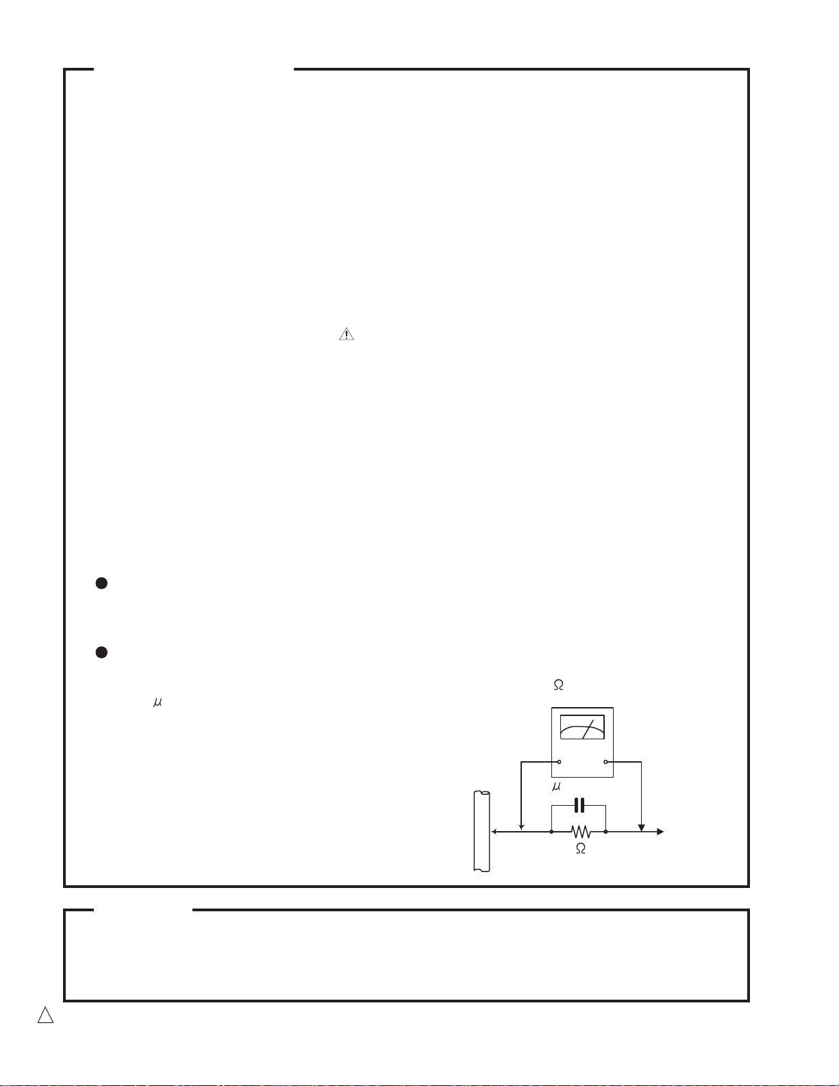
Electrostatic discharge (ESD), which occurs when static electricity stored in the body, fabric, etc. is discharged,
can destroy the laser diode in the traverse unit (optical pickup). Take care to prevent this when performing repairs.
1.1. Grounding to prevent damage by static electricity
Static electricity in the work area can destroy the optical pickup (laser diode) in devices such as DVD players.
Be careful to use proper grounding in the area where repairs are being performed.
1.1.1. Ground the workbench
1. Ground the workbench by laying conductive material (such as a conductive sheet) or an iron plate over
it before placing the traverse unit (optical pickup) on it.
1.1.2. Ground yourself
1. Use an anti-static wrist strap to release any static electricity built up in your body.
(caption)
Anti-static wrist strap
Conductive material
(conductive sheet) or iron plate
1.1.3. Handling the optical pickup
1. In order to maintain quality during transport and before installation, both sides of the laser diode on the
replacement optical pickup are shorted. After replacement, return the shorted parts to their original condition.
(Refer to the text.)
2. Do not use a tester to check the condition of the laser diode in the optical pickup. The tester's internal power
source can easily destroy the laser diode.
1.2. Handling the traverse unit (optical pickup)
1. Do not subject the traverse unit (optical pickup) to strong shocks, as it is a sensitive, complex unit.
2. Cut off the shorted part of the flexible cable using nippers, etc. after replacing the optical pickup. For specific
details, refer to the replacement procedure in the text. Remove the anti-static pin when replacing the traverse
unit. Be careful not to take too long a time when attaching it to the connector.
3. Handle the flexible cable carefully as it may break when subjected to strong force.
4. It is not possible to adjust the semi-fixed resistor that adjusts the laser power. Do not turn it
1-3
Page 4
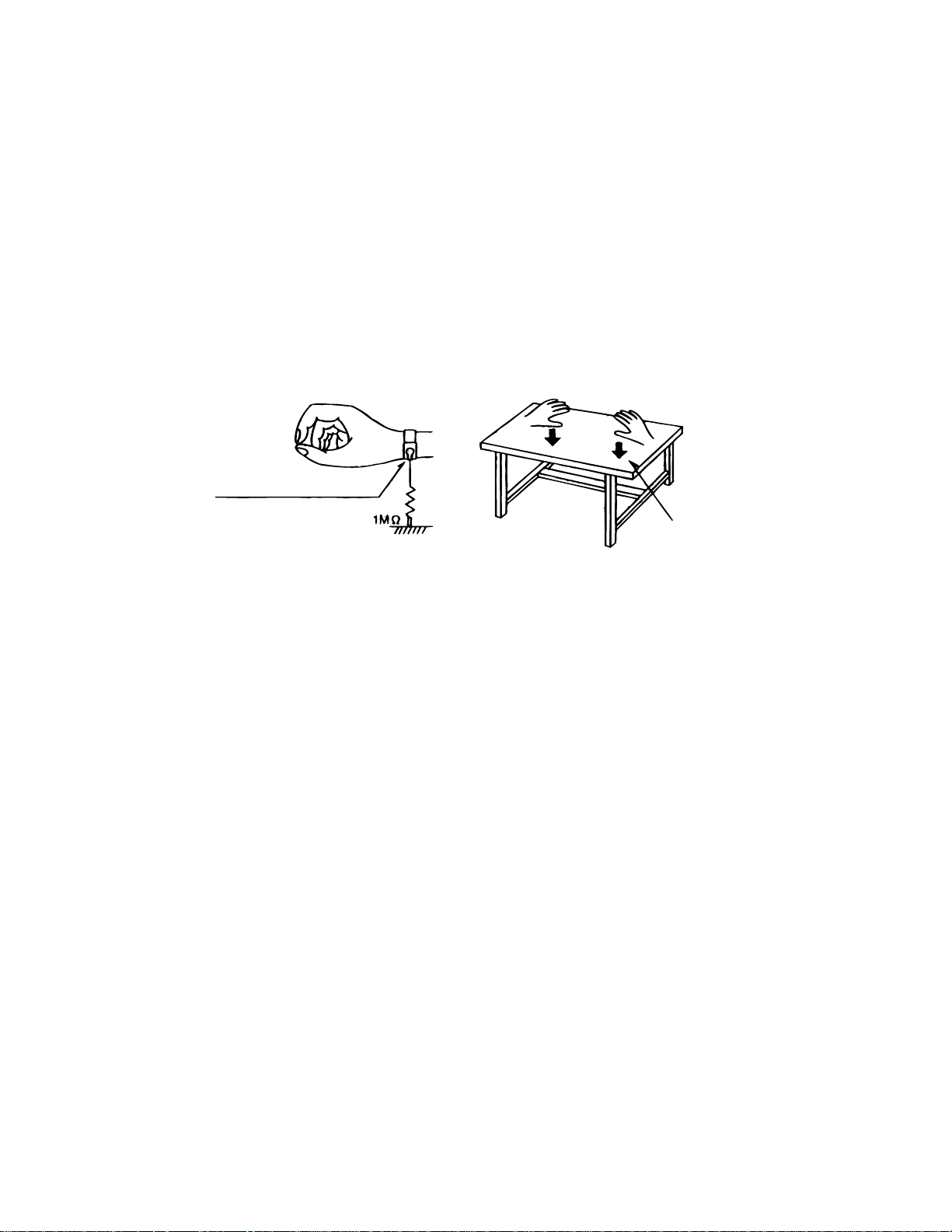
UX-F70MD/UX-F72MD
CN451
MAIN board
CN321
CD SERVO board
Pickup
Soldering part b
1.3. Cautions on removing the CD traverse unit
* For removing the CD traverse unit in detail, refer to the "Adjustment Method" section of this manual.
1. Before disconnecting the flexible wire from the connector CN601 on the CD SERVO board, solder the part shown in
the figure below.
(Note:If the flexible wire is disconnected from the CN601 without presoldering, it may cause breakdown of the CD
pickup assembly.)
2. When reassembling the CD traverse unit, be sure to remove the solder from the soldered part after reconnecting the
flexible wire to the CN601.
CD SERVO board
CD SERVO board
CN601
CN601
1-4
Soldering part
Page 5
UX-F70MD/UX-F72MD
1-5
Page 6
UX-F70MD/UX-F72MD
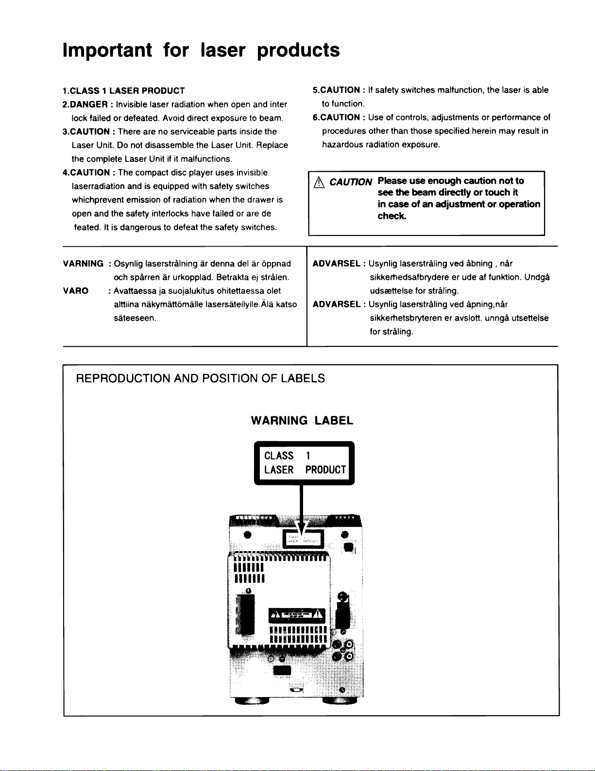
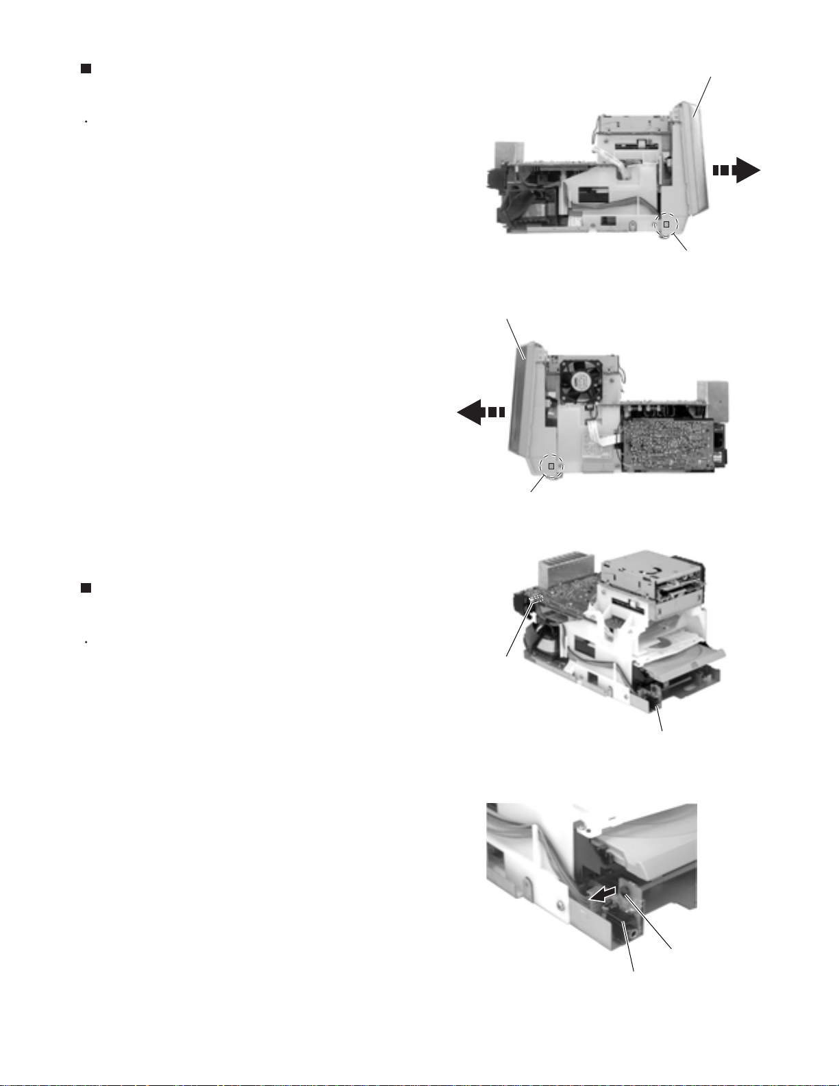
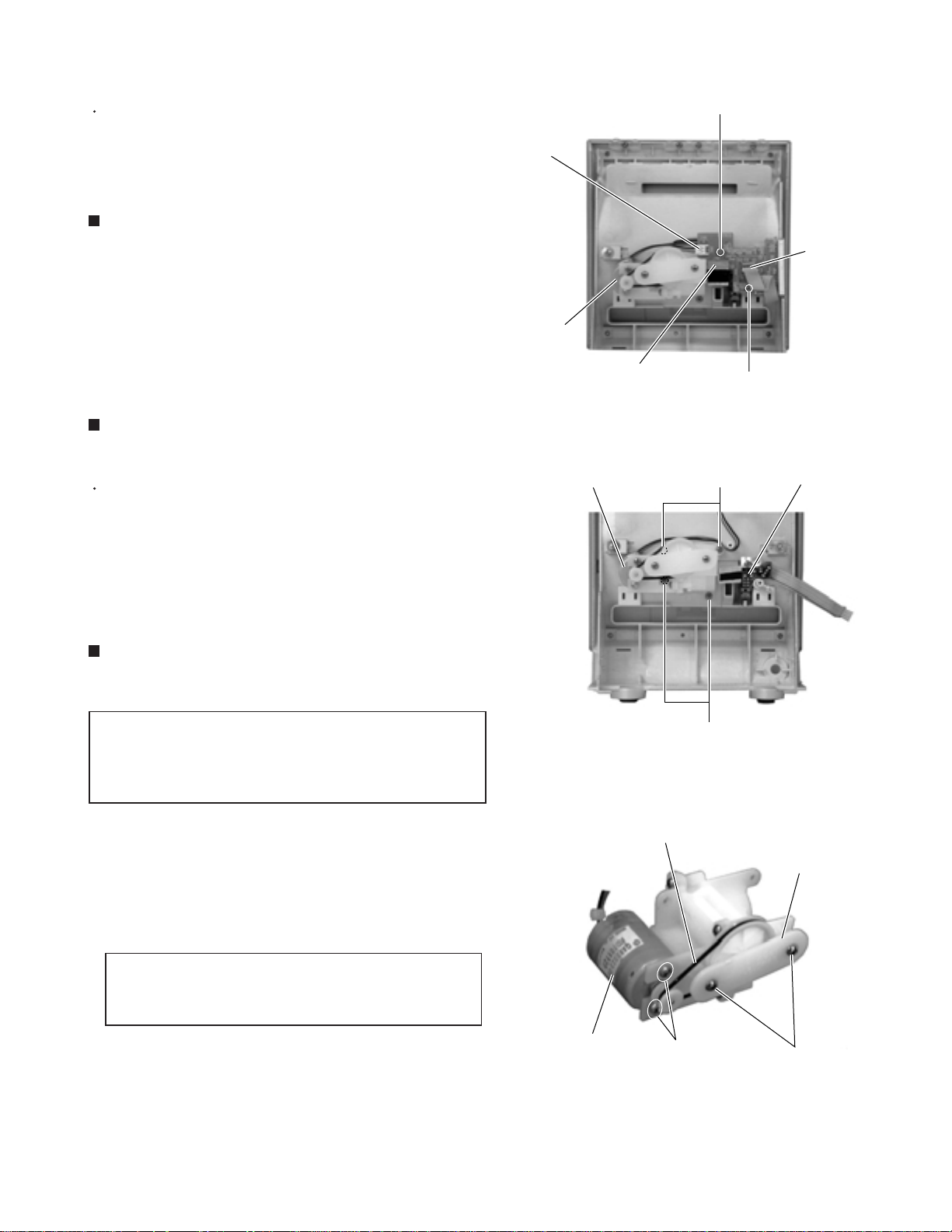
Disassembly method
<Main body>
Removing the rear cover
(See Fig.1 and 2)
1.
Remove the seven screws A on the back of the
body.
2.
Remove the two screws B on the bottom of the
body.
3.
Unlock the speaker terminal and the antenna
terminal, then remove the rear cover backward with
releasing the hooks.
Removing the side panels
(See Fig.3 to 5)
Prior to performing the following procedure, remove
the rear cover.
Rear cover
A
Antenna terminal
Side panel (R)
A
Speaker terminal
Fig.1
(Bottom)
B
A
A
Rear cover
1.
Remove the two screws C attaching the side panels
on the bottom of the body.
2.
Remove each side panel backward while releasing
the eight joints a as shown in Fig.4 and 5.
Joint a
Joint a
Side panel (L)
Fig.2
C
C
Side panel (R)
Side panel (L)
Fig.3
Joint a
B
Joint a
1-6
Side panel (L)
Fig.5
Side panel (R)
Fig.4
Page 7
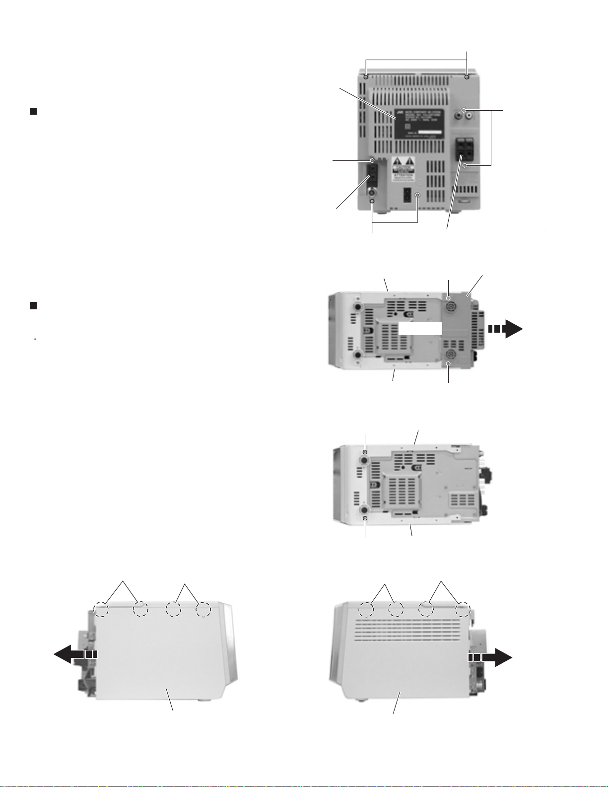
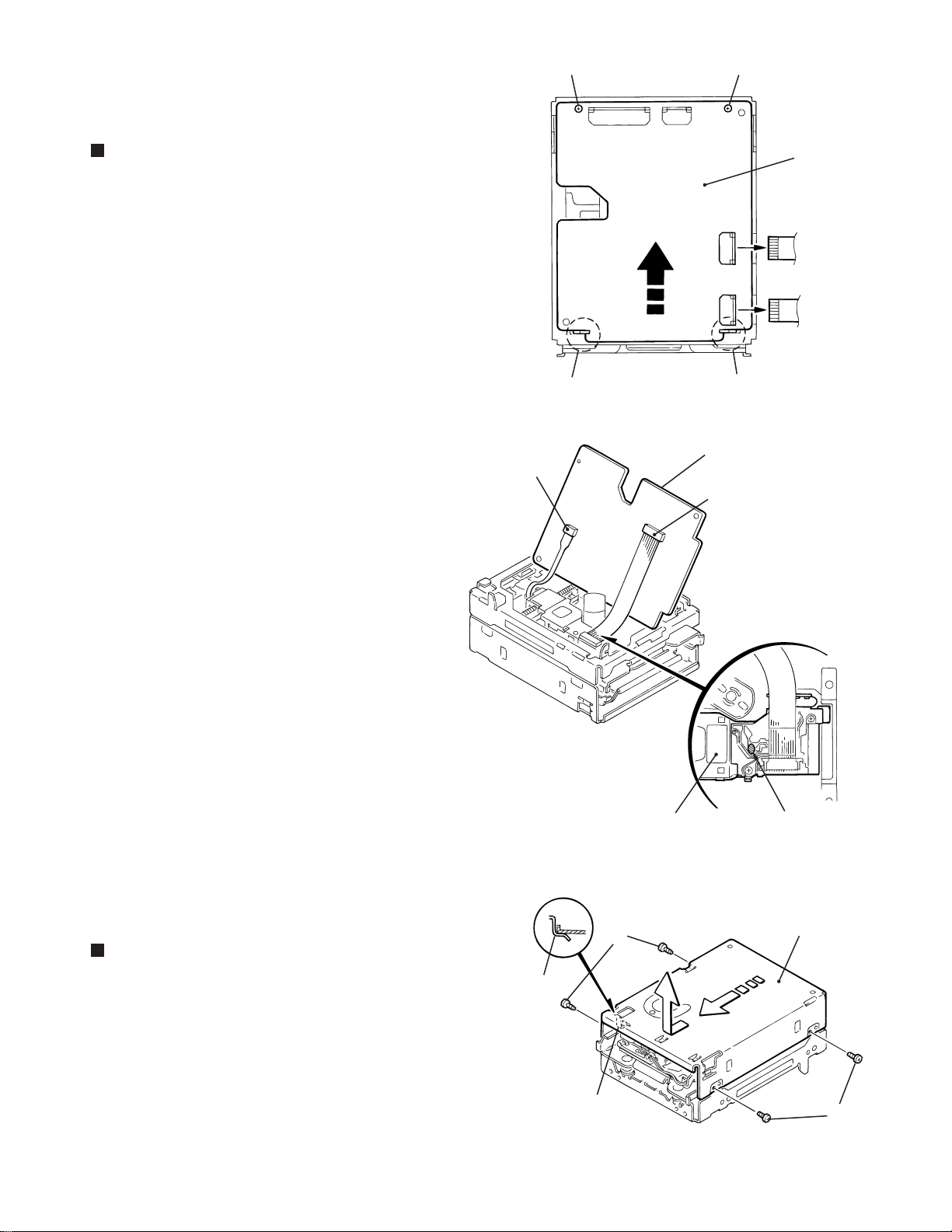
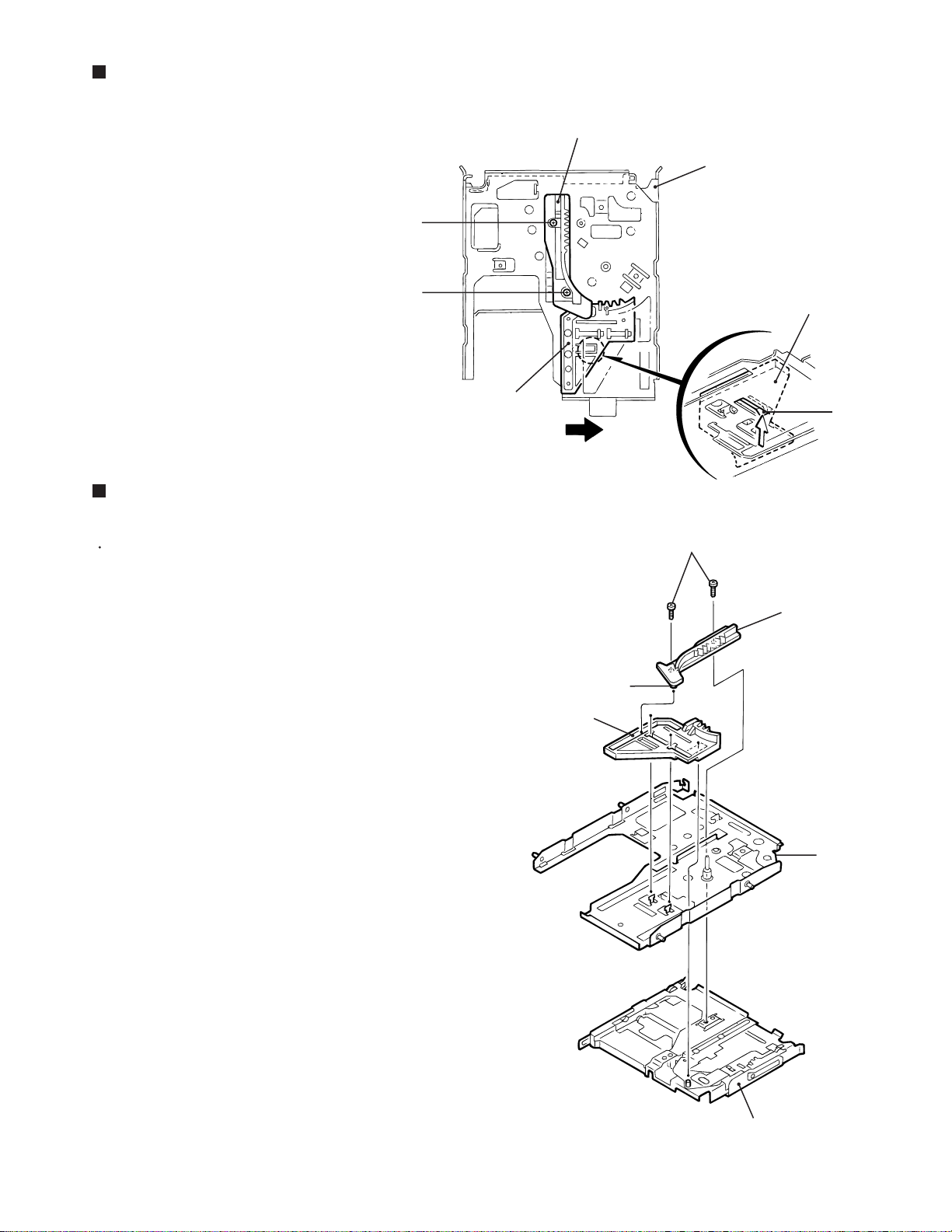
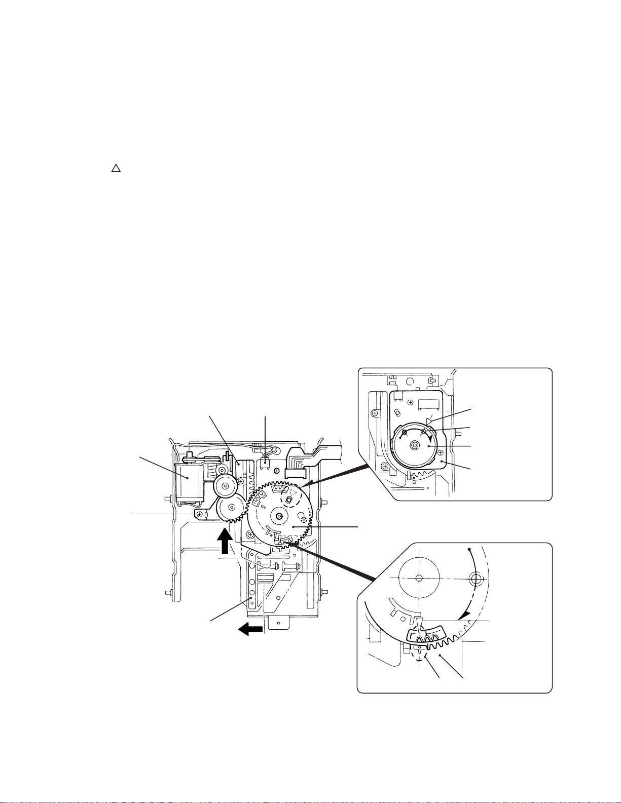
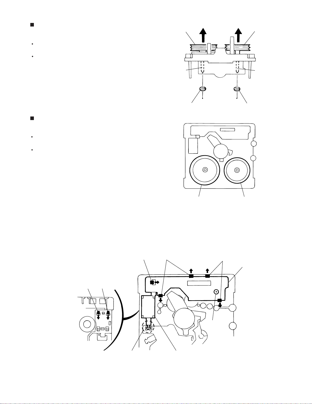
Removing the cassette mechanism
assembly section (See Fig.6 and 7)
UX-F70MD/UX-F72MD
Cassette mechanism assembly
Prior to performing the following procedure, remove
the rear cover and the side panels.
1.
Remove the two screw D on each side of the body.
2.
Release the joint b on each side of the body and
remove the cassette mechanism assembly section in
the direction of the arrow.
3.
Disconnect the card wires from connector CN705,
CN743 and CN744 on the system control board on
the left side of the body.
Removing the fan assembly (See Fig.6)
Prior to performing the following procedure, remove
the rear panel and the right side panel.
1.
Disconnect the wire from connector CN907 on the
main board on the right side of the body.
Joint b
Fan assembly
E
CN744
CN743
D
E
Main board
CN907
Fig.6
Cassette mechanism assembly
CN705
D
Joint b
2.
Remove the two screws E attaching the fan
assembly.
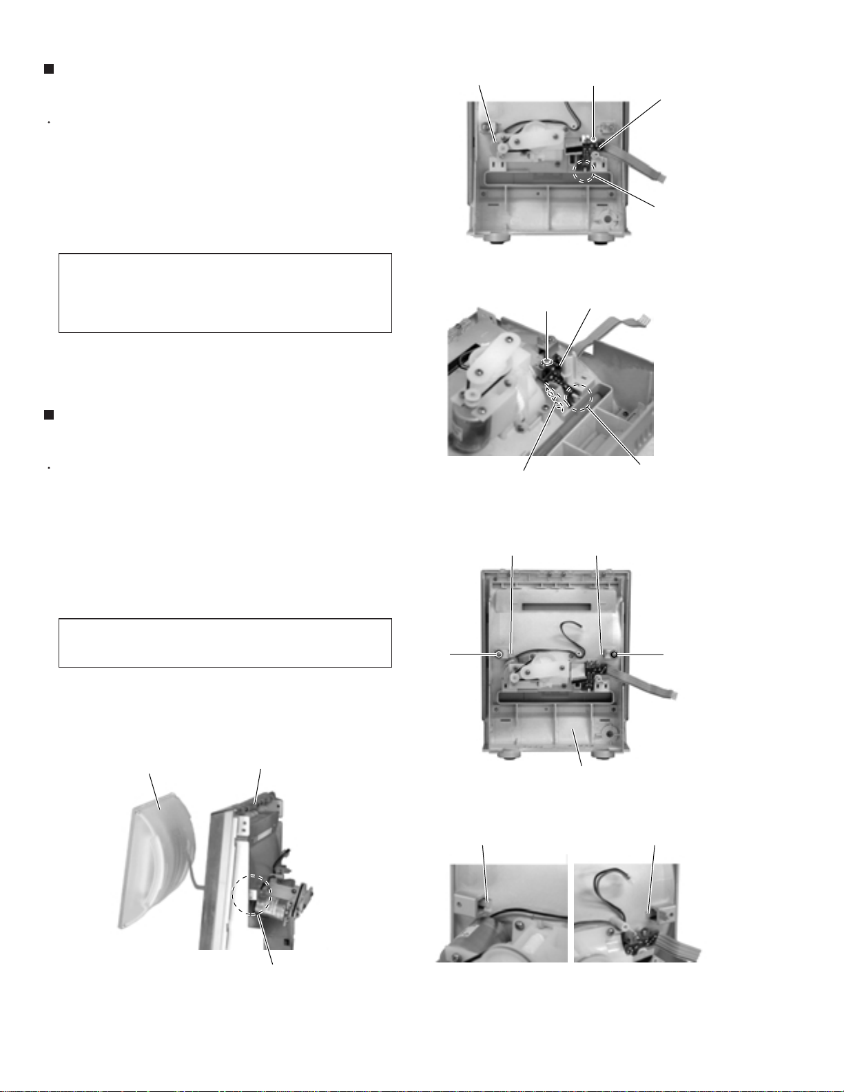
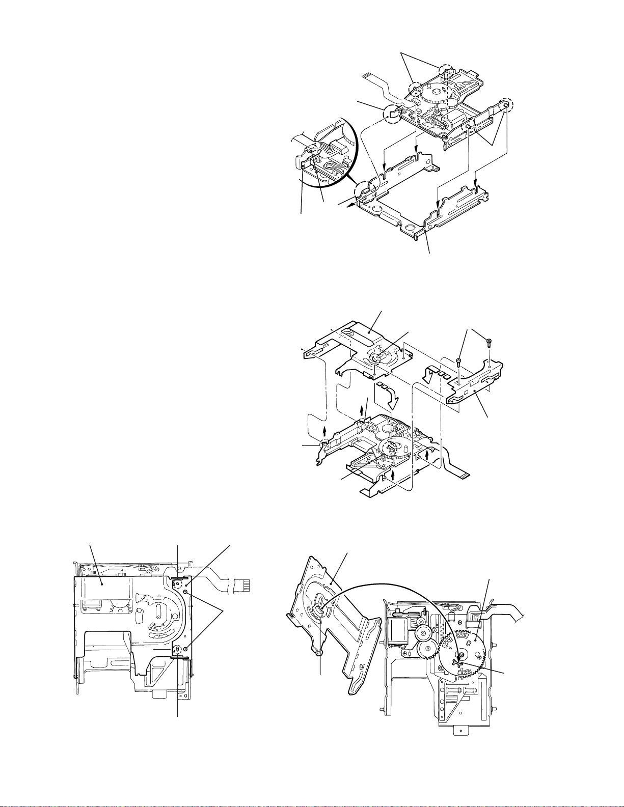
Removing the MD mechanism assembly
section (See Fig.8)
Prior to performing the following procedure, remove
the rear cover, the side panels, the cassette
mechanism assembly section and the fan assembly.
1.
Disconnect the card wire from connector CN721 on
the system control board.
2.
Disconnect the card wire from connector CN522 on
the underside of the MD mechanism assembly
section.
3.
Remove the four screws F and the MD mechanism
assembly section upward.
System control board
System
control board
CN721
F
F
Fig.7
MD mechanism assembly
CN522
F
F
Fig.8
Front panel
1-7
Page 8
UX-F70MD/UX-F72MD
Removing the system control board
(See Fig.9)
Prior to performing the following procedure, remove
the rear cover, the side panels and the cassette
mechanism assembly section.
1.
Remove the screw G on the left side of the body.
2.
Disconnect the card wire from connector CN701 and
CN721on the system control board.
3.
Disconnect connector CN709, CN711 and CN712 on
the system control board from the body outward.
4.
Disconnect the card wire from connector CN704 on
the underside of the system control board.
System control board
CN712
CN711
CN701
CN721
CN709
Removing the tuner board (See Fig.10)
Prior to performing the following procedure, remove
the rear cover and the right side panel.
1.
Disconnect the card wire from connector CN1 on the
tuner board on the right side of the body.
2.
Remove the screw H and remove the tuner board
upward while disengaging the three joint c.
CN704
CN1
G
Fig.9
Tuner board
H
Joint c
1-8
Fig.10
Page 9
UX-F70MD/UX-F72MD
Removing the front panel assembly
(See Fig.11 and 12)
Prior to performing the following procedure, remove
the rear cover, the side panels, the cassette
mechanism assembly section and the system control
board.
1.
Release the two joints d on the lower right and left
sides of the front panel assembly, then remove the
front panel assembly toward the front.
Front panel assembly
Joint d
Fig.11
Front panel assembly
Removing the headphone jack board
(See Fig.13 and 14)
Prior to performing the following rear cover, the side
panels, the cassette mechanism assembly section,
the system control board and the front panel
assembly section.
1.
Disconnect the wire from connector CN804 on the
main board.
2.
Remove the plastic rivet fixing the headphone jack
board.
Joint d
Fig.12
Main board
CN804
Headphone jack board
Fig.13
Plastic rivet
Headphone jack board
Fig.14
1-9
Page 10
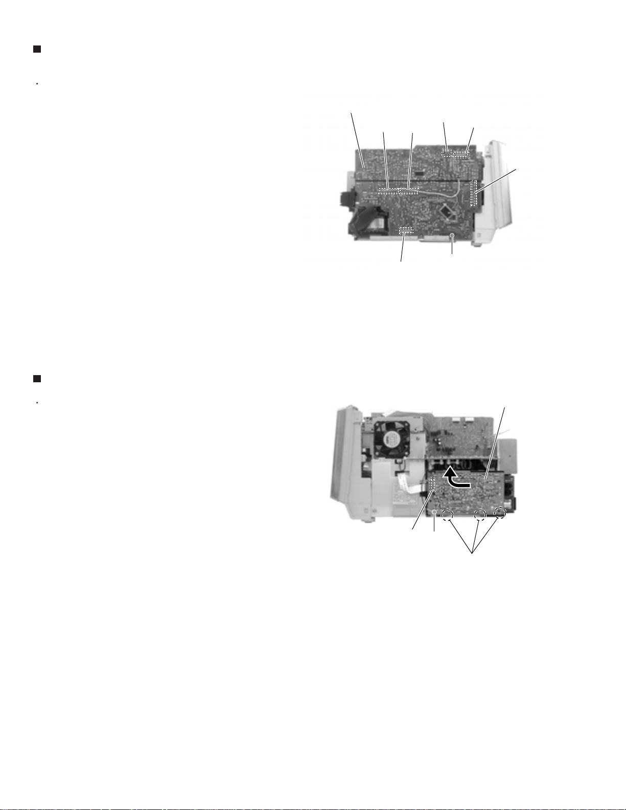
UX-F70MD/UX-F72MD
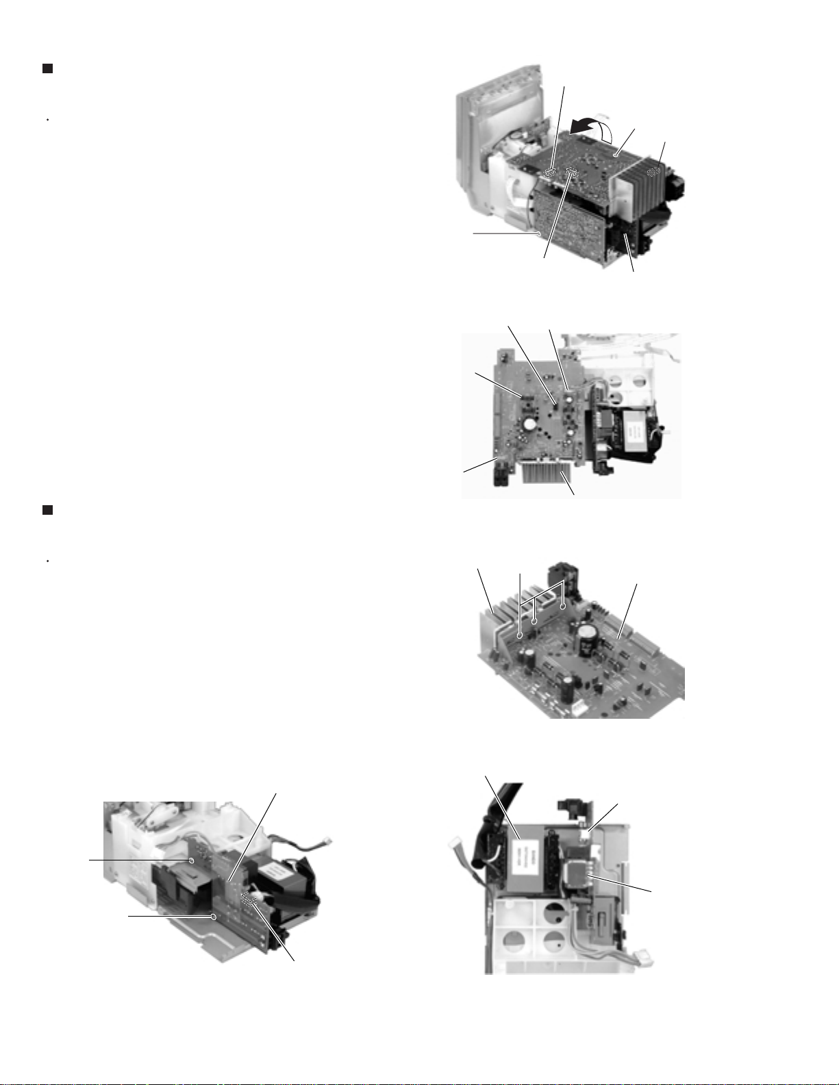
Removing the main board / the heat sink
(See Fig.15 to 17)
Prior to performing the following procedure, remove
the rear cover, the side panels, the cassette
mechanism assembly section, the system control
board and the MD mechanism assembly section.
1.
Remove the screw I attaching the main board.
2.
Remove the screw H attaching the grounding
terminal extending from the main board.
3.
Disconnect the wire from connector CN804 on the
main board.
4.
Disconnect connector CN805 on the main board
from the AC jack board while pulling out it. Remove
the main board in the direction of the arrow and
disconnect the wire from connector CN803 on the
reverse side of the main board.
5.
Remove the three screws J attaching the heat sink
on the reverse side of the main board.
H
Main board
Main board
CN805
CN805
CN803
CN803
I
CN804
AC jack board
Fig.15
Removing the AC jack board
(See Fig.18 and 19)
Prior to performing the following procedure, remove
the rear cover, the side panels, the cassette
mechanism assembly section, the system control
board, the MD mechanism assembly section and the
main board / the tuner board.
1.
Disconnect the wire from connector CN809 on the
AC jack board.
2.
Remove the screw K and screw L attaching the AC
jack board.
AC jack board
K
CN804
Heat sink
Power transformer assembly
J
Heat sink
Fig.16
Main board
Fig.17
CN809
1-10
AC jack board
L
CN809
Fig.19
Fig.18
Page 11
UX-F70MD/UX-F72MD
Removing the power transformer
assembly (See Fig.20)
Prior to performing the following procedure, remove
the rear cover, the side panels, the cassette
mechanism assembly section, the system control
board, the MD mechanism assembly section and the
main board.
1.
Disconnect the wire from connector CN809 on the
AC jack board.
2.
Cut off the band setting the wire on the CD
mechanism cover.
3.
Remove the four screws M attaching the power
transformer assembly.
Removing the CD mechanism assembly
(See Fig.21 to 23)
Power transformer
assembly
CD mechanism cover
Band
M
M
CD mechanism cover
Fig.20
AC jack board
CD mechanism assembly
CN809
Band
Notch
Headphone
jack board
Prior to performing the following procedure, remove
the rear cover, the side panels, the cassette
mechanism assembly section, the system control
board, the front panel assembly section, the MD
mechanism assembly section, the main board / the
tuner board and the AC jack board.
1.
Cut off the band setting the wire on CD mechanism
cover.
2.
Release the wire extending from the headphone jack
board from the three notches of the CD mechanism
cover on the left side of the body.
3.
Remove the four screws N on the left and right side
of the CD mechanism cover. Then remove the CD
mechanism cover upward.
4.
Remove the three screws O attaching the CD
mechanism assembly.
N
Notches
Fig.21
CD mechanism cover
CD mechanism assembly
Band
N
Fig.22
O
O
CD mechanism assembly
Fig.23
1-11
Page 12
UX-F70MD/UX-F72MD
<MD mechanism assembly section>
Prior to performing the following procedure, remove
the rear cover, the side panels, the cassette
mechanism assembly section, the fan assembly and
the MD mechanism assembly section.
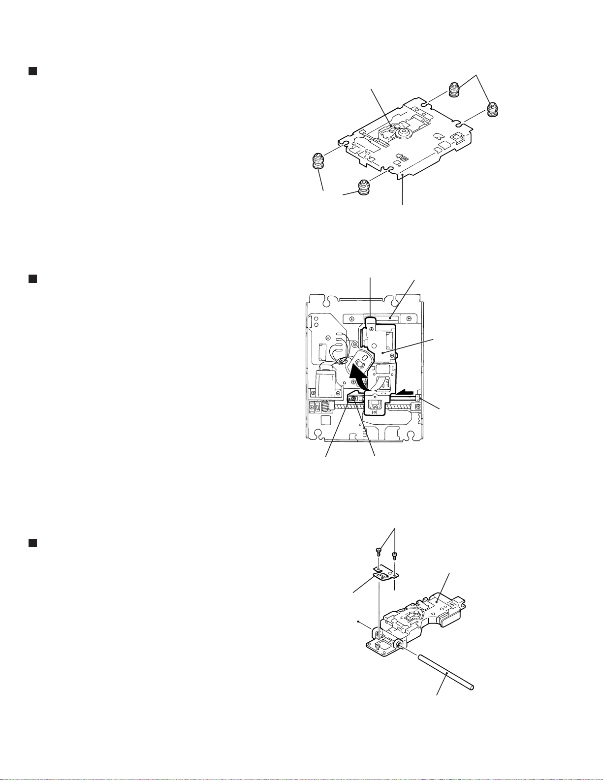
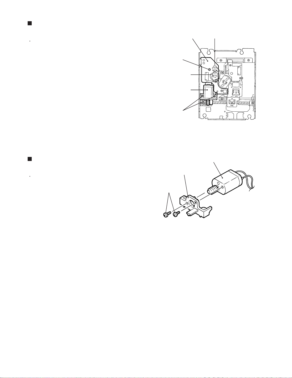
Removing the MD mechanism assembly
(See Fig.24 to 26)
1.
Remove the four screws P attaching the brackets
(1) and (2) on the left and right side of the MD
mechanism assembly.
2.
Disconnect the card wire from connector CN521 on
the MD mechanism board.
3.
Remove the MD mechanism bottom cover
downward.
MD mechanism assembly
P
brackets (1)
Fig.24
MD mechanism assembly
P
CN521
brackets (2)
Fig.25
MD mechanism assembly
MD mechanism bottom cover
1-12
Fig.26
Page 13
<Front panel assembly section>
UX-F70MD/UX-F72MD
Prior to performing the following procedure, remove
the rear cover, the side panels, the cassette
mechanism assembly section, the system control
board and the front panel assembly section.
Removing the relay board (See Fig. 27)
Disconnect the wire from connector CN906, CN907
1.
and the card wire from CN908 on the relay board
respectively.
Remove the two screws Q.
2.
Removing the drive motor assembly
(See Fig.28)
Prior to performing the following procedure, remove
the relay board.
1.
Remove the four screws R attaching the drive motor
assembly.
CN907
Drive motor
assembly
Drive motor assembly
CN908
Fig.27
Q
Q
Door switch board
R
Relay board
CN906
Removing the belt and the drive motor
(See Fig.29)
REFERENCE:
1.
Remove the two screws S attaching the plate.
2.
Remove the belt from the two pulleys.
3.
Remove the two screws T attaching the drive motor.
REFERENCE:
The belt and the drive motor can be
removed respectively without removing the
drive motor assembly from the front panel
section.
When removing the drive motor only,
remove the belt from the drive motor
pulleys in advance.
Drive motor
Fig.28
Belt
T
Fig.29
R
Plate
S
1-13
Page 14
UX-F70MD/UX-F72MD
Removing the door switch board
(See Fig.30 and 31)
Prior to performing the following procedure, remove
the relay board.
1.
Loosen the screw U attaching the door switch.
2.
Remove the door switch board while releasing it from
the joint e.
CAUTION:
When reattaching the door switch board,
fit it to the joint e and check the
operating state of the switch before
tightening the screw U.
Removing the LCD section
(See Fig.32 to 34)
Prior to performing the following procedure, remove
the relay board.
1.
Loosen the two screws V attaching the lock lever.
Drive motor assembly
Switch section
U
Fig.30
Door switch board
U
Fig.31
Door switch board
Joint e
Joint e
2.
Push the part f of the lock lever in the direction of
the arrow as shown in Fig.33-1 / 33-2 and disengage
the LCD section from the front panel assembly.
CAUTION:
Because the LCD may come off, hold it
when loosening the screws V.
LCD section
Front panel assembly
Lock lever Lock lever
V
Front panel assembly
Fig.32
Lock lever f Lock lever f
V
1-14
Fig.34
Joint f
Fig.33-1 Fig.33-2
Page 15
UX-F70MD/UX-F72MD
Removing the LCD board assembly
(See Fig.35 to 39)
Prior to performing the following procedure, remove
the relay board and the LCD section.
1.
Remove the four screws W attaching the case
cover.
2.
Remove the four screws X attaching the LCD panel
on the back of the LCD section.
3.
Remove the LCD cover.
4.
Release the joint g and remove the LCD board
assembly in the direction of the arrow.
W
X
W
Case cover
W
W
Fig.35
LCD section
Joint g
X
Fig.36
LCD panel
Fig.37
LCD board assembly
LCD cover
Fig.38Fig.39
1-15
Page 16
UX-F70MD/UX-F72MD
<Cassette mechanism assembly section>
Prior to performing the following procedure, remove
the rear cover, the side panels and the cassette
mechanism assembly section.
Removing the operation switch board
(See Fig.40)
1.
Remove the seven screws Y attaching the operation
switch board on the reverse side of the cassette
mechanism assembly.
Y
Cassette amplifier board
Y
Operation switch board
Y
Removing the cassette mechanism
assembly (See Fig.41)
1.
Remove the four screws Z on the reverse side of the
cassette mechanism assembly.
Z
Fig.40
Cassette mechanism assembly
1-16
Cassette amplifier board
Z
Fig.41
Page 17
UX-F70MD/UX-F72MD
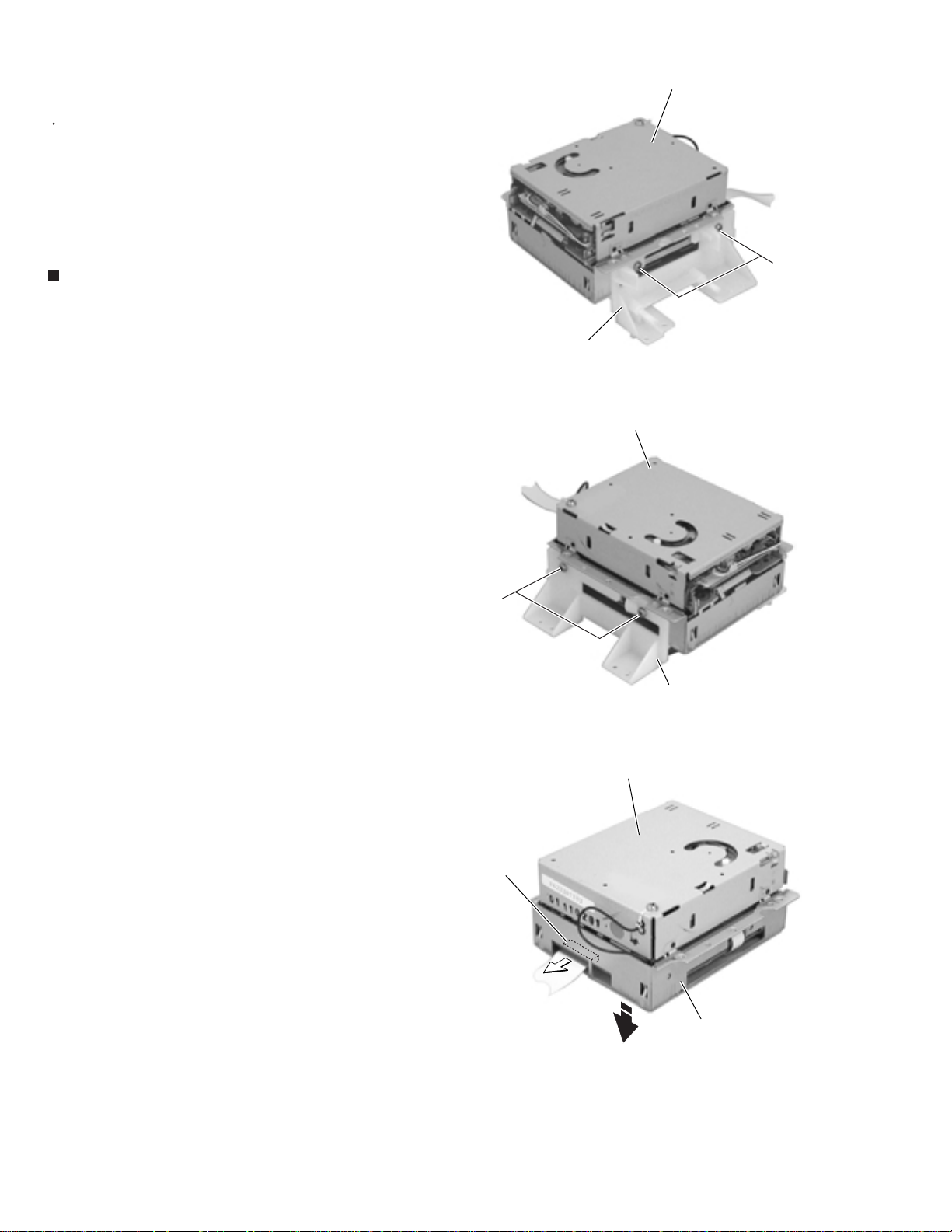
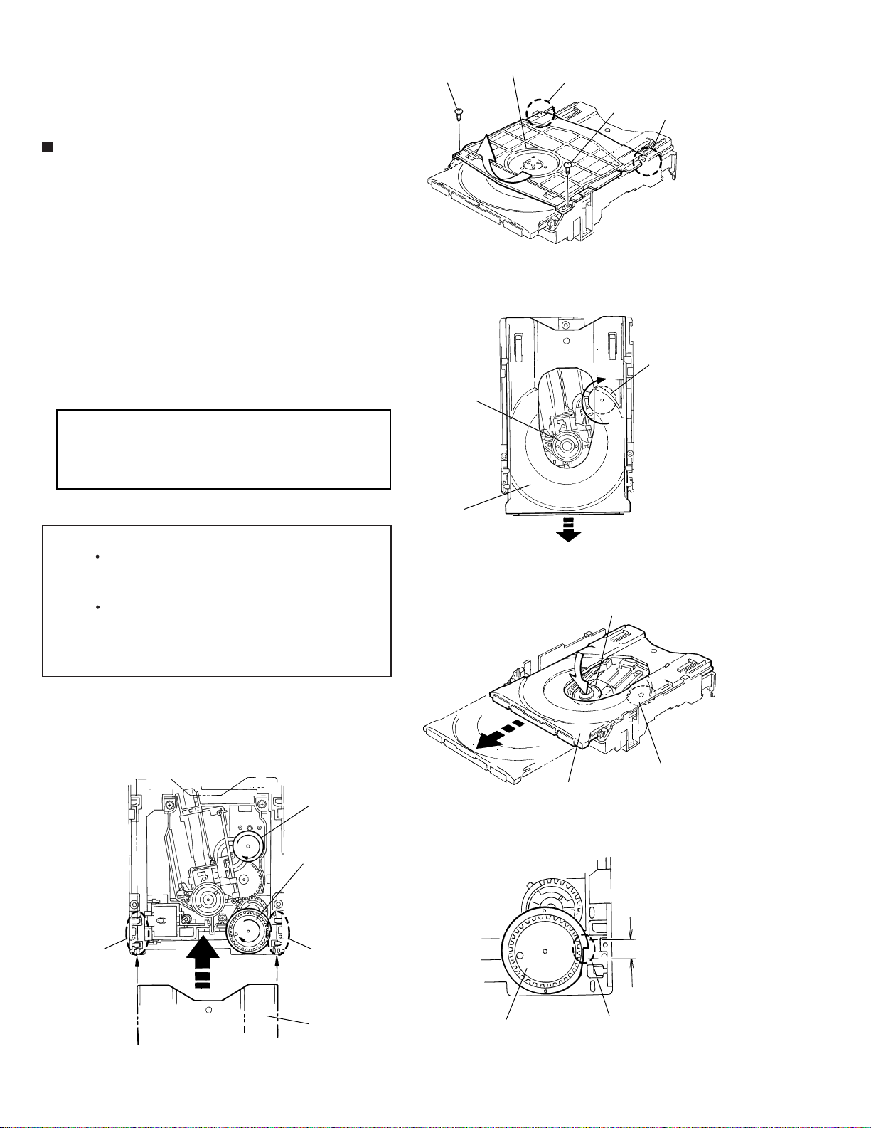
Disassembly method
<Main body>
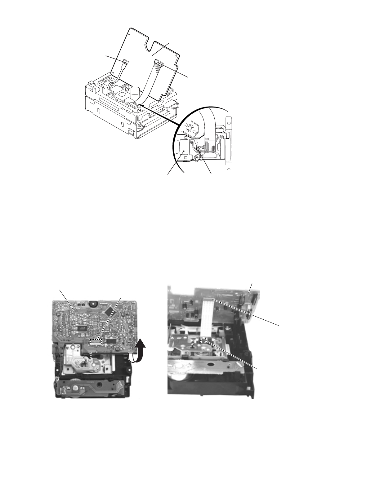
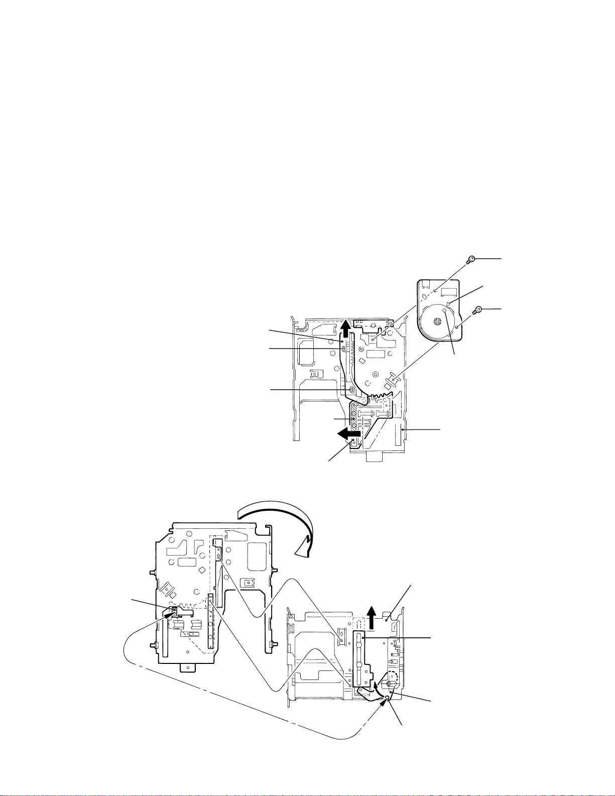
Removing the main board
(See Fig.1 and 2)
1.
Turn over the body and disconnect the card wire
from connector CN408 and the flexible wire from
CN407 on the main board.
2.
Remove the two screws A attaching the main board.
Slide the main board in the direction of the arrow to
release the two joints a with the single flame.
3.
Solder part b on the pickup in the body. Disconnect
the flexible harness from connector CN321 and
CN451 on the underside of the main board. Then
remove the main board.
AA
(Bottom)
Main board
CN408
CN407
Joint b Joint b
Fig.1
Main board
CN451
CN321
Removing the mechanism cover
(See Fig.3)
1.
Remove the four screws B on both sides of the
body.
2.
Move the mechanism cover toward the front to
disengage the front hook of the mechanism cover
from the internal loading assembly (Joint c). Then
remove the mechanism cover upward.
Fook
Joint c
Joint c
B
Pickup
Fig.2
Fig.3
Solder part b
Mechanism cover
B
1-17
Page 18
UX-F70MD/UX-F72MD
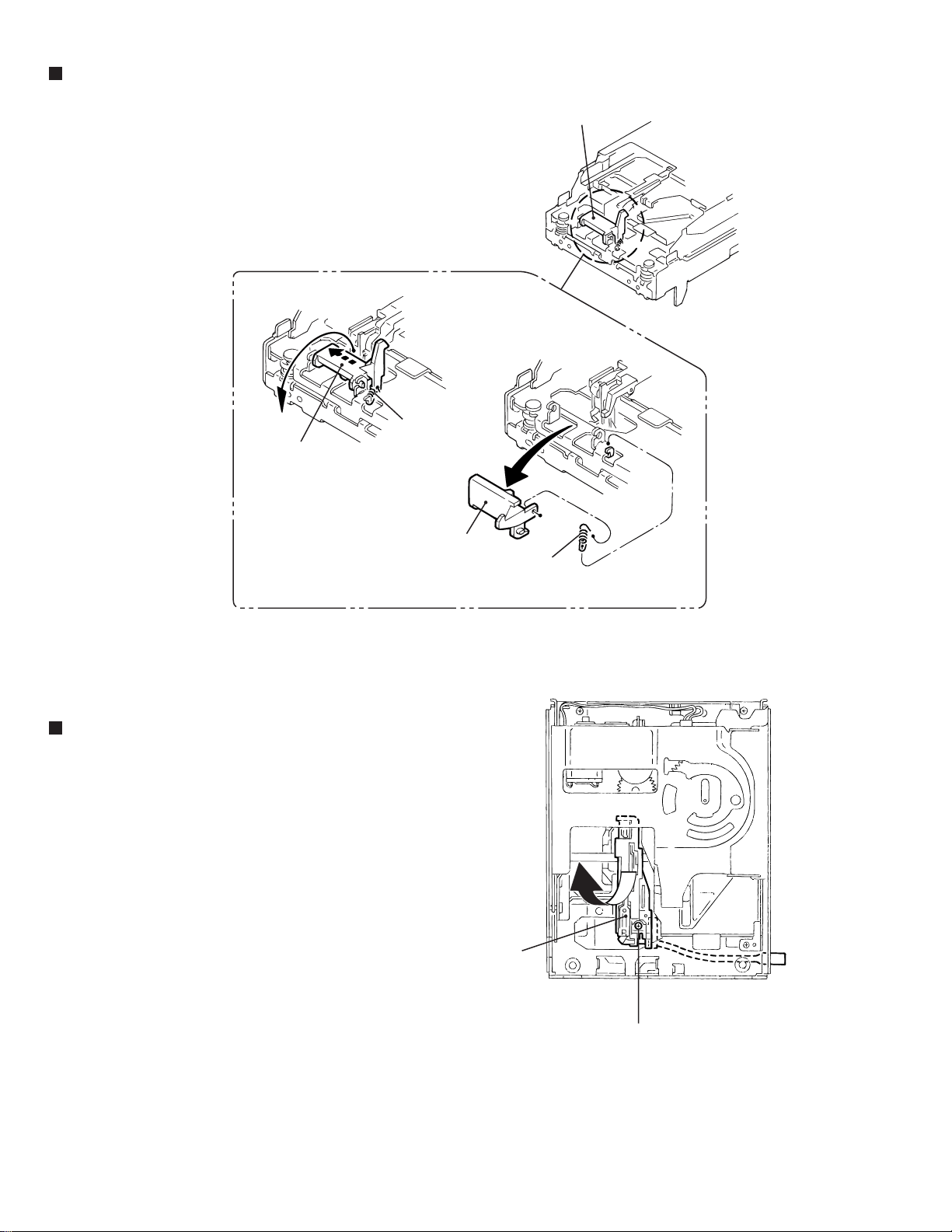
Removing the head lifter (See Fig.4 to 6)
1.
Move the head lifter on top of the body in the
direction of the arrow and turn around.
2.
Detach the spring from the hook of the body.
Remove the head lifter with the spring.
3.
If necessary, remove the spring from the head lifter.
Head lifter
Fig.5
Head lifter
Fig.4
Spring
Removing the head assembly (See Fig.7)
1.
Remove the screw C on the upper side of the body.
Remove the head assembly while pulling the flexible
harness from the body.
Head lifter
Spring
Fig.6
Head assembly
1-18
C
Fig.7
Page 19
Removing the Loading assembly
(See Fig.8 and 9)
Ref:
The loading assembly, the traverse mechanism
assembly and the single flame will be
removable after removing the loading assembly
from the body.
D
UX-F70MD/UX-F72MD
D
Prior to performing the following procedure, remove
the main board, the mechanism cover, the head lifter
and the head assembly.
1.
Remove the three screws D on the upper side of the
body.
2.
Move the loading assembly forward to disengage it
from the traverse mechanism assembly (Joint d).
Then remove it upward.
3.
Remove the traverse mechanism assembly from the
single flame.
Joint d
Loading assembly
D
Fig.8
Loading assembly
Fig.9
Traverse mechanism
assembly
Single flame
1-19
Page 20
UX-F70MD/UX-F72MD
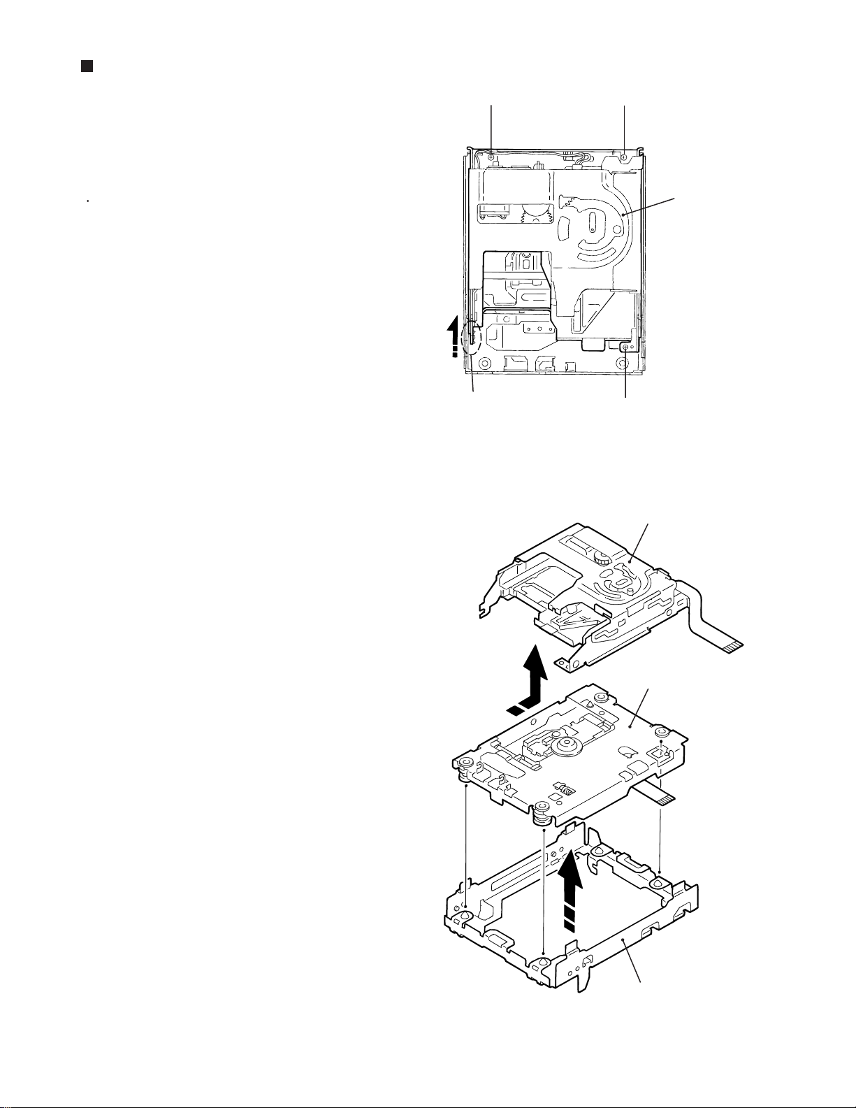
<Loading assembly>
Slide base (R)
E'
Removing the slide base (L) / (R)
(See Fig.10)
1.
Remove the two screws E on the upper side of the
loading assembly.
2.
Remove the slide base (L) outward. (Release it from
the joint bosses E.)
3.
Remove the slide base (R) outward.
Removing the loading mechanism
assembly (See Fig.11)
1.
Detach the loading mechanism assembly upward to
release the four pins on both sides from the loading
motor, paying attention to the part e of the loading
mechanism base.
E
Slide base (L)
E
E'
Fig.10
Part e
Loading mechanism assembly
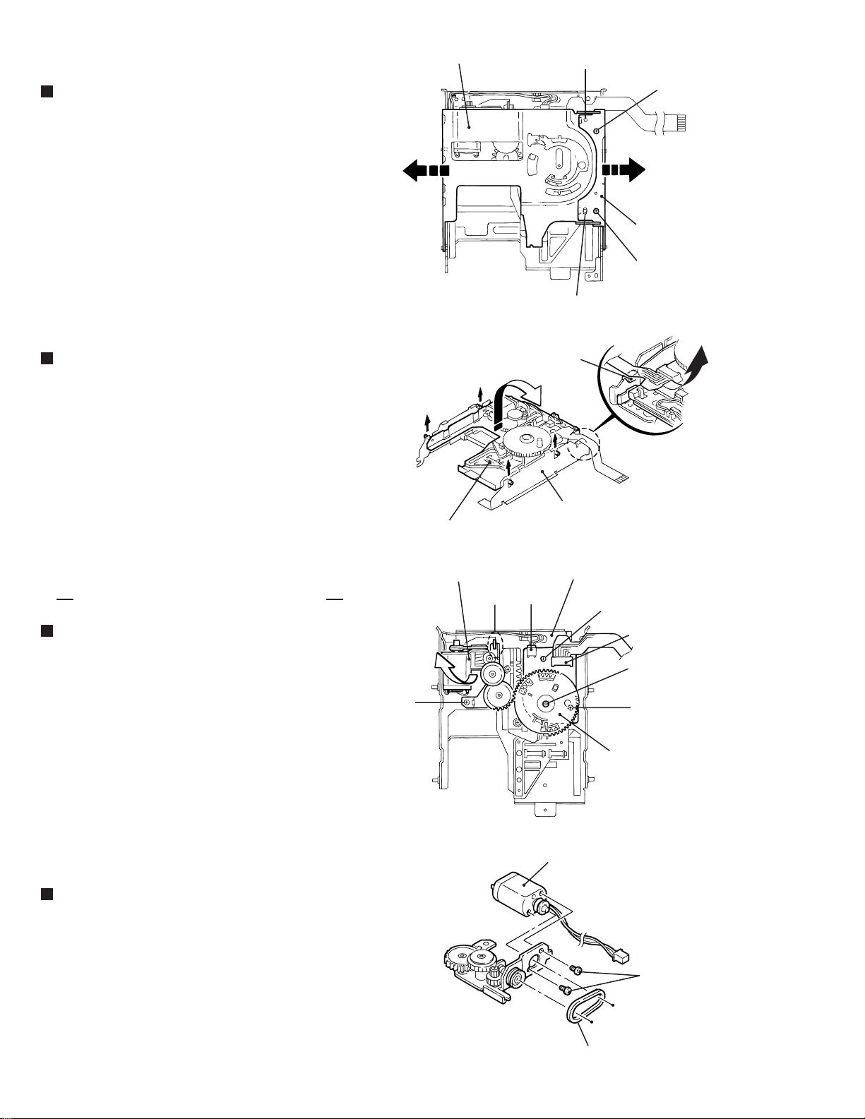
Removing the loading motor
(See Fig.12 and 13)
1.
Disconnect the harnesses from the wire holder and
from connector CN612 on the cam switch board.
2.
Remove the screw F attaching the loading motor
and release the joint f.
3.
Remove the belt from the loading motor assembly.
4.
Remove the two screws G attaching the loading
motor.
Removing the cam gear and the cam
switch board (See Fig.12)
Loading mechanism
assembly
Loading motor assembly
Joint f
CN612
F
Loading mechanism base
Fig.11
Wire holder
H
Cam switch board
Slit washer
H
Cam gear
Fig.12
Loading motor
1.
Remove the slit washer attaching the cam gear and
pull out the cam gear.
2.
Disconnect the harness from the wire holder and
from connector CN612 on the cam switch board.
3.
Remove the two screws H and the clamp. Remove
the cam switch board.
1-20
G
Belt
Fig.13
Page 21
Removing the cartridge holder assembly
(See Fig.14 and 15)
UX-F70MD/UX-F72MD
1.
Remove the two screws I on the upper side of the
loading assembly.
I
I
Removing the slide bar and the eject bar
(See Fig.14 and 15)
Prior to performing the following procedure, remove
the cartridge holder assembly.
Slide bar
Cartridge holder assembly
Eject bar
Eject bar
Part g
Fig.14
I
1.
Remove the slide bar upward.
2.
Move the eject bar outward until it stops as shown in
Fig.14. Push the convex part g on the bottom of the
body and remove the eject bar from the chassis.
Slide bar
k
Eject bar
UD base
Cartridge holder assembly
Fig.15
1-21
Page 22
UX-F70MD/UX-F72MD
<Traverse mechanism assembly>
Removing the Insulators (See Fig.16)
1.
Disengage the four insulators from the notches of the
traverse mechanism chassis.
Removing the pickup unit (See Fig.17)
1.
Turn over the traverse mechanism assembly and
remove the screw J attaching the shaft holder (F).
2.
Move the shaft inward and remove it from the shaft
holder (R).
Pickup unit
Insulators
Traverse machanism chassis
Fig.16
Joint h
Pickup guide
Pickup unit
Insulators
3.
Detach the shaft side of the pickup unit upward and
release the joint h with the pickup guide. Then
remove the pickup unit with the shaft.
Removing the pickup (See Fig.18)
1.
Draw out the shaft from the pickup.
2.
Remove the two screws K attaching the rack spring.
Shaft holder (F)
Rack spring
Shaft holder (R)
J
Fig.17
K
Pickup
1-22
Shaft
Fig.18
Page 23
Removing the feed motor assembly
(See Fig.19-1, 19-2)
It is not necessary to remove the pickup unit.
1.
For the white and black harnesses extending from
the feed motor assembly, unsolder the soldering i on
the traverse mechanism board.
UX-F70MD/UX-F72MD
Traberse mechanism board Soldering j
M
2.
Remove the two screws L attaching the feed motor
assembly.
3.
Remove the two screws N attaching the feed motor
bracket.
Removing the traverse mechanism
board (See Fig.19-1)
Prior to performing procedure, remove the feed
motor assembly.
1.
For the red and black harnesses extending from the
spindle motor, unsolder the soldering j on the
traverse mechanism board.
Soldering i
Feed motor assembly
L
Fig.19-1
Feed motor
Feed motor bracket
N
2.
Remove the screw M attaching the traverse
mechanism board.
Fig.19-2
1-23
Page 24
UX-F70MD/UX-F72MD
<Reattaching the loading assembly>
1.
Reattach the eject bar to the UD base.
(Fig.15 and 20)
2.
Reattach the slide bar to the loading mechanism
chassis while fitting the boss marked k to the eject
bar slot. (Fig.20)
3.
Slide the slide bar and the eject bar in the direction
of the arrow in Fig.20 and reattach the cartridge
holder assembly using the two screws I.
(Fig.20 and 21)
ATTENTION:
Make sure the pin of the eject lever
marked l is fitted to the slot of the eject
bar marked m at the bottom of the
loading mechanism chassis after
moving the eject lever and the loading
slider of the cartridge holder assembly
in the direction of the arrow.
(Refer to Fig.21)
Slide bar
I
I
Cam switch board
H
Point marked
H
Cam switch boss
Ditch
UD base
Eject bar
Fig.20
1-24
UD base (Bottom)
Cartridge holder assembly
Ditch m
Loading slider
Eject lever
l
Fig.21
Page 25
4.
Reattach the wire holder to the UD base while
engaging the UD base hook marked u to the wire
holder slot marked t (At the same time, the boss on
the reverse side of the wire holder is fitted to the UD
base round hole).
5.
Reattach the cam switch board using the two screws
H. (Fig.22)
6.
Turn the cam switch to bring the boss to the point
marked on the cam switch board. Reattach the
cam gear using a slit washer while fitting the cam
gear slot to the cam switch boss. (Fig.22)
UX-F70MD/UX-F72MD
ATTENTION:
When reattaching the cam gear, the
cam switch boss should be fitted to the
cam gear slot, and the triangle mark of
the cam gear should be aligned to the
hole of the eject bar as shown in
Fig.22.
7.
Reattach the loading motor assembly, using the
screw F. Connect the harness extending from the
loading motor to connector CN612 on the switch
board and fix it with the wire holder. (Fig.22)
Slide bar CN612
Loading motor assembly
Point marked
Boss
Cam switch
Cam switch board
F
Eject lever
Fig.22
Cam gear
n
Cam gear
(Triangle mark)
Eject lever
1-25
Page 26
UX-F70MD/UX-F72MD
8.
Reattach the UD base while engaging the four pins
on both sides of the UD base to the notches of the
loading mechanism base and placing the edge
(marked e’) of the cartridge holder assembly under
the hook e of the loading mechanism base. (Fig.23)
9.
Reattach the slide base (R) while fitting the two pins
on another side of the UD base to the slots of the
slide base (R). (Fig.24)
ATTENTION:
10.
Reattach the slide base (L) on the slide base (R)
while fitting the two pins on another side of the UD
base to the slots of the slide base (L) (Fig.25). Make
sure the two slots of the slide base (L) are fitted to
the two bosses marked E’ and tighten the two
screws E. (Fig.26)
Ref:
To expedite the work, bring up the UD base
slightly when fitting each pin to the appropriate
notch.
Fit the part v of the slide base (R) to
the part w on the inward side of the
cam gear rib. (Fig.25)
Hook e
Hook e'
Hook e'
Pin
Loading mechanism base
Fig.23
Slide base (R)
Part v
Pin
E
E'
Pin
Slide base (L)
Pin
Part w
Fig.24
Slide base (L)Slide base (R)
Slide base (R)
Cam gear
E
Part v
Part w
1-26
E'
Fig.25Fig.26
Page 27
UX-F70MD/UX-F72MD
<Cassette Mechanism Section>
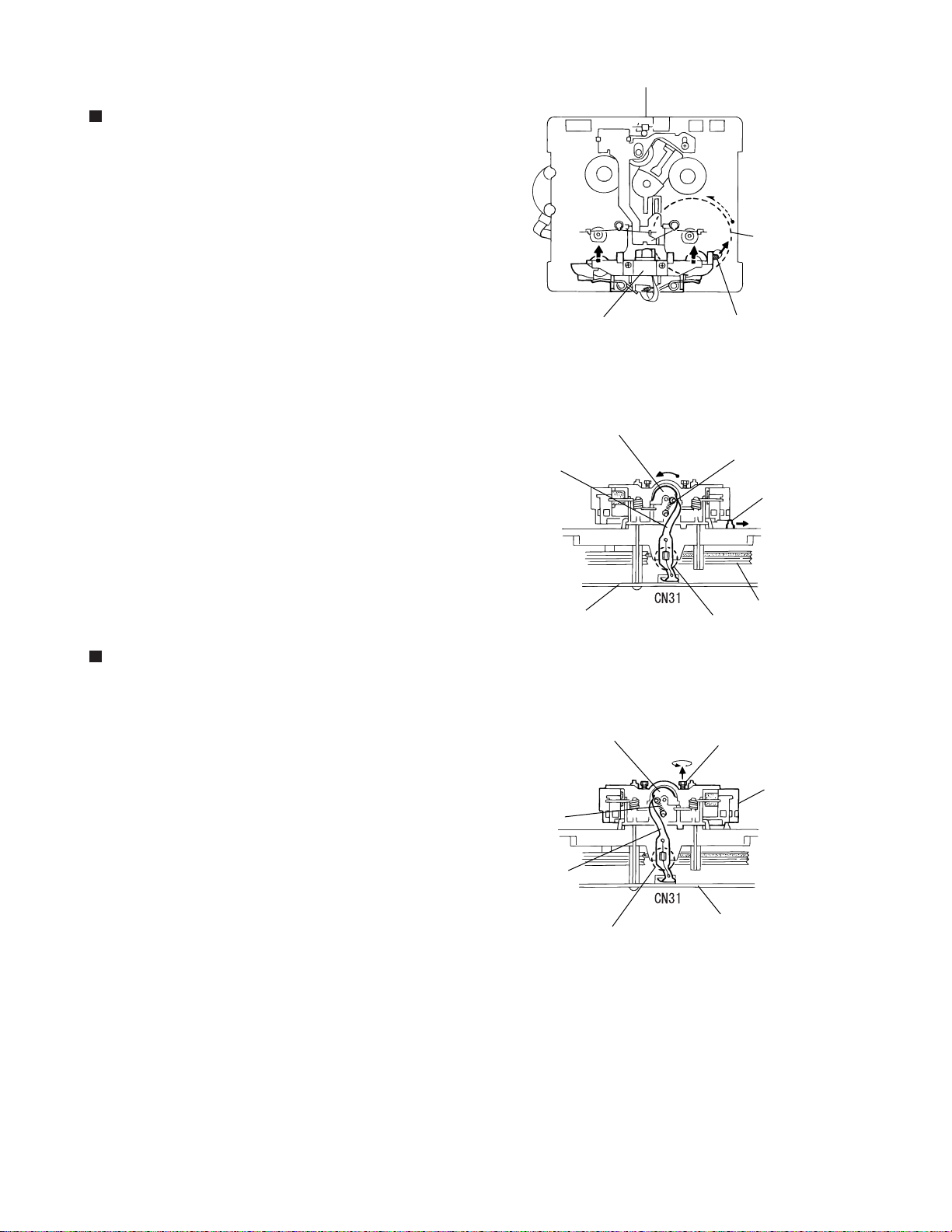
Removing the Recording, Playback / Erasing
Head (Refer to Figs. 1 to 3.)
1. Shifting the trigger arm seen in the right side of the
head mount in the arrow-marked direction, turn the
flywheel (R) counterclockwise until the head mount
clicks while moving frontwards. (See Fig. 1.)
2. Turn the flywheel (R) counterclockwise. The
playback head accordingly turns counterclockwise
from the position shown in Fig. 2 to that in Fig. 3.
3. Leaving the playback head in the position shown in
Fig. 3, disconnect the flexible wire coming from the
playback head from the connector CN31 on the
head amplifier & mechanism control P.C. board.
4. Remove the flexible wire from the hook b of the
chassis base.
5. Remove the spring a from the back of the head.
Cassette mechanism
Head mount
Head (REC, PB/Erasing)
Flexible wire
Flywheel (R)
Trigger arm
Fig. 1
Spring a
Trigger arm
6. Loosen the reversing azimuth screw A that fastens
the head.
7. Remove the recording, playback/erasing head from
the front side (head side) of the head mount.
Reinstalling the Recording, Playback /
Erasing Head
1. Install the recording, playback/erasing head from the
front side of the head mount as shown in Fig. 3.
2. Tighten the reversing azimuth screw A.
3. Install the spring a from the back of the head.
4. Set the flexible wire at the hook b of the chassis
base.
5. Connect the flexible wire coming from the head to
the connector CN31 on the head amplifier &
mechanism control P.C. board.
Head amp. & mechanism
control P.C. board
Head (REC, PB/Erasing)
Spring a
Flexible wire
Hook b
Hook b
Flywheel (R)
Fig. 2
Reversing azimuth
screw A
Head mount
Head amp. & mechanism
control P.C. board
Fig. 3
1-27
Page 28
UX-F70MD/UX-F72MD
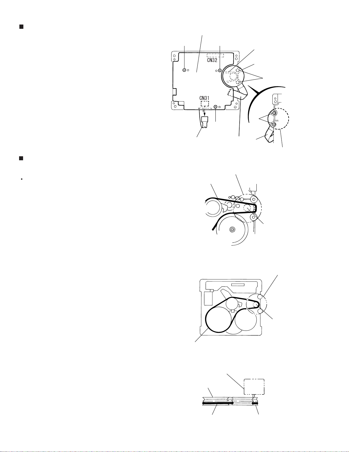
Removing the Head Amplifier & Mechanism
Control P.C. Board (Refer to Figs. 4 and 5.)
1. Disconnect the flexible wire from the connector
CN31 on the head amplifier & mechanism control
P.C. board mounted on the back of the cassette
mechanism assembly.
2. Remove the three screws B fastening the head
amplifier & mechanism control P.C. board.
3. Disconnect the connector CN32 of the head
amplifier & mechanism control P.C. board from the
connector CN1 on the reel pulse P.C. board.
Note: Remove the 4-pin parallel wire soldered to the
main motor depending on the situation.
Removing the Main Motor Assembly (Refer
to Figs. 4 to 7.)
The main motor assembly can be removed without
removal of the head amplifier & mechanism control
P.C. board.
Head amp. & mechanism
control P.C. board
BB
B
Flexible P.C. board 4-pin parallel wire
Fig. 4
Main motor assembly
Capstan belt
Main motor assembly
Belt
Main motor
assembly
C
C
1. Remove the two screws C fastening the main motor
assembly.
2. Lifting the main motor assembly slightly upwards,
disengage the capstan belt from the motor pulley.
Note: Be careful not to soil the capstan belt with grease
or the like. When reinstalling the main motor
assembly, refer to Fig. 6 and Fig. 7 for engaging
the capstan belt.
Capstan belt
Main motor assembly
Motor pulley
Fig. 5
Main motor assembly
Motor pulley
Fig. 6
1-28
Flywheel
Capstan belt
Motor pulley
Fig. 7
Page 29
UX-F70MD/UX-F72MD
Removing the Flywheel (Refer to Figs. 8
and 9.)
Remove the head amplifier & mechanism control
P.C. board.
Remove the main motor assembly.
1. Remove the slit washers c and d that fasten the
capstan shafts (L) and (R) from the front side of the
cassette mechanism assembly, and then draw out
the flywheels (L) and (R) from the back side of the
cassette mechanism assembly in the arrow-marked
direction for removing them.
Removing the Reel Pulse P.C. Board /
Solenoid (Refer to Fig. 10.)
Remove the head amplifier & mechanism control
P.C. board.
Remove the main motor assembly.
1. Remove the screw D fastening the reel pulse P.C.
board.
Flywheel (R)
Capstan
shaft (R)
Slit washer d
Fig. 8
Flywheel (L)
Capstan
shaft (L)
Slit washer c
2. Disengage the five hooks e that retain the reel
pulse P.C. board by pressing each in the arrowmarked direction.
3. Disengage the two hooks f that retain the solenoid
by pressing each from the front side of the cassette
mechanism assembly in the arrow-marked
direction.
Note: When reinstalling the reel pulse P.C. board and
solenoid, make sure that the hook g of the
solenoid is properly engaged.
Hook e
Hook f
Hook f
Hook e
Flywheel (R)
Flywheel (L)
Fig. 9
Hook e
Reel pulse P.C. board
D
1-29
Page 30
UX-F70MD/UX-F72MD
Disassembly Method
<CD Mechanism Assembly>
Removing the CL. Base Assembly and Tray
(Refer to Figs. 1 to 5.)
1. Remove the two screws A fastening the CL. base
assembly from the top of the CD mechanism
assembly.
CL. base assembly
A
Hook a
A
Hook a
2. Move the CL. base assembly diagonally upwards
as indicated by the arrow to release it from the two
hooks a.
3. Turn the idle gear in the arrow-marked direction
from the upper side of the CD mechanism
assembly. Accordingly, the TRAMECHA assembly
moves downwards.
Note: When drawing out the tray, shift down the
TRAMECHA assembly to the position where
the tray does not contact the T-T assembly
of the TRAMECHA assembly.
4. Draw out the tray frontwards for removing it.
Note: When reinstalling the tray:
Turn the idle gear so that the part b of the
tray gear is positioned in the part c shown in
Fig. 4. (Eject position)
Engage the right and left hooks d and e of
the tray with the right and left grooves of the
TRAMECHA assembly respectively for
retaining the tray.
Fig. 1
Idle gear
TRAMECHA
assembly
Tray
Fig. 2
TRAMECHA assembly
1-30
Hook d
Idle gear
Tray gear
Hook d
Tray
Tray gear
Idle gear
Tray
Fig. 3
Part c
Part b
Fig. 4Fig. 5
Page 31

UX-F70MD/UX-F72MD
Removing the TRAMECHA Assembly
(Refer to Figs. 6 to 9.)
Remove the CL. base assembly and tray.
Reference: The TRAMECHA assembly can be
removed without removal of the
mechanism P.C. board.
1. If the TRAMECHA assembly is lowered and it is
located out of the PLAY position, turn the idle gear
in the arrow-marked direction so that the hole in the
part f of the tray gear meets the hole on the CL.
base assembly. (Set the TRAMECHA assembly at
the PLAY position.)
2. Remove the three screws B fastening the
TRAMECHA assembly and then remove the
TRAMECHA assembly upwards from the front side.
3. At the same time, remove the spring from the groove of
the CH. base assembly in the part g of the TRAMECHA
assembly.
Note: When reinstalling the TRAMECHA assembly:
Check to see if the spring is properly
engaged with groove of the CH. base
assembly in the part g of the TRAMECHA
assembly.
After making sure that the three insulators of
the TRAMECHA assembly are properly set
on the bosses of the L. base assembly's
guide, fasten them with the screws.
TRAMECHA
assembly
B
Part g
L. base assembly
B
Fig. 6
Fig. 7
B
Idle gear
Tray gear
Tray gear
Part f
Spring
Part g
Fig. 8
Spring
Groove of CH. base assembly
Fig. 9
1-31
Page 32

UX-F70MD/UX-F72MD
Removing the Mechanism P.C. Board
(Refer to Fig 10.)
Reference:The mechanism P.C. board can be
removed without removal of the
TRAMECHA assembly.
C
Flexible wire
Shorting round
Note: Before disconnecting the flexible wire coming
from the pickup from the connector, be sure to
solder its shorting round.
If the flexible wire is connected without
soldering, it may cause breakdown of the
pickup.
1. Solder the shorting round of the flexible wire
connected with the mechanism P.C. board from the
back of the mechanism assembly.
2. Disconnect the flexible wire from the connector
CN601 on the mechanism P.C. board.
3. Remove the three screws C fastening the
mechanism P.C. board.
4. Unsolder the two points of the part h and one point
of the part i of the mechanism P.C. board. Then,
remove the mechanism P.C. board upwards.
Note: When reinstalling the mechanism P.C. board,
connect the flexible wire coming from the
pickup to the connector first and then remove
the solder from the shorting round of the
flexible cable.
Soldered
part h
C
CN601 on
mechanism
P.C. board
C
Soldered part i
Fig. 10
1-32
Page 33

UX-F70MD/UX-F72MD
Removing the Pickup
(Refer to Figs. 11 to 14.)
Remove the CL. base assembly and tray.
Remove the TRAMECHA assembly.
Reference: The pickup can be removed without
removal of the mechanism P.C. board.
Note: Before disconnecting the flexible wire coming
from the pickup from the connector, be sure to
solder its shorting round.
If the flexible wire is connected without
soldering, it may cause breakdown of the
pickup.
1. Solder the shorting round of the flexible wire
connected with the mechanism P.C. board from the
back of the TRAMECHA assembly.
2. Disconnect the flexible wire from the connector
CN601 on the mechanism P.C. board.
Part j of
rack plate
CH. base
assembly
Flexible wire
Shorting round
CN601 on
mechanism
P.C. board
Fig. 11
T-T assembly
Pickup assembly
3. Turn the idle gear in the arrow-marked direction from
the top of the TRAMECHA assembly so that the
pickup assembly is shifted to the reverse side of the
T-T assembly.
Move the pickup assembly until the part j of the rack
plate in the lower part of the pickup assembly comes
out of the CH. base assembly.
4. Remove the two screws D retaining the shaft of the
pickup assembly. Next, disengage the hook k from
the CH. base assembly and then remove the pickup
assembly together with the shaft.
5. Pull the shaft out of the pickup.
6. Remove the two screws E fastening the rack plate
from the pickup.
7. Remove the screw F retaining the P.S. spring from
the pickup.
D
Idle gear
Shaft
Fig. 12
Pickup assembly
Par t k
CH. base
assembly
D
Fig. 13
Pickup
Par t j
Rack plate
P.S. spring
F
E
Fig. 14
1-33
Page 34

UX-F70MD/UX-F72MD
Reinstalling the Pickup Assembly
(Refer to Figs. 15 and 16.)
Reference: Refer to the explanation of "Removing
the Pickup" on the preceding page.
1. Fit the P.S. spring and rack plate to the pickup.
2. Insert the shaft into the pickup.
3. Engage the hook k of the pickup assembly with the
CH. base assembly first, and set the part j of the
rack plate in the opening I next. Then, reinstall the
pickup assembly while shifting it to the T-T side
(inward) so that the part m of the rack plate is
positioned as shown in Fig. 16.
4. Move the pickup assembly to the center position
and fasten the shaft with the two screws D. (Make
sure that the part n of the rack plate is correctly
engaged with the middle gear.)
5. After passing the flexible wire coming from the
pickup through the opening of the CH. base
assembly, connect it to the connector CN601.
Part I
Part j
Part m
Part k
Pickup
assembly
CH. base
assembly
Fig. 15
Middle gear
Note: When reinstalling the pickup assembly,
remove the solder from the shorting round
after connecting the flexible wire coming from
the pick to the connector CN601.
Removing the Feed Motor Assembly
(Refer to Fig. 17.)
Remove the CL. base assembly and tray.
Remove the mechanism P.C. board.
Remove the two screws E fastening the feed motor
assembly from the top of the mechanism assembly.
Rack plate
Part n
Fig. 16
E
Feed motor assembly
1-34
Fig. 17
Page 35

Adjustment Method 1 (CD/MD section)
1. Jigs and test instruments
Laser power meter
Laser power meter sensor (or disk sensor)
Premastered disk (MRG-1018)
Recordable disk (MDW-74/AU1)
2. Adjustment and check items
1) Indications in the modes that all LCD's are on
2) CD section
(1) Indication of the C1 error
(2) Cancel of the C1 error indication
3) MD section
(1) Setup of the TEST MODE 1
(2) Initialization of the EEPROM
(3) Adjustment of the laser power
(4) Adjustment of the disk
(5) Setup of the TEST MODE 2
(6) Indication of variation in the pickup adjustment value
(7) Indication of the C1 error
(8) Cancel of the TEST MODE
UX-F70MD/UX-F72MD
3. Adjustment and check method
1) CD section
(1) Indication of the C1 error
While pressing both the POWER key
and BACK SKIP key on the main unit,
turn on the primary power supply.
FL indication
CRC = 0
Press the CD OPEN/CLOSE key
and insert the test disk.
Press the CD PLAY key. The set starts
counting and the number of error correction
times is indicated every 10 seconds.
FL indication
CRC = ***
200 Hz or less
(2) Cancel of the C1 error indication
To cancel the C1 error indication, cut off the power supply.
1-35
Page 36

UX-F70MD/UX-F72MD
2) MD section
(1) Setup of the TEST MODE 1
While pressing both the POWER
key and FORWARD SKIP key, turn
on the primary power supply.
FL indication
MD TEST MODE 1
Setup is complete.
(3) Adjustment of the playback laser power
Set up the MD TEST MODE 1.
(2) Initializing the EEPROM
(For initializing the EEPROM,
it is the prerequisite that the
test mode has been
completely set up. Use the
remote controller for the
following operation.)
Among the keys on the main
unit, only the EJECT key is
used for ejecting the disk.)
(4) Adjustment of the recording laser power
Set up the MD TEST MODE 1.
Initialization of the EEPROM
Press the OPEN/CLOSE
key on the main unit.
Press the REC SPEED key
on the remote controller.
Press the STOP key on
the remote controller.
Press the STOP key on
the remote controller.
Initialization is complete.
Press the stop key
the remote controller.
Insert the laser power
meter sensor.
Press the "2" key on
the remote controller.
Set up the playback
laser power.
Increase the laser
power with the F.
SKIP key on the
remote controller.
Adjust the power to be 0.68 mW or
more. If the value exceeds 0.68 mW,
approximate it to 0.68 mW as
accurately as possible.
Press the stop key
the remote controller.
Decrease the laser
power with the B.
SKIP key on the
remote controller.
Press the stop key
the remote controller.
Insert the laser power
meter sensor.
Press the "4" key on
the remote controller.
Set up the recording
laser power.
Increase the laser
power with the F.
SKIP key on the
remote controller.
Adjust the power to be 6.23 mW or
more. If the value exceeds 6.23 mW,
approximate it to 6.23 mW as
accurately as possible.
Press the stop key
the remote controller.
Decrease the laser
power with the B.
SKIP key on the
remote controller.
1-36
Press the MD EJECT
key on the main unit.
Setup of the MD laser
power is complete.
Press the MD EJECT
key on the main unit.
Setup of the MD laser
power is complete.
Page 37

(5) Adjustment of the disk
Set up the MD TEST MODE 1.
Press the stop key
the remote controller.
Insert the
premastered disk.
UX-F70MD/UX-F72MD
Reading of TOC ends.
Press the MD PLAY
key on the remote
controller.
FL indication
ON TUNING
Automatic adjustment starts.
Adjustment OK?
YES
FL indication
OK TUNING
Press the STOP key on
the remote controller.
Press the EJECT key
on the main unit.
Insert a recordable
disk.
Press the MD PLAY key
on the remote controller.
FL indication
ON TUNING
Automatic adjustment starts.
Adjustment OK?
NO
NO
* If an error indication of "ERR:07"
appears at the first adjustment, try
to make a fresh start of the same
adjustment.
FL indication
NG ERR: XX
XX: Refer to the NG judgment code table.
NG Judgment Code Table
Code
00 Automatic adjustment is incomplete.
01 Rest switch detection
02 Focus-on
03 EF balance, tracking offset adjustment (Pit area)
04 ABCD level (I-V resistance) adjustment (Pit area)
05 Focus servo AGC (Pit area)
06 Tracking servo AGC (Pit area)
07 Focus bias adjustment (Pit area)
08 EF balance, tracking offset adjustment (GRV area)
09 ABCD level (I-V resistance) adjustment (GRV area)
0A Focus servo AGC (GRV area)
0B Tracking servo AGC (GRV area)
0C Focus bias adjustment (GRV area)
0D Room temperature measurement
0E Write in EEPROM
XX Automatic adjustment is complete.
NG item in adjustment
YES
FL indication
ON TUNING
Press the STOP key on
the remote controller.
Press the MD EJECT
key on the main unit.
FL indication
NG ERR: XX
Refer to the NG judgment code table.
Automatic adjustment
ends.
Press the POWER key on the
main unit or remote controller.
Cut off the power supply after
cancelling the TEST MODE.
1-37
Page 38

UX-F70MD/UX-F72MD
Adjustment Method 2 (Cassette mechanism section)
Tuner section
Playback/Recording &
eraser head
Head azimuth
adjusting screw
(Forward side)
Head azimuth
adjusting screw
(Reverse side)
Head azimuth
adjusting screw
(Forward side)
Playback/Recording &
eraser head
Removing the Cassette Mechanism Assembly
1. Remove the rear cover.
2. Remove the side panels (right and left).
3. Remove the cassette mechanism assembly.
4. Remove the four screws S fastening the cassette mechanism assembly from the back
of the cassette mechanism.
5. Press the EJECT button on the front side of the cassette mechanism assembly to open
the cassette door, and then remove the cassette mechanism assembly.
Head azimuth
adjusting screw
(Reverse side)
1-38
Page 39

Check and Adjustment of the Head Amplifier Section
UX-F70MD/UX-F72MD
Item
1. Head azimuth
adjustment
2. Tape speed
adjustment
(Reference value)
Speed difference
between the
normal and
reverse directions
Wow and flutter
3. Recording /
playback
frequency
characteristic
adjustment
(Reference value)
Recording bias
frequency
(Reference value)
Erasing current
Check/Adjustment Method
1) Play back the end part of the test tape VT703 (10 kHz).
2) Adjust the head azimuth screws so that the output becomes
maximum in both the normal and reverse directions. After
adjustment, lock the screws with screw bond without fail.
Measuring output terminal: Speaker terminal, 3 load resistance
Difference between L-ch and R-ch: Within 3 dB
Difference between FWD and REV directions: Within 4 dB
1) Play back the end part of the test tape VT712 (3 kHz).
2) Adjust VR37 so that the frequency counter reads 3015 15 Hz
in playback in the normal direction.
Measuring output terminal: Speaker terminal
Make sure that speed difference between the normal and
reverse directions is 60 Hz or less by reading of the frequency
counter. (With the beginning part of the test tape)
Play back the end part of the test tape VT712 (3 kHz).
Make sure that the wow and flutter meter reads 0.25 % (WRMS)
or less.
1) Set a blank cassette tape (Type I: AC225) and enter the set into
the recording pause mode.
2) Cancel the pause mode and start recording. Repeat to input the
1 kHz and 10 kHz reference signals alternately from the CD test
disk to record the signals on the blank tape.
3) While playing back the repeatedly input 1 kHz and 10 kHz
reference signals, adjust VR31 so that output distortion between
the 1 kHz and 10 kHz signals is -1 dB 1 dB.
1) Set a blank cassette tape (Type I: AC225) and enter the set into
the recording pause mode.
2) Make sure that the bias frequency at the bias test point on the
head amplifier P.C. board is 70 9 kHz.
1) Set a blank cassette tape (Type I: AC225) and enter the set into
the recording pause mode.
2) After connecting a 1 resistor to the erasing head in series,
cancel the pause mode and start recording. Connect the
electronic voltmeter to both the terminals and measure the
erasing current.
Adjusting
Point
Head
azimuth
screw
VR37
VR31
Standard
Value
Maximum
output
3015 15Hz
60 Hz or less
0.25 %
(WRMS) or
less
-1dB 1dB
70 9kHz
Erasing
current: 60
mA (Type I
tape)
1-39
Page 40

UX-F70MD/UX-F72MD
Flow of functional operation until TOC read (CD)
Power ON
Power Key
Slider turns REST
SW ON.
Automatic tuning
of TE offset
Check to see if the voltage at the
pin 72 of IC701 or pin 5 of CN602
becomes 0 V for an instant. (The
moment the switch is turned on,
the voltage becomes 0 V.)
Check Point
VREF
Tracking error waveform at TOC reading
pin 25 of
IC601(TE)
Approx
1.8V
Tracking
servo
Disc statas
to rotate
off statas
Automatic measurement
of TE amplitude and
automatic tuning of
TE balance
Approx.3sec
Tracking
servo
on statas
Disc to be
braked to stop
TOC reading
finishes
500mv/div
2ms/div
Fig.1
Laser ON
Detection of disc
Automatic tuning of
Foucus offset
Automatic measurement of
Focus A-curve amplitude
Disc is rotated
Focus servo ON
(Tracking servo ON)
Automatic measurement of
Tracking error amplitude
Automatic tuning of
Tracking error balance
Make sure of the H level at
the pin 40 of IC603.
Confirm that the Focus error
S-curve siganl at the pin28 of
IC603 is approx.2Vp-p
Confirm that the siganl from
pin24 IC603 (R645) is 0V as
a accelerated pulse during
approx.400ms.
Make sure that the TE
signal (1.8 Vp-p approx.)
indicating the tracking
servo off status is output
from the pin 25 (one side
of R609) of IC601.
1-40
Automatic tuning of
Focus error balance
Automatic tuning of
Focus error gain
Automatic tuning of
Tracking error gain
TOC reading
Play a disc
Confirm the eys-pattern
at the lead of TP602
Page 41

Flow of functional operation until TOC read (MD)
Power ON
MD play key
Check Point
Slider turns REST
Switch ON.
Confirm that the voltage
at the pin 9 of CN408 are 0V
UX-F70MD/UX-F72MD
Mechanism Operation ON
Laser ON
Detection of Disc
Automatic tuning of
Focus S-curve amplitude
Disc is rotated
Focus servo ON
(Tracking servo ON)
Automatic tuning of
Focus error gain
Confirm that the voltage
at the pin 50 of IC500 are 4V
Confirm that the Focus error
S-cuve signal at the pin34 of
IC310 is approx.2Vpp
It is confirmed that pin7 of CN408
become 0V from VREF as an acceleration
pulse between about 400ms.
Automatic tuning of
Tracking error gain
TOC reading
Play a disc
Confirm that the eye-pattern
at the pin38 of IC310
1-41
Page 42

UX-F70MD/UX-F72MD
Maintenance of laser pickup
(1) Cleaning the pick up lens
Befor you replace the pick up, please try to
clean the lens with a alcohol soaked cotton
swab.
(2) Life of the laser diode (Fig.1)
When the life of the laser diode has expired,
the following symptoms wil appear.
(1) The level of RF output (EFM output:ampli
tude of eye pattern) will below.
Is RF output
1.25 0.22Vp-p?
YES
O.K
NO
Replace it.
Replacement of laser pickup
Turn off the power switch and,disconnect the
power cord from the ac outlet.
Replace the pickup with a normal one.(Refer
to "Pickup Removal" on the previous page)
Plug the power cord in,and turn the power on.
At this time,check that the laser emits for
about 3seconds and the objective lens moves
up and down.
Note: Do not observe the laser beam directly.
Play a disc.
(Fig.1)
(3) Semi-fixed resistor on the APC PC board
The semi-fixed resistor on the APC printed
circuit board which is attached to the pickup
is used to adjust the laser power.Since this
adjustment should be performed to match the
characteristics of the whole optical block,
do not touch the semi-fixed resistor.
If the laser power is lower than the specified
value,the laser diode is almost worn out, and
the laser pickup should be replaced.
If the semi-fixed resistor is adjusted while
the pickup is functioning normally,the laser
pickup may be damaged due to excessive current.
Check the eye-pattern at TP602.
Finish.
1-42
Page 43

UX-F70MD/UX-F72MD
Maintenance of MD pickup
1. Cleaning of pickup lens
(1) Prior to changing the pickup, clean the pickup lens.
(2) For cleaning the lens, use the following cotton swab after
mearsing it in alcohol.
Product No. JCB-B4; Manufacturer;Nippon Cotton Swab
2. Confirmation of the service life of laser
diode when the service life of the laser
diode has been exhausted, the following
symptoms will appear.
(1) Recording will become impossible.
(2) The RF output (EFM output and eye pattern amplitude)
will become lower.
(3) The drive current required for light emitting of laser diode
will be increased.
Confirm the service life according to the following flow chart:
Procedures of changing
the MD pickup
Change the MD pickup by referring
to "Removing the MD pickup" in the
Disassembly Method.
Set the pickup to [TEST] mode according
to the procedures described in the
Adjustment Method.
Adjust the laser power.
Completion the disc.
Is the recording power
(6.23mV) output with the
laser power under
test mode?
YES
Is the drive current
of laser diode
120mA or less?
YES
NO
Change the pickup
NO
Change the pickup
OK.
3. Method of measuring the drive current of
laser diode
For disk check after the laser power adjustment, be
sure to use a disk that is not only clean without
scratch but full of circular recording, because the
adjustment is automatically carried out and resultant
setup values are written in the memory.
Completion of changing the MD pickup.
[Caution]
Since this system is designed to perform
magnetic recording, the laser power ten
times or over of the conventional MD player
will be output. Therefore, be sure to perform
not only adjustment and operation of this
system so carefully as not to directly look at
the laser beam or touch on the body.
Measure the voltage at both sides of R337 on
the MD servo control P.C. board. If the voltage
is 120 mV or more, the laser diode is judged
as it has come to the end of its service life.
4. Semi-solid state resistors on
the APC P.C. board
The semi-solid state resistor on the APC P.C.board
attached to the pickup is used for adjusting the laser
power. Since these resistor should be adjusted in
pair according to the characteristics of the optical
block, be sure not to touch on the resistors.
Since the service life of the laser diode will be
exhausted when the laser power is low, it is
necessary to change the pickup. Meanwhile, do not
pickup. Otherwise, the pickup will be damaged due
to over current.
1-43
Page 44

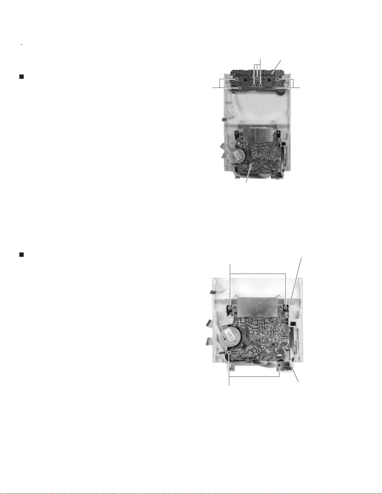
UX-F70MD/UX-F72MD
Description of major ICs
UPD784216AGF(IC701) : System micon
1. Pin layout
1
100
76
75
2. Block diagram
INTP2/NMI
INTP0.INTP1.
INTP3-INTP6
TI00
TI01
TO0
TI1
TO1
TI2
TO2
TI5/TO5
TI6/TO6
TI7/TO7
TI8/TO8
RTP0-RTP7
ANO0
ANO1
AV
REF1
AV
SS
ANI0-ANI7
REF0
AV
AV
D0
AV
SS
P03/INTP3
PCL
BUZ
25
26
PROGRAMMABLE
INTERRUPT
CONTROLLER
TIMER/EVENT
COUNTER
(16BITS)
TIMER/EVENT
COUNTER1
(8BITS)
TIMER/EVENT
COUNTER2
(8BITS)
TIMER/EVENT
COUNTER5
(8BITS)
TIMER/EVENT
COUNTER6
(8BITS)
TIMER/EVENT
COUNTER7
(8BITS)
TIMER/EVENT
COUNTER8
(8BITS)
WATCH TIMER
WATCHDOG TIMER
REAL-TIME
OUTPUT PORT
D/A
CONVERTER
A/D
CONVERTER
CLOCK OUTPUT
CONTROL
BUZZER OUTPUT
50
51
78K/1V
CPU CORE
RAM
8192BITS
ROM
128K BITS
UART/IOE1
BAUD-RATE
GENERATOR
UART/IOE2
BAUD-RATE
GENERATOR
CLOCKED
SERIAL
INTERFACE
BUS I/F
PORT0
PORT1
PORT2
PORT3
PORT4
PORT5
PORT6
PORT7
PORT8
PORT9
PORT10
PORT12
PORT13
SYSTEM CONTROL
RxD1/SI1
TxD1/SO1
ASCK1/SCK1
RxD2/SI2
TxD2/SO2
ASCK2/SCK2
SI0
SO0
SCK0
AD0-AD7
A0-A7
A8-A15
A16-A19
RD
WR
WAIT
ASTB
P00-P06
P10-P17
P20-P27
P30-P37
P40-P47
P50-P57
P60-P67
P70-P72
P80-P87
P90-P95
P100-P103
P120-P127
P130.P131
RESET
X1
X2
XT1
XT2
V
DD
V
SS
TEST
1-44
Page 45

1
2
3
4
5
6
7
8
9
10
11
12
13
14
15
16
17
18
19
20
21
22
23
24
25
26
27
28
29
30
31
32
33
34
35
36
37
38
39
40
41
42
43
44
45
46
47
FAUX2
NC
RDSDATA
MPX
TUST
NC
FTUNER
FCD
VDD
NC
PBMUTE
NC
PIN
LEDCTL
BUZER
MDPOUT
MDRESET
SMUTE
NC
NC
POUT
VPP
UP
RMT0
RMT1
MIDDLE
RMSPEED
VOLCK
VOLCE
VOLDA
AHB
BUB
BTCL
NC
XKILL
VDD
X1
X2
VSS
XT2
XT1
RESET
REM
RDSCK
NC
PHOTO
I/O
-
-
I
I
O
O
O
-
-
O
-
I
O
O
O
O
O
-
-
O
I
I
O
O
I
I
O
O
O
O
O
I
O
O
I/O
I
I
O
I
O
I
I
I
-
-
I
DOWN
49
48
50
SAFTEY4
NC
NC
I
-
-
3. Pin function (1/2)
Not connected
Not connected
Not connected
Stereo detection
Stereo indicator detection
Not connected
Tuner switch output
CD switch output
Connected with VDD
Not connected
PB mute output
Not connected
Power key input
LED control output
Buzzer output
MD PB output
MD reset output
System mute output
Not connected
Not connected
Power-on control output
GND
Door position detection - UP
Door open/shut motor control output
Door open/shut motor control output
Door position detection - MIDDLE
Door position detection - DOWN
Door open/shut motor speed control output
Volume control clock
Volume control chip enable
Volume control data
Active hyper bus control
Backup detection
Battery control
Not connected
Power-off clock oscillator control
Power supply
Master clock
Master clock
GND
Clock for timer
Clock for timer
Power-on reset
Remote control sensor
Not connected
Not connected
Reel pulse detection
Current detection
Not connected
Not connected
Description
Symbol
Pin No.
UX-F70MD/UX-F72MD
1-45
Page 46

UX-F70MD/UX-F72MD
3. Pin function (2/2)
Pin No.
51
52
53
54
55
56
57
58
59
60
61
62
63
64
65
66
67
68
69
70
71
72
73
74
75
76
77
78
79
80
81
82
83
84
85
86
87
88
89
90
91
92
93
94
95
96
97
98
99
100
Symbol
AVREF
AVREF0
SEFTY2
SEFTY3
LDCK
FKEY1
VERSION
FKEY2
KEY1
SEFTY1
VSS
RCDL
BCDL
AVREF1
RXD
TXD
NC
CDRXD
CDTXD
CDRST
GCDL
NC
TUDATA
TUDATA
TUCK
NC
NC
NC
NC
NC
NC
NC
NC
NC
NC
NC
NC
SCL
CS
RESET
SDA
NC
RS
NC
NC
S DATA
SCK
STTA
PLAY
VSS
UPD784216AGF(2/2)
I/O
Reference power supply +5 V
I
Reference power supply +5 V
I
Current detection
I
Current detection
I
Description
I/O
Function switch key input
I
Destination switch input
I
Function switch key input
I
Cassette key input
I
Current detection
I
GND
I
LED color display control
O
LED color display control
O
Reference power supply +5 V
I
Digital input
I
Digital output
O
Not connected
-
CD digital input
I
CD digital output
O
CD reset
O
LED color display control
O
Not connected
-
Tuner data
I
1
Tuner data
O
Tuner clock
O
Not connected
-
Not connected
-
Not connected
-
Not connected
-
Not connected
-
Not connected
-
Not connected
-
Not connected
-
Not connected
-
Not connected
-
Not connected
-
Not connected
-
LCD clock
O
LCD power supply
O
LCD reset
O
LCD serial data
I/O
Not connected
-
LCD start
I
Not connected
-
Not connected
-
Cassette control serial data
I/O
Cassette control serial clock
I/O
Cassette control status signal
I/O
Cassette PB switch detection
O
I
GND
1-46
Page 47

UPD784217AGF139 (IC500) : MD micon
1. Pin layout
UX-F70MD/UX-F72MD
2. Block diagram
INTP2/NMI
INTP0.INTP1.
INTP3-INTP6
TI00
TI01
TO0
TI1
TO1
TI2
TO2
TI5/TO5
TI6/TO6
TI7/TO7
TI8/TO8
RTP0-RTP7
ANO0
ANO1
REF1
AV
AV
SS
ANI0-ANI7
REF0
AV
AV
D0
AV
SS
P03/INTP3
PCL
BUZ
100
1
25
26
PROGRAMMABLE
INTERRUPT
CONTROLLER
TIMER/EVENT
COUNTER
(16BITS)
TIMER/EVENT
COUNTER1
(8BITS)
TIMER/EVENT
COUNTER2
(8BITS)
TIMER/EVENT
COUNTER5
(8BITS)
TIMER/EVENT
COUNTER6
(8BITS)
TIMER/EVENT
COUNTER7
(8BITS)
TIMER/EVENT
COUNTER8
(8BITS)
WATCH TIMER
WATCHDOG TIMER
REAL-TIME
OUTPUT PORT
D/A
CONVERTER
A/D
CONVERTER
CLOCK OUTPUT
CONTROL
BUZZER OUTPUT
76
50
75
51
78K/1V
CPU CORE
RAM
8192BITS
ROM
128K BITS
UART/IOE1
BAUD-RATE
GENERATOR
UART/IOE2
BAUD-RATE
GENERATOR
CLOCKED
SERIAL
INTERFACE
BUS I/F
PORT0
PORT1
PORT2
PORT3
PORT4
PORT5
PORT6
PORT7
PORT8
PORT9
PORT10
PORT12
PORT13
SYSTEM CONTROL
RxD1/SI1
TxD1/SO1
ASCK1/SCK1
RxD2/SI2
TxD2/SO2
ASCK2/SCK2
SI0
SO0
SCK0
AD0-AD7
A0-A7
A8-A15
A16-A19
RD
WR
WAIT
ASTB
P00-P06
P10-P17
P20-P27
P30-P37
P40-P47
P50-P57
P60-P67
P70-P72
P80-P87
P90-P95
P100-P103
P120-P127
P130.P131
RESET
X1
X2
XT1
XT2
V
DD
V
SS
TEST
1-47
Page 48

UX-F70MD/UX-F72MD
3. Pin function (1/2)
Pin No.
1
2
3
4
5
6
7
8
9
10
11
12
13
14
15
16
17
18
19
20
21
22
23
24
25
26
27
28
29
30
31
32
33
34
35
36
37
38
39
40
41
42
43
44
45
46
47
48
49
50
Symbol
MPROT
SSTOP
MREF
NC
NC
NC
NC
NC
Vdd
X2
X1
Vss
XT2
XT1
RESET
MHON
SQSY
DQSY
XINT
CD_EMP
CD_CBIT
CD_TNO
AVdd
AVref0
MT0
MT1
MT2
MT3
MODSEL
UART
DOUT_SEL
DOUT_OFF
AVss
EJECT
LOAD
AVref1
COMIN
COMOUT
COMCLK
SRDT
SWDT
SCLK
MONILT
NC
NC
MONIDATA
MONICLK
DINUNL
SVIB
AXREC
I/O
Disk hole detection switch input (REC protection detection input)
I
Disk innermost circumference detection limit switch on/off detection signal input
I
Disk detection (premaster and recordable disk)
I
Not connected
Not connected
Not connected
Not connected
Not connected
Power supply
Connected with 12 MHz oscillator
Connected with 12 MHz oscillator
GND
Not used
Not used. Connected to GND
Reset input
I
Magnetic head drive control (L: Recording)
O
Disk sub-code Q sync/ADIP sync input
I
Digital input U-bit, Sub-code Q sync input
I
Connected with DSP (IC350) XINT terminal (Interrupt request output terminal)
I
Emphasis detection
I
CD copy inhibit
I
Non CD track detection
I
Analog power supply
Connected to GND
Not used. Connected to GND
Not used. Connected to GND
Not used. Connected to GND
Not used. Connected to GND
Microcomputer operation mode select (H: Usual)
I
External communication system select (H: UART, L: 4-wire)
I
Digital output select (H: DIN through output, L: FS convert output)
I
Digital output select (H: Off, L: On)
I
GND
Eject control signal output
O
Load control signal output
O
Connected with power supply terminal
Command input
I
Command output
O
Command clock
I/O
Data input for microcomputer serial interface
I
Data output for microcomputer serial interface
O
Shift clock for microcomputer serial interface
O
Not used
-
-
Not connected
-
Not connected
-
Not used
-
Not used
Not used
-
O
Spindle servo brake
Recording speed switch output
O
Description
1-48
Page 49

51
52
53
54
55
56
57
58
59
60
61
62
63
64
65
66
67
68
69
70
71
72
73
74
75
76
77
78
79
80
81
82
83
84
85
86
87
88
89
90
91
92
93
94
95
96
97
98
99
100
I/O
O
I
O
O
-
-
I
I
I
I
-
-
O
O
O
O
-
-
-
-
-
O
O
-
-
O
O
O
O
-
O
I
O
I
I
I
I
I
I
I
I
-
-
DO
DI
SCL
CS
TEST
STS_RDY
MMON10
MMON11
MMON12
MMON13
NC
NC
NC
POWER
PWAD
PWDA
EMPHA
ID0
ID1
ID2
ID3
Vss
NC
MODON
MODCHG
NC
NC
NC
DRIVER_ON
XTSL
Vdd
TX
NC
RECP
NC
NC
XRST
SENS
XLAT
MNT3
MNT2
MNT1
MNT0
Vpp
CAM4
CAM3
CAM1
CAM2
NC
NC
3. Pin function (2/2)
Description
Symbol
Pin No.
Serial data output for external EEPROM
Serial data input for external EEPROM
Clock output for external EEPROM
Chip select output for external EEPROM
Test pin
Not used
Parallel operation monitor input
Parallel operation monitor input
Parallel operation monitor input
Parallel operation monitor input
Not connected
Not connected
Not connected
Power on/off control (H: Power on)
Audio A-D converter on/off control (L: Power down)
Audio D-A converter on/off control (L: Power down)
PB signal emphasis on/off signal (L: On)
Connected to GND
Connected to GND
Connected to GND
Connected to GND
GND
Not connected
Laser pickup high frequency duplex on/off (L: On [in PB])
Laser pickup high frequency duplex voltage control (L: PB, H: REC)
Not connected
Not connected
Not connected
Driver shoot
Connected with DSP (IC350) XTSL terminal (for switching input frequency)
Power supply
REC data output enable signal
Not connected
Connected with DSP (IC350) RECP terminal (for switching laser power)
Not connected
Not connected
Connected with DSP (IC350) XRST terminal (reset input)
Connected with DSP (IC350) SENS terminal (internal status output)
Connected with DSP (IC350) XLAT terminal (microcomputer serial interface latch input)
Connected with DSP (IC350) MNT3 terminal (monitor output)
Connected with DSP (IC350) MNT2 terminal (monitor output)
Connected with DSP (IC350) MNT1 terminal (monitor output)
Connected with DSP (IC350) MNT0 terminal (monitor input/output)
Cam switch input 4
Cam switch input 3
Cam switch input 1
Cam switch input 2
Not connected
Not connected
UX-F70MD/UX-F72MD
1-49
Page 50

UX-F70MD/UX-F72MD
UPD780024AGKB21 (IC251) : Unit micon
1. Pin layout
64 ~ 49
1
48
~
16
17 ~ 32
2. Pin function (1/2)
Pin
No.
Symbol I/O Description
P50/A8
1
P59/A9
2
MCS
3
MRDY
4
CDINDEX
5
CDEMP
6
CDTNO
7
CDCOPY
8
VSS0
9
VDD0
10
P30
11
P31
12
P32
13
MUTE
14
SUBQ
15
P35/SO31
16
SQCK
17
KCMND
18
M STAT
19
MCLK
20
RXDO
21
TXDO
22
P25/SCK0
23
VDD1
24
AVSS
25
KEY1
26
KEY2
27
PCHK
28
P14/AN14
29
P13/AN13
30
/OPEN
31
/REST
32
~
33
Connected to GND
Not used
Pull-up +B
Not used
Not used
CD emphasis detection
I
CD track No. detection
I
CD copy detection
I
GND
Power supply
Not used
Not used
Not used
Mute output
O
Sub-code Q data input from IC651
I
Not used
Sub-code Q register clock output to IC651
O
Kick command data
O
CD control status output to IC801
O
CD control command clock input from IC801
I
Digital data input
I
Digital data output
O
Connected to GND
Power supply
GND
Key input 1
I
Key input 2
I
Parity check
I
Connected to GND
Connected to GND
Open switch input
I
Rest switch input
I
1-50
Page 51

UX-F70MD/UX-F72MD
2. Pin function (2/2)
33
34
35
36
37
38
39
40
41
42
43
44
45
46
47
48
49
50
51
52
53
54
55
56
57
58
59
60
61
62
63
64
Pin
No.
Symbol I/O
Function
-
I
-
-
O
-
-
I
I
I
O
O
-
I
I
O
-
O
I
O
O
O
O
O
-
-
-
-
P10/AN10
AVREF
AVDD
/RESET
XT2
XT1
IC
X2
X1
VSS1
FLAG
BLKCK
/RFDET
EQx2
EQx4
VCOx4
OPEN
/CLOSE
IREFx4
P75/BUZ
/RESET
S TAT
/DMUTE
/P.ON
MLD
M DATA
MCLK
CLKSW
JIG
JIG
JIG
JIG
Connected to GND
Analog circuit reference voltage. Connected with analog circuit power supply
Analog circuit power supply
CD control reset input from IC801
Not used
Connected with power supply
Flash memory control
Connected with external crystal oscillator
Connected with external crystal oscillator
GND
Flag signal input from IC651
Sub-code block clock signal input from IC651
RF signal amplitude detection input
2 equalizer switch output
4 equalizer switch output
Not used
Open door detection
Closed door detection
4 DSP current switch output
Not used
Reset signal output to IC651 (L: Reset)
Status signal input from IC651
Muting output to IC651
Power on/off switch signal output to IC291
Microcomputer command load signal output to IC651
Microcomputer command data output to IC651
Microcomputer command clock signal output to IC651
Not used
Not used
Not used
Not used
Connected to GND
1. Pin layout
LB1641 (IC703) : DC motor driver
1 2 3 4 5 6 7 8 9
GND OUT1 P1
VZ IN1 IN2
VCC1
VCC2 P2
2. Pin function
10
OUT2
Input Output
IN1 IN2 OUT1 OUT2
0 0 0 0
1 0 1 0
0 1 0 1
1 1 0 0
Mode
Brake
CLOCKWISE
COUNTER-CLOCKWISE
Brake
1-51
Page 52

UX-F70MD/UX-F72MD
CXD2662R (IC350) : DSP
1.Pin layout
2.Block diagram
59
PCO
60
FILI
61
FILO
62
CLTV
100
EFM
57
RFI
54
ASYI
BIAS
56
COMP
75 ~ 51
76
~~
100
PLL
1 ~ 25
50
26
EFM / ACIRC
ENCODER / DECODER
OSCI
OSCO
XTSL
16 17 18 29
CLOCK
GENERATOR
each block
FS256
LRCK
XBCK
FS4
MDDT1
90 52
27 28
SHOCK RESISTANT
MEMORY CONTROLLER
12
XRAS
46
XCAS
44
XWE
4
4
47
43
14
15
XOE
A00~A11
D0~D3
XINT
TX
ASYO
ADFG
FGIN
SPFD
SPRD
F0CNT
APC
FE
TE
SE
PEAK
BOTM
ABCD
AUX1
DCHG
VC
ADIO
ADRT
ADRB
DTRF
CKRF
XLRF
53
78
95
94
93
79
77
66
75
74
63
64
65
67
76
68
69
71
72
82
81
80
ADIP DECODER
SPINDLE
SERVO
A/D
CONVERTER
ANALOG MUX
AUTO
SEQUENCER
ATRAC/ATRAC3
ENCODER/DECODER
SAMPLING
RATE
CONVERTER
SERVO
DSP
each block each block
CPU I/F
MONITOR
CONTROL
DIGITAL
AUDIO
I/F
SUBCODE
PROCESSOR
PWM
GENERATOR
DADT
26
ADDT
25
XBCKI
4
24
LRCKI
23
DATA I
22
2
DIN~DIN1
DOUT
21
12
DQSY
11
SQSY
LDDR
84
FFDR
88
FRDR
89
TFDR
86
TRDR
85
SFDR
92
SRDR
91
APCREF
83
1-52
10 7
XRST
5689 1 2 34 13
XLAT
SCLK
SWDT
SRDT
SENS
MNT0
MNT1
MNT2
MNT3
RECP
Page 53

3.Pin function (1/3)
UX-F70MD/UX-F72MD
Pin No.
1
2
3
4
5
6
7
8
9
10
11
12
13
14
15
16
17
18
19
20
21
22
23
24
25
26
27
28
29
30
31
32
33
34
35
36
37
38
39
40
41
42
43
Symbol
MNT0
MNT1
MNT2
MNT3
SWDT
SCLK
XLAT
SRDT
SENS
XRST
SQSY
DQSY
RECP
XINT
TX
OSCI
OSCO
XTSL
DIN0
DIN1
DOUT
DATAI
LRCKI
XBCKI
ADDT
DADT
LRCK
XBCK
FS256
DVDD
A03
A02
A01
A00
A10
A04
A05
A06
A07
A08
A11
DVSS
XOE
I/O
I/O
Monitor output.
O
Monitor output.
O
Monitor output.
O
Monitor output.
I
Data input for microcomputer serial interface.
I
Shift clook input for microcomputer serial interface.
I
Latch input for microcomputer serial interface.Latched at the falling edge.
O
Data output for microcomputer serial interface.
O
Outputs the internal status corresponding to the microcomputer serial
Function
interface address.
I
Reset input. Low : reset
O
Disc subcode Q sync / ADIP sync output.
O
Subcode Q sync output in U-bit CD or MD format when the Digital In
source is CD or MD.
I
Laser power switching input.
High : recording power ; low ; playback power
O
Interruption request output. Low when the interruption status occurs.
I
Enable signal input for recoding data output. High : enabled
I
Crystal oscillation circuit input.
O
Crystal oscillation circuit output. (inverted output of the OSCI pin)
I
OSCI input frequency switching.
XTSL1(command) = low and XTSL = high : 512Fs (22.5792MHz)
XTSL1(command) = low and XTSL = low : 1024Fs (45.1584MHz)
XTSL1(command) = high : 2048Fs (90.3168MHz)
I
Digital audio interface signal input 1.
I
Digital audio interface signal input 2.
O
Digital audio interface signal output.
I
Test pin. Connect to GND.
I
Test pin. Connect to GND.
I
Test pin. Connect to GND.
I
Data input from A / D converter.
O
REC monitor output / decoded audio data output.
O
LA clock (44.1kHz) output to the external audio block.
O
Bit clock (2.8224kHz) output to the external audio block.
O
256Fs output.
-
Digital power supply.
O
External DRAM address output.
O
External DRAM address output.
O
External DRAM address output.
O
External DRAM address output.
O
External DRAM address output.
O
External DRAM address output.
O
External DRAM address output.
O
External DRAM address output.
O
External DRAM address output.
O
External DRAM address output.
O
External DRAM address output.
-
Digital ground.
O
External DRAM output enable.
1-53
Page 54

UX-F70MD/UX-F72MD
3. Pin function (2/3)
Pin No.
44
45
46
47
48
49
50
51
52
53
54
55
56
57
58
59
60
61
62
63
64
65
66
67
68
69
70
71
72
73
74
75
76
77
78
79
80
81
82
83
84
85
86
87
88
89
90
Symbol
XCAS
A09
XRAS
XWE
D1
D0
D2
D3
MDDTI
ASYO
ASYI
AVDD
BIAS
RFI
AVSS
PCO
FILI
FILO
CLTV
PEAK
BOTM
ABCD
FE
AUXI
VC
ADIO
AVDD
ADRT
ADRB
AVSS
SE
TE
DCHG
APC
ADFG
F0CNT
XLRF
CKRF
DTRF
APCREF
LDDR
TRDR
TFDR
DVDD
FFDR
FRDR
FS4
I/O
O
External DRAM CAS output.
O
External DRAM address output.
O
External DRAM RAS output.
O
External DRAM write enable.
I/O
External DRAM data bus.
I/O
External DRAM data bus.
I/O
External DRAM data bus.
I/O
External DRAM data bus.
I
MD-DATA mode 1 switching input. (Low : normal mode ; high : MD-DATA mode 1)
O
Playback EFM full-swing input. (Low : vss ; high : Vdd)
I
Playback EFM comparator slice voltage input.
-
Analog power supply.
I
Playback EFM comparator bias current input.
I
Playback EFM RE signal input.
-
Analog ground.
O
Phase comparison output for master PLL of playback digital PLL and recording
Function
EFM PLL.
I
Filter input for master PLL of playback digital PLL and recording EFM PLL.
O
Filter output for master PLL of playback digital PLL and recording EFM PLL.
I
Internal VCO control voltage input for master PLL of playback digital EFM PLL and
recording EFM PLL.
I
Peak hold signal input for quantity of light.
I
Bottom hold signal input for quantity of light.
I
Signal input for quantity of light.
I
Focus error signal input.
I
Auxillary input 1.
I
Center voltage input.
I
Monitor output for A / D converter input signal.
-
Analog power supply.
I
Voltage input for the upper limit of the A / D converter operating range.
I
Voltage input for the lower limit of the A / D converter operating range.
-
Analog ground.
I
Sled error signal input.
I
Tracking error signal input.
I
Connect to he low-inpedance power supply.
I
Error signal input for laser digital APC.
I
ADIP binary FM signal (22.05 1kHz) input.
O
CXA2523 current source setting output.
O
CXA2523 control latch output. Latched at the falling edge.
O
CXA2523 control shift clock output.
O
CXA2523 control data output.
O
Reference PWM output for laser APC.
O
PWM output for laser digital APC.
O
Tracking servo drive PWM output. ( )
O
Tracking servo drive PWM output. (+)
-
Digital power supply.
O
Focus servo drive PWM output. (+)
O
Focus servo drive PWM output. ( )
O
4Fs output. (176.4kHz)
1-54
Page 55

3. Pin function (3/3)
UX-F70MD/UX-F72MD
Pin No.
91
92
93
94
95
96
97
98
99
100
Symbol
SRDR
SFDR
SPRD
SPFD
FGIN
TEST1
TEST2
TEST3
DVSS
EFMO
I/O
O
Sled servo drive PWM output. ( )
O
Sled servo drive PWM output. (+)
O
Spindle servo drive output. (PWM ( ) or polarity)
O
Spindle servo drive output. (PWM (+) or PWM absolute value)
I
Spindle CAV servo FG input.
I
Test pin. Connect to GND.
I
Test pin. Connect to GND.
I
Test pin. Connect to GND.
-
Digital ground.
O
Low when playback ; EFM (encoded data) output when recording.
BD7910FV-X (IC450) : Pre driver
1.Block diagram
20 19 18 17 16 15 14 13 12 11
Function
- +
Vregin
1 2 3 4 5 6 7 8 9 10
- +
VG
SVcc
Pre driver
EFM
2.Pin function
Pin
Symbol Symbol
No.
1
Vreg IN
2
Reg GN
3
4
5
SVCC
6
PDGND
7
EFM
8
MUTE
9
10
I/O I/O
Regulator input and regulator
I
power supply
Regulator GND
-
NC
VG
NC
NC
Non connect
-
Voltage input for power MOS drive
I
EFM high level output voltage
O
Pre-driver GND
-
EFM signal input
I
Mute control (Low active)
I
Non conncet
O
Non connect
O
Function Function
Pin
No.
11
12
13
14
15
16
17
18
19
20
Mute
NC
VOD2
VSS
VOD1
VOS1
VDD
VOS2
Reg DRV
Reg OUT
Reg NF
Non connect
O
Sync.output (Lower power MOS,drain)
"H"bridge GND (Lower power MOS,source)
O
Sync.output (Lower power MOS,drain)
O
Source output (Upper power MOS,source)
"H" bridge power supply terminal
(Upper power MOS,source)
O
Source output (Upper power MOS,source)
O
External PNP drive output for regulator
O
Reglator output (Emitter follower output)
Regulator feedbaack terminal
1-55
Page 56

UX-F70MD/UX-F72MD
LC75345M-X(IC702) : E. volume
1. Pin layout & Block diagram
LOUT
LSB
LBASS2
LBASS1
LINP
LINM
LOPOUT
VSS
CE
DI
CL
VDD
ROPOUT
RINM
RINP
ROUT
RSB
RBASS2
RBASS1
LTRE
LVRIN
LSEL0
CDL
AUXL
MDL
PBL
TUL
Vref
TUR
PBR
MDR
AUXR
RTRE
RVRIN
RSEL0
CDR
1-56
Page 57

2. Block diagram
UX-F70MD/UX-F72MD
Pin No.
1 DI
2CE
3 Vss
4 LOPOUT
5 LINM
6 LINP
7 LOUT
8 LSB
9 LBASS2
10 LBASS1
11 LTRE
12 LVRIN
13 LSELO
14 CDL
15 AUXL
16 MDL
17 PBL
18 TUL
19 Vref
20 TUR
21 PBR
22 MDR
23 AUXR
24 CDR
25 RSELO
26 RVRIN
27 RTRE
28 RBASS1
29 RBASS2
30 RSB
31 ROUT
32 RINP
33 RINM
34 ROPOUT
35 VDD
36 CL
Symbol
Description
Serial data/clock input terminal
Chip enable terminal
GND
Op-amp output
Op-amp inverse input
Op-amp non-inverse input
C-connector terminal comprising volume + equalizer output and super-bass filter
Super-bass band filter C & R connector terminal
Bass band filter C & R connector terminal
Bass band filter C & R connector terminal
Treble band filter C connector terminal
Volume input
Input selector output
CD signal input
AUX signal input
MD signal input
Tape PB signal input
FM tuner signal input
Analog GND
FM tuner signal input
Tape PB signal input
MD signal input
AUX signal input
CD signal input
Input selector output
Volume input
Treble band filter C connector terminal
Bass band filter C & R connector terminal
Bass band filter C & R connector terminal
Super-bass band filter C & R connector terminal
C connector terminal consisting of volume + equalizer output and super-bass filter
Op-amp non-inverse input
Op-amp inverse input
Op-amp output
Power supply
Serial data and clock input
1-57
Page 58

UX-F70MD/UX-F72MD
CXA2523AR (IC310) : MD servo
1.Block diagram
BOTM
ABCD34FE33AUX32ADFG31ADAGC30ADIN29ADFM28SE27CSLED26TE25WBLADJ
36 35
PEAK
37
38
RF
39RFAGC
40AGCI
41COMPO
42COMPP
43ADDC
44OPO
45OPN
46RFO
47MORFI
48
MORFO
2.Pin function
Pin No.
Symbol
1
2
3
4
5
6
7
8
9
10
11
12
APCREF
13
14
15
16
17
18
19
20
TEMPI
TEMP R
SWDT
SCLK
XLAT
XSTBY
F0CNT
I
J
VC
A
B
C
D
E
F
PD
APC
GND
AGC, EQ
Comp
USER
USER
OP Amp
RF Amp
1 2
I
ADIP Amp TE/SE Amp
MUX FE Amp
Peak, Bottom Detector
CPU
Command I/F
ABCD Amp
3T Detector
I-V Amp APC
3VC4A5B6C7D8E9F10PD11
J
I/O
I-V converted RF signal I input.
I
I-V converted RF signal J input.
I
Vcc/2 voltage output.
O
A current input for main beam servo signal.
I
B current input for main beam servo signal.
I
C current input for main beam servo signal.
I
D current input for main beam servo signal.
I
E current input for side beam servo signal.
I
F current input for side beam servo signal.
I
Reflection light quantity monitor signal input.
I
Laser APC output.
O
Reference voltage input for the laser power intensity setting.
I
Connect to GND.
Connects the temperature sensor.
I
Connects the temperature sensor. outputs the reference voltage.
I
Data input for microcomputer serial interface.
I
Shift clock input for microcomputer serial interface.
I
Latch signal input for microcomputer serial interface.Latched when low.
I
Standby setting pin. Normal operation when high Standby when low.
I
Internal current source setting pin.
I
TEMP Amp
12
APC
APCREF
Function
Vcc
24
23
3TADJ
22 EQADJ
21 VREF
20 F0CNT
19 XSTBY
18 XLAT
17 SCLK
16 SWDT
15 TEMP R
14 TEMP I
13 GND
1-58
Page 59

UX-F70MD/UX-F72MD
Pin No.
21
22
23
24
25
26
27
28
29
30
31
32
33
34
35
36
37
38
39
40
41
42
43
44
45
46
47
48
Symbol
VREF
EQADJ
3TADJ
Vcc
WBLADJ
TE
CSLED
SE
ADFM
ADIN
ADAGC
ADFG
AUX
FE
ABCD
BOTM
PEAK
RF
RFAGC
AGCI
COMPO
COMPP
ADDC
OPO
OPN
RFO
MORFI
MORFO
I/O
Reference voltage output.
O
Equalizer center frequency setting pin.
I/O
BPF3T center frequency setting pin.
I/O
Power supply.
BPF22 center frequency setting pin.
I/O
Tracking error signal output.
O
Connects the sled error signal LPF capacitor.
Sled error signal output.
O
ADIP FM signal output.
O
ADIP signal comparator input.
I
Connects the ADIPAGC capacitor.
ADIP2 binary value signal output.
O
13 output / temperature signal output. Switched with serial commands.
O
Focus error signal output.
O
Reflection light quantity signal output for the main beam servo detector.
O
RF/ABCD bottom hold signal output.
O
Peak hold signal output for the RF/ABCD signals.
O
RF equalizer output.
O
Connects the RFAGC capacitor.
RFAGC input.
I
User comparator output.
O
User comparator non-inverted input.
I
Connects the capacitor for ADIP amplifier feedback circuit.
I/O
User operational amplifier output.
O
User operational amplifier inverted input.
I
RF amplifier output. Eye pattern checkpoint.
O
Input of the groove RF signal with AC coupling.
I
Groove RF signal output.
O
Function
GP1UM271XK (IC901) : Receiver for remote
+
–
Amp.
Limiter Integrator Comparator
B.P.F
Demodulator
GND
VCC Vout
1-59
Page 60

UX-F70MD/UX-F72MD
AK4519VF-X (IC480) : A / D D / A converter
1.Pin layout
1
2
3
4
5
6
7
8
9
10
11
12
24
23
22
21
20
19
18
17
16
15
14
13
2.Block diagram
AINL
VCML
AINR
VCMR
VRAD
ARDV
VCOM
AOUTL
AOUTR
3.Pin Function
Pin
Symbol I/O Function
NO.
1
2
3
4
5
6
7
8
9
10
11
12
13
14
15
16
17
18
19
20
21
22
23
24
VRDA
VRAD
AINR
VCMR
VCML
AINL
PWAD
PWDA
MCLK
LRCK
SCLK
SDTO
DGND
VD
SDTI
CMODE
DEM1
DEM0
AOUTL
AOUTR
VCOM
AGND
VB
VA
Voltage Reference Input Pin for DAC, VA
I
Voltage Reference Input Pin for ADC, VA
I
RCH Analog Input Pin
I
Rch Common Voltage Output Pin, 0.45xVA
O
Lch Common Voltage Output Pin, 0.45xVA
O
Lch Analog Input Pin
I
ADC Power-Down Mode Pin "L":Power Down
I
DAC Power-Down Mode Pin "L":Power Down
I
Master Clock Input Pin
I
Input/Output Channel Clock Pin
I
Audio Serial Data Clock Pin
I
Audio Serial Data Output Pin
O
Digital Ground Pin
Digital Power Supply Pin
Audio Serial Data Input Pin
I
Master Clock Select Pin
I
De-emphasis Frequency Select Pin
I
De-emphasis Frequency Select Pin
I
Lch Analog Output Pin
O
Rch Analog Output Pin
O
Common Voltage Output Pin, 0.45xVA
O
Analog Ground Pin
Substrate Pin
Analog Power Supply Pin
-
VA AGND VB VD DGND
Decimation
Modulator
Filter
Decimation
Modulator
Filter
Common Voltage
LPF
LPF
Modulator
Modulator
PWAD PWDA
8x
Interpolator
8x
Interpolator
Clock
Divider
Serial I/O
Interface
MCLK
CMODE
LRCK
SCLK
SDTO
SDTI
1-60
Page 61

AN22000A(IC601):RF & SERVO AMP
1. Pin layout
32 17
116
UX-F70MD/UX-F72MD
2. Block diagram
3. Pin function
VREF
ARF
RF IN
RF OUT
RFN
RF_EQ AGC BDO
NRFDET
32
A
31
C
30
B
29
D
27
E
28
F
17
AMP
AMP
AMP
AMP
GCA
GCA
GCA
GCA
CBDO
C.AGC
8
7654
BCA
BCA
BCA
BCA
26 25 16 3
24
GCTL TBAL FBAL
SUBT
SUBT
BDO
OFTR
COFTR
14131211
OFTR
3TENV
VDET
CDDG VCC
9
10
15
22
23
21
20
19
18
2
1
CEA
3TOUT
NRFDET
FEN
FEOUT
TEN
TEOUT
TEBPF
VDET
LD
PD
Pin
Symbol Function
No.
1
2
3
4
5
6
7
PD
LD
VCC
RFN
RF OUT
RF IN
C.AGC
APC Amp. Input terminal
APC Amp.Output terminal
Power supply terminal
RF addition Amp.Reversing input terminal
RF addition Amp.Output terminal
AGC input terminal
Terminal of connection of capacity of AGC loop
filter.
8
10
11
ARF
9
CEA
3TOUT
CBDO
AGC output terminal
Capacity connection terminal for HPF-Amp.
3TENV output terminal
Capacity connection terminal for RF shade side
envelope detection
12
13
BDO
COFTR
BDO output terminal
Capacity connection terminal for RF discernment
side envelope detection
14
15
OFTR
NRFDET
OFTR output terminal
NRFDET output terminal
Pin
Symbol Function
No.
16
17
18
19
20
21
22
23
24
25
26
27
28
29
30
31
32
CDDG
VREF
VDET
TEBPF
TEOUT
TEN
FEN
FEOUT
GCTL
FBAL
TBAL
E
F
D
B
C
A
Earth terminal
VREF output terminal
VDET output terminal
VDET input terminal
TE Amp. output terminal
TE Amp. reversing input terminal
FE Amp. reversing input terminal
FE Amp. output terminal
Terminal GCTL & APC
FBAL control terminal
TBAL control terminal
Tracking signal input terminal 1
Tracking signal input terminal 2
Focus signal input terminal 4
Focus signal input terminal 2
Focus signal input terminal 3
Focus signal input terminal 1
1-61
Page 62

UX-F70MD/UX-F72MD
AN7317(IC32) : ALC & Pre Amplifier
Pre-in
Pre-NF
16 15
60k
Pre
112k
Pre-out
14
Rec-in12Rec-out11Rec-Mute
13
30k
Rec
AN7317
1
Pre-in
Pre
60k
112k
2
Pre-NF3Pre-out4Rec-in5Rec-out
30k
Pin No. Pin Descriptions
1
2
3
4
5
6
7
8
9
10
11
12
13
14
15
16
Channel 1 Playback Amplifier Input
Channel 1 Playback Amplifier Negative Freedback
Channel 1 Playback Amplifier Output
Channel 1 Record Amplifier Input
Channel 1 Record Amplifier Output
ALC Low-Cut
ALC Time
Ground
Vcc
Ripple Filter
Record - Amplifier Mute
Channel 2 Record Amplifier Output
Channel 2 Record Amplifier Input
Channel 2 Playback Amplifier Output
Channel 2 Playback Amplifier Negative Freedback
Channel 2 Playback Amplifier Input
Rec
R.R.
10
Mute R.R.
A L C
6
ALC
Low-cut
7
ALC
Time
Vcc
9
8
GND
1-62
Page 63

LA1838 (IC1): FM AM IF AMP&detector, FM MPX decoder
1. Block Diagram
UX-F70MD/UX-F72MD
30
ALC
BUFF
FM
S-METER
FM IF
1
2. Pin Function
Pin
Symbol
No.
FM IN
1
AM MIX
2
3
FM IF
AM IF
4
GND
5
6
TUNED
STEREO
7
8
VCC
9
FM DET
10
AM SD
FM VSM
11
AM VSM
12
13
MUTE
14
FM/AM
MONO/ST O
15
29
28
AM
OSC
SD
COMP
S-CLRVE
PM
DET
2
I/O
I
This is an input terminal of FM IF
REG
AM
MIX
AM/FM
IF-BUFF
3
27
FM
RF.AMP
AM IF
4
26
AGC
AM
S-METER
GND
Function
DET
5
signal.
This is an out put terminal for AM
O
mixer.
I
Bypass of FM IF
Input of AM IF Signal.
I
I
This is the device ground terminal.
When the set is tuning, this terminal
O
becomes "L".
O
Stereo indicator output. Stereo "L",
Mono: "H"
III
This is the power supply terminal.
I
FM detect transformer.
I
This is a terminal of AM ceramic filter.
O
Adjust FM SD sensitivity.
O
Adjust AM SD sensitivity.
I/O
When the signal of IF REQ of IC121(
LC72131) appear, the signal of FM/AM
IF output. //Muting control input.
Change over the FM/AM input.
I
"H" :FM, "L" : AM
Stereo : "H", Mono: "L"
25
TUNING
DRIVE
6
24
STEREO
DRIVE
7
22
23
P-DET
VCC
89
Pin
Symbol
No.
16
L OUT
17
R OUT
18
19
20
21
22
23
24
25
26
27
28
29
30
L IN
R IN
RO
LO
IF IN
FM OUT
AM DET
AM AGC
AFC
AM RF
REG
AM OSC
OSC BUFFER
21
DECODER
ANIT-BIRDIE
VCO
384KHz
10
20
STEREO
5N
SW
FF
38k
11
I/O
O
Left channel signal output.
O
Right channel signal output.
Input terminal of the left channel post
I
18
19
MUTE
FF
/
19k
2
12 13
FF
19k
/
LS
Function
17 16
PILOT
DET
14
AMP.
Input terminal of the right channel
I
post AMP.
Mpx Right channel signal output.
O
O
Mpx Left channel signal output.
I
Mpx input terminal
FM detection output.
O
AM detection output.
O
This is an AGC voltage input terminal
I
for AM
I
This is an output terminal of voltage
for FM-AFC.
AM RF signal input.
I
Register value between pin 26 and pin28
O
desides the frequency width of the
input signal.
I
This is a terminal of AM Local
oscillation circuit.
AM Local oscillation Signal output.
O
15
1-63
Page 64

UX-F70MD/UX-F72MD
LA6541-X (IC801) : Servo driver
1. Pin Layout & block diagram
Vcc Vref Vin4 Vg4 Vo8 Vo7
24 23
11k
ohm
22
21
20
19
Vcc
Gnd
Vo6 Vo5 Vg3 Vin3 Cd Res
18
17 16
- +
- +
Level
shift
Level
shift
11k
ohm
1
2
3456
Vcc Mute Vin1 Vg1 Vo1 Vo2 Vo3 Vo4 Vg2 Vin2 Reg
B T L
driver
B T L
driver
Gnd
B T L
driver
B T L
driver
7 8 9101112
Level
shift
Level
shift
2. Pin function
Pin
Symbol Function
No.
1
10
11
12
13
14
15
16
17
18
19
20
21
22
23
24
2
3
4
5
6
7
8
9
Vcc
Mute
Vin1
Vg1
Vo1
Vo2
Vo3
Vo4
Vg2
Vin2
Reg Out
Reg In
Res
Cd
Vin3
Vg3
Vo5
Vo6
Vo7
Vo8
Vg4
Vin4
Vref
Vcc
Power supply (Shorted to pin 24)
All BTL amplifier outputs ON/OFF
BTL AMP 1 input pin
BTL AMP 1 input pin (For gain adjustment)
BTL AMP 1 input pin (Non inverting side)
BTL AMP 1 input pin (Inverting side)
BTL AMP 2 input pin (Inverting side)
BTL AMP 2 input pin (Non inverting side)
BTL AMP 2 input pin (For gain adjustment)
BTL AMP 2 input pin
External transistor collector (PNP) connection. 5V power supply output
External transistor (PNP) base connection
Reset output
Reset output delay time setting (Capacitor connected externally)
BTL AMP 3 input pin
BTL AMP 3 input pin (For gain adjustment)
BTL AMP 3 output pin (Non inverting side)
BTL AMP 3 output pin (Inverting side)
BTL AMP 4 output pin (Inverting side)
BTL AMP 4 output pin (Non inverting side)
BTL AMP 4 output pin (For gain adjustment)
BTL AMP 4 output pin
Level shift circuit's reference voltage application
Power supply (Shorted to pin 1)
15
14
11k
ohm
13
RESET
Regulator
11k
ohm
out
Reg
In
1-64
Page 65

LC72136N (IC2) : PLL frequency synthesizer
1. Pin layout
FM/AM
CLOCK
FM/ST/VCO
AM/FM
2. Block diagram
XT
CE
DI
DO
SDIN
1
2
3
4
5
6
7
8
9
10
11
22
21
20
19
18
17
16
15
14
13
12
XT
GND
LPFOUT
LPFIN
PD
VCC
FMIN
AMIN
IFCONT
IFIN
UX-F70MD/UX-F72MD
1
22
16
15
3
4
5
6
17
21
3. Pin function
Pin
Symbol
No.
1
2
3
4
5
6
7
8
9
10
11
XT
FM/AM
CE
DI
CLOCK
DO
FM/ST/VCO
AM/FM
SDIN
Reference
Driver
Swallow Counter
1/2
2
B
C
I/F
Powe r
on
Reset
Function
I/O
X'tal oscillator connect (75kHz)
I
LOW:FM mode
O
When data output/input for 4pin(input) and
I
Swallow Counter
1/16,1/17 4bit
1/16,1/17 4bit
12bit
Programmable
DriverS
Data Shift Register & Latch
7821113
6pin(output): H
Input for receive the serial data from
I
controller
Sync signal input use
I
Data output for Controller
O
Output port
"Low": MW mode
O
Open state after the power on reset
O
Not use
-
Not use
-
Data input/output
I/O
Phase
Detector
Charge Pump
Unlock
Detector
Universal
Counter
Pin
Symbol
No.
12
IFCONT
13
14
15
16
17
18
19
LPFOUT
20
21
22
IFIN
AMIN
FMIN
VCC
PD
LPFIN
GND
XT
18
19
20
12
I/O
Function
IF counter signal input
I
IF signal output
O
Not use
-
AM Local OSC signal output
I
FM Local OSC signal input
I
Power suplly(VDD=4.5-5.5V)
-
When power ON:Reset circuit move
PLL charge pump output(H: Local OSC
O
frequency Height than Reference frequency.
L: Low Agreement: Height impedance)
Input for active lowpassfilter of PLL
I
Output for active lowpassfilter of PLL
O
Connected to GND
-
X'tal oscillator(75KHz)
I
1-65
Page 66

UX-F70MD/UX-F72MD
M63008FP-X (IC410) : 5ch Actuator driver
1.Pin layout
CH3IN
OUT3
IN3-
VBS2
Vm2
IN3+
N.C
VM3-
VM3+
GND
VM4+
VM4-
VM5+
VM5-
OUT5
IN5-
IN5+
IN4+
IN4-
OUT4
2.Block diagram
IN1+
IN1-
OUT1
VM1(+)
VM1(-)
VM2(+)
VM2(-)
OUT2
IN2-I
IN2+
VREFO
VREF
REGB
REG+
IN1-
Vm1
IN1+
VBS1
REG+
REGB
Vm1
5
VBS2
CH1
CH2
VBS1
VREF
X5
X5
E1
E2
VBS1
VBS1
VBS1
VBS1
3
6
7
9
8
12
13
14
15
16
21
20
2
VREG
1
OUT1
VM1-
VM1+
GND
1.25V
19 17
VM2+
Vrefm1
VM2-
R
R
BIAS
IN2-
OUT2
VBS1
4
Low,Open
MUTE ON
1~4
CH
IN2+
Vm1
VBS1
MUTE1
MUTE2
VBS2
18
VREF
SS,GND
39
Vm2
VREFO
HI :Sleep
5CH
10 113233
VREFO
Vrefm2
SLEEP
TSD
Vm2
38
VBS2
R
R
E3
VBS2
CH3
X8
VBS2
CH4
X8
E4
VBS2
CH5
X8
VBS2
E5
40
37
41
42
34
35
31
30
23
24
22
29
28
26
25
27
IN3IN3+
OUT3
CH3 IN
VM3(+)
VM3(-)
VM4(+)
VM4(-)
IN4IN4+
OUT4
VM5(+)
vm5(-)
IN5IN5+
OUT5
MUTE1 MUTE2
SS,GND
GND (4PIN)
BA3126N(IC31) : R/P Switch
S W
R E C
123456789
1-66
G
P / B
S W
C O N T .
G N D
V c c
P / B
S W
G
S W
R E C
Page 67

BU4094B(IC33):Serial to parallel port extension
UX-F70MD/UX-F72MD
1.Pin layout
STTA
S DATA
SCK
BIAS1
BIAS2
BIAS3
RECB
GND
2.Block diagram
1
2
3
4
5
6
7
8
16
15
14
13
12
11
10
9
VDD
CE
RECH
SOLCTRL
MOTOR
RMUTE
NC
NC
S DATA
SCK
STTA
OUTPUT
ENABLE
15
2
3
1
Q1
8-STAGE
SHIFT REGISTER
8-BIT
LATHES
3-STATE
OUTPUTS
Q8
PARALLEL OUTPUT
10
9
Q's
Qs
SERIAL
OUTPUT
GM71VS17400CLT5(IC390) : DRAM
1. Pin layout
VCC
DQO
DQ1
WE
RAS
(NC)A11
A10
A0
A1
A2
A3
VCC
1
2
3
4
5
6
8
9
10
11
12
13
26
25
24
23
22
21
19
18
17
16
15
14
VSS
DQ3
DQ2
CAS
OE
A9
A8
A7
A6
A5
A4
VSS
2. Block diagram
Pin No.
1.13
2.3.24.25
4
5
6.8
12.
15
19.21
8
12.
15 19.21
14.26
22
23
Symbol
DQO
AO
AO
VCC
WE
RAS
VSS
OE
CAS
DQ3
A11
A10
Function
Power (+3.3V)
Data-input/Data-output
Write Enable
Row Address Strobe
Address Inputs
(4K Refresh Product)
Address Inputs
(2K Refresh Product)
Ground
Output Enable
Column Address Strobe
1-67
Page 68

UX-F70MD/UX-F72MD
BR93LC66F-X(IC590):EEPROM
1. Pin layout
PE
2. Pin function
Pin No.
1
2
3
4
5
6
7
8
3. Block diagram
PE
Symbol
PE
VCC
CS
SK
DI
DO
GND
NC
Command decoder control
clock generation
Program enable
Power supply
Chip select
Clock input
Data input
Data output
Ground
Non connect
Pin function
Supply voltage
detection
Write
protect
High tension
generation
1-68
Command
register
Dummy bit
Address
buffer
Data
register
Address
decoder
R/W amp
4.096-bit
EEPROM
array
Page 69

MN662790RSC (IC651) : Digital servo & Digital signal processer
1. Pin layout
2. Pin function
Pin
No.
1
2
3
4
6
7
8
9
10
11
12
13
14
15
16
17
18
19
20
21
22
23
24
25
26
27
28
29
30
31
32
33
34
35
36
37
38
39
40
5
Symbol
BCLK
LRCK
SRDATA
DVDD1
DVSS1
TX
MCLK I
MDATA
MLD
SENSE
FLOCK
TLOCK
BLKCK
SQCK
SUBQ
DMUTE
STAT
DSP-RST
SMCK
CSEL
TEST2
TVD
PC
ECM
ECS
VDETMON
TRD
FOD
VREF
FBAL
TBAL
FE
TE
RF ENV
TEST3
OFT
TRCRS
RFDET
BDO
LDON
I/O
Bit clock output for SRDATA output (pin 3)
O
L/R discrimination signal output
O
Serial data output
O
II
Power supply for digital circuit
Digital circuit GND
Digital audio interface output signal
O
Microcomputer command clock signal input
Microcomputer command data input
I
Microcomputer command load signal input (L: Load)
I
III
Not used
Not used
Not used
Sub-code block clock signal
O
External clock input for sub-code Q register
I
Sub-code Q data output
O
Muting input (H: Mute)
I
Status signal output
O
Reset signal input (L: Reset)
I
Not used
I
Oscillation frequency selector
I
Not used
I
Traverse drive output
O
I
Not used
Spindle motor drive signal (Forced mode output)
O
Spindle motor drive signal
O
(Servo malfunction signal output)
II
Not used
Tracking drive output
O
Focus drive output
O
D/A output reference voltage
I
Focus balance control output
O
Tracking balance control output
O
Focus error signal input (analog input)
I
Tracking error signal input (analog input)
I
RF envelope signal input (analog input)
I
Connected to GND
Off-track signal input (H: Off-track)
I
Track cross signal input
I
RF detection signal input (L: Detection)
I
I
Dropout signal input (H: Dropout)
I
Not used
Description
Pin
No.
41
42
43
44
45
46
47
48
49
50
51
52
53
54
55
56
57
58
59
60
61
62
63
64
65
66
67
68
69
70
71
72
73
74
75
76
77
78
79
80
Symbol
PLLF2
DSLBDA
WVEL
ARF
IREF
DRF
DSLF
PLLF
VCOF
AVDD2
AVSS2
EFM
DSLB
VCOF2
SUBC
SBCK
VSS
X1
X2
VDD
BYTCK
LD
GAIN
IPFLAG
FLAG
CLVS
CRC
DEMPH
RESY
IOSEL
TEST
AVDD1
OUTL
AVSS1
OUTR
DQSY
Vcc5V
PSEL
MSEL
SSEL
I/O
I/O
PLL loop filter characteristic switching terminal
I
Not used
I
Not used
I
RF signal input
I
Reference current input
DSL bias input
I
I/O
DSL loop filter input/output
PLL loop filter input/output
I/O
I/O
VCO loop filter input/output
I
Power supply for analog circuit
Analog circuit GND
II
Not used
DSL balance output
O
Digital servo 33.8688 MHz generator VCO loop
I/O
filter input/output
I
Not used
I
Connected to GND
I
GND for transmission circuit
Crystal oscillator circuit input (f = 16.9344 MHz)
I
Crystal oscillator circuit output (f = 16.9344 MHz)
O
Power supply for oscillator circuit
I
I
Not used
I
Not used
Flag signal output
O
Not used
I
Not used
II
Not used
I
Not used
Mode switching, Pull-up
I
I
Test pin (H: Usual)
I
Power supply for analog circuit
L-ch audio output
O
I
Analog circuit GND
O
R-ch audio output
I
Connected with power supply
I
When IOSEL = H: Test pin (Usually L)
I
When IOSEL = H: SMCK output frequency
switching terminal (L: SMCK = 4.2336 MHz)
When IOSEL = H: SUBQ output mode switching
I
terminal (H: Q code buffer use mode)
UX-F70MD/UX-F72MD
Description
1-69
Page 70

UX-F70MD/UX-F72MD
LA4628 (IC801) : Power amp.
1. Pin layout
2. Block diagram
1-70
Page 71

L4909 (IC802) : Regulator
1. Pin layout
UX-F70MD/UX-F72MD
2. Pin function
Pin No.
2 Vo1
3 VinA
4 TRIG
5 OC
6 EN1
7 EN2
8 GND
9 EN3
10 FB3
11 Vo3
12 N.C.
13 VinB
14 Vo2
15 FB2
Symbol
1 FB1
Description
REG1 feedback voltage input
REG1 output voltage
Input DC supply voltage
External SCR trigger (clover protection)
Overcurrent warning output
REG1 enable input
REG2 enable input
Analog GND
REG3 enable input
REG3 feedback voltage input
REG3 output voltage
Not connected
Input DC supply voltage
REG2 output voltage
REG2 feedback voltage input
1-71
Page 72

UX-F70MD/UX-F72MD
<<MEMO>>
1-72
Page 73

UX-F70MD/UX-F72MD
UX-F70MD/UX-F72MD
VICTOR COMPANY OF JAPAN, LIMITED
AUDIO & COMMUNICATION BUSINESS DIVISION
PERSONAL & MOBILE NETWORK BUSINESS UNIT 10-1,1Chome,Ohwatari-machi,Maebashi-city,371-8543,Japan
No.21028
Printed in Japan
200109(O)
1-73
Page 74

Block diagram
UX-F70MD/UX-F72MD
LED
FMA-006
6
FM/AM
J1
ANT
LVA10166-A1
CN31
R/P
HEAD
L+,LR+,R-
5
M
REEL
CN1
PULSE
SWITCH
CN001
4
CD
CN601
PICKUP
OPEN
/OPEN
SWITCH
REST
SWITCH
3
FEED
MOTOR
SPINDLE
/REST
FM+,FM-
SM+,SM-
MOTOR
CN321 CN407 CN408 CN415
A,B,C,D
CN611
CN601
E,F,I,J,PD
FCS+
FCS-
TRK+
TRK-
LM+
LM-
CAM1CAM3
SM+,SMFM+,FM-
MPRO,MREF
SSTOP
MAG+
MAG-
PICKUP
2
LOADING
MOTOR
CN612
CAM
SWITCH
SPINDLE
MOTOR
1
FEED
MOTOR
MAG.
HEAD
IC310
RF
IC410
DRIVER
IC450
MAG.HEAD
DRIVER
BC
IFOUT
TU1
OSCOUT
FM RF
L1
AM RF
& OSC
AMRF
AFC
AMOSC
IC31
HEAD
SWITCH
FW31
MOTOR
DRIVE
CN32
SOLENOLIDE
DRIVE
A+C
B+D
E,F
LD,MD
T+,TF+,F-
IC601
RF & SERVO
OFT
BDO
ARF
RFENV
IC801
FCS/SP/FE/TR
BTL DRIVER
TRD
FOD
ECM
ECS
TVD
RF,PEAK,ABCD,FE,F0CNT
APCREF,AUX,ADFG,SE,TE
DTRF,CKRF,XLR
XRST
LOAD
EJECT
FFDR,FRDR
TFDR,TRDR
SFDR,SRDR
SPFD,SPRD
MNT3~MNT6
SWDT,SCLK
XLAT,SRDT,SENS
SQSY,DQSY,RECP
XINT,TX,XTSL
IC500
MCU
EDO,EDI
ESCL,ECS
IC590
EEPROM
EFM
IC2
PLL
AMP
TBAL
FBAL
FE,TE
GCTL
RFDET
MUTE/IFOUT
FM/AM
SQIN
ST/MONO
AMOSC
STEREO,CK
CE,DATA
IC32
PB/REC
AMP
IC33
PORT
EXTENSION
SQL,KEY1,PLAY,PHOTO
IC251
UNIT
MICON
/RESET
S TAT
/DMUTE
SUBQ
SQCK
BLKCK
MLD
M DATA
MCLK
FLAG
IREFx4
IC651
DSP
DQSY,SBCK
SUBC
XWE,XRAS,A00~A10
XOE,XCAS,D0D3
IC350
DSP
EMPHA
PWAD
PWDA
IC480
ADC/DAC
COMMAND,STATUS
COMCLK,STSRDY
SET3,DIN1,SET1,MODESE
IC1
FMDET
AM DET
MS,PBL,PBR
RECL,RECR
TXDO,RXDO
IC,/RESET
KCMND
CDCOPY
CDTNO
CDEMP
CDINDEX
IC390
DRAM
LRCKI
DATA I
XBCKI
DIN0
DIN1
DOUT
STTA
S DATA
SCK
MCS
M STAT
MRDY
KCLK
SRDATA
LRCK
BCLK
LOUT
ROUT
TX
OUTL
OUTR
CN1
CN34 CN33
/RESET
CN606
CN605CN651CN671
TUL,TUR
TUDATA
TUST
TUCK
MPX
PBL,PBR
CN743
CN704
to FLASH MICON
PHOTO
PLAY,KEY1
SAFETY1
SCK,SDATA
STTA
OUTL,OUTR
CDTXD
CDRXD
CDRST
TX
SW201
SW202
RESET,SDA,RS
DOWN,UP,MIDDLE
IC701
SYSTEM
MICON
RMT0,RMT1
LOCK
RMSPEED
IC703
MOTOR
DRIVER
MDRESET
COMMAND
STATUS
CN522
CDTNO
CDCOPY
CDEMP
LIN
RIN
LOUT
ROUT
CN521
CN721CN701 CN744
RECL,RECR
MDLOUT
MDROUT
DE
MATRIX
LEDCTL
RED
BLUE
GREEN
FW907
DOWN
MIDDLE
UP
VOLDA,VOLCE
BUZZER,PIN
FKEY1,FKEY2
IC901
REMOCON
REM
CN918
CN908
CN906
CN909
CN709
MOTOR+
MOTOR-
F
SDA
SCL,RS
RESET
MOTOR+
MOTOR-
IC702
FUCTION/
VOL/AHB
LCD
CN907
AHB,FCD
MDPOUT
SMUTE
POUT
SAFETY4
OUTL,OUTR
SAFETY2
SAFETY3
CN705
M
CN905
CN711
CN712
KEY1
KEY2
PIN
BUZZER
G
RY801
CN808
CN805
US6V
SW5V
CN802CN801
FANCTL
S2601~S2617
KEY MATRIX
BUZZER
L1006T1002
IC802
REG.
IC801
POWER
AMP
INL
INR
HA
VOLTAGE
CONTROL
LIN
RIN
LOUT
ROUT
+OUTL
-OUTL
+OUTR
-OUTR
CN807
M
J1003
CN809
CN804
J1001
T1001
CN803
W1001
J1002
I
2-1
Page 75

Standard schematic diagrams
Main & control circuit
6
5
UX-F70MD/UX-F72MD UX-F70MD/UX-F72MD
4
3
2
CD SIGNAL
MD SIGNAL
1
BC
DE
2-2
F
G
HA
MAIN SIGNAL
TAPE P. B. SIGNAL
FM/TUNER SIGNAL
I
Page 76

Power amplifier & Power supply cir cuit
MAIN SIGNAL
Parts are safety assurance parts.
When replacing those parts make
sure to use the specified one.
6
5
UX-F70MD/UX-F72MD
4
3
2
1
BC
DE
F
G
HA
I
2-3
Page 77

MD control circuit
UX-F70MD/UX-F72MD UX-F70MD/UX-F72MD
C323
0.0068
C325
6
C327
R309
470k
C314
0.022
R310
330
KRA102S-X
R451
47k
R452
56k
D451
D452
R311
Q331
SM+
FM+
FM-
LM+
LM-TRDR
NAD0006-103X
C452
0.1
1SS355-X
6.8k
C315
0.001
R340
2.2k
XC62ER3602M-X
TP441
R456
0.1
C451
D454
NI
D453
NI
C312
47/4
C311
1
0.001
C331
NI
5
FCS+
FCS-
TRK+
TRK-
0
CN321
QGF0501F2-21X
R302
4
R420
FRDR
22k
R422
FFDR
22k
3
R424
22k
TFDR
R426
0.01
TP422
VREF
C455
CAM4
CAM3
CAM2
CAM1
SM+
SM-
FM+
FM-
MPROT
MREF
SSTOP
100p/100
22k
QAR0144-001
MT603
C406
NI
QGF1006F2-08W
CN407
CN612
QGA1501F1-02
QGF1006F2-09W
H601
QAH0039-001
CN611
QGF1016F3-08
CN601
MT601
MT602
2
S611
QSW0848-001
FF-110PH-08280
QAR0144-001
NSW0057-002X
S601
S602
S602
NSW0007-001X
1
C405
NI
C407
100p
C408
NI
C415
C416
QGF1016F2-04W QGF1006F2-09W
CN451 CN408
NI
C330
0.1
C302
0.1
R305
2.2k
NI
C300
C303
R421
C421
R423
C423
560p
560p
C425
R425
10k
C427
LM-
LM+
R454
1
C456
NI
R453
1
470k
R306
0.1
KRA116S-X
C301
NI
0
10k
560p
10k
R427
10k
560p
0.1
Q333
R301
Q332
KRA116S-X
MODON
MODCHG
2SA1363/EF/-X
C400
NI
C410
C411
1
FCS+ SM-
FCS-
TRK+
TRK-
C412
0.1
100/16
C450
C453
R455
NI
C310
0.0022
Q330R338R337
2SA1362/G/-X
4.71
C334
0.1
R401R402
C402
330p
IC410
M63008FP-X
IC450
TP309
0.15
C333
15k5.6k
C307
100k
R336
100/6.3
C401
RB160L-60-X
RB160L-60-X
8.2
R330
27
R331
Q400
22/16
BD7910FV-X
0.01
C361
0.1
1k
R387
10
XBCKI
COMMAND
1k
R518
1k
R514
MNT3
XLAT
NI
NI
LOAD
MNT2
330
R389
47/4
C350
L351
SET3
DIN1
SET1
1k1k1k
R558
R557
R556
R509
R517
EJECT ADDT
R506
MNT0
MNT1
10k
1k
1k1kNI
R563
R564
CAM3
CAM4
R328
0.22
100
0.022
C324
C326
IC310
CXA2523AR
0.0047
C320
R320
0.1
DTRF
CKRF
D310
NI
Q451
XLRF
R314
C316
13k
R312
10k
C341C340
0.0220.022
IC400
0.1
Q401
R403
470
33k
R404 C409
2SA1363/EF/-X
C429
0.0039
R428
R429
3.9k
24k
R430
24k
C431
3.9k
R431
0.0039
0.01
C437
R436
22k
R437
3k
R438
C439
0.01
3k
R439
8.2k
R433
R432C433
0.0056
R435
R434
8.2k
C435
0.0056
100/4
IC590
BR93LC66F-X
1
C317
NI
IC340
R315
R313
100k
22k
12k
12k
R342R341
2.2k2.2k
47/4
C403
KRC102S-X
24k
R300
R440
10k
10k
R441
Q410
KRC102S-X
Q411
0
SPRD
SPFD
EJECT
SFDR
SRDR
LOAD
C342
0.1
SVIB
4REC
0.1
C591
R591
TC7S08F-W
100k
10k
R593
R592
NI
PEAK
10k
10k
100k
R372
R371
R370
K346
NQR0360-002X
NAX0355-001X
10k10k
R355R354
0.1
NI
C510
SVIB
R361
R362
R363
R364
R365
R366
R356
R367
R368
R369
D351
NI
D350
NI
330
R397
R335
47k
R339
47k
R334
47k
R333
47k
R332
47k
DIN0
SCLK
1k
R520
1k1k1k
R510
R511
R512
XTSLTXRECP
1k
1k
1k
1k
1k
1k
1k
1k
1k
1k
3301k1k
330
R396
R398
R399
R390
LRCKI
DATAI
DIN1
DOUT
SRDT
SWDT
STATUS
COMCLK
1k
1k
1k
R516
R515
R519
IC500
UPD784217AGC139
1k
R513
SENS
XRST
BOTM
R327
330
ABCD
R326
330
R324
R323
C321
1
56k
C328
R316
100k
C318
0.0068
ESCL
FE
1k
AUX
TP331
330
ADFG
C322
1
R322
SE
330
TP332
R321
TE
330
C329
NI
R325
4.7k
R343
1k
F0CNT
R317
APCREF
10k
C319
0.033
EDO
EDI
ESCL
ECS
PWAD
PWDA
EMPHA
NI
R549
MODON
MODCHG
EDO
2.2k
R522
EDI
ECS
STSRDY
0
R545
C515
0.1
XRST
MNT0
MNT1
MNT2
MNT3
SWDT
SCLK
XLAT
SRDT
SENS
XRST
SQSY
DQSY
RECP
XINT
TX
XTSL
X350
C358
0.1
K353
NQR0389-003X
VREF
C359
K505
NQR0389-003X
4REC
R521
1k
R523
1k
R524
1k
R525
1k
R546
0
R547
0
R548
0
1k1k1k
R394
R393
LRCK
DADT
MODESE
1k
R554
R555
R553
R552
R551
R565
R566
CAM1
CAM2
SPFD
SPRD
SFDR
SRDR
FRDR
FFDR
TFDR
TRDRA11
C355
0.1
IC350
CXD2662R
560
R392
R391
FS256
XBCK
100k
NI
100k
100k
000
R560
R562
R561
R537
10k
R536
10k
R534R533
10k
R535
NI
A05
A06
A07
A00
R559
1k1k1k
R567
MPROT
A10
0
XINT
DQSY
SQSY
R568
SSTOP
A08
A04
33p
C378
22k
R570
R569
MREF
A03
A02
A01
1
C351
R532
NI
R531
NI
NI
ADFG
XLRF
CKRF
DTRF
F0CNT
APCREF
TE
47/4
C352
SE
1
C353
C391
AUX
FE
ABCD
BOTM
PEAK
1
C354
R375 R376
10k 100k
0.01
C375
XRAS
XOE
XCAS
A09D1XWED3D0
D2
C492
0.001
C491
0.001
C480
47/6.3
CDTNO
CDEMP
EMPHA
PWAD
PWDA
FS256
LRCK
XBCK
ADDT
DADT
C481
1
C484
10/16
C485
0.1
C486
0.1
C488
10/16
1k
R395
R490
NI
47k
47k
47k
R538
R540
R541
R530
1k
R529
CDCOPY
1k
R528
1k
C511
R503
0.1
C512
2.2k
R504
0.1
33k
C501
18p
NI
R501
C502
X500
R502
18p
1.5k
NAX0426-001X
R378
3.3k 1k
C376
R381
1M
0.47
AK4519VF-X
C380
R382
150
0.015
1k
R380
R379
470p
680k
R492
470
R491
470
IC480
D0
D1
XWE
C379
0.47
XRAS
A11
C377
R377
A10
A00
A01
10
L352
A02
A03
R483
0
R481
10
4.7/35
C489
C487
0.1
22/6.3
C482
C483
0.1
NI
IC390
M11L1644SA-50T
D3
D2
XCAS
XOE
A09
A08
A07
A06
A05
A04
C390
10/6.3
CDTNO
CDCOPY
LRCKI
CDEMP
DATAI
XBCKI
K521
K522
NQR0354-001X
NQR0389-003X
K495
L526
NQL274M-1R5X
K492
K491
K523
NQR0354-001X
DOUT
DIN0
KRA116S-X
KRA102S-X
KRC102S-X
0.01
C493
C490
1
IC485
TK11140SC-W
C497
0.1
C496
1
R497
1
NQR0022-005X
NQR0022-005X
NQR0389-003X
K524
C495
C494
NI
NI
K496
R496
470
NQR0022-005X
NQR0022-005X
R495
470
L525
NQL274M-1R5X
C590
0
0
0
0
0
COMMAND
STATUS
MODESE
100p
RESET
COMCLK
STSRDY
SET3
DIN1
SET1
CN522
K530
K531
K528
K532
K527
K529
0
CN521
QGF1006F2-08W
QGF1006F2-21W
MD SIGNAL
BC
DE
2-4
F
G
HA
I
Page 78

CD control circuit
6
5
4
3
0.1
C003 C002
UX-F70MD/UX-F72MD
CDTNO
MCS
MRDY
CDEMP
CDCOPY
IC251
UPD780024AGKB21
MLD
MCLK
MDATA
CDINDEX
1k
1k1k100
1k
R282
R281
R283
R256
K655
R284
BLKCK
FLAG
NQR0007-002X
SRDATA
K656
MCLK
R251
1k
MDATA
R252
1k
MLD
R253
1k
/DMUTE
1k
R254
STAT
/RESET
IREFx4
R264
10k
R265
20k
D251
DA204U-X
D292
10k
C255
0.1/16
R275
R291
10k
1SS355-X
LRCK
BCLK
K657
K658
NQR0251-004X
NQR0251-004X
NQR0251-004X
D603
R675
10
100/6.3
0.1/16
C657
C655
MA112-X
47/10
C254
IC291
1
1
R292
R293
C291
XC62HR3502P-X
1/16
C292
1/16
KCMND
R258
MSTAT
MRDY
KCLK
R260
MCS
R255
R285
C658
0.1/16
NI
CN671
QGF1016F3-19
CN651
1k
1k
1k
1k
R601
220k
R602
82k
39k
C604
0.022
C603
C602C601
0.001
AN22000A-W
IC601
0.022
1/16
0.1/16
100/6.3
C611
C623
C624
C608
NI
R611
R613
5.6k
F
E
B+D
A+C
HDU-110
0.1
1
C001
CN001
47k
F-
F+
T+
T-
CN601
QGF1037F1-15W
47k
VR001
1k
C633
A+C
0.022
F
R635
R608
R607
10
E
B+D
R636
150
C632
1/16
R634
3.9
0.001
D601
NI
R631
R632
2.2
C631
3.9
10/16
2SA1037AK/RS/-X
Q631
C605
270p
R603
82p
220k
R604
C606
0.1/16
100/6.3
C622
C621
0.039
0.0027
0.1/50
680p
C617
C614
C615
C612
C610
0.056/16
R617
3.3k
5.6k
330p
C616
C681
6p
C682
15p
C683
22p
TP1
Q651
DTC114EUA-X
Q652
DTC114EUA-X
TBAL
FBAL
FE
TE
SUBQ
C270
NI
C272
C271
100p
GCTL
/RFDET
OFT
BDO
ARF
RFENV
TP2
SQCK
/OPEN
/REST
100p
R257
1k
KCMND
R259
MSTAT
1k
KCLK
R261
0
1k
R263
1k
R262
0.1/16
C256
NI
6.8k
10k
10k
10k
R274
R276
R272
R271
R273
C261
NI
C273
0.1/16
X251
QAX0664-001Z
STAT
SUBQ
SQCK
BLKCK
/RESET
/DMUTE
R651
R652
R653
R654
C653
0.33/10
1k
1k
1k
1k
TVD
ECM
ECS
TRD
R812
C802
1.5k
C815
1/10
R803
1000p
T+
F+
F-
C801
390p
0.022
390p
C814
C811
1/16
LA6541-X
IC801
R804
47k
R811
2
1
SW102
QSW0931-001
SW101
QSW0927-001
QAR0176-001
QAR0175-001
/OPEN
/REST
M851
M852
FM-
C818
1/16
FM+
SM-
C817
1/16
SM+
R801
10k
390p
C812
SM- T-
2.7k
C821
390p
C813
SM+
FM-
FM+
4.7k
TRD
R813
1.8k
C816
1.5/6.3
R802
R808
R805
FOD
1.5k
C822
220/10
ECM
18k
ECS
R809
1.5k
TVD
12K
FOD
FBAL
TBAL
FE
R682
TE
RFENV
OFT
/RFDET
BDO
GCTL
1k
C676
0.1/16
R683
1M
DTA114EKA-x
R672
C661
470p
Q673
NI
R663
R673
68k
0.022
C664
ARF
R667
4.7
D602
NI
0.1/161k100/6.3
C680
C679
IC651
MN662790RSC
R679
68k
R685
R671
680k
C667
330
R662
68k
R664
68k
0.15/16
0.022
1.5M
C663
C665
R668
0.47/16
C668
5.6k
0.047
R669
100
R665
C651
1p
NAX0476-001X
1k
X651
C652
1p
0.1/16
C678
C673
100/6.3
R666
C677
100
0.1/16
K652
R677
FLAG
47k
R661
20k
R659
0.1/16
C656
IREFx4
NI
R656 R655
R862
680
R861 R863
680
NI NI
C862
560
C864R864
2700p
1000p
C863
C861
2700p
1000p
560
IC652
NI
R657
NI
C654
NI
R658
NI
CDINDEX
CDTNO
CDCOPY
LRCK
CDEMP
SRDATA
BCLK
K651
NI
QGF1016F2-08W
CN606
NI
CN607
QGF1016F2-04W
CN605
R678
1k
CD SIGNAL
BC
DE
F
G
HA
I
2-5
Page 79

Cassette control circuit
6
5
4
3
QAH0047-001
QGF1205F1-06
CN31
UX-F70MD/UX-F72MD UX-F70MD/UX-F72MD
IC1
22
R201
C203
220/6.3
C204
220P
C202
C103
220P
R101
C102
QVP0008-203Z
VR31
0.033
C104
0.033
DTC114TKA
220/6.3
22
Q203
R203
2.4K
DTC114TKA
R103
2.4K
820P
C201
IC31
BA3126N
1K1K
R216R116
R301
220
4.7/25
C301
100/10
R327
470K
C209
0.0068
R207
12K
R107
12K
C210
C110
820P
0.0068
4.7/25
C109
R121
15K
R221
15K
C101
C121
330P
C221
330P
Q103
R102
1.8K
R202
1.8K
Q101
DTC114TKA
0.0047
C319
Q201
1K
R122
DTC114TKA
R222
R305
2.2K
C205
0.0022
R206
3.3K
1K
C206
10/16
C106
10/16
R106 R205
3.3K 100K
100K
0.0022
R105
C105
QQR1118-001
0.022
C316
22/16
22/16
C304
C302
L301
560P
C207
C305
C306
220/6.3
0.039
C303
39K
R303
100/10
C313
R204
1.2K
47/16
R304
100
IC32
AN7317
560P
C107
L303
QQL244K-100Z
1.5
C314
R208
5.6K
C108
R108
5.6K
4.7/25
Q302
2SC2001/K/
2.2
C310
R313
4.7
R310
Q305
2SC2001/LK/
C208
4.7/25
R109
R353
QRZ9005-100X
R315
100
0.022
R210
2.7K
1K
R209
C113
1K
R110
C211
0.0015
R212
2.2K
0.0015
R211
36K
R104
1.2K
R111
36K
C111
R112
2.2K
R335
1.5K
Q321
DTC144EKA
C307
0.01
Q375
2SB562/C/
C376
0.01
D375
2SC2412K/RS/
Q376
150
R375
DTC114TKA
MA3051/M/
DTC124EKA
R376
4.7K
2.2K
R345
Q331
C334
4.7/25
C213
0.039
0.039
2.7K
R314
15K
C308
0.0015
VR37
QVP0008-103Z
Q371
Q372
SW4
VWS304-06A13K
R371
2SA952/LK/
1K
R372
IC33
R339
R336
SW5
FW31
12K
BU4094BCF
2.2K
4.7K
QSW0859-001
SW6
SW1
SW2
C371
MSI-5U2LWA
C374
R338
3.9K
R337
3.3K
4.7/25
SG-105F3-BB,C
100/10
390
R340
47/16
C331
D1
1SR139-400-T2
12K
R341
20K
R342
VKZ3174-00A
CN1
QGB2011L1-10
CN32
QGB2011M1-10
18K
R343
2
CN34
QGF1205F1-10
TO CN744
OF FMH-025-1
SHEET 5/7
1
Parts are safety assurance parts.
When replacing those parts make
sure to use the specified one.
BC
DE
F
G
2-6
CN33
QGF1205F1-09
TO CN743
OF FMH-025-1
SHEET 5/7
TAPE P. B. SIGNAL
SHEET 4/7
HA
I
Page 80

Tuner circuit
6
UX-F70MD/UX-F72MD
TU1
5
R1
QNB0014-001
1SS133-T2
D1
J1
1SS133-T2
56
D2
C1
1SS133-T2
D3
D4
1SS133-T2
R5
56
C3
0.022
10/16
CF1
VCF2L3B-105Z
R4
330
R3
220K
Q1
C2
C4
0.01
0.01
2SC2814/4-5/-X
R2
R6
47
330
100/10
C25
4
L1
QQR0796-001
3
C11
0.1
R13
R15
3.3k
C12
C13
0.047
10K
12P
R14
100K
R16
4.7K
R17
C14
68( 1/4W) F.RES.
100/10
C7
0.001
C17
0.0039
C18
0.47/50
R23
1.8k
R10
2.2K
C15
12P
LC72136N
X1
IC2
QAX0402-001
C16
12P
1K
1K
R18
R19
C22
150P
150P
C23
150P
C24
C20
1000P
C19
0.047
R26
2.2K
R25
R22
1K
R20
330
4.7k
R21
5.6K
Q5
DTA114YKA-X
R30
1.2K
R29
10K
10K
R24
R27
R28
10K
10K
C54
C53
C52
0.27
0.047
22/16
R41
3.3K
T1
QQR0793-001
C6
0.001
D11
1SS133-T2
C57
0.001
CF2
VCF2L3B-105Z
C51
1/50
IC1
LA1838
C48
0.0022
C49
470P
C58
C50
22/16
0.047
C32
0.047
C31
22/16
C21
0.022
0
R60
R40
C60
24K
C47
C46
1/50
0.027
C33
0.047
47
R34C34
0.022
0.047
C35
CF3
QAX0610-001Z
R33
330
*R38
C45
10/16
C44
10/16
*R39
*C43
*C42
C41
10/16
C40
10/16
R37
10K
R36
3.3K
C38
1/50
0.22/50
C37
1/50
C39
5.6k
C36
1/50
R35
C30
100/10
R32
1K
C26
0.001
C27
0.001
R31
1K
2
DATA
TO CN701 OF FMH-025-1
SHEET 5/7
GND
QGF1205F1-09
CN1
5.6V
LOUT
ROUT
STEREOCE9V
CK
AM SIGNAL
FM/TUNER SIGNAL
1
Parts are safety assurance parts.
When replacing those parts make
BC
DE
sure to use the specified one.
F
G
SHEET 1/7
HA
I
2-7
Page 81

Printed circuit boards
Main board Block No. 01
UX-F70MD/UX-F72MD UX-F70MD/UX-F72MD
TUCK
K2302
R2008
R2007
BU+5V
C2316
B2760
R2015
R2061
TUST
C2218
9
R2072
1
TUDATA
C2305
R2012
R2073
K2301
R2083
R2082
R2081
R2080
B2917
CN701
B2754
R2011
R2005
100
R2070
1
C2216
R2010
R2003
TX
21
MODESE,
SET1
1
C2215
L2201
L2101
E
R2009
R2077
R2075
CDRST
MCS
NC
Q2301
R2303
L2401
NC
R2079
NC
NC
NC
R2714
CDRXD
C2115
C2217
C2117
A
NC
C2118
K2303
B2933
R2084
R2713
R2716
1
CDTXD
STATUS
L2302
B
R2002
R2001
B2903
CN704
COMMAND
RESET
C2306
D2301
C2317
W702
R2090
R2006
R2718
R2717
R2715
MGND
L2304
C2318
Q2706
M5.5V
DIN1
L2306
C2319
C2014
C2013
C2012
Q2708
DOUT
C2308
DGND
21
K2305
C2310
Q2707
MDLOUT
CN721
K2304
R2086
B2922
19
8V
R2111
R2110
1
R2235
C2131
R2020
8V
C2128
R2066
MGND
C2228
D2201
R2019
R2064
MGND
1
R2018
R2062
OUTR
9
TUR
C2219
R2057
80
R2060
R2088
CDAGND
CDAGND
AGND
R2085
TUL
CN701
C2010
OUTL
5V
R2215
C2116
R2115
R2122
R2222
R2016
3031
CDDGND
CDDGND
9V
R2017
C2009
MPX
81
BU+5V
1
5
FKEY2
DGND
BUZZER
FKEY1
PIN
R2026
B
Q2701
E
X2701
R2051
R2210
C2225
R2231
C2703
C2704
R2053
R2136
R2137
R2025
C2005
C2230
R2135
R2024
R2052
C2750
R2232
Q2103
R2023
R2701
C2114
C2231
C2709
R2054
5
C2130
R2022
CN705
C2210
R2237
CN705
D2202
R2021
IC701
R2134
50
51
R2087
C2011
C2006
C2007
R2234
Q2203
B2932
Q2352
D2703
C2208
R2503
C2208
C2119
D2705
Q2351
D2351
R2351
R2352
B2906
C2209
C2229
C2226
19
IC702
36
1
B2905
B2908
C2125
R2132
C2110
12
C2701
Q2705
Q2704
R2703
R2709
R2712
R2711
C2713
R2040
R2039
C2706
R2029
X2702
C2002
R2044
L2002
B2918
6
CN744
1
MGND
R2411
D2046
SW10V
NC
Q2201
PBR
AGND
PBL
8V
RECR
Q2101
NC
RECL
10
R2106
C2129
R2203
R2204
C2212
R2103
R2104
C2112
C2227
C2453
C2853
R2852
10
B2920
R2856
R2855
5
J2001
D2451D2451
D2452
4
C2855
R2853
R2092
R2223
R2123
Q2104
Q2853
R2209
R2407
R2208
Q2204
IC703
R2105
C2452
B
Q2453
D2455
D2851
R2206
CN744
R2093
R2854
R2108
10
E
C2403
W702
A
B2255
1
1
1
R2205
R2207
R2107
B
Q2452
E
E
C2127
D2852
C2852
R2096
B
D2402
12
AGND
LOPOUT
R2415
R2416
ROPOUT
R2109
MGNDA
CD+B
B2902
1
R2408
SAFETY3
CDDGND
CN712
CN743
Q2403
SW10V
B2403
C2109
SAFETY2
DGND
R2418
R2225
1
CDAGND
MICON+B
C2404
CN712
9
C2107
D2708
R2417
C2202
R2130
C2108
12
C2326
C2712
3
CN711
1
MGNDB
5V
MD+B
MDDGND
W201
FCD
2
MDPOUT
SMUTE
POUT
A9V
SAFETY4
AHB
NC
12
12
CN743
PHOTO
1
PLAY
KEY1
SAFETY1
DGND
SCK
SW5V
R2229
R2230
SDATA
9
STTA
C2205
C2206
C2201
C2103
R2133
CN711
R2708
R2126
R2707
L2001
C2004
R2037
C2101
R2036
R2041
R2042
C2207
B2907
C2714
R2043
R2045
C2102
D2702
K2001
D2701
R2032
R2033
R2034
C2502
R2228
C2203
R2233
C2204
R2227
R2128
R2129
B2919
R2125
C2104
C2106
C2105
R2127
1
B2916
Q2703
R2706
R2705
R2095
R2138
CN704
119
C2352
C2351
R2354
C2214
R2353
R2211
D2353
D2352
C2211
R2505
18
R2131
C2126
B2910
R2702
R2028
C2001
R2704
C2707
R2710
R2027
C2702
BE
Q2702
D2001
C2705
C2708
C2711
R2031
R2030
C2710
R2049
R2050
R2046
R2047
R2048
D5.5V
R2740
R2741
R2742
R2743
MDROUT
C2309
R2744
R2745
K2002
C2015
A5V
CN709
C2307
L2305
1
2
C2313
20
1
RECL
AGND
W202
1 RECR
CN721
K2003
C2753
C2752
C2751
CN709
NC
1
BLUE
SW10V
GREEN,
RED
DGND
REM
SCL
CS
RESET
SDA
RS
LEDCTL
UP
MIDDLE
DOWN
LCD5V
MOTOR+
MOTOR-
MGNB20
1
BC
DE
2-8
F
G
HA
I
Page 82

Power amplifier & control & AC jac k board Block No. 02
UX-F70MD/UX-F72MD
S2610
R2608
R2604
D1605
CDAGND
Z1007
1
CN802
C1002
R1004
S2604
C1042
R1049
F1003
R2606
R2605
D1007
Q1004
1
Z1006
E
Q1023
B
DGND
C1018
D1008
BZ
S2609
CN802
C1003
FKEY1
D1003
R1101
R1210
FKEY2
R1209
5
PIN
S2606
E
C1205
R1615
D1002
C1005
D1005
C1209
R1211
R1213
R1201
E
R1110
Q1202
C1005
C1206
Q1607
C1106
C1057
R1617
C1105
C1043
B
R1109
E
C1047
R1077
Z1005
F1005
B
BE
D1603
R1616
D1005
R1113
B
Q1102
D1403
C1501
B
R1802
R1801
D1604
E
Q1705
Q1703
C1302
C1109
Q1704
J,CONLY
R1111
C1707
C1046
R1807
R1099
E
D1903
R1601
R1301
D1404
D1902
C1601
T1002
R1112
R1803
L1006
C1108
R1705
R1114
C1056
Q1901
D1405
Q1301
B
E
D1301
R1704
R1214
C1208
D1801
R1602
R1212
R1806
C1803
C1058
R1804
C1602
B
R1903
B1002
B1007
C1903
C1301
B
B
15
R1805
R1502
1
D1601
C1801
C1802
R1901
R1215
R1902
Q1803
C1107
R1115
B1001
C1902
CN804
C1207
Q1802
RY801
B1003
B1006
C1110
L1101
C1210
L1201
R1702
R1703
1
14
1
C1901
IC801
E
IC802
C1502
E
D1501
R1501
Q1801
B
E
CN909
SW10V
GREEN
MTR-
MGND
Z1002
BLUE
RED
DGND
REM
SCL
RESET
LCD5V
-
CS
CN809
SDA
MTR+
OTHERSVER
C1111
C1211
E
Q1701
B
RS
LEDCL
UP
MID
DOWN
20
Z1004
F1001
USERIESONLY
C1706
S1001
F1002
J1001
B
Q1702
E
4
CN906
1
1
CN909
14
T001B
Z1001
Z1003
J1003
B1004
B1005
20
14
CN908
RESET
RS
LCDCK
LCD5V
LCDCE
REM
SDA
M.GND
GREEN
BLUE
RED
SW10V
LEDCTL
1
DGND
CN907
C1009
2
1
S2605
K1010
L1004
L1003
S2615
L1005
R2611
J1002
S2612
S2611
S2614
R2609
R2610
W1001
K1009
6
SW202
SW201
1
4
BZ201
R2607
5
S2607
S2601
S2608
R2601
R2603
R2602
S2603
S2602
R2613
R1091
R1090
S2613
R2612
S2616
CN808
4
CN801
K1003
12
SAFETY4
AHB
A9V
SMUTE
POUT
-
C1055
R1087
D1027
C1053
C1052
C1054
R1086
D1026
3
D1606
K1006
K1005
D1904
D1905
C1402
C1401
2
T1003
D1702
BE
R1924
CN807
Q1909
R1925
B
Q1910
B
E
Q1908
E
R1923
R1926
C1907
1
D1401
D1901
IC803
F1004
D1703
C1701
Z1010
CN803
R1708
C1014
D1701
6.3A-125V
R1707
E
B
Q1708
MDPOUT
FCD
K1004
E
Q1707
B
R1706
MDGND
B
E
C1006
Z1009
MD+B
Q1706
C1017
SW5V
K1002
D1015
MGNDB
D1012
B1801
1
CN801
12
CDGND
SAFETY3
INL
INR
CD+B
SAFETY2
AGND
MGNDA
SW10V
US6V
MICONGND
D1014
C1016
C1015
D1013
1
+B
US6V
POUT
B1802
AGND
4
CN805
4
D1004
D1001
C1004
C1001
Z1008
1
2.5A-125V
D1402
BC
DE
F
G
HA
I
2-9
Page 83

UX-F70MD/UX-F72MD UX-F70MD/UX-F72MD
Tuner board Block No. 03
6
5
4
CD servo control boar d Block No. 04
Forward side
R255
R285
SW101
M852
R812
C802
C815
C658
C821
C822
CN651
R809
C812
R254
SW102
R604
C611
C608
C605
R603
IC601
R611
C651
C652
R613
C679
X651
R617
C612
R661
R659
C661
R672
R665
C606
C676
C663
C665
C667
C610
R668
R664
C668
R669
C673
R662
R685
CN601
C622
C617
R682
C677
C624
IC651
R671
Q631
R677
R634
R632
C631
C678
C657
R652
R653
R654
IC291
C291
K656
K655
R291
R292
R293
C653
R651
K657
K658
R258
R260
C292
R804
R803
C254
R805
R801
C801
R808
R284
R261
R256
R813
R282
C816
R281
C261
M851
R283
R257
R802
C272
R272
R271
CN605
C271
CN606
CN607
X251
Reverse side
R636
C633
R864
R656
R655
K652
C621
R683
R679
C623
D602
R666
C622
R608
C616
C612
C602
C615
C656
R607
C614
C682
C683
R657
TP1
R667
K651
R663
R658
C680
C664
C601
C603
C681
Q651Q652
C679
R673
Q673
C654
IC652
C254
IC801
C255
CN651
D292
C822
R263
R678
R259
M851
C256
C813
C818
C811
R811
C814
3
CN671
R262
R276
R273
R274
2
R275
X251
IC251
R265
R264
SW102
D251
R251
R252
R253
C273
1
SW101
C861
C817
C632
TP2
R631
D601
D603
C863 C864
R863
R861
M852
C631
R601
R602
C655
R635
C604
C624
R675
C657
C862
R862
C673
BC
DE
2-10
F
G
HA
I
Page 84

UX-F70MD/UX-F72MD
MD servo board Block No. 05
C323
R328
C324
C326
C325
6
R324
R327
R321
R322
R323
R326
C375
C376
R376
R375
R377
C377
5
R380
C380
R379
R382
R378
C379
R381
CN407
IC350
R422
R420
R428
C327
IC390
R430
4
R391
C321
C310
R389
IC310
R392
C405
R387
R361
R390
R393
R399
R369
R356
R362
C406
R320
R368
R363
R563
C407
R314
R315
D351
C307
C390
R396
R564
R313
C300
D350
R537
C318
C378
C408
R394
R364
R565R566
C319
R309
R534
R317
R340
C314
R310
R512
R511
R514
CN408
R316
R536
R510
C328
R306
R305
R513
R367
R567
R343
C301
R532
R535
R531
R301
R302
IC500
C303
R398
R397
R339
R335
R533
R546
R547
R548
R502
R501
R569
R568
C501
X500
IC590
C511
C502
R559
R593
R541
R570
(Forward side)
C488
R592
R504
R591
C591
R562
R561
R355
R560
R530
R529
R528
R540
R538
C412
R503
C415
C416
C402
R401
Q400
R404
R354
Q401
C359
C409
C401
R427
C427
R431
C484
R403
R402
R425
C425
C429C431
R429
C400
C403
C421
C489
R423
C423
IC485
IC400
IC410
C490
R421
C497
K522
C493
K523
C496
K521
R497
C411
K524
CN521
CN522
C410
K496
K495
L525L526
Traverse mehanism board Block No. 06
(Forward side)
S601
(Reverse side)
(Traverse mechanism board)
S602
MT602
CN601
MT601
(MD servo board)
(Reverse side)
R496
C495
C494
R495
R481
C487
R483
C481
C452
R492
C491C492
C451
IC450
C455
R451
R454
R456
R491
D454
R490
C456
R453
R452
C483
C486
C485
R395
C453
D453
R455
R557
R437
R439
R558
R555
D452
D451
C482
R521
R556
C433
R436
C437
K505
C439
R509
C435
R435
R554
R553
R433
R434
R552
R438
R432
R551
R517
Q411
C510
Q410
3
IC480
C480
C590
K492
K491
R519
R515
R518
K528
K529
K530
K531
K527
K532
TP422
CN451
Q451
C450
2
1
R549
C515
R522
R545
C342
C333
R342
R338
R336
R523
C341
Q331
R341
R506
IC340
C340
R311
R524
D310
R525
C512
C315
R337
C334
CN321
Q330
R331
Q332
R366
R371
R365
R372
C302
C317
R516
R300
R520
R333
Q333
R312
R334
R332
C361
C316
C330
R330
R370
X350
C331
K346
R440
R441
C358
C320
C322
C311
C312
C351
C355
K353
R426
R424
C350
R325
L351
C329
C391
L352
C354
C353
C352
BC
DE
F
G
HA
I
2-11
Page 85

UX-F70MD/UX-F72MD UX-F70MD/UX-F72MD
Head amplifier board Block No. 07
6
MB
PBR
PBL
RECR
RECL
5
4
3
VR37
L301
VR31
R314
C308
B155
R315
R327
C310
Q302
C319
C221
R313
C314
AG
C313
C317
C121
B112
SW8V
L303
C316
AG
1
MS
R310
R335
MG
CN34
C106
Q103
B198
R353
Q305
R305
C307
Q321
R303
R122
Q101
C103
B163
R221
10
B156
C303
R115
B157
R108
R101
C113
R110
R109
R102
C110
1
C108
C107
C104
9
R301
R121
B151
R112
R111
C102
R107
B152
C111
C302
R103
1
B164
C301
C306
R304
B158
8
B106
C101
C109
6
B166
R116
9
R212
R211
C211
9
IC32
R216
B101
C201
B109B108
C209
CN33
R342
C213
R210
R209
C207
B159
16
B102
R341
C208
R207
1
CN31
B200
B110
1
R340
R205
R105
C105
R208
B160
NC
R343
C305
C206
R201
R345
TAP
C304
1IC31
B113
RRE
C202
C210
Q331
SOL
C375
C205
B161
R215
R339
C203
C334
MG
R106
R206
5V
R204
C204
R203
B168
PHO
B153
R104
R222
R202
C333
PLA
R375
Q201
C332
Q372
Q203
C331
R331
FRE
B167
70u
B162
16
1
10
CN32
R372
R373
C371
R371
Q375
R376
E
C374
R338
D375
E
R337
C376
Q371
R336
9
8
Q376
IC33
Cassette switch board Block No. 08
B
B
SW1 SW2 SW3
D1
T01
P1
CN1
IC1
SW4 SW5
SW6
2
1
BC
DE
2-12
F
G
HA
I
Page 86

UX-F70MD/UX-F72MD
PARTS LIST
[ UX-F70MD ]
[ UX-F72MD ]
* All printed circuit boards and its assemblies are not available as service parts.
Area suffix
UB --------------------- Hong Kong
UF ---------------------------- China
- Contents -
Exploded view of general assembly and parts list (Block No.M1)
CD mechanism assembly and parts list (Block No.MB)
MD mechanism assembly and parts list (Block No.ME)
Cassette mechanism assembly and parts list (Block No.MP)
Electrical parts list (Block No.01~08)
Packing materials and accessories parts list (Block No.M3,M5)
3- 3
3- 6
3- 8
3-11
3-13
3-26
3-1
Page 87

UX-F70MD/UX-F72MD
< MEMO >
3-2
Page 88

UX-F70MD/UX-F72MD
Exploded view of general assembly and parts list
Block No.
84
85
5
4
88
89
3
41
41
2
104
101
87
83
93
86
48
119
32
Operation switch
34
89
89
39
2
3
89
41
24
41
38
96
1
45
116
30
47
37
8
7
4
5
43
31
LCD board
29
Door switch
6
36
91
94
94
92
33
35
10
9
4
96
43
4
23
M
90
94
72
93
40
28
44
125
46
49
18
M
1
103
42
Connection board
71
M
102
100
98
72
40
27
59
14
13
71
40
114
69
99
67
113
70
53
58
68
56
126
71
59
118
111
61
73
72
53
System control
board
76
77
59
117
75
H.P. jack
board
63
128
75
80
Main board
54
51
127
108
123
52
97
122
66
79
107
80
54
121
66
97
130
112
108
54
54
131
106
78
107
64
50
81
110
107
129
107
62
Power supply board
55
65
74
25
19
12
97
95
45
1
4
97
95
11
23
20
14
AB CD E F G
15
17
23
21
16
22
14
3.7 0.2mm
21
16
109
57
120
53
132
115
Tuner board
105
60
3-3
Page 89

UX-F70MD/UX-F72MD
L
UX-F70MD/UX-F72MD
Parts list (General assembly)
Item
A
1 GV10076-007A
2 GV10077-001A
3 GV10078-001A
4 QYSBSF2008Z
5 GV40190-001A
6 QYSBSF2608Z
7 GV40197-001A
8 QYSBSF2608Z
9 GV40198-001A
10 QYSBSF2608Z
11 GV20216-001A
12 GV20217-001A
13 GV40191-001A
14 QYSBSF2608Z
15 WJM0072-001A
16 GV40126-001A
17 GV30038-001A
18 GV40098-001A
19 GV40097-001A
20 GV40096-001A
21 QAR0023-001
22 QYSPSP3004Z
23 QYSBSF2608Z
24 GV40200-002A
25 GV40201-002A
27 GV20131-002A
28 GV30207-001A
29 QYSBSF2608Z
30 GV40217-001A
31 GV40242-003A
32 GV40210-001A
33 GV30206-001A
34 GV40221-001A
35 GV40202-001A
36 GV40203-002A
37 GV30208-002A
38 GV30213-002A
39 GV20132-007A
40 QYSBSF2610Z
41 QYSDSF2006N
42 QYSBSF2608Z
43 GV40035-001A
44 GV40219-001A
45 GV40199-001A
46 GV40214-001A
47 GV40235-003A
Parts number Parts name Area
GV10076-008A
GV20132-006A
Q'ty
FRONT PANEL
FRONT PANEL
SUB FRAME
MAIN FRAME
SCREW
CONTROL BUTTON
T.SCREW
EJECT BUTTON A
T.SCREW
EJECT BUTTON B
T.SCREW
GEAR HOLDER A
GEAR HOLDER B
GEAR HOLDER C
T.SCREW
WIRE CONNECTOR
PULLEY
BELT
WORM/PULLEY
GEAR B
GEAR A 1
MOTOR
SCREW
T.SCREW
PANEL HOLDER L
PANEL HOLDER R
FRONT CASE
LED LENS
T.SCREW 1
SPACER
COMMON SPACER
LCD LENS
LCD HOLDER
LCD SHEET
LED HOLDER A
LED HOLDER B
LED COVER
LCD COVER
FRONT LENS
FRONT LENS
SCREW
SCREW
T.SCREW
SPECIAL SCREW
SPECIAL SCREW
ROLLER
FRONT SPRING
SPACER
Block No. M1MM
Description
1
UX-F70MD
1
UX-F72MD
1
1
4
FRONT PNL+MAIN
1
2
FRONT+CONT.BOTTON
1
1
FRONT+E.BOTTON+F.PANE
1
1
FRONT+E.BOTTON.B
1
1
1
6
AT G.HOLDER A/B
1
1
1
1
1
1
2
AT MOTOR
4
FRONT+ GEAR ASSY
1
1
1
1
LED LENS+FRONT
1
1
1
1
1
1
1
1
1
1
UX-F72MD
1
UX-F70MD
4
LCD COVER+F.CASE
4
F.LENS+ F.CASE
2
CON.PWB+ F.PANEL
2
F.PANEL+PANEL HOLDER
1
DETEC.SW.PWB+F.PANEL
2
1
1
Parts list (General assembly)
Item
A
48 GV40243-001A
49 GV40242-003A
50 GV10081-001A
51 GV40195-001A
52 QYSBST3004Z
53 QYSBST3008Z
54 QYSBST4006Z
55 QYSBST3006Z
56 GV40247-001A
57 ----------
58 GV10080-001A
59 QYSBST3006Z
60 QYSBST3006Z
61 QYSBST3006Z
62 QYSBSF3010N
63 QYSBSF3008Z
64 GV30201-002A
65 GV30203-001A
66 QYSBSF3012Z
67 GV20079-001A
68 ----------
69 GV30198-001A
70 GV30199-001A
71 QYSBSF3010Z
72 QYSBST3008Z
73 GV30217-001A
74 GV40240-001A
75 GV40133-001A
76 QAR0124-002
77 E310243-002
78 QYSBSF3010Z
79 VKZ4001-016
80 QYSBSF3008Z
81 GV30225-001A
83 GV20152-010A
84 GV40245-001A
85 GV40216-002A
86 GV40034-001A
87 GV40220-001A
88 GV30197-001A
89 QYSBSF2608Z
90 --------
91 VKZ4001-110S
92 GV30071-001A
93 QYSBSF2608Z
94 QYSBSF3010Z
95 QYSSST3010Z
Parts number Parts name Area
GV20152-009A
SPACER
COMMON SPACER
BOTTOM CHASSIS
CD MECHA BRACKE
T.SCREW
T.SCREW
T.SCREW
T.SCREW
SPACER
CD MECHA
INNER CHASSIS
T.SCREW
T.SCREW
T.SCREW
TAP SCREW
SCREW
IC HOLDER
HEAT SINK
SCREW
MD MECHA BASE
MD MECHA
MD MECHA HOLDER
MD MECHA HOLDER
SCREW
T.SCREW
PROTECT SHEET
PROTECT SHT(AC)
SPECIAL SCREW
FAN MOTOR
PLASTIC RIVET
SCREW
WIRE HOLDER
SCREW
HEAT PROTECT SH
TOP COVER
TOP COVER
CASS DOOR LENS
DOOR SPRING
DAMPER ASSY
LACH
BUTTON
T.SCREW
CASSETTE MECHA
WIRE HOLDER
HEAD SHIELD
T.SCREW
SCREW
SCREW
Q'ty
1
STICK AT LCD HOLDER
1
MOV.PNL/TUNER/P.WIRE
1
1
2
CD M.BKT+BTM.CHASSIS
3
CD MECHA+BTM.CHASSIS
4
TRANS +BTM.CHASSIS
1
BKT.+ AC PWB.
1
1
1
4
INNER CHA+ BTTM.CHASSIS
1
TUNER PWB+ BTTM.CHASSIS
1
FMB PWB+BTTM.CHASSIS
1
TUNER + R.COVER
1
MAIN PWB+INNER CHASSIS
1
1
3
IC HOLD.+ H.SINK
1
1
1
1
4
MD M.HLD+IN.CHASSIS
4
MD MECHA+MD.M.BASE
1
1
2
MD HOLDER/FAN
1
F1901
1
PHONE PWB+BOTTOM
1
AC PWB+INNER CHASSIS
1
2
MAIN BRD/BRACKE
1
1
UX-F72MD
1
UX-F70MD
1
1
1
1
1
7
BUTTON+TOP COVER
1
1
SLC TO TOP COVER
1
2
FOR HEAD SHIELD
3
FOR SLC MECHA
2
F.PNL/BTTM CHASSIS
Description
Block No. M1MM
3-4
Page 90

Item
Parts list (General assembly)
A
96 QYSBSF3008Z
97 GV40091-002A
98 GV40229-001A
99 QYSBSF3010Z
100 QYSBST3008Z
101 VKY4180-401
102 VKL7850-002
103 VKW5258-003
104 GV10082-002A
105 GV10083-001A
106 GV10085-001A
107 QYSBSF3010N
108 QYSSST3010Z
109 GV30200-001A
110 GV30226-001A
111 GV40250-001A
112 QQT0340-002
113 QUQ412-1018CJ
114 QUQ412-0919CJ
115 QUQ412-0932CJ
116 QUQ610-1415BF
117 QUQ110-1915BJ
118 QUQ110-2125BJ
119 QUQ412-0512DJ
120 QUQ110-0838AJ
121 QMF51W2-R40-J8
122 QMF51W2-1R6-J8
123 QMF51W2-5R0-J8
125 QYSBSF2608Z
126 QYSBST3006Z
127 GV40251-001A
128 GV40242-003A
129 VND4118-003
130 LV41768-001A
131 E409372-001
132 GV40242-003A
Parts number Parts name Area
GV10082-001A
GV10083-002A
GV30200-002A
GV30226-003A
GV30226-004A
GV30226-002A
Q'ty
SCREW
FOOT
SUPPORT BRACKET
SCREW 1
T.SCREW
CASSETTE SPRING
EJECT SAFTY(R)
TORSION SPRING
SIDE PANEL(L)
SIDE PANEL(L)
SIDE PANEL(R)
SIDE PANEL(R)
REAR COVER
TAP SCREW
SCREW
CD FITTING
CD FITTING
RATING LABEL
RATING LABEL
RATING LABEL
RATING LABEL
BOARD SPACER
POWER TRANS
FFC WIRE
FFC WIRE
FFC WIRE
FFC WIRE
FFC WIRE
CARD WIRE
FFC WIRE
FFC WIRE
FUSE
FUSE
FUSE
T.SCREW
T.SCREW
SPACER
COMMON SPACER
CAUTION LABEL
CCIB LABEL
CCEE LABEL
COMMON SPACER
Description
2
F.PANEL/T.COVER
4
FRONT & REAR
1
SLC MECHA PROCE
FOR SUPPORT BKT
1
SLC MECH./BRAC.
2
PUT AT CASS.DOOR
1
1
1
UX-F72MD
1
UX-F70MD
1
UX-F70MD
1
UX-F72MD
1
6
FOR REAR COVER
2
BOTTOM+REAR COVER
1
UX-F70MD
1
UX-F72MD
1
UX-F72MD
1
UX-F72MD
1
UX-F70MD
1
UX-F70MD
1
STICK AT FMB BOARD
1
T1001
1
FMB-SLC
1
FMB-SLC
1
FMB-TUNER
1
CONN-LCD
1
FMB-CD
1
FMB-MD
1
FMB-FKEY
1
1
F1001
1
F1003
1
F1004
1
F.SPRING/F.BRD
1
MD MECHA/S.WIRE
1
STICK AT BOTTOM
1
WIRE ARRANGEMENT
1
STICK AT R.COVER
1
1
1
STICK AT INNER
UX-F70MD/UX-F72MD
Block No. M1MM
UB
UF
UF
UB
UF
UF
3-5
Page 91

UX-F70MD/UX-F72MD
CD mechanism assembly and parts list
Block No.
M
B
M
M
Grease
UD-24H2
EM-30L
LEN-320M
11
12
FMU-N1H-2M
6
9
8
16
7
22
15
19
13
17
18
15
17
10
10
21
22
21
BACK SIDE
4
2
17
5
3
18
13.8 0.1 mm
13
14
23
24
14
23
24
CD servo board
1
5
3
7.2 0.2 mm
3-6
20
BACK SIDE
20
Page 92

Item
Parts list (CD mechanism)
A
1 LV32649-005A
2 LV32651-002A
3 QAR0176-001
4 VKZ4743-001
5 LV42229-001A
6 OPTIMA-725B1
7 LV20993-002A
8 QYSPSGT1735M
9 E406777-002SM
10 LV41741-001A
11 LV31744-001A
12 QYSPSGT1425M
13 LV42350-001A
14 QAR0175-001
15 VKZ4743-001
16 LVB30008-001A
17 LV41424-001A
18 LV41659-001A
19 LV41659-002A
20 LV10503-002A
21 LV32650-003A
22 QYSBSF2005Z
23 LV30225-0B6A
24 QYSBSF2005Z
UX-F70MD/UX-F72MD
Block No. MBMM
Parts number Parts name Area
L.BASE ASSY
CH.BASE ASSY
FEED MOTOR
SPECIAL SCREW
MOTOR GEAR
CD PICK UP
RACK PLATE
MINI SCREW
C.D SHAFT
SPECIAL SCREW
P.S.SPRING
TAP SCREW
T.T.ASSY
SP.MOTOR
SPECIAL SCREW
FPC
SPECIAL SCREW
INSULATOR
INSULATOR
TRAY
CL.BASE ASSY
T.SCREW
SPACER
T.SCREW
Q'ty
1
1
1
2
1
1
1
2
1
2
1
1
1
1
2
1
3
2
1
1
1
2
2
3
Description
3-7
Page 93

UX-F70MD/UX-F72MD
MD mechanism assembly and parts list
Block No.
M
E
M
M
16
Grease
=EM-30L
=CFD-4007ZY2
58
A
17
15
2
FMU-S5M-2M
57
38
10.0 0.2mm
39
53
52
28
37
36
30
35
d
21
34
33
42
47
51
58
39
B
c
38
40
37
C
51
e
3
MD cam switch
4
board
49
51
c
50
24
25
27
23
25
22
27
55
48
41
54
51
42
61.5 0.1mm
41
19
5
31
32
a
26
29
b
8
12
44
43
A
44
f
46
45
32
1
20
20
6
11
7
10
B
56
b
20
C
18
9
7.0 0.2mm
13
59
14
e
a
d
f
3-8
9
7
MD servo contro
board
60
Page 94

Item
Parts list (MD mechanism)
A
1 LV20548-013A
2 LV31472-002A
3 QYWDL1230252
4 LV41477-002A
5 LV32168-002A
6 LV31710-002A
7 QAR0144-001
8 WJM0117-003A
9 LV41341-001A
10 QYSPSPT2020M
11 LV41342-001A
12 LV41477-002A
13 LV30225-068A
14 LV30225-085A
15 LV20543-002A
16 LV31483-001A
17 LV41477-002A
18 LV10286-002A
19 LVB40003-001A
20 LV41477-002A
21 LV31709-003A
22 LV20545-001A
23 LE40515-001A
24 LE40516-001A
25 QYSPSPU1720N
26 FF-110PH-08280
27 LV41477-002A
28 LE30470-202A
29 LV41343-001A
30 LV41344-002A
31 VKH5803-001
32 LV41477-002A
33 LV31484-001A
34 LV41350-001A
35 LV41477-002A
36 LV31485-001A
37 QYSPSPT2025N
38 QAR0144-001
39 LV41345-001A
40 LV41477-002A
41 LV42702-001A
42 LV41347-001A
43 LV31486-001A
44 LV41477-002A
45 KMS-260E
46 LVB30007-002A
47 LV41348-001A
48 QYSPSPT1414M
UX-F70MD/UX-F72MD
Block No. MEMM
Parts number Parts name Area
LOADING ASSY
CAM GEAR
SLIT WASHER
MINI TAP SCREW
WIRE HOLDER
L.MOTOR ASSY
MOTOR
E-SI C WIRE C-F
MOTOR PULLEY
MINI SCREW
BELT
MINI TAP SCREW
SPACER
SPACER
SLIDE BASE R
SLIDE BASE L
MINI TAP SCREW
LOAD.MECHA BASE
FPC CABLE
MINI TAP SCREW
TM.CHASSIS ASSY
SP.MOTOR BASE
COLLAR
SPRING
SCREW
SP.MOTOR
MINI TAP SCREW
T.TABLE ASSY
SHAFT HOLDER R
SHAFT HOLDER F
GUIDE SHAFT
MINI TAP SCREW
T.SPRING HOLDER
COM.SPRING
MINI TAP SCREW
FEED MOTOR BKT.
MINI SCREW
MOTOR
FEED WORM
MINI TAP SCREW
SCREW SHAFT
S.SHAFT GEAR
PICK UP GUIDE
MINI TAP SCREW
MD PICK UNIT
FPC CABLE
RACK SPRING
MINI SCREW
Q'ty
1
1
1
2
CAM SW PWB
1
1
1
MT601
1
1
2
LOAD.MOTOR
1
1
L.MOTOR BKT.
1
1
1
1
2
SLIDE BASE
1
1
3
L.MECHA BASE
1
1
1
1
2
SP.MOTOR
1
MT603
2
SP.MOTOR BASE
1
1
1
1
2
SHAFT HOLDER
1
1
1
T.SP.HOLDER
1
2
FEED MOTOR
1
MT602
1
2
FEED MOTOR BKT.
1
1
1
2
P-UP GUIDE
1
1
1
2
RACK SPRING
Description
3-9
Page 95

UX-F70MD/UX-F72MD
Parts list (MD mechanism)
Item
A
49 WJT0042-001A
50 LV41477-002A
51 LV40761-003A
52 QAH0039-002
53 QYSPSPT1740N
54 LV31487-002A
55 LV41349-001A
56 LV10284-002A
57 LV10285-003A
58 LV41477-002A
59 LV30225-096A
60 VKZ4539-024
Parts number Parts name Area
E-CARD WIRE
MINI TAP SCREW
INSULATOR
MD HEAD
MINI SCREW
HEAD LIFTER
H.LIFTER SPRING
SINGLE FRAME
MECHA COVER
MINI TAP SCREW
SPACER
MINI SCREW
Q'ty
1
1
4
1
1
1
1
1
1
4
1
2
Block No. MEMM
Description
T.MECHA PWB
H601
MD HEAD
MECHA COVER
SERVO PWB
3-10
Page 96

Cassette mechanism assembly and parts list
UX-F70MD/UX-F72MD
Grease
= EM-30L
=UD-24
=UD-24H2
=LEN-320M
=JC-888B
=MOBIL-1
33
SLC-S21M
3
12
26
Block No.
M
P
M
M
7
14
2
2
9
13
8
15
11
22
3
4
10
5
6
1
28
1
The lower side
23
5
Switch board
18
29
24
17
21
10
20
19
16
30
25
32
32
27
31
0.1
8.7
0.15 mm
31
34
Head amplifier
board
34
3-11
Page 97

UX-F70MD/UX-F72MD
Parts list (Cassette mechanism)
Item
A
1 VKS1165-00J
2 VKS2274-002
3 VKW5286-002
4 VKS5559-001
5 VKS5597-00B
6 VKW5296-001
7 SLC-RP1SVM
8 VKY3149-002
9 LV31786-001A
10 VKS1166-003
11 VKW5279-001
12 VKW5280-001
13 LV41584-001A
14 LV41585-002A
15 QYSBSF2005Z
16 VKS5603-00G
17 VKS3785-001MM
18 VKW5284-002
19 VKS2278-003
20 VKW5301-001
21 VKW5266-001
22 WDL214025
23 QYSBSF2005Z
24 VKS3786-00G
25 VKF3205-00B
26 WDL183425
27 VKF3207-00B
28 WDL173525-6
29 VKZ3174-00A
30 LV42234-001A
31 MSI-5U2LWA
32 VKR4761-001
33 QYSPSP2604Z
34 QYSBSF2608Z
Parts number Parts name Area
CHASSIS B.ASS'Y
REEL GEAR
B.T. SPRING
PLAY IDLE GEAR
BLIND
EARTH SPRING
HEAD MOUNT ASSY
CASSETTE SP.
PLAY SW LEVER
CONTROL CAM
HEAD BASE SP(R)
HEAD BASE SP(L)
BRAKE(R)
BRAKE(L)
T.SCREW
MAIN PULLEY ASY
FR ARM
SWING SPRING
TRIGGER ARM
FR SPRING
ELEVATOR SPRING
WASHER
T.SCREW
CLUTCH ASS'Y
F.WHEEL ASSY(R)
SLIT WASHER
F.WHEEL ASSY(L)
SLIT WASHER
DC SOLENOID
CAPSTAN BELT
D.C.MOTOR ASS'Y
MOTOR PULLEY
SCREW
T.SCREW
Q'ty
1
2
2
1
1
1
1
1
1
1
1
1
1
1
1
1
1
1
1
1
1
1
1
1
1
1
1
1
1
1
1
1
2
3
FOR P.W.B.
Block No. MPMM
Description
3-12
Page 98

UX-F70MD/UX-F72MD
ea
Area
Electrical parts list (System control board)
Item
A
B2526 QRE141J-221Y C RESISTOR 220 5% 1/4W
BZ201 QAN0045-001 BUZZER SOUNDER
CN701 QGF1205C1-09 CONNECTOR TO TUNER
CN704 QGF1016C1-19 CONNECTOR TO CD MECHA
CN705 QGF1201C3-05 FFC CONNE TO FUNCTION KEY
CN709 QGB2024K1-20S CONNECTOR TO CONN BOARD
CN711 QGB2510J1-12 CONNECTOR TO FMH
CN712 QGB2510J1-12 CONNECTOR TO FMH
CN721 QGF1016C1-21 CONNECTOR TO MD MECHA
CN743 QGF1201F3-09 CONNECTOR TO SLC
CN744 QGF1201F3-10 CONNECTOR TO SLC
CN913 QGF1016F1-14 CONNECTOR LED CONN.
C2001 NCB31HK-103X C CAPACITOR
C2002 NCB31HK-103X C CAPACITOR
C2004 NCS31HJ-101X C CAPACITOR
C2005 NCB31HK-103X C CAPACITOR
C2006 NCS31HJ-101X C CAPACITOR
C2007 NCS31HJ-101X C CAPACITOR
C2009 NCS31HJ-101X C CAPACITOR
C2010 NCS31HJ-101X C CAPACITOR
C2011 NCS31HJ-101X C CAPACITOR
C2012 NCS31HJ-101X C CAPACITOR
C2013 NCS31HJ-101X C CAPACITOR
C2014 NCS31HJ-101X C CAPACITOR
C2015 EEKC1AM-476ZJC E CAPACITOR
C2101 QTE1E06-226Z E CAPACITOR
C2102 QFVJ1HJ-823Z MF CAPACITOR .082MF 5% 50V
C2103 QFVJ1HJ-823Z MF CAPACITOR .082MF 5% 50V
C2104 QFVJ1HJ-274Z MF CAPACITOR .27MF 5% 50V
C2105 QFVJ1HJ-184Z MF CAPACITOR .18MF 5% 50V
C2106 QFVJ1HJ-184Z MF CAPACITOR .18MF 5% 50V
C2107 QFLA1HJ-104Z M CAPACITOR .10MF 5% 50V
C2108 QFLA1HJ-104Z M CAPACITOR .10MF 5% 50V
C2109 QFLC1HJ-272Z M CAPACITOR 2700PF 5% 50V
C2110 QEKC1HM-475Z E CAPACITOR 4.7MF 20% 50V
C2112 NCS31HJ-221X C CAPACITOR
C2114 QFN31HJ-822Z M CAPACITOR 8200PF 5% 50V
C2115 EEKC1EM-106ZJC E CAPACITOR
C2116 QCBB1HK-151Y C CAPACITOR 150PF 10% 50V
C2117 QCBB1HK-151Y C CAPACITOR 150PF 10% 50V
C2118 QDGB1HK-102Y C CAPACITOR
C2119 QFLC1HJ-123Z M CAPACITOR .012MF 5% 50V
C2125 QETC1HM-475Z E CAPACITOR 4.7MF 20% 50V
C2126 QTE1V06-106Z E CAPACITOR
C2127 QETC1HM-475Z E CAPACITOR 4.7MF 20% 50V
C2128 QETC1HM-475Z E CAPACITOR 4.7MF 20% 50V
C2129 QEKC1HM-475Z E CAPACITOR 4.7MF 20% 50V
C2130 QEKC1HM-475Z E CAPACITOR 4.7MF 20% 50V
C2131 EETC1HM-105ZJC E CAPACITOR
C2201 QTE1E06-226Z E CAPACITOR
C2202 QFVJ1HJ-823Z MF CAPACITOR .082MF 5% 50V
C2203 QFVJ1HJ-823Z MF CAPACITOR .082MF 5% 50V
C2204 QFVJ1HJ-274Z MF CAPACITOR .27MF 5% 50V
C2205 QFVJ1HJ-184Z MF CAPACITOR .18MF 5% 50V
C2206 QFVJ1HJ-184Z MF CAPACITOR .18MF 5% 50V
C2207 QFLA1HJ-104Z M CAPACITOR .10MF 5% 50V
C2208 QFLA1HJ-104Z M CAPACITOR .10MF 5% 50V
C2209 QFLC1HJ-272Z M CAPACITOR 2700PF 5% 50V
C2210 QEKC1HM-475Z E CAPACITOR 4.7MF 20% 50V
C2211 QFLC1HJ-123Z M CAPACITOR .012MF 5% 50V
C2212 NCS31HJ-221X C CAPACITOR
C2214 QFN31HJ-822Z M CAPACITOR 8200PF 5% 50V
C2215 EEKC1EM-106ZJC E CAPACITOR
Parts number Parts name Ar
Block No. 01
Remarks
Item
A
C2216 QCBB1HK-151Y C CAPACITOR 150PF 10% 50V
C2217 QCBB1HK-151Y C CAPACITOR 150PF 10% 50V
C2218 QDGB1HK-102Y C CAPACITOR
C2219 EETC1CM-106ZJC E CAPACITOR
C2225 QETC1HM-475Z E CAPACITOR 4.7MF 20% 50V
C2226 QTE1V06-106Z E CAPACITOR
C2227 QEKC1HM-475Z E CAPACITOR 4.7MF 20% 50V
C2228 QETC1HM-475Z E CAPACITOR 4.7MF 20% 50V
C2229 QEKC1HM-475Z E CAPACITOR 4.7MF 20% 50V
C2230 QEKC1HM-475Z E CAPACITOR 4.7MF 20% 50V
C2231 EEKC1CM-226ZJC E CAPACITOR
C2305 QDGB1HK-102Y C CAPACITOR
C2306 QCBB1HK-101Y C CAPACITOR 100PF 10% 50V
C2307 QCBB1HK-101Y C CAPACITOR 100PF 10% 50V
C2308 QCBB1HK-101Y C CAPACITOR 100PF 10% 50V
C2309 QDGB1HK-102Y C CAPACITOR
C2310 QDGB1HK-102Y C CAPACITOR
C2313 QDGB1HK-102Y C CAPACITOR
C2316 QDYB1CM-103Y C CAPACITOR
C2317 QEKC0JM-107Z E CAPACITOR 100MF 20% 6.3V
C2318 QDVB1EZ-223Y C CAPACITOR
C2319 QDVB1EZ-223Y C CAPACITOR
C2326 QDGB1HK-102Y C CAPACITOR
C2351 QER61EM-475Z E CAPACITOR 4.7MF 20% 25V
C2352 QER61CM-107Z E CAPACITOR 100MF 20% 16V
C2403 QER61HM-105Z E CAPACITOR 1.0MF 20% 50V
C2404 NCB31HK-103X C CAPACITOR
C2453 NCB31HK-103X C CAPACITOR
C2502 EETC1CM-107ZJC E CAPACITOR
C2604 NCB21HK-471X C CAPACITOR
C2605 NCB21HK-102X C CAPACITOR
C2704 NCS31HJ-330X C CAPACITOR
C2705 NCS31HJ-330X C CAPACITOR
C2708 EEKC1CM-107ZJC E CAPACITOR
C2709 NCB31HK-103X C CAPACITOR
C2710 NCS31HJ-220X C CAPACITOR
C2711 NCS31HJ-220X C CAPACITOR
C2712 QETM0JM-228 E CAPACITOR 2200MF 20% 6.3V
C2713 EEKC1HM-225ZJC E CAPACITOR
C2714 EEKC1HM-475ZJC E CAPACITOR
C2750 QDGB1HK-102Y C CAPACITOR
C2751 EEKC1HM-105ZJC E CAPACITOR
C2752 EEKC1HM-105ZJC E CAPACITOR
C2753 EEKC1HM-105ZJC E CAPACITOR
C2852 QDYB1CM-103Y C CAPACITOR
C2853 EEKC1CM-107ZJC E CAPACITOR
C2855 QDYB1CM-103Y C CAPACITOR
C2901 QER61AM-107Z E CAPACITOR 100MF 20% 10V
C2902 NCB31HK-102X C CAPACITOR
C2905 QCFB1HZ-105Y ML C CAPACITOR 1.0MF +80:-20%
C2906 QCFB1HZ-105Y ML C CAPACITOR 1.0MF +80:-20%
D2001 1SS133-T2 SI DIODE
D2046 1N4003S-T5 SI DIODE
A
D2201 1SS133-T2 SI DIODE
D2202 1SS133-T2 SI DIODE
D2301 MTZJ6.2A-T2 Z DIODE
D2351 MTZJ3.9B-T2 Z DIODE
D2352 1SS133-T2 SI DIODE
D2353 1SS133-T2 SI DIODE
D2402 MTZJ7.5C-T2 Z DIODE
D2451 1SS133-T2 SI DIODE
D2452 1SS133-T2 SI DIODE
D2601 1SS133-T2 SI DIODE
Parts number Parts name
Remarks
3-13
Page 99

UX-F70MD/UX-F72MD
ea
Q
Q
Q
Q
Q
Q
Q
Q
Q
Q
Q
Q
Q
Q
Q
Q
Q
Q
Q
Q
Q
Q
Q
Q
Q
Q
Area
Electrical parts list (System control board)
Item
A
D2602 SPR-39MVWF LED
D2701 1SS133-T2 SI DIODE US5V
D2702 1SS133-T2 SI DIODE
D2703 MTZJ5.1C-T2 Z DIODE
D2705 1SS133-T2 SI DIODE
D2708 1SS133-T2 SI DIODE
D2723 1SS355-X DIODE
D2724 1SS355-X DIODE
D2725 1SS355-X DIODE
D2726 1SS355-X DIODE
D2731 1SS355-X DIODE
D2732 1SS355-X DIODE
D2851 MTZJ5.1C-T2 Z DIODE
D2852 MTZJ7.5C-T2 Z DIODE
D2902 MTZJ7.5C-T2 Z DIODE
D2903 MTZJ7.5C-T2 Z DIODE
D2904 NSTM515AS LED COLOR LED
D2906 MTZJ7.5C-T2 Z DIODE
D2907 MTZJ7.5C-T2 Z DIODE
D2908 NSTM515AS LED COLOR LED
D2910 MTZJ7.5C-T2 Z DIODE
D2911 MTZJ7.5C-T2 Z DIODE
D2912 NSTM515AS LED COLOR LED
IC701 UPD784215AGF511 IC SYSTEM MICOM
IC702 LC75345M-X IC
IC703 LB1641 IC
IC901 GP1UM271XK IR DETECT UNIT REMOCON SENS
J2001 QNN0215-001 PIN JACK AUX IN JACK
KI901 QLD0184-001 LCD MODULE LCD
K2001 QQR0621-001Z FERRITE BEADS
K2002 QQR0621-001Z FERRITE BEADS
K2003 QQR0621-001Z FERRITE BEADS
K2301 QQR0621-001Z FERRITE BEADS
K2302 QQR0621-001Z FERRITE BEADS
K2303 QQR0621-001Z FERRITE BEADS
K2304 QQR0621-001Z FERRITE BEADS
K2305 QQR0621-001Z FERRITE BEADS
K3002 QQR0621-001Z FERRITE BEADS
K3003 NQR0428-002X FERRITE BEADS
L2001 QQL244K-100Z INDUCTOR
L2002 QQL244K-100Z INDUCTOR
L2101 QQL231K-4R7Y INDUCTOR
L2201 QQL231K-4R7Y INDUCTOR
L2302 QQL173K-470Z INDUCTOR
L2304 QQL231K-4R7Y INDUCTOR
L2305 QQL231K-4R7Y INDUCTOR
L2306 QQL231K-4R7Y INDUCTOR
Parts number Parts name Ar
2101 KTC3875/GR/-X TRANSISTOR
2103 KTC3875/GR/-X TRANSISTOR
2201 KTC3875/GR/-X TRANSISTOR
2203 KTC3875/GR/-X TRANSISTOR
2301 2SC2001/LK/-T TRANSISTOR
2351 KTA1504/GR-X TRANSISTOR
2352 KTC3875/GR/-X TRANSISTOR
2402 KRA101M-T TRANSISTOR
2403 KTC3875/GR/-X TRANSISTOR
2601 KRC102S-X D TRANSISTOR
2703 KTA1504/GR-X TORANSISTOR SW5V
2704 KTC3875/GR/-X TORANSISTOR RESET SW
2705 KTC3875/GR/-X TORANSISTOR BACKUP CONT
2706 KTC3875/GR/-X TRANSISTOR
2707 KTC3875/GR/-X TRANSISTOR
2708 KTC3875/GR/-X TRANSISTOR
Block No. 01
Remarks
Item
A
R2002 NRSA63J-103X MG RESISTOR
R2003 NRSA63J-222X MG RESISTOR
R2005 NRSA63J-222X MG RESISTOR
R2006 NRSA63J-222X MG RESISTOR
R2007 NRSA63J-222X MG RESISTOR
R2008 NRSA63J-103X MG RESISTOR
R2009 NRSA63J-222X MG RESISTOR
R2010 NRSA63J-222X MG RESISTOR
R2011 NRSA63J-102X MG RESISTOR
R2012 NRSA63J-153X MG RESISTOR
R2015 NRSA63J-102X MG RESISTOR
R2016 NRSA63J-103X MG RESISTOR
R2017 NRSA63J-103X MG RESISTOR
R2018 NRSA63J-222X MG RESISTOR
R2019 NRSA63J-222X MG RESISTOR
R2020 NRSA63J-103X MG RESISTOR
R2021 NRSA63J-103X MG RESISTOR
R2022 NRSA63J-222X MG RESISTOR
R2023 NRSA63J-102X MG RESISTOR
R2024 NRSA63J-102X MG RESISTOR
R2025 NRSA63J-102X MG RESISTOR
R2026 NRSA63J-222X MG RESISTOR
R2027 NRSA63J-102X MG RESISTOR
R2028 NRSA63J-103X MG RESISTOR
R2029 NRSA63J-102X MG RESISTOR
R2030 NRSA63J-104X MG RESISTOR
R2031 NRSA63J-104X MG RESISTOR
R2032 NRSA63J-102X MG RESISTOR
R2033 NRSA63J-222X MG RESISTOR
R2036 NRSA63J-222X MG RESISTOR
R2039 NRSA63J-223X MG RESISTOR
R2040 NRSA63J-472X MG RESISTOR
R2041 NRSA63J-222X MG RESISTOR
R2042 NRSA63J-222X MG RESISTOR
R2043 NRSA63J-222X MG RESISTOR
R2044 NRSA63J-222X MG RESISTOR
R2045 NRSA63J-103X MG RESISTOR
R2046 NRSA63J-222X MG RESISTOR
R2047 NRSA63J-103X MG RESISTOR
R2048 NRSA63J-222X MG RESISTOR
R2049 NRSA63J-103X MG RESISTOR
R2050 NRSA63J-222X MG RESISTOR
R2051 NRSA63J-222X MG RESISTOR
R2052 NRSA63J-222X MG RESISTOR
R2053 NRSA63J-102X MG RESISTOR
R2054 NRSA63J-102X MG RESISTOR
R2057 NRSA63J-222X MG RESISTOR
R2060 NRSA63J-222X MG RESISTOR
R2061 NRSA63J-222X MG RESISTOR
R2062 NRSA63J-102X MG RESISTOR
R2064 NRSA63J-102X MG RESISTOR
R2066 NRSA63J-102X MG RESISTOR
R2070 NRSA63J-101X MG RESISTOR
Parts number Parts name
2709 KTC3875/GR/-X TRANSISTOR
2710 KTC3875/GR/-X TRANSISTOR
2711 KTC3875/GR/-X TRANSISTOR
2712 KTC3875/GR/-X TRANSISTOR
2713 KTC3875/GR/-X TRANSISTOR
2714 KTC3875/GR/-X TRANSISTOR
2715 KTC3875/GR/-X TRANSISTOR
2716 KTC3875/GR/-X TRANSISTOR
2717 KTC3875/GR/-X TRANSISTOR
2853 KTC3875/GR/-X TRANSISTOR
Remarks
3-14
Page 100

UX-F70MD/UX-F72MD
ea
Electrical parts list (System control board)
Item
A
R2072 NRSA63J-101X MG RESISTOR
R2073 NRSA63J-101X MG RESISTOR
R2075 NRSA63J-101X MG RESISTOR
R2077 NRSA63J-101X MG RESISTOR
R2079 NRSA63J-222X MG RESISTOR
R2080 NRSA63J-222X MG RESISTOR
R2081 NRSA63J-222X MG RESISTOR
R2082 NRSA63J-222X MG RESISTOR
R2083 NRSA63J-103X MG RESISTOR
R2084 NRSA63J-103X MG RESISTOR
R2085 NRSA63J-473X MG RESISTOR
R2086 NRSA63J-473X MG RESISTOR
R2087 NRSA63J-473X MG RESISTOR
R2088 NRSA63J-104X MG RESISTOR
R2092 QRE141J-473Y C RESISTOR 47K 5% 1/4W
R2093 QRE141J-473Y C RESISTOR 47K 5% 1/4W
R2095 NRSA63J-103X MG RESISTOR
R2096 NRSA63J-103X MG RESISTOR
R2103 NRSA63J-393X MG RESISTOR
R2104 NRSA63J-103X MG RESISTOR
R2105 NRSA63J-472X MG RESISTOR
R2106 NRSA63J-153X MG RESISTOR
R2107 NRSA63J-222X MG RESISTOR
R2108 NRSA63J-152X MG RESISTOR
R2109 NRSA63J-182X MG RESISTOR
R2110 NRSA63J-122X MG RESISTOR
R2111 NRSA63J-682X MG RESISTOR
R2115 QRE141J-332Y C RESISTOR 3.3K 5% 1/4W
R2122 QRE141J-332Y C RESISTOR 3.3K 5% 1/4W
R2125 QRE141J-222Y C RESISTOR 2.2K 5% 1/4W
R2126 QRE141J-222Y C RESISTOR 2.2K 5% 1/4W
R2127 QRE141J-182Y C RESISTOR 1.8K 5% 1/4W
R2128 QRE141J-472Y C RESISTOR 4.7K 5% 1/4W
R2129 NRSA63J-752X MG RESISTOR
R2130 NRSA63J-752X MG RESISTOR
R2131 QRE141J-182Y C RESISTOR 1.8K 5% 1/4W
R2132 QRE141J-182Y C RESISTOR 1.8K 5% 1/4W
R2133 QRE141J-224Y C RESISTOR 220K 5% 1/4W
R2134 NRSA63J-103X MG RESISTOR
R2135 NRSA63J-124X MG RESISTOR
R2136 NRSA63J-154X MG RESISTOR
R2137 QRE141J-153Y C RESISTOR 15K 5% 1/4W
R2138 NRSA63J-103X MG RESISTOR
R2203 NRSA63J-393X MG RESISTOR
R2204 NRSA63J-103X MG RESISTOR
R2205 NRSA63J-472X MG RESISTOR
R2206 NRSA63J-153X MG RESISTOR
R2207 NRSA63J-222X MG RESISTOR
R2208 NRSA63J-152X MG RESISTOR
R2209 NRSA63J-182X MG RESISTOR
R2210 NRSA63J-122X MG RESISTOR
R2211 NRSA63J-682X MG RESISTOR
R2215 QRE141J-332Y C RESISTOR 3.3K 5% 1/4W
R2222 QRE141J-332Y C RESISTOR 3.3K 5% 1/4W
R2225 QRE141J-222Y C RESISTOR 2.2K 5% 1/4W
R2226 QRE141J-222Y C RESISTOR 2.2K 5% 1/4W
R2227 QRE141J-182Y C RESISTOR 1.8K 5% 1/4W
R2228 QRE141J-472Y C RESISTOR 4.7K 5% 1/4W
R2229 NRSA63J-752X MG RESISTOR
R2230 NRSA63J-752X MG RESISTOR
R2231 QRE141J-182Y C RESISTOR 1.8K 5% 1/4W
R2232 QRE141J-182Y C RESISTOR 1.8K 5% 1/4W
R2233 QRE141J-224Y C RESISTOR 220K 5% 1/4W
Parts number Parts name Ar
Block No. 01
Remarks
Item
A
R2234 NRSA63J-103X MG RESISTOR
R2235 NRSA63J-513X MG RESISTOR
R2237 QRE141J-153Y C RESISTOR 15K 5% 1/4W
R2303 QRE141J-561Y C RESISTOR 560 5% 1/4W
R2351 NRSA63J-390X MG RESISTOR
R2352 NRSA63J-332X MG RESISTOR
R2353 NRSA63J-273X MG RESISTOR
R2354 NRSA63J-102X MG RESISTOR
R2407 NRSA63J-332X MG RESISTOR
R2408 NRSA63J-392X MG RESISTOR
R2415 NRSA63J-823X MG RESISTOR
R2416 NRSA63J-823X MG RESISTOR
R2417 NRSA63J-394X MG RESISTOR
R2418 NRSA63J-104X MG RESISTOR
R2503 NRSA63J-222X MG RESISTOR
R2505 QRE141J-222Y C RESISTOR 2.2K 5% 1/4W
R2614 NRSA63J-161X MG RESISTOR
R2615 NRSA63J-470X MG RESISTOR
R2705 NRSA63J-331X MG RESISTOR
R2706 NRSA63J-103X MG RESISTOR
R2707 NRSA63J-103X MG RESISTOR
R2708 NRSA63J-103X MG RESISTOR
R2709 NRSA63J-103X MG RESISTOR
R2710 NRSA63J-104X MG RESISTOR
R2711 NRSA63J-473X MG RESISTOR
R2712 NRSA63J-333X MG RESISTOR
R2713 NRSA63J-102X MG RESISTOR
R2714 NRSA63J-102X MG RESISTOR
R2715 NRSA63J-102X MG RESISTOR
R2716 NRSA63J-102X MG RESISTOR
R2717 NRSA63J-102X MG RESISTOR
R2718 NRSA63J-102X MG RESISTOR
R2719 NRSA63J-221X MG RESISTOR
R2720 NRSA63J-221X MG RESISTOR
R2721 NRSA63J-271X MG RESISTOR
R2722 NRSA63J-271X MG RESISTOR
R2723 NRSA63J-271X MG RESISTOR
R2724 NRSA63J-271X MG RESISTOR
R2725 NRSA63J-221X MG RESISTOR
R2726 NRSA63J-221X MG RESISTOR
R2727 NRSA63J-271X MG RESISTOR
R2728 NRSA63J-271X MG RESISTOR
R2729 NRSA63J-271X MG RESISTOR
R2730 NRSA63J-271X MG RESISTOR
R2731 NRSA63J-221X MG RESISTOR
R2732 NRSA63J-221X MG RESISTOR
R2733 NRSA63J-271X MG RESISTOR
R2734 NRSA63J-271X MG RESISTOR
R2735 NRSA63J-271X MG RESISTOR
R2736 NRSA63J-271X MG RESISTOR
R2740 NRSA63J-222X MG RESISTOR
R2741 NRSA63J-222X MG RESISTOR
R2742 NRSA63J-222X MG RESISTOR
R2743 NRSA63J-222X MG RESISTOR
R2744 NRSA63J-222X MG RESISTOR
R2745 NRSA63J-222X MG RESISTOR
R2750 NRSA63J-221X MG RESISTOR
R2751 NRSA63J-221X MG RESISTOR
R2752 NRSA63J-221X MG RESISTOR
R2852 QRE141J-100Y C RESISTOR 10 5% 1/4W
R2853 QRE141J-222Y C RESISTOR 2.2K 5% 1/4W
R2854 QRE141J-222Y C RESISTOR 2.2K 5% 1/4W
R2855 QRE141J-100Y C RESISTOR 10 5% 1/4W
R2856 QRE141J-9R1Y C RESISTOR 9.1 5% 1/4W
R2901 NRSA63J-103X MG RESISTOR
X2701 QAX0283-001Z RESONATOR MAIN CLOCK
X2702 QAX0401-001 CRYSTAL SUB CLOCK
Parts number Parts name
Remarks
3-15
 Loading...