

JVC RX-D702BB, RX-D702BE, RX-D702BEN, RX-D701SE, RX-D701SEN Service Manual
SERVICE MANUAL
AUDIO/VIDEO CONTROL RECEIVER
MB50020061
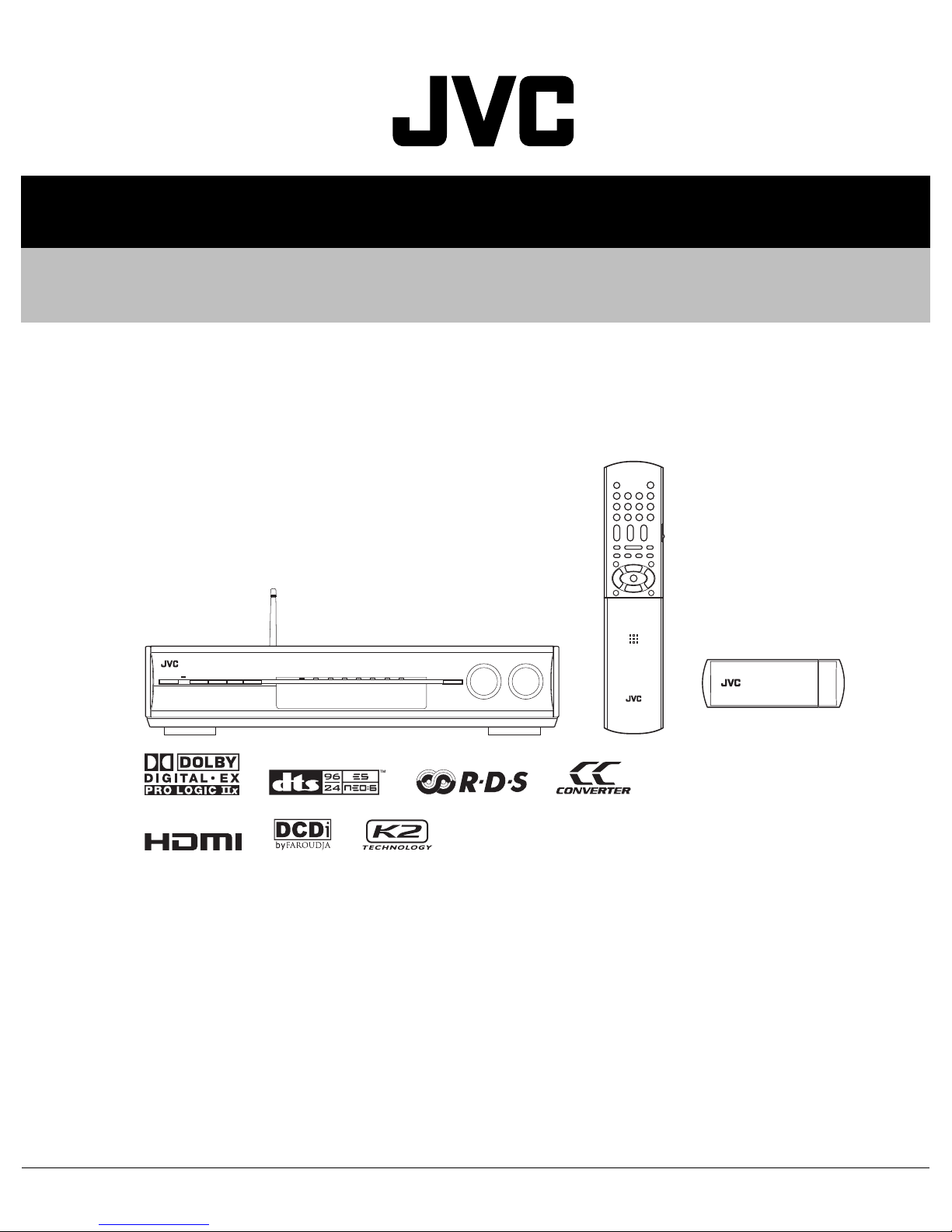
RX-D701SB,RX-D701SE,RX-D701SEN
RX-D702BB,RX-D702BE,RX-D702BEN
Lead free solder used in the board (material : Sn-Ag-Cu, melting point : 219 Centigrade)
1 PRECAUTIONS . . . . . . . . . . . . . . . . . . . . . . . . . . . . . . . . . . . . . . . . . . . . . . . . . . . . . . . . . . . . . . . . . . . . . . . 1-3
2 SPECIFIC SERVICE INSTRUCTIONS . . . . . . . . . . . . . . . . . . . . . . . . . . . . . . . . . . . . . . . . . . . . . . . . . . . . . . 1-5
3 DISASSEMBLY . . . . . . . . . . . . . . . . . . . . . . . . . . . . . . . . . . . . . . . . . . . . . . . . . . . . . . . . . . . . . . . . . . . . . . . 1-6
4 ADJUSTMENT . . . . . . . . . . . . . . . . . . . . . . . . . . . . . . . . . . . . . . . . . . . . . . . . . . . . . . . . . . . . . . . . . . . . . . . . 1-9
5 TROUBLESHOOTING . . . . . . . . . . . . . . . . . . . . . . . . . . . . . . . . . . . . . . . . . . . . . . . . . . . . . . . . . . . . . . . . . . 1-9
COPYRIGHT © 2006 Victor Company of Japan, Limited
TABLE OF CONTENTS
No.MB500
2006/1
SPECIFICATION
Amplifier
Output Power At stereo operation Front channels 130 W per channel, min. RMS, driven into 6
At surround operation Front channels 130 W per channel, min. RMS, driven into 6
Center channel 130 W, min. RMS, driven into 6
Surround channels 130 W per channel, min. RMS, driven into 6
Surround back channels 130 W per channel, min. RMS, driven into 6
Audio Audio Input Sensitivity/
Video Video Input Sensitivity/
HDMI HDMI Input (Ver. 1.1) VCR (DBS), DVR/DVD
Tuning Range 87.50 MHz to 108.00 MHz
Usable Sensitivity Monaural 12.8 dBf (1.2
50 dB Quieting Sensitivity Monaural 16.0 dBf (1.7
Stereo Separation at REC OUT 35 dB at 1 kHz
Tuning Range 531 kHz to 1 710 kHz
Power Requirements AC 240 V , 50 Hz
Power Consumption 180 W (at operation)
Dimensions (W
Mass 7.8 kg
USB WIRELESS SYSTEM The USB wireless transmitter supplied with this receiver supports
× H × D) 435 mm × 91.5 mm × 371 mm
Impedance
Audio Input (DIGITAL IN) Coaxial:
Audio Output Level DVR, VCR 300mV
Signal-to-Noise Ratio ('66 IHF/'78 IHF) 80 dB/62 dB
Frequency Response (6
Bass Boost +4 dB ±1 dB at 100 Hz
Equalization
(at DSP operation)
Impedance
Video Output Level/
Impedance
Synchronization Negative
HDMI Output (Ver. 1.0) MONITOR OUT
Stereo 37.5 dBf (20.5
DVR/DVD, VCR, DBS, TV 300 mV/47 k
DIGITAL IN 1(DVR/DVD)
Optical:
DIGITAL IN 2(DBS), 3(VCR)
USB USB WIRELESS
Ω) 20 Hz to 20 kHz (±1 dB)
Center frequency 63 Hz, 250 Hz, 1 kHz, 4kHz, 16 kHz
Control range ±8 dB
Composite video:
DVR/DVD, VCR, DBS
S-video:
DVR/DVD, VCR, DBS
Component:
DVR/DVD, VCR (DBS)
Composite video:
DVR, VCR, MONITOR OUT
S-video:
DVR, VCR, MONITOR OUT
Component:
MONITOR OUT
FM tuner (IHF)
AM tuner
General
more than 0.8% total harmonic distortion (IEC268-3/DIN).
more than 0.8% total harmonic distortion.
Ω at 1 kHz, with no more than
0.8% total harmonic distortion.
more than 0.8% total harmonic distortion.
more than 0.8% total harmonic distortion.
Ω
0.5 V(p-p)/75Ω
-21 dBm to -15 dBm (660 nm ±30 nm)
USB TERMINAL
1 V(p-p)/75
Y (luminance): 1 V(p-p)/75 Ω
C (chrominance, burst): 0.3 V(p-p)/75 Ω
Y (luminance): 1 V(p-p)/75 Ω
PB, PR: 0.7 V(p-p)/75 Ω
1 V(p-p)/75 Ω
Y (luminance): 1 V(p-p)/75 Ω
C (chrominance, burst): 0.3 V(p-p)/75 Ω
Y (luminance): 1 V(p-p)/75 Ω
PB, PR: 0.7 V(p-p)/75 Ω
Ω
µV/75 Ω)
µV/75 Ω)
µV/75 Ω)
5.0 W (in standby mode)
Direct Sequence Spreading Spectrum (DSSS) using 2.4 GHz
frequency band.
Designs and specifications are subject to change without notice.
Ω at 1 kHz with no
Ω at 1 kHz with no
Ω at 1 kHz, with no
Ω at 1 kHz, with no
1-2 (No.MB500)
SECTION 1
PRECAUTIONS
1.1 Safety Precautions
(1) This design of this product contains special hardware and
many circuits and components specially for safety purposes. For continued protection, no changes should be made
to the original design unless authorized in writing by the
manufacturer. Replacement parts must be identical to
those used in the original circuits. Services should be performed by qualified personnel only.
(2) Alterations of the design or circuitry of the product should
not be made. Any design alterations of the product should
not be made. Any design alterations or additions will void
the manufacturers warranty and will further relieve the
manufacture of responsibility for personal injury or property
damage resulting therefrom.
(3) Many electrical and mechanical parts in the products have
special safety-related characteristics. These characteristics are often not evident from visual inspection nor can the
protection afforded by them necessarily be obtained by using replacement components rated for higher voltage, wattage, etc. Replacement parts which have these special
safety characteristics are identified in the Parts List of Service Manual. Electrical components having such features
are identified by shading on the schematics and by ( ) on
the Parts List in the Service Manual. The use of a substitute
replacement which does not have the same safety characteristics as the recommended replacement parts shown in
the Parts List of Service Manual may create shock, fire, or
other hazards.
(4) The leads in the products are routed and dressed with ties,
clamps, tubings, barriers and the like to be separated from
live parts, high temperature parts, moving parts and/or
sharp edges for the prevention of electric shock and fire
hazard. When service is required, the original lead routing
and dress should be observed, and it should be confirmed
that they have been returned to normal, after reassembling.
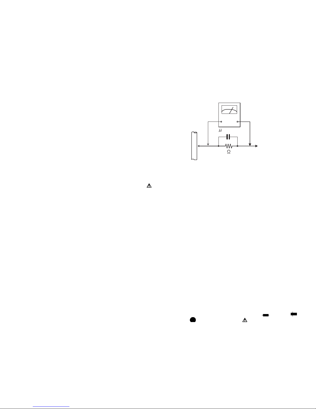
(5) Leakage shock hazard testing
After reassembling the product, always perform an isolation check on the exposed metal parts of the product (antenna terminals, knobs, metal cabinet, screw heads,
headphone jack, control shafts, etc.) to be sure the product
is safe to operate without danger of electrical shock.Do not
use a line isolation transformer during this check.
• Plug the AC line cord directly into the AC outlet. Using a
"Leakage Current Tester", measure the leakage current
from each exposed metal parts of the cabinet, particularly any exposed metal part having a return path to the
chassis, to a known good earth ground. Any leakage current must not exceed 0.5mA AC (r.m.s.).
• Alternate check method
Plug the AC line cord directly into the AC outlet. Use an
AC voltmeter having, 1,000Ω per volt or more sensitivity
in the following manner. Connect a 1,500Ω 10W resistor
paralleled by a 0.15µF AC-type capacitor between an ex-
posed metal part and a known good earth ground.
Measure the AC voltage across the resistor with the AC
voltmeter.
Move the resistor connection to each exposed metal
part, particularly any exposed metal part having a return
path to the chassis, and measure the AC voltage across
the resistor. Now, reverse the plug in the AC outlet and
repeat each measurement. Voltage measured any must
not exceed 0.75 V AC (r.m.s.). This corresponds to 0.5
mA AC (r.m.s.).
AC VOLTMETER
(Having 1000
ohms/volts,
or more sensitivity)
0.15 F AC TYPE
Place this
probe on
1500 10W
Good earth ground
1.2 Warning
(1) This equipment has been designed and manufactured to
meet international safety standards.
(2) It is the legal responsibility of the repairer to ensure that
these safety standards are maintained.
(3) Repairs must be made in accordance with the relevant
safety standards.
(4) It is essential that safety critical components are replaced
by approved parts.
(5) If mains voltage selector is provided, check setting for local
voltage.
1.3 Caution
Burrs formed during molding may be left over on some parts
of the chassis.
Therefore, pay attention to such burrs in the case of preforming repair of this system.
1.4 Critical parts for safety
In regard with component parts appearing on the silk-screen
printed side (parts side) of the PWB diagrams, the parts that are
printed over with black such as the resistor ( ), diode ( )
and ICP ( ) or identified by the " " mark nearby are critical
for safety. When replacing them, be sure to use the parts of the
same type and rating as specified by the manufacturer.
(This regulation dose not Except the J and C version)
each exposed
metal part.
(No.MB500)1-3
1.5 Safety Precautions (U.K only)
(1) This design of this product contains special hardware and many circuits and components specially for safety purposes. For con-
tinued protection, no changes should be made to the original design unless authorized in writing by the manufacturer. Replacement parts must be identical to those used in the original circuits.
(2) Any unauthorised design alterations or additions will void the manufacturer's guarantee; furthermore the manufacturer cannot
accept responsibility for personal injury or property damage resulting therefrom.
(3) Essential safety critical components are identified by ( ) on the Parts List and by shading on the schematics, and must never
be replaced by parts other than those listed in the manual. Please note however that many electrical and mechanical parts in
the product have special safety related characteristics. These characteristics are often not evident from visual inspection. Parts
other than specified by the manufacturer may not have the same safety characteristics as the recommended replacement parts
shown in the Parts List of the Service Manual and may create shock, fire, or other hazards.
(4) The leads in the products are routed and dressed with ties, clamps, tubings, barriers and the like to be separated from live parts,
high temperature parts, moving parts and/or sharp edges for the prevention of electric shock and fire hazard. When service is
required, the original lead routing and dress should be observed, and it should be confirmed that they have been returned to
normal, after re-assembling.
1.5.1 Warning
(1) Service should be performed by qualified personnel only.
(2) This equipment has been designed and manufactured to meet international safety standards.
(3) It is the legal responsibility of the repairer to ensure that these safety standards are maintained.
(4) Repairs must be made in accordance with the relevant safety standards.
(5) It is essential that safety critical components are replaced by approved parts.
(6) If mains voltage selector is provided, check setting for local voltage.
Burrs formed during molding may be left over on some parts of the chassis. Therefore,
pay attention to such burrs in the case of preforming repair of this system.
1-4 (No.MB500)

SECTION 2
SPECIFIC SERVICE INSTRUCTIONS
This service manual does not describe SPECIFIC SERVICE INSTRUCTIONS.
(No.MB500)1-5
SECTION 3
DISASSEMBLY
3.1 Main body section
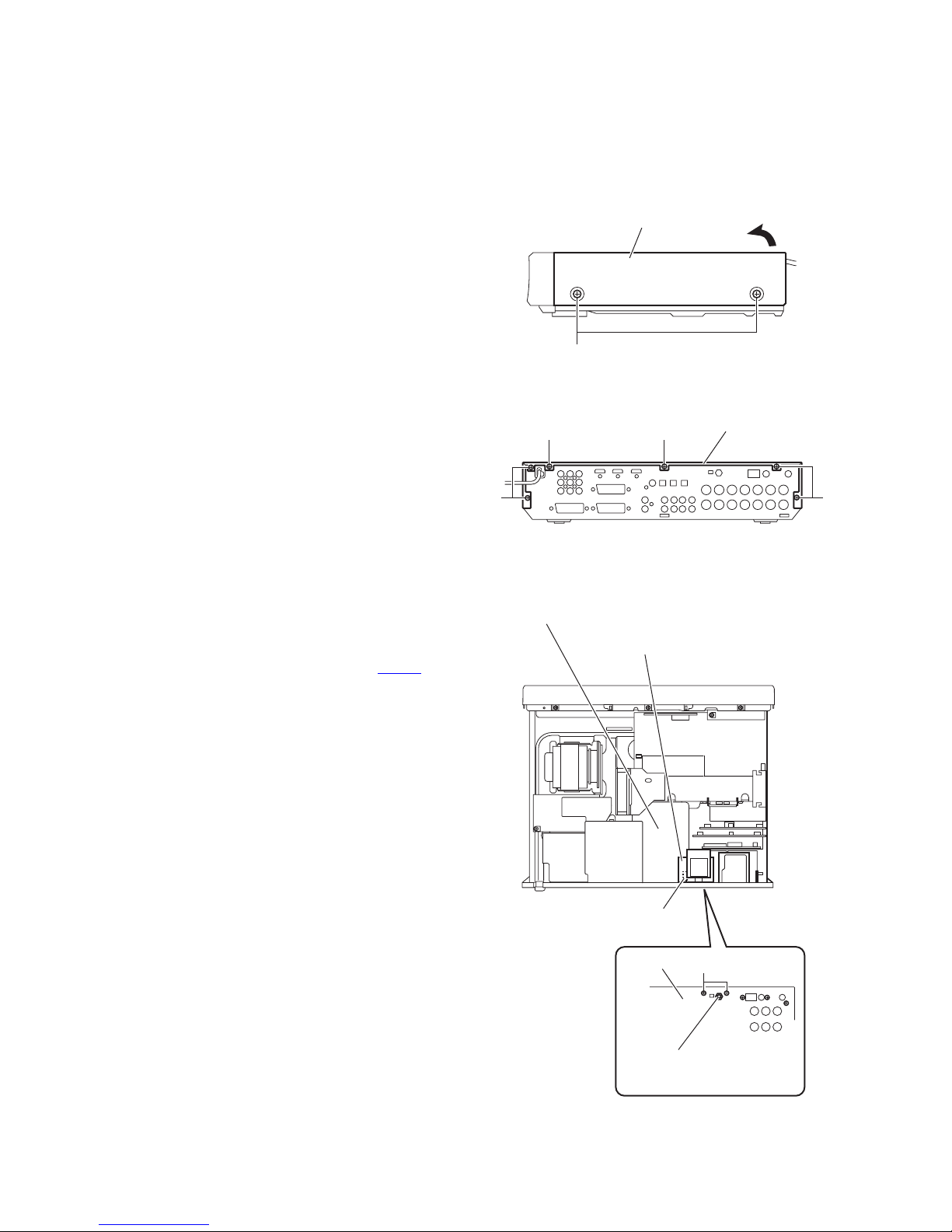
3.1.1 Removing the top cover
(See Fig.1 and 2)
(1) From the both sides of the main body, remove the four
screws A attaching the top cover. (See fig. 1)
(2) From the back side of the main body, remove the five
screws B and screw C attaching the top cover. (See Fig. 2)
Reference:
When removing the screw C, use a screwdriver to show
as follows.
TORX Driver: size T10
Parts number: DR-L70
(3) Remove the top cover in the direction of the arrow. (See
Fig. 1)
Top cover
A
Fig.1
3.1.2 Removing the USB wireless board
(See Fig. 3)
• Remove the top cover.
(1) From the top side of the main body, disconnect the LAN
module board from USB board.
(2) Remove the two screws D attaching the USB board.
(3) Disconnect the connector wire from connector CN662
the DSP board.
of
B
C
Top cover
B B
Fig.2
DSP board
USB wireless board
1-6 (No.MB500)
CN662
Rear panel
Coaxial connector
Fig.3
D
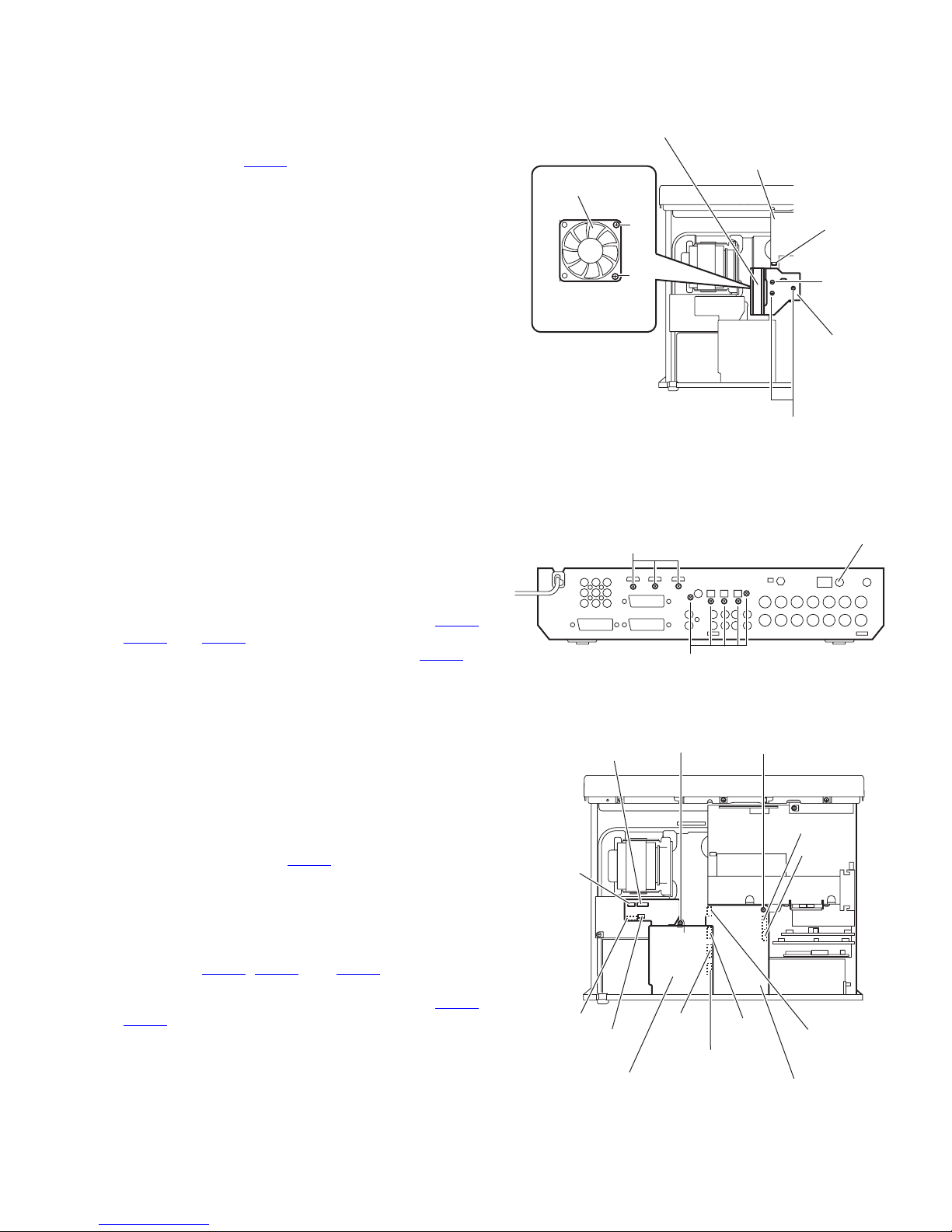
3.1.3 Removing the fan motor
(See Fig. 4)
• Remove the top cover.
(1) Remove the tie band bundling the wires.
(2) From the top side of the main body, disconnect the wire
from the connector CN103
(3) Remove the three screws E and take out the fan motor as-
sembly.
(4) Remove the two screws F attaching the fan motor to the fan
bracket.
on the main amplifier board.
Fan motor assembly
Fan motor
F
Main amplifier board
CN103
3.1.4 Removing the HDMI board
(See Figs.5 and 6)
• Remove the top cover.
(1) From the back side of the main body, remove the three
screws G attaching the HDMI board to the rear panel. (See
Fig.5)
(2) From the top side of the main body, remove the screw H at-
taching the HDMI board. (See Fig.6)
(3) Disconnect the card wires from the connectors (CN731
CN732, and CN762) on the HDMI board. (See Fig.6)
(4) Disconnect the parallel wire from the connector CN711 on
the HDMI board. (See Fig.6)
(5) Take out the HDMI board from the main body. (See Fig.6)
3.1.5 Removing the DSP board
(See Figs.5 and 6)
• Remove the top cover and fan motor.
(1) From the back side of the main body, remove the five
screws J attaching the DSP board to the rear panel. (See
Fig.5)
(2) From the top side of the main body, remove the screw K at-
taching the DSP board. (See Fig.6)
(3) Disconnect the connector CN681
the DSP connect board. (See Fig.6)
Note:
When removing the DSP board, take care not to break
the claw of the connector on it.
(4) Take out the DSP board and disconnect the wires from the
connectors (CN661
side of the DSP board. (See Fig.6)
(5) Disconnect the card wires from the connectors (CN651
CN652
) on the DSP board. (See Fig.6)
(6) Take out the DSP board from the main body.
, CN682, and CN683) on the forward
on the DSP board from
F
E
Fan bracket
E
Fig.4
G
,
Rear panel
J
Fig.5
CN652
DSP board
K
CN683
CN682
CN661
CN732
CN731
,
CN771
CN762
HDMI board
H
CN681
CN651
Fig.6
(No.MB500)1-7
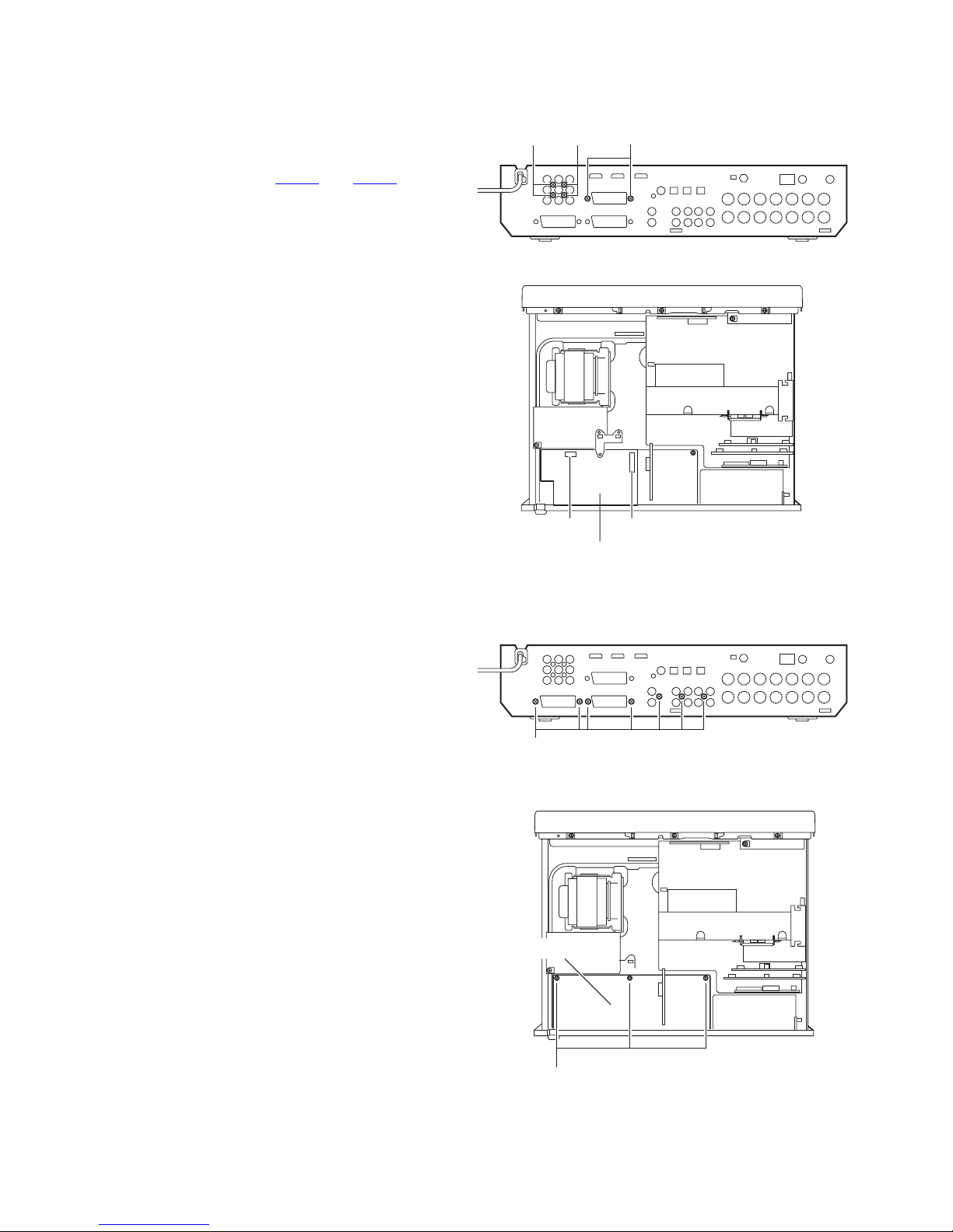
3.1.6 Removing the SCART board
(See Fig.7 and 8)
• Remove the top cove, USB board, DSP board and HDMI
board.
(1) Remove the six screws L attaching the SCART board.
(See Fig.7)
(2) Disconnect the card wire from CN537
SCART board. (See Fig.8)
and CN539 of the
LL L
Fig.7
3.1.7 Removing the input board
(See Fig.9 and 10)
(1) Remove the seven screws M attaching the input
board.(See Fig.9)
(2) Remove the three screws N attaching the input board. (See
Fig.10)
(3) Disconnect the each wire from each connector of the input
board.
CN539
SCART board
M
Input board
CN537
Fig.8
Fig.9
3.2 Other item
For the other items, please refer to RX-D701S,RX-D702B No.MB441.
1-8 (No.MB500)
N
Fig.10

SECTION 4
ADJUSTMENT
This service manual does not describe ADJUSTMENT.
SECTION 5
TROUBLESHOOTING
This service manual does not describe TROUBLESHOOTING.
(No.MB500)1-9

Victor Company of Japan, Limited
Audio/Video Systems Category 10-1,1chome,Ohwatari-machi,Maebashi-city,371-8543,Japan
(No.MB500)
Printed in Japan
VPT
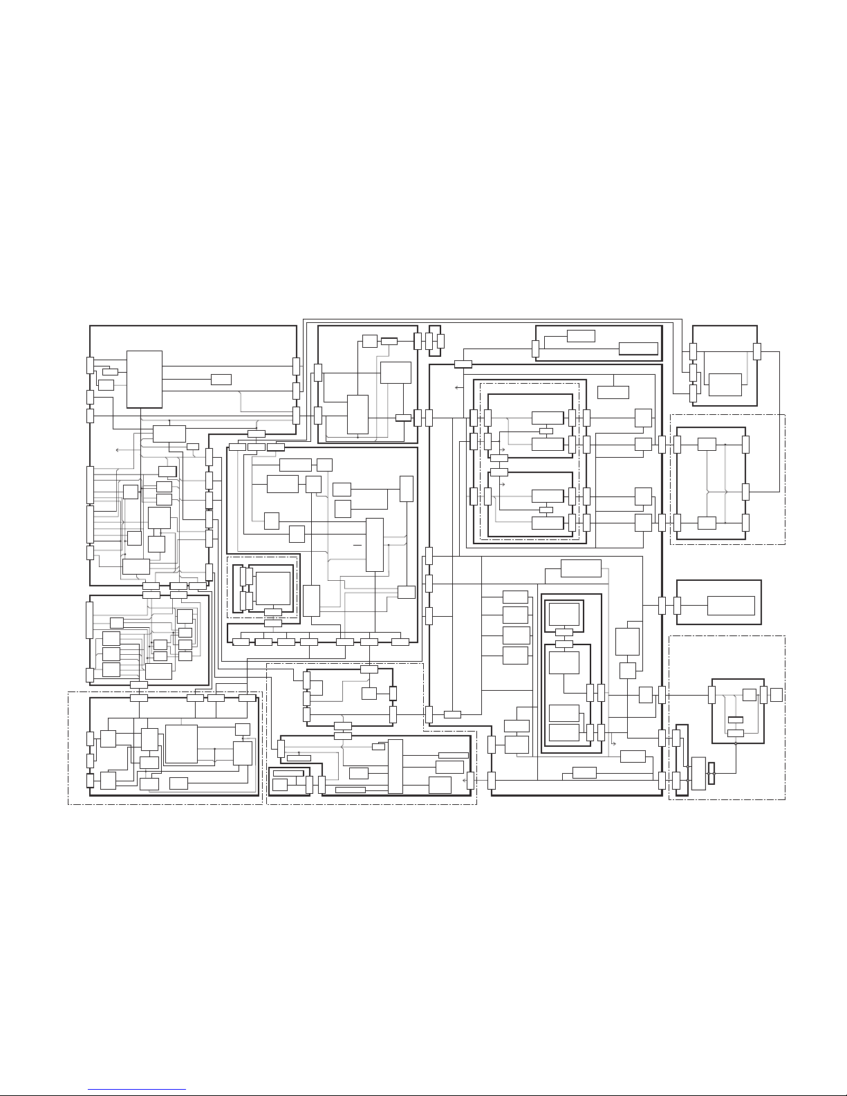
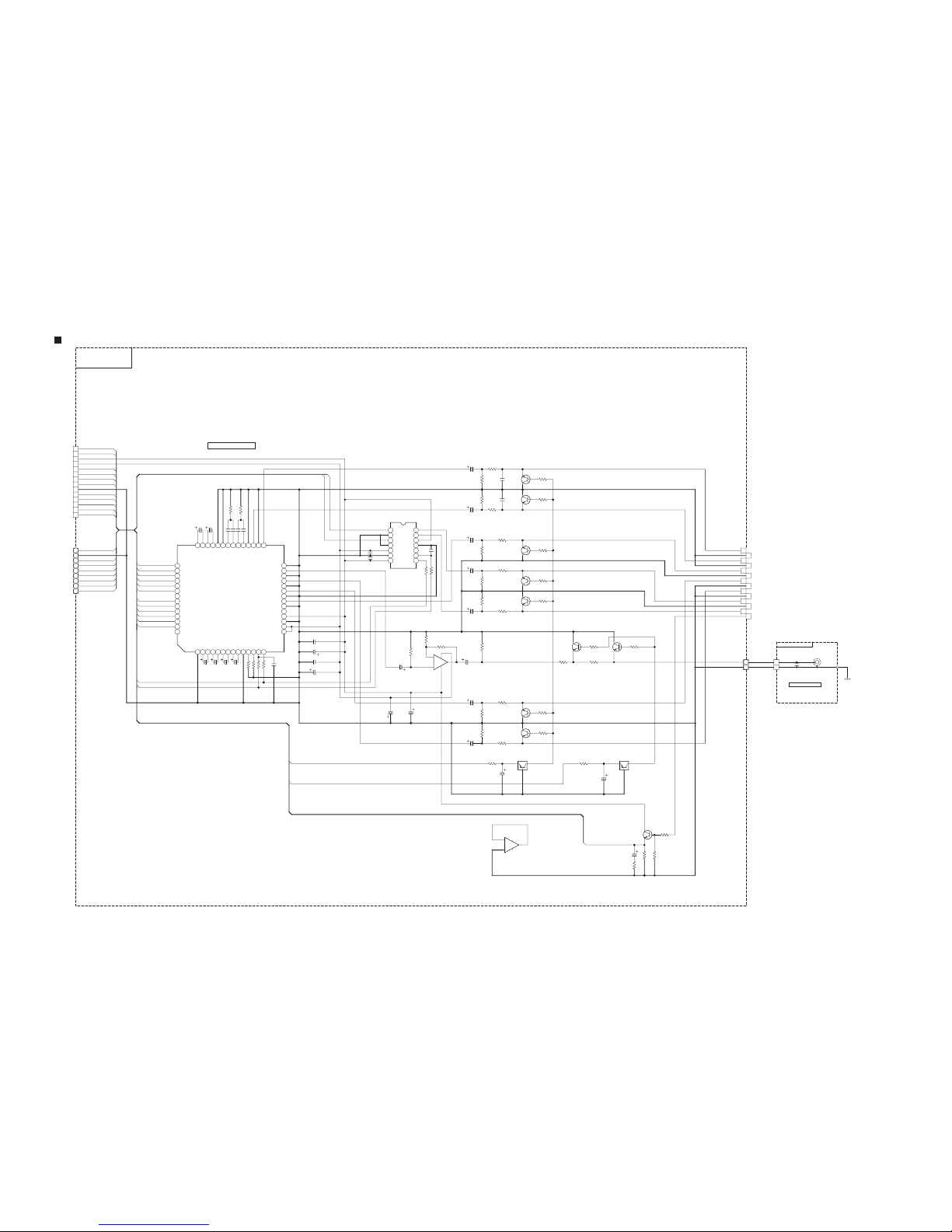
SCHEMATIC DIAGRAMS
AUDIO/VIDEO CONTROL RECEIVER
RX-D701SB,RX-D701SE,RX-D701SEN
RX-D702BB,RX-D702BE,RX-D702BEN
CD-ROM No.SML200601
Lead free solder used in the board (material : Sn-Ag-Cu, melting point : 219 Centigrade)
Contents
Block diagrams
Standard schematic diagrams
Printed circuit boards
COPYRIGHT 2006 Victor Company of Japan, Limited.
2-1
2-2
2-15 to 21
No.MB500SCH
2006/1

In regard with component parts appearing on the silk-screen printed side (parts side) of the PWB diagrams, the
parts that are printed over with black such as the resistor ( ), diode ( ) and ICP ( ) or identified by the " "
mark nearby are critical for safety.
2-1
Block diagram
CN106CN111CN101CN152
CN151
IC111 to IC113, IC115
DCDC converter
control
PWM_V,Vout_DET
M_CLOCK,SSS_ON/OFF
AC_DET_1
VCHANGE_1
VCHANGE_2
D1101
to
D1104
Q1101
Q1102
IC101
DCDC
converter
PWM_V
Vout_DET
AC_DET_1
D101
to
D104
D+5V_Mi
B+5V_Mi
D111, D112
D119,D120
S2
S3
S2
Q102
VPP REG.
VPP
CN102
IC151
A+5V_DSP
REG
CN130
A+5V_DSP
CN131
IC152
A+9V_Vi_Tu
REG
A+9V_Vi_Tu
CN103
TO
FAN
IC153
A+5V_Vi
REG
A+5V_Vi
Q157,Q158
+/-7V REG
+/-7V
VCHANGE_1,VCHANGE_2,SSS_ON/OFF,M_CLOCK
Q153
+12V_FAN
REG
FAN
Q151,Q152
Q154
FAN_ON/OFF
FAN_LOW
Q101
D+5V_Mi,B+5V_Mi
REG
CN104 CN105
CN114 CN115
Q174
DCDC_+12
REG
Q175
DCDC_-B+12
REG
Q155,Q171
Q172
D+5V_DSP
REG
CN252
CN272
RY721
RY731
ST702
SURROUND
&
SURROUND
BACK
SLout
SRout
SBLout
SBRout
CN208
SB_RY
SURR_RY
CN251
CN271
RY701
RY711
ST701
FRONT
&
CENTER
Lout
Rout
Cout
F_RY
C_RY
Speaker terminal section
IC851
AMP
CN322
IC451
IC461
AMP
CN422
IC261
IC361
AMP
CN421
IC251
IC351
AMP
CN321
CN312CN311 CN412CN411
IC201
MODULATOR
IC202
IC302
FRONT_L
FRONT_R
CENTER
SURROUND_L
SURROUND_R
SURRBACK_L
SURRBACK_R
IC801
MODULATOR
IC301
MODULATOR
IC401
MODULATOR
CN302
CN301
CN413
CN423
PWM modulator section
FW323
CN313
FL,FR
A.NFB_FL
D.NFB_FL
A.NFB_FR
D.NFB_FR
C
A.NFB_C
D.NFB_C
M_CLOCK,+/-7V
M_CLOCK
+/-7V
+/-7V
CN402
CN401
SL,SR
A.NFB_SL
D.NFB_SL
A.NFB_SR
D.NFB_SR
SBL,SBR
A.NFB_SBL,A.NFB_SBR
D.NFB_SBL,D.NFB_SBR
CN202
IC211 to IC214
Master clock GEN.
Q441,Q444
-B+12V REG
Master clock section
CN201
M_CLOCK
FREQ_CTRL
-B,-B+12V
FL,FR,C
SL,SR
SBL,SBR
A.NFB_SBL,D.NFB_SBL
A.NFB_SBR,D.NFB_SBR
A.NFB_FL,D.NFB_FL
A.NFB_FR,D.NFB_FR
A.NFB_C
D.NFB_C
A.NFB_SL,D.NFB_SL
A.NFB_SR,D.NFB_SR
M_CS
M_COMMAND,M_STATUS
M_CLK,M_RESET,M_BUSY
FW240
CN222
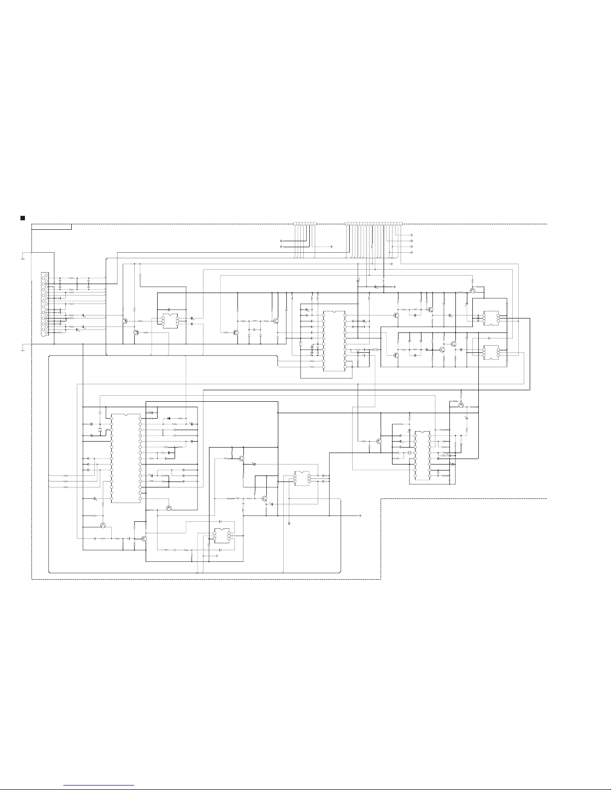
Regulator, DC-DC converter and digital power amplifier section
CN513
IC503
MASTER
VOLUME
L,R,DVD_C
DVD_SW
DVD_SL/SR
IC508
AUDIO
SOUND
PROCESSOR
MUTE
DSP_L/R
DSP_C
DSP_SW
DSP_SL/SR
S_MUTE
IC504
AMP
CN522
CN523
SUBWFR
SBWFR OUT
CN524
J504
DA
CL
FL
FR
C
SL
SR
SBL
SBR
CN521
CN681 CN682
SUBWOOFER
OUT
CN683
IC697
8CH
CODEC
DSP_IN_L
DSP_IN_R
IC671
CPU
DSPSTATUS,DSPREADY
DSPCLK,DSPRESET
DSPCOMMAND
SCK
MOSI
MISO
HD3,HD4
HD13
READY
CSDSP
DSP_RST
IC661
DSP
IC601
IC602
AMP.
LIN+/RIN+/-
IC621,IC622
IC632 to IC634
AMP.
DATA
S_BCK
S_LRCK
SBL/SBR
A4+/-,B4+/-
Master volume section
DSP and digital signal input terminal section
IC901
FL
DRV.
&
KEY
CONT.
DI901
FL DISPLAY
SEG1 to 35
GRID1 to 15
CN913
CN903
JS901
JS902
VOL1,VOL2,JOG1,JOG2
J901
HEADPHONE
CN904
CN914
J902
USB
TERMINAL
IC903
D/A
CN961
D+/VBUS
USB_IN
CN905
HP_L
HP_R
UN686
RX3,RX4
CN351
CN902
F1,F2
-VPP
D+5V
CN952
AV COMPULINK
Q910
AVC_IN,AVC_OUT
D916 to D923
AM_LED,FM_LED
USB_LED,TV_LED
DBS_LED,DVD_MULTI_LED
VCR_LED,DVD_LED
S901 to S906
KEY_IN1 to 3
D907
STANDBY
LED
STANDBY_IND
IC902
IR DET.
REMOCON
User control keys, system control and FL display section
DSP_SBL
DSP_SBR
HEADPHONE_DET
AMP_-B
AMP_-B+12V
Q281 to Q286
PROTECTOR
PROTECT
Lout_HP
Rout_HP
Lout_HP
Rout_HP
RY300
HP_RY
+12V_RY
D+5V_Mi
D+5V_Mi,D+5V_DSP
D+5V_HDMI,B+5V_Mi
POWER_ON,FAN_ON/OFF
FAN_LOW
RY+9V
POWER_ON
+12V
-B+12V
D+5V_DSP
D+5V_HDMI
POWER_ON
IC611 to IC614
AMP.
CDIN
CDOUT
CCLK
D_CS
D_RST
IC610
D/A
DSP.L
DSP.R
UN683
RX2
DIGITAL
IN3
CN771
IC771
SDTV/HDTV
VIDEO
DECODER
& RGB
GRAPHICS
DIGITIZER
AD_RST
IP_RST
BUS_SW2
AD_SDA,AD_SCL
HDMI RX,TX,micom,HDMI ADC and i/p converter section
CN661
TX
DIGITAL
OUT
D+5V_Mi,FL1,FL2,VPP
CN117
CN107
Q156,Q176
Q177
D+5V_HDMI
REG
IC781
DIGITAL
VIDEO
CONV.
IC772
BUFF.
AD_OUT_Y0 to Y7
AD_OUT_CBCR0 to 7
AD_OUT_HS/VS/CLK
BUF_OUT_Y0 to Y7,BUF_OUT_HS/VS/CLK
BUFF_OUT_CBCR0 to 7
Y0 to Y7,CBCR0 to 7,HS,VS,CLK
IC782
SDRAM
DATA0 to 31,ADDR0 to 10
SDRAM_CLK,BA0,BA1,DQM
J711
HDMI
PORT0
J721
HDMI
PORT1
IC731
HDMI
RX
IC751
HDMI
TX
J751
IC761
HDMI
SUB
MICON
IC741
BUS SW
Y,Pb,Pr
Y,Pb,Pr
CN762
IC743
BUS SW
CN651 CN652
CN732CN731
AUDIO_SEL1 to 4
HDMI_MUTE
RX0 to RX6,TX
RX6,TX
IC681
IC685
IC686
DATA
SEL
& MPX
AUDIO_SEL1 to 4
SD0 to 2,LRCK
RX_MUTE,BCK
HDMI_CLK,HDMI_STS
HDMI_COM,HDMI_RDY
HDMI_RST
RX_SPDIF
DSP_SPDIF
M_CLK
SD0 to 2
LRCK
BCK
RX_SPDIF
RX_MUTE
RX_MCLK
TX_RST
TX_HPD
TX_INT
CSDA,CSCL
HD_VS/HS
Q8 to Q23
TX_SPDIF
TX_MCLK
RX_INT
RX_RST
RX_SCDT
BUS_SW1
BUS_SW3
IC651
IC652
AMP.
FL/FR
SL/SR
C/LFE
C_BCK
C_LRCK
SD0 to 2
LRCK,BCK
CC_CS
CC_CLK
CC_RST
CC_DATA
DVD_AUD_SEL
IC620
IC630
D/A
P_SL/SR,P_C/LFE
P_BCK,P_LRCK
IC663
FLASH
ROM
IC664
SDRAM
DSP.SBL
DSP.SBR
DAC_fs1,DAC_fs2
PD_DD,RST_DD
DSP.LS
DSP.RS
DSP.C
DSP.SW
DAC_fs3
DAC_fs4
PD_DD
RST_DD
DSP_A2 to A21
DSP_D0 to D15
DSP_CE1,DSP_AWE
DSP_AOE
DSP_A2 to A15
DSP_D0 to D15
DSP_CE0,DSP_ARE
DSP_AWE,DSP_AOE
DSP_BE0,DSP_BE1
SDRAM_CLK
+B,-B
Main
plug
T102
Trans.
POWER_ON
Primary section
Power
trans.
S1
S2
S3
AC
RY+9V
CN211 CN206
RY101
Q1001
FW121
CN120
CN218
CN516
FRONT_RELAY,C_RELAY
SB_RELAY,SURR_RELAY
IC591 to IC594
SMART
SURROUND
SETUP
L,R,C
LS,RS
SBL,SBR
CN602 CN672
SSS section
IC11
DIGITAL
AUDIO
TRANSMITTER
LAN MODULE
USB wireless section
CN12 CN13
UN682
RX1
DIGITAL
IN2
J681
RX0
DIGITAL
IN1
CN662
CN11
RX5
CN971
J903
SVIDEO_Y,SVIDEO_C
CVIDEO,FL,FR
OPTICAL
S-VODEO
C-VIDEO
AUDIO L/R
OPT_IN
AUDIO_SEL1 to 4
RX_MUTE
MUTE
SBWR_MUTE
D908,D909
L,R,C
LS,RS
SBL,SBR
+12V_RY
+12V_RY
SSS_ON/OFF
FREQ_CTRL
PROTECT
BLUE_LED
LED_DIM1
LED_DIM2
D911 to D914
M_CLOCK
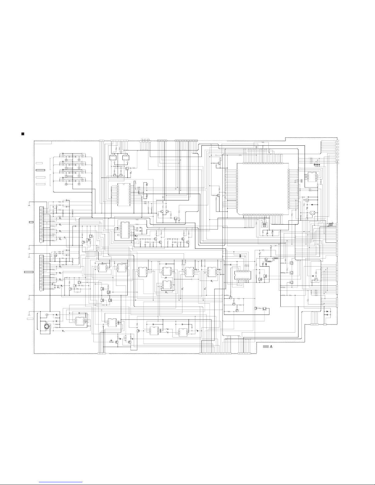
Audio/Video signal input,system control and component section
Scart section
J6503
VIDEO
DVR/DVD
J6504
DVD C/SW
DVD SURR
IC502
6CH
SOURCE SEL.
VID_L/R,DVR_L/R
DVD_C
DVD_SW
DVD_SL/SR
L,R
IC501
CPU
CN505
TO
TUNER
TU_L/R
TU_DATAI
TU_DATAO
TU_CLK,TU_CE
DSP_STATUS,DSP_READY
DSP_CLOCK,DSP_RESET
DSP_COMMAND
BCHANGE1
BCHANGE2
HP_RELAY
MUTE
T_MUTE
FW781
CN537 CN539
IC507
EEPROM
RC_SDA
RC_SCL
RC_WP
SSS_FL,SSS_FR,SSS_C
SSS_LS,SSS_RS
SSS_SBL,SSS_SBR
SSS_ON/OFF
FR_RELAY,C_RELAY
SURR_RELAY,SBK_RELAY
CN501
CN531
CN502
DA,CL
S_MUTE
SBWR_MUTE
CN530
D+5V,B+5V
+/-7V,+9V
A+5V(DSP)
D+5V(DSP)
D+5V(HDMI)
+5V(VIDEO)
+12V(RELAY)
FAN_ON/OFF
FAN_L
POWER_ON
Q524
HP_RY
CN540
PROTECT
FREQ_CTRL
SSS_ON/OFF
CN552
CN504
CN506
CN572
VIDEO L/R
CN571
CN503
M_CS,M_BUSY
M_COMMAND
M_STATUS
M_CLOCK
M_RESET
BLUE_LED
LED_DIM1/2
HDMI_Y
HDMI_Y/PB/PR
HDMI_PB
HDMI_PR
VCR IN
DVR/DVD IN
MONITOR
TV IN
PB
Y
PR
B-Y/B_OUT
Y/G_OUT
R-Y/R_OUT
J4503
IC531
IC534
PB SEL.
IC530
IC533
Y SEL.
IC532
IC535
PR SEL.
IC561,IC562
CROMA
DECODER
TA/TC_SDA
TA/TC_SCL
TV_L/R,TV_G,TV_B,TV_LINK
TV_YS_OUT,TV_V/SY_IN
TV_SLOW_OUT
V/SY_OUT
VIDEO7
VIDEO6
VIDEO8
VIDEO8/10
VIDEO1/6/7
LC_CS
LC_SIN
LC_SCLK
VIDEO1,10
IC551
Y/C
SEPA.
IC542
SEL.
IC560
OSD
IC537
SEL.
IC536
SEL.
IC538
SEL.
IC539
SEL.
SC_OUT
R/SC
V/Y_OUT
TV_R/C
J9511
C
Y
IC505
RDS
RDSCL
RDSDA
DVD_R/C
DVD_VOUT
VIDEO_SC
VIDEO_SY
VIDEO_CV
VCR_R/C
VCR_H/M
DVR_H/M
VCR_VOUT
VCR_L/R
VCROUT_L/R
VCR_G/B/YS/VY
DVD_G/B/YS/VY
DVR_L/R
DVROUT_L/R
VCR_B
DVD_B
B
G
YS
VCR_YS
DVD_YS
VCR_G
DVD_G
VIDEO1
VIDEO2
VIDEO2
VIDEO1/2/4/5/9
VIDEO1/3/4/11
VCR_VY
DVD_VY
V/SY_OUT
Y/C MIX
TV_LINK
R/SC
VIDEO C
VIDEO Y
VIDEO CV
V/SY IN
TV_L/R
IC573
IC574
IC575
R/SC SEL.
IC576,IC577
IC580,IC581
CV/SY SEL.
IC571
B SEL.
IC582
YS SEL.
IC572
G SEL.
IC578
IC579
YC MIX
Q8515
Q8516
Q8529
Q8521
Q8522
Q8523
DVR/DVD
VCR
J8511 J8512
VIDEO IN
J8513
CN527 CN529
2-2
Parts are safety assurance parts.
When replacing those parts make
sure to use the specified one.
Standard schematic diagrams
PW157
PW156
PW155
PW154
PW153
PW152
PW151
CN206
1
2
3
4
5
6
7
8
PW151
CN206
1
2
3
4
5
6
7
8
PW157
PW156
PW155
PW154
PW153
PW152
PW113
PW57
PW56
PW55
PW54
VS101
QSW0812-001
!
8
1
746
3
5
2
PW53
PW52
FC115
QNG0020-001Z
!
FC105
QNG0020-001Z
PW151
CN206
1
2
3
4
5
6
7
8
PW157
PW156
PW155
PW154
PW153
PW152
C1001
4700p
!
B142
QUY158-150Y
Q1001
KRC105S-X
FW121
1
2
3
4
T102
!
9541
PW103
RY101
!
QSK0128-001
2
1
4
3
FC103
QNG0020-001Z
D1001
1SS133-T2
FC113
QNG0020-001Z
!
CN120
QGA7901C1-02
1
2
EP151
QNZ0136-001Z
123
C1002
0.22
!
R1002
3.3M
!
R1001
3.3M
!
PW104
C1001
4700p
!
Q1001
KRC105S-X
FW121
1
2
3
4
QQT0478-002
T102
!
9541
PW103
RY101
!
QSK0128-001
2
1
4
3
FC103
QNG0020-001Z
D1001
1SS133-T2
FC113
QNG0020-001Z
!
CN120
QGA7901C1-02
1
2
FC114
QNG0020-001Z
EP151
QNZ0136-001Z
123
C1002
0.22
!
R1002
3.3M
!
FC104
QNG0020-001Z
!
PW104
C1001
4700p
!
Q1001
KRC105S-X
FW121
1
2
3
4
QQT0281-006
T102
!
9541
PW103
RY101
!
QSK0142-001
2143
FC103
QNG0020-001Z
D1001
1SS133-T2
FC113
QNG0020-001Z
!
CN120
QGA7901C1-02
1
2
FC114
QNG0020-001Z
EP151
QNZ0136-001Z
123
C1002
0.22
!
R1002
3.3M
!
FC104
QNG0020-001Z
!
PW104
8
1
746
3
5
2
8
1
746
3
528
1
746
3
528
1
746
3
5
2
C1003
0.001
!
C1004
0.001
!
C1003
0.001
!
C1004
0.001
!
CN211
1
2
3
CN211
1
2
3
CN211
1
2
3
TH.FUSE
S2
COM
S2
S3
S3
S1
COM
S1
LVA10579-12
LVA10579-13
S2
LVA10579-13
TH.FUSE
LVA10579-12
S1
S3
COM
COM
S2
S3
S1
LVA10579-6
127V
0V
110V
127V
0V
17V
S2
LVA10579-13
TH.FUSE
LVA10579-12
S1
S3
COM
COM
S2
S3
S1
POWER_ON
RY+9V
BRN
!
AC
NEUTRAL/
LIVE/
BLU
AC
of LVA10578-1to CN101
LVA10579-5
POWER_ON
RY+9V
BRN
!
AC
NEUTRAL/
LIVE/
BLU
AC
LVA10579-5
POWER_ON
RY+12V
BRN
!
AC
NEUTRAL/
LIVE/
BLU
AC
LVA10579-5
220V 230-240V127V110V
VOLTAGE SELECTOR LOCATION
SOURCE FM(NO SIGNAL)
VOLTAGE MEASUREMENT CONDITION
POWER ON
VOLUME 0
SURROUND OFF
VERSION CODES
J ;U.S.A.
C ;CANADA
B ;U.K.
E ;CONTINENTAL EUROPE
EN:NORDIC COUNTRIES
EV;EAST EUROPEAN COUNTRIES
US;SINGAPORE
UJ;U.S. ARMY
A ;AUSTRARIA
UT;TAIWAN
UF;CHINA
F103 F103
F104
F103
F104
F103
F104
J/C/D B/E/EN/EV US/UJ/UT A UF
QMF51U1-6R3-J8 -QMF51W2-2R5-J8
QMF5AE2-R10-J1
QMF51W2-5R0-J8
QMF5AE2-R10-J1
QMF51W2-2R5-J8 QMF51W2-2R5-J8
QMF5AE2-R10-J1 QMF5AE2-R10-J1
TO CN111 OF LVA10578-1
(SHEET 3/18)
TO CN106 OF LVA10578-1
(SHEET 3/18)
(SHEET 3/18)
TO CN111 OF LVA10578-1
(SHEET 3/18)(SHEET 3/18)
TO CN106 OF LVA10578-1
to CN101 of LVA10578-1
(SHEET 3/18)
TO CN111 OF LVA10578-1
(SHEET 3/18)(SHEET 3/18)
TO CN106 OF LVA10578-1
to CN101 of LVA10578-1
(SHEET 3/18)
D :JAPAN
F105
F105 - - QMF51W2-2R5-J8 - -
**
* MARK LIST
J,C D
R1001
T102
USE NONE
QQT0478-003QQT0478-001
J/C/D US/UJ/UT
B/E/EN/EV
PLUG
MAINS
PLUG
MAINS
PLUG
MAINS
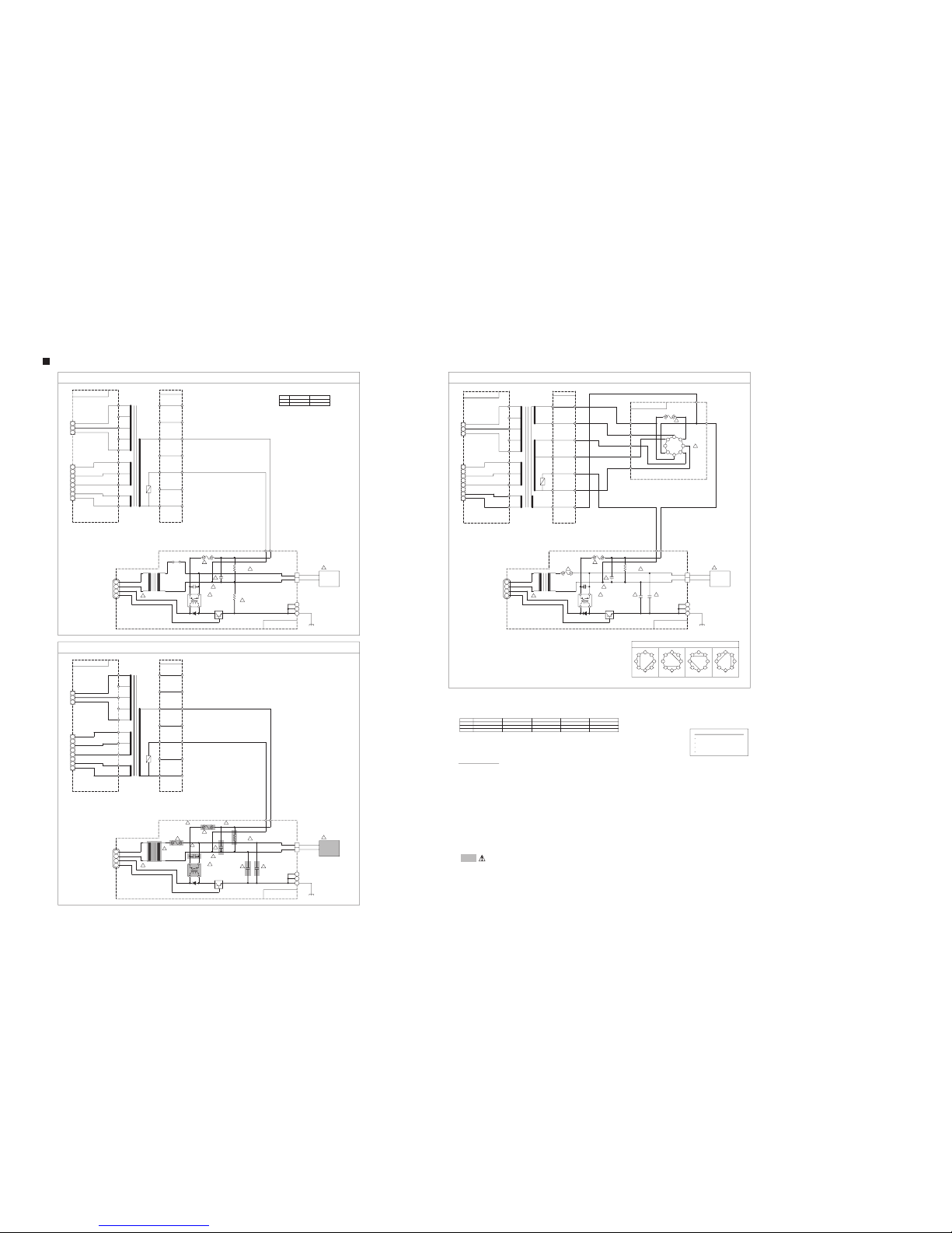
Primary section
!
!
!
!
2-3
Parts are safety assurance parts.
When replacing those parts make
sure to use the specified one.
Regulator / DC-DC converter section
+
-
+
-
+
-
IC112
NJM2403M-X
2
3
1
8
4
R1156
120k
C1174
100/16
R1151
C1154
100p
R1160
1k
R1172
3.3k
D1152
1SS133-T2IC113
SN74HC00ANS-X
891011121314
7654321
C1157
0.1
R1163
330
R1159
10k
C1155
1
R1152
C1182
100/16
R1162
1k
Q1173
KTA1504/YG/-X
C1152
1
C1153
1
R1157
10k
IC111
NJM2125F-X
3
1
4
5
2
R1166
470
D1174
1SS133-T2
R1165
3.3k
Q1171
KTC3875/YG/-X
C1181
0.01
R1174
10k
R1164
R1175
2.2k
R1161
1M
C1173
0.01
C1151
47/16
D1153
1SS133-T2
R1176
47k
C1156
100p
D1173
1SS133-T2
Q1172
KRC102S-X
D1172
1SS133-T2
R1158
680
R1154
3.3k
IC121
KIA7805API
123
R1153
D1151
1SS133-T2
R1173
10k
IC112
NJM2403M-X
6
5
7
R1155
22k
Q1151
KRC102S-X
Q1152
KRC102S-X
C1172
1000p
IC115
SN74HC74ANS-X
891011121314
7654321
C1158
0.1
D1154
UDZS2.7B-X
R11701kR1169
3.3k
Q1174
KTC3875/YG/-X
R1178
100
Q1103
KTA1268/GL/-T
R1114
820
D1155
1SS133-T2
R1180
13k
R1179
3.3k
C1159
820p
Q1176
Q1175
CN151
QGB2510K1-12
123456789
101112
Q1177
R1181
47k
FEEDBACK
VCC
GND
+12V
Vout_DET
VCHANGE_1
VCHANGE_2
M_CLOCK
PGND
PWM_V
(1/2)
(2/2)
1CLR1D1CLK
1PRE1Q1Q
GND 2Q
2Q
2PRE
2CLK2D2CLR
VCC
DCDC Converter_Control
LVA10579-11
AC_DET_2
AC_DET_1
DRIVER_SD
NI
NI
SSS_ON/OFF
NI
*
*
*
*
C164
2200p
D158
MTZJ7.5A-T2
C165
100/16
Q155
2SC1740S/RS/-T
C166
470/16
R165
0.22
UNF
(1W)
!
R166
2.2k
UNF
(1/4W)
!
Q171
2SD2394/EF/
Q172
2SD2394/EF/
R172
100
R171
100
Q173
2SD2394/EF/
C172
0.0047
C174
10/50
C173
1/50
Q174
2SD2394/EF/
D171
MTZJ13B-T2
C176
10/50
C175
1/50
Q175
2SD2394/EF/
D172
MTZJ13B-T2
R173
4.7
UNF
!
R174
10k
UNF
!
R175
4.7
UNF
!
R176
10k
UNF
!
CN115
1
2
3
4
5
CN114
QGA2001F1-07
1
2
3
4
5
6
7
CN117
QGA2001F1-03
123
D+5V_DSP
PRI_RY+12V
+12V
+B
PGND
-B+12V
-B
(1/2W)
(1/2W)
(1/2W)
(1/2W)
DCDC_+12
LVA10578-4
to CN104
of LVA10578-1
to CN105
of LVA10578-1
*
*
R177
100
Q176
2SD2394/EF/
CN107
123
C167
0.0022
R16710UNF
1W
!
Q156
2SC1740S/RS/-T
C168
100/16
C169
470/16
R178
100
Q177
2SD2394/EF/
D159
MTZJ6.2C-T2
R168
2.2k
UNF
1/4W
!
R186
10
1W
UNF
!
R187
10
1W
UNF
!
R188
10
1W
UNF
!
R189
10
1W
UNF
!
LVA10578-6
D+5V_HDMI
C1122
0.33
D1103
30PRA20-FC
!
D1104
30PRA20-FC
!
D1105
C1103
0.22
L1102
QQL78AK-220
22
R1103
33
1/4W
IC101
IRS2011S-X
8765
1234
Q1102
2SK3599-01MR
D
G
S
C1104
0.22
C1118
4700/63
R1111
1k
D1106
C1117
4700/63
R1112
1k
L1101
QQL78AK-220
22
R1105
10
C1113
0.0033
R1108
10
D1102
30PRA20-FC
!
D1171
1SS133-T2
C1171
4.7/50
C1101
0.22/100
C1120
0.1/100
C1109
0.0033
C1116
0.1/100
R1106
10
D1108
FMB-G19L
C1105
6800/80
C1106
6800/80
D1107
FMB-G19L
R1113
39k
R1115
820
C1102
0.22/100
D1109
1SS133-T2
C1119
0.1/100
C1111
0.0033
C1107
0.0033
C1123
1
R1107
10
C1115
0.1/100
Q1101
2SK3599-01MR
D
G
S
R1104
33
1/4W
D1101
30PRA20-FC
!
D111
10DDA20-FD
!
D110
D109
D112
10DDA20-FD
!
C151
6800/25
C152
3300/25
TH101
4.7
C110
220/50
D113
1A3G-T1
D114
1A3G-T1
D115
1A3G-T1
C112
22/50
Q102
KTA1046/Y/
D116
MTZJ36C-T2
C113
22/50
R109
22k
Q103
KTC3200/GL/-T
D117
MTZJ8.2C-T2
C114
1/50
R110
100k
IC151
KIA7805API
123
IC153
KIA7805API
123
IC152
KIA7809API
123
C153
0.01
C158
0.01
C155
0.01
C154
100/16
C159
100/16
C156
100/25
Q157
2SD2394/EF/
C160
100/16
D156
MTZJ8.2C-T2
D157
MTZJ8.2C-T2
C162
100/16
D103
1A3G-T1
!
D104
1A3G-T1
!
D101
1A3G-T1
!
D102
1A3G-T1
!
C101
0.0047/100
C102
C103
4700p
Q101
KTD863/Y/-T
D106
MTZJ6.2B-T2
C104
470/16
Q158
KTA1046/Y/
CN101
QGA2001C1-04
123
4
D107
1A3G-T1
D108
1A3G-T1
CN102
QGF1205C1-05
1
2
3
4
5
Q153
2SD2394/EF/
Q151
KRA102S-X
Q152
KRC102S-X
D152
1SS133-T2
C157
10/50
D153
MTZJ13B-T2
D154
MTZJ8.2A-T2
Q154
KRC102S-X
D161 1A3G-T1
D162
1A3G-T1
R154
10k
R155
11k
R159
2k
R160
47k
C161
470/16
C163
470/16
CN103
QGA2501C1-02
1
2
R1101
100k
R1102
100k
B2017
D105
MTZJ12C-T2
C111
100/63
R101
15k
UNF
R102
3.3k
UNF
R103
6.8
UNF
R104
10
UNF
R106
820
UNF
R107
5.6 UNF
1/4W
!
R108
3.3k
UNF
R157
470
UNF
!
R158
4.7
UNF
1W
!
R162
2.2k
UNF
!
R164
2.2k
UNF
!
R1109
2.2k
UNF
2W
R1110
2.2k
UNF
2W
R1171
3.3k
UNF
1/4W
CN131
1
2
3
4
5
6
7
8
9
R15122UNF
1W
!
R153
0.47
UNF
1W
!
CN105
QGA2001C1-05
1
2
3
4
5
AMP_+B
PGND
AMP_-B
HP_RY
+12V_RY
R105
10
UNF
C106
0.1/100
C107
0.1/100
C105
0.1/100
C109
0.047
MY
C108
0.047
MY
R1524.7
UNF
!
R161
4.7
UNF
!
R16310UNF
!
R156
10
UNF
!
BLK_DCCTRL
C1108
0.0033
C1110
0.0033
C1112
0.0033
C1114
0.0033
FC101
QNG0020-001Z
!
FC111
QNG0020-001Z
FC112
QNG0020-001Z
FC102
QNG0020-001Z
!
R1116
4.7
1/4W
CN104
7
6
5
4
3
2
1
CN130
1
2
3
4
5
6
7
8
9
10
11
CN106
QGA3901C1-08
1234567
8
CN111
QGA3901C1-03
3
2
1
BLK_REG
R183
2k
R184
47k
Q161
KRC111S-X
Q163
KRC111S-X
Q162
KRC111S-X
R181
100
R182
C1126
R1117
4.7
1/4W
D1110
1SS133-T2
EP101
QNZ0136-001Z
1
DRIVER_SD
Q1104
KTA1268/GL/-T
D1111
1SS133-T2
R1118
47k
FW323
1
2
3
4
EP102
QNZ0136-001Z
BLK_REG2
C1124
0.1/250
C1125
0.1/250
CN152
QGB2510J1-12
123456789
101112
SSS_ON/OFF
C1143
0.22/100
C1142
0.22/100
C1144
0.22/100
C1145
0.22/100
C1133
0.22/100
C1134
0.22/100
C1131
0.22/100
C1132
0.22/100
C1135
0.1/250
C1136
0.1/250
C1146
0.1/250
C1147
0.1/250
C1137
0.1/250
C1138
0.1/250
C1139
C1140
C1141
R272
TH272
TH_COM
C1149
0.1/250
C1150
0.1/250
C1148
C1161
C1162
C1163
C1164
C1166
C1165
D120
UF304G-F82
!
D119
UF304G-F82
!
C1167
0.1/250
C1168
0.1/250
HIN
VCCLO
COM
LIN
VBHOVS
D+5V_Mi
DGND
FL1
VPP
FL2
+7V
-7V
AGND
A+5V_DSP
A+5V_Vi
A+9V_Vi_Tu
+12V_RY
D+5V_Mi
B+5V_Mi
D+5V_DSP
DGND
FAN_ON/OFF
FAN_LOW
POWER_ON
REG_DET
D+5V_HDMI
AC
AC
RY+9V
POWER_ON
S2
COM
S2S3S3
FAN
FANGND
+12V
FEEDBACK
AC_DET_1
Vout_DET
VCHANGE_2
M_CLOCK
PGND
PWM_V
A+5V_DSP
A+9V_Vi_Tu
+12V_FAN
A+5V_Vi
+7V
-7V
(1/4W)
(1W)
(1/4W)
(1/4W)
(1/4W)
(1/4W)
(1/4W)
(1/4W)
(1/4W)
(1/4W)
(1/4W)
(1/4W)
(1/4W)
(1W)(1W)(1W) (1W)
(With H.Sink)
(With H.Sink)
(With H.Sink)
(With H.Sink)
(With H.Sink)
(With H.Sink)
(With H.Sink)
(With H.Sink)
(With H.Sink)
(With H.Sink)
DCDC Converter
VCHANGE_1
VCHANGE_2
HP_RY
(1/4W)
VCHANGE_1
AC_DET_2
AC_DET_2
M_CLOCK
+7V
-7V
AGND
N.I.
N.I.
DRIVER_SD
to CN313
of LVA10578-2
*
**
*
*
*
*
C102
R101
R102
R104
R105
D105
B2017
Q173
C172
US,A,UF,
UT,UJ
J,C,B,E,EN,EV
220/63 1000/25
USE NONE
USE NONE
USE NONE
USENONE
USE NONE
USENONE
USE
USE
NONE
NONE
LVA10578-1
NI
NI
NI
NI
NI
NI
NI
NI
NI
NI
NI
NI
NI
F101
J,C,D
F102
QMF51U1-4R0-J8
QMF51U1-4R0-J8
F101
F102
R1164
J,C
B,E,EN,EV,US,A,
UF,UT,UJ,D
51k 47k
*MARK LIST
R1153
R1152
R1151
1.2k
1.8k
1.5k
1.8k
3.6k
2.2k
B,E,EN,EV,US,A,
UF,UT,UJ
QMF51W2-4R0-J8
QMF51W2-4R0-J8
*
*
*
*
C1149
C1150
C1167
C1168
J,C,D,
US,A,UF,UT,UJ
B,E,EN,EV
*
*
*
J,C,D
B,E,EN,EV,
US,A,UF,UT,UJ
C1139
C1140
C1141
NONE
NONE
NONE
NONE
USE
USE
USE
USE
NONE
NONE
NONE
USE
USE
USE
Fuse
from CN211
of LVA10579-13
from FW121
of LVA10579-5
from CN206
of LVA10579-13
to CN902
of LVA10579-1
of LVA10599-1
to CN531
to CN530
of LVA10599-1
of LVA10600-1
of LVA10600-1
DCDC_-B+12
!
!
!
!
!
!
!
!
!
!
!
!
!
!
!
!
!
!!
!
!
!
!
!
!
!
!
!
!
!
!
!
!!
!
!!!
!
!
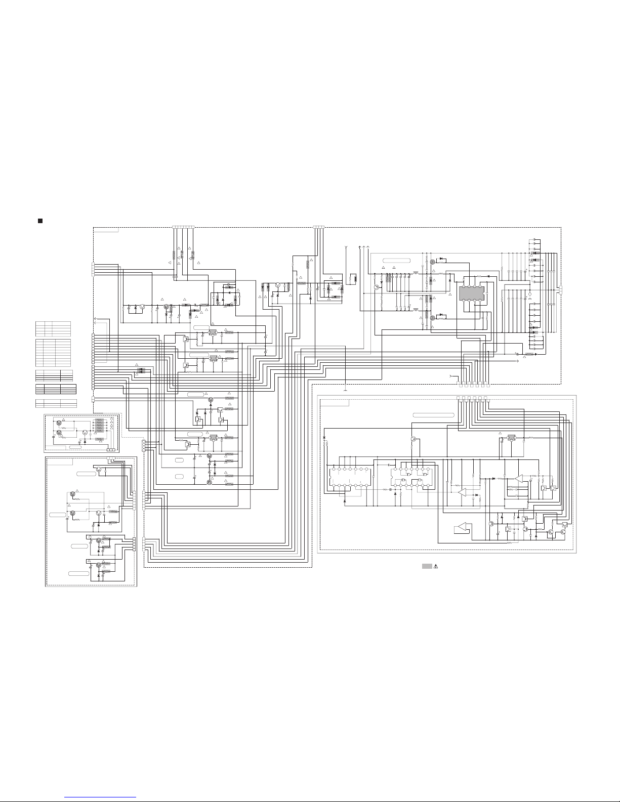
2-4
Parts are safety assurance parts.
When replacing those parts make
sure to use the specified one.
Digital power amp / Speaker terminal section
!
!
!
!
!
!
!
!
!
!
!
!
!
!
!
!
!
!
!
!
!
!
!
!
!
!
!
!
!
!
!
!
!
!
!
!
!
!
!
!
!
!
!
!
RY731
QSK0127-001
321
654
C7006
C7105
C7206
CN272
QGA3901C1-08
8
7
6
5
4
3
2
1
Q7001
KTC3875/YG/-X
Q7201
KTC3875/YG/-X
C7205
D7301
1SS133-T2
C7004
D7001
1SS133-T2
Q7301
KTC3875/YG/-X
C7303
C7005
C7008 NI
C7207 NI
RY721
QSK0127-001
321
654
C7007
NI
C7103
C7308
NI
C7208 NI
C7002
220p
C7304
UNF
R7301
47
D7201
1SS133-T2
C7003
RY711
QSK0127-001
321
654
C7107 NI
R7001
47UNF
C7202
220p
ST701
QNB0078-002
RY701
QSK0127-001
321
654
C7305
ST702
QNB0105-002
CN271
QGA3901C1-06
6
5
4
3
2
1
C7101
220p
C7302
220p
C7203
D7101
1SS133-T2
UNF
R7101
47
C7306
Q7101
KTC3875/YG/-X
C7001
220p
C7307 NI
C7204
C7301
220p
UNF
R7201
47
C7201
220p
CN208
QGF1205C1-13
123456789
101112
13
R7003
10k
1/2W
R7004
10k
1/2W
R7103
10k
1/2W
R7203
10k
1/2W
R7204
10k
1/2W
R7303
10k
1/2W
R7304
10k
1/2W
SBLout
GND
Lout
Rout
GND
SURR_RY
(1/4W)
(1/4W)
R
L
Cout
R
LVA10622-1
SB_RY
GND
SLout
SURROUND BACK
L
SURROUND
DGND
R
CENTER
FRONT
F_RY
GND
GND
(1/4W)
(1/4W)
RY12V
GND
SBRout
L
GND
C_RY
SRout
from CN218
of LVA10599-6
of LVA10600-6
*
*
*
*
*
*
*
*
*
*
*
*
*
*
R367
10k
1/2W
R262
1/4W
C265
0.001
R267
10k
1/2W
D361
NI
C365
0.001
D261
NI
R264
22
1W
D362
NI
R366
22
C370
0.001
D262
NI
R265
C352
1
L261
QQL77AK-220
22
D251
1SS244-T2
C268
1.5
Q261
D
G
S
R355
C269
0.1
R356
D351
1SS244-T2
R365
R256
Q262
D
G
S
C253
0.33
R266
22
R357
C353
0.33
C374
220/63
R257
C252
1
C271
0.1/100
R353
3.3k
C364
0.001
L361
QQL77AK-220
22
Q361
D
G
S
R253
3.3k
C272
0.1/100
R352
8.2k
C363
0.1/250
R364
22
1W
R252
8.2k
C273
220/63
Q362
D
G
S
C373
220/63
C371
0.1/100
IC251
IRS20124S-X
141312111098
7654321
C263
0.1/250
C274
220/63
IC351
IRS20124S-X
141312111098
7654321
R361
1/4W
C372
0.1/100
C369
0.1
R261
1/4W
C264
0.001
C270
0.001
R362
1/4W
C368
1.5
C873
220/63
C869
0.1
R853
3.3k
R862
1/4W
D861
NI
L861
QQL77AK-220
22
C865
0.001
R864
22
1W
R867
10k
1/2W
C863
0.1/250
D851
1SS244-T2
C872
0.1/100
C874
220/63
R861
1/4W
R857
R856
C864
0.001
C852
1
Q862
D
G
S
C870
0.001
C871
0.1/100
C868
1.5
R855
IC851
IRS20124S-X
141312111098
7654321
C853
0.33
Q861
D
G
S
R866
22
D862
NI
R852
8.2k
R865
C1352
1
C1374
220/63
R1367
10k
1/2W
C1273
220/63
C1269
0.1
C1365
0.001
R1253
3.3k
R1361
1/4W
R1262
1/4W
R1355
D1261
NI
L1261
QQL77AK-220
22
C1265
0.001
Q1362
D
G
S
R1356
R1264
22
1W
C1372
0.1/100
R1267
10k
1/2W
C1263
0.1/250
D1362
NI
D1361
NI
D1251
1SS244-T2
D1351
1SS244-T2
R1366
22
C1272
0.1/100
C1369
0.1
C1274
220/63
C1370
0.001
R1365
R1261
1/4W
IC361
IRS20124S-X
141312111098
7654321
R1257
C1373
220/63
R1256
C1264
0.001
C1252
1
C1371
0.1/100
Q1262
D
G
S
C1270
0.001
C1271
0.1/100
C1268
1.5
R1352
8.2k
R1255
R1362
1/4W
R1353
3.3k
IC261
IRS20124S-X
141312111098
7654321
C1253
0.33
Q1261
D
G
S
C1363
0.1/250
C1368
1.5
C1364
0.001
R1266
22
R1364
22
1W
L1361
QQL77AK-220
22
D1262
NI
R1357
R1252
8.2k
R1265
Q1361
D
G
SC1353
0.33
C1452
1 C1474
220/63
R1467
10k
1/2W
C473
220/63
C469
0.1
C1465
0.001
R453
3.3k
R1461
1/4W
R462
1/4W
R1455
D461
NI
L461
QQL77AK-220
22
C465
0.001
Q1462
D
G
S
R1456
R464
22
1W
C1472
0.1/100
R467
10k
1/2W
C463
0.1/250
D1462
NI
D1461
NI
D451
1SS244-T2
D1451
1SS244-T2
R1466
22
C472
0.1/100
C1469
0.1
C474
220/63
C1470
0.001
R1465
R461
1/4W
IC461
IRS20124S-X
141312111098
7654321
R457
C1473
220/63
R456
C464
0.001
C452
1
C1471
0.1/100
Q462
D
G
S
C470
0.001
C471
0.1/100
C468
1.5
R1452
8.2k
R455
R1462
1/4W
R1453
3.3k
IC451
IRS20124S-X
141312111098
7654321
C453
0.33
Q461
D
G
S
C1463
0.1/250
C1468
1.5
C1464
0.001
R466
22
R1464
22
1W
L1461
QQL77AK-220
22
D462
NI
R1457
R452
8.2k
R465
Q1461
D
G
SC1453
0.33
C251
1000p
C351
1000p
C851
1000p
C1251
1000p
C1351
1000p
C451
1000p
C1451
1000p
R251
100
R351
100
R851
100
R1251
100
R1351
100
R451
100
R1451
100
R270
100k
R370
100k
R870
100k
R1270
100k
R1370
100k
R470
100k
R1470
100k
Q284
KTA1268/GL/-T
R288
220k
C282
47/16
Q285
KTC3199/GL/-T
Q283
KTC3200/GL/-T
R286
100k
R287
3.9k
R285
47k
C283
10/50
D281
1SS133-T2
R281
10k
R282
10k
R283
0
C281
0.01
R284
22k
R255
RY300
QSK0127-001
321
65 4
D300
MA111-X
R289
100
R290
100
C266
0.001
C267
0.001
C366
0.001
C367
0.001
C866
0.001
C867
0.001
C1266
0.001
C1267
0.001
C1366
0.001
C1367
0.001
C466
0.001
C467
0.001
C1466
0.001
C1467
0.001
CN351
QGA2501C1-03
1
2
3
R30047UNF
TH271
QAD0146-103
R271 NI
AMP_+B
PGND
AMP_-B
+12V_RY
HP_RY
TH_COM
A.NFB_FL
D.NFB_FL
D.NFB_FR
A.NFB_FR
D.NFB_C
A.NFB_C
D.NFB_SL
A.NFB_SL
D.NFB_SR
A.NFB_SR
D.NFB_SBL
A.NFB_SBL
D.NFB_SBR
A.NFB_SBR
PWM_TH
FREQ_CTRL
AMP_-B+12V
AMP_-B
PGND
R291
470
UNF
R391
470
UNF
R254
R354
R854
R1254
R1354
R454
R1454
R258
4.7
R358
4.7
R858
4.7
R1258
4.7
R1358
4.7
R458
4.7
R1458
4.7
CN321
1
2
3
C250
CN322
1
2
C850
CN421
3
2
1
R216
820
R316
820
R816
820
R1216
820
R1316
820
C1250
R416
820
R1416
820
C450
R268
6.8k
R368
6.8k
R868
6.8k
R1268
6.8k
R1368
6.8k
R468
6.8k
R1468
6.8k
FW240
1
2
3
4
5
6
C254
100p
C354
100p
C854
100p
C1254
100p
C1354
100p
C454
100p
C1454
100p
CN251
6
5
4
3
2
1
CN252
8
7
6
5
4
3
2
1
C275
10/100
C1475
10/100
C475
10/100
C1375
10/100
C1275
10/100
C875
10/100
C375
10/100
R269
4.7k
R369
4.7k
R869
4.7k
R1269
4.7k
R1369
4.7k
R469
4.7k
R1469
4.7k
Q400
NI
R400
NI
DRIVER_SD
C400
NI
Q282
KRA102M-T
Q286
KRC102M-T
Q281
KRC109M-T
Q251
KTA1504/YG/-X
Q351
KTA1504/YG/-X
Q851
KTA1504/YG/-X
Q1251
KTA1504/YG/-X
Q1351
KTA1504/YG/-X
Q451
KTA1504/YG/-X
Q1451
KTA1504/YG/-X
C476
47/25
C876
47/25
C276
47/25
C277
220p
C377
220p
C877
220p
C1277
220p
C1377
220p
C477
220p
C1477
220p
CN422
1
2
3
4
C284
0.47
EP201
QNZ0136-001Z
123
EP202
QNZ0136-001Z
123
SSS_ON/OFF
C285
10/16
R275R375R875R1275R1375R475R1475
BLK_SPK701
ISET1
VCC
NC
COM
LO VCC
VS
HO
VB
LO
IN
IN
ISET1
VBDT/SD
NC
NC
NC
DT/SD
ISET2
ISET2
OCNCVS
HO
NC
OC
COM
HO
ISET1
VCC
NCIN
NC
VS
LO
VB
COM
DT/SD
ISET2
NC
OC
ISET2
NC
IN
ISET1
HO
NC
OC
VCC
ISET1
VCC
VB
HO
NC
NCIN
NC
VS
COM
LO
VB
LO
VS
COM
DT/SD
ISET2
NC
OC
DT/SD
ISET2
NC
IN
ISET1
HO
NC
OC
VCC
ISET1
VCC
VB
HO
NC
NCIN
NC
VS
COM
LO
VB
LO
VS
COM
DT/SD
ISET2
NC
OC
DT/SD
(1W)(1W)
(1W)
(1W)(1W)(1W)(1W)
Lout_HP
Rout_HP
GND
(1/4W)
FRONT_L
FRONT_R
CENTER
SURROUND_L
SURROUND_R
SURRBACK_L
SURRBACK_R
TH_COM
SSS_ON/OFF
TH1
FREQ_CTRL
PROTECT
PWM_TH
(2W)
(2W)
(1/4W)
(1/4W)
(1/4W)
(1/4W)
(1/4W)
(1/4W)
(1/4W)
N.I.
N.I.
N.I.
N.I.
LVA10578-1
*
*
*
*
*
*
*
*
*
*
*
*
*
*
J,C
B,E,EN,EV,US,A,
UF,UT,UJ,D
*MARK LIST
Q261,Q262,Q361,Q362,
Q861,Q862,Q1261,Q1262,
Q1361,Q1362,Q461,Q462,
Q1461,Q1462
2SK3770-01MR IRFB4212
*
*
*
**
**
*
*
*
*
*
*
*
R265,365,865,1265,1365,
R465,1465
N.I 22,1/2W
R275,375,875,1275,1375,
R475,1475
22,1W N.I
R261,262,361,362,861,862,
R1261,1262,1361,1362,
R461,462,1461,1462
39,1/4W 47,1/4W
R254,354,854,
R1254,1354,454,1454
220 330
R255,355
R855,1255,1355,455,1455
9.1k 6.8k
8.2k 6.8k
R256,356
R856,1256,1356,456,1456
R257,357
R857,1257,1357,457,1457
5.6k 2.4k
3.3k 2.4k
1.6k 1.3k
1.2k 1.3k
*
*
*
*
*
*
*
*
*
*
*
*
*
*
*
**
*
*
**
*
*
**
*
*
**
*
*
**
*
*
**
*
*
**
*
to CN540
of LVA10599-1
of LVA10600-1
to CN905
of LVA10599-4
of LVA10600-4
from CN311
of LVA10578-2
from CN312
of LVA10578-2
from CN411
of LVA10578-3
from CN412
of LVA10578-3
B,E,EN,EV
J,C,D,A,US,
UF,UT,UJ
C7003,7004,7103
C7203,7204,7303,7304
C7005,7006,7105
C7205,7206,7305,7306
220p470p
0.022470p
!
!
!
!
!
!
!
2-5
Master volume section
+
-
+
-
CL
INP_LEVEL
DSP_SW
SBWR_MUTE
DSP_SBL
DSP_C
DVD_SW
DVD_SR
DSP_SBR
DSP_SBL
SBWR_MUTE
DVD_SL
L
R
DSP_L
DSP_C
DSP_SL
DSP_SR
DSP_SW
DSP_R
DSP_L
DSP_R
DVD_C
DVD_SL
DVD_SW
DVD_SR
L
DSP_SBR
R
S_MUTE
DSP_SL
S_MUTE
DVD_C
DA
DSP_SR
INP_LEVEL
DA
CL
100k
R1514
C1503
0.1
CN523
1
2
47/16
C550
Q517
2SC3576-JVC-T
1k
R1515
4.7/50
C556
4.7/50
C557
0.1
C545
1k
R1504
Q512
KRA104S-X
47k
R575
R1581
100k
Q519
2SC3576-JVC-T
4.7/50
C553
10k
R1505
47/16
C536
560p
C532
10/50
C542
47/16
C549
13k
R1521
10/50
C538
100k
R1513
4.7/50
C555
100k
R1508
10k
R1506
Q515
2SC3576-JVC-T
100k
R1519
10/50
C539
10k
R1511
CN522
QGB2510K1-14
1
2
3
4
5
6
7
8
9
10
11
12
13
14
R561
1k
1k
R1510
1k
R577
4.7/50
C554
10k
R1517
Q526
2SC3576-JVC-T
4.7k
R580
C1502
0.1
IC504
NJM4565M-WE
6
5
7
8
4
10/50
C537
C1581
4.7/50
Q518
2SC3576-JVC-T
0.1C533
Q525
2SC3576-JVC-T
Q516
2SC3576-JVC-T
680p
C562
0.1C535
IC508
BD3812F
14
SBL
OUT
13
SBR
OUT
1211
D.GND
109
DA
8CL7
VCC
6
A.GND
5
VEE
4
A.GND
3
SBR
IN
2
A.GND
1
SBL
IN
Q511
KRA104S-X
100k
R1507
R1586
10k
10k
R1512
R1583
1k
10/50
C540
47/16C534
100k
R1529
1k
R1527
Q514
2SC3576-JVC-T
CN513
QGA2501F1-14
1
2
3
4
5
6
7
8
9
10
11
12
13
14
10/50
C541
R1552
5.1k
47kR574
0.1
C548
4.7k
R1526
C1551
100/16
680p
C561
R1551
20k
R1585
10k
0.1C546
1k
R1523
R1584
1k
Q1501
2SC2412K/RS/-X
10/16
C558
IC504
NJM4565M-WE
2
3
1
10
9
1kR576
R1553
10k
4.7k
R579
CN521
QJK016-091804-E
1
2
3
4
5
6
7
8
9
R562
1k
IC503
BD3813KS
1 2 3 4 5 6 7 8 9 10 11 12 13 14
15
16
17
18
19
20
21
22
23
24
25
26
27
28
2930313233343536373839404142
43
44
45
46
47
48
49
50
51
52
53
54
55
56
10k
R1524
1k
R1503
R1582
100k
C1582
4.7/50
10k
R1525
0.1C547
1k
R1509
1k
R1520
1k
R1522
100k
R1530
C1504
560p
10/50
C552
10/50
C551
22/16
C559
Q513
2SC3576-JVC-T
R1561
220
C1583
N.I.
J504
QNN0480-001
2
1
CN524
QGA2501C1-02
1
2
0.6V
0V
SBWFR OUT
0V
6.9V
-7.0V
0V
0V
0V0V
0V
0V
C
0V
0V
0V
0V
SL OUT
0.6V
R OUT
FL
0V
F.GND
0.6V
0V
0V
A.GND
0V
0V
0V
0V
0V
0V
-7.0V
0V
0V
0V
0V
0V
CL
0V
VCC
DA
0V
0V
0V
FR
0V
SL
0V
0.6V
3.0V
3.0V
3.0V
0V
0V
C OUT
A.GND
0V
0V
0V
0V
7.0V
0.6V
0V
-7.0V
0V
0V
SB.GND
A.GND
SBR
SUBWFR
D.GND
0V
L OUT
SR
0V
0V
C.GND
GND
0V
0V
S.GND
0V
0V
0V
3.0V
6.9V
0V
VEE
0V
0V
0V
0V
0V
-6.2V
0.6V
A.GND
0V
0V
A.GND
0V
0.6V
LEVEL_DET
0V
0V
0V
-6.2V
-7.0V
0V
A.GND
0V
0V
0V0V
0V
0V
0V
0V
A.GND
0V0V
0V
SR OUT
0V
LVA10599-3
0V
0V
SBL
0.6V
LVA10600-3
LVA10579-3
GND
SUBWFR
SUBWOOFER OUT
MASTER VOLUME
TO CN222 OF LVA10578-1
FROM CN683 OF LVA10602-1 FROM CN503 OF LVA10599-1/LVA10600-1
(SHEET 6/18,9/18)(SHEET 16/18)
(SHEET 4/18)
2-6
Scart section
VIDEO6
TV_YS_OUT
LC_SCLK
TV_R
LC_SCLK
TV_L
LC_CS
TV_B
TA/TC_SCL
TV_SLOW_OUT
LC_SIN
TV_LINK
TV_YS_OUT
VIDEO8
SYNCDET
SC_OUT
TV_G
TA/TC_SDA
LC_CS
TA/TC_SDA
LC_SIN
TV_G
TV_V/SY_IN
V/Y_OUT
TV_V/SY_IN
TV_B
SYNCDET
VIDEO8
SC_OUT
VIDEO6
TV_SLOW_OUT
TV_R
TV_LINK
VIDEO8
TA/TC_SCL
TV_L
V/Y_OUT
330p
C9501
62
R9509
47k
R9503
68
R9506
N.I.C9507
75
R9510
N.I.
C9508
330p/50
C9502
N.I.
C9503
470
R9501
N.I.
C9505
62
R9507
J9511
QNZ0625-001
1
2
3
4
5
6
7
8
9
10
11
12
13
14
15
16
17
18
19
20
21
68
R9505
N.I.
C9504
470/10
C9506
4.7/50
C9510
47k
R9504
75
R9508
470/10
C9509
470
R9502
IC542
MM1502XN-X
123
456
C9512
4.7/50
C9511
0.1
Q9501
KTA1267/YG/-T
Q9502
KTA1267/YG/-T
R4592
13k
Q4521
2SA1037AK/RS/-X
R4593
1.8k
C4546
100/16
L4504
10u
C4552 0.01
C4555
0.01
R4585
100
C4565
82p
C4553
0.01
L4506
6.8u
L4502
10u
C4554
100/16
C4562
0.01
C4545
12p
R4590
560
C4550
100/16
C4558
180p
R4591
390
R4586
820
C4547
0.01
R4583
1.8k
C4559
0.01
C4564
N.I.
R4584
100
Q4522
2SC2412K/RS/-X
C4557
0.0012
R4581
360
L4505
10u
R4587
390
R4580
1k
L4503
10u
L4501
22u
C4548
0.01
R4579
560
C4563
100/16
R4557
1.5k
C4549 0.01
IC551
TC90A49AP
20191817161514131211
10987654321
C4556
10p
C4561
0.01
C4544
47p
C4560
0.01
C4543
10p
R4582
1.1k
IC536
MM1502XN-X
123
456
C4574
0.01
C4598
0.01
IC537
MM1504XN-X
123
456
C4596
0.22/50
C4571
0.1
C4570
0.1
C4551 0.47
C4572
39p
C4573
39p
R5540
4.3k
C5539
560p
C5562
2.2/50
R5584
2.2K
R5541
1k
C5543
0.01
R5581
2.2k
R5537
220k
R5542
15k
C5545
390p
IC559
MM1093NF-X
161514131211109
87654321
X5505
QAX0879-001Z
C5576
0.1
C5542
6p
C5544
N.I.
R5536
390
R5582
2.2k
C5538
0.01
R5539
10k
R5585
2.2k
C5540
12p
C5541 0.022
R5583
560
R5538
10k
C5592
N.I.
R5586
560
C5560
10/50
C5561
4.7/50
C5563
4.7/50
R5534
2.2k
C5565
0.01
R5533
2.2k
R5511
6.8k
C5547
1/50
X5503
N.I.
R5527
1.3k
C5557
0.22/50
Q5504
2SC3938/QR/-X
R5505
120
R5525
560
C5583
39p
C5594
0.001
Q5505
2SA1037AK/RS/-X
R5530
1k
C5559
0.22/50
R5519
470
R5518
470
C5533
10p
R5503
560
C5501
24p
R5544
330
C5593
39p
IC538
MM1501XN-X
123
456
R5516
560
L5505
100u
R5517
560
R5507
1k
C5524
N.I.
C5551
1/50
R5509
51k
R5523
470
C5584
39p
C5566
0.1
C5567
0.1
D5501
MA111-X
C5520
0.01
C5507
33p
C5523
22p
L5501
N.I.
L5503
100u
C5534
820p
IC560
LC74761M-9894-X
302928272625242322212019181716
15 14 13 12 11 10 9 8 7 6 5 4 3 2 1
C5522
120p
R5520
4.3k
C5527
0.022
C5526
10p
C5546
470/10
C5508
0.0068
R5522
560
R5531
N.I
R5532
2k
C5531
0.01
R5508
2.7k
C5564
1/50
C5519
N.I.
C5511
0.01
L5504
2.2u
IC539
MM1504XN-X
123
456
C5516
N.I.
C5504
270p
C5532
0.01
R5515
1.5k
L5502
5.6u
R5513
220
R5521
3k
Q5501
2SA1037AK/RS/-X
R5524
330
R5535
2.2k
R5512
560
C5552
0.47/50
R9511
270
UNF
R9512
300
UNF
K4501
0
K4502
N.I.
C4595
0.22/50
Q4527
2SA1037AK/RS/-X
R4551
2.2k
R4550
2.2k
R4552
560
C9513
0.01
Q4523
2SA1037AK/RS/-X
Q4524
2SC2412K/RS/-X
Q4525
2SA1037AK/RS/-X
Q4526
2SC2412K/RS/-X
L4507
6.8u
C4567
N.I.
C4568
82P
C4566
N.I
R4556
1.5k
R4561
10k
R4560
680
R4559
2.2k
Q4530
2SC2412K/RS/-X
C4597
0.01
L4508
10u
L4509
10u
C4575
47/16
C4576
47/16
CN537
QGF1205F2-20
1 23 4 56 7 8 91011121314151617181920
D.GND
HDMI_5V
R5587
1.5k
V/Y_OUT
SC_OUT
VIDEO1
COMP_5V
VIDEO10
V.GND
9V
TA/TC_SCL
TA/TC_SDA
C5595
47/16
Q5531
2SA1037AK/RS/-X
Q5532
2SA1037AK/RS/-X
C4541
0.1
C4540
0.1
R5526
910
R9516
470
R9517
470
R4578
470
C4542
0.1
C9514
0.1
Q5510
2SC2412K/RS/-X
C5568
0.01
+5V
Q5502
2SC2412K/RS/-X
R4594
N.I.
CN539
QGF1205F2-08
12345678
C9516
330p
C9515
330p
VCC
GND
IN1
IN2
SW
OUT
A.GND
V/SY_OUT
R/SC
GND
9V
5V
SCL
VRT
SDA
VDD1
DAVRT
DAVRB
COUT
VDD4
FIL
TEST
VSS1
YOUT
BIAS
AIN
VDD3
VRB
VDD2
KILLER
CKIN
VSS2
VCC
IN1
OUTGND
SW
IN2
GND
VCCIN2
IN1
OUT
SW
VIDEO7
COMPONENT 5V
VIDEO1
IN1
GND
SYNCIN
VCOUT
XTALOUT
Vcc
IN2VCC
ANPIN
GND
Vss
VCOIN
FC
CVIN
Vss
SIN
RST
CHARA OUT
SYNCDET
PDOUT
XTALIN
ANPOUT
OUT
SW
IN2VCC
OUT
SW
Vcc
CS
IN1
VCOOUT
SCLK
CVCR
LVB10600-2(1)
FROM CN529 OFLVA10600-1
(SHEET 9/18)
FROM CN527 OFLVA10600-1
(SHEET 9/18)
2-7
Parts are safety assurance parts.
When replacing those parts make
sure to use the specified one.
Audio, Video signal input / System control section
DVD_SR
TU_CE
DVROUT_L
DSP_READY
SSS_FL
SSS_ON/OFF
FREQ_CTRL
RC_WP
LED_DIM1
VIDEO6
VIDEO7
RDSDA
VCR_R
HDMI_READY
FR_RELAY
LED_DIM1
LC_SCLK
DVROUT_R
VCR_R
T_MUTE
RDSCL
DVD_SL
PWM_DET
VIDEO4
DVD_SR
DSP_CLOCK
VIDEO3
DVD_C
DSP_STATUS
VIDEO9
HDMI_COM
VCROUT_R
FAN_ON/OFF
VIDEO3
VIDEO8
RDSCL
SSS_ON/OFF
VIDEO10
SYNCDET
VID_L
REGDET
DVR_M
SSS_SBL
VCROUT_L
BCHANGE1
DVD_C
LC_SIN
TV_L
M_COMMAND
HDMI_CLK
TU_CLK
DVR_H
SSS_LS
VCR_L
C_RELAY
VIDEO7
REGDET
DVROUT_R
SBWR_MUTE
REG_DTCT
DVROUT_L
HDMI_RESET
DVD_SW
VCR_M
HDMI_READY
VIDEO11
SLOW_L
SSS_SBR
M_STATUS
VIDEO5
SSS_FL
M_COMMAND
HDMI_CLK
SURR_RELAY
VIDEO2
VCR_H
SSS_C
VIDEO1
SBK_RELAY
VIDEO10
HP_DETECT
FAN_L
RC_SCL
TV_L
TA/TC_SCL
M_BUSY
SSS_RS
TH
TH
PROTECT
TU_DATAO
TA/TC_SDA
DVD_SW
VIDEO9
M_RESET
FREQ_CTRL
DVR_M
VCR_M
VIDEO1
TU_CLK
HDMI_STS
VIDEO8
DVR_R
M_RESET
SBWR_MUTE
BCHANGE2
VCR_H
VIDEO1
HP_RELAY
TU_DATAI
DSP_READY
DSP_STATUS
POWER_ON
BLUE_LED
DSP_RESET
DVD_SL
SURR_RELAY
FAN_ON/OFF
VIDEO1
VID_R
SBK_RELAY
DVR_H
T_MUTE
DVR_L
M_BUSY
DSP_COMMAND
VIDEO2
TA/TC_SCL
M_CLOCK
HDMI_STS
SYNCDET
TU_CE
REG_DTCT
RC_SDA
BCHANGE2
SSS_ON/OFF
SLOW_M
TV_R
HP_DETECT
VCR_L
VIDEO11
LC_CS
LC_SCLK
RDSDA
TU_DATAI
VID_R
SSS_FR
M_STATUS
VCROUT_L
BLUE_LED
PROTECT
M_CS
RC_WP
DSP_RESET
LC_SIN
PWM_DET
DVR_R
SLOW_M
VID_L
LED_DIM2
HDMI_RESET
VIDEO6
M_CS
DVR_R
VIDEO4
S_MUTE
VIDEO5
FR_RELAY
TA/TC_SDA
BCHANGE1
SSS_RS
INP_LEVEL
VCROUT_R
DVR_L
FAN_L
SLOW_L
POWER_ON
TU_DATAO
S_MUTE
C_RELAY
RC_SDA
LC_CS
DVR_L
SSS_LS
SSS_SBR
M_CLOCK
INP_LEVEL
TH
DSP_COMMAND
HP_RELAY
HDMI_COM
LED_DIM2
SSS_C
DSP_CLOCK
SSS_SBL
RC_SCL
VIDEO4
TV_R
SSS_FR
CN572
QGA2501C1-05
12345
510
R567
C8514
330p
D8501
MA111-X
3.3k
R6582
R8508
100
R8548
75
470
R6519
C8538
0.1
R588
1k
0.0056
C563
C8543
4.7/50
R8581
270
R8553
15k
R8544
75
R8551
68k
C8555
N.I.
9
R8566
47k
1k
R1556
R8585
1k
Q8511
KTC3199/GL/-T
C8569
39p
100k
R6517
1k
R8569
47k
R6503
D508
RB751V-40
C8552
N.I.
47/16
C523
10k
R1544
C8509
330p
D8504
UDZS6.2B-X
C8570
39p
C8546
4.7/50
X502
QAX0263-001Z
1.5
C528
R8534
10k
C8544
4.7/50
C571
270p
C1552
0.001
CN531
QGA2001C1-09
1
2
3
4
5
6
7
8
9
Q542
KTC3199/GL/-T
R8556
10k
R8554
27k
R8517
100k
C8556
470/10
IC572
MM1502XN-X
123
456
R1565
0
FL501
QQR1372-001
123
46
C8571
39p
CN504
QGF1036C2-05
12345
C8518
4.7/50
10k
R572
R8565
10k
C8507
330p
Q524
KTC3875/YG/-X
C8549 0.1
CN501
123456
CN502
QGB2510J1-07
1234567
R564
510
R8577
390
1k
R593
R1596
15k
CN540
QGA2001C1-06
1
2
3
4
5
6
R8586
1k
R8538
68k
R8549
22k
330
R585
R8583
10
FR
D510
MA111-X
47k
R6504
C8529
0.1
2.2/50
C530
Q503
KRA104S-X
Q8505
KTC3199/GL
Q8503
KRC102S-X
R8559
300
2SC3576
Q502
Q8524
KRC102S-X
R8509
47k
2SC3576
Q501
R589
1k
R8530
75
Q8526
KTA1267/YG/-T
C8515
330p
C8565
0.1
R8550
47k
C8522
4.7/50
R8567
10k
C8526
470/10
R1501
2.2
FR
Q510
KRC102S-X
C8554
0.001
R8520
470
20k
R1571
100k
R6518
IC507
BR24L01AF-W-X
8765
4321
R1502
2.2
FR
C8577
39p
C8545
0.047
CN503
1234567891011 12 13 14
Q8517
KTA1267/YG/
C8541
0.047
R8542
10k
C8572
0.1
R6576 10k
C568
33p
C8530
0.1
123456
R8580
47
R8507
100
R8562 220
X501
QAX0246-001Z
321
1k
R565
Q8507
KTC3199/GL/
240
R570
Q523
KRA104S-X
IC573
MM1113XF-X
8765
4321
Q8506
KTC3199/GL/-T
C8528
4.7/50
Q8504
KRC102S-X
R8523
75
470
R6506
R8588
1k
240
R569
R8524
75
C6515
330p
C8503
330p
300
R8568
IC578
MM1511XN-X
123
456
470
R6585
R8511
470
10k
R1573
Q522
2SC3576-JVC-T
C573
0.1
Q521
2SC3576-JVC-T
330p
C6518
1k
R566
R8576
300
R8564 220
J6503 QNN0476-001
6
5
C8510
330p
C8553
0.001
Q8509
KTC3199/GL/-T
C8531
0.1
J8511
1
2
3
4
5
6
7
8
9
10
11
12
13
14
15
16
17
18
19
20
21
C8535 4.7/50
47k
R6583
Q8519
KTC3203/OY/-T
C8559
N.I.
R1592 15k
R573
1k
470
R6520
IC506
IC-PST9139-T
321
C8512
330p
Q8508
KTC3199/GL/
C8523
4.7/50
C8548
0.1
R8537
47k
470
R6505
CN505
QGF1205C2-11
1234567891011
R8545
75
6.2k
R6521
C8573
0.1
330p
C6517
C597
0.1
C8539
4.7/50
560p
C522
C8566
47/25
R8575
1k
10k
R571
D507
RB751V-40
R8582
47
Q8527
KRA120S-X
R8531
68
Q8515
KRA121S-X
R8574
10k
R8539
47k
D509
MA111-X
C574
47/16
IC581
MM1503XN-X
123
456
R8519
470
330p
C6520
47/16
C524
R1567
10k
R8522
75
7.5k
R1572
Q8518
KTA1267/YG/-T
470
R6586
D505
RB751V-40
27k
R1557
D8503
UDZS11B-X
330p
C6506
D506
RB751V-40
J8512
1
2
3
4
5
6
7
8
9
10
11
12
13
14
15
16
17
18
19
20
21
R1548 N.I.
R8521
75
R8560
1k
CN555
QGA2501C1-02
12
R563
510
IC577
MM1117XF-XE
8765
4321
C567
33p
Q8523
KRA121S-X
6.8k
R595
R8510
47k
C8537
4.7/50
R8528
75
C570
560p
C8578
39p
C8521
N.I.
R8540
15k
C8532 0.1
CN552
QGA2001C1-12
1
2
3
4
5
6
7
8
9
10
11
12
CN571
QGA2501C1-03
123
IC576
MM1117XF-XE
8765
4321
4.7k
R586
C8557
N.I.
3
2
Q8529
KRA121S-X
IC574
MM1501XN-X
123
456
330p
C6516
C572
2.2/50
R1590 1k
R8532
75
100/6.3
C527
R8584
1k
0.022
C529
C8575
470/16
22k
R587
1k
R594
C8540
4.7/50
6.2k
R6522
C8519
4.7/50
J6504 QNN0690-001
3
2
6.8k
R596
C8527
N.I.
R8541
27k
R1595 15k
R8535
10k
13k
R6581
Q8516
KTA1267/YG/-T
IC580
MM1503XN-X
123
456
C8567
39p
10/25
C581
C577 0.1
330p
C6505
IC502
BD3843FS-X
242322212019181716151413
121110987654321
R598
10k
IC575
MM1501XN-X
123
456
CN551
N.I.
1
2
3
4
5
6
R8515
100
C8547
4.7/50
R1599
22k
R8555
10k
0.022
C531
R8525
68
6
5
C8525
4.7/50
Q8521
KRA121S-X
R8561
10k
C8533
0.1
R1580
15k
Q541
KTC3199/GL/-T
R1550 N.I.
R8536
22k
C8576
220p
R8512
470
R8526
75
R1549 N.I.
R8529
75
510
R568
C8517
4.7/50
R8579
270
4.7/50
C525
C8520
470/10
C578 0.1
IC571
MM1502XN-X
123
456
R8518
100k
C8516
330p
C8513
330p
1k
R1545
47k
R6584
Q8501
KRC102S-X
C8574
47/25
R8516
100
R8587
100k
10k
R1558
CN530
QGA2001C1-11
1
2
3
4
5
6
7
8
9
10
11
Q8510
KTC3199/GL/-T
0.0056
C564
R1593 15k
C8558
470/10
FL502
QQR1372-001
123
46
C8536
0.1
R8543
10k
C8504
330p
C8511
330p
R8570
10k
R8563
220
D8502
MA111-X
C8508
330p
C8564 0.1
Q8522
KTA1267/YG/-T
C8542
4.7/50
C8563
0.1
J8513 QNN0557-002
8
7
10k
R1543
R1566 N.I.
IC582
CD74HC4053NS-X
1615 14 13 12 11 10 9
87654321
R8527
75
IC505
BU1924F-X
161514131211109
87654321
R1594
15k
Q8525
KRC102S-X
C8524
4.7/50
C8568
39p
2200/6.3
C526
330p
C6519
IC579
MM1504XN-X
123
456
Q8502
KRC102S-X
C8579
39p
R8552
47k
Q8530
KTA1267/YG/-T
R8591
1k
L8501
10u
L8502
10u
C8534 4.7/50
CN527
QGF1205C2-20
1234567891011121314151617181920
C8584
39p
C8580
39p
C8581
39p
C8582
39p
C8583
39p
1
4
1
4
IC501
MN101C49KNR1
1
VREF-2S.S.S. L3S.S.S. R4S.S.S. C5S.S.S. SL6S.S.S. SR7S.S.S. SBL8S.S.S. SBR9THERMAL DETECT10VREF+11VDD12OSC213OSC114VSS15XI(GND)16XO(OPEN)17MMOD(GND)18HDMI MICOM COMMAND19HDMI MICOM STATUS20HDMI MICOM CLK21MICOM COMMAND22MICOM STATUS23MICOM CLK24MICOM RESET25MICOM CS
26
MICON
BUSY
27
SYNCDET
28
REG. DETECT
29
RDS SCL
30
INH
31
D.A. PROTECTOR
32
VDD2(FRASH)
33
RESET
34
TUNER DATA O
35
TUNER DATA I
36
TUNER CLK
37
TUNER CE
38
RDS SDA
39
DSP RESET
40
TUNER MUTE
41
VPP(FRASH)
42
LC74761 SIN/TEST TX
43
LC74761 CS/TEST RX
44
LC74761 SCLK
45
DSP COMMAND
46
DSP STATUS
47
DSP CLK
48
DSP READY
49
SUBWFR MUTE
50
SOURCE MUTE
51
VIDEO
SW1
52
VIDEO SW253VIDEO SW354VIDEO SW4
55
VIDEO SW10
56
BD3813/3842 DA
57
BD3813/3842 CL
58
VIDEO SW11
59
HP. DETECT
60
S.S.S. ON/OFF
61
CARRIER F CONT
62
D.AMP CONT1
63
GND
64
PWM DETECT
65
D.AMP CONT2
66
INPUT LEVEL 2
67
CB TEST MODE
68
SB RELAY
69
HP RELAY
70
FRONT RELAY
71
C RELAY
72
SURR RELAY
73
INPUT ATT
74
ROM CORRE WP
75
ROM CORRE SCL
76
ROM CR
SDA
77
SLOW SW
M OUT
78 SLOW SW L OUT
79 SCAR DVR H IN
80 SCART DVR M IN
81 SCART VCR H IN
82 SCART VCR M IN
83 POWER ON
84 BLUE LED
85 LED DIMMAER 1
86 LED DIMMAER 2
87 HDMI MICOM RESET
88 HDMI MICOM READY
89 FAN ON/OFF
90 INPUT LEVEL 1
91 FAN L
92 VIDEO SW9
93 TA1270/TC90A49 SCL
94 TA1270/TC90A49 SDA
95 GND
96 VIDEO SW5
97 VIDEO SW6
98 VIDEO SW7
99 VIDEO SW8
100
DAVDD
TP3
R521
10k
TP1
TP2
R501
22k
R502
47k
R503
2k
R504
47k
R5052kR506
47k
Q507
KRC111S-X
Q506
KRC111S-X
Q505
KRC111S-X
R507
2.2k
CN506
QGB1224J1-15
1
2
3
4
5
6
7
8
9
10
11
12
13
14
15
CN529
QGF1205C2-08
12345678
C6507
330p
C6508
330p
C6509
330p
C6510
330p
C6511
330p
C6512
330p
C6513
330p
C6514
330p
C8502
330p
C8501
330p
C8506
330p
C8505
330p
!
!
VCC
IN2
Vdda
RDSID
BCHANGE1
RDCL
AX
WP
V/SY OUT
SURR_RELAY
VIDEO
BCHANGE2
FOR FLASH
DVR/DVD
VCC
GND
DVD_VY
DVD C/SW
SW1
TH_COM
VDD
DVD SURR
AV COMPULINK
TEST
DVD_R/C
RESET
TV_L
DVD_YS
CIN
S2UDT
TV_R
S2SDT
VCR_L
SCLK
VCC
VCR_R
HP_RY
CV/SY
A
VCR
SCL
R/SC
REC2L
SW2
CIN
DBS_L
AC.DET.2
+12V
DBS_R
A0
DVR_L
A1
DVR_R
TU_L
A2
VIDEO C
GND
TU_R
GND
VIDEO_L
VCC
GND
VIDEO_R
AVCLINK
G
D.GND
YIN
RST
OUT
CL
C
DVD_B
NC
DA
OUT
VEE
IN2
GND
VCC
A.GND
VCCVCC
VCC
REC1L
REC1R
GND
B
REC2R
C_RELAY
L_OUT
SW
VIDEO Y
R_OUT
OUT
0V
GND
0V0V
SW
SLOW
DA
VCC
FLOUT
CL
IN1
VREF
+7V
SW
INP_LEVEL1
A.GND
-7V
IN1
L
XIN
9V
GND
VCR_R/C
R
SW1
XOUT
VCR_YS
L
D.GND
INH
VCC
GND
IN1
R
GND
+7V
OUT
-7V
Vssd
INP_LEVEL2
+12V(RELAY)
+9V
+5V(VIDEO)
5V
A+5V(DSP)
COMPONENT 5V
VEE
B+5V
FR_RELAY
RDDA
Vddd
DVD_SLOW
A.GND
OUT
DVD_G
R/SC
D+5V
IN1
D.GND
OUT
D+5V(HDMI)
SDA
MPXIN
GND
GNDIN2
+9V
BY
IN1
VIDEO L
GND
GND
VIDEO R
B
HDMI 5V
IN3
TVLIMK
IN2
DVR/DVD
GND
OUT
IN3
GND
VCR_SLOW
SW
BX
OUT
VCR_G
VCR_VOUT
VCC
Vssa
SW
VCR_VY
SBK_RELAY
GND
MODE
SW2
B
IN1
SW2
IN2
G
IN2
YS
OUT
IN1
VCC
IN2
VIDEO CV
SW
VCC
D+5V(DSP)
OUT
IN1
SW1
D+5V(DSP)
IN2
VCR_B
IN1
VIDEO
D.GND
OUT
IN2
GND
IN3
A+5V(DSP)
CY
SW
IN2
A
+7V
-7V
B
AY
V/SY IN
CX
C
VCC
GND
IN1
(FRASH)
(MASK)
+7V
-7V
LVA10600-1
FROM CN971
OF LVA10600-4
(SHEET 15/18) TO TUNER
TO CN602 OF LVA10600-6
(SHEET 14/18)
TO CN682 OF LVA10602-1
(SHEET 16/18)
TO CN513 OF LVA10600-3
(SHEET 13/18)
TO CN516 OF LVA10600-6
(SHEET 14/18)
FROM CN130 OF LVA10578-1FROM CN131 OF LVA10578-1
(SHEET 3/18)(SHEET 3/18)
FROM CN952 OF LVA10579-1
(SHEET 15/18)
TO FW240
OF LVA10578-1
(SHEET 5/18)
TO CN565
OF LVA10579-4
(SHEET 14/18)
TO CN762
OF LVA10561-1
(SHEET 17/18)
TO CN539 OF LVA10600-2
(SHEET 10/18)(SHEET 10/18)
TO CN537 OF LVA10600-2FROM CN971 OF LVA10600-4
(SHEET 15/18)
!
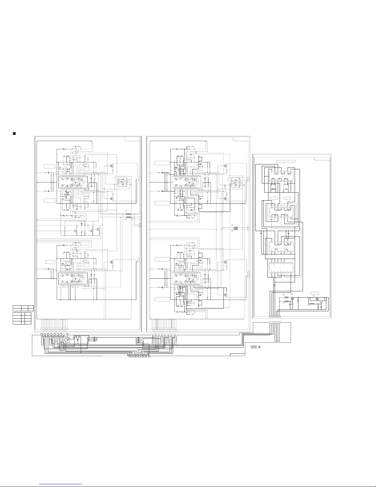
2-8
Parts are safety assurance parts.
When replacing those parts make
sure to use the specified one.
PWM modulator / Master clock section
IC211
SN74HCU04ANS-X
891011121314
7654321
R241
1M
C242
470p
C243
470p
R242
5.6k
X241
QAX0734-001
C241
0.1
R243
1M
C244
470p
C245
470p
R244
5.6k
X242
QAX0735-001
IC212
SN74HC00ANS-X
891011121314
7654321
IC213
SN74HC08NS-X
891011121314
7654321
C247
100p
C248
100p
D242
1SS133-T2
D241
1SS133-T2
R247
2.2k
R246
2.2k
C249
0.1
IC214
SN74HC74ANS-X
891011121314
7654321
C246
0.1
C341
0.1
R341
1k
R245
100
R342
2.2k
D341
UDZS2.7B-X
CN202
1234567
Q441
2SD2394/EF/
D441
MTZJ20C-T2
Q445
2SC2812N/6/-X
D442
MTZJ24B-T2
R443
680
C442
100/25
C441
100/25
D444
MTZJ11C-T2
R441
4.7
UNF
1/2W
R442
3.6k
UNF
1/2W
Q444
KTA1046/Y/
R444
1.8k
UNF
1/4W
C443
100/35
VCC
VSS
VCC
VCC
VSSVSS
1CLR
1D
1CLK
1PRE
1Q1QVSS
2Q
2Q
2PRE
2CLK
2D
2CLR
VCC
MasterClock Block
400kHz 420kHz
-B+12V-BPGND
FREQ_CTRL
+2.5V
-2.5V
M_CLOCK
-B+12V
LVA10579-7
+-+
-
+
-
+
-
+-+
+
-
+
-
+
-
+
-
+-+
-
+
-
+
-
+-+
+
-
+
-
+
-
+
-
SBR
SBL
D.NFB_SL
A.NFB_SR
A.NFB_SL
D.NFB_SR
SL
SR
S.GND
SL
SR
A.NFB_SR
D.NFB_SR
D.NFB_SBL
LIMITTER
D.NFB_SBR
A.NFB_SBR
SBR
SB.GND
M_CLOCK
SBL
A.NFB_SBL
A.NFB_SBL
S.GND
D.NFB_SBL
LIMITTER
D.NFB_SL
SB.GND
A.NFB_SL
D.NFB_SBR
A.NFB_SBR
M_CLOCK
Q1301
KTA1268/GL/-T
R1205
1.5M
R1332
100k
C1302
470p
R1215
6.8k
R1304
NI
R1234 1k
R1310
1M
R1209
10k
C1202
470p
C1210
1
R1305
1.5M
R1309
10k
C1201
10/50
C1209
100p
R1232
100k
C1308
1
R1201
1k
C1224
100/16
R1317
820
C1310
1
R1210
1M
R1202
22k
C1223
100/16
R1217
820
C1309
100p
R1214
100k
IC301
JCV8015-X
3231 30 29 28 27 26 25 24 23 22 21 20 19 18 17
16151413121110987654321
R1307
C1225
0.1
R1311
2.2k
R1233
4.7k
R1314
100k
C1204
2200p
R1207
C1226
0.1
R1334
1k
R1211
2.2k
C1332
R1315
6.8k
C1205
2200p
R1331
1k
R1333
4.7k
R1303
0
C1232
R1231
1k
C1322
1
R1203
0
C1331
100/16
R1302
22k
R1306
C1231
100/16
C1222
1
C1307
0.0022
R1204
NI
C1207
0.0022
Q1201
KTA1268/GL/-T
C1305
2200p
R1301
1k
R1206
C1208
1
C1301
10/50
C1304
2200p
Q1401
KTA1268/GL/-T
R405
1.5M
R1432
100k
C1402
470p
R415
6.8k
R1404
NI
R434 1k
R1410
1M
R409
10k
C402
470p
C410
1
R1405
1.5M
R1409
10k
C401
10/50
C409
100p
R432
100k
C1408
1
R401
1k
C424
100/16
R1417
820
C1410
1
R410
1M
R402
22k
C423
100/16
R417
820
C1409
100p
R414
100k
IC401
JCV8015-X
3231 30 29 28 27 26 25 24 23 22 21 20 19 18 17
16151413121110987654321
R1407
C425
0.1
R1411
2.2k
R433
4.7k
R1414
100k
C404
2200p
R407
C426
0.1
R1434 1k
R411
2.2k
C1432
R1415
6.8k
C405
2200p
R1431
1k
R1433
4.7k
R1403
0
C432
R431
1k
C1422
1
R403
0
C1431
100/16
R1402
22k
R1406
C431
100/16
C422
1
C1407
0.0022
R404
NI
C407
0.0022
Q401
KTA1268/GL/-T
C1405
2200p
R1401
1k
R406
C408
1
C1401
10/50
C1404
2200p
IC302
SN74LVC3G04T-X
8765
4321
C1324
0.1
C1323
1
C1423
1
C1403
10/50
R1408
100k
C403
10/50
R408
100k
C1203
10/50
R1208
100k
C1303
10/50
R1308
100k
R1319
10
UNF
1/4W
R1318
10
UNF
1/4W
CN401
QGB2510K1-16
123456789
10111213141516
CN411
QGA2501F1-03
3
2
1
R1335
10k
R1235 10k
R1435 10k
C1411
100p
C1211
100p
C1311
100p
C411
100p
R435 10k
CN413
QGA2501F1-02
1
2
C1312
NI
C1212
NI
C1412
NI
C412
NI
CN412
QGA2501F1-04
1
2
3
4
R1230 R1330
R1430
R430
C1313
100p
C1213
100p
C1413
100p
C413
100p
Reg
Thermal
Warning
Limiter
+V
Limiter
LowV&
-V
GND
Reg
Thermal
Warning
Limiter
+V
Limiter
LowV&
-V
GND
VCC
VEE
SURROUND_L
SURROUND_R
SURRBACK_L
SURRBACK_R
LVA10578-3
+7V
-7V
to CN422
of LVA10578-1
to CN423
of LVA10578-2 of LVA10578-1
to CN421
NI NI
NI
NI
*
*
*
*
** * *
****
*
*
*
*
+-+
-
+
-
+
-
+-+
+
-
+
-
+
-
+
-
+-+
-
+
-
+
-
+-+
+
-
+
-
+
-
+
-
D.NFB_C
D.NFB_FL
A.NFB_FR
LIMITTER
FL
A.NFB_FL
C
FR
FL
FR
A.NFB_FR
A.NFB_FL
PWM_TH
A.NFB_C
D.NFB_FR
F.GND
D.NFB_FR
M_CLOCK
M_CLOCK
+B_DET
LIMITTER
F.GND
PWM_TH
+B_DET
+2.5V
-2.5V
C.GND
C
D.NFB_C
D.NFB_FL
+2.5V
-2.5V
A.NFB_C
C.GND
R302
22k
R3011kC301
10/50
C302
470p
C202
470p
C201
10/50
R201
1k
R202
22k
R303
1K
R306
C305
2200p
C304
2200p
R304
1K
R305
1.5M
C307
0.0022
R310
1M
R309
10k
C308
1
C310
1
C309
100p
R314
100k
R315
6.8k
R203
1K
R204
1K
R206
R205
1.5M
R209
10k
R210
1M
R214
100k
C204
2200p
C205
2200p
C207
0.0022
C208
1
R215
6.8k
C210
1
C209
100p
C224
100/16
C223
100/16
C225
0.1
C226
0.1
R307R207
R3311kC331
100/16
R311
2.2k
R211
2.2k
R2311kC231
100/16
R221
68k
R222
22k
C227
100/16
D221
1SS133-T2
C222
1
C322
1
R334
1k
R332
100k
C332
R333
4.7k
R234 1k
R232 100k
C232
R233
4.7k
R217
820
Q301
KTA1268/GL/-T
Q201
KTA1268/GL/-T
R317
820
Q801
KTA1268/GL/-T
R832
100k
C802
470p
R804
2k
R810
1M
R805
1.5M
R809
10k
C808
1
C823
100/16
R817
820
C810
1
C824
100/16
C809
100p
IC801
JCV8015-X
3231 30 29 28 27 26 25 24 23 22 21 20 19 18 17
16151413121110987654321
R807
C826
0.1
R811
2.2k
R814
100k
C825
0.1
R834 1k
C832
R815
6.8k
R831
1k
R833
4.7k
R803
1k
C822
1
C831
100/16
R802
22k
R806
C830
1
C807
0.0022
C805
2200p
R8011kC801
10/50
C804
2200p
IC202
SN74LVC3G04T-X
8765
4321
C324
0.1
C323
1
C827
1
C303
10/50
R308
100k
C203
10/50
R208
100k
C803
10/50
R808
100k
R223
1k
Q211
KTC3875/YG/-X
Q212
NI
R318
10
UNF
1/4W
R319
10
UNF
1/4W
IC201
JCV8015-X
3231 30 29 28 27 26 25 24 23 22 21 20 19 18 17
16151413121110987654321
CN311
QGA2001F1-03
1
2
3
CN312
QGA2501F1-02
1
2
CN313
QGA2001C1-04
1
2
3
4
CN423
1
2
C311
100p
R335
10k
C211
100p
R235 10k
R835
10k
R224
15k
R225
15k
R226
NI
Q213
NI
C811
100p
C312
470p
C212
470p
C812
470p
CN301
QGB2510K1-17
123456789
10111213141516
17
R230 R330R830
C313
100p
C213
100p
C813
100p
Limiter
Reg
LowV&
Thermal
Warning
Limiter
+V
-V
GND
Reg
Thermal
Warning
Limiter
+V
Limiter
LowV&
-V
GND
FRONT_R
FRONT_L
VCC
VEE
CENTER
LVA10578-2
M_CLOCK
-7V
+7V
+7V
-7V
to CN322
of LVA10578-1 of LVA10578-1
of LVA10578-1
of LVA10578-3
to CN413
from FW323
to CN321
NI
NI
NI
*
*
*
* **
* * *
*
*
*
CN201
QGA2501C1-07
1234567
AMP_-B+12V
AMP_-B
PGND
FREQ_CTRL
BLK_CLOCK
CN402
QGB2510J1-16
123456789
10111213141516
D.NFB_SBR
A.NFB_SBR
D.NFB_SR
A.NFB_SBL
D.NFB_SBL
A.NFB_SR
A.NFB_SL
D.NFB_SL
D.NFB_C
A.NFB_C
D.NFB_FR
A.NFB_FR
A.NFB_FL
D.NFB_FL
C821
100/10
C829
100/10
PWM_TH
BLK_PWM2BLK_PWM1
Q214
KRC102M-T
D222
MTZJ16B-T2
AMP_+B
CN302
QGB2510J1-17
123456789
10111213141516
17
D211
1SS244-T2
D311
1SS244-T2
D811
1SS244-T2
CN222
QGB2510J1-14
123456789
1011121314
D1211
1SS244-T2
D1311
1SS244-T2
D411
1SS244-T2
D1411
1SS244-T2
LVA10578-1
* MARK LIST
C213,313,813,
C1213,1313,
C413,1413
B,E,EN,EV J,C,D,
US,A,UF,
UT,UJ
USE NONE
R206,306,806,
R1206,1306,
R406,1406
J,C B,E,EN,EV
US,A,UF,
UT,UJ
R207,307,807,
R1207,1307,
R407,1407
C232,332,832
C1232,1332,
C432,1432
3.3k10k
10k 18k
56p 33p
!
!
!
!
!
!
!
!
!
 Loading...