

Page 1
SERVICE MANUAL
COMPACT COMPONENT SYSTEM
MB707<Rev.002>20102SERVICE MANUAL
NX-T10E, NX-T10EN, NX-T10EV,
NX-T10UG
COPYRIGHT © 2010 Victor Company of Japan, Limited
Lead free solder used in the board (material : Sn-Ag-Cu, melting point : 219 Centigrade)
1 PRECAUTION. . . . . . . . . . . . . . . . . . . . . . . . . . . . . . . . . . . . . . . . . . . . . . . . . . . . . . . . . . . . . . . . . . . . . . . . . 1-4
2 SPECIFIC SERVICE INSTRUCTIONS . . . . . . . . . . . . . . . . . . . . . . . . . . . . . . . . . . . . . . . . . . . . . . . . . . . . . . 1-7
3 DISASSEMBLY . . . . . . . . . . . . . . . . . . . . . . . . . . . . . . . . . . . . . . . . . . . . . . . . . . . . . . . . . . . . . . . . . . . . . . . 1-7
4 ADJUSTMENT . . . . . . . . . . . . . . . . . . . . . . . . . . . . . . . . . . . . . . . . . . . . . . . . . . . . . . . . . . . . . . . . . . . . . . . 1-11
5 TROUBLESHOOTING . . . . . . . . . . . . . . . . . . . . . . . . . . . . . . . . . . . . . . . . . . . . . . . . . . . . . . . . . . . . . . . . . 1-11
COPYRIGHT © 2010 Victor Company of Japan, Limited
SP-NXT10FSP-NXT10F SP-NXT10WCA-NXT10
Except UG
TABLE OF CONTENTS
No.MB707<Rev.002>
2010/2
Page 2
SPECIFICATION
Main unit-CA-NXT10
Input/output
HDMI input HDMI IN 1, HDMI IN 2
HDMI output HDMI MONITOR OUT
USB terminal USB MEMORY REC/PLAY
Analog audio input AUDIO IN 500 mV/50 kΩ
Digital audio input DIGITAL IN (OPTICAL) -21 dBm to -15 dBm (660 nm ±30 nm)
Analog video output VIDEO OUT Color system PAL (E, EN, EV) : NTSC/PAL (UG)
VIDEO Composite video, 1 V(p-p)/75 Ω
COMPONENT Component video (interlaced/progressive)
(Y): 1 V(p-p)/75 Ω
(PB/PR): 0.7 V(p-p)/75 Ω
Tuner
FM tuning range 87.50 MHz - 108.00 MHz
Disc player
Playable disc DVD Video/CD/VCD/SVCD
CD-R/CD-RW (CD/SVCD/VCD/MP3/WMA/JPEG/MPEG-1/MPEG-2/DivX format)
DVD-R/-RW (DVD Video/DVDVR/MP3/WMA/JPEG/MPEG-1/MPEG-2/DivX format)
+R/+RW (DVD Video/MP3/WMA/JPEG/MPEG-1/MPEG-2/DivX format)
Dynamic range 80 dB
Horizontal resolution 500 lines
Wow and flutter Immeasurable
USB
Playable files MP3/WMA/JPEG/MPEG-1/MPEG-2/DivX format
CD recording format MP3
USB specification Compatible with USB 2.0 Full Speed
Compatible device Mass storage class
Compatible system FAT16, FAT32
Bus power supply DC 5 V 500 mA
HDMI
Video resolution 576p, 720p, 1080i, 1080p
Output power (HDMI MONITOR OUT) DC 5 V 55 mA
General
Mass (approx.) 2.3 kg (without the stand)
Dimensions (approx.) Placed vertically (1): 240mm, (2): 420mm, (3): 64mm, (4): 70mm, (5): 134mm
(2)
Placed horizontally (1): 420mm, (2): 70mm, (3): 240mm
Designs & specifications are subject to change without notice.
1-2 (No.MB707<Rev.002>)
(1)
(3) (4)
(5)
(1)
(2)
(3)
Page 3

Subwoofer-SP-NXT10W
Output power Front 160 W (80 W + 80 W) at 4 Ω (10% THD)
Surround 160 W (80 W + 80 W) at 4 Ω (10% THD)
Subwoofer 200 W at 6 Ω (10% THD)
Speaker Bass reflex type
16 cm cone × 1
Power handling capacity 200 W
Frequency range 42 Hz - 150 Hz
Sound pressure level 75 dB/W
Power requirements AC 230 V , 50 Hz (E, EN, EV) : AC110V - 240V , 50Hz/60Hz (UG)
Power consumption 80 W (at operation of the System) for E, EN, EV : 95W (at operation of the System) for UG
0.85 W (at standby)
Mass (approx.) 10 kg
Dimensions (approx.) 231 mm × 393 mm × 370.5 mm (W/H/D)
Speaker 1 way bass reflex type (magnetically shielded)
Front 8 cm cone × 1
Surround 5.5 cm cone × 1
Impedance 4 Ω
Power handling capacity
Frequency range Front 80 Hz - 20 kHz
Sound pressure level Front 80 dB/W
Mass (approx.) 1.3 kg each
Dimensions (approx.) 100 mm × 240 mm × 128 mm (W/H/D)
Front 80 W
Surround 80 W
Surround 125 Hz - 20 kHz
Surround 71 dB/W · m
· m
Speakers-SP-NXT10F
· m
Designs & specifications are subject to change without notice.
(No.MB707<Rev.002>)1-3
Page 4

SECTION 1
PRECAUTION
1.1 Safety Precautions
(1) This design of this product contains special hardware and
many circuits and components specially for safety purposes. For continued protection, no changes should be made
to the original design unless authorized in writing by the
manufacturer. Replacement parts must be identical to
those used in the original circuits. Services should be performed by qualified personnel only.
(2) Alterations of the design or circuitry of the product should
not be made. Any design alterations of the product should
not be made. Any design alterations or additions will void
the manufacturers warranty and will further relieve the
manufacture of responsibility for personal injury or property
damage resulting therefrom.
(3) Many electrical and mechanical parts in the products have
special safety-related characteristics. These characteristics are often not evident from visual inspection nor can the
protection afforded by them necessarily be obtained by using replacement components rated for higher voltage, wattage, etc. Replacement parts which have these special
safety characteristics are identified in the Parts List of Service Manual. Electrical components having such features
are identified by shading on the schematics and by ( ) on
the Parts List in the Service Manual. The use of a substitute
replacement which does not have the same safety characteristics as the recommended replacement parts shown in
the Parts List of Service Manual may create shock, fire, or
other hazards.
(4) The leads in the products are routed and dressed with ties,
clamps, tubings, barriers and the like to be separated from
live parts, high temperature parts, moving parts and/or
sharp edges for the prevention of electric shock and fire
hazard. When service is required, the original lead routing
and dress should be observed, and it should be confirmed
that they have been returned to normal, after reassembling.
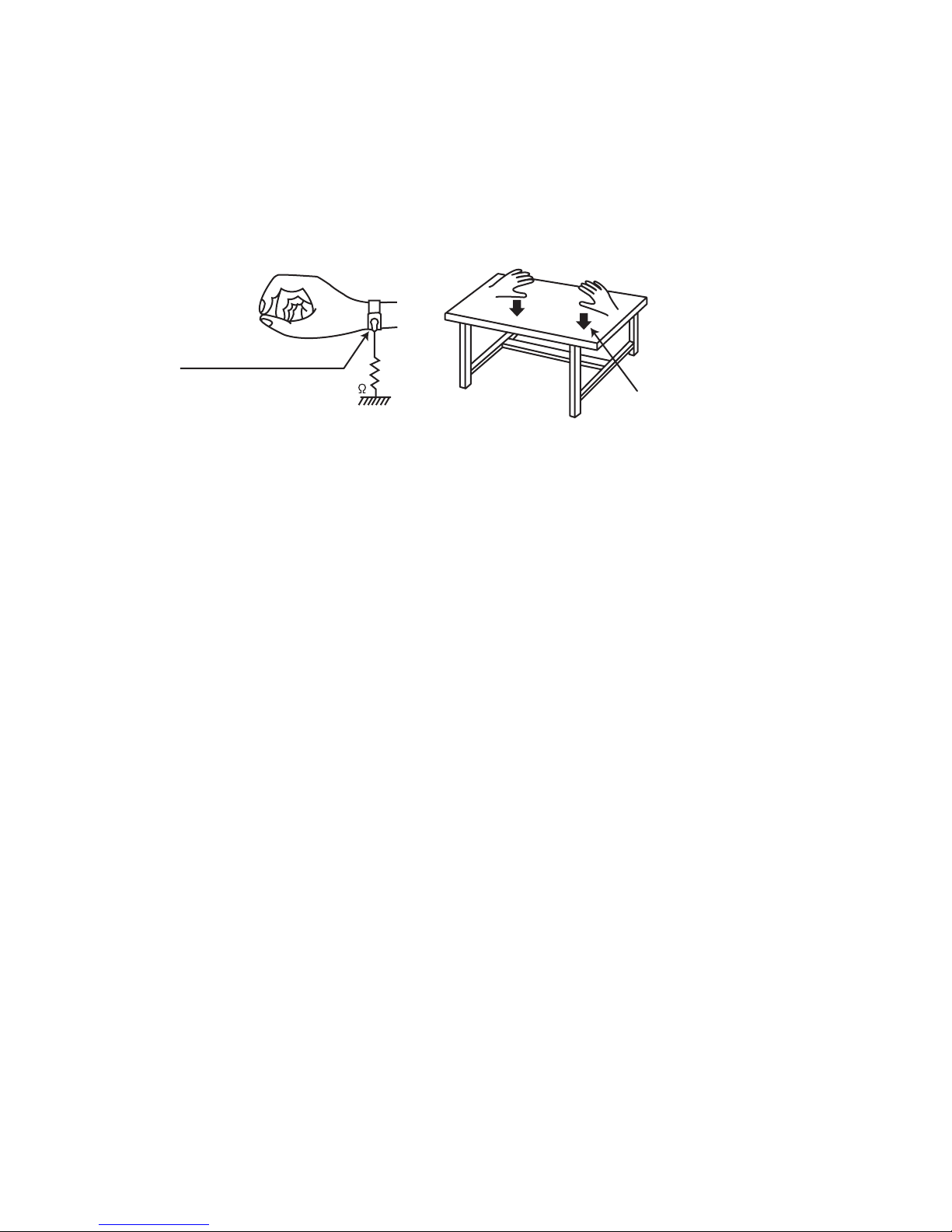
(5) Leakage shock hazard testing
After reassembling the product, always perform an isolation check on the exposed metal parts of the product (antenna terminals, knobs, metal cabinet, screw heads,
headphone jack, control shafts, etc.) to be sure the product
is safe to operate without danger of electrical shock.Do not
use a line isolation transformer during this check.
• Plug the AC line cord directly into the AC outlet. Using a
"Leakage Current Tester", measure the leakage current
from each exposed metal parts of the cabinet, particularly any exposed metal part having a return path to the
chassis, to a known good earth ground. Any leakage current must not exceed 0.5mA AC (r.m.s.).
• Alternate check method
Plug the AC line cord directly into the AC outlet. Use an
AC voltmeter having, 1,000Ω per volt or more sensitivity
in the following manner. Connect a 1,500Ω 10W resistor
paralleled by a 0.15µF AC-type capacitor between an ex-
posed metal part and a known good earth ground.
Measure the AC voltage across the resistor with the AC
voltmeter.
Move the resistor connection to each exposed metal
part, particularly any exposed metal part having a return
path to the chassis, and measure the AC voltage across
the resistor. Now, reverse the plug in the AC outlet and
repeat each measurement. Voltage measured any must
not exceed 0.75 V AC (r.m.s.). This corresponds to 0.5
mA AC (r.m.s.).
AC VOLTMETER
(Having 1000
ohms/volts,
or more sensitivity)
0.15 F AC TYPE
Place this
probe on
1500 10W
Good earth ground
1.2 Warning
(1) This equipment has been designed and manufactured to
meet international safety standards.
(2) It is the legal responsibility of the repairer to ensure that
these safety standards are maintained.
(3) Repairs must be made in accordance with the relevant
safety standards.
(4) It is essential that safety critical components are replaced
by approved parts.
(5) If mains voltage selector is provided, check setting for local
voltage.
1.3 Caution
Burrs formed during molding may be left over on some parts
of the chassis.
Therefore, pay attention to such burrs in the case of preforming repair of this system.
1.4 Critical parts for safety
In regard with component parts appearing on the silk-screen
printed side (parts side) of the PWB diagrams, the parts that are
printed over with black such as the resistor ( ), diode ( )
and ICP ( ) or identified by the " " mark nearby are critical
for safety. When replacing them, be sure to use the parts of the
same type and rating as specified by the manufacturer.
(This regulation dose not Except the J and C version)
each exposed
metal part.
1-4 (No.MB707<Rev.002>)
Page 5
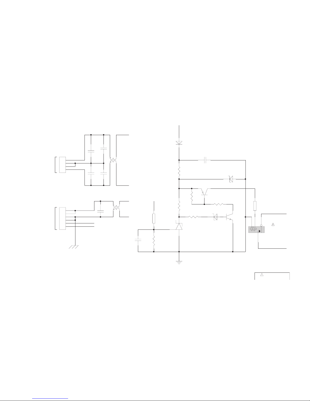
1.5 Preventing static electricity
Electrostatic discharge (ESD), which occurs when static electricity stored in the body, fabric, etc. is discharged, can destroy the laser
diode in the traverse unit (optical pickup). Take care to prevent this when performing repairs.
1.5.1 Grounding to prevent damage by static electricity
Static electricity in the work area can destroy the optical pickup (laser diode) in devices such as laser products.
Be careful to use proper grounding in the area where repairs are being performed.
(1) Ground the workbench
Ground the workbench by laying conductive material (such as a conductive sheet) or an iron plate over it before placing the
traverse unit (optical pickup) on it.
(2) Ground yourself
Use an anti-static wrist strap to release any static electricity built up in your body.
(caption)
Anti-static wrist strap
1M
Conductive material
(conductive sheet) or iron palate
(3) Handling the optical pickup
• In order to maintain quality during transport and before installation, both sides of the laser diode on the replacement optical
pickup are shorted. After replacement, return the shorted parts to their original condition.
(Refer to the text.)
• Do not use a tester to check the condition of the laser diode in the optical pickup. The tester's internal power source can easily
destroy the laser diode.
1.6 Handling the traverse unit (optical pickup)
(1) Do not subject the traverse unit (optical pickup) to strong shocks, as it is a sensitive, complex unit.
(2) Cut off the shorted part of the flexible cable using nippers, etc. after replacing the optical pickup. For specific details, refer to the
replacement procedure in the text. Remove the anti-static pin when replacing the traverse unit. Be careful not to take too long a
time when attaching it to the connector.
(3) Handle the flexible cable carefully as it may break when subjected to strong force.
(4) I t is not possible to adjust the semi-fixed resistor that adjusts the laser power. Do not turn it.
(No.MB707<Rev.002>)1-5
Page 6
1.7 Important for laser products
1.CLASS 1 LASER PRODUCT
2.CAUTION :
(For U.S.A.) Visible and/or invisible class II laser radiation
when open. Do not stare into beam.
(Others) Visible and/or invisible class 1M laser radiation
when open. Do not view directly with optical instruments.
3.CAUTION : Visible and/or invisible laser radiation when
open and inter lock failed or defeated. Avoid direct
exposure to beam.
4.CAUTION : This laser product uses visible and/or invisible
laser radiation and is equipped with safety switches which
prevent emission of radiation when the drawer is open and
the safety interlocks have failed or are defeated. It is
dangerous to defeat the safety switches.
5.CAUTION : If safety switches malfunction, the laser is able
to function.
6.CAUTION : Use of controls, adjustments or performance of
procedures other than those specified here in may result in
hazardous radiation exposure.
!
Please use enough caution not to
see the beam directly or touch it
in case of an adjustment or operation
check.
REPRODUCTION AND POSITION OF LABELS and PRINT
WARNING LABEL and PRINT
1-6 (No.MB707<Rev.002>)
Page 7
SECTION 2
SPECIFIC SERVICE INSTRUCTIONS
This service manual does not describe SPECIFIC SERVICE INSTRUCTIONS.
SECTION 3
DISASSEMBLY
3.1 Main body (Used figure were NX-T10E)
3.1.1 Removing the DVD door
(1) Connect the Main unit and Subwoofer.
(2) Power to ON and then open the DVD door.
(3) Slid to front side and pull up the DVD door.
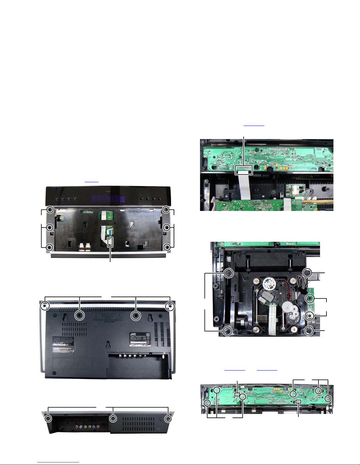
3.1.2 Removing the Top cabinet (See Fig.1, 2, 3, 4)
(1) Remove the six screws A attaching the Top cabinet. (See
Fig.1)
(2) Disconnect the card wire from DVD MPEG board connect-
ed to connector CNC5
of the Connect board. (See Fig.1)
AA
CNC5
Fig.1
(3) Remove the four screws B attaching the Top cabinet. (See
Fig.2)
(5) Disconnect the card wire from DVD MPEG board connect-
ed to connector CON401
CON401
3.1.3 Removing the DVD mechanism (See Fig.5)
(1) Remove the four screws D attaching the DVD mechanism.
(2) Remove the two screws E attaching the Connect board.
of the Display board. (See Fig.4)
Fig.4
D
B
Fig.2
(4) Remove the three screws C attaching the Top cabinet.
(See Fig.3)
C
Fig.3
D
Fig.5
3.1.4 Removing the DVD mechanism (See Fig.6)
(1) Remove the six screws F attaching the Display board.
(2) Disconnect the card wire from Key board connected to con-
nectors CON402
F
and CON403 of the Display board.
CON403
CON402
Fig.6
(No.MB707<Rev.002>)1-7
F
E
D
Page 8
3.1.5 Removing the DVD mechanism (See Fig.7, 8, 9)
(1) Remove the three screws G and one screw H attaching the
DVD MPEG board. (See Fig.7)
G H
Fig.7
(2) Disconnect the card wire from DVD MPEG board connect-
ed to connector SCON3
Fig.8)
(3) Remove the four screws J attaching the DVD MPEG
board. (See Fig.8)
(4) Disconnect the connector wire from Main board connected
to connector CN100
(5) Disconnect the connector wire from DVCC board connect-
ed to connector CON1 of the DVD MPEG board. (See
Fig.8)
(6) Disconnect the card wire from Main board connected to
connector CN2
(7) Disconnect the earth wire from Main board connected to
post pin of the Main board. (see Fig.8)
(8) Disconnect the connector wire from USB board connected
to connector CN82
(9) Disconnect the card wires from Main board connected to
connectors CN8 and CN9 of the DVD MPEG board. (See
Fig.8)
of the DVD MPEG board. (See Fig.8)
of the UP GRADE board. (See
of the DVD MPEG board. (See Fig.8)
of the DVD MPEG board. (See Fig.8)
3.1.6 Removing the USB board (See Fig.9)
(1) Disconnect the connector wire from USB board connected
to connector CON103
(2) Disconnect the card wire from Main board connected to
connector CON504
(3) Remove the two screws K attaching the USB board.
of the Main board.
of the USB board.
K
CON504
CON103
Fig.9
3.1.7 Removing the UP GRADE board (See Fig.10)
(1) Disconnect the card wire from Main board connected to
connector SCON1
(2) Remove the four screws L attaching the UP GRADE board.
of the UPGRADE board.
SCON1
L
L
GND3
CN100 CN2 CN8 CN9
CON1
J
CN82
Fig.8
SCON3
Fig.10
J
3.1.8 Removing the FM tuner module (See Fig.11, 12)
(1) Disconnect the card wire from FM tuner module connected
to connector CON603
CON603
of the Main board. (See Fig.11)
Fig.11
1-8 (No.MB707<Rev.002>)
Page 9
(2) Remove the one screw M attaching the FM tuner module.
(See Fig.12)
M
Fig.12
3.1.9 Removing the Main board (See Fig.13, 14, 15)
(1) Remove the four screws N attaching the Main board. (See
Fig.13)
3.2 Subwoofer (Used figure were SP-NXT10WE)
3.2.1 Removing the Power amp unit (See Fig.1, 2, 3)
(1) Remove the six screws A attaching the Power amp unit.
(See Fig.1)
A
N
Fig.13
(2) Disconnect the connector wire from DC motor connected to
connector MTCON1
(3) Remove the four screws P attaching the bracket. (See
Fig.14)
(4) Remove the two screws Q attaching the bracket. (See
Fig.14)
(5) Remove the three screws R and two screws S attaching
the Motor bracket. (See Fig.14)
of the Main board. (See Fig.14)
R
Q
MTCON1
(6) Remove the five screws T attaching the Main board. (See
Fig.15)
RS
Fig.14
P
P
A
Fig.1
(2) Remove the three screws B attaching the Power amp unit.
(See Fig.2)
B
Fig.2
(3) Pull out the Power amp unit for half way; disconnect the
connector wire from Subwoofer speaker connected to connector CN2
of the Power amp board. (See Fig.3)
T
Fig.15
T
CN2
Fig.3
(No.MB707<Rev.002>)1-9
Page 10
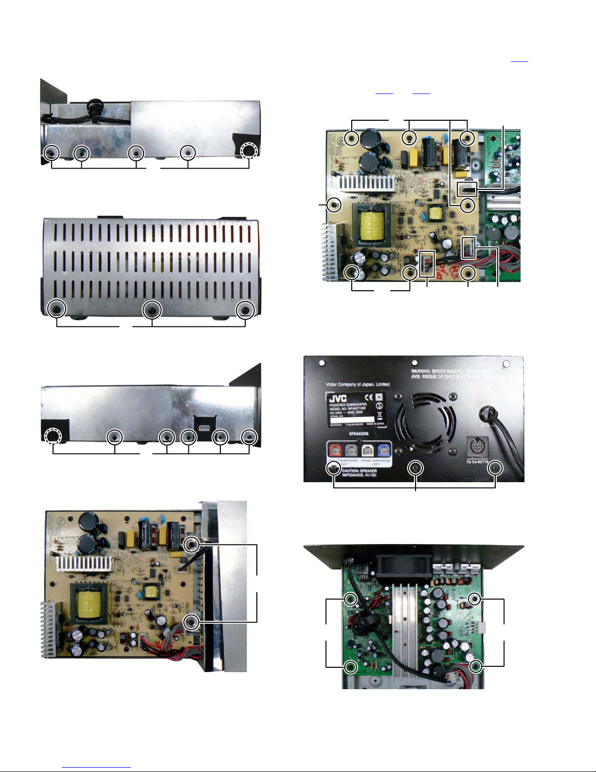
3.2.2 Removing the Power cover and Amp cover (See Fig.4,
5, 6, 7)
(1) Remove the five screws C attaching the Cover. (See Fig.4)
3.2.3 Removing the Power board (See Fig.8)
(1) Disconnect the power cord connected to connector CN1
the Power board.
(2) Disconnect the connector wires from Amp board connect-
ed to connector CN2
(3) Remove the eight screws G attaching the Power board.
and CN3 of the Power board.
of
C
Fig.4
(2) Remove the three screws D attaching the Cover. (See
Fig.5)
D
Fig.5
(3) Remove the six screws E attaching the Cover. (See Fig.6)
G
CN1
G
G
3.2.4 Removing the Amp board (See Fig.9, 10)
(1) Remove the three screws H attaching the Back plate. (See
Fig.9)
CN2 CN3
Fig.8
G
E
Fig.6
(4) Lift up the Power cover; remove the two screws F attaching
the Amp cover. (See Fig.7)
F
Fig.7
H
Fig.9
(2) Remove the four screws J attaching the Amp board. (see
Fig.10)
JJ
Fig.10
1-10 (No.MB707<Rev.002>)
Page 11

SECTION 4
ADJUSTMENT
This service manual does not describe ADJUSTMENT.
SECTION 5
TROUBLESHOOTING
This service manual does not describe TROUBLESHOOTING.
(No.MB707<Rev.002>)1-11
Page 12

Victor Company of Japan, Limited
Home Entertainment Business Division Personal AV Operation 10-1,1chome,Ohwatari-machi,Maebashi-city,371-8543,Japan
(No.MB707<Rev.002>)
Printed in Japan
VSE
Page 13
SCHEMATIC DIAGRAMS
COMPACT COMPONENT SYSTEM
NX-T10E, NX-T10EN, NX-T10EV,
NX-T10UG
DVD-ROM No.SML2009S2
Lead free solder used in the board (material : Sn-Ag-Cu, melting point : 219 Centigrade)
Contents
Block diagrams
Standard schematic diagrams
Printed circuit boards
SP-NXT10FSP-NXT10F SP-NXT10WCA-NXT10
COPYRIGHT 2010 Victor Company of Japan, Limited.
Except UG
2-1
2-2
2-18 to 22
No.MB707SCH<Rev.002>
2010/2
Page 14

In regard with component parts appearing on the silk-screen printed side (parts side) of the PWB diagrams, the
parts that are printed over with black such as the resistor ( ), diode ( ) and ICP ( ) or identified by the " "
mark nearby are critical for safety.
Page 15
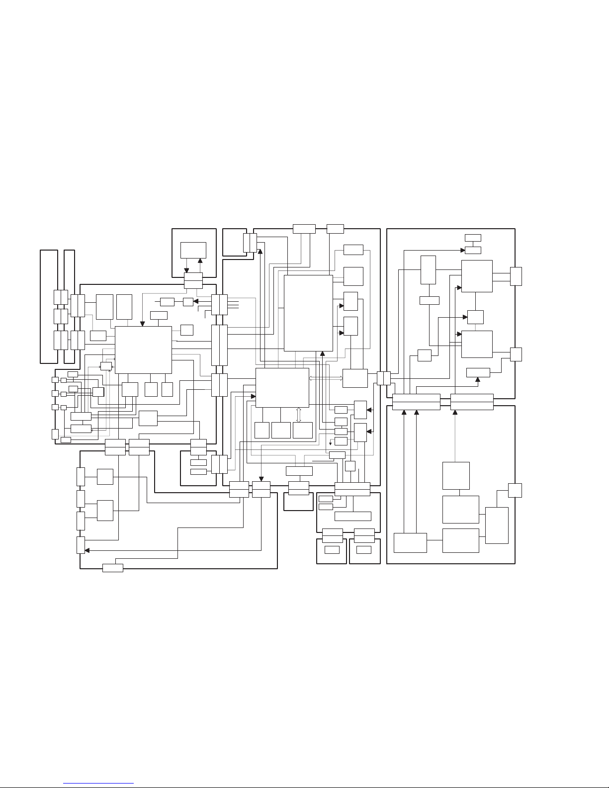
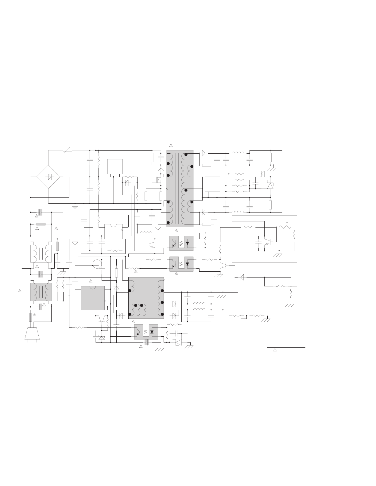
2-1
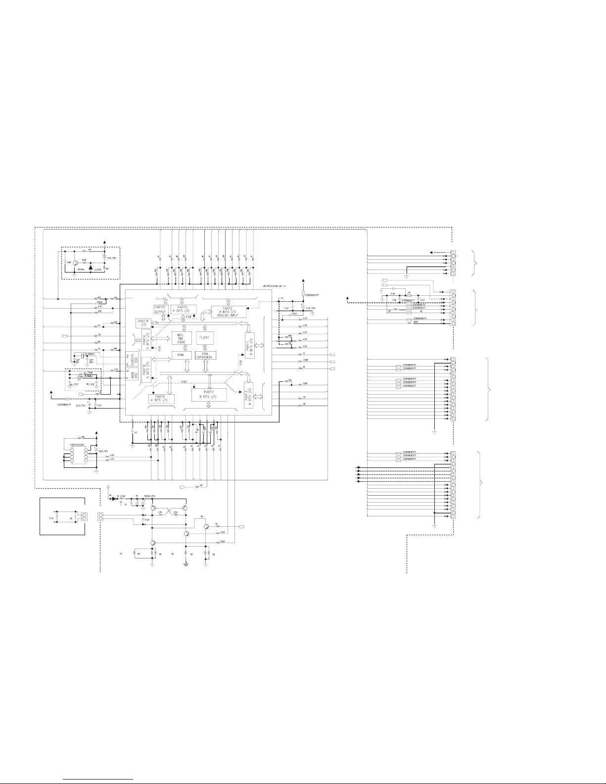
Block Diagram
D11,D12
T1
POWER TRANS
D1
DIODE BRIDGE
RECTIFIER
CN3
CN2
CN5 CN6
D7,D8
U1
SMPS CONTROLLER
AC PLUG
U601
U602
U701
IC1,IC3
HP AMP
MCU
POWER AMP
E. VOLUME
CN2
SUBWOOFER
CON501
CON602
CON401
EEPROM
X602Q601
RESET 32.768K
CON504
CN82
J102
CN1
Speaker
USB
MIC1
HEADPHONE
D+/-
+5V_USB
HP L/R
MIC1 L/R
VFD_CLK
VFD_DATA
VFD_STB
Y/Pr/Pb
U6
MPEG
U10
SDRAMU8FLASH
U7
DRIVERX127MHz
UD001
AC IN
TU L/R
TXD/RXD
TU_CLK
TU_DA
TU_RST
SMPS section
Audio Amp section
TU_DET
AMP_MUTE
VFD DISPLAY section
HP&MIC&USB section
D+/-
CN1
MIC2
MIC2 L/R
CON502
U502
MU501
SW501
VFD_MODE H/V
CON503
CN81
&LED
P1
J301
AUX IN
CON801
CON1
U801
U802
DC power supply PWB
J101
TUNER
MODULE
FM/RDS
CON201 CON103
CN101
CN102
TO NTC
TO FAN
VFD401
CON402
CON403
J2 J2
4KEY L4KEY R
IR401
IR402
IC1
IC1
MTCON1
CN7
SCON3
CNM1
MOTOR PWB
Software Upgrade PCB
SCON4
SCON2
CNC4
DVD
LOADER
MODULE
U201
DSP
U202
U203
L/R
SL/SR
HP L/R
AUX L/R
Y/Pr/Pb
CVBS
I2S
+12V
U301
U302
PWR_ON
I2C
12V
L/R
SL/SR
IC4
POWER AMP
+/- 27V
Pre_OP
I2S
DVD 5V
U204
EEPROM
U205
I2C
Q303
Q301
Touch
Touch
SUB
IC6
IC2
IC5
Q1,2,3,4,6
RX1OPT_IN
HDIM_IN1
J4
HDIM_IN2
HDIM_OUT
J2
J3
U3
U1
U4
U2
LPF
UD005
EEPROM
T2
POWER TRANS
OSC
U8
5V
IC7
Q303
Q308
U303
U304
U3,U12
CVBS
MPEG rest
UM203
I2C
DSP+MCU
SECTION
SMPS CONTROLLER
12V 12V
Adder, LPL
HLP
Switch
U2
RECTIFIER
RECTIFIER
12V 5V +/- 27V
SWITCH
I2C
LPF
LPF
Regulator
DC/DC
DC/DC
Regulator
SWITCH
SWITCH
DSP
3V3
SWITCH
D304
D306
DC/DC
D305
VFD display
IR sensor
IR sensor
ENCODER ENCODER
MTQ1/Q2/Q3/Q4/Q5
MOTOR CONTROL
+1V8 Regulator
+3V3 Regulator
Main_MCU
HDMI_MCU
+5V_DVD
U14
Regulator SWITCH
+12V_MIC
+3V3STBY
+3V3STBY
+3V3STBY
+12V_MIC
+5V2
Q24
MIC+12V
NXP_5V
Y/Pr/Pb/CVBS
RX/TX_CEC_ I2C, etc
Control Bus
DVD+HDMI Repeater Section
DRIVER
Protection
Protection
Protection
transmitter
Receiver/Selector
U12
Translator
U11
CEC
U9
MCU
IC1
Selector
SEL1/SEL2
Eeprom
Eeprom
UD004
UD006
UD006
Eeprom
IC3, U17
Selector
USB501
MJK502
MJK501
HPJ501
Connecting PCB
CNC3
CNC5
CN10CN3
CNC2
CNC1
CON603
CON102
CN8 CN100
CON101
VFD+12V
VFD-27V
VFD +5V/+5V
+3V3STBY
SCON1
CON604
CON601
CN9
U101,U102,U1
Page 16
2-2
NOTE)
With respect to risk of fire or
electrical shock.
Parts that are shaded are critical
Warning
Near D7(Detect D7
Temperature)
PC
HV
+28VA
INA
TL431
PD1
12V
TL432
INA
ECO
GND
12V
12VA
REFREF
REF
PGND
-28VA
AUX
AC1+PAC2
HV
HV
5V
PD1
HOT_GND
+
C16
470UF/35V
R44
4K7
R24 NC
R3
47K/2W
R13
2R/0.25W
CN1
AC_plug
N
L
U5
817
1
23
4
R5
0R56/2W
U3
817
1
23
4
+
C15
2200UF/35V
+
C8
1UF/50V
R32
100
+
C26
10UF/400V
R20
2K2/2W
D10
1N4148
R36
1K8
T2
EF20_NX-T10
4
3
2
18
7
6
5
P1
P2
HOT_GND
VCC +12V
+5V
GND
-33V
R29
3K3
+
C10
47UF/25V
T1 ER40_TRANSFORMER_
2
3
4
5
1
7
813
14
15
12
11
10
9
P1
P2
P3
P4
P5
HOT_GND
VCC -27VA
-27VB
PGND1
PGND2
PGND3
+27VA
+27VB
C4
471
CY3
222/250V_Y1
R11
2M/0.5W
C30
472/1KV
C29
0.1UF/275V
0.22UF/275V
+
C17
470UF/35V
R7
47
D12
1N5819
C3
R14
2R/0.25W
U1
NCP1216D65G2
1
2
3
45
6
7
8
ADJ
FB
CS
GND DRV
VCC
NC
HV
R27
10
D3
1N4007
0.22UF/275V
NTC
RT2
5R/4A
L4 10uH
R17 22/2W
D4
FR104
+
C11
1UF/50V
t
RT1
PTC 95C
12
V4
2N5551
R45
241
VD1 12VR21
L2
10UH
U4
817
1
23
4
V3
S8050
L5
10uH
+
C27
1uF/50V
V5
S8050
+
C1
330UF/200V
R16
3K3
R33 1K
VD4
15V
HS1
HEATSINK
1
2
C5
471
R31
3K3
D15
FR107
+
C14
2200UF/35V
C6
104
D11SR3100
C12
472/630V
R46
241
R15
22
R22 22K
CY4
152/250V_Y1
L3
10UH
R9
10K
F1
T4AL250V
+
C22
2200uF/25V
V2
8050
L6
40mH_0.55mm
D6
FR104
V1
SPA11N60C3
D7
UF803
+
C2
330UF/200V
C9
103
R34
3K3
U6
TL431
C20
104
HS2
HEATSINK
1
2
R48
47K/2W
U7
TL431
+
C24
100uF/16V
R23
CY2
152/250V_Y1
+
C28
10uF/50V
R10
1K
D2
FR157
R8
5K1
R25
10K
U2
ICE3B1565
1
2
3
45
6
7
8
RES
FB
S
DD
NC
VCC
GND
R4
0R51/2W
+
C7
47UF/25V
R1
2M/0.5W
D8
UF803
C13
472/630V
R28
1K
D5
1N4148
R19
2K2/2W
LF1
40mH_0.55mm
R18
22/2W
R47
3K3
R35
6K8
L1
1MH(0410)
R2
10K
+
C21
2200uF/25V
+
C23
470uF/16V
D1
KB606
+
AC1-AC
CX2
472M/1KV
NX-T10
2K2
2K2
CX1
Standard schematic diagrams
<SMPS Section 1>
Page 17
2-3
12V
AGND
+28V
PGND
-28V
5VS
ECO
+P
AC1
AC2
+28VA
-28VA
12VA
GND
AUX
0
R49
22
VD2
7.5V
+
C33
100uF/35V
+
C34
100uF/35V
R42
12K
U8
C18
104
RL1
5A/250V 12V
342
1
R38
30K
D16
FR104
R39
6K8
V6
S8550
L9
33UH
V7
S8050
CN3
TJC3-6A
1
2
3
4
5
6
C19
104
+
C32
100uF/16V
L7
33uH
CN2
TJC1-4A
1
2
3
4
C25
104
R43
10/1W
R40
100K
R41
4K7
+
C31
47UF/25V
R37
2.2M/1W
VD3
12V
TL431
To Power Amplifier Section 1
(CN6)
To Power Amplifier Section 1
(CN5)
<SMPS Section 2>
NOTE)
With respect to risk of fire or
electrical shock.
Parts that are shaded are critical
Warning
Page 18

2-4
J101-B
RCA - 214P - 02
RCA - 214P - 02
RCA - 414DB - 030
RCA - 414DB - 030
RCA - 414DB - 030
RCA - 414DB - 030
FFC 15P 1.0MM STRAIGHT
AUX_IN_L
AUX_IN_R
CVBS_OUT
Y_OUT
PB_OUT
PR_OUT
PR_OUT
PB_OUT
Y_OUT
CVBS_OUT
GND_V
GND
EEP_SEL
DOUT1
DOUTO
LRCLK
BCLK
BCLK
MCLK
MCLK
IPODR
GND_A
IPODL
FROM SUBWOOFER PWB(P1)
To DVD MPEG Section 3
(CN8)
To Power Amplifier Section 1
(P1)
To DVD MPEG Section 3
(CN100)
To DVD MPEG Section 3
(CON1)
J101-A
T62
3
4
1
2
1
2
3
4
5
6
7
8
1
2
3
4
5
6
7
8
9
10
11
12
13
14
15
D201
D202
R201
R202
D203
D204
GND_A
GND_V
GND_V
GND_V
GND_V
C202
C201
C203
C204
C104
C103
C102
C101
C331
C304
C303
C302
C320
C321
C322
D304
D305
R318
R329
R317
C330
R321
R311
Q301
Q304
R312
R319
Q303
R323
R324
PWR_ON
FB310
C334
FB311
FB308
FB309
FB313
+3V3STBY
+12V_MIC
CON103
To USB Section
(CON503)
1
1
2
2
3
4
5
6
7
8
9
T60
TV10
TV11
TV17
TV15
TV6
TV2
GND
GND
CON101
HOUSING 9P 2.0MM
2P 2.0MM 90 DEGREE
9950_RESET
9950_RESET
DVD_5V
IPOD_5V
IPOD_5V
GND
GND
+3V3STBY
+12V_MIC
+5V(CN)
+5V_DVD
TV5
+12VA
VFD+12V
+12V_MIC
TV4
DVD_PWR
+5V_DVD
Q302
TV9
VFD-27V
C323
C324
C305
C333
D307
C325
C326
D306
R316
R306
C315
R307
C318
C317
R308
D302
FB316
R309
R310
TV8
L302
W307
W308
Q308
R305
R313
Q307
3
3
3
3
3
3
4
4
4
4
5
4
TV14
C310
C306
C309
GND
W310
CABLE ASSY (W310-T0-W201)
U304
S
S
S
D
D
D
G
G
G
1
1
1
1
1
1
2
2
2
2
2
2
D303
LL4148
SS0520
SS0520 SS0520
+4V8_MCU
TV16
D311
TV13
+5V
+5V2
C5
C4
C3
GND_A
GND_A
GND_V
GND
GND
GND
C6
C2
C1
R304
D312
SS0520
FB315
TV3
TUNER+5V
VFD+5V
+3V3_DSP
+3V3STBY
C308
C307
FB314
TV12
U303
D308
D309
R333
C311
C312
C801
C803
C804
C805
C806
CON801
HOUSING 5P 2.0MM
DVD_+5V
DVD_+5V
VCC_1V9
VCC_3V3
GND-GND
GND-GND
C802
R801
R802
U801
U802
NOD
NOD
NOD
NOD
VIN
VIN
VIN
VIN
VOUT
VOUT
VOUT
VOUT
ADJ/GND
ADJ/GND
ADJ/GND
ADJ/GND
D801
D802
D803
D804
D805
SS12
SS12
SS12
SS12
1N4007
SS12
D806
C313
C327
C328
NC1
MASK
MASK
MASK MASK
NC2
NC3
NC4
R303
PWR_ON
W302
W303
W305
W306
W309
FB318
C319
C319B
C332
C319A
W301
C316
U302
SYNC
SYNC
EN
EN
IN
IN
BS
BS
SW
SW
FB
FB
COMP
COMP
GND
GND
FB317
D301
L303
L301
R320
R302
TV7
R332
C301
R322
U301
PWR_ON
7
7
2
2
1
1
3
3
3
3
2
2
2
3
3
1
1
1
2
2
1
1
3
5
5
6
644
8
8
CON102
D107
D108
D105
D106
D103
D104
D101
D102
C109
DOUT1
DOUT0
LRCLK
C110
C105
C107
R103
R101
R102
R301
FB307
FB303
FB304
FB305
FB306
FB301
FB302
C106
C335
C329
AUDIO-L-O
IPOD_L_IN
IPOD_R_IN
DSP_BUS
[4]
+12V
EEP_SEL
AUDIO-R-O
PWR_ON
AMP_MUTE
AUDIO-SL-O
AUDIO-SR-O
GND
GND
J301
GND_A
GND_A
C108
R104
C205
AUX_L
AUX_R
R205
R206
C206
T61
T4
T3
T2
T1
T5
T6
T14
T7
T8
T9
T10
TV19
T67
2
16
5109
14
13
15121187
4
3
TV1 +12V
T68
T69
T70
T65
T66
T11
TV18
J102-A
J102-B
J102-C
J102-D
<Main Section 1>
Page 19
2-5
R637
R638
C611
R639
D602
Q601
R665
C618
R666
R656
R607
R623
R657
R632
R667
R608
X601
C603
C604
R677
R675
U602
1
2
3
4
8
7
6
5
C616
C609
REGC
+4V8_MCU
+4V8_MCU
+4V8_MCU
+4V8_MCU_VDD
RESET
FLMOD
BLNK_3KEY_2
PWR_ON
BLNK_4KEY_1
EXCLK
A0
A1
A2
GND
VCC
WP
SCL
SDA
R640
R668
R627
PCL0
14
11
15
161719
20
21
22
23
242526
SDA0
P62
P63
P77
P76
P75
P74
P73
P72
P71
P70
R625
R628
R622
R629
R658
C607
C606
C605
R613
R669
R647
R636
R648
R635
R670
R671
R672
R621
STB_R/B_LED_OFF
HDMI_ON
LOAD_UP_DOWN-
LOAD_UP_DOWN+
BLINK_4KEY_2
VFD_CLK
VFD_DATA
VFD_STB
VFD_V_H_MODE
BLINK_3KEY_1
TRIANGLE_LED_1/2
MCU_B(SW)_DETECT+
MCU_A(SW)_DETECT+
MCU_LOAD_DISC-
MCU_LOAD_DISC+
MCU_DOWN(SW)_DETECT-
MCU_UP(SW)_DETECT+
R633
R626
R650
R653
R624
R603
R645
R643
R642
R644
R649
R646
R634
48
52
51
50
49
47
464544
43
42
41
40
P130
P00
P01
P02
P03
P20
P21
P22
P23
P24
P25
P26
P27
R602
R651
R601
R659
R610
R611
R612
R614
R615
R617
R618
R619
TU_RESET
HPD_TV
TRIANGLE_LED_ON
TU_I2C_DATA
TU_I2C_CLK
MCU_I2C_DATA
MCU_I2C_CLK
R641
CM1
CM2
HOUSING 2P 2.0MM
CNM1
MTCON1
2P 2.0MM 90 DEGREE
LOADER_UP_DOWN_MOTOR-
LOADER_UP_DOWN_MOTOR+
JVC NX-T10 MOTO PWB
LOADER_UP_DOWN MOTOR DRIVER CIRCUIT
MTD1
+12V_MIC
MTR14 MTEC2
MTEC1
DVD_PWR
MTQ1
3CA8550(TO-92)
3CA8550(TO-92)
SS8050(TO-92)
SS8050(TO-92)
SS8050(TO-92)
MTR1
MTR2
MTQ2
R678
MTQ3
MTR10
MTR12
MTR9
MTR4
MTR3
MTR11
GND
GND
GND
GND
MTR5 MTR7
MTR13
MTQ4
MODE_H_IN
MTQ5
T20
T59
MTC1
MTC2
2
2
2
2
2
2
2
3
3
3
3
3
1
1
1
1
1
1
1
MOTOR2
MOTOR2
MOTOR1
MOTOR1
TV21
C617
C615
FB608
9950_RESET
C602
X602
C601
R2 5
RESET
AVREF
AVREF
38
TV22
U601
+4V8_MCU
FB606
C608 C610
C619
R616
R661
R630
R680
R609
R652
R660
TUNER_NORMAL_PULSE
IR_IN
EEP_EN
9950_INT
R662
R620
R673
R674
R606
R605
R604
MPEG_CLK
MPEG_DATA
MPEG_STB
TXD
RXD
MCU-BUS
RXD
TXD
RESET
FLMDO
EXCLK
CON604
CON603
CON601
CON602
FFC 7P 1.0MM STRAIGHT
FFC 10P 1.25MM STRAIGHT
FFC 18P 1.0MM STRAIGHT
FFC 19P 1.0MM STRAIGHT
T50
T51
RXD
TXD
RESET
GND
FLMDO
EXCLK
TUNER_L
GND(CN)
TUNER_R
TU+5V
SCLK
SDIO
FROM TUNER MODULE
To UPGRADE PWB
TU_RESET(CN)
TU_I2C_CLK
TU_I2C_DATA
TU_RESET
9950_INT
9950_INT
MCU_I2C_DATA
MCU_I2C_DATA(CN)
MCU_I2C_CLK
MCU_I2C_CLK(CN)
TXD
TXD
RXD
RXD
MPEG_CLK
MPEG_CLK(CN)
MPEG_STB
MPEG_STB(CN)
MPEG_DATA
MPEG_DATA(CN)
HDMI_ON
HDMI_ON
MCU_LOAD_DISC+
MCU_LOAD_DISC+
MCU_LOAD_DISC-
MCU_LOAD_DISC-
MCU_A(SW)_DETECT+
MCU_A(SW)_DETECT+
MCU_B(SW)_DETECT+
MCU_B(SW)_DETECT+
MCU_UP(SW)_DETECT+
MCU_UP(SW)_DETECT+
MCU_DOWN(SW)_DETECT-
MCU_DOWN(SW)_DETECT-
EEP_EN
EEP_EN
HPD_TV
HPD_TV
FB607
FB609
FB610
FB611
FB612
FB613
FB614
FB615
FB604
FB618
FB603
FB602
R679
FB601
R676
C612
C614
FB605
TUNER_NORMAL_PULSE
TYU_NO_PU
T52
T53
T54
T46
T48
TV20
T63
T64
T47
T45
T15
T17
T18
T19
T21
T22
T23
T24
T25
T26
T27
T28
T31
T32
T33
T34
T35
VFD_STB(CN)
VFD_STB
VFD_CLK(CN)
VFD_CLK
VFD_DATA(CN)
VFD_DATA
VFD-27V
VFD-27V
VFD+5V
VFD+5V
VFD+12V
VFD+12V
+3V3STBY
+3V3STBY
+5V
+5V
VFD_V_H_MODE
VFD_V_H_MODE
BLINK_4KEY_1
BLINK_4KEY_1
BLINK_4KEY_2
BLINK_4KEY_2
STB_R/B_LED_OFF
STB_R/B_LED_OFF
TRIANGLE_LED_ON
TRIANGLE_LED_ON
TRIANGLE_LED_1/2
TRIANGLE_LED_1/2
BLINK_3KEY_1
BLINK_3KEY_1
BLINK_3KEY_2
BLINK_3KEY_2
IR_IN
IR_IN
T36
T37
T38
T12
T13
T41
T42
T29
T30
T43
T44
GND
GND
GND
GND
1
1
1
1
2
2
2
2
3
3
3
3
4
4
4
4
5
5
5
5
6
6
6
6
7
7
7
7
8
8
8
9
9
9
10
10
10
11
11
12
12
13
13
14
14
15
15
16
16
17
17
18
18
19
TUNER_L
TUNER_R
GND_A
GND
C7
TUNER+5V
+4V8_MCU
+4V8_MCU
AMP_MUTE
HP_DET
HP_MUTE
39
37
36
35
34
33
32
31
30
29
28
27
18
AVSS
P10
P11
P12
P13
P14
P15
P16
P17
P30
P31
P32
P33
FLMDO
P140
P41
P40
P120
VDD
VSS
8
1
3
4
6
7
9
10
2
13
12
R663
EEP_SEL
R631
C613
3
1
2
To DVD MPEG Section 3
(CN9)
To USB Section
(SCON1)
To Display Section
(CON401)
<Main Section 2>
Page 20

2-6
CNC2
1
2
3
4
5
6
7
8
9
10
11
12
13
14
15
16
17
18
19
20
21
22
23
24
24
23
22
21
20
19
18
TO LOADER
17
16
15
14
13
12
11
10
9
8
7
6
5
4
3
2
1
26
25
CNC1
25
FCS-
FCS+
TRK+
TRK-
C
D
MSW
RF
A
B
F
GND-PD
VC
VCC
E
NC3
VR-CD
VR-DVD
CD-LD
PD
NC2
NC1
DVD-LD
GND-LD
FCS-
FCS+
TRK+
TRK-
C
D
MSW
RF
A
B
F
GND-PD
RFGND2
CNC3
CNC5
CNC4
1
1
3
5
7
9
11
2
2
4
1
3
5
2
4
6
8
10
3
4
5
6
SLED+
SLED-
HOME
RFGND2
SP+
SP-
SLED+
SLED-
HOME
RFGND2
SP+
SP-
RFGND3
RFGND3
LOAD+
LOAD+
LOAD-
LOAD-
TRAYOUT
TRAYOUT
TRAYIN
TRAYIN
RFGND3
VC
VCC
E
NC3
VR-CD
VR-DVD
CD-LD
PD
NC2
NC1
DVD-LD
GND-LD
JVC NX-T10 CONNECTOR PWB
26
To DVD MPEG Section 1
(CN3)
To DVD MPEG Section 1
(CN10)
To LOADER
To LOADER
<Main Section 3>
Page 21

2-7
FB210
AGC4
DSP_BUS
C229
C228
R272
TU_I2C_CLK
TU_I2C_DATA
GND
GND
GND_A
GND_A
GND_A
C277
C239
C268
C238
C267
R210
C215
C290
C289
R274
R275
AVSS_L0
AVDD_REF
AVDD_ADC
VIP5_REF
BG_REF
BIAS_REF
AVSS_ADC
AVDD_ADC
LINE10R
LINE10L
AVSS_L1_4
1
2
2
3
3
SCL
SDA
1
W601
W701
HOUSING 3P 2.0MM
BOARD IN BOARD
R273
R217
C213
C212
R211
C705
C706
C707
C708
C714
C715
R706
R710
R711
R712
R705
R713
C721
C716
C722
C717
C718
C723
C703
C704
C719
C724
C713
C712
U701
CON701
CON202
+12VB
+12VB
+12VA
R231
C291
C257
C258
C233
C232
C235
C234
OUT2R
OUT2L
OUT2L
OUT1R
OUT1R
OUT1L
OUT1L
OUT2R
R234
R278
R226
R233
R279
R225
C249
R227
C247
C270
C269
R283
C253
C276
C272
C271
C243
C275
R237
R252
R246
R245
R222
FB201
FB203
FB204
FB205
R286
AGND
R1
R285
R284
R244
R243
C265
C266
AGC3
AGC2
AGC1
AGND
R281
R251
R254
R280
R253
R256
R255
R235
C250
R228
C254
C248
R282
U202-B
U202-A
U203-B
U203-A
R238
R236
R239
W201
CABLE ASSY
R240
+VREF
+VREF
+VREF
+VREF
+4V8_MCU
+12VA
C292
IN1
IN2
IN3
CODE2
DGND
SCL
SDA
IN4
IN5
IN6
OUT1
OUT2
OUT3
CODE1
VCC
REF
GND
OUT4
OUT5
OUT6
Q701
FB701
R701
AGND
GND_A
GND_A
GND_A
GND_A
GND_A
GND_A
GND_A
GND_A
GND_A
GND_A
GND_A
GND_A
GND_A
GND_A
GND_V
AVC1
DAGND1
DAGND
GND_DVSS
DVSSGND
VIDEOGND
GND
GND
CON201
FFC 8P 1.25MM 90DEGREE
FFC 9P 1.0MM 90DEGREE
FFC 9P 1.0MM STRAIGHT
HP_MUTE
HP_MUTE
HP_R_O
GND_A
HP_L_O
HP_DET_O
HP_DET
VFD_MODE_O
VFD_V_H_MODE
MODE_H_IN
MODE_H_IN
LOAD_UP_DOWN+
LOAD_UP_DOWN+
T58
T16
T39
T40
T55
T56
T57
GND_A
GND_A
GND_A
AUDIO-L
AUDIO-L
AUDIO_SR
AUDIO_SL
AUDIO-R
AUDIO-R
AUDIO_SL
AUDIO_SR
AUDIO-L-0
AUDIO-R-0
AUDIO_SL_0
AUDIO_SR_0
C702
C701
D701
R707
R708
R703
R704
C709
C720
C710
C711
R709
R702
R212
R213
R214
R218
R714
AVSS_ESD2
AVDD_HP2
HPOUTR
HPOUTR
AVSSHP
HPOUTL
HPOUTL
AVDD_HP1
AVDD_HP
AVDD_DAC
AVSS_DAC
DACOUT1R
DACOUT1L
DACOUT2R
DACOUT2L
LINEOUT1R
LINEOUT1L
95
1
1
1
1
1
1
1
20
19
18
17
16
15
14
13
12
11
2
2
2
2
2
2
2
3
3
3
3
3
3
3
4
4
4
4
4
4
5
5
5
5
5
5
6
6
6
6
6
6
7
7
7
7
7
7
8
8
8
8
8
8
9
9
9
10
94
93
92
91
90
89
88
87
86
85
84
83
82
81
76
75
74
73
72
71
70
69
68
X201
R207
R250
C209
C296
DVDD1
AVDD_OSC
VR_ANA
XTAL_OUT
XTAL_IN
LRCLKIN
LRCLKOUT
SCLKIN
MCLKIN
MCLKOUT
SCLKOUT
SDOUT1
SPDIF_OUT
SPDIF_IN
DVSS2
VR_DIG1
DVDD2
C210
C221
C222
C223
C230
C260
R203
LRCLK
BCLK
MCLK
R204
R264
C236
C231
C259
C293
C294
+3V3_DSP
FB202
R263
DVDD12
C299
DVSS1
+3V3_DSP
R262
DOUT0
DOUT1
R219
R220
C224
C225
SDIN3
1
100
99
98
979624
25
26
8
10
11
9
12
16
15
14
13
80
LINEOUT2R
LINEOUT2L
LINEOUT3R
LINEOUT3L
79
78
77
2
3
4
5
27
28
37
23
22
21
38
39
40
41
36
31
32
29
30
33
A0
A1
A2
GND
VCC
WP
SCL
SDA
CS
34
35
6
6
5
7
8
1
2
3
4
7
17
18
19
20
C226
C227
C240
C278
C297
TU_I2C_DATA
TU_I2C_CLK
R208
R209
I2C_SDA1
I2C_SCL1
I2C_SDA2
I2C_SCL2
GPI01
GPI02
GPI04
GPI03
R261
R664
R248
C295
R265
R221
R271
R267
256_SCL
256_SDA
R268
RESERVED4
RESERVED5
RESERVED6
RESERVED7
FB209 R258
FB207
FB206
+3V3_DSP
+3V3_DSP
R266
R269
R276
R229
R277
TU_I2C_DATA
256_SDA
R289
EXCLK
U205
1
2
3
4
5
6
7
8
1Y
1Z
2E
GND
2Y
2Z
1E
VCC
C216
+AVDD_L1
AVDD_ADC
C214
AVDD_HP
C211
GND_A
GND_A
GND_DVSS
256_SCL
TUNER_R_IN
TUNER_L_IN
C298
C245
C241
C242
C208
TUNER_L
TUNER_R
C207
C246
R230
R259
R260
R247
TU_I2C_CLK
GND_A
C255
C256
C217
AUX_L
AVSS_ESD1
AVDD_L1_1
AVSS_L1_1
AVDD_L1_2
AVSS_L1_2
AVDD_L1_3
LINEIN1L
LINEIN1R
LINEIN2L
LINEIN3L
LINEIN3R
LINEIN4L
LINEIN4R
LINEIN5L
LINEIN5R
LINEIN6L
LINEIN6R
LINEIN7L
LINEIN7R
AVSS_L1_3
LINEIN8L
LINEIN8R
AVDD_L1_4
LINEIN9L
LINEIN9R
LINEIN2R
AUX_R
TUNER_L_IN
TUNER_R_IN
IPOD_L_IN
IPOD_R_IN
C279
C280
C218
C281
C282
C219
C283
C284
C285
C286
C220
C287
C288
C261
C262
C263
C264
R241
R242
R224
R223
424344
45
46
47
48
49
50
51
52
53
54
55
565758
59
60
61
62
636465
66
67
GND_A
GND_A
GND_A
GND_A
GND_A
U204
GND_DVSS
GND_DVSS
+3V3_DSP
R249
R288
R287
VREG_EN
RESERVED1
RESERVED2
RESERVED3
DVSS3
DVDD3
RESET
SDIN1
SDIN2
SDIN3
DVSS4
DVDD4
DVSS5
VR_DIG2
MUTE
U201
<Main Section 4>
To USB Section
(CON501)
Page 22

2-8
To SMPS Section 2
(CN2)
To Main Section 1
(J301)
To SMPS Section 2
(CN3)
L41
L42
R142
R140
L12
L14
L43
L46
C134
L45
R155
C133
AUDIO-L
AUDIO-R
R120
AUDIO_SL
AUDIO_SR
CN6
CN5
+12V
FROM POWER BOARD
FROM POWER BOARD
MGND
STB+5V
PWR_EN
GND
-27V
C5
C4
R143
R39
MGND
MGND
MGND
MGND
+12V
C183C182C111
R123
R105
R103
C181
R102
C28
OSC_GNDOSC_GNDOSC_GND
OSC_GND
OSC_GND
700K OSCILLATOR
OSC_GNDOSC_GNDOSC_GND
OSC_GND
OSC_GND
OSC_GND
+5V_OSC
L13
C186
IC7
1
Z3
2
3
4
5
6
7
1A
1Y
2A
2Y
3A
3Y
GND
VCC
6A
6Y
5A
5Y
4A
4Y
14
13
12
11
10
9
8
+5V_OSC
R75
R62
R323
Q303
R319
R312
+12V
Q304
MGND
MGND
OSC_GND
MGND
STB+5V
R71
R63
R125
PWR_EN
R324
R54
C69
R10
R36
X1
2
1
C160
CN102
2-PINS HEADER, 2.5MM
Q103
R167
R152
Q104
MGND
CN101
C105
R153
R137
Q109
C106
R136
D2
R145
R150
C150
Q107
R149
C148
D4
R147
D3
D1
R109
SPK_L_+
SPK_R_+
Fan control circuit
C189
C190
C191
C192
CLOCK_1
CLOCK_2
CLOCK_3
R129
C180
C6
C3
L1
L2
C82
C7
C187
C188
+27VV
-27VV
-27VV
R41
-12VV
C39
C71
Z2
+12VV
R99
+27VV
C49
C40
Z1
+/-12V POWER
AMP +/-31VV POWER
+27V
-27V
R83
R118
C138
C137
C136C135
L44
C130
GND
GND
P1
165109141315121187432
1
2
3
4
1
2
3
4
5
6
R141
+27V
C132
C131
MGND
AMP_MUTE
PWR_EN
R111
R119
FROM SUBWOOFER TO MAIN SET
<Power Amplifier Section 1>
Page 23

2-9
AUDIO-L
C12
R97
C126
R85
1
2
3
4
IC2-A
R16
C125
C114
R87
C1
R14
-12VV
C36
+12VV
R93
R95
IC2-B
PRE_L_OUT
SUB_IN_R
+27VV
D6
R131
R132
Q7
Z4
R133
D7
R138
C184
+12V
R22
CLOCK_1
C32
C87
C27
AMP_STB
12345 6789101112
24 23 22 21 20 19 18 17 16 15 14 13
IC1
C18
C44
C41
R20
C33
C45
C46
C31
C81
C29
C8
R21
C42
C43
C9
C11
C10
R27
R26
C14
C15
C16
C17
R5
R4
SPK_SL_+
SPK_L_+
GND
R11
R15
R12
R13
R17
Q9
UNPLUG_MUTE
AMP_STB
R144
R148
R135
C80
PWR_EN
R146
C185
R134
Q5
C30
R110
Q10
R139
STB+5V
Q8
AMP_MUTE
ZD6
C13
L3
L11
C37
R25
C38
+27VV
-27VV
L/SL_CHANNEL
VSSD
VDDP2
BOOT2
OUT2
VSSP2NCSTABI
VSSP1
OUT1
BOOT1
VDDP1
PROT
VSSA2
SGND2
VDDA2
IN2M
IN2P
MODE
OSC
IN1P
IN1M
VDDA1
SGND1
VSSA1
C20
C21
R6
R7
R8
R9
C22
C23
PRE_L_OUT
PRE_SL_OUT
R28
C118
L4
L5
C24
C19
C86
C34
C26
UNPLUG_MUTE
R3
R1
8
7
6
5
R2
R122
C104
C2
<Power Amplifier Section 2>
Page 24

2-10
AUDIO-R
C116
C139
R86
IC5-A
R91
R98
C127
1
2
3
4
R92
C115
C25 C35
R19
IC5-B
R24
R23
R18
-12VV
PRE_R_OUT
C117
R96
R94
C47
C107
R121
SUB_IN_L
AUDIO_SR
C122
R117
C142
IC6-A
R100
C143
R112
1
2
3
4
R113
C121
C203
R162
C208
IC6-B
R115
R163
R164
C209
5
6
7
8
R166
R168
C210
PRE_SR_OUT
SUB_IN_SR
R169
C211
+12VV
PRE_SL_OUT
C215R176
R175
C214
R174 R165
C200
C199
C198
C197
C196
C195
C194
C193
R48
R47
C54
C58
C57
C56
VSSD
VSSA2
SGND2
VDDA2
IN2M
IN2P
MODE
OSC
IN1P
IN1M
VDDA1
SGND1
VSSA1
VSSP2
VSSP1
VDDP1
STABINCOUT2
BOOT2
VDDP2
R34
C62
C63
R33
R32
PRE_R_OUT
PRE_SR_OUT
C64
C65
R35
OUT1
BOOT1
PROT
SUB_IN_SL
R177
C216+12VV
C212 C213
R173
R172
R170
IC8-B
R171
5
6
7
8
IC8-A
R38
C145
R42
R128
C144
C128
C120
1
2
3
4
-12VV
R84
AUDIO_SL
CLOCK_2
R45
R40
AMP_STB
C75
C73
C67
C92
C68
C66C61
C91
C60
IC3
C79
C76
C83
C74
C84
C89
C51
R44
C72
C100
R46
C99
L18
+27VV
-27VV
L17
R43
L10
GND
GND
GND
GND
GND
GND
C53
L16
L15
L23
GND
2
9
1
4
3
6
5
8
7
10
CN1
C119
C177
SPK_SL_+
SPK_L_+
SPK_R_+
L25
C147
C146
123
4
123
4
123
4
123
4
C149
123456789101112
24 23 22 21 20 19 18 17 16 15 14 13
L8
C52
C55
C59
R30
R31
L9
C77
C78
C70
-12VV
VSSD
VSSD
5
6
7
8
+12VV
R29
<Power Amplifier Section 3>
Page 25

2-11
SUB_CHANNEL
R81
C101
C141
R74
C140
+12VV
R70
R72
R73
C112
R68
U101-B
AZ4558
C102
-12VV
SUB_IN_R
U102-A
C202
C205
R159
R151
C204
SUB_IN_SL
SUB_IN_SR
-12VV
R158
+12VV
C206
R154
R161
C201
C207
U102-B
R157
R156
R160
SUB_IN_L
R69
C50
R59
C158
C153
C154
C155
R52
C156
R50
R51
R53
VSSD
VDDP2
BOOT2
OUT2
OUT1
STABI
VSSP1
BOOT1
VDDP1
PROT
VSSP2
NC
VSSA2
SGND2
VDDA2
IN2M
IN1M
OSC
IN1P
VDDA1
SGND1
VSSA1
IN2P
MODE
R76
C124
R124
C110
R78
R64
R77
U1-A
AZ4558
+12VV
R82
C113
R79
R80
6
5
8
7
6
5
8
7
2
3
4
1
2
3
4
1
C109
R67
C103
R66
C108
U1-B
AZ4558
R61
R60
C48
L31
C176
R88
C175
L32
-27VV
-12VV
+27VV
R56
C169
C170
C151
R58
CLOCK_3
R55
STB+5V
PWR_EN
R107
Q2
R101
R106
Q6
Q1
Q4
R104
Q3
R108
LED2
LED1
R130
R65
C165
AMP_STB
C163
C174
C94
L6
L7
C93
C88
R89
LED1
LED2
C167
C161
C172
CN2
1
2
3
4
SUB-
SUB+
GREEN
RED
R57
C171
C85
C179
C90
C178
GND
GND
R90
R37
R49
C98
C97
C96
C95
C159
C152
C173
24 23 222120 19 18
C157
121110
987654321
C168
C162
IC4
17 16 15 14 13
C164
C166
U101-A
AZ4558
6
5
8
7
2
3
4
1
<Power Amplifier Section 4>
Page 26

2-12
CON402
D405
IR401 IR402
Upright Level
R430
Q430
D407
R436 R437
TP420
TP423
C412
R482
R487
R485
R486
U401
D404
VFD_STB
TP401
TP402
TP403
TP404
TP405
TP406
TP407
TP408
TP409
TP410
TP411
TP412
TP413
TP414
TP415
TP416
TP417
CON401
JW425
JW435
JW100
R422
JW125
VFD_STB
VFD_CLK
VFD_DATA
VFD-30V
VFD+5V
VFD+12V
+3V3STBY
+5V
GND
GND
GND
IR_IN
TP419
VFD_CLK
VFD_DATA
+3V3STBY
VFD-30V
VFD+5V
VFD+12V
C411
R483
D408
R481
R484
GND
GND
GND
GND
2Y
1A
2A
1Y
2OE
VCC
1OE/1OE
123
OUT
GND
VCC
EC403
+3V3STBY
C413
123
OUT
GND
VCC
F2
10G
RL/VFD_M
TEST_B
TEST_A
VFD_CLK/CP
VFD_STB/CS
RESET
OSC
VDD
VFL
GNDF1VDDH
VFD_DA/DA
Q1G
Q10G
11G
62
61
51
605059585756555453
52
41
30
49484746454443
42
31
20
39383736353433
32
21
20
11
10
987654321
292827262524232219181716151413
12
EC404
TP424
TP429
AC4V9_2
VFD401
JW446
R415 R414
C402
JW443
JW100
JW444
RV404
RV405
JW150
JW445
JW150
JW448
JW150
JW449
VFD_MODE
GND
VFD+12V
VFD_DATA
VFD_V_H_MODE
VFD_CLK
VFD_STB
R402
VFD-30V
Q416
C406
C401
Q415
R491
R447
R446
R479
R440
R441
C405
C410
TP428
EC402
RV401
RV402
RV403
EC410
R443
R444
R445
R448
TP418
TP427
TP434
TP426
TP425
AC4V9_1
R426
+5V
+5V_LED_V
TP430
Q410
JW413
JW402
GND
JW420
+3V3STBY
+5V
VFD+5V
VFD+12V
VFD-30V
BLED_V
IR_IN
KEY_R_MODE
JW439
JW075
JW150
JW150
JW075
JW075
JW075
JW409
JW440
JW419
JW411
JW403
JW410
JW408 JW426
JW427
JW075
JW075
JW075
JW412 JW442
JW401
JW424
JW421
JW434 JW438
JW075
JW100
JW100
JW100
JW055
JW055JW100
JW100
JW100
JW075JW125
JW125
JW125
JW125
JW125
JW125
JW075
JW428 JW405
JW432
JW436
JW429
JW422
JW431
JW430
R431
R425
R456
R427
R442
R432
R457
R439
GND
GND
Q422
TP431
Q425
Q426
Q427
JW100
VFD+5V
+5V
R480
MCU:P03
MCU:P62 MCU:P62
VFD FILAMENT AC4V9 POWER
R435
R459
C407
C403
C404
Q412
GND
Q424
Q411
Q413
Q414
BLED_V
BLED_H
BLED_V
BLED_H
LED403
LED408
GND
GND
GND
GND
+5V
EC415
D403
D402
D401
JW415
JW125
JW406
JW100
R468
R476
R406
R405
R450
D406
R404
R416
EC401
EC411
EC412
EC413
EC414
EC406
EC405
R409
Q406
R451
R429
Q423
GND
LED407
LED404
LED405
TP433 TP432
Q404
R408
R412
R418
R419
R424
GND
GND
GND
GND
GND
GND
GND
R471
GND
GND
HORIZONTAL POWER KEY LED
HORIZONTAL/VERTICAL POWER SELECT
VERTICAL POWER KEY LED
R411
R477
R475
R478
R420
Q421
Q420
Q403
Q409
GND
NC1
MASK
NC2
MASK
GND
Q407
Q402
R413
R417
JW423
JW075
JW404
JW075
JW437
JW075
JW414
JW075
JW441
JW100
JW418
JW100
JW416
JW075
JW100
STB_R/B_LED_OFF STB_R/B_LED_OFF
+5V_LED_H
BLED_H
BLED_V
BLED_V
+5V_LED_V
+5V_LED_H
LED401
RLED_H
Q408
R428
R453
R410
R474
R433
R473
R470
R421
R401
LED402
R423
R466
R458
R469R467
R452
R407
Q428
Q417
Q418
Q419
Q429
JW407
JW433
JW100
LED406
R403
R472
R434
R454
R455
Q405
BLINK_3KEY_1
MCU:P47
MCU:P21
MCU:P77
MCU:P140
MCU:P130
MCU:P120
BLINK_3KEY_2
TRIANGLE_LED_1/2
TRIANGLE_LED_ON
BLINK_4KEY_2
BLINK_4KEY_1
R460
R449
R461
R462
JW417
JW075
R464
EC407
EC408
C408
C409
EC409
Z401
AC4V9_1
VFD-30V
AC4V9_2
R465
R438
GND
Q401
Z402
JW075
JW447
JW075
TP421
TP422
1
3
3
5
5
2
2
4
1
3
5
7
9
11
13
15
17
19
2
4
6
8
10
12
14
16
18
4
1
+3V3STTBY
GND
+3V3STTBY
VFD_V_H_MODE_O
VFD_V_H_MODE
BLINK_4KEY_1
BLINK_4KEY_2
STB_R/B_LED_OFF
BLINK_4KEY_1
BLINK_4KEY_2
STB_R/B_LED_OFF
TRIANGLE_LED_ON
TRIANGLE_LED_1/2
BLINK_3KEY_1
BLINK_3KEY_2
TRIANGLE_LED_ON
TRIANGLE_LED_1/2
BLINK_3KEY_1
BLINK_3KEY_2
KEY_R_MODE
FFC 5P 1.0MM STRAIGHT
FROM KEY PWB
FROM KEY PWB
CON403
FFC 5P 1.0MM STRAIGHT
To Main Section 2
(CON602)
<Display Section>
Page 27

2-13
C2
STANBY+3.3VL
STANBY+3.3VL
KEY_L4 KEY_L3 KEY_L2 KEY_L1
R32
IC1
IC1
VCC
1
2
3
4
5
1
2
3
4
5
6
7
14
T3
T1 T2
R39
C1
C5
R41
R7
R38C4 C3
R6
R8
R5
COM1
H_V
GND
GND GND GND GND GND
T4
13
12
11
10
9
8
P1.0/TACLK
XIN/P2.6/TA1
XOUT/P2.7
RST/NMI/SBWTD
P1.7/CAOUT/CA7
P1.6/TA1/CA6
TEST/SBWTCK
P1.1/TA0
P1.2/TA1
P1.3/CAOUT
P1.4/SMCLK
P1.5/TA0/CA5
VSS
R31
R33
R1
H_V
COM1
GND
R2
R3
R4
L1
J2
J2
KEY_L1
KEY_L2
KEY_L3
KEY_L4
L2
L3
L4
L1
L2
L3
L4
TP18
D509
D510
FB503
FB501
FB502
R523
R516
R517
C511
C520
C525
R554
P+5V
123
456
C514
C516
R514
R521 R520
R513
R512
R546
C515
R511
GND_HP
GND_HP
D512
C522
R549
R502
R501
C519
C517
D511
Q502
Q509
VCC GND
VMGND
JW175
JW502
JW506
JW501
JW503
CON501
SCON3
SCON1
MODE_H_OUT
1
2
4
6
8
3
5
7
NC1
MASK
NC2
1
3
5
7
2
4
6
8
7
5
3
1
1
2
3
4
5
6
7
6
4
2
7
5
3
1
8
6
4
2
SCON4
SCON2
MASK
MODE_H_IN
VFD_MODE
HP_DET
GND_HP
HP_R
HP_MUTE
HP_L
JW505
JW504
JW175
JW125
JW200
TP1
TP2
TP3
TP4
TP5
TP6
TP7
TP25
ESDGND_MIC2
GND_HP
U502
OUT2
GND_HP
JW507
JW125
OUT1
IN2
IN1
BIAS MUTE
R552
R553
R542
R548
SW501
L501
FB504
R515
GND_HP
GND_HP
C513
R503
C523
Q501
GND_HP
R518
MR509
MR503
MR505
MR501
MC511
MC515
R545
R543
Q507
D516
C524
MU501-A
MIC_IN_1
MIC_+12V
MC509
MC513
MC507
MIC_GND
MIC_DET1
MIC_GND
MIC_IN1
W502
MIC_GND
GND_HP
R519
R544
Q508
R539
D502
MD501
MFB501
MFB503
MD507
MD505
MD502
R541
MD504
MD508
MD506
W503
MC519
MD503
TP20
TP21
TP23
TP24
USB_CASE
USB501
6
1
2
3
4
5
VCC
GND
D-
D+
W506
TP28
TP29
L502
MFB502
MFB504
MC502
MC504
MC506
MIC_IN2
MIC_IN2
P+5V
MC510
MC508
MIC_DET2
MIC_GND
MJW502
JW225
MJW501
MR510
JW125
W505
R525
R526
R551
R538
RS501
RS502
RV501
W507
GND_HP
USB_GND
ESDGND_HP
CAPE ELECT HIGH <=6.0MM
R547
R550
R530
R529 R505
C509
D513
Q505
Q506
R531
R533
W504
JW509
F501
JW150
JW508
JW075
R532
R535
R534
R536
C507
P+5V
USB_CASE
USB_GND
USB_+5V
CON503
CON502
CON504
P+5V
C508
MC516
MC512
MR506
MR507
MR502
MR508
MR511
MC505
P+5V
MR504
MU501-B
MIC_IN_2
MC514
MIC_+12V
MIC_GND
MC521
MC518
MC517
MIC_GND
TP26
TP27
TP14
TP16
TP15
D+D-_CONNECT
OPT_IN
CP1
RX1
OUT
1
2
1
2
3
3
7
5
3
1
6
4
2
2
1
1
2
3
GND
VCC
OPT_GND
OPT_VCC
MIC_GND
MIC_GND
MIC_+12V
MIC_IN_2(CN)
MIC_IN_1(CN)
MIC_DET2(CN)
MIC_DET1(CN)
TP13
TP17
TP12
TP11
TP10
TP9
TP8
R537
FB508
R509R510
MIC_+12V
USB_GND
GND_HP
D514
D515
FB509
MFB506
MIC_IN_2
MIC_IN_1
MIC_DET2
MIC_DET1
MFB507
MFB508
MFB505
FB510
R506
RV502
Q504
Q503
MC520
7
6
2
1
3
5
4
7
6
2
1
3
5
4
7
6
2
1
3
5
4
TP22
R540
MJK501
MIC1 JACK
MJK502
MIC2 JACK
ESDGND_MIC1
ESDGND_MIC2
TP19
HPJ501
HEADPHONE JACK
ESDGND_HP
D503
D501
D504
R504
W501
MIC_IN1
MC503MC501
C521
R522
C503
C512
C504C502
C501
R524
To Main Section 4
(CON201)
To DVD MPEG Section 3
(CN82)
To Main Section 1
(CON103)
To DVD MPEG Section 3
(CN2)
To Main Section 2
(CON604)
To DVD MPEG Section 4
(CN7)
<Key Section>
<USB Section>
Page 28

2-14
FROM CONNECT BD (LOADER SIGNAL)
SERVO SECTION
MOTOR SECTION
FLASH
Close to connector
CN3
1
1
1
1111
1
TP53
TP54
TP52
VREF1 BC16
Q17
Q18
BC26
TP60
TP61
TP63
R64
R61
R62
Q16
R106
R98
R100
BC18
R117
R99
R101
R102
R108
R238
R237
C67
C68
R115
R116
R034
R255 R256
R166
R285
R033
R383
R112
R113
R193
BC53 BC54
BC7
UD005
IC1
BC74BC61BC67BC78
BC9BC1BC83BC82
EC34
BC21
EC30
BC24
R147
R148
C151
RN2
RN3
RN4
RN5
R239
EC43
BC44 BC47 BC43 BC46
C85 C138
EC23
BC20
EC18
BC19
EC15
BC17
BC71
BC76 BC79 BC73 BC77 BC40
BC69
BC60
BC59
BC75
EC53
EEPROM
TRAY_IN/OUT CONTROL
RESET
UART DEBUG
Close to 8203H
Close to 8203H
Close to 8203H
TO CONNECT BD (LOADER CONTROL)
TRAY IN/OUT FOR MCU/8203 DETECT
Close to 8203H
SDRAM
FROM USB BOARD J6 RX179AT
R114
R090
R124
R125
R139
R052
R009
R253
R254
R159
BC56
BC55
R227
R157
DVCC3+
R156
R160
TP15
RESET
R162
R161
CN6
+5AV
GND
GND
M+5V
VREF2
U7
BC36
BC25
R134
RFGND
RFGND
M+5V
U15
RFGND
RFGND
GND
R135
CN10
R133
R27
EC42
U8
BC90
BC42
R109
C140
R198
R138
R143
R146
R142
GND
GND
L21
SPI_VCC3
DVCC3+
SPI_VCC3
BC39 BC38
C70
R
197
X1
C69
BC48 BC62
R154
C91
C122
R153
EC7C45
DVCC3
Q24
EC11
C57
R155
IPOD+5V
EC14
EC17
UM203
LOAD+/- TO SLOT MECH
1
VCC
AOUT
BOUT
GND
AIN
BIN
GND
NC
2
3
4
8
7
6
5
R164
R163
R165
R195
C52 C54 C53 C55
R283
R127
BC65
BC92
C42
L16
C12
L2
R177
R176
R178
R179
R180
EC52
VGND
VGND
VGND VGND
VVCC3
VIDEO DAC USES FULL CURRENT MODE
C41
C40
C11
C7
C16
L4
VGND
C15
C14
C4
L1
VGND
C2
C1
R129
R136
R121
R122
R287 R288
R286
R289
R53
Q19
D5
Q20
D6
R118
R119
R111
PUH_CDLD
PUHRF
PUH_DVDLD
DVDLDO
LDSW
FGIN
PUH_DVDLD
PUH_CDLD
CDLDO
HOME
LDSW
D
C
B
A
F
E
1
2
3
4
5
6
7
8
9
10
11
12
13
14
15
16
17
18
19
20
21
22
23
24
25
26
27
28
29
30
31
32
33
34
35
36
37
38
39
40
41
42
43
44
45
46
47
48
49
50
52
53
54
51
162
161
160
159
158
157
156
155
154
153
152
151
150
149
148
147
146
145
144
143
142
141
140
139
138
137
136
135
134
133
132
131
130
129
128
127
126
125
124
123
122
121
120
119
118
117
116
115
114
113
111
110
109
112
M_A3
M_A2
M_A1
M_A0
M_A10
M_BA1
M_BA0
M_CS0
M_RAS
M_CAS
M_DQM0
M_A4
M_A5
M_WE
CDLDO
DVDLDO
FCO
TCO
SCO
SPDCO
USB_DP
USB_DM
CP
GND
Close to 8203H Pin 27
near 8203 Pin171/178
USB_GND
MPEG_CLK
MPEG_DATA
MIC_DET1
MIC_DET2
TRAY+
LOAD+
LOAD-
TRAY-
MCU_LOAD_DISK+
MPEG_RESET
USB_GND
UA0_TX
CLKIN
DMEA
TCO
SCO
VINFC
CFCERR1
CFCERR2
VINSP
VNFFC
FWD
REV
VCC1
GND2
VOLDVOLD+
VOSPVOSP+
VOFCVOFC+
STBY
BIAS
VINTK
CTKERR1
CTKERR2
VINSL
RREGND
VCTL
GND1
VNFTK
VCC2
VOSL-
VOSL+
VOTK-
VOTL+
21
20
19
18
17
16
15
28
27
26
25
24
23
22
1
2
3
8
9
10
11
12
13
14
4
5
6
7
2930
SLED+
SPI_CS
CE_B
DQ0
WP#
GND
1
2
3
4
8
7
6
5
VDD
SPI_HOLD
SPI_HOLD
SPI_WP
DQ0
DQ0
M_A0
M_A1
M_A2
M_A3
M_A4
M_A5
M_A6
M_A7
M_A8
M_A9
M_A10
M_A11
M_DQM0
M_DQM1
M_WE
MD0
M_CLK
RAM_CLK
M_D2
MD3
MD1
MD2
MD0
MD6
IPOD_RESET
MPEG_I2C_DATA
2019181716
1514131211
MPEG_I2C_CLK
MD4
MD9
MD11
MD13
MD15
MD7
MD5
MD8
MD10
MD12
MD14
M_D0
M_D3
M_D1
M_D7
M_D5
M_D8
M_D10
M_D12
M_D14
M_D6
M_D4
M_D9
M_D11
M_D13
M_D15
M_CKE
GND
GND
GND
R103
R104
BC45
BC41
DVCC3
IC2
6
7
8
9
1
2
3
4
5
10
MCKE
MD1
MD2
MD3
MD4
MD5
MD6
MD7
MD8
MD9
MD10
MD11
MD12
MD13
MD14
MD15
SD_VCC3
2
4
5
7
8
10
11
13
42
44
45
47
48
50
51
53
36
40
28
41
54
1
14
27
3
9
43
49
M_CAS
M_RAS
M_CS0
D0
D1
D2
D3
D4
D5
D6
D7
D8
D9
D10
D11
D12
D13
D14
D15
NC
NC/RFU
A0
A1
A2
A3
A4
A5
A6
A7
A8
A9
23
24
25
26
29
30
31
32
33
34
22
35
15
39
16
17
18
19
37
38
20
12
46
52
24
6
A10/AP
A11
LDQM
UDQM
VE
CAS
RAS
CS
VSS
VSS
VSS
VDD
CKE
CLK
BA0
BA1
VDD
VDD
VDDQ
VDDQ
VDDQ
VDDQ
VSSQ
VSSQ
VSSQ
VSSQ
MCKE
RAM_CLK
M_BA0
M_BA1
DQ1
DQ1
GND
U10
GND
GND GND
GND
SPI_D0
SPI_D1
SPI_CLK_F
SPI_CLK_F SPI_CLK
DQ1
HOLD#
SCK
DQ1
CE#
DOUT
WP#
GND
1
2
3
4
8
7
6
5
VDD
HOLD#
SCK
DIN
SPI_WP
DQ0
SLEDRADRAD+
CLKOUT
NEAR IC PIN
SPDCO
FCO
SP-
SLED+
T42
1
1
3
5
7
9
2
4
6
8
10
11
1
1
1
1
1
1
1
1
1
1
T43
T44
T45
T46
T47
T48
T49
T50
T51
T52
SLED-
HOME
LOAD+
LOAD-
B(SW)_DETECT+
A(SW)_DETECT+
SP+
SP-
SP+
XOPVIP
XOPVIN
FOCFOC+
RFGND
M+5V
1
2
3
4
1
2
3
4
UA0_RX
GND
D8
MCU_LOAD_DISK-
MPEG_STB
IR_IN
DVDMDI
CDLDO
DVDLDO
RF_APC_AVSS
U6
DVDMDI
CDMDI
V21
SRV_AVDD
APC_AVDD
V165
RF3_3V
RFGND
VREF1
VREF2
VRT
VRB
VCM
VRT
VRB
VCM
SCH_AD18
SRV_DA_AVSS
DATE0
DAFE0
DA_AVDD
SC1_OUT_GPIO
SC_OUT_GPIO
SPDC_OUT_GPIO
TRAY_OUT_GPIO
STEP_OUT_GPIO
TRAY_IS_IN_GPIO
FGIN/GPIO
DMEA/GPIO
TRAY_IS_OUT_GPIO
CP
VSS_PLL
VDD_PLL
CLKOUT
CLKIN
REXT
AVDDRX
AVSSRX
DM
AVDDTX
AVDDTX
DP
VSS
SPI_CS_B
SPI_D2/GPIO
SPI_D0
VDD18
SPI_D1/GPIO
SPI_CLK
SPI_D3/GPIO
SD_CMD/MS_BS
SD_D1/MS_D1
SD_D0/MS_D0
RST_B
SD_D2/MS_D2
SD_D3/MS_D3
SD_CLK/MS_CLK
CARD_SENSE1
AU_PWM2A
AU_PWM1B
AU_PWM1A
AU_PWM2B
AU_PWM2B
J7
PWM_VDD33
J8
AU_PWM3A
CVBS_OUT
R_V_OUT CR_C_R_OUT CB_V_B_OUT
Y_Y_G_OUT
G_Y_OUT
B_U_OUT
CVBS_OUT
G_Y_OUT
B_U_OUT
R_V_OUT
V_COMP
V_FSADJ
CVB1_0
AU_PWM3B
AU_PWM4B
AU_PWM5A
AU_PWM5B
AU_PWM3A
AU_PWM4A
PWM_VDD33
AU_PWM3B
AU_PWM4B
AU_PWM5A
AU_PWM5B
PWM_VSS
AU_PWM6A
AU_PWM6B
SPDIF_OUT
8203_SPDIF_OUT
SPDIF_8203_IN
IPOD_RX
IPOD_TX
UAO_RX
UAO_TX
PWM_GND
VSSH
HAVCC
VDD33
AUDIO_MUTE
GPIO81
H_SYNC
V_SYNC
GPIO80
GPIO79
GPIO76
GPIO77
GPIO78
VSS
GPIO75
GPIO74
GPIO73
GPIO72
VDD33
GPIO71
GPIO70
GPIO69
M_DQM3
VSS
M_DQM2
VDD18
M_A3
M_A2
M_A10
M_A0
M_A1
M_BA1/GPIO
M_BA0
VDD33
M_CS0_B/GPIO
M_RAS_B
M_CAS_B
VSS
M_WE_B
M_DQM0/GPIO
M_A4
M_A5
PLLVCC1_8
TRAY-
TRAY+
STEP_OUT
DMEA
FGIN
B(SW)_DETECT+
CLOSE_DETECT+
CP
PLL_VCC3
CLKOUT
CLKIN
USB_REXT
SPI_CS
MPEG_RESET
J1 J5
B(SW)_DETECT+
CLOSE_DETECT+
MPEG_I2C_DATA
MPEG_I2C_CLK
GND
GND
DVCC3
VCC
X1-IN
SPDIF_OPT_IN
SPDIF_OPT_IN
RD2
RD1
C63
+5AV
1
2
3
1
2
3
GND GND GND
CN4
SPDIF_8203_IN
SPDIF_9984_IN
SPDIF_SELE_1
SPDIF_SELE_2
19977_SPDIF_IN
8203_SPDIF_OUT
X2-IN
X-OUT
Y-OUT
A
B
INH
VDD
VEE
VSS
X3-IN
X4-IN
Y1-IN
Y2-IN
Y3-IN
Y4-IN
WP
SCL
SDA
1
2
3
4
1
3
13
2
3
4
10
16
8
7
9
6
00
R1
R32
+5AV
C118
01
10
11
00
01
10
11
12
14
15
11
8
7
6
5
A0
A1
A2
GND
ACC_PWR
IPOD_RX
VRT
VREF2
TP13
VREF1
TP12
VREF2VREF1
VRB VCM
VCC1_8
SPI_D0
SPI_D1
SPI_CLK
HDMI_CEC
TP26 GPIO
TP1 GPIO
TP2 GPIO
TP3 GPIO
USB_RX
USB_GND
RFGND
VCC1_8
GND
GND
RFGND
RFGNDRFGNDRFGND
RFGND
RFGND RFGND
RF3_3V
DVCC3
PLLVCC1_8
VVCC3
VGND
TP20 STEP_OUT
USB_GND
GND
HOME
USB_REXT
STAP_OUT
IPOD+5V
RF3_3V
USB_TX
GND
GND
VCC1_8
GND
DVCC3
E
A
B
C
D
F
FOCFOC+
RAD+
RAD-
DVDMDI
EC39
EC28
EC29
BC58
BC30
BC57
RFGND
RFGND
RFGND
RFGND
RFGND
RFGND
RFGND
5556575859
6061626364
65
66
676869
707172
73
74
75
76
777879
808182
83
84
85
86
878889
909192
93
94
95
96
979899
100
101
102
103
104
106
107
108
105
216
245
214
213
212
211
210
209
208
207
206
205
204
203
202
201
200
199
198
197
196
195
194
193
192
191
190
189
188
187
186
185
184
183
182
181
180
179
178
177
176
175
174
173
172
171
170
169
168
167
165
164
163
166
GPIO33
CARD_SRST
CARD_SENSE2
GPIO34
VDD33
GPIO37
GPIO36
GPIO35
GPIO
GPIO
GPIO
GPIOTP29
TP143
TP42
TP31
TP32
TP33
GPIO
GPIO
GPIO38
GPIO39
GPIO40
VSS
GPIO41
HDMI_HOT_PLUG
I2C_CLK
I2C_DATA
SCART_REL/GAME_PAD0
GAME_PAD1
SCART_SIG/GAME_CLK
SCART_DIS/GMAE_LATCH
IR_INIR_IN
VFD_CLKMPEG_CLK
MPEG_I2C_CLK
MPEG_I2C_DATA
IPOD+5V_OFF
IPOD_RESET
IPOD_DETECT
D+D-_CONNECT
MIC_DET2
MIC_DET1
B_HPD
SPDIF_SELE_2
SPDIF_SELE_1
SELE_CVBS
VDD18
VFD_DATA
VFD_STB
MPEG_DATA
MPEG_STB
M_D0M_D0
VSS
M_D1
M_D2
M_D3
M_D4
M_D1
M_D2
M_D3
M_D4
VDD33
M_D5
M_D6
M_D7
M_D13
M_D14
M_D15
M_D5
M_D6
M_D7
M_D13
M_D14
M_D15
VSS
M_D12
M_D9
M_D10
M_D11
M_D8
M_D12
M_D9
M_D10
M_D11
M_D8
M_DQM1/GPIOM_DQM1
VDD33
M_CLKO
VSS
M_CKE/M_A12/GPIO
M_CLK
M_CKE
M_A11/GPIO
M_A9
M_A8
M_A7
M_A6
CDE
OPVIP
OPVIN
CDF
DVDA
DVDD
DVDC
DVDB
RFSUM
RFIS
AGCCAP
RF_AVDD
SVOTST2/LDSW/GPIO
SVOTST1/HOME/GPIO
VDD18
AD_AVSS
AD_AVDD
VM
ADC_AVDD
XOPVIN
TP10
TP9
TP8
TP7
TP6
TP4
EFABC
D
TP5
C39
C25
VGND
HPVCC2
HAVCC
VSSH
HPVCC1
R194
R210
HAVCC
VCC1_8
VVCC3
CVBS_OUT
V_FSADJ
V_COMP
C38
R171
R50
R51
R6
C66
LDSW
HOME
TP16
LDSW
HOME
XOPVIP
PLLVCC1_8
RF3_3V
GND
ADC_GND
ADC_VCC
R_V_OUT
B_U_OUT
G_Y_OUT
MIC_IN1
MIC_IN2
PUHRF
ADC_AVSS
AIN_R
AIN
TV_DAC2
TV_DAC3
VSS_TVA1
TV_DAC1
VDD_TVA1
VSS_TVA0
VDD_TVA0
TV_DAC0
V_FSADJ
V_COMP
VDD18
HPGND
HPVCC2
TX2-
TX2+
TX2-
TX2+
HAGND
HAVCC
TX1+
TX0+
HAGND
TX1-
TX1+
TX1-
TXC+
TXC-
TX0+
TX0-
TX0-
HAVCC
TXC+
TXC-
HAGND
EXT_SWING
HPVCC1
HPGND
OTP_VPP
DDC_SCL
DDC_SDA
HDMI_DDCB_CLK
HDMI_DDCB_DAT
M_A11
M_A9
M_A8
M_A7
M_A6
RFGND
RFGND
A+5V
RF3_3V
RF3_3V
A+5V
TP11
R97
R105
R107
L15
L14
2
3
4
5
6
7
8
9
10
11
12
13
14
15
16
17
18
19
20
21
22
23
24
TP34
11111111111
TP38
TP43
TP44
TP45
TP55
TP62
11111
1
TP56
TP57
TP58
TP59
TP46
TP47
28
25
27
26
TP48
TP49
TP50
TP54
A+5V
To Main Section 3
(CNC2)
To Main Section 3
(CNC5)
<DVD MPEG Section 1>
Page 29

2-15
HDMIA_5V
HDMIA_5V
J4
TD2+
ACEC R298
R294
C101
U1
C104
R295
R186
R187
R188
R67
R168
VSSH
R93
ACL
ADA
TD2G
TD2TD1+
TD1G
TD1-
TD0G
TD0-
TD0+
TCK+
TCKG
TCKCEC
RESE
DSCL
TCEG
+5V
TSDA
HPDE
TGND
TGND
GND
TGND
TGND
1
2
3
4
5
6
8
9
7
10
1
2
3
4
5
6
8
9
7
10
20
19
18
17
16
15
13
12
14
11
CEC_POL
NT
CEC_OUT
RST
Vss
XTAL1
CEC_IN
SDA
XTAL2
SCL
A0
A1
ONT_POL
RSVD7
RSVD6
Vdd
RSVD4
RSVD3
RSVD5
RSVD2
11
12
13
14
15
17
18
16
19
20
22
23
21
1
2
3
4
5
6
8
9
7
10
11
12
13
14
15
17
18
16
19
1
2
3
4
5
6
8
9
7
10
11
12
13
14
15
17
18
16
30
31
32
33
34
35
36
19
20
21
22
23
24
25
27
28
26
29
108
107
106
105
104
103
101
100
102
99
98
97
96
95
94
92
91
93
79
78
77
76
75
74
73
90
89
88
87
86
85
84
82
81
83
80
R246
AP5
AP4
AP3
AP2
AP1
ACLK
Vssc
PD
Vddh93v3
NC
NC
Vssh
RXCC+
Vddh(3v3)
RXCC-
NC
NC
Vssh
RXC0RXC0+
Vddh(1v8)
U12
NC
VssH
NC
VCLK
Vsso
CS/FREF
VS/VREF
HS/HREF
DE
VP
RXC1RXC1+
Vddh(3v3)
NC
NC
Vssh
RXC2-
Vpp
Vddc(1v8)
RXC2+
Vddc(3v3)
144
143
142
141
140
139
137
136
138
135
134
133
132
131
130
128
127
129
115
114
113
112
111
110
109
126
125
124
123
122
121
120
118
117
119
116
37
VP6
VP7
VP8
VP9
VP10
VP11
VP12
VP13
VP14
VP15
VP16
VP17
VP18
VP19
VP20
VP21
VP26
VP27
VP28
VP29
VP22
VP23
VP24
VP25
3839404142444543464748495051535452
66676869707172
5556575859606163646265
Vssc
VP[1]
VP[2]
VP[3]
Vddo(3v3)
Vddc(1v8)
VP[4]
VP[5]
Vsso
VP[6]
VP[7]
VP[8]
VP[9]
VP[10]
VP[11]
VP[12]
Vsso
Vddo(3v3)
VP[21]
VP[22]
VP[23]
VP[24]
VP[25]
VP[26]
VP[27]
VP[13]
VP[14]
VP[15]
VP[16]
VP[17]
VP[18]
VP[19]
Vddo(3v3)
Vddc(1v8)
VP[20]
Vsso
Vddh(1V8)
RPX2
Vddl(3V3)
TEST2
TEST1
HSCLC
VddC(1V8)
VddC(1V8)
HSDAC
Vssh
RXA2+
RXA2-
RXA2+
RXA2-
R14
R16
R151
R152
Vssh
RXB2-
RXB2+
RXA1+
RXA1-
RXA1+
RXA1-
Vddh(3V3)
RXAC-
Vssh
RXBC+
RXBC-
Vddh(3V3)
A0
Vssc
Vssh
RXB1+
RXB1-
Vddh(1V8)
RXA0+
RXA0-
RXA0+
RXA0-
Vssh
RXB0-
Vddh
RXB0+
RXAC+
RXAC-
RXAC+
TX0-
TX0+
TX1-
TX1+
TX2-
TX2+
Vddh(1v8)
Vddc(1v8)
RRX1
Vssh
Vddh(3v3)
TESTO
HSDAB
HSCLA
HSCLB
HSKAA
SCL
SDA
VAI
Vddi(3v3)
XTALIN/MCLK
Vddc(1v8)
Vssh
XTALOUT
AP0
ACLK
Vsso
VP[29]
VP[28]
Vddo(3v3)
Vssc
Vddh(1v8)
Vssh
Vddh(3v3)
Vddh(3v3)
Vsso
AP5/SYSCLK
Vddo(3v3)
AP3
AP2
AP4/WSJ
AP1
1
2
3
4
5
6
8
9
7
10
11
12
13
14
15
17
18
16
19
20
21
22
23
TD2+
2+
4
4
4
2-
K+
KCEC
HPD1
SC
SD
0+
0-
1+
1-
TD2G
TD2TD1+
TD1G
TD1-
TD0G
TD0-
TD0+
TCK+
TCKG
TCKCEC
RESE
DSCL
DCEG
+5V
DSDA
HPDE
TGND
TGND
TGND
TGND
38
R110
R257
R258
HDMI_ESD_PWR
DDC_DATA_C
DDC_CLOCK_C
VDDH
+3V3STBY
R120
R123
37
36
35
34
33
31
30
32
29
28
27
26
25
24
23
21
20
22
N.C.
TVDD
TGND
N.C. (TD2+)
TGND
TD2-
TGND
TD1-
N.C. (TD1+)
N.C. (TD0+)
TGND
TD0N.C. (TCK+)
TGND
TCKCEC_OUT
DAT_OUT
HPDO
CLK_OUT
+5V0
+3V3
TGND
TD2+
TGND
(TD2-) N.C.
TGND
(TD1-) N.C.
TD1+
N.C. (TD0+)
TGND
(TD0-) N.C.
TCK+
TGND
(TCK) N.C.
CEC_IN
DAT_IN
HPDI
CLK_IN
1
2
3
4
5
6
8
9
7
10
11
12
13
14
15
17
18
16
19
62
61
63
64
65
66
67
69
70
68
71
72
73
74
75
76
78
79
77
80
39
40
38
37
36
35
34
32
31
33
30
29
28
27
26
25
23
22
24
21
VPB4
VPB5
VPB3
VPB2
VPB1
VCLK
VPB0
VPA6
VPA5
VPA7
Vddd(3v3)
Vssd
Vssc
Vddc(1v8)
VPA4
VPA3
VPA1
VPA0
VPA2
DE/FREF
59605857565554525153504948474645434244
41
2134567
9108
11
12131415161819
4_HPD
17
20
Vddc(1v8)
Vssc
HSYNC/HREF
Vssd
Vssc
Vddc(1v8)
INT
HPD
DDC_SDA
DDC_SCL
VSYNC/VREF
VPB6
VPB7
VPC0
VPC1
VPC2
VPC4
VPC5
VPC3
VPC6
VPC7
Vddd(3v3)
Vpp
AP7
AP6
AP5
AP4
AP2
AP1
AP3
AP0
ACLK
Vddd(3v3)
Vssd
Vssa(PLL_1V8)
Vddc(1v8)
I2C_SCL
RST_IN
I2C_SDA
A0
VSSH
Vssc(PLL_3V3)
A1
Vddha(PLL_3V3)
Vssh
TX2+
TX2-
Vddh(3v3)
TX1Vssh
TX1+
TX0+
TX0-
Vddh(3v3)
TXC+
TXCVssh
Vdda(FRO_3V3)
Vssa(FRO_3V3)
EXT_SWING
TM
38
37
36
35
34
33
31
30
32
29
28
27
26
25
24
23
21
20
22
N.C.
TVDD
TGND
(TD2+) N.C.
TGND
TD2-
TGND
TD1-
(TD1+) N.C.
(TD0+) N.C.
TGND
TD0-
(TCK+) N.C.
TGND
TCK-
CEC_OUT
DAT_OUT
HPDO
CLK_OUT
+5V0
U2
R11
R12
D+3V3
D+3V3D+3V3
GNDA
A+1V8
D+3V3
D+3V3
HDVCC5
HDVCC5
R2
R244
R20
R22
R77
R21
U3
VSSH
NRST
D+1V8C
NXP_DATA
NXP_CLK
R65
A+3V3F A+3V3
R13
+3V3
TGND
TD2+
TGND
N.C. (TD2-)
TGND
N.C. (TD1-)
TD1+
N.C.
TGND
N.C. (TD0-)
TCK+
TGND
N.C. (TCK-)
CEC_IN
DAT_IN
HPDI
CLK_IN
1
2
3
4
5
6
8
9
7
10
11
12
13
14
15
17
18
16
19
38
37
36
35
34
33
31
30
32
29
28
27
26
25
24
23
21
20
22
N.C.
TVDD
TGND
N.C. (TD2+)
TGND
TD2-
TGND
TD1-
N.C. (TD1+)
N.C. (TD0+)
TGND
TD0N.C. (TCK+)
TGND
TCKCEC_OUT
DAT_OUT
HPDO
CLK_OUT
+5V0
+3V3
TGND
TD2+
RXC2+
RXC2RXC1+
RXC0+
RXC1-
RXCC+
RXCC-
HPD_C
DDC_DATA_C
DDC_CLOCK_C
RXC0-
RXA2+
VDDC1V8
VDDC1V8VDDC1V8
VDDC1V8
VDDH
VDDH
R175 R60
J20
R131
19977PD
R236
R245
RN7
RN8
RN9
RNX CLOCE TDA9984 IC SIDE
All CAP. close the IC pin
All CAP. close the IC pin
RN10 RN11
RN12
RXCC-
RXCC+
RXC0RXC0+
RXC1RXC1+
RXC2RXC2+
VS_VREF
HS_HREF
DE
VCLK
VDDI
VSSH
VDDH
VSSH
VSSH
VSSH
VDDH
VDDH3V3PLL
C26
C90
C92
C95 C97 C98
C99
C100
C58
VDDO
VDDO
VDDH
R58
R137
C143 BC50
TXCTXC+
R59
R57
VDDH1V8
VDDC1V8
VDDH3V3PLL
19977_SPDIF_IN
19977_INT
NRST
NXP_CLK
DCC_DATA_A
DCC_CLOCK_A
HDMI_DDCB_DAT
HDMI_DDCB_CLK
NXP_DATA
R149
R130
R128
R54
R3
R150
R213
MPEG_I2C_CLK
MPEG_I2C_DATA
VDDI
VDDO
VDDC1V8
VSSH VSSH VSSH
OPEN
OPEN
1
1
VSSH
VSSH
VSSH
C73
C75
C47
C71
C132 C133
C76 C82 C79
C126 C125 C129
C128 C127
C77
C88
C83
C56
C72
VDDC1V8 VDDC1V8
VDDH1V8
VDDI
R241
R240
C61
Y1
C62
J9
J10
XTI
XTO
XTI
XTO
VDDH1V8
VDDC1V8
VDDO
VSSH
near 91pin
J9/J10 PLACE TOP LAYER NEAR IC
PIN79/AP0=SPDIF OUT
R17
RXA2RXA1+
RXA0+
RXA1-
RXAC+
RXAC-
HPD_A
DDC_DATA_A
DDC_CLOCK_A
RXA0-
TGND
(TD2-) N.C.
TGND
(TD1-) N.C.
TD1+
N.C. (TD0+)
TGND
(TD0-) N.C.
TCK+
TGND
(TCK) N.C.
CEC_IN
DAT_IN
HPDI
CLK_IN
HDMI JACK (HDMIA_IN)
HDMI 2 INPUT
J3
TD2+
TD2G
TD2TD1+
TD1G
TD1-
TD0G
TD0-
TD0+
TCK+
TCKG
TCK-
CEC
RESE
CDA
CCL
CCEC
R299
R259
GNDA
VSSH
VSSH
VP29
VP28
VP27
VP26
VP25
VP24
VP23
VP22
VP21
VP20
VP19
VP18
VP17
VP16
VP15
VCLK
VP14
VP13
VP12
VP11
VP10
D+1V8C
VP9
VP8
VP7
VP6
DE
VSSH
VSSH
VSSH
VSSH
D+3V3
+3V3STBY
VSSH
GNDA
GNDA
GNDA
D2
VSSH
GNDA
D+3V3
HPD_TV
D+1V8C
NIRQ
VSSH
C29
R37
C37
C141
C36 C35
C34
R36
HS_HREF
VS_VREF
SPDIF_9984_IN
AP5
AP3
AP2
AP1
AP4
ACLK
R215
R76
R214
R78
R79
R80
R55
R82
R83
R73
R81
R72
R74
R296
R158
R71
R23
R28
R297
R15 C13
R169
C23
C107
J2
HDMI JACK (HDMI OUT)
MPEG_I2C_CLK J11
A+3V3
D+3V3
D+1V8C
A+1V8
C3
C32
C17 C27
C18
C19
C43C28C31
GNDA GNDA
VSSH
VSSHVSSHVSSH
C8
C9 C10 C5C6
A+3V3F
OPEN
OPEN
1
1
J12
C20
J11/J12 PLACE TOP LAYER NEAR IC
MPEG_I2C_DATA
R260
R7
R30
R85
R75
R8
VSSH
VSSH
VSSH
Y4
R84
C80 C81
R66
R43
R86
R87
R94
R174
R48
C30
R49
R189
C119
R243
R242
VSSH
TP27
TP14
TP23
9950_CLK
9950_+3V3
9950_+3V3
9950_+3V3
CEC_OUTPUT
CEC_OUTPUT
CEC_INPUT
CEC_INPUT
BC93
BC98
R47
R46
R45
R44
C78
C103
D1
Q7
R63
NCEC_IRQ
U11
9950_DATA
9950_RAT
CEC_9950
CEC FROM
TDA9950TT
CEC_9950
9950_IN
VSSH HDMI_CEC
HDMI_DDCB_CLK
HDMI_DDCB_DAT
CEC_9950
HDMI_DDCB_CLK
HDMI_DDCB_DAT
R68
R300
R185
R184
R183
R89
R301
C106
C105
U4
HDMIC_5V
HDMIC_5V
CEC_9950
R96
VDDH
R91
R69
R70
R88
R92
R95
DSCL
TCEG
+5V
TSDA
HPDE
TGND
TGND
TGND
TGND
1
2
3
4
5
6
8
9
7
10
11
12
13
14
15
17
18
16
19
20
22
23
21
HDMI JACK (HDMIC_IN)
HDMI 1 INPUT
<DVD MPEG Section 2>
Page 30

2-16
CN100
9-PINS HEADER,2.0MM
CN1
8-PINS HEADER,2.0MM
1
2
3
4
5
6
7
8
9
T34
T35
T38
T39
T40
T41
1
1
1
1
1
1
1
2
4
6
7
8
3
5
DVD_+5V
GND
9950_RST
GND
GND
R302
OR
D13
OPEN
CD6
OPEN,TAN
CD5
OPEN,TAN
DVD_+5V
IPOD+5V
+3V3STBY
MIC+12V
NXP_5V
CD1
100u/16V TAN
GND
T1
T2
T3
T4
T5
T6
T7
T8
T9
T10
T11
T12
T13
T14
T15
1
1
1
1
1
1
1
1
1
1
1
1
1
1
1
1
2
3
4
5
6
7
8
9
10
11
12
13
14
15
CN8
15-PINS FFC HEADER,1.0MM
EEP_SEL
AU_D1
AU_D0
AU_LRCK
AU_BCK
AU_XCK
C142
1000P
C131
100P
C135
1000P
C117
100P
C116
100P
C115
100P
C109
100P
C108
OPEN
C134
100P
GND
C124
OPEN
C130
OPEN
C123
OPEN
L68
L54
OR
OR
L69
L71
OR
OR
L29
L67
OPEN
FB-600R
L59
L28
FB-600R
FB-600R
L27
L20
FB-600R
FB-600R
GND
IPOD_AGMD
VGND
GND
PWM_GND
CR_C_R_OUT
CB_V_B_OUT
Y_Y_G_OUT
CVBS_RCA_OUT
EEP_SEL
AU_PWM4B
AU_PWM5A
AU_PWM5B
AU_PWM3B
AU_PWM3A
AU_PWM2B
IPOD_R
IPOD_L
L30
L65
FB-600R
FB-600R
L64
L66
FB-600R
FB-600R
L22
L60
FB-600R
FB-600R
L61
L62
FB-600R
FB-600R
CN9
18-PINS FFC HEADER,1.0MM
T16
T17
T18
T19
T20
T21
T22
T23
T24
T25
T26
T27
T28
T29
T30
1
1
1
1
1
1
1
1
1
1
1
1
1
1
1
T31
T32
T33
1
1
1
1
2
3
4
5
6
7
8
9
10
11
12
13
14
15
16
17
18
I2C_DATA
I2C_CLK
MPEG_CLK-
MPEG_STB-
MPEG_DATA-
L40
FB-600R
HPD_TV'
C94
100P
C96
100P
C89
100P
C93
100P
GND
GND
9950_INT
9950_DATA
9950_CLK
RXD1
TXD1
MPEG_CLK
MPEG_STB
MPEG_DATA
HDMI_NO
MCU_LOAD_DISC+
MCU_LOAD_DISC-
A(SW)_DETECT+
B(SW)_DETECT+
MCU_UP(SW)_DETECT+
MCU_DOWN(SW)_DETECT-
EEP_EN#
HPD_TV
CN2
CON-FFC-1.25-7
T36
T37
T61
T62
1
1
1
1
1
1
1
1
1
1
T63
T64
T68
T65
T66
T67
1
2
3
1
3
5
7
2
4
6
CN82
CON-2.0-3P
L87
FB-600R
L79
FB-600R
L77
OR
L78
OR
MIC+12V
C114
0.01U
C113
100P
C112
100P
C111
100P
C110
100P
GND
USB_GND
MIC_DET1
MIC_DET2
MIC_IN1
MIC_IN2
D+D-_CONNECT
USB_DP
USB_DM
OR
OPEN
R140
R144
1
2
SW2
DOWN SWITCH
1
T79
C120
1000P
MCU_DOWN(SW)_DETECT-
MCU_UP(SW)_DETECT+
OPEN
OR
R145
R141
C121
1000P
1
T80
GND
SW1
UP SWITCH
1
2
CON1
5-WAYS CABLE, 2.0MM
1
2
3
4
5
DVD_+5V
FROM +5V_MCU
CD7
1000P
L25
OPEN
CD310
100U/16V
CD253
0.1U
VCC1_8
TP39
GND
L43
FB-600R
PLLVCC1_8
Should close to +1.9V
8203 PLLV 1.9V
8203 DVCC3_RESET_EPROM_OPT
DVCC3
TP41
EC41
100U/16V
BC80
0.1U
GND
+5AV
R24
2R2,1206
ANALOG 5V
OPT RF 5V
MOTER 5V
BC32
33P
BC31
330P
BC14
0.1U
GND
GND
BC49
33P
BC51
330P
BC52
0.1U
R132
2R2,1206
BC28
1U
A+5V
RFGND
BC81
1U
M+5V
RFGND
L18
22UH,SMD
L26
OPEN, AXIAL
FB-600R
L19
DVCC3
SD_VCC3
FB-600R
L38
8203 OPT RF 3.3V
RF3_3V
SDROM_3.3V
Close to 8203H
RFGND
PLL_VCC3
R196
33R
BC72
1U
GND
VVCC3
L35
BC99
FB-600R
0.01U
EC4
100U/16V
BC5
0.1U
VGND
USB_TX
L17
FB-600R
L39
FB-600R
BC101
0.01U
BC35
USB_GND
1U
USB_RX
BC29
1U
ADC_VDD
USB_GND
R167
12R
L10
FB-600R
BC8
1U
EC10
100U/16V
BC22
1U
ADC_GND
PWM_VDD33
GND
PWM_GND
C87
0.01U
8203 AUDIO 3.3V
8203 ADC 3.3V
8203 USB 3.3V
EC24
100U/16V
BC70
0.1U
BC68
0.01U
BC66
1000P
8203 PLLV 3.3V
8203 VIDEO 3.3V
8203 USB 3.3V
8203 HDMI POWER
8203 HDMI POWER
8203 HDMI POWER
HDMI TDA9984 D+3V3
HDMI TDA9984 A+3V3
HDMI TDA9984 A+3V3
HDMI TDA9950 POWER
DVCC3
L9
BC96
FB-600R
0.01U
HAVCC
EC3
100U/16V
C86
0.01U
GND
HPVCC1
VSSH
BC64
0.1U
BC63
1U
L7
BC95
FB-600R
0.01U
BC12
1U
BC11
0.1U
near 8203 pin167
VSSH
L36
BC97
FB-600R
0.01U
HPVCC2
BC6
1U
BC10
0.1U
near 8203 pin182
VSSH
D+3V3
L24
FB-600R
NXP_3V3
BC33
0.1U
BC34
1U
VSSH
BC85
1U
BC84
0.1U
GNDA
A+3V3
L73
FB-600R
A+3V3F
L75
FB-600R
EC2
100U/16V
GND
9950_+3V3
L72
FB-600R
+3V3STBY
BC87
1U
BC86
0.1U
GNDA
EC8
47U/16V
BC2
0.1U
BC3
0.01U
VSSH
HDMI TDA19977 D+3V3
HDMI TDA19977 D+3V3
HDMI TDA19977 D+3V3
HDMI TDA19977 D+3V3
HDMI TDA9984 D/A +1V8
HDMI TDA19977 D+1V8
NXP HDMI 5V
L6
FB-600R
C102
1U
NXP_3V3
VDDH
VSSH
L8
FB-600R
BC117
1U
VDDI
VSSH
L11
FB-600R
BC120
1U
VDDO
VSSH
EC5
100U/16V
GND
L12
FB-600R
BC27
1U
VDDH3V3PLL
VSSH
UD001
AZ1117H-ADJ
NOD
1
VIN
VOUT
4
3
2
ADJ/GND
CD2
0.1U
RD003
51R, 1%
RD004
120R, 1%
EC12
100U/16V
TP30
HD+1.8V
CD3
0.1U
GND
HD+1.8V
D+1V8C
L76
FB-600R
EC9
47U/16V
BC89
1U
BC88
0.1U
L81
FB-600R
A+1V8
BC91
1U
VSSH
VSSH
L5
FB-600R
BC37
0.1U
BC15
0.1U
L3
FB-600R
EC1
22U/16V
EC16
47U/16V
VSSH
GND
VSSH
VDDC1V8
VDDH1V8
BC94
0.1U
L13
FB-600R
BC4
0.1U
EC6
100U/16V
HDVCC5
NXP_5V
VSSH
JK60-075F(IPOD)
F1
IPOD+5V_EN
SMD1812PO50TF
R284
N
MIC+12V
ACC_PWR
IPOD_DETECT
IPOD_R
IPOD_L
IPOD_RX
IPOD_TX
IPOD_CVBS
C60
0.1U(IPOD)
R4
OPEN
R5
OPEN
IPOD+5V
R282
10K(IPOD)
R29
1K(IPOD)
L45
FB-600R(IPOD)
L47
FB-600R(IPOD)
L49
R6H6x10-2Ts(IPOD)
EC25
100U/16V(IPOD)
D22
C59
D21
D20
C51
D19
D18
C50
D17
D16
C49
D15
5.1V (IPOD)
5.1V (IPOD)
5.1V (IPOD)
5.1V (IPOD)
5.1V (IPOD)
5.1V (IPOD)
5.1V (IPOD)
5.1V (IPOD)
100P (IPOD)
100P (IPOD)
100P (IPOD)
100P (IPOD)
VGND
GND
IPOD_AGND
GND
T77
T76
T75
T74
T73
T72
T71
T70
T69
T78
CN80
18-PINS HEADER (DT-18001)(IPOD)
18
16
17
15
14
12
13
11
10
8
9
7
6
4
5
3
2
1
CVB1_0
IPOD_CVBS
R170
OR(NO IPOD) / OPEN(WITH IPOD)
SELE_CVBS
CVBS_RCA_OUT
R126
10K(IPOD)
U13
SN74CBT3257 (IPOD)
C65
0.1U (IPOD)
L51
FB-600R (IPOD)
EC26
100U/16V (IPOD)
VCC
DVD_+5V
S
OE
1B1
4B1
1B2
4B2
1A
4A
2B1
3B1
2B2
3B2
2A
3A
GND
1
2
3
4
5
6
7
8
16
15
14
13
12
11
10
9
U5
AP2305GN (IPOD)
VGND
IPOD+5V_EN
R38
33K (IPOD)
R39
3K3 (IPOD)
R42
10K (IPOD)
IPOD+5V
IPOD+5V_OFF
R35
3K3 (IPOD)
QF4
8050C (IPOD)
R41
1K (IPOD)
R40
33K (IPOD)
QF1
8050C (IPOD)
GND
GND
1
1
1
1
1
1
1
1
1
1
D
S
G
D14
LL4148
DVD_+5V
D23
LL4148
R278
10K
R281
10K
Q5
8050C
R277
1K
U18
AP2305GN
R280
33R, 1206
CN11
2-PINS HEADER, 2.0MM
1
2
GND
CD4
100U/16V TAN
GND
R279
1K
MIC+12V
D
S
G
GND
R275
R261
OR
OR
R262
OR
R266
OR
R268
OR
R267
OR
R269
OR
GND
VGND
RFGND
VSSH
R270
OR
R264
OR
GND
R263
OR
R271
OR
R272
OR
VGND
RFGND
R276
OR, 1206
R265
OR
R273
OR
R274
OR
VSSH
VSSH
GNDA
GND
TP17
VGND
GND
TP18
ADC_GND
GND
TP19
PWM_GND
GND
TP21
VSSH
GND
TP24
USB_GND
GND
TP22
PWM_GND
GND
TP25
RFGND
VSSH
TP28
GNDA
GND
TP36
VSSH
GND
TP37
GNDA
GND
TP40
VSSH
To Main Section 1
(CON101)
To Main Section 1
(CON801)
To Main Section 1
(CON102)
To Main Section 2
(CON601)
To USB Section
(CON502)
To USB Section
(CON504)
<DVD MPEG Section 3>
Page 31

2-17
VSSH
VDDH
C84
C74
R25
Y3
Y2
C24
19977_INT
NRST
NXP_CLK
NXP_DATA
C33
R207
R231
R232
R233
R234
R235
R228
R229
R230
R206
R208
R209
R216
NXP_3V3
UPDATE_RXD0
UPDATE_TXD0
UPDATE_CTRL1
UPDATE_RST_1
B_HPD
R173
R18
R19
R56
C139
C136
C46
L23
Q8
Q6
R292
R290
R293
R291
HPD_A
HDVCC5
HDVCC5 VDDH
HDVCC5 VDDH
NXP_CLK
NXP_DATA
UPDATE_RST_1
UPDATE_RST
1
VSSH
CN7
RXD1
R31
R26
R217
R10
TXD1
UPDATE_RST
UPDATE_TXD0
UPDATE_RXD0
UPDATE_CTRL
HDVCC5
T58
T59
T60
T53
T54
T55
T56
T57
1111111
1
2
3
4
5
6
7
8
UPDATE_CTRL1
UPDATE_CTRL
VDDH
VDDH
VSSH
VSSH
+3V3STBY
NXP_3V3
U14
R172
R225
R224
Q3
VSSH
VSSH
HDMI_NO
EC19
R200
R203
R204
R201
C21
C22
Q1
D3
D4
D9
Q2
C137
R226
HPD_C
J6
NCEC_IRQ
NIRQ
VSSH
U16
I_00
I_01
I_02
VCC
SDA
SCL
I_03GND
1
2
3
4
8
7
6
5
A0
A1
A2
VCC
WP
SCL
SDA
BC23BC13
VSSHVSSH
R248R249
R251 R250
GND
1
2
3
4
8
7
6
5
19977PD
Q4
R252
R222
R190
R205
R199
R181
R182
R202
R223
U9
C64
C48
VSSH
VSSH
HDMI_EPR_5VHDMI_EPR_5V
EEP_SCL_C
EEP_SDA_C
EEP_SCL_A
EEP_SDA_A
UD006
IC3
R218
R219
X-OUT
3
13
10
1
5
2
4
12
14
15
11
X1-IN
X2-IN
X3-IN
X4-IN
Y1-IN
Y2-IN
Y3-IN
Y4-IN
9
6
16
8
7
Y-OUT
A
B
INH
VDD
VEE
VSSH
C44
HDMI_EPR_5V
HDMI_EPR_5V
HDMIA_5V HDVCC5
HDMIC_5V
D10 D12
D11
9950_DATA
9950_CLK
EEP_SEL
EEP_EN#
VSS
R221
R220
A0
A1
A2
VCC
WP
SCL
SDA
GND
1
2
3
4
8
7
6
5
UD006
EC13
R247
HDMI_EPR_5V
U17
EEP_SCL_A
EEP_SDA_A
EEP_SCL_C
EEP_SDA_C
DA
S1A
S2A
S1C
S2C
S1D
S2D
S1B
S2B
4052_CLOCK_A
DDC_CLOCK_A
4052_CLOCK_C
DDC_CLOCK_C
4052_DATA_C
DDC_CLOCK_C
EEP_EN#
4052_DATA_A
DDC_DATA_A
4052_CLOCK_A
4052_CLOCK_C
4052_DATA_A
4052_DATA_C
DB
DC
DD
VDD
GNDINEN
2
3
11
10
14
13
5
6
1
15
4
7
9
12
16
8
R211
R212
2
1
3
4
5
6
7
9
10
8
11
12
13
14
15
16
47
48
46
45
44
43
42
40
39
41
38
37
36
35
34
33
P0_17
P1_20
P0_16
P0_15
P1_21
VDD4
VSS4
PP1_2
P0_13
P0_14
P0_12
P0_11
P_23
P0_8
RXD1
TXD1
636462616059585655575453525150
49
181719202122232526242728293031
32
VREF
TD0
XTAL1
XTAL2
TD1
VSSA
P0_23
TCK
P0_20
NTEST
P0_19
P0_18
TMS
VDD5
VSS5
VBAT
VSS2
P0_31
TXD0
NTRST
RXD0
MCU_SCL
VDD2
VSS3
MCU_SDA
RTCK
MTK_CK
P1_25
P0_5
P0_6
SSCEL
P1_24
RXD1
TXD1
P0_22/AD1_7
P0_21/PWM5
RTXC1
P1_19
RTXC2
VSS1
VDDA1
P0_25/AD0_4
DP
P1_18
DN
P1_17/
P0_28/AD0_1
P0_29/AD0_2
P0_30/AD0_3
P1_16
To USB Section
(SCON3)
<DVD MPEG Section 4>
Page 32

2-18
HS2
C13
C15
R27
C17 C16
R20
R19
R21
R22
R23
C11
U4
U8
U3
U6
VD1
V2
R24
V3
C34
C18
R25
CY3
T2
V4
JP9
C25
CX2
R1
R41
R43
C30
C31
RL1
V6
D1
CY1
R46R45
RT2
C2
HGND
R4
R5
HS1
C1
U1
R10
R2
R8
D2
C3
JP10
JP1
JP11
JP15
CY2
JP3
JP2
R48
R9
R47
R32
R31
R14
R15
JP4
JP14
D15
V7
C8
C9
R13
R38
R42
VD2
R44
C20
D10
D16
VD3
R49
R39
R40
D3
R11
R7
D5
D4
C7
C6
C5
C4
JP8JP12JP13
L1
R3
R37
D12
D11
D6
C23
C21
C28
C22
C24
JP16
V5
L5
L4
L9
JP7
CN3
U7
U5
U2
C27
ECO
12V
12V
12V
GND
GND
5VS
ECO
GND
5V
R36
R50
R33
R16
VD4
CN1
C26
JP18
JP17
LF1
C10
CX1
CY4
C29
A
N
F1
L6
L
R35
R34
R28
C32
R29
C33
C19
CN2
PGND
GND GND
-28V
-30V +30V
+28V
JP6
JP5
C14
L2
T1
V1
C12
R18
R17
D8
L3
L7
D7
RT1
Printed circuit boards
<SMPS board>
(Lead free solder used in the board (material : Sn-Ag-Cu, melting point : 219 Centigrade))
Page 33

2-19
C265
C701
C704
R313
W305
R305
Q308
D701
FB603
FB618
R2
C239
C267
C287
C288
C283
C284
C218
C219
C308
C202
C203
C204
R206
R205
R675
R662
R274
R273
C262
C263
C264
C247
C102
C101
R301
C332
C334
FB318
C333
C317
C318
C302
C301
R332
R312R319
R324
C705
C716
Q701
C706
C707
C708
C709
R706
R703
R704
C714
C715
C720
C710
C711
R708
R709
R707
R710
FB701
FB205
C702
C703
C719
C724
C713
C712
C721
R701
R711
R712
C722
C723
R323
C327
MTC1
MTC2
MTR2
MTR12
MTR11
CNM1
CM1
CM2
MOTOR1
MOTOR2
MTR4
MTR13
MTR1
C303
R316
R308
D101
D102
R231
R239
R240
C257
R222
C201
D203
D204
D201
D107
D108
R218
R217
C104
C103
D106
D105
D104
D103
D202
R679
C261
R275
C220
C296
C295
U204
AVC1
R221
C256
R283
C249
C299
C297
DAGND
R267
R271
R248
R229
R289
R277
R276
C298
R262
R265
R268
R629
C606
R658R680
R663
R608
C7
R636
R628
R677
C604
R670
C603
Q601
C609
C602
C601
R634
R651
R602
R638
R639
R611
R615
R674
R673
R609
R652
R672
R671
R678
FB606
AGC2
AGC4
FB210
R241
R242
R224
R223
R272
AGND
C206
R202
R201
C277
R249
C213
R266
C212R269 FB206
R207
R258
R250
R233
R227
R288
R287
FB207
FB303
FB302
FB301
FB305
FB306
FB304
AGC3
FB209
FB202
R263
U205
AGC1
C205
C229
C271
C250
C269
C3
C4
C2C5
R226
R251
R285
L303
R306
Q303
Q304
U701
C718
C717
FB201
FB204
FB203
R713
C319A
C319
R282
R278
R234
R279
R225
R261
C228
C6
FB604
CON201
C312
C311
C306
C309
C325
C310
R310
C319B
C315
R309
R307
D307
FB314
W301
C326
C313
MTR3
MTQ3
MTR14
MTCON1
MTR5
MTR7
MTR9
MTR10
MTEC1
MTEC2
L302
R329
R317
R311
W310
Q307
R322
R303
R304
C331
C335
C329
FROM MPEG PWB
FROM MPEG PWB
CNC4
CNC2
CNC1
CNC5
CNC3
TO LOADER TO LOADER
TO LOADER
U301
U302
W302
FB307
L301
C305
Q301
W309
W201
C330
R237
C258
FB311
SDIN3
C291
C294
U201
C259
C109
C107 C108
R103 R104
C110
U202
U203
C243
C234
C616
C307
C615
FB601
FB605
R260
R259
C207
C208
C235
C232
C233
R635
X602
FB602
C608
R630
C275
C248
C223
C268
W601
R613
C238
C215
R210
C290
C289
C286
C619
R620
U601
D602
CON604
CON602
TO VFD PWB(CON401)
TODVD PWB(CN9)
VIDEOGND
FROM DVD PWB(CN8)
CON102
CON601
R667
R656
C618
C613
R665
4:RESET
7:EXCLK
6:FLMDO
5:GND
3:TXD
2:RXD
1:+4V8_MCU
R637
R661
R616
R606
R605
R604
R208
R209
C285
C282
C281
C227
C278
C255
C279
C280
C217
R614
R612
R619
R618
R617
R653
R650
R626
R659
R610
R633
R631
C611
R621
R648
R603
R607
R624
R657
R632
C240
C225
C224
C226
DVSSGND
R204
R264
R219
R203
R220
FB607
FB613
FB615
FB614
R601
FB609
FB610
FB611
FB612
R642
R643
R645
R646
R649
R644
R101
C105
C106
R102
R664
C236
C222
C231
C293
C221
C272
R228
R281
X201
R243
R244
R280
C276
C270 R246
R245
C254
C253
TO MPEG PWB(CN1)
FB308
R256
R252
R255
R253
R236
R238
R235
J301
R320
R302
C328
CON103
TO USB PWB(CON503)
W306
W701
R702
TO CON202
D308
D309
R333
C304
C316
C324
FB317
9:+5V
8:+12V_MIC
7:+3V3STBY
5,6:GND
3,4:IPOD5V
FB310
FB313
FB309
C292
C209
C210
C260
C230
DAGND1
R254
R211
R212
R213
R214
C216
R660
R669
R668
C605
C607
R622
R647
R625
R627
R641
R640
C214
C610
R623
R666
X601
C617
CON603
TO TUNER(CP1)
SOFTWARE UPGRADE
U602
W303
FB608
C245
C241
R230 R247
C246
C242
C211
J102
R676
D312
FB315
D303
D311
J101
R284
2:DVD_5V
1:9950_RESET
CON101
FB316
D302
MTD1
R318
C323
U304
MTQ4
D305
D304
C321
C320
MTQ5
MTQ1
MTQ2
D306
C322
D301
Q302
CON202
R321
R714
U303
R705
TO USB PWB(CON501)
U802
CON801
C805
C802
U801
D804
D805
D801
D802
D803
D806
R801
R802
C803
C801
5:GND
4:VCC_3V3
3:VCC_1V9
1,2:DVD_5V
C806
C804
CON701
C266
R286
R1
(Lead free solder used in the board (material : Sn-Ag-Cu, melting point : 219 Centigrade))
<Main board (forward side)>
(Lead free solder used in the board (material : Sn-Ag-Cu, melting point : 219 Centigrade))
<Main board (reverse side)>
Page 34

2-20
R146
L46
P1
R39
C130
C150
C148
R143
R149
R137
R150
Q107
Q103
R167
CN101
THERMAL
R153
R134
C128
C122
C12
C118
C80
R14
R17
R139
R135
R3
R2
R93
IC8
C36
R176
R38
C215
C216
C201
U102
C202
R156
R157
R159
R158
C204
R122
C47
R29
R86
R76
R72
R70
R77
R78
R41
C39
C71
C50
C140
C113
R68
R98
R91
R160
R172
R144
R85
R164
C208
116
R173C212
C206
C207
C127
R169
R171
R177
R154
R161
C213
C1
R84
R73 R81
C112
C117
C40
R99
T22
T23
C198
C119
C149
C177
R26
C11
C53
C54
R48
R47
C179
C188
C187
C178
T30
T31
T32
T33
T15
T14
T13
T18
T19
T17
R89
R90
C90
C93
T16
C147
T24
T25
T26
T27
T28
R36
C183
R103
Q304
Q303
C182
C190
C16
C14
C15
C17
R5
R4
C86
T9
T5
T3
T4
T1
T2
T8
T10
T12
T21
T11
C87
C92
T20
T6
T7
C91
C58
C97
C173
C174
C95
C189
C98
C96
R37
R49
C59
C56
C192
C57
R30
R31
C191
R123
R129
C111
R312
R105
R125
R324
R323
R102 C181
C193
C194
C195
C196
C197
C199
C200
R75
R319
R63
R71
R54
C69
R10
L13
C146
T29
C180
C186
IC7
C160
C49
R55
R51
R50
R52
R79
C48
C108
R67
C76
C83
C171
C168
C162
C159
C158
C152
C154
C155
C60
R66
R61
R80
C61
C63
C73
R113
R165
R92
R121
R23
R28
R94
R148
R97
R42
R151
C125
R174
C138
C131
C137
C132
R83
R118
R119
R155
R141
R140
R133
R132
L12
L43
L44
L41
L42
R142
C135
C134
C133
C136
R120
R170
R175
C205
R117
C142
C109
C163
R64
C157
C164
C170
C84
C74
R43
R56
R46
R45
R57
C85
C172
L17
L9L8L9A
L8A
L32
L31
L6
L7
R60
R58
C68
C78
C72
C79
C70
C100
C7
C99
C77
IC3
R32
R112
C156
C151
C161
IC4
C102
R82
R
6
9
R53
U1
R
1
2
4
Z1
Z2
R59
C101
C110
C103
C153
C165
U101
R74
IC5
C115
C143
R100
IC6
C121
C175
C176
C166
R88
C169
C167
R33
R40
C75
C65
R35
D7
R138
C203
R162
R115
C
210
C209
C126
R34
C67
C66C64
C62
R163
R168
R166
C211
C139
C141
R19
C35
R24
R
1
8
C
1
2
4
R96
C25
C117
C104
C120
C145
R1
C2
IC2
R87
C114
Z4
Q5
Q9
Q7
R13
R9R8R7R6R15
C184
C20
C21 C19
C34
C18
C32
C26
C45
C46
C44
C33
R131
R44
C51
R20
C8
R21
C30
C23
C24
C22
FAN
C27
R62
C29
R12
ZD6
R11
C81
C28
CN1
L16
X1
C10
C42
C31
C43
C37
C38
R25
R22
L4
L11
L11A
L3A
Q109
R27
D3
C13
C55
Q3
R108
R101
R106
R130
R65
C52
C94
C88
CN6
+12V
MGND
CN5
R104
Q6
Q2
C6
C5
C82
R107
L2
L1
L10
C4
C3
L5
L18
CN2
Q4
Q1
C106
L25
L23
D2
D1
C9
L15
R136
R145
R147
R109
L3
D6
C41
C89
IC1
Q10
Q8
R110
R
9
5
C214
C116
C144
R128
C185
Q104
CN102
Z3
C105
L14
L45
R152
R111
D4
(Lead free solder used in the board (material : Sn-Ag-Cu, melting point : 219 Centigrade))
<Power Amplifier board (forward side)>
(Lead free solder used in the board (material : Sn-Ag-Cu, melting point : 219 Centigrade))
<Power Amplifier board (reverse side)>
Page 35

2-21
LED403
EC408
EC409
JW405
LED404
Q402
Q414
Q412
Q428
Q417
R466
R421
R422
Q430
Q416
Q426
R425
R442
R427
R439
Q410
Q415
TP428
R443
R446
R445
R448
R438
R409
R481
R483
R487
R482
Z401
C402
D408
R486R484
C411
R402
R414
D407
R424
R434
R455
R454
R412
R413
R430
R485
D404
R435
R447
R444
R479
R491
R440
C401
R415
R472
R437
R436
D405
C408
C407
R467
R471
R449
R465
R464
R459
R452
R401
R418
R417
R419
R461
R460
R458
R469
R403
R408
C409
C406
C405
R429
R450
EC412
EC411
R406
R405
R404
R416
D406
D403
D402
EC415
R476
R468
R441
C410
RV402
TP425
C412
RV404
RV401
R432
R457
Q427
Q422
Q425
R431
R426
R456
Q401
Q423
R451
Q406
D401
Z402
Q407
Q405
Q409
R410
R474
R473
R475
Q421
Q403
R428
R411
Q408
TP432
R453
R433
R478
R420
Q420
R477
R480
TP431
TP421
TP417
TP429
TP410
TP419
TP408
TP424
C413
U401
EC414EC413
Q404
TP412
Q429
Q419
Q418
R470
R423
TP407
TP402
TP413
TP405
TP420
TP423
TP403 TP401
TP433
RV405
TP415
TP406
TP426
RV403
TP434
TP418
TP427
TP414
TP409
TP430
TP422
TP422
TP416
C403
C404
EC403
JW422
CON403
JW1
JW439
JW436
JW430
JW421
JW445
JW444
JW447
JW440
JW432
JW427
JW406
JW419
JW415
JW448
JW410
JW411
JW402
JW420
JW431
JW443
JW434
JW435
JW409
JW424
JW429
JW425
JW401
JW408
LED402
R
B
EC402
EC407
JW423
JW437
JW416
JW418
JW438
IR402
LED407
VFD401
IR401
EC410
EC405EC401
EC406
LED408
LED406
LED405
JW414
JW413
JW417
JW428
JW426
R462
JW441
JW442
JW407
JW433
JW403
CON401
Q411
Q424
Q413
JW412
JW404
CON402
JW446
EC404
LED401
B
R
KEY_L2
KEY_L3 KEY_L4
C5
R8
C2
C1 C3
C4
T2
T3
J2
T4
T1
R39
R38
R41
IC1
R1
R31
R4
R6
R7
R2
R3
R32
R5
R33
KEY_L1
MC515
MC516
C512
C522
C524
C513C520
C521
USB501
F501
D513
W504
W505
W506
CON503
W507
R534
JW504
JW507
JW508
JW509
JW501
Q502
C507
HPJ501 MJK501
MJK502
SW501
JW505
MC517
NX-T10
94HB
NX-T10/05[104.0*49.0MM]
2009-OCT-16
2009-OCT-16
SCON3
SCON4
L502
CON504
MC507
CON501
JW506
RX1
CP1
OPTVCC
OPTGND
OPT_IN
L501
JW503
MFB502
MFB506
MFB507
MFB508
MFB505
MFB504
MC503
TP20
D504
C502
D502
MC519
MD505
MD507
TP24
MR502
MC520
MD506
MD508
MC514
MC504
MC510
R541
R549
MC512
MC518
MU501
MFB503
MC511
R546
R521
R520
R519
C523
U502
C516
C514
C515
C517
R516
C508
R504
R523
R524
R510
R509
R545
C519
R512
R513
R511
R522
C509
R515
R542
TP16
R533
R537
FB509
FB510
D512
Q509
R547
RS501
RS502
RV501
RV502
R538
R531
R505
R506
R532
R535
Q503
R529
R530
Q504
TP5
TP14
C501
C511
D501
D503
R553
R517
D510
D509
R539
MR511
MR510
MC505
TP12
MR507
MR508
R548
R502
R501
MC502
MC501
MC501
MC509
MC506
MR509
MD502
MD501
MD503
MD504
MC508
MJW501
1:MIC_DET1
2:MIC_DET2
3:MIC_IN1
4:MIC_IN2
5:MIC_+12V
6:MIC_GND
7:D+D-_CONNECT
1:USB_D+
1:MODE_H_OUT
2:MODE_H_IN
3:VFD_MODE
4:HP_DET
8:HP_MUTE
5:HP_L_OUT
7:HP_R_OUT
6:GND_A
2:USB_D-
3:USB_GND
R536
SCON1
SCON2
FROM MPEG PWB
FROM MAIN PWB(CON604)
THK=1.6MM
94HB
NX-T10/12[49*21MM]
THK=1.6MM
USB PWB
NX-T10/09 OPT PWB
OPTVCC
OPTGND
OPT_IN
V5.0
NX-T10
UPGRADE PWB
V2.0
3701-00104520
NX-T10
94HB
NX-T10/05[107.0*49.0MM]
2009-OCT-16
THK=1.6MM
USB PWB V5.0
3701-00104520
MC521
W502
W503
JW502
MJW502
TP3
TP2
TP11
R543
D516
R544
MR503
R540
MR505
MR501
MC513
R552
Q506
Q505
R551
TP21
TP19 TP18
TP22
TP23
C504
FB501
C503
FB502
R503
R514
D511
FB503
R526
TP29
TP28
R550
R525
R518
FB508
FB504
TP9
TP6
TP7
TP1
TP15
TP4
TP25
TP26
TP27
TP8 Q507
Q508
Q501
TP17
TP10
TP13
MR504
MR506
C525
R554
W501
D514
CON502
D515
(Lead free solder used in the board (material : Sn-Ag-Cu, melting point : 219 Centigrade))
<Display board (forward side)>
(Lead free solder used in the board (material : Sn-Ag-Cu, melting point : 219 Centigrade))
<Display board (reverse side)>
(Lead free solder used in the board (material : Sn-Ag-Cu, melting point : 219 Centigrade))
<Key board (forward side)>
(Lead free solder used in the board (material : Sn-Ag-Cu, melting point : 219 Centigrade))
<Key board (reverse side)>
(Lead free solder used in the board (material : Sn-Ag-Cu, melting point : 219 Centigrade))
<USB board (reverse side)>
(Lead free solder used in the board (material : Sn-Ag-Cu, melting point : 219 Centigrade))
<USB board (forward side)>
Page 36

2-22
CN10
CN100
CD310
EC53
CN8
EC41
R227
1.FOC-
4.RAD-
8.PUHRF
16.RFGND
24.RFGND
19.PUH_CDLD
23.PUH_DVDLD
20.DVDMDI
22.RFGND
3.RAD+
5.C
9.A
11.F
15.E
10.B
12.RFGND
13.VREF1
14.A+5V
6.D
2.FOC+
CON1
SLEO+
LOAD+
LOAD-
TRAYIN
TRAYOUT
CR_C_R_OUT
CB_V_B_OUT
Y_Y_G_OUT
VGND
VGND
PWM_GND
AU_PWM5A
AU_PWM5B
AU_PWBM3B
AU_PWBM3A
AU_PWBM2B
IPOD_R
IPOD_L
IR_IN
GND
GND
IR_IN
DOWN_-
DOWN_+
DETECT-
DETECT+
VFD_CLK
TRAY_+
TRAY_-
TARAY_IN
TRAY_OUT
VFD_STB
VFD_DATA
12C_DATA
12C_CLK
MCU_INT
MCU_RESET
IPOD_AGND
CVBS_RCA_
SLEO-
HOME
RFGND
SP+
SP-
NXP_5V
MIC+12V
IPOD+5V
IPOD+5V
IPOD+5V
+3V3S
GND
GND
CD5
R281
BC52
BC51
R277
R279
R50 R51R171
R302
R6
R278
R256
BC16
R62
R119
R282
R198
R237
R112
C41
C40
C42
L16
R177
R114
R156
R131
R296 R30 R15
BC4
R28
C103
R174
R293
R291
R33
C13
R23
C105
R14
R16
R89
R184
R183
R185
R53
C101
BC40
D8
R152
R151
R130
R128
C104
C57
R187
R67
R186
R29
EC34
BC58
BC57
R117
C60
R39
L47
L51
R106
C65
CD6
Q5
BC49
L25
GND3
D23
D14
R170
R280
CN1
C49
U13
CN3
C38
C39
L18
L87
CN2
D13
CN11
L79
L15
L14
L49
Q20
BC36
EC26 EC23 EC30
EC42
R100
R111
R98
D6
D5
EC39
EC15
R118
R61
R38
T80
T79
TP30
BC47
UD005
C138
R239
C151
L19
T32
T20
BC69
BC63
BC67
BC10
L43
TP18
TP143
BC64
BC6
BC22
BC12
BC11
BC1
TP16
T45
UM203
BC55
L7
L9
L36
L35
L38
C25
C66
R193
R167
BC20
R180
C11
C7
C54
CD4
T61
T63
T62
T37
T36
T68
C112
C113
BC39
C53
EC14
C55
C52
L2
R262
TP41
R268
CN2
L4
L1
C1
C2
R178
EC17
T48
T42 T43 T44 T46T47
T34 T38 T40
T35 T39
TP39
T41
T64
T49 T51 T52 T50
CD7
R165
BC56
R179
C14
C15
C96
T33
T31 T30 T29 T28
T27
C115
C116
R124
R125
R090
R139
TP19
TP22
BC80
CD253
R27
BC74
BC92
BC65
TP40
C89
C108
C93
T22
T24
C135
C123
C124
R264
T23
T21
T26 T19
T17
T15
T13
T14
T12 T10T9T8
T7 T6
T4
T2T5T1
T3
T11
T16
T18
C94
C134
C130
C142
BC95
BC97
BC96
C131
R275
T25
C85
BC73
BC77
BC78
T57
T59
T60
T58
L23
L24
R84
C81
TP23
TP27
R169
R258
TP14
R44
R11
R243
C119
L73
C5
C19
R43
C9 C8 C10
C34
C73
C127
R150
R149
R17
L8
L5
L3
L11
L12
C88
C125
C26
C61
R240
R383
C72
BC120
BC117
C132
C77
C95
C82
C92
C98
C122
R267
R122
D22
C114
TP24
C62
R91
R59
R92
R166
R137
C75
C90
C79
R58
TP42
BC9
BC83
TP29
TP31
R57
BC27
R213
R246
C97
R8
R75
R215
C36
R21
C141
C32
C43
L81
C35
C31
C17
C29
R292
R211
R212
C48
C64
R290
R83
R22
R20
C80
C78
C30
BC2
BC93
BC98
TP37
R297
R13
R12
C20
BC34
BC33
R71
BC88
R201
R229
R228
C102
C74
BC45
R104
TP36
BC43
BC44
BC46
C128
C129
BC101
BC50
BC76
BC75
R196
BC53
BC71
BC5
BC8
BC82
TP20
BC99
R176
R271
R272
R263
BC26
R255
R261
BC60
BC59
BC70
BC68
BC66
R253
R163
TP25
C111
C110
R159
TP17
R254
C12C16
C4
R164
L39
L17
TP26
TP1
TP2
TP3
TP33
TP32
BC54
BC72
BC90
L21
C140
BC62
BC48
C118
T78 BC25
T69
R42
R132
R121
BC42
R289
BC29
BC35
C68
C67
R257
R157
R160
R195
R96
R153
R161
C133
C76
C56
C47
C99
R76
R60
R68
R70
R69
R299
R175
R276
C45
R110
R120
R123
R250
R251
R294
R295
R93
R298
C91
R273
R266
BC79
BC61
C143
C71
C58
R241
R285
R052
C87
C109
C117
R009
R25
C137
C136
C21
BC85
BC86
BC87
BC84
R65
C3
C6
C37
C27
C28
C23
UD006
J20
R274
R301
R300
BC23
R248 R249
IC3
C44
BC13
TP15
R265
R270
C100
Q24
C70
C69
R288
R283
BC24
BC14
R033
R136
R129
R284
T74
T75
D18
R269
R35
D20
BC32
BC31
RD1
R24
C51
Q16 Q18
C50
R41
D21 D19
T70
T72
R5
R4
T76
T66
T67
T71
TP11
TP58
TP56
TP55
TP54
TP52
TP10
TP13
TP12
BC30
CD1
TP34
TP9
TP5
BC28
BC38
BC17
BC21
BC19
BC81
T77
T65
TP8
TP4
L26
TP38
TP48
TP43
TP45
TP46
TP44
TP49
TP51
TP6
TP7
BC18
TP59
TP57
TP60
TP63
TP61
TP53
TP50
TP62
TP47
T73
D17
IC1
C63
L78
L77
R287
R146
R142
R286
R197
R188
UD004
R154
R95
TP28
L75
C139
C24
C33
R230
C84
C83
C126
BC94
BC15
BC37
R206
R231
R232
R216
R202
R205
R233
R204
R199
R234
R235
R173
J6
L6
J9
J5
J10
J1
L22
T55
T54
T56
Q1
Q8
Q6
Q3
C86
TP21
Q4
C22
R252
R225
R224
Q2
T53
R97
CN3
R40
QF1
QF4
U5
R64
R107
R105
Q17
C59
RD2
CN82
U8
U15
R109
R138
R143
R113
R238
EC25
GND
R168
D16
D15
USB_GND
USB_DM
USB_DP
UAO_RX
UAO_TX
+5AV
CN80
CN6
EC7
EC11
J4
J3
D10 D11
U17
U1
R162
R155
R034
R3
R54
X1
U4
EC13
EC6
D12
R236
R245
R214
C106
R82
R80
R78
R79
R36
R37
EC5
EC1
R158
Y2
Y3
U9
U16
RN12
R103
R116
R115
BC7
BC41
CD3
R200
R203
R209
R226
BC89
C46
R19
R208
R207
RN11
D2
RN10
RN9 RN7
RN8
L76
U3
EC9
EC8
L72
Y4
R56
R244
C18
EC16
R18
IC2
CD2
J11
J12
R190
R172
R144
R141
R145
R140
C121
R189
U14
SW2
C120
R26
R31
D9
R10
R217
CN7
RXD1
TXD1
RES
CTRL
VSSH
VCC5
TXD0
RXD0
R223
R222
D4 D3
R182
R181
RD003
RD004
UD001
R55
R81
BC91
BC3
R72
R73
R85
R2
U2
Q7
D1
R77
R49
R94
R46
R87
R66
R48
U11
R45
R47
R86
R219
R260
R259
C107
R221
R220
R218
R247
R242
R7
L13
J2
R74
R68
CN4
R1
R32
Q19
F1
L45
EC29
EC18
EC24
U6
EC28
U7
R126
U18
R134
R133
R135
R101
R102
R108
R99
EC52
EC4
L54
L68
L60
L61
L62
L65
L71
R194
R210
L29
L28
L69
L30
L67
L59
L64
R127
CN9
R148 R147
RN4 RN5 RN3
RN2
U12
Y1
L40
L66
EC10
U10
EC43
EC12
EC2
EC19
SW1
EC3
L10
J7
J8
L20
L27
<DVD MPEG board (forward side)>
(Lead free solder used in the board (material : Sn-Ag-Cu, melting point : 219 Centigrade))
<DVD MPEG board (reverse side)>
(Lead free solder used in the board (material : Sn-Ag-Cu, melting point : 219 Centigrade))
Page 37

< MEMO >
Page 38

Victor Company of Japan, Limited
Home Entertainment Business Division Personal AV Operation
(No.MB707SCH<Rev.002>)
Printed in Japan
VSE
Page 39

PARTS LIST
NX-T10E,NX-T10EN,NX-T10EV,NX-T10UG
MODEL MARK
ANX-T10E
NX-T10EN
* All printed circuit boards and its assemblies are not available as service parts.
B
CNX-T10EV
DNX-T10UG
- Contents -
Exploded view of general assembly and parts list (Block No.M1)
Subwoofer assembly and parts list (Block No.M2)
Electrical parts list (Block No.01~07)
Packing materials and accessories parts list (Block No.M3)
MB707PAR<Rev.002>
3- 2
3- 6
3- 8
3-22
3-1
Page 40

Exploded view of general assembly and parts list
3
3
4
1
2
2
t
O
Block No.
96
95
82
67
66
30
M MM1
32
75
94
65
69
64
63
30
68
38
83
82
75
35
82
38
A1
69
75
82
30
A
B
76
38
78
83
86
8
80
84
83
79
U
75
ST
UPGRADE board
R
79
81
30
J
27
M
89
I
89
L
N
93
28
K
35
H
29
35
USB board
26
N
M
L
Connect board
54
38
38
2
33
35
19
35
34
Mo
57
C
53
55
52
51
75
87
3-2
62
A1
56
88
54
B
38
Optical board
Main board
F
E
D
S
C
G
61
54
35
P
R
I
91
90
92
58
59
T
H
F
E
60
38
DVD MPEG board
A
38
50
44
49
3
48
4
31
46 38
47
G
4
J
85
K
45
44
38
43
38
Page 41

22
38
33
Display board
35
D
O
19
16
Key board
Motor board
36
P
37
38
39
25
15
17
18
24
23
20
Q
U
O
30
12
13
8
21
14
15
7
Key board
8
24
Q
10
11
30
3
9
2
5
4
1
40
41
42
43
The parts without symbol number are not service.
3-3
Page 42

General Assembly
Symbol No. Part No. Part Name Description Local
1 CD5201081500100 DVD DOOR 5201-081500100
2 CD5922081500100 JVC SCUTCHEON 5922-081500100
3 CD5501081500100 LCD DISPLAY LENS 5501-081500100
4 CD5705081500200 DECORATION BAR 5705-081500200 A,B,C
4 CD5705081500300 DECORATION BAR 5705-081500300 D
5 CD5001081500100 TOP CABINET 5001-081500100 A,B,C
5 CD5001081500500 TOP CABINET 5001-081500500 D
7 CD5705081500100 DECORATION BAR 5705-081500100
8 CD6011221704100 SCREW 6011-221704100(x16)
9 CD6105081500100 DOOR SPRING L 6105-081500100
10 CD6105081500200 DOOR SPRING R 6105-081500200
11 CD6814081500100 ADHESIVE TAPE 6814-081500100
12 CD5502081500600 PRISM LIGHT GUIDE 5502-081500600
13 CD5502081500200 SOURCE R LIGHT GUIDE 5502-081500200
14 CD5502081500400 POWER R LIGHT GUIDE 5502-081500400
15 CD5502081500100 PLAY LIGHT GUIDE 5502-081500100(x2)
16 CD5502081500500 POWER L LIGHT GUIDE 5502-081500500
17 CD5502081500300 SOURCE L LIGHT GUIDE 5502-081500300
18 CD5601081500300 BRACKET 5601-081500300
19 CD5601081500200 BRACKET 5601-081500200
20 CD5603081500100 BRACKET 5603-081500100
21 CD5601081500100 BRACKET 5601-081500100
22 CD5615081500100 BRACKET 5615-081500100 A,B,C
22 CD5615081500200 BRACKET 5615-081500200 D
23 CD2401000000080 FL LAMP 2401-000000080
24 CD3002050035900 FFC CABLE 3002-050035900(x2)
25 CD3002190125900 FFC CABLE 3002-190125900
26 CD3002240200900 FFC CABLE 3002-240200900
27 CD3502060122010 HOUSING 3502-060122010
28 CD3002240060900 FFC CABLE 3002-240060900
29 CD3002110160900 FFC CABLE 3002-110160900
30 CD6013230100101 SCREW 6013-230100101(x14)
31 CD3505090132000 HOUSING 3505-090132000
32 CD4407120085000 DVD MECHANISM 4407-120085000
33 CD6700081500500 FELT 6700-081500500(x2)
34 CD6307081500100 BRACKET 6307-081500100
35 CD6013326060100 SCREW 6013-326060100(x20)
36 CD3505020062000 HOUSING 3505-020062000
37 CD2201000091000 DC MOTOR 2201-000091000
38 CD6013226080200 SCREW 6013-226080200(x33)
39 CD6021226060100 SCREW 6021-226060100(x2)
40 CD6818081500100 WORM GEAR SHAFT 6818-081500100
41 CD5702081500200 WORM GEAR -1 5702-081500200
42 CD5704081500100 SERVO MOTOR PULLEY 5704-081500100
43 CD6402081500100 MOTOR BELT 6402-081500100
44 CD6015226080100 SCREW 6015-226080100(x7)
45 CD5710081500100 GEAR BOX TOP 5710-081500100
46 CD5710081500200 GEAR BOX COVER 5710-081500200
47 CD5702081500100 WORM GEAR 5702-081500100
48 CD5711081500100 PINION GEAR A 5711-081500100
49 CD5712081500100 GEAR B 5712-081500100
50 CD5611081500100 BRACKET 5611-081500100
51 CD5109081500100 PANEL GEAR L 5109-081500100
52 CD5711081500200 PINION GEAR B 5711-081500200
53 CD5109081500200 PANEL GEAR R 5109-081500200
54 CD6900081500100 M6 E-RING 6900-081500100(x4)
55 CD6901081500100 GEAR SHAFT 6901-081500100
56 CD3801000000350 FM TUNER MODULE 3801-000000350
57 CD3002100070000 FFC CABLE 3002-100070000
58 CD3002150045900 FFC CABLE 3002-150045900
59 CD3002180050910 FFC CABLE 3002-180050910
60 CD8024000005000 FIBRE WASHER 8024-000005000(x2)
61 CD6600081500200 HEATSINK 6600-081500200
62 CD5611081500200 BRACKET 5611-081500200
63 CD5904081500100 JACK COVER 5904-081500100
64 CD5002081500300 BOTTOM CABINET 5002-081500300 A,B,C
64 CD5002081500200 BOTTOM CABINET 5002-081500200 D
65 CD5005081500100 MIDDLE R CABINET 5005-081500100 A,B,C
65 CD5005081500500 MIDDLE R CABINET 5005-081500500 D
66 CD5005081500200 MIDDLE L CABINET 5005-081500200 A,B,C
66 CD5005081500400 MIDDLE L CABINET 5005-081500400 D
67 CD5510081500100 DECORATE LENS 5510-081500100
68 CD5005081500300 MIDDLE CABINET 5005-081500300 A,B,C
68 CD5005081500600 MIDDLE CABINET 5005-081500600 D
Block No. [M][1][M][M]
3-4
Page 43

Symbol No. Part No. Part Name Description Local
69 CD6825081500300 SCREW COVER 6825-081500300(x2) A,B,C
69 CD5904081500600 SCREW COVER 5904-081500600(x2) D
75 CD6404081500100 RUBBER FEET 6404-081500100(x8)
76 CD6802081500100 IRON SHEET 6802-081500100
78 CD3002080230900 FFC CABLE 3002-080230900
79 CD3002100230900 FFC CABLE 3002-100230900(x2)
80 CD3501020222000 HOUSING 3501-020222000
81 CD3002080100910 FFC CABLE 3002-080100910
82 CD6012326050100 SCREW 6012-326050100(x4)
83 CD6015230100100 SCREW 6015-230100100(x3)
84 CD6023230100100 SCREW 6023-230100100(x3)
85 CD6013230060120 SCREW 6013-230060120(x2)
86 CD6209081500100 PLATE 6209-081500100
87 CD8028000001200 FAN 8028-000001200
88 CD6013226140100 SCREW 6013-226140100(x3)
89 CD6409081500100 SPONGE 6409-081500100(x2)
90 CD6409081500200 SPONGE 6409-081500200
91 CD2712000020000 FERRITE CORE 2712-000020000
92 CD6209081500400 PLATE 6209-081500400
93 CD7112081000100 LASER CAUTION LABEL 7112-081000100
94 CD7111081500110 RATING LABEL 7111-081500110 A,B,C
94 CD7111081500700 RATING LABEL 7111-081500700 D
95 CD7124081500300 DOLBY LABEL 7124-081500300
96 CD7115081500100 DTS LABEL 7115-081500100
3-5
Page 44

Sobwoofer assembly and parts list
2
4
25
25
3
7
6
5
G
25
3
25
Block No.
M MM2
1
G
31
25
32
33
34
ED
SMPS board
12
31
25
F
25
25
15
16
26
E
25
25
27
29
8
25
9
Power Amplifier board
B
19
35
A
14
18
23
24
22
F
25
30
11
10
D
H
25
B
15
25
H
28
27
21
20
25
15
13
3-6
25
A
17
The parts without symbol number are not service.
Page 45

Subwoofer
Symbol No. Part No. Part Name Description Local
1 CD8919081500200 SUBWOOFER 8919-081500200
2 CD6410081500300 EVA PAD CORD A 6410-081500300(x2)
3 CD6410081500400 EVA PAD CORD B 6410-081500400(x2)
4 CD6828081500100 POWER COVER 6828-081500100
5 CD6828081500200 AMPILIFER COVER 6828-081500200
6 CD6700081500600 FELT-1 6700-081500600
7 CD6700081500300 FELT-3 6700-081500300
8 CD6600081500400 HEATSINK B 6600-081500400
9 CD1214050003000 THERMISTOR NTC 1214-050003000
10 CD3502040143900 HOUSING 3502-040143900
11 CD3502060162500 HOUSING 3502-060162500
12 CD6411081500200 EVA COVER 6411-081500200
13 CD6411081500100 EVA COVER 6411-081500100
14 CD6411081500300 EVA COVER 6411-081500300
15 CD6216081500100 BOARD COVER 6216-081500100(x6)
16 CD6110042500100 SPRING 6110-042500100
17 CD6828081500300 BOTTOM COVER 6828-081500300
18 CD6215081500100 BACK PLATE 6215-081500100
19 CD8028000001000 FAN 8028-000001000
20 CD2902123007060 AC CORD 2902-123007060
20 or CD2902125007230 AC CORD 2902-125007230 A,B,C
21 CD6306081500200 BRACKET 6306-081500200
22 CD6011240100100 SCREW 6011-240100100(x3)
23 CD6013345010100 SCREW 6013-345010100(x4)
24 CD6013230100101 SCREW 6013-230100101(x6)
25 CD6033330060100 SCREW 6033-330060100(x44)
26 CD6013230100101 SCREW 6013-230100101(x4)
27 CD6012230120100 SCREW 6012-230120100(x6)
28 CD2712104030000 FERRITE CORE 2712-104030000
29 CD6013230060120 SCREW 6013-230060120
30 CD5939071000200 PLASTIC WASHER 5939-071000200(x4)
31 CD6600081500300 HEATSINK A 6600-081500300(x2)
32 CD8045000000300 SLILCA GEL SHEET 8045-000000300(x2)
33 CD5939080200100 TRANSISTOR WASHER 5939-080200100(x2)
34 CD6013230060120 SCREW 6013-230060120(x4)
35 CD7130081500101 LABEL 7130-081500101 A,B,C
35 CD7130081500200 LABEL 7130-081500200 D
Block No. [M][2][M][M]
3-7
Page 46

Electrical parts list
Display board
Block No. [0][1]
Symbol No.
U401 CD1507742126010 IC 1507-742126010
Q401 CD1422080500020 TRANSISTOR 1422-080500020
Q402 CD1422080500020 TRANSISTOR 1422-080500020
Q403 CD1422080500020 TRANSISTOR 1422-080500020
Q404 CD1422080500020 TRANSISTOR 1422-080500020
Q405 CD1422080500020 TRANSISTOR 1422-080500020
Q406 CD1422080500020 TRANSISTOR 1422-080500020
Q407 CD1422080500020 TRANSISTOR 1422-080500020
Q408 CD1421385500000 TRANSISTOR 1421-385500000
Q409 CD1422080500020 TRANSISTOR 1422-080500020
Q410 CD1421385500000 TRANSISTOR 1421-385500000
Q411 CD1411385500000 TRANSISTOR 1411-385500000
Q412 CD1422080500020 TRANSISTOR 1422-080500020
Q413 CD1412080500000 TRANSISTOR 1412-080500000
Q414 CD1422080500020 TRANSISTOR 1422-080500020
Q415 CD1422817400010 TRANSISTOR 1422-817400010
Q416 CD1422817400010 TRANSISTOR 1422-817400010
Q417 CD1421385500000 TRANSISTOR 1421-385500000
Q418 CD1422080500020 TRANSISTOR 1422-080500020
Q419 CD1422080500020 TRANSISTOR 1422-080500020
Q420 CD1421385500000 TRANSISTOR 1421-385500000
Q421 CD1422080500020 TRANSISTOR 1422-080500020
Q422 CD1422080500020 TRANSISTOR 1422-080500020
Q423 CD1422080500020 TRANSISTOR 1422-080500020
Q424 CD1412080500000 TRANSISTOR 1412-080500000
Q425 CD1421385500000 TRANSISTOR 1421-385500000
Q426 CD1422080500020 TRANSISTOR 1422-080500020
Q427 CD1422080500020 TRANSISTOR 1422-080500020
Q428 CD1421385500000 TRANSISTOR 1421-385500000
Q429 CD1422080500020 TRANSISTOR 1422-080500020
Q430 CD1422080500020 TRANSISTOR 1422-080500020
D401 CD1321041480050 DIODE 1321-041480050
D402 CD1321041480050 DIODE 1321-041480050
D403 CD1321041480050 DIODE 1321-041480050
D404 CD1322005200020 BARRIER DIODE 1322-005200020
D405 CD1322005200020 BARRIER DIODE 1322-005200020
D406 CD1321041480050 DIODE 1321-041480050
D407 CD1322005200020 BARRIER DIODE 1322-005200020
D408 CD1322005200020 BARRIER DIODE 1322-005200020
C401 CD1121104082020 C CAPACITOR 1121-104082020
C402 CD1121104082020 C CAPACITOR 1121-104082020
C403 CD1121222082020 C CAPACITOR 1121-222082020
C404 CD1121222082020 C CAPACITOR 1121-222082020
C405 CD1121106042170 C CAPACITOR 1121-106042170
C406 CD1121104082020 C CAPACITOR 1121-104082020
C407 CD1121104082020 C CAPACITOR 1121-104082020
C408 CD1121104082020 C CAPACITOR 1121-104082020
C409 CD1121104082020 C CAPACITOR 1121-104082020
C411 CD1121104082020 C CAPACITOR 1121-104082020
C412 CD1121104082020 C CAPACITOR 1121-104082020
C413 CD1121104082020 C CAPACITOR 1121-104082020
R401 CD1221272062020 C RESISTOR 1221-272062020
R403 CD1221103062020 C RESISTOR 1221-103062020
R404 CD1221472062020 C RESISTOR 1221-472062020
R405 CD1221473062020 C RESISTOR 1221-473062020
R406 CD1221243062020 C RESISTOR 1221-243062020
R407 CD1221103062020 C RESISTOR 1221-103062020
R408 CD1221103062020 C RESISTOR 1221-103062020
R409 CD1221511062020 C RESISTOR 1221-511062020
R410 CD1221103062020 C RESISTOR 1221-103062020
R411 CD1221103062020 C RESISTOR 1221-103062020
R412 CD1221103062020 C RESISTOR 1221-103062020
R413 CD1221103062020 C RESISTOR 1221-103062020
R414 CD1221470062020 C RESISTOR 1221-470062020
R415 CD1221470062020 C RESISTOR 1221-470062020
R416 CD1221103062020 C RESISTOR 1221-103062020
R417 CD1221103062020 C RESISTOR 1221-103062020
R418 CD1221103062020 C RESISTOR 1221-103062020
Part No. Part Name Description Local
Symbol No.
R419 CD1221102062020 C RESISTOR 1221-102062020
R420 CD1221103062020 C RESISTOR 1221-103062020
R421 CD1221102062020 C RESISTOR 1221-102062020
R423 CD1221103062020 C RESISTOR 1221-103062020
R424 CD1221152062020 C RESISTOR 1221-152062020
R425 CD1221102062020 C RESISTOR 1221-102062020
R426 CD1221563062020 C RESISTOR 1221-563062020
R427 CD1221102062020 C RESISTOR 1221-102062020
R428 CD1221272062020 C RESISTOR 1221-272062020
R429 CD1221472062020 C RESISTOR 1221-472062020
R430 CD1221103062020 C RESISTOR 1221-103062020
R431 CD1221103062020 C RESISTOR 1221-103062020
R432 CD1221563062020 C RESISTOR 1221-563062020
R433 CD1221103062020 C RESISTOR 1221-103062020
R434 CD1221103062020 C RESISTOR 1221-103062020
R435 CD1221184062020 C RESISTOR 1221-184062020
R436 CD1221103062020 C RESISTOR 1221-103062020
R437 CD1221184062020 C RESISTOR 1221-184062020
R438 CD1221103062020 C RESISTOR 1221-103062020
R439 CD1221103062020 C RESISTOR 1221-103062020
R440 CD1221303062020 C RESISTOR 1221-303062020
R441 CD1221103062020 C RESISTOR 1221-103062020
R442 CD1221103062020 C RESISTOR 1221-103062020
R443 CD1221101062020 C RESISTOR 1221-101062020
R444 CD1221104062020 C RESISTOR 1221-104062020
R445 CD1221333062020 C RESISTOR 1221-333062020
R446 CD1221101062020 C RESISTOR 1221-101062020
R447 CD1221104062020 C RESISTOR 1221-104062020
R448 CD1221333062020 C RESISTOR 1221-333062020
R449 CD1221102062020 C RESISTOR 1221-102062020
R450 CD1221622062020 C RESISTOR 1221-622062020
R451 CD1221332062020 C RESISTOR 1221-332062020
R452 CD1221152062020 C RESISTOR 1221-152062020
R453 CD1221152062020 C RESISTOR 1221-152062020
R454 CD1221103062020 C RESISTOR 1221-103062020
R455 CD1221102062020 C RESISTOR 1221-102062020
R456 CD1221563062020 C RESISTOR 1221-563062020
R457 CD1221563062020 C RESISTOR 1221-563062020
R458 CD1221102062020 C RESISTOR 1221-102062020
R459 CD1221222062020 C RESISTOR 1221-222062020
R460 CD1221103062020 C RESISTOR 1221-103062020
R461 CD1221103062020 C RESISTOR 1221-103062020
R462 CD1211471012000 RESISTOR 1211-471012000
R464 CD1221102062020 C RESISTOR 1221-102062020
R465 CD1221103062020 C RESISTOR 1221-103062020
R466 CD1221103062020 C RESISTOR 1221-103062020
R467 CD1221103062020 C RESISTOR 1221-103062020
R468 CD1221473062020 C RESISTOR 1221-473062020
R469 CD1221103062020 C RESISTOR 1221-103062020
R470 CD1221103062020 C RESISTOR 1221-103062020
R471 CD1221103062020 C RESISTOR 1221-103062020
R472 CD1221152062020 C RESISTOR 1221-152062020
R473 CD1221102062020 C RESISTOR 1221-102062020
R474 CD1221103062020 C RESISTOR 1221-103062020
R475 CD1221102062020 C RESISTOR 1221-102062020
R476 CD1221103062020 C RESISTOR 1221-103062020
R477 CD1221103062020 C RESISTOR 1221-103062020
R478 CD1221103062020 C RESISTOR 1221-103062020
R479 CD1221000062020 C RESISTOR 1221-000062020
R481 CD1221102062020 C RESISTOR 1221-102062020
R482 CD1221102062020 C RESISTOR 1221-102062020
R483 CD1221000062020 C RESISTOR 1221-000062020
R484 CD1221000062020 C RESISTOR 1221-000062020
R491 CD1221000062020 C RESISTOR 1221-000062020
CON401 CD3106101911000 FFC CONNECTOR 3106-101911000
CON402 CD3106100520000 FFC CONNECTOR 3106-100520000
CON403 CD3106100520000 FFC CONNECTOR 3106-100520000
EC402 CD1132106053010 E CAPACITOR 1132-106053010
EC403 CD1132476053040 E CAPACITOR 1132-476053040
EC404 CD1132476053040 E CAPACITOR 1132-476053040
EC407 CD1132476053040 E CAPACITOR 1132-476053040
EC408 CD1132106083080 E CAPACITOR 1132-106083080
EC409 CD1132476073200 E CAPACITOR 1132-476073200
EC410 CD1112108043291 E CAPACITOR 1112-108043291
Part No. Part Name Description Local
3-8
Page 47

Symbol No.
Part No. Part Name Description Local
Symbol No.
Part No. Part Name Description Local
EC411 CD1123107053180 T CAPACITOR 1123-107053180
EC412 CD1123107053180 T CAPACITOR 1123-107053180
EC413 CD1123107053180 T CAPACITOR 1123-107053180
EC414 CD1123107053180 T CAPACITOR 1123-107053180
EC415 CD1123107053180 T CAPACITOR 1123-107053180
IR401 CD1801000000220 SENSOR 1801-000000220
IR402 CD1801000000220 SENSOR 1801-000000220
LED401 CD1316030200000 LED 1316-030200000
LED402 CD1316030200000 LED 1316-030200000
LED403 CD1316234500000 LED 1316-234500000
LED404 CD1316234500000 LED 1316-234500000
LED405 CD1316234500000 LED 1316-234500000
LED406 CD1316234500000 LED 1316-234500000
LED407 CD1316234500000 LED 1316-234500000
LED408 CD1316234500000 LED 1316-234500000
RV401 CD8022000000600 PULSE GUARD 8022-000000600
RV402 CD8022000000600 PULSE GUARD 8022-000000600
RV403 CD8022000000600 PULSE GUARD 8022-000000600
RV404 CD8022000000600 PULSE GUARD 8022-000000600
RV405 CD8022000000600 PULSE GUARD 8022-000000600
VFD401 CD2401000000080 FL LAMP 2401-000000080
Z401 CD1323000510060 Z DIODE 1323-000510060
Key board
Block No. [0][2]
Symbol No.
IC1 CD1506430201100 IC 1506-430201100
C1 CD1121105052020 C CAPACITOR 1121-105052020
C2 CD1121106052170 C CAPACITOR 1121-106052170
C3 CD1121102082020 C CAPACITOR 1121-102082020
C5 CD1121105052020 C CAPACITOR 1121-105052020
R1 CD1221333062020 C RESISTOR 1221-333062020
R2 CD1221333062020 C RESISTOR 1221-333062020
R3 CD1221333062020 C RESISTOR 1221-333062020
R4 CD1221333062020 C RESISTOR 1221-333062020
R8 CD1221334062020 C RESISTOR 1221-334062020
R31 CD1221104062020 C RESISTOR 1221-104062020
R32 CD1221104062020 C RESISTOR 1221-104062020
R33 CD1221104062020 C RESISTOR 1221-104062020
R38 CD1221332062020 C RESISTOR 1221-332062020
R39 CD1221121062020 C RESISTOR 1221-121062020
R41 CD1221332062020 C RESISTOR 1221-332062020
J2 CD3106100511000 FFC CONNECTOR 3106-100511000
Part No. Part Name Description Local
USB board
Block No. [0][3]
Symbol No.
MD501 CD1323000510060 Z DIODE 1323-000510060 D
MD502 CD1323000510060 Z DIODE 1323-000510060 D
MD503 CD1323000510060 Z DIODE 1323-000510060 D
MD504 CD1323000510060 Z DIODE 1323-000510060 D
MD505 CD1323000510060 Z DIODE 1323-000510060 D
MD506 CD1323000510060 Z DIODE 1323-000510060 D
MD507 CD1323000510060 Z DIODE 1323-000510060 D
MD508 CD1323000510060 Z DIODE 1323-000510060 D
U502 CD1502004453000 IC 1502-004453000
Q501 CD1422080500020 TRANSISTOR 1422-080500020
Q502 CD1411385500000 TRANSISTOR 1411-385500000
Q503 CD1424003030000 MOS FET 1424-003030000
Q504 CD1424003030000 MOS FET 1424-003030000
Part No. Part Name Description Local
Q505 CD1422080500020 TRANSISTOR 1422-080500020
Q506 CD1422080500020 TRANSISTOR 1422-080500020
Q507 CD1421385500000 TRANSISTOR 1421-385500000
Q508 CD1422080500020 TRANSISTOR 1422-080500020
Q509 CD1422080500020 TRANSISTOR 1422-080500020
D501 CD1323000510060 Z DIODE 1323-000510060
D502 CD1323000510060 Z DIODE 1323-000510060
D503 CD1323000510060 Z DIODE 1323-000510060
D504 CD1323000510060 Z DIODE 1323-000510060
D509 CD1323000510060 Z DIODE 1323-000510060
D510 CD1323000510060 Z DIODE 1323-000510060
D511 CD1321041480050 DIODE 1321-041480050
D512 CD1321041480050 DIODE 1321-041480050
D513 CD1311141480010 DIODE 1311-141480010
D514 CD1311141480010 DIODE 1311-141480010
D515 CD1311141480010 DIODE 1311-141480010
D516 CD1321041480050 DIODE 1321-041480050
C501 CD1121103082020 C CAPACITOR 1121-103082020
C502 CD1121103082020 C CAPACITOR 1121-103082020
C503 CD1121102082020 C CAPACITOR 1121-102082020
C504 CD1121102082020 C CAPACITOR 1121-102082020
C507 CD1132107053082 E CAPACITOR 1132-107053082
C508 CD1121104082020 C CAPACITOR 1121-104082020
C509 CD1121104082020 C CAPACITOR 1121-104082020
C511 CD1121101081020 C CAPACITOR 1121-101081020
C512 CD1132227033082 E CAPACITOR 1132-227033082
C513 CD1132227033082 E CAPACITOR 1132-227033082
C516 CD1121475044020 C CAPACITOR 1121-475044020
C517 CD1121475044020 C CAPACITOR 1121-475044020
C519 CD1121104082020 C CAPACITOR 1121-104082020
C520 CD1132227033082 E CAPACITOR 1132-227033082
C521 CD1132476053042 E CAPACITOR 1132-476053042
C522 CD1132225083021 E CAPACITOR 1132-225083021
C523 CD1121104082020 C CAPACITOR 1121-104082020
C524 CD1132476053042 E CAPACITOR 1132-476053042
C525 CD1121104082020 C CAPACITOR 1121-104082020
R502 CD1221000062020 C RESISTOR 1221-000062020
R503 CD1221104062020 C RESISTOR 1221-104062020
R504 CD1221104062020 C RESISTOR 1221-104062020
R505 CD1221000062020 C RESISTOR 1221-000062020
R506 CD1221000062020 C RESISTOR 1221-000062020
R509 CD1221103062020 C RESISTOR 1221-103062020
R510 CD1221103062020 C RESISTOR 1221-103062020
R511 CD1221153062020 C RESISTOR 1221-153062020
R512 CD1221153062020 C RESISTOR 1221-153062020
R513 CD1221153062020 C RESISTOR 1221-153062020
R514 CD1221153062020 C RESISTOR 1221-153062020
R515 CD1221472062020 C RESISTOR 1221-472062020
R516 CD1221561062020 C RESISTOR 1221-561062020
R517 CD1221561062020 C RESISTOR 1221-561062020
R518 CD1221103062020 C RESISTOR 1221-103062020
R520 CD1221103062020 C RESISTOR 1221-103062020
R521 CD1221223062020 C RESISTOR 1221-223062020
R522 CD1221000062020 C RESISTOR 1221-000062020
R523 CD1221000062020 C RESISTOR 1221-000062020
R524 CD1221000062020 C RESISTOR 1221-000062020
R529 CD1221000062020 C RESISTOR 1221-000062020
R530 CD1221000062020 C RESISTOR 1221-000062020
R531 CD1221562062020 C RESISTOR 1221-562062020
R532 CD1221562062020 C RESISTOR 1221-562062020
R533 CD1221103062020 C RESISTOR 1221-103062020
R534 CD1231104042000 RESISTOR 1231-104042000
R535 CD1221000062020 C RESISTOR 1221-000062020
R536 CD1231473042000 RESISTOR 1231-473042000
R537 CD1221104062020 C RESISTOR 1221-104062020
R538 CD1221000062020 C RESISTOR 1221-000062020
R539 CD1221000062020 C RESISTOR 1221-000062020
R540 CD1221000062020 C RESISTOR 1221-000062020
R541 CD1221000062020 C RESISTOR 1221-000062020
R542 CD1221180052020 C RESISTOR 1221-180052020
R543 CD1221472062020 C RESISTOR 1221-472062020
R544 CD1221000062020 C RESISTOR 1221-000062020
R546 CD1221102062020 C RESISTOR 1221-102062020
R547 CD8022000000600 PULSE GUARD 8022-000000600
R549 CD1221000062020 C RESISTOR 1221-000062020
3-9
Page 48

Symbol No.
R550 CD8022000000600 PULSE GUARD 8022-000000600
R551 CD1221000062020 C RESISTOR 1221-000062020
R552 CD1221681062020 C RESISTOR 1221-681062020
R553 CD1221123062020 C RESISTOR 1221-123062020
RX1 CD1802000000060 OPT. RECEIVER 1802-000000060
L502 CD2721480000000 FERRITE BEAD 2721-480000000
CON501 CD3106120811000 FFC CONNECTOR 3106-120811000
CON502 CD3106120711000 FFC CONNECTOR 3106-120711000
CON503 CD3505020052000 HOUSING 3505-020052000
CON504 CD3505030242000 HOUSING SHIELD 3505-030242000
CP1 CD3102250312000 CONNECTOR 3102-250312000
F501 CD1214033000001 THERMISTOR 1214-033000001
FB501 CD2721601020030 FERRITE BEADS 2721-601020030
FB502 CD2721601020030 FERRITE BEADS 2721-601020030
FB503 CD2721601020030 FERRITE BEADS 2721-601020030
FB504 CD2721601020030 FERRITE BEADS 2721-601020030
FB509 CD1221000062020 C RESISTOR 1221-000062020
FB510 CD1221000062020 C RESISTOR 1221-000062020
HPJ501 CD3202070236000 HP JACK 3202-070236000
MC501 CD1121101081020 C CAPACITOR 1121-101081020 D
MC502 CD1121101081020 C CAPACITOR 1121-101081020 D
MC503 CD1121102082020 C CAPACITOR 1121-102082020 D
MC504 CD1121102082020 C CAPACITOR 1121-102082020 D
MC505 CD1121101081020 C CAPACITOR 1121-101081020 D
MC506 CD1121101081020 C CAPACITOR 1121-101081020 D
MC507 CD1132226063041 E CAPACITOR 1132-226063041 D
MC508 CD1132226063041 E CAPACITOR 1132-226063041 D
MC511 CD1121270081020 C CAPACITOR 1121-270081020 D
MC512 CD1121270081020 C CAPACITOR 1121-270081020 D
MC513 CD1121102082020 C CAPACITOR 1121-102082020 D
MC514 CD1121102082020 C CAPACITOR 1121-102082020 D
MC515 CD1132226063041 E CAPACITOR 1132-226063041 D
MC516 CD1132226063041 E CAPACITOR 1132-226063041 D
MC517 CD1132226063041 E CAPACITOR 1132-226063041 D
MC518 CD1121102082020 C CAPACITOR 1121-102082020 D
MC519 CD1121101081020 C CAPACITOR 1121-101081020 D
MC520 CD1121101081020 C CAPACITOR 1121-101081020 D
MC521 CD1132476053042 E CAPACITOR 1132-476053042 D
MFB501 CD2721601020030 FERRITE BEADS 2721-601020030 D
MFB502 CD2721601020030 FERRITE BEADS 2721-601020030 D
MFB503 CD2721601020030 FERRITE BEADS 2721-601020030 D
MFB504 CD2721601020030 FERRITE BEADS 2721-601020030 D
MFB505 CD2721601020030 FERRITE BEADS 2721-601020030 D
MFB506 CD2721601020030 FERRITE BEADS 2721-601020030 D
MFB507 CD2721601020030 FERRITE BEADS 2721-601020030 D
MFB508 CD2721601020030 FERRITE BEADS 2721-601020030 D
MJK501 CD3202070236000 HP JACK 3202-070236000 D
MJK502 CD3202070236000 HP JACK 3202-070236000 D
MR501 CD1221392062020 C RESISTOR 1221-392062020 D
MR502 CD1221392062020 C RESISTOR 1221-392062020 D
MR503 CD1221511062020 C RESISTOR 1221-511062020 D
MR504 CD1221511062020 C RESISTOR 1221-511062020 D
MR505 CD1221104062020 C RESISTOR 1221-104062020 D
MR506 CD1221104062020 C RESISTOR 1221-104062020 D
MR507 CD1221473062020 C RESISTOR 1221-473062020 D
MR508 CD1221330062020 C RESISTOR 1221-330062020 D
MR509 CD1221473062020 C RESISTOR 1221-473062020 D
MR510 CD1221103062020 C RESISTOR 1221-103062020 D
MR511 CD1221103062020 C RESISTOR 1221-103062020 D
MU501 CD1502004558030 IC 1502-004558030 D
RV501 CD8022000000600 PULSE GUARD 8022-000000600
RV502 CD8022000000600 PULSE GUARD 8022-000000600
SCON1 CD3106120711000 FFC CONNECTOR 3106-120711000
SCON2 CD3101200721000 HEADER 3101-200721000
SCON3 CD3106120811000 FFC CONNECTOR 3106-120811000
SCON4 CD3106120821000 FFC CONNECTOR 3106-120821000
SW501 CD3303020206000 SLIDE SWITCH 3303-020206000
USB501 CD3209040100050 USB JACK 3209-040100050
Part No. Part Name Description Local
DVD MPEG board
Block No. [0][4]
Symbol No.
IC1 CD1507004052010 IC 1507-004052010
IC3 CD1507004052010 IC 1507-004052010
U1 CD1507477638000 ESD PROTECTOR 1507-477638000
U2 CD1507477638000 ESD PROTECTOR 1507-477638000
U3 CD1508009984000 IC 1508-009984000
U4 CD1507477638000 ESD PROTECTOR 1507-477638000
U6 CD1509008203020 IC 1509-008203020
U7 CD1513005888020 IC 1513-005888020
U8 CD1511002516010 IC 1511-002516010
U9 CD1508002138000 IC 1508-002138000
U10 CD1511986466010 IC 1511-986466010
U11 CD1508009950000 IC 1508-009950000
U12 CD1508019977000 IC 1508-019977000
U14 CD1424023050020 MOS FET 1424-023050020
U16 CD1508009536010 IC 1508-009536010
U17 CD1510743257000 IC 1510-743257000
U18 CD1424023050020 MOS FET 1424-023050020
UD001 CD1512001117080 IC 1512-001117080
UD004 CD1511002402080 IC 1511-002402080
UD005 CD1511002402080 IC 1511-002402080
UD006 CD1511002402080 IC 1511-002402080
UM203 CD1513006208010 IC 1513-006208010
Q1 CD1422080500020 TRANSISTOR 1422-080500020
Q2 CD1422080500020 TRANSISTOR 1422-080500020
Q3 CD1422080500020 TRANSISTOR 1422-080500020
Q4 CD1424230180010 MOS FET 1424-230180010
Q5 CD1422080500020 TRANSISTOR 1422-080500020
Q6 CD1424230180010 MOS FET 1424-230180010
Q7 CD1422817400010 TRANSISTOR 1422-817400010
Q8 CD1424230180010 MOS FET 1424-230180010
Q16 CD1422080500020 TRANSISTOR 1422-080500020
Q17 CD1424230180010 MOS FET 1424-230180010
Q18 CD1424230180010 MOS FET 1424-230180010
Q19 CD1421211320010 TRANSISTOR 1421-211320010
Q20 CD1421211320010 TRANSISTOR 1421-211320010
Q24 CD1422080500020 TRANSISTOR 1422-080500020
D1 CD1321041480050 DIODE 1321-041480050
D2 CD1321041480050 DIODE 1321-041480050
D3 CD1321041480050 DIODE 1321-041480050
D4 CD1321041480050 DIODE 1321-041480050
D5 CD1321041480050 DIODE 1321-041480050
D6 CD1321041480050 DIODE 1321-041480050
D8 CD1321041480050 DIODE 1321-041480050
D9 CD1321041480050 DIODE 1321-041480050
D10 CD1321041480050 DIODE 1321-041480050
D11 CD1321041480050 DIODE 1321-041480050
D12 CD1321041480050 DIODE 1321-041480050
D14 CD1321041480050 DIODE 1321-041480050
D23 CD1321041480050 DIODE 1321-041480050
C1 CD1121750081020 C CAPACITOR 1121-750081020
C2 CD1121620081020 C CAPACITOR 1121-620081020
C3 CD1121102082020 C CAPACITOR 1121-102082020
C5 CD1121104082020 C CAPACITOR 1121-104082020
C6 CD1121104082020 C CAPACITOR 1121-104082020
C7 CD1121750081020 C CAPACITOR 1121-750081020
C8 CD1121102082020 C CAPACITOR 1121-102082020
C9 CD1121104082020 C CAPACITOR 1121-104082020
C10 CD1121104082020 C CAPACITOR 1121-104082020
C11 CD1121620081020 C CAPACITOR 1121-620081020
C13 CD1121330081020 C CAPACITOR 1121-330081020
C14 CD1121750081020 C CAPACITOR 1121-750081020
C15 CD1121620081020 C CAPACITOR 1121-620081020
C17 CD1121104082020 C CAPACITOR 1121-104082020
C18 CD1121104082020 C CAPACITOR 1121-104082020
C19 CD1121102082020 C CAPACITOR 1121-102082020
C20 CD1121104082020 C CAPACITOR 1121-104082020
C21 CD1121104082020 C CAPACITOR 1121-104082020
C22 CD1121105052020 C CAPACITOR 1121-105052020
C23 CD1121104082020 C CAPACITOR 1121-104082020
C24 CD1121240081021 C CAPACITOR 1121-240081021
C25 CD1121104082020 C CAPACITOR 1121-104082020
Part No. Part Name Description Local
3-10
Page 49

Symbol No.
Part No. Part Name Description Local
Symbol No.
Part No. Part Name Description Local
C26 CD1121104082020 C CAPACITOR 1121-104082020
C27 CD1121104082020 C CAPACITOR 1121-104082020
C28 CD1121104082020 C CAPACITOR 1121-104082020
C29 CD1121050081020 C CAPACITOR 1121-050081020
C30 CD1121104082020 C CAPACITOR 1121-104082020
C31 CD1121104082020 C CAPACITOR 1121-104082020
C32 CD1121104082020 C CAPACITOR 1121-104082020
C33 CD1121240081021 C CAPACITOR 1121-240081021
C34 CD1121100081020 C CAPACITOR 1121-100081020
C35 CD1121100081020 C CAPACITOR 1121-100081020
C36 CD1121100081020 C CAPACITOR 1121-100081020
C37 CD1121100081020 C CAPACITOR 1121-100081020
C38 CD1121105052020 C CAPACITOR 1121-105052020
C40 CD1121101081020 C CAPACITOR 1121-101081020
C41 CD1121101081020 C CAPACITOR 1121-101081020
C42 CD1121100081020 C CAPACITOR 1121-100081020
C43 CD1121104082020 C CAPACITOR 1121-104082020
C44 CD1121105052020 C CAPACITOR 1121-105052020
C45 CD1121103082020 C CAPACITOR 1121-103082020
C46 CD1121104082020 C CAPACITOR 1121-104082020
C47 CD1121104082020 C CAPACITOR 1121-104082020
C48 CD1121470081020 C CAPACITOR 1121-470081020
C52 CD1121681081020 C CAPACITOR 1121-681081020
C53 CD1121104082020 C CAPACITOR 1121-104082020
C54 CD1121102082020 C CAPACITOR 1121-102082020
C55 CD1121104082020 C CAPACITOR 1121-104082020
C56 CD1121104082020 C CAPACITOR 1121-104082020
C57 CD1121105052020 C CAPACITOR 1121-105052020
C58 CD1121104082020 C CAPACITOR 1121-104082020
C61 CD1121470081021 C CAPACITOR 1121-470081021
C62 CD1121470081021 C CAPACITOR 1121-470081021
C63 CD1121100081020 C CAPACITOR 1121-100081020
C64 CD1121470081020 C CAPACITOR 1121-470081020
C66 CD1121104082020 C CAPACITOR 1121-104082020
C67 CD1121151081020 C CAPACITOR 1121-151081020
C68 CD1121472082020 C CAPACITOR 1121-472082020
C69 CD1121470081021 C CAPACITOR 1121-470081021
C70 CD1121470081021 C CAPACITOR 1121-470081021
C71 CD1121104082020 C CAPACITOR 1121-104082020
C72 CD1121104082020 C CAPACITOR 1121-104082020
C73 CD1121104082020 C CAPACITOR 1121-104082020
C74 CD1121220081020 C CAPACITOR 1121-220081020
C75 CD1121104082020 C CAPACITOR 1121-104082020
C76 CD1121104082020 C CAPACITOR 1121-104082020
C77 CD1121104082020 C CAPACITOR 1121-104082020
C79 CD1121104082020 C CAPACITOR 1121-104082020
C80 CD1121270081021 C CAPACITOR 1121-270081021
C81 CD1121270081021 C CAPACITOR 1121-270081021
C82 CD1121104082020 C CAPACITOR 1121-104082020
C83 CD1121104082020 C CAPACITOR 1121-104082020
C84 CD1121220081020 C CAPACITOR 1121-220081020
C86 CD1121103082020 C CAPACITOR 1121-103082020
C87 CD1121103082020 C CAPACITOR 1121-103082020
C88 CD1121104082020 C CAPACITOR 1121-104082020
C89 CD1121101081020 C CAPACITOR 1121-101081020
C90 CD1121104082020 C CAPACITOR 1121-104082020
C91 CD1121103082020 C CAPACITOR 1121-103082020
C92 CD1121104082020 C CAPACITOR 1121-104082020
C93 CD1121101081020 C CAPACITOR 1121-101081020
C94 CD1121101081020 C CAPACITOR 1121-101081020
C95 CD1121104082020 C CAPACITOR 1121-104082020
C96 CD1121101081020 C CAPACITOR 1121-101081020
C97 CD1121104082020 C CAPACITOR 1121-104082020
C98 CD1121104082020 C CAPACITOR 1121-104082020
C99 CD1121104082020 C CAPACITOR 1121-104082020
C100 CD1121104082020 C CAPACITOR 1121-104082020
C101 CD1121104082020 C CAPACITOR 1121-104082020
C102 CD1121105052020 C CAPACITOR 1121-105052020
C103 CD1121221081020 C CAPACITOR 1121-221081020
C104 CD1121104082020 C CAPACITOR 1121-104082020
C105 CD1121104082020 C CAPACITOR 1121-104082020
C106 CD1121104082020 C CAPACITOR 1121-104082020
C107 CD1121104082020 C CAPACITOR 1121-104082020
C109 CD1121101081020 C CAPACITOR 1121-101081020
C110 CD1121101081020 C CAPACITOR 1121-101081020
C111 CD1121101081020 C CAPACITOR 1121-101081020
C112 CD1121101081020 C CAPACITOR 1121-101081020
C113 CD1121101081020 C CAPACITOR 1121-101081020
C114 CD1121103082020 C CAPACITOR 1121-103082020
C115 CD1121101081020 C CAPACITOR 1121-101081020
C116 CD1121101081020 C CAPACITOR 1121-101081020
C117 CD1121101081020 C CAPACITOR 1121-101081020
C118 CD1121104082020 C CAPACITOR 1121-104082020
C120 CD1121102082020 C CAPACITOR 1121-102082020
C121 CD1121102082020 C CAPACITOR 1121-102082020
C122 CD1121102082020 C CAPACITOR 1121-102082020
C125 CD1121104082020 C CAPACITOR 1121-104082020
C126 CD1121104082020 C CAPACITOR 1121-104082020
C127 CD1121104082020 C CAPACITOR 1121-104082020
C128 CD1121104082020 C CAPACITOR 1121-104082020
C129 CD1121104082020 C CAPACITOR 1121-104082020
C131 CD1121101081020 C CAPACITOR 1121-101081020
C132 CD1121104082020 C CAPACITOR 1121-104082020
C133 CD1121104082020 C CAPACITOR 1121-104082020
C134 CD1121101081020 C CAPACITOR 1121-101081020
C135 CD1121102082020 C CAPACITOR 1121-102082020
C142 CD1121102082020 C CAPACITOR 1121-102082020
C143 CD1121100081020 C CAPACITOR 1121-100081020
C144 CD1121101081020 C CAPACITOR 1121-101081020
C145 CD1121101081020 C CAPACITOR 1121-101081020
C146 CD1121102082020 C CAPACITOR 1121-102082020
R1 CD1221330062020 C RESISTOR 1221-330062020
R2 CD1221391061020 C RESISTOR 1221-391061020
R3 CD1221330062020 C RESISTOR 1221-330062020
R8 CD1221473062020 C RESISTOR 1221-473062020
R10 CD1221330062020 C RESISTOR 1221-330062020
R12 CD1221182062020 C RESISTOR 1221-182062020
R13 CD1221182062020 C RESISTOR 1221-182062020
R14 CD1221473062020 C RESISTOR 1221-473062020
R15 CD1221153062020 C RESISTOR 1221-153062020
R16 CD1221473062020 C RESISTOR 1221-473062020
R17 CD1221512062020 C RESISTOR 1221-512062020
R18 CD1221330062020 C RESISTOR 1221-330062020
R19 CD1221330062020 C RESISTOR 1221-330062020
R20 CD1221330062020 C RESISTOR 1221-330062020
R21 CD1221103062020 C RESISTOR 1221-103062020
R22 CD1221330062020 C RESISTOR 1221-330062020
R24 CD1221022022050 C RESISTOR 1221-022022050
R25 CD1221000062020 C RESISTOR 1221-000062020
R26 CD1221330062020 C RESISTOR 1221-330062020
R27 CD1221000062020 C RESISTOR 1221-000062020
R31 CD1221330062020 C RESISTOR 1221-330062020
R32 CD1221330062020 C RESISTOR 1221-330062020
R36 CD1221330062020 C RESISTOR 1221-330062020
R37 CD1221330062020 C RESISTOR 1221-330062020
R44 CD1221104062020 C RESISTOR 1221-104062020
R45 CD1221473062020 C RESISTOR 1221-473062020
R46 CD1221273062020 C RESISTOR 1221-273062020
R47 CD1221183062020 C RESISTOR 1221-183062020
R48 CD1221000062020 C RESISTOR 1221-000062020
R49 CD1221000062020 C RESISTOR 1221-000062020
R50 CD1221000062020 C RESISTOR 1221-000062020
R51 CD1221000062020 C RESISTOR 1221-000062020
R53 CD1221152062020 C RESISTOR 1221-152062020
R54 CD1221330062020 C RESISTOR 1221-330062020
R55 CD1221101062020 C RESISTOR 1221-101062020
R56 CD1221330062020 C RESISTOR 1221-330062020
R57 CD1221103062020 C RESISTOR 1221-103062020
R61 CD1221103062020 C RESISTOR 1221-103062020
R62 CD1221103062020 C RESISTOR 1221-103062020
R63 CD1221221062020 C RESISTOR 1221-221062020
R64 CD1221104062020 C RESISTOR 1221-104062020
R65 CD1221472062020 C RESISTOR 1221-472062020
R68 CD1221102061020 C RESISTOR 1221-102061020
R69 CD1221473062020 C RESISTOR 1221-473062020
R70 CD1221473062020 C RESISTOR 1221-473062020
R71 CD1221104062020 C RESISTOR 1221-104062020
R72 CD1221221061020 C RESISTOR 1221-221061020
R73 CD1221000062020 C RESISTOR 1221-000062020
R74 CD1221000062020 C RESISTOR 1221-000062020
R75 CD1221473062020 C RESISTOR 1221-473062020
R76 CD1221101062020 C RESISTOR 1221-101062020
R77 CD1221472062020 C RESISTOR 1221-472062020
R78 CD1221101062020 C RESISTOR 1221-101062020
R79 CD1221101062020 C RESISTOR 1221-101062020
3-11
Page 50

Symbol No.
Part No. Part Name Description Local
Symbol No.
Part No. Part Name Description Local
R80 CD1221101062020 C RESISTOR 1221-101062020
R81 CD1221103062020 C RESISTOR 1221-103062020
R82 CD1221101062020 C RESISTOR 1221-101062020
R83 CD1221101062020 C RESISTOR 1221-101062020
R84 CD1221105062020 C RESISTOR 1221-105062020
R85 CD1221512062020 C RESISTOR 1221-512062020
R86 CD1221330062020 C RESISTOR 1221-330062020
R87 CD1221330062020 C RESISTOR 1221-330062020
R88 CD1221104062020 C RESISTOR 1221-104062020
R91 CD1221202062020 C RESISTOR 1221-202062020
R92 CD1221202062020 C RESISTOR 1221-202062020
R93 CD1221102061020 C RESISTOR 1221-102061020
R94 CD1221103062020 C RESISTOR 1221-103062020
R97 CD1221000062020 C RESISTOR 1221-000062020
R98 CD1221000062020 C RESISTOR 1221-000062020
R99 CD1221913062020 C RESISTOR 1221-913062020
R009 CD1221103062020 C RESISTOR 1221-103062020
R034 CD1221103062020 C RESISTOR 1221-103062020
R052 CD1221103062020 C RESISTOR 1221-103062020
R090 CD1221103062020 C RESISTOR 1221-103062020
R101 CD1221203062020 C RESISTOR 1221-203062020
R102 CD1221222062020 C RESISTOR 1221-222062020
R105 CD1221000062020 C RESISTOR 1221-000062020
R106 CD1221104062020 C RESISTOR 1221-104062020
R107 CD1221000062020 C RESISTOR 1221-000062020
R108 CD1221222062020 C RESISTOR 1221-222062020
R109 CD1221000062020 C RESISTOR 1221-000062020
R110 CD1221473062020 C RESISTOR 1221-473062020
R111 CD1221000062020 C RESISTOR 1221-000062020
R112 CD1221472062020 C RESISTOR 1221-472062020
R113 CD1221472062020 C RESISTOR 1221-472062020
R114 CD1221123062020 C RESISTOR 1221-123062020
R115 CD1221102062020 C RESISTOR 1221-102062020
R116 CD1221102062020 C RESISTOR 1221-102062020
R117 CD1221051062020 C RESISTOR 1221-051062020
R118 CD1221000062020 C RESISTOR 1221-000062020
R119 CD1221051062020 C RESISTOR 1221-051062020
R120 CD1221473062020 C RESISTOR 1221-473062020
R121 CD1221000062020 C RESISTOR 1221-000062020
R122 CD1221000062020 C RESISTOR 1221-000062020
R123 CD1221104062020 C RESISTOR 1221-104062020
R124 CD1221103062020 C RESISTOR 1221-103062020
R125 CD1221103062020 C RESISTOR 1221-103062020
R128 CD1221330062020 C RESISTOR 1221-330062020
R130 CD1221330062020 C RESISTOR 1221-330062020
R131 CD1221123061020 C RESISTOR 1221-123061020
R132 CD1221022022050 C RESISTOR 1221-022022050
R133 CD1221000062020 C RESISTOR 1221-000062020
R134 CD1221010062020 C RESISTOR 1221-010062020
R135 CD1221000062020 C RESISTOR 1221-000062020
R137 CD1221123061020 C RESISTOR 1221-123061020
R138 CD1221000062020 C RESISTOR 1221-000062020
R139 CD1221103062020 C RESISTOR 1221-103062020
R140 CD1221000062020 C RESISTOR 1221-000062020
R141 CD1221000062020 C RESISTOR 1221-000062020
R142 CD1221103062020 C RESISTOR 1221-103062020
R143 CD1221000062020 C RESISTOR 1221-000062020
R146 CD1221103062020 C RESISTOR 1221-103062020
R147 CD1221330062020 C RESISTOR 1221-330062020
R148 CD1221000062020 C RESISTOR 1221-000062020
R149 CD1221330062020 C RESISTOR 1221-330062020
R150 CD1221330062020 C RESISTOR 1221-330062020
R151 CD1221330062020 C RESISTOR 1221-330062020
R152 CD1221330062020 C RESISTOR 1221-330062020
R153 CD1221103062020 C RESISTOR 1221-103062020
R154 CD1221470062020 C RESISTOR 1221-470062020
R155 CD1221471062020 C RESISTOR 1221-471062020
R157 CD1221000062020 C RESISTOR 1221-000062020
R158 CD1221221062020 C RESISTOR 1221-221062020
R160 CD1221220062020 C RESISTOR 1221-220062020
R161 CD1221103062020 C RESISTOR 1221-103062020
R162 CD1221220062020 C RESISTOR 1221-220062020
R164 CD1221000062020 C RESISTOR 1221-000062020
R165 CD1221000062020 C RESISTOR 1221-000062020
R167 CD1221120062020 C RESISTOR 1221-120062020
R168 CD1221000062020 C RESISTOR 1221-000062020
R169 CD1214006000000 THERMISTOR PTC 1214-006000000
R170 CD1221000062020 C RESISTOR 1221-000062020
R172 CD1221103062020 C RESISTOR 1221-103062020
R173 CD1221330062020 C RESISTOR 1221-330062020
R174 CD1221273062020 C RESISTOR 1221-273062020
R175 CD1221000062020 C RESISTOR 1221-000062020
R176 CD1221102061020 C RESISTOR 1221-102061020
R177 CD1221750061020 C RESISTOR 1221-750061020
R178 CD1221750061020 C RESISTOR 1221-750061020
R179 CD1221750061020 C RESISTOR 1221-750061020
R180 CD1221750061020 C RESISTOR 1221-750061020
R189 CD1221330062020 C RESISTOR 1221-330062020
R190 CD1221330062020 C RESISTOR 1221-330062020
R193 CD1221472062020 C RESISTOR 1221-472062020
R194 CD1221391061020 C RESISTOR 1221-391061020
R195 CD1221303062020 C RESISTOR 1221-303062020
R196 CD1221330062020 C RESISTOR 1221-330062020
R197 CD1221472062020 C RESISTOR 1221-472062020
R199 CD1221333062020 C RESISTOR 1221-333062020
R200 CD1221303062020 C RESISTOR 1221-303062020
R201 CD1221103062020 C RESISTOR 1221-103062020
R202 CD1221330062020 C RESISTOR 1221-330062020
R203 CD1221303062020 C RESISTOR 1221-303062020
R204 CD1221473062020 C RESISTOR 1221-473062020
R205 CD1221100062020 C RESISTOR 1221-100062020
R206 CD1221000062020 C RESISTOR 1221-000062020
R208 CD1221330062020 C RESISTOR 1221-330062020
R209 CD1221330062020 C RESISTOR 1221-330062020
R210 CD1221000062020 C RESISTOR 1221-000062020
R211 CD1221330062020 C RESISTOR 1221-330062020
R212 CD1221330062020 C RESISTOR 1221-330062020
R214 CD1221101062020 C RESISTOR 1221-101062020
R216 CD1221103062020 C RESISTOR 1221-103062020
R217 CD1221330062020 C RESISTOR 1221-330062020
R218 CD1221330062020 C RESISTOR 1221-330062020
R219 CD1221330062020 C RESISTOR 1221-330062020
R220 CD1221330062020 C RESISTOR 1221-330062020
R221 CD1221330062020 C RESISTOR 1221-330062020
R222 CD1221471062020 C RESISTOR 1221-471062020
R223 CD1221471062020 C RESISTOR 1221-471062020
R224 CD1221102062020 C RESISTOR 1221-102062020
R225 CD1221103062020 C RESISTOR 1221-103062020
R226 CD1221330062020 C RESISTOR 1221-330062020
R227 CD1221000042050 C RESISTOR 1221-000042050
R228 CD1221103062020 C RESISTOR 1221-103062020
R229 CD1221103062020 C RESISTOR 1221-103062020
R230 CD1221103062020 C RESISTOR 1221-103062020
R231 CD1221153062020 C RESISTOR 1221-153062020
R232 CD1221103062020 C RESISTOR 1221-103062020
R233 CD1221103062020 C RESISTOR 1221-103062020
R234 CD1221103062020 C RESISTOR 1221-103062020
R235 CD1221103062020 C RESISTOR 1221-103062020
R236 CD1221000062020 C RESISTOR 1221-000062020
R237 CD1221102062020 C RESISTOR 1221-102062020
R238 CD1221681062020 C RESISTOR 1221-681062020
R239 CD2721121020000 C RESISTOR 2721-121020000
R240 CD1221472062020 C RESISTOR 1221-472062020
R241 CD1221681062020 C RESISTOR 1221-681062020
R242 CD1221681062020 C RESISTOR 1221-681062020
R244 CD1221000062020 C RESISTOR 1221-000062020
R245 CD1221100062020 C RESISTOR 1221-100062020
R246 CD1221000062020 C RESISTOR 1221-000062020
R247 CD1221330062020 C RESISTOR 1221-330062020
R248 CD1221103062020 C RESISTOR 1221-103062020
R249 CD1221103062020 C RESISTOR 1221-103062020
R250 CD1221103062020 C RESISTOR 1221-103062020
R251 CD1221103062020 C RESISTOR 1221-103062020
R252 CD1221102062020 C RESISTOR 1221-102062020
R255 CD1221104062020 C RESISTOR 1221-104062020
R256 CD1221104062020 C RESISTOR 1221-104062020
R258 CD1221000062020 C RESISTOR 1221-000062020
R259 CD1221000062020 C RESISTOR 1221-000062020
R260 CD1221000062020 C RESISTOR 1221-000062020
R261 CD1221000062020 C RESISTOR 1221-000062020
R262 CD1221000062020 C RESISTOR 1221-000062020
R263 CD1221000062020 C RESISTOR 1221-000062020
R264 CD1221000062020 C RESISTOR 1221-000062020
R265 CD1221000062020 C RESISTOR 1221-000062020
R266 CD1221000062020 C RESISTOR 1221-000062020
R267 CD1221000062020 C RESISTOR 1221-000062020
3-12
Page 51

Symbol No.
Part No. Part Name Description Local
Symbol No.
Part No. Part Name Description Local
R268 CD1221000062020 C RESISTOR 1221-000062020
R269 CD1221000062020 C RESISTOR 1221-000062020
R270 CD1221000062020 C RESISTOR 1221-000062020
R271 CD1221000062020 C RESISTOR 1221-000062020
R272 CD1221000062020 C RESISTOR 1221-000062020
R273 CD1221000062020 C RESISTOR 1221-000062020
R274 CD1221000062020 C RESISTOR 1221-000062020
R275 CD1221000062020 C RESISTOR 1221-000062020
R276 CD1221000042050 C RESISTOR 1221-000042050
R277 CD1221102062020 C RESISTOR 1221-102062020
R278 CD1221103062020 C RESISTOR 1221-103062020
R279 CD1221102062020 C RESISTOR 1221-102062020
R280 CD1221330042050 C RESISTOR 1221-330042050
R281 CD1221103062020 C RESISTOR 1221-103062020
R283 CD1221220062020 C RESISTOR 1221-220062020
R286 CD1221220062020 C RESISTOR 1221-220062020
R287 CD1221153062020 C RESISTOR 1221-153062020
R288 CD1221153062020 C RESISTOR 1221-153062020
R289 CD1221000062020 C RESISTOR 1221-000062020
R290 CD1221103062020 C RESISTOR 1221-103062020
R292 CD1221103062020 C RESISTOR 1221-103062020
R294 CD1221473062020 C RESISTOR 1221-473062020
R295 CD1221473062020 C RESISTOR 1221-473062020
R296 CD1221000062020 C RESISTOR 1221-000062020
R297 CD1221000062020 C RESISTOR 1221-000062020
R298 CD1221000062020 C RESISTOR 1221-000062020
R299 CD1221000062020 C RESISTOR 1221-000062020
R300 CD1221473062020 C RESISTOR 1221-473062020
R301 CD1221473062020 C RESISTOR 1221-473062020
R302 CD1221000062020 C RESISTOR 1221-000062020
L1 CD1606002050010 INDUCTOR 1606-002050010
L2 CD1606002050010 INDUCTOR 1606-002050010
L3 CD2721601030020 FERRITE BEADS 2721-601030020
L4 CD1606002050010 INDUCTOR 1606-002050010
L5 CD2721601030020 FERRITE BEADS 2721-601030020
L6 CD2721601030020 FERRITE BEADS 2721-601030020
L7 CD2721601030020 FERRITE BEADS 2721-601030020
L8 CD2721601030020 FERRITE BEADS 2721-601030020
L9 CD2721601030020 FERRITE BEADS 2721-601030020
L10 CD2721601030020 FERRITE BEADS 2721-601030020
L11 CD2721601030020 FERRITE BEADS 2721-601030020
L12 CD2721601030020 FERRITE BEADS 2721-601030020
L13 CD2721601030020 FERRITE BEADS 2721-601030020
L14 CD1606100115000 CHOCK COIL 1606-100115000
L15 CD1606100115000 CHOCK COIL 1606-100115000
L16 CD1606010040000 INDUCTOR 1606-010040000
L17 CD2721601030020 FERRITE BEADS 2721-601030020
L18 CD1606220027000 INDUCTOR 1606-220027000
L19 CD2721601030020 FERRITE BEADS 2721-601030020
L20 CD2721301020000 FERRITE BEADS 2721-301020000
L21 CD2721601030020 FERRITE BEADS 2721-601030020
L22 CD2721601030020 FERRITE BEADS 2721-601030020
L23 CD2721601030020 FERRITE BEADS 2721-601030020
L24 CD2721601030020 FERRITE BEADS 2721-601030020
L27 CD2721601030020 FERRITE BEADS 2721-601030020
L28 CD2721601030020 FERRITE BEADS 2721-601030020
L30 CD2721601030020 FERRITE BEADS 2721-601030020
L35 CD2721601030020 FERRITE BEADS 2721-601030020
L36 CD2721601030020 FERRITE BEADS 2721-601030020
L38 CD2721601030020 FERRITE BEADS 2721-601030020
L39 CD2721601030020 FERRITE BEADS 2721-601030020
L40 CD2721601030020 FERRITE BEADS 2721-601030020
L43 CD2721601030020 FERRITE BEADS 2721-601030020
L54 CD1221000062020 C RESISTOR 1221-000062020
L59 CD2721601030020 FERRITE BEADS 2721-601030020
L60 CD2721601030020 FERRITE BEADS 2721-601030020
L61 CD2721601030020 FERRITE BEADS 2721-601030020
L62 CD2721601030020 FERRITE BEADS 2721-601030020
L64 CD2721601030020 FERRITE BEADS 2721-601030020
L65 CD2721601030020 FERRITE BEADS 2721-601030020
L66 CD2721601030020 FERRITE BEADS 2721-601030020
L67 CD2721601030020 FERRITE BEADS 2721-601030020
L68 CD1221000062020 C RESISTOR 1221-000062020
L69 CD1221000062020 C RESISTOR 1221-000062020
L71 CD1221000062020 C RESISTOR 1221-000062020
L72 CD2721601030020 FERRITE BEADS 2721-601030020
L73 CD2721601030020 FERRITE BEADS 2721-601030020
L75 CD2721601030020 FERRITE BEADS 2721-601030020
L76 CD2721601030020 FERRITE BEADS 2721-601030020
L77 CD1221000062020 C RESISTOR 1221-000062020
L78 CD1221000062020 C RESISTOR 1221-000062020
L79 CD2721601030020 FERRITE BEADS 2721-601030020
L81 CD2721601030020 FERRITE BEADS 2721-601030020
L87 CD2721601030020 FERRITE BEADS 2721-601030020
BC1 CD1121104082020 C CAPACITOR 1121-104082020
BC2 CD1121104082020 C CAPACITOR 1121-104082020
BC3 CD1121103082020 C CAPACITOR 1121-103082020
BC4 CD1121104082020 C CAPACITOR 1121-104082020
BC5 CD1121104082020 C CAPACITOR 1121-104082020
BC6 CD1121105052020 C CAPACITOR 1121-105052020
BC7 CD1121104082020 C CAPACITOR 1121-104082020
BC8 CD1121105052020 C CAPACITOR 1121-105052020
BC9 CD1121101081020 C CAPACITOR 1121-101081020
BC10 CD1121104082020 C CAPACITOR 1121-104082020
BC11 CD1121104082020 C CAPACITOR 1121-104082020
BC12 CD1121105052020 C CAPACITOR 1121-105052020
BC13 CD1121104082020 C CAPACITOR 1121-104082020
BC14 CD1121104082020 C CAPACITOR 1121-104082020
BC15 CD1121104082020 C CAPACITOR 1121-104082020
BC16 CD1121104082020 C CAPACITOR 1121-104082020
BC17 CD1121104082020 C CAPACITOR 1121-104082020
BC18 CD1121104082020 C CAPACITOR 1121-104082020
BC19 CD1121104082020 C CAPACITOR 1121-104082020
BC20 CD1121104082020 C CAPACITOR 1121-104082020
BC21 CD1121104082020 C CAPACITOR 1121-104082020
BC22 CD1121105052020 C CAPACITOR 1121-105052020
BC23 CD1121104082020 C CAPACITOR 1121-104082020
BC24 CD1121104082020 C CAPACITOR 1121-104082020
BC25 CD1121103082020 C CAPACITOR 1121-103082020
BC26 CD1121104082020 C CAPACITOR 1121-104082020
BC27 CD1121105052020 C CAPACITOR 1121-105052020
BC28 CD1121105052020 C CAPACITOR 1121-105052020
BC29 CD1121105052020 C CAPACITOR 1121-105052020
BC30 CD1121104082020 C CAPACITOR 1121-104082020
BC31 CD1121331081020 C CAPACITOR 1121-331081020
BC32 CD1121330081020 C CAPACITOR 1121-330081020
BC33 CD1121104082020 C CAPACITOR 1121-104082020
BC34 CD1121105052020 C CAPACITOR 1121-105052020
BC35 CD1121105052020 C CAPACITOR 1121-105052020
BC36 CD1121104082020 C CAPACITOR 1121-104082020
BC37 CD1121104082020 C CAPACITOR 1121-104082020
BC38 CD1121104082020 C CAPACITOR 1121-104082020
BC39 CD1121104082020 C CAPACITOR 1121-104082020
BC40 CD1121104082020 C CAPACITOR 1121-104082020
BC42 CD1121104082020 C CAPACITOR 1121-104082020
BC43 CD1121104082020 C CAPACITOR 1121-104082020
BC44 CD1121104082020 C CAPACITOR 1121-104082020
BC46 CD1121104082020 C CAPACITOR 1121-104082020
BC48 CD1121102082020 C CAPACITOR 1121-102082020
BC49 CD1121330081020 C CAPACITOR 1121-330081020
BC50 CD1121100081020 C CAPACITOR 1121-100081020
BC51 CD1121331081020 C CAPACITOR 1121-331081020
BC62 CD1121102082020 C CAPACITOR 1121-102082020
BC63 CD1121105052020 C CAPACITOR 1121-105052020
BC66 CD1121102082020 C CAPACITOR 1121-102082020
BC68 CD1121103082020 C CAPACITOR 1121-103082020
BC72 CD1121105052020 C CAPACITOR 1121-105052020
BC81 CD1121105052020 C CAPACITOR 1121-105052020
BC82 CD1121102082020 C CAPACITOR 1121-102082020
BC83 CD1121102082020 C CAPACITOR 1121-102082020
BC85 CD1121105052020 C CAPACITOR 1121-105052020
BC87 CD1121105052020 C CAPACITOR 1121-105052020
BC89 CD1121105052020 C CAPACITOR 1121-105052020
BC90 CD1121103082020 C CAPACITOR 1121-103082020
BC91 CD1121105052020 C CAPACITOR 1121-105052020
BC93 CD1121105052020 C CAPACITOR 1121-105052020
BC95 CD1121103082020 C CAPACITOR 1121-103082020
BC96 CD1121103082020 C CAPACITOR 1121-103082020
BC97 CD1121103082020 C CAPACITOR 1121-103082020
BC99 CD1121103082020 C CAPACITOR 1121-103082020
BC100 CD1121101081020 C CAPACITOR 1121-101081020
BC101 CD1121103082020 C CAPACITOR 1121-103082020
BC102 CD1121103082020 C CAPACITOR 1121-103082020
BC117 CD1121105052020 C CAPACITOR 1121-105052020
3-13
Page 52

Symbol No.
BC120 CD1121105052020 C CAPACITOR 1121-105052020
CD1 CD1123107053180 T CAPACITOR 1123-107053180
CD4 CD1123107053180 T CAPACITOR 1123-107053180
CD7 CD1121102082020 C CAPACITOR 1121-102082020
CD310 CD1132107053081 E CAPACITOR 1132-107053081
CN2 CD3106120721000 FFC CONNECTOR 3106-120721000
CN3 CD3106052411000 FFC CONNECTOR 3106-052411000
CN7 CD3106120811000 FFC CONNECTOR 3106-120811000
CN8 CD3106101521000 FFC CONNECTOR 3106-101521000
CN9 CD3106101821000 FFC CONNECTOR 3106-101821000
CN10 CD3106121121000 FFC CONNECTOR 3106-121121000
CN11 CD3101200221010 CONNECTOR 3101-200221010
CN82 CD3101200321020 CONNECTOR 3101-200321020
CN100 CD3101200921000 CONNECTOR 3101-200921000
CON1 CD3101200511020 HEADER 3101-200511020
EC1 CD1132226053060 E CAPACITOR 1132-226053060
EC2 CD1132107053060 E CAPACITOR 1132-107053060
EC3 CD1132107053060 E CAPACITOR 1132-107053060
EC4 CD1132107053060 E CAPACITOR 1132-107053060
EC5 CD1132107053060 E CAPACITOR 1132-107053060
EC6 CD1132107053060 E CAPACITOR 1132-107053060
EC7 CD1132106053060 E CAPACITOR 1132-106053060
EC8 CD1132476053040 E CAPACITOR 1132-476053040
EC9 CD1132476053040 E CAPACITOR 1132-476053040
EC10 CD1132107053060 E CAPACITOR 1132-107053060
EC11 CD1132105083060 E CAPACITOR 1132-105083060
EC12 CD1132107053060 E CAPACITOR 1132-107053060
EC13 CD1132106053060 E CAPACITOR 1132-106053060
EC14 CD1123107053180 T CAPACITOR 1123-107053180
EC15 CD1132476053040 E CAPACITOR 1132-476053040
EC16 CD1132476053040 E CAPACITOR 1132-476053040
EC17 CD1123107053180 T CAPACITOR 1123-107053180
EC18 CD1132476053040 E CAPACITOR 1132-476053040
EC19 CD1122108033121 AL E.CAPACITOR 1122-108033121
EC23 CD1132476053060 E CAPACITOR 1132-476053060
EC24 CD1132107053060 E CAPACITOR 1132-107053060
EC28 CD1132476053040 E CAPACITOR 1132-476053040
EC29 CD1132476053040 E CAPACITOR 1132-476053040
EC30 CD1132476053060 E CAPACITOR 1132-476053060
EC34 CD1132476053040 E CAPACITOR 1132-476053040
EC39 CD1132107053060 E CAPACITOR 1132-107053060
EC41 CD1132107053060 E CAPACITOR 1132-107053060
EC42 CD1132477043060 E CAPACITOR 1132-477043060
EC43 CD1132107053060 E CAPACITOR 1132-107053060
EC52 CD1132106053010 E CAPACITOR 1132-106053010
EC53 CD1132227054201 E CAPACITOR 1132-227054201
GND3 CD8016000000100 FM ANT CONT PIN 8016-000000100
J2 CD3211190200000 HDMI JACK 3211-190200000
J3 CD3211190200000 HDMI JACK 3211-190200000
J4 CD3211190200000 HDMI JACK 3211-190200000
RD2 CD1221000062020 C RESISTOR 1221-000062020
RD003 CD1221510051020 C RESISTOR 1221-510051020
RD004 CD1221121061020 C RESISTOR 1221-121061020
RN2 CD1225330062020 RESISTOR ARRAY 1225-330062020
RN3 CD1225330062020 RESISTOR ARRAY 1225-330062020
RN4 CD1225330062020 RESISTOR ARRAY 1225-330062020
RN5 CD1225330062020 RESISTOR ARRAY 1225-330062020
RN7 CD1225330062020 RESISTOR ARRAY 1225-330062020
RN8 CD1225330062020 RESISTOR ARRAY 1225-330062020
RN9 CD1225330062020 RESISTOR ARRAY 1225-330062020
RN10 CD1225330062020 RESISTOR ARRAY 1225-330062020
RN11 CD1225330062020 RESISTOR ARRAY 1225-330062020
RN12 CD1225330062020 RESISTOR ARRAY 1225-330062020
SW1 CD3309010134010 DOOR SWITCH 3309-010134010
SW2 CD3309010134010 DOOR SWITCH 3309-010134010
X1 CD1001270000250 CRYSTAL 1001-270000250
Y1 CD1001270000250 CRYSTAL 1001-270000250
Y2 CD1001000327130 CRYSTAL 1001-000327130
Y3 CD1001120000200 CRYSTAL 1001-120000200
Y4 CD1001120000200 CRYSTAL 1001-120000200
Part No. Part Name Description Local
Main board
Block No. [0][5]
Symbol No.
U201 CD1502003208000 IC 1502-003208000
U202 CD1502004558030 IC 1502-004558030
U203 CD1502004558030 IC 1502-004558030
U204 CD1511024256010 IC 1511-024256010
U205 CD1507074266000 IC 1507-074266000
U301 CD1512001580000 IC 1512-001580000
U302 CD1512001580000 IC 1512-001580000
U303 CD1512001117130 IC 1512-001117130
U304 CD1512001117130 IC 1512-001117130
U601 CD1506780527000 IC 1506-780527000
U602 CD1511002402010 IC 1511-002402010
U701 CD1502002258000 IC 1502-002258000
U801 CD1512001117080 IC 1512-001117080
U802 CD1512001117130 IC 1512-001117130
Q301 CD1424023050020 MOS FET 1424-023050020
Q302 CD1422080500020 TRANSISTOR 1422-080500020
Q303 CD1424023050020 MOS FET 1424-023050020
Q304 CD1422080500020 TRANSISTOR 1422-080500020
Q307 CD1422080500020 TRANSISTOR 1422-080500020
Q308 CD1424023050020 MOS FET 1424-023050020
Q601 CD1422080500020 TRANSISTOR 1422-080500020
Q701 CD1422080500020 TRANSISTOR 1422-080500020
D101 CD1323000510060 Z DIODE 1323-000510060
D102 CD1323000510060 Z DIODE 1323-000510060
D103 CD1323000510060 Z DIODE 1323-000510060
D104 CD1323000510060 Z DIODE 1323-000510060
D105 CD1323000510060 Z DIODE 1323-000510060
D106 CD1323000510060 Z DIODE 1323-000510060
D107 CD1323000510060 Z DIODE 1323-000510060
D108 CD1323000510060 Z DIODE 1323-000510060
D201 CD1323000510060 Z DIODE 1323-000510060
D202 CD1323000510060 Z DIODE 1323-000510060
D203 CD1323000510060 Z DIODE 1323-000510060
D204 CD1323000510060 Z DIODE 1323-000510060
D301 CD1322000340010 SCHOTTKY DIODE 1322-000340010
D302 CD1322000340010 SCHOTTKY DIODE 1322-000340010
D303 CD1321041480050 DIODE 1321-041480050
D304 CD1321000990030 SWITCH DIODE 1321-000990030
D305 CD1321000990030 SWITCH DIODE 1321-000990030
D306 CD1321000990030 SWITCH DIODE 1321-000990030
D307 CD1323003000000 Z DIODE 1323-003000000
D308 CD1322005200020 BARRIER DIODE 1322-005200020
D309 CD1322005200020 BARRIER DIODE 1322-005200020
D311 CD1322005200020 BARRIER DIODE 1322-005200020
D312 CD1322005200020 BARRIER DIODE 1322-005200020
D602 CD1321041480050 DIODE 1321-041480050
D701 CD1313000910010 Z DIODE 1313-000910010
D801 CD1322000120000
D802 CD1322000120000
D803 CD1322000120000
D804 CD1311140070000 DIODE RECTIFIER 1311-140070000
D805 CD1322000120000
D806 CD1322000120000
C1 CD1121103082020 C CAPACITOR 1121-103082020
C2 CD1121103082020 C CAPACITOR 1121-103082020
C3 CD1121103082020 C CAPACITOR 1121-103082020
C4 CD1221000062020 C RESISTOR 1221-000062020
C5 CD1121103082020 C CAPACITOR 1121-103082020
C6 CD1121103082020 C CAPACITOR 1121-103082020
C7 CD1121104082020 C CAPACITOR 1121-104082020
C107 CD1121101081020 C CAPACITOR 1121-101081020
C108 CD1121101081020 C CAPACITOR 1121-101081020
C109 CD1121105052020 C CAPACITOR 1121-105052020
C110 CD1121105052020 C CAPACITOR 1121-105052020
C201 CD1121101081020 C CAPACITOR 1121-101081020
C202 CD1121101081020 C CAPACITOR 1121-101081020
C203 CD1121101081020 C CAPACITOR 1121-101081020
C204 CD1121101081020 C CAPACITOR 1121-101081020
C205 CD1121105052020 C CAPACITOR 1121-105052020
C206 CD1121105052020 C CAPACITOR 1121-105052020
C207 CD1121101081020 C CAPACITOR 1121-101081020
Part No. Part Name Description Local
SCHOTTKY BARRIER DIODE
SCHOTTKY BARRIER DIODE
SCHOTTKY BARRIER DIODE
SCHOTTKY BARRIER DIODE
SCHOTTKY BARRIER DIODE
1322-000120000
1322-000120000
1322-000120000
1322-000120000
1322-000120000
3-14
Page 53

Symbol No.
Part No. Part Name Description Local
Symbol No.
Part No. Part Name Description Local
C208 CD1121101081020 C CAPACITOR 1121-101081020
C209 CD1123106053050 T CAPACITOR 1123-106053050
C210 CD1121104082020 C CAPACITOR 1121-104082020
C211 CD1132227043060 C CAPACITOR 1132-227043060
C212 CD1121104082020 C CAPACITOR 1121-104082020
C213 CD1121104082020 C CAPACITOR 1121-104082020
C214 CD1132477043060 E CAPACITOR 1132-477043060
C215 CD1121104082020 C CAPACITOR 1121-104082020
C216 CD1132477043060 E CAPACITOR 1132-477043060
C217 CD1121104082020 C CAPACITOR 1121-104082020
C218 CD1121104082020 C CAPACITOR 1121-104082020
C219 CD1121104082020 C CAPACITOR 1121-104082020
C220 CD1121104082020 C CAPACITOR 1121-104082020
C221 CD1123106053050 T CAPACITOR 1123-106053050
C222 CD1121475052030 C CAPACITOR 1121-475052030
C223 CD1121104082020 C CAPACITOR 1121-104082020
C224 CD1121475052030 C CAPACITOR 1121-475052030
C225 CD1121104082020 C CAPACITOR 1121-104082020
C226 CD1121475052030 C CAPACITOR 1121-475052030
C227 CD1121104082020 C CAPACITOR 1121-104082020
C228 CD1121150081021 C CAPACITOR 1121-150081021
C229 CD1121150081021 C CAPACITOR 1121-150081021
C230 CD1121475052030 C CAPACITOR 1121-475052030
C231 CD1121475052030 C CAPACITOR 1121-475052030
C232 CD1121475052030 C CAPACITOR 1121-475052030
C233 CD1121475052030 C CAPACITOR 1121-475052030
C234 CD1121475052030 C CAPACITOR 1121-475052030
C235 CD1121475052030 C CAPACITOR 1121-475052030
C236 CD1121221081020 C CAPACITOR 1121-221081020
C238 CD1121105052020 C CAPACITOR 1121-105052020
C239 CD1121105052020 C CAPACITOR 1121-105052020
C240 CD1121475052030 C CAPACITOR 1121-475052030
C241 CD1121101081020 C CAPACITOR 1121-101081020
C242 CD1121101081020 C CAPACITOR 1121-101081020
C243 CD1121104082020 C CAPACITOR 1121-104082020
C245 CD1121105052020 C CAPACITOR 1121-105052020
C246 CD1121105052020 C CAPACITOR 1121-105052020
C247 CD1121680081020 C CAPACITOR 1121-680081020
C248 CD1121680081020 C CAPACITOR 1121-680081020
C249 CD1121152081020 C CAPACITOR 1121-152081020
C250 CD1121152081020 C CAPACITOR 1121-152081020
C253 CD1121226054170 C CAPACITOR 1121-226054170
C254 CD1121226054170 C CAPACITOR 1121-226054170
C255 CD1121104082020 C CAPACITOR 1121-104082020
C256 CD1121104082020 C CAPACITOR 1121-104082020
C257 CD1121104082020 C CAPACITOR 1121-104082020
C258 CD1132107053060 E CAPACITOR 1132-107053060
C259 CD1121104082020 C CAPACITOR 1121-104082020
C260 CD1121104082020 C CAPACITOR 1121-104082020
C261 CD1121331081020 C CAPACITOR 1121-331081020
C262 CD1121331081020 C CAPACITOR 1121-331081020
C263 CD1121331081020 C CAPACITOR 1121-331081020
C264 CD1121331081020 C CAPACITOR 1121-331081020
C265 CD1121153082020 C CAPACITOR 1121-153082020
C266 CD1121153082020 C CAPACITOR 1121-153082020
C267 CD1121104082020 C CAPACITOR 1121-104082020
C268 CD1121104082020 C CAPACITOR 1121-104082020
C269 CD1121680081020 C CAPACITOR 1121-680081020
C270 CD1121680081020 C CAPACITOR 1121-680081020
C271 CD1121152081020 C CAPACITOR 1121-152081020
C272 CD1121152081020 C CAPACITOR 1121-152081020
C275 CD1121226054170 C CAPACITOR 1121-226054170
C276 CD1121226054170 C CAPACITOR 1121-226054170
C277 CD1121104082020 C CAPACITOR 1121-104082020
C278 CD1121104082020 C CAPACITOR 1121-104082020
C279 CD1121104082020 C CAPACITOR 1121-104082020
C280 CD1121104082020 C CAPACITOR 1121-104082020
C281 CD1121104082020 C CAPACITOR 1121-104082020
C282 CD1121104082020 C CAPACITOR 1121-104082020
C283 CD1121104082020 C CAPACITOR 1121-104082020
C284 CD1121104082020 C CAPACITOR 1121-104082020
C285 CD1121104082020 C CAPACITOR 1121-104082020
C286 CD1121104082020 C CAPACITOR 1121-104082020
C287 CD1121104082020 C CAPACITOR 1121-104082020
C288 CD1121104082020 C CAPACITOR 1121-104082020
C289 CD1121104082020 C CAPACITOR 1121-104082020
C290 CD1121104082020 C CAPACITOR 1121-104082020
C291 CD1132227053060 E CAPACITOR 1132-227053060
C292 CD1121104082020 C CAPACITOR 1121-104082020
C293 CD1121475052030 C CAPACITOR 1121-475052030
C294 CD1121104082020 C CAPACITOR 1121-104082020
C295 CD1123106053050 T CAPACITOR 1123-106053050
C296 CD1123106053050 T CAPACITOR 1123-106053050
C298 CD1121104082020 C CAPACITOR 1121-104082020
C299 CD1121103082020 C CAPACITOR 1121-103082020
C301 CD1121105052020 C CAPACITOR 1121-105052020
C302 CD1121223082020 C CAPACITOR 1121-223082020
C303 CD1121101081020 C CAPACITOR 1121-101081020
C304 CD1121103082020 C CAPACITOR 1121-103082020
C305 CD1132108043850 E CAPACITOR 1132-108043850
C307 CD1132107053060 E CAPACITOR 1132-107053060
C308 CD1121104082020 C CAPACITOR 1121-104082020
C309 CD1121104082020 C CAPACITOR 1121-104082020
C311 CD1123107053180 T CAPACITOR 1123-107053180
C312 CD1123107053180 T CAPACITOR 1123-107053180
C313 CD1121104082020 C CAPACITOR 1121-104082020
C315 CD1121106052170 C CAPACITOR 1121-106052170
C316 CD1121103082020 C CAPACITOR 1121-103082020
C317 CD1121223082020 C CAPACITOR 1121-223082020
C318 CD1121101081020 C CAPACITOR 1121-101081020
C319 CD1121226054170 C CAPACITOR 1121-226054170
C320 CD1121104082020 C CAPACITOR 1121-104082020
C321 CD1121104082020 C CAPACITOR 1121-104082020
C322 CD1121104082020 C CAPACITOR 1121-104082020
C323 CD1121104082020 C CAPACITOR 1121-104082020
C324 CD1123106073080 T CAPACITOR 1123-106073080
C325 CD1121104082020 C CAPACITOR 1121-104082020
C326 CD1121104082020 C CAPACITOR 1121-104082020
C327 CD1121104082020 C CAPACITOR 1121-104082020
C328 CD1123107053180 T CAPACITOR 1123-107053180
C329 CD1112338053860 E CAPACITOR 1112-338053860
C330 CD1132108043291 E CAPACITOR 1132-108043291
C331 CD1121106052170 C CAPACITOR 1121-106052170
C332 CD1121103082020 C CAPACITOR 1121-103082020
C333 CD1121103082020 C CAPACITOR 1121-103082020
C334 CD1121103082020 C CAPACITOR 1121-103082020
C335 CD1112338053860 E CAPACITOR 1112-338053860
C601 CD1121240081021 C CAPACITOR 1121-240081021
C602 CD1121240081021 C CAPACITOR 1121-240081021
C605 CD1121104082020 C CAPACITOR 1121-104082020
C606 CD1121101081020 C CAPACITOR 1121-101081020
C608 CD1121104082020 C CAPACITOR 1121-104082020
C609 CD1121105052020 C CAPACITOR 1121-105052020
C610 CD1132476053060 E CAPACITOR 1132-476053060
C611 CD1132106053060 E CAPACITOR 1132-106053060
C612 CD1121104082020 C CAPACITOR 1121-104082020
C613 CD1121104082020 C CAPACITOR 1121-104082020
C614 CD1121104082020 C CAPACITOR 1121-104082020
C615 CD1132476053060 E CAPACITOR 1132-476053060
C616 CD1132106053060 E CAPACITOR 1132-106053060
C617 CD1121104082020 C CAPACITOR 1121-104082020
C618 CD1121102082020 C CAPACITOR 1121-102082020
C619 CD1121103082020 C CAPACITOR 1121-103082020
C701 CD1132107053060 E CAPACITOR 1132-107053060
C702 CD1121104082020 C CAPACITOR 1121-104082020
C703 CD1121104082020 C CAPACITOR 1121-104082020
C704 CD1132106053010 E CAPACITOR 1132-106053010
C706 CD1121106052170 C CAPACITOR 1121-106052170
C707 CD1121106052170 C CAPACITOR 1121-106052170
C708 CD1121106052170 C CAPACITOR 1121-106052170
C709 CD1121106052170 C CAPACITOR 1121-106052170
C710 CD1121104082020 C CAPACITOR 1121-104082020
C711 CD1121104082020 C CAPACITOR 1121-104082020
C712 CD1121104082020 C CAPACITOR 1121-104082020
C713 CD1121104082020 C CAPACITOR 1121-104082020
C716 CD1121106052170 C CAPACITOR 1121-106052170
C717 CD1121106052170 C CAPACITOR 1121-106052170
C718 CD1121106052170 C CAPACITOR 1121-106052170
C719 CD1121106052170 C CAPACITOR 1121-106052170
C721 CD1121152081020 C CAPACITOR 1121-152081020
C722 CD1121152081020 C CAPACITOR 1121-152081020
C723 CD1121152081020 C CAPACITOR 1121-152081020
C724 CD1121152081020 C CAPACITOR 1121-152081020
C801 CD1121104082020 C CAPACITOR 1121-104082020
C802 CD1132107053061 E CAPACITOR 1132-107053061
C803 CD1121104082020 C CAPACITOR 1121-104082020
3-15
Page 54

Symbol No.
Part No. Part Name Description Local
Symbol No.
Part No. Part Name Description Local
C804 CD1121104082020 C CAPACITOR 1121-104082020
C805 CD1132107053061 E CAPACITOR 1132-107053061
C806 CD1121104082020 C CAPACITOR 1121-104082020
C319A CD1121226054170 C CAPACITOR 1121-226054170
R1 CD1221000062020 C RESISTOR 1221-000062020
R2 CD1221152062020 C RESISTOR 1221-152062020
R101 CD1221000062020 C RESISTOR 1221-000062020
R102 CD1221000062020 C RESISTOR 1221-000062020
R103 CD1221473062020 C RESISTOR 1221-473062020
R104 CD1221473062020 C RESISTOR 1221-473062020
R201 CD1221912062020 C RESISTOR 1221-912062020
R202 CD1221912062020 C RESISTOR 1221-912062020
R203 CD1221470062020 C RESISTOR 1221-470062020
R204 CD1221470062020 C RESISTOR 1221-470062020
R205 CD1221183062020 C RESISTOR 1221-183062020
R206 CD1221183062020 C RESISTOR 1221-183062020
R207 CD1221105062020 C RESISTOR 1221-105062020
R208 CD1221470062020 C RESISTOR 1221-470062020
R209 CD1221470062020 C RESISTOR 1221-470062020
R210 CD1221223062020 C RESISTOR 1221-223062020
R211 CD1221103062020 C RESISTOR 1221-103062020
R212 CD1221103062020 C RESISTOR 1221-103062020
R213 CD1221103062020 C RESISTOR 1221-103062020
R214 CD1221103062020 C RESISTOR 1221-103062020
R217 CD1221361062020 C RESISTOR 1221-361062020
R218 CD1221361062020 C RESISTOR 1221-361062020
R219 CD1221470062020 C RESISTOR 1221-470062020
R220 CD1221470062020 C RESISTOR 1221-470062020
R221 CD1221103062020 C RESISTOR 1221-103062020
R222 CD1221222062020 C RESISTOR 1221-222062020
R225 CD1221392062020 C RESISTOR 1221-392062020
R226 CD1221392062020 C RESISTOR 1221-392062020
R227 CD1221123062020 C RESISTOR 1221-123062020
R228 CD1221123062020 C RESISTOR 1221-123062020
R229 CD1221102062020 C RESISTOR 1221-102062020
R230 CD1221473062020 C RESISTOR 1221-473062020
R231 CD1221271062020 C RESISTOR 1221-271062020
R233 CD1221103062020 C RESISTOR 1221-103062020
R234 CD1221103062020 C RESISTOR 1221-103062020
R235 CD1221223062020 C RESISTOR 1221-223062020
R236 CD1221223062020 C RESISTOR 1221-223062020
R237 CD1221471062020 C RESISTOR 1221-471062020
R238 CD1221471062020 C RESISTOR 1221-471062020
R239 CD1221472062020 C RESISTOR 1221-472062020
R240 CD1221472062020 C RESISTOR 1221-472062020
R243 CD1221392062020 C RESISTOR 1221-392062020
R244 CD1221392062020 C RESISTOR 1221-392062020
R245 CD1221123062020 C RESISTOR 1221-123062020
R246 CD1221123062020 C RESISTOR 1221-123062020
R247 CD1221473062020 C RESISTOR 1221-473062020
R248 CD1221103062020 C RESISTOR 1221-103062020
R249 CD1221103062020 C RESISTOR 1221-103062020
R250 CD1221033062020 C RESISTOR 1221-033062020
R251 CD1221103062020 C RESISTOR 1221-103062020
R252 CD1221471062020 C RESISTOR 1221-471062020
R253 CD1221471062020 C RESISTOR 1221-471062020
R254 CD1221103062020 C RESISTOR 1221-103062020
R255 CD1221223062020 C RESISTOR 1221-223062020
R256 CD1221223062020 C RESISTOR 1221-223062020
R258 CD1221033062020 C RESISTOR 1221-033062020
R259 CD1221361062020 C RESISTOR 1221-361062020
R260 CD1221361062020 C RESISTOR 1221-361062020
R261 CD1221103062020 C RESISTOR 1221-103062020
R262 CD1221223062020 C RESISTOR 1221-223062020
R263 CD1221033062020 C RESISTOR 1221-033062020
R264 CD1221470062020 C RESISTOR 1221-470062020
R265 CD1221470062020 C RESISTOR 1221-470062020
R266 CD1221033062020 C RESISTOR 1221-033062020
R267 CD1221103062020 C RESISTOR 1221-103062020
R268 CD1221470062020 C RESISTOR 1221-470062020
R269 CD1221033062020 C RESISTOR 1221-033062020
R271 CD1221103062020 C RESISTOR 1221-103062020
R273 CD1221000062020 C RESISTOR 1221-000062020
R275 CD1221000062020 C RESISTOR 1221-000062020
R276 CD1221102062020 C RESISTOR 1221-102062020
R277 CD1221103062020 C RESISTOR 1221-103062020
R278 CD1221204062020 C RESISTOR 1221-204062020
R279 CD1221204062020 C RESISTOR 1221-204062020
R280 CD1221204062020 C RESISTOR 1221-204062020
R281 CD1221204062020 C RESISTOR 1221-204062020
R282 CD1221393062020 C RESISTOR 1221-393062020
R283 CD1221393062020 C RESISTOR 1221-393062020
R284 CD1221393062020 C RESISTOR 1221-393062020
R285 CD1221393062020 C RESISTOR 1221-393062020
R287 CD1221103062020 C RESISTOR 1221-103062020
R288 CD1221103062020 C RESISTOR 1221-103062020
R300 CD1221472062020 C RESISTOR 1221-472062020
R301 CD1221000062020 C RESISTOR 1221-000062020
R302 CD1221103061020 C RESISTOR 1221-103061020
R303 CD1221473062020 C RESISTOR 1221-473062020
R304 CD1221472062020 C RESISTOR 1221-472062020
R305 CD1221473062020 C RESISTOR 1221-473062020
R306 CD1221104062020 C RESISTOR 1221-104062020
R307 CD1221303062020 C RESISTOR 1221-303062020
R308 CD1221103062020 C RESISTOR 1221-103062020
R309 CD1221103061020 C RESISTOR 1221-103061020
R310 CD1221324061020 C RESISTOR 1221-324061020
R311 CD1221102062020 C RESISTOR 1221-102062020
R312 CD1221102062020 C RESISTOR 1221-102062020
R313 CD1221102062020 C RESISTOR 1221-102062020
R316 CD1221103062020 C RESISTOR 1221-103062020
R317 CD1221472062020 C RESISTOR 1221-472062020
R318 CD1221101062020 C RESISTOR 1221-101062020
R319 CD1221473062020 C RESISTOR 1221-473062020
R320 CD1221324061020 C RESISTOR 1221-324061020
R321 CD1221473062020 C RESISTOR 1221-473062020
R322 CD1221334062020 C RESISTOR 1221-334062020
R323 CD1221472062020 C RESISTOR 1221-472062020
R324 CD1221473062020 C RESISTOR 1221-473062020
R329 CD1221473062020 C RESISTOR 1221-473062020
R332 CD1221103062020 C RESISTOR 1221-103062020
R601 CD1221103062020 C RESISTOR 1221-103062020
R602 CD1221103062020 C RESISTOR 1221-103062020
R603 CD1221102062020 C RESISTOR 1221-102062020
R604 CD1221470062020 C RESISTOR 1221-470062020
R605 CD1221470062020 C RESISTOR 1221-470062020
R606 CD1221470062020 C RESISTOR 1221-470062020
R607 CD1221102062020 C RESISTOR 1221-102062020
R609 CD1221101062020 C RESISTOR 1221-101062020
R610 CD1221103062020 C RESISTOR 1221-103062020
R611 CD1221103062020 C RESISTOR 1221-103062020
R612 CD1221103062020 C RESISTOR 1221-103062020
R614 CD1221103062020 C RESISTOR 1221-103062020
R615 CD1221103062020 C RESISTOR 1221-103062020
R616 CD1221103062020 C RESISTOR 1221-103062020
R617 CD1221103062020 C RESISTOR 1221-103062020
R618 CD1221103062020 C RESISTOR 1221-103062020
R619 CD1221103062020 C RESISTOR 1221-103062020
R620 CD1221102062020 C RESISTOR 1221-102062020
R621 CD1221102062020 C RESISTOR 1221-102062020
R622 CD1221103062020 C RESISTOR 1221-103062020
R623 CD1221000062020 C RESISTOR 1221-000062020
R624 CD1221102062020 C RESISTOR 1221-102062020
R625 CD1221103062020 C RESISTOR 1221-103062020
R626 CD1221102062020 C RESISTOR 1221-102062020
R627 CD1221103062020 C RESISTOR 1221-103062020
R628 CD1221103062020 C RESISTOR 1221-103062020
R629 CD1221103062020 C RESISTOR 1221-103062020
R630 CD1221102062020 C RESISTOR 1221-102062020
R631 CD1221102062020 C RESISTOR 1221-102062020
R632 CD1221103062020 C RESISTOR 1221-103062020
R633 CD1221102062020 C RESISTOR 1221-102062020
R634 CD1221103062020 C RESISTOR 1221-103062020
R635 CD1221102062020 C RESISTOR 1221-102062020
R636 CD1221102062020 C RESISTOR 1221-102062020
R637 CD1221103062020 C RESISTOR 1221-103062020
R638 CD1221101062020 C RESISTOR 1221-101062020
R639 CD1221103062020 C RESISTOR 1221-103062020
R640 CD1221470062020 C RESISTOR 1221-470062020
R641 CD1221470062020 C RESISTOR 1221-470062020
R642 CD1221102062020 C RESISTOR 1221-102062020
R643 CD1221000062020 C RESISTOR 1221-000062020
R644 CD1221102062020 C RESISTOR 1221-102062020
R645 CD1221000062020 C RESISTOR 1221-000062020
R646 CD1221102062020 C RESISTOR 1221-102062020
3-16
Page 55

Symbol No.
Part No. Part Name Description Local
Symbol No.
Part No. Part Name Description Local
R647 CD1221102062020 C RESISTOR 1221-102062020
R648 CD1221102062020 C RESISTOR 1221-102062020
R649 CD1221102062020 C RESISTOR 1221-102062020
R650 CD1221102062020 C RESISTOR 1221-102062020
R651 CD1221103062020 C RESISTOR 1221-103062020
R652 CD1221000062020 C RESISTOR 1221-000062020
R653 CD1221000062020 C RESISTOR 1221-000062020
R656 CD1221103062020 C RESISTOR 1221-103062020
R657 CD1221103062020 C RESISTOR 1221-103062020
R659 CD1221103062020 C RESISTOR 1221-103062020
R660 CD1221000062020 C RESISTOR 1221-000062020
R661 CD1221103062020 C RESISTOR 1221-103062020
R662 CD1221331062020 C RESISTOR 1221-331062020
R663 CD1221000062020 C RESISTOR 1221-000062020
R664 CD1221103062020 C RESISTOR 1221-103062020
R665 CD1221152062020 C RESISTOR 1221-152062020
R666 CD1221470062020 C RESISTOR 1221-470062020
R667 CD1221470062020 C RESISTOR 1221-470062020
R668 CD1221000062020 C RESISTOR 1221-000062020
R669 CD1221000062020 C RESISTOR 1221-000062020
R670 CD1221102062020 C RESISTOR 1221-102062020
R671 CD1221102062020 C RESISTOR 1221-102062020
R672 CD1221102062020 C RESISTOR 1221-102062020
R673 CD1221470062020 C RESISTOR 1221-470062020
R674 CD1221470062020 C RESISTOR 1221-470062020
R675 CD1221103062020 C RESISTOR 1221-103062020
R676 CD1221101062020 C RESISTOR 1221-101062020
R677 CD1221000062020 C RESISTOR 1221-000062020
R678 CD1221000062020 C RESISTOR 1221-000062020
R679 CD1221000062020 C RESISTOR 1221-000062020
R680 CD1221103062020 C RESISTOR 1221-103062020
R701 CD1221471062020 C RESISTOR 1221-471062020
R702 CD1221000062020 C RESISTOR 1221-000062020
R703 CD1221470062020 C RESISTOR 1221-470062020
R704 CD1221470062020 C RESISTOR 1221-470062020
R706 CD1221000062020 C RESISTOR 1221-000062020
R707 CD1221000062020 C RESISTOR 1221-000062020
R708 CD1221000062020 C RESISTOR 1221-000062020
R709 CD1221000062020 C RESISTOR 1221-000062020
R710 CD1221821052020 C RESISTOR 1221-821052020
R711 CD1221821052020 C RESISTOR 1221-821052020
R712 CD1221821052020 C RESISTOR 1221-821052020
R713 CD1221821052020 C RESISTOR 1221-821052020
R801 CD1221620061020 C RESISTOR 1221-620061020
R802 CD1221121061020 C RESISTOR 1221-121061020
L301 CD1606220004000 INDUCTOR 1606-220004000
L302 CD1606220004000 INDUCTOR 1606-220004000
L303 CD2721601020030 FERRITE BEADS 2721-601020030
AGC1 CD1121104082020 C CAPACITOR 1121-104082020
AGC2 CD1121104082020 C CAPACITOR 1121-104082020
AGC3 CD1121104082020 C CAPACITOR 1121-104082020
AGC4 CD1121103082020 C CAPACITOR 1121-103082020
AVC1 CD1221000062020 C RESISTOR 1221-000062020
CM1 CD1121104082020 C CAPACITOR 1121-104082020
CNC1 CD3106052411010 FFC CONNECTOR 3106-052411010
CNC2 CD3106052411010 FFC CONNECTOR 3106-052411010
CNC3 CD3101200611000 CONNECTOR 3101-200611000
CNC4 CD3106100510000 FFC CONNECTOR 3106-100510000
CNC5 CD3106121111010 FFC CONNECTOR 3106-121111010
CNM1 CD3501020062030 HOUSING 3501-020062030
CON101 CD3505090132000 HOUSING 3505-090132000 D
CON102 CD3106101521000 FFC CONNECTOR 3106-101521000
CON103 CD3101200211020 HEADER 3101-200211020
CON201 CD3106120811000 FFC CONNECTOR 3106-120811000
CON202 CD3002090110900 FFC CABLE 3002-090110900
CON202 CD3106100921020 FFC CONNECTOR 3106-100921020
CON601 CD3106101821000 FFC CONNECTOR 3106-101821000
CON602 CD3106101921000 FFC CONNECTOR 3106-101921000
CON603 CD3106121021000 FFC CONNECTOR 3106-121021000
CON604 CD3106120721000 FFC CONNECTOR 3106-120721000
CON701 CD3106100911000 FFC CONNECTOR 3106-100911000
CON801 CD3505050112000 HOUSING 3505-050112000
DAGND CD1221000062020 C RESISTOR 1221-000062020
DAGND1
CD1221000062020 C RESISTOR 1221-000062020
DVSSGN
FB201 CD2721601020030 FERRITE BEADS 2721-601020030
FB202 CD2721601020030 FERRITE BEADS 2721-601020030
FB203 CD2721601020030 FERRITE BEADS 2721-601020030
FB204 CD2721601020030 FERRITE BEADS 2721-601020030
FB205 CD2721601020030 FERRITE BEADS 2721-601020030
FB206 CD2721601020030 FERRITE BEADS 2721-601020030
FB207 CD2721601020030 FERRITE BEADS 2721-601020030
FB209 CD2721601020030 FERRITE BEADS 2721-601020030
FB210 CD2721601020030 FERRITE BEADS 2721-601020030
FB301 CD2721601020030 FERRITE BEADS 2721-601020030
FB302 CD2721601020030 FERRITE BEADS 2721-601020030
FB303 CD2721601020030 FERRITE BEADS 2721-601020030
FB304 CD2721601020030 FERRITE BEADS 2721-601020030
FB305 CD2721601020030 FERRITE BEADS 2721-601020030
FB306 CD2721601020030 FERRITE BEADS 2721-601020030
FB307 CD2105000000030 FILTER BEAD 2105-000000030
FB308 CD2105000000030 FILTER BEAD 2105-000000030
FB309 CD2721480000000 FERRITE BEAD 2721-480000000
FB310 CD2105000000030 FILTER BEAD 2105-000000030
FB311 CD2721601020030 FERRITE BEADS 2721-601020030
FB313 CD2721601020030 FERRITE BEADS 2721-601020030
FB314 CD1221620062020 C RESISTOR 1221-620062020
FB316 CD1221000062020 C RESISTOR 1221-000062020
FB317 CD1221000062020 C RESISTOR 1221-000062020
FB318 CD1221000062020 C RESISTOR 1221-000062020
FB601 CD2721601020030 FERRITE BEADS 2721-601020030
FB603 CD2721601020030 FERRITE BEADS 2721-601020030
FB604 CD2721601020030 FERRITE BEADS 2721-601020030
FB605 CD2721601020030 FERRITE BEADS 2721-601020030
FB606 CD2721601020030 FERRITE BEADS 2721-601020030
FB607 CD2721601020030 FERRITE BEADS 2721-601020030
FB608 CD2721601020030 FERRITE BEADS 2721-601020030
FB609 CD2721601020030 FERRITE BEADS 2721-601020030
FB610 CD2721601020030 FERRITE BEADS 2721-601020030
FB611 CD2721601020030 FERRITE BEADS 2721-601020030
FB612 CD2721601020030 FERRITE BEADS 2721-601020030
FB613 CD2721601020030 FERRITE BEADS 2721-601020030
FB614 CD2721601020030 FERRITE BEADS 2721-601020030
FB615 CD2721601020030 FERRITE BEADS 2721-601020030
FB618 CD1221000062020 C RESISTOR 1221-000062020
FB701 CD2721601020030 FERRITE BEADS 2721-601020030
J101 CD3204020183030 RCA JACK 3204-020183030
J102 CD3204040183030 RCA JACK 3204-040183030
J301 CD3212130100100 DIN JACK 3212-130100100
MTC1 CD1121104082020 C CAPACITOR 1121-104082020
MTC2 CD1121105052020 C CAPACITOR 1121-105052020
MTCON1
MTEC1 CD1112108053140 E CAPACITOR 1112-108053140
MTQ1 CD1411385500000 TRANSISTOR 1411-385500000
MTQ2 CD1411385500000 TRANSISTOR 1411-385500000
MTQ3 CD1412080500000 TRANSISTOR 1412-080500000
MTQ4 CD1412080500000 TRANSISTOR 1412-080500000
MTR1 CD1221222062020 C RESISTOR 1221-222062020
MTR2 CD1221222062020 C RESISTOR 1221-222062020
MTR3 CD1221101062020 C RESISTOR 1221-101062020
MTR4 CD1221101062020 C RESISTOR 1221-101062020
MTR12 CD1221000062020 C RESISTOR 1221-000062020
MTR13 CD1221000062020 C RESISTOR 1221-000062020
MTR14 CD1231010012000 RESISTOR 1231-010012000
W301 CD3001000050120 WIRE 3001-000050120
W310 CD3001000090800 WIRE 3001-000090800
W601 CD3504030212000 HOUSING SHIELD 3504-030212000
X201 CD1001000245200 CRYSTAL 1001-000245200
X602 CD1001000327130 CRYSTAL 1001-000327130
CD1121104082020 C CAPACITOR 1121-104082020
CD3101200211020 HEADER 3101-200211020
3-17
Page 56

SMPS board
Block No. [0][6]
Symbol No.
U1 CD1512001216020 IC 1512-001216020
U2 CD1508031565000 IC 1508-031565000
U3 CD1415008170000 PHOTO COUPLER 1415-008170000
U4 CD1415008170000 PHOTO COUPLER 1415-008170000
U5 CD1415008170000 PHOTO COUPLER 1415-008170000
U6 CD1512000431020 IC 1512-000431020
U7 CD1512000431020 IC 1512-000431020
U8 CD1512000431020 IC 1512-000431020 D
D1 CD1314000100000 RECTIFIER 1314-000100000
D2 CD1311001570000 DIODE 1311-001570000
D3 CD1311140070020 DIODE 1311-140070020
D4 CD1311001040030 DIODE 1311-001040030
D5 CD1311141480010 DIODE 1311-141480010
D6 CD1311001040030 DIODE 1311-001040030
D7 CD1311008300000 DIODE 1311-008300000
D8 CD1311008300000 DIODE 1311-008300000
D10 CD1311141480010 DIODE 1311-141480010
D11 CD1312031000000 SCHOTTKY
D12 CD1312158190000 DIODE 1312-158190000
D15 CD1311001070050 DIODE 1311-001070050
D16 CD1311001040030 DIODE 1311-001040030 D
C1 CD1112337203380 E CAPACITOR 1112-337203380
C2 CD1112337203380 E CAPACITOR 1112-337203380
C3 CD1111472193001 C CAPACITOR 1111-472193001
C4 CD1111471082000 C CAPACITOR 1111-471082000
C5 CD1111471082000 C CAPACITOR 1111-471082000
C6 CD1131104084000 E CAPACITOR 1131-104084000
C7 CD1132476063060 E CAPACITOR 1132-476063060
C8 CD1132105083030 E CAPACITOR 1132-105083030
C9 CD1131103084000 E CAPACITOR 1131-103084000
C10 CD1132476063060 E CAPACITOR 1132-476063060
C11 CD1132105083030 E CAPACITOR 1132-105083030
C12 CD1111472193001 C CAPACITOR 1111-472193001
C13 CD1111472193001 C CAPACITOR 1111-472193001
C14 CD1132228073271 E CAPACITOR 1132-228073271
C15 CD1132228073271 E CAPACITOR 1132-228073271
C16 CD1132477073140 E CAPACITOR 1132-477073140
C17 CD1132477073140 E CAPACITOR 1132-477073140
C18 CD1131104084000 E CAPACITOR 1131-104084000
C19 CD1131104084000 E CAPACITOR 1131-104084000
C21 CD1112228063180 E CAPACITOR 1112-228063180
C22 CD1112228063180 E CAPACITOR 1112-228063180
C23 CD1132477053220 E CAPACITOR 1132-477053220
C24 CD1132107053060 E CAPACITOR 1132-107053060
C25 CD1131104084000 E CAPACITOR 1131-104084000 D
C26 CD1132106123160 E CAPACITOR 1132-106123160 D
C27 CD1132105083030 E CAPACITOR 1132-105083030
C28 CD1132106083710 E CAPACITOR 1132-106083710
C29 CD1116104132840 M.M.CAPACITOR 1116-104132840
C30 CD1118472212000 M.M.CAPACITOR 1118-472212000
C31 CD1132476063060 E CAPACITOR 1132-476063060 D
C32 CD1132107053060 E CAPACITOR 1132-107053060
C33 CD1132227073220 E CAPACITOR 1132-227073220
C34 CD1132227073220 E CAPACITOR 1132-227073220
R1 CD1237205012000 RESISTOR 1237-205012000
R2 CD1231103032000 RESISTOR 1231-103032000
R3 CD1231104082000 RESISTOR 1231-104082000
R4 CD1237005081000 RESISTOR 1237-005081000
R5 CD1237051082000 RESISTOR 1237-051082000
R7 CD1231470042000 RESISTOR 1231-470042000
R8 CD1231682042000 RESISTOR 1231-682042000
R9 CD1231103032000 RESISTOR 1231-103032000
R10 CD1231102042000 RESISTOR 1231-102042000
R11 CD1237205012000 RESISTOR 1237-205012000
R13 CD1231020022000 RESISTOR 1231-020022000
R14 CD1231020022000 RESISTOR 1231-020022000
R15 CD1231220042000 RESISTOR 1231-220042000
R16 CD1231332022000 RESISTOR 1231-332022000
R17 CD1231330082000 RESISTOR 1231-330082000
R18 CD1231330082000 RESISTOR 1231-330082000
Part No. Part Name Description Local
BARRIER DIODE
1312-031000000
Symbol No.
R19 CD1231222082000 RESISTOR 1231-222082000
R20 CD1231222082000 RESISTOR 1231-222082000
R21 CD1231222042000 RESISTOR 1231-222042000
R22 CD1231223042000 RESISTOR 1231-223042000
R23 CD1231222042000 RESISTOR 1231-222042000
R25 CD1231123042000 RESISTOR 1231-123042000
R27 CD1231100042000 RESISTOR 1231-100042000
R28 CD1231102042000 RESISTOR 1231-102042000
R29 CD1231103032000 RESISTOR 1231-103032000
R31 CD1231103032000 RESISTOR 1231-103032000
R32 CD1231101042000 RESISTOR 1231-101042000
R33 CD1231102042000 RESISTOR 1231-102042000
R34 CD1231332022000 RESISTOR 1231-332022000
R35 CD1231682042000 RESISTOR 1231-682042000
R36 CD1231182062000 RESISTOR 1231-182062000
R37 CD1211225082000 RESISTOR 1211-225082000 D
R38 CD1231303062000 RESISTOR 1231-303062000 D
R39 CD1231682042000 RESISTOR 1231-682042000 D
R40 CD1231104042000 RESISTOR 1231-104042000 D
R41 CD1231472042000 RESISTOR 1231-472042000 D
R42 CD1231123042000 RESISTOR 1231-123042000 D
R43 CD1211100072000 RESISTOR 1211-100072000
R44 CD1231472042000 RESISTOR 1231-472042000
R45 CD1219241200051 VARISTOR 1219-241200051
R45 CD8031091000600 TUBE 8031-091000600
R46 CD1219241200051 VARISTOR 1219-241200051
R46 CD8031091000600 TUBE 8031-091000600
R47 CD1231103032000 RESISTOR 1231-103032000
R48 CD1237473082000 RESISTOR 1237-473082000
R49 CD1231220042000 RESISTOR 1231-220042000 D
R50 CD1231473042000 RESISTOR 1231-473042000
L1 CD1604102174000 COIL 1604-102174000
L2 CD1614100003010 INDUCTOR 1614-100003010
L3 CD1614100003010 INDUCTOR 1614-100003010
L4 CD1614100006000 POWER INDUCTOR 1614-100006000
L5 CD1614100006000 POWER INDUCTOR 1614-100006000
L6 CD2104000000280 COIL 2104-000000280
L7 CD1608300025000 TOROIDAL COIL 1608-300025000
L9 CD1608300025000 TOROIDAL COIL 1608-300025000
T1 CD2302409001000 TRANSFORMER 2302-409001000
T2 CD2302209001030 TRANSFORMER 2302-209001030
CN1 CD3101790221000 HEADER 3101-790221000
CN2 CD3101390421000 HEADER 3101-390421000
CN3 CD3101250621000 HEADER 3101-250621000
CX1 CD1111224133790 E CAPACITOR 1111-224133790
CX2 CD1111224133790 E CAPACITOR 1111-224133790
CY2 CD1111152143010 C CAPACITOR 1111-152143010
CY3 CD1111222143000 C CAPACITOR 1111-222143000
CY4 CD1111152143010 C CAPACITOR 1111-152143010
F1 CD2003400250430 FUSE 2003-400250430
LF1 CD2104000000280 COIL 2104-000000280
RL1 CD2501250050000 RELAY 2501-250050000 D
RT1 CD1214101000000 THERMISTOR PTC 1214-101000000
RT2 CD1214050003010 THERMISTOR NTC 1214-050003010
V1 CD1414116030000 TRANSISTOR 1414-116030000
V2 CD1412080500000 TRANSISTOR 1412-080500000
V3 CD1412080500000 TRANSISTOR 1412-080500000
V4 CD1412255510010 TRANSISTOR 1412-255510010
V5 CD1412080500000 TRANSISTOR 1412-080500000
V6 CD1411385500000 TRANSISTOR 1411-385500000 D
V7 CD1412080500000 TRANSISTOR 1412-080500000 D
VD1 CD1313001200010 Z DIODE 1313-001200010
VD2 CD1313000750010 Z DIODE 1313-000750010 D
VD3 CD1313001200010 Z DIODE 1313-001200010 D
VD4 CD1313055150000 Z DIODE 1313-055150000
Part No. Part Name Description Local
3-18
Page 57

Power Amplifier board
Block No. [0][7]
Symbol No.
IC1 CD1502008920010 IC 1502-008920010
IC2 CD1502004558030 IC 1502-004558030
IC3 CD1502008920010 IC 1502-008920010
IC4 CD1502008920010 IC 1502-008920010
IC5 CD1502004558030 IC 1502-004558030
IC6 CD1502004558030 IC 1502-004558030
IC7 CD1507004069000 IC 1507-004069000
IC8 CD1502004558030 IC 1502-004558030
U1 CD1502004558030 IC 1502-004558030
U101 CD1502004558030 IC 1502-004558030
U102 CD1502004558030 IC 1502-004558030
Q1 CD1422080500020 TRANSISTOR 1422-080500020
Q2 CD1421385500000 TRANSISTOR 1421-385500000
Q3 CD1422080500020 TRANSISTOR 1422-080500020
Q4 CD1422080500020 TRANSISTOR 1422-080500020
Q5 CD1412080500000 TRANSISTOR 1412-080500000
Q6 CD1421385500000 TRANSISTOR 1421-385500000
Q7 CD1421385500000 TRANSISTOR 1421-385500000
Q8 CD1422080500020 TRANSISTOR 1422-080500020
Q9 CD1422080500020 TRANSISTOR 1422-080500020
Q10 CD1422080500020 TRANSISTOR 1422-080500020
Q103 CD1411385500000 TRANSISTOR 1411-385500000
Q104 CD1422080500020 TRANSISTOR 1422-080500020
Q107 CD1421385500000 TRANSISTOR 1421-385500000
Q109 CD1422080500020 TRANSISTOR 1422-080500020
Q303 CD1424023010020 MOS FET 1424-023010020
Q304 CD1422080500020 TRANSISTOR 1422-080500020
D1 CD1311140070020 DIODE 1311-140070020
D2 CD1313079680000 Z DIODE 1313-079680000
D3 CD1311140070020 DIODE 1311-140070020
D4 CD1311140070020 DIODE 1311-140070020
D6 CD1321041480050 DIODE 1321-041480050
C1 CD1121104082020 C CAPACITOR 1121-104082020
C2 CD1121104082020 C CAPACITOR 1121-104082020
C3 CD1132108073190 E CAPACITOR 1132-108073190
C4 CD1121104082020 C CAPACITOR 1121-104082020
C5 CD1121104082020 C CAPACITOR 1121-104082020
C6 CD1132108073190 E CAPACITOR 1132-108073190
C7 CD1132477083160 E CAPACITOR 1132-477083160
C8 CD1121153082020 C CAPACITOR 1121-153082020
C9 CD1138474091210 M CAPACITOR 1138-474091210
C10 CD1121104082020 C CAPACITOR 1121-104082020
C11 CD1121104082020 C CAPACITOR 1121-104082020
C12 CD1132106053060 E CAPACITOR 1132-106053060
C13 CD1138474091210 M CAPACITOR 1138-474091210
C14 CD1121221081020 C CAPACITOR 1121-221081020
C15 CD1121221081020 C CAPACITOR 1121-221081020
C16 CD1121221081020 C CAPACITOR 1121-221081020
C17 CD1121221081020 C CAPACITOR 1121-221081020
C18 CD1121104082020 C CAPACITOR 1121-104082020
C19 CD1121102082020 C CAPACITOR 1121-102082020
C20 CD1121104082020 C CAPACITOR 1121-104082020
C21 CD1121104082020 C CAPACITOR 1121-104082020
C22 CD1121104082020 C CAPACITOR 1121-104082020
C23 CD1121104082020 C CAPACITOR 1121-104082020
C24 CD1121102082020 C CAPACITOR 1121-102082020
C25 CD1121104082020 C CAPACITOR 1121-104082020
C26 CD1121104082020 C CAPACITOR 1121-104082020
C27 CD1121104082020 C CAPACITOR 1121-104082020
C28 CD1132107053060 E CAPACITOR 1132-107053060
C29 CD1121221081020 C CAPACITOR 1121-221081020
C30 CD1132107053060 E CAPACITOR 1132-107053060
C31 CD1121104082020 C CAPACITOR 1121-104082020
C32 CD1121104082020 C CAPACITOR 1121-104082020
C33 CD1121153082020 C CAPACITOR 1121-153082020
C34 CD1121104082020 C CAPACITOR 1121-104082020
C35 CD1121104082020 C CAPACITOR 1121-104082020
C36 CD1132107053060 E CAPACITOR 1132-107053060
C37 CD1132477083160 E CAPACITOR 1132-477083160
C38 CD1132477083160 E CAPACITOR 1132-477083160
C39 CD1132107053060 E CAPACITOR 1132-107053060
Part No. Part Name Description Local
Symbol No.
C40 CD1132107053060 E CAPACITOR 1132-107053060
C41 CD1121104082020 C CAPACITOR 1121-104082020
C42 CD1121104082020 C CAPACITOR 1121-104082020
C43 CD1121104102120 C CAPACITOR 1121-104102120
C44 CD1121104102120 C CAPACITOR 1121-104102120
C45 CD1121104082020 C CAPACITOR 1121-104082020
C46 CD1121104082020 C CAPACITOR 1121-104082020
C47 CD1132107053060 E CAPACITOR 1132-107053060
C48 CD1121102082020 C CAPACITOR 1121-102082020
C49 CD1121104082020 C CAPACITOR 1121-104082020
C50 CD1121102082020 C CAPACITOR 1121-102082020
C51 CD1121153082020 C CAPACITOR 1121-153082020
C52 CD1138474091210 M CAPACITOR 1138-474091210
C53 CD1121104082020 C CAPACITOR 1121-104082020
C54 CD1121104082020 C CAPACITOR 1121-104082020
C55 CD1138474091210 M CAPACITOR 1138-474091210
C56 CD1121221081020 C CAPACITOR 1121-221081020
C57 CD1121221081020 C CAPACITOR 1121-221081020
C58 CD1121221081020 C CAPACITOR 1121-221081020
C59 CD1121221081020 C CAPACITOR 1121-221081020
C60 CD1121104082020 C CAPACITOR 1121-104082020
C61 CD1121102082020 C CAPACITOR 1121-102082020
C62 CD1121104082020 C CAPACITOR 1121-104082020
C63 CD1121104082020 C CAPACITOR 1121-104082020
C64 CD1121104082020 C CAPACITOR 1121-104082020
C65 CD1121104082020 C CAPACITOR 1121-104082020
C66 CD1121102082020 C CAPACITOR 1121-102082020
C67 CD1121104082020 C CAPACITOR 1121-104082020
C68 CD1121104082020 C CAPACITOR 1121-104082020
C69 CD1121330081020 C CAPACITOR 1121-330081020
C70 CD1121221081020 C CAPACITOR 1121-221081020
C71 CD1121104082020 C CAPACITOR 1121-104082020
C72 CD1121104082020 C CAPACITOR 1121-104082020
C73 CD1121104082020 C CAPACITOR 1121-104082020
C74 CD1121153082020 C CAPACITOR 1121-153082020
C75 CD1121104082020 C CAPACITOR 1121-104082020
C76 CD1121104082020 C CAPACITOR 1121-104082020
C77 CD1121104082020 C CAPACITOR 1121-104082020
C78 CD1121104102120 C CAPACITOR 1121-104102120
C79 CD1121104102120 C CAPACITOR 1121-104102120
C80 CD1132107053060 E CAPACITOR 1132-107053060
C81 CD1132476103820 E CAPACITOR 1132-476103820
C82 CD1132477083160 E CAPACITOR 1132-477083160
C83 CD1121104082020 C CAPACITOR 1121-104082020
C84 CD1121104082020 C CAPACITOR 1121-104082020
C85 CD1121153082020 C CAPACITOR 1121-153082020
C86 CD1121224102120 C CAPACITOR 1121-224102120
C87 CD1121224102120 C CAPACITOR 1121-224102120
C88 CD1138474091210 M CAPACITOR 1138-474091210
C89 CD1132476103820 E CAPACITOR 1132-476103820
C90 CD1121104082020 C CAPACITOR 1121-104082020
C91 CD1121224102120 C CAPACITOR 1121-224102120
C92 CD1121224102120 C CAPACITOR 1121-224102120
C93 CD1121104082020 C CAPACITOR 1121-104082020
C94 CD1138474091210 M CAPACITOR 1138-474091210
C95 CD1121221081020 C CAPACITOR 1121-221081020
C96 CD1121221081020 C CAPACITOR 1121-221081020
C97 CD1121221081020 C CAPACITOR 1121-221081020
C98 CD1121221081020 C CAPACITOR 1121-221081020
C99 CD1132477083160 E CAPACITOR 1132-477083160
C100 CD1132477083160 E CAPACITOR 1132-477083160
C101 CD1132107053060 E CAPACITOR 1132-107053060
C102 CD1132107053060 E CAPACITOR 1132-107053060
C103 CD1132107053060 E CAPACITOR 1132-107053060
C104 CD1132225083060 E CAPACITOR 1132-225083060
C105 CD1132107053060 E CAPACITOR 1132-107053060
C106 CD1121105052020 C CAPACITOR 1121-105052020
C107 CD1132225083060 E CAPACITOR 1132-225083060
C108 CD1121683082020 C CAPACITOR 1121-683082020
C109 CD1121683082020 C CAPACITOR 1121-683082020
C110 CD1121223082020 C CAPACITOR 1121-223082020
C111 CD1121100081020 C CAPACITOR 1121-100081020
C112 CD1132105083060 E CAPACITOR 1132-105083060
C113 CD1132107053060 E CAPACITOR 1132-107053060
C114 CD1132107053060 E CAPACITOR 1132-107053060
C115 CD1132107053060 E CAPACITOR 1132-107053060
C116 CD1132106053060 E CAPACITOR 1132-106053060
C117 CD1121471081020 C CAPACITOR 1121-471081020
Part No. Part Name Description Local
3-19
Page 58

Symbol No.
Part No. Part Name Description Local
Symbol No.
Part No. Part Name Description Local
C118 CD1121471081020 C CAPACITOR 1121-471081020
C119 CD1121104082020 C CAPACITOR 1121-104082020
C120 CD1132107053060 E CAPACITOR 1132-107053060
C121 CD1132107053060 E CAPACITOR 1132-107053060
C122 CD1132106053060 E CAPACITOR 1132-106053060
C124 CD1121102082020 C CAPACITOR 1121-102082020
C125 CD1121221081020 C CAPACITOR 1121-221081020
C126 CD1121471081020 C CAPACITOR 1121-471081020
C127 CD1121221081020 C CAPACITOR 1121-221081020
C128 CD1132106053060 E CAPACITOR 1132-106053060
C131 CD1121271081020 C CAPACITOR 1121-271081020
C132 CD1121271081020 C CAPACITOR 1121-271081020
C133 CD1121471081020 C CAPACITOR 1121-471081020
C134 CD1121471081020 C CAPACITOR 1121-471081020
C135 CD1121471081020 C CAPACITOR 1121-471081020
C136 CD1121471081020 C CAPACITOR 1121-471081020
C137 CD1121271081020 C CAPACITOR 1121-271081020
C138 CD1121271081020 C CAPACITOR 1121-271081020
C139 CD1121471081020 C CAPACITOR 1121-471081020
C140 CD1121221081020 C CAPACITOR 1121-221081020
C141 CD1121221081020 C CAPACITOR 1121-221081020
C142 CD1121471081020 C CAPACITOR 1121-471081020
C143 CD1121221081020 C CAPACITOR 1121-221081020
C144 CD1121471081020 C CAPACITOR 1121-471081020
C145 CD1121221081020 C CAPACITOR 1121-221081020
C146 CD1121104082020 C CAPACITOR 1121-104082020
C147 CD1121104082020 C CAPACITOR 1121-104082020
C148 CD1121105052020 C CAPACITOR 1121-105052020
C149 CD1121104082020 C CAPACITOR 1121-104082020
C150 CD1132107053060 E CAPACITOR 1132-107053060
C151 CD1121104082020 C CAPACITOR 1121-104082020
C152 CD1121102082020 C CAPACITOR 1121-102082020
C153 CD1121474052020 C CAPACITOR 1121-474052020
C154 CD1121474052020 C CAPACITOR 1121-474052020
C155 CD1121474052020 C CAPACITOR 1121-474052020
C156 CD1121474052020 C CAPACITOR 1121-474052020
C157 CD1121102082020 C CAPACITOR 1121-102082020
C158 CD1121104082020 C CAPACITOR 1121-104082020
C159 CD1121104082020 C CAPACITOR 1121-104082020
C160 CD1121101081020 C CAPACITOR 1121-101081020
C161 CD1121221081020 C CAPACITOR 1121-221081020
C162 CD1121104082020 C CAPACITOR 1121-104082020
C163 CD1121104082020 C CAPACITOR 1121-104082020
C164 CD1121153082020 C CAPACITOR 1121-153082020
C165 CD1121104082020 C CAPACITOR 1121-104082020
C166 CD1121104082020 C CAPACITOR 1121-104082020
C167 CD1121104082020 C CAPACITOR 1121-104082020
C168 CD1121104102120 C CAPACITOR 1121-104102120
C169 CD1121104102120 C CAPACITOR 1121-104102120
C170 CD1121104082020 C CAPACITOR 1121-104082020
C171 CD1121104082020 C CAPACITOR 1121-104082020
C172 CD1132476103820 E CAPACITOR 1132-476103820
C173 CD1121224102120 C CAPACITOR 1121-224102120
C174 CD1121224102120 C CAPACITOR 1121-224102120
C175 CD1132477083160 E CAPACITOR 1132-477083160
C176 CD1132477083160 E CAPACITOR 1132-477083160
C177 CD1121104082020 C CAPACITOR 1121-104082020
C178 CD1121104082020 C CAPACITOR 1121-104082020
C179 CD1121104082020 C CAPACITOR 1121-104082020
C180 CD1121101081020 C CAPACITOR 1121-101081020
C181 CD1121101081020 C CAPACITOR 1121-101081020
C182 CD1121100081020 C CAPACITOR 1121-100081020
C183 CD1121100081020 C CAPACITOR 1121-100081020
C184 CD1132106053060 E CAPACITOR 1132-106053060
C186 CD1121331081020 C CAPACITOR 1121-331081020
C187 CD1121104082020 C CAPACITOR 1121-104082020
C188 CD1121104082020 C CAPACITOR 1121-104082020
C189 CD1221750062020 C RESISTOR 1221-750062020
C190 CD1221750062020 C RESISTOR 1221-750062020
C191 CD1221750062020 C RESISTOR 1221-750062020
C192 CD1221750062020 C RESISTOR 1221-750062020
C193 CD1121474084020 C CAPACITOR 1121-474084020
C194 CD1121474084020 C CAPACITOR 1121-474084020
C195 CD1121474084020 C CAPACITOR 1121-474084020
C196 CD1121474084020 C CAPACITOR 1121-474084020
C197 CD1121474084020 C CAPACITOR 1121-474084020
C198 CD1121474084020 C CAPACITOR 1121-474084020
C199 CD1121474084020 C CAPACITOR 1121-474084020
C200 CD1121474084020 C CAPACITOR 1121-474084020
C201 CD1132107053060 E CAPACITOR 1132-107053060
C202 CD1132107053060 E CAPACITOR 1132-107053060
C203 CD1121104082020 C CAPACITOR 1121-104082020
C204 CD1121102082020 C CAPACITOR 1121-102082020
C205 CD1121102082020 C CAPACITOR 1121-102082020
C206 CD1121221081020 C CAPACITOR 1121-221081020
C207 CD1121221081020 C CAPACITOR 1121-221081020
C208 CD1121104082020 C CAPACITOR 1121-104082020
C209 CD1132107053060 E CAPACITOR 1132-107053060
C210 CD1121471081020 C CAPACITOR 1121-471081020
C211 CD1132225083060 E CAPACITOR 1132-225083060
C212 CD1121104082020 C CAPACITOR 1121-104082020
C214 CD1132107053060 E CAPACITOR 1132-107053060
C215 CD1121471081020 C CAPACITOR 1121-471081020
C216 CD1132225083060 E CAPACITOR 1132-225083060
R1 CD1221103062020 C RESISTOR 1221-103062020
R2 CD1221113062020 C RESISTOR 1221-113062020
R3 CD1221153062020 C RESISTOR 1221-153062020
R4 CD1221100022050 C RESISTOR 1221-100022050
R5 CD1221100022050 C RESISTOR 1221-100022050
R6 CD1221562062020 C RESISTOR 1221-562062020
R7 CD1221562062020 C RESISTOR 1221-562062020
R8 CD1221562062020 C RESISTOR 1221-562062020
R9 CD1221562062020 C RESISTOR 1221-562062020
R10 CD1221682062020 C RESISTOR 1221-682062020
R11 CD1221472052030 C RESISTOR 1221-472052030
R12 CD1221472062020 C RESISTOR 1221-472062020
R13 CD1221392062020 C RESISTOR 1221-392062020
R14 CD1221113062020 C RESISTOR 1221-113062020
R15 CD1221102062020 C RESISTOR 1221-102062020
R16 CD1221223062020 C RESISTOR 1221-223062020
R17 CD1221472062020 C RESISTOR 1221-472062020
R18 CD1221103062020 C RESISTOR 1221-103062020
R19 CD1221113062020 C RESISTOR 1221-113062020
R20 CD1221105062020 C RESISTOR 1221-105062020
R21 CD1221105062020 C RESISTOR 1221-105062020
R22 CD1221100022050 C RESISTOR 1221-100022050
R23 CD1221153062020 C RESISTOR 1221-153062020
R24 CD1221113062020 C RESISTOR 1221-113062020
R25 CD1221100022050 C RESISTOR 1221-100022050
R26 CD1221220072060 C RESISTOR 1221-220072060
R27 CD1221220072060 C RESISTOR 1221-220072060
R28 CD1221121062020 C RESISTOR 1221-121062020
R29 CD1221121062020 C RESISTOR 1221-121062020
R30 CD1221100022050 C RESISTOR 1221-100022050
R31 CD1221100022050 C RESISTOR 1221-100022050
R32 CD1221562062020 C RESISTOR 1221-562062020
R33 CD1221562062020 C RESISTOR 1221-562062020
R34 CD1221562062020 C RESISTOR 1221-562062020
R35 CD1221562062020 C RESISTOR 1221-562062020
R36 CD1221105062020 C RESISTOR 1221-105062020
R37 CD1221100022050 C RESISTOR 1221-100022050
R38 CD1221223062020 C RESISTOR 1221-223062020
R40 CD1221102062020 C RESISTOR 1221-102062020
R41 CD1231561012000 RESISTOR 1231-561012000
R43 CD1221105062020 C RESISTOR 1221-105062020
R44 CD1221105062020 C RESISTOR 1221-105062020
R45 CD1221100022050 C RESISTOR 1221-100022050
R46 CD1221100022050 C RESISTOR 1221-100022050
R47 CD1221220072060 C RESISTOR 1221-220072060
R48 CD1221220072060 C RESISTOR 1221-220072060
R49 CD1221100022050 C RESISTOR 1221-100022050
R50 CD1221472062020 C RESISTOR 1221-472062020
R51 CD1221472062020 C RESISTOR 1221-472062020
R52 CD1221472062020 C RESISTOR 1221-472062020
R53 CD1221472062020 C RESISTOR 1221-472062020
R54 CD1221103062020 C RESISTOR 1221-103062020
R55 CD1221102062020 C RESISTOR 1221-102062020
R56 CD1221105062020 C RESISTOR 1221-105062020
R57 CD1221105062020 C RESISTOR 1221-105062020
R58 CD1221100022050 C RESISTOR 1221-100022050
R59 CD1221121062020 C RESISTOR 1221-121062020
R60 CD1221473062020 C RESISTOR 1221-473062020
R61 CD1221101062020 C RESISTOR 1221-101062020
R62 CD1231561012000 RESISTOR 1231-561012000
R63 CD1221000062020 C RESISTOR 1221-000062020
3-20
Page 59

Symbol No.
Part No. Part Name Description Local
Symbol No.
Part No. Part Name Description Local
R64 CD1221121062020 C RESISTOR 1221-121062020
R65 CD1221331062020 C RESISTOR 1221-331062020
R66 CD1221123062020 C RESISTOR 1221-123062020
R67 CD1221123062020 C RESISTOR 1221-123062020
R68 CD1221182062020 C RESISTOR 1221-182062020
R69 CD1221513062020 C RESISTOR 1221-513062020
R70 CD1221473062020 C RESISTOR 1221-473062020
R72 CD1221222062020 C RESISTOR 1221-222062020
R73 CD1221222062020 C RESISTOR 1221-222062020
R74 CD1221473062020 C RESISTOR 1221-473062020
R76 CD1221513062020 C RESISTOR 1221-513062020
R77 CD1221273062020 C RESISTOR 1221-273062020
R78 CD1221752062020 C RESISTOR 1221-752062020
R79 CD1221223062020 C RESISTOR 1221-223062020
R81 CD1221121062020 C RESISTOR 1221-121062020
R82 CD1221121062020 C RESISTOR 1221-121062020
R83 CD1221512062020 C RESISTOR 1221-512062020
R84 CD1221121062020 C RESISTOR 1221-121062020
R86 CD1221223062020 C RESISTOR 1221-223062020
R87 CD1221121062020 C RESISTOR 1221-121062020
R88 CD1221100022050 C RESISTOR 1221-100022050
R89 CD1221220072060 C RESISTOR 1221-220072060
R90 CD1221220072060 C RESISTOR 1221-220072060
R92 CD1221121062020 C RESISTOR 1221-121062020
R93 CD1221222062020 C RESISTOR 1221-222062020
R94 CD1221222062020 C RESISTOR 1221-222062020
R95 CD1221223062020 C RESISTOR 1221-223062020
R96 CD1221223062020 C RESISTOR 1221-223062020
R97 CD1221333062020 C RESISTOR 1221-333062020
R98 CD1221333062020 C RESISTOR 1221-333062020
R99 CD1231561012000 RESISTOR 1231-561012000
R100 CD1221223062020 C RESISTOR 1221-223062020
R101 CD1221222062020 C RESISTOR 1221-222062020
R102 CD1221682062020 C RESISTOR 1221-682062020
R103 CD1221101062020 C RESISTOR 1221-101062020
R104 CD1221103062020 C RESISTOR 1221-103062020
R105 CD1221101062020 C RESISTOR 1221-101062020
R106 CD1221222062020 C RESISTOR 1221-222062020
R107 CD1221103062020 C RESISTOR 1221-103062020
R108 CD1221103062020 C RESISTOR 1221-103062020
R109 CD1221103062020 C RESISTOR 1221-103062020
R110 CD1221223062020 C RESISTOR 1221-223062020
R111 CD1221000062020 C RESISTOR 1221-000062020
R113 CD1221121062020 C RESISTOR 1221-121062020
R115 CD1221103062020 C RESISTOR 1221-103062020
R117 CD1221333062020 C RESISTOR 1221-333062020
R118 CD1221512062020 C RESISTOR 1221-512062020
R119 CD1221512062020 C RESISTOR 1221-512062020
R120 CD1221512062020 C RESISTOR 1221-512062020
R121 CD1221223062020 C RESISTOR 1221-223062020
R122 CD1221223062020 C RESISTOR 1221-223062020
R123 CD1221101062020 C RESISTOR 1221-101062020
R124 CD1221223062020 C RESISTOR 1221-223062020
R128 CD1221333062020 C RESISTOR 1221-333062020
R129 CD1221000062020 C RESISTOR 1221-000062020
R130 CD1221470062020 C RESISTOR 1221-470062020
R131 CD1221103062020 C RESISTOR 1221-103062020
R132 CD1221472062020 C RESISTOR 1221-472062020
R134 CD1221223062020 C RESISTOR 1221-223062020
R135 CD1221103062020 C RESISTOR 1221-103062020
R136 CD1221273062020 C RESISTOR 1221-273062020
R137 CD1221102062020 C RESISTOR 1221-102062020
R138 CD1221000062020 C RESISTOR 1221-000062020
R139 CD1221000062020 C RESISTOR 1221-000062020
R140 CD1221153062020 C RESISTOR 1221-153062020
R141 CD1221153062020 C RESISTOR 1221-153062020
R142 CD1221153062020 C RESISTOR 1221-153062020
R143 CD1221153062020 C RESISTOR 1221-153062020
R144 CD1221000062020 C RESISTOR 1221-000062020
R145 CD1221153062020 C RESISTOR 1221-153062020
R146 CD1221103062020 C RESISTOR 1221-103062020
R147 CD1221103062020 C RESISTOR 1221-103062020
R148 CD1221103062020 C RESISTOR 1221-103062020
R149 CD1221102062020 C RESISTOR 1221-102062020
R150 CD1221102062020 C RESISTOR 1221-102062020
R151 CD1221513062020 C RESISTOR 1221-513062020
R152 CD1221222062020 C RESISTOR 1221-222062020
R154 CD1221473062020 C RESISTOR 1221-473062020
R155 CD1221153062020 C RESISTOR 1221-153062020
R156 CD1221222062020 C RESISTOR 1221-222062020
R157 CD1221222062020 C RESISTOR 1221-222062020
R158 CD1221473062020 C RESISTOR 1221-473062020
R159 CD1221513062020 C RESISTOR 1221-513062020
R160 CD1221121062020 C RESISTOR 1221-121062020
R161 CD1221121062020 C RESISTOR 1221-121062020
R162 CD1221113062020 C RESISTOR 1221-113062020
R163 CD1221153062020 C RESISTOR 1221-153062020
R164 CD1221113062020 C RESISTOR 1221-113062020
R165 CD1221121062020 C RESISTOR 1221-121062020
R166 CD1221222062020 C RESISTOR 1221-222062020
R167 CD1221331062020 C RESISTOR 1221-331062020
R168 CD1221223062020 C RESISTOR 1221-223062020
R169 CD1221223062020 C RESISTOR 1221-223062020
R170 CD1221103062020 C RESISTOR 1221-103062020
R171 CD1221113062020 C RESISTOR 1221-113062020
R172 CD1221153062020 C RESISTOR 1221-153062020
R173 CD1221113062020 C RESISTOR 1221-113062020
R174 CD1221121062020 C RESISTOR 1221-121062020
R175 CD1221222062020 C RESISTOR 1221-222062020
R176 CD1221223062020 C RESISTOR 1221-223062020
R177 CD1221223062020 C RESISTOR 1221-223062020
R312 CD1221102062020 C RESISTOR 1221-102062020
R319 CD1221473062020 C RESISTOR 1221-473062020
R323 CD1221472062020 C RESISTOR 1221-472062020
R324 CD1221473062020 C RESISTOR 1221-473062020
L1 CD2105000000030 FILTER BEAD 2105-000000030
L2 CD2105000000030 FILTER BEAD 2105-000000030
L3 CD1614220001000 CHOKE COIL 1614-220001000
L4 CD2105000000030 FILTER BEAD 2105-000000030
L5 CD2105000000030 FILTER BEAD 2105-000000030
L6 CD1614220015010 CHOKE COIL 1614-220015010
L7 CD1614220015010 CHOKE COIL 1614-220015010
L8 CD1614220001000 CHOKE COIL 1614-220001000
L9 CD1614220001000 CHOKE COIL 1614-220001000
L10 CD2105000000030 FILTER BEAD 2105-000000030
L11 CD1614220001000 CHOKE COIL 1614-220001000
L12 CD2105000000030 FILTER BEAD 2105-000000030
L13 CD1606100115000 CHOCK COIL 1606-100115000
L14 CD2105000000030 FILTER BEAD 2105-000000030
L15 CD1608300025000 TOROIDAL COIL 1608-300025000
L16 CD1608300025000 TOROIDAL COIL 1608-300025000
L17 CD2105000000030 FILTER BEAD 2105-000000030
L18 CD2105000000030 FILTER BEAD 2105-000000030
L23 CD1608300025000 TOROIDAL COIL 1608-300025000
L25 CD1608300025000 TOROIDAL COIL 1608-300025000
L31 CD2105000000030 FILTER BEAD 2105-000000030
L32 CD2105000000030 FILTER BEAD 2105-000000030
L41 CD2721601030020 FERRITE BEADS 2721-601030020
L42 CD2721601030020 FERRITE BEADS 2721-601030020
L43 CD2721601030020 FERRITE BEADS 2721-601030020
L44 CD2721601030020 FERRITE BEADS 2721-601030020
L45 CD2721601030020 FERRITE BEADS 2721-601030020
L46 CD2721601030020 FERRITE BEADS 2721-601030020
CN1 CD3401000000320 SPEAKER TERMINAL 3401-000000320
CN2 CD3101390411010 HEADER 3101-390411010
CN101 CD3101250221020 CONNECTOR 3101-250221020
CN102 CD3101250221020 CONNECTOR 3101-250221020
P1 CD3212130100100 DIN JACK 3212-130100100
X1 CD1002007000900
Z1 CD1313001200010 Z DIODE 1313-001200010
Z2 CD1313001200010 Z DIODE 1313-001200010
Z3 CD1313000510000 Z DIODE 1313-000510000
Z4 CD1323001110000 Z DIODE 1323-001110000
ZD6 CD1313079680000 Z DIODE 1313-079680000
CERAMIC RESONATOR
1002-007000900
3-21
Page 60

Packing materials and accessories parts list
A4
A5
A6
P6
P5
A7
P2
A1
A2
A3
P3
A13
Block No.
P4
A15
A14
M MM3
P1
NX-T10UG
A12
P9
a
b
c
P10
P8
P7
A9
P6
P4
A11
a
A16
c
b
P11
3-22
The parts without symbol number are not service.
Page 61

Packing and Accessories
Block No. [M][3][M][M]
Symbol No. Part No. Part Name Description Local
A 1 CD7202081500100 INST BOOK 7202-081500100 (GER/FRE) A
A 1 CD7202081500500 INST BOOK 7202-081500500 (SPA/POR) B
A 1 CD7202081500600 INST BOOK 7202-081500600 (HUN/CZE/POL) C
A 1 CD7202081500300 INST BOOK 7202-081500300(ENG) D
A 2 CD7202081501100 INST BOOK 7202-081501100 (ITA/DUT) A
A 2 CD7202081501200 INST BOOK 7202-081501200 (DAN/FIN/SWE) B
A 2 CD7202081501300 INST BOOK 7202-081501300(ARA/PER) D
A 3 ------------ WARRANTY CARD 7201-081000102 BT-54039-1 (0209) A,B,C
A 4 ------------ BATTERY 4201-730215030
A 5 CD3007002000500 RCA CABLE 3007-002000500
A 6 CD3009001400100 FM ANTENNA 3009-001400100
A 7 CD1901000009000 REMOTE CONTROL UNIT WITH BAG 1901-000009000 A,B,C
A 7 CD1901000009100 REMOTE CONTROL UNIT WITH BAG 1901-000009100 D
A 9 CD3010134000100 CABLE 3010-134000100
A 11 NXT10ENQSPBOX-R SPEAKER WITH BOX(R) 8919-081500100
A 12 CD6404081500200 RUBBER FEET 6404-081500200(x4)
A 13 CD6303081500100 SUPPORT SHEET 6303-081500100
A 14 CD5935081500100 BRACKET 5935-081500100
A 15 CD6024226050100 SCREW 6024-226050100
A 16 NXT10ENQSPBOX-L SPEAKER WITH BOX(L) 8919-081500100
P 1 CD7603081500200 CARTON 7603-081500200 A,B,C
P 2 CD7403081500100 POLYFOAM L 7403-081500100
P 3 CD7404081500100 POLYFOAM R 7404-081500100
P 4 CD7905042100300 POLY BAG 7905-042100300(x2)
P 5 CD7502081500100 HEPE BAG 7502-081500100
P 6 CD7502081000100 POLY BAG 7502-081000100(x2)
P 7 CD7603081500300 CARTON 7603-081500300 A,B,C
P 8 CD7402081500100 POLYFOAM BOTTOM 7402-081500100
P 9 CD7401081500200 POLYFOAM TOP 7401-081500200
P 10 CD8919081500400 SUBWOOFER WITH EPE AND BAG 8919-081500400 A,B,C
P 10 CD8919081500600 SUBWOOFER WITH EPE AND BAG 8919-081500600 D
P 11 CD7603081500600 CARTON 7603-081500600 D
3-23
 Loading...