

Page 1
SERVICE MANUAL
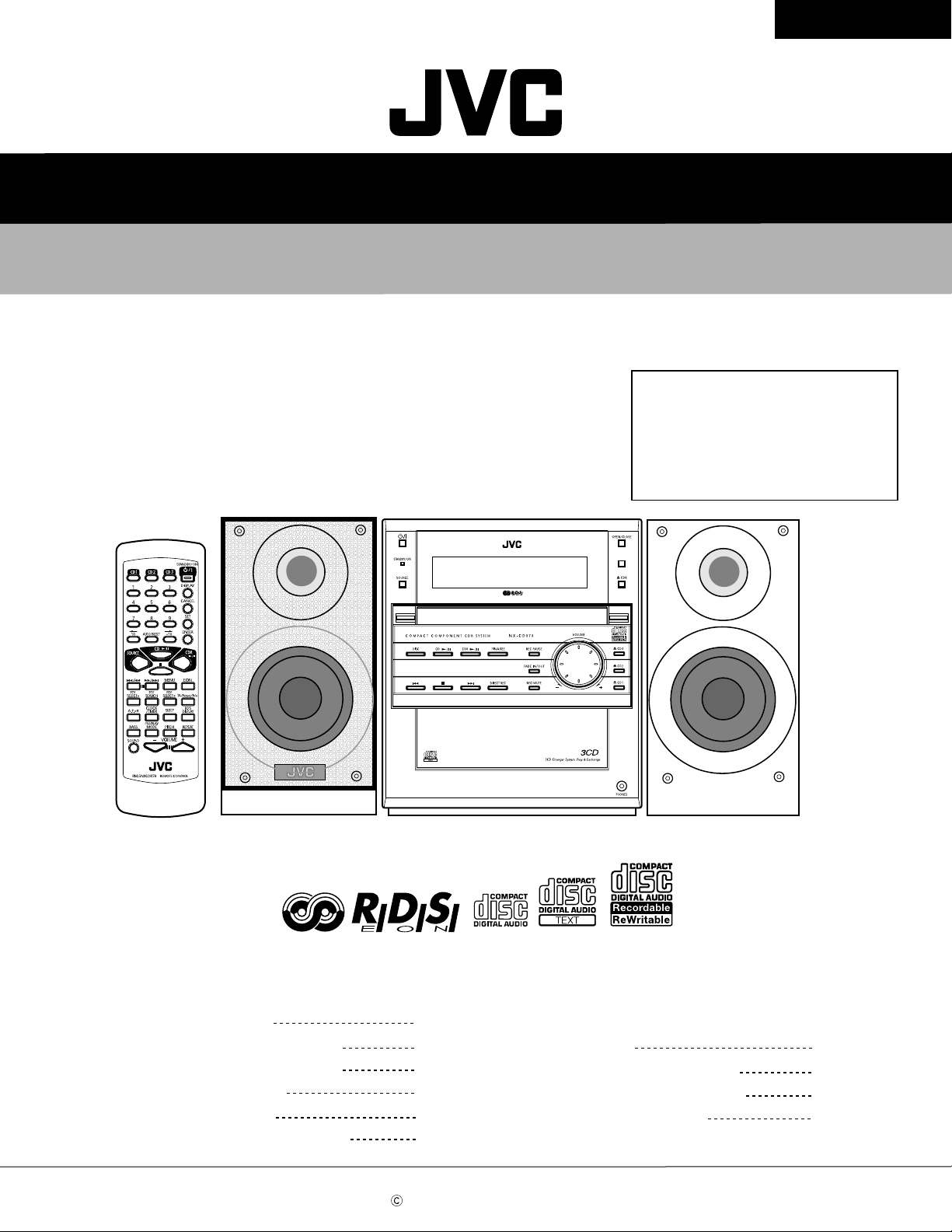
COMPACT COMPONENT CDR SYSTEM
NX-CDR7R
Area suffix
B ------------------------------- U.K.
E ----------- Continental Europe
EN ------------ Northern Europe
NX-CDR7R
SP-NXCDR7
Contents
Safety Precautions
Preventing static electricity
Important for laser products
Disassembly method
Adjustment method
Confirm method of operation
COPYRIGHT 2001 VICTOR COMPANY OF JAPAN, LTD.
CA-NXCDR7R
1-2
1-3
1-4
1-5
1-29
1-30
Flow of functional operation until
TOC read
Maintenance of laser pickup
Replacement of laser pickup
Description of major ICs
SP-NXCDR7
1-32
1-33
1-33
1-34~50
No.21030
Oct. 2001
Page 2
NX-CDR7R
1. This design of this product contains special hardware and many circuits and components specially for safety
purposes. For continued protection, no changes should be made to the original design unless authorized in
writing by the manufacturer. Replacement parts must be identical to those used in the original circuits. Services
should be performed by qualified personnel only.
2. Alterations of the design or circuitr y of the product should not be made. Any design alterations of the product
should not be made. Any design alterations or additions will void the manufacturer`s warranty and will further
relieve the manufacture of responsibility for personal injury or property damage resulting therefrom.
3. Many electrical and mechanical parts in the products have special safety-related characteristics. These
characteristics are often not evident from visual inspection nor can the protection afforded by them necessarily
be obtained by using replacement components rated for higher voltage, wattage, etc. Replacement parts which
have these special safety characteristics are identified in the Parts List of Service Manual. Electrical
components having such features are identified by shading on the schematics and by ( ) on the Parts List in
the Service Manual. The use of a substitute replacement which does not have the same safety characteristics
as the recommended replacement parts shown in the Parts List of Service Manual may create shock, fire, or
other hazards.
4. The leads in the products are routed and dressed with ties, clamps, tubings, barriers and the like to be
separated from live parts, high temperature parts, moving parts and/or sharp edges for the prevention of
electric shock and fire hazard. When service is required, the original lead routing and dress should be
observed, and it should be confirmed that they have been returned to normal, after re-assembling.
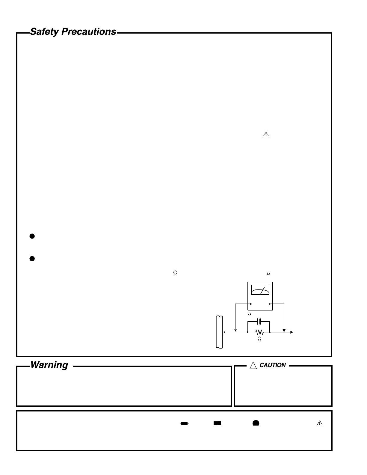
5. Leakage currnet check (Electrical shock hazard testing)
After re-assembling the product, always perform an isolation check on the exposed metal parts of the product
(antenna terminals, knobs, metal cabinet, screw heads, headphone jack, control shafts, etc.) to be sure the
product is safe to operate without danger of electrical shock.
Do not use a line isolation transformer during this check.
Plug the AC line cord directly into the AC outlet. Using a "Leakage Current Tester", measure the leakage
current from each exposed metal parts of the cabinet, particularly any exposed metal part having a return
path to the chassis, to a known good earth ground. Any leakage current must not exceed 0.5mA AC (r.m.s.).
Alternate check method
Plug the AC line cord directly into the AC outlet. Use an AC voltmeter having, 1,000 ohms per volt or more
sensitivity in the following manner. Connect a 1,500 10W resistor paralleled by a 0.15 F AC-type capacitor
between an exposed metal part and a known good earth ground.
Measure the AC voltage across the resistor with the AC
voltmeter.
Move the resistor connection to each exposed metal part,
particularly any exposed metal part having a return path to
the chassis, and meausre the AC voltage across the resistor.
Now, reverse the plug in the AC outlet and repeat each
measurement. Voltage measured any must not exceed 0.75 V
AC (r.m.s.). This corresponds to 0.5 mA AC (r.m.s.).
0.15 F AC TYPE
1500 10W
Good earth ground
AC VOLTMETER
(Having 1000
ohms/volts,
or more sensitivity)
Place this
probe on
each exposed
metal part.
!
1. This equipment has been designed and manufactured to meet international safety standards.
2. It is the legal responsibility of the repairer to ensure that these safety standards are maintained.
3. Repairs m ust be made in accordance with the relevant safety standards.
4. It is essential that safety critical components are replaced by approved parts.
5. If mains voltage selector is provided, check setting for local v oltage.
Burrs formed during molding may
be left over on some parts of the
chassis. Therefore, pay attention to
such burrs in the case of
preforming repair of this system.
In regard with component parts appearing on the silk-screen pr inted side (parts side) of the PWB diagrams, the
parts that are printed over with black such as the resistor ( ), diode ( ) and ICP ( ) or identified by the " "
mark nearby are critical for safety.
When replacing them, be sure to use the parts of the same type and rating as specified by the manufacturer.
(Except the J and C version)
1-2
Page 3
NX-CDR7R
Preventing static electricity
Electrostatic discharge (ESD), which occurs when static electricity stored in the body, fabric, etc. is discharged,
can destroy the laser diode in the traverse unit (optical pickup). Take care to prevent this when performing repairs.
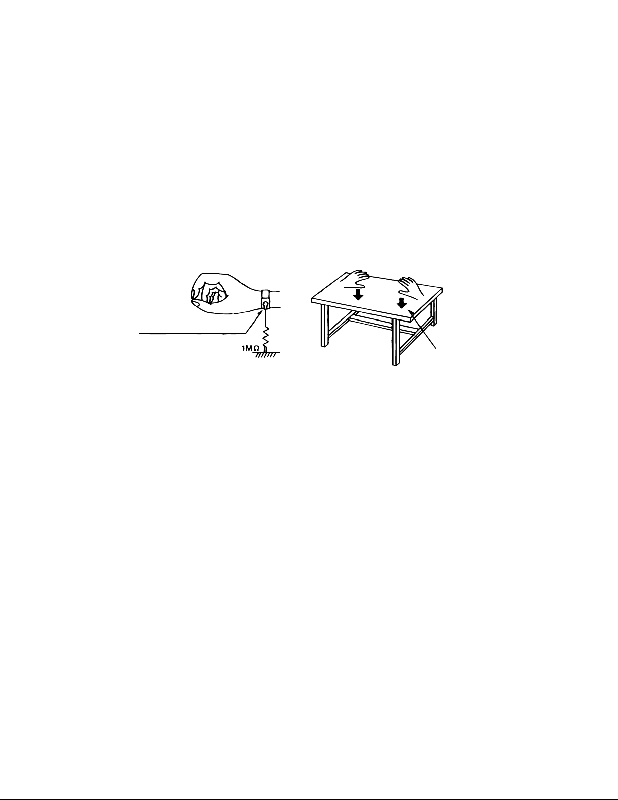
1.1. Grounding to prevent damage by static electricity
Static electricity in the work area can destroy the optical pickup (laser diode) in devices such as DVD players.
Be careful to use proper grounding in the area where repairs are being performed.
1.1.1. Ground the workbench
1. Ground the workbench by laying conductive material (such as a conductive sheet) or an iron plate over
it before placing the traverse unit (optical pickup) on it.
1.1.2. Ground yourself
1. Use an anti-static wrist strap to release any static electricity built up in your body.
(caption)
Anti-static wrist strap
Conductive material
(conductive sheet) or iron plate
1.1.3. Handling the optical pickup
1. In order to maintain quality during transport and before installation, both sides of the laser diode on the
replacement optical pickup are shorted. After replacement, return the shorted parts to their original condition.
(Refer to the next page.)
2. Do not use a tester to check the condition of the laser diode in the optical pickup. The tester's internal power
source can easily destroy the laser diode.
1.2. Handling the traverse unit (optical pickup)
1. Do not subject the traverse unit (optical pickup) to strong shocks, as it is a sensitive, complex unit.
2. For specific details, refer to the replacement procedure in the text. Be careful not to take too long a time
when attaching it to the connector.
3. Handle the flexible cable carefully as it may break when subjected to strong force.
4. It is not possible to adjust the semi-fixed resistor that adjusts the laser power. Do not turn it
1-3
Page 4
NX-CDR7R
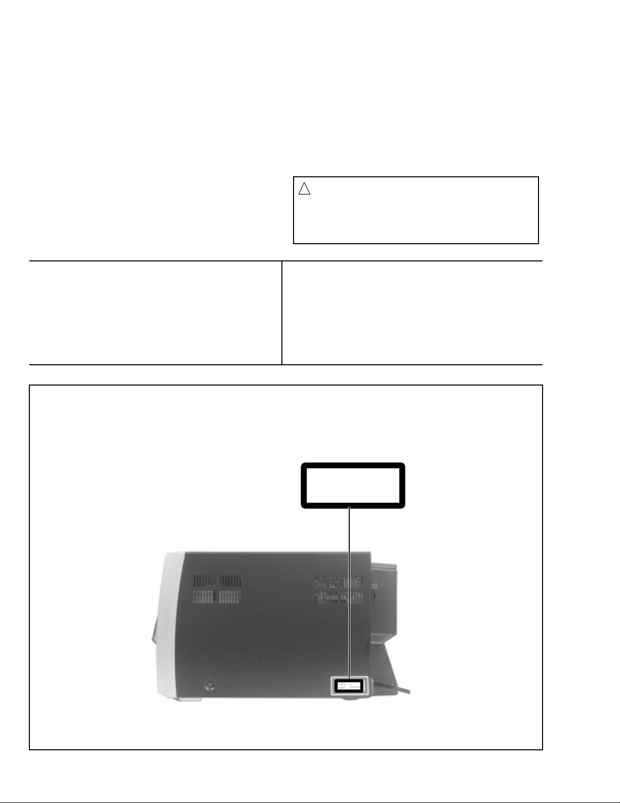
Important for Laser Products
1.CLASS 1 LASER PRODUCT
2.DANGER : Invisible laser radiation when open and inter
lock failed or defeated. Avoid direct exposure to beam.
3.CAUTION : There are no serviceable parts inside the
Laser Unit. Do not disassemble the Laser Unit. Replace
the complete Laser Unit if it malfunctions.
4.CAUTION : The compact disc player uses invisible
laserradiation and is equipped with safety switches
whichprevent emission of radiation when the drawer is
open and the safety interlocks have failed or are de
feated. It is dangerous to defeat the safety switches.
VARNING : Osynlig laserstrålning är denna del är öppnad
och spårren är urkopplad. Betrakta ej strålen.
VARO : Avattaessa ja suojalukitus ohitettaessa olet
alttiina näkymättömälle lasersäteilylle.Älä katso
säteeseen.
5.CAUTION : If safety switches malfunction, the laser is able
to function.
6.CAUTION : Use of controls, adjustments or performance of
procedures other than those specified herein may result in
hazardous radiation exposure.
CAUTION
!
Please use enough caution not to
see the beam directly or touch it
in case of an adjustment or operation
check.
ADVARSEL : Usynlig laserstråling ved åbning , når
sikkerhedsafbrydere er ude af funktion. Undgå
udsættelse for stråling.
ADVARSEL : Usynlig laserstråling ved åpning,når
sikkerhetsbryteren er avslott. unngå utsettelse
for stråling.
REPRODUCTION AND POSITION OF LABELS
WARNING LABEL
CLASS 1
LASER PRODUCT
CLASS 1
LASER PRODUCT
1-4
Page 5
NX-CDR7R
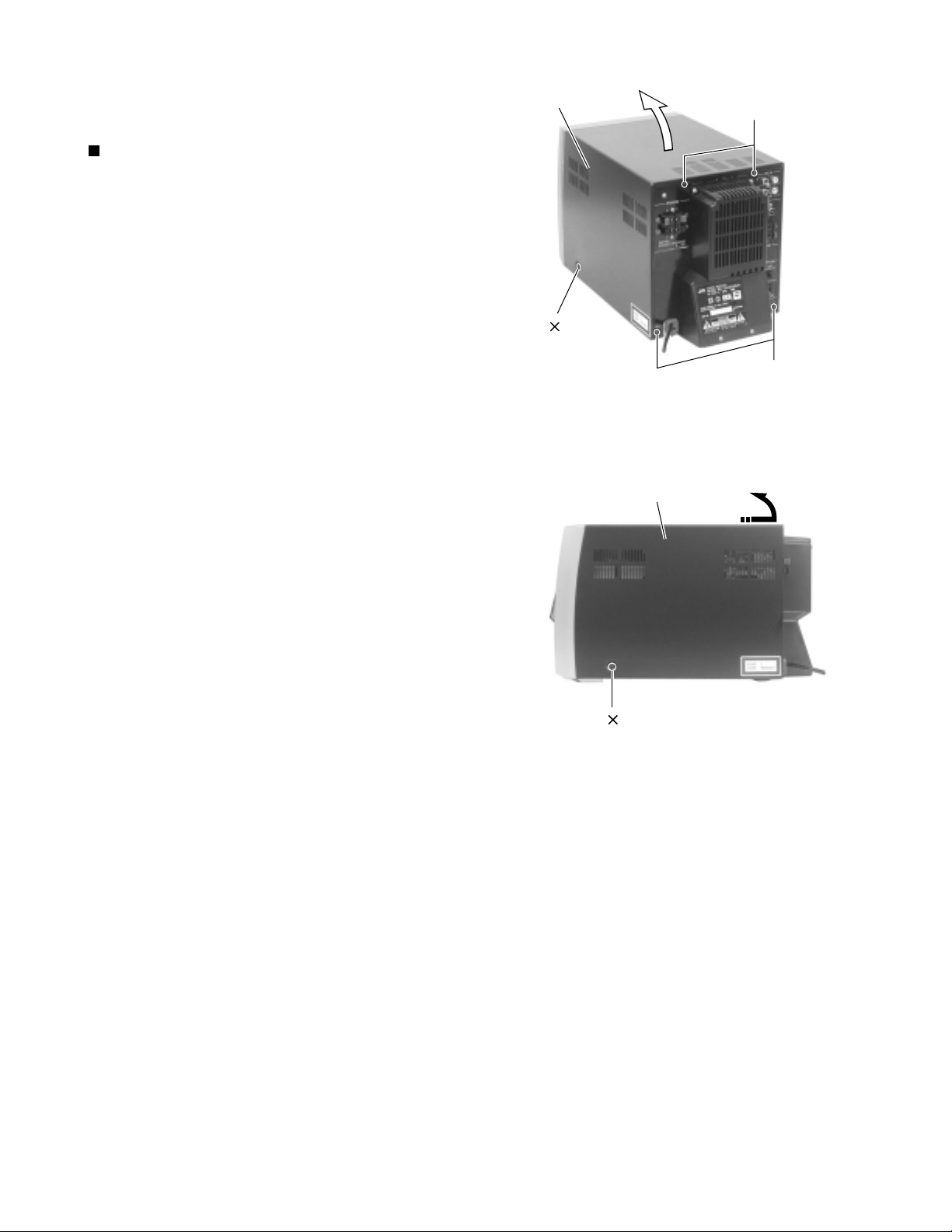
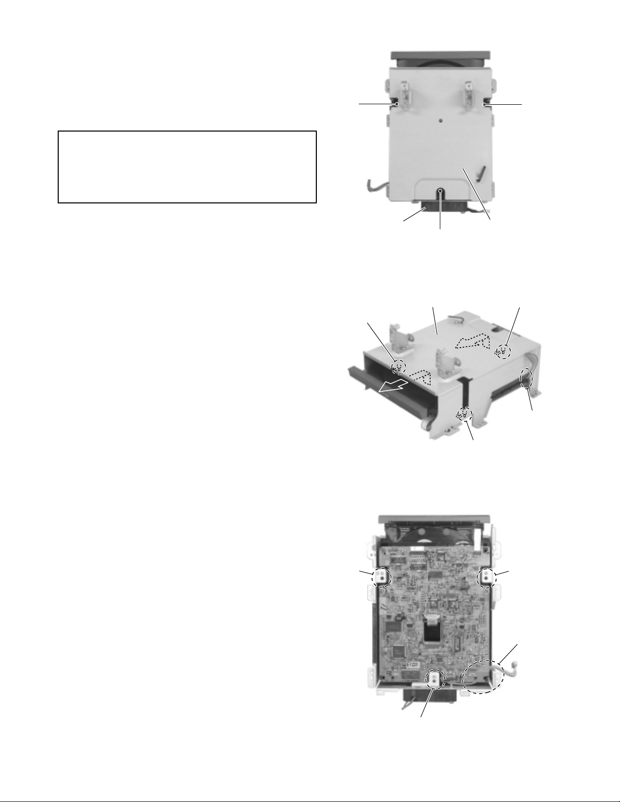
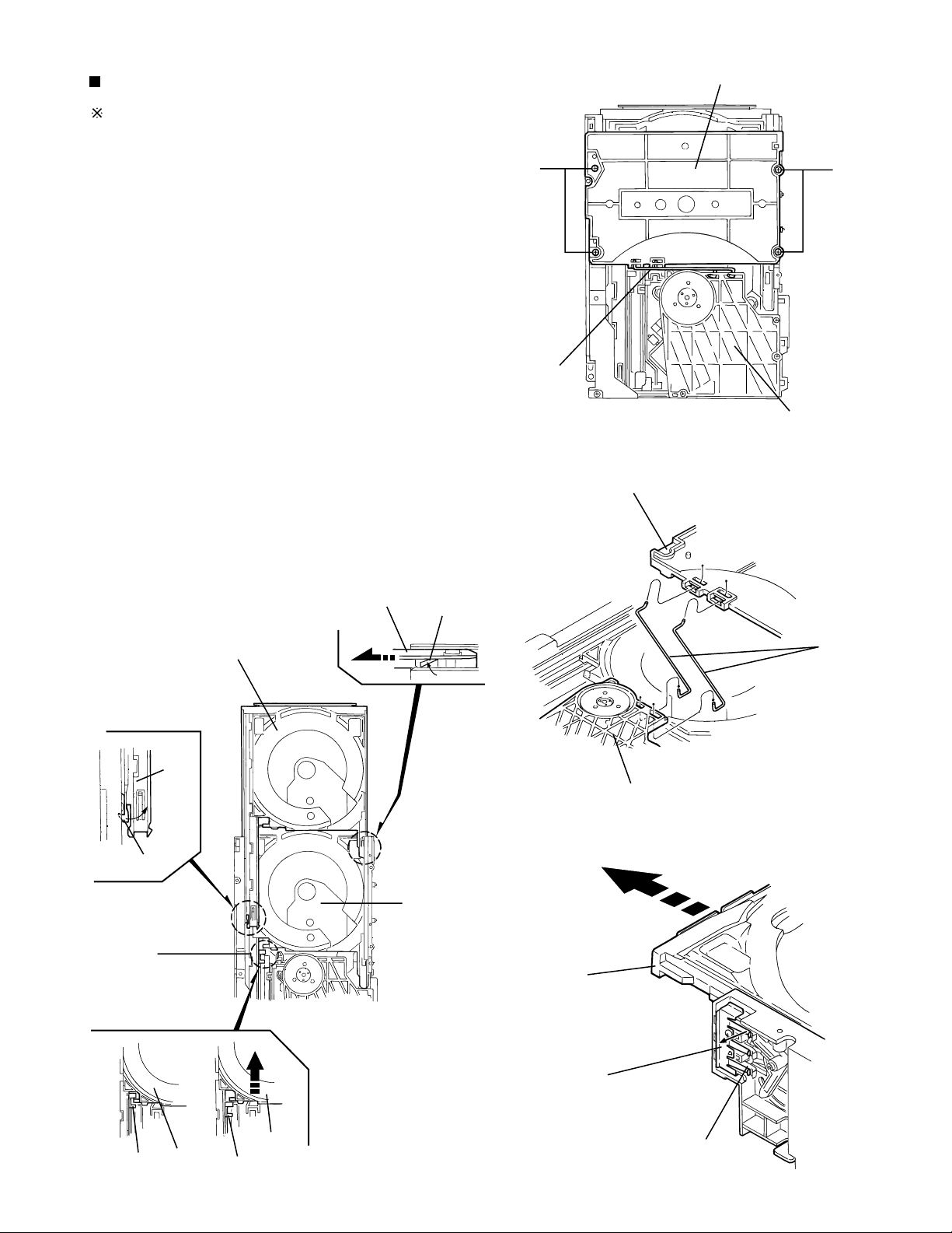
Disassembly method
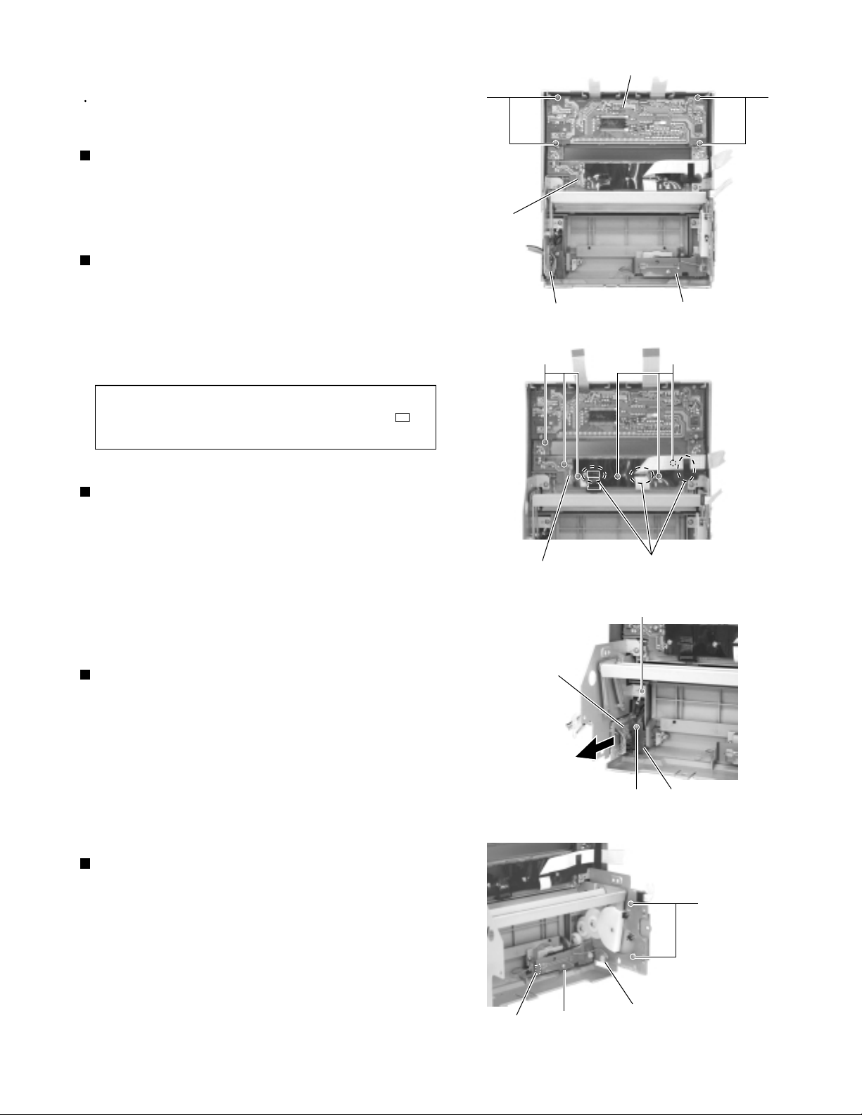
<Main body>
Removing the metal cover
(See Fig.1 and 2)
1.
Remove the four screws A on the back of the body.
2.
Remove the screw B on each side of the body.
3.
Remove the rear part of the metal cover upward
while pulling the lower part of both sides.
Metal cover
B
2
A
A
Fig.1
Metal cover
B 2
Fig.2
1-5
Page 6
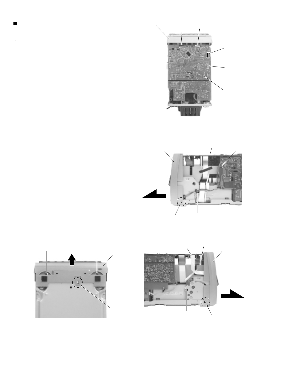
NX-CDR7R
Removing the front panel assembly
(See Fig.3 to 6)
Prior to performing the following procedure, remove
the metal cover.
1.
Disconnect the card wire from connector CN705,
CN708, CN704 and CN712 on the main board.
2.
Disconnect the wire from connector CN905 on the
power board.
3.
Remove the two screws C on each side of the body.
4.
Remove the two screws D on the bottom of the
body.
5.
Disengage the joint a on the bottom and the two
joints b on the lower side of the body using a
screwdriver. Then remove the front panel assembly
toward the front.
Front panel assembly
Front panel assembly
CN704
Fig.3
CN712
Main board
CN705
CN708
Main board
Power board
CN905
D
Front panel assembly
Joint a
Joint b
Main board
CN708
Fig.4
C
Fig.5Fig.6
C
CN705
Front panel assembly
Joint b
1-6
Page 7
NX-CDR7R
Removing the main board
(See Fig.7 and 8)
Prior to performing the following procedure, remove
the metal cover.
1.
Disconnect the card wire from connector CN704,
CN705, CN706, CN707, CN708, CN709 and CN712
on the main board on the upper side of body.
2.
Remove the two screws E on the upper side of the
body.
3.
Disconnect connector CN701, CN702, CN703,
CN710, CN711 on the main board from other boards
respectively.
Front panel assembly
E
CN706
CN707
Main board
CN701
Front panel assembly
CN704
CN712
CN705
CN708
CN709
CN711
CN710
CN702
CN703
Fig.7
Main board
E
CN711
CN710
CN706
CN707
CN702
CN703
CN701
Fig.8
1-7
Page 8
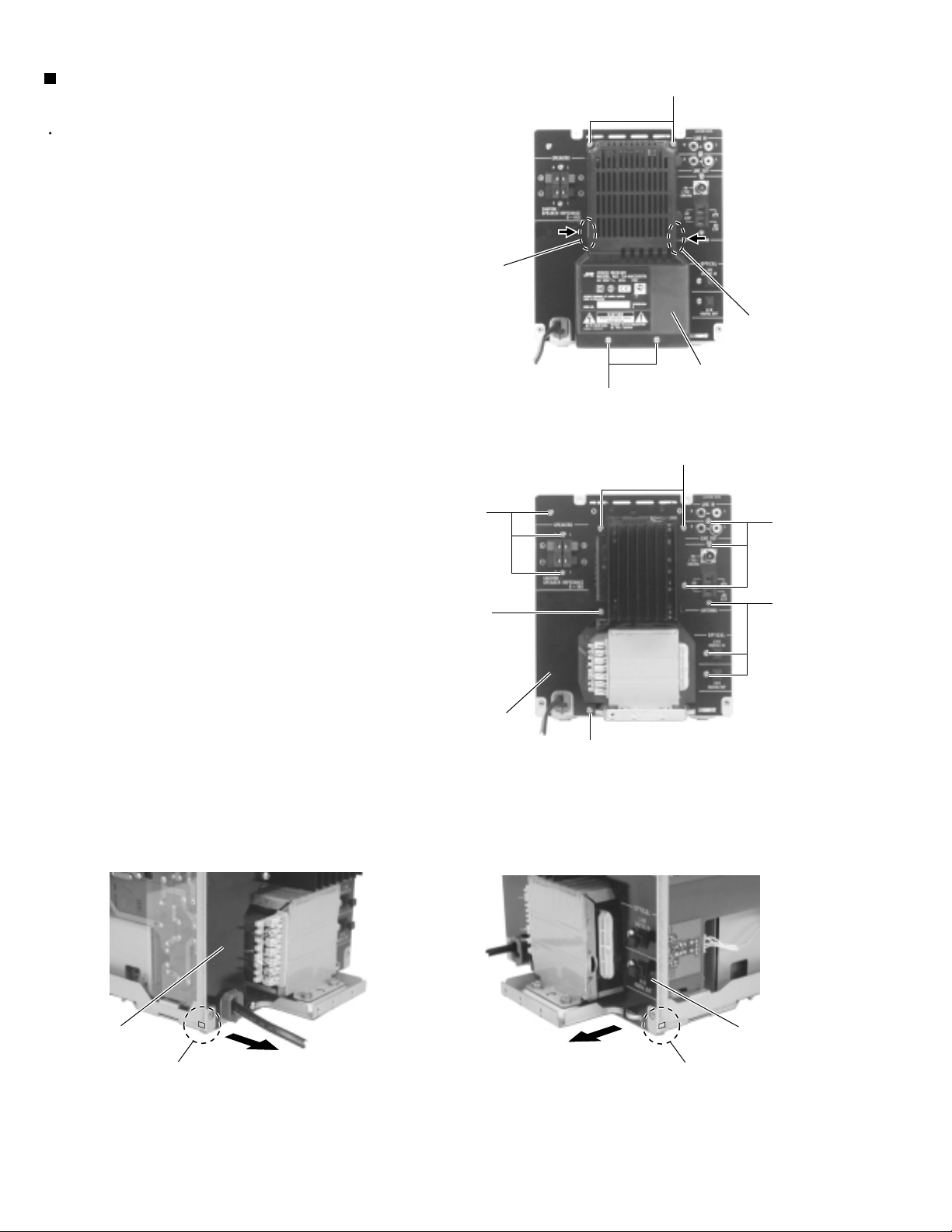
NX-CDR7R
Removing the rear cover / rear panel
(See Fig.9 to 12)
Prior to performing the following procedure, remove
the metal cover.
1.
Remove the four screws F on the back of the body,
and press the two joints c inward to release.
2.
Remove the thirteen screws G attaching the rear
panel.
3.
Disengage the two joints d in the lower part of the
rear panel using a screwdriver.
Joint c
G
F
Joint c
Rear cover
F
Fig.9
G
G
Rear panel
G
Rear panel
G
G
Fig.10
Rear panel
1-8
Joint d
Joint d
Fig.11Fig.12
Page 9
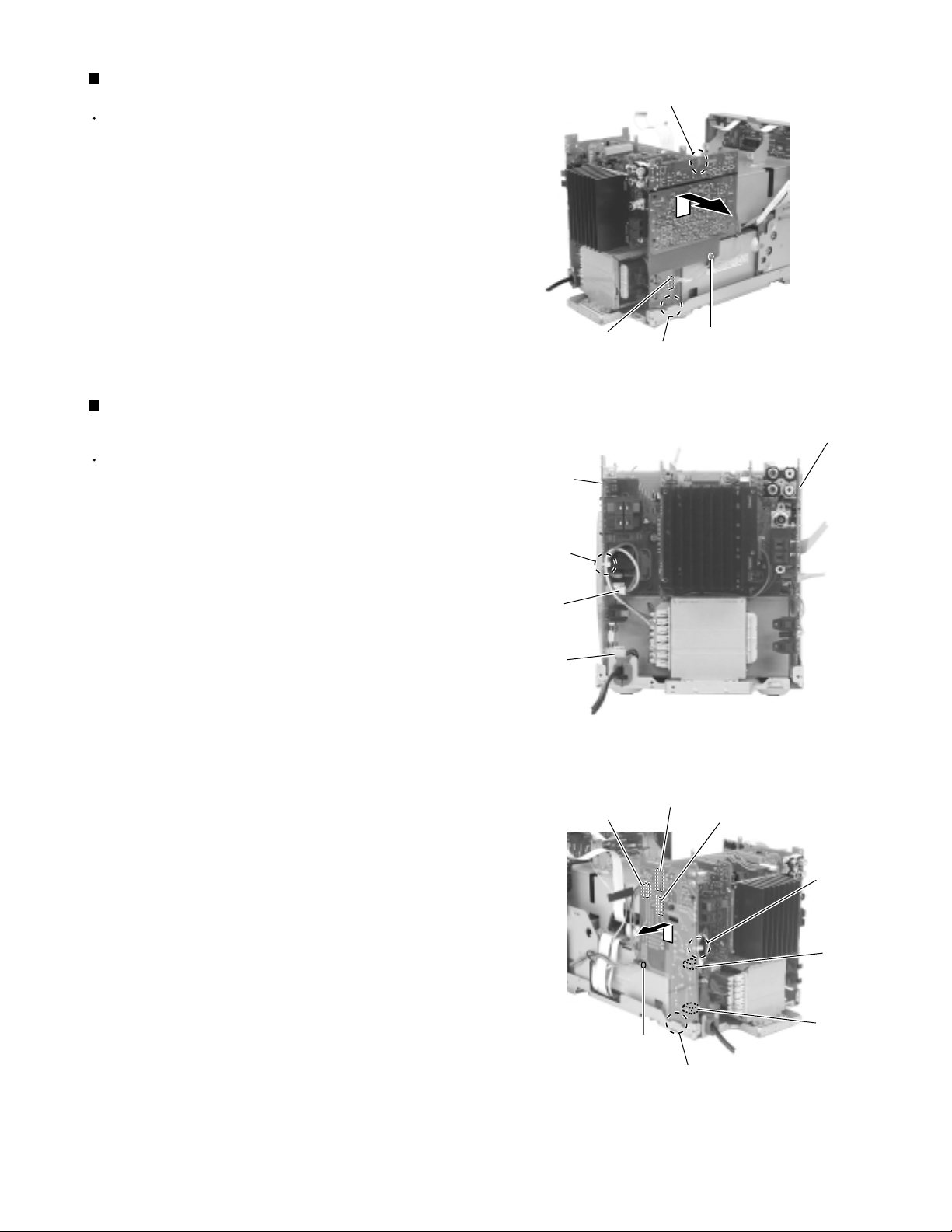
Removing the tuner board (See Fig.13)
Prior to performing the following procedure, remove
the metal cover, the main board and the rear panel.
1.
Disconnect the wire from connector CN802 on the
tuner board on the right side of the body.
2.
Remove the screw H attaching the tuner board.
3.
Move the tuner board upward and outward to
disengage the tuner board from the base chassis at
the joint f, and from the power board at the joint e.
NX-CDR7R
Joint e
Removing the power board
(See Fig.14 and 15)
Prior to performing the following procedure, remove
the metal cover, the main board and the rear panel.
1.
Remove the band attaching the wire to the power
board on the back of the body.
2.
Disconnect the wire from connector CN901, CN904
and CN905 on the power board.
3.
Remove the screw I on the left side of the body.
4.
Disconnect connector CN902 and CN903 on the
power board from the power board, and move the
power board upward to disengage it from the base
chassis at the joint g.
Tuner board
CN802
Power board
Band
CN904
CN901
Joint f
Fig.13
Fig.14
Power board
CN903
CN905 CN902
H
Tuner board
I
Fig.15
Band
CN904
CN901
Joint g
1-9
Page 10
NX-CDR7R
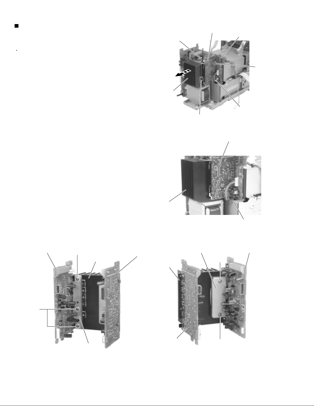
Removing the power amplifier board 1 /
power amplifier board 2 / heat sink
(See Fig.16 to 19)
Prior to performing the following procedure, remove
the metal cover, the main board, the rear panel and
the tuner board.
1.
Disconnect the wire from connector CN403 on the
power amplifier board 2.
2.
As the wire extending from the fan, take it off the notch
h in the lower part of the power amplifier board 2.
3.
Disconnect connector CN101 and CN103 on the
power amplifier board 1, and CN402 and CN405 on
the power amplifier board 2 from the power board
respectively. The heat sink is still attached to the
power amplifier board 1 and the power amplifier
board 2.
4.
Remove the two screws J attaching the IC bracket
(1) on the back of the heat sink, and remove the
power amplifier 1.
Power amplifier board 2
Power amplifier board 1
CN101
Heat sink
CN103
CN403
Fig.16
Power amplifier board 2
Power board
Power amplifier board 2
CN402
CN405
5.
Remove the three screws K attaching the IC bracket
(2) on the back of the heat sink, and remove the
power amplifier 2.
Power amplifier board 2
K
Power amplifier board 1
Heat sink
K
Heat sink
Heat sink
Fig.17
IC bracket (1)
Notch h
Power amplifier board 1
J
1-10
IC bracket (2)
Power amplifier board 2
J
Fig.18Fig.19
Page 11
Removing the fan (See Fig.20)
Prior to performing the following procedure, remove
the metal cover, the main board, the rear panel, the
tuner board, the power amplifier board 1, the power
amplifier board 2 and the heat sink.
NX-CDR7R
L
Fan
REFERENCE:
1.
Disconnect the wire from connector CN210 on the
power board.
2.
Remove the two screws L attaching the fan.
3.
Push down the clamp which settles the wire
extending from the power transformer, in the
direction of the arrow, and remove the fan backward.
The fan is detachable without removing
the CDR mechanism assembly.
Removing the power board (See Fig.21)
Prior to performing the following procedure, remove
the metal cover, the main board, the rear panel, the
tuner board, the power amplifier board 1, the power
amplifier board 2 and the heat sink.
1.
Disconnect the wire from connector CN203 and
CN210 on the power board on the back of the body.
L
Power board
CN204
Clamp
Fig.20
CN207
Power board
CN210
Power board
CN203
2.
Remove the two screws M attaching the power
board.
3.
Disconnect connector CN204 and CN207 on the
power board from the power board.
CN210
M
Fig.21
1-11
Page 12
NX-CDR7R
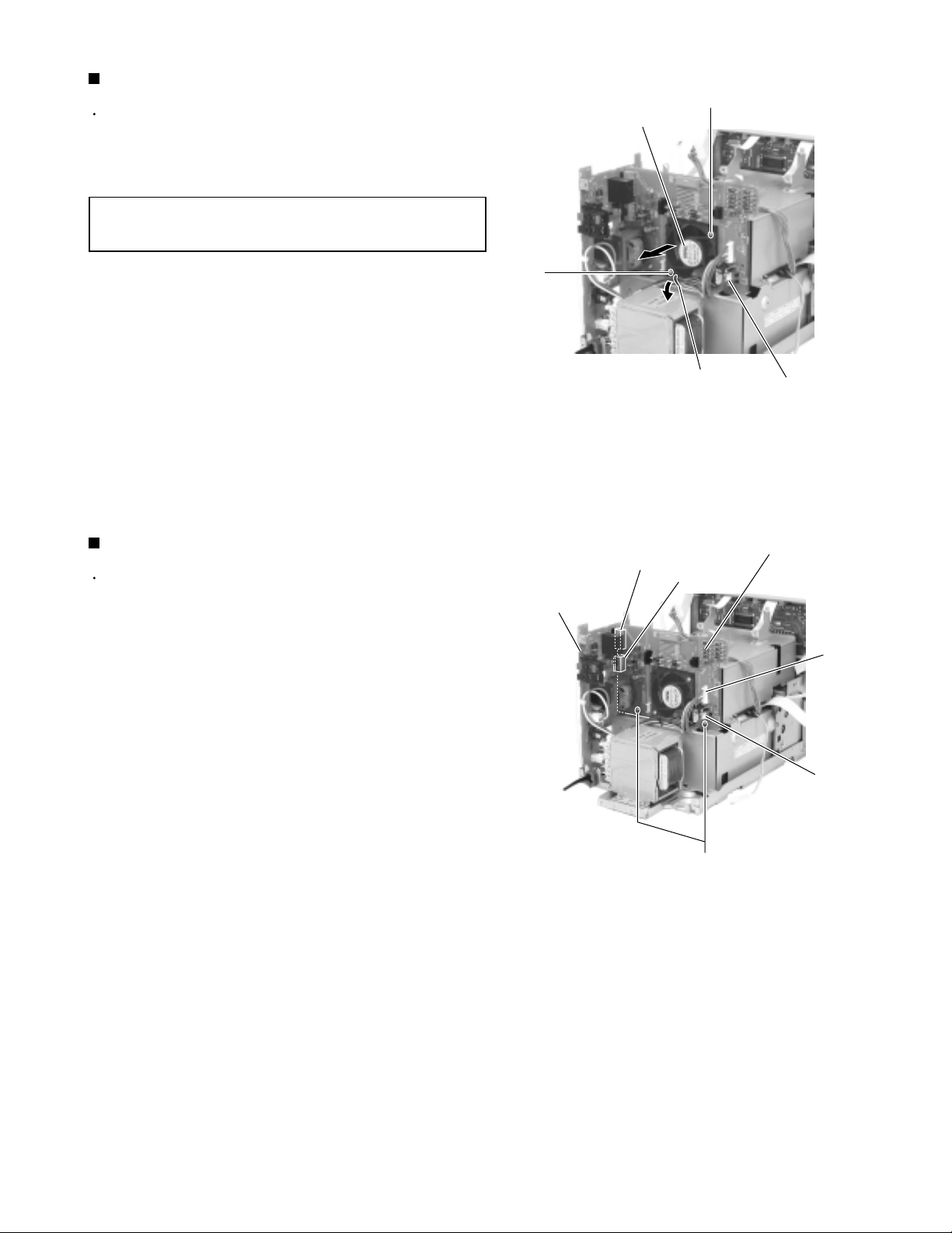
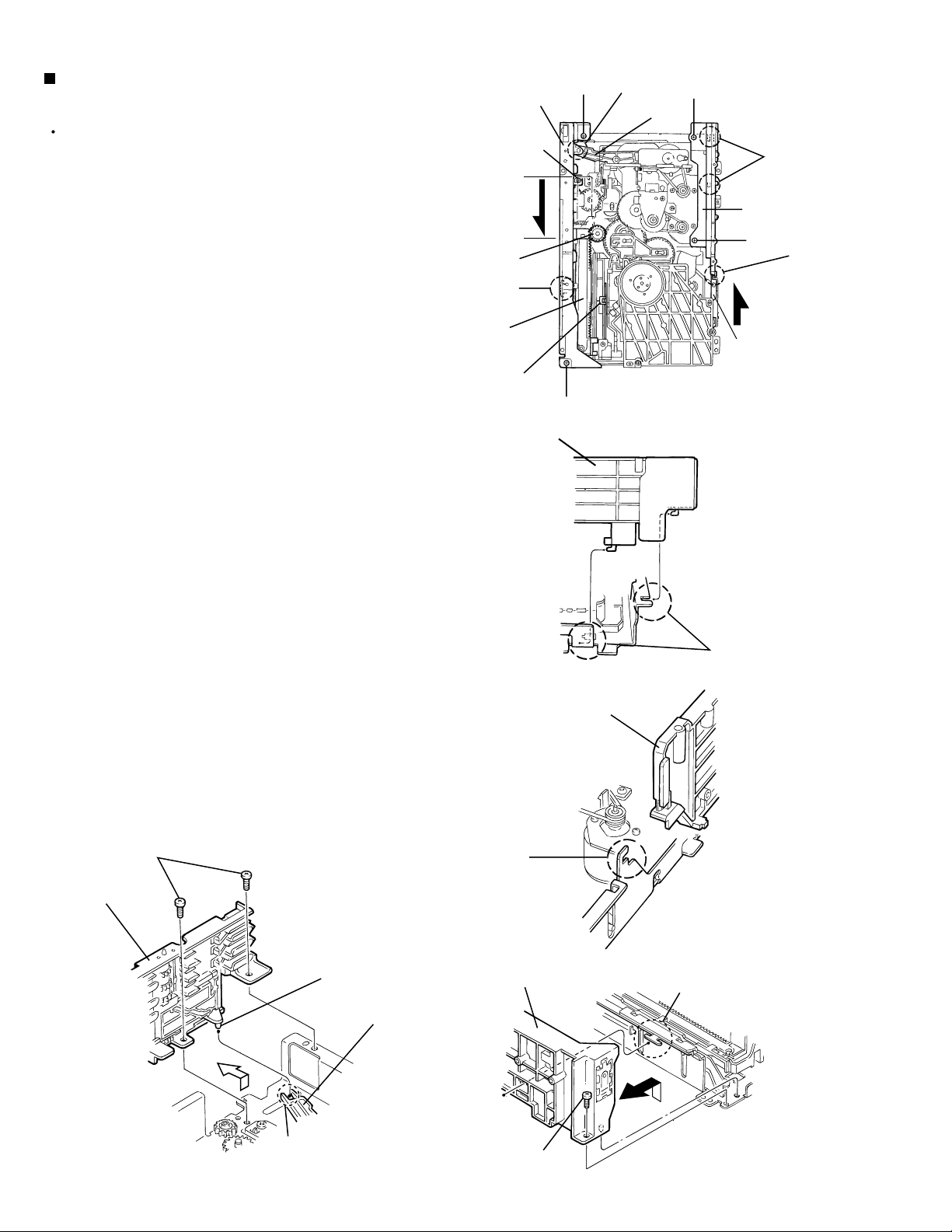
Removing the CDR mechanism cover /
CDR mechanism assembly
(See Fig.22 to 27)
Prior to performing the following procedure, remove
the metal cover, the front panel assembly, the rear
panel, the main board and the tuner board.
REFERENCE:
REFERENCE:
1.
Remove the spacer settling the card wire on the right
side of the body and release the wire from the clamp
and the notch i of the power board on the upper side
of the body. Disconnect the card wire from connector
CN702 and CN703 on the CDR connection board.
2.
Disconnect the wire from connector CN507 on the
CD servo board.
When removing the CDR mechanism
assembly only, refer to the next section.
When removing the fan only, refer to
“Removing the fan”.
Clamp
CDR mechanism cover
CDR connection board
CN703
N
Notch i
CDR connection board
CN702
CD servo board
CN507
Fig.22
CDR mechanism cover
N
3.
Disconnect the wire from connector CN210 on the
power board on the back of the body and release the
wire from the notch h of the power amplifier board 2.
4.
Remove the four screws N on the upper front side of
the body and remove the CDR mechanism cover
toward the front. The CDR mechanism assembly and
the fan are also removed with the CDR mechanism
cover.
Clamp
Notch i
Fig.23
Power amplifier board 2
1-12
Notch h
Fig.24
Page 13
5.
Remove the three screws O attaching the CDR
mechanism cover. Move the CDR mechanism
assembly in the direction of the arrow, inside of the
CDR mechanism cover, to disengage it from the
three joint bosses marked j. Then remove the CDR
mechanism assembly toward the front.
O
NX-CDR7R
O
CAUTION:
When reassembling, set the wire extending
from the rear of the CDR mechanism board
on the side of the CDR mechanism cover
(marked k) as shown in Fig.26 before
reattaching the CDR mechanism assembly.
Joint bosses j
Fan
O
Fig.25
CDR mechanism cover
CDR mechanism cover
Joint bosses j
k
Joint bosses j
Joint bosses j
Fig.26
Joint bosses j
k
Joint bosses j
Fig.27
1-13
Page 14
NX-CDR7R
Removing the CDR mechanism
assembly only (See Fig.28 and 29)
REFERENCE:
Prior to performing the following procedure, remove
the metal cover, the front panel assembly and the
main board.
1.
Disconnect the card wire from connector CN702 and
CN703 on the CDR connection board on the right
side of the body.
2.
Disconnect the wire from connector CN507 on the
CD servo board.
3.
Remove the three screws O on the upper side of the
body.
4.
Move the CDR mechanism assembly in the direction
of the arrow, inside of the CDR mechanism cover, to
disengage it from the three joint bosses marked j.
Then pull out the CDR mechanism assembly toward
the front (See Fig. 25 to 27).
The CDR mechanism assembly is
detachable without removing the CDR
mechanism cover.
O
O
CDR connection board
CDR mechanism assembly
CDR mechanism assembly
O
CDR mechanism cover
Fig.28
CN703
CN702
CAUTION:
When reassembling, set the wire extending
from the back of the CDR mechanism board
on the side of the CDR mechanism cover
(marked k) as shown in Fig.26 before
reattaching the CDR mechanism assembly.
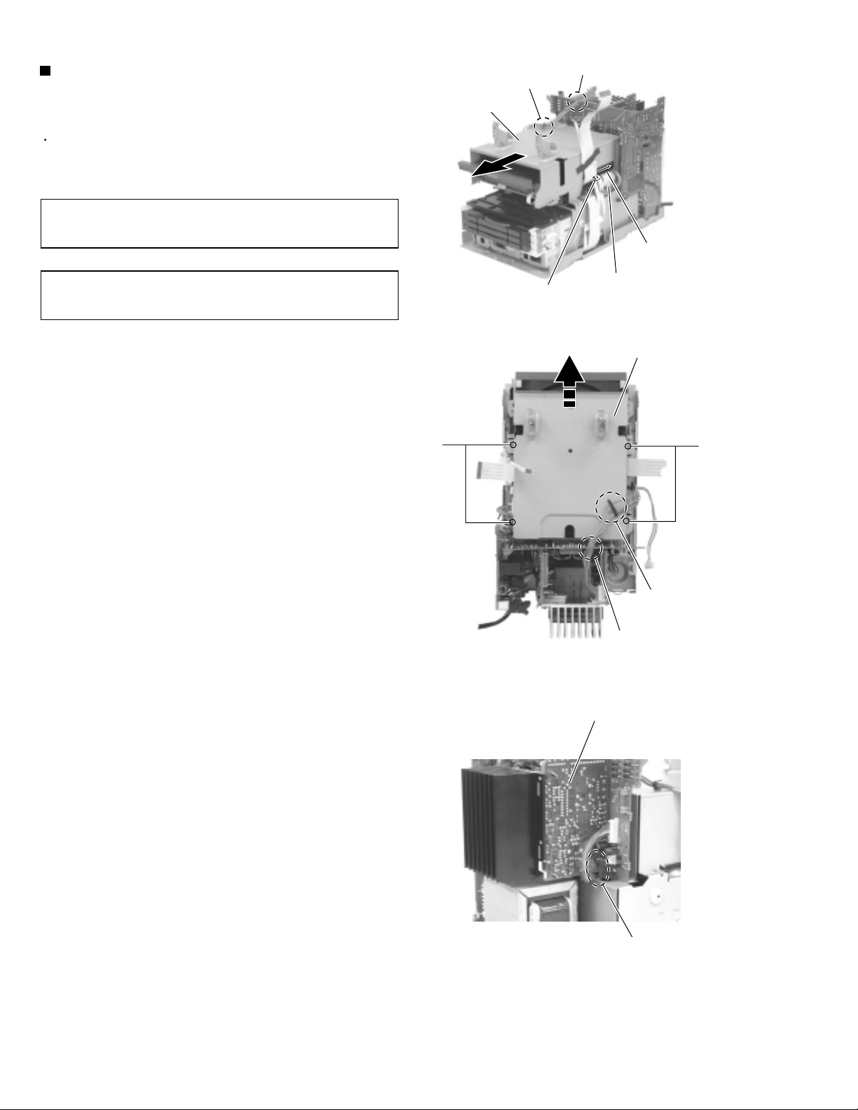
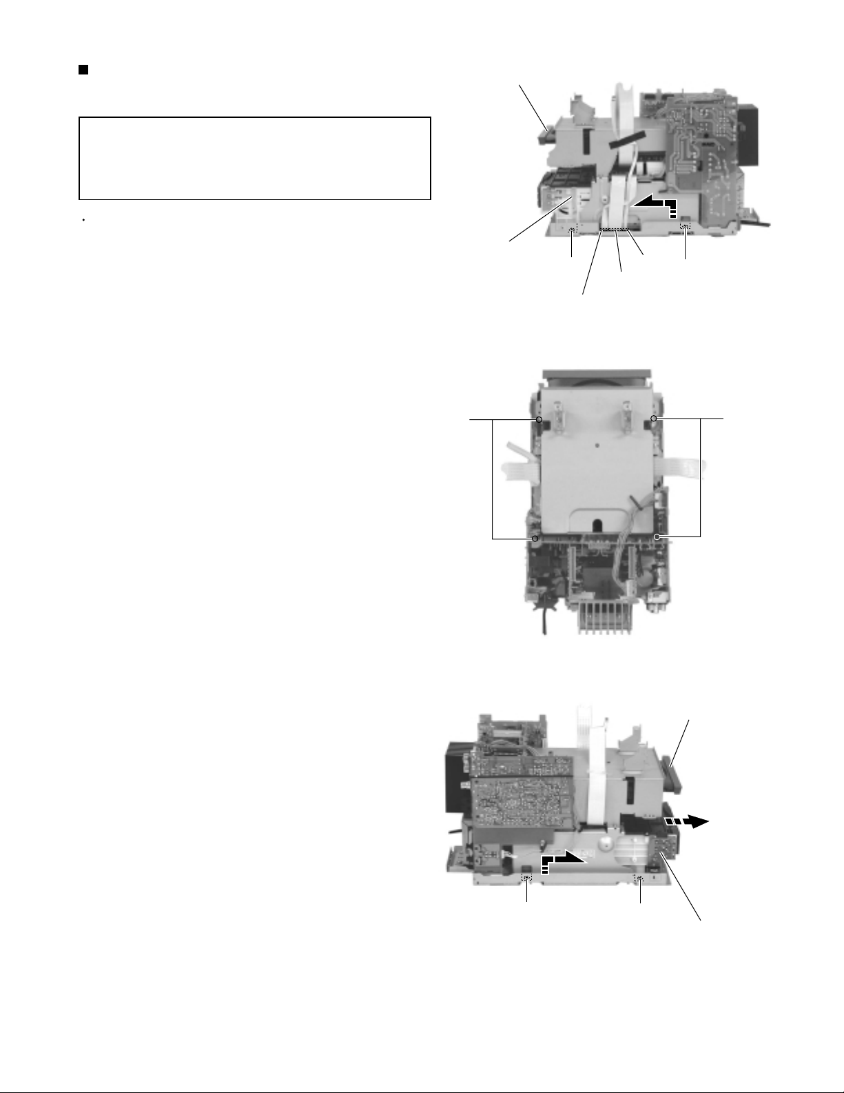
Removing the CD servo board
(See Fig.30)
Prior to performing the following procedure, remove
the metal cover, the front panel assembly, the main
board, the rear panel, the tuner
mechanism cover.
Disconnect the card wire from connector CN504 and
1.
CN505 on the CD servo
the body.
Disconnect the wire from connector CN403 on the
2.
3.
board.
power
Remove the two screws P and move the CD servo
board in the direction of the arrow to release the two
joints l.
board on the
board and the CDR
upper side of
Joint bosses j 3
CN504
CN505
CD servo board
CN507
Fig.29
P
Joints l
CD servo board
P
Fig.30
1-14
Page 15
NX-CDR7R
Removing the CD changer mechanism
assembly (See Fig.31 to 33)
REFERENCE:
Prior to performing the following procedure, remove
the metal cover, the front panel assembly and the
main board.
1.
Disconnect the card wire from connector CN606,
CN608, CN651 on the CD changer mechanism
board on the right side of the body.
2.
Remove the four screws Q attaching the CD
changer mechanism assembly on the upper side of
the body.
3.
Move the CD changer mechanism assembly in the
direction of the arrow, inside of the CD changer
mechanism cover, and pull out it toward the front
while raising it slightly.
The CD changer mechanism assembly is
detachable without removing the CDR
mechanism cover and the CDR
mechanism assembly.
CDR mechanism assembly
CD changer
mechanism assembly
CD changer mechanism board
CN606
Q
Q
CN651
Fig.31
CN608
Q
Q
Q
Fig.32
Fig.33
CDR mechanism assembly
Q
CD changer
mechanism assembly
1-15
Page 16
NX-CDR7R
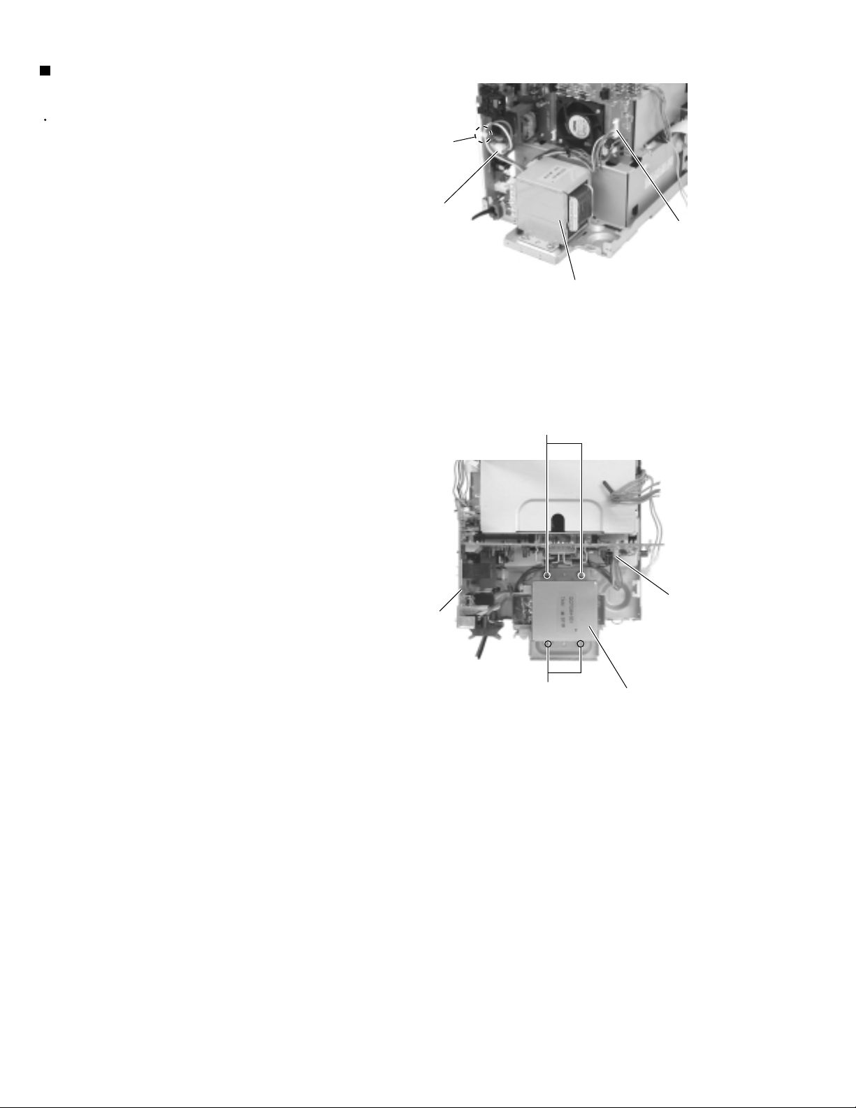
Removing the power transformer
assembly (See Fig.34 and 35)
Prior to performing the following procedure, remove
the metal cover, the main board, the rear panel, the
tuner board, the power amplifier board 1, the power
board and the heat sink.
1.
Remove the band setling the wire on the power
board on the back of the body and disconnect the
wire from connector CN904.
2.
Disconnect the wire from connector CN203 on the
power board.
3.
Remove the four screws R on the upper side of the
body, and remove the power transformer assembly
from under the heat sink backward.
Band
Power board
CN904
Power board
CN203
Power transformer assembly
Fig.34
R
Power board
Power transformer assembly
R
Fig.35
Power board
CN203
1-16
Page 17
NX-CDR7R
<Front panel assembly section>
Prior to performing the following procedures, remove
the metal cover and the front panel assembly.
Removing the LCD board (See Fig.36)
1.
Remove the four screws S on the back of the front
panel assembly.
Removing the function switch board
(See Fig.37)
1.
Remove the seven screws T.
2.
Disconnect the card wire from connector CN671 and
CN672 on the function switch board.
CAUTION:
When reconnecting each card wire, let it
through the three notches m of the as
shown in Fig.37.
S
Function switch
board
Phone jack board
LCD board
S
Motor board
Fig.36
TT
Removing the phone jack board
(See Fig.38)
1.
Remove the screw U attaching the presser board of
the phone jack board.
2.
Remove the screw V attaching the earth terminal
extending from the phone jack board.
Removing the motor board (See Fig.39)
1.
Disconnect the wire from connector CN582 on the
OPEN / CLOSE SW detect board.
2.
Disconnect the wire from connector CN583 on the
motor board.
3.
Remove the screw W.
Removing the OPEN / CLOSE SW detect
board (See Fig.39)
1.
Disconnect the wire from connector CN582 on the
OPEN / CLOSE SW detect board.
Function switch board
Phone jack board
Notches m
Fig.37
U
Fig.38
V
Presser board
X
2.
Remove the two screws X.
Motor board
CN583
W
OPEN / CLOSE SW detect board
CN582
Fig.39
1-17
Page 18
NX-CDR7R
Removing the door motor
(See Fig.40 and 41)
Prior to performing the following procedure, remove
the motor board.
1.
Remove the belt from the door motor.
2.
Remove the screw Y attaching the door motor
bracket.
3.
Remove the two screws Z.
Y
Door motor
Door motor bracket
Door motor
Belt
Fig.40
Door motor bracket
Z
Fig.41
1-18
Page 19
Removing the control board
(See Fig.42 to 46)
Prior to performing the following procedure, remove
the function switch board, the motor board and the
belt.
1.
Remove the belt. Rotate the pulley (1) and move the
control panel assembly toward the front until it stops.
2.
Remove the control panel assembly toward the front
while pulling out the two shafts of the joint l on the
right and left sides of the control panel assembly.
NX-CDR7R
CAUTION:
3.
Put the front panel assembly down toward the front,
and release the four joint m and n inside of the
control panel by pressing them inward.
4.
Remove the four screws Z' attaching the control
board.
Joint m
Joint n
Each shaft of the joint l is attached a
collar. Be careful not to lose that.
Arm bracket
Fig.45
Control board
Pulley (1)
Fig.42
Joint l
Joint l
Joint m
Joint n
Control panel assembly
Fig.43
Control board
Fig.46
Z'Z'
Control panel assembly
Collar
Collar
Fig.44
1-19
Page 20
NX-CDR7R
<Changer mechanism assembly>
Removing the servo control board
(See Fig.1 to 4)
ATTENTION:
1.
Insert a screwdriver into the sub chassis slot on the
back of the body and push the slider (R) toward the
front.
2.
From the top of the body, slide the hook and the
slider (R) forward until they stop.
3.
From the right side of the body, slide the slide cam
(L) backward until it stops. The sub chassis unit will
move to the lowest position.
4.
From the bottom of the body, unsolder each soldered
part a and b of the motors on the servo control
board.
5.
Remove the five screws A attaching the servo
control board.
6.
Disconnect connector CN610 on the servo control
board from the tray select switch board to suspend
the servo control board tentatively. Solder the part c
of the flexible wire connected to connector CN601 on
the underside of the servo control board.
Make sure the sub chassis unit is
locating at the lowest position. If
not,perform the following procedure
from 1 to 3.
Slot
Sub chassis unit
Hook
Tray select switch board
A
CN610
Slide cam (L)
Fig.1
Slider (R)
Slide cam (L)
Fig.2
Cam switch
7.
Disconnect the flexible wire from connector CN601
and remove the servo control board from the body.
ATTENTION:
ATTENTION:
Control cam
Slot p
1-20
In case of disconnecting the flexible
wire without soldering, the CD pick up
may be damaged.
When reassembling, make sure the
cam switch boss of the servo control
board is fitted to the slot p of the
control cam on the bottom of the body
(Refer to Fig.3-1).
Cam switch boss
Gear base unit
Main board
Solder part a
A
Solder
part b
A
Solder part c
CN601
CN601
A
Servo
control board
A
Fig.3-1
Servo control board
Fig.4Fig.3-2
Page 21
NX-CDR7R
Removing the tray unit (See Fig.5 to 8)
The tray unit can be removed despite the position of
the sub chassis unit, but the lowest position is
recommended to expedite the work.
1.
Remove the four screws B attaching the top cover
on the top of the body.
2.
Remove the top cover with the two rods attached to
the top cover and the clamper base unit.
3.
Pull the lock lever of the return spring on the right
side of the body to eject the tray unit.
4.
From the top of the body, release the tray from the
joint hook marked d (Push the tray toward the front).
5.
Release the stoppers on both sides in the direction
of the arrow and pull out the tray unit from the body.
ATTENTION:
Pull out the tray unit from the top tray 3
in sequence.
B
Top cover
B
Rod
Clamper base unit
Fig.5
Top cover
Both
Joint d
Tray
Tray unit
Tray
Both
Rod
Clamper base unit
Fig.6
Tray unit
Tray 3
Hook
Tray
Hook
Tray
Fig.8
Return spring
Lock lever
Fig.7
1-21
Page 22
NX-CDR7R
Removing the side unit (L) and (R)
(See Fig.9-1 to 9-5)
Prior to performing the following procedures, remove
the servo control board, the top cover and the tray
unit.
1.
Remove the two screws C attaching the side unit (L).
2.
Slide and remove the side unit (L) toward the front
while releasing the two joints e and the joint f with
the chassis unit.
3.
Slide the slide cam (L) toward the front until it stops
to place the sub chassis unit at the top position.
ATTENTION:
4.
Turn the hook gear counterclockwise to move the
slide hook and the slider (R) backward until they
stop.
5.
Remove the three screws D attaching the side unit
(R). Raise the side unit (R) upward and release the
joint g with the chassis unit and the boss from the
select arm marked h. Then remove the side unit (R)
from the body.
The side unit (R) can be removed
when the sub chassis unit is located at
the top position.
Side unit (R)
Hook gear
Joint g
slide hook
Slider (R)
Side unit (L)
D
D
D
Joint h
Select arm
Fig.9-1
C
Joints e
Side unit (L)
C
Joint f
Slide cam(L)
ATTENTION:
D
Side unit (R)
When reassembling, make sure the boss
is fitted to the select arm marked h.
Boss
Select arm
Side unit (L)
Joint f
Side unit (R)
Joints e
Fig.9-2
Fig.9-3
Joint g
1-22
Joint h
D
Fig.9-5Fig.9-4
Page 23
Removing the sub chassis unit
(See Fig.10 to 12)
Prior to performing the following procedures, remove
the servo control board, the top cover, the tray unit,
the side unit (L) and the side unit (R).
1.
Turn the hook gear counterclockwise to move the
slide hook and the slider (R) backward until they
stop.
2.
Slide the slide cam (L) and the slide cam (R) in the
direction of the arrow until they stop.
(The notches of each slide cam are fitted to the pins
on both sides of the sub chassis unit.)
3.
Detach the sub chassis unit upward.
ATTENTION:
When reassembling, turn the hook gear
of the chassis unit counterclockwise until
it stops and slide the slide hook and the
slider (R) of the sub chassis unit
backward until they stop.
NX-CDR7R
Slide cam (L)
Slide cam (R)
Sub chassis unit
Fig.10
Sub chassis unit
Pin
Slider (R)
slide hook
Pin
Slide cam (L)
Notch
Fig.11
Hook gear
Fig.12
1-23
Page 24
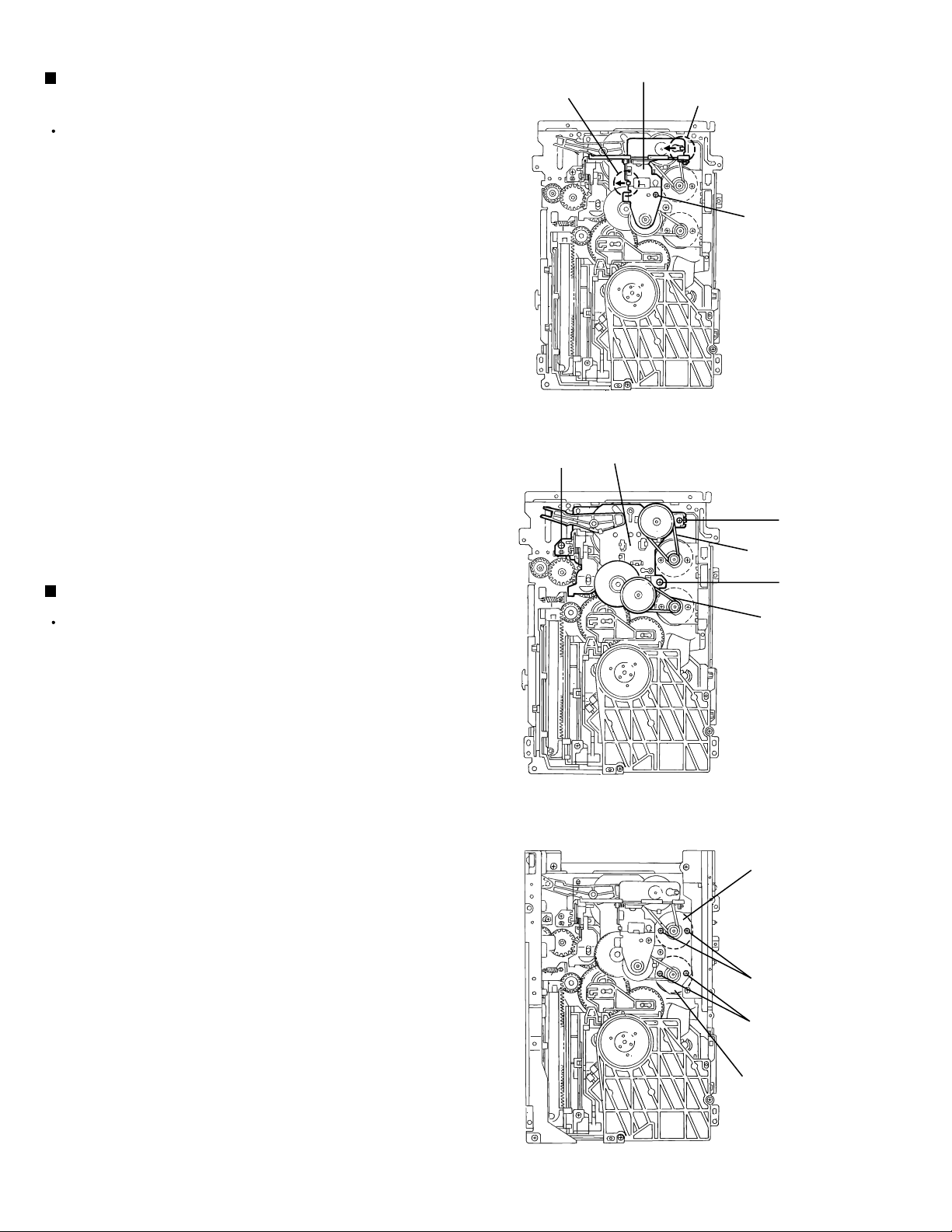
NX-CDR7R
Removing the flap base unit and the gear
base unit (See Fig.13 and 14)
Prior to performing the following procedures, remove
the servo control board, the top cover, the tray unit,
the side unit (L) and the side unit (R).
1.
Remove the screw E attaching the flap base unit.
Release the joint tabs i and j, then remove the flap
base unit from the body.
2.
Remove the belts from the two pulleys on the gear
base unit.
3.
Remove the three screws F and remove the gear
base unit from the body.
Joint tab j
F
Flap base unit
Joint tab i
E
Fig.13
Gear base unit
F
Removing the motors (See Fig.15)
Prior to performing the following procedure, remove
the main board.
1.
Remove the belts from the two pulleys.
2.
Remove the four screws G and detach each motor
from the body.
Belt
F
Belt
Fig.14
Motor
G
1-24
G
Motor
Fig.15
Page 25
NX-CDR7R
Removing the pickup (See Fig.16 to 20)
1.
From the top of the body, remove the three screws H
attaching the clamper base unit.
2.
Remove the clamper base unit with the two rods
attached to the clamper base unit and the top cover.
3.
Turn the screw shaft gear marked k in the direction
of the arrow to move the pickup unit.
4.
Remove the screw I attaching the shaft holder.
5.
Move the screw shaft in the direction of the arrow
and release it from the joint l. Then release it from
the joint m with the pickup holder. Detach the pickup
with the screw shaft.
6.
Solder the part n of the flexible board on the
underside of the pickup. After soldering, disconnect
the flexible wire connected to the pickup (In case of
disconnecting the flexible wire without soldering, it
may cause damage to the CD pickup).
7.
Remove the two screws J attaching the rack arm to
the pickup unit.
Fig.16
Clamper base
Top cover
H
Rod
H
Clamper base unit
8.
Pull out the screw shaft from the pickup.
Part n (soldering)
Fig.19
Rack arm
Flexible board
J
Shaft holder
Fig.17
k
Rods
Top cover
Joint m
Screw shaft
Fig.20
Pickup
I
Joint l
Fig.18
1-25
Page 26
NX-CDR7R
Removing the traverse mechanism
assembly (See Fig.21)
Prior to performing the following procedure, remove
the servo control board and the clamper base unit.
1.
Remove the three screws K attaching the traverse
mechanism assembly.
2.
Detach the rear part of the traverse mechanism
assembly upward to release the joint o with the sub
chassis unit. Then remove the assembly from the
body.
Removing the feed motor (See Fig.22)
Prior to performing the following procedure, remove
the traverse mechanism assembly.
1.
Remove the screw L attaching the feed motor.
K
Traverse mechanism
assembly
Traverse mechanism assembly
Fig.21
Joint o
K
K
Feed motor
Removing the tray select switch board
(See Fig.5,6 and 23)
1.
Remove the four screws B attaching the top cover
on the top of the body.
2.
Remove the top cover with the two rods attached to
the top cover and the clamper base unit.
3.
Remove the screw M on the right side of the body.
Top cover
B
Rod
Fig.22
L
Top cover
Fig.5
Tray select switch board
Clamper base unit
B
1-26
Clamper base unit
Fig.6
Rod
Fig.23
M
CN620
Page 27
NX-CDR7R
Disassembly method
<Speaker section>
Removing the tweeter speaker
(See Fig.1 to 5)
1.
Release the four bosses of the joint a and remove
the front grill toward the front.
2.
Turn over the body and insert a slotted screwdriver
into the two holes b of the front panel assembly.
Then release the four joint bosses c and remove the
front panel assembly toward the front.
CAUTION:
3.
Disconnect the two wires from the tweeter speaker
terminal on the back of the front panel assembly.
4.
Remove the two screws A attaching the tweeter
speaker.
To prevent damage to the product, apply
a cloth to the box assembly.
Joints a
Front grill
Joints a
Fig.1
Joint bosses c
Hole b
A
(Bottom)
Fig.3
Front panel assembly
Hole b
Box assembly
Tweeter speaker
Front panel assembly
Box assembly
Joint bosses c
Fig.2
Wires
Speaker terminal
Front panel assembly
Front panel assembly
Tweeter speaker
Fig.4Fig.5
1-27
Page 28

NX-CDR7R
Removing the squawker speaker
(See Fig.6)
Prior to performing the following procedure, remove
the front grille and the front panel assembly.
1.
Remove the four screws B on the front side of the
box assembly.
2.
Disconnect the two wires from the squawker speaker
terminal.
Box assemby
BB
Squawker speaker
Fig.6
1-28
Page 29

Adjustment method
Measurement instruments required
for adjustment
1. Low frequency oscillator,
This oscillator should have a capacity to output 0dBs
to 600ohm at an oscillation frequency of 50Hz-20kHz.
2. Attenuator impedance : 600ohm
3. Electronic voltmeter
4. Frequency counter
5. Test disc
: CTS-1000(12cm),GRG-1211(8cm)
6. Jitter meter
Measurement conditions
Power supply voltage
AC120V(60Hz)
Measurement
output terminal : Speaker out
: Dummy load 6ohm
NX-CDR7R
Radio input signal
AM modulation frequency : 400Hz
Modulation factor : 30%
FM modulation frequency : 400Hz
Frequency displacement : 22.5kHz
Frequency Range
AM 531kHz~1710kHz
FM 87.5MHz~108MHz
Standard measurement positions of volume
and switch
Power : Standby (Light STANDBY Indicator)
Sub woofer VOL. : Minimum
Sound mode : OFF
Main VOL. : 0 Minimum
Traverse mecha set position : Disc 1
Mic MIX VOL : MAX
ECHO : OFF
Precautions for measurement
1. Apply 30pF and 33kohm to the IF sweeper output
side and 0.082 F and 100kohm in series to
the sweeper input side.
2. The IF sweeper output level should be made as
low as possible within the adjustable range.
3. Since the IF sweeper is a fixed device, there is
no need to adjust this sweeper.
4. Since a ceramic oscillator is used, there is no need
to perform any MPX adjustment.
5. Since a fixed coil is used, there is no need to adjust
the FM tracking.
6. The input and output earth systems are separated.
In case of simultaneously measuring the voltage
in both of the input and output systems with an
electronic voltmeter for two channels, therefore,
the earth should be connected particularly.
7. In the case of BTL connection amplifier, the minus
terminal of speaker is not for earthing. Therefore,
be sure not to connect any other earth terminal
to this terminal. This system is of an OTL system.
1-29
Page 30

NX-CDR7R
Confirm method of operation
Check mode
All lighting FL display and reducing time operation of clock
<Setting method of all lighting FL display>
"STANDBY/ON" key is pushed while pushing "REC/REC MUTING" key by the stand-by state.
<Setting method of reducing time operation of clock>
FL display is put into the state of all lighting by the method of the above-mentioned, and "STANDBY/ON" key
is pushed afterwards.
The clock display comes to advance during one minute a second in actual time when changing to this mode.
Because other operation can do the normal operation, Uses for the confirmation of the operation of the timer
function etc.
<Release method>
"STANDBY/ON" key is pushed while pushing "REC/REC MUTING" key.
All release of set content
All content of the item in the following set is returned to initial state. (State of factory shipment)
<Setting method>
"STANDBY/ON" key is pushed while pushing "REC SOURCE SELECTOR" key by the stand-by state.
[Set items]
Deletion of time setting
The setting of the timer is deleted.
The program of the program play is deleted.
The content of the registration of the listening editing and the program editing is deleted.
The repeat setting is turned off.
Release of disc lock
The unit of busy is adjusted to the changer mechanism side.
The play mode of changer mechanism is made a normal mode.
The pitch control setting is turned off.
The selection of the recording source is made DIGITAL of CD.
DUB-SPEED setting is made HIGH.
AUTO TRACK setting is turned ON.
TRACK SPACE setting is turned ON.
CONVERTER setting is turned ON.
D-IN SYNCHRO setting is START
FINALISE setting is ON
Service menu
The running operation and the version of the firmware can be confirmed by the undermentioned method.
<Setting method of service menu>
1."STANDBY/ON" key is pushed while pushing "FINALIZE" key by the stand-by state.
2.When the blinking display of the disk distinction ends, "MENU" key is pushed.
The menu display changes if "MULTI JOG" knob of the main body is turned.
3.The execution of the each item is completed or either "CANCEL"key, "CD-RW STOP"key or "MENU"key
is pushed when going out of the menu mode.
<Release method>
If "STANDBY/ON" key is pushed, and the power supply is turned off once, becomes a normal menu.
1-30
Page 31

Running operation
When this mode is executed, the operation of the recording and the playback is repeated.
Please use to confirm operation.
It is necessary to put the recorded disk or CD-DA in tray 1 of changer mechanism beforehand to
execute this item, and put CD-RW of the blank disk in recording mechanism.
<Setting method of running operation>
1."Service menu" is made to be displayed on the FL display referring to the above-mentioned.
2."SYSTEM_AGING" is made to turn "MULTI JOG" knob, and to be displayed on the FL display.
3.The undermentioned operation starts when "SET" key is pushed.
The undermentioned control becomes possible according to the content of the disk turned on to tray 1
of changer mechanism.
* The time required of operation of running once
* Movement frequency of pick-up
NX-CDR7R
1 Disc recording
Finalize
CD-RW is playback to the last minute.
DISC ERASE for CD-RW.
F L display becomes " ", and the frequency to
which the running operation is done is displayed by the
figure when "STOP" key is pushed to the running working
or interrupted because of the error etc.
Display of version number
When this item is executed, version number "system controller", "CD recording unit", and "3CD changer unit"
respectively is displayed in FL display for five seconds.
When five seconds pass, this mode is automatically made clear.
FL Display
3CD Changer unit version number
CD Recording unit version number
System controller version number
It is displayed instead of version number when failing in reading version number, "000".
1-31
Page 32

NX-CDR7R
Flow of functional operation until TOC read
Power ON
Play Key
Slider turns REST
SW ON.
Automatic tuning
of TE offset
Check Point
Confirm that the voltage at the pin13
of CN601 is "H"\"L"\"H".
Tracking error waveform at TOC reading
Approx.3sec
Tracking
servo
off states
Automatic measurement
of TE amplitude and
automatic tuning of
TE balance
VREF
pin 33 of
IC651(TE)
Approx
1.8V
Disc states
to rotate
Tracking
servo
on states
Disc to be
braked to stop
TOC reading
finishes
500mv/div
2ms/div
Fig.1
Laser ON
Detection of disc
Automatic tuning of
Focus offset
Automatic measurement of
Focus S-curve amplitude
Disc is rotated
Focus servo ON
(Tracking servo ON)
Automatic measurement of
Tracking error amplitude
Automatic tuning of
Tracking error balance
Check that the voltage at the
pin40 of IC651 is + 5V?
Confirm that the Focus error
S-cuve signal at the pin 32 of
IC651 is approx.2Vp-p
Confirm that the signal from
pin 24 IC651 is 0V as a
accelerated pulse during
approx.400ms.
Confirm the waveform of
the Tracking error signal.
at the pin 33 of IC651 (R682)
(See fig-1)
1-32
Automatic tuning of
Focus error balance
Automatic tuning of
Focus error gain
Automatic tuning of
Tracking error gain
TOC reading
Play a disc
Confirm the eys-pattern
at the lead of TP1
Page 33

NX-CDR7R
Maintenance of laser pickup
(1) Cleaning the pick up lens
Before you replace the pick up, please try to
clean the lens with a alcohol soaked cotton
swab.
(2) Life of the laser diode
When the life of the laser diode has expired,
the following symptoms will appear.
1. The level of RF output (EFM output : ampli
tude of eye pattern) will below.
Is the level of
RFOUT under
1.25V 0.22Vp-p?
YES
O.K
NO
Replace it.
Replacement of laser pickup
Turn off the power switch and, disconnect the
power cord from the ac outlet.
Replace the pickup with a normal one.(Refer
to "Pickup Removal" on the previous page)
Plug the power cord in, and turn the power on.
At this time, check that the laser emits for
about 3seconds and the objective lens moves
up and down.
Note: Do not observe the laser beam directly.
Play a disc.
Check the eye-pattern at TP1.
Finish.
(3) Semi-fixed resistor on the APC PC board
The semi-fixed resistor on the APC printed circuit board which is attached to the pickup is used to adjust the laser
power. Since this adjustment should be performed to match the characteristics of the whole optical block, do not
touch the semi-fixed resistor.
If the laser power is lower than the specified value, the laser diode is almost worn out, and the laser pickup should
be replaced.
If the semi-fixed resistor is adjusted while the pickup is functioning normally, the laser pickup may be damaged
due to excessive current.
1-33
Page 34

NX-CDR7R
Description of major ICs
UPD784216AGF (IC701) : System micon
1.Terminal layout
~
100 76
1
~
75
~
25
26 50
51
~
2.Pin function
Pin No.
1 PROTECT I Power amplifier output protect detection
2 SPK-RELAY O SPK-relay control signal
3 SURROUND O Surround output control signal
4 SMUTE O System mute control signal
5 POUT1 O FL power supply control signal output
6 POUT2 O Main power supply switching control
7 POUT3 O FL regulator control output
8 STANDBY O Power amplifier control signal
9 VDD - Power supply
10 FL-RESET O FL reset signal output
11 FL-STB O FL strobe signal output
12 FL-CLK O FL clock output
13 FL-DATA O FL data output
14 LED-JOG O JOG dial LED control signal
15 LED-CDR/AMD O CDR/AMD LED control signal
16 LED-STBY O STBY LED control signal
17 LED-BMD O BMD LED control signal
18 NC - Connect to GND
19 NC - Connect to GND
20 NC - Connect to GND
21 NC - Connect to GND
22 TEST - TEST terminal
23 NC - Connect to GND
24 NC - Connect to GND
25 NC - Connect to GND
26 NC - Connect to GND
27 NC - Connect to GND
28 NC - Connect to GND
29 NC - Connect to GND
30 NC - Connect to GND
31 NC - Connect to GND
32 NC - Connect to GND
33 NC - Connect to GND
34 NC - Connect to GND
35 INH O Inhibit output signal
36 XKILL O Main clock of CPU stop signal
37 VDD - Power supply
38 X2 O Connect to system main clock X'tal osc
39 X1 I Connect to system main clock X'tal osc
40 VSS - Connect to GND
41 XT2 O Connect to system sub clock X'tal osc
42 XT1 I Connect to system sub clock X'tal osc
43 RESET I Reset signal input
44 REM I Remote control signal input
45 ZC4-DQSY O
Symbol
I/O
RF signal polarity specification terminal
Function
1-34
Page 35

Pin No. Symbol I/O Function
46 CDR-RREQ O CDR request signal
47 RDCLK I/O Clock for data communication
48 NC - No connect
49 KEYP I Power on key input
50 +BCTL - No connect
51 AVDD - Power supply
52 AVREF0 I Reference voltage
53 KEY0 I Key control 0 input terminal
54 KEY1 I Key control 1 input terminal
55 KEY2 I Key control 2 input terminal
56 KEY3 I Key control 3 input terminal
57 LOCK I Current detection of Motor control driver IC
58 VER I Version swching input
59 SAFE0 I Over current detection input 0
60 SAFE1 I Over current detection input 1
61 AVSS - Connect to GND
62 JOGB O Jog dial control signal output B
63 JOGA O Jog dial control signal output A
64 AVREF1 O Power supply terminal
65 CDR-DATAI I Data communication for CDR input signal
66 CDR-DATAO O Data communication for CDR output signal
67 CDR-CLK I/O Clock for data communication
68 ZC4-MSTAT I Status input signal from CD unit micon
69 ZC4-KCMD O Command output signal to CD unit micon
70 NC - No connect
71 ZC4-RESET O CD chnger CPU reset
72 NC - No connect
73 ZC4-SUBC I CD SUB code data input
74 NC - No connect
75 ZC-SBCK I/O Bit clock for CD data communication
76 CDR-SREQ O Request signal for CDR unit
77 CDR-SRDY O Stand-by signal for CDR unit
78 CDR-RESET O Reset signal for CDR unit
79 VOL-DATA O Data output terminal
80 VOL-CLK O Clock signal output terminal
81 CDRMON O Signal input swiching for CDR
82 MIXOUT O Fanction swiching
83 VOLIN I VOL data input
84 FTU O Tuner control signal output
85 RDDA I Radio data input
86 TUDATA I/O Tuner data output
87 TUSTB I/O Tuner strobe signal
88 TUCLK I/O Clock for tuner data comimnucation
89 STEREO I Stereo indicator detection
90 LINEOUT-MUTE O Line out mute signal
91 DINCD O Dagital data control signal for CD
92 DINAUX O Dagital data control signal for fanction
93 PASWOP I Panel sw detection at open
94 PASWCL I Panel sw detection at close
95 PASWMIO - No connect
96 MT01 O Panel motor drive control output 1
97 MT02 O Panel motor drive control output 2
98 NC - No connect
99 NC - No connect
100 VSS - Connect to GND
NX-CDR7R
1-35
Page 36

NX-CDR7R
MN662790RSC (IC651) : Digital servo & processor
1.Terminal layout
60 41
61
40
80
21
1 20
2.Pin function
Pin No. Symbol I/O
1
2
3
4
5
6
7
8
9
10
11
12
13
14
15
16
17
18
19
20
21
22
23
24
25
26
27
28
29
30
31
32
33
34
35
36
37
38
39
40
BCLK
LRCK
SRDATA
DVDD1
DVSS1
TX
MCLK
MDATA
MLD
SENSE
FLOCK
TLOCK
BLKCK
SQCK
SUBQ
DMUTE
STAT
LSI_RST
SMCK
CSEL
TEST2
TVD
PC
ECM
ECS
VDETMON
TRD
FOD
VREF
FBAL
TBAL
FE
TE
RFENV
TEST3
OFT
TRCRS
RFDET
BDO
LDON
O
O
O
-
-
O
I
I
I
-
-
-
O
I
O
I
O
I
O
I
-
O
O
O
O
O
O
O
I
I
I
I
I
I
I
I
-
MN662790RSC (1/2)
Function
Bit clock output for SRDATA
Identifying signal output of L,R
Serial data output
Power supply for digital circuit
Connect to ground for digital circuit
Digital audio interface output signal
Micom command clock signal input
Micom command data signal input
Micom command load signal input L:load
Non connect
Non connect
Non connect
Sub code block clock signal
Export clock signal input for sub code Q resister
Sub code Q data output
Muting input H:muting
Status signal output
Reset signal input L:reset
Clock signal output MSEL is H : 8.4672 MHz MSEL is L : 4.2336 MHz
Oscillation frequency specification terminal H:33.8688 MHz L:16.9344 MHz
TEST2 terminal usually : open
Traverse drive output
Non connect
Spindle motor drive signal output (Compulsion mode output)
Spindle motor drive signal output (Servo error signal output)
Non connect
Tracking drive signal output
Focus drive signal output
Reference voltage for DA output section
Focus balance adjust signal output
Tracking balance adjust signal output
Focus error signal input (analog input)
Tracking error signal input (analog input)
RF Envelope signal input (analog input)
TEST3 Terminal usually : Fixation L
Off track signal input H : off track
Track cross signal input (analog input)
RF detection signal input L : detection
Dropout signal input H : dropout
Non connect
(Command execution : CD-TEXT data readout enabling signal (DQSY) output)
1-36
Page 37

Pin No. Symbol I/O
41
42
43
44
45
46
47
48
49
50
51
52
53
54
55
56
57
58
59
60
61
62
63
64
65
66
67
68
69
70
71
72
73
74
75
76
77
78
79
80
PLLF2
DSLBDA
WVEL
ARF
IREF
DRF
DSLF
PLLF
VCOF
AVDD2
AVSS2
EFM
DSLB
VCOF2
SUBC
SBCK
VSS
X1
X2
VDD
BYTCK
LDON
GCTRL
IPFLAG
FLAG
CLVS
CRC
DEMPH
RESY
IOSEL
TEST
AVDD1
OUTL
AVSS1
OUTR
DQSY
VCC5V
PSEL
MSEL
SSEL
I/O
I/O
I/O
I/O
O
I/O
O
O
O
O
O
O
O
O
O
O
O
MN662790RSC (2/2)
Functions
Terminal for loop filter characteristic switch for PLL
Non connect
-
Non connect
-
RF Signal output
I
Standard electric current input terminal
I
Bias terminal for DSL
I
Loop filter terminal for DSL
Loop filter terminal for PLL
Loop filter terminal for VCO
Power supply terminal for analog circuit
-
Connect to ground terminal for analog circuit
-
Non connect
-
PLL extraction clock output
Loop filter terminal for VCO
Sub code serial output
Clock signal input for sub code serial output
I
Connect to ground terminal for oscillation circuit
-
Oscillation circuit input terminal f=16.9344 MHz, 33.8688 MHz
I
Oscillation circuit output terminal f=16.9344 MHz, 33.8688 MHz
Power supply terminal for oscillation circuit
-
Non connect
-
Laser ON signal output H : ON
General I/O port
Non connect
-
Flag signal output
Non connect
-
Non connect
-
De-emphasis detection signal output
Non connect
-
Mode switch terminal
I
TEST terminal usually : H
I
Power supply terminal for analog circuit (for audio output section)
-
Lch audio output
Connect to ground terminal for analog circuit (for audio output section)
-
Rch audio output
RF signal polarity specification terminal
I
Power supply terminal (5V)
-
IOSEL=H TEST terminal IOSEL=L SRDATA input
IOSEL=H SMCK terminal output (frequency switch terminal) IOSEL=L LRCK input
IOSEL=H SUBQ terminal output mode switch terminal IOSEL=L BCLK input
NX-CDR7R
1-37
Page 38

NX-CDR7R
UPD780076GK502 (IC251) : Unit micon
1.Terminal layout
64 49
1
~
~
48
~
16
17 32
33
~
2.Pin function
.
Symbol
Pin No. Pin No.
1 ES2SCK O EEPROM serial clock output
2 E2SDL O EEPROM serial data I/O
3 MCS O Synchronizatio
4 MRDY I Ready signal input
5 ITRVP3 O Tray play position3
6 ITRVP2 O Tray play position2
7 ITRVP1 O Tray play position1
8 ITRVSoc I Sub tray open/close
9 VSS0 - Connect to GND
10 VDD0 - Power supply
11 /REST I Rest switch
12 - No connect
13 - No connect
14 ICAMP1 O Cam position 1
15
KCMND/TXD
16
MSTAT/RXD
17 KCLK I Power supply
18 SUBQ I Sub Q data input
19 CDCOPY O Connect to GND
20 SQCK O Sub Q clock output
21 CDINDEX
22 CDTNO I Power supply
23 ICAMP2 O Cam position 2
24 VDD1 - Power supply
25 AVSS - Connect to GND
26
VDET_LEVEL
27 KEY2 I Key2 signal from running jig
28
TRY3CLOSE
29
TRY3OPEN
30
TRY2CLOSE
31
TRY2OPEN
32
TRY1OPEN
33
TRY1CLOSE
34 AVREF I Reference power supply voltage
35 CAM_CW O Cam motor rotation clockwise
I/O Description
/asynchronous system
I Command signal input
O Status output
I Tray 3 close signal input
I Tray 3 open signal input
I Tray 2 close signal input
I Tray 2 open signal input
I Tray 1 close signal input
I Tray 1 open signal input
36 /RESET O Reset signal output
37 XT2 O
38 XT1 I
39 IC I Not use(for flash micon)
40 X2 O X'tal osc output
41 X1 I X'tal osc input
42 VSS1 - Connect to GND
43 FLAG O FLAG for C1 error
42 VSS1 - Connect to GND
43 FLAG O FLAG for C1 error
44 BLKCK
45 /RFDET
46 CAM_CW O Cam motor rotation clockwise
47
48 ACT_CW O Actuator motor rotation clockwise
49 - No connect
50 /EQX2 I Surrond ings position detection
51 ICAMP3 O Cam position 3
52 ICAMP4 O Cam position 4
53 /RESET O Reset signal output
54 STAT I Status signal input
55 DMUTE I Digital mute signal input
56 P.ON I Power on signal input
57 MLD I Command load signal input
58 MDATA I Command data input
59 MCLK I Command clock input
60 CLKSW
61 /EQX4 - Connect to GND
62 - No connect
63 - No connect
64
.
Symbol I/O Description
ACT_CCW
DR_MUTE
O Actuator motor rotation counter
clockwise
in traverse
1-38
Page 39

BR24C01AFV-W-X (IC201) : EEPROM
1.Terminal layout
Vcc WP SCL SDA
A0 A1 A2 GND
2.Block diagram
NX-CDR7R
A0
1
A1
2
A2
3
GND
4
3.Pin function
Pin name I/O
Vcc
7bit
ADDRESS
DECODER
CONTROL LOGIC
HIGH VOLTAGE GEN.
-
1kbit EEPROM ARRAY
SLAVE/WORD
7bit
ADDRESS REGISTER
START
STOP
Vcc LEVEL DETECT
Power supply
ACK
Function
8bit
DATA
REGISTER
Vcc
8
WP
7
SCL
6
SDA
5
GND
A0,A1,A2
SCL
SDA
WP
*1 An open drain output requires a pull-up resister.
IN
IN
IN / OUT
IN
Ground (0v)
Slave address set
Serial clock input
Slave and word address,
serial data input, serial data output *1
Write protect input
1-39
Page 40

NX-CDR7R
TDA7439 (IC303) : Control volume
1.Terminal layout
1
SDA
2
CRE
3
Vs
4
AGND
5
ROUT
6
LOUT
7
R-IN4
8
R-IN3
9
R-IN2
10
R-IN1
11
L-IN1
12
L-IN2
13
L-IN3
14
L-IN4
MUXOUTL
2.Block diagram
15
TDA7439
30
CSL
29
DIG GND
28
TREBLE(R)
27
TREBLE(L)
26
MIN(L)
25
MOUT(L)
24
BOUT(L)
23
BIN(L)
22
BOUT(R)
21
BIN(R)
20
MOUT(R)
19
MIN(R)
18
INR
17
MUXOUTR
16
INL
L-IN1
L-IN2
L-IN3
L-IN4
R-IN1
R-IN2
R-IN3
R-IN4
11
12
13
14
10
MIN(L)
25
MIDLE
MOT(L)
23
G
0/30dB
2dB STEP
INL
MUXOUT
15 16 27
VOLUME
2
I C BUS DECODER LATCHES
TREBLE
TREBLE(L)
26
9
G
VOLUME
TREBLE
MIDLE
8
7
INPUT
MULTIPLEXER
GAIN
17
18
201928
BIN(L)
24
BASS
BASS
2221
BOUT(L)
SPEAKER
ATT
LEFT
SPEAKER
ATT
RIGHT
SUPPLY
2
6
30
SCL
1
SDA
29
DIG-GND
5
ROUT
3
Vs
4
AGND
LOUT
INR
CREF
MUXOUT
MIN(R)
TREBLE(R)
BIN(R)
MOUT(R)
BOUT(R)
1-40
Page 41

AN22000A(IC601):RF & Servo amplifier
1. Terminal layout
32 17
116
NX-CDR7R
2. Block diagram
3. Pin function
VREF
ARF
RF IN
RF OUT
RFN
RF_EQ AGC BDO
NRFDET
32
A
31
C
30
B
29
D
27
E
28
F
17
AMP
AMP
AMP
AMP
GCA
GCA
GCA
GCA
GCTL TBAL FBAL
CBDO
C.AGC
8
7654
BCA
BCA
BCA
BCA
26 25 16 3
24
SUBT
SUBT
BDO
OFTR
COFTR
14131211
OFTR
3TENV
VDET
CDDG VCC
9
10
15
22
23
21
20
19
18
2
1
CEA
3TOUT
NRFDET
FEN
FEOUT
TEN
TEOUT
TEBPF
VDET
LD
PD
Pin
Symbol Function
No.
1
2
3
4
5
6
7
PD
LD
VCC
RFN
RF OUT
RF IN
C.AGC
APC Amp. Input terminal
APC Amp.Output terminal
Power supply terminal
RF addition Amp.Reversing input terminal
RF addition Amp.Output terminal
AGC input terminal
Terminal of connection of capacity of AGC loop
filter.
8
10
11
ARF
9
CEA
3TOUT
CBDO
AGC output terminal
Capacity connection terminal for HPF-Amp.
3TENV output terminal
Capacity connection terminal for RF shade side
envelope detection
12
13
BDO
COFTR
BDO output terminal
Capacity connection terminal for RF discernment
side envelope detection
14
15
OFTR
NRFDET
OFTR output terminal
NRFDET output terminal
Pin
Symbol Function
No.
16
17
18
19
20
21
22
23
24
25
26
27
28
29
30
31
32
CDDG
VREF
VDET
TEBPF
TEOUT
TEN
FEN
FEOUT
GCTL
FBAL
TBAL
E
F
D
B
C
A
Earth terminal
VREF output terminal
VDET output terminal
VDET input terminal
TE Amp. output terminal
TE Amp. reversing input terminal
FE Amp. reversing input terminal
FE Amp. output terminal
Terminal GCTL & APC
FBAL control terminal
TBAL control terminal
Tracking signal input terminal 1
Tracking signal input terminal 2
Focus signal input terminal 4
Focus signal input terminal 2
Focus signal input terminal 3
Focus signal input terminal 1
1-41
Page 42

NX-CDR7R
LA6541-X (IC801) : BTL driver
1. Terminal layout & block diagram
Vcc
Vref
Vin4
24
23
22
Vg4
21
Vo8
20
Vo7
19
Vo6
18
Vo5
17
Vg3
16
Vin3
15
Cd
14
Res
13
-
1
Vcc
2.Pin function
Pin No.
1
2
3
4
5
6
7
8
9
10
11
REG OUT
12
REG IN
13
14
15
16
17
18
19
20
21
22
23
24
11k
+
2
Multi
Level
Level
11k
3
Vin1
Symbol I/O
VCC
MUTE
VIN1
VG1
VO1
VO2
VO3
VO4
VG2
VIN2
-
O
I
I
I
I
I
I
I
I
O
I
RES
CD
VIN3
VG3
VO5
VO6
VO7
VO8
VG4
VIN4
VREF
VCC
O
O
I
I
O
O
O
O
O
O
-
-
shift
shift
4
Vg1
5
Vo1
BTL
BTL
driver
driver
6
Vo2
Vcc
Gnd Gnd
-
+
BTL
driver
BTL
driver
7
Vo3
8
Vo4
11k
Level
Level
11k
9
Vg2
Description
Power supply (shorted to pin 24)
All BTL amplifier outputs ON/OFF
BTL AMP 1 input pin
BTL AMP 1 input pin (for gain adjustment)
BTL AMP 1 input pin (non inverting side)
BTL AMP 1 input pin (inverting side)
BTL AMP 2 input pin (inverting side)
BTL AMP 2 input pin (non inverting side)
BTL AMP 2 input pin (for gain adjustment)
BTL AMP 2 input pin
External transistor collector (PNP) connection. 5V power supply output
External transistor (PNP) base connection
Reset output
Reset output delay time setting (capacitor connected externally)
BTL AMP 3 input pin
BTL AMP 3 input pin (for gain adjustment)
BTL AMP 3 output pin (non inverting side)
BTL AMP 3 output pin (inverting side)
BTL AMP 4 output pin (inverting side)
BTL AMP 4 output pin (non inverting side)
BTL AMP 4 output pin (for gain adjustment)
BTL AMP 4 output pin
Level shift circuit's reference voltage application
Power supply (short to pin 1)
10
Vin2
shift
shift
11
Reg out
RESET
Regulator
12
Reg in
1-42
Page 43

M66004FP(IC852):FL driver
1.Block Diagram
FLCS
FLCK
FLDATA
14
15
16
Cereal
reception
circuit
Vcc Vcc2
19 60 23
Display code
register
(8bit 16)
control circuit
Code/Command
RAM write
Decoder Decoder
(35bit 160)
CGROM
CGRAM
(35bit 16)
NC
Segment output circuit
Output port
(2bit)
24
31
33
59
17
18
NX-CDR7R
S35
S28
S27
S1
TATEIND
YOKOIND
13
POR
XIN
21
generation
XOUT
20
2.Pin function
Pin.No.
1
2~12
13
14
15
16
17
18
19
20
21
22
23
24~31
32
33~59
60
61~64
Clock
circuit
Display
control
register
Symbol
D11
D10~D0
POR
FLCS
FLCK
FLDATA
TATEIND
YOKOIND
VCC1
XOUT
XIN
VSS
S35
S34~S27
VP
S26~S0
VCC2
D15~D12
code select
Display
controller
22 32
Vss
I/O
Function
Non connect
FL grid control signal output.
O
FL Driver chip select.
I
Chip select signal input.
I
Shift clock signal input.
I
Serial data input.
I
Indicator control signal output.
O
Indicator control signal output.
O
Power supply for internal logic.
-
Clock signal output.
O
Clock signal input.
I
Connect to GND.
-
Non connect.
-
FL Segment control signal output.
O
Power supply.
-
FL Segment control signal output.
O
Power supply for grid output and segment output.
-
FL grid control signal output.
O
Grid
output
circuit
Vp
D12
1
12
D1
D15
61
64
D13
1-43
Page 44

NX-CDR7R
LC72136N (IC2) : PLL frequency synthesizer
1. Terminal layout
1
XT
CE
DI
DO
2
3
4
5
6
7
8
FM/AM
CLOCK
FM/ST/VCO
AM/FM
9
10
11
SDIN
2. Block diagram
22
21
20
19
18
17
16
15
14
13
12
XT
GND
LPFOUT
LPFIN
PD
VCC
FMIN
AMIN
IFCONT
IFIN
1
22
16
15
3
4
5
6
17
21
3. Pin function
Pin
Symbol
No.
1
2
3
4
5
6
7
8
9
10
11
XT
FM/AM
CE
DI
CLOCK
DO
FM/ST/VCO
AM/FM
LW
MW
SDIN
Reference
Driver
Swallow Counter
1/2
C
2
B
I/F
Power
on
Reset
Function
I/O
X'tal oscillator connect (75kHz)
I
LOW:FM mode
O
When data output/input for 4pin(input) and
I
Swallow Counter
1/16,1/17 4bit
1/16,1/17 4bit
12bit
Programmable
DriverS
Data Shift Register & Latch
7821113
6pin(output): H
Input for receive the serial data from
I
controller
Sync signal input use
I
Data output for Controller
O
Output port
"Low": MW mode
O
Open state after the power on reset
O
Input/output port
I/O
Input/output port
I/O
Data input/output
I/O
Phase
Detector
Charge Pump
Unlock
Detector
Universal
Counter
Pin
Symbol
No.
12
IFCONT
13
14
15
16
17
18
19
LPFOUT
20
21
22
IFIN
AMIN
FMIN
VCC
PD
LPFIN
GND
XT
18
19
20
12
I/O
Function
IF counter signal input
I
IF signal output
O
Not use
-
AM Local OSC signal output
I
FM Local OSC signal input
I
Power suplly(VDD=4.5-5.5V)
When power ON:Reset circuit move
PLL charge pump output(H: Local OSC
O
frequency Height than Reference frequency.
L: Low Agreement: Height impedance)
Input for active lowpassfilter of PLL
I
Output for active lowpassfilter of PLL
O
Connected to GND
X'tal oscillator(75KHz)
I
1-44
Page 45

LA1838 (IC1): FM AM IF AMP&detector, FM MPX decoder
1. Block Diagram
NX-CDR7R
30
ALC
BUFF
FM
S-METER
FM IF
1
2. Pin Function
Pin
Symbol
No.
FM IN
1
AM MIX
2
3
FM IF
AM IF
4
GND
5
6
TUNED
STEREO
7
8
VCC
9
FM DET
10
AM SD
FM VSM
11
AM VSM
12
13
MUTE
14
FM/AM
MONO/ST O
15
29
28
AM
OSC
SD
COMP
S-CLRVE
PM
DET
2
I/O
I
This is an input terminal of FM IF
REG
AM
MIX
AM/FM
IF-BUFF
3
27
FM
RF.AMP
AM IF
4
26
AGC
AM
S-METER
GND
Function
DET
TUNING
DRIVE
5
signal.
This is an out put terminal for AM
O
mixer.
I
Bypass of FM IF
Input of AM IF Signal.
I
I
This is the device ground terminal.
When the set is tuning, this terminal
O
becomes "L".
O
Stereo indicator output. Stereo "L",
Mono: "H"
III
This is the power supply terminal.
I
FM detect transformer.
I
This is a terminal of AM ceramic filter.
O
Adjust FM SD sensitivity.
O
Adjust AM SD sensitivity.
I/O
When the signal of IF REQ of IC121(
LC72131) appear, the signal of FM/AM
IF output. //Muting control input.
Change over the FM/AM input.
I
"H" :FM, "L" : AM
Stereo : "H", Mono: "L"
25
21
DECODER
ANIT-BIRDIE
STEREO
5N
SW
10
I/O
O
O
I
20
FF
38k
11
Left channel signal output.
Right channel signal output.
Input terminal of the left channel post
24
STEREO
DRIVE
6
7
22
23
P-DET
VCC
89
Pin
Symbol
No.
16
L OUT
17
R OUT
18
L IN
VCO
384KHz
18
19
MUTE
FF
/
19k
2
12 13
FF
19k
/
LS
Function
17 16
PILOT
DET
15
14
AMP.
Input terminal of the right channel
19
R IN
I
post AMP.
Mpx Right channel signal output.
20
21
22
23
24
25
RO
LO
IF IN
FM OUT
AM DET
AM AGC
O
O
Mpx Left channel signal output.
I
Mpx input terminal
FM detection output.
O
AM detection output.
O
This is an AGC voltage input terminal
I
for AM
I
26
AFC
This is an output terminal of voltage
for FM-AFC.
27
28
AM RF
REG
AM RF signal input.
I
Register value between pin 26 and pin28
O
desides the frequency width of the
input signal.
29
AM OSC
I
This is a terminal of AM Local
oscillation circuit.
30
OSC BUFFER
AM Local oscillation Signal output.
O
1-45
Page 46

NX-CDR7R
LB1641 (IC851, IC852) : DC motor driver
1. Terminal layout
1 2 3 4 5 6 7 8 9
GNDOUT1 P1
VZ IN1 IN2
VCC1
VCC2 P2
STK402-030 (IC101) : Power amplifier
1.Terminal layout
115
2. Pin function
10
OUT2
Input Output
IN1 IN2 OUT1 OUT2
0 0 0 0
1 0 1 0
0 1 0 1
1 1 0 0
Mode
Brake
CLOCKWISE
COUNTER-CLOCKWISE
Brake
2.Block diagram
4
R1
1
TR1
2
TR3
R2
TR2
D1
C1
R3
R4
TR4
R5
TR5
TR6
R6
R7
TR7
TR8
TR9
TR10
R8
TR12
TR13
R9
TR11
R10
C2
R11
R12
8
R13
TR14 TR15
TR16
R14
1-46
SUB
13
1256710
11
9
15
14
Page 47

NJM4580D (IC301) : Dual operation amplifier
1.Terminal layout
NX-CDR7R
2.Block diagram
+
V
INPUT
+
A OUT
A -IN
A +IN
V
1
2
A
3
-
4
(TOP VIEW)
B
8
7
6
5
+
V
B OUT
B -IN
B +IN
OUTPUT
-
V
XC62HR3502P-X (IC291) : Regulator
1.Terminal layout
54
123
3.Block diagram
VIN
Current
Limit
2.Pin function
Pin
Symbol Function
No.
1
Vss
2
VIN
3
ON/OFF
4
NC
5
VOUT
VOUT
GND
Power supply
On/Off control
Not use
Regulator output
CE
Output
Control
Voltage
Reference
VSS
1-47
Page 48

NX-CDR7R
TC74HCOOAP (IC501) : Optical digital in selector
1.Termainal layout & block diagram
1
1A
2
1B
3
1Y
4
2A
5
2B
6
2Y
7
GND
14
13
12
11
10
9
8
VCC
4B
4A
4Y
3B
3A
3Y
2.Truth table
A
L
L
H
H
B
L
H
L
H
Y
H
H
H
C
TC74HCT04AF (IC702) : Inverter
1. Terminal Layout
11A
21Y
32A
42Y
53A
63Y
7
(TOP VIEW)
14
13
12
11
10
9
8GND
2. Truth tabel
A
L
Y
H
VCC
6A
6Y
5A
5Y
4A
4Y
BU4066BCF-X (IC304, IC305) : Switch
1.terminal layout
14 13 12 11 10 9 8
1 2 3 4 5 6 7
2.Block diagram
VDD
14 13 12 11 10 9 8
C1
C4
I/O 4
O/I 4
O/I 3
I/O 3
1-48
H
L
1 2 3 4 5 6 7
C2
I/O 1
O/I 1
O/I 2
I/O 2
C3
VSS
Page 49

TA8409S (IC704) : Motor driver
1.Terminal layout 2.Pin function
1
IN2
VCC
OUT 2
GND
GND
VS
OUT 1
VR
IN1
2
3
4
5
6
7
8
9
TA8409S
INPUT OUTPUT MODE
IN1
IN2
0
0
1
0
0
1
1
1
LA72723(IC3): RDS demodulation
1. Terminal layout
OUT1
H
L
L
OUT2
L
H
L
NX-CDR7R
MOTOR
STOP
CW/CCW
CCW/CW
BRAKE
VREF
MPXIN
Vdda
Vssa
FLOUT
CIN
TES
XOUT
1
2
3
4
5
6
7
8
2. Block Diagram
+5V
Vdda
REFERENCE
Vssa
MPXIN
VOLTAGE
ANTI ALIASING
FILTER
VREF
57kHz
BPF
(SCF)
RDS-ID/READY
16
RDCL
15
RDDA
14
RST
13
MODE
12
Vddd
11
Vssd
10
XIN
9
FLOUT
SMOOTHING
FILTER
VREF
CIN
+5V
+
-
PLL
(57kHz)
CLOCK
RECOVERY
(1187.5Hz)
DATA
DECODER
Vddd
Vssd
RDDA
RDCL
TEST
TEST
CLK(4.332MHz)
XIN
OSC
XOUT
RAM
(128-bits)
RDS-ID
DETECT
MODE
RST
RDS-ID/
READY
1-49
Page 50

NX-CDR7R
< MEMO >
1-50
Page 51

NX-CDR7R
VICTOR COMPANY OF JAPAN, LIMITED
AUDIO & COMMUNICATION BUSINESS DIVISION
PERSONAL & MOBILE NETWORK BUSINESS UNIT. 10-1,1Chome,Ohwatari-machi,maebashi-city,371-8543,Japan
No.21030
200110(S)
Page 52

NX-CDR7R
In regard with component parts appearing on the silk-screen pr inted side (par ts side) of
the PWB diagrams, the parts that are printed over with black such as the resistor ( ),
diode ( ) and ICP ( ) or identified by the " " mark nearby are critical for safety.
When replacing them, be sure to use the parts of the same type and rating as specified
by the manufacturer. (Except the J and C version)
Page 53

Block diagram
NX-CDR7R
5
4
3
2
J1
FM IN
AM IN
J8001
LINE IN
LINE OUT
J8002
DIGITAL
IN
J8003
DIGITAL
OUT
PICKUP
ASSY
HQ100063
TRVERSE
MACHA
VMW2958
LVA10280-A2
TU1
L1
Q8101, Q8201
Q8301
LINE OUT MUTE
CN001CN609
RF & SERVO AMP
FOCUS & SPINDLE
CN601
& FEED & TRACKING
IC651, IC652
ACTU, CAM
MOTOR DRIVER
ACTU, CAM
CF1, Q1
FM IF AMP
CN802
IC601
IC801
BTL DRIVER
M
MOTOR
IC1
FM DET
AM DET
IC2
PLL
LVA10281-A4
W5002
IC651
DIGITAL SERVO
PROCESSOR
IC251
UNIT MICON
CAM SW
SW660, SW690
~SW693
CN610
&
LF810
LF820
MPX
FILTER
X1
IC501
DIGITAL
SELECTOR
CN504CN505
CN651CN606
LVA10268-01A1
CN508
CN803
CN801
CN502
CN608
LVA10280-A1
CN711
CN710
IC304
IC305
SELECTOR
CN709
CN706
IC303
VOL/EQ
AMP
L VA10281-A1
L VA10281-A3
L VA10282-A1
IC301
BASS BOOST
AMP
CN701
CN102
IC101
POWER
AMP
CN101
CN206
CN204
CN903
IC705
INVERTER
Q7203
Q7206
INH/RESET
Q7404
Q7405
MANUAL
RESET
CN708
CN672
CN671
CN601
AMD LED
BMD LED
CDR SLOT LED
CDR SPLOT LED
LVA10281-A6
IC703
FL6V
CN702
CN401
Q4022
Q4024
FL CTL
Q4019
Q4021
FL -Vpp
REG
LVA10281-A2
IC701
SYSTEM
MICON
IC702
US6V
CN402
CN405
CN703
CN202
F2501
CN205
CN208
LVA10281-A3
IC704
MOTOR
DRIVER
CN203
CN712
CN704
CN705
T9001
MAIN
TRANS.
CN852CN851
LVA10280-A3
L VA10280-A4
CN581
OPEN SW
CLOSE SW
CN904CN902CN103
CN207CN209
LVA10281-A1
IC1852
FLD DRIVER
IC851
REMOCON
CN582
T9002
SUB TRANS.
Q1250
Q1350
SOURCE
MUTE
DI1851
FLD
FRONT
CONTROL
SW
W5801
L V A10281-A7
F9001
LF901
LVA10282-A1
M
CN583
AC IN
CN901
CN620
TRY OPEN/CLOSE SW
SW1~SW6
LVA10270-01A1
1
CN905
W2901
J931
SPEAKER
TERMINAL
LVA10281-A5
J2901
HEADPHONE
JACK
JOG SW
JOG LED
LVA10281-A8
ABCD E F G
2-1
Page 54

Standard schematic diagrams
System control section
To E-2 on page 2-5 To F-2 on page 2-5
NX-CDR7R NX-CDR7R
R3183
R3283
47K
47K
1N4003S-T5
D7201
1N4003S-T5
Q3161
C3163
R3165 R3166
R3170
IC301
NJM4580D
R3270
C3263
R3266
2SC3576-JVC2SD2144S/VW/-T
R3982
2.2K
D3981
MTZJ6.8A-T2
D7208
1N4003S-T5
4.7
R7201
D7209
Q3261
R3265
C3982
C3264
22/16
C3182
C3981
C3282
C3164
R3981
4.7/50
100/16
4.7/50
Q3162
R3268
Q3262
MTZJ6.8A-T2
220
220K
D3961
R3182
47K
R3282
47K
R3169
R3168
R3167
R3267
220K
R3269
4.7K
22/16
10/50
C3166
C3266
10/50
4.7K
R3961R3962
220
2.2K
C3961
C3962
100/16
To A-6 on page 2-8
CN701
QGB2510J1-15
PASW
SAFE1
SURROUND
PROTECT
To A-3 on page 2-8
CN702
QGB2510J1-14
SAFE1
F1
F2
-VPP
POUT1
C7901
6800/25
To A-5 on page 2-9
CN703
QGB2510J1-09
SPK-RELAY
C7902C7903
4700/354700/35
SMUTE
IC302
R3382
C7201
R3263
1K
C3261
C3283
22P
D3281
C3381
1000/25
C3183
R3284
47K
D3181
22P
0.068
R3184
2SD2144S/VW/-T2SD2144S/VW/-T
1SS133-T2
47K
1SS133-T2
TU-R
TU-L
TUDATA
TUCLK
TUCE
STEREO
RDCL
LINEOUT-MUTE
CN710
QGB1214J1-12S
LINE1-L
LINE1-R
FTU
SAFE1
5
C3155
C3255
To D-7 on page 2-6
4
TM1-ALOUT
TM1-AROUT
ZC4-L
ZC4-R
CN709
QGF1205F1-17
C3254
0.001
C3154
0.001
To H-6 on page 2-6
CN708
QGF1036F1-13
LOCK
3
10K
MTO1
MTO2
R7694
R7693
R7685
1k
MONI
R7781
1k
R7782
MIXOUT
VOLIN
1k
R7783
1k
R7784
1k
R7785
100
R7786
TUCE
1k
R7787
1k
R7788
1k
R7789
1k
R7790
1k
R7791
1k
R7792
1k
R7793
R7794
1k
1k
R7796
R7797
1k
10K
10K
R7601
R7799
47K
L-JOG
L-A/C
L-B
C7010
22/25
To C-7 on page 2-6
TC5
TC4
TC1
TC2
TC3
ZC4-MSTAT
ZC4-KCMD
2
ZC4-RESET
DINAUX
DINCD
FTU
TC6
SAFE0
CN707
QGF1205F1-15
L-JOG
LED-JOG
Q7406
LED-BMD
Q7407
LED-CDR/AMD
Q7408
L-B
L-A/C
RDDA
CN711
QGB1214J1-10S
R7404
R7776
R7777
R7778
R7779
R7780
1k
TC4
TC5
TC6
VOL-DATA
VOL-CLK
FTU
RDDA
TUDATA
TUCLK
STEREO
LINEOUT-MUTE
DINCD
DINAUX
SMUTE
SURROUND
SPK-RELAY
PROTECT
10k
1k1k1k1k1k1k1k1k1k1k1k1k1k
R7701
R7702
R7703
R7704
R7705
1000P
C7601
100K
R7775
POUT1
R7706
R7773
1k471k1k1k1k1k
ZC4-SBCK
POUT2
POUT3
R7707
R7708
R7405
10K
Q7405
2SC2412K/RS/-X
R7771
1k
ZC4-RESET
ZC4-SUBC
IC701
UPD784216AGF508
STANDBY
FL-RESET
R7710
R7711
R7769
FL-STB
R7712
Q7404
2SC2412K/RS/-X
R7767
R7768
TC1
ZC4-MSTAT
ZC4-KCMD
FL-CLK
FL-DATA
LED-JOG
R7713
R7714
47K
R3144
47K
R3143
R7406
1K
R7407
100K
R7765
R7766
1k1k1k1k1k
TC2
TC3
LED-BMD
LED-STBY
LED-CDR/AMD
10k
10k
10k
R7715
R7716
R7717
R7763
1k
R7663
JOGA
47K
R3243
R7662
R7762
JOGB
47K
R3244
10/25
C3153
R3161
R3261
C3253
TU-L
ZC4-L
LINE1-L
C3144
C7009
10/50
100/16
C3143
10/50
MONI
C3142
C3248
10/50
0.018
R3242
TM1-ALOUT
C3141
10/50
0.022
C3249
2.7K
SEL-MONI
27K
R7401
Q7401
1/50
SEL-MINI
R3145
470K
IC304
BU4066BCF-X
SEL-MIX
SEL-VOLSEL-VOL
R3245
470K
SEL-MINI
C3946
D3942
IC305
SEL-MIX
BU4066BCF-X
R7657
R7653
R7654
R7655
R7656
R7659
R7660
R7753
R7754
R7755
R7756
R7757
R7758
R7759
R7760
SAFE1
10k
R7721
R7722
10k
SAFE0
R7723
1k1k1k1k1k1k1k1k1k
KEY2
KEY1
KEY3
KEY0
KEYP
RDCLK
CDR-RREQ
ZC4-DQSY
REM
10k
1k
R7749
R7748
R7747
R7746
R7745
R7736
R7735
R7744
1
C7008
R7734
10K
R7649
1k
1k
1k
1k
1k
1k
R7743
1k
1k
1SS133-T2
D7003
10k
MTZJ6.2C-T2
QAX0401-001 22P
X7002
1M
R7003
X7001
QAX0699-001Z
C7001
100/16
R7001
R7002
C7002
1000/6.3
0.01/50
22P
47k
C7007
C7006
C7005
22/50
10K
R7647
C3156
IC303
TDA7439
1/50
C3145
C3256
1/50
C3245
1/50
680
R3944
LINE1-R
TM1-AROUT
C3244
C3243
10/50
0.15
0.15
C3246
5.6K
R3241
VOLIN
R7402
DTC114EKA-X
DTC114YKA-X
Q7206
ZC4-R
C3242
10/50
C3247
C3146
R3141
SEL-VOL
27K
Q7402
CN799
QGF1205C1-06
C7208
TU-R
C3241
10/50
10/50
0.15
0.15
C3147
5.6K
MIXOUT
R7403
DTC114EKA-X
1SS133-T2
D7001
D7002
1SS133-T2
0.01/50
C3149
R3142
0.022
0.018
2.7K
SEL-MIX
27K
Q7403
DTC114EKA-X
Q7205
47K
DTC114YKA-X
R7209
MTZJ11A-T2
C3148
C3150
D7206
D3941
0.0056
10/50
C7205
C3942
100/16
220K
R3942
C3250
0.0056
C3944
0.01/50
KTC3199/GL/-T
KTA1271/OY/
Q7201
R7204
DTC114YKA-X
100K
R7208
1SS133-T2
C3941
10/25
C3943
0.01/50
R7211
4.7K
Q7202
2SA952/LK/-T
1K
R7203
1K
R7207
Q7204
10/25
R3941
KTA1271/OY/
Q7207
R7210
Q7208
2.7K
R7202
D7202
10K
R7206
DTC114YKA-X
Q7203
2.2/50
220
4.7K
D7207
1K
MTZJ6.8A-T2
C7204
47/25
MTZJ6.8A-T2
C7207
IC702
KIA78S06P-T
C7203
47/25
1SS133-T2
D7205
MTZJ5.1C-T2
D7204
R3162
1SS133-T2
1SS133-T2
IC703
KIA78S06P-T
0.1/50
C7206
C7202
0.1/50
R3163
C3161
D3182
D3282
R3381
R7205
10K
R3262
R3185R3285
1.5M
C3184
22/50
47K47K
NJM4580D
C3284
22/50
MTO2
K7802
K7801
LOCK
100/16
C7801
12
R7807
12
R7806
R7801
180
R7805
12
12
R7804
3.3K
R7302
IC705
10p
C7302
CN706
To H-3
on page 2-7
1
QGF1016F3-04
C7303
R7303
0.01
6.8K
TC74HCT04AF-X
R7301
100
0.1
C7301
QGF1205F1-05
CN705
QQR1183-001Z
QQR1183-001Z
R7802
18K47K
R7803
C7802
10/50
MTO1
IC704
TA8409S
CN704
QGF1036C1-11
150K
R7005
R7004
470K
QGF1036C1-15
CN712
EP701
QNZ0136-001Z
POUT3
POUT2
KTC3199/GL/-T
Q7409
R7408
4.7K
To H-3 on page 2-9To G-3 on page 2-9
2-2
Main signal TLine out signal
Tuner signal
Line signal
CDR input signal
CDR output signal
Parts are safety assurance parts.
When replacing those parts make
sure to use the specified one.
HABC DEFG
Page 55

Tuner section
NX-CDR7R
5
4
3
2
QNN0018-002
J8001
1
TU1
QAU0160-001
1SS133-T2
D1
J1
QNB0014-001
C8446
1SS133-T2
C10
12P
L3
4.7
C8201 C8101
0.01
C8444
J8002
GP1FA550RZ
D2
C8103
C8203
0.01
J8003
GP1FA550TZ
1SS133-T2
1SS133-T2
R8201
100P
100P 100P 100P
R8205 R8105
R8101
C17
0.0039
C18
0.47/50
R23
1.8K
C56
10P
R5
12
C1
C3
0.022
10/50
CF1
QAX0420-001
D3
D4
C9
0.001
10K
R13
R15
3.3K
C11
0.1
22K
33K 33K
22K
R8202 R8102
Q8101
NC
R8106
180
R8108
NC
4.7K 4.7K
R8206
180
C8408
0.01
R8208
NC
Q8201
NC
47/250.01
QQR1183-001Z
C8406C8407
QQR1183-001Z
R8410
470
C8409
6P
K8401
K8402
C8105
R8107
3.9K
10/50
R8207
3.9K
C8205
10/50
To A-5 on page 2-6
QGA2501F1-04
CN802
Q8301
NC
R3
220K
Q1
C2
0.01
R2
330
Q2
2SC1623/5-6/-X
R11
4.7k
L1
QQR1094-001
0.047
R6
C12
R4
330
2SC2814/4-5/-X
12
C13
C4
Q3
2SC1623/5-6/-X
12P
0.01
Q4
DTA114YKA-X
R12
4.7k
R14
100K
R16
4.7K
C14
100/16
C25
R10
100/16
R17
68
C7
0.001
C15
12P
C16
12P
X1
IC2
QAX0402-001
150P
C22
150P
C23
150P
C24
2.2K
LC72136N
R22
1K
1K
1K
R18
R19
R20
C20
1000P
0.047
C19
R26
2.2K
R25
4.7K
330
R21
5.6K
Q5
DTA114YKA-X
R30
1.2K
R29
10K
R28
10K
CN801
QGB1214K1-12S
To B-7 on page 2-4
C55
L2
33P
33
R24
10K
R27
10K
0.001
C54
C53
0.047
22/50
R41
3.3K
T1
QQR0793-001
C6
C52
0.27
C57
0.001
CF2
QAX0458-001Z
CN803
QGB1214K1-10S
C51
1/50
LA1838
IC1
R8112R8212
C58
0.047
C31
4.3K4.3K
22/16
R8111
430
R8211
430
C21
0.022
C48
0.0022
C49
470P
C50
22/16
R40
C46
C32
0.047
C33
0.047
R33
LF810
QQR0590-001
LF820
QQR0590-001
C8204 C8104
0.0056 0.0056
0
R60
C60
39k
C47
1/50
0.022
C45
10/16
C44
10/16
47
R34C34
R36
0.022
0.047
C37
1/50
C35
5.6k
C36
1/50
R35
CF3
QAX0610-001Z
330
R8110
200
C26
NI
C27
NI
R8210
200
D8403D8404
47/16
C8405
Digital in signal
Digital out signal
FM/Tuner signal
NC
R38
39K
R39
39K
C42
0.0018
3.3K
C38
0.22/50
Q8404
KTA1267/YG/-T
1SS133-T21SS133-T2
Q8405
R8404
C43
0.0018
R37
10K
1/50
C39
R32
1K
C59
0.001
R31
1K
R8403
39
D8402
MTZJ3.9B-T2
KTC3199/GL/-T
1K
C8404
10/16
R8405
10K
100/16
C41
10/16
C40
10/16
10K
R70
C73
C70
1K1K1K
R71
LC72723
IC3
C30
C76
330P
C75
10/16
L70
100
KTC3203/OY/-T
C8402
47/16
Q8401
D8401
C8401
MTZJ10C-T2
0.01
R8402
Q8402
Q8403
270
KRA102M-T
KRC102M-T
R8401
22
0.1
22P
R72
R73
X70
QAX0263-001Z
C74
C72
0.1
560P
C71
22P
Parts are safety assurance parts.
When replacing those parts make
sure to use the specified one.
AM signal
Line in signal
Line out signal
ABCD E F G
2-3
Page 56

Key input section
NX-CDR7R NX-CDR7R
To A-3 on page 2-4 To A-6 on page 2-4
FET-B
DINAUX
DINCD
ZC4-RESET
ZC4-KCMD
100
R5309
IC501
TC74HC00AP
B5016
NI
NI
C5607
K5306
FTU
CN501
QGF1205C1-15
QQR1183-001Z
QQR1183-001Z
K5305
K5304
CN507
B5017
0.1
C5601
QQR1183-001Z
QQR1183-001Z
QQR1183-001Z
K5303
K5302
K5301
1N4003S-T5
C5602
D5601
100/16
AL-OUT
FET-B
FTU
DINCD
DINAUX
QQR1183-001Z
QQR1183-001Z
R-IN
L-IN
AR-OUT
K5601
K5602
BWBWBWBWBWBWBW
BW
C5604
R5308
R5306
R5305
R5304
R5303
R5302
SRDATA
CDEMP
LRCK
CDCOPY
XBCK
CDTNO
L-OUT
R5301
CDINDEX
R-OUT
CN502
QGF1205F1-17
D5102
1SS133-T2
B5005
R5102
Q5101
4.7K
KTC3199/GL/-T
R5101
D5103
1SS133-T2
BWBWBWBWBWBWBW
R5214
R5213
R5212
R5211
R5210
CDINDEX
CDTNO
CDCOPY
LRCK
CDEMP
R5209
SRDATA
4.7K
0.01
C5603
D5101
MTZJ6.2C-T2
R5207
XBCK
TH501
QAD0015-103Z
R5103
C5903
D5104
MTZJ8.2B-T2
MTZJ11A-T2
D5105
ZC4-KCMD
100
R5206
10K
47/16
C5908
47/16
ZC4-MSTAT
R5104
D5107
1SS133-T2
Q5102
KTA1267/YG/-T
R5105
KTC3203/OY/-T
C5902
47/16
KTC3199/GL/-T
100
R5205
6.2K
10K
Q5901
Q5903
ZC4-RESET
100
R5204
R5901
R5902
D5901
MTZJ5.6C-T2
R5904
180
D5903
MTZJ5.6C-T2
100
R5203
C5901
0.01/16
560
560
C5907
0.01/16
BWBWQQR1183-001Z
QQR1183-001Z
R5202
K5204
K5205
W5001
D5904
QQR1183-001Z
QQR1183-001Z
R5201
K5203
K5202
1N4003S-T5
D5906
1N4003S-T5
QQR1183-001Z
K5201
CN504CN505
QGF1016F3-19QGF1016F3-08
KEY1
KEY2
JOGA
KEY1
JOGB
S5801
QSW0620-001
S5802
QSW0620-001
To A-4 on page 2-4
JOGB
JOGA
KEY2
CN671
QGF1004F4-10
LED-JOG
A12V
CN601
QGF1004F4-10
LED-JOG
C6302
C6301
R5413
C5141
C5241
L-OUT
R-OUT
QQR1183-001Z
BW
K5307
R5318
R5317
CDR-RREQ
TC5
47K
Q5402
KRC102M-T
1/50
1/50
TC4
100
R5316
5
4
To C-1 on page 2-5
3
2
CDINDEX
CDTNO
CDCOPY
LRCK
CDEMP
SRDATA
XBCK
W5002
QGF1016C1-27
CN510
CN509
QGF1016C1-08
R5411
R5410
R5409
R5408
R5407
K5406
K5405
R5406
R5405
K5404
R5404
K5403
R5403
K5402
R5402
K5401
R5401
R5414
R5415
R5416
R5417
R5418
R5419
C5606
R5421
100
100
100
100
100
QQR1183-001Z
QQR1183-001Z
100
100
QQR1183-001Z
100
QQR1183-001Z
100
QQR1183-001Z
100
QQR1183-001Z
100
100
100
100
100
100
100
NI
100
R5412
1M
KRA111M-T
Q5401
Q5403
2SK301/PQ/-T
TC3
TC2
TC1
AL-OUT
AR-OUT
L-OUT
R-OUT
L-IN
R-IN
QQR1183-001Z
BWBWBW
K5308
R5320
R5319
CN508 CN506
QGF1016C1-23 QGF1016C1-08QGA2001F1-06
TC4
TC5
100
R5315
TC1
TC3
TC2
R-IN
TC1
TC3
CDR-RREQ
100
100
100
R5314
R5313
R5312
TC6
L-IN
TC2
100
R5311
ZC4-MSTAT
TC6
100
R5310
QGF1205F1-05
CN581
D6701D6702
SELU2E10CSELU2E10C
S6106 S6107 S6108S6102S6101
R6506R6502 R6503 R6504 R6505
3.9K1.2K 1.5K 2.2K 2.7K
S6507
QAR0160-001
MTZJ8.2B-T2
D6704 D6703
MTZJ8.2B-T2
D6302
MTZJ8.2B-T2
CN583
QGA2001F1-02
820
R6301
D6301
SELU1E10CXM
CN582
QGA2001F1-02
CN672
QGF1036F1-13
R6601
820
B6074
R6602
820
D6602 D6601
SELU2E10C SELU2E10C
R6501 R6507
2K 5.6K
S6502 S6503 S6504 S6505 S6506
S6501 S6508
R6101 R6102 R6103 R6104 R6105 R6106 R6107
2K 1.2K 1.5K 2.2K 2.7K 3.9K 5.6K
R6201 R6202 R6203 R6204 R6205
2K 1.5K 1.8K 2.2K 3.3K
S6201 S6202 S6203 S6204 S6205 S6206
NI
NI
W5801
D6603D6604
MTZJ8.2B-T2MTZJ8.2B-T2
S6103 S6104 S6105
JS631
QSW0793-001
To H-4 on page 2-7To H-3 on page 2-7
1
CDR input signal
CDR output signal
Digital in signal
Digital out signal
2-4
HABC DEFG
Page 57

NX-CDR7R
3CD Changer mechanism CD servo section
TP3
QSW0865-001
SW680
SW690
SW690
SW691
SW692
SW693
QSW0886-002
SW691
QSW0886-002
QSW0886-002
SW692
SW693
QSW0886-002
5
SW1
SW2
SW3
SW4
SW5
SW6
CN620
QGB1214K1-08S
4
HDU-110
CN001
3
VR001
1k
0.1
C003 C002
0.1
1
C001
CN699
EMV7169-006R
2
VSH1173-001
PPN-13KA10C
QAR0123-001
1
TP7
TP6
TP5
TP4
CAMP1
CAMP2
CAMP3
CAMP4
SW690
P.POSI1
SW691
P.POSI2
SW692
P.POSI3
SW693
L853
NI
AM+
B853
C859
0
1/10
AM-
L854
NI
CM+
B854
C860
0
1/10
CM-
C602C601
0.0010.001
C633
0.022
C632
R635
100/10
10
1/10
R632
3.9
R634
3.9
Q631
2SA1037AK/RS/-X
LA6541-X
IC801
47k
TP8
TP9
TP10
QGB1214J1-08S
CN610
FF+
T+
T-
FM+
FMSMSM+
CN601
QGF1016C1-21
TP11
RF-500TB-12560
RF-500TB-12560
A+C
R608
47k
47k
R607
B+D
R636
150
SUB_OP/CL
M851
M852
TRY1OPEN
TRY1CLOSE
TRY2OPEN
TRY2CLOSE
TRY3OPEN
TRY3CLOSE
F
E
B+D
A+C
F
E
C624
R811
R631
C631
10/16
IC601
AN22000A-W
2.2
1SS355-X
IC851
LB1641
R851
AM-
ACTU_CW
ACTU_CCW
39k
C604
0.022
C603
0.022
1/10
C623
D631
C608
5.6k
R611
R617
T+
10k
R804
C814
C812
C813
390p 390p
SM- T-
SM+
R603
0.1/16
0.039/16
0.0027
C611
C614
C615
0.1/50
C612
DTC114EUA-X
15p
Q602
C641
NI
22p
Q601
C642
5.6k
R613
6p
3.3k
C643
R812
1.5k
C802
F+
F-
C815
1000p
R813
1.8k
C816
C801
0.022
390p390p
1.5/6.3
2.7k
R801
C811
FM-
FM+
C852
NI
R601
R602
270p
82p
C606
680p
C616
DTC114EUA-X
1/10
R803
R802
R808
R805
IC852
LB1641
NI
C258
10k
RXD0
TXD0
KCLK
R283
1k
R257
1k
R285
1k
R284
1k
R269
NI
NI
10k
22k
R276
R277
R275
10k
R295
NI
470p
C661
ARF
0.1/16
100/10
C680
C679
R672
CAM_CCW
TBAL
FBAL
CAM_CW
FE
TE
100/10
C622
TP2
GCTRL
EQSW
1SR154-400-X
0.01
C853
NI
R854
0.1/16
C855
CM-
OFT
BDO
RFENV
ARF
D801
C821C822
1/10220/10
SUBQ
CDCOPY
SQCK
CDINDEX
CDTNO
CAMP2
TRY3CLOSE
TRY3OPEN
TRY2CLOSE
TRY2OPEN
TRY1OPEN
22k
22k
22k
22k
R273
R271
R272
R274
C260
R261
0
TVD
ECM
ECS
TRD
FOD
FBAL
TBAL
FE
R682
TE
RFENV
1k
OFT
C676
0.1/16
BDO
R683
1M
R667
4.7
D667
MA152WA-X
0.01
UDZS5.6B-X
10/16
C851
D852
AM+
CM+
220k
82k
C605
220k
R605
0.1/16
C625
C626
NI
C621
0.1/16
TP1
330p
C617
R614
0
C610
0.056/16
TRD
4.7k
FOD
1.5k
ECM
18k
ECS
R809
1.5k
TVD
5.6k
MSTAT
KCMND
NI
NI
C256
C257
CAMP1
R259
X251
TRY1CLOSE
QAX0684-001Z
BLKCK
1k
R654
R664
C665
OUTL
OUTR
C653
0.33/10
MN662790RSC
330
C666
0.15/10
R293
10k
IC251
UPD780076GK502
MLD
MDATA
IC651
680k
R671
NI
Q673
68k
DTA114EUA-X
R673
R691
R692
1k
R288
22k
R270
R279
CAM_CW
STAT
SUBQ
SQCK
DMUTE
/RESET
1k
1k
1k
R651
R652
R653
68k
R685
68k
68k
NI
R662
R663
0.022
0.022
1.5M
C663
C664
R668
C667
MCLK
680
680
P.POSI1
SUB_OP/CL
K655
1k
SUBC
5.6k
R669
0.47/10
P.POSI3
P.POSI2
BLKCK
NQR0007-002X
SBCK
R658
C659
0.047/16
R695
C691
0.001
C692
0.001
R696
SRDATA
K656
MRDY
100
R665
C651
MCS
1k
R256
1k1k1k
R278
CAM_CCW
LRCK
BCLK
K657
K658
QAX0599-001Z
1p
560
560
R201
1k
R280
R281
ACTU_CCW
ACTU_CW
NQR0251-004X
10k
10k
R294
NQR0251-004X
NQR0251-004X
X651
C652
1p
C693
0.0027
C694
0.0027
CAMP4
CAMP3
EQSW
C259
NI
C255
NI
C657
C655
220/10
0.1/16
C695
0.1/16
R656
DQSY
OUTR
1k
C677
C673
OUTL
220/10
0.1/16
R701
1k
20k
R661
0.1/25
C656
C669
220/10
GCTRL
BR24C01AFV-W-X
NI
R251
1k
1k
R252
1k
R253
1k
R254
0.1/16
C253
100
R666
D653
NI
47k
R659
R670
100
OUT_L
OUT_R
0.1/16
C250
IC201
TXD0
RXD0
R264
MCLK
NI
MDATA
MLD
R265
DMUTE
STAT
/RESET
D251
MA112-X
47/6.3
C254
KCMND
R258
MSTAT
MRDY
KCLK
R260
MCS
R255
R286
C658
OUT_L
0.1/16
OUT_R
DQSY
SBCK
R657
SUBC
CDINDEX
CDTNO
CDCOPY
LRCK
SRDATA
BCLK
IC291
XC62HR3502P-X
1
1
1/16
R291
R292
C292
1/16
C291
IC652
NI
NI
C654
K651
NI
CN671
QGF1016F3-19
CN651
1k
1k
1k
1k
To F- 2
on page 2-6
TO CN504
CN608
QGF1016F3-04
100
CN606
QGF1016F3-08
To A- 2
on page 2-4
To E- 2
on page 2-6
TO CN505
CN652
NI
NI
3CD Digital signal
ABCD E F G
2-5
Page 58

Power amplifier section
IC101
STK402-030
NX-CDR7R NX-CDR7R
CN103
QGB2024J1-04S
To A-6 on page 2-9
0.33
R1109
0.33
R1111
18K
D1101
1SS133-T2
D1201
1SS133-T2
R1211
18K
R1210
1K
R1209
0.33
0.01
R4040
0.33
2.7K
R1108
L1101
Q1101
KTA1268/GL/
L1201
R1208
D4008
MTZJ9.1A
680
R4039
4.7
100K
KTC3199/GL/
R1808
100K
C1806
47/25
VPP
22/50
C4012
Q1807
100K
R1809
2SC3576-JVC-T
KTA1271/OY/
0.01
C4014
22/50
C4013
Q4023
R4025
R4026
47K
D4010
47K
1SS133-T2
D1805
Q4019
KRC114M-T
R4023
2.2K
MTZJ36A-T2
R1114
C1109
Q4020
2SC3576-JVC-T
Q4024
3.9K
47/25
F2
R1214
47/25
3.9K
C1209
USGND
To A-5 on page 2-9
CN101
QGB2510K2-06
F1
CN405
To B-7 on page 2-9
QGB2024J1-07SQGA2501C1-07
USB
CN402
QGB2510K2-04
To C-7 on page 2-9
QQLZ005-R45
Q1805
2SC945/QP/
R1806
10K
R1112
47K
R1805
10K
R1212
47K
Q1201
KTA1268/GL/
QQLZ005-R45
4.7
0.01
C4021
22/50
1SS133-T2
C4011
D4009
2SA733/QP/
C1805
10/50
Q4022
KRA102M-T
Q1806
R1810
Q4021
KRA102M-T
R1807
82K
470
R4037
470
R4038
R4041
R1107
R1110
1K
R1207
2.2K
R4042
C4009
680
Q4029
KTC3199/GL/
5
2SC3576-JVC
KRA102M
Q1402
Q1150
10K
R1150
R1407
R1401
R1101
1.8k
220K
1.5M
R1404
47K
To I-5 on page 2-4
CN102
QGB2510K2-15
KRC110M-T
1SS133-T2
Q1801
D1802
D1801
1SS133-T2
R1801 R1802
47K
R1803
47K
12K
4
1/50
C1111
390
390
R1117
R1217
C1211
1/50
3
Q4001
2SD2395/EF/
100
To I-4 on page 2-4
CN401
QGB2510K2-14
F1
F2
VPP
POUT1
USB
USGND
SAFETY
R4001
820
0.01
C4001
R4046
Q4002
KTC3199/GL/
R4002
820
D4001
MTZJ11B
R4048
100
D4020
Q4030
2SD2395/EF/
1SS133
C4003
47/25
R4045
D4002
10K
2
D4018
1N4003S
C4019
0.01
C4020
R1103
27K
R1102
R1403
4.7M
C1401
0.047
R1408
33K
1N5402M-20
180100/10
R4043
180
C1104
2.2/50
IC401
SI-3033C
R4044
NC( 10K)
C1105
220P
0.47/50
C1370
Q1401
2SK301/PQ/
D4019
1SS133
56K
R1104
C1106
100P
R1405
100
R1215
1SS133-T2
D4005
100
R1302
C1207
750
R1205
47/50
100P
C1206
R4012
C4008
C1205
220P
2.2/50
56K
R1204
C1204
390
C4006
22/50
R1203
Q4009
KTC3199/GL/
0.01
D4006
180
Q1250
2SC3576-JVC
27K
R1202
Q4013
2SD2395/EF/
MTZJ7.5A
R1201
1.8k
R1250
Q1350
KRA102M
1SS133-T2
C1350
1/50
R1350
22k
Q4017
R4047 C4022
56K
Q4018
KTC3199/GL/
0.1
470
R4035
2SB1565/EF/
470
R4036
10K
D4007
KRC104M
10K
C1107
47/50
100
R1115
R1301
56K
3.3P
750
C1301
100/35
C1108
R1105
1M
R1406
R1106
1.2K
R4009
4.7
Q4005
0.01
KTC3199/GL/
C4004
R4010
1.2k
0.1
C1303
2SD2395/EF/
D4003
56K
0.1
C1304
R1206
Q4004
C4005
22/50
MTZJ13C-T2
Q1901
3.3P
C1208
100/35
C1302
Q1902
KRA104M
MTZJ13C-T2
D4004
CN403
POUT1
1
Main signal
2-6
Parts are safety assurance parts.
When replacing those parts make
sure to use the specified one.
HABC DEFG
Page 59

NX-CDR7R
FL display & Power supply section
5
To I-7 on page 2-8
To I-6 on page 2-8
4
CN209
QGB2024K1-04S
CN206
QGB2510J1-06
R2401
330
To I-3 on page 2-8
CN205
QGB2510J1-04
D2401
D2403
C2402
100/50
1N4003S-T5
D2402
C2401
220/50
R2402
CN210
QGA2501C1-02
Q2401
KTA1267/YG/
10
C2403
10/50
To I-3 on page 2-4
CN202
QGB2510K2-09
1N5402M-20
D2509
D2510
C2503
0.1/100
0.1/100
C2504
D2511
D2512
3
R2403
10K
Q2402
KRC102M
0.022/50
C2502
To I-2 on page 2-8
C2201
0.1
C2101
0.1
D2503
D2505
D2507
D2504
D2508
D2506
CN208
QGB2024K1-07S
C2001
D2001
R2201
4.7
R2101
4.7
2A02-M
D2501
D2502
4.7/50
MTZJ5.1C
C2501
0.022/50
F2501
T4AL
CN203
QGA2501C1-07
QGB2510K2-07
T9001
QQT0354-001
CN207
QGB2510K2-09
CN204
CN902
QGB2510J1-07
CN903
QGB2510J1-09
CN904
QGA7901C1-02
R9301
22K
C9301
1/50
Q9301
KRA102M
T9002
QQT0353-001
C9001
0.1/50
C9002
0.1/50
R9102
QSK0124-001
QSK0109-001
330
RY901
RY941
2SC3576-JVC
R9104
10K
R9204
10K
Q9101
Q9201
2SC3576-JVC
R9202
D9001
1SS133-T2
330
R9203
R9103
180
180
To E-1 on page 2-4 To F-1 on page 2-4
R9401
1.5K
C9401
1/50
R9402
100K
KTC3199/GL/-T
Q9401
C9005
0.0047/400
CN905
QGA2501F1-05
LF901
QQR1145-001
W2901
J2902
LUG
K2901
K2902
K2903
C9101
C9201
R9101
R9201
F9001
T1AL
4.7
0.022
0.022 0.01
4.7
QQR1183-001Z
QQR1183-001Z
QQR1183-001Z
QGA7901C1-02
0.01
C9202
C9102
100P
C2903
100P
C2902
0.01
C9203
100P
C2901
CN901
0.01
C9103
QNB0038-001
J931
J932
E409182-001SM
J2901
QNS0170-001
VPP
FLGND
FL6V
FLDATA
FLCLK
FLSTB
DGND
330
R8504
330
R8505
FLRST
Q8501
DTC114TKA
D8501
SPR-39MVWF
CN851 CN852
QGF1036F1-11 QGF1036F1-15
QLF0092-001
DI851
G1
G5
G4
G3
2
C8514
560P/50
C8515
C8513
560P/50
6.8K
560P/50
C8527
R8510
G2
G6G7G8G9G10
220P
C8516
220P
C8518
220P
220P
C8517
C8519
C8520
560P/50
6.8K
560P/50
C8528
R8509
G11
220P
C8521
220P
C8522
D8504
1SS133-T2
D8505
1SS133-T2
G12
G13
G14
G15
G16S1S2S3S4S5S6S7S8S9S10
220P
220P
C8523
C8525
2SC2412K/RS/-X
220P
220P
220P
C8524
C8526
Q8504
Q8503
2SC2412K/RS/-X
R8507
R8508
S11
S12
S13
S14
S15
S16
S17
S18
S19
S20
S21
S22
S23
S24
S25
S26
S27
S28
S29
S30
S31
S32
S33
S34
S35
S36
G13
G14
G15
G16S1S2S3S4S5S6S7S8S9S10
IC852
M66004FP-X
G12
G11
G10G9G8G7G6G5G4
10K
10K
G3
1000P
C8507
1000P
C8508
C8509
1000P 1000P
C8511
S11
S12
S13
S14
S15
S16
S17
S18
S19
S20
S21
S22
S23
S24
S25
S26
S27
S28
S29
S30
S31
S32
S33
S34
FLCLK
FLSTB
FLRST
FLDATA
R8506
27K
C8510
C8512
1/50
1/50
S35
S36
100P/50
C8503
C8502
0.1/50
C8504 C8506
100/16
C8505
1000P
1/50
FLGND
FL6V
VPP
D8503
1SS133-T2
F2
F1
F1
F2
IC851
GP1U271X
C8501
22/6.3
S8501
QSW0651-001Z
R8501
2k
S8502 S8503 S8504
R8502
1.2K
1
Main signal
Parts are safety assurance parts.
When replacing those parts make
sure to use the specified one.
ABCD E F G
2-7
Page 60

NX-CDR7R NX-CDR7R
Printed circuit boards
Main section
5
4
(OPEN/CLOSE SW detect board)
(Tuner board)
(Main board)
3
2
1
(LCD board)
2-8
HABC DEFG
Page 61

NX-CDR7R
Amp section
(Power board)
(Function swith board)
5
(CD servo board)
4
(Motor
board)
3
2
(Phone jack
board)
1
(Power amplifier board 1)
ABCD E F G
(Power amplifier board 2)
2-9
Page 62

NX-CDR7R NX-CDR7R
CDR connection board
5
TP836
TP834
R901
R907
R743
TP840
TP838
C304
R746
TP841
C814
TP105
TP181
TP831
TP117
R745
TP842
TP818
C247
R128
TP207
R747
C260
R145
IC106
R820
R874
R873
R824
R825
C816
R201
C248 C249
R342
R142
IC103
R287
C228
R377
TP118
TP116
TP115
A1LEA20005-
C817
R826
R141
IC804
C115
R908
R303
C232
C813
TP817
TP815
TP826
R129
R372
R331
R268
R866
R868
R869
C849
R854
R853
R855
R266
C261
TP816
TP824
R344
R345
C210
R367
R369
R368
C308
C143
C297
R301
C117C118
C132
C268
R130
C250
C126
TP827
TP152
R131
R132R133
R302
TP151
R136R139
R299
C231
R298
R300
R349
R851
C832
R850
R847
C831
R848
C828
R150R151
TP823
R843
TP150
C264
R352
C136
R166
R165
C104
C105
R105
C106
C107
R877
TP149
R346
C219
TP148
C263
TP202
R178
TP147
TP103
C127
R169
R398
C296
R175
R878
R879
C844
R347
TP206
R224
C207
R222
R223
TP820
TP819
C265
C120
R872
R871
R870
TP180
TP213
R863
R862
C836
R859
C821
C823
R839
R838
TP102
TP203
IC114
R225
C310
C208
C122
TP101
C833
R849
R395
C829
R909
TP821
TP871
C214
R240
C295
TP201
TP868
R183
R396
R182
C302
R181
C128
R184
C839 C840
IC602
TP869
TP870
TP210
R161
R394
C225
C803
C837
C838
C294
IC112
TP843
R864R865
Q801
IC116
C125
R327
C269
R328
C205
TP211
R688
R239
R238
C212
R216
R326
R325
R373
TP139
C134
C830
R233
R205
R204
C201
R211
C290
R846
R235
R330
R845
R234
R844
IC601
TP215
IC109
R376
R374
TP205
C123
R243
C215
C213
C203
R215
R210
R217
TP615
TP209
TP614
R249
TP853
TP852
TP107
CN601
R113
R115R116
R203
C200
TP104
C609
C607
R856
R392
R857
R202
C298
C124
R391
R250
C624
C243
R212
C621
C619
C608
CN603
IC102
TP856TP857
TP616
C292
C293
TP106
TP111
TP860
TP862
TP864 TP865
C288
TP108
TP855
TP854
TP858TP859
TP861
TP863
TP866
C525
R896
R402
R403
R404
TP537
R721
TP540
C741
TP515
C730
C517
TP503
R716
R717
C733
R767 R768
TP778
SIDEALEB20005-001AI1
TP781
TP777
TP780
TP531
IC714
TP775
C731
TP543
TP783
C734
TP535
TP782
C736
R884
R885
C845C846
R320
C241
R321
C244
C238
C289
R284
C284
R317
R359
C103
IC803
IC801
C242
C227
C825
C824
IC802
C233
R305
R304
R315
C236
R283
C109
R336
R387
R310
R338
C303
C110
R124
R834
R835
C101
C158
R358
R316
IC118
R140
R173
R307
TP830
R894
R318
R306
C234
C102
R886
C140
R313
C237
R312
R296
R311
C235
CP101
C434
R103
C433
R887
R295
K101
R412
R405
TP530
TP526
TP525
IC708
R723
TP199
R348
C305
R343
R337
R388
C746
C299
IC403
IC406
R722
R121
C108
R728
R729
CN704
C141
R122
C720
C142
C426
C139
R119
R120
R117
R118
TP772
R357
R353
TP505
TP773
TP510
TP512
TP506
TP533
TP508
C716
C519
TP532
C718
C744
CN703
R739
C512
TP786TP787
IC707
C740
TP784 TP785
C724
C515
TP711
IC704
R720
C726
C516
IC501
TP507
TP504
TP534
C818
R828
R830
R375
R135
C116
R276
C223
R281
IC806
C224
R363
R290
C229
IC805
TP208
R361
C286
IC113
IC115
R137
C137
C291
R134
R322
C239
R319
IC810
R362
R289
C121
R288
C283
R390
R354
C240
C114
C281
R265
R267
R827
C826
C819
R832
R831
R833
C111
R125
IC117
R324
R323
C262
R852
IC808
R163
IC110
C266C267
R168
R167
C113
R104
R179
IC811
R269
R271
TP829
R876
C843
R875
C822
R837
R836
C222
R273
R274
R146R147
C841C842
R881
R883
C129
R148
D101
R829
C820
R270
R880
TP828
R882
R893
TP844
TP825
R138
R277
C285
R360
C226
SECONDMOUNTSIDE!
R801
R381
R378
R379
C804
R804
R616
C632
R615
R385
R114
C617
R199
C221
R264
R393
R248
R255
R242
C801
R245
R244
R246
TP127
R263
R159
TP110
R257
C220
R262
R261
TP188
C625
R260
R803
R675
R676
R630
R198
R197
Q102
R802
R618
R601
C601
C217
TP125
R619
C631
C301
C131
C623
R221
R220
R160
R399
TP803
L601
C282
D106
R152
R154
C130
R153
R158
R626
C615
C630
TP619
C611
R259
R247
C202
R213
R214
D107
R397
R180
C133
R157
R149
HEATRESISTFLUX
C805
R380
R383
C806
R382
C626
C606
R622
R625
R256
R254
R384
R614
R617
R623
R621
R628
R688
R613
TP212
TP126
C218
R258
TP214
C119
R677
R659
IC108
R237
R236
C620
IC111
IC107
C216
R200
C622
R253
R251
R252
R627
4
3
2
C612
R609
R631
C209
R227
R228
R229
R155
C614
R218
R633
C258
C616
R309
TP618
TP621
TP620
R602
C602
C604
R604
R603
C603
R605
R607
C259
R334
R185
R608
C270
C271
R156
R219
R232
R230
C275
R335
R188
R189
R308
C272
D104
TP801 TP802
IC809
C605
C610
R610
R611
C613
R612
R231
C211
R226
R164
D102
R370
C287
R371
R389
C276
C274
R606
D105
C835
R861
R860
R892
R186
TP804
TP822
D103
R351
C309
TP845
C273
R350
TP809
C206
R206
R207
R209
R208
C204
R187
IC807
R867
IC119
TH101
IC104
IC105
TP401
C518
TP779
TP536
TP776
C712
TP544
TP542
TP774
C714
C710
TP545
TP516
IC711IC712 IC713
R798
C522
C763
R776
C527
R555
R554
C546
TP730
CN702
R777
C762
R560
IC710
TP727
TP502
R775
R778
R561
TP553
TP554
TP555
R536
C550
R786
R779
C761
IC505
C551
K502
K501
C756
TP729
C748
TP556
TP501
C534
TP557
C506
C533
R563
C531
C524
R540
R506
R507
R518
R519
R517
R515
R516
R514
R544
R550
R543
R542
R541
IC409
TP517
TP733
C545
R509
R508
R538
C547
R537
CN701
TP735
C548
C543
TP514
R505
TP513
L501
R545
C538
C537
C536
C535
R513
C549
S1A
T1A
C521
C520
C501
C502
C503
C505
C544
IC504
C553
L505
TP731
K505
TP732
K503
TP734
C753
TP726
C704
TP788
TP704
IC404
TP703
C701
TP701
TP705
IC503
C529
R504
C705
TP706
K710
K709
R401
R569
R539
TP702
R503
TP752
R753
TP748
C402
R571
IC507
R501 R502
R754
TP747
C541
C540
C707
R751
R701
R702
R755
TP746
R752
R546
R570
R567
TP743
R565
C754
D501
K706
C703
TP740
R407
C427
C428
R459
TP539
TP406
R788
R782
R783
C727
R735
C509
C513
R785
C759
K703
K704
C728
R799
TP846
R789
TP712
TP738
TP558
C507
C508
IC706
C732
R906
TP737
R512
R705
R420
R511
R719
R703
C725
R551
R734
R510
C723
TP753
TP402
K708
TP407
C526
R549
R726
R406
TP405
R899 R900
R904
R905
R709
IC702
X402
R411
R410
C435
C523
R559
R558
TP847
R458
IC401
R568
R566
TP403
C514
IC502
IC506
R564
TP709
TP751
C729
TP750
Ver.
X501
TP519
C755
TP707
K705
C504
C747
TP749
TP538
TP541
R548
C528
C438
C447
C448
C760
R773
R774
R557
R556
R780
C757
C552
R562
R781
R797
R787
R784
TP523
C758
TP524
TP708
K707
D701
C711
C735
C742
C709
D401
C713
TP728
TP736
TP739
TP710
TP741
TP744
TP745
TP742
SIDEB FIRSTMOUNTSIDE!
R460
TP518
R708
TP756
TP851
R408
C510
R414
TP509
R730
TP755
TP848
C530
C511
R902
R903
TP522
TP754
TP757
R764
IC709
C446
R737
TP850
R809
TP764
TP765
R763
R762
R547
R731
C743
C737
R769
R891
R890
C847
R736
IC402
R738
TP758
TP759
R748
R749
R750
R757
R756
C401
IC701
TP762
TP763
C715
R815
C848
R814
R888R889
TP833
C808
R765
R770
C751
IC405
R706
K701
C404
IC705
R727
R707
K702
TP760
TP761
TP872
TP875
TP876
TP877
TP878
C745
C722
R766
C721
C752
TP770
TP771
C739
C405
C717
TP529
C750
C719
R818
IC407
IC408
TP811
TP873TP874
CN101
TP880
R758
R759
R760
C749
R761
R553
R552
R294
R292
R293
R297
C230
TP527
TP528
TP768
TP769
R162
R143
R101
C144
C812
R821
TP814
TP813
R102
R174
R170
R172
R176
TP812
TP879
TP766
TP767
R291
C112
TP867
TP195
R112
R111
R110
R109
R106
R107
R108
R339
R123
R355
R816
C815
TP835
R340
TP109
TP197
C300
R341
R314
TP832
IC101
TP191
TP177
R812
R895
C807
TP113
R177
R897
C811
R813
R126 R127
C245 C246
TP114
R144
R898
R742
R741
C827
R842
R841
R858
R840
R744
1
2-10
HABC DEFG
Page 63

3CD Changer board
NX-CDR7R
CN606
CN651
5
CN652
4
3
2
CN608
CN601
SW693
SW690
M851
C631
C612
C822
C622
C254
CN606
C673
C624
C679
L853
C669
L854
X651
K651
C622
IC652
M851
C859
D251
R805
R658
C632
C813
R813
C821
D653
C621
C623
C658
R286
R801
C816
D801
C822
C625
C626
C606
R605
C812
R808
C617
TP2
R809
R811
C801
C811
C631
R283
CN671
R284
R285
R257
R295
TP7
C292
C853
X251
R851
R653
C653
IC251
R654
R668
IC852
D852
R279
C855
R278
R652
R280
R651
R281
C657
C663
C664
R682
C851
R672
R662
R854
R673
R601
R602
R277
R276
R269
R275
R274
R273
R272
X251
SW680
C657
IC852
M852
SW692SW691
C851
IC851
CN610
R271
R270
R294
C259
IC291
TP3
C291
C852
TP4
IC851
TP5
SW680
R291
R292
CN610
TP6
C655
R663
C258
IC651
R669
R683
C676
K655
M852
TP9
R288
R259
C257
C253
Q673
C256
R254
R253
R685
R252
C666
SW692
K656
K657
K658
C665
R256
R201
R293
C680
C667
C860
L854
R691
R664
C661
R251
C255
R659
R661
C695
X651
R671
D667
TP10
R692
C692
R695
R701
C673
C656
R667
C260
R264
R265
C691
C652
C651
IC201
R261
C693
C677
R665
C679
TP1
L853
SW691
C250
R656
R696
C694
C654
R657
C254
R670
C624
R614
R631
R666
D631
R802
C814
C612
R260
C610
R632
IC601
C605
Q631
R603
TP11
C604
CN651
IC801
Q601
Q602
C603
C802
R812
C815
R804
R803
C601
C602
R258
R634
R608
TP8
R255
R607
CN608
SW693
C643
C608
SW690
R617
C611
C616
C642
R613
C615
CN652
B602
C641
R611
C614
CN601
R636
R635
C633
1
ABCD E F G
2-11
Page 64

NX-CDR7R NX-CDR7R
Power section
5
4
3
2
1
2-12
HABC DEFG
Page 65

-MEMO-
NX-CDR7R
Page 66

PARTS LIST
[ NX-CDR7R ]
* All printed circuit boards and its assemblies are not available as service parts.
NX-CDR7R
CA-NXCDR7R / SP-NXCDR7R
Area suffix
B ------------------------------- U.K.
E ----------- Continental Europe
EN ------------ Northern Europe
- Contents -
Exploded view of general assembly and parts list (Block No.M1)
CD changer mechanism assembly and parts list (Block No.MA)
CD-R/RW loading mechanism assembly and parts list (Block No.MR)
Electrical parts list (Block No.01~07)
Packing materials and accessories parts list (Block No.M3,M5)
3- 3
3- 6
3- 8
3-10
3-22
3-1
Page 67

NX-CDR7R
< MEMO >
3-2
Page 68

Exploded view of general assembly and parts list
Block No.
M
NX-CDR7R
M
1
M
116
110
115
5
116
117
123
21
15
122
14
140
LCD board
10
15
15
12
15
11
117
4
9
1
13
12
19
3
55
Operation SW
board
49
3
57
48
50
53
54
46
47
57
61
26
46
2
32
51
3
134
25
24
23
121
Door open/
close det board
60
2
27
60
29
2
30
Door motor
board
133
45
17
16
4
8
18
17
5
31
Protect board
35
59
58
36
40
42
43
41
44
28
43
39
34
43
43
43
38
43
43
Head phone
board
46
61
66
87
Main board
20
124
19
7
67
65
139
78
137
85
82
86
84
83
82
86
85
138
82
80
90
89
90
102
105
104
104
109
108
114
119
113
120
109
109
107
112
103
96
22
79
20
139
20
81
79
77
82
81
98
Out put
board
132
106
Power amplifier
board(2)
20
91
20
LED board
118
92
94
111
130
126
131
135
141
125
CDR control
board
70
70
6
99
74
69
62
93
Power suplly
connection board
Power suplly
board
96
72
72
Power amplifier
board(1)
95
69
101
68
136
100
76
67
69
69
71
88
75
127
56
1
37
33
59
73
66
129
128
63
64
64
58
ABCD E F G
3-3
Page 69

NX-CDR7R
Parts list (General assembly)
Item
A
1 LV10573-002A
2 E75896-002
3 E69897-002
4 LV21113-001A
5 LV41694-001A
6 LV41695-001A
7 QYSBSF2608Z
8 LV42533-001A
9 LV32966-004A
10 LV42471-001A
11 LV42472-001A
12 LV32964-001A
13 LV42601-001A
14 LV31383-002A
15 QYSBSF2608Z
16 LV21102-001A
17 QYSBSF2606M
18 LV21103-001A
19 LV42474-001A
20 QYSBSF2608Z
21 LV30225-011A
22 LV42630-002A
23 QAR0164-001
24 VKS5548-001
25 LV42509-001A
26 LV30225-011A
27 QYSPSPU1720Z
28 VKB3000-184
29 QYSBSF2608Z
30 QYSBSF2608Z
31 QYSBSF3008Z
32 LV33024-001A
33 LV33025-001A
34 LV33013-001A
35 LV33014-001A
36 LV42526-001A
37 LV42527-001A
38 LV33022-001A
39 LV42489-001A
40 LV42490-001A
41 LV42491-001A
42 LV42525-001A
43 LV42701-001A
44 WDL163225-0
45 QYSDST3006Z
46 QYSBSF2608Z
47 LV21104-002A
48 LV21105-001A
Parts number Parts name Area
Q'ty
FRONT PANEL
FELT SPACER
CUSHION
CD DOOR
DOOR BKT(L)
DOOR BKT(R)
T.SCREW
DOOR SPRING
WINDOW LENS
REMOCON LENS
POWER INDICATOR
POWER BUTTON
FILTER
FL HOLDER
T.SCREW
CD ESCUTCHEON
SCREW
REC.BUTTON
INDICATOR(CD)
T.SCREW
SPACER
BURRIER(A)
MOTOR
MOTOR PULLEY
MOTOR BKT
SPACER
SCREW
BELT
T.SCREW
T.SCREW
SCREW
GEAR BKT ASS'Y
ARM BKT ASS'Y
ARM1
ARM2
ARM3 ASS'Y
ARM4 ASS'Y 1
GEAR1
GEAR2
GEAR3
GEAR4
PULLY WORM
WASHER
SLIT WASHER
SCREW
T.SCREW
MOVING LENS
MOVING PANEL
10
Description
1
MIPS/SPRAY/SILK
2
FOOT
2
FOR CD DOOR
1
1
FOR CD DOOR
1
FOR CD DOOR
2
FOR DOOR BKT
1
FOR CD DOOR
1
PMMA/HOT ST/SIL
1
AS/CLEAR
1
AS/CLEAR
2
ABS/VACUUM METAL
1
PC T0.5
1
4
FL PWB+F.PANEL
1
PS/SPRAY/SILK
2
CD ESC+F.PANEL
1
PS/SPRAY
2
AS/CLEAR
7
CD ESC+REC PWB
1
FOR FFC
1
1
1
1
1
2
FOR MOTOR
1
1
MOTOR BKT+F.P
1
FOR MOTOR PWB
1
FOR H.P PWB
1
1
1
EGC T1.0
1
EGC T1.0
1
1
POM
1
POM
1
POM
1
POM
1
POM
GEARX4,ARMX6
1
PULLY WORM
2
FOR SW PWB
4
MOVING ASSY+F.P
1
ABS/SILK
1
PS/SPRAY
Block No. M1MM
Parts list (General assembly)
Item
A
49 LV33026-001A
50 LV32968-001A
51 QYSBSF2608Z
53 LV32969-001A
54 LV32970-001A
55 LV33156-002A
56 LV32967-001A
57 LV42528-001A
58 LV42529-001A
59 QYSSSF2608Z
60 QYSBSG3008Z
61 QYSDST3006Z
62 VKZ4001-110S
63 LV10574-001A
64 E75896-006
65 -------------66 QYSDST3006Z
67 QYSDST3006Z
68 LV10575-001A
69 QYSDST3006E
70 QYSBSG3008Z
71 QQT0354-001
72 QYSDSTL4008Z
73 VKZ4001-110S
74 QYSDST3004Z
75 QMPN160-200-JD
76 QZW0033-001
77
78 LV10581-001A
79 LV30225-059A
80 LV30225-059A
81 QYSBSG3008Z
82 QYSDST3006E
83 VKZ4001-111S
84 QYSDST3004Z
85 LV32973-001A
86 QYSDST3006E
87 LV30225-0D1A
88 VYSH101-009
89 QAR0124-002
90 QYSBSG3020Z
91 LV32974-002A
92 LV31393-002A
93 QYSBSG3014E
94 LV32129-001A
95 QYSBSG3014E
96 QYSBSG3008Z
Parts number Parts name Area
QMPK200-200-JD
EMU-R7-11M
FUNCTION BUTTON
EJECT BUTTON
T.SCREW
VOLUME RING
VOLUME KNOB
MOVING PROTECT
MOVING COVER
COLLOR(A)
COLLOR(B)
SCREW
T.SCREW
SCREW
WIRE HOLDER
BOTTOM CHASSIS
FELT SPACER
3CD CHANGER MECHA
SCREW
SCREW
SUB CHASSIS
SCREW
T.SCREW
POWER TRANS
SPECIAL SCREW
WIRE HOLDER
SCREW
POWER CORD
POWER CORD
STRAIN RELIEF
SINGLE CD MECHA
CDR CHASSIS
SPACER
SPACER
T.SCREW
SCREW
WIRE CLAMP
SCREW
PWB BKT
SCREW
SPACER
SPACER
FAN MOTOR
TAP SCREW
HEAT SINK
IC HOLDER
T.SCREW
IC HOLDER
T.SCREW
T.SCREW
Q'ty
1
ABS/VACUUM METAL
2
ABS/VACUUM METAL
4
FOR MOVING PWB
1
ABS/VACUUM METAL
1
AS/CLEAR
1
1
2
FOR MOVING LENS
2
ARM3,4+MOVING
2
ARM3,4+MOVING
2
F.PANEL+BOTTOM
2
M.MECHA+SUB.CHASSIS
1
FOR H.P.WIRE
1
EGC T1.0
2
FOOT FOR CHASSIS
1
BDL1131-M001YP
2
ZC4 + CD BKT
2
ZC4 + CHASSIS
1
EGC T1.0
5
BOTTOM+SUB CHASSIS
2
CNCT PWB+SUB CHASSIS
1
4
TRANS+B.CHASSIS
1
FOR TRANS WIRE
1
WIRE HOLDER
1
1
1
1
1
2
FOR CDR CHASSIS
1
FOR ZC4 WIRE
3
CD MECHA+CDR CHASSIS
4
SUB CHAS+CDR CHASSIS
1
1
2
2
PWB BKT+CDR CHASSIS
1
1
1
WIRE 200MM
2
FAN+CDR CHASSIS
1
BLACK ALUMITE
1
REGULATOR
3
IC HOLDER+H.SINK
1
POWER AMP IC
2
IC HOLDER+H.SINK
2
REAR PWB+SUB CHASSIS
Description
Block No. M1MM
B
E,EN
3-4
Page 70

NX-CDR7R
Parts list (General assmbly)
Item
A
98 QYSDST3006Z
99 LV30225-011A
100 LV32972-001A
101 FMYH4004-001
102 LV21108-002A
103 QYSBSGY3008E
104 QYSBSGY3008E
105 QYSBSGY3008E
106 QYSBSGY3008E
107 QYSBSGY3008E
108 QYSBSGY3008E
109 QYSBSGY3008E
110 QYSDST3006E
111 VYSH101-009
112 LV21109-002A
113 QYSBSGY3008E
114 QYSBSGY3008E
115 LV21110-001A/S/
116 QYSBSGY3008E
117 QYSDSG3006M
118 LV32965-001A
119 LV33030-004A
120 VND4118-004
121 WJM0252-001A
122 QUQ110-1108AF
123 QUQ110-1508AF
124 QUQ110-1324AF
125 QUQ412-1722CJ
126 QUQ412-1520CF
127 QUQ110-0424AF
128 QUQ110-1910BJ
129 WJU0007-001A
130 QUQ110-2313AF
131 WJU0006-001A
132 QJJ009-061101
133 QUQ412-0524DJ
134 QUQG10-1014BF
135 QMF51W2-4R0-J8
136 QMF51W2-1R0-J8
137 LV30225-011A
138 LV30225-0E3A
139 LV30225-0E4A
140 LV40859-001A
141 VYSH101-009
Parts number Parts name Area
LV33030-002A
SCREW
SPACER
PWB COVER
PLASTIC RIVET
REAR PANEL
SPECIAL SCREW
SPECIAL SCREW
SPECIAL SCREW
SPECIAL SCREW
SPECIAL SCREW
SPECIAL SCREW
SPECIAL SCREW
SCREW
SPACER
REAR COVER
SPECIAL SCREW
SPECIAL SCREW
METAL COVER
SPECIAL SCREW
T.SCREW
TRAY FITTING
NAME PLATE
NAME PLATE
CAUTION LABEL
E-SI C WIRE C-F
FFC WIRE
FFC WIRE
FFC WIRE
FFC WIRE
FFC WIRE
FFC WIRE
FFC WIRE
SH FFC WIRE
FFC WIRE
FFC WIRE
SIN ID C-C WIRE
FFC WIRE
FFC WIRE
FUSE
FUSE
SPACER
SPACER
SPACER
SPACER
SPACER
Q'ty
1
M.TRA PWB+SUB CHASSIS
1
1
FOR MINI TR PWB
1
1
1
R.PANEL+BOTTOM
2
ANT.+R.PANEL
1
PIN JACK+R.PANE
2
DIGITAL OPT+R.P
2
SPEAKER JACK+R.P
1
M.TRANS PWB+R.P
4
HEAT SINK+R.PANEL
2
MICON PWB+PWB BK
1
1
2
REAR COVER+R.PANEL
2
REAR COVER+B.CHASSIS
1
4
FOR REAR
2
FOR SIDE
1
FOR CDR
1
REAR COVER
1
REAR COVER
1
REAR COVER
1
1
FL-MICON(1)
1
FL-MICON(2)
1
REC-MICON
1
CONNECT-MICON
1
CONNECT-MICON
1
ZC4-MICON
1
ZC4-CONNECT(1)
1
1
CDR-CONNECT(1)
1
1
CDR-CONNECT
1
1
1
1
1
1
2
1
1
Description
Block No. M1MM
E
B,EN
3-5
Page 71

3-6
Grease
=EM-30L
=FL-7750
39
NX-CDR7R
CD changer mechanism assembly and parts list
10.8
44
44
43
40
38
45
44
44
40
48
41
9
8
7
34
33
5
8
6
4
1
0.1mm
34
11
14
17
31
10
32
30
19
16
31
32
13
12
0.2mm66.7
15
47
31
20
32
18
21
25
24
29
26
28
27
23
22
0.2mm9.8
FMU-ZC4-1M
37
36
3
42
2
42
42
0.2mm6.6
2
35
36
Block No.
M
A
M
46
46
46
M
Page 72

NX-CDR7R
Parts list (CD Changer mechanism)
Item
A
1 LV20581-001A
2 RF-500TB-12560
3 VKS5548-001
4 QYSPSP2603Z
5 LV31586-001A
6 LV41427-001A
7 LV20588-001A
8 QYSDST2606Z
9 LV41431-001A
10 LV20586-003A
11 OPTIMA-725B1
12 LV32013-003A
13 QYSPSPT1720M
14 LV31744-001A
15 QYSPSGT1425M
16 VKS1161-006
17 LV31745-001A
18 QAR0123-001
19 VKZ4743-001
20 WFM214025
21 VKS5556-001
22 VKS5557-001
23 PPN-13KA10C
24 VWE292-07AZAZ
25 VWE290-08AZAZ
26 VKS5558-001
27 VKM3904-001
28 VKZ4248-204
29 QYSPSPL2004Z
30 LVB30006-002A
31 LV41424-001A
32 LV41659-001A
33 LV31799-001A
34 QYSBSF2608Z
35 LV20594-002A
36 QYSDST2606Z
37 LV31575-001A
38 LV10308-001A
39 QYSBSF2608Z
40 QYSDST2606Z
41 LV32067-001A
42 LV20590-002A
43 LV10309-001A
44 QYSBSF2608Z
45 LV41429-002A
46 QYSDST2606Z
47 LV42703-001A
48 QYSBSF2608Z
Parts number Parts name Area
CHASSIS UNIT
MOTOR
MOTOR PULLEY
SCREW
SELECT GEAR
SELECT SPRING
GEAR BASE UNIT
SCREW
BELT
SUB CHAS. UNIT
CD PICK UP
RACK ARM
MINI SCREW
P.S.SPRING
TAP SCREW
T.MECHA CHASSIS
TURN TABLE ASSY
SPINDLE MOTOR
SPECIAL SCREW
WASHER
S.S. GEAR
F.M. GEAR
MOTOR
UL VINYL WIRE
WIRE
MIDDLE GEAR
SHAFT HOLDER
MINI TAP SCREW
SCREW
FPC
SPECIAL SCREW
INSULATOR
CLAMPER UNIT
T.SCREW
SIDE(R) UNIT
SCREW
CLICK SPRING
SIDE BKT(L)
T.SCREW
SCREW
FLAP BASE UNIT
TRAY UNIT
TOP COVER
T.SCREW
ROD
SCREW
SCREW SHAFT
T.SCREW
Q'ty
Block No. MAMM
Description
1
2
2
4
1
1
1
3
2
1
1
1
2
1
1
1
1
1
2
1
1
1
1
1
1
1
1
1
1
1
3
3
1
3
1
3
1
1
1
2
1
3
1
4
2
5
1
1
3-7
Page 73

NX-CDR7R
CD-R/RW loading mechanism assembly and parts list
Block No.
16
16
22
22
20
18
16
M
R
16
M
M
Grease
=EM-30L
=CFD-4007ZYZ
17
19
21
22
22
10
9
8
A
12
11
7
6
4
15
13
3-8
6.85mm 0.1mm
1
3
2
5
14
A
Page 74

NX-CDR7R
Parts list (CD-R/RW loading mechanism)
Item
A
1 LV10454-007A
2 QAR0164-001
3 LV42087-001A
4 QYSPSPU1730Z
5 VKZ4777-003
6 LV42209-001A
7 LV42084-002A
8 LV42085-002A
9 LV42086-001A
10 LV32514-002A
11 LV42348-001A
12 VKZ4777-003
13 LV20912-002A
14 QUQ110-0606AJ
15 -----------16 LV41424-001A
17 LV32417-001A
18 LV42089-001A
19 LV41118-003A
20 LV41741-001A
21 LV20913-002A
22 QYSBSF2008Z
Parts number Parts name Area
LOADING BASE
MOTOR
MOTOR PULLEY
SCREW
MINI SCREW
BELT
PULLEYGEAR
MIDDLE GEAR
IDLE GEAR
SLIDE CAM
P GEAR BKT
MINI SCREW
ELEVATOR
FLAT WIRE
CD-R/RW TRAVERS
SPECIAL SCREW
CLAMPER
YOKE
MAGNET
SPECIAL SCREW
CLAMPER BASE
TAPPING SCREW
Q'ty
1
1
MABUCHI
1
1
FOR MOTOR
1
1
1
1
1
1
1
1
FOR PULLEY GEAR
1
1
1
4
1
1
1
1
1
4
Block No. MRMM
Description
3-9
Page 75

NX-CDR7R
e
Are
Electrical parts list (Main board)
Item
A
C 1 NCB31CK-223X C CAPACITOR
C 2 NCB31CK-103X C CAPACITOR
C 3 QETN1HM-106Z E CAPACITOR 10MF 20% 50V
C 4 NCB31CK-103X C CAPACITOR
C 6 NCB31HK-102X C CAPACITOR
C 7 NCB31HK-102X C CAPACITOR
C 8 NCB31HK-102X C CAPACITOR
C 9 NCB31HK-102X C CAPACITOR
C 10 NCS31HJ-120X C.CAPA. C.M
C 11 NCB31CK-104X C CAPACITOR
C 12 NCB31CK-473X C CAPACITOR
C 13 NCS31HJ-120X C.CAPA. C.M
C 14 QEKC1CM-107Z E.CAPACITOR 100MF 20% 16V
C 15 NCS31HJ-120X C.CAPA. C.M
C 16 NCS31HJ-120X C.CAPA. C.M
C 17 NCB31HK-392X C CAPACITOR
C 18 QEQ61HM-474Z N.P.E.CAPA. I.M .47MF 20% 50V
C 19 NCB31CK-473X C CAPACITOR
C 20 NCB31HK-102X C CAPACITOR
C 21 NCB31CK-223X C CAPACITOR
C 22 NCS31HJ-151X C CAPACITOR
C 23 NCS31HJ-151X C CAPACITOR
C 24 NCS31HJ-151X C CAPACITOR
C 25 QEKC1CM-107Z E.CAPACITOR 100MF 20% 16V
C 30 QEKC1CM-107Z E.CAPACITOR 100MF 20% 16V
C 31 QEKC1CM-226Z E CAPACITOR 22MF 20% 16V
C 32 NCB31CK-473X C CAPACITOR
C 33 NCB31CK-473X C CAPACITOR
C 34 NCB31CK-223X C CAPACITOR
C 35 NCB31CK-473X C CAPACITOR
C 36 QEKC1HM-105Z E.CAPACITOR 1.0MF 20% 50V
C 37 QEKC1HM-105Z E.CAPACITOR 1.0MF 20% 50V
C 38 QEKC1HM-224Z E CAPACITOR .22MF 20% 50V
C 39 QEKC1HM-105Z E.CAPACITOR 1.0MF 20% 50V
C 40 QEKC1CM-106Z E CAPACITOR 10MF 20% 16V
C 41 QEKC1CM-106Z E CAPACITOR 10MF 20% 16V
C 42 NCB31HK-182X C CAPACITOR
C 43 NCB31HK-182X C CAPACITOR
C 44 QEKC1CM-106Z E CAPACITOR 10MF 20% 16V
C 45 QEKC1CM-106Z E CAPACITOR 10MF 20% 16V
C 46 NCB31CK-223X C CAPACITOR
C 47 QEKC1HM-105Z E.CAPACITOR 1.0MF 20% 50V
C 48 NCB31HK-222X C CAPACITOR
C 49 NCS31HJ-471X C CAPACITOR
C 50 QEKC1CM-226Z E CAPACITOR 22MF 20% 16V
C 51 QEKC1HM-105Z E.CAPACITOR 1.0MF 20% 50V
C 52 QFVF1HJ-274Z MF CAPACITOR .27MF 5% 50V
C 53 QETN1HM-226Z E CAPACITOR 22MF 20% 50V
C 54 NCB31CK-473X C CAPACITOR
C 55 NCS31HJ-330X C CAPACITOR
C 56 NCS31HJ-100X C CAPACITOR
C 57 NCB31HK-102X C CAPACITOR
C 58 NCB31CK-473X C CAPACITOR
C 59 NCB31HK-102X C CAPACITOR
C 70 NCS31HJ-220X C CAPACITOR
C 71 NCS31HJ-220X C CAPACITOR
C 72 NCB31HK-561X C CAPACITOR
C 73 NCB31CK-104X C CAPACITOR
C 74 NCB31CK-104X C CAPACITOR
C 75 QEKC1CM-106Z E CAPACITOR 10MF 20% 16V
C 76 NCB31HK-331X C CAPACITOR
CF 1 QAX0420-001 C FILTER
CF 2 QAX0458-001Z C FILTER
Parts number Parts name Ar
Block No. 01
Remarks
a
Item
A
CF 3 QAX0610-001Z C DISCRIMINATOR
CN581 QGF1205F1-05 CONNECTOR TO MAIN
CN582 QGA2001F1-02 2P CONNECTOR TO MOVING MOTOR
CN701 QGB2510J1-15 CONNECTOR TO POWER-AMP
CN702 QGB2510J1-14 CONNECTOR TO REG
CN703 QGB2510J1-09 CONNECTOR TO REAR
CN704 QGF1036C1-11 CONNECTOR TO FL
CN705 QGF1205F1-05 CONNECTOR TO PANEL SW
CN706 QGF1016F3-04 CONNECTOR TO CDR
CN707 QGF1205F1-15 CONNECTOR TO CONNECT
CN708 QGF1036F1-13 13P PLUG ASSY TO KEY
CN709 QGF1205F1-17 CONNECTOR TO CONNECT
CN710 QGB1214J1-12S CONNECTOR TO TUNER-I/O
CN711 QGB1214J1-10S CONNECTOR TO TUNER-I/O
CN712 QGF1036C1-15 FFC CONNECTOR TO FL
CN801 QGB1214K1-12S CONNECTOR
CN802 QGA2501F1-04 CONNECTOR
CN803 QGB1214K1-10S CONNECTOR
CN851 QGF1036F1-11 CONNECTOR
CN852 QGF1036F1-15 15FFC CONNECTOR
C3122 QTE1H28-106Z E CAPACITOR
C3142 QEKC1CM-106Z E CAPACITOR 10MF 20% 16V
C3143 QTE1H28-106Z E CAPACITOR
C3144 QETN1HM-106Z E CAPACITOR 10MF 20% 50V
C3145 QETN1HM-105Z E CAPACITOR 1.0MF 20% 50V
C3146 QFVF1HJ-124Z MF CAPACITOR .12MF 5% 50V
C3147 QFVF1HJ-124Z MF CAPACITOR .12MF 5% 50V
C3148 QFLC1HJ-183Z TF CAPACITOR .018MF 5% 50V
C3149 QFLC1HJ-223Z M CAPACITOR .022MF 5% 50V
C3150 QFLC1HJ-562Z M CAPACITOR 5600PF 5% 50V
C3151 QETN1HM-106Z E CAPACITOR 10MF 20% 50V
C3154 NCB31HK-102X C CAPACITOR
C3156 QTE1H28-105Z E CAPACITOR
C3161 QFP32AJ-222Z PP CAPACITOR 2200PF 5% 100V
C3163 QFLC1HJ-563Z TF CAPACITOR .056MF 5% 50V
C3164 QFLC1HJ-563Z TF CAPACITOR .056MF 5% 50V
C3166 QTE1V06-106Z E CAPACITOR
C3182 QETN1HM-475Z E CAPACITOR 4.7MF 20% 50V
C3183 NCS31HJ-220X C CAPACITOR
C3184 QEKC1HM-226Z E.CAPACITOR 22MF 20% 50V
C3222 QTE1H28-106Z E CAPACITOR
C3242 QEKC1CM-106Z E CAPACITOR 10MF 20% 16V
C3243 QTE1H28-106Z E CAPACITOR
C3244 QETN1HM-106Z E CAPACITOR 10MF 20% 50V
C3245 QETN1HM-105Z E CAPACITOR 1.0MF 20% 50V
C3246 QFVF1HJ-124Z MF CAPACITOR .12MF 5% 50V
C3247 QFVF1HJ-124Z MF CAPACITOR .12MF 5% 50V
C3248 QFLC1HJ-183Z TF CAPACITOR .018MF 5% 50V
C3249 QFLC1HJ-223Z M CAPACITOR .022MF 5% 50V
C3250 QFLC1HJ-562Z M CAPACITOR 5600PF 5% 50V
C3251 QETN1HM-106Z E CAPACITOR 10MF 20% 50V
C3254 NCB31HK-102X C CAPACITOR
C3256 QTE1H28-105Z E CAPACITOR
C3261 QFP32AJ-222Z PP CAPACITOR 2200PF 5% 100V
C3263 QFLC1HJ-563Z TF CAPACITOR .056MF 5% 50V
C3264 QFLC1HJ-563Z TF CAPACITOR .056MF 5% 50V
C3266 QTE1V06-106Z E CAPACITOR
C3282 QETN1HM-475Z E CAPACITOR 4.7MF 20% 50V
C3283 NCS31HJ-220X C CAPACITOR
C3284 QEKC1HM-226Z E.CAPACITOR 22MF 20% 50V
C3381 QEKC1HM-105Z E.CAPACITOR 1.0MF 20% 50V
C3941 QTE1E28-106Z E CAPACITOR
C3942 QTE1C28-107Z E CAPACITOR
Parts number Parts name
Remarks
a
3-10
Page 76

NX-CDR7R
e
)
)
Q
Are
Electrical parts list (Main board)
Item
A
C3943 NCB31HK-103X C CAPACITOR
C3946 QETN1HM-226Z E CAPACITOR 22MF 20% 50V
C3961 QTE1C28-107Z E CAPACITOR
C3962 QTE1C28-226Z E CAPACITOR
C3981 QTE1C28-107Z E CAPACITOR
C3982 QTE1C28-226Z E CAPACITOR
C7001 QETN1CM-107Z E CAPACITOR 100MF 20% 16V
C7002 QETN0JM-108Z E CAPACITOR 1000MF 20% 6.3V
C7005 NCS31HJ-220X C CAPACITOR 32KHZ
C7006 NCS31HJ-220X C CAPACITOR 32KHZ
C7007 NCB31HK-103X C CAPACITOR
C7008 QCFB1HZ-105Y ML C CAPA I/M 1.0MF +80:-20%
C7009 QETN1CM-107Z E CAPACITOR 100MF 20% 16V
C7010 QETN1EM-226Z E CAPACITOR 22MF 20% 25V
C7201 QETM1EM-108 E CAPACITOR 1000MF 20% 25V
C7202 QFLC1HJ-104Z M CAPACITOR .10MF 5% 50V
C7203 QETN1EM-476Z E CAPACITOR 47MF 20% 25V
C7204 QETN1HM-225Z E CAPACITOR 2.2MF 20% 50V
C7205 QETN1HM-106Z E CAPACITOR 10MF 20% 50V
C7206 QFLC1HJ-104Z M CAPACITOR .10MF 5% 50V
C7207 QETN1EM-476Z E CAPACITOR 47MF 20% 25V
C7208 NCB31HK-103X C CAPACITOR
C7301 NCB31CK-104X C CAPACITOR
C7302 NCS31HJ-100X C CAPACITOR
C7601 NCB31HK-102X C CAPACITOR
C7602 NCB31CK-473X C CAPACITOR
C7605 QETN0JM-227Z E CAPACITOR 220MF 20% 6.3V
C7801 QETN1CM-107Z E CAPACITOR 100MF 20% 16V
C7802 QETN1HM-106Z E CAPACITOR 10MF 20% 50V
C7901 QETM1EM-688 E CAPACITOR 6800MF 20% 25V
C7902 QETM1VM-478 E.CAPACITOR 4700MF 20% 35V
C7903 QETM1VM-478 E.CAPACITOR 4700MF 20% 35V
C8101 NCS31HJ-101X C.CAPA. C.M
C8103 NCS31HJ-101X C.CAPA. C.M
C8104 NCB31HK-562X C CAPACITOR
C8105 QETN1HM-106Z E CAPACITOR 10MF 20% 50V
C8201 NCS31HJ-101X C.CAPA. C.M
C8203 NCS31HJ-101X C.CAPA. C.M
C8204 NCB31HK-562X C CAPACITOR
C8205 QETN1HM-106Z E CAPACITOR 10MF 20% 50V
C8401 NCB31HK-103X C CAPACITOR
C8402 QEKC1CM-476Z E.CAPACITOR 47MF 20% 16V
C8404 QEKC1CM-106Z E CAPACITOR 10MF 20% 16V
C8405 QEKC1CM-476Z E.CAPACITOR 47MF 20% 16V
C8406 QETN1EM-476Z E CAPACITOR 47MF 20% 25V
C8407 NCB31HK-103X C CAPACITOR
C8408 NCB31HK-103X C CAPACITOR
C8409 NCS31HJ-6R0X C CAPACITOR
C8410 NCB31HK-103X C CAPACITOR
C8444 NCB31HK-103X C CAPACITOR
C8446 NCB31HK-103X C CAPACITOR
C8501 QEKC0JM-226Z E CAPACITOR 22MF 20% 6.3V
C8502 QFVF1HJ-104Z MF CAPACITOR .10MF 5% 50V
C8503 NCS31HJ-101X C.CAPA. C.M
C8504 QEKC1CM-107Z E.CAPACITOR 100MF 20% 16V
C8505 NCB31HK-102X C CAPACITOR
C8506 QEKC1HM-105Z E.CAPACITOR 1.0MF 20% 50V
C8507 NCB31HK-102X C CAPACITOR
C8508 NCB31HK-102X C CAPACITOR
C8509 NCB31HK-102X C CAPACITOR
C8510 NCB31HK-102X C CAPACITOR
C8511 QEKC1HM-105Z E.CAPACITOR 1.0MF 20% 50V
C8512 QEKC1HM-105Z E.CAPACITOR 1.0MF 20% 50V
Parts number Parts name Ar
Block No. 01
Remarks
a
Item
A
C8513 NCB31HK-561X C CAPACITOR
C8514 NCB31HK-561X C CAPACITOR
C8515 NCB31HK-561X C CAPACITOR
C8516 NCS31HJ-221X C.CAPA. C.M
C8517 NCS31HJ-221X C.CAPA. C.M
C8518 NCS31HJ-221X C.CAPA. C.M
C8519 NCS31HJ-221X C.CAPA. C.M
C8520 NCS31HJ-221X C.CAPA. C.M
C8521 NCS31HJ-221X C.CAPA. C.M
C8522 NCS31HJ-221X C.CAPA. C.M
C8523 NCS31HJ-221X C.CAPA. C.M
C8524 NCS31HJ-221X C.CAPA. C.M
C8525 NCS31HJ-221X C.CAPA. C.M
C8526 NCS31HJ-221X C.CAPA. C.M
C8527 NCB31HK-561X C CAPACITOR
C8528 NCB31HK-561X C CAPACITOR
D 1 1SS133-T2 SI DIODE IM
D 2 1SS133-T2 SI DIODE IM
D 3 1SS133-T2 SI DIODE IM
D 4 1SS133-T2 SI DIODE IM
DI851 QLF0092-001 FL TUBE
D3181 1SS133-T2 SI DIODE IM DETECTOR
D3182 1SS133-T2 SI DIODE IM DETECTOR
D3281 1SS133-T2 SI DIODE IM DETECTOR
D3282 1SS133-T2 SI DIODE IM DETECTOR
D3941 MTZJ11A-T2 ZENER DIODE VOL
D3942 MTZJ10C-T2 Z.DIODE I.M
D3961 MTZJ6.8A-T2 ZENER DIODE AHB/BPF
D3981 MTZJ6.8A-T2 ZENER DIODE DETECTOR
D7001 1SS133-T2 SI DIODE IM
D7002 1SS133-T2 SI DIODE IM
D7003 1SS133-T2 SI DIODE IM
D7201 1N4003S-T5 SI DIODE
D7202 MTZJ6.8A-T2 ZENER DIODE US6V
D7204 1SS133-T2 SI DIODE IM INH/RESET
D7205 MTZJ5.1C-T2 ZENER DIODE INH/RESET
D7206 1SS133-T2 SI DIODE IM INH/RESET
D7207 MTZJ6.8A-T2 ZENER DIODE FL6V
D7208 1N4003S-T5 SI DIODE
D7209 1N4003S-T5 SI DIODE
D8401 MTZJ10C-T2 Z.DIODE I.M
D8402 MTZJ3.9B-T2 ZENER DIODE
D8403 1SS133-T2 SI DIODE IM
D8404 1SS133-T2 SI DIODE IM
D8405 MTZJ9.1A-T2 ZENER DIODE
D8501 SPR-39MVWF LED
D8503 1SS133-T2 SI DIODE IM
D8504 1SS133-T2 SI DIODE IM
D8505 1SS133-T2 SI DIODE IM
EP701 QNZ0136-001Z EARTH PLATE
FW702 QUM026-20Z3Z3 PARA RIBON WIRE IN MICON
IC 1 LA1838 IC
IC 2 LC72136N IC
IC 3 LC72723 IC(RDS)
IC301 NJM4580D IC AHB/BPF(CDR7
IC302 NJM4580D IC DETECTOR(CDR7
IC303 TDA7439 IC VOL/E
IC304 BU4066BCF-X IC SELECTOR-L
IC305 BU4066BCF-X IC SELECTOR-R
IC701 UPD784216AGF517 IC SYSTEM MICOM
IC702 KIA78S06P-T IC
A
IC703 KIA78S06P-T IC
A
IC704 TA8409S IC MOT DRIVER
Parts number Parts name
Remarks
US6V
FL6V
a
3-11
Page 77

NX-CDR7R
e
)
Q
Q
Q
Q
Q
Q
)
Q
)
Q
)
Q
)
Q
Q
Q
Q
Q
Q
Q
Q
Q
Q
Q
Q
Q
Q
Q
Q
Q
Q
Q
Q
Q
Q
Q
Q
Q
Q
Q
Q
Q
Q
Are
Electrical parts list (Main board)
Item
A
IC705 TC74HCT04AF-X IC VOL BUFF
IC851 GP1U261X IR DETECT UNIT
IC852 M66004FP-X IC
J 1 QNB0014-001 ANT TERMINAL
J8001 QNN0018-002 PIN JACK 4PIN
J8002 GP1FA550RZ OPT RECEIVER
J8003 GP1FA550TZ OPT TRANSMITTER(F5WMD NO USE
K7801 QQR1183-001Z F.BEADS I.M MOT. DRIVER
K7802 QQR1183-001Z F.BEADS I.M MOT. DRIVER
K8401 QQR1183-001Z F.BEADS I.M
K8402 QQR1183-001Z F.BEADS I.M
L 1 QQR1094-001 COIL BLOCK
L 2 QQL231K-330Y INDUCTOR
L 3 QQL231K-4R7Y INDUCTOR
L 70 QQL231K-101Y INDUCTOR
LF810 QQR0590-001 FILTER
LF820 QQR0590-001 FILTER
R 2 NRSA63J-331X MG RESISTOR
R 3 NRSA63J-224X MG RESISTOR
R 4 NRSA63J-331X MG RESISTOR
R 5 NRSA63J-120X MG RESISTOR
R 6 NRSA63J-120X MG RESISTOR
R 10 NRSA63J-222X MG RESISTOR
R 11 NRSA63J-472X MG RESISTOR
Parts number Parts name Ar
1 2SC2814/4-5/-X TRANSISTOR
2 2SC1623/5-6/-X TRANSISTOR
3 2SC1623/5-6/-X TRANSISTOR
4 DTA114YKA-X TRANSISTOR
5 DTA114YKA-X TRANSISTOR
3161 2SC3576-JVC-T TRANSISTOR I/M AHB(CDR7
3162 2SC3576-JVC-T TRANSISTOR I/M AHB(CDR7
3261 2SC3576-JVC-T TRANSISTOR I/M AHB(CDR7
3262 2SC3576-JVC-T TRANSISTOR I/M AHB(CDR7
7201 KTA1271/OY/-T TRANSISTOR US6V
7202 KTA1271/OY/-T TRANSISTOR US6V
7203 DTC114YKA-X CHIP D.TRANSIST INH/RESET
7204 DTC114YKA-X CHIP D.TRANSIST INH/RESET
7205 DTC114YKA-X CHIP D.TRANSIST INH/RESET
7206 DTC114YKA-X CHIP D.TRANSIST INH/RESET
7207 KTA1271/OY/-T TRANSISTOR FL6V
7208 KTC3199/GL/-T TRANSISTOR FL6V
7401 DTC144EKA-X TRANSISTOR
7402 DTC144EKA-X TRANSISTOR
7403 DTC144EKA-X TRANSISTOR
7404 2SC2412K/RS/-X CHIP TRANSISTOR MANUAL RESET
7405 2SC2412K/RS/-X CHIP TRANSISTOR MANUAL RESET
7406 2SC2412K/RS/-X CHIP TRANSISTOR LED CTL
7408 2SC2412K/RS/-X CHIP TRANSISTOR LED CTL
7409 KTC3199/GL/-T TRANSISTOR POUT2
7410 DTA144EKA-X TRANSISTOR
7411 DTA144EKA-X TRANSISTOR
7412 DTA144EKA-X TRANSISTOR
8101 2SC3576-JVC-T TRANSISTOR I/M
8201 2SC3576-JVC-T TRANSISTOR I/M
8301 KRA102M-T D.TRANSISTOR
8401 KTC3203/OY/-T TRANSISTOR
8402 KRA102M-T D.TRANSISTOR
8403 KRC102M-T D.TRANSISTOR
8404 KTA1267/YG/-T TRANSISTOR
8405 KTC3199/GL/-T TRANSISTOR
8501 DTC114TKA-X TRANSISTOR
8503 2SC2412K/RS/-X CHIP TRANSISTOR
8504 2SC2412K/RS/-X CHIP TRANSISTOR
Block No. 01
Remarks
a
Item
A
R 12 NRSA63J-472X MG RESISTOR
R 13 NRSA63J-103X MG RESISTOR
R 14 NRSA63J-104X MG RESISTOR
R 15 NRSA63J-332X MG RESISTOR
R 16 NRSA63J-472X MG RESISTOR
R 17 QRZ9005-680X F.RES I/M 68 1/4W
R 18 NRSA63J-102X MG RESISTOR
R 19 NRSA63J-102X MG RESISTOR
R 20 NRSA63J-102X MG RESISTOR
R 21 NRSA63J-562X MG RESISTOR
R 22 NRSA63J-472X MG RESISTOR
R 23 NRSA63J-182X MG RESISTOR
R 24 NRSA63J-103X MG RESISTOR
R 25 NRSA63J-331X MG RESISTOR
R 26 NRSA63J-222X MG RESISTOR
R 27 NRSA63J-103X MG RESISTOR
R 28 NRSA63J-103X MG RESISTOR
R 29 NRSA63J-103X MG RESISTOR
R 30 NRSA63J-122X MG RESISTOR
R 31 NRSA63J-102X MG RESISTOR
R 32 NRSA63J-102X MG RESISTOR
R 33 NRSA63J-331X MG RESISTOR
R 34 NRSA63J-470X MG RESISTOR
R 35 NRSA63J-562X MG RESISTOR
R 36 NRSA63J-332X MG RESISTOR
R 37 NRSA63J-103X MG RESISTOR
R 38 NRSA63J-393X MG RESISTOR
R 39 NRSA63J-393X MG RESISTOR
R 40 NRSA63J-393X MG RESISTOR
R 41 NRSA63J-332X MG RESISTOR
R 60 NRSA63J-0R0X MG RESISTOR
R 70 NRSA63J-103X MG RESISTOR
R 71 NRSA63J-102X MG RESISTOR
R 72 NRSA63J-102X MG RESISTOR
R 73 NRSA63J-102X MG RESISTOR
R3124 NRSA63J-102X MG RESISTOR
R3141 NRSA63J-562X MG RESISTOR
R3142 NRSA63J-272X MG RESISTOR
R3143 NRSA63J-473X MG RESISTOR
R3144 NRSA63J-473X MG RESISTOR
R3147 NRSA63J-473X MG RESISTOR
R3148 NRSA63J-473X MG RESISTOR
R3161 NRSA63J-332X MG RESISTOR
R3162 NRSA63J-182X MG RESISTOR
R3163 NRSA63J-103X MG RESISTOR
R3164 NRSA63J-0R0X MG RESISTOR
R3165 NRSA63J-561X MG RESISTOR
R3166 NRSA63J-223X MG RESISTOR
R3167 NRSA63J-622X MG RESISTOR
R3168 NRSA63J-472X MG RESISTOR
R3169 NRSA63J-224X MG RESISTOR
R3170 NRSA63J-304X MG RESISTOR
R3182 NRSA63J-473X MG RESISTOR
R3183 NRSA63J-473X MG RESISTOR
R3184 NRSA63J-473X MG RESISTOR
R3185 NRSA63J-473X MG RESISTOR
R3224 NRSA63J-102X MG RESISTOR
R3241 NRSA63J-562X MG RESISTOR
R3242 NRSA63J-272X MG RESISTOR
R3243 NRSA63J-473X MG RESISTOR
R3244 NRSA63J-473X MG RESISTOR
R3247 NRSA63J-473X MG RESISTOR
R3248 NRSA63J-473X MG RESISTOR
Parts number Parts name
Remarks
a
3-12
Page 78

NX-CDR7R
e
Electrical parts list (Main board)
Item
A
R3261 NRSA63J-332X MG RESISTOR
R3262 NRSA63J-182X MG RESISTOR
R3263 NRSA63J-103X MG RESISTOR
R3264 NRSA63J-0R0X MG RESISTOR
R3265 NRSA63J-561X MG RESISTOR
R3266 NRSA63J-223X MG RESISTOR
R3267 NRSA63J-622X MG RESISTOR
R3268 NRSA63J-472X MG RESISTOR
R3269 NRSA63J-224X MG RESISTOR
R3270 NRSA63J-304X MG RESISTOR
R3282 NRSA63J-473X MG RESISTOR
R3283 NRSA63J-473X MG RESISTOR
R3284 NRSA63J-473X MG RESISTOR
R3285 NRSA63J-473X MG RESISTOR
R3381 NRSA63J-104X MG RESISTOR
R3382 NRSA63J-682X MG RESISTOR
R3941 QRJ146J-221X UNF C.RES I/M 220 5% 1/4W
R3942 NRSA63J-224X MG RESISTOR
R3944 QRE141J-331Y C RESISTOR 330 5% 1/4W
R3961 NRSA63J-221X MG RESISTOR
R3962 NRSA63J-222X MG RESISTOR
R3981 NRSA63J-221X MG RESISTOR
R3982 NRSA63J-222X MG RESISTOR
R7001 NRSA63J-473X MG RESISTOR
R7002 QRE141J-470Y C RESISTOR 47 5% 1/4W
R7003 NRSA63J-105X MG RESISTOR
R7201 QRZ9006-4R7X F RESISTOR
A
R7202 NRSA63J-102X MG RESISTOR
R7203 NRSA63J-272X MG RESISTOR
R7204 NRSA63J-102X MG RESISTOR
R7205 NRSA63J-103X MG RESISTOR
R7206 NRSA63J-103X MG RESISTOR
R7207 NRSA63J-102X MG RESISTOR
R7208 NRSA63J-104X MG RESISTOR
R7209 NRSA63J-473X MG RESISTOR
R7210 NRSA63J-472X MG RESISTOR
R7211 NRSA63J-472X MG RESISTOR
R7301 NRSA63J-101X MG RESISTOR
R7302 NRSA63J-332X MG RESISTOR
R7303 NRSA63J-682X MG RESISTOR
R7401 NRSA63J-473X MG RESISTOR
R7402 NRSA63J-473X MG RESISTOR
R7403 NRSA63J-473X MG RESISTOR
R7404 NRSA63J-104X MG RESISTOR
R7405 NRSA63J-103X MG RESISTOR
R7406 NRSA63J-102X MG RESISTOR
R7407 NRSA63J-104X MG RESISTOR
R7408 NRSA63J-472X MG RESISTOR
R7409 NRSA63J-473X MG RESISTOR
R7601 NRSA63J-473X MG RESISTOR
R7649 NRSA63J-103X MG RESISTOR
R7653 NRSA63J-103X MG RESISTOR
R7654 NRSA63J-103X MG RESISTOR
R7655 NRSA63J-103X MG RESISTOR
R7656 NRSA63J-103X MG RESISTOR
R7657 NRSA63J-103X MG RESISTOR
R7659 NRSA63J-103X MG RESISTOR
R7660 NRSA63J-103X MG RESISTOR
R7662 NRSA63J-103X MG RESISTOR
R7663 NRSA63J-103X MG RESISTOR
R7693 NRSA63J-103X MG RESISTOR
R7694 NRSA63J-103X MG RESISTOR
R7701 NRSA63J-102X MG RESISTOR
Parts number Parts name Ar
4.7 1/4W
Block No. 01
Remarks
a
Item
A
R7702 NRSA63J-102X MG RESISTOR
R7703 NRSA63J-102X MG RESISTOR
R7704 NRSA63J-102X MG RESISTOR
R7705 NRSA63J-471X MG RESISTOR
R7706 NRSA63J-102X MG RESISTOR
R7707 NRSA63J-102X MG RESISTOR
R7708 NRSA63J-102X MG RESISTOR
R7710 NRSA63J-102X MG RESISTOR
R7711 NRSA63J-102X MG RESISTOR
R7712 NRSA63J-102X MG RESISTOR
R7713 NRSA63J-102X MG RESISTOR
R7714 NRSA63J-102X MG RESISTOR
R7715 NRSA63J-103X MG RESISTOR
R7716 NRSA63J-103X MG RESISTOR
R7721 NRSA63J-103X MG RESISTOR
R7722 NRSA63J-103X MG RESISTOR
R7723 NRSA63J-103X MG RESISTOR
R7734 NRSA63J-103X MG RESISTOR
R7735 NRSA63J-102X MG RESISTOR
R7736 NRSA63J-102X MG RESISTOR
R7743 NRSA63J-102X MG RESISTOR
R7744 NRSA63J-102X MG RESISTOR
R7745 NRSA63J-102X MG RESISTOR
R7746 NRSA63J-102X MG RESISTOR
R7747 NRSA63J-102X MG RESISTOR
R7748 NRSA63J-102X MG RESISTOR
R7749 NRSA63J-102X MG RESISTOR
R7753 NRSA63J-102X MG RESISTOR
R7754 NRSA63J-102X MG RESISTOR
R7755 NRSA63J-102X MG RESISTOR
R7756 NRSA63J-102X MG RESISTOR
R7757 NRSA63J-102X MG RESISTOR
R7758 NRSA63J-102X MG RESISTOR
R7759 NRSA63J-102X MG RESISTOR
R7760 NRSA63J-102X MG RESISTOR
R7762 NRSA63J-102X MG RESISTOR
R7763 NRSA63J-102X MG RESISTOR
R7765 NRSA63J-102X MG RESISTOR
R7766 NRSA63J-102X MG RESISTOR
R7767 NRSA63J-102X MG RESISTOR
R7768 NRSA63J-102X MG RESISTOR
R7769 NRSA63J-102X MG RESISTOR
R7771 NRSA63J-102X MG RESISTOR
R7773 NRSA63J-102X MG RESISTOR
R7775 NRSA63J-102X MG RESISTOR
R7776 NRSA63J-102X MG RESISTOR
R7777 NRSA63J-102X MG RESISTOR
R7778 NRSA63J-102X MG RESISTOR
R7779 NRSA63J-102X MG RESISTOR
R7780 NRSA63J-102X MG RESISTOR
R7781 NRSA63J-102X MG RESISTOR
R7782 NRSA63J-102X MG RESISTOR
R7783 NRSA63J-102X MG RESISTOR
R7784 NRSA63J-102X MG RESISTOR
R7785 NRSA63J-102X MG RESISTOR
R7786 NRSA63J-101X MG RESISTOR
R7787 NRSA63J-102X MG RESISTOR
R7788 NRSA63J-102X MG RESISTOR
R7789 NRSA63J-102X MG RESISTOR
R7790 NRSA63J-103X MG RESISTOR
R7793 NRSA63J-102X MG RESISTOR
R7794 NRSA63J-102X MG RESISTOR
R7796 NRSA63J-102X MG RESISTOR
Parts number Parts name Ar
Remarks
a
3-13
Page 79

NX-CDR7R
Electrical parts list (Main board)
Item
A
R7797 NRSA63J-102X MG RESISTOR
R7799 NRSA63J-103X MG RESISTOR
R7801 QRJ146J-181X UNF C.RES I/M
A
R7802 NRSA63J-183X MG RESISTOR
R7803 NRSA63J-473X MG RESISTOR
R7804 NRSA63J-120X MG RESISTOR
R7805 NRSA63J-120X MG RESISTOR
R7806 NRSA63J-120X MG RESISTOR
R7807 NRSA63J-120X MG RESISTOR
R8101 NRSA63J-223X MG RESISTOR
R8102 NRSA63J-333X MG RESISTOR
R8105 NRSA63J-472X MG RESISTOR
R8106 NRSA63J-181X MG RESISTOR
R8107 NRSA63J-392X MG RESISTOR
R8108 NRSA63J-332X MG RESISTOR
R8110 NRSA63J-201X MG RESISTOR
R8111 NRSA63J-431X MG RESISTOR
R8112 NRSA63J-432X MG RESISTOR
R8201 NRSA63J-223X MG RESISTOR
R8202 NRSA63J-333X MG RESISTOR
R8205 NRSA63J-472X MG RESISTOR
R8206 NRSA63J-181X MG RESISTOR
R8207 NRSA63J-392X MG RESISTOR
R8208 NRSA63J-332X MG RESISTOR
R8210 NRSA63J-201X MG RESISTOR
R8211 NRSA63J-431X MG RESISTOR
R8212 NRSA63J-432X MG RESISTOR
R8401 QRZ9005-220X F.RES I/M
A
R8402 NRSA63J-271X MG RESISTOR
R8403 NRSA63J-390X MG RESISTOR
R8404 NRSA63J-102X MG RESISTOR
R8405 NRSA63J-103X MG RESISTOR
R8410 NRSA63J-471X MG RESISTOR
R8501 NRSA63J-202X MG RESISTOR
R8502 NRSA63J-122X MG RESISTOR
R8504 NRSA63J-331X MG RESISTOR
R8505 NRSA63J-331X MG RESISTOR
R8506 NRSA63J-273X MG RESISTOR
R8507 NRSA63J-103X MG RESISTOR
R8508 NRSA63J-103X MG RESISTOR
R8509 NRSA63J-682X MG RESISTOR
R8510 NRSA63J-682X MG RESISTOR
S5801 QSW0620-001 SWITCH
S5802 QSW0620-001 SWITCH
S8501 QSW0651-001Z TACT SWITCH POWER
S8502 QSW0651-001Z TACT SWITCH SOURCE
S8503 QSW0651-001Z TACT SWITCH CDR EJECT
S8504 QSW0651-001Z TACT SWITCH PANEL OP/CL
T 1 QQR0793-001 IFT
TU 1 QAU0160-001 FRONT END
WC802 QZW0038-001 WIRE CLAMP
X 1 QAX0402-001 CRYSTAL
X 70 QAX0263-001Z CRYSTAL
X7001 QAX0699-001Z RESONATOR 10MHZ
X7002 QAX0401-001 CRYSTAL 32KHZ
Parts number Parts name Ar
180 5% 1/4W
22 1/4W
Block No. 01
Remarks
a
3-14
Page 80

NX-CDR7R
e
Are
Electrical parts list (AMP board)
Item
A
CN101 QGB2510K2-06 CONNECTOR
CN102 QGB2510K2-15 CONNECTOR
CN103 QGB2024J1-04S CONNECTOR
CN202 QGB2510K2-09 CONNECTOR TO MICOM
CN203 QGA2501C1-07 7P CONNECTOR TO MAIN TRANS
CN204 QGB2510K2-09 CONNECTOR TO PWB
CN205 QGB2510J1-04 CONNECTOR TO REG
CN206 QGB2510J1-06 CONNECTOR TO AMP
CN207 QGB2510K2-07 CONNECTOR
CN208 QGB2024K1-07S CONNECTOR TO REG
CN209 QGB2024K1-04S CONNECTOR TO AMP
CN210 QGA2501C1-02 2P CONNECTOR
CN401 QGB2510K2-14 CONNECTOR
CN402 QGB2510K2-04 CONNECTOR
CN403 QGA2501C1-07 7P CONNECTOR TO CONNECT WIRE
CN405 QGB2024J1-07S CONNECTOR
CN501 QGF1205C1-15 CONNECTOR TO MAIN DIGITAL
CN502 QGF1205F1-17 CONNECTOR TO MAIN ANALOG
CN504 QGF1016F3-19 CONNECTOR TO CD
CN505 QGF1016F3-08 CONNECTOR TO CD
CN506 QGF1016C1-08 CONNECTOR TO CDR
CN507 QGA2001F1-06 6P PLUG ASSY TO CDR
CN508 QGF1016C1-23 CONNECTOR TO CDR
CN583 QGA2001F1-02 2P CONNECTOR FOR MOVING MOTO
CN601 QGF1004F4-10 CONNECTOR TO REC-KEY PWB
CN671 QGF1004F4-10 CONNECTOR TO JOG
CN672 QGF1036F1-13 13P PLUG ASSY TO UCON PWB
C1104 QTE1V06-106Z E CAPACITOR
C1105 QCBB1HK-221Y C CAPACITOR 220PF 10% 50V
C1106 QCBB1HK-101Y C CAPACITOR 100PF 10% 50V
C1107 QTE1H28-476Z E CAPACITOR
C1108 QCSB1HK-3R3Y C CAPACITOR 3.3PF 10% 50V
C1109 QETN1EM-476Z E CAPACITOR 47MF 20% 25V
C1111 QETN1HM-105Z E CAPACITOR 1.0MF 20% 50V
C1204 QTE1V06-106Z E CAPACITOR
C1205 QCBB1HK-221Y C CAPACITOR 220PF 10% 50V
C1206 QCBB1HK-101Y C CAPACITOR 100PF 10% 50V
C1207 QTE1H28-476Z E CAPACITOR
C1208 QCSB1HK-3R3Y C CAPACITOR 3.3PF 10% 50V
C1209 QETN1EM-476Z E CAPACITOR 47MF 20% 25V
C1211 QETN1HM-105Z E CAPACITOR 1.0MF 20% 50V
C1301 QTE1V28-107Z E CAPACITOR
C1302 QTE1V28-107Z E CAPACITOR
C1303 QTE1V06-226Z E CAPACITOR
C1304 QTE1V06-226Z E CAPACITOR
C1350 QETN1HM-105Z E CAPACITOR 1.0MF 20% 50V
C1370 QETN1HM-474Z E CAPACITOR .47MF 20% 50V
C1401 QFLC1HJ-473Z M CAPACITOR .047MF 5% 50V
C1805 QETN1HM-106Z E CAPACITOR 10MF 20% 50V
C1806 QETN1EM-476Z E CAPACITOR 47MF 20% 25V
C2001 QETN1HM-475Z E CAPACITOR 4.7MF 20% 50V
C2101 QFLC1HJ-104Z M CAPACITOR .10MF 5% 50V
C2201 QFLC1HJ-104Z M CAPACITOR .10MF 5% 50V
C2401 QETN1HM-227Z E CAPACITOR 220MF 20% 50V
C2402 QETN1HM-107Z E CAPACITOR 100MF 20% 50V
C2403 QETN1HM-106Z E CAPACITOR 10MF 20% 50V
C2501 QFLC1HJ-223Z M CAPACITOR .022MF 5% 50V
C2502 QFLC1HJ-223Z M CAPACITOR .022MF 5% 50V
C2503 QFV72AJ-104Z MF CAPACITOR .10MF 5% 100V
C2504 QFV72AJ-104Z MF CAPACITOR .10MF 5% 100V
C2901 QCBB1HK-101Y C CAPACITOR 100PF 10% 50V
C2902 QDGB1HK-102Y C CAPACITOR
C2903 QCBB1HK-101Y C CAPACITOR 100PF 10% 50V
Parts number Parts name Ar
Block No. 02
Remarks
a
Item
A
C4001 QCBB1HK-103Y C CAPACITOR .010MF 10% 50V
C4003 QETN1EM-476Z E CAPACITOR 47MF 20% 25V
C4004 QCBB1HK-103Y C CAPACITOR .010MF 10% 50V
C4005 QTE1V06-226Z E CAPACITOR
C4006 QCBB1HK-103Y C CAPACITOR .010MF 10% 50V
C4008 QETN1HM-226Z E CAPACITOR 22MF 20% 50V
C4009 QCBB1HK-103Y C CAPACITOR .010MF 10% 50V
C4011 QETN1HM-226Z E CAPACITOR 22MF 20% 50V
C4012 QETN1HM-226Z E CAPACITOR 22MF 20% 50V
C4013 QETN1HM-226Z E CAPACITOR 22MF 20% 50V
C4014 QCBB1HK-103Y C CAPACITOR .010MF 10% 50V
C4019 QCBB1HK-103Y C CAPACITOR .010MF 10% 50V
C4020 QETN1AM-107Z E CAPACITOR 100MF 20% 10V
C4021 QCBB1HK-103Y C CAPACITOR .010MF 10% 50V
C4022 QCFB1HZ-104Y C CAPACITOR .10MF +80:-20%
C5603 QCBB1HK-103Y C CAPACITOR .010MF 10% 50V
C5901 QDYB1CM-103Y C.CAPACITOR
C5902 QTE1C06-476Z E CAPACITOR
C5903 QEKC1CM-476Z E.CAPACITOR 47MF 20% 16V
C5907 QDYB1CM-103Y C.CAPACITOR
C5908 QTE1C06-476Z E CAPACITOR
D1101 1SS133-T2 SI DIODE IM
D1201 1SS133-T2 SI DIODE IM
D1801 1SS133-T2 SI DIODE IM
D1802 1SS133-T2 SI DIODE IM
D1805 1SS133-T2 SI DIODE IM
D2001 MTZJ5.1C-T2 ZENER DIODE FL VPP
D2401 1N4003S-T5 SI DIODE FL VPP
D2402 1N4003S-T5 SI DIODE FL VPP
D2403 1N4003S-T5 SI DIODE
D2501 2A02-M DIODE
A
D2502 2A02-M DIODE
A
D2503 2A02-M DIODE
A
D2504 2A02-M DIODE
A
D2505 2A02-M DIODE
A
D2506 2A02-M DIODE
A
D2507 2A02-M DIODE
A
D2508 2A02-M DIODE
A
D2509 1N5402M-20 DIODE
A
D2510 1N5402M-20 DIODE
A
D2511 1N5402M-20 DIODE
A
D2512 1N5402M-20 DIODE
A
D4001 MTZJ11B-T2 ZENER DIODE
D4002 1N5402M-20 DIODE 1SR35-400
D4003 MTZJ13C-T2 ZENER DIODE
D4004 MTZJ13C-T2 ZENER DIODE
D4005 1SS133-T2 SI DIODE IM
D4006 MTZJ7.5A-T2 Z.DIODE I.M
D4007 1SS133-T2 SI DIODE IM
D4008 MTZJ9.1A-T2 ZENER DIODE
D4009 1SS133-T2 SI DIODE IM
D4010 MTZJ36A-T2 Z.DIODE I.M
D4018 1N4003S-T5 SI DIODE
D4019 1SS133-T2 SI DIODE IM
D4020 1SS133-T2 SI DIODE IM
D5101 MTZJ6.2C-T2 Z DIODE I/M SAFETY
D5102 1SS133-T2 SI DIODE IM SAFETY
D5103 1SS133-T2 SI DIODE IM SAFETY
D5104 MTZJ8.2B-T2 DIODE D6V SAFETY
D5105 MTZJ11A-T2 ZENER DIODE SAFETY
D5107 1SS133-T2 SI DIODE IM
D5901 MTZJ5.6C-T2 ZENER DIODE
A
D5903 MTZJ5.6C-T2 ZENER DIODE
A
Parts number Parts name
F5WMD NO USE
F5WMD NO USE
F5WMD NO USE
F5WMD NO USE
CD5V
A5V
Remarks
a
3-15
Page 81

NX-CDR7R
e
Q
Q
Q
Q
Q
Q
Q
Q
Q
Q
Q
Q
Q
Q
Q
Q
Q
Q
Q
Q
Q
Q
Q
Q
Q
Q
Q
Q
Q
Q
Q
Q
Q
Q
Q
Are
Electrical parts list (AMP board)
Item
A
D5904 1N4003S-T5 SI DIODE
D5906 1N4003S-T5 SI DIODE
D6301 SELU1E10CXM L ED
D6302 MTZJ8.2B-T2 DIODE
D6701 SELU2E10C LED
D6702 SELU2E10C LED
D6703 MTZJ8.2B-T2 DIODE
D6704 MTZJ8.2B-T2 DIODE
FT251 QNG0003-001Z FUSE CLIP FOR F2501
FT252 QNG0003-001Z FUSE CLIP FOR F2501
IC101 STK402-030 I C
A
IC401 SI-3033C IC D3.3V REG
JS631 QSW0793-001 ROTARY ENCODER
J2901 QNS0170-001 JACK
K2901 QQR1183-001Z F.BEADS I.M
K2902 QQR1183-001Z F.BEADS I.M
K2903 QQR1183-001Z F.BEADS I.M
K5201 QQR1183-001Z F.BEADS I.M CD
K5205 QQR1183-001Z F.BEADS I.M CD
K5301 QQR1183-001Z F.BEADS I.M CDR
K5302 QQR1183-001Z F.BEADS I.M CDR
K5303 QQR1183-001Z F.BEADS I.M CDR
K5304 QQR1183-001Z F.BEADS I.M CDR
K5305 QQR1183-001Z F.BEADS I.M CDR
K5308 QQR1183-001Z F.BEADS I.M CDR
L1101 QQLZ005-R45 INDUCTOR
L1201 QQLZ005-R45 INDUCTOR
A
R1101 QRE141J-182Y C RESISTOR 1.8K 5% 1/4W
Parts number Parts name Ar
1101 KTA1268/GL/-T TRANSISTOR PROTECT
1150 2SC3576-JVC-T TRANSISTOR I/M S-MUTE
1201 KTA1268/GL/-T TRANSISTOR PROTECT
1250 2SC3576-JVC-T TRANSISTOR I/M S-MUTE
1350 KRA102M-T D.TRANSISTOR S-MUTE
1401 2SK301/PQ/-T TRANSISTOR(FET) SURROUND
1402 KRA102M-T D.TRANSISTOR
1801 KRC110M-T TR I/M
1805 2SC945/QP/-T TRANSISTOR
1806 2SA733/QP/-T TRANSISTOR
1807 KTC3199/GL/-T TRANSISTOR
1901 KRC104M-T D.TR.I.M AMP SW
1902 KRA104M-T D.TR.I.M
2401 KTA1267/YG/-T TRANSISTOR
2402 KRC102M-T D.TRANSISTOR
4001 2SD2395/EF/ TRANSISTOR
4002 KTC3199/GL/-T TRANSISTOR
4004 2SD2395/EF/ TRANSISTOR A12V
4005 KTC3199/GL/-T TRANSISTOR
4009 KTC3199/GL/-T TRANSISTOR
4013 2SD2395/EF/ TRANSISTOR MD6V
4017 2SB1565/EF/ TRANSISTOR M9V
4018 KTC3199/GL/-T TRANSISTOR
4019 2SC3576-JVC-T TRANSISTOR I/M
4020 2SC3576-JVC-T TRANSISTOR I/M
4021 KRA102M-T D.TRANSISTOR
4022 KRA102M-T D.TRANSISTOR
4023 KTA1271/OY/-T TRANSISTOR
4024 KRC114M-T TR I.M
4029 KTC3199/GL/-T TRANSISTOR
4030 2SD2395/EF/ TRANSISTOR REG
5101 KTC3199/GL/-T TRANSISTOR SAFETY
5102 KTA1267/YG/-T TRANSISTOR
5901 KTC3203/OY/-T TRANSISTOR CD5V
5903 KTC3199/GL/-T TRANSISTOR A5V
AMP SW
Block No. 02
Remarks
a
Item
A
R1102 QRE141J-273Y C RESISTOR 27K 5% 1/4W
R1103 QRE141J-181Y C RESISTOR 180 5% 1/4W
R1104 QRE141J-563Y C RESISTOR 56K 5% 1/4W
R1105 QRJ146J-751X UNF C.RES I/M 750 5% 1/4W
R1106 QRE141J-563Y C RESISTOR 56K 5% 1/4W
R1107 QRT01DJ-R33X UNF.MF.RES.I/M
A
R1108 QRJ146J-4R7X UNF C.RES I/M
A
R1109 QRT01DJ-R33X UNF.MF.RES.I/M
A
R1110 QRE141J-102Y C RESISTOR 1.0K 5% 1/4W
R1111 QRE141J-183Y C RESISTOR 18K 5% 1/4W
R1112 QRE141J-473Y C RESISTOR 47K 5% 1/4W
R1114 QRE141J-392Y C RESISTOR 3.9K 5% 1/4W
R1115 QRZ9005-101X F.RES I/M
A
R1117 QRE141J-391Y C RESISTOR 390 5% 1/4W
R1150 QRE141J-103Y C RESISTOR 10K 5% 1/4W
R1201 QRE141J-182Y C RESISTOR 1.8K 5% 1/4W
R1202 QRE141J-273Y C RESISTOR 27K 5% 1/4W
R1203 QRE141J-181Y C RESISTOR 180 5% 1/4W
R1204 QRE141J-563Y C RESISTOR 56K 5% 1/4W
R1205 QRJ146J-751X UNF C.RES I/M 750 5% 1/4W
R1206 QRE141J-563Y C RESISTOR 56K 5% 1/4W
R1207 QRT01DJ-R33X UNF.MF.RES.I/M
A
R1208 QRJ146J-4R7X UNF C.RES I/M
A
R1209 QRT01DJ-R33X UNF.MF.RES.I/M
A
R1210 QRE141J-102Y C RESISTOR 1.0K 5% 1/4W
R1211 QRE141J-183Y C RESISTOR 18K 5% 1/4W
R1212 QRE141J-473Y C RESISTOR 47K 5% 1/4W
R1214 QRE141J-392Y C RESISTOR 3.9K 5% 1/4W
R1215 QRZ9005-101X F.RES I/M
A
R1217 QRE141J-391Y C RESISTOR 390 5% 1/4W
R1250 QRE141J-103Y C RESISTOR 10K 5% 1/4W
R1301 QRE141J-103Y C RESISTOR 10K 5% 1/4W
R1302 QRJ146J-101X UNF C.RES I/M 100 5% 1/4W
R1350 QRE141J-223Y C RESISTOR 22K 5% 1/4W
R1401 QRE141J-155Y C RESISTOR 1.5M 5% 1/4W
R1403 QRE141J-475Y C RESISTOR 4.7M 5% 1/4W
R1404 QRE141J-473Y C RESISTOR 47K 5% 1/4W
R1405 QRE141J-105Y C RESISTOR 1.0M 5% 1/4W
R1406 QRE141J-122Y C RESISTOR 1.2K 5% 1/4W
R1407 QRE141J-224Y C RESISTOR 220K 5% 1/4W
R1408 QRE141J-333Y C RESISTOR 33K 5% 1/4W
R1801 QRE141J-473Y C RESISTOR 47K 5% 1/4W
R1802 QRE141J-473Y C RESISTOR 47K 5% 1/4W
R1803 QRE141J-123Y C RESISTOR 12K 5% 1/4W
R1805 QRE141J-103Y C RESISTOR 10K 5% 1/4W
R1806 QRE141J-103Y C RESISTOR 10K 5% 1/4W
R1807 QRE141J-104Y C RESISTOR 100K 5% 1/4W
R1808 QRE141J-104Y C RESISTOR 100K 5% 1/4W
R1809 QRE141J-104Y C RESISTOR 100K 5% 1/4W
R1810 QRE141J-823Y C RESISTOR 82K 5% 1/4W
R2101 QRZ9006-4R7X F RESISTOR
A
R2201 QRZ9006-4R7X F RESISTOR
A
R2401 QRZ9005-331X F.RES I/M
A
R2402 QRZ9005-100X F.RES I/M
A
R2403 QRE141J-103Y C RESISTOR 10K 5% 1/4W
R4001 QRJ146J-821X UNF C.RES I/M 820 5% 1/4W
R4002 QRE141J-821Y C RESISTOR 820 5% 1/4W
R4009 QRZ9006-4R7X F RESISTOR
A
R4010 QRE141J-122Y C RESISTOR 1.2K 5% 1/4W
R4012 QRE141J-391Y C RESISTOR 390 5% 1/4W
R4023 QRE141J-222Y C RESISTOR 2.2K 5% 1/4W
R4025 QRE141J-223Y C RESISTOR 22K 5% 1/4W
R4026 QRE141J-223Y C RESISTOR 22K 5% 1/4W
Parts number Parts name
5% 1/1W
4.7 5% 1/4W
5% 1/1W
100 1/0W
5% 1/1W
4.7 5% 1/4W
5% 1/1W
100 1/0W
4.7 1/0W
4.7 1/0W
330 1/4W
10 1/4W
4.7 1/0W
Remarks
a
3-16
Page 82

NX-CDR7R
e
)
Are
Electrical parts list (AMP board)
Item
A
R4035 QRE141J-471Y C RESISTOR 470 5% 1/4W
R4036 QRE141J-471Y C RESISTOR 470 5% 1/4W
R4039 QRE141J-681Y C RESISTOR 680 5% 1/4W
R4040 QRE141J-272Y C RESISTOR 2.7K 5% 1/4W
R4041 QRE141J-681Y C RESISTOR 680 5% 1/4W
R4042 QRE141J-222Y C RESISTOR 2.2K 5% 1/4W
R4043 QRE141J-181Y C RESISTOR 180 5% 1/4W
R4045 QRE141J-103Y C RESISTOR FOR FAN TEST
R4046 QRE141J-101Y C RESISTOR 100 5% 1/4W
R4047 QRE141J-563Y C RESISTOR 56K 5% 1/4W
R4048 QRE141J-101Y C RESISTOR 100 5% 1/4W
R4049 QRE141J-103Y C RESISTOR FOR FAN TEST
R5101 QRE141J-472Y C RESISTOR 4.7K 5% 1/4W
R5102 QRE141J-472Y C RESISTOR 4.7K 5% 1/4W
R5103 QRE141J-103Y C RESISTOR 10K 5% 1/4W
R5104 QRE141J-622Y C RESISTOR 6.2K 5% 1/4W
R5105 QRE141J-103Y C RESISTOR 10K 5% 1/4W
R5203 QRE141J-101Y C RESISTOR 100 5% 1/4W
R5204 QRE141J-101Y C RESISTOR 100 5% 1/4W
R5205 QRE141J-101Y C RESISTOR 100 5% 1/4W
R5206 QRE141J-101Y C RESISTOR 100 5% 1/4W
R5309 QRE141J-101Y C RESISTOR 100 5% 1/4W
R5310 QRE141J-102Y C RESISTOR 1.0K 5% 1/4W
R5311 QRE141J-102Y C RESISTOR 1.0K 5% 1/4W
R5312 QRE141J-102Y C RESISTOR 1.0K 5% 1/4W
R5313 QRE141J-102Y C RESISTOR 1.0K 5% 1/4W
R5314 QRE141J-102Y C RESISTOR 1.0K 5% 1/4W
R5315 QRE141J-102Y C RESISTOR 1.0K 5% 1/4W
R5316 QRE141J-102Y C RESISTOR 1.0K 5% 1/4W
R5901 QRE141J-561Y C RESISTOR 560 5% 1/4W
R5902 QRE141J-561Y C RESISTOR 560 5% 1/4W
R5904 QRE141J-181Y C RESISTOR 180 5% 1/4W
R6101 QRE141J-202Y C RESISTOR 2.0K 5% 1/4W
R6102 QRE141J-122Y C RESISTOR 1.2K 5% 1/4W
R6103 QRE141J-152Y C RESISTOR 1.5K 5% 1/4W
R6104 QRE141J-222Y C RESISTOR 2.2K 5% 1/4W
R6105 QRE141J-272Y C RESISTOR 2.7K 5% 1/4W
R6106 QRE141J-392Y C RESISTOR 3.9K 5% 1/4W
R6107 QRE141J-562Y C RESISTOR 5.6K 5% 1/4W
R6201 QRE141J-202Y C RESISTOR 2.0K 5% 1/4W
R6202 QRE141J-152Y C RESISTOR 1.5K 5% 1/4W
R6203 QRE141J-182Y C RESISTOR 1.8K 5% 1/4W
R6204 QRE141J-222Y C RESISTOR 2.2K 5% 1/4W
R6205 QRE141J-332Y C RESISTOR 3.3K 5% 1/4W
R6301 QRE141J-821Y C RESISTOR 820 5% 1/4W
R6501 QRE141J-202Y C RESISTOR 2.0K 5% 1/4W
R6502 QRE141J-122Y C RESISTOR 1.2K 5% 1/4W
R6503 QRE141J-152Y C RESISTOR 1.5K 5% 1/4W
R6504 QRE141J-222Y C RESISTOR 2.2K 5% 1/4W
R6505 QRE141J-272Y C RESISTOR 2.7K 5% 1/4W
R6506 QRE141J-392Y C RESISTOR 3.9K 5% 1/4W
R6507 QRE141J-562Y C RESISTOR 5.6K 5% 1/4W
R6601 QRE141J-821Y C RESISTOR 820 5% 1/4W
R6602 QRE141J-821Y C RESISTOR 820 5% 1/4W
S6101 QSW0651-001Z TACT SWITCH B.SKIP
S6102 QSW0651-001Z TACT SWITCH STOP
S6103 QSW0651-001Z TACT SWITCH F.SKIP
S6104 QSW0651-001Z TACT SWITCH DIRECT REC
S6105 QSW0651-001Z TACT SWITCH DISK SELECT
S6106 QSW0651-001Z TACT SWITCH CD PLAY/PAUSE
S6107 QSW0651-001Z TACT SWITCH CDR PLAY/PAUSE
S6108 QSW0651-001Z TACT SWITCH FINALIZE
S6201 QSW0651-001Z TACT SWITCH REC MUTE
Parts number Parts name Ar
Block No. 02
Remarks
a
Item
A
S6202 QSW0651-001Z TACT SWITCH FADE IN/OUT
S6203 QSW0651-001Z TACT SWITCH REC PAUSE
S6204 QSW0651-001Z TACT SWITCH CD3 EJECT
S6205 QSW0651-001Z TACT SWITCH CD2 EJECT
S6206 QSW0651-001Z TACT SWITCH CD1 EJECT
S6501 QSW0651-001Z TACT SWITCH REC LEVEL
S6502 QSW0651-001Z TACT SWITCH REC START
S6503 QSW0651-001Z TACT SWITCH CANCEL
S6504 QSW0651-001Z TACT SWITCH SET
S6505 QSW0651-001Z TACT SWITCH REC MODE
S6506 QSW0651-001Z TACT SWITCH REC SPEED
S6508 QSW0651-001Z TACT SWITCH GROUP(F5
TH501 QAD0015-103Z THERMISTOR
W2901 QJK026-052800 SIN CR C-B WIRE H.P.-MINI TRA.
W5001 QJK026-072802 SIN CR C-B WIRE CONNECT-REGU.
W5002 QJP012-042204 SHI CR C-B WIRE CONNECT-TUNER
W5801 QJB002-020802 SIN CR C-B WIRE MOTOR CONN-CAM
Parts number Parts name
Remarks
a
3-17
Page 83

NX-CDR7R
e
)
Q
Q
Q
Q
Electrical parts list (Power board)
Item
A
CN901 QGA7901C1-02 CONNECTOR POWER CORD(PRI
CN902 QGB2510J1-07 CONNECTOR TO REAR PWB
CN903 QGB2510J1-09 CONNECTOR TO REAR PWB
CN904 QGA7901C1-02 CONNECTOR
CN905 QGA2501F1-05 CONNECTOR FOR HP
C9001 QFV61HJ-104Z MF CAPACITOR .10MF 5% 50V
C9002 QFV61HJ-104Z MF CAPACITOR .10MF 5% 50V
C9005 QCZ9104-472 C.CAPACITOR
A
C9101 QFLC1HJ-223Z M CAPACITOR .022MF 5% 50V
C9102 QFLC1HJ-103Z M CAPACITOR .010MF 5% 50V
C9103 QFLC1HJ-103Z M CAPACITOR .010MF 5% 50V
C9201 QFLC1HJ-223Z M CAPACITOR .022MF 5% 50V
C9202 QFLC1HJ-103Z M CAPACITOR .010MF 5% 50V
C9203 QFLC1HJ-103Z M CAPACITOR .010MF 5% 50V
C9301 QETN1HM-105Z E CAPACITOR 1.0MF 20% 50V
C9401 QETN1HM-105Z E CAPACITOR 1.0MF 20% 50V
D9001 1SS133-T2 SI DIODE IM
A
FT911 QNG0003-001Z FUSE CLIP FOR F9001
FT912 QNG0003-001Z FUSE CLIP FOR F9001
J 931 QNB0038-001 SPK.TERMINAL EVER=-002
J 932 E409182-001SM GRAND TERMINAL
LF901 QQR1145-001 LINE FILTER
A
RY901 QSK0124-001 RELAY
A
RY941 QSK0109-001 RELAY SPK RELAY
R9101 QRZ9006-4R7X F RESISTOR
A
R9102 QRL01DJ-331X UNF.OMF.RES.I.MA330 5% 1/1W
R9103 QRJ146J-181X UNF C.RES I/M 180 5% 1/4W
R9104 QRE141J-103Y C RESISTOR 10K 5% 1/4W
R9201 QRZ9006-4R7X F RESISTOR
A
R9202 QRL01DJ-331X UNF.OMF.RES.I.MA330 5% 1/1W
R9203 QRJ146J-181X UNF C.RES I/M 180 5% 1/4W
R9204 QRE141J-103Y C RESISTOR 10K 5% 1/4W
R9301 QRE141J-223Y C RESISTOR 22K 5% 1/4W
R9401 QRE141J-152Y C RESISTOR 1.5K 5% 1/4W
R9402 QRE141J-104Y C RESISTOR 100K 5% 1/4W
T9002 QQT0353-001 POWER TRANSF
A
Parts number Parts name Ar
9101 2SC3576-JVC-T TRANSISTOR I/M
9201 2SC3576-JVC-T TRANSISTOR I/M
9301 KRA102M-T D.TRANSISTOR
9401 KTC3199/GL/-T TRANSISTOR
Block No. 03
Remarks
4700PF
FOR EVER
PRI RELAY
4.7 1/4W
4.7 1/4W
a
3-18
Page 84

NX-CDR7R
e
)
Q
Q
Q
Q
e
Electrical parts list (CD servo board)
Item
A
C 250 NCB31CK-104X C CAPACITOR E2P VDD-VSS
C 253 NCB31CK-104X C CAPACITOR VDD-VSS
C 254 QERF0JM-476Z E CAPACITOR VDD-VSS
C 291 NCB21CK-105X C CAPACITOR +5V-D.GND
C 292 NCB21CK-105X C CAPACITOR
C 601 NCB31HK-102X C CAPACITOR PU E
C 602 NCB31HK-102X C CAPACITOR PU F
C 603 NCB31HK-223X C CAPACITOR TBAL
C 604 NCB31HK-223X C CAPACITOR FBAL
C 605 NCS31HJ-271X C CAPACITOR FE
C 606 NCS31HJ-820X C CAPACITOR TE
C 610 NCB31CK-563X C CAPACITOR RFENV
C 611 NCB31CK-104X C CAPACITOR RF
C 612 QERF1HM-104Z E CAPACITOR CAGC
C 614 NCB31CK-393X C CAPACITOR CEA
C 615 NCB31HK-272X C CAPACITOR CBDO
C 616 NCB31HK-681X C CAPACITOR COFTR
C 617 NCB31HK-331X C CAPACITOR OFT-D.GND
C 621 NCB31CK-104X C CAPACITOR VREF-D.GND
C 622 QERF1AM-107Z E CAPACITOR VREF-D.GND
C 623 NCF31AZ-105X C CAPACITOR VCC-D.GND
C 624 QERF1AM-107Z E CAPACITOR VCC-D.GND
C 625 NCB31CK-104X C CAPACITOR VREF-D.GND
C 631 QERF1CM-106Z E CAPACITOR APC +5V-BASE
C 632 NCF31AZ-105X C CAPACITOR APC +5V-D.GND
C 633 NCB31HK-223X C CAPACITOR PU K-VREF
C 641 NCS31HJ-150X C CAPACITOR EQ X1X2
C 642 NCS31HJ-220X C CAPACITOR EQ X1
C 643 NCS31HJ-6R0X C CAPACITOR
C 651 NCS31HJ-1R0X C.CAPA. C.M X1
C 652 NCS31HJ-1R0X C.CAPA. C.M X2
C 653 NCB31AK-334X C.CAPA. C.M RST-VSS
C 655 NCB31CK-104X C CAPACITOR DVDD1-DVSS1
C 656 NCB11EK-104X C.CAPA. C.M VDD-VSS
C 657 QERF1AM-227Z E CAPACITOR DVDD1-DVSS1
C 658 NCB31CK-104X C CAPACITOR A.GND-D.GND
C 659 NCB31CK-473X C CAPACITOR
C 661 NCS31HJ-471X C CAPACITOR ARF
C 663 NCB31HK-223X C CAPACITOR ARF
C 664 NCB31HK-223X C CAPACITOR IREF
C 665 NCB31AK-154X C CAPACITOR PLLF
C 667 NCB31AK-474X C CAPACITOR VCOF
C 669 QERF1AM-227Z E CAPACITOR VDD-VSS
C 673 QERF1AM-227Z E CAPACITOR AVDD1-AVSS1
C 676 NCB31CK-104X C CAPACITOR OFT
C 677 NCB31CK-104X C CAPACITOR AVDD1-AVSS1
C 679 QERF1AM-107Z E CAPACITOR AVDD2-AVSS2
C 680 NCB31CK-104X C CAPACITOR AVDD2-AVSS2
C 691 NCS31HJ-102X C CAPACITOR OUTL
C 692 NCS31HJ-102X C CAPACITOR OUTR
C 693 NCB31HK-272X C CAPACITOR OUTL
C 694 NCB31HK-272X C CAPACITOR OUTR
C 695 NCB31CK-104X C CAPACITOR VCC4.3V-GND
C 801 NCB31HK-223X C CAPACITOR VG3
C 802 NCS31HJ-102X C CAPACITOR TRD
C 811 NCS31HJ-391X C CAPACITOR FOCUS
C 812 NCS31HJ-391X C CAPACITOR SPINDLE
C 813 NCS31HJ-391X C CAPACITOR FEED
C 814 NCS31HJ-391X C CAPACITOR TRACKING
C 815 NCB21AK-105X C.CAPA. C.M TRD
C 816 NCB20JK-155X C.CAPA. C.M FOD
C 821 NCF31AZ-105X C CAPACITOR VCC-M.GND
C 822 QERF1AM-227Z E CAPACITOR VCC-M.GND
Parts number Parts name Ar
Block No. 04
Remarks
Item
a
A
C 851 QERF1CM-106Z E CAPACITOR VCC-M.GND
C 852 NCB31HK-103X C CAPACITOR
C 853 NCB31HK-103X C CAPACITOR
C 855 NCB31CK-104X C CAPACITOR VCC-M.GND
C 859 NCF31AZ-105X C CAPACITOR CAM MOTOR
C 860 NCF31AZ-105X C CAPACITOR ACTU MOTOR
CN601 QGF1016C1-21 CONNECTOR TRAVERSE
CN606 QGF1016F3-08 CONNECTOR 4T I/F
CN608 QGF1016F3-04 CONNECTOR CD-TEXT
CN610 QGB1214J1-08S CONNECTOR TO SW CB(CN620
CN651 QGF1016F3-19 CONNECTOR MAIN
D 251 MA112-X DIODE
D 631 1SS355-X DIODE C.M
D 667 MA152WA-X DIODE
D 801 1SR154-400-X DIODE
D 852 UDZS5.6B-X Z DIODE VZ
IC201 BR24C01AFV-W-X IC E2PROM
IC251 UPD780076GK502 IC MICOM
IC291 XC62HR3502P-X IC
IC601 AN22000A-W I.C C.M RF AMP
IC651 MN662790RSC IC DSP & DAC
IC801 LA6541-X IC PU DRIVE
IC851 LB1641 IC ACTU MOTOR DRIVE
IC852 LB1641 IC CAM MOTOR DRIVE
K 655 NQR0007-002X FERRITE BEADS TX
K 656 NQR0251-004X FERRITE BEADS SRDATA
K 657 NQR0251-004X FERRITE BEADS LRCK
K 658 NQR0251-004X FERRITE BEADS BCLK
R 201 NRSA63J-103X MG RESISTOR SDA PULL UP
R 251 NRSA63J-102X MG RESISTOR MCLK
R 252 NRSA63J-102X MG RESISTOR MDATA
R 253 NRSA63J-102X MG RESISTOR MLD
R 254 NRSA63J-102X MG RESISTOR /DMUTE
R 255 NRSA63J-102X MG RESISTOR MCS
R 256 NRSA63J-102X MG RESISTOR MRDY
R 257 NRSA63J-102X MG RESISTOR SQCK
R 258 NRSA63J-102X MG RESISTOR KCMND
R 259 NRSA63J-102X MG RESISTOR MSTAT
R 260 NRSA63J-102X MG RESISTOR KCLK
R 261 NRSA63J-0R0X MG RESISTOR
R 270 NRSA63J-223X MG RESISTOR TRY1 CLOSE
R 271 NRSA63J-223X MG RESISTOR TRY1OP PULL-UP
R 272 NRSA63J-223X MG RESISTOR TRY2OP PULL-UP
R 273 NRSA63J-223X MG RESISTOR TRY2 CLOSE
R 274 NRSA63J-223X MG RESISTOR TRY3OP PULL-UP
R 275 NRSA63J-223X MG RESISTOR TRY3 CLOSE
R 277 NRSA63J-103X MG RESISTOR
R 278 NRSA63J-102X MG RESISTOR CAM CCW
R 279 NRSA63J-102X MG RESISTOR CAM CW
R 280 NRSA63J-102X MG RESISTOR ACTU CCW
R 281 NRSA63J-102X MG RESISTOR ACTU CW
R 283 NRSA63J-102X MG RESISTOR CDEMF
R 284 NRSA63J-102X MG RESISTOR CDCOPY
R 285 NRSA63J-102X MG RESISTOR CDTNO
R 286 NRSA63J-102X MG RESISTOR
R 288 NRSA63J-103X MG RESISTOR CDTNO PULL UP
R 291 NRSA63J-1R0X MG RESISTOR
R 292 NRSA63J-1R0X MG RESISTOR
R 293 NRSA63J-103X MG RESISTOR /REST PULL UP
Parts number Parts name Ar
601 DTC114EUA-X TRANSISTOR EQX2
602 DTC114EUA-X TRANSISTOR EQX4
631 2SA1037AK/RS/-X TRANSISTOR APC
673 DTA114EUA-X DIGITAL.TR IREF CHANGER
Remarks
a
3-19
Page 85

NX-CDR7R
e
Q
e
e
e
Electrical parts list (CD servo board)
Item
A
R 294 NRSA63J-103X MG RESISTOR IC PULL DOWN
R 295 NRSA63J-103X MG RESISTOR
R 601 NRSA63J-224X MG RESISTOR TBAL
R 602 NRSA63J-823X MG RESISTOR FBAL
R 603 NRSA63J-393X MG RESISTOR FE
R 605 NRSA63J-224X MG RESISTOR TE
R 607 NRSA63J-473X MG RESISTOR PDE
R 608 NRSA63J-473X MG RESISTOR PDF
R 611 NRSA63J-562X MG RESISTOR RF
R 613 NRSA63J-562X MG RESISTOR RF
R 614 NRSA63J-0R0X MG RESISTOR ARF
R 617 NRSA63J-332X MG RESISTOR
R 631 NRSA02J-2R2X MG RESISTOR +5V DE-COUPLE
R 632 NRSA02J-3R9X MG RESISTOR APC EMITTER
R 634 NRSA02J-3R9X MG RESISTOR APC COLECTOR
R 635 NRSA63J-100X MG RESISTOR PU K
R 636 NRSA63J-151X MG RESISTOR PU LD
R 651 NRSA63J-102X MG RESISTOR LSI RESET
R 652 NRSA63J-102X MG RESISTOR STATAS
R 653 NRSA63J-102X MG RESISTOR SUB
R 654 NRSA63J-102X MG RESISTOR BLKCK
R 656 NRSA63J-102X MG RESISTOR DQSY
R 657 NRSA63J-101X MG RESISTOR SBCK
R 658 NRSA63J-102X MG RESISTOR SUBC
R 659 NRSA63J-473X MG RESISTOR LD ON
R 661 NRSA63J-203X MG RESISTOR LDON
R 662 NRSA63J-683X MG RESISTOR ARFF
R 663 NRSA63J-683X MG RESISTOR IREF
R 664 NRSA63J-331X MG RESISTOR PLLF
R 665 NRSA63J-101X MG RESISTOR X2
R 666 NRSA02J-101X MG RESISTOR AVDD1 DE-COUPLE
R 667 NRSA02J-4R7X MG RESISTOR AVDD2 DE-COUPLE
R 668 NRSA63J-155X MG RESISTOR
R 669 NRSA63J-562X MG RESISTOR VCOF
R 670 NRSA02J-101X MG RESISTOR VDD DE-COUPLE
R 671 NRSA63J-684X MG RESISTOR DSLB-DSLF
R 673 NRSA63J-683X MG RESISTOR IREF CHANGE
R 682 NRSA63J-102X MG RESISTOR TE
R 683 NRSA63J-105X MG RESISTOR TRSRC
R 685 NRSA63J-683X MG RESISTOR DRF
R 691 NRSA63J-681X MG RESISTOR OUTL
R 692 NRSA63J-681X MG RESISTOR OUTR
R 695 NRSA63J-561X MG RESISTOR OUTL
R 696 NRSA63J-561X MG RESISTOR OUTR
R 701 NRSA63J-102X MG RESISTOR DEMPH
R 801 NRSA63J-272X MG RESISTOR VG3
R 802 NRSA63J-152X MG RESISTOR FOD
R 803 NRSA63J-472X MG RESISTOR TRD
R 804 NRSA63J-103X MG RESISTOR TRD
R 805 NRSA63J-562X MG RESISTOR TVD
R 808 NRSA63J-183X MG RESISTOR ECM
R 809 NRSA63J-152X MG RESISTOR ECS
R 811 NRSA63J-473X MG RESISTOR /DRMUTE
R 812 NRSA63J-152X MG RESISTOR TRD
R 813 NRSA63J-182X MG RESISTOR FOD
SW680 QSW0865-001 CAM SWITCH CAM SW
SW690 QSW0886-002 DETECT SWITCH P.POSI1
SW691 QSW0886-002 DETECT SWITCH P.POSI2
SW692 QSW0886-002 DETECT SWITCH P.POSI3
SW693 QSW0886-002 DETECT SWITCH SUB.TRY OP/CL
X 251 QAX0684-001Z C RESONATOR FOR IC251 8.38M
X 651 QAX0599-001Z CRYSTAL FOR IC651
Parts number Parts name Ar
Block No. 04
Remarks
Electrical parts list
Item
A
a
CN620 QGB1214K1-08S CONNECTOR
SW 1 QSW0844-001 PUSH SWITCH
SW 2 QSW0844-001 PUSH SWITCH
SW 3 QSW0844-001 PUSH SWITCH
SW 4 QSW0844-001 PUSH SWITCH
SW 5 QSW0844-001 PUSH SWITCH
SW 6 QSW0844-001 PUSH SWITCH
Parts number Parts name Ar
Electrical parts list
Item
A
CN699 EMV7169-006R CONNECTOR
S 699 VSH1173-001 LEAF SWITCH
Parts number Parts name Ar
Electrical parts list
Item
A
CN 1 QGF1016F3-06 FFC/FPC CONNE
S 1 QSW0910-002 SWITCH DW DET SW
S 2 QSW0910-002 SWITCH OC DET SW
Parts number Parts name Ar
Block No. 05
Remarks
Block No. 06
Remarks
Block No. 07
Remarks
a
a
a
3-20
Page 86

< MEMO >
NX-CDR7R
3-21
Page 87

NX-CDR7R
Packing materials and accessories parts list
Block No.
Block No.
M
M
3
M
M
5
M
M
P11
A8
A9
P10
A9
A11
P8
P10
A8
P9
P11
A10
P2
P5
P6
A7A6
P3
P4
A1~A5
3-22
SP-NXCDR7R
P7
P1
CA-NXCDR7R
Page 88

NX-CDR7R
Parts list (Packing)
Item
A
P 1 LV33029-001A
P 2 LV10583-001A
P 3 LV10584-001A
P 4 QPC02503510P
P 5 QPC05006515P
P 6 QPA01002503
P 7 8300043931
P 8 8000046701
P 9 8000046711
P 10 8500042701
P 11 8500041601
Parts number Parts name Area
Parts list (Accessories)
Item
A
A 1 LVT0749-003A
A 2 VNA3000-204
A 3 BT-54008-2
A 4 QAL0014-001
A 5 EWP503-001C
A 6 R6SPTT-2STSM
A 7 RM-SNXCDR7R
A 8 NXCDR7R-SPBOX
A 9 9910006211
A 10 6200036801
A 11 8700099901
Parts number Parts name Area
LVT0749-004A
LVT0749-005A
PACKING CASE
PACKING PAD(F)
PACKING PAD(R)
POLY BAG
POLY BAG
POLY BAG
CARTON
TOP CUSHION
BOTTOM CUSHION
MIRROR MAT
POLY BAG
INST.BOOK(CA-NXCDR7R)
INST.BOOK(CA-NXCDR7R)
INST.BOOK(CA-NXCDR7R)
REGIST.CARD
WARRANTY CARD
AM LOOP ANT
ANT.WIRE
BATTERY
REMOCON
SPEAKER BOX
NET ASSY
SPEAKER CORD
INST BOOK(SP-NXCDR7R)
Q'ty
1
1
1
1
FOR ACCESSARY
1
FOR SET
1
1
1
1
2
2
Q'ty
1
1
GER,FRE,DUT
1
GER,FRE,SPA,ITA,SWE,FIN,DAN
1
1
1
1
2
FOR REMOCON
1
FOR E VER
2
2
2
ENG,GER,FRE,DUT,SPA,ITA
1
SWE,FIN,DAN,POL,HUN,CZE
Description
Description
Block No. M3MM
B
Block No. M5MM
BENG
E
EN
B
3-23
 Loading...