

Page 1
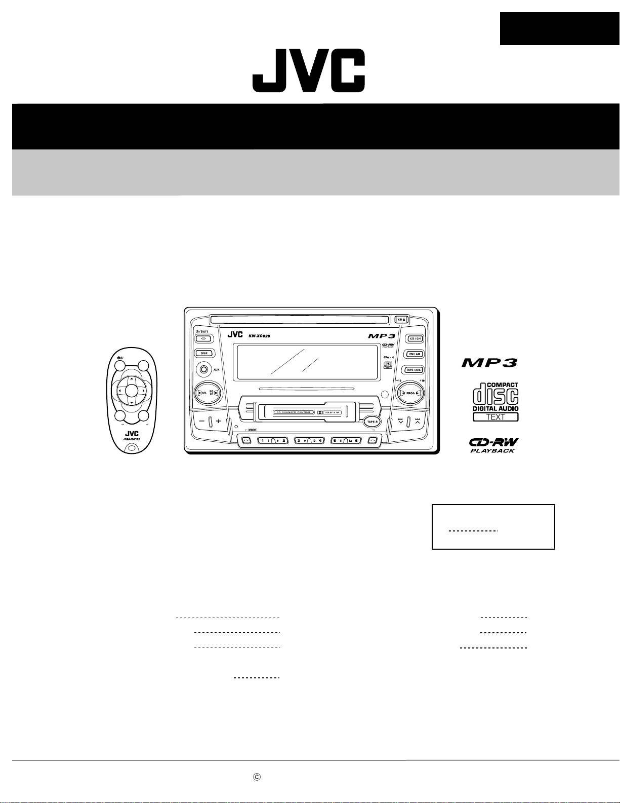
SERVICE MANUAL
CD/CASSETTE RECEIVER
KW-XC828
KW-XC828
SOUND
ATT
U
SOURCE
F
R
D
VOL
VOL
Contents
Safety precaution
Disassembly method
Adjustment method
Flow of functional
operation unit TOC read
1-2
1-3
1-30
1-31
DIRECTORY
E
X
Area Suffix
U Ather Areas
Maintenance of laser pickup
Replacement of laser pickup
Description of major ICs
1-33
1-33
1-36
COPYRIGHT 2002 VICTOR COMPANY OF JAPAN, LTD.
No.49729
Apr. 2002
Page 2
KW-XC828
Safety precaution
CAUTION
!
CAUTION
!
Burrs formed during molding may be left over on some parts of the chassis. Therefore,
pay attention to such burrs in the case of preforming repair of this system.
Please use enough caution not to see the beam directly or touch it in case of an
adjustment or operation check.
1-2
Page 3
KW-XC828
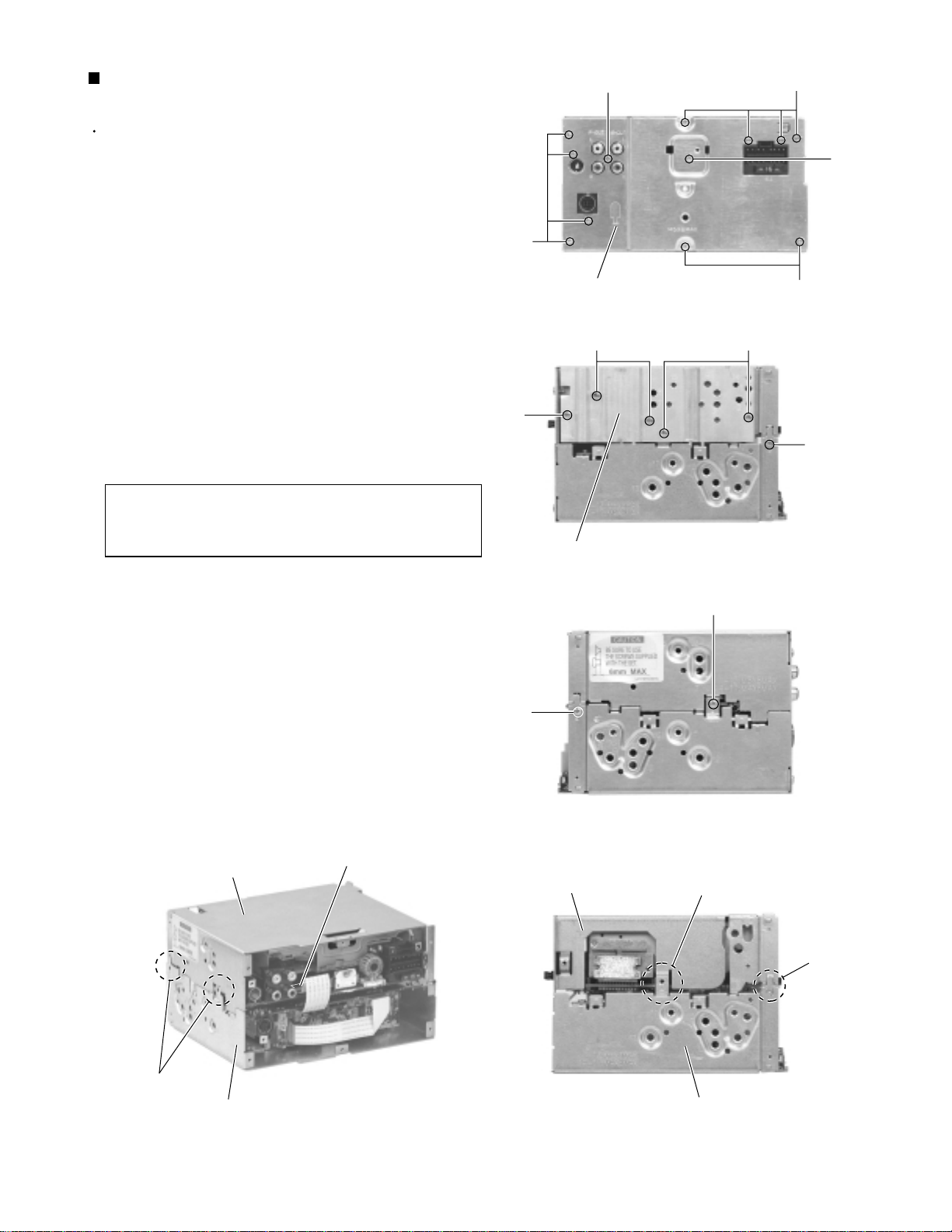
Disassembly method
Removing the front panel assembly
(See Fig.1 ~ 3)
1.
Remove the four screws A on both sides of the
body.
2.
Release four joints a on both sides of the body using
a screwdriver and remove the front panel assembly
toward the front. The connector which connects the
front panel assembly with the rear section comes off.
CAUTION:
When reassembling, make sure that
connector CN501 on the front panel
assembly is securely connected to
CN701 on the main board (See Fig.3).
Joint a
A
A
Joint a
Front panel assembly
Fig.1
Joint a
A
CN501
A
Joint a
Front panel assembly
Fig.2
Front panel assembly
CN701
Fig.3
1-3
Page 4
KW-XC828
Removing the system control board /
switch board (See Fig.4 , 5)
Prior to performing the following procedure, remove
the front panel assembly.
1.
Remove the twelve screws B retaining the system
control board.
2.
Remove the five screws C retaining the switch
board.
3.
Unsolder WR501 and WR502 of the wires
connecting the system control board with the switch
board.
B
B
WR502
System control board
WR502
B
Switch board
Fig.4
B
B
WR501
WR502
System control board
CC
Switch board
Fig.5
WR501
1-4
Page 5
KW-XC828
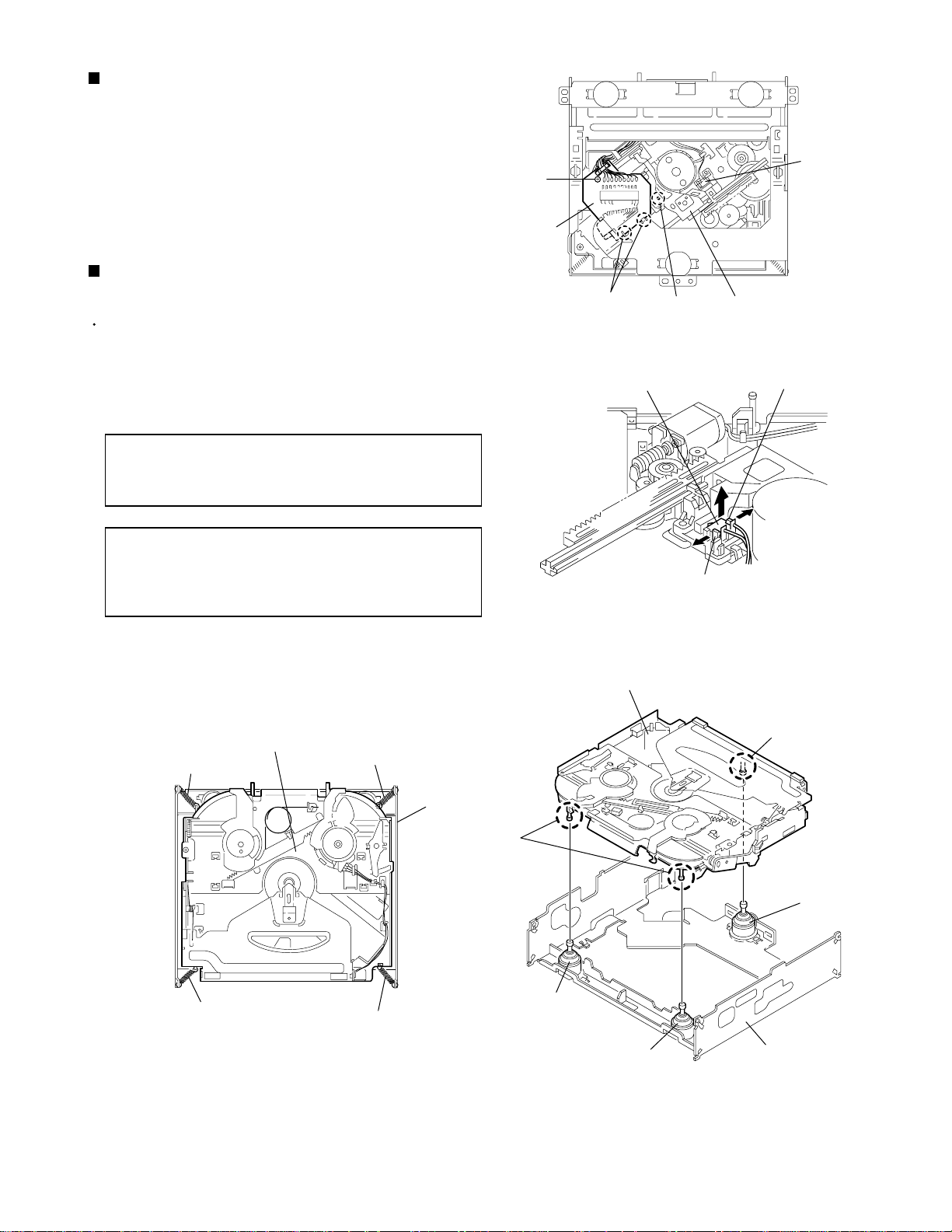
Removing the CD player section /
cassette player section (See Fig.6 ~ 10)
Prior to performing the following procedure, remove
the front panel assembly.
1.
Remove the ten screws D, the screw E and F
attaching the rear panel on the back of the body.
2.
Remove the three screws G and the two screws H
attaching the heat sink on the left side.
3.
Remove the three screws I attaching the CD player
section and the cassette player section on the both
sides of the body.
4.
Disconnect the card wire from connector CN702 on
the main board in the CD player section on the back
of the body.
5.
Remove the CD player section upward.
CAUTION:
When reassembling, joint the CD player
section and the cassette player section
at four joints b.
D
G
Rear panel
Heat sink
H
E
Fig.6
Fig.7
D
F
D
G
I
CD player section
CN702
I
CD player section
I
Fig.8
Joint b
Joint b
Joint b
Cassette player section
Cassette player section
Fig.10Fig.9
1-5
Page 6
KW-XC828
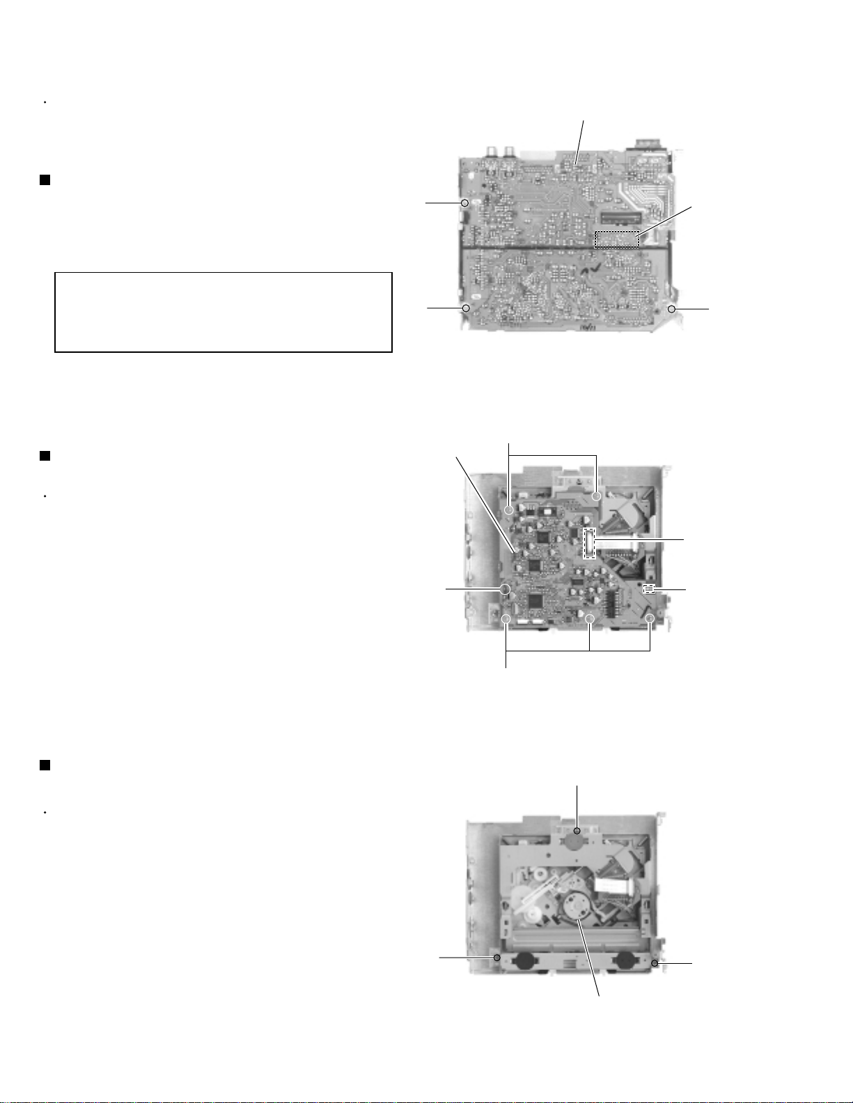
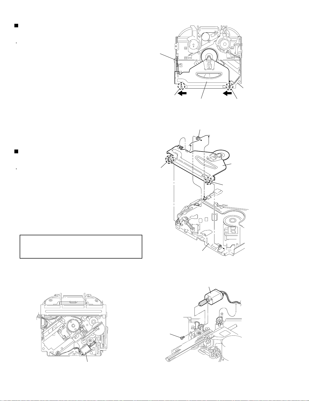
<CD player section>
Prior to performing the following procedure, remove
the front panel assembly, the CD player section and
the cassette player section.
Removing the main board (See Fig.11)
1.
Remove the three screws J attaching the main
board. The connector CN601 on the main board is
disconnected from the CD mechanism control board.
CAUTION:
When reassembling, securely connect
connector CN601 on the main board to
the connector on the CD mechanism
control board.
Removing the MP3 board
(See Fig.12)
Prior to performing the following procedure, remove
the main board.
J
J
MP3 board
Main board
CN601
J
Fig.11
K
1.
Disconnect the wire from connector CN601on the
MP3 board.
2.
Remove the five screws K and the MP3 board,
releasing the joint c and d.
Removing the CD mechanism assembly
(See Fig.13)
Prior to performing the following procedure, remove
the main board and MP3 board.
1.
Remove the three screws L attaching the CD
mechanism assembly.
Joint c
CN601
Joint d
K
Fig.12
L
1-6
L
CD mechanism assembly
Fig.13
L
Page 7
KW-XC828
<Cassette player section>
Prior to performing the following procedures, remove
the front panel assembly, the CD player section and
the cassette player section.
Removing the main board (See Fig.14)
1.
Disconnect the card wire from connector CN972 on
the main board.
2.
Remove the two screws M attaching the main
board.
Removing the cassette mechanism
assembly (See Fig.14 , 15)
Prior to performing the following procedure, remove
the main board.
N
M
CN972
Cassette mechanism assembly
Fig.14
Bottom cover
Main board
M
N
1.
Disconnect the card wire from connector CN972 on
the main board.
2.
Remove the four screws N from the bottom cover of
the cassette player section.
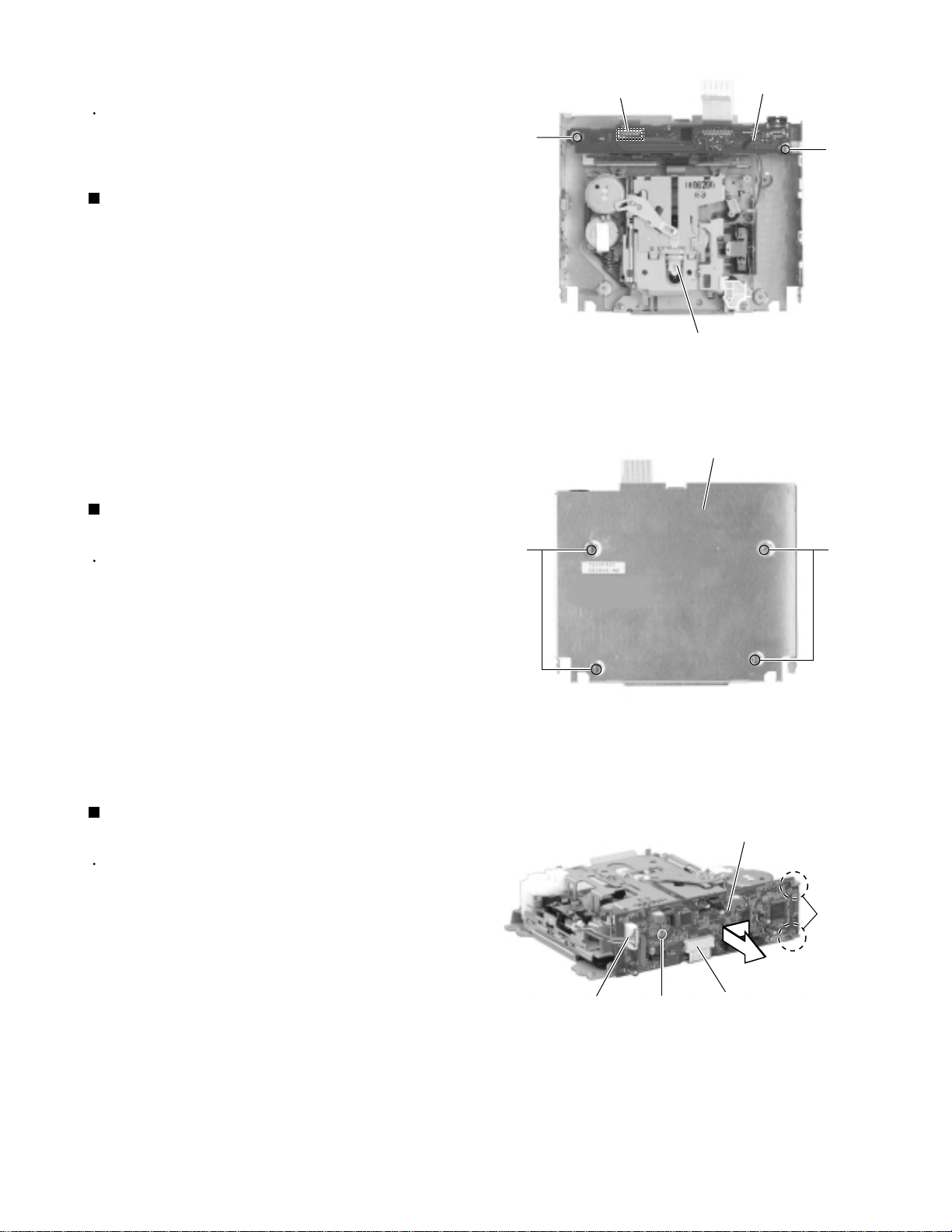
Removing the connector board
(See Fig.16)
Prior to performing the following procedure,
remove the cassette mechanism assembly.
1.
Remove the screw O and move the connector
board in the direction of the arrow to release the
two joints e.
2.
Disconnect the wire from connector CJ402 and
the card wire from CN403 on the connector
board respectively.
CJ402
Fig.15
O
Fig.16
Connector board
Joint e
CN403
1-7
Page 8
KW-XC828
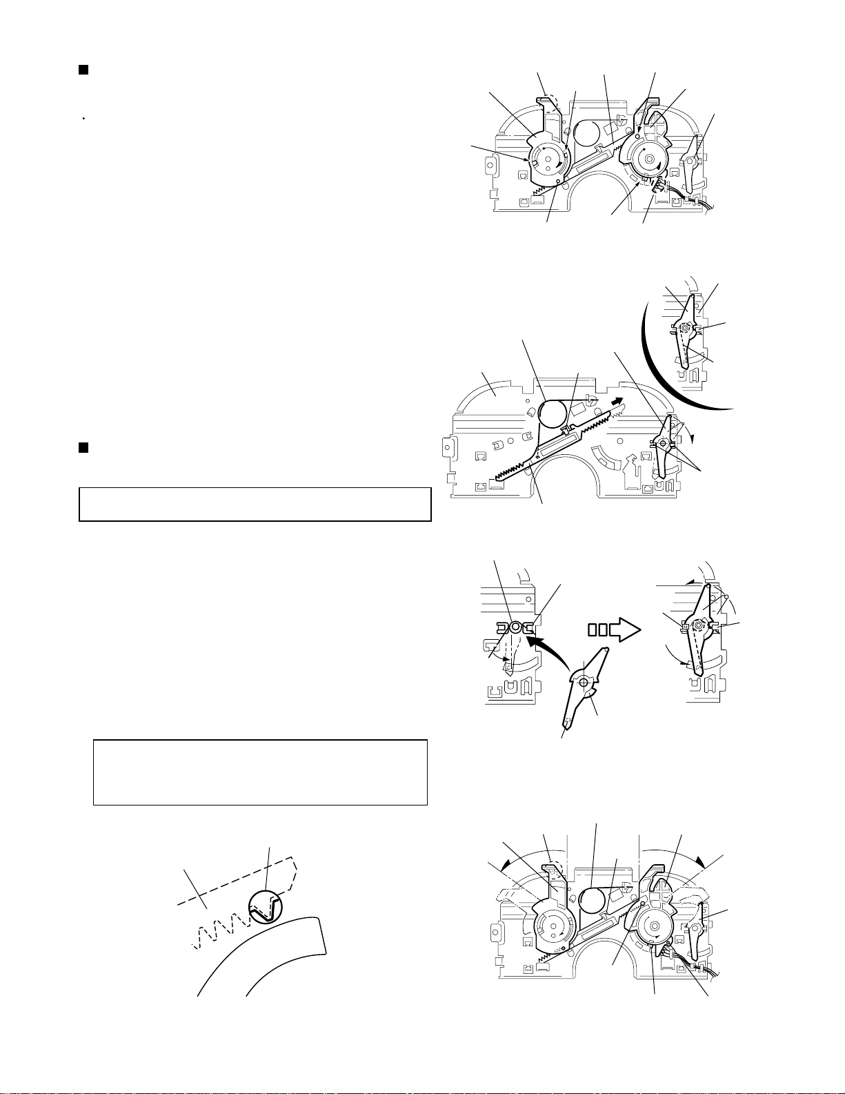
< CD mechanism section >
Removing the top cover
(See Fig.1 and 2)
1.
Remove the two screws A on each side of the body.
2.
Lift the front side of the top cover and move the
cover backward to release the two joints a.
Removing the connector board
(See Fig.3 to 5)
Top cover
A
A
Joints a
CAUTION:
1.
Remove the screw B fixing the connector board.
2.
Solder the short-circuit point on the connector board.
Disconnect the flexible wire from the pickup.
3.
Move the connector board in the direction of the
arrow to release the two joints b.
4.
Unsolder the wire on the connector board if
necessary.
CAUTION:
Before disconnecting the flexible wire
from the pickup, solder the short-circuit
point on the pickup. No observance of
this instruction may cause damage of
the pickup.
Unsolder the short-circuit point after
reassembling.
A
Fig.1
Joints a
Top cover
Fig.2
DET switch
B
1-8
Flexible wire
Frame
Connector board
B
Connector board
Joints b
Flexible wire
Short-circuit
Fig.3
Fig.4Fig.5
Pickup
Short-circuit point
(Soldering)
Pickup
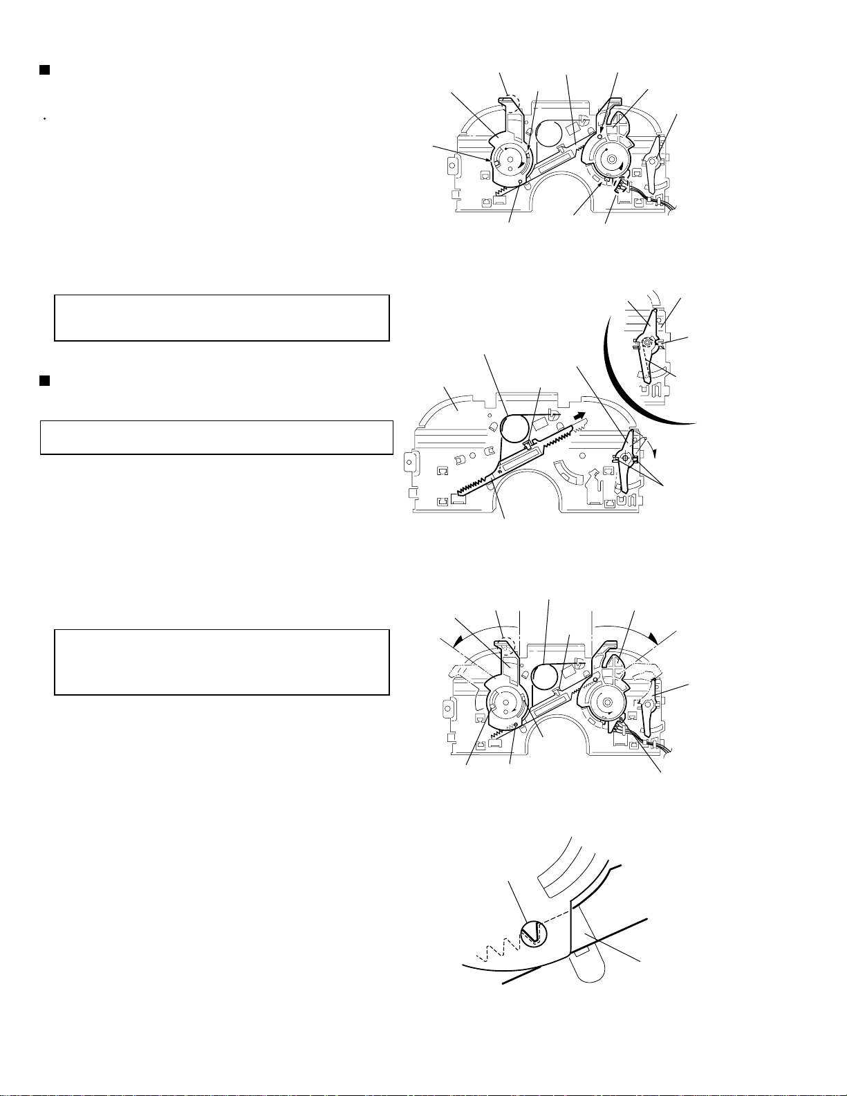
Page 9
Removing the DET switch
(See Fig.3 and 6)
1.
Extend the two tabs c of the feed sw. holder and pull
out the switch.
2.
Unsolder the DET switch wire if necessary.
Removing the chassis unit
(See Fig.7 and 8)
Prior to performing the following procedure, remove
the top cover and the connector board.
B
Connector board
Joints b
Short-circuit
Fig.3
KW-XC828
DET switch
Pickup
1.
Remove the two suspension springs (L) and (R)
attaching the chassis unit to the frame.
CAUTION:
The shape of the suspension spring (L)
and (R) are different. Handle them with
care.
CAUTION:
When reassembling, make sure that the
three shafts on the underside of the
chassis unit are inserted to the dampers
certainly.
Chassis unit
Suspension spring (R)
Suspension spring (L)
Frame
DET switch
Chassis unit
Tab c
Feed sw. holder
Tab c
Fig.6
Shaft
Suspension spring (R)
Suspension spring (L)
Shafts
Damper
Damper
Damper
Frame
Fig.8Fig.7
1-9
Page 10
KW-XC828
Removing the clamper assembly
(See Fig.9 and 10)
Prior to performing the following procedure, remove
the top cover.
1.
Remove the clamper arm spring.
2.
Move the clamper assembly in the direction of the
arrow to release the two joints d.
Removing the loading / feed motor
assembly (See Fig.11 and 12)
Prior to performing the following procedure, remove
the top cover, the connector board and the chassis
unit.
1.
Remove the screw C and move the loading / feed
motor assembly in the direction of the arrow to
remove it from the chassis rivet assembly.
Clamper arm
spring
Joint d
Joint d
Clamper assembly
Fig.9
Clamper arm spring
Chassis rivet
assembly
Joint d
Clamper assembly
Joint d
2.
Disconnect the wire from the loading / feed motor
assembly if necessary.
CAUTION:
When reassembling, connect the wire
from the loading / feed motor assembly
to the flame as shown in Fig.11.
Chassis rivet assembly
Fig.10
Loading / feed motor assembly
C
1-10
Loading / feed motor assembly
Fig.12Fig.11
Page 11

KW-XC828
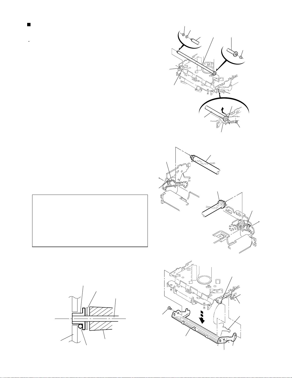
Removing the pickup unit
(See Fig.13 to 17)
Prior to performing the following procedure, remove
the top cover, the connector board and the chassis
unit.
1.
Remove the screw D and pull out the pu. shaft
holder from the shaft.
2.
Remove the screw E attaching the feed sw. holder.
3.
Move the part e of the pickup unit upward with the
shaft and the feed sw. holder, then release the joint f
of the feed sw. holder in the direction of the arrow.
The joint g of the pickup unit and the feed rack is
released, and the feed sw. holder comes off.
4.
Remove the shaft from the pickup unit.
5.
Remove the screw F attaching the feed rack to the
pickup unit.
Reattaching the pickup unit
(See Fig.13 to 16)
Joint f
Shaft
D
Joint e
Pu. shaft holder
Feed sw. holder
Pickup unit
Fig.13
Pickup unit
E
Joint f
Joint e
1.
Reattach the feed rack to the pickup unit using the
screw F.
2.
Reattach the feed sw. holder to the feed rack while
setting the joint tab g to the slot of the feed rack and
setting the part f of the feed rack to the switch of the
feed sw. holder correctly.
3.
As the feed sw. holder is temporarily attached to the
pickup unit, set to the gear of the joint g and to the
bending part of the chassis (joint h) at a time.
CAUTION:
4.
Reattach the feed sw. holder using the screw E.
5.
Reattach the shaft to the pickup unit. Reattach the
pu. shaft holder to the shaft using the screw D.
Make sure that the part i on the underside
of the feed rack is certainly inserted to the
slot j of the change lock lever.
F
Feed rack
Feed rack
E
Joint g
Feed sw. holder
Part i
Pickup unit
Slot j
Joint g
Feed sw. holder
Fig.14
Shaft
Joint f
Joint h
Fig.15
D
Pu. shaft holder
Pickup unit
Pickup unit
Feed rack
Joint f
Feed sw. holder
Fig.17Fig.16
1-11
Page 12
KW-XC828
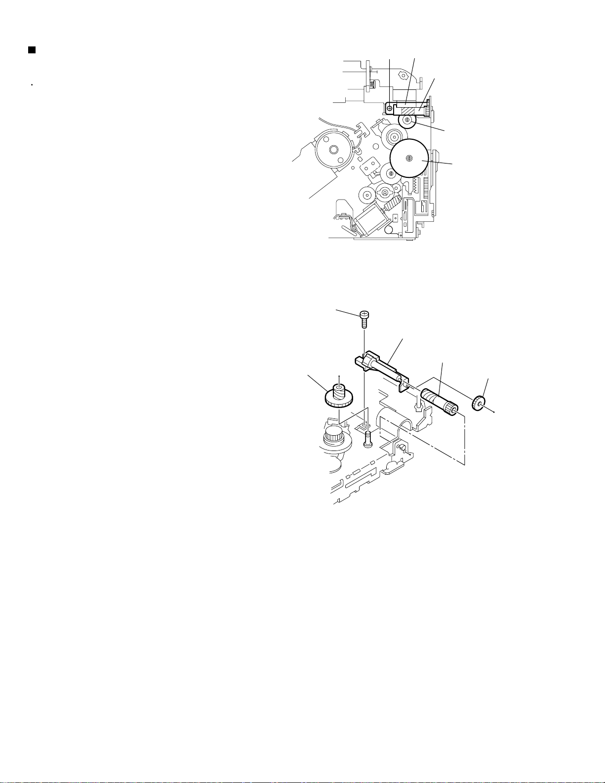
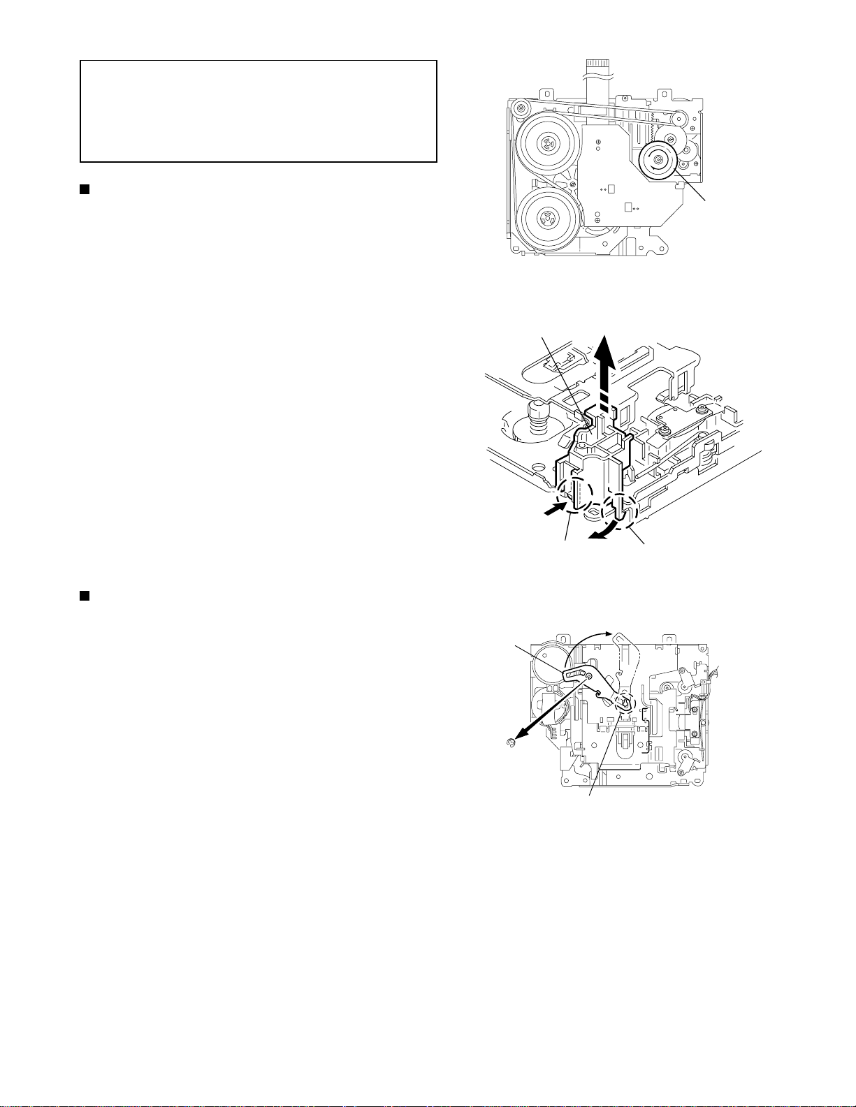
Removing the trigger arm
(See Fig.18 and 19)
Prior to performing the following procedure, remove
the top cover, the connector board and the clamper
unit.
1.
Turn the trigger arm in the direction of the arrow to
release the joint k and pull out upward.
Joint k
Trigger arm
CAUTION:
When reassembling, insert the part l and
m of the trigger arm into the part n and
o at the slot of the chassis rivet
assembly respectively and join the joint
k at a time.
Chassis rivet assembly
Chassis rivet assembly
Trigger arm
Fig.18
Part n
Part o
Part l
Part m
Fig.19
Removing the top plate assembly
(See Fig.20)
Prior to performing the following procedure, remove
the top cover, the connector board, the chassis unit,
and the clamper assembly.
1.
Remove the screw H.
2.
Move the top plate assembly in the direction of the
arrow to release the two joints p.
3.
Unsolder the wire marked q if necessary.
1-12
H
Top plate assembly
Joints p
q
Fig.20
Page 13
KW-XC828
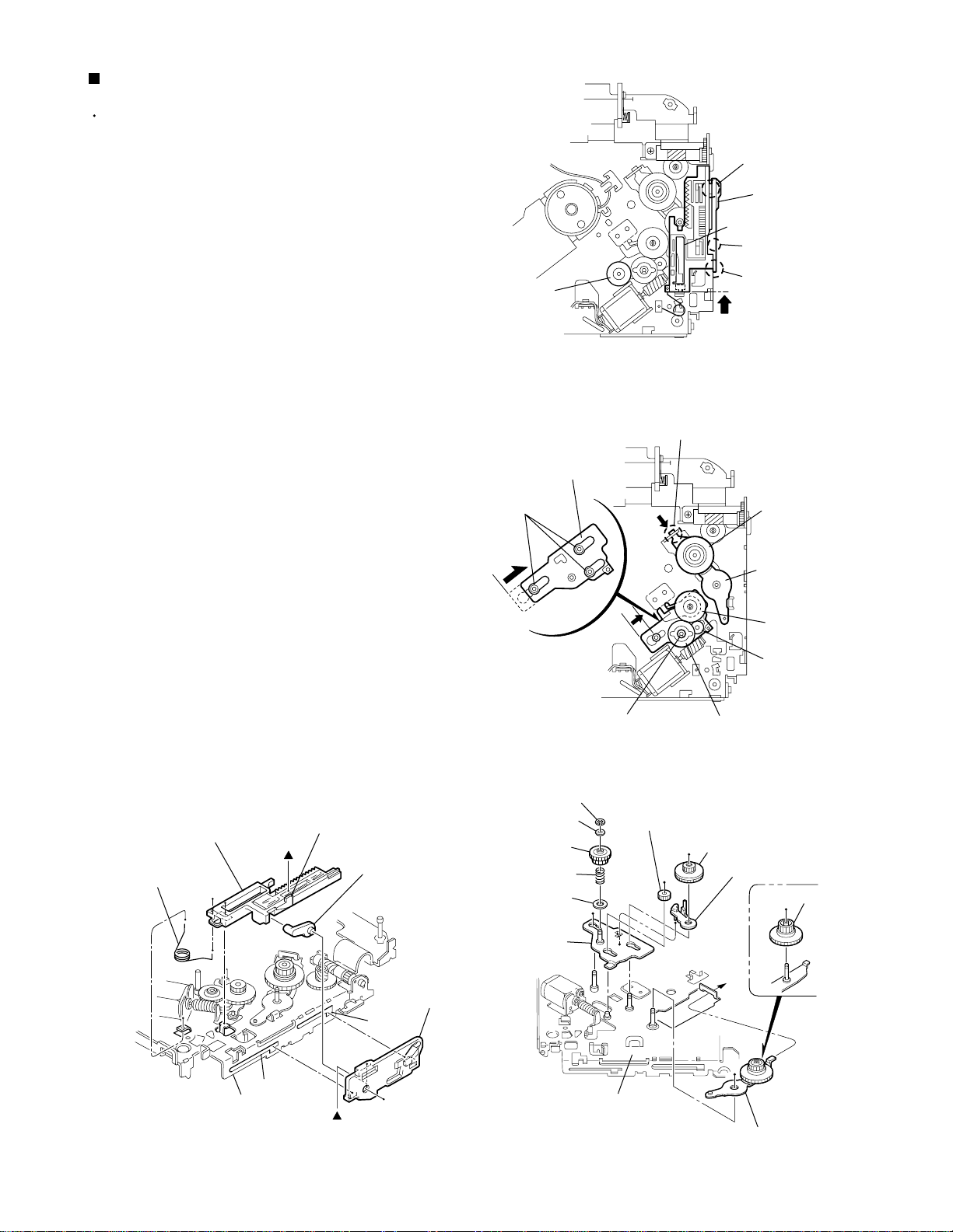
Removing the select arm (L) / select lock
arm (See Fig.21 and 22)
Prior to performing the following procedure, remove
the top plate assembly.
1.
Bring up the select arm (L) to release from the link
plate (joint r) and turn in the direction of the arrow to
release the joint s.
2.
Unsolder the wire of the select arm (L) marked q if
necessary.
3.
Turn the select lock arm in the direction of the arrow
to release the two joints t.
The select lock arm spring comes off the select lock
arm at the same time.
Reassembling the select arm (L) / select
lock arm (See Fig.23 to 25)
Select arm (R)
Joint z
Link plate spring
Top plate
Joint a'
Joint y
Link plate
Joint z
Joint s
Fig.21
Select lock arm
Select lock arm
Joint b'
Joint r
Select arm (L)
Select lock arm
q
Top plate
Hook u
Select lock
arm spring
Joints t
REFERENCE:
1.
Reattach the select lock arm spring to the top plate
Reverse the above removing procedure.
and set the shorter end of the select lock arm spring
to the hook u on the top plate.
2.
Set the other longer end of the select lock arm spring
to the boss v on the underside of the select lock arm,
and join the select lock arm to the slots (joint t). Turn
the select lock arm as shown in the figure.
3.
Reattach the select arm (L) while setting the part r to
the first peak of the link plate gear, and join the joint
s.
CAUTION:
When reattaching the select arm (L),
check if the points w and x are correctly
fitted and if each part operates properly.
Joint r
Link plate
Link plate
Select lock arm spring
Boss v
Select arm (R)
Joint a'
Fig.22
Hook u
Joint t
Joint t
Select lock arm
Fig.23
Link plate spring
Select arm (L)
Joint b'
Joint r
Fig.25Fig.24
Joint s
Select
lock arm
Point x
1-13
Page 14
KW-XC828
Removing the select arm (R) / link plate
(See Fig.21 and 22)
Prior to performing the following procedure, remove
the top plate assembly.
1.
Bring up the select arm (R) to release from the link
plate (joint y) and turn as shown in the figure to
release the two joints z and joint a’.
2.
Move the link plate in the direction of the arrow to
release the joint b’. Remove the link plate spring at
the same time.
REFERENCE:
Before removing the link plate, remove
the select arm (L).
Reattaching the Select arm (R) / link
plate (See Fig.25 and 26)
REFERENCE:
Reverse the above removing procedure.
Select arm (R)
Joint z
Link plate spring
Top plate
Joint a'
Part y
Link plate
Joint z
Joint s
Fig.21
Select lock arm
Select lock arm
Joint b'
Joint r
Select arm (L)
Select lock arm
q
Top plate
Hook u
Select lock
arm spring
1.
Reattach the link plate spring.
2.
Reattach the link plate to the link plate spring while
joining them at joint b’.
3.
Reattach the part y of the select arm (R) to the first
peak of the link plate while joining the two joints z
with the slots. Then turn the select arm (R) as shown
in the figure. The top plate is joined to the joint a’.
CAUTION:
When reattaching the select arm (R),
check if the part c’ is correctly fitted and
if each part operates properly.
Select arm (R)
Joint z
Link plate
Link plate spring
Joint a'
Part y
Part y
Fig.22
Joint b'
Joint z
Fig.25
Joints t
Select arm (L)
Select
lock arm
Point x
1-14
Link plate
Fig.26
Page 15
KW-XC828
Removing the loading roller assembly
(See Fig.27 to 29)
Prior to performing the following procedure, remove
the clamper assembly and the top plate assembly.
1.
Push inward the loading roller assembly on the gear
side and detach it upward from the slot of the joint d’
of the lock arm rivet assembly.
Detach the loading roller assembly from the slot of
the joint e’ of the lock arm rivet assembly.
The roller guide comes off the gear section of the
loading roller assembly.
Remove the roller guide and the washer from the
shaft of the loading roller assembly.
2.
Remove the screw I attaching the lock arm rivet
assembly.
3.
Push the shaft at the joint f’ of the lock arm rivet
assembly inward to release the lock arm rivet
assembly from the slot of the slide plate. Extend the
lock arm rivet assembly outward and release the
joint g’ from the boss of the chassis rivet assembly.
The roller guide springs on both sides come off.
Roller guide
Washer
Loading roller assembly
Roller guide
Joint e'
Roller guide spring
Roller guide spring
Joint d'
Loading roller assembly
Roller guide spring
Lock arm rivet assembly
Fig.27
Loading roller assembly
Roller guide
spring
CAUTION:
When reassembling, reattach the left
and right roller guide springs to the lock
arm rivet assembly before reattaching
the lock arm rivet assembly to the
chassis rivet assembly. Make sure to fit
the part h’ of the roller guide spring (L)
inside of the roller guide (Refer to
Fig.30).
Roller guide
Washer
Roller shaft assembly
Joint h'
Loading roller assembly
Roller guide
spring
Fig.28-1
Fig.28-2
Chassis rivet assembly
Boss
Slide plate
Roller guide spring
I
Frame
Loading roller
Roller guide spring
Lock arm rivet assembly
Joint f'
Part g'
Fig.29Fig.30
1-15
Page 16
KW-XC828
Removing the loading gear (5), (6) and
(7) (See Fig.31 and 32)
Prior to performing the following procedure, remove
the top cover, the chassis unit and the top plate
assembly.
1.
Remove the screw J attaching the loading gear
bracket. The loading gear (6) and (7) come off the
loading gear bracket.
2.
Pull out the loading gear (5).
Loading gear bracket
J
Loading gear (6)
Loading gear (5)
Loading gear (3)
Fig.31
J
Loading gear bracket
Loading gear (5)
Loading gear (6)
Loading gear (7)
Fig.32
1-16
Page 17
Removing the gears (See Fig.33 to 36)
Prior to performing the following procedure, remove
the top cover, the chassis unit, the top plate
assembly and the pickup unit.
1.
Pull out the feed gear.
KW-XC828
Slot j'
Slide plate
2.
Move the loading plate assembly in the direction of
the arrow to release the slide plate from the two slots
j’ of the chassis rivet assembly.
3.
Detach the loading plate assembly upward from the
chassis rivet assembly while releasing the joint k’.
Remove the slide hook and the loading plate spring
from the loading plate assembly.
4.
Pull out the loading gear (2) and remove the change
lock lever.
5.
Remove the E-washer and the washer attaching the
changer gear (2).
6.
The changer gear (2), the changer gear spring and
the adjusting washer come off.
7.
Remove the loading gear (1).
8.
Move the hang plate rivet assembly in the direction
of the arrow to release from the three shafts of the
chassis rivet assembly upward.
9.
Detach the loading gear plate rivet assembly from
the shaft of the chassis rivet assembly upward while
releasing the joint l’.
Feed gear
Change plate
rivet assembly
Shafts
E-washer
Loading plate assembly
Joint k'
Slot j'
Fig.33
Joint l'
Loading gear (4)
Loading gear plate
rivet assembly
Loading gear (2)
Loading gear (1)
Change gear (2)
10.
Pull out the loading gear (4).
Loading plate assembly
Loading plate spring
Slot j'
Chassis rivet assembly
Joint k'
Slide hook
Slide plate
Slot j'
E-washer
Washer
Loading gear (2)
Loading plate spring
Adjusting washer
Change plate
rivet assembly
Chassis rivet assembly
Fig.34
Loading gear (1)
Loading gear (2)
Change lock lever
Loading gear (4)
Loading gear plate rivet assembly
Fig.36Fig.35
1-17
Page 18
KW-XC828
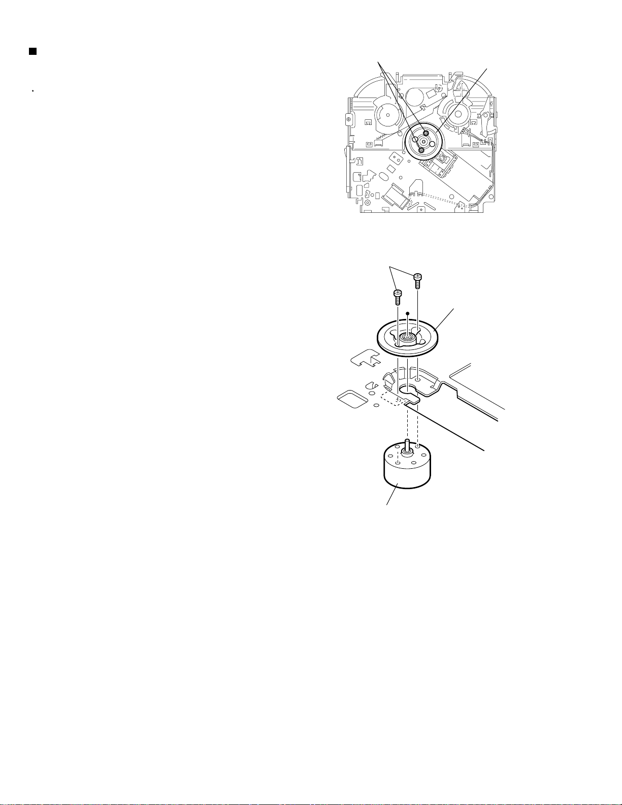
Removing the turn table / spindle motor
(See Fig.37 and 38)
Prior to performing the following procedure, remove
the top cover, the connector assembly and the
chassis / clamper assembly.
1.
Remove the two screws K attaching the spindle
motor assembly through the slot of the turn table on
top of the body.
2.
Unsolder the wire on the connector board if
necessary.
K
Turn table
Fig.37
K
Turn table
1-18
Spindle motor
Fig.38
Page 19
KW-XC828
REFERENCE:
Prior to performing the following
procedures, turn the mode gear on the
bottom of the body until the respective part
comes to the EJECT position (Refer to
Fig.1).
Removing the cassette guide (See Fig.2)
1.
Turn the mode gear to set to RVS play or
subsequent mode.
2.
Remove the cassette guide from the main chassis
while releasing each two joint tabs a in the direction
of the arrow.
Mode gear
Fig.1
Cassette guide
Removing the load arm (See Fig.3)
1.
Remove the E-washer attaching the load arm.
2.
Move the load arm in the direction of the arrow and
release the joint b on the cassette catch.
Load arm
E-washer
Tab a
Joint b
Tab a
Fig.2
Fig.3
1-19
Page 20

KW-XC828
Removing the cassette hanger assembly /
cassette holder (See Fig.4 to 7)
1.
Check the mode is set to EJECT. Push down the
front part of the cassette holder and move in the
direction of the arrow to release the joint c.
2.
Move the rear part of the cassette hanger assembly
in the direction of the arrow to release it from the two
joint bosses d.
3.
Release the holder stabilizer spring from the hooks e
and f, then pull out from the cassette hanger
assembly.
4.
Bring up the rear side of the cassette hanger
assembly to release the joint g and h.
5.
Pull out the cassette catch from the cassette hanger
assembly.
Cassette holder assembly
Side bracket
Joints c
Cassette holder assembly
Cassette stabilizer spring
Fig.4
Boss d
Cassette hanger assembly
Cassette hanger
assembly
Boss d
Cassette holder
assembly
Hook g
Fig.6
Hook f
Hook e
Fig.5
Cassette hanger assembly
Cassette catch
Cassette holder assembly
Cassette hanger assembly
Hook h
Fig.7
1-20
Page 21

KW-XC828
Removing the side bracket assembly
(See Fig.8 to 10)
1.
Remove the screw A attaching the side bracket
assembly.
2.
Detach the front side of the side bracket assembly
upward and pull out forward to release the joint i and
j in the rear.
CAUTION:
CAUTION:
When reassembling, make sure that the
boss k of the main chassis is set in the
notch of the load rack under the side
bracket assembly. Do not reattach the
load rack on the boss k.
After reattaching the side bracket
assembly, confirm operation.
Side bracket assembly
Joint i
Joint j
A
Side bracket assembly
Fig.8
Side bracket assembly
Joint i
Joint j
Load rack
Load rack
Boss k
Boss k
Fig.9
Fig.10
1-21
Page 22

KW-XC828
Removing the pinch arm (F) assembly
(See Fig.11 and 12)
1.
Remove the polywasher and pull out the pinch arm
(F) assembly.
2.
Remove the compulsion spring.
Removing the pinch arm (R) assembly
(See Fig.11 and 13)
1.
Remove the polywasher and pull out the pinch arm
(R) assembly.
Removing the slide chassis assembly
(See Fig.14 and 15)
Polywasher
Pinch arm
(R) assembly
Polywasher
Compulsion spring
Fig.11
Pinch arm
(F) assembly
Pinch arm (F) assembly
Polywasher
REFERENCE:
It is not necessary to remove the head
and the tape guide.
1.
Move the slide chassis assembly in the direction of
the arrow to release the two joints l and remove from
the main chassis.
2.
Remove the rack link.
CAUTION:
When reassembling, first reattach the rack
link, and next fit the boss m and hook n of
the slide chassis assembly to the hole of
the main chassis, and engage the two joints
l.
Rack link
Fig.12
Boss m
Pinch arm
(R) assembly
Fig.13
Head
Hook n
Polywasher
Tape guide
Joint l
Slide chassis assembly
1-22
Fig.14
Joint l
Fig.15
Page 23

KW-XC828
Removing the head / tape guide
(See Fig.16 and 17)
REFERENCE:
1.
Remove the band attaching the wire to the head.
2.
Remove the two screws B, the head and the head
support spring.
3.
Remove the pinch arm spring from the tape guide.
4.
Remove the tape guide and the pinch spring arm.
CAUTION:
CAUTION:
It is not necessary to remove the slide
chassis assembly.
When reattaching the pinch arm spring, set
both end of it to the pinch spring arm (
remarked o).
When reattaching the head, set the wires
into the groove of the tape guide (Fig.16).
B
Slide chassis assembly
Head
Tape guide
Fig.16
B
Pinch arm spring
Head
Head support spring
Tape guide
Removing the flywheel assembly (F) & (R)
(See Fig.18 and 19)
REFERENCE:
1.
Remove the belt at the bottom.
2.
Remove the two polywashers on the upper side.
3.
Pull out each flywheel assembly downward.
Flywheel assembly (F)
It is not necessary to remove the slide
chassis assembly.
Belt
o
Pinch spring arm
o
Slid chassis assembly
Fig.17
Polywasher
Polywasher
Flywheel assembly (R)
Fig.18
Flywheel assembly (F)
Fig.19
Flywheel assembly (R)
1-23
Page 24

KW-XC828
Disassembling the flywheel assembly (F)
(See Fig.20 and 21)
1.
Push and turn counterclockwise the spring holder (F)
to release the three joints p on the bottom of the
flywheel.
2.
The spring holder (F), the TU spring and the friction
gear play come off.
3.
Remove the polywasher and felt.
Flywheel assembly (F)
Joints p
Flywheel assembly (R)
Joints q
Disassembling the flywheel assembly (R)
(See Fig.20 and 22)
1.
Push and turn clockwise the spring holder (R) to
release the three joints q on the bottom of the
flywheel.
2.
The spring holder (R), the FF spring and the friction
gear FF come off.
3.
Remove the polywasher and the felt.
Removing the reel board
(See Fig.23 and 24)
1.
Remove the two screws C attaching the reel board.
2.
Move the reel board in the direction of the arrow to
release the joint r.
3.
Unsolder the wires if necessary.
CAUTION:
When reattaching, confirm operation of
the MODE switch and the ST-BY switch.
The mode position between EJECT and
ST-BY is optimum for reattaching.
Joint p
Fig.20
Polywasher
Polywasher
Spring holder (R)
Spring holder (F)
TU spring
Friction gear FF
Friction gear play
Felt
Flywheel assembly (F)
FF spring
Felt
Flywheel assembly (R)
Fig.21 Fig.22
Joint q
1-24
Connect the card wire extending from
the reel board to the FFC pad before
reattaching the reel board.
FFC pad
C
Reel board
C
Fig.23
Joint r
FFC pad
CT-1 switch
MODE switch
Soldering
ST-BY switch
Fig.24
Page 25

KW-XC828
Removing the gear base arm / gear base
link assembly (See Fig.25 to 27)
1.
Move the gear base arm in the direction of the arrow.
2.
Insert a slotted screwdriver to the gear base spring
under the gear base arm, and release the gear base
arm upward from the boss on the gear base
assembly.
3.
Remove the gear base arm from the main chassis
while releasing the two joints s.
4.
Move the gear base link assemby in the direction of
the arrow to release the two joints t.
REFERENCE:
When reattaching the gear base arm,
make sure that the boss on the gear
base assembly is inside the gear base
spring.
Removing the FFC pad
(See Fig.27 and 29)
Gear base
link assembly
Gear base spring
Joint t
Gear base arm
Joints s
Hook u
FFC pad
Hook u
Joint t
Fig.25
Gear base arm
Screwdriver
1.
Push each joint hook u of the FFC pad and remove
toward the bottom.
Gear base link assembly
Fig.26
Gear base arm
Fig.27
FFC pad
1-25
Page 26

KW-XC828
Removing the mode gear
(See Fig.28 and 31)
1.
Remove the polywasher on the bottom and pull out
the mode gear.
Removing the mode switch actuator
(See Fig.28, 29 and 31)
1.
Pull out the mode switch actuator at the bottom.
REFERENCE:
When reattaching the mode switch
actuator to the main chassis, make sure to
set on the shaft and insert v into the slot w.
Removing the direction link / direction
plate (See Fig.29 to 31)
1.
Remove the polywasher attaching the direction link.
2.
Bring up the direction link to release the three joints
x, y and z at a time.
3.
Move the direction plate in the direction of the arrow
to release the two joints a’.
REFERENCE:
When reattaching the direction plate,
engage the two joints a’ and move in the
direction of the arrow (Refer to Fig.30).
Mode switch actuator
Direction plate
Direction link
Fig.28
Direction plate
Joints a'
Joint z
Direction link
Slot w
Joint y
Polywasher
Fig.29
Direction plate Mode rack assembly
Joint b'
Mode gear
Polywasher
Mode rack assembly
Joint x
Joint b'
Joint c'
REFERENCE:
When reattaching the direction link,
move the direction plate in the direction
of the arrow and engage the three joint
x, y and z at a time (Refer to Fig.31).
Removing the mode rack assembly
(See Fig.29 and 30)
1.
Move the mode rack assembly in the direction of the
arrow to release the two joints b’ and the joint c’.
REFERENCE:
When reattaching, set the two b’ on the
bottom of the mode rack assembly into the
slots of the main chassis and move in the
direction of the arrow (See Fig.30).
Joints a'
Fig.30
Direction link
Mode switch actuator
Polywasher
v
Mode gear
Direction plate
Mode rack assembly
Fig.31
1-26
Page 27

KW-XC828
Removing the gear base assembly / take
up gear / reflector gear (See Fig.32 to 34)
1.
Push in the pin d’ of the gear base assembly on the
upper side of the body and move the reflector gear
toward the bottom, then pull out.
2.
Remove the polywasher on the bottom and pull out
the take up gear.
3.
Move the gear base assembly in the direction of the
arrow to release it from the two slots e’ of the main
chassis.
REFERENCE:
The parts are damaged when removed.
Please replace with new ones.
Gear base assembly
Pin d'
Polywasher
Slot e'
Slot e'
Fig.32
Take up gear
Removing the reel driver / reel spindle
(See Fig.34)
1.
Draw out the reel driver from the shaft on the main
chassis and remove the reel driver spring and the
reel spindle respectively.
CAUTION:
The reel driver is damaged when
removed. Please replace with a new
one.
Reflector gear
Reel driver
Reel driver spring
Reel spindle
Main chassis
Fig.33
Reel driver
Reel driver spring
Reel spindle
Gear base assembly
Slots e’
Take up gear
Reflector gear
Polywasher
Fig.34
1-27
Page 28

KW-XC828
Removing the side bracket assembly
(See Fig.35 to 39)
1.
Remove the eject cam plate spring.
2.
Push the joint f‘ through the slot to remove the load
rack downward.
3.
Move the eject cam limiter in the direction of the
arrow to release it from the boss g’ of the side
bracket assembly and from the two joints h’.
4.
Move the eject cam plate in the direction of the arrow
to release the joint i’.
Joint f'
CAUTION:
Joint h'
When reassembling, confirm operation of
each part before reattaching the eject cam
plate spring.
Side bracket assembly
Boss g'
Eject cam limiter
Side bracket assembly
Joint h'
Joint f'
Eject cam plate spring
Joint h'
Load rack
Fig.35
Boss g'
Eject cam limiter
Eject cam plate
Fig.37
Joint h'
1-28
Fig.36
Side bracket assembly
Boss g'
Eject cam plate
Fig.38
Load rack
Joint i'
Side bracket assembly
Eject cam plate
Joint i'
Fig.39
Page 29

KW-XC828
Removing the main motor assembly /
sub motor assembly (See Fig.40 to 42)
1.
Remove the belt at the bottom.
2.
Remove the polywasher and pull out the mode gear.
3.
Pull out the reduction gear (B).
4.
Remove the polywasher and pull out the reduction
gear (A).
5.
Remove the two screws D attaching the main motor
assembly.
6.
Remove the two screws E attaching the sub motor
assembly.
7.
Unsolder the wires on the reel board if necessary.
CAUTION:
When reassembling, adjust the length of the
wires extending from the sub motor
asswmbly by attaching them to the side of
the sub motor assembly with the wires
extending from the main motor assembly
using a spacer.
Belt
Reduction gear (B)
Reduction gear (B)
E
Polywasher
Fig.40
D
E
Mode gear
Polywasher
Reduction gear (A)
D
Main motor
assembly
Reduction
gear (A)
Polywasher
Sub motor
assembly
Spacer
Main motor assembly
Sub motor assembly
Main motor assembly
Sub motor assembly
Fig.41
Spacer
Fig.42
1-29
Page 30

KW-XC828
Adjustment method
Test Instruments required for adjustment
1.
Digital osclloscope(100Mz)
2.
Frequency Counter meter
3.
Electric voltmeter
4.
Wow&flutter meter
5.
Test tapes VT739..For playback frequency
measurement
VT712..For wow flutter&
tape speed measurement
VT703..For head azimuth measurement
6.
Torque gauge Cassette
for CTG-N(mechanism adjustment
7.
Laser power meter(Reader:LP800102)
8.
Prove for MD (Reader:LP8010-02)
9.
Pre masterd disc (TGYS-1)
10.
Test disc (JVC:CTS1000)
Measuring conditions (amplifier section)
Power supply voltage ..... DC14.4V(11V to 16V allowance )
Load impedance..... 4 ohm (4 ohm to 8 ohm allowance)
Line out .... 2.0V
Method of connecting extension cable
adjustment
Jig list: EXTSH002-22P x 1pc
Frequency Range:
FM: 87.5MHz to 108.0MHz
AM: 531 kHz to 1602kHz
Cassette mechanism
CN601
Extension cables
EXTSH002-22P
CN501
Main P.W.B
1-30
CD mechanism
Page 31

Flow of functional operation unit TOC read
Power ON
When the pickup correctly moves
v
to the inner area of the disc
Set Function CD
KW-XC828
When the laser diode correctly
emits
Microprocessor
commands
FMO
TC94A14FA" 40"
FEED MOTOR
+TERMINAL
IC561"4"
REST SW
When correctly focused
FEO
TA2157" 15"
Focus Servo Loop ONo
$83
$82
$81
3.3V
Hi-Z
0V
6V
4V
2V
OFF
ON
Pickup feed to the inner area
2.2V
RF signal eye-patternn
remains closed
RF signal eye-pattern
opens
Disc inserted
YES
Laser emitted
Focus search
Disc rotates
Tracking loop closed
TOC read out
YES
Microprocessor
commands
SEL
TC94A14FA"38"
LD
CN501"15"
"No disc"
display
When the disc correctly rotates
Microprocessor
commands
DMO
TC94A14FA"41"
Spindle
motor(-)
IC561"1"
$84 $86 $ A200
Acceleration Servo CLV
Rough
Servo
0.5 Sec 0.5 Sec
$84
3.3V
0V
4V
0V
3.3V
2.2V
0V
6V
3.2
2V
Jump to the first track
Play
Tracking Servo Loop ON
RF signal
Rough Servo Modev
CLV Servo Mode
(Program Area)
CLV Servo Mode
(Lead-In Area;
Digital :0)
1-31
Page 32

KW-XC828
Feed section
Is the voltage output at
IC521 pin "40" 5V or 0V?
Is 4V present at both
sides of the feed motor?
YES
YES
NO YES NO
NO
Is the wiring for IC521
(56)~(64) correct?
NO
Is 6V or 2V present at
IC561 "4" and "5"?
NO
Is 3.3V present at IC561
pin "20"?
Check the vicinity of
IC521.
YES
Check the feed motor
connection wiring.
YES
Check CD 8V
and 5V.
Check the feed motor.
Focus section
When the lens is
moving:
4V
Does the S-search
waveform appear at
IC561 pins "8" and "9"?
Spindle section
Is the disk rotated?
YES
Does the RF signal
appear at TP1?
YES
Is the RF waveform at TP1
distorted?
YES
Proceed to the Tracking
section
Check IC561.
NO
YES
NO
NO
NO
Check the circuits in
the vicinity of IC561
pins "8","9"and"15".
Check the pickup and
its connections
Is 4V present at IC561
pins "6" and "7"?
Check the spindle motor
and its wiring
Check the circuits in the
vicinity of IC501 "19"~
"24" or the pickup
YES
YES
NO
Is 4V present at IC521
pins "41" ?
Check the vicinity of
IC561.
NO
YES
Check IC521 and
IC501.
Tracking section
1-32
When the disc is rotated
at first:
Approx. 1.2V
Is the tracking error signal
output at IC501 "11"?
YES
Check IC521.
YES YES
Check the circuit in the
vicinity of IC501 pins
"2"~"12".
Check the pickup and
its connections
Page 33

Maintenance of laser pickup
(1) Cleaning the pickup lens
Before you replace the pickup,please try to
clean the lens with a alcohol soaked cotton
swab.
(2) Life of the laser diode
When the life of the laser diode has expired.
the following symptoms will appear..
(1) The level of RF output (EFM output:amplitude
of eye patterrn) will be low.
KW-XC828
Is RF output
1.3 0.4Vp-p?
YES
O.K
(3) Semi-fixed resistor on the APC PC board
The semi-fixed resistor on the APC printed
circuit board which is attached to the pickup
is used to adjust the laser power.Since this.
adjustment should be performed to match the
characteristics of the whole optical block,
do not touch the semi-fixed resistor..
If the laser power is lower than the specified
value, the laser diode is almost worn out, and
the laser pickup should be replaced.
If the semi-fixed resistor is adjusted while
the pickup is functioning normally, the laser
pickup may be damaged due to excessive current.
NO
Replace it.
Replacement of laser pickup
Turn of the power switch and, disconnect the
power cord.
Replace the pickup with a normal one.(Refer
to "Pickup Removal" on the previous page)
Plug the power cord in, and turn the power on.
At this time, check that the laser emits for
about 3seconds and the objective lens moves
up and down.
Note: Do not observe the laser beam directly..
Play a disc.
Check the eye-pattern at TP1.
Finish.
1-33
Page 34

KW-XC828
Mechanism Adjustment Section
Item
1.Head azimuth
Adjusting & Confirmation Methods
"Head Height Adjustment"
Note
Adjust the azimuth directly. When you adjust the height using a
mirror tape, remove the cassette housing from the mechanism
chassis. After installing the cassette housing, perform the azimuth
adjustment.
1. load the mirror tape (SCC-1659). Adjust with height adjustment
screw A and azimuth adjustment screw B so that line "A" of
the mirror tape runs in the center between Lch and Rch in the
reverse play mode.
2. After switching from REV to FWD then to REV, check that the
head position set in procedure "1" is not changed.
*If the position has shifted, adjust again and check.
3. Adjust the azimuth screw B so that line "B" of the mirror tape
runs in the center between Lch and Rch in the forward play
mode.
"Head Azimuth Adjustment"
1. Load the test tape (VT724: 1kHz) and play it back in the
reverse play mode. set the Rch output level to maximum.
2. Load the test tape (VT703: 10kHz) and play it back in the
forward play mode. Adjust the Rch and Lch output levels to
maximum, with azimuth adjustment screw B .
In this case, the phase difference should be within 45 .
3. Engage the reverse mode and adjust the output level to
maximum, with azimuth adjustment screw C .
4. When switching between forward and reverse modes, the
difference between channels should be within 3dB.
*Between FWD Lch and Rch, REV Lch and Rch.
5. When the test tape (VT721 (315Hz )) is played back, the level
difference between channels should be within 1.5dB.
Std. V alueAdjust
Head shield
The head is at low position
during FWD.
Head shield
The head is at height position
during REV.
FWD adj.
B
REV adj.
C
0
Playback head
Height adj.
Phase
A
45
2. Tape Speed
and
Wow & Flutter
3. DOLBY NR
level adjustment
1-34
1. Check to see if the reading of the frequency counter & Wow
flutter meter is within 3015-3045 Hz (FWD/REV), and less than
0.35% (JIS RMS).
2. In case of out of specification, adjust the motor with a built-in
volume resistor.
1. Play the test tape (VT724 : 1kHz) back.
2. Adjust the VR191 (Lch) and VR291 (Rch) so that the DOLBY NR
level is 27.5mV 0.5dB by TP191 (Lch), TP291 (Rch).
Built-in
volume resistor
VR191:Lch
VR291: Rch
Tape Speed
3015-3045Hz
Wow & Flutter
Less than
0.35%
(JIS RMS)
Speaker out
1kHz/10kHz
: -1dB 3dB,
63Hz/1kHz
: 0dB 3dB,
Page 35

Arrangement of adjusting & test points
Cassette mechanism
(Surface)
Azimuth screw (Reverse side)
Head amplifier board
DOLBY NR Level Adj.
Lch : VR401
Playback head
DOLBY NR Level Adj.
Rch : VR402
KW-XC828
Azimuth screw
(Forward side)
Capstan motor
Tape speed adjust
DOLBY NR Level Adj.
Lch : VR401
DOLBY NR Level Adj.
Rch : VR402
Head amplifier board
1-35
Page 36

KW-XC828
Description of major ICs
BR24C01AFV-W-X (IC502) : EEPROM
1.Pin layout
2.Block diagram
A0
1
A1
2
A2
3
VDD WPIN SCL SDA
A0 A1 A2 GND
1kbit EEPROM ARRAY
7bit
ADDRESS
DECODER
CONTROL LOGIC
SLAVE/WORD
7bit
ADDRESS REGISTER
START
STOP
ACK
8bit
DATA
REGISTER
8
7
6
VDD
WPIN
SCL
GND
4
HIGH VOLTAGE GEN.
3.Pin function
Pin name I/O
VDD
GND
A0,A1,A2
SCL
SDA
WPIN
*1 An open drain output requires a pull-up resister.
-
IN
IN
IN / OUT
IN
Power supply
Ground (0v)
Slave address set
Serial clock input
Slave and word address,
serial data input, serial data output *1
Write protect input
Vcc LEVEL DETECT
Function
SDA
5
1-36
Page 37

CXA2560Q (IC401) : Dolb y B type noise reduction system with play back equalizer amp.
1.Pin layout & block diagram
KW-XC828
31
PBFB2
32
PBRIN2
33
PBGND
34
PBFIN2
35
VCT
45k
36
PBREF
37
PBFIN1
38
PBGND
39
PBRIN1
40
PBFB1
2. Pin function
Pin No. Symbol
1
2
3
4
5
6
7
8
9
10
11
12
13
14
15
16
17
18
19
20
21
22
23
24
PBTC1
PBOUT1
OUTREF1
TAPEIN1
Vcc
NC
OUT1
TCH1
NC
MSLPF
G2FB
G1FB
MSTC
MSOUT
NC
NRSW
MUTE
METAL
DRSW
DIRECTION
FF/REW
NC
TCH2
OUT2
PBTC2
30 29 28
7k/12k
12345
PBTC1
300k
30k
30k
300k
7k/12k
F2
F1
PBOUT2
+
+
-
PBOUT1
OUTREF2
27
70 /120
1
1
70 /120
OUTREF1
TAPEIN2
100k
100k
TAPEIN1
GND
26
T2
T1
Vcc
I/O Function
Playback equalizer amplifier
capacitance
Playback equalizer amplifier
O
output
Output reference
O
TAPE input
I
Power supply
-
Line output
O
Time constant for the HLS
-
Cut-off frequency adjustment
of the music sensor LPF
Music signal interval detection
Music signal interval detection
Time constant for detecting
music signal interval
Music sensor out
O
No use
Dolby NR control
I
Mute function control
I
Playback equalizer amplifier
I
control
Head select control
I
Music sensor mode control
I
Music sensor control
I
Time constant for the HLS
Line output
O
25
FWD/RVS
LPF
6
DIREF
+
BIAS
MUTE
TAPE EQ
Vcc
+
-
NC
TCH2
OUT2
23 22 21
24
NR
OFF/B
-
F3
OFF/B
-
+
NR
8910
7
TCH1
OUT1
NC
MS MODE
NR MODE
MS ON/
OFF
DET
NC
MSSW
MSLPF
20
FF/REW
DIRECTION
19
METAL
18
MUTE
17
NRSW
16
NC
15
MSOUT
14
MSTC
13
G1FB
12
G2FB
11
Pin No. Symbol
25
26
27
28
29
30
31
32
33
34
35
36
37
38
39
40
DIREF
GND
TAPEIN2
OUTREF2
PBOUT2
PBTC2
PBFB2
PBRIN2
PBGND
PBFIN2
VCT
PBREF
PBFIN1
PBGND
PBRIN1
PBFB1
I/O Function
-
Resistance for setting the
reference
-
Ground
I
TAPE input
O
Output reference
O
Playback equalizer amplifier
output
-
Playback equalizer amplifier
capacitance
I
Playback equalizer amplifier
feedback
I
Playback equalizer amplifier
input
-
Playback equalizer amplifier
ground
I
Playback equalizer amplifier
input
O
Center
O
Playback equalizer amplifier
reference
I
Playback equalizer amplifier
input
-
Playback equalizer amplifier
ground
I
Playback equalizer amplifier
input
I
Playback equalizer amplifier
feedback
1-37
Page 38

KW-XC828
UPD784215AGC173 (IC701) : Main micon
1.Pin layout
100 ~ 76
1
75
~
25
26 ~ 50
2.Pin functions(1/2)
Pin No.
1
2
3~7
8
9
10
11
12
13
14
15
16
17
18
19
20
21
22
23
24
25
26
27
28
29
30
31
32
33
34
35
36
37
38
39
40
41
42
43
Symbol
NC
NC
NC
MUTE
VDD
X2
X1
GND
XT2
XT1
RESET
BUS INT
REMOCON
ACC DET
MEMORY DET
NC
CST P.REQ
CD P.REQ
AVDD
AVREF0
KEY0
KEY1
KEY2
KEY3
S.METER
LEVEL/ANA
TEMP
NC
AVSS
DIMMER IN
DIMMER OUT
AVREF1
BUS-SI
BUS-SO
BUS-SCK
BUS-I/O
LCD-DA
LCD-SCK
LCD-CE
~
51
I/O
Function
O
Non connect
O
Non connect
O
Non connect
O
Mute output terminal("L" output at mute)
-
Connects with VDD
-
Connects with X'tal departure pendulum of 12.5MHz(output )(main)
-
Connects with X'tal departure pendulum of 12.5MHz(input )(main)
-
Connect with GND
-
Connects with X'tal departure pendulum of 32.768KHz(output)
-
Connects with X'tal departure pendulum of 32.768KHz(input)
I
System reset input terminal
I
Interrupt signal detection terminal from J-BUS communication
I
Interrupt signal detection terminal from optical remote control
I
ACC power supply detection terminal("L" become a holding mode
because of the input)
I
Backup power supply detection terminal
("L" it when backup power supply is input)
("H" input when backup power supply uninputs)
O
Non connect
I
Cassette mechanism power supply start-up demand signal input
I
CD mechanism power supply start-up demand signal input
-
(Connect witj VDD)(Power supply for the A/D converter)
-
(Connect with VDD)(Standard power supply for the A/D converter)
I
KEY0 input terminal
I
KEY1 input terminal
I
KEY2 input terminal
I
KEY3 input terminal
I
Terminal of input of voltage of S meter(Electric field strength)
I
Level input terminal of level meter
I
Voltage input terminal (Use to correct the temperature of the contrast)
from the thermally sensitive resister.
I
To GND with 47k
-
(Connect with GND)(GND for the A/D converter and the D/A converter)
I
Dimmer signal input terminal("L" input at dimmer)
O
"H" output at DIMMER ON
-
(Connect with VDD)(Standard power supply for the D/A converter)
I
Input of data J-BUS communication
O
Output of data of J-BUS communication
I/O
Clock output for J-BUS communication
O
Output of I/O switch signal of J-BUS communication
(output "H" and input "L")
O
data output terminal to LCD driver
O
Clock output terminal for communication to LCD driver
O
Chip enable output terminal to LCD driver
1-38
Page 39

KW-XC828
2.Pin functions(2/2)
Pin No.
44~47
48
49
50
51
52
53
54
55
56~60
61
62
63
64
65
66~71
72
73~79
80
81
82
83
84
85
86
87
88
89
90
91
92
93
94
95~100
EPROM DI
EPROM DO
EPROM CK
SD/SI
PLL CE
PLLDATA
PLL CLK
PLL DI
E.VOL SO
E.VOL SCK
LCD RESET
TEL MUTE
GND
POWER ON
VDD
CD MUTE
CD RESET
AREA SET1
AREA SET2
LCD TEST
CST MUTE
CST RESET
TEST
NC
NC
NC
NC
NC
NC
NC
NC
NC
NC
NC
UPD784215AGC173(2/2)
I/O
FunctionSymbol
O
Non connect
O
Data input from EPROM
O
Data output to EPROM
O
EPROM Clock signal I/O
I
Stationdetector and stereo signal input terminal ("H" input at SD)
O
Chip enable output terminal to PLL
O
Data output terminal to PLL
O
Clock output terminal for communication to PLL
I
Data input terminal from PLL
O
Non connect
O
Non connect
I/O
Data I/O terminal to electric volume
I/O
Clock I/O terminal for communication to electric volume
O
Reset signal output terminalto LCD driver("L" output when resetting)
I
Outputs by "L" input the mute output terminal "L"
O
Non connect
-
(Connect with GND)
O
Non connect
O
Power is output " H" when it is on
-
(Connect with VDD)
I
Mute signal demand input terminal from CD mechanism
O
When the terminal RESET detects "L", 200mS "H"
O
(CD mechanism) (Reset output terminal is output)
Non connect
O
Non connect
I
Area setting of tuner 1
I
Area setting of tuner 2
O
Non connect
I
All lighring display of LCD by "L" input
O
Non connect
O
Non connect
I
Mute signal demandinput terminal from cassette mechanism
O
Reset output terminal to cassette mechanism
-
(When the terminal RESET detects "L", 200mS "H" is output)
GND and connects with 10k
O
Non connect
1-39
Page 40

KW-XC828
UPD784225GK-623 (IC501) : CPU
1.Pin layout
80 ~ 61
1 ~ 20
21 ~ 40
2.Pin function
Pin
Symbol
no.
1
TEMP
2
GND
3
GND
4
AVSS
5
ADCONT
6
NC
7
AVREF1
8
EPROMDI
9
EPROMDO
10
EPROMCK
11
LCDCE/SO
12
LCDDA/SI
13
LCDCK
14
/BUSIO
15
BUSIO
16
BUSSI
17
BUSSO
18
BUSSCK
19
BUSOUT
20
CDON
21
CDREQ
22
CDMUTE
23
NC
24
DSPRESET
25
CCE
26
BUCK
27
BUS3
28
BUS2
29
BUS1
30
BUS0
31
2XPLAY
32
RWSEL
33
VSS1
34
LOAD
35
LD/FE
36
MP3DI
37
MP3DO
38
MP3CK
39
MP3RESET
40
MPSSTB
60 ~ 41
I/O
Connect to TEMP detecter
I41
Connect to GND
-
Connect to GND
-
Connect to GND
-
No use
-
No use
-
Analog reference voltage
-
Data input terminal from EEPROM
I
Data output terminal from EEPROM
O
Clock signal I/O terminal with EEPROM
I/O
No use
-
No use
-
No use
-
J-BUS data I/O terminal
I/O
J-BUS data I/O terminal
I/O
J-BUS data input
I
J-BUS data output
O
J-BUS clock I/O
I/O
No use
-
The CD power supply control signal output.At CD:H
O
CD request
I
CD Mute
O
No use
-
DSP reset
O
CE output for data communication with CDLSI
O
Clock output for data communication with CDLSI
O
Data communication input output port 3 with CDLSI
I/O
Data communication input output port 2 with CDLSI
I/O
Data communication input output port 1 with CDLSI
I/O
Data communication input output port 0 with CDLSI
I/O
No use
-
CD RW select
I
Connect to GND
-
Loading signal
O
LDFLE switching signal
O
MP3 data input
I
MP3 data output
O
MP3 data clock
O
MP3 data reset
O
MP3 data standby
I
Function Function
Pin
no.
42
43
44
45
46
47
48
49
50
51
52
53
54
55
TEST MODE
56
57
58
59
60
61
62
63
64
65
66
67
68
69
70
71
72
73
74
75
76
77
78
79
80
Symbol
NC
NC
NC
DACML
DACMC
DACMD
DACCS
NC
NC
NC
NC
DISCSEL
DACSEL
NC
MP3SEL
8VDET
REST
SW2
RESET
SW1
B.DET
P.DET
BUSINT
MP3REQ
NC
VSS0
VDD1
X2
X1
VPP
XT2
XT1
VDD0
AVDD
IOP
KEY0
KEY1
KEY2
KEY3
I/O
Non use
-
Non use
-
Non use
-
DAC mode control latch
O
DAC mode control clock
O
DAC mode control data
O
DA convertor chip select
I
No use
-
No use
-
No use
-
No use
-
Initial setting
O
DA convertor select
O
No use
-
Connect to GND
-
MP3/CD-DA switch SW L:CD H:MP3
O
8V detection
I
Systemreset signal input
I
Detection switch of CD mechanism
I
Reset detection terminal
Detection switch of CD mechanism
I
Panel switch detection
I
Power switch detection
I
J-BUS signal interrupt input
I
MP3 request
O
No use
-
Connect to ground
-
Reference voltage terminal
-
No use
-
Connect to X'tal osc.
I
Test terminal
I
Non use
-
Connect to ground
-
Connect to ground
-
Reference voltage terminal
-
Laser signal input output
I/O
Key control signal input 0
I
Key control signal input 0
I
Key control signal input 0
I
Key control signal input 0
I
1-40
Page 41

UPD789166GB-590 (IC431) : CPU
1.Pin layout
44 ~ 34
1
KW-XC828
33
2.Pin function
Pin No.
1
2
3
4
5
6
7
8
9
10
11
12
13
14
15
16
17
18
19
20
21
22
23
24
25
26
27
28
29
30
31
32
33
34
35
36
37
38
39
40
41
42
43
44
~
11
12 ~ 22
Symbol
KEY0
KEY1
KEY2
KEY SEL
DOLBY SEL
RPT SEL
B.SKIP
NC
AVSS
NC
BUS-I/O
BUS-INT
TAPE IN
MAIN POWER
PWR_DET
BUS-SCK
VDD1
BUS-SO
BUS-SI
METAL IN
METAL OUT
ICO
XT2
XT1
RESET
X2
X1
VSS0
VDD0
DOLBY
MS IN
FF/REW
MOTOR
SUBMO-
SUBMO+
HEAD SEL
VSS1
REEL
STANBY
MODE
PREQ
MUTE
AVDD
AVREF
I/O
O
O
I/O
O
O
O
O
O
O
O
O
O
~
23
Function
I
KEY0 input terminal
I
KEY1 input terminal
I
KEY2 input terminal
I
KEY in select setting terminal (H:active)
I
DOLBY select setting terminal L: No DOLBY
I
REPEAT select setting input terminal L:No REPEAT
I
B.SKIP select setting input terminal
-
Connect to GND
-
A/D converter GND voltage. Connect to GND
Non connect
J-BUS I/O switching output. output:H input:L
I
J-BUS signal interlupt input
I
Tape IN detection switch input
I
CTRL+B input H:Normal operation L:Save mode
I
MEMORY detection
J-BUS clock input/output
-
Power supply (without port section) connect to 5V
J-BUS data output terminal
I
J-BUS data input terminal
-
Non connect
-
Non connect
-
Connect to VSS0 or VSS1
-
Non connect
-
Connect to VSS0 or VSS1
-
Reset detection terminal
-
X'tal oscillator (4.1943MHz)
-
X'tal oscillator (4.1943MHz)
-
Ground voltage of port section. Connect to GND
-
Power supply for port section Connect to 5V
DOLBY ON/OFF setting output H:ON
I
MS input
Input level selrct for MS L:FF,REW H:Normal PLAY
Main motor output H:Motor rotation
Clockwise operation output for sub motor
Counterclockwise operation output for sub motor
HEAD AMP input signal select output L:FWD H:REV
I
GND voltage (without port section)
I
REEL palse input
I
Standby position detection H:EJECT side L:operation side
I
Mode palse input L: mechanism position fix
Power request output H:cassette mechanism operation
Mute request output L:mute request
-
A/D converter analog power supply. Connect to 5V
-
A/D converter reference voltege. Connect to 5V
1-41
Page 42

KW-XC828
HA13164A (IC911) : Regulator
1.Terminal layout
2.Block diagram
123456789101112131415
ANT OUT
EXT OUT
ANT CTRL
CTRL
CD OUT
AUDIO OUT
C3
0.1u
C4
0.1u
C5
0.1u
C6
10u
2
1
7
11
12
10
MEMORY
AJ ACC
8
Surge Protector
BIAS TSD
15
3
TAB
C1
100u
C2
0.1u
13
AJGND GND
+B
BATT.DET OUT
9
ACC 5V
6
VDD OUT
4
SW5VOUT
5
14
ACC
ILMOUT
R1
C7
0.1u
C8
0.1u
3.Pin function
Pin No. Symbol Function
1
2
EXTOUT
ANT
Output voltage is VCC-1 V when M or H level applied to CTRL pin.
Output voltage is VCC-1 V when M or H level to CTRL pin and H level
to ANT-CTRL.
3
4
5
6
7
8
9
10
11
12
13
14
15
ACCIN
VDDOUT
SW5VOUT
ACC5V
ANT CTRL
MEMORY
BATT
9V
CTRL
CD OUT
AJ
ILM
GND
Connected to ACC.
Regular 5.7V.
Output voltage is 5V when M or H level applied to CTRL pin.
Output for ACC detector.
L:ANT output OFF , H:ANT output ON
Connected to VCC.
Low battery detect.
Output voltage is 9V when M or H level applied to CTRL pin.
L:BIAS OFF, M:BIAS ON, H:CD ON
Output voltage is 8V when H level applied to CTRL pin.
Adjustment pin for ILM output voltage.
Output voltage is 10V when M or H level applied to CTRL pin.
Connected to GND.
UNIT R:
C:F
note1) TAB (header of IC)
connected to GND
1-42
Page 43

LC75878W (IC501) : LCD driver
1. Pin layout
100 ~ 76
KW-XC828
2. Block diagram
OSC
VLCD
VLCD0
VLCD1
VLCD2
VLCD3
VLCD4
VDD
VSS
1
~
25
26 ~ 50
P1
GENERAL
PORT
CLOCK
GENERATOR
CONTRAST
ADJUSTER
P4
75
~
51
COM1
COMMON
DRIVER
COM8
S75/COM9
S74/COM10
S73
SEGMENT DRIVER & LATCH
CONTROL
REGISTER
SHIFT REGISTER
CCB
INTERFACE
S1
3. Pin function
No. Symbol
1~73
74
75
76~83
84~87
88
89
90
91
92
93
94
95
96
97
98
99
100
SEG1~SEG73
SEG74
SEG75
COM8~COM1
P1~P4
VDD
VLCD
VLCD0
VLCD1
VLCD2
VLCD3
VLCD4
VSS
OSC
LCD RESET
CE
CL
DI
DI
INH
I/O
O
Segment driver output pin.
O
Segment driver output pin.
O
Segment driver output pin.
O
Common driver output pin.
O
General-purpose output pin.
-
Logic block power supply pin.
-
LCD driver power supply pin.
O
LCD driver bias 4/4 voltage (H-level) power pin.
I
LCD driver bias 3/4 voltage (intermediate level) power pin.
I
LCD driver bias 2/4 voltage (intermediate level) power pin.
I
LCD driver bias 1/4 voltage (intermediate level) power pin.
I
LCD driver bias 0/4 voltage (L-level) power pin.
-
Power supply pin to connect to ground.
I/O
Oscillator pin.
I
Display off, general-purpose output port L fixed input pin.
I
Chip enable
I
Synchronization clock
I
Transfer data
Function
CL
CE
1-43
Page 44

KW-XC828
LA4743K (IC901) : Power amp.
1.Block diagram
IN 1
0.22 F
TAB
IN 2
0.22 F
+
Vcc 1/2 Vcc 3/4
2200 F 0.022 F
6 20
+
11
-
+
+
-
9
7
OUT 1+
OUT 1-
1
Protective
circuit
+
-
+
12
+
-
PWR GND1
8
OUT 2+
5
OUT 2-
3
PWR GND2
2
ST BY
R.F
47 F
IN 3
PRE GND
IN 4
+5V
ST ON
+
0.22 F
N.C
+
0.22 F
4
Stand by
Switch
Mute
10
+
Ripple
Filter
Mute
22
circuit
3.3 F
+
15
-
+
-
17
19
10K
+
OUT 3+
OUT 3-
Low Level
Mute ON
25
18
21
23
PWR GND3
OUT 4+
OUT 4-
13
14
Protective
circuit
-
+
+
-
1-44
ON TIME C
22 F
Muting &
16
+
ON Time Control
Circuit
PWR GND4
24
Page 45

2.Terminal layout
3.Pin function
1
2
3
4
5
6
7
8
9
10
11
12
13
14
15
16
17
18
19
20
21
22
23
24
25
SymbolPin No. Function
GND
GND
RFOUTSTBY
RFOUT+
GND
RROUTGND
RROUT+
SVR
RRIN
RFIN
SGND
FLIN
RLIN
AC-GND
RLOUT+
GND
RLOUTVCC2
FLOUT+
MUTE
RLOUTGND
HSD
Header of IC
Power GND
Outpur(-) for front Rch
Stand by input
Output (+) for front Rch
Power input
Output (-) for rear Rch
Power GND
Output (+) for rear Rch
Ripple filter
Rear Rch input
Front Rch input
Signal GND
Front Lch input
Rear Lch input
Power on time control
Output (+) for rear Lch
Power GND
Output (-) for rear Lch
Power input
Output (+) for front
Muting control input
Output (-) for front
Power GND
No connection
KW-XC828
1-45
Page 46

KW-XC828
LA6579H-X (IC681) : 4-Channel bridge driver
1. Pin layout & Block diagram
VIN1-A
VIN1+A
VCCP1
1
+
2
3
VIN1_SW
[H]: OP-AMP_A
[L]: OP-AMP_B
[H]
[L]
28
VIN1
27
VIN1-B
-
+
26
VIN1+B
VO+
VO-
VO2+
VO2-
FR
VO3+
VO3-
VO4+
4
5
6
7
FR
8
9
10
Power system
GND
Level shift
33k
11k
-
Signal system
power supply
25
S-GND
+
24
VIN1-SW
Level shift
+
Level shift
Level shift
All outputs ON/OFF
H : ON
L : OFF
3.3VREG
(External:PTP Tr)
MUTE
Power system GND
Signal system
power supply
23
MUTE
22
VREFIN
FR
21
20
FR
VCCS
3.3VREG
+
-
19
REGIN
1-46
VO4-
VCCP2
VIN4
VIN4G
11
12
13
14
11k
33k
+
33k
33k
18
VIN2G
11k
-
17
VIN2
+
16
VIN3G
11k
-
15
VIN3
+
Page 47

3.Pin function
Pin No. Symbol Function
1
2
3
4
5
6
7
8
9
10
11
12
13
14
15
16
17
18
19
20
21
22
23
24
25
26
27
28
VIN1-A
VIN1+A
VCCP1
VO1+
VO1VO2+
VO2VO3+
VO3VO4+
VO4VCCP2
VIN4
VIN4G
VIN3
VIN3G
VIN2
VIN2G
REGIN
3.3VREG
VCCS
VREFIN
MUTE
VIN1_SW
S_GND
VIN1+B
VIN1-B
VIN1
CH1 input AMP_inverted input
CH1 input AMP_non-inverted input
CH1 and CH2 power stage power supply
Output pin(+)for channel 1
CH1 output pin (-) for channel 1
Output pin(+)for channel 2
Output pin(-)for channel 2
Output pin(+)for channel 3
Output pin(-)for channel 3
Output pin(+)for channel 4
Output pin(-)for channel 4
CH3 and CH4 power stage powr supply
Input pin for channel 4
Input pin for channel 4(for gain adjustment)
Input pin for channel 3
Input pin for channel 3(for gain adjustment)
Input pin for channel 2
Input pin for channel 2(for gain adjustment)
External PNP transistor, base connection
3.3VREG output pin, external PNP transistor,collector connection
Signal system GND
Reference voltage application pin
Output ON/OFF pin
CH1 input OP AMP_changeover pin
Signal system GND
CH1 AMP_B non-inverted input pin
CH1 AMP_B inverted input pin
CH1 input pin, input OP_AMP output pin
KW-XC828
1-47
Page 48

KW-XC828
TA2157FN-X(IC601):RF amp
1.Terminal layout
2.Block diagram
24 ~ 13
1 ~ 12
13
14
15
16
17
18
19
20
21
10pF
20k
40k30k
20k 20k
20k
BOTTOM
15k
50 A
12k
12k
PEAK
20k
20k
20k
PEAK
1.3V
40k
40k
240k
15pF
240k
15pF
50k
2k
20k
50k
14k
K
1
15k
x0.5
x2
x0.5
x2
1k
2k
1.75k
10pF
12
11
10
9
8
7
6
5
4
1-48
22
23
24
PIN SEL
VCTRLPIN
VCC
HiZ
GND
3k
3k
(APC SW)
APC ON
APC ON
APC OFF
(LDO=H)
180k
40pF
TEB
(TE BAL)
-50%
0%
+50%
180k
40pF
60k
60k
94k
22k
94k
22k
RFGC
(AGC Gian)
+12dB
+6dB
0dB
3
2
1
TEB
(TE BAL)
Normal mode
(0dB)
Normal mode
(0dB)
CD-RW mode
(+12dB)
Page 49

3.Pin function
Pin No. Symbol I/O Function
1
VCC
2
FNI
3
FPI
4
TPI
5
TNI
6
MDI
7
LDO
8
SEL
-
3.3V power supply pin
I
Main-beam amp input pin
I
Main-beam amp input pin
I
Sub-beam amp input pin
I
Sub-beam amp input pin
I
Monitor photo diode amp input pin
O
Laser diode amp output pin
I
APC circuit ON/OFF control signal, laser diode (LDO) control signal input
or bottom/peak detection frequency change pin.
KW-XC828
TA2175FN-X
9
10
11
12
13
TEB
TEN
TEO
RFDC
GVSW
SEL
GND
Hiz
VCC
I
Tracking error balance adjustment signal input pin
Adjusts TE signal balance by ellminating carrier component from PWM
signal (3-state output,PWM carrier = 88.2kHz) output from TC94A14F/FA
TEBC pin using RC-LPF and inputting DC.
TEBC input voltage:GND~VCC
I
Tracking error signal genaration amp negative-phase input pin
O
Tracking error signal generation amp output pin.
Combining TEO signal RFRP signal with TC94A14F/FA configures tracking
search system.
O
RF signal peak detection output pin
I
AGC/FE/TE amp gain change pin
GVSW Mode
GND
Hiz
VCC
APC
circuit
OFF Connected VCC through 1k resistor
ON
ON Control signal output
Control signal output
CD-RW
Normal
LCD
14
15
16
17
18
19
20
21
22
23
24
VRO
FEO
FEN
RFRP
REIIS
RFGO
RFGC
AGCI
RFO
RFN
GND
O
Reference voltage (VRO) output pin
VRO=1/2VCC When VCC=3.3V
O
Focus error signal generation amp output pin
I
Focus error signal generation amp negative-phase input pin
O
Signal amp output pin for track count
Combining RFRP signal and TEO signal with TC94A14F/FA configures
tracking search system.
I
Signal generation amp input pin for track count
O
RF signal amplitude adjustment amp output pin
I
RF amplitude adjustment control signal input pin
Adjusts RF signal amplitude by eliminating carrier component from PWM
signal (3-state output,PWM carrier=88.2kHz)output fromTC94A14F/14FA
RFGC pin using RC-LPF and inputting DC.
RFGC input voltage:GND~VCC
I
RF signal amplitude adjustment amp input pin
O
RF signal generation amp output pin
I
RF signal generation amp input pin
-
GND pin
1-49
Page 50

1-50
VSS
io1
io0
AD15
AD16
/WR
AD14
AD13
VSS
REQ
AD6
AD7
AD8
VDDT
AD9
KW-XC828
TC94A02F-005(IC652) : DSP
AD10
io2
io3
io4
VDD
io5
io6
io7
VSSP
PDo
VCoi
VDDP
CK0
VDDX
48
49
50
Generator
Prog.
Start
DIT
VC0
General Input Port
Timing
51
52
53
54
55
56
57
58
59
60
61
62
Xi
47
SRAM I/F
I-Bus
PROM
4k*2+2k
=10kword
40bit
Instruction
Decoder
4546
Interrupt
Control
PRAM
256word
X-Bus
Y-Bus
Program
Control
44
Timer
XRAM
4k word
43
YRAM
4k word
42
41
Flag
CROM
4k word
*3
X0 X1 X2
Y0 Y1 Y2
40
2k word
register
ERAM
39
X-Pointer
register
MX MY MZ
MAC ALU
A0 A1
round & limit
38
General
Output Port
Address Calc.
2sets
Y-Pointer
register
AX AY
A2
37
A3
round & limit
36
C-Pointer
register
35
Bus
Switch
34
33
AD11
32
AD12
31
CKS
30
TESTP
29
28
VSSR
27
VRAR
DAC
DAC
26
Ro
25
VDAR
24
VDAL
23
Lo
22
VRAL
21
VSSL
20
VSS
19
STANDBY
Xo
VSSX
16
/CE
18
VDD
17
/oE
63
10
AD3
Audio.I/F
11
AD4
12
SDi0
13
BCKiA
14
LRCKiA
15
AD5
64
1
/RESET
2
MiMD
AD0
Microcom.I/F
AD1
543
MiDio
6
/MiCK
AD2
87
VDDT
9
SDo
Page 51

KW-XC828
3.Pin function(1/2)
Pin No. Symbol Function
1
/RESET
2
MiMD
3
AD0
4
AD1
5
MiDio
6
/MiCK
7
AD2
8
VDDT
9
SDo
10
11
12
13
14
15
16
17
18
19
20
21
22
23
24
25
26
27
28
29
30
31
32
33
34
35
36
37
38
39
40
41
42
43
44
45
46
47
48
49
50
AD3
AD4
SDi0
BCKiA
LRCKiA
AD5
CE
OE
VDD
STANBY
VSS
VSSL
VRAL
LO
VDAL
VDAR
RO
VRAR
VSSR
TESTP
CKS
AD12
AD11
AD10
AD9
VDDT
AD8
AD7
AD6
REQ
VSS
AD13
AD14
WR
AD16
AD15
io0
io1
VSS
io2
io3
I/O
O
O
I/O
O
O
O
O
O
O
O
O
O
O
O
O
O
O
O
O
O
O
O
O
O
O
I/O
I/O
I/O
I/O
Hard reset input terminal(H:Normal operation L: Reset)
I
Micon I/F mode select input terminal
I
External SRAM address output 0 terminal
External SRAM address output 1 terminal
Micon I/F data input/output terminal
Micon I/F clock input terminal
I
External SRAM address output 2 terminal
Digital power supply (3.3V)
Data output terminal
External SRAM address output 3 terminal
External SRAM address output 4 terminal
Data input terminal 0
I
Bit clock input terminal A
I
LR clock input terminal A
I
External SRAM address output 5 terminal
External SRAM chip enable terminal
External SRAM output enable terminal
Digital power supply (2.5V)
Standby mode control terminal
I
Digital GND
DAC Lch GND
DAC Lch reference voltage terminal
DAC Lch output terminal
DAC Rch power supply terminal(2.5V)
DAC Lch power supply terminal(2.5V)
DAC Rch output terminal
DAC Rch reference voltage terminal
DAC Rch GND
Test terminal
I
VCO select terminal
I
External SRAM address output 12 terminal
External SRAM address output 11 terminal
External SRAM address output 10 terminal
External SRAM address output 9 terminal
Digital power supply terminal (3.3V)
External SRAM address output 8 terminal
External SRAM address output 7 terminal
External SRAM address output 6 terminal
Squeeze request terminal to host
Digital GND
External SRAM address output 13 terminal
External SRAM address output 14 terminal
External SRAM write signal
External SRAM address output 16 terminal
External SRAM address output 15 terminal
External SRAM data input/output 0 terminal
External SRAM data input/output 1 terminal
Digital GND
External SRAM data input/output 2 terminal
External SRAM data input/output 3 terminal
TC94A02F-005
1-51
Page 52

KW-XC828
3.Pin function(2/2)
Pin No. Symbol Function
51
52
53
54
55
56
57
58
59
60
61
62
63
64
io4
VDD
io5
io6
io7
VSSP
Pdo
Vcoi
VDDP
Cko
VDDX
Xi
Xo
VSSX
I/O
I/O
I/O
I/O
I/O
O
O
O
External SRAM data input/output 4 terminal
Digital power supply (2.5V) terminal
External SRAM data input/output 5 terminal
External SRAM data input/output 6 terminal
External SRAM data input/output 7 terminal
VCO GND
PLL phase error detection signal output terminal
VCO control voltage input terminal
I
VCO power supply
-
16.934 MHz clock output terminal
Power supply (2.5V) terminal for oscillator
Connection terminal for oscillator(input)
I
Connection terminal for oscillator(output)
GND for oscillator
-
TC94A02F-005
1-52
Page 53

M61508FP-X (IC951) : E. volume
1. Pin layout & Block diagram
VCC
(Anarog)
2. Pin function
Pin No.
1
2
3
DEFP IN1
DEFN IN1
4
5
6
7
8
9
DEFN OUT1
SEL OUT1
10
11
12
13
14
15
TONE OUT1
FADER IN1
REAR OUT1
FRONT OUT1
NonFader OUT1
16
17
18
19
VDDOUT1
VDDOUT2
20
21
22
NonFader OUT2
23
24
25
26
FRONT OUT2
REAR OUT2
FADER IN2
TONE OUT2
27
28
29
SEL OUT2
DEFN OUT1
30
31
32
33
34
35
DEFN IN1
DEFP IN1
36
REF
Symbol Function
REF
Grand for IC signal
Differential motion amp. Positive terminal
Differential motion amp. Negative terminal
INA1
INB1
INC1
IND1
Input terminal of input selector switch channel 1
Input terminal of input selector switch channel 1
Input terminal of input selector switch channel 1
Input terminal of input selector switch channel 1
Differential output terminal (-)
Input selector output terminal
VOL IN1
Volume 1 input terminal
Tone output terminal
Volume 2 input terminal
Fader volume control (Rear) output terminal
Fader volume control (Front) output terminal
Non fader volume output terminal
GND
DATA
GND terminal
Control data input terminal
Test terminal
Test terminal
CLOCK
VDD
Clock input terminal for serial data transport
Power supply terminal for digital
Non fader volume control output terminal
Fader volume (Front) output terminal
Fader volume (Rear) output terminal
Volume 2 input terminal
Tone output terminal
VOL IN2
Volume 1 input terminal
Input selector output terminal
Differential output terminal (-)
IND2
INC2
INB2
INA2
Input terminal of input selector switch channel 2
Input terminal of input selector switch channel 2
Input terminal of input selector switch channel 2
Input terminal of input selector switch channel 2
Differential motion amp negative input terminal
Differential motion amp positive input terminal
VCC
Power supply terminal
50K
27282930313233343536
LOUDNESS
+
3BAND TONE CONTROL
(BASS/MID/TREBLE)
ZERO CROSS
DETECTOR
ZERO CROSS
DETECTOR
LOUDNESS
+
3BAND TONE CONTROL
(BASS/MID/TREBLE)
A
B
B
A
2526
Zero detect
Select SW
121110987654321
24 23 22 21 20 19
VDO
(Digital)
Soft select
12dB
I/F
12dB
TIMER
DETECTOR
GND
13 14 15 16 17
KW-XC828
18
1-53
Page 54

KW-XC828
TC94A14FA (IC621) : DSP & DAC
1.Terminal layout & block daiagram
49
50
51
52
53
54
55
56
57
58
59
60
61
62
63
48 47 46 45 44 43 42 41 40 39
Clock
LPF
generator
Micro-
controller
interface
1-bit
DAC
Audio out
circuit
Address
circuit
circuit
Correction
Digital
output
16 k
RAM
PWM
Servo
control
ROM
RAM
CLV servo
Synchronous
guarantee
EFM
decoder
Sub code
decoder
38 37 36 35 34 33
D/A
A/D
Digital equalizer
automatic
adjustment circuit
Data
slicer
VCO
PLL
TMAX
32
31
30
29
28
27
26
25
24
23
22
21
20
19
18
64
2.Pin function
Pin
Symbol I/O Descroption
No
1
BCK
2
LRCK
O
Bit clock output pin.32fs,48fs,or 64fs selectable by command.
O
L/R channel clock output pin."L" for L channel and "H" for R channel. Output polarity
can be inverted by command.
3
AOUT
4
DOUT
5
IPF
O
Audio data output pin. MSB-first or LSB-first selectable by command.
O
Digital data output pin.Outputs up to double-speed playback.
O
Correction flag output pin. When set to "H", AOUT output cannot be corrected by C2
correction processing.
6
7
8
9
10
11
12
13
14
15
V
DD3
V
SS3
SBOK
CLCK
DATA
SFSY
SBSY
HSO
UHSO
PV
DD3
-
Digital 3.3V power supply voltage pin.
-
Digital GND pin.
O
Subcode Q data CRCC result output pin. "H" level when result is OK.
O
Subcode P-W data read I/O pin. I/O polarity selectable by command.
O
Subcode P-W data output pin.
O
Playback frame sync signal output pin.
O
Subcode block sync signal output pin. "H" level at S1 when subcode sync is detected.
I/O
General-purpose input / output pins.
Input port at reset.
-
PLL-only 3.3V power supply voltage pin.
17
161514131211101 2 3 4 5 6 7 8 9
1-54
Page 55

Pin
Symbol I/O Description
No
16
17
PDO
TMAX
EFM and PLCK phase difference signal output pin.
O
TMAX detection result output pin.
O
KW-XC828
TC94A14FA
18
19
20
21
22
23
24
25
26
27
28
29
30
31
32
33
34
35
36
37
38
39
40
41
42
43
44
45
46
47
48
49
50
51
52
53
54
55
56
57
58
59
60
61
62
63
64
LPFN
LPFO
PVREF
VCOF
AVSS3
SLCO
RFI
AVDD3
RFCT
RFZI
RFRP
FEI
SBAD
TEI
TEZI
FOO
TRO
VREF
RFGC
TEBC
SEL
AVDD3
FMO
DMO
VSS3
VDD3
TESIN
XVSS3
XI
XO
XVDD3
DVSS3R
RO
DVDD3
DVR
LO
DVSS3L
ZDET
VSS5
BUS0
BUS1
BUS2
BUS3
BUCK
/CCE
/RST
VDD5
TMAX Detection Result
Longer than fixed period
Within fixed period
Shorter than fixed period
Inverted input pin for PLL LPF amp.
I
Output pin for PLL LPF amp.
O
PLL-only VREF pin.
VCO filter pin.
O
Analog GND pin.
DAC output pin for data slice level generation.
O
RF signal input pin. Zin selectable by command.
I
Analog 3.3V power supply voltage pin.
RFRP signal center level input pin.
I
RFRP signal zero-cross input pin.
I
RF ripple signal input pin.
I
Focus error signal input pin.
I
Sub-beam adder signal input pin.
I
Tracking error input pin. Inputs when tracking servo is on.
I
Tracking error signal zero-cross input pin.
I
Focus equalizer output pin.
O
Tracking equalizer output pin.
O
Analog reference power supply voltage pin.
RF amplitude adjustment control signal output pin.
O
Tracking balance control signal output pin.
O
APC circuit ON/OFF signal output pin. At laser on, high impedance with UHS="L",
O
TMAX Output
DD3
"PV
"
"HiZ"
"AV
SS3
"
H output with UHS="H".
Analog 3.3V power supply voltage pin.
Feed equalizer output pin.
O
Disc equalizer output pin.
O
Digital GND pin.
Digital 3.3V power supply voltage pin.
Test input pin. Normally, fixed to "L".
I
System clock oscillator GND pin.
System clock oscillator input pin.
I
System clock oscillator output pin.
O
System clock oscillator 3.3V power supply voltage pin.
DA converter GND pin.
R-channel data forward output pin.
O
DA converter 3.3V power supply pin.
Reference voltage pin.
L-channel data forward output pin.
O
DA converter GND pin.
1 bit DA converter zero detection flag output pin.
O
Microcontroller interface GND pin.
Microcontroller interface data I/O pins.
I/O
Microcontroller interface clock input pin.
I
Microcontroller interface chip enable signal input pin.At "L", BUS0 to BUS3 are active.
I
Reset signal input pin. At reset, "L".
I
Microcontroller interface 5V power supply pin.
-
1-55
Page 56

KW-XC828
PCM1716E-X (IC571) : D/A converter
1. Pin layout
2. Block diagram
BCK
LBCK
DATA
ML/llS
MC/DM1
MD/DM0
CS/WO
MODE
MUTE
RST
3. Pin function
Pin
Symbol Function
No.
1
LRCK
2
DATA
3
BCK
4
CLKO
5
6
7
8
9
10
11
12
13
14
15
16
17
18
19
20
21
22
23
24
25
26
27
28
XTI
XTO
DGND
VDD
VDD2R
AGND2R
EXTR
NC
VOUTR
AGND1
Vcc1
VOUTL
NC
EXTL
AGND2L
Vcc2L
ZERO
RST
CS/IWO
MODE
MUTE
MD/DM0
MC/DM1
ML/IIS
28 15
114
Serial
Input
I/F
Mode
Control
I/F
Mult-level
8X Oversampling
Digital Filter
with
Function Controller
SCK
BPZ-Cont
Crystal OSC
XTI XTO CLKO Vcc1 VccAGND1 DGND
Delta-Sigma
Modulator
Power Supply
Vcc2L
DAC
DAC
AGND2L
Vcc2R
AGND2R
Open drain
Low-pass
Filter
Low-pass
Filter
I/O
I
LRCK clock input
I
Serial audio data input
I
Bit clock input for serial audio data
O
Buffered output of system clock
I
Oscillator input / External clock input
O
Oscillator output
-
Digital ground
-
Digital power +5V
-
Analog power +5V
-
Analog ground
O
Rch common pin of analog output amp
-
Non connection
O
Rch analog voltage output of audio signal
-
Analog ground
-
Analog power +5V
O
Lch analog voltage output of audio signal
-
Non connection
O
Lch common pin of analog output amp
-
Analog ground
-
Analog power +5V
O
Zero data flag
I
Reset
I
Chip select / Input format selection
I
Mode control select
I
Mute control
I
Mode control, Data / De-emphasis selection 1
I
Mode control, BCK / De-emphasis selection 2
I
Mode control, WDCK / Input format selection
VoutL
EXTL
VoutR
EXTR
ZERO
1-56
Page 57

TB2118F-X (IC21) : PLL
1.Terminal Layout
2423222120191817161514
KW-XC828
13
2.Block diagram
NC
2
1
XO
24
XI
FM VCO
AMVCO
IFC
CE
DIN
DOUT
DIMM
15
16
13
3
4
5
6
123456789
Buff.
ON/OFF
OSC circuit
AMP
AMP
AMP
Serial
Interface
101112
Reference Counter
Prescaler
20-bit BINARY COUNTER
Resistor 1
Resistor 2
I/O PORT
Swallow counter
Phase
Comparator
4-bit
12-bit
Programmable counter
22-bit
40bit shift register
OUTPUT PORT
Constant
power supply voltage
switch
Vdd
Vcc
switch
AM CP.
20
+
+
-
REG.
22
19
vt
18
FM cp
3.Pin Function
Pin
Symbol I/O Function
No.
XOUT
10
11
12
1
2
3
4
5
6
7
8
9
NC
CE
DI
CK
DOUT
SR
I/01
I/02
O1
O2
VDD2
Crystal oscillator pin
O
Non connect
Chip enable input
I
Serial data input
I
Clock input
I
Serial data output
O
Register control pin
O
I/O ports
I/O
I/O ports
I/O
Non connect
Non connect
Single power supply for REF. frequency block
-
7
SL
8
9
I/O -2I/O -1
10 11
12
out-2out-1
vdd2
Pin
Symbol I/O Function
No.
IFC
13
VDD
14
FMIN
15
AMIN
16
DGND
17
FMCP
18
VT
19
AMCP
20
VCC
21
RF
22
AGND
23
XIN
24
17
14
IF signal input
I
Power pins for digital block
FM band local signal input
I
AM band local signal input
I
Connect to GND (for digital circuit)
Charge pump output for FM
O
Tuning voltage biased to 2.5V.
Charge pump output for AM
O
Power pins for analog block
Ripple filter connecting pin
I
Connect to GND (for analog circuit)
Crystal oscillator pin
I
21
23
a-gnd
vccd-gndvdd
1-57
Page 58

KW-XC828
HD74HCT126T-X (IC503) : Buffer
1.Terminal layout
Vcc
14
1
1C
2.Block diagram
2
1A
4C
13
3
1Y
1A
4A
12
4Y
11
4
2C
3C
10
5
2A
6
2Y
3A
9
3Y
8
7
GND
3.Pin function
INPUT
C
L
H
H
H : High level
L : Low level
X : Irrelevant
Off (Hhigh-impedance)state of a 3-stage
Z :
output
OUTPUT
A
X
L
H
Y
Z
L
H
1C
2A
2C
3A
3C
4A
1Y
2Y
3Y
1-58
4Y
4C
Page 59

BR24C16F-X (IC702) : EEPROM
KW-XC828
1. Pin layout
VDD WPIN SCL SDA
A0 A1 A2 GND
3. Block diagram
A0 1
A1 2
A2 3
11bit
Address
decoder
16kbit EEPROM allay
11bit
START
Control circuit
2. Pin function
Symbol
VDD
GND
A0,A1,A2
SCL
SDA
WPIN
Slave W ard
Address resister
STOP
I/O
Power supply.
GND
No use connect to GND.
I
I
Serial clock input.
I/O
Serial data I/O of slave and ward address.
I
Write protect terminal.
8bit
Data
resister
Function
8 VDD
7 WPIN
6 SCL
GND 4
High voltage osc circuit
LB1641 (IC402) : DC motor driver
1. Pin layout
1 2 3 4 5 6 7 8 9
GNDOUT1 P1
VZ IN1 IN2
VCC1
VCC2 P2
Power supply
voltage det.
10
OUT2
ACK
2. Pin function
Input Output
IN1 IN2 OUT1 OUT2
0 0 0 0
1 0 1 0
0 1 0 1
1 1 0 0
5 SDA
Mode
Brake
CLOCKWISE
COUNTER-CLOCKWISE
Brake
1-59
Page 60

KW-XC828
HD74HC126FP-X (IC461,IC761) : Buffer
1.Pin layout
2.Pin function
1C
1
1A
2
1Y
3
2C
4
2A
5
2Y
6
GND
7
3.Block diagram
VCC
14
4C
13
4A
12
4Y
11
3C
10
3A
9
3Y
8
Vcc Vcc
1A
2A
3A
Input
4A
1C
2C
3C
See Function Table
4C
1Y
2Y
3Y
4Y
Output
Output
Output
Output
Input
C
L
H
H
A
X
L
H
Output
Y
Z
H
L
Note) H:High level
L:Low level
X:Irrelevant
Z:Off(High-impedance)
State a 3-state input
1k
S1
CL
1k
Sample as Load Circuit 1
Sample as Load Circuit 1
Sample as Load Circuit 1
Note) CL includes probe and jig capacitance
NJU7241F25-X(IC651,IC504):Voltage regulator
1.Terminal layout & Pin function
(Top View)
Pin function
1
2
3
4
5
GND
IN
V
V
OUT
NC
STB
1
5
2
3
4
1-60
Page 61

IC-PST9333U-X (IC432,IC791) : Regulator
1. Pin layout
2. Block diagram
KW-XC828
NC 1
GND 2
3. Pin function
Pin No.
Symbol
1
2
GND
3
VOUT
4
Vcc
4 Vcc
Vcc 4
3 VOUT
NC 1
Function
NC
Non connect
GND terminal
Reset signal output terminal
Vcc terminal/Voltage detect terminal
3 VOUT
2 GND
RPM6938-V4 (IC502) : Remocon reseiver
1. Block diagram
AGC
AMP
I/V
conversion
PD
magnetic shield
BPF Detector
for
trimming
circuit
Vcc
Comp
Vcc
22k
ROUT
GND
1-61
Page 62

KW-XC828
W24L010AJ-12-X (IC653) : SRAM
1. Pin layout
DD
A15
V
32
31
1 2 3 4 5 6 7 8 9
NC
3. Pin function
Pin No.
1
2
3
4
5
6
7
8
9
10
11
12
13
14
15
16
CS2WEA13A8A9
30
29
28
A16
A7A6A5A4A3A2A1
A14
A12
Symbol
NC
A16
A14
A12
A7
A6
A5
A4
A3
A2
A1
A0
I/O1
I/O2
I/O3
Vss
A11OEA10
27
26
25
24
23
10
Function
No Connection
Address Input
Address Input
Address Input
Address Input
Address Input
Address Input
Address Input
Address Input
Address Input
Address Input
Address Input
Data Input/Output
Data Input/Output
Data Input/Output
Ground
CS1
22
11
I/O8
21
12
A0
I/O7
20
13
I/O1
I/O6
19
14
I/O2
I/O5
18
15
I/O3
I/O4
17
16
Vss
Pin No.
17
18
19
20
21
22
23
24
25
26
27
28
29
30
31
32
2. Block diaglam
DD
V
Vss
A0
A16
CS2
CS1
OE
WE
Symbol
I/O4
I/O5
I/O6
I/O7
I/O8
CS1
A10
OE
A11
A9
A8
A13
WE
CS2
A15
DD
V
Function
Data Input/Output
Data Input/Output
Data Input/Output
Data Input/Output
Data Input/Output
Chip Select Inputs
Address Input
Output Enable Input
Address Input
Address Input
Address Input
Address Input
Write Enable Input
Chip Select Inputs
Address Input
Power Supply
DECODER
CONTROL
CORE
ARRAY
DATA I/O
I/O1
I/O8
NJM4565V-X (IC572) : Dual ope amp
1.Terminal layout & Pin function
1
A
2
+
-
B
3
+
-
4
1-62
1
8
7
6
AOUTPUT
2
A-INPUT
3
A+INPUT
4
V
5
B+INPUT
6
B-INPUT
7
B OUTPUT
8
V
5
Page 63

KW-XC828
VICTOR COMPANY OF JAPAN, LIMITED
MOBILE ELECTRONICS DIVISION
PERSONAL & MOBILE NETWORK BUSINESS UNIT. 10-1,1Chome,Ohwatari-machi,Maebashi-city,371-8543,Japan
(No.49729)
200204
 Loading...