

Page 1
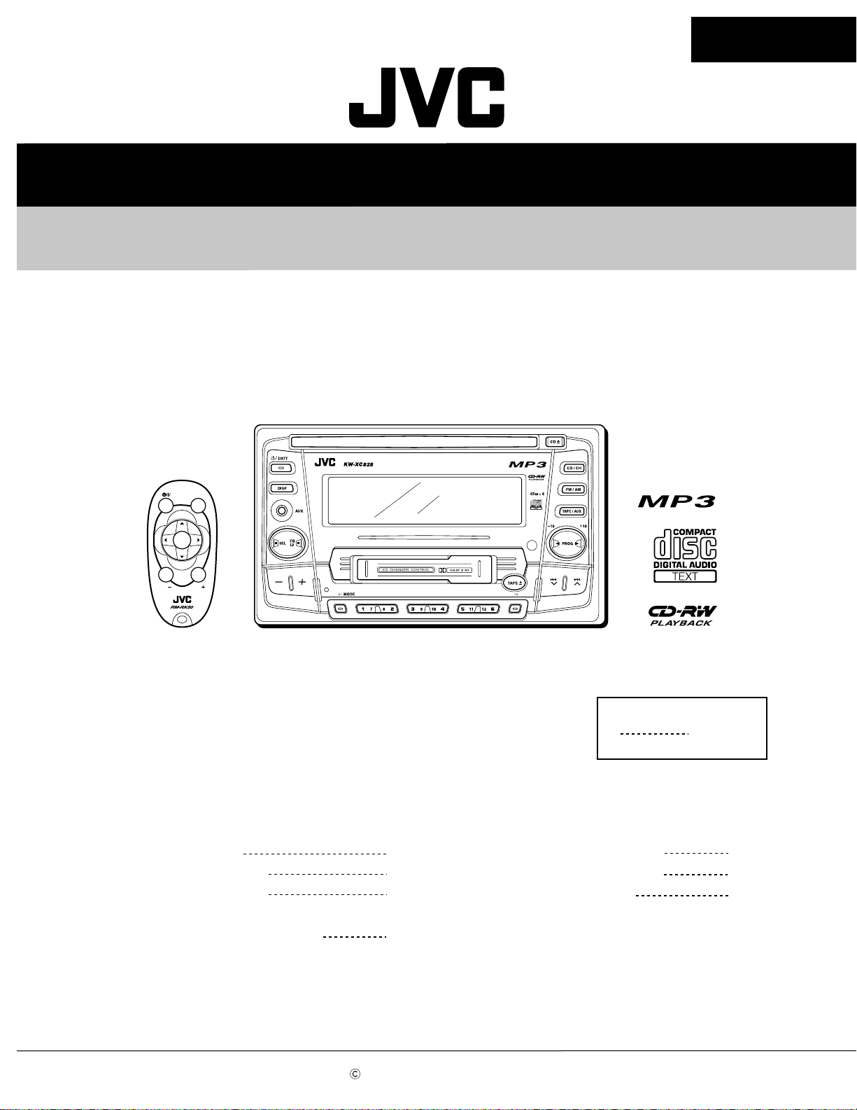
SERVICE MANUAL
CD/CASSETTE RECEIVER
KW-XC828
KW-XC828
SOUND
ATT
U
SOURCE
F
R
D
VOL
VOL
Contents
Safety precaution
Disassembly method
Adjustment method
Flow of functional
operation unit TOC read
1-2
1-3
1-30
1-31
DIRECTORY
E
X
Area Suffix
U Ather Areas
Maintenance of laser pickup
Replacement of laser pickup
Description of major ICs
1-33
1-33
1-36
COPYRIGHT 2002 VICTOR COMPANY OF JAPAN, LTD.
No.49729
Apr. 2002
Page 2
KW-XC828
Safety precaution
CAUTION
!
CAUTION
!
Burrs formed during molding may be left over on some parts of the chassis. Therefore,
pay attention to such burrs in the case of preforming repair of this system.
Please use enough caution not to see the beam directly or touch it in case of an
adjustment or operation check.
1-2
Page 3
KW-XC828
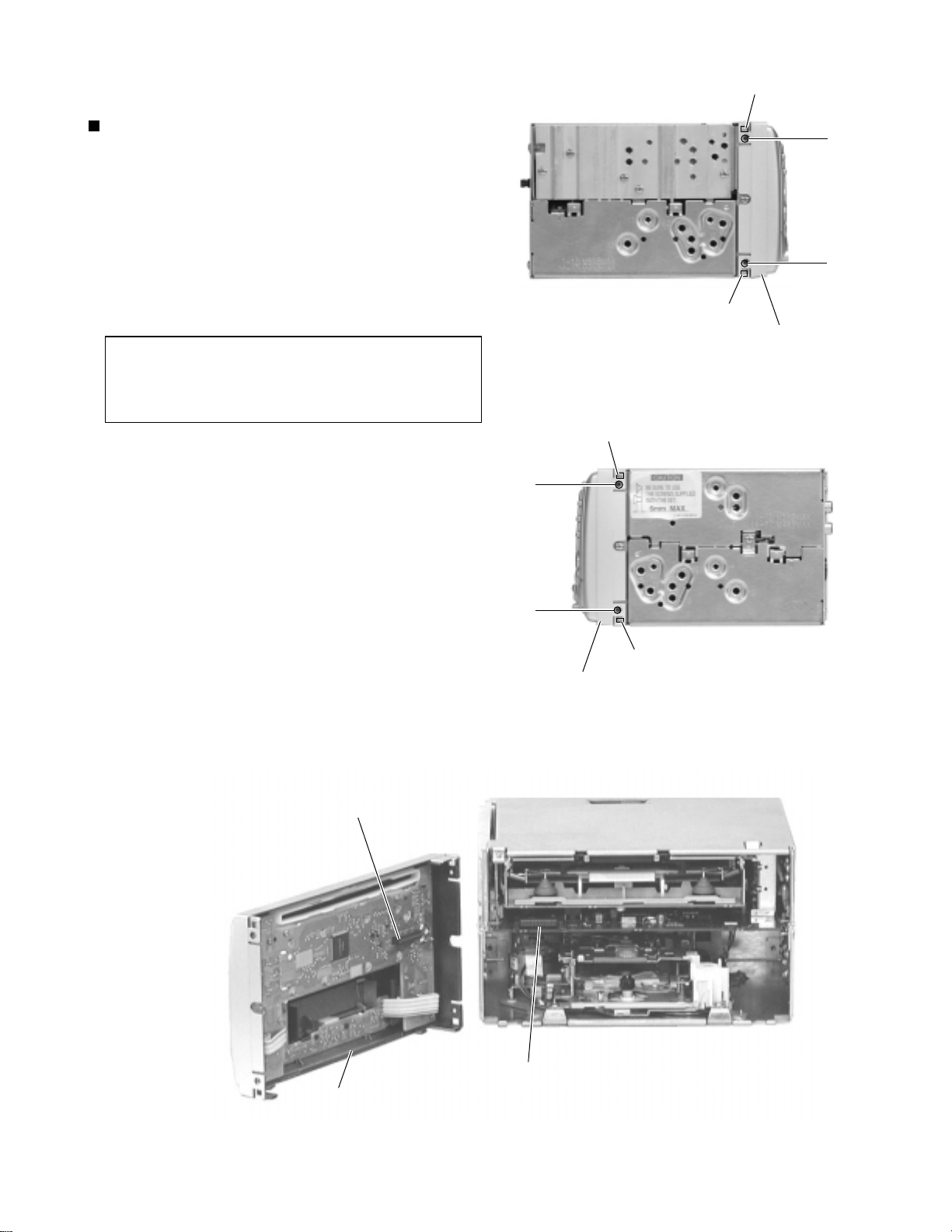
Disassembly method
Removing the front panel assembly
(See Fig.1 ~ 3)
1.
Remove the four screws A on both sides of the
body.
2.
Release four joints a on both sides of the body using
a screwdriver and remove the front panel assembly
toward the front. The connector which connects the
front panel assembly with the rear section comes off.
CAUTION:
When reassembling, make sure that
connector CN501 on the front panel
assembly is securely connected to
CN701 on the main board (See Fig.3).
Joint a
A
A
Joint a
Front panel assembly
Fig.1
Joint a
A
CN501
A
Joint a
Front panel assembly
Fig.2
Front panel assembly
CN701
Fig.3
1-3
Page 4
KW-XC828
Removing the system control board /
switch board (See Fig.4 , 5)
Prior to performing the following procedure, remove
the front panel assembly.
1.
Remove the twelve screws B retaining the system
control board.
2.
Remove the five screws C retaining the switch
board.
3.
Unsolder WR501 and WR502 of the wires
connecting the system control board with the switch
board.
B
B
WR502
System control board
WR502
B
Switch board
Fig.4
B
B
WR501
WR502
System control board
CC
Switch board
Fig.5
WR501
1-4
Page 5
KW-XC828
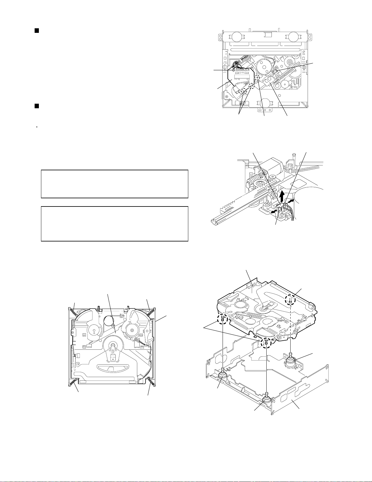
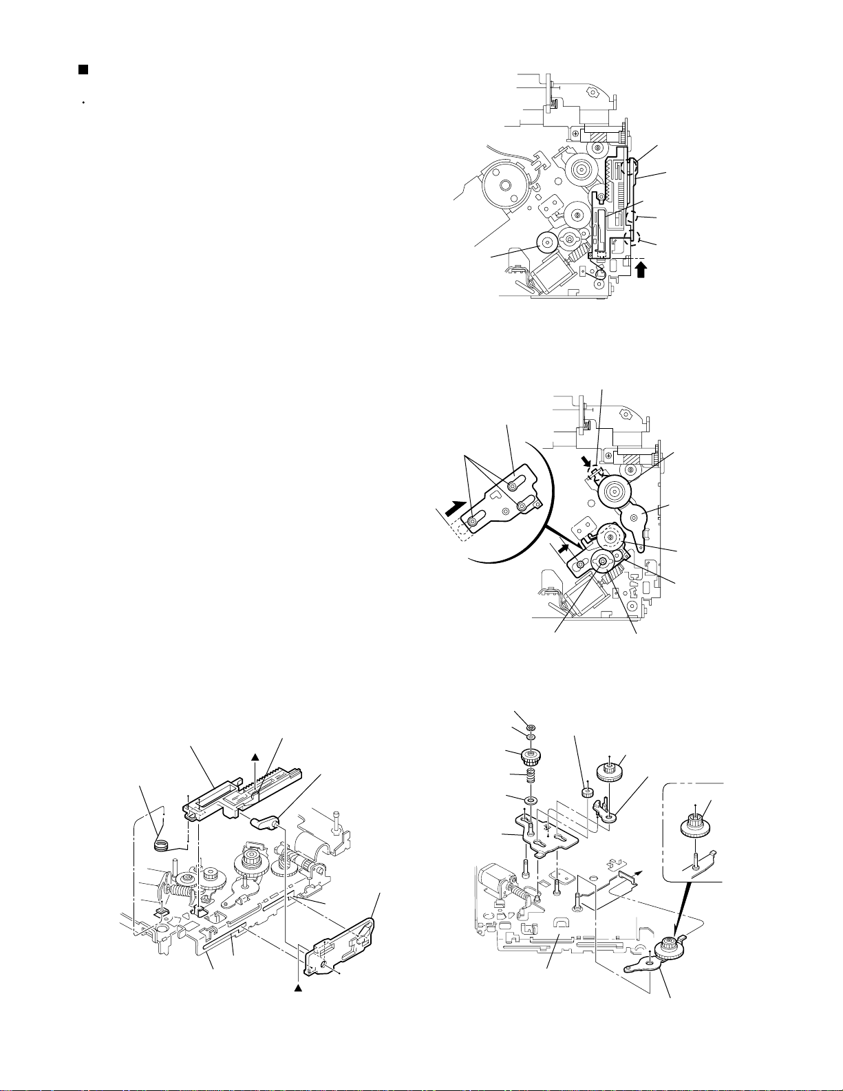
Removing the CD player section /
cassette player section (See Fig.6 ~ 10)
Prior to performing the following procedure, remove
the front panel assembly.
1.
Remove the ten screws D, the screw E and F
attaching the rear panel on the back of the body.
2.
Remove the three screws G and the two screws H
attaching the heat sink on the left side.
3.
Remove the three screws I attaching the CD player
section and the cassette player section on the both
sides of the body.
4.
Disconnect the card wire from connector CN702 on
the main board in the CD player section on the back
of the body.
5.
Remove the CD player section upward.
CAUTION:
When reassembling, joint the CD player
section and the cassette player section
at four joints b.
D
G
Rear panel
Heat sink
H
E
Fig.6
Fig.7
D
F
D
G
I
CD player section
CN702
I
CD player section
I
Fig.8
Joint b
Joint b
Joint b
Cassette player section
Cassette player section
Fig.10Fig.9
1-5
Page 6
KW-XC828
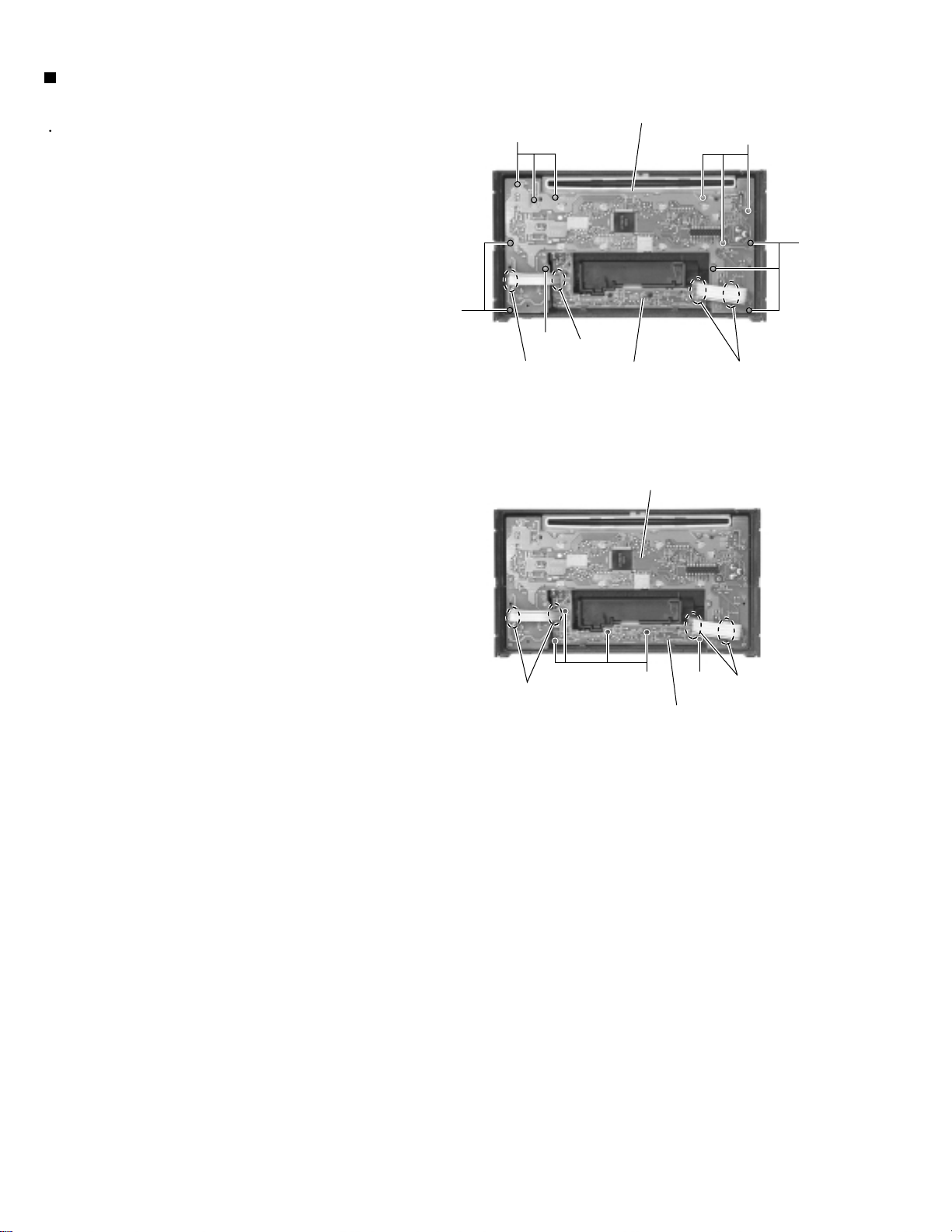
<CD player section>
Prior to performing the following procedure, remove
the front panel assembly, the CD player section and
the cassette player section.
Removing the main board (See Fig.11)
1.
Remove the three screws J attaching the main
board. The connector CN601 on the main board is
disconnected from the CD mechanism control board.
CAUTION:
When reassembling, securely connect
connector CN601 on the main board to
the connector on the CD mechanism
control board.
Removing the MP3 board
(See Fig.12)
Prior to performing the following procedure, remove
the main board.
J
J
MP3 board
Main board
CN601
J
Fig.11
K
1.
Disconnect the wire from connector CN601on the
MP3 board.
2.
Remove the five screws K and the MP3 board,
releasing the joint c and d.
Removing the CD mechanism assembly
(See Fig.13)
Prior to performing the following procedure, remove
the main board and MP3 board.
1.
Remove the three screws L attaching the CD
mechanism assembly.
Joint c
CN601
Joint d
K
Fig.12
L
1-6
L
CD mechanism assembly
Fig.13
L
Page 7
KW-XC828
<Cassette player section>
Prior to performing the following procedures, remove
the front panel assembly, the CD player section and
the cassette player section.
Removing the main board (See Fig.14)
1.
Disconnect the card wire from connector CN972 on
the main board.
2.
Remove the two screws M attaching the main
board.
Removing the cassette mechanism
assembly (See Fig.14 , 15)
Prior to performing the following procedure, remove
the main board.
N
M
CN972
Cassette mechanism assembly
Fig.14
Bottom cover
Main board
M
N
1.
Disconnect the card wire from connector CN972 on
the main board.
2.
Remove the four screws N from the bottom cover of
the cassette player section.
Removing the connector board
(See Fig.16)
Prior to performing the following procedure,
remove the cassette mechanism assembly.
1.
Remove the screw O and move the connector
board in the direction of the arrow to release the
two joints e.
2.
Disconnect the wire from connector CJ402 and
the card wire from CN403 on the connector
board respectively.
CJ402
Fig.15
O
Fig.16
Connector board
Joint e
CN403
1-7
Page 8
KW-XC828
< CD mechanism section >
Removing the top cover
(See Fig.1 and 2)
1.
Remove the two screws A on each side of the body.
2.
Lift the front side of the top cover and move the
cover backward to release the two joints a.
Removing the connector board
(See Fig.3 to 5)
Top cover
A
A
Joints a
CAUTION:
1.
Remove the screw B fixing the connector board.
2.
Solder the short-circuit point on the connector board.
Disconnect the flexible wire from the pickup.
3.
Move the connector board in the direction of the
arrow to release the two joints b.
4.
Unsolder the wire on the connector board if
necessary.
CAUTION:
Before disconnecting the flexible wire
from the pickup, solder the short-circuit
point on the pickup. No observance of
this instruction may cause damage of
the pickup.
Unsolder the short-circuit point after
reassembling.
A
Fig.1
Joints a
Top cover
Fig.2
DET switch
B
1-8
Flexible wire
Frame
Connector board
B
Connector board
Joints b
Flexible wire
Short-circuit
Fig.3
Fig.4Fig.5
Pickup
Short-circuit point
(Soldering)
Pickup
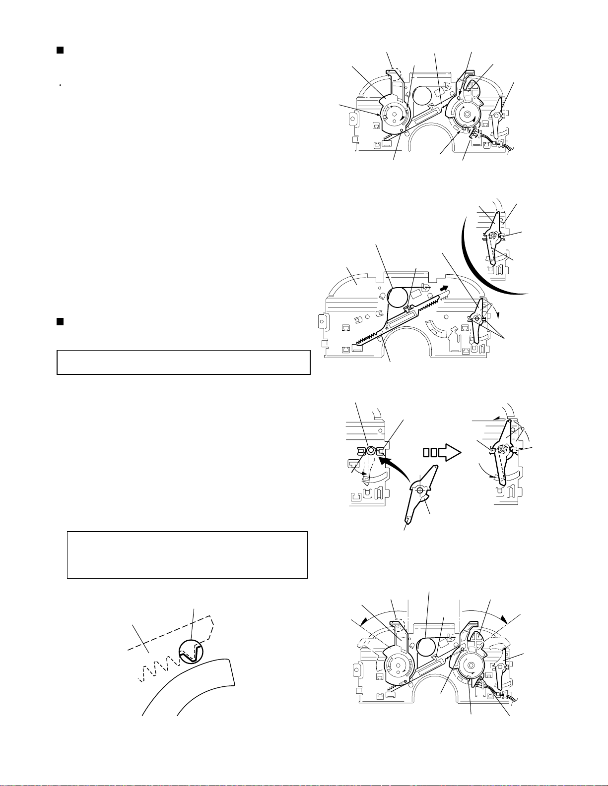
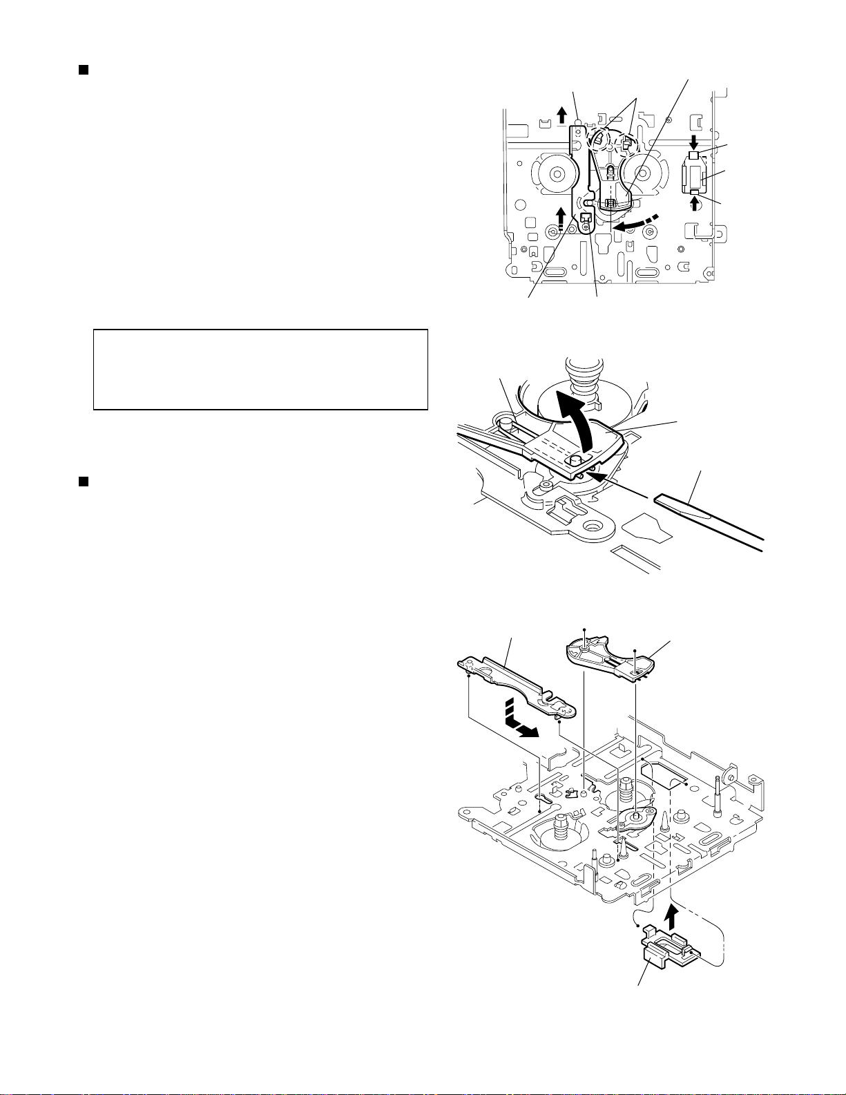
Page 9
Removing the DET switch
(See Fig.3 and 6)
1.
Extend the two tabs c of the feed sw. holder and pull
out the switch.
2.
Unsolder the DET switch wire if necessary.
Removing the chassis unit
(See Fig.7 and 8)
Prior to performing the following procedure, remove
the top cover and the connector board.
B
Connector board
Joints b
Short-circuit
Fig.3
KW-XC828
DET switch
Pickup
1.
Remove the two suspension springs (L) and (R)
attaching the chassis unit to the frame.
CAUTION:
The shape of the suspension spring (L)
and (R) are different. Handle them with
care.
CAUTION:
When reassembling, make sure that the
three shafts on the underside of the
chassis unit are inserted to the dampers
certainly.
Chassis unit
Suspension spring (R)
Suspension spring (L)
Frame
DET switch
Chassis unit
Tab c
Feed sw. holder
Tab c
Fig.6
Shaft
Suspension spring (R)
Suspension spring (L)
Shafts
Damper
Damper
Damper
Frame
Fig.8Fig.7
1-9
Page 10
KW-XC828
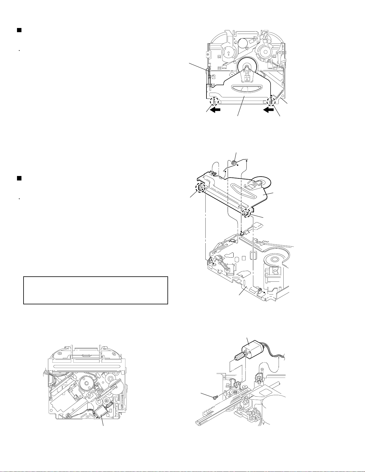
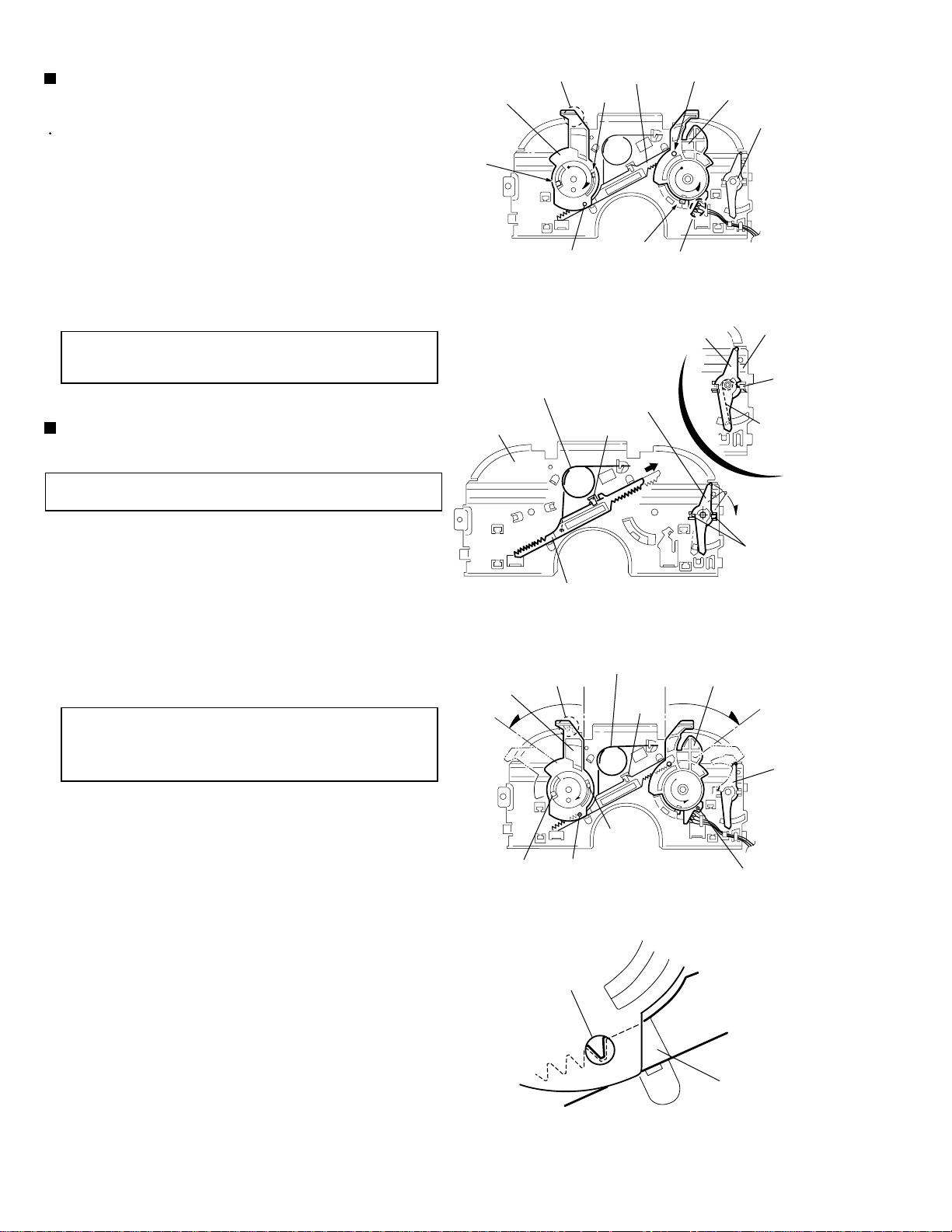
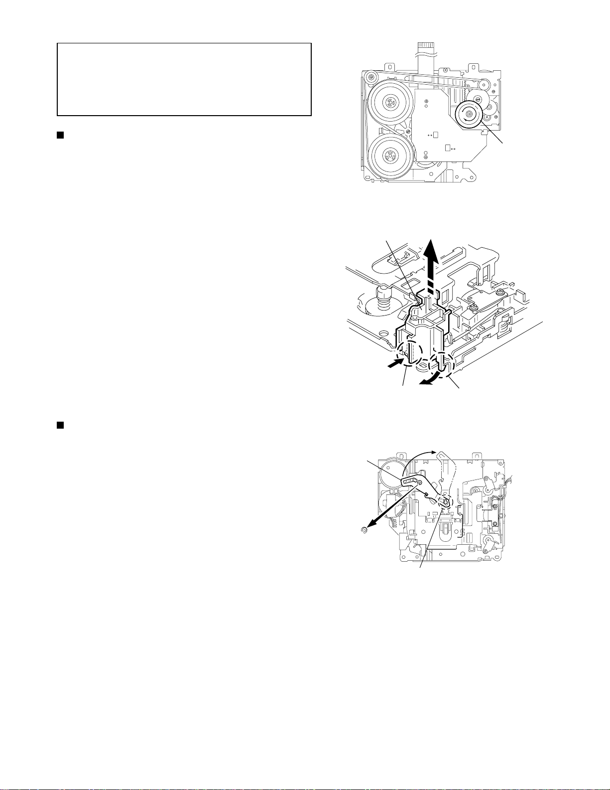
Removing the clamper assembly
(See Fig.9 and 10)
Prior to performing the following procedure, remove
the top cover.
1.
Remove the clamper arm spring.
2.
Move the clamper assembly in the direction of the
arrow to release the two joints d.
Removing the loading / feed motor
assembly (See Fig.11 and 12)
Prior to performing the following procedure, remove
the top cover, the connector board and the chassis
unit.
1.
Remove the screw C and move the loading / feed
motor assembly in the direction of the arrow to
remove it from the chassis rivet assembly.
Clamper arm
spring
Joint d
Joint d
Clamper assembly
Fig.9
Clamper arm spring
Chassis rivet
assembly
Joint d
Clamper assembly
Joint d
2.
Disconnect the wire from the loading / feed motor
assembly if necessary.
CAUTION:
When reassembling, connect the wire
from the loading / feed motor assembly
to the flame as shown in Fig.11.
Chassis rivet assembly
Fig.10
Loading / feed motor assembly
C
1-10
Loading / feed motor assembly
Fig.12Fig.11
Page 11
KW-XC828
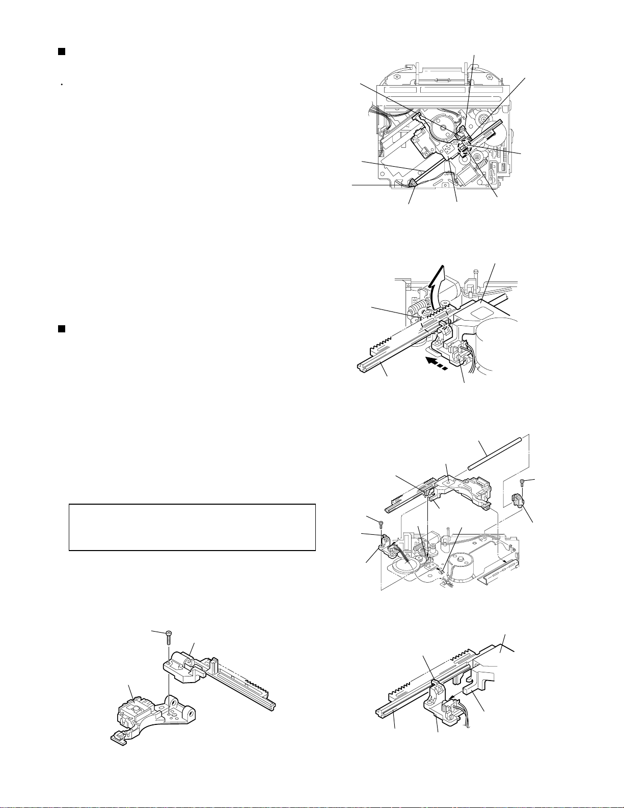
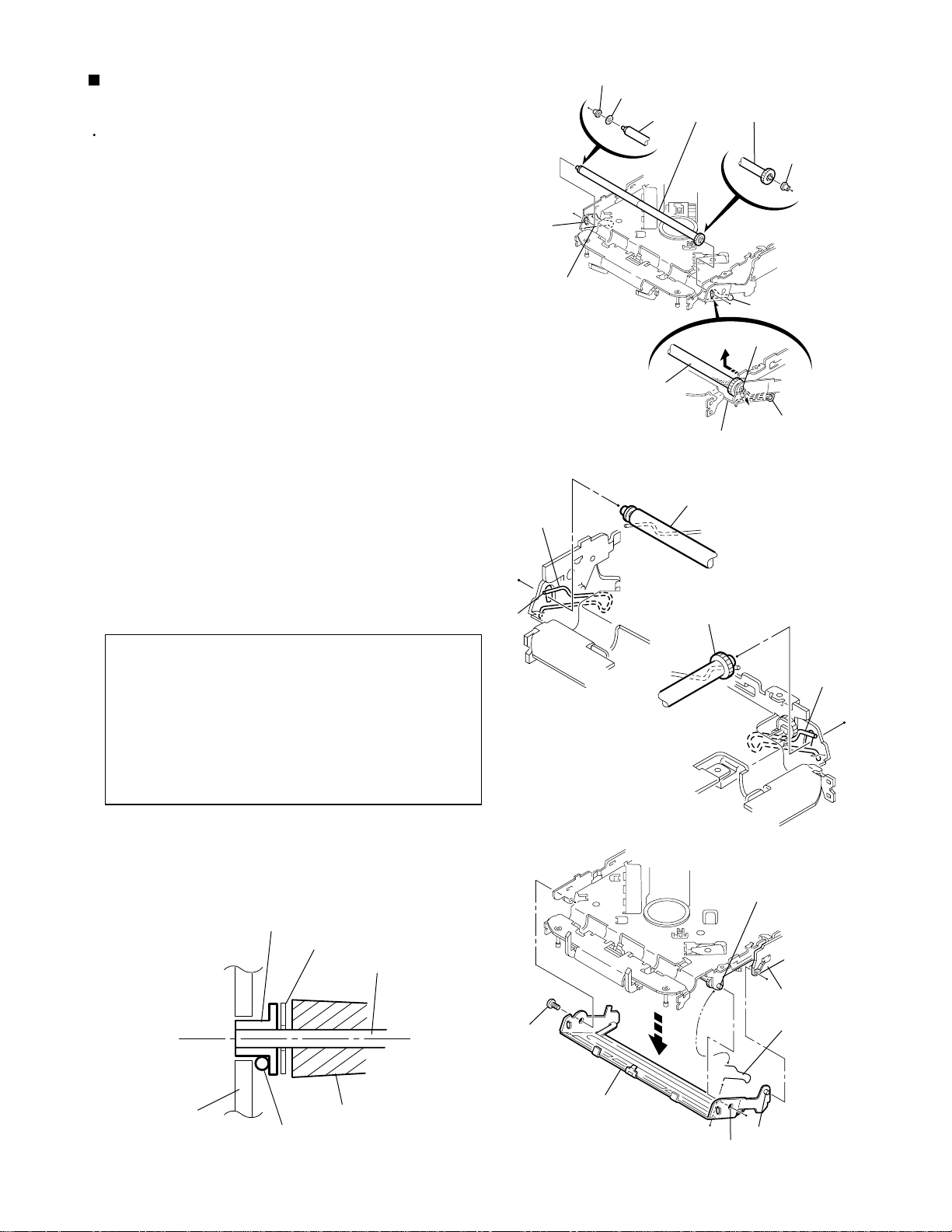
Removing the pickup unit
(See Fig.13 to 17)
Prior to performing the following procedure, remove
the top cover, the connector board and the chassis
unit.
1.
Remove the screw D and pull out the pu. shaft
holder from the shaft.
2.
Remove the screw E attaching the feed sw. holder.
3.
Move the part e of the pickup unit upward with the
shaft and the feed sw. holder, then release the joint f
of the feed sw. holder in the direction of the arrow.
The joint g of the pickup unit and the feed rack is
released, and the feed sw. holder comes off.
4.
Remove the shaft from the pickup unit.
5.
Remove the screw F attaching the feed rack to the
pickup unit.
Reattaching the pickup unit
(See Fig.13 to 16)
Joint f
Shaft
D
Joint e
Pu. shaft holder
Feed sw. holder
Pickup unit
Fig.13
Pickup unit
E
Joint f
Joint e
1.
Reattach the feed rack to the pickup unit using the
screw F.
2.
Reattach the feed sw. holder to the feed rack while
setting the joint tab g to the slot of the feed rack and
setting the part f of the feed rack to the switch of the
feed sw. holder correctly.
3.
As the feed sw. holder is temporarily attached to the
pickup unit, set to the gear of the joint g and to the
bending part of the chassis (joint h) at a time.
CAUTION:
4.
Reattach the feed sw. holder using the screw E.
5.
Reattach the shaft to the pickup unit. Reattach the
pu. shaft holder to the shaft using the screw D.
Make sure that the part i on the underside
of the feed rack is certainly inserted to the
slot j of the change lock lever.
F
Feed rack
Feed rack
E
Joint g
Feed sw. holder
Part i
Pickup unit
Slot j
Joint g
Feed sw. holder
Fig.14
Shaft
Joint f
Joint h
Fig.15
D
Pu. shaft holder
Pickup unit
Pickup unit
Feed rack
Joint f
Feed sw. holder
Fig.17Fig.16
1-11
Page 12
KW-XC828
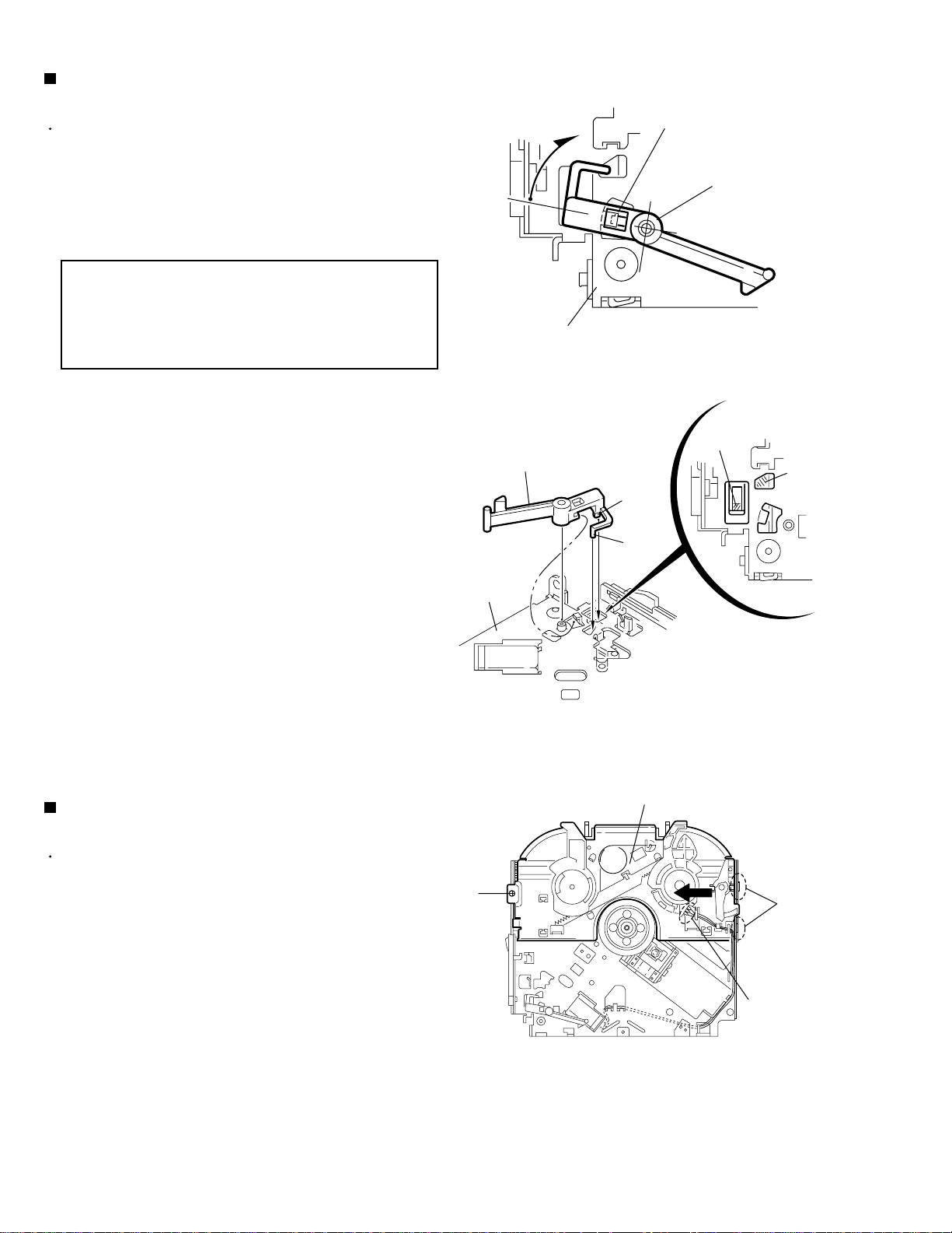
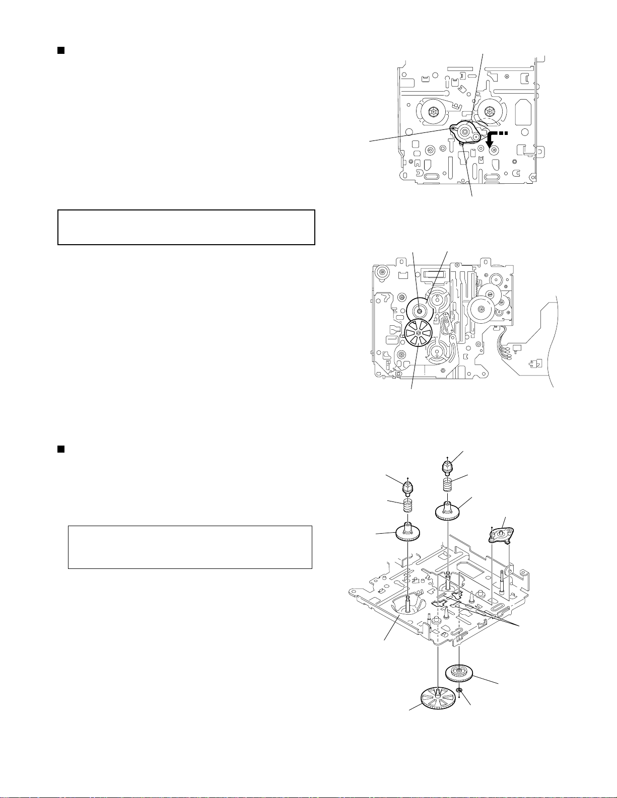
Removing the trigger arm
(See Fig.18 and 19)
Prior to performing the following procedure, remove
the top cover, the connector board and the clamper
unit.
1.
Turn the trigger arm in the direction of the arrow to
release the joint k and pull out upward.
Joint k
Trigger arm
CAUTION:
When reassembling, insert the part l and
m of the trigger arm into the part n and
o at the slot of the chassis rivet
assembly respectively and join the joint
k at a time.
Chassis rivet assembly
Chassis rivet assembly
Trigger arm
Fig.18
Part n
Part o
Part l
Part m
Fig.19
Removing the top plate assembly
(See Fig.20)
Prior to performing the following procedure, remove
the top cover, the connector board, the chassis unit,
and the clamper assembly.
1.
Remove the screw H.
2.
Move the top plate assembly in the direction of the
arrow to release the two joints p.
3.
Unsolder the wire marked q if necessary.
1-12
H
Top plate assembly
Joints p
q
Fig.20
Page 13
KW-XC828
Removing the select arm (L) / select lock
arm (See Fig.21 and 22)
Prior to performing the following procedure, remove
the top plate assembly.
1.
Bring up the select arm (L) to release from the link
plate (joint r) and turn in the direction of the arrow to
release the joint s.
2.
Unsolder the wire of the select arm (L) marked q if
necessary.
3.
Turn the select lock arm in the direction of the arrow
to release the two joints t.
The select lock arm spring comes off the select lock
arm at the same time.
Reassembling the select arm (L) / select
lock arm (See Fig.23 to 25)
Select arm (R)
Joint z
Link plate spring
Top plate
Joint a'
Joint y
Link plate
Joint z
Joint s
Fig.21
Select lock arm
Select lock arm
Joint b'
Joint r
Select arm (L)
Select lock arm
q
Top plate
Hook u
Select lock
arm spring
Joints t
REFERENCE:
1.
Reattach the select lock arm spring to the top plate
Reverse the above removing procedure.
and set the shorter end of the select lock arm spring
to the hook u on the top plate.
2.
Set the other longer end of the select lock arm spring
to the boss v on the underside of the select lock arm,
and join the select lock arm to the slots (joint t). Turn
the select lock arm as shown in the figure.
3.
Reattach the select arm (L) while setting the part r to
the first peak of the link plate gear, and join the joint
s.
CAUTION:
When reattaching the select arm (L),
check if the points w and x are correctly
fitted and if each part operates properly.
Joint r
Link plate
Link plate
Select lock arm spring
Boss v
Select arm (R)
Joint a'
Fig.22
Hook u
Joint t
Joint t
Select lock arm
Fig.23
Link plate spring
Select arm (L)
Joint b'
Joint r
Fig.25Fig.24
Joint s
Select
lock arm
Point x
1-13
Page 14
KW-XC828
Removing the select arm (R) / link plate
(See Fig.21 and 22)
Prior to performing the following procedure, remove
the top plate assembly.
1.
Bring up the select arm (R) to release from the link
plate (joint y) and turn as shown in the figure to
release the two joints z and joint a’.
2.
Move the link plate in the direction of the arrow to
release the joint b’. Remove the link plate spring at
the same time.
REFERENCE:
Before removing the link plate, remove
the select arm (L).
Reattaching the Select arm (R) / link
plate (See Fig.25 and 26)
REFERENCE:
Reverse the above removing procedure.
Select arm (R)
Joint z
Link plate spring
Top plate
Joint a'
Part y
Link plate
Joint z
Joint s
Fig.21
Select lock arm
Select lock arm
Joint b'
Joint r
Select arm (L)
Select lock arm
q
Top plate
Hook u
Select lock
arm spring
1.
Reattach the link plate spring.
2.
Reattach the link plate to the link plate spring while
joining them at joint b’.
3.
Reattach the part y of the select arm (R) to the first
peak of the link plate while joining the two joints z
with the slots. Then turn the select arm (R) as shown
in the figure. The top plate is joined to the joint a’.
CAUTION:
When reattaching the select arm (R),
check if the part c’ is correctly fitted and
if each part operates properly.
Select arm (R)
Joint z
Link plate
Link plate spring
Joint a'
Part y
Part y
Fig.22
Joint b'
Joint z
Fig.25
Joints t
Select arm (L)
Select
lock arm
Point x
1-14
Link plate
Fig.26
Page 15
KW-XC828
Removing the loading roller assembly
(See Fig.27 to 29)
Prior to performing the following procedure, remove
the clamper assembly and the top plate assembly.
1.
Push inward the loading roller assembly on the gear
side and detach it upward from the slot of the joint d’
of the lock arm rivet assembly.
Detach the loading roller assembly from the slot of
the joint e’ of the lock arm rivet assembly.
The roller guide comes off the gear section of the
loading roller assembly.
Remove the roller guide and the washer from the
shaft of the loading roller assembly.
2.
Remove the screw I attaching the lock arm rivet
assembly.
3.
Push the shaft at the joint f’ of the lock arm rivet
assembly inward to release the lock arm rivet
assembly from the slot of the slide plate. Extend the
lock arm rivet assembly outward and release the
joint g’ from the boss of the chassis rivet assembly.
The roller guide springs on both sides come off.
Roller guide
Washer
Loading roller assembly
Roller guide
Joint e'
Roller guide spring
Roller guide spring
Joint d'
Loading roller assembly
Roller guide spring
Lock arm rivet assembly
Fig.27
Loading roller assembly
Roller guide
spring
CAUTION:
When reassembling, reattach the left
and right roller guide springs to the lock
arm rivet assembly before reattaching
the lock arm rivet assembly to the
chassis rivet assembly. Make sure to fit
the part h’ of the roller guide spring (L)
inside of the roller guide (Refer to
Fig.30).
Roller guide
Washer
Roller shaft assembly
Joint h'
Loading roller assembly
Roller guide
spring
Fig.28-1
Fig.28-2
Chassis rivet assembly
Boss
Slide plate
Roller guide spring
I
Frame
Loading roller
Roller guide spring
Lock arm rivet assembly
Joint f'
Part g'
Fig.29Fig.30
1-15
Page 16
KW-XC828
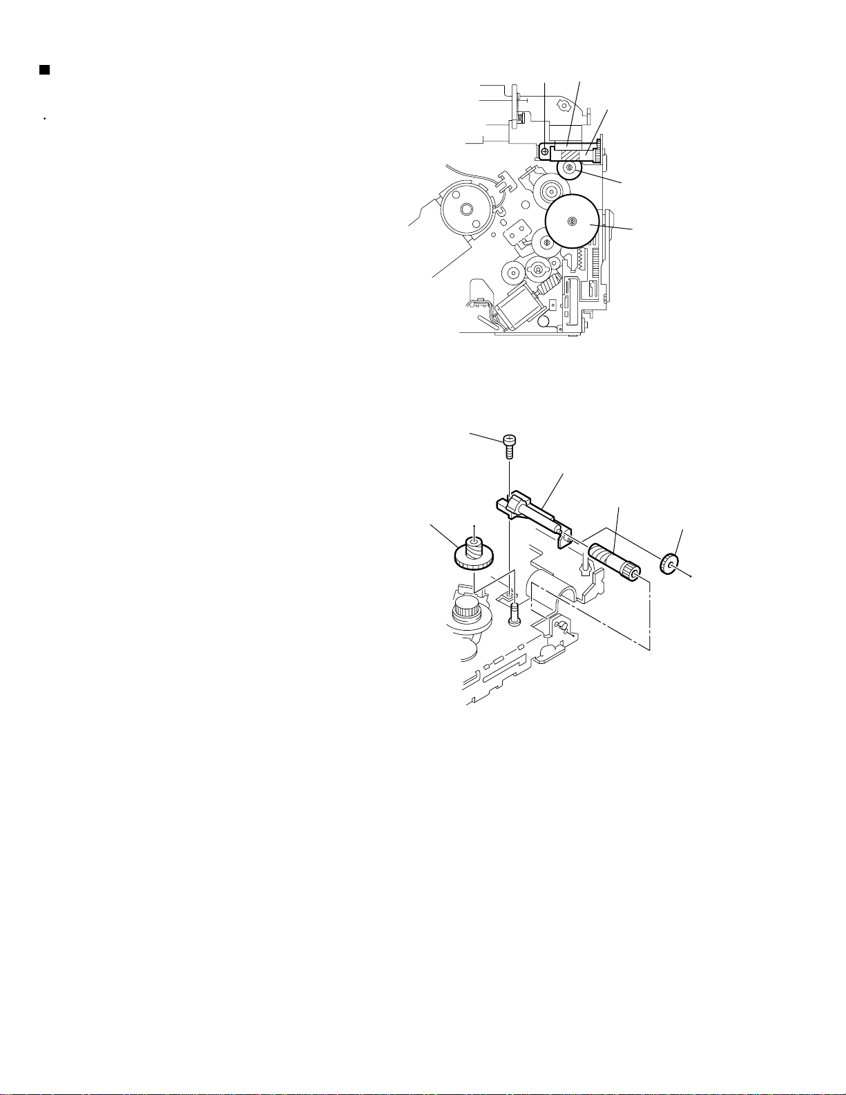
Removing the loading gear (5), (6) and
(7) (See Fig.31 and 32)
Prior to performing the following procedure, remove
the top cover, the chassis unit and the top plate
assembly.
1.
Remove the screw J attaching the loading gear
bracket. The loading gear (6) and (7) come off the
loading gear bracket.
2.
Pull out the loading gear (5).
Loading gear bracket
J
Loading gear (6)
Loading gear (5)
Loading gear (3)
Fig.31
J
Loading gear bracket
Loading gear (5)
Loading gear (6)
Loading gear (7)
Fig.32
1-16
Page 17
Removing the gears (See Fig.33 to 36)
Prior to performing the following procedure, remove
the top cover, the chassis unit, the top plate
assembly and the pickup unit.
1.
Pull out the feed gear.
KW-XC828
Slot j'
Slide plate
2.
Move the loading plate assembly in the direction of
the arrow to release the slide plate from the two slots
j’ of the chassis rivet assembly.
3.
Detach the loading plate assembly upward from the
chassis rivet assembly while releasing the joint k’.
Remove the slide hook and the loading plate spring
from the loading plate assembly.
4.
Pull out the loading gear (2) and remove the change
lock lever.
5.
Remove the E-washer and the washer attaching the
changer gear (2).
6.
The changer gear (2), the changer gear spring and
the adjusting washer come off.
7.
Remove the loading gear (1).
8.
Move the hang plate rivet assembly in the direction
of the arrow to release from the three shafts of the
chassis rivet assembly upward.
9.
Detach the loading gear plate rivet assembly from
the shaft of the chassis rivet assembly upward while
releasing the joint l’.
Feed gear
Change plate
rivet assembly
Shafts
E-washer
Loading plate assembly
Joint k'
Slot j'
Fig.33
Joint l'
Loading gear (4)
Loading gear plate
rivet assembly
Loading gear (2)
Loading gear (1)
Change gear (2)
10.
Pull out the loading gear (4).
Loading plate assembly
Loading plate spring
Slot j'
Chassis rivet assembly
Joint k'
Slide hook
Slide plate
Slot j'
E-washer
Washer
Loading gear (2)
Loading plate spring
Adjusting washer
Change plate
rivet assembly
Chassis rivet assembly
Fig.34
Loading gear (1)
Loading gear (2)
Change lock lever
Loading gear (4)
Loading gear plate rivet assembly
Fig.36Fig.35
1-17
Page 18
KW-XC828
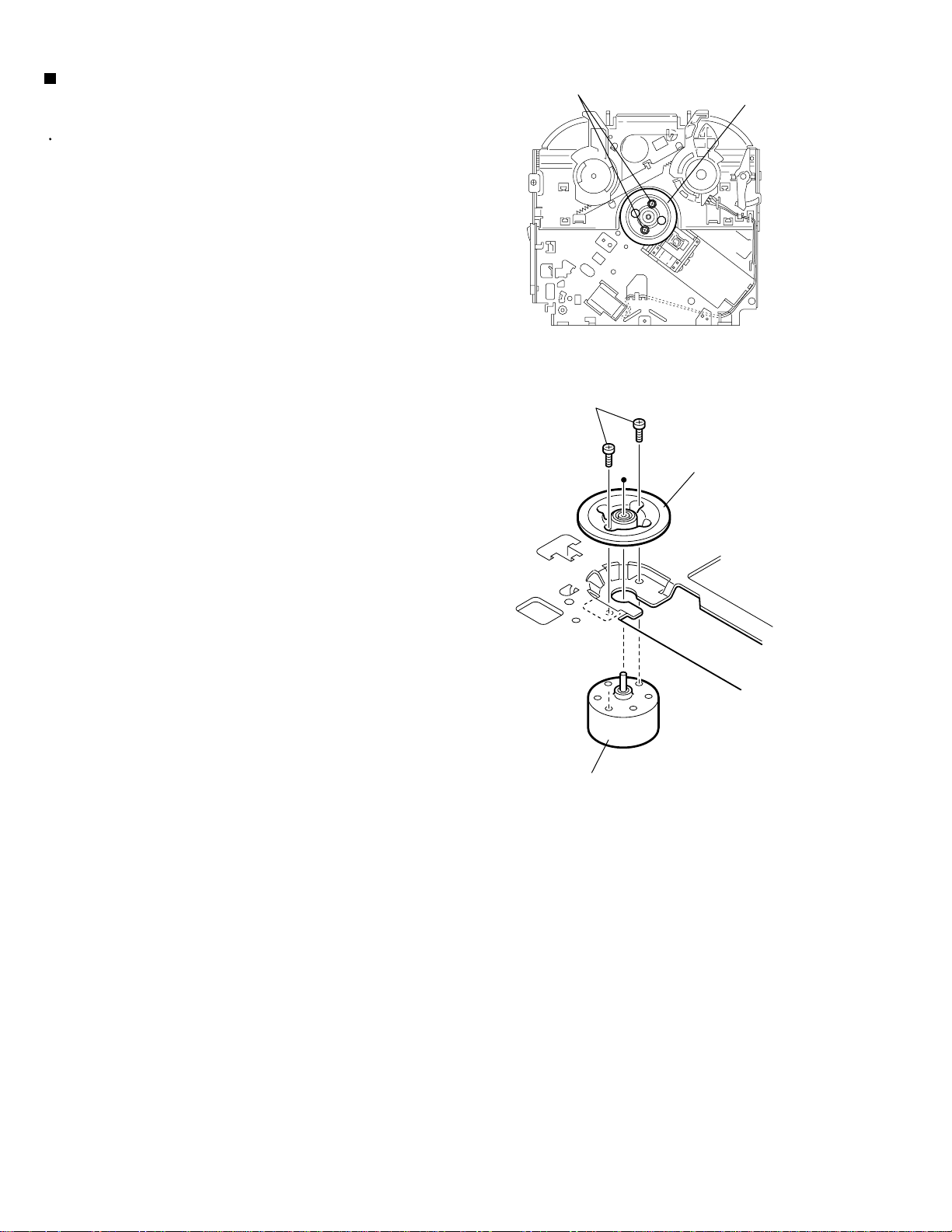
Removing the turn table / spindle motor
(See Fig.37 and 38)
Prior to performing the following procedure, remove
the top cover, the connector assembly and the
chassis / clamper assembly.
1.
Remove the two screws K attaching the spindle
motor assembly through the slot of the turn table on
top of the body.
2.
Unsolder the wire on the connector board if
necessary.
K
Turn table
Fig.37
K
Turn table
1-18
Spindle motor
Fig.38
Page 19
KW-XC828
REFERENCE:
Prior to performing the following
procedures, turn the mode gear on the
bottom of the body until the respective part
comes to the EJECT position (Refer to
Fig.1).
Removing the cassette guide (See Fig.2)
1.
Turn the mode gear to set to RVS play or
subsequent mode.
2.
Remove the cassette guide from the main chassis
while releasing each two joint tabs a in the direction
of the arrow.
Mode gear
Fig.1
Cassette guide
Removing the load arm (See Fig.3)
1.
Remove the E-washer attaching the load arm.
2.
Move the load arm in the direction of the arrow and
release the joint b on the cassette catch.
Load arm
E-washer
Tab a
Joint b
Tab a
Fig.2
Fig.3
1-19
Page 20
KW-XC828
Removing the cassette hanger assembly /
cassette holder (See Fig.4 to 7)
1.
Check the mode is set to EJECT. Push down the
front part of the cassette holder and move in the
direction of the arrow to release the joint c.
2.
Move the rear part of the cassette hanger assembly
in the direction of the arrow to release it from the two
joint bosses d.
3.
Release the holder stabilizer spring from the hooks e
and f, then pull out from the cassette hanger
assembly.
4.
Bring up the rear side of the cassette hanger
assembly to release the joint g and h.
5.
Pull out the cassette catch from the cassette hanger
assembly.
Cassette holder assembly
Side bracket
Joints c
Cassette holder assembly
Cassette stabilizer spring
Fig.4
Boss d
Cassette hanger assembly
Cassette hanger
assembly
Boss d
Cassette holder
assembly
Hook g
Fig.6
Hook f
Hook e
Fig.5
Cassette hanger assembly
Cassette catch
Cassette holder assembly
Cassette hanger assembly
Hook h
Fig.7
1-20
Page 21
KW-XC828
Removing the side bracket assembly
(See Fig.8 to 10)
1.
Remove the screw A attaching the side bracket
assembly.
2.
Detach the front side of the side bracket assembly
upward and pull out forward to release the joint i and
j in the rear.
CAUTION:
CAUTION:
When reassembling, make sure that the
boss k of the main chassis is set in the
notch of the load rack under the side
bracket assembly. Do not reattach the
load rack on the boss k.
After reattaching the side bracket
assembly, confirm operation.
Side bracket assembly
Joint i
Joint j
A
Side bracket assembly
Fig.8
Side bracket assembly
Joint i
Joint j
Load rack
Load rack
Boss k
Boss k
Fig.9
Fig.10
1-21
Page 22
KW-XC828
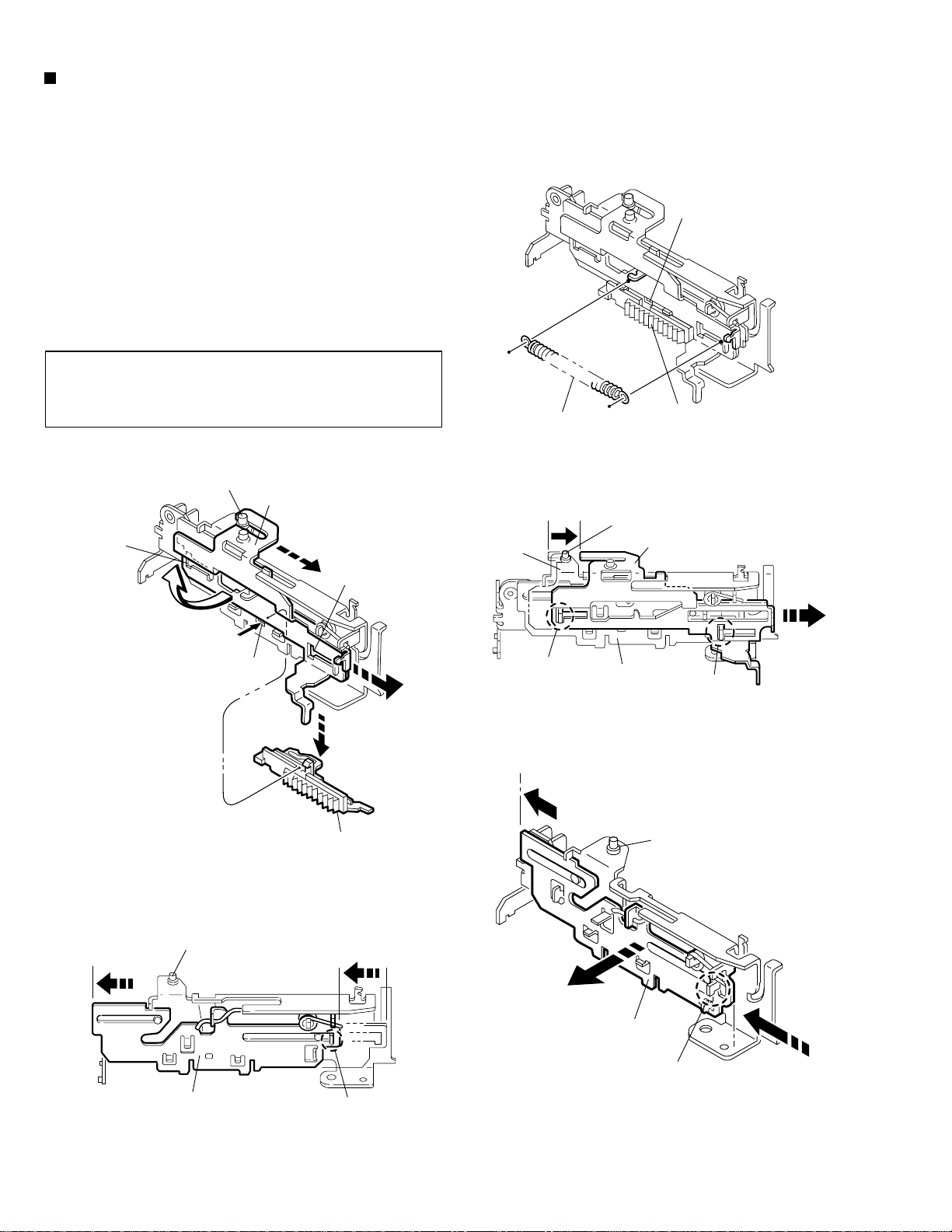
Removing the pinch arm (F) assembly
(See Fig.11 and 12)
1.
Remove the polywasher and pull out the pinch arm
(F) assembly.
2.
Remove the compulsion spring.
Removing the pinch arm (R) assembly
(See Fig.11 and 13)
1.
Remove the polywasher and pull out the pinch arm
(R) assembly.
Removing the slide chassis assembly
(See Fig.14 and 15)
Polywasher
Pinch arm
(R) assembly
Polywasher
Compulsion spring
Fig.11
Pinch arm
(F) assembly
Pinch arm (F) assembly
Polywasher
REFERENCE:
It is not necessary to remove the head
and the tape guide.
1.
Move the slide chassis assembly in the direction of
the arrow to release the two joints l and remove from
the main chassis.
2.
Remove the rack link.
CAUTION:
When reassembling, first reattach the rack
link, and next fit the boss m and hook n of
the slide chassis assembly to the hole of
the main chassis, and engage the two joints
l.
Rack link
Fig.12
Boss m
Pinch arm
(R) assembly
Fig.13
Head
Hook n
Polywasher
Tape guide
Joint l
Slide chassis assembly
1-22
Fig.14
Joint l
Fig.15
Page 23
KW-XC828
Removing the head / tape guide
(See Fig.16 and 17)
REFERENCE:
1.
Remove the band attaching the wire to the head.
2.
Remove the two screws B, the head and the head
support spring.
3.
Remove the pinch arm spring from the tape guide.
4.
Remove the tape guide and the pinch spring arm.
CAUTION:
CAUTION:
It is not necessary to remove the slide
chassis assembly.
When reattaching the pinch arm spring, set
both end of it to the pinch spring arm (
remarked o).
When reattaching the head, set the wires
into the groove of the tape guide (Fig.16).
B
Slide chassis assembly
Head
Tape guide
Fig.16
B
Pinch arm spring
Head
Head support spring
Tape guide
Removing the flywheel assembly (F) & (R)
(See Fig.18 and 19)
REFERENCE:
1.
Remove the belt at the bottom.
2.
Remove the two polywashers on the upper side.
3.
Pull out each flywheel assembly downward.
Flywheel assembly (F)
It is not necessary to remove the slide
chassis assembly.
Belt
o
Pinch spring arm
o
Slid chassis assembly
Fig.17
Polywasher
Polywasher
Flywheel assembly (R)
Fig.18
Flywheel assembly (F)
Fig.19
Flywheel assembly (R)
1-23
Page 24
KW-XC828
Disassembling the flywheel assembly (F)
(See Fig.20 and 21)
1.
Push and turn counterclockwise the spring holder (F)
to release the three joints p on the bottom of the
flywheel.
2.
The spring holder (F), the TU spring and the friction
gear play come off.
3.
Remove the polywasher and felt.
Flywheel assembly (F)
Joints p
Flywheel assembly (R)
Joints q
Disassembling the flywheel assembly (R)
(See Fig.20 and 22)
1.
Push and turn clockwise the spring holder (R) to
release the three joints q on the bottom of the
flywheel.
2.
The spring holder (R), the FF spring and the friction
gear FF come off.
3.
Remove the polywasher and the felt.
Removing the reel board
(See Fig.23 and 24)
1.
Remove the two screws C attaching the reel board.
2.
Move the reel board in the direction of the arrow to
release the joint r.
3.
Unsolder the wires if necessary.
CAUTION:
When reattaching, confirm operation of
the MODE switch and the ST-BY switch.
The mode position between EJECT and
ST-BY is optimum for reattaching.
Joint p
Fig.20
Polywasher
Polywasher
Spring holder (R)
Spring holder (F)
TU spring
Friction gear FF
Friction gear play
Felt
Flywheel assembly (F)
FF spring
Felt
Flywheel assembly (R)
Fig.21 Fig.22
Joint q
1-24
Connect the card wire extending from
the reel board to the FFC pad before
reattaching the reel board.
FFC pad
C
Reel board
C
Fig.23
Joint r
FFC pad
CT-1 switch
MODE switch
Soldering
ST-BY switch
Fig.24
Page 25
KW-XC828
Removing the gear base arm / gear base
link assembly (See Fig.25 to 27)
1.
Move the gear base arm in the direction of the arrow.
2.
Insert a slotted screwdriver to the gear base spring
under the gear base arm, and release the gear base
arm upward from the boss on the gear base
assembly.
3.
Remove the gear base arm from the main chassis
while releasing the two joints s.
4.
Move the gear base link assemby in the direction of
the arrow to release the two joints t.
REFERENCE:
When reattaching the gear base arm,
make sure that the boss on the gear
base assembly is inside the gear base
spring.
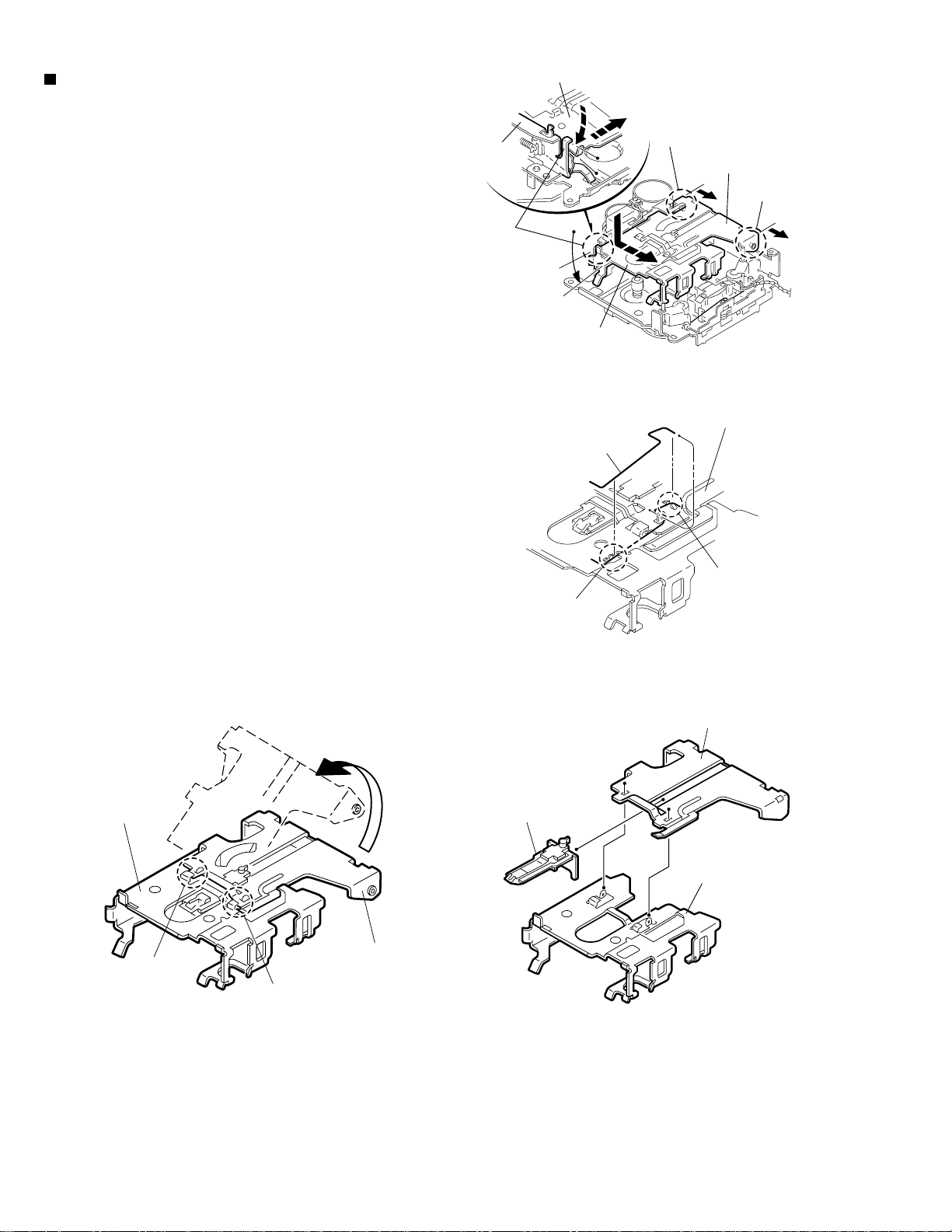
Removing the FFC pad
(See Fig.27 and 29)
Gear base
link assembly
Gear base spring
Joint t
Gear base arm
Joints s
Hook u
FFC pad
Hook u
Joint t
Fig.25
Gear base arm
Screwdriver
1.
Push each joint hook u of the FFC pad and remove
toward the bottom.
Gear base link assembly
Fig.26
Gear base arm
Fig.27
FFC pad
1-25
Page 26
KW-XC828
Removing the mode gear
(See Fig.28 and 31)
1.
Remove the polywasher on the bottom and pull out
the mode gear.
Removing the mode switch actuator
(See Fig.28, 29 and 31)
1.
Pull out the mode switch actuator at the bottom.
REFERENCE:
When reattaching the mode switch
actuator to the main chassis, make sure to
set on the shaft and insert v into the slot w.
Removing the direction link / direction
plate (See Fig.29 to 31)
1.
Remove the polywasher attaching the direction link.
2.
Bring up the direction link to release the three joints
x, y and z at a time.
3.
Move the direction plate in the direction of the arrow
to release the two joints a’.
REFERENCE:
When reattaching the direction plate,
engage the two joints a’ and move in the
direction of the arrow (Refer to Fig.30).
Mode switch actuator
Direction plate
Direction link
Fig.28
Direction plate
Joints a'
Joint z
Direction link
Slot w
Joint y
Polywasher
Fig.29
Direction plate Mode rack assembly
Joint b'
Mode gear
Polywasher
Mode rack assembly
Joint x
Joint b'
Joint c'
REFERENCE:
When reattaching the direction link,
move the direction plate in the direction
of the arrow and engage the three joint
x, y and z at a time (Refer to Fig.31).
Removing the mode rack assembly
(See Fig.29 and 30)
1.
Move the mode rack assembly in the direction of the
arrow to release the two joints b’ and the joint c’.
REFERENCE:
When reattaching, set the two b’ on the
bottom of the mode rack assembly into the
slots of the main chassis and move in the
direction of the arrow (See Fig.30).
Joints a'
Fig.30
Direction link
Mode switch actuator
Polywasher
v
Mode gear
Direction plate
Mode rack assembly
Fig.31
1-26
Page 27
KW-XC828
Removing the gear base assembly / take
up gear / reflector gear (See Fig.32 to 34)
1.
Push in the pin d’ of the gear base assembly on the
upper side of the body and move the reflector gear
toward the bottom, then pull out.
2.
Remove the polywasher on the bottom and pull out
the take up gear.
3.
Move the gear base assembly in the direction of the
arrow to release it from the two slots e’ of the main
chassis.
REFERENCE:
The parts are damaged when removed.
Please replace with new ones.
Gear base assembly
Pin d'
Polywasher
Slot e'
Slot e'
Fig.32
Take up gear
Removing the reel driver / reel spindle
(See Fig.34)
1.
Draw out the reel driver from the shaft on the main
chassis and remove the reel driver spring and the
reel spindle respectively.
CAUTION:
The reel driver is damaged when
removed. Please replace with a new
one.
Reflector gear
Reel driver
Reel driver spring
Reel spindle
Main chassis
Fig.33
Reel driver
Reel driver spring
Reel spindle
Gear base assembly
Slots e’
Take up gear
Reflector gear
Polywasher
Fig.34
1-27
Page 28
KW-XC828
Removing the side bracket assembly
(See Fig.35 to 39)
1.
Remove the eject cam plate spring.
2.
Push the joint f‘ through the slot to remove the load
rack downward.
3.
Move the eject cam limiter in the direction of the
arrow to release it from the boss g’ of the side
bracket assembly and from the two joints h’.
4.
Move the eject cam plate in the direction of the arrow
to release the joint i’.
Joint f'
CAUTION:
Joint h'
When reassembling, confirm operation of
each part before reattaching the eject cam
plate spring.
Side bracket assembly
Boss g'
Eject cam limiter
Side bracket assembly
Joint h'
Joint f'
Eject cam plate spring
Joint h'
Load rack
Fig.35
Boss g'
Eject cam limiter
Eject cam plate
Fig.37
Joint h'
1-28
Fig.36
Side bracket assembly
Boss g'
Eject cam plate
Fig.38
Load rack
Joint i'
Side bracket assembly
Eject cam plate
Joint i'
Fig.39
Page 29
KW-XC828
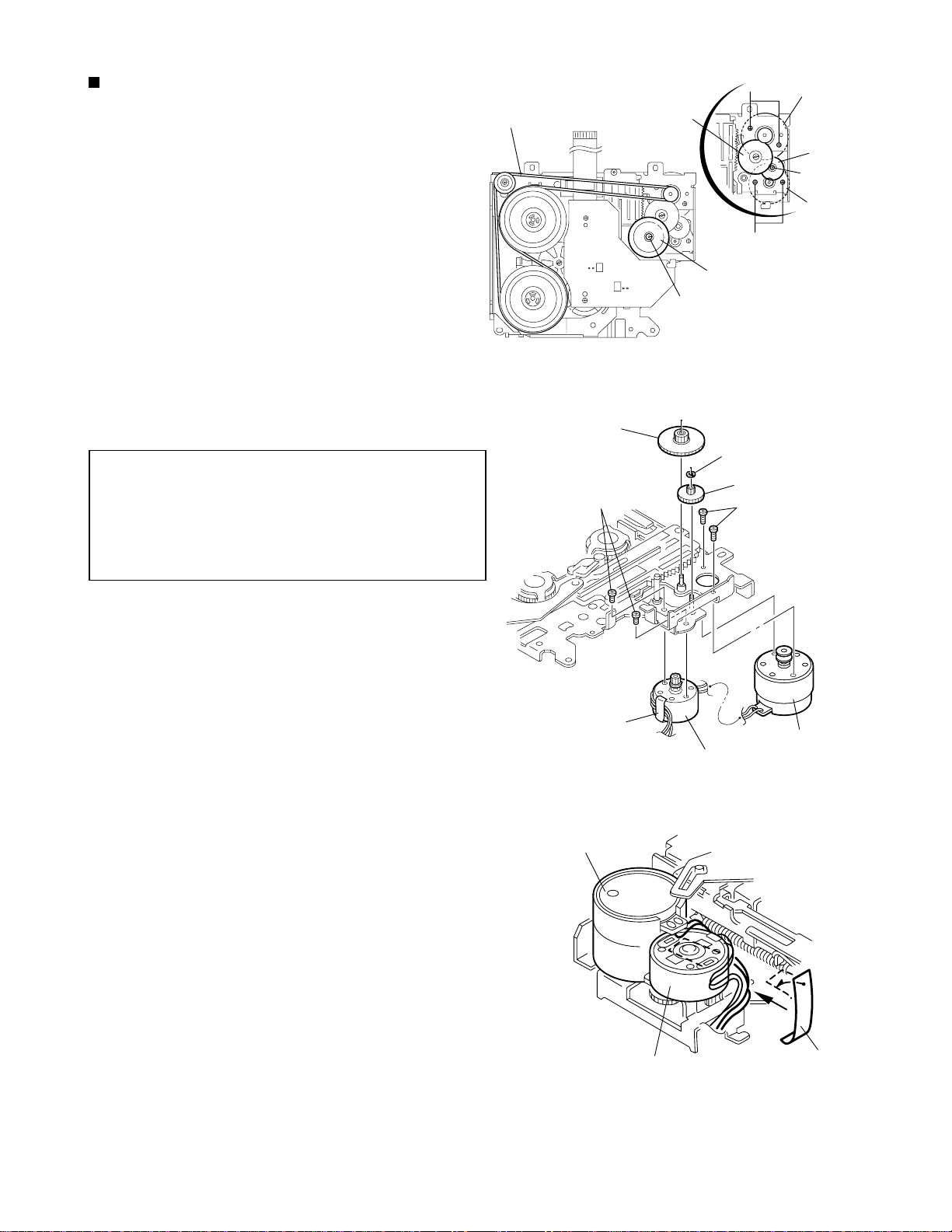
Removing the main motor assembly /
sub motor assembly (See Fig.40 to 42)
1.
Remove the belt at the bottom.
2.
Remove the polywasher and pull out the mode gear.
3.
Pull out the reduction gear (B).
4.
Remove the polywasher and pull out the reduction
gear (A).
5.
Remove the two screws D attaching the main motor
assembly.
6.
Remove the two screws E attaching the sub motor
assembly.
7.
Unsolder the wires on the reel board if necessary.
CAUTION:
When reassembling, adjust the length of the
wires extending from the sub motor
asswmbly by attaching them to the side of
the sub motor assembly with the wires
extending from the main motor assembly
using a spacer.
Belt
Reduction gear (B)
Reduction gear (B)
E
Polywasher
Fig.40
D
E
Mode gear
Polywasher
Reduction gear (A)
D
Main motor
assembly
Reduction
gear (A)
Polywasher
Sub motor
assembly
Spacer
Main motor assembly
Sub motor assembly
Main motor assembly
Sub motor assembly
Fig.41
Spacer
Fig.42
1-29
Page 30

KW-XC828
Adjustment method
Test Instruments required for adjustment
1.
Digital osclloscope(100Mz)
2.
Frequency Counter meter
3.
Electric voltmeter
4.
Wow&flutter meter
5.
Test tapes VT739..For playback frequency
measurement
VT712..For wow flutter&
tape speed measurement
VT703..For head azimuth measurement
6.
Torque gauge Cassette
for CTG-N(mechanism adjustment
7.
Laser power meter(Reader:LP800102)
8.
Prove for MD (Reader:LP8010-02)
9.
Pre masterd disc (TGYS-1)
10.
Test disc (JVC:CTS1000)
Measuring conditions (amplifier section)
Power supply voltage ..... DC14.4V(11V to 16V allowance )
Load impedance..... 4 ohm (4 ohm to 8 ohm allowance)
Line out .... 2.0V
Method of connecting extension cable
adjustment
Jig list: EXTSH002-22P x 1pc
Frequency Range:
FM: 87.5MHz to 108.0MHz
AM: 531 kHz to 1602kHz
Cassette mechanism
CN601
Extension cables
EXTSH002-22P
CN501
Main P.W.B
1-30
CD mechanism
Page 31

Flow of functional operation unit TOC read
Power ON
When the pickup correctly moves
v
to the inner area of the disc
Set Function CD
KW-XC828
When the laser diode correctly
emits
Microprocessor
commands
FMO
TC94A14FA" 40"
FEED MOTOR
+TERMINAL
IC561"4"
REST SW
When correctly focused
FEO
TA2157" 15"
Focus Servo Loop ONo
$83
$82
$81
3.3V
Hi-Z
0V
6V
4V
2V
OFF
ON
Pickup feed to the inner area
2.2V
RF signal eye-patternn
remains closed
RF signal eye-pattern
opens
Disc inserted
YES
Laser emitted
Focus search
Disc rotates
Tracking loop closed
TOC read out
YES
Microprocessor
commands
SEL
TC94A14FA"38"
LD
CN501"15"
"No disc"
display
When the disc correctly rotates
Microprocessor
commands
DMO
TC94A14FA"41"
Spindle
motor(-)
IC561"1"
$84 $86 $ A200
Acceleration Servo CLV
Rough
Servo
0.5 Sec 0.5 Sec
$84
3.3V
0V
4V
0V
3.3V
2.2V
0V
6V
3.2
2V
Jump to the first track
Play
Tracking Servo Loop ON
RF signal
Rough Servo Modev
CLV Servo Mode
(Program Area)
CLV Servo Mode
(Lead-In Area;
Digital :0)
1-31
Page 32

KW-XC828
Feed section
Is the voltage output at
IC521 pin "40" 5V or 0V?
Is 4V present at both
sides of the feed motor?
YES
YES
NO YES NO
NO
Is the wiring for IC521
(56)~(64) correct?
NO
Is 6V or 2V present at
IC561 "4" and "5"?
NO
Is 3.3V present at IC561
pin "20"?
Check the vicinity of
IC521.
YES
Check the feed motor
connection wiring.
YES
Check CD 8V
and 5V.
Check the feed motor.
Focus section
When the lens is
moving:
4V
Does the S-search
waveform appear at
IC561 pins "8" and "9"?
Spindle section
Is the disk rotated?
YES
Does the RF signal
appear at TP1?
YES
Is the RF waveform at TP1
distorted?
YES
Proceed to the Tracking
section
Check IC561.
NO
YES
NO
NO
NO
Check the circuits in
the vicinity of IC561
pins "8","9"and"15".
Check the pickup and
its connections
Is 4V present at IC561
pins "6" and "7"?
Check the spindle motor
and its wiring
Check the circuits in the
vicinity of IC501 "19"~
"24" or the pickup
YES
YES
NO
Is 4V present at IC521
pins "41" ?
Check the vicinity of
IC561.
NO
YES
Check IC521 and
IC501.
Tracking section
1-32
When the disc is rotated
at first:
Approx. 1.2V
Is the tracking error signal
output at IC501 "11"?
YES
Check IC521.
YES YES
Check the circuit in the
vicinity of IC501 pins
"2"~"12".
Check the pickup and
its connections
Page 33

Maintenance of laser pickup
(1) Cleaning the pickup lens
Before you replace the pickup,please try to
clean the lens with a alcohol soaked cotton
swab.
(2) Life of the laser diode
When the life of the laser diode has expired.
the following symptoms will appear..
(1) The level of RF output (EFM output:amplitude
of eye patterrn) will be low.
KW-XC828
Is RF output
1.3 0.4Vp-p?
YES
O.K
(3) Semi-fixed resistor on the APC PC board
The semi-fixed resistor on the APC printed
circuit board which is attached to the pickup
is used to adjust the laser power.Since this.
adjustment should be performed to match the
characteristics of the whole optical block,
do not touch the semi-fixed resistor..
If the laser power is lower than the specified
value, the laser diode is almost worn out, and
the laser pickup should be replaced.
If the semi-fixed resistor is adjusted while
the pickup is functioning normally, the laser
pickup may be damaged due to excessive current.
NO
Replace it.
Replacement of laser pickup
Turn of the power switch and, disconnect the
power cord.
Replace the pickup with a normal one.(Refer
to "Pickup Removal" on the previous page)
Plug the power cord in, and turn the power on.
At this time, check that the laser emits for
about 3seconds and the objective lens moves
up and down.
Note: Do not observe the laser beam directly..
Play a disc.
Check the eye-pattern at TP1.
Finish.
1-33
Page 34

KW-XC828
Mechanism Adjustment Section
Item
1.Head azimuth
Adjusting & Confirmation Methods
"Head Height Adjustment"
Note
Adjust the azimuth directly. When you adjust the height using a
mirror tape, remove the cassette housing from the mechanism
chassis. After installing the cassette housing, perform the azimuth
adjustment.
1. load the mirror tape (SCC-1659). Adjust with height adjustment
screw A and azimuth adjustment screw B so that line "A" of
the mirror tape runs in the center between Lch and Rch in the
reverse play mode.
2. After switching from REV to FWD then to REV, check that the
head position set in procedure "1" is not changed.
*If the position has shifted, adjust again and check.
3. Adjust the azimuth screw B so that line "B" of the mirror tape
runs in the center between Lch and Rch in the forward play
mode.
"Head Azimuth Adjustment"
1. Load the test tape (VT724: 1kHz) and play it back in the
reverse play mode. set the Rch output level to maximum.
2. Load the test tape (VT703: 10kHz) and play it back in the
forward play mode. Adjust the Rch and Lch output levels to
maximum, with azimuth adjustment screw B .
In this case, the phase difference should be within 45 .
3. Engage the reverse mode and adjust the output level to
maximum, with azimuth adjustment screw C .
4. When switching between forward and reverse modes, the
difference between channels should be within 3dB.
*Between FWD Lch and Rch, REV Lch and Rch.
5. When the test tape (VT721 (315Hz )) is played back, the level
difference between channels should be within 1.5dB.
Std. V alueAdjust
Head shield
The head is at low position
during FWD.
Head shield
The head is at height position
during REV.
FWD adj.
B
REV adj.
C
0
Playback head
Height adj.
Phase
A
45
2. Tape Speed
and
Wow & Flutter
3. DOLBY NR
level adjustment
1-34
1. Check to see if the reading of the frequency counter & Wow
flutter meter is within 3015-3045 Hz (FWD/REV), and less than
0.35% (JIS RMS).
2. In case of out of specification, adjust the motor with a built-in
volume resistor.
1. Play the test tape (VT724 : 1kHz) back.
2. Adjust the VR191 (Lch) and VR291 (Rch) so that the DOLBY NR
level is 27.5mV 0.5dB by TP191 (Lch), TP291 (Rch).
Built-in
volume resistor
VR191:Lch
VR291: Rch
Tape Speed
3015-3045Hz
Wow & Flutter
Less than
0.35%
(JIS RMS)
Speaker out
1kHz/10kHz
: -1dB 3dB,
63Hz/1kHz
: 0dB 3dB,
Page 35

Arrangement of adjusting & test points
Cassette mechanism
(Surface)
Azimuth screw (Reverse side)
Head amplifier board
DOLBY NR Level Adj.
Lch : VR401
Playback head
DOLBY NR Level Adj.
Rch : VR402
KW-XC828
Azimuth screw
(Forward side)
Capstan motor
Tape speed adjust
DOLBY NR Level Adj.
Lch : VR401
DOLBY NR Level Adj.
Rch : VR402
Head amplifier board
1-35
Page 36

KW-XC828
Description of major ICs
BR24C01AFV-W-X (IC502) : EEPROM
1.Pin layout
2.Block diagram
A0
1
A1
2
A2
3
VDD WPIN SCL SDA
A0 A1 A2 GND
1kbit EEPROM ARRAY
7bit
ADDRESS
DECODER
CONTROL LOGIC
SLAVE/WORD
7bit
ADDRESS REGISTER
START
STOP
ACK
8bit
DATA
REGISTER
8
7
6
VDD
WPIN
SCL
GND
4
HIGH VOLTAGE GEN.
3.Pin function
Pin name I/O
VDD
GND
A0,A1,A2
SCL
SDA
WPIN
*1 An open drain output requires a pull-up resister.
-
IN
IN
IN / OUT
IN
Power supply
Ground (0v)
Slave address set
Serial clock input
Slave and word address,
serial data input, serial data output *1
Write protect input
Vcc LEVEL DETECT
Function
SDA
5
1-36
Page 37

CXA2560Q (IC401) : Dolb y B type noise reduction system with play back equalizer amp.
1.Pin layout & block diagram
KW-XC828
31
PBFB2
32
PBRIN2
33
PBGND
34
PBFIN2
35
VCT
45k
36
PBREF
37
PBFIN1
38
PBGND
39
PBRIN1
40
PBFB1
2. Pin function
Pin No. Symbol
1
2
3
4
5
6
7
8
9
10
11
12
13
14
15
16
17
18
19
20
21
22
23
24
PBTC1
PBOUT1
OUTREF1
TAPEIN1
Vcc
NC
OUT1
TCH1
NC
MSLPF
G2FB
G1FB
MSTC
MSOUT
NC
NRSW
MUTE
METAL
DRSW
DIRECTION
FF/REW
NC
TCH2
OUT2
PBTC2
30 29 28
7k/12k
12345
PBTC1
300k
30k
30k
300k
7k/12k
F2
F1
PBOUT2
+
+
-
PBOUT1
OUTREF2
27
70 /120
1
1
70 /120
OUTREF1
TAPEIN2
100k
100k
TAPEIN1
GND
26
T2
T1
Vcc
I/O Function
Playback equalizer amplifier
capacitance
Playback equalizer amplifier
O
output
Output reference
O
TAPE input
I
Power supply
-
Line output
O
Time constant for the HLS
-
Cut-off frequency adjustment
of the music sensor LPF
Music signal interval detection
Music signal interval detection
Time constant for detecting
music signal interval
Music sensor out
O
No use
Dolby NR control
I
Mute function control
I
Playback equalizer amplifier
I
control
Head select control
I
Music sensor mode control
I
Music sensor control
I
Time constant for the HLS
Line output
O
25
FWD/RVS
LPF
6
DIREF
+
BIAS
MUTE
TAPE EQ
Vcc
+
-
NC
TCH2
OUT2
23 22 21
24
NR
OFF/B
-
F3
OFF/B
-
+
NR
8910
7
TCH1
OUT1
NC
MS MODE
NR MODE
MS ON/
OFF
DET
NC
MSSW
MSLPF
20
FF/REW
DIRECTION
19
METAL
18
MUTE
17
NRSW
16
NC
15
MSOUT
14
MSTC
13
G1FB
12
G2FB
11
Pin No. Symbol
25
26
27
28
29
30
31
32
33
34
35
36
37
38
39
40
DIREF
GND
TAPEIN2
OUTREF2
PBOUT2
PBTC2
PBFB2
PBRIN2
PBGND
PBFIN2
VCT
PBREF
PBFIN1
PBGND
PBRIN1
PBFB1
I/O Function
-
Resistance for setting the
reference
-
Ground
I
TAPE input
O
Output reference
O
Playback equalizer amplifier
output
-
Playback equalizer amplifier
capacitance
I
Playback equalizer amplifier
feedback
I
Playback equalizer amplifier
input
-
Playback equalizer amplifier
ground
I
Playback equalizer amplifier
input
O
Center
O
Playback equalizer amplifier
reference
I
Playback equalizer amplifier
input
-
Playback equalizer amplifier
ground
I
Playback equalizer amplifier
input
I
Playback equalizer amplifier
feedback
1-37
Page 38

KW-XC828
UPD784215AGC173 (IC701) : Main micon
1.Pin layout
100 ~ 76
1
75
~
25
26 ~ 50
2.Pin functions(1/2)
Pin No.
1
2
3~7
8
9
10
11
12
13
14
15
16
17
18
19
20
21
22
23
24
25
26
27
28
29
30
31
32
33
34
35
36
37
38
39
40
41
42
43
Symbol
NC
NC
NC
MUTE
VDD
X2
X1
GND
XT2
XT1
RESET
BUS INT
REMOCON
ACC DET
MEMORY DET
NC
CST P.REQ
CD P.REQ
AVDD
AVREF0
KEY0
KEY1
KEY2
KEY3
S.METER
LEVEL/ANA
TEMP
NC
AVSS
DIMMER IN
DIMMER OUT
AVREF1
BUS-SI
BUS-SO
BUS-SCK
BUS-I/O
LCD-DA
LCD-SCK
LCD-CE
~
51
I/O
Function
O
Non connect
O
Non connect
O
Non connect
O
Mute output terminal("L" output at mute)
-
Connects with VDD
-
Connects with X'tal departure pendulum of 12.5MHz(output )(main)
-
Connects with X'tal departure pendulum of 12.5MHz(input )(main)
-
Connect with GND
-
Connects with X'tal departure pendulum of 32.768KHz(output)
-
Connects with X'tal departure pendulum of 32.768KHz(input)
I
System reset input terminal
I
Interrupt signal detection terminal from J-BUS communication
I
Interrupt signal detection terminal from optical remote control
I
ACC power supply detection terminal("L" become a holding mode
because of the input)
I
Backup power supply detection terminal
("L" it when backup power supply is input)
("H" input when backup power supply uninputs)
O
Non connect
I
Cassette mechanism power supply start-up demand signal input
I
CD mechanism power supply start-up demand signal input
-
(Connect witj VDD)(Power supply for the A/D converter)
-
(Connect with VDD)(Standard power supply for the A/D converter)
I
KEY0 input terminal
I
KEY1 input terminal
I
KEY2 input terminal
I
KEY3 input terminal
I
Terminal of input of voltage of S meter(Electric field strength)
I
Level input terminal of level meter
I
Voltage input terminal (Use to correct the temperature of the contrast)
from the thermally sensitive resister.
I
To GND with 47k
-
(Connect with GND)(GND for the A/D converter and the D/A converter)
I
Dimmer signal input terminal("L" input at dimmer)
O
"H" output at DIMMER ON
-
(Connect with VDD)(Standard power supply for the D/A converter)
I
Input of data J-BUS communication
O
Output of data of J-BUS communication
I/O
Clock output for J-BUS communication
O
Output of I/O switch signal of J-BUS communication
(output "H" and input "L")
O
data output terminal to LCD driver
O
Clock output terminal for communication to LCD driver
O
Chip enable output terminal to LCD driver
1-38
Page 39

KW-XC828
2.Pin functions(2/2)
Pin No.
44~47
48
49
50
51
52
53
54
55
56~60
61
62
63
64
65
66~71
72
73~79
80
81
82
83
84
85
86
87
88
89
90
91
92
93
94
95~100
EPROM DI
EPROM DO
EPROM CK
SD/SI
PLL CE
PLLDATA
PLL CLK
PLL DI
E.VOL SO
E.VOL SCK
LCD RESET
TEL MUTE
GND
POWER ON
VDD
CD MUTE
CD RESET
AREA SET1
AREA SET2
LCD TEST
CST MUTE
CST RESET
TEST
NC
NC
NC
NC
NC
NC
NC
NC
NC
NC
NC
UPD784215AGC173(2/2)
I/O
FunctionSymbol
O
Non connect
O
Data input from EPROM
O
Data output to EPROM
O
EPROM Clock signal I/O
I
Stationdetector and stereo signal input terminal ("H" input at SD)
O
Chip enable output terminal to PLL
O
Data output terminal to PLL
O
Clock output terminal for communication to PLL
I
Data input terminal from PLL
O
Non connect
O
Non connect
I/O
Data I/O terminal to electric volume
I/O
Clock I/O terminal for communication to electric volume
O
Reset signal output terminalto LCD driver("L" output when resetting)
I
Outputs by "L" input the mute output terminal "L"
O
Non connect
-
(Connect with GND)
O
Non connect
O
Power is output " H" when it is on
-
(Connect with VDD)
I
Mute signal demand input terminal from CD mechanism
O
When the terminal RESET detects "L", 200mS "H"
O
(CD mechanism) (Reset output terminal is output)
Non connect
O
Non connect
I
Area setting of tuner 1
I
Area setting of tuner 2
O
Non connect
I
All lighring display of LCD by "L" input
O
Non connect
O
Non connect
I
Mute signal demandinput terminal from cassette mechanism
O
Reset output terminal to cassette mechanism
-
(When the terminal RESET detects "L", 200mS "H" is output)
GND and connects with 10k
O
Non connect
1-39
Page 40

KW-XC828
UPD784225GK-623 (IC501) : CPU
1.Pin layout
80 ~ 61
1 ~ 20
21 ~ 40
2.Pin function
Pin
Symbol
no.
1
TEMP
2
GND
3
GND
4
AVSS
5
ADCONT
6
NC
7
AVREF1
8
EPROMDI
9
EPROMDO
10
EPROMCK
11
LCDCE/SO
12
LCDDA/SI
13
LCDCK
14
/BUSIO
15
BUSIO
16
BUSSI
17
BUSSO
18
BUSSCK
19
BUSOUT
20
CDON
21
CDREQ
22
CDMUTE
23
NC
24
DSPRESET
25
CCE
26
BUCK
27
BUS3
28
BUS2
29
BUS1
30
BUS0
31
2XPLAY
32
RWSEL
33
VSS1
34
LOAD
35
LD/FE
36
MP3DI
37
MP3DO
38
MP3CK
39
MP3RESET
40
MPSSTB
60 ~ 41
I/O
Connect to TEMP detecter
I41
Connect to GND
-
Connect to GND
-
Connect to GND
-
No use
-
No use
-
Analog reference voltage
-
Data input terminal from EEPROM
I
Data output terminal from EEPROM
O
Clock signal I/O terminal with EEPROM
I/O
No use
-
No use
-
No use
-
J-BUS data I/O terminal
I/O
J-BUS data I/O terminal
I/O
J-BUS data input
I
J-BUS data output
O
J-BUS clock I/O
I/O
No use
-
The CD power supply control signal output.At CD:H
O
CD request
I
CD Mute
O
No use
-
DSP reset
O
CE output for data communication with CDLSI
O
Clock output for data communication with CDLSI
O
Data communication input output port 3 with CDLSI
I/O
Data communication input output port 2 with CDLSI
I/O
Data communication input output port 1 with CDLSI
I/O
Data communication input output port 0 with CDLSI
I/O
No use
-
CD RW select
I
Connect to GND
-
Loading signal
O
LDFLE switching signal
O
MP3 data input
I
MP3 data output
O
MP3 data clock
O
MP3 data reset
O
MP3 data standby
I
Function Function
Pin
no.
42
43
44
45
46
47
48
49
50
51
52
53
54
55
TEST MODE
56
57
58
59
60
61
62
63
64
65
66
67
68
69
70
71
72
73
74
75
76
77
78
79
80
Symbol
NC
NC
NC
DACML
DACMC
DACMD
DACCS
NC
NC
NC
NC
DISCSEL
DACSEL
NC
MP3SEL
8VDET
REST
SW2
RESET
SW1
B.DET
P.DET
BUSINT
MP3REQ
NC
VSS0
VDD1
X2
X1
VPP
XT2
XT1
VDD0
AVDD
IOP
KEY0
KEY1
KEY2
KEY3
I/O
Non use
-
Non use
-
Non use
-
DAC mode control latch
O
DAC mode control clock
O
DAC mode control data
O
DA convertor chip select
I
No use
-
No use
-
No use
-
No use
-
Initial setting
O
DA convertor select
O
No use
-
Connect to GND
-
MP3/CD-DA switch SW L:CD H:MP3
O
8V detection
I
Systemreset signal input
I
Detection switch of CD mechanism
I
Reset detection terminal
Detection switch of CD mechanism
I
Panel switch detection
I
Power switch detection
I
J-BUS signal interrupt input
I
MP3 request
O
No use
-
Connect to ground
-
Reference voltage terminal
-
No use
-
Connect to X'tal osc.
I
Test terminal
I
Non use
-
Connect to ground
-
Connect to ground
-
Reference voltage terminal
-
Laser signal input output
I/O
Key control signal input 0
I
Key control signal input 0
I
Key control signal input 0
I
Key control signal input 0
I
1-40
Page 41

UPD789166GB-590 (IC431) : CPU
1.Pin layout
44 ~ 34
1
KW-XC828
33
2.Pin function
Pin No.
1
2
3
4
5
6
7
8
9
10
11
12
13
14
15
16
17
18
19
20
21
22
23
24
25
26
27
28
29
30
31
32
33
34
35
36
37
38
39
40
41
42
43
44
~
11
12 ~ 22
Symbol
KEY0
KEY1
KEY2
KEY SEL
DOLBY SEL
RPT SEL
B.SKIP
NC
AVSS
NC
BUS-I/O
BUS-INT
TAPE IN
MAIN POWER
PWR_DET
BUS-SCK
VDD1
BUS-SO
BUS-SI
METAL IN
METAL OUT
ICO
XT2
XT1
RESET
X2
X1
VSS0
VDD0
DOLBY
MS IN
FF/REW
MOTOR
SUBMO-
SUBMO+
HEAD SEL
VSS1
REEL
STANBY
MODE
PREQ
MUTE
AVDD
AVREF
I/O
O
O
I/O
O
O
O
O
O
O
O
O
O
~
23
Function
I
KEY0 input terminal
I
KEY1 input terminal
I
KEY2 input terminal
I
KEY in select setting terminal (H:active)
I
DOLBY select setting terminal L: No DOLBY
I
REPEAT select setting input terminal L:No REPEAT
I
B.SKIP select setting input terminal
-
Connect to GND
-
A/D converter GND voltage. Connect to GND
Non connect
J-BUS I/O switching output. output:H input:L
I
J-BUS signal interlupt input
I
Tape IN detection switch input
I
CTRL+B input H:Normal operation L:Save mode
I
MEMORY detection
J-BUS clock input/output
-
Power supply (without port section) connect to 5V
J-BUS data output terminal
I
J-BUS data input terminal
-
Non connect
-
Non connect
-
Connect to VSS0 or VSS1
-
Non connect
-
Connect to VSS0 or VSS1
-
Reset detection terminal
-
X'tal oscillator (4.1943MHz)
-
X'tal oscillator (4.1943MHz)
-
Ground voltage of port section. Connect to GND
-
Power supply for port section Connect to 5V
DOLBY ON/OFF setting output H:ON
I
MS input
Input level selrct for MS L:FF,REW H:Normal PLAY
Main motor output H:Motor rotation
Clockwise operation output for sub motor
Counterclockwise operation output for sub motor
HEAD AMP input signal select output L:FWD H:REV
I
GND voltage (without port section)
I
REEL palse input
I
Standby position detection H:EJECT side L:operation side
I
Mode palse input L: mechanism position fix
Power request output H:cassette mechanism operation
Mute request output L:mute request
-
A/D converter analog power supply. Connect to 5V
-
A/D converter reference voltege. Connect to 5V
1-41
Page 42

KW-XC828
HA13164A (IC911) : Regulator
1.Terminal layout
2.Block diagram
123456789101112131415
ANT OUT
EXT OUT
ANT CTRL
CTRL
CD OUT
AUDIO OUT
C3
0.1u
C4
0.1u
C5
0.1u
C6
10u
2
1
7
11
12
10
MEMORY
AJ ACC
8
Surge Protector
BIAS TSD
15
3
TAB
C1
100u
C2
0.1u
13
AJGND GND
+B
BATT.DET OUT
9
ACC 5V
6
VDD OUT
4
SW5VOUT
5
14
ACC
ILMOUT
R1
C7
0.1u
C8
0.1u
3.Pin function
Pin No. Symbol Function
1
2
EXTOUT
ANT
Output voltage is VCC-1 V when M or H level applied to CTRL pin.
Output voltage is VCC-1 V when M or H level to CTRL pin and H level
to ANT-CTRL.
3
4
5
6
7
8
9
10
11
12
13
14
15
ACCIN
VDDOUT
SW5VOUT
ACC5V
ANT CTRL
MEMORY
BATT
9V
CTRL
CD OUT
AJ
ILM
GND
Connected to ACC.
Regular 5.7V.
Output voltage is 5V when M or H level applied to CTRL pin.
Output for ACC detector.
L:ANT output OFF , H:ANT output ON
Connected to VCC.
Low battery detect.
Output voltage is 9V when M or H level applied to CTRL pin.
L:BIAS OFF, M:BIAS ON, H:CD ON
Output voltage is 8V when H level applied to CTRL pin.
Adjustment pin for ILM output voltage.
Output voltage is 10V when M or H level applied to CTRL pin.
Connected to GND.
UNIT R:
C:F
note1) TAB (header of IC)
connected to GND
1-42
Page 43

LC75878W (IC501) : LCD driver
1. Pin layout
100 ~ 76
KW-XC828
2. Block diagram
OSC
VLCD
VLCD0
VLCD1
VLCD2
VLCD3
VLCD4
VDD
VSS
1
~
25
26 ~ 50
P1
GENERAL
PORT
CLOCK
GENERATOR
CONTRAST
ADJUSTER
P4
75
~
51
COM1
COMMON
DRIVER
COM8
S75/COM9
S74/COM10
S73
SEGMENT DRIVER & LATCH
CONTROL
REGISTER
SHIFT REGISTER
CCB
INTERFACE
S1
3. Pin function
No. Symbol
1~73
74
75
76~83
84~87
88
89
90
91
92
93
94
95
96
97
98
99
100
SEG1~SEG73
SEG74
SEG75
COM8~COM1
P1~P4
VDD
VLCD
VLCD0
VLCD1
VLCD2
VLCD3
VLCD4
VSS
OSC
LCD RESET
CE
CL
DI
DI
INH
I/O
O
Segment driver output pin.
O
Segment driver output pin.
O
Segment driver output pin.
O
Common driver output pin.
O
General-purpose output pin.
-
Logic block power supply pin.
-
LCD driver power supply pin.
O
LCD driver bias 4/4 voltage (H-level) power pin.
I
LCD driver bias 3/4 voltage (intermediate level) power pin.
I
LCD driver bias 2/4 voltage (intermediate level) power pin.
I
LCD driver bias 1/4 voltage (intermediate level) power pin.
I
LCD driver bias 0/4 voltage (L-level) power pin.
-
Power supply pin to connect to ground.
I/O
Oscillator pin.
I
Display off, general-purpose output port L fixed input pin.
I
Chip enable
I
Synchronization clock
I
Transfer data
Function
CL
CE
1-43
Page 44

KW-XC828
LA4743K (IC901) : Power amp.
1.Block diagram
IN 1
0.22 F
TAB
IN 2
0.22 F
+
Vcc 1/2 Vcc 3/4
2200 F 0.022 F
6 20
+
11
-
+
+
-
9
7
OUT 1+
OUT 1-
1
Protective
circuit
+
-
+
12
+
-
PWR GND1
8
OUT 2+
5
OUT 2-
3
PWR GND2
2
ST BY
R.F
47 F
IN 3
PRE GND
IN 4
+5V
ST ON
+
0.22 F
N.C
+
0.22 F
4
Stand by
Switch
Mute
10
+
Ripple
Filter
Mute
22
circuit
3.3 F
+
15
-
+
-
17
19
10K
+
OUT 3+
OUT 3-
Low Level
Mute ON
25
18
21
23
PWR GND3
OUT 4+
OUT 4-
13
14
Protective
circuit
-
+
+
-
1-44
ON TIME C
22 F
Muting &
16
+
ON Time Control
Circuit
PWR GND4
24
Page 45

2.Terminal layout
3.Pin function
1
2
3
4
5
6
7
8
9
10
11
12
13
14
15
16
17
18
19
20
21
22
23
24
25
SymbolPin No. Function
GND
GND
RFOUTSTBY
RFOUT+
GND
RROUTGND
RROUT+
SVR
RRIN
RFIN
SGND
FLIN
RLIN
AC-GND
RLOUT+
GND
RLOUTVCC2
FLOUT+
MUTE
RLOUTGND
HSD
Header of IC
Power GND
Outpur(-) for front Rch
Stand by input
Output (+) for front Rch
Power input
Output (-) for rear Rch
Power GND
Output (+) for rear Rch
Ripple filter
Rear Rch input
Front Rch input
Signal GND
Front Lch input
Rear Lch input
Power on time control
Output (+) for rear Lch
Power GND
Output (-) for rear Lch
Power input
Output (+) for front
Muting control input
Output (-) for front
Power GND
No connection
KW-XC828
1-45
Page 46

KW-XC828
LA6579H-X (IC681) : 4-Channel bridge driver
1. Pin layout & Block diagram
VIN1-A
VIN1+A
VCCP1
1
+
2
3
VIN1_SW
[H]: OP-AMP_A
[L]: OP-AMP_B
[H]
[L]
28
VIN1
27
VIN1-B
-
+
26
VIN1+B
VO+
VO-
VO2+
VO2-
FR
VO3+
VO3-
VO4+
4
5
6
7
FR
8
9
10
Power system
GND
Level shift
33k
11k
-
Signal system
power supply
25
S-GND
+
24
VIN1-SW
Level shift
+
Level shift
Level shift
All outputs ON/OFF
H : ON
L : OFF
3.3VREG
(External:PTP Tr)
MUTE
Power system GND
Signal system
power supply
23
MUTE
22
VREFIN
FR
21
20
FR
VCCS
3.3VREG
+
-
19
REGIN
1-46
VO4-
VCCP2
VIN4
VIN4G
11
12
13
14
11k
33k
+
33k
33k
18
VIN2G
11k
-
17
VIN2
+
16
VIN3G
11k
-
15
VIN3
+
Page 47

3.Pin function
Pin No. Symbol Function
1
2
3
4
5
6
7
8
9
10
11
12
13
14
15
16
17
18
19
20
21
22
23
24
25
26
27
28
VIN1-A
VIN1+A
VCCP1
VO1+
VO1VO2+
VO2VO3+
VO3VO4+
VO4VCCP2
VIN4
VIN4G
VIN3
VIN3G
VIN2
VIN2G
REGIN
3.3VREG
VCCS
VREFIN
MUTE
VIN1_SW
S_GND
VIN1+B
VIN1-B
VIN1
CH1 input AMP_inverted input
CH1 input AMP_non-inverted input
CH1 and CH2 power stage power supply
Output pin(+)for channel 1
CH1 output pin (-) for channel 1
Output pin(+)for channel 2
Output pin(-)for channel 2
Output pin(+)for channel 3
Output pin(-)for channel 3
Output pin(+)for channel 4
Output pin(-)for channel 4
CH3 and CH4 power stage powr supply
Input pin for channel 4
Input pin for channel 4(for gain adjustment)
Input pin for channel 3
Input pin for channel 3(for gain adjustment)
Input pin for channel 2
Input pin for channel 2(for gain adjustment)
External PNP transistor, base connection
3.3VREG output pin, external PNP transistor,collector connection
Signal system GND
Reference voltage application pin
Output ON/OFF pin
CH1 input OP AMP_changeover pin
Signal system GND
CH1 AMP_B non-inverted input pin
CH1 AMP_B inverted input pin
CH1 input pin, input OP_AMP output pin
KW-XC828
1-47
Page 48

KW-XC828
TA2157FN-X(IC601):RF amp
1.Terminal layout
2.Block diagram
24 ~ 13
1 ~ 12
13
14
15
16
17
18
19
20
21
10pF
20k
40k30k
20k 20k
20k
BOTTOM
15k
50 A
12k
12k
PEAK
20k
20k
20k
PEAK
1.3V
40k
40k
240k
15pF
240k
15pF
50k
2k
20k
50k
14k
K
1
15k
x0.5
x2
x0.5
x2
1k
2k
1.75k
10pF
12
11
10
9
8
7
6
5
4
1-48
22
23
24
PIN SEL
VCTRLPIN
VCC
HiZ
GND
3k
3k
(APC SW)
APC ON
APC ON
APC OFF
(LDO=H)
180k
40pF
TEB
(TE BAL)
-50%
0%
+50%
180k
40pF
60k
60k
94k
22k
94k
22k
RFGC
(AGC Gian)
+12dB
+6dB
0dB
3
2
1
TEB
(TE BAL)
Normal mode
(0dB)
Normal mode
(0dB)
CD-RW mode
(+12dB)
Page 49

3.Pin function
Pin No. Symbol I/O Function
1
VCC
2
FNI
3
FPI
4
TPI
5
TNI
6
MDI
7
LDO
8
SEL
-
3.3V power supply pin
I
Main-beam amp input pin
I
Main-beam amp input pin
I
Sub-beam amp input pin
I
Sub-beam amp input pin
I
Monitor photo diode amp input pin
O
Laser diode amp output pin
I
APC circuit ON/OFF control signal, laser diode (LDO) control signal input
or bottom/peak detection frequency change pin.
KW-XC828
TA2175FN-X
9
10
11
12
13
TEB
TEN
TEO
RFDC
GVSW
SEL
GND
Hiz
VCC
I
Tracking error balance adjustment signal input pin
Adjusts TE signal balance by ellminating carrier component from PWM
signal (3-state output,PWM carrier = 88.2kHz) output from TC94A14F/FA
TEBC pin using RC-LPF and inputting DC.
TEBC input voltage:GND~VCC
I
Tracking error signal genaration amp negative-phase input pin
O
Tracking error signal generation amp output pin.
Combining TEO signal RFRP signal with TC94A14F/FA configures tracking
search system.
O
RF signal peak detection output pin
I
AGC/FE/TE amp gain change pin
GVSW Mode
GND
Hiz
VCC
APC
circuit
OFF Connected VCC through 1k resistor
ON
ON Control signal output
Control signal output
CD-RW
Normal
LCD
14
15
16
17
18
19
20
21
22
23
24
VRO
FEO
FEN
RFRP
REIIS
RFGO
RFGC
AGCI
RFO
RFN
GND
O
Reference voltage (VRO) output pin
VRO=1/2VCC When VCC=3.3V
O
Focus error signal generation amp output pin
I
Focus error signal generation amp negative-phase input pin
O
Signal amp output pin for track count
Combining RFRP signal and TEO signal with TC94A14F/FA configures
tracking search system.
I
Signal generation amp input pin for track count
O
RF signal amplitude adjustment amp output pin
I
RF amplitude adjustment control signal input pin
Adjusts RF signal amplitude by eliminating carrier component from PWM
signal (3-state output,PWM carrier=88.2kHz)output fromTC94A14F/14FA
RFGC pin using RC-LPF and inputting DC.
RFGC input voltage:GND~VCC
I
RF signal amplitude adjustment amp input pin
O
RF signal generation amp output pin
I
RF signal generation amp input pin
-
GND pin
1-49
Page 50

1-50
VSS
io1
io0
AD15
AD16
/WR
AD14
AD13
VSS
REQ
AD6
AD7
AD8
VDDT
AD9
KW-XC828
TC94A02F-005(IC652) : DSP
AD10
io2
io3
io4
VDD
io5
io6
io7
VSSP
PDo
VCoi
VDDP
CK0
VDDX
48
49
50
Generator
Prog.
Start
DIT
VC0
General Input Port
Timing
51
52
53
54
55
56
57
58
59
60
61
62
Xi
47
SRAM I/F
I-Bus
PROM
4k*2+2k
=10kword
40bit
Instruction
Decoder
4546
Interrupt
Control
PRAM
256word
X-Bus
Y-Bus
Program
Control
44
Timer
XRAM
4k word
43
YRAM
4k word
42
41
Flag
CROM
4k word
*3
X0 X1 X2
Y0 Y1 Y2
40
2k word
register
ERAM
39
X-Pointer
register
MX MY MZ
MAC ALU
A0 A1
round & limit
38
General
Output Port
Address Calc.
2sets
Y-Pointer
register
AX AY
A2
37
A3
round & limit
36
C-Pointer
register
35
Bus
Switch
34
33
AD11
32
AD12
31
CKS
30
TESTP
29
28
VSSR
27
VRAR
DAC
DAC
26
Ro
25
VDAR
24
VDAL
23
Lo
22
VRAL
21
VSSL
20
VSS
19
STANDBY
Xo
VSSX
16
/CE
18
VDD
17
/oE
63
10
AD3
Audio.I/F
11
AD4
12
SDi0
13
BCKiA
14
LRCKiA
15
AD5
64
1
/RESET
2
MiMD
AD0
Microcom.I/F
AD1
543
MiDio
6
/MiCK
AD2
87
VDDT
9
SDo
Page 51

KW-XC828
3.Pin function(1/2)
Pin No. Symbol Function
1
/RESET
2
MiMD
3
AD0
4
AD1
5
MiDio
6
/MiCK
7
AD2
8
VDDT
9
SDo
10
11
12
13
14
15
16
17
18
19
20
21
22
23
24
25
26
27
28
29
30
31
32
33
34
35
36
37
38
39
40
41
42
43
44
45
46
47
48
49
50
AD3
AD4
SDi0
BCKiA
LRCKiA
AD5
CE
OE
VDD
STANBY
VSS
VSSL
VRAL
LO
VDAL
VDAR
RO
VRAR
VSSR
TESTP
CKS
AD12
AD11
AD10
AD9
VDDT
AD8
AD7
AD6
REQ
VSS
AD13
AD14
WR
AD16
AD15
io0
io1
VSS
io2
io3
I/O
O
O
I/O
O
O
O
O
O
O
O
O
O
O
O
O
O
O
O
O
O
O
O
O
O
O
I/O
I/O
I/O
I/O
Hard reset input terminal(H:Normal operation L: Reset)
I
Micon I/F mode select input terminal
I
External SRAM address output 0 terminal
External SRAM address output 1 terminal
Micon I/F data input/output terminal
Micon I/F clock input terminal
I
External SRAM address output 2 terminal
Digital power supply (3.3V)
Data output terminal
External SRAM address output 3 terminal
External SRAM address output 4 terminal
Data input terminal 0
I
Bit clock input terminal A
I
LR clock input terminal A
I
External SRAM address output 5 terminal
External SRAM chip enable terminal
External SRAM output enable terminal
Digital power supply (2.5V)
Standby mode control terminal
I
Digital GND
DAC Lch GND
DAC Lch reference voltage terminal
DAC Lch output terminal
DAC Rch power supply terminal(2.5V)
DAC Lch power supply terminal(2.5V)
DAC Rch output terminal
DAC Rch reference voltage terminal
DAC Rch GND
Test terminal
I
VCO select terminal
I
External SRAM address output 12 terminal
External SRAM address output 11 terminal
External SRAM address output 10 terminal
External SRAM address output 9 terminal
Digital power supply terminal (3.3V)
External SRAM address output 8 terminal
External SRAM address output 7 terminal
External SRAM address output 6 terminal
Squeeze request terminal to host
Digital GND
External SRAM address output 13 terminal
External SRAM address output 14 terminal
External SRAM write signal
External SRAM address output 16 terminal
External SRAM address output 15 terminal
External SRAM data input/output 0 terminal
External SRAM data input/output 1 terminal
Digital GND
External SRAM data input/output 2 terminal
External SRAM data input/output 3 terminal
TC94A02F-005
1-51
Page 52

KW-XC828
3.Pin function(2/2)
Pin No. Symbol Function
51
52
53
54
55
56
57
58
59
60
61
62
63
64
io4
VDD
io5
io6
io7
VSSP
Pdo
Vcoi
VDDP
Cko
VDDX
Xi
Xo
VSSX
I/O
I/O
I/O
I/O
I/O
O
O
O
External SRAM data input/output 4 terminal
Digital power supply (2.5V) terminal
External SRAM data input/output 5 terminal
External SRAM data input/output 6 terminal
External SRAM data input/output 7 terminal
VCO GND
PLL phase error detection signal output terminal
VCO control voltage input terminal
I
VCO power supply
-
16.934 MHz clock output terminal
Power supply (2.5V) terminal for oscillator
Connection terminal for oscillator(input)
I
Connection terminal for oscillator(output)
GND for oscillator
-
TC94A02F-005
1-52
Page 53

M61508FP-X (IC951) : E. volume
1. Pin layout & Block diagram
VCC
(Anarog)
2. Pin function
Pin No.
1
2
3
DEFP IN1
DEFN IN1
4
5
6
7
8
9
DEFN OUT1
SEL OUT1
10
11
12
13
14
15
TONE OUT1
FADER IN1
REAR OUT1
FRONT OUT1
NonFader OUT1
16
17
18
19
VDDOUT1
VDDOUT2
20
21
22
NonFader OUT2
23
24
25
26
FRONT OUT2
REAR OUT2
FADER IN2
TONE OUT2
27
28
29
SEL OUT2
DEFN OUT1
30
31
32
33
34
35
DEFN IN1
DEFP IN1
36
REF
Symbol Function
REF
Grand for IC signal
Differential motion amp. Positive terminal
Differential motion amp. Negative terminal
INA1
INB1
INC1
IND1
Input terminal of input selector switch channel 1
Input terminal of input selector switch channel 1
Input terminal of input selector switch channel 1
Input terminal of input selector switch channel 1
Differential output terminal (-)
Input selector output terminal
VOL IN1
Volume 1 input terminal
Tone output terminal
Volume 2 input terminal
Fader volume control (Rear) output terminal
Fader volume control (Front) output terminal
Non fader volume output terminal
GND
DATA
GND terminal
Control data input terminal
Test terminal
Test terminal
CLOCK
VDD
Clock input terminal for serial data transport
Power supply terminal for digital
Non fader volume control output terminal
Fader volume (Front) output terminal
Fader volume (Rear) output terminal
Volume 2 input terminal
Tone output terminal
VOL IN2
Volume 1 input terminal
Input selector output terminal
Differential output terminal (-)
IND2
INC2
INB2
INA2
Input terminal of input selector switch channel 2
Input terminal of input selector switch channel 2
Input terminal of input selector switch channel 2
Input terminal of input selector switch channel 2
Differential motion amp negative input terminal
Differential motion amp positive input terminal
VCC
Power supply terminal
50K
27282930313233343536
LOUDNESS
+
3BAND TONE CONTROL
(BASS/MID/TREBLE)
ZERO CROSS
DETECTOR
ZERO CROSS
DETECTOR
LOUDNESS
+
3BAND TONE CONTROL
(BASS/MID/TREBLE)
A
B
B
A
2526
Zero detect
Select SW
121110987654321
24 23 22 21 20 19
VDO
(Digital)
Soft select
12dB
I/F
12dB
TIMER
DETECTOR
GND
13 14 15 16 17
KW-XC828
18
1-53
Page 54

KW-XC828
TC94A14FA (IC621) : DSP & DAC
1.Terminal layout & block daiagram
49
50
51
52
53
54
55
56
57
58
59
60
61
62
63
48 47 46 45 44 43 42 41 40 39
Clock
LPF
generator
Micro-
controller
interface
1-bit
DAC
Audio out
circuit
Address
circuit
circuit
Correction
Digital
output
16 k
RAM
PWM
Servo
control
ROM
RAM
CLV servo
Synchronous
guarantee
EFM
decoder
Sub code
decoder
38 37 36 35 34 33
D/A
A/D
Digital equalizer
automatic
adjustment circuit
Data
slicer
VCO
PLL
TMAX
32
31
30
29
28
27
26
25
24
23
22
21
20
19
18
64
2.Pin function
Pin
Symbol I/O Descroption
No
1
BCK
2
LRCK
O
Bit clock output pin.32fs,48fs,or 64fs selectable by command.
O
L/R channel clock output pin."L" for L channel and "H" for R channel. Output polarity
can be inverted by command.
3
AOUT
4
DOUT
5
IPF
O
Audio data output pin. MSB-first or LSB-first selectable by command.
O
Digital data output pin.Outputs up to double-speed playback.
O
Correction flag output pin. When set to "H", AOUT output cannot be corrected by C2
correction processing.
6
7
8
9
10
11
12
13
14
15
V
DD3
V
SS3
SBOK
CLCK
DATA
SFSY
SBSY
HSO
UHSO
PV
DD3
-
Digital 3.3V power supply voltage pin.
-
Digital GND pin.
O
Subcode Q data CRCC result output pin. "H" level when result is OK.
O
Subcode P-W data read I/O pin. I/O polarity selectable by command.
O
Subcode P-W data output pin.
O
Playback frame sync signal output pin.
O
Subcode block sync signal output pin. "H" level at S1 when subcode sync is detected.
I/O
General-purpose input / output pins.
Input port at reset.
-
PLL-only 3.3V power supply voltage pin.
17
161514131211101 2 3 4 5 6 7 8 9
1-54
Page 55

Pin
Symbol I/O Description
No
16
17
PDO
TMAX
EFM and PLCK phase difference signal output pin.
O
TMAX detection result output pin.
O
KW-XC828
TC94A14FA
18
19
20
21
22
23
24
25
26
27
28
29
30
31
32
33
34
35
36
37
38
39
40
41
42
43
44
45
46
47
48
49
50
51
52
53
54
55
56
57
58
59
60
61
62
63
64
LPFN
LPFO
PVREF
VCOF
AVSS3
SLCO
RFI
AVDD3
RFCT
RFZI
RFRP
FEI
SBAD
TEI
TEZI
FOO
TRO
VREF
RFGC
TEBC
SEL
AVDD3
FMO
DMO
VSS3
VDD3
TESIN
XVSS3
XI
XO
XVDD3
DVSS3R
RO
DVDD3
DVR
LO
DVSS3L
ZDET
VSS5
BUS0
BUS1
BUS2
BUS3
BUCK
/CCE
/RST
VDD5
TMAX Detection Result
Longer than fixed period
Within fixed period
Shorter than fixed period
Inverted input pin for PLL LPF amp.
I
Output pin for PLL LPF amp.
O
PLL-only VREF pin.
VCO filter pin.
O
Analog GND pin.
DAC output pin for data slice level generation.
O
RF signal input pin. Zin selectable by command.
I
Analog 3.3V power supply voltage pin.
RFRP signal center level input pin.
I
RFRP signal zero-cross input pin.
I
RF ripple signal input pin.
I
Focus error signal input pin.
I
Sub-beam adder signal input pin.
I
Tracking error input pin. Inputs when tracking servo is on.
I
Tracking error signal zero-cross input pin.
I
Focus equalizer output pin.
O
Tracking equalizer output pin.
O
Analog reference power supply voltage pin.
RF amplitude adjustment control signal output pin.
O
Tracking balance control signal output pin.
O
APC circuit ON/OFF signal output pin. At laser on, high impedance with UHS="L",
O
TMAX Output
DD3
"PV
"
"HiZ"
"AV
SS3
"
H output with UHS="H".
Analog 3.3V power supply voltage pin.
Feed equalizer output pin.
O
Disc equalizer output pin.
O
Digital GND pin.
Digital 3.3V power supply voltage pin.
Test input pin. Normally, fixed to "L".
I
System clock oscillator GND pin.
System clock oscillator input pin.
I
System clock oscillator output pin.
O
System clock oscillator 3.3V power supply voltage pin.
DA converter GND pin.
R-channel data forward output pin.
O
DA converter 3.3V power supply pin.
Reference voltage pin.
L-channel data forward output pin.
O
DA converter GND pin.
1 bit DA converter zero detection flag output pin.
O
Microcontroller interface GND pin.
Microcontroller interface data I/O pins.
I/O
Microcontroller interface clock input pin.
I
Microcontroller interface chip enable signal input pin.At "L", BUS0 to BUS3 are active.
I
Reset signal input pin. At reset, "L".
I
Microcontroller interface 5V power supply pin.
-
1-55
Page 56

KW-XC828
PCM1716E-X (IC571) : D/A converter
1. Pin layout
2. Block diagram
BCK
LBCK
DATA
ML/llS
MC/DM1
MD/DM0
CS/WO
MODE
MUTE
RST
3. Pin function
Pin
Symbol Function
No.
1
LRCK
2
DATA
3
BCK
4
CLKO
5
6
7
8
9
10
11
12
13
14
15
16
17
18
19
20
21
22
23
24
25
26
27
28
XTI
XTO
DGND
VDD
VDD2R
AGND2R
EXTR
NC
VOUTR
AGND1
Vcc1
VOUTL
NC
EXTL
AGND2L
Vcc2L
ZERO
RST
CS/IWO
MODE
MUTE
MD/DM0
MC/DM1
ML/IIS
28 15
114
Serial
Input
I/F
Mode
Control
I/F
Mult-level
8X Oversampling
Digital Filter
with
Function Controller
SCK
BPZ-Cont
Crystal OSC
XTI XTO CLKO Vcc1 VccAGND1 DGND
Delta-Sigma
Modulator
Power Supply
Vcc2L
DAC
DAC
AGND2L
Vcc2R
AGND2R
Open drain
Low-pass
Filter
Low-pass
Filter
I/O
I
LRCK clock input
I
Serial audio data input
I
Bit clock input for serial audio data
O
Buffered output of system clock
I
Oscillator input / External clock input
O
Oscillator output
-
Digital ground
-
Digital power +5V
-
Analog power +5V
-
Analog ground
O
Rch common pin of analog output amp
-
Non connection
O
Rch analog voltage output of audio signal
-
Analog ground
-
Analog power +5V
O
Lch analog voltage output of audio signal
-
Non connection
O
Lch common pin of analog output amp
-
Analog ground
-
Analog power +5V
O
Zero data flag
I
Reset
I
Chip select / Input format selection
I
Mode control select
I
Mute control
I
Mode control, Data / De-emphasis selection 1
I
Mode control, BCK / De-emphasis selection 2
I
Mode control, WDCK / Input format selection
VoutL
EXTL
VoutR
EXTR
ZERO
1-56
Page 57

TB2118F-X (IC21) : PLL
1.Terminal Layout
2423222120191817161514
KW-XC828
13
2.Block diagram
NC
2
1
XO
24
XI
FM VCO
AMVCO
IFC
CE
DIN
DOUT
DIMM
15
16
13
3
4
5
6
123456789
Buff.
ON/OFF
OSC circuit
AMP
AMP
AMP
Serial
Interface
101112
Reference Counter
Prescaler
20-bit BINARY COUNTER
Resistor 1
Resistor 2
I/O PORT
Swallow counter
Phase
Comparator
4-bit
12-bit
Programmable counter
22-bit
40bit shift register
OUTPUT PORT
Constant
power supply voltage
switch
Vdd
Vcc
switch
AM CP.
20
+
+
-
REG.
22
19
vt
18
FM cp
3.Pin Function
Pin
Symbol I/O Function
No.
XOUT
10
11
12
1
2
3
4
5
6
7
8
9
NC
CE
DI
CK
DOUT
SR
I/01
I/02
O1
O2
VDD2
Crystal oscillator pin
O
Non connect
Chip enable input
I
Serial data input
I
Clock input
I
Serial data output
O
Register control pin
O
I/O ports
I/O
I/O ports
I/O
Non connect
Non connect
Single power supply for REF. frequency block
-
7
SL
8
9
I/O -2I/O -1
10 11
12
out-2out-1
vdd2
Pin
Symbol I/O Function
No.
IFC
13
VDD
14
FMIN
15
AMIN
16
DGND
17
FMCP
18
VT
19
AMCP
20
VCC
21
RF
22
AGND
23
XIN
24
17
14
IF signal input
I
Power pins for digital block
FM band local signal input
I
AM band local signal input
I
Connect to GND (for digital circuit)
Charge pump output for FM
O
Tuning voltage biased to 2.5V.
Charge pump output for AM
O
Power pins for analog block
Ripple filter connecting pin
I
Connect to GND (for analog circuit)
Crystal oscillator pin
I
21
23
a-gnd
vccd-gndvdd
1-57
Page 58

KW-XC828
HD74HCT126T-X (IC503) : Buffer
1.Terminal layout
Vcc
14
1
1C
2.Block diagram
2
1A
4C
13
3
1Y
1A
4A
12
4Y
11
4
2C
3C
10
5
2A
6
2Y
3A
9
3Y
8
7
GND
3.Pin function
INPUT
C
L
H
H
H : High level
L : Low level
X : Irrelevant
Off (Hhigh-impedance)state of a 3-stage
Z :
output
OUTPUT
A
X
L
H
Y
Z
L
H
1C
2A
2C
3A
3C
4A
1Y
2Y
3Y
1-58
4Y
4C
Page 59

BR24C16F-X (IC702) : EEPROM
KW-XC828
1. Pin layout
VDD WPIN SCL SDA
A0 A1 A2 GND
3. Block diagram
A0 1
A1 2
A2 3
11bit
Address
decoder
16kbit EEPROM allay
11bit
START
Control circuit
2. Pin function
Symbol
VDD
GND
A0,A1,A2
SCL
SDA
WPIN
Slave W ard
Address resister
STOP
I/O
Power supply.
GND
No use connect to GND.
I
I
Serial clock input.
I/O
Serial data I/O of slave and ward address.
I
Write protect terminal.
8bit
Data
resister
Function
8 VDD
7 WPIN
6 SCL
GND 4
High voltage osc circuit
LB1641 (IC402) : DC motor driver
1. Pin layout
1 2 3 4 5 6 7 8 9
GNDOUT1 P1
VZ IN1 IN2
VCC1
VCC2 P2
Power supply
voltage det.
10
OUT2
ACK
2. Pin function
Input Output
IN1 IN2 OUT1 OUT2
0 0 0 0
1 0 1 0
0 1 0 1
1 1 0 0
5 SDA
Mode
Brake
CLOCKWISE
COUNTER-CLOCKWISE
Brake
1-59
Page 60

KW-XC828
HD74HC126FP-X (IC461,IC761) : Buffer
1.Pin layout
2.Pin function
1C
1
1A
2
1Y
3
2C
4
2A
5
2Y
6
GND
7
3.Block diagram
VCC
14
4C
13
4A
12
4Y
11
3C
10
3A
9
3Y
8
Vcc Vcc
1A
2A
3A
Input
4A
1C
2C
3C
See Function Table
4C
1Y
2Y
3Y
4Y
Output
Output
Output
Output
Input
C
L
H
H
A
X
L
H
Output
Y
Z
H
L
Note) H:High level
L:Low level
X:Irrelevant
Z:Off(High-impedance)
State a 3-state input
1k
S1
CL
1k
Sample as Load Circuit 1
Sample as Load Circuit 1
Sample as Load Circuit 1
Note) CL includes probe and jig capacitance
NJU7241F25-X(IC651,IC504):Voltage regulator
1.Terminal layout & Pin function
(Top View)
Pin function
1
2
3
4
5
GND
IN
V
V
OUT
NC
STB
1
5
2
3
4
1-60
Page 61

IC-PST9333U-X (IC432,IC791) : Regulator
1. Pin layout
2. Block diagram
KW-XC828
NC 1
GND 2
3. Pin function
Pin No.
Symbol
1
2
GND
3
VOUT
4
Vcc
4 Vcc
Vcc 4
3 VOUT
NC 1
Function
NC
Non connect
GND terminal
Reset signal output terminal
Vcc terminal/Voltage detect terminal
3 VOUT
2 GND
RPM6938-V4 (IC502) : Remocon reseiver
1. Block diagram
AGC
AMP
I/V
conversion
PD
magnetic shield
BPF Detector
for
trimming
circuit
Vcc
Comp
Vcc
22k
ROUT
GND
1-61
Page 62

KW-XC828
W24L010AJ-12-X (IC653) : SRAM
1. Pin layout
DD
A15
V
32
31
1 2 3 4 5 6 7 8 9
NC
3. Pin function
Pin No.
1
2
3
4
5
6
7
8
9
10
11
12
13
14
15
16
CS2WEA13A8A9
30
29
28
A16
A7A6A5A4A3A2A1
A14
A12
Symbol
NC
A16
A14
A12
A7
A6
A5
A4
A3
A2
A1
A0
I/O1
I/O2
I/O3
Vss
A11OEA10
27
26
25
24
23
10
Function
No Connection
Address Input
Address Input
Address Input
Address Input
Address Input
Address Input
Address Input
Address Input
Address Input
Address Input
Address Input
Data Input/Output
Data Input/Output
Data Input/Output
Ground
CS1
22
11
I/O8
21
12
A0
I/O7
20
13
I/O1
I/O6
19
14
I/O2
I/O5
18
15
I/O3
I/O4
17
16
Vss
Pin No.
17
18
19
20
21
22
23
24
25
26
27
28
29
30
31
32
2. Block diaglam
DD
V
Vss
A0
A16
CS2
CS1
OE
WE
Symbol
I/O4
I/O5
I/O6
I/O7
I/O8
CS1
A10
OE
A11
A9
A8
A13
WE
CS2
A15
DD
V
Function
Data Input/Output
Data Input/Output
Data Input/Output
Data Input/Output
Data Input/Output
Chip Select Inputs
Address Input
Output Enable Input
Address Input
Address Input
Address Input
Address Input
Write Enable Input
Chip Select Inputs
Address Input
Power Supply
DECODER
CONTROL
CORE
ARRAY
DATA I/O
I/O1
I/O8
NJM4565V-X (IC572) : Dual ope amp
1.Terminal layout & Pin function
1
A
2
+
-
B
3
+
-
4
1-62
1
8
7
6
AOUTPUT
2
A-INPUT
3
A+INPUT
4
V
5
B+INPUT
6
B-INPUT
7
B OUTPUT
8
V
5
Page 63

KW-XC828
VICTOR COMPANY OF JAPAN, LIMITED
MOBILE ELECTRONICS DIVISION
PERSONAL & MOBILE NETWORK BUSINESS UNIT. 10-1,1Chome,Ohwatari-machi,Maebashi-city,371-8543,Japan
(No.49729)
200204
Page 64

PARTS LIST
[ KW-XC828 ]
* All printed circuit boards and its assemblies are not available as service parts.
Area suffix
U --------------------- Other Areas
KW-XC828
- Contents -
Exploded view of general assembly and parts list (Block No.M1)
CD mechanism assembly and parts list (Block No.MB)
Cassette mechanism assembly and parts list (Block No.MP)
Electrical parts list (Block No.01~04)
Packing materials and accessories parts list (Block No.M3,M5)
3- 2
3- 5
3- 8
3-13
3-22
3-1
Page 65

KW-XC828
Exploded view of general assembly and parts list
Block No.
49
a
16
19
20
19
24
23
21
19
22
19
a
19
12
54
53
19
D
51
B
c
6
Mecha control board
15
15
50
16
b
8
b
7
Changer control
board
D
10
17
c
7
M
17
14
E
14
14
M
1
M
47
C
52
48
A
B
9
C
26
25
18
26
1
11
Main board
15
7
CD mecha
13
comtrol board
2
13
2
3
13
61
60
55
57
44
44
44
44
60
44
44
46
58
45
45
LCD
board
46
42
43
30
32
40
31
4
45
Switch board
34
35
37
38
41
39
E
27
A
5
36
27
28
3-2
59
LCD1
33
56
27
29
Page 66

KW-XC828
Parts list (General assembly)
Item
A
1 ---------------
2 QYSDST2004Z
3 VYSH101-009
4 ---------------
5 LV21157-001A
6 QYSDST2604Z
7 QYSDST2604Z
8 FSYH4036-050
9 LV10611-003A
10 LV10612-003A
11 LV33135-001A
12 LV21156-001A
13 QYSDST2604Z
14 QYSDST2604Z
15 QYSDST2606Z
16 QYSDST2606Z
17 QYSDST2606Z
18 QYSDST2610Z
19 QYSDST2606Z
20 QYSDST2606Z
21 QYSDST2610Z
22 QYSDST2606Z
23 QYSDSF3006Z
24 QYSDST2606Z
25 QYSDSP2612Z
26 QYSDST2610Z
27 QYSDST2004Z
28 LV10613-011B
29 LV21159-010B
30 LV33139-001A
31 LV33140-001A
32 LV33141-004A
33 LV33142-004A
34 LV21158-001A
35 LV33143-001A
36 LV33144-004A
37 LV33145-004A
38 LV33146-006A
39 LV33147-004A
40 VKW5312-001
41 LV42673-001A
42 LV33148-002A
43 LV42674-001A
44 VKZ4777-005
45 VKZ4777-003
46 LV40846-030A
47 LV33414-001A
48 LV42940-001A
Parts number Parts name Area
Q'ty
CD MECHA
SCREW
SPACER
CASSETTE MECHA
MECHA BKT(CA)
SCREW
SCREW
SHEET
TOP CHASSIS
BOTTOM CHASSIS
HEAT SINK
REAR BRACKET
SCREW
SCREW
SCREW
SCREW
SCREW
SCREW
SCREW
SCREW
SCREW
SCREW
SCREW
SCREW
SCREW
SCREW
SCREW
FRONT PANEL
FINDER
PUSH BUTTON 1
PUSH BUTTON 2
PUSH BUTTON 3
PUSH BUTTON 4
PUSH BUTTON 5
PUSH BUTTON 6
PUSH BUTTON 7
PUSH BUTTON 8
PUSH BUTTON 9
CS LID
DOOR SPRING
CS LENS
DISC GUIDE
BLIND
MINI SCREW
MINI SCREW
SPACER(F) 2
NAME PLATE
CAUTION LABEL
12
Description
1
TN-2001-1003
5
1
1
CDS-802JE3
1
1
PWB+CS BKT
4
CS MECHA+CS BKT
1
1
1
1
1
3
CD MECHA+T.CHASSIS
4
CS BKT+B.CHASSIS
3
PWB+TO P CHASSIS
2
PWB+B.CHASSIS
3
T.CHASSIS+B.CHASSIS
1
T.CHA+B.CHA+HEAT SINK
6
REAR BKT+CHASSIS
1
REAR BKT+CD-CH
1
REAR BKT+REG.BKT
2
REAR BKT+16PIN
1
REAR BKT+PIN JACK
1
REAR BKT+ANT JACK
2
HEAT SINK+IC BKT
2
HEAT SINK+CHASSIS
4
F.PANEL+CHASSIS
1
1
1
1
1
1
1
1
1
1
1
1
1
CS LID
1
1
1
PWB+F.PANEL
5
PWB+F.PANEL
1
1
Block No. M1MM
3-3
Page 67

KW-XC828
Parts list (General assembly)
Item
A
49 QUQ210-2107CJ
50 QUQ210-1512CJ
51 VMA4652-001SS
52 LV42302-001A
53 LV42670-001A
54 QMFZ047-150-T
A
55 LV33136-001A
56 LV33137-001A
57 LV42671-001A
58 LV33138-001A
59 LV42672-001A
60 QNZ0556-001
61 QUQ105-2207AE
LCD 1 QLD0229-001
Parts number Parts name Area
FFC WIRE
FFC WIRE
EARTH PLATE
POWER IC BRACKE
REG.IC BRACKET
FUSE
LIGHTING CASE
LCD CASE
LCD LENS
LED HOLDER
LCD FILTER
RUBBER CONNECTOR
FFC WIRE
LCD-PAMERU
Q'ty
Block No. M1MM
Description
1
1
1
1
1
1
1
1
1
1
1
2
1
1
3-4
Page 68

CD mechanism assembly and parts list
KW-XC828
Grease
31
C
22
112
24
TNG-87
26
36
29
61
D
72
116
74
62
75
Block No.
M
M
B
M
TN-2001-1003
111
34
35
33
111
25
73
85
15
A
19
B
21
112
114
11
38
30
A
23
13
32
2
111
37
27
101
93
76
94
122
100
84
73
95
38
74
100
a
14
75
94
96
77
123
97
81
32
a
113
99
115
D
82
91
111
111
89
90
93
71
C
B
92
18
20
87
125
88
3
12
121
16
17
124
3
83
86
28
98
4
1
111
3-5
Page 69

KW-XC828
Parts list (CD mechanism)
Item
A
1 30320101T
2 30320102T
3 30320109T
4 30320110T
11 303205501T
12 303205503T
13 303205301T
14 303205304T
15 30320502T
16 30320503T
17 30320505T
18 30320506T
19 30320507T
20 30320509T
21 30320510T
22 30320511T
23 30320513T
24 30320514T
25 30320518T
26 30320519T
27 30320520T
28 30320521T
29 30320522T
30 30320525T
31 30320526T
32 30320527T
33 30320529T
34 30320530T
35 30320531T
36 30320523T
37 30320524T
38 30320528T
61 69011614T
62 64180406T
71 303210302T
72 30321002T
73 30321003T
74 30321005T
75 30321009T
76 30321011T
77 19501403T
81 303211301T
82 303211501T
83 303211302T
84 303211502T
85 303211303T
86 30321101T
87 30321102T
Parts number Parts name Area
Q'ty
FRAME
TOP COVER
DAMPER F
DAMPER R
CHASSIS RIVET A
CHANGE P.RVT A
CLAMPER ASS'Y
SPINDLE MOTOR A
CLAMPER ARM
CHANGE GEAR SPG
CHANGE GEAR 2
FEED GEAR
FEED RACK
CHANGE LOCK RAR
FEED SW HOLDER
PU SHAFT HOLDER
CLAMPER SUB SPG
FD SUB HOLDER
TOP PLATE
SELECT LOCK ARM
TRIGGER ARM
SLIDE HOOK
PU SHAFT
CLAMPER ARM SPG
SELECT L ARM SP
SUSPENSION SPG
SELECT ARM R
LINK PLATE
LINK PLATE SPG
CUSHION F
CUSHION R
SUSPENSION SPGL
PICKUP OPT-725
DET SW ESE22
CONN PWB ASS'Y
MODE SW
LOAD MOTOR WIRE
MODE SW WIRE
SL WIRE
WIRE HOLDER
WIRE CLAMPER
ROLLER SHAFT AS
L GEAR PLATE RV
LOADING PLATE A
LOCK ARM RV ASS
L/F MOTOR ASS'Y 1
LOADING GEAR 1
LOADING GEAR 2
Description
1
1
2
1
1
1
1
1
MDN1AL3RHCS
1
1
1
1
1
1
1
1
1
1
1
1
1
1
1
1
1
2
1
1
1
1
2
2
1
1
ESE22MH56
1
MP3 CONN
1
MMS000690ZMB0
1
1
1
1
1
1
1
1
1
FF030PK-10180
1
1
Block No. MBMM
3-6
Page 70

KW-XC828
Parts list (CD mechanism)
Item
A
88 30321103T
89 30321104T
90 30321105T
91 30321106T
92 30321107T
93 30321111T
94 30321114T
95 30321116T
96 30321117T
97 30321118T
98 30321125T
99 30321131T
100 30321133T
101 18211223T
111 9P0420031T
112 9P0420041T
113 9B0320041T
114 9C0117183T
115 9C0120203T
116 9C0317503T
121 9W0130170T
122 9W0513060T
123 9W0710070T
124 9E0100152T
125 9W0113020T
Parts number Parts name Area
LOADING GEAR 3
LOADING GEAR 4
LOADING GEAR 5
LOADING GEAR 6
LOADING GEAR 7
ROLLER GUIDE
ROLLER GUIDE SP
DISC STOPPER AR
DISC ST ARM SPG
LD GEAR BRACKET
L SIDE PLATE
LOAD PLATE SPG
LDG ROLLER
COLLAR SCREW
SCREW M2X3
SCREW(M2 X 4)
SCREW(M2 X 4)
SCREW
SCREW
SCREW
PW 3.5X8X0.3
HL WASHER
L WASHER
E RING
PW 2.1X4X0.13
Q'ty
1
1
1
1
1
2
2
1
1
1
1
1
2
1
6
2
1
2
1
1
1
1
1
1
1
Block No. MBMM
Description
TAP 2X3
TAP 2X4
BIND 2X4
SCR M1.7X1.8
SCR M2X2
T SCR M1.5X5
HLW1.85X5X0.13
LW3.1X6X0.1
S 1.5
3-7
Page 71

KW-XC828
Cassette mechanism assembly and parts list
94
CDS-802JE3
108
39
116
66
38
27
3
32
66
67
38
114
5
1
24
59
17
93
106
65
33
11
7
64
34
16
44
28
46
117
Block No.
4
50
23
114
M
63
73
91
25
62
75
M
M
P
96
35
26
82
10
45
87
84
107
83
86
111
107
37
111
43
40
114
85
47
111
22
51
21
13
110
31
42
61
49
74
113
109
6
109
2
113
41
60
48
72
12
71
3-8
Page 72

KW-XC828
Parts list (Cassette mechanism)
Item
A
1 X-0802-1009S
2 X-0802-1002S
3 X-0802-1003S
4 X-0802-1004S
5 X-0802-1005S
6 X-0802-1006S
7 X-0802-1007S
10 X-0802-2001S
11 X-0802-2002S
12 1-0802-6001S
13 1-0802-6002S
16 X-0802-7002S
17 X-0802-7004S
21 1-0802-1002S
22 1-0802-1005S
23 1-0802-1006S
24 1-0802-1011S
25 1-0802-1012S
26 1-0802-1013S
27 1-0802-1014S
28 1-0802-1015S
31 1-0101-2056S
32 1-0802-2001S
33 1-0802-2004S
34 1-0802-2006S
35 1-0802-2007S
37 1-0802-2009S
38 1-0802-2010S
39 1-0802-2011S
40 1-0802-2012S
41 1-0802-2013S
42 1-0802-2014S
43 1-0802-2015S
44 1-0802-2016S
45 1-0802-2017S
46 1-0802-2018S
47 1-0802-2019S
48 1-0802-2020S
49 1-0802-2021S
50 1-0802-2022S
51 1-0802-2026S
59 1-0802-4001S
60 1-0802-4002S
61 1-0802-4003S
62 1-0802-4004S
63 1-0802-4005S
64 1-0802-4006S
65 1-0802-4007S
Parts number Parts name Area
Q'ty
MAIN CHASSIS AS
SLIDE CHASSIS A
SIDE BKT ASSY
CASSETTE HANGER
PINCH ARM(F)ASS
PINCH ARM(R)ASS
GEAR BASE LINK
MODE RACK ASSY
GEAR BASE ASSY
FLYWHEEL ASSY(F
FLYWHEEL ASSY(R
SUB MOTOR ASSY
MAIN MOTOR ASSY
DIRECTION PLATE
DIRECTION LINK
CASSETTE HOLDER
EJECT CAM LIMIT
HEAD SUPT SPG
PINCH SPG ARM
LOAD ARM
EJECT CAM PLATE
IDLE PULLEY(A1)
CASSETTE GUIDE
GEAR BASE ARM
LOAD RACK
TAPE GUIDE
REDUCTION GEAR
REEL SPINDLE
REEL DRIVER
REDUCTION GEAR
SPG HOLDER(F)
SPG HOLDER(R)
MODE GEAR
TAKE UP GEAR
REFLECTOR GEAR
RACK LINK
MODE SW ACTUATR
FRICTION GEAR
FRICTION GEAR
CASSETTE CATCH
FFC PAD
EJECT CAM PL SP
TU SPG
FF SPG
PINCH ARM SPG
HOLDER STAB SPG 1
HOLDER CUSH SPG
GEAR BASE SPG
Block No. MPMM
Description
1
1
1
1
1
1
1
1
1
1
1
1
1
1
1
1
1
1
1
1
1
1
1
1
1
1
1
A
2
2
1
B
1
1
1
1
1
1
1
1
PLAY
1
FF
1
1
1
1
1
1
1
1
3-9
Page 73

KW-XC828
Parts list (Cassette mechanism)
Item
A
66 1-0802-4008S
67 1-0802-4013S
71 1-0802-5001S
72 1-0802-5002S
73 1-0802-5003S
74 1-0802-5004S
75 1-0050-5023S
82 1-0802-7001S
83 1-0802-7010S
84 1-0802-7003S
85 1-0802-7016S
86 1-0801-7024S
87 1-0802-7009S
91 1-0802-7007S
93 1-0801-7009-0S
94 1-0801-7009-1S
96 1-0802-7017S
106 2-1032-0025-C2S
107 2-13S2-0025-P2S
108 2-1112-6035-C2S
109 2-1816-0032-E8S
110 2-1812-0032-D2S
111 1-0036-5024S
113 2-1821-0040-D1S
114 2-1821-0040-D2S
116 2-1711-5040-16S
117 2-1031-7030-C2S
Parts number Parts name Area
REEL DRIVER SPG
COMPULSION SPG
BELT
FELT
AZIMUTH SCREW
FELT
WTRE CLAMPER
REEL PCB
SWITCH(MATSUSHI
SWITCH(MIC)
FLAT CABLE
PHOTO SENSOR
SWITCH(MIC)
HEAD(MITSUMI)
M.MOTOR WIRE
M.MOTOR WIRE
JOINT WIRE ASSY
SCREW
+PLAIN SCREW
+PLAIN SCREW
MYLAR WASHER(S)
PSW-S
PSW(REEL)
POLY WASHER
PSW-S
E RING
SCREW
Q'ty
2
1
1
1
2
1
1
1
1
1
1
1
1
1
1
1
1
2
2
1
2
1
3
2
3
1
2
Block No. MPMM
Description
7.5*18.5*1
11*18.5*1
ESE22MH32
MPU11750MLB0
10P-J
ON2170-QR FS
MPU12370MLB0
P-5344-CB-4152
BLACK
RED
6P-J
M2*2.5
M2*2.5 #2S
M2.6*3.5
1.6*3.2*0.35
1.2*3.2*0.25
1.5*3.2*0.25
2.1*4.0*0.25
2.1*4.0*0.25
M1.7*3.0 #3
3-10
Page 74

Grease point 1/2
KW-XC828
FG-84M
MEA-512R
MEN-223
SW-902
CFD-409
CFD-250H
EP-56
SW-474B
1
2
3
5
4
6
3-11
Page 75

KW-XC828
Grease point 2/2
7
10
21
27
11
24
28
12
13
33
35
41
3-12
39
44
46
42
62
Page 76

KW-XC828
ea
ea
Electrical parts list (Main board)
Item
A
C 1 NCB31HK-103X C CAPACITOR
C 4 NCB31HK-103X C CAPACITOR
C 5 NCB31HK-103X C CAPACITOR
C 6 QERF1HM-104Z E CAPACITOR 0.1MF 20% 50V
C 8 NCB31HK-331X C CAPACITOR
C 9 QERF1AM-227Z E CAPACITOR 220MF 20% 10V
C 12 NCS31HJ-470X C CAPACITOR
C 13 NCS31HJ-101X C CAPACITOR
C 20 QDYB1CM-103Y C CAPACITOR
C 21 QERF1AM-227Z E CAPACITOR 220MF 20% 10V
C 22 QERF1CM-226Z E CAPACITOR 22MF 20% 16V
C 23 NCB31CK-473X C CAPACITOR
C 24 NCB31HK-102X C CAPACITOR
C 25 NCB31HK-103X C CAPACITOR
C 26 NCB31HK-103X C CAPACITOR
C 27 NCB31HK-103X C CAPACITOR
C 28 NCB31HK-272X C CAPACITOR
C 29 QFV61HJ-473Z MF CAPACITOR 0.047MF 5% 50V
C 30 NCB31HK-103X C CAPACITOR
C 31 NCB31CK-473X C CAPACITOR
C 32 QERF1CM-106Z E CAPACITOR 10MF 20% 16V
C 33 NDC31HJ-100X C CAPACITOR
C 34 NDC31HJ-100X C CAPACITOR
C 35 NCS31HJ-7R0X C CAPACITOR
C 36 NCB31HK-102X C CAPACITOR
C 37 NCB31HK-102X C CAPACITOR
C 38 NCB31CK-473X C CAPACITOR
C 39 NCS31HJ-470X C CAPACITOR
C 81 QERF1HM-105Z E CAPACITOR 1.0MF 20% 50V
C 82 NCB31CK-473X C CAPACITOR
C 83 QERF1CM-226Z E CAPACITOR 22MF 20% 16V
C 84 QERF1HM-224Z E CAPACITOR 0.22MF 20% 50V
C 91 QERF0JM-476Z E CAPACITOR 47MF 20% 6.3V
C 101 QERF1HM-105Z E CAPACITOR 1.0MF 20% 50V
C 102 QERF1HM-105Z E CAPACITOR 1.0MF 20% 50V
C 103 NCS31HJ-331X C CAPACITOR
C 104 NCS31HJ-331X C CAPACITOR
C 111 NCB31EK-183X C CAPACITOR
C 112 QERF1EM-475Z E CAPACITOR 4.7MF 20% 25V
C 113 NCS31HJ-681X C CAPACITOR
C 114 QERF1EM-475Z E CAPACITOR 4.7MF 20% 25V
C 131 NCB31EK-473X C CAPACITOR
C 142 QERF1HM-105Z E CAPACITOR 1.0MF 20% 50V
C 146 QERF1HM-225Z E CAPACITOR 2.2MF 20% 50V
C 147 QERF1HM-225Z E CAPACITOR 2.2MF 20% 50V
C 148 QERF1HM-225Z E CAPACITOR 2.2MF 20% 50V
C 149 QERF1HM-225Z E CAPACITOR 2.2MF 20% 50V
C 172 QERF1HM-105Z E CAPACITOR 1.0MF 20% 50V
C 181 QERF1EM-475Z E CAPACITOR 4.7MF 20% 25V
C 182 QERF0JM-226Z E CAPACITOR 22MF 20% 6.3V
C 191 QERF1HM-105Z E CAPACITOR 1.0MF 20% 50V
C 201 QERF1HM-105Z E CAPACITOR 1.0MF 20% 50V
C 202 QERF1HM-105Z E CAPACITOR 1.0MF 20% 50V
C 203 NCS31HJ-331X C CAPACITOR
C 204 NCS31HJ-331X C CAPACITOR
C 211 NCB31EK-183X C CAPACITOR
C 212 QERF1EM-475Z E CAPACITOR 4.7MF 20% 25V
C 213 NCS31HJ-681X C CAPACITOR
C 214 QERF1EM-475Z E CAPACITOR 4.7MF 20% 25V
C 232 NCB31EK-473X C CAPACITOR
C 242 QERF1HM-105Z E CAPACITOR 1.0MF 20% 50V
C 246 QERF1HM-225Z E CAPACITOR 2.2MF 20% 50V
C 247 QERF1HM-225Z E CAPACITOR 2.2MF 20% 50V
Parts number Parts name Ar
Block No. 01
Remarks
Item
A
C 248 QE RF1HM-225Z E CAPACITOR 2.2MF 20% 50V
C 249 QE RF1HM-225Z E CAPACITOR 2.2MF 20% 50V
C 272 QERF1HM-105Z E CAPACITOR 1.0MF 20% 50V
C 281 QERF1EM-475Z E CAPACITOR 4.7MF 20% 25V
C 291 QERF1HM-105Z E CAPACITOR 1.0MF 20% 50V
C 701 QERF1AM-227Z E CAPACITOR 220MF 20% 10V
C 702 NCB31HK-103X C CAPACITOR
C 703 NCS31HJ-8R0X C CAPACITOR
C 704 NDC31HJ-270X C CAPACITOR
C 705 NDC31HJ-270X C CAPACITOR
C 706 NDC31HJ-220X C CAPACITOR
C 708 NCB31HK-103X C CAPACITOR
C 709 NCB31HK-103X C CAPACITOR
C 710 NCB31HK-103X C CAPACITOR
C 714 Q ERF0JM-476Z E CAPACITOR 47MF 20% 6.3V
C 715 NCB31HK-103X C CAPACITOR
C 771 NCB31HK-223X C CAPACITOR
C 791 Q ERF0JM-476Z E CAPACITOR 47MF 20% 6.3V
C 792 NCB31HK-103X C CAPACITOR
C 801 NCB31HK-103X C CAPACITOR
C 802 NCB31HK-103X C CAPACITOR
C 803 NCB31HK-103X C CAPACITOR
C 804 NCB31HK-103X C CAPACITOR
C 805 QERF1AM-227Z E CAPACITOR 220MF 20% 10V
C 901 NCB31HK-103X C CAPACITOR
C 902 QERF1CM-476Z E CAPACITOR 47MF 20% 16V
C 904 QERF1CM-107Z E CAPACITOR 100MF 20% 16V
C 905 QERF1EM-475Z E CAPACITOR 4.7MF 20% 25V
C 906 QE RF1CM-226Z E CAPACITOR 22MF 20% 16V
C 911 QEZ0338-228 E CAPACITOR 2200MF
C 913 NCF31EZ-104X C CAPACITOR
C 914 QE RF1HM-225Z E CAPACITOR 2.2MF 20% 50V
C 915 QE RF1CM-226Z E CAPACITOR 22MF 20% 16V
C 916 QE RF1CM-226Z E CAPACITOR 22MF 20% 16V
C 917 QE RF1CM-226Z E CAPACITOR 22MF 20% 16V
C 918 QERF1AM-227Z E CAPACITOR 220MF 20% 10V
C 919 QERF1CM-106Z E CAPACITOR 10MF 20% 16V
C 920 QERF1AM-227Z E CAPACITOR 220MF 20% 10V
C 921 QE RF1CM-226Z E CAPACITOR 22MF 20% 16V
C 922 NCB31EK-104X C CAPACITOR
C 923 NCB31EK-104X C CAPACITOR
C 925 NCB31CK-104X C CAPACITOR
C 926 NCF31EZ-104X C CAPACITOR
C 927 NCB31EK-104X C CAPACITOR
C 928 NCB31HK-103X C CAPACITOR
C 929 NCB31HK-103X C CAPACITOR
C 930 QERF1AM-227Z E CAPACITOR 220MF 20% 10V
C 931 NCF31EZ-104X C CAPACITOR
C 941 NCB31HK-103X C CAPACITOR
C 942 NCB31HK-103X C CAPACITOR
C 944 QERF1CM-107Z E CAPACITOR 100MF 20% 16V
C 951 QERF1HM-105Z E CAPACITOR 1.0MF 20% 50V
C 952 QERF1CM-106Z E CAPACITOR 10MF 20% 16V
C 953 QERF1AM-107Z E CAPACITOR 100MF 20% 10V
C 954 NBE21AM-106X E CAPACITOR
C 955 QERF1HM-105Z E CAPACITOR 1.0MF 20% 50V
C 974 NCF31EZ-104X C CAPACITOR
C 981 NCB31EK-104X C CAPACITOR
C 982 NCB31EK-104X C CAPACITOR
C 983 NCB31EK-104X C CAPACITOR
C 984 NCB31EK-104X C CAPACITOR
C 990 NCB31HK-103X C CAPACITOR
C 991 NCS31HJ-101X C CAPACITOR
Parts number Parts name Ar
Remarks
3-13
Page 77

KW-XC828
ea
Q
Q
Q
Q
Q
Q
Q
Q
Q
Q
Q
Q
Q
Q
Q
Q
Q
Q
Q
Q
Q
Q
Q
Q
Q
Q
ea
Electrical parts list (Main board)
Item
A
C 992 NCS31HJ-101X C CAPACITOR
C 993 NCS31HJ-101X C CAPACITOR
C 994 NCS31HJ-101X C CAPACITOR
C 995 NCS31HJ-101X C CAPACITOR
C 996 NCS31HJ-101X C CAPACITOR
C 997 NCS31HJ-101X C CAPACITOR
C 998 NCS31HJ-101X C CAPACITOR
CN601 QGB2027M4-22S CONNECTOR
CN701 QGB1004K1-20 CONNECTOR
CN702 QGF1016F3-21 CONNECTOR
CN911 QNZ0002-001 JACK UNIT
CN951 QNN0175-001 PIN JACK
CN971 QNZ0095-001 CONNECTOR
CN972 QGF1016F3-15 CONNECTOR
CN973 QGF1016F3-21 CONNECTOR
D 1 1SS355-X DIODE
D 2 1SS355-X DIODE
D 3 MA152WK-X SI DIODE
D 81 MA152WK-X SI DIODE
D 82 1SS355-X DIOD E
D 83 1SS355-X DIOD E
D 84 CRS03-W SB DIODE
D 90 1SS355-X DIOD E
D 91 1SS355-X DIOD E
D 92 1SS355-X DIOD E
D 101 MA152WA-X DIODE
D 201 MA152WA-X DIODE
D 791 1SS355-X DIO DE
D 801 CRS03-W SB DIODE
D 901 UDZ11B-X ZENER DIODE
D 902 1SS355-X DIO DE
D 911 1N5404-TU-15 DI ODE
D 912 CRS03-W SB DIODE
D 913 CRS03-W SB DIODE
D 914 1SS355-X DIO DE
D 921 UDZS6.2B-X SI DIODE
D 932 CRS03-W SB DIODE
D 933 CRS03-W SB DIODE
IC 21 TB2118F-X IC
IC701 UPD784215AGC173 IC
IC761 HD74HC126FP-X IC
IC791 IC-PST9333U-X IC
IC901 LA4743K IC
IC911 HA13164A IC
IC951 M61508FP-X IC
J 1 QNB0100-002 ANT TERMINAL
L 1 NQL334J-4R7X INDU CTOR
L 21 NQL114K-470X I NDUCTOR
L 701 NQL114K-470X IN DUCTOR
L 702 NQL114K-101X IN DUCTOR
L 781 NQL093K-1R8X CHIP INDUCTOR
L 782 NQL093K-1R8X CHIP INDUCTOR
L 802 NQL114K-470X IN DUCTOR
L 803 NQL114K-100X IN DUCTOR
L 804 NQL114K-470X IN DUCTOR
L 911 QQR0703-001 CHOKE COIL
L 941 NQL114K-100X IN DUCTOR
L 942 NQL114K-470X IN DUCTOR
L 999 NQL114K-470X IN DUCTOR
Parts number Parts name Ar
1 UN2211-X TRANSISTOR
2 2SB815/7/-X TRANSIST OR
3 2SB815/7/-X TRANSIST OR
4 UN2211-X TRANSISTOR
Block No. 01
Remarks
Item
A
R 1 NRSA63J-101X M G RESISTOR
R 2 NRSA63J-103X M G RESISTOR
R 3 NRSA63J-223X M G RESISTOR
R 4 NRSA63J-103X M G RESISTOR
R 5 NRSA63J-222X M G RESISTOR
R 6 NRSA63J-103X M G RESISTOR
R 7 NRSA63J-102X M G RESISTOR
R 8 NRS181J-100X MG RESISTOR
R 9 NRSA63J-103X M G RESISTOR
R 10 NRSA63J-221X MG RESISTOR
R 11 NRSA63J-471X MG RESISTOR
R 21 NRS181J-220X MG RESISTOR
R 22 NRSA63J-0R0X MG RESISTOR
R 23 NRSA63J-682X MG RESISTOR
R 24 NRSA63J-472X MG RESISTOR
R 25 NRSA63J-222X MG RESISTOR
R 26 NRSA63J-222X MG RESISTOR
R 27 NRSA63J-222X MG RESISTOR
R 28 NRSA63J-222X MG RESISTOR
R 29 NRSA63J-103X MG RESISTOR
R 30 NRSA63J-393X MG RESISTOR
R 31 NRSA63J-101X MG RESISTOR
R 32 NRSA63J-103X MG RESISTOR
R 33 NRSA63J-103X MG RESISTOR
R 81 NRSA63J-473X MG RESISTOR
R 82 NRSA63J-184X MG RESISTOR
R 83 NRSA63J-223X MG RESISTOR
R 84 NRSA63J-123X MG RESISTOR
R 85 NRSA63J-391X MG RESISTOR
R 86 NRSA63J-102X MG RESISTOR
R 87 NRSA63J-274X MG RESISTOR
R 108 NRSA63J-473X MG RESISTOR
R 109 NRSA63J-473X MG RESISTOR
R 111 NRSA63J-472X MG RESISTOR
R 115 NRSA63J-123X MG RESISTOR
R 121 NRSA63J-203X MG RESISTOR
R 122 NRSA63J-203X MG RESISTOR
R 131 NRSA63J-102X MG RESISTOR
R 132 NRSA63J-102X MG RESISTOR
R 133 NRSA63J-332X MG RESISTOR
R 134 NRSA63J-332X MG RESISTOR
Parts number Parts name Ar
5 UN2211-X TRANSISTOR
81 2SD601A/RS/-X TRANSIS TOR
91 UN2111-X TRANSISTOR
101 2SD1048/6-7/-X TRANSISTOR
102 2SD1048/6-7/-X TRANSISTOR
201 2SD1048/6-7/-X TRANSISTOR
202 2SD1048/6-7/-X TRANSISTOR
701 UN2213-X TRANSISTOR
801 UN2211-X TRANSISTOR
802 UN2213-X TRANSISTOR
803 UN2213-X TRANSISTOR
804 UN2211-X TRANSISTOR
805 UN2211-X TRANSISTOR
901 UN2211-X TRANSISTOR
903 UN2111-X TRANSISTOR
911 UN2211-X TRANSISTOR
914 2SB709A/QR/-X TRANSISTOR
918 UN2111-X TRANSISTOR
919 UN2211-X TRANSISTOR
920 UN2211-X TRANSISTOR
941 UN2211-X TRANSISTOR
943 UN2213-X TRANSISTOR
Remarks
3-14
Page 78

KW-XC828
ea
ea
Electrical parts list (Main board)
Item
A
R 141 NRSA63J-272X MG RESISTOR
R 142 NRSA63J-123X MG RESISTOR
R 147 NRSA63J-124X MG RESISTOR
R 161 NRSA63J-101X MG RESISTOR
R 162 NRSA63J-101X MG RESISTOR
R 181 NRSA63J-104X MG RESISTOR
R 182 NRSA63J-102X MG RESISTOR
R 191 NRSA63J-472X MG RESISTOR
R 208 NRSA63J-473X MG RESISTOR
R 209 NRSA63J-473X MG RESISTOR
R 211 NRSA63J-472X MG RESISTOR
R 215 NRSA63J-123X MG RESISTOR
R 221 NRSA63J-203X MG RESISTOR
R 222 NRSA63J-203X MG RESISTOR
R 231 NRSA63J-102X MG RESISTOR
R 232 NRSA63J-102X MG RESISTOR
R 233 NRSA63J-332X MG RESISTOR
R 234 NRSA63J-332X MG RESISTOR
R 241 NRSA63J-272X MG RESISTOR
R 242 NRSA63J-123X MG RESISTOR
R 247 NRSA63J-124X MG RESISTOR
R 261 NRSA63J-101X MG RESISTOR
R 262 NRSA63J-101X MG RESISTOR
R 281 NRSA63J-104X MG RESISTOR
R 282 NRSA63J-102X MG RESISTOR
R 291 NRSA63J-472X MG RESISTOR
R 704 NRSA63J-102X MG RESISTOR
R 705 NRSA63J-821X MG RESISTOR
R 706 NRSA63J-473X MG RESISTOR
R 707 NRSA63J-106X MG RESISTOR
R 708 NRSA63J-102X MG RESISTOR
R 709 NRSA63J-102X MG RESISTOR
R 710 NRSA63J-102X MG RESISTOR
R 711 NRSA63J-102X MG RESISTOR
R 712 NRSA63J-102X MG RESISTOR
R 713 NRSA63J-102X MG RESISTOR
R 714 NRSA63J-103X MG RESISTOR
R 715 NRSA63J-473X MG RESISTOR
R 716 NRSA63J-473X MG RESISTOR
R 717 NRSA63J-473X MG RESISTOR
R 718 NRSA63J-332X MG RESISTOR
R 719 NRSA63J-103X MG RESISTOR
R 720 NRSA63J-103X MG RESISTOR
R 721 NRSA63J-103X MG RESISTOR
R 722 NRSA63J-332X MG RESISTOR
R 723 NRSA63J-332X MG RESISTOR
R 724 NRSA63J-332X MG RESISTOR
R 725 NRSA63J-102X MG RESISTOR
R 726 NRSA63J-102X MG RESISTOR
R 727 NRSA63J-102X MG RESISTOR
R 728 NRSA63J-102X MG RESISTOR
R 729 NRSA63J-102X MG RESISTOR
R 730 NRSA63J-102X MG RESISTOR
R 731 NRSA63J-222X MG RESISTOR
R 732 NRSA63J-222X MG RESISTOR
R 733 NRSA63J-222X MG RESISTOR
R 739 NRSA63J-473X MG RESISTOR
R 740 NRSA63J-102X MG RESISTOR
R 741 NRSA63J-102X MG RESISTOR
R 742 NRSA63J-102X MG RESISTOR
R 743 NRSA63J-222X MG RESISTOR
R 744 NRSA63J-102X MG RESISTOR
R 745 NRSA63J-103X MG RESISTOR
Parts number Parts name Ar
Block No. 01
Remarks
Item
A
R 746 NRSA63J-473X MG RESISTOR
R 752 NRSA63J-102X MG RESISTOR
R 753 NRSA63J-473X MG RESISTOR
R 754 NRSA63J-102X MG RESISTOR
R 759 NRSA63J-102X MG RESISTOR
R 765 NRSA63J-473X MG RESISTOR
R 767 NRSA63J-473X MG RESISTOR
R 769 NRSA63J-473X MG RESISTOR
R 771 NRSA63J-102X MG RESISTOR
R 772 NRSA63J-103X MG RESISTOR
R 773 NRSA63J-473X MG RESISTOR
R 774 NRSA63J-223X MG RESISTOR
R 775 NRSA63J-104X MG RESISTOR
R 776 NRSA63J-473X MG RESISTOR
R 777 NRSA63J-101X MG RESISTOR
R 778 NRSA63J-104X MG RESISTOR
R 779 NRSA63J-331X MG RESISTOR
R 780 NRSA63J-103X MG RESISTOR
R 781 NRSA63J-223X MG RESISTOR
R 782 NRSA63J-101X MG RESISTOR
R 783 NRSA63J-473X MG RESISTOR
R 784 NRSA63J-223X MG RESISTOR
R 786 NRSA63J-473X MG RESISTOR
R 791 NRSA63J-473X MG RESISTOR
R 792 NRSA63J-222X MG RESISTOR
R 902 NRSA63J-273X MG RESISTOR
R 903 NRSA63J-273X MG RESISTOR
R 904 NRSA63J-102X MG RESISTOR
R 911 NRS181J-222X MG RESISTOR
R 912 NRS181J-222X MG RESISTOR
R 913 QRE142J-102X C RESISTOR 1.0K 5% 1/4W
R 914 NRSA63J-912X MG RESISTOR
R 915 NRSA63J-472X MG RESISTOR
R 916 NRSA63J-104X MG RESISTOR
R 917 NRSA63J-472X MG RESISTOR
R 918 NRSA63J-473X MG RESISTOR
R 921 NRSA63J-562X MG RESISTOR
R 922 NRSA63J-183X MG RESISTOR
R 923 NRSA63J-473X MG RESISTOR
R 925 NRSA63J-273X MG RESISTOR
R 926 NRSA63J-153X MG RESISTOR
R 927 NRSA63J-332X MG RESISTOR
R 928 NRSA63J-103X MG RESISTOR
R 929 NRSA63J-473X MG RESISTOR
R 931 NRSA63J-103X MG RESISTOR
R 971 NRS181J-0R0X MG RESISTOR
R 974 NRSA63J-271X MG RESISTOR
R 975 NRSA63J-271X MG RESISTOR
TH745 NAD0028-103X N T HERMISTOR
TU 1 QAU0258-002 TUNER
X 21 QAX0616-001Z CRYSTAL
X 701 QAX0617-001Z CRYSTAL
X 702 QAX0401-001 CRYSTAL
Parts number Parts name Ar
Remarks
3-15
Page 79

KW-XC828
ea
Q
Q
ea
Electrical parts list (Front board)
Item
A
C 501 NBE21AM-106X E CAPACITOR
C 502 NBE21AM-106X E CAPACITOR
C 503 NCB31CK-104X C CAPACITOR
C 504 NCB31CK-104X C CAPACITOR
C 505 NCB31CK-104X C CAPACITOR
C 506 NCB31CK-473X C CAPACITOR
C 507 NCS31HJ-681X C CAPACITOR
C 509 NBE20JM-475X TS E CAPACITOR
C 511 NCB31HK-472X C CAPACITOR
C 512 NCB31HK-472X C CAPACITOR
C 513 NCB31CK-473X C CAPACITOR
CN501 QGB1004J1-20X CONNECTOR
D 501 UDZS9.1B-X ZENER DIODE
D 520 MA152WK-X SI DIODE
D 521 SML-310LT/MN/-X LED
D 522 SML-310PT/KL/-X LED
D 524 SML-310PT/KL/-X LED
D 525 SML-310PT/KL/-X LED
D 526 SML-310PT/KL/-X LED
D 527 SML-310PT/KL/-X LED
D 528 SML-310PT/KL/-X LED
D 529 SML-310PT/KL/-X LED
D 530 SML-310PT/KL/-X LED
D 531 SML-310PT/KL/-X LED
D 532 SML-310PT/KL/-X LED
D 533 SML-310PT/KL/-X LED
D 534 SML-310PT/KL/-X LED
D 535 SML-310PT/KL/-X LED
D 536 SML-310PT/KL/-X LED
D 537 SML-310PT/KL/-X LED
D 538 SML-310PT/KL/-X LED
D 541 NSPW310BS/BRS/ LED
D 542 NSPW310BS/BRS/ LED
D 543 NSPW310BS/BRS/ LED
D 561 SML-310PT/KL/-X LED
D 562 SML-310PT/KL/-X LED
D 569 SML-310PT/KL/-X LED
D 570 SML-310PT/KL/-X LED
D 571 SML-310PT/KL/-X LED
D 572 SML-310PT/KL/-X LED
D 573 SML-310PT/KL/-X LED
D 574 SML-310PT/KL/-X LED
D 575 SML-310PT/KL/-X LED
D 576 SML-310PT/KL/-X LED
D 581 SML-310PT/KL/-X LED
D 582 SML-310PT/KL/-X LED
D 583 SML-310PT/KL/-X LED
IC501 LC75878W IC
IC502 RPM6938-SV4 IC
PJ501 QNS0180-002 3.5 JACK
R 501 NRSA63J-471X MG RESISTOR
R 502 NRSA63J-823X MG RESISTOR
R 503 NRSA63J-0R0X MG RESISTOR
R 508 NRSA63J-103X MG RESISTOR
R 509 NRSA63J-470X MG RESISTOR
R 511 NRSA63J-473X MG RESISTOR
R 512 NRSA63J-473X MG RESISTOR
R 513 NRSA63J-471X MG RESISTOR
R 515 NRSA63J-221X MG RESISTOR
R 516 NRSA63J-221X MG RESISTOR
R 517 NRSA63J-223X MG RESISTOR
Parts number Parts name Ar
501 2SB815/7/-X TRANSISTOR
502 DTC114EKA-X TRANSISTOR
Block No. 02
Remarks
Item
A
R 518 NRSA63J-222X MG RESISTOR
R 520 NRSA63J-471X MG RESISTOR
R 521 NRSA63J-122X MG RESISTOR
R 522 NRSA63J-122X MG RESISTOR
R 523 NRSA63J-821X MG RESISTOR
R 524 NRSA63J-821X MG RESISTOR
R 525 NRSA63J-821X MG RESISTOR
R 526 NRSA63J-821X MG RESISTOR
R 527 NRSA63J-561X MG RESISTOR
R 528 NRSA63J-561X MG RESISTOR
R 529 NRSA63J-561X MG RESISTOR
R 530 NRSA63J-561X MG RESISTOR
R 531 NRSA63J-561X MG RESISTOR
R 532 NRSA63J-561X MG RESISTOR
R 533 NRSA63J-561X MG RESISTOR
R 534 NRSA63J-561X MG RESISTOR
R 535 NRSA63J-561X MG RESISTOR
R 536 NRSA63J-561X MG RESISTOR
R 537 NRSA63J-561X MG RESISTOR
R 538 NRSA63J-561X MG RESISTOR
R 539 NRSA63J-561X MG RESISTOR
R 540 NRSA63J-561X MG RESISTOR
R 541 NRSA63J-471X MG RESISTOR
R 542 NRSA63J-471X MG RESISTOR
R 543 NRSA63J-471X MG RESISTOR
R 544 NRSA63J-471X MG RESISTOR
R 545 NRSA63J-471X MG RESISTOR
R 546 NRSA63J-471X MG RESISTOR
R 551 NRSA63J-621X MG RESISTOR
R 552 NRSA63J-621X MG RESISTOR
R 553 NRSA63J-821X MG RESISTOR
R 554 NRSA63J-122X MG RESISTOR
R 555 NRSA63J-621X MG RESISTOR
R 556 NRSA63J-621X MG RESISTOR
R 561 NRSA63J-561X MG RESISTOR
R 562 NRSA63J-561X MG RESISTOR
R 569 NRSA63J-561X MG RESISTOR
R 570 NRSA63J-561X MG RESISTOR
R 571 NRSA63J-561X MG RESISTOR
R 572 NRSA63J-561X MG RESISTOR
R 573 NRSA63J-561X MG RESISTOR
R 574 NRSA63J-561X MG RESISTOR
R 575 NRSA63J-561X MG RESISTOR
R 576 NRSA63J-561X MG RESISTOR
R 581 NRSA63J-821X MG RESISTOR
R 582 NRSA63J-821X MG RESISTOR
R 583 NRSA63J-821X MG RESISTOR
R 584 NRSA63J-821X MG RESISTOR
R 585 NRSA63J-821X MG RESISTOR
R 586 NRSA63J-821X MG RESISTOR
R 587 NRSA63J-681X MG RESISTOR
R 588 NRSA63J-681X MG RESISTOR
R 589 NRSA63J-821X MG RESISTOR
R 590 NRSA63J-122X MG RESISTOR
R 591 NRSA63J-182X MG RESISTOR
R 592 NRSA63J-302X MG RESISTOR
R 593 NRSA63J-562X MG RESISTOR
R 594 NRSA63J-681X MG RESISTOR
R 595 NRSA63J-681X MG RESISTOR
R 596 NRSA63J-821X MG RESISTOR
R 597 NRSA63J-122X MG RESISTOR
R 598 NRSA63J-182X MG RESISTOR
R 599 NRSA63J-302X MG RESISTOR
Parts number Parts name Ar
Remarks
3-16
Page 80

KW-XC828
ea
Electrical parts list (Front board)
Item
A
S 501 NSW0066-001X TACT SWITCH
S 502 NSW0066-001X TACT SWITCH
S 503 NSW0066-001X TACT SWITCH
S 504 NSW0066-001X TACT SWITCH
S 505 NSW0066-001X TACT SWITCH
S 511 NSW0066-001X TACT SWITCH
S 512 NSW0066-001X TACT SWITCH
S 513 NSW0066-001X TACT SWITCH
S 520 NSW0066-001X TACT SWITCH
S 521 NSW0066-001X TACT SWITCH
S 522 NSW0041-001X TACT SWITCH
S 523 NSW0041-001X TACT SWITCH
S 524 NSW0041-001X TACT SWITCH
S 525 NSW0041-001X TACT SWITCH
S 526 NSW0041-001X TACT SWITCH
S 527 NSW0041-001X TACT SWITCH
S 528 NSW0041-001X TACT SWITCH
S 531 NSW0066-001X TACT SWITCH
S 532 NSW0066-001X TACT SWITCH
S 533 NSW0066-001X TACT SWITCH
S 534 NSW0066-001X TACT SWITCH
S 535 NSW0066-001X TACT SWITCH
S 536 NSW0066-001X TACT SWITCH
S 537 NSW0041-001X TACT SWITCH
WR501 QUM024-06BGBG PARA RIBON WIRE
WR502 QUM023-06BGBG PARA RIBON WIRE
Parts number Parts name Ar
Block No. 02
Remarks
3-17
Page 81

KW-XC828
ea
ea
Electrical parts list (CD mecha control board)
Item
A
C 501 NCB31HK-103X C CAPACITOR
C 502 NCB31HK-103X C CAPACITOR
C 503 NCB31HK-103X C CAPACITOR
C 504 NEAD0JM-107X E CAPACITOR
C 505 NDC31HJ-270X C CAPACITOR
C 506 NDC31HJ-220X C CAPACITOR
C 507 NCS31HJ-471X C CAPACITOR
C 508 NCB31HK-103X C CAPACITOR
C 509 NCB31HK-103X C CAPACITOR
C 510 NCS31HJ-102X C CAPACITOR
C 511 NCB31CK-104X C CAPACITOR
C 512 NEAD0JM-107X E CAPACITOR
C 513 NCB31HK-103X C CAPACITOR
C 551 NCB31HK-103X C CAPACITOR
C 571 NDC31HJ-100X C CAPACITOR
C 572 NDC31HJ-100X C CAPACITOR
C 573 NCB31CK-104X C CAPACITOR
C 574 NEAD1CM-106X E CAPACITOR
C 575 NEAD0JM-476X E CAPACITOR
C 576 NCB31CK-104X C CAPACITOR
C 577 NCB31CK-104X C CAPACITOR
C 578 NEAD0JM-476X E CAPACITOR
C 579 NEAD1CM-106X E CAPACITOR
C 580 NCB31CK-104X C CAPACITOR
C 581 NCS31HJ-101X C CAPACITOR
C 582 NCS31HJ-101X C CAPACITOR
C 583 NCS31HJ-821X C CAPACITOR
C 584 NCS31HJ-821X C CAPACITOR
C 585 NEAD1VM-475X E CAPACITOR
C 586 NEAD1VM-475X E CAPACITOR
C 587 NCS31HJ-121X C CAPACITOR
C 588 NCS31HJ-121X C CAPACITOR
C 589 NEAD1VM-475X E CAPACITOR
C 590 NEAD1VM-475X E CAPACITOR
C 591 NEAD0JM-476X E CAPACITOR
C 592 NEAD0JM-476X E CAPACITOR
C 593 NEAD1CM-476X E CAPACITOR
C 594 NCS31HJ-102X C CAPACITOR
C 595 NCB31CK-473X C CAPACITOR
C 596 NCS31HJ-101X C CAPACITOR
C 597 NCS31HJ-102X C CAPACITOR
C 598 NCS31HJ-102X C CAPACITOR
C 601 NEAD0JM-476X E CAPACITOR
C 602 NCB31HK-103X C CAPACITOR
C 603 NEAD0JM-107X E CAPACITOR
C 604 NCB31HK-103X C CAPACITOR
C 605 NCB31HK-682X C CAPACITOR
C 606 NEAD0JM-476X E CAPACITOR
C 607 NCB31HK-103X C CAPACITOR
C 608 NCB31CK-104X C CAPACITOR
C 609 NCB31CK-104X C CAPACITOR
C 610 NDC31HJ-5R0X C CAPACITOR
C 611 NCS31HJ-680X C CAPACITOR
C 612 NCB31HK-103X C CAPACITOR
C 613 NCB31HK-103X C CAPACITOR
C 614 NCB31HK-103X C CAPACITOR
C 621 NCB31HK-103X C CAPACITOR
C 622 NEAD0JM-476X E CAPACITOR
C 623 NCS31HJ-470X C CAPACITOR
C 624 NCB31HK-153X C CAPACITOR
C 625 NCB31HK-103X C CAPACITOR
C 626 NCB31HK-272X C CAPACITOR
C 627 NCB31HK-103X C CAPACITOR
Parts number Parts name Ar
Block No. 03
Remarks
Item
A
C 628 NEAD0JM-476X E CAPACITOR
C 629 NCB31EK-333X C CAPACITOR
C 630 NCB31EK-333X C CAPACITOR
C 631 NCS31HJ-471X C CAPACITOR
C 632 NCS31HJ-471X C CAPACITOR
C 633 NCB31CK-473X C CAPACITOR
C 634 NCB31CK-473X C CAPACITOR
C 635 NCB31CK-473X C CAPACITOR
C 636 NCB31CK-473X C CAPACITOR
C 637 NCB31CK-473X C CAPACITOR
C 638 NCB31HK-103X C CAPACITOR
C 639 NEAD0JM-476X E CAPACITOR
C 640 NCB31HK-103X C CAPACITOR
C 641 NEAD0JM-476X E CAPACITOR
C 642 NCS31HJ-101X C CAPACITOR
C 643 NCB31HK-103X C CAPACITOR
C 644 NCB31AK-334X C CAPACITOR
C 645 NEAD0JM-476X E CAPACITOR
C 646 NCB31HK-103X C CAPACITOR
C 651 NEAD0JM-476X E CAPACITOR
C 652 NCB31HK-103X C CAPACITOR
C 653 NEAD0JM-476X E CAPACITOR
C 654 NCB31CK-104X C CAPACITOR
C 655 NCB31HK-103X C CAPACITOR
C 656 NCB31CK-104X C CAPACITOR
C 657 NCB31CK-104X C CAPACITOR
C 658 NCB31CK-104X C CAPACITOR
C 659 NCB31CK-104X C CAPACITOR
C 660 NCS31HJ-101X C CAPACITOR
C 661 NCB31HK-103X C CAPACITOR
C 662 NCS31HJ-101X C CAPACITOR
C 663 NCB31CK-104X C CAPACITOR
C 664 NCB31EK-273X C CAPACITOR
C 665 NCB31AK-334X C CAPACITOR
C 666 NCS31HJ-101X C CAPACITOR
C 667 NCB31HK-103X C CAPACITOR
C 668 NEAD0JM-476X E CAPACITOR
C 669 NCB31HK-103X C CAPACITOR
C 671 NEAD0JM-476X E CAPACITOR
C 672 NCB31CK-104X C CAPACITOR
C 673 NCS31HJ-101X C CAPACITOR
C 682 NEAD1CM-106X E CAPACITOR
C 683 NCB31CK-104X C CAPACITOR
C 684 NEAD1CM-476X E CAPACITOR
C 685 NCB31CK-473X C CAPACITOR
C 686 NCB31CK-473X C CAPACITOR
C 687 NCB31CK-473X C CAPACITOR
C 688 NCB31CK-473X C CAPACITOR
C 689 NEAD1CM-476X E CAPACITOR
C 690 NBE20JM-106X TS E CAPACITOR
CN501 QGB2027L1-22X CONNECTOR
CN502 QGF0501F1-08X CONNECTOR
CN601 QGF0526F1-22X FPC CONNECTOR
D 501 1SS355-X DIO DE
D 502 1SS355-X DIO DE
D 503 1SS355-X DIO DE
D 504 1SS355-X DIO DE
D 505 1SS355-X DIO DE
D 506 CRS03-W SB DIODE
D 682 1SR154-400-X DIODE
IC501 UPD784225GK-624 IC
IC502 BR24C01AFV-W-X IC
IC503 HD74HCT126T-X IC
Parts number Parts name Ar
Remarks
3-18
Page 82

KW-XC828
ea
Q
Q
Q
Q
Q
Q
ea
Electrical parts list (CD mecha control board)
Item
A
IC504 NJU7241F33-X IC
IC571 PCM1716E-X IC
IC572 NJM4565V-X IC
IC601 TA2157FN-X IC
IC621 TC94A14FA IC
IC651 NJU7241F25-X IC
IC652 TC94A02F-005 IC
IC653 W24L010AJ-12-X IC
IC681 LA6579H-X IC
L 501 NQL114K-470X INDUCTOR
L 502 NQL114K-470X INDUCTOR
L 571 NQL114K-470X INDUCTOR
L 572 NQL114K-470X INDUCTOR
L 621 NQL114K-470X INDUCTOR
L 622 NQL114K-470X INDUCTOR
L 623 NQL114K-470X INDUCTOR
L 651 NQL114K-470X INDUCTOR
L 652 NQL114K-470X INDUCTOR
L 653 NQL114K-470X INDUCTOR
R 501 NRSA63J-822X MG RESISTOR
R 502 NRSA63J-271X MG RESISTOR
R 503 NRSA63J-103X MG RESISTOR
R 504 NRSA63J-271X MG RESISTOR
R 505 NRSA63J-102X MG RESISTOR
R 506 NRSA63J-102X MG RESISTOR
R 507 NRSA63J-101X MG RESISTOR
R 508 NRSA63J-101X MG RESISTOR
R 509 NRSA63J-101X MG RESISTOR
R 510 NRSA63J-101X MG RESISTOR
R 511 NRSA63J-101X MG RESISTOR
R 512 NRSA63J-101X MG RESISTOR
R 513 NRSA63J-101X MG RESISTOR
R 514 NRSA63J-102X MG RESISTOR
R 515 NRSA63J-101X MG RESISTOR
R 516 NRSA63J-101X MG RESISTOR
R 517 NRSA63J-101X MG RESISTOR
R 518 NRSA63J-472X MG RESISTOR
R 519 NRSA63J-101X MG RESISTOR
R 520 NRSA63J-101X MG RESISTOR
R 521 NRSA63J-101X MG RESISTOR
R 522 NRSA63J-101X MG RESISTOR
R 523 NRSA63J-101X MG RESISTOR
R 524 NRSA63J-101X MG RESISTOR
R 525 NRSA63J-101X MG RESISTOR
R 527 NRSA63J-104X MG RESISTOR
R 528 NRSA63J-473X MG RESISTOR
R 530 NRSA63J-473X MG RESISTOR
R 531 NRSA63J-473X MG RESISTOR
R 533 NRSA63J-473X MG RESISTOR
R 534 NRSA63J-473X MG RESISTOR
R 535 NRSA63J-473X MG RESISTOR
R 536 NRSA63J-102X MG RESISTOR
R 537 NRSA63J-473X MG RESISTOR
R 538 NRSA63J-473X MG RESISTOR
R 539 NRSA63J-102X MG RESISTOR
R 540 NRSA63J-473X MG RESISTOR
R 541 NRSA63J-102X MG RESISTOR
Parts number Parts name Ar
501 UN2111-X TRANSISTOR
502 UN2211-X TRANSISTOR
571 UN2111-X TRANSISTOR
572 UN2211-X TRANSISTOR
601 2SB1132/QR/-X TRANSISTOR
681 2SB1184/QR/-X TRANSISTOR
Block No. 03
Remarks
Item
A
R 542 NRSA63J-101X MG RESISTOR
R 543 NRSA63J-0R0X MG RESISTOR
R 544 NRSA63J-102X MG RESISTOR
R 545 NRSA63J-103X MG RESISTOR
R 546 NRSA63J-104X MG RESISTOR
R 547 NRSA63J-472X MG RESISTOR
R 548 NRSA63J-472X MG RESISTOR
R 549 NRSA63J-472X MG RESISTOR
R 550 NRSA63J-472X MG RESISTOR
R 551 NRSA63J-104X MG RESISTOR
R 552 NRSA63J-104X MG RESISTOR
R 553 NRSA63J-183X MG RESISTOR
R 554 NRSA63J-333X MG RESISTOR
R 555 NRSA63J-101X MG RESISTOR
R 556 NRSA63J-0R0X MG RESISTOR
R 557 NRSA63J-104X MG RESISTOR
R 558 NRSA63J-104X MG RESISTOR
R 559 NRSA63J-0R0X MG RESISTOR
R 560 NRSA63J-101X MG RESISTOR
R 561 NRSA63J-104X MG RESISTOR
R 562 NRSA63J-392X MG RESISTOR
R 563 NRSA63J-682X MG RESISTOR
R 567 NRSA63J-101X MG RESISTOR
R 568 NRSA63J-102X MG RESISTOR
R 569 NRSA63J-102X MG RESISTOR
R 570 NRSA63J-102X MG RESISTOR
R 572 NRSA63J-473X MG RESISTOR
R 573 NRSA63J-473X MG RESISTOR
R 574 NRSA63J-470X MG RESISTOR
R 581 NRSA63J-203X MG RESISTOR
R 582 NRSA63J-203X MG RESISTOR
R 583 NRSA63J-123X MG RESISTOR
R 584 NRSA63J-123X MG RESISTOR
R 585 NRSA63J-303X MG RESISTOR
R 586 NRSA63J-303X MG RESISTOR
R 587 NRSA63J-473X MG RESISTOR
R 588 NRSA63J-473X MG RESISTOR
R 589 NRSA63J-103X MG RESISTOR
R 590 NRSA63J-103X MG RESISTOR
R 591 NRSA63J-103X MG RESISTOR
R 592 NRSA63J-103X MG RESISTOR
R 593 NRSA63J-4R7X MG RESISTOR
R 601 NRSA63J-823X MG RESISTOR
R 602 NRSA63J-823X MG RESISTOR
R 603 NRSA63J-334X MG RESISTOR
R 604 NRSA63J-334X MG RESISTOR
R 605 NRSA63J-220X MG RESISTOR
R 606 NRSA63J-220X MG RESISTOR
R 607 NRSA63J-823X MG RESISTOR
R 608 NRSA63J-821X MG RESISTOR
R 609 NRSA63J-563X MG RESISTOR
R 610 NRSA63J-101X MG RESISTOR
R 611 NRSA63J-103X MG RESISTOR
R 612 NRSA63J-202X MG RESISTOR
R 613 NRSA63J-102X MG RESISTOR
R 614 NRSA63J-153X MG RESISTOR
R 615 NRSA63J-151X MG RESISTOR
R 616 NRSA63J-103X MG RESISTOR
R 621 NRSA63J-470X MG RESISTOR
R 622 NRSA63J-470X MG RESISTOR
R 623 NRSA63J-470X MG RESISTOR
R 624 NRSA63J-562X MG RESISTOR
R 625 NRSA63J-473X MG RESISTOR
Parts number Parts name Ar
Remarks
3-19
Page 83

KW-XC828
Electrical parts list (CD mecha control board)
Item
A
R 626 NRSA63J-474X MG RESISTOR
R 627 NRSA63J-103X MG RESISTOR
R 628 NRSA63J-225X MG RESISTOR
R 629 NRSA63J-103X MG RESISTOR
R 630 NRSA63J-101X MG RESISTOR
R 631 NRSA63J-101X MG RESISTOR
R 632 NRSA63J-0R0X MG RESISTOR
R 633 NRSA63J-0R0X MG RESISTOR
R 634 NRSA63J-0R0X MG RESISTOR
R 635 NRSA63J-101X MG RESISTOR
R 636 NRSA63J-101X MG RESISTOR
R 637 NRSA63J-105X MG RESISTOR
R 638 NRSA63J-472X MG RESISTOR
R 639 NRSA63J-472X MG RESISTOR
R 640 NRSA63J-472X MG RESISTOR
R 641 NRSA63J-472X MG RESISTOR
R 642 NRSA63J-103X MG RESISTOR
R 651 NRSA63J-104X MG RESISTOR
R 652 NRSA63J-474X MG RESISTOR
R 653 NRSA63J-474X MG RESISTOR
R 654 NRSA63J-470X MG RESISTOR
R 655 NRSA63J-0R0X MG RESISTOR
R 656 NRSA63J-0R0X MG RESISTOR
R 657 NRSA63J-0R0X MG RESISTOR
R 658 NRSA63J-474X MG RESISTOR
R 659 NRSA63J-474X MG RESISTOR
R 660 NRSA63J-474X MG RESISTOR
R 661 NRSA63J-474X MG RESISTOR
R 662 NRSA63J-474X MG RESISTOR
R 663 NRSA63J-474X MG RESISTOR
R 664 NRSA63J-474X MG RESISTOR
R 665 NRSA63J-474X MG RESISTOR
R 666 NRSA63J-474X MG RESISTOR
R 667 NRSA63J-474X MG RESISTOR
R 668 NRSA63J-0R0X MG RESISTOR
R 669 NRSA63J-474X MG RESISTOR
R 670 NRSA63J-474X MG RESISTOR
R 671 NRSA63J-474X MG RESISTOR
R 672 NRSA63J-474X MG RESISTOR
R 673 NRSA63J-474X MG RESISTOR
R 674 NRSA63J-331X MG RESISTOR
R 675 NRSA63J-331X MG RESISTOR
R 677 NRSA63J-105X MG RESISTOR
R 681 NRSA63J-682X MG RESISTOR
R 682 NRSA63J-682X MG RESISTOR
R 683 NRSA63J-472X MG RESISTOR
R 684 NRSA63J-153X MG RESISTOR
R 685 NRSA63J-333X MG RESISTOR
R 686 NRSA63J-822X MG RESISTOR
R 687 NRSA63J-0R0X MG RESISTOR
R 688 NRSA63J-303X MG RESISTOR
R 689 NRSA63J-223X MG RESISTOR
TH501 NAD0022-103X N THE RMISTOR
X 501 NAX0430-001X CRYSTAL
X 571 NAX0375-001X CRYSTAL
Parts number Parts name Ar
Block No. 03
Remarks
3-20
Page 84

KW-XC828
ea
Q
Q
Q
Q
ea
Electrical parts list (Mecha control board)
Item
A
C 401 NCS31HJ-101X C CAPACITOR
C 402 NCS31HJ-101X C CAPACITOR
C 403 NCS31HJ-101X C CAPACITOR
C 404 NCS31HJ-101X C CAPACITOR
C 405 NCS31HJ-101X C CAPACITOR
C 406 NCS31HJ-101X C CAPACITOR
C 407 NCS31HJ-101X C CAPACITOR
C 408 NCS31HJ-101X C CAPACITOR
C 409 QEKJ1CM-226Z E CAPACITOR 22MF 20% 16V
C 410 QFV61HJ-153Z MF CAPACITOR 0.015MF 5% 50V
C 411 QFV61HJ-153Z MF CAPACITOR 0.015MF 5% 50V
C 412 NCB31CK-104X C CAPACITOR
C 413 NCB31CK-104X C CAPACITOR
C 414 QEKJ1CM-226Z E CAPACITOR 22MF 20% 16V
C 416 QFV61HJ-104Z MF CAPACITOR 0.1MF 5% 50V
C 417 QFV61HJ-104Z MF CAPACITOR 0.1MF 5% 50V
C 418 NCS31HJ-221X C CAPACITOR
C 419 QEKJ1HM-474Z E CAPACITOR 0.47MF 20% 50V
C 421 NCB31HK-103X C CAPACITOR
C 422 NCB31CK-104X C CAPACITOR
C 423 QEKJ1CM-106Z E CAPACITOR 10MF 20% 16V
C 424 NCB31CK-104X C CAPACITOR
C 425 NCB31HK-103X C CAPACITOR
C 431 QEKJ0JM-476Z E CAPACITOR 47MF 20% 6.3V
C 432 NCB31HK-103X C CAPACITOR
C 433 QEKJ0JM-476Z E CAPACITOR 47MF 20% 6.3V
C 434 NCB31HK-103X C CAPACITOR
C 435 NCS31HJ-220X C CAPACITOR
C 436 NCS31HJ-220X C CAPACITOR
C 437 NCB31HK-103X C CAPACITOR
C 438 NCB31HK-103X C CAPACITOR
C 439 NCB31HK-103X C CAPACITOR
C 461 NCB31HK-103X C CAPACITOR
C 491 NCS31HJ-101X C CAPACITOR
CJ402 QGA2001C1-06 6P PLUG ASSY
CN401 QGF1016C1-15 CONNECTOR
CN403 QGF1219F1-10 CONNECTOR
D 401 MA8047/H/-X ZENER DIODE
D 402 DSK10C-T1 DIODE
IC401 CXA2560Q IC
IC402 LB1641 IC
IC431 UPD789166GB-590 IC
IC432 IC-PST9333U-X IC
IC461 HD74HC126FP-X IC
L 431 QQL244K-4R7Z INDUCTOR
R 401 NRS181J-681X MG RESISTOR
R 402 NRSA63J-104X MG RESISTOR
R 403 NRSA63J-104X MG RESISTOR
R 404 NRSA63J-104X MG RESISTOR
R 405 NRSA63J-104X MG RESISTOR
R 406 NRSA63J-181X MG RESISTOR
R 407 NRSA63J-181X MG RESISTOR
R 412 NRSA63J-101X MG RESISTOR
R 413 NRSA63J-183X MG RESISTOR
R 414 NRSA63J-392X MG RESISTOR
R 415 NRSA63J-223X MG RESISTOR
R 416 NRSA63J-155X MG RESISTOR
R 417 NRSA63J-103X MG RESISTOR
R 418 NRSA63J-153X MG RESISTOR
Parts number Parts name Ar
402 DTC114EKA-X TRAN SISTOR
403 2SB1322/RS/-T TRANSISTOR
431 DTC114EKA-X TRAN SISTOR
432 2SD601A/QR/-X TR ANSISTOR
Block No. 04
Remarks
Item
A
R 420 NRSA63J-124X MG RESISTOR
R 421 NRSA63J-0R0X MG RESISTOR
R 422 NRSA63J-332X MG RESISTOR
R 423 NRSA63J-473X MG RESISTOR
R 424 NRSA63J-222X MG RESISTOR
R 425 NRSA63J-680X MG RESISTOR
R 426 NRSA63J-680X MG RESISTOR
R 432 NRSA63J-473X MG RESISTOR
R 433 NRSA63J-473X MG RESISTOR
R 435 NRSA63J-473X MG RESISTOR
R 437 NRSA63J-473X MG RESISTOR
R 438 NRSA63J-473X MG RESISTOR
R 439 NRSA63J-473X MG RESISTOR
R 440 NRSA63J-473X MG RESISTOR
R 441 NRSA63J-473X MG RESISTOR
R 442 NRSA63J-473X MG RESISTOR
R 443 NRSA63J-222X MG RESISTOR
R 444 NRSA63J-473X MG RESISTOR
R 445 NRSA63J-473X MG RESISTOR
R 446 NRSA63J-473X MG RESISTOR
R 447 NRSA63J-473X MG RESISTOR
R 449 NRSA63J-103X MG RESISTOR
R 450 NRSA63J-473X MG RESISTOR
R 461 NRSA63J-223X MG RESISTOR
R 462 NRSA63J-334X MG RESISTOR
R 463 NRSA63J-101X MG RESISTOR
R 464 NRSA63J-104X MG RESISTOR
R 465 NRSA63J-223X MG RESISTOR
R 466 NRSA63J-104X MG RESISTOR
R 467 NRSA63J-103X MG RESISTOR
R 468 NRSA63J-331X MG RESISTOR
R 469 NRSA63J-223X MG RESISTOR
R 470 NRSA63J-101X MG RESISTOR
R 471 NRSA63J-334X MG RESISTOR
R 481 NRSA63J-473X MG RESISTOR
R 484 NRSA63J-473X MG RESISTOR
VR401 QVP0009-333Z SEMI V RESISTOR
VR402 QVP0009-333Z SEMI V RESISTOR
X 431 QAX0414-001Z CRYSTAL
Parts number Parts name Ar
Remarks
3-21
Page 85

KW-XC828
Packing materials and accessories parts list
P1
A1~A4
Block No.
Block No.
M
M
3
M
M
5
M
M
P2
A5, A6
P5
A8
A9
A7
P6
P3
P4
3-22
Page 86

KW-XC828
Parts list (Packing)
Item
A
P 1 QPA01703505P
P 2 QPA00801205
P 3 QPC03004315P
P 4 LV33415-001A
P 5 LV10614-001A
P 6 LV10615-001A
Parts number Parts name Area
Parts list (Accessories)
Item
A
A 1 LVT0835-001A
A 2 LVT0834-002A
A 3 LVT0918-001A
A 4 VJC3300-001
A 5 QYSDSP5006Z
A 6 QYSSSP5006Z
A 7 QAM0397-001
A 8 RM-RK50
A 9 ---------------
Parts number Parts name Area
POLY BAG
POLY BAG
POLY BAG
CARTON
CUSHION
CUSHION
INST.BOOK
SETTING MANUAL
MP3 MANUAL
BLIND PLATE
SCREW
SCREW
CAR CABLE
REMOCON
LI BATTERY
Q'ty
1
INST.BOOK
1
SCREW ASSY
1
SET
1
1
1
Q'ty
1
ENG,CHI,THA,ARA
1
1
1
8
8
1
1
1
Block No. M3MM
Description
Block No. M5MM
Description
3-23
Page 87

Block diagram
KW-XC828
J1
INLF
INLR
INRF
INRR
IC901
POWER
AMP
OUTLF+
OUTLFOUTRF+
OUTRFOUTLR+
OUTLROUTRR+
OUOTRR-
ANT CONT
VOLDA
VOLCL
OUTLF
OUTRF
OUTFR
OUTRR
FRONTL
REARL
FRONTR
REARR
IC911
REGULATOR
CH.L
CH.R
ANT
5
SEL
TEB
RFGC
TE,FE
RFDC
RF
RFRP
FMO
DMO
TRO
FOO
RWSEL
IOP
BUS0
BUS1
BUS2
BUS3
BUCK
CCE
DSPRST
LOAD
LD/FE
CDON
IC571
24bit DAC
DACML
DACMC
DACMD
DACCS
DSPRST
IC501
CPU
VA,VB
VE,VF
MD,LD
4
REST
REST
SWITCH
IC601
CD RF
IC621
D.SERVO
DSP
LOAD/FEED
MOTOR
SPINDLE
MOTOR
SW1,SW2
3
PICKUP
LOAD/FEED+
LOAD/FEED-
SPINDLE+
SPINDLE-
SW1,SW2
A,B,E,F
VR,MD,LD
FOCUS+
FOCUSTRACKING+
TRACKING-
CN601
LOAD/FEED+
LOAD/FEEDSPINDLE+
SPINDLETRACKING+
TRACKINGFOCUS+
FOCUS-
IC681
CD DRIVER
SW1,SW2,RESET
SDO
LRCK
BCK
BCK
LRCK
DATA
MP3RST
MP3DA
PM3CK
/BUSIO
BUSIO
BUSSI
BUSSO
BUSSCK
VOUTL
VOUTR
IC653
SRAM
IC652
MP3 DEC
DISCSEL
CDMUTE
CDREQ
B.DET
P.DET
IC503
J-BUS
BUFF
IC572
CD LPF
CD.L-CH
CD.R-CH
IO0~IO7
AD0~AD16
OE,CE,WR
BUSSI/SO
BUSCLK
CN601
CN501
FM/AMOSC
CD.L-CH
CD.R-CH
TAPE Lch
TAPE Rch
CH Lch
CH Rch
CDMUTE
CDREQ
CDRESET
B.DET
P.DET
BUSSI/SO
BUSCLK
DISCSEL
AUX.L
AUX.R
PLLCE
PLLDA
PLLCL
PLLDI
TU1
FM/AM
TUNER
SEEK/STOP
IC21
PLL
TU.L,TU.R
SD/ST
FM/AM
MONO
S.METER
IC951
E.VOL
IC701
CPU
SO,SI
I/O
BUSINT
BUSSCK
LCD
2
COM1~COM8
SEG1~SEG75
KEY0~KEY2
S601~S617
KEY
MATRIX
MMAIN MOTOR
SUB MOTOR
1
M
HEAD
1~4
CN403
CJ402
IC401
HEAD
AMP
IC501
LCD
DRIVER
IC502
REMOCON
TAPE IN,MOTOR
STANBY,REEL
FFREW
HEADSEL
DOLBY
MSIN
SCK
DATA
REMOCON
SUBMO
IC431
CPU
IC461
BUFFER
JP501
AUX IN
IC402
MOTOR
DRIVER
BUSSO
BUSSI
BUSSCK
BUSI/O
BUSINT
L-CH,R-CH
8V
PREQ
SI/SO
RESET
CN501
CN401
CN701
LCDCE,LCSCK
KEY0,KEY1,KEY3
BLED-CONT
I/O,LCD DATA
CN972
CHANGER
CONTROL
CN702
CN973
J801
BUS_SCK
SO,SI
IC761
JVC BUS
SI/SO
SCK
REQ
SCK
MOUT
ROUT
SI/SO
TAPE Lch
TAPE Rch
CH-Lch
CH-Rch
CN951
LINE OUT
CN911
SPK
BATT
ABCD E F G
2-1
Page 88

KW-XC828KW-XC828
Standard schematic diagrams
Receiver & System control section
TU1
QAU0258-001
C281
C181
R85
390
2.2k
2.2k
2.2k
1k
1k
1k
1k
1k
47k
NAD0028-103X
1k
10k
10k
10k
10K
1/50
22/6.3
1/50
IC702
3.3k
R722
4.7k
2.7K
2.7K
4.7k
0.047
R86
3.3k
R723
12K
R142
C82
1k
C707
LCD-CE
LCD-SCK
LCD-DATA
BUS_SCK
B-LED-CONT
S_METER
KEY3
KEY2
KEY1
3.3k
R724
C291
1/50
C242
1/50
C142
1/50
C191
1/50
12K
CRS03-W
D84
R242
D83
1SS355-X
D82
1SS355-X
C83
22/16
C708
0.01
I/O
SO
SI
10/16
100/10
C952
C953
C956
270k
0.22/50
R87
C84
C709
0.01
ACC5V
L701
47u
AJ
CD8V
L702
100u
ILL
220/10
220/10
C714
47/6.3
C715
0.01
C930
C920
ON5V
TEL
Q920
UN2211-X
IC951
M61508FP-X
2.2/50
2.2/50
C247
C246
2.2/50
2.2/50
C146
C147
47k
R929
0.1
C926
R928
10k
CRS03-W
0.1
D933
C931
D914
R971
Q914
2SB709A/QR/-X
2.2/50
C248
C249
2.2/50
47k
R208
C148
2.2/50
C149
2.2/50
47k
1/50
C951
UDZ11B-X
CRS03-W
10k
D901
D932
R931
1SS355-X
47k
1/50
10/10
R109
R108
C954
C955
Q903
UN2111-X
100/16
100/16
C904
C944
0
0.1
0.1
10/16
220/10
C919
C918
C925
C922
5.6k
18k
R921
R922
C201
R221
20k
1/50
C202
R222
20k
1/50
47k
R209
C101
R121
20k
1/50
C102
R122
20k
1/50
1k
R904
D902
1SS355-X
Q901
C990
0.1
C927
UN2211-X
0.01
IC911
HA13164A
R926
15k
47k
0.01
3.3k
4.7k
22/16
22/16
22/16
R927
C915
C916
C917
C928
R923
R918
47k
Q911
UN2211-X
R915
R917
4.7k
C921
22/16
330P
C203
27k
27k
4.7/25
C905
R902
R903
D913
CRS03-W
D912
CRS03-W
R913R914
1k9.1k
2.2/50
C914
100k
0.1
C923
R916
330P
C204
2SD1048/6-7/-X
Q101
0.1
C913
IC901
LA4743K
330P
330P
0.01
C901
D201
R134
2SD1048/6-7/-X
Q102
100
3.3K
Q202
2SD1048
MA152WA-X
R234
3.3K
100
R162
QMFZ047-150-T
C902
47/16
C906
22/16
1k
1k
R232
R132
C911
2200/16
D911
1N5404-TU-15
100
R262
L911
QQR0703-001
C991
C992
C993
C994
C995
C996
C997
C998
C981
C982
C983
C984
100P
100P
100P
100P
100P
100P
100P
100P
0.1
0.1
0.1
0.1
CN911
QNZ0002-001
C103
C104
D101
MA152WA-X
1k
1k
R233
R133
3.3K
3.3k
R131
R231
Q201
2SD1048
2.2k
2.2k
R161
R261
100
R912
R911
C232
0.047
C131
0.047
QNN0175-001
CN951
Parts are safety assurance parts.
When replacing those parts make
sure to use the specified one.
Tuner signal
CN706
0.01
1SS355-X
47k
C792
D791
R791
C793
CD signal
Cassette signal
AUX IN signal
Front signal
CH-Rch
R291
C272
TAPE-Rch
CD-Rch
R241
D81
MA152WK-X
SD/ST
R739
1k
R740
10k
R714
R718
R717
R716
R715
KEY0
TU-Rch
AUXR
4.7/25
100k100k
R281R181
AUXG
C182
AUXL
4.7/25
TU-Lch
CD-Lch
R141
C172
TAPE-Lch
CH-Lch
R191
R84
12k
R82
180k
C81
1/50
47k
R83
22k
Q81
R81
2SD601A/RS/-X
47k
R736
R735
R734
R733
R732
R731
R730
R729
R728
R727
R726
R746
TH745
R725
R721
R720
R719
R745
3.3k
47k
47k
47k
47/6.3
2.2k
C791
R792
IC791
IC-PST9333U-X
0.01
C20
IC21
TB2118F-X
LCD-CE
LCD-SCK
LCD-DATA
J1
QNB0100-002
J1
X21
QAX0616-001Z
R23
6.8K
C22
AUXL
AUXG
AUXR
KEY0
KEY1
KEY2
KEY3
ON5V
LRST
ACC5V
L1
4.7u
1SS355-X
1SS355-X
D1
R31
100
C36
0.001
C33
10P
0.01
C32
10/16
C30
C31
0.047
C26
0.01
C25
0.01
22
R21
C21
220/10
0
R22
22/16
IFC
AJ
ILL
C929
L782
SI/SO
SCK
C782
1.8u
C781
L781
R782
1.8u
100
47k
R783
0.01
D2
C1
C37
0.001
Q2
2SB815/7/-X
10k
R30
39k
R4
10k
R29
0.0027
C28
0.01
C29
0.047
R781
22k
C38
0.047
Q918
UN2111-X
0.01
D3
C27
R5
2.2k
10
R8
R925
27K
B-LED-CONT
Q919
UN2211-X
47k
100k
22k
R776
R775
R774
100
R777
R779
330
10k
R780
C771
220/10
C9
MA152WK-X
R784
22k
IC761
0.022
Q3
2SB815/7/-X
L21
47u
SI
SO
I/O
100k
R778
HD74HC126FP-X
100
10k
10k
0.01
R1
R2
R9
C4
C11
R7
1k
Q4
UN2211-X
S_METER
SEEK
FM/AM
C212
4.7/25
C112
R6
10k
4.7/25
0.018
0.018
C111
C211
R752
CMU
1k
47k
R753
R754
1k
0.01
C710
CRS
R759
R764
R766
R765
47k
R767
47k
R768
R769
47k
MOUT
R771
ROUT
R772
R773
BUS_SCK
UN2211-X
Q1
22k
0.01
330P
C8
R3
R10
220
C13
Q5
UN2211-X
R211
4.7k
R111
4.7k
1SS355-X
1SS355-X
1k
1k
10K
47K
R786
C6
C5
SD/ST
470
47P
12k
12k
R215
R115
D91
D92
47k
0.1/50
MONO
R11
IFC
C12
100P
C214
4.7/25
C114
4.7/25
680P
680P
C213
C113
TU-Lch
TU-Rch
Q91
UN2111-X
D90
1SS355-X
C91
47/6.3
TEL
LRST
VOLSCK
1k
1k1k2.2k
R744
R741
R742
R743
IC701
UPD784215AGC173
1k
R704
0.01
R705
220/10
C702
C701
8P
C703
1k
R708
R707
10M
47k
820
R706
27P
22P
27P
C705
C706
C704
X702X701
QAX0401-001QAX0617-001Z
R147
120k
R247
120k
PLLCE
PLLDA
PLLCL
PLLDI
1K
1k
1k1k1k
R710
R709
R711
R713
R712
REQ
CDREQ
Q701
UN2213-X
5
0
7P10P
B24
C35C34
0.001
C24
2.2k
R28
PLLCE
R27
2.2k
PLLDA
2.2k
R26
PLLCL
R25
4
TAPE-Lch
TAPE-Rch
VDD5V
CH-Lch
GNDM
CH-Rch
CD-Lch
CD-Rch
9V
CD8V
3
REQ
MOUT
ROUT
SCK
SI/SO
CMU
CDREQ
CRS
14V
PS2
MEMORY
CN701
QGB1004K1-20
2
2.2k
PLLDI
SEEK
ANT
MONO
FM/AM
R182
1k
R282
1k
47P
4.7k
10k
10k
C39
0.047
R24
R33
R32
C23
D182
D181
L999
47
D921
UDZS6.2B-X
1
2-2
Rear signal
CD Changer signal
HABC DEFG
Page 89

LCD driver & Operation switch section
KW-XC828
CN972
5
4
R587
R588
IC502
RPM6938-SV4
R509
10K
R508
3
47
C509
R510
4.7/6.3
WR502
S520
NSW0066-001X
680
NSW0041-001X
WR501
680
S522
R589
S523
NSW0041-001X
820
NSW0041-001X
QGF1016F3-15
270
R974
270
R975
0.1
CN971
QNZ0095-001
R590
R591
R592
R593
3k
1.8k
1.2k
S524
S525
NSW0041-001X
S526
NSW0041-001X
R598
1.8k
5.6k
S527 S528
NSW0041-001X
R599
3k
NSW0066-001X
NSW0041-001X
S537
NSW0041-001X
C974
D575D576
D581
D569
D571
D573
D574
D570
D572
560
560
560
560
560
560
560
560
R572
R571
R574
R570
R569
R573
R576
R575
D582
820
820
820
820
820
R582
R581
R584
R583
R585
CN973
QGF1016F3-21
D583
820
R586
CN702
QGF1016F3-21
CN601
QGB2027M4-22S
47u
L942
L941
10u
TAPE-Lch
GND
TAPE-Rch
VDD5V
CH-Lch
GNDM
CH-Rch
0.01
C941
C942
L804
B801
0
L801
CRS03
D801
L802
0.01
220/10
C804
C805
UN2211-X
47u
47u
Q943
UN2213-X
L803
10u
Q804
Q801
UN2211-X
0.01
C801
Q802S536
UN2213-X
0.01
C802
Q803
UN2213-X
0.01
C803
UN2211-X
UN2211-X
Q805
Q941
0.01
CD-Lch
CD-Rch
9V
CD8V
REQ
MOUT
ROUT
SCK
SI/SO
CMU
CDREQ
CRS
ON5V
14V
PS2
MEMORY
WR501WR502
S521
NSW0066-001X
R595
R594
680
R512
R511
47k
PJ501
QNS0180-001
2
QGB1004J1-20X
R501
R520
D520
MA152WK-X
D521
R521
470
1.2k
R522
470
D522
SML-310LT/MN/-X
820
1.2k
R524
R523
CN501
1
47k
0.0047
D524
820
820
820
R526
R525
R527
0.0047
R513
C511
C512
470
C513
0.047
D533D534
D535D536
D537
D525
D529
D527
D531D532
D526
D528
D530
560
560
560
560
560
560
560
560
560
560
R536
R535
R531
R528
R529
R530
R532
R533
R534
D561
D562
D538
560
560
560
560
560
560
R561
R562
R538
R537
R540
R539
NSW0066-001X
NSW0066-001X
NSW0066-001X
R517
22K
Q501
2SB815
220
R515
220
R516
D541
D542
NSPW310BS/BRS/
470
470
R542
R541
R543
680
S531
S532
NSW0066-001X
NSW0066-001X
R552 R553 R554
R551
620 820 1.2k
620
S502 S503 S504 S505
S501
NSW0066-001X
NSW0066-001X
R556
R555
620
620
S511
S512
NSW0066-001X
NSW0066-001X
D543
NSPW310BS/BRS/
NSPW310BS/BRS/
470
470
470
470
R545
R544
R546
R597
R596
1.2k820
S535
S534
S533
NSW0066-001X
NSW0066-001X
COM8
COM7
NSW0066-001X
NSW0066-001X
R518
UDZS9.1B-X
D501
2.2K
C502
C598
C599
C501
10/10
S513
COM6 SEG48
COM5
COM4
COM3
COM2
Q502
DTC114EKA
COM1
R503
0
C506
0.047
0.1
0.1
0.1
82k
C503
C505
R502
C507
C504
10/10
680P
SEG75
SEG1
SEG74
SEG73
SEG72
SEG71
SEG70
SEG69
SEG68
SEG67
SEG66
SEG65
SEG64
SEG63
SEG62
SEG61
SEG60
SEG59
SEG58
SEG57
SEG56
SEG55
SEG54
SEG51
SEG52
SEG53
SEG50
SEG49
SEG47
SEG46
SEG45
SEG44
SEG43
SEG42
SEG41
SEG40
SEG25
SEG39
SEG38
SEG37
SEG36
SEG35
SEG34
SEG33
SEG32
SEG31
SEG30
SEG29
SEG28
SEG27
SEG26
IC501
LC75878W
SEG3
SEG4
SEG5
SEG6
SEG7
SEG8
SEG9
SEG10
SEG11
SEG12
SEG13
SEG14
SEG15
SEG16
SEG17
SEG18
SEG19
SEG20
SEG21
SEG2
SEG22
SEG23
SEG24
SEG2
SEG75
SEG5
LCD1
QLD0229-001
SEG74
SEG7
SEG73
SEG9
SEG72
SEG13
SEG71
SEG14
SEG70
SEG15
SEG68
SEG18
SEG69
SEG19
SEG1
SEG22
SEG23
SEG26
SEG27
SEG30
SEG31
SEG33
SEG34
SEG35
SEG36
SEG37
SEG38
SEG39
SEG40
SEG42
SEG45
SEG47
SEG48
SEG49
SEG50
SEG51
SEG53
SEG54
SEG55
SEG56
SEG57
SEG58
SEG59
SEG60
SEG61
SEG62
SEG63
SEG64
SEG65
SEG66
SEG67
SEG3
SEG4
SEG6
SEG8
SEG10
SEG11
SEG12
SEG16
SEG17
SEG20
SEG21
SEG24
SEG25
SEG28
SEG29
SEG32
SEG41
SEG43
SEG44
SEG46
SEG52
COM8
COM7
COM6
COM5
COM4
COM3
COM2
COM1
AUX IN signal
CD Changer signal
ABCD E F G
2-3
Page 90

Mecha control circuit section
KW-XC828KW-XC828
IC402
LB1641
5
CN403
QGF1219F1-10
Q403
2SB1322/RS/-T
47k
R423
3.3k
R422
DSK10C-T1
R446
0.01
R448
Q432
2SD601A/QR/-X
47k
R445
C439
0.01
R421
0
L421
D402
47k
R401
680
4
R417
10k
C419
R414
Q401
C422
R416
1.5M
3.9k
0.47/50
R415
C421
R420
120k
0.1
22k
0.01
L431
47k
R447
C438
4.7
R418
C416
15k
0.1
0.1
220P
C418
R412
100
VR402
18k
C417
R413
R411 R410R408
C411
0.015
C408
3
CJ402
QGA2001C1-06
C401
100P
R402
100k
C402
100P
R403
100k
C403
100P
R404
100k
C404
100P
R405
100k
C409
22/16
C407
C406
C405
100P
100P 100P
100P
R407
R406
180
180
C410
0.015
2
R409
VR401
C413
IC401
CXA2560Q
C412
C414
0.1
0.1
QVP0009-333Z QVP0009-333Z
22/16
R439
R438
R437
Q402
DTC114EKA-X
47K
47K
47K
R483
R481
R435
R433
R431
47k
0.01
C437
R444
IC431
UPD789166GB-590
47k
47k
47k
47k
R432
C491
100P
QAX0414-001Z
R436
R434
22P
C436
X431
R482
22P
C435
47k
R484
0.01
C434
IC432
IC-PST9333U-X
MA8047/H/-X
D401
R450
47K
R449
10K
C433
47/6.3
R424
2.2k
R443
2.2K
R442
R441
R440
C425
0.01
C424
0.1
68
R425
68
R426
C423
10/16
C461
0.01
R466
100k
R465
C432
0.01
C431
47/6.3
47k
47k
47k
R461
22k
22k
R464
100k
R462 R463
100
330k
IC461
HD74HC126FP-X
R468
10k
R467
330
22k
R469R471
R470
100
330k
Q431
DTC114EKA-X
1
CN401
QGF1016C1-15
Cassette signal
2-4
HABC DEFG
Page 91

CD servo control section
KW-XC828
RWSEL
RF
R613
C611
68P
1k
R612R614
C610
2k15k
RFGC
R610R611
10010k
0.1
C609
5P
C608
FE
RFRP
C606
C607R630
0.01
47/6.3
0.1
56k
R609
5
IC601
TA2157FN
R601
VB
VA
VF
VE
MD
C612
0.01
C613
0.01
CN601
QGF0526F1-22X
4
3
R615
FOCUS-
FOCUS+
TRACKING+
TRACKING-
SPINDLE+
SPINDLE-
LOAD/FEED+
LOAD/FEED-
LD
VA
IOP
VF
C614
0.01
VE
VREF
VB
MD
150
LD
REST
SW2
SW1
BUS0
BUS1
BUS2
BUS3
BUCK
CCE
DSPRST
L623
47u
82k
R602
82k
R603
330k
R604
330k
C603
100/6.3
22
22
R605
R606
47/6.3
0.01
C601
C602
L622
47u
C643
0.01
4.7k
4.7k
4.7k
4.7k
10k
IC621
R638
R639
R640
TC94A14FA
R641
R642
0.33
47/6.3
0.01
C645
C646
C644
Q601
10k
R616
2SB1132/QR/
C604
0.01
0.01
47/6.3
100P
C640
C641
C642
1M
R637
474747
R621
R622
R623
BCK
LRCK
DATA
R607
82k
SEL
TEB
RFDC
TE
C605
R608
820
0.0068
FOO
TRO
FMO
DMO
C639
47/6.3
100
100
R635
R636
0.01
47u
L621
C621
C637
0.047
VREF
C636
0.047
C632
470P
C631
C638
0.01
470P
R634
R633
R632
100
100
R631
R624
5.6k
C622
47/6.3
0
0
0
0.047
0.047
C635
C634
C630
0.033
R629 C629
10k
C627
C626
C625
R628
2.2M
R626
R625
47P
C623
0.047
C633
SEL
TEB
RFGC
TE
RFDC
FE
RFRP
0.033
RF
0.01
0.0027
0.01
C624
0.015
10k
R627
470k
47k
1000P
1000P
C598
C597
C628
47/6.3
47u
L652
DACML
DACMC
DACMD
DACCS
0.1
DSPRST
C579
10/16
C580
R572
R573
47k
47k
IC571
PCM1716E
47NAX0375-001X
R574
X571
C573
10/16
0.1
C574
C575
LRCK
SDO
BCK
10P
C571
C662
0R0
R668
470k
470k
470k
470k
470k
IC652
IO2
IO3
IO4
IO5
IO6
IO7
C665
R675
0.33
C664
C666
C667
C668
47/6.3
C669
TC94A02F-005
R673
R672
R671
R670
R669
R674
330
0.027
100P
0.01
R677
0.01
IC651
NJU7241F25
L651
C651
C652
0.01
47/6.3
47/6.3
10P
C572
100P
470k
R667
470k
R666
470k
R665
470k
R664
C663
0.1
330
1M
R653 R658
R652
R651
47u
C653
47/6.3
C510
1000P
0.1
C578
C577
47/6.3
47u
47u
0.1
L571
L572
C576
IO0
IO1
AD14WRAD16
AD15
470k 470k
470k
100k
0.1
MP3RST
C654
0.01
C655
MP3DA
MP3CK
AD0
AD1
AD2
100P 100P
C582 C581
AD13
4700
R654
AD3
SDO
C585
R581
20k
4.7/35
820P820P
C583C584
C586
R582
20k
4.7/35
C661
0.01
AD9
AD8
AD7
AD6
AD10
R661
R662
R663
0
R659
R655
R656
R657
CE
AD5
AD4
DATA
BCK
LRCK
L501
30k
R585
R583
12k
R584
30k
R586
470k
470k
C660
470k
100P
C659
0.1
AD11
AD12
C658
0.1
C657
0.1
C656
0.1
470k
R660
470k
47u
C589
C587
4.7/35
120P
12k
10k10k
C592
47/6.3
R592
IC572
NJM4565V
47k 47k
C588
120P
OE
R588 R587
C590
4.7/35
C593
47/16
W24L010AJ-12
AD16
AD14
AD12
AD7
AD6
AD5
AD4
AD3
AD2
AD1
AD0
IO0
IO1
IO2
47/6.3
R590
C591
Q571
UN2111
Q572
UN2211
C594
100P
C673
0.1
C672
47/6.3
C671
IC653
CD.L-CH
10k 10k
R591 R589
9V
CD.R-CH
ON5V
CDON
AGND
100P
1000P
0.047
4.7
C596
C595
R593
AD15
WR
AD13
AD8
AD9
47u
AD11
OE
AD10
L653
CE
IO7
IO6
IO5
IO4
IO3
SW1
47k
VREF
2
C688
0.047
LOAD/FEED+
LOAD/FEEDSPINDLE+
SPINDLE-
C687
0.047
C686
0.047
TRACKINGTRACKING+
FOCUS+
FOCUS-
C685
0.047
0
R687
30k
1
22k
R688
R689
C684
47/16
LOAD
6.8k
R681
IC681
LA6579H
R686
8.2k
2SB1184/QR/
R682
6.8k
R683
FMO
4.7k
LD/FE
CDON
R684
DMO
15k
R685
33k
FOO
C690
10/6.3
C682
10/16
Q681
B681
D682
0.1
C683
0
1SR154-400
C689
47/16
C503
0.01
100/6.3
C504
C505
C506
C507
470P
R538
47k
R537
Q501
C502
UN2111
0.01
R540
47k
P.DET
NAX0430-001X
27P 0
X501
22P
R545
IOPTRO
IC502
BR24C01AFV-W
10k
R546
R547
R548
R549
R550
C508
0.01
CDRESET
R536
R535
R534
R533
C509
R539
1k
R541
1k
R542
100
R543
100k
4.7k
4.7k
4.7k
4.7k
R501
ABCD E F G
NAD0022-103X
R502
270
SW2
REST
8VDET
100k
47k
1k
47k
47k
47k
0.01
8.2k
TH501
47k
47k
R530
R531
C501
0.01
DISCSEL
R527
R528
100
R567
10k
270
/BUSIO
R503
R504
D505
100
R525
100
R524
100
R523
100
R522
1k
BUSIO
BUSSI
BUSSO
BUSSCK
R544
CDON
1SS355
D504
1SS355
D503
D502
1SS355
1SS355
R521
R520
R519
R518
R516
R515
R514
R513
R512
R511
R510
R509
R508
R507
R506
R505
IC501
UPD784225GK-623
DACCS
DACMD
DACMC
DACML
D501
1SS355
100
MP3RSTB.DET
100
MP3CK
100
4.7k
R517
MP3DA
100
100
LD/FE
100
LOAD
RWSEL
1k
BUS0
100
BUS1
100
BUS2
100
BUS3
100
BUCK
100
CCE
100
DSPRST
100
CDMUTE
1k
CDREQ
1k
100/6.3
BUSSO
BUSSI
BUSIO
/BUSIO
BUSSCK
0.01
C513
C512
0.1
C511
100k
R561
1k
R568
6.8k
R563
C551
0.01
1k
R569
1k
R570
18k
R553
R554
33k
R562
3.9k
IC503
IC504
HD74HCT126T
R551
NJU7241F33
L502
100
R560
0
R559
100
R555
R552
R558
100k
100k
8VDET
47u
R556
0
R557
100k
D506
CRS03-W
Q502
UN2211
100k
CD.L-CH
AGND
CD.R-CH
9V
ON5V
DISCSEL
CDMUTE
CDREQ
CDRESET
B.DET
P.DET
BUSSI/SO
BUSCLK
CD8V
GND
QGB2027L1-22X
CN501
CD signal
2-5
Page 92

Printed circuit boards
Main board (Reverse side) Main board (Forward side)
5
KW-XC828KW-XC828
IC911
D932
C931
Q911
C919
R914
R915
Q801
C715
R917
C930
Q803
C803
C201
B102
R931
D913
L911
D933
D911
R913
C914
C102
R765
R764
R769
R771
R772
C805
B103
R916
C202
C920
Q805
C905
C906
C902
CN601
D921
CN951
C131
R161
Q101
R131
R133
D101
TU1
L1
D1
D2
Q2
D3
R7
Q3
C11
C27
C4
R29
C26
C23
R9
C5
R2
Q1
C6
Q6
B101
D902
R141
R754
R923
C714
Q914
R242
IC701
C918
R744
C249
C917
R142
X701
C248
C916
R925
C246
R743
IC911
R742
Q918
C953
R704
C929
R927
CN951
C904
C9
C21
C22
C32
C29
X21
R32
C112
C212
C6
CN706
J1
J1
TU1
C1
C111
C211
R6
C37
C25
R1
R23
R3
C8
L21
C11
IC21
R33
IC951
R736
IC702
C172
C708
C709
R739
R735
R721
R720
R719
C181C182
TH745
R745
R725
R726
R730
R710
R727
R724
R723
R722
CN702
C191
C952
C771
C147
L941
C944
C91
C951
C148
C149
C146
C142
C214
R728
C781
R783
R780
R776
L781
R784
R781
R774
IC761
R778
R775
C114
R779
R777
R782
C782
L782
C915
L942
Q919
C272
C291
C955
C247
C242
C281
R740
R741
R734
R746
R714
R709
R718
R708
X702
C791
C922
C927
C202
C101
L911
C919
C914
C201
Q901
C921
R902
R241
C81
C930
R752
R753
R759
C701
C805
R913
C102
L803
C801
B801
L801
CN911
C913
C908
4
C204
R221
IC901
C907
C203
C911
C103
C104
C998
R222
C997
R911
C996
R912
3
L802
B802
2
CN701
L999
R121
C995
D912
R122
C804
C905
C902
L804
C802
C993
C992
D911
C991
C923
C994
R904
R903
C906
C84
L701
Q802
D801
C83
L702
C920
Q804
B804
CN601
C232
R162
R261 R262
Q201
Q102
R132
R134
C904
R231
R233
D201
D90
R8
C9
R21
C24
R4
R5
R12
B24
Q4
C21
R22
C38
C22
C29
C32
R30
C30
C28
R28
R26
R27
R25
R24
C112
R10
C212
R11
C13
C12
R211
Q5
Q7
C792
R731
C793
R733
C181
C147
R791
IC791
Q941
Q701
D791
R792
R147
C172
R181
C954
C706
R926
C182
C915
C917
C928
D914
R971
R922
C926
R929
R928
Q920
C272
C291
C955
C247
D81
R247
C242
C281
R281
C956
C710
C707
R711
R712
R713
R715
C705
R707
X702
C791
C953
R706
R208
R717
C925
R921
C248
R209
C249
C246
D84
R766
R767
R768
R786
R773
R705
X701
C704
C703
C918
C916
D901
D92
C36
R31
R111
C213
R291
Q202
R234
Q91
C31
R109
X21
C35
C33
C34
C39
R115
CN702
R232
R191
Q943
C944
Q903
C990
C91 C101
C951
R108
C149
C146
C113
R215
C114
C941C942
D91
C191
C148
C142
C952
C214
R732
R729
R716
C714
C701
C921
R918
C702
R81
CN701
CN911
C908
C984
C983
C982
C911
C907
C82
R84
R82
C81
Q81
R86
R83
D181
R282
B1
B2
C981
IC901
C901
D83
R85
R87
D82
C83
C84
D182
R182
C974
CN972
CN971
CN973
CN971
R974
R975
CN973
CN972
1
2-6
HABC DEFG
Page 93

KW-XC828
Front board (Forward side)
D522
S533
D561
D521
S511
5
D524
S521
PJ501
S512
D525
D526
S531
D562
IC502
LCD1
D529
D530
D535
D531
D533
S501
D532
S502
D534
S503
S504
D536
D541
D542
D543
S534
D527
4
S513
D528
D574
D583
S536
D582
S528
S532
S520
D581
S537
D569
D570 D571
S526S527
D575
S525
D576
D572 D573
S524
S523
S522
D537
S535
D538
S505
Caseette board (Forward side)
R445
R446
R439
R447
R438
VR402
R444
R436
R481
R483
C438
R437
R431
R433
R435
R432
R434
R421
R482
R469
R471
R470
R484
L421
R468
C461
R411
R466
R410
3
2
C411
C409
IC401
C410
C412
R407
C408
C407
C403
VR401
R404
C405
R406
R405
C404
C406
1
C413
R442
R440
R441
C419
C417
C437
R413
R408
C439
R467
C402
R403
R402
C401
R409
R465
B405
C416
Q432
IC431
R449
C434
C436
C435
IC432
R443
R450
X431
B401
MP3 board (Forward side)
C433
B404
C431
C432
IC402
D401
IC461
R424
C423
R426
R425
Q431
R418
Q401
R417
R420
R461
R462
R463
R464
B402
B403
CN403
R416
C422
C421
R415
R414
C418
D402
Q402
R422
R423
CN401
CJ402
R412
C424
C425
R448
R401
Q403
C491
L431
C414
C573
C576
R564
R566
R567
R517
R519
R520
R521
R522
R523
R524
R525
R526 R527
R534
R535
C571
R528R529
R531R532
C572
R565
R571
R574
C676
C675
R677
R666
C667
IC653
R669
C666
R676
R668
R667
R675
TH501
R673
C664
C663
R674
C665
R672
R612
R670
R671
C610
C609
R623
R621
R622
R626
C644
R642
R640
R641
C621
R627
R625
C646
R624
R628
C602
R639
R615
C625
R604
R614
R638
R635
R636
R601
C627
C626
C636
R602
R608
R607
C643
R603
C608
C642
R629
R609
C640
C614
C632
C631
R605
R606
C637
C611
R616
C605
R637
R613
C638
R611
R630
R631
R632
R610
R634
R633
ABC
2-7
Page 94

KW-XC828
5
Front board (Reverse side)
R581
R582
R556
R595
WR501
R529
R530
R599
R598
R592
R569
R570
R591
R590
R589
R571
R575
R572
R576
R588
R587
R573
R585
R508
R593
R574
IC502
R510
R586
R583
R584
C509
R509
R597
R554
WR502
R540
R539
R528
R527
R594
PJ501
R511
C511
R512
C512
R513
C513
4
R555
D520
R520
R526
R525
R522
R521
R516
R515
CN501
Q501
R517
R518
Q502
R501
C502
D501
C501
R561
C506
R562
C507
R502
IC501
R503
C505
C504
C503
C599
C598
D542D543
D541
R544
R543
R596
R546
R545
R542
R541
R537
R524
R523
R538
R553
R552
R551
R532
R531
R534
R533
R536
R535
Cassettet board (Reverse side)
L501
CLK
C504
DSEL
C531
C506
C505
R543
C509
R515
R518
C594
C575
L571
R592
C586
BCK
9V
R590
C592
ON5V
LRCK
RCH
C533
C527
C525
C529
C524
C526
C528
C530
X501
R547
R548
R549
R550
VPP
C513
CN501
R557
R556
R555
CN502
C538
CN503
BUSCK
R503
SO
Q501
C502
C511
IC504
R546
C537
C539
C501
SI
R553
R506
R505
D501
D506
VDD
IC501
C535
C536
SI/SO
C532
R545
R562
C512
CDMUTE
PDET
Q502
R563
R554
R501
R533
L502
Q572
Q571
C593
RESET
REQ
R507
BDET
C507
R514
X571
DATA
C534
3
X431
C433
C431
IC402
2
1
Q403
C423
CN403
C416
D402
L431
VR402
C411
C417 C419
C409
C410
VR401
C508
R551
R552
R502
R570
R558
C551
R561
IC502
R504
R569
R560
R559
R568
IC503
R544
C503
R537
C574
R536
C523
R516
R510
R509
R511
R508
R513
R512
R588
R530
R593
C595
C596
C522
R541R542
C521
D504D505
D503
D502
R585R586
R583R584
C587C588
R539R540
C510
R538
C656
C590
LCH
C654
R651
C655
R654
R655
R656
R657
X651
C670
R652
R653
C657 C658
IC571
C580
C577
L572
IC572
R587
IC652
C589
C579
C651
L652
L651
R589
C671
C585
C653
R572
C578
C591
C598
R591
R573
C597
C582
R582
C584
C659
C660
L653
C622
C672
C673
R659
R658
R662 R663
R664 R665
C581
R581
C583
R660
C669
R661
C661
CN601
C662
C668
C623
IC621
C624
C615
C604
IC651
C628
RWSEL
C652
C601
C645
C689
C674
D681
BUCK
C690
C647
3
C641
2
L623
1
CCE
BUS0
L621
R685
R683
C630
RFRP
FE
RF
C607
RFGC
TE
IC601
Q601
C612
C613
MP3 board (Reverse side)
B681
L622
R684
C682
R682
VREF
TEB
C639
D682
C684
R686
Q681
C681
IC681
R688
C683
R681
R687
R689
R690
C688
C606
C629
C633
C634
C635
C687
SEL
RFDC
C603
C685C686
2-8
C414
CN401
CJ402
ABC
 Loading...