

Page 1
SERVICE MANUAL
CASSETTE RECEIVER
KS-LX200R
E
EX
KS-LX200R
KS-LX200R
Area Suffix
Continental Europe
Central Europe
Contents
Safety precaution 1-2
Disassembly method 1-3
Adjustment method 1-13
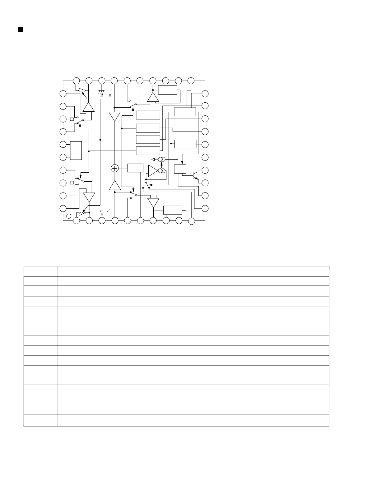
Description of major ICs 1-17
78
9 11 12
KS-LX200R
OFFSEL
10
This service manual is printed on 100% recycled paper.
COPYRIGHT 2000 VICTOR COMPANY OF JAPAN, LTD.
No.49573
Oct. 2000
1-1
Page 2

KS-LX200R
Safety precaution
!
Burrs formed during molding may be left over on some parts of the chassis. Therefore,
pay attention to such burrs in the case of preforming repair of this system.
1-2
Page 3
KS-LX200R
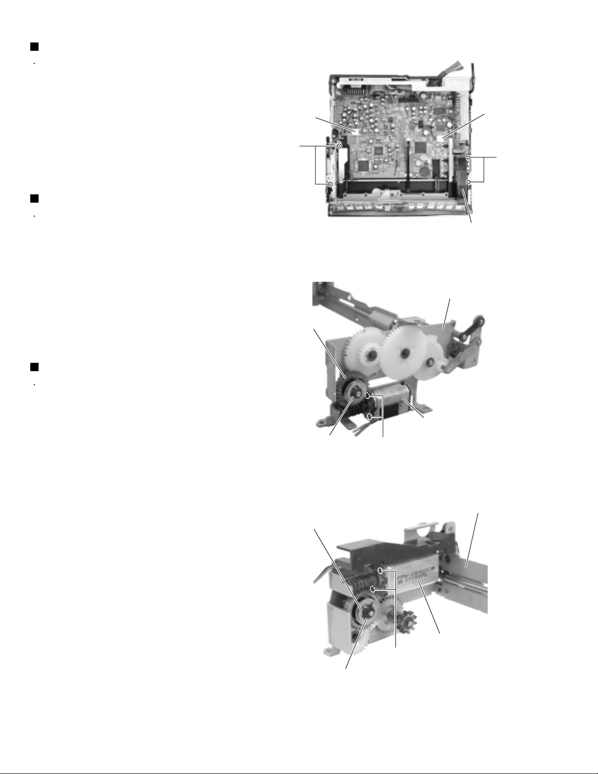
Disassembly method
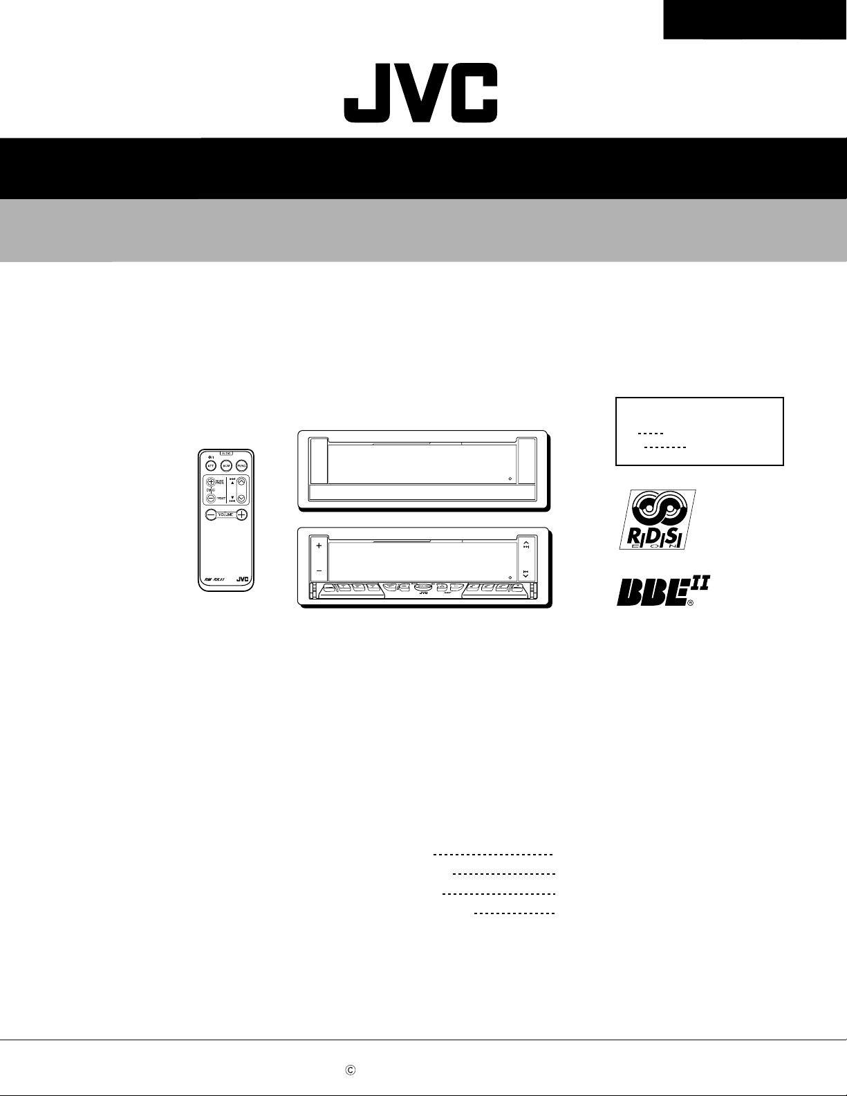
Removing the top chassis
(See Fig.1 to 5)
1.
Remove the two screws A attaching the bottom
cover to the top chassis on the bottom of the body.
2.
Remove the two screws B attaching the top chassis
on both sides of the body.
3.
Remove the screw C and the three screws D
attaching the heat sink on the left side of the body.
4.
Remove the two screws E and the screw F on the
back of the body.
5.
Remove the two screws G on the upper side of the
body.
6.
Move the top chassis upward and disconnect the
cassette mechanism connector from the main board
connector by pulling it. Remove the top chassis from
the body.
Bottom cover
A
A
Fig.1
Top chassis
Top chassis
Heat sink
C
E
Fig.2
D
Fig.3
B
Top chassis
B
F
G
G
Fig.4Fig.5
1-3
Page 4
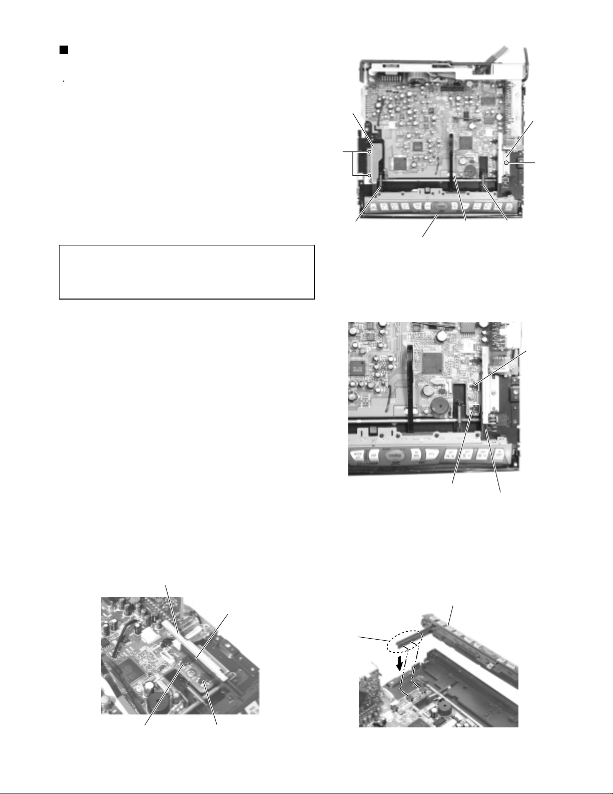
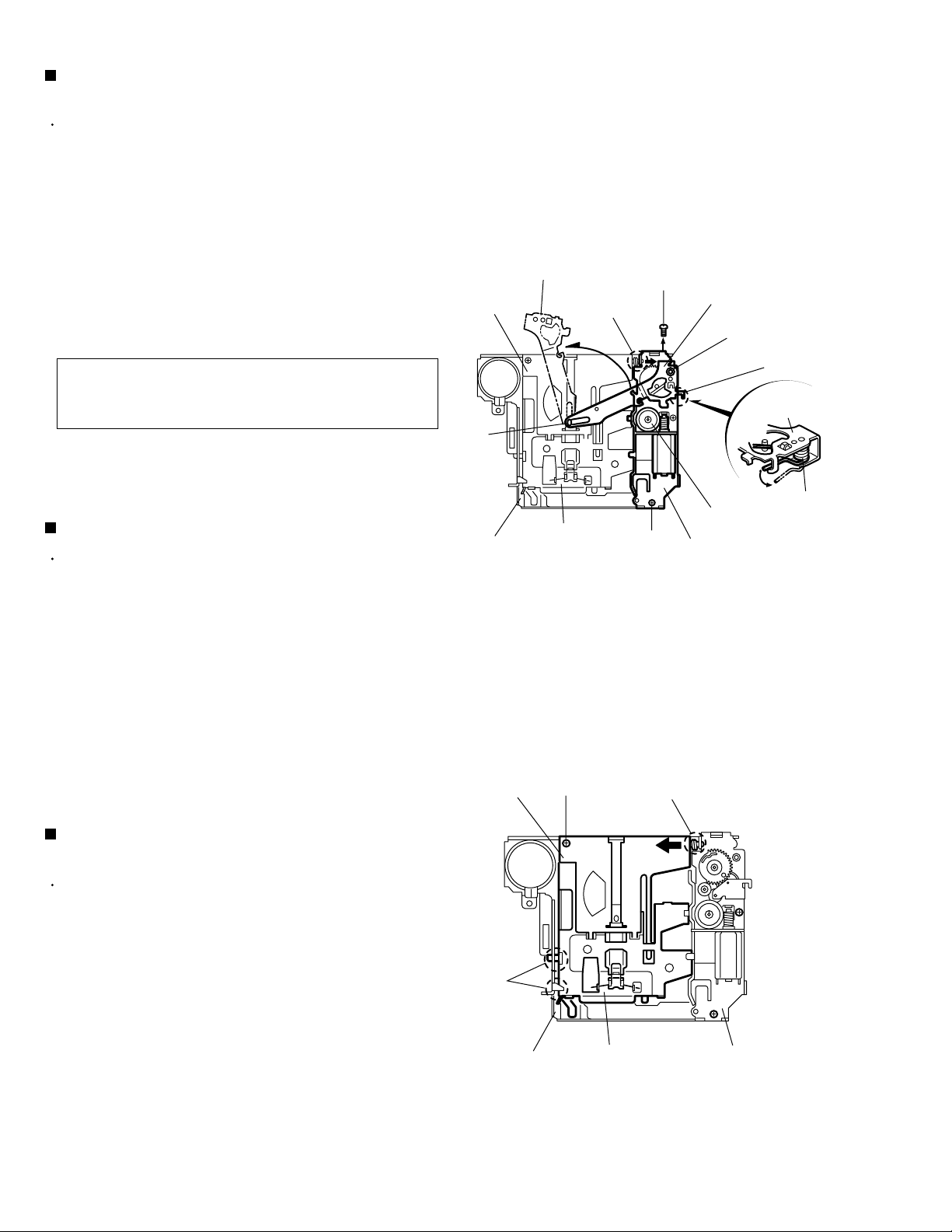
KS-LX200R
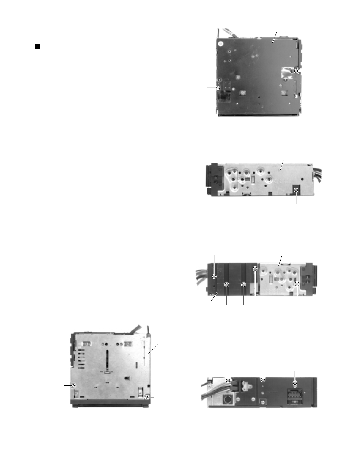
Removing the main board assembly
(See Fig.6 to 8)
Prior to performing the following procedure, remove
the top chassis.
1.
Remove the screw S attaching the bracket (L).
2.
Disconnect the flexible harness from connector
CN701, the card wire from CN702 on the main board
and the harness from CN503 and CN504
respectively.
3.
Remove the three screws H attaching the main
board assembly to the bottom cover on the upper
side of the body.
4.
Remove the screw I attaching the rear panel and the
bottom cover on the back of the body. Move the
main board in the direction of the arrow and release
the two joints a. (At this point, the main board can be
removed with the rear panel and the rear heat sink.)
5.
Remove the screw J and the two screws K attaching
the rear heat sink on the back of the body.
Main board assembly
CN503
H
Joint
a
CN702
Joint
Front panel assembly
Fig.6
CN504
Bracket (L)
CN701
H
S
H
a
6.
Remove the two screws L and the screw M attaching
the rear panel. Now, the main board assembly will be
removed.
ATTENTION:
When reassembling, correctly engage the
switch S561 and S562 on the main board
with the part e of the operation assembly
(Refer to Fig.7, 18 and 19).
Main board
L
M
S652
Fig.7
Rear heat sink
L
e
S651
J
1-4
Rear panel
K
I
Fig.8
Page 5
KS-LX200R
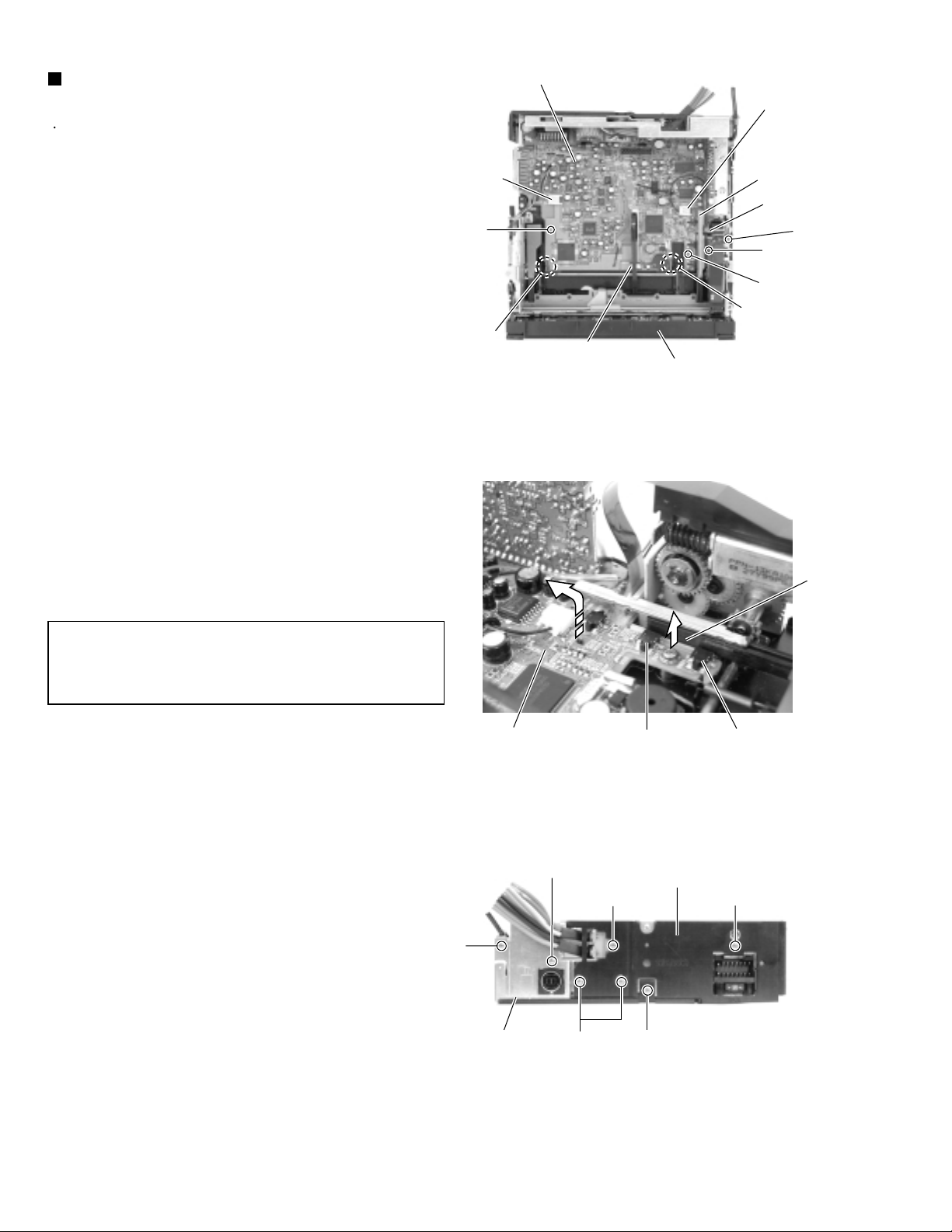
Removing the front panel assembly
(See Fig.9 to 11)
Prior to performing the following procedure, remove
the top chassis assembly.
1.
Disconnect the flexible harness from connector
CN701 on the main board assembly.
2.
Remove the four screws N attaching the front panel
assembly on both sides of the body. Remove the
front panel toward the front.
Front panel assembly
Main board assembly
CN701
Front panel assembly
Fig.9
Front panel assembly
N
Removing the Front Board (See Fig.12)
Prior to performing the following procedure, remove
the top chassis assembly and the front panel
assembly.
1.
Remove the four screws O attaching the front board
on the back of the front panel assembly and release
the eight joints b.
O
N
CN701
Fig.10Fig.11
Joints b
O
Joints b
Fig.12
1-5
Page 6
KS-LX200R
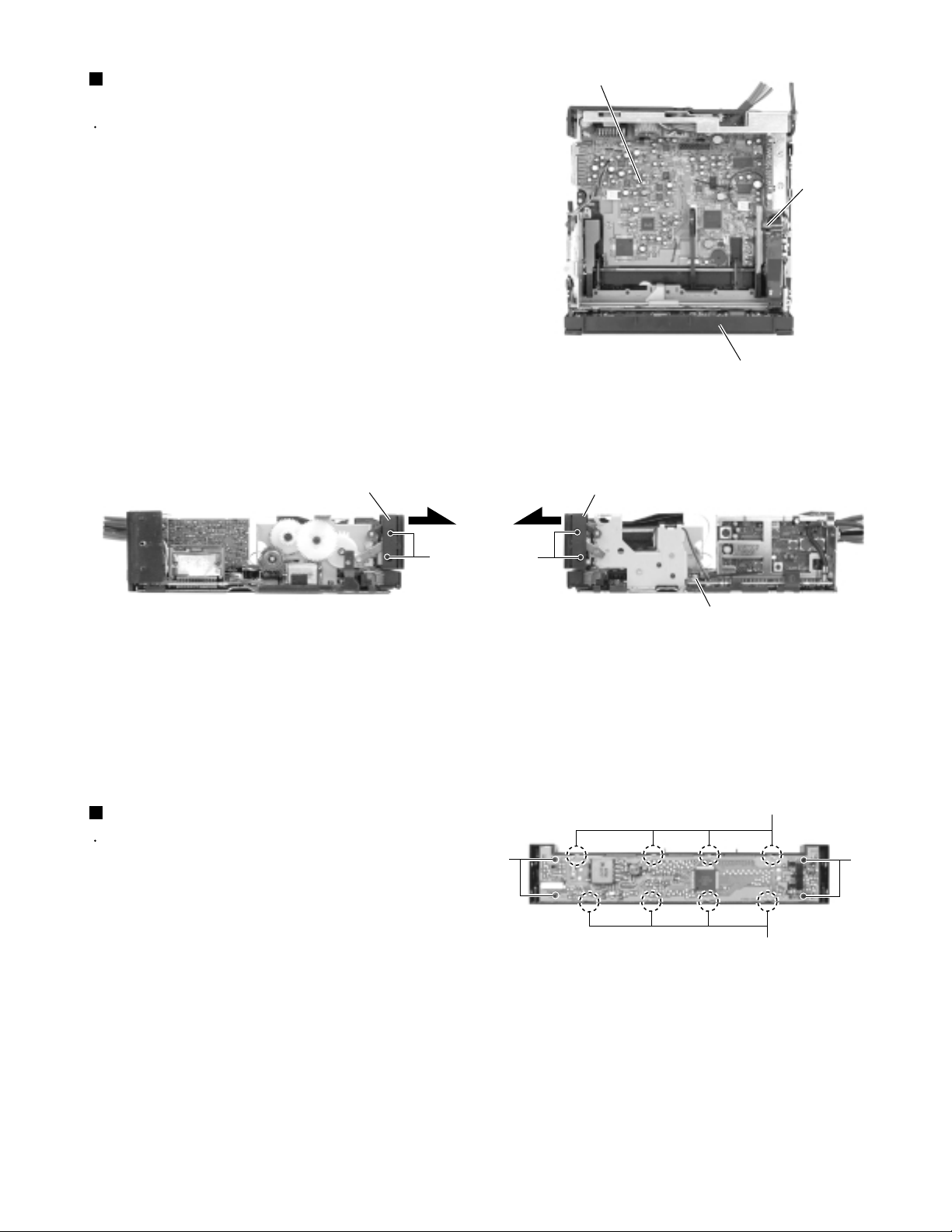
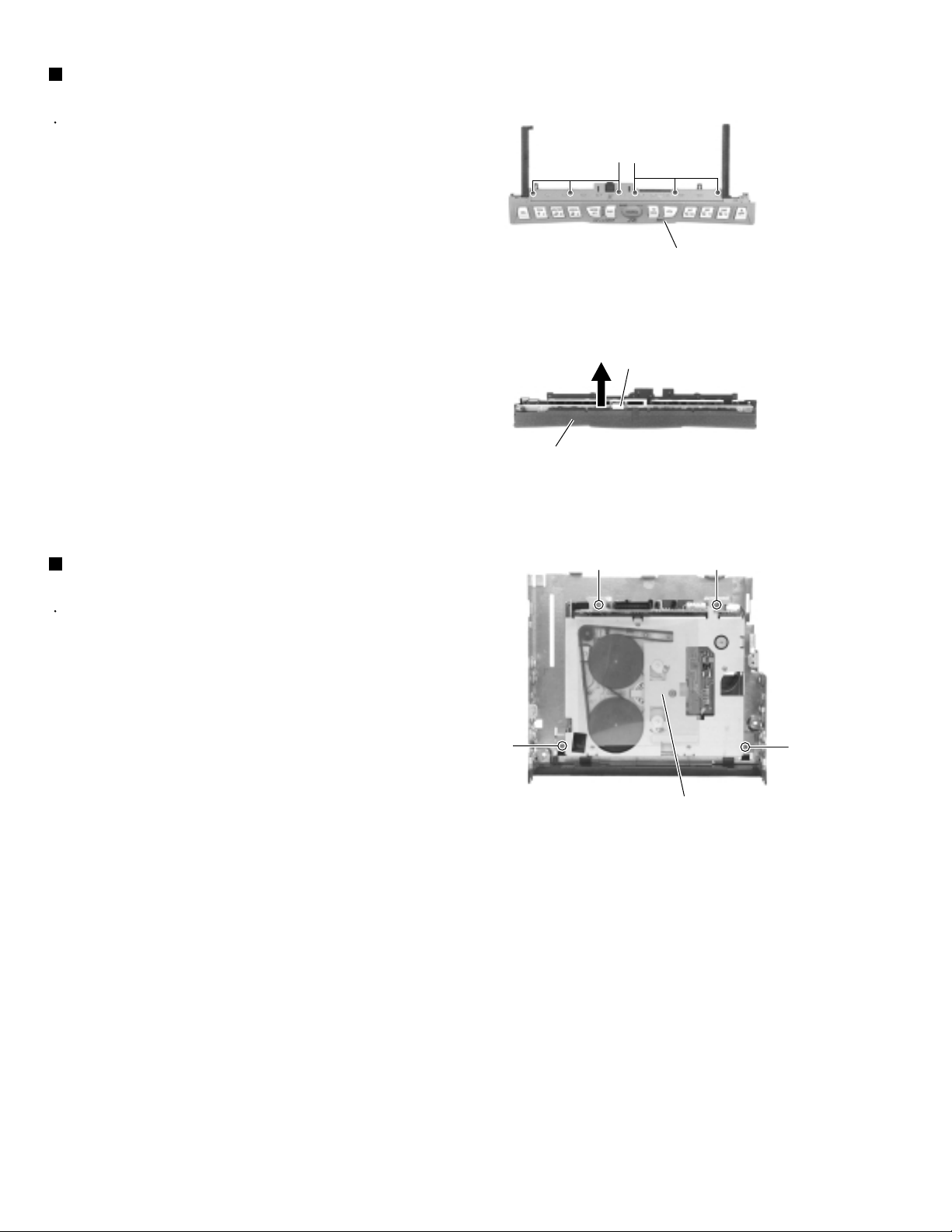
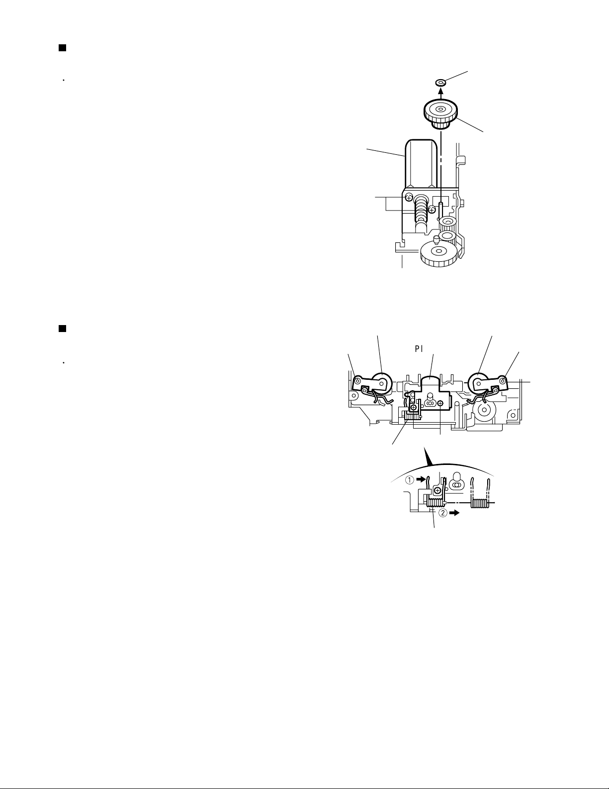
Removing the lifter unit (See Fig.13)
Prior to performing the following procedure, remove
the top chassis assembly and the front panel
assembly.
1.
Disconnect the harness from connector CN503 and
CN504 on the main board.
2.
Remove the four screws P and detach the lifter unit
from the bottom cover.
Removing the feed motor (L) (See Fig.14)
Prior to performing the following procedure, remove
the lifter unit.
1.
Remove the washer attaching the clutch assembly
and detach the clutch assembly from the shaft of the
lifter unit.
2.
Remove the two screws Q attaching the feed motor
(L).
Removing the feed motor (R) (See Fig.15)
Prior to performing the following procedure, remove
the lifter unit.
CN503
P
Clutch assembly
CN504
P
Lifter unit assembly
Fig.13
Lifter unit assembly
1.
Remove the washer attaching the clutch assembly
and detach the clutch assembly from the shaft of the
lifter unit.
2.
Remove the two screws R attaching the feed motor
(R).
Washer
Clutch assembly
Washer
Feed motor (L) assembly
Q
Fig.14
Lifter unit assembly
Feed motor (R) assembly
R
Fig.15
1-6
Page 7
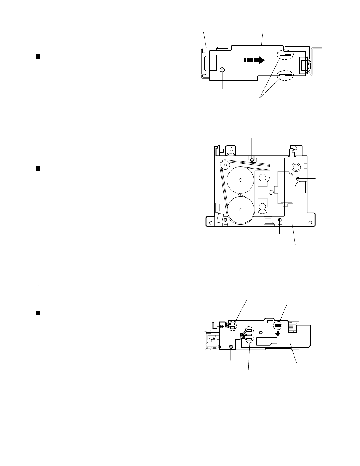
Removing the operation assembly
(See Fig.16 to 19)
Prior to performing the following procedure, remove
the top chassis assembly, the front panel assembly
and the lifer unit.
1.
Remove the three screws S attaching the right and
left brackets which fix gears on both sides of the
operation assembly.
2.
Remove the springs 5 and 6 from the operation
assembly.
3.
Disconnect the card wire from connector CN702 on
the main board and remove the operation assembly.
ATTENTION:
When reassembling, correctly engage the
switch S561 and S562 on the main board
and the right gear with the part c of the
operation assembly.
Bracket (R)
S
Spring 5
Operation assembly
Fig.16
CN702
KS-LX200R
Bracket (L)
S
Spring 6
Bracket (R)
Operation assembly
S652
S651
Operation assembly
Fig.17
Operation assembly
c
c
c
S652
S651
Fig.18Fig.19
1-7
Page 8
KS-LX200R
Removing the operation switch board
(See Fig.20 and 21)
Prior to performing the following procedure, remove
the operation assembly.
1.
Remove the six screws T attaching the button panel
on the operation assembly.
2.
Pull out the operation switch board from inside of the
button panel.
TT
Button panel
Fig.20
Operation switch board
Button panel
Fig.21
Removing the cassette mechanism
assembly (See Fig.22)
Prior to performing the following procedure, remove
the top chassis.
1.
Remove the four screws U and the cassette
mechanism assembly from the top chassis.
U
U U
U
CD mechanism assembly
Fig.22
1-8
Page 9
KS-LX200R
Disassembly method
<Cassette mechanism assembly>
Removing the head amplifier board
(See Fig.1)
1.
Disconnect the wire from connector CP401 on the
head amplifier board.
2.
Remove the screw A.
3.
Remove the head amplifier board in the direction of
the arrow to unhook two joints a.
4.
Disconnect connector CP402 on the head amplifier
board from the connector board.
Removing the mechanism bracket
(See Fig.2)
Prior to performing the following procedure, remove
the head amplifier board.
Connector board
A
Head amplifier board
Joints
a
Fig.1
B
B
1.
Remove the four screws B on the underside of the
cassette mechanism assembly.
<Cassette mechanism>
Prior to performing the following procedure, remove
the head amplifier board and the mechanism
bracket.
Removing the connector board
(See Fig.3)
1.
Unsolder soldering b and c on the connector board.
2.
Remove the three screws C.
3.
Remove the connector board in the direction of the
arrow to unhook joint d.
C
B
C
Fig.2
Soldering
Soldering
C
Mechanism bracket
b
Joint
Connector board
c
d
Fig.3
1-9
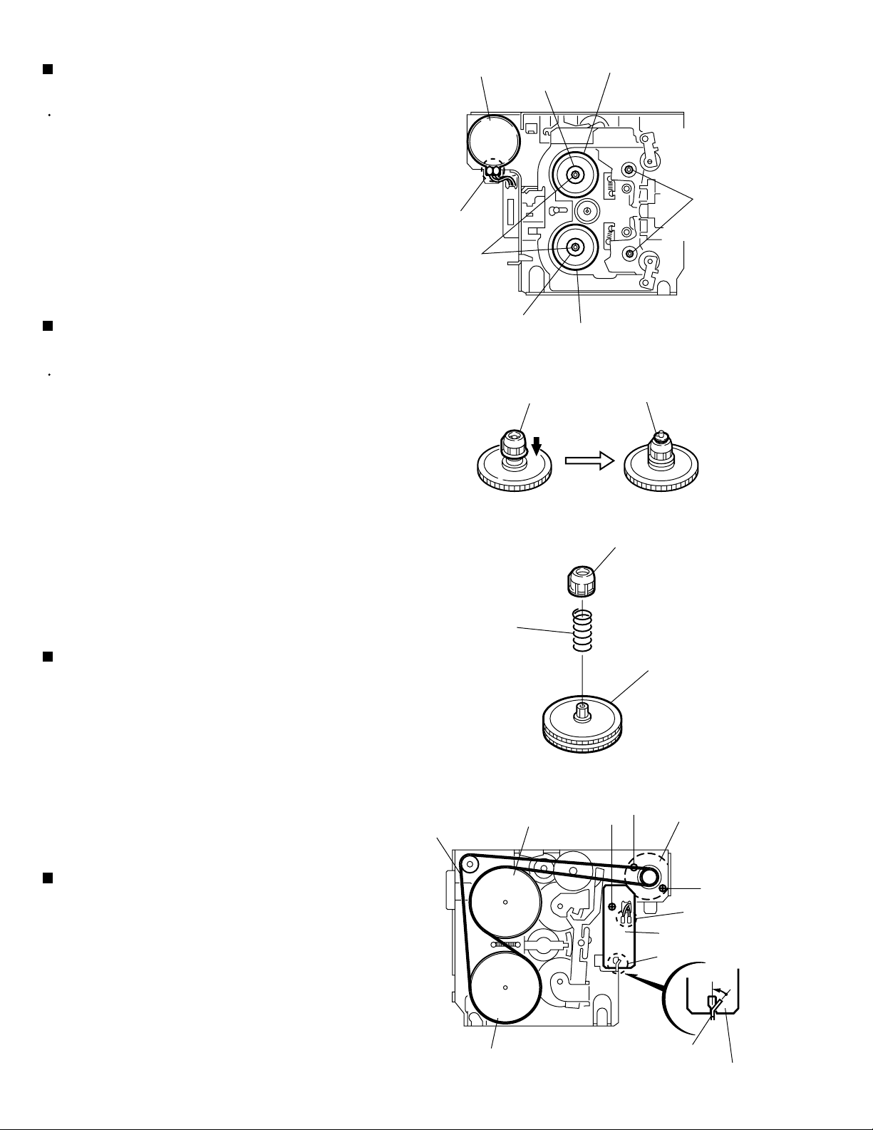
Page 10
KS-LX200R
Removing the load arm assembly
(See Fig.4)
Prior to performing the following procedure, remove
the connector board.
1.
Remove the slit washer e retaining the load arm
assembly.
2.
Remove the spring g in the load arm assembly
marked joint f.
3.
Draw out the load arm assembly from the shaft and
rotate in the direction of the arrow to remove it from
the cach.
ATTENTION:
The spring g comes off as the load
arm assembly is drawn out from the
shaft.
Load arm assembly
Holder arm
Cach
Joint
D
h
Load arm assembly
Slit washer
e
Joint
f
Load arm
assembly
Removing the sub chassis (See Fig.4)
Prior to performing the following procedure, remove
the connector board and the load arm assembly.
1.
Remove the two screws D attaching the sub
chassis.
2.
Draw out the sub chassis from the holder arm shaft
in the direction of the arrow (marked joint h).
Remove the sub chassis from the main chassis
upwards.
Removing the cassette holder / holder
arm (See Fig.5)
Prior to performing the following procedure, remove
the connector board and the load arm assembly.
1.
Remove the screw E attaching the cassette holder /
holder arm.
2.
Draw out the holder arm shaft from the sub chassis
in the direction of the arrow (marked joint h).
Main chassis
Holder arm
i
Joints
Cassette holder
Fig.4
E
D
Joint
Worm gear
Sub chassis
h
Spring
g
3.
Disengage two joints i and remove the cassette
holder / holder arm.
1-10
Main chassis
Cassette holder
Fig.5
Sub chassis
Page 11
Removing the sub motor
(See Fig.4 and 6)
Prior to performing the following procedure, remove
the connector board and the load arm assembly.
1.
Remove the slit washer j and the worm gear.
Slit washer
KS-LX200R
j
2.
Remove the two screws F.
Removing the play head / pinch roller
assembly (twin set) (See Fig.7)
Prior to performing the following procedure, remove
the connector board, the load arm assembly and the
sub chassis.
1.
Remove the spring K retaining the play head
assembly and pull out the play head assembly.
Sub motor
Pinch roller assembly
Slit washer
F
Worm gear
Fig.6
Pinch roller assembly
l
Play head
Slit washer
l
2.
Remove the two screws G.
3.
Remove the two slit washers l attaching the pinch
roller assembly (twin set). Pull out each pinch roller
assembly.
Spring
1
G
Spring
Fig.7
2
k
k
1-11
Page 12
KS-LX200R
Removing the reel disc assembly (twin
set) (See Fig.8 to 10)
Prior to performing the following procedure, remove
the connector board, the load arm assembly, the sub
chassis and the cassette holder / holder arm.
1.
Remove the two slit washers m while pushing down
the reel driver on the two reel disc assemblies.
2.
Pull out the two screws I from the shaft with the reel
driver and the spring respectively.
Removing the flywheel assembly (F) and
(R) (See Fig.8 and 11)
Prior to performing the following procedure, remove
the connector board, the load arm assembly, the sub
chassis and the cassette holder / holder arm.
1.
Remove the belt from the underside of the
mechanism assembly.
Soldering
Slit
washers
Motor
q
m
Reel driver
Reel driver
Reel driver
Reel disc assembly
Reel disc assembly
Fig.8
Slit washer
m
Slit
washers
n
2.
Remove the two slit washers on the upper side of the
mechanism assembly.
3.
Pull out the flywheel assembly (F) and (R) from
underside of the mechanism assembly.
Removing the reel disc board
(See Fig.11)
1.
From the underside of the mechanism assembly,
unsolder soldering o on the reel disc board.
2.
Unbend the joint hook p retaining the reel disc board.
3.
Remove the screw H.
Removing the motor (See Fig.8and 11)
1.
Unsolder soldering q on the motor.
2.
Remove the belt from the underside of the
mechanism assembly.
Belt
Spring
Flywheel (F)
Fig.9
Fig.10
Reel driver
Reel disc
I
H
Motor
I
Soldering
Reel disc board
Joint hook
p
o
3.
Remove the two screws I from the underside of the
mechanism assembly.
1-12
Flywheel (R)
Fig.11
Tab
Reel disc board
Page 13
Adjustment method
KS-LX200R
Test Instruments reqired for adjustment
1.Digital osclloscope(100MHz)
2.Frequency Counter meter
3.Electric voltmeter
4.Wow & flutter meter
5.Test Tapes
VT724
VT739
VT712
For wow flutter & tape speed measurement
VT703
6.Torque gauge
For playback frequency measurement
for DOLBY level measurement
For head azimuth measurement
Cassette type for CTG-N
(mechanism adjustment)
Measuring conditions(Amplifier section)
Power supply voltage
Load impedance
4 (2Speakers connection)
DC14.4V(10.5~16V)
Line out
Standard volume position
Balance and Bass,Treble volume .Fader
20k
Tuner section
BAND STEP
FM : 100kHz (Seek), 50kHz (Manual)
AM : 9kHz step
Preset Memory Initialization
Preset Memory
Band
FM(MHz)
AM(kHz)
M1
87.5
153
M2
89.9
216
M3
97.9
603
M4
105.9
999
M5
108.0
1404
DUMMY LOAD
Exclusive dummy load should be used for AM
and FM dummy load,there is a loss of 6dB
between SSG output and antenna input. The
loss of 6dB need not be considered since
direct reading of figures are applied in this
working standard.
M6
87.5
1620
:Center(Indication"0")
Loudness,Dolby NR,Sound,Cruise:Off
Volume position is about 2V at speaker output with
following conditions.Playback the test tape VT721.
AM mode 999kHz/62dB,INT/400Hz,30%
modulation signal on receiving.
FM mono mode 97.9MHz/66dB,INT/400Hz,22.5kHz
deviation pilot off mono.
FM stereo mode 1kHz,67.5kHz dev. pilot7.5kHz dev.
Output level 0dB(1 V,50 /open terminal).
Arrangement of Adjusting
Cassette Mechanism Section
Capstan motor
Cassette mechanism
(Surface)
Azimuth screw
Playback head
(Forward side)
Azimuth screw
(Reverse side)
Tape speed adjust
1-13
Page 14
KS-LX200R
Arrangment of adjusting
Head amplifier board section (Reverse side)
VR402:Rch
(Dolby NR level adj)
VR401:Rch
(Dolby NR Frequency response adj)
B402
E
Q401
D401
B401
CP401
1
R420
1
R423
R421
R422
Q402
B409
Q403
D402
B408
FSMW1101A
VR402
C417
D403
C418
R424
IC402
R425
C419
C414
B403
B410
B404
C410
C412
C411
R413
1
C415
R416
R415
C416
R418
R419
CP403
C409
R411
B415
C413
1
11
B411
IC401
B412
17
VR401
B416
R412
R410
C405
R408
31
C407
21
C408
R417
B413
R404
B406
B414
R409
C406
R414
R407
1
B405
TPP
C404
CP402
1
R402
C401
2
R405
C403
R401
R406
R403
C402
B407
Information for using a Car Stereo service jig (for adjustment and checking)
We are advancing efforts to make our extension cords comman for all Car Stereo products.
Please use this type of extension cord as follows.
As a U -shape type top cover is employed,this type of extension cord needed to check operation of
the mechanism assembly after disassembly.
Extension cords
EXT-KSRT002-18P(18 pin extension cord)
For connection between mechanism assembly
and main board assembly.
Check for mechanism-driving section such as moter ,etc.
Disassembly method. (Refer to mthod to remove main parts)
1.Remove the bottom cover.
2.Remove the front panel assembly.
3.Remove the top cover. (Remove the screws at each side of heat sink and rear panel)
4.Install the front panel (whose assembly was removed in step 2) to the main unit.
5.Confirm that current is being is carried by connecting an extension cord jig.
Connection diagram
1-14
EXT-KSRT002-18P
EXTLX001-16PF
EXTLX002-4P
EXTLX002-16PC
EXTLX002-SWPWB
EXTLX001-2P
EXTLX001-6PC
EXTLX001-2P
EXTLX001-6PF
Page 15
Extension cord list
EXTLX002-JIG : Kit including the following 8 extension parts.
KS-LX200R
No.
1
2
3
4
5
6
7
Parts number Quantity Description
EXTLX001-2P
EXTLX001-6PF
EXTLX001-6PC
EXTLX002-16PF
EXTLX002-16PC
EXTLX002-SWPWB
EXTLX002-4P
Besides the above kit, we offer the conventional extension cord for CASSETTE
mechanism which are not essential to operation check or service.
The mechanism should be directly connected to the board using the extension wire.
EXT-KSRT002-18P
2
1
1
1
1
1
1
2Pin, 30cm extension cord
6Pin, 30cm flat wire
6Pin x 2, interlocking connector
16Pin flat wire
16Pin, interlocking connector
3 switch PWB
4Pin, 30cm extension cord
EXTGS004-26P
EXTLX001-16PF
EXTLX002-SWPWB
EXTLX002-4P
EXTLX002-16PC
EXTLX001-2P
EXTLX001-6PC
EXTLX001-2P
EXTLX001-6PF
1-15
Page 16
KS-LX200R
Item
1.
Head
azimuth
adjustment
Conditions
Test tape:
SCC-1659
VT703(10kHz)
Adjustment and Confirmation methods
Head height adjustment
Adjust the azimuth directly. When you
adjust the height using a mirror tape,
remove the cassette housing from the
mechanism chassis. After installing the
cassette housing, perform the azimuth
adjustment.
Load the SCC-1659 mirror tape. Adjust with
1.
height adjustment screw A and azimuth
adjustment screw B so that line A of the
mirror tape runs in the center between Lch
and Rch in the reverse play mode.
After switching from REV to FWD then to
2.
REV, check that the head position set in
procedure 1 is not changed. (If the position
has shifted, adjust again and check.)
Adjust with azimuth adjustment screw B so
3.
that line B of the mirror tape runs in the
center between Lch and Rch in the forward
play mode.
Head azimuth adjustment
Load VTT724 (VT724) (1kHz) and play it
1.
back in the reverse play mode. Set the Rch
output level to max.
Load VTT703 (VT703) (10kHz) and play it
2.
back in the forward play mode. Adjust the
Rch and Lch output levels to max, with
azimuth adjustment screw B. In this case,
the phase difference should be within 45 .
Engage the reverse mode and adjust the
3.
output level to max, with azimuth
adjustment screw C.
(The phase difference should be 45 or
more.)
When switching between forward and
4.
reverse modes, the difference between
channels should be within 3dB. (Between
FWD L and R, REV L and R.)
S.Values Adjust
A line
Head shield
The head is at low position
during.
B line
Head shield
The head is at High position
during REV.
Output
level:
Maximum
PBHead
FWD Adj B
REV Adj C
(0 ) (45 )
HEIGHT Adj A
phase
Tape speed
2.
and wow
flutter
confirmation
Play back
3.
frequency
response
confiramation
1-16
When VTT721 (VT721) (315Hz) is played
5.
back, the level difference between channels
should be within 1.5dB.
Test tape: VTT712
(3kHz)
Test tape: VTT724
(1kHz)
VTT739
(63Hz / 1kHz / 10kHz)
The tuner section is of an adjustment-freedesign. In case the tuner is in trouble, replace the tuner pack.
Check to see if the reading of the F, counter /
1.
wow flutter meter is within 3015 3045(FWD
/ REV), and less than 0.35% (JIS RMS).
In case of out of specification, adjust the
2.
motor with a built-in volume resistor.
Play test tape VTT724, and set the volume
1.
position at 2V.
Play test tape VTT739 and confirm.
2.
1kHz / 10kHz: -1 3dB,
1kHz / 63Hz: 0 3dB,
When 10kHz is out of specification, it will be
3.
necessary to read adjust the azimuth.
Tape speed:
3015
3045Hz
Wow
flutter: less
than 0.35%
Speaker out
1kHz / 63Hz
: 0 3db
1kHz / 10kHz
: -1 3db
Built-in volume
resistor
Page 17
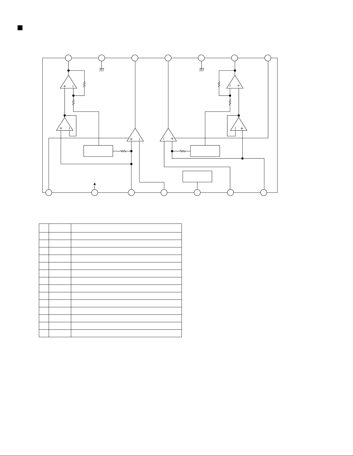
Description of major ICs
BA4905-V3 (IC961) : Regulator
1.Pin layout
1234 56789101112
2.Block diagram
KS-LX200R
REGULATOR
EXT
RESET
1 2 3 4 5 6 7 8 9 10 11 12
RESET COMP VDD 5.7V CD 8V VCC AJ
EXT ACC AUDIO 9V CTRL ILM 10V GND
3.Pin function
Pin no. Symbol Function
1
2
RESET
EXT output
If VDD voltage becomes 4V or less.RESET output becomes low level.
This output voltage is approximately 0.5V lower than VCC. and max
output current is 300mA.
3
COMP output
A voltage supply for ACC block. This output voltage is approximately
0.7V lower than VDD'S. The max output current is 100mA.
4
5
ACC
VDD output
Control of the COMP output by inputting voltage.
This output voltage is 5.7V, and max output current is 100mA.
This voltage supply is for microcomputer. Whenever back up voltage
supply is connected, the output keeps on running.
6
AUDIO output
This output voltage is 9.0v, and max output current is 500mA.
This voltage supply for AUDIO.
7
CD output
This output voltage is 8.0V, and max output current is 1A.
This voltage supply for CD.
8
9
10
CTRL
VCC
ILM output
Output selector of CD. AUDIO, ILM and EXT.
To be connected with the BACK UP of car.
This output voltage is 10V, and max output current is 500mA.
Output voltage is adjustable.
11
AJ
Putting a resistance between ILM and AJ or between AJ and GND
makes ILM output voltage adjustable.
12
GND
Ground.
Overvoltage
protection circuit
37K
5K
1-17
Page 18
KS-LX200R
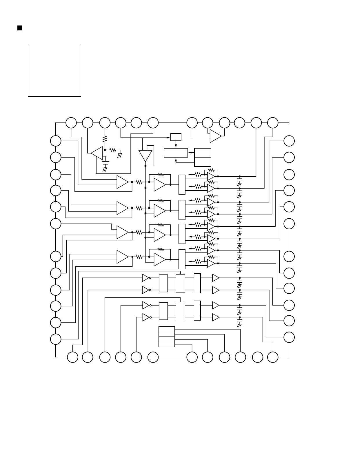
CXA2510AQ (IC401) : Head AMP / Dolby
1. Pin layout & Block diagram
30 PBEQ2
29 PBOUT2
28 GND
27 TAPEIN2
26 AUXIN2
PBFB2 31
PBRIN 32
PBREF2 33
PBFIN2 34
VCT 35
PBGND 36
PBFIN1 37
PBREF1 38
PBRIN1 39
PBFB1 40
VCT
F1
-
-
F2
120 /70
+
+
120 /70
T2
X1
TAPE / AUX
FWD / RVS
LPF
X1
T1
25 DIREF
24 LINEOUT2
+
NR BIAS
TAPE EQ
Vcc
+
F3
+
OFF/
-
B / C
-
23 TCH2
NR
NR
22 TCL2
MS MODE
NR MODE
MS ON/
OFF
DET
21 MSSW
20 MSMODE
19 DRSW
18 TAPESW
17 INSW
16 NRSW
15 MRMODE
14 MSOUT
13 DGND
12 MSTC
11 G1FB
2. Pin functions
Pin No.
1
2
3
4
5
6
7
8
9
10
11
12
13
14
15
PBEQ1 1
PBOUT1 2
Symbol
PBEQ1
PBOUT1
Vcc
TAPEIN1
AUXIN1
MSLPF
LINEOUT1
TCH1
NC
G2FB
G1FB
MSTC
DGND
MSUOT
NC
Vcc 3
TCL1 9
AUXIN 5
TAPEIN1 4
MSLPF 6
TCH1 8
LINEOUT1 7
I/O
O
Resistance for selecting the equalizer amplifier time constant.
O
Playback equalizer amplifier out put.
Power supply
TAPE input.
I
External input.
I
Cut-off frequency adjustment of the music sensor LPF.
Line out.
O
Time constant for the HLS.
Non connection.
Music signal interval detection level setting.
-
G2FB 10
Functions
Time constant for detecting the music signal interval.
Logic ground (Connect to GND)
Music sensor output.
O
Non connection.
I
1-18
Page 19
KS-LX200R
Pin
16
17
18
19
20
21
22
23
24
25
26
27
28
29
30
31
32
33
34
35
36
37
38
39
40
Symbol
NRSW
INSW
METAL
DRSW
FF/REW
MSSW
NC
TCH2
LINEOUT2
DIREF
NC
TAPEIN2
GND
PBOUT2
PBEQ2
PBFB2
NC
PBREF2
PBFIN2
VCT
PBGND
PBFIN1
PBREF1
NC
PBFB1
I/O
I
Dolby NR control L:NR OFF H:NR ON
I
Line amplifier input select control L:TAPE IN H:AUX IN
I
Playback equalizer amplifier control L:120us H:70us
I
Head select control L:FORWARD H:REVERSE
I
Music sensor mode control Low(open):G1 High:G2
I
Music sensor control Low(open):MS on High:MS OFF
-
Non connection
-
Time constant for the HLS
O
Line output
-
Resistance for setting the reference current (Connects 20(18)K
between DIREF pin and GND for the standard setting.)
-
Non connection.
I
TAPE input.
-
To ground.
O
Playback equalizer amplifier output.
O
Resistance for selecting the playback equalizer amplifier time constant
I
Playback equalizer amplifier feedback.
-
Non connection.
O
Playback equalizer amplifier reference (Vcc/2 output)
I
Playback equalizer amplifier input (FORWARD head connected)
O
Center (Vcc/2 output)
-
Playback equalizer amplifier ground (Connect to ground)
I
Playback equalizer amplifier input (FORWARD head connected)
O
Playback equalizer amplifier reference (Vcc/2 output)
-
Non connection.
I
Playback equalizer amplifier feedback.
Functions
NJM4565M-W (IC951,IC171,IC323) : Ope amp.
V-
1
2
8
V+
7
B OUTPUT
AB
3
4
6
B -INPUT
5
B +INPUT
A OUTPUT
A -INPUT
A +INPUT
1-19
Page 20
KS-LX200R
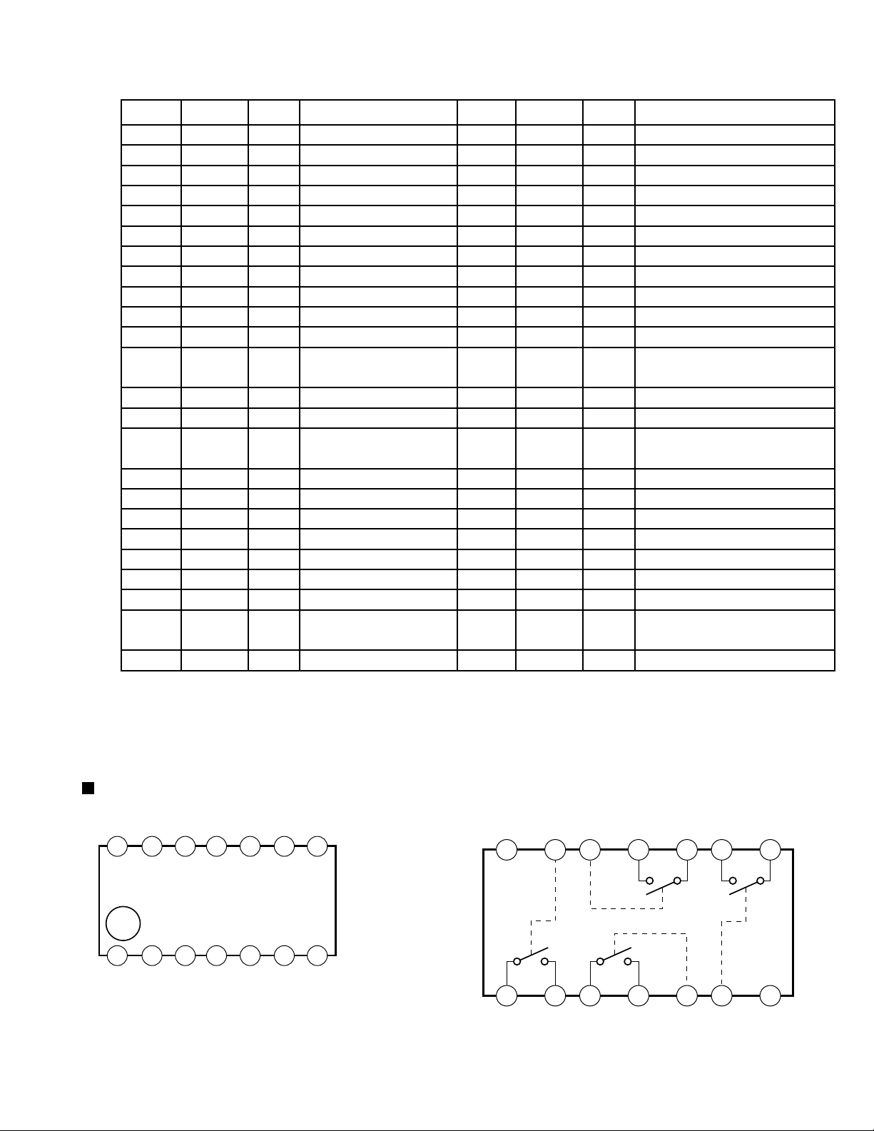
KA3031 (IC831) : Motor driver
1. Pin layout
48 ~ 37
1
36
~
12
13 ~ 24
2. Block diagram
1
IN1.2
2
OUT1
3
IN2.1
4
IN2.2
5
OUT2
6
IN3.1
7
IN3.2
8
OUT3
9
IN4.1
~
25
IN1.1 REG50 REG050 REF SVCC RES50 OPIN(+) OPIN(-) OPOUT PVCC2 DO1.1 DO1.2
48 47 46 45 44 43 42 41 40 39 38 37
T.S.D
O.V.P
+
-
+
-
+
-
+
-
+
-
+
-
+
-
+
-
+
-
+
D
D
2P
2P
2P
2P
2P
2P
2P
2P
2P
2P
2.5V
SW
+ -
+
-
+
-
+
-
+
-
-
+
-
+
-
+
-
+
S
W
ALL MUTE
+
-
+
-
+
-
+
-
M
S
C
36
35
34
33
32
31
30
29
28
DO2.1
DO2.2
PGND3
DO3.1
DO3.2
PGND2
PGND1
DO4.1
DO4.2
1-20
IN4.2
OUT4
CTL1
10
11
12
S
W
MUTE4
MUTE3
MUTE2
MUTE1
+
M
S
C
D
-
D
2P
2P
13 14 15 16 17 18 19 20 21 22 23 24
FWD1 REV1 CTL FWD2 REV2 SGND MUTE1 MUTE2 MUTE3 MUTE4 PVCC1 DO6.2
27
26
25
DO5.1
DO5.2
DO6.1
Page 21
3. Pin function
Pin No. Symbol I/O Function Pin No. Symbol I/O Function
1
2
3
4
5
6
7
8
9
10
11
12
13
14
15
16
17
18
19
20
21
22
23
24
IN1.2
OUT1
IN2.1
IN2.2
OUT2
IN3.1
IN3.2
OUT3
IN4.1
IN4.2
OUT4
CTL1
FWD1
REW1
CTL2
FED2
REW2
SGND
MUTE1
MUTE2
MUTE3
MUTE4
PVCC1
DO6.2
I
CH 1 op-amp input (-)
CH 1 op-amp output
O
CH 2 op-amp input (+)
I
CH 2 op-amp input (-)
I
CH 2 op-amp output
O
CH 3 op-amp input (+)
I
CH 3 op-amp input (-)
I
CH 3 op-amp output
O
CH 4 op-amp input(+)
I
CH 4 op-amp input (-)
I
O
CH 4 op-amp output
CH 5 motor speed
I
control
CH 5 forward input
I
CH 5 reverse input
I
CH 6 motor speed
I
control
CH 6 torward input
I
CH 6 reverse input
I
Signal ground
CH 1 mute
I
CH 2 mute
I
CH 3 mute
I
CH 4 mute
I
Power supply voltage
-
(For CH 5, CH 6)
CH 6 drive output
O
25
26
27
28
29
30
31
32
33
34
35
36
37
38
39
40
41
42
43
44
45
46
47
48
DO6.1
DO5.2
DO5.1
SO4.2
DO4.1
PGND
PGND
DO3.2
DO3.1
PGND
DO2.2
SO2.1
SO1.2
DO1.1
PVCC2
OPOUT
OPIN(-)
OPIN(+)
RES50
SVCC
REF
REG050
REG50
IN1.1
O
CH 6 drive outout
CH 5 drive output
O
CH 5 drive output
O
CH 4 drive output
O
CH 4 drive output
O
Power ground
Power ground
CH 3 drive output
O
CH 3 drive output
O
Power ground
CH 2 drive output
O
CH 2 drive output
O
O
CH 1 drive output
O
CH 1 drive output
Power supply voltage
-
(For CH 1, CH 2, CH 3, CH 4)
Opamp output
O
Opamp input (-)
I
Opamp input (+)
I
Regulator 5V reset
I
Signal supply voltage
Bias voltage input
I
regulator 5V output
O
Regulator output
O
CH 1 opamp onput (+)
I
KS-LX200R
BU4066BCF-X (IC322) : Switch
1.Pin l ayout
14 13 12 11 10 9 8
1 2 3 4 5 6 7
2.Block diagram
VDD
14 13 12 11 10 9 8
1 2 3 4 5 6 7
I/O 1
C1
O/I 1
C4
O/I 2
I/O 4
I/O 2
O/I 4
C2
O/I 3
C3
I/O 3
VSS
1-21
Page 22

KS-LX200R
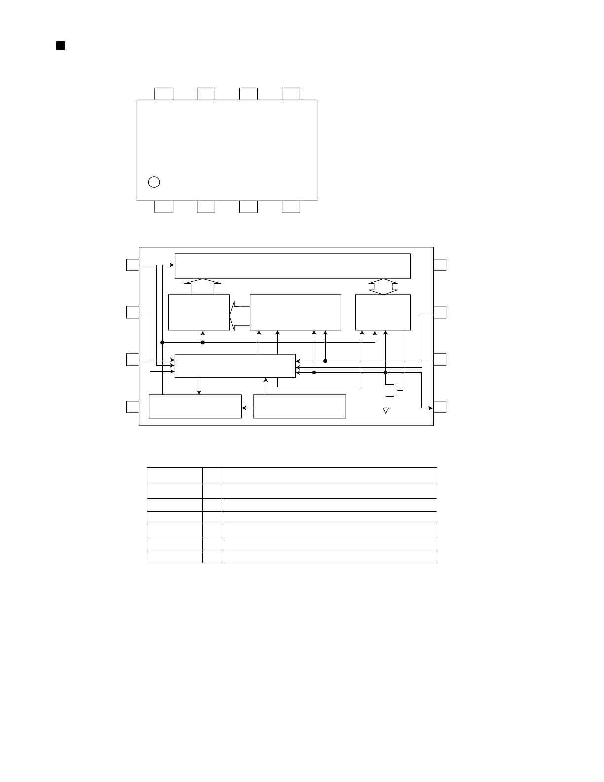
UPD784215AGC113 (IC701) : UNIT CPU
1.Pin layout
75 ~ 51
76
~
50
~
100
1 ~ 25
26
2.Pin function
Pin No. Symbol I/O Function
1
2
3
4
5
6
7
8
9
10
11
12
13
14
15
16
17
18
19
20
21
22
23
24
25
26
27
28
29
30
31
32
33
34
35
36
37
38
39
40
41
42
43
44
45
46
47
48
49
50
FF/REW
DOLBY
MS-OUT
F/R
HOLD
TRAYCNT
DIMMER-OUT
LCD-POWER
VDD
X2
X1
VSS
XT2
XT1
RESET
SW1
BUS-IN
PS2
CURUISE
RDS-SCK
RDS-DA
REMOCON
AVDD
AVREF0
NC
NC
KEY0
KEY1
KEY2
LEVEL
SQ
S.METER
AVSS
W-VOL
DOT CONT
AVREF
BUS-SI
BUS-SO
BUS-SCK
STAGE2
LCD-DA
LCD-CL
LCD-LEI
BUZZER
E2PR-DA-I
E2PR-DA-O
E2PR-CLK
BUS-I/O
TM0
TM1
I/O
I/O
I/O
I/O
Output for input signal level switching for MS.
O
Dolby on "H" output.
O
MS output.
O
Fwd, REV direction switch signal input.
I
Non connect
Tray light control signal output.
O
Dimmer signal output.
O
Non connect.
Power supply terminal.
Connecting the crystal oscillator for system main clock.
O
Connecting the crystal oscillator for system main clock.
I
Connect to GND.
Connecting the crystal oscillator for system sub clock.
O
Connecting the crystal oscillator for system sub clock.
I
System reset signal input.
I
Cassette mechanism detect switch.
I
J-BUS signal cut in input.
I
Power save 2.
I
CRUISE signal input.
I
RDS selial clock input.
I
RDS data input.
I
Remove control signal input.
I
Power supply terminal.
Connect to GND.
Connect to GND.
Connect to GND.
Key control 0 input.
I
Key control 1 input.
I
Key control 2 input.
I
Level meter signal input.
I
S.quality level input.
I
S.meter level input.
I
Connect to GND.
Woofer volume signal output.
O
Dot contrast signal input.
O
Power supply terminal.
J-BUS data I/O terminal.
J-BUS data output.
O
J-BUS serial clock signal I/O.
Initial setting.
I
Data output for LCD driver.
O
Clock otput for LCD driver.
O
Chip enable 1 output for LCD driver.
O
BUZZER control signal output.
O
Data input terminal from EEPROM.
I
Data output terminal from EEPROM.
O
Data input terminal from EEPROM.
J-BUS I/O signal terminal.
Tray motor negative signal output.
O
Tray motor positive signal output.
O
1-22
Page 23

Pin No. Symbol I/O Function
51
52
53
54
55
56
57
58
59
60
61
62
63
64
65
66
67
68
69
70
71
72
73
74
75
76
77
78
79
80
81
82
83
84
85
86
87
88
89
90
91
92
93
94
95
96
97
98
99
100
DM0
DM1
ST
LOCAL
MONO
CA-SW1
CA-SW2
CA-SW3
CA-SW4
CA-SW5
VCR-CONT
AFCK
SEEK/STOP
SD
FM/AM
PLL-CE
PLL-DA
PLL-CK
BAND IN
TEL-MUTE
AMP KILL
VSS
DIMMER-IN
DSI
POWER
CD-ON
MUTE
W-LPF1
W-LPF2
W-MUTE
VDD
VOL-DA
VOL-CLK
CF-SEL
NC
LCD RST
LCD-CE2
DMK
TMK
STAGE1
MOTOR
MODE
STANDBY
TEST
TAPE-IN
SUBMO-
SUBMO+
TAPE-END
KICK
VOICE IN
Door motor negative signal output.
O
Door motor positive signal output.
O
Stereo signal input.
I
Non connect.
Manual ON/OFF select signal output.
O
DOOR/TRAY open/close detect switch signal input.
I
DOOR/TRAY open/close detect switch signal input.
I
DOOR/TRAY open/close detect switch signal input.
I
DOOR/TRAY open/close detect switch signal input.
I
DOOR/TRAY open/close detect switch signal input.
I
Non connect.
AF check output.
O
AUTO SEEK/STOP select signal output.
O
Station detector input.
I
FM/AM select signal output.
O
Chip enable signal output.
O
Data output.
O
Clock signal output.
O
AM detect signal input.
I
Telephone.
I
Non connect.
Connect to GND
DIMMER signal input.
I
Power save 1.
I
Power ON/OFF select signal output.
O
Non connect.
Mute signal output.
O
Woofer LPF 1 signal output.
O
Woofer LPF 2 signal output.
O
Woofer mute signal output.
O
Power supply.
Data output.
O
Clock signal output.
O
CF select signal input.
I
Non connect.
LCD reset signal output.
O
Chip enable 2 output.
O
Motor speed control signal output.
O
Tray motor control signal output.
O
Initial setting.
I
Mecha Motor signal output.
O
Mecha mode position detection input.
I
Standby position derection input.
I
Test terminal
I
Cassette in detection input.
O
Sub motor clock direction drive output.
O
Sub motor clock oppositte direction drive output.
Tape end detection input.
I
Kick output.
O
Voice control signal input.
I
KS-LX200R
1-23
Page 24
KS-LX200R
BD3860K (IC911) : E. volume
1. Pin layout
33 ~ 23
34
22
44
2. Block diagram
GND FIL VCC SEL1
6 5 9 40 36 35 343328323130 2919 15 14
POWER
SUPPLY
A1
41
B1
42
C1
43
D1
44
INPUT
1
2
3
4
SELECTOR
A2
B2
C2
D2
~
1 ~ 11
INPUT
GAIN
0 to 18 dB
INPUT
GAIN
0 to 18 dB
~
12
VIN1 LOUD1 HF1 LF1 DET1 TIN1 TNF1 BNF1
MAIN
VOLUME
0 to -40 dB
LOUDNESS
MAIN
VOLUME
0 to -40 dB
LOUDNESS
LOW(f=50Hz) 6dB
PROCESS CONTROL +3 to 12dB
(f=10kHz)
LOGIC
LOW(f=50Hz) 6dB
PROCESS CONTROL +3 to 12dB
(f=10kHz)
TREBLE
-14 to +14dB
TREBLE
-14 to +14dB
-14 to +14dB
-14 to +14dB
BASS
BASS
BOUT1VCA1 MIX1 BBOUT1
FADER
CH1 FRONT
0 to -5 dB
FADER
CH1 REAR
0 to -5 dB
FADER
CH2 REAR
0 to -5 dB
FADER
CH2 FRONT
0 to -5 dB
13
12
10
11
7
8
OUTF1
OUTR1
SI
SC
OUTR2
OUTF2
3. Pin function
Pin
Symbol Function
No.
1
2
3
4
5
6
7
8
9
10
11
12
13
14
15
16
17
18
19
20
21
BBOUT2
22
A2
B2
C2
D2
FIL
GND
SC
VCC
OUTR2
OUTF2
OUTR1
OUTF1
BOUT1
BNF1
BOUT2
BNF2
TNF2
TNF1
TIN2
MIX2
CH2 input terminal A
CH2 input terminal B
CH2 input terminal C
CH2 input terminal D
1/2 VCC terminal
Ground terminal
Serial data input terminal
SI
Serial clock input terminal
Power supply
CH2 rear output terminal
CH2 front output terminal
CH1 rear output terminal
CH1 front output terminal
CH1 bus filter setting terminal
CH1 bus filter setting terminal
CH2 bus filter setting terminal
CH2 bus filter setting terminal
CH2 treble filter setting terminal
CH1 treble setting terminal
CH2 treble input terminal
CH2 BBE II signal output terminal
CH2 output mix amp negative input terminal
39 38 37 25 24 26 23 22 21 20 18 17 16
Pin
Symbol Function
No.
23
24
25
26
27
28
29
BBOUT1
30
31
32
33
34
LOUD1
35
36
LOUD2
37
38
39
40
41
42
43
44
VCA2
LF2
HF2
DET2
DET1
TIN1
MIX1
VCA1
LF1
HF1
VIN1
VIN2
SEL2
SEL1
CH2 high frequency VCA output terminal
CH2 low frequency filter setting terminal
CH2 high frequency filter setting terminal
CH2 high frequency attack release time setting
Non connect
NC
CH1 high frequency attack release time setting
CH1 treble input terminal
CH1 BBE II signal output terminal
CH1 output mix amp. negative input terminal
CH1 high frequency VCA output terminal
CH1 low frequency filter setting terminal
CH1 high frequency filter setting terminal
CH1 loudness filter setting terminal
CH1 main volume input terminal
CH2 loudness filter setting terminal
CH2 main volume input terminal
CH2 input gain output terminal
CH1 input gain output terminal
CH1 input terminal A
A1
CH1 input terminal B
B1
CH1 input terminal C
C1
CH1 input terminal D
D1
BOUT2BNF2TNF2TIN2BBOUT2MIX2VCA2DET2LF2HF2LOUD2VIN2SEL2
1-24
Page 25
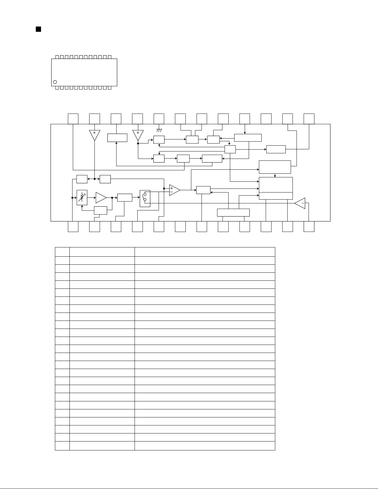
LA3460M-X (IC31) : FM noise canceller & Stereo MPX demodulator
1. Pin layout
24 13
112
2. Block diagram
24 23 22 21 20 19 18 17 16 15 14 13
KS-LX200R
123456789101112
3. Pin function
Pin
No.
1
2
3
4
5
6
7
8
9
10
11
12
13
14
15
16
17
18
19
20
21
22
23
24
DRIVER
HPF LPF
TRIG
AGC
GATE
PC
PD
LPF
Function Description
Noise sense
Noise sensitivity adjustment
Noise AGC
Gate time
Signal hold
Pilot output
Vcc
Capacitor for HCC
SNC control
HCC control
Vcc=+8.0V
High pass filter
Stereo noise controlled voltage
High cut controlled voltage
Lch output
Rch output
Pican input
Pican output
pilot cancel signal input
pilot cancel signal outpt
Separation ADJ
NC
NC
456kHz OSC
Phase comp LPF (+)
Phase comp LPF (-)
Ceramic resonator
Phase comparator low pass filter
Phase comparator low pass filter
GND
PLL input
Stereo indicator
Composite input
Phase locked loop signal input
Active low
Composite signal input
Pilot det LPF
LPF
SCHMIT
HCC
VCO
FF
MAIN
CONTROL
VCO STOP
PACAN
SEPARATION
ADJ.
SUB
ANTI-BRIDGE
DECODER
SNC
1-25
Page 26
KS-LX200R
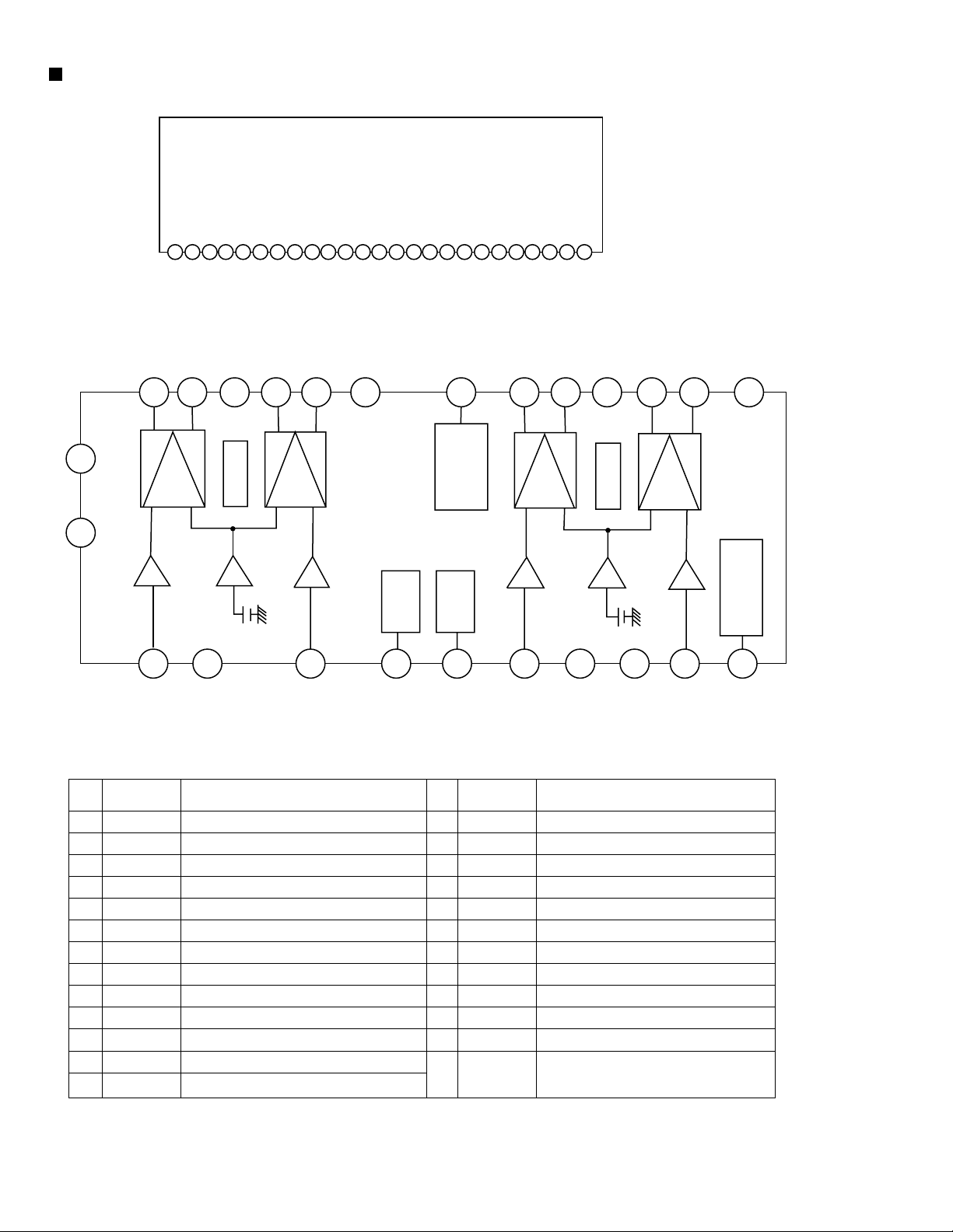
LA4743B (IC941) :Power amp
1.Terminal layout
TAB
GND1
OUTFR+
STBY
OUTFR-
1 2 3 4 5 6 7 8 910111213141516171819202122232425
2.Block diagram
VCC1/2
OUTRR+
GND2
OUTRR-
VREF
INRR
INFR
SGND
INFR
INRL
ONTIME
OUTRL+
GND3
OUTRL-
VCC3/4
OUTFL+
MUTE
OUTFL-
GND4
NC
206
VCC3/4
VCC1/2
3.Pin function
Pin
No.
1
2
3
4
5
6
7
8
9
10
11
12
13
OUT 1+
7
9
+
-
+
-
11
IN 1
Symbol Function
TAB
GND1
RFOSTBY
RFO+
VCC1/2
RROGND2
RRO+
R.F
RRIN
RFIN
SGND
1
TAB
Header of IC
Power GND
Output (-) for front Rch
Stand by input
Output (+) for front Rch
Power input
Output (-) for rear Rch
Power GND
Output (+) for rear Rch
Ripple filter
Rear Rch input
Front Rch input
Signal GND
8
Protective
circuit
OUT 2+
5
+
-
PWR GND1
OUT 1-
OUT 2-
3
-
+
12
IN 2
PWR GND2
2
Stand by
switch
4
ST BY
Pin
No.
14
15
16
17
18
19
20
21
22
23
24
25
OUT 3-
19
-
Protective
-
25
N.C
PWR GND3
18
circuit
MUTE
22
OUT 3+
17
+
Mute
circuit
+
Ripple
filter
10
R.F
Symbol Function
LFIN
LRIN
ONTIME
LRO+
GND3
LROVCC3/4
LFO+
MUTE
LFOGND4
NC
15
IN 3
Front Lch input
Rear Lch input
Power on time control
Output (+) for rear Lch
Power GND
Output (-) for rear Lch
Power input
Output (+) for front
Muting control input
Output (-) for front
Power GND
Non connection
OUT 4+
21
+
-
-
+
13
PRE GND
14
IN 4
OUT 4-
23
Muting &
PWR GND4
24
on time control
circuit
16
ON TIME
1-26
Page 27
LC75873NW (IC601) : LCD driver
1.Block diagram
COM3
COM2
COM1
S68
S67
S5
S4/P4
S3/P3
S2/P2
S1/P1
KS-LX200R
VDD1
VDD2
INH
OSC
VDD
VSS
COMMOM
DRIVER
CLOCK
GENERATOR
SEGMENT DRIVER
SHIFT REGISTER
ADDRESS
DETECTOR
2.Pin functions
Pin No. Symbol Description
1~66
67~69
70
71
S3~S68
COM1~3
VDD
VDD1
I/O
Segment Output.
O
Common Driver Output.
O
Power Supply Connection.
Used for applying the LCD drive 2/3 bias voltage externally.
I
Must be connected to VDD2 when a 1/2 bias drive scheme in used.
72
VDD2
Used for applying the LCD drive 1/3 bias voltage externally.
I
Must be connected to VDD1 when a 1/2 bias drive scheme in used.
73
74
VSS
OSC
Power supply connection.
Oscillator connection. An oscillator circuit is formed by connecting an
I/O
external resistor and capacitor to this pin.
75
76
77
78
79
80
INH
CE
CLOCK
DI
S1
S2
Display off control input.
I
Chip enable input.
I
Synchronization clock input.
I
Serial data input.
I
Signal output.
O
Signal output.
O
1-27
Page 28
KS-LX200R
BA3220FV-X (IC301) : Driver
1. Pin layout & Block diagram
CL- LGND OUTL OUTR RGND CR - CR +
1314
REFL REFR
1112 9 810
FILTER
CL+ Vcc INL NFL FIL NFR INR
2. Pin function
Pin
Symbol Function
No.
1
CL+
2
3
4
NFL
5
6
NFR
7
INR
8
CR+
9
CR-
10
RGND
11
OUTR
12
OUTL
13
LGND
14
Vcc
INL
FIL
CL-
2143675
Powe supply terminal for amp.
power supply terminal.
input terminal.
Negative feedback terminal.
Filter terminal.
Negative feedback terminal.
Input terminal
Power supply terminal for amp.
Output terminal of internal amp.
Rch GND terminal.
Rch output terminal.
Lch output terminal.
Lch GND terminal.
Output terminal of internal amp.
1-28
Page 29
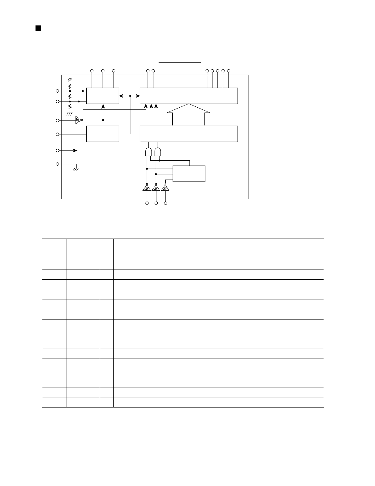
BR24C32F-X (IC703) : EEPROM
KS-LX200R
1. Pin layout
2. Block diagram
A0 1
A1 2
A2 3
Vcc WP SCL SDA
A0
A1 A2
GND
32k bit EEPROM ARRAY
12bit
ADDERESS
DECODER
CONTROL LOGIC
SLAVE/WORD
12bit
ADDRESS REGISTER
START
STOP
ACK
8bit
DATA
REGISTER
8 Vcc
7 WP
6 SCL
GND 4
3. Pin function
HIGH VOLT A GE GEN.
Vcc LEVEL DETECT
Pin No. I/O Functions
Vcc
GND
AO,A1,A2
SCL
SDA
WP
-
Power supply
-
Ground (0V)
IN
Slave address set
IN
Serial clock input
I/O
Slave and word address/Serial data output
IN
Write protect input
5 SDA
1-29
Page 30
KS-LX200R
SAA6579T-X (IC51) : RDS demodulator
1. Pin layout 2. Pin function
1
2
3
4
5
6
7
8
16
15
14
13
12
11
10
9
Pin
Symbol Function
No.
1
2
3
4
5
6
7
8
9
10
11
12
13
14
15
16
QUAL
RDDA
Vref
MUX
VDDA
VSSA
CIN
SCOUT
MODE
TEST
VSSD
VDDD
OSCI
OSCO
T57
RDCL
Quality indication output
RDS data output
Reference voltage output (0.5VDDA)
Multiplex signal input
+5V supply voltage for analog part
Ground for analog part (0V)
Sub carrier input to comparator
Sub carrier output of reconstruction filter
Oscillator mode / test control input
Test enable input
Ground for digital part (0V)
+5V supply voltage for digital part
Oscillator input
Oscillator output
57kHz clock signal output
RDS clock output
3. Block diagram
57kHz
BAND PASS
(8th ORDER)
COSTAR LOOP
VARIABLE AND
FIXED DIVIDER
CLOCK
REGENERATION
AND SYNC
RECONSTRUCTION
MUX
SCOUT
CIN
VDDA
Vref
ANTI-
4
ALIASING
FILTER
8
7
CLOCKED
COMPARATOR
5
3
REFERENCE
VOLT AGE
Vp1
6
IC-PST600M/G/-W (IC702) : System reset
FILTER
OSCI OSCO VDDD
13 14 12
OSCILLATOR
AND
DIVIDER
BIPHASE
SYMBOL
DECODER
TEST LOGIC AND OUTPUT
SELECTOR SWITCH
91011
QUALITY BIT
GENERA TOR
DIFFERENTIAL
DECODER
VSDDTESTMODEVSSA
16
15
1
2
QUAL
RDDA
RDCL
T57
1-30
Co1
OP1
1
3
2
IN
Vout
OUT
Page 31

HD74HC126FP-X (IC771) : Buffer
KS-LX200R
1. Pin layout
1
2
3
4
5
6
7
3. Block diagram
14
13
12
11
10
9
8
Vcc Vcc
1A
2A
3A
Input
4A
1C
2C
3C
See Function Table
4C
2. Pin function
Output
1Y
2Y
Output
2Y
Output
3Y
Output
4Y
Inputs Outputs
C
A
L
X
H
L
H
H
Y
Z
H
L
1k
S1
CL
1k
Sample as Load Circuit 1
Sample as Load Circuit 1
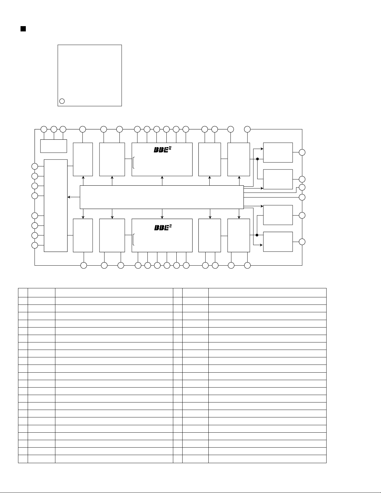
Sample as Load Circuit 1
RPM6938-SV4 (IC602) : Remote control receiver
AGC
AMP
I/V
conversion
PD
magnetic shield
BPF
for
trimming
circuit
Detector
Vcc
Comp
Vcc
22k
ohm
Rout
GND
1-31
Page 32

KS-LX200R
M5282FP-XE (IC321) : E. volume
1. Pin layout
1
2
3
4
5
3. Pin function
Pin
Symbol Function
No.
1
Vcc/2
2
Amp+IN
3
Amp-IN
4
Amp OUT
5
GND
6
7
VCA IN
8
9
VCA OUT
10
NC
Vc
Vcc
2. Block diagram
10
9
8
7
6
1
2
3
10
457
Vcc/2 output for microphone amp.
Microphone amp. positive input terminal.
Microphone amp. negative input terminal.
Microphone amp. output terminal.
Ground.
Non connection.
VCA input terminal.
VCA control terminal.
VCA output terminal.
Power supply.
9
8
LB1641 (IC402) : DC Motor driver
1. Pin layout
1 2 3 4 5 6 7 8 9
GNDOUT1 P1
VZ IN1 IN2
2. Pin function
Input Output
IN1 IN2 OUT1 OUT2
0 0 0 0
1 0 1 0
0 1 0 1
1 1 0 0
VCC1
VCC2 P2
10
OUT2
Mode
Brake
CLOCKWISE
COUNTER-CLOCKWISE
Brake
1-32
Page 33

Block diagram
KS-LX200R
6
M
5
M
4
3
2
1
CP401 CP402
STANDBY,TAPEEND
Lch,Rch
HEAD COMMON
MODE,F/R,TAPE IN
SUBMO
LCD1
COM1~3
S1~S86
LCD DRIVER
MOTOR
DRIVER
IC601
Lch,Rch
IC401
HEAD AMP
IC402
IC603
REMOCON
LCDRST,LCDCE1
LCDCL,LCDDA
MSOUT
NRSW
FF REW
SUBMO
LED &
KEY MATRIX
REMOCON
KEY
MATRIX
KEY1
KEY2
RESET
TRAY
MOTOR
M
DOOR
MOTOR
M
CN703
CP403
CN631
CN601
CN504 CN503CN702 CN701
RDS
IC51
RDS
TAPE.L
TAPE.R
SUBMO ,TAPE IN
STANDBY,MODE
MOTOR,FF REW
DOLBY,MSOUT,F/R
KEY0,KEY1
REMOCON,KEY1
KEY2,LCDCA
LCDCL,LCDCE1
TRAY
DRIVER
DOOR
TU1
TUNER PACK
FM/AM
S.METER
SD/ST
PLLCE
PLLDA
PLLCL
TM0
TM1
DM0
DM1
IC831
FMDET.ADJ
SEPA.ADJ
IC701
CPU
SCL
SDDA
ST
VOLDA
VOLCLK
W.VOL
IC703
EEPROM
DOTCONT
IC951
OPE.AMP.
BLOCK
SI/SO
SO,I/O
BUSINT
BUSSCK
EACH
IC961
REG.
IC31
MPX
L-ch
R-ch
CN901
IC911
E.VOL.
WLPF1
WLPF2
IC771
JVC-BUS
FRONTL
FRONTR
REARL
REARR
LOUTFL
LOUTRR
ROUTFL
ROUTRR
IC321
E.VOL
IC322
SWITCHING
SCK,SI/SO
IC323
OPE.AMP.
WOOFER
OUT
IC301
Lch LINE
AMP.
IC401
Rch LINE
AMP.
AU.L
AU.R
CH.L
CH.R
INFL
INRL
FRONTL
FRONTR
INFR
INRR
REARL
REARR
IC901
POWER AMP.
IC171
LINE IN
AULI
AURI
CN771
CD-CH
LINE OUTLINE INSUB
BC
DE
F
G
HA
I
2-1
Page 34

Standard schematic diagrams
Main amp. section
TU1
4.7K
Q12
UN2211
10K
R25
TAPE.L
TAPE.R
SW14V
MSOUT
DOLBY
FF/REW
MOTOR
MODE
STANDBY
TAPE-IN
SUBMOSUBMO+
TAPE-END
KICK
CASW1
CASW2
CASW3
TRAY-
TRAY+
DOOR+
DOOR-
CASW4
CASW5
TRAY10V
REMOCON
BZ791
GND
2SB709A
R14
10K
R23
C24
0.1
R24
C23
0.0047
GND
F/R
KEY0
KEY1
RESET
ACC5V
10V
KEY1
KEY2
DOT
LCDDA
LCDCL
LCDCE1
14V
QAN0009-001Z
Q791
UN2211
J1
Q13
47K
R15
Q22
2.2K
DMK
TMK
QAU0157-002
QAM0105-002
D11
MA152WK
3.3K
47K
R21
C22
2SC2412K
0.01
47K
R22
C712
0.047
C719
470P
TAPE-END
Q21
2SC2412K
C21
UN2211
KICK
L1
PP4
2SD601A
330P
VDD5V
R43
UN2111
R28
Q33
R45
47K
Q34
68K
Q24
MOTOR
MODE
STANDBY
TAPE-IN
SUBMO-
SUBMO+
47K
R783
4.7u
100K
W-LPF1
W-LPF2
W-MUTE
VOL-DA
VOL-CLK
CFSEL
47K
47K
R785
R784
BUZZER
2SB815
UN2211
R44
D31
22/16
1SS355
1SS355
C4
D1
D2
470
R42
1K
UN2111
R37
2.2K
UN2211
Q32
1SS355
MUTE
UPD784215GC-XXX
R766
330
R767
330
R758
47K
R740
47K
47K
47K
47K
47K
R786
R790
R787
R788
R789
TRAY10V
Q702
Q701
100P
R1
SEEK
IFBW
C10
1SS355
0.01
22/16
0.047
C3
C2
C1
1/50
C44
C43 C457
1/50
C42
1M
R41
Q31
IC31
LA3460
18K
0.47/50
1/50
C45
C32
R38
47K
R739
IC701
VDD
2.2K
R742
10K
R743
47K
R746
47K
VPP
47K
R747
47K
R748
47K
R749
47K
R750
X1
10V
1K
R794
R793
0
6
R11
Q11
8.2( 1/8W)
2SB815
47K
CN703
CN504
CN503
CN702
FM/AM
S.METER
SQ
R12
R13
Q23
15K
R26
2SC2412K
R27
470
C25
0.47/50
S651
S652
S653
5
4
CN704
QGA1201C2-04X
3
NSW0120-002X
NSW0120-002X
NSW0120-002X
QGA2501F1-02
QGA2501F1-02
QGF0501F1-06X
2
CN701
QGF0503C1-16V
1
PP1
UDZS5.1B-X
D702
D703
1K
R791
C791
0.1/50
KS-LX200R KS-LX200R
R3
10
Q1
10K
0
SD
D3
0.047
R2
100K
VR1 C9
R40
5.6K
1/50 0.0047
C39
0.1/50
C41
0.01
R34
2.2K
470K
12K
0.001
C33
R33
R31
R32
C34
0.01
C31
PON
DIMIN
ACC5V
10K
R738
FF/REW
DOLBY
MSOUT
F/R
HOLD
C11
3.9K
0.0068
C705
220/10
C5
C40
1/50
22/16
C35
C36
0
R47
IFBW
TELMUTE
2.2K
R765
C713
470P
220/6.3
C6
0.047
QAX0605-001
CF31
68K
R36
0.0015
33K
R35
C101
Q36
UN2211
VSS
PLLCE
PLLDA
PLLCK
2.2K
2.2K
2.2K
R762
R763
R764
R702
DIMOUT
X701R4X702
8P
C704
PLLCE
C7
50K
VR31
C38
0.047
0.015
0.015
FM/AM
47K
R757
820
C703
PLLCK
AMAF
C8
0.1
0.018
C201
10K
R761
QAX0617-001
27P
PLLDA
2SB709A
SEEK
10K
R751 R737
R701
C702
C55
R101
10K
R201
10K
C46
1K
R736
47K
27P
560P
22K
R39
C37
1/16
Q35
R46
10M
C701
C56
0.01
47/6.3
C54
C53
0.01
MA152WK
D201
MA152WK
68K
CASW3
CASW5
CASW4
SW1
BUSINT
47K
QAX0445-001
R703
22P
UN2211
C57
0.022
R53
X51
47P
C52
D101
CASW2SDCASW1
47K
RESET
R704
PP2
CFSEL
2.2/50
R54
R52
2.2k
QAX0263-001
82P
C51
22K
R202
10K
R730
RDSSCK
RDSDA
RDSDA
2.2k
2.2k
RDSSCK
100
R51
AMAF
680P
22K
C202
R102
REF
10K
R728
DM1
REMOCON
IC51
680P
C102
DM0
SAA6579T
R735
R734
R733
R732
R731
CRUISE
47K
R768
CH.L
TAPE.L
CH.R
TAPE.R
GND
4.7K
4.7K
47K
47K
47K
RESET
R705
47K
DOT
TM1
9V
C724
D711
R354
6.8K
R454
6.8K
R118
100
R119
R120
10K
R218
100
R219
R220
C103
C203
TH951
NAD0021-103X
TM0
270
R725
R721
R720
R719
R718
R717
R716
R715
R714
R713
R712
R711
R710
0.0022
1SS355
C707
MA152WK
220K
C354
0.1
R211
220K
C951
14V
LCDCL
LCDDA
IC951
NJM4565M
KEY2
KEY1
KEY0
R709
R708
R707
C355
470P
C456
0.1
BR24C32F
4.7K
4.7K
4.7K
10/16
AU.L
DOTCONT
TD
RD
R752
47K
W-VOL
S.METER
LEVEL
R111
SQ
C352
0.01
R355
220K
C454
0.1
C455
R455
470P
C112
C356
10/16
4.7/10
0
1/50
C104
C212
4.7/10
0
10K
1/50
C204
0.22/50
0.22/50
5.6K1K
R953
R952
IC703
270
C711
R724
470P
R723
1K
10K
R722
10K
BUZZER
330
LCDCE1
1.8uH
1.8uH
4.7K
4.7K
4.7K
10K
10K
10K
10K
10K
0.0022
0.0022
C722
C723
IC702
PST600MG
R706
10K
10/6.3
0.01
C708
C120
1M
470P
0.047
0.1
10/16
C353
C119
C118
C351
R353
D111
220K
2.2K
2.2K
R911
R954
10K
AU.R
C952
L701
C710
220/10
I/O
BUSSCK
SI/SO
DOTCONT
R912
47/16
C914
C911
10/16
R951
5.6K
47u
MUTE
SO
DIMIN
R987
TELMUTE
Q986
UN2211
R779
0.047
47K
SI/SO
47K
AU.L
AU.R
4.7/25
UN2111
R776
100k
R777
22K
R778
100
0.01
0.1
0.1
C451
C452
C913
C218
0.047
C357
C458
C358
220k
R451
220k
R452
C912
100/10
R177
1K
R176
10k
C175
C174
0.022
47/6.3
R276
10k
R277
1K
Q979
Q977
UN2111
D980
C978
R986
C986
SO
47/6.3
1K
I/O
1SS355
D986
MA152WA
0.1
HD74HC126FP
C977
D978
UDZ11B
47k
R984
Q983
2SD601A
C982
TEL
R775
10k
IC771
0.0047
0.22
0.22
R275
47/16
10/16
R161
C459
C359
D451
MA152WK
10k
2SB709A
10K
R985
ILL
C161
1/50
47K
IC911
BA3860K
C220
C219
0.22
0.22
R175
10k
Q965
Q964
UN2211
R965
R774
100
C771
R163
R164
220K
R351
D351
R458
R358
R340
R964
2.2K
0.047
R162
12K
180K
22K
470P
10/16
Q966
2SB709A
47k
Q963
UN2213
R781
330
470K
BUSINT
R773R772
3.3K
3.3K
220K
R352
MA152WK
C321
10/16
R174
R173
IC171
NJM4565M
R273
R274
D963
MA152WA
R782
22k47K
IC831
KA3031
Q161
2SD601A
8.2K
8.2K
8.2K
8.2K
R971
BUSSCK
100K
R165
390
VOL-CLK
VOL-DA
R970
12K
39K
SCK
CD8V
C163
D161
1SS355
0.047
C173
22/6.3
C172
10/16
C272
10/16
C273
22/6.3
5V
270K
1SS355
0.22/50
D162
R167
1K
R166
LEVEL
C164
22/16
C162
100k100k
R172R272
9V
14V
CD8V
W-VOL
W-LPF2
W-LPF1
W-MUTE
IC961
0.01
C966
IC321
Q321
UN2211
10/16
C969
M5282FP
R326
ACC5V
C305
4.7/25
C306
4.7/25
C405
4.7/25
C406
4.7/25
C322
R322
10K
C335
IC322
Q322
UN2211
BA4905
22/16
220/10
220/10
C967
C965
C964
TRAY+
2.2/50
BU4066
TRAY-
0.01
PON
DOOR-
R834
24K
4.7/25
R301
C301
C303
R302
C302
4.7/25
R305
150K
4.7/25
R401
24K
C401
C403
C402
R402
4.7/25
24K
R405
150K
R323
10K
10K
R324
100K
C325
2.2/50
C324
10/16
0.0056
C331
47K
R333
R342
R341
1M
1M
C334
C333
0.033
120K
R975
22/16
C971
10V
D00R+
R832
3.9K
24K
0.027
TH981
R981
4.7K
47/16
47/16
C323
R332
C332
IC301
IC401
47/16
100K
R325
R344
1M
0.027
NAD0021-103X
47K
Q981
UN2111
CD8V
0.01
100/10
C831
C832
DM0
DM1
DMK
TM0
TM1
TMK
R831
4.7K
R833
3.3K
R303
R304
R403
IC323
NJM4565M
R329
0
100K
C330
R334
47K
SW14V
Q991
2SA1706/ST/-T
R994
Q992
UN2211
33K
BA3220FV
33K
33K
BA3220FV
R404
33K
R343
1M
Q324
UN2211
Q982
UN2211
DIMOUT
R992
1K
R993
C307
100/10
4.7/25
C308
C309
4.7/25
C310
100/10
C407
100/10
C408
4.7/25
C409
4.7/25
C410
100/10
C327
R327
0.082
5.6K
R328
15K
C329
47K
18K
100K
R331
D962
CRS03-W
CRS03-W
D701
R963 R962
R335
4.7K
R337
D332
MA152WK
Q325
UN2111
TEL
ILL
MUT
AU.LI
AU.G
AU.RI
SUBW
GND
4.7K 9.1K
GND
SCK
CH.L
SI/SO
CH.R
C328
0.0068
R330
0.012
R321
1K
AU.LI
AU.G
AU.RI
PON
MEMORY
47K
10K
R991
820
D967
2.2/50
R336
Q323
47K
R141
47K
SUBW
2SD1048
GND
CRS03-W
C968
0.047
C336
C117
47K
R142
47K
R241
0.1
R976
470
R178
R338
100
R339
100
0.1
82K
82K
R143
R144
C142
47K
47K
1/50
R146
R145
47K
47K
47K
R245
R246
R242
82K
R244
MUT
MEMORY
2.2K( 1/8W)
2.2K( 1/8W)
R977
C932
CN301
QGA2501C1-07
0.047
C337
C141
1/50
C241
1/50
82K
R243
680
R133
0.047
C931
CN302
QGA2501C1-06
QNZ0095-001
CN771
IC941
330P
330P330P
C144
C143C243
330P
C244
C242
1/50
R941
27K
D941
1SS355
D131
MA152WA
680
2.2k
2.2k
R132
R131
R134
Q131
2SD1048
Q132 Q232
2SD1048 2SD1048
100
100
R136
R135
100P
LA4743B
100
R236
C941
C942
47/16
1/25
0.01
C943
R942
27K
R943
1K
Q942
C944
UN2211
10/16
D231
MA152WA
680
680
2.2k
2.2k
R231
R232
R233
R234
Q231
2SD1048
100
R235
C962
QNZ0090-001
R961
1K( 1/8W)
2.2/50
CN901
L961
D961
1N5401TU
C961
2200/16
QQR0703-001
R978
100K
TAPE REC SIGNAL
TUNER SIGNAL
CD-CH SIGNAL
LINE IN SIGNAL
FRONT SIGNAL
REAR SIGNAL
Parts are safety assurance parts.
When replacing those parts make
sure to use the specified one.
PP3
C921
100P
C922
100P
C923
100P
C924
100P
C925
100P
C926
100P
C927
100P
C928
100P
BC
DE
2-2
F
G
HA
I
Page 35

Mecha. contr ol section
TAPE REC SIGNAL
C409
R410
Q403
C405
C416
R419
CP402
C406
R406
Q402
Q401
CP401
D403
IC402
C418
C419
CP403
R420
IC401
C412
R417
R412
VR101
C411
C410
R408
C415
C413
C414
R415
R418
C403
R405 R404
R403
C402
R402
C401
R411
R407
VR201
C407
R409
C404
C408
R414
R422
R421
D401
D402
R424
R425
C417
R423
R413
R401
R416
0.01
300K
DTC114EKA
22/16
0.1
1.2M
QGB1214K1-10S
0.01
300K
DTC114EKA
2SA1706/ST/-T
QGA2001F1-07
MA3075( M)
LB1641
0.01
0.1
QGB1214K1-18S
15K
100P
1K
12K
33K
1/50
22/16
18K
0.01
0.1
0.47/50
3.9K
22K
100P
180 180
100K
470P
100K
470P
18K 12K
33K
1/50
18K
100P
0.1
1K
3.3K
47K
DSK10C
MA3036( L)
33
8R2
10/16
3.3K
100
2.2K
10K
6
KS-LX200R
5
4
3
2
1
BC
DE
F
G
HA
I
2-3
Page 36

KS-LX200R KS-LX200R
LCD & Key control section
R636R637R638R639R640R641
6
8208201.2k1.8k2.7k3.9k
S637
QSW0856-001X
S636
QSW0856-001X
R647
3.9K
R633
R651
220
S635
QSW0856-001X
220
2.7k
S634
QSW0856-001X
220
R632
1.8k 1.2k
S633
QSW0856-001X
S632
NSW0041-001X
D656
CL-190UB-X-X
R643R646 R645 R644
D655
CL-190UB-X-X
R655
S631
390
390
R656
QSW0856-001X
R642
820820
220
R652
R634R635
220220
CN631
QGF0501F1-06X
S643
QSW0856-001X
S642
QSW0856-001X
S641
QSW0856-001X
S640
QSW0856-001X
S639
S638
QSW0856-001
QSW0856-001
5
S64S2S65
S66
S67
S41
S42
S43
S44
S45
S46
S47
S48
S49
S50
S51
S52
S53
S54
S55
S56
COM3
COM2
COM1
S25
S26
S27
S28
S29
S30
S31
S32
S33
S34
S35
S36
S37
S38
S39
S40
S57
S58
S59
S60
S61
S62
4
QNZ0495-001
S3S2S1
S4
S5S6S7S8S9
S10
S11
S12
S13
S14
S15
S16
S22
S23
S24
S21
S20
S19
S18
S17
10V
R621
INV
Q612
2SD2185
L612
47U
L613
L611
NQLZ007-680X
220
680
R613
D621D622
10/10
R612 R611
0.1
C615
C614
C611
5600P
2SD2185
C612
0.022
4.7k 4.7k
Q611
KEY2
RESET
3
S625
R623
R624
820
820
S622S624
S623
S621
KEY1
R676
390
D627
LT1F67AF-W
R622
220
D623
D624
S68
S63
C613
BL611
QNZ0494-001
4.7/6.3
C601
15P/3.15k
QLL0059-001
R601
D626
R629
S43
S44
S45
S46
S47
S48
S49
S50
S51
S52
S53
S54
S55
S56
S57
S58
S59
S60
S61
S62S3
PC601
PR-20
S64
S65
S66
S67
S68
COM1
COM2
R603
COM3
LCDRST
LCDCE1
LCDCL
220p
LCDDA
220K
10K
C604
R604
S1
S4S5S6S7S8S9S10
10K
10K
R602
0.1
0.1
C603
C602
IC601
LC75873NW
S11
S12
S13
S14
S15
S16
S17
S18
S19
S20
S21
S22
S42S63
S41
S40
S39
S38
S37
S36
S35
S34
S33
S32
S31
S30
S29
S28
S27
S26
S25
S24
S23
PC602
PR-20
MA152WK
R630
470
Q691
1K
2SD601A
100k
R691
39k
R692
100k
R693
Q692
39k
R694
2SD601A
VDD
LCDDA
LCDCL
LCDCE1
LCDCE2
LCDRST
D625
IC603
RPM6938-V4
R627R628
1200
MA3051/M
CN601
QGF0501F1-16X
R671
R672
R673
R674
R675
4.7/6.3
R625
RESET
470
INV
KEY1
KEY2
330
330
3.3K
3.3K
3.3K
10V
10K
R626
C625
2
1
BC
DE
2-4
F
G
HA
I
Page 37

Printed circuit boards
BZ791
C2
C4
C5
C25
C32
C35
C39
C40
C42
C43
C44
C45
C53
C57
C101
C102
C103
C104
C112
C119
C120
C141
C142
C161
C162
C163
C164
C172
C173
C175
C201
C202
C203
C204
C212
C218
C219
C241
C242
C272
C273
C301
C302
C303
C305
C306
C307
C308
C309
C310
C321
C322
C323
C324
C325
C327
C328
C329
C334
C335
C353
C356
C401
C402
C403
C405
C406
C407
C408
C409
C410
C456
C710
C712
C713
C719
C722
C723
C791
C911
C912
C913
C921
C922
C923
C924
C925
C926
C927
C928
C941
C942
C944
C951
C952
C961
C962
C964
C965
C967
C969 C971
C977
C978
C982
CF31
CN301
CN302
CN503
CN504
CN701
CN702
CN771
CN901
D3
D31
D101
D111
D161
D162
D201
D351
D451
D701
D941
D961
D978
D980
IC831
IC31
IC51
IC171
IC301
IC321
IC322
IC323
IC401
IC701
IC702
IC771
IC911
IC941
IC951
IC961
J1
L701
L961
PP1
PP2
PP3
PP4
Q31
Q32
Q33
Q34
Q131
Q132
Q161
Q231
Q232
Q321
Q322
Q323
Q966
Q977
Q979
Q982
Q991
Q992
R101
R111
R133
R134
R145
R146
R161
R164
R166
R175
R201
R211
R233
R234
R245
R246
R275
R322
R323
R324
R330
R331
R343
R344
R351
R352
R451
R452
R707
R708
R709
R710
R711
R712
R718
R719
R720
R721
R728
R730
R731
R732
R733
R734
R735
R736
R737
R738
R739
R752
R757
R758
R761
R762
R763
R764
R765
R766
R767
C453
R941
R954
R961
R981
R985
R991
R992
R993
R994
RD
RESET
TD
TH951
TH981
TU1
VPP
VR1
VR31
VSS
X1
X51
X701
X702
S653
S652
S651
R753
C720
C721
VDD
CN703
C946
C947
C948
C949
C945
C831
HOLD
R756
B1
C832
R831
R832
R833
R834
Q701
R794
R793
B701
Q324
Q325
R321
B941
B321
CN631
R631
R632
R633
R634
R635
R636
R637
R638
R639
R640
R641
R642
R643
R644
R645
R646
R647
R651
R652
R655
R656
BL611
D621
D622
D623
D624
D627
IC603
S621S622
S623
S624
S625
1
C401
C402
C403
C404
C405
C406
C407
C408
C409
C410
C411
C412
C413
C414
C415
C416
C417
C418
C419
CP401
CP402
CP403
D401
D402
D403
IC401
IC402
Q401
Q402
Q403
R401
R402
R403
R404
R405
R406
R407
R408
R409
R410
R411
R412
R413
R414
R415
R416
R417
R418
R419
R420
R421
R422
R423
R424
R425
VR402
VR401
B403
B415
B413
B407
B416
B406
B414
B405
B412
B404
B410
B402
B408
B401
B409
B411
1
11
21
1
17
1
2
E
1
1
FSMW1101A
31
TPP
Main board (Forward side)
6
KS-LX200R
5
4
Front boar d (Forward side)
3
2
1
Mecha. contr ol board
ABC DE
2-5
Page 38

KS-LX200R
Main board (Rever se side)
6
J1
L1
Q12
R11
D11
R15
C21
C22
5
R22
C23
R25
C24
C6
R26
Q23
R27
PP1
4
TU1
D1
D2
C7
R1
C8
Q21
R21
Q22
R23
R24
C11
R4
C12
C732
CN771
C216
C117
C10
C1
R2
C3
C2
Q11
Q13
VR31
R12
R13
R14
C44
R37
R47
C9
C46
C5
R28
Q24
C57
C25
R3
Q1
CN504
C718
IC961
R975
C971
C967
C966
R218
VR1
C711
S653
S652
S651
Q981
R118
C116
C4
Q965
CF31
R41
Q36
C53
C54
C56
C55
D963
C37
C41
R42
R43
R44
R45
R34
C34
C38
R39
C52
R52
R54
R713
R701
C33
C36
R31
R32
R35
R36
R38
C32
Q35
R102
C35
C45
R51
C51
R53
R725
IC703
R714
C724
R751
R202
R46
X51
PP4
R723
C710
R703
R722
R724
X702
C701
Q791
R791
BZ791
R962
R963
C964
C969
R970
R965
R971
C965
R964
Q964
C31
R33
C39
C43
R40
C40
C42
R781
C771
R715
R716
R742
R740
R717
C707
R768
R702
X701
C705
C713
C702
R705
B702
Q702
C791
C931
C132
C232
CN301
Q963
C977
C103
C203
C952
R952
R953
R746
C730
PP2
C708
R272
R172
R178
C336
Q991
C978
R951
R986
R987
R912
R911
C703
C704
R706
D711
C174
CN703
R120
R219
R220
R119
R775
R776
R782
R772
R774
R773
R777 R778
R779
Q983
R984
D986
Q986
C104
C112
R747
R783
R784
R704
R748
R785
R786
R787
R749
R750
R788
R789
R790
R792
C131
C231
C932
C337
R338R339
CN302
C272 C273
C175
R173
R176
R174
R336
R273
R276
R274
C335
R277
R177
C332
R326
C323
C321
R340
C333
R325
C325
R327
C356
R455
C456
C455
C161
R165
R167
R163
R162
C162
C164
L961
C933
R135
R136
CN901
R235
R236
D967
D961
C172
C173
R335
R337
C329
R401
R332
R341
C324
R334
R333
C331
C330
R342
R328
R329
C204
C212
R355
C354
C355
C119
R354
C454
R454
C351
C352
C968
R961
C962
C986
D962
C403
R976
R977
R402
R405
D332
C406
R407
C402
R406
C405
R404
C401
R403
C306
C310
C305
R302
R301
C302
C303
C301
R304
C914
R303
C911
C353
C451
R353
C118
C831
R978
C982
R231
R241
C410
C912
R305
C307
R307
R306
C219
C220
C453
C731
R132
R232
C409
D131
D231
C408
R242
C407
R142
C309
C308
C944
Q942
R141
R942
C144
CN503
R144
R143
R243
R244
C358
R358
R458
C359
C458
C457
C459
C357
C452
C961
C943
R131
C141
C941
C142
C143
C243
C244
C242
C942
C945
C241
IC941
R943
PP3
3
2
Front board (Reverse side)
B601
R622
S643
CN601
R623
R624
C613
R675
Q612
R673
S642
R671
R672
S640
S641
R613
R611
L612
C614
R612
C612
C615
Q611
R692
L613
C611
L611
C603
R603
S639
S631
C601
C602
R602
R601
R604
IC601
C604
D656
D631
D655
S638
S632
S633
S635
S634
PC601
Q691
IC603
D626
R691
R630
R693
R629
R627
R625
R626
R621
R628
D625
S637
R694
Q692
PC602
R676
C625
S636
1
ABC DE
2-6
Page 39

PARTS LIST
[ KS-LX200R ]
* All printed circuit boards and its assemblies are not available as service parts.
KS-LX200R
- Contents -
Exploded view of general assembly and parts list
Cassette mechanism assembly and parts list
Electrical parts list
Packing materials and accessories parts list
Area suffix
E ----------- Continental Europe
EX --------------- Central Europe
3-3
3-6
3-9
3-16
3-1
Page 40

KS-LX200R
<<MEMO>>
3-2
Page 41

Exploded view of general assembly and parts list
8
11
12
6
14
Block No.
6
M
1
Switch board
14
M
68
M
63
62
67
69
63
86
KS-LX200R
103
103
13
93
84
15
19
89
95
83
90
96
92
9
55
16
81
25
104
53
23
14
64
17
14
7
5
1
14
17
Mecha.control
46
28
57
58
45
57
47
board
4
10
29
56
3
2
34
3
10
78
71
59
76
77
2
75
76
75
73
72
10
4
4
59
74
10
79
5
102
37
36
41
40
98
99
1
101
LCD1
100
68
66
60
30
26
80
79
Front board
51
68
56
35
65
49
44
61
57
29
28
31
22
43
70
33
21
57
38
24
58
54
85
87
39
20
48
52
27
50
21
14
88
94
97
91
18
42
Main board
18
18
32
15
82
BC
DE
F
G
HA
I
3-3
Page 42

KS-LX200R
)
)
KS-LX200R
Parts list
Item Parts number Parts name Area
A
6
10 QYSDST2604Z SCREW 4 T.CHAS+CS MECHA
11 QYSDSF2610Z TAPPING SCREW 1 T.CHAS+S H.SINK
12 LV41200-003A SPESIAL SCREW 3 T.CHAS+S H.SINK
13 LV41200-003A SPESIAL SCREW 1 T.CHAS+REAR
5
14 QYSDST2604Z SCREW 6 T.CHAS+B.CHAS
15 QYSDST2604Z SCREW 2 T.CHAS+R.BKT
16 LV41200-001A SPECIAL SCREW 1 BOTTOM CHA.+REAR BKT
17 QYSPSP2003M SCREW 4 T.CHAS+F.COVER
18 LV41200-001A SPECIAL SCREW 3 MAIN PWB+BOTTOM CHA.
19 LV31604-002A BOTTOM ASS'Y 1
20 LV31605-001A DOOR BASE ASS'Y 1
21 LV41452-001A TENS SPRING BTM 2
4
22 LV31607-001A PANEL COVER 1
23 LV31965-001A BUTTON BASE BKT 1
24 LV41500-001A BUTTON B.SUPORT 1
25 LV41545-001A BUTTON B.GUIDE 1
26 FSKL3014-001A FRONT BKT ASS'Y 1
27 LV20614-002A BRACKET ASS'Y 1
28 WDM215025 WASHER 4
29 LV41503-001A ARM 3 2
3
30 FSYH4036-015 SHEET 1
31 LV31777-001A FFC GUIDE 1
32 LV31610-001A ROD GEAR 1
33 LV40847-002A SPACER 1 MOTOR L
34 QAR0029001-SA2 FEED MOTOR 1 FOR BKT MOTOR L
35 PPN13KA10C-SA6 FEED MOTOR 1 FOR BKT MOTOR R
36 LV40847-002A SPACER 1 MOTOR R
37 WJM0137-001A E-SI CARD WIRE 1 FOR MOTOR L
38 WJM0136-001A E-SI CARD WIRE 1 FOR MOTOR R
2
39 QWTA20H-030 UL VINYL TUBE 1 FOR R WIRE
40 QE40110-001A SHIELD CASE 1
41 FSYH4036-064 SPACER 1
42 LV41463-001A GEAR 1 1 R SIDE
43 LV41464-001A GEAR 2 1 R SIDE
44 LV31611-001A GEAR 3 1 R SIDE
45 LV41466-001A GEAR 4 1 L SIDE
46 LV41467-001A GEAR 5 1 L SIDE
1
47 LV31612-001A GEAR 6 1 L SIDE
48 LV30981-004A CLUTCH ASS'Y 1 RIGHT SIDE
(General assembly)
Q'ty Description
1 --------------- CDS-522VJ2 1 CASSETTE MECHA
2 FSKM2006-001 MECHA BRACKET 1
3 QYSDST2604Z SCREW 1 PCB+MECHA
4 FSKZ4004-002 SCREW 4 MECHA+M.BKT
5 FSMA4010-002 INSULATOR 1 M.BKT+SCREW
6 FSJC1065-001 TOP CHASSIS 1
7 FSJC1064-001 FRONT COVER 1
8 LV31602-003A SIDE HEAT SINK 1
9 FSMA3007-001 INSULATOR 1
Block No. M1MM
Parts list
Item Parts number Parts name Area
A
49 QYSPSPT2020Z MINI SCREW 2 F.MOTOR+B.M. L
50 QYSPSPT2020Z MINI SCREW 2 F.MOTOR+B.M. R
51 LV40865-001A MINI SCREW 2 ROD BKT(L)+LO.BKT
52 LV40865-001A MINI SCREW 2 ROD BKT(R)+LO.BKT
53 LV40865-001A MINI SCREW 1 B.BASE BKT+BO.CHAS
54 LV40865-001A MINI SCREW 2 B.B.SUPPO+BO.CHAS
55 LV40865-001A MINI SCREW 1 B.B.GUIDE+BO.CHAS
56 LV40865-001A MINI SCREW 4 BKT.M.L&R+C.BOTTOM
57 WDM215025 WASHER 6 FOR GEAR 1-6
58 WDM214540 WASHER 2 FOR CLUTCH ASSY
59 QYSPSPU1725M SCREW 4 LO.UNIT A+DIS.PANEL
60 LV30981-005A CLUTCH ASS'Y 1 LEFT SIDE
61 LV10317-007A BUTTON PANEL 1 KS-LX200R
62 LV10318-001A BUTTON BASE 1
63 LV40848-007A SPACER(P
64 LV20615-003A PRESET BUTTON 1 LEFT PRESET BUTTON
65 LV20616-002A PRESET BUTTON 2 1
66 LV31613-001A FUNCTION BUTTON 1
67 LV41825-002A PLATE SPRING 1
68 VKZ4777-004 MINI SCREW 6
69 WJT0030-001A E-CARD WIRE 1
70 FSYH4036-035 SHEET 1 FOR E-CARD WIRE
71 FSJC1066-002 DISPLAY PANEL 1
72 LV32035-001A D.P. PLATE 1
73 FSJD3026-001A FINDER LENS 1
74 LV41469-001A UP DOWN B.ASS'Y 1
75 VYSH1R5-007 SPACER 2
76 LV40848-009A SPACER(P
77 LV41471-001A +/- BUTTON ASSY 1
78 LV41505-001A REMOTE LENS 1
79 VKZ4777-001 MINI SCREW 4 D.PANEL+SW.PWB
80 WJT0031-001A E-CARD WIRE 1
81 FSYN3148-105 NAME PLATE 1
82 LV41143-001A SHEET 2
83 QAM0178-001 PIN CORD ASS'Y 1
84 QAM0179-001 CAR CABLE 1
85 LV30943-201A REAR BRACKET 1
86 LV30946-005A REAR HEAT SINK 1 BLACK ANODISED
87 LV40790-001A PIN CORD BRACKET 1
88 QYSDST2604Z SCREW 1
89 LV41200-003A SPESIAL SCREW 2
90 LV40792-001A REG.IC BRACKET 1
91 LV41863-001A POWER IC BRACKET 1
92 VMA4652-001SS SHIELD PLATE 1
93 QYSDST2606Z SCREW 1
94 QYSDST2606Z SCREW 1
95 QYSDST2604Z SCREW 2
96 QYSDST2604Z SCREW 1
(General assembly)
Block No. M1MM
Q'ty Description
2
2
BC
DE
F
G
HA
I
3-4
Page 43

KS-LX200R
A
Parts list
Item Parts number Parts name Area
A
97 QMFZ039-150-T FUSE
98 FSKS3023-001 LIGHTING CASE 1
99 FSYH4081-002 LIGHTING SHEET 1 D105
100 FSYH2006-001 LCD CASE 1
101 QNZ0495-001 RUBBER CONNECTOR 1
102 QNZ0494-001 RUBBER CONNECTOR 1
103 VYTA500-001 PIN CAP 8
104 QAM0105-002 CAR CABLE 1 J1
LCD 1 QLD0149-001 LCD MODULE 1
(General assembly)
Q'ty Description
1
Block No. M1MM
3-5
Page 44

KS-LX200R
Cassette mechanism assembly and parts list
Block No.
M
M
2
M
A
98
MODEL:CDS522-VJ2
3-6
Grease & Oil
SW-902S
SW-474B
SW-522B
PANORL-56
CFD-409
Page 45

KS-LX200R
)
)
)
)
)
)
Parts list
Item Parts number Parts name Area
A
10 X-0522-1022S FR ARM ASS'Y 1
13 X-0522-2008S DETECT ARM ASSY 2
14 X-0522-2010S LOAD GEAR ASS'Y 1
15 X-0522-2016-6S FLYWHEEL ASY(FN 1
16 X-0522-2018S REEL TABLE ASSY 2
17 X-0522-2020S REDUCT.GEAR ARM 1
18 X-0522-2021-6S FLYWHEEL ASY(RN 1
19 X-0052-2001S F.R. GEAR ASS'Y 1
22 1-0522-1008S DIR.PLATE 1
23 1-0522-1031S FF/REW PLATE 1
24 1-0522-1027S MOTOR BKT 1
25 1-0522-1013-30S LOAD ARM 1
26 1-0522-1014S SHIFT CAM LINK 1
27 1-0522-1017-50S CASSETTE HOLDER 1
32 1-0522-2001S TAPE GUIDE 1
33 1-0522-2002S HEAD BKT 1
34 1-0522-2003S HEAD SHIFT CAM 1
35 1-0522-2004-03S SELECT GEAR 1
36 1-0522-2005S REDUCTION GEAR 1
37 1-0522-2006S DETECT GEAR 1
38 1-0522-2007-50S DETECTOR 1
39 1-0522-2009S WORM GEAR 1
40 1-0522-2011S MODE GEAR 1
41 1-0522-2012S MODE GEAR(2
42 1-0522-2013S GEAR LATCH 1
43 1-0522-2014S IDLE GEAR(1
44 1-0522-2015S IDLE GEAR(2
45 1-0522-2017S TU GEAR 2
46 1-0522-2019S RACHET 1
47 1-0522-2022S SW ACTUATER 1
48 1-0522-2024S PWB STAY 1
52 1-0052-2004S REEL DRIVER 2
53 1-0052-2006S IDLE PULLEY 1
54 1-0522-2023S WORM 1
55 1-0052-2032S CATCH(K
57 1-0052-2041S COUNTER GEAR 1
59 1-0522-3005S SELECT GEAR COL 1
62 1-0052-3028S H.B. ROLLER(L
(Cassette mechanism)
Q'ty Description
A 100367057S-SA1 DC MOTOR ASS'Y 1(NO.64.104.126
1 1-0522-6001-02S CHASSIS ASS'Y 1
2 1-0522-6002-02S HEAD PLATE ASSY 1
3 1-0522-6003-11S SUB CHASSIS ASY 1
4 X-0522-1004S HOLDER ARM ASSY 1
5 X-0522-1006-02S T.U.ARM(F)ASS'Y 1
6 X-0522-1007S T.U.ARM(R)ASS'Y 1
7 X-0522-1010S SET ARM ASS'Y 1
8 X-0522-1019S PINCH ARM(F)ASY 1
9 X-0522-1020S PINCH ARM(R)ASY 1
1
1
1
1
1
Block No. M2MM
3-7
Page 46

KS-LX200R
)
)
)
)
)
)
)
)
)
Parts list
Item Parts number Parts name Area
A
63 1-0052-3029S H.B. ROLLER(S
64 ------------ MOTOR PULLEY 1
67 1-0522-4001S PINCH ARM(F)SPG 1
68 1-0522-4002S PINCH ARM(R)SPG 1
69 1-0522-4003S GEAR LATCH SPG 1
70 1-0522-4004S HEAD SPRING 1
71 1-0522-4006S LOAD ARM SPG 1
73 1-0522-4008S CATCH SPRING 1
74 1-0522-4010S REEL DRIVER SPG 2
75 1-0522-4011S DASH SPRING 1
76 1-0522-4014S HOLDER ARM SPG 1
77 1-0522-4016S HOLD SPRING 1
79 1-0522-4017S TU ARM SPRING 2
80 1-0522-4015S FR ARM SPRING 1
83 1-0052-5022S BELT 1
87 1-0522-7042S REEL PWB 1
88 1-0522-7003S 2CH HEAD 1 P-7742-HG
89 1-0522-7004S HEAD WIRE(A
90 1-0522-7005S HEAD WIRE(B
91 1-0522-7006S HEAD WIRE(C
92 1-0522-7007-04S SUB MOTOR WIRE 1 RED
93 1-0522-7008-04S SUB MOTOR WIRE 1 BLACK
94 1-0522-7038S LEAF SW 2 10920
95 1-0522-7039S LEAF SW 1 11610
96 1-0522-7013S MOTOR WIRE 1 RED
97 1-0522-7014S MOTOR WIRE 1 BLACK
98 1-0522-7040S SUB MOTOR 1 FF-050SK-10200
99 1-0522-7022-01S HEAD PWB(JV
100 1-0522-7024S CONNECTOR 10P 1 TKC-F10X-K1
102 X-0052-7040S PHOTO COUPLER 1
103 1-0036-7007-1S SLIDE SWITCH 1 SLD-32-710S
104 ------------ MOTOR ASS'Y 1 EG-520ED-3B
105 1-0056-7011S SWITCH 1 SW-112-5
107 1-0052-7013S JOINT WIRE (7P
110 1-0522-5003S AZIMUTH SCREW 3
111 1-0052-5023S MOTOR SCREW 2 M2X2.5
112 1-0101-5006S SCREW PLAIN 2 M1.7X7
116 1-0522-5005S SPECIAL SCREW(2 2
117 2-1032-0022-C2S MACHINE SCREW 2 M2X2.2
119 1-0522-5006S SPECIAL SCREW(3 2
120 2-1332-0030-C1S SCREW 6 M2X3
121 2-1382-0050-C2S PLAIN 1 M2X5
126 ------------ MYLAR WASHER 1
127 2-1812-0030-D2S POLY WASHER(S
128 2-1816-0032-D2S POLY WASHER(S
129 2-1817-5040-D8S LMW-S 1 1.75X4X0.25
130 2-1816-0032-E8S MYLAR WASHER(S
131 2-1821-0040-D1S POLY WASHER 2 2.1X4X0.25
132 1-0053-5005S LMW-S 2 1.5X3.2X0.25
137 2-1711-5040-16S E RING 1 1.5
(Cassette mechanism)
Q'ty Description
1
1
1
1
1
1
6 1.2X3X0.25
8 1.6X3.2X0.25
2 1.6X3.2X0.35
Block No. M2MM
3-8
Page 47

KS-LX200R
Electrical parts list
Item
A
BZ791 QAN0009-001Z BUZZER
C 1 NCB21EK-473X C CAPACITOR
C 2 QERF1CM-226Z E CAPACITOR 22MF 20% 16V
C 3 NCB21HK-103X C CAPACITOR
C 4 QERF1CM-226Z E CAPACITOR 22MF 20% 16V
C 5 QERF1AM-227Z E CAPACITOR 220MF 20% 10V
C 6 NCB21EK-473X C CAPACITOR
C 7 NCB21HK-183X C CAPACITOR
C 8 NCB21HK-104X C CAPACITOR
C 10 NCS21HJ-101X C CAPACITOR
C 11 NCB21HK-473X C CAPACITOR
C 21 NCS21HJ-331X C CAPACITOR
C 22 NCB21HK-103X C CAPACITOR
C 23 NCB21HK-472X C CAPACITOR
C 24 NCB21EK-104X C CAPACITOR
C 25 QERF1HM-474Z E CAPACITOR 0.47MF 20% 50V
C 31 NCB21HK-103X C CAPACITOR
C 32 QERF1HM-474Z E CAPACITOR 0.47MF 20% 50V
C 33 NCB21HK-102X C CAPACITOR
C 34 NCB21HK-682X C CAPACITOR
C 35 QERF1CM-226Z E CAPACITOR 22MF 20% 16V
C 36 NCB21HK-152X C CAPACITOR
C 37 NCB21HK-103X C CAPACITOR
C 38 NCB21EK-473X C CAPACITOR
C 39 QERF1HM-104Z E CAPACITOR 0.1MF 20% 50V
C 40 QERF1HM-105Z E CAPACITOR 1.0MF 20% 50V
C 41 NCB21HK-103X C CAPACITOR
C 42 QERF1HM-105Z E CAPACITOR 1.0MF 20% 50V
C 43 QERF1HM-105Z E CAPACITOR 1.0MF 20% 50V
C 44 QERF1HM-105Z E CAPACITOR 1.0MF 20% 50V
C 45 QERF1HM-105Z E CAPACITOR 1.0MF 20% 50V
C 46 NBE21CM-105X E CAPACITOR
C 51 NDC21HJ-820X C CAPACITOR
C 52 NDC21HJ-470X C CAPACITOR
C 53 QERF0JM-476Z E CAPACITOR 47MF 20% 6.3V
C 54 NCB21HK-103X C CAPACITOR
C 55 NCS21HJ-561X C CAPACITOR
C 56 NCB21EK-223X C CAPACITOR
C 57 QERF1HM-225Z E CAPACITOR 2.2MF 20% 50V
C 101 NCB21HK-153X C CAPACITOR
C 102 NCS21HJ-681X C CAPACITOR
C 103 QERF1HM-224Z E CAPACITOR 0.22MF 20% 50V
C 104 QERF1HM-105Z E CAPACITOR 1.0MF 20% 50V
C 112 QERF1CM-475Z E CAPACITOR 4.7MF 20% 16V
C 117 NCB21HK-104X C CAPACITOR
C 118 NCB21HK-472X C CAPACITOR
C 119 QERF1CM-106Z E CAPACITOR 10MF 20% 16V
C 120 NCB21HK-471X C CAPACITOR
C 121 NCB31HK-332X C CAPACITOR
C 122 NCB31HK-332X C CAPACITOR
C 141 QERF1HM-105Z E CAPACITOR 1.0MF 20% 50V
C 142 QERF1HM-105Z E CAPACITOR 1.0MF 20% 50V
C 143 NCS21HJ-331X C CAPACITOR
C 144 NCS21HJ-331X C CAPACITOR
C 161 QERF1HM-105Z E CAPACITOR 1.0MF 20% 50V
C 162 QERF1CM-226Z E CAPACITOR 22MF 20% 16V
C 163 NCB21EK-473X C CAPACITOR
C 164 QERF1HM-224Z E CAPACITOR 0.22MF 20% 50V
C 172 QERF1CM-106Z E CAPACITOR 10MF 20% 16V
C 173 QERF0JM-226Z E CAPACITOR 22MF 20% 6.3V
C 174 NCB21EK-223X C CAPACITOR
C 175 QERF0JM-476Z E CAPACITOR 47MF 20% 6.3V
C 201 NCB21HK-153X C CAPACITOR
Parts number Parts name Area
(Main board)
Block No. 01
Remarks
Item
A
C 202 NCS21HJ-681X C CAPACITOR
C 203 QERF1HM-224Z E CAPACITOR 0.22MF 20% 50V
C 204 QERF1HM-105Z E CAPACITOR 1.0MF 20% 50V
C 212 QERF1CM-475Z E CAPACITOR 4.7MF 20% 16V
C 218 NCB21HK-472X C CAPACITOR
C 219 QERF1CM-106Z E CAPACITOR 10MF 20% 16V
C 220 NCB21HK-471X C CAPACITOR
C 241 QERF1HM-105Z E CAPACITOR 1.0MF 20% 50V
C 242 QERF1HM-105Z E CAPACITOR 1.0MF 20% 50V
C 243 NCS21HJ-331X C CAPACITOR
C 244 NCS21HJ-331X C CAPACITOR
C 272 QERF1CM-106Z E CAPACITOR 10MF 20% 16V
C 273 QERF0JM-226Z E CAPACITOR 22MF 20% 6.3V
C 301 QERF1EM-475Z E CAPACITOR 4.7MF 20% 25V
C 302 QERF1EM-475Z E CAPACITOR 4.7MF 20% 25V
C 303 QERF1CM-476Z E CAPACITOR 47MF 20% 16V
C 305 QERF1EM-475Z E CAPACITOR 4.7MF 20% 25V
C 306 QERF1EM-475Z E CAPACITOR 4.7MF 20% 25V
C 307 QERF1AM-107Z E CAPACITOR 100MF 20% 10V
C 308 QERF1EM-475Z E CAPACITOR 4.7MF 20% 25V
C 309 QERF1EM-475Z E CAPACITOR 4.7MF 20% 25V
C 310 QERF1AM-107Z E CAPACITOR 100MF 20% 10V
C 321 QERF1CM-106Z E CAPACITOR 10MF 20% 16V
C 322 NCB21HK-103X C CAPACITOR
C 323 QERF1CM-476Z E CAPACITOR 47MF 20% 16V
C 324 QERF1CM-106Z E CAPACITOR 10MF 20% 16V
C 325 QERF1HM-225Z E CAPACITOR 2.2MF 20% 50V
C 327 NCB21EK-823X C CAPACITOR
C 328 NCB21HK-682X C CAPACITOR
C 329 QERF1HM-225Z E CAPACITOR 2.2MF 20% 50V
C 330 NCB21HK-123X C CAPACITOR
C 331 NCB21HK-562X C CAPACITOR
C 332 NCB21HK-273X C CAPACITOR
C 333 NCB21HK-273X C CAPACITOR
C 334 NCB21HK-333X C CAPACITOR
C 335 QERF1HM-225Z E CAPACITOR 2.2MF 20% 50V
C 336 NCB21HK-473X C CAPACITOR
C 337 NCB21HK-473X C CAPACITOR
C 351 NCB21HK-104X C CAPACITOR
C 352 NCB21HK-103X C CAPACITOR
C 353 QERF1EM-475Z E CAPACITOR 4.7MF 20% 25V
C 354 NCB21HK-104X C CAPACITOR
C 355 NCB21HK-471X C CAPACITOR
C 356 QERF1CM-106Z E CAPACITOR 10MF 20% 16V
C 357 NCB21HK-472X C CAPACITOR
C 358 NCB21CK-224X C CAPACITOR
C 359 NCB21CK-224X C CAPACITOR
C 401 QERF1EM-475Z E CAPACITOR 4.7MF 20% 25V
C 402 QERF1EM-475Z E CAPACITOR 4.7MF 20% 25V
C 403 QERF1CM-476Z E CAPACITOR 47MF 20% 16V
C 405 QERF1EM-475Z E CAPACITOR 4.7MF 20% 25V
C 406 QERF1EM-475Z E CAPACITOR 4.7MF 20% 25V
C 407 QERF1AM-107Z E CAPACITOR 100MF 20% 10V
C 408 QERF1EM-475Z E CAPACITOR 4.7MF 20% 25V
C 409 QERF1EM-475Z E CAPACITOR 4.7MF 20% 25V
C 410 QERF1AM-107Z E CAPACITOR 100MF 20% 10V
C 451 NCB21HK-104X C CAPACITOR
C 452 NCB21HK-103X C CAPACITOR
C 454 NCB21HK-104X C CAPACITOR
C 455 NCB21HK-471X C CAPACITOR
C 456 QERF1CM-106Z E CAPACITOR 10MF 20% 16V
C 457 NCB21HK-472X C CAPACITOR
C 458 NCB21CK-224X C CAPACITOR
Parts number Parts name Area
Remarks
3-9
Page 48

KS-LX200R
Q
Q
Q
Q
Q
Q
Q
Q
Q
Q
Q
Q
Electrical parts list
Item
A
C 459 NCB21CK-224X C CAPACITOR
C 701 NDC21HJ-220X C CAPACITOR
C 702 NDC21HJ-270X C CAPACITOR
C 703 NDC21HJ-270X C CAPACITOR
C 704 NDC21HJ-8R0X C CAPACITOR
C 705 NCS21HJ-471X C CAPACITOR
C 707 NCB21EK-103X C CAPACITOR
C 708 NBE21AM-106X E CAPACITOR
C 710 QERF1AM-227Z E CAPACITOR 220MF 20% 10V
C 711 NCS21HJ-471X C CAPACITOR
C 713 QERF1AM-227Z E CAPACITOR 220MF 20% 10V
C 722 NCB21HK-222X C CAPACITOR
C 723 NCB21HK-222X C CAPACITOR
C 724 NCB21HK-222X C CAPACITOR
C 771 NCB21EK-473X C CAPACITOR
C 791 QERF1HM-104Z E CAPACITOR 0.1MF 20% 50V
C 831 QERF1AM-107Z E CAPACITOR 100MF 20% 10V
C 832 NCB21HK-103X C CAPACITOR
C 911 QERF1CM-476Z E CAPACITOR 47MF 20% 16V
C 912 QERF1AM-107Z E CAPACITOR 100MF 20% 10V
C 913 NCB21EK-104X C CAPACITOR
C 914 NCB21EK-473X C CAPACITOR
C 921 NCS21HJ-101X C CAPACITOR
C 922 NCS21HJ-101X C CAPACITOR
C 923 NCS21HJ-101X C CAPACITOR
C 924 NCS21HJ-101X C CAPACITOR
C 925 NCS21HJ-101X C CAPACITOR
C 926 NCS21HJ-101X C CAPACITOR
C 927 NCS21HJ-101X C CAPACITOR
C 928 NCS21HJ-101X C CAPACITOR
C 931 NDC21HJ-101X C CAPACITOR
C 932 NCB21EK-473X C CAPACITOR
C 941 QERF1CM-106Z E CAPACITOR 10MF 20% 16V
C 942 QERF1CM-476Z E CAPACITOR 47MF 20% 16V
C 943 NCB21HK-103X C CAPACITOR
C 944 QERF1CM-106Z E CAPACITOR 10MF 20% 16V
C 946 NCB21EK-104X C CAPACITOR
C 947 NCB21EK-104X C CAPACITOR
C 948 NCB21EK-104X C CAPACITOR
C 949 NCB21EK-104X C CAPACITOR
C 961 QEZ0337-228 E CAPACITOR 2200MF
C 962 QERF1HM-225Z E CAPACITOR 2.2MF 20% 50V
C 964 QERF1AM-227Z E CAPACITOR 220MF 20% 10V
C 965 QERF1AM-227Z E CAPACITOR 220MF 20% 10V
C 966 NCB21HK-103X C CAPACITOR
C 967 QERF1CM-226Z E CAPACITOR 22MF 20% 16V
C 968 NCB21EK-104X C CAPACITOR
C 969 QERF1CM-106Z E CAPACITOR 10MF 20% 16V
C 971 QERF1CM-226Z E CAPACITOR 22MF 20% 16V
C 977 QERF1CM-476Z E CAPACITOR 47MF 20% 16V
C 978 QERF0JM-476Z E CAPACITOR 47MF 20% 6.3V
C 982 QERF1CM-106Z E CAPACITOR 10MF 20% 16V
C 986 NCB21EK-104X C CAPACITOR
CF 31 QAX0605-001 CRYSTAL
CN301 QGA2501C1-07 7P CONNECTOR
CN302 QGA2501C1-06 6P CONNECTOR
CN503 QGA2501F1-02 CONNECTOR
CN504 QGA2501F1-02 CONNECTOR
CN701 QGF0503C1-16V FPC CONNECTOR
CN702 QGF0501F1-06X CONNECTOR
CN703 QGB1214J1-18S CONNECTOR
CN704 QGA1201C2-04X CONNECTOR
CN771 QNZ0095-001 CONNECTOR
Parts number Parts name Area
(Main board)
Block No. 01
Remarks
Item
A
CN901 QNZ0090-001 CAR CONNECTOR
D 1 1SS355-X DIODE
D 2 1SS355-X DIODE
D 3 1SS355-X DIODE
D 11 MA152WK-X SI DIODE
D 31 1SS355-X DIODE
D 101 MA152WK-X SI DIODE
D 111 MA152WK-X SI DIODE
D 131 MA152WA-X DIODE
D 161 1SS355-X DIODE
D 162 1SS355-X DIODE
D 201 MA152WK-X SI DIODE
D 231 MA152WA-X DIODE
D 332 MA152WK-X SI DIODE
D 351 MA152WK-X SI DIODE
D 451 MA152WK-X SI DIODE
D 701 CRS03-W SB DIODE
D 702 UDZS5.1B-X ZENER DIODE
D 703 UDZS5.1B-X ZENER DIODE
D 711 1SS355-X DIODE
D 941 1SS355-X DIODE
D 961 1N5404-TU-15 DIODE
D 962 CRS03-W SB DIODE
D 963 MA152WA-X DIODE
D 967 CRS03-W SB DIODE
D 978 UDZ11B-X ZENER DIODE
D 980 1SS355-X DIODE
D 986 MA152WA-X DIODE
IC 31 LA3460M-X IC
IC 51 SAA6579T-X IC
IC171 NJM4565M-W IC
IC301 BA3220FV-X IC
IC321 M5282FP-XE IC
IC322 BU4066BCFV-X IC
IC323 NJM4565M-W IC
IC401 BA3220FV-X IC
IC701 UPD784215AGC113 IC
IC702 IC-PST600M/G/-W IC(1197)
IC703 BR24C32F-X IC(EEPROM)
IC771 HD74HC126FP-X IC
IC831 KA3031 IC
IC911 BD3860K IC
IC941 LA4743B IC
IC951 NJM4565M-W IC
IC961 BA4905-V3 I C
L 1 NQL334J-4R7X INDUCTOR
L 701 NQL114K-470X INDUCTOR
L 961 QQR0703-001 CHOKE COIL
PP 1 QZW0010-001 STYLE PIN
PP 3 QZW0010-001 STYLE PIN
PP 4 QZW0010-001 STYLE PIN
Parts number Parts name Area
1 UN2211-X TRANSISTOR
11 2SB815/7/-X TRANSISTOR
12 UN2211-X TRANSISTOR
13 2SB709A/R/-X TRANSISTOR
21 2SC2412K/R/-X TRANSISTOR
22 2SC2412K/R/-X TRANSISTOR
23 2SC2412K/R/-X TRANSISTOR
24 UN2211-X TRANSISTOR
31 UN2111-X TRANSISTOR
32 UN2211-X TRANSISTOR
33 2SD601A/R/-X TRANSISTOR
34 UN2111-X TRANSISTOR
Remarks
3-10
Page 49

KS-LX200R
Q
Q
Q
Q
Q
Q
Q
Q
Q
Q
Q
Q
Q
Q
Q
Q
Q
Q
Q
Q
Q
Q
Q
Q
Q
Q
Q
Q
Electrical parts list
Item
A
R 1 NRSA02J-0R0X MG RESISTOR
R 2 NRSA02J-104X MG RESISTOR
R 3 NRSA02J-100X MG RESISTOR
R 4 NRSA02J-103X MG RESISTOR
R 11 NRS181J-8R2X MG RESISTOR
R 12 NRSA02J-473X MG RESISTOR
R 13 NRSA02J-472X MG RESISTOR
R 14 NRSA02J-473X MG RESISTOR
R 15 NRSA02J-332X MG RESISTOR
R 21 NRSA02J-473X MG RESISTOR
R 22 NRSA02J-473X MG RESISTOR
R 23 NRSA02J-103X MG RESISTOR
R 24 NRSA02J-222X MG RESISTOR
R 25 NRSA02J-103X MG RESISTOR
R 26 NRSA02J-153X MG RESISTOR
R 27 NRSA02J-471X MG RESISTOR
R 28 NRSA02J-683X MG RESISTOR
R 31 NRSA02J-123X MG RESISTOR
R 32 NRSA02J-474X MG RESISTOR
R 33 NRSA02J-222X MG RESISTOR
R 34 NRSA02J-392X MG RESISTOR
R 35 NRSA02J-333X MG RESISTOR
R 36 NRSA02J-683X MG RESISTOR
R 37 NRSA02J-222X MG RESISTOR
R 38 NRSA02J-183X MG RESISTOR
R 39 NRSA02J-223X MG RESISTOR
R 40 NRSA02J-562X MG RESISTOR
R 41 NRSA02J-105X MG RESISTOR
R 42 NRSA02J-471X MG RESISTOR
R 43 NRSA02J-104X MG RESISTOR
R 44 NRSA02J-102X MG RESISTOR
R 45 NRSA02J-473X MG RESISTOR
R 46 NRSA02J-683X MG RESISTOR
R 47 NRSA02J-0R0X MG RESISTOR
R 51 NRSA02J-101X MG RESISTOR
Parts number Parts name Area
35 2SB709A/R/-X TRANSISTOR
36 UN2211-X TRANSISTOR
131 2SD1048/6-7/-X TRANSISTOR
132 2SD1048/6-7/-X TRANSISTOR
161 2SD601A/R/-X TRANSISTOR
231 2SD1048/6-7/-X TRANSISTOR
232 2SD1048/6-7/-X TRANSISTOR
321 UN2211-X TRANSISTOR
322 UN2211-X TRANSISTOR
323 2SD1048/6-7/-X TRANSISTOR
324 UN2211-X TRANSISTOR
325 UN2111-X TRANSISTOR
701 UN2211-X TRANSISTOR
702 2SB815/7/-X TRANSISTOR
791 UN2211-X TRANSISTOR
942 UN2211-X TRANSISTOR
963 UN2213-X TRANSISTOR
964 2SB709A/R/-X TRANSISTOR
965 UN2211-X TRANSISTOR
966 2SB709A/R/-X TRANSISTOR
977 UN2111-X TRANSISTOR
979 UN2111-X TRANSISTOR
981 UN2111-X TRANSISTOR
982 UN2211-X TRANSISTOR
983 2SD601A/R/-X TRANSISTOR
986 UN2211-X TRANSISTOR
991 2SA1706/ST/-T TRANSISTOR
992 UN2211-X TRANSISTOR
(Main board)
Block No. 01
Remarks
Item
A
R 52 NRSA02J-222X MG RESISTOR
R 53 NRSA02J-222X MG RESISTOR
R 54 NRSA02J-222X MG RESISTOR
R 101 NRSA02J-103X MG RESISTOR
R 102 NRSA02J-223X MG RESISTOR
R 111 NRSA02J-224X MG RESISTOR
R 118 NRSA02J-101X MG RESISTOR
R 119 NRSA02J-102X MG RESISTOR
R 120 NCB21HK-332X C CAPACITOR
R 131 NRSA02J-222X MG RESISTOR
R 132 NRSA02J-222X MG RESISTOR
R 133 NRSA63J-681X MG RESISTOR
R 134 NRSA63J-681X MG RESISTOR
R 135 NRSA02J-101X MG RESISTOR
R 136 NRSA02J-101X MG RESISTOR
R 141 NRSA02J-473X MG RESISTOR
R 142 NRSA02J-473X MG RESISTOR
R 143 NRSA02J-823X MG RESISTOR
R 144 NRSA02J-823X MG RESISTOR
R 145 NRSA02J-473X MG RESISTOR
R 146 NRSA02J-473X MG RESISTOR
R 161 NRSA02J-473X MG RESISTOR
R 162 NRSA02J-123X MG RESISTOR
R 163 NRSA02J-184X MG RESISTOR
R 164 NRSA02J-223X MG RESISTOR
R 165 NRSA02J-391X MG RESISTOR
R 166 NRSA02J-102X MG RESISTOR
R 167 NRSA02J-274X MG RESISTOR
R 172 NRSA02J-104X MG RESISTOR
R 173 NRSA02J-822X MG RESISTOR
R 174 NRSA02J-822X MG RESISTOR
R 175 NRSA02J-103X MG RESISTOR
R 176 NRSA02J-103X MG RESISTOR
R 177 NRSA02J-102X MG RESISTOR
R 178 NRSA02J-471X MG RESISTOR
R 201 NRSA02J-103X MG RESISTOR
R 202 NRSA02J-223X MG RESISTOR
R 211 NRSA02J-224X MG RESISTOR
R 218 NRSA02J-101X MG RESISTOR
R 219 NRSA02J-102X MG RESISTOR
R 220 NCB21HK-332X C CAPACITOR
R 231 NRSA02J-222X MG RESISTOR
R 232 NRSA02J-222X MG RESISTOR
R 233 NRSA63J-681X MG RESISTOR
R 234 NRSA63J-681X MG RESISTOR
R 235 NRSA02J-101X MG RESISTOR
R 236 NRSA02J-101X MG RESISTOR
R 241 NRSA02J-473X MG RESISTOR
R 242 NRSA02J-473X MG RESISTOR
R 243 NRSA02J-823X MG RESISTOR
R 244 NRSA02J-823X MG RESISTOR
R 245 NRSA02J-473X MG RESISTOR
R 246 NRSA02J-473X MG RESISTOR
R 272 NRSA02J-104X MG RESISTOR
R 273 NRSA02J-822X MG RESISTOR
R 274 NRSA02J-822X MG RESISTOR
R 275 NRSA02J-103X MG RESISTOR
R 276 NRSA02J-103X MG RESISTOR
R 277 NRSA02J-102X MG RESISTOR
R 301 NRSA02J-243X MG RESISTOR
R 302 NRSA02J-243X MG RESISTOR
R 303 NRSA02J-333X MG RESISTOR
R 304 NRSA02J-333X MG RESISTOR
Parts number Parts name Area
Remarks
3-11
Page 50

KS-LX200R
Electrical parts list
Item
A
R 305 NRSA02J-154X MG RESISTOR
R 321 NRSA02J-102X MG RESISTOR
R 322 NRSA02J-103X MG RESISTOR
R 323 NRSA02J-103X MG RESISTOR
R 324 NRSA02J-104X MG RESISTOR
R 325 NRSA02J-104X MG RESISTOR
R 326 NRSA02J-103X MG RESISTOR
R 327 NRSA02J-562X MG RESISTOR
R 328 NRSA02J-153X MG RESISTOR
R 329 NRSA02J-0R0X MG RESISTOR
R 330 NRSA02J-473X MG RESISTOR
R 331 NRSA02J-104X MG RESISTOR
R 332 NRSA02J-104X MG RESISTOR
R 333 NRSA02J-473X MG RESISTOR
R 334 NRSA02J-473X MG RESISTOR
R 335 NRSA02J-821X MG RESISTOR
R 336 NRSA02J-473X MG RESISTOR
R 337 NRSA02J-472X MG RESISTOR
R 338 NRSA02J-101X MG RESISTOR
R 339 NRSA02J-101X MG RESISTOR
R 340 NRSA02J-474X MG RESISTOR
R 341 NRSA02J-105X MG RESISTOR
R 342 NRSA02J-105X MG RESISTOR
R 343 NRSA02J-105X MG RESISTOR
R 344 NRSA02J-105X MG RESISTOR
R 351 NRSA02J-224X MG RESISTOR
R 352 NRSA02J-224X MG RESISTOR
R 353 NRSA02J-105X MG RESISTOR
R 354 NRSA02J-682X MG RESISTOR
R 355 NRSA02J-224X MG RESISTOR
R 358 NRSA02J-332X MG RESISTOR
R 401 NRSA02J-243X MG RESISTOR
R 402 NRSA02J-243X MG RESISTOR
R 403 NRSA02J-333X MG RESISTOR
R 404 NRSA02J-333X MG RESISTOR
R 405 NRSA02J-154X MG RESISTOR
R 451 NRSA02J-224X MG RESISTOR
R 452 NRSA02J-224X MG RESISTOR
R 454 NRSA02J-682X MG RESISTOR
R 455 NRSA02J-224X MG RESISTOR
R 458 NRSA02J-332X MG RESISTOR
R 701 NRSA02J-473X MG RESISTOR
R 702 NRSA02J-821X MG RESISTOR
R 703 NRSA02J-473X MG RESISTOR
R 704 NRSA02J-473X MG RESISTOR
R 705 NRSA02J-473X MG RESISTOR
R 706 NRSA02J-103X MG RESISTOR
R 707 NRSA02J-472X MG RESISTOR
R 708 NRSA02J-472X MG RESISTOR
R 709 NRSA02J-472X MG RESISTOR
R 710 NRSA02J-103X MG RESISTOR
R 711 NRSA02J-103X MG RESISTOR
R 712 NRSA02J-103X MG RESISTOR
R 713 NRSA02J-103X MG RESISTOR
R 714 NRSA02J-103X MG RESISTOR
R 715 NRSA02J-472X MG RESISTOR
R 716 NRSA02J-472X MG RESISTOR
R 717 NRSA02J-472X MG RESISTOR
R 718 NQL012K-1R8X INDUCTOR
R 719 NQL012K-1R8X INDUCTOR
R 720 NRSA02J-331X MG RESISTOR
R 721 NRSA02J-103X MG RESISTOR
R 722 NRSA02J-103X MG RESISTOR
Parts number Parts name Area
(Main board)
Block No. 01
Remarks
Item
A
R 723 NRSA02J-102X MG RESISTOR
R 724 NRSA02J-271X MG RESISTOR
R 725 NRSA02J-271X MG RESISTOR
R 728 NRSA02J-103X MG RESISTOR
R 730 NRSA02J-103X MG RESISTOR
R 731 NRSA63J-473X MG RESISTOR
R 732 NRSA63J-473X MG RESISTOR
R 733 NRSA63J-473X MG RESISTOR
R 734 NRSA63J-472X MG RESISTOR
R 735 NRSA63J-472X MG RESISTOR
R 736 NRSA02J-102X MG RESISTOR
R 737 NRSA02J-103X MG RESISTOR
R 738 NRSA02J-103X MG RESISTOR
R 739 NRSA02J-473X MG RESISTOR
R 740 NRSA02J-473X MG RESISTOR
R 742 NRSA02J-103X MG RESISTOR
R 746 NRSA02J-473X MG RESISTOR
R 747 NRSA02J-473X MG RESISTOR
R 748 NRSA02J-473X MG RESISTOR
R 749 NRSA02J-473X MG RESISTOR
R 750 NRSA02J-473X MG RESISTOR
R 751 NRSA02J-106X MG RESISTOR
R 752 NRSA02J-473X MG RESISTOR
R 757 NRSA02J-103X MG RESISTOR
R 758 NRSA02J-331X MG RESISTOR
R 761 NRSA02J-103X MG RESISTOR
R 762 NRSA02J-222X MG RESISTOR
R 763 NRSA02J-222X MG RESISTOR
R 764 NRSA02J-222X MG RESISTOR
R 765 NRSA02J-222X MG RESISTOR
R 766 NRSA02J-222X MG RESISTOR
R 767 NRSA02J-331X MG RESISTOR
R 768 NRSA02J-473X MG RESISTOR
R 772 NRSA02J-473X MG RESISTOR
R 773 NRSA02J-223X MG RESISTOR
R 774 NRSA02J-101X MG RESISTOR
R 775 NRSA02J-103X MG RESISTOR
R 776 NRSA02J-104X MG RESISTOR
R 777 NRSA02J-223X MG RESISTOR
R 778 NRSA02J-101X MG RESISTOR
R 779 NRSA02J-473X MG RESISTOR
R 781 NRSA02J-331X MG RESISTOR
R 782 NRSA02J-104X MG RESISTOR
R 783 NRSA02J-473X MG RESISTOR
R 784 NRSA02J-473X MG RESISTOR
R 785 NRSA02J-473X MG RESISTOR
R 786 NRSA02J-473X MG RESISTOR
R 787 NRSA02J-473X MG RESISTOR
R 788 NRSA02J-473X MG RESISTOR
R 789 NRSA02J-473X MG RESISTOR
R 790 NRSA02J-473X MG RESISTOR
R 791 NRSA02J-102X MG RESISTOR
R 793 NRSA02J-0R0X MG RESISTOR
R 794 NRSA02J-102X MG RESISTOR
R 831 NRSA02J-472X MG RESISTOR
R 832 NRSA02J-472X MG RESISTOR
R 833 NRSA02J-332X MG RESISTOR
R 834 NRSA02J-332X MG RESISTOR
R 911 NRSA02J-222X MG RESISTOR
R 912 NRSA02J-222X MG RESISTOR
R 941 NRSA02J-273X MG RESISTOR
R 942 NRSA02J-273X MG RESISTOR
R 943 NRSA02J-102X MG RESISTOR
Parts number Parts name Area
Remarks
3-12
Page 51

KS-LX200R
Electrical parts list
Item
A
R 954 NRSA02J-103X MG RESISTOR
R 961 QRE142J-102X C RESISTOR 1.0K 5% 1/4W
R 962 NRSA02J-912X MG RESISTOR
R 963 NRSA02J-472X MG RESISTOR
R 964 NRSA02J-473X MG RESISTOR
R 965 NRSA02J-222X MG RESISTOR
R 970 NRSA02J-123X MG RESISTOR
R 971 NRSA02J-393X MG RESISTOR
R 975 NRSA02J-124X MG RESISTOR
R 976 NRS181J-222X MG RESISTOR
R 977 NRS181J-222X MG RESISTOR
R 978 NRSA02J-104X MG RESISTOR
R 981 NRSA02J-473X MG RESISTOR
R 984 NRSA02J-473X MG RESISTOR
R 985 NRSA02J-103X MG RESISTOR
R 986 NRSA02J-102X MG RESISTOR
R 987 NRSA02J-473X MG RESISTOR
R 991 NRSA02J-183X MG RESISTOR
R 992 NRSA02J-473X MG RESISTOR
R 993 NRSA02J-103X MG RESISTOR
R 994 NRSA02J-102X MG RESISTOR
S 651 NSW0120-002X PUSH SWITCH
S 652 NSW0120-002X PUSH SWITCH
S 653 NSW0120-002X PUSH SWITCH
TH981 NAD0021-103X THERMISTOR
TU 1 QAU0157-002 TUNER PACK
VR 31 QVP0004-503Z SEMI.V.RESISTOR
X 51 QAX0263-001Z CRYSTAL
X 701 QAX0617-001Z CRYSTAL
X 702 QAX0401-001 CRYSTAL
Parts number Parts name Area
(Main board)
Block No. 01
Remarks
3-13
Page 52

KS-LX200R
Q
Q
Q
Q
Electrical parts list
Item
A
BL611 QLL0059-001 BACK LIGHT
C 601 NBE20JM-475X E CAPACITOR
C 602 NCB21HK-104X C CAPACITOR
C 603 NCB21HK-104X C CAPACITOR
C 604 NCS21HJ-221X C CAPACITOR
C 611 NBE21AM-106X E CAPACITOR
C 612 NFV41CG-393X MPPS CAPACITOR
C 613 NCZ1011-180X C CAPACITOR
C 614 NCB21EK-104X C CAPACITOR
C 615 NCB21HK-562X C CAPACITOR
C 625 NBE20JM-475X E CAPACITOR
CN601 QGF0501F1-16X FPC CONNECTOR
CN631 QGF0501F1-06X CONNECTOR
D 621 SML-310LT/MN/-X LED
D 622 SML-310LT/MN/-X LED
D 623 SML-310LT/MN/-X LED
D 624 SML-310LT/MN/-X LED
D 625 MA3051/M/-X ZENER DIODE
D 626 MA152WK-X SI DIODE
D 627 LT1F67AF-W LED
D 655 CL-190UB-X-X LED
D 656 CL-190UB-X-X LED
IC601 LC75873NW IC
IC603 RPM6938-SV4 IC
L 611 NQLZ007-680X INDUCTOR
L 612 NQR0372-001X C FL TRANSF
L 613 NQL114K-470X INDUCTOR
PC601 PR-20/B-E/-W PHOTO REF.
PC602 PR-20/B-E/-W PHOTO REF.
R 601 NRSA02J-103X MG RESISTOR
R 602 NRSA02J-103X MG RESISTOR
R 603 NRSA02J-103X MG RESISTOR
R 604 NRSA02J-224X MG RESISTOR
R 611 NRSA02J-472X MG RESISTOR
R 612 NRSA02J-472X MG RESISTOR
R 613 NRSA02J-681X MG RESISTOR
R 621 NRSA02J-221X MG RESISTOR
R 622 NRSA02J-221X MG RESISTOR
R 623 NRSA02J-821X MG RESISTOR
R 624 NRSA02J-821X MG RESISTOR
R 625 NRSA02J-471X MG RESISTOR
R 626 NRSA02J-103X MG RESISTOR
R 627 NRSA02J-121X MG RESISTOR
R 628 NRSA02J-0R0X MG RESISTOR
R 629 NRSA02J-471X MG RESISTOR
R 632 NRSA02J-221X MG RESISTOR
R 633 NRSA02J-221X MG RESISTOR
R 634 NRSA02J-221X MG RESISTOR
R 635 NRSA02J-221X MG RESISTOR
R 636 NRSA02J-821X MG RESISTOR
R 637 NRSA02J-821X MG RESISTOR
R 638 NRSA02J-122X MG RESISTOR
R 639 NRSA02J-182X MG RESISTOR
R 640 NRSA02J-272X MG RESISTOR
R 641 NRSA02J-392X MG RESISTOR
R 642 NRSA02J-821X MG RESISTOR
R 643 NRSA02J-821X MG RESISTOR
R 644 NRSA02J-122X MG RESISTOR
R 645 NRSA02J-182X MG RESISTOR
Parts number Parts name Area
611 2SD2185/R/-X TRANSISTOR
612 2SD2185/R/-X TRANSISTOR
691 2SD601A/R/-X TRANSISTOR
692 2SD601A/R/-X TRANSISTOR
(Front&switch board)
Block No. 02
Remarks
Item
A
R 646 NRSA02J-272X MG RESISTOR
R 647 NRSA02J-392X MG RESISTOR
R 651 NRSA02J-221X MG RESISTOR
R 652 NRSA02J-221X MG RESISTOR
R 655 NRSA02J-391X MG RESISTOR
R 656 NRSA02J-391X MG RESISTOR
R 671 NRSA02J-331X MG RESISTOR
R 672 NRSA02J-331X MG RESISTOR
R 673 NRSA02J-332X MG RESISTOR
R 675 NRSA02J-332X MG RESISTOR
R 676 NRSA02J-391X MG RESISTOR
R 691 NRSA02J-104X MG RESISTOR
R 692 NRSA02J-393X MG RESISTOR
R 693 NRSA02J-104X MG RESISTOR
R 694 NRSA02J-393X MG RESISTOR
S 621 NSW0041-001X TACT SWITCH
S 622 NSW0041-001X TACT SWITCH
S 623 NSW0041-001X TACT SWITCH
S 624 NSW0041-001X TACT SWITCH
S 625 NSW0039-001X TACT SWITCH
S 631 QSW0856-002X TACT SWITCH
S 632 NSW0041-001X TACT SWITCH
S 633 QSW0856-002X TACT SWITCH
S 634 QSW0856-002X TACT SWITCH
S 635 QSW0856-002X TACT SWITCH
S 636 QSW0856-002X TACT SWITCH
S 637 QSW0856-002X TACT SWITCH
S 638 QSW0856-002X TACT SWITCH
S 639 QSW0856-002X TACT SWITCH
S 640 QSW0856-002X TACT SWITCH
S 641 QSW0856-002X TACT SWITCH
S 642 QSW0856-002X TACT SWITCH
S 643 QSW0856-002X TACT SWITCH
Parts number Parts name Area
Remarks
3-14
Page 53

KS-LX200R
Q
Q
Q
Electrical parts list
Item
A
C 401 NCB21HK-122X C CAPACITOR
C 402 NCB21HK-122X C CAPACITOR
C 403 NDC21HJ-101X C CAPACITOR
C 404 NDC21HJ-101X C CAPACITOR
C 405 QEKJ1CM-226Z E CAPACITOR 22MF 20% 16V
C 406 QFV61HJ-103Z MF CAPACITOR 0.01MF 5% 50V
C 407 QEQF1HM-105Z E CAPACITOR 1.0MF 20% 50V
C 408 QFV61HJ-104Z MF CAPACITOR 0.1MF 5% 50V
C 409 QFV61HJ-103Z MF CAPACITOR 0.01MF 5% 50V
C 410 QEKJ1CM-226Z E CAPACITOR 22MF 20% 16V
C 411 QEQF1HM-105Z E CAPACITOR 1.0MF 20% 50V
C 412 NDC21HJ-221X C CAPACITOR
C 413 QFV61HJ-104Z MF CAPACITOR 0.1MF 5% 50V
C 414 QEKJ1HM-474Z E CAPACITOR 0.47MF 20% 50V
C 415 NCB21HK-103X C CAPACITOR
C 416 NCB21EK-104X C CAPACITOR
C 417 QEKJ1CM-106Z E CAPACITOR 10MF 20% 16V
C 418 NCB21HK-103X C CAPACITOR
C 419 NCB21EK-104X C CAPACITOR
CP401 QGA2001F1-07 CONNECTOR
CP402 QGB1214K1-10S CONNECTOR
CP403 QGB1214K1-18S CONNECTOR
D 401 DSK10C-T1 DIODE
D 402 MA3036/L/-X ZENER DIODE
D 403 MA3075/M/-X ZENER DIODE
IC401 CXA2510AQ IC
IC402 LB1641 IC
R 401 NRSA02J-222X MG RESISTOR
R 402 NRSA02J-104X MG RESISTOR
R 403 NRSA02J-104X MG RESISTOR
R 404 NRS181J-181X MG RESISTOR
R 405 NRS181J-181X MG RESISTOR
R 406 NRSA02J-304X MG RESISTOR
R 407 NRSA02J-123X MG RESISTOR
R 408 NRSA02J-183X MG RESISTOR
R 409 NRSA02J-183X MG RESISTOR
R 410 NRSA02J-304X MG RESISTOR
R 411 NRSA02J-183X MG RESISTOR
R 412 NRSA02J-123X MG RESISTOR
R 413 NRS181J-101X MG RESISTOR
R 414 NRS181J-102X MG RESISTOR
R 415 NRSA02J-392X MG RESISTOR
R 417 NRS181J-102X MG RESISTOR
R 418 NRSA02J-223X MG RESISTOR
R 419 NRSA02J-125X MG RESISTOR
R 421 NRSA02J-473X MG RESISTOR
R 422 NRSA02J-332X MG RESISTOR
R 423 NRS181J-332X MG RESISTOR
R 424 NRS181J-330X MG RESISTOR
R 425 QRT036J-8R2 OMF RESISTOR 8.2 5% 1/3W
VR401 QVP0009-333Z SEMI V RESISTOR
VR402 QVP0009-333Z SEMI V RESISTOR
Parts number Parts name Area
401 2SB1322/RS/-T TRANSISTOR
402 DTC114EKA-X TRANSISTOR
403 DTC144EKA-X TRANSISTOR
(Mecha.control board)
Block No. 03
Remarks
3-15
Page 54

KS-LX200R
Packing materials and accessories parts list
A7~A12
Block No.
Block No.
P2
M
M
P4
3
M
M
4
M
M
P5
P4
A1
A3
P2
A4
A6
P1
A14
A13
P3
KIT1
A16~A20
3-16
A2
A15
Front view
Page 55

KS-LX200R
)
Parts list
Item Parts number Parts name Area
A
P 1 VPE3005-066 POLY BAG 1 SET
P 2 QPA01703505P POLY BAG 2 INSTRUCTIONS
P 3 QPA00801205 POLY BAG 1 SCREW KIT
P 4 LV10193-201A PAPER CUSHION 2
P 5 FSPE3001-198 CARTON 1
Parts list
Item Parts number Parts name Area
A
A 1 FSJD1007-001 TRIM PLATE 1
A 2 LV41820-002A TRANSPORT SHEET 1
A 3 FSKM2004-003SSF MOUNTING SLEEVE 1
A 4 LV40978-001A CAUTION SHEET 1
A 6 FSUN3148-311 INSTRUCTIONS 1
A 7 FSUN3148-321 INSTRUCTIONS 1
A 8 FSUN3148-T211 INST.MANUAL 1
A 9 LV41144-001A LABEL(CODE
A 10 BT-54013-1 WARRANTY CARD 1
A 11 VND3046-001 SERIAL TICKET 1
A 12 GET0037-001A CAUTION SHEET 1
A 13 RM-RK31 REMOCON 1
A 14 QAB0014-001 BATTERY 1
A 15 QAM0267-001 CAR CABLE 1
A 16 VKZ4027-202 PLUG NUT 1
A 17 VKH4871-001 MOUNT BOLT 1
A 18 VKZ4328-001 LOCK NUT 1
A 19 WNS5000Z WASHER 1
A 20 FSKL4010-002 HOOK 2
KIT 1 KDGS717K-SCREW1 SCREW PARTS KIT 1 A16-A20
(Packlng)
Q'ty Description
(Accessories)
Q'ty Description
FSUN3148-T481 INST.MANUAL 1
FSUN3148-T451 INST.MANUAL 1
ENG,GER,FRE,DUT
SPA,ITA,SWE,FIN
ENG,GER,FRE
SWE,FIN
DUT,SPA,ITA
1
Block No. M3MM
Block No. M4MM
3-17
Page 56

KS-LX200R
KS-LX200R
VICTOR COMPANY OF JAPAN, LIMITED
MOBILE ELECTRONICS DIVISION
PERSONAL & MOBILE NETWORK B.U. 10-1,1Chome,Ohwatari-machi,Maebashi-city,Japan
No.49573
Printed in Japan
200010(O)
1-33
Page 57

CASSETTE RECEIVER
CASSETTEN-RECEIVER
RADIOCASSETTE
RADIO/CASSETTESPELER
ENGLISH
DEUTSCH
KS-LX200R
BAND
MODE
DISP
SOURCE
ATT
S
S
M
KS-LX200R
For installation and connections, refer to the separate manual.
Angaben zu Einbau und Verkabelung entnehmen Sie bitte der gesonderten Anleitung.
Pour l’installation et les raccordements, se référer au manuel séparé.
Zie de afzonderlijke handleiding voor details aangaande het installeren en verbinden van het
toestel.
INSTRUCTIONS
BEDIENUNGSANLEITUNG
MANUEL D’INSTRUCTIONS
GEBRUIKSAANWIJZING
INTLOCALMONOSCM
PTY
RPT RND
10789 11 12
OFFSEL
TP
RDS
For Customer Use:
Enter below the password
you have entered for your
security lock.
Retain this password for
future reference.
PASSWORD:
FRANÇAIS
NEDERLANDS
FSUN3148-311
[E]
Page 58

Thank you for purchasing a JVC product. Please read all instructions carefully before operation,
to ensure your complete understanding and to obtain the best possible performance from the unit.
CONTENTS
LOCATION OF THE BUTTONS............ 3
Front panel ............................................ 3
ENGLISH
Remote controller.................................. 4
Preparing the remote controller ............. 5
BASIC OPERATIONS ...................... 6
Turning on the power ................................ 6
RADIO BASIC OPERATIONS ............. 7
Listening to the radio ................................ 7
Storing stations in memory ....................... 8
Tuning into a preset station....................... 9
RDS OPERATIONS ........................ 10
What you can do with RDS EON.............. 10
Other convenient RDS functions and
adjustments........................................... 13
TAPE OPERATIONS ....................... 15
Listening to a tape ................................... 15
Finding the beginning of a tune ................ 16
OTHER CONVENIENT TAPE FUNCTIONS 17
SOUND ADJUSTMENTS ......................... 18
Adjusting the sound ................................. 18
Using the Sound Control Memory ............ 19
Storing your own sound adjustments ....... 20
OTHER MAIN FUNCTIONS ............... 21
Setting the clock ...................................... 21
Changing the general settings (PSM) ...... 21
Using the security lock.............................. 25
CD CHANGER OPERATIONS ............. 27
Playing CDs ............................................. 27
Selecting CD playback modes.................. 28
EXTERNAL COMPONENT OPERATIONS29
Playing an external component.............. 29
Using a subwoofer ................................. 29
DAB TUNER OPERATIONS ............... 30
Tuning into an ensemble and one of the
services .............................................. 30
Storing DAB services in memory ........... 31
Tuning into a preset DAB service........... 32
What you can do more with DAB........... 33
TROUBLESHOOTING...................... 34
MAINTENANCE ............................ 36
SPECIFICATIONS .......................... 37
How to reset your unit
Press the reset button on the front panel using
a ball-point pen or a similar tool.
This will reset the built-in microcomputer.
Note:
Your preset adjustments — such as preset channels
or sound adjustments — will also be erased.
Note:
For security reasons, a numbered ID card is provided with this unit, and the same ID number is imprinted on
the unit’s chassis. Keep the card in a safe place, as it will help the authorities to identify your unit if stolen.
BEFORE USE
*
For safety....
• Do not raise the volume level too much, as this will
block outside sounds, making driving dangerous.
• Stop the car before performing any complicated
operations.
2
*
Temperature inside the car....
If you have parked the car for a long time in hot or
cold weather, wait until the temperature in the car
becomes normal before operating the unit.
Page 59

Front panel
LOCATION OF THE BUTTONS
Cassette compartment
1
Control panel*
/
3
1 +/– button
2
¢
/ 4 button
• ¢ / 4 also functions as ON or
CLOSE button.
3 SEL (select) button
4 SCM (sound control memory) button
5 MO/ (mono/Dolby) button
6 LOCAL button
7 MODE ATT (attenuator) button
• Also functions as SSM buttons when pressed
together with the DISP button.
5 7 8
4
6
Display window
2
y
0
9 p q w
*The control panel slides out when you press ON/CLOSE .
8 DISP (display) button
• Also functions as SSM buttons when pressed
together with the MODE ATT button.
9 SOURCE button
• Also functions as BAND or 23.
p TP (traffic programme)
RDS (radio data system) button
q PTY (programme type) button
w INT (intro) button
e RPT (repeat) button
r RND (random) button
t 0 (eject) OFF button
y Number buttons
e
r
t
ENGLISH
To activate the display demonstration
While holding DISP, press ¢ until “DEMO” appears on the display.
Various functions and display illumination modes equipped with this unit will be demonstr ated repeatedly
in sequence. During the display demonstration, “DEMO” flashes on the display.
To turn off the display demonstration, press ¢ again for a few seconds while holding DISP.
• The display demonstration will turn off automatically after 1 hour.
How to use the number buttons:
After pressing MODE ATT, the number buttons work as different function buttons (while “MODE”
remains on the display.)
To use these buttons as number buttons after pressing MODE ATT, wait for 5 seconds without
pressing any number button so that
“MODE” disappears from the display.
• Pressing MODE ATT again also
erases “MODE” from the display.
/
3
Page 60

Remote controller
ENGLISH
1
2
3
4
1 • Turns on the unit if pressed when the unit is
turned off.
• T urns off the unit if pressed and held until “SEE
YOU” appears on the display.
• Drops the volume level for a moment if pressed
briefly .
Press again to resume the volume.
2 • Functions as the BAND button while listening
to the FM broadcast (or the DAB tuner).
Each time you press the button, the band
changes.
• Functions as the DISC + button while listening
to the CD changer.
Each time you press the button, the disc
number increases, and the selected disc starts
playing.
• Functions as the PROG button while listening
to a tape.
Each time you press the button, the tape
direction changes alternately.
5
6
7
3 • Functions as the PRESET button while
listening to the radio (or the DAB tuner.)
Each time you press the button, the preset
station (or service) number increases, and the
selected station (or service) is tuned in.
• Functions as the DISC – button while listening
to the CD changer.
Each time you press the button, the disc
number decreases, and the selected disc starts
playing.
4 Functions the same as the +/– button on the main
unit.
NOTE:
This button does not function for the
preferred setting mode adjustment.
5 Selects the sound mode.
Each time you press the button, the mode
changes.
6 Selects the source.
Each time you press the button, the source
changes.
7 • Searches stations while listening to the radio.
• Selects services while listening to the DAB
tuner if pressed briefly.
• Searches ensembles while listening to the DAB
tuner if pressed for more than 1 second.
• Functions as the fast forward/rewind buttons
or multi music scan buttons while listening to a
tape.
• Fast-forwards or reverses the track if pressed
and held while listening to a CD.
• Skips to the beginning of the next tracks or goes
back to the beginning of the current (or previous
tracks) if pressed briefly while listening to a CD.
4
Page 61

Preparing the remote controller
B
Before using the remote controller:
• Aim the remote controller directly at the remote
sensor on the main unit. Make sure there is no
obstacle in between.
Remote sensor
• Do not expose the remote sensor to strong light
(direct sunlight or artificial lighting).
Installing the battery
When the controllable range or effectiveness of the
remote controller decreases, replace the battery.
1. Remove the battery holder.
1) Push out the battery holder in the direction
indicated by the arrow using a ball-point pen
or a similar tool.
2) Remove the battery holder.
(back side)
1)
2)
3. Return the battery holder.
Insert again the battery holder pushing it until
you hear a clicking sound.
(back side)
WARNING:
• Store the batteries in a place which children
cannot reach.
If a child accidentally swallows the batteries,
immediately consult a doctor.
• Do not recharge, short, disassemble or heat the
batteries or dispose of in a fire.
Doing any of these things may cause the
batteries to give off heat, crack or start a fire.
• Do not leave the batteries with other metallic
materials.
Doing this may cause the batteries to give off
heat, crack or start a fire.
• When throwing away or saving batteries, wrap in
tape and insulate; otherwise, it may cause the
batteries to give off heat, crack or start a fire.
• Do not poke the batteries with tweezers or
similar tools.
Doing this may cause the batteries to give off
heat, crack or start a fire.
ENGLISH
2. Place the battery.
Slide the battery into the holder with the + side
facing upwards so that the battery is fixed in the
holder.
Lithium coin battery
(product number:
CR2025)
5
Page 62

ENGLISH
BASIC OPERATIONS
1
Turning on the power
1
Turn on the power.
The display illuminates and
the control panel comes out.
2
Select the source.
Each time you press the
button, the source changes
as follows:
= FM = DAB tuner** = Tape*
= CD changer** = External component
= AM = (back to the beginning)
* If a cassette is not in the cassette compartment,
you cannot select tape as the source to play.
** Without connecting the CD changer and/or the
DAB tuner, you cannot select it as the source to
play.
To operate the tuner (FM or AM),
see pages 7 – 14.
To operate the tape, see pages 15 – 17.
To operate the CD changer,
see pages 27 – 28.
T o operate the e xternal component connected
to the LINE IN plugs, see page 29.
To operate the DAB tuner,
see pages 30 – 33.
23
3
Adjust the volume.
Press + to increase the volume.
Press – to decrease the volume.
Volume level meter
4
Adjust the sound as you want (see
page 18.)
To drop the volume in a moment
Press MODE ATT for more than 1 second while
listening to any source. “ATT” starts flashing on the
display , and the volume le vel will drop in a moment.
To resume the previous volume level, press the
button for more than 1 second again.
To turn off the power
Press and hold 0 OFF until “SEE YOU” appears
on the display.
Note:
When you use this unit for the first time, set the built-in
clock correctly, see page 21.
6
Page 63

RADIO BASIC OPERATIONS
MODE
ATT
/
Listening to the radio
You can use either automatic searching or manual
searching to tune into a particular station.
Searching a station automatically:
Auto search
1
Select the band (FM1–3, AM).
• Press and hold SOURCE (BAND)
repeatedly to select the FM band (FM1,
FM2 or FM3.)
BAND
DISP
SOURCE
S
S
M
INTLOCALMONOSCM
TP
RDS
RPT RND
PTY
10789 11 12
R
OFFSEL
0
To tune in FM stations only with strong signals
1 Press MODE ATT.
“MODE” appears on the display, and the number
buttons can work as different function buttons.
2 Press LOCAL, while “MODE” is still on the displa y ,
so that the LOCAL indicator lights up on the
display.
This function works only while searching FM
stations, including SSM preset (see page 8).
Each time you press the button, the LOCAL
indicator lights up and goes off alternately.
Searching a station manually:
Manual search
1
Select the band (FM1–3, AM).
ENGLISH
Selected band appears
Note:
This receiver has three FM bands (FM1, FM2,
FM3). You can use any one of them to listen to an
FM broadcast.
2
Start searching a station.
Press ¢ to search
stations of higher frequencies.
Press 4 to search
stations of lower frequencies.
When a station is received, searching
stops.
To stop searching before a station is received,
press the same button you have pressed for
searching.
• Press and hold SOURCE (BAND)
repeatedly to select the FM band (FM1,
FM2 or FM3.)
Note:
This receiver has three FM bands (FM1, FM2,
FM3). You can use any one of them to listen to an
FM broadcast.
2
Press and hold ¢ or 4 until
“MANU” (manual) starts flashing on
the display.
CONTINUED ON THE NEXT PAGE
7
Page 64

3
Tune into a station you want while
“MANU” is flashing.
Press ¢ to tune into
ENGLISH
• If you release your finger from the button,
the manual mode will automatically turn off
after 5 seconds.
• If you hold down the button, the frequency
keeps changing (in 50 kHz intervals for FM
and 9 kHz intervals for AM – MW/LW) until
you release the button.
When an FM stereo broadcast is hard to receive:
stations of higher frequencies.
Press 4 to tune into
stations of lower frequencies.
1 Press MODE A TT while listening to an FM stereo
broadcast (the STEREO indicator lights up while
receiving an FM stereo broadcast).
2 Press MO/ , while “MODE” is still on the display,
so that the MONO indicator lights up on the
display.
The sound you hear becomes monaural but the
reception will be improved (the STEREO indicator
goes off).
Each time you press the button, the MONO
indicator lights up and goes off alternately.
Storing stations in memory
You can use one of the following two methods to
store broadcasting stations in memory.
• Automatic preset of FM stations: SSM (Strongstation Sequential Memory)
• Manual preset of both FM and AM stations
FM station automatic preset: SSM
Y ou can preset 6 local FM stations in each FM band
(FM1, FM2 and FM3.)
1
Select the FM band (FM1–3) you want
to store FM stations into.
1 Press SOURCE (BAND)
to select FM as the
source.
2 If necessary, press and
hold SOURCE (BAND)
repeatedly to select the
FM band (FM1, FM2 or
FM3.)
Each time you press and hold the button, the
FM band changes as follows:
FM1 FM2 FM3
2
Press and hold both buttons for more
than 2 seconds.
“SSM” appears, then disappears when automatic
preset is over.
Local FM stations with the strongest signals are
searched and stored automatically in the band
number you have selected (FM1, FM2 or FM3.)
These stations are preset in the number buttons —
No.1 (lowest frequency) to No .6 (highest frequency .)
When automatic preset is over, the station stored
in number button 1 will be automatically tuned in.
8
Page 65

Manual preset
Y ou can preset up to 6 stations in each band (FM1,
FM2, FM3 and AM) manually.
Ex: Storing an FM station of 88.3 MHz into the
preset number 1 of the FM1 band
1
Select the band (FM1).
1 Press SOURCE (BAND)
to select FM as the
source.
2 Press and hold
SOURCE (BAND)
repeatedly to select the
FM1 band.
2
Tune into a station of 88.3 MHz.
Press ¢ to tune into
stations of higher frequencies.
Press 4 to tune into
stations of lower frequencies.
3
Press and hold the number button (in
this example, 1) for more than 2
seconds.
Tuning into a preset station
You can easily tune into a preset station.
Remember that you must store stations first. If you
have not stored them yet, see “Storing stations in
memory” on page 8.
1
Select the band (FM1–3, AM).
1 Press SOURCE (BAND) to
select FM or AM as the
source.
2 If necessary, press and
hold SOURCE (BAND)
repeatedly to select the FM
band number (FM1, FM2 or
FM3.)
Each time you press and hold the button, the
FM band changes as follows:
FM1 FM2 FM3
2
Select the number (1 – 6) for the preset
station you want.
/
ENGLISH
Band/preset number and
“MEMO” flash alternately for
a while.
4
Repeat the above procedure to store
other stations into other preset
numbers.
Notes:
• A previously preset station is erased when a new
station is stored in the same preset number.
• Preset stations are erased when the power supply to
the memory circuit is interrupted (for example, during
battery replacement). If this occurs, preset the stations
again.
If the sound quality decreases and the stereo
effect is lost while listening to an FM station
In some areas, adjacent stations may interfere
with each other. If this interference occurs, this
unit can automatically reduce this interference
noise (the initial setting when shipped from the
factory). However, in this case, the sound quality
will be degraded and the stereo effect will be also
lost.
If you do not want to degrade the sound quality
and to lose the stereo effect, rather than to
eliminate the interference noise, see “To change
the FM tuner selectivity – FILTER” on page 24.
9
Page 66

RDS OPERATIONS
What you can do with RDS EON
RDS (Radio Data System) allows FM stations to
send an additional signal along with their regular
programme signals. For example, the stations send
ENGLISH
their station names, as well as information about
what type of programme they broadcast, such as
sports or music, etc.
Another advantage of RDS function is called “EON
(Enhanced Other Networks).” The EON indicator
lights up while receiving an FM station with the EON
data. By using the EON data sent from a station,
you can tune into a different station of a different
network broadcasting your favorite programme or
traffic announcement while listening to another
programme or to another source such as tape.
By receiving the RDS data, this unit can do the
following:
• Tracing the same programme automatically
(Network-Tracking Reception)
• Standby Reception of TA (Traffic Announcement)
or your favorite programme
• PTY (Programme Type) search
• Programme search
• And some other functions
Tracing the same programme
automatically (Network-Tracking
Reception)
When driving in an area where FM reception is not
good, the tuner built in this unit automatically tunes
into another RDS station, broadcasting the same
programme with stronger signals. So, you can
continue to listen to the same programme in its
finest reception, no matter where you drive. (See
the illustration on the next page.)
Two types of the RDS data are used to make
Network-Tracking Reception work correctly — PI
(Programme Identification) and AF (Alternative
Frequency.)
Without receiving these data correctly from the RDS
station you are listening to, Network-Tracking
Reception will not operate.
To use Network-Tracking Reception, press and
hold TP RDS (Traffic Programme/Radio Data
System) for more than 1 second. Each time you
press and hold the button, Network-Tracking
Reception modes change as follows:
Mode 1 Mode 2 Mode 3
AF indicator
Mode 1
The AF indicator lights up but the REG indicator
does not.
Network-Tracking Reception is activated with
Regionalization set to “off.”
Switches to another station within the same network
when the receiving signals from the current station
become weak.
• In this mode, the programme may differ from the one
currently received.
Mode 2
Both the AF indicator and the REG indicator light
up.
Network-Tracking Reception is activated with
Regionalization set to “on.”
Switches to another station, within the same
network, broadcasting the same programme when
the receiving signals from the current station
become weak.
Mode 3
Neither the AF indicator nor the REG indicator lights
up.
Network-Tracking Reception is deactivated.
Note:
If a DAB tuner is connected and Alternative Reception
(for DAB services) is activated, Network-Tracking
Reception is also activated automatically. On the other
hand, Network-Tracking Reception cannot be
deactivated without deactivating Alternative Reception.
(See page 33.)
REG indicator
10
Page 67

The same programme can be received on
different frequencies.
Programme 1
broadcasting
on frequency A
Programme 1
broadcasting
on frequency B
Programme 1
broadcasting
on frequency C
Programme 1
broadcasting
on frequency E
Programme 1
broadcasting
on frequency D
To deactivate the TA standby mode, press
TP RDS again.
PTY Standby Reception
When you press PTY while listening to
an FM station, the PTY indicator is lit
during reception of a PTY station and
the PTY standby mode is engaged.
The selected PTY name stored on
page 12 flashes for 5 seconds.
• When the station being received is not a PTY station,
the PTY indicator flashes.
to engage the PTY standby mode. “SEARCH”
appears on the display, and PTY station search
starts. When a PTY station is tuned in, the PTY
indicator is lit.
Press ¢ or 4
ENGLISH
Using Standby Reception
Standby Reception allows the unit to switch
temporarily to your favorite programme (PTY:
Programme Type) and Traffic Announcement (TA)
from the current source (another FM station, tape
and other connected components.)
• Standby Reception will not work if you are listening
to an AM station.
TA Standby Reception
When you press TP RDS while
listening to an FM station, the TP
indicator is lit during reception of a TP
(T raffic Programme) station and the TA
standby mode is engaged.
• When the station being received is not a TP station,
the TP indicator flashes. Press ¢ or 4
to engage the TA standby mode. “SEARCH” appears
on the display, and TP station search starts. When a
TP station is tuned in, the TP indicator is lit.
7 If you are listening to a tape or other connected
components and wish to listen to a TP station,
press TP RDS to enter the T A standb y mode. (The
TP indicator lights up.)
If a traffic programme starts broadcasting while the
T A standby mode is activ e, “TRAFFIC” appears and
the playback source changes to the FM band. The
volume increases to the preset TA volume level (see
page 14) and the traffic programme can be heard.
7 If you are listening to a tape or other connected
components and wish to listen to a selected PTY
broadcast, press PTY to enter the PTY standby
mode. (The PTY indicator lights up.)
If the selected PTY programme starts broadcasting
while the PTY standby mode is active, the selected
PTY name appears and the playback source
changes to the FM band. The selected PTY
programme can then be heard.
To deactivate the PTY standby mode, press PTY
again.
11
Page 68

Selecting your favorite programme for
PTY Standby Reception
You can select your favorite programme for PTY
Standby Reception to store in memory.
When shipped from the factory, “NEWS” is stored
ENGLISH
as the programme type for PTY Standby Reception.
1
Press and hold SEL (select) for more
than 2 seconds so that one of the PSM
items appears on the display.
(PSM: see page 22.)
2
Select “PTY STBY” (standby) if not
shown on the display.
3
Select one of twenty-nine PTY codes.
Selected code name appears on
the display and is stored into
memory.
4
Press SEL (select) to finish the setting.
Searching your favorite programme
You can search one of your 6 favorite programme
types stored in memory.
When shipped from the factory, the following 6
programme types have been stored in the number
buttons (1 to 6.)
To store your favorite programme types, see
below.
To search your favorite programme type, see
page 13.
1
POP M
45
CLASSICS
2
ROCK M EASY M
AFFAIRS
To store your favorite programme types
1
Press and hold SEL (select) for more
than 2 seconds so that one of the PSM
items appears on the display.
(PSM: see page 22.)
3
6
VARIED
12
Each time you press the button, the PTY codes
change as follows:
PTY codes
NEWS “ AFFAIRS “ INFO “
SPORT “ EDUCATE “ DRAMA “
CULTURE “ SCIENCE “ VARIED “
POP M “ ROCK M “ EASY M “
LIGHT M “ CLASSICS “ OTHER M “
WEA THER “ FINANCE “ CHILDREN “
SOCIAL “ RELIGION “ PHONE IN “
TRAVEL “ LEISURE “ JAZZ “
COUNTRY “ NATION M “ OLDIES “
FOLK M “ DOCUMENT “ (back to the
beginning)
For details, see page 35.
2
Select “PTY SRCH” (search) if not
shown on the display.
3
Select one of twenty-nine PTY codes.
(See left column.)
Selected code name appears on
the display.
• If the code already stored in
memory is selected, it will flash
on the display.
Page 69

4
Press and hold the number button for
more than 2 seconds to store the PTY
code selected into the preset number
you want.
/
PTY preset number appears, and selected
code name and “MEMORY” alternate on the
display.
5
Press SEL (select) to finish the setting.
To search your favorite programme type
1
Press and hold PTY (programme type)
for more than 1 second while listening
to an FM station.
The last selected PTY code and
preset number appear.
2
Select one of the PTY codes stored
in preset number buttons (1 to 6.)
Other convenient RDS functions
and adjustments
Automatic selection of the station
when using the number buttons
Usually when you press the number button, the
preset station is tuned in.
However , when the preset station is an RDS station,
something different will happen. If the signals from
that preset station are not sufficient for good
reception, this unit, using the AF data, tunes in
another frequency broadcasting the same
programme as the original preset station is
broadcasting.
In case no other station is tuned in, you can also
search all receivable frequencies for the same
programme (Programme search).
T o activate progr amme search, follow the procedure
below.
• Programme search takes a while.
• See also “Changing the general settings (PSM)”
on page 21.
1 Press and hold SEL (select) for more than 2
seconds so that one of the PSM items appears
on the display.
2 Press ¢ or 4 to select
“P(Programme)-SEARCH.”
3 Press + to select “SRCH ON.”
Now programme search is activated.
ENGLISH
/
PTY search for your f avorite programme starts
after 5 seconds.
• If there is a station broadcasting a programme of
the same PTY code you selected, that station is
tuned in.
• If there is no station broadcasting a programme
of the same PTY code you selected, the station
will not change.
Note:
In some areas, the PTY search will not work correctly.
To cancel programme search, repeat the same
procedure and select “SRCH OFF” in step 3 by
pressing –.
13
Page 70

Changing the display mode while
listening to an FM station
You can change the initial indication on the display
to either station name (PS NAME) or to station
frequency (FREQ), while listening to an FM RDS
ENGLISH
station.
• See also “Changing the general settings (PSM)”
on page 21.
1 Press and hold SEL (select) for more than 2
seconds so that one of the PSM items appears
on the display.
2 Press ¢ or 4 to select “TU DISP”
(tuner display).
3 Press + or – to set to the desired indication (“PS
NAME” or “FREQ”).
Note:
By pressing DISP, you can also change the display while
listening to an FM RDS station.
Each time you press the button, the following information
appears on the display:
Station name
(PS NAME)
Station Frequency
(FREQ)
Automatic clock adjustment
When shipped from the factory, the clock built in
this unit is set to be readjusted automatically using
the CT (Clock Time) data in the RDS signal.
If you do not want to use automatic clock
adjustment, follow the procedure below.
• See also “Changing the general settings (PSM)”
on page 21.
1 Press and hold SEL (select) for more than 2
seconds so that one of the PSM items appears
on the display.
2 Press ¢ or 4 to select “AUTO ADJ .”
3 Press – to select “ADJ OFF.”
Now automatic clock adjustment is canceled.
To reactivate clock adjustment, repeat the same
procedure and select “ADJ ON” in step 3 by
pressing +.
Note:
It takes about 2 minutes to adjust the time using the CT
data. So, you should not change the station for more
than 2 minutes continuously; otherwise, the clock time
will not be adjusted.
Programme type
(PTY)
• Then, the display goes back to the original indication
in several seconds.
Setting the TA volume level
You can preset the volume level for TA Standby
Reception. When a traffic programme is received,
the volume level automatically changes to the
preset level.
• See also “Changing the general settings (PSM)”
on page 21.
1 Press and hold SEL (select) for more than 2
seconds so that one of the PSM items appears
on the display.
2 Press ¢ or 4 to select “TA VOL.”
3 Press + or – to set to the desired volume.
You can set it from “VOL 00” to “VOL 50.”
14
Page 71

TAPE OPERATIONS
/
Listening to a tape
1
Open the cassette compartment.
0
2
Insert a cassette into the cassette
compartment.
The unit draws the cassette,
and tape play starts
automatically after the
ON
CLOSE
display panel moves up.
“Cassette in” indicator appears.
BAND
MODE
DISP
SOURCE
ATT
S
S
M
INTLOCALMONOSCM
TP
RDS
RPT RND
PTY
10789 11 12
R
OFFSEL
To stop play and eject the cassette
Press 0 OFF briefly.
Tape play stops and the cassette automatically
ejects from the cassette compartment. The source
changes to the previously selected one.
If you change the source, the tape play also stops
(without ejecting the cassette this time).
• You can eject the cassette while the ignition key
is turned off by pressing ¢ or 4 .
To close the display panel, press ¢ or
4 .
• Turning on or off the ignition key does not close
the display panel. To close it, press ¢
or 4 .
CAUTION
NEVER insert your finger
between the display panel
and the unit, as it may get
ON
CLOSE
caught in the unit.
ENGLISH
0
Notes:
• When a cassette is already in the cassette
compartment, select tape as the source by
pressing SOURCE (23) to start tape play.
• When one side of the tape reaches its end during
play, the other side of the tape automatically
starts playing. (Auto Reverse)
3
Select the tape direction.
Each time you press and hold
SOURCE (23), the tape
direction changes alternately
forward ( ) and
reverse ( ).
To fast-forward and rewind a tape
Press ¢ for more than 1
second to fast-forward the tape.
When the tape reaches its end, the
tape is reversed and playback
starts from the beginning of the
other side.
Press 4 for more than 1
second to rewind the tape.
When the tape reaches its end,
playback of the same side starts.
To stop fast forward and rewind at any position
on the tape, press and hold SOURCE (23).
Tape play starts from that position on the tape.
Note:
When the tape reaches its end while fast-forwar ding, the
tape direction will be changed automatically.
15
Page 72

To play back tapes recorded with the
Dolby B NR
1 Press MODE ATT.
“MODE” appears on the display.
ENGLISH
Finding the beginning of a tune
Multi Music Scan allows you to automatically start
playback from the beginning of a specified tune.
You can specify up to 9 tunes ahead of or before
the current tune.
2 Press MO/ while “MODE” is still on the
display so that the indicator lights up,
and “DOLBY B” appears on the display for
several seconds.
To cancel the Dolby B NR, repeat the above
procedure again so that the indicator goes
off.
* Dolby noise reduction is manufactured under
license from Dolby Laboratories Licensing
Corporation.
“DOLBY” and the double-D symbol are
trademarks of Dolby Laboratories Licensing
Corporation.
Prohibiting tape ejection
Y ou can prohibit tape ejection and can “lock” a tape
in the cassette compartment.
Press and hold SOURCE (23) and 0 OFF for more
than 2 seconds. “NO EJECT” flashes on the displa y
for about 5 seconds, and the tape is “locked.”
To cancel the prohibition and “unlock” the tape,
press and hold SOURCE (23) and 0 OFF for
more than 2 seconds again. “EJECT OK” flashes
for about 5 seconds, and this time the tape is
“unlocked.”
Note:
If you press 0 OFF while tape ejection is prohibited,
the display panel moves down, but the tape cannot be
ejected. (“NO EJECT” appears on the display.)
T o move up the display panel, press ¢ or 4 .
During playback
Specify how many tunes ahead of or
before the current tune the one you want
is located.
Press ¢ to locate a tune ahead
of the current tune on the tape.
Press 4 to locate a tune
before the current tune on the tape.
Each time you press the buttons, the number
changes up to ±9.
When the beginning of the specified tune is located,
playback starts automatically.
Notes:
• While locating a specified tune:
– If the tape is rewound to its be ginning, playback starts
from the beginning of that side.
– If the tape is fast-forwarded to the end, it is r ev ersed
and played from the beginning of the other side.
• In the following cases, the Multi Music Scan function
may not operate correctly:
– Tapes with tunes having long pianissimo passages
(very quiet parts) or non-recorded portions between
tunes.
– Tapes with short non-recorded sections.
– Tapes with high level of noise or humming between
tunes.
– The Dolby NR setting does not match. For example,
if Dolby B NR is on and the tape was recorded with
no Dolby NR.
16
Page 73

Other convenient tape functions
Skipping the blank portions on the tape
You can skip blank portions between the tunes
(Blank Skip).
When this function is on, the unit skips blank
portions of 15 seconds or more, fast-forwards to
the next tune, then starts playing it.
• See also “Changing the general settings (PSM)”
on page 21.
1
Press and hold SEL (select) for more
than 2 seconds so that one of the
PSM items appears on the display.
(PSM: see page 22.)
2
Press ¢ or 4 to select
“B. SKIP” (blank skip).
.
3
Press + to select “ON.”
Now Blank Skip is activated.
Playing the current tune repeatedly
You can play the current tune repeatedly (Repeat
Play).
1
Press MODE ATT while playing a
tape.
“MODE” appears on the display.
2
Press RPT while “MODE” is still on
the display so that the RPT indicator
lights up on the display.
Each time you briefly press the
button, Repeat Play turns on and
off alternately.
Lights up when Repeat Play is turned on.
Note:
• In the following cases, Blank Skip and Repeat Play
may not operate correctly:
– Tapes with tunes having long pianissimo passages
(very quiet parts) or non-recorded portions during
tunes.
– Tapes with short non-recorded sections.
– Tapes with high level noise or humming between
tunes.
– The Dolby NR setting does not match. For example,
if Dolby B NR is on and the tape was recorded with
no Dolby NR.
ENGLISH
4
Press SEL (select) to finish the setting.
To cancel Blank Skip, repeat the same procedure
and select “OFF” in step 3 by pressing –.
17
Page 74

SOUND ADJUSTMENTS
Adjusting the sound
You can adjust the sound characteristics to your
preference.
ENGLISH
1
Select the item you want to adjust.
Each time you press the button, the
adjustable items change as
follows:
BAS
(bass) (treble) (fader) (balance)
VOL
(volume)
Indication To do: Range
BAS Adjust the bass. –06 (min.)
TRE Adjust the treble. –06 (min.)
FAD* Adjust the front R06 (Rear only)
BAL Adjust the left L06 (Left only)
BBE See “What is OFF, 1, 2, 3
WOOFER Adjust the 0 (min.)
VOL Adjust the volume. 00 (min.)
TRE
and rear speaker |
balance. F06 (Front only)
and right speaker |
balance. R06 (Right only)
BBEII?” on the
next page.
subwoofer output |
level. 8 (max.)
WOOFER
FAD
|
+06 (max.)
|
+06 (max.)
|
50 (max.)
BAL
BBE
2
Adjust the level.
Press + to increase the level.
Press – to decrease the level.
Equalization pattern changes as you adjust
the bass or treble.
Note:
Normally +/– button works as the volume control.
So you do not have to select “VOL” to adjust the
volume level.
* If you are using a two-speaker system, set the fader
level to “00.”
18
Page 75

What is BBEII?
The BBEII* function restores the brilliance and clarity
of the original live sound in recording, broadcasts,
etc.
When a speaker reproduces sound, it introduces
frequency-dependent phase shifting, causing highfrequency sounds to take longer to reach the ear
than low frequency sounds. The BBEII function
adjusts the phase relationship between the low , mid
and high frequencies by adding a progressively
longer delay time to the low and mid frequencies,
so that all frequencies reach the listener’s ears at
the proper time.
In addition, the BBEII function boosts low and high
frequencies, which loudspeakers tend to be less
efficient in reproducing, through dynamic, programdriven augmentation. When combined with the
phase compensation feature, the resulting sound
has a clearer, more finely detailed “live” presence.
Each time you press + or – in step 2 on the previous
page, the BBEII function changes as follows:
BBE 1
BBE 2 BBE 3
BBE OFF
(Canceled)
Using the Sound Control
Memory
Y ou can select and store a preset sound adjustment
suitable for each playback source
(Advanced SCM.)
Once you select a sound mode, it is stored in
memory. It will be recalled every time you select
the same source and will be shown on the display.
A sound mode can be stored for each of the
following sources — FM1, FM2, FM3, AM, tape and
external components.
• If you do not want to store the sound mode
separately for each playback source, but want to
use the same sound mode for all the sources,
see “T o cancel Advanced SCM LINK – SCM LINK”
on page 23.
1
Press MODE ATT.
The number buttons can work as
different function buttons.
2
Select the sound mode you want.
Each time you press the button, the
sound mode changes as follows:
ENGLISH
(1) (2)
Canceled
(OFF)
As the number gets higher, the BBEII function
becomes stronger.
When shipped from the factory, the BBEII function
is set to “2.”
To cancel the BBEII function, select “OFF.”
* Under license from BBE Sound, Inc.
R
is a trademark of BBE Sound, Inc.
(3)
BEAT
• If “SCM LINK” is set to “LINK ON” (see page 23),
the selected sound mode can be stored in
memory for the current source, and the effect
applies to the current source.
• If “SCM LINK” is set to “LINK OFF,” the selected
sound mode effect applies to any source.
SOFT
CONTINUED ON THE NEXT PAGE
POP SCM OFF
19
Page 76

Indication For: Preset values
Bass Treble BBE
BEAT Rock or disco +02 00 2
music
SOFT Quiet +01 –03 OFF
ENGLISH
POP Light music +04 +01 OFF
SCM OFF (Flat sound) 00 00 2
Notes:
• You can adjust each sound mode to your preference,
and store it in memory.
If you want to adjust and store your original sound
mode, see “Storing your own sound adjustments”
below.
• To adjust the bass and treble reinforcement levels or
to turn on/off the BBEII function temporarily, see pages
18 and 19. (Your adjustments will be canceled if
another source is selected.)
background
music
Storing your own sound
adjustments
You can adjust the sound modes (BEAT, SOFT,
POP) to your preference and store your own
adjustments in memory.
• There is a time limit in doing the following
procedure. If the setting is canceled before you
finish, start from step 1 again.
3
II
Select the item you want to adjust
(BAS, TRE, or BBE
4
Adjust the selected item.
5
Repeat steps 3 and 4 to adjust the
other items.
6
Press and hold SCM until the sound
mode you have selected flashes on the
display.
Your adjustment made for the
selected sound mode is stored in
memory.
7
Repeat the same procedure to adjust
other sound modes.
II
).
To reset to the factory settings
Repeat the same procedure and reassign the preset
values listed in the table on the left column.
20
1
Press MODE ATT.
The number buttons can work as
different function buttons.
2
Select the sound mode you want.
For details, see page 19.
Page 77

OTHER MAIN FUNCTIONS
Setting the clock
You can also set the clock system either 24 hours
or 12 hours.
1
Press and hold SEL (select) for more
than 2 seconds so that one of the PSM
items appears on the display.
(See page 22.)
2
Set the hour.
1 Select “CLOCK H” if not shown on the
display.
2 Adjust the hour.
1
3
Set the minute.
1 Select “CLOCK M.”
2 Adjust the minute.
1
2
2
Changing the general settings
(PSM)
You can change the items listed on the next page
by using the PSM (Preferred Setting Mode) control.
Basic Procedure
1
Press and hold SEL (select) for more
than 2 seconds so that one of the PSM
items appears on the display.
(See page 22.)
2
Select the PSM item you want to
adjust. (See page 22.)
3
Adjust the PSM item selected above.
ENGLISH
4
Set the clock system.
1 Select “24H/12H.”
2 Select “24HOUR” or “12HOUR.”
12
5
Press SEL (select) to finish the setting.
To chec k the current clock time while the unit
is turned off, press + or –.
The power turns on, the clock time is shown for
5 seconds, then the power turns off.
4
Repeat steps 2 and 3 to adjust the
other PSM items if necessary.
5
Press SEL (select) to finish the setting.
21
Page 78

Preferred Setting Mode (PSM) items
1
ENGLISH
Hold.
CLOCK H Hour adjustment
CLOCK M Minute adjustment
SCM LINK Sound control
24H/12H 24/12-hour time
AUTO ADJ Automatic clock
CLOCK Clock display
TU DISP Tuner display
PTY STBY PTY standby
PTY SRCH PTY search
TA VOL Traffic announcement
P-SEARCH Programme search
DAB AF* Alternative frequency
LEVEL Lev el display
DIMMER Dimmer mode
TEL Telephone muting
BEEP Key-touch tone
B.SKIP Blank skip
CUTOFF F Subwoofer cutoff
LINE ADJ Line input level
PANEL Flat panel
FILTER Intermediate
2
Select.
memory linkage
display
setting
volume
search
frequency
adjustment
frequency filter
3
–
AdvanceBack
Back Advance
LINK OFF
12HOUR
ADJ OFF
OFF
FREQ PS NAME
29 programme types
(see pages 12 and 35.)
VOL 00 – VOL 50
AUDIO 1
AUTO
MUTING 1
BEEP OFF
OFF ON
LOW
L.ADJ 00 – 05
FLAT OFF
WIDE
LINK ON
24HOUR
ADJ ON
SRCH ONSRCH OFF SRCH OFF
AUDIO 2
OFF
ON
MUTING 2
OFF
BEEP ON
HIGH
Set.
+
ON
OFF
MID
AUTO
Factory-preset
settings
0:00
LINK ON
24HOUR
ADJ ON
ON
PS NAME
NEWS
(See page 12.)
VOL 20
AF ONAF ON 33AF OFF
AUDIO 2
AUTO 23
OFF
BEEP ON
MID
L.ADJ 00
FLAT OFFFLAT ON
AUTO
See
page
21
19, 23
21
14
23
14
12
12
14
13
23
23
24
17OFF
29
24
24
24
* Displayed only when the DAB tuner is connected.
• Press SEL (select) to finish the setting.
22
Page 79

To cancel Advanced SCM – SCM LINK
Y ou can cancel the Adv anced SCM (Sound Control
Memory), and unlink the sound modes and the
playback sources.
When shipped from the factory, a different sound
mode can be stored in memory for each source so
that you can change the sound modes simply by
changing the sources.
• LINK ON: Advanced SCM (different sound
• LINK OFF: Conventional SCM (one sound
modes for different sources)
mode for all sources)
To set the clock display – CLOCK
You can set the clock to be shown on the display
when the unit is turned on. When shipped from the
factory , the cloc k is set to be sho wn on the display.
• ON: Clock display is turned on.
• OFF: Clock display is turned off. When
“OFF” is selected, the current source
name appears instead of the clock
display (except when “EXT–LINE IN”
is selected as the source).
To select the level meter – LEVEL
You can select the level display according to your
preference. When shipped from the factory,
“AUDIO 2” is selected.
• AUDIO 1:
• AUDIO 2:
• OFF:
Level meter illuminates from outside
to center.
Alternates level meter (moves from
bottom to top) and illumination
display.
Erases the audio level indicator.
To select the dimmer mode – DIMMER
When you turn on the car head lights, the display
automatically dims (Auto Dimmer.)
When shipped from the factory , Auto Dimmer mode
is activated.
• AUTO: Activates Auto Dimmer.
• OFF: Cancels Auto Dimmer.
• ON: Always dims the display.
Note on Auto Dimmer:
Auto Dimmer equipped with this unit may not work
correctly on some vehicles, particularly on those having
a control dial for dimming.
In this case, set the dimmer mode to “ON” or “OFF.”
To select the telephone muting – TEL
This mode is used when a cellular phone system is
connected. Depending on the phone system used,
select either “MUTING 1” or “MUTING 2,” whichever
mutes the sounds from this unit. When shipped from
the factory, this mode is deactivated.
• MUTING 1: Select this if this setting can mute
the sounds.
• MUTING 2: Select this if this setting can mute
the sounds.
• OFF: Cancels the telephone muting.
ENGLISH
23
Page 80

To turn on/off the key-touch tone – BEEP
You can deactivate the key-touch tone if you do
not want it to beep each time you press a button.
When shipped from the factory , the key-touch tone
is activated.
ENGLISH
• BEEP ON: Activates the key-touch tone.
• BEEP OFF: Deactivates the key-touch tone.
To adjust the line input level – LINE ADJ
Adjust the line input level properly when an external
component is connected to the LINE IN plugs.
When shipped from the factory , the line input le v el
is set at level “00”.
If the input level of the connected component is
not high enough, increase the input level properly.
Without adjusting the line input level, you may be
surprised at a loud sound when you change from
the external component to another source.
To make the front panel look flat (hiding the
control panel) – PANEL
When operating the receiver using the remote
control, you can hide the control panel to make the
front panel look flat. When shipped from the factory ,
“FLAT OFF” is selected.
• FLAT ON:
• FLAT OFF: You can use the control panel
The control panel will not come out
when you turn on the unit.
To use the control panel, press
4 so that the control panel
comes out. If no operation is done
for about 10 seconds, it automatically
goes back into the receiver.
normally.
To change the FM tuner selectivity – FILTER
In some areas, adjacent stations may interfere with
each other. If this interference occurs, noise may
be heard. This unit has been preset to automatically
reduce this interference noise (“AUTO”) when
shipped from the factory.
• AUTO: When this type of interference occurs,
this unit automatically increases the
tuner selectivity so that interference
noise will be reduced. (But the stereo
effect will be also lost.)
• WIDE: Subject to the interference from
adjacent stations, but the sound quality
will not be degraded and the stereo
effect will not be lost.
24
Page 81

Using the security lock
0
1
2..............9
Z....... CBA
(numerals)
(alphabets)
You can prohibit the unauthorized use of this unit
by the others.
To use the security lock, you need to set the
password first. Once you set the password, the unit
will ask you to enter the password when you turn
on the unit for the first time after re-installation (or
after recovering the car battery exhaustion.)
CAUTION: Be careful not to forget the password
you have entered; otherwise, you cannot use
this unit. Keep the password in your mind and
more importantly on paper or some other
materials. You can write down your password in
the spaces provided on the cover page.
Registering the password
You have to use 4 characters for your password.
Y ou can use the f ollowing characters: Capital letters
(A – Z) and numerals (0 –9).
Note:
When “FLAT ON” is selected, you cannot register
password. In this case, select “FLAT OFF” (see page
24) before following the procedure below.
1
Press and hold both buttons for more
than 2 seconds.
2
Select a character.
Each time you press the button,
character changes as follows:
3
Move the character entry position to
the next.
4
Repeat steps 2 and 3 until you enter
all 4 characters.
5
Press SEL (select) to finish the setting.
The password flashes on the
display for a while, then the unit
returns to the normal operation
mode.
ENGLISH
The unit enters password entry mode.
How to Use the Provided CODE Sticker
Attach the provided CODE sticker in a
conspicuous position on your car to notify
would-be unauthorized users that the security
lock function is provided for this unit and,
therefore, will foil their efforts.
25
Page 82

When Security Lock works?
Once you register the password, “ ”
appears on the display, and the unit will ask you to
enter the password in the following cases:
• When you turn on the unit for the first time after
ENGLISH
re-installing the unit.
• When you turn on the unit for the first time after
replacing the car battery.
T o use this unit, you must enter the correct pass word
by following the procedure below.
1 Press + or – to enter a character.
2 Press ¢ or 4 to move the character
entry position.
3 Repeat steps 1 and 2 to enter the entire password
(4 letters) correctly, then press SEL (select).
•If you enter the correct password, the security
lock is canceled and you can use the unit
normally.
•In the following cases, the security lock is not
canceled (“ERROR” appears on the display)
then the unit turns off. (The unit will never turn
on unless you press the reset button on the front
panel. See page 2.)
– If you enter an incorrect password then press
SEL (select).
– If you cannot finish entering the correct
password within 30 seconds.
To change the password
If you want to change the password after y ou ha v e
registered it, follow the procedure below.
1 Press + and ¢ at the same time for more
than 2 seconds.
“ ” appears on the display.
2 Enter the current password correctly, then press
SEL (select).
The unit enters password entry mode.
3 Enter a new password as you want, then press
SEL (select).
The password flashes on the display f or a while ,
then the unit returns to the normal operation
mode.
• See page 25 for details on how to enter the
password.
If you enter an incorrect character while
entering the password
Press 4 to move back the character entry position
over the incorrect character, then press + or – to select
the correct character.
26
Page 83

CD CHANGER OPERATIONS
MODE
ATT
S
S
M
/
We recommend that you use one of the CH-X series
with your unit.
If you have another CD automatic changer , consult
your JVC IN-CAR ENTERTAINMENT dealer for
connections.
• For example, if your CD automatic changer is one of
the KD-MK series, you need a cord (KS-U15K) for
connecting it to this unit.
Before operating your CD automatic changer:
• Refer also to the Instructions supplied with your
CD changer.
• If no discs are in the magazine of the CD
changer or the discs are inserted upside down,
“NO DISC” will appear on the display. If this
happens, remove the magazine and set the
discs correctly.
• If “RESET 1” - “RESET 8” appears on the
display, something is wrong with the
connection between this unit and the CD
changer. If this happens, check the connection,
connect the connecting cord(s) firmly if
necessary, then press the reset button of the
CD changer.
BAND
DISP
SOURCE
INTLOCALMONOSCM
RPT RND
TP
PTY
RDS
10789 11 12
R
OFFSEL
0
Playing CDs
Select the CD automatic changer (CD-CH).
Each time you press the button, the
source changes as described on
page 6.
Playback starts from the first track
of the first disc.
All tracks of all discs are played
back.
Elapsed
Track
number
playing
time
* When “CLOCK” is set to “ON” (see page 23),
the clock time appears.
To fast-forward or reverse the track
Press and hold ¢, while playing
a CD, to fast-forward the track.
.
Press and hold 4 , while playing
a CD, to reverse the track.
Disc number
appears*.
ENGLISH
To go to the next track or the previous tracks
Press ¢ briefly, while playing
a CD, to go ahead to the beginning
of the next track. Each time you
press the button consecutively , the
beginning of the next track is
located and played back.
Press 4 briefly, while playing
a CD, to go back to the beginning
of the current track. Each time you
press the button consecutively , the
beginning of the previous tracks is
located and played back.
27
Page 84

To go to a particular disc directly
Press the number button corresponding to the disc
number to start its playback (while the CD changer
is playing.)
ENGLISH
• To select a disc number from 1 – 6:
Press 1 (7) – 6 (12) briefly.
• To select a disc number from 7 – 12:
Press and hold 1 (7) – 6 (12) for more than 1
second.
Track number
Ex. When disc number 3 is selected
/
Disc number
Selecting CD playback modes
To play back tracks repeatedly (Repeat Play)
1 Press MODE ATT while playing a CD.
“MODE” appears on the display.
2 Press RPT (repeat), while “MODE” is still on the
display , so that the RPT indicator lights up on the
display .
Each time you press the button, CD repeat play
mode changes as follows:
RPT1 RPT2
Canceled
Mode
RPT1 Lights The current track (or
(repeat1) specified track).
RPT2 Flashes All tracks of the current
(repeat2) disc (or specified disc).
RPT
Indicator
Plays
repeatedly
• There is a time limit in doing the following
procedure. If the setting is cancelled before you
finish, start from step 1 again.
To play back tracks at random (Random Play)
1 Press MODE ATT while playing a CD.
“MODE” appears on the display.
2 Press RND (random), while “MODE” is still on
the display, so that the RND indicator lights up
on the display.
Each time you press the button, CD random play
mode changes as follows:
RND1 RND2
Canceled
Mode
RND1 Lights All tracks of the current
(random1) disc, then the tracks of
RND2 Flashes All tracks of all discs
(random2) inserted in the magazine.
RND
Indicator
28
Plays at random
the next disc, and so on.
To play back only intros (Intro Scan)
1 Press MODE ATT while playing a CD.
“MODE” appears on the display.
2 Press INT (intro), while “MODE” is still on the
display.
Each time you press the button, CD intro scan
mode changes as follows:
INT2
Plays the
beginnings
(15 seconds)
Of all tracks on all
inserted discs.
Of the first track on
each inserted disc.
Mode
INT1
(intro1)
INT2
(intro2)
INT1
Canceled
Indication
Track number
flashes
Disc number
flashes (when it
is shown on the
display)
Page 85

EXTERNAL COMPONENT OPERATIONS
Playing an external component
When connecting an external component to the
LINE IN plugs on the rear, you can select the
component as the sound source.
1
Select the external component (EXT–
LINE IN).
Each time you press the
button, the source changes
as described on page 6.
2
Operate the external component.
Note:
For the external component connection, see the
Installation/Connection Manual (separate volume.)
Using a subwoofer
By connecting a subwoofer to the SUBWOOFER
OUT plugs on the rear, you can enjoy enhanced
bass sounds and a more realistic theater
atmosphere in your car.
• Refer also to the instructions supplied with your
subwoofer.
When a subwoofer is connected to this unit, select
an appropriate cutoff frequency level for your
subwoofer. When shipped from the factory, the
subwoofer cutoff frequency is set to “MID”.
To set the subwoofer cutoff frequency, follow
the procedure below.
• See also “Changing the general settings (PSM)”
on page 21.
• LOW: Frequencies higher than 50 Hz are cut
off to the subwoofer.
• MID: Frequencies higher than 80 Hz are cut
off to the subwoofer.
• HIGH: Frequencies higher than 120 Hz are cut
off to the subwoofer.
1 Press and hold SEL (select) for more than 2
seconds so that one of the PSM items appears
on the display.
2 Press ¢ or 4 repeatedly until
“CUTOFF F” (frequency) appears on the display .
3 Press + or – to select the desired cutoff frequency.
4 Press SEL (select) again to finish the setting.
ENGLISH
To adjust the subwoofer output volume, see
“Adjusting the sound” on page 18.
29
Page 86

DAB TUNER OPERATIONS
ENGLISH
/
We recommend that you use DAB (Digital Audio
Broadcasting) tuner KT-DB1500 with your unit.
If you have another DAB tuner, consult your JVC
IN-CAR ENTERTAINMENT dealer.
• Refer also to the Instructions supplied with your
DAB tuner.
What is DAB system?
DAB is one of the digital radio broadcasting
systems available toda y . It can deliver CD quality
sound without any annoying interference and
signal distortion. Furthermore, it can carry text,
pictures and data.
In contrast to FM broadcast, where each
programme is transmitted on its own frequency ,
DAB combines several programmes (called
“services”) to form one “ensemble.”
With the DAB tuner connected with this unit,
you can enjoy these DAB services.
BAND
MODE
DISP
SOURCE
ATT
S
S
M
INTLOCALMONOSCM
TP
RDS
RPT RND
PTY
10789 11 12
R
OFFSEL
Tuning into an ensemble and
one of the services
A typical ensemble has 6 or more programmes
(services) broadcast at the same time. After tuning
into an ensemble, you can select a service you
want to listen to.
1
Select the DAB tuner (DAB1–3).
• Press and hold SOURCE (BAND)
repeatedly to select the DAB band number
(DAB1, DAB2 or DAB3.)
Note:
This receiver has three DAB bands (DAB1,
DAB2, DAB3.) You can use any of them to tune
into an ensemble.
2
Start searching an ensemble.
Press ¢ to search
ensembles of higher frequencies.
0
30
Press 4 to search
ensembles of lower frequencies.
When an ensemble is received, searching
stops.
To stop searching before an ensemble is
received, press the same button you have
pressed for searching.
3
Select a service you want to listen to.
1 Press MODE ATT.
“MODE” appears on the display .
2 Press ¢ or 4 to
select a service you want, while
“MODE” is still on the display.
Page 87

To change the display information while
tuning into an ensemble
Normally service name is shown on the display.
If you want to check the ensemble name or its
frequency, press DISP.
Each time you press the button, the following
information appears for a while on the display.
Service name
Ensemble name
Channel number
Frequency
Storing DAB services in
memory
You can preset up to 6 DAB services in each DAB
band (DAB1, DAB2 and DAB3) manually.
1
Select the DAB tuner (DAB1–3).
1 Press SOURCE (BAND) to
select DAB tuner as the
source.
2 If necessary, press and
hold SOURCE (BAND)
repeatedly to select the
DAB band number
(DAB1, DAB2 or DAB3.)
ENGLISH
To tune in a particular ensemble without
searching:
1 Press SOURCE (BAND) to select DAB tuner as
the source.
2 Press and hold ¢ or 4 for more than
1 second.
3 Press ¢ or 4 repeatedly until the
ensemble you want is reached.
• If you hold down the button, the frequency
keeps changing until you release the button.
Each time you press and hold the button, the
DAB band changes as follows:
DAB1
2
Tune into an ensemble you want.
3
Select a service of the ensemble you
DAB2
want.
1 Press MODE ATT .
“MODE” appears on the display .
2 Press ¢ or 4 to
select a service you want, while
“MODE” is still on the display.
CONTINUED ON THE NEXT PAGE
DAB3
31
Page 88

4
Press and hold the number button (in
this example, 1) you want to store the
selected service into for more than 2
seconds.
ENGLISH
Band/preset number
and “MEMO” flash
alternately for a while.
Tuning into a preset DAB
service
You can easily tune into a preset DAB service.
Remember that you must store services first. If you
have not stored them yet, see page 31.
1
Select the DAB tuner (DAB1–3).
1 Press SOURCE (BAND)
to select DAB tuner as the
source.
2 If necessary, press and
hold SOURCE (BAND)
repeatedly to select the
DAB band number
(DAB1, DAB2 or DAB3.)
5
Repeat the above procedure to store
other DAB services into other preset
numbers.
Notes:
• A previously preset D AB service is erased when a new
DAB service is stored in the same preset number.
• Preset DAB services are erased w hen the power supply
to the memory circuit is interrupted (for example,
during battery replacement). If this occurs, pr eset the
DAB services again.
Each time you press and hold the button, the
DAB band changes as follows:
DAB1
2
Select the number (1 – 6) for the
preset DAB service you want.
DAB2
/
DAB3
32
Page 89

What you can do more with DAB
Tracing the same program automatically
(Alternative Reception)
You can keep listening to the same program
• While receiving a DAB service:
When driving in an area where a service cannot
be received, this unit automatically tunes in
another ensemble or FM RDS station,
broadcasting the same program.
• While receiving an FM RDS station:
When driving in an area where a DAB service is
broadcasting the same program as the FM RDS
station is broadcasting, this unit automatically
tunes into the DAB service.
Note:
When reception switches between DAB and FM, the
listening volume level may increase or decrease
inconveniently. This change in the volume level results
from unequal audio injection levels at br oadcaster site ,
but not from the malfunction of this unit.
To use Alternative Reception
When shipped from the factory, Alternative
Reception is activated.
1 Press and hold SEL (select) for more than 2
seconds so that one of the PSM items appears
on the display.
2 Press ¢ or 4 to select “DAB AF”
(alternative frequency).
3 Press + or – to select the desired mode.
• AF ON: Traces the program among DAB
services and FM RDS stations —
Alternative Reception. The AF
indicator lights up on the display (see
page 10.)
• AF OFF:Deactivates Alternative Reception
Note:
When Alternative Reception (for DAB services) is
activated, Network-Tracking Reception (for RDS
stations: see page 10) is also activated automatically.
On the other hand, Network-Tracking Reception
cannot be deactivated without deactivating
Alternative Reception.
4 Press SEL (select) again to finish the setting.
ENGLISH
33
Page 90

TROUBLESHOOTING
What appears to be trouble is not always serious. Check the following points before calling a service
center.
Symptoms
Causes
Remedies
• A cassette tape cannot be
ENGLISH
inserted.
• A cassette tape cannot be
ejected.
• Cassette tapes become hot.
• Tape sound is at very low
level and sound quality is
degraded.
• Sound is sometimes
interrupted.
• Sound cannot be heard from
the speakers.
• SSM (Strong-station
Sequential Memory)
automatic preset does not
work.
• Static noise while listening to
the radio.
You have tried to insert a
cassette in the wrong way.
Cassette ejection is prohibited.
This is not a malfunction.
The tape head is dirty.
Connections are not good.
The volume is turned to the
minimum level.
Connections are incorrect.
Signals are too weak.
The antenna is not connected
firmly.
Insert the cassette with the
exposed tape facing right.
Press and hold 0 OFF for more
than two seconds while
pressing SOURCE (23).
Clean it with a head cleaning
tape.
Check the cords and
connections.
Adjust it to the optimum level.
Check the cords and
connections.
Store stations manually.
Connect the antenna firmly.
• “NO DISC” appears on the
display.
• “NO MAG” appears on the
display.
• “RESET 8” appears on the
display.
34
No CD is in the magazine.
CDs are inserted incorrectly.
No magazine is loaded in the
CD changer.
This unit is not connected to a
CD changer correctly.
Insert CDs into the magazine.
Insert them correctly.
Insert the magazine.
Connect this unit and the CD
changer correctly and press the
reset button of the CD changer.
Page 91

Symptoms
Causes
Remedies
• “RESET 1” - “RESET 7”
appears on the display.
• This unit does not work at all.
• The CD changer does not
work at all.
•“ ” appears on the
display.
The built-in microcomputer may
function incorrectly due to
noise, etc.
Security lock is in use.
PTY codes
NEWS: News
AFFAIRS: T opical programmes expanding
INFO: Programmes which impart
SPORT: Sport events
EDUCATE: Educational programmes
DRAMA: Radio plays
CULTURE: Programmes on national or
SCIENCE: Programmes on natural science
VARIED: Other programmes like comedies
POP M: Pop music
ROCK M: Rock music
EASY M: Easy-listening music
LIGHT M: Light music
CLASSICS: Classical music
OTHER M: Other music
WEATHER: Weather information
FINANCE: Reports on commerce, trading,
CHILDREN: Entertainment programmes for
on current news or affairs
advice on a wide variety of
topics
regional culture
and technology
or ceremonies
the Stock Market, etc.
children
Press the reset button of the
CD changer.
Press the reset button on the
front panel. (The clock setting
and preset stations stored in
memory are erased.)
(See page 2.)
Enter the password.
(See page 25.)
SOCIAL: Programmes on social activities
RELIGION: Programmes dealing with any
aspect of belief or faith, or the
nature of existence or ethics
PHONE IN: Programmes where people can
express their views either by
phone or in a public forum
TRAVEL: Programmes about travel
destinations, package tours, and
travel ideas and opportunities
LEISURE: Programmes concerned with
recreational activities such as
gardening, cooking, fishing, etc.
JAZZ: Jazz music
COUNTRY: Country music
NATION M: Current popular music from
another nation or region, in that
country’s language
OLDIES: Classic pop music
FOLK M: Folk music
DOCUMENT: Programmes dealing with factual
matters, presented in an
investigative style
ENGLISH
35
Page 92

MAINTENANCE
This unit requires very little attention, but you will
be able to extend the life of the unit if y ou f ollow the
instructions below.
To clean the heads
ENGLISH
CAUTION:
• Do not play the tapes with peeling labels;
otherwise, they can damage the unit.
• Tighten tapes to remove slac k since loose tape may
become entangled with the mechanism.
• Do not leave a cassette in the cassette compartment
after use, as the tape may become slack.
The function below is also provided to ensure the
longer life of this unit.
ON
CLOSE
• Clean the heads after every 10 hours of use using
a wet-type head cleaning tape (available at an
audio store.)
When the head becomes dirty, you may realize
the following symptoms:
–Sound quality is reduced.
–Sound level decreases.
–Sound drops out.
• Do not play dirty or dusty tapes.
• Do not touch the highly-polished head with any
metallic or magnetic tools.
To keep the tape clean
• Always store the tapes to their storage cases after
use.
• Do not store tapes in the following places:
–Subject to direct sunlight
–With high humidity
–At extremely hot temperatures
Ignition key-off release/Ignition key-on
play
• Tur ning off the ignition key with a cassette in the
compartment automatically releases the tape from
the unit's tapehead.
• Tur ning on the ignition key with a cassette in the
compartment starts playback automatically if you
turned off the ignition during tape play.
36
Page 93

SPECIFICATIONS
AUDIO AMPLIFIER SECTION
Maximum Power Output:
Front: 45 W per channel
Rear: 45 W per channel
Continuous Power Output (RMS):
Front: 17 W per channel into 4 Ω, 40 Hz
to 20 000 Hz at no more than
0.8% total harmonic distortion.
Rear: 17 W per channel into 4 Ω, 40 Hz
to 20 000 Hz at no more than
0.8% total harmonic distortion.
Load Impedance: 4 Ω (4 Ω to 8 Ω allowance)
Tone Control Range:
Bass: ±10 dB at 100 Hz
Treble: ±10 dB at 10 kHz
Frequency Response: 40 Hz to 20 000 Hz
Signal-to-Noise Ratio: 70 dB
Line-In Level/Impedance:
1.5 V/20 kΩ load
Line-Out Level/Impedance:
4.0 V/20 kΩ load (full scale)
Output Impedance: 1 kΩ
TUNER SECTION
Frequency Range:
FM: 87.5 MHz to 108.0 MHz
AM: (MW) 522 kHz to 1 620 kHz
(LW) 144 kHz to 279 kHz
CASSETTE DECK SECTION
Wow & Flutter: 0.11% (WRMS)
Fast-Wind Time: 100 sec. (C-60)
Frequency Response (Dolby NR-OFF):
30 Hz to 16 000 Hz (Normal tape)
Signal-to-Noise Ratio: (Normal tape)
(Dolby NR-ON): 65 dB
(Dolby NR-OFF): 56 dB
Stereo Separation: 40 dB
GENERAL
Power Requirement:
Operating Voltage: DC 14.4 V
(11 V to16 V allowance)
Grounding System: Negative ground
Allowable Operating Temperature: 0°C to +40°C
Dimensions (W × H × D):
Installation Size: 182 mm × 52 mm × 160 mm
Panel Size: 188 mm × 58 mm × 8 mm
Mass: 1.7 kg (excluding accessories)
Design and specifications subject to change without
notice.
ENGLISH
[FM Tuner]
Usable Sensitivity: 11.3 dBf (1.0 µV/75 Ω)
50 dB Quieting Sensitivity:
16.3 dBf (1.8 µV/75 Ω)
Alternate Channel Selectivity (400 kHz):
65 dB
Frequency Response: 40 Hz to 15 000 Hz
Stereo Separation: 30 dB
Capture Ratio: 1.5 dB
[MW Tuner]
Sensitivity: 20 µV
Selectivity: 35 dB
[LW T uner]
Sensitivity: 50 µV
37
Page 94

Having TROUBLE with operation?
Please reset your unit
Refer to page of How to reset your unit
Haben Sie PROBLEME mit dem Betrieb?
Bitte setzen Sie Ihr Gerät zurück
Siehe Seite Zurücksetzen des Geräts
Vous avez des PROBLÈMES de fonctionnement?
Réinitialisez votre appareil
Référez-vous à la page intitulée Comment réinitialiser votre appareil
Hebt u PROBLEMEN met de bediening?
Stel het apparaat terug
Zie de pagina met de paragraaf Het apparaat terugstellen
EN, GE, FR, NL
VICTOR COMPANY OF JAPAN, LIMITED
0800MNMMDWJES
Page 95

KS-LX200R
Installation/Connection Manual
Einbau/Anschlußanleitung
Manuel d’installation/raccordement
FSUN3148-T211
[E]
ENGLISH
• This unit is designed to operate on 12 volts DC, NEGATIVE
ground electrical systems.
INSTALLATION
(IN-DASH MOUNTING)
• The following illustration shows a typical installation. However,
you should make adjustments corresponding to your specific
car. If you have any questions or require infor mation regarding
installation kits, consult your JVC IN-CAR ENTERTAINMENT
dealer or a company supplying kits.
1
Remove the trim plate.
2
Remove the sleeve after disengaging the sleeve locks.
1 Stand the unit.
Note: When you stand the unit, be careful not to damage
the fuse on the rear.
2 Insert the 2 handles between the unit and the sleeve, as
illustrated, to disengage the sleeve locks.
3 Remove the sleeve.
Note: Be sure to keep the handles for future use after
installing the unit.
3
Attach the trim plate.
4
Install the sleeve into the dashboard.
* After the sleeve is correctly installed into the dashboard,
bend the appropriate tabs to hold the sleeve firmly in place,
as illustrated.
5
Fix the mounting bolt to the rear of the unit’s body and place
the rubber cushion over the end of the bolt.
6
Do the required electrical connections.
7
Slide the unit into the sleeve until it is locked by pressing
the four corners of the trim plate.
Note: Do not press the panel (shaded in the illustration);
otherwise, the panel may become unable to open or close .
1
2
Handles
Griffe
Poignées
DEUTSCH
• Dieses Gerät ist für einen Betrieb in elektrischen Anlagen mit
12 V Gleichstrom und (–) Erdung ausgelegt.
EINBAU
(IM ARMATURENBRETT)
• Die folgende Abbildung zeigt einen typischen Einbau. Dennoch
müssen Sie entsprechend Ihrem jeweiligen Auto Anpassungen
vornehmen. Bei irgendwelchen Fragen oder wenn Sie
Informationen hinsichtlich des Einbausatzes brauchen, wenden
Sie sich an ihren JVC Autoradiohändler oder ein Unternehmen
das diese Einbausätze vertreibt.
1
Den Frontrahmen herausnehmen.
2
Die Schutzhülle nach dem Entriegeln der Halterungensperren
abnehmen.
1 Das Gerät aufstellen.
Hinweis: Beim Aufstellen des Geräts darauf achten,
daß die Sicherung auf der Rückseite nicht beschädigt
wird.
2 Die 2 Griffe zwischen dem Gerät und der Halterung wie
abgebildet einstecken und die
entriegeln.
3 Die Halterung entfernen.
Hinweis: Sicherstellen, daß die Griffe für künftigen
Gebrauch nach dem Einbau des Geräts aufbewahrt
werden.
3
Befestigen Sie die Frontrahmen.
4
Die Halterung im Armaturenbrett einbauen.
* Nach dem korrekten Einbau der Halterung im
Armaturenbrett, die entsprechenden Riegel umknicken,
um die Halterung an ihrem Platz zu sichern, siehe
Abbildung.
5
Die Befestigungsschraube an der Rückseite des
Gerätekörpers befestigen und das Ende der Schraube mit
einem Gummipuffer abdecken.
6
Nehmen Sie die erforderlichen elektrischen Anschlüsse vor.
7
Schieben Sie das Gerät in die Halterung. Das Gerät wird
verriegelt, indem Sie auf die vier Ecken des Frontrahmen
drücken.
Hinweis: Drücken Sie nicht auf die Blende (die in der
Abbildung dunkelgetönt dargestellt ist); anderenfalls läßt
sich die Blende weder öffnen noch schließen.
Halterungensperren
Sleeve
Halterung
Manchon
0800MNMMDWJES
JVC
EN, GE, FR
FRANÇAIS
•
Cet appareil est conçu pour fonctionner sur des sources de
courant continu de 12 volts à masse NEGATIVE.
INSTALLATION
(MONTAGE DANS LE TABLEAU DE BORD)
•
L’illustration suivante est un exemple d’installation typique.
Cependant, vous devez faire les ajustements correspondant à
votre voiture particulière. Si vous avez des questions ou avez
besoin d’information sur des kits d’installation, consulter votre
revendeur d’autoradios JVC ou une compagnie
d’approvisionnement.
1
Retirer la plaque d’assemblage.
2
Libérer les verrous du manchon et retirer le manchon.
1
Poser l’appareil à la verticale.
Remarque:
faire attention de ne pas endommager le fusible situé
sur l’arrière.
2
Insérer les 2 poignées entre l’appareil et le manchon
comme indiqué pour désengagé les verrous de manchon.
3
Retirer le manchon.
Remarque:
utilisation ultérieur, après l’installation de l’appareil.
3
Fixez la plaque d’assemblage.
4
Installer le manchon dans le tableau de bord.
* Après installation correcte du manchon dans le tableau
de bord, plier les bonnes pattes pour maintenir fermement
le manchon en place, comme montré.
5
Monter le boulon de montage sur l’arrière du corps de
l’appareil puis passer l’amortisseur en caoutchouc sur
l’extrémité du boulon.
6
Réalisez les connexions électriques.
7
Faites glisser l’appareil dans le manchon jusqu’à ce qu’il
soit verrouillé en appuyant sur les quatre coins de la plaque
d’assemblage.
Remarque:
l’illustration); sinon le panneau risquerait de ne pas pouvoir
s’ouvrir ou se fermer.
Lorsque vous mettez l’appareil à la verticale,
S’assurer de garder les poignées pour une
N’appuyez pas sur le panneau (ombré sur
Trim plate
Frontrahmen
Plaque d’assemblage
3
Slot
Schlitz
Fente
Fuse
Sicherung
Fusible
Lock plate
Arretierplättchen
Plaque de verrouillage
Sleeve
Halterung
Manchon
7
Rubber cushion
Gummipuffer
Amortisseur en
caoutchouc
4
Dashboard
Armaturenbrett
Tableau de bord
184 mm
4
53 mm
5
Mounting bolt
Befestigungsschraube
Boulon de montage
6
See “ELECTRICAL CONNECTIONS. ”
*
Siehe „ELEKTRISCHE ANSCHLÜSSE“.
Référez-vous à “RACCORDEMENTS
ELECTRIQUES”.
Parts list for installation and connection
The following parts are provided with this unit.
After checking them, please set them correctly.
Sleeve
Halterung
Manchon
Power cord
Stromkabel
Cordon d’alimentation
Trim plate
Frontrahmen
Plaque d’assemblage
Teileliste für den Einbau und Anschluß
Die folgenden Teile werden zusammen mit diesem Gerät geliefert.
Nach ihrer Überprüfung, die Teile richtig einsetzen.
Mounting bolt (M5 x 20 mm)
Befestigungsschraube (M5 x 20 mm)
Boulon de montage (M5 x 20 mm)
Handles
Griffe
Poignées
Washer (ø5)
Unterlegscheibe(ø5)
Rondelle (ø5)
Battery
Batterie
Pile
Remote controller
Fernbedienung
Télécommande
CR2025
Liste des pièces pour l’installation et
raccordement
Les pièces suivantes sont fournies avec cet appareil.
Après vérification, veuillez les placer correctement.
Rubber cushion
Gummipuffer
Amortisseur en caoutchouc
Lock nut (M5)
Sicherungsmutter (M5)
Ecrou d’arrêt (M5)
Page 96

• When using the optional stay
• Beim Verwenden der Anker-Option
• Lors de l'utilisation du hauban en option
Washer
Dashboard
Armaturenbrett
Tableau de bord
Unterlegscheibe
Rondelle
Sleeve
Halterung
Manchon
Fire wall
Feuerwand
Cloison
Mounting bolt
Befestigungsschraube
Boulon de montage
Stay (option)
Anker (Option)
Hauban (en option)
Lock nut
Sicherungsmutter
Ecrou d’arrêt
Screw (option)
Schraube (Option)
Vis (en option)
• When installing the unit without using the sleeve
• Beim Einbau des Geräts ohne Halterung
• Lors de l'installation de l’appareil sans utiliser de manchon
In a Toyota for example, first remove the car radio and install the unit in its place.
Zum Beispiel in einem Toyota zuerst das Autoradio ausbauen und dann das Gerät an seinem Platz einbauen.
Par exemple dans une Toyota, retirer d’abord l’autoradio et installer l’appareil à la place.
Flat type screws (M5 x 6 mm)*
Senkkopfschrauben (M5 x 6 mm)*
Vis à tête plate (M5 x 6 mm)*
Bracket*
Konsole*
Support*
Pocket
Taschen
Poche
Note: When installing the unit on the mounting brac k et, mak e sure to use the 6 mm-long screws. If
longer screws are used, they could damage the unit.
Hinweis: Beim Anbringen des Gerät an der Konsole sicherstellen, daß 6 mm lange Schrauben
verwendet werden. Werden längere Schrauben verwendet, können sie das Gerät beschädigen.
Remarque:
Lors de l’installation de l’appareil sur le support de montage, s’assurer d’utiliser des vis
d’une longueur de 6 mm. Si des vis plus longues sont utilisées , elles peuvent endommager l’appareil.
* Not included with this unit.
* Nicht Teil dieses Geräts.
*
Non fourni avec cet appareil.
Flat type screws (M5 x 6 mm)*
Senkkopfschrauben (M5 x 6 mm)*
Bracket*
Konsole*
Support*
Vis à tête plate (M5 x 6 mm)*
Removing the unit
• Before removing the unit, release the rear section.
1
Remove the trim plate.
2
Insert the 2 handles into the slots, as shown. Then, while gently
pulling the handles away from each other, slide out the unit.
(Be sure to keep the handles after installing it.)
1
Trim plate
Frontrahmen
Plaque d’assemblage
ELECTRICAL CONNECTIONS
T o prev ent short circuits, we recommend that you disconnect the battery’s
negative terminal and make all electrical connections before installing
the unit. If you are not sure ho w to install this unit correctly , hav e it installed
by a qualified technician.
Note:
This unit is designed to operate on 12 volts DC, NEGATIVE ground
electrical systems. If your vehicle does not have this system, a voltage
inverter is required, which can be purchased at JVC IN-CAR
ENTERTAINMENT dealers.
• Replace the fuse with one of the specified rating. If the fuse blows
frequently, consult your JVC IN-CAR ENTERTAINMENT dealer.
• If noise is a problem...
This unit incorporates a noise filter in the power circuit. Ho wever, with
some vehicles, clicking or other unwanted noise may occur. If this
happens, connect the unit’s rear ground terminal (see connection
diagram) to the car’s chassis using shorter and thick er cords , such as
copper braiding or gauge wire. If noise still persists, consult your JVC
IN-CAR ENTERTAINMENT dealer.
• Maximum input of the speakers should be more than 45 watts at the
rear and 45 watts at the front, with an impedance of 4 to 8 ohms.
• Be sure to ground this unit to the car’s chassis.
• The heat sink becomes very hot after use. Be careful not to touch it
when removing this unit.
Heat sink
Abstrahlblech
Dissipateur de chaleur
Ausbau des Geräts
• Vor dem Ausbau des Geräts den hinteren Teil freigeben.
1
Den Frontrahmen herausnehmen.
2
Die 2 Griffe in die Schlitze wie gezeigt stecken. Dann die Griffe
behutsam auseinander ziehen und das Gerät herausziehen.
(Die Griffe nach dem Einbau auf jeden Fall aufbewahren.)
2
Handle
Griff
Poignée
ELEKTRISCHE ANSCHLÜSSE
Zur Vermeidung von Kurzschlüssen empfehlen wir, daß Sie den
negativen Batterieanschluß abtrennen und alle elektrischen
Anschlüsse herstellen, bevor das Gerät eingebaut wird. Sind Sie sich
über den richtigen Einbau des Geräts nicht sicher, lassen Sie es von
einem qualifizierten Techniker einbauen.
Hinweis:
Dieses Gerät ist für einen Betrieb in elektrischen Anlagen mit 12 V
Gleichstrom und (–) Erdung ausgelegt. Verfügt Ihr Fahrzeug nicht
über diese Anlage, ist ein Spannungsinverter erforderlich, der bei
JVC Autoradiohändler erworben werden kann.
• Die Sicherung mit einer der entsprechenden Nennleistung ersetzen.
Brennt die Sicherung häufig durch, wenden Sie sich an ihren JVC
Autoradiohändler.
• Sind Störgeräusche ein Problem...
Dieses Gerät enthält ein Störfilter im Stromkreis. Bei manchen
Fahrzeugen kann jedoch ein Klicken oder andere unerwünschte
Störgeräusche auftreten. Sollte das der Fall sein, die hintere
Erdungsanschlußklemme (siehe Schaltplan) des Geräts am
Fahrwerk des Fahrzeugs anschließen, dabei kürzere und dickere
Kabel wie beispielsweise Kupfergeflechtdraht oder Stahldraht
verwenden. Bleibt Störgeräusch bestehen, wenden Sie sich an Ihren
JVC Autoradiohändler.
• Maximale Eingangsleistung der Lautsprecher muß höher als 45 W
hinten und 45 W vorne sein, mit einer Impedanz von 4 bis 8 Ohm.
• Sicherstellen, daß das Gerät am Fahrwerk geerdet wird.
• Das Abstrahlblech wird nach dem Gebrauch sehr heiß. Beim
Ausbau des Geräts darauf achten, das Abstrahlblech nicht zu
berühren.
Retrait de l’appareil
•
Avant de retirer l’appareil, libérer la section arrière.
1
Retirer la plaque d’assemblage.
2
Introduire les 2 poignées dans les fentes, comme montré. Puis,
tout en tirant doucement les poignées écartées, faire glisser
l’appareil pour le sortir.
(S’assurer de conserver les poignées
après l’installation de l’appareil.)
RACCORDEMENTS ELECTRIQUES
Pour éviter tout court-circuit, nous vous recommandons de débrancher
la borne négative de la batterie et d’effectuer tous les raccordements
électriques avant d’installer l’appareil. Si l
installer correctement cet appareil, le faire installer par un technicien
qualifié.
Remarque:
Cet appareil est conçu pour fonctionner sur des sources de courant
continu de
12 volts à masse NEGATIVE
ce type d’alimentation, il vous faut un con vertisseur de tension, que vous
pouvez acheter chez un revendeur d’autoradios JVC.
•
Remplacer le fusible par un de la valeur précisée. Si le fusible saute
souvent, consulter votre revendeur d’autoradios JVC.
•
Si le bruit est un problème...
Cet appareil incorpore un filtre de bruit dans le circuit d’alimentation.
Cependant, avec certains véhicules, quelques claquements ou autres
bruits non désirés risquent de se produire. Si cela arrive , raccorder la
borne arrière de masse
de l’appareil au châssis de la voiture (voir le
diagramme de raccordement) en utilisant des cordons les plus gros et
les plus courts possibles telle qu
’
le bruit persiste, consulter votre revendeur d’autoradios JVC.
•
La puissance admissible des haut-parleurs doit être supérieure à 45
watts à l’arrière et à 45 watts l’avant, avec une impédance de
.
ohms
•S’assurer de raccorder la mise à la masse de cet appareil au
châssis de la voiture.
•
Le dissipateur de chaleur devient très chaud après usage. Faire
attention de ne pas le toucher en retirant cet appareil.
’
on n’est pas sûr de pouvoir
. Si votre véhicule n’offre pas
une barre de cuivre ou une tresse. Si
4 à 8
A If your car is equipped with the ISO connector
Wenn Ihr Auto mit ISO-Steckern ausgestattet
ist
Si votre voiture est équippée d’un connecteur
ISO
• Connect the ISO connectors as illustrated.
• Die ISO-Stecker wie abgebildet anschließen.
Connectez les connecteurs ISO comme montré sur l’illustration.
•
A1
B1
A2
B2
A3
B3
A4
B4
A1
B1
A2
B2
B3
B4
View from the lead side
Ansicht von der Leitungsseite
Vue à partir du côté des fils
ISO connector of the supplied power cord
A3
ISO-Stecker am mitgelieferten Stromkabel
A4
Connecteur ISO pour le cordon d’alimentation fourni
From the car body
Von der Karosserie
De la carrosserie de la
voiture
For some VW/Audi or Opel (Vauxhall) automobile
Für manche VW/Audi oder Opel (Vauxhall) Fahrzeuge
Pour certaine voiture VW/Audi ou Opel (Vauxhall)
You may need to modify the wiring of the supplied power cord as illustrated.
• Contact your authorized car dealer before installing this unit.
Sie müssen evtl. die Verdrahtung des mitgelieferten Stromkabels wie abgebildet ändern.
• Wenden Sie sich an Ihre Vertragswerkstatt, bevor Sie das Gerät einbauen.
Vous aurrez peut-être besoin de modifier le câblage du cordon d’alimentation fourni comme montré sur l’illustration.
•
Contactez votre revendeur automobile autorisé avant d’installer l’appareil.
Original wiring
Originalverdrahtung
Câblage original
Modified wiring 1
Geänderte
Verdrahtung 1
Câblage modifié
Modified wiring 2
Geänderte
Verdrahtung 2
Câblage modifié
1
2
ISO connector
ISO-Stecker
Connecteur ISO
Y ello w/Gelb/
Red/
Rot/
Rouge
Y ello w/Gelb/
Red/
Rot/
Rouge
Y ello w/Gelb/
Red/
Rot/
Rouge
Jaune
Jaune
Jaune
Red/Rot/
Red/Rot/
Y ellow/Gelb
Rouge
Y ello w/Gelb
Rouge
Y ellow/Gelb
Red/Rot/
Red/Rot/
/Jaune
Rouge
/Jaune
Rouge
/Jaune
Red/
Rot/
Rouge
Use modified wiring 2 if the unit does
not turn on.
Geänderte Verdrahtung 2 verwenden,
wenn das Gerät so nicht an geht.
Utilisez le câblage modifié 2 si l’appareil
ne se met pas sous tension.
Page 97

ENGLISH
DEUTSCH FRANÇAIS
B Connections without using the ISO connectors / Anschlüsse ohne ISO-Stecker / Connexions sans l’utilisation des connecteurs ISO
Before connecting: Check the wiring in the vehicle carefully.
Incorrect connection may cause serious damage to this unit.
1
Cut the ISO connector.
2
Connect the colored leads of the power cord to the car battery ,
speakers and power aerial (if any) in the f ollo wing sequence.
1 Black: ground
2 Yellow: to car battery (constant 12 V)
3 Red: to an accessory terminal
4 Blue with white stripe: to power aerial (200 mA max.)
5 Orange with white stripe: to car light control switch
6 Brown: to cellular phone system (For details, refer to the
instructions of the cellular phone.)
7 Others: to speakers
3
Connect the aerial cord.
4
Finally connect the wiring harness to the unit.
Cut the ISO connector
1
Den ISO-Stecker
abschneiden
Coupez le connecteur
ISO
JVC CD changer/DAB tuner jack
Buchse für CD-Wechsler/DAB-Tuner von
Aerial terminal
Antennenanschlußklemme
Borne de l’antenne
To aerial
Zur Antenne
A l’antenne
3
JVC
Prise CD changeur/tuner DAB JVC
Vor dem Anschließen: Die Verdrahtung im Fahrzeug sorgfältig
überprüfen. Falsche Anschlüsse können ernsthafte Schäden am
Gerät hervorrufen.
1
Den ISO-Stecker abschneiden.
2
Die farbigen Leitungen des Spannunsgversorgungskabels an
der Autobatterie, den Lautsprechern und dem Motorantenne
(sofern vorhanden) in folgender Reihenfolge anschließen.
1 Schwarz: Erdung
2 Gelb: an autobatterie (konstant 12 V)
3 Rot: an Zubehöranschlußklemme
4 Blau mit weißem Streifen: an Motorantenne (max. 200 mA)
5 Orange mit weißem Streifen: zum Autolichtschalter
6 Braun: an Mobiltelefon (Weitere informationen entnehmen
Sie bitte der Bedienungsanleitung des Mobiltelefons.)
7 Andere: an Lautsprecher
3
Das Antennenkabel anschließen.
4
Die Kabelbäume am Gerät anschließen.
You can connect a JVC CD changer and/or a JVC DAB (Digital Audio Broadcasting) tuner to this jack.
• For their connections, refer to the instructions supplied with them. (See also “C Connections Adding
Other Equipment.”)
An diese Buchse können Sie einen CD-Wechsler und/oder einen DAB-Tuner (Tuner für digitalen
Rundfunk) von JVC anschließen.
• Weitere Informationen über den Anschluß können Sie der Bedienungsanleitung entnehmen, die
dem jeweiligen Gerät beiliegt (zusätzliche Hinweise finden Sie im „ C Anschlüsse zum Hinzufügen
von anderer Ausrüstung“).
Avant de commencer la connexion:
câblage du véhicule. Une connexion incorrecte peut endommager
sérieusement l’appareil.
1
Coupez le connecteur ISO.
2
Connectez les fils de couleur du cordon d’alimentation à la batterie
de la voiture, aux enceintes et à l’antenne automatique (s’il y en a
une) dans l’ordre suivant.
1
Noir: a la masse
2
Jaune: a la batterie de la voiture (12 V constant)
3
Rouge: à la prise accessoire
4
Bleu: à l’antenne automatique (200 mA max.) avec bande
blanche
5
Orange: à l’interrupteur d’éclairage de la v oiture a vec bande
blanche
6
Marron: à un système de téléphone cellulaire (P our les détails,
se référer aux instructions du téléphone cellulaire.)
7
Autres: aux enceintes
3
Connectez le cordon d’antenne.
4
Finalement, connectez le faisceau de fils à l’appareil.
vérifiez attentivement le
15A fuse
15A Sicherung
Fusible 15A
To subwoofer (see diagram C )
Zum Subwoofer (siehe Schaltplan C )
Au caisson de grave
(voir le diagramme C )
Line out/in (see diagram C )
Schutz kappen Signalausgang/-eingang
(siehe Schaltplan C )
Sortie/entrée de ligne (voir le diagramme C )
Rear ground terminal
Hintere Erdungsanschlußklemme
Borne arrière de masse
*1: Before checking the operation of this unit prior to
installation, this lead must be connected, otherwise
power cannot be turned on.
*1: Vor der Überprüfung der Funktionsfähigkeit des Geräts
vor dem Einbau, muß diese Leitung angeschlossen
werden, da sonst die Stromversorgung nicht
eingeschaltet werden kann.
*1:Pour vérifier le fonctionnement de cet appareil avant
installation, ce fil doit être raccordé, sinon l’appareil
ne peut pas être mis sous tension.
2
Vous pouvez connecter un changeur CD JVC et/ou un tuner DAB (Digital Audio Broadcast) JVC à
cette prise.
15
4
Black
Schwarz
Noir
1
Yellow*
1
Gelb*
1
Jaune*
Red
Rot
Rouge
Blue with white stripe
Blau mit weißem Streifen
Bleu avec bande blanche
Orange with white stripe
Orange mit weißem Streifen
Orange avec bande blanche
Brown / Braun /
A4
1
A2
2
Marron
To metallic body or chassis of the car
Zur metallenen Karosserie oder zum Fahrwerk des Autos
Vers corps métallique ou châssis de la voiture
T o a live terminal in the fuse bloc k connecting to the car battery (bypassing
the ignition swich)
Zur einer stromführenden Anschlußklemme im Sicherungsblock zum
Anschließen an die Autobatterie (Umgehen des Zündschalters)
A une borne sous tension du porte-fusible connectée à la batterie de la
voiture (en dérivant l’interrupteur d’allumage)
B4
3
B3
• Pour leurs connexions, référez-vous aux modes d’emploi qui les accompagnent. (Référez-vous
aussi à “C Raccordement pour ajouter d’autres appareils”.)
Not included with this unit.
*
Wird nicht mit Gerät mitgeliefert.
Non fourni avec cet appareil.
Ignition switch
Zündschalter
*
Interrupteur d’allumage
*
To an accessory terminal in the fuse block
Zur einer Zubehöranschlußklemme im Sicherungsblock
Vers borne accessoire du porte-fusible
To power aerial if any
Zur Motorantenne, sofern vorhanden
4
Vers l’antenne automatique s’il y en
a une
A3
(ILLUMINATION)
A1
Fuse block
Sicherungsblock
Porte-fusible
To car light control switch
Zum Autolichtschalter
5
À l’interrupteur d’éclairage
de la voiture
To cellular phone system
Zur Moblitelephon
6
À un système de téléphone cellulaire
7
White with black stripe
Weiß mit schwarzem
Streifen
Blanc avec bande noire
PRECAUTIONS on power supply and speaker
connections:
• DO NOT connect the speaker leads of the power cord to
the car battery; otherwise, the unit will be seriously
damaged.
• Connect the black lead (ground), yellow lead (to car battery,
constant 12 V), and red lead (to an accessory terminal) correctly .
• BEFORE connecting the speaker leads of the power cord to
the speakers, check the speaker wiring in your car.
– If the speaker wiring in your car is as illustrated in Fig. 1
and Fig. 2 below, DO NO T connect the unit using that original
speaker wiring. If y ou do, the unit will be seriously damaged.
Redo the speaker wiring so that you can connect the unit to
the speakers as illustrated in Fig. 3.
– If the speaker wiring in your car is as illustrated in Fig. 3,
you can connect the unit using the original speaker wiring in
your car .
– If you are not sure of the speaker wiring of your car, consult
your car dealer.
+
+
L
-
-
+
+
R
-
-
+
L
-
+
R
-
White
Weiß
Blanc
Left speaker (front)
Linker Lautsprecher (vorne)
Enceintes gauche (avant)
+
-
+
-
Gray with black stripe
Grau mit schwarzem
Streifen
Gris avec bande noire
B4A4B2A2B3A3
Gray
Grau
Gris
Right speaker (front)
Rechter Lautsprecher (vorne)
Enceintes droit (avant)
Green with black stripe
Grün mit schwarzem
Streifen
V ert avec bande noire
Left speaker (rear)
Linker Lautsprecher (hinten)
Enceintes gauche (arrière)
VORSICHTSMASSREGELN beim Anschließen der
Stromversorgung und Lautsprecher:
• Die Lautsprecherleitungen des Netzkabels NICHT an der
Autobatterie anschließen, da sonst das Gerät schwer
beschädigt wird.
• Die schwarze Leitung (Erdung), die gelbe Leitung (zur
Autobatterie, konstant 12 V) und die rote Leitung (zur
Zubehöranschlußklemme) richtig anschließen.
• VOR dem Anschließen der Lautsprecherleitungen des
Spannunsgversorgungskabels an die Lautsprecher, die
Lautsprecherverdrahtung in Ihrem Auto überprüfen.
– Ist die Lautsprecherverdrahtung wie unten in “Fig. 1”
und “Fig. 2” abgebildet, das Gerät NICHT mit der
Originalverdrahtung der Lautsprecher anschließen, da
sonst das Gerät schwer beschädigt wird.
Die Lautsprecherverdrahtung erneuern, so daß Sie das Gerät
an den Lautsprechern wie in “Fig. 3” abgebildet anschließen
können.
– Ist die Lautsprecherverdrahtung in Ihrem Auto wie in
“Fig. 3” abgebildet, können Sie das Gerät mit der
Originalverdrahtung der Lautsprecher in Ihrem Auto
anschließen.
– Sind Sie sich über die Lautsprecherverdrahtung in Ihrem Auto
nicht sicher, wenden Sie sich an Ihren Autohändler.
B1A1
Green
Purple with black stripe
Grün
Lila mit schwarzem Streifen
Vert
Violet avec bande noire
Purple
Lila
Violet
Right speaker (rear)
Rechter Lautsprecher
(hinten)
Enceintes droit (arrière)
PRECAUTIONS sur l’alimentation et la
connexion des enceintes:
• NE CONNECTEZ PAS les fils d’enceintes du cordon
d’alimentation à la batterie; sinon, l’appareil serait
sérieusement endommagé.
Connectez correctement le fil noir (a la masse), le fil jaune (a la
•
batterie de la voiture,12 V constant) et le fil rouge (à la prise
accessoire).
•
AVANT de connecter les fils d’enceintes du cordon
d’alimentation aux enceintes, vérifiez le câblage des enceintes
de votre voiture.
Si le câblage des enceintes de votre voiture est réalisé
–
comme montré sur la Fig. 1 ou Fig. 2 ci-dessous,
CONNECTEZ PAS l’appareil en utilisant ce câblage original
d’enceintes. Si vous le faites, l’appareil sera sérieusement
endommagé.
Recommencez le câblage des enceintes de façon que vous
puissiez connecter l’appareil aux enceintes comme montré
sur la Fig. 3.
Si le câblage des enceintes de votre voiture est comme
–
montré sur la Fig. 3,
utilisant ce câblage original d’enceintes pour votre voiture.
– Si vous n’êtes pas sûrs du câblage d’enceintes de votre
voiture, consulter le concessionnaire de votre voiture.
vous pouvez connecter l’appareil en
NE
Fig. 2Fig. 1 Fig. 3
Page 98

C Connections Adding Other Equipment / Anschlüsse zum Hinzufügen von anderer Ausrüstung / Raccordement pour ajouter d’autres appareils
Amplifier / Verstärker / Amplificateur
You can connect an amplifier and other equipment to upgrade your car
stereo system.
• Connect the remote lead (blue with white stripe) to the remote lead of
the other equipment so that it can be controlled through this unit.
• For amplifier only:
– Connect this unit’s line-out terminals to the amplifier’s line-in
terminals.
– Disconnect the speakers from this unit, connect them to the
amplifier. Leave the speaker leads of this unit unused.
– The line output level of this unit is kept high to maintain the hi-fi
sounds reproduced from this unit.
When connecting an external amplifier to this unit, turn down
the gain control on the external amplifier to obtain the best
performance from this unit.
• For subwoofer only:
– Connect this unit’s SUBWOOFER OUT plugs to the amplifier’s line-
in jacks.
• For connecting the source equipment only:
– Connect this unit’s line-in (LINE IN) terminals to the other equipment’s
line-out terminals.
Sie können einen Verstärker oder ein anderes Gerät anschließen, um
lhre Autostereoanlage zu erweitern.
• Schließen Sie das Fernbedienungskabel (blau mit weißem Streifen) an
das Fernbedienungskabel des anderen Geräts an, so daß es über
dieses Gerät gesteuert werden kann.
• Nur für den Verstärker:
– Die Anschlußklemmen am Ausgang dieses Gerät an den
Anschlußklemmen des Eingangs des Verstärkers anschließen.
– Die Lautsprecher von diesem Gerät abtrennen und am
Verstärker anschließen. Die Lautsprecherleitungen dieses
Geräts unbenutzt lassen.
– Der Ausgangspegel dieses Geräts wird auf einem hohen Wert
gehalten, um den Hifi-Klang zu unterstützen, den dieses Gerät
reproduziert.
Wenn Sie einen externen Verstärker an dieses Gerät anschließen,
stellen Sie den Verstärkungsregler des externen Verstärkers herunter,
um die bestmögliche Leistung dieses Geräts zu erzielen.
• Nur für den Subwoofer:
– Die Stecker SUBWOOFER OUT des Geräts an die
Eingangsbuchsen am Verstärker anschließen.
• Nur für den Anschluß externer Geräte:
– Verbinden Sie die Eingangsanschlüsse (LINE IN) dieses Geräts mit
den Ausgangsanschlüssen des externen Geräts.
V ous pouvez connecter un amplificateur ou autre appareil pour améliorer
votre système autoradio.
•
Connectez le fil de commande à distance (bleu avec bande blanche)
au fil de commande à distance de l’autre appareil de façon qu’il puisse
être commandé via cet appareil.
•
Pour l’amplificateur seulement:
– Raccorder les bornes de sortie ligne de cet appareil aux bor nes
d’entrée ligne de l’amplificateur.
– Déconnectez les enceintes de cet appareil et connectez-les à
l’amplificateur. Laissez les fils d’enceintes de cet appareil
inutilisés.
– Le niveau de sortie de ligne de cet appareil est maintenu à un niveau
élevé pour maintenir une qualité Hi-Fi pour les sons reproduits par
cet appareil.
Lors de la connexion d’un amplificateur extérieur à cet appareil,
diminuez le réglage du gain sur l’amplificateur extérieur pour obtenir
les meilleures performances de cet appareil.
•
Pour le caisson de grave seulement :
– Connectez les fiches SUBWOOFER OUT de cet appareil aux prises
d’entrée de ligne de l’amplificateur.
• Pour la connexion de l’appareil source seulement:
– Connectez les prises d’entrée de ligne (LINE IN) de cet appareil
aux prises de sortie de ligne de l’autre appareil.
Signal cord (not supplied with this unit)
Einzelleitung (nicht mit diesem Gerät mitgeliefert)
Cordon de signal (non fourni avec cet appareil)
INPUT
L
R
Hintere Lautsprecher
L
R
INPUT
JVC Amplifier
L
L
R
You can connect another power amplifier for front speakers.
Sie können einen anderen Leistungsverstärker für die
vorderen Lautsprecher anschließen
Vous pouvez connecter un autre amplificateur de puissance
pour les enceintes avant.
Verstärker von JVC
Amplificateur JVC
R
L
R
Rear speakers
Enceintes arrière
L
R
Front speakers
Vordere Lautsprecher
Enceintes avant
JVC Amplifier
Verstärker von JVC
Amplificateur JVC
REAR OUT
FRONT OUT
Remote Lead
Fernbedienungsleitung
Fil d’alimentation à distance
Remote lead (Blue with white stripe)
Fernbedienungsleitung (Blau mit weißem Streifen)
Fil d’alimentation à distance (Bleu avec bande blanche)
KS-LX200R
Y-connector (not supplied with this unit)
Y-Anschluß (nicht mit diesem Gerät mitgeliefert)
Connecteur Y (non fourni avec cet appareil)
B1
*
B2
B3
B4
*
Rear speakers
Hintere Lautsprecher
Enceintes arrière
Front speakers
Vordere Lautsprecher
Enceintes avant
CD changer and DAB tuner / CD-Wechsler und DAB-Tuner / Changeur CD et tuner DAB
You can connect a JVC CD changer and/or a JVC DAB (Digital
Audio Broadcasting) tuner.
• For their connections, refer to the instructions supplied with
them.
Connecting cord supplied with your DAB tuner
Verbindungskabel, das zum Lieferumfang des DABTuners gehört
Cordon de connexion fourni avec votre tuner DAB
Connecting cord supplied with your CD changer
Verbindungskabel, das zum Lieferumfang des
CD-Wechsler gehört
Cordon de connexion fourni avec v otre changeur CD
Sie können einen CD-Wechsler und/oder einen DAB-Tuner (Tuner
für digitalen Rundfunk) von JVC anschließen.
• Weitere Informationen über den Anschluß können Sie der
Bedienungsanleitung entnehmen, die dem jeweiligen Gerät
beiliegt.
To power aerial if any
Zur Motorantenne, sofern vorhanden
Vers l’antenne automatique, s’il y en a une
Cut the rear speaker leads of the car’s ISO connector and connect them to the
*
amplifier.
A1
*
Die Leitungen des ISO-Steckers der hinteren Lautsprecher durchtrennen und am
*
A2
Verstärker anschließen.
A3
Coupez les fils des enceintes arrière du connecteur ISO de la voiture et
*
A4
*
connectez-les à l’amplificateur.
Vous pouvez connecter un changeur CD JVC et/ou un tuner
DAB (Digital Audio Broadcast) JVC.
•
Pour leurs connexions, référez-vous aux modes d’emploi qui
les accompagnent.
Connecting cord supplied with your DAB tuner or CD changer
Verbindungskabel, das zum Lieferumfang des DAB-Tuners oder
CD-Wechslers gehört
Cordon de connexion fourni avec v otre tuner DAB ou changeur
CD
KS-LX200R
JVC DAB tuner
DAB-Tuner von JVC
Tuner DAB JVC
• You can connect both components in series as illustrated above.
• Es ist möglich, beide Komponenten in einer Serienschaltung
entsprechend der obigen Darstellung anzuschließen.
• Vous pouvez connecter les deux appareils en série comme montré
ci-dessus.
JVC CD changer
CD-Wechsler von JVC
Changeur CD JVC
KS-LX200R
JVC DAB tuner
DAB-Tuner von JVC
Tuner DAB JVC
or
oder
ou
JVC CD changer
CD-Wechsler von JVC
Changeur CD JVC
CAUTION / VORSICHT / PRECAUTION:
• Before connecting the CD changer and/or the DAB tuner, make sure
that the unit is turned off.
• Bevor Sie den CD-Wechsler und/oder den DAB-Tuner anschließen,
vergewissern Sie sich, daß das Gerät ausgeschaltet ist.
• Avant de connecter le changeur CD et/ou le tuner DAB, s’assurer
que l’unité est éteinte.
Subwoofer and other source equipment / Subwoofer und andere externe Geräte/Subwoofer / Caisson de grave et autre appareil source
For their connections, ref er to the instructions supplied with each
component.
Signal cord (not supplied with this unit)
Einzelleitung (nicht mit diesem Gerät mitgeliefert)
Cordon de signal (non fourni avec cet appareil)
KS-LX200R
LINE IN
L
R
Informationen darüber, wie diese Geräte angeschlossen werden,
finden Sie in der Bedienungsanleitung, die zum Lieferumfang der
jeweiligen Komponente gehört.
Source equipment
Externes Gerät
Appareil source
KS-LX200R
SUBWOOFER OUT
Pour leur conne xion, référez-vous aux instructions fournies avec
chaque appareil.
Signal cord (not supplied with this unit)
Einzelleitung (nicht mit diesem Gerät mitgeliefert)
Cordon de signal (non fourni avec cet appareil)
L
R
Amplifier
Verstärker
Amplificateur
Subwoofer
Subwoofer
Caisson de grave
TROUBLESHOOTING
• The fuse blows.
* Are the red and black leads connected correctly?
• Power cannot be turned on.
* Is the yellow lead connected?
• No sound from the speakers.
* Is the speaker output lead short-circuited?
• Sound is distorted.
* Is the speaker output lead grounded?
* Are the “–” terminals of L and R speakers grounded in common?
• Unit becomes hot.
* Is the speaker output lead grounded?
* Are the “–” terminals of L and R speakers grounded in common?
FEHLERSUCHE
• Die Sicherung brennt durch.
* Sind die roten und schwarzen Leitungen richtig angeschlossen?
• Stromversorgung kann nicht eingeschaltet werden.
* Ist die gelbe Leitung angeschlossen?
• Kein Ton aus den Lautsprechern.
* Ist die Lautsprecherausgangsleitung kurzgeschlossen?
• Ton verzerrt.
* Ist die Lautsprecherausgangsleitung geerdet?
* Sind die (–) Anschlußklemmen der linken und rechten
Lautsprecher zusammen geerdet?
• Gerät wird heiß.
* Ist die Lautsprecherausgangsleitung geerdet?
* Sind die (–) Anschlußklemmen der linken und rechten
Lautsprecher zusammen geerdet?
EN CAS DE DIFFICULTÉS
• Le fusible saute.
*
Les fils rouge et noir sont-ils racordés correctement?
• L’appareil ne peut pas être mise sous tension.
Le fil jaune est-elle raccordée?
*
• Pas de son des enceintes.
*
Le fil de sortie d’enceinte est-il court-circuité?
• Le son est déformé.
Le fil de sortie d’enceinte est-il à la masse?
*
*
Les bornes “–” des enceintes gauche et droit sont-elles mises
ensemble à la masse?
• L’appareil devient chaud.
Le fil de sortie d’enceinte est-il à la masse?
*
*
Les bornes “–” des enceintes gauche et droit sont-elles mises
ensemble à la masse?
Page 99

CAUTION / ACHTUNG / ATTENTION / LET OP
DEUTSCH
Um dieses Gerät zu installieren, bringen Sie zunächst den
Zierrahmen am Gerät an. Schieben Sie anschließend das Gerät in
die Schutzhülle, indem Sie auf die vier Ecken des Zierrahmens
drücken.
Drücken Sie NICHT auf die Blende (die in der Abbildung
dunkelgetönt dargestellt ist); anderenfalls läßt sich die Blende
weder öffnen noch schließen.
FRANÇAIS
Pour installer cet appareil, fixezd’abord la plaque d’assemblage à
l’appareil, puis ajustezl’appareil dans le manchon en appuyant sur
les quatre coins de la plaqued’assemblage. N’APPUYEZ PAS sur
le panneau (partie ombrée surl’illustration); sinon le panneau risque de ne pas pouvoir s’ouvrirou se fermer.
ENGLISH
To install this unit, attach the trim plate to the unit first, then fit the
unit into the mounting sleeve by pressing the four corners of the
trim plate.
DO NOT press the panel (shaded in the illustration); otherwise the
panel may become unable to open or close.
NEDERLANDS
Om dit apparaat te installeren, dient u eerst de sierplaat op het
apparaat te bevestigen, daarna het apparaat in de behuizing te
plaatsen en de vier hoeken van de sierplaat aan te drukken.
Druk NIET op het paneel (gearceerd in de illustratie aangegeven),
anders loopt u het risico dat het paneel niet meer kan worden
geopend of gesloten.
GET0037-001A
 Loading...