

Page 1
SERVICE MANUAL
CASSETTE RECEIVER
KS-LX200R
E
EX
KS-LX200R
KS-LX200R
Area Suffix
Continental Europe
Central Europe
Contents
Safety precaution 1-2
Disassembly method 1-3
Adjustment method 1-13
Description of major ICs 1-17
78
9 11 12
KS-LX200R
OFFSEL
10
This service manual is printed on 100% recycled paper.
COPYRIGHT 2000 VICTOR COMPANY OF JAPAN, LTD.
No.49573
Oct. 2000
1-1
Page 2

KS-LX200R
Safety precaution
!
Burrs formed during molding may be left over on some parts of the chassis. Therefore,
pay attention to such burrs in the case of preforming repair of this system.
1-2
Page 3
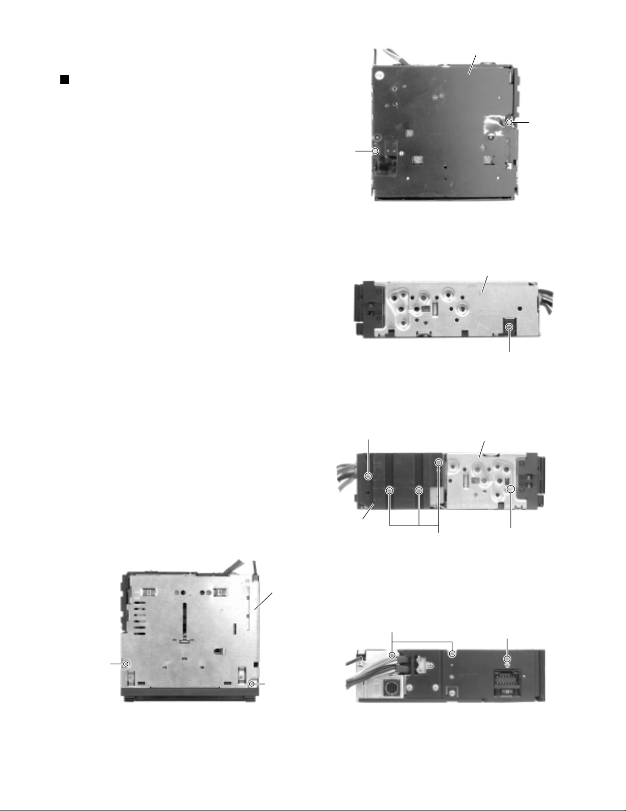
KS-LX200R
Disassembly method
Removing the top chassis
(See Fig.1 to 5)
1.
Remove the two screws A attaching the bottom
cover to the top chassis on the bottom of the body.
2.
Remove the two screws B attaching the top chassis
on both sides of the body.
3.
Remove the screw C and the three screws D
attaching the heat sink on the left side of the body.
4.
Remove the two screws E and the screw F on the
back of the body.
5.
Remove the two screws G on the upper side of the
body.
6.
Move the top chassis upward and disconnect the
cassette mechanism connector from the main board
connector by pulling it. Remove the top chassis from
the body.
Bottom cover
A
A
Fig.1
Top chassis
Top chassis
Heat sink
C
E
Fig.2
D
Fig.3
B
Top chassis
B
F
G
G
Fig.4Fig.5
1-3
Page 4
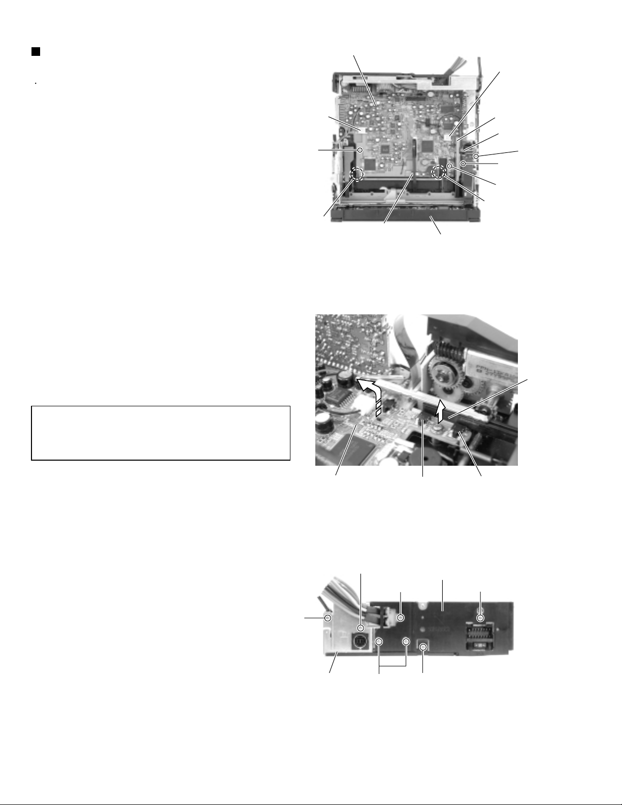
KS-LX200R
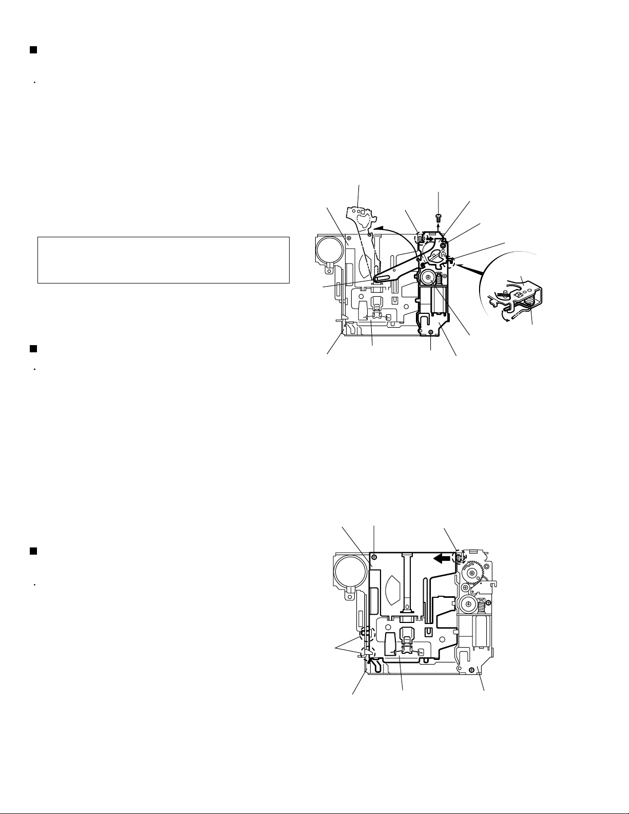
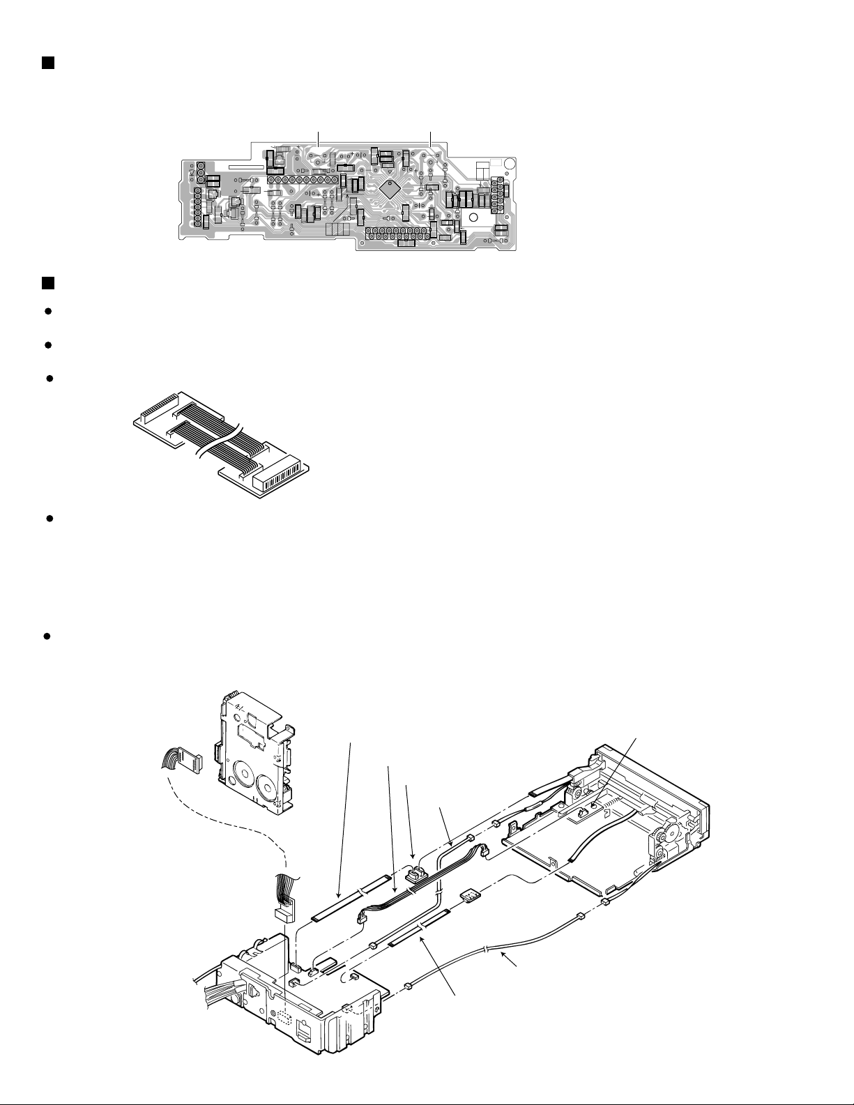
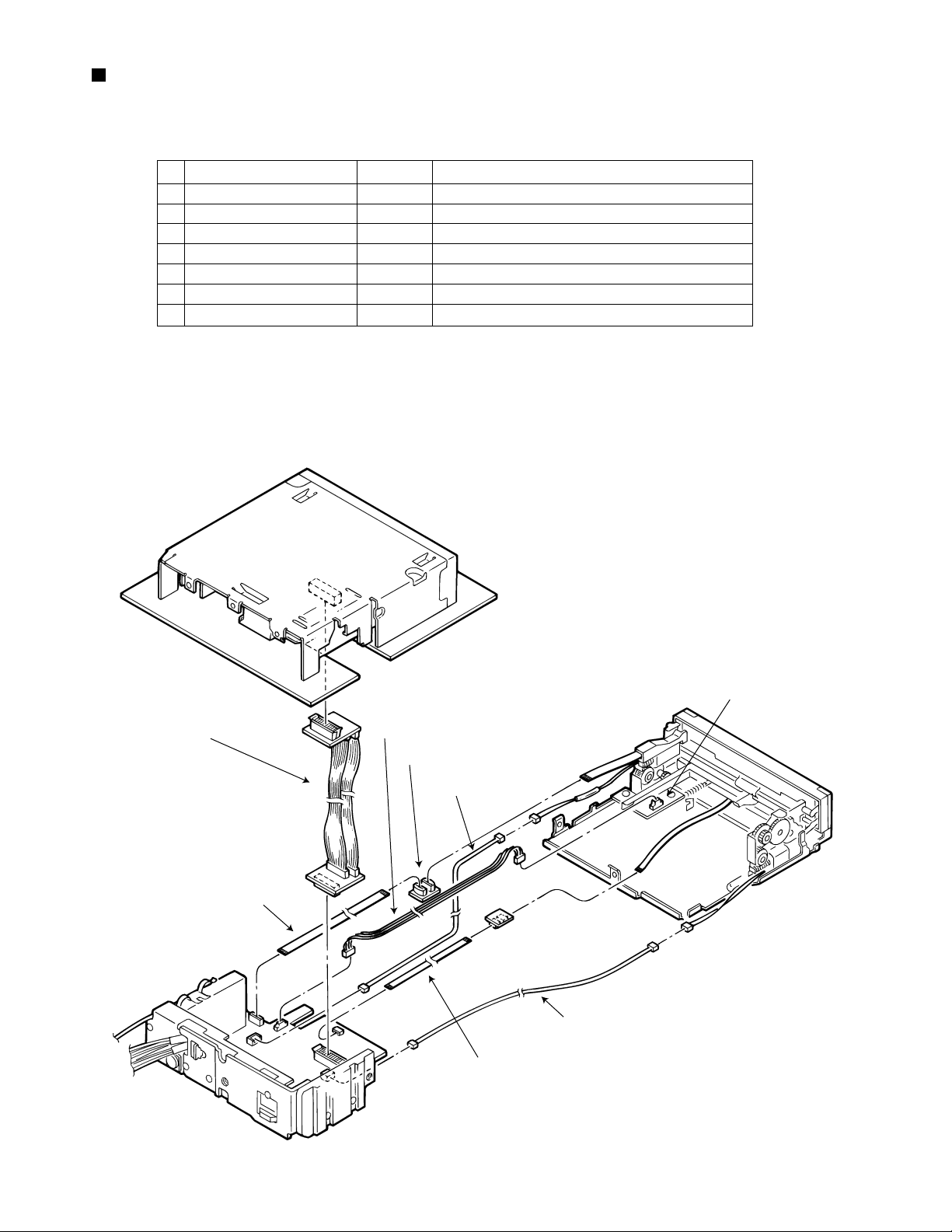
Removing the main board assembly
(See Fig.6 to 8)
Prior to performing the following procedure, remove
the top chassis.
1.
Remove the screw S attaching the bracket (L).
2.
Disconnect the flexible harness from connector
CN701, the card wire from CN702 on the main board
and the harness from CN503 and CN504
respectively.
3.
Remove the three screws H attaching the main
board assembly to the bottom cover on the upper
side of the body.
4.
Remove the screw I attaching the rear panel and the
bottom cover on the back of the body. Move the
main board in the direction of the arrow and release
the two joints a. (At this point, the main board can be
removed with the rear panel and the rear heat sink.)
5.
Remove the screw J and the two screws K attaching
the rear heat sink on the back of the body.
Main board assembly
CN503
H
Joint
a
CN702
Joint
Front panel assembly
Fig.6
CN504
Bracket (L)
CN701
H
S
H
a
6.
Remove the two screws L and the screw M attaching
the rear panel. Now, the main board assembly will be
removed.
ATTENTION:
When reassembling, correctly engage the
switch S561 and S562 on the main board
with the part e of the operation assembly
(Refer to Fig.7, 18 and 19).
Main board
L
M
S652
Fig.7
Rear heat sink
L
e
S651
J
1-4
Rear panel
K
I
Fig.8
Page 5
KS-LX200R
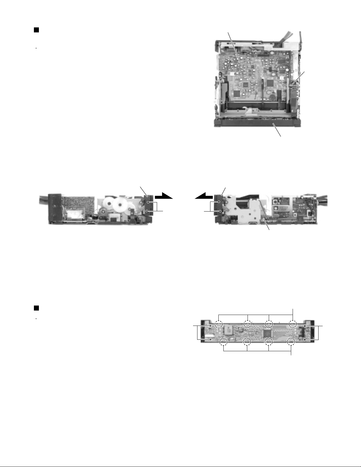
Removing the front panel assembly
(See Fig.9 to 11)
Prior to performing the following procedure, remove
the top chassis assembly.
1.
Disconnect the flexible harness from connector
CN701 on the main board assembly.
2.
Remove the four screws N attaching the front panel
assembly on both sides of the body. Remove the
front panel toward the front.
Front panel assembly
Main board assembly
CN701
Front panel assembly
Fig.9
Front panel assembly
N
Removing the Front Board (See Fig.12)
Prior to performing the following procedure, remove
the top chassis assembly and the front panel
assembly.
1.
Remove the four screws O attaching the front board
on the back of the front panel assembly and release
the eight joints b.
O
N
CN701
Fig.10Fig.11
Joints b
O
Joints b
Fig.12
1-5
Page 6
KS-LX200R
Removing the lifter unit (See Fig.13)
Prior to performing the following procedure, remove
the top chassis assembly and the front panel
assembly.
1.
Disconnect the harness from connector CN503 and
CN504 on the main board.
2.
Remove the four screws P and detach the lifter unit
from the bottom cover.
Removing the feed motor (L) (See Fig.14)
Prior to performing the following procedure, remove
the lifter unit.
1.
Remove the washer attaching the clutch assembly
and detach the clutch assembly from the shaft of the
lifter unit.
2.
Remove the two screws Q attaching the feed motor
(L).
Removing the feed motor (R) (See Fig.15)
Prior to performing the following procedure, remove
the lifter unit.
CN503
P
Clutch assembly
CN504
P
Lifter unit assembly
Fig.13
Lifter unit assembly
1.
Remove the washer attaching the clutch assembly
and detach the clutch assembly from the shaft of the
lifter unit.
2.
Remove the two screws R attaching the feed motor
(R).
Washer
Clutch assembly
Washer
Feed motor (L) assembly
Q
Fig.14
Lifter unit assembly
Feed motor (R) assembly
R
Fig.15
1-6
Page 7
Removing the operation assembly
(See Fig.16 to 19)
Prior to performing the following procedure, remove
the top chassis assembly, the front panel assembly
and the lifer unit.
1.
Remove the three screws S attaching the right and
left brackets which fix gears on both sides of the
operation assembly.
2.
Remove the springs 5 and 6 from the operation
assembly.
3.
Disconnect the card wire from connector CN702 on
the main board and remove the operation assembly.
ATTENTION:
When reassembling, correctly engage the
switch S561 and S562 on the main board
and the right gear with the part c of the
operation assembly.
Bracket (R)
S
Spring 5
Operation assembly
Fig.16
CN702
KS-LX200R
Bracket (L)
S
Spring 6
Bracket (R)
Operation assembly
S652
S651
Operation assembly
Fig.17
Operation assembly
c
c
c
S652
S651
Fig.18Fig.19
1-7
Page 8
KS-LX200R
Removing the operation switch board
(See Fig.20 and 21)
Prior to performing the following procedure, remove
the operation assembly.
1.
Remove the six screws T attaching the button panel
on the operation assembly.
2.
Pull out the operation switch board from inside of the
button panel.
TT
Button panel
Fig.20
Operation switch board
Button panel
Fig.21
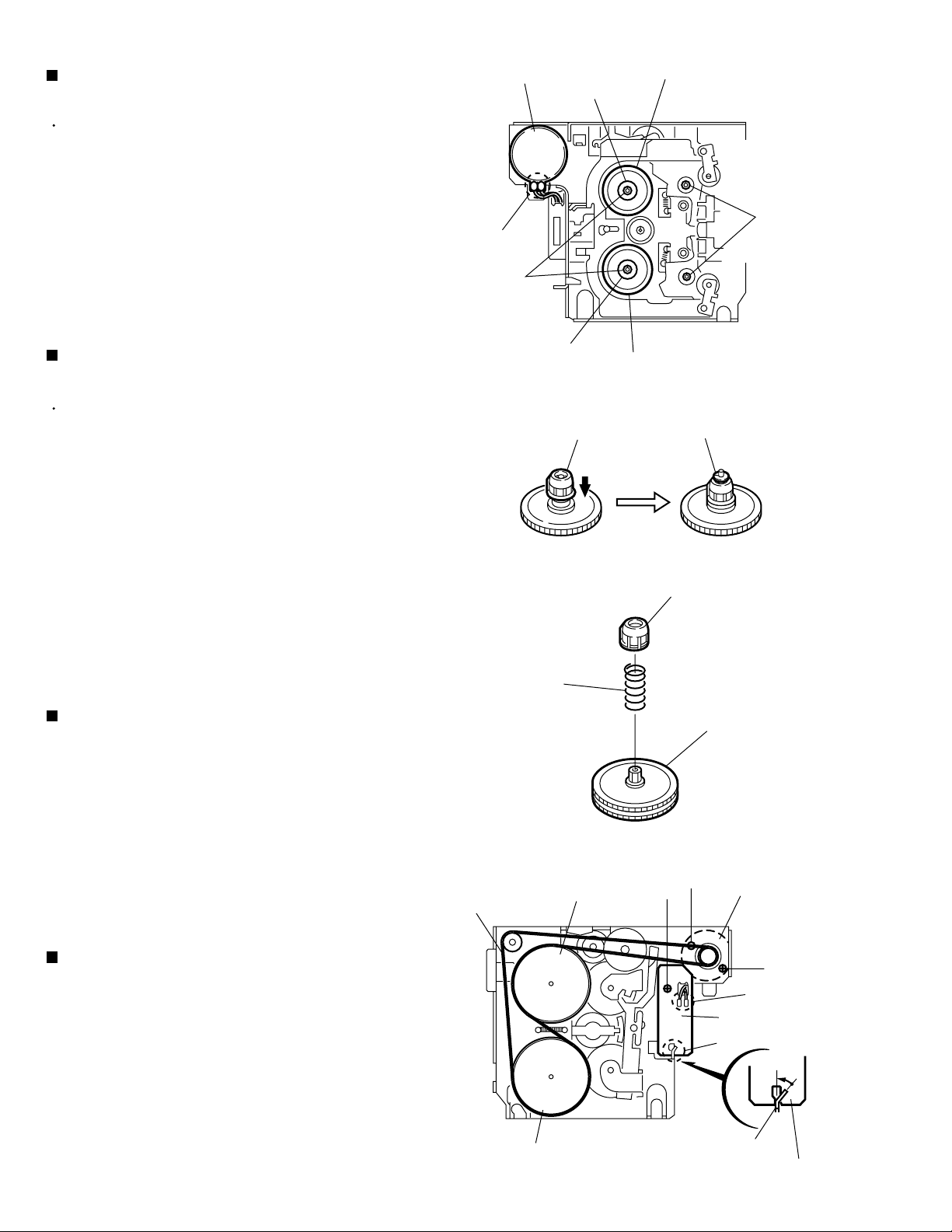
Removing the cassette mechanism
assembly (See Fig.22)
Prior to performing the following procedure, remove
the top chassis.
1.
Remove the four screws U and the cassette
mechanism assembly from the top chassis.
U
U U
U
CD mechanism assembly
Fig.22
1-8
Page 9
KS-LX200R
Disassembly method
<Cassette mechanism assembly>
Removing the head amplifier board
(See Fig.1)
1.
Disconnect the wire from connector CP401 on the
head amplifier board.
2.
Remove the screw A.
3.
Remove the head amplifier board in the direction of
the arrow to unhook two joints a.
4.
Disconnect connector CP402 on the head amplifier
board from the connector board.
Removing the mechanism bracket
(See Fig.2)
Prior to performing the following procedure, remove
the head amplifier board.
Connector board
A
Head amplifier board
Joints
a
Fig.1
B
B
1.
Remove the four screws B on the underside of the
cassette mechanism assembly.
<Cassette mechanism>
Prior to performing the following procedure, remove
the head amplifier board and the mechanism
bracket.
Removing the connector board
(See Fig.3)
1.
Unsolder soldering b and c on the connector board.
2.
Remove the three screws C.
3.
Remove the connector board in the direction of the
arrow to unhook joint d.
C
B
C
Fig.2
Soldering
Soldering
C
Mechanism bracket
b
Joint
Connector board
c
d
Fig.3
1-9
Page 10
KS-LX200R
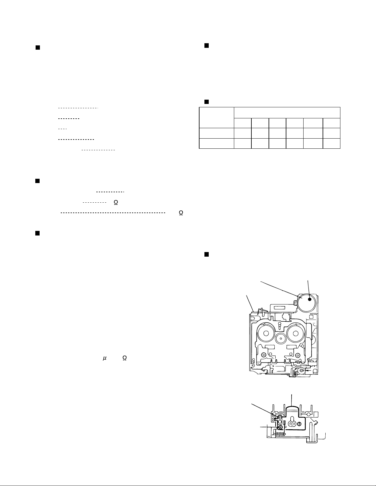
Removing the load arm assembly
(See Fig.4)
Prior to performing the following procedure, remove
the connector board.
1.
Remove the slit washer e retaining the load arm
assembly.
2.
Remove the spring g in the load arm assembly
marked joint f.
3.
Draw out the load arm assembly from the shaft and
rotate in the direction of the arrow to remove it from
the cach.
ATTENTION:
The spring g comes off as the load
arm assembly is drawn out from the
shaft.
Load arm assembly
Holder arm
Cach
Joint
D
h
Load arm assembly
Slit washer
e
Joint
f
Load arm
assembly
Removing the sub chassis (See Fig.4)
Prior to performing the following procedure, remove
the connector board and the load arm assembly.
1.
Remove the two screws D attaching the sub
chassis.
2.
Draw out the sub chassis from the holder arm shaft
in the direction of the arrow (marked joint h).
Remove the sub chassis from the main chassis
upwards.
Removing the cassette holder / holder
arm (See Fig.5)
Prior to performing the following procedure, remove
the connector board and the load arm assembly.
1.
Remove the screw E attaching the cassette holder /
holder arm.
2.
Draw out the holder arm shaft from the sub chassis
in the direction of the arrow (marked joint h).
Main chassis
Holder arm
i
Joints
Cassette holder
Fig.4
E
D
Joint
Worm gear
Sub chassis
h
Spring
g
3.
Disengage two joints i and remove the cassette
holder / holder arm.
1-10
Main chassis
Cassette holder
Fig.5
Sub chassis
Page 11
Removing the sub motor
(See Fig.4 and 6)
Prior to performing the following procedure, remove
the connector board and the load arm assembly.
1.
Remove the slit washer j and the worm gear.
Slit washer
KS-LX200R
j
2.
Remove the two screws F.
Removing the play head / pinch roller
assembly (twin set) (See Fig.7)
Prior to performing the following procedure, remove
the connector board, the load arm assembly and the
sub chassis.
1.
Remove the spring K retaining the play head
assembly and pull out the play head assembly.
Sub motor
Pinch roller assembly
Slit washer
F
Worm gear
Fig.6
Pinch roller assembly
l
Play head
Slit washer
l
2.
Remove the two screws G.
3.
Remove the two slit washers l attaching the pinch
roller assembly (twin set). Pull out each pinch roller
assembly.
Spring
1
G
Spring
Fig.7
2
k
k
1-11
Page 12
KS-LX200R
Removing the reel disc assembly (twin
set) (See Fig.8 to 10)
Prior to performing the following procedure, remove
the connector board, the load arm assembly, the sub
chassis and the cassette holder / holder arm.
1.
Remove the two slit washers m while pushing down
the reel driver on the two reel disc assemblies.
2.
Pull out the two screws I from the shaft with the reel
driver and the spring respectively.
Removing the flywheel assembly (F) and
(R) (See Fig.8 and 11)
Prior to performing the following procedure, remove
the connector board, the load arm assembly, the sub
chassis and the cassette holder / holder arm.
1.
Remove the belt from the underside of the
mechanism assembly.
Soldering
Slit
washers
Motor
q
m
Reel driver
Reel driver
Reel driver
Reel disc assembly
Reel disc assembly
Fig.8
Slit washer
m
Slit
washers
n
2.
Remove the two slit washers on the upper side of the
mechanism assembly.
3.
Pull out the flywheel assembly (F) and (R) from
underside of the mechanism assembly.
Removing the reel disc board
(See Fig.11)
1.
From the underside of the mechanism assembly,
unsolder soldering o on the reel disc board.
2.
Unbend the joint hook p retaining the reel disc board.
3.
Remove the screw H.
Removing the motor (See Fig.8and 11)
1.
Unsolder soldering q on the motor.
2.
Remove the belt from the underside of the
mechanism assembly.
Belt
Spring
Flywheel (F)
Fig.9
Fig.10
Reel driver
Reel disc
I
H
Motor
I
Soldering
Reel disc board
Joint hook
p
o
3.
Remove the two screws I from the underside of the
mechanism assembly.
1-12
Flywheel (R)
Fig.11
Tab
Reel disc board
Page 13
Adjustment method
KS-LX200R
Test Instruments reqired for adjustment
1.Digital osclloscope(100MHz)
2.Frequency Counter meter
3.Electric voltmeter
4.Wow & flutter meter
5.Test Tapes
VT724
VT739
VT712
For wow flutter & tape speed measurement
VT703
6.Torque gauge
For playback frequency measurement
for DOLBY level measurement
For head azimuth measurement
Cassette type for CTG-N
(mechanism adjustment)
Measuring conditions(Amplifier section)
Power supply voltage
Load impedance
4 (2Speakers connection)
DC14.4V(10.5~16V)
Line out
Standard volume position
Balance and Bass,Treble volume .Fader
20k
Tuner section
BAND STEP
FM : 100kHz (Seek), 50kHz (Manual)
AM : 9kHz step
Preset Memory Initialization
Preset Memory
Band
FM(MHz)
AM(kHz)
M1
87.5
153
M2
89.9
216
M3
97.9
603
M4
105.9
999
M5
108.0
1404
DUMMY LOAD
Exclusive dummy load should be used for AM
and FM dummy load,there is a loss of 6dB
between SSG output and antenna input. The
loss of 6dB need not be considered since
direct reading of figures are applied in this
working standard.
M6
87.5
1620
:Center(Indication"0")
Loudness,Dolby NR,Sound,Cruise:Off
Volume position is about 2V at speaker output with
following conditions.Playback the test tape VT721.
AM mode 999kHz/62dB,INT/400Hz,30%
modulation signal on receiving.
FM mono mode 97.9MHz/66dB,INT/400Hz,22.5kHz
deviation pilot off mono.
FM stereo mode 1kHz,67.5kHz dev. pilot7.5kHz dev.
Output level 0dB(1 V,50 /open terminal).
Arrangement of Adjusting
Cassette Mechanism Section
Capstan motor
Cassette mechanism
(Surface)
Azimuth screw
Playback head
(Forward side)
Azimuth screw
(Reverse side)
Tape speed adjust
1-13
Page 14
KS-LX200R
Arrangment of adjusting
Head amplifier board section (Reverse side)
VR402:Rch
(Dolby NR level adj)
VR401:Rch
(Dolby NR Frequency response adj)
B402
E
Q401
D401
B401
CP401
1
R420
1
R423
R421
R422
Q402
B409
Q403
D402
B408
FSMW1101A
VR402
C417
D403
C418
R424
IC402
R425
C419
C414
B403
B410
B404
C410
C412
C411
R413
1
C415
R416
R415
C416
R418
R419
CP403
C409
R411
B415
C413
1
11
B411
IC401
B412
17
VR401
B416
R412
R410
C405
R408
31
C407
21
C408
R417
B413
R404
B406
B414
R409
C406
R414
R407
1
B405
TPP
C404
CP402
1
R402
C401
2
R405
C403
R401
R406
R403
C402
B407
Information for using a Car Stereo service jig (for adjustment and checking)
We are advancing efforts to make our extension cords comman for all Car Stereo products.
Please use this type of extension cord as follows.
As a U -shape type top cover is employed,this type of extension cord needed to check operation of
the mechanism assembly after disassembly.
Extension cords
EXT-KSRT002-18P(18 pin extension cord)
For connection between mechanism assembly
and main board assembly.
Check for mechanism-driving section such as moter ,etc.
Disassembly method. (Refer to mthod to remove main parts)
1.Remove the bottom cover.
2.Remove the front panel assembly.
3.Remove the top cover. (Remove the screws at each side of heat sink and rear panel)
4.Install the front panel (whose assembly was removed in step 2) to the main unit.
5.Confirm that current is being is carried by connecting an extension cord jig.
Connection diagram
1-14
EXT-KSRT002-18P
EXTLX001-16PF
EXTLX002-4P
EXTLX002-16PC
EXTLX002-SWPWB
EXTLX001-2P
EXTLX001-6PC
EXTLX001-2P
EXTLX001-6PF
Page 15
Extension cord list
EXTLX002-JIG : Kit including the following 8 extension parts.
KS-LX200R
No.
1
2
3
4
5
6
7
Parts number Quantity Description
EXTLX001-2P
EXTLX001-6PF
EXTLX001-6PC
EXTLX002-16PF
EXTLX002-16PC
EXTLX002-SWPWB
EXTLX002-4P
Besides the above kit, we offer the conventional extension cord for CASSETTE
mechanism which are not essential to operation check or service.
The mechanism should be directly connected to the board using the extension wire.
EXT-KSRT002-18P
2
1
1
1
1
1
1
2Pin, 30cm extension cord
6Pin, 30cm flat wire
6Pin x 2, interlocking connector
16Pin flat wire
16Pin, interlocking connector
3 switch PWB
4Pin, 30cm extension cord
EXTGS004-26P
EXTLX001-16PF
EXTLX002-SWPWB
EXTLX002-4P
EXTLX002-16PC
EXTLX001-2P
EXTLX001-6PC
EXTLX001-2P
EXTLX001-6PF
1-15
Page 16

KS-LX200R
Item
1.
Head
azimuth
adjustment
Conditions
Test tape:
SCC-1659
VT703(10kHz)
Adjustment and Confirmation methods
Head height adjustment
Adjust the azimuth directly. When you
adjust the height using a mirror tape,
remove the cassette housing from the
mechanism chassis. After installing the
cassette housing, perform the azimuth
adjustment.
Load the SCC-1659 mirror tape. Adjust with
1.
height adjustment screw A and azimuth
adjustment screw B so that line A of the
mirror tape runs in the center between Lch
and Rch in the reverse play mode.
After switching from REV to FWD then to
2.
REV, check that the head position set in
procedure 1 is not changed. (If the position
has shifted, adjust again and check.)
Adjust with azimuth adjustment screw B so
3.
that line B of the mirror tape runs in the
center between Lch and Rch in the forward
play mode.
Head azimuth adjustment
Load VTT724 (VT724) (1kHz) and play it
1.
back in the reverse play mode. Set the Rch
output level to max.
Load VTT703 (VT703) (10kHz) and play it
2.
back in the forward play mode. Adjust the
Rch and Lch output levels to max, with
azimuth adjustment screw B. In this case,
the phase difference should be within 45 .
Engage the reverse mode and adjust the
3.
output level to max, with azimuth
adjustment screw C.
(The phase difference should be 45 or
more.)
When switching between forward and
4.
reverse modes, the difference between
channels should be within 3dB. (Between
FWD L and R, REV L and R.)
S.Values Adjust
A line
Head shield
The head is at low position
during.
B line
Head shield
The head is at High position
during REV.
Output
level:
Maximum
PBHead
FWD Adj B
REV Adj C
(0 ) (45 )
HEIGHT Adj A
phase
Tape speed
2.
and wow
flutter
confirmation
Play back
3.
frequency
response
confiramation
1-16
When VTT721 (VT721) (315Hz) is played
5.
back, the level difference between channels
should be within 1.5dB.
Test tape: VTT712
(3kHz)
Test tape: VTT724
(1kHz)
VTT739
(63Hz / 1kHz / 10kHz)
The tuner section is of an adjustment-freedesign. In case the tuner is in trouble, replace the tuner pack.
Check to see if the reading of the F, counter /
1.
wow flutter meter is within 3015 3045(FWD
/ REV), and less than 0.35% (JIS RMS).
In case of out of specification, adjust the
2.
motor with a built-in volume resistor.
Play test tape VTT724, and set the volume
1.
position at 2V.
Play test tape VTT739 and confirm.
2.
1kHz / 10kHz: -1 3dB,
1kHz / 63Hz: 0 3dB,
When 10kHz is out of specification, it will be
3.
necessary to read adjust the azimuth.
Tape speed:
3015
3045Hz
Wow
flutter: less
than 0.35%
Speaker out
1kHz / 63Hz
: 0 3db
1kHz / 10kHz
: -1 3db
Built-in volume
resistor
Page 17

Description of major ICs
BA4905-V3 (IC961) : Regulator
1.Pin layout
1234 56789101112
2.Block diagram
KS-LX200R
REGULATOR
EXT
RESET
1 2 3 4 5 6 7 8 9 10 11 12
RESET COMP VDD 5.7V CD 8V VCC AJ
EXT ACC AUDIO 9V CTRL ILM 10V GND
3.Pin function
Pin no. Symbol Function
1
2
RESET
EXT output
If VDD voltage becomes 4V or less.RESET output becomes low level.
This output voltage is approximately 0.5V lower than VCC. and max
output current is 300mA.
3
COMP output
A voltage supply for ACC block. This output voltage is approximately
0.7V lower than VDD'S. The max output current is 100mA.
4
5
ACC
VDD output
Control of the COMP output by inputting voltage.
This output voltage is 5.7V, and max output current is 100mA.
This voltage supply is for microcomputer. Whenever back up voltage
supply is connected, the output keeps on running.
6
AUDIO output
This output voltage is 9.0v, and max output current is 500mA.
This voltage supply for AUDIO.
7
CD output
This output voltage is 8.0V, and max output current is 1A.
This voltage supply for CD.
8
9
10
CTRL
VCC
ILM output
Output selector of CD. AUDIO, ILM and EXT.
To be connected with the BACK UP of car.
This output voltage is 10V, and max output current is 500mA.
Output voltage is adjustable.
11
AJ
Putting a resistance between ILM and AJ or between AJ and GND
makes ILM output voltage adjustable.
12
GND
Ground.
Overvoltage
protection circuit
37K
5K
1-17
Page 18

KS-LX200R
CXA2510AQ (IC401) : Head AMP / Dolby
1. Pin layout & Block diagram
30 PBEQ2
29 PBOUT2
28 GND
27 TAPEIN2
26 AUXIN2
PBFB2 31
PBRIN 32
PBREF2 33
PBFIN2 34
VCT 35
PBGND 36
PBFIN1 37
PBREF1 38
PBRIN1 39
PBFB1 40
VCT
F1
-
-
F2
120 /70
+
+
120 /70
T2
X1
TAPE / AUX
FWD / RVS
LPF
X1
T1
25 DIREF
24 LINEOUT2
+
NR BIAS
TAPE EQ
Vcc
+
F3
+
OFF/
-
B / C
-
23 TCH2
NR
NR
22 TCL2
MS MODE
NR MODE
MS ON/
OFF
DET
21 MSSW
20 MSMODE
19 DRSW
18 TAPESW
17 INSW
16 NRSW
15 MRMODE
14 MSOUT
13 DGND
12 MSTC
11 G1FB
2. Pin functions
Pin No.
1
2
3
4
5
6
7
8
9
10
11
12
13
14
15
PBEQ1 1
PBOUT1 2
Symbol
PBEQ1
PBOUT1
Vcc
TAPEIN1
AUXIN1
MSLPF
LINEOUT1
TCH1
NC
G2FB
G1FB
MSTC
DGND
MSUOT
NC
Vcc 3
TCL1 9
AUXIN 5
TAPEIN1 4
MSLPF 6
TCH1 8
LINEOUT1 7
I/O
O
Resistance for selecting the equalizer amplifier time constant.
O
Playback equalizer amplifier out put.
Power supply
TAPE input.
I
External input.
I
Cut-off frequency adjustment of the music sensor LPF.
Line out.
O
Time constant for the HLS.
Non connection.
Music signal interval detection level setting.
-
G2FB 10
Functions
Time constant for detecting the music signal interval.
Logic ground (Connect to GND)
Music sensor output.
O
Non connection.
I
1-18
Page 19

KS-LX200R
Pin
16
17
18
19
20
21
22
23
24
25
26
27
28
29
30
31
32
33
34
35
36
37
38
39
40
Symbol
NRSW
INSW
METAL
DRSW
FF/REW
MSSW
NC
TCH2
LINEOUT2
DIREF
NC
TAPEIN2
GND
PBOUT2
PBEQ2
PBFB2
NC
PBREF2
PBFIN2
VCT
PBGND
PBFIN1
PBREF1
NC
PBFB1
I/O
I
Dolby NR control L:NR OFF H:NR ON
I
Line amplifier input select control L:TAPE IN H:AUX IN
I
Playback equalizer amplifier control L:120us H:70us
I
Head select control L:FORWARD H:REVERSE
I
Music sensor mode control Low(open):G1 High:G2
I
Music sensor control Low(open):MS on High:MS OFF
-
Non connection
-
Time constant for the HLS
O
Line output
-
Resistance for setting the reference current (Connects 20(18)K
between DIREF pin and GND for the standard setting.)
-
Non connection.
I
TAPE input.
-
To ground.
O
Playback equalizer amplifier output.
O
Resistance for selecting the playback equalizer amplifier time constant
I
Playback equalizer amplifier feedback.
-
Non connection.
O
Playback equalizer amplifier reference (Vcc/2 output)
I
Playback equalizer amplifier input (FORWARD head connected)
O
Center (Vcc/2 output)
-
Playback equalizer amplifier ground (Connect to ground)
I
Playback equalizer amplifier input (FORWARD head connected)
O
Playback equalizer amplifier reference (Vcc/2 output)
-
Non connection.
I
Playback equalizer amplifier feedback.
Functions
NJM4565M-W (IC951,IC171,IC323) : Ope amp.
V-
1
2
8
V+
7
B OUTPUT
AB
3
4
6
B -INPUT
5
B +INPUT
A OUTPUT
A -INPUT
A +INPUT
1-19
Page 20

KS-LX200R
KA3031 (IC831) : Motor driver
1. Pin layout
48 ~ 37
1
36
~
12
13 ~ 24
2. Block diagram
1
IN1.2
2
OUT1
3
IN2.1
4
IN2.2
5
OUT2
6
IN3.1
7
IN3.2
8
OUT3
9
IN4.1
~
25
IN1.1 REG50 REG050 REF SVCC RES50 OPIN(+) OPIN(-) OPOUT PVCC2 DO1.1 DO1.2
48 47 46 45 44 43 42 41 40 39 38 37
T.S.D
O.V.P
+
-
+
-
+
-
+
-
+
-
+
-
+
-
+
-
+
-
+
D
D
2P
2P
2P
2P
2P
2P
2P
2P
2P
2P
2.5V
SW
+ -
+
-
+
-
+
-
+
-
-
+
-
+
-
+
-
+
S
W
ALL MUTE
+
-
+
-
+
-
+
-
M
S
C
36
35
34
33
32
31
30
29
28
DO2.1
DO2.2
PGND3
DO3.1
DO3.2
PGND2
PGND1
DO4.1
DO4.2
1-20
IN4.2
OUT4
CTL1
10
11
12
S
W
MUTE4
MUTE3
MUTE2
MUTE1
+
M
S
C
D
-
D
2P
2P
13 14 15 16 17 18 19 20 21 22 23 24
FWD1 REV1 CTL FWD2 REV2 SGND MUTE1 MUTE2 MUTE3 MUTE4 PVCC1 DO6.2
27
26
25
DO5.1
DO5.2
DO6.1
Page 21

3. Pin function
Pin No. Symbol I/O Function Pin No. Symbol I/O Function
1
2
3
4
5
6
7
8
9
10
11
12
13
14
15
16
17
18
19
20
21
22
23
24
IN1.2
OUT1
IN2.1
IN2.2
OUT2
IN3.1
IN3.2
OUT3
IN4.1
IN4.2
OUT4
CTL1
FWD1
REW1
CTL2
FED2
REW2
SGND
MUTE1
MUTE2
MUTE3
MUTE4
PVCC1
DO6.2
I
CH 1 op-amp input (-)
CH 1 op-amp output
O
CH 2 op-amp input (+)
I
CH 2 op-amp input (-)
I
CH 2 op-amp output
O
CH 3 op-amp input (+)
I
CH 3 op-amp input (-)
I
CH 3 op-amp output
O
CH 4 op-amp input(+)
I
CH 4 op-amp input (-)
I
O
CH 4 op-amp output
CH 5 motor speed
I
control
CH 5 forward input
I
CH 5 reverse input
I
CH 6 motor speed
I
control
CH 6 torward input
I
CH 6 reverse input
I
Signal ground
CH 1 mute
I
CH 2 mute
I
CH 3 mute
I
CH 4 mute
I
Power supply voltage
-
(For CH 5, CH 6)
CH 6 drive output
O
25
26
27
28
29
30
31
32
33
34
35
36
37
38
39
40
41
42
43
44
45
46
47
48
DO6.1
DO5.2
DO5.1
SO4.2
DO4.1
PGND
PGND
DO3.2
DO3.1
PGND
DO2.2
SO2.1
SO1.2
DO1.1
PVCC2
OPOUT
OPIN(-)
OPIN(+)
RES50
SVCC
REF
REG050
REG50
IN1.1
O
CH 6 drive outout
CH 5 drive output
O
CH 5 drive output
O
CH 4 drive output
O
CH 4 drive output
O
Power ground
Power ground
CH 3 drive output
O
CH 3 drive output
O
Power ground
CH 2 drive output
O
CH 2 drive output
O
O
CH 1 drive output
O
CH 1 drive output
Power supply voltage
-
(For CH 1, CH 2, CH 3, CH 4)
Opamp output
O
Opamp input (-)
I
Opamp input (+)
I
Regulator 5V reset
I
Signal supply voltage
Bias voltage input
I
regulator 5V output
O
Regulator output
O
CH 1 opamp onput (+)
I
KS-LX200R
BU4066BCF-X (IC322) : Switch
1.Pin l ayout
14 13 12 11 10 9 8
1 2 3 4 5 6 7
2.Block diagram
VDD
14 13 12 11 10 9 8
1 2 3 4 5 6 7
I/O 1
C1
O/I 1
C4
O/I 2
I/O 4
I/O 2
O/I 4
C2
O/I 3
C3
I/O 3
VSS
1-21
Page 22

KS-LX200R
UPD784215AGC113 (IC701) : UNIT CPU
1.Pin layout
75 ~ 51
76
~
50
~
100
1 ~ 25
26
2.Pin function
Pin No. Symbol I/O Function
1
2
3
4
5
6
7
8
9
10
11
12
13
14
15
16
17
18
19
20
21
22
23
24
25
26
27
28
29
30
31
32
33
34
35
36
37
38
39
40
41
42
43
44
45
46
47
48
49
50
FF/REW
DOLBY
MS-OUT
F/R
HOLD
TRAYCNT
DIMMER-OUT
LCD-POWER
VDD
X2
X1
VSS
XT2
XT1
RESET
SW1
BUS-IN
PS2
CURUISE
RDS-SCK
RDS-DA
REMOCON
AVDD
AVREF0
NC
NC
KEY0
KEY1
KEY2
LEVEL
SQ
S.METER
AVSS
W-VOL
DOT CONT
AVREF
BUS-SI
BUS-SO
BUS-SCK
STAGE2
LCD-DA
LCD-CL
LCD-LEI
BUZZER
E2PR-DA-I
E2PR-DA-O
E2PR-CLK
BUS-I/O
TM0
TM1
I/O
I/O
I/O
I/O
Output for input signal level switching for MS.
O
Dolby on "H" output.
O
MS output.
O
Fwd, REV direction switch signal input.
I
Non connect
Tray light control signal output.
O
Dimmer signal output.
O
Non connect.
Power supply terminal.
Connecting the crystal oscillator for system main clock.
O
Connecting the crystal oscillator for system main clock.
I
Connect to GND.
Connecting the crystal oscillator for system sub clock.
O
Connecting the crystal oscillator for system sub clock.
I
System reset signal input.
I
Cassette mechanism detect switch.
I
J-BUS signal cut in input.
I
Power save 2.
I
CRUISE signal input.
I
RDS selial clock input.
I
RDS data input.
I
Remove control signal input.
I
Power supply terminal.
Connect to GND.
Connect to GND.
Connect to GND.
Key control 0 input.
I
Key control 1 input.
I
Key control 2 input.
I
Level meter signal input.
I
S.quality level input.
I
S.meter level input.
I
Connect to GND.
Woofer volume signal output.
O
Dot contrast signal input.
O
Power supply terminal.
J-BUS data I/O terminal.
J-BUS data output.
O
J-BUS serial clock signal I/O.
Initial setting.
I
Data output for LCD driver.
O
Clock otput for LCD driver.
O
Chip enable 1 output for LCD driver.
O
BUZZER control signal output.
O
Data input terminal from EEPROM.
I
Data output terminal from EEPROM.
O
Data input terminal from EEPROM.
J-BUS I/O signal terminal.
Tray motor negative signal output.
O
Tray motor positive signal output.
O
1-22
Page 23

Pin No. Symbol I/O Function
51
52
53
54
55
56
57
58
59
60
61
62
63
64
65
66
67
68
69
70
71
72
73
74
75
76
77
78
79
80
81
82
83
84
85
86
87
88
89
90
91
92
93
94
95
96
97
98
99
100
DM0
DM1
ST
LOCAL
MONO
CA-SW1
CA-SW2
CA-SW3
CA-SW4
CA-SW5
VCR-CONT
AFCK
SEEK/STOP
SD
FM/AM
PLL-CE
PLL-DA
PLL-CK
BAND IN
TEL-MUTE
AMP KILL
VSS
DIMMER-IN
DSI
POWER
CD-ON
MUTE
W-LPF1
W-LPF2
W-MUTE
VDD
VOL-DA
VOL-CLK
CF-SEL
NC
LCD RST
LCD-CE2
DMK
TMK
STAGE1
MOTOR
MODE
STANDBY
TEST
TAPE-IN
SUBMO-
SUBMO+
TAPE-END
KICK
VOICE IN
Door motor negative signal output.
O
Door motor positive signal output.
O
Stereo signal input.
I
Non connect.
Manual ON/OFF select signal output.
O
DOOR/TRAY open/close detect switch signal input.
I
DOOR/TRAY open/close detect switch signal input.
I
DOOR/TRAY open/close detect switch signal input.
I
DOOR/TRAY open/close detect switch signal input.
I
DOOR/TRAY open/close detect switch signal input.
I
Non connect.
AF check output.
O
AUTO SEEK/STOP select signal output.
O
Station detector input.
I
FM/AM select signal output.
O
Chip enable signal output.
O
Data output.
O
Clock signal output.
O
AM detect signal input.
I
Telephone.
I
Non connect.
Connect to GND
DIMMER signal input.
I
Power save 1.
I
Power ON/OFF select signal output.
O
Non connect.
Mute signal output.
O
Woofer LPF 1 signal output.
O
Woofer LPF 2 signal output.
O
Woofer mute signal output.
O
Power supply.
Data output.
O
Clock signal output.
O
CF select signal input.
I
Non connect.
LCD reset signal output.
O
Chip enable 2 output.
O
Motor speed control signal output.
O
Tray motor control signal output.
O
Initial setting.
I
Mecha Motor signal output.
O
Mecha mode position detection input.
I
Standby position derection input.
I
Test terminal
I
Cassette in detection input.
O
Sub motor clock direction drive output.
O
Sub motor clock oppositte direction drive output.
Tape end detection input.
I
Kick output.
O
Voice control signal input.
I
KS-LX200R
1-23
Page 24

KS-LX200R
BD3860K (IC911) : E. volume
1. Pin layout
33 ~ 23
34
22
44
2. Block diagram
GND FIL VCC SEL1
6 5 9 40 36 35 343328323130 2919 15 14
POWER
SUPPLY
A1
41
B1
42
C1
43
D1
44
INPUT
1
2
3
4
SELECTOR
A2
B2
C2
D2
~
1 ~ 11
INPUT
GAIN
0 to 18 dB
INPUT
GAIN
0 to 18 dB
~
12
VIN1 LOUD1 HF1 LF1 DET1 TIN1 TNF1 BNF1
MAIN
VOLUME
0 to -40 dB
LOUDNESS
MAIN
VOLUME
0 to -40 dB
LOUDNESS
LOW(f=50Hz) 6dB
PROCESS CONTROL +3 to 12dB
(f=10kHz)
LOGIC
LOW(f=50Hz) 6dB
PROCESS CONTROL +3 to 12dB
(f=10kHz)
TREBLE
-14 to +14dB
TREBLE
-14 to +14dB
-14 to +14dB
-14 to +14dB
BASS
BASS
BOUT1VCA1 MIX1 BBOUT1
FADER
CH1 FRONT
0 to -5 dB
FADER
CH1 REAR
0 to -5 dB
FADER
CH2 REAR
0 to -5 dB
FADER
CH2 FRONT
0 to -5 dB
13
12
10
11
7
8
OUTF1
OUTR1
SI
SC
OUTR2
OUTF2
3. Pin function
Pin
Symbol Function
No.
1
2
3
4
5
6
7
8
9
10
11
12
13
14
15
16
17
18
19
20
21
BBOUT2
22
A2
B2
C2
D2
FIL
GND
SC
VCC
OUTR2
OUTF2
OUTR1
OUTF1
BOUT1
BNF1
BOUT2
BNF2
TNF2
TNF1
TIN2
MIX2
CH2 input terminal A
CH2 input terminal B
CH2 input terminal C
CH2 input terminal D
1/2 VCC terminal
Ground terminal
Serial data input terminal
SI
Serial clock input terminal
Power supply
CH2 rear output terminal
CH2 front output terminal
CH1 rear output terminal
CH1 front output terminal
CH1 bus filter setting terminal
CH1 bus filter setting terminal
CH2 bus filter setting terminal
CH2 bus filter setting terminal
CH2 treble filter setting terminal
CH1 treble setting terminal
CH2 treble input terminal
CH2 BBE II signal output terminal
CH2 output mix amp negative input terminal
39 38 37 25 24 26 23 22 21 20 18 17 16
Pin
Symbol Function
No.
23
24
25
26
27
28
29
BBOUT1
30
31
32
33
34
LOUD1
35
36
LOUD2
37
38
39
40
41
42
43
44
VCA2
LF2
HF2
DET2
DET1
TIN1
MIX1
VCA1
LF1
HF1
VIN1
VIN2
SEL2
SEL1
CH2 high frequency VCA output terminal
CH2 low frequency filter setting terminal
CH2 high frequency filter setting terminal
CH2 high frequency attack release time setting
Non connect
NC
CH1 high frequency attack release time setting
CH1 treble input terminal
CH1 BBE II signal output terminal
CH1 output mix amp. negative input terminal
CH1 high frequency VCA output terminal
CH1 low frequency filter setting terminal
CH1 high frequency filter setting terminal
CH1 loudness filter setting terminal
CH1 main volume input terminal
CH2 loudness filter setting terminal
CH2 main volume input terminal
CH2 input gain output terminal
CH1 input gain output terminal
CH1 input terminal A
A1
CH1 input terminal B
B1
CH1 input terminal C
C1
CH1 input terminal D
D1
BOUT2BNF2TNF2TIN2BBOUT2MIX2VCA2DET2LF2HF2LOUD2VIN2SEL2
1-24
Page 25

LA3460M-X (IC31) : FM noise canceller & Stereo MPX demodulator
1. Pin layout
24 13
112
2. Block diagram
24 23 22 21 20 19 18 17 16 15 14 13
KS-LX200R
123456789101112
3. Pin function
Pin
No.
1
2
3
4
5
6
7
8
9
10
11
12
13
14
15
16
17
18
19
20
21
22
23
24
DRIVER
HPF LPF
TRIG
AGC
GATE
PC
PD
LPF
Function Description
Noise sense
Noise sensitivity adjustment
Noise AGC
Gate time
Signal hold
Pilot output
Vcc
Capacitor for HCC
SNC control
HCC control
Vcc=+8.0V
High pass filter
Stereo noise controlled voltage
High cut controlled voltage
Lch output
Rch output
Pican input
Pican output
pilot cancel signal input
pilot cancel signal outpt
Separation ADJ
NC
NC
456kHz OSC
Phase comp LPF (+)
Phase comp LPF (-)
Ceramic resonator
Phase comparator low pass filter
Phase comparator low pass filter
GND
PLL input
Stereo indicator
Composite input
Phase locked loop signal input
Active low
Composite signal input
Pilot det LPF
LPF
SCHMIT
HCC
VCO
FF
MAIN
CONTROL
VCO STOP
PACAN
SEPARATION
ADJ.
SUB
ANTI-BRIDGE
DECODER
SNC
1-25
Page 26

KS-LX200R
LA4743B (IC941) :Power amp
1.Terminal layout
TAB
GND1
OUTFR+
STBY
OUTFR-
1 2 3 4 5 6 7 8 910111213141516171819202122232425
2.Block diagram
VCC1/2
OUTRR+
GND2
OUTRR-
VREF
INRR
INFR
SGND
INFR
INRL
ONTIME
OUTRL+
GND3
OUTRL-
VCC3/4
OUTFL+
MUTE
OUTFL-
GND4
NC
206
VCC3/4
VCC1/2
3.Pin function
Pin
No.
1
2
3
4
5
6
7
8
9
10
11
12
13
OUT 1+
7
9
+
-
+
-
11
IN 1
Symbol Function
TAB
GND1
RFOSTBY
RFO+
VCC1/2
RROGND2
RRO+
R.F
RRIN
RFIN
SGND
1
TAB
Header of IC
Power GND
Output (-) for front Rch
Stand by input
Output (+) for front Rch
Power input
Output (-) for rear Rch
Power GND
Output (+) for rear Rch
Ripple filter
Rear Rch input
Front Rch input
Signal GND
8
Protective
circuit
OUT 2+
5
+
-
PWR GND1
OUT 1-
OUT 2-
3
-
+
12
IN 2
PWR GND2
2
Stand by
switch
4
ST BY
Pin
No.
14
15
16
17
18
19
20
21
22
23
24
25
OUT 3-
19
-
Protective
-
25
N.C
PWR GND3
18
circuit
MUTE
22
OUT 3+
17
+
Mute
circuit
+
Ripple
filter
10
R.F
Symbol Function
LFIN
LRIN
ONTIME
LRO+
GND3
LROVCC3/4
LFO+
MUTE
LFOGND4
NC
15
IN 3
Front Lch input
Rear Lch input
Power on time control
Output (+) for rear Lch
Power GND
Output (-) for rear Lch
Power input
Output (+) for front
Muting control input
Output (-) for front
Power GND
Non connection
OUT 4+
21
+
-
-
+
13
PRE GND
14
IN 4
OUT 4-
23
Muting &
PWR GND4
24
on time control
circuit
16
ON TIME
1-26
Page 27

LC75873NW (IC601) : LCD driver
1.Block diagram
COM3
COM2
COM1
S68
S67
S5
S4/P4
S3/P3
S2/P2
S1/P1
KS-LX200R
VDD1
VDD2
INH
OSC
VDD
VSS
COMMOM
DRIVER
CLOCK
GENERATOR
SEGMENT DRIVER
SHIFT REGISTER
ADDRESS
DETECTOR
2.Pin functions
Pin No. Symbol Description
1~66
67~69
70
71
S3~S68
COM1~3
VDD
VDD1
I/O
Segment Output.
O
Common Driver Output.
O
Power Supply Connection.
Used for applying the LCD drive 2/3 bias voltage externally.
I
Must be connected to VDD2 when a 1/2 bias drive scheme in used.
72
VDD2
Used for applying the LCD drive 1/3 bias voltage externally.
I
Must be connected to VDD1 when a 1/2 bias drive scheme in used.
73
74
VSS
OSC
Power supply connection.
Oscillator connection. An oscillator circuit is formed by connecting an
I/O
external resistor and capacitor to this pin.
75
76
77
78
79
80
INH
CE
CLOCK
DI
S1
S2
Display off control input.
I
Chip enable input.
I
Synchronization clock input.
I
Serial data input.
I
Signal output.
O
Signal output.
O
1-27
Page 28

KS-LX200R
BA3220FV-X (IC301) : Driver
1. Pin layout & Block diagram
CL- LGND OUTL OUTR RGND CR - CR +
1314
REFL REFR
1112 9 810
FILTER
CL+ Vcc INL NFL FIL NFR INR
2. Pin function
Pin
Symbol Function
No.
1
CL+
2
3
4
NFL
5
6
NFR
7
INR
8
CR+
9
CR-
10
RGND
11
OUTR
12
OUTL
13
LGND
14
Vcc
INL
FIL
CL-
2143675
Powe supply terminal for amp.
power supply terminal.
input terminal.
Negative feedback terminal.
Filter terminal.
Negative feedback terminal.
Input terminal
Power supply terminal for amp.
Output terminal of internal amp.
Rch GND terminal.
Rch output terminal.
Lch output terminal.
Lch GND terminal.
Output terminal of internal amp.
1-28
Page 29

BR24C32F-X (IC703) : EEPROM
KS-LX200R
1. Pin layout
2. Block diagram
A0 1
A1 2
A2 3
Vcc WP SCL SDA
A0
A1 A2
GND
32k bit EEPROM ARRAY
12bit
ADDERESS
DECODER
CONTROL LOGIC
SLAVE/WORD
12bit
ADDRESS REGISTER
START
STOP
ACK
8bit
DATA
REGISTER
8 Vcc
7 WP
6 SCL
GND 4
3. Pin function
HIGH VOLT A GE GEN.
Vcc LEVEL DETECT
Pin No. I/O Functions
Vcc
GND
AO,A1,A2
SCL
SDA
WP
-
Power supply
-
Ground (0V)
IN
Slave address set
IN
Serial clock input
I/O
Slave and word address/Serial data output
IN
Write protect input
5 SDA
1-29
Page 30

KS-LX200R
SAA6579T-X (IC51) : RDS demodulator
1. Pin layout 2. Pin function
1
2
3
4
5
6
7
8
16
15
14
13
12
11
10
9
Pin
Symbol Function
No.
1
2
3
4
5
6
7
8
9
10
11
12
13
14
15
16
QUAL
RDDA
Vref
MUX
VDDA
VSSA
CIN
SCOUT
MODE
TEST
VSSD
VDDD
OSCI
OSCO
T57
RDCL
Quality indication output
RDS data output
Reference voltage output (0.5VDDA)
Multiplex signal input
+5V supply voltage for analog part
Ground for analog part (0V)
Sub carrier input to comparator
Sub carrier output of reconstruction filter
Oscillator mode / test control input
Test enable input
Ground for digital part (0V)
+5V supply voltage for digital part
Oscillator input
Oscillator output
57kHz clock signal output
RDS clock output
3. Block diagram
57kHz
BAND PASS
(8th ORDER)
COSTAR LOOP
VARIABLE AND
FIXED DIVIDER
CLOCK
REGENERATION
AND SYNC
RECONSTRUCTION
MUX
SCOUT
CIN
VDDA
Vref
ANTI-
4
ALIASING
FILTER
8
7
CLOCKED
COMPARATOR
5
3
REFERENCE
VOLT AGE
Vp1
6
IC-PST600M/G/-W (IC702) : System reset
FILTER
OSCI OSCO VDDD
13 14 12
OSCILLATOR
AND
DIVIDER
BIPHASE
SYMBOL
DECODER
TEST LOGIC AND OUTPUT
SELECTOR SWITCH
91011
QUALITY BIT
GENERA TOR
DIFFERENTIAL
DECODER
VSDDTESTMODEVSSA
16
15
1
2
QUAL
RDDA
RDCL
T57
1-30
Co1
OP1
1
3
2
IN
Vout
OUT
Page 31

HD74HC126FP-X (IC771) : Buffer
KS-LX200R
1. Pin layout
1
2
3
4
5
6
7
3. Block diagram
14
13
12
11
10
9
8
Vcc Vcc
1A
2A
3A
Input
4A
1C
2C
3C
See Function Table
4C
2. Pin function
Output
1Y
2Y
Output
2Y
Output
3Y
Output
4Y
Inputs Outputs
C
A
L
X
H
L
H
H
Y
Z
H
L
1k
S1
CL
1k
Sample as Load Circuit 1
Sample as Load Circuit 1
Sample as Load Circuit 1
RPM6938-SV4 (IC602) : Remote control receiver
AGC
AMP
I/V
conversion
PD
magnetic shield
BPF
for
trimming
circuit
Detector
Vcc
Comp
Vcc
22k
ohm
Rout
GND
1-31
Page 32

KS-LX200R
M5282FP-XE (IC321) : E. volume
1. Pin layout
1
2
3
4
5
3. Pin function
Pin
Symbol Function
No.
1
Vcc/2
2
Amp+IN
3
Amp-IN
4
Amp OUT
5
GND
6
7
VCA IN
8
9
VCA OUT
10
NC
Vc
Vcc
2. Block diagram
10
9
8
7
6
1
2
3
10
457
Vcc/2 output for microphone amp.
Microphone amp. positive input terminal.
Microphone amp. negative input terminal.
Microphone amp. output terminal.
Ground.
Non connection.
VCA input terminal.
VCA control terminal.
VCA output terminal.
Power supply.
9
8
LB1641 (IC402) : DC Motor driver
1. Pin layout
1 2 3 4 5 6 7 8 9
GNDOUT1 P1
VZ IN1 IN2
2. Pin function
Input Output
IN1 IN2 OUT1 OUT2
0 0 0 0
1 0 1 0
0 1 0 1
1 1 0 0
VCC1
VCC2 P2
10
OUT2
Mode
Brake
CLOCKWISE
COUNTER-CLOCKWISE
Brake
1-32
Page 33

KS-LX200R
KS-LX200R
VICTOR COMPANY OF JAPAN, LIMITED
MOBILE ELECTRONICS DIVISION
PERSONAL & MOBILE NETWORK B.U. 10-1,1Chome,Ohwatari-machi,Maebashi-city,Japan
No.49573
Printed in Japan
200010(O)
1-33
Page 34

PARTS LIST
[ KS-LX200R ]
* All printed circuit boards and its assemblies are not available as service parts.
KS-LX200R
- Contents -
Exploded view of general assembly and parts list
Cassette mechanism assembly and parts list
Electrical parts list
Packing materials and accessories parts list
Area suffix
E ----------- Continental Europe
EX --------------- Central Europe
3-3
3-6
3-9
3-16
3-1
Page 35

KS-LX200R
<<MEMO>>
3-2
Page 36

Exploded view of general assembly and parts list
8
11
12
6
14
Block No.
6
M
1
Switch board
14
68
M
M
63
62
67
69
63
86
KS-LX200R
103
103
13
93
84
15
19
89
95
83
90
96
92
9
55
16
81
25
104
53
23
14
64
17
14
7
5
1
14
17
Mecha.control
46
28
57
58
45
57
47
board
4
10
29
56
3
2
34
3
10
78
71
59
76
77
2
75
76
75
73
72
10
4
4
59
74
10
79
5
102
37
36
41
40
98
99
1
101
LCD1
100
68
66
60
30
26
80
79
Front board
51
68
56
35
65
49
44
61
57
31
29
28
22
43
70
33
21
57
38
24
58
54
85
87
39
20
52
48
27
50
21
14
88
94
97
91
18
42
Main board
18
18
32
15
82
BC
DE
F
G
HA
I
3-3
Page 37

KS-LX200R
)
)
KS-LX200R
Parts list
Item Parts number Parts name Area
A
6
10 QYSDST2604Z SCREW 4 T.CHAS+CS MECHA
11 QYSDSF2610Z TAPPING SCREW 1 T.CHAS+S H.SINK
12 LV41200-003A SPESIAL SCREW 3 T.CHAS+S H.SINK
13 LV41200-003A SPESIAL SCREW 1 T.CHAS+REAR
5
14 QYSDST2604Z SCREW 6 T.CHAS+B.CHAS
15 QYSDST2604Z SCREW 2 T.CHAS+R.BKT
16 LV41200-001A SPECIAL SCREW 1 BOTTOM CHA.+REAR BKT
17 QYSPSP2003M SCREW 4 T.CHAS+F.COVER
18 LV41200-001A SPECIAL SCREW 3 MAIN PWB+BOTTOM CHA.
19 LV31604-002A BOTTOM ASS'Y 1
20 LV31605-001A DOOR BASE ASS'Y 1
21 LV41452-001A TENS SPRING BTM 2
4
22 LV31607-001A PANEL COVER 1
23 LV31965-001A BUTTON BASE BKT 1
24 LV41500-001A BUTTON B.SUPORT 1
25 LV41545-001A BUTTON B.GUIDE 1
26 FSKL3014-001A FRONT BKT ASS'Y 1
27 LV20614-002A BRACKET ASS'Y 1
28 WDM215025 WASHER 4
29 LV41503-001A ARM 3 2
3
30 FSYH4036-015 SHEET 1
31 LV31777-001A FFC GUIDE 1
32 LV31610-001A ROD GEAR 1
33 LV40847-002A SPACER 1 MOTOR L
34 QAR0029001-SA2 FEED MOTOR 1 FOR BKT MOTOR L
35 PPN13KA10C-SA6 FEED MOTOR 1 FOR BKT MOTOR R
36 LV40847-002A SPACER 1 MOTOR R
37 WJM0137-001A E-SI CARD WIRE 1 FOR MOTOR L
38 WJM0136-001A E-SI CARD WIRE 1 FOR MOTOR R
2
39 QWTA20H-030 UL VINYL TUBE 1 FOR R WIRE
40 QE40110-001A SHIELD CASE 1
41 FSYH4036-064 SPACER 1
42 LV41463-001A GEAR 1 1 R SIDE
43 LV41464-001A GEAR 2 1 R SIDE
44 LV31611-001A GEAR 3 1 R SIDE
45 LV41466-001A GEAR 4 1 L SIDE
46 LV41467-001A GEAR 5 1 L SIDE
1
47 LV31612-001A GEAR 6 1 L SIDE
48 LV30981-004A CLUTCH ASS'Y 1 RIGHT SIDE
(General assembly)
Q'ty Description
1 --------------- CDS-522VJ2 1 CASSETTE MECHA
2 FSKM2006-001 MECHA BRACKET 1
3 QYSDST2604Z SCREW 1 PCB+MECHA
4 FSKZ4004-002 SCREW 4 MECHA+M.BKT
5 FSMA4010-002 INSULATOR 1 M.BKT+SCREW
6 FSJC1065-001 TOP CHASSIS 1
7 FSJC1064-001 FRONT COVER 1
8 LV31602-003A SIDE HEAT SINK 1
9 FSMA3007-001 INSULATOR 1
Block No. M1MM
Parts list
Item Parts number Parts name Area
A
49 QYSPSPT2020Z MINI SCREW 2 F.MOTOR+B.M. L
50 QYSPSPT2020Z MINI SCREW 2 F.MOTOR+B.M. R
51 LV40865-001A MINI SCREW 2 ROD BKT(L)+LO.BKT
52 LV40865-001A MINI SCREW 2 ROD BKT(R)+LO.BKT
53 LV40865-001A MINI SCREW 1 B.BASE BKT+BO.CHAS
54 LV40865-001A MINI SCREW 2 B.B.SUPPO+BO.CHAS
55 LV40865-001A MINI SCREW 1 B.B.GUIDE+BO.CHAS
56 LV40865-001A MINI SCREW 4 BKT.M.L&R+C.BOTTOM
57 WDM215025 WASHER 6 FOR GEAR 1-6
58 WDM214540 WASHER 2 FOR CLUTCH ASSY
59 QYSPSPU1725M SCREW 4 LO.UNIT A+DIS.PANEL
60 LV30981-005A CLUTCH ASS'Y 1 LEFT SIDE
61 LV10317-007A BUTTON PANEL 1 KS-LX200R
62 LV10318-001A BUTTON BASE 1
63 LV40848-007A SPACER(P
64 LV20615-003A PRESET BUTTON 1 LEFT PRESET BUTTON
65 LV20616-002A PRESET BUTTON 2 1
66 LV31613-001A FUNCTION BUTTON 1
67 LV41825-002A PLATE SPRING 1
68 VKZ4777-004 MINI SCREW 6
69 WJT0030-001A E-CARD WIRE 1
70 FSYH4036-035 SHEET 1 FOR E-CARD WIRE
71 FSJC1066-002 DISPLAY PANEL 1
72 LV32035-001A D.P. PLATE 1
73 FSJD3026-001A FINDER LENS 1
74 LV41469-001A UP DOWN B.ASS'Y 1
75 VYSH1R5-007 SPACER 2
76 LV40848-009A SPACER(P
77 LV41471-001A +/- BUTTON ASSY 1
78 LV41505-001A REMOTE LENS 1
79 VKZ4777-001 MINI SCREW 4 D.PANEL+SW.PWB
80 WJT0031-001A E-CARD WIRE 1
81 FSYN3148-105 NAME PLATE 1
82 LV41143-001A SHEET 2
83 QAM0178-001 PIN CORD ASS'Y 1
84 QAM0179-001 CAR CABLE 1
85 LV30943-201A REAR BRACKET 1
86 LV30946-005A REAR HEAT SINK 1 BLACK ANODISED
87 LV40790-001A PIN CORD BRACKET 1
88 QYSDST2604Z SCREW 1
89 LV41200-003A SPESIAL SCREW 2
90 LV40792-001A REG.IC BRACKET 1
91 LV41863-001A POWER IC BRACKET 1
92 VMA4652-001SS SHIELD PLATE 1
93 QYSDST2606Z SCREW 1
94 QYSDST2606Z SCREW 1
95 QYSDST2604Z SCREW 2
96 QYSDST2604Z SCREW 1
(General assembly)
Block No. M1MM
Q'ty Description
2
2
BC
DE
F
G
HA
I
3-4
Page 38

KS-LX200R
A
Parts list
Item Parts number Parts name Area
A
97 QMFZ039-150-T FUSE
98 FSKS3023-001 LIGHTING CASE 1
99 FSYH4081-002 LIGHTING SHEET 1 D105
100 FSYH2006-001 LCD CASE 1
101 QNZ0495-001 RUBBER CONNECTOR 1
102 QNZ0494-001 RUBBER CONNECTOR 1
103 VYTA500-001 PIN CAP 8
104 QAM0105-002 CAR CABLE 1 J1
LCD 1 QLD0149-001 LCD MODULE 1
(General assembly)
Q'ty Description
1
Block No. M1MM
3-5
Page 39

KS-LX200R
Cassette mechanism assembly and parts list
Block No.
M
M
2
M
A
98
MODEL:CDS522-VJ2
3-6
Grease & Oil
SW-902S
SW-474B
SW-522B
PANORL-56
CFD-409
Page 40

KS-LX200R
)
)
)
)
)
)
Parts list
Item Parts number Parts name Area
A
10 X-0522-1022S FR ARM ASS'Y 1
13 X-0522-2008S DETECT ARM ASSY 2
14 X-0522-2010S LOAD GEAR ASS'Y 1
15 X-0522-2016-6S FLYWHEEL ASY(FN 1
16 X-0522-2018S REEL TABLE ASSY 2
17 X-0522-2020S REDUCT.GEAR ARM 1
18 X-0522-2021-6S FLYWHEEL ASY(RN 1
19 X-0052-2001S F.R. GEAR ASS'Y 1
22 1-0522-1008S DIR.PLATE 1
23 1-0522-1031S FF/REW PLATE 1
24 1-0522-1027S MOTOR BKT 1
25 1-0522-1013-30S LOAD ARM 1
26 1-0522-1014S SHIFT CAM LINK 1
27 1-0522-1017-50S CASSETTE HOLDER 1
32 1-0522-2001S TAPE GUIDE 1
33 1-0522-2002S HEAD BKT 1
34 1-0522-2003S HEAD SHIFT CAM 1
35 1-0522-2004-03S SELECT GEAR 1
36 1-0522-2005S REDUCTION GEAR 1
37 1-0522-2006S DETECT GEAR 1
38 1-0522-2007-50S DETECTOR 1
39 1-0522-2009S WORM GEAR 1
40 1-0522-2011S MODE GEAR 1
41 1-0522-2012S MODE GEAR(2
42 1-0522-2013S GEAR LATCH 1
43 1-0522-2014S IDLE GEAR(1
44 1-0522-2015S IDLE GEAR(2
45 1-0522-2017S TU GEAR 2
46 1-0522-2019S RACHET 1
47 1-0522-2022S SW ACTUATER 1
48 1-0522-2024S PWB STAY 1
52 1-0052-2004S REEL DRIVER 2
53 1-0052-2006S IDLE PULLEY 1
54 1-0522-2023S WORM 1
55 1-0052-2032S CATCH(K
57 1-0052-2041S COUNTER GEAR 1
59 1-0522-3005S SELECT GEAR COL 1
62 1-0052-3028S H.B. ROLLER(L
(Cassette mechanism)
Q'ty Description
A 100367057S-SA1 DC MOTOR ASS'Y 1(NO.64.104.126
1 1-0522-6001-02S CHASSIS ASS'Y 1
2 1-0522-6002-02S HEAD PLATE ASSY 1
3 1-0522-6003-11S SUB CHASSIS ASY 1
4 X-0522-1004S HOLDER ARM ASSY 1
5 X-0522-1006-02S T.U.ARM(F)ASS'Y 1
6 X-0522-1007S T.U.ARM(R)ASS'Y 1
7 X-0522-1010S SET ARM ASS'Y 1
8 X-0522-1019S PINCH ARM(F)ASY 1
9 X-0522-1020S PINCH ARM(R)ASY 1
1
1
1
1
1
Block No. M2MM
3-7
Page 41

KS-LX200R
)
)
)
)
)
)
)
)
)
Parts list
Item Parts number Parts name Area
A
63 1-0052-3029S H.B. ROLLER(S
64 ------------ MOTOR PULLEY 1
67 1-0522-4001S PINCH ARM(F)SPG 1
68 1-0522-4002S PINCH ARM(R)SPG 1
69 1-0522-4003S GEAR LATCH SPG 1
70 1-0522-4004S HEAD SPRING 1
71 1-0522-4006S LOAD ARM SPG 1
73 1-0522-4008S CATCH SPRING 1
74 1-0522-4010S REEL DRIVER SPG 2
75 1-0522-4011S DASH SPRING 1
76 1-0522-4014S HOLDER ARM SPG 1
77 1-0522-4016S HOLD SPRING 1
79 1-0522-4017S TU ARM SPRING 2
80 1-0522-4015S FR ARM SPRING 1
83 1-0052-5022S BELT 1
87 1-0522-7042S REEL PWB 1
88 1-0522-7003S 2CH HEAD 1 P-7742-HG
89 1-0522-7004S HEAD WIRE(A
90 1-0522-7005S HEAD WIRE(B
91 1-0522-7006S HEAD WIRE(C
92 1-0522-7007-04S SUB MOTOR WIRE 1 RED
93 1-0522-7008-04S SUB MOTOR WIRE 1 BLACK
94 1-0522-7038S LEAF SW 2 10920
95 1-0522-7039S LEAF SW 1 11610
96 1-0522-7013S MOTOR WIRE 1 RED
97 1-0522-7014S MOTOR WIRE 1 BLACK
98 1-0522-7040S SUB MOTOR 1 FF-050SK-10200
99 1-0522-7022-01S HEAD PWB(JV
100 1-0522-7024S CONNECTOR 10P 1 TKC-F10X-K1
102 X-0052-7040S PHOTO COUPLER 1
103 1-0036-7007-1S SLIDE SWITCH 1 SLD-32-710S
104 ------------ MOTOR ASS'Y 1 EG-520ED-3B
105 1-0056-7011S SWITCH 1 SW-112-5
107 1-0052-7013S JOINT WIRE (7P
110 1-0522-5003S AZIMUTH SCREW 3
111 1-0052-5023S MOTOR SCREW 2 M2X2.5
112 1-0101-5006S SCREW PLAIN 2 M1.7X7
116 1-0522-5005S SPECIAL SCREW(2 2
117 2-1032-0022-C2S MACHINE SCREW 2 M2X2.2
119 1-0522-5006S SPECIAL SCREW(3 2
120 2-1332-0030-C1S SCREW 6 M2X3
121 2-1382-0050-C2S PLAIN 1 M2X5
126 ------------ MYLAR WASHER 1
127 2-1812-0030-D2S POLY WASHER(S
128 2-1816-0032-D2S POLY WASHER(S
129 2-1817-5040-D8S LMW-S 1 1.75X4X0.25
130 2-1816-0032-E8S MYLAR WASHER(S
131 2-1821-0040-D1S POLY WASHER 2 2.1X4X0.25
132 1-0053-5005S LMW-S 2 1.5X3.2X0.25
137 2-1711-5040-16S E RING 1 1.5
(Cassette mechanism)
Q'ty Description
1
1
1
1
1
1
6 1.2X3X0.25
8 1.6X3.2X0.25
2 1.6X3.2X0.35
Block No. M2MM
3-8
Page 42

KS-LX200R
Electrical parts list
Item
A
BZ791 QAN0009-001Z BUZZER
C 1 NCB21EK-473X C CAPACITOR
C 2 QERF1CM-226Z E CAPACITOR 22MF 20% 16V
C 3 NCB21HK-103X C CAPACITOR
C 4 QERF1CM-226Z E CAPACITOR 22MF 20% 16V
C 5 QERF1AM-227Z E CAPACITOR 220MF 20% 10V
C 6 NCB21EK-473X C CAPACITOR
C 7 NCB21HK-183X C CAPACITOR
C 8 NCB21HK-104X C CAPACITOR
C 10 NCS21HJ-101X C CAPACITOR
C 11 NCB21HK-473X C CAPACITOR
C 21 NCS21HJ-331X C CAPACITOR
C 22 NCB21HK-103X C CAPACITOR
C 23 NCB21HK-472X C CAPACITOR
C 24 NCB21EK-104X C CAPACITOR
C 25 QERF1HM-474Z E CAPACITOR 0.47MF 20% 50V
C 31 NCB21HK-103X C CAPACITOR
C 32 QERF1HM-474Z E CAPACITOR 0.47MF 20% 50V
C 33 NCB21HK-102X C CAPACITOR
C 34 NCB21HK-682X C CAPACITOR
C 35 QERF1CM-226Z E CAPACITOR 22MF 20% 16V
C 36 NCB21HK-152X C CAPACITOR
C 37 NCB21HK-103X C CAPACITOR
C 38 NCB21EK-473X C CAPACITOR
C 39 QERF1HM-104Z E CAPACITOR 0.1MF 20% 50V
C 40 QERF1HM-105Z E CAPACITOR 1.0MF 20% 50V
C 41 NCB21HK-103X C CAPACITOR
C 42 QERF1HM-105Z E CAPACITOR 1.0MF 20% 50V
C 43 QERF1HM-105Z E CAPACITOR 1.0MF 20% 50V
C 44 QERF1HM-105Z E CAPACITOR 1.0MF 20% 50V
C 45 QERF1HM-105Z E CAPACITOR 1.0MF 20% 50V
C 46 NBE21CM-105X E CAPACITOR
C 51 NDC21HJ-820X C CAPACITOR
C 52 NDC21HJ-470X C CAPACITOR
C 53 QERF0JM-476Z E CAPACITOR 47MF 20% 6.3V
C 54 NCB21HK-103X C CAPACITOR
C 55 NCS21HJ-561X C CAPACITOR
C 56 NCB21EK-223X C CAPACITOR
C 57 QERF1HM-225Z E CAPACITOR 2.2MF 20% 50V
C 101 NCB21HK-153X C CAPACITOR
C 102 NCS21HJ-681X C CAPACITOR
C 103 QERF1HM-224Z E CAPACITOR 0.22MF 20% 50V
C 104 QERF1HM-105Z E CAPACITOR 1.0MF 20% 50V
C 112 QERF1CM-475Z E CAPACITOR 4.7MF 20% 16V
C 117 NCB21HK-104X C CAPACITOR
C 118 NCB21HK-472X C CAPACITOR
C 119 QERF1CM-106Z E CAPACITOR 10MF 20% 16V
C 120 NCB21HK-471X C CAPACITOR
C 121 NCB31HK-332X C CAPACITOR
C 122 NCB31HK-332X C CAPACITOR
C 141 QERF1HM-105Z E CAPACITOR 1.0MF 20% 50V
C 142 QERF1HM-105Z E CAPACITOR 1.0MF 20% 50V
C 143 NCS21HJ-331X C CAPACITOR
C 144 NCS21HJ-331X C CAPACITOR
C 161 QERF1HM-105Z E CAPACITOR 1.0MF 20% 50V
C 162 QERF1CM-226Z E CAPACITOR 22MF 20% 16V
C 163 NCB21EK-473X C CAPACITOR
C 164 QERF1HM-224Z E CAPACITOR 0.22MF 20% 50V
C 172 QERF1CM-106Z E CAPACITOR 10MF 20% 16V
C 173 QERF0JM-226Z E CAPACITOR 22MF 20% 6.3V
C 174 NCB21EK-223X C CAPACITOR
C 175 QERF0JM-476Z E CAPACITOR 47MF 20% 6.3V
C 201 NCB21HK-153X C CAPACITOR
Parts number Parts name Area
(Main board)
Block No. 01
Remarks
Item
A
C 202 NCS21HJ-681X C CAPACITOR
C 203 QERF1HM-224Z E CAPACITOR 0.22MF 20% 50V
C 204 QERF1HM-105Z E CAPACITOR 1.0MF 20% 50V
C 212 QERF1CM-475Z E CAPACITOR 4.7MF 20% 16V
C 218 NCB21HK-472X C CAPACITOR
C 219 QERF1CM-106Z E CAPACITOR 10MF 20% 16V
C 220 NCB21HK-471X C CAPACITOR
C 241 QERF1HM-105Z E CAPACITOR 1.0MF 20% 50V
C 242 QERF1HM-105Z E CAPACITOR 1.0MF 20% 50V
C 243 NCS21HJ-331X C CAPACITOR
C 244 NCS21HJ-331X C CAPACITOR
C 272 QERF1CM-106Z E CAPACITOR 10MF 20% 16V
C 273 QERF0JM-226Z E CAPACITOR 22MF 20% 6.3V
C 301 QERF1EM-475Z E CAPACITOR 4.7MF 20% 25V
C 302 QERF1EM-475Z E CAPACITOR 4.7MF 20% 25V
C 303 QERF1CM-476Z E CAPACITOR 47MF 20% 16V
C 305 QERF1EM-475Z E CAPACITOR 4.7MF 20% 25V
C 306 QERF1EM-475Z E CAPACITOR 4.7MF 20% 25V
C 307 QERF1AM-107Z E CAPACITOR 100MF 20% 10V
C 308 QERF1EM-475Z E CAPACITOR 4.7MF 20% 25V
C 309 QERF1EM-475Z E CAPACITOR 4.7MF 20% 25V
C 310 QERF1AM-107Z E CAPACITOR 100MF 20% 10V
C 321 QERF1CM-106Z E CAPACITOR 10MF 20% 16V
C 322 NCB21HK-103X C CAPACITOR
C 323 QERF1CM-476Z E CAPACITOR 47MF 20% 16V
C 324 QERF1CM-106Z E CAPACITOR 10MF 20% 16V
C 325 QERF1HM-225Z E CAPACITOR 2.2MF 20% 50V
C 327 NCB21EK-823X C CAPACITOR
C 328 NCB21HK-682X C CAPACITOR
C 329 QERF1HM-225Z E CAPACITOR 2.2MF 20% 50V
C 330 NCB21HK-123X C CAPACITOR
C 331 NCB21HK-562X C CAPACITOR
C 332 NCB21HK-273X C CAPACITOR
C 333 NCB21HK-273X C CAPACITOR
C 334 NCB21HK-333X C CAPACITOR
C 335 QERF1HM-225Z E CAPACITOR 2.2MF 20% 50V
C 336 NCB21HK-473X C CAPACITOR
C 337 NCB21HK-473X C CAPACITOR
C 351 NCB21HK-104X C CAPACITOR
C 352 NCB21HK-103X C CAPACITOR
C 353 QERF1EM-475Z E CAPACITOR 4.7MF 20% 25V
C 354 NCB21HK-104X C CAPACITOR
C 355 NCB21HK-471X C CAPACITOR
C 356 QERF1CM-106Z E CAPACITOR 10MF 20% 16V
C 357 NCB21HK-472X C CAPACITOR
C 358 NCB21CK-224X C CAPACITOR
C 359 NCB21CK-224X C CAPACITOR
C 401 QERF1EM-475Z E CAPACITOR 4.7MF 20% 25V
C 402 QERF1EM-475Z E CAPACITOR 4.7MF 20% 25V
C 403 QERF1CM-476Z E CAPACITOR 47MF 20% 16V
C 405 QERF1EM-475Z E CAPACITOR 4.7MF 20% 25V
C 406 QERF1EM-475Z E CAPACITOR 4.7MF 20% 25V
C 407 QERF1AM-107Z E CAPACITOR 100MF 20% 10V
C 408 QERF1EM-475Z E CAPACITOR 4.7MF 20% 25V
C 409 QERF1EM-475Z E CAPACITOR 4.7MF 20% 25V
C 410 QERF1AM-107Z E CAPACITOR 100MF 20% 10V
C 451 NCB21HK-104X C CAPACITOR
C 452 NCB21HK-103X C CAPACITOR
C 454 NCB21HK-104X C CAPACITOR
C 455 NCB21HK-471X C CAPACITOR
C 456 QERF1CM-106Z E CAPACITOR 10MF 20% 16V
C 457 NCB21HK-472X C CAPACITOR
C 458 NCB21CK-224X C CAPACITOR
Parts number Parts name Area
Remarks
3-9
Page 43

KS-LX200R
Q
Q
Q
Q
Q
Q
Q
Q
Q
Q
Q
Q
Electrical parts list
Item
A
C 459 NCB21CK-224X C CAPACITOR
C 701 NDC21HJ-220X C CAPACITOR
C 702 NDC21HJ-270X C CAPACITOR
C 703 NDC21HJ-270X C CAPACITOR
C 704 NDC21HJ-8R0X C CAPACITOR
C 705 NCS21HJ-471X C CAPACITOR
C 707 NCB21EK-103X C CAPACITOR
C 708 NBE21AM-106X E CAPACITOR
C 710 QERF1AM-227Z E CAPACITOR 220MF 20% 10V
C 711 NCS21HJ-471X C CAPACITOR
C 713 QERF1AM-227Z E CAPACITOR 220MF 20% 10V
C 722 NCB21HK-222X C CAPACITOR
C 723 NCB21HK-222X C CAPACITOR
C 724 NCB21HK-222X C CAPACITOR
C 771 NCB21EK-473X C CAPACITOR
C 791 QERF1HM-104Z E CAPACITOR 0.1MF 20% 50V
C 831 QERF1AM-107Z E CAPACITOR 100MF 20% 10V
C 832 NCB21HK-103X C CAPACITOR
C 911 QERF1CM-476Z E CAPACITOR 47MF 20% 16V
C 912 QERF1AM-107Z E CAPACITOR 100MF 20% 10V
C 913 NCB21EK-104X C CAPACITOR
C 914 NCB21EK-473X C CAPACITOR
C 921 NCS21HJ-101X C CAPACITOR
C 922 NCS21HJ-101X C CAPACITOR
C 923 NCS21HJ-101X C CAPACITOR
C 924 NCS21HJ-101X C CAPACITOR
C 925 NCS21HJ-101X C CAPACITOR
C 926 NCS21HJ-101X C CAPACITOR
C 927 NCS21HJ-101X C CAPACITOR
C 928 NCS21HJ-101X C CAPACITOR
C 931 NDC21HJ-101X C CAPACITOR
C 932 NCB21EK-473X C CAPACITOR
C 941 QERF1CM-106Z E CAPACITOR 10MF 20% 16V
C 942 QERF1CM-476Z E CAPACITOR 47MF 20% 16V
C 943 NCB21HK-103X C CAPACITOR
C 944 QERF1CM-106Z E CAPACITOR 10MF 20% 16V
C 946 NCB21EK-104X C CAPACITOR
C 947 NCB21EK-104X C CAPACITOR
C 948 NCB21EK-104X C CAPACITOR
C 949 NCB21EK-104X C CAPACITOR
C 961 QEZ0337-228 E CAPACITOR 2200MF
C 962 QERF1HM-225Z E CAPACITOR 2.2MF 20% 50V
C 964 QERF1AM-227Z E CAPACITOR 220MF 20% 10V
C 965 QERF1AM-227Z E CAPACITOR 220MF 20% 10V
C 966 NCB21HK-103X C CAPACITOR
C 967 QERF1CM-226Z E CAPACITOR 22MF 20% 16V
C 968 NCB21EK-104X C CAPACITOR
C 969 QERF1CM-106Z E CAPACITOR 10MF 20% 16V
C 971 QERF1CM-226Z E CAPACITOR 22MF 20% 16V
C 977 QERF1CM-476Z E CAPACITOR 47MF 20% 16V
C 978 QERF0JM-476Z E CAPACITOR 47MF 20% 6.3V
C 982 QERF1CM-106Z E CAPACITOR 10MF 20% 16V
C 986 NCB21EK-104X C CAPACITOR
CF 31 QAX0605-001 CRYSTAL
CN301 QGA2501C1-07 7P CONNECTOR
CN302 QGA2501C1-06 6P CONNECTOR
CN503 QGA2501F1-02 CONNECTOR
CN504 QGA2501F1-02 CONNECTOR
CN701 QGF0503C1-16V FPC CONNECTOR
CN702 QGF0501F1-06X CONNECTOR
CN703 QGB1214J1-18S CONNECTOR
CN704 QGA1201C2-04X CONNECTOR
CN771 QNZ0095-001 CONNECTOR
Parts number Parts name Area
(Main board)
Block No. 01
Remarks
Item
A
CN901 QNZ0090-001 CAR CONNECTOR
D 1 1SS355-X DIODE
D 2 1SS355-X DIODE
D 3 1SS355-X DIODE
D 11 MA152WK-X SI DIODE
D 31 1SS355-X DIODE
D 101 MA152WK-X SI DIODE
D 111 MA152WK-X SI DIODE
D 131 MA152WA-X DIODE
D 161 1SS355-X DIODE
D 162 1SS355-X DIODE
D 201 MA152WK-X SI DIODE
D 231 MA152WA-X DIODE
D 332 MA152WK-X SI DIODE
D 351 MA152WK-X SI DIODE
D 451 MA152WK-X SI DIODE
D 701 CRS03-W SB DIODE
D 702 UDZS5.1B-X ZENER DIODE
D 703 UDZS5.1B-X ZENER DIODE
D 711 1SS355-X DIODE
D 941 1SS355-X DIODE
D 961 1N5404-TU-15 DIODE
D 962 CRS03-W SB DIODE
D 963 MA152WA-X DIODE
D 967 CRS03-W SB DIODE
D 978 UDZ11B-X ZENER DIODE
D 980 1SS355-X DIODE
D 986 MA152WA-X DIODE
IC 31 LA3460M-X IC
IC 51 SAA6579T-X IC
IC171 NJM4565M-W IC
IC301 BA3220FV-X IC
IC321 M5282FP-XE IC
IC322 BU4066BCFV-X IC
IC323 NJM4565M-W IC
IC401 BA3220FV-X IC
IC701 UPD784215AGC113 IC
IC702 IC-PST600M/G/-W IC(1197)
IC703 BR24C32F-X IC(EEPROM)
IC771 HD74HC126FP-X IC
IC831 KA3031 IC
IC911 BD3860K IC
IC941 LA4743B IC
IC951 NJM4565M-W IC
IC961 BA4905-V3 I C
L 1 NQL334J-4R7X INDUCTOR
L 701 NQL114K-470X INDUCTOR
L 961 QQR0703-001 CHOKE COIL
PP 1 QZW0010-001 STYLE PIN
PP 3 QZW0010-001 STYLE PIN
PP 4 QZW0010-001 STYLE PIN
Parts number Parts name Area
1 UN2211-X TRANSISTOR
11 2SB815/7/-X TRANSISTOR
12 UN2211-X TRANSISTOR
13 2SB709A/R/-X TRANSISTOR
21 2SC2412K/R/-X TRANSISTOR
22 2SC2412K/R/-X TRANSISTOR
23 2SC2412K/R/-X TRANSISTOR
24 UN2211-X TRANSISTOR
31 UN2111-X TRANSISTOR
32 UN2211-X TRANSISTOR
33 2SD601A/R/-X TRANSISTOR
34 UN2111-X TRANSISTOR
Remarks
3-10
Page 44

KS-LX200R
Q
Q
Q
Q
Q
Q
Q
Q
Q
Q
Q
Q
Q
Q
Q
Q
Q
Q
Q
Q
Q
Q
Q
Q
Q
Q
Q
Q
Electrical parts list
Item
A
R 1 NRSA02J-0R0X MG RESISTOR
R 2 NRSA02J-104X MG RESISTOR
R 3 NRSA02J-100X MG RESISTOR
R 4 NRSA02J-103X MG RESISTOR
R 11 NRS181J-8R2X MG RESISTOR
R 12 NRSA02J-473X MG RESISTOR
R 13 NRSA02J-472X MG RESISTOR
R 14 NRSA02J-473X MG RESISTOR
R 15 NRSA02J-332X MG RESISTOR
R 21 NRSA02J-473X MG RESISTOR
R 22 NRSA02J-473X MG RESISTOR
R 23 NRSA02J-103X MG RESISTOR
R 24 NRSA02J-222X MG RESISTOR
R 25 NRSA02J-103X MG RESISTOR
R 26 NRSA02J-153X MG RESISTOR
R 27 NRSA02J-471X MG RESISTOR
R 28 NRSA02J-683X MG RESISTOR
R 31 NRSA02J-123X MG RESISTOR
R 32 NRSA02J-474X MG RESISTOR
R 33 NRSA02J-222X MG RESISTOR
R 34 NRSA02J-392X MG RESISTOR
R 35 NRSA02J-333X MG RESISTOR
R 36 NRSA02J-683X MG RESISTOR
R 37 NRSA02J-222X MG RESISTOR
R 38 NRSA02J-183X MG RESISTOR
R 39 NRSA02J-223X MG RESISTOR
R 40 NRSA02J-562X MG RESISTOR
R 41 NRSA02J-105X MG RESISTOR
R 42 NRSA02J-471X MG RESISTOR
R 43 NRSA02J-104X MG RESISTOR
R 44 NRSA02J-102X MG RESISTOR
R 45 NRSA02J-473X MG RESISTOR
R 46 NRSA02J-683X MG RESISTOR
R 47 NRSA02J-0R0X MG RESISTOR
R 51 NRSA02J-101X MG RESISTOR
Parts number Parts name Area
35 2SB709A/R/-X TRANSISTOR
36 UN2211-X TRANSISTOR
131 2SD1048/6-7/-X TRANSISTOR
132 2SD1048/6-7/-X TRANSISTOR
161 2SD601A/R/-X TRANSISTOR
231 2SD1048/6-7/-X TRANSISTOR
232 2SD1048/6-7/-X TRANSISTOR
321 UN2211-X TRANSISTOR
322 UN2211-X TRANSISTOR
323 2SD1048/6-7/-X TRANSISTOR
324 UN2211-X TRANSISTOR
325 UN2111-X TRANSISTOR
701 UN2211-X TRANSISTOR
702 2SB815/7/-X TRANSISTOR
791 UN2211-X TRANSISTOR
942 UN2211-X TRANSISTOR
963 UN2213-X TRANSISTOR
964 2SB709A/R/-X TRANSISTOR
965 UN2211-X TRANSISTOR
966 2SB709A/R/-X TRANSISTOR
977 UN2111-X TRANSISTOR
979 UN2111-X TRANSISTOR
981 UN2111-X TRANSISTOR
982 UN2211-X TRANSISTOR
983 2SD601A/R/-X TRANSISTOR
986 UN2211-X TRANSISTOR
991 2SA1706/ST/-T TRANSISTOR
992 UN2211-X TRANSISTOR
(Main board)
Block No. 01
Remarks
Item
A
R 52 NRSA02J-222X MG RESISTOR
R 53 NRSA02J-222X MG RESISTOR
R 54 NRSA02J-222X MG RESISTOR
R 101 NRSA02J-103X MG RESISTOR
R 102 NRSA02J-223X MG RESISTOR
R 111 NRSA02J-224X MG RESISTOR
R 118 NRSA02J-101X MG RESISTOR
R 119 NRSA02J-102X MG RESISTOR
R 120 NCB21HK-332X C CAPACITOR
R 131 NRSA02J-222X MG RESISTOR
R 132 NRSA02J-222X MG RESISTOR
R 133 NRSA63J-681X MG RESISTOR
R 134 NRSA63J-681X MG RESISTOR
R 135 NRSA02J-101X MG RESISTOR
R 136 NRSA02J-101X MG RESISTOR
R 141 NRSA02J-473X MG RESISTOR
R 142 NRSA02J-473X MG RESISTOR
R 143 NRSA02J-823X MG RESISTOR
R 144 NRSA02J-823X MG RESISTOR
R 145 NRSA02J-473X MG RESISTOR
R 146 NRSA02J-473X MG RESISTOR
R 161 NRSA02J-473X MG RESISTOR
R 162 NRSA02J-123X MG RESISTOR
R 163 NRSA02J-184X MG RESISTOR
R 164 NRSA02J-223X MG RESISTOR
R 165 NRSA02J-391X MG RESISTOR
R 166 NRSA02J-102X MG RESISTOR
R 167 NRSA02J-274X MG RESISTOR
R 172 NRSA02J-104X MG RESISTOR
R 173 NRSA02J-822X MG RESISTOR
R 174 NRSA02J-822X MG RESISTOR
R 175 NRSA02J-103X MG RESISTOR
R 176 NRSA02J-103X MG RESISTOR
R 177 NRSA02J-102X MG RESISTOR
R 178 NRSA02J-471X MG RESISTOR
R 201 NRSA02J-103X MG RESISTOR
R 202 NRSA02J-223X MG RESISTOR
R 211 NRSA02J-224X MG RESISTOR
R 218 NRSA02J-101X MG RESISTOR
R 219 NRSA02J-102X MG RESISTOR
R 220 NCB21HK-332X C CAPACITOR
R 231 NRSA02J-222X MG RESISTOR
R 232 NRSA02J-222X MG RESISTOR
R 233 NRSA63J-681X MG RESISTOR
R 234 NRSA63J-681X MG RESISTOR
R 235 NRSA02J-101X MG RESISTOR
R 236 NRSA02J-101X MG RESISTOR
R 241 NRSA02J-473X MG RESISTOR
R 242 NRSA02J-473X MG RESISTOR
R 243 NRSA02J-823X MG RESISTOR
R 244 NRSA02J-823X MG RESISTOR
R 245 NRSA02J-473X MG RESISTOR
R 246 NRSA02J-473X MG RESISTOR
R 272 NRSA02J-104X MG RESISTOR
R 273 NRSA02J-822X MG RESISTOR
R 274 NRSA02J-822X MG RESISTOR
R 275 NRSA02J-103X MG RESISTOR
R 276 NRSA02J-103X MG RESISTOR
R 277 NRSA02J-102X MG RESISTOR
R 301 NRSA02J-243X MG RESISTOR
R 302 NRSA02J-243X MG RESISTOR
R 303 NRSA02J-333X MG RESISTOR
R 304 NRSA02J-333X MG RESISTOR
Parts number Parts name Area
Remarks
3-11
Page 45

KS-LX200R
Electrical parts list
Item
A
R 305 NRSA02J-154X MG RESISTOR
R 321 NRSA02J-102X MG RESISTOR
R 322 NRSA02J-103X MG RESISTOR
R 323 NRSA02J-103X MG RESISTOR
R 324 NRSA02J-104X MG RESISTOR
R 325 NRSA02J-104X MG RESISTOR
R 326 NRSA02J-103X MG RESISTOR
R 327 NRSA02J-562X MG RESISTOR
R 328 NRSA02J-153X MG RESISTOR
R 329 NRSA02J-0R0X MG RESISTOR
R 330 NRSA02J-473X MG RESISTOR
R 331 NRSA02J-104X MG RESISTOR
R 332 NRSA02J-104X MG RESISTOR
R 333 NRSA02J-473X MG RESISTOR
R 334 NRSA02J-473X MG RESISTOR
R 335 NRSA02J-821X MG RESISTOR
R 336 NRSA02J-473X MG RESISTOR
R 337 NRSA02J-472X MG RESISTOR
R 338 NRSA02J-101X MG RESISTOR
R 339 NRSA02J-101X MG RESISTOR
R 340 NRSA02J-474X MG RESISTOR
R 341 NRSA02J-105X MG RESISTOR
R 342 NRSA02J-105X MG RESISTOR
R 343 NRSA02J-105X MG RESISTOR
R 344 NRSA02J-105X MG RESISTOR
R 351 NRSA02J-224X MG RESISTOR
R 352 NRSA02J-224X MG RESISTOR
R 353 NRSA02J-105X MG RESISTOR
R 354 NRSA02J-682X MG RESISTOR
R 355 NRSA02J-224X MG RESISTOR
R 358 NRSA02J-332X MG RESISTOR
R 401 NRSA02J-243X MG RESISTOR
R 402 NRSA02J-243X MG RESISTOR
R 403 NRSA02J-333X MG RESISTOR
R 404 NRSA02J-333X MG RESISTOR
R 405 NRSA02J-154X MG RESISTOR
R 451 NRSA02J-224X MG RESISTOR
R 452 NRSA02J-224X MG RESISTOR
R 454 NRSA02J-682X MG RESISTOR
R 455 NRSA02J-224X MG RESISTOR
R 458 NRSA02J-332X MG RESISTOR
R 701 NRSA02J-473X MG RESISTOR
R 702 NRSA02J-821X MG RESISTOR
R 703 NRSA02J-473X MG RESISTOR
R 704 NRSA02J-473X MG RESISTOR
R 705 NRSA02J-473X MG RESISTOR
R 706 NRSA02J-103X MG RESISTOR
R 707 NRSA02J-472X MG RESISTOR
R 708 NRSA02J-472X MG RESISTOR
R 709 NRSA02J-472X MG RESISTOR
R 710 NRSA02J-103X MG RESISTOR
R 711 NRSA02J-103X MG RESISTOR
R 712 NRSA02J-103X MG RESISTOR
R 713 NRSA02J-103X MG RESISTOR
R 714 NRSA02J-103X MG RESISTOR
R 715 NRSA02J-472X MG RESISTOR
R 716 NRSA02J-472X MG RESISTOR
R 717 NRSA02J-472X MG RESISTOR
R 718 NQL012K-1R8X INDUCTOR
R 719 NQL012K-1R8X INDUCTOR
R 720 NRSA02J-331X MG RESISTOR
R 721 NRSA02J-103X MG RESISTOR
R 722 NRSA02J-103X MG RESISTOR
Parts number Parts name Area
(Main board)
Block No. 01
Remarks
Item
A
R 723 NRSA02J-102X MG RESISTOR
R 724 NRSA02J-271X MG RESISTOR
R 725 NRSA02J-271X MG RESISTOR
R 728 NRSA02J-103X MG RESISTOR
R 730 NRSA02J-103X MG RESISTOR
R 731 NRSA63J-473X MG RESISTOR
R 732 NRSA63J-473X MG RESISTOR
R 733 NRSA63J-473X MG RESISTOR
R 734 NRSA63J-472X MG RESISTOR
R 735 NRSA63J-472X MG RESISTOR
R 736 NRSA02J-102X MG RESISTOR
R 737 NRSA02J-103X MG RESISTOR
R 738 NRSA02J-103X MG RESISTOR
R 739 NRSA02J-473X MG RESISTOR
R 740 NRSA02J-473X MG RESISTOR
R 742 NRSA02J-103X MG RESISTOR
R 746 NRSA02J-473X MG RESISTOR
R 747 NRSA02J-473X MG RESISTOR
R 748 NRSA02J-473X MG RESISTOR
R 749 NRSA02J-473X MG RESISTOR
R 750 NRSA02J-473X MG RESISTOR
R 751 NRSA02J-106X MG RESISTOR
R 752 NRSA02J-473X MG RESISTOR
R 757 NRSA02J-103X MG RESISTOR
R 758 NRSA02J-331X MG RESISTOR
R 761 NRSA02J-103X MG RESISTOR
R 762 NRSA02J-222X MG RESISTOR
R 763 NRSA02J-222X MG RESISTOR
R 764 NRSA02J-222X MG RESISTOR
R 765 NRSA02J-222X MG RESISTOR
R 766 NRSA02J-222X MG RESISTOR
R 767 NRSA02J-331X MG RESISTOR
R 768 NRSA02J-473X MG RESISTOR
R 772 NRSA02J-473X MG RESISTOR
R 773 NRSA02J-223X MG RESISTOR
R 774 NRSA02J-101X MG RESISTOR
R 775 NRSA02J-103X MG RESISTOR
R 776 NRSA02J-104X MG RESISTOR
R 777 NRSA02J-223X MG RESISTOR
R 778 NRSA02J-101X MG RESISTOR
R 779 NRSA02J-473X MG RESISTOR
R 781 NRSA02J-331X MG RESISTOR
R 782 NRSA02J-104X MG RESISTOR
R 783 NRSA02J-473X MG RESISTOR
R 784 NRSA02J-473X MG RESISTOR
R 785 NRSA02J-473X MG RESISTOR
R 786 NRSA02J-473X MG RESISTOR
R 787 NRSA02J-473X MG RESISTOR
R 788 NRSA02J-473X MG RESISTOR
R 789 NRSA02J-473X MG RESISTOR
R 790 NRSA02J-473X MG RESISTOR
R 791 NRSA02J-102X MG RESISTOR
R 793 NRSA02J-0R0X MG RESISTOR
R 794 NRSA02J-102X MG RESISTOR
R 831 NRSA02J-472X MG RESISTOR
R 832 NRSA02J-472X MG RESISTOR
R 833 NRSA02J-332X MG RESISTOR
R 834 NRSA02J-332X MG RESISTOR
R 911 NRSA02J-222X MG RESISTOR
R 912 NRSA02J-222X MG RESISTOR
R 941 NRSA02J-273X MG RESISTOR
R 942 NRSA02J-273X MG RESISTOR
R 943 NRSA02J-102X MG RESISTOR
Parts number Parts name Area
Remarks
3-12
Page 46

KS-LX200R
Electrical parts list
Item
A
R 954 NRSA02J-103X MG RESISTOR
R 961 QRE142J-102X C RESISTOR 1.0K 5% 1/4W
R 962 NRSA02J-912X MG RESISTOR
R 963 NRSA02J-472X MG RESISTOR
R 964 NRSA02J-473X MG RESISTOR
R 965 NRSA02J-222X MG RESISTOR
R 970 NRSA02J-123X MG RESISTOR
R 971 NRSA02J-393X MG RESISTOR
R 975 NRSA02J-124X MG RESISTOR
R 976 NRS181J-222X MG RESISTOR
R 977 NRS181J-222X MG RESISTOR
R 978 NRSA02J-104X MG RESISTOR
R 981 NRSA02J-473X MG RESISTOR
R 984 NRSA02J-473X MG RESISTOR
R 985 NRSA02J-103X MG RESISTOR
R 986 NRSA02J-102X MG RESISTOR
R 987 NRSA02J-473X MG RESISTOR
R 991 NRSA02J-183X MG RESISTOR
R 992 NRSA02J-473X MG RESISTOR
R 993 NRSA02J-103X MG RESISTOR
R 994 NRSA02J-102X MG RESISTOR
S 651 NSW0120-002X PUSH SWITCH
S 652 NSW0120-002X PUSH SWITCH
S 653 NSW0120-002X PUSH SWITCH
TH981 NAD0021-103X THERMISTOR
TU 1 QAU0157-002 TUNER PACK
VR 31 QVP0004-503Z SEMI.V.RESISTOR
X 51 QAX0263-001Z CRYSTAL
X 701 QAX0617-001Z CRYSTAL
X 702 QAX0401-001 CRYSTAL
Parts number Parts name Area
(Main board)
Block No. 01
Remarks
3-13
Page 47

KS-LX200R
Q
Q
Q
Q
Electrical parts list
Item
A
BL611 QLL0059-001 BACK LIGHT
C 601 NBE20JM-475X E CAPACITOR
C 602 NCB21HK-104X C CAPACITOR
C 603 NCB21HK-104X C CAPACITOR
C 604 NCS21HJ-221X C CAPACITOR
C 611 NBE21AM-106X E CAPACITOR
C 612 NFV41CG-393X MPPS CAPACITOR
C 613 NCZ1011-180X C CAPACITOR
C 614 NCB21EK-104X C CAPACITOR
C 615 NCB21HK-562X C CAPACITOR
C 625 NBE20JM-475X E CAPACITOR
CN601 QGF0501F1-16X FPC CONNECTOR
CN631 QGF0501F1-06X CONNECTOR
D 621 SML-310LT/MN/-X LED
D 622 SML-310LT/MN/-X LED
D 623 SML-310LT/MN/-X LED
D 624 SML-310LT/MN/-X LED
D 625 MA3051/M/-X ZENER DIODE
D 626 MA152WK-X SI DIODE
D 627 LT1F67AF-W LED
D 655 CL-190UB-X-X LED
D 656 CL-190UB-X-X LED
IC601 LC75873NW IC
IC603 RPM6938-SV4 IC
L 611 NQLZ007-680X INDUCTOR
L 612 NQR0372-001X C FL TRANSF
L 613 NQL114K-470X INDUCTOR
PC601 PR-20/B-E/-W PHOTO REF.
PC602 PR-20/B-E/-W PHOTO REF.
R 601 NRSA02J-103X MG RESISTOR
R 602 NRSA02J-103X MG RESISTOR
R 603 NRSA02J-103X MG RESISTOR
R 604 NRSA02J-224X MG RESISTOR
R 611 NRSA02J-472X MG RESISTOR
R 612 NRSA02J-472X MG RESISTOR
R 613 NRSA02J-681X MG RESISTOR
R 621 NRSA02J-221X MG RESISTOR
R 622 NRSA02J-221X MG RESISTOR
R 623 NRSA02J-821X MG RESISTOR
R 624 NRSA02J-821X MG RESISTOR
R 625 NRSA02J-471X MG RESISTOR
R 626 NRSA02J-103X MG RESISTOR
R 627 NRSA02J-121X MG RESISTOR
R 628 NRSA02J-0R0X MG RESISTOR
R 629 NRSA02J-471X MG RESISTOR
R 632 NRSA02J-221X MG RESISTOR
R 633 NRSA02J-221X MG RESISTOR
R 634 NRSA02J-221X MG RESISTOR
R 635 NRSA02J-221X MG RESISTOR
R 636 NRSA02J-821X MG RESISTOR
R 637 NRSA02J-821X MG RESISTOR
R 638 NRSA02J-122X MG RESISTOR
R 639 NRSA02J-182X MG RESISTOR
R 640 NRSA02J-272X MG RESISTOR
R 641 NRSA02J-392X MG RESISTOR
R 642 NRSA02J-821X MG RESISTOR
R 643 NRSA02J-821X MG RESISTOR
R 644 NRSA02J-122X MG RESISTOR
R 645 NRSA02J-182X MG RESISTOR
Parts number Parts name Area
611 2SD2185/R/-X TRANSISTOR
612 2SD2185/R/-X TRANSISTOR
691 2SD601A/R/-X TRANSISTOR
692 2SD601A/R/-X TRANSISTOR
(Front&switch board)
Block No. 02
Remarks
Item
A
R 646 NRSA02J-272X MG RESISTOR
R 647 NRSA02J-392X MG RESISTOR
R 651 NRSA02J-221X MG RESISTOR
R 652 NRSA02J-221X MG RESISTOR
R 655 NRSA02J-391X MG RESISTOR
R 656 NRSA02J-391X MG RESISTOR
R 671 NRSA02J-331X MG RESISTOR
R 672 NRSA02J-331X MG RESISTOR
R 673 NRSA02J-332X MG RESISTOR
R 675 NRSA02J-332X MG RESISTOR
R 676 NRSA02J-391X MG RESISTOR
R 691 NRSA02J-104X MG RESISTOR
R 692 NRSA02J-393X MG RESISTOR
R 693 NRSA02J-104X MG RESISTOR
R 694 NRSA02J-393X MG RESISTOR
S 621 NSW0041-001X TACT SWITCH
S 622 NSW0041-001X TACT SWITCH
S 623 NSW0041-001X TACT SWITCH
S 624 NSW0041-001X TACT SWITCH
S 625 NSW0039-001X TACT SWITCH
S 631 QSW0856-002X TACT SWITCH
S 632 NSW0041-001X TACT SWITCH
S 633 QSW0856-002X TACT SWITCH
S 634 QSW0856-002X TACT SWITCH
S 635 QSW0856-002X TACT SWITCH
S 636 QSW0856-002X TACT SWITCH
S 637 QSW0856-002X TACT SWITCH
S 638 QSW0856-002X TACT SWITCH
S 639 QSW0856-002X TACT SWITCH
S 640 QSW0856-002X TACT SWITCH
S 641 QSW0856-002X TACT SWITCH
S 642 QSW0856-002X TACT SWITCH
S 643 QSW0856-002X TACT SWITCH
Parts number Parts name Area
Remarks
3-14
Page 48

KS-LX200R
Q
Q
Q
Electrical parts list
Item
A
C 401 NCB21HK-122X C CAPACITOR
C 402 NCB21HK-122X C CAPACITOR
C 403 NDC21HJ-101X C CAPACITOR
C 404 NDC21HJ-101X C CAPACITOR
C 405 QEKJ1CM-226Z E CAPACITOR 22MF 20% 16V
C 406 QFV61HJ-103Z MF CAPACITOR 0.01MF 5% 50V
C 407 QEQF1HM-105Z E CAPACITOR 1.0MF 20% 50V
C 408 QFV61HJ-104Z MF CAPACITOR 0.1MF 5% 50V
C 409 QFV61HJ-103Z MF CAPACITOR 0.01MF 5% 50V
C 410 QEKJ1CM-226Z E CAPACITOR 22MF 20% 16V
C 411 QEQF1HM-105Z E CAPACITOR 1.0MF 20% 50V
C 412 NDC21HJ-221X C CAPACITOR
C 413 QFV61HJ-104Z MF CAPACITOR 0.1MF 5% 50V
C 414 QEKJ1HM-474Z E CAPACITOR 0.47MF 20% 50V
C 415 NCB21HK-103X C CAPACITOR
C 416 NCB21EK-104X C CAPACITOR
C 417 QEKJ1CM-106Z E CAPACITOR 10MF 20% 16V
C 418 NCB21HK-103X C CAPACITOR
C 419 NCB21EK-104X C CAPACITOR
CP401 QGA2001F1-07 CONNECTOR
CP402 QGB1214K1-10S CONNECTOR
CP403 QGB1214K1-18S CONNECTOR
D 401 DSK10C-T1 DIODE
D 402 MA3036/L/-X ZENER DIODE
D 403 MA3075/M/-X ZENER DIODE
IC401 CXA2510AQ IC
IC402 LB1641 IC
R 401 NRSA02J-222X MG RESISTOR
R 402 NRSA02J-104X MG RESISTOR
R 403 NRSA02J-104X MG RESISTOR
R 404 NRS181J-181X MG RESISTOR
R 405 NRS181J-181X MG RESISTOR
R 406 NRSA02J-304X MG RESISTOR
R 407 NRSA02J-123X MG RESISTOR
R 408 NRSA02J-183X MG RESISTOR
R 409 NRSA02J-183X MG RESISTOR
R 410 NRSA02J-304X MG RESISTOR
R 411 NRSA02J-183X MG RESISTOR
R 412 NRSA02J-123X MG RESISTOR
R 413 NRS181J-101X MG RESISTOR
R 414 NRS181J-102X MG RESISTOR
R 415 NRSA02J-392X MG RESISTOR
R 417 NRS181J-102X MG RESISTOR
R 418 NRSA02J-223X MG RESISTOR
R 419 NRSA02J-125X MG RESISTOR
R 421 NRSA02J-473X MG RESISTOR
R 422 NRSA02J-332X MG RESISTOR
R 423 NRS181J-332X MG RESISTOR
R 424 NRS181J-330X MG RESISTOR
R 425 QRT036J-8R2 OMF RESISTOR 8.2 5% 1/3W
VR401 QVP0009-333Z SEMI V RESISTOR
VR402 QVP0009-333Z SEMI V RESISTOR
Parts number Parts name Area
401 2SB1322/RS/-T TRANSISTOR
402 DTC114EKA-X TRANSISTOR
403 DTC144EKA-X TRANSISTOR
(Mecha.control board)
Block No. 03
Remarks
3-15
Page 49

KS-LX200R
Packing materials and accessories parts list
A7~A12
Block No.
Block No.
P2
M
M
P4
3
M
M
4
M
M
P5
P4
A1
A3
P2
A4
A6
P1
A14
A13
P3
KIT1
A16~A20
3-16
A2
A15
Front view
Page 50

KS-LX200R
)
Parts list
Item Parts number Parts name Area
A
P 1 VPE3005-066 POLY BAG 1 SET
P 2 QPA01703505P POLY BAG 2 INSTRUCTIONS
P 3 QPA00801205 POLY BAG 1 SCREW KIT
P 4 LV10193-201A PAPER CUSHION 2
P 5 FSPE3001-198 CARTON 1
Parts list
Item Parts number Parts name Area
A
A 1 FSJD1007-001 TRIM PLATE 1
A 2 LV41820-002A TRANSPORT SHEET 1
A 3 FSKM2004-003SSF MOUNTING SLEEVE 1
A 4 LV40978-001A CAUTION SHEET 1
A 6 FSUN3148-311 INSTRUCTIONS 1
A 7 FSUN3148-321 INSTRUCTIONS 1
A 8 FSUN3148-T211 INST.MANUAL 1
A 9 LV41144-001A LABEL(CODE
A 10 BT-54013-1 WARRANTY CARD 1
A 11 VND3046-001 SERIAL TICKET 1
A 12 GET0037-001A CAUTION SHEET 1
A 13 RM-RK31 REMOCON 1
A 14 QAB0014-001 BATTERY 1
A 15 QAM0267-001 CAR CABLE 1
A 16 VKZ4027-202 PLUG NUT 1
A 17 VKH4871-001 MOUNT BOLT 1
A 18 VKZ4328-001 LOCK NUT 1
A 19 WNS5000Z WASHER 1
A 20 FSKL4010-002 HOOK 2
KIT 1 KDGS717K-SCREW1 SCREW PARTS KIT 1 A16-A20
(Packlng)
Q'ty Description
(Accessories)
Q'ty Description
FSUN3148-T481 INST.MANUAL 1
FSUN3148-T451 INST.MANUAL 1
ENG,GER,FRE,DUT
SPA,ITA,SWE,FIN
ENG,GER,FRE
SWE,FIN
DUT,SPA,ITA
1
Block No. M3MM
Block No. M4MM
3-17
 Loading...