

Page 1
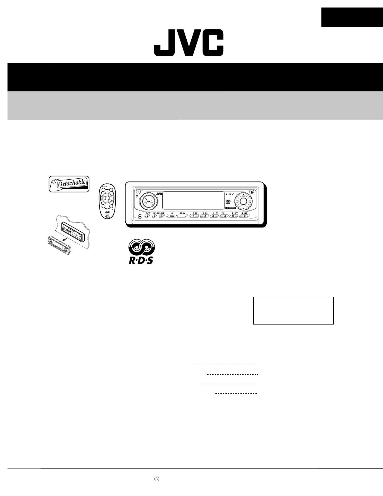
SERVICE MANUAL
CASSETTE RECEIVER
KS-LH6R
SOUND
6
U
SOURCE
F
R
D
VOL
VOL
TAPE
S
KS-LH6R
Contents
Safety precaution
Disassembly method
Adjustment method
Description of major ICs
COPYRIGHT 2002 VICTOR COMPANY OF JAPAN, LTD.
Area Suffix
E ----------- Continental Europe
1- 2
1- 3
1-11
1-15~26
No.49734
Apr. 2002
Page 2

KS-LH6R
Safety precaution
!
Burrs formed during molding may be left over on some parts of the chassis. Therefore,
pay attention to such burrs in the case of preforming repair of this system.
1-2
Page 3

Disassembly method
Removing the front panel unit
(See Fig.1)
1.
Press the release switch and remove the front panel
unit in the direction of the arrow.
KS-LH6R
Front panel unit
Removing the bottom cover
(See Fig.2,3)
1.
Turn the body upside down.
2.
Insert a screwdriver to the two joints a and two joints
b on both sides of the body and the joint c on the
back of the body, then detach the bottom cover from
the body.
CAUTION:
When disengaging the joint c using a
screwdriver, do not damage or break the
board.
Removing the front chassis (See Fig.4,5)
Prior to performing the following procedure, remove
the bottom cover.
1.
Remove the two screws A attaching the front
chassis.
Fig.1
Joint a
Bottom cover
Joint c
Joint b
Fig. 2
Joint b
Bottom cover
2.
Remove the two screws B on each side of the body.
3.
Release the two joints d and the two joints e on the
sides. remove the front chassis toward the front.
Joint d
Joint d
B
Front chassis
Fig. 5
Joint e
Joint e
Joint a
A
Joint c
Fig. 3
Front chassis
Fig.4
1-3
Page 4
KS-LH6R
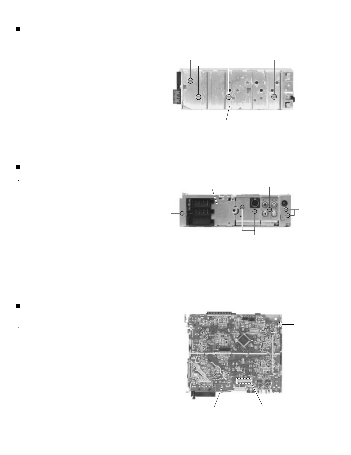
Removing the heat sink (See Fig.6)
1.
Remove the four screws C attaching the heat sink
on the left side of the body, and remove the heat
sink.
Removing the rear panel (See Fig.7 )
C
C
Heat sink
Fig. 6
C
Prior to performing the following procedure, remove
the front chassis, the heat sink and bottom cover.
1.
Remove the five screws D attaching the rear panel
and one screw E attaching the pine jack on the back
of the body.
D
Rear panel
Removing the main amplifier board assembly
(See Fig.8)
Prior to performing the following procedure, remove
the front chassis, the heat sink, bottom cover and the
rear panel.
F
E
D
D
Fig. 7
F
1.
Remove the two screws F attaching the main
amplifier board assembly on the top cover.
2.
Disconnect connector CP401 on the main amplifier
board assembly from the cassette mechanism
assembly.
1-4
Main board assembly
Fig. 8
CP401
Page 5
KS-LH6R
Removing the cassette mechanism assembly
Cassette mechanism assembly
(See Fig.9)
Prior to performing the following procedure, remove
the front chassis, the heat sink, bottom cover and the
main amplifier board assembly.
1.
Remove the four screws G attaching the cassette
mechanism assembly from the top cover.
G
G
H
Removing the (LCD & key) control switch
board (See Fig.10
Prior to performing the following procedure, remove
the front panel assembly.
~ 12)
G
G
Top cover
Fig. 9
H
1.
Remove the four screws H attaching the rear cover
on the back of the front panel assembly.
2.
Unjoint the nine joints g with the front panel and the
rear cover.
3.
Remove the control switch board on the back of the
front panel.
H
Front panel
Joint g
LCD & Key control board
Joint g
H
Fig. 10
Rear cover
Joint g
Joint g
Fig. 11
Fig. 12
1-5
Page 6
KS-LH6R
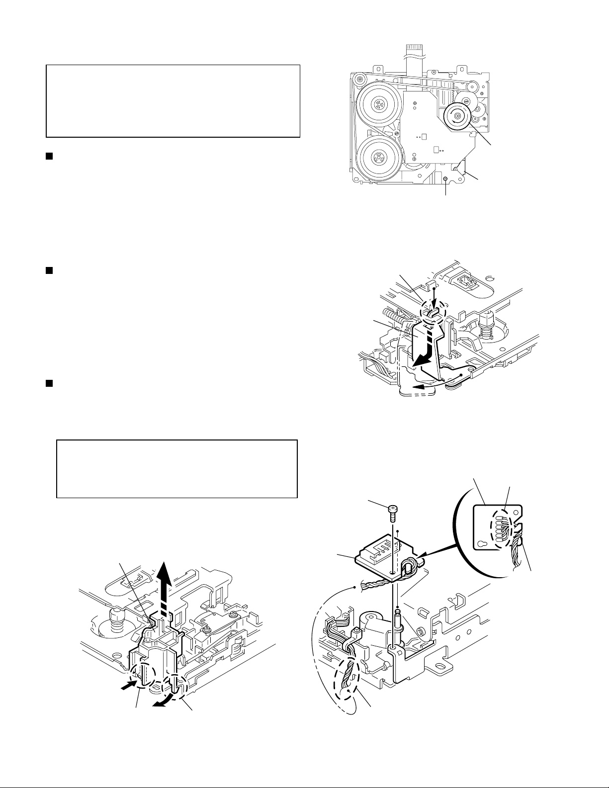
<Cassette mechanism section>
REFERENCE:
Prior to performing the following
procedures, turn the mode gear on the
bottom of the body until the respective part
comes to the EJECT position (Refer to
Fig.1).
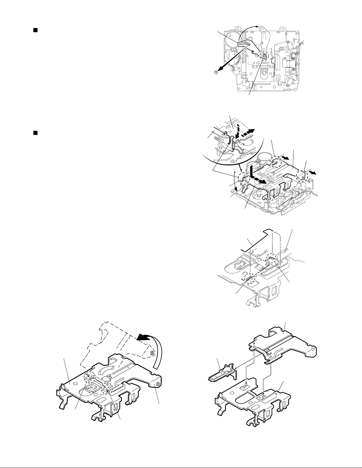
Removing the reinforce bracket
(See Fig.1 and 2)
1.
Remove the screw A attaching the reinforce bracket
on the bottom of the body.
2.
To release joint a, turn and detach the reinforce
bracket from the side bracket assembly as shown in
Fig.2
Removing the cassette guide (See Fig.3)
1.
Turn the mode gear to set to RVS play or
subsequent mode.
2.
Remove the cassette guide from the main chassis
while releasing each two joint tabs b in the direction
of the arrow.
Mode gear
Reinforce bracket
A
Fig.1
Joint a
Reinforce bracket
Removing the head board (See Fig.4)
1.
Remove the screw B on the upper side. Unsolder
the wires on the under side of the head board, if
necessary.
REFERENCE:
Cassette guide
When reassembling, twist the wires by
turning the head board twice remarked c
and pass through the notch d as shown
in Fig.4.
Head board
B
Fig.2
Head board
Soldering
notch d
1-6
Tab b
Tab b
c
Fig.4Fig.3
Page 7
KS-LH6R
y
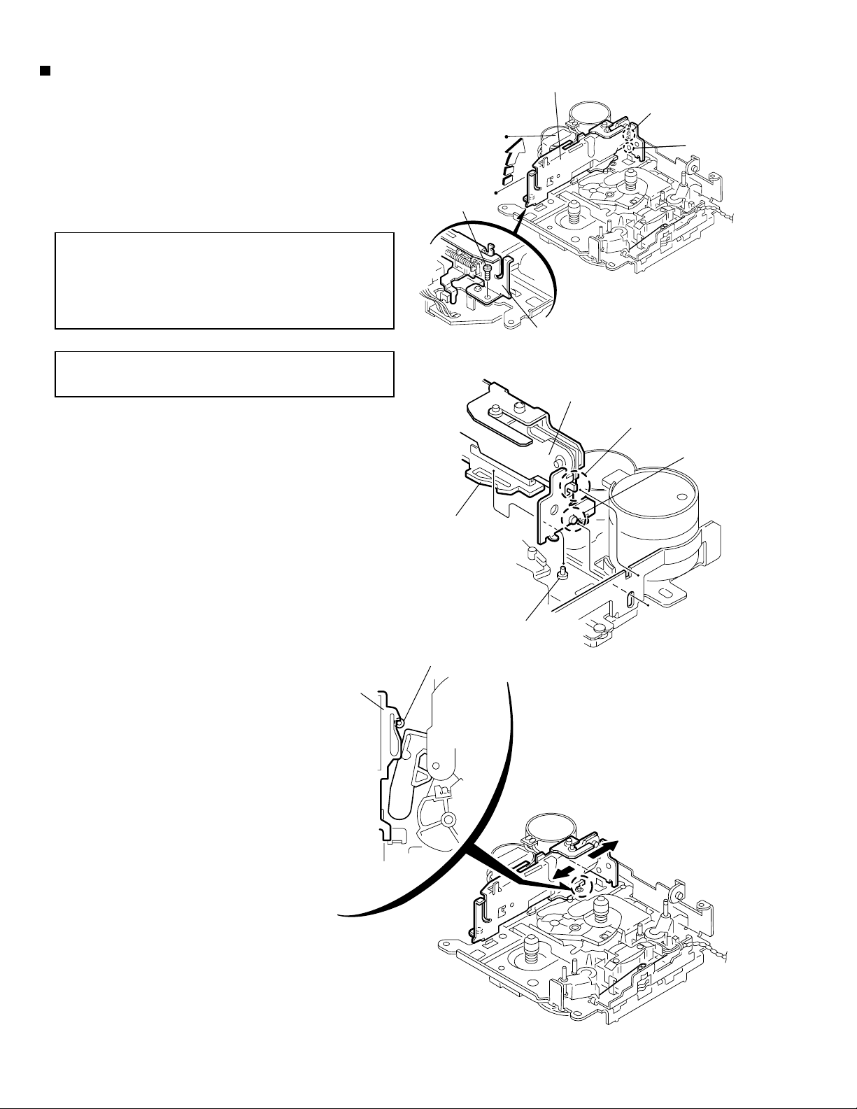
Removing the load arm (See Fig.5)
1.
Remove the E-washer attaching the load arm.
2.
Move the load arm in the direction of the arrow and
release the joint e on the cassette catch.
Removing the cassette hanger assembly /
cassette holder (See Fig.6 to 9)
1.
Check the mode is set to EJECT. Push down the
front part of the cassette holder and move in the
direction of the arrow to release the joint f.
2.
Move the rear part of the cassette hanger assembly
in the direction of the arrow to release it from the two
joint bosses g.
Load arm
E-washer
Cassette holder assembly
Side bracket
Joints f
Joint e
Fig.5
Boss g
Cassette hanger
assembly
Boss g
3.
Release the holder stabilizer spring from the hooks h
and i, then pull out from the cassette hanger
assembly.
4.
Bring up the rear side of the cassette hanger
assembly to release the joint j and k.
5.
Pull out the cassette catch from the cassette hanger
assembly.
Cassette holder
assembly
Cassette holder assembly
Fig.6
Cassette hanger assembl
Cassette stabilizer spring
Hook i
Hook h
Fig.7
Cassette hanger assembly
Cassette catch
Cassette holder assembly
Hook j
Fig.8
Cassette hanger assembly
Hook k
Fig.9
1-7
Page 8
KS-LH6R
Removing the side bracket assembly
(See Fig.10 to 12)
1.
Remove the screw C attaching the side bracket
assembly.
2.
Detach the front side of the side bracket assembly
upward and pull out forward to release the joint l and
m in the rear.
CAUTION:
CAUTION:
When reassembling, make sure that the
boss n of the main chassis is set in the
notch of the load rack under the side
bracket assembly. Do not reattach the
load rack on the boss n.
After reattaching the side bracket
assembly, confirm operation.
Side bracket assembly
Joint l
Joint m
C
Side bracket assembly
Fig.10
Side bracket assembly
Joint l
Joint m
Load rack
Load rack
Boss n
Boss n
Fig.11
1-8
Fig.12
Page 9
Removing the pinch arm (F) assembly
(See Fig.13 and 14)
1.
Remove the polywasher and pull out the pinch arm
(F) assembly.
2.
Remove the compulsion spring.
Removing the pinch arm (R) assembly
(See Fig.13 and 15)
1.
Remove the polywasher and pull out the pinch arm
(R) assembly.
Removing the slide chassis assembly
(See Fig.16 and 17)
Polywasher
Polywasher
Compulsion spring
Pinch arm
(R) assembly
Fig.13
Pinch arm
(F) assembly
Pinch arm (F) assembly
Polywasher
KS-LH6R
REFERENCE:
It is not necessary to remove the head
and the tape guide.
1.
Move the slide chassis assembly in the direction of
the arrow to release the two joints o and remove
from the main chassis.
2.
Remove the rack link.
CAUTION:
When reassembling, first reattach the rack
link, and next fit the boss p and hook q of
the slide chassis assembly to the hole of the
main chassis, and engage the two joints o.
Rack link
Fig.14
Boss p
Pinch arm
(R) assembly
Fig.15
Head
Hook q
Polywasher
Tape guide
Joint o
Slide chassis assembly
Fig.16
Joint o
Fig.17
1-9
Page 10
KS-LH6R
Removing the head / tape guide
(See Fig.18 and 19)
REFERENCE:
1.
Remove the band attaching the wire to the head.
2.
Remove the two screws D, the head and the head
support spring.
3.
Remove the pinch arm spring from the tape guide.
4.
Remove the tape guide and the pinch spring arm.
CAUTION:
CAUTION:
It is not necessary to remove the slide
chassis assembly.
When reattaching the pinch arm spring, set
both end of it to the pinch spring arm (
remarked r).
When reattaching the head, set the wires
into the groove of the tape guide (Fig.18).
D
Slide chassis assembly
Head
Tape guide
Fig.18
D
Pinch arm spring
Head
Head support spring
Tape guide
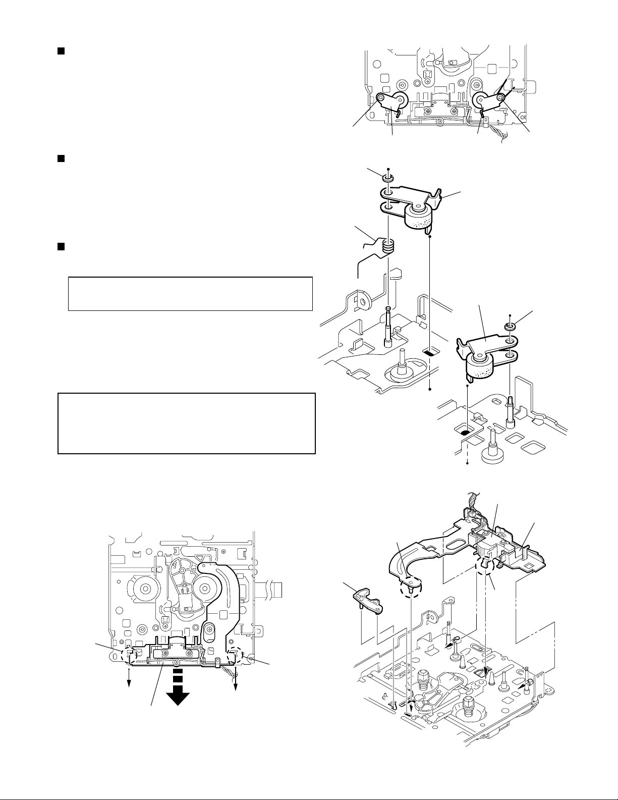
Removing the flywheel assembly (F) & (R)
(See Fig.20 and 21)
REFERENCE:
1.
Remove the belt at the bottom.
2.
Remove the two polywashers on the upper side.
3.
Pull out each flywheel assembly downward.
Flywheel assembly (F)
It is not necessary to remove the slide
chassis assembly.
Belt
r
Pinch spring arm
r
Slid chassis assembly
Fig.19
Polywasher
Polywasher
Flywheel assembly (R)
1-10
Fig.20
Flywheel assembly (F)
Fig.21
Flywheel assembly (R)
Page 11

Disassembling the flywheel assembly (F)
(See Fig.22 and 23)
1.
Push and turn counterclockwise the spring holder (F)
to release the three joints s on the bottom of the
flywheel.
2.
The spring holder (F), the TU spring and the friction
gear play come off.
3.
Remove the polywasher and felt.
Flywheel assembly (F)
Joints s
KS-LH6R
Flywheel assembly (R)
Joints t
Disassembling the flywheel assembly (R)
(See Fig.22 and 24)
1.
Push and turn clockwise the spring holder (R) to
release the three joints t on the bottom of the
flywheel.
2.
The spring holder (R), the FF spring and the friction
gear FF come off.
3.
Remove the polywasher and the felt.
Removing the reel board
(See Fig.25 and 26)
1.
Remove the two screws E attaching the reel board.
2.
Move the reel board in the direction of the arrow to
release the joint u.
3.
Unsolder the wires if necessary.
CAUTION:
When reattaching, confirm operation of
the MODE switch and the ST-BY switch.
The mode position between EJECT and
ST-BY is optimum for reattaching.
Joint s
Fig.22
Polywasher
Polywasher
Spring holder (R)
Spring holder (F)
TU spring
Friction gear FF
Friction gear play
Felt
Flywheel assembly (F)
FF spring
Felt
Flywheel assembly (R)
Fig.23 Fig.24
Joint t
Connect the card wire extending from
the reel board to the FFC pad before
reattaching the reel board.
FFC pad
E
Reel board
E
Fig.25
Joint u
FFC pad
CT-1 switch
MODE switch
Soldering
ST-BY switch
Fig.26
1-11
Page 12

KS-LH6R
Removing the gear base arm / gear base
link assembly (See Fig.27 to 29)
1.
Move the gear base arm in the direction of the arrow.
2.
Insert a slotted screwdriver to the gear base spring
under the gear base arm, and release the gear base
arm upward from the boss on the gear base
assembly.
3.
Remove the gear base arm from the main chassis
while releasing the two joints v.
4.
Move the gear base link assemby in the direction of
the arrow to release the two joints w.
REFERENCE:
When reattaching the gear base arm,
make sure that the boss on the gear
base assembly is inside the gear base
spring.
Removing the FFC pad
(See Fig.27 and 29)
Gear base
link assembly
Gear base spring
Joint w
Gear base arm
Joints v
Hook x
FFC pad
Hook x
Joint w
Fig.27
Gear base arm
Screwdriver
1.
Push each joint hook x of the FFC pad and remove
toward the bottom.
Gear base link assembly
Fig.28
Gear base arm
1-12
FFC pad
Fig.29
Page 13

KS-LH6R
Removing the mode gear
(See Fig.30 and 33)
1.
Remove the polywasher on the bottom and pull out
the mode gear.
Removing the mode switch actuator
(See Fig.30, 31 and 33)
1.
Pull out the mode switch actuator at the bottom.
REFERENCE:
When reattaching the mode switch
actuator to the main chassis, make sure to
set on the shaft and insert y into the slot z.
Removing the direction link / direction
plate (See Fig.31 to 33)
1.
Remove the polywasher attaching the direction link.
2.
Bring up the direction link to release the three joints
a’, b’ and c’ at a time.
3.
Move the direction plate in the direction of the arrow
to release the two joints d’.
REFERENCE:
When reattaching the direction plate,
engage the two joints d’ and move in the
direction of the arrow (See Fig.32).
Mode switch actuator
Direction plate
Direction link
Fig.30
Direction plate
Joints d'
Joint c'
Direction link
Slot z
Joint b'
Polywasher
Fig.31
Direction plate Mode rack assembly
Joint k'
Mode gear
Polywasher
Mode rack assembly
Joint a'
Joint k'
Joint l'
REFERENCE:
When reattaching the direction link,
move the direction plate in the direction
of the arrow and engage the three joint
a’, b’ and c’ at a time (See Fig.33).
Removing the mode rack assembly
(See Fig.31 and 32)
1.
Move the mode rack assembly in the direction of the
arrow to release the two joints k’ and the joint l’.
REFERENCE:
When reattaching, set the two k’ on the
bottom of the mode rack assembly into the
slots of the main chassis and move in the
direction of the arrow (See Fig.32).
Joints d'
Fig.32
Direction link
Mode switch actuator
Polywasher
y
Mode gear
Direction plate
Mode rack assembly
Fig.33
1-13
Page 14

KS-LH6R
Removing the gear base assembly / take
up gear / reflector gear (See Fig.34 to 36)
1.
Push in the pin e’ of the gear base assembly on the
upper side of the body and move the reflector gear
toward the bottom, then pull out.
2.
Remove the polywasher on the bottom and pull out
the take up gear.
3.
Move the gear base assembly in the direction of the
arrow to release it from the two slots f’ of the main
chassis.
REFERENCE:
The parts are damaged when removed.
Please replace with new ones.
Gear base assembly
Pin e'
Polywasher
Slot f'
Slot f'
Fig.34
Take up gear
Removing the reel driver / reel spindle
(See Fig.36)
1.
Draw out the reel driver from the shaft on the main
chassis and remove the reel driver spring and the
reel spindle respectively.
CAUTION:
The reel driver is damaged when
removed. Please replace with a new
one.
Reflector gear
Reel driver
Reel driver spring
Reel spindle
Main chassis
Fig.35
Reel driver
Reel driver spring
Reel spindle
Gear base assembly
Slots f’
Take up gear
1-14
Reflector gear
Polywasher
Fig.36
Page 15

Removing the side bracket assembly
(See Fig.37 to 41)
1.
Remove the eject cam plate spring.
2.
Push the joint g‘ through the slot to remove the load
rack downward.
3.
Move the eject cam limiter in the direction of the
arrow to release it from the boss h’ of the side
bracket assembly and from the two joints i’.
4.
Move the eject cam plate in the direction of the arrow
to release the joint j’.
KS-LH6R
Joint g'
CAUTION:
Joint i'
When reassembling, confirm operation of
each part before reattaching the eject cam
plate spring.
Side bracket assembly
Boss h'
Eject cam limiter
Side bracket assembly
Joint i'
Joint g'
Eject cam plate spring
Joint i'
Load rack
Fig.37
Boss h'
Eject cam limiter
Eject cam plate
Fig.39
Joint i'
Fig.38
Side bracket assembly
Boss h'
Eject cam plate
Fig.40
Load rack
Joint j'
Side bracket assembly
Eject cam plate
Joint j'
Fig.41
1-15
Page 16

KS-LH6R
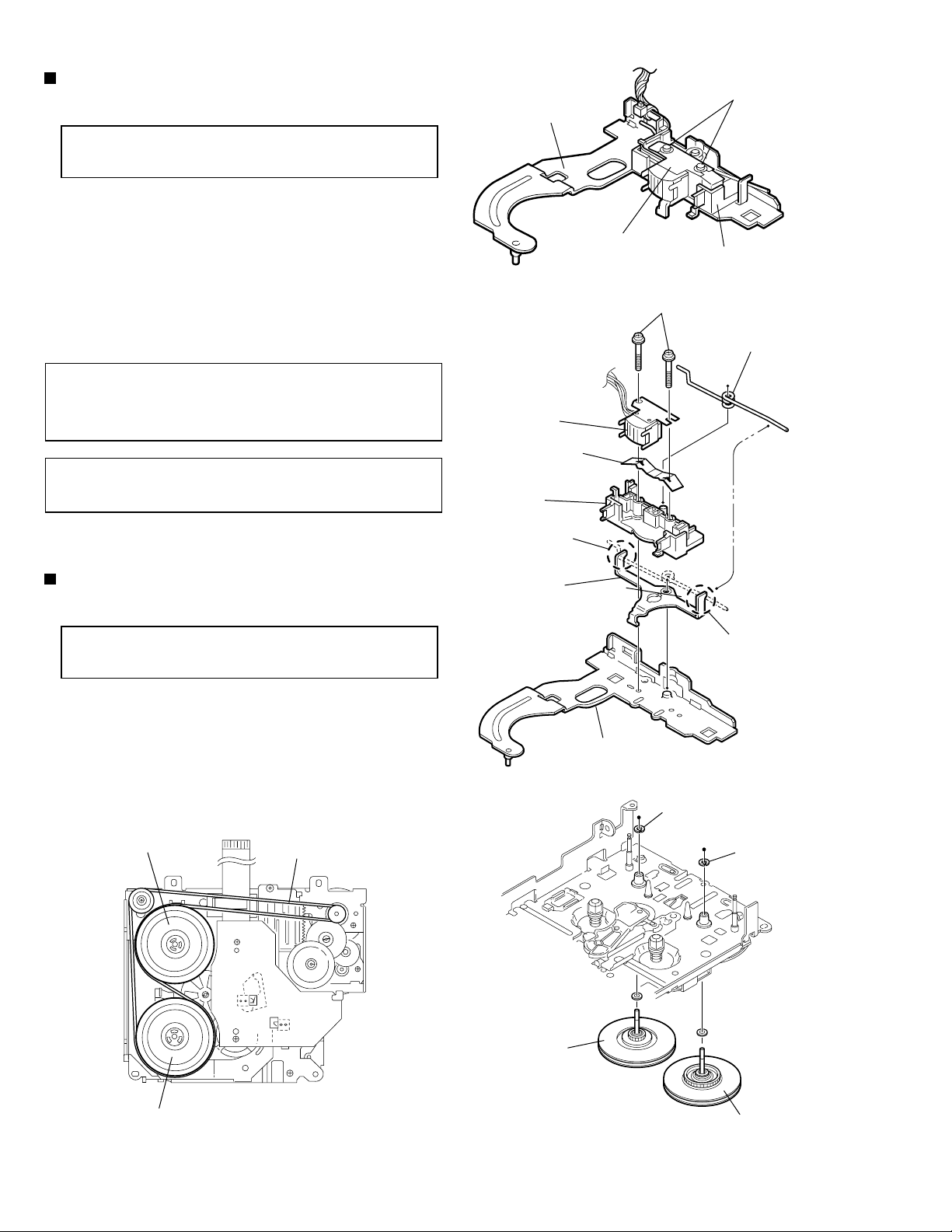
Removing the main motor assembly /
sub motor assembly (See Fig.42 to 44)
1.
Remove the belt at the bottom.
2.
Remove the polywasher and pull out the mode gear.
3.
Pull out the reduction gear (B).
4.
Remove the polywasher and pull out the reduction
gear (A).
5.
Remove the two screws F attaching the main motor
assembly.
6.
Remove the two screws G attaching the sub motor
assembly.
7.
Unsolder the wires on the reel board if necessary.
CAUTION:
When reassembling, adjust the length of the
wires extending from the sub motor
asswmbly by attaching them to the side of
the sub motor assembly with the wires
extending from the main motor assembly
using a spacer.
Belt
Reduction gear (B)
Reduction gear (B)
G
Polywasher
Fig.42
F
G
Mode gear
Polywasher
Reduction gear (A)
F
Main motor
assembly
Reduction
gear (A)
Polywasher
Sub motor
assembly
Spacer
Main motor assembly
Sub motor assembly
Main motor assembly
Sub motor assembly
Fig.43
Spacer
Fig.44
1-16
Page 17

Adjustment method
KS-LH6R
Test Instruments reqired for adjustment
1.Digital osclloscope(100MHz)
2.Frequency Counter meter
3.Electric voltmeter
4.Wow & flutter meter
5.Test Tapes
VT724
VT739
VT712
VT703
6.Torque gauge
Measuring conditions(Amplifier section)
Power supply voltage
Load impedance
Line out
For playback frequency measurement
For wow flutter & tape speed measurement
for DOLBY level measurement
For head azimuth measurement
Cassette type for CTG-N
(mechanism adjustment)
4 (2Speakers connection)
DC14.4V(10.5~16V)
20k
Frequency Range
FM : 87.5 MHz to 108.0 MHz
AM :(MW) 522 kHz to 1620 kHz
(LW) 144kHz to 279 kHz
DUMMY LOAD
Exclusive dummy load should be used for AM
and FM dummy load,there is a loss of 6dB
between SSG output and antenna input. The
loss of 6dB need not be considered since
direct reading of figures are applied in this
working standard.
Standard volume position
Balance and Bass,Treble volume .Fader
:Center(Indication"0")
Loudness,Dolby NR,Sound,Cruise:Off
Volume position is about 2V at speaker output with
following conditions.Playback the test tape VT721.
AM mode 999kHz/62dB,INT/400Hz,30%
modulation signal on receiving.
FM mono mode 97.9MHz/66dB,INT/400Hz,22.5kHz
deviation pilot off mono.
FM stereo mode 1kHz,67.5kHz dev. pilot7.5kHz dev.
Output level 0dB(1 V,50 /open terminal).
Arrangement of Adjusting
Cassette Mechanism Section
Capstan motor
Cassette mechanism
(Surface)
Azimuth screw
(Forward side)
Playback head
Tape speed adjust
Azimuth screw
(Reverse side)
1-17
Page 18

KS-LH6R
y
Arrangment of adjusting
Head amplifier board section (Reverse side)
VR402:Rch
(Dolby NR level adj)
C413
FSMW1093A
C423
D401
R426
VR402
B409
R425
R411
T11
R424
IC402
R410
R416
Q401
1
B407
R401
C424
B406
D402
C425
C419
C422
B408
C414
C421
B403
C416
R420
Q403
C418
R412
R414
R415
R418
B411
B410
21
R413
R417
C417
B404
2
C415
1
B413
VR401:Rch
(Dolby NR Frequency response adj)
CJ403
11
C412
1
IC401
31
C411
B405
B412
R423
B401
R408
VR401
C410
B402
C409
CJ401
C405
R407
C406
C402
C408
R406
C407
R403
1
R405
C404
R404
C403
R422
C401
R402
2
Q402
1
Information for using a car audio service jig
1. We're advancing efforts to make our extension cords common for all car audio products.
Please use this type of extension cord as follows.
2. As a U-shape type top cover is employed, this type of extension cord is needed to check operation of the
mechanism assembly after disassembly.
3. Extension cord : EXTKSRT002-18P ( 18 pin extension cord ) For connection between mechanism assembl
and main board assembly.
Check for mechanism driving section such as motor ,etc..
Disassembly method
1. Remove the bottom cover.
2. Remove the front panel assembly.
3. Remove the top cover .
4. Install the front panel.
5. Confirm that current is being carried by connecting
an extension cord jig.
Note
Available to connect to the CP701 connector when in-
stalling the front panel.
to Cassette mechanism
Cassette mechanism
Extension cord
EXTKSRT002-18P
1-18
EXTKSRT002-18P
to Main board
Page 19

Item Adjustment and check method Adjust Spec
1.Tape position
a)
Playback at FWD side, use the mirror tape and
adjuste azimuth screw A and B, check the tape
position at tape guide position of the head.
b)
Playback at REV side, use the mirror tape and
adjuste azimuth screw A and B, check the tape
position at tape guide position of the head.
c)
Playback at FWD and REV both side, check the
tape position at tape guide position at the head.
KS-LH6R
Azimuth
screw A
Azimuth
screw B
2.Head azimuth ajust
and check
a)
Playback at FWD side, adjuste azimuth screw A
to make peak position of Lch /Rch.
*
Oscilloscope wave forme standard is 45 digrees.
b)
Playback at REV side, adjuste azimuth screw B to
make peak position of Lch/Rch.
*
Oscilloscope wave forme standard si 45 digrees.
c)
Chech the level difference of FWD side and REV
side less than 3dB by VTVM.
d)
After operation check, Lch/Rch azimuth output
level difference is less than 1 dB at adjustment
level.
OK
Head
Tape guide
Tape position NG
0
PHASE
45
3.Tape speed
WOW & Flutter
4.Playback frequency
responce
Head
a)
Check the frequency counter and wow flutter
meter are 2940~3090Hz(FWD/REV), less than
0.35%(RMS).
b)
If tape speed is not clear the specification, adjust
the v.resistor inside of motor.
a)
Playback the test tape(VT724:1kHz), spreaker
output set to 2V by set volume.
Playback the test tape(VT739), check level differe
b)
to 0 3dB at 1kHz/10kHz, -4dB 2dB at
1kHz/63Hz.
10kHz level is not clear the specification, readjust
the head azimuth.
Tape
Internal
v.resistor
Tape speed
2940~3090Hz
WOW & Flutter
less than 0.35%
(RMS)
Speaker output
1kHZ/10kHz
:0 3dB
1kHZ/63Hz
:-4 2dB
1-19
Page 20

KS-LH6R
Description of major ICs
HA13164A (IC901) : Regulator
1.Terminal layout
123456789101112131415
2.Block diagram
ANT OUT
C3
0.1u
EXT OUT
C4
0.1u
ANT CTRL
CTRL
CD OUT
C5
0.1u
AUDIO OUT
C6
10u
11
12
10
BATT.DET OUT
9
COMPOUT
6
VDD OUT
4
SW5VOUT
5
14
UNIT R:
+B
ACC
ILMOUT
R1
C7
0.1u
C8
0.1u
C1
100u
VCC ACC
8
2
1
7
Surge Protector
BIAS TSD
15
3
TA B
note1) TAB (header of IC)
connected to GND
ILM AJGND GND
13
C2
0.1u
C:F
1-20
3.Pin function
Pin No. Symbol Function
1
2
EXTOUT
ANTOUT
Output voltage is VCC-1 V when M or H level applied to CTRL pin.
Output voltage is VCC-1 V when M or H level to CTRL pin and H level
to ANT-CTRL.
3
4
5
6
7
8
9
10
11
12
13
14
15
ACCIN
VDDOUT
SW5VOUT
COMPOUT
ANT CTRL
VCC
BATT DET
AUDIO OUT
CTRL
CD OUT
ILM AJ
ILM OUT
GND
Connected to ACC.
Regular 5.7V.
Output voltage is 5V when M or H level applied to CTRL pin.
Output for ACC detector.
L:ANT output OFF , H:ANT output ON
Connected to VCC.
Low battery detect.
Output voltage is 9V when M or H level applied to CTRL pin.
L:BIAS OFF, M:BIAS ON, H:CD ON
Output voltage is 8V when H level applied to CTRL pin.
Adjustment pin for ILM output voltage.
Output voltage is 10V when M or H level applied to CTRL pin.
Connected to GND.
Page 21

HD74HC126FP-X (IC801) : Buffer
KS-LH6R
1.Terminal layout
1C
1
1A
2
1Y
3
2C
4
2A
5
2Y
6
GND
7
2.Block diagram
Input
VU
14
4C
13
4A
12
4Y
11
3C
10
3A
9
3Y
8
Vcc Vcc
1A
2A
3A
4A
1C
2C
3C
See Function Table
4C
3.Pin function
Output
1Y
2Y
Output
2Y
Output
3Y
Output
4Y
Input
C
L
H
H
A
X
L
H
Output
Y
Z
H
L
Note) H:High level
L:Low level
X:Irrelevant
Z:Off(High-impedance)
State a 3-state input
1k
S1
CL
1k
Sample as Load Circuit 1
Sample as Load Circuit 1
Sample as Load Circuit 1
Note) CL includes probe and jig capacitance
1-21
Page 22

KS-LH6R
UPD178018AGC621 (IC701) : CPU
1. Pin layout
2. Pin function
Pin No.
1
2
3
4
5
6
7
8
9
10
11
12
13
14
15
16
17
18
19
20
21
22
23
24
25
26
27
28
29
30
31
32
33
34
35
36
37
38
39
40
80 ~ 61
1
~
20
21 ~ 40
60
~
41
Port Name I/O Descriptions
KEY 0
KEY 1
KEY 2
LEVEL
SM
SQ
LCDCE
LCDDA
LCDCK
BUSI/O
OPEN
BUSSI
BUSSO
BUSSCK
NC
NC
NC
NC
INLOCK
NC
GNDPORT
VDDPORT
NC
AFCK
MONO
FM/AM
SEEK/STOP
NC
IFC
VDDPLL
FMOSC
NC
GNDPLL
AMEO
FMEO
IC
SD/ST
STAGE0
NC
MOTOR
I
I
I
I
I
I
O
O
O
I
I
I
O
I/O
-
-
-
-
-
-
-
-
O
O
O
O
-
I
-
I
-
O
O
-
I
I
O
Key input 0
Key input 1
Key input 2
Level meter input
S.meter level input
S.Quality level input
CE output to LCD driver
Data output to LCD driver
Clock output to LCD driver
I/O selector output for J-BUS, H : OUT, L: INPUT
Door open detect input
J-BUS Data input
J-BUS Data output
J-BUS Clock in/output
Non connect
Non connect
Non connect
Non connect
Non connect
Non connect
Port GND
Por t Vdd
Non connect
AF check output, L: AF check
Monaural on /off selecting output, H:mono on
FM/AM switching output L : FM H : AM
Auto seek /stop selecting output, H: Seek, L:Stop
Non connect
FM/AM midle frequency counter input
PLL Vdd
FM/AM limited generator frequency input
None connect
PLL GND
AM error out output
FM error out output
GND
Station detector, Stereo signal input, H:Find Station, L:Stereo
Pull up
Non connect
Main motor output
1-22
Page 23

Pin No.
41
42
43
44
45
46
47
48
49
50
51
52
53
54
55
56
57
58
59
60
61
62
63
64
65
66
67
68
69
70
71
72
73
74
75
76
77
78
79
80
Port Name I/O Descriptions
FF/REW
F/R
DOLBY
MSIN
I2CSCK
I2CDAO
I2CDAI
REEL
SUBMO1
SUBMO2
MODE
TAPEIN
STANDBY
NC
NC
NC
NC
NC
BEEP
MUTE
PCNT
TELMUTE
DIMIN
DIMOUT
ENC2
ENC1
ACCDET
MEMDET
RDSCK
RDSDA
REMOCON
DETACH
J-BUSINT
REGCPU
GND
X2
X1
REGOSC
VDD
RESET
I
O
O
I
I/O
O
I
O
I
O
O
O
I
-
-
-
-
-
O
O
O
I
I
O
I
I
I
I
I
I
I
I
I
-
-
-
I
-
-
-
Output for input signal level switching for MS L : FF,REW H : PLAY
FWD,REV running direction switch signal input
Dolby on "H" output
MS input
E-VOL IC control data I/O
I2C information data output
I2C information clock input
Switch for detecting tape end position
Sub motor clock direction input
Sub motor clock opposite detection drive output
Mechanism mode position detection input
Cassette in detection input H : cassette in L : cassette out
Standby position detection input H : eject side L : operation side
Non connect
Non connect
Non connect
Non connect
Non connect
Touch tone output
Mute output , L : mute on
Power ON /OFF switching output , H : power on
Telephone mute signal detection input
Dimmer signal detection input L : dimmer
Dimmer control output , Dimmer off L output
Rotary volume signal 2 input
Rotary volume signal 1 input Power save : L
Power save 1 Working togethe ACC Power save : L
Backup power supply detection terminal
Clock input for RDS
RDS data input
Remocom input
Detach signal input H : Power save
Cut-in input for J-BUS signal
Regulator for CPU power supply, Connect the GND with 0.1 F.
Ground
Connecting the crystal oscillator for system clock
Connecting the crystal oscillator for system clock
Regulator for oscillator circuit.Connect the GND with 0.1 F.
Vdd
Pull up
KS-LH6R
UPD178018AGC621(2/2)
1-23
Page 24

KS-LH6R
LA47503 (IC301) : Power amp.
1.Terminal layout
206
11
1
12
4
10
Stand by
Switch
Ripple
Filter
Protective
circuit
Mute
circuit
9
7
8
5
3
2
22
1-24
15
25
13
14
16
Muting &
On Time Control
Circuit
protective
circuit
17
19
18
21
23
24
Page 25

2.Terminal layout
AC CONT1
GND1
OUTFR-
STBY
OUTFR+
Vcc1/2
OUTRR-
GND2
OUTRR+
VREF
INRR
INFR
SGND
INFL
INRL
ONTIME
OUTRL+
GND3
OUTRL-
Vcc3/4
OUTFL+
MUTE
OUTFL-
GND4
KS-LH6R
NC
3.Pin function
1
2
3
4
5
6
7
8
9
10
11
12
13
14
15
16
17
18
19
20
21
22
23
24
25
SymbolPin No. Function
AC CONT1
GND1
OUTFRSTBY
OUTFR+
Vcc1/2
OUTRRGND2
OUTRR+
VREF
INRR
INFR
SGND
INFL
INRL
ONTIME
OUTRL+
GND3
OUTRLVcc3/4
OUTFL+
MUTE
OUTFLGND4
NC
Header of IC
Power GND
Outpur(-) for front Rch
Stand by input
Output (+) for front Rch
Power input
Output (-) for rear Rch
Power GND
Output (+) for rear Rch
Ripple filter
Rear Rch input
Front Rch input
Signal GND
Front Lch input
Rear Lch input
Power on time control
Output (+) for rear Lch
Power GND
Output (-) for rear Lch
Power input
Output (+) for front
Muting control input
Output (-) for front
Power GND
No connection
LA47503
1-25
Page 26

KS-LH6R
CXA2560Q (IC401) : Dolby B type noise reduction system with play back equalizer amp.
1.Pin layout & block diagram
PBTC2
30 29 28
PBFB2
PBRIN2
PBGND
PBFIN2
VCT
PBREF
PBFIN1
PBGND
PBRIN1
PBFB1
2. Pin function
7k/12k
31
32
300k
33
F2
34
30k
35
45k
36
30k
37
F1
38
300k
39
7k/12k
40
12345
PBTC1
PBOUT2
+
+
-
PBOUT1
OUTREF2
27
70 /120
1
1
70 /120
OUTREF1
TAPEIN2
100k
100k
TAPEIN1
TCH2
23 22 21
NR
OFF/B
MS MODE
NR MODE
DET
OFF/B
-
NR
8910
TCH1
NC
MS ON/
NC
OFF
MSSW
MSLPF
20
19
18
17
16
15
14
13
12
11
MSMODE
DRSW
TAPESW
MUTESW
NRSW
NC
MSOUT
MSTC
G1FB
G2FB
LINEOUT2
DIREF
GND
26
24
25
+
-
T2
BIAS
MUTE
TAPE EQ
FWD/RVS
Vcc
LPF
+
-
T1
F3
+
6
7
NC
Vcc
LINEOUT1
Pin No. Symbol
1
2
3
4
5
6
7
8
9
10
11
12
13
14
15
16
17
18
19
20
21
22
23
24
PBTC1
PBOUT1
OUTREF1
TAPEIN1
Vcc
NC
LINEOUT1
TCH1
NC
MSLPF
G2FB
G1FB
MSTC
MSOUT
NC
NRSW
MUTESW
TAPESW
DRSW
MSMODE
MSSW
NC
TCH2
LINEOUT2
I/O Function
Playback equalizer amplifier
capacitance
Playback equalizer amplifier
O
output
Output reference
O
TAPE input
I
Power supply
-
Line output
O
Time constant for the HLS
-
Cut-off frequency adjustment
of the music sensor LPF
Music signal interval detection
Music signal interval detection
Time constant for detecting
music signal interval
Music sensor out
O
No use
Dolby NR control
I
Mute function control
I
Playback equalizer amplifier
I
control
Head select control
I
Music sensor mode control
I
Music sensor control
I
Time constant for the HLS
Line output
O
Pin No. Symbol
25
26
27
28
29
30
31
32
33
34
35
36
37
38
39
40
DIREF
GND
TAPEIN2
OUTREF2
PBOUT2
PBTC2
PBFB2
PBRIN2
PBGND
PBFIN2
VCT
PBREF
PBFIN1
PBGND
PBRIN1
PBFB1
I/O Function
-
Resistance for setting the
reference
-
Ground
I
TAPE input
O
Output reference
O
Playback equalizer amplifier
output
-
Playback equalizer amplifier
capacitance
I
Playback equalizer amplifier
feedback
I
Playback equalizer amplifier
input
-
Playback equalizer amplifier
ground
I
Playback equalizer amplifier
input
O
Center
O
Playback equalizer amplifier
reference
I
Playback equalizer amplifier
input
-
Playback equalizer amplifier
ground
I
Playback equalizer amplifier
input
I
Playback equalizer amplifier
feedback
1-26
Page 27

LC75873NW (IC601) : LCD driver
KS-LH6R
1.Pin layout
60 41
61
80
1 20
3.Pin function
Pin No.
79,80
1,2,3
to 66
67
78
69
2.Block diagram
40
21
Pin name
S1/P1 TO S4/P4
S5 to S68
COM1
COM2
COM3
VDD1
VDD2
INH
OSC
VDD
VSS
I/O
O
O
S5
S4/P4
S3/P3
S2/P2
COM2
COM3
COMON
DRIVER
CLOCK
GENERATOR
COM1
S68
S67
DI
CL
SEGMENT DRIVER
SHIFT REGISTOR
ADDRESS
DETECTOR
CE
S1/P1
Description
Segment outouts for displaying the display data
transferred by serial data input.
The S1/P1 to S4/P4 pins can be used as generalpurpose output ports under serial data control.
Common driver outputs.
The frame frequency f0 is given by :
f0 = (FOSC/384)Hz.
74
76
77
78
75
71
72
70
OSC
CE
CL
DI
INH
VDD1
VDD2
VDD
I/O
I
I
I
I
I
I
-
Oscillator connection
An oscillator circuit is formed by connecting an
external resistor and capacitor to this pin.
Serial data transfer inputs.
Connected to the controller.
CE:Chip enable
CL:Synchronization clock
DI:Transfer data
Display off control input
INH= "L"(VSS) Display forced off
S1/P1 to S4/P4 = "L"
(These pins are forcibly set to the
segment output port function and held
at the low level.)
S5 to S68 = "L"
COM1 to COM3"L"
INH = "H"(HDD) Display on
However, serial data transfer is possible when
the display is forced off by this pin.
Used for applying the LCD drive 2/3 bias voltage
externally. Must be connected to VDD2 when a
1/2 bias drive scheme is used.
Used for applying the LCD drive 1/3 bias voltage
externally. Must be connected to VDD1 when a
1/2 bias drive scheme is used.
Power supply connection.
Provide a voltage of between 3.0 and 6.0V.
73
VSS
-
Power supply connection. Connect to ground.
1-27
Page 28

KS-LH6R
SAA6579T-X (IC71) : RDS
1.Pin layout
QUAL
1
RDDA
2
Vref
3
MUX
4
V
ODA
5
V
SSA
6
CIN
7
SCOUT
8
2.Block diagram
RDCL
16
T57
15
OSCO
14
OSCI
13
0DD
V
12
V
SSD
11
TEST
10
MODE
9
121413
3.Pin function
4
8
7
CLOCKED
COMPARATOR
5
3
REFERENCE
VOLTAGE
Pin No.
1
2
3
4
5
6
7
8
9
10
11
12
13
14
15
16
ANTIALIASING
FILTER
6 11
Symbol
VP1
QUAL
RDDA
Vref
MUX
VDDA
VSSA
CIN
SCOUT
MODE
TEST
VSSD
VDDD
OSCI
OSCO
T57
RDCL
57 kHz
BANDPASS
(8th ORDER)
COSTAS LOOP
VARIABLE AND
FIXED DIVIDER
CLOCK
REGERATION
AND SYNC
Quality indication output
RDS data output
Reference voltage output (0.5VDDA)
Multiolex signal input
+5V supply voltage for analog part
Ground for analog part (0V)
Subcarrier input to comparator
Subcarrier output of reconstruction filter
Oscllator mode / test control input
Test enable input
Ground for digital part (0V)
+5V supply voltage for digital part
Oscillator input
Oscillator output
57 kHz clock signal output
RDS clock output
RECONSTRUCTION
FILTER
TEST LOGIC AND OUTPUT
SELECTOR SWITCH
Description
OSCILATOR
AND
DIVIDER
BIPHASE
SYMBOL
DECODER
910
QUALITY BIT
GENERATOR
DIFFERENTIAL
DECODER
1
2
15
15
1-28
Page 29

TEA6320T-X (IC301) : E.VOLUME
KS-LH6R
1.Terminal Layout
SDA
1
GND
2
OUTLR
OUTLF
MUTE
TL
B2L
B1L
IVL
ILL
QSL
IDL
ICL
IMD
IBL
IAL
3
4
5
6
7
8
9
10
11
12
13
14
15
16
CD-CH
TAPE
TUNER
3.Pin Functions
32
31
30
29
28
27
26
25
24
23
22
21
20
19
18
17
SCL
VCC
OUTRR
OUTRF
TR
B2R
B1R
IVR
ILR
QSR
IDR
Vref
ICR
CAP
IBR
IAR
2.Block Diagram
10 8 9 7 6
21
31
2
19
16
15
13
11
14
22
20
18
17
POWER
SUPPLY
SOURCE
SELECTOR
23 25 24 26 27 28
VOLUME 1
+20 to -31 dB
LOUDNESS
LEFT
VOLUME 1
+20 to -31 dB
LOUDNESS
RIGHT
BASS
LEFT
+15 dB
LOGIC
BASS
RIGHT
+15 dB
5
TREBLE
LEFT
+12 dB
TREBLE
RIGHT
+12 dB
12
MUTE
FUNCTION
ZERO CROSS
DETECTOR
VOLUM E 2
0 to 55 dB
BALANCE
FENDER REAR
VOLUM E 2
0 to 55 dB
BALANCE
FENDER FRONT
HC BUS
REC
VOLUM E 2
0 to -55dB
BALANCE
FENDER FRONT
VOLUM E 2
0 to -55dB
BALANCE
FENDER REAR
3
4
32
1
29
30
Pin
No.
1
2
3
4
5
6
7
8
9
10
11
12
13
14
Symbol
SDA
GND
OUTLR
OUTLF
TL
B2L
B1L
IVL
ILL
QSL
IDL
MUTE
ICL
IMO
I/O
Serial data input/output.
I/O
Ground.
-
output left rear.
O
output left front.
O
Treble control capacitor left channel or
I
input from an external equalizer.
Bass control capacitor leftchannel or
output to an external equalizer.
Bass control capacitor left channel.
-
Input volume 1. left control part.
I
Input loudness. left control part.
I
Output source selector. left channel.
O
Not used
-
Not used
-
Input C left source.
I
Not used
-
Functions Functions
Pin
No.
17
18
19
20
21
22
23
24
25
26
27
28
29
30
Symbol
IAR
IBR
CAP
ICR
Vref
IDR
QSR
ILR
IVR
B1R
B2R
TR
OUTRF
OUTRR
I/O
I
Input A right source.
I
Input B right source.
-
Electronic filtering for supply.
I
Input C right source.
-
Reference voltage (0.5Vcc)
-
Not used
O
Output source selector right channel.
I
Input loudness right channel.
I
Input volume 1. right control part.
-
Bass control capacitor right channel
Bass control capacitor right channel or
O
output to an external equalizer.
Treble control capacitor right channel or
I
input from an external equalizer.
O
Output right front.
O
Output right rear.
15
16
IBL
IAL
Input B left source.
I
Input A left source.
I
31
32
Vcc
SCL
-
Supply voltage.
I
Serial clock input.
1-29
Page 30

KS-LH6R
GP1UM261XK (IC602) : Receiver
1. Pin layout
Vout
GND
Vcc
2. Block diagram
LB1641 (IC402) : DC motor driver
1. Pin layout
1 2 3 4 5 6 7 8 9
GND OUT1 P1
VZ IN1 IN2
VCC1
VCC2 P2
10
OUT2
B.P.F.LimiterAmp
Demodulator
2. Pin function
Input Output
IN1 IN2 OUT1 OUT2
0 0 0 0
1 0 1 0
0 1 0 1
1 1 0 0
Integrator
Comparator
GND Vdd Vout
Mode
Brake
CLOCKWISE
COUNTER-CLOCKWISE
Brake
1-30
Page 31

< MEMO >
KS-LH6R
1-31
Page 32

KS-LH6R
VICTOR COMPANY OF JAPAN, LIMITED
MOBILE ELECTRONICS DIVISION
PERSONAL & MOBILE NETWORK BUSINESS UNIT. 10-1,1Chome,Ohwatari-machi,Maebashi-city,371-8543,Japan
(No.49734)
200204
 Loading...