

Page 1
SERVICE MANUAL
CASSETTE RECEIVER
KS-F160
KS-F160
Contents
MO
Safety precaution
Disassembly method
Adjustment method
Description of major ICs
K
S-
F
160
Area Suffix
J ---- Northern America
1-2
1-3
1-12
1-16
COPYRIGHT 2001 VICTOR COMPANY OF JAPAN, LTD.
No.49659
Nov. 2001
Page 2

KS-F160
Safety precaution
!
Burrs formed during molding may be left over on some parts of the chassis. Therefore,
pay attention to such burrs in the case of preforming repair of this system.
1-2
Page 3
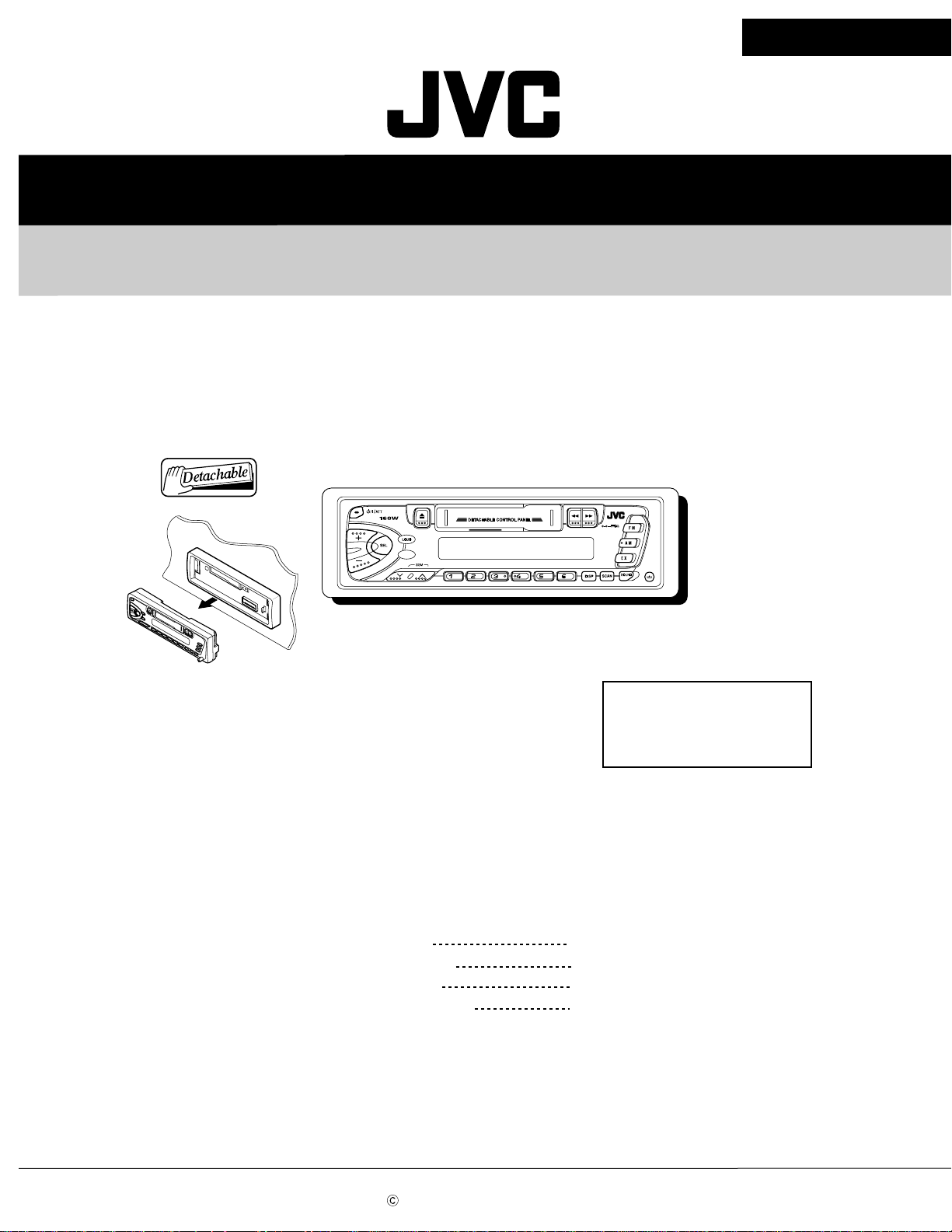
Disassembly method
Detaching the front panel unit
( See Fig.1 )
Push the Release button in the direction of arrow to
detach the front panel unit.
KS-F160
Front panel unit
Push the release button
Fig. 1
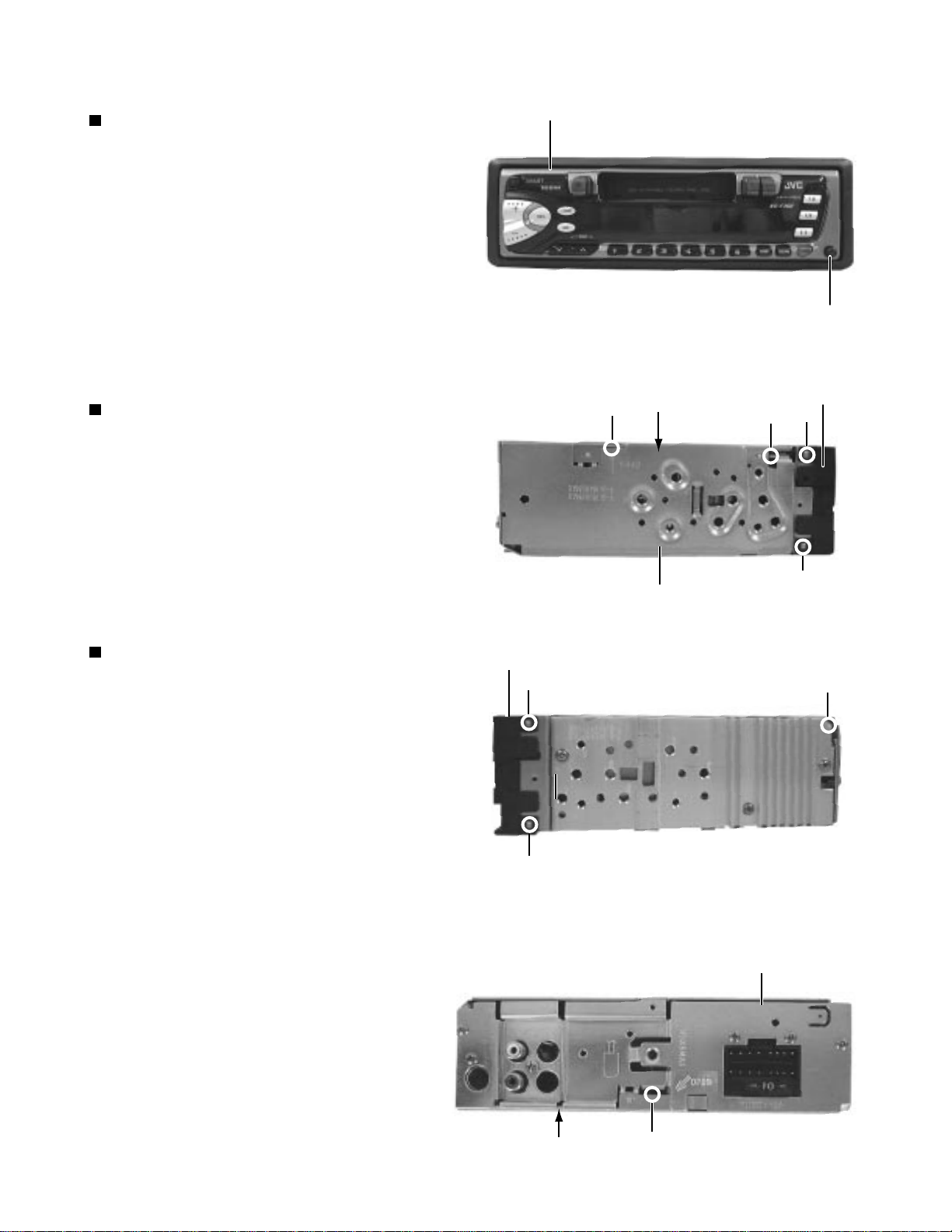
Removing the front chassis
( See Fig. 2 and 3 )
Disengage the four tabs ( a ) in the right and left sides of
unit and pull the front chassis forward to remove it.
Removing the bottom cover
( See Fig. 2 to 4 )
1. Removie the front chassis.
2 . Turn the unit up side down.
3. Insert the screwdriver to the four engagements
( b, c, d, f ) .
4 . Turn the screwdriver and remove the bottom
cover.
Front chassis
a
Bottom cover
c
Top chassis
Fig. 2
Front chassis
a
b
a
d
a
Bottom cover
Fig. 3
Rear panel
f
Fig. 4
1-3
Page 4
KS-F160
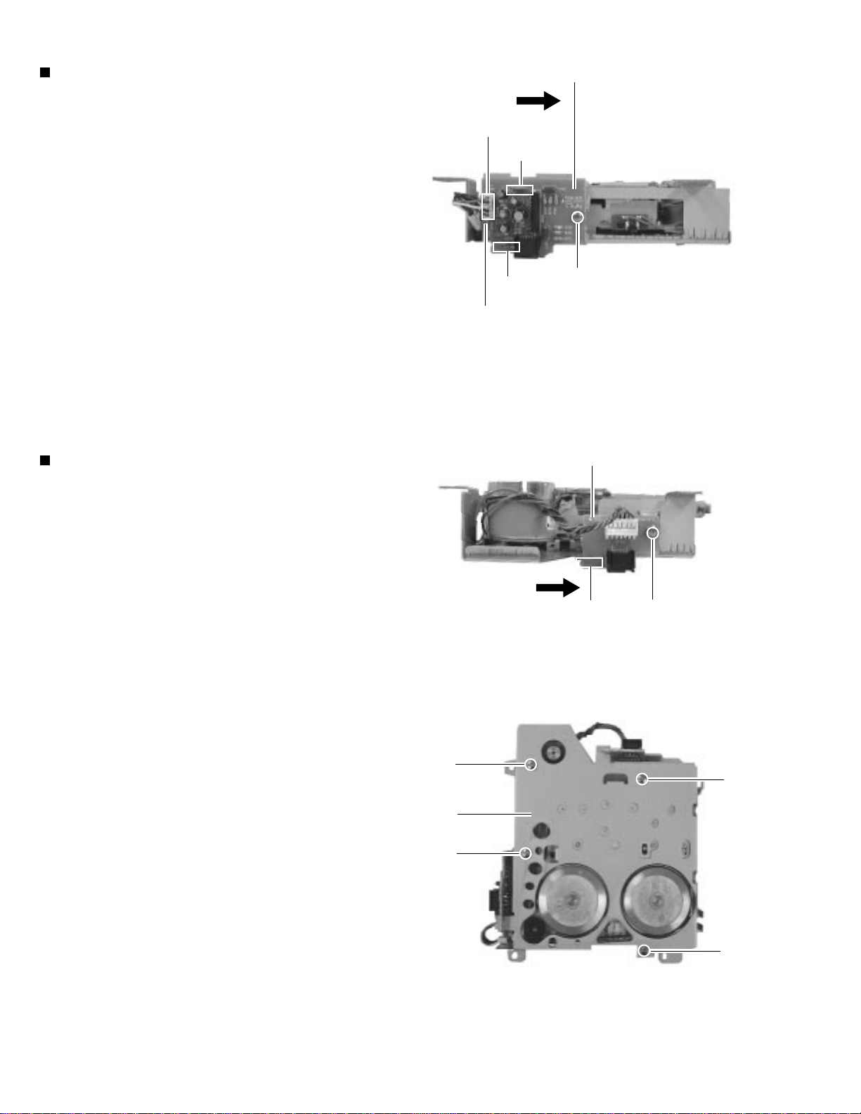
Removing the heat sink (SeeFig.5)
1. Removing the front chassis.
2. Removing the bottom cover.
3. Remove the three screws ( 1 and 1` ) retaining the
heat sink.
Removing the main board assembly
( See Fig. 5 to 7)
1. Removing the front chassis.
2. Removing the bottom cover.
3. Removing the heat sink.
Attach the heat sink with a screw ( 1` ) on operat-
( )
ing checks.
4. Remove the two screws ( 2 ) retaining the main
board assembly.
5. Remove the two screws ( 3 ) retaining the rear
panel .
6. Separate the main board assembly and cassette
mechanism assembly.
7. Take out the main board assembly.
1
Heat sink
Fig. 5
1
1`
2
2
Main board assembly
Fig. 6
3
Rear panel
Fig. 7
3
1-4
Page 5
KS-F160
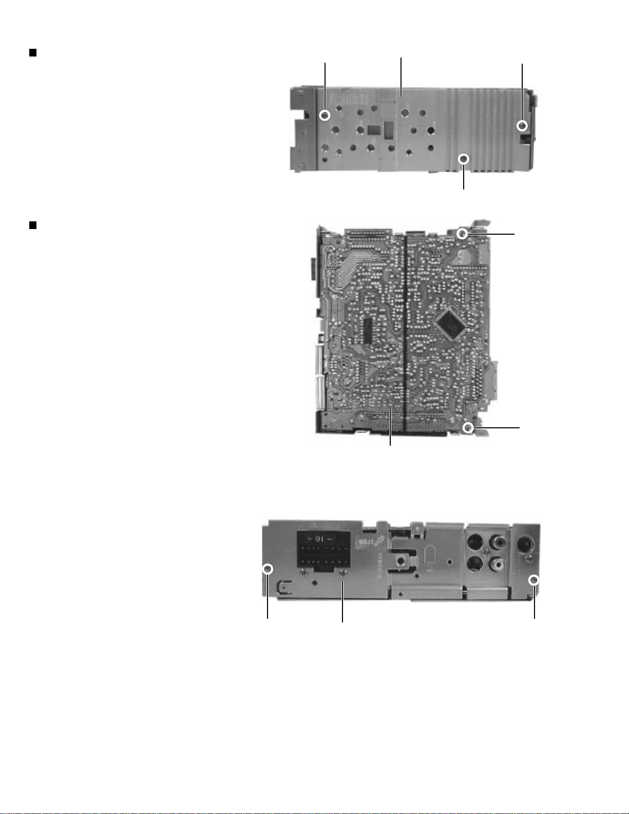
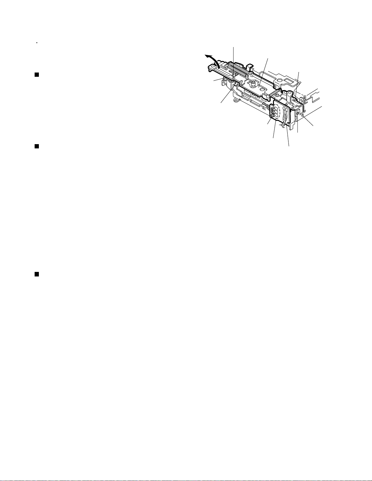
Removing the cassette mechanism assembly
( See Fig. 8 )
1. Removing the front chassis.
2. Removing the bottom cover.
3. Removing the heat sink.
4. Removing the main board assembly.
5. Remove the four screws ( 4 ) retaining the cassette
mechanism.
6. Separate the top chassis and cassette mechanism.
Removing the operation switch board
( See Fig. 9 to 11 )
1. Detaching the front panel unit.
2. Turn the front panel back side down.
3. Remove the four screws ( 5 ) retaining the front
cover.
4. Open the front cover gradually by disengaging the
three engagements ( g ) while pushing the top of
the front cover in the arrow "A" direction, then
disengage the three engagements ( h ) on the both
sides.
5. Place the front panel unit front side down.
6. Disengage the three engagements ( i ) on the
bottom to separate the front cover from the front
panel.
(Be careful not to lose the button springs.)
h
g
5
5
Front panel
Cassette mechanism
4
4
Top chassis
Fig. 8
A
Front cover
Front cover
i
i
g
Fig. 9
Fig. 10
4
Front side
4
g
5
h
h
5
i
Operation switch board
Fig. 11
1-5
Page 6
KS-F160
Removing the head amplifier board
( See Fig. 12 )
1. Removing the front chassis.
2. Removing the bottom cover.
3. Removing the heat sink.
4. Removing the main board assembly .
5. Removing the cassette mechanism.
6. Remove the screw ( 6 ) retaining the head amplifier board.
7. Shift the two inter rocking sections ( j ) securing
the head amplifier board in the direction shown by
the arrow "B" to remove the printed circuit board.
8. From the connector CJ901 on the head amplifier
board from connector wire out going to the head
relay board.
Removing the chassis assembly
Head amplifier board
B
CJ901
j
j
To head relay board
Relay board
6
Fig. 12
( See Fig. 13 and 14 )
1. Removing the front chassis.
2. Removing the bottom cover.
3. Removing the heat sink.
4. Removing the main board assembly .
5. Removing the cassette mechanism.
6. Removing the head amplifier board.
7. Turn the left side to cassette mechanism.
8. Remove the screw ( 7 ) retaining the relay board.
9. Shift the one inter rocking sections ( k ) securing
the relay board in the direction shown by the
arrow "C" to remove the printed circuit board.
10. Turn the back side down, remove the four screws
( 8 ) retaining the chassis assembly .
Chassis assembly
C
7k
Fig. 13
8
8
8
1-6
8
Fig. 14
Page 7
<Cassette mechanism assembly>
KS-F160
Prior to performing the following procedures, remove
the head amplifier board, the relay board and the
mechanism bracket.
Removing the direction switch board
(See Fig.1)
1.
Unsolder the three wires a on the direction switch
board.
2.
Remove the one screw A attaching the direction
switch board.
Removing the FF / REW lever assembly
(See Fig.1)
1.
Remove the screw B attaching the FF / REW lever
assembly on the back of the cassette mechanism
assembly.
2.
Remove the screw C on the upper side of the FF /
REW lever assembly.
3.
Lift and pull forward the FF / REW lever assembly to
disengage the joints b, c, d and e.
Joint e
Joint d
C
FF / REW lever assembly
A
Soldering a
Direction switch board
Fig.1
Joint c
Joint b
B
Reattaching the FF / REW lever assembly
(See Fig.1)
1.
Reattach the FF / REW lever assembly to the joint c
on the back of the chassis.
2.
Reattach the pinch-roller shaft e, the change lever d
and the return link e to the chassis.
1-7
Page 8

KS-F160
Pinch-roller (R) assembly
A arm spring (b)
Shaft
Remove the P arm spring (r)
from the chassis.
P arm spring (r)
S support plate
C washer
FF roller
Removing the playback head (See Fig.2)
Prior to performing the following procedure, remove
the direction switch board and the FF / REW lever
assembly.
Pinch-roller (F) assembly
D
A arm spring (a)
Shaft
Playback head
Remove the P arm spring (f)
from the chassis.
P arm spring (f)
Fig.2
1.
Remove the screw D attaching the playback head.
2.
Remove the C washer and pull out the FF roller.
3.
Remove the S support plate, the A arm spring (a)
and (b), the playback head.
ATTENTION:
The A arm spring (a) differs from the A
arm spring (b).
Removing the pinch-roller (R) and (F)
assembly (See Fig.2)
Prior to performing the following procedure, remove
the direction switch board and the FF / REW lever
assembly.
1.
Remove the P arm spring (f) in the pinch-roller (F)
assembly from the chassis.
2.
Remove the P arm spring (r) in the pinch-roller (R)
assembly from the chassis.
3.
Draw out the pinch roller (F) and (R) assembly from
the shaft.
ATTENTION:
The P arm spring (f) differs from the P
arm spring (r).
ATTENTION:
The pinch roller (F) assembly differs
from the pinch roller (R) assembly.
1-8
Page 9

KS-F160
Removing the cassette hanger / cassette
holder (See Fig.3)
Prior to performing the following procedure, remove
the FF / REW lever assembly.
1.
From the rear of the unit, bend the two tabs f
outwards and disengage the two joints g in the
direction of the arrow.
2.
Push the eject lever and remove the cassette holder
from the playback head. Disengage the two joints h
of the cassette hanger / cassette holder and the eject
lever in the direction of the arrow.
3.
Lift the cassette hanger / cassette holder and disengage
the joint i of the return link and the eject lever.
Removing the reel disc assembly
(See Fig.4)
Prior to performing the following procedure, remove
the FF / REW lever assembly and the cassette
hanger / cassette holder.
Joint g
Cassette holder
Return link
Joint i
Cassette hanger
Eject lever
Joint h
Chassis
Joint h
Tab f
Tab f
Joint g
Fig.3
C washer
1.
Remove the C washer and pull out reel disc assembly.
ATTENTION:
Replace with a new C washer when
reattaching.
Removing the motor assembly
(See Fig.5)
1.
Unsolder the two wires j on the motor assembly.
ATTENTION:
2.
Turn over the cassette mechanism assembly and
remove the main belt and the sub-belt from the
motor pulley.
ATTENTION:
To replace the sub-belt, remove the
main belt and the sub-belt from the
motor pulley. Then remove the three
screws E and one screw F. Replace
with a new sub-belt while lifting the reel
base assembly slightly.
The main belt can now be removed.
C washer
Flywheel (BF)
Fig.4
Main-belt
E
Reel disc assembly
Motor assembly
Sub-belt
G
E
Motor pulley
G
Soldering j
3.
Remove the two screws G attaching the motor
assembly.
Flywheel (BR)
Reel base assembly
E
Fig.5
F
1-9
Page 10

KS-F160
Removing the Flywheel (BF) and (BR)
assembly (See Fig.4 and 5)
Prior to performing the following procedure, remove
the cassette hanger / cassette holder.
1.
From the upper side of the cassette mechanism
assembly, remove the C washer from each shaft of
the flywheel (BF) and (BR).
2.
Turn over the cassette mechanism assembly and
remove the main belt. Pull out the flywheel (BF) and
(BR) downward respectively.
Removing the reel base assembly
(See Fig.5 and 6)
1.
Raise the part k of the reel base assembly slightly
and remove the selector link (B) on the front side of
the cassette mechanism assembly by turning it as
shown in Fig.10.
C washer
C washer
Flywheel (BF)
Fig.4
Main-belt
E
Reel disc assembly
Motor assembly
Sub-belt
G
Motor pulley
2.
Remove the three screws E and the one screw F
on the underside of the cassette mechanism
assembly.
ATTENTION:
The reel base assembly is not
repairable. Handle with care.
Inside of the reel base assembly
Flywheel (BR)
k
Reel base assembly
E
Fig.5
Pinch-roller (R) assembly
G
Soldering j
E
F
1-10
Selector link (B).
Turn the selector link (B).
Fig.6Fig.7
Page 11

Removing the mute switch board
(See Fig.8)
1.
Unsolder the two wires l on the mute switch board on
the back of the cassette mechanism assembly.
2.
Remove the screw H attaching the mute switch
board.
Cassette mechanism assembly
Soldering l
Fig.8
H
Rower switch
Mute
switch board
KS-F160
Motor assembly
Removing the power switch (See Fig.9)
Prior to performing the following procedure, remove
the motor assembly.
1.
Unsolder the two wires m on the power switch on the
side of the cassette mechanism assembly.
2.
Remove the screw I attaching the power switch.
Soldering m
I
Cassette mechanism assembly
Power switch
Fig.9
1-11
Page 12

KS-F160
Adjustment method
Test instruments reqired for adjustment
1. Digital oscilloscoe(100MHz)
2.Frequency counter meter
3.Electric voltmeter
4.Wow & flutter meter
5.Test tapes
VT724.......................for DOLBY level measurement
VT739............For playback frequency measurement
VT712....For wow flutter & tape speed measurement
VT703.....................For head azimuth measurement
6.Torque gauge...................Cassette type for CTG-N
(Mechanism adjustment)
Standard volume position
Balance and Bass, Treble volume, Fader
:Center(Indication"0")
Loudness,Dolby NR,Sound,Cruise:Off
V
Volume position is about 2V at speaker output with
following conditions,Playback the test tape VT721.
AM mode 999kHz/62dB,INT/400Hz,30%
FM mono mode
FM stereo mode 1kHz,67.5kHz dev.pilot 7.5kHz dev
Output level 0dB(1 V,50 /open terminal)
Measuring conditions(Amplifier section)
Power supply voltage.............. DC14.4V(11V - 16V allowance)
Load impedance............ 4 (4 to 8 allowance)
Line out level/Impedance..............1.0V/20k load (250 nWb/m)
modulation signal on recieving.
97.9MHz/66dB,INT/400Hz,22.5kHz
deviation pilot off mono
Frequenc
Frequency band
FM
Band
MW
AM
LW 531-1602KHz
87.5-107.9MHz
87.5-108MHz
530-1710KHz
200KHz step
50KHz step
10KHz step
9KHz step
1-12
Page 13

Information for using a Car Audio Service Jig
1. For 1995 and 1996 , we're advancing efforts to make our extension cords common for all car audio products.
Please use this type of extension cord as follows.
2. As a U-shape type top cover is employed, this type of extension cord is needed to check operation of the
mechanism assembly after disassembly.
3. Extension cord : EXTKSRT002-6P ( 6 pin extension cord ) For connection between mechanism assembly
and main board assembly .
Check for mechanism driving section such as motor ,etc..
Disassembly Method
1. Remove the bottom cover.
2. Remove the front panel assembly.
3. Remove the top cover .
4. Install the front panel.
5. Confirm that current is being carried by connecting
an extension cord jig.
Note
Available to connect to the CN701 connector when installing the front panel.
Cassette mechanism
KS-F160
EXTKSRT002-6P
Extension cord
: EXTKSRT002-6P
Main board
Front panel assembly
1-13
Page 14

KS-F160
Arrangement of adjusting & test points
Cassette mechanism
(Surface)
Motor assembly
Tape speed adjust
Playback head
Head section view
Head azimuth screw
Playback head
Azimuth screw
Fixed screw
1-14
Height adjusting screw
Height adjusting screw
c
Height adjusting screw
b
a
Page 15

Mechanism adjustment section
KS-F160
Item Adjusting & Confirmation Methods Adjust
1.Head azimuth
"Head Height Adjustment"
Note
Adjust the azimuth directly.When you adjust the height using a mirror tape, remove the cassette housing from the
mechanism chassis.
After installing the cassette housing, perform the azimuth
adjustment.
Load the mirror tape (SCC-1659). Adjust with height
1.
adjustment screw(a) and azimuth adjustment screw(b) so
that the "A" of the mirror tape runs in the center between
Lch and Rch in the reverse play mode.
2.
After switching from REV to FWD then to REV,check that
the head position set in procedure "1" is not changed.
*If the position has shifted, adjust again and check.
3.
Adjust the azimuth screw (b) so that line "B" of the mirror
tape runs in the center between Lch and Rch in the
forword play mode.
"Head azimuth adjustment"
1.
Load the test tape (VT724: 1kHz) and play it back in the
reverse play mode. set the Rch output level to maximum.
2..
Load the test tape (VT703:10kHz) and play it back in the
forward play mode. Adjust the Rch and Lch output levels
to maximum, with azimuth adjustment acrew(b).
In this case, the phase difference should be within 45 .
Engage the reverse mode and adjust the output level to
3.
maximum, with azimuth adjustment screw (c).
*The phase difference should be 45_Kor more.
When switching between forward and reverse modes, the
4.
difference between channels should be within 3dB.
*Between FWD Lch and Rch REV Lcj and Rch.
When the test tape (VT721 : 315Hz) is played back, the
5.
level difference between channels should be within 1.5dB.
Std.Value
A Line
Head shield
The head is at low position
during FWD.
B Line
Head shield
The head is at low position
during REV.
Head azimuth
screw
screw(c)
screw(b)
0
screw(a)
Phase
Fixed screw
45
2.Tape speed and
Wow & Flutter
3.Playback
Frequency
response
1.Check to see if the reading of the frequency counter & Wow
flutter meter is within 2940-3090 Hz(FWD/REV), and less
than 0.35% (JIS RMS).
2.In case of out of specification,adjust the motor with a built-
in volume resister.
1.Play the test tape (VT724 : 1kHz) back and set the volume
position at 2V.
2.Play the test tape (VT739)back and confirm 0 3dB at 1kHz/
8kHz and -4+2dB at 1kHz/125Hz.
3.When 8kHz is out of specification, it will be necessary to read
adjust the azimuth.
Built-in
volume resister
Tape speed
2940-3090Hz
Wow & Flutter
Less than
0.35%
(JIS RMS)
Speaker out
1kHz/8kHz
: 0dB_}3dB,
125Hz/1kHz
: -4dB+2dB,
1-15
Page 16

KS-F160
Description of major ICs
AN80T05LF (IC781) : Regulator
1.Terminal layout & Block diagram
Reference V oltage
ASO & Peak
Thermal
Protection
Current Protection
Pre
Drive
1 2 3 4 5 6 7 8 9 10 11 12
ILL
10V
2.Pin function
Pin
No.
1
2
3
4
5
6
7
8
9
10
11
12
Pre
Drive
MODE2 MODE1 STB VDD
5.6V
AMP
Out
AMP VCC ANT COM
Symbol Function
NC
TUNER
FM/AM
POWER CNT
5V
VSW 14VOUT
MEMORY
NC
9V
AM
FM
GND
Non connect
When 5V is input,becomes AM. and the antenna output is turned on.
When 5V is input,becomes AM. and the output of FM is switched.
When 5V is input, outputs to ILL,COM,and AMP. It is 0V usually.
5.6V power supply.
Power supply supply to remote amplifier
Back up. connects with ACC with it.
Non connect
8.7V power supply.
The power supply of 8.7V to AM.
The power supply of 8.7V to FM.
Ground
AMP
Out
Pre
Drive
Pre
Drive
8.7VAM8.7VFM8.7V
Pre
Drive
GND
1-16
Page 17

LC75823W (IC651) : LCD driver
1. Pin Layout & Symbol
DATA
S8
S9
S10
S11
S12
S13
S14
S15
S16
CLOCKCEOSC
64 63 62 61 60 59 58 57 56 55 54 53 52 51 50 49
1
2
3
4
5
6
7
8
9
10
11
12
13
14
15
16
17 18 19 20 21 22 23 24 25 26 27 28 29 30 31 32
Vss
INH
VDD
COM3
COM2
COM1
S52
S51
S50
S49
48
47
46
45
44
43
42
41
40
39
38
37
36
35
34
33
KS-F160
S48
S47
S46
S45
S44
S43
S42
S41
S40
S39
S38
S37
S36
S35
S34
S33
2. Pin Function
Pin No.
1 to 7
8 to 52
53 to 55
S53 to S55
57
58,59
60
61
62
63
Symbol
S8 to S52
INH
Vss
OSC
CE
CLOCK
S17
S18
S19
S20
S21
S22
S23
S24
S25
S26
S27
S28
S29
S30
S31
S32
I/O
--
Non connect
O
Common driver output pins. The frame frequency is given
Function
by : t0=(fosc/384)Hz.
--
Power supply connection. Provide a voltage of between
4.5 and 6.0V.
I
Display turning off input pin.
INT="L" (Vss) ----- off (S1 to S52, COM1 to COM3="L"
INT="H" (VDD)----- on
Serial data can be transferred in display off mode.
Non connect
--
Power supply connection. Connect to GND.
I/O
Oscillator connection.
An oscillator circuit is formed by connecting an external
resistor and capacitor at this pin.
Serial data CE : Chip enable
interface connection
I
to the controller. CL : Sync clock
64
DATA
DI : Transfer data
1-17
Page 18

KS-F160
LC72362N-9920 (IC701):System controller
1.Terminal Layout
24 - 1
25
-
80
-
40
41 - 64
2.Block diagram
XIN
XOUT
FMIN
AMIN
SNS
VDD
VSS
HCTR
LCTR
HOLD
TEST1
TEST2
PA0
PA1
PA2
PA3
PB0
PB1
PB2
BP3
PC0
PC1
PC2
PC3
PD0
PD1
PD2
PD3
PE0
SCK2/PE1
PO2/PE2
SI2/PE3
PF0
SCK1/PF1
SO1/PF2
SI1/PF3
64
V-DET
DIVIDER REFERENCE DIVIDER SELECTOR
SNSFF
1/2
BUS
DRIV.
LATCH
BUS
DRIV.
LATCH
BUS
DRIV.
LATCH
BUS
DRIV.
LATCH
BUS
DRIV.
LATCH
BUS
DRIV.
1/16, 1/17
PROGRAMMABLE DIVIDER
1/114, 1/124
LATCH
UNIVERSAL
COUNTER
(20bits)
RAM
512 4bits
ROM
12K 16bits
ADDRESS DECODER
PROGRAM COUNTER
STACK
ALU
ADDRESS
DECODER
BUS
DRIVER
INSTRUCTION
DECODER
JUDGE
PHASE
DETECTOR
UNLOCK
F/F
PHASE
DETECTOR
LATCH
LATCH
BUS
DRIV.
LATCH
BUS
DRIV.
LATCH
BUS
DRIV.
BEEP
LATCH
BUS
DRIV.
LATCH
BUS
DRIV.
LATCH
BUS
DRIV.
LATCH
BUS
DRIV.
BUS
DRIV.
SUB
C.P.
MPX
INTERRUPT
E01
E02
SUBPD
EO3
PQ0
PP3
PP2
PP1
PP0
PO3
PO2
PO1
PO0
PN3
PN2
PN1
PN0/BEEP
PM3
PM2
PM1
PM0
PL3
PL2
PL1
PL0
PK3
PK2
PK1/INT1
PK0/INT0
PJ3
PJ2
PJ1
PJ0
PI1/ADI5
PI0/ADI4
1-18
PF0
SCK1/PF1
SO1/PF2
SI1/PF3
SIO
LATCH
BUS
DRIV.
ADC
MPX
BUS
DRIV.
PH3/ADI3
PH2/ADI2
PH1/ADI1
PH0/ADI0
Page 19

KS-F160
3.Description
Pin
No.
1
2
3
4
5
6
7
8
9
10
11
12
13
14
15
16
17
18
19
20
21
22
23
24
25
26
27
28
29
30
31
32
33
34
35
36
37
38
39
40
Symbol
XIN
GND
J BUS SI
J BUS SO
J BUS SCK
J BUSI/O SEL
NC
LCD SO
LCD SCK
LCD CE
NC
E.VOL SO
E.VOL SCK
NC
TUNER ILLUM
TAPE ILLUM
CD ILLUM
DIMMER OUT
NC
NC
NC
NC
NC
NC
KS1
KS0
Vdd
TEST
NC
SEEK/STOP
MONO
RADIO/TAPE
BEEP LEVEL
POWER CNT
Acc
NC
K3
K2
K1
K0
I/O
Crystal oscillator
I
To GND
Bus serial data input from CP751
I
Bus serial data output to CP751
O
Bus serial clock output to CP751
O
BUS I/O switch signal output
O
Non connect
Serial data output to IC651
O
Serial clock output to IC651
O
Chip enable output to IC651
O
Non connect
Serial data output
O
Serial clock output
O
Non connect
Non connect
Non connect
Non connect
Non connect
Non connect
Non connect
Non connect
Non connect
Non connect
Non connect
Non connect
Initializing output port
O
Initializing input port
I
Initializing input port
I
Non connect
Initializing input port
I
Power supply
Test input
I
Non connect
-
Output the "If signal request"
O
Monaural and stereo change
O
over output
Non connect
Non connect
Power control output
O
Power supply
Non connect
-
Function
Pin
Symbol
No.
41
42
43
44
45
46
47
48
49
F/R SENSE
50
TAPE MUTE
51
52
53
54
55
J BUS INT
56
REMOCON
57
58
59
60
61
MEMORY DET
62
LEVEL METER
63
64
65
66
67
68
69
70
FM/AM IF COUNT
71
72
73
74
75
76
77
78
79
80
NC
NC
NC
BEEP
NC
NC
NC
TAPE IN
SD/ST
NC
DETACH
NC
FM/AM
DOLBY
NC
MUTE
SMETER
KEY 2
KEY1
KEY0
ACCDET
SENS
NC
NC
NC
Vdd
AM OSC
FM OSC
Vss
NC
ED
TEST 1
XOUT
LC72362N-9920
I/O
-
Non connect
-
Non connect
-
Non connect
-
Non connect
-
Non connect
-
Non connect
-
Non connect
I
H:RADIO L:TAPE
I
FORWARD/REVERSE switch detector
I
DIR.FF/REW MUTE
I
Station detector and ST input
-
Non connect
I
Detection of Front Panel
-
Non connect
I
BUS interruption signal detection communication
-
To GND
I
Change over the FM/AM Input
-
Non connect
-
Non connect
-
The mute time is controlled by the
connected capacitor when changing
over the FM/AM
I
Memorydetector input
I
I
Signal meter input
I
Mementary key input
Mementary key input
I
Mementary key input
I
I
ACC DET
-
To GND
I
Non connect
-
AM/FM Frequency detection
-
Non connect
-
Non connect
I
Power supply
I
Input the local oscillator signal of AM
-
Input the local oscillator signal of FM
Power supply
-
O
Non connect
-
PLL Error signal output
O
To GND
Crystal oscillator
Function
1-19
Page 20

KS-F160
TEA6320T-X (IC931) : E.volume
1.Pin layout
2.Block diagram
10 8 9 7 6
5
12
SDA
1
GND
2
OUTLR
OUTLF
MUTE
TL
B2L
B1L
IVL
ILL
QSL
IDL
ICL
IMD
IBL
IAL
3
4
5
6
7
8
9
10
11
12
13
14
15
16
3.Pin functions
Pin
Symbol
No.
SDA
1
SCL
32
VCC
31
OUTRR
30
OUTRF
29
TR
28
B2R
27
B1R
26
IVR
25
ILR
24
QSR
23
IDR
22
Vref
21
ICR
CD-CH
TAPE
TUNER
20
19
18
17
CAP
IBR
IAR
I/O
Serial data input/output.
I/O
MUTE
21
31
2
19
16
15
13
11
14
22
20
18
17
Functions Functions
POWER
SUPPLY
SOURCE
SELECTOR
23 25 24 26 27 28
VOLUME 1
+20 to -31 dB
LOUDNESS
LEFT
VOLUME 1
+20 to -31 dB
LOUDNESS
RIGHT
Pin
No.
17
Symbol
IAR
BASS
LEFT
+15 dB
LOGIC
BASS
RIGHT
+15 dB
I/O
I
Input A right source.
TREBLE
LEFT
+12 dB
TREBLE
RIGHT
+12 dB
FUNCTION
ZERO CROSS
DETECTOR
VOLUME 2
0 to 55 dB
BALANCE
FENDER REAR
VOLUME 2
0 to 55 dB
BALANCE
FENDER FRONT
HC BUS
REC
VOLUME 2
0 to -55dB
BALANCE
FENDER FRONT
VOLUME 2
0 to -55dB
BALANCE
FENDER REAR
3
4
32
1
29
30
2
3
4
5
6
7
8
9
10
11
12
13
14
15
16
GND
OUTLR
OUTLF
TL
B2L
B1L
IVL
ILL
QSL
IDL
MUTE
ICL
IMO
IBL
IAL
Ground.
output left rear.
O
output left front.
O
Treble control capacitor left channel or
I
input from an external equalizer.
Bass control capacitor left channel or
-
output to an external equalizer.
Bass control capacitor left channel.
Input volume 1. left control part.
I
Input loudness. left control part.
I
Output source selector. left channel.
O
Not used
Not used
Input C left source.
I
Not used
Input B left source.
I
Input A left source.
I
18
19
20
21
22
23
24
25
26
27
28
29
30
31
32
IBR
CAP
ICR
Vref
IDR
QSR
ILR
IVR
B1R
B2R
TR
OUTRF
OUTRR
Vcc
SCL
I
Input B right source.
-
Electronic filtering for supply.
I
Input C right source.
-
Reference voltage (0.5Vcc)
-
Not used
O
Output source selector right channel.
I
Input loudness right channel.
I
Input volume 1. right control part.
-
Bass control capacitor right channel
Bass control capacitor right channel or
O
output to an external equalizer.
Treble control capacitor right channel or
I
input from an external equalizer.
O
Output right front.
O
Output right rear.
-
Supply voltage.
I
Serial clock input.
1-20
Page 21

HA13158A (IC981) : Power amp
1. Pin layout
1 ~ 23
2. Block diagram
KS-F160
IN1
IN2
IN3
IN4
11
13
23
10
2
1
STBY
MUTE
14 18 6
INVCC
INPUTBUFFER1
INPUTBUFFER2
INPUTBUFFER3
INPUTBUFFER4
PROTECTOR (ASO
SURGE, TSD)
PVCC1PVCC2
AMP1
AMP2
AMP3
AMP4
+
-
+
-
+
-
+
-
3
4
5
7
8
9
15
16
17
19
20
21
12 22
TAB
UPC1228HA(IC901):Head amp
1.Terminal layout & Block diagram 2.Pin function
Pin No.
1
AMP1 AMP2
1
2345678
2
3
4
5
6
7
8
Electrical connection
Input 1
Negative feed back 1
Output 1
Power supply; +Vcc
Ground
Output 2
Negative feed back 2
Input 2
1-21
Page 22

KS-F160
VICTOR COMPANY OF JAPAN, LIMITED
MOBILE ERECTRONICS DIVISIOIN
PERSONAL & MOBILE NETWORK BUSINESS UNIT. 10-1,1Chome,Ohwatari-machi,Maebashi-city,Japan
(No.49659)
200111
 Loading...