

Page 1
SERVICE MANUAL
CD RECEIVER
4986020035
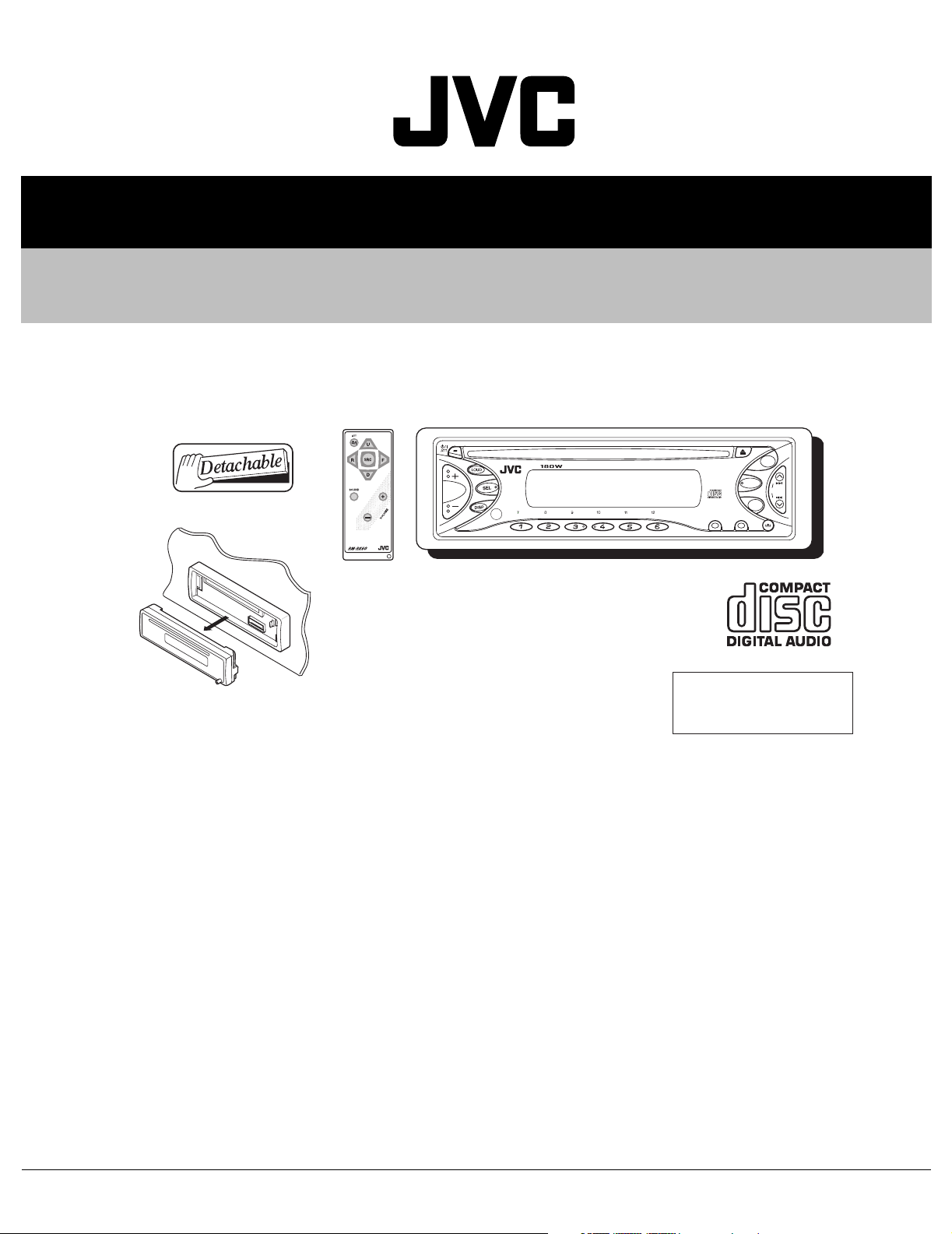
KD-S598,KD-S597
DIRECT TRACK ACCESS
S
MO
RPT RND
MODE
UR -------------- Brazil
FM
CD
SSM
AM
SCM
Area Suffix
TABLE OF CONTENTS
1 Important Safety Precautions . . . . . . . . . . . . . . . . . . . . . . . . . . . . . . . . . . . . . . . . . . . . . . . . . . . . . . . . . . . 1-2
2 Disassembly method . . . . . . . . . . . . . . . . . . . . . . . . . . . . . . . . . . . . . . . . . . . . . . . . . . . . . . . . . . . . . . . . . . 1-4
3 Adjustment. . . . . . . . . . . . . . . . . . . . . . . . . . . . . . . . . . . . . . . . . . . . . . . . . . . . . . . . . . . . . . . . . . . . . . . . . . 1-23
4 Description of major ICs. . . . . . . . . . . . . . . . . . . . . . . . . . . . . . . . . . . . . . . . . . . . . . . . . . . . . . . . . . . . . . . 1-27
COPYRIGHT © 2003 VICTOR COMPANY OF JAPAN, LTD.
No.49860
2003/5
Page 2
1.1 Safety Precautions
SECTION 1
Important Safety Precautions
!
!
Burrs formed during molding may be left over on some parts of the chassis. Therefore,
pay attention to such burrs in the case of preforming repair of this system.
Please use enough caution not to see the beam directly or touch it in case of an
adjustment or operation check.
1-2 (No.49860)
Page 3
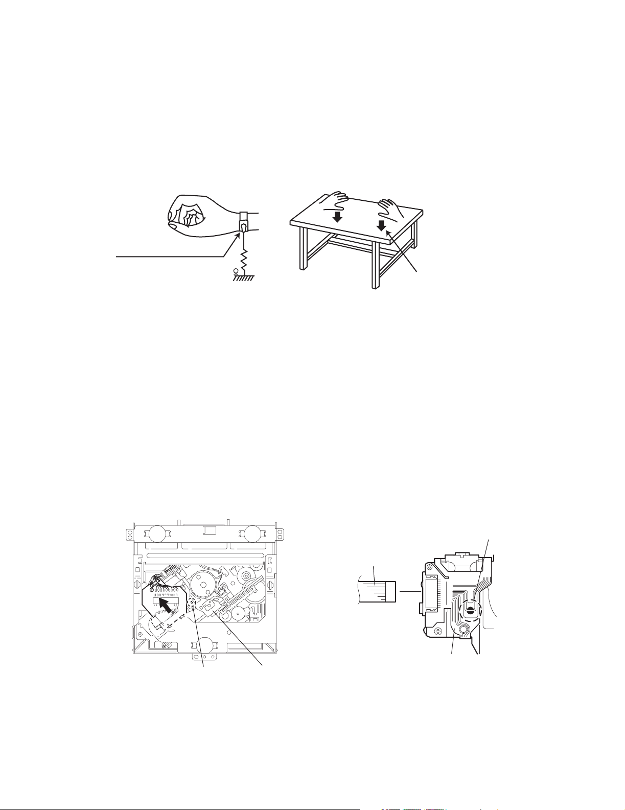
1.2 Preventing static electricity
Electrostatic discharge (ESD), which occurs when static electricity stored in the body, fabric, etc. is discharged,
can destroy the laser diode in the traverse unit (optical pickup). Take care to prevent this when performing repairs.
1.2.1 Grounding to prevent damage by static electricity
Static electricity in the work area can destroy the optical pickup (laser diode) in devices such as DVD players.
Be careful to use proper grounding in the area where repairs are being performed.
(1) Ground the workbench
Ground the workbench by laying conductive material (such as a conductive sheet) or an iron plate over it before placing the
traverse unit (optical pickup) on it.
(2) Ground yourself
Use an anti-static wrist strap to release any static electricity built up in your body.
(caption)
Anti-static wrist strap
1M
Conductive material
(conductive sheet) or iron plate
(3) Handling the optical pickup
• In order to maintain quality during transport and before installation, both sides of the laser diode on the replacement optical
pickup are shorted. After replacement, return the shorted parts to their original condition.
(Refer to the text.)
• Do not use a tester to check the condition of the laser diode in the optical pickup. The tester's internal power source can easily
destroy the laser diode.
1.3 Handling the traverse unit (optical pickup)
(1) Do not subject the traverse unit (optical pickup) to strong shocks, as it is a sensitive, complex unit.
(2) Cut off the shorted part of the flexible cable using nippers, etc. after replacing the optical pickup. For specific details, refer to the
replacement procedure in the text. Remove the anti-static pin when replacing the traverse unit. Be careful not to take too long a
time when attaching it to the connector.
(3) Handle the flexible cable carefully as it may break when subjected to strong force.
(4) I t is not possible to adjust the semi-fixed resistor that adjusts the laser power. Do not turn it.
1.4 Attention when traverse unit is decomposed
*Please refer to "Disassembly method" in the text for the CD pickup unit.
• Apply solder to the short land before the flexible wire is disconnected from the connector on the CD pickup unit.
(If the flexible wire is disconnected without applying solder, the CDpickup may be destroyed by static electricity.)
• In the assembly, be sure to remove solder from the short land after connecting the flexible wire.
Short-circuit point
(Soldering)
Flexible wire
Short-circuit point
Pickup
Pickup
(No.49860)1-3
Page 4
SECTION 2
Disassembly method
2.1 Main body
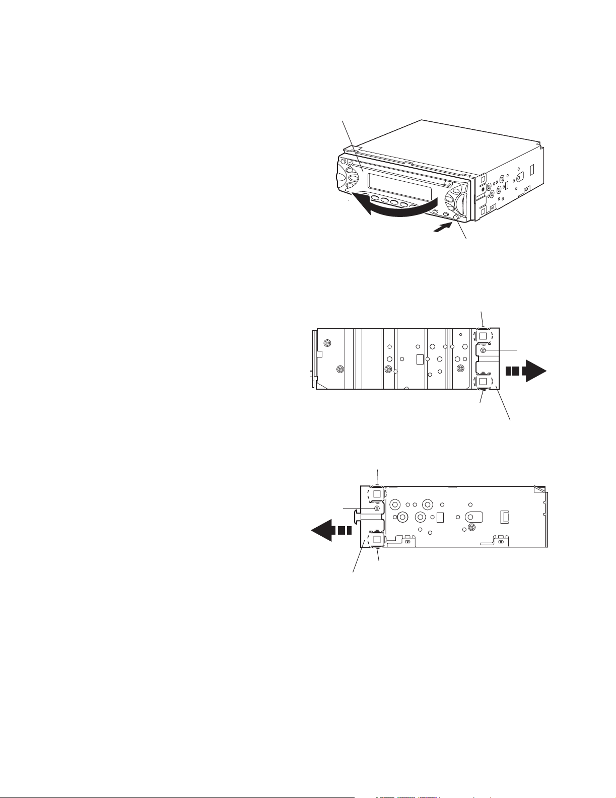
2.1.1 Removing the front panel assembly
(See Fig.1)
(1) Push the detach button in the lower right part of the front
panel assembly and remove the front panel assembly in
the direction of the arrow.
2.1.2 Removing the front chassis assembly
(See Figs.2 and 3)
• Prior to performing the following procedure, remove the front
panel assembly.
(1) Remove the two screws A on the both sides of the main
body.
(2) Release the two joints a and two joints b on both sides of
the main body using a screwdriver, and remove the front
chassis assembly forward.
Front panel assembly
Detach button
Fig.1
Joint a
A
Joint b
A
Joint b
Front chassis assembly
Joint a
Front chassis assembly
Fig.2
Fig.3
1-4 (No.49860)
Page 5
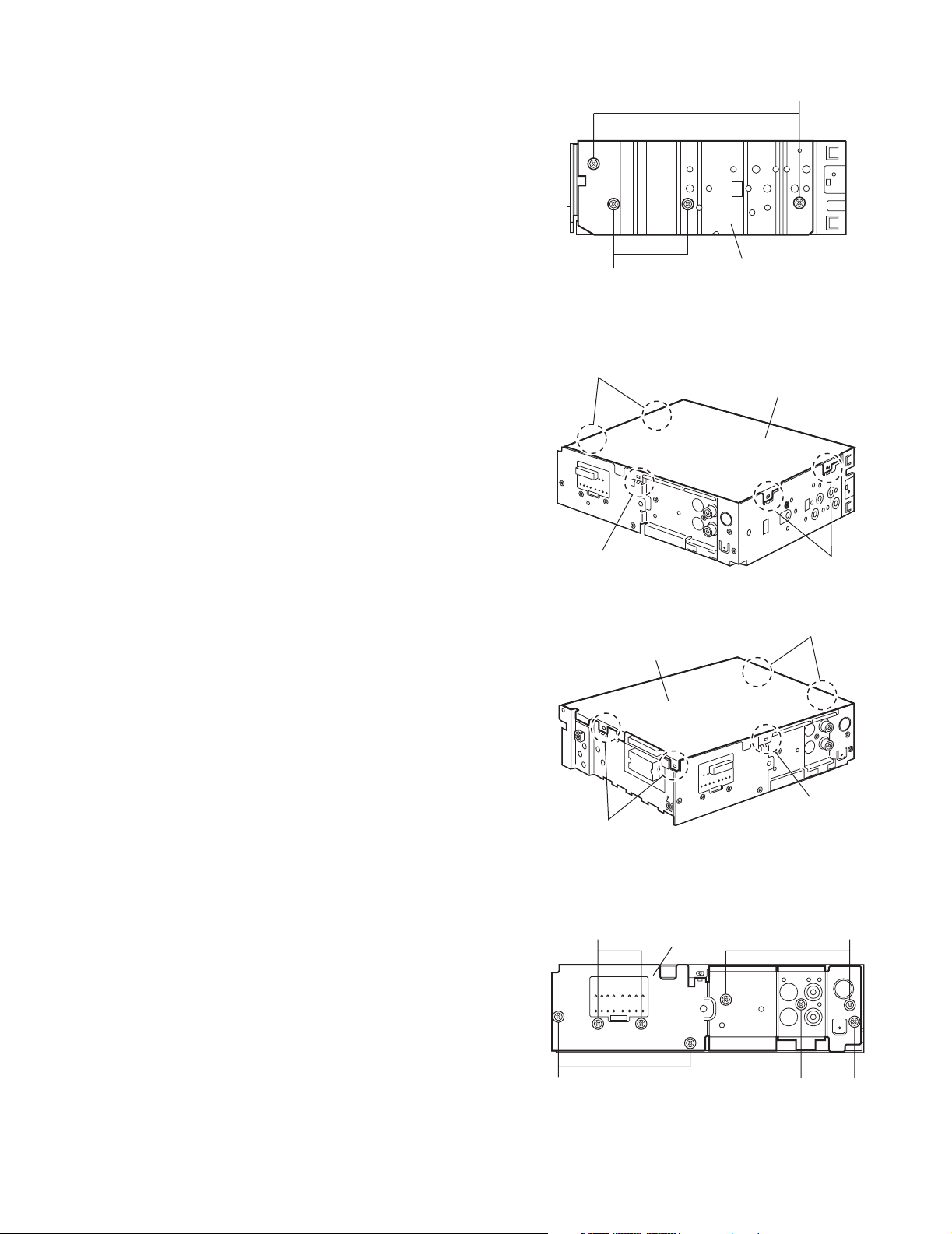
2.1.3 Removing the heat sink
(See Fig.4)
(1) Remove the two screws B and two screws C on the left
side of the main body.
B
2.1.4 Removing the bottom cover
(See Figs.5 and 6)
• Prior to performing the following procedure, remove the front
panel assembly, front chassis assembly and heat sink.
(1) Turn over the body and release the two joints c, two joints
d and joint e.
CAUTION:
Do not damage the main board when releasing the joint e using a screwdriver. (See Figs.5 and 6.)
Joint c
Joint e
C
Heat sink
Fig.4
Bottom cover
Joint d
Fig.5
Joint d
Bottom cover
2.1.5 Removing the rear bracket
(See Fig.7)
• Prior to performing the following procedure, remove the front
panel assembly, front chassis assembly, heat sink and bottom
cover.
(1) Remove the three screws D, three screws E and two
screws F on the back of the body.
(2) Remove the rear bracket.
Joint e
Joint c
Fig.6
EF
Rear bracket
DD
Fig.7
E
(No.49860)1-5
Page 6
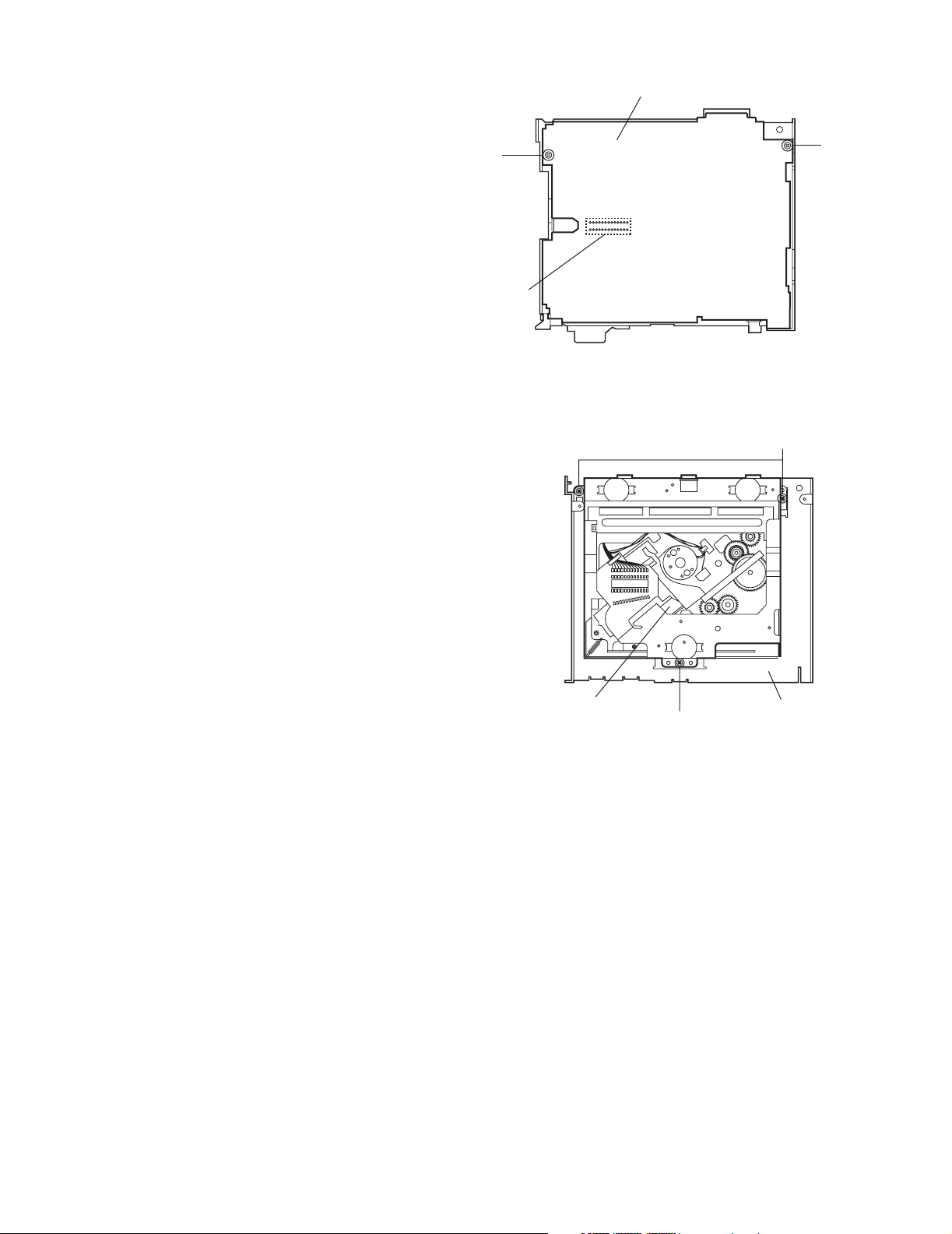
2.1.6 Removing the main board
(See Fig.8)
• Prior to performing the following procedure, remove the front
panel assembly, front chassis assembly, heat sink, bottom
cover and rear bracket
(1) Remove the two screws G attaching the main board.
(2) Disconnect the connector CN501 and remove the main
board.
2.1.7 Removing the CD mechanism assembly
(See Fig.9)
• Prior to performing the following procedure, remove the front
panel assembly, front chassis assembly, heat sink, bottom
cover, rear bracket and main board.
(1) Remove the three screws H.
G
CN501
Main board assembly
G
Fig.8
H
CD mechanism assembly
Top chassis
H
Fig.9
1-6 (No.49860)
Page 7
2.1.8 Removing the front board
f
(See Figs.10 to 12)
• Prior to performing the following procedure, remove the front
panel assembly.
(1) Remove the four screws J on the back side of the front pan-
el assembly.
(2) Release the eleven joints f.
(3) Take out the front board.
J
Front panel
Joint f
Front board
J
Rear cover
J
Fig.10
Joint f
Joint
Joint f
Joint f
Fig.11
Fig.12
(No.49860)1-7
Page 8
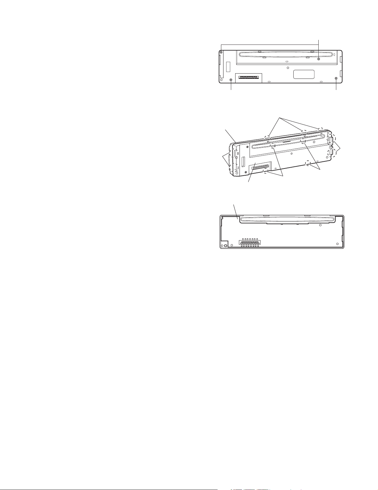
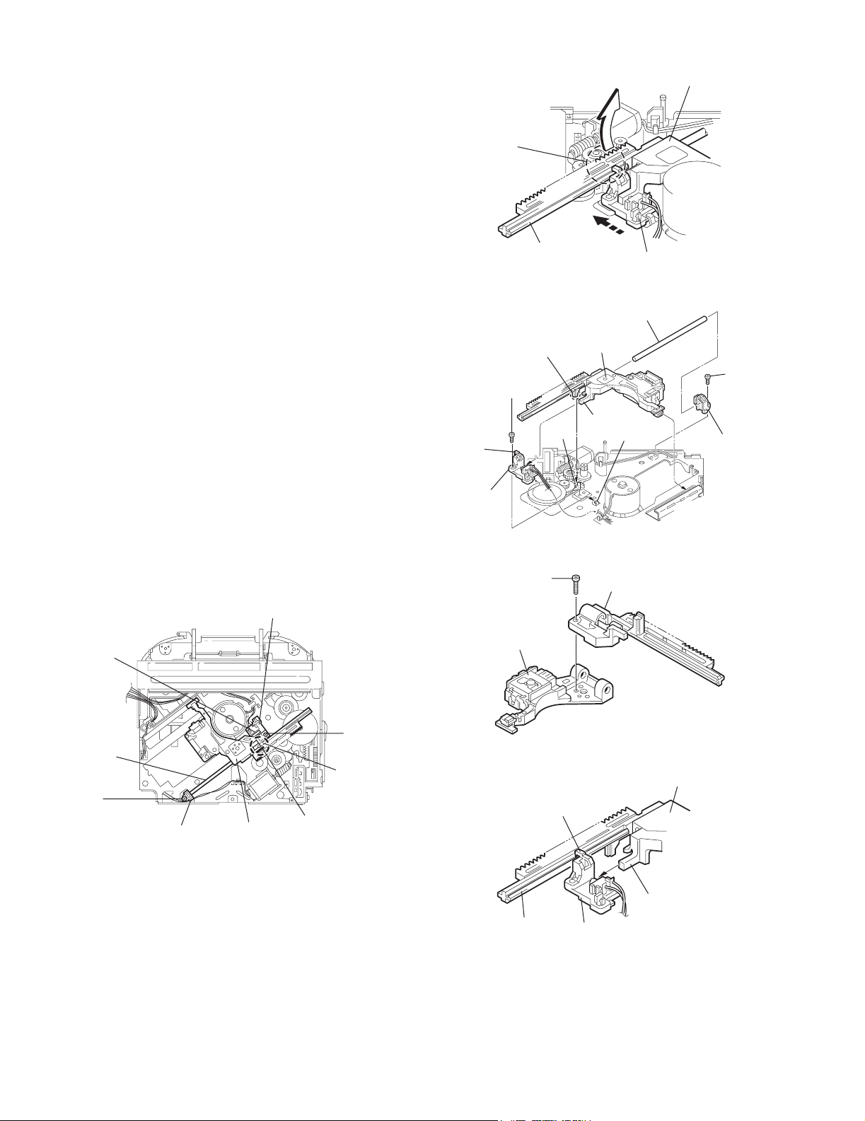
2.2 CD Mechanism Assembly
A
2.2.1 Removing the top cover
(See Figs.1 and 2)
(1) Remove the two screws A on the both side of the body.
(2) Lift the front side of the top cover and move the top cover
backward to release the two joints a.
Top cover
Joints a
A
Joints a
A
Fig.1
Fig.2
Top cover
1-8 (No.49860)
Page 9
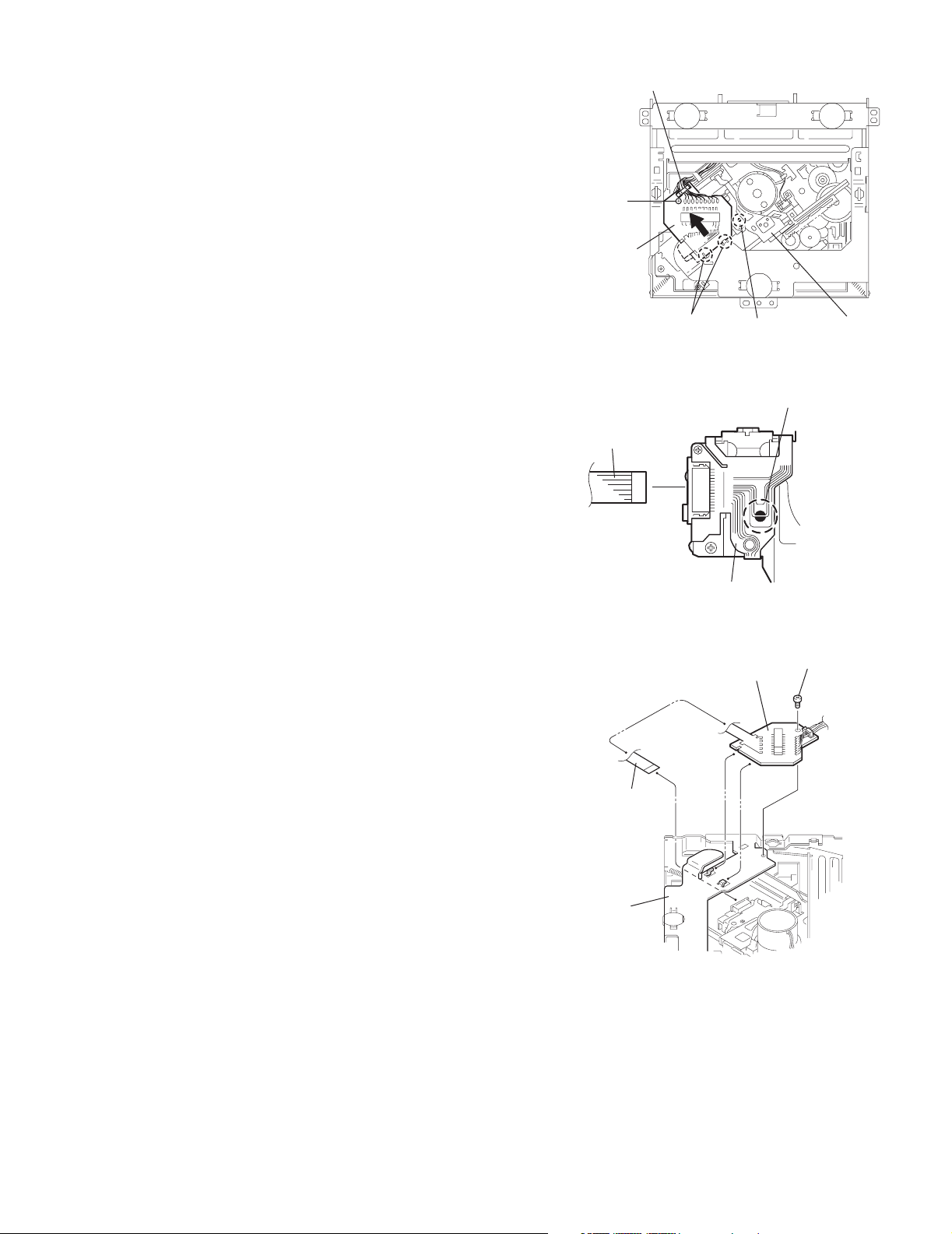
2.2.2 Removing the connector board
(See Figs.3 to 5)
CAUTION:
Before disconnecting the flexible wire from the pickup, solder
the short-circuit point on the pickup. No observance of this instruction may cause damage of the pickup.
(1) Remove the screw B fixing the connector board.
(2) Solder the short-circuit point on the connector board.
(3) Disconnect the flexible wire from the pickup.
(4) Move the connector board in the direction of the arrow to
release the two joints b.
(5) Unsolder the wire on the connector board if necessary.
CAUTION:
Unsolder the short-circuit point after reassembling.
B
Connector board
Flexible wire
Wires
Joints b
Short-circuit point
Fig.3
Short-circuit point
(Soldering)
Pickup
Flexible wire
Frame
Pickup
Fig.4
B
Connector board
Fig.5
(No.49860)1-9
Page 10
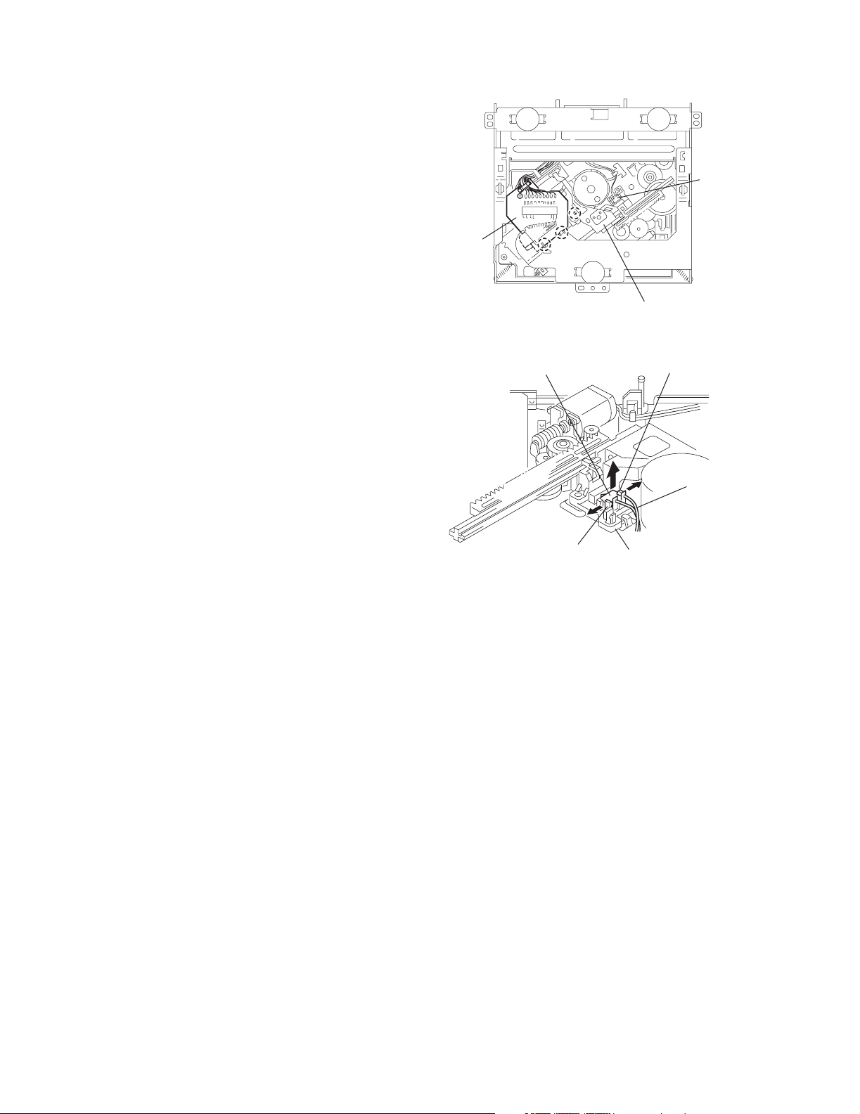
2.2.3 Removing the DET switch
(See Figs.6 and 7)
(1) Extend the two tabs c of the feed sw. holder and pull out
the switch.
(2) Unsolder the DET switch wire if necessary.
DET switch
Connector
board
Pickup
Fig.6
DET switch
Tab c
Tab c
DET switch wire
Feed sw. holder
Fig.7
1-10 (No.49860)
Page 11
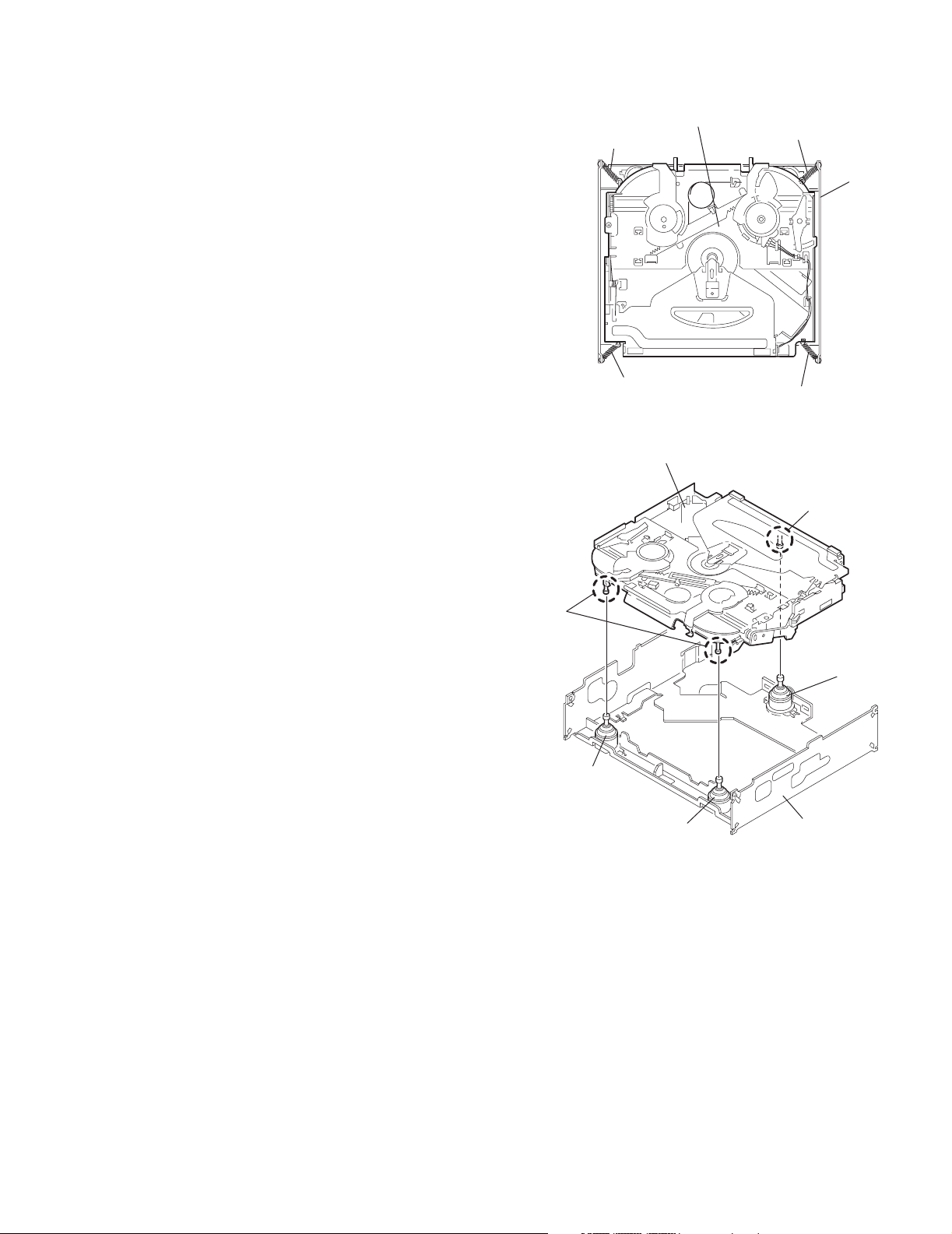
2.2.4 Removing the chassis unit
r
(See Figs.8 and 9)
• Prior to performing the following procedure, remove the top
cover and connector board.
(1) Remove the two suspension springs (L) and (R) attaching
the chassis unit to the frame.
CAUTION:
• The shape of the suspension spring (L) and (R) are different. Handle them with care.
• When reassembling, make sure that the three shafts
on the underside of the chassis unit are inserted to the
dampers certainly.
Suspension spring (R)
Chassis unit
Suspension spring (L)
Frame
Suspension spring (R)
Chassis unit
Shafts
Damper
Damper
Suspension spring (L)
Fig.8
Shaft
Dampe
Frame
Fig.9
(No.49860)1-11
Page 12

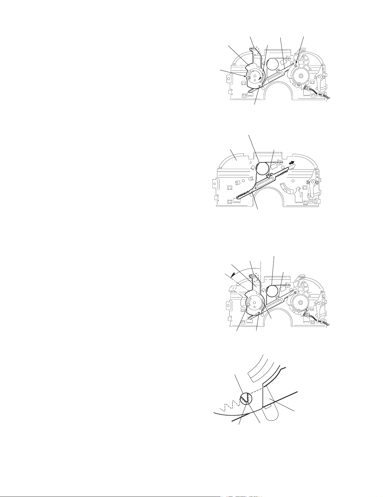
2.2.5 Removing the clamper assembly
(See Figs.10 and 11)
• Prior to performing the following procedure, remove the top
cover.
(1) Remove the clamper arm spring.
(2) Move the clamper assembly in the direction of the arrow to
release the two joints d.
Clamper arm
spring
Joint d
Joint d
Clamper assembly
Fig.10
Clamper arm spring
Chassis rivet
assembly
Joint d
Clamper
assembly
Chassis rivet assembly
Fig.11
Joint d
1-12 (No.49860)
Page 13
2.2.6 Removing the loading / feed motor assembly
(See Figs.12 and 13)
• Prior to performing the following procedure, remove the top
cover, connector board and chassis unit.
(1) Remove the screw C and move the loading / feed motor as-
sembly in the direction of the arrow to remove it from the
chassis rivet assembly.
(2) Disconnect the wire from the loading / feed motor assembly
if necessary.
CAUTION:
When reassembling, connect the wire from the loading /
feed motor assembly to the flame as shown in Fig.12.
Loading / feed motor assembly
Fig.12
Loading / feed motor assembly
C
Fig.13
(No.49860)1-13
Page 14
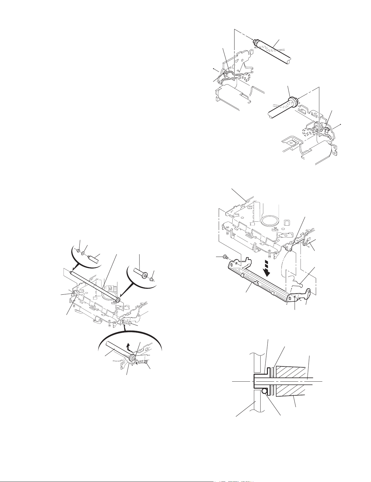
2.2.7 Removing the pickup unit
(See Figs.14 to 18)
• Prior to performing the following procedure, remove the top
cover, connector board and chassis unit.
(1) Remove the screw D and pull out the pu. shaft holder from
the pu. shaft.
(2) Remove the screw E attaching the feed sw. holder.
(3) Move the part e of the pickup unit upward with the pu. shaft
and the feed sw. holder, then release the joint f of the feed
sw. holder in the direction of the arrow. The joint g of the
pickup unit and the feed rack is released, and the feed sw.
holder comes off.
(4) Remove the pu. shaft from the pickup unit.
(5) Remove the screw F attaching the feed rack to the pickup
unit.
Part e
Feed rack
Pickup unit
Feed sw. holder
Fig.15
2.2.8 Reattaching the pickup unit
(See Figs.14 to 17)
(1) Reattach the feed rack to the pickup unit using the screw F.
(2) Reattach the feed sw. holder to the feed rack while setting
the joint g to the slot of the feed rack and setting the part f
of the feed rack to the switch of the feed sw. holder correctly.
(3) As the feed sw. holder is temporarily attached to the pickup
unit, set to the gear of the joint g and to the bending part of
the chassis (joint h) at a time.
CAUTION:
Make sure that the part i on the underside of the feed
rack is certainly inserted to the slot j of the change lock
lever.
(4) Reattach the feed sw. holder using the screw E.
(5) Reattach the pu. shaft to the pickup unit. Reattach the pu.
shaft holder to the pu. shaft using the screw D.
Feed sw. holder
Joint f
Joint g
Feed sw.
holder
Part i
E
Pickup unit
Slot j
F
Pu. shaft
Pickup unit
Joint f
Joint h
Fig.16
Feed rack
D
Pu. shaft
holder
Pu. shaft
D
Pu. shaft holder
1-14 (No.49860)
Pickup unit
Fig.14
Part e
E
Joint g
Feed rack
Fig.17
Pickup unit
Joint g
Joint f
Feed sw. holder
Fig.18
Page 15
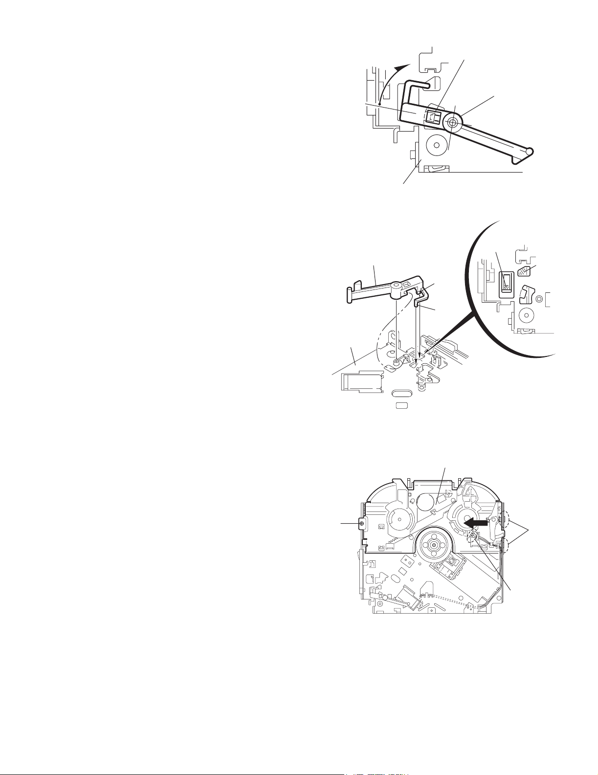
2.2.9 Removing the trigger arm
r
(See Figs.19 and 20)
• Prior to performing the following procedure, remove the top
cover, connector board and clamper unit.
(1) Turn the trigger arm in the direction of the arrow to release
the joint k and pull out upward.
CAUTION:
When reassembling, insert the part m and n of the trigger
arm into the part p and q at the slot of the chassis rivet
assembly respectively and join the joint k at a time.
Chassis rivet assembly
Trigger arm
Chassis rivet
assembly
Joint k
Trigger arm
Fig.19
Part p
Part q
Part m
Part n
2.2.10 Removing the top plate assembly
(See Fig.21)
• Prior to performing the following procedure, remove the top
cover, connector board, chassis unit, and clamper assembly.
(1) Remove the screw H.
(2) Move the top plate assembly in the direction of the arrow to
release the two joints r.
(3) Unsolder the wire marked s if necessary.
H
Fig.20
Top plate assembly
Joints
s
Fig.21
(No.49860)1-15
Page 16
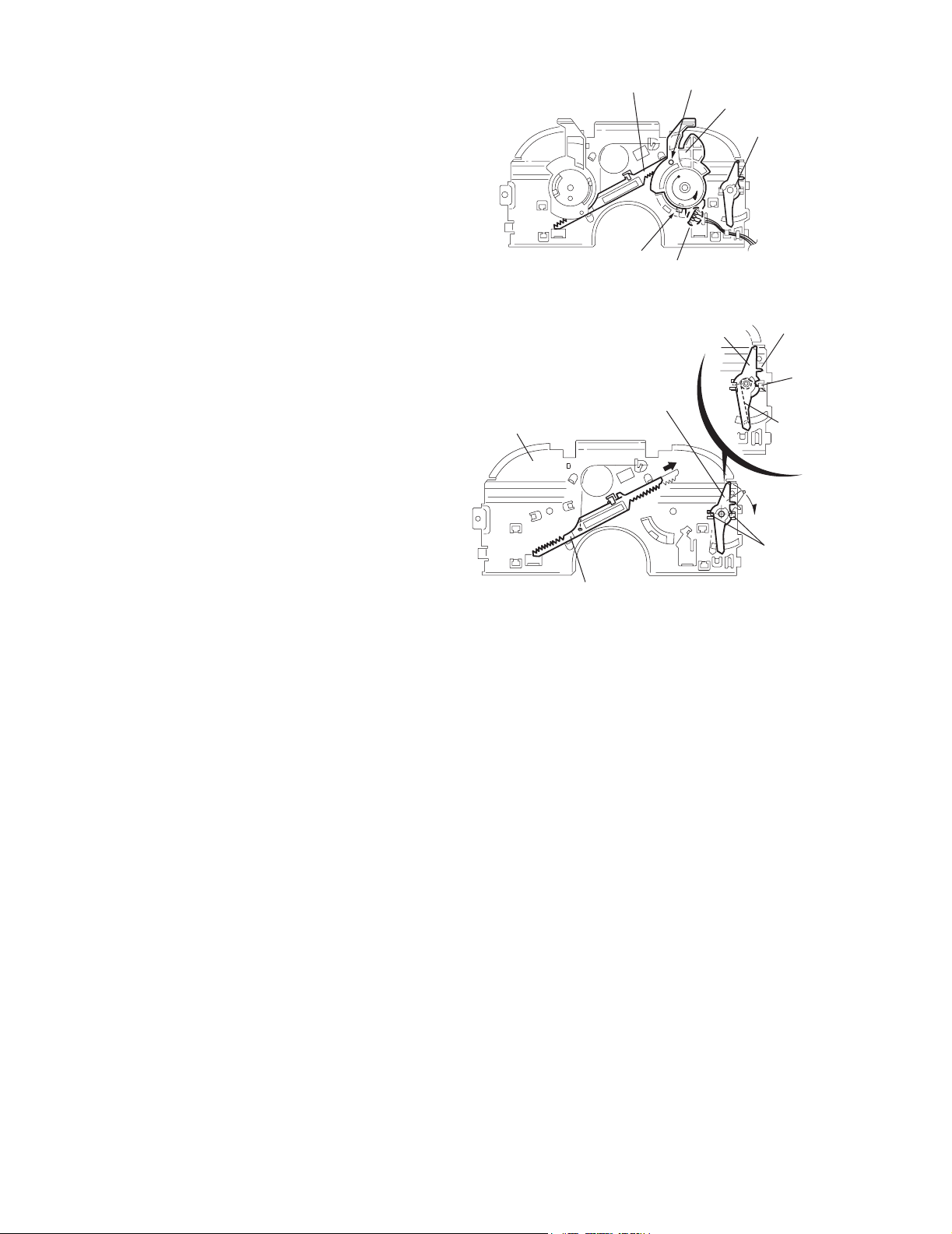
2.2.11 Removing the mode sw. / select lock arm
(See Figs.22 and 23)
• Prior to performing the following procedure, remove the top
plate assembly.
(1) Bring up the mode sw. to release from the link plate (joint t)
and turn in the direction of the arrow to release the joint u.
(2) Unsolder the wire of the mode sw. marked s if necessary.
(3) Turn the select lock arm in the direction of the arrow to re-
lease the two joints v.
(4) The select lock arm spring comes off the select lock arm at
the same time.
Link plate
Joint u
Fig.22
Joint t
Mode sw.
Select lock arm
s
Top plate
Select lock arm
Link plate
Select lock arm
Fig.23
Top plate
Hook w
Select lock
arm spring
Joints v
1-16 (No.49860)
Page 17
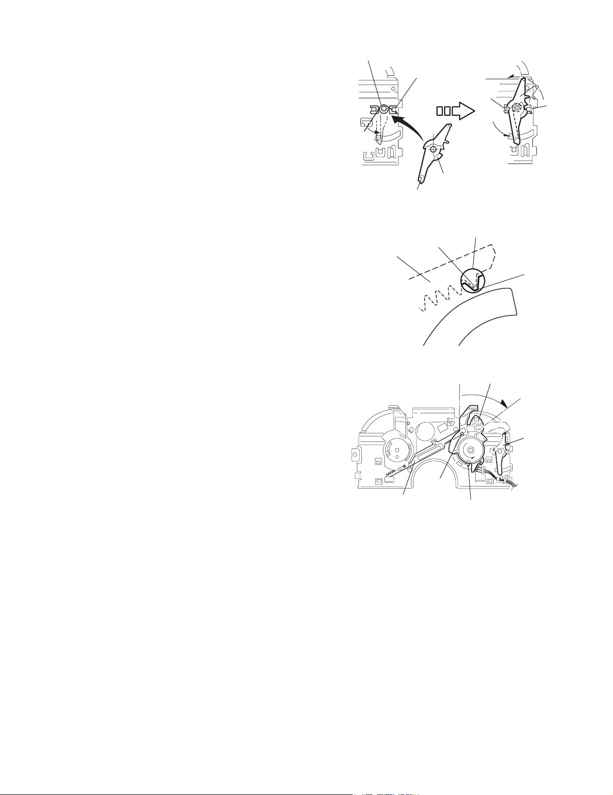
2.2.12 Reassembling the mode sw. / select lock arm
(See Figs.24 to 26)
REFERENCE:
Reverse the above removing procedure.
(1) Reattach the select lock arm spring to the top plate and set
the shorter end of the select lock arm spring to the hook w
on the top plate.
(2) Set the other longer end of the select lock arm spring to the
boss x on the underside of the select lock arm, and join the
select lock arm to the slots (joint v). Turn the select lock
arm as shown in the figure.
(3) Reattach the mode sw. while setting the part t to the first
peak of the link plate gear, and join the joint u.
CAUTION:
When reattaching the mode sw., check if the points y and
z are correctly fitted and if each part operates properly.
Select lock arm spring
Hook w
Joint v
Joint v
Select lock arm
Boss x
Fig.24
Joint t
Point y
Link plate
Point z
Link plate
Fig.25
Mode sw.
Select
lock arm
Joint t
Joint u
Fig.26
(No.49860)1-17
Page 18
2.2.13 Removing the select arm R / link plate
(See Figs.27 and 28)
• Prior to performing the following procedure, remove the top
plate assembly.
(1) Bring up the select arm R to release from the link plate
(joint a') and turn as shown in the figure to release the two
joints b' and joint c'.
(2) Move the link plate in the direction of the arrow to release
the joint d'. Remove the link plate spring at the same time.
REFERENCE:
Before removing the link plate, remove the mode sw.
Select arm R
Joint b'
Link plate spring
Joint c'
Joint a'
Link plate
Joint b'
Fig.27
Joint r
2.2.14 Reattaching the Select arm R / link plate
(See Figs.29 and 30)
REFERENCE:
Reverse the above removing procedure.
(1) Reattach the link plate spring.
(2) Reattach the link plate to the link plate spring while joining
them at joint d'.
(3) Reattach the joint a' of the select arm R to the first peak of
the link plate while joining the two joints b' with the slots.
Then turn the select arm R as shown in the figure. The top
plate is joined to the joint c'.
CAUTION:
When reattaching the select arm R, check if the points e'
and f' are correctly fitted and if each part operates properly.
Top plate
Select arm R
Joint b'
Joint d'
Link plate
Fig.28
Link plate spring
Joint c'
Joint d'
Joint b'
Joint a'
Fig.29
1-18 (No.49860)
Joint a'
Point e'
Link plate
Point f'
Fig.30
Page 19
2.2.15 Removing the loading roller assembly
(See Figs.31 to 33)
• Prior to performing the following procedure, remove the
clamper assembly and top plate assembly.
(1) Push inward the loading roller assembly on the gear side
and detach it upward from the slot of the joint g' of the lock
arm rivet assembly.
(2) Detach the loading roller assembly from the slot of the joint
h' of the lock arm rivet assembly.
Roller guide
spring
Part k'
Loading roller assembly
Loading roller assembly
The roller guide comes off the gear section of the loading
roller assembly.
Remove the roller guide and the HL washer from the shaft
of the loading roller assembly.
(3) Remove the screw J attaching the lock arm rivet assembly.
(4) Push the shaft at the joint i' of the lock arm rivet assembly
inward to release the lock arm rivet assembly from the slot
of the L side plate.
(5) Extend the lock arm rivet assembly outward and release
the joint j' from the boss of the chassis rivet assembly. The
roller guide springs on both sides come off at the same
time.
CAUTION:
When reassembling, reattach the left and right roller
guide springs to the lock arm rivet assembly before reattaching the lock arm rivet assembly to the chassis rivet
assembly. Make sure to fit the part k' of the roller guide
spring inside of the roller guide. (Refer to Fig.34.)
Roller guide
HL washer
Loading roller assembly
Roller guide
Chassis rivet assembly
J
Roller guide
spring
Fig.32
Boss
L side plate
Roller guide spring
Joint h'
Roller guide spring
Loading roller assembly
Joint g'
Lock arm rivet assembly
Fig.31
Roller guide spring
Roller guide spring
Lock arm rivet assembly
Lock arm rivet assembly
Joint i'
Part j'
Fig.33
Roller guide
HL washer
Roller shaft assembly
Loading roller
Roller guide spring
Fig.34
(No.49860)1-19
Page 20

2.2.16 Removing the loading gear 5, 6 and 7
(See Figs.35 and 36)
• Prior to performing the following procedure, remove the top
cover, chassis unit, pickup unit and top plate assembly.
(1) Remove the screw K attaching the loading gear bracket.
The loading gear 6 and 7 come off the loading gear bracket.
(2) Pull out the loading gear 5.
K
Loading gear bracket
K
Loading gear 6
Loading gear 5
Loading gear 3
Fig.35
Loading gear bracket
Loading gear 5
Loading gear 6
Loading gear 7
Fig.36
1-20 (No.49860)
Page 21

2.2.17 Removing the gears
(See Figs.37 to 40)
• Prior to performing the following procedure, remove the top
cover, chassis unit, top plate assembly and pickup unit.
• Pull out the loading gear 3. (See Fig.35.)
(1) Pull out the feed gear.
(2) Move the loading plate assembly in the direction of the ar-
row to release the L side plate from the two slots m' of the
chassis rivet assembly. (See Fig.37.)
(3) Detach the loading plate assembly upward from the chas-
sis rivet assembly while releasing the joint n'. Remove the
slide hook and loading plate spring from the loading plate
assembly.
(4) Pull out the loading gear 2 and remove the change lock le-
ver.
(5) Remove the E ring and washer attaching the changer gear
2.
(6) The changer gear 2, change gear spring and adjusting
washer come off.
(7) Remove the loading gear 1.
(8) Move the change plate rivet assembly in the direction of the
arrow to release from the three shafts of the chassis rivet
assembly upward. (See Fig.38.)
(9) Detach the loading gear plate rivet assembly from the shaft
of the chassis rivet assembly upward while releasing the
joint p'. (See Figs.38 and 40.)
(10) Pull out the loading gear 4.
Change plate
rivet assembly
Shafts
E ring
Loading plate assembly
Loading plate spring
Joint p'
Loading gear 4
Loading gear plate
rivet assembly
Shaft
Loading gear 2
Loading gear 1
Chassis rivet assembly
Change gear 2
Fig.38
Joint n'
Slide hook
Feed gear
Fig.37
Slot m'
L side plate
Loading plate assembly
Joint n'
Slot m'
Chassis rivet assembly
Chassis rivet assembly
E ring
Washer
Change gear 2
Change gear spring
Adjusting washer
Change plate
rivet assembly
Chassis rivet assembly
L side plate
Slot m'
Slot m'
Fig.39
Loading gear 1
Loading gear 2
Change lock lever
Loading gear 4
Loading gear plate rivet assembly
Fig.40
(No.49860)1-21
Page 22

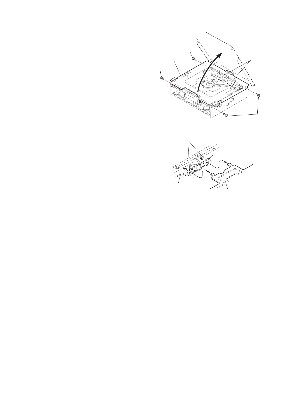
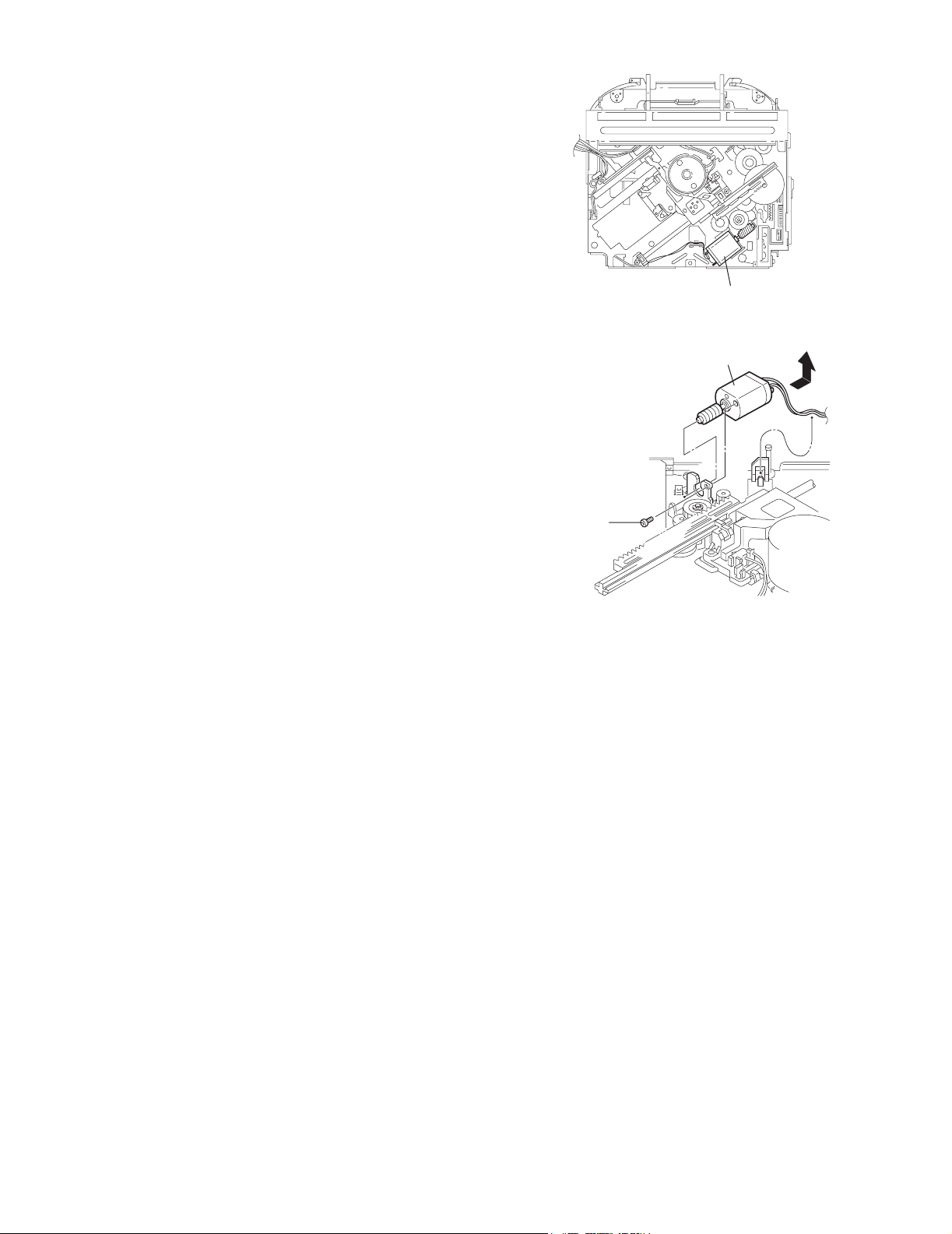
2.2.18 Removing the turn table / spindle motor
(See Figs.41 and 42)
• Prior to performing the following procedure, remove the top
cover, connector board, chassis unit and clamper assembly.
(1) Remove the two screws L attaching the spindle motor as-
sembly through the slot of the turn table on top of the body.
(2) Unsolder the wire on the connector board if necessary.
Turn table
L
Fig.41
L
Turn table
1-22 (No.49860)
Spindle motor
Fig.42
Page 23

SECTION 3
Adjustment
3.1 Adjustment method
Test instruments required for adjustment
1. Digital oscilloscope (100MHz)
2. AM Standard signal generator
3. FM Standard signal generator
4. Stereo modulator
5. Electric voltmeter
6. Digital tester
7. Tracking offset meter
8. Test Disc JVC : CTS-1000
9. Extension cable for check
EXTSH002-22P × 1
Standard measuring conditions
Power supply voltage DC14.4V(10.5 ~ 16V)
Load impedance 20Kohm(2 Speakers connection)
Output Level Line out 2.0V (Vol. MAX)
Standard volume position
Balance and Bass & Treble volume : lndication"0"
Loudness : OFF
BBE : OFF
Frequency Band
FM 87.5MHz ~ 107.9MHz
AM 530kHz ~ 1710 kHz
Dummy load
Exclusive dummy load should be used for AM, and FM. For
FM dummy load, there is a loss of 6dB between SSG output
and antenna input. The loss of 6dB need not be considered
since direct reading of figures are applied in this working
standard.
How to connect the extension cable for adjusting
The cardboard is cut in a suitable size.
uses for the insulation stand of mechanism.
CAUTION :
Be sure to attach the parts (Heat sink and rear bracket)
on the IC (Power amplifier IC321 and regulator IC901)
of a main board when supplying the power.
If voltage is applied without attaching those parts, the
power amplifier IC and regulator IC will be destroyed by heat.
Heat sink
Extension cable
EXTSH002-22P
Rear bracket
(No.49860)1-23
Page 24

3.2 Troubleshooting
3.2.1 Feed section
Is the voltage output at
IC541 pin 4 is 5V or 0V?
Is 4V present at both
sides of the feed motor?
Check the feed motor
3.2.2 Focus section
YES
YES
NO
YES
Is 5V present at IC581
Check the vicinity of
Check the circuits in
the vicinity of IC541
pin 6?
YES
IC521.
Is the wiring for IC541
1 ~ 14 correct?
NO
.
Check the feed motor
connection wiring.
When the lens is
moving:
NONO
Check CD 9V
and 5V.
pins 8 and 9.
4V
Does the S-search
waveform appear at
IC561 pins 32?
YES
Check the pickup and
its connections
YES
.
3.2.3 Spindle section
Is the disk rotated?
YES
Does the RF signal
appear at ARF TP?
YES
Is the RF waveform at
ARF TP distorted?
YES
Proceed to the Tracking
section
3.2.4 Tracking section
When the disc is rotated
at first:
Approx. 1.2V
NO
NO
Is 4V present between
IC541 pins 6 and 7?
Check the spindle motor
and its wiring.
NO
Check the circuits in the
vicinity of IC561 21 ~ 40
or the pickup
NO
Check the circuit in the
vicinity of IC561 pins
21 ~ 40
Is 4V present at IC561
pin 29?
YES
Check the vicinity of
IC541.
YESYES
Check the pickup and
NO
Check IC561 and
its connections
IC901.
1-24 (No.49860)
Is the tracking error
signal output at TE TP?
YES
Check IC501.
Page 25

3.2.5 Signal processing section
Is the sound output from
both channels (L, R)?
YES
Normal
NO
No sound from either
channel.
Is 9V present at IC101 pin
(8)?
Is the audio signal
(including sampling output
components) output to
IC801 pins 39 and 40 during
playback
Is the audio signal output
at IC301 pins 1
and 32during playback?
Check the muting circuit.
YES
YES
YES
YES
NO
Compare the L-ch and R-ch
to locate the defective point.
NO
Check the vicinity of the
Q981 audio power supply.
NO
Check IC801 and its
peripheral circuits
NO
Check IC301 and its
peripheral circuits
YES
(No.49860)1-25
Page 26

3.3 Maintenance of laser pickup
(1) Cleaning the pick up lens
Before you replace the pick up, please try to clean the lens
with a alcohol soaked cotton swab.
(2) Life of the laser diode
When the life of the laser diode has expired, the following
symptoms will appear.
• The level of RF output (EFM output:ampli tude of eye
pattern) will be low.
3.4 Replacement of laser pickup
Turn off the power switch and,disconnect the power cord
from the ac outlet.
Replace the pickup with a normal one.(Refer to
"Pickup Removal" on the previous page)
Is RF output
1.0
±
0.35Vp-p?
NO
Replace it.
YES
O.K
(3) Semi-fixed resistor on the APC PC board
The semi-fixed resistor on the APC printed circuit board
which is attached to the pickup is used to adjust the laser
power.Since this adjustment should be performed to match
the characteristics of the whole optical block, do not touch
the semi-fixed resistor. If the laser power is lower than the
specified value,the laser diode is almost worn out, and the
laser pickup should be replaced. If the semi-fixed resistor
is adjusted while the pickup is functioning normally,the laser pickup may be damaged due to excessive current.
Plug the power cord in,and turn the power on.
At this time,check that the laser emits for about 3seconds
and the objective lens moves up and down.
Note: Do not observe the laser beam directly.
Play a disc.
Check the eye-pattern at ARF TP.
Finish.
1-26 (No.49860)
Page 27

4.1 HA13164A (IC901) : Regulator
•Pin layout
123456789101112131415
• Block diagram
ANT OUT
EXT OUT
ANT CTRL
CTRL
CD OUT
AUDIO OUT
C3
0.1u
C4
0.1u
C5
0.1u
C6
10u
2
1
7
11
12
10
SECTION 4
Description of major ICs
C1
100u
VCC ACC
8
Surge Protector
BIAS TSD
15
3
TAB
ILM AJGND GND
13
C2
0.1u
+B
ACC
BATT.DET OUT
9
COMPOUT
6
VDD OUT
4
SW5VOUT
5
ILMOUT
14
R1
C7
0.1u
C8
0.1u
UNIT R:
C:F
note1) TAB (header of IC)
connected to GND
• Pin function
Pin No. Symbol Function
1 EXTOUT Output voltage is VCC-1 V when M or H level applied to CTRL pin.
2 ANTOUT Output voltage is VCC-1 V when M or H level to CTRL pin and H level to ANT-CTRL.
3 ACCIN Connected to ACC.
4 VDDOUT Regular 5.7V.
5 SW5VOUT Output voltage is 5V when M or H level applied to CTRL pin.
6 COMPOUT Output for ACC detector.
7 ANT CTRL L:ANT output OFF H:ANT output ON
8 VCC Connected to VCC.
9 BATT DET Low battery detect.
10 AUDIO OUT Output voltage is 9V when M or H level applied to CTRL pin.
11 CTRL L: BIAS OFF M: BIAS ON H: CD ON
12 CD OUT Output voltage is 8V when H level applied to CTRL pin.
13 ILM AJ Adjustment pin for ILM output voltage.
14 ILM OUT Output voltage is 10V when M or H level applied to CTRL pin.
15 GND Connected to GND.
(No.49860)1-27
Page 28

4.2 AN8806SB-W (IC501) : RF & amp.
• Pin layout
PD 1
LD 2
LDON 3
LDP 4
VCC 5
RF- 6
RF OUT 7
RF IN 8
C.AGC 9
ARF 10
C.ENV 11
C.EA 12
CS BDO 13
BDO 14
CS BRT 15
OFTR 16
/NRFDET 17
GND 18
• Block diagram
6
+
36 PDAC
35 PDBD
34 PDF
33 PDE
32 PDER
31 PDFR
30 TBAL
29 FBAL
28 EF27 EF OUT
26 TE25 TE OUT
24 CROSS
23 TE BPF
22 VDET
21 LD OFF
20 VREF
19 ENV
29
728
- +
27
+
910 17
8
AGC
EQ
RF
DET
11
12 19
ENV CURCUIT
36
+
35
+
31
34
-
+
VCBA
-
+
VCBA
-
-
VCBA
+
+
OFTR
BDO
+
13
14
15
16
20
+
- +
32
33
+
-
VCBA
+
+ -
+
- +
21
2
+
-
24 25
30
23
26
22
14
3
1-28 (No.49860)
Page 29

• Pin function
Pin No. Symbol I/O Function
1 PD I APC amp input terminal
2 LD O APC amp output terminal
3 LD ON I APC ON/OFF control terminal
4 LDP - Connect to ground
5 VCC - Power supply
6 RF- I Inverse input pin for RF amp
7 RF OUT O RFamp output
8 RF IN I RF input
9 C.AGC I/O Connecting pin of AGC loop filter
10 ARF O RF output
11 C.ENV I/O A capacitor is connected to this terminal to detect the envelope of RF signal
12 C.EA I/O A capacitor is connected to this terminal to detect the envelope of RF signal
13 CS BDO I/O A capacitor is connected to detect the lower envelope of RF signal
14 BDO O BDO output pin
15 CS BRT I/O A capacitor is connected to detect the lower envelope of RF signal
16 OFTR O Of-track status signal output
17 /NRFDET O RF detection signal output
18 GND - Ground
19 ENV O Envelope output
20 VREF O Reference voltage output
21 LD OFF - Connect to ground
22 VDET O Vibration detection signal output
23 TE BPF I Input pin of tracking error through BPF
24 CROSS O Tracking error cross output
25 TE OUT O Tracking error signal output
26 TE- I Inverse input pin for tracking error amp
27 FE OUT O Output pin of focus error
28 FE- I Inverse input pin for focus error amp
29 FBAL I Focus balance control
30 TBAL I Tracking balance control
31 PDFR I/O F I-V amp gain control
32 PDER I/O E I-V amp gain control
33 PDF I I-V amp input
34 PDE I I-V amp input
35 PD BD I I-V amp input
36 PD AC I I-V amp input
(No.49860)1-29
Page 30

4.3 TEA6320T-X (IC301) : E.volume
• Pin layout
SDA
1
GND
TL
B2L
B1L
IVL
ILL
QSL
IDL
MUTE
ICL
IMD
IBL
IAL
2
3
4
5
6
7
8
9
10
11
12
13
14
15
16
CD-CH
TAPE
TUNER
OUTLR
OUTLF
• Block diagram
10 8 9 7 6
32
31
30
29
28
27
26
25
24
23
22
21
20
19
18
17
SCL
VCC
OUTRR
OUTRF
TR
B2R
B1R
IVR
ILR
QSR
IDR
Vref
ICR
CAP
IBR
IAR
5
12
21
31
19
POWER
SUPPLY
2
VOLUME 1
+20 to -31 dB
LOUDNESS
LEFT
16
15
13
11
14
22
20
SOURCE
SELECTOR
VOLUME 1
+20 to -31 dB
LOUDNESS
RIGHT
18
17
23 25 24 26 27 28
• Pin functions
Pin No. Symbol I/O Functions
1 SDA I/O Serial data input/output.
2 GND - Ground.
3 OUTLR O output left rear.
4 OUTLF O output left front.
5 TL I Treble control capacitor left channel
or input from an external equalizer.
6 B2L - Bass control capacitor left channel or
output to an external equalizer.
7 B1L - Bass control capacitor left channel.
8 IVL I Input volume 1. left control part.
9 ILL I Input loudness. left control part.
10 QSL O Output source selector. left channel.
11 IDL - Not used
12 MUTE - Not used
13 ICL I Input C left source.
14 IMO - Not used
15 IBL I Input B left source.
16 IAL I Input A left source.
17 IAR I Input A right source.
18 IBR I Input B right source.
BASS
LEFT
+15 dB
LOGIC
BASS
RIGHT
+15 dB
VOLUME 2
0 to 55 dB
BALANCE
FENDER REAR
VOLUME 2
0 to 55 dB
BALANCE
FENDER FRONT
HC BUS
REC
VOLUME 2
0 to -55dB
BALANCE
FENDER FRONT
VOLUME 2
0 to -55dB
BALANCE
FENDER REAR
3
4
32
1
29
30
TREBLE
LEFT
+12 dB
TREBLE
RIGHT
+12 dB
MUTE
FUNCTION
ZERO CROSS
DETECTOR
Pin No. Symbol I/O Functions
19 CAP - Electronic filtering for supply.
20 ICR I Input C right source.
21 Vref - Reference voltage (0.5Vcc)
22 IDR - Not used
23 QSR O Output source selector right channel.
24 ILR I Input loudness right channel.
25 IVR I Input volume 1. right control part.
26 B1R - Bass control capacitor right channel
27 B2R O Bass control capacitor right channel
or output to an external equalizer.
28 TR I Treble control capacitor right channel
or input from an external equalizer.
29 OUTRF O Output right front.
30 OUTRR O Output right rear.
31 Vcc - Supply voltage.
32 SCL I Serial clock input.
1-30 (No.49860)
Page 31

4.4 NJM4565M-WE (IC151) : CD L.P.F.
T
A
• Pin layout & Block diagram
OUTPUT
+
1
8
V
-
A INPUT
+
A INPUT
-
V
4.5 RPM6938-SV4 (IC602) : Remote sensor
• Pin diagram
1 2 3
• Block diagram
AMP
I/V
conversion
2
3
4
AGC
Comp
BPF
Detector
7
6
5
Vcc
B OUTPU
-
B INPUT
+
B INPUT
22k
Vcc
Rout
PD
magnetic shield
fo
trimming
circuit
GND
(No.49860)1-31
Page 32

4.6 JES01-9B42 (IC801) : Main micon
• Pin layout
25 ~ 40
24 ~ 1
80 ~ 65
41 ~ 64
• Pin function
Pin No. Symbol Function
1 XIN X'tal oscillator conection terminal
2 TEST2 GND
3 J BUS SI Non connect
4 J BUS SO Non connect
5 J BUS SCK Non connect
6 J BUS I/O CONT Non connect
7 SUBQ CD LSI subQ code data input terminal
8 NC Non connect
9 SQCK CD LSI sub code clock terminal
10 RESET Main micon reset terminal
11 LCD SI Non connect
12 LCD SO LCD serial data output
13 LCD SCK LCD serial clock
14 LCD CE Chip enable output for LCD driver
15 FM ILLUMI Non connect
16 AM ILLUMI Non connect
17 CD ILLUMI Non connect
18 DIMMER OUT Non connect
19 NC Non connect
20 MOTOR SEL Loading motor signal select terminal
21 ~ 23 NC Non connect
24 KS2 Open
25 KS1 Open
26 KS0 Open
27 DETACH Front panel detach detectionsignal input
28 K2 Non connect
29 K1 Open
30 K0 Open
31 Vdd Power supply
32 LM Loading motor control terminal
33 CD LSI RESET CD LSI reset signaloutput terminal
34 MCLK CD LSI command clock signal output terminal
35 MDATA CD LSI command data output terminal
36 MLD CD LSI command load signal output terminal
37,38 NC Non connect
39 SCL E.volume clock signal output terminal
40 SDA E.volume data output terminal
41 CD ON CD power ON control terminal
1-32 (No.49860)
Page 33

Pin No. Symbol Function
42 RELAY Power supply control terminal
43 BLKCL Sub code/ Block signal input terminal
44 BEEP Non connect
45 SW1 Detection switch 1
46 SW2 Detection switch 2
47 PSW Pnael switch detection
48 REST Rest switch input terminal
49 FLOCK Focus signal input terminal
50 TLOCK Tracking signal input terminal
51 CD SENSE Senser signal input terminal from CD LSI
52 STATUS Status signal input terminal
53 P.SAVE2 Power save 2 detection signal input termianl
54 SD/ST Station detect/Stereo indocator
55 REMOCON Remocon signal detection terminal
56 J BUS INT Non connect
57 BAND FM/AM band select terminal
58 MONO FM mono control signal output termianl
59 IFRQ/AGC FA auto serch IF request output
60 MUTE Mute switch
61 LEVEL Non connect
62 S METER S meter input terminal
63 KEY CHANGE AD key select terminal
64 KEY2 Key AD input terminal 2
65 KEY1 Key AD input terminal 1
66 KEY0 Key AD input terminal 0
67 P.SAVE1 Power save 1 detection input terminal
68 SENSE Senser signal output terminal
69 NC Non connect
70 FM IF COUNT FM IF control signal input terminal
71,72 NC Non connect
73 Vdd Power supply
74 AM OSC Non connect
75 FM OSC FM local osc signal input terminal
76 Vss GND
77 NC Non connect
78 EQ PLL error signalinput terminal
79 TEST1 Test terminal 1
80 XOUT X'tal oscillator connect terminal
(No.49860)1-33
Page 34

4.7 LA4743K (IC321) : Power amp.
• Block diagram
IN 1
TAB
IN 2
+
0.22 F
+
0.22 F
11
1
12
Vcc 1/2 Vcc 3/4
6 20
-
+
Protective
circuit
-
+
2200 F 0.022 F
+
9
7
+
OUT 1+
OUT 1-
PWR GND1
8
+
OUT 2+
5
-
OUT 2-
3
PWR GND2
2
ST BY
R.F
47 F
IN 3
PRE GND
IN 4
+5V
ST ON
+
0.22 F
N.C
+
0.22 F
4
Stand by
Switch
Mute
10
+
Ripple
Filter
Mute
22
circuit
3.3 F
+
15
-
+
-
17
19
10K
+
OUT 3+
OUT 3-
Low Level
Mute ON
25
18
21
23
PWR GND3
OUT 4+
OUT 4-
13
14
Protective
circuit
-
+
+
-
ON TIME C
1-34 (No.49860)
22 F
Muting &
16
+
ON Time Control
Circuit
PWR GND4
24
Page 35

•Pin layout
TAB
GND
FR-
STDBY
FR+
VP1
RR-
GND
RR+
RIPPLE
INRF
INRR
SGND
FLIN
RLIN
DNTIME
RL+
GND
RL-
VP3
FL+
MUTE
FL-
GND
NC
• Pin function
Pin No. Symbol Function
1 TAB Header of IC
2 GND Power GND
3 FR- Outpur(-) for front Rch
4 STDBY Stand by input
5 FR+ Output (+) for front Rch
6 VP1 Power input
7 RR- Output (-) for rear Rch
8 GND Power GND
9 RR+ Output (+) for rear Rch
10 RIPPLE Ripple filter
11 RRIN Rear Rch input
12 FRIN Front Rch input
13 SGND Signal GND
14 FLIN Front Lch input
15 RLIN Rear Lch input
16 ONTIME Power on time control
17 RL+ Output (+) for rear Lch
18 GND Power GND
19 RL- Output (-) for rear Lch
20 VP3 Power input
21 FL+ Output (+) for front
22 MUTE Muting control input
23 FL- Output (-) for front
24 GND Power GND
25 NC Non connection
(No.49860)1-35
Page 36

4.8 LA6589H-X (IC541) : BTL driver
• Pin layout & Block diagram
VIN1-A
1
+
VIN1+A
VCCP1
2
3
VIN1_SW
H : OP-AMP_A
L : OP-AMP_B
H
28
VIN1
L
27
VIN1-B
+
26
VIN1+B
VO1+
VO1-
VO2+
VO2-
FR
VO3+
VO3-
VO4+
4
5
6
7
Power system
FR
8
9
10
GND
Level shift Level shift
+
Level shift Level shift
33k
11k
+
It is ON/OFF as for all outputs.
5VREG(PNPTr External)
Signal system
GND
H : ON
L : OFF
Signal system
power supply
MUTE
Power system GND
25
S-GND
24
VIN1-SW
23
MUTE
22
VREF_IN
FR
FR
21
VCC_S
20
REG-OUT
+
19
REG_IN
VCCP2
VIN4G
1-36 (No.49860)
VO4-
VIN4
11
12
13
14
11k
+
33k
33k
33k
18
VIN2G
11k
+
11k
+
17
16
15
VIN2
VIN3G
VIN3
Page 37

• Pin function
Pin No. Symbol Function
1 VIN1-A CH1 input AMP_A reversing input
2 VIN1+A CH1 input AMP_A non-reversing input
3 VCCP1 CH1 and CH2 power steps power supply
4 VO1+ CH1 Output terminal (+)
5 VO1- CH1 Output terminal (-)
6 VO2+ CH2 Output terminal (+)
7 VO2- CH2 Output terminal (-)
8 VO3+ CH3 Output terminal (+)
9 VO3- CH3 Output terminal (-)
10 VO4+ CH4 Output terminal (+)
11 VO4- CH4 Output terminal (-)
12 VCCP2 CH3 and CH4 power steps power supply
13 VIN4 CH4 Input terminal
14 VIN4G CH4 Input terminal(For gain adjustment)
15 VIN3 CH3 Input terminal
16 VIN3G CH3 Input terminal(For gain adjustment)
17 VIN2 CH2 Input terminal
18 VIN2G CH2 Input terminal(For gain adjustment)
19 REGIN External PNP transistor base connection
20 REG-OUT 5VREG output terminal and external PNP transistor collector connection
21 VCCS Signal system power supply
22 VREFIN Standard voltage impression terminal
23 MUTE Output ON/OFF terminal
24 VIN1_SW CH1 input OP_AMP switch terminal
25 S_GND Signal system GND
26 VIN1+B CH1 AMP_B non-reversing input terminal
27 VIN1-B CH1 AMP_B reversing input terminal
28 VIN1 CH1 input terminal and input OP_AMP output terminal
*1 Frame (FR) at the center becomes system GND(P-GND) power . Please give (*O) as the lowest potential with system GND(S-
GND) signal.
*2 Be short-circuited of VCC_S (signal system power supply) and VCCP1 and VCCP2 (output steps power supply) on the out-
side.
(No.49860)1-37
Page 38

4.9 MN6627482WA (IC561) : DSP & DAC
A
R
• Pin layout
20 ~ 1
• Block diagram
LRCKIN(MSEL)
BCLK(SSEL)
SRDATAIN
(PSEL)
IOSEL
CLVS
CRC
BLKCK
CLDCK
SBCK
SUBC
DEMPH
RESY
FLAG6(RESY)
SSEL
SQCK
SUBQ
AVDD2
AVDD2
PCK
EFM
PLLF
DSLF
IREF
DRF
ARF
RSEL
PSEL
MLD
MCLK
MDATA
CK384(EFM)
VCOF
BYTCK
SMCK
FCLK
CSEL
MSEL
X2
X1
ÊSTAT
21
~
40
41 ~ 60
DIGITAL
DEEMPHSIS
SUB
CODE
BUFFER
DSL.
PLL
VCO
VCO
ITUNING
GENERATION
PITCH
CONTROL
80
~
61
8TIMES
OVER SAMPUNC
DIGITAL FILTER
EFM
DEMODULATION
SYNC
INTERPOLATION
SUBCODE
DEMODULATION
MICRO
COMPUTER
INTERFACE
A/D
COVERTER
1BIT
DAC
LOGIC
S
16k
SRAM
CIRC
ERROR
CORRECTION
DEINTERLEVE
CLV
SERVO
INPUT
PEM
(R)
PEM
(L)
D/A
CONVERTER
OUTPUT
DIGITAL
AUDIO
INTERFASE
DIGITAL
AUDIO
INTERFASE
INTER POLATION
SOFT MUTING DIGITAL
ATTENUATION
PEAK DETECTIVE
AUTO CUE
PORT
SERVO
TIMING GENERATOR
AVSS1
AVDD1
OUTR
OUTL
FLAG
IPFLAG
TX
ECM
PC
LRCK
SRDAT
BCLK
DMUTE
TRKV
KICK
VREF
TRVST
ECS
TVD
TRD
FOD
TBAL
FBAL
TOFS
TES
/TLOCK
/FLOCK
PLAY
LDON
WVEL
SENSE
1-38 (No.49860)
D
/
D
V
V
V
R
V
S
D
D
S
S
S
D
D
T
S
1
1
F
/
E
T
E
S
T
R
T
F
E
E
N
V
T
R
C
R
S
B
V
D
D
O
E
T
/
R
F
D
E
O
F
T
Page 39

• Pin function
Pin No. Symbol I/O Function
1 BCLK O Not used
2 LRCK O Not used
3 SRDATA O Not used
4 DVDD1 - Power supply (Digital)
5 DVSS1 - Connected to GND
6 TX O Not used
7 MCLK I CPU command clock signal input(Data is
latched at signal's rising point)
8 MDATA I CPU command data input
9 MLD I CPU command load signal input
10 SENSE O Sense signal output
11 FLOCK O Focus lock signal output Active: Low
12 TLOCK O Tracking lock signal output Active: Low
13 BLKCK O sub-code/block/clock signal output
14 SQCK I Outside clock for sub-code Q resister in-
put
15 SUBQ O Sub-code Q -code output
16 DMUTE Connected to GND
17 STAT O Status signal(CRC,CUE,CLVS,
TTSTOP,ECLV,SQOK)
18 RST I Reset signal input (L:Reset)
19 SMCK - Not used
20 PMCK - Not used
21 TRV O Traverse enforced output
22 TVD O Traverse drive output
23 PC - Not used
24 ECM O Spindle motor drive signal (Enforced
mode output) 3-State
25 ECS O Spindle motor drive signal (Servo error
signal output)
26 KICK O Kick pulse output
27 TRD O Tracking drive output
28 FOD O Focus drive output
29 VREF - Reference voltage input pin for D/A out-
put block (TVD,FOD,FBA,TBAL)
30 FBAL O Focus Balance adjust signal output
31 TBAL O Tracking Balance adjust signal output
32 FE I Focus error signal input (Analog input)
33 TE I Tracking error signal input (Analog input)
34 RF ENV I RF envelope signal input (Analog input)
35 VDET I Vibration detect signal input (H:detect)
36 OFT I Off track signal input (H:off track)
37 TRCRS I Track cross signal input
38 RFDET I RF detect signal input (L:detect)
39 BDO I BDO input pin (L:detect)
40 LDON O Laser ON signal output (H:on)
41 PLLF2 - Not used
42 TOFS O Tracking error shunt signal output
(H:shunt)
Pin No. Symbol I/O Function
43 WVEL - Not used
44 ARF I RF signal input
45 IREF I Reference current input pin
46 DRF I Bias pin for DSL
47 DSLF I/O Loop filter pin for DSL
48 PLLF I/O Loop filter pin for PLL
49 VCOF - Not used
50 AVDD2 - Power supply (Analog)
51 AVSS2 - Connected to GND (Analog)
52 EFM - Not used
53 PCK - Not used
54 VCOF2 - PLL data slice output
55 SUBC - Not used
56 SBCK - Not used
57 VSS - Connected to GND (for X'tal oscillation
circuit)
58 XI I Input of 16.9344MHz X'tal oscillation cir-
cuit
59 X2 O Output of X'tal oscillation circuit
60 VDD - Power supply (for X'tal oscillation circuit)
61 BYTCK - Not used
62 CLDCK - Not used
63 FCLK - Not used
64 IPFLAG - Not used
65 FLAG - Not used
66 CLVS - Not used
67 CRC - Not used
68 DEMPH - Not used
69 RESY - Not used
70 IOSEL - pull up
71 TEST - pull up
72 AVDD1 - Power supply (Digital)
73 OUT L O Lch audio output
74 AVSS1 - Connected to GND
75 OUT R O Rch audio output
76 RSEL - pull up
77 CSEL - Connected to GND
78 PSEL - Connected to GND
79 MSEL - Connected to GND
80 SSEL - Pull up
(No.49860)1-39
Page 40

4.10PT6523LQ (IC601) : LCD driver
• Pin layout
48 ~ 33
49
32
• Block diagram
64
1 ~ 16
17
COMMON
DRIVER
CLOCK
GENERATOR
ADDRESS
DETECTOR
SEGMENT DRIVER & LATCH
SHIFT REGISTER
• Piin function
Pin No. Pin Name I/O Description
1 ~ 52 SG1 ~ SG52 O Segment Output Pins
53 ~ 55 COM1 ~ COM3 O Common Driver Output Pins
56 VDD - Power Supply
57 INH
I Display OFF Control Input Pin
When this pin is "Low", the Display is forcibly turned OFF. (SG1 to SG52, COM1 to COM3 are
set to "LOW"). (See Note 1)
When this pin is set to "High", the Displa is ON.
58 VDD1 I Used for the 2/3 Bias Voltage when the Bias Voltages are provied externally. Connect to VDD2
when 1/2 Bias is used.
59 VDD2 I Used for 1/3 Bias Voltage when the Bias Voltages are provided externally. Connect to VDD1
when 1/2 Bias is used.
60 VSS - Ground Pin.
61 OSC I/O Oscillation Input /Outout Pin
62 CE I Chip Enable Pin
63 CLK I Synchronization Clock
64 DI I Transfer Data Pin
Note 1:
When INH
= "LOW" : Serial data trensfers can be performed when the display is forcibly OFF.
1-40 (No.49860)
Page 41

(No.49860)1-41
Page 42

VICTOR COMPANY OF JAPAN, LIMITED
AV & MULTIMEDIA COMPANY MOBILE ENTERTAINMENT CATEGORY 10-1,1chome,Ohwatari-machi,Maebashi-city,371-8543,Japan
(No.49860)
Printed in Japan
WPC
Page 43

PARTS LIST
[ KD-S598,KD-S597 ]
* All printed circuit boards and its assemblies are not available as service parts.
Area suffix
KD-S598,KD-S597
UR --------------------------- Brazil
- Contents -
Exploded view of general assembly and parts list (Block No.M1)
CD mechanism assembly and parts list (Block No.MB)
Electrical parts list (Block No.01,02)
Packing materials and accessories parts list (Block No.M3)
3-2
3-4
3-6
3-10
No. 49860 3-1
Page 44

KD-S598,KD-S597
Exploded view of general assembly and parts list
6
9
47
48
50
51
Block No.
M
5
M
1
M
40
9
49
9
43
52
45
4
8
11
8
A
2
A
46
10
14
Main board
17
B
10
C
18
7
13
12
33
16
15
33
1
32
44
Front
board
21
24
28
23
36
42
39
25
38
35
37
LCD1
41
34
30
29
3-2
7
26
3
27
B
C
7
22
19
31
20
Page 45

General assembly
Block No. [M][1][M][M]
Symbol No.
1 ------------------- CD MECHA
2 GE10043-210A TOP CHASSIS
3 GE40135-001A EART PLATE
4 GE30938-003A HEAT SINK
5 GE30393-002A BOTTOM COVER
6 FSMA3004-203 ISULATOR
7 QYSDST2604Z SCREW 2.6mm x 4mm(x3)
8 FSKZ4005-001 SCREW (x2)
9 QYSDST2604Z SCREW 2.6mm x 4mm(x3)
10 QYSDST2606Z SCREW 2.6mm x 6mm(x2)
11 QYSDST2610Z SCREW 2.6mm x 10mm
12 GE10056-002A FRONT CHASSIS
12 GE10056-001A FRONT CHASSIS
13 GE30583-001A LOCK LEVER
14 FSKW4005-003 TORS. SPRING
15 FSXP3026-002 RLS KNOB
16 FSKW3002-015 COMP.SPRING
17 GE40140-001A BLIND
18 QYSDST2004M MINI SCREW 2mm x 4mm
19 GE10037-003A FRONT PANEL
20 GE30300-026A FINDER ASSY
20 GE30300-025A FINDER ASSY
21 GE20119-001A PRESET BUTTON
22 GE30304-001A POWER BUTTON
23 GE30305-001A EJECT BUTTON
24 GE20131-002A D.FUNC BUTTON
25 GE30307-001A SND.FUNC.BUTTON
26 GE20130-002A PUSH BUTTON
27 GE20118-002A +/- BUTTON
28 GE20120-001A UP/DOWN BUTTON
29 GE30306-001A DETACH BUTTON
30 FSKW3002-012 COMP.SPRING
31 GE30117-001A LIGHT LENS
32 GE10055-002A REAR COVER
33 VKZ4777-001 MINI SCREW (x4)
34 GE30302-001A LCD CASE
35 FSJK3025-001 LCD LENS
36 GE30301-001A LENS CASE
37 GE40142-005A LIGHTING SHEET
38 FSYH4071-002 LIGHTING SHEET
39 FSYH4070-005 LIGHTING SHEET
40 ------------------- NAME PLATE
41 QLD0255-001 LCD MODULE
42 QNZ0442-001 LCD CONNECTOR
43 QMFZ047-150-T FUSE 15A
44 GE30854-001A LED HOLDER
45 GE40172-002A IC BRACKET
46 GE40124-001A REG BRACKET
47 QYSDST2606Z SCREW 2.6mm x 6mm
48 QYSDSF2606Z SCREW 2.6mm x 6mm
49 QYSDSF2606Z SCREW 2.6mm x 6mm(x2)
50 QYSDST2606Z SCREW 2.6mm x 6mm
51 GE30382-019A REAR BRACKET
52 VYSH101-009 SPACER (x2)
Part No. Part Name Description Local
S597
UR
S598
UR
S597
UR
S598
UR
KD-S598,KD-S597
3-3
Page 46

KD-S598,KD-S597
CD mechanism assembly and parts list
Grease
TNG-87
GP-501MK
CFD-005Z
GP-501A
31
C
22
112
24
61
26
36
29
Block No.
M
M
B
M
TN-2001-1011
111
74
72
35
116
34
33
111
25
73
85
15
A
19
B
21
62
D
75
112
114
11
38
30
A
23
13
32
2
111
37
27
101
93
76
94
122
100
84
73
95
38
74
100
a
14
75
94
96
77
123
97
81
32
a
113
99
28
115
D
111
91
90
89
111
93
71
C
B
92
82
18
20
87
125
88
3
12
121
16
17
124
83
86
111
3
98
83
4
1
3-4
Page 47

CD mechanism
Block No. [M][B][M][M]
Symbol No.
1 30320101T FRAME
2 30320102T TOP COVER
3 30320115T DANPER F
4 30320116T DANPER R
11 303205505T CHASSIS RIVET
12 303205503T CHANGE P. RVT A
13 303205301T CLAMPER ASS'Y
14 303205302T SPINDLE MOTOR A
15 30320502T CLAMPER ARM
16 30320503T CHANGE GEAR SPG
17 30320505T CHANGE GEAR 2
18 30320506T FEED GEAR
19 30320507T FEED RACK
20 30320509T CHANGE LOCK RAR
21 30320510T FEED SW HOLDER
22 30320511T PU SHAFT HOLDER
23 30320513T CLAMPER SUB SPG
24 30320514T FD SUB HOLDER
25 30320518T TOP PLATE
26 30320519T SELECT LOCK ARM
27 30320520T TRIGGER ARM
28 30320521T SLIDE HOOK
29 30320522T PU SHAFT
30 30320525T CLAMPER ARM SPG
31 30320526T SELECT L ARM SP
32 30320538T SUSPENSION SP R
33 30320529T SELECT ARM R
34 30320530T LINK PLATE
35 30320531T LINK PLATE SPG
36 30320523T CUSHION F
37 30320524T CUSHION R
38 30320539T SUSPENSION SP L
61 69011614T PICKUP OPT-725
62 64180406T DET SW ESE22
71 303210301T CONN PWB ASS'Y
72 30321002T MODE SW
73 30321003T LOAD MOTOR WIRE
74 30321005T MODE SW WIRE
75 30321009T SL WIRE
76 30321011T WIRE HOLDER
77 19501403T WIRE CLUMPER
81 303211301T ROLLER SHAFT AS
82 303211501T L GEAR PLATE RV
83 303211302T LOADING PLATE A
84 303211502T LOCK ARM RV ASS
85 303211303T L/F MOTOR ASS'Y
86 30321101T LOADING GEAR 1
87 30321102T LOADING GEAR 2
88 30321103T LOADING GEAR 3
89 30321104T LOADING GEAR 4
90 30321105T LOADING GEAR 5
91 30321106T LOADING GEAR 6
92 30321107T LOADING GEAR 7
93 30321111T ROLLER GUIDE
94 30321114T ROLLER GUIDE SP
95 30321116T DISC STOPPER AR
96 30321117T DISC ST ARM SPG
97 30321118T LD GEAR BRACKET
98 30321125T L SIDE PLATE
99 30321131T LOAD PLATE SPG
100 30321133T LDG ROLLER
101 18211223T COLLAR SCREW
111 9P0420031T SCREW
112 9P0420041T TAP.SCREW
113 9B0320041T SCREW
114 9C0117183T SCREW
115 9C0120203T SCREW
116 9C0317503T SCREW
121 9W0130170T PW 3.5X8X0.3
122 9W0513060T HL WASHER
123 9W0710070T L WASHER
124 9E0100152T E RING
125 9W0113020T PW 2.1X4X0.13
Part No. Part Name Description Local
KD-S598,KD-S597
3-5
Page 48

KD-S598,KD-S597
Electrical parts list
Main board
Block No. [0][1][0][0]
Symbol No.
IC151 NJM4565M-WE IC
IC301 TEA6320T-X IC
IC321 LA4743K POWER IC
IC501 AN8806SB-W IC
IC541 LA6589H-X BTL DRIVER IC
IC561 MN6627482WA IC
IC801 JES01-9B42 IC
IC901 HA13164A IC
Q321 UN2211-X TRANSISTOR
Q332 2SD1781K/QR/-X TRANSISTOR
Q432 2SD1781K/QR/-X TRANSISTOR
Q501 2SA1706/ST/-T TRANSISTOR
Q541 2SA1706/ST/-T TRANSISTOR
Q701 UN2211-X TRANSISTOR
Q731 2SC1623/5-6/-X TRANSISTOR
Q732 2SC1623/5-6/-X TRANSISTOR
Q791 2SB1197K/QR/-X TRANSISTOR
Q792 2SA812/5-6/-X TRANSISTOR
Q793 UN2211-X TRANSISTOR
Q861 UN2111-X TRANSISTOR
Q902 2SC1623/5-6/-X TRANSISTOR
Q903 2SA812/5-6/-X TRANSISTOR
D321 1SS133-T2 DIODE
D332 1SS355-X SI DIODE
D333 1SS355-X SI DIODE
D551 1A3G-T1 SI DIODE
D701 1SS133-T2 DIODE
D702 1SS133-T2 DIODE
D731 MTZJ10B-T2 Z DIODE
D791 1SS355-X SI DIODE
D792 1SS355-X SI DIODE
D810 1SS355-X SI DIODE
D821 UDZS6.2B-X Z DIODE
D822 UDZS6.2B-X Z DIODE
D823 UDZS6.2B-X Z DIODE
D824 UDZS6.2B-X Z DIODE
D825 UDZS6.2B-X Z DIODE
D826 UDZS6.2B-X Z DIODE
D827 UDZS6.2B-X Z DIODE
D828 UDZS6.2B-X Z DIODE
D861 MTZJ4.7B-T2 Z DIODE
D866 1SS355-X SI DIODE
D867 1SS355-X SI DIODE
D868 1SS355-X SI DIODE
D869 1SS355-X SI DIODE
D901 1N5401-F64 DIODE
D903 1SS133-T2 DIODE
D904 RB160M-30-X SB DIODE
D905 RB160M-30-X SB DIODE
C101 QERF1HM-105Z E CAPACITOR 1uF 50V M
C151 NCB31HK-102X C CAPACITOR 1000pF 50V K
C152 QEKJ1EM-475Z E CAPACITOR 4.7uF 25V M
C153 NDC31HJ-151X C CAPACITOR 150pF 50V J
C155 QEKJ0JM-476Z E CAPACITOR 47uF 6.3V M
C201 QERF1HM-105Z E CAPACITOR 1uF 50V M
C251 NCB31HK-102X C CAPACITOR 1000pF 50V K
C252 QERF1EM-475Z E CAPA CITOR 4.7uF 25V M
C253 NDC31HJ-151X C CAPACITOR 150pF 50V J
C255 QERF0JM-476Z E CAPACITOR 47uF 6.3V M
C256 QERF1AM-107Z E CAPA CITOR 100uF 10V M
C302 NCB31HK-822X C CAPACITOR 8200pF 50V K
C303 NCB21CK-184X C CAPACITOR 0.18uF 16V K
C304 NCB21CK-224X C CAPACITOR 0.22uF 16V K
C305 NCB21HK-333X C CAPACITOR 0.033uF 50V K
C306 NCB31HK-562X C CAPACITOR 5600pF 50V K
C307 QERF1EM-475Z E CAPA CITOR 4.7uF 25V M
C308 QERF1EM-475Z E CAPA CITOR 4.7uF 25V M
C309 QEKJ1AM-107Z E CAPACITOR 100uF 10V M
C310 NCB31HK-103X C CAPACITOR 0.01uF 50V K
Part No. Part Name Description Local
Symbol No.
C311 QEKJ1AM-107Z E CAPACITOR 100uF 10V M
C312 QEKJ1CM-476Z E CAPACITOR 47uF 16V M
C319 NDC31HJ-221X C CAPACITOR 220pF 50V J
C320 NDC31HJ-221X C CAPACITOR 220pF 50V J
C321 QERF1CM-107Z E CAPACITOR 100uF 16V M
C327 QEKJ1EM-475Z E CAPACITOR 4.7uF 25V M
C328 QEKJ1CM-476Z E CAPACITOR 47uF 16V M
C329 QEKJ1EM-475Z E CAPACITOR 4.7uF 25V M
C330 NCB31HK-223X C CAPACITOR 0.022uF 50V K
C331 NCB31HK-223X C CAPACITOR 0.022uF 50V K
C332 NCB31EK-104X C CAPACITOR 0.1uF 25V K
C333 NCB31EK-104X C CAPACITOR 0.1uF 25V K
C334 QERF1HM-105Z E CAPACITOR 1uF 50V M
C335 QERF1HM-105Z E CAPACITOR 1uF 50V M
C402 NCB31HK-822X C CAPACITOR 8200pF 50V K
C403 NCB21CK-184X C CAPACITOR 0.18uF 16V K
C404 NCB21CK-224X C CAPACITOR 0.22uF 16V K
C405 NCB21HK-333X C CAPACITOR 0.033uF 50V K
C406 NCB31HK-562X C CAPACITOR 5600pF 50V K
C407 QERF1EM-475Z E CAP AC ITOR 4.7uF 25V M
C408 QERF1EM-475Z E CAP AC ITOR 4.7uF 25V M
C419 NDC31HJ-221X C CAPACITOR 220pF 50V J
C420 NDC31HJ-221X C CAPACITOR 220pF 50V J
C427 QEKJ1CM-226Z E CAPACITOR 22uF 16V M
C432 NCB31EK-104X C CAPACITOR 0.1uF 25V K
C433 NCB31EK-104X C CAPACITOR 0.1uF 25V K
C434 QERF1HM-105Z E CAPACITOR 1uF 50V M
C435 QERF1HM-105Z E CAPACITOR 1uF 50V M
C501 NCB31EK-103X C CAPACITOR 0.01uF 25V K
C502 QEKJ1AM-107Z E CAPACITOR 100uF 10V M
C503 NCS31HJ-680X C CAPACITOR 68pF 50V J
C504 QEKJ1AM-107Z E CAPACITOR 100uF 10V M
C505 NCB31EK-103X C CAPACITOR 0.01uF 25V K
C507 NCB31EK-104X C CAPACITOR 0.1uF 25V K
C508 QEKJ1HM-105Z E CAPACITOR 1uF 50V M
C509 NDC31HJ-101X C CAPACITOR 100pF 50V J
C510 NCB31EK-273X C CAPACITOR 0.027uF 25V K
C511 NCB31HK-472X C CAPACITOR 4700pF 50V K
C512 NCB31HK-103X C CAPACITOR 0.01uF 50V K
C513 NDC31HJ-331X C CAPACITOR 330pF 50V J
C514 NCB31EK-104X C CAPACITOR 0.1uF 25V K
C515 NCB31EK-103X C CAPACITOR 0.01uF 25V K
C516 QEKJ1AM-107Z E CAPACITOR 100uF 10V M
C518 NCB31AK-224X C CAPACITOR 0.22uF 10V K
C519 NCB31EK-473X C CAPACITOR 0.047uF 25V K
C520 NDC31HJ-470X C CAPACITOR 47pF 50V J
C521 NDC31HJ-561X C CAPACITOR 560pF 50V J
C522 NCB31HK-223X C CAPACITOR 0.022uF 50V K
C523 NCB31HK-223X C CAPACITOR 0.022uF 50V K
C526 NDC31HJ-3R0X C CAPACITOR 3pF 50V J
C527 NCB31EK-223X C CAPACITOR 0.022uF 25V K
C528 NCB31HK-182X C CAPACITOR 1800pF 50V K
C529 NCB31HK-122X C CAPACITOR 1200pF 50V K
C530 NDC31HJ-680X C CAPACITOR 68pF 50V J
C540 NCS31HJ-680X C CAPACITOR 68pF 50V J
C541 QERF1CM-226Z E CAPACITOR 22uF 16V M
C542 NCB31HK-332X C CAPACITOR 3300pF 50V K
C543 NCB31EK-333X C CAPACITOR 0.033uF 25V K
C551 QERF1AM-227Z E CAPACITOR 220uF 10V M
C552 NCB31EK-103X C CAPACITOR 0.01uF 25V K
C555 NCB31EK-473X C CAPACITOR 0.047uF 25V K
C556 NCB31EK-473X C CAPACITOR 0.047uF 25V K
C557 NCB31EK-473X C CAPACITOR 0.047uF 25V K
C558 NCB31EK-473X C CAPACITOR 0.047uF 25V K
C561 NCB31EK-103X C CAPACITOR 0.01uF 25V K
C562 NCB31EK-103X C CAPACITOR 0.01uF 25V K
C563 NCB31HK-102X C CAPACITOR 1000pF 50V K
C564 NCB21CK-274X C CAPACITOR 0.27uF 16V K
C565 NCB31EK-104X C CAPACITOR 0.1uF 25V K
C566 NCB31AK-474X C CAPACITOR 0.47uF 10V K
C567 QERF1AM-107Z E CAPACITOR 100uF 10V M
C568 NCB31EK-103X C CAPACITOR 0.01uF 25V K
C571 NCB31EK-103X C CAPACITOR 0.01uF 25V K
C572 QEKJ1AM-107Z E CAPACITOR 100uF 10V M
Part No. Part Name Description Local
3-6
Page 49

Symbol No.
Part No. Part Name Description Local
Symbol No.
KD-S598,KD-S597
Part No. Part Name Description Local
C573 QERF1AM-227Z E CAPACITOR 220uF 10V M
C574 NCB31EK-103X C CAPACITOR 0.01uF 25V K
C576 NCB31HK-152X C CAPACITOR 1500pF 50V K
C577 NCB31EK-104X C CAPACITOR 0.1uF 25V K
C579 NCB31HK-102X C CAPACITOR 1000pF 50V K
C701 QERF1AM-476Z E CAPACITOR 47uF 10V M
C702 QEKJ1HM-104Z E CAPACITOR 0.1uF 50V M
C703 QERF1HM-104Z E CAPACITOR 0.1uF 50V M
C709 NCB31EK-333X C CAPACITOR 0.033uF 25V K
C710 NCB31EK-333X C CAPACITOR 0.033uF 25V K
C711 NCB31EK-103X C CAPACITOR 0.01uF 25V K
C712 QEKJ1HM-104Z E CAPACITOR 0.1uF 50V M
C714 NCS31HJ-121X C CAPACITOR 120pF 50V J
C717 NDC31HJ-221X C CAPACITOR 220pF 50V J
C718 NCB31EK-223X C CAPACITOR 0.022uF 25V K
C720 QERF1AM-227Z E CAPACITOR 220uF 10V M
C725 NCB31EK-103X C CAPACITOR 0.01uF 25V K
C731 QERF1HM-225Z E CAPACITOR 2.2uF 50V M
C732 NCB31HK-102X C CAPACITOR 1000pF 50V K
C733 QERF1AM-227Z E CAPACITOR 220uF 10V M
C801 QEKJ0JM-227Z E CAPACIT O R 220uF 6.3V M
C802 NCB31EK-103X C CAPACITOR 0.01uF 25V K
C803 NDC31HJ-220X C CAPACITOR 22pF 50V J
C804 NDC31HJ-330X C CAPACITOR 33pF 50V J
C807 QERF1CM-106Z E CAPACITOR 10uF 16V M
C821 NCB31EK-104X C CAPACITOR 0.1uF 25V K
C822 NCB31EK-104X C CAPACITOR 0.1uF 25V K
C823 NCB31EK-104X C CAPACITOR 0.1uF 25V K
C824 NCB31HK-221X C CAPACITOR 220pF 50V K
C861 QEKJ0JM-227Z E CAPACIT O R 220uF 6.3V M
C862 NCB31EK-823X C CAPACITOR 0.082uF 25V K
C901 QEZ0615-228 E CAPA CITOR 2200uF
C902 NCB31HK-103X C CAPACITOR 0.01uF 50V K
C903 QEKJ1CM-226Z E CAPACITOR 22uF 16V M
C904 QERF1CM-226Z E CAPACITOR 22uF 16V M
C905 QERF1CM-226Z E CAPACITOR 22uF 16V M
C906 NCB31EK-104X C CAPACITOR 0.1uF 25V K
C907 NCB31HK-103X C CAPACITOR 0.01uF 50V K
C908 QERF1AM-107Z E CAPACITOR 100uF 10V M
C909 QERF1AM-107Z E CAPACITOR 100uF 10V M
C910 NCB31HK-103X C CAPACITOR 0.01uF 50V K
C911 QERF1AM-227Z E CAPACITOR 220uF 10V M
C914 NCB31EK-104X C CAPACITOR 0.1uF 25V K
C915 NCB11CK-225X C CAPACITOR 2.2uF 16V K
C916 QERF1HM-225Z E CAPACITOR 2.2uF 50V M
R101 NRSA63J-272X MG RESISTOR 2.7kΩ 1/16W J
R102 NRSA63J-512X MG RESISTOR 5.1kΩ 1/16W J
R151 NRSA63J-183X MG RESISTOR 18kΩ 1/16W J
R152 NRSA63J-123X MG RESISTOR 12k
R153 NRSA63J-273X MG RESISTOR 27kΩ 1/16W J
R154 NRSA63J-223X MG RESISTOR 22k
R155 NRSA63J-152X MG RESISTOR 1.5k
R156 NRS181J-223X MG RESISTOR 22kΩ 1/8W J
R201 NRSA63J-272X MG RESISTOR 2.7k
R202 NRSA63J-512X MG RESISTOR 5.1k
R251 NRSA63J-183X MG RESISTOR 18kΩ 1/16W J
R252 NRSA63J-123X MG RESISTOR 12k
R253 NRSA63J-273X MG RESISTOR 27kΩ 1/16W J
R254 NRSA63J-223X MG RESISTOR 22k
R255 NRSA63J-152X MG RESISTOR 1.5k
R256 NRS181J-223X MG RESISTOR 22kΩ 1/8W J
R301 NRSA63J-223X MG RESISTOR 22k
R302 NRSA63J-222X MG RESISTOR 2.2k
R303 NRSA63J-473X MG RESISTOR 47kΩ 1/16W J
R304 NRSA63J-473X MG RESISTOR 47k
R307 NRSA63J-273X MG RESISTOR 27k
R308 NRSA63J-273X MG RESISTOR 27k
R321 NRSA63J-473X MG RESISTOR 47k
R322 NRSA63J-471X MG RESISTOR 470Ω 1/16W J
R323 NRSA63J-102X MG RESISTOR 1k
R333 NRSA63J-102X MG RESISTOR 1k
R334 NRSA63J-101X MG RESISTOR 100Ω 1/16W J
R336 NRSA63J-222X MG RESISTOR 2.2k
R401 NRSA63J-223X MG RESISTOR 22k
R402 NRSA63J-222X MG RESISTOR 2.2kΩ 1/16W J
R403 NRSA63J-473X MG RESISTOR 47k
R404 NRSA63J-473X MG RESISTOR 47k
Ω
1/16W J
Ω
1/16W J
Ω
1/16W J
Ω
1/16W J
Ω
1/16W J
Ω
1/16W J
Ω
1/16W J
Ω
1/16W J
Ω
1/16W J
Ω
1/16W J
Ω
1/16W J
Ω
1/16W J
Ω
1/16W J
Ω
1/16W J
Ω
1/16W J
Ω
1/16W J
Ω
1/16W J
Ω
1/16W J
Ω
1/16W J
Ω
1/16W J
R407 NRSA63J-273X MG RESISTOR 27kΩ 1/16W J
R408 NRSA63J-273X MG RESISTOR 27kΩ 1/16W J
R433 NRSA63J-102X MG RESISTOR 1kΩ 1/16W J
R434 NRSA63J-101X MG RESISTOR 100Ω 1/16W J
R436 NRSA63J-222X MG RESISTOR 2.2kΩ 1/16W J
R501 NRSA02J-220X MG RESISTOR 22
R502 NRSA02J-220X MG RESISTOR 22
R503 NRS181J-102X MG RESISTOR 1kΩ 1/8W J
R504 NRSA63J-202X MG RESISTOR 2kΩ 1/16W J
R505 NRSA63J-224X MG RESISTOR 220kΩ 1/16W J
R506 NRSA63J-223X MG RESISTOR 22kΩ 1/16W J
R507 NRSA63J-822X MG RESISTOR 8.2kΩ 1/16W J
R508 NRSA63J-393X MG RESISTOR 39kΩ 1/16W J
R509 NRSA63J-153X MG RESISTOR 15kΩ 1/16W J
R510 NRSA63J-154X MG RESISTOR 150kΩ 1/16W J
R511 NRSA63J-274X MG RESISTOR 270kΩ 1/16W J
R512 NRSA63J-563X MG RESISTOR 56kΩ 1/16W J
R513 NRSA63J-563X MG RESISTOR 56kΩ 1/16W J
R516 NRSA63J-123X MG RESISTOR 12kΩ 1/16W J
R517 NRSA63J-123X MG RESISTOR 12kΩ 1/16W J
R518 NRSA63J-822X MG RESISTOR 8.2k
R519 NRSA63J-105X MG RESISTOR 1M
R524 NRSA63J-202X MG RESISTOR 2kΩ 1/16W J
R541 NRS181J-682X MG RESISTOR 6.8kΩ 1/8W J
R542 NRSA63J-561X MG RESISTOR 560Ω 1/16W J
R543 NRSA63J-473X MG RESISTOR 47kΩ 1/16W J
R544 NRSA63J-512X MG RESISTOR 5.1kΩ 1/16W J
R545 NRSA63J-332X MG RESISTOR 3.3kΩ 1/16W J
R546 NRSA63J-123X MG RESISTOR 12kΩ 1/16W J
R547 NRSA63J-224X MG RESISTOR 220kΩ 1/16W J
R548 NRSA63J-562X MG RESISTOR 5.6kΩ 1/16W J
R550 NRSA63J-113X MG RESISTOR 11kΩ 1/16W J
R551 NRSA63J-202X MG RESISTOR 2kΩ 1/16W J
R552 NRSA63J-183X MG RESISTOR 18kΩ 1/16W J
R553 NRS181J-0R0X MG RESISTOR 0Ω 1/8W J
R554 NRS181J-513X MG RESISTOR 51kΩ 1/8W J
R557 NRSA02J-151X MG RESISTOR 150Ω 1/10W J
R560 NRS181J-101X MG RESISTOR 100Ω 1/8W J
R561 NRSA63J-102X MG RESISTOR 1kΩ 1/16W J
R562 NRSA63J-102X MG RESISTOR 1kΩ 1/16W J
R563 NRSA63J-102X MG RESISTOR 1kΩ 1/16W J
R564 NRSA63J-102X MG RESISTOR 1kΩ 1/16W J
R567 NRSA63J-102X MG RESISTOR 1kΩ 1/16W J
R568 NRSA63J-102X MG RESISTOR 1kΩ 1/16W J
R569 NRSA63J-102X MG RESISTOR 1kΩ 1/16W J
R570 NRSA63J-102X MG RESISTOR 1kΩ 1/16W J
R571 NRS181J-333X MG RESISTOR 33kΩ 1/8W J
R573 NRSA63J-333X MG RESISTOR 33kΩ 1/16W J
R574 NRSA63J-221X MG RESISTOR 220Ω 1/16W J
R575 NRSA63J-221X MG RESISTOR 220
R576 NRSA63J-0R0X MG RESISTOR 0Ω 1/16W J
R577 NRSA63J-104X MG RESISTOR 100k
R579 NRSA63J-102X MG RESISTOR 1k
R580 NRSA63J-224X MG RESISTOR 220kΩ 1/16W J
R581 NRSA63J-0R0X MG RESISTOR 0
R596 NRSA02J-822X MG RESISTOR 8.2k
R701 NRSA63J-102X MG RESISTOR 1kΩ 1/16W J
R702 NRSA63J-0R0X MG RESISTOR 0
R703 NRSA63J-102X MG RESISTOR 1kΩ 1/16W J
R704 NRSA63J-0R0X MG RESISTOR 0
R705 NRSA63J-103X MG RESISTOR 10k
R708 NRSA63J-822X MG RESISTOR 8.2kΩ 1/16W J
R725 NRSA63J-820X MG RESISTOR 82
R733 NRSA63J-103X MG RESISTOR 10k
R734 NRS181J-471X MG RESISTOR 470Ω 1/8W J
R735 NRS181J-152X MG RESISTOR 1.5k
R736 NRSA63J-102X MG RESISTOR 1k
R791 NRSA63J-103X MG RESISTOR 10k
R792 NRSA63J-102X MG RESISTOR 1k
R793 NRSA63J-103X MG RESISTOR 10kΩ 1/16W J
R794 NRSA63J-222X MG RESISTOR 2.2k
R795 NRS181J-150X MG RESISTOR 15
R796 NRS181J-150X MG RESISTOR 15Ω 1/8W J
R797 NRS181J-100X MG RESISTOR 10
R798 NRSA63J-223X MG RESISTOR 22k
R801 NRS181J-103X MG RESISTOR 10kΩ 1/8W J
R803 NRS181J-332X MG RESISTOR 3.3k
R804 NRS181J-332X MG RESISTOR 3.3k
Ω
1/10W J
Ω
1/10W J
Ω
1/16W J
Ω
1/16W J
Ω
1/16W J
Ω
1/16W J
Ω
1/16W J
Ω
1/16W J
Ω
1/10W J
Ω
1/16W J
Ω
1/16W J
Ω
1/16W J
Ω
1/16W J
Ω
1/16W J
Ω
1/8W J
Ω
1/16W J
Ω
1/16W J
Ω
1/16W J
Ω
1/16W J
Ω
1/8W J
Ω
1/8W J
Ω
1/16W J
Ω
1/8W J
Ω
1/8W J
3-7
Page 50

KD-S598,KD-S597
Symbol No.
Part No. Part Name Description Local
Symbol No.
Part No. Part Name Description Local
R805 NRS181J-332X MG RESISTOR 3.3kΩ 1/8W J
R807 NRSA63J-473X MG RESISTOR 47kΩ 1/16W J
R808 NRS181J-102X MG RESISTOR 1kΩ 1/8W J
R809 NRS181J-103X MG RESISTOR 10kΩ 1/8W J
R811 NRSA63J-332X MG RESISTOR 3.3kΩ 1/16W J
R812 NRSA63J-332X MG RESISTOR 3.3k
R813 NRSA63J-473X MG RESISTOR 47k
R814 NRSA63J-473X MG RESISTOR 47kΩ 1/16W J
R815 NRSA63J-473X MG RESISTOR 47kΩ 1/16W J
R817 NRS181J-472X MG RESISTOR 4.7kΩ 1/8W J
R822 NRSA63J-222X MG RESISTOR 2.2kΩ 1/16W J
R823 NRSA63J-473X MG RESISTOR 47kΩ 1/16W J
R825 NRS181J-473X MG RESISTOR 47kΩ 1/8W J
R826 NRSA63J-473X MG RESISTOR 47kΩ 1/16W J
R827 NRSA63J-473X MG RESISTOR 47kΩ 1/16W J
R828 NRSA63J-473X MG RESISTOR 47kΩ 1/16W J
R829 NRS181J-473X MG RESISTOR 47kΩ 1/8W J
R830 NRS181J-223X MG RESISTOR 22kΩ 1/8W J
R831 NRS181J-472X MG RESISTOR 4.7kΩ 1/8W J
R832 NRS181J-223X MG RESISTOR 22kΩ 1/8W J
R833 NRS181J-472X MG RESISTOR 4.7k
R834 NRS181J-223X MG RESISTOR 22k
R835 NRS181J-472X MG RESISTOR 4.7kΩ 1/8W J
R836 NRSA63J-473X MG RESISTOR 47kΩ 1/16W J
R840 NRSA63J-473X MG RESISTOR 47kΩ 1/16W J
R841 NRSA63J-473X MG RESISTOR 47kΩ 1/16W J
R842 NRSA63J-473X MG RESISTOR 47kΩ 1/16W J
R843 NRSA63J-0R0X MG RESISTOR 0Ω 1/16W J
R844 NRSA63J-0R0X MG RESISTOR 0Ω 1/16W J
R861 NRS181J-471X MG RESISTOR 470Ω 1/8W J
R862 NRS181J-471X MG RESISTOR 470Ω 1/8W J
R901 NRSA63J-912X MG RESISTOR 9.1kΩ 1/16W J
R902 QRE142J-102X C RESISTOR 1kΩ 1/4W J
R903 NRSA63J-472X MG RESISTOR 4.7kΩ 1/16W J
R904 NRSA63J-104X MG RESISTOR 100kΩ 1/16W J
R905 NRSA63J-472X MG RESISTOR 4.7kΩ 1/16W J
R906 NRSA63J-472X MG RESISTOR 4.7kΩ 1/16W J
R907 NRSA63J-393X MG RESISTOR 39kΩ 1/16W J
R908 NRSA63J-683X MG RESISTOR 68kΩ 1/16W J
R909 NRSA63J-273X MG RESISTOR 27kΩ 1/16W J
R910 NRSA63J-473X MG RESISTOR 47kΩ 1/16W J
R911 NRS181J-473X MG RESISTOR 47kΩ 1/8W J
L501 QQL231K-4R7Y INDUCTOR I/M 4.7uH K
L561 QQL231K-4R7Y INDUCTOR I/M 4.7uH K
L562 QQL231K-4R7Y INDUCTOR I/M 4.7uH K
L701 QQL231K-4R7Y INDUCTOR I/M 4.7uH K
L801 QQL231K-4R7Y INDUCTOR I/M 4.7uH K
L901 QQR0703-001 CHOKE COIL
CJ321 QNN0533-001 PIN JACK
CJ701 QNB0100-002 CAR ANT JACK
CN501 QGB2027M4-22S CONNECTOR B-B (1-22)
CN801 VMC0334-001 CONNECTOR
CN901 QNZ061 1-001 16P CONNECTOR
TU701 QAU0281-001 TUNER PACK
X561 QAX0714-001Z C RESISTOR 16.000MHz
X801 QAX0406-001Z CRYSTAL 4.500MHz
Ω
1/16W J
Ω
1/16W J
Ω
1/8W J
Ω
1/8W J
Front board
Block No. [0][2][0][0]
Symbol No.
IC601 PT6523LQ IC
IC602 RPM6938-SV4 REMOCON RCV
D601 SML-310VT/JK/-X LED
D602 SML-310VT/JK/-X LED
D603 SML-310VT/JK/-X LED
D604 SML-310VT/JK/-X LED
D605 SML-310VT/JK/-X LED
D606 SML-310VT/JK/-X LED
D607 SML-310VT/JK/-X LED
Part No. Part Name Description Local
D608 SML-310VT/JK/-X LED
D609 SML-310VT/JK/-X LED
D610 SML-310VT/JK/-X LED
D611 SML-310VT/JK/-X LED
D612 SML-310VT/JK/-X LED
D613 LT1F67AF-W LED
D614 SML-310VT/JK/-X LED
D615 SML-310VT/JK/-X LED
D616 SML-310VT/JK/-X LED
D617 SML-310VT/JK/-X LED
D618 SML-310VT/JK/-X LED
D619 SML-310VT/JK/-X LED
D620 SML-310LT/MN/-X LED
D641 UDZS5.6B-X Z DIODE 1.5kΩ 1/10W J
D643 1SS355-X SI DIODE
D644 UDZS6.2B-X Z DIODE
D645 UDZS6.2B-X Z DIODE
D731 NSPW310BS/B2RS/ LED
D732 NSPW310BS/B2RS/ LED
C601 NCB31HK-223X C CAPACITOR 0.022uF 50V K
C602 NCS31HJ-681X C CAPACITOR 680pF 50V J
C603 NBE20JM-106X TA E CAPACITOR 10uF 6.3V M
C611 NCB31HK-123X C CAPACITOR 0.012uF 50V K
C612 NBE20JM-475X TA E CAPACITOR 4.7uF 6.3V M
R601 NRSA63J-681X MG RESISTOR 680Ω 1/16W J
R602 NRSA63J-561X MG RESISTOR 560Ω 1/16W J
R603 NRSA63J-681X MG RESISTOR 680Ω 1/16W J
R604 NRSA63J-911X MG RESISTOR 910Ω 1/16W J
R605 NRSA63J-122X MG RESISTOR 1.2kΩ 1/16W J
R606 NRSA63J-681X MG RESISTOR 680Ω 1/16W J
R607 NRSA63J-561X MG RESISTOR 560Ω 1/16W J
R608 NRSA63J-681X MG RESISTOR 680Ω 1/16W J
R609 NRSA63J-911X MG RESISTOR 910Ω 1/16W J
R610 NRSA63J-122X MG RESISTOR 1.2kΩ 1/16W J
R611 NRSA63J-152X MG RESISTOR 1.5kΩ 1/16W J
R612 NRSA63J-681X MG RESISTOR 680Ω 1/16W J
R613 NRSA63J-561X MG RESISTOR 560Ω 1/16W J
R614 NRSA63J-681X MG RESISTOR 680Ω 1/16W J
R615 NRSA63J-911X MG RESISTOR 910Ω 1/16W J
R616 NRSA63J-122X MG RESISTOR 1.2kΩ 1/16W J
R617 NRSA63J-152X MG RESISTOR 1.5kΩ 1/16W J
R631 NRSA02J-821X MG RESISTOR 820Ω 1/10W J
R632 NRSA02J-222X MG RESISTOR 2.2kΩ 1/10W J
R633 NRSA02J-222X MG RESISTOR 2.2kΩ 1/10W J
R634 NRSA02J-102X MG RESISTOR 1kΩ 1/10W J
R635 NRSA02J-102X MG RESISTOR 1kΩ 1/10W J
R636 NRSA02J-122X MG RESISTOR 1.2kΩ 1/10W J
R637 NRSA02J-122X MG RESISTOR 1.2k
R638 NRSA02J-391X MG RESISTOR 390Ω 1/10W J
R639 NRSA02J-391X MG RESISTOR 390
R640 NRSA02J-391X MG RESISTOR 390
R641 NRSA02J-391X MG RESISTOR 390Ω 1/10W J
R642 NRSA02J-681X MG RESISTOR 680
R643 NRSA02J-681X MG RESISTOR 680
R644 NRSA02J-102X MG RESISTOR 1kΩ 1/10W J
R645 NRSA02J-102X MG RESISTOR 1k
R651 NRSA63J-222X MG RESISTOR 2.2kΩ 1/16W J
R652 NRSA63J-222X MG RESISTOR 2.2k
R653 NRSA63J-103X MG RESISTOR 10k
R654 NRSA63J-103X MG RESISTOR 10kΩ 1/16W J
R655 NRSA63J-103X MG RESISTOR 10k
R656 NRSA63J-103X MG RESISTOR 10k
R657 NRSA63J-513X MG RESISTOR 51kΩ 1/16W J
R658 NRSA63J-184X MG RESISTOR 180k
R661 NRSA63J-103X MG RESISTOR 10k
R662 NRSA63J-471X MG RESISTOR 470
R731 NRS181J-391X MG RESISTOR 390
R732 NRS181J-391X MG RESISTOR 390Ω 1/8W J
CJ601 VMC0335-001 PANEL CONNECTOR
S601 NSW0066-001X TACT SW
S602 NSW0066-001X TACT SW
S603 NSW0066-001X TACT SW
S604 NSW0066-001X TACT SW
S605 NSW0066-001X TACT SW
S606 NSW0066-001X TACT SW
Ω
1/10W J
Ω
1/10W J
Ω
1/10W J
Ω
1/10W J
Ω
1/10W J
Ω
1/10W J
Ω
1/16W J
Ω
1/16W J
Ω
1/16W J
Ω
1/16W J
Ω
1/16W J
Ω
1/16W J
Ω
1/16W J
Ω
1/8W J
3-8
Page 51

Symbol No.
S607 NSW0066-001X TACT SW
S608 NSW0066-001X TACT SW
S609 NSW0066-001X TACT SW
S610 NSW0066-001X TACT SW
S611 NSW0066-001X TACT SW
S612 NSW0066-001X TACT SW
S613 NSW0066-001X TACT SW
S614 NSW0066-001X TACT SW
S615 NSW0066-001X TACT SW
S616 NSW0066-001X TACT SW
S617 NSW0066-001X TACT SW
S618 NSW0066-001X TACT SW
S619 NSW0066-001X TACT SW
S620 NSW0066-001X TACT SW
Part No. Part Name Description Local
KD-S598,KD-S597
3-9
Page 52

KD-S598,KD-S597
Packing materials and accessories parts list
Block No.
P1
A1
A2
M
P7
3
M
M
P6
P7
P5
A9
A3A4
A13
A12
P2
A7A5A6
A10
A11
P3
3-10
P4
A8
Page 53

Packing and accessories
Block No. [M][3][M][M]
Symbol No.
A 1 ---------------- --- INST.BOOK
A 2 ------------------- INSTALL BOOK
A 3 VKZ4027-202 PLUG NUT
A 4 VKH4871-001SS MOUNT BOLT
A 5 VKZ4328-001 LOCK NUT
A 6 WNS5000Z WASHER
A 7 GE40130-001A HOOK (x2)
A 8 FSJB3001-30D HARD CASE
A 9 GE20137-003A MOUNTING SLEEVE
A 10 RM-RK60 REMOCON UNIT
A 11 ------ ------------- BATTERY
A 12 GE20135-003A TRIM PLATE
A 12 GE20135-001A TRIM PLATE
A 13 QAM0089-001SSF 16P CORD ASSY
P 1 ------------------- POLY BAG
P 2 ------------------- POLY BAG
P 3 ------------------- POLY BAG
P 4 ------------------- SHEET
P 5 ------------------- POLY BAG
P 6 ------------------- CARTON
P 7 ------------------- EPS CUSHION (x2)
Part No. Part Name Description Local
S597
UR
S598
UR
KD-S598,KD-S597
3-11
Page 54

KD-S598,KD-S597
SCHEMATIC DIAGRAMS
CD RECEIVER
KD-S598,KD-S597
CD-ROM No.SML200305
Contents
Block diagram
Standard schematic diagrams
Printed circuit boards
DIRECT TRACK ACCESS
S
MO
RPT RND
UR ----------------------- Brazil
MODE
Area Suffix
FM
CD
SSM
AM
SCM
2-1
2-2
2-5,6
COPYRIGHT 2003 VICTOR COMPANY OF JAPAN, LTD.
No.49860SCH
2003/05
Page 55

KD-S598,KD-S597
Safety precaution
!
!
Burrs formed during molding may be left over on some parts of the chassis. Therefore,
pay attention to such burrs in the case of preforming repair of this system.
Please use enough caution not to see the beam directly or touch it in case of an
adjustment or operation check.
1-4
Page 56

Block diagram
5
SW1,SW2,PSW
CJ701
ANT
TU701
FM/AM
TUNER
TU.LCH
TU.RCH
LRO
RRO
KD-S598,KD-S597
CJ321
LINE OUT
EQ
MICOM
IC801
FM/AM
FM.OSC
IFC
AGC
S.METER
SD/ST
SDA
SCL
IC301
E.VOL
OUT LF
OUT RF
OUT LR
OUT RR
CD.LCH
CD.RCH
REGULATOR
EACH BLOCK
IC901
IC321
POWER
AMP
LF+, LFRF+, RFLR+, LRRR+, RR-
LM,MSW
CN501
SPINDLE+
SPINDLEFEED+
FEEDTRACKING+
TRACKINGFOCUS+
FOCUS-
VF1,VF2,
VT1,VT2,
MD,LD
IC541
BTL
DRIVER
IC501
RF AMP
LOAD&FEED
MOTOR
4
POSITION SET
SWITCH
SPINDLE
FEED+
FEED-
PSW
SPINDLE+
SPINDLE-
MOTOR
SW1, SW2
PICK UP
SW1, SW2
VF1,VF2,
VT1,VT2,
LD,MD,
TRACKING+
TRACKINGFOCUS+
FOCUS-
TRV,TVD,
ECM,ECS,
KICK,TRD,FOD
TBAL
FBAL
FE,TE
TRCRS
VDET
LDON
ARF
BDO
OFTR
/RFDET
RFENV
IC561
DSP
&
DAC
OUTL
OUTR
IC151
L.P.F.
CD.SENSE
/CD.RESET
STATUS
SUBQ,SQCK
BLKCK,/TLOCK
/FLOCK,MLD
MDATA,MCLK
CD LCH
CD RCH
MONO
CN901
3
SPK
BATTERY
S601
to
IC602
REMOCON
REMOCON
S620
KEY MATRIX
KEY0
KEY1
KEY2
CJ601
CN801
LCD1
2
COM1
COM2
COM3
S1 to S48
IC601
LCD
DRIVER
LCD.CLK
LCD.SO
LCD.CE
1
AB CD E F G
2-1
Page 57

Standard schematic diagrams
Main amplifier section
CJ701
5
4
QNB0100-002
2SC1623/5-6/-X
C731
2.2/50
C732
0.001
Q731
2SC1623/5-6/-X
Q732
R735
1.5k
R736
R733
10k
1k
220/10
C733
R703
R701
D731
MTZJ10B-T2
KD-S598,KD-S597
TU701
QAU0281-001
4.7u
L701
2.7K
22k
R798
SD/ST
R799
220/10
C720
47k
R201
R101
0.1/50
C712
Q701
UN2211-X
MONO
2.7K
1/50
1/50
5.1K
5.1K
C201
C101
R202
R102
MICON.MUTE
TU.RCH
TU.LCH
1k
1k
0.022
220p
47/10
1SS133-T2
D702
R793
1SS355-X
2.2k
C717
10k
C701
Q793
UN2211-X
0.1/50
C718
C703
Q791
2SB1197K/QR/-X
1k
R792
R734
1SS133-T2
R797
D701
Q792
2SA812/5-6/-X
470
D791
D792
1SS355-X
R794
EO
R791
82
R725
15p
0.01
C725
C716
10k
15
15
R796
R795
FM.OSC
IFC
9V
FM/AM
0.1/50
C702
R702
0
150p
C715
C713
Q702
DTC144EKA-X
0.033
C709
0.033
C710
R704
100p
0
SW5V
120p
C714
AGC
10k
R705
0.01
C711
S.METER
8.2k
R708
KD-S598,KD-S597
Q861
UN2111-X
D867
1SS355-X
R861
D861
1SS355-X
470
220/6.3
MTZJ4.7B-T2
C861
D866
C862
D868
1SS355-X
0.082
1SS355-X
D869
R862
470
MUTE
1k
D332
1SS355-X
D333
1SS355-X
R333
R336
R436
R433
2.2k
Q332
2SD1781K/QR/-X
2.2k
Q432
2SD1781K/QR/-X
1k
LRO
RRO
R334
R434
100
100
IC321
LA4743K
CJ321
R307
2.2/50
C916
C334
RRO
27k
1/50
C319
220p
C320
220p
C335
R308
1/50
27k
C435
R408
27k
1/50
220p220p
C420C419
C434
R407
27k
1/50
47k
2.2
R911
C915
C902
0.01
C901
2200/16
D901
1N5401-F64
L901
QQR1378-001
R902
1k
C331
0.022
C330
0.022
D904
C427
C321
100/16
C432
0.1
RF+
RR+
LR+
RB160M-30-X
LF+
C914
RF-
RR-
D905
LR-
LF-
RB160M-30-X
C328
LR+
22/16
47/16
RF+
LR-
LF+
C333
0.1
RF-
RR+
C329
4.7/25
R323
1k
CN901
QNZ0611-001
D902
SB10-03A3-T2
0.1
LF-
C332
0.1
C433
0.1
RR-
C327
4.7/25
R321
R322
47k
470
Q321
UN2211-X
F1
QMFZ047-150-T
D321
1SS133-T2
MUTE
SDA
LRO
22/16
C904
100/10
C309
0.01
C310
HA13164A
C903
22/16
SCL
IC901
PSW
SW1
SW2
LM
MSW
CD8V
CD.RESET
3
2
STATUS
SUBQ
SQCK
TLOCK
FLOCK
CD.SENSE
MLD
MDATA
MCLK
To
CD servo control section
BLKCK
CD.RCH
CD.LCH
9V
CN801
VMC0334-001
To
LCD & Key control section CJ601
0.1
C821
0.1
C822
0.1
C823
UDZS6.2B-X
UDZS6.2B-X
D821
D822
UDZS6.2B-X
UDZS6.2B-X
UDZS6.2B-X
D824
D823
D825
DETACH
ILL_10V
R5V
REMOCON
LCD.SCK
LCD.SO
LCD.CE
UDZS6.2B-X
UDZS6.2B-X
UDZS6.2B-X
D827
D828
D826
KEY0
KEY1
KEY2
1
DETACH
LM
CD.RESET
MCLK
MDATA
MLD
SCL
SDA
ILL_10V
D803
D805
D802
D804
D801
1SS133-T2
1SS133-T2
1SS133-T2
1SS133-T2
1SS133-T2
R808
JES01-9B42
R813
IC801
ILL_10V
MSW
1k
3.3k
R811
3.3k
R812
47k
R809
10k
0100
R843
R807
R814
R815
R816
R840
R841
R842
47k
47k
47k
47k
47k
47k
R845
0
47k
BLKCK
R844
FLOCK
TLOCK
SW1
SW2
PSW
LCD.CE
LCD.SCK
3.3k
3.3k
R804
R805
R822
PS2
CD.SENSE
STATUS
LCD.SO
3.3k
R803
2.2k
10K
R801
R817
SD/ST
REMOCON
SQCK
4.7k
R818
47k
FM/AM
SUBQ
MONO
AGC
MICON.MUTE
S.METER
R830
KEY2
R831
R829
R828
R827
R826
R825
R823
CD.RCH
22p
C803
X801
QAX0406-001Z
33p
C804
EO
TU.LCH
10/16
KEY1
TU.RCH
C802
0.01
C801
IFC
220/6.3
C824
220p
L801
4.7u
SW5V
R5V
VDD
CD8V
KEY0
C911
220/10
FM.OSC
47k
R836
D810
1SS355-X
C807
22k
R834
22k
R832
4.7k
4.7k
R833
R835
22k
4.7k
47k
47k
47k
47k
47k
47k
9V
CD.LCH
Q902
2SC1623/5-6/-X
47k
R910
Q903
2SA812/5-6/-X
IC301
TEA6320T-X
C312
27k
R909
47/16
C311
R908
R302
2.2k
R301
22k
C303
0.18
C304
C305
0.033
0.22
C405
C404
0.033
0.22
C403
C402 C302
4.7k
R906
R401
D903
1SS133-T2
R907
39k
4.7k
R905
22k
R904
100K
0.0082 0.0082
R402
0.01
C910
0.18
2.2k
100/10
C909
100/10
C908
0.01
C907
22/16
C905
100/10
68k
C306
0.0056
C406
C307
0.0056
R403
4.7k
R903
R303
4.7/25
C407
0.1
C906
47k
47k
4.7/25
R304
C308
R404
47k
4.7/25
4.7/25
C408
47k
9.1k
R901
2-2
Tuner signal
CD signal
Front signal
Rear signal
Parts are safety assurance parts.
When replacing those parts make
sure to use the specified one.
HAB C DE FG
Page 58

CD servo control section
KD-S598,KD-S597
LM
5
18k
R552
4
FEED-
FEED+
PSW
SPINDLE-
SPINDLE+
3
SW1
SW2
TRACKING-
TRACKING+
FOCUS+
FOCUS-
LD
GND
MD
VR
VF1
VREF
VT1
GND
VT2
VCC
VF2
FEED-
GND
FEED+
VF2
GND
VCC
SW1
VT2
SW2
VT1
PSW
VF1
SPINDLE-
VR
SPINDLE+
LD
VREF
FOCUS-
MD
FOCUS+
TRACKINGTRACKING+
LA6589H-X
CN501
QGB2027M4-22S
R557
150
VR
IC541
FEED-
FEED+
SPINDLE+
SPINDLE-
FOCUS-
FOCUS+
TRACKING-
TRACKING+
0
R553
VF2
VCC
SW1
VT2
SW2
VT1
PSW
VF1
LD
MD
VT1
VT2
VF2
VF1
R512
R513
R516
R517
56k
56k
12k
12k
2
IC501
AN8806SB-W
MD
VCC
C501
0.01
LD
C527
0.022
R501
22
Q501
2SA1706/ST/-T
R502
C502
22
12k
R546
R551
R554
TRV
100/10
3.3k
R545
2k
51k
MSW
C552
0.01
FOD
ECS
0.047
C504
R524
C557
0.047
C522
0.022
C523
0.022
2k
R504
R525
100/10
FOCUS-
FOCUS+
C526
3p
2k
910
C505
ECM
47k
R543
TRACKING+
TRACKING-
TBAL
R511
270k
C506
150p
0.01
5.1k
R544
C507
C558
R510
0.047
560
R542
R541
FBAL
C528
150k
0.1
C508
C543
0.033
6.8k
FE
0.0018
R518
8.2k
FE
TP TP
R509
15k
C521
560p
1/50
RF
TP
ARF
R550
11K
TE
100p
Q541
2SA1706/ST/-T
C542
R508
39k
C520
47p
C509
R507
0.027
C510
R506
22k
0.0033
TE
8.2k
C518
0.0047
C529
0.047
BT
C511
C519
TRD
KICK
C541
22/16
5.6k
220k
R547
R548
VDET
TRCRS
0.0012
VREF
TP
R505
0.22
220k
C516
100/10
GND
GND
BT
IC2
GND
GND
1M
C513
0.01
330p
R519
C512
BDO
OFTR
RFDET
0.1
C514
C515
0.01
RFENV
L501
4.7U
TVD
R549
R596
8.2k
C540
68p
C555
C556
0.047
SPINDLE+
SPINDLE-
FEED-
FEED+
C524
0.001
C525
0.001
GND
BT
GND
BT
C503
68p
1k
R503
68p
C530
LDON
C551
220/10
D551
1A3G-T1
TRV
TVD
ECM
ECS
KICK
TRD
FOD
FBAL
TBAL
FE
TE
RFENV
VDET
OFTR
TRCRS
RFDET
BDO
LDON
ARF
IC561
MN6627482WA
MLD
220
R574
0.47
C566
TLOCK
FLOCK
CD.SENSE
1k1k1k
R564
0.0015
C576
4.7/25
47/6.3
R563
C152
47/6.3
22k
R254
C255
C155
R154
22k
R562
0
R576
0
R581
MDATA
1k
R561
MCLK
220
R575
R156
22k
R256
22k
0.1
C577
0.01
C561
0.001
C579
X561
QAX0714-001Z
R153
27k
R152
12k
R252
12k
R253
27k
C253
150p
C153
150p
C570
0.022
C571
0.01
C256
220/10
R560
100
L562
C572
100/10
R155
1.5k
NJM4565M-WE
R255
1.5k
100/10
C574
0.01
C573
4.7U
IC151
PSW
SW1
SW2
LM
MSW
CD8V
CD.RESET
STATUS
SUBQ
SQCK
TLOCK
FLOCK
CD.SENSE
MLD
MDATA
MCLK
BLKCK
CD.RCH
GND
CD.LCH
To
Main amplifier section
SUBQ
SQCK
BLKCK
STATUS
CD.RESET
1k
1k
1k
1k
1k
0.01
R570
R569
R579
R568
R571
0.27
C564
R567
33k
R577
100k
R573
33k
0.01
0.1
C568
C567
C565
100/10
4.7U
L561
R151
18k
C151
0.001
C251
0.001
C252
R251
18k
4.7/25
9V
C562
C563
0.001
TP
ARF
220k
R580
1
CD signal
AB CD E F G
2-3
Page 59

KD-S598,KD-S597
KD-S598,KD-S597
LCD & Key control section
5
IC602
RPM6938-SV4
4
LCD1
QLD0255-001
D644
R661
C611
0.012
UDZS6.2B-X
10k
C612
4.7/6.3
R662
470
ILL-10V
R5V
REMOCON
CJ601
VMC0355-001
S12
S603
S8S9S10
S602S604S605S606
S608
S11
S13
S14
S15
S16
R601R602R603R604R605
6805606809101.2k
S601
R606R607R611 R610 R609 R608
6805601.5k 1.2k 910 680
S607
R612
680
S615S616S617
S614
S2
S3S4S5S6S7
S1
3
R617
1.5k 680 5609101.2k
S620
S618S619
S609S610S611S612S613
R614 R613R615R616
S17
KEY0
KEY1
KEY2
S22
S19
S20
S21
S18
S28
S23
S24
S25
S26
S27
S30
S31
S29
S32
S33
S34
1
D606
VOL+
D601
D603D604D605
VOL-
D602
1k
680
1k
R643
R644
R645
LOUDSELDISP
680
R642
D607
D608
D609
390
R641
2
3
4
390
R640
S37
S38
S35
S36
D611 D610
65
D612
MODE
EJECT
D614
390
390
R638
R639
S40
S39
S41
S42
S43
S46
S47
S48
S44
D613
1.2k
R637
SCM
1.2k
R636
D615
D616
D617
1k
R635
S45
COM2
COM3
COM1
R651
10/6.3
C603
D642
D643
R658
R654
R655
R656
R653
2.2k
R652
2.2k
10k
10k
10k
10k
1SS355-X
1SS355-X
180k
D641
UDZS5.6B-X
C601
0.022
CD
AM
1k FM
R634
D618
D619
2.2k
R633
UP
DOWN
2.2k
R632
D620
820
R631
POWER
UDZS6.2B-X
D645
390
R731
D731
390
R732
D732
LCD.CE
LCD.SCK
LCD.SO
C602
680P
IC601
PT6523LQ
COM1
COM2
COM3
R657
51k
S48
S46
S47
S1S2S3
S44
S45
S8
S9
S4
S5S6S7
S33
S34
S35
S32
S31
S30
S29
S28
S27
S26
S25
S24
S23
S22
S21
S20
S19
S18
S17
S10
S11
S13
S12
S14
S15
S16
S36
S37
S38
S39
S40
S41
S42
S43
LCD.SCK
LCD.SO
LCD.CE
KEY0
KEY1
KEY2
GND
To
Main amplifier section CN801
2
1
2-4
HAB C DE FG
Page 60

Printed circuit boards
Main board
5
KD-S598,KD-S597
Reverse side
D903
Q902
B458
C521
R503
C905
C506
R504
R524
C513
R156
C904
R910
C507
B552
C516
B553
C256
R155
C152
C151
R153
C530
C526
L901
R903
C998
L801
C252
R152
R151
C153
D904
C915
R911
R822
R525
C906
R901
C504
R254
R256
C911
C525
C155
C524
R154
C502
D905
D321
R510
C255
C902
D901
Q321
C407
C527
C563
C568
R251
C307
C505
C503
R572
C251
IC151
B152
R513
C308
R516
R573
C565
R517
L562
C327
B554
C567
Q501
C408
C557
R511
L561
B150
CN501
L501
R571
B558
C916
C558
B601
C523
C522
C566
R578
R502
R512
R323
R321
R322
C576
R581
R501
R550
R574
R303
B151
Q541
R580
C577
R307
C319
R576
C579
B352
R304
R308
C320
C542
R577
R575
C556
C543
C564
R547
R544
R543
R553
R542
B607
B556
B557
R541
R548
B606
R545
R546
X561
C329
C554
R557
C553
C571
IC541
R596
B602
B605
C914
C555
D902
C540
R407
B351
C434
IC561
C334
R403
B604
C572
B600
R902
R560
C573
C419
C435
C562
C335
C321
B603
C561
R404
C570
R554
C420
R551
R552
C574
B353
C427
R408
C328
R556
C541
C330
B354
C333
C433
R563
C996
C332
C551
D555
R570
R569
R568
R579
C432
C597
C901
C552
Q555
C331
C995
R862
D333
R807
R814
R815
D822
Q861
R841
R809
D861
R836
R835
D866
C807
C801
D868
D826
D810
C404
C402
C403
R825
D827
C304
R828
B453
C802
CN801
R861
C302
R840
C303
R844
C862
C804
R843
B852
C312
C311
R906
X801
R833
B851
R905
C903
R831
R812
D828
C803
R904
R401
C501
B551
R801
R567
B898
C405
C833
C910
IC801
D824
R402
D823
C310
R803
D825
C909
R302
R301
C305
R519
C406
C512
C309
C511
R813
R804
C306
R907
IC301
R842
R562
Q903
R909
R908
R811
R805
D551
C908
B456
B455
C509 C510
C515
R505
C518
C514
C528
C529
D804
D802
D801
D805
D803
R255
R561
R518
R564
C907
C508
IC501
C520
C519
R253
B855
B457
B560
R508
R506
R507
R252
IC901
R509
C253
D869
D867
C861
Q332
R336
C717
C824
C718
C711
Q793
Q702
R793
C201
D731
R795
C703
C101
B827
R808
C701
R830
R817
B366
R796
R829
R832
R834
Q432
R797
R823
R826
B756
R433
R102
R101
R201
R202
R708
C822
R434
R436
Q792
R798
C451
R827
R818
B451
B452
B454
C336
R334
R333
D332
CJ701
L701
B759
C709
C710
C712
Q791
Q731 Q732
C719
R735
R733
R701
C823
B752
C720
B757
Q701
R734
C733
B751
B758
D821
C716
R725
C725
4
3
D792
D791
B753
B754
B755
R791
R703
R736
C732
R794
C731
C715
D702
D701
C999
C702
C714
R702
R704
C713
R705
R792
2
C821
B853
1
AB C
2-5
Page 61

KD-S598,KD-S597
Front board
5
D620
S601
S604
S602
R605
R603
IC602
S607
D605
D603
R604
D604
R606
S605
LCD1
D606
S606 S608 S609
D607
R607
D601
S603
R602
R601
D602
4
3
Forward side
D608
R608
S610
Reverse side
D609
R609
S611
D610
S614
D611
R612
S615
D612
R613
D731
D732
D616
R639
S620
D614
R610
D613
S616
R638
R637
R636
S618
R611
S612
D615
D617
S619
R616
R617
R615
R614
S613
S617
D618
D619
R657
C602
C603
D641
C601
R658
D643
D642
2
R652
R651
CJ601
D731
D732
R731
R732
R654
R655
R656
R653
IC601
R632
R633
R634
R635
IC602
D644
R641
R640
R661
R662
R631
R645
R644
D645
R643
R642
C612
C611
1
2-6
AB CD
Page 62

< MEMO >
KD-S598,KD-S597
1-7
Page 63

KD-S598,KD-S597
VICTOR COMPANY OF JAPAN, LIMITED
AV & MULTIMEDIA COMPANY 10-1,1Chome,Ohwatari-machi,Maebashi-city,371-8543,Japan
(No.49860SCH)
Printed in Japan
2003/05
 Loading...