

Page 1
SERVICE MANUAL
CD RECEIVER
4986020035
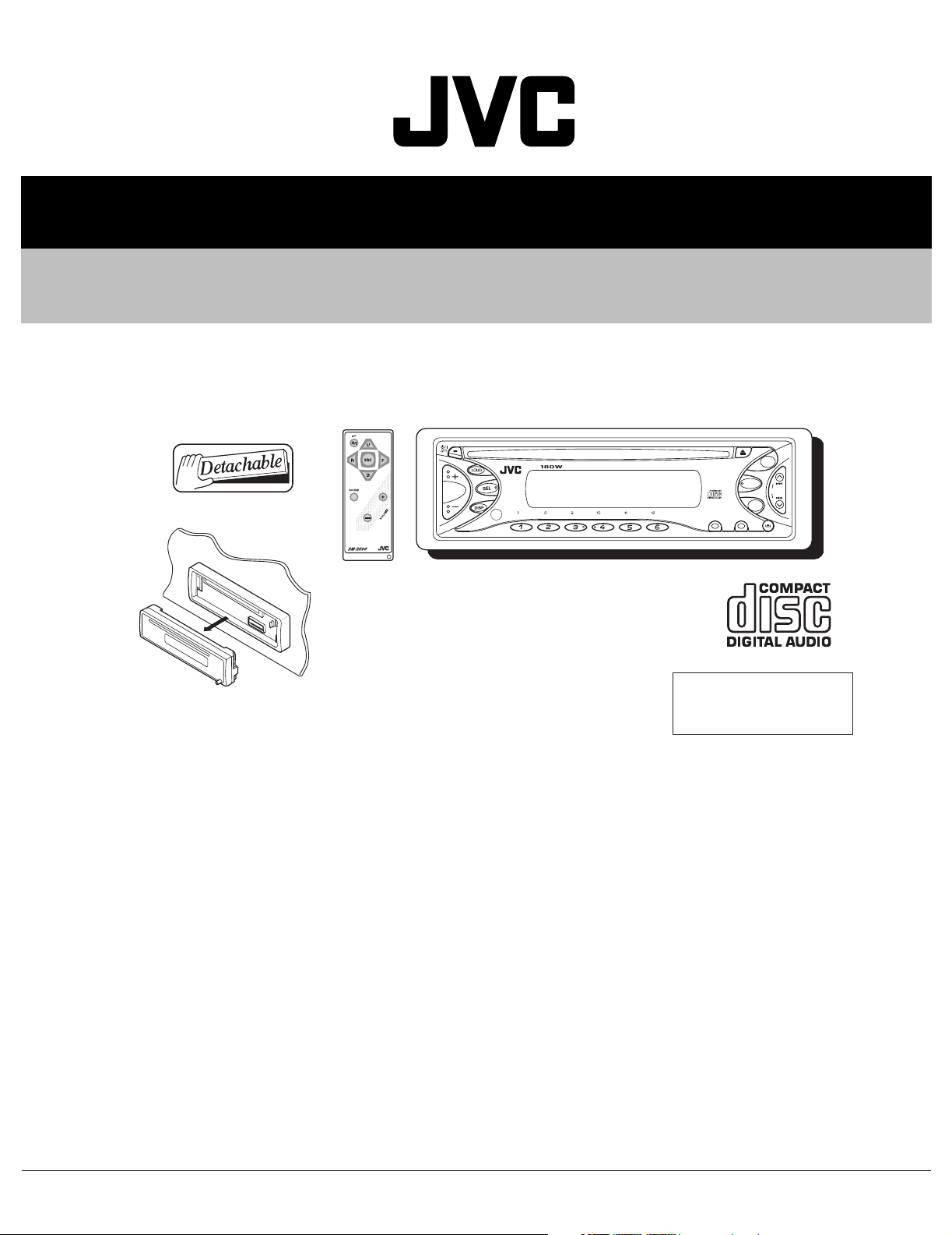
KD-S598,KD-S597
DIRECT TRACK ACCESS
S
MO
RPT RND
MODE
UR -------------- Brazil
FM
CD
SSM
AM
SCM
Area Suffix
TABLE OF CONTENTS
1 Important Safety Precautions . . . . . . . . . . . . . . . . . . . . . . . . . . . . . . . . . . . . . . . . . . . . . . . . . . . . . . . . . . . 1-2
2 Disassembly method . . . . . . . . . . . . . . . . . . . . . . . . . . . . . . . . . . . . . . . . . . . . . . . . . . . . . . . . . . . . . . . . . . 1-4
3 Adjustment. . . . . . . . . . . . . . . . . . . . . . . . . . . . . . . . . . . . . . . . . . . . . . . . . . . . . . . . . . . . . . . . . . . . . . . . . . 1-23
4 Description of major ICs. . . . . . . . . . . . . . . . . . . . . . . . . . . . . . . . . . . . . . . . . . . . . . . . . . . . . . . . . . . . . . . 1-27
COPYRIGHT © 2003 VICTOR COMPANY OF JAPAN, LTD.
No.49860
2003/5
Page 2
1.1 Safety Precautions
SECTION 1
Important Safety Precautions
!
!
Burrs formed during molding may be left over on some parts of the chassis. Therefore,
pay attention to such burrs in the case of preforming repair of this system.
Please use enough caution not to see the beam directly or touch it in case of an
adjustment or operation check.
1-2 (No.49860)
Page 3
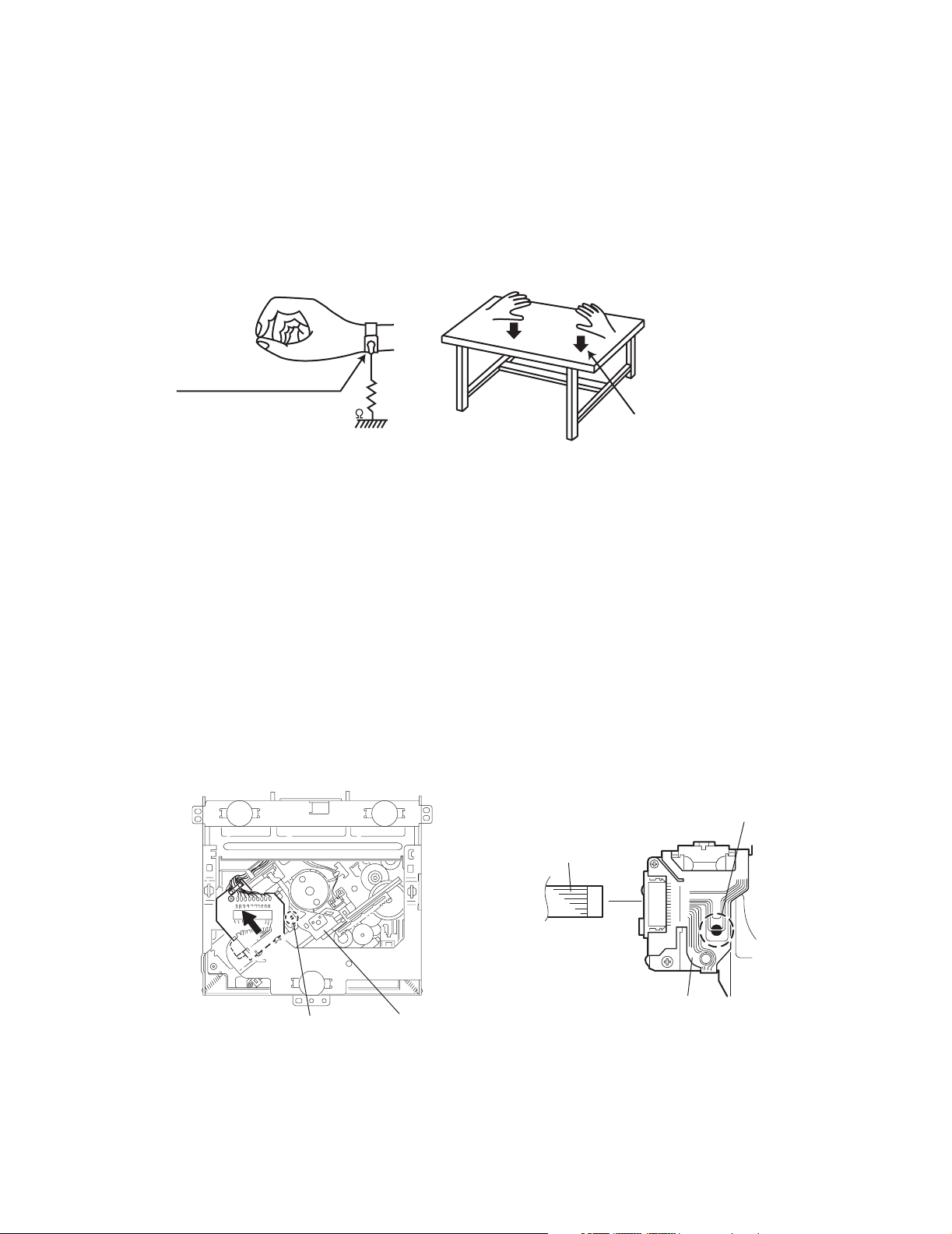
1.2 Preventing static electricity
Electrostatic discharge (ESD), which occurs when static electricity stored in the body, fabric, etc. is discharged,
can destroy the laser diode in the traverse unit (optical pickup). Take care to prevent this when performing repairs.
1.2.1 Grounding to prevent damage by static electricity
Static electricity in the work area can destroy the optical pickup (laser diode) in devices such as DVD players.
Be careful to use proper grounding in the area where repairs are being performed.
(1) Ground the workbench
Ground the workbench by laying conductive material (such as a conductive sheet) or an iron plate over it before placing the
traverse unit (optical pickup) on it.
(2) Ground yourself
Use an anti-static wrist strap to release any static electricity built up in your body.
(caption)
Anti-static wrist strap
1M
Conductive material
(conductive sheet) or iron plate
(3) Handling the optical pickup
• In order to maintain quality during transport and before installation, both sides of the laser diode on the replacement optical
pickup are shorted. After replacement, return the shorted parts to their original condition.
(Refer to the text.)
• Do not use a tester to check the condition of the laser diode in the optical pickup. The tester's internal power source can easily
destroy the laser diode.
1.3 Handling the traverse unit (optical pickup)
(1) Do not subject the traverse unit (optical pickup) to strong shocks, as it is a sensitive, complex unit.
(2) Cut off the shorted part of the flexible cable using nippers, etc. after replacing the optical pickup. For specific details, refer to the
replacement procedure in the text. Remove the anti-static pin when replacing the traverse unit. Be careful not to take too long a
time when attaching it to the connector.
(3) Handle the flexible cable carefully as it may break when subjected to strong force.
(4) I t is not possible to adjust the semi-fixed resistor that adjusts the laser power. Do not turn it.
1.4 Attention when traverse unit is decomposed
*Please refer to "Disassembly method" in the text for the CD pickup unit.
• Apply solder to the short land before the flexible wire is disconnected from the connector on the CD pickup unit.
(If the flexible wire is disconnected without applying solder, the CDpickup may be destroyed by static electricity.)
• In the assembly, be sure to remove solder from the short land after connecting the flexible wire.
Short-circuit point
(Soldering)
Flexible wire
Short-circuit point
Pickup
Pickup
(No.49860)1-3
Page 4
SECTION 2
Disassembly method
2.1 Main body
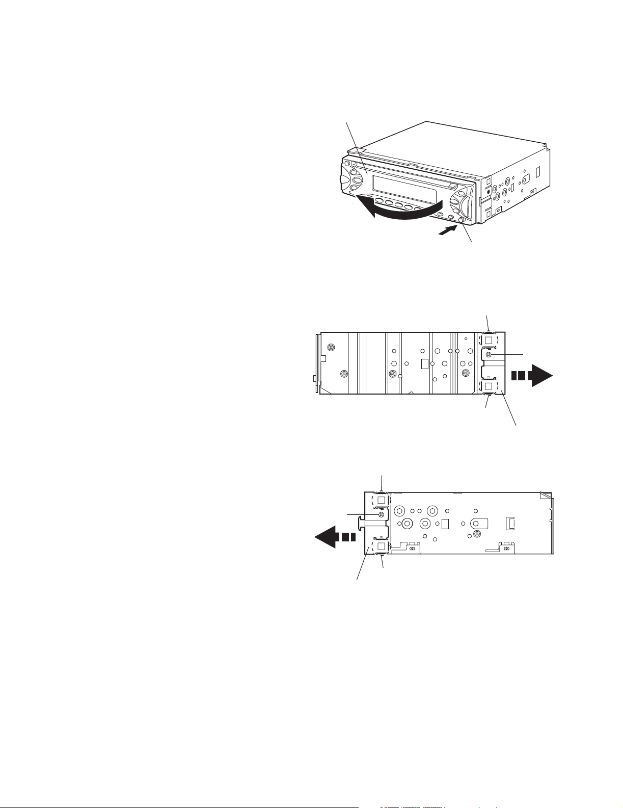
2.1.1 Removing the front panel assembly
(See Fig.1)
(1) Push the detach button in the lower right part of the front
panel assembly and remove the front panel assembly in
the direction of the arrow.
2.1.2 Removing the front chassis assembly
(See Figs.2 and 3)
• Prior to performing the following procedure, remove the front
panel assembly.
(1) Remove the two screws A on the both sides of the main
body.
(2) Release the two joints a and two joints b on both sides of
the main body using a screwdriver, and remove the front
chassis assembly forward.
Front panel assembly
Detach button
Fig.1
Joint a
A
Joint b
A
Joint b
Front chassis assembly
Joint a
Front chassis assembly
Fig.2
Fig.3
1-4 (No.49860)
Page 5
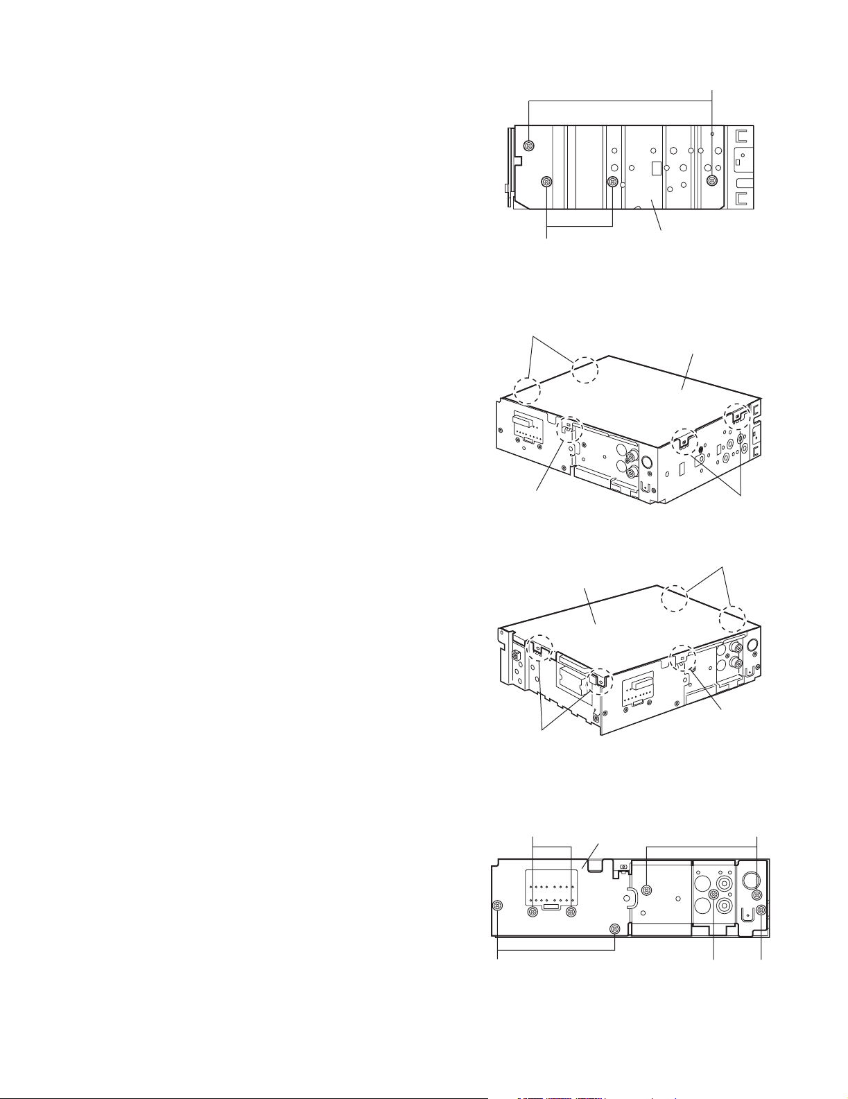
2.1.3 Removing the heat sink
(See Fig.4)
(1) Remove the two screws B and two screws C on the left
side of the main body.
B
2.1.4 Removing the bottom cover
(See Figs.5 and 6)
• Prior to performing the following procedure, remove the front
panel assembly, front chassis assembly and heat sink.
(1) Turn over the body and release the two joints c, two joints
d and joint e.
CAUTION:
Do not damage the main board when releasing the joint e using a screwdriver. (See Figs.5 and 6.)
Joint c
Joint e
C
Heat sink
Fig.4
Bottom cover
Joint d
Fig.5
Joint d
Bottom cover
2.1.5 Removing the rear bracket
(See Fig.7)
• Prior to performing the following procedure, remove the front
panel assembly, front chassis assembly, heat sink and bottom
cover.
(1) Remove the three screws D, three screws E and two
screws F on the back of the body.
(2) Remove the rear bracket.
Joint e
Joint c
Fig.6
EF
Rear bracket
DD
Fig.7
E
(No.49860)1-5
Page 6
2.1.6 Removing the main board
(See Fig.8)
• Prior to performing the following procedure, remove the front
panel assembly, front chassis assembly, heat sink, bottom
cover and rear bracket
(1) Remove the two screws G attaching the main board.
(2) Disconnect the connector CN501 and remove the main
board.
2.1.7 Removing the CD mechanism assembly
(See Fig.9)
• Prior to performing the following procedure, remove the front
panel assembly, front chassis assembly, heat sink, bottom
cover, rear bracket and main board.
(1) Remove the three screws H.
G
CN501
Main board assembly
G
Fig.8
H
CD mechanism assembly
Top chassis
H
Fig.9
1-6 (No.49860)
Page 7
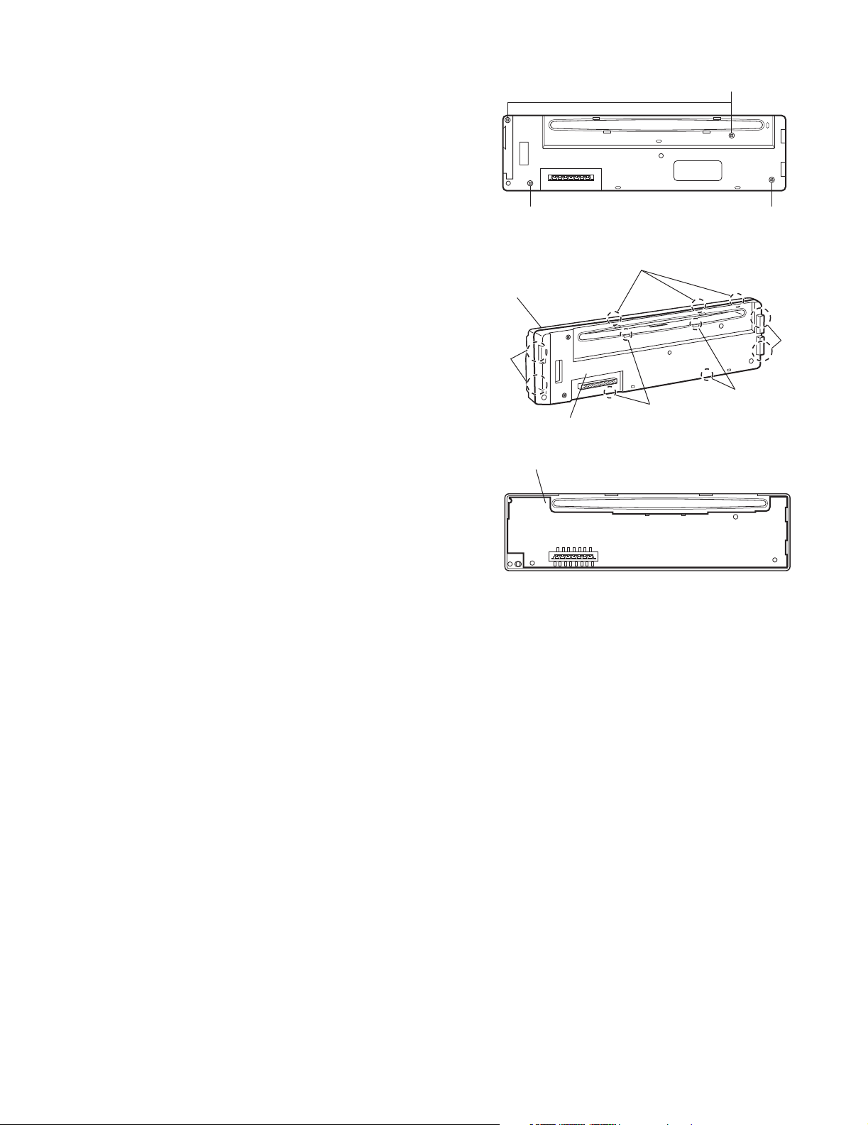
2.1.8 Removing the front board
f
(See Figs.10 to 12)
• Prior to performing the following procedure, remove the front
panel assembly.
(1) Remove the four screws J on the back side of the front pan-
el assembly.
(2) Release the eleven joints f.
(3) Take out the front board.
J
Front panel
Joint f
Front board
J
Rear cover
J
Fig.10
Joint f
Joint
Joint f
Joint f
Fig.11
Fig.12
(No.49860)1-7
Page 8
2.2 CD Mechanism Assembly
A
2.2.1 Removing the top cover
(See Figs.1 and 2)
(1) Remove the two screws A on the both side of the body.
(2) Lift the front side of the top cover and move the top cover
backward to release the two joints a.
Top cover
Joints a
A
Joints a
A
Fig.1
Fig.2
Top cover
1-8 (No.49860)
Page 9
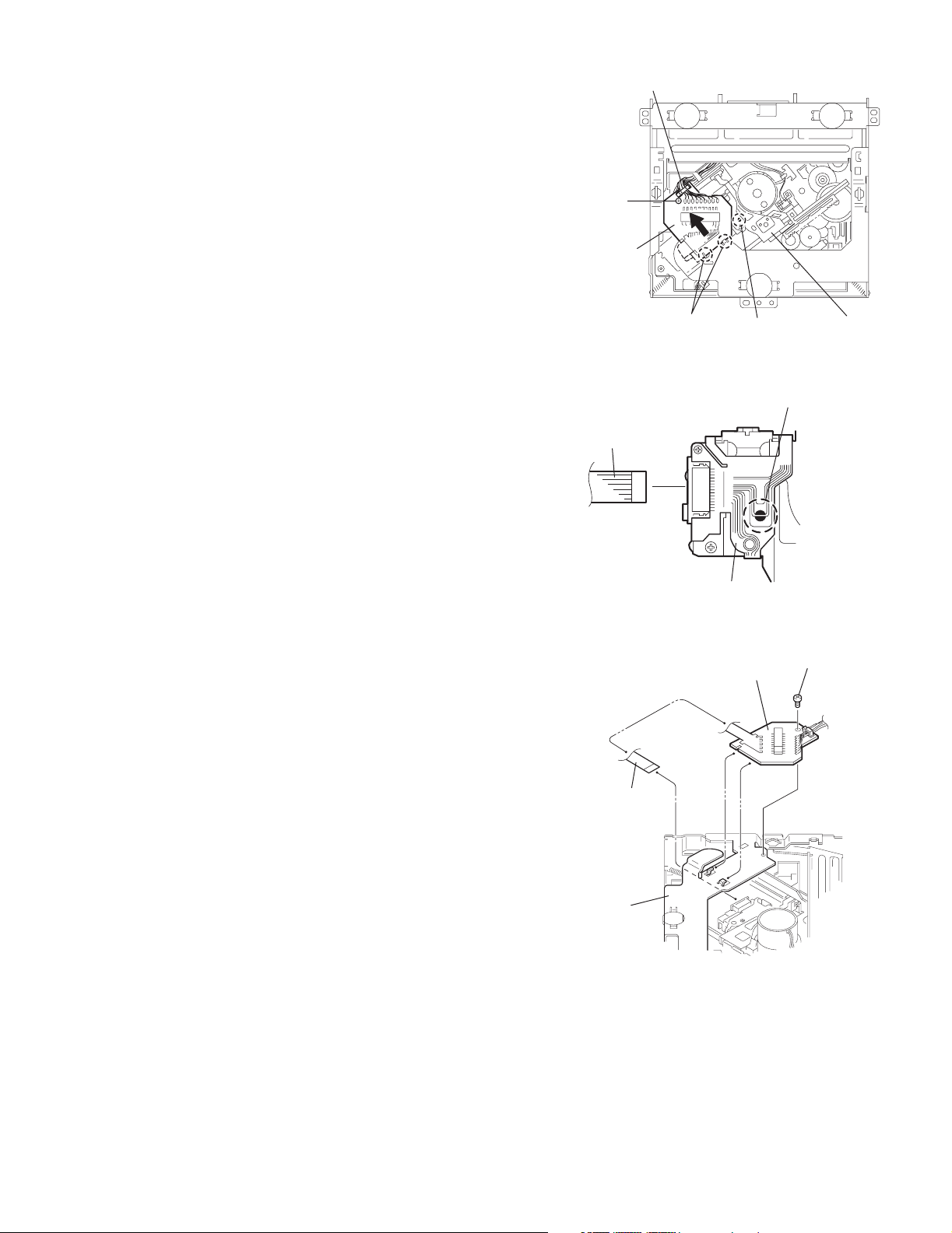
2.2.2 Removing the connector board
(See Figs.3 to 5)
CAUTION:
Before disconnecting the flexible wire from the pickup, solder
the short-circuit point on the pickup. No observance of this instruction may cause damage of the pickup.
(1) Remove the screw B fixing the connector board.
(2) Solder the short-circuit point on the connector board.
(3) Disconnect the flexible wire from the pickup.
(4) Move the connector board in the direction of the arrow to
release the two joints b.
(5) Unsolder the wire on the connector board if necessary.
CAUTION:
Unsolder the short-circuit point after reassembling.
B
Connector board
Flexible wire
Wires
Joints b
Short-circuit point
Fig.3
Short-circuit point
(Soldering)
Pickup
Flexible wire
Frame
Pickup
Fig.4
B
Connector board
Fig.5
(No.49860)1-9
Page 10
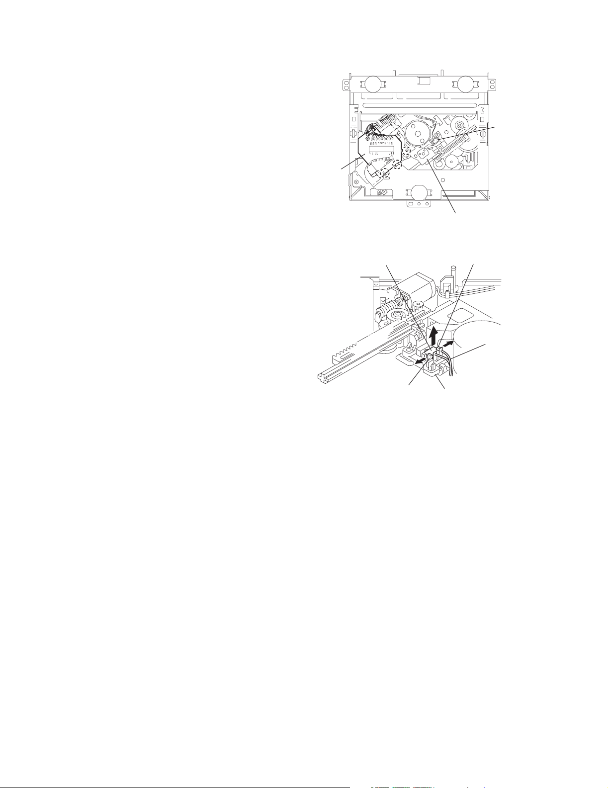
2.2.3 Removing the DET switch
(See Figs.6 and 7)
(1) Extend the two tabs c of the feed sw. holder and pull out
the switch.
(2) Unsolder the DET switch wire if necessary.
DET switch
Connector
board
Pickup
Fig.6
DET switch
Tab c
Tab c
DET switch wire
Feed sw. holder
Fig.7
1-10 (No.49860)
Page 11
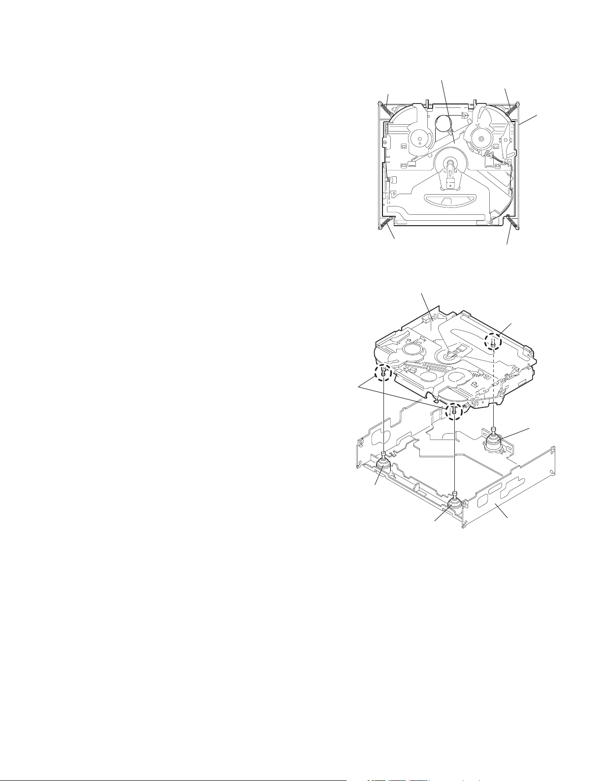
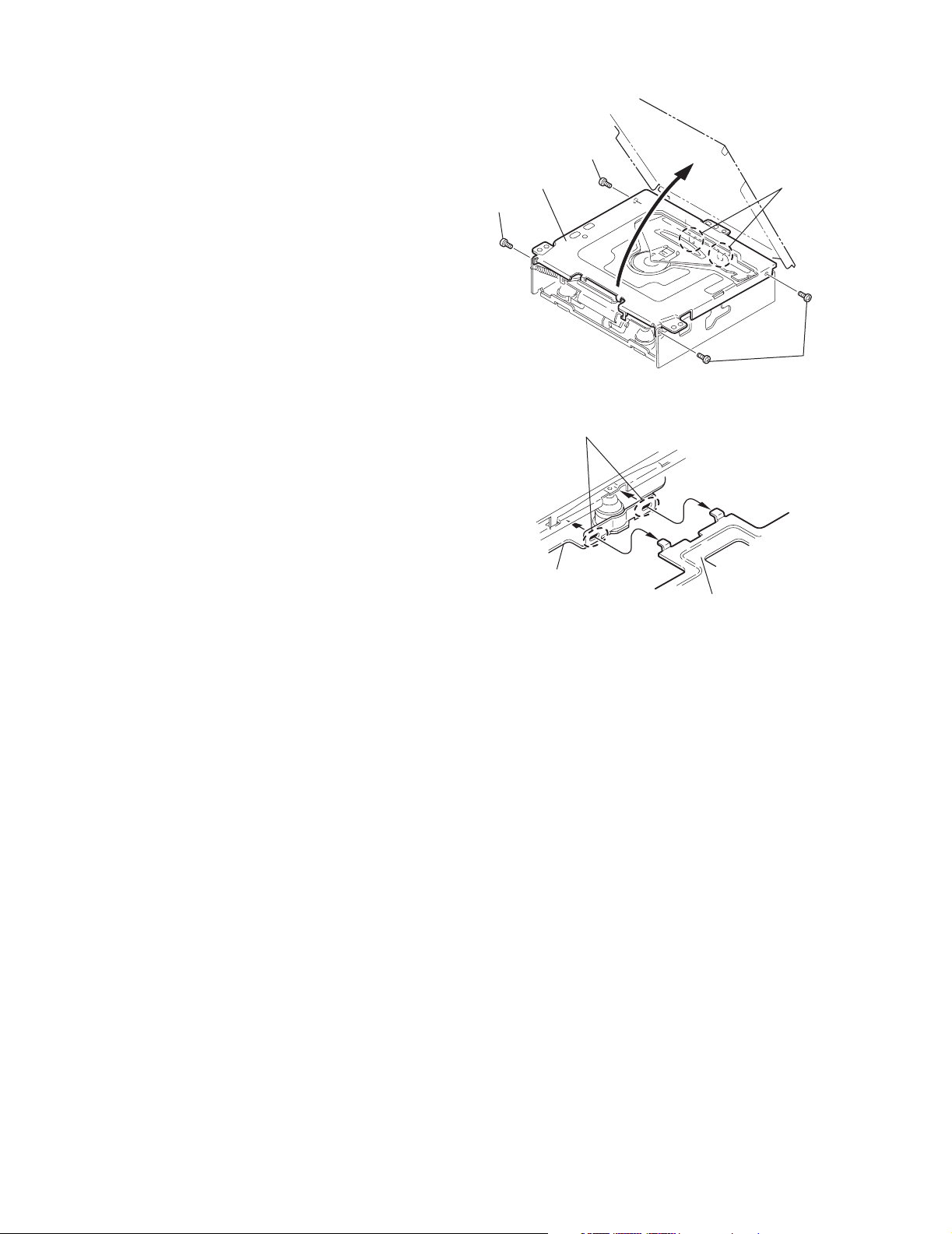
2.2.4 Removing the chassis unit
r
(See Figs.8 and 9)
• Prior to performing the following procedure, remove the top
cover and connector board.
(1) Remove the two suspension springs (L) and (R) attaching
the chassis unit to the frame.
CAUTION:
• The shape of the suspension spring (L) and (R) are different. Handle them with care.
• When reassembling, make sure that the three shafts
on the underside of the chassis unit are inserted to the
dampers certainly.
Suspension spring (R)
Chassis unit
Suspension spring (L)
Frame
Suspension spring (R)
Chassis unit
Shafts
Damper
Damper
Suspension spring (L)
Fig.8
Shaft
Dampe
Frame
Fig.9
(No.49860)1-11
Page 12
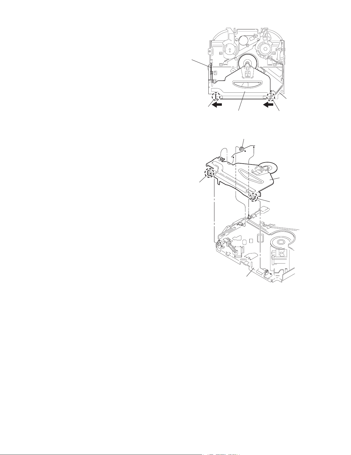
2.2.5 Removing the clamper assembly
(See Figs.10 and 11)
• Prior to performing the following procedure, remove the top
cover.
(1) Remove the clamper arm spring.
(2) Move the clamper assembly in the direction of the arrow to
release the two joints d.
Clamper arm
spring
Joint d
Joint d
Clamper assembly
Fig.10
Clamper arm spring
Chassis rivet
assembly
Joint d
Clamper
assembly
Chassis rivet assembly
Fig.11
Joint d
1-12 (No.49860)
Page 13
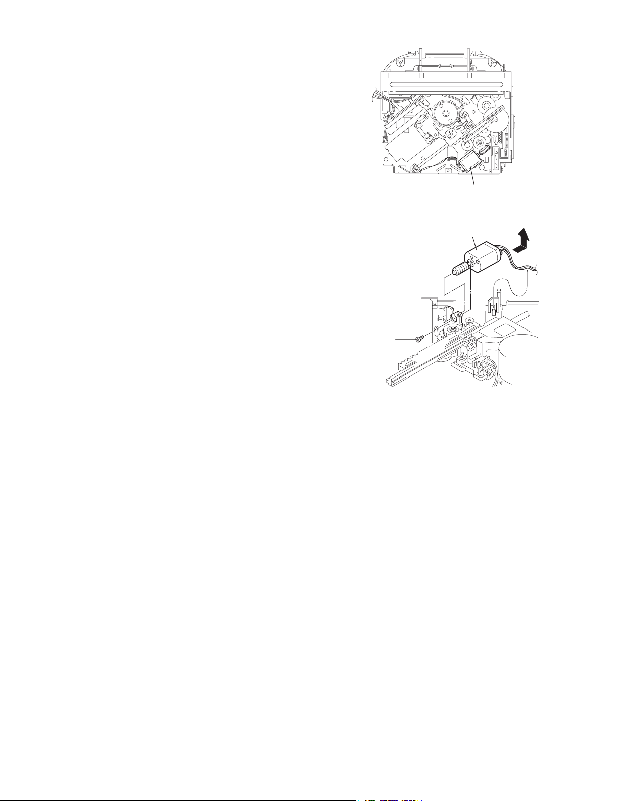
2.2.6 Removing the loading / feed motor assembly
(See Figs.12 and 13)
• Prior to performing the following procedure, remove the top
cover, connector board and chassis unit.
(1) Remove the screw C and move the loading / feed motor as-
sembly in the direction of the arrow to remove it from the
chassis rivet assembly.
(2) Disconnect the wire from the loading / feed motor assembly
if necessary.
CAUTION:
When reassembling, connect the wire from the loading /
feed motor assembly to the flame as shown in Fig.12.
Loading / feed motor assembly
Fig.12
Loading / feed motor assembly
C
Fig.13
(No.49860)1-13
Page 14

2.2.7 Removing the pickup unit
(See Figs.14 to 18)
• Prior to performing the following procedure, remove the top
cover, connector board and chassis unit.
(1) Remove the screw D and pull out the pu. shaft holder from
the pu. shaft.
(2) Remove the screw E attaching the feed sw. holder.
(3) Move the part e of the pickup unit upward with the pu. shaft
and the feed sw. holder, then release the joint f of the feed
sw. holder in the direction of the arrow. The joint g of the
pickup unit and the feed rack is released, and the feed sw.
holder comes off.
(4) Remove the pu. shaft from the pickup unit.
(5) Remove the screw F attaching the feed rack to the pickup
unit.
Part e
Feed rack
Pickup unit
Feed sw. holder
Fig.15
2.2.8 Reattaching the pickup unit
(See Figs.14 to 17)
(1) Reattach the feed rack to the pickup unit using the screw F.
(2) Reattach the feed sw. holder to the feed rack while setting
the joint g to the slot of the feed rack and setting the part f
of the feed rack to the switch of the feed sw. holder correctly.
(3) As the feed sw. holder is temporarily attached to the pickup
unit, set to the gear of the joint g and to the bending part of
the chassis (joint h) at a time.
CAUTION:
Make sure that the part i on the underside of the feed
rack is certainly inserted to the slot j of the change lock
lever.
(4) Reattach the feed sw. holder using the screw E.
(5) Reattach the pu. shaft to the pickup unit. Reattach the pu.
shaft holder to the pu. shaft using the screw D.
Feed sw. holder
Joint f
Joint g
Feed sw.
holder
Part i
E
Pickup unit
Slot j
F
Pu. shaft
Pickup unit
Joint f
Joint h
Fig.16
Feed rack
D
Pu. shaft
holder
Pu. shaft
D
Pu. shaft holder
1-14 (No.49860)
Pickup unit
Fig.14
Part e
E
Joint g
Feed rack
Fig.17
Pickup unit
Joint g
Joint f
Feed sw. holder
Fig.18
Page 15

2.2.9 Removing the trigger arm
r
(See Figs.19 and 20)
• Prior to performing the following procedure, remove the top
cover, connector board and clamper unit.
(1) Turn the trigger arm in the direction of the arrow to release
the joint k and pull out upward.
CAUTION:
When reassembling, insert the part m and n of the trigger
arm into the part p and q at the slot of the chassis rivet
assembly respectively and join the joint k at a time.
Chassis rivet assembly
Trigger arm
Chassis rivet
assembly
Joint k
Trigger arm
Fig.19
Part p
Part q
Part m
Part n
2.2.10 Removing the top plate assembly
(See Fig.21)
• Prior to performing the following procedure, remove the top
cover, connector board, chassis unit, and clamper assembly.
(1) Remove the screw H.
(2) Move the top plate assembly in the direction of the arrow to
release the two joints r.
(3) Unsolder the wire marked s if necessary.
H
Fig.20
Top plate assembly
Joints
s
Fig.21
(No.49860)1-15
Page 16

2.2.11 Removing the mode sw. / select lock arm
(See Figs.22 and 23)
• Prior to performing the following procedure, remove the top
plate assembly.
(1) Bring up the mode sw. to release from the link plate (joint t)
and turn in the direction of the arrow to release the joint u.
(2) Unsolder the wire of the mode sw. marked s if necessary.
(3) Turn the select lock arm in the direction of the arrow to re-
lease the two joints v.
(4) The select lock arm spring comes off the select lock arm at
the same time.
Link plate
Joint u
Fig.22
Joint t
Mode sw.
Select lock arm
s
Top plate
Select lock arm
Link plate
Select lock arm
Fig.23
Top plate
Hook w
Select lock
arm spring
Joints v
1-16 (No.49860)
Page 17

2.2.12 Reassembling the mode sw. / select lock arm
(See Figs.24 to 26)
REFERENCE:
Reverse the above removing procedure.
(1) Reattach the select lock arm spring to the top plate and set
the shorter end of the select lock arm spring to the hook w
on the top plate.
(2) Set the other longer end of the select lock arm spring to the
boss x on the underside of the select lock arm, and join the
select lock arm to the slots (joint v). Turn the select lock
arm as shown in the figure.
(3) Reattach the mode sw. while setting the part t to the first
peak of the link plate gear, and join the joint u.
CAUTION:
When reattaching the mode sw., check if the points y and
z are correctly fitted and if each part operates properly.
Select lock arm spring
Hook w
Joint v
Joint v
Select lock arm
Boss x
Fig.24
Joint t
Point y
Link plate
Point z
Link plate
Fig.25
Mode sw.
Select
lock arm
Joint t
Joint u
Fig.26
(No.49860)1-17
Page 18

2.2.13 Removing the select arm R / link plate
(See Figs.27 and 28)
• Prior to performing the following procedure, remove the top
plate assembly.
(1) Bring up the select arm R to release from the link plate
(joint a') and turn as shown in the figure to release the two
joints b' and joint c'.
(2) Move the link plate in the direction of the arrow to release
the joint d'. Remove the link plate spring at the same time.
REFERENCE:
Before removing the link plate, remove the mode sw.
Select arm R
Joint b'
Link plate spring
Joint c'
Joint a'
Link plate
Joint b'
Fig.27
Joint r
2.2.14 Reattaching the Select arm R / link plate
(See Figs.29 and 30)
REFERENCE:
Reverse the above removing procedure.
(1) Reattach the link plate spring.
(2) Reattach the link plate to the link plate spring while joining
them at joint d'.
(3) Reattach the joint a' of the select arm R to the first peak of
the link plate while joining the two joints b' with the slots.
Then turn the select arm R as shown in the figure. The top
plate is joined to the joint c'.
CAUTION:
When reattaching the select arm R, check if the points e'
and f' are correctly fitted and if each part operates properly.
Top plate
Select arm R
Joint b'
Joint d'
Link plate
Fig.28
Link plate spring
Joint c'
Joint d'
Joint b'
Joint a'
Fig.29
1-18 (No.49860)
Joint a'
Point e'
Link plate
Point f'
Fig.30
Page 19

2.2.15 Removing the loading roller assembly
(See Figs.31 to 33)
• Prior to performing the following procedure, remove the
clamper assembly and top plate assembly.
(1) Push inward the loading roller assembly on the gear side
and detach it upward from the slot of the joint g' of the lock
arm rivet assembly.
(2) Detach the loading roller assembly from the slot of the joint
h' of the lock arm rivet assembly.
Roller guide
spring
Part k'
Loading roller assembly
Loading roller assembly
The roller guide comes off the gear section of the loading
roller assembly.
Remove the roller guide and the HL washer from the shaft
of the loading roller assembly.
(3) Remove the screw J attaching the lock arm rivet assembly.
(4) Push the shaft at the joint i' of the lock arm rivet assembly
inward to release the lock arm rivet assembly from the slot
of the L side plate.
(5) Extend the lock arm rivet assembly outward and release
the joint j' from the boss of the chassis rivet assembly. The
roller guide springs on both sides come off at the same
time.
CAUTION:
When reassembling, reattach the left and right roller
guide springs to the lock arm rivet assembly before reattaching the lock arm rivet assembly to the chassis rivet
assembly. Make sure to fit the part k' of the roller guide
spring inside of the roller guide. (Refer to Fig.34.)
Roller guide
HL washer
Loading roller assembly
Roller guide
Chassis rivet assembly
J
Roller guide
spring
Fig.32
Boss
L side plate
Roller guide spring
Joint h'
Roller guide spring
Loading roller assembly
Joint g'
Lock arm rivet assembly
Fig.31
Roller guide spring
Roller guide spring
Lock arm rivet assembly
Lock arm rivet assembly
Joint i'
Part j'
Fig.33
Roller guide
HL washer
Roller shaft assembly
Loading roller
Roller guide spring
Fig.34
(No.49860)1-19
Page 20

2.2.16 Removing the loading gear 5, 6 and 7
(See Figs.35 and 36)
• Prior to performing the following procedure, remove the top
cover, chassis unit, pickup unit and top plate assembly.
(1) Remove the screw K attaching the loading gear bracket.
The loading gear 6 and 7 come off the loading gear bracket.
(2) Pull out the loading gear 5.
K
Loading gear bracket
K
Loading gear 6
Loading gear 5
Loading gear 3
Fig.35
Loading gear bracket
Loading gear 5
Loading gear 6
Loading gear 7
Fig.36
1-20 (No.49860)
Page 21

2.2.17 Removing the gears
(See Figs.37 to 40)
• Prior to performing the following procedure, remove the top
cover, chassis unit, top plate assembly and pickup unit.
• Pull out the loading gear 3. (See Fig.35.)
(1) Pull out the feed gear.
(2) Move the loading plate assembly in the direction of the ar-
row to release the L side plate from the two slots m' of the
chassis rivet assembly. (See Fig.37.)
(3) Detach the loading plate assembly upward from the chas-
sis rivet assembly while releasing the joint n'. Remove the
slide hook and loading plate spring from the loading plate
assembly.
(4) Pull out the loading gear 2 and remove the change lock le-
ver.
(5) Remove the E ring and washer attaching the changer gear
2.
(6) The changer gear 2, change gear spring and adjusting
washer come off.
(7) Remove the loading gear 1.
(8) Move the change plate rivet assembly in the direction of the
arrow to release from the three shafts of the chassis rivet
assembly upward. (See Fig.38.)
(9) Detach the loading gear plate rivet assembly from the shaft
of the chassis rivet assembly upward while releasing the
joint p'. (See Figs.38 and 40.)
(10) Pull out the loading gear 4.
Change plate
rivet assembly
Shafts
E ring
Loading plate assembly
Loading plate spring
Joint p'
Loading gear 4
Loading gear plate
rivet assembly
Shaft
Loading gear 2
Loading gear 1
Chassis rivet assembly
Change gear 2
Fig.38
Joint n'
Slide hook
Feed gear
Fig.37
Slot m'
L side plate
Loading plate assembly
Joint n'
Slot m'
Chassis rivet assembly
Chassis rivet assembly
E ring
Washer
Change gear 2
Change gear spring
Adjusting washer
Change plate
rivet assembly
Chassis rivet assembly
L side plate
Slot m'
Slot m'
Fig.39
Loading gear 1
Loading gear 2
Change lock lever
Loading gear 4
Loading gear plate rivet assembly
Fig.40
(No.49860)1-21
Page 22

2.2.18 Removing the turn table / spindle motor
(See Figs.41 and 42)
• Prior to performing the following procedure, remove the top
cover, connector board, chassis unit and clamper assembly.
(1) Remove the two screws L attaching the spindle motor as-
sembly through the slot of the turn table on top of the body.
(2) Unsolder the wire on the connector board if necessary.
Turn table
L
Fig.41
L
Turn table
1-22 (No.49860)
Spindle motor
Fig.42
Page 23

SECTION 3
Adjustment
3.1 Adjustment method
Test instruments required for adjustment
1. Digital oscilloscope (100MHz)
2. AM Standard signal generator
3. FM Standard signal generator
4. Stereo modulator
5. Electric voltmeter
6. Digital tester
7. Tracking offset meter
8. Test Disc JVC : CTS-1000
9. Extension cable for check
EXTSH002-22P × 1
Standard measuring conditions
Power supply voltage DC14.4V(10.5 ~ 16V)
Load impedance 20Kohm(2 Speakers connection)
Output Level Line out 2.0V (Vol. MAX)
Standard volume position
Balance and Bass & Treble volume : lndication"0"
Loudness : OFF
BBE : OFF
Frequency Band
FM 87.5MHz ~ 107.9MHz
AM 530kHz ~ 1710 kHz
Dummy load
Exclusive dummy load should be used for AM, and FM. For
FM dummy load, there is a loss of 6dB between SSG output
and antenna input. The loss of 6dB need not be considered
since direct reading of figures are applied in this working
standard.
How to connect the extension cable for adjusting
The cardboard is cut in a suitable size.
uses for the insulation stand of mechanism.
CAUTION :
Be sure to attach the parts (Heat sink and rear bracket)
on the IC (Power amplifier IC321 and regulator IC901)
of a main board when supplying the power.
If voltage is applied without attaching those parts, the
power amplifier IC and regulator IC will be destroyed by heat.
Heat sink
Extension cable
EXTSH002-22P
Rear bracket
(No.49860)1-23
Page 24

3.2 Troubleshooting
3.2.1 Feed section
Is the voltage output at
IC541 pin 4 is 5V or 0V?
Is 4V present at both
sides of the feed motor?
Check the feed motor
3.2.2 Focus section
YES
YES
NO
YES
Is 5V present at IC581
Check the vicinity of
Check the circuits in
the vicinity of IC541
pin 6?
YES
IC521.
Is the wiring for IC541
1 ~ 14 correct?
NO
.
Check the feed motor
connection wiring.
When the lens is
moving:
NONO
Check CD 9V
and 5V.
pins 8 and 9.
4V
Does the S-search
waveform appear at
IC561 pins 32?
YES
Check the pickup and
its connections
YES
.
3.2.3 Spindle section
Is the disk rotated?
YES
Does the RF signal
appear at ARF TP?
YES
Is the RF waveform at
ARF TP distorted?
YES
Proceed to the Tracking
section
3.2.4 Tracking section
When the disc is rotated
at first:
Approx. 1.2V
NO
NO
Is 4V present between
IC541 pins 6 and 7?
Check the spindle motor
and its wiring.
NO
Check the circuits in the
vicinity of IC561 21 ~ 40
or the pickup
NO
Check the circuit in the
vicinity of IC561 pins
21 ~ 40
Is 4V present at IC561
pin 29?
YES
Check the vicinity of
IC541.
YESYES
Check the pickup and
NO
Check IC561 and
its connections
IC901.
1-24 (No.49860)
Is the tracking error
signal output at TE TP?
YES
Check IC501.
Page 25

3.2.5 Signal processing section
Is the sound output from
both channels (L, R)?
YES
Normal
NO
No sound from either
channel.
Is 9V present at IC101 pin
(8)?
Is the audio signal
(including sampling output
components) output to
IC801 pins 39 and 40 during
playback
Is the audio signal output
at IC301 pins 1
and 32during playback?
Check the muting circuit.
YES
YES
YES
YES
NO
Compare the L-ch and R-ch
to locate the defective point.
NO
Check the vicinity of the
Q981 audio power supply.
NO
Check IC801 and its
peripheral circuits
NO
Check IC301 and its
peripheral circuits
YES
(No.49860)1-25
Page 26

3.3 Maintenance of laser pickup
(1) Cleaning the pick up lens
Before you replace the pick up, please try to clean the lens
with a alcohol soaked cotton swab.
(2) Life of the laser diode
When the life of the laser diode has expired, the following
symptoms will appear.
• The level of RF output (EFM output:ampli tude of eye
pattern) will be low.
3.4 Replacement of laser pickup
Turn off the power switch and,disconnect the power cord
from the ac outlet.
Replace the pickup with a normal one.(Refer to
"Pickup Removal" on the previous page)
Is RF output
1.0
±
0.35Vp-p?
NO
Replace it.
YES
O.K
(3) Semi-fixed resistor on the APC PC board
The semi-fixed resistor on the APC printed circuit board
which is attached to the pickup is used to adjust the laser
power.Since this adjustment should be performed to match
the characteristics of the whole optical block, do not touch
the semi-fixed resistor. If the laser power is lower than the
specified value,the laser diode is almost worn out, and the
laser pickup should be replaced. If the semi-fixed resistor
is adjusted while the pickup is functioning normally,the laser pickup may be damaged due to excessive current.
Plug the power cord in,and turn the power on.
At this time,check that the laser emits for about 3seconds
and the objective lens moves up and down.
Note: Do not observe the laser beam directly.
Play a disc.
Check the eye-pattern at ARF TP.
Finish.
1-26 (No.49860)
Page 27

4.1 HA13164A (IC901) : Regulator
•Pin layout
123456789101112131415
• Block diagram
ANT OUT
EXT OUT
ANT CTRL
CTRL
CD OUT
AUDIO OUT
C3
0.1u
C4
0.1u
C5
0.1u
C6
10u
2
1
7
11
12
10
SECTION 4
Description of major ICs
C1
100u
VCC ACC
8
Surge Protector
BIAS TSD
15
3
TAB
ILM AJGND GND
13
C2
0.1u
+B
ACC
BATT.DET OUT
9
COMPOUT
6
VDD OUT
4
SW5VOUT
5
ILMOUT
14
R1
C7
0.1u
C8
0.1u
UNIT R:
C:F
note1) TAB (header of IC)
connected to GND
• Pin function
Pin No. Symbol Function
1 EXTOUT Output voltage is VCC-1 V when M or H level applied to CTRL pin.
2 ANTOUT Output voltage is VCC-1 V when M or H level to CTRL pin and H level to ANT-CTRL.
3 ACCIN Connected to ACC.
4 VDDOUT Regular 5.7V.
5 SW5VOUT Output voltage is 5V when M or H level applied to CTRL pin.
6 COMPOUT Output for ACC detector.
7 ANT CTRL L:ANT output OFF H:ANT output ON
8 VCC Connected to VCC.
9 BATT DET Low battery detect.
10 AUDIO OUT Output voltage is 9V when M or H level applied to CTRL pin.
11 CTRL L: BIAS OFF M: BIAS ON H: CD ON
12 CD OUT Output voltage is 8V when H level applied to CTRL pin.
13 ILM AJ Adjustment pin for ILM output voltage.
14 ILM OUT Output voltage is 10V when M or H level applied to CTRL pin.
15 GND Connected to GND.
(No.49860)1-27
Page 28

4.2 AN8806SB-W (IC501) : RF & amp.
• Pin layout
PD 1
LD 2
LDON 3
LDP 4
VCC 5
RF- 6
RF OUT 7
RF IN 8
C.AGC 9
ARF 10
C.ENV 11
C.EA 12
CS BDO 13
BDO 14
CS BRT 15
OFTR 16
/NRFDET 17
GND 18
• Block diagram
6
+
36 PDAC
35 PDBD
34 PDF
33 PDE
32 PDER
31 PDFR
30 TBAL
29 FBAL
28 EF27 EF OUT
26 TE25 TE OUT
24 CROSS
23 TE BPF
22 VDET
21 LD OFF
20 VREF
19 ENV
29
728
- +
27
+
910 17
8
AGC
EQ
RF
DET
11
12 19
ENV CURCUIT
36
+
35
+
31
34
-
+
VCBA
-
+
VCBA
-
-
VCBA
+
+
OFTR
BDO
+
13
14
15
16
20
+
- +
32
33
+
-
VCBA
+
+ -
+
- +
21
2
+
-
24 25
30
23
26
22
14
3
1-28 (No.49860)
Page 29

• Pin function
Pin No. Symbol I/O Function
1 PD I APC amp input terminal
2 LD O APC amp output terminal
3 LD ON I APC ON/OFF control terminal
4 LDP - Connect to ground
5 VCC - Power supply
6 RF- I Inverse input pin for RF amp
7 RF OUT O RFamp output
8 RF IN I RF input
9 C.AGC I/O Connecting pin of AGC loop filter
10 ARF O RF output
11 C.ENV I/O A capacitor is connected to this terminal to detect the envelope of RF signal
12 C.EA I/O A capacitor is connected to this terminal to detect the envelope of RF signal
13 CS BDO I/O A capacitor is connected to detect the lower envelope of RF signal
14 BDO O BDO output pin
15 CS BRT I/O A capacitor is connected to detect the lower envelope of RF signal
16 OFTR O Of-track status signal output
17 /NRFDET O RF detection signal output
18 GND - Ground
19 ENV O Envelope output
20 VREF O Reference voltage output
21 LD OFF - Connect to ground
22 VDET O Vibration detection signal output
23 TE BPF I Input pin of tracking error through BPF
24 CROSS O Tracking error cross output
25 TE OUT O Tracking error signal output
26 TE- I Inverse input pin for tracking error amp
27 FE OUT O Output pin of focus error
28 FE- I Inverse input pin for focus error amp
29 FBAL I Focus balance control
30 TBAL I Tracking balance control
31 PDFR I/O F I-V amp gain control
32 PDER I/O E I-V amp gain control
33 PDF I I-V amp input
34 PDE I I-V amp input
35 PD BD I I-V amp input
36 PD AC I I-V amp input
(No.49860)1-29
Page 30

4.3 TEA6320T-X (IC301) : E.volume
• Pin layout
SDA
1
GND
TL
B2L
B1L
IVL
ILL
QSL
IDL
MUTE
ICL
IMD
IBL
IAL
2
3
4
5
6
7
8
9
10
11
12
13
14
15
16
CD-CH
TAPE
TUNER
OUTLR
OUTLF
• Block diagram
10 8 9 7 6
32
31
30
29
28
27
26
25
24
23
22
21
20
19
18
17
SCL
VCC
OUTRR
OUTRF
TR
B2R
B1R
IVR
ILR
QSR
IDR
Vref
ICR
CAP
IBR
IAR
5
12
21
31
19
POWER
SUPPLY
2
VOLUME 1
+20 to -31 dB
LOUDNESS
LEFT
16
15
13
11
14
22
20
SOURCE
SELECTOR
VOLUME 1
+20 to -31 dB
LOUDNESS
RIGHT
18
17
23 25 24 26 27 28
• Pin functions
Pin No. Symbol I/O Functions
1 SDA I/O Serial data input/output.
2 GND - Ground.
3 OUTLR O output left rear.
4 OUTLF O output left front.
5 TL I Treble control capacitor left channel
or input from an external equalizer.
6 B2L - Bass control capacitor left channel or
output to an external equalizer.
7 B1L - Bass control capacitor left channel.
8 IVL I Input volume 1. left control part.
9 ILL I Input loudness. left control part.
10 QSL O Output source selector. left channel.
11 IDL - Not used
12 MUTE - Not used
13 ICL I Input C left source.
14 IMO - Not used
15 IBL I Input B left source.
16 IAL I Input A left source.
17 IAR I Input A right source.
18 IBR I Input B right source.
BASS
LEFT
+15 dB
LOGIC
BASS
RIGHT
+15 dB
VOLUME 2
0 to 55 dB
BALANCE
FENDER REAR
VOLUME 2
0 to 55 dB
BALANCE
FENDER FRONT
HC BUS
REC
VOLUME 2
0 to -55dB
BALANCE
FENDER FRONT
VOLUME 2
0 to -55dB
BALANCE
FENDER REAR
3
4
32
1
29
30
TREBLE
LEFT
+12 dB
TREBLE
RIGHT
+12 dB
MUTE
FUNCTION
ZERO CROSS
DETECTOR
Pin No. Symbol I/O Functions
19 CAP - Electronic filtering for supply.
20 ICR I Input C right source.
21 Vref - Reference voltage (0.5Vcc)
22 IDR - Not used
23 QSR O Output source selector right channel.
24 ILR I Input loudness right channel.
25 IVR I Input volume 1. right control part.
26 B1R - Bass control capacitor right channel
27 B2R O Bass control capacitor right channel
or output to an external equalizer.
28 TR I Treble control capacitor right channel
or input from an external equalizer.
29 OUTRF O Output right front.
30 OUTRR O Output right rear.
31 Vcc - Supply voltage.
32 SCL I Serial clock input.
1-30 (No.49860)
Page 31

4.4 NJM4565M-WE (IC151) : CD L.P.F.
T
A
• Pin layout & Block diagram
OUTPUT
+
1
8
V
-
A INPUT
+
A INPUT
-
V
4.5 RPM6938-SV4 (IC602) : Remote sensor
• Pin diagram
1 2 3
• Block diagram
AMP
I/V
conversion
2
3
4
AGC
Comp
BPF
Detector
7
6
5
Vcc
B OUTPU
-
B INPUT
+
B INPUT
22k
Vcc
Rout
PD
magnetic shield
fo
trimming
circuit
GND
(No.49860)1-31
Page 32

4.6 JES01-9B42 (IC801) : Main micon
• Pin layout
25 ~ 40
24 ~ 1
80 ~ 65
41 ~ 64
• Pin function
Pin No. Symbol Function
1 XIN X'tal oscillator conection terminal
2 TEST2 GND
3 J BUS SI Non connect
4 J BUS SO Non connect
5 J BUS SCK Non connect
6 J BUS I/O CONT Non connect
7 SUBQ CD LSI subQ code data input terminal
8 NC Non connect
9 SQCK CD LSI sub code clock terminal
10 RESET Main micon reset terminal
11 LCD SI Non connect
12 LCD SO LCD serial data output
13 LCD SCK LCD serial clock
14 LCD CE Chip enable output for LCD driver
15 FM ILLUMI Non connect
16 AM ILLUMI Non connect
17 CD ILLUMI Non connect
18 DIMMER OUT Non connect
19 NC Non connect
20 MOTOR SEL Loading motor signal select terminal
21 ~ 23 NC Non connect
24 KS2 Open
25 KS1 Open
26 KS0 Open
27 DETACH Front panel detach detectionsignal input
28 K2 Non connect
29 K1 Open
30 K0 Open
31 Vdd Power supply
32 LM Loading motor control terminal
33 CD LSI RESET CD LSI reset signaloutput terminal
34 MCLK CD LSI command clock signal output terminal
35 MDATA CD LSI command data output terminal
36 MLD CD LSI command load signal output terminal
37,38 NC Non connect
39 SCL E.volume clock signal output terminal
40 SDA E.volume data output terminal
41 CD ON CD power ON control terminal
1-32 (No.49860)
Page 33

Pin No. Symbol Function
42 RELAY Power supply control terminal
43 BLKCL Sub code/ Block signal input terminal
44 BEEP Non connect
45 SW1 Detection switch 1
46 SW2 Detection switch 2
47 PSW Pnael switch detection
48 REST Rest switch input terminal
49 FLOCK Focus signal input terminal
50 TLOCK Tracking signal input terminal
51 CD SENSE Senser signal input terminal from CD LSI
52 STATUS Status signal input terminal
53 P.SAVE2 Power save 2 detection signal input termianl
54 SD/ST Station detect/Stereo indocator
55 REMOCON Remocon signal detection terminal
56 J BUS INT Non connect
57 BAND FM/AM band select terminal
58 MONO FM mono control signal output termianl
59 IFRQ/AGC FA auto serch IF request output
60 MUTE Mute switch
61 LEVEL Non connect
62 S METER S meter input terminal
63 KEY CHANGE AD key select terminal
64 KEY2 Key AD input terminal 2
65 KEY1 Key AD input terminal 1
66 KEY0 Key AD input terminal 0
67 P.SAVE1 Power save 1 detection input terminal
68 SENSE Senser signal output terminal
69 NC Non connect
70 FM IF COUNT FM IF control signal input terminal
71,72 NC Non connect
73 Vdd Power supply
74 AM OSC Non connect
75 FM OSC FM local osc signal input terminal
76 Vss GND
77 NC Non connect
78 EQ PLL error signalinput terminal
79 TEST1 Test terminal 1
80 XOUT X'tal oscillator connect terminal
(No.49860)1-33
Page 34

4.7 LA4743K (IC321) : Power amp.
• Block diagram
IN 1
TAB
IN 2
+
0.22 F
+
0.22 F
11
1
12
Vcc 1/2 Vcc 3/4
6 20
-
+
Protective
circuit
-
+
2200 F 0.022 F
+
9
7
+
OUT 1+
OUT 1-
PWR GND1
8
+
OUT 2+
5
-
OUT 2-
3
PWR GND2
2
ST BY
R.F
47 F
IN 3
PRE GND
IN 4
+5V
ST ON
+
0.22 F
N.C
+
0.22 F
4
Stand by
Switch
Mute
10
+
Ripple
Filter
Mute
22
circuit
3.3 F
+
15
-
+
-
17
19
10K
+
OUT 3+
OUT 3-
Low Level
Mute ON
25
18
21
23
PWR GND3
OUT 4+
OUT 4-
13
14
Protective
circuit
-
+
+
-
ON TIME C
1-34 (No.49860)
22 F
Muting &
16
+
ON Time Control
Circuit
PWR GND4
24
Page 35

•Pin layout
TAB
GND
FR-
STDBY
FR+
VP1
RR-
GND
RR+
RIPPLE
INRF
INRR
SGND
FLIN
RLIN
DNTIME
RL+
GND
RL-
VP3
FL+
MUTE
FL-
GND
NC
• Pin function
Pin No. Symbol Function
1 TAB Header of IC
2 GND Power GND
3 FR- Outpur(-) for front Rch
4 STDBY Stand by input
5 FR+ Output (+) for front Rch
6 VP1 Power input
7 RR- Output (-) for rear Rch
8 GND Power GND
9 RR+ Output (+) for rear Rch
10 RIPPLE Ripple filter
11 RRIN Rear Rch input
12 FRIN Front Rch input
13 SGND Signal GND
14 FLIN Front Lch input
15 RLIN Rear Lch input
16 ONTIME Power on time control
17 RL+ Output (+) for rear Lch
18 GND Power GND
19 RL- Output (-) for rear Lch
20 VP3 Power input
21 FL+ Output (+) for front
22 MUTE Muting control input
23 FL- Output (-) for front
24 GND Power GND
25 NC Non connection
(No.49860)1-35
Page 36

4.8 LA6589H-X (IC541) : BTL driver
• Pin layout & Block diagram
VIN1-A
1
+
VIN1+A
VCCP1
2
3
VIN1_SW
H : OP-AMP_A
L : OP-AMP_B
H
28
VIN1
L
27
VIN1-B
+
26
VIN1+B
VO1+
VO1-
VO2+
VO2-
FR
VO3+
VO3-
VO4+
4
5
6
7
Power system
FR
8
9
10
GND
Level shift Level shift
+
Level shift Level shift
33k
11k
+
It is ON/OFF as for all outputs.
5VREG(PNPTr External)
Signal system
GND
H : ON
L : OFF
Signal system
power supply
MUTE
Power system GND
25
S-GND
24
VIN1-SW
23
MUTE
22
VREF_IN
FR
FR
21
VCC_S
20
REG-OUT
+
19
REG_IN
VCCP2
VIN4G
1-36 (No.49860)
VO4-
VIN4
11
12
13
14
11k
+
33k
33k
33k
18
VIN2G
11k
+
11k
+
17
16
15
VIN2
VIN3G
VIN3
Page 37

• Pin function
Pin No. Symbol Function
1 VIN1-A CH1 input AMP_A reversing input
2 VIN1+A CH1 input AMP_A non-reversing input
3 VCCP1 CH1 and CH2 power steps power supply
4 VO1+ CH1 Output terminal (+)
5 VO1- CH1 Output terminal (-)
6 VO2+ CH2 Output terminal (+)
7 VO2- CH2 Output terminal (-)
8 VO3+ CH3 Output terminal (+)
9 VO3- CH3 Output terminal (-)
10 VO4+ CH4 Output terminal (+)
11 VO4- CH4 Output terminal (-)
12 VCCP2 CH3 and CH4 power steps power supply
13 VIN4 CH4 Input terminal
14 VIN4G CH4 Input terminal(For gain adjustment)
15 VIN3 CH3 Input terminal
16 VIN3G CH3 Input terminal(For gain adjustment)
17 VIN2 CH2 Input terminal
18 VIN2G CH2 Input terminal(For gain adjustment)
19 REGIN External PNP transistor base connection
20 REG-OUT 5VREG output terminal and external PNP transistor collector connection
21 VCCS Signal system power supply
22 VREFIN Standard voltage impression terminal
23 MUTE Output ON/OFF terminal
24 VIN1_SW CH1 input OP_AMP switch terminal
25 S_GND Signal system GND
26 VIN1+B CH1 AMP_B non-reversing input terminal
27 VIN1-B CH1 AMP_B reversing input terminal
28 VIN1 CH1 input terminal and input OP_AMP output terminal
*1 Frame (FR) at the center becomes system GND(P-GND) power . Please give (*O) as the lowest potential with system GND(S-
GND) signal.
*2 Be short-circuited of VCC_S (signal system power supply) and VCCP1 and VCCP2 (output steps power supply) on the out-
side.
(No.49860)1-37
Page 38

4.9 MN6627482WA (IC561) : DSP & DAC
A
R
• Pin layout
20 ~ 1
• Block diagram
LRCKIN(MSEL)
BCLK(SSEL)
SRDATAIN
(PSEL)
IOSEL
CLVS
CRC
BLKCK
CLDCK
SBCK
SUBC
DEMPH
RESY
FLAG6(RESY)
SSEL
SQCK
SUBQ
AVDD2
AVDD2
PCK
EFM
PLLF
DSLF
IREF
DRF
ARF
RSEL
PSEL
MLD
MCLK
MDATA
CK384(EFM)
VCOF
BYTCK
SMCK
FCLK
CSEL
MSEL
X2
X1
ÊSTAT
21
~
40
41 ~ 60
DIGITAL
DEEMPHSIS
SUB
CODE
BUFFER
DSL.
PLL
VCO
VCO
ITUNING
GENERATION
PITCH
CONTROL
80
~
61
8TIMES
OVER SAMPUNC
DIGITAL FILTER
EFM
DEMODULATION
SYNC
INTERPOLATION
SUBCODE
DEMODULATION
MICRO
COMPUTER
INTERFACE
A/D
COVERTER
1BIT
DAC
LOGIC
S
16k
SRAM
CIRC
ERROR
CORRECTION
DEINTERLEVE
CLV
SERVO
INPUT
PEM
(R)
PEM
(L)
D/A
CONVERTER
OUTPUT
DIGITAL
AUDIO
INTERFASE
DIGITAL
AUDIO
INTERFASE
INTER POLATION
SOFT MUTING DIGITAL
ATTENUATION
PEAK DETECTIVE
AUTO CUE
PORT
SERVO
TIMING GENERATOR
AVSS1
AVDD1
OUTR
OUTL
FLAG
IPFLAG
TX
ECM
PC
LRCK
SRDAT
BCLK
DMUTE
TRKV
KICK
VREF
TRVST
ECS
TVD
TRD
FOD
TBAL
FBAL
TOFS
TES
/TLOCK
/FLOCK
PLAY
LDON
WVEL
SENSE
1-38 (No.49860)
D
/
D
V
V
V
R
V
S
D
D
S
S
S
D
D
T
S
1
1
F
/
E
T
E
S
T
R
T
F
E
E
N
V
T
R
C
R
S
B
V
D
D
O
E
T
/
R
F
D
E
O
F
T
Page 39

• Pin function
Pin No. Symbol I/O Function
1 BCLK O Not used
2 LRCK O Not used
3 SRDATA O Not used
4 DVDD1 - Power supply (Digital)
5 DVSS1 - Connected to GND
6 TX O Not used
7 MCLK I CPU command clock signal input(Data is
latched at signal's rising point)
8 MDATA I CPU command data input
9 MLD I CPU command load signal input
10 SENSE O Sense signal output
11 FLOCK O Focus lock signal output Active: Low
12 TLOCK O Tracking lock signal output Active: Low
13 BLKCK O sub-code/block/clock signal output
14 SQCK I Outside clock for sub-code Q resister in-
put
15 SUBQ O Sub-code Q -code output
16 DMUTE Connected to GND
17 STAT O Status signal(CRC,CUE,CLVS,
TTSTOP,ECLV,SQOK)
18 RST I Reset signal input (L:Reset)
19 SMCK - Not used
20 PMCK - Not used
21 TRV O Traverse enforced output
22 TVD O Traverse drive output
23 PC - Not used
24 ECM O Spindle motor drive signal (Enforced
mode output) 3-State
25 ECS O Spindle motor drive signal (Servo error
signal output)
26 KICK O Kick pulse output
27 TRD O Tracking drive output
28 FOD O Focus drive output
29 VREF - Reference voltage input pin for D/A out-
put block (TVD,FOD,FBA,TBAL)
30 FBAL O Focus Balance adjust signal output
31 TBAL O Tracking Balance adjust signal output
32 FE I Focus error signal input (Analog input)
33 TE I Tracking error signal input (Analog input)
34 RF ENV I RF envelope signal input (Analog input)
35 VDET I Vibration detect signal input (H:detect)
36 OFT I Off track signal input (H:off track)
37 TRCRS I Track cross signal input
38 RFDET I RF detect signal input (L:detect)
39 BDO I BDO input pin (L:detect)
40 LDON O Laser ON signal output (H:on)
41 PLLF2 - Not used
42 TOFS O Tracking error shunt signal output
(H:shunt)
Pin No. Symbol I/O Function
43 WVEL - Not used
44 ARF I RF signal input
45 IREF I Reference current input pin
46 DRF I Bias pin for DSL
47 DSLF I/O Loop filter pin for DSL
48 PLLF I/O Loop filter pin for PLL
49 VCOF - Not used
50 AVDD2 - Power supply (Analog)
51 AVSS2 - Connected to GND (Analog)
52 EFM - Not used
53 PCK - Not used
54 VCOF2 - PLL data slice output
55 SUBC - Not used
56 SBCK - Not used
57 VSS - Connected to GND (for X'tal oscillation
circuit)
58 XI I Input of 16.9344MHz X'tal oscillation cir-
cuit
59 X2 O Output of X'tal oscillation circuit
60 VDD - Power supply (for X'tal oscillation circuit)
61 BYTCK - Not used
62 CLDCK - Not used
63 FCLK - Not used
64 IPFLAG - Not used
65 FLAG - Not used
66 CLVS - Not used
67 CRC - Not used
68 DEMPH - Not used
69 RESY - Not used
70 IOSEL - pull up
71 TEST - pull up
72 AVDD1 - Power supply (Digital)
73 OUT L O Lch audio output
74 AVSS1 - Connected to GND
75 OUT R O Rch audio output
76 RSEL - pull up
77 CSEL - Connected to GND
78 PSEL - Connected to GND
79 MSEL - Connected to GND
80 SSEL - Pull up
(No.49860)1-39
Page 40

4.10PT6523LQ (IC601) : LCD driver
• Pin layout
48 ~ 33
49
32
• Block diagram
64
1 ~ 16
17
COMMON
DRIVER
CLOCK
GENERATOR
ADDRESS
DETECTOR
SEGMENT DRIVER & LATCH
SHIFT REGISTER
• Piin function
Pin No. Pin Name I/O Description
1 ~ 52 SG1 ~ SG52 O Segment Output Pins
53 ~ 55 COM1 ~ COM3 O Common Driver Output Pins
56 VDD - Power Supply
57 INH
I Display OFF Control Input Pin
When this pin is "Low", the Display is forcibly turned OFF. (SG1 to SG52, COM1 to COM3 are
set to "LOW"). (See Note 1)
When this pin is set to "High", the Displa is ON.
58 VDD1 I Used for the 2/3 Bias Voltage when the Bias Voltages are provied externally. Connect to VDD2
when 1/2 Bias is used.
59 VDD2 I Used for 1/3 Bias Voltage when the Bias Voltages are provided externally. Connect to VDD1
when 1/2 Bias is used.
60 VSS - Ground Pin.
61 OSC I/O Oscillation Input /Outout Pin
62 CE I Chip Enable Pin
63 CLK I Synchronization Clock
64 DI I Transfer Data Pin
Note 1:
When INH
= "LOW" : Serial data trensfers can be performed when the display is forcibly OFF.
1-40 (No.49860)
Page 41

(No.49860)1-41
Page 42

VICTOR COMPANY OF JAPAN, LIMITED
AV & MULTIMEDIA COMPANY MOBILE ENTERTAINMENT CATEGORY 10-1,1chome,Ohwatari-machi,Maebashi-city,371-8543,Japan
(No.49860)
Printed in Japan
WPC
 Loading...