

Page 1

SERVICE MANUAL
CD RECEIVER
4979320034
KD-LX555R
S
STDM
SOURCE
9
7
8
KD-LX555R
0
1
12
11
Area Suffix
E ------ Continental Europe
TABLE OF CONTENTS
1 Precautions . . . . . . . . . . . . . . . . . . . . . . . . . . . . . . . . . . . . . . . . . . . . . . . . . . . . . . . . . . . . . . . . . . . . . . . . . . . . 3
2 Disassembly method . . . . . . . . . . . . . . . . . . . . . . . . . . . . . . . . . . . . . . . . . . . . . . . . . . . . . . . . . . . . . . . . . . . . 5
3 Adjustment. . . . . . . . . . . . . . . . . . . . . . . . . . . . . . . . . . . . . . . . . . . . . . . . . . . . . . . . . . . . . . . . . . . . . . . . . . . . 28
4 Description of major ICs. . . . . . . . . . . . . . . . . . . . . . . . . . . . . . . . . . . . . . . . . . . . . . . . . . . . . . . . . . . . . . . . . 32
COPYRIGHT © 2003 VICTOR COMPANY OF JAPAN, LTD.
No.49793
2003/5
Page 2
SPECIFICATION
AUDIO AMPLIFIER SECTION Maximum Power Output Front 50 W per channel
Rear 50 W per channel
Continuous Power Output (RMS) Front 19 W per channel into 4 Ω, 40 Hz to 20 000 Hz
at no more than 0.8% total harmonic distortion.
Rear 19 W per channel into 4 Ω, 40 Hz to 20 000 Hz
at no more than 0.8% total harmonic distortion.
Load Impedance 4 Ω (4 Ω to 8 Ω allowance)
Equalizer Control Range: LOW ±12 dB (50 Hz, 80 Hz, 120 Hz)
MID ±12 dB (700 Hz, 1 kHz, 2 kHz)
HIGH ±12 dB (8 kHz, 12 kHz)
Frequency Response 40 Hz to 20 000 Hz
Signal-to-Noise Ratio 70 dB
Line-Out Level/Impedance 2.0 V/20 kΩ load (full scale)
Output Impedance 1 kΩ
TUNER SECTION Frequency Range FM 87.5 MHz to 108.0 MHz
AM (MW) 522 kHz to 1 620 kHz
(LW) 144 kHz to 279 kHz
[FM Tuner]
Usable Sensitivity 11.3 dBf (1.0 µV/75 Ω)
50 dB Quieting Sensitivity 16.3 dBf (1.8 µV/75 Ω)
Alternate Channel Selectivity (400 kHz) 65 dB
Frequency Response 40 Hz to 15 000 Hz
Stereo Separation 30 dB
Capture Ratio 1.5 dB
[MW Tuner]
Sensitivity 20 µV
Selectivity 35 dB
[LW Tuner]
Sensitivity 50 µV
CD PLAYER SECTION Type Compact disc player
Signal Detection System
Number of channels 2 channels (stereo)
Frequency Response 5 Hz to 20 000 Hz
Dynamic Range 98 dB
Signal-to-Noise Ratio 102 dB
Wow and Flutter Less than measurable limit
MP3 decoding format
GENERAL Power Requirement: Operating Voltage DC 14.4 V (11 V to 16 V allowance)
Grounding System Negative ground
Allowable Operating Temperature 0°C to +40°C
Dimensions (W × H × D) Installation Size 182 mm × 52 mm × 160 mm
Panel Size 188 mm × 58 mm × 8 mm
Mass 1.8 kg (excluding accessories)
Non-contact optical pickup (semiconductor laser)
MPEG1/2 Audio Layer 3
Max. Bit Rate:320 Kbps
Design and specifications are subject to change without notice.
1-2 (No.49793)
Page 3
1.1 Safety Precautions
SECTION 1
Precautions
!
!
Burrs formed during molding may be left over on some parts of the chassis. Therefore,
pay attention to such burrs in the case of preforming repair of this system.
Please use enough caution not to see the beam directly or touch it in case of an
adjustment or operation check.
(No.49793)1-3
Page 4
1.2 Preventing static electricity
Electrostatic discharge (ESD), which occurs when static electricity stored in the body, fabric, etc. is discharged, can destroy the laser
diode in the traverse unit (optical pickup). Take care to prevent this when performing repairs.
1.2.1 Grounding to prevent damage by static electricity
Static electricity in the work area can destroy the optical pickup (laser diode) in devices such as CD players.
Be careful to use proper grounding in the area where repairs are being performed.
(1) Ground the workbench
Ground the workbench by laying conductive material (such as a conductive sheet) or an iron plate over it before placing the
traverse unit (optical pickup) on it.
(2) Ground yourself
Use an anti-static wrist strap to release any static electricity built up in your body.
(caption)
Anti-static wrist strap
1M
Conductive material
(conductive sheet) or iron plate
(3) Handling the optical pickup
• In order to maintain quality during transport and before installation, both sides of the laser diode on the replacement optical
pickup are shorted. After replacement, return the shorted parts to their original condition.
(Refer to the text.)
• Do not use a tester to check the condition of the laser diode in the optical pickup. The tester's internal power source can easily
destroy the laser diode.
1.3 Handling the traverse unit (optical pickup)
(1) Do not subject the traverse unit (optical pickup) to strong shocks, as it is a sensitive, complex unit.
(2) Cut off the shorted part of the flexible cable using nippers, etc. after replacing the optical pickup. For specific details, refer to the
replacement procedure in the text. Remove the anti-static pin when replacing the traverse unit. Be careful not to take too long a
time when attaching it to the connector.
(3) Handle the flexible cable carefully as it may break when subjected to strong force.
(4) It is not possible to adjust the semi-fixed resistor that adjusts the laser power. Do not turn it.
1.4 Attention when traverse unit is decomposed
*Please refer to "Disassembly method" in the text for the CD pickup unit.
• Apply solder to the short land before the flexible wire is disconnected from the connector on the CD pickup unit.
(If the flexible wire is disconnected without applying solder, the CDpickup may be destroyed by static electricity.)
• In the assembly, be sure to remove solder from the short land after connecting the flexible wire.
1-4 (No.49793)
Connector board
Soldering
Page 5
SECTION 2
A
A
Disassembly method
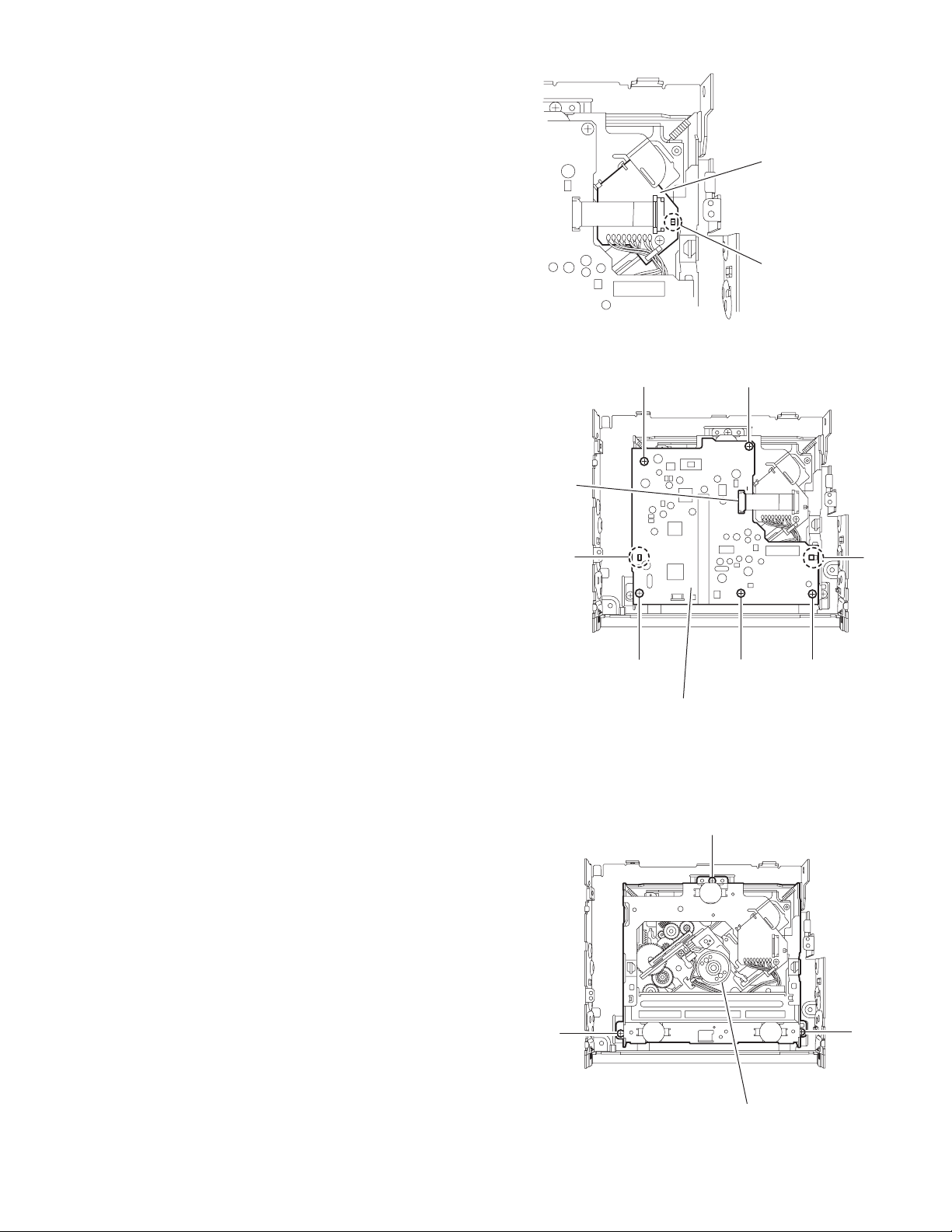
2.1 Main body
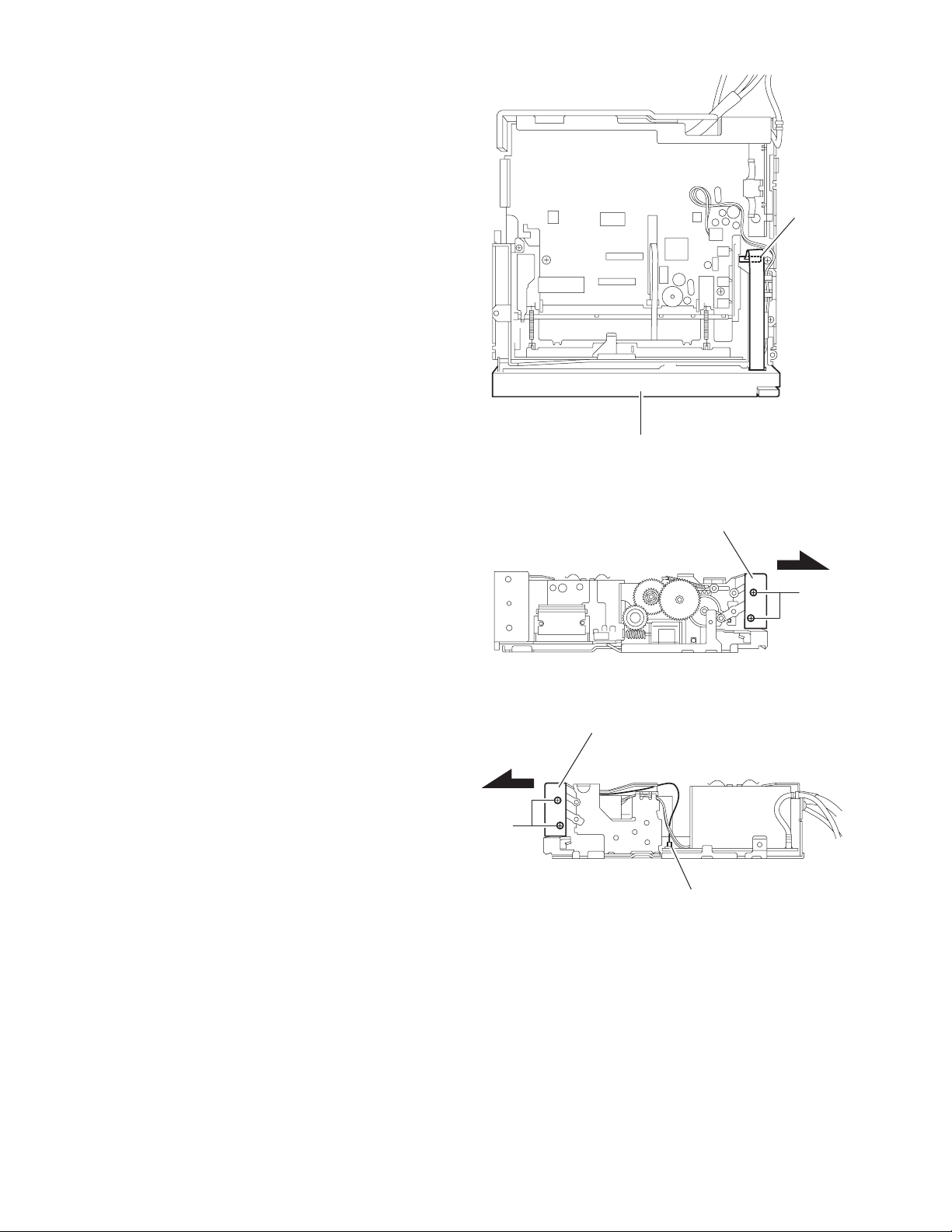
2.1.1 Removing the top chassis
(See Fig.1~5)
(1) Remove the two screws A attaching the bottom cover to
the top chassis on the bottom of the body.
(2) Remove the two screws B attaching the top chassis on
both sides of the body.
(3) Remove the screw C and the thee screws D attaching the
heat sink on the left side of the body.
(4) Remove the two screws E and the screw F on the back of
the body.
(5) Remove the two screws G on the upper side of the body.
(6) Move the top chassis upward and disconnect the CD
mechanism connector from the main board connector by
pulling it. Remove the top chassis from the body.
Bottom cover
C
Heat sink
E
D
D
Fig.3
Top chassis
B
F
Fig.1
Top chassis
Fig.2
B
Fig.4
Top chassis
G
G
Fig.5
(No.49793)1-5
Page 6
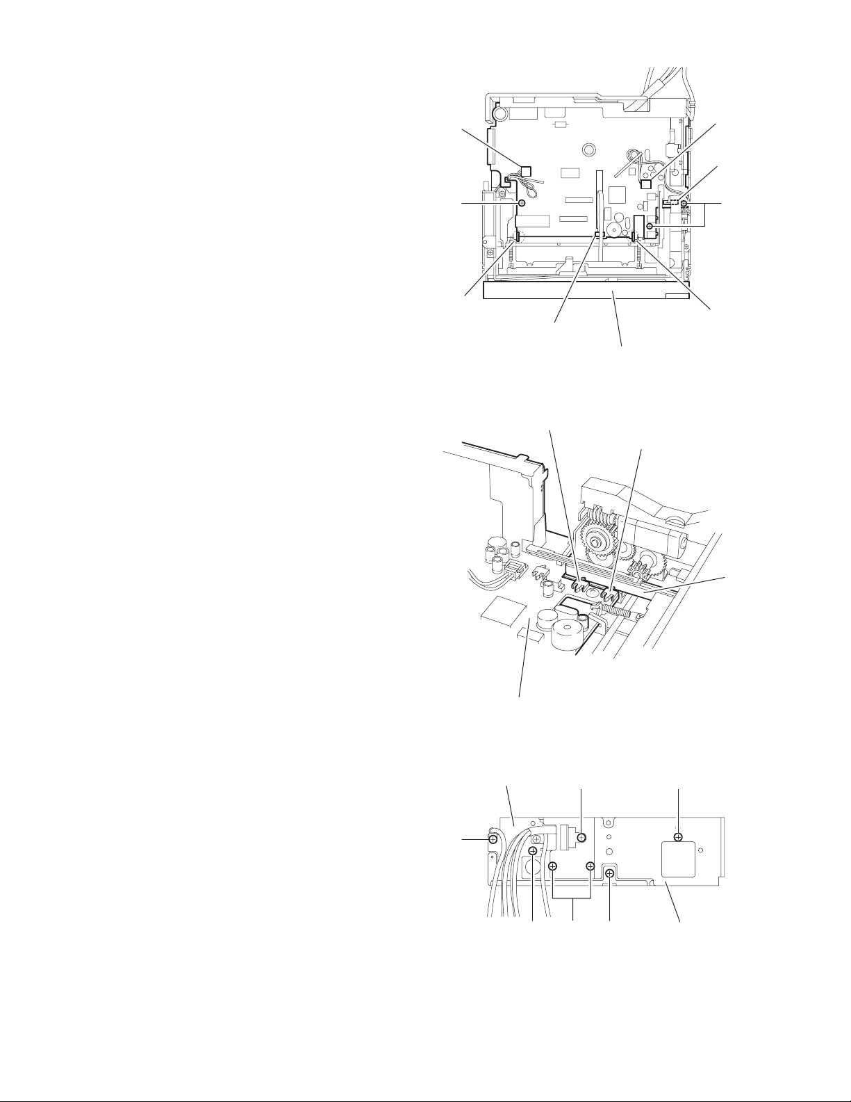
2.1.2 Removing the front panel assembly
(See Fig.6~8)
• Prior to performing the following procedure, remove the top
chassis assembly.
(1) Disconnect the flexible harness from connector CN701 on
the main board assembly.
(2) Remove the four screws H attaching the front panel as-
sembly on both sides of the body. Remove the front panel
toward the front.
CN701
Front panel assembly
Fig.6
Front panel assembly
H
H
Fig.7
Front panel assembly
CN701
Fig.8
1-6 (No.49793)
Page 7

2.1.3 Removing the Front Board
(See Fig.9)
• Prior to performing the following procedure, remove the top
chassis assembly and the front panel assembly.
(1) Remove the four screws I attaching the front board on the
back of the front panel assembly and release the eight
joints a.
2.1.4 Removing the lifter unit
(See Fig.10)
• Prior to performing the following procedure, remove the top
chassis assembly and the front panel assembly.
(1) Disconnect the harness from connector CN830 and CN831
on the main board.
(2) Remove the four screws J and detach the lifter unit from
the bottom cover.
I
CN830
J
Joints a
I
Joints a
Fig.9
CN831
J
Fig.10
Lifter unit assembly
(No.49793)1-7
Page 8
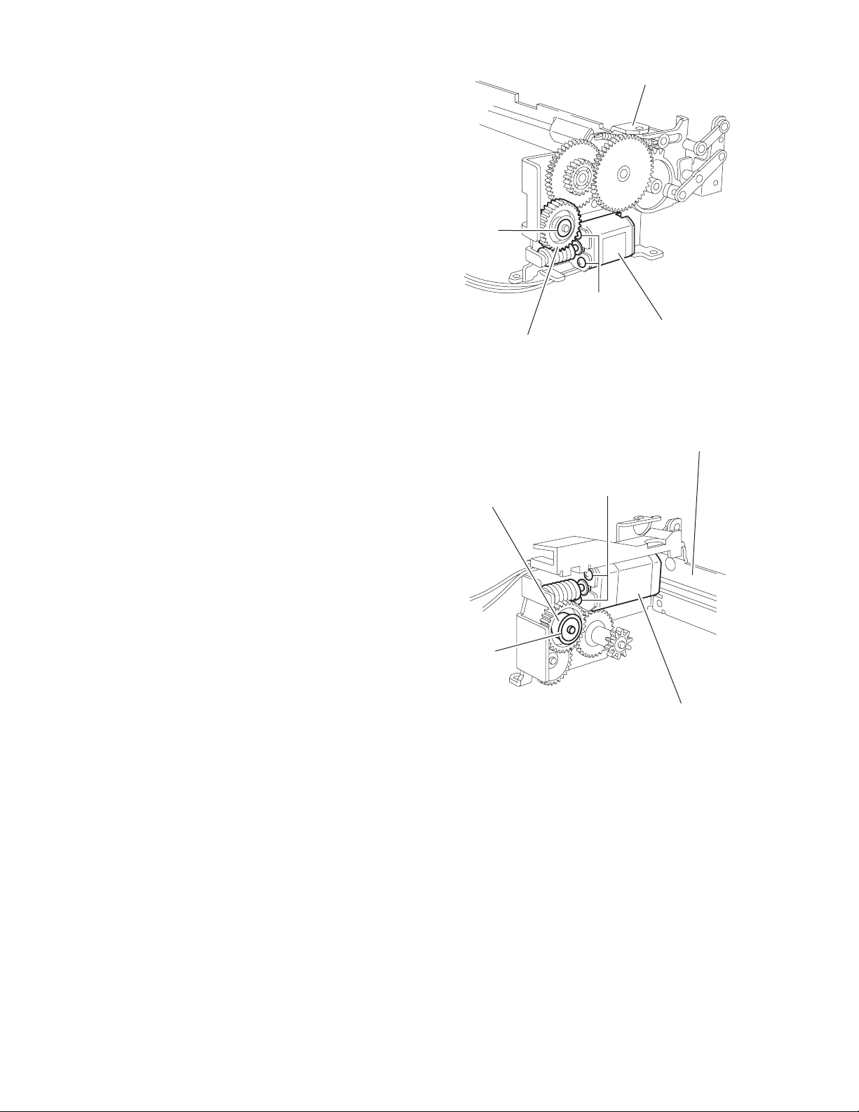
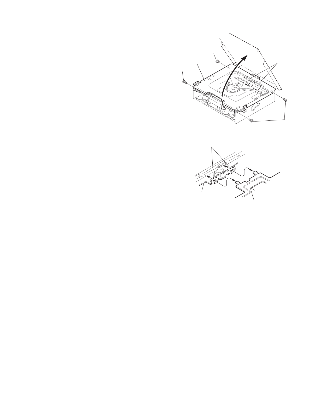
2.1.5 Removing the feed motor (L)
(See Fig.11)
• Prior to performing the following procedure, remove the lifter
unit.
(1) Remove the washer attaching the clutch assembly and de-
tach the clutch assembly from the shaft of the lifter unit.
(2) Remove the two screws K attaching the feed motor (L).
Lifter unit assembly
Washer
K
2.1.6 Removing the feed motor (R)
(See Fig.12)
• Prior to performing the following procedure, remove the lifter
unit.
(1) Remove the washer attaching the clutch assembly and de-
tach the clutch assembly from the shaft of the lifter unit.
(2) Remove the two screws L attaching the feed motor (R).
Clutch assembly
Clutch assembly
Washer
Feed motor (L) assembly
Fig.11
Lifter unit assembly
L
Feed motor (R) assembly
Fig.12
1-8 (No.49793)
Page 9
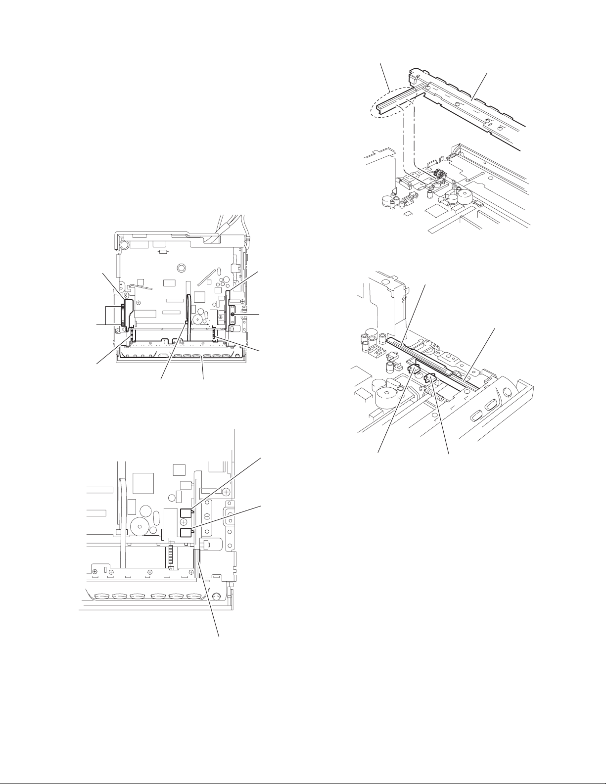
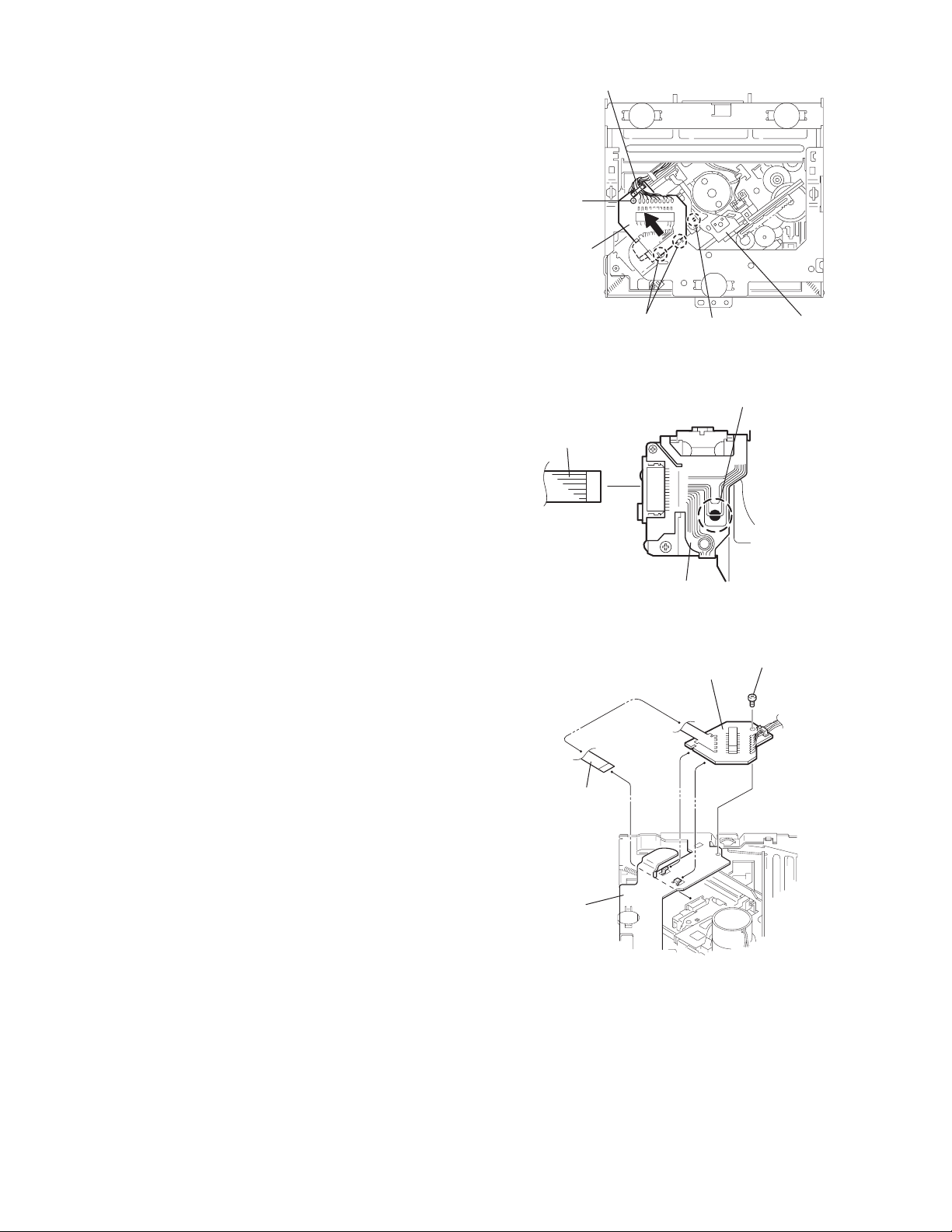
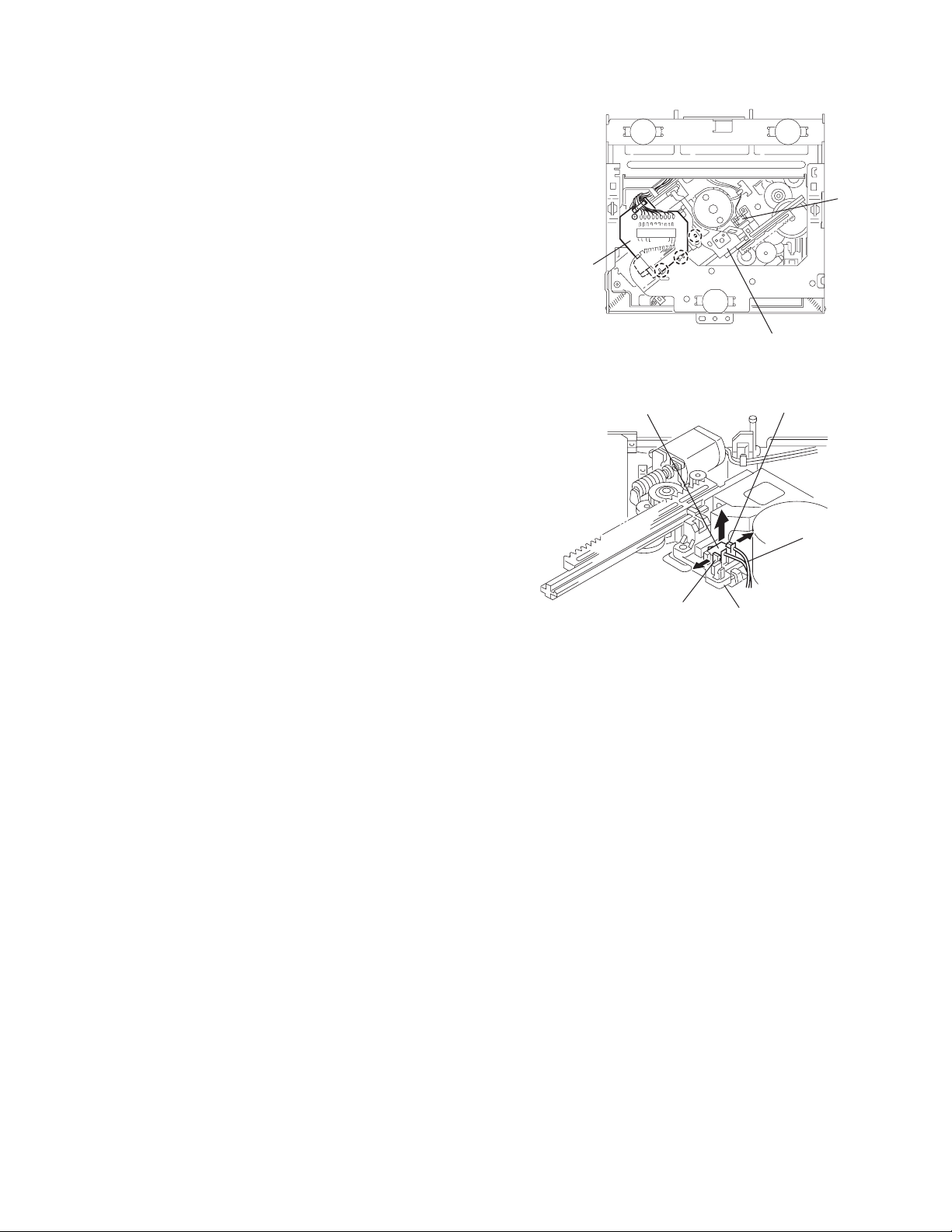
2.1.7 Removing the operation assembly
(See Fig.13~16)
• Prior to performing the following procedure, remove the top
chassis assembly, the front panel assembly and the lifer unit.
(1) Disconnect the card wire from connector CN702 on the
main board and remove the operation assembly.
(2) Remove the three screws M attaching the right and left
brackets, which fix gears on both sides of the operation assembly.
(3) Remove the springs 5 and 6 from the operation assembly.
ATTENTION:
When reassembling, correctly engage the switch S651 and
S652 on the main board and the right gear with the part b of
the operation assembly.
b
Operation assembly
Fig.15
Bracket (L)
M
Spring 5
CN702
Operation assembly
Fig.13
Bracket (R)
M
Spring 6
S652
S651
S652
Bracket (R)
Operation assembly b
S651
Fig.16
Operation assembly b
Fig.14
(No.49793)1-9
Page 10
2.1.8 Removing the operation switch board
(See Fig.17~19)
• Prior to performing the following procedure, remove the oper-
ation assembly.
(1) Remove the six screws N attaching the button panel on the
operation assembly.
(2) Release the bottom panel from the bottom base at the bot-
tom of the operation switch assembly five joint c and remove the bottom panel.
(3) Pull out the operation switch board from inside of the button
panel.
NN
Button panel
Fig.17
CC
Operation switch board
Button base
Button panel
Fig.18
Button panel
Fig.19
1-10 (No.49793)
Page 11
2.1.9 Removing the MP3 board assembly
(See Fig.20,21)
• Prior to performing the following procedure, remove the top
chassis.
Caution:
Before disconnecting the card wire from connector CN601 on
the MP3 board, solder the short-circuit point on the connector
board in the CD mechanism assembly (Refer to Fig.20).
(1) Disconnect the card wire from connector CN601 on the
MP3 board assembly.
(2) Remove the five screws O attaching the MP3 board as-
sembly and release the joint d and e.
Caution:
When reattaching the MP3 board, connect the card wire extending from the connector board to connector CN601 and unsolder the short-circuit point (Refer to Fig.21).
Connector board
Soldering
Fig.20
OO
CN601
2.1.10 Removing the CD mechanism assembly
(See Fig.22)
(1) Remove the three screws P and the CD mechanism as-
sembly from the top chassis.
e
d
OOO
MP3 board
Fig.21
P
P
P
CD mechanism assembly
Fig.22
(No.49793)1-11
Page 12
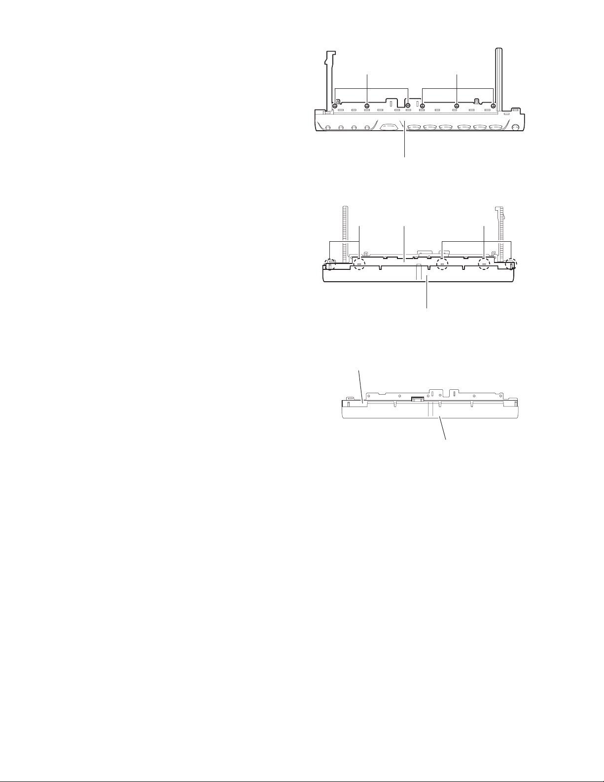
2.1.11 Removing the main board assembly
(See Fig.23~25)
• Prior to performing the following procedure, remove the top
chassis.
(1) Disconnect the flexible harness from connector CN701, the
card wire from CN702 on the main board and the harness
from CN830 and CN831 respectively.
(2) Remove the three screws Q attaching the main board as-
sembly to the bottom cover on the upper side of the body.
(3) Remove the screw R attaching the rear panel and the bot-
tom cover on the back of the body. Move the main board in
the direction of the arrow and release the two joints f. (At
this point, the main board can be removed with the rear
panel and the rear heat sink.)
(4) Remove the three screws S attaching the rear heat sink on
the back of the body.
(5) Remove the two screws T and the screw U attaching the
rear panel. Now, the main board assembly will be removed.
ATTENTION:
When reassembling, correctly engage the switch S651 and
S652 on the main board and the right gear with the part b of
the operation assembly (Refer to Fig.24).
CN830
Q
Joint f
CN831
CN701
Q
Joint f
CN702
Front panel assembly
Fig.23
S652
S651
Rear panel
T
Main board
USR
b
Fig.24
ST
Rear heat sink
Fig.25
1-12 (No.49793)
Page 13
2.2 CD Mechanism section
A
2.2.1 Removing the top cover
(See Figs.1 and 2)
(1) Remove the four screws A on the both side of the body.
(2) Lift the front side of the top cover and move the top cover
backward to release the two joints a.
Top cover
Joints a
A
Joints a
A
Fig.1
Fig.2
Top cover
(No.49793)1-13
Page 14
2.2.2 Removing the connector board
(See Figs.3 to 5)
CAUTION:
Before disconnecting the flexible wire from the pickup, solder
the short-circuit point on the pickup. No observance of this instruction may cause damage of the pickup.
(1) Remove the screw B fixing the connector board.
(2) Solder the short-circuit point on the pickup.
(3) Disconnect the flexible wire from the pickup.
(4) Move the connector board in the direction of the arrow to
release the two joints b.
(5) Unsolder the wires on the connector board if necessary.
CAUTION:
Unsolder the short-circuit point after reassembling.
B
Connector board
Flexible wire
Wires
Joints b
Short-circuit point
Fig.3
Short-circuit point
(Soldering)
Pickup
Flexible wire
Frame
Pickup
Fig.4
B
Connector board
Fig.5
1-14 (No.49793)
Page 15
2.2.3 Removing the DET switch
(See Figs.6 and 7)
(1) Extend the two tabs c of the feed sw. holder and pull out
the switch.
(2) Unsolder the DET switch wire if necessary.
DET
switch
Connector
board
Pickup
Fig.6
DET switch
Tab c
Tab c
DET switch wire
Feed sw. holder
Fig.7
(No.49793)1-15
Page 16
2.2.4 Removing the chassis unit
r
(See Figs.8 and 9)
• Prior to performing the following procedure, remove the top
cover and connector board.
(1) Remove the two suspension springs (L) and (R) attaching
the chassis unit to the frame.
CAUTION:
• The shape of the suspension spring (L) and (R) are different. Handle them with care.
• When reassembling, make sure that the three shafts
on the underside of the chassis unit are inserted to the
dampers certainly.
Suspension spring (R)
Chassis unit
Suspension spring (L)
Frame
Suspension spring (R)
Chassis unit
Shafts
Damper
Damper
Suspension spring (L)
Fig.8
Shaft
Dampe
Frame
Fig.9
1-16 (No.49793)
Page 17
2.2.5 Removing the clamper assembly
(See Figs.10 and 11)
• Prior to performing the following procedure, remove the top
cover.
(1) Remove the clamper arm spring.
(2) Move the clamper assembly in the direction of the arrow to
release the two joints d.
Clamper arm
spring
Joint d
Joint d
Clamper assembly
Fig.10
Clamper arm spring
Chassis rivet
assembly
Joint d
Clamper assembly
Chassis rivet assembly
Joint d
Fig.11
(No.49793)1-17
Page 18
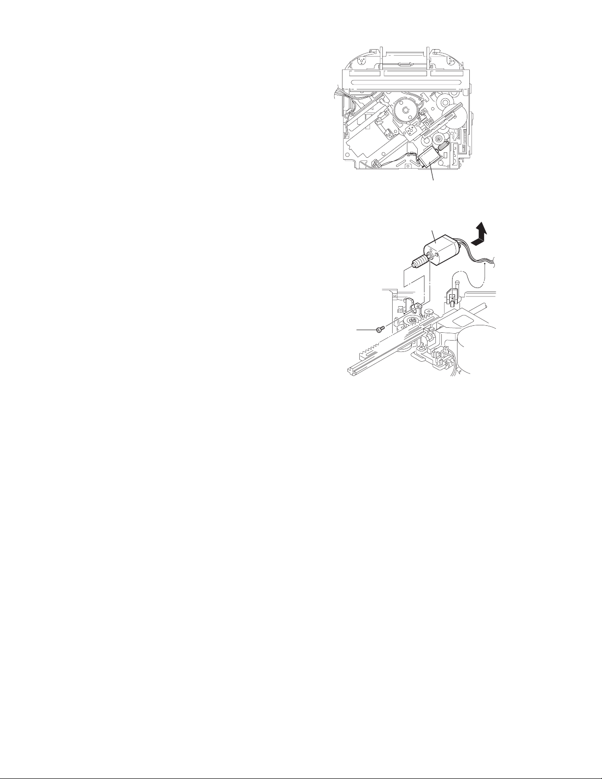
2.2.6 Removing the loading / feed motor assembly
(See Figs.12 and 13)
• Prior to performing the following procedure, remove the top
cover, connector board and chassis unit.
(1) Remove the screw C and move the loading / feed motor as-
sembly in the direction of the arrow to remove it from the
chassis rivet assembly.
(2) Disconnect the wire from the loading / feed motor assembly
if necessary.
CAUTION:
When reassembling, connect the wire from the loading /
feed motor assembly to the flame as shown in Fig.12.
Loading / feed motor assembly
Fig.12
Loading / feed motor assembly
C
Fig.13
1-18 (No.49793)
Page 19

2.2.7 Removing the pickup unit
r
(See Figs.14 to 18)
• Prior to performing the following procedure, remove the top
cover, connector board and chassis unit.
(1) Remove the screw D and pull out the pu. shaft holder from
the pu. shaft.
(2) Remove the screw E attaching the feed sw. holder.
(3) Move the part e of the pickup unit upward with the pu. shaft
and the feed sw. holder, then release the joint f of the feed
sw. holder in the direction of the arrow. The joint g of the
pickup unit and the feed rack is released, and the feed sw.
holder comes off.
(4) Remove the pu. shaft from the pickup unit.
(5) Remove the screw F attaching the feed rack to the pickup
unit.
Part e
Feed rack
Pickup unit
Feed sw. holder
Fig.15
2.2.8 Reattaching the pickup unit
(See Figs.14 to 17)
(1) Reattach the feed rack to the pickup unit using the screw F.
(2) Reattach the feed sw. holder to the feed rack while setting
the joint g to the slot of the feed rack and setting the joint f
of the feed rack to the switch of the feed sw. holder correctly.
(3) As the feed sw. holder is temporarily attached to the pickup
unit, set to the gear of the joint g and to the bending part of
the chassis (joint h) at a time.
CAUTION:
Make sure that the part i on the underside of the feed
rack is certainly inserted to the slot j of the change lock
lever.
(4) Reattach the feed sw. holder using the screw E.
(5) Reattach the pu. shaft to the pickup unit. Reattach the pu.
shaft holder to the pu. shaft using the screw D.
Feed sw. holder
Joint f
Joint g
Feed sw. holder
Pickup unit
E
Part i
Slot j
F
Pu. shaft
Pickup unit
Joint f
Joint h
Fig.16
Feed rack
D
Pu. shaft holde
Pu. shaft
D
Pu. shaft holder
Pickup unit
Fig.14
Part e
E
Joint g
Feed rack
Fig.17
Pickup unit
Joint g
Joint f
Feed sw. holder
Fig.18
(No.49793)1-19
Page 20

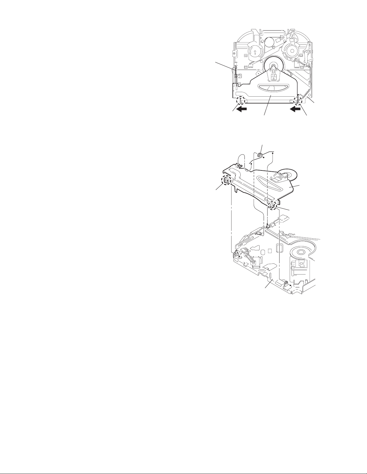
2.2.9 Removing the trigger arm
r
(See Figs.19 and 20)
• Prior to performing the following procedure, remove the top
cover, connector board and clamper unit.
(1) Turn the trigger arm in the direction of the arrow to release
the joint k and pull out upward.
CAUTION:
When reassembling, insert the part m and n of the trigger
arm into the part p and q at the slot of the chassis rivet
assembly respectively and join the joint k at a time.
Chassis rivet assembly
Trigger arm
Chassis
rivet
assembly
Joint k
Trigger arm
Fig.19
Part p
Part q
Part m
Part n
2.2.10 Removing the top plate assembly
(See Fig.21)
• Prior to performing the following procedure, remove the top
cover, connector board, chassis unit, and clamper assembly.
(1) Remove the screw H.
(2) Move the top plate assembly in the direction of the arrow to
release the two joints r.
(3) Unsolder the wire marked s if necessary.
H
Fig.20
Top plate assembly
Joints
s
Fig.21
1-20 (No.49793)
Page 21

2.2.11 Removing the mode sw. / select lock arm
(See Figs.22 and 23)
• Prior to performing the following procedure, remove the top
plate assembly.
(1) Bring up the mode sw. to release from the link plate (joint t)
and turn in the direction of the arrow to release the joint u.
(2) Unsolder the wire of the mode sw. marked s if necessary.
(3) Turn the select lock arm in the direction of the arrow to re-
lease the two joints v.
(4) The select lock arm spring comes off the select lock arm at
the same time.
Link plate
Joint u
Fig.22
Joint t
Mode sw.
Select lock arm
s
Top plate
Select lock arm
Link plate
Select lock arm
Fig.23
Top plate
Hook w
Select lock
arm spring
Joints v
(No.49793)1-21
Page 22

2.2.12 Reassembling the mode sw. / select lock arm
(See Figs.24 to 26)
REFERENCE:
Reverse the above removing procedure.
(1) Reattach the select lock arm spring to the top plate and set
the shorter end of the select lock arm spring to the hook w
on the top plate.
(2) Set the other longer end of the select lock arm spring to the
boss x on the underside of the select lock arm, and join the
select lock arm to the slots (joint v). Turn the select lock
arm as shown in the figure.
(3) Reattach the mode sw. while setting the part t to the first
peak of the link plate gear, and join the joint u.
CAUTION:
When reattaching the mode sw., check if the points y and
z are correctly fitted and if each part operates properly.
Select lock arm spring
Hook w
Joint v
Joint v
Select lock arm
Boss x
Fig.24
Joint t
Point y
Link plate
Point z
Link plate
Fig.25
Mode sw.
Select
lock arm
Joint t
Joint u
Fig.26
1-22 (No.49793)
Page 23

2.2.13 Removing the select arm R / link plate
(See Figs.27 and 28)
• Prior to performing the following procedure, remove the top
plate assembly.
(1) Bring up the select arm R to release from the link plate
(joint a') and turn as shown in the figure to release the two
joints b' and joint c'.
(2) Move the link plate in the direction of the arrow to release
the joint d'. Remove the link plate spring at the same time.
REFERENCE:
Before removing the link plate, remove the mode sw..
Select arm R
Joint b'
Link plate spring
Joint c'
Joint a'
Link plate
Joint b'
Fig.27
Joint r
2.2.14 Reattaching the Select arm R / link plate
(See Figs.29 and 30)
REFERENCE:
Reverse the above removing procedure.
(1) Reattach the link plate spring.
(2) Reattach the link plate to the link plate spring while joining
them at joint d'.
(3) Reattach the joint a' of the select arm R to the first peak of
the link plate while joining the two joints b' with the slots.
Then turn the select arm R as shown in the figure. The top
plate is joined to the joint c'.
CAUTION:
When reattaching the select arm R, check if the points e'
and f' are correctly fitted and if each part operates properly.
Top plate
Select arm R
Joint b'
Joint d'
Link plate
Fig.28
Link plate spring
Joint c'
Joint d'
Joint b'
Joint a'
Fig.29
Joint a'
Point e'
Link plate
Point f'
Fig.30
(No.49793)1-23
Page 24

2.2.15 Removing the loading roller assembly
(See Figs.31 to 33)
• Prior to performing the following procedure, remove the
clamper assembly and top plate assembly.
(1) Push inward the loading roller assembly on the gear side
and detach it upward from the slot of the joint g' of the lock
arm rivet assembly.
(2) Detach the loading roller assembly from the slot of the joint
h' of the lock arm rivet assembly.
Roller guide
spring
Part k'
Loading roller assembly
Loading roller assembly
The roller guide comes off the gear section of the loading
roller assembly.
Remove the roller guide and the HL washer from the shaft
of the loading roller assembly.
(3) Remove the screw J attaching the lock arm rivet assembly.
(4) Push the shaft at the joint i' of the lock arm rivet assembly
inward to release the lock arm rivet assembly from the slot
of the L side plate.
(5) Extend the lock arm rivet assembly outward and release
the joint j' from the boss of the chassis rivet assembly. The
roller guide springs on both sides come off at the same
time.
CAUTION:
When reassembling, reattach the left and right roller
guide springs to the lock arm rivet assembly before reattaching the lock arm rivet assembly to the chassis rivet
assembly. Make sure to fit the part k' of the roller guide
spring inside of the roller guide. (Refer to Fig.34.)
Roller guide
HL washer
Loading roller assembly
Roller guide
Chassis rivet assembly
J
Roller guide
spring
Fig.32
Boss
L side plate
Roller guide spring
Joint h'
Roller guide spring
Loading roller assembly
1-24 (No.49793)
Joint g'
Lock arm rivet assembly
Fig.31
Roller guide spring
Roller guide spring
Lock arm rivet assembly
Lock arm rivet assembly
Joint j'
Joint i'
Fig.33
Roller guide
HL washer
Roller shaft assembly
Loading roller
Roller guide spring
Fig.34
Page 25

2.2.16 Removing the loading gear 5, 6 and 7
(See Figs.35 and 36)
• Prior to performing the following procedure, remove the top
cover, chassis unit, pickup unit and top plate assembly.
(1) Remove the screw K attaching the loading gear bracket.
The loading gear 6 and 7 come off the loading gear bracket.
(2) Pull out the loading gear 5.
K
Loading gear 5
Loading gear bracket
K
Loading gear 6
Loading gear 5
Loading gear 3
Fig.35
Loading gear bracket
Loading gear 6
Loading gear 7
Fig.36
(No.49793)1-25
Page 26

2.2.17 Removing the gears
(See Figs.37 to 40)
• Prior to performing the following procedure, remove the top
cover, chassis unit, top plate assembly and pickup unit.
• Pull out the loading gear 3. (See Fig.35.)
(1) Pull out the feed gear.
(2) Move the loading plate assembly in the direction of the ar-
row to release the L side plate from the two slots m' of the
chassis rivet assembly. (See Fig.37.)
(3) Detach the loading plate assembly upward from the chas-
sis rivet assembly while releasing the joint n'. Remove the
slide hook and loading plate spring from the loading plate
assembly.
(4) Pull out the loading gear 2 and remove the change lock le-
ver.
(5) Remove the E ring and washer attaching the change gear
2.
(6) The change gear 2, change gear spring and adjusting
washer come off.
(7) Remove the loading gear 1.
(8) Move the change plate rivet assembly in the direction of the
arrow to release from the three shafts of the chassis rivet
assembly upward. (See Fig.38.)
(9) Detach the loading gear plate rivet assembly from the shaft
of the chassis rivet assembly upward while releasing the
joint p'. (See Figs.38 and 40.)
(10) Pull out the loading gear 4.
Change plate
rivet assembly
Shafts
E ring
Loading plate assembly
Loading plate spring
Joint p'
Loading gear 4
Loading gear plate
rivet assembly
Shaft
Loading gear 2
Loading gear 1
Chassis rivet assembly
Change gear 2
Fig.38
Joint n'
Slide hook
Feed gear
Fig.37
Slot m'
L side plate
Loading plate assembly
Joint n'
Slot m'
Chassis rivet assembly
Chassis rivet assembly
E ring
Washer
Change gear 2
Change gear
spring
Adjusting
washer
Change plate
rivet assembly
L side plate
Slot m'
Slot m'
Fig.39
Loading gear 1
Loading gear 2
Change lock lever
Loading gear 4
1-26 (No.49793)
Chassis rivet assembly
Loading gear plate rivet
assembly
Fig.40
Page 27

2.2.18 Removing the turn table / spindle motor
(See Figs.41 and 42)
• Prior to performing the following procedure, remove the top
cover, connector board, chassis unit and clamper assembly.
(1) Remove the two screws L attaching the spindle motor as-
sembly through the slot of the turn table on top of the body.
(2) Unsolder the wire on the connector board if necessary.
Turn table
L
Fig.41
L
Turn table
Spindle motor
Fig.42
(No.49793)1-27
Page 28

SECTION 3
Adjustment
3.1 Test instruments required for adjustment
(1) Digital oscilloscope (100MHz)
(2) AM Standard signal generator
(3) FM Standard signal generator
(4) Stereo modulator
(5) Electric voltmeter
(6) Digital tester
(7) Tracking offset meter
(8) Test Disc JVC :CTS-1000
(9) Extension cable for check
EXTSH002-22P × 1
3.2 Standard volume position
Balance and Bass &Treble volume : lndication"0"
Loudness : OFF
3.6 How to connect the extension cable for adjusting
Caution:
Be sure to attach the heat sink and rear bracket onto the power amplifier and regulator respectively, before supply the power. If
voltage is applied without attaching these parts, the power amplifier IC and regulator IC will be destroyed by heat.
3.3 Standard measuring conditions
Power supply voltage DC14.4V(11 to 16V)
Load impedance 20KΩ(2 Speakers connection)
Output Level Line out 2.0V (Vol. MAX)
3.4 Frequency Band
FM1 87.5MHz to 108.0MHz
AM (MW) 522kHz to 1620kHz
AM (LW) 144kHz to 279kHz
3.5 Dummy load
Exclusive dummy load should be used for AM,and FM. For FM
dummy load,there is a loss of 6dB between SSG output and antenna input.The loss of 6dB need not be considered since direct
reading of figures are applied in this working standard.
EXTLX002-JIG : Kit including the following 8 extension parts.
No.
1
2
3
4
5
6
7
Parts number Quantity Description
EXTLX001-2P
EXTLX001-6PF
EXTLX001-6PC
EXTLX002-16PF
EXTLX002-16PC
EXTLX002-SWPWB
EXTLX002-4P
2
1
1
1
1
1
1
2Pin, 30cm extension cord
6Pin, 30cm flat wire
6Pin x 2, interlocking connector
16Pin flat wire
16Pin, interlocking connector
3 switch PWB
4Pin, 30cm extension cord
EXTSH002-22P
EXTLX001-16PF
EXTLX002-SWPWB
EXTLX002-4P
EXTLX002-16PC
EXTLX001-2P
EXTLX001-6PC
EXTLX001-2P
EXTLX001-6PF
1-28 (No.49793)
Page 29

3.7 Flow of functional operation unit TOC read
When the pickup correctly moves
v
to the inner area of the disc
Power ON
Set Function CD
When the laser diode correctly
emits
Microprocessor
commands
FMO
TC94A14FA "40"
FEED MOTOR
+TERMINAL
IC681 "4"
REST SW
When correctly focused
FEO
TA2157 "15"
Focus Servo Loop ON
$83
$82
$81
3.3V
Hi-Z
0V
6V
4V
2V
OFF
ON
Pickup feed to the inner area
2.2V
RF signal eye-pattern
remains closed
Disc inserted
YES
Laser emitted
Focus search
Disc rotates
Tracking loop closed
YES
Microprocessor
commands
SEL
TC94A14FA"38"
LD
CN601"15"
"No disc"
display
When the disc correctly rotates
Microprocessor
commands
DMO
TC94A14FA "41"
$84 $86 $ A200
$84
3.3V
0V
4V
0V
3.3V
2.2V
0V
RF signal eye-pattern
opens
TOC read out
Jump to the first track
Play
Spindle
motor(-)
IC681 "7"
Acceleration Servo CLV
Tracking Servo Loop ON
RF signal
6V
3.2
2V
Rough
Servo
0.5 Sec 0.5 Sec
Rough Servo Mode
CLV Servo Mode
(Program Area)
CLV Servo Mode
(Lead-In Area;
Digital :0)
(No.49793)1-29
Page 30

3.8 Troubleshooting
Feed section
Is the voltage output at
IC621 pin "40" 5V or 0V?
Is 4V present at both
sides of the feed motor?
YES
YES
NO YES NO
Is the wiring for IC681
pin 27?
NO
Is 3.3V present at IC681
pin "20"?
YES
Check the vicinity of
Check CD 8V
and 5V.
IC621.
NO
Is 6V or 2V present at
IC681 "4" and "5"?
YES
Check the feed motor
connection wiring.
NO
Check the feed motor.
Focus section
When the lens is
moving:
4V
Does the S-search
waveform appear at
IC681 pins "8" and "9"?
Spindle section
Is the disk rotated?
YES
Does the RF signal
appear at RF test point?
YES
Is the RF waveform at RF
test point distorted?
YES
Proceed to the Tracking
section
Check IC601.
NO
Check the circuits in
the vicinity of IC681
pins "8","9"and"15".
YES
Check the pickup and
its connections
NO
Is 4V present at IC681
pins "6" and "7"?
Check the spindle motor
and its wiring
NO
Check the circuits in the
vicinity of IC681 "19"~
NO
"24" or the pickup
YES
YES
NO
Is 4V present at IC621
pins "41" ?
Check the vicinity of
IC561.
NO
YES
Check IC621 and
IC681.
Tracking section
When the disc is rotated
at first:
Is the tracking error signal
output at IC601 "11"?
1-30 (No.49793)
Approx. 1.2V
YES
Check IC621.
YES YES
Check the circuit in the
vicinity of IC501 pins
"2"~"7".
Check the pickup and
its connections
Page 31

3.9 Maintenance of laser pickup
(1) Cleaning the pick up lens
Before you replace the pick up, please try to clean the lens
with a alcohol soaked cotton swab.
(2) Life of the laser diode
When the life of the laser diode has expired, the following
symptoms will appear.
• The level of RF output (EFM output: amplitude of eye
pattern) will be low.
3.10 Replacement of laser pickup
Turn off the power switch and,disconnect the
power cord from the ac outlet.
Replace the pickup with a normal one.(Refer
to "Pickup Removal" on the previous page)
Is RF output
1.0 0.35Vp-p?
NO
Replace it.
YES
O.K
(3) Semi-fixed resistor on the APC PC board
The semi-fixed resistor on the APC printed circuit board
which is attached to the pickup is used to adjust the laser
power.Since this adjustment should be performed to match
the characteristics of the whole optical block, do not touch
the semi-fixed resistor.
If the laser power is lower than the specified value, the laser diode is almost worn out, and the laser pickup should
be replaced. If the semi-fixed resistor is adjusted while the
pickup is functioning normally, the laser pickup may be
damaged due to excessive current.
Plug the power cord in,and turn the power on.
At this time,check that the laser emits for
about 3seconds and the objective lens moves
up and down.
Note: Do not observe the laser beam directly.
Play a disc.
Check the eye-pattern at RF test point.
Finish.
(No.49793)1-31
Page 32

SECTION 4
Description of major ICs
4.1 BA6956AN (IC830, IC831) : Reversible motor driver
• Block diagram
TSD
CONTROL LOGIC
1 2 3 4 5 6 7 8 9
REF
OUT2
RNF
VM
OUT1
Vcc
FIN
GND
RIN
• Pin function • Truth table
Pin No. Symbol Function
1 VREF Output high voltage level control terminal
2 OUT2 Output terminal for motor
3 RNF GND of driver division
4 OUT1 Output terminal for motor
FIN RIN OUT1 OUT2 MODE
H L H L Forward rotation mode
L H L H Reverse rotation mode
H H L L Break Mode
L L OPEN OPEN Stand-by mode
5 VM Power supply for driver division
6 Vcc Power supply for signal division
7 FIN Input terminal for control logic
8GNDGND
9 RIN Input terminal for control logic
1-32 (No.49793)
Page 33

4.2 BR24C01AFV-W-X (IC1502) : EEPROM
A
•Pin layout
Vcc WP SCL SDA
A0 A1 A2 GND
• Block diagram
A0
1
7bit
A1
2
A2
3
GND
• Pin function
Pin name I/O Description
Vcc - Power supply
GND - Ground (0v)
A0,A1,A2 IN Slave address set
SCL IN Serial clock input
SDA IN / OUT Slave and word addressserial data input serial data output *1
WP IN Write protect input
*1 An open drain output requires a pull-up resister.
4
ADDRESS
DECODER
CONTROL LOGIC
HIGH VOLTAGE GEN.
1kbit EEPROM ARRAY
SLAVE/WORD
7bit
ADDRESS REGISTER
START
STOP
Vcc LEVEL DETECT
ACK
8bit
DATA
REGISTER
Vcc
8
7
WP
6
SCL
5
SD
(No.49793)1-33
Page 34

4.3 BR24C32F (IC703) : EEPROM
A
• Pin Layout
VCC
BR24C32/F
• Pin function
SDASCLWP
• Pin layout & Block diagram
PIN NAME I/O Function
VCC - Power Supply
GND - Ground (0V)
A0-A2 I Slave Address Set
SCL I Serial Clock Input
SDA I/O Slave and Word Address.
Serial Data Input$ Serial Data Output *1
WP I Write Protect Input
GNDA2A1A0
1
A0
12bit
2
A1
3
A2
4
GND
4.4 HD74HC126FP (IC771) : Changer Control
OE1
A1
Y1
1
2
3
ADDRESS
DECODER
CONTROL LOGIC
HIGH VOLTAGE GEN.
14
13
12
32 Kbit EEPROM ARRAY
SLAVE WORD
12bit
ADDRESS REGISTER
START STOP
VCC LEVEL DETECT
Vcc
OE4
A4
DATA
REGISTER
ACK
8bit
8
7
6
5
Vcc
WP
SCL
SD
OE2
A2
Y2
Vss
1-34 (No.49793)
4
5
6
7
HD74HC126
11
10
9
8
Y4
OE3
A3
Y3
Page 35

4.5 BU1923F (IC51) : RDS decoder
A
•Pin layout
1
QUAL
RDATA
Vref
MUX
VDD1
VSS1
VSS3
CMP
2
3
4
5
6
7
8
16
15
14
13
12
11
10
• Block diagram
9
RCLK
N.C.
XO
XI
VDD2
VSS2
T1
T2
MUX
Vref
VDD1
VSS1
VDD2
VSS2
4
3
5
Power supply
6
12
Power supply
11
100k
120k
Analog
Digital
100k
-
+
anti-aliasing
filter
PLL
57kHz
RDS/ARI
Reference
clock
PLL
1187.5Hz
VSS3
8th Switched
capacitor filter
Bi-phase
decoder
7
CMP
Measurement
circuit
8
comparator
Differential
decoder
16
1
2
RCLK
QUAL
RDAT
13
Xl
14
X0
10 9
T1
T2
(No.49793)1-35
Page 36

4.6 HA13164A (IC961) : Regulator
• Terminal layout
123456789101112131415
• Block diagram
ANT OUT
EXT OUT
ANT CTRL
CTRL
CD OUT
AUDIO OUT
C3
0.1u
C4
0.1u
C5
0.1u
C6
10u
2
1
7
11
12
10
VCC ACC
8
Surge Protector
BIAS TSD
15
3
TAB
C1
100u
C2
0.1u
13
ILM AJGND GND
+B
ACC
BATT.DET OUT
9
COMPOUT
6
VDD OUT
4
SW5VOUT
5
ILMOUT
14
R1
C7
0.1u
C8
0.1u
UNIT R:
C:F
note1) TAB (header of IC)
connected to GND
• Pin function
Pin No. Symbol Function
1 EXTOUT Output voltage is VCC-1 V when M or H level applied to CTRL pin.
2 ANTOUT Output voltage is VCC-1 V when M or H level to CTRL pin and H level to ANT-CTRL.
3 ACCIN Connected to ACC.
4 VDDOUT Regular 5.7V.
5 SW5VOUT Output voltage is 5V when M or H level applied to CTRL pin.
6 COMPOUT Output for ACC detector.
7 ANT CTRL L:ANT output OFF H:ANT output ON
8 VCC Connected to VCC.
9 BATT DET Low battery detect.
10 AUDIO OUT Output voltage is 9V when M or H level applied to CTRL pin.
11 CTRL L:BIAS OFF M:BIAS ON H:CD ON
12 CD OUT Output voltage is 8V when H level applied to CTRL pin.
13 ILM AJ Adjustment pin for ILM output voltage.
14 ILM OUT Output voltage is 10V when M or H level applied to CTRL pin.
15 GND Connected to GND.
1-36 (No.49793)
Page 37

4.7 HD74HCT126T-X : (IC1500,IC1503) Buffer
• Pin arrangement • Pin function
Input Output
1C
1A
1Y
2C
2A
2Y
GND
• Block diagram
1
2
3
4
5
6
7
14
13
12
11
10
Vcc
4C
4A
4Y
3C
9
3A
8
3Y
CA Y
LX Z
HL L
HH H
H : High level
L : Low level
X : Irrelevant
Z : Off (Hhigh-impedance)state of a 3-stage output
1A
1C
2A
2C
3A
3C
4A
1Y
2Y
3Y
4Y
4C
(No.49793)1-37
Page 38

4.8 LA47505 (IC941) : Power amp.
• Terminal layout
206
11
1
12
4
10
Stand by
Switch
Ripple
Filter
Protective
circuit
Mute
circuit
9
7
8
5
3
2
22
15
25
13
14
16
Muting &
On Time Control
Circuit
protective
circuit
17
19
18
21
23
24
1-38 (No.49793)
Page 39

• Terminal layout
AC CONT1
GND1
OUTFR-
STBY
OUTFR+
Vcc1/2
OUTRR-
GND2
OUTRR+
VREF
INRR
INFR
SGND
INFL
INRL
ONTIME
OUTRL+
GND3
OUTRL-
Vcc3/4
OUTFL+
MUTE
OUTFL-
GND4
NC
• Pin function
Pin No. Symbol Function
1 AC CONT1 Header of IC
2 GND1 Power GND
3 OUTFR- Outpur(-) for front Rch
4 STBY Stand by input
5 OUTFR+ Output (+) for front Rch
6 Vcc1/2 Power input
7 OUTRR- Output (-) for rear Rch
8 GND2 Power GND
9 OUTRR+ Output (+) for rear Rch
10 VREF Ripple filter
11 INRR Rear Rch input
12 INFR Front Rch input
13 SGND Signal GND
14 INFL Front Lch input
15 INRL Rear Lch input
16 ONTIME Power on time control
17 OUTRL+ Output (+) for rear Lch
18 GND3 Power GND
19 OUTRL- Output (-) for rear Lch
20 Vcc3/4 Power input
21 OUTFL+ Output (+) for front
22 MUTE Muting control input
23 OUTFL- Output (-) for front
24 GND4 Power GND
25 NC No connection
(No.49793)1-39
Page 40

4.9 LA6579H-X (IC1681) : 4-Channel bridge driver
W
• Pin layout & Block diagram
VIN1-A
1
+
VIN1+A
VCCP1
2
3
VIN1_SW
[H]: OP-AMP_A
[L]: OP-AMP_B
[H]
[L]
28
VIN1
27
VIN1-B
-
+
26
VIN1+B
VO+
VO-
VO2+
VO2-
FR
VO3+
VO3-
VO4+
4
5
6
7
FR
8
9
10
Power system
GND
+
Level shift
Level shift
Level shift
Level shift
33k
11k
-
+
H : ON
L : OFF
3.3VREG
(External:PTP Tr)
Signal system
power supply
All outputs ON/OFF
MUTE
Power system GND
Signal system
power supply
+
-
25
24
23
22
FR
21
20
19
S-GND
VIN1-S
MUTE
VREFIN
FR
VCCS
3.3VREG
REGIN
VO4-
VCCP2
VIN4
VIN4G
1-40 (No.49793)
11
12
13
14
11k
33k
+
33k
33k
18
VIN2G
11k
-
17
VIN2
+
16
VIN3G
11k
-
15
VIN3
+
Page 41

• Pin function
Pin No. Symbol Function
1 VIN1-A CH1 input AMP_inverted input
2 VIN1+A CH1 input AMP_non-inverted input
3 VCCP1 CH1 and CH2 power stage power supply
4 VO1+ Output pin(+)for channel 1
5 VO1- CH1 output pin (-) for channel 1
6 VO2+ Output pin(+)for channel 2
7 VO2- Output pin(-)for channel 2
8 VO3+ Output pin(+)for channel 3
9 VO3- Output pin(-)for channel 3
10 VO4+ Output pin(+)for channel 4
11 VO4- Output pin(-)for channel 4
12 VCCP2 CH3 and CH4 power stage powr supply
13 VIN4 Input pin for channel 4
14 VIN4G Input pin for channel 4(for gain adjustment)
15 VIN3 Input pin for channel 3
16 VIN3G Input pin for channel 3(for gain adjustment)
17 VIN2 Input pin for channel 2
18 VIN2G Input pin for channel 2(for gain adjustment)
19 REGIN External PNP transistor base connection
20 3.3VREG 3.3VREG output pin external PNP transistor,collector connection
21 VCCS Signal system GND
22 VREFIN Reference voltage application pin
23 MUTE Output ON/OFF pin
24 VIN1_SW CH1 input OP AMP_changeover pin
25 S_GND Signal system GND
26 VIN1+B CH1 AMP_B non-inverted input pin
27 VIN1-B CH1 AMP_B inverted input pin
28 VIN1 CH1 input pin input OP_AMP output pin
(No.49793)1-41
Page 42

4.10 M61508FP (IC400) : E.volume
• Pin layout & Block diagram
VDD OUT 2
CLOCK
VDD
NonFadaer OUT 2
FRONT OUT 2
REAR OUT2
FADER IN 2
TONE OUT 2
VOL IN 2
SEL OUT 2
19
20
21
22
23
24
25
26
LOUDNESS
+
3BAND TONE
CONTROL
(BASS/MID/
TREBLE)
27
28
SOFT
SELECT
NON FADER
VOLUME
+ -
VOLUME 2
A
B
ZERO
CROSS
DETECTOR
VOLUME 1
I/F
TIMER
DETECTOR
NON FADER
VOLUME
A
B
ZERO DETECT
SELECT SWITCH
ZERO
CROSS
DETECTOR
GNDVDD
- +
LOUDNESS
+
3BAND TONE
CONTROL
(BASS/MID/
TREBLE)
18 VDD OUT 1
17
DATA
GND
16
15
NonFadaer OUT 1
FRONT OUT 1
14
REAR OUT1
13
FADER IN 1
12
11
TONE OUT 1
10
VOL IN 1
9
SEL OUT 1
1-42 (No.49793)
DEFN OUT 2
IND 2
INC 2
INB 2
INA 2
DEFN IN 2
DEFP IN 2
AVDD
29
30
31
32
33
34
35
36
50K
50K
50K
50K
+
VCC
+ -
51K
51K
- +
25.5K
REF
25.5K
+ -
30K 30K
+ -
- +
25.5K25.5K
51K
51K
-
+
50K
50K
50K
50K
8
DEFN OUT 1
IND 1
7
INC 1
6
5
INB 1
4
INA 1
3
DEFN IN 1
DEFP IN 1
2
1
REF
Page 43

• Pin function
Pin No. Symbol Function
1 REF IC signal GND
2 DEFP IN 1 Ope amp positive input
3 DEFN IN 1 Ope amp negative input
4 INA 1 Input selector ch1 input terminal
5 INB 1 Input selector ch1 input terminal
6 INC 1 Input selector ch1 input terminal
7 IND 1 Input selector ch1 input terminal
8 DEFN OUT 1 Operation outoutterminal (-)
9 SEL OUT 1 Input selector output terminal
10 VOL IN 1 Volume 1 input terminal
11 TONE OUT 1 Tone output terminal
12 FADER IN 1 Volume 2 input terminal
13 REAR OUT1 Fader volume (rear) output terminal
14 FRONT OUT 1 Fader volume (front) output terminal
15 NonFadaer OUT 1 Non fader volume output terminal
16 GND GND
17 DATA Control data input terminal
18 VDDOUT 1 Connect to GND with capacitor
19 VDDOUT 2 Connect to GND with capacitor
20 CLOCK Serial data clock input terminal
21 VDD VDD for digital
22 NonFadaer OUT 2 Non fader volume output terminal
23 FRONT OUT 2 Fader volume (front) output terminal
24 REAR OUT2 Fader volume (rear) output terminal
25 FADER IN 2 Volume 2 input terminal
26 TONE OUT 2 Tone output terminal
27 VOL IN 2 Volume 1 input terminal
28 SEL OUT 2 Input selector output terminal
29 DEFN OUT 2 Ope amp output terminal (-)
30 IND 2 Input selector switch ch2 input terminal
31 INC 2 Input selector switch ch2 input terminal
32 INB 2 Input selector switch ch2 input terminal
33 INA 2 Input selector switch ch2 input terminal
34 DEFN IN 2 Ope amp negative input terminal
35 IEFP IN 2 Ope amp positive input terminal
36 VCC VCC for analog
(No.49793)1-43
Page 44

4.11 LC75878W (IC601) : LCD driver
• Pin layout
100 ~ 76
1
75
• Block diagram
~
25
OSC
VLCD
VLCD0
VLCD1
VLCD2
VLCD3
VLCD4
VDD
VSS
26 ~ 50
P1
GENERAL
GENERATOR
CONTRAST
ADJUSTER
PORT
CLOCK
~
51
P4
COM1
COMMON
DRIVER
COM8
S75/COM9
S74/COM10
S73
SEGMENT DRIVER & LATCH
CONTROL
REGISTER
SHIFT REGISTER
CCB
INTERFACE
S1
DI
CL
• Pin function
INH
No. Symbol I/O Function
1~73 SEG1~SEG73 O Segment driver output pin.
74 SEG74 O Segment driver output pin.
75 SEG75 O Segment driver output pin.
76~83 COM8~COM1 O Common driver output pin.
84~87 P1~P4 O General-purpose output pin.
88 VDD - Logic block power supply pin.
89 VLCD - LCD driver power supply pin.
90 VLCD0 O LCD driver bias 4/4 voltage (H-level) power pin.
91 VLCD1 I LCD driver bias 3/4 voltage (intermediate level) power pin.
92 VLCD2 I LCD driver bias 2/4 voltage (intermediate level) power pin.
93 VLCD3 I LCD driver bias 1/4 voltage (intermediate level) power pin.
94 VLCD4 I LCD driver bias 0/4 voltage (L-level) power pin.
95 VSS - Power supply pin to connect to ground.
96 OSC I/O Oscillator pin.
97 LCD RESET I Display off general-purpose output port "L" fixed input pin.
98 CE I Chip enable
99 CL I Synchronization clock
100 DI I Transfer data
CE
1-44 (No.49793)
Page 45

4.12 NJM4565V-X (IC1572) : Dual ope amp
• Terminal layout & Pin function
1
8
A
2
+
-
7
B
3
+
-
4
4.13 NJU7241F25 (IC1651) : Regulator
• Pin Layout • Block Diagram
6
5
1
AOUTPUT
2
A-INPUT
3
A+INPUT
4
V
5
B+INPUT
6
B-INPUT
7
B OUTPUT
8
V
GND 1
VIN 2
VOUT 3
4.14 NJU7241F33 (IC1504) : Voltage regulator
PIN FUNCTION
1
2
3
5
4
1. GND
IN
2. V
3. VOUT
4. NC
5. STB
5 STB
4 NC
VIN 2
STB 5
GND 1
Short protect
3 VOUT
Vref
1 GND
(No.49793)1-45
Page 46

4.15 TA2157FN-X (IC1601):RF amp
• Terminal layout
24 ~ 13
1 ~ 12
• Block diagram
13
14
15
16
17
18
19
20
21
10pF
40k30k
20k 20k
20k
20k
15k
50 A
12k
12k
BOTTOM
PEAK
20k
20k
20k
PEAK
1.3V
40k
240k
15pF
240k
15pF
40k
50k
2k
20k
50k
14k
K
1
15k
x0.5
x2
x0.5
x2
1k
2k
1.75k
10pF
12
11
10
9
8
7
6
5
4
PIN
VCTRLPIN
1-46 (No.49793)
180k
40pF
22
23
24
SEL
(APC SW)
180k
40pF
3k
3k
TEB
(TE BAL)
60k
60k
RFGC
(AGC Gian)
VCC APC ON -50% +12dB
HiZ APC ON 0% +6dB
GND
APC OFF
(LDO=H)
50% 0dB
94k
94k
22k
22k
3
2
1
TEB
(TE BAL)
Normal mode
(0dB)
Normal mode
(0dB)
CD-RW mode
(+12dB)
Page 47

• Pin function
Pin No. Symbol I/O Function
1 VCC - 3.3V power supply pin
2 FNI I Main-beam amp input pin
3 FPI I Main-beam amp input pin
4 TPI I Sub-beam amp input pin
5 TNI I Sub-beam amp input pin
6 MDI I Monitor photo diode amp input pin
7 LDO O Laser diode amp output pin
8 SEL I APC circuit ON/OFF control signal, laser diode (LDO) control signal input
or bottom/peak detection frequency change pin.
SEL
GND
Hiz
VCC
9 TEB I Tracking error balance adjustment signal input pin
Adjusts TE signal balance by eliminating carrier component from PWM signal (3-state output,
PWM carrier = 88.2kHz) output from TC94A14F/FA
TEBC pin using RC-LPF and inputting DC.
TEBC input voltage:GND~VCC
10 TEN I Tracking error signal generation amp negative-phase input pin
11 TEO O Tracking error signal generation amp output pin.
Combining TEO signal RFRP signal with TC94A14F/FA configures tracking search system.
12 RFDC O RF signal peak detection output pin
13 GVSW I AGC/FE/TE amp gain change pin
APC
circuit
LDO
OFF Connected VCC through 1k resistor
ON
Control signal output
ON Control signal output
GVSW Mode
GND
Hiz
CD-RW
Normal
VCC
14 VRO O Reference voltage (VRO) output pin
*VRO=1/2VCC When VCC=3.3V
15 FEO O Focus error signal generation amp output pin
16 FEN I Focus error signal generation amp negative-phase input pin
17 RFRP O Signal amp output pin for track count
Combining RFRP signal and TEO signal with TC94A14F/FA configures tracking search system.
18
19
20
21 AGCIN I RF signal amplitude adjustment amp input pin
22 RFO O RF signal generation amp output pin
23 RFI I RF signal generation amp input pin
24 GND - GND pin
REIS
RFGO
RFGC
I
OIRF signal amplitude adjustment amp output pin
RF amplitude adjustment control signal input pin
Adjusts RF signal amplitude by eliminating carrier component from PWM signal (3-state output,
PWM carrier=88.2kHz)output fromTC94A14F/14FA *RFGC pin using RC-LPF and inputting DC.
*RFGC input voltage:GND~VCC
(No.49793)1-47
Page 48

4.16 TC94A14FA (IC1621) : DSP & DAC
• Terminal layout & block daiagram
48 47 46 45 44 43 42 41 40 39
38 37 36 35 34 33
49
50
51
52
53
54
55
56
57
58
59
60
61
62
63
LPF
generator
Micro-
controller
interface
Clock
1-bit
DAC
Audio out
Correction
circuit
circuit
Address
circuit
16 k
RAM
Digital
output
PWM
Servo
control
ROM
RAM
CLV servo
Synchronous
guarantee
EFM
decoder
Sub code
decoder
Digital equalizer
automatic
adjustment circuit
A/D
Data
slicer
VCO
PLL
TMAX
D/A
32
31
30
29
28
27
26
25
24
23
22
21
20
19
18
64
17
161514131211101 2 3 4 5 6 7 8 9
• Pin function
Pin
Symbol I/O Descroption
No
1 BCK O Bit clock output pin.32fs48fsor 64fs selectable by command.
2 LRCK O L/R channel clock output pin."L" for L channel and "H" for R channel.
Output polarity can be inverted by command.
3 AOUT O Audio data output pin. MSB-first or LSB-first selectable by command.
4 DOUT O Digital data output pin.Outputs up to double-speed playback.
5 IPF O Correction flag output pin. When set to "H" AOUT output cannot be corrected by C2 correction processing.
6V
DD3
7V
SS3
- Digital 3.3V power supply voltage pin.
- Digital GND pin.
8 SBOK O Subcode Q data CRCC result output pin. "H" level when result is OK.
9 CLCK O Subcode P-W data read I/O pin. I/O polarity selectable by command.
10 DATA O Subcode P-W data output pin.
11 SFSY O Playback frame sync signal output pin.
12 SBSY O Subcode block sync signal output pin. "H" level at S1 when subcode sync is detected.
13 HSO
14 UHSO
15 PV
I/O General-purpose input / output pins.Input port at reset.
- PLL-only 3.3V power supply voltage pin.
DD3
16 PDO O EFM and PLCK phase difference signal output pin.
1-48 (No.49793)
Page 49

Pin
Symbol I/O Descroption
No
17 TMAX O TMAX detection result output pin.
TMAX Detection Result
Longer than fixed period
Within fixed period
Shorter than fixed period
TMAX Output
DD3"
"PV
"HiZ"
"AV
SS3"
18 LPFN I Inverted input pin for PLL LPF amp.
19 LPFO O Output pin for PLL LPF amp.
20 PVREF - PLL-only VREF pin.
21 VCOF O VCO filter pin.
22 AV
- Analog GND pin.
SS3
23 SLCO O DAC output pin for data slice level generation.
24 RFI I RF signal input pin. Zin selectable by command.
25 AV
- Analog 3.3V power supply voltage pin.
DD3
26 RFCT I RFRP signal center level input pin.
27 RFZI I RFRP signal zero-cross input pin.
28 RFRP I RF ripple signal input pin.
29 FEI I Focus error signal input pin.
30 SBAD I Sub-beam adder signal input pin.
31 TEI I Tracking error input pin. Inputs when tracking servo is on.
32 TEZI I Tracking error signal zero-cross input pin.
33 FOO O Focus equalizer output pin.
34 TRO O Tracking equalizer output pin.
35 VREF - Analog reference power supply voltage pin.
36 RFGC O RF amplitude adjustment control signal output pin.
37 TEBC O Tracking balance control signal output pin.
38 SEL O APC circuit ON/OFF signal output pin. At laser on, high impedance with UHS="L",
H output with UHS="H".
39 AV
- Analog 3.3V power supply voltage pin.
DD3
40 FMO O Feed equalizer output pin.
41 DMO O Disc equalizer output pin.
42 V
43 V
SS3
DD3
- Digital GND pin.
- Digital 3.3V power supply voltage pin.
44 TESIN I Test input pin. Normally, fixed to "L".
45 XV
- System clock oscillator GND pin.
SS3
46 XI I System clock oscillator input pin.
47 XO O System clock oscillator output pin.
48 XV
49 DV
SS3
- System clock oscillator 3.3V power supply voltage pin.
DD3
R - DA converter GND pin.
50 RO O R-channel data forward output pin.
51 DV
- DA converter 3.3V power supply pin.
DD3
52 DVR - Reference voltage pin.
53 LO O L-channel data forward output pin.
54 DV
L - DA converter GND pin.
SS3
55 ZDET O 1 bit DA converter zero detection flag output pin.
56 V
SS5
- Microcontroller interface GND pin.
57 BUS0
58 BUS1
I/O Microcontroller interface data I/O pins.59 BUS2
60 BUS3
61 BUCK I Microcontroller interface clock input pin.
62 /CCE I Microcontroller interface chip enable signal input pin.At "L", BUS0 to BUS3 are active.
63 /RST I Reset signal input pin. At reset, "L".
64 V
DD5
- Microcontroller interface 5V power supply pin.
(No.49793)1-49
Page 50

4.17 TC94A20F-011 (IC1652) : DAC/SRAM built in type D-ROM decoder+ MP3 decoder
• Pin layout
48 33
49
32
• Block diagram
64
17
116
32 31 30 29 28
33
34
35
36
General output
37
38
39
DIT
port
2sets
Address calc.
27
Bus
Switch
register
C-Pointer
register
Y-Pointer
register
X-Pointer
25
26
DAC DAC
24
22 21
23
ALU
20 19 18 17
A2A1A0 A3
16
15
14
13
12
11
Audio I/F
10
40
41
Flag
42
43
Timer
44
control
45
46
47
48
Interrupt
DRAM I/F
General
inputbport
ERAM
2k word
*7
CROM
4k word
Y-RAM
4k word
X-RAM
4k word
SRAM I/F
1Mbit
SRAM
I/F
SubCode
register
X0 X1 X2
PRAM
Y0 Y1 Y2
256word
MX AX AYMY MZ
Program
PROM
VCO
control
4k*3
=12k word
MAC
Timing
generator
round & limit round & limit
decoder
Instruction
Microcom. I/F
9
8
7
6
5
4
3
2
1
1-50 (No.49793)
51
52
5049
53
5857565554
6059
6261
64
63
Page 51

• Pin functions
Pin No Symbol I/O Functions
1 /RESET I Hard reset input H:normal L:reset
2 MiMD I Micon I/F mode select input
3 /MiCS I Micon I/F chip select input
4 /MiLP I Micon I/F latch palus input
5 MiDio I/O Micon I/F data input/output
6 /MiCK I Micon I/F clock input
7 MiACK O Micon I/F acknowledge output
8 VDDT - Power supply for digital (3.3V)
9 SDo O Data output
10 BCKo O Bit output
11 LRCKo O LR clock output
12 SDiO I Data input 0
13 BCKiA I Bit clock input A
14 LRCKiA I LR clock input A
15 SDiL I Data input terminal 1
16 BCKiB I Bit clock input terminal B
17 LRCKiB I LR clock input terminal B
18 VDD - Power supply for digital (2.5V)
19 STANBY I Standby mode control input H:STBY L:normal
20 VSS - GND for digital
21 VSSL - GND for DAC Lch
22 VRAL - Reference voltage for DAC Lch
23 LO O DAC Lch output
24,25 VDAL,VDAR - Power supply for DAC Lch/Power supply for DAC Rch (2.5V)
26 RO O DAC Rch output
27 VRAR - Reference voltage for DAC Rch
28 VSSR - GND for DAC R ch
29 TESTP I Test terminal H:test mode L:normal
30 TXO O SPDIF output
31~34 Po0~Po3 O General purpose output 0 ~ 3
35 VDDT - Power supply for digital (3.3V)
36~38 Po4~Po6 O General purpose output 4 ~ 6
39 REQ O REC terminal
40 VSS - GND for digital
41 IRO I/O External interrupt input
42 VDDM - Internal 1Mbit SRAM power supply (2.5V)
43,44 Fi0,Fi1 I Flug input 0,1
45 VSSM - GND for internal 1Mbit SRAM
46,47 Pi0,Pi1 I General ourpose input 01
48 VSS - GND for digital
49,50 Pi2,Pi3 I General purpose input 23
51 Pi4/CLCL I General purpose input 4/SUBQ I/F clock inputoutput
52 VDD - Power supply for digital (2.5V)
53 Pi5/DATA I General purpose input 5/SUBQ I/F data input
54 TSTiN/SFSY I Test terminal/SUBQ I/F flame sync input
55 Fi2/SBSY I Flug input 2/SUBQ I/F block sync input
56 VSSP - GND for VCO
57 Pdo O PLL phase error detection signal output
58 Vcoi I VCO control voltage input
59 VDDP - Power supply for VCO (2.5V)
60 CKo/CKi I/O External clock input/Clock output terminal
61 VDDX - Power supply for X'tal oscillator (2.5V)
62,63 Xi,Xo I,O Oscillator connection terminal for input/output
64 VSSX - GND for oscillator
(No.49793)1-51
Page 52

4.18 UPD784217AGC208 (IC962) : Main micon
• Pin Layout
100 ~ 76
1
~
25
26 ~ 50
• Pin functions
Pin No Symbol I/O Function
1NC-Not use
2NC-Not use
3NC-Not use
4NC-Not use
5NC-Not use
6NC-Not use
7 DIM_OUT O DIMMER pulse control output
8 ILLUM1 O POWER ON:H,FLAT PANEL:L
9VDD-5V
10 X2 11 X1 12 VSS - GND
13 XT2 14 XT1 15 RESET I Reset detection teaminal
16 CD_P.REQ I CD mechanical switch 1 detection signal input
17 BUS_NT I J-BUS int
18 PS2 I POWER SAVE2. Operating together with BACKUP.H input:STOP
19 H.REMOCON I Pulse signal for CRUISE input(only in 330R)
20 RDS_SCK I RDS clock input
21 RDS_ DA I RDS data input
22 REMOCON I Remocon input(111R:READY)
23 AVDD - 5V
24 AVREF0 - 5V
25 TEMP I Temperature detection input
26 KEY0 I Key input 0
27 KEY1 I Key input 1
28 KEY2 I Key input 2
29 LEVEL I Level meter input
30 MRC I MRC output voltage detection
31 SQ I S.QUALITY level input
32 SM I S.METER level input
33 AVSS - GND
34 NC - Not use
35 DOT_CNT O Dot matrix contrast adjustment analog output
36 AVREF - 5V
37 BUS_SI I J-BUS data input
38 BUS_SO O J-BUS data output
39 BUS_SCK I/O J-BUS clock input and output
40 NC - Not use
75
~
51
1-52 (No.49793)
Page 53

Pin No Symbol I/O Function
41 LCD_DA O Data output to LCD driver
42 LCD_SCK O Clock output to LCD driver
43 LCD-CE1 O Chip enable output 1 to LCD driver
44 BUZZER O Buzzer output
45 12C_DAI I 12C communication data input
46 12C_DAO O 12C communication data output
47 12C-CLK O 12C communication clock output
48 BUS-I/O O J-BUSI/O signal terminal
49 TMO O Tray motor negative signal output terminal
50 TM1 O Tray motor positive signal output terminal
51 DMO O Motor control signal output in door down
52 DM1 O Motor control signal output in door up
53 ST I Stereo signal input L:Stereo
54 NC - Not use
55 AFCK O AF check output AF check:L
56 C_SW1 I Chameleon machanical switch 1 detection signal input
57 C_SW2 I Chameleon machanical switch 2 detection signal input
58 C_SW3 I Chameleon machanical switch 3 detection signal input
59 C_SW4 I Chameleon machanical switch 4 detection signal input
60 C_SW5 I Chameleon machanical switch 5 detection signal input
61 VOL1 I Rotary volume signal 1 input
62 VOL2 I Rotary volume signal 2 input
63 SEEK/STP O Auto seek/stop selection output SEEK:L STOP:H
64 NC - Not use
65 FM/AM - FM/AM selection output FM:H AM:L
66 PLL_CE O IC control CE output
67 PLL_DO O IC control data output
68 PLL_CLK O IC control clock output
69 PLL_DI I IC control data input
70 TEL_MUTE I Telephone mute detection input
71 NC - Not use
72 VSS - GND
73 DIM_IN I Dimmer detection input L:dimmer ON
74 PS1 I Power save 1 Operating together with ACC.Power save :L Operating :H
75 POWER O Power ON/OFF selection output Power ON:H
76 CD_ON O CD power supply control signal output CD:H
77 MUTE O Mute output MUTEON:L
78 CD_RESET O Subwoofer cut off frequency control output 1
79 CD_MUTE O Subwoofer cut off frequency control output 2
80 NC - Not use
81 VDD - 5V
82 VOL_DA O data output terminal
83 VOL_CLK O clock signal output terminal
84 CF-SEL O FM band filter selection signal output
85 NC O Not use
86 LCD_RST O Reset signal output to LCD driver
87~93 NC - Not use
94 TEST - GND
95~100 NC - Not use
(No.49793)1-53
Page 54

4.19 UPD784225GK-629 (IC1501) : CPU
• Pin layout
60 ~ 41
61
40
~
80
1 ~ 20
~
21
• Pin function
Pin No. Symbol I/O Function
1 TEMP IN I Temp. detection input terminal
2,3 - - No use
4 AVSS - GND
5 ADCONT O Output H level during power on. During stop mode:L
6---
7 AVREF1 - 3.3V
8 EPROMDI I EEPROM data input terminal
9 EPROMDO O EEPROM data output terminal. Output H level during input
10 EPROMCK I/O EEPROM clock signal input/output terminal
11 LCD CE O Chip enable output for LCD driver
12 LCD DA O Data output for LCD driver
13 LCD CK O Clock output for LCD driver
14 BUS I/O O JVC BUS input/output control terminal (negative)
15 BUS I/O O JVC BUS input/output control terminal
16 BUS SI I JVC BUS data input terminal
17 BUS SO O JVC BUS data output terminal
18 BUS SCK I/O JVC BUS clock input/output terminal
19 BUSOUT O JVC BUS BUSOUT output terminal
20 CD ON O Power supply (3.3V) control for CD
21 CD REQ O CD mechanism power supply on request signal output terminal
22 CD MUTE O CD mute signal output terminal
23 - - -
24 DSP RESET O CD DSP reset signal output terminal
25 CCE O CD DSP chip enable output terminal
26 BUCK O CD DSP data clock output terminal
27 BUS3 I/O CD DSP data 3 input/output terminal
28 BUS2 I/O CD DSP data 2 input/output terminal
29 BUS1 I/O CD DSP data 1 input/output terminal
30 BUS0 I/O CD DSP data 0 input/output terminal
31 2X PLAY O RF frequency response select output of 2x speed playback
32 RW SEL O CD-RW select output terminal (RW:L)
33 VSS1 - GND
34 LD O Loading signal output terminal (L:loading, H:eject)
35 LD/FE O Loading/Feed select signal output terminal (H:LD, L:FE)
36 MP3 DI I CD MP3 data input terminal
37 MP3 DO O CD MP3 data output terminal
38 MP3 CK O Clock signal output terminal for CD MP3 data
1-54 (No.49793)
Page 55

Pin No. Symbol I/O Function
39 MP3 RESET O CD MP3 reset signal output terminal
40 MP3 STB O CD MP3 standby signal output terminal (H:Standby)
41~43 - - -
44 DAC ML O DAC mode control latch output terminal
45 DAC MC O DAC mode control BCK output terminal
46 DAC MD O DAC mode control data output terminal
47 DAC CS O DAC chip select output terminal
48~51 - - No use
52 DISC SEL I 8cm disc correspondence mode select terminal (correspondence:L)
53 DAC SEL I DAC select mode input terminal
54 - - -
55 TEST MODE I LCD/AD key/Remocon invalid select mode input terminal L:invalid
56 MP3 SEL I MP3 select mode input terminal
57 8V DET I CD mechanism power supply detection terminal (L:8V on)
58 REST I CD mechanism rest switch input terminal
59 SW2 I CD mechanism SW2 input terminal
60 RESET I Reset signal input terminal
61 SW1 I CD mechanism SW1 input terminal
62 B.DET I Backup power supply detection input terminal (H:Stop mode)
63 P.DET I Main power off detection input terminal (H:HALT mode)
64 BUS INT I JVC BUS communication start interrupt input terminal
65 MP3 REQ I CD MP3 request signal input terminal
66 - - -
67 VSS0 - GND
68 VDD1 - 3.3V
69 X2 O Oscillator (6MHz)
70 X1 I Oscillator (6MHz)
71 VPP - GND
72 XT2 O Open
73 XT1 I GND
74 VDD0 - 3.3V
75 AVDD - Connect to ADCONT (Power supply for A/D convertor)
76 IOP I Pickup IOP measurement input terminal
77 KEY0 I Key input 0 (8bit A/D input) terminal
78 KEY1 I Key input 1 (8bit A/D input) terminal
79 KEY2 I Key input 2 (8bit A/D input) terminal
80 KET3 I Key input 3 (8bit A/D input) terminal
(No.49793)1-55
Page 56

4.20 PCM1716E-X (IC1571) : D/A converter
O
• Pin layout
28 15
114
• Block diagram
BCK
LBCK
DATA
ML/llS
MC/DM1
MD/DM0
CS/WO
MODE
MUTE
RST
Serial
Input
I/F
Mode
Control
I/F
8X Oversampling
Digital Filter
with
Function Controller
SCK
BPZ-Cont
Crystal OSC
XTI XTO CLKO Vcc1 VccAGND1 DGND
• Pin function
Pin
Symbol I/O Function
No.
1 LRCK I LRCK clock input
2 DATA I Serial audio data input
3 BCK I Bit clock input for serial audio data
4 CLKO O Buffered output of system clock
5 XTI I Oscillator input / External clock input
6 XTO O Oscillator output
7 DGND - Digital ground
8 VDD - Digital power +5V
9 VDD2R - Analog power +5V
10 AGND2R - Analog ground
11 EXTR O Rch common pin of analog output amp
12 NC - Non connection
13 VOUTR O Rch analog voltage output of audio signal
14 AGND1 - Analog ground
15 Vcc1 - Analog power +5V
Mult-level
Delta-Sigma
Modulator
Pin
No.
Vcc2L
DAC
DAC
Power Supply
Symbol I/O Function
AGND2L
Open drain
Vcc2R
AGND2R
Low-pass
Filter
Low-pass
Filter
VoutL
EXTL
VoutR
EXTR
ZER
16 VOUTL O Lch analog voltage output of audio signal
17 NC - Non connection
18 EXTL O Lch common pin of analog output amp
19 AGND2L - Analog ground
20 Vcc2L - Analog power +5V
21 ZERO O Zero data flag
22 RST I Reset
23 CS/IWO I Chip select / Input format selection
24 MODE I Mode control select
25 MUTE I Mute control
26 MD/DM0 I Mode control, Data /
De-emphasis selection 1
27 MC/DM1 I Mode control, BCK /
De-emphasis selection 2
28 ML/IIS I Mode control, WDCK /
Input format selection
1-56 (No.49793)
Page 57

(No.49793)1-57
Page 58

VICTOR COMPANY OF JAPAN, LIMITED
AV & MULTIMEDIA COMPANY MOBILE ENTERTAINMENT CATEGORY 10-1,1chome,Ohwatari-machi,Maebashi-city,371-8543,Japan
(No.49793)
Printed in Japan
WPC
 Loading...