

Page 1
JVC
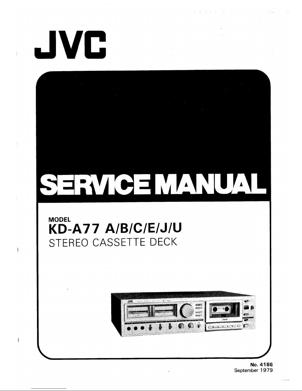
MODEL
KD-A77
A/B/C/E/J/U
STEREO
CASSETTE
DECK
No.
4186
September
1979
Page 2
KD-A77A/8/C/E/J/U
r-
Contents
Specifications
.........................................................
2
Features
..................................................................
3
Controls and Connections
..........................................
3
Main Parts Location
...................................................
4
Maintenance
............................................................
4
New
Technique
......................................................
5
Removal
of
the Main Parts
..........................................
6
Main
Adjustments
...................................................
1 0
Block Diagram
......................................................
16
Integrant Circuit
......................................................
18
Standard Schematic Diagram
of
KD-A
77
Amplifier
circuit
................................................
1 9
Mecha. control
circuit
..........................................
20
Wiring
Connection
(1
)
of
KD-A 7 7
..............................
21
Specifications
Type
Track
system
Tape speed
Frequency response
OVU
Metal
tape
SA/Cr02
tape
-20VU
Metal
tape
SA/Cr02
tape
*
1
*2
SF/Normal tape
*
3
SIN ratio
Stereo cassette
deck
4-track,
2-channel
1-7/8
inch/sec
(4.8
cm/sec)
25-12500Hz
±3dB(Typical)
25
-
8000Hz
± 3dB(Typical)
15-20000Hz
25
-1
8000Hz
± 3dB(Typical)
15-20000Hz
25-
1
8000Hz
± 3dB(Typical)
15-19000Hz
25-17000Hz
±3dB(Typical)
Surpases DIN
45
500
60dB (from peak level, weighted,
Metal tape)
The SIN is improved by 5dB
at
1 kHz and by
10dB
above 5kHz
with
ANRS on.
(DIN
45
500
weighted)
Effect
of
Super ANRS : (normal tape)
Improvement
of
SIN : the same
as
with
ANRS
Improvement
of
frequency response
:
OVU
recording; 6dB
at
10kHz
+
5VU recording; 12dB at 10kHz
Improvement
of
distortion
Wow
and
flutter
Crosstalk
Hormonic
distortion
Bias
Erasure
Heads
No.4186
OVU
recording;
3 % or less
at
10kHz
+
5VU recoridng;
3 % or less at 10kHz
0.04%
(WRMS),
0.14%
(DIN
45
500)
65dB
(1
kHz)
K3;
0.4%,
THD:
1.0%
(metal tape, 1 kHz OVU)
AC bias
(85kHz)
AC erasure
(85kHz)
3 heads
SEN
ALLOY head
for
recording,
SEN
ALLOY X
cut
type
for
playback and
two-gap
SEN
ALLOY head
for
erasure
Wiring Connection (2)
of
KD-A77
..............................
22
Enclosure
Ass'y
and Electrical Parts
...........................
25
Enclosure
Ass'y
and Electrical Parts List
..................
23
Mechanical Components Parts
.................................
26
Mechanical
Components
Parts List
........................
28
Printed Wiring Board Parts
Main
Amp.
P.W. Board Parts
....................................
33
Power Supply P.W. Board Parts
.................................
34
Main
Amp.
P.
W.B
Parts List
.................................
30
Power
Supply P.W.B Parts List
..............................
35
Other
P.W.B Parts
...................................................
37
Other
P.
W.B
Parts List
.......................................
39
Packing
......................................................
Back cover
Accessories
................................................
Back cover
Motors
Fast
forward
time
Rewind
time
Semiconductors
Input terminals
Output
terminals
Power requirement
Power consumption
Dimensions
Weight
FG
type
DC
servo
motor
(for
Capstan)
DC
motor
(for
Reel)
85
sec.
with
C-60
cassette
85
sec.
with
C-60
cassette
1 8 ICs,
49
transistors,
59
diodes,
14
LEDs
Mic jack x
2,
Max. sensitivity;
0.2mV
(-72dBs)
Matching impedance;
6000-10kO
Input jack x
2,
Min. input level;
80mV
(-20dBs)
Input impedance;
100kO
Output
jack x
2,
Output
level;
0-300mV
Output
impedance; 6kO
Matching impedance:
50kO or more
Phones jack x 1,
Output
level;
0-0.5mW/SO
Matching
impedance:
80-1
kO
AC
120V,
60Hz
(KD-AnCW
AC
240/220/120V,
50/60Z
(KD-A
n
A/B/E)
AC
240/220/120/1
OOV,
50/60Hz
(KD-A77U)
36W
17-3/4"
(450
mm) W
4-3/4"
(120
mm) H
12-7/16"
(316mm)D
18.3
Ibs
(8.3
kg)
Note:
*
1 ... SCOTCH MET AFINE or Equivalent
*
2 ... TDK SA or Equivalent
*
3 ... MAXELL
UD
or Equivalent
Design and specifications are subject
to
change
without
notice.
- 2 -
Page 3
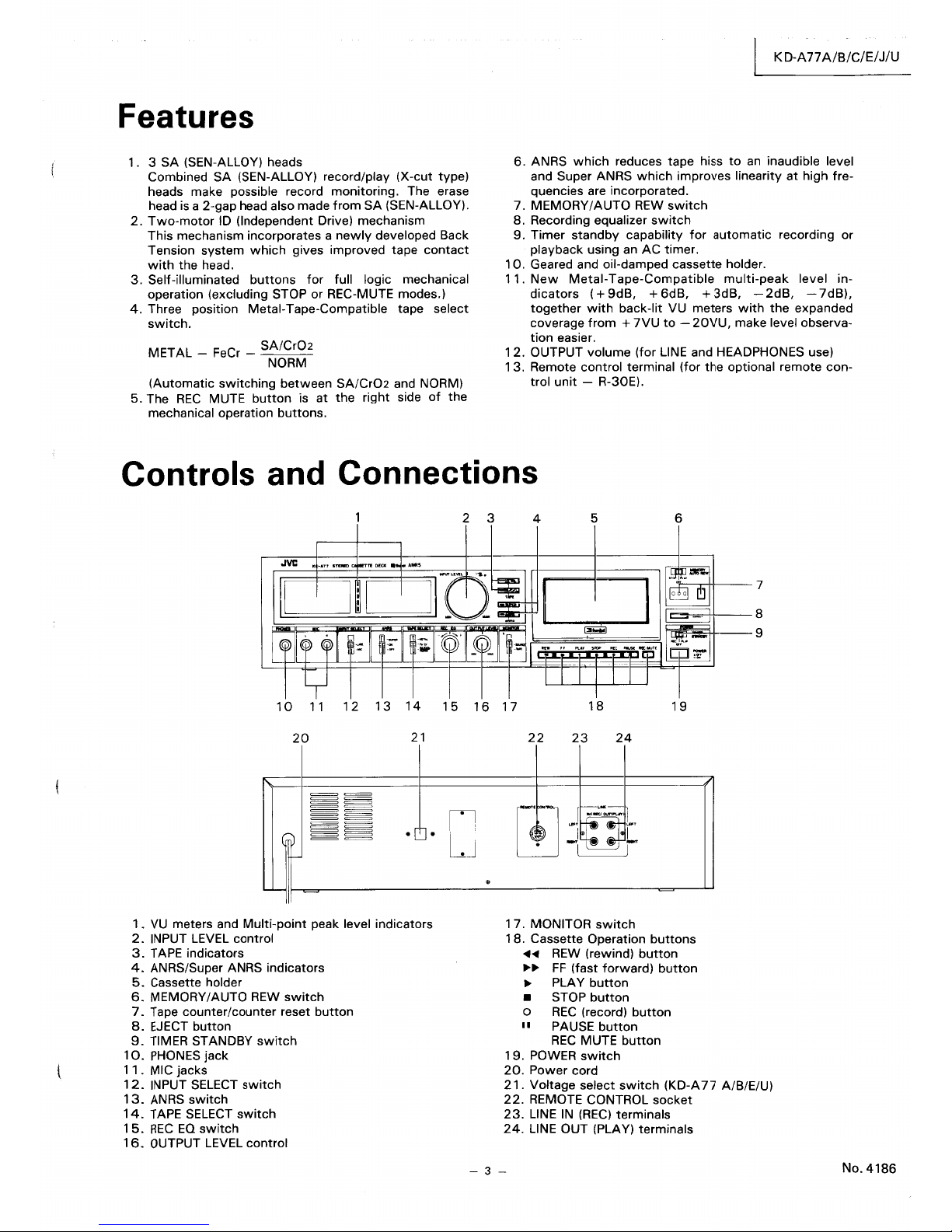
Features
1. 3
SA
(SEN-ALLOY) heads
Combined
SA
(SEN-ALLOY) record/play (X-cut type)
heads make possible record monitoring. The erase
head is a 2-gap head also made
from
SA
(SEN-ALLOY).
2.
Two-motor
ID (independent Drive) mechanism
This mechanism incorporates a
newly
developed Back
Tension
system
which
gives improved tape
contact
with
the
head.
3.
Self-illuminated
buttons
for
full logic mechanical
operation (excluding STOP or REC-MUTE modes.)
4.
Three position Metal-Tape-Compatible tape select
switch.
METAL - FeCr _
SA/Cr02
NORM
(Automatic
switching
between
SA/Cr02
and NORM)
5. The
REC
MUTE
button
is at
the
right side
of
the
mechanical operation
buttons.
KD-An
A/B/C/E/J/U
6.
ANRS
which
reduces tape hiss
to
an
inaudible level
and Super ANRS
which
improves linearity
at
high fre-
quencies are incorporated.
7.
MEMORY/AUTO
REW
switch
8. Recording equalizer
switch
9.
Timer
standby
capability
for
automatic
recording or
playback using an
AC
timer.
10.
Geared and oil-damped cassette holder.
11.
New
Metal-Tape-Compatible
multi-peak
level in-
dicators
(+
9dB,
+ 6dB, +
3dB,
-2dB, -7dB).
together
with
back-lit VU meters
with
the
expanded
coverage
from + 7VU
to -20VU,
make level observa-
tion
easier.
12.
OUTPUT volume (for LINE and HEADPHONES use)
13.
Remote control terminal (for
the
optional remote
con-
trol
unit
- R-30E).
Controls and Connections
2 3
4
5
6
10
11
12
14
15
16
17
18
19
20
21
==
==
==
==
==
==
==
==
==
==
r-
==
. .
==
'-
1.
VU
meters and
Multi-point
peak level indicators
2.
INPUT LEVEL control
3.
TAPE
indicators
4.
ANRS/Super ANRS indicators
5.
Cassette holder
6.
MEMORY/AUTO REW
switch
7.
Tape counter/counter reset
button
8.
EJECT
button
9.
TIMER STANDBY
switch
10.
PHONES
jack
11.
MIC jacks
12.
INPUT SELECT
switch
13.
ANRS
switch
14.
TAPE
SELECT
switch
15.
REC
EQ
switch
1
6.
OUTPUT LEVEL
control
n
LJ
•
22
23
24
[f]
r~:f
~1
r
-[
~
I
1 7. MONITOR
switch
1 8. Cassette Operation
buttons
~~
REW
(rewind)
button
~~
FF
(fast
forward)
button
~
PLA Y
button
• STOP
button
o
REC
(record)
button
11
PAUSE
button
REC
MUTE
button
19.
POWER
switch
20.
Power
cord
21.
Voltage select
switch
(KD-A
77
A/B/E/U)
22.
REMOTE CONTROL
socket
23.
LINE
IN
(REC)
terminals
24.
LINE OUT (PLAY) terminals
- 3 -
No.4186
Page 4
KD-A77
A/B/C/E/J/U
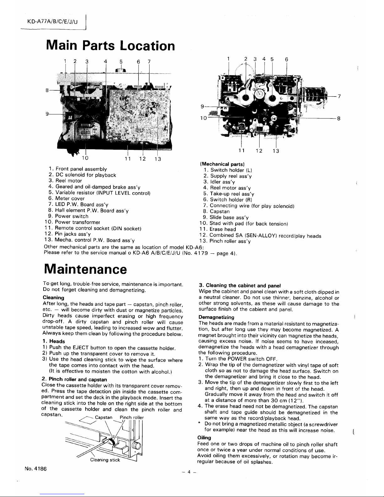
Main Parts Location
2 3 4 5 6
7
9
"--------
8
1 1
1 2 1 3
(Mechanical parts)
1.
Front
panel assembly
1.
Switch
holder (U
2.
DC solenoid
for
playback
2.
Supply
reel
ass'y
3.
Reel
motor
3.
Idler
ass'y
4.
Geared and oil-damped brake
ass'y
4.
Reel
motor
ass'y
5. Variable resistor (INPUT LEVEL control) 5. Take-up reel
ass'y
6.
Meter
cover
6.
Switch
holder
(R)
7.
LED P.W. Board
ass'y
7.
Connecting
wire
(for play solenoid)
8.
Hall
element
P.W. Board
ass'y
8.
Capstan
9.
Power
switch
9.
Slide base
ass'y
10.
Power
transformer
10.
Stad
with
pad (for
back
tension)
11.
Remote
control
socket
(DIN
socket)
11.
Erase head
12.
Pin
jacks
ass'y
12.
Combined
SA
(SEN-ALLOY) record/play heads
13.
Mecha.
control
P.W. Board
ass'y
13.
Pinch roller
ass'y
Other
mechanical parts are
the
same
as
location
of
model
KD-A6:
Please refer
to
the
service manual 0
KD-A6
A/B/C/E/J/U
(No.
4179
- page
4).
Maintenance
To
get
long, trouble-free service,
maintenance
is
important.
Do
not
forget
cleaning and
demagnetizing.
Cleaning
After
long,
the
heads and tape
part
- capstan,
pinch
roller,
etc. -will
become
dirty
with
dust
or
magnetize
particles.
Dirty
heads cause
imperfect
erasing
or
high
frequency
drop-off. A dirty
capstan and pinch roller
will
cause
unstable
tape speed, leading
to
increased
wow
and
flutter.
Always
keep
them
clean
by
following
the
procedure
below.
1.
Heads
1)
Push the EJECT
button
to
open
the
cassette
holder.
2)
Push
up
the
transparent
cover
to
remove
it.
3)
Use
the
head cleaning
stick
to
wipe
the
surface
where
the
tape
comes
into
contact
with
the
head.
(it
is
effective
to
moisten
the
cotton
with
alcohol.)
2.
Pinch roller and capstan
Close
the
cassette
holder
with
its
transparent
cover
remov-
ed. Press
the
tape
detection
pin inside
the
cassette
com-
partment
and
set
the
deck
in
the
playback
mode.
Insert
the
cleaning
stick
into
the
hole on
the
right
side
at
the
bottom
of
the
cassette
holder and clean
the
pinch roller and
oop"an.
~~:,"'h
"",,
~.~
Cleaning stick
No.
4186
- 4 -
3.
Cleaning the cabinet and panel
Wipe
the
cabinet
and panel clean
with a soft
cloth
dipped in
a neutral cleaner. Do
not
use thinner, benzine,
alcohol
or
other
strong
solvents,
as these
will
cause
damage
to
the
surface
finish
of
the
cabient
and panel.
Demagnetizing
The heads are made
from
a material resistant
to
magnetiza-
tion,
but
after
long use
they
may
become
magnetized.
A
magnet
brought
into
their
vicinity
can magnetize
the
heads,
causing excess noise.
If
noise seems
to
have inceased,
demagnetize
the
heads
with
a head
demagnetizer
through
the
following
procedure.
1.
Turn
the
POWER
switch
OFF.
2.
Wrap
the
tip
of
the
demagnetizer
with
vinyl
tape
of
soft
cloth
so as
not
to
damage
the
head surface.
Switch
on
the
demagnetizer
and bring
it
close
to
the
head.
3.
Move
the
tip
of
the
demagnetizer
slowly
first
to
the
left
and
right,
then
up and
down
in
front
of
the
head.
Gradually
move
it
away
from
the
head and
switch
it
off
at a distance
of
more
than
30
cm
(1
2").
4.
The
erase head need
not
be demagnetized.
The
capstan
shaft
and
tape
guide should be demagnetized in
the
same
way
as
the
record/playback
head.
* Do
not
bring a magnetized metallic
object
(a
screwdriver
for
example) near
the
head as
this
will
increase noise.
Oiling
Feed one or
two
drops
of
machine oil
to
pinch
roller
shaft
once
or
twice
a year
under
normal
conditions
of
use.
Avoid
oiling
them
excessively, or
rotation
may
become
ir-
regular because
of
oil splashes.
Page 5
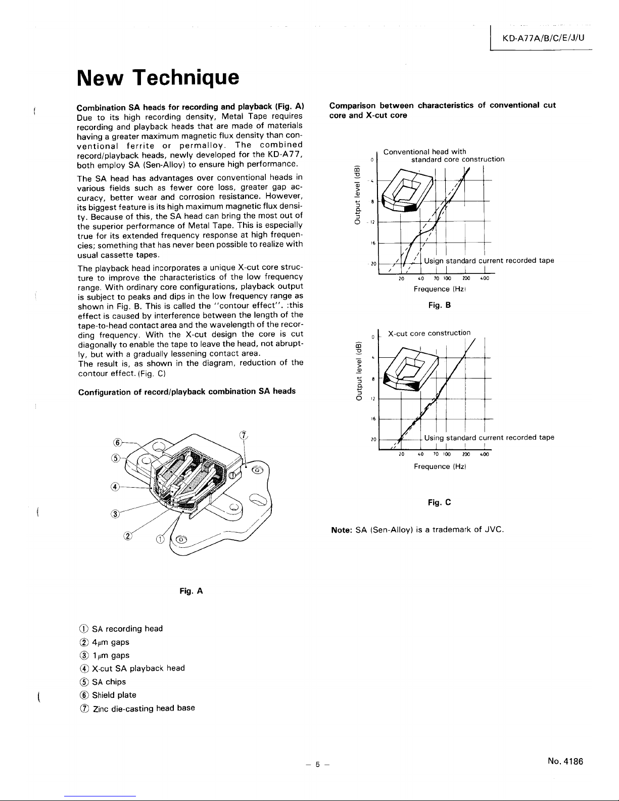
New
Technique
Combination
SA
heads
for
recording and
playback
(Fig.
Al
Due
to
its
high
recording
density,
Metal
Tape requires
recording and
playback
heads
that
are made
of
materials
having
a greater
maximum
magnetic
flux
density
than
con-
ventional
ferrite
or
permalloy.
The
combined
record/playback
heads,
newly
developed
for
the
KD-A
77,
both
employ
SA
(Sen-Alloy)
to
ensure high
performance.
The
SA head has
advantages
over
conventional
heads in
various fields
such
as
fewer
core loss, greater gap ac-
curacy,
better
wear
and corrosion resistance.
However,
its
biggest
feature
is its high
maximum
magnetic
flux
densi-
ty.
Because
of
this,
the
SA
head can bring
the
most
out
of
the
superior
performance
of
Metal
Tape. This is especially
true
for
its
extended
frequency
response
at
high frequen-
cies;
something
that
has never been possible
to
realize
with
usual
cassette
tapes.
The
playback head
incorporates
a unique
X-cut
core
struc-
ture
to
improve
the
characteristics
of
the
low
frequency
range.
With
ordinary core
configurations,
playback
output
is
subject
to
peaks and dips in
the
low
frequency
range as
shown
in Fig.
B.
This is called
the
"contour
effect".
:this
effect
is caused
by
interference
between
the
length
of
the
tape-to-head
contact
area and
the
wavelength
of
the
recor-
ding
frequency.
With
the
X-cut
design
the
core is
cut
diagonally
to
enable
the
tape
to
leave
the
head,
not
abrupt-
ly,
but
with
a gradually lessening
contact
area.
The
result is, as
shown
in
the
diagram, reduction
of
the
contour
effect.
(Fig.
C)
Configuration
of
record/playback
combination
SA heads
CD
SA recording head
® 4/lm gaps
® 1/lm gaps
Fig.
A
®
X-cut
SA
playback
head
® SA chips
® Shield plate
rJ)
Zinc die-casting head base
- 5 -
KD-A77
A/B/C/E/J/U
Comparison
between
characteristics
of
conventional
cut
core and
X-cut
core
c
onventlona
I h d . h
ea
Wit
standard
core
constructi
on
in
~
-.
QJ
>
~
...
:J
B-
:J
0
-11
16
10
@~
I
:J
/
~
/
/,1./
Usign
standard
curre
/
I
I I I I
,
nt
recorded
tape
10
.0
70
100
100
.00
Frequence (Hz)
Fig. B
X
-cut
core
construction
in
:9
a;
>
~
...
:J
Cl.
...
:J
0
11
16
10
t--off----+
Using
standard
current
recorded
tape
I I I
10
.0
70
100
100
.00
Frequence (Hz)
Fig. C
Note:
SA
(Sen-Alloy) is a
trademark
of
JVC.
No.4186
Page 6
KD-An
A/B/C/E/J/U
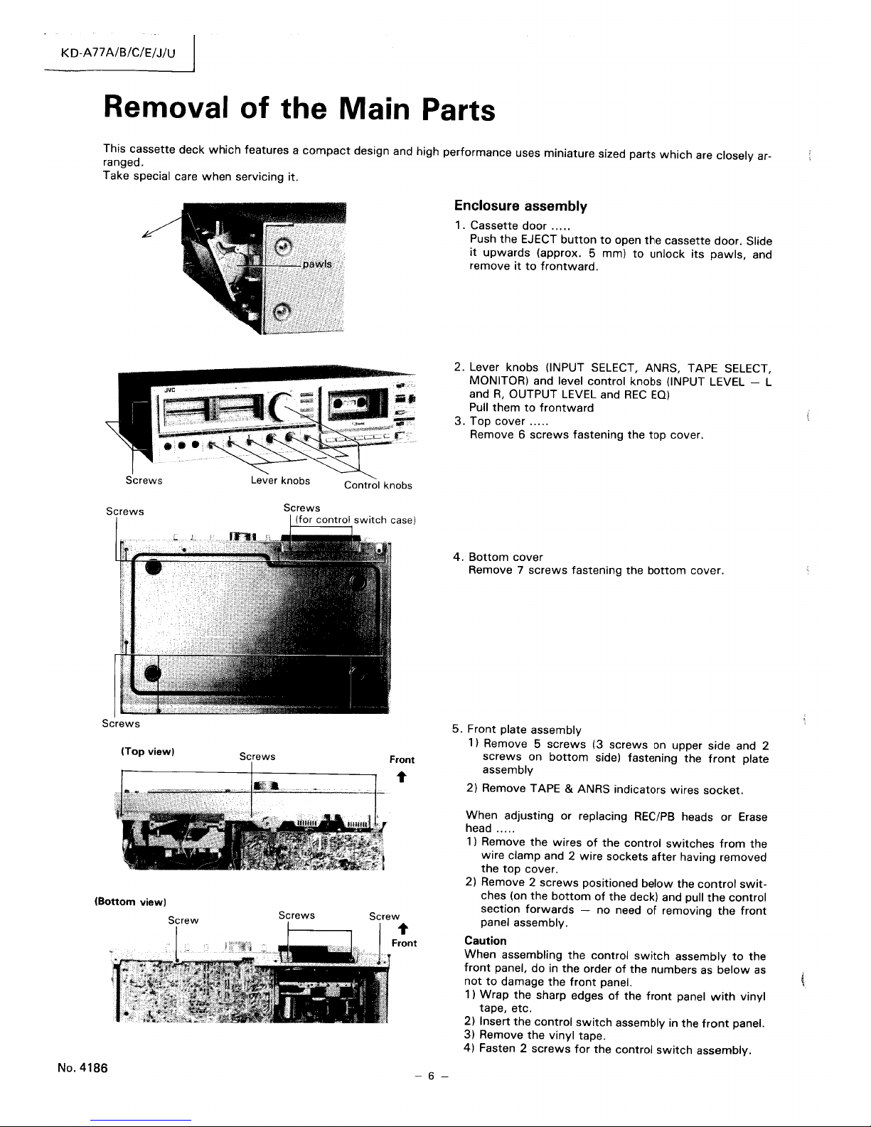
Removal of the Main Parts
This cassette deck
which
features a
compact
design and high performance uses miniature sized parts
which
are closely arranged.
Take special care
when
servicing it.
.11
Q
~
~--~.
~~~;;;;;:;;.;...f='.
Lever
knobs
Screws
(Top
view)
Screws
(Bottom
view)
Screw
Screws
Screw
l'
Enclosure assembly
1 . Cassette door
.....
Push
the
EJECT
button
to
open
the
cassette door. Slide
it
upwards
(approx. 5 mm)
to
unlock
its
pawls,
and
remove
it
to
frontward.
2.
Lever knobs (INPUT SELECT, ANRS, TAPE SELECT,
MONITOR) and level control knobs (INPUT LEVEL - L
and
R,
OUTPUT LEVEL and
REC
EQ)
Pull
them
to
frontward
3.
Top cover
.....
Remove 6
screws
fastening the
top
cover.
4.
Bottom
cover
Remove
7
screws
fastening the
bottom
cover.
5. Front plate assembly
1) Remove 5
screws
(3
screws
on upper side and 2
screws
on
bottom
side) fastening the
front
plate
assembly
2)
Remove TAPE & ANRS indicators wires
socket.
When adjusting or replacing REC/PB heads or Erase
head .....
1)
Remove
the
wires
of
the
control
switches
from
the
wire clamp and 2
wire
sockets
after
having removed
the top
cover.
2) Remove 2
screws
positioned
below
the
control
swit-
ches (on
the
bottom
of
the deck) and pull
the
control
section
forwards
- no need
of
removing
the
front
panel assembly.
Front
Caution
No.
4186
- 6 -
When
assembling
the
control
switch
assembly
to
the
front
panel,
do
in
the
order
of
the numbers as
below
as
not
to
damage
the
front
panel.
1 ) Wrap
the
sharp edges
of
the
front
panel
with
vinyl
tape, etc.
2)
Insert
the
control
switch
assembly in the
front
panel.
3)
Remove
the
vinyl
tape.
4) Fasten 2
screws
for
the
control
switch
assembly.
Page 7
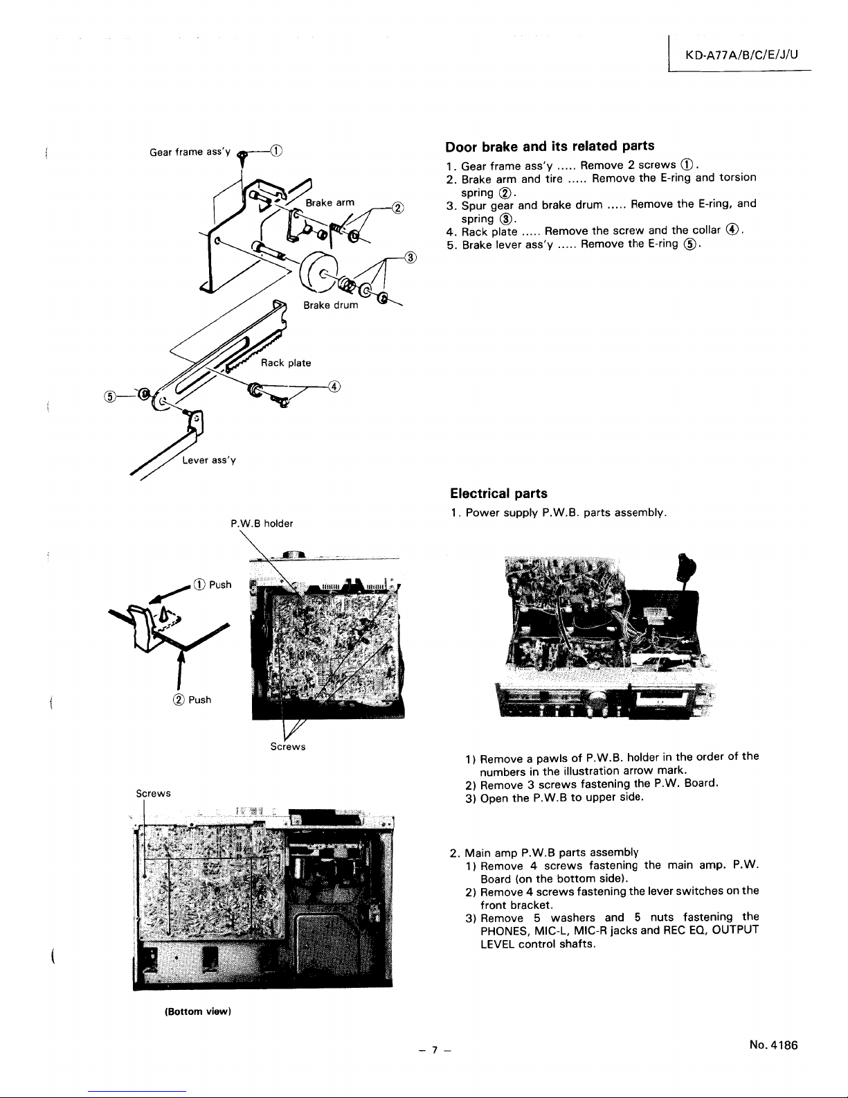
Gear frame
ass'y
,CD
P.W.B holder
® Push
Screws
Screws
(Bottom
view)
- 7 -
KD-A77
A/B/C/E/J/U
Door brake and its related parts
1.
Gear frame
ass'y
.....
Remove 2
screws
CD.
2. Brake arm and tire
.....
Remove
the
E-ring and
torsion
spring ®.
3.
Spur gear and brake
drum
.....
Remove
the
E-ring, and
spring
@.
4.
Rack plate
.....
Remove
the
screw
and
the
collar
@.
5. Brake lever
ass'y
.....
Remove the E-ring
@.
Electrical parts
1. Power supply P.W.B. parts assembly.
1)
Remove a
pawls
of
P.W.B. holder in
the
order
of
the
numbers in
the
illustration
arrow
mark.
2) Remove 3
screws
fastening
the
P.W. Board.
3)
Open
the
P.W.B
to
upper side.
2. Main amp P.W.B parts assembly
1) Remove 4
screws
fastening
the
main amp. P.W.
Board (on
the
bottom
side).
2) Remove 4
screws
fastening
the
lever
switches
on
the
front
bracket.
3)
Remove 5 washers and 5
nuts
fastening
the
PHONES, MIC-L, MIC-R jacks and
REC
EO,
OUTPUT
LEVEL control shafts.
No.4186
Page 8
K D-A
77
A/B/C/EI J/U
~ckPlate
Screws
-----,rl-I~rv
I
(Top
view)
Screws
Power
switch
Screws
Screws
(for
door
brake
related parts)
tIP_--_Screw
(Right side)
No_4186
- 8 -
3.
Power
switch
1) Remove
the
lock
plate
CID
holding
the
remote
bar.
2) Remove a
screw
®
fastening
the
power
switch
bracket.
3) Remote 2
screws
(j)
fastening
the
power
switch.
4.
Power
transformer
Remove
the 2 screws
and 2
washers
fastening
the
power
transformer.
Removal of the mechanical assembly
1 . Remove a
screw
fastening
the
arm
of
gear-oil
damper
(Left side
of
the
cassette
holder), and Remove 2
screws
fastening
the
gear
frame
ass'y
to
Remove
door
brake
related parts.
2.
Remove 5
screws
fastening
the
mechanical
bracket
to
the
amp. chassis (Right - 2 p.c.S,
Left
- 3
p.c.s).
3.
Remove a
screw
fastening
the
counter
bracket
to
the
front
bracket.
Page 9
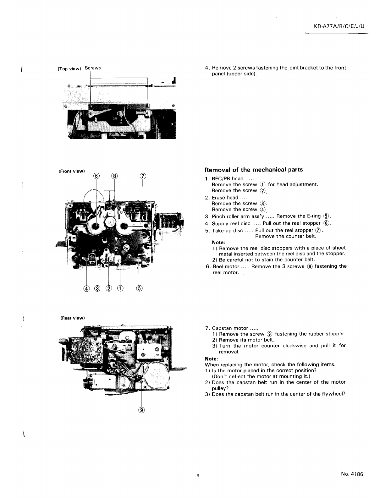
(Top
view)
Screws
..
(Front
view)
(Rear
view)
- 9 -
KO-An
A!B!C!E!J!U
4.
Remove 2
screws
fastening
the
joint
bracket
to
the
front
panel (upper side) .
Removal
of
the mechanical parts
1 . REC/PB head
.....
Remove
the
screw
CD
for
head
adjustment.
Remove
the
screw
CV.
2.
Erase head
.....
Remove
the
screw
®.
Remove
the
screw
®
3.
Pinch roller arm
ass'y
: .... Remove
the
E-ring
@.
4.
Supply
reel
disc
.....
Pull
out
the
reel
stopper
@.
5. Take-up
disc
.....
Pull
out
the
reel
stopper
(j) .
Remove
the
counter
belt.
Note:
1) Remove
the
reel disc
stoppers
with
a piece
of
sheet
metal inserted
between
the
reel
disc
and
the
stopper.
2)
Be
careful
not
to
stain
the
counter
belt.
6. Reel
motor
.....
Remove
the 3 screws ® fastening
the
reel
motor.
7.
Capstan
motor
.....
1) Remove
the
screw ® fastening
the
rubber
stopper.
2) Remove
its
motor
belt.
3)
Turn
the
motor
counter
clockwise
and pull
it
for
removal.
Note:
When
replacing
the
motor,
check
the
following
items.
1 )
Is
the
motor
placed in
the
correct
position?
(Don't
deflect
the
motor
at
mounting
it.)
2) Does
the
capstan
belt
run in
the
center
of
the
motor
pulley?
3) Does
the
capstan
belt run in
the
center
of
the
flywheel?
No.4186
Page 10
K
D-A
77
AIBICIEI
J/u
Main Adjustments
[I] Equipment and measuring instruments used for adjustment
1.
Electrical adjustment
1) Electronic
voltmeter
2)
Audio
frequency
oscillator
(range;
50 -20kHz
and
output
OdB
with
impedance
600fl)
3)
Attenuator
4)
Standard tapes
for
RECIPB
Maxell UD -
SF
tape
(for normal) }
TDK
SA -SA
tape
(for
Cr02)
or
equivalent
SCOTCH MET AFINE -
Metal
tape
5) Reference tapes
for
playback
(JVC
Test
Tape)
VTT-658
(for
head
azimuth
adj.)
VTT-656
(for
motor
speed,
wow
flutter
adj.)
VTT-664
(for Reference level 1 kHz)
TMT-6002N
(for
playback
frequency
response)
6) Resistors
1
oon
(for
measurement
of
the
bias current)
600n
(for
attenuator
matching)
2.
Mechanical adjustment
1) Gauge
for
checking
the
head position.
2)
Torque
gauge.
3) Blank tape
(C-120)
for
tape
running checker.
[11]
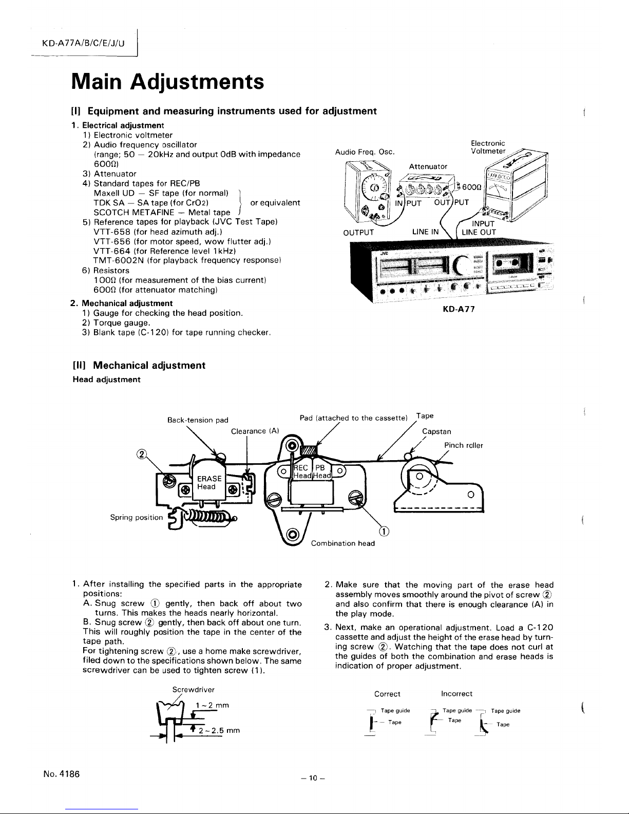
Mechanical adjustment
Head adjustment
KO-A77
Back-tension
pad
Pad
(attached
to
the
cassette)
Tape
Clearance (A)
1.
After
installing
the
specified parts in
the
appropriate
positions:
A.
Snug
screw
CD
gently,
then
back
off
about
two
turns.
This makes
the
heads nearly horizontal.
B.
Snug
screw @ gently,
then
back
off
about
one
turn.
This
will
roughly
position
the
tape in
the
center
of
the
tape
path.
For
tightening
screw
@"
use a
home
make
screwdriver,
filed
down
to
the
specifications
shown
below.
The same
screwdriver
can be used
to
tighten
screw
(1).
Screwdriver
Pinch roller
Combination
head
2.
Make
sure
that
the
moving
part
of
the
erase head
assembly
moves
smoothly
around
the
pivot
of
screw
@
and also
confirm
that
there
is
enough clearance (A) in
the
play mode.
3.
Next,
make an operational
adjustment.
Load a C-1
20
cassette
and
adjust
the
height
of
the
erase head
by
turn-
ing
screw
@.
Watching
that
the
tape does
not
curl
at
the
guides
of
both
the
combination
and erase heads is
indication
of
proper
adjustment.
Correct
-1
Tape guide
t -Tape
Incorrect
f
Tap€
guide
--,
Tape guide
Tape l
__
'
_~--
Tape
No.4186
-10
-
Page 11
KD-A77
A/B/C/E/J/U
Item
Adjustment
Adjusting
Standard
Remarks
point
value
Adjusting
Connect
a speed
meter
to
the
LINE Semi-
3000Hz
If
the
speed
meter
functions
as a
wow
motor
speed
OUT
terminals.
Play
back
the
fixed
and
flutter
meter,
also,
connect
the
VTT-656
test
tape.
resistor
deck
to
the
INPUT
terminals
of
the
Adjust
the
semi-fixed
resistor
on
the
on
the
meter.
motor
P.W.
board until
the
reading
of
motor
the
speed
meter
is
3000Hz.
P.w.
board
Checking play-
Employ
a
torque
testing
cassette
40-70
If
the
standard
torque
is
not
obtained,
back
torque
tape
for
the
checking, or remove
the
gr-cm
replace
the
take-up
disc
assembly.
cassette
cover
and
use
a
torque
gauge.
Checking
fast
Measure
the
torque
in
the
fast
for-
More
If
the
standard
torque
is
not
obtained,
forward
torque
ward
mode
in
the
same manner as in
than
perform
the
following.
the
above.
70
gr-cm
1 . Clean
the
capstan
belt,
the
idler
cir-
cumference,
the
motor
pulley,
the
take-up
reel
disc
circumference,
the
flywheel
circumference,
etc.
2. Replace
the
belt and idler.
Checking re-
Measure
the
torque
in
the
rewind
More
If
the
standard
torque
is
not
obtained,
wind
torque
mode
in
the
same manner
as
in
the
than
clean
the
capstan
belt, idler,
motor
above.
70
gr-cm
pulley,
flywheel
circumference,
rewin-
ding idler
circumference,
left
reel
disc
circumference,
etc.
Checking
wow
Connect a wow
and
flutter
meter
to
If
the
reading becomes
moving
value
and
flutter
the
LINE
OUT
terminals.
even
if
conforming
to
the
standard,
a
Play
back
the
VTT-656
test
tape. re-claim
may
be raised. Repairs are
Check
to
see
if
the
reading
of
the
necessary.
meter
is
within
0.04%
(WRMS).
[Ill] Repair of
wow
flutter
If
wow
and
flutter
increase,
check
the
following
points.
If
there
is
defect
in
revolving
parts,
the
wow
and
flutter
generated
will
increase in
proportion
to
the
number
of
revolutions.
Play a
3000Hz
test
tape, and
defective
part
can
be
detected
from
the
sound.
Section
Trouble
Repair
Capstan and
flywheel
Capstan
shaft
has excessive
run-out
Replace
flywheel.
Flywheel
turns
heavily. Clean
the
capstan
shaft
and
the
groove
in
the
(shaft
seisure,
thrust
play,
etc.)
flywheel.
Apply
oil
to
the
metal
position.
Replace
the
capstan assembly.
Pinch roller
Rough
rotation
(Deformation
scrat-
Replace pinch roller, or pinch roller spring.
ches, or dust)
Clean
the
pinch roller
or
apply oil
to
the
rotary
The
angular
position
of
the
pinch
roller shaft.
is
not
correct.
Adjust
the
pinch roller so
that
it
is
parallel
with
The pinch roller pressure is
not
correct.
the
capstan shaft.
Replace
the
pinch roller spring.
Belt
Belt has undue run-out. Clean
the
belt.
Belt is
dirty
or slippery. Replace
the
belt.
Back tension
Back tension
is
irregular, or back ten- Replace back tension spring (under supply disc).
sion
is
too
strong.
Motor
Motor
shaft
has undue run-out. Replace motor.
Motor
pulley
is
oily and
dusty.
Clean
motor
pulley.
Damping gear
oil
Oil
employed - Torque grease specified
by
JVC
(KANTO KASEI GP-608)
Applying method -
Apply
in both concaved sections
as
shown
in
the
figure.
-11-
Page 12
K
D-A
77
A/B/C/E/
J/U
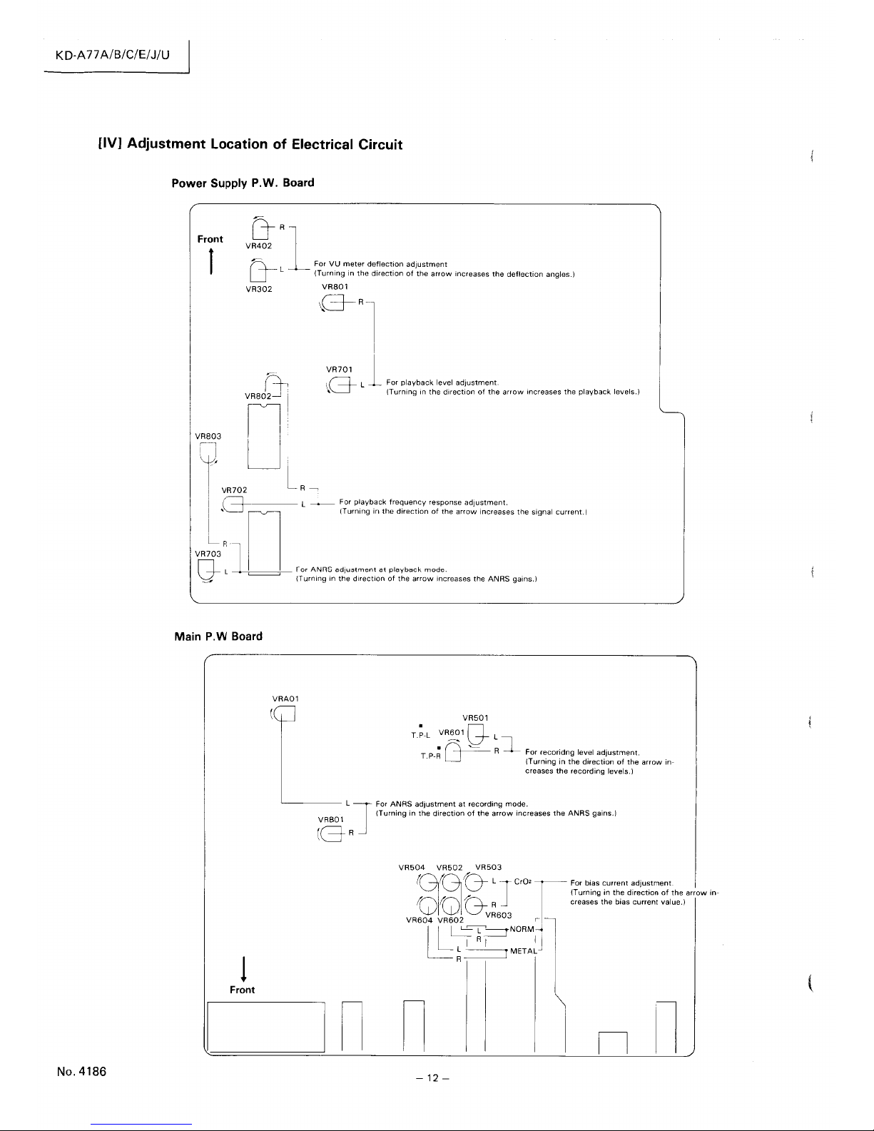
[IV]
Adjustment
Location
of
Electrical
Circuit
No.4186
Power
Supply P.W. Board
Front
l]-R
'~'
_ 1
.,,'
'"
m
...
om"'''''"
',,""'m,m
_
U L
(Turning
in
the
direction
of
the
arrow
Increases
the
deflection
angles.)
t
VR302
VR801
(3-R
VR701
For
playback
level
adjustment.
\G-L
(Turning
In
the
direction
of
the
arrow
increases
the
playback
levels.)
VR803
11
_____
L _
For
playback
frequency
response
adjustment
,,~
(Turning
In
the
direction
of
the
arrow
Increases
the
signal
current)
VR703Rtl
Q-
L For
ANRS
adjustment
at
playback
mode
_
__#
'-----------.J
(Turning
In
the
direction
of
the
arrow
Increases
the
ANRS
gains.)
Main
P.
W Board
VRAOl
VR501
T.;-L
VR601 G L
For
recoridng
level
adjustment.
·0
~
Rl
T.P-R
(Turning
in
the
direction
of
the
arrow
in-
creases
the
recording
levels.)
1
Front
L ] For
ANAS
adjustment
at
recording
mode.
(Turning
in
the
direction
of
the
arrow
increases
the
ANRS
gains.)
VRBOl
(eR
VR504
VR502
VR503
((~((~G-
L J ero, t -For bias CUrrent
adjustment.
(Turning
in
the
direction
of
the
arrOw
in-
Q Q
G-
v
:
creases
the
bias
current
value.1
VR604
VR602
603
r
I
LL'::=~==rNORM~
I R I I J
L I
METAL
R---~
In
nl
n
n
~12~
Page 13

K D-A
77
A/B/C/E/
J/U
[V]
Electrical
circuit
adjustment
procedure
In
the
steps marked
by
an asterisk
(*),
adjustment
should be
performed,
however,
only
checking
is
sufficient
with
steps
other
than
those.
Adjustment
should be
performed
in
the
order
of
steps
1,
2, 3 .....
Perform these
adjustments
with
the
ANRS
switch
set
to
OFF and
with
the
OUTPUT
level
control
set
max.
Step
Item
1 * Adjusting
2*
3*
4*
playback
level
Adjusting
playback
frequency
response
Adjusting
VU
meter
sensitivity
Adjustment
record/
playback
frequency
response
Adjustment
1. Play back
the
VTT-664
Reference
tape
(1
kHz)
with
Tape select
switch
set
to
the
NORMAL posi-
tion.
2.
Adjust
VR701 and VR801 until
the
LINE
OUT becomes about - 8dBs.
Play back
test
tape,
TMT-6002N
for
following
againstment.
1)
Adjust
VR702,
802
so
that
10kHz
signal and 1 kHz signal gains become
flat
response.
1 . Set
the
cassette deck
to
its source
mode.
2
.Apply
a 1 kHz, approx.
-10dBs
signal
to
the
LINE
IN
terminals.
3.
Adjust
the
recording level controls
until
the
signal is available
at
-8dBs
at
the
LINE OUT terminals.
4.
Adjust
VR302
and VR402 until
the
VU meters
deflect
to
O.
Record 1 kHz,
50Hz
and
12.5kHz
sig-
nals at an
input
level
of
OVU -
20dB.
Play back
the
tape.
Check
to
see
that
the 50Hz and
12.5kHz
signal
output
deviations fall
within
the
standard range, using
the
1 kHz signal
output
as a reference. (It
is basically desirable
that
the 1 kHz,
50Hz
and
12.5KHz
signal
outputs
are
the
same.
Adjust
VR502
amd
VR602
(for a nor-
mal tape),
VR503
and
VR603
(for a
chrome tape),
VR504
and
VR604
(for a metal tape) until the indicated
deviation
of
the
12.5kHz
signal
out-
put
from
the 1 kHz signal
output
be-
comes
O.
Adjusting
point
VR701
801
VR702
802
VR302
402
For normal
tape:
VR502
602
For chrome
tape:
VR503
603
For Metal
tape:
VR504
604
-13
-
Standard
value
-8dBs
(0.3V)
Reference
frequency;
1kHz
0±2dB
at
10kHz
OVU
Reference
frequency;
1kHz
0±3dB
at
50Hz
0±3dB
at
12.5kHz
Ol
:s
Q)
<n
J
c:
0
C.
<n
Q)
er:
50Hz
Remarks
This
adjustment
becomes necessary
when
a change in playback level
results (for example, due
to
head
replacement) .
Perform
the
adjustment
when
the
parts are replaced.
1. Bias current
adjustment
for
a
cassette
deck
should generally
be
performed referring
to
the
record/playback frequency response. This is because
the
fre-
quency
response
of
a cassette
deck depends more greatly
upon
the
bias
current
than does
that
of
an open reel deck.
The current measuring
method
described
below
is
an alternative
one.
2. If
the
bias current
is
not
properly
adjusted,
the
record and play-
back characteristics become as
shown
below.
Increase in
high
frequencies
Iwith
a small bias current)
>t\
/1\'
Optimum
level
Decrease in
high
frequencies
Iwith
a larger bias current)
1 kHz
12.5kHz
Frequency
1Hz)
No.4186
Page 14

I(D-A77
A/B/C/E/J/U
Step
5
6
7
8
Item
Adjusting
recording
level
Checking
record/
playback
signal
distortion
Checking
signal
to
noise ratio
in recording/playback
Checking
erasing
coefficient
Adjustment
1.
Apply
a 1 kHz,
approx.
-10dBs
signal
to
the LINE IN terminals.
Ad-
just
the recording level controls
until the signal is available
at
- 8dBs
at
the LINE
OUT
terminals.
2.
After
checking
to
see
if
the
VU
meters
point
to
0,
record
the
signal
applied
to
both
left
and
right
chan-
nels using a normal tape.
3.
Play back the recorded part.
Perform the recording signal adjustment
with
VR501 and VR601
so
that
the
VU
meters
deflect
to
O.
1. Record a 1 kHz signal so
that
OUT-
PUT level become -
8dBs
and VU
meters
deflect
to
O.
2. Play back the recorded part. Check
the
output
with a distortion
meter
to
see if
the
value
conforms
to
the
standard value.
1. Record a 1 kHz, OVU signal.
Stop
the
input
by
disconnecting
from
the terminal
to
perform
non-
signal recording.
2.
Play back
the
recorded part.
Measure the OVU recording
output
and the non-signal recording
out-
put
for
comparison using an elec-
tronic
voltmeter.
Check
to
see
if
the
value
conforms
to
the standard value.
1.
Apply
a 1 kHz signal
to
the
LINE
IN
terminals.
Adjust
the recording level controls
until the VU meters
deflect
to
O.
2.
Perform recording
with
the signal
enhanced
by
20dB.
3.
Erase a part
of
the
recording.
4.
Measure the
output
difference
bet-
ween
the erased
part
and non-
erased part
to
compare
with
an
electronic
voltmeter.
Adjusting Standard
point value
VR501
0 VU
601
Normal tape:
Less
than
2.5%
Cr02
tape:
Less
than
3%
Metal
tape
Less
than
2%
Normal tape:
More
than
42dB
Chrome tape:
More
than
42dB
More
than
65dB
Remarks
The level
difference
between
left
and
right
channels
for
normal tape,
chrome
tape and metal
tape
should
be less
than
1 dB
(1
VU). Perform the
adjustment
using a normal tape,
level difference
between
recording
and playback
for
Cr02
and metal
tapes should be less
than
1.
5dB,
and
that
between
left
and
right
channels should also
be
less
than
1 dB.
Be
sure
to
perform this
adjustment
following
bias
current
and recording
level adjustments.
Apply
an
output (-72dBs)
to
the
MIC
terminals
with
the
recording
level controls set
to
maximum
so
that
the VU meters
deflect
to
O.
For the measuring,
connect
a band
pass
filter
between
the
deck
and
the
electronic voltmeter.
/
Input
(1
kHz OVU
+20dBi
I r Band pass
I
filter
Tape
deckh
(recording
erasingi
Electronic
I
voltmeter
Used
test
tape; Metal tape
9 Adjustment the Super ANRS circuit
(Super ANRS circuit for recording mode)
1.
Remove
the
bias-cut
connector
on
the
main P.W. board
to
stop
the
bias
oscillation.
2.
Fully
turn
the semi-fixed resistors
VRA01,
B01 in
the
opposite
direction
of
the
arrow
shown
on
the
P.W.
board.
(If
they
have
been
roughly
adjusted,
there
is
no
need
to
turn
them.)
3.
Set
the
MONITOR
switch
of
the
deck
to
SOURCE
position
with
ANRS
switch
set
to
OFF.
4.
Apply
a 1 kHz,
-1
OdBs signal
to
the
LINE
IN
terminals.
Adjust
the
INPUT LEVEL
control
until
the
output
at
test
points,
TP-L and TP-R are
-5.5dBs.
(Be sure
not
to
move
the INPUT LEVEL
control
positions
during this adjustment.) and
then
the
OUTPUT
level is
approx.
- 5dBs.
(Corresponding
to + 3VU
on
the
VU
meters.)
5. Decrease the
input
signal
to
40dB
(its signal
become -50dBs)
with
an
attenuator.
(The
output
at
the
test
point
is
-45.5dB.)
6.
Adjust
the
VRA01
(for
left
channel) and
the
VRB01 (for right channel)
with
ANRS
switch
set
to
ON
until
the
out-
puts
at
the
test
points
are
-39.8dBs.
(The
output
difference
is
5.7dB
with
ANRS
switch
set
to
ON
from
OFF.)
7. Check
to
see
if
the
output
at
test
points
is -
22dB
± 1 dB
with
the
input
5kHz, -30dBs
signal. (Its signal
adjust
to
20dB
with
an
attenuator.)
(The
output
difference
with
ANRS
switch
set
to
ON
from
OFF is
3.5dB
± 1 dB)
-14
-
Page 15

KD-A77
A!B!C!E!J!U
Step
Adjustment
8. Check
to
see
if
the
test
point
output
difference
between
that
with
ANRS
switch
set
to
ON
and
that
set
to
OFF is
less than
±
O.
5dB,
with
the
input
a 1 kHz,
-1
OdBs signal. (its signal adjust
to
20dB
with
an attenuator.)
9. Set ANRS
switch
to
SUPER
from
OFF
when
input
10kHz
signal
to
LINE IN. Check LINE OUT level so
that
it
become
from -5.5dBs
to
-11.
5dBs ± 1 dB.
(Super
ANRS
circuit
for
playback mode)
10.
Apply the Oscillation signal
with
connecting a condenser
(1
JLF)
to
test
points
TP-L and TP-R
for
playback mode.
I
~
C:ndenser
(~~~~)
OSC
8L-_---iAttenuator
I
~
=
~~:=::=~
AN~r~uit
7'7
'TT
11.
Fully turn the semi-fixed resistors
VR703,
803
in
the
direction
of
the
arrow
shown
on
the
P.W. board. (If
they
have been roughly adjusted, there is no need
to
turn
them.)
12.
Set the deck
to
playback mode
with
ANRS
switch
set
to
OFF. (Use
the
non-tape cassette.)
13.
Apply a 1 kHz signal
to
the LINE
IN
terminals.
Adjust
an
attenuator
until
the
LINE OUT levels become - 5dBs. (This level is caliblation point.)
14.
Adjust
the
input
signal
to
34.3dB
with
an
attenuator,
and then LINE OUT level become
-39.3dBs.
15.
Adjust
the
VR703
(for
left
channel) and
the
VR803
(for right channel)
with
ANRS
switch
set
to
ON
until
the
LINE
OUT levels become
-45dBs.
(The
output
difference is
5.7dB
with
ANRS
swith
to
ON
from OFF.)
16.
Apply
5kHz signal
with
the ANRS
switch
set
to
OFF.
Adjust
an
attenuator
so
that
LINE OUT level become -
21.
5dB.
1 7. Check
to
see
if
the
LINE OUT level is -
25dBs
± 1 dB
with
ANRS
switch
set
to
ON
from
OFF.
18.
Apply
1 kHz signal
of
caliblation level
with
the
ANRS
switch
set
to
ON
fro,m OFF,
check
to
see
if
the
LINE OUT
level is less than - 5dBs
±
O.
5dB.
19.
Set the ANRS
switch
to
SUPER,
apply
10kHz
signal
to
the
LINE
IN
terminals.
Adjust
an
attenuator
so
that
LINE OUT level become check
to
see
if
the LINE OUT level is - 5dB ± 1 dB
with
ANRS
switch
set
to
OFF.
20.
Play back the reference tape
VTT-664
and
check
output
level so
that
it
less than ± 1 dB
when
ANRS
switch
set
to
ON
from
OFF.
21.
To operate the bias oscillation, insert + B
wire
connector
of
the
bias circuit.
Wiring Supplementary (refer to page
21
and
22)
-15-
O.M.F. Resistors
(R39 and R40)
No.4186
Page 16

z
~
.j::.
~
00
Ol
Super ANRS
Circuit
IC
GOI
TATOO0351-
01
~
21
~~~61
81
11
I
18
1
_evel
~~
IC
911
J
AdJ
UPC4558C
Boost
Amp
LI
NE
IN
'Z~)'I
ANRS
I
Switch
I
ON t oOFF
I nput
Se
lect
Super ANRS
CircUit
0;
MicroPhon~J
SWitch
"Y----
2SC1344 n
1
(E,F)
I
le
AOI
TATOO0351-01
1
Control
Switch
~--------,>UlO
.-
23
r~e,
Multi - Peak Le
lA:!
I
Multi Peak Level
Indicator
EE
2
IC912
LBI416
Output
Level
Control
Circuit
LINE
OUT
~_
Head phone
UPC4557CI
?
Headphone
Amp
,
Record
Ing
Head
»
3
"E..
~
~.
£1.
(;
t:
;:;:
Cl
-
o
(')
~
C
_.
Q)
CC
~
Q)
3
A
9
»
-...J
-...J
»
---
co
---
(')
---
m
c:::
---
c
Page 17

.-
R
emote
Connector
C
PLA
STOP
FF
REW
PAUS
REC
REC
-eh
7
1,4'
r b
ntrol
Switch
>-0""".
~(
~,
:~,
~,
.....
MUT
:L4,
I
z
~
.j:>.
(Xl
O"l
To
Amp
~
Time
REC
Mem
SHP
Switch
-CFF
-PLAY
)~4-
I
xy
Switch
-OFF
-PLAY
i~~
I
1
Rec
Proof SW
1
Play
Play
Play
Play Solenoid
~j
I1IC2-1
IC3-1
~~IC3-2
IC4-1
Play
.1
Cassette
XI
2SC
Solenoid SW
~
Ploy
-11'"
P:::~llri':k:
~
Pause
I1
IC2
-
2
I
~Muting
~PIOY
'----
IC
I
+B(5'v?
IC3-3
IC3-4
I
X22SC
C
To
Amp
~~
58R31CCIj
Brake
I
PLAY
Vcc
16
Fast Deloy
Fast
FF
Solenoid
2
15
IC2-6
~y
IC2-5
~~
IC6-2j
~:IS4-~~
I
lc
3
STOP
FF
14
X 2 C Brake
FF FAST
-1162 Solenoid
4..
MErvo
REW
13
~
Rew
5
REW
PLAY
~
IC6-
3
1
M
l"=-
t--
6
PAUSE
11
Rec
-
7
F't>lJSE
10
:
IC2-4
REW
REC
[g
To
8
GND
AR
~
Pause
Pause
Amp
H
IC2-4
~
Solenoid
..
X4
Pause I
2SC{~f
Solenoid
Counter Merrory
Fo"
Sto~
ReelMotor
Drive
HalllC
IC5-2
~
~IC6-1
IC5-1
X6,XI12SC456R3(CO
L--
1~~C458
~
Xl,
X9)2SD468
(B,C)
[fel
-PGlal)
Play Stop
XIO
~
Motor
r-i
IC6
-
4
~
X 8 2SC 1162
(B,C)
4'""'
~
Start
011
RD62E
IC5-4
J-r1'C5-3
F
To
Amp I
I
~wer
Supply Circuit
'v
5V
To
Mecha Cor
To
LED
nlC;lf;
17
IXB
2SA
715
(B.C)
I
?III
AC
To
Amp
IC I M54410P
IC 2 HD7404P
IC 3 HD7400P
IC4
HD7400P
IC5
HD7400P
IC6
HD7403P
pstan
Motor
rol
s:
(l)
n
:::T
Cl
::J
Ci·
!!!.
n
o
::J
...
2-
!:l.
e:;
I:
;:;:
A
0
j:.
'-J
'-J
»
--
co
--
(")
--
m
--
<-
--
C
Page 18

K O-A 77
A/B/C/E/
J/U
Integrant Circuit
IC
A01,
B01
G01,H01
TAT000351-01
Super ANRS
cirucit
IC
C01
J01
(Top
view)
242'"
222'2'C"g
18
'7
'6
!~.4·3
Lnnnnn
)
aSuPt'rA~~F<S
w u U I U L.J
I 2 3 4 ~ 6 7 8 9
10
I'
12
(Top
view)
AM
PlIFIER
No 2
,----
_-,--I
__
NON
OUT
INV
Vc,,
PUT
INPUT
8 6 5
UPC4558C
ANRS control amp.
circuit
Equivalent circuit
(1/2)
Vcc+O--~-~-~""",-",-,
INV
INPU'r
NON
-INV
o--t--t--i-
INPUT
~
Y.-+~OUT
PUT
IC901
UPC4557C
Headpone amp.
Top
view
is
the
same as
UPC4558C.
IC903
LB1416
Multi-peak level
circuit
(Top
view)
OUT
05 04 03 02
~[]
Q
I11
()
~(
LB
1416
~-~3~ATTO"'~~
IN
IN
IN Ro
Vret
Ro
GNO
(Mecha.
control)
OUT
NOr-.
Vec
pu,
INV
iNPUT
'-------
,,---~
AM
PLIf'IER
No I
Equivalent
circuit
is the same as
UPC4558C
except
R8 only.
Equivalent
circuit
OUT
GNO
05
04
03
02
IC1
M54410P
See
the
service manual
of
KO-85A/B/C/E/J/U
(No.
4165
- page 7).
No.4186
IC3,4,5
HP7400P
(Top
view)
IC2
14
vcc
lJ
r
Equivalent circuit
(1/4)
.----~---r----o
.'cr
130
y
L-.,~
_____
-+-
____
--<>
CND
H07404P
1
H07403P
f See
the
service manual
of
KO-A 7 A/B/C/E/J/U (No.
4185
- page
17)
IC6
-18-
01
Page 19

KD-A77 A/B/C/E/J/U
Standard Schematic Diagram of KD-A
77
(Amplifier
circuit)
A
B
c
D
E
F
G
L - C H
R-
CH
L I
NE
OJT
1 N
I
,
VMWI528
RI02
33K
RI04
rSOK
18K
2
X
701
2SC
1344(E,F)
7.3
R96f
rSK
IC911
UPC4558C
3
X702
2SC458PG(C,O)
Roh
4
PB
EQ.Adj.
0911
.,
INPUTLEVEL
_Input Level Control
(_...w'::':"T
<WE"A3A-054F
(on
the
front
panel)
TAT0003SI-OI
5
ANRS
Adj
XGO
I
2SD468(B,C)
6
IC
JOI
UPC4558C
7
X301
2
SC458A
(c,O)
Meter
G
8
X 911
2SA
844
(C;ol
A
from
MECHA
CON
c
X912
2SC458PGCC,O)
9
X303
2SD468/a,C)
-
le
912
Roh
eN-AS
L
rr~~~~~~*RAI~5
~~~~~~~~~~X~7--
[gJ
~
2
X~2
X
SOl
2SC458PG(CPJ
250468
(B,C)
8-{J---.'W'-+t:
;;
~
,.
~
NOTE
Recording Level Adj.
X904
2
5C458
PG(C,O)
IC~2
UPQ4066C
470
25D468(I:\C)
XS02 XS03
2SCI344(E,F)
2SC
458
(C,O)
Output Level
Adj.
(on the
front
panel)
VSK5D24-211
-
eN
AZ
R915
rOK
X905,XOO6
2SC
1685(S}
REC
HEAD
VGH0425
-3QI-OA
R 1/2
CN-A
3 ERASE HEAD
R75
270
10
I
METAL
er
0"
I
SUPER
.J
ANRS
from
MECHA
CON
I§]
CN-
A4
-2
1-7
076,77
SL8-26URIN
075,78
SLB-26GGIN
ALL
VOL TAGES
ARE
MEASURED BY
YTYM
WITHOUT
I NPUT SIGNAL
AT
STOP
MODE
-
Diode-
-
Transistor-
;~
cMM0904I4-0A
I 2
Automatic
CrOzSelect
P.
W B
f[iiiJl
(M_NORM)
UNLESS
OTHERWISE
SPECifiED
ALL
RESISTORS
ARE 1/4
W,:t
5%
CARBON FlESISTORS
AND
ALL
CAPACITORS ARE
50Y
FIXED
CERAMIC
CAPACITORS
OR
SOY
MYLAR
CAPACITORS
u
~
QSPOO29-001
b1w~d
UF
UNFLAMABLE
CARBON RESISTOR
'MF
METAL FILM RESISTOR
t:wIF OXIDED METAL
FILM
RESISTOR
\_LL
!:20%
LON
LEAK
CURRENT
ELECTROLYTIC
CAPACITOR
P.P POLYPROPYLENE CAPACITOR
Blue line
shows
the
signal
at
playback.
LN LOW NOISE CARBON RESISTOR
Red line
shows
the
signal
at
recording
and + B
circuits.
parts
are
safety
assurance
parts.
When
replacing
those
parts,
make
sure
to
use
the
specified
one.
,PS
POLYSTYRENE
CAPACITOR
'Ta
TANTALUM
SOLID ELECTROLYTIC
CAPACITOR
-19
-
No.4186
Page 20

KO-An
A/B/C/E/J/U
Standard Schematic Diagram of KD-A
77
(Mecha.
control
circuit)
A
B
c
D
E
F
G
REMOTE
CONECTQR
OMC
0888
-008
-
Diode
CN-5
2
r
01005
To
Amp
§1
CN-B
01
tA~Et-~~~J--+~
REC
01003
o 5
01006
FF
I REW
01007
CN-9
8
IPLAY
STOP
IFF
5
fEW
4
"'~
4
31"EC
o 2
REC
liE
VSTO~OOI:J
CONTROl
SW
ASS'Y
TIMER
SW
C
REC~6~l!O~~~O;)
rv:W4~
-
riMER
sw
PW B
I 0
L
I
r-
CN-8
I
4
•
I
6
I
N-
CN-5
3A
lA
2A
3
53
44
RI5270
4
RIG
270
52
RI?
330
@
!f
-g
44
R44
270
'"''
44
R45270
Cl
0.001
C2
oml
C3
C4
0001
C5
0001
C6
0001
07
IN34A
DB
09
IN34A
IN34A
r-
;:..
-,
I
Ir
o~
____
_
3 8
ME~ORY
sw
pws
I :
28
4
R36
100 <NI
~
IC
I
M
54410P
"
C23
IOtll6V
5
--
IC2
HD7404P
IC 2
PLAY
IC3
H0740QP
IC
3
D61N34A
R23
IK
6
R26
56
+C
16
looop
63V
02
152076
7
IC4
HD7400P
03)
RB
IN34A
IK
X7
2SD468(B,C)
RIO
4,7K
X8
2SC
1162
(B,C)
8
XI
2SCII62(B,C)
R4
270
To
Amp
A 8 E
I
!
.rl
.-t~I~---{~--------------------------------r--------------t----------------t---~-----x~s--------------~2~SC~~8~
X9
v _
2SC45BPG(C,O)
(C,DJ
250468
(8,C)
'-------------------------H-t---"
9
I
,
t
I"
·32
1
26
30
• 27
1
26
1
25
I
19
,I!"
•
18
278 I 12
1 "
~W4~
.J
~================================================================~+=t===~
~~~~ftRS~~~8ME~Coorn~8L~
~--------------------------------------------~X~D~----~X~I~I-----X=12~----+H---------+~-+~~
CN-M4
4
CN-M3
4
CN-M2
PL3
CN-MI
MEMORY
sw
0852301-101
(STOP-
OFF-PLAY)
- - - -
..
2SD468(B,C)
25C458PG
2SC458PG.(C_",,0'-l)
H-t------+--'
I
ToAmp
rrg
(e,O)
r
F To
Amp
I
53
~'o~~
L!"
022
I
IOEI
'F'Jld)~77/C/Ji-/U"--'==~
____
H
97
:
10
Ni
j:::::".
QSPOO29-001
L _ J
'~:;;;:::,
'-VM=S
HOLE
IC
PW B
IH
PL
I
I m
1606-00A
~711
1J.l50V
.,.
lOjJ H
DM603
IOEI-8
~MW~9
~
vGP0201-005
TERMINAL
,P'NB
I
TISA
98
~ ~ '~""'I'
RESISTOR PW B
0:
31
PW
B
L
F2(KD-A77/C/J/U
wlthou1F2}
-
--
XI4
2SC
458PG
(C,D)
XIS
2SC
458PG
(C,D)
_...1
-
Transistor-
NOTE
No.4186
--
20-
ALL VOLTAGES ARE
MEASURED
BY
VTVM
WITHOUT
INPUT
SIGNAL
AT STOP
MODE
UNLESS
OTHERWISE
SPECIFIED
ALL
RESISTORS
ARE
1/4W.t5%
CARBON RESISTORS
AND
ALL
CAPACITORS
ARE
SOV
FIXEO
CERAMIC
CAPACITORS
OR
50V
MYLAR
CAPACITORS
,UF UNFLAMABLE CARBCtIi RESISTOR
MF
METAL
FILM
RESISTOR
{)M7
0 XIDEO
METAL
FILM
RESISTOR
1_1."
!20%
LOW
LEAK
CURRENT
ELECTROLYTIC
CAPACITOR
PP)
POlYPRQPYLENE
CAPACITOR
,PS;
POLYSTYRENE
CAPACITOR
"T_(v
TANTAUJM
SOLID
ELECTROLYTIC
CAPACITOR
"I,.~_
lOW
NOISE CARBON RESISTOR
Red lines
show
+ B
circuits.
parts are
safety
assurance parts.
When
replacing
those
parts,
make
sure
to
use
the
specified
one.
Page 21

Wiring Connection (1) of KO-A
77
~~================~
Voltage
Selector
2
Power
Trans
fo
rmer
KD-A 77
AI B/E
~
........
:;4.
Pin
Jacks
Power
Supply
P.
W.
B.
Ass'y
-21-
Earth
Lug
Hall
IC
P.WB.
tv1echa
Connector P W
B.
~~_A~
__
~
Main P W.
B.
Ass'y
KD-An
A!B!C!E!J!U
Color
code
are shown
below
Slide
SW
PWB.
1 ..........
Brown
2 .......... Red
3 .......... Orange
4 ..........
Yellow
5 .......... Green
6 .......... Blue
7 ..........
Violet
8 .......... Grey
9 ..........
White
o
..........
Black
Memory
Switch
Timer
Switch
Input
Level
·~~I
rols
Mult
i -
PEBk
Indicators
VU
Meter(L
-ch)
No.4186
Page 22

Wiring Connection (2) of
KO-A77
Counter
LED
Indicators
Hall
IC
PW.s.
Socket
(5pin)
o
KD-A77A/8/C/E/J/U
Back
Light
(for arrount
indicator)
Reel
Motor
Socket(7pin)
o
Switch unit Ass'y
o
No.4186
-22-
Connector Ass'y
for
REC
Head
for
E.Head
KO-A77
U
for
KO-A77 C/J
P.S.
Head
Page 23

KD-An
A/B/C/E/J/U
A parts are
safety
assurance parts.
Enclosure
Ass'y
and
Electrical Parts
List
(except
P.W.
Board Parts)
When
replacing those parts, make sure
to
use the specified one.
Ref. No. Parts No. Parts Name
Remarks
Q'ty
1
VKL4522-001
Joint
Bracket 1
2
VKL4169-00A
Gear Frame
Ass'y
1
3
VKS41
09-004
Brake Drum 1
4
VKS4108-003
Spur Gear
5
VKW3001
-006
Spring 1
6
VKS4110-002
Brake
Arm
1
7 VKZ41 1 1
-001
Rubber Tire 1
8
VKL4271-001
Rubber Retainer 1
9
VKW4106-001
Torsion Spring 1
10
VKS3102-001
Rack Plate 1
1 1
VKH4123-001
Collar 1
12
VKL4609-00A
Arm
Ass'y
1
13
*VKL3188-00C
Holder Plate
Ass'y
1
14
VKL4213-002
Panel Plate 1
15
VJD4273-001
Indicator
1
16
VKZ4120-001
Sheet 1
17
VKL4507-001
Lamp Bracket 1
18
T47861-001
Pilot Lamp
1
19
VKL4380-00A
Cross Bar
Ass'y
2
(20 -22,)
25
ZCKDA77Y-CCA
Cassette Lid Sub
Ass'y
1 set
20
VJT2035-001
Cassette Lid 1
21
VKY4156-001
Cassette Spring 2
22
VKY4159-002
Cassette Spring 1
23
VKW41
53-002
Holder Spring
1
24
VKW4153-003
Holder Spring 1
25
*VJD4339-001
Head Mark 1
26
*VGM0112-001
Level
Meter
2
(27-35)
ZCKDA 7
7Y
-CBF Front Plate Sub
Ass'y
1 set
27
*VJC1089-001
Front Plate 1
28
VJD4262-003
Power
Escutcheon
1
29
*VJD4328-001
Knob Escutcheon
1
30
VXP4031-00B
Eject Knob
Ass'y
1
31
*
VKL461
3-001
Knob Bracket 1
32
VKW3001
-031
Spring
1
33
VJK4106-001
Counter Lens
1
34
*VJD4329-001
Lever Escutcheon
1
35
*VJD4330-001
Volume Escutcheon 1
36
*VJD3201-001
Meter
Plate 1
37
*VJK3141-001
Finder 1
38
*VJD2142-002
Meter
Escutcheon 1
39
*VJD4326-001
Indicator
for
Multi-peak 1
40
*VJD4327-001
Indicator Holder 1
41
*VMW4554-001
P.W. Board
for
Indicator 1
42
VXP3027-00B
Power Knob
Ass'y
1
43
VKS4113-002
Remote Bar 1
44
VYTS404-00
1 Lock Plate
1
45
VXS4019-001
Knob
for
Timer &
Memory
2
46
T47818-001
Spacer 3
47
VXP3046-00
1 Push Button
for
REW
1
48
"
-002
"
for
FF
1
49
"
-003
"
for
PLAY 1
50
"
-004
"
for
STOP 1
51
"
-005
"
for
REC
1
52
"
-006
"
for
PAUSE
1
53
VJD3204-001
Button
Case
1
54
VXP4056-001
Push
Button
for
Rec
Mute
1
55
*VXL4088-00A
Knob
Ass'y
for
Rec
(L)
1
56
*VXL4089-00A
"
for
Rec
(R)
1
57
*VXL4085-00A
"
for
Output
1
58
*VXL4086-00A
"
for
Rec
EO
1
59
*VX04017-002
Lever Knob 4
60
*VJT3046-001
Cassette Door 1
61
*VJT3032-003
Door Plate 1
-
23-
No.4186
Page 24

KO-An
A/B/C/E/J/U
Ref. No. Parts No.
Parts Name
Remarks
Q'ty
62
VJZ4008-001
Oouble Face
1
63
*VJ04331-001
3 Head
Mark
1
64
*VKL
1158-001
Bottom
Cover
1
65
*VJF4003-001
Foot
4
66
VKL
1124-002
Top cover
1
67
VKZ3001-002
Special Screw
6
68
VN04016-001
Metal Sticker
1
69
VYN2052-001
GA Name Plate
KO-A77
B
1
"
-002GA
"
KO-A77
A
1
"
-003GA
"
KO-A77
C
1
"
-004GA
"
KO-A77
E
1
"
-005GA
"
KO-A77
J
1
"
-006GA
"
KO-A77
U
1
70
E48729-002
Plastic Rivet
for
Name Plate
2
71
*VKL
1155-001
Amp
Chassis
1
72
VKL4441
-001
Switch
Bracket
1
73
OSP21
11
-01 1
BS
Push
Switch
KO-A77
B,
for
Power
6,
1
OSP2111
-011
"
KO-A77
A,
"
6,
1
OSP1110-222
"
KO-A77
C/J,
"
6,
1
OSP1110-221
"
KO-A77
U,
"
6,
1
74
T4
704
7-001
Condenser Cap.
KO-A77
J/U
6,
1
75
OFA
72BM-223
M.P. Capacitor
KO-A77
C,
O.022jlF
6,
1
OFH72BM-223
M.M.
Capacitor
KO-A77
J,
0.022jlF
6,
1
OFH53AM-223
"
KO-A77
U,
0.022jlF
&
1
76
OMG1321-002BS
Fuse Holder
KO-A77
B
6,
1
OMG
1321-002
"
KO-A77
E
6,
1
77
T
AP344324-0
1 Power Transformer
KO-A77
AlE
6,
1
T
AP344324-0 1 BS
"
KO-A77
B
6,
1
TAP344325-01
"
KO-A77
C/J
6,
1
VTP66U3-0
11
"
KO-A77
U
6,
1
78
OSS2325-011
Voltage Select
Switch
KO-A77
AlE
6,
1
OSS2325-011
BS
"
KO-A77
B
6,
1
OSR0084-00
1
"
KO-A77
U
6,
1
79
OMF51
A2-R20LBS
Fuse
KO-A77
B
6,
1
80
T
AZOO0509-08
Fuse Seal
KO-A77
B
1
81
VKZ4001
-01 1 Wire Clamp
5
82
VKL
1156-001
Front Bracket
1
83
VMW4551-001
Switch
P.W.B.
for
Timer &
Memory
2
84
OSS2301-101
Slide
Switch
"
"
2
85
VKL4641
-001
Chassis Bracket
for
Power Supply P.W.B.
2
86
OVE3A3A-054F
Variable Resistor
1
87
*VMW4552-001
P.w.B.
for
V.R.
1
88
*
VST0003-00
1
Switch
Unit
Ass'y
1
89
*TLR102S
LED
for
REC
1
90
TLG102S
"
for
PLAY,
FF,
REW, PAUSE
4
91
VKS4167-001
Spacer
5
92
VKS3000-00
1 P.C.B. Support
3
93
*VKL
1157-001
Rear Bracket
KO-A
77
A/B/E/U
1
VKL
1157-002
"
KO-A77
C/J
1
94
OMC0888-008
OIN
Jack
Ass'y
for
Remote
1
95
OMP2560-200
Power Cord
with
Plug
KO-A77
A
6,
1
OMP9017-008BS
Power Cord
KO-A77
B
6,
1
OMP1200-200
Power Cord
with
Plug
KO-A77
C/J
6,
1
OMP3900-200
Power Cord
KO-A77
E
6,
1
OMP7600-200
Power Cord
with
Plug
KO-A77
U
&
1
96
OHS3876-162
Strain Relief
6,
1
OHS3876-162BS
"
KO-A77
B
6,
1
97
TAJ331301-03
Pin
Jack
Ass'y
1
98
TAA345532-01
Circuit Board
1
99
VKS21
04-001
Lamp Hood
1
100
OMG
11
21-003
Fuse Holder
for
Lamp
2
\
101
VGZOO01-002
Lamp
Ass'y
2
102
*VMW4553-001
P.W. Board
for
LEO
1
103
* VKS41
64-001
LEO
Holder
1
104
TLR102
LEO
1
105
*VKL4618-001
P.W.B Bracket
1
No.4186
-
24-
Page 25

Enclosure Ass' y and Electrical Parts
(Except P W B
. . oard parts)
2
3
4
5
6 7
8
9
10
A
~
~
t~
At
...
KO
A77A1B/E
B
c
D
E
KD-A77U
F
G
-
25-
No.4186
Page 26

I K D-A
77
AIBICIEI
J/U
6
7
8
9
10
No_4186
-26-
Page 27

KD-A77
A/B/C/E/J/U
Ret
No. Parts No. Parts Name Remarks
Q'ty
106
*VKL4619-001
Support
Bracket
1
107
VKS31
08-001
P.W.B. Support
for
Support
Bracket 1
108
TAWOO0504-01
Connector KD-A
77
C/J/U 2
109
VKL427
5-00
1 Bracket
KD-A77
U
1
for
Voltage Select
Switch
110
NTB3000S
Nut
for
Pin
Jack
2
111
VKZ4001
-001
Wire Clamp
1
112
F4932-002
Special Washer
for
Power
Transformer
2
113
*VYTA446-001
Blind
for
Volume ESC.
1
114
VYT
A44 7 -001
"
for
Lever
ESC.
1
11
5
T46392-009
Illumination Shield
for
Rear Panel
3
116
VYSH103-023
Spacer
2
117
VKL4690-001
Bracket
1
121
REE2000 E Ring
for
Brake Drum x 1
4
Rubber Retainer x 1
Rake Plate
x 1
Arm
Ass'y
x 1
122
REE2500
"
for
Holder Plate x 2
4
Cross Bar
Ass'y
x 2
124
WNS2600Z
Washer
for
Brake Drum
1
125
003093-524
"
for
Rubber Retainer
1
126
WSS3000N
"
1
127
DPSP4010ZS
Screw
for
Power Transformer 2
128
LDSP2604R
"
for
Cassette Lid
1
129
LPSP2604Z
"
for
Timer SW. P.W.B. x 2
4
Memory
SW. P.W.B. x 2
130
LPSP2605Z
"
for
Joint
Bracket
1
131
LPSP2608Z
"
for
Rack Plate
1
132
LPSP3006ZS
"
for
Power
Switch
x 2
6
Lever
Switch
x 4
133
SBSB2606Z
Tapping Screw
for
Lamp Bracket
2
134
SBSB2608Z
"
for
Button
Case
4
135
SBSB3006Z
"
for
Dumper x 2, Front Plate x 2
21
Chassis Bracket
x 2,
P.
Bracket
xl,
Wire Clamp x
10,
Rear Bracket x 4
136
SBSB3008Z
"
for
Knob Bracket
xl,
1 1
Fuse Holder
x
3,
Bottom
Cover x 7
138
SBSB3006V
"
for
Amp.
P.W.B. x 4
6
P.W.B.
x 2
139
SDSB3006R
Screw
for
Rear Bracket
1
140
SDSP2606R
"
for
DIN jack
Ass'y
2
141
SDSP3006ZS
"
for
Front Bracket
7
142
SDSP3006RS
"
for
Voltage Select SW
2
143
SDSP3008RS
"
for
Pin
Jack
Ass'y
2
145
SSSP2608Z
"
for
Button
Case
2
146
DPSP2608Z
"
for
Meter
Escutcheon
5
147
DPSP3006ZS
"
for
P.W.B Bracket x 2
6
Front Bracket
x 4
(Label)
VND4001-005
Caution Label
for
Remote Control
1
VND4006-002
Caution Label
for
Timer
1
-
27-
No.4186
Page 28

K D-A 77 A/B/C/EI
J/U
Mechanical Component Parts List
Ref. No.
Parts No. Parts Name Remarks
Q'ty
1
*VKL
1118-00E
Chassis Base
Ass'y
1
2
VKL4361
-002
Brake Bar
1
3
T44341-00
1 Rubber Tire
2
4
VKW4145-001
Brake Bar Spring
for
Brake Bar 1
5
VKL4664-00
1
Lock Bar
1
6
VKZ4005-001
Stopper
for
Brake Bar
1
7
VKS41
35-00A
Lock Lever
Ass'y
1
8
VKL4364-001
Pause Lever
1
9
VKW3002-004
Tension Spring
for
Pause Lever
2
10
VKW4136-001
Connecting Wire
1
1 1
VKL4365-001
Pause Solenoid Lever
1
12
*VKH3001-027
Flange Collar
3
13
VKL4366-00A
Play
Arm
Ass'y
1
14
*VKS4166-001
Cassette SW. Lever
1
15
VKS31
09-001
Switch
Holder (L)
1
16
VMW4522-001
P.W.B.
)L)
1
17
OSP0029-001
Slide
Switch
3
18
OMV5004-004
Connector 1
19
VKS31
10-001
Switch
Holder
(R)
1
20
VKL447
9-00
1 Flywheel Cover
1
21
VKH4196-001
Shaft
1
22
VKS4136-002
Switch
Lever
2
23
VKS4156-001
Pressure Lever
2
24
VKH4196-002
Shaft
1
25
VKW4138-001
Pressure Lever Spring
2
26
VKL4399-001
Eject Safety Lever
1
27
VKW4142-001
Connecting Wire
1
28
VKW4191-001
Pressure Lever Spring 1
29
GPSA2608Z
W. Tap. Screw
1
30
VKZ3003-001
Rubber Tube
4
31
*
VKL43
70-000
Slide Base
Ass'y
1
32
*VKP4105-00B
Pinch Roller Bracket
Ass'y
1
33
VKL43
71
-001
Push
Arm
1
34
VKW4139-001
Pinch Roller Spring 1
35
*VYSF10l-013
Spacer 1
36
*VGH0425-301-0A
R & P Head
Ass'y
1
37
*VND4020-001
Head Plate
RIP
Head 1
38
THC037417-02
Head Plate E Head
1
39
*VKH4238-001
Azimuth
Screw
1
40
*VKH4239-001
RIP Head Screw 1
41
*VKW3001-038
Compression Spring
for
Azimuth
1
42
ZMM090414-0A
E.
Head
Ass'y
1
43
*VKL4620-001
E.
Head Lever
1
44
*VKH3001-029
Flange Collar
for
E.
Head Lever
1
45
*
VKW300
1-039
Compression Spring
1
46
*
VKW300 1 -040
"
1
47
*
VKH4240-00
1
Adjust
Screw
1
48
*VKW3002-033
Tension Spring
1
49
VKZ4001
-009
Wire Holder
1
50
GPSA2612Z
Tappil!£l Screw
for
Slide Base
4
51
VKW3002-005
Tension Spring
for
Slide Base
1
52
T
JN265559-02
Silencer 1
53
VKL31
55-00A
Reel
Disk Bracket
Ass'y
1
54
VKR4
11
3-00A
Take-Up
Reel
Ass'y
1
55
VKR4118-00A
Supply
Reel
Ass'y
1
56
VKS41
30-001
Back Tension Base
1
57
VKW3001-026
Compression Spring
for
Back Tension
1
58
VKS4131-001
Reel
Stopper
2
59
VKS41
51
-OOB
Idler
Ass'y
Unit
1
60
MDN-7Vl
Reel
Motor
1
61
VKR4121-001
Motor
Pulley
1
62
YRS2603B
Screw
for
Motor
Pulley 1
63
VKW4149-00
1
Play Solenoid Spring
1
64
VKY4170-001
Wire Clamper
2
65
VKF3107-00C
Flywheel
Ass'y
1
66
VKF3103-00B
Capstan Metal
1
No.4186
-
28-
Page 29

KD-A77
A/B/C/E/J/U
Ref. No. Parts No. Parts Name Remarks
Q'ty
67
T30301-137
Spring
1
68
VKB3001
-008
Capstan Belt
1
69
VKL4372-00B
Flywheel Holder
Ass'y
1
70
VKL4368-002
Play Solenoid Lever
1
71
VKW4137-001
Connecting Wire
1
72
TEP357456-01
Thrust
Screw
1
73
*
VKL4629-00
1
Play Solenoid Bracket
1
74
VGP0201-004
D.C. Solenoid
Ass'y
for
Pause
1
75
VKL447
8-00
1 Pause Solenoid Bracket
1
76
VGP0301-002
D.C. Solenoid
Ass'y
for
Play
1
77
VKL3161-002
Motor
Bracket 1
78
m1606-00A
D.C.
Motor
Capstan
1
79
VKS4l
39-001
Motor
Pulley 1
80
TER3 5 7
465-03
Cushion Rubber
3
81
VKZ4l
09-001
Motor
Screw
3
82
TFB345469-01
Rubber Stopper 1
83
VKZ400l
-01 1
Wire Holder
1
84
VGP0201-005
D.C. Solenoid
Ass'y
for
Brake
1
85
VKL4363-002
Lock Solenoid Lever
1
86
VKH4l
94-001
Shaft 1
87
*VKL4622-00A
Joint
Arm
Ass'y
1
88
VKH4202-001
Flange Collar
1
89
VKL4464-00
1
Lock Lever
1
90
VKW3000-030
Spring 1
91
T
JN265559-04
Silencer
1
92
VKC611
0-001
T
Counter
Ass'y
1
93
VKB3000-0
1 2
Belt
for
Counter
1
94
*VKL4608-00B
Mecha Bracket
(R)
Ass'y
1
95
*VMW4555-001
P.W. Board
1
96
DN6835
HaIlI.C.
1
97
OMV5004-004
Connector 1
98
VMW4534-001
P.W. Board
1
99
VKZ4128-001
Special
Screw
1
100
OMV5004-003
Connector 1
101
*VKL4617-001
Counter Bracket 1
102
* VKL461
4-001
Lock
Arm
1
103
*VKH4253-001
Collar 1
104
VKW4161-002
Wire 1
105
* VKL461
5-001
Lock
Arm
Bracket 1
106
VKW3002-024
Tension Spring 1
107
T
JN265559-04
Silencer 1
108
VKL4568-00
1 Hold
Arm
1
110
*VKL4607-00A
Mecha Bracket
(L)
Ass'y
1
111
VKL4403-00D
Shift
Arm
Ass'y
1
112
VKW4156-001
Shift
Arm
Spring 1
113
T43909-002
Metal 1
114
VKW4l
34-001
Idler Spring 1
121
REE2000
E Ring
for
Push
Arm
1
122
REE2500
"
for
Lock Lever
Ass'y
x 1
4
Play Solenoid Lever x 1
Shaft
xl,
Lock Lever x 1
124
WNB2600N
Washer
for
Slide Base
Ass'y
1
125
003093-522
"
for
Flywheel 1
126
003093-621
" "
1
127
003093-827
" "
1
130
LPSP2604Z
Screw
for
Reel
Motor
x 3
10
Play Solenoid Bracket x 2
Pause Solenoid Bracket x 2
Rubber Stopper x 1
Lock
Arm
Bracket x 2
131
LPSP2605Z
"
for
Pause Solenoid Lever x 1
12
Flywheel Cover x 2
Motor
Bracket x 1
Counter Bracket x 3
Flange Collar x 2
Metal
xl,
Mecha x 2
-
29-
No.4186
Page 30

K
D-A
77
A/B/C/E/
J/U
Ref. No. Parts No. Parts Name
Remarks
O'ty
132
LPSP2606Z
Screw
for
Capstan
Metal
x 3
4
Flywheel
Holder x 1
133
LPSP3004ZS
"
for
Solenoid
2
135
SBSB2610Z
Tapping
Screw
for
Flywheel
Holder x 2
4
Motor
Bracket x 2
137
SDSP2606Z
Screw
for
P.W. Board
3
139
SPSP2004N
"
for
E.
Head
7
140
SPSP2605Z
for
Reel
Ass'y
Unit
x 4
9
Switch
Holder x 5
141
SPSP3003ZS
for
Play Solenoid x 2
4
Brake Solenoid x 2
143
SSSP2605Z
"
for
Flange Collar
1
144
SSSP3006ZS
"
for
Counter
2
Main Amp. P.W.B. Parts List
Ref. No.
Parts No.
Parts Name
Remarks
O'ty
VMW1527-002
P.W. Board
No
supply
as
parts
ass'y
1
Rl
01,201
,304,404,
ORD141
J-823SY
C.
Resistor
82kO
1/4W
8
502,602,504,604
Rl
02,202,507,607,
"
-333SY
"
33KO
"
7
510,610,923
R103,203
"
-101
SY
"
1000
"
2
Rl04,204,111,211
"
-154SY
"
150kO
"
4
R
105,205,513,613,
"
-183SY
"
18kO
"
6
A08,B08
Rl06,206,All,Bl1,
"
-103SY
"
10kO
"
13
C04,C05,911,912,
915,916,931,933,
934
Rl07,207
"
-122SY
"
1.2kO
"
2
Rl08,208,520,620
"
-820SY
"
820
"
4
Rl09,209,113,213,
"
-104SY
"
100kO
"
12
A09,B09,301,401,
302,402,512,612,
Rll
0,21
0,303,403,
"
-332SY
"
3.3kO
"
5
914
R114,214,A02,B02,
"
-473SY
"
47kO
"
9
918,941,942,952,
953
R115,215
"
-152SY
"
1.5kO
"
2
R116,216
"
-682SY
"
6.8kO
"
2
RA01
,BOl
,A04,B04,
"
-472SY
"
4.7kO
"
7
A 1
7,B17,925
RA03,B03
"
-222SY
"
2.2kO
"
2
RA05,B05,501,601
"
-102SY
"
1
kO
"
4
RA06,B06,A07,B07
"
-272SY
"
2.7kO
H
4
RA10,Bl0
ORD146K-181
Unflammable Resistor
1800
"
6
2
RA 1
2,B12,307,407,
ORD
141
J-223SY
C.
Resistor
22kO
H
10
505,605,917,930,
932,938
RA13,B13
H
-474SY
H
470kO
"
2
RA14,B14
"
-153SY
"
15kO
H
2
RA 1
5,
B 1 5, 5 1
6,6
1 6
"
-471
SY
H
4700
"
4
RA 1
6,B16,523,623
H
-680SY
H
680
"
4
R901
"
-822SY
"
8.2kO
"
1
ReOl
ORD
146K-221
Unflammable
Resistor
2200
H
1
RC02,C03,922
ORD
141
J-683SY
C.
Resistor
68kO
H
3
R503,603,919
"
-273SY
"
27kO
"
3
R506,606
H
-274SY
"
270kO
H
2
R305,405,509,609
H
-334SY
H
330kO
H
4
R511,611
"
-684SY
H
680kO
H
2
R514,614
"
-821
SY
H
8200
H
2
No.4186
-30
-
Page 31

KD-A77
A/B/C/E/J/U
Ref. No. Parts No. Parts Name
Remarks
Q'ty
R515,615
QRD141
J-392SY
C.
Resistor
39kfl
1/4W
2
R517,617
"
-121
SY
"
120fl
"
2
R522,622
"
-101SY
"
100fl
"
2
R521,621,304,306
"
-150SY
"
150fl
"
4
R524,624
"
-470SY
"
47fl
"
2
R518,618
"
-271
SY
"
270fl
"
2
R913,112,212
"
-393SY
"
39kfl
"
3
R920
"
-563SY
"
56kfl
"
1
R921
,508,608
"
-224SY
"
220kfl
"
3
R926
QRD146K-330
Unflammable Resistor
33fl
"
ffi
1
R927
QRD126K-391
"
390fl
1/2W
ffi
1
R928
"
-181
"
180fl
"
ffi
1
R929
"
-331
"
330fl
"
ffi
1
R951
QRD
146K-1
50
"
15fl
1/4W
ffi
1
C1
01,201,104,204,
QEB41EM-335N
Low
Leak
E.
Capacitor
3.3/tF
25V
ffi
6
A20,B20
ffi
C102,202,A17,B17
QCS
11
HJ-47
1
F.
Ceramic Capacitor
470pF
50V
4
C1
05,205,901
,CO2,
QEW41EA-476N
E.
Capacitor
47/tF
25V
6
509,609
C106,206
QEB41 HM-1
05N
Low
Leak
E.
Capacitor
1/t
F
50V
2
C107,207,A11,B11,
QCS11
HJ-151
F.
Ceramic Capacitor
150pF
"
6
A13,B13
C108,208
QEW41
CA-476N
E.
Capacitor
47/tF
16V
2
CA01,B01
QCS11
HJ-201
F.
Ceramic Capacitor
200pF
50V
2
CA02,B02
QFM41 HJ-1
02
Mylar Capacitor
0.001/t
F
"
2
CA03,B03,A05,B05,
QEW41
CA-336N
E.
Capacitor
33/tF
16V
9
A07,B07,C01,912,
931
CA04,B04,A23,B23,
QEW41 HA-1
05N
"
1/t
F
50V
10
501,601,506,606,
303,403
CA06,B06
QEW41
EA-335N
"
3.3/tF
25V
2
CA08,B08,A09,B09
QEW41AA-107N
"
100/tF
10V
4
CA
1 0,B1 O,A
12,B12
QEW41 EA-47 5N
"
4.7/t
F
25V
4
CA
14,B14,924,925
QFM41
HJ-272
Mylar Capacitor
0.0
027
/t
F
50V
4
CA15,B15,511,611
"
-273
"
0.
027/tF
"
4
CA18,B18
"
-122
"
0.0012/tF
"
2
CA19,B19
QEB41
HM-334M
Low
Leak
E.
Capacitor
0.33/t
F
"
2
CA21,B21
QEW41
AA-476N
E.
Capacitor
47/tF
10V
2
CA24,B24
QEW41EA-107N
"
100/tF
25V
2
C503,603,504,604,
QFM41 HJ-1
82
Mylar Capacitor
0.0018/tF
50V
6
505,605
C507,607
"
-104
"
0.1/t
F
"
2
C508,608
QCS11
HJ-201
F.
Ceramic Capacitor
200pF
"
2
C510,610
QEW41
EA-335N
E.
Capacitor
3.3/tF
25V
2
C512,612,513,613
QFM41 HJ-1
53
Mylar Capacitor
0.015/tF
50V
4
C514,614
"
-562
"
0.0056/tF
"
2
C515,615
"
-123
"
0.
012/tF
"
2
C516,616
"
-183
"
0.018/tF
"
2
C517,617
"
-273
"
0.
027
/t
F
"
2
C518,618
QCS
11
HJ-391
F.
Ceramic Capacitor
390pF
"
2
C519,619
QCS12HJ-201
"
200pF
"
2
C520,620
"
-221
"
220pF
"
2
C521,621
QFM41
HJ-682
Mylar Capacitor
0.0068/t
F
"
2
C911
QEW41
EA-336N
E.
Capacitor
33/tF
25V
1
C921
QFP32AJ-562L
Polystylene Capacitor
0.0056/tF
10V
1
C922
"
-223L
"
0.022/t
F
"
1
C923
QFM41 HJ-1
03
Mylar Capacitor
0.01/t
F
50V
1
C926
QEW41 EA-1
06N
E.
Capacitor
10/tF
25V
1
C302,402
"
-476N
"
47/tF
"
2
QWY123-022
Bus Wire
45
VRA01,B01
QVP8AOB-023
Semi Fixed Resistor
2kfl
2
VR501,601
"
-024
"
20kfl
2
CR502,602
QVZ3
50 1 -473
"
47kfl
2
VR503,603,504,604
*QVZ3501-223
"
22kfl
4
VR301,401
QVP8A2A-014V
Variable Resistor
10kfl
1
-31
-
No.4186
Page 32

KD-A77
A/B/C/E/J/U
Ref. No.
Parts No.
Parts Name
Remarks
Q'ty
LAOl
,BOl
,501
,601
VOPOOOl-183
Indicator
18mH
6
503,603
L502,602
*TACOO0320-08
"
2
L901
VOPOO01-l02
"
lmH
1
L902
* VOH
1009-004
DSC Coil
1
RL901
*
VSK5D24-211
Relay
1
Xl
01
,201
,502,602
2SC1344(E.F)
Si. Transistor
4
Xl02,202
2SC458A(C.D)
"
2
ICA01,BOl
TATOO0351-01
I.C. 2
ICCOl
UPC4558C
"
1
IC901
UPC4557C
"
1
DAOl
,BOl
,A02,B02
lN34A
Ge. Diode
4
DA03,B03,A04,B04
lS2076
Si. Diode
4
X901,902,904,908,
2SC458PG(C.D)
Si. Transistor
6
909,910
D903
RD6.8E(C)
Zener Diode
1
X501
,601
,907
2SD468(B.C)
Si. Transistor
3
IC902
UPC4066C
I.C. 1
X503,603
2SC458A(C.D)
Si. Transistor
2
D904,905,906,907,
lS2076
Si. Diode
6
908,909
X905,906
2SC1685(S)
Si. Transistor
2
XCOl
2SA84'4(C.D)
"
1
VMJ5002-003
Jack
Ass'y
for
Mic
& Headphone
1
Sl
OSL2209-002
Lever
Switch
for
Input
Select
1
S2
OSL2309-001
"
for
ANRS
1
S3
OSL8309-001
"
for
EO
1
S4
*
OSR6045-204
Rotary
Switch
for
REC
EO
1
S5
OSL2209-002
Lever
Switch
for
Monitor
1
OMV5005-003
Connector
for
Erase
1
OMV5005-006
"
for
Rec
1
VMZOO05-001
Post pin
2
E43727-002
Wrapping Tab
33
No.4186
-32-
Page 33

KD-A77
A/B/C/E/J/U
Printed Wiring Board Parts
Main Amp P.W. Board Parts
E
C
B
X904
0 0
0.66
X502
602
1.83
18.8
2.37
X503
603
1.16
9.1
1.83
X906
(0.44) (13.2)
(-3.1)
X901
0
0.68
5.1
X905
(0.44) (13.2)
(-3.1)
X907
0
19.2
(14)
0
X902
0
10
0
X908
0 0
0.68
X501
601
0
0.67
0
) at
recording
mode
E
C B
X909
0 5.1 0
X910
0
0.68
0
X101
102
1.2
7.3
1.81
X201
202
1.37
8.6
2.15
XC01
21 21
20.3
ICA01
8.6
8.1
8.4 8.6
6.3
3.6
0
3.5
7.4
7.4
0.2
0
0.06
0.7
17.6
7.4
8.7
7.4
8.7
9.9 9.9 9.9 9.9
14
B01
IC902
6.6 6.6
6.6 6.6
12.5
0 0
1.16
0
1.16
0 0
12.5
13.1
IC901
10.5 10.5
10.5
0
10.5
10.5
10.5
21
-33
-
No.4186
Page 34

K
O-A
77
A/B/C/E/
J/U
Power Supply
P.
w.
Board Parts
ICGOl
r-------------------------------------------------~
HOl
~--~--~--4_--~~--_+--~--+_--r_~---L--~--L---~~--~--L-~--~---L--~--~~---L--~
.------------------------------------------1IC911
8.68.6
8.4 o 8.4 8.6 8.6
17.2
.------------------1
IC91 2
o o
o
2.7
2.7
o o
14.6
0
.------4ICJOl
9 9
9 o
9 9
9
18
E
C B
XGOl
0
HOl
0
0.67
X303
403
0
0 0
X14 0 28
0.64
Xll12 0
0
0.7
X15
0
0.64
0.62
X911
16.7 16.7
16.7
X12
0
0.2
Xll 0 0.74
0.73
X6 0 0
0.74
X7 0
15.3
0.74
X8
0
15.3
0.74
X701
0.1
801
4.3
0.67
X702
0
802
0
0.65
X302
8.9
402
3
8.2
X301
401
3
8.2
3.6
No.4186
-34-
Page 35

KD-A77
A/B/C/E/J/U
Power Supply
P.
W. B Parts List
Ref. No.
Parts No. Parts Name Remarks
Q'ty
VMW1528-002
P.W. Board
No supply
as
parts ass'y
1
R8,9,21,22,23,G05,
QRD141J-102SY
C.
Resistor 1
kn
1/4W
13
H05,317,41
7,964,
965,984,985
R2,6,7,10,27,34,
"
-472SY
"
4.7kn
"
9
G17,H17,983
R3
"
-561
SY
"
560n
"
1
R4,1
5,16,44,45
"
-271SY
"
27
on
"
5
R5,974,977,978,
"
-151
SY
"
150n
"
7
979,980,981
R11,12,13,14,17
"
-331
SY
"
330n
"
5
R24,G09,H09,315,
"
-104SY
"
100kn
"
5
415
R20,4 7 ,G
12,H
12,
"
-223SY
"
22kn
"
5
973
R1,G15,H15
"
-471
SY
"
470n
"
3
R25,971
"
-562SY
"
5.6kn
"
2
R26
"
-560SY
"
56n
"
1
R28,30
QRD121K-122
"
1.2kn
1/2W
2
R29
QRG029J-220
O.
M.
F.
Resistor
22n
2W
ill
1
RG03,H03,313,413
QRD141
J-222SY
C.
Resistor
2.2kn
1/4W
4
R31,32
"
-272SY
"
2.7kn
"
2
R33,962,963,972
"
-333SY
"
33kn
"
4
R35
QRGO
1 9J-1
51
O.M.F. Resistor
150n
1W
ill
1
R36
QRG029J-101
"
100n
2W
ill
1
R37
QRG039J-560
"
56n
3W
ill
1
R38
QRX029J-1
50
M.
F.
Resistor
15n
"
ill
1
R42
QRD126K-220
Unflammable Resistor
22n
1/2W
ill
1
R43
QRD
141 J-1
03SY
C.
Resistor
10kn
1/4W
1
R46
"
-391
SY
"
390n
"
1
R49
"
-562S
"
5.6kn
"
1
R51,J02,J03
"
-683SY
"
68kn
"
3
R52
QRD146K-152
Unflammable Resistor
1.5kn
"
ill
1
R53
QRD141
K-332SY
C.
Resistor
3.3kn
"
1
R54
QRD
141
J-472SY
"
4.7kn
"
1
R55,48
"
-471
SY
"
470n
"
2
R56
QRD146K-2R2
Unflammable Resistor
2.2n
"
ill
1
RG11,H11,G18,H18,
QRD
141 J-1
03SY
C.
Resistor
10kn
"
6
18,19
R702,802
"
-184SY
"
180kn
"
2
R703,803
"
-154SY
"
150kn
"
2
R705,805
"
-331
SY
"
330n
"
2
R706,806,976
"
-334SY
"
330kn
"
3
R707,807
"
-470SY
"
47n
"
2
R708,808
"
-822SY
"
8.2kn
"
2
R709,809
"
-274SY
"
270kn
"
2
R71
0,81
O,G14,H14,
"
-153SY
"
15kn
"
5
961
R711,811,G08,H08,
"
-183SY
"
18kn
"
9
701,801,704,804,
986
R712,812,311,411
"
-154SY
"
150kn
"
4
R713,813,G02,H02
"
-473SY
"
47kn
"
4
RG06,H06,G07,H07
"
-272SY
"
2.7kn
"
4
RG10,H10
QRD146K-181
Unflammable Resistor
180n
"
ill
2
RG13,H13
QRD141
J-474SY
C.
Resistor
470kn
"
2
RG16,H16
"
-680SY
"
68n
"
2
R310,410
"
-823SY
"
82kn
"
2
R312,412
"
-224SY
"
220kn
"
2
R314,414
"
-561
SY
"
560n
"
2
R316,416
"
-393SY
"
39kn
"
2
R975
"
-473SY
"
47kn
"
1
RG01,H01
QRD
143J-821
S
"
820n
"
2
R982
QRG029J-560
Unflammable Resistor
56n
2W
ill
1
C1-7
QCF11
HP-1
02
Mylar Capacitor 0.001p.F
50V
7
-35-
No.4186
Page 36

KD-An
A/B/C/E/J/U
Ref_
No_
Parts
No_
Parts Name
Remarks
Q'ty
C56
QCF11
HP-1
03
F.
Ceramic Capacitor
0.01JtF
50V
1
CS
QEW40JA~
1
OSN
E.
Capacitor
1000JtF
6.3V
1
C9
QEN41
EM-476M
N.P.E. Capacitor
47JtF
25V
1
C10,15
QEW41
CA-476N
E.
Capacitor
47JtF
16V
2
C11,956,G12,H12
QEW41
EA-47
5N
"
4.7JtF
25V
4
C703,S03
QFM41
HJ-473
Mylar Capacitor
0.047JtF
50V
2
C13,16,1S
QEW40JA-10SN
E.
Capacitor
1000JtF
6.3V
3
C14,314,414,957,
QEW41
CA-336N
"
33JtF
16V
1 1
G03,H03,G05,H05,
G06,H06,J01
C17,952
QEW41 CA-1
07N
"
100JtF
16V
2
C19
QEW41 VA-1
OSN
"
1000JtF
35V
1
C20
"
-477N
"
470JtF
"
1
C21
QEW40JA-107N
"
100JtF
6.3V
1
C22
QEW41HA-105N
"
1JtF
50V
1
C23
QEW41 CA-1
06N
"
10JtF
16V
1
C24
QCF11
HP-1
04
F.
Ceramic Capacitor
0.1~F
50V
1
C51
QEW41EA-10SN
E.
Cal'acitor
1000JtF
25V
ffi
1
C52,53
QCF12HP-103
F.
Ceramic Capacitor
0.01JtF
50V
ffi
2
C54
QET41 HR-22SN
E.
Capacitor
2200JtF
50V
ffi
1
C55
QCS11HJ-221
F.
Ceramic Capacitor
220pF
"
1
C57,954
QEW41 EA-1
06N
E.
Capacitor
10JtF
25V
2
C5S
QEW41
CA-336N
"
1
JtF
16V
1
C59
QEW41
EA-477N
"
470JtF
25V
ffi
1
C701,S01
QCS11 HJ-1S1
F.
Ceramic Capacitor
1S0pF
50V
2
C702,S02
QEB41 EM-1
05N
Low
Leak
E.
Capacitor
1JtF
25V
2
C704,S04
QCS 1 1
HJ-471
F.
Ceramic Capacitor
470pF
50V
2
C705,S05
QEB41CM-107M
Low
Leak
E.
Capacitor
100JtF
16V
2
C706,S06
QFM41 HJ-1
53
Mylar Capacitor
0.015JtF
50V
2
C707,S07
"
-472
"
0.0047JtF
"
2
C951
QEB41
EM-476N
Low Leak
E.
Capacitor
47JtF
25V
ffi
1
C953
QEW41
EA-476N
E.
Capacitor
47JtF
"
1
C95S
"
-107N
"
100JtF
"
1
CG01,H01
QCS11
HJ-201
F.
Ceramic Capacitor
200pF
50V
2
CG02,H02
QFM41 HJ-1
52
Mylar Capacitor
0.0015JtF
"
2
CG04,H04,G23,H23,
QEW41 HA-1
05N
E.
Capacitor
1JtF
"
S
311,411,315,415
CGOS,HOS,G09,H09
QEW41AA-107N
"
100JtF
10V
4
CG11 ,H11
,G13,H13
QCS11
HJ-151
F.
Ceramic Capacitor
150pF
50V
4
CG14,H14
QFM41
HJ-272
Mylar Capacitor
0.0027JtF
"
2
CG15,H15
"
-273
"
0.027JtF
"
2
CG16,H16
"
-6S2
"
0.006SJtF
"
2
CG
17,H17
QCS
1 1
HJ-471
F.
Ceramic Capacitor
470pF
"
2
CG1S,H1S
QFM41 HJ-1
22
Mylar Capacitor
0.0012JtF
"
2
CG19,H19
QEB41
HM-334M
Low Leak
E.
Capacitor
0.33JtF
"
2
CG20,H20
QEB41
EM-335N
"
3.3JtF
25V
2
CG21,H21
QEW41AA-476N
E.
Capacitor
47JtF
10V
2
CG22,H22,312,412
QEW40JA-227N
"
220JtF
6.3V
4
CG24,H24
QEW41 EA-1
07N
"
100JtF
25V
2
CJ02
"
-476N
"
47JtF
"
1
C313,413
"
-335N
"
3.3JtF
"
2
C955
QEW41 EA-1
06N
"
10JtF
"
1
QWY123-022
Bus Wire
46
V44611-005
"
1
"
-006
"
2
VMZOO05-001
Post pin
1
VR701
,S01,
QVPSAOB-O 1 3 Semi Fixed Resistor
2
VR702,S02
"
-014
"
2
VR302,402,703,S03
"
-023
"
4
LG01,H01
VQPOO01-1S3 Indicator
2
IC1
M54410P
I.C. 1
D1
RD5.1
F(B)
Zener Diode 1
IC2
HD7404
I.C. 1
IC3,4,5
HD7400
"
3
IC6
HD7403
"
1
D2,4
1S2076
Si. Diode 2
No.41S6
-36
-
Page 37

KD-A77
A/B/C/E/J/U
Ref. No. Parts No. Parts Name
Remarks
Q'ty
D3,5,6,
7,B,9,l
0,20,
lN34A
Ge. Diode 9
21
Dll
RD6.2E(B3) Zener Diode
1
D12
RD5.1 F(B) Zener Diode 1
D13-1B
1
OE
l-B
Si. Diode 6 6
D19,22,23
RD10E(I) Zener Diode 6 3
Xl,3,4,B
2SCl162(B,C)
Si. Transistor 4
X2,5,6,
11,12,14,15,
2SC45BPG(C,D)
"
10
702,B02,912
X7,9,10
2SD46B(B,C)
"
3
X701,BOl
2SC 1 344(E,F)
"
2
IC911 ,JO 1
UPC455BC
I.C.
2
D911
RD6.BE(C)
Zener Diode
1
D914
RD6.BE(B3)
"
1
ICG01,HOl
TATOO0351-01
I.C. 2
XG01,H01,303,403
2SD46B(B,C)
Si. Transistor
4
DG01,H01,G02,H02,
lN34A
Ge. Diode
10
301,401,302,402,
915,917
DG03,H03,G04,H04,
lS2076
Si. Diode
5
913
X301,401
2SC45BA(C.D)
Si. Transistor 2
X302,402
2SAB44(C.D)
"
2
D912,916
RD4.3E(C) Zener Diode 2
X911
2SAB44(C.D)
Si. Transistor 1
IC912
LB1416S
I.C. 1
OMF51 A2-1 R6BS
Fuse
6
2
OMV5005-004
Connector
for
P.
Head 1
OMV5005-00B
"
for
Remote Control
2
OMV5005-007
"
for
LED
1
OMF51 A2-1 R6 Fuse
KD-A77
AlE
2
E43727-002
Wrapping Tab
55
E40130-001
Tab 3
T
AZ000331
-02
Fuse Holder 6 4
OMV5005-003
Plug
Ass'y
CN-ll
1
Other
P.
W. Board Parts
Slide switch
Hall
le
-37
-
No.41B6
Page 38

KD-A
77 AIBICIEI
J/U
Variable resistor
LED
Connector
LED
Transistor
Cr02
switch
Timer and Memory switch
Resistor
Pin
jacks
No_4186
-38-
Page 39

KD-A77
A/B/C/E/J/U
(
Other
P.W.B. Parts List
Ref. No.
Parts No.
Parts Name
Remarks
Q'ty
(Slide
Switch)
VMW4522-001
P.W. Board
(L)
1
QSP0029-001
Slide
Switch
2
QMV5004-004
Connector
1
(HaIlIC)
VMW4555-001
P.W. Board
1
DN6835
HaIlI.C.
1
QMV5004-004
Connector 1
(Connector)
VMW4549-002
P.W. Board 1
1
OE
l-B
Si. Diode 3
QMV5005-003
Connector
1
QMV5005-009
Connector 1
FG9010-001
Tab 8
QEW41
HA-l
05N
E.
Capacitor 1
T41572-001
Inductor
2
(Cr02
Switch)
VMW4534-001
P.W. Board 1
QSP0029-001
Slide
Switch
1
QMV5004-003
Connector 1
(Timer and
Memory
Switches)
*VMW4551-001
Switch
P.W. Board
for Timer Memory
2
QSS2301-101
Slide
Switch
2
LPSP2604Z
Screw
4
(Variable Resistor)
*VMW4552-001
P.W. Board
for
V.R. 1
QVE5A3A-054F
Variable Resistor 1
(Pin Jacks)
TAA345532-01
Circuit Board 1
TAJ331301-03
Pin
Jack
Ass'y
1
(LED)
*VMW4553-001
P.W. Board
for
LED
1
*VKS4164-001
LED
Holder 1
TLR102
LED
(LED)
VMW4554-001
P.W. Board 1
074,75
SLB-26GGIN
LED
2
076,77
SLB-26URIN
LED
2
R74,75
QRD142J-271S
C.
Resistor
27
on
1/4W
2
(Transistor)
VMW4514-00
1
P.W. Board 1
VKL4264-002
Radiation Plate 1
X13
2SA
71
5(B,S) Si. Transistor 1
LPSP3008ZS
Screw
1
LPSP2606Z
Screw
1
SBSB3006Z
Tapping
Screw
1
(Resistor)
VMW4565-001
P.W. Board 1
R39
QRG039J-151
O.M.F. Resistor
150n
3W
ill
1
R40
QRG029J-181
"
180n
2W
ill
1
-39-
No.4186
Page 40

Packing
Packing Material
list
Ref. No. Parts No.
Parts Name Remarks
1.2.3
VPA3110-00B
Packing Case
Ass'y
KO-A n A/B/E/J/U
1.2.3
"
-OOF
"
KO-An
C
1
VPA3110-004
Case
KO-A
n A/B/EI J/U
1
"
-006
"
KO-An
C
2
VPH2124-001
Cushion
(L)
3
VPH2125-001
Cushion
(R)
TKSOO0501-01
Sheet
for
Oeck
QPGA060-0600
5
Envelope
for
Oeck
AP4056A-036
"
for
Provided Cord
4
QPGB024-03404
"
for
Instruction
Book
5
*VPK3132-001
Front
Pad
Accessories
Parts No.
Parts Name
Remarks
VMPOO02-00A
PIN
Cord
VY
A400 1 -OOA
Head Cleaning
Stick
*VNN0046-301
Instruction
Book
BT20029
Warranty
Card
KO-An
A
VN04013-001
Warning Label
KO-A
77
A/B/E
T46328-003
Caution Label
KO-An
A/B
TLJOO0476-02
ANRS Seal
TLJ00047 7 -02
Super ANRS Seal
VPZ4001
-001
Serial
Ticket
KO-A n A/B/E/J/U
BT20013B
Guarantee
Certificate
KO-An
B
T
JLOO0443-01
Seal
KO-An
B
BEAB Label
KO-An
B
QZL 1
002-003BS
Warning Label
KO-An
B
VNC5004-001
Mark
Sticker
KO-An
B/E
BT2005C
Warranty
Card
KO-An
C
T44362-001
CSA Marker
KO-An
C
TL
T000505-0
1
UL/CSA Caution Label
KO-An
C/J
T43758-003
Serial
Ticket
KO-An
C
T46328-004
Caution Label
KO-An
E
BT20032
Warranty
Card
KO-An
J/U
BT20042
Special Reply Card
KO-An
J/U
En95-1
EP
Mark
KO-An
U
.'
V04062-001
Siemens Plug
KO-An
U
T46328-001
Caution Label
KO-An
U
JVC
VICTOR
COMPANY
OF
JAPAN,
LIMITED
RADIO & RECORDING
MACHINE
DIVISION
804
Futoo-cho,
Kohoku·ku,
Yokohama,
Japan
Q'ty
1
1
1
1
1
1
1
1
1
1
1
Q'ty
2
1
1
1
1
1
1
1
1
1
1
1
1
1
1
1
1
1
1
1
1
1
1
m
Printed
in
Japan
~
-5409-0-
 Loading...