

Page 1
SERVICE MANUAL
DVD PLAYER & VIDEO CASSETTE RECORDER
YD05220053
HR-XVC28BUC, HR-XVC28BUS,
HR-XVC29SUC, HR-XVC29SUS
HR-XVC28BUC, HR-XVC28BUS, HR-XVC29SUC, HR-XVC29SUS [D5PV1]
For disassembling and assembling of MECHANISM ASSEMBLY, refer to the SERVICE MANUAL No.86700(MECHANISM ASSEMBLY).
TABLE OF CONTENTS
1 PRECAUTION. . . . . . . . . . . . . . . . . . . . . . . . . . . . . . . . . . . . . . . . . . . . . . . . . . . . . . . . . . . . . . . . . . . . . . . . . 1-3
2 SPECIFIC SERVICE INSTRUCTIONS . . . . . . . . . . . . . . . . . . . . . . . . . . . . . . . . . . . . . . . . . . . . . . . . . . . . . . 1-7
3 DISASSEMBLY . . . . . . . . . . . . . . . . . . . . . . . . . . . . . . . . . . . . . . . . . . . . . . . . . . . . . . . . . . . . . . . . . . . . . . . 1-9
4 ADJUSTMENT . . . . . . . . . . . . . . . . . . . . . . . . . . . . . . . . . . . . . . . . . . . . . . . . . . . . . . . . . . . . . . . . . . . . . . . 1-15
5 TROUBLESHOOTING . . . . . . . . . . . . . . . . . . . . . . . . . . . . . . . . . . . . . . . . . . . . . . . . . . . . . . . . . . . . . . . . . 1-22
COPYRIGHT © 2005 Victor Company of Japan, Limited
No.YD052
2005/3
Page 2

SPECIFICATION
GENERAL
Power requirement AC 120 V, 60 Hz
Power consumption
Power on 25 W
Power off
Temperature
Operating 5
Storage -20
Operating position Horizontal only
Dimensions (W
Maximum recording time
VIDEO/AUDIO (VCR deck)
Recording system DA4 (Double Azimuth) head helical scan system
Signal-to-noise ratio 45 dB
Horizontal resolution 230 lines
VIDEO/AUDIO (DVD deck)
Audio characteristics DVD:4 Hz - 22 KHz
Frequency response CD:4 Hz - 20 KHz
Harmonic distortion 0.1%
Output
Component-PB/PR (RCA) 0.7 Vp-p/75 Ω
TUNER
Channel coverage VHF: Channels 2 - 13, UHF: Channels 14 - 69, CATV: 113 Channels
TIMER
Program capacity 1-year programmable timer/8 programs
ACCESSORIES
Provided accessories RF cable, Infrared remote control unit, "AA" battery
× H × D) 435 mm x 93 mm x 272 mm
Weight
Format VHS NTSC standard
(SP) 210 min. with T-210 video cassette
(EP) 630 min. with T-210 video cassette
Signal system NTSC color signal and EIA monochrome signal, 525 lines/60 fields
Frequency range 70 Hz to 10,000 Hz (Normal audio) 20 Hz to 20,000 Hz (Hi-Fi audio)
Input/Output RCA connectors: IN
Signal system NTSC
Applicable disc DVD (12 cm, 8 cm), CD (12 cm, 8 cm)
S/N Ratio 90 dB
Wow and flutter Below Measurable Level
Dynamic range 90 dB
Component-Y (RCA) 1.0 Vp-p/75 Ω
Audio (RCA) 2 Vrms, 1 KΩ
Digital Audio (COAXIAL) 0.5 Vp-p/75 Ω
Tuning system Frequency synthesized tuner
RF output Channel 3 or 4 (switchable; preset to Channel 3 when shipped) 75 Ω, unbalanced
Clock reference Quartz
°C to 40°C (41°F to 104°F)
°C to 60°C (-4°F to140°F)
• Specifications shown are for SP mode unless otherwise specified.
• E.& O.E. Design and specifications subject to change without notice.
• Manufactured under license from Dolby Laboratories. "Dolby" and the double-D symbol are trademarks of Dolby Laboratories.
• "DTS" and "DTS 2.0 + Digital Out" are trademarks of Digital Theater Systems, Inc.
2.0 W
4.1 kg (9.1Ibs)
× 1, OUT × 1
× 2
1-2 (No.YD052)
Page 3
SECTION 1
r
PRECAUTION
1.1 SAFTY PRECAUTIONS
Prior to shipment from the factory, JVC products are strictly inspected to conform with the recognized product safety and electrical codes of the countries in which they are to be
sold.However,in order to maintain such compliance, it is equally
important to implement the following precautions when a set is
being serviced.
1.1.1 Precautions during Servicing
(1) Locations requiring special caution are denoted by labels
and inscriptions on the cabinet, chassis and certain parts of
the product.When performing service, be sure to read and
comply with these and other cautionary notices appearing
in the operation and service manuals.
(2) Parts identified by the symbol and shaded ( ) parts
are critical for safety.
Replace only with specified part numbers.
NOTE :
Parts in this category also include those specified to
comply with X-ray emission standards for products
using cathode ray tubes and those specified for
compliance with various regulations regarding spurious radiation emission.
(3) Fuse replacement caution notice.
Caution for continued protection against fire hazard.
Replace only with same type and rated fuse(s) as specified.
(4) Use specified internal wiring. Note especially:
• Wires covered with PVC tubing
• Double insulated wires
• High voltage leads
(5) Use specified insulating materials for hazardous live parts.
Note especially:
• Insulation Tape
• PVC tubing
•Spacers
• Insulation sheets for transistors
•Barrier
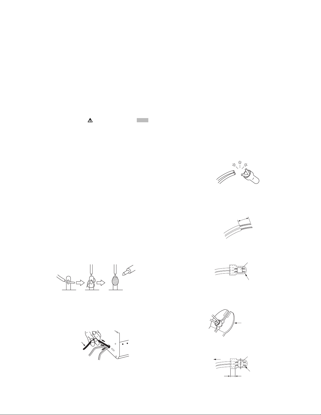
(6) When replacing AC primary side components (transformers,
power cords, noise blocking capacitors, etc.) wrap ends of
wires securely about the terminals before soldering.
Consequently, when servicing these products, replace the
cathode ray tubes and other parts with only the specified
parts. Under no circumstances attempt to modify these circuits.Unauthorized modification can increase the high voltage value and cause X-ray emission from the cathode ray
tube.
(12) Crimp type wire connectorIn such cases as when replacing
the power transformer in sets where the connections between the power cord and power trans former primary lead
wires are performed using crimp type connectors, if replacing the connectors is unavoidable, in order to prevent safety hazards, perform carefully and precisely according to the
following steps.
• Connector part number :E03830-001
• Required tool : Connector crimping tool of the proper
type which will not damage insulated parts.
• Replacement procedure
a) Remove the old connector by cutting the wires at a
point close to the connector.Important : Do not reuse a connector (discard it).
cut close to connector
Fig.1-1-3
b) Strip about 15 mm of the insulation from the ends
of the wires. If the wires are stranded, twist the
strands to avoid frayed conductors.
15 mm
Fig.1-1-4
c) Align the lengths of the wires to be connected. In-
sert the wires fully into the connector.
Metal sleeve
Fig.1-1-1
(7) Observe that wires do not contact heat producing parts
(heatsinks, oxide metal film resistors, fusible resistors, etc.)
(8) Check that replaced wires do not contact sharp edged or
pointed parts.
(9) When a power cord has been replaced, check that 10-15
kg of force in any direction will not loosen it.
Power cord
Fig.1-1-2
(10) Also check areas surrounding repaired locations.
(11) Products using cathode ray tubes (CRTs)In regard to such
products, the cathode ray tubes themselves, the high voltage circuits, and related circuits are specified for compliance with recognized codes pertaining to X-ray emission.
Connector
Fig.1-1-5
d) As shown in Fig.1-1-6, use the crimping tool to crimp
the metal sleeve at the center position. Be sure to
crimp fully to the complete closure of the tool.
1.25
2.0
5.5
Crimping tool
Fig.1-1-6
e) Check the four points noted in Fig.1-1-7.
Not easily pulled free
Wire insulation recessed
more than 4 mm
Crimped at approx. cente
of metal sleeve
Conductors extended
Fig.1-1-7
(No.YD052)1-3
Page 4
1.1.2 Safety Check after Servicing
Examine the area surrounding the repaired location for damage
or deterioration. Observe that screws, parts and wires have been
returned to original positions, Afterwards, perform the following
tests and confirm the specified values in order to verify compliance with safety standards.
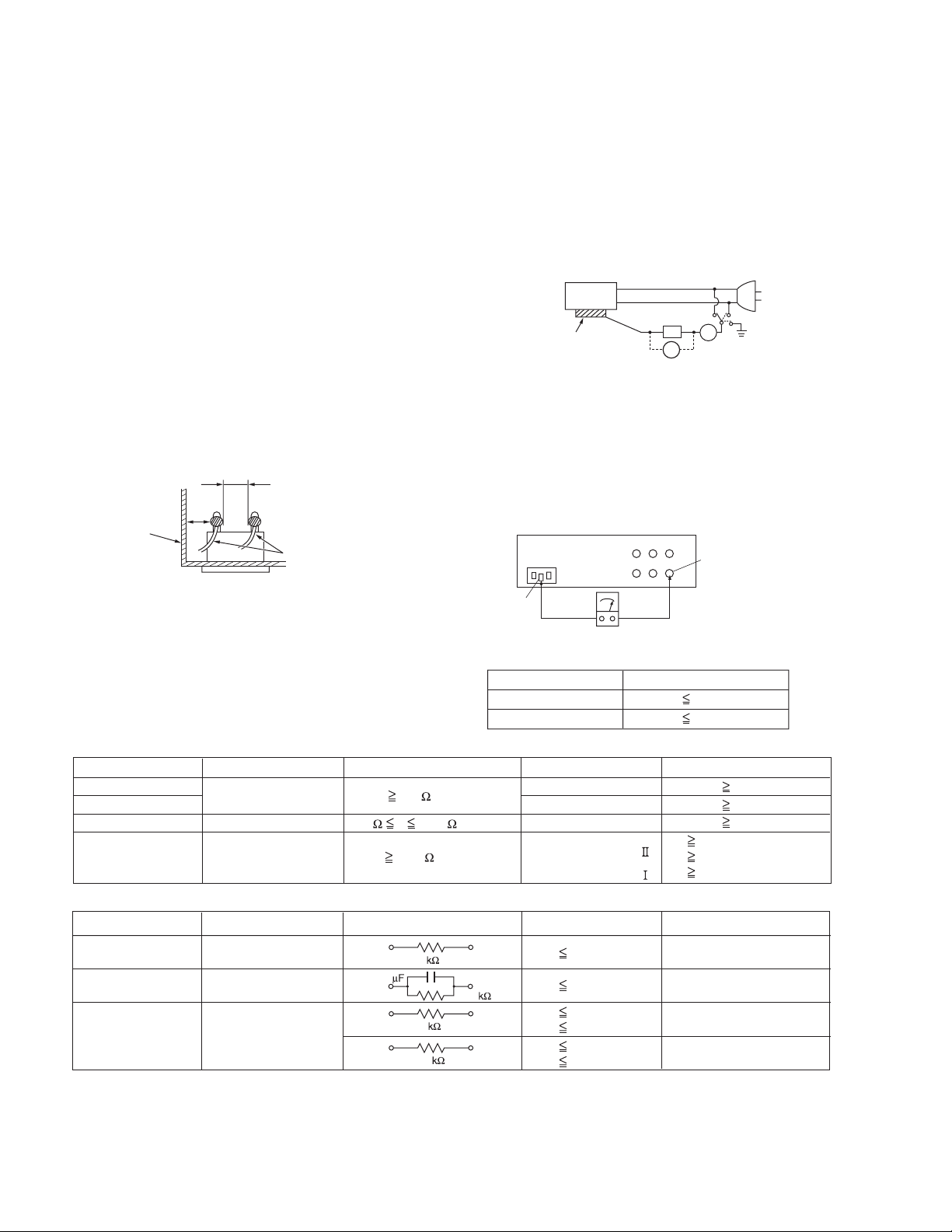
(1) Insulation resistance test
Confirm the specified insulation resistance or greater between power cord plug prongs and externally exposed
parts of the set (RF terminals, antenna terminals, video and
audio input and output terminals, microphone jacks, earphone jacks, etc.).See table 1 below.
(2) Dielectric strength test
Confirm specified dielectric strength or greater between
power cord plug prongs and exposed accessible parts of
the set (RF terminals, antenna terminals, video and audio
input and output terminals, microphone jacks, earphone
jacks, etc.). See Fig.1-1-11 below.
(3) Clearance distance
When replacing primary circuit components, confirm specified clearance distance (d), (d') between soldered terminals, and between terminals and surrounding metallic
parts. See Fig.1-1-11 below.
d
Chassis
d'
Power cord
primary wire
Fig.1-1-8
(4) Leakage current test
Confirm specified or lower leakage current between earth
ground/power cord plug prongs and externally exposed accessible parts (RF terminals, antenna terminals, video and
audio input and output terminals, microphone jacks, earphone jacks, etc.).
Measuring Method : (Power ON)Insert load Z between
earth ground/power cord plug prongs and externally exposed accessible parts. Use an AC voltmeter to measure
across both terminals of load Z. See Fig.1-1-9 and following Fig.1-1-12.
ab
Externally
exposed
accessible part
Z
V
c
A
Fig.1-1-9
(5) Grounding (Class 1 model only)
Confirm specified or lower grounding impedance between
earth pin in AC inlet and externally exposed accessible
parts (Video in, Video out, Audio in, Audio out or Fixing
screw etc.).Measuring Method:
Connect milli ohm meter between earth pin in AC inlet and
exposed accessible parts. See Fig.1-1-10 and grounding
specifications.
AC inlet
Earth pin
Exposed accessible part
MIlli ohm meter
Grounding Specifications
Region
USA & Canada
Europe & Australia
Grounding Impedance (Z
Z 0.1 ohm
Z 0.5 ohm
)
Fig.1-1-10
AC Line Voltage
100 V
100 to 240 V
110 to 130 V
110 to 130 V
200 to 240 V
Region
Japan
USA & Canada
Europe & Australia
Insulation Resistance (R
R 1 M /500 V DC
1 M R 12 M /500 V DC
R 10 M /500 V DC
)
Dielectric Strength
AC 1 kV 1 minute
AC 1.5 kV 1 minute
AC 1 kV 1 minute
AC 3 kV 1 minute
AC 1.5 kV 1 minute
(
Class
(
Class
Clearance Distance (d), (d'
d, d' 3 mm
d, d' 4 mm
d, d' 3.2 mm
d 4 m m
)
d' 8 m m (Power cord
d' 6 m m (Primary wire
)
Fig.1-1-11
AC Line Voltage
100 V
110 to 130 V
110 to 130 V
220 to 240 V
Region
Japan
USA & Canada
Europe & Australia
Load Z Leakage Current (i)
1
0.15
1.5
2
50
i 1 mA rms
i 0.5 mA rms
i 0.7 mA peak
i 2 mA dc
i 0.7 mA peak
i 2 mA dc
a, b, c
Exposed accessible parts
Exposed accessible parts
Antenna earth terminals
Other terminals
Fig.1-1-12
NOTE :
These tables are unofficial and for reference only. Be sure to confirm the precise values for your particular country and locality.
)
)
)
1-4 (No.YD052)
Page 5
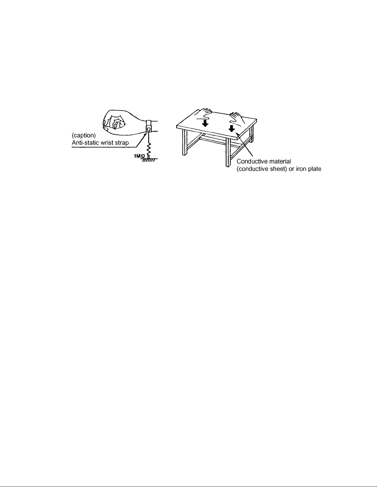
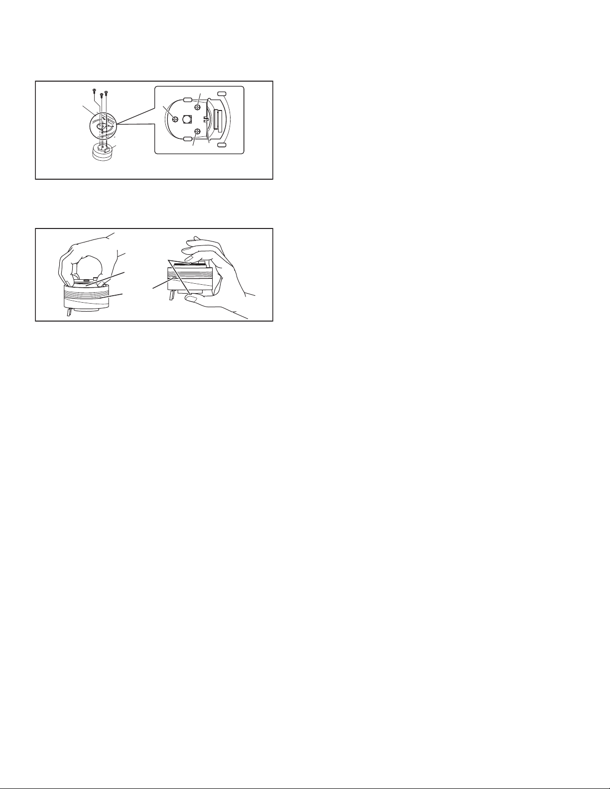
1.2 Preventing static electricity
Electrostatic discharge (ESD), which occurs when static electricity stored in the body, fabric, etc. is discharged, can destroy the laser
diode in the traverse unit (optical pickup). Take care to prevent this when performing repairs.
1.2.1 Grounding to prevent damage by static electricity
Static electricity in the work area can destroy the optical pickup (laser diode) in devices such as DVD players.
Be careful to use proper grounding in the area where repairs are being performed.
(1) Ground the workbench
Ground the workbench by laying conductive material (such as a conductive sheet) or an iron plate over it before placing the
traverse unit (optical pickup) on it.
(2) Ground yourself
Use an anti-static wrist strap to release any static electricity built up in your body.
(3) Handling the optical pickup
• In order to maintain quality during transport and before installation, both sides of the laser diode on the replacement optical
pickup are shorted. After replacement, return the shorted parts to their original condition.
(Refer to the text.)
• Do not use a tester to check the condition of the laser diode in the optical pickup. The tester's internal power source can easily
destroy the laser diode.
(No.YD052)1-5
Page 6
1.3 Precautions for Service
1.3.1 Handling of Traverse Unit and Laser Pickup
(1) Do not touch any peripheral element of the pickup or the actuator.
(2) The traverse unit and the pickup are precision devices and therefore must not be subjected to strong shock.
(3) Do not use a tester to examine the laser diode. (The diode can easily be destroyed by the internal power supply of the tester.)
(4) To replace the traverse unit, pull out the metal short pin for protection from charging.
(5) When replacing the pickup, after mounting a new pickup, remove the solder on the short land which is provided at the center of
the flexible wire to open the circuit.
(6) Half-fixed resistors for laser power adjustment are adjusted in pairs at shipment to match the characteristics of the optical block.
Do not change the setting of these half-fixed resistors for laser power adjustment.
1.3.2 Destruction of Traverse Unit and Laser Pickup by Static Electricity
Laser diodes are easily destroyed by static electricity charged on clothingor the human body. Before repairing peripheral elements of
the traverse unit or pickup, be sure to take the following electrostatic protection:
(1) Wear an antistatic wrist wrap.
(2) With a conductive sheet or a steel plate on the workbench on which the traverse unit or the pick up is to be repaired, ground the
sheet or the plate.
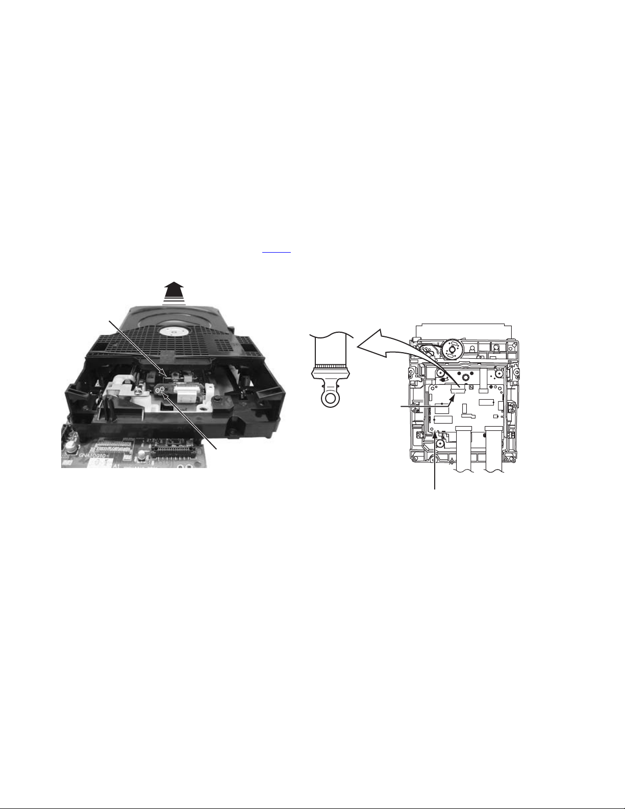
(3) It solders to two short circuit sections on the substrate of a pick-up.
(4) After removing the flexible wire from the connector (CN101
(5) Short-circuit the laser diode by soldering the land which is provided at the center of the flexible wire for the pickup.
After completing the repair, remove the solder to open the circuit.
), short-circuit the flexible wire by the metal clip.
Pick-up
Short circuit
* Please refer to the SECTION3 DISASSEMBLY method for details.
CN101
DVD SERVO CONTROL BOARD
1-6 (No.YD052)
Page 7
SECTION 2
SPECIFIC SERVICE INSTRUCTIONS
2.1 Different table of feature
The following table indicates main different points between models HR-XVC28BUC, HR-XVC28BUS, HR-XVC29SUC and HRXVC29SUS.
HR-XVC28BUC HR-XVC28BUS HR-XVC29SUC HR-XVC29SUS
BODY COLOR BLACK ← PURE SILVER ←
MP3 PLAYBACK USED NOT USED USED NOT USED
NOTE :
Mark ← is same as left.
2.2 Service position
This unit has been designed so that the Mechanism and Main
board assemblies can be removed together from the bottom
chassis. Before diagnosing or servicing the circuit boards, take
out the major parts from the bottom chassis.
2.2.1 How to set the "Service position"
(1) Refer to the disassembly procedure and perform the disas-
sembly of the major parts before removing the Mechanism
assembly.
(2) Remove the screws that fix the Mechanism, Main board as-
sembly to the bottom chassis. If any other screws are used
to fix the boards, remove them also.
(3) Remove the combined Mechanism and Main board assem-
blies.
(4) If any other major parts are used, remove them also.
(5) Connect the wires and connectors of the major parts that
have been removed in steps (1) to (4). (Refer to Fig. 2-2a.)
(6) Place the combined Mechanism, Main board and other
board assemblies upside down.
(7) Insert the power cord plug into the power outlet and then
proceed with the diagnostics and servicing of the board as-
sembly.
Notes:
• Before inserting the power cord plug into the power out-
let, make sure that none of the electrical parts are able
to short-circuit between the workbench and the board
assembly.
• For the disassembly procedure of the major parts and
details of the precautions to be taken, see "Removing
the major parts".
• If there are wire connections from the Main board and
Mechanism assemblies to the other major parts, be sure
to remove them (including wires connected to the major
parts) first before performing step (2).
• When carrying out diagnosis and repair of the Main
board assembly in the "Service position", be sure to
ground both the Main board and Mechanism assemblies. If they are improperly grounded, there may be
noise on the playback picture or FDP counter display
may move even when the mechanism is kept in an inoperative status.
• In order to diagnose the playback or recording of the
cassette tape, set the Mechanism assembly to the required mode before placing it upside down. If the mechanism mode is changed (including ejection) while it is in
an upside down position the tape inside may be damaged.
• For some models, the mechanism and board assem-
blies are attached by connectors only. When carrying
out a diagnosis or repair of the boards in the "Service
position", make sure that the connectors are not disconnected.
TP111 D.FF
TP4001 CTL.P
TP106 PB FM
TP2253 A.PB FM
Display board assembly
Fig.2-2a
2.3 Jig RCU mode
This unit uses the following two modes for receiving remote control codes.
(1) User RCU mode:Ordinary mode for use by the user.
(2) Jig RCU mode: Mode for use in production and servicing.
When using the Jig RCU, it is required to set the VCR to the Jig
RCU mode (the mode in which codes from the Jig RCU can be
received). As both of the above two modes are stored in the EEPROM, it is required to set the VCR back to the User RCU mode
each time that an adjustment is made or to check that the necessary operations have been completed.These modes can be set
by the operations described below.
Note:
• Confirm the RCU mode when exchanged parts. Since
some SERVICE PARTS sets the VCR to the Jig RCU
mode as initial setting. Therefore please set the VCR to
the user RCU mode after replacing the EEPROM.
Main board assembly
Switch/jack board assembly
(No.YD052)1-7
Page 8
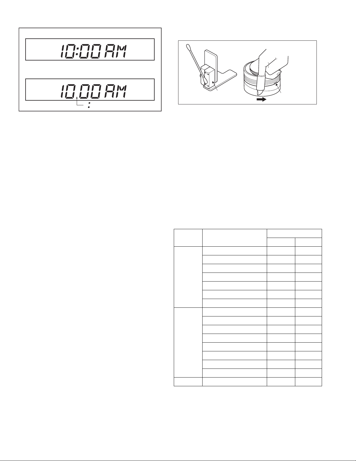
User RCU mode
Jig RCU mode
(3) After cleaning, make sure that the cleaned parts are com-
pletely dry before using the cassette tape.
( not displayed)
Fig.2-3a User/Jig RCU mode
2.3.1 Setting the Jig RCU mode
(1) Turn on the power.
(2) Press the following remocon keys continuously within 2
seconds " SET UP " → " 2 " → " 8 " → " ENTER ".
When the VCR is set to the Jig RCU mode, the symbols
( " : " ) in the time display of the FDP are turned off.
(Refer to Fig.2-3a)
2.3.2 Setting the User RCU mode
(1) Turn off the power.
(2) Press the "REC" and "PAUSE" buttons of the VCR simul-
taneously. Alternatively, transmit the code "43-80" from the
Jig RCU.
2.4 Mechanism service mode
This model has a unique function to enter the mechanism into every operation mode without loading of any cassette tape. This
function is called the "Mechanism service mode".
2.4.1 How to set the "Mechanism service mode"
(1) Set the VCR to the Jig RCU mode (the mode in which
codes from the Jig RCU can be received)
(2) Transmit the code "43-E5" from the Jig RCU.
(3) Release the lug of the Cassette holder and then slide the
Cassette holder toward the direction where the Cassette
holder is loaded by manually.
(4) The cassette holder lowers and, when the loading has
completed, the mechanism enters the desired mode.
When the VCR is set to the Mechanism service mode, the
symbols ("Timer") in the FDP (LED) are blinked.
2.4.2 How to exit from the "Mechanism service mode"
(1) Unplug the power cord plug from the power outlet.
2.5 Maintenance and inspection
2.5.1 Cleaning
Regular cleaning of the transport system parts is desirable but
practically impossible. So make it a rule to carry out cleaning of
the tape transport system whenever the machine is serviced.
When the video head, tape guide and/or brush get soiled, the
playback picture may appear inferior or at worst disappear, resulting in possible tape damage.
Note:
• Absolutely avoid sweeping the upper drum vertically as
this will cause damage to the video head.
(1) When cleaning the upper drum (especially the video head),
soak a piece of closely woven cloth with alcohol and while
holding the cloth onto the upper drum by the fingers, turn
the upper drum counterclockwise.
(2) To clean the parts of the tape transport system other than
the upper drum, use a piece of closely woven cloth or a cot-
ton swab soaked with alcohol.
A/C head
Fig.2-5a
2.5.2 Lubrication
With no need for periodical lubrication, you have only to lubricate
new parts after replacement. If any oil or grease on contact parts
is soiled, wipe it off and newly lubricate the parts.
Note:
• See the "mechanism assembly" diagram of the "parts
list" for the lubricating or greasing spots, and for the
types of oil or grease to be used.
2.5.3 Suggested servicing schedule for main components
The following table indicates the suggested period for such service measures as cleaning, lubrication and replacement. In practice, the indicated periods will vary widely according to
environmental and usage conditions. However, the indicated
components should be inspected when a set is brought for service and the maintenance work performed if necessary. Also
note that rubber parts may deform in time, even if the set is not
used.
System Parts name
Drum assembly C,X X
A/C head C,X C,X
Tape
transport
Drive
Other Rotary encoder X
C : Cleaning
X : Inspection or Replacement if necessary
Pinch roller arm assembly C C
Full erase head C C
Tension arm assembly C C
Capstan motor (Shaft) C C
Guide arm assembly C C
Capstan motor X
Capstan brake assembly X
Main brake assembly X
Belt (Capstan) X X
Loading motor X
Clutch unit X
Worm gear X
Control plate X
Video heads
Operation hours
1000H 2000H
1-8 (No.YD052)
Page 9
SECTION 3
DISASSEMBLY
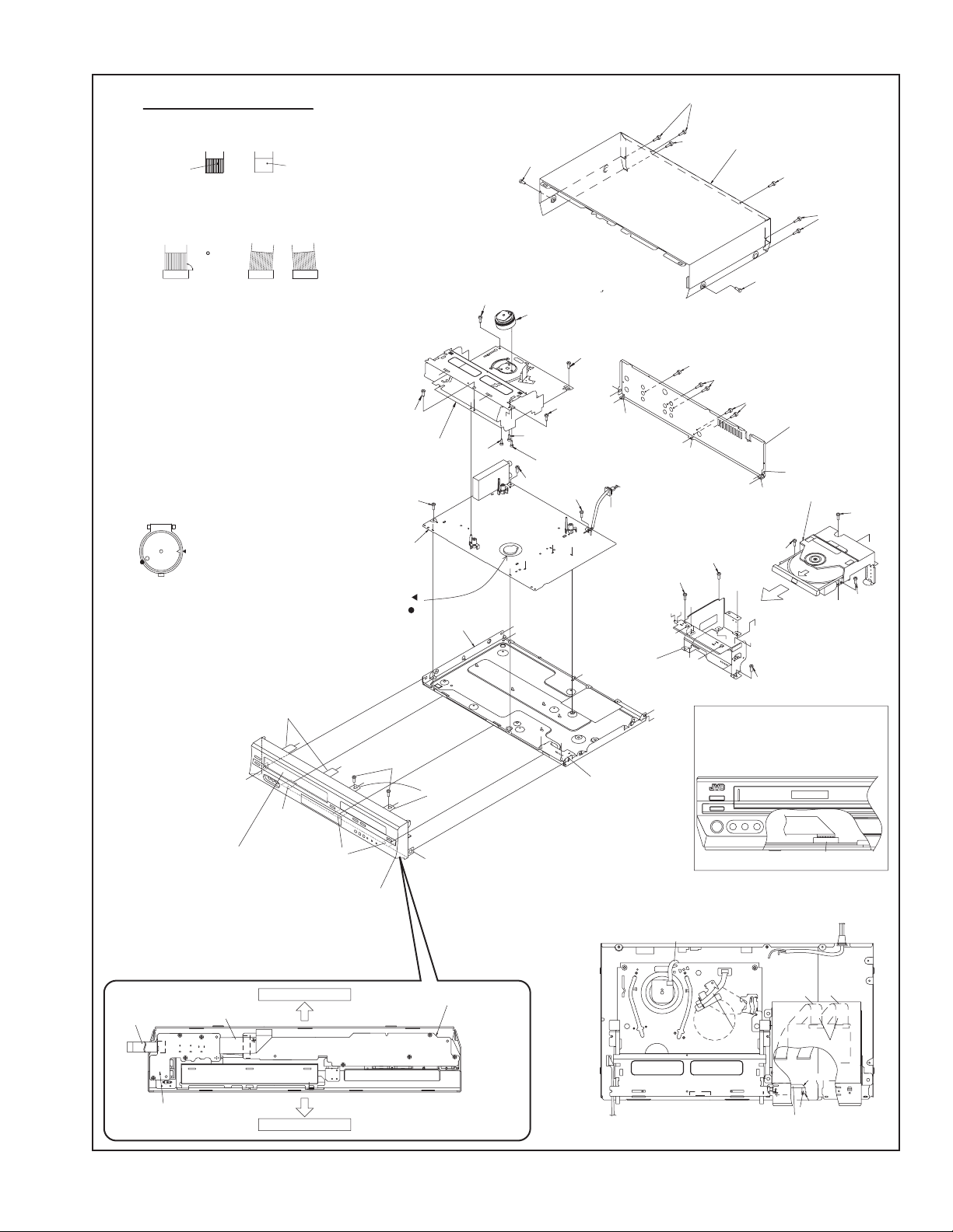
3.1 Removing the major parts
3.1.1 Destination of connectors
Two kinds of double-arrows in connection tables respectively
show kinds of connector/wires.
: The connector of the side to remove
CONN. No. PIN No.CONNECTOR
WR2a
WR2b
Main CN101
Main CN103
Destination of connectors
CONN. No. PIN No.CONNECTOR
WR2a
WR2b
WR3a
WR3b
WR4a
WR4b
WR4c
Main
Main
Main
Drum
assembly
Main
Main
Main
3.1.2 How to read the procedure table
This table shows the steps for disassembly of the externally furnished parts and board assemblies. Reverse these steps when
re-assembling them.
Step/
Loc No.
[1] Top cover 3-1a
(1) (2) (3) (4) (5)
Part Name
Bracket 2(S1c)
(1) Order of steps in Procedure
When reassembling, perform the step(s) in the reverse order.
These numbers are also used as the identification (loca-
tion) No. of parts Figures.
(2) Part name to be removed or installed.
(3) Fig. No. showing procedure or part location.
(4) Identification of part to be removed, unhooked, unlocked,
released, unplugged, unclamped or unsoldered.
P= Spring, W= Washer, S= Screw, L= Locking tab, SD=
Solder, CN**(WR**)= Remove the wire (WR**) from the
connector (CN**).
Note:
• The bracketed ( ) WR of the connector symbol are
assigned nos. in priority order and do not correspond to those on the spare parts list.
(5) Adjustment information for installation
: Wire: Flat wire : Board to board (B-B)
Digital CN761
Digital CN762
CN7103
CN3102
CN2001
CN7302
CN7301
CN3301
Switch/jack
Display
A/C head
Main
DVD
servo control
DVD
servo control
DVD
servo control
Fig.
No.
4(S1a),(S1b),3(L1a), <Note 1a>
2(SD1a),(P1a),(W1a),
CN1(WR1a),
----------------------------------------
CN7191
CN7003
CN503
CN501
Point Note
CN1
CN1
40
10
10
22
6
9
17
19
5
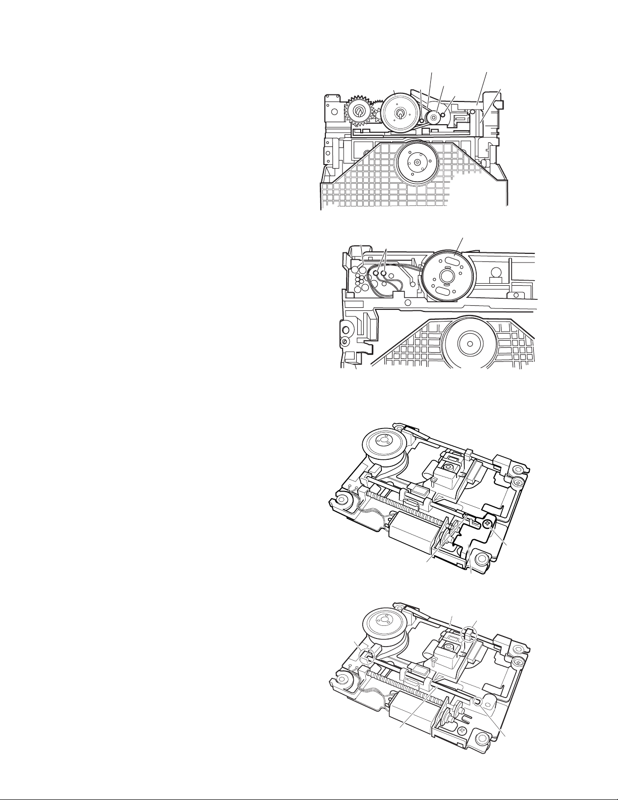
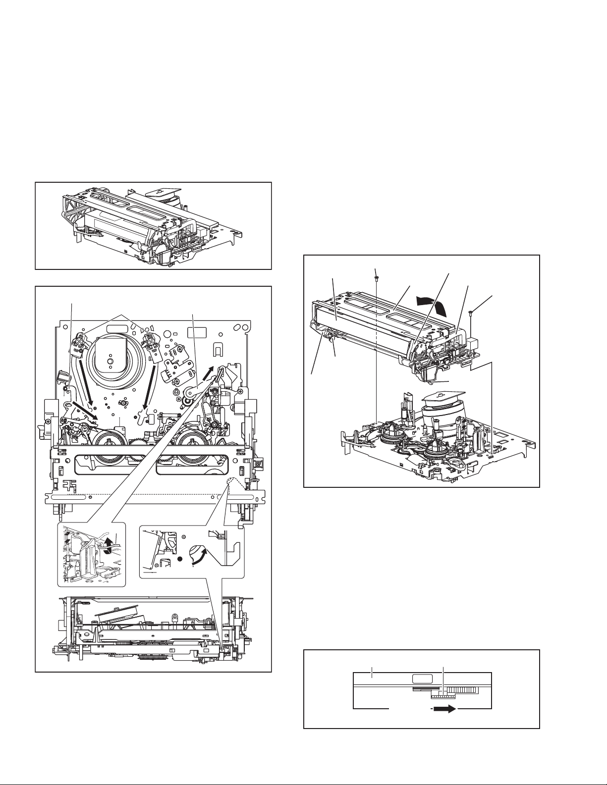
3.1.3 Disassembly procedure
Step/
Loc No.
[1]
[2]
[3]
[4]
[5]
[6]
Part Name
Top cover
Front panel assembly
(Display board assembly)
(
Switch/jack board assembly
Mechanism assembly
(Drum assembly)
DVD unit
(Bracket)
Rear cover
Main board assembly
Fig.
No.
8(S1a)
3-1d
4(L2a),5(L2b),2(S2a)
3-1a
CN7103(WR2a),
3-1d
)
CN3102(WR2b)
CN2001(WR3a)
3-1b
3(S3a),(S3b)
3-1c
--------------------------
CN(WR3b)
3-1d
(S3c),(S3d),(S3e)
3(S4a),3(S4b),
3-1d
CN7302(WR4a),
CN7301(WR46),
CN3301(WR4c)
5(S5a),5(L5a)
3-1d
3(S6a)
3-1d
Point Note
<Note 2a>
<Note 2b>
<Note 2a>
<Note 3a>
<Note 3b>
<Note 3c>
<Note 2a>
• Be careful not to damage the connector and wire etc. during
connection and disconnection.
• When connecting the flat wire to the connector, be careful with
the flat wire direction.
<Note 2b>
• When reattaching the Front panel assembly, make sure that
the door opener of the Side frame (R) is lowered in position prior to the reinstallation.
• When reattaching the Front panel assembly, pay careful attention
to the switch lever of the Front panel assembly not to make it
touch the switch knob of the Main board assembly from the side.
• When reattaching the Front panel assembly, lift the Cassette
door slightly.
Door
opener
Side
frame(R)
Switch
knob
Switch
lever
Fig.3-1a
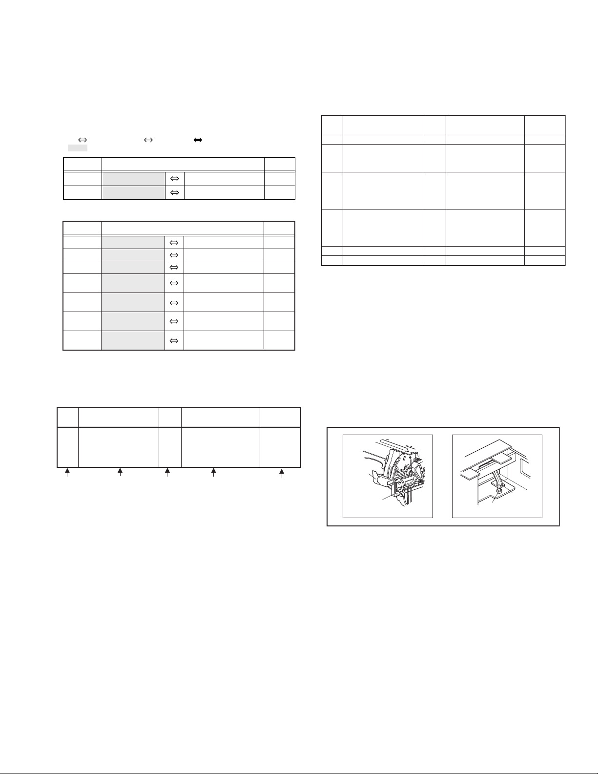
<Note 3a>
• When reattaching the Mechanism assembly, secure the
screws (S3a to S3b) in the order of 1,2,3.
<Note 3b>
• When reattaching the Mechanism assembly, be sure to align
the phase of the Rotary encoder on the Main board assembly.
• When reattaching the Mechanism assembly, set the "Mechanism assembling mode". [See "MECHANISM ASSEMBLY
SERVICE MANUAL (No. 86700)".]
• When reattaching the Mechanism assembly to the Main board
assembly, take care not to damage the sensors and switch on
the Main board assembly.
(No.YD052)1-9
Page 10
<Note 3c>
• When reattaching the Drum assembly, secure the screws (S3c
to S3e) in the order of c, d, e.
(S3d)
Mechanism
assembly
(S3c)
(S3e)
(S3d)
(S3e)
Drum
assembly
<Note 3c>
<NOTE>
Attach the Drum assembly appropriately,
since the installation state of the Drum assembly
influences the FM WAVEFORM LINEARITY
greatly.
(S3c)
HOOK
Fig.3-1b
• When handling the drum assembly alone, hold it by the motor
or shaft. Be careful not to touch other parts, especially the video heads. Also take care not to damage the connectors.
Shaft
Motor
Video heads
Fig.3-1c
1-10 (No.YD052)
Page 11
(WR3a)
<Note 2b>
NOTE
1. Insert direction of FFC WIRE as follows.
right side
electrode side
back side
supporting side
(S1a)
(S1a)
(S1a)
[1]Top cover
(S1a)
2. FFC WIRE and DRUM FPC WIRE
should be insert as follows.
OK
NG
90
CN
CN
CN
3.Insert the wire to even the root of connector completely
at the same time as inserting each wire.
4.Check to see that outside parts.
TOP COVER,BOTTOM COVER,FRONT PANEL, etc
are fixed certainly to the BOTTOM CHASSIS
5.Pay attention NOT to make any scratches
on FRONT PANEL.
6.Pay close attention not to cut any
3
(S3a)
Sheath of WIRE by sharp edge
of CHASSIS while Wireing Process.
[3]Mechanism
assembly
(S6a)
JS3001
[6]Main board assembly
<Phase alignment>
.
Accord the position of V gap on R.ENCORDER and PWB silk
.
Accord the position of Boss on R.ENCORDER and PWB silk
(L2a)
j
(S2a)
j
(L2b)
j
(L2a)
j
(L2b)
(S3a)
1
j
j
f
(S3c)
TU6001
Bottom chassis
[3]Drum assembly
2
(S3b)
e
(S3e)
(S3d)
(S6a)
(S6a)
JS3001
c
c
i
i
b
a
a
DVD bracket
board assembly
(S3a)
(L5a)
i
i
i
(L5a)
m
[4]Bracket
(S1a)
(S1a)
(S5a)
(S5a)
(S5a)
[5]Rear cover
i
(L5a)
(L5a)
i
i
(L5a)
[4]DVD unit
(S4a)
LP*****
d
(S4a)
(S4b)
e
f
j
d
c
(S4b)
j
(S4a)
d
b
d
c
(S4b)
i
i
NOTE) FFC WIRE SHOULD BE POSITIONED
BELLOW CASSETTE DOOR.
(FOR AVOID FFC WIRE
DISTURB CASSETTE IN AND OUT.)
d
Cassette door
<Note 2b>
CN7191
3
(WR2b)
<Note 2a>
4
2
(WR2a)
<Note 2a>
1
Switch/jack board assembly
BOTTOM SIDE
CN7003
5
TOP SIDE
(L2b)
[2]Front panel
assembly
4
(L2b)
Display board assembly
3
1
2
Fig.3-1d
CN3102
Insert the bushing of POWER CORD so as not to twist the cord.
(WR3b)
<Note 2b>
A/C HEAD
CN7103
CN3102
from FRONT PANEL
(JACK CN7191)
CN2001
(WR3a)
(WR3a)
<Note 2b>
<Note 2b>
(WR4a)
<Note 2b>
(WR4c)
<Note 2b>
CN7302
CN1
CN503
back side
CN7301
Make a crease.
CN3301
right side
(WR4b)
<Note 2b>
CN501
(No.YD052)1-11
Page 12
3.2 Loading mechanism assembly
Projection of the tray
3.2.1 Removing the tray (See Figure 3-2a, Figure 3-2b, Figure 3-2c, Figure 3-2d, Figure 3-2e, Figure 3-2f)
(1) Push a of the slide cam on the hole in the right side of the
loading base by using a driver until it stops. (See Figure 32a.)
(2) The tray comes out. Pull the tray in a front direction until it
stops.
(3) Remove the two screws A attaching the slide bracket. (See
Figure 3-2b.)
(4) Tilt the tray in a direction of the arrow around the point in
the left rear part of the tray. (See Figure 3-2c.)
(5) The rail of the tray is removed from b of the loading base.
Then, remove the tray upward. (See Figure 3-2d.)
Attaching the tray:
Engage c of the loading base to the projection of the tray while
tilting the tray to the left. Turn the tray in a direction of the arrow, and attach the slide bracket. (See Figure 3-2e.)
Note:
Prior to the procedure above, move the slide cam in a direction
of the arrow so that d of the slide cam can be inserted in e of
the tray. (See Figure 3-2f.)
Tray
The point in the left rear part
Fig.3-2c
Tray
Push
Slide cam part a
Slide bracket
A
Fig.3-2a
Fig.3-2b
A
Loading base
Tray
Loading base part b
Rail of the tray
Fig.3-2d
Projection of the tray
Loading base part c
Fig.3-2e
Part e
1-12 (No.YD052)
Part d
Slide cam
Fig.3-2f
Page 13
3.2.2 Removing the traverse mechanism assembly (See Figure 3-2g)
f
Shaft
Reverse the loading mechanism assembly. Remove the four
screws B attaching the traverse mechanism assembly. Remove
the traverse mechanism assembly upward.
Loading mechanism assembly
3.2.3 Removing the elevator (See Figure 3-2h and Figure 3-2j)
• Prior to the following procedure, remove the traverse mechanism assembly.
(1) Remove the two arms of the elevator from the two parts f
by moving the arms in a direction of the arrow.
(2) Pull out the elevator in a rear direction.
Attaching the elevator:
Engage the two holes g to the two shafts on the front part of
the elevator. And then, attach the elevator.
B
B
B
B
Traverse mechanism assembly
Fig.3-2g
Elevator
Part f
Fig.3-2h
g
Slide cam
Elevator
Shaft
Fig.3-2j
(No.YD052)1-13
Part
g
Page 14
3.2.4 Removing the loading motor (See Figure 3-2k and Figure 3-2l)
• Prior to the following procedure, remove the tray, the traverse
mechanism assembly, and the elevator.
(1) Remove the belt from the pulley.
(2) Remove two screws C attaching the loading motor.
(3) Remove two solders h on the switch board.
Switch board
Pulley
Part h
Belt
Pulley
C
Fig.3-2k
Loading base
Slide cam
C
Loading motor
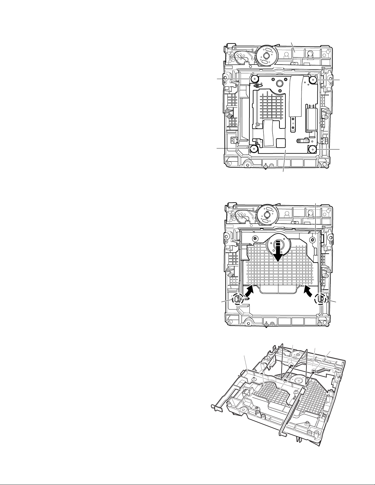
3.3 Traverse mechanism assembly
3.3.1 Removing the pickup (See Figure 3-3a, Figure 3-3b)
• Prior to the following procedure, remove the traverse mechanism assembly.
(1) Remove one screw D attaching the plate.
(2) Remove the plate and the leaf spring.
(3) Lift i of the shaft 1, and pull out the shaft 1 from j.
(4) Remove k of the pickup from the shaft 2.
Attaching the pickup:
(1) Engage k of the pickup to the shaft 2.
(2) Insert the shaft 1 in j, and attach the shaft 1 to i.
(3) Attach the leaf spring, and then attach the plate. Fix the
leaf spring and the plate by using the screw D.
Fig.3-2l
D
Leaf spring
Plate
Fig.3-3a
Shaft 2
Part k
Part j
1-14 (No.YD052)
Shaft 1
Part i
Fig.3-3b
Page 15
SECTION 4
ADJUSTMENT
4.1 Before adjustment
4.1.1 Precaution
• The adjustments of this unit include the mechanism com-
patibility and electrical adjustments. During the performance of this work, be sure to observe the precautions for
each type of adjustment.
• If there is a reference to a signal input method in the signal
column of the adjustment chart, "Ext. S-input" means the
Y/C separated video signal and "Ext. input" means the
composite video signal input.
• Unless otherwise specified, all measuring points and
adjustment parts are located on the Main board.
4.1.2 Required test equipments
• Color (colour) television or monitor
• Oscilloscope: wide-band, dual-trace, triggered delayed sweep
• Signal generator: RF / IF sweep / marker
• Signal generator: stairstep, color (colour) bar [NTSC]
• Recording tape
• Digit-key remote controller(provided)
4.1.3 Required adjustment tools
--- : Not used
z
: Used
Mechanism
compatibility
adjustment
Roller driver
z ---
Jig RCU --- z
Back tension cassette gauge z ---
Alignment tape(MHP) z ---
Alignment tape(MHP-L) zz
Roller driver
PTU94002
Alignment tape
(SP, stairstep, NTSC)
MHP
CD-DA test disc
CTS-1000
Jig RCU
PTU94023B
Alignment tape
(EP, stairstep, NTSC)
MHP-L
Back tension cassette gauge
Electrical
adjustment
PUJ48076-2
DVD test disc
VT-501
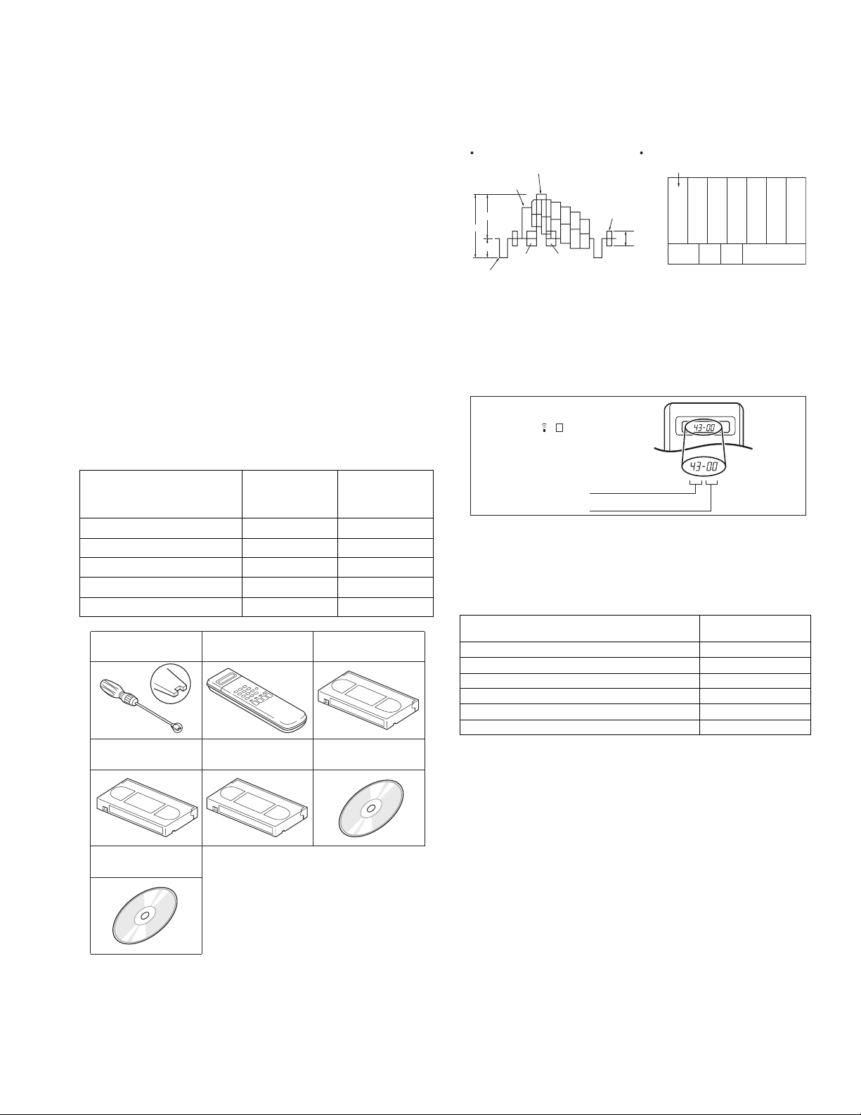
4.1.4 Color (colour) bar signal,Color (colour) bar pattern
Color(colour) bar signal [NTSC]
White(100%)
White(75%)
100 IRE
1V
40 IRE
Horizontal sync
Yellow
Cyan
Green
Magenta
Red
QI
Blue
Color(colour) bar pattern [NTSC]
(75%)
Burst
40 IRE
White
Yellow
White
Q I Black
100%
Cyan
Green
Magenta
Red
Blue
4.1.5 Switch settings
When adjusting this unit, set the VCR mode and switches
as described below.
• When using the Jig RCU, it is required to set the VCR to the
Jig RCU mode (the mode in which codes from the Jig RCU can
be received). (See "section 2 SPECIFIC SERVICE INSTRUCTIONS".)
Jig RCU
[Data transmitting method]
Depress the " "( 3 ) button
after the data code is set.
CUSTOM CODE
43: A CODE
DATA CODE
INITIAL MODE
Fig.4-1 Jig RCU [PTU94023B]
• Set the switches as shown below unless otherwise specified
on the relevant adjustment chart. The switches that are not listed below can be set as desired.
If the VCR is not equipped with the functions detailed below,
setup is not required.
AUTO PICTURE/VIDEO CALIBRATION/
B.E.S.T./D.S.P.C.
PICTURE CONTROL/SMART PICTURE NORMAL/NATURAL
VIDEO STABILIZER OFF
TBC ON
Digital 3R ON
VIDEO NAVIGATION/TAPE MANAGER OFF
BLUE BACK OFF
OFF
4.1.6 Manual tracking mode (Auto tracking ON/OFF) set-
ting
(1) In order to set to the manual tracking mode during tape
playback, press the "TRACKING + and -" button at the
same time on the remote control unit.
• Each press of the button switches the auto tracking ON
or OFF.
• When the manual tracking mode is set, the tracking is
placed at the center position.
(2) Press "TRACKING +/-" to adjust the tracking manually.
(No.YD052)1-15
Page 16
4.2 Mechanism compatibility adjustment (VHS SECTION)
Notes:
• Although compatibility adjustment is very important, it
is not necessary to perform this as part of the normal
servicing work. It will be required when you have replaced the A/C head, drum assembly or any part of the
tape transport system.
• To prevent damaging the alignment tape in the compat-
ibility adjustment, prepare a cassette tape (for self-recording/playback), perform a test on it by transporting it
and making sure that the tape is not bent by the tape
transport mechanisms such as in the guide rollers.(See
Fig.4-2b.)
4.2.1 Tension pole position
Notes:
• This adjustment must be performed every time the ten-
sion band is replaced.
Signal (A) • Back tension cassette gauge [PUJ48076-2]
Mode (B1)
Adjustment part (F) • Adjust pin [Mechansim assembly]
Specified value (G)
•PB
(B2)
• Eject end
• 25 - 51 gf•cm (2.45 - 5 x 10
-3
Nm)
(1) Play back the back tension cassette gauge (A).
(2) Check that the indicated value on the left side gauge is
within the specified value (G).
(3) If the indicated value is not within the specified value (G),
perform the adjustment in a following procedure.(See
Fig.4-2a.)
a) Remove the top frame, cassette holder and side
frames (L/R) all together. (Refer to the SERVICE
MANUAL No.86700 [MECHANISM ASSEMBLY].)
b) Rotate the loading motor gear to move the control
plate so that the triangular stamping to the left of the
“P”stamping is aligned with the stamping (a) on the
main deck. This positioning is mode (B1).
c) Adjust by turning the adjustment pin so that the tip of
the tension arm is aligned with the stamping (b) on
the main deck.
d) Rotate the reel disk (S) by about one turn clockwise
and make sure that the round hole of the adjustment
pin is located in the "OK" range. If it is outside this
range, restart the adjustment from the beginning.
After completion of the adjustment, rotate the loading gear
motor to return it to the mode (B2) position.
4.2.2 FM waveform linearity
Signal (A1)
Mode (B) • PB
Equipment (C) • Oscilloscope
Measuring point (D) • TP106 (PB. FM)
External trigger (E) • TP111 (D.FF)
Adjustment part (F) • Guide roller [Mechanism assembly]
Specified value (G) • Flat V.PB FM waveform
Adjustment tool (H) • Roller driver [PTU94002]
• Alignment tape(SP, stairstep, NTSC) [MHP]
(A2)
• Alignment tape(EP,stairstep,NTSC) [MHP-L]
(1) Play back the alignment tape (A1).
(2) Apply the external trigger signal to D.FF (E), to observe
the V.PB FM waveform at the measuring point (D).
(3) Set the VCR to the manual tracking mode.
(4) Make sure that there is no significant level drop of the V.PB
FM waveform caused by the tracking operation, with its
generally parallel and linear variation ensured. Perform the
following adjustments when required. (See Fig. 4-2c.)
(5) Reduce the V.PB FM waveform by the tracking operation.
If a drop in level is found on the left side, turn the guide roll-
er of the pole base assembly (supply side) with the roller
driver to make the V.PB FM waveform linear.
If a drop in level is on the right side, likewise turn the guide
roller of the pole base assembly (take-up side) with the
roller driver to make it linear. (See Fig. 4-2c.)
(6) Make sure that the V.PB FM waveform varies in parallel
and linearly with the tracking operation again. When re-
quired, perform fine-adjustment of the guide roller of the
pole base assembly (supply or take-up side).
(7) Unload the cassette tape once, play back the alignment
tape (A1) again and confirm the V.PB FM waveform.
(8) After adjustment, confirm that the tape wrinkling does not
occur at the roller upper or lower limits. (See Fig. 4-2b.)
[Perform adjustment step (9) only for the models equipped
with SP mode and EP (or LP) mode.]
[Perform adjustment step (9) only for the models
equipped with SP mode and EP (or LP) mode.]
(9) Repeat steps (1) to (8) by using the alignment tape (A2).
Improper
(a)
GUIDE ROLLER
Proper
TENSION ARM
Stamping(b)
OK
ADJUST PIN
1-16 (No.YD052)
NG
Fig.4-2a
CONTROL PLATE
Stamping(a)
(b)
GUIDE POLE
Fig.4-2b
Page 17
Proper waveform variation
Improper waveform variation
A
C
Up Down
B
D
Roller driver
Guide roller
(supply side)
Fig.4-2c
4.2.3 Height and tilt of the A/C head
Note:
• Set a temporary level of the height of the A/C head in ad-
vance to make the adjustment easier after the A/C head
has been replaced. (Refer to the SERVICE MANUAL
No.86700 [MECHANISM ASSEMBLY].)
Signal (A) • Alignment tape(SP, stairstep, NTSC) [MHP]
Mode (B) • PB
Equipment (C) • Oscilloscope
Measuring point (D1)
External trigger (E) • TP111 (D.FF)
Adjustment part (F) • A/C head [Mechanism assembly]
Specified value (G) • Maximum waveform
• TP106 (PB. FM)
(D2)
• TP4001 (CTL. P)
(1) Play back the alignment tape (A).
(2) Apply the external trigger signal to D.FF (E), to observe the
AUDIO OUT waveform and Control pulse waveform at the
measuring points (D1) and (D2) in the ALT mode.
(3) Set the VCR to the manual tracking mode.
(4) Adjust the AUDIO OUT waveform and Control pulse wave-
form by turning the screws (1), (2) and (3) little by little until
both waveforms reach maximum. The screw (1)
and (3) are for adjustment of tilt and the screw (2) for azi-
muth.
Head base
(2)
(1)
AUDIO OUT
4.2.4 A/C head phase (X-value)
Signal (A1)
Mode (B) • PB
Equipment (C) • Oscilloscope
Measuring point (D) • TP106 (PB. FM)
External trigger (E) • TP111 (D.FF)
Adjustment part (F) • A/C head base [Mechanism assembly]
Specified value (G) • Flat V.PB FM waveform
Adjustment tool (H) • Roller driver [PTU94002]
• Alignment tape(SP, stairstep, NTSC) [MHP]
(A2)
• Alignment tape(EP,stairstep,NTSC) [MHP-L]
(1) Play back the alignment tape (A1).
(2) Apply the external trigger signal to D.FF (E), to observe the
V.PB FM waveform at the measuring point (D).
(3) Set the VCR to the manual tracking mode.
(4) Loosen the screws (4) and (5), then set the Roller driver to
the innermost projected part of the A/C head. (See Fig. 4-
2e.)
(5) Rotate the roller driver so that the A/C head comes closest
to the capstan. From there, move the A/C head back grad-
ually toward the drum until the point where the FM wave-
form is maximized for the second time, and then
tighten the screws (4) and (5) temporarily.
(6) Play an alignment tape (A2) and set to the manual-tracking
mode.
(7) Fine-adjust A/C head base position to maximize the FM
waveform, and then tighten the screws (4) and (5) firmly.
(8) Play alignment tapes (A1) and (A2) and confirm that the FM
waveforms are maximized when the tracking is at the cen-
ter position.
To the drum
Toward the capstan
Toward the drum
A/C head
Screw (5)
Roller driver
Screw (4)
Head base
To the capstan
Fig.4-2e
Alignment tape
[SP, stairstep]
played with the
SP head
Waveform output
X-value adjustment point
Drum side Control head position Capstan side
Alignment tape
[EP(LP), stairstep]
played with the
EP(LP) head
A/C head
(3)
Fig.4-2d
CTL. P
Maximum
Fig.4-2f
(No.YD052)1-17
Page 18
4.3 Electrical adjustment (VHS SECTION)
Note:
The following adjustment procedures are not only necessary
after replacement of consumable mechanical parts or board
assemblies, but are also provided as references to be referred
to when servicing the electrical circuitry.
In case of trouble with the electrical circuitry, always begin a
service by identifying the defective points by using the measuring instruments as described in the following electrical adjustment procedures. After this, proceed to the repair,
replacement and/or adjustment. If the required measuring instruments are not available in the field, do not change the adjustment parts (variable resistor, etc.) carelessly.
4.3.1 Servo circuit
4.3.1.1 Switching point
Signal (A1)
Mode (B) • PB
Equipment (C) • Oscilloscope
Measuring point (D) • VIDEO OUT terminal (75 ohm terminated)
External trigger (E) • TP111 (D.FF)
Adjustment part (F) • Jig RCU: Code “43-5A”
Specified value (G) • 6.5 ± 0.5H
Adjustment tool (H) • Jig RCU [PTU94023B]
• Stairstep signal
(A2)
• Alignment tape(EP,stairstep,NTSC) [MHP-L]
• TP106 (PB. FM)
(1) Play back the signal (A1) of the alignment tape (A2).
(2) Apply the external trigger signal to D.FF (E) to observe the
VIDEO OUT waveform and V.PB FM waveform at the
measuring points (D1) and (D2).
(3) Set the VCR to the manual tracking mode.
(4) Adjust tracking so that the V.PB FM waveform becomes
maximum.
(5) Set the VCR to the Auto adjust mode by transmitting the
code (F) from the Jig RCU. When the VCR enters the stop
mode, the adjustment is completed.
(6) If the VCR enters the eject mode, repeat steps (1) to (5)
again.
(7) Play back the alignment tape (A2) again, confirm that the
switching point is the specified value (G).
4.3.1.2 Slow tracking preset
Signal (A1)
Mode (B1)
Measuring point (D) • TV-Monitor
Adjustment part (F) • Jig RCU: Code “43-71”or “43-72”
Specified value (G) • minimum noise
Adjustment tool (H) • Jig RCU [PTU94023B]
• Ext. input
(A2)
• Color (colour) bar signal [NTSC]
• VHS SP
(B2)
•VHS EP
(1) Record the signal (A2) in the mode (B1), and play back
the recorded signal.
(2) Set the VCR to the manual tracking mode.
(3) Set the VCR to the FWD slow (+1/6x) mode.
(4) Transmit the code (F) from the Jig RCU to adjust so that the
noise bar becomes the specified value (G) on the TV
monitor in the slow mode.
(5) Set the VCR to the Stop mode.
(6) Confirm that the noise bar is (G) on the TV monitor in the
slow mode.
(7) Repeat steps (3) to (6) in the REV slow (+1/6x) mode.
(8) Repeat steps (1) to (7) in the mode (B2).
Note:
• For FWD slow (+1/6x) playback, transmit the code "43-
08" from the Jig RCU to enter the slow playback mode,
and transmit the code "43-D0" for REV slow (-1/6x)
mode.
Trigger point
1-18 (No.YD052)
Switching point
V.sync
V. rate
Fig.4-3a Switching point
Page 19
4.4 Electrical adjustment (DVD SECTION)
r
4.4.1 Test mode setting method
(1) Press POWER button to turn off the unit.
(2) Press the following remocon keys continuously within 2seconds " SET UP " → " 2 " → " 8 " → " ENTER ".
(3) The unit becomes JIG RCU mode.
(4) Press POWER button then press VCR/DVD repeatedly so that the DVD indicator lights up on the front display panel.
(5) Press the POWER button again to turn off the unit.
(6) Transmit the code " 43-FA " from the Jig RCU.
(7) The power supply of the unit turns on automatically then the FDP shows the region number.
(8) Each pressing of DISPLAY button of the remote controller in test mode as follows.
(9) To release test mode, press POWER key of the front panel.
FDP(Example)
Becames test mode
VCR
(Region number)
Optimize Front End paramete
4.4.2 Method of displayed version of firmware
(1) Set the unit to the test mode.
(2) The version number is displayed in the monitor screen.
OPENING DISPLAY
**_Ver.****_HS/HR_XVC29/*******
Version of firmware
Destination
CD Laser
DVD Laser
Others
Model name
(No.YD052)1-19
Page 20
4.4.3 Initialization method
Please initialize according to the following procedures in the following case:
• Just after you upgrade the firmware.
• After you confirm the symptoms that a customer points out. First Initialize, and then confirm whether the symptoms are improved or
not.
• After servicing, before returning the main body to a customer. (Initialized unit should be returned to a customer.)
(1) Set the unit to the test mode.
(2) Press PAUSE key of the remote controller or transmit the code "43-6F" from the Jig RCU.
(3) When initialization is completed, the PLAY (). mark is indicated in the FDP.
4.4.4 All-initialization method
Please perform all-initialization according to the following procedures in the following case:
• Just after you exchange the pick-up.
• Just after you exchange the spindle motor.
• Just after you exchange the traverse mechanism base.
NOTE:
Please perform all-initialization when you exchange the parts above and also when you remove the parts above.
(1) Set the unit to the test mode.
(2) Press the REVERSE SKIP/INDEX () key of the remote controller for more than 2 seconds.
(3) When initialization is completed, the PLAY (). mark is indicated in the FDP.
NOTE:
After all-initialization, be sure to perform optimization adjustment of Front End parameter.
4.4.5 Optimization adjustment of Front End parameter
Adjustment to optimize Front End parameter must be performed in each mechanism assembly of this model for high-speed starting.Please perform optimization according to the following procedures just after all-initialization is completed and when FDP shows
anything except "0" (For example when FDP shows "1", "2", and "3") at test mode.
(1) Set the unit to the test mode.
(2) The FDP shows the region number first.
(3) Press the DISPLAY key of the remote controller and check that FDP shows the number.
(4) Press the DISPLAY key again to return the region number.
NOTE:
Status of this adjustment can be judged by the number displayed at test mode as follows:
DVD adjustment CD adjustment FDP at test mode
Adjusted Adjusted 0
Not adjusted Adjusted 1
Adjusted Not adjusted 2
Not adjusted Not adjusted 3
NOTE:
As for a disc used for adjustment,
• Disc should be mounted. ("Mounting" means to display "READ" after the disc is inserted and then display the disc information.) Disc need not be played.
• If you do not have test disc either VT-501 (DVD) or CTS-1000 (CD-DA), use a commercial disc (for DVD, dual-layer software) after seeing and checking that the disc is neither curved nor foreseen that it may shake at the time of playback.If you
use a disc with bad features, starting time may be slow or disc may not be read.
1-20 (No.YD052)
Page 21
4.4.6 Upgrading of firmware
• Firmware update disc supports CD-R media.
• When firmware update is necessary, information is available from the homepage of DIGITAL VIDEO STORAGE CATEGORY, CS
group.
4.4.6.1 Creating an update disc
Please check the details of the update disc creation method by JS-NET.
(1) Down load the update file from JS-NET.
(2) Write the update file into CD-R. Pay attention in the following points when writing the update disc.
• Make sure to write in "Disc at Once".
• Set the file compatibility to "ISO9660 format".
4.4.6.2 Update procedure
(1) Turn the power ON. Load the update disc on the tray and close the tray.
(2) Update of the firmware starts automatically then upgrading status is displayed in the monitor screen.
(3) The tray opens automatically. Remove the upgrade disc.
(4) Close the tray then press the POWER button to turn off the unit.
(5) Confirm the version of the firmware.in the test mode.
MONITOR(Example)
VERSION UP DISC
PROGRAM&DESTINATION MODE
CURRENT VERSION 0494(or0495)
NEW VERSION 0496
READING....
SECTOR
**
NUMBER
KEYS
SET UP
REVERSE
SKIP/INDEX
ENTER
DISPLAY
PAU SE
(No.YD052)1-21
Page 22
SECTION 5
TROUBLESHOOTING
5.1 Manually removing the cassette tape
If you cannot remove the cassette tape which is loaded because
of any electrical or mechanical failures, manually remove it by
taking the following steps.
(1) Unplug the power cord plug from the power outlet.
(2) Refer to the disassembly procedure of the VCR and per-
form the disassembly of the major parts before removing
the mechanism assembly. (See Fig. 5-1a)
Fig.5-1a
Tension arm assembly
Pole base assembly
Pinch roller arm assembly
(3) Unload the pole base assembly by manually turning the
gear of the loading motor until the pole base assembly is
hidden behind the cassette lid. In doing so, hold the tape by
the hand to keep the slack away from any grease. (See
Fig.5-1b )
In case of mechanical failures, while keeping the tension arm assembly free from tension, pull out the tape
on the pole base assembly. Take the spring(a) of the
pinch roller arm assembly off the hook, and detach it
from the tape.
(4) Remove the screw (a) of the side frame (L/R).
(5) Hold the slack tape and cassette cover together, lift the
cassette tape, top frame, cassette holder and side frames
(L, R) together from the rear and remove them by dis-engaging the hooks (a) and (b).
Screw(a)
Cassette tape
Hook(a)
Cassette holder
Top frame
Side frame(R)
Screw(a)
Spring(a)
Direction of unloading
Fig.5-1b
Side frame(L)
Hook(b)
Fig.5-1c
(6) Take up the slack of the tape into the cassette. This com-
pletes removal of the cassette tape.
5.2 Manually removing the disk(DVD/CD)
If you cannot remove the disk which is loaded because of any
electrical or mechanical failures, manually remove it by taking the
following steps.
(1) Unplug the power cord plug from the power outlet.
(2) Remove the top cover and front panel assembly.
(Refer to the disassembly procedure and perform the disassembly of the major parts before removing)
(3) Turn the Middle gear (a) by hand to open the disk tray.(See
Fig. 5-2a)
DVD unit
Middle gear (a)
1-22 (No.YD052)
Unloading
Fig.5-2a
Page 23
5.3 Emergency display function (VHS SECTION)
This unit saves details of the last two emergencies as the EMG
history and allows the status of the VCR and the mechanism of
each emergency to be shown both on the display and as OSD information.
When using the emergency function, it is required to set the VCR
to the Jig RCU mode.
Jig RCU
[Data transmitting method]
Depress the " " ( 3 ) button
after the data code is set.
CUSTOM CODE
43: A CODE
DATA CODE
INITIAL MODE
Fig.5-3a Jig RCU [PTU94023B]
5.3.1 Displaying the EMG information
The EMG detail of information can be displayed by transmitting
the code "43-59" from the Jig RCU.
Note:
• Press VCR/DVD repeatedly so that the VHS indicator
lights up on the front display panel.
• The EMG detail information <1><2> show the informa-
tion on the latest EMG.
It becomes “ - - : - - : - - ” when there is no latest EMG
record.
0: 00
E: **
1E: **
1: *1
2: *2
3: 34
4: *5
5: *6
6: *7
7: *8
8: *9
9: *1 0
Normal display
EMG content display (Latest) See 5.3.4
EMG content display (Previous) See 5.3.4
EMG detail information <1> See 5.3.5
[Deck operation mode]
EMG detail information <1> See 5.3.5
[Mechanism operation mode]
EMG detail information <1> See 5.3.5
[Mechanism sensor information and Mechanism mode position]
EMG detail information <2> See 5.3.6
[Type of the cassette tape in use <1>]
EMG detail information <2> See 5.3.6
[Winding position of the cassette tape in use]
EMG detail information <2> See 5.3.6
[Type of the cassette tape in use <2> (Winding area)]
EMG detail information <3> See 5.3.7
[Previous deck operation mode]
EMG detail information <3> See 5.3.7
[The deck operation mode of the one before the last]
EMG detail information <3> See 5.3.7
[The deck operation mode of the one prior to one above]
EMG display of 7 FDP display model
Fig.5-3b
EMG display of FDP display mode
(1) Transmit the code “43-59” from the Jig RCU.
The FDP shows the EMG content in the form of “E:**:**”.
<Example 1> E : 01
Latest EMG
<Example 2> E : - -
No EMG record
(2) Transmit the code “43-59” from the Jig RCU again.
The FDP shows the EMG detail information <1> in the form
of “ *1: *2 : 34 ”.
*1 : Deck operation mode at the moment of EMG
*2 : Mechanism operation mode at the moment of EMG
3- : Mechanism sensor information at the moment of EMG
-4 : Mechanism mode position at the moment of EMG
(3) Transmit the code “43-59” from the Jig RCU once again.
The FDP shows the EMG detail information <2> in the form
of “ *5 : *6 : *7 ”.
*5 : Type of the cassette tape in use <1> .
*6 : Winding position of the cassette tape in use
*7 : Type of the cassette tape in use <2> (Winding area)
(4) Transmit the code “43-59” from the Jig RCU once again.
The FDP shows the EMG detail information <3> in the form
of “*8 : *9 : *10”.
*8 : Previous deck operation mode at the moment of EMG
*9 : The deck operation mode of the one before the last at
the moment of EMG
*10: The deck operation mode of the one prior to one
above at the moment of EMG
(5) Transmit the code “43-59” from the Jig RCU once again to
reset the display.
(No.YD052)1-23
Page 24
5.3.2 Clearing the EMG history
(1) Display the EMG history.
(2) Transmit the code “43-36” from the Jig RCU.
(3) Reset the EMG display.
5.3.3 Details of the OSD display in the EMG display mode
During the EMG display, the OSD shows the data on the deck
mode, etc. The details of the display contents are as follows.
Notes:
• The display is variable depending on the part No. of the
System Control microcomputer (IC3001) built into the
VCR. In the following, refer to the figure carrying the
same two characters as the top two characters of the
part number of your IC.
• The sensor information in the OSD display contents is
partially different from the mechanism sensor information in EMG detail information <1>.
[For MN* only]
AA BB CC DD EE
FF GG HH I I J J
KK LL MM NN OO
PP QQ RR SS TT
UU VV WW XX YY
AA : Deck operation mode (See EMG detail information <1>.)
BB : Mechanism operation mode
(See EMG detail of information <1>.)
CC : Mechanism transition flag
DD : Capstan motor control status
EE : Loading motor control status
FF : Sensor information (See sensor information details.)
GG : Capstan motor speed
HH : Key code (JVC code)
I I : Supply reel winding diameter data higher 8 bits.
JJ : Supply reel winding diameter data lower 8 bits.
KK : Mechanism sensor information & mechanism mode posi-
tion(See EMG detail of information <1>.)
LL : Tape speed data higher 8 bits.
MM : Tape speed data lower 8 bits.
NN : Cassette tape type <2> higher 8 bits.
(See EMG detail of information <2>.)
OO : Cassette tape type <2> lower 8 bits.
(See EMG detail of information <2>.)
PP : General data display area
YY : General data display area
*FF:Sensor information details
<Display>
** h
********
Encoder data
(See Mechanism mode sequence.)
Cassette tab present = 1
Cassette tab broken = 0
Cassette absent = 1
Cassette present = 0
Start sensor
End sensor
[For *HD only]
AA BB CC
DD EE FF
GGGG HHHH
I I JJJJ
KKKK LLLL MMMM
ROM No.
AA : Key code (JVC code)
BB : Deck operation mode(See EMG detail information
<1>.)
CC : Mechanism operation mode (See EMG detail informa-
tion <1>.)
DD : Sensor information (See sensor information details.)
EE : Capstan motor speed (Search, double speed)
FF : Tracking value
GGGG : Cassette tape type <2>, 16 bits.
(See EMG detail information <2>.)
HHHH : Supply reel winding diameter data
I I : Capstan motor speed (FF/REW, double speed)
JJJJ : Tape speed data, lower 8 bits.
KKKK : General data display area
LLLL : General data display area
MMMM : General data display area
*DD:Sensor information details
<Display>
** h
********
Encoder data
(See Mechanism mode sequence.)
Remote pause
End sensor
Start sensor
Cassette tab present = 1
Cassette tab broken = 0
[For both MN*/HD*]
Mechanism mode sequence
Mechanism mode - Encoder data
LSA
12345
1110
GND
LSA
LSB
LSC
LSD
No. Position Encoder data
21
Encoder output = Low
or
Trerminal - GND = SHORT
1
2
3
4
5
6
7
8
9
10
11
12
EJECT 0 h = 0000
EJECT1 1 h = 0001
EJECT2 2 h = 0010
ULSTOP 3 h = 0011
UPPER 4 h = 0100
ONSTOP(PLAY) 5 h = 0101
FWD/SS 6 h = 0110
REV/SS 7 h = 0111
OFFSTOP 8 h = 1000
FFREW-BRAKE 9 h = 1001
FFREW A h = 1010
MIDDLE F h = 1111
543
Encoder output = High
or
Trerminal - GND = OPEN
LSD
9876
LSC
LSB
1-24 (No.YD052)
Page 25

5.3.4 EMG content description
Note:
EMG contents “E09” are for the model with Dynamic Drum (DD).
FDP CONTENT CAUSE
E01: Loading EMG
E02:
Unloading EMG
E03: Take Up Reel
Pulse EMG
E04: Drum FG EMG
E05: Cassette Eject
EMG
E06: Capstan FG
EMG
E07: SW Power
Short-Circuit
EMG
E08:
DVD EMG
E09: DD FG EMG
E0A: Supply Reel
Pulse EMG
EU1:
Head clog warning
history
If the mechanism mode does not change to the next mode within 4 seconds after the loading motor starts rotating in the loading direction, while
the mechanism is in the after-loading position (with the tape up against
the pole base), [E:01] is identified and the power is switched OFF.
However, if the tape loading is not completed within 4 seconds after
the loading motor starts rotating in the loading direction, the tape is
simply unloaded and ejected. No EMG data is recorded in this case.
When the mechanism mode cannot be changed to another mode
even when the loading motor has rotated for more than 4 seconds in the unloading direction, [E:02] is identified and the power
is turned off.
When the falling edje of the take-up reel pulse has not been generated for more than 4 seconds in the capstan rotating mode,
[E:03] is identified, the pinch rollers are turned off and stopped,
and the power is turned off. In this case, however, the mechanism should be in position after tape loading. Note that the reel
EMG is not detected during Slow/Frame advance operations.
When the drum FG pulse has not been input for more than 3 seconds in the drum rotating mode, [E:04] is identified, the pinch rollers are turned off and stopped, and the power is turned off.
If the cassette does not reach the eject position within about 0.7
seconds after the cassette housing has started the cassette ejection operation, [E:05] is identified, the drive direction is reversed
to load the tape, the mode is switched to STOP mode with the
pinch roller OFF, and the power is switched OFF.
During the cassette insertion process, the drive direction is reversed
and the cassette is ejected if the tape is not up against the pole
base within about 3 seconds after the start of the cassette pullingin operation. If the cassette does not reach the eject position within
about 0.7 seconds after the drive mode reversal operation, [E:05]
is identified and the power is switched OFF immediately.
When the capstan FG pulse has not been generated for more
than 1 second in the capstan rotating mode, [E:06] is identified,
the pinch rollers are turned off and stopped, and the power is
turned off.However, the capstan EMG is not detected in SLOW/
STILL modes.
Note that, if the part number of the System Control IC begins with
"MN" or "M3", the capstan EMG is not detected even during the
FF/REW operation.
When short-circuiting of the SW power supply with GND has lasted
for 0.5 second or more, [E:07] is identified, all the motors are
stopped and the power is turned off.
When communication with a system computer of VHS side is not
carried out because of the defective DVD unit, or when the DVD
unit must be reset
When the DD FG pulse is not generated within 2.5 seconds, [E:09]
is identified, the tilt motor is stopped and the power is turned off.
When the falling edge of the supply reel pulse has not been generated for more than 10 seconds in the capstan rotating mode,
[E:0A] is identified and the cassette is ejected (but the power is
not turned off). In this case, however, the mechanism should be
in the position after tape loading (with the tape up against the pole
base). Also note that the reel EMG is not detected during Slow/
Frame advance operations.
Presupposing the presence of the control pulse output in the PLAY mode, when the value obtained by mixing the two V.FM output channels (without regard
to the A.FM output) has remained below a certain threshold level for more than 10 seconds, [E:U1] is identified and recorded in the emergency history.
During the period in which the head clog is detected, the FDP shows "U:01" and the OSD repeats the "3 seconds of warning display" and the "7 seconds of
noise picture display" alternately.
EMG code : "E:C1" or "E:U1" / FDP : "U:01" / OSD : "Try cleaning tape." or "Use cleaning cassette."
The head clog warning is reset when the above-mentioned threshold has been exceeded for more than 2 seconds or the mode is changed to another mode
than PLAY.
1. The mechanism is locked in the middle of the mode transition during a tape loading operation.
The mechanism overruns during the tape loading operation because the SYSCON cannot recognize
2.
the mechanism mode normally. This problem is due to a cause such as a rotary encoder failure.
3.
Power is not supplied to the loading MDA. (M12V/Vcc/Vref/ICP are disconnected in the middle.)
1.
The mechanism is locked in the middle of mode transition.
2.
Without an eject signal being sent from the SYSCON, unloading is attempted (i.e. Ejection is attempted
while the tape is still inside the mechanism.) because the SYSCON cannot recognize the mechanism
mode normally. This is due to a cause such as a rotary encoder failure. (Mechanism position:
UPPER)
3.
Power is not supplied to the loading MDA. (M12V/Vcc/Vref/ICP are disconnected in the middle.)
1.
The take-up reel pulse is not generated in the FWD transport modes (PLAY/FWD SEARCH/FF,
etc.) because;
1) The idler gear is not meshed with the take-up reel gear because the mechanism mal-functions for
2)
3) The reel is rotating normally but an FG pulse is not generated due to the take-up reel sensor failure.
2.
The supply reel pulse is not generated in the REV transport modes (REV SEARCH/REW, etc.)
because;
1) The idler gear is not meshed with the supply reel gear because the mechanism mal-functions for
2) The idler gear is meshed with the supply reel gear, but incapable of winding due to too large a
3) The reel rotates normally but the FG pulse is not generated due to a supply reel sensor failure.
3.
Power(SW5V) is not supplied to the reel sensor on the tape winding side.
1.
The drum could not start or the drum rotation has stopped due to too large a load on the tape,
because;
1) The tape tension is abnormally high;
2) The tape is damaged or a foreign object (grease, etc.) adheres to the tape.
2.
The drum FG pulse did not reach the System controller CPU because;
1) The signal circuit is disconnected in the middle;
2) The FG pulse generator (hall device) of the drum is faulty.
3.
The drum control voltage (DRUM CTL V) is not supplied to the MDA.
4.
Power (M12V) is not supplied to the drum MDA.
1.
The cassette cannot be ejected due to a failure in the drive mechanism of the housing.
2.
When the housing load increases during ejection, the loading motor is stopped because of lack of
headroom in its drive torque.
3.
The sensor/switch for detecting the end of ejection are not functioning normally.
4.
The loading motor drive voltage is lower than specified or power (M12V) is not supplied to the
motor (MDA).
5.
When the user attempted to eject a cassette, a foreign object (or perhaps the user's hand) was
caught in the opening of the housing.
1.
The capstan could not start or the capstan rotation has stopped due to too large a load on the tape,
because;
1) The tape tension is abnormally high (mechanical lock);
2) The tape is damaged or a foreign object (grease, etc.) is adhered to the tape (occurrence of tape
2.
The capstan FG pulse did not reach the System controller CPU because;
1) The signal circuit is disconnected in the middle;
2) The FG pulse generator (MR device) of the capstans is faulty.
3.
The capstan control voltage (CAPSTAN CTL V) is not supplied to the MDA.
4.
Power (M12V, SW5V) are not supplied to the capstan MDA.
1.
The SW 5 V power supply circuit is shorted with GND.
2.
The SW 12 V power supply circuit is shorted with GND.
1. The DVD unit is defective.
2. Contact failure of the wires in the DVD unit or VHS side.
1. The FG sensor is defective. (The soldered parts have separated.)
2. The pull-up resistor at the FG sensor output is defective. (The soldered parts have separated.)
3. Contact failure or soldering failure of the pins of the connector (board-to-board) to the FG sensor.
4. The power (5V) to the sensor is not supplied. (Connection failure/soldering failure)
5. The FG pulse is not sent to the System Controller CPU.
The tilt motor is defective. (The soldered parts have separated.)
6.
7. The drive power to the tilt motor is not supplied. (Connection failure/soldering failure)
8. The tilt motor drive MDA - IC is defective.
9. Auto-recovery of the DD tilting cannot take place due to overrun.
1.
The supply reel pulse is not generated in the FWD transport mode (PLAY/FWD SEARCH/FF,
etc.) because;
1) PLAY/FWD or SEARCH/FF is started while the tape in the inserted cassette is cut in the middle;
2) A mechanical factor caused tape slack inside and outside the supply reel side of the cassette shell.
3) The reel is rotating normally but the FG pulse is not generated due to a supply reel sensor failure.
2.
The take-up reel pulse is not generated in the REV transport mode (REV SEARCH/REW, etc.).
1) REV SEARCH/REW is started when the tape in the inserted cassette has been cut in the middle;
2) A mechanical factor caused tape slack inside and outside the take-up reel side of the cassette
3) The reel is rotating normally but the FG pulse is not generated due to a take-up reel sensor failure.
3.
The power (SW 5V) to a reel sensor is not supplied.
some reason.
The idler gear is meshed with the take-up reel gear, but incapable of winding due to too large
mechanical load (abnormal tension);
some reason.
mechanical load (abnormal tension);
Housing load increasing factors: Temperature environment (low temperature, etc.), mechanism
wear or failure.
entangling, etc.).
In this case, the supply reel will not rotate until the tape slack is removed by the FWD transport,
so the pulse is not generated until then;
shell. In this case, the take up will not rotate until the tape slack is removed by the REV transport,
so the pulse will not be generated until that time;
(No.YD052)1-25
Page 26
5.3.5 EMG detail information <1>
The status (electrical operation mode) of the VCR and the status
(mechanism operation mode/sensor information) of the mechanism in the latest EMG can be confirmed based on the figure in
EMG detail information <1> .
[FDP/OSD display] *1 : *2 : 34
*1 : Deck operation mode at the moment of EMG
*2 : Mechanism operation mode at the moment of EMG
3- : Mechanism sensor information at the moment of EMG
-4 : Mechanism mode position at the moment of EMG
Note:
• For EMG detailed information <1>, the content of the
code that is shown on the display (or OSD) differs depending on the parts number of the system control microprocessor (IC3001) of the VCR. The system control
microprocessor parts number starts with two letters, refer these to the corresponding table.
*1 : Deck operation mode
[Common table of MN* and HD]
Display
MN* HD*
00 - Mechanism being initialized
01 00 STOP with pinch roller pressure off (or tape present with P.OFF)
02 01 STOP with pinch roller pressure on
03 - POWER OFF as a result of EMG
04 04 PLAY (Normal playback)
0C 0E REC
10 11 Cassette ejected
20 22 FF
21 - Tape fully loaded, START sensor ON, short FF
22 -
24 26 FWD SEARCH (variable speed) including x2-speed
2C 2E INSERT REC
40 43 REW
42 - Cassette identification REV SEARCH before transition to REW
44 47 REV SEARCH (variable speed)
4C 4C AUDIO DUB
6C 6E INSERT REC (VIDEO + AUDIO)
84 84 FWD STILL / SLOW
85 85 REV STILL / SLOW
8C 8F REC PAUSE
8D - Back spacing
8E - Forward spacing (FWD transport mode with BEST function)
AC AF INSERT REC PAUSE
AD - INSERT REC back spacing
CC CD AUDIO DUB PAUSE
CD - AUDIO DUB back spacing
EC EF INSERT REC (VIDEO + AUDIO) PAUSE
ED - INSERT REC (VIDEO + AUDIO) back spacing
Cassette identification FWD SEARCH before transition to FF
(SPx7-speed)
(SPx7-speed)
Deck operation mode
*2 : Mechanism operation mode
[Table of MN*]
Display
00 Command standby (No command to be executed)
01 Immediate Power OFF after EMG occurrence
02 Loading from an intermediate position during mechanism initialization
03 Unloading due to EMG occurrence during mechanism initialization
04 Ejecting cassette (ULSTOP to EJECT)
05 Inserting cassette (EJECT to ULSTOP)
06 Loading tape (ULSTOP to PLAY)
07 Unloading tape (PLAY to ULSTOP)
08 Transition from pinch roller ON to STOP
09 Transition from pinch roller OFF to STOP (PLAY to OFFSTOP)
0A Transition from pinch roller OFF to STOP at power OFF
0B Transition from pinch roller ON to STOP at power ON
0C Transition to PLAY
0D Transition to Search FF
0E Transition to REC
0F Transition to FWD STILL/SLOW
10 Transition to REV STILL/SLOW
11 Transition to Search REV
12 Transition from FF/REW to STOP
13 Transition to FF
14 Transition to REW
15 Tape end detection processing during loading
16 Short FWD/REV at tape sensor ON during unloading
17 Transition to FF/REW brake mode
Mechanism operation mode
[Table of HD*]
Display
00 STOP with pinch roller pressure off
01 STOP with pinch roller pressure on
02 U/L STOP (or tape being loaded)
04 PLAY (Normal playback)
05 PLAY (x1-speed playback using JOG)
0E REC
11 Cassette ejected
22 FF
26 FWD SEARCH (variable speed) including x2-speed
2E INSERT REC
43 REW
47 REV SEARCH
4C AUDIO DUB
6E INSERT REC (VIDEO + AUDIO)
84 FWD STILL/SLOW
85 REV STILL/SLOW
8F REC PAUSE
AF INSERT REC PAUSE
C7 REV SEARCH (x1-speed reverse playback using JOG)
CD AUDIO DUB PAUSE
EF INSERT REC (VIDEO + AUDIO) PAUSE
F0 Mechanism being initialized
F1 POWER OFF as a result of EMG
F2 Cassette being inserted
F3 Cassette being ejected
F4 Transition from STOP with pinch roller pressure on to STOP with pinch
roller pressure off
F5 Transition from STOP with pinch roller pressure on to PLAY
F6 Transition from STOP with pinch roller pressure on to REC
F7 Cassette type detection SEARCH before FF/REW is being executed
F8 Tape being unloaded
F9 Transition from STOP with pinch roller pressure off to STOP with pinch
roller pressure on
FA Transition from STOP with pinch roller pressure off to FF/REW
FB Transition from STOP with pinch roller pressure off to REC.P (T.REC,etc.)
FC Transition from STOP with pinch roller pressure off to cassette type
detection SEARCH
FD Short REV being executed after END sensor on during unloading
FE Tension loosening being executed after tape loading (STOP with pinch
roller pressure on)
FF Tape being unloaded
Mechanism operation mode
1-26 (No.YD052)
Page 27

3- : Mechanism sensor information
[Common table of MN* and HD*]
Display
REC safety SW
0- Tab broken ON ON ON
1- Tab broken ON
2- Tab broken ON
3- Tab broken ON OFF
4- Tab present ON
5- Tab present
6- Tab present OFF
7- Tab present OFF
8- Tab broken ON ON
9- Tab broken ON
A- Tab broken
B- Tab broken OFF
C- Tab present ON
D- Tab present
E- Tab present OFF
F- Tab present OFF
Tab broken = 0 Sensor ON = 0 Sensor ON = 0
Tab present = 1 sensor OFF = 1 Sensor OFF = 1
Mechanism sensor informatio n
Start sensor End sensor
ON
OFF
OFF
OFF
ON
ON
OFF
OFF
ON
OFF
OFF
ON
OFF
ON
OFF
OFF OFF
Mechansim
position sensor
OFF
ON
OFF
ON
OFF
ON
OFF
ON
OFF
ON
OFF
ON
OFF
ON
-4 : Mechanism mode position
[Common table of MN* and HD*]
Mechanism
sensor
information
Dis-
play
Deck operation mode
-0 Not established
-1 EJECT EJECT position
-2 EJECT-EJECT1 Intermodal position
-3 EJECT1 EJECT1 position
-4 EJECT1-EJECT2 Intermodal position
-5 EJECT2 EJECT2 position
-6 EJECT2-ULSTOP Intermodal position
Even number
(0, 2, 4, 6, 8,
A, C, E)
-7 ULSTOP ULSTOP position
-8 ULSTOP-UPPER Intermodal position
-9 UPPER Loading (unloading) tape
-A UPPER-ONSTOP Intermodal position
-B ONSTOP PLAY position
-C PLAY-FWD/SS Intermodal position
-D FWD/SS
FWD (FWD Still/Slow) position
-E FWD/SS-REV Intermodal position
-F REV
REV (REV Still/Slow) position
-0 REV-OFFSTOP Intermodal position
-1 OFFSTOP Pinch roller OFF position
Odd number
(1, 3, 5, 7, 9,
B, D, F)
-2
OFFSTOP-FFREWB
Intermodal position
-3 FFREWB FF/REW Brake position
-4 FFREWB-FFREW Intermodal position
-5 FFREW FF/REW position
5.3.6 EMG detail information <2>
The type of the cassette tape and the cassette tape winding position can be confirmed based on the figure in EMG detail information <2> .
Note:
• EMG detail information <2> is the reference information
stored using the remaining tape detection function of
the cassette tape. As a result, it may not identify cassette correctly when a special cassette tape is used or
when the tape has variable thickness.
*5 : Cassette tape type <1>
Display Cassette tape type <1>
00 Cassette type not identified
16
Large reel/small reel (T-0 to T-15/T-130 to T-210) not classified
82 Small reel, thick tape (T-120) identified/thin tape (T-140) identified
84 Large reel (T-0 to T-60) identified
92
Small reel, thick tape (T-130) identified/thin tape (T-160 to T-210) identified
93
Small reel, thick tape/C cassette (T-0 to T-100/C cassette) not classified
C3
Small reel, thick tape/C cassette (T-0 to T-100/C cassette) being classified
D3
Small reel, thick tape/C cassette (T-0 to T-100/C cassette) being classified
E1 C cassette, thick tape (TC-10 to TC-20) identified
E2 Small reel, thick tape (T-0 to T-100) identified
E9 C cassette, thin tape (TC-30 to TC-40) identified
F1
C cassette, thick tape/thin tape (TC-10 to TC-40) not classified
Notes:
• Cassette tape type <1> is identified a few times during
mode transition and the identification count is variable
depending on the cassette tape type. If an EMG occurs
in the middle of identification, the cassette tape type
may not be able to be identified.
• If other value than those listed in the above table is dis-
played, the cassette tape type is not identified.
*6 : Cassette tape winding position
The cassette tape winding position at the moment of EMG is displayed by dividing the entire tape (from the beginning to the end)
in 21 sections using a hex number from “00” to “14”.
00 : End of winding
14 : Beginning of winding
FF : Tape position not identified
*7 : Cassette tape type <2> (Winding area)
Display
00
04 - 08
05 - 06
05 - 0C
06 - 0C
06 - 0C
07 - 08
09 - 0B
0C - 0D
0D - 0F
0E - 10
10 - 12
10 - 13
11 - 14
12 - 14
13 - 14
13 - 14
13 - 14
13 - 14
15 - 16
16 - 17
17 - 18
19 - 1B
Cassette tape type <2>
Cassette type not identified
C cassette, thick tape TC-10
Small reel, thick tape T-20
C cassette, thick tape TC-20P
C cassette, thin tape TC-40
C cassette, thin tape TC-30
Small reel, thick tape T-40
Small reel, thick tape T-60
Small reel, thick tape T-80(DF-160)
Small reel, thick tape T-90(DF-180)
Small reel, thick tape T-100
Small reel, thin tape T-140
Small reel, thick tape T-120(DF-240)
Small reel, thick tape T-130
Small reel, thin tape T-160
Small reel, thin tape T-210(DF-420)
Small reel, thin tape T-180(DF-360)
Small reel, thin tape T-168
Small reel, thick tape DF-300
Large reel T-20
Large reel T-30
Large reel T-40
Large reel T-60
(Reference) Word data
(Beginning) (End)
(0497 - 0506) (0732 - 0858)
(05A9 - 0661)
(0599 - 05FF) (0AA1 - 0C07)
(0623 - 063D) (0C41 - 0CC3)
(0611 - 0638) (0C0C - 0CB2)
(07CC - 08E5)
(09FD - 0B78)
(0C20 - 0DFC)
(0D31 - 0F3E)
(0E43 - 107F)
(10E1 - 120C)
(1073 - 1313)
(1185 - 1429)
(12D3 - 141F)
(1373 - 14C3)
(1357 - 14C0)
(1395 - 14EE)
(13A8 - 14CE)
(1536 - 1618)
(1647 - 175A)
(1759 - 189C)
(1989 - 1B2F)
Note:
• The values of cassette tape type <2> in the above table
are typical values with representative cassette tapes.
5.3.7 EMG detail information <3>
Three deck operation modes preceding the deck operation mode
in which the EMG occurs may be confirmed based on the figures
in the EMG information detail <3>. For the contents of the displayed information, see the table "Deck operation mode" in section "5.3.5 EMG detail information <1>".
(No.YD052)1-27
Page 28

Victor Company of Japan, Limited
AV & MULTIMEDIA COMPANY DIGITAL VIDEO STORAGE CATEGORY 12, 3-chome, Moriya-cho, kanagawa-ku, Yokohama, kanagawa-prefecture, 221-8528, Japan
(No.YD052)
Printed in Japan
VPT
Page 29

SCHEMATIC DIAGRAMS
DVD PLAYER & VIDEO CASSETTE RECORDER
HR-XVC28BUC, HR-XVC28BUS,
HR-XVC29SUC, HR-XVC29SUS
CD-ROM No.SML200503
HR-XVC28BUC, HR-XVC28BUS, HR-XVC29SUC, HR-XVC29SUS [D5PV1]
For disassembling and assembling of MECHANISM ASSEMBLY, refer to the SERVICE MANUAL No.86700(MECHANISM ASSEMBLY).
COPYRIGHT © 2005 Victor Company of Japan, Limited.
No.YD052SCH
2005/3
Page 30

CHARTS AND DIAGRAMS
NOTES OF SCHEMATIC DIAGRAM
Safety precautions
The Components indentified by the symbol are
critical for safety. For continued safety, replace safety
critical components only with manufacturer's recommended parts.
1. Units of components on the schematic diagram
Unless otherwise specified.
1) All resistance values are in ohm. 1/6 W, 1/8 W (refer to
parts list).
Chip resistors are 1/16 W.
K: KΩ(1000Ω), M: MΩ (1000KΩ)
2) All capacitance values are in µF, (P: PF).
3) All inductance values are in µH, (m: mH).
4) All diodes are 1SS133, MA165 or 1N4148M (refer to parts
list).
Note: The Parts Number, value and rated voltage etc. in
the Schematic Diagram are for references only.
When replacing the parts, refer to the Parts List.
2. Indications of control voltage
AUX : Active at high.
AUX or AUX(L) : Active at low.
!
4. Voltage measurement
1) Regulator (DC/DC CONV) circuits
REC : Colour bar signal.
PB : Alignment tape (Colour bar).
— : Unmeasurable or unnecessary to measure.
2) Indication on schematic diagram
Voltage indications for REC and PB mode on the schematic diagram are as shown below.
REC mode
12 3
2.5
(5.0)
PB mode
1.8
PB and REC modes
(Voltage of PB and REC modes
are the same)
Note: If the voltages are not indicated on the schematic
diagram, refer to the voltage charts.
5. Signal path Symbols
The arrows indicate the signal path as follows.
NOTE : The arrow is DVC unique object.
Playback signal path
Playback and recording signal path
3. Interpreting Connector indications
1
2
Removable connector
3
1
2
Wire soldered directly on board
3
1
Non-removable Board connector
2
3
1
2
4
Board to Board
3
Connected pattern on board
The arrows indicate signal path
Note: For the destination of each signal and further line
connections that are cut off from the diagram,
refer to "BOARD INTERCONNECTIONS"
Recording signal path
(including E-E signal path)
Capstan servo path
Drum servo path
(Example)
R-Y
Playback R-Y signal path
Y
Recording Y signal path
6. Indication of the parts for adjustments
The parts for the adjustments are surrounded with the circle
as shown below.
7. Indication of the parts not mounted on the circuit board
“OPEN” is indicated by the parts not mounted on the circuit
board.
R216
2-1
OPEN
Page 31

CIRCUIT BOARD NOTES
1. Foil and Component sides
1) Foil side (B side) :
Parts on the foil side seen from foil face (pattern face)
are indicated.
2) Component side (A side) :
Parts on the component side seen from component face
(parts face) indicated.
rts location are indicated by guide scale on the circuit board.
2. Parts location guides
Parts location are indicated by guide scale on the circuit board.
LOCATION
IC
Category : IC
Horizontal “A” zone
Vertical “6” zone
(A : Component side)
D : Discrete component)
B : Foil side
C : Chip component
REF No.
IC101 B C 6 A
Note: For general information in service manual, please
refer to the Service Manual of GENERAL INFORMATION Edition 4 No. 82054D (January 1994).
2-2
Page 32

BOARD INTERCONNECTIONS
5
4
VIDEO/N.AUDIO Page 2-5 SHEET 1
SYSCON Page 2-7 SHEET 2
FMA/DEMOD Page 2-9 SHEET 3
SW.REG Page 2-11 SHEET 4
TUNER Page 2-13 SHEET 5
TERMINAL Page 2-15 SHEET 6
3
2
1
2-3
A
BCD
Page 33

T
1
T
T
T
T
T
2
3
4
5
6
Page 2-19
SHEET 8
Page 2-17
SHEET 7
Page 2-17
SHEET 7
p10721001a_rev0
DE F G
2-4
Page 34

MAIN(VIDEO/N.AUDIO) SCHEMATIC DIAGRAM
5
Fsc
TO FMA/DEMOD
SHEET 3
4
TO SYSCON
SHEET 2
TO FMA/DEMOD
SHEET 3
3
TO SYSCON
SHEET 2
2
NA_REC
NA_PB
SW12V
SW5V
FMA_CH1
FMA_COM
FMA_CH2
CTL[+]
CTL[-]
CN2001
CN2002
GND
GND
CN1
R2053
C2051
330p
C2052
C56
C64
C63
0.01 0.01
R21
2.2k
R22
2.2k
C78
0.1
Q2001
R2018
R2019
C2004C2003
C57
C58
C59
33k
R2021
C2005
4.7
R2015
270
4.7k
4.7k
R2014
0.0068
C2007
22
C2008
C2010
R2017
C2011
22k
C2012
C2009 R2016
0.001 33k
390k
C2006
L2001
B10
D1
UN221E-X
T2051
C2055
10
C2053
R2054
C2054
12k
12k
L10
Q2051
2SD601A/QRS/
R2056
R2055
µ
10
R2057
R2059
47k
Q2052
Q2054
Q7
Q8
Q9
Q10
R2058
Q2053
18k
R2060
47k
18k
Q2055
C61
C60
Q2003
Q2002
C55
0.1
TP111
10k
R2022
D2001
R37
10k
C62
R2013
12k
4.7
680p
4.7
4.7
IC1
10k
R2024
12k
R2007
TO SYSCON
SHEET 2
N.REC[H]
N.REC_ST[H]
1
2-5
A
BCD
Page 35

LP_SHORT[H]
SP_SHORT[H]
VIDEO_ENV
D.FF
A.MUTE[H]
I2C_DATA_A/V
I2C_CLK_A/V
TO SYSCON
SHEET 2
C55
TP111
R2023
R2022
D2001
3
10k
10k
R37
10k
TP106
4.7
C49
X1
C45
C46
C48
C47
0.033
0.022
0.47
R11
4.7k
X2
C41
C43
2.2
3.3
C44
R12
C36
C38
C39
1
C37
4p
µ
L7
12
C35
0.01
C34
0.1
C40
0.01
C33
10
Q4
R15
B4
R16
R17
R38
C26
10
C24
0.1
C22
0.1
L6
10
L5
µ
C31
47
C30
0.1
C77
C27
0.01
C25
3.3
0.1
C20
IC1
R2024
R2007
10k
12k
12k
R2010
1
C2002
C2001
4.7
R1
6.2k
L1
C4
10
C1
150p
R2
1.5k
C6
0.1 0.1
C5
0.1
C7
C8
1
C2
R3
C11
1
8.2k
D5
C9
2.2
C13
1
C12
1
C17
0.1
C15
0.1
C14
C10
1
C19
0.1
Q2
R6
B1
R7
L3
Fsc
V.PULSE
S_DET
TO SYSCON
SB_GAIN
SHEET 2
V_TO_OSD
TO TUNER
SHEET 5
TO TERMINAL
SHEET 6
GND
TO TERMINAL
F_V
L_1_V
SHEET 6
TU_VIDEO
TO TUNER
DVD_V_IN
SHEET 5
TO TERMINAL
SHEET 6
TO TERMINAL
SHEET 6
p10718001a_rev0
DE F G
SHEET 1
2-6
Page 36

MAIN(SYSCON) SCHEMATIC DIAGRAM
5
TO SW.REG
SHEET 4
TO SW.REG
SHEET 4
TO TUNER
SHEET 5
TO SW.REG
SHEET 4
TO SW.REG
SHEET 4
TO TUNER
4
3
SHEET 5
TO DISPLAY
SHEET 7
TO TUNER
SHEET 5
USED
CN7003
NOT
SW3.3V
AL5.8V
P.CTL[H]
CN3102
JUST_CLK/SW2
TU_V_MUTE[H]
I2C_DATA
I2C_CLK
CONV.CTL[H]
CN3010
AL12V
SW12V
26V
48V
SW5V
GND
BT2
AFC
BT2
!
CP3101
B3003
B3008
B3007
C3048C3047
1K1K1K1K1K
R3100
R3099
R3098
R4009
R3027
R3028
0.010.01
C4007
0.01
C4025
1K
1K
4.7k
4.7k
4.7k
4.7k
R3097
R3096
R3095
R3087
R3094
R3093
R3092
R3091
R3042
10k
2.2K
1.8K
330
330
C3035
0.022
10K
R3242
R3031
R4001
R3035
C3036
R3032
D4003
100
0.01
TP4001
Q4004
C4009
R4012
R4010
470
R4011
470
C4004
33
2.2K
R3060
2.2k
R202
1
C207
C215 C216
100p
C202
0.022
3.3k
100p
C203
R208
1
C213
R201
C205
4.7
L203
1
0.0022
0.
C201
47
0
R3320
C4011
0.22
Q4001
C3042
C3041
100p
100p
B3004
B3005
IC3001
MN101D10GJJ
1K
R3003
1K
R3005
0
R3006
0
R3007
0
R3008
0
R3009
0
R3010
1K
R3011
2.2K
R3014
0
R3015
0
R3016
0
R3017
0
R3018
R3019
R3020
0
R3021
4.7K
R36
R4004
2
1
2-7
TO FMA/DEMOD
SHEET 3
JUST_CLK/SW2
A.ENV/ND[L]
A.MUTE[H]
H.REC_ST[H]
A
I2C_DATA
I2C_CLK
D3002
R3211
R3210
R3209
18k
12k
180
C3049
0.01
D3001
LED
A.FF
C3052
0.01
C3008
C3007
Q3002
Q3001
R3213
R3212 R3214
18k
120 120
PC3001 PC3002
R3216
R3219
R3215
470k
10K
18k
R3217
330k
S3001
IC3003
0.1
R3244
330
C3022
Q3007
0.01
5.6k
C3050
R3222
R3220
0.1
D3016
4.7
C3011
680
R3243
10
C3013
C3012
Q3006
5
C3070
C3015
R324
6.8K
R3223
1M
R3225
100
R3224
18p
C3016
X3001
X3002
22p
15p
15p
C3017
C3018
C3020
C3019
C3023
R3227
1
10k
C3055
BCD
Page 37

4025
.01
4001
R4010
470
R4011
470
C4004
33
R3060
2
4.7
Q4004
2.2K
R202
2.2k
C207
1
C215 C216
100p
C201
47
R208
C3023
1
C3055
C3071
!
CP3001
L4001
CP4001
!
R3254
R4018
1k
C4022
C4006
OPEN
R4003
R204
100
C211
0.01
R3226
10k
C4012
R203
100
2SD601A/QRS/-X
R41
470
IC3004
AT24C04N-10SI-X
R4021
R4024
R4019
C4002
C4019
1k
0.01
1
C4010
47
C4008
100p
C4014
C3053
0.01
C209
0.01
L201
10
Q19
100
R40
B11
C3045
C3043
5.6k
R4002
R4005
C4009
R4012
0.0022
R3227
10k
R3255
Q3004
R3234
Q4002
D3004
C3028
Q3301
R3206 R3207
10K 10K
47K
1K
1K
1K
D3301D3302
C4016
R4022
0
C3024 C3025
47 0.01
1.8K
R3301
C3302
C3301
330
R3308
4.7K
R3208
10K
0.01
4.7k
D3006
R3232
100k
R3233
4.7k
C3030
C3029
220
0.01
D3005
B3001
Q3302
R3304
R3305
R3306
IC3302
47K
R3311
C3303
0.1
IC3301
R3205
10K
R3237
4.7k 4.7k
R3236
R3238
33
R3253R3252
10K
C4031
C4001
0.1
C4017
R3202
39k
R3201
10k
1.8K
1.8K
R3302
R3303
R3307
4.7
0
L3301
270
R3309
CN3001
C3056
LED1
DVD[H]
A.MUTE2[L]
INT/PRG
S1OUT
SW5V
SW3.3V
SW12V
TO
P/EJ
AL5.8V
TERMINAL
GND
SHEET 6
CPURST
U2SDT
UCS
S2UDT
SCLK
SCS
SMUTE
M9V
V_FROM_OSD
COMPU_IO
CN3301
TO DVD UNIT
CN1
4.7K
JS3001
R3310
TO VIDEO/N.AUDIO
SHEET 1
VIDEO_ENV
CTL[-]
CTL[+]
DVD[H]
V_TO_OSD
TO VIDEO/N.AUDIO
I2C_CLK_A/V
I2C_DATA_A/V
SHEET 1
GND
S_DET
A.MUTE[H]
Fsc
N.REC[H]
SB_GAIN
N.REC_ST[H]
V.PULSE
TO VIDEO/N.AUDIO
D.FF
LP_SHORT[H]
SHEET 1
SP_SHORT[H]
SW5V
SW12V
TO VIDEO/N.AUDIO
SHEET 1
TO TUNER
SHEET 5
TO VIDEO/N.AUDIO
SHEET 1
TO TERMINAL
SHEET 6
TO VIDEO/N.AUDIO
SHEET 1
TO TUNER
SHEET 5
p10720001a_rev0
DE F G
SHEET2
2-8
Page 38

MAIN(FMA/DEMOD) SCHEMATIC DIAGRAM
5
AL5.8V
TO SW.REG
SHEET 4
TO TUNER
SHEET 5
4
TO TERMINAL
SHEET 6
3
TO VIDEO/N.AUDIO
SHEET 1
SW5V
SW12V
RF_AUDIO
FMA_OUT[R]
FMA_OUT[L]
F.AUDIO[R]
F.AUDIO[L]
A.IN1[R]
A.IN1[L]
DVD_OUT[R]
DVD_OUT[L]
NA_REC
NA_PB
GND
SIF
GND
Fsc
GND
R2211
3.3k
Q2203
2SD601A/QRS/-X
2SD601A/QRS/-X
Q2204
R2212
3.3k
R2209
100
R2213
4.7k
R2214
100
R2210
4.7k
C2216
Q2201
R2218
Q2202
R2220
1k
3.9k
R2219
1k
C6511
0.1
R2216
0`
R2217
C6605
1
C6508
0.022
C6509
C2214
C6513
2.2
0.1
C6512
0.022
C2215
C2218
C2219
C2220
C2221
C6514
C6515
C2222
0.1
C6602
1
10
10
10
22
10
0.022
0.022
C6504
C6517
0.1
R6502
1
3.3
C6505
3.3k0.22
C6601
!
IC2201
AN3663FBP
C2235
R2201
R2203
0.1
1^
C6501 C6516
R2202
47k
47k
1^
C2234
R2224 R2223
3.9k
3.9k
560 560
2
R2222
R2221
1
2-9
A
BCD
Page 39

47047470
3.3
C2230
1
C2231
C2212
27k
10
10
33
C6601
1^
C2235
0.1
C6501 C6516
R2231
10
C2201
R2230
4.7
C2202
10
C6502
R2255
4.7
C2203
1
C6503
C2211
C2210
C2209
C2204
33
C2259
R2252
3.3k
C2208
R2257
C2257
C2256
C2261
C2262
C2251
C2207
C2206
C2205
0.33
C2255
0.015
680k
0.01
0.01
0.01
0.015
10
10
R2251
4.7k
C2254
470.1
TP2253
L2251
10^
K2251
K2252
K2253
D2251
C2253
C2252
B6601
0.01
0.01
JUST_CLK/SW2
I2C_DATA
I2C_CLK
A.MUTE[H]
H.REC_ST[H]
LED
A.ENV/ND[L]
A.FF
FMA_CH2
FMA_CH1
FMA_COM
TO SYSCON
SHEET 2
TO VIDEO/N.AUDIO
SHEET 1
6.8k
6.8k
R2208
R2206
47k
47k
R2201
R2203
6.8k
6.8k
R2204
R2202
47k
47k
R2205
R2207
p20473001a_rev0
DE F G
SHEET 3
2-10
Page 40

C
MAIN(SW.REG) SCHEMATIC DIAGRAM
5
!
!
CN5001
!
VA5001
4
3
C5003
100p
2
DANGEROUS VOLTAGE
F5001
!
R5106
0.27
!
C5001
!
0.068
R5103
68k
2SK2043-CB14
R5110
220k
D5106
R5113
100k
B5001
!
R5001
!
LF5002
C5104
1
Q5101
C5002
!
0.022
R5101
220k
R5102
220k
K5101
C5108
0.1
C5107
0.1
C5109
0.018
C5105
0.018
Q5102
2SA1530A/QR/
Q5103
!
PC5101
GROUND POINT FOR
PRIMARY VOLTAGE
!
C5004
D5001
R5104
68k
D5105
C5214
0.15
C5201
0.15
C5006
R5109
680
C5106
R5107
330
K5102
D5101
D5102
R5112
220
D5103
R5202
IC5201
C5102
0.001
R5111
R5108
1k
C5101
100p
R5201
220
GROUND POINT FOR
SECONDARY VOLTAGE
R5203
1k
R5205
12k
!
T5001
R5206
3.3k
R5204
3.3k
D5201
C5203
100
R5390
1k
D5204
D5209
D5206
D5207
D5212
D5213
D5205
D5208
C5207
C5213
4.7
L5201
C5205
390
D5301
L5203
33µ
C5202
1200
L5202
33µ
C5204 C5209
1200 100
R5317
47k
33µ
C5211
100
C5210
100
R5326
R5392 R5393
D5308
QUY160-100Y
C5306
1
!
CP5302
R5394
R5325
100
R5395
Q5307
I
D5310
Q5315
1
2-11
A
BCD
Page 41

Q5305
R5310
Q5304
26V
C5302D5304
B5303
TO SYSCON
SHEET 2
4
Q5306
C5311
100
B5301
L5302
SHORT
L5303
22µ
Q5308
C5312
100
C5313
100
R5395
Q5307
D5310
IC5302
Q5391
B5393
C5314
100
R5391
560
D5391
!
C5307
470p 1
CP5301
B5311
B5392
C5308
R5311
C5309
100
10k
D5305
R5319
56
C5301
100
D5306
Q5311
Q5310
IC5301
C5303
2.2
D5393
B5394
C5304
100
C5305
R5316
180
100
R5320
15k
R5321
47k
C5310
100
R5312
1k
L5301
SHORT
Q5309
R5313
1.2k
D5392
R5314
27k
R5315
27k
AL12V
48V
SW12V
BT2
AL5.8V
SW5V
P.CTL[H]
GND
SW3.3V
SW2V
S3.3V
A5V
S5V
GND
M5V
GND
TO SYSCON
SHEET 2
TO FMA/DEMOD
SHEET 3
TO FMA/DEMOD
SHEET 3
TO SYSCON
SHEET 2
TO FMA/DEMOD
SHEET 3
TO SYSCON
SHEET 2
TO SYSCON
SHEET 2
TO FMA/DEMOD
SHEET 3
TO SYSCON
SHEET 2
TO TERMINAL
SHEET 6
Q5315
M9V
p20476001a_rev0
DE F G
SHEET 4
2-12
Page 42

6
6
0
0
MAIN(TUNER) SCHEMATIC DIAGRAM
5
30
MAIN(TUNER)
TU6001
4
3
R6054
1.2k
L6005
L6003
R6051
R6055
C6054
C6053
C6013
C6012
C6052
L6050
R6050
C6055
R6020
C6020
R6021
C6021
C6006
C6005
1k
4.7k
330
100p
SHORT
22p
1k
1k
0.01
10
C
0.
0
2
1
2-13
TO SYSCON
SHEET 2
I2C_CLK
I2C_DATA
AFC/BS_ANT
TU_V_MUTE[H]
JUST_CLK/SW2
CONV.CTL[H]
A
D6002
B6020
R
1
BCD
Page 43

C6532
0.01
GND
SW5V
SW12V
BT2
RF_AUDIO
SIF
TO SYSCON
SHEET 2
TO FMA DEMOD
SHEET 3
R6030
Q6030
2SB709A/QR
TU_VIDEO
RF_VIDEO
GND
TO VIDEO/N.AUDIO
SHEET 1
TO VIDEO/N.AUDIO
SHEET 1
TO TERMINAL
SHEET 6
R6031
100
CF6031
OPEN
L6032
SHORT
R6034
OPEN 3.3k
C6033
OPEN
Q6031
p20472001a_rev0
DE F G
SHEET 5
2-14
Page 44

4
MAIN(TERMINAL) SCHEMATIC DIAGRAM
TO JACK
CN7191
SHEET 7
TO VIDEO/N.AUDIO
SHEET 1
CN7103
L_1_V
F_V
DVD_V_IN
GND
5
LED1
P/EJ
AL5.8V
F.AUDIO[L]
F.AUDIO[R]
A.IN1[L]
A.IN1[R]
FMA_OUT[L]
FMA_OUT[R]
DVD_OUT[L]
DVD_OUT[R]
CN7303
CPURST
SW12V
U2SDT
S2UDT
SMUTE
CN7302
SW5V
SCLK
GND
GND
GND
L7202
R7206
1k
Q7202
UCS
SCS
GND
C7204C7205
Q7201
C7202
5p
R7201
100
R7203
L7201
µ
560
6.8
R7202
1k
C7201C7203
3p33p
R7204R7205
1.5k
L7103
10
µ
R7135
220
C7126
TO SYSCON
SHEET 2
TO FMA/DEMOD
SHEET 3
4
TO SYSCON
SHEET 2
TO DVD UNIT
CN503
3
TO SYSCON
SHEET 2
TO SW.REG
SHEET 4
2
SHEET 9
TO SW.REG
SHEET 4
TO SW.REG
SHEET 4
TO DVD UNIT
CN501
SHEET 9
TO SYSCON
SHEET 2
A.MUTE2[L]
INT/PRG
COMPU_IO
CN7301
SW3.3V
S3.3V
SW2V
S1OUT
R8019
R8020
Q8001
Q8002
R8017
R8018
C8053
D8001
Q8053Q8052
10k
10k
A5V
M9V
M5V
GND
S5V
GND
C8001
22
C8002
22
C7141
R8001
4.7k
R8002
4.7k
180
R7183
2.2k
R7184
R8004
180
2.2k
180
2.2k
R7173
R7174
R7175
C8004
C8003
IC8001
R8005R8003
R8006
C8006
820p
R7176
C7138
R8007
3.3k
820p
C8005
820p
2.7k1k
2.7k
820p
R8010
3.9k
R8008
3.3k
C8051
C7137
1k
C7139
82
82
R8055
22
C8008
22
C8007
R8013
27k
R8014
27k
R8015
C8010
R8016
47k
R8054
47k
820
C8009
820
R7180
R7179
R7178
R7177
C7140
R8009
3.9k
R8051
R8052
5.6k
C8052
R8053
5.6k
100
C7128
C7133
22
C7130
C7131
C7132
C7134
C7135
C7136
0.01
1
C7129
IC710
1
1
1
0.1
1
2-15
A
BCD
Page 45

TO SYSCON
SHEET 2
TO TUNER
SHEET 5
R7135
220
C7126
R7136
R7137
220
Q7113
R7138
C7118
10
R7182
C7117
10
C7119
0.1
DVD[H]
V_FROM_OSD
L7101
10
µ
IC7102
RF_VIDEO
C7109
R7131
75
J7002
J7002
J7002
J7002
C7114
470
R7134
75
R7154
75
C7121
R7155
0.01
75
R7156
10k
C7122
R7157
470
75
J7004
J7004J7004
0.01
1
3
C7129
7130
7131
7132
7134
7135
7136
0.1
IC7104
R7164
75
R7165
75
R7166
75
470
C7144
470
C7146
1
470
1
1
C7148
C7150
IC7501
SN74AHCT08NS-X
C7502C7501
0.1
B7502
R7502
300
R7503
300
C7503
4.7
82Ω
K7501
B7501
R7501
10
K7502
470
R7167
R7168
75
R7170
75
R7172
75
K7503
R7507
100k
C7507 C7508
47
R7506
10k
R7193
100
33
C7505
0.1
R7169
10k
R7171
10k
L7501
1
µ
C7504R7504
150p
R7505
L7502
1
µ
C7506
0.1
J7005
J7005
J7006
J7008
J7009
J7010
p10719001a_rev0
DE F G
SHEET 6
2-16
Page 46

0
R
DISPLAY AND SWITCH/JACK SCHEMATIC DIAGRAM
5
Q7001 Q7002 Q7003 Q7004 Q7005 Q7006 Q7007
4
DI7001
CN7003
TO MAIN(SYSCON)
CN3102
SHEET 2
3
D7002
R7041
330
D7006
C7021
R7001
220
R7037
4.7k
R7002 R7003 R7004
220 220 220 220
R7036
4.7k
C7022
Q7014 Q7013 Q7012 Q7011 Q7010 Q7009 Q7008
C7023
R7035
4.7k
C7024
R7034
4.7k
R7005 R7006
R7033 R7032 R7031
4.7k
C7025
220 220
4.7k
C7026
R7007
4.7k
C7027
2
R7015
R7014
4.7k 1.2k2.2k
S7006
S7005
R7013
R7012 R7011
1.8k 1.2k2.7k 21.8k
S7004
S7003 S7001S7002
C7013
0.01
C7014
0.01
R7021
S7010
S7011
R7022
S7016
S7012
S7
1
2-17
A
BCD
Page 47

47
0
D7022
C7012
C7011
R7040
IC7002
J7191
75
R7191
D7191
1
D7006
D7192
C7191
CN7191
TO MAIN
(TERMINAL)
CN7103
SHEET 6
R7042
R7010
R7020
10k
10k
330
D7005D7001
R702
4.7k
5
S7015S7014
S7012
R7023
2.2k
S7017
S7013
22
k
p20474001a_rev0
DE F G
SHEET 7
2-18
Page 48

R303
R308
HAGUP MCK
DVD SERVO CONTROL AND DECODER SCHEMATIC DIAGRAM
5
MDQ7
MDQ8
MDQ6
P3.3V
C306
0.1/16
NWE
NRAS
NCAS
DQM0
DQM1
C372
NI
S5V
LPCO1/DRVMUTE
27
KTA1001/Y/-X
T-
T+
FG
CDLDCUR/SPMUTE
0
R110
C106
470
R108
R113
47/6.3
R112
2.2
R106
30k
R107
100
Q101
Q102
R109
C204
0.1/16
R220
R207
47K
C206
150P
TP331
TP326
KTA1001/Y/-X
2SC4617/R/-X
24k
R111
470
C264
220/6.3
C205
270P
R204 R208
NI
27K 22k
R206
30K
K201
18K
R219
24K
NI
R201
27k
R205
C253
560p
20k
R254
FODRV
VHALF
TP19
CN101
QGF0523F1-24W
C107
C103
0.1/16
C104
4
TP5
TP4
TP3
TP2
TP1
CN201
QGF1016F2-08W
TP24
TP25
TP26
TP27
3
TP28
TP99
C907
C908
NI
NI
SGND
DGND
TP98
C910
R909
NI
0
DGNDSGND
2
C101
0.1/16
VREFH
K101
C102
0.1/16
R101
100
0.1/16
R102
1000.1/16
F+
F-
T+
T-
TP9
TP7
TP6
TP8
TP10 TP11
FM+
FM-
WOUT
VOUT
UOUT
COM
TP22
TP23
TP21
M9V
0
E
F
D
NI
NI
A
B
C
RF+
R122
LPC2
LPC1
C260
C261
C262
M5V
C263
NI
TP310
C255
0.015/16
R255
10k
NI
NI
R121
C110
C109
R124
R123
0
0
R120
R119
0
0
COM
R257
SPDRV
WOUT
VOUT
UOUT
0.022
0.022
0.022
C217
0.1/16
R252
2.2
R251
0.47
NI
R256
0
10K
6.8K
R221
R259
R213
10K
C256
C211
0.1/16
0.022
10K
R214
C212
0.01/16
10k
R215
TRSDRV
UN2119-X
K102
C111
0.1/16
R126
100
DVDLDCUR
S3.3V
Q105
0
TP311
R105
R104
30k
0
R128
24k
R103
2SC4617/R/-X
F+
F-
FM-
FM+
IC201
LA6502-X
0.47/10
0.0082
0.015/16
0.015/16
C251
C257
C258
C259
TP12
TP13
TP14
TP15
TP20
TP16
TP17
TP18
LPCO2
1
0
R125
R118
AD4
C108
470
R116
27
47/6.3
2.2
R114
R115
100
Q103
Q104
C105
47/6.3
330
R117
SGND
/HFMON
TRVSW
TP330
TRDRV
C208
560p
1k
R384R385
1k
1/16
C371
EXADR20
NEXWE
EXADT0
EXADT4
EXADT8
EXADT12
EXADR16
EXADR18
EXADT14
EXADT10
EXADT6
EXADT2
NEXCE
EXADT1
EXADT5
EXADT9
EXADT13
EXADR17
EXADR19
EXADT15
EXADT11
EXADT7
EXADT3
NEXOE
DAC2CS
UCS
DCLK
DDATA
DAC1CS
DAC0CS
SWMUTE
DACPDN
MDQ9
MDQ5
MDQ10
MDQ4
MDQ11
MDQ3
MDQ12
MDQ2
MDQ13
MDQ1
MDQ14
MDQ0
MDQ15
C307
0.1/16
R321
NI
C377
NI
TP351
330
R325
330
R326
C378
NI
TP350
/TALK
DGND
P3.3V
NI
R381
NI
R382
NI
R383
C309
0.1/16
C308
0.1/16
DGND
100k
C310
R323
R309
NI
R320
10k
0.1/16
LRMUTE
100
100
K302
K303
C327
0.01
1k
1k
NI
NI
R371
R372
R373
R374
TRSDRV
SPDRV
/HFMON
FG
SCLK
U2SDT
S2UDT
SCS
MGND
DGND
1
2-19
A
BCD
Page 49

MDQ7
DQM1
I
100
K303
C327
R371
MCK
NWE
DQM0
0.01
NCSM
NRAS
NCAS
27
R303
HAGUP
TP327
22K
R308
1kNI1k
NI
NI
NI
R372
R373
R374
R375
R376
R377
MA8
MA9
BA0
BA1
MA11
C373
NI
TP329
TP328
NI
R324
TP313
NI
TRACK
INDEX
MA1
MA6
MA0
MA7
MA10
IC301
MN2DS0003AA-H
TP309
TP308
TP307
TP312
TP302
TP303
DEMP
COPY
MA3
MA4
MA2
MA5
C374
0.1
TP306
0.1/16
0.1/16
0.033/16
C331
0
R314
0.018/16
C333
C332
C337
0.1/16
0.0056
C334
C338
C335
0.1/16
R313
EXDAT2
EXDAT14
EXDAT1
EXDAT15
EXDAT0
TP314
TP315
0.1/16
0.1/16
C348
C320
0.1/16
0.1/16
C330
C350
NI
C358
0
150
R363
EXDAT3
EXDAT13
C375 C376
NI
0.1/16
0.1/16
0.1/16
C321
C322
C323
R312
EXDAT12
EXDAT11
EXDAT5
EXDAT10
EXDAT6
EXDAT9
EXDAT4
NI
0.1/16
0.1/16
0.1/16
C319
C347
C314
C349
0
EXDAT7
R341
3.6k
R317
R318
R319
P3.3V
TP318
0
33k
0
R392
0.1/16
C392
18p
15p
NQR0129-002X
0
0
10K
IC302
LM1117MP-ADJ-X
D1.2V
TP316
R301
47/4
C303
DVDLDCUR
CDLDCUR
FODRV
TRDRV
NI
24
R302
AOUT0
AOUT1
AOUT2
LRCLK
DAC5OUT
DAC4OUT
DAC3OUT
DAC2OUT
DAC1OUT
AD4
PCMCLK
K304
1
C304
CN301
NI
TX
BCK
A
B
C
D
E
F
D3.3V
0
K301
C359
0.1/16
DGND
TP325
TP324
TP323
TP322
TP321
TP320
TP319
TP317
C315
0.1/16
C311
0.1/16
C379
NI
R395
0
R344
1/6.3
C341
30k
R340
6.8
TP333
1/16
C356
0.1/16
C316
0
0
R393
R394
C324
1/16
C340
1/16
0.1/16
EXDAT8
C305
0.1/16
47/4
C302
DGND
R307
1K
R306
1K
330
R362
100
R361
NI
R360
NI
R359
100
R358
100
R357
R351
C325
680
X351
NAX0550-001X
1M
R352
C326
R345
0.1/16
C313
R315
0.1/16
C339
R316
0
R343
0.1/16
C318
R342
2.2K
C312
0.1/16
1k
R378
1k
R379
TP332
R333
16k
0.1/16
C317
150
R334
150
R335
150
R336
150
R337
0
R338
0
R339
R391
NAD0025-103X
R390
4.7k
C391
0.1/16
TP305
C346
NI
C345
NI
C344
NI
C343
NI
D3.3V
R310
0
0.47
R311
NI
VGND
S3.3V
C329
C328
NI
NI
C301
220/4
SGND
DGND
TRSDRV
/HFMON
FG
U2SDT
S2UDT
TRVSW
SPDRV
/DRVMUTE
/SPMUTE
1k
0
R458
R457
C455
0.01/16
IC453
S-80827CNNB-W
RF+
LPC2
LPCO1
LPC1
VREFH
VHALF
LPCO2
e10057001a_rev0
DE F G
SHEET 8
2-20
Page 50

DVD FLASH ROM SCHEMATIC DIAGRAM
PCMCLK
C713
NI
5
4
SGND
3
EXADR16
EXADT15
EXADT14
EXADT13
EXADT12
EXADT11
EXADT10
EXADT9
EXADT8
EXADR19
EXADR20
NEXWE
R511
R322
EXADR18
EXADR17
EXADT7
EXADT6
EXADT5
EXADT4
EXADT3
EXADT2
EXADT1 EXADT0
IC509
AT49LV1614T90TC
NI
47k
2
P3.3V
K501
0
C553
22/6.3
C551
MDQ0
MDQ1
MDQ2
MDQ3
MDQ4
MDQ5
MDQ6
MDQ7
DQM0
NWE
NCAS
NRAS
NCSM
BA0
BA1
MA10
MA0
MA1
MA2
EXDAT15
EXDAT7
EXDAT14
EXDAT6
EXDAT13
EXDAT5
EXDAT12
EXDAT4
EXDAT11
EXDAT3
EXDAT10
EXDAT2
EXDAT9
EXDAT1
EXDAT8
EXDAT0
MA3
NEXOE
NEXCE
0.1/16
C556
C547
0.1
NI
C548
C549
NI
C550
NI
R510
NI
C554
0.1/16
R530
NI
0.1/16
C558
0.1/16
C552
0.1/16
C555
0.1/16
IC505
K4S641632H-TC75
C559
0.1/16
C557
1/10
BCK
MDQ15
MDQ14
MDQ13
MDQ12
MDQ11
MDQ10
MDQ9
MDQ8
DQM1
MCK
MA11
MA9
MA8
MA7
MA6
MA5
MA4
R710
R711
R713
AOUT0
LRCLK
R712
DACPDN
DAC0CS
DCLK
DDATA
R714
AOUT1
DAC1CS
R715
AOUT2
DAC2CS
DGND
1
2-21
A
BCD
Page 51

PCMCLK
R716
C713
0
NI
IC704
NI
R719
0
C715
NI
IC705
NI
R717
NI
NI
BCK
AOUT0
LRCLK
DACPDN
DAC0CS
DCLK
DDATA
AOUT1
DAC1CS
AOUT2
DAC2CS
C712
TP701
TP702
TP703
TP704
TP705
TP706
IC701
R710
10
R711
100
R713
100
R712
100
R714
NI
R715
NI
AK4384VT-X
R718
47k
IC702
NI
IC703
NI
R720
NI
NI
C714
C704
DGND
C706
10/16
C707
0.1/16
C705
NI
C702
NI
C709
NI
C711
NI
220/6.3
C701
0.1/16
R745
R741
R746
R742
C703
NI
R747
R743
R748
R744
R701
10
C906
0.001
R722
C721
NI
NI
NI
NI
NI
NI
NI
NI
S3.3V
S5V
NI
0.1/16
R703
NI
NI
R721
0.1/16
SGND DGND
NQR0022-005XNINININI
NI
K555
R729
R730
D3.3V
R702
0
C502
NI
IC501
NI
C903
0.1/16
C904
0.1/16
C902
NININI
K724
K722
K725
K723
NI
K721
R728
R723
R724
SWMUTE
TRACK
INDEX
M9V
M5V
NI
C501
C503
NI
R501
470
R502
470
C912
NI
NININI
R727
R725
DEMP
COPY
C905
NI
K502
NQR0502-001X
L501
NI
C901
NI
MGND
TP54
TP58
R911
0
TP51
TP52
TP53
TP55
TP57
TP56
R704
NI
TO MAIN(TERMINAL)
CN7301
SHEET 6
CN501
QGF1016F2-19W
TP64
TP65
TP59
TP60
TP61
TP62
TP63
TP71
TP72
TP73
TP74
TP75
TP76
TP77
TP78
CN502
NI
AOUT1
TX
AOUT0
LRCLK
AOUT2
TP86
TP85
TP84
TP82
TP81
TP83
DAC1OUT
DAC2OUT
DAC3OUT
DAC5OUT
DAC4OUT
VGND
LRMUTE
SWMUTE
UCS
SCS
SCLK
U2SDT
S2UDT
CPURST
K554
NQR0129-002X
NQR0129-002X
K553
K551
NQR0129-002X
K552
NQR0129-002X
K556
NQR0129-002X
R551
1k
R552
NI
R503
100
33p
NI
33p
33p
C511
C508
C509
C510
150
R553
150
R554
150
R555
150
R556
150
R557
1k
R558
33p
33p
33p
C506
C507
C505
DGND
TP93
TP94
TP92
CN503
QGF1016F2-17W
TP87
TP88
TP89
TP90
TP91
TO MAIN(TERMINAL)
CN7302
SHEET 6
e10057001a_rev0
SHEET 9
DE F G
2-22
Page 52

M
P
VOLTAGE CHARTS
<MAIN>
MODE
REC PLAY
PIN NO.
IC1
1 0 0
2 0 0
3 0 0
4 4.5 4.5
5 2.0 1.8
6 2.5 2.6
7 2.8 2.8
8 1.7 1.4
9 1.8 1.3
10 2.3 1.9
11 2.6 3.0
12 1.8 0.7
13 0 0
14 2.8 2.8
15 2.7 2.8
16 0 0
17 2.8 2.8
18 1.9 1.9
19 2.7 2.8
20 0 0
21 2.8 2.8
22 0 5.1
23 2.3 2.3
24 0.8 0.8
25 0 0
26 2.9 2.8
27 0.7 0.9
28 0 0
29 2.4 2.4
30 2.8 2.9
31 0.4 0.4
32 2.4 2.7
33 2.1 2.1
34 2.0 1.9
35 3.0 2.9
36 2.3 2.3
37 3.0 3.0
38 2.1 2.2
39 1.3 1.4
40 2.0 2.1
41 2.7 2.8
42 1.9 1.9
43 2.1 2.1
44 0 0
45 3.2 3.2
46 3.2 3.2
47 5.1 5.1
48 5.1 5.1
49 3.2 3.2
50 5.1 5.1
51 2.1 2.1
52 5.1 5.1
53 2.6 2.6
54 0 0
55 2.0 2.1
56 0 0
57 2.1 2.2
58 2.3 2.3
59 5.1 5.1
60 5.1 5.1
61 0 0
62 2.3 2.2
63 2.0 2.2
64 2.8 2.8
65 2.2 2.2
66 2.9 2.9
67 2.2 2.2
68 0 1.2
69 1.9 1.9
70 2.7 2.1
71 0.7 0.9
72 5.1 5.1
73 4.4 4.3
74 4.7 4.4
75 2.7 2.7
76 0 2.2
77 1.8 1.8
78 0 0
79 0.6 2.6
80 2.5 2.4
81 0 0
82 0 0
83 0 2.9
84 5.1 5.0
85 2.3 2.3
86 2.5 2.2
87 2.3 2.3
88 0 0
89 0 0
90 0 0
91 0 0
92 5.1 5.1
93 1.4 0.2
94 2.5 2.5
95 2.5 2.5
96 2.5 2.5
MODE
REC PLAY
PIN NO.
97 0 0
98 2.4 2.5
99 0 0
100 2.6 2.6
IC2201
1 2.5 2.5
2 0 0
3 2.5 2.5
4 0 0
5 2.3 2.3
6 2.5 2.5
7 1.9 2.0
8 0.7 0.7
9 0 0
10 0 0
11 0 0
12 2.0 2.1
13 2.5 2.5
14 0 0
15 0 0
16 2.5 2.6
17 0.8 0.8
18 2.5 2.5
19 2.5 2.4
20 1.9 0
21 2.0 0
22 2.1 0.7
23 0 0
24 2.0 0.6
25 5.0 4.9
26 2.1 0
27 0 2.4
28 4.3 2.8
29 4.0 1.8
30 2.2 0.9
31 1.0 1.9
32 2.5 2.5
33 2.5 2.5
34 0.8 0.7
35 2.6 2.4
36 0 0
37 1.6 1.7
38 0 0
39 0 0
40 5.1 5.1
41 0 0
42 3.8 4.7
43 3.9 4.6
44 2.24 2.4
45 0 0
46 3.6 3.5
47 2.8 2.8
48 2.2 2.2
49 3.3 3.3
50 3.1 3.0
51 5.1 5.1
52 2.7 2.6
53 4.4 4.3
54 2.4 2.4
55 0 0
56 1.9 1.6
57 4.4 4.4
58 10.7 10.7
59 4.3 4.4
60 1.3 1.2
61 2.5 2.5
62 2.4 2.4
63 2.5 2.5
64 0.8 0.9
IC3001
1 - 2 - 3 4.8 4.9
4 4.9 4.8
5 4.7 4.8
6 4.5 2.8
7 1.7 2.8
8 2.8 3.9
9 2.8 2.8
10 3.9 3.9
11 4.9 4.9
12 4.9 4.9
13 0 4.3
14 0 0
15 4.8 0
16 3.4 3.0
17 4.7 4.5
18 4.4 4.4
19 0 0
20 0 0
21 1.1 1.7
22 4.9 4.8
23 2.4 2.4
24 0 0
25 4.9 4.8
26 0 2.4
27 4.8 0
MODE
REC PLAY
PIN NO.
28 4.6 0
29 4.3 4.3
30 4.3 4.3
31 3.8 4.7
32 3.7 4.6
33 2.7 2.6
34 2.6 2.6
35 0 2.9
36 4.8 4.9
37 2.3 2.4
38 2.3 2.3
39 0 0
40 0 0
41 0 0
42 0 0
43 0 0
44 4.8 4.9
45 4.7 4.7
46 0 4.8
47 1.7 1.7
48 0 0
49 1.8 1.8
50 2.4 2.5
51 5.1 5.1
52 2.9 2.9
53 2.5 2.5
54 0 0
55 0 0
56 0 0
57 4.8 4.8
58 0 0
59 4.7 4.7
60 0 0
61 2.6 2.6
62 0 0
63 0 0
64 0 0
65 1.4 1.3
66 0 0
67 2.4 2.5
68 2.4 2.4
69 2.4 2.5
70 2.4 2.5
71 0 0
72 2.4 2.5
73 4.9 4.9
74 2.9 2.5
75 2.0 2.5
76 2.4 2.4
77 4.3 4.3
78 4.2 4.0
79 4.4 4.4
80 1.9 1.8
81 4.3 2.6
82 5.1 0.2
83 0 2.9
84 2.4 2.4
85 0 0
86 0 0
87 3.8 3.8
88 4.8 4.8
89 4.9 4.8
90 0 0
91 0 0
92 4.9 4.8
93 0 0
94 4.9 4.9
95 4.3 4.3
96 4.3 4.3
97 4.3 4.3
98 4.3 0.4
99 4.3 4.3
100 4.3 4.3
IC3004
1 0 0
2 0 0
3 0 0
4 0 0
5 3.6 4.7
6 3.7 4.8
7 0 0
8 4.7 4.9
IC3301
1 0 0
2 0.5 0.5
3 0.7 0.5
4 0.8 0.8
5 0 0
6 0 0
7 9.2 9.2
8 9.2 9.2
9 0.6 0.7
10 0.5 0.4
IC3302
1 3.3 3.3
2 4.8 4.9
3 4.8 4.9
MODE
REC PLAY
PIN NO.
4 4.8 4.9
5 4.9 4.9
6 4.9 4.8
7 0 0
8 4.9 4.8
9 4.9 4.9
10 3.3 3.3
11 4.9 4.9
12 4.8 4.9
13 0 3.3
14 4.8 4.9
IC5201
1 2.4 2.5
2 0 0
3 4.6 4.6
IC5301
1 2.4 2.5
2 0 0
3 4.0 4.0
IC5302
1 5.0 5.0
2 0 0
3 0 0
4 3.4 3.4
5 5.1 5.1
6 0 0
7 5.7 5.6
IC7102
1 0 0
2 3.7 3.7
3 10.7 10.7
4 3.9 3.7
5 0 0
6 3.6 3.6
IC7104
1 5.1 5.1
2 0 0
3 0 0
4 2.2 2.1
5 5.1 5.1
6 0.7 0.8
7 0 0
8 1.6 1.5
9 2.2 2.2
10 0 0
11 1.6 1.5
12 0 0
13 2.2 2.2
14 5.1 5.1
15 2.1 2.2
16 5.1 5.1
17 2.1 2.3
18 2.2 2.3
19 0 0
20 2.2 2.2
21 2.2 2.2
22 0 0
23 1.6 1.4
24 1.6 1.4
25 0 0
26 1.6 1.3
27 1.6 1.3
28 0 0
29 1.7 1.4
30 1.7 1.4
31 0 0
32 2.3 2.3
IC7501
1 0 0
2 0 0
3 0 0
4 0 0
5 0 0
6 0 0
7 0 0
8 1.6 1.6
9 3.3 3.3
10 1.6 1.6
11 1.6 1.6
12 1.6 1.6
13 3.3 3.3
14 3.3 3.3
IC8001
1 5.3 5.4
2 5.3 5.3
3 5.3 5.3
4 0 0
5 5.3 5.4
6 5.3 5.3
7 5.3 5.3
8 10.6 10.7
Q19
E 1.7 1.8
C 5.0 5.1
B 2.4 2.4
Q2001
E -5.8 0
MODE
REC PLAY
PIN NO.
C 0 0
B -13.3 0.6
Q2002
E -5.8 0
C 0 0
B -13.1 0.7
Q2003
E 5.1 5.1
C -13.2 5.0
B 4.8 0
Q2051
E 0 0
C 7.3 0.2
B 0.2 0.3
Q2052
E 10.6 10.7
C 10.3 0.5
B 9.8 10.6
Q2053
E 0 0
C 0 10.6
B 4.8 0
Q2054
E 10.3 0.5
C 10.1 0.2
B 9.5 0.3
Q2055
E 0 0
C 0 0.5
B 4.8 0
Q2201
E 5.6 5.6
C -1.7 -1.4
B 5.6 5.6
Q2202
E 0 0
C 5.6 5.6
B 0 0
Q2203
E 0 0
C 0 0
B -1.7 -1.4
Q2204
E 0 0
C 0 0
B -1.6 -1.4
Q3002
E 0 0
C 4.2 4.0
B - Q3006
E 0 0
C 4.8 4.8
B 0 0
Q3007
E 0 0
C 0 0
B 0.7 0.7
Q4001
E 0 0
C 0 0
B 4.7 4.7
Q4002
E 4.9 4.9
C 5.6 5.6
B 5.6 5.6
Q5101
S 0 0
D 132.0 132.4
G 2.2 2.1
Q5102
E 0 0
C 2.2 2.1
B 0 0
Q5103
E 2.2 2.1
C 0 0
B 9.1 9.1
Q5306
E 10.7 10.7
C 11.4 11.4
B 11.3 11.3
Q5307
E 52.7 52.4
C 52.7 52.3
B 0 0
Q5309
E 0 0
C 0 0
B 4.7 4.7
Q5310
E 5.2 5.1
C 5.6 5.6
B 5.9 5.9
Q5311
E 3.3 3.3
C 3.5 3.6
MODE
REC PLAY
PIN NO.
B 4.0 4.0
Q5315
E 9.3 9.3
C 11.4 11.4
B 9.9 9.8
Q6030
E 2.2 2.2
C 0 0
B 1.6 1.6
Q7113
E 2.1 2.0
C 0 0
B 1.3 1.4
Q8001
E 0 0
C 0 0
B 0.6 0.5
Q8002
E 0 0
C 0 0
B 0.6 0.7
Q8052
E 0 0
C 0 0
B 0.6 0.6
Q8053
E 5.6 5.6
C 5.6 5.6
B 0 0
CN1
1 0 0
2 0 0
3 0 0
4 2.5 2.3
5 2.5 2.3
6 2.5 2.3
7 2.0 0
8 2.0 0
9 2.0 0
CN2001
1 0 0
2 0 0
3 0 0
4 0 0
5 2.3 2.4
6 2.6 2.5
CN2002
1 0 0
2 0 0
CN3001
1 2.4 2.4
2 11.4 11.4
3 5.1 5.2
4 0 0
5 11.3 11.4
6 0 0
7 0 0
8 11.4 11.3
9 2.7 2.7
10 2.6 2.6
11 1.3 1.3
12 2.6 2.6
CN3102
1 4.9 4.8
2 4.8 4.8
3 4. 4.7
4 4.8 4.7
5 4.7 4.7
6 4.7 4.7
7 4.7 4.7
8 4.7 4.7
9 4.6 4.6
10 2.8 3.4
11 2.8 3.3
12 2.3 4.0
13 1.7 2.8
14 2.3 2.2
15 2.8 3.4
16 1.2 1.7
17 0 0
18 0 0
19 0 0
20 0 0
21 4.5 4.8
22 4.8 4.9
CN3301
1 0.5 0.5
2 0.5 0.5
3 0 0
4 0 0
5 0 0
CN7103
1 0 0
2 0 0
3 0 0
4 0 0
5 0 0
MODE
REC PLAY
PIN NO.
6 0 0
7 0 0
8 0 0
9 0 0
10 4.8 4.8
CN7301
1 2.4 2.4
2 0 0
3 2.4 2.4
4 0 0
5 5.0 5.0
6 0 0
7 0 0
8 9.3 9.3
9 5.0 4.9
10 5.0 5.0
11 0 0
12 0 0
13 3.3 3.3
14 3.3 3.2
15 3.3 3.3
16 0 0
17 1.6 1.6
18 0 0
19 3.3 3.3
CN7302
1 0.5 0.4
2 0 0
3 0.5 0.5
4 0 0
5 0.2 0.2
6 0 0
7 0.8 0.8
8 0 0
9 0.6 0.4
10 3.2 3.2
11 0 0
12 3.3 3.3
13 2.7 2.8
14 3.2 3.3
15 3.3 3.3
16 0 2.8
17 2.7 2.8
JS3001
1 0 0
2 0 0
3 4.8 4.9
4 0 0
5 4.9 4.8
TU6001
27 0 0
28 4.4 4.4
29 5.1 5.0
30 0 4.8
31 3.7 3.7
33 1.9 2.0
34 0 0
35 0 0
36 3.9 4.7
37 3.7 4.7
38 2.4 2.4
39 2.9 2.9
40 2.4 2.4
41 32.4 32.3
42 0 0
43 1.6 1.6
<SWITCH/JACK>
MODE
REC PLAY
PIN NO.
CN7191
1 4.8 4.8
2 0 0
3 0 0
4 0 0
5 0 0
6 0 0
7 0 0
8 0 0
9 0 0
10 0 0
<DISPLAY>
MODE
REC PLAY
PIN NO.
IC7002
1 4.8 4.8
2 4.8 4.8
3 0 0
Q7001
E 4.9 4.8
C 0.7 0.8
B 4.8 4.7
Q7002
E 4.9 4.8
C 0.8 0.8
B 4.7 4.7
Q7003
E 4.8 4.8
C 0.8 0.8
B 4.7 4.7
Q7004
E 4.8 4.7
C 0.8 0.8
B 4.7 4.7
Q7005
E 4.9 4.8
C 0.8 0.8
B 4.7 4.7
Q7006
E 4.9 4.8
C 1.0 0.8
B 4.8 4.7
Q7007
E 4.9 4.8
C 1.7 1.6
B 4.6 4.6
Q7008
E 0 0
C 0.9 0.4
B 0.5 0.6
Q7009
E 0 0
C 1.7 0.9
B 0.3 0.3
Q7010
E 0 0
C 1.3 0.7
B 0.3 0.3
Q7011
E 0 0
C 2.1 1.3
B 0.2 0.3
Q7012
E 0 0
C 1.4 1.9
B 0.2 0.2
Q7013
E 0 0
C 0.9 1.7
B 0.3 0.3
Q7014
E 0 0
C 2.1 1.7
B 0.2 0.3
CN7003
1 4.8 4.9
2 4.5 4.8
3 0 0
4 0 0
5 0 0
6 0 0
7 1.2 1.7
8 2.8 3.4
9 2.3 2.2
10 1.7 2.8
11 2.3 4.0
12 2.8 3.3
13 2.8 3.4
14 4.6 4.6
15 4.7 4.7
16 4.7 4.7
17 4.7 4.7
18 4.7 4.7
19 4.8 4.7
20 4.7 4.7
21 4.8 4.8
22 4.9 4.8
<DVD SERVO CONTROL>
MODE
PB
PIN NO.
IC201
1 1.7
2 1.6
3 1.5
4 5.2
5 6 7 0.7
8 0.7
9 0.7
10 0.7
11 0.8
12 0
13 0
14 0.8
15 0.9
16 0.9
17 0
18 0
19 0
20 0.9
21 9.5
22 9.5
23 3.3
24 0
25 0
26 1.7
27 0
28 0
29 0
30 0
31 1.7
32 2.0
33 2.2
34 35 0
36 0
37 0.2
38 0.1
39 0.1
40 0.1
41 3.3
42 1.5
43 1.6
44 1.7
45 0
46 0
47 0
48 0
49 0
50 0
IC301
1 3.3
2 3.3
3 0
4 3.3
5 3.3
6 3.3
7 3.3
8 3.3
9 0
10 1.2
11 3.1
12 3.3
13 3.3
14 3.1
15 3.3
16 0
17 3.1
18 3.3
19 3.3
20 0
21 0
22 3.3
23 2.0
24 2.8
25 0.5
26 1.2
27 0.4
28 3.3
29 0
30 0
31 0
32 0
33 0
34 3.3
35 0
36 0.5
37 2.8
38 0.3
39 2.0
40 0.5
41 2.9
42 0.3
43 0
44 1.2
45 0
2-23
Page 53

SERVO CONTROL>
DE
NO.
201
1 1.7
2 1.6
3 1.5
4 5.2
5 6 7 0.7
8 0.7
9 0.7
10 0.7
11 0.8
12 0
13 0
14 0.8
15 0.9
16 0.9
17 0
18 0
19 0
20 0.9
21 9.5
22 9.5
23 3.3
24 0
25 0
26 1.7
27 0
28 0
29 0
30 0
31 1.7
32 2.0
33 2.2
34 35 0
36 0
37 0.2
38 0.1
39 0.1
40 0.1
41 3.3
42 1.5
43 1.6
44 1.7
45 0
46 0
47 0
48 0
49 0
50 0
301
1 3.3
2 3.3
3 0
4 3.3
5 3.3
6 3.3
7 3.3
8 3.3
9 0
10 1.2
11 3.1
12 3.3
13 3.3
14 3.1
15 3.3
16 0
17 3.1
18 3.3
19 3.3
20 0
21 0
22 3.3
23 2.0
24 2.8
25 0.5
26 1.2
27 0.4
28 3.3
29 0
30 0
31 0
32 0
33 0
34 3.3
35 0
36 0.5
37 2.8
38 0.3
39 2.0
40 0.5
41 2.9
42 0.3
43 0
44 1.2
45 0
MODE
PB PB PB PB PB
PIN NO.
46 0
47 0
48 3.3
49 0
50 0.5
51 2.8
52 0.8
53 0
54 3.3
55 3.3
56 3.3
57 3.3
58 3.3
59 3.3
60 3.3
61 3.3
62 3.3
63 0
64 0
65 3.3
66 3.2
67 3.3
68 3.3
69 3.3
70 3.2
71 0
72 3.3
73 3.3
74 0
75 1.7
76 1.7
77 3.3
78 0
79 3.3
80 0
81 0
82 3.3
83 3.3
84 3.3
85 3.3
86 3.3
87 0
88 0
89 1.2
90 0
91 3.3
92 0
93 0
94 0
95 0
96 0
97 0
98 3.3
99 0.7
100 0
101 2.3
102 2.0
103 1.8
104 0
105 0
106 1.8
107 3.3
108 2.2
109 2.2
110 1.8
111 1.8
112 1.6
113 1.6
114 1.6
115 1.6
116 0.7
117 0.7
118 3.3
119 1.9
120 1.7
121 1.4
122 0
123 0
124 0
125 0
126 0
127 2.2
128 1.6
129 2.2
130 2.2
131 2.2
132 2.2
133 2.2
134 2.2
135 2.2
136 2.2
137 2.2
138 2.2
139 2.2
140 1.7
141 3.3
142 1.2
MODE
PIN NO.
143 2.2
144 2.1
145 0
146 1.6
147 1.6
148 1.6
149 0.5
150 3.3
151 0.6
152 1.4
153 1.3
154 1.3
155 2.2
156 0.5
157 0
158 0.8
159 3.3
160 0
161 3.3
162 0
163 1.6
164 0
165 1.5
166 1.5
167 3.3
168 0
169 1.7
170 1.6
171 0
172 1.2
173 0
174 0
175 0
176 0
177 1.7
178 3.3
179 0
180 3.3
181 0
182 3.3
183 0
184 0
185 0
186 0
187 0
188 0
189 0
190 3.3
191 0
192 1.0
193 2.0
194 1.1
195 2.0
196 3.3
197 0.5
198 0.5
199 1.2
200 0.5
201 0
202 3.3
203 0.5
204 2.0
205 0
206 1.2
207 1.5
208 0.5
209 3.3
210 1.0
211 0.6
212 1.1
213 0
214 2.9
215 2.9
216 3.3
217 0
218 0
219 1.2
220 0
221 0
222 0
223 0
224 0
225 3.3
226 0
227 0
228 0
229 0
230 0
231 3.3
232 0
233 0
234 3.2
235 0
236 1.2
237 0
238 0
239 3.3
MODE
PIN NO.
240 3.3
241 1.7
242 0
243 1.7
244 3.3
245 3.3
246 3.3
247 0
248 3.3
249 3.3
250 0
251 3.3
252 3.3
253 0
254 3.3
255 3.3
256 3.3
IC302
1 0
2 1.2
3 3.2
IC453
1 3.2
2 3.3
3 0
4 0
IC505
1 3.3
2 3.1
3 3.3
4 3.1
5 3.1
6 0
7 3.3
8 3.3
9 3.3
10 3.3
11 3.3
12 0
13 3.3
14 3.3
15 3.3
16 3.3
17 3.3
18 3.3
19 3.3
20 3.2
21 0
22 0
23 0
24 0
25 0
26 0
27 3.3
28 0
29 0
30 0
31 0
32 0
33 0
34 0
35 0
36 0
37 3.3
38 1.7
39 3.3
40 0
41 0
42 3.3
43 3.3
44 3.3
45 3.3
46 0
47 3.3
48 3.3
49 3.3
50 3.3
51 3.3
52 0
53 3.3
54 0
IC509
1 0
2 0
3 0.3
4 0.4
5 0
6 0.3
7 2.9
8 2.9
9 0
10 0
11 3.3
12 3.2
13 1.1
14 0
15 3.3
MODE
PIN NO.
16 0
17 0
18 0.5
19 0.5
20 0.5
21 2.8
22 2.8
23 2.8
24 2.0
25 2.0
26 0.3
27 0
28 0.8
29 1.1
30 1.0
31 1.0
32 1.1
33 1.2
34 0.5
35 2.0
36 1.2
37 3.3
38 0.5
39 0.5
40 0.5
41 1.2
42 2.0
43 0.5
44 2.0
45 0.6
46 0
47 3.3
48 0.3
IC701
1 1.6
2 1.6
3 0
4 1.7
5 3.3
6 3.3
7 3.3
8 3.3
9 0
10 2.5
11 2.5
12 2.5
13 0
14 5.0
15 0
16 0
2-24
Page 54

W8
Z
0
0
0
MAIN CIRCUIT BOARD
<03>MAIN
LPB10280-001B
R5317
C5002
D5209
C5102
D5204
C5207
K5102
D5101
C5213
LF5002
D5102
D5206
D5208
D5001
D5205
R5104
T5001
C5204
D5213
C5006
C5101
C5001
DANGEROUS VOLTAGE
VA5001
Q5101
R5101
D5106
F5001
C5211
D5201
C5106
R5390
C5202
R5102
C5109
PC5101
R5202
C5203
FC5001
R5110
R5109
D5207
D5212
C5105
R5203
Q5102
ZZ4
L5203
R5113
CN5001
C5107
C5201
R5206
R5103
C5104
R5108
C5214
FC5002
R5106
K5101
R5111
C5205
R5001
B5001
D5105
R5112
D5103
R5201
R5204
C5003
Q5103
R5107
IC5201
C5108
R5205
C5004
D5391
R7138
CN2001
Q7113
R7135
R7136
R7137
R7168
C2051
R7172
WR7
R7167
R7170
J7010
C7508
C7507
L7502
ZZ1
W45
B5393
R5391
C7505
R7506
R7507
C7506
R7501
K7501
B7501
C7501
B7502
C7144
WR12
C7128
Q5391
W1
C7131
C7132 C7133
C7134
C7135
L4001
CP3001
CP4001
B5303
R7505
C7502
C7130
J7009
K7503
K7502
C4031
C7504
L7501
R7504
R3252
R7502
C7146
IC7104
C3071
R7503
IC7501
C7503
C7148
R3253
J7006
CN3001
C7136
C7150
C7129
C3056
R7169
R7171
C7126
L7103
L5202
R3309
C5310
C5314
C8006
R8018
C8053
IC5301
L5301
R8006
C8052
L3301
C5210
D5301
L5201
R5326
R5316
D5308
CP5302
R5325
Q5315
C7139
R7177
R7178
C8008
R8051
C7138
W22
C8051
C3025
R8014
C3024
R8016
R8020
C8010
R8055
Q8002
R8054
Q8052
D3004
C3301
IC3301
W4
R3310
Q5304
ST1
D5304
C5302
R5310
Q5305
Q5311
ST2
Q5307
R5312
R5315
R5313
L5302
R5314
Q5308
Q5309
B5301
C5313
CN7301
C8001
C8002
R8004
R8002
R8001
R8005
R8003
C8003
R3307
R3234
D3006
C8005
C8007
R3233
CN3301
CP5301
R5319
R8007
R8009
R8015
R8013
L5303
R8052
C8009
W50
C5301
R8010
R8017
Q3004
B5394
Q8001
D5393
C5311
C8004
IC8001
C5209
R5320
R5321
C5312
R8008
R8053
R8019
Q8053
C5304
D5310
R7176
Q5306
D8001
D5305
W25
R7175
WR14
CN7303
C7140
C3302
R5311
C5303
R7180
C3028
C5306
R7179
C5308
W24
CN7302
C7205
R5395
D3302
C7137
D5306
R7174
L7202
D3301
Q5310
R7173
C5309
W23
ZZ7
C5307
C5305
IC5302
C7204
C7141
R7183
R5392
B5311
R5394
B5392
CP3101
D3005
R7184
Q7202
R7206
C3030
R5393
R7205
C3007
R7204
C3029
L7201
C7202
Q3001
R3320
B3001
R7202
WR13
C7203
C7201
R3232
IC3302
C3303
W12
R3308
R7201
R7203
Q7201
R4022
Q4002
R3303
W10
C4017
C4016
R3301
R3306
R3311
W11
R3304
R3302
R3305
R3210
W9
R3236
R3255
R3205
JS3001
B3003
R3206
R3207
R3208
C4007
C4025
C4011
R3202
W6
R3201
Q4004
R3215
R3214
R3094
D3002
R3216
Q4001
R3091
R3092
R3093
Q3301
PC3002
C3048
R3217
Q3302
C3052
C3047
R3
R3
R3
2-25
Page 55

CAUTION :
FOR CONTINUED PROTECTION AGAINST FIRE HAZARD, REPLACE ONLY WITH SAME TYPE AND RATED FUSE(S).
T
ATTENTION :
REPLACER PAR DES FUSIBLE DE MEME TYPE.
W30
R2202
Q2053
R2201
C6501
R2214
R2209
W32
R2057
J7008
WR3
R2221
R2223
C6513
D2001
C2219
C2215
ZZ3
R2222
C6515
R3211
C2234
C2216
R2220
S3001
R7193
R2224
C2235
C2055
C6514
C6605
WR10
IC2201
R2219
T2051
Q2052
C2053
R2054
L6005
R2218
R2056
Q2055
R2217
R2216
R3219
C2218
Q2201
R2060
L6050
CN2002
C2052
R2059
C6012
R2211
R2213
R6055
C6054
R6051
C6053
R6054
C6013
C6052
C6055
R6050
L6003
W49
C6020
C6005
C6021
D6002
C6532
R6031
CF6031
ZZ6
Q2203
Q2204
R2212
R2210
Q2202
Q2051
R2053
R2055
Q2054
B6020
R6030
R6034
CN7103
C2054
CN3010
C3008
L6032
Q6031
Q3002
TU6001
R6020
R6021
C6006
C6033
Q6030
C57
Q7
R2252
R2257
PC3001
C3036
R3020
C2254
C3045
R3226
R2255
D4003
R4001
R3031
R3220
C3050
R3222
R3021
C2209
R3032
D3016
W44
C2256
C2255
C2208
R36
C7119
K2251
R2230
R4004
C2262
C2261
C2212
C3011
C2230
C2231
R3244
C2253
R2231
C7109
Q10
R3212
R4009
Q9
K2252
C2210
R3027
J7002
D1
Q8
C2251
C2252
C6601
R3213
CN1
C2211
K2253
R3028
C3022
B3007
R7134
C2204
C2222
W5
C4001
W31
C2206
C2207
L7101
R3035
W34
C7114
B10
W41
R6502
C2203
C6504
C6517
C6602
C6502
C6503
R2208
R2206
C6516
R2207
C6508
C6505
C2205
R2058
WR5
C2202
C6509
R2205
C2220
B6601
R2204
WR2
R2203
C2201
C2221
C6512
C6511
C2214
WR7
R3217
Q3302
C3052
C3047
R3095
R3096
R3097
J7005
WR8
R7166
R7165
R2018
R2019
W47
Q2003
R4024
R4005
R3098
R4002
C4008
C4004
CN3102
R3087
L3
R3099
L6
R3100
C4002
L2001
C12
C10
C14
B1
R6
L5
R38
R40
B11
R41
C201
R4021
C4014
C4022
R4018
W7
C4009
R4012
R4011
R4010
ZZ2
C4010
W8
R7164
Q19
Q2002
D3001
R4019
R4003
L201
C9
C4019
R2007
Q2
C4006
C2001
C13
R3254
C24
C3053
L1
D5
C20
C34
IC3001
C2
W36
R7156
R7
C27
ZZ5
J7004
C7121
Q2001
C2003
R3
C11
C8
C15
C17
C19
C22
C25
C26
C77
W37
C44
C215
C211
R204
R203
R3060
R202
C4012
R7167
R7170
72
Q3301
PC3002
R3215
R3214
D3002
R3216
Q4001
C3048
R3091
R3092
R3093
R3094
C216
C2004
C47
C7
C30
C31
R3209
C2002
C6
C5
C207
R7157
TP2253
R17
R208
R201
R3005
R3003
C7122
TP106
W43
C2012
R2017
C2011
C2010
W38
L7
X2
C37
C40
R16
C38
R15
Q4
B4
W33
L203
C213
C3018
X3002
C3020
R3225
W2
C3035
C3070
C3015
R3006
R3007
R3008
R3009
R7155
R7154
R2024
C4
R2010
W42
R2
C1
R1
C33
C36
C39
C35
C43
C41
C3049
C209
C203
C202
C205
W3
R2016
IC1
C46
R2022
C3017
R3010
C2009
C45
R3223
R12
C2006
C2008
W35
C3019
R3011
TP4001
R2014
C62
X3001
Q3006
R3014
C2007
R11
C3042
WR1
X1
C48
B3004
C3055
R3224
R3245
C49
R7182
R2013
R37
C55
TP111
WR4
IC3003
R3015
C3041
WR9
R2015
R2021
W40
C2257
R3242
C3016
R3016
IC3004
C56
R2023
R3237
C61
C2259
C3013
C3023
R7131
W39
R3017
C7118
C78
Q3007
R3238
C7117
IC7102
C58
C63
L2251
C2005
L10
C64
R22
R21
C3012
W46
C60
C59
R2251
D2251
R3042
R3243
R3019
R3018
C3043
R3227
2-26
Page 56

COMPONENT PARTS LOCATION GUIDE <MAIN> LPB10280-001B
REF.NO. LOCATION REF.NO. LOCATION REF.NO. LOCATION REF.NO. LOCATION REF.NO. LOCATION REF.NO. LOCATION REF.NO. LOCATION
CAPACITOR
C1 B C 15L
C2 B C 14M
C4 A D 15M
C5 B C 14M
C6 B C 14M
C7 B C 14L
C8 B C 14L
C9 A D 13L
C10 A D 13L
C11 B C 14L
C12 B C 13L
C13 B C 13L
C14 B C 13L
C15 B C 14L
C17 B C 14L
C19 B C 14K
C20 B C 14K
C22 B C 14K
C24 B C 14K
C25 A D 14K
C26 A D 14J
C27 B C 14J
C30 B C 14J
C31 A D 15J
C33 A D 15J
C34 B C 14J
C35 B C 15J
C36 A D 15J
C37 B C 15J
C38 B C 15I
C39 A D 15J
C40 B C 15J
C41 B C 15I
C43 A D 15I
C44 A D 14I
C45 B C 16J
C46 B C 16J
C47 A D 15I
C48 B C 16J
C49 A D 17J
C55 B C 17J
C56 B C 17K
C57 B C 17L
C58 B C 17L
C59 B C 17L
C60 B C 17M
C61 A D 17L
C62 A D 16L
C63 B C 17K
C64 B C 17K
C77 B C 14J
C78 B C 17L
C201 A D 13F
C202 B C 15E
C203 A D 15E
C205 B C 15E
C207 B C 14E
C209 B C 14F
C211 B C 14F
C213 B C 15F
C215 B C 14F
C216 B C 14F
C2001 A D 14M
C2002 A D 14M
C2003 A D 14M
C2004 B C 14M
C2005 A D 17M
C2006 B C 16M
C2007 A D 16M
C2008 A D 16L
C2009 B C 16M
C2010 B C 16M
C2011 A D 16M
C2012 A D 15M
C2051 B C 11M
C2052 A D 21J
C2053 B C 20D
C2054 B C 21D
C2055 A D 20C
C2201 A D 19M
C2202 A D 19M
C2203 A D 19L
C2204 A D 18L
C2205 A D 18K
C2206 A D 18K
C2207 B C 18K
C2208 B C 17J
C2209 A D 18G
C2210 A D 18G
C2211 A D 18H
C2212 A D 18G
C2214 A D 19G
C2215 A D 20G
C2216 A D 20G
C2218 A D 20H
C2219 A D 20H
C2220 A D 19I
C2221 B C 19I
C2222 B C 18H
C2230 B C 18I
C2231 B C 18I
C2234 B C 20J
C2235 B C 19J
C2251 B C 18K
C2252 B C 18K
C2253 B C 18K
C2254 A D 17J
C2255 B C 18J
C2256 B C 17K
C2257 B C 17I
C2259 A D 17J
C2261 B C 18J
C2262 B C 18K
C3007 B C 6H
C3008 B C 21H
C3011 A D 18C
C3012 B C 17C
C3013 A D 17C
C3015 B C 16C
C3016 B C 16E
C3017 B C 16E
C3018 A D 16E
C3019 B C 16E
C3020 B C 16E
C3022 B C 18C
C3023 B C 17A
C3024 A D 3D
C3025 B C 3D
C3028 A D 4C
C3029 B C 6B
C3030 A D 6B
C3035 B C 16D
C3036 A D 17D
C3041 B C 17B
C3042 B C 16B
C3043 B C 17A
C3045 B C 17A
C3047 B C 12C
C3048 B C 11C
C3049 B C 15G
C3050 B C 18C
C3052 B C 11D
C3053 B C 14E
C3055 A D 16A
C3056 B C 9J
C3070 A D 16C
C3071 A D 8J
C3301 A D 3B
C3302 B C 4A
C3303 B C 7B
C4001 B C 18D
C4002 A D 13F
C4004 A D 13E
C4006 B C 14E
C4007 B C 11D
C4008 A D 13F
C4009 B C 13D
C4010 A D 12E
C4011 B C 11C
C4012 B C 14E
C4014 B C 13E
C4016 A D 8C
C4017 B C 8C
C4019 B C 14D
C4022 B C 13E
C4025 B C 11C
C4031 A D 8J
C5001 A D 3P
C5002 A D 1O
C5003 A D 5O
C5004 A D 6L
C5006 A D 2N
C5101 A D 2M
C5102 A D 1L
C5104 A D 5N
C5105 A D 4M
C5106 B C 4L
C5107 A D 5M
C5108 B C 5M
C5109 B C 4M
C5201 A D 5K
C5202 A D 4I
C5203 A D 4J
C5204 A D 2I
C5205 A D 3I
C5207 A D 1I
C5209 A D 2H
C5210 A D 3H
C5211 A D 5I
C5213 A D 1J
C5214 B C 5K
C5301 A D 2G
C5302 A D 1H
C5303 A D 4G
C5304 A D 4G
C5305 A D 5G
C5306 B C 4G
C5307 B C 5G
C5308 B C 5F
C5309 A D 5F
C5310 A D 3G
C5311 A D 2E
C5312 A D 2F
C5313 A D 2E
C5314 A D 3F
C6005 A D 21M
C6006 B C 22M
C6012 A D 21O
C6013 B C 22O
C6020 B C 21M
C6021 B C 21M
C6033 B C 22L
C6052 B C 22O
C6053 B C 22O
C6054 B C 22O
C6055 B C 22O
C6501 B C 19K
C6502 A D 19M
C6503 A D 19K
C6504 B C 19H
C6505 A D 19G
C6508 B C 19H
C6509 B C 19H
C6511 B C 19H
C6512 B C 19H
C6513 A D 19H
C6514 B C 20I
C6515 A D 20I
C6516 A D 19G
C6517 B C 19H
C6532 B C 21M
C6601 A D 18H
C6602 A D 19H
C6605 A D 20I
C7109 A D 18O
C7114 A D 18O
C7117 A D 17O
C7118 A D 17O
C7119 B C 18O
C7121 B C 14O
C7122 A D 16P
C7126 B C 10K
C7128 A D 8L
C7129 B C 9L
C7130 B C 8L
C7131 B C 7K
C7132 B C 7K
C7133 A D 8K
C7134 B C 8K
C7135 B C 7K
C7136 B C 9K
C7137 B C 4E
C7138 B C 4D
C7139 B C 4E
C7140 B C 4E
C7141 B C 5E
C7144 A D 8L
C7146 A D 8M
C7148 A D 9M
C7150 A D 9M
C7201 B C 7E
C7202 B C 6E
C7203 B C 7E
C7204 B C 5D
C7205 A D 4D
C7501 A D 8O
C7502 B C 8O
C7503 A D 8O
C7504 B C 8O
C7505 B C 7P
C7506 B C 7O
C7507 A D 7O
C7508 B C 7P
C8001 A D 2D
C8002 A D 1C
C8003 B C 2C
C8004 B C 2D
C8005 B C 2C
C8006 B C 3D
C8007 A D 2C
C8008 A D 3D
C8009 B C 2C
C8010 B C 3C
C8051 A D 3D
C8052 A D 3C
C8053 B C 3C
CONNECTOR
CN1 A D 18K
CN2001 A D 11M
CN2002 A D 21J
CN3001 A D 9J
CN3010 A D 22B
CN3102 A D 12A
CN3301 A D 2A
CN5001 A D 5O
CN7103 A D 22E
CN7301 A D 1E
CN7302 A D 4E
CN7303 A D 4C
DIODE
D1 B C 18N
D5 B C 14L
D2001 A D 20D
D2251 A D 17G
D3001 A D 14G
D3002 A D 11D
D3004 A D 3B
D3005 A D 5F
D3006 A D 2B
D3016 A D 17C
D3301 A D 5B
D3302 A D 4B
D4003 B C 18D
D5001 B C 1N
D5101 A D 2M
D5102 A D 2M
D5103 A D 5L
D5105 A D 5M
D5106 A D 5N
D5201 A D 4K
D5204 A D 1K
D5205 A D 2J
D5206 A D 2J
D5207 A D 4K
D5208 A D 2K
D5209 A D 1K
D5212 A D 4K
D5213 A D 2K
D5301 A D 3H
D5304 A D 2H
D5305 A D 4G
D5306 A D 5G
D5308 A D 3H
D5310 A D 4G
D5391 A D 6K
D5392 A D 3F
D5393 A D 2G
D6002 A D 21M
D8001 A D 4C
FUSE
F5001 A D 5P
IC
IC1 B C 15K
IC2201 B C 18J
IC3001 B C 15D
IC3003 B C 17C
IC3004 B C 17A
IC3301 A D 5B
IC3302 B C 7B
IC5201 A D 5K
IC5301 A D 3G
IC5302 B C 5G
IC7102 B C 17O
IC7104 B C 9L
IC7501 B C 8N
IC8001 B C 2C
COIL
L1 A D 14L
L3 A D 13L
L5 A D 13K
L6 A D 13J
L7 A D 16J
L10 A D 17K
L201 A D 13F
L203 A D 16E
L2001 A D 12M
L2251 A D 17J
L3301 A D 3B
L4001 A D 7J
L5201 A D 3H
L5202 A D 2H
L5203 A D 4I
L5301 A D 3E
L5302 A D 2G
L5303 A D 2E
L6003 A D 21O
L6005 A D 21L
L6032 A D 22L
L6050 A D 21O
L7101 A D 19O
L7103 A D 10K
L7201 A D 6E
L7202 A D 5D
L7501 A D 8O
L7502 A D 7O
TRNSISTOR
Q2 B C 14L
Q4 B C 16I
Q7 B C 17K
Q8 B C 18L
Q9 B C 18L
Q10 B C 18M
Q19 B C 13G
Q2001 B C 14N
Q2002 B C 14N
Q2003 B C 12M
Q2051 B C 21D
Q2052 B C 20C
Q2053 B C 20C
Q2054 B C 21C
Q2055 B C 20C
Q2201 B C 20F
Q2202 B C 21F
Q2203 B C 21G
Q2204 B C 20G
Q3001 A D 7H
Q3002 A D 21H
Q3004 B C 2B
Q3006 B C 16C
Q3007 B C 17C
Q3301 B C 12G
Q3302 B C 12G
Q4001 B C 11D
Q4002 B C 8C
Q4004 B C 11D
Q5101 A D 4M
Q5102 A D 5L
Q5103 B C 5N
Q5304 A D 2H
Q5305 B C 1H
Q5306 A D 4H
Q5307 B C 1G
Q5308 B C 1F
Q5309 B C 1F
Q5310 A D 5H
Q5311 A D 2G
Q5315 A D 4F
Q5391 B C 7L
Q6030 B C 22K
Q6031 B C 22K
Q7113 B C 10L
Q7201 B C 7E
Q7202 B C 6E
Q8001 B C 2C
Q8002 B C 3C
Q8052 B C 3C
Q8053 B C 3B
RESISTOR
R1 B C 15L
R2 B C 15M
R3 B C 14M
R6 B C 13K
R7 B C 14K
R11 B C 16J
R12 B C 16J
R15 B C 16I
R16 B C 16J
R17 B C 15I
R21 B C 17J
R22 B C 17J
R36 B C 17B
R37 B C 16K
R38 B C 13K
R40 B C 13G
R41 B C 13G
R201 B C 15E
R202 B C 14E
R203 B C 14E
R204 B C 14E
R208 B C 15F
R2007 B C 14M
R2010 B C 15M
R2013 B C 16M
R2014 B C 16M
R2015 B C 17M
R2016 B C 16M
R2017 B C 15M
R2018 B C 13N
R2019 B C 13N
R2021 B C 17M
R2022 B C 16H
R2023 A D 17I
R2024 B C 15M
R2053 B C 21D
R2054 B C 20C
R2055 B C 21D
R2056 A D 20C
R2057 B C 20C
R2058 B C 20C
R2059 B C 21B
R2060 B C 20C
R2201 B C 19K
R2202 B C 19K
R2203 B C 19K
R2204 B C 19K
R2205 B C 19K
R2206 B C 19K
R2207 B C 19K
R2208 B C 19K
R2209 A D 20F
R2210 B C 21F
R2211 B C 20H
R2212 B C 21G
R2213 B C 21F
R2214 A D 20F
R2216 B C 20H
R2217 B C 20H
R2218 B C 20G
R2219 B C 20H
R2220 B C 20F
R2221 B C 19K
R2222 B C 20K
R2223 B C 20K
R2224 B C 20K
R2230 B C 18H
R2231 B C 18H
R2251 B C 17I
R2252 B C 17J
R2255 B C 18I
R2257 B C 17J
R3003 B C 15B
R3005 B C 15B
R3006 B C 15B
R3007 B C 16B
R3008 B C 16B
R3009 B C 16B
R3010 B C 16B
R3011 B C 16B
R3014 B C 16B
R3015 B C 17B
R3016 B C 17B
R3017 B C 17B
R3018 B C 17B
R3019 B C 17C
R3020 B C 17C
R3021 B C 17B
R3027 B C 18C
R3028 B C 18C
R3031 B C 18D
R3032 B C 18D
R3035 B C 18D
R3042 B C 17E
R3060 B C 14E
R3087 B C 13C
R3091 B C 12C
R3092 B C 12B
R3093 B C 12B
R3094 B C 12B
R3095 B C 12B
R3096 B C 12B
R3097 B C 12B
R3098 B C 12B
R3099 B C 13B
R3100 B C 13B
R3201 B C 10A
R3202 B C 10A
R3205 B C 9F
R3206 B C 10F
R3207 B C 10E
R3208 B C 10E
R3209 A D 15G
R3210 A D 8B
R3211 B C 20E
R3212 B C 18D
R3213 B C 18D
R3214 B C 11D
R3215 B C 11D
R3216 B C 11D
R3217 B C 11D
R3219 B C 20B
R3220 B C 18C
R3222 B C 18C
R3223 B C 16E
R3224 B C 17D
R3225 B C 16E
R3226 B C 17A
R3227 B C 17A
R3232 B C 6B
R3233 B C 2B
R3234 B C 1B
R3236 B C 9B
R3237 B C 17B
R3238 B C 17B
R3242 B C 17E
R3243 B C 17C
R3244 B C 18C
R3245 B C 16D
R3252 B C 8J
R3253 B C 9J
R3254 B C 14E
R3255 B C 10G
R3301 B C 7B
R3302 B C 8C
R3303 B C 8C
R3304 B C 8B
R3305 B C 8B
R3306 B C 7A
R3307 A D 1B
R3308 B C 7A
R3309 B C 2A
R3310 B C 2A
R3311 B C 7A
R3320 B C 11G
R4001 B C 18D
R4002 B C 12F
R4003 B C 14E
R4004 B C 18B
R4005 B C 12G
R4009 B C 18C
R4010 B C 13D
R4011 B C 13D
R4012 B C 13D
R4018 B C 13E
R4019 B C 14E
R4021 B C 13E
R4022 B C 7C
R4024 A D 12F
R5001 A D 5O
R5101 A D 4N
R5102 A D 4N
R5103 A D 5N
R5104 A D 2M
R5106 A D 3N
R5107 A D 5M
R5108 B C 5L
R5109 B C 4M
R5110 B C 4M
R5111 B C 4L
R5112 B C 5L
R5113 B C 5N
R5201 A D 5K
R5202 B C 4K
R5203 B C 5J
R5204 B C 5J
R5205 B C 5J
R5206 B C 5J
R5310 B C 1H
R5311 B C 4G
R5312 B C 1G
R5313 B C 1G
R5314 B C 1G
R5315 B C 1G
R5316 A D 4H
R5317 B C 1J
R5319 B C 2G
R5320 B C 3G
R5321 B C 3G
R5325 B C 4F
R5326 A D 4H
R5390 A D 4J
R5391 B C 6K
R5392 A D 5H
R5393 A D 5H
R5394 A D 5G
R5395 A D 5H
R6020 B C 22M
R6021 B C 22M
R6030 B C 22K
R6031 B C 21L
R6034 B C 22K
R6050 B C 22O
R6051 A D 21O
R6054 B C 21O
R6055 B C 22P
R6502 B C 19H
R7131 B C 17P
R7134 B C 18O
R7135 B C 10K
R7136 B C 10K
R7137 B C 10L
R7138 A D 10L
R7154 A D 15O
R7155 B C 14O
R7156 B C 14O
R7157 A D 15P
R7164 A D 13O
R7165 A D 13O
R7166 A D 13O
R7167 B C 11P
R7168 B C 11P
R7169 B C 10P
R7170 B C 11P
R7171 B C 10P
R7172 B C 11O
R7173 B C 5E
R7174 B C 5E
R7175 B C 4D
R7176 B C 4D
R7177 B C 4E
R7178 B C 4E
R7179 B C 4E
R7180 B C 4E
R7182 A D 17O
R7183 B C 5E
R7184 B C 5E
R7193 B C 20O
R7201 A D 8E
R7202 B C 7E
R7203 B C 7E
R7204 B C 6E
R7205 B C 6E
R7206 B C 6D
R7501 B C 7O
R7502 B C 8O
R7503 B C 8O
R7504 B C 8O
R7505 B C 8O
R7506 B C 8P
R7507 B C 7O
R8001 B C 2C
R8002 B C 2D
R8003 B C 1C
R8004 B C 2D
R8005 B C 2C
R8006 B C 3D
R8007 B C 2C
R8008 B C 2D
R8009 B C 2C
R8010 B C 2D
R8013 B C 2C
R8014 B C 3D
R8015 B C 2C
R8016 B C 3D
R8017 B C 2C
R8018 B C 3C
R8019 B C 3C
R8020 B C 3C
R8051 A D 3D
R8052 B C 2D
R8053 B C 2C
R8054 B C 3C
R8055 B C 3C
OTHER
CF6031 A D 21L
CP3001 A D 7J
CP3101 A D 5G
CP4001 A D 7J
CP5301 A D 2H
CP5302 A D 3F
FC5001 A D 5P
FC5002 A D 3P
J7002 A D 18P
J7004 A D 14P
J7005 A D 13P
J7006 A D 10P
J7008 A D 20P
J7009 A D 8P
J7010 A D 7P
JS3001 A D 10F
K2251 B C 18K
K2252 B C 18K
K2253 B C 18K
K5101 A D 4M
K5102 A D 2N
K7501 B C 7O
K7502 B C 8N
K7503 B C 8P
LF5002 A D 2O
PC085 B C 19O
PC0864 A D 4O
PC0865 A D 4O
PC02242 B C 1A
PC02505 B C 22N
PC3001 A D 17E
PC3002 A D 11E
PC5101 A D 5L
S3001 A D 20B
T2051 A D 20D
T5001 A D 2L
TP106 A D 16O
TP111 A D 16O
TP2253 A D 15O
TP4001 A D 16O
TU6001 A D 22P
VA5001 A D 3O
WR11 A D 4H
X1 A D 16J
X2 A D 16J
X3001 A D 16E
X3002 A D 16E
2-27
Page 57

CPU PIN FUNCTION
<SYSCON IC3001>
PIN NO.
1 SP_FG IN
2 TU_FG IN
3 BS_DIGI/COMP_IN IN NOT USED/A/V COMPULINK INPUT
4 UCS IN COMMUNICATION DATA FROM DVD CPU
5 RC IN REMOTE CONTROL DATA INPUT
6 D_A OUT LED DRIVE
7 D_B OUT LED DRIVE
8 D_C OUT LED DRIVE
9 D_D OUT LED DRIVE
10 D_E OUT LED DRIVE
11 SCLK IN
12 U2SDT IN COMMUNICATION INPUT DATA FROM DVD CPU
13 S2UDT OUT COMMUNICATION OUTPUT DATA TO DVD CPU
14 MTO OUT CONTROL FOR DVD LOADING MOTOR OF TRAY
15 N_REC[H] OUT NORMAL AUDIO REC MODE CONTROL SIGNAL (REC:H)
16 D_F OUT LED DRIVE
17 I2C_DATA_A/V IN/OUT SERIAL DATA TRANSFER OUTPUT FOR A/V IC
18 I2C_CLK_A/V OUT SERIAL DATA TRANSFER CLOCK FOR A/V IC
19 SP_SHORT[H] OUT MODE SELECT
20 EP_SHORT[H] OUT MODE SELECT
21 D_G OUT LED DRIVE
22 REC_S IN REC SAFETY SWITCH DETECT (SW ON:L)
23 D.FF OUT
24 V.PULSE OUT V.PULSE ADDITION TIMING CONTROL
25 RESET IN/OUT RESET TERMINAL(RESET ON:L)
26 A.FF OUT AUDIO FF OUTPUT
27 N.REC_ST[H] OUT NORMAL AUDIO SOUND RECORDING START
28 H.REC_ST[H] OUT HiFi AUDIO SOUND RECORDING START
29 SCS OUT DVD CPU CHIP SELECT
30 CPURST OUT RESET FOR DVD CPU
31 I2C_DATA IN
32 I2C_CLK/TEST IN/OUT
33 CAP_CTL_V OUT CAPSTAN MOTOR CONTROL
34 DRUM_CTL_V OUT DRUM MOTOR CONTROL
35 SB_GAIN OUT
36 VDD - SYSTEM POWER
37 X_OUT - MAIN SYSTEM CLOCK (14MHz)
38 X_IN - MAIN SYSTEM CLOCK (14MHz)
39 VSS - GND
40 XC_IN - TIMER CLOCK(32KHz)
41 XC_OUT - TIMER CLOCK(32KHz)
42 CLK_SEL IN CLOCK SELECT FOR FLASH WRITER
43 A.MUTE[H] OUT AUDIO MUTE CONTROL (MUTE:H)
44 P.MUTE OUT PICTURE MUTE CONTROL(MUTE ON:H)
45 CTL_GAIN OUT CONTROL AMP OUT FREQUENCY RESPONSE SWITCHING
46 CONV.CTL OUT RF CONVERTER ON/OFF CONTROL
47 VIDEO_OSD_OUT OUT COMPOSITE VIDEO SIGNAL OUTPUT
48 VSS2 - GND
49 V_TO_OSD IN COMPOSITE VIDEO SIGNAL INPUT
50 SYN_IN IN COMPOSITE SYNC/HORIZONTAL SYNC
LABEL IN/OUT FUNCTION
DETECTION SIGNAL FOR SUPPLY REEL ROTATION/TAPE REMAIN
DETECTION SIGNAL TAKE-UP REEL ROTATION/TAPE REMAIN
EXTERNAL BUS CLOCK USED FOR PROGRAMMABLE HOST PERIPHERALS
ROTATION DETECTION SIGNAL FOR DRUM MOTOR/TIMING CONTROL SIGNAL FOR REC
SERIAL DATA TRANSFER OUTPUT FOR TUNER AND FMA CIRCUITS
SERIAL DATA TRANSFER CLOCK FOR TUNER AND FMA CIRCUITS
VOLTAGE CONTROL SIGNAL FOR VIDEO FREQUENCY RESPONSE
PIN NO.
51 VDD2 - SYSTEM POWER
52 AFCC -
53 AFCLPF -
54 VCR_LED[L]/FSCI OUT
55 DVD_LED[L]/FSCLPF OUT
56 SMUTE OUT SPINDLE MUTING OUTPUT SIGNAL
57 A.MUTE2[H] OUT AUDIO MUTE CONTROL(MUTE ON:H)
58 DVD[H] OUT DVD MODE:H
59 P.CTL[H] OUT CONTROL SIGNAL FOR SWITCHING POWER SUPPLY
60 MT1 OUT CONTROL FOR DVD LOADING MOTOR OF TRAY
61 LM_F/R/S OUT LOADING MOTOR DRIVE
62 CAP.M_F/R OUT CAPSTAN MOTOR REVERSE CONTROL(FWD : H / REV : L)
63 HS_FR/AGC_CTL OUT HIGH SPEED FF/REW CONTROL
64 PROG/INTER OUT INTERLACE/PROGRESSIVE SELECT
65 D.FG.IN IN DRUM FG PULSE INPUT
66 S_DET IN DETECTION OF VIDEO SYNC SIGNAL (DETECTED:H)
67 C.FG_AMP_OUT OUT CAPSTAN FG PULSE AMP OUT
68 C.FG_IN IN CAPSTAN FG PULSE INPUT
69 AMP_VREF_OUT OUT CTL PULSE AMP REFFERENCE VOLTAGE OUTPUT
70 AMP_VREF_IN IN CTL PULSE AMP REFFERENCE VOLTAGE INPUT
71 AVSS - GND
72 AMP_C -
73 AVCC - SYSTEM POWER
74 CTL[+] IN/OUT CTL(+) SIGNAL
75 CTL[-] IN/OUT CTL(-) SIGNAL
76 CTL_AMP_OUT OUT CTL PULSE OUTPUT
77 PROTECT IN CONTROL SIGNAL FOR SWITCHING POWER SUPPLY
78 END_SENSOR IN END SENSOR
79 JUST_CLK/CH_SW OUT RF CONVERTER CHANNEL SELECT
80 LED IN DETECT THE MTS MODE
81 A.ENV/ND[L] IN AUDIO PB FM ENV.INPUT/NON HiFi MODE:L
82 TRAYOPSW IN DETECTION SWITCH OF TRAY OPEN/CLOSE
83 VIDEO_ENV IN
84 AFC IN TUNING CHECK
85 START_SENSOR IN START SENSOR
86 S1OUT OUT ADD THE DC BIAS TO S1 OUTPUT
87 DIG7 OUT LED DRIVE
88 KEY1 IN OPERATION CONTROL SIGNAL
89 KEY2 IN OPERATION CONTROL SIGNAL
90 POWER_DET IN
91 LSA IN MECHANISM MODE DETECT(A)
92 LSB IN MECHANISM MODE DETECT(B)
93 LSC IN MECHANISM MODE DETECT(C)
94 LSD IN MECHANISM MODE DETECT(D)
95 DIG1 OUT LED DRIVE
96 DIG2 OUT LED DRIVE
97 DIG3 OUT LED DRIVE
98 DIG4 OUT LED DRIVE
99 DIG5 OUT LED DRIVE
100 DIG6 OUT LED DRIVE
LABEL IN/OUT FUNCTION
AFC CLOCK(SYNC SEPARATOR FOR OSD/EXTERNAL CIRCUIT FOR AFC)
FILTER OUTPUT FOR HORIZONTAL SYNCHRONIZING OF OSD CHARACTER
VCR LED ON/OFF CONTROL (LED ON : L) / FSC INPUT FOR OSD
DVD LED ON/OFF CONTROL (LED ON : L) / FSC OUTPUT FOR OSD
CAPCITOR CONNECT TERMINAL FOR CTL PULSE AMP CIRCUIT
AUTO TRACKING DETECT/INPUT THE AVERAGE OF PLAYBACK VIDEO SIGNAL
DETECTION SIGNAL FOR POWER DOWN OF AC POWER SUPPLY
2-28
Page 58

V
2
SWITCH/JACK, DISPLAY, DVD BRACKET AND SWITCH CIRCUIT BOARDS
<36>SWITCH/JACK
D7001
D7005
J7191
LPB10228-001A
R7191
D7192
D7191
C7191
S7014
R7025
S7015
R7042
CN7191
<13>D
LPB10
<28>DISPLAY
LPB10228-001A
S7001
R7011
S7016 S7017
S7002
C7013
R7012 R7013 R7014 R7015
S7003
S7010
COMPONENT PARTS LOCATION GUIDE <DISPLAY> LPB10228-001A
REF.NO. LOCATION
CAPACITOR
C7011 A D 18A
C7012 B C 19B
C7013 B C 2A
C7014 B C 5A
C7021 B C 17B
C7022 B C 16B
C7023 B C 16B
C7024 B C 16B
C7025 B C 15B
C7026 B C 15B
C7027 B C 15B
REF.NO. LOCATION
CONNECTOR
CN7003 A D 20C
DIODE
D7002 A D 7C
D7006 A D 7C
D7022 B C 19B
IC
IC7002 A D 19B
REF.NO. LOCATION
TRANSISTOR
Q7001 B C 13B
Q7002 B C 13B
Q7003 B C 13B
Q7004 B C 14B
Q7005 B C 14B
Q7006 B C 14B
Q7007 B C 15B
Q7008 B C 15B
Q7009 B C 15B
Q7010 B C 15B
Q7011 B C 16B
S7011
C7014
S7004
REF.NO. LOCATION
Q7012 B C 16B
Q7013 B C 17B
Q7014 B C 17B
RESISTOR
R7001 B C 17B
R7002 B C 16B
R7003 B C 16B
R7004 B C 16B
R7005 B C 15B
R7006 B C 15B
R7007 B C 15A
R7041
D7002
REF.NO. LOCATION
R7010 B C 19A
R7011 B C 3A
R7012 B C 3A
R7013 B C 4A
R7014 B C 6A
R7015 B C 7A
R7020 B C 19A
R7021 B C 8B
R7022 B C 8B
R7023 B C 8B
R7031 B C 15A
R7032 B C 15B
S7005
D7006
R7022
S7012
R7023
R7021
S7006
REF.NO. LOCATION
R7033 B C 15B
R7034 B C 16B
R7035 B C 16B
R7036 B C 17B
R7037 B C 17B
R7040 B C 19B
R7041 B C 7C
OTHER
DI7001 A D 15B
S7001 A D 2C
S7002 A D 3A
REF.NO. LOCATION
S7003 A D 4A
S7004 A D 6A
S7005 A D 7A
S7006 A D 8A
S7010 A D 5A
S7011 A D 6C
S7012 A D 8C
S7013 A D 12C
S7016 A D 3C
S7017 A D 4C
2-29
Page 59

<13>DVD BRACKET
LPB10228-001A
<98>SWITCH
LEB10070-001A
S7013
Q7001
Q7002 Q7003
Q7004
Q7005
Q7006
DI7001
Q7007
C7027
Q7008
R7031
C7026
Q7009
R7032
R7007
R7006
Q7010
C7025
R7033
R7005
Q7011
C7024
R7034
C7023
R7004
Q7012
R7003
R7035
C7022
Q7013
R7002
R7036
C7021
R7001
Q7014
R7037
C7011
D7022
C7012
R7010
IC7002
R7040
CN7003
R7020
2-30
Page 60

DVD SERVO CONTROL CIRCUIT BOARD
<99> DVD SERVO CONTROL
LVB10452-003B -COMPONENT SIDE-
TP52
TP55
R704
R502
TP62
R746
TP63
R748
R745
TP73
R724
TP53
TP64
K555
TP77
CN503
TP24
TP23
TP22
R256
R102
C103
TP13
TP14
TP15
TP16
TP17
TP18
TP19
R336
R335
R334
R337
R339
R338
C346
R384
TP4
C107
CN101
TP12
TP306
TP308
R909
TP330
R208
CN201
C371
Q105
C549
TP3
TP2
TP314
TP315
TP309
TP98
C208
R204
R385
R128
TP1
C111
C104
C101
TP302
R383
C910
TP27
TP28
TP25
TP5
TP6
TP7
TP8
TP10
TP11
C338
C334
C331
C548
R206
C205
TP26
TP21
C550
Q104
R126
TP20
TP701
TP702
TP704
TP706
TP703
R254
R205
R207
IC201
R257
R116
R115
R117
R118
R378
R101
C320
C333
C253
C206
TP326
C256
C712
TP310
R113
Q103
TP333
TP9
R379
C343
C344
C345
C322
C321
C332
TP303
TP313
TP331
R717
TP305
X351
TP332
C316
C312
C323
C337
TP312
R112
C328
R111
C326
R317
C318
R510
R213
R214
IC704
C255
R255
R341
R316
C259
TP705
C258
C257
C251
R215
C211
TP311
C713
R716
C325
R345
R315
C341
R344
C339
TP54
TP56
TP57
TP58
TP59
TP60
TP61
IC701
C212
C715
R358
R357
C313
C554
R710
R711
C714
IC705
R719
TP85
TP86
TP87
TP88
TP89
TP90
TP91
TP92
TP93
TP94
TP323
C547
R340
R342
R530
IC505
IC509
R712
K723
R720
K722
TP75
R729
TP81
TP82
TP83
TP84
TP319
TP317
TP321
TP320
TP322
C556
R501
IC702
R747
IC703
K721
TP72
TP74
TP76
TP78
K554
K553
K551
K552
K556
R552
TP324
TP325
C553
TP51
CN501
TP65
TP71
K501
C555
R556
R554
C552
C511
CN502
R558
R555
R557
2-31
TP307
TP99
C908
C907
R382
R324
TP328
TP327
K302
R307
TP316
R323
R326
R306
TP318
TP329
R325
TP350
CN301
TP351
R322
C557
R511
R321
C551
C559
C509
C558
C508
C510
Page 61

<99> DVD SERVO CONTROL
LVB10452-003B -FOIL SIDE-
R308
R375
R376
R377
R314
R313
C358
R363
C329
C349
R312
R108
R201
C335
C350
C348
C102
K101
C110
C314
C347
C319
R109
Q102
R107
R106
C262
C261
R395
R371
R374
C330
R120
C309
C109
R119
R121
R110
C106
C260
C263
C264
R381
R320
C327
R123
R122
R124
Q101
K303
R372
R373
C308
C324
C340
K102
R105
R104
R103
C217
R309
C310
R393
R391
C105
C378
R394
R319
R392
R252
K201
R219
C377
C391
C317
R390
R114
C108
R251
C204
R333
C356
C301
R125
R221
IC301
R343
R318
R259
R220
R352
R351
C705
R360
R359
R723
R730
R725
K725
R727
K724
R728
C721
R722
C704
C709
C702
R714
C307
R361
R362
C302
R744
R743
R741
R715
R713
R718
C503
R701
C315
C311
C379
R742
C711
C703
C306
C305
C707
C701
C372
C359
R302
C904
C501
IC501
R303
C373
R553
C506
C374
C375
C376
R457
C706
K301
R702
C502
C505
IC453
R301
L501
K502
C905
C912
R503
R551
C507
R458 C455
C304
R310
C902
C392
IC302
C303
R311
R703
R721
K304
R911
C901
C903
C906
2-32
Page 62

F
n
T
D
VIDEO BLOCK DIAGRAM
TO
FMA/DEMOD
TO
SYSCON
Fsc
Fsc
I2C_DATA_AV
I2C_CLK_AV
V.PULSE
53 55 57
TO
DVD UNIT
CN503
J7005
COMPONENT
VIDEO OUT
Pr
Pb
Y
Y/COMP
Y/G
CB/B
CR/R
CN7302
7
C
9
1
3
5
IC7104
NOT
USED
PB
4
6dB
+
6
6dB
7
8
6dB
11
6dB
13
6dB
6dB
75 DRV
LPF
6dB
LPF
LPF
75 DRV
LPF
LPF
LPF
C
Y
Y
Cb
Cr
2
PR
3
4
Y
1
75 DRV
75 DRV
75 DRV
75 DRV
32
NOT
USED
30
27
NOT
USED
24
Y
21
Cb
1815
Cr
Cb
Y
Cr
NOT
USED
NOT
USED
NOT
USED
45
37
35
WF2
CLOCK DRIVER
DATA
CLK
SW27
R*L-SECAM
EXT
CCD-
CONT
MODE
CONTROL
CCD BLOCK
KINSEKI
MSM7470 Series
Y-CC D
C-CCD
CCD
LPF
RP
SW51
P
INT
SW26
LPF
SW24
DO
GCL
GCL
DO/REC
R*SDECK
GCL
R*SVHS
NP
C.K
CONV
6dBAMP
SQPB EQ
SQPB
SQPB
SW19
C-SQUELCH
SW23
YNR
V-AMP
SQUE
LCH
SW21
R*SDECK
SYNC
SEP
R*SDECK
PG
27
NOT
USED
B.D
CLEAR
PILOT
PILOT
ERASE
ADD
BPF
SW17
SVHS+L-SECAM
SECAM
DELAY
N.L.
+SSEQ
DE-EMPH
SVHS+L-SECAM
SW20
R
P
N.L.
VIDEO ALC
/ FBC
AGC DET
ET LP
EMPH
HP-NC
TRAP-NC
SW52
R*SDECK
SW22
35Pi
0.5Vp-p
R*SDECK
GCL
24
NO
USE
DEH
SYNC
PG
48
51
49
46
74
73
43
42
40
38
34
33
36
25
28
31
29
2-33
J7002
LINE OUT
TO
TUNER
TO
SYSCON
RF_VIDEO
TU_VIDEO
V_FROM_OSD
V_TO_OSD
IC7102
8
5
4
2
6
Page 63

MAIN (VIDEO/N. AUDIO, TERMINAL)03
TP106
PB. FM
7
PILOT
ERASE
N.L.
-EMPH
20
R
DEH
G
SW17
SVHS+L-SECAM
N.L.
EMPH
TRAP-NC
VIDEO ALC
/ FBC
SW22
AGC DET
0.5Vp-p
RP
SW51
PILOT
ADD
BPF
SECAM
DELAY
+SSEQ
SVHS+L-SECAM
HP-NC
R*SDECK
R*SDECK
24
ET LPF
SW52
NOT
USED
35PinGCL
GCL
IC1
( VIDEO & AUDIO
SIGNAL PROCESSOR )
COMP
SP2
SW42
CH2
CH1
SP1
SP
SP2
SP
SW43
CH2
CH1
SP1
REC
FILTER
FM MOD
FO/DEV ADJ
MAIN EMPHASIS
CARRIER OFFSET
W.C/D. C
SW10
WF3
TP111
D. FF
80
D.FF
81
TANK
ENVDET
HPF
NOT
82
USED
83
D. FF
VIDEO_ENV
85
SP2
SW44
SP1
86
SW45
87
SW46
WF4
89
SP2
SW47
SP1
90
SW48
91
SW49
20
CN1
6
5
4
3
2
1
S_DET(H)
TO
SYSCON
TO
SYSCON
VIDEO
HEAD
SP CH2
SP CH1
LP/EP_CH2
LP/EP_CH1
TO
SYSCON
8
9
SB_GAIN
TO
SYSCON
72
CONT
DO DET
WF1
X2
NOT
USED
70
71
CCD
X-TAL
VCO/OSC
PB
APC
APC
SW
CHROMA
+
C.K
C-ACC:THROUGH
FH HPF
CTL TRAP
P
REC TRAP
C
DELAY
HiFi TRAP
ACC
SQPB
DL
SQPB
SQPB
SW12
G-EQ
DLIM
DEMO
SUB LPF
REC FBC+ALC
PB AGC+APL
DE EMPHASIS
12
ACC
KILLER
SW34
FM AGC
P
R
:C-ACC:ON
P-EQ
DET
MAIN
CR DET
REC
APC
MESECAM
SW35
SW36
L-SECAM
MIX LEVEL
ADJUST
L-SECAM
B.E
REC
TRAP
:ON
SW37
REC
R
TRAP
:OFF
SW38
SD
SW25
SD
LPF
SW11
R
SW13
P
14
SW39
L-SECAM
LPF
L-SECAM
+
2MLPF
HPF
S-DET
57 PIN
3.3k ADD
P
R
629
TRAP
10
L7
FILTER
5859
2fsc
CHROMA
ACC DET
P
R
21
-10dB
CLPF2
MAIN
CONV2
SW31
PR
ATT
NOT
USED
ACC
SW
4PHASE
VIDEO AGC
CH4
ATT
-10dB
DOWN
CONV
ACC
DET
+
CONV1
SW32
R
P
4.43PAL
MPAL CONV.
DELAY
CH2
CH3
ATT
-10dB
CLPF1
SW33
RP
MAIN
SW16
CH1
15161719
DISCRI
REC
AFC
ATT
-4dB
ATT
-6dB
LCVCO
SW30
P
VCA
R
RP
SW29
L-DET
P
SW28
R
SW15
Y-LP F
GCL
SW14
PC
SW18
P
R
R
ATP
23
26
NOT
USED
7665 67 6963
77 78
B-Y INVERT
DET
DET DET
REC
VC
MUTE
SW40
SW41
EXT
INT
EXT
INT
EXT
SW8
P
SW9
R
36
SW/JACK
CN7191CN7103
7
4
2
1
J7191
VIDEO_IN
2-34
Page 64

F
O
C
C
C
_
C
A
C
_
O
A
AUDIO BLOCK DIAGRAM
J7191
FRONT_IN
ANT IN
ANT OUT
TO
DVD UNIT
CN501
AUDIO(L)
AUDIO(R)
TU6001
SIF OUT
AOUTL
AOUTR
40
CN7301
1
3
SW/JACK36
6
7
5
4
3
R
L
CN7191
IC8001
AMP
AMP
1
7
3
L
5
R
CN7103
7
9
F.AUDIO[R]
4
F.AUDIO[L]
2
R
L
9
R
EXT1_IN(R)
14
L
EXT1_IN(L)
IC2201
WF1
48
SIF_IN
WF2
4
EXT3_IN(L)
3
BS_IN(L)
2
EXT3_IN(R)
1
BS_IN(R)
57
LINE_OUT(L)
53
LINE_OUT(R)
62
NORMAL_IN
PB_FM
PRE_
D
MUTE_
fsc
NORMAL_
WF5
6
W
X2
69 67
L
L
R
R
L
R
L
R
L
R
MUTE
CONTROL
(Q2201 - Q2204)
2-35
TO
A.MUTE2(L)
SYSCON
J7004
DVD LINE OUT
AUDIO(L)
AUDIO(R)
J7002
LINE OUT
AUDIO(L)
AUDIO(R)
S.MUTE
MUTE
CONTROL
(Q8001, Q8002,
Q8052, Q8053)
DET
VC
2
3
1
7
6
5
L
R
L
R
DVD_OUT[L]
DVD_OUT[R]
FMA_OUT[L]
FMA_OUT[R]
REC
EQ
IC1
(VIDEO/N.AUDIO
Page 65

C2201
CH1
COM
CH2
0
MAIN (VIDEO/N. AUDIO, FMA/DEMOD, TERMINAL, TUNER)
3
WF3
22
21
24
CN1
7
8
9
AUDIO HEAD
FMA_CH1
FMA_CH2
NORMAL_OUT
F5
69 67
PB_FM_IN
PRE_OUT
CLK
DATA
MUTE_CTL
fsc_IN
WF6
X2
DET
VCA
REC
EQ
30
29
42
43
36
45
61
NOT
USED
1
2
R
P
SW5V
NOT
USED
34
TP2253
A.PB.FM
63
SP ON
-
+
PRE AMP
REC ON
EP(LP)ON
79
A.MUTE
WF4
TO
SYSCON
H.REC_ST(H)
I2C_CLK
I2C_DATA
A.MUTE(H)
Fsc
N.REC_ST(H)
N.REC(H)
Q2001
POWER
SW
-Q2003
POWER
Q2052-Q2055
SW
OSC
Q2051
5
TRANS
6
94
FILTER
95
96
+
T2051
FULL ERASE HEAD
CN2002
2
1
12
F.ERASE
A/C HEAD
97
98
FILTER
CN2001
3
4
2
1
4
3
5
6
A.ERASE
REC/PB
/N.AUDIO SIGNAL PROCESSOR)
WF7
2-36
Page 66

T
T
O
SYSTEM CONTROL BLOCK DIAGRAM
DRUM MOTOR85
M
D_PG+
D_PG-
12
21
3 in 1 MDA
75
CAP MOTOR
M
L1
L2
55
LOADING MOTOR
M
1
4
9
10
11
12
CAP.M_FG
CAP.M_F/R
CAP.M_VCTL
LM_F/R/S
DRUM_PG/FG
DRUM_VCTL
4
10
12
CN3001
1
9
11
MAIN(SYSCON, ON SCREEN, SUB CPU
30
WF1
WF2
WF3
PC3001
PHOTO
SENSOR
PC3002
PHOTO
SENSOR
)
MAIN SYSTEM
TP4001
CTL. P
Q3002
Q3003
X3001
CLOCK
(14.32MHz)
Q4001
START
SENSOR
END
SENSOR
SW
IC3001
(
SYSTEM CON
37
X_OUT
38
X_IN
68
C.FG_IN
62
CAP.M_F/R
33
CAP_CTL_V
61
LM_F/R/S
65
D.FG_IN
34
DRUM_CTL_V
76
CTL_AMP_OU
45
CTL_GAIN
1
SP_FG
2
TU_FG
14
START_SENS
15
END_SENSOR
A/C HEAD
CTL
21
A/C HEAD
TO
VIDEO/N. AUDIO
ROTARY
ENCODER
CTL HEAD (-)
2
CTL HEAD (+)
1
LSA
LSB
LSC
LSD
S_DET
D.FF
V. PULSE
VIDEO_ENV
SB_GAIN
JS3001
2
3
4
5
CN2001
5
6
WF4
91
92
93
94
75
74
66
22
24
83
35
LSA
LSB
LSC
LSD
CTL(-)
CTL(+)
S_DET
D.FF
V. PULSE
VIDEO_ENV
SB_GAIN
2-37
Page 67

3001
STEM CONTROL MICRO PROCESSOR
X_OUT
X_IN
C.FG_IN
CAP.M_F/R
CAP_CTL_V
LM_F/R/S
D.FG_IN
DRUM_CTL_V
CTL_AMP_OUT
REC_SAFETY
)
AL5V
22
REC SAFETY SWS3001
IC3004
(
SERIAL MEMORY
6
SCL
5
SDA
)
CTL_GAIN
SP_FG
TU_FG
START_SENSOR
END_SENSOR
LSA
LSB
LSC
LSD
CTL(-)
CTL(+)
I2C_CLK
I2C_DATA
I2C_CLK_AV
A.MUTE(H
N.REC(H)
V_TO_OSD
SYN_IN
A.MUTE2(L)
SMUTE
)
)
H.REC_ST(H
I2C_DATA_AV
N.REC_ST(H
VIDEO_OSD_OUT
32
31
28
17
18
43
27
)
15
49
50
WF5
Q19
BUF
I2C_CLK
I2C_DATA
I2C_CLK
I2C_DATA
)
A.MUTE(H
H.REC_ST(H)
I2C_DATA_AV
I2C_CLK_AV
)
A.MUTE(H
N.REC_ST(H)
N.REC(H)
V_TO_OSD
TO
TUNER
TO
FMA/DEMOD
TO
VIDEO/N. AUDIO
WF6
47
57
56
V_FROM_OSD
A.MUTE(L)
SMUTE
TO
TERMINAL
S_DET
D.FF
V. PULSE
VIDEO_ENV
SB_GAIN
2-38
Page 68

VCR
VHS DVD
P
FDP GRID ASSIGNMENT AND ANODE CONNECTION
H1 H2J2
J4
J1 J3 H3
A
H4
FB
G
E
D
H5
C
DIG1 DIG2 DIG3 DIG4 DIG5
H7H6
No.
1
2
3
4
5
6
7
8
9
10
11
12
13
14
CONNECTION
Cathode G, J7, H8
Cathode F, J6, H7
Cathode E, J5, H6
Cathode D, J4, H5,H4
Cathode C, J3, H3
Cathode B, J2, H2
Cathode A, J1, H1
Anode H1~H8
Anode J1~J7
Common Anode Digit5
Common Anode Digit4
Common Anode Digit3
Common Anode Digit2
Common Anode Digit1
H8
J5 J6 J7
2-39
Page 69

WAVE FORMS
<VIDEO BLOCK DIAGRAM >
WF1 IC1-15
IC1-29WF2
WF3
TP111
WF4 IC1-86
D.FF
REC 1.3Vp-p
0.5V/20µsec/DIV
REC 2.9Vp-p / PB 2.2Vp-p
1.0V/20µsec/DIV
<AUDIO BLOCK DIAGRAM >
WF1
WF7
IC2201-14
REC/PB 30mVp-p
10mV/2msec/DIV
IC1-98
REC 0.6Vp-p
0.2V/1.0ms/DIV
IC2201-57WF2
REC/PB 0.3Vp-p
0.1V/1.0msec/DIV
WF3
<SYSTEM CONTROL BLOCK DIAGRAM >
CN3001-1
CAP.M_FG
WF2WF1 WF3 WF4
CN3001-11
DRUM_PG/FG
REC/PB 3.4Vp-p
1.0V/10msec/DIV
IC2201-21
REC 1.0Vp-p
0.5V/0.5µsec/DIV
TP4001
CTL.P
REC 1.6Vp-p
0.5V/20µsec/DIV
WF4 IC1-6
0.2V/5µsec/DIV
A.PB_FM
PB 0.6Vp-p
IC3001-74
TP2253
WF5
REC/PB 0.4Vp-p
0.2V/1.0ms/DIV
IC3001-49WF5
WF6
REC/PB 30mVp-p
10mV/1.0ms/DIV
IC1-2
WF6 IC3001-47
REC/PB 5.0Vp-p
2.0V/0.2msec/DIV
REC/PB 5.0Vp-p
2.0V/1msec/DIV
PB 4.0Vp-p
2.0V/10msec/DIV
REC 4.0Vp-p
2.0V/10msec/DIV
REC/PB 2.2Vp-p
1.0V/20µsec/DIV
REC/PB 2.2Vp-p
1.0V/20µsec/DIV
2-40
Page 70

Victor Company of Japan, Limited
AV & MULTIMEDIA COMPANY DIGITAL VIDEO STORAGE CATEGORY 12, 3-chome, Moriya-cho, kanagawa-ku, Yokohama, kanagawa-prefecture, 221-8528, Japan
(No.YD052)
Printed in Japan
VPT
Page 71

PARTS LIST
[HR-XVC28BUC,HR-XVC28BUS,
HR-XVC29SUC,HR-XVC29SUS]
* SAFETY PRECAUTION
Parts identified by the symbol are critical for safety. Replace only with
specified part numbers.
* BEWARE OF BOGUS PARTS
Parts that do not meet specifications may cause trouble in regard to safety
and performance. We recommend that genuine JVC parts be used.
* (x_) in a description column shows the number of the used part.
- Contents -
Exploded view of general assembly and parts list ........................ 2
VHS mechanism assembly and parts list ...................................... 5
TRAVERSE mechanism assembly and parts list .......................... 8
LOADING mechanism assembly and parts list ........................... 10
Packing materials and accessories parts list .............................. 20
(No.YD052)3-1
Page 72

Exploded view of general assembly and parts list
6
6
6
4
6
5
5
Block No. M1MM
VHS MECHANISM ASSY<M2>
22
24
MAIN BOARD ASSY<03>
1
16
1A
j
j
1C
1B
j
22
j
j
TU6001
10
j
21
9
f
e
JS3001
c
i
i
21
24
25
14
25
25
15
m
i
23
22
i
i
27
i
UP
24
m
c
b
13
13
12
d
e
f
17
26
j
c
j
c
a
a
i
i
i
a
a
11
i
20
20
7
d
b
d
A
d
17
d
20
8
d
18
19
13
DVD BRACKET BOARD ASSY<13>
16
3
3-2(No.YD052)
Page 73

CN2001
CN7103
CN7191
CN7103
from FRONT PANEL
(JACK CN7191)
SWITCH/JACK BOARD ASSY<36>
2
WR2
CN7191
WR1
B
2
CN7003
A/C HEAD
CN3102
BOTTOM SIDE
CN7302
CN1
CN503
WR3
CN501
WR4
CN7301
WR5
CN3301
DISPLAY BOARD ASSY<28>
2
2
2
2
2
DVD UNIT
Z
FITTING
DVD UNIT
Z
Z-Z SECTION
FITTING's hooks hold DVD UNIT.
DRAWING FROM DIRECTION A
FITTING
Z
Z
NOTE) WHEN YOU FIX ANY
TOP SIDE
PWB WITH THE SCREW.
PUT IT ON THE JIGS.
NOTE) FFC WIRE SHOULD BE POSITIONED
BELLOW CASSETTE DOOR.
(FOR AVOID FFC WIRE DISTURB CASSETTE
IN AND OUT.)
CN3102
After Assembling FRONT PANEL
DRAWING FROM DIRECTION B
(No.YD052)3-3
Page 74

MODEL
HR-XVC28BUC
HR-XVC28BUSAB
MARK
MODEL
HR-XVC29SUC
HR-XVC29SUSCD
General assembly
Block No. [M][1][M][M]
Symbol No. Part No. Part Name Description Local
1 LP10492-021C FRONT PANEL ASSY A,B
1 LP10492-022C FRONT PANEL ASSY C,D
1A LP21188-005B CASSETTE DOOR A,B
1A LP21188-006B CASSETTE DOOR C,D
1B LP31269-007A ORNAMENT(CASSETTE DOOR) A,B
1B LP31269-008A ORNAMENT(CASSETTE DOOR) C,D
1C PQ46448 TORSION SPRING
2 QYTDSF2608ZA TAP SCREW M2.6 x 8mm DISPLAY SWITCH/JACK(x9)
3 LP31391-001A SPECIAL SCREW FRONT PANEL(x2)
4 LP10488-004C TOP COVER A,B
4 LP10488-002C TOP COVER C,D
5 QYSBSG3006MA TAP SCREW M3 x 6mm TOP SIDE(x2) A,B
5 QYSBSG3006NA TAP SCREW M3 x 6mm TOP SIDE(x2) C,D
6 QYSBSG3006MA TAP SCREW M3 x 6mm TOP REAR(x6) A,B
6 QYSBSG3006NA TAP SCREW M3 x 6mm TOP REAR(x6) C,D
7 LP21190-004A FITTING A,B
7 LP21190-005A FITTING C,D
8 LP41077-002A LABEL(CAUTION)
9 PDV2531D DRUM FINAL ASSY
10 LP10489-001B BOTTOM CHASSIS
11 LP30002-0F1A SPACER
12 LP21177-001B BRACKET(DVD)
13 LP31391-001A SPECIAL SCREW BRACKET(DVD)(x3)
14 LP21178-023A REAR COVER
15 QYSBSG3006MA TAP SCREW M3 x 6mm REAR COVER
16 LP31348-001A FOOT (x2)
17 LP30002-0E5A SPACER (x2)
18 LP31392-001A BRACKET
19 QYSDSF2608ZA TAP SCREW M2.6 x 8mm BRACKET
20 QYSBSG3010ZA TAP SCREW M3 x 10mm DVD UNIT(x3)
21 QYSPSPD3008ZA SCREW M3 x 8mm DRUM(x3)
22 LP31391-002A SPECIAL SCREW MECHANISM(x3)
23 LP31391-001A SPECIAL SCREW HOUSING
24 LP31391-001A SPECIAL SCREW MAIN(x3)
25 QYTDSF3008MA TAP SCREW M3 x 8mm JACK(x4)
26 PQ44695-1-1 EARTH PLATE
27 LP31345-001A EARTH PLATE
WR1 QUQ112-2212CG-E FFC WIRE DISPLAY CN7003-MAIN CN3102
WR2 QUQ112-1010CG-E FFC WIRE SWITCH/JACK CN7191-MAIN CN7103
WR3 QUQ210-1916CC-E FFC WIRE DVD UNIT CN501-MAIN CN7301
WR4 QUQ210-1716CC-E FFC WIRE DVD UNIT CN503-MAIN CN7302
WR5 QUQ210-0510CC-E FFC WIRE DVD UNIT CN1-MAIN CN3301
MARK
3-4(No.YD052)
Page 75

VHS mechanism assembly and parts list
112
AA
124
128
Block No. M2MM
127
141
AA
110
AA
118
77
76
AA
122
130
140
72
71
AA
73
75
37
17
AA
36
78
121
74
105
88
BB
90
79
89
21
4
AA
BB
38
107
90
BB
89
AA
AA
Not used
137
151
123
125
112
126
119
111
120
117
115
AA
56
52
55
3
53
58
86
91
107
80
26
83
81
105
AA
82
113
114
A/C HEAD
BOARD ASSY <12>
WR2
57
42
58
116
50
44
49
WR1
134
102
AA
AA
69
70
PMD0048A-C
BB
AA
95
AA
96
93
94
Classification Part No. Symbol in drawing
Grease KYODO-SH-JB AA
Oil COSMO-HV56 BB
BB
15
22
39
68
AA
61
60
63
66
AA
24
18
19
20
LOADING MOTOR
BOARD ASSY <55>
16
AA
AA
AA
64
65
WR3
67
62
59
AA
23
NOTE:The section marked in AA and BB
indicate lubrication and greasing areas.
85
87
AA
AA
46
47
(No.YD052)3-5
Page 76

MODEL
HR-XVC28BUC
HR-XVC28BUSAB
VHS mechanism
Symbol No. Part No. Part Name Description Local
3 LP40097-002E GUIDE POLE CAP
4 NAH0004-001 FULL ERASE HEAD
15 LP30958-001B LOADING GEAR BASE
16 QYTPST2620ZA TAP SCREW M2.6 x 20mm(x2)
17 QYTDST2606ZA TAP SCREW M2.6 x 6mm
18 LP40798-002A LOADING GEAR(SUPPLY) ASSY
19 LP40837-001A TORSION SPRING(SUPPLY)
20 LP40903-004A FIXING PLATE
21 LP40806-001D POLE BASE ASSY(SUPPLY)
22 LP30959-001B LOADING GEAR
23 LP40802-002A LOADING GEAR(TAKE UP) ASSY
24 LP40838-001A TORSION SPRING(TAKE UP)
26 LP40808-001E POLE BASE ASSY(TAKE UP)
36 LP21055-001G TAKE UP LEVER
37 LP40943-001A TENSION SPRING
38 LP40859-001D T-UP HEAD
39 LP30961-001C LID GUIDE
42 LP40810-003A PINCH ROLLER ARM ASSY
44 LP40840-001E TORSION SPRING
46 LP30963-002A PRESS LEVER
47 PQM30017-24 SLIT WASHER
49 LP40813-001D GUIDE ARM ASSY
50 LP40841-001A TORSION SPRING
52 NAH0005-001 AC HEAD
53 LP30965-003A HEAD BASE
55 LP40842-001D COMPRESSION SPRING
56 QYTDST2006MA TAP SCREW M2 x 6mm
57 LP41036-002A A/C ADJ.SCREW (x2)
58 QYTDST2606ZA TAP SCREW M2.6 x 6mm(x2)
59 QAR0289-001 LOADING MOTOR
60 QYTPSP3003ZA SCREW M3 x 3mm(x2)
61 LP21056-002J MOTOR BRACKET
62 QYTPST2620ZA TAP SCREW M2.6 x 20mm
63 LP40814-001B WORM BEARING
64 LP21044-001E CONTROL CAM
65 PQM30017-24 SLIT WASHER
66 LP40815-001A WORM GEAR
67 LP40816-001B HELICAL GEAR
68 LP40817-001A CONNECT GEAR
69 LP10400-001N CONTROL PLATE
70 LP40843-001A TORSION SPRING
71 LP40818-002A TENSION ARM ASSY
72 LP40844-001F TENSION SPRING
73 LP21045-001E TENSION ARM BASE
74 LP40821-001A TENSION BAND ASSY
75 LP30967-001B BAND HOLDER-1
76 LP30968-001C BAND HOLDER-2
77 LP40822-002B ADJUST PIN
78 LP31000-005E TENSION ARM LEVER
79 LP21046-001C MAIN BRAKE(TAKE UP)
80 LP40824-001A BAND BRAKE ASSY
81 LP30969-002B BRAKE LEVER
82 LP30003-033C TENSION SPRING
83 LP30003-035C TENSION SPRING
85 QAR0322-002 CAPSTAN MOTOR
86 QYTPSG2606ZA TAP SCREW M2.6 x 6mm(x3)
87 LP30005-010A BELT CAPSTAN MOTOR
88 LP30970-001B IDLER ARM
89 LP40828-004A IDLER GEAR 1 (x2)
90 LP40829-003A IDLER GEAR 2 (x2)
91 LP31014-002A WIRE HOLDER
93 LP40934-001B CLUTCH UNIT
94 PQM30017-47 SLIT WASHER
95 LP30973-001A DIRECT GEAR
96 LP40939-001A COMPRESSION SPRING
102 LP30974-001C CHANGE LEVER
105 LP21049-001A REEL DISK (x2)
107 LP30017-004A SPACER REEL DISK(x2)
110 LP10401-001L SIDE FRAME(L)
111 LP10402-001M SIDE FRAME(R)
112 QYTDST2606ZA TAP SCREW M2.6 x 6mm(x2)
113 LP40917-001D TORSION SPRING
114 LP30976-002B SIDE PLATE
115 LP30977-002E LIMIT PLATE
116 LP40846-001C LIMIT SPRING
117 LP31100-002A DRIVE LEVER
118 LP30978-001B DRIVE ARM(L)
119 LP30979-001S DRIVE ARM(R)
120 LP40847-001B TORSION SPRING
MARK
MODEL
HR-XVC29SUC
HR-XVC29SUSCD
MARK
Block No. [M][2][M][M]
3-6(No.YD052)
Page 77

MODEL
HR-XVC28BUC
HR-XVC28BUSAB
Symbol No. Part No. Part Name Description Local
121 LP30980-002A CONNECT PLATE
122 LP10403-001C SIDE HOLDER(L)
123 LP10404-001F SIDE HOLDER(R)
124 LP30983-002A LOCK LEVER(L)
125 LP30984-002A LOCK LEVER(R)
126 LP40924-001D TENSION SPRING
127 LP40972-001A EARTH SPRING(1)
128 LP40857-001B EARTH SPRING(2)
130 LP30981-003B CASSETTE HOLDER ASSY
134 LP21051-002C REC SAFETY LEVER
137 LP21052-002A TOP FRAME
140 LP41153-001A EARTH SPRING(3)
141 LP40924-001D TENSION SPRING
151 LP30985-002M DOOR OPENER
WR1 WJT0117-001A E-CARD WIRE DRUM
WR2 WJT0067-001B E-CARD WIRE A/C HEAD CN2001
WR3 WJS0022-001A E-FL/RB WIRE LOADING MOTOR
MARK
MODEL
HR-XVC29SUC
HR-XVC29SUSCD
MARK
(No.YD052)3-7
Page 78

DVD Traverse mechanism assembly and parts list
A
16
28
BEND WIRE AT THE PWB EDGE
AFTER INSERTING WIRE
CN101
28
CN101
CN201
Block No. M3MM
Grease
JVG-31N
CFD-4007ZY2
1401C
27
27
25
A
24
DVD SERVO CONTROL BOARD ASSY <99>
27
15
14
12
26
BACK SIDE
3
6
13
23
22
3
17
3-8(No.YD052)
2
5
21
4
11
1
LETTER SIDE
11
9
8
7
10
20
19
18
63.3mm 0.1mm
Page 79

MODEL
HR-XVC28BUC
HR-XVC28BUSAB
DVD Traverse mechanism
Block No. [M][3][M][M]
Symbol No. Part No. Part Name Description Local
1 LV21814-001A MECHA BASE
2 LE20731-002A SPINDLE BASE
3 QYSDST2605M TAP SCREW M2.6 x 5mm(x2)
4 LE40931-001A SHAFT
5 LE40995-001A BAR SPRING
6 QYSPSTU2080M TAP SCREW M2 x 8mm
7 LE20730-002A FEED HOLDER
8 QAR0165-001 FEED MOTOR
9 LV41510-001A FEED GEAR T
10 QYSPSPU2040M SCREW M2 x 4mm(x2)
11 QYSDST2605M TAP SCREW M2.6 x 5mm(x3)
12 QAL0577-001 P.UP
13 LE20732-001A SW ACTUATOR
14 LE31093-001A LEAD SPRING
15 QYSPSFU1740Z TAP SCREW M1.7 x 4mm(x2)
16 QUQ105-2412AC FFC WIRE 24pin 12cm
17 LE40931-001A SHAFT
18 LE40855-002A FEED GEAR E
19 LV41517-003A LEAD SCREW
20 LE40930-001A FEED GEAR M
21 LE40928-002A THURUST SPRING
22 LE40927-002A PLATE
23 QYSDST2614Z TAP SCREW M2.6 x 14mm
24 QAR0334-001 S.MOTOR
25 QYSPSPU1760Z SCREW M1.7 x 6mm(x3)
26 LE40994-001A T.SPRING
27 LE40858-002A SPECIAL SCREW (x4)
28 QYSDST2004Z TAP SCREW M2 x 4mm(x2)
MARK
MODEL
HR-XVC29SUC
HR-XVC29SUSCD
MARK
(No.YD052)3-9
Page 80

DVD Loading mechanism assembly and parts list
Block No. M4MM
20
18
(All circumferences)
19
17
11
12
9
5
15
_
+
7.95mm
3
0.10mm
24
22
14
13
24
22
16
2
4
Back side
24
23
Grease
JVG-31N
JVS-1003
1
24
25
23
8
3-10(No.YD052)
10
7
DVD TRAVERSE
MECHANISM ASSY<M3>
a
b
6
SWITCH
BOARD
ASSY <98>
a
b
_
+
Page 81

MODEL
HR-XVC28BUC
HR-XVC28BUSAB
DVD Loading mechanism
Block No. [M][4][M][M]
Symbol No. Part No. Part Name Description Local
1 LE10275-006A LOADING BASE
2 LE31043-001A PULLEY GEAR
3 LE31042-001A MIDDLE GEAR
4 LE31044-001A IDLE GEAR
5 LE20665-005A SLIDE CAM
6 LE20666-003A ELEVATOR
7 LE10276-002A TRAY
8 LE31045-001A BUSHING
9 LE40898-001A SHAFT
10 QYSSSF2008Z TAP SCREW M2 x 8mm
11 QYSDSF2008Z TAP SCREW M2 x 8mm(x2)
12 LE40937-003A LEAF SPRING
13 QAR0197-001 MOTOR
14 LV42087-002A MOTOR PULLEY
15 QYSPSPU1730Z SCREW FOR MOTOR(x2)
16 LE40897-001A BELT
17 LE31046-003A CLAMPER
18 LV42930-003A P.C.MAGNET
19 LE40899-001A YOKE
20 LE40906-001A SPECIAL SCREW
22 LE40900-003A INSULATOR REAR(x2)
23 LE40900-005A INSULATOR FRONT(x2)
24 LE40901-001A SPECIAL SCREW (x4)
25 QYWFM419025 WASHER 9mm/4.1mm x 0.25mm
MARK
MODEL
HR-XVC29SUC
HR-XVC29SUSCD
MARK
(No.YD052)3-11
Page 82

Electrical parts list
Main board
Block No. [0][3]
Symbol No.
PW1 LPA10280-01B MAIN BOARD ASSY
IC1 JCP8060-NVA IC
IC2201 AN3663FBP IC
IC3001 MN101D10GJJ IC(MCU) MASK
IC3004 LPN0956-001B-01 IC(EEPROM)
IC3301 LB1641 IC
IC3302
IC5201 UTCTL431-T IC
IC5201 or TL431/A/-T IC
IC5301 UTCTL431-T IC
IC5302 MM1565AF-X IC
IC7102 MM1507XN-X IC
IC7104 BH7868FS-X IC
IC7501
IC7501 or 74VHCT08ASJ-X IC
IC8001 HA17558AF-X IC
IC8001 or RC4558D-X IC
Q19 2SD601A/QRS/-X TRANSISTOR
Q19 or
Q19 or
Q2001 2SD601A/QRS/-X TRANSISTOR
Q2001 or
Q2001 or
Q2002 2SD601A/QRS/-X TRANSISTOR
Q2002 or
Q2002 or
Q2003 UN211E-X DIGI TRANSISTOR
Q2003 or DTA144WKA-X TRANSISTOR
Q2003 or RT1P44HC-X DIGI TRANSISTOR
Q2051 2SD601A/QRS/-X TRANSISTOR
Q2051 or
Q2051 or
Q2052 2SB709A/QR/-X TRANSISTOR
Q2052 or 2SA1037AK/QR/-X TRANSISTOR
Q2052 or 2SA1530A/QR/-X TRANSISTOR
Q2053 UN221E-X TRANSTSTOR
Q2053 or DTC144WKA-X DIGI TRANSISTOR
Q2053 or RT1N44HC-X DIGI TRANSISTOR
Q2054 2SB709A/QR/-X TRANSISTOR
Q2054 or 2SA1037AK/QR/-X TRANSISTOR
Q2054 or 2SA1530A/QR/-X TRANSISTOR
Q2055 UN221E-X TRANSTSTOR
Q2055 or DTC144WKA-X DIGI TRANSISTOR
Q2055 or RT1N44HC-X DIGI TRANSISTOR
Q2201 UN211E-X DIGI TRANSISTOR
Q2201 or DTA144WKA-X TRANSISTOR
Q2201 or RT1P44HC-X DIGI TRANSISTOR
Q2202 UN221E-X TRANSTSTOR
Q2202 or DTC144WKA-X DIGI TRANSISTOR
Q2202 or RT1N44HC-X DIGI TRANSISTOR
Q2203 2SD601A/QRS/-X TRANSISTOR
Q2203 or
Q2203 or
Q2204 2SD601A/QRS/-X TRANSISTOR
Q2204 or
Q2204 or
Q3002 PTZ-NV16A IC(PHOTO SENSOR)
Q3006
Q3006 or 2SD601A/QRS/-X TRANSISTOR
Q3006 or
Q3007
Q3007 or 2SD601A/QRS/-X TRANSISTOR
Q3007 or
Q4001 UN2211-X TRANSISTOR
Q4001 or DTC114EKA-X DIGI TRANSISTOR
Q4001 or RT1N141C-X DIGI TRANSISTOR
Q4002 2SD601A/QRS/-X TRANSISTOR
Q4002 or
Q4002 or
Q5101 2SK2043-CB14 FET
Part No. Part Name Description Local
*(REFER TO BELOW)
SN74HCT08APW-X
SN74AHCT08NS-X
2SC2412K/QRS/-X
2SC3928A/QRS/-X
2SC2412K/QRS/-X
2SC3928A/QRS/-X
2SC2412K/QRS/-X
2SC3928A/QRS/-X
2SC2412K/QRS/-X
2SC3928A/QRS/-X
2SC2412K/QRS/-X
2SC3928A/QRS/-X
2SC2412K/QRS/-X
2SC3928A/QRS/-X
2SC2412K/QRS/-X
2SC3928A/QRS/-X
2SC2412K/QRS/-X
2SC3928A/QRS/-X
2SC2412K/QRS/-X
2SC3928A/QRS/-X
IC
IC
TRANSISTOR
TRANSISTOR
TRANSISTOR
TRANSISTOR
TRANSISTOR
TRANSISTOR
TRANSISTOR
TRANSISTOR
TRANSISTOR
TRANSISTOR
TRANSISTOR
TRANSISTOR
TRANSISTOR
TRANSISTOR
TRANSISTOR
TRANSISTOR
TRANSISTOR
TRANSISTOR
MODEL
HR-XVC28BUC
HR-XVC28BUSAB
Symbol No.
Q5102 2SC3576-JVC-T TRANSISTOR
Q5103 2SA1530A/QR/-X TRANSISTOR
Q5103 or 2SB709A/QR/-X TRANSISTOR
Q5103 or 2SA1037AK/QR/-X TRANSISTOR
Q5306 2SD1302/ST/-T TRANSISTOR
Q5307 UN211E-X DIGI TRANSISTOR
Q5307 or DTA144WKA-X TRANSISTOR
Q5307 or RT1P44HC-X DIGI TRANSISTOR
Q5309 UN2211-X TRANSISTOR
Q5309 or DTC114EKA-X DIGI TRANSISTOR
Q5309 or RT1N141C-X DIGI TRANSISTOR
Q5310 2SD1858/QR/-T TRANSISTOR
Q5311 2SC5739/QP/ TRANSISTOR
Q5315 2SD1858/QR/-T TRANSISTOR
Q6030 2SB709A/QR/-X TRANSISTOR
Q6030 or 2SA1037AK/QR/-X TRANSISTOR
Q6030 or 2SA1530A/QR/-X TRANSISTOR
Q7113 2SA1037AK/QR/-X TRANSISTOR
Q7113 or 2SB709A/QR/-X TRANSISTOR
Q7113 or 2SA1530A/QR/-X TRANSISTOR
Q8001 2SD601A/QRS/-X TRANSISTOR
Q8001 or
Q8001 or
Q8002 2SD601A/QRS/-X TRANSISTOR
Q8002 or
Q8002 or
Q8052 2SD601A/QRS/-X TRANSISTOR
Q8052 or
Q8052 or
Q8053 UN2111-X TRANSISTOR
Q8053 or DTA114EKA-X DIGI TRANSISTOR
Q8053 or RT1P141C-X DIGI TRANSISTOR
D2001 1SS133-T2 SI DIODE
D2001 or 1SS270A-T2 SI DIODE
D2251 1SS133-T2 SI DIODE
D2251 or 1SS270A-T2 SI DIODE
D3001 LNB2301L01VI LED
D3002 1SS133-T2 SI DIODE
D3002 or 1SS270A-T2 SI DIODE
D3004 10EDB20-T2 SI DIODE
D3005 10EDB20-T2 SI DIODE
D3016 MTZJ3.9B-T2 Z DIODE
D3301 MTZJ5.1B-T2 Z DIODE
D5001 S1WB/A/60-X BRIDGE DIODE
D5001 or S1WB/A/60-7102 BRIDGE DIODE
D5101 10ERB40-T2 FR DIODE
D5101 or AU01-T2 SI DIODE
D5102 10ERB40-T2 FR DIODE
D5102 or AU01-T2 SI DIODE
D5103 1SS133-T2 SI DIODE
D5103 or 1SS270A-T2 SI DIODE
D5105 1SS133-T2 SI DIODE
D5105 or 1SS270A-T2 SI DIODE
D5106 MTZJ33D-T2 Z DIODE
D5208 AW04-T2 SB DIODE
D5209 AU01Z-T2 FR DIODE
D5209 or 10ERB20-T2 FR DIODE
D5212 RK14-LFB2 SB DIODE
D5213 AU01Z-T2 FR DIODE
D5213 or 10ERB20-T2 FR DIODE
D5301 MTZJ15C-T2 Z DIODE
D5305 MTZJ11C-T2 Z DIODE
D5306 MTZJ5.6C-T2 Z DIODE
D5310 MTZJ10B-T2 Z DIODE
D6002 HZ30-2L-T2 Z DIODE
D8001 1SS133-T2 SI DIODE
D8001 or 1SS270A-T2 SI DIODE
PC3001 RPI-304J IC(PHOTO SENSOR)
PC3002 RPI-304J IC(PHOTO SENSOR)
PC5101 PC123Y22FZ PHOTO COUPLER
C1 NDC31HJ-151X C CAPACITOR 150pF 50V J
C2 NDC31HJ-330X C CAPACITOR 33pF 50V J
C4 QEKJ1EM-106Z E CAPACITOR 10uF 25V M
Part No. Part Name Description Local
2SC2412K/QRS/-X
2SC3928A/QRS/-X
2SC2412K/QRS/-X
2SC3928A/QRS/-X
2SC2412K/QRS/-X
2SC3928A/QRS/-X
TRANSISTOR
TRANSISTOR
TRANSISTOR
TRANSISTOR
TRANSISTOR
TRANSISTOR
MARK
HR-XVC29SUC
HR-XVC29SUSCD
MODEL
MARK
3-12(No.YD052)
*The VCR goes to jig RCU mode after replacing the EEPROM and the VCR does not accept some RCU command.
Therefore please set the VCR to the user RCU mode after replacing the EEPROM.
The method of setting the VCR to the user RCU mode is written on the service manual.
Page 83

Symbol No.
Part No. Part Name Description Local
Symbol No.
MODEL
HR-XVC28BUC
HR-XVC28BUSAB
MARK
MODEL
HR-XVC29SUC
HR-XVC29SUSCD
Part No. Part Name Description Local
MARK
C5 NCB31CK-104X C CAPACITOR 0.1uF 16V K
C6 NCB31CK-104X C CAPACITOR 0.1uF 16V K
C7 NCB31CK-104X C CAPACITOR 0.1uF 16V K
C8 NCF31AZ-105X C CAPACITOR 1uF 10V Z
C9 QEKJ1HM-225Z E CAPACITOR 2.2uF 50V M
C11 NCF31AZ-105X C CAPACITOR 1uF 10V Z
C12 NCF31AZ-105X C CAPACITOR 1uF 10V Z
C14 NCF31AZ-105X C CAPACITOR 1uF 10V Z
C15 NCB31CK-104X C CAPACITOR 0.1uF 16V K
C17 NCF31EZ-104X C CAPACITOR 0.1uF 25V Z
C19 NCB31CK-104X C CAPACITOR 0.1uF 16V K
C20 NCB31CK-104X C CAPACITOR 0.1uF 16V K
C22 NCF31EZ-104X C CAPACITOR 0.1uF 25V Z
C24 NCF31EZ-104X C CAPACITOR 0.1uF 25V Z
C25 QEKJ1HM-335Z E CAPACITOR 3.3uF 50V M
C26 QEKJ1EM-106Z E CAPACITOR 10uF 25V M
C27 NCB31EK-103X C CAPACITOR 0.01uF 25V K
C30 NCB31HK-331X C CAPACITOR 330pF 50V K
C31 QEKJ0JM-476Z E CAPACITOR 47uF 6.3V M
C33 QEKJ1EM-106Z E CAPACITOR 10uF 25V M
C34 NCB31EK-103X C CAPACITOR 0.01uF 25V K
C35 NCB31EK-103X C CAPACITOR 0.01uF 25V K
C36 QEKJ1HM-105Z E CAPACITOR 1uF 50V M
C37 NDC31HJ-4R0X C CAPACITOR 4pF 50V J
C40 NCF31EZ-104X C CAPACITOR 0.1uF 25V Z
C41 NCB31CK-104X C CAPACITOR 0.1uF 16V K
C43 QEKJ1HM-335Z E CAPACITOR 3.3uF 50V M
C44 QEKJ1HM-225Z E CAPACITOR 2.2uF 50V M
C45 NCB31EK-472X C CAPACITOR 4700pF 25V K
C46 NCB31CK-333X C CAPACITOR 0.033uF 16V K
C47 QEKJ1HM-474Z E CAPACITOR 0.47uF 50V M
C48 NCB31EK-223X C CAPACITOR 0.022uF 25V K
C49 QEKJ1HM-475Z E CAPACITOR 4.7uF 50V M
C56 NCB31CK-104X C CAPACITOR 0.1uF 16V K
C57 NCF31EZ-104X C CAPACITOR 0.1uF 25V Z
C58 NCF31EZ-104X C CAPACITOR 0.1uF 25V Z
C59 NCF31EZ-104X C CAPACITOR 0.1uF 25V Z
C60 NCF31EZ-104X C CAPACITOR 0.1uF 25V Z
C77 NCF31EZ-104X C CAPACITOR 0.1uF 25V Z
C78 NCF31EZ-104X C CAPACITOR 0.1uF 25V Z
C201 QERF0JM-476Z E CAPACITOR 47uF 6.3V M
C202 NCB31CK-104X C CAPACITOR 0.1uF 16V K
C203 QERF1HM-105Z E CAPACITOR 1uF 50V M
C205 NDC31HJ-101X C CAPACITOR 100pF 50V J
C207 NCF31AZ-105X C CAPACITOR 1uF 10V Z
C215 NRSA63J-0R0X MG RESISTOR 0Ω 1/16W J
C216 NRSA63J-0R0X MG RESISTOR 0Ω 1/16W J
C2001 QEKJ1HM-475Z E CAPACITOR 4.7uF 50V M
C2002 QEKJ1HM-105Z E CAPACITOR 1uF 50V M
C2005 QEKJ1HM-475Z E CAPACITOR 4.7uF 50V M
C2006 NCB31EK-682X C CAPACITOR 6800pF 25V K
C2007 QEKJ1CM-226Z E CAPACITOR 22uF 16V M
C2008 QEKJ1HM-475Z E CAPACITOR 4.7uF 50V M
C2009 NCB31HK-102X C CAPACITOR 1000pF 50V K
C2010 NCB31HK-681X C CAPACITOR 680pF 50V K
C2011 QEKJ1HM-475Z E CAPACITOR 4.7uF 50V M
C2012 QEKJ1HM-475Z E CAPACITOR 4.7uF 50V M
C2051 NCB31HK-331X C CAPACITOR 330pF 50V K
C2052 QFV61HJ-823Z MF CAPACITOR 0.082uF 50V J
C2053 NCB31HK-472X C CAPACITOR 4700pF 50V K
C2054 NCB31EK-223X C CAPACITOR 0.022uF 25V K
C2055 QEKJ1EM-106Z E CAPACITOR 10uF 25V M
C2201 QEKJ1EM-106Z E CAPACITOR 10uF 25V M
C2202 QEKJ1HM-475Z E CAPACITOR 4.7uF 50V M
C2203 QEKJ1HM-475Z E CAPACITOR 4.7uF 50V M
C2204 QEKJ0JM-336Z E CAPACITOR 33uF 6.3V M
C2205 QEKJ1EM-106Z E CAPACITOR 10uF 25V M
C2206 QEKJ1EM-106Z E CAPACITOR 10uF 25V M
C2207 NCB31EK-153X C CAPACITOR 0.015uF 25V K
C2208 NCB31EK-153X C CAPACITOR 0.015uF 25V K
C2209 QEKJ1EM-106Z E CAPACITOR 10uF 25V M
C2210 QEKJ1EM-106Z E CAPACITOR 10uF 25V M
C2211 QEKJ0JM-336Z E CAPACITOR 33uF 6.3V M
C2212 QEKJ0JM-476Z E CAPACITOR 47uF 6.3V M
C2214 QEKJ1EM-106Z E CAPACITOR 10uF 25V M
C2215 QEKJ1EM-106Z E CAPACITOR 10uF 25V M
C2218 QEKJ1EM-106Z E CAPACITOR 10uF 25V M
C2219 QEKJ1CM-226Z E CAPACITOR 22uF 16V M
C2220 QEKJ1EM-106Z E CAPACITOR 10uF 25V M
C2221 NCB31EK-223X C CAPACITOR 0.022uF 25V K
C2222 NCF31EZ-104X C CAPACITOR 0.1uF 25V Z
C2234 NCB30JK-105X C CAPACITOR 1uF 6.3V K
C2235 NCB30JK-105X C CAPACITOR 1uF 6.3V K
C2251 NCB31EK-103X C CAPACITOR 0.01uF 25V K
C2252 NCB31EK-103X C CAPACITOR 0.01uF 25V K
C2253 NCB31EK-103X C CAPACITOR 0.01uF 25V K
C2254 QEKJ0JM-476Z E CAPACITOR 47uF 6.3V M
C2255 NCF31EZ-104X C CAPACITOR 0.1uF 25V Z
C2256 NCB31EK-103X C CAPACITOR 0.01uF 25V K
C2257 NCB31EK-103X C CAPACITOR 0.01uF 25V K
C2259 QEKJ1HM-334Z E CAPACITOR 0.33uF 50V M
C3011 QEKJ1HM-475Z E CAPACITOR 4.7uF 50V M
C3016 NDC31HJ-180X C CAPACITOR 18pF 50V J
C3017 NDC31HJ-270X C CAPACITOR 27pF 50V J
C3028 QETN0JM-108Z E CAPACITOR 1000uF 6.3V M
C3029 NCF31AZ-105X C CAPACITOR 1uF 10V Z
C3030 QEKJ1HM-475Z E CAPACITOR 4.7uF 50V M
C3035 NCB31CK-223X C CAPACITOR 0.022uF 16V K
C3036 QERF0JM-107Z E CAPACITOR 100uF 6.3V M
C3047 NCB31EK-103X C CAPACITOR 0.01uF 25V K
C3048 NCB31EK-103X C CAPACITOR 0.01uF 25V K
C3049 NCB31EK-103X C CAPACITOR 0.01uF 25V K
C3052 NCB31EK-103X C CAPACITOR 0.01uF 25V K
C3053 NCB31EK-103X C CAPACITOR 0.01uF 25V K
C3071 QETN1HM-336Z E CAPACITOR 33uF 50V M
C3301 QETN1CM-107Z E CAPACITOR 100uF 16V M
C3302 NCB31EK-103X C CAPACITOR 0.01uF 25V K
C3303 NCF31EZ-104X C CAPACITOR 0.1uF 25V Z
C4001 NCB31CK-104X C CAPACITOR 0.1uF 16V K
C4002 QERF1HM-105Z E CAPACITOR 1uF 50V M
C4004 QERF1AM-336Z E CAPACITOR 33uF 10V M
C4006 NRSA63J-0R0X MG RESISTOR 0Ω 1/16W J
C4007 NCB31EK-103X C CAPACITOR 0.01uF 25V K
C4009 NCB31HK-102X C CAPACITOR 1000pF 50V K
C4010 QEKJ0JM-476Z E CAPACITOR 47uF 6.3V M
C4011 NCF31CZ-224X C CAPACITOR 0.22uF 16V Z
C4014 NDC31HJ-101X C CAPACITOR 100pF 50V J
C4019 NCB31EK-103X C CAPACITOR 0.01uF 25V K
C5001 QFZ9073-683 MM CAPACITOR 0.068uF AC250V M
C5002 QFZ9073-223 MM CAPACITOR 0.022uF AC250V M
C5003 QCZ9071-101 C CAPACITOR 100pF AC400V K
C5004 QCZ9071-472 C CAPACITOR 4700pF AC400V M
C5006 QETM2DM-157 E CAPACITOR 150uF 200V M
C5101 QCZ0353-101Z C CAPACITOR 100pF 1kV K
C5102 QCZ0136-102Z C CAPACITOR 1000pF 1kV K
C5104 QETN1HM-105Z E CAPACITOR 1uF 50V M
C5106 NCB31HK-821X C CAPACITOR 820pF 50V K
C5108 NCB31HK-104X C CAPACITOR 0.1uF 50V K
C5109 NCB31HK-183X C CAPACITOR 0.018uF 50V K
C5202 QEZ0564-128 E CAPACITOR 1200uF 10V M
C5204 QEZ0564-128 E CAPACITOR 1200uF 10V M
C5205 QEZ0655-397Z E CAPACITOR 390uF 16V M
C5207 QETN2AM-475Z E CAPACITOR 4.7uF 100V M
C5209 QETN1AM-107Z E CAPACITOR 100uF 10V M
C5210 QETN1CM-107Z E CAPACITOR 100uF 16V M
C5211 QETN1AM-107Z E CAPACITOR 100uF 10V M
C5214 NCB31AK-154X C CAPACITOR 0.15uF 10V K
C5301 QETN1AM-107Z E CAPACITOR 100uF 10V M
C5303 QETN1HM-225Z E CAPACITOR 2.2uF 50V M
C5304 QETN1CM-107Z E CAPACITOR 100uF 16V M
C5305 QETN1AM-107Z E CAPACITOR 100uF 10V M
C5306 NCF31AZ-105X C CAPACITOR 1uF 10V Z
C5307 NCB31HK-471X C CAPACITOR 470pF 50V K
C5308 NCB30JK-105X C CAPACITOR 1uF 6.3V K
C5309 QETN1AM-107Z E CAPACITOR 100uF 10V M
C5310 QETN1AM-107Z E CAPACITOR 100uF 10V M
C5314 QETN1CM-107Z E CAPACITOR 100uF 16V M
C6013 NCB31HK-102X C CAPACITOR 1000pF 50V K
C6021 NDC31HJ-151X C CAPACITOR 150pF 50V J
C6053 NDC31HJ-120X C CAPACITOR 12pF 50V J
C6054 NDC31HJ-100X C CAPACITOR 10pF 50V J
C6501 NCB31CK-104X C CAPACITOR 0.1uF 16V K
C6502 QEKJ1EM-106Z E CAPACITOR 10uF 25V M
C6503 QEKJ1HM-105Z E CAPACITOR 1uF 50V M
C6504 NCF31EZ-104X C CAPACITOR 0.1uF 25V Z
C6505 QEKJ1HM-335Z E CAPACITOR 3.3uF 50V M
(No.YD052)3-13
Page 84

Symbol No.
Part No. Part Name Description Local
Symbol No.
MODEL
HR-XVC28BUC
HR-XVC28BUSAB
MARK
MODEL
HR-XVC29SUC
HR-XVC29SUSCD
Part No. Part Name Description Local
MARK
C6508 NCB31EK-223X C CAPACITOR 0.022uF 25V K
C6509 NCB31CK-104X C CAPACITOR 0.1uF 16V K
C6511 NCF31EZ-104X C CAPACITOR 0.1uF 25V Z
C6512 NCB31EK-223X C CAPACITOR 0.022uF 25V K
C6513 QEKJ1HM-225Z E CAPACITOR 2.2uF 50V M
C6514 NCB31EK-223X C CAPACITOR 0.022uF 25V K
C6515 QEKJ1HM-335Z E CAPACITOR 3.3uF 50V M
C6516 QEKJ1EM-475Z E CAPACITOR 4.7uF 25V M
C6517 NCB31AK-224X C CAPACITOR 0.22uF 10V K
C6532 NCF31EZ-104X C CAPACITOR 0.1uF 25V Z
C7114 QETJ0JM-477Z E CAPACITOR 470uF 6.3V M
C7117 QEKJ1EM-106Z E CAPACITOR 10uF 25V M
C7118 QEKJ1EM-106Z E CAPACITOR 10uF 25V M
C7119 NCF31EZ-104X C CAPACITOR 0.1uF 25V Z
C7129 NCF31EZ-104X C CAPACITOR 0.1uF 25V Z
C7131 NCB31EK-103X C CAPACITOR 0.01uF 25V K
C7132 NCF31AZ-105X C CAPACITOR 1uF 10V Z
C7133 QEKJ1CM-226Z E CAPACITOR 22uF 16V M
C7134 NCF31AZ-105X C CAPACITOR 1uF 10V Z
C7135 NCF31AZ-105X C CAPACITOR 1uF 10V Z
C7136 NCF31AZ-105X C CAPACITOR 1uF 10V Z
C7146 QETJ0JM-477Z E CAPACITOR 470uF 6.3V M
C7148 QETJ0JM-477Z E CAPACITOR 470uF 6.3V M
C7150 QETJ0JM-477Z E CAPACITOR 470uF 6.3V M
C7502 NCF31EZ-104X C CAPACITOR 0.1uF 25V Z
C7503 QEKJ1HM-475Z E CAPACITOR 4.7uF 50V M
C7504 NDC31HJ-151X C CAPACITOR 150pF 50V J
C7506 NCB31CK-104X C CAPACITOR 0.1uF 16V K
C7507 QEKJ0JM-107Z E CAPACITOR 100uF 6.3V M
C7508 NCB31CK-104X C CAPACITOR 0.1uF 16V K
C8001 QEKJ1CM-226Z E CAPACITOR 22uF 16V M
C8002 QEKJ1CM-226Z E CAPACITOR 22uF 16V M
C8003 NCB31HK-821X C CAPACITOR 820pF 50V K
C8004 NCB31HK-821X C CAPACITOR 820pF 50V K
C8005 NCB31HK-821X C CAPACITOR 820pF 50V K
C8006 NCB31HK-821X C CAPACITOR 820pF 50V K
C8007 QEKJ1CM-226Z E CAPACITOR 22uF 16V M
C8008 QEKJ1CM-226Z E CAPACITOR 22uF 16V M
C8052 QEKJ0JM-107Z E CAPACITOR 100uF 6.3V M
R1 NRSA63J-622X MG RESISTOR 6.2kΩ 1/16W J
R2 NRSA63J-152X MG RESISTOR 1.5kΩ 1/16W J
R3 NRSA63J-822X MG RESISTOR 8.2kΩ 1/16W J
R11 NRSA63J-472X MG RESISTOR 4.7kΩ 1/16W J
R12 NRSA63J-102X MG RESISTOR 1kΩ 1/16W J
R36 NRSA63J-472X MG RESISTOR 4.7kΩ 1/16W J
R37 NRSA63J-103X MG RESISTOR 10kΩ 1/16W J
R40 NRSA63J-0R0X MG RESISTOR 0Ω 1/16W J
R41 NRSA63J-471X MG RESISTOR 470Ω 1/16W J
Ω
R201 NRSA63J-332X MG RESISTOR 3.3k
1/16W J
R202 NRSA63J-222X MG RESISTOR 2.2kΩ 1/16W J
R2007 NRSA63J-123X MG RESISTOR 12k
R2010 NRSA63J-123X MG RESISTOR 12k
Ω
1/16W J
Ω
1/16W J
R2013 NRSA63J-123X MG RESISTOR 12kΩ 1/16W J
R2014 NRSA63J-394X MG RESISTOR 390k
R2015 NRSA63J-271X MG RESISTOR 270
Ω
1/16W J
Ω
1/16W J
R2016 NRSA63J-333X MG RESISTOR 33kΩ 1/16W J
R2017 NRSA63J-223X MG RESISTOR 22k
Ω
1/16W J
R2018 NRSA63J-472X MG RESISTOR 4.7kΩ 1/16W J
Ω
R2019 NRSA63J-472X MG RESISTOR 4.7k
R2021 NRSA63J-333X MG RESISTOR 33k
1/16W J
Ω
1/16W J
R2022 NRSA63J-103X MG RESISTOR 10kΩ 1/16W J
Ω
R2023 QRE141J-103Y C RESISTOR 10k
R2024 NRSA63J-103X MG RESISTOR 10k
1/4W J
Ω
1/16W J
R2053 NRSA63J-123X MG RESISTOR 12kΩ 1/16W J
Ω
R2054 NRSA63J-123X MG RESISTOR 12k
R2055 NRSA63J-3R3X MG RESISTOR 3.3
R2056 QRE141J-820Y C RESISTOR 82
R2057 NRSA63J-473X MG RESISTOR 47k
1/16W J
Ω
1/16W J
Ω
1/4W J
Ω
1/16W J
R2058 NRSA63J-183X MG RESISTOR 18kΩ 1/16W J
Ω
R2059 NRSA63J-473X MG RESISTOR 47k
R2060 NRSA63J-183X MG RESISTOR 18k
1/16W J
Ω
1/16W J
R2201 NRSA63J-473X MG RESISTOR 47kΩ 1/16W J
Ω
R2202 NRSA63J-682X MG RESISTOR 6.8k
R2205 NRSA63J-473X MG RESISTOR 47k
1/16W J
Ω
1/16W J
R2206 NRSA63J-682X MG RESISTOR 6.8kΩ 1/16W J
Ω
R2209 QRE141J-101Y C RESISTOR 100
R2210 NRSA63J-472X MG RESISTOR 4.7k
1/4W J
Ω
1/16W J
R2211 NRSA63J-332X MG RESISTOR 3.3kΩ 1/16W J
R2212 NRSA63J-332X MG RESISTOR 3.3kΩ 1/16W J
R2213 NRSA63J-472X MG RESISTOR 4.7kΩ 1/16W J
R2214 QRE141J-101Y C RESISTOR 100Ω 1/4W J
R2216 NRSA63J-0R0X MG RESISTOR 0Ω 1/16W J
Ω
R2218 NRSA63J-392X MG RESISTOR 3.9k
R2219 NRSA63J-102X MG RESISTOR 1k
1/16W J
Ω
1/16W J
R2220 NRSA63J-102X MG RESISTOR 1kΩ 1/16W J
R2221 NRSA63J-392X MG RESISTOR 3.9kΩ 1/16W J
R2222 NRSA63J-392X MG RESISTOR 3.9kΩ 1/16W J
R2223 NRSA63J-561X MG RESISTOR 560Ω 1/16W J
R2224 NRSA63J-561X MG RESISTOR 560Ω 1/16W J
R2230 NRSA63J-471X MG RESISTOR 470Ω 1/16W J
R2231 NRSA63J-471X MG RESISTOR 470Ω 1/16W J
R2251 NRSA63J-472X MG RESISTOR 4.7kΩ 1/16W J
R2252 NRSA63J-332X MG RESISTOR 3.3kΩ 1/16W J
R2255 NRSA63J-273X MG RESISTOR 27kΩ 1/16W J
R2257 NRSA63J-684X MG RESISTOR 680kΩ 1/16W J
R3003 NRSA63J-102X MG RESISTOR 1kΩ 1/16W J
R3005 NRSA63J-102X MG RESISTOR 1kΩ 1/16W J
Ω
R3006 NRSA63J-0R0X MG RESISTOR 0
R3007 NRSA63J-0R0X MG RESISTOR 0
1/16W J
Ω
1/16W J
R3008 NRSA63J-0R0X MG RESISTOR 0Ω 1/16W J
R3009 NRSA63J-0R0X MG RESISTOR 0Ω 1/16W J
R3010 NRSA63J-0R0X MG RESISTOR 0Ω 1/16W J
R3011 NRSA63J-102X MG RESISTOR 1kΩ 1/16W J
R3014 NRSA63J-222X MG RESISTOR 2.2kΩ 1/16W J
R3015 NRSA63J-0R0X MG RESISTOR 0Ω 1/16W J
R3016 NRSA63J-0R0X MG RESISTOR 0Ω 1/16W J
R3017 NRSA63J-0R0X MG RESISTOR 0Ω 1/16W J
R3018 NRSA63J-0R0X MG RESISTOR 0Ω 1/16W J
R3021 NRSA63J-0R0X MG RESISTOR 0Ω 1/16W J
R3031 NRSA63J-331X MG RESISTOR 330Ω 1/16W J
R3032 NRSA63J-331X MG RESISTOR 330Ω 1/16W J
R3035 NRSA63J-182X MG RESISTOR 1.8kΩ 1/16W J
R3060 NRSA63J-222X MG RESISTOR 2.2kΩ 1/16W J
R3087 NRSA63J-102X MG RESISTOR 1kΩ 1/16W J
R3091 NRSA63J-472X MG RESISTOR 4.7kΩ 1/16W J
R3092 NRSA63J-472X MG RESISTOR 4.7kΩ 1/16W J
R3093 NRSA63J-472X MG RESISTOR 4.7kΩ 1/16W J
R3094 NRSA63J-472X MG RESISTOR 4.7kΩ 1/16W J
R3095 NRSA63J-102X MG RESISTOR 1kΩ 1/16W J
R3096 NRSA63J-102X MG RESISTOR 1kΩ 1/16W J
R3097 NRSA63J-102X MG RESISTOR 1kΩ 1/16W J
R3098 NRSA63J-102X MG RESISTOR 1kΩ 1/16W J
R3099 NRSA63J-102X MG RESISTOR 1kΩ 1/16W J
R3100 NRSA63J-102X MG RESISTOR 1kΩ 1/16W J
R3201 NRSA63J-103X MG RESISTOR 10kΩ 1/16W J
R3202 NRSA63J-393X MG RESISTOR 39kΩ 1/16W J
Ω
R3205 NRSA63J-103X MG RESISTOR 10k
1/16W J
R3206 NRSA63J-103X MG RESISTOR 10kΩ 1/16W J
R3207 NRSA63J-103X MG RESISTOR 10k
R3208 NRSA63J-103X MG RESISTOR 10k
Ω
1/16W J
Ω
1/16W J
R3209 QRE141J-181Y C RESISTOR 180Ω 1/4W J
R3211 NRSA63J-183X MG RESISTOR 18k
R3212 NRSA63J-121X MG RESISTOR 120
Ω
1/16W J
Ω
1/16W J
R3213 NRSA63J-183X MG RESISTOR 18kΩ 1/16W J
R3214 NRSA63J-121X MG RESISTOR 120
Ω
1/16W J
R3215 NRSA63J-183X MG RESISTOR 18kΩ 1/16W J
Ω
R3216 NRSA63J-474X MG RESISTOR 470k
R3217 NRSA63J-334X MG RESISTOR 330k
1/16W J
Ω
1/16W J
R3219 NRSA63J-103X MG RESISTOR 10kΩ 1/16W J
Ω
R3220 NRSA63J-562X MG RESISTOR 5.6k
R3222 NRSA63J-471X MG RESISTOR 470
1/16W J
Ω
1/16W J
R3223 NRSA63J-105X MG RESISTOR 1MΩ 1/16W J
Ω
R3224 NRSA63J-101X MG RESISTOR 100
R3226 NRSA63J-103X MG RESISTOR 10k
R3227 NRSA63J-103X MG RESISTOR 10k
R3236 NRSA63J-473X MG RESISTOR 47k
1/16W J
Ω
1/16W J
Ω
1/16W J
Ω
1/16W J
R3237 NRSA63J-472X MG RESISTOR 4.7kΩ 1/16W J
Ω
R3238 NRSA63J-472X MG RESISTOR 4.7k
R3242 NRSA63J-103X MG RESISTOR 10k
1/16W J
Ω
1/16W J
R3243 NRSA63J-681X MG RESISTOR 680Ω 1/16W J
Ω
R3244 NRSA63J-331X MG RESISTOR 330
R3245 NRSA63J-682X MG RESISTOR 6.8k
1/16W J
Ω
1/16W J
R3253 NRSA63J-103X MG RESISTOR 10kΩ 1/16W J
Ω
R3301 NRSA63J-182X MG RESISTOR 1.8k
R3302 NRSA63J-182X MG RESISTOR 1.8k
1/16W J
Ω
1/16W J
3-14(No.YD052)
Page 85

Symbol No.
Part No. Part Name Description Local
Symbol No.
MODEL
HR-XVC28BUC
HR-XVC28BUSAB
MARK
MODEL
HR-XVC29SUC
HR-XVC29SUSCD
Part No. Part Name Description Local
MARK
R3303 NRSA63J-182X MG RESISTOR 1.8kΩ 1/16W J
R3304 NRSA63J-102X MG RESISTOR 1kΩ 1/16W J
R3305 NRSA63J-102X MG RESISTOR 1kΩ 1/16W J
R3306 NRSA63J-102X MG RESISTOR 1kΩ 1/16W J
R3307 QRE141J-4R7Y C RESISTOR 4.7Ω 1/4W J
Ω
R3308 NRSA63J-472X MG RESISTOR 4.7k
R3309 NRSA63J-271X MG RESISTOR 270
1/16W J
Ω
1/16W J
R3310 NRSA63J-472X MG RESISTOR 4.7kΩ 1/16W J
R3311 NRSA63J-473X MG RESISTOR 47kΩ 1/16W J
R4001 NRSA63J-222X MG RESISTOR 2.2kΩ 1/16W J
R4002 NRSA63J-562X MG RESISTOR 5.6kΩ 1/16W J
R4010 NRSA63J-471X MG RESISTOR 470Ω 1/16W J
R4011 NRSA63J-471X MG RESISTOR 470Ω 1/16W J
R4012 NRSA63J-153X MG RESISTOR 15kΩ 1/16W J
R4018 NRSA63J-102X MG RESISTOR 1kΩ 1/16W J
R4019 NRSA63J-102X MG RESISTOR 1kΩ 1/16W J
R4022 NRSA63J-0R0X MG RESISTOR 0Ω 1/16W J
R5001 QRZ9046-475Z C RESISTOR 4.7MΩ 1/2W K
R5101 QRE141J-224Y C RESISTOR 220kΩ 1/4W J
R5102 QRE141J-224Y C RESISTOR 220kΩ 1/4W J
R5103 QRE141J-683Y C RESISTOR 68k
R5104 QRG02GJ-683 OMF RESISTOR 68k
Ω
Ω
R5106 QRT01DJ-R27X MF RESISTOR 0.27Ω 1W J
R5107 QRE121J-331Y C RESISTOR 330Ω 1/2W J
R5108 NRSA63J-152X MG RESISTOR 1.5kΩ 1/16W J
R5109 NRSA63J-681X MG RESISTOR 680Ω 1/16W J
R5110 NRSA63J-224X MG RESISTOR 220kΩ 1/16W J
R5111 NRSA63J-101X MG RESISTOR 100Ω 1/16W J
R5112 NRSA63J-221X MG RESISTOR 220Ω 1/16W J
R5113 NRSA63J-104X MG RESISTOR 100kΩ 1/16W J
R5201 QRE141J-221Y C RESISTOR 220Ω 1/4W J
R5202 NRSA63J-102X MG RESISTOR 1kΩ 1/16W J
R5203 NRSA63J-102X MG RESISTOR 1kΩ 1/16W J
R5204 NRSA63J-332X MG RESISTOR 3.3kΩ 1/16W J
R5205 NRSA63J-123X MG RESISTOR 12kΩ 1/16W J
R5206 NRSA63J-332X MG RESISTOR 3.3kΩ 1/16W J
R5311 NRSA63J-103X MG RESISTOR 10kΩ 1/16W J
R5312 NRSA63J-102X MG RESISTOR 1kΩ 1/16W J
R5313 NRSA63J-122X MG RESISTOR 1.2kΩ 1/16W J
R5316 QRE141J-181Y C RESISTOR 180Ω 1/4W J
R5317 NRSA63J-473X MG RESISTOR 47kΩ 1/16W J
R5319 NRSA63J-560X MG RESISTOR 56Ω 1/16W J
R5320 NRSA63J-153X MG RESISTOR 15kΩ 1/16W J
R5321 NRSA63J-473X MG RESISTOR 47kΩ 1/16W J
R5325 NRSA63J-101X MG RESISTOR 100Ω 1/16W J
R6020 NRSA63J-102X MG RESISTOR 1kΩ 1/16W J
R6021 NRSA63J-102X MG RESISTOR 1kΩ 1/16W J
R6030 NRSA63J-332X MG RESISTOR 3.3kΩ 1/16W J
R6031 NRSA63J-101X MG RESISTOR 100Ω 1/16W J
Ω
R6050 NRSA63J-0R0X MG RESISTOR 0
1/16W J
R6051 QRE141J-102Y C RESISTOR 1kΩ 1/4W J
R6054 NRSA63J-122X MG RESISTOR 1.2k
R6055 NRSA63J-472X MG RESISTOR 4.7k
Ω
1/16W J
Ω
1/16W J
R6502 NRSA63J-332X MG RESISTOR 3.3kΩ 1/16W J
R7134 NRSA63J-750X MG RESISTOR 75
R7135 NRSA63J-221X MG RESISTOR 220
Ω
1/16W J
Ω
1/16W J
R7137 NRSA63J-221X MG RESISTOR 220Ω 1/16W J
R7164 QRE141J-750Y C RESISTOR 75
Ω
R7165 QRE141J-750Y C RESISTOR 75Ω 1/4W J
R7166 QRE141J-750Y C RESISTOR 75
R7173 NRSA63J-181X MG RESISTOR 180
Ω
Ω
1/16W J
R7174 NRSA63J-222X MG RESISTOR 2.2kΩ 1/16W J
Ω
R7175 NRSA63J-181X MG RESISTOR 180
R7176 NRSA63J-222X MG RESISTOR 2.2k
1/16W J
Ω
1/16W J
R7177 NRSA63J-820X MG RESISTOR 82Ω 1/16W J
Ω
R7179 NRSA63J-820X MG RESISTOR 82
R7183 NRSA63J-181X MG RESISTOR 180
R7184 NRSA63J-222X MG RESISTOR 2.2k
R7501 NRSA02J-100X MG RESISTOR 10
1/16W J
Ω
1/16W J
Ω
1/16W J
Ω
1/10W J
R7502 NRSA63J-301X MG RESISTOR 300Ω 1/16W J
Ω
R7503 NRSA63J-301X MG RESISTOR 300
R7504 NRSA63J-820X MG RESISTOR 82
1/16W J
Ω
1/16W J
R7506 NRSA63J-330X MG RESISTOR 33Ω 1/16W J
Ω
R8001 NRSA63J-472X MG RESISTOR 4.7k
R8002 NRSA63J-472X MG RESISTOR 4.7k
1/16W J
Ω
1/16W J
R8003 NRSA63J-102X MG RESISTOR 1kΩ 1/16W J
Ω
R8004 NRSA63J-102X MG RESISTOR 1k
R8005 NRSA63J-272X MG RESISTOR 2.7k
1/16W J
Ω
1/16W J
1/4W J
2W J
1/4W J
1/4W J
R8006 NRSA63J-272X MG RESISTOR 2.7kΩ 1/16W J
R8007 NRSA63J-332X MG RESISTOR 3.3kΩ 1/16W J
R8008 NRSA63J-332X MG RESISTOR 3.3kΩ 1/16W J
R8009 NRSA63J-392X MG RESISTOR 3.9kΩ 1/16W J
R8010 NRSA63J-392X MG RESISTOR 3.9kΩ 1/16W J
Ω
R8013 NRSA63J-273X MG RESISTOR 27k
R8014 NRSA63J-273X MG RESISTOR 27k
1/16W J
Ω
1/16W J
R8015 NRSA63J-821X MG RESISTOR 820Ω 1/16W J
R8016 NRSA63J-821X MG RESISTOR 820Ω 1/16W J
R8017 NRSA63J-103X MG RESISTOR 10kΩ 1/16W J
R8018 NRSA63J-103X MG RESISTOR 10kΩ 1/16W J
R8052 NRSA63J-562X MG RESISTOR 5.6kΩ 1/16W J
R8053 NRSA63J-562X MG RESISTOR 5.6kΩ 1/16W J
R8054 NRSA63J-473X MG RESISTOR 47kΩ 1/16W J
R8055 NRSA63J-473X MG RESISTOR 47kΩ 1/16W J
L5 QQL29BJ-100Z P COIL 10uH J
L7 QQL071J-120Y COIL 12uH J
L10 QQL29BJ-100Z P COIL 10uH J
L203 QQL231J-4R7Y COIL 4.7uH J
L2251 QQL29BJ-100Z P COIL 10uH J
L4001 QQL29BJ-100Z P COIL 10uH J
L5201 QQR1287-001 CHOKE COIL
L5202 QQR1287-001 CHOKE COIL
L5203 QQR1287-001 CHOKE COIL
L5303 QQL231J-220Y COIL 22uH J
L7101 QQL29BJ-100Z P COIL 10uH J
L7103 QQL29BJ-100Z P COIL 10uH J
L7501 QQL231K-1R0Y COIL 1uH K
L7502 QQL29BK-1R0Z P COIL 1uH K
T2051 QQR1309-001 BIAS COIL
T5001 QQS0219-001 SW TRANSF
B4 NRSA63J-0R0X MG RESISTOR 0Ω 1/16W J
B10 NRSA63J-0R0X MG RESISTOR 0Ω 1/16W J
B3003 NRSA63J-0R0X MG RESISTOR 0Ω 1/16W J
B5301 NRSA63J-0R0X MG RESISTOR 0Ω 1/16W J
B5303 NRSA63J-0R0X MG RESISTOR 0Ω 1/16W J
B5393 NRSA63J-0R0X MG RESISTOR 0Ω 1/16W J
B6020 NRSA63J-0R0X MG RESISTOR 0Ω 1/16W J
B7501 NRSA63J-0R0X MG RESISTOR 0Ω 1/16W J
B7502 NRSA63J-0R0X MG RESISTOR 0Ω 1/16W J
CD1 QMPD530-172-JD
POWER CORD(US/CA)
1.72m BLACK
CN1 QGF1201C2-09 CONNECTOR FFC/FPC (1-9)
CN2001 QGF1207C1-06 CONNECTOR FFC/FPC (1-6)
CN2002 QGB2532J1-02 CONNECTOR B-B (1-2)
CN3001 QGB2032M4-12 CONNECTOR B-B (1-12)
CN3102 QGF1207C1-22 CONNECTOR FFC/FPC (1-22)
CN3301 QGF1016C3-05 CONNECTOR FFC/FPC (1-5)
CN7103 QGF1207C1-10 CONNECTOR FFC/FPC (1-10)
CN7301 QGF1016C3-19 CONNECTOR FFC/FPC (1-19)
CN7302 QGF1016C3-17 CONNECTOR FFC/FPC (1-17)
CP3001
CP3101
CP4001
CP5301
CP5302
F5001
QMFZ053-1R5Z-J1
QMFZ053-1R5Z-J1
QMFZ053-1R5Z-J1
QMFZ054-1R5X-J1
QMFZ054-1R5X-J1
QMF51N2-1R25-J5
FUSE 1.5A
FUSE 1.5A
FUSE 1.5A
FUSE 1.5A
FUSE 1.5A
FUSE 1.25A AC250V
FC5001 QNG0006-001Z FUSE CLIP
FC5002 QNG0006-001Z FUSE CLIP
HS1 LP40090-001A HEAT SINK Q5101
J7002 QNN0586-001 PIN JACK
AUDIO/VIDEO OUTPUT
J7004 QNN0588-001 PIN JACK DVD OUTPUT
J7005 QNN0587-002 PIN JACK
J7009 QNN0347-001
JS3001 NSW0238-001
SURROUND JACK
ROTARY ENCODER
COMPONENT VIDEO OUT
COAX OUT
K5101 QQR0621-001Z FERRITE BEADS
LF5002 QQR1515-001 LINE FILTER
OT1 LP31158-001A BOSS(MECHA) 1
OT2 LP31185-001A BOSS(MECHA) 2 (x2)
OT3 QYTDST3006ZA TAP SCREW M3 x 6mm Q5101
S3001 QSW0602-004 PUSH SWITCH REC.SAFETY
SD1 LP31179-001A SHILD PLATE(PRE/REC)
TU6001 QAU0336-003 TUNER
VA5001 QAF0023-431Z VARISTOR 430V
W1 NRSA63J-0R0X MG RESISTOR 0Ω 1/16W J
Ω
W2 NRSA63J-0R0X MG RESISTOR 0
W3 NRSA63J-0R0X MG RESISTOR 0
1/16W J
Ω
1/16W J
(No.YD052)3-15
Page 86

Symbol No.
W4 NRSA63J-0R0X MG RESISTOR 0Ω 1/16W J
W5 NRSA63J-0R0X MG RESISTOR 0Ω 1/16W J
W6 NRSA63J-0R0X MG RESISTOR 0Ω 1/16W J
W7 NRSA63J-0R0X MG RESISTOR 0Ω 1/16W J
W8 NRSA63J-0R0X MG RESISTOR 0Ω 1/16W J
W9 NRSA63J-0R0X MG RESISTOR 0
W10 NRSA63J-0R0X MG RESISTOR 0
W11 NRSA63J-0R0X MG RESISTOR 0Ω 1/16W J
W12 NRSA63J-0R0X MG RESISTOR 0Ω 1/16W J
W23 NRSA63J-0R0X MG RESISTOR 0Ω 1/16W J
W25 NRSA63J-0R0X MG RESISTOR 0Ω 1/16W J
W30 NRSA63J-0R0X MG RESISTOR 0Ω 1/16W J
W31 NRSA63J-0R0X MG RESISTOR 0Ω 1/16W J
W32 NRSA63J-0R0X MG RESISTOR 0Ω 1/16W J
W33 NRSA63J-0R0X MG RESISTOR 0Ω 1/16W J
W34 NRSA63J-0R0X MG RESISTOR 0Ω 1/16W J
W36 NRSA63J-0R0X MG RESISTOR 0Ω 1/16W J
W37 NRSA63J-0R0X MG RESISTOR 0Ω 1/16W J
W38 NRSA63J-0R0X MG RESISTOR 0Ω 1/16W J
W39 NRSA63J-0R0X MG RESISTOR 0Ω 1/16W J
W40 NRSA63J-0R0X MG RESISTOR 0
W41 NRSA63J-0R0X MG RESISTOR 0
W42 NRSA63J-0R0X MG RESISTOR 0Ω 1/16W J
W43 NRSA63J-0R0X MG RESISTOR 0Ω 1/16W J
W45 NRSA63J-0R0X MG RESISTOR 0Ω 1/16W J
W47 NRSA63J-0R0X MG RESISTOR 0Ω 1/16W J
W49 NRSA63J-0R0X MG RESISTOR 0Ω 1/16W J
W50 NRSA63J-0R0X MG RESISTOR 0Ω 1/16W J
X2 QAX0739-001 CRYSTAL 3.57MHz
X3001 QAX0526-001 CRYSTAL 14.31818MHz
Part No. Part Name Description Local
Ω
1/16W J
Ω
1/16W J
Ω
1/16W J
Ω
1/16W J
A/C head board
Block No. [1][2]
Symbol No.
PW1 LPA10158-01A1 A/C HEAD BOARD ASSY
Part No. Part Name Description Local
DVD bracket board
Block No. [1][3]
Symbol No.
PW1 LPA10228-03A3 DVD BRACKET BOARD ASSY
Part No. Part Name Description Local
MODEL
HR-XVC28BUC
HR-XVC28BUSAB
MARK
HR-XVC29SUC
HR-XVC29SUSCD
Display board
Block No. [2][8]
Symbol No.
PW1 LPA10228-03A1 DISPLAY BOARD ASSY
IC7002 GP1UM281XKVF IR DETECT UNIT
IC7002 or PNA4652M00XB IR DETECT UNIT
Q7001 2SA1037AK/QR/-X TRANSISTOR
Q7001 or 2SB709A/QR/-X TRANSISTOR
Q7001 or 2SA1530A/QR/-X TRANSISTOR
Q7002 2SA1037AK/QR/-X TRANSISTOR
Q7002 or 2SB709A/QR/-X TRANSISTOR
Q7002 or 2SA1530A/QR/-X TRANSISTOR
Q7003 2SA1037AK/QR/-X TRANSISTOR
Q7003 or 2SB709A/QR/-X TRANSISTOR
Q7003 or 2SA1530A/QR/-X TRANSISTOR
Q7004 2SA1037AK/QR/-X TRANSISTOR
Q7004 or 2SB709A/QR/-X TRANSISTOR
Q7004 or 2SA1530A/QR/-X TRANSISTOR
Q7005 2SA1037AK/QR/-X TRANSISTOR
Q7005 or 2SB709A/QR/-X TRANSISTOR
Q7005 or 2SA1530A/QR/-X TRANSISTOR
Q7006 2SA1037AK/QR/-X TRANSISTOR
Q7006 or 2SB709A/QR/-X TRANSISTOR
Q7006 or 2SA1530A/QR/-X TRANSISTOR
Q7007 2SA1037AK/QR/-X TRANSISTOR
Q7007 or 2SB709A/QR/-X TRANSISTOR
Q7007 or 2SA1530A/QR/-X TRANSISTOR
Q7008
Q7008 or 2SD601A/QRS/-X TRANSISTOR
Q7008 or
Q7009
Q7009 or 2SD601A/QRS/-X TRANSISTOR
Q7009 or
Q7010
Q7010 or 2SD601A/QRS/-X TRANSISTOR
Q7010 or
Q7011
Q7011 or 2SD601A/QRS/-X TRANSISTOR
Q7011 or
Q7012
Q7012 or 2SD601A/QRS/-X TRANSISTOR
Q7012 or
Q7013
Q7013 or 2SD601A/QRS/-X TRANSISTOR
Q7013 or
Q7014
Q7014 or 2SD601A/QRS/-X TRANSISTOR
Q7014 or
C7011 QEKJ0JM-476Z E CAPACITOR 47uF 6.3V M
R7001 NRSA63J-221X MG RESISTOR 220
R7002 NRSA63J-221X MG RESISTOR 220
R7003 NRSA63J-221X MG RESISTOR 220Ω 1/16W J
R7004 NRSA63J-221X MG RESISTOR 220
R7005 NRSA63J-221X MG RESISTOR 220Ω 1/16W J
R7006 NRSA63J-221X MG RESISTOR 220
R7007 NRSA63J-221X MG RESISTOR 220
R7010 NRSA63J-103X MG RESISTOR 10kΩ 1/16W J
R7011 NRSA63J-122X MG RESISTOR 1.2k
R7012 NRSA63J-182X MG RESISTOR 1.8k
R7013 NRSA63J-222X MG RESISTOR 2.2kΩ 1/16W J
R7014 NRSA63J-272X MG RESISTOR 2.7k
R7015 NRSA63J-472X MG RESISTOR 4.7k
R7020 NRSA63J-103X MG RESISTOR 10k
R7021 NRSA63J-122X MG RESISTOR 1.2k
R7022 NRSA63J-182X MG RESISTOR 1.8kΩ 1/16W J
R7023 NRSA63J-222X MG RESISTOR 2.2k
R7031 NRSA63J-472X MG RESISTOR 4.7k
R7032 NRSA63J-472X MG RESISTOR 4.7kΩ 1/16W J
R7033 NRSA63J-472X MG RESISTOR 4.7k
R7034 NRSA63J-472X MG RESISTOR 4.7k
R7035 NRSA63J-472X MG RESISTOR 4.7kΩ 1/16W J
R7036 NRSA63J-472X MG RESISTOR 4.7k
R7037 NRSA63J-472X MG RESISTOR 4.7k
Part No. Part Name Description Local
2SC2412K/QRS/-X
2SC3928A/QRS/-X
2SC2412K/QRS/-X
2SC3928A/QRS/-X
2SC2412K/QRS/-X
2SC3928A/QRS/-X
2SC2412K/QRS/-X
2SC3928A/QRS/-X
2SC2412K/QRS/-X
2SC3928A/QRS/-X
2SC2412K/QRS/-X
2SC3928A/QRS/-X
2SC2412K/QRS/-X
2SC3928A/QRS/-X
TRANSISTOR
TRANSISTOR
TRANSISTOR
TRANSISTOR
TRANSISTOR
TRANSISTOR
TRANSISTOR
TRANSISTOR
TRANSISTOR
TRANSISTOR
TRANSISTOR
TRANSISTOR
TRANSISTOR
TRANSISTOR
Ω
1/16W J
Ω
1/16W J
Ω
1/16W J
Ω
1/16W J
Ω
1/16W J
Ω
1/16W J
Ω
1/16W J
Ω
1/16W J
Ω
1/16W J
Ω
1/16W J
Ω
1/16W J
Ω
1/16W J
Ω
1/16W J
Ω
1/16W J
Ω
1/16W J
Ω
1/16W J
Ω
1/16W J
MODEL
MARK
3-16(No.YD052)
Page 87

Symbol No.
Part No. Part Name Description Local
Symbol No.
MODEL
HR-XVC28BUC
HR-XVC28BUSAB
Part No. Part Name Description Local
MARK
MODEL
HR-XVC29SUC
HR-XVC29SUSCD
MARK
R7040 NRSA63J-0R0X MG RESISTOR 0Ω 1/16W J
CN7003 QGF1208F1-22 CONNECTOR FFC/FPC (1-22)
DI7001
S7001 QSW1061-001Z TACT SWITCH DVD OPEN/CLOSE
S7002 QSW1061-001Z TACT SWITCH
S7003 QSW1061-001Z TACT SWITCH CH+
S7004 QSW1061-001Z TACT SWITCH FF
S7005 QSW1061-001Z TACT SWITCH REW
S7006 QSW1061-001Z TACT SWITCH REC
S7010 QSW1061-001Z TACT SWITCH CHS7011 QSW1061-001Z TACT SWITCH PLAY
S7012 QSW1061-001Z TACT SWITCH STOP
S7013 QSW1061-001Z TACT SWITCH VCR/DVD
ZDP-17902AEG-21
LED
PROGRESSIVE SCAN
Switch/jack board
Block No. [3][6]
Symbol No.
PW1 LPA10228-03A2 SWITCH/JACK BOARD ASSY
R7025 NRSA63J-472X MG RESISTOR 4.7kΩ 1/16W J
R7191 NRSA63J-750X MG RESISTOR 75Ω 1/16W J
CN7191 QGF1201F2-10 CONNECTOR FFC/FPC (1-10)
J7191 QNN0673-001 PIN JACK
S7014 QSW1061-001Z TACT SWITCH POWER
S7015 QSW1061-001Z TACT SWITCH EJECT
Part No. Part Name Description Local
FRONT VIDEO AUDIO IN
Loading motor board
Block No. [5][5]
Symbol No.
PW1 LPA10158-01A2 LOADING MOTOR BOARD ASSY
Part No. Part Name Description Local
Switch board
Block No. [9][8]
Symbol No.
CN1 QGF1016F3-05 CONNECTOR FFC/FPC (1-5)
S1 QSW1007-001 DETECT SWITCH
Part No. Part Name Description Local
DVD servo control board
Block No. [9][9]
Symbol No.
IC201 LA6502-X IC
IC301 MN2DS0003AA-H IC
IC302 LM1117MP-ADJ-X IC
IC453 S-80827CNNB-W IC
IC505
IC505 or
IC505 or
IC505 or
IC509
IC509
IC701 AK4384VT-X IC
Part No. Part Name Description Local
K4S641632H-UC75
K4S641632H-TC75
K4S641632F-TC60
K4S641632F-TC75
SA16M90TF-R0163
SA16M90TF-R0093
IC
IC(DIGITAL)
IC
IC(DIGITAL)
IC(FLASH) (SERVICE) A,C
IC(FLASH) (SERVICE) B,D
Q101 KTA1001/Y/-X TRANSISTOR
Q101 or 2SB1424/R/-W TRANSISTOR
Q102 2SC4617/R/-X TRANSISTOR
Q103 KTA1001/Y/-X TRANSISTOR
Q103 or 2SB1424/R/-W TRANSISTOR
Q104 2SC4617/R/-X TRANSISTOR
Q105 UN2119-X TRANSISTOR
C101 NCB31CK-104X C CAPACITOR 0.1uF 16V K
C102 NCB31CK-104X C CAPACITOR 0.1uF 16V K
C103 NCB31CK-104X C CAPACITOR 0.1uF 16V K
C104 NCB31CK-104X C CAPACITOR 0.1uF 16V K
C105 NEA70JM-476X E CAPACITOR 47uF 6.3V M
C106 NBE20JM-226X
C107 NCB31CK-104X C CAPACITOR 0.1uF 16V K
C108 NEA70JM-476X E CAPACITOR 47uF 6.3V M
C111 NCB31CK-104X C CAPACITOR 0.1uF 16V K
C204 NCB31CK-104X C CAPACITOR 0.1uF 16V K
C205 NCB31HK-271X C CAPACITOR 270pF 50V K
C206 NDC31HJ-151X C CAPACITOR 150pF 50V J
C208 NCB31HK-561X C CAPACITOR 560pF 50V K
C211 NCB31HK-223X C CAPACITOR 0.022uF 50V K
C212 NCB31CK-103X C CAPACITOR 0.01uF 16V K
C217 NCB31CK-104X C CAPACITOR 0.1uF 16V K
C251 NCB31AK-474X C CAPACITOR 0.47uF 10V K
C253 NCB31HK-561X C CAPACITOR 560pF 50V K
C255 NCB31CK-153X C CAPACITOR 0.015uF 16V K
C256 NCB31CK-104X C CAPACITOR 0.1uF 16V K
C257 NCB31HK-822X C CAPACITOR 8200pF 50V K
C258 NCB31CK-153X C CAPACITOR 0.015uF 16V K
C259 NCB31CK-153X C CAPACITOR 0.015uF 16V K
C260 NCB31EK-223X C CAPACITOR 0.022uF 25V K
C261 NCB31EK-223X C CAPACITOR 0.022uF 25V K
C262 NCB31EK-223X C CAPACITOR 0.022uF 25V K
C264 NEA70JM-227X E CAPACITOR 220uF 6.3V M
C301 NEA70GM-227X E CAPACITOR 220uF 4V M
C302 NEA70GM-476X E CAPACITOR 47uF 4V M
C303 NEA70GM-476X E CAPACITOR 47uF 4V M
C304 NCB31CK-105X C CAPACITOR 1uF 16V K
C305 NCB31CK-104X C CAPACITOR 0.1uF 16V K
C306 NCB31CK-104X C CAPACITOR 0.1uF 16V K
C307 NCB31CK-104X C CAPACITOR 0.1uF 16V K
C308 NCB31CK-104X C CAPACITOR 0.1uF 16V K
C309 NCB31CK-104X C CAPACITOR 0.1uF 16V K
C310 NCB31CK-104X C CAPACITOR 0.1uF 16V K
C311 NCB31CK-104X C CAPACITOR 0.1uF 16V K
C312 NCB31CK-104X C CAPACITOR 0.1uF 16V K
C313 NCB31CK-104X C CAPACITOR 0.1uF 16V K
C314 NCB31CK-104X C CAPACITOR 0.1uF 16V K
C315 NCB31CK-104X C CAPACITOR 0.1uF 16V K
C316 NCB31CK-104X C CAPACITOR 0.1uF 16V K
C317 NCB31CK-104X C CAPACITOR 0.1uF 16V K
C318 NCB31CK-104X C CAPACITOR 0.1uF 16V K
C319 NCB31CK-104X C CAPACITOR 0.1uF 16V K
C320 NCB31CK-104X C CAPACITOR 0.1uF 16V K
C321 NCB31CK-104X C CAPACITOR 0.1uF 16V K
C322 NCB31CK-104X C CAPACITOR 0.1uF 16V K
C323 NCB31CK-104X C CAPACITOR 0.1uF 16V K
C324 NCB21CK-105X C CAPACITOR 1uF 16V K
C325 NDC31HJ-180X C CAPACITOR 18pF 50V J
C326 NDC31HJ-150X C CAPACITOR 15pF 50V J
C327 NCB31HK-103X C CAPACITOR 0.01uF 50V K
C330 NCB31CK-104X C CAPACITOR 0.1uF 16V K
C331 NCB31CK-333X C CAPACITOR 0.033uF 16V K
C332 NCB31CK-104X C CAPACITOR 0.1uF 16V K
C333 NCB31CK-104X C CAPACITOR 0.1uF 16V K
C334 NCB31CK-104X C CAPACITOR 0.1uF 16V K
C335 NCB31CK-104X C CAPACITOR 0.1uF 16V K
C337 NCB31CK-183X C CAPACITOR 0.018uF 16V K
C338 NCB31HK-562X C CAPACITOR 5600pF 50V K
C339 NCB31CK-104X C CAPACITOR 0.1uF 16V K
C340 NCB21CK-105X C CAPACITOR 1uF 16V K
C341 NCB30JK-105X C CAPACITOR 1uF 6.3V K
C347 NCB31CK-104X C CAPACITOR 0.1uF 16V K
C348 NCB31CK-104X C CAPACITOR 0.1uF 16V K
C349 NCB31CK-104X C CAPACITOR 0.1uF 16V K
C350 NCB31CK-104X C CAPACITOR 0.1uF 16V K
C356 NCB21CK-105X C CAPACITOR 1uF 16V K
TA E CAPACITOR
22uF 6.3V M
(No.YD052)3-17
Page 88

Symbol No.
Part No. Part Name Description Local
Symbol No.
MODEL
HR-XVC28BUC
HR-XVC28BUSAB
MARK
MODEL
HR-XVC29SUC
HR-XVC29SUSCD
Part No. Part Name Description Local
MARK
C359 NCB31CK-104X C CAPACITOR 0.1uF 16V K
C371 NCB21CK-105X C CAPACITOR 1uF 16V K
C374 NCB31CK-104X C CAPACITOR 0.1uF 16V K
C391 NCB31CK-104X C CAPACITOR 0.1uF 16V K
C392 NCB31CK-104X C CAPACITOR 0.1uF 16V K
C455 NCB31CK-103X C CAPACITOR 0.01uF 16V K
C505 NDC31HJ-330X C CAPACITOR 33pF 50V J
C506 NDC31HJ-330X C CAPACITOR 33pF 50V J
C507 NDC31HJ-330X C CAPACITOR 33pF 50V J
C508 NDC31HJ-330X C CAPACITOR 33pF 50V J
C509 NDC31HJ-330X C CAPACITOR 33pF 50V J
C510 NDC31HJ-330X C CAPACITOR 33pF 50V J
C547 NCB31CK-104X C CAPACITOR 0.1uF 16V K
C551 NCB31CK-104X C CAPACITOR 0.1uF 16V K
C552 NCB31CK-104X C CAPACITOR 0.1uF 16V K
C553 NBE20JM-226X
TA E CAPACITOR
22uF 6.3V M
C554 NCB31CK-104X C CAPACITOR 0.1uF 16V K
C555 NCB31CK-104X C CAPACITOR 0.1uF 16V K
C556 NCB31CK-104X C CAPACITOR 0.1uF 16V K
C557 NCF31AZ-105X C CAPACITOR 1uF 10V Z
C558 NCB31CK-104X C CAPACITOR 0.1uF 16V K
C559 NCB31CK-104X C CAPACITOR 0.1uF 16V K
C701 NCB31CK-104X C CAPACITOR 0.1uF 16V K
C704 NEA70JM-227X E CAPACITOR 220uF 6.3V M
C706 NEA71CM-106X E CAPACITOR 10uF 16V M
C707 NCB31CK-104X C CAPACITOR 0.1uF 16V K
C721 NCB31HK-102X C CAPACITOR 1000pF 50V K
C902 NCB31CK-104X C CAPACITOR 0.1uF 16V K
C903 NCB31CK-104X C CAPACITOR 0.1uF 16V K
C904 NCB31CK-104X C CAPACITOR 0.1uF 16V K
C906 NCB31CK-104X C CAPACITOR 0.1uF 16V K
C907 NRSA02J-100X MG RESISTOR 10Ω 1/10W J
R101 NRSA63J-101X MG RESISTOR 100Ω 1/16W J
R102 NRSA63J-101X MG RESISTOR 100Ω 1/16W J
R103 NRSA63J-243X MG RESISTOR 24kΩ 1/16W J
R104 NRSA63J-303X MG RESISTOR 30kΩ 1/16W J
R105 NRS125J-180X MG RESISTOR 18Ω 1/2W J
R106 NRSA63J-2R2X MG RESISTOR 2.2Ω 1/16W J
R107 NRSA63J-102X MG RESISTOR 1kΩ 1/16W J
R108 NRSA63J-471X MG RESISTOR 470Ω 1/16W J
R109 NRSA63J-331X MG RESISTOR 330Ω 1/16W J
R110 NRSA63J-0R0X MG RESISTOR 0Ω 1/16W J
R111 NRSA63J-243X MG RESISTOR 24kΩ 1/16W J
R112 NRSA63J-303X MG RESISTOR 30kΩ 1/16W J
R113 NRS125J-270X MG RESISTOR 27Ω 1/2W J
R114 NRSA63J-2R2X MG RESISTOR 2.2Ω 1/16W J
R115 NRSA63J-101X MG RESISTOR 100Ω 1/16W J
R116 NRSA63J-471X MG RESISTOR 470Ω 1/16W J
Ω
R117 NRSA63J-331X MG RESISTOR 330
1/16W J
R118 NRSA63J-0R0X MG RESISTOR 0Ω 1/16W J
R119 NRSA63J-0R0X MG RESISTOR 0
R120 NRSA63J-0R0X MG RESISTOR 0
Ω
1/16W J
Ω
1/16W J
R122 NRSA63J-0R0X MG RESISTOR 0Ω 1/16W J
R123 NRSA63J-0R0X MG RESISTOR 0
R125 NRS125J-1R0X MG RESISTOR 1
Ω
1/16W J
Ω
1/2W J
R126 NRSA02J-101X MG RESISTOR 100Ω 1/10W J
R128 NRSA63J-0R0X MG RESISTOR 0
Ω
1/16W J
R204 NRSA63J-273X MG RESISTOR 27kΩ 1/16W J
Ω
R205 NRSA63J-273X MG RESISTOR 27k
R206 NRSA63J-303X MG RESISTOR 30k
1/16W J
Ω
1/16W J
R207 NRSA63J-473X MG RESISTOR 47kΩ 1/16W J
Ω
R208 NRSA63J-223X MG RESISTOR 22k
R213 NRSA63J-103X MG RESISTOR 10k
1/16W J
Ω
1/16W J
R214 NRSA63J-103X MG RESISTOR 10kΩ 1/16W J
Ω
R215 NRSA63J-103X MG RESISTOR 10k
R219 NRSA63J-183X MG RESISTOR 18k
R220 NRSA63J-243X MG RESISTOR 24k
R221 NRSA63J-682X MG RESISTOR 6.8k
1/16W J
Ω
1/16W J
Ω
1/16W J
Ω
1/16W J
R251 NRS125J-R47X MG RESISTOR 0.47Ω 1/2W J
Ω
R252 NRSA63J-2R2X MG RESISTOR 2.2
R254 NRSA63J-203X MG RESISTOR 20k
1/16W J
Ω
1/16W J
R255 NRSA63J-103X MG RESISTOR 10kΩ 1/16W J
Ω
R257 NRSA63J-0R0X MG RESISTOR 0
R259 NRSA63J-103X MG RESISTOR 10k
1/16W J
Ω
1/16W J
R302 NRSA63J-240X MG RESISTOR 24Ω 1/16W J
Ω
R303 NRSA63J-270X MG RESISTOR 27
R306 NRSA63J-102X MG RESISTOR 1k
1/16W J
Ω
1/16W J
R307 NRSA63J-102X MG RESISTOR 1kΩ 1/16W J
R308 NRSA63J-223X MG RESISTOR 22kΩ 1/16W J
R309 NRSA63J-104X MG RESISTOR 100kΩ 1/16W J
R310 NRS125J-R47X MG RESISTOR 0.47Ω 1/2W J
R312 NRSA63J-0R0X MG RESISTOR 0Ω 1/16W J
Ω
R313 NRSA63J-0R0X MG RESISTOR 0
R314 NRSA63J-0R0X MG RESISTOR 0
1/16W J
Ω
1/16W J
R315 NRSA63J-0R0X MG RESISTOR 0Ω 1/16W J
R316 NRSA63J-0R0X MG RESISTOR 0Ω 1/16W J
R317 NRSA63J-0R0X MG RESISTOR 0Ω 1/16W J
R318 NRSA63J-333X MG RESISTOR 33kΩ 1/16W J
R319 NRSA63J-0R0X MG RESISTOR 0Ω 1/16W J
R320 NRSA63J-103X MG RESISTOR 10kΩ 1/16W J
R322 NRSA63J-473X MG RESISTOR 47kΩ 1/16W J
R325 NRSA63J-331X MG RESISTOR 330Ω 1/16W J
R326 NRSA63J-331X MG RESISTOR 330Ω 1/16W J
R333 NRSA63J-163X MG RESISTOR 16kΩ 1/16W J
R334 NRSA63J-151X MG RESISTOR 150Ω 1/16W J
R335 NRSA63J-151X MG RESISTOR 150Ω 1/16W J
R336 NRSA63J-151X MG RESISTOR 150Ω 1/16W J
Ω
R337 NRSA63J-151X MG RESISTOR 150
R338 NRSA63J-0R0X MG RESISTOR 0
1/16W J
Ω
1/16W J
R339 NRSA63J-0R0X MG RESISTOR 0Ω 1/16W J
R340 NRSA63D-303X MG RESISTOR 30kΩ 1/16W D
R341 NRSA63D-362X MG RESISTOR 3.6kΩ 1/16W D
R342 NRSA63D-222X MG RESISTOR 2.2kΩ 1/16W D
R343 NRSA63J-0R0X MG RESISTOR 0Ω 1/16W J
R344 NRSA63J-6R8X MG RESISTOR 6.8Ω 1/16W J
R345 NQR0129-002X FERRITE BEADS
R351 NRSA63J-681X MG RESISTOR 680Ω 1/16W J
R352 NRSA63J-105X MG RESISTOR 1MΩ 1/16W J
R357 NRSA63J-101X MG RESISTOR 100Ω 1/16W J
R358 NRSA63J-101X MG RESISTOR 100Ω 1/16W J
R361 NRSA63J-101X MG RESISTOR 100Ω 1/16W J
R362 NRSA63J-331X MG RESISTOR 330Ω 1/16W J
R363 NRSA63J-151X MG RESISTOR 150Ω 1/16W J
R372 NRSA63J-102X MG RESISTOR 1kΩ 1/16W J
R373 NRSA63J-102X MG RESISTOR 1kΩ 1/16W J
R378 NRSA63J-102X MG RESISTOR 1kΩ 1/16W J
R379 NRSA63J-102X MG RESISTOR 1kΩ 1/16W J
R384 NRSA63J-102X MG RESISTOR 1kΩ 1/16W J
R385 NRSA63J-102X MG RESISTOR 1kΩ 1/16W J
R390 NRSA63J-472X MG RESISTOR 4.7kΩ 1/16W J
R391 NAD0025-103X N THERMISTOR 10k
Ω
R392 NRSA63J-103X MG RESISTOR 10kΩ 1/16W J
R393 NRSA63J-0R0X MG RESISTOR 0Ω 1/16W J
R394 NRSA63J-0R0X MG RESISTOR 0Ω 1/16W J
R395 NRSA02J-0R0X MG RESISTOR 0Ω 1/10W J
R457 NRSA63J-0R0X MG RESISTOR 0Ω 1/16W J
Ω
R458 NRSA63J-102X MG RESISTOR 1k
1/16W J
R501 NRSA63J-471X MG RESISTOR 470Ω 1/16W J
R502 NRSA63J-471X MG RESISTOR 470
R503 NRSA63J-101X MG RESISTOR 100
Ω
1/16W J
Ω
1/16W J
R551 NRSA63J-102X MG RESISTOR 1kΩ 1/16W J
R553 NRSA63J-151X MG RESISTOR 150
R554 NRSA63J-151X MG RESISTOR 150
Ω
1/16W J
Ω
1/16W J
R555 NRSA63J-151X MG RESISTOR 150Ω 1/16W J
R556 NRSA63J-151X MG RESISTOR 150
Ω
1/16W J
R557 NRSA63J-151X MG RESISTOR 150Ω 1/16W J
Ω
R558 NRSA63J-102X MG RESISTOR 1k
R701 NRSA63J-100X MG RESISTOR 10
1/16W J
Ω
1/16W J
R702 NRSA63J-0R0X MG RESISTOR 0Ω 1/16W J
Ω
R710 NRSA63J-100X MG RESISTOR 10
R711 NRSA63J-101X MG RESISTOR 100
1/16W J
Ω
1/16W J
R712 NRSA63J-101X MG RESISTOR 100Ω 1/16W J
Ω
R713 NRSA63J-101X MG RESISTOR 100
R716 NRSA63J-0R0X MG RESISTOR 0
R718 NRSA63J-473X MG RESISTOR 47k
R719 NRSA63J-0R0X MG RESISTOR 0
1/16W J
Ω
1/16W J
Ω
1/16W J
Ω
1/16W J
R909 NRSA02J-100X MG RESISTOR 10Ω 1/10W J
Ω
R911 NRSA02J-0R0X MG RESISTOR 0
1/10W J
CN101 QGF0523F1-24W CONNECTOR FFC/FPC (1-24)
CN201 QGF1016F2-08W CONNECTOR FFC/FPC (1-8)
CN501 QGF1016F2-19W CONNECTOR FFC/FPC (1-19)
CN503 QGF1016F2-17W CONNECTOR FFC/FPC (1-17)
K101 NRSA02J-0R0X MG RESISTOR 0Ω 1/10W J
K102 NRSA02J-0R0X MG RESISTOR 0
Ω
1/10W J
3-18(No.YD052)
Page 89

Symbol No.
Part No. Part Name Description Local
K301 NRSA02J-0R0X MG RESISTOR 0Ω 1/10W J
K302 NRSA63J-101X MG RESISTOR 100Ω 1/16W J
K303 NRSA63J-101X MG RESISTOR 100Ω 1/16W J
K304 NRSA02J-0R0X MG RESISTOR 0Ω 1/10W J
K501 NQR0129-002X FERRITE BEADS
K502 NQR0502-001X FERRITE BEADS
K551 NQR0129-002X FERRITE BEADS
K552 NQR0129-002X FERRITE BEADS
K553 NQR0129-002X FERRITE BEADS
K554 NQR0129-002X FERRITE BEADS
K555 NQR0022-005X FERRITE BEADS
K556 NQR0129-002X FERRITE BEADS
X351 NAX0550-001X CRYSTAL 27.000MHz
MODEL
HR-XVC28BUC
HR-XVC28BUSAB
MARK
MODEL
HR-XVC29SUC
HR-XVC29SUSCD
MARK
(No.YD052)3-19
Page 90

Packing materials and accessories parts list
The instruction manual to be provided with this product will differ according to the destination.
9
11
Block No. M5MM
7
5
4
8
ADHESIVE TAPE
6
10
2
3
POWER CORD
RED CELLOPHANE TAPE
SET
3-20(No.YD052)
POLY BAG
2
GENERAL ASSY<M1>
SPEC OF BARCODE
1
Page 91

MODEL
HR-XVC28BUC
HR-XVC28BUSAB
MARK
MODEL
HR-XVC29SUC
HR-XVC29SUSCD
Packing and accessories
Block No. [M][5][M][M]
Symbol No. Part No. Part Name Description Local
1 LP31263-044A PACKING CASE A,B
1 LP31263-046A PACKING CASE C,D
2 LP31265-001E CUSHION ASSY
3 LP41038-001A POLY BAG
4 QAM0501-003 RF CABLE
5 ------------ BATTERY R6 TYPE(x2)
6 QPC02202230P POLY BAG 22cm x 22cm
7 LPT1014-001A INST.BOOK (ENGLISH) A
7 LPT1014-002A INST.BOOK (FRENCH) A
7 LPT1017-001A INST.BOOK (ENGLISH) B
7 LPT1019-001A INST.BOOK (ENGLISH) C
7 LPT1019-002A INST.BOOK (FRENCH) C
7 LPT1018-001A INST.BOOK (ENGLISH) D
8 QPC02503530P POLY BAG 25cm x 35cm
9 BT-51034-2 REGISTRATION CARD B,D
10 RM-SHR003U REMOCON
11 ------------ WARRANTY CARD BT-52006-2 A,C
MARK
(No.YD052)3-21
 Loading...