

JVC HR-XV10AG Service Manual

SERVICE MANUAL
DVD PLAYER/Hi-Fi STEREO KARAOKE VIDEO CASSETTE PLAYER
HR-XV10AG
SPECIFICATIONS
General
Power requirements AC 110-240V , 50/60 Hz
Power consumption 20W
Dimensions (approx.) 430 X 97.5 X 360 mm (w/h/d)
Mass (approx.) 5.3 kg
Operating temperature 5˚C to 35˚C
Operating humidity 5 % to 90 %
System
Laser Semiconductor laser, wavelength 650 nm
Video Head system Double azimuth 4 heads, helical scanning.
Signal system PAL/NTSC
Frequency response DVD (PCM 96 kHz): 2 Hz to 44 kHz
DVD (PCM 48 kHz): 2 Hz to 22 kHz
CD: 2 Hz to 20 kHz
Signal-to-noise ratio More than 100dB (ANALOG OUT connectors only)
Harmonic distortion Less than 0.008%
Dynamic range More than 95 dB (DVD)
More than 95 dB (CD)
Wow and flutter Less than detected value (±0.001% W PEAK)
Manufactured under license from Dolby Laboratories. “Dolby” and the double-D symbol are trademarks of Dolby Laboratories.
Confidential unpublished works. Copyright 1992-1997 Dolby Laboratories. All rights reserved.
“DTS” and “DTS Digital Out” are trademarks of Digital Theater Systems, Inc.
Inputs (VCP)
Audio -6.0dBm, more than 47 kohms
Video 1.0 Vp-p, 75 ohms, unbalanced
Outputs (DVD)
VIDEO OUT 1 Vp-p 75 ohms, sync negative
COMPONENT VIDEO OUT (Y) 1.0 V (p-p), 75 Ω, negative sync., RCA jack x 1
(Pb)/(Pr) 0.7 V (p-p), 75 Ω, RCA jack x 2
Audio output (digital audio) 0.5 V (p-p), 75 Ω, RCAjack x 1
Audio output (analog audio) 2.0 Vrms (1 KHz, 0 dB), 330 Ω, RCA jack (L, R)
Outputs (VCP/DVD)
Audio -6.0dBm, less than 1 kohms
Video 1.0 Vp-p, 75 ohms, unbalanced
Design and specifications are subject to change without notice.
·
COPYRIGHT © 2003 VICTOR COMPANY OF JAPAN, LTD
HR-XV10AG D2VP11E
No.82959
2003/02

CONTENTS
SECTION 1 . . . .SUMMARY
SECTION 2 . . . .CABINET & MAIN CHASSIS
SECTION 3 . . . .ELECTRICAL
SECTION 4 . . . .MECHANISM OF VCR PART
SECTION 5 . . . .MECHANISM OF DVD PART
SECTION 6 . . . .REPLACEMENT PARTS LIST

SECTION 1
SUMMARY
CONTENTS
Important safety precautions .............................................................................................. 1-3
SPECIFICATIONS ...................................................................................................................... 1-5
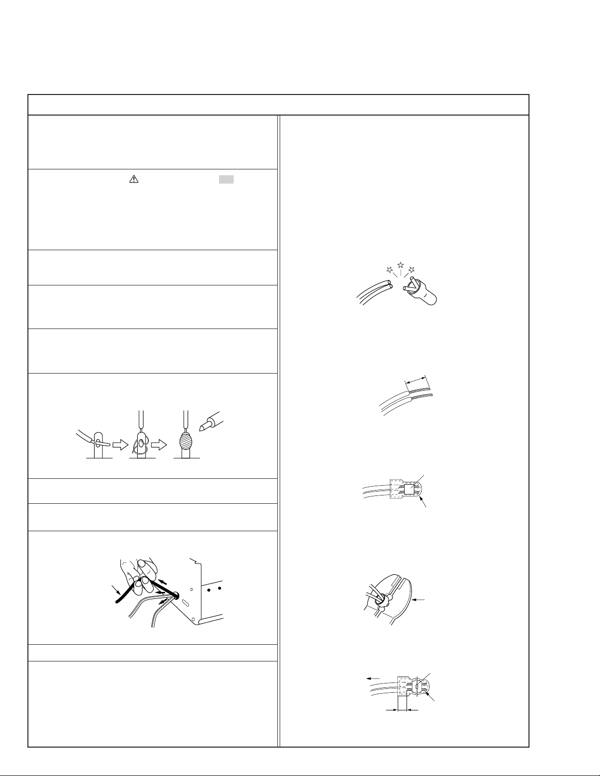
Important Safety Precautions
cut close to connector
Prior to shipment from the factory, JVC products are strictly inspected to conform with the recognized product safety and electrical codes
of the countries in which they are to be sold. However, in order to maintain such compliance, it is equally important to implement the
following precautions when a set is being serviced.
v
Precautions during Servicing
1. Locations requiring special caution are denoted by labels and
inscriptions on the cabinet, chassis and certain parts of the
product. When performing service, be sure to read and comply with these and other cautionary notices appearing in the
operation and service manuals.
2. Parts identified by the symbol and shaded ( ) parts are
critical for safety.
Replace only with specified part numbers.
Note: Parts in this category also include those specified to com-
ply with X-ray emission standards for products using
cathode ray tubes and those specified for compliance
with various regulations regarding spurious radiation
emission.
3. Fuse replacement caution notice.
Caution for continued protection against fire hazard.
Replace only with same type and rated fuse(s) as specified.
4. Use specified internal wiring. Note especially:
1) Wires covered with PVC tubing
2) Double insulated wires
3) High voltage leads
5. Use specified insulating materials for hazardous live parts.
Note especially:
1) Insulation Tape 3) Spacers 5) Barrier
2) PVC tubing 4) Insulation sheets for transistors
6. When replacing AC primary side components (transformers,
power cords, noise blocking capacitors, etc.) wrap ends of
wires securely about the terminals before soldering.
12. Crimp type wire connector
In such cases as when replacing the power transformer in sets
where the connections between the power cord and power
transformer primary lead wires are performed using crimp type
connectors, if replacing the connectors is unavoidable, in order to prevent safety hazards, perform carefully and precisely
according to the following steps.
1) Connector part number : E03830-001
2) Required tool : Connector crimping tool of the proper type
which will not damage insulated parts.
3) Replacement procedure
(1) Remove the old connector by cutting the wires at a point
close to the connector.
Important : Do not reuse a connector (discard it).
Fig.3
(2) Strip about 15 mm of the insulation from the ends of
the wires. If the wires are stranded, twist the strands to
avoid frayed conductors.
15 mm
Fig.1
7. Observe that wires do not contact heat producing parts
(heatsinks, oxide metal film resistors, fusible resistors, etc.)
8. Check that replaced wires do not contact sharp edged or
pointed parts.
9. When a power cord has been replaced, check that 10-15 kg of
force in any direction will not loosen it.
Power cord
Fig.2
10. Also check areas surrounding repaired locations.
11. Products using cathode ray tubes (CRTs)
In regard to such products, the cathode ray tubes themselves,
the high voltage circuits, and related circuits are specified for
compliance with recognized codes pertaining to X-ray emission.
Consequently, when servicing these products, replace the cathode ray tubes and other parts with only the specified parts.
Under no circumstances attempt to modify these circuits.
Unauthorized modification can increase the high voltage value
and cause X-ray emission from the cathode ray tube.
Fig.4
(3) Align the lengths of the wires to be connected. Insert
the wires fully into the connector.
Metal sleeve
Connector
Fig.5
(4) As shown in Fig.6, use the crimping tool to crimp the
metal sleeve at the center position. Be sure to crimp fully
to the complete closure of the tool.
1.25
2.0
5.5
Fig.6
(5) Check the four points noted in Fig.7.
Not easily pulled free
Wire insulation recessed
more than 4 mm
Fig.7
Crimping tool
Crimped at approx. center
of metal sleeve
Conductors extended
1
S40888-01
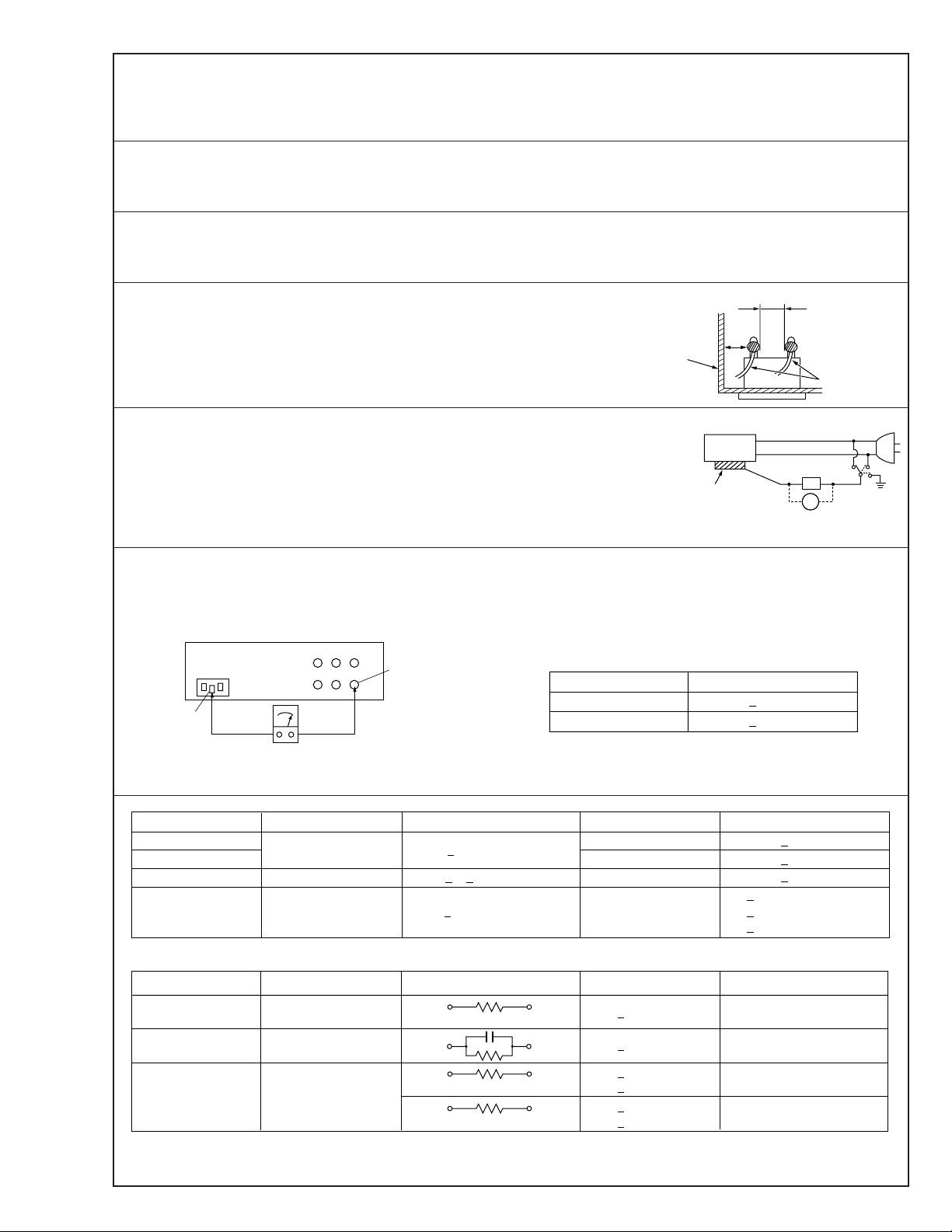
v
d'
d
Chassis
Power cord,
primary wire
Region
USA & Canada
Europe & Australia
Grounding Impedance (Z)
Z 0.1 ohm
Z 0.5 ohm
≤
≤
AC inlet
Earth pin
Exposed accessible part
Milli ohm meter
Grounding Specifications
ab
c
V
Externally
exposed
accessible part
Z
Safety Check after Servicing
Examine the area surrounding the repaired location for damage or deterioration. Observe that screws, parts and wires have been
returned to original positions, Afterwards, perform the following tests and confirm the specified values in order to verify compliance with safety standards.
1. Insulation resistance test
Confirm the specified insulation resistance or greater between power cord plug prongs and
externally exposed parts of the set (RF terminals, antenna terminals, video and audio input
and output terminals, microphone jacks, earphone jacks, etc.). See table 1 below.
2. Dielectric strength test
Confirm specified dielectric strength or greater between power cord plug prongs and exposed
accessible parts of the set (RF terminals, antenna terminals, video and audio input and output
terminals, microphone jacks, earphone jacks, etc.). See table 1 below.
3. Clearance distance
When replacing primary circuit components, confirm specified clearance distance (d), (d’) between soldered terminals, and between terminals and surrounding metallic parts. See table 1
below.
Fig. 8
4. Leakage current test
Confirm specified or lower leakage current between earth ground/power cord plug prongs
and externally exposed accessible parts (RF terminals, antenna terminals, video and audio
input and output terminals, microphone jacks, earphone jacks, etc.).
Measuring Method : (Power ON)
Insert load Z between earth ground/power cord plug prongs and externally exposed accessible parts. Use an AC voltmeter to measure across both terminals of load Z. See figure 9 and
following table 2.
Fig. 9
5. Grounding (Class 1 model only)
Confirm specified or lower grounding impedance between earth pin in AC inlet and externally exposed accessible parts (Video in,
Video out, Audio in, Audio out or Fixing screw etc.).
Measuring Method:
Connect milli ohm meter between earth pin in AC inlet and exposed accessible parts. See figure 10 and grounding specifications.
Fig. 10
AC Line Voltage
100 V
100 to 240 V
110 to 130 V
110 to 130 V
200 to 240 V
Region
Japan
USA & Canada
Europe & Australia R 10 MΩ/500 V DC
Region Load Z
Insulation Resistance (R)
≤
R 1 MΩ/500 V DC
≥≥
1 MΩ R 12 MΩ/500 V DC
≤
Table 1 Specifications for each region
Dielectric Strength
AC 1 kV 1 minute
AC 1.5 kV 1 miute
AC 1 kV 1 minute
AC 3 kV 1 minute
AC 1.5 kV 1 minute
(Class 2)
(Class 1)
Clearance Distance (d), (d')
≤
d, d' 3 mm
≤
d, d' 4 mm
≤
d, d' 3.2 mm
≤
d 4 mm
≤
d' 8 mm (Power cord)
≤
d' 6 mm (Primary wire)
a, b, cLeakage Current (i)AC Line Voltage
100 V
110 to 130 V
110 to 130 V
220 to 240 V
Note: These tables are unofficial and for reference only. Be sure to confirm the precise values for your particular country and locality.
Japan
USA & Canada
Europe & Australia
Table 2 Leakage current specifications for each region
1 kΩ
0.15 µF
1.5 kΩ
2 kΩ
50 kΩ
2
≤
i 1 mA rms Exposed accessible parts
≤
i 0.5 mA rms
≤
i 0.7 mA peak
≤
i 2 mA dc
≤
i 0.7 mA peak
≤
i 2 mA dc
Exposed accessible parts
Antenna earth terminals
Other terminals
S40888-01

SPECIFICATIONS
DVD PART
Power requirements AC 110-240V , 50/60 Hz
Power consumption 20W
Dimensions (approx.) 430 X 97.5 X 360 mm (w/h/d)
Mass (approx.) 5.4 kg
Operating temperature 5˚C to 35˚C (41˚F to 95˚F)
Operating humidity 5 % to 90 %
SYSTEM
Laser Semiconductor laser, wavelength 650 nm
Video Head system Double azimuth 4 heads, helical scanning.
Signal system PAL/NTSC
Frequency response DVD (PCM 96 kHz): 2 Hz to 44 kHz
DVD (PCM 48 kHz): 2 Hz to 22 kHz
CD: 2 Hz to 20 kHz
Signal-to-noise ratio More than 100dB (ANALOG OUT connectors only)
Harmonic distortion Less than 0.008%
Dynamic range More than 95 dB (DVD)
More than 95 dB (CD)
Wow and flutter Less than detected value (±0.001% W PEAK)
INPUT
Audio -6.0dBm, more than 47 kohms
Video 1.0 Vp-p, 75 ohms, unbalanced
OUTPUTS
VIDEO OUT 1 Vp-p 75 ohms, sync negative
COMPONENT VIDEO OUT (Y) 1.0 V (p-p), 75 Ω, negative sync., RCA jack x 1
(Pb)/(Pr) 0.7 V (p-p), 75 Ω, RCA jack x 2
Audio output (digital audio) 0.5 V (p-p), 75 Ω, RCA jack x 1
Audio output (analog audio) 2.0 Vrms (1 KHz, 0 dB), 330 Ω, RCA jack (L, R)
*Design and specifications are subject to change without notice.
1-5

SECTION 2
CABINET & MAIN CHASSIS
CONTENTS
1. EXPLODED VIEWS ................................................................................................................2-2
1. Cabinet and Main Frame Section...........................................................................................2-2
2. Packing Accessory Section ....................................................................................................2-3
2-1
EXPLODED VIEWS
330
452
452
A43
A00
A42
A26
A46
A46A
A49
276
260
285
300
323
457
463
463
457
250
462
462
462
DG601
457
A41
465
467
320
1. Cabinet and Main Frame Section
5
4
3
2
1
A
BCD
2-2
2-3
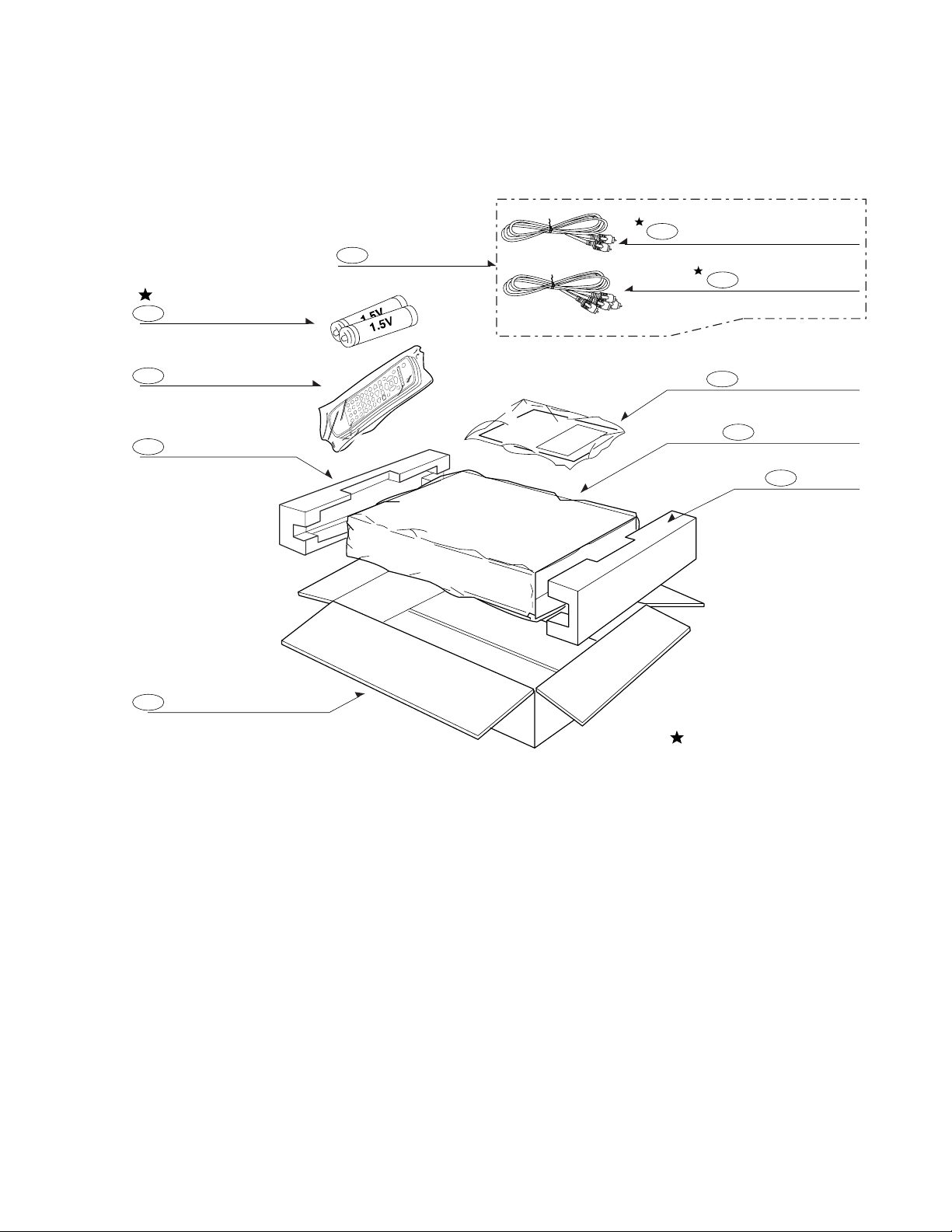
2.Packing Accessory Section
808
BATTERY
900
REMOCON
803
PACKING
810
CABLE SET ASS'Y
811
PLUG ASS'Y 1WAY(YELLO W)
812
PLUG ASS'Y 2WA Y
OWNER'S MANUAL
801
PACKING SHEET
804
803
PACKING
802
BOX CARTONX
OPTIONAL PARTS

SECTION 3
ELECTRICAL
CONTENTS
OVERALL BLOCK DIAGRAM...........................................................................................................................................................3-2
VCR PART
ELECTRICAL ADJUSTMENT PROCEDURES...........................................................................................................................3-3
ELECTRICAL TROUBLESHOOTING GUIDE .............................................................................................................................3-4
1. POWER(SMPS) Circuit.......................................................................................................................................................................3-4
2. SYSTEM/KEY CIRCUIT .......................................................................................................................................................................3-7
3. SERVO CIRCUIT..................................................................................................................................................................................3-8
4. OSD CIRCUIT ....................................................................................................................................................................................3-10
5. Y/C CIRCUIT......................................................................................................................................................................................3-11
6. Hi-Fi CIRCUIT....................................................................................................................................................................................3-15
7. KARAOKE CIRCUIT..........................................................................................................................................................................3-18
BLOCK DIAGRAMS............................................................................................................................................................................3-20
1. Power (SMPS) Block Diagram.........................................................................................................................................................3-20
2. KARAOKE Block DIAGRAM ............................................................................................................................................................3-22
3. Y/C Block Diagram ...........................................................................................................................................................................3-24
4. NORMAL AUDIO Block Diagram .....................................................................................................................................................3-26
5. Hi-Fi Block Diagram(Hi-Fi PART) ....................................................................................................................................................3-28
6. SYSTEM Block Diagram...................................................................................................................................................................3-30
CIRCUIT DIAGRAMS..........................................................................................................................................................................3-32
1. Power (SMPS) Circuit Diagram .......................................................................................................................................................3-32
2. KARAOKE Circuit Diagram..............................................................................................................................................................3-34
3. A/V Circuit Diagram..........................................................................................................................................................................3-36
4. Hi-Fi Circuit Diagram ........................................................................................................................................................................3-38
5. SYSTEM Circuit Diagram.................................................................................................................................................................3-40
• WAVEFORMS ......................................................................................................................................................................................3-42
• CIRCUIT VOLTAGE CHART ...............................................................................................................................................................3-44
PRINTED CIRCUIT DIAGRAMS.....................................................................................................................................................3-46
1. MAIN P.C.BOARD..............................................................................................................................................................................3-46
2. KARAOKE P.C.BOARD.....................................................................................................................................................................3-48
3 KEY P.C.BOARD................................................................................................................................................................................3-48
4. CLOCK P.C.BOARD ..........................................................................................................................................................................3-49
DVD PART
ELECTRICAL TROUBLESHOOTING GUIDE
1. µ-COM CIRCUIT................................................................................................................................................................................3-50
2. MPEG CIRCUIT.................................................................................................................................................................................3-53
3. RF/Servo CIRCUIT ............................................................................................................................................................................3-54
BLOCK DIAGRAMS............................................................................................................................................................................3-58
1. DVD Overall BLOCK DIAGRAM.......................................................................................................................................................3-58
2. RF/CD DSP/DVD DSP/DVD SERVO BLOCK DIAGRAM .................................................................................................................3-59
3. Audio BLOCK DIAGRAM .................................................................................................................................................................3-60
4. MPEG BLOCK DIAGRAM.................................................................................................................................................................3-61
CIRCUIT DIAGRAMS..........................................................................................................................................................................3-62
1. DVD DSP CIRCUIT DIAGRAM..........................................................................................................................................................3-62
2. DRIVE & RF CIRCUIT DIAGRAM.....................................................................................................................................................3-64
3. MPEG CIRCUIT DIAGRAM ...............................................................................................................................................................3-66
4. Audio DM CIRCUIT DIAGRAM .........................................................................................................................................................3-68
5. MEMORY CIRCUIT DIAGRAM ..........................................................................................................................................................3-70
6. SCART(JACK) CIRCUIT DIAGRAM.................................................................................................................................................3-72
• WAVEFORMS ......................................................................................................................................................................................3-74
• CIRCUIT VOLTAGE CHART ...............................................................................................................................................................3-76
PRINTED CIRCUIT DIAGRAMS.....................................................................................................................................................3-80
1. MAIN P.C.BOARD (TOP VIEW) .........................................................................................................................................................3-80
1. MAIN P.C.BOARD (BOTTOM VIEW)................................................................................................................................................3-82
...........................................................................................................................3-50
3-1
ELECTRICAL ADJUSTMENT PROCEDURES
1. Servo Adjustment
1) PG Adjustment
• Test Equipment
VCR PART
a) OSCILLOSCOPE
b) NTSC MODEL : NTSC SP TEST TAPE
C) PALMODEL : PAL SP TEST TAPE
• Adjustment And Specification
MODE
PLAY
MEASUREMENT POINT ADJUSTMENT POINT SPECIFICATION
V.Out
H/SW(W373, W374)
R/C TRK JIG KEY 6.5 ± 0.5H
• Adjustment Procedure
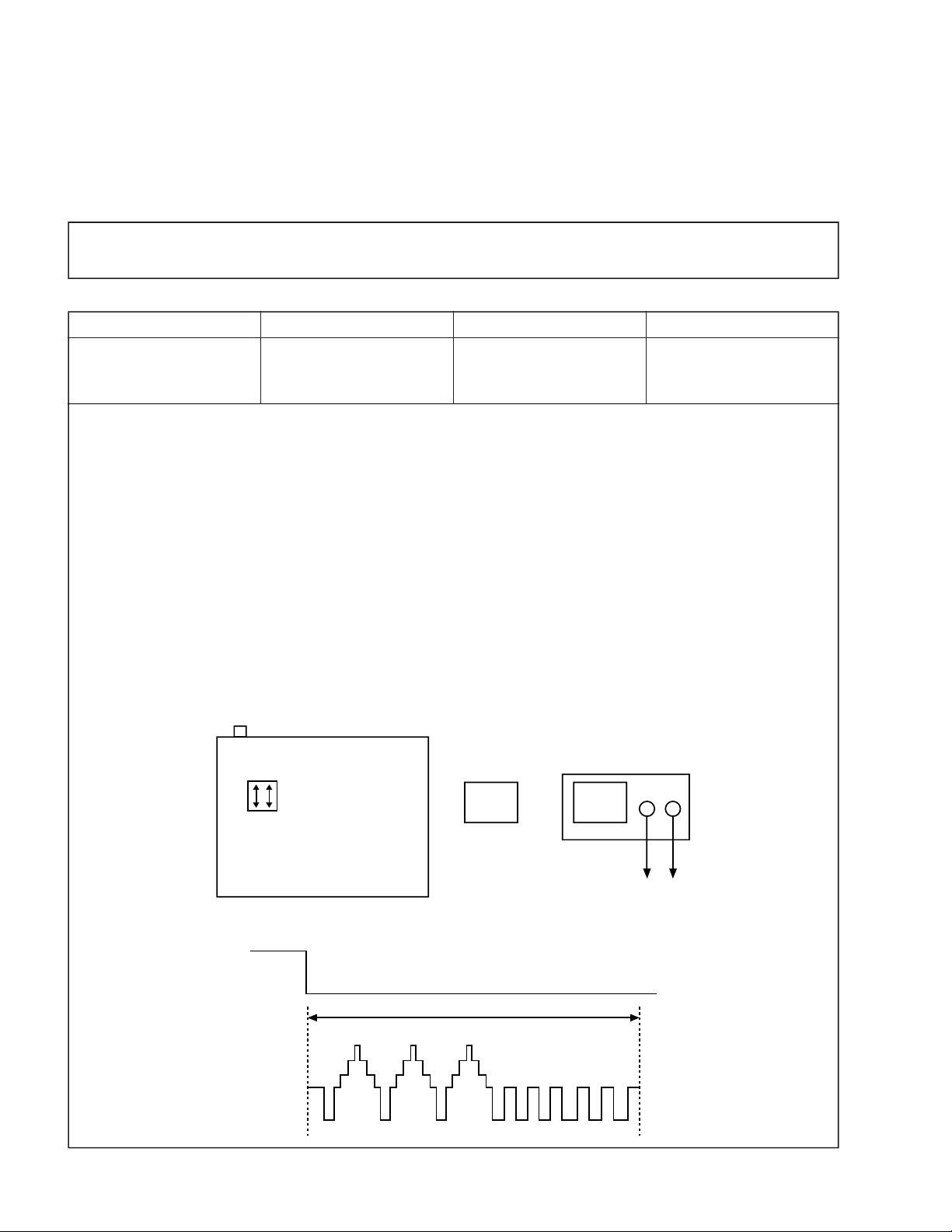
a) Insert the SP Test Tape and play.
Note - Adjust the distance of X, pressing the Tracking(+) or Tracking(-) when the “ATR” is b link after the
SP Test Tape is inser ted.
b) Connect the CH1 of the oscilloscope to the H/SW(W373, W374) and CH2 to the Video Out f or the VCR.
c) Trigger the mixed Combo Video Signal of CH2 to the CH1 H/SW(W373, W374), and then check the dis-
tance (time difference), which is from the selected A(B) Head point of the H/SW(W373, W374) signal to
the starting point of the vertical synchronized signal, to 6.5H ± 0.5H (412µs, 1H=63µs).
• PG Adjustment Procedure
a) Payback the SP standard tape
b) Press the “1” key on the Remote controller and the “PLAY” key on the Front Panel the same time, then
it goes in to Tracking initial mode. (Note: NTSC Model : “1” key and PAL Model “0” key on Remote con-
troller)
c) Repeat the above step(No.2), then it finishes the PG adjusting automatically.
d) Stop the playback, then it goes out to PG adjusting mode after mony the PG data.
• CONNECTION
V .Out
• WAVEFORM
H/SW(W373,W374)
H/SW
Composite
VIDEO
6.5H(416us)
3-3
R/C KEY
OSCILLOSCOPE
CH1 CH2
H/SW
(W373, W374)
V.out
3-4
ELECTRICAL TROUBLESHOOTING GUIDE
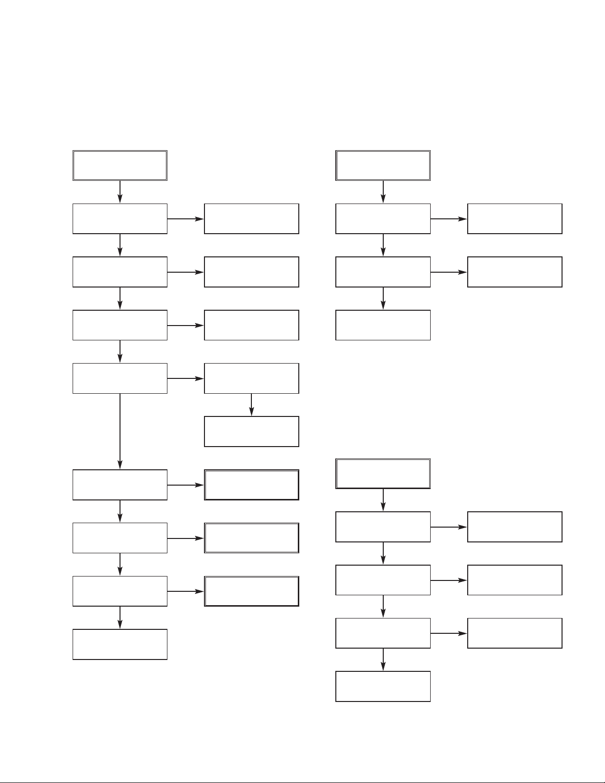
1. Power(SMPS) CIRCUIT
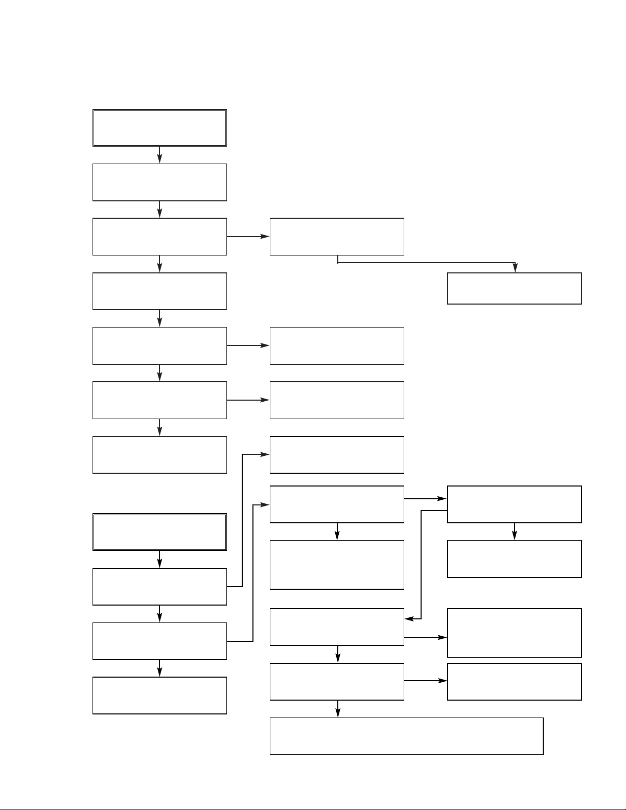
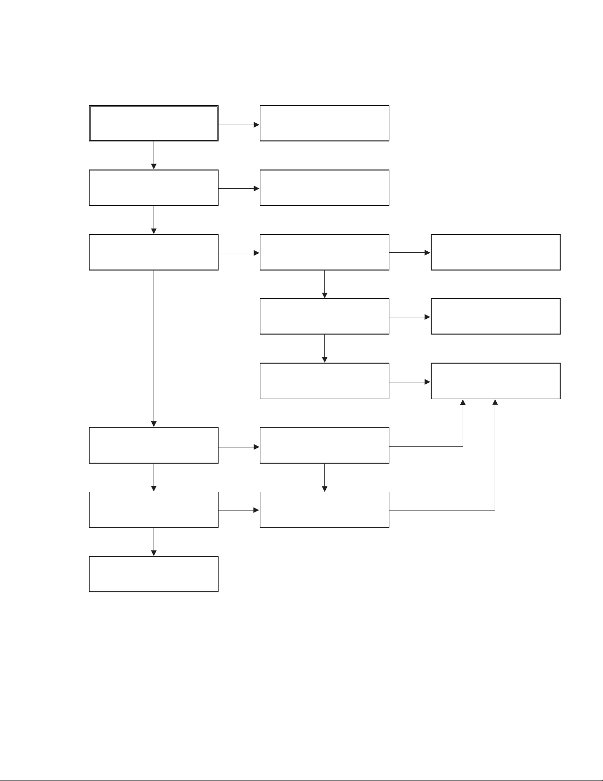
NO 5.3VA.
Replace the F101.
(Use the same Fuse)
Is the F101 normal?
Is the R101
normal?
Is the BD101
normal?
NO
NO
NO
NO
NO
NO
NO
Replace the
BD101.
Replace the R101.
Is the D102
normal?
Check or Replace
the D102.
Replace the D112.
Replace the IC102.
Replace the D110.
YES
YES
YES
YES
YES
YES
YES
YES
Is Vcc(8.5~21V) supplied to IC101 Pin7?
NO
Is the D112 nor mal?
Is there about 2.5V
at the IC102 Vref?
Is the D110 nor mal?
Check the Main PCB
5.3VA/5.0V Line short?
(1) No 5.3VA (SYS/Hi-Fi/TUNER)
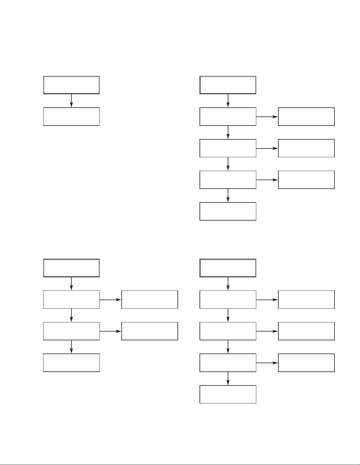
NO 12VA.
Check or Replace
the D110.
Is the Vcc(13V) supplied to (+)
terminal in D115 and D117?
Check or Replace
the Motor Vcc.
Is the Vcc(12V) supplied to (-)
terminal in D115 and D117?
NO
NO
Replace the D115,
D117.
YES
YES
YES
(2) No 12VA (TO CAP, DRUM MOTOR)
NO 5.2VA.
5.3VA Line Check.
Is 5.3VA put into
the Q116 Emitter?
Is about 5V put into
the Q116 Base?
Is the Q115 Base
“H”?
NO
NO
Check the Power
Control.
NO
Check or Replace the Q115,
R160, R161, R162, D122.
YES
YES
YES
Check or Replace
the Q115/Q116
YES
(3) No 5.2V (SYS/Hi-Fi/TUNER)

(4) No 5V (TO DVD)
(5) No REG 5V (AVCP)
NO 5V.
YES
Is 5.3VA put into
the Q113 Emitter?
YES
Is the Q115 Base
“H”?
YES
Is about 5V put into
the Q113 Base?
YES
Check or Replace
the Q113/Q115
(6) No 33V (TUNER)
NO
NO
NO
5.3VA Line Check.
Check the Power
Control.
Check or Replace the Q115,
R157, R158, R159, D121.
No REG 5V.
YES
Is 5.3VA put into the
Q117 Collector?
YES
Is 33V put into the
Q117 Base?
YES
Check or Replace the Q117,
R167, ZD105, C162.
(7) No REG 12V
NO
NO
5.3VA Line Check.
Check 33V Line.
No 33V.
YES
Is Q115 Base “H”?
YES
Check or Replace
Q114, R154, R155.
NO
Check the Power
Control.
No REG 12V.
YES
Is 13V put into the
Q112 Collector?
YES
Is 33V put into the
Q112 Base?
YES
Check or Replace the Q112,
ZD103, R153, C151.
NO
NO
Check or Replace
D110.
Check 33V Line.
3-5
3-6
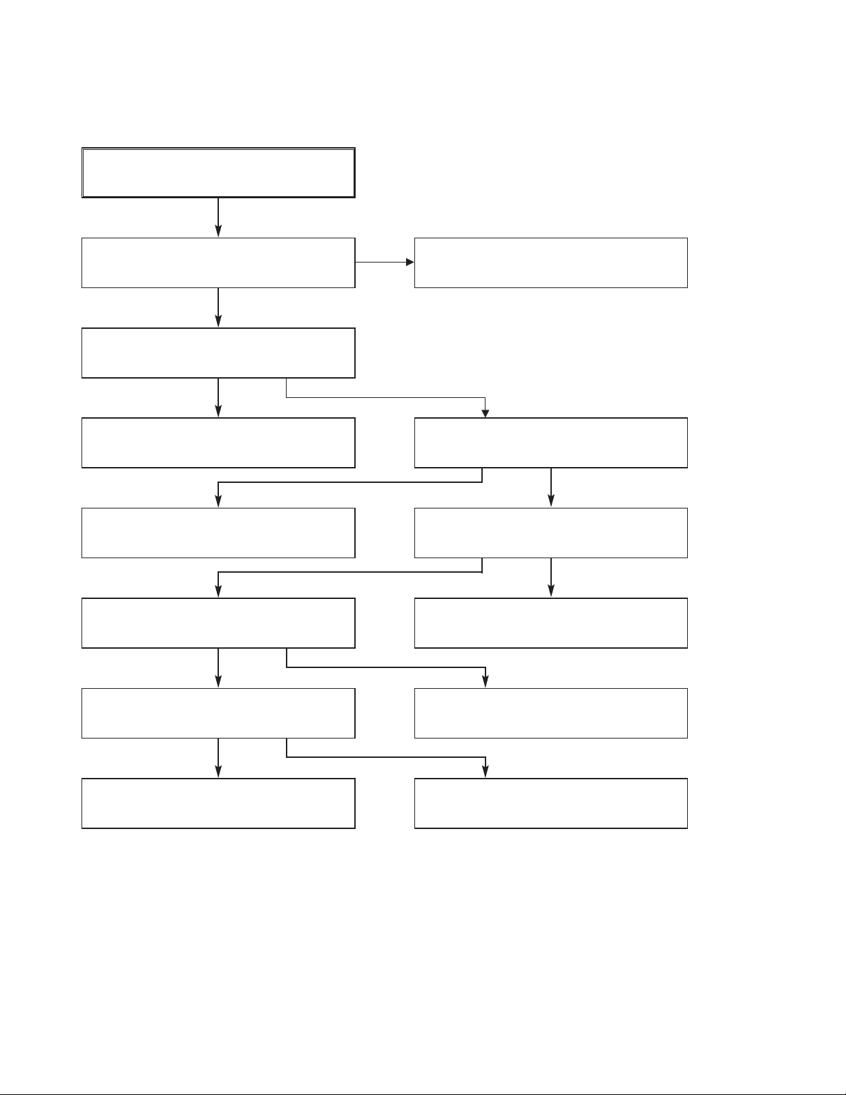
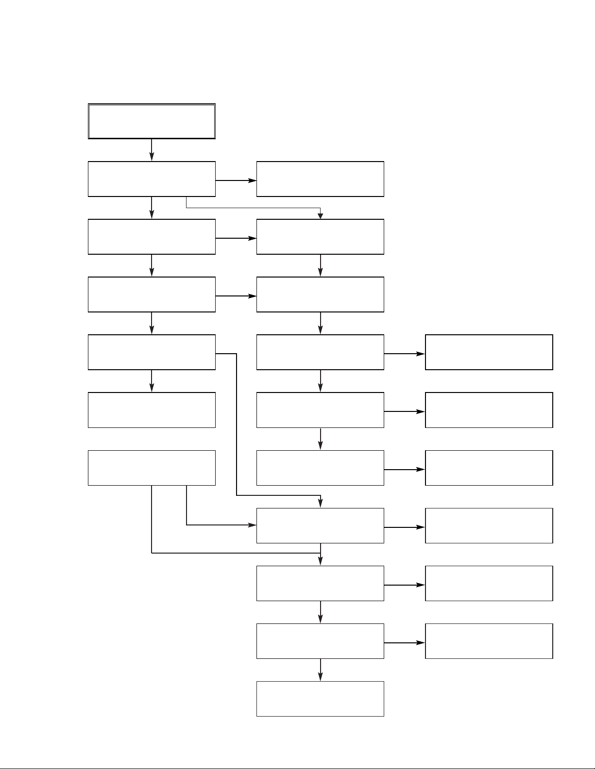
NO -29VA.
Check or Replace
D108.
YES
(8) No -29VA
NO 8VA.
Check or Replace
the D110.
Is Vcc(13V) supplied to
(+) terminal in D114?
Is the Q115 Base
“H”?
Is Vcc(12V) supplied
to IC106 Pin1?
NO
NO
Check or Replace
the D114.
NO
Check the Power
Control.
YES
YES
YES
Check or Replace
IC106, R170, C154.
YES
(9) No 8VA
NO 3.3VA.
Is Vcc(4V) supplied
to IC103 Pin1?
YES
Is the Q115 Base
“H”?
YES
Check or Replace
IC103, R156, C153.
YES
(10) No 3.3V
Check or Replace
the D111.
NO
NO
Check the Power
Control.
NO 2.5VA.
Is Vcc(4V) supplied
to IC104 Pin1?
YES
Is the Q115 Base
“H”?
YES
Is Vcc(3.3V) supplied
to IC104 Pin2?
YES
Check or Replace
D119, C159.
YES
(11) No 2.5V
Check or Replace
the D111.
NO
NO
Check the Power
Control.
NO
Check or Replace
the IC104.
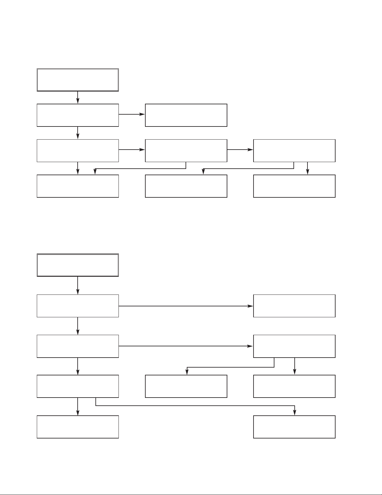
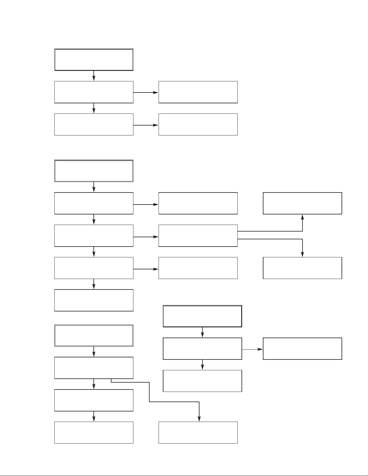
2. SYSTEM/KEY CIRCUIT
(1) AUTO STOP
Auto Stop
YES
Does the SW30 wavefor m
appear at the IC501
Pin24?
YES
Do the T-UP Reel Pulses
appear at the IC501 Pin4?
YES
Replace the IC501.
NO
NO NO
Check the Drum Motor
signal.
Do T/UP Reel Pulses
appear at the Q514
Base terminal ?
YES YES
Replace the T/UP Reel
Sensor (RS501).
(2) The unstable loading of a Cassette tape
The unstable loading of a
Cassette tape
YES
Does 5.2V appear at the
RS501?
NO
Check the Q116 Power
Circuit.
Is 12V applied to the
PMC01 Pin8?
YES
Does the “H” signal appear
at the IC501 Pin57 during
inserting the CST ?
YES
Does the “L” signal appear
at the IC501 Pin19 during
inserting the CST?
YES
Check the Deck
Mechanism.
Caution :
Auto stop can occur because Grease or Oil is dried up
NO
NO
NO
Check the CST SW and
the peripheral circuitry.
3-7
Refer to “SMPS DRUM
12 Volt Trouble Shooting”.
Is 5.3V applied to the
R544 ?
YES
Refer to SMPS 5.3VA
troubleshooting.
Check the IC501
Pins74, 75, 76, 77.
NO
3. SERVO CIRCUIT
(1) Unstable Video in PB MODE
Unstable Video in
PB Mode.
YES
Does the Noise level of the
screen change
periodically?
YES
Do the CTL pulses appear
at the IC501 Pin37?
YES
Does the CFG wavefor m
appear at the IC501
Pin40?
YES
On tracking do the CTL
pulses move?
YES
Does the Video Envelope
wavefor m appear at the
IC501 Pin12?
YES
Replace the IC501.
(2) When the Drum Motor
(2) doesn’t run.
When the Drum Motor
doesn’t run,
Does 12V appear at the
PMC01 Pin8?
NO
NO
NO
NO
Is adjusting the height of
the CTL Head accurate?
Replace the IC501.
Refer to “When the Y signal
doesn’t appear on the
screen in PB Mode”.
Refer to “(2)
No 12VA of Power section”
Do the Drum PWM Pulses
appear at the IC501
Pin26?
YES
Aren’t the foil patterns and
the Components between
IC501 Pin26 and PMC01
Pin12 short?
NO
Readjust the height of the
CTL Head.
NO
Do the DFG Pulses appear
at the PMC01 Pin11?
YES
NO
Replace the Cap M.
YES
Does 2.8V appear at the
PMC01 Pin12?
YES
Check the connector
(PMC01) and the Drum
Motor Ass’y.
NO
Do the DFG Pulses appear
at the IC501 Pin38?
YES
Do the Drum PWM Pulses
appear at the IC501
Pin26?
YES
Aren’t the connecting patterns and the Components
between IC501 Pin26 and PMC01 Pin11 short?
3-8
NO
NO
Aren’t the foil patterns and
the Components between
IC501 Pin 38 and PMC01
Pin11 short?
Replace the IC501.
2. SERVO CIRCUIT
(3) When the Capstan Motor doesn’t run,
When the Capstan Motor doesn’t run,
Does 12VA appear at the PMC01?
YES
Does 2.8V appear at the PMC01?
YES
Check the PMC01 and the Capstan
Motor Ass’y.
Aren’t the foil patterns and Components
between IC501 Pin 25 and PMC01
Pin9 short?
Does the CFG signal come into the
IC501 Pin40?
NO
NO
YES
YES
Refer to “SMPS(CAPSTAN/12Volt)
Trouble Shooting”.
Does the PWM signal appear at the
IC501 Pin25?
NO
Does the CFG signal appear at the
PMC01 Pin1?
NO
Check the Capstan Motor Ass’y.
YES
Does the Capstan PWM signal appear at
the IC501 Pin25?
YES
Aren’t the foil patterns and Components
between IC501 Pin25 and PMC01
Pin9 short?
NO
Aren’t the foil patterns and component
between IC501 Pin40 and PMC01
Pin1 short?
NO
Replace the IC501.
3-9
(3) KEY doesn’t working
KEY doesn’t working.
Is 5V applied to the IC501
Pin 15?
YES
Does LED or FLD change
when a function button is
pressed?
4. OSD CIRCUIT
(1) No OSD display.
No OSD display.
Is 5.3V applied to the
IC501 Pin42?
YES
Does oscillation occur at
the IC501 Pins52, 53?
YES
Does oscillation occur at
the IC501 Pins50, 51?
YES
Replace the IC501.
NO
NO
NO
NO
NO
Refer to “SMPS 5.3VA
Trouble Shooting”.
Replace the defective
switches.
Refer to “SMPS 5.3VA
Trouble Shooting”.
Is the oscillation input to
Q501 base?
Check or Replace the
Peripheral Circuitry. (L506,
R517, C519, C518, R518)
2
C BUS CHECK
(3) I
Check whether X301
oscillates
NO
YES
Check or Replace the
Peripheral Circuitry. (L506,
R517, C519, C518, R518)
(2) No F.OSD display.
No F.OSD display.
Refer to “(1) No OSD
display”.
YES
Does the C.SYNC signal
appear at the IC501 Pin87?
YES
Replace the IC501.
NO
The I2C waves don’t
come out.
Does Power appear at the
Pull up impedence
(R508, R510)?
YES
Replace the IC501.
Refer to “AVCP. C. Sync.
Trouble shooting”.
3-10
NO
Refer to “SMPS 5.3VA
Trouble Shooting”.
5. Y/C CIRCUIT
(1) No Video in EE Mode,
No Video in EE Mode
Does the Video signal
appear at the IC301
Pins28, 30, 31?
YES
Is 5.2V applied to the IC301
Pins12, 36, 61, 67, 90, 96?
YES
Does the Video signal
appear at the IC301 Pin52?
YES
Does the Video signal
appear at the IC501 Pin 45?
YES
Does the Video signal
appear at the Emitter
terminal of the Q801?
NO
NO
NO
NO
NO
Check DVD Video Input (IC802, Pin29), Tuner Video Input
(TU701 Pin24), Line Video Input (JK801), respectively.
Check the REG 5V Line.
(Power Circuit)
Is I2C BUS signal applied to
the IC301 Pins 62, 63?
YES
Check the path of the signal between the IC301 Pin
52 and IC501 Pins 43,45.
Is there 12V on the plus
terminal of the C822?
YES
NO
NO
Check the System Circuit.
(Refer to ‘SYSTEM I2C BUS
CHECK Trouble Shooting’)
Check C330. (AGC)
Replace the IC301.
YES
Replace the Q801.
3-11
Check the REG 12V Line.
(Power Circuit)
3. Y/C CIRCUIT
(2) When the Y(Luminance) signal doesn’t appear on the screen in PB Mode,
Is 5V applied to the IC301
Pins12, 36, 61, 67, 90, 96?
YES
Is the I2C Bus siganl applied
to the IC301 Pins62, 63?
YES
Does the normal RF signal
appear at the IC301 Pin79?
YES
NO
NO
NO
Check the line of the REG
5V Line. (Power Circuit)
Refer to ‘SYSTEM I2C BUS
CHECK Trouble Shooting’.
Is the V.H.S/W signal
applied to the IC301 Pin81?
YES
Does the Rectangular
wavefor m(5V) appear at
the IC301 Pin81(V.H.S/W)
YES
Clean the Drum.
NO
NO
NO
Check the System Circuit.
(IC501 Pin24)
Check the V.H.S/W level.
Replace the IC301.
Does the Y(Luminance)
signal appear at the IC301
Pin18?
YES
Is the Y(Luminance) Video
wavefor m showed up at the
IC301 Pin39?
YES
Replace the IC301.
NO
NO
Check the path of the
Y(Luminance) signal.
Check the path of the
Y(Luminance) signal.
YES
YES
3-12

3. Y/C CIRCUIT
(3) When the C(Color) signal doesn’t appear on the screen in PB Mode,
Is 5V applied to the IC301
Pins12, 36, 61, 67, 90, 96?
YES
Does the Color signal
appear at the IC301
Pins58, 60?
YES
Replace the IC301.
NO
NO
Check the line of the REG
5V Line. (Power Circuit)
Does the X301(3.58MHZ)
oscillate?
Does the Color signal
appear at the IC301 Pin55?
Check the circuit of the
IC301 Pins60, 58, 35.
NO
NO
YES
Replace the X301.
Check the Color Pass.
(Check the C341)
Replace the IC301.
3-13
3. Y/C CIRCUIT
(4) When the Video signal doesn’t appear on the screen in REC Mode,
REC mode
YES
Is EE mode normal?
YES
Is brightness ?
YES
Is the brightness signal supplied to IC301 Pins13,14?
YES
Check the power of Pins12,
36, 61, 67, 90, 96.
YES
Check the REG 5V power
NO
YES
NO
NO
NO
Check the EE mode
Is color ?
NO
Does signal appear at
IC301 Pins58, 60?
YES
Is 5V supplied to IC301
Pins12, 36, 61, 90, 96?
YES
Is I2C Bus applied to
IC301 Pins62, 63?
YES
NO
NO
Check the 5V power
Check system part
Does the brightness signal
appear at IC301 Pins21, 26?
YES NO
Do X301, 302 and X-TAL
oscillate?
Is I2C Bus applied to IC301
Pins62, 63?
YES
Is V.H SW supplied to
IC301 Pin81?
YES
Does the FM signal appear
at IC301 Pins87, 88(SP)/
92, 93(EP)?
YES
Check the drum
3-14
NO
NO
NO
NO
Check X301, 302
Check system part
Check system part
(V.H/SW)
Replace the IC301.
*OPTION
Pins86, 87, 88, 89(SP)
Pins91, 92, 93, 94(EP)

6. Hi-Fi CIRCUIT
(A) No Sound(EE Mode)
No Sound.
YES
Check the DVD Audio of IC801
Pins4, 5.
Check the AV1 Audio of IC801
Pins6, 7.
Check the Vcc of IC801 Pins34, 40,
IC802 Pin4.
YES
Check the IIC Clock and DATA at
IC801 Pins42, 43, IC802 Pins32, 33.
YES
Check the Audio of IC801 Pins16, 17.
YES
NO
NO
YES
NO
NO
NO
Check the DVD MODULE.
(P8D01 Pins3, 5).
Check the Rear Jack.
(JK801 Audio in).
Check the Power 5.2V, 12V.
Check the IC501 Pins90, 91.
Replace IC801.
Check the Audio of IC802 Pins22, 26.
YES
Check the Audio of IC401
Pins26, 27(input), 28, 29(output).
YES
Check the Audio of IC405
Pins3, 5(input), 1, 7(output).
YES
Check the JK801.
NO
Replace IC802.
NO
Replace IC401.
NO
Replace IC405.
3-15
 Loading...