

Page 1
SERVICE MANUAL
/
VIDEO CASSETTE RECORDER
TV
– –:– –
TV/VCR
AUDIO
3
12
2
4
65
DAILY/QTDN.
VPS/PDC
WEEKLY/HEBDO
8
9
7
AUX
4
0000
0
STOP
START
DATE
PR
FIN
DEBUT
EXPRESS
?
30 SEC
1
PROG
E
N
T
E
R
/
E
N
T
R
E
E
3
U
O
N
K
E
M
P
V
R
T
+
T
+
V
V
–
T
–
T
V
R
P
SAT
VCR
SAT
REVIEW
24H EXPRESS
/
PR
1
33
PUSH / TURN
2
PAL
SPECIFICATIONS
(The specifications shown pertain specifically to the model HR-J785EK)
g e n e r a l
Power requirement : AC 220 V – 240 V
, 50 Hz/60 Hz
Ó
Power consumption : on : 16 W, off : 4.0 W
Operating Temperature : 5°C to 40°C
Storage Temperature : –20°C to 60°C
Operating position : Horizontal only
Dimensions (WxHxD) : 400 mm x 94 mm x 278 mm
Weight : 3.4 kg
Format : VHS PAL standard
Maximum recording time
(SP) : 240 min. with E-240 video cassette
(LP) : 480 min. with E-240 video cassette
v i d e o / a u d i o
Signal system : PAL-type colour signal and CCIR monochrome signal,
625 lines/50 fields
Recording system : DA4 (Double Azimuth) helical scan system
Signal-to-noise ratio : 45 dB
Horizontal resolution : 250 lines
Frequency range : 70 Hz to 10,000 Hz (Normal audio)
20 Hz to 20,000 Hz (Hi-Fi audio)
Input/Output :
21-pin SCART connectors (IN/OUT x 1, IN/DECODER x 1)
RCA connectors (AUDIO OUT x 1)
This service manual is printed on 100% recycled paper.
COPYRIGHT © 2001 VICTOR COMPANY OF JAPAN, LTD.
t u n e r
TV channel storage capacity
t i m e r
: 99 positions (+AUX position)
Tuning system : Frequency synthesized tuner
Channel coverage : VHF 44.5 MHz – 143 MHz/
143 MHz – 470 MHz/
UHF 470 MHz – 862 MHz
Aerial output : UHF channels 22 – 69 (Adjustable)
Memory backup time : Approx. 10 min.
a c c e s s o r i e s
Provided accessories : RF cable, Satellite Controller,
Infrared remote control unit,
‘AA’ battery x 2
Specifications shown are for SP mode unless otherwise specified.
E.& O.E. Design and specifications subject to change without notice.
No. 82847
January 2001
Page 2

TABLE OF CONTENTS
Section Title Page Section Title Page
Important Safety Precautions
INSTRUCTIONS
1. DISASSEMBLY
1.1 Disassembly flow chart......................................................... 1-1
1.2 How to read the disassembly and assembly ........................ 1-1
1.3 Disassembly/assembly method............................................ 1-1
1.4 Service position .................................................................... 1-4
1.4.1 How to set the “Service position”..................................... 1-4
1.5 Mechanism service mode..................................................... 1-4
1.5.1 How to set the “Mechanism service mode” ..................... 1-4
1.6 Jig RCU mode ....................................................................... 1-4
1.6.1 Setting the Jig RCU mode............................................... 1-4
1.6.2 Setting the User RCU mode ............................................ 1-4
1.7 Emergency display function ................................................. 1-5
1.7.1 Displaying the EMG information...................................... 1-5
1.7.2 Clearing the EMG history ................................................ 1-5
1.7.3 EMG content description ................................................. 1-6
1.7.4 EMG detail information <1>............................................. 1-7
1.7.5 EMG detail information <2>............................................. 1-8
2. MECHANISM ADJUSTMENT
2.1 Before starting repair and adjustment ................................... 2-1
2.1.1 Precautions ..................................................................... 2-1
2.1.2 Checking for proper mechanical operations.................... 2-1
2.1.3 Manually removing the cassette tape.............................. 2-1
2.1.4 Jigs and tools required for adjustment ............................ 2-2
2.1.5 Maintenance and inspection............................................ 2-3
2.2 Replacement of major parts ................................................. 2-6
2.2.1 Before starting disassembling (Phase matching between
mechanical parts) ............................................................ 2-6
2.2.2 How to set the “Mechanism assembling mode” .............. 2-6
2.2.3 Cassette holder assembly ............................................... 2-6
2.2.4 Pinch roller arm assembly ............................................... 2-8
2.2.5 Guide arm assembly and press lever assembly.............. 2-8
2.2.6 A/C head ......................................................................... 2-8
2.2.7 Loading motor ................................................................. 2-8
2.2.8 Capstan motor................................................................. 2-9
2.2.9 Pole base assembly (supply or take-up side).................. 2-9
2.2.10 Rotary encoder ........................................................... 2-10
2.2.11 Clutch unit................................................................... 2-10
2.2.12 Change lever assembly, direct gear, clutch gear and
coupling gear .............................................................. 2-10
2.2.13 Link lever .....................................................................2-11
2.2.14 Cassette gear, control cam and worm gear.................2-11
2.2.15 Control plate ................................................................2-11
2.2.16 Loading arm gear (supply or take-up side) and
loading arm gear shaft ................................................ 2-12
2.2.17 Take-up lever, take-up head and control plate guide .. 2-13
2.2.18 Capstan brake assembly ............................................ 2-13
2.2.19 Sub brake assembly (take-up side) ............................ 2-13
Main brake assembly (take-up side), reel disk (take-up side)
2.2.20
and main brake assembly (supply side) ................................
2-13
2.2.21 Tension brake assembly, reel disk (supply side) and
tension arm assembly................................................. 2-14
2.2.22 Idler lever, idler arm assembly .................................... 2-14
2.2.23 Stator assembly .......................................................... 2-14
2.2.24 Rotor assembly........................................................... 2-14
2.2.25 Upper drum assembly................................................. 2-15
2.3 Compatibility adjustment .................................................... 2-16
2.3.1 FM waveform linearity ................................................... 2-16
2.3.2 Height and tilt of the A/C head....................................... 2-17
2.3.3 A/C head phase (X-value) ............................................. 2-17
2.3.4 Standard tracking preset ............................................... 2-18
2.3.5 Tension pole position ..................................................... 2-18
3. ELECTRICAL ADJUSTMENT
3.1 Precaution ............................................................................ 3-1
3.1.1 Required test equipments ............................................... 3-1
3.1.2 Required adjustment tools............................................... 3-1
3.1.3 Color (colour) bar signal, color (colour) bar pattern......... 3-1
3.1.4 Switch settings and standard precautions....................... 3-1
3.2 Servo circuit.......................................................................... 3-2
3.2.1 Switching point ................................................................ 3-2
3.2.2 Slow tracking preset ........................................................ 3-2
3.3 Video circuit.......................................................................... 3-2
3.3.1 Auto picture initial setting ................................................ 3-2
3.4 Syscon circuit [HR-J680EU/J780EU] ................................... 3-2
3.4.1 Timer clock ...................................................................... 3-2
4. CHARTS AND DIAGRAMS
NOTES OF SCHEMATIC DIAGRAM .......................................... 4-1
CIRCUIT BOARD NOTES ........................................................... 4-2
4.1 BOARD INTERCONNECTIONS .......................................... 4-3
4.2 MAIN(VIDEO/AUDIO) SCHEMATIC DIAGRAM ................... 4-5
4.3 MAIN(ON SCREEN) SCHEMATIC DIAGRAM ..................... 4-7
4.4 MAIN(SYSCON) SCHEMATIC DIAGRAM ........................... 4-9
4.5 MAIN(SW.REG) SCHEMATIC DIAGRAM ...........................4-11
4.6 MAIN(TUNER) SCHEMATIC DIAGRAM ............................ 4-13
4.7 MAIN(FRONT) AND ADV.JOG SCHEMATIC DIAGRAMS. 4-15
4.8 MAIN(TERMINAL), SAT CTL AND R.PAUSE SCHEMATIC
DIAGRAMS ........................................................................ 4-17
4.9 REMOTE CONTROLLER SCHEMATIC DIAGRAM ........... 4-19
4.10 MAIN, SAT CTL AND R.PAUSE CIRCUIT BOARDS ....... 4-21
4.11 FDP GRID ASSIGNMENT AND ANODE CONNECTION 4-23
4.12 WAVEFORMS.................................................................. 4-24
4.13 VOLTAGE CHARTS......................................................... 4-25
4.14 CPU PIN FUNCTION....................................................... 4-26
4.15 SYSTEM CONTROL BLOCK DIAGRAM......................... 4-27
4.16 VIDEO BLOCK DIAGRAM............................................... 4-29
4.17 AUDIO BLOCK DIAGRAM .............................................. 4-31
5. PARTS LIST
5.1 PACKING AND ACCESSORY ASSEMBLY <M1> ............... 5-1
5.2 FINAL ASSEMBLY <M2> .................................................... 5-2
5.3 MECHANISM ASSEMBLY <M4> ........................................ 5-4
5.4 ELECTRICAL PARTS LIST .................................................. 5-6
MAIN BOARD ASSEMBLY <03>............................................... 5-6
A/C HEAD BOARD ASSEMBLY <12>..................................... 5-13
ADV.JOG BOARD ASSEMBLY(HR-J780EU/J785EK) <38>... 5-13
LOADING MOTOR BOARD ASSEMBLY <55> ....................... 5-13
R.PAUSE BOARD ASSEMBLY(HR-J780EU)<91> ................. 5-13
SAT_CTL BOARD ASSEMBLY <92> ...................................... 5-13
The following table lists the differing points between Models ( HR-J680EK, HR-J680EU, HR-J780EU and HR-J785EK) in this series.
HR-J680EK HR-J680EU HR-J780EU HR-J785EK
JOG/SHUTTLE NOT USED NOT USED USED USED
VIDEO SYSTEM PAL PAL/MESECAM(MANUAL) PAL/MESECAM(MANUAL) PAL
BROADCASTING STANDARD I B/G,D/K B/G,D/K I
STEREO DECODER NICAM NICAM/A2 NICAM/A2 NICAM
RF OUT SYSTEM [INITIAL] I G,K G,K I
VCR PLUS+ VIDEOPLUS+ DELUXE SHOWVIEW DELUXE SHOWVIEW DELUXE VIDEOPLUS+ DELUXE
LANGUAGE [INITIAL] (ON SCREEN DISPLAY)
AUDIO DUBBING/OPERATION NOT USED NOT USED USED/BUTTON NOT USED
FRONT VIDEO/AUDIO IN NOT USED NOT USED USED NOT USED
WINDOW COLOR SMOKE LIGHT GRAY SMOKE LIGHT GRAY BLUE SMOKE LIGHT GRAY
REMOTE PAUSE NOT USED NOT USED USED NOT USED
CABLE MOUSE PROVIDED OPTION OPTION PROVIDED
ENG 13LANG.[ENG] 13LANG.[ENG] ENG
Page 3
Important Safety Precautions
Prior to shipment from the factory, JVC products are strictly inspected to conform with the recognized product safety and electrical codes of the
countries in which they are to be sold. However, in order to maintain such compliance, it is equally important to implement the following precautions
when a set is being serviced.
Precautions during Servicing
•
1. Locations requiring special caution are denoted by labels and inscriptions on the cabinet, chassis and certain parts of the product.
When performing service, be sure to read and comply with these
and other cautionary notices appearing in the operation and service manuals.
2. Parts identified by the
critical for safety.
Replace only with specified part numbers.
Note: Parts in this category also include those specified to com-
ply with X-ray emission standards for products using
cathode ray tubes and those specified for compliance
with various regulations regarding spurious radiation
emission.
3. Fuse replacement caution notice.
Caution for continued protection against fire hazard.
Replace only with same type and rated fuse(s) as specified.
4. Use specified internal wiring. Note especially:
1) Wires covered with PVC tubing
2) Double insulated wires
3) High voltage leads
5. Use specified insulating materials for hazardous live parts. Note
especially:
1) Insulation Tape 3) Spacers 5) Barrier
2) PVC tubing 4) Insulation sheets for transistors
6. When replacing AC primary side components (transformers, power
cords, noise blocking capacitors, etc.) wrap ends of wires securely
about the terminals before soldering.
! symbol and shaded ( ) parts are
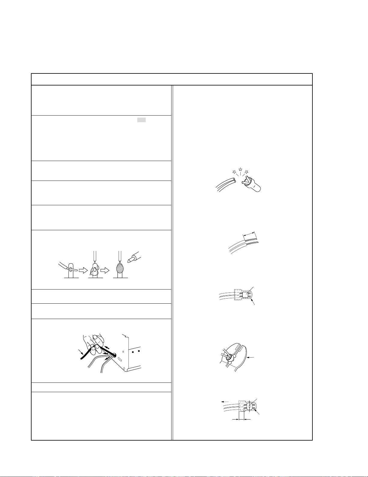
12. Crimp type wire connector
In such cases as when replacing the power transformer in sets
where the connections between the power cord and power transformer primary lead wires are performed using crimp type connectors, if replacing the connectors is unavoidable, in order to prevent
safety hazards, perform carefully and precisely according to the
following steps.
1) Connector part number : E03830-001
2) Required tool : Connector crimping tool of the proper type which
will not damage insulated parts.
3) Replacement procedure
(1) Remove the old connector by cutting the wires at a point
close to the connector.
Important : Do not reuse a connector (discard it).
cut close to connector
Fig.3
(2) Strip about 15 mm of the insulation from the ends of the
wires. If the wires are stranded, twist the strands to avoid
frayed conductors.
15 mm
Fig.1
7. Observe that wires do not contact heat producing parts (heatsinks,
oxide metal film resistors, fusible resistors, etc.)
8. Check that replaced wires do not contact sharp edged or pointed
parts.
9. When a power cord has been replaced, check that 10-15 kg of
force in any direction will not loosen it.
Power cord
Fig.2
10. Also check areas surrounding repaired locations.
11. Products using cathode ray tubes (CRTs)
In regard to such products, the cathode ray tubes themselves, the
high voltage circuits, and related circuits are specified for compliance with recognized codes pertaining to X-ray emission.
Consequently, when servicing these products, replace the cathode ray tubes and other parts with only the specified parts. Under
no circumstances attempt to modify these circuits.
Unauthorized modification can increase the high voltage value and
cause X-ray emission from the cathode ray tube.
Fig.4
(3) Align the lengths of the wires to be connected. Insert the
wires fully into the connector.
Metal sleeve
Connector
Fig.5
(4) As shown in Fig.6, use the crimping tool to crimp the metal
sleeve at the center position. Be sure to crimp fully to the
complete closure of the tool.
1
.2
2
.0
5
.5
(5) Check the four points noted in Fig.7.
Not easily pulled free
Wire insulation recessed
more than 4 mm
Crimping tool
5
Fig.6
Crimped at approx. center
Fig.7
of metal sleeve
Conductors extended
I
S40888-01
Page 4
Safety Check after Servicing
•
Examine the area surrounding the repaired location for damage or deterioration. Observe that screws, parts and wires have been returned
to original positions, Afterwards, perform the following tests and confirm the specified values in order to verify compliance with safety
standards.
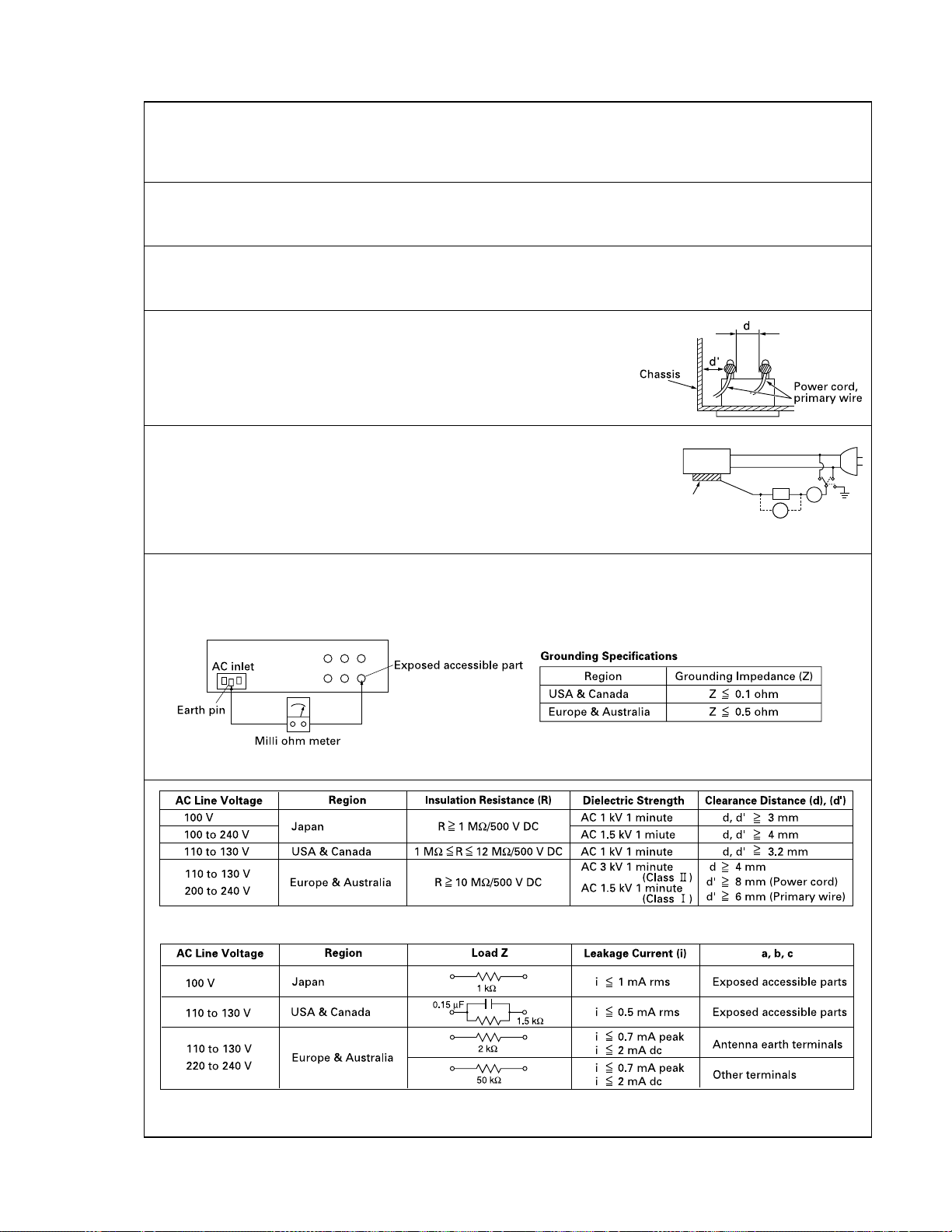
1. Insulation resistance test
Confirm the specified insulation resistance or greater between power cord plug prongs and externally exposed parts of the set (RF terminals, antenna terminals, video and audio input and output
terminals, microphone jacks, earphone jacks, etc.). See table 1 below.
2. Dielectric strength test
Confirm specified dielectric strength or greater between power cord plug prongs and exposed accessible parts of the set (RF terminals, antenna terminals, video and audio input and output terminals,
microphone jacks, earphone jacks, etc.). See table 1 below.
3. Clearance distance
When replacing primary circuit components, confirm specified clearance distance (d), (d’) between soldered terminals, and between terminals and surrounding metallic parts. See table 1
below.
Fig. 8
4. Leakage current test
Confirm specified or lower leakage current between earth ground/power cord plug prongs and
externally exposed accessible parts (RF terminals, antenna terminals, video and audio input and
output terminals, microphone jacks, earphone jacks, etc.).
Measuring Method : (Power ON)
Insert load Z between earth ground/power cord plug prongs and externally exposed accessible
parts. Use an AC voltmeter to measure across both terminals of load Z. See figure 9 and following
table 2.
5. Grounding (Class 1 model only)
Confirm specified or lower grounding impedance between earth pin in AC inlet and externally exposed accessible parts (Video in, Video out,
Audio in, Audio out or Fixing screw etc.).
Measuring Method:
Connect milli ohm meter between earth pin in AC inlet and exposed accessible parts. See figure 10 and grounding specifications.
Externally
exposed
accessible part
Z
V
Fig. 9
A
ab
c
Fig. 10
Table 1 Specifications for each region
Table 2 Leakage current specifications for each region
Note: These tables are unofficial and for reference only. Be sure to confirm the precise values for your particular country and locality.
II
S40888-01
Page 5
SECTION 1
DISASSEMBLY
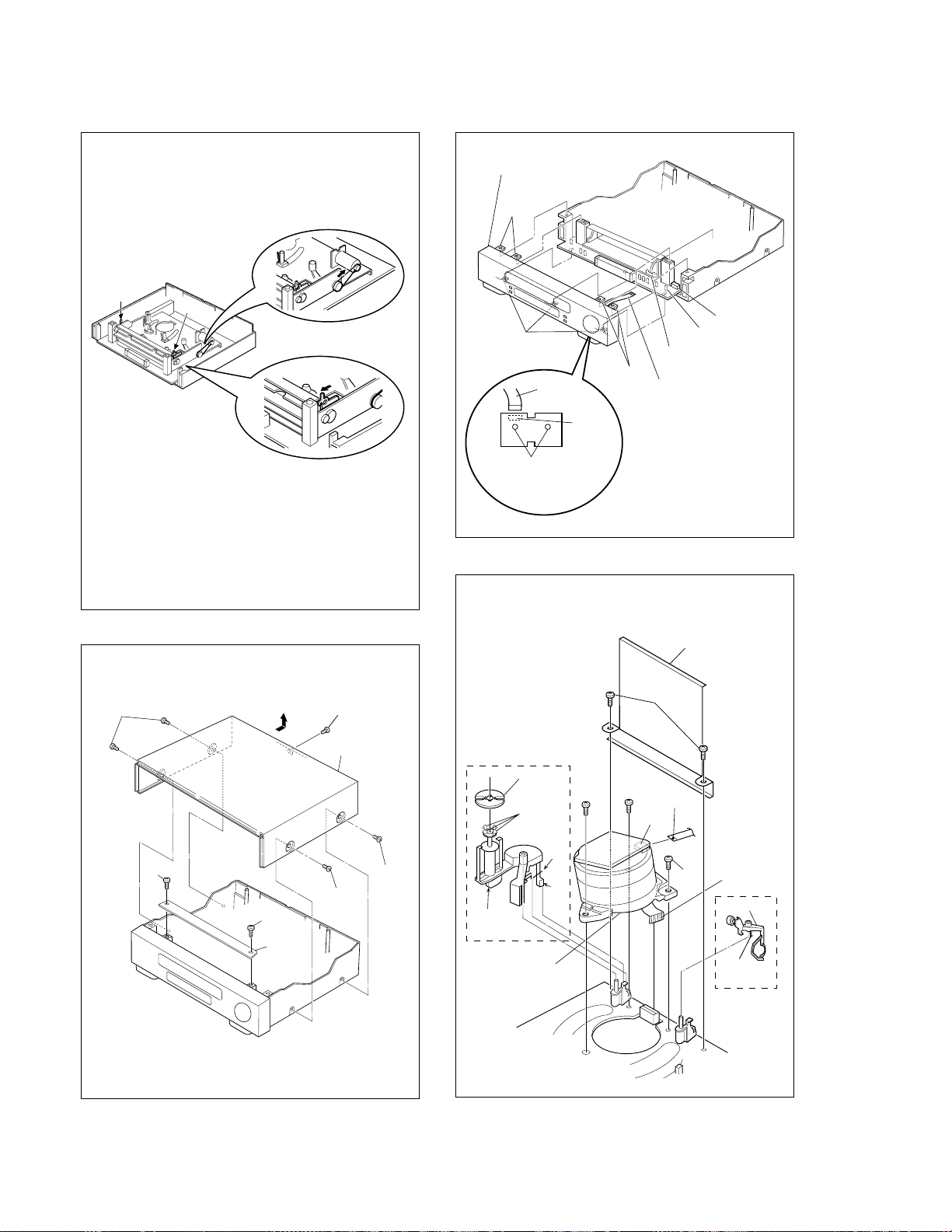
1.1 Disassembly flow chart
This flowchart lists the disassembling steps for the cabinet
parts and P.C. boards in order to gain access to item(s) to
be serviced. When reassembling, perform the step(s) in reverse order. Bend, route and dress the flat cables as they
were originally laid.
[1]
[2]
[3]
[4]
[5]
[6]
1.2
How to read the disassembly and assembly
Top cover, Bracket
Front panel assembly
Drum assembly
Mechanism assembly
Main board assembly
Bottom cover
<Example>
Step/
Loc No.
[1] Top cover, D1
(1) (2) (3) (4) (5)
Part Name
Bracket 2(S1c)
Fig.
No.
Point Note
4(S1a),(S1b),3(L1a), <Note 1a>
2(SD1a),(P1a),(W1a),
CN1(WR1a),
(1) Order of steps in Procedure
When reassembling, perform the step(s) in the reverse order.
These numbers are also used as the identification (location) No.
of parts Figures.
(2) Part name to be removed or installed.
(3) Fig. No. showing procedure or part location.
(4) Identification of part to be removed, unhooked, unlocked,
released, unplugged, unclamped or unsoldered.
P= Spring, W= Washer, S= Screw, L= Locking tab, SD= Solder,
CN**(WR**)= Remove the wire (WR**) from the connector
(CN**).
Note:
•
The bracketed ( ) WR of the connector symbol are assigned nos. in priority order and do not correspond to
those on the spare parts list.
(5) Adjustment information for installation
1.3 Disassembly/assembly method
Step/
Loc No.
[1] Top cover, D1 4(S1a), (S1b)
[2] Front panel assembly D2 CN7001(WR2a) <Note 2a>
[3] Drum assembly D3 CON1(WR3a),
[4] Mechanism assembly D4 CN2001(WR4a), <Note 2c>
[5] Main board assembly D5 6(L5a), <Note 2c>
[6] Bottom cover D6 2(L6a), 9(L6b) <Note 6a>
Part Name
Bracket 2(S1c)
ADV. Jog board assembly
(Drum shield) 2(S3d)
Fig.
No.
Point Note
-----------------
[HR-J780EU/J785EK],
4(L2a), 3(L2b) <Note 2c>
-----------------
2(S2a)
CN1(WR3b),
(S3a), (S3b), (S3c)
-----------------
(S4a),(S4b), <Note 4a>
(S4c), (S4d)
(S5a), 3(S5b), (S5c)
<Note 2b>
<Note 2c>
<Note 2a>
• When reattaching the Front panel assembly , make sure that
the door opener “a” of the Cassette holder assembly is lowered in position prior to the reinstallation.
<Note 2b>
• When reattaching the Front panel assembly , pay careful attention to the switch lever not to make it touch the switch
knob “b” of the Main board assembly from the side.
<Note 2c>
• Be careful not to damage the connector and wire etc. during
connection and disconnection.
When connecting the wire to the connector, be careful with
the wire direction.
<Note 4a>
• When it is required to remove the screws (S4a to S4b) retaining the Mechanism assembly, please refer to the “Procedures for Lowering the Cassette holder assembly”(See
on page 1-2).
• When reattaching the Mechanism assembly to the Main
board assembly, take care not to damage the sensors on
the Main board assembly.
• When removing the Mechanism assembly only , unhook the
two spacers connecting it with the Main board assembly
with pliers from the back side of the Main board assembly
first, and then remove the Mechanism assembly.
• The wire (WR4a) has excess length that may be loose, as it
is quite long. After inserting the wire and connectors, the
loose portion of the wire should be taken up and accommodated between the A/C head base and the main deck.
<Note 6a>
When removing the bottom cover, push down the two tabs
(L6a) to slide the bottom cover.
1-1
Page 6
Procedures for Lowering the Cassette holder assembly
As the mechanism of this unit is integrated with the Housing
assembly, the holder must be lowered and the two screws unscrewed when removing the Mechanism assembly.
[2] Front panel assembly
(L2a)
(A)
(B)
Fig. 2
Fig. 1
Fig. 3
Turn the loading motor pulley in the direction as indicated by
Fig.2. As both (A) and (B) levers are lodged twice, push the
levers in the direction as indicated by Fig.3 to release them.
When pushing the levers, do it in the order of (A), (B), (B),
(A). When the holder has been lowered, turn the pulley until
the cassette holder is securely in place without allowing any
up/down movement.
Procedures for Lowering the Cassette holder assembly
(S1a)
(S1b)
CN7001
(L2b)
b <Note 2b>
a <Note 2a>
(L2a)
WR2a
<Note 2c>
CN7004
(S2a)
ADV. Jog board assembly
[HR-J780EU/J785EK]
WR2a
<Note 2c>
Fig. D2
Note:
When installing the Drum assembly, secure the screws (S3a to
S3c) in the order of a, b, c.
Drum shield
(S3d)
1-2
(S1c)
[1]
Top cover
Inertia plate
(S3c)
(S3a)
(L3a)
(P3)
(S1a)
(L3b)
[3]
Drum
asembly
CN1
(S1c)
[1]
Bracket
(S1a)
Roller arm
assy
Not used
Fig. D1 Fig. D3
CON1
WR3a
<Note 2c>
(S3b)
WR3b
<Note 2c>
Cleaner assy
(L3c)
Not used
Page 7
WR4a
(S4b)
<Note 4a>
A/C head base
(S4c)
Note:
When installing the
Mechanism assembly,
secure the screws
(S4a to S4b) in the
order of a, b.
WR4a
<Note 2c>
(S4a)
<Note 4a>
(S4d)
Q3002
End sensor
<Note 4a>
(L4)
Spacer
<Note 4a>
(S5a)
D3001
LED
<Note 4a>
Fig. D4
CN2001
[4]
Mechanism
assembly
(L4)
Spacer
<Note 4a>
(S5b)
(S5c)
(L6b)
Fig. D6
(L6b)
(L6a)
<Note 6a>
(L6b)
[6]
Bottom cover
Fig. D5
(L5a)
[5]
Main board
assembly
1-3
Page 8
1.4 Service position
This unit has been designed so that the Mechanism and
Main board assemblies can be removed together from the
chassis assembly. Before diagnosing or servicing the circuit boards, take out the major parts from the chassis assembly.
1.4.1 How to set the “Service position”
(1) Refer to the disassembly procedure and perform the dis-
assembly of the major parts before removing the Drum
assembly.
(2) Lower the cassette holder to prepare for the removal of
the Mechanism assembly screws. (Refer to the “Procedures for lowering the Cassette holder assembly” of 1.3
Disassembly/assembly method.)
(3) Remove the combined Mechanism and Main board as-
semblies.
(4) Connect the wires and connectors of the major parts that
have been removed in step (1). (Refer to Fig.1-4-1a.)
(5) Place the combined Mechanism and Main board assem-
blies upside down.
(6) Insert the power cord plug into the power outlet and then
proceed with the diagnostics and servicing of the board
assembly.
Notes:
• Before inserting the power cord plug into the power
outlet, make sure that none of the electrical parts are
able to short-circuit between the workbench and the
board assembly.
• For the disassembly procedure of the major parts and
details of the precautions to be taken, see “1.3 Disassembly/assembly method”.
• If there are wire connections from the Main board and
Mechanism assemblies to the other major parts, be
sure to remove them ( including wires connected to the
major parts ) first before performing step (2).
• When carrying out diagnosis and repair of the Main
board assembly in the “Service position”, be sure to
ground both the Main board and Mechanism assemblies. If they are improperly grounded, there may be
noise on the playback picture or FDP counter display
may move even when the mechanism is kept in an inoperative status.
• In order to diagnose the playback or recording of the
cassette tape, set the Mechanism assembly to the required mode before placing it upside down. If the
mechanism mode is changed (including ejection) while
it is in an upside down position the tape inside may
be damaged.
TP4001
TP106
CTL. P
PB. FM
TP2253
A.PB.FM
TP111
D.FF
CP4001
CP5302
Main board
assembly
1.5 Mechanism service mode
This model has a unique function to enter the mechanism
into every operation mode without loading of any cassette
tape. This function is called the “Mechanism service mode”.
1.5.1 How to set the “Mechanism service mode”
(1) Unplug the power cord plug from the power outlet.
(2) Connect TPGND and TP7001(TEST) on the Main board
assembly with a jump wire.
(3) Insert the power cord plug into the power outlet.
(4) With lock levers (A) (B) on the left and right of the Cas-
sette holder assembly pulled toward the front, slide the
holder in the same direction as the cassette insertion di-
rection. (For the positions of lock levers (A) (B), refer to
the “Procedures for lowering the Cassette holder assem-
bly” of 1.3 Disassembly/assembly method.)
(5) The cassette holder lowers and, when the loading has
completed, the mechanism enters the desired mode.
1.6 Jig RCU mode
This unit uses the following two modes for receiving remote
control codes.
1) User RCU mode : Ordinary mode for use by the user.
2) Jig RCU mode : Mode for use in production and serv-
icing.
When using the Jig RCU, it is required to set the VCR to
the Jig RCU mode (the mode in which codes from the Jig
RCU can be received). As both of the above two modes
are stored in the EEPROM, it is required to set the VCR
back to the User RCU mode each time that an adjustment
is made or to check that the necessary operations have
been completed. These modes can be set by the operations described below.
1.6.1 Setting the Jig RCU mode
(1) Unplug the power cord plug from the power outlet.
(2) Press and hold the “REC” and “PAUSE” buttons on the
VCR simultaneously, while plugging the power cord plug
into the power outlet.
When the VCR is set to the Jig RCU mode, the symbols
( “ : ” ) in the time display of the FDP are turned off.
1.6.2 Setting the User RCU mode
(1) Turn off the power.
(2) Press the “REC” and “PAUSE” buttons of the VCR si-
multaneously. Alternatively, transmit the code “80” from
the Jig RCU.
1-4
C3025
Timer Clock
[HR-J680EU/J780EU]
Fig. 1-4-1a
TPGND
TP7001
TEST
Page 9
1.7 Emergency display function
This unit has a function for storing the history of the past two
emergencies (EMG) and displaying them on each FDP (or
OSD). With the status of the VCR and mechanism at the moment an emergency occurred can also be confirmed.
FDP display model
[FDP display]
0: 00 : 00
E:**:**
*1: *2 : 34
*5: *6 : *7
FDP (7segment LED) display model
[FDP display]
0: 00
E: **
1: **
2: *1
3: *2
4: 34
5: *5
6: *6
7: *7
OSD display model
[OSD display]
Normal display
EMG content display
(E:Latest:Previous)
EMG detail information <1>
EMG detail information <2>
Normal display
EMG content display (Latest)
EMG content display (Previous)
EMG detail information <1>
[Deck operation mode]
EMG detail information <1>
[Mechanism operation mode]
EMG detail information <1>
[Mechanism sensor information and Mechanism mode position]
EMG detail information <2>
[Type of the cassette tape in use <1>]
EMG detail information <2>
[Winding position of the cassette tape in use]
EMG detail information <2>
[Type of the cassette tape in use <2> (Winding area)]
EMG
E:**:**
*1: *2 : 34
*5: *6 :*7
EMG content display
(E:Latest:Previous)
EMG detail information <1>
EMG detail information <2>
Notes:
•
The EMG detail information <1><2> show the information
on the latest EMG.
It becomes “ – – : – – : – –” when there is no latest EMG
record.
•
When using the Jig RCU, it is required to set the VCR to
the Jig RCU mode (the mode in which codes from the Jig
RCU can be received).
Jig RCU
[Data transmitting method]
Depress the “ ” ( 3 ) button
after the data code is set.
CUSTOM CODE
43: A CODE
53: B CODE
DATA CODE
INITIAL MODE
Fig. 1-7a Jig RCU [PTU94023B]
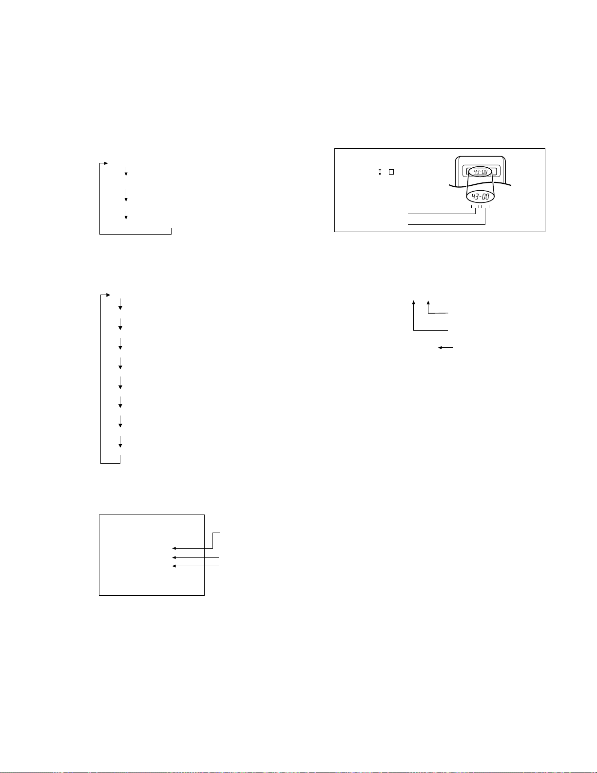
1.7.1 Displaying the EMG information
(1) Transmit the code “59” from the Jig RCU.
The FDP shows the EMG content in the form of “E:**:**”.
<Example 1> E : 01 : 03
Previous EMG
Latest EMG
<Example 2> E : –– : ––
No EMG record
(2) Transmit the code “59” from the Jig RCU again.
The FDP shows the EMG detail information <1> in the form
of “ *1: *2 : 34 ”.
*1 : Deck operation mode at the moment of EMG
*2 : Mechanism operation mode at the moment of EMG
3– : Mechanism sensor information at the moment of
EMG
–4 : Mechanism mode position at the moment of EMG
(3) Transmit the code “59” from the Jig RCU once again.
The FDP shows the EMG detail information <2> in the form
of “ *5 : *6 : *7 ”.
*5 : Type of the cassette tape in use <1> .
*6 : Winding position of the cassette tape in use
*7 : Type of the cassette tape in use <2> (Winding area)
(4) Transmit the code “59” from the Jig RCU once again to re-
set the display.
Notes:
•
For the OSD display model, all EMG information are
showed by transmitting first code from the Jig RCU.
•
For the EMG content, see “1.7.3 EMG content description”.
•
For the EMG detail information <1> , see “1.7.4 EMG detail information <1> ”.
•
For the EMG detail information <2> , see “1.7.5 EMG detail information <2>”.
1.7.2 Clearing the EMG history
(1) Display the EMG history.
(2) Transmit the code “36” from the Jig RCU.
(3) Reset the EMG display.
(EMG-02e)
1-5
Page 10

1.7.3 EMG content description
Note:
EMG contents “E08/E09” are for the model with Dynamic Drum (DD).
FDP CONTENT CAUSE
E01:Loading EMG
E02:
Unloading EMG
E03:Take Up Reel
Pulse EMG
E04: Drum FG
EMG
E05:Cassette Eject
EMG
E06:Capstan FG
EMG
E07:SW Power
Short-Circuit
EMG
E08:
DD Initialized
(Absolute
Position
Sensor)
EMG
E09: DD FG EMG
E0A:Supply Reel
Pulse EMG
EC1 or EU1:
Head clog warning
When the mechanism mode cannot be changed to another mode even when the loading motor has rotated
for more than 4 seconds in the loading direction, [E:01]
is identified and the power is turned off.
When the mechanism mode cannot be changed to another mode even when the loading motor has rotated
for more than 4 seconds in the unloading direction, [E:02]
is identified and the power is turned off.
When the take-up reel pulse has not been generated for
more than 4 seconds in the capstan rotating mode, [E:03]
is identified, the pinch rollers are turned off and stopped,
and the power is turned off. However, the reel EMG is
not detected in STILL/SLOW modes.
When the drum FG pulse has not been input for more
than 3 seconds in the drum rotating mode, [E:04] is identified, the pinch rollers are turned off and stopped, and
the power is turned off.
When the eject operation does not complete in 3 seconds after the start, [E:05] is identified, the pinch rollers
are turned off and stopped, and the power is turned off.
When the cassette insertion operation does not complete
in 3 seconds after the start, the cassette is ejected. In
addition, when the operation does not complete within
3 seconds after the start, [E:05] is also identified and the
power is turned off immediately.
When the capstan FG pulse has not been generated for
more than 1 second in the capstan rotating mode, [E:06]
is identified, the pinch rollers are turned off and stopped,
and the power is turned off.However, the capstan EMG
is not detected in STILL/SLOW/FF/REW modes.
When short-circuiting of the SW power supply with GND
has lasted for 0.5 second or more, [E:07] is identified,
all the motors are stopped and the power is turned off.
When DD tilting does not complete in 4 seconds, [E:08]
is identified, the tilt motor is stopped and the power is
turned off.
When the DD FG pulse is not generated within 2.5 seconds, [E:09] is identified, the tilt motor is stopped and
the power is turned off.
When the supply reel pulse has not been generated for
more than 10 seconds in the capstan rotating mode,
[E:0A] is identified and the cassette is ejected (but the
power is not turned off). However, note that the reel EMG
is not detected in the SLOW/STILL mode.
Presupposing the presence of the control pulse output in the PLAY mode, when the value obtained by mixing the two V.FM output
channels (without regard to the A.FM output) has remained below a certain threshold level for more than 10 seconds, [E:C1] or [E:U1]
is identified and recorded in the emergency history. During the period in which a head clog is detected, the FDP and OSD repeat the
“3-second warning display” and “7-second noise picture display” alternately.
EMG code : “E:C1” or “E:U1” / FDP : “U:01” / OSD : “Try cleaning tape.” or “Use cleaning cassette.”
The head clog warning is reset when the above-mentioned threshold has been exceeded for more than 2 seconds or the mode is
changed to another mode than PLAY.
1.
The mechanism is locked in the middle of mode transition.
2
. The mechanism is locked at the loading end due to the encoder position
reading error during mode transition.
3.
Power is not supplied to the loading MDA.
1.
The mechanism is locked in the middle of mode transition.
2.
The mechanism is locked at the unloading end due to the encoder position reading error during mode transition.
3.
Power is not supplied to the loading MDA.
1.
The take-up reel pulse is not generated in the FWD transport modes (PLAY/
FWD SEARCH/FF, etc.) because;
1) The idler gear is not meshed with the take-up reel gear;
2)
The idler gear is meshed with the take-up reel gear, but incapable of wind-
ing due to too large mechanical load (abnormal tension);
3) The take-up reel sensor does not output the FG pulse.
2.
The supply reel pulse is not generated in the REV transport modes (REV
SEARCH/REW, etc.) because;
1) The idler gear is not meshed with the supply reel gear.
2) The idler gear is meshed with the supply reel gear, but incapable of winding due to too large a mechanical load (abnormal tension);
3) The supply reel sensor does not output the FG pulse.
3.
Power is not supplied to the reel sensors.
1.
The drum could not start or the drum rotation has stopped due to too large
a load on the tape, because;
1) The tape tension is abnormally high;
2)
The tape is damaged or a foreign object (grease, etc.) adheres to the tape.
2.
The drum FG pulse did not reach the System controller CPU because;
1) The signal circuit is disconnected in the middle;
2) The FG pulse generator (hall device) of the drum is faulty.
3.
The drum control voltage (DRUM CTL V) is not supplied to the MDA.
4.
Power is not supplied to the drum MDA.
1.
The cassette cannot be ejected due to a failure in the drive mechanism of
the housing.
2.
When the housing load increases during ejection, the loading motor is
stopped because of lack of headroom in its drive torque.
Housing load increasing factors: Temperature environment (low temperature, etc.), mechanism wear or failure.
3.
The sensor/switch for detecting the end of ejection are not functioning normally.
4.
The loading motor drive voltage is lower than specified or power is not supplied to the motor (MDA).
5.
When the user attempted to eject a cassette, a foreign object (or perhaps
the user's hand) was caught in the opening of the housing.
1.
The capstan could not start or the capstan rotation has stopped due to too
large a load on the tape, because;
1) The tape tension is abnormally high (mechanical lock);
2) The tape is damaged or a foreign object (grease, etc.) is adhered to the
tape (occurrence of tape entangling, etc.).
2.
The capstan FG pulse did not reach the System controller CPU because;
1) The signal circuit is disconnected in the middle;
2) The FG pulse generator (MR device) of the capstans is faulty.
3.
The capstan control voltage (CAPSTAN CTL V) is not supplied to the MDA.
4.
Power is not supplied to the capstan MDA.
1.
The SW 5 V power supply circuit is shorted with GND.
2.
The SW 12 V power supply circuit is shorted with GND.
1. The absolute value sensor is defective. (The soldered parts have separated.)
2. The pull-up resistor at the absolute sensor output is defective. (The soldered parts
have separated.)
3. Contact failure or soldering failure of the pins of the connector (board-to-board) to the
absolute value sensor.
4.
The absolute value sensor data is not sent to the System Controller CPU.
1. The FG sensor is defective. (The soldered parts have separated.)
2. The pull-up resistor at the FG sensor output is defective. (The soldered parts have
separated.)
3. Contact failure or soldering failure of the pins of the connector (board-to-board) to the FG sensor.
4. The power to the sensor is not supplied. (Connection failure/soldering failure)
5. The FG pulse is not sent to the System Controller CPU.
6.
The tilt motor is defective. (The soldered parts have separated.)
7. The drive power to the tilt motor is not supplied. (Connection failure/soldering failure)
8. The tilt motor drive MDA - IC is defective.
9. Auto-recovery of the DD tilting cannot take place due to overrun.
The supply reel pulse is not generated in the FWD transport mode (PLAY/
1.
FWD SEARCH/FF, etc.) because;
1) PLAY/FWD or SEARCH/FF is started while the tape in the inserted cas-
sette is cut in the middle;
2) A mechanical factor caused tape slack inside and outside the supply
reel side of the cassette shell. In this case, the supply reel will not rotate
until the tape slack is removed by the FWD transport, so the pulse is not
generated until then;
3) The FG pulse output from the supply reel sensor is absent.
2.
The take-up reel pulse is not generated in the REV transport mode (REV
SEARCH/REW, etc.).
1) REV SEARCH/REW is started when the tape in the inserted cassette
has been cut in the middle;
2) A mechanical factor caused tape slack inside and outside the take-up
reel side of the cassette shell. In this case, the supply reel will not rotate
until the tape slack is removed by the REV transport, so the pulse will
not be generated until that time;
3) The FG pulse output from the take-up reel sensor is absent.
3.
The power to a reel sensor is not supplied.
Table 1-7-3a
1-6
Page 11
1.7.4 EMG detail information <1>
The status (electrical operation mode) of the VCR and the status (mechanism operation mode/sensor information) of the
mechanism in the latest EMG can be confirmed based on the
figure in EMG detail information <1> .
[FDP/OSD display]
*1 : *2 : 34
*1 : Deck operation mode at the moment of EMG
*2 : Mechanism operation mode at the moment of EMG
3– : Mechanism sensor information at the moment of EMG
–4 : Mechanism mod
e position at the moment of EMG
Note:
•
For EMG detailed information <1>, the content of the code
that is shown on the FDP (or OSD) differs depending on
the parts number of the system control microprocessor
(IC3001) of the VCR. The system control microprocessor
parts number starts with two letters, refer these to the corresponding table.
*1 : Deck operation mode
[Common table of MN*, HD* and M3*]
Display
MN*/M3* HD*
00 - Mechanism being initialized
01 00 STOP with pinch roller pressure off (or tape present with P.OFF)
02 01 STOP with pinch roller pressure on
03 - POWER OFF as a result of EMG
04 04 PLAY
0C 0E REC
10 11 Cassette ejected
20 22 FF
21 - Tape fully loaded, START sensor ON, short FF
22 - Cassette identification FWD SEARCH before transition to FF (SP
24 26 FWD SEARCH (variable speed) including x2-speed
2C 2E INSERT REC
40 43 REW
42 - Cassette identification REV SEARCH before transition to REW (SP
44 47 REV SEARCH (variable speed)
4C 4C AUDIO DUB
6C 6E INSERT REC (VIDEO + AUDIO)
84 84 FWD STILL / SLOW
85 85 REV STILL / SLOW
8C 8F REC PAUSE
8D - Back spacing
8E - Forward spacing (FWD transport mode with BEST function)
AC AF INSERT REC PAUSE
AD - INSERT REC back spacing
CC CD AUDIO DUB PAUSE
CD - AUDIO DUB back spacing
EC EF INSERT REC (VIDEO + AUDIO) PAUSE
ED - INSERT REC (VIDEO + AUDIO) back spacing
x7-speed)
x7-speed)
Deck operation mode
*2 : Mechanism operation mode
[Common table of MN* and M3*]
Display
MN* M3*
00 00 Command standby (Status without executing command)
02 02 POWER OFF by EMG occurrence
04 04 Moving to the adjacent position in the LOAD direction
06 06 Moving to the adjacent position in the UNLOAD direction
08 08 Cassette ejection being executed / Cassette housing ejection being
0A 0C Cassette insertion being executed
0C 0E Tape being loaded
0E 10 Tape being unloaded
10 12 Mode transition to STOP with pinch roller compression ON
12 14 Mode transition to STOP with pinch roller compression OFF
14 16
16 18
18 1A Mode transition to PLAY
1A 1C Mode transition to FWD SEARCH
1C 1E Mode transition to REC
1E 20 Mode transition to FWD STILL / SLOW
20 22 Mode transition to REV STILL / SLOW
22 24 Mode transition to REV SEARCH
24 26 Mode transition from FF / REW to STOP
26 28 Mode transition to FF
28 2A Mode transition to REW
2A 2C 4 sec. of REV as a result of END sensor going ON during loading
2C 2E
2E 30 Mechanism position being corrected due to overrun
80 80 Mechanism in initial position (Dummy command)
executed
- 0A Mode transition to STOP with cassette ejection end
Mode transition to STOP with pinch roller compression OFF as a result
of POWER OFF
Mode transition to STOP with pinch roller compression ON as a result
of POWER ON
Short FF / REV as a result of END sensor going ON during unloading
Mechanism operation mode
[Table of HD*]
Display
00 STOP with pinch roller pressure off
01 STOP with pinch roller pressure on
02 U/L STOP (or tape being loaded)
04 PLAY
05 PLAY (x1-speed playback using JOG)
0E REC
11 Cassette ejected
22 FF
26 FWD SEARCH (variable speed) including x2-speed
2E INSERT REC
43 REW
47 REV SEARCH
4C AUDIO DUB
6E INSERT REC (VIDEO + AUDIO)
84 FWD STILL/SLOW
85 REV STILL/SLOW
8F REC PAUSE
AF INSERT REC PAUSE
C7 REV SEARCH (x1-speed reverse playback using JOG)
CD AUDIO DUB PAUSE
EF INSERT REC (VIDEO + AUDIO) PAUSE
F0 Mechanism being initialized
F1 POWER OFF as a result of EMG
F2 Cassette being inserted
F3 Cassette being ejected
F4 Transition from STOP with pinch roller pressure on to STOP with pinch
roller pressure off
F5 Transition from STOP with pinch roller pressure on to PLAY
F6 Transition from STOP with pinch roller pressure on to REC
F7 Cassette type detection SEARCH before FF/REW is being executed
F8 Tape being unloaded
F9 Transition from STOP with pinch roller pressure off to STOP with pinch
roller pressure on
FA Transition from STOP with pinch roller pressure off to FF/REW
FB Transition from STOP with pinch roller pressure off to REC.P (T.REC,etc.)
FC Transition from STOP with pinch roller pressure off to cassette type de-
tection SEARCH
FD Short REV being executed after END sensor on during unloading
FE Tension loosening being executed after tape loading (STOP with pinch
roller pressure on)
Mechanism operation mode
1-7
Page 12
3– : Mechanism sensor information
[Common table of MN*, HD* and M3*]
Display
MN* / HD* M3* REC safety Start End
S-VHS SW CASS SW SW sensor sensor
0- VHS Cassette insertion Tab broken ON ON
1- VHS Cassette insertion Tab broken ON OFF
2- VHS Cassette insertion Tab broken OFF ON
3- VHS Cassette insertion Tab broken OFF OFF
4- VHS Cassette insertion Tab present ON ON
5- VHS Cassette insertion Tab present ON OFF
6- VHS Cassette insertion Tab present OFF ON
7- VHS Cassette insertion Tab present OFF OFF
8- S-VHS Cassette ejection Tab broken ON ON
9- S-VHS Cassette ejection Tab broken ON OFF
A- S-VHS Cassette ejection Tab broken OFF ON
B- S-VHS Cassette ejection Tab broken OFF OFF
C- S-VHS Cassette ejection Tab present ON ON
D- S-VHS Cassette ejection Tab present ON OFF
E- S-VHS Cassette ejection Tab present OFF ON
F- S-VHS Cassette ejection Tab present OFF OFF
Mechanism sensor information
–4 : Mechanism mode position
[Common table of MN*, HD* and M3*]
Display Mechanism mode position
MN* HD* M3*
-0 -7 - Initial value
-1 -0 - EJECT position
- - -0 EJECT position (Cassette housing drive mode)
-2 -7 - Housing operating
- - -1 Between EJECT and U / L STOP
-3 -1 -2 U / L STOP position
- - -3 Guide arm drive position
-4 -7 -4 Tape being loaded / unloaded (When the pole base is
-5 -2 -5 Tape being loaded / unloaded (When the pole base is
-6 -7 -6 Pole base compressed position
-7 -3 -F FF / REW position
-8 -7 -F Between FF / REW and STOP with pinch roller compres-
-9 -4 -F STOP with pinch roller compression OFF
-A -7 -E Between STOP with pinch roller compression OFF and
-B -5 - REV (REV STILL / SLOW) position
- - -D REV position
- - -C Between REV and REV STILL / SLOW
- - -B REV STILL / SLOW position
-C -7 - Between REV and FWD
- - -A Between REV STILL / SLOW and FWD STILL / SLOW
-D -6 - FWD (FWD STILL / SLOW) position
- - -9 FWD STILL / SLOW position
-E -7 - Between FWD and PLAY
- - -8 Between FWD STILL / SLOW and PLAY
-F -6 -7 PLAY position
located on the front side of the position just beside the
drum)
located on the rear side of the position just beside the
drum)
sion ON
REV
Note:
• In the case of the "HD*” microprocessor, as the display is
always "-7” at any intermediate position between modes,
the position of transitory EMG may sometimes not be located.
1.7.5 EMG detail information <2>
The type of the cassette tape and the cassette tape winding position can be confirmed based on the figure in EMG detail information <2> .
[FDP/OSD display]
*5 : *6 : *7
*5 : Type of the cassette tape in use <1>
*6 : Winding position of the cassette tape in use
*7 : Type of th
e cassette tape in use
<2>
(Winding area)
Note:
• EMG detail information <2> is the reference information
stored using the remaining tape detection function of the
cassette tape. As a result, it may not identify cassette correctly when a special cassette tape is used or when the
tape has variable thickness.
*5 : Cassette tape type <1>
Display Cassette tape type <1>
00 Cassette type not identified
16
Large reel/small reel (T-0 to T-15/T-130 to T-210) not classified
82 Small reel, thick tape (T-120) identified/thin tape (T-140) identified
84 Large reel (T-0 to T-60) identified
92
Small reel, thick tape (T-130) identified/thin tape (T-160 to T-210) identified
93
Small reel, thick tape/C cassette (T-0 to T-100/C cassette) not classified
C3
Small reel, thick tape/C cassette (T-0 to T-100/C cassette) being classified
D3
Small reel, thick tape/C cassette (T-0 to T-100/C cassette) being classified
E1 C cassette, thick tape (TC-10 to TC-20) identified
E2 Small reel, thick tape (T-0 to T-100) identified
E9 C cassette, thin tape (TC-30 to TC-40) identified
C cassette, thick tape/thin tape (TC-10 to TC-40) not classified
F1
Notes:
Cassette tape type
•
<1>
is identified a few times during mode
transition and the identification count is variable depending on
the cassette tape type. If an EMG occurs in the middle of identification, the cassette tape type may not be able to be identified.
•
If other value than those listed in the above table is displayed,
the cassette tape type is not identified.
*6 : Cassette tape winding position
The cassette tape winding position at the moment of EMG is
displayed by dividing the entire tape (from the beginning to the
end) in 22 sections using a hex number from “00” to “15”.
“00” : End of winding
“15” : Beginning of winding
“FF or ––” : Tape position not identified
*7 : Cassette tape type <2> (Winding area)
Display Cassette tape type <2>
00 Cassette type not identified
07 Small reel, thick tape T-5
08 - 0E C cassette, thick tape TC-10
09 - 15 C cassette, thick tape TC-20P
0A - 0B Small reel, thick tape T-20
0A - 16 C cassette, thin tape TC-30
0A - 16 C cassette, thin tape TC-40
0D - 0F Small reel, thick tape T-40
11 - 14 Small reel, thick tape T-60
15 - 18 Small reel, thick tape T-80 / DF-160
17 - 1A Small reel, thick tape T-90 / DF-180
19 - 1D Small reel, thick tape T-100
1D - 21 Small reel, thick tape T-120 / DF-240
1E - 1F Small reel, thin tape T-140
1F - 23 Small reel, thick tape T-130
21 - 23 Small reel, thin tape T-160
21 - 23 Small reel, thin tape T-168
22 - 24 Small reel, thick tape DF-300
22 - 24 Small reel, thin tape T-180 / DF-360
22 - 24 Small reel, thin tape T-210 / DF-420
22 - 23 Large reel T-5
23 - 24 Large reel T-10
25 - 26 Large reel T-20
27 - 29 Large reel T-30
29 - 2B Large reel T-40
2D - 2F Large reel T-60
Note:
•
The values of cassette tape type <2> in the above table
are typical values with representative cassette tapes.
1-8
Page 13
SECTION 2
MECHANISM ADJUSTMENT
2.1 Before starting repair and adjustment
2.1.1 Precautions
(1) Unplug the power cord plug of the VCR before using your
soldering iron.
(2) Take care not to cause any damage to the conductor
wires when plugging and unplugging the connectors.
(3) Do not randomly handle the parts without identifying
where the trouble is.
(4) Exercise enough care not to damage the lugs, etc. dur-
ing the repair work.
(5) When reattaching the front panel assembly, make sure
that the door opener of the cassette holder assembly is
lowered in position prior to the reinstallation. (See SECTION 1 DISASSEMBLY.)
(6) When using the Jig RCU, it is required to set the VCR to
the Jig RCU mode (the mode in which codes from the
Jig RCU can be received). (See SECTION 1 DISASSEMBLY.)
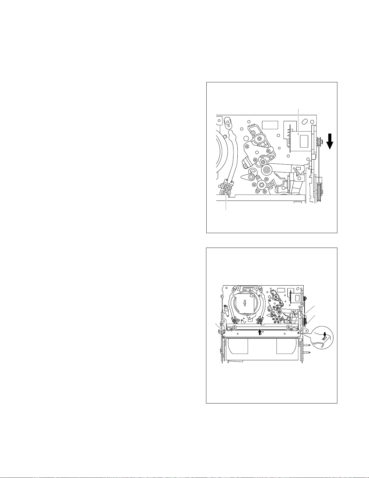
Loading motor
2.1.2 Checking for proper mechanical operations
Enter the mechanism service mode when you want to operate the mechanism when no cassette is loaded. (See SECTION 1 DISASSEMBLY.)
2.1.3 Manually removing the cassette tape
1. In case of electrical failures
If you cannot remove the cassette tape which is loaded because of any electrical failure, manually remove it by taking
the following steps.
(1) Unplug the power cord plug from the power outlet.
(2) Refer to the disassembly procedure and perform the dis-
assembly of the major parts before removing the drum
assembly.
(3) Unload the pole base assembly by manually turning the
loading motor of the mechanism assembly toward the
front. In doing so, hold the tape by the hand to keep the
slack away from any grease. (See Fig.2-1-3a.)
(4) Bring the pole base assembly to a pause when it reaches
the position where it is hidden behind the cassette tape.
(5) Move the top guide toward the drum while holding down
the lug (A) of the bracket retaining the top guide. Likewise hold part (B) down and remove the top guide.
Section (C) of the top guide is then brought under the
cassette lid. Then remove the top guide by pressing the
whole cassette tape down. (See Fig.2-1-3b.)
(6) Remove the cassette tape by holding both the slackened
tape and the cassette lid.
(7) Take up the slack of the tape into the cassette. This com-
pletes removal of the cassette tape.
Note:
• For the disassembly procedure of the major parts and
details of the precautions to be taken, see “SECTION
1 DISASSEMBLY”.
Pole base assembly
Fig. 2-1-3a
(C)
(A)
(B)
Press
Fig. 2-1-3b
2-1
Page 14
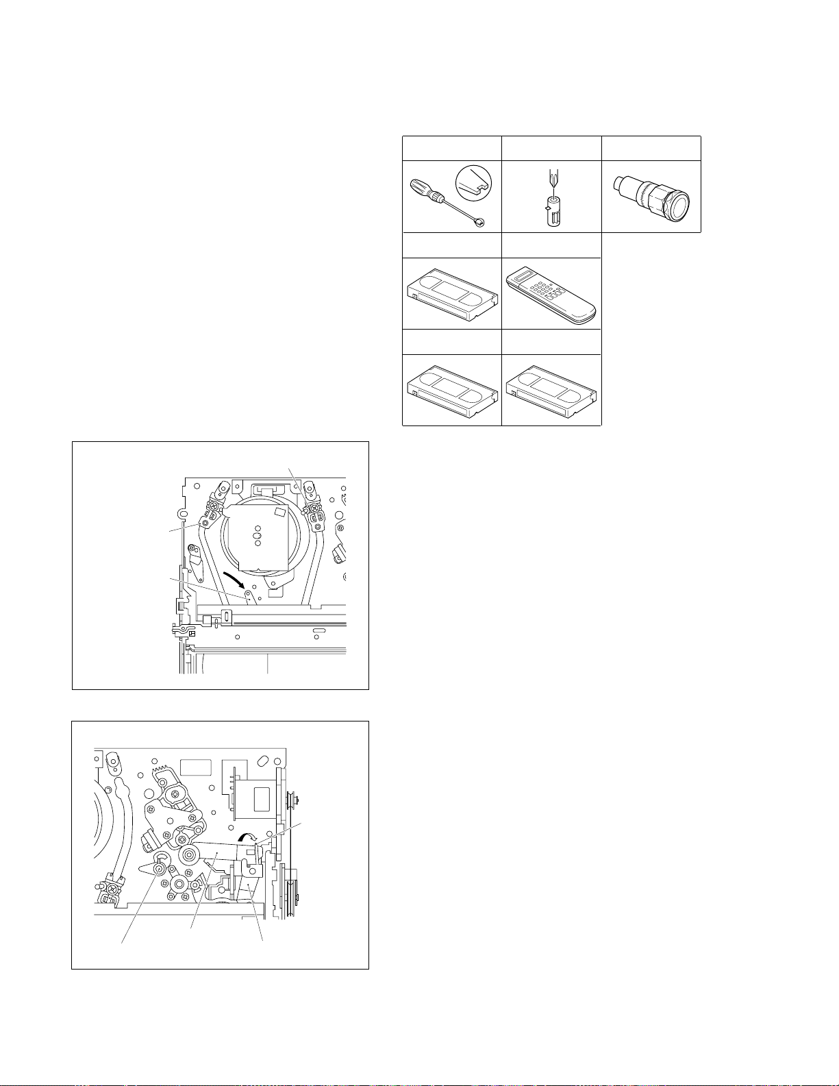
2. In case of mechanical failure
If you cannot remove the cassette tape which is loaded because of any mechanical failure, manually remove it by taking the following steps.
(1) Unplug the power cable and remove the top cover, front
panel assembly and others so that the mechanism assembly is visible. (See SECTION 1 DASASSEMBLY.)
(2) While keeping the tension arm assembly of the mecha-
nism assembly free from tension, pull the tape on the pole
base assembly (supply or take-up side) out of the guide
roller. (See Fig.2-1-3c.)
(3) Take the spring of the pinch roller arm assembly off the
hook of the press lever assembly, and detach it from the
tape. (See Fig.2-1-3d.)
(4) In the same way as in the electrical failure instructions in
2.1.3-1(5), remove the top guide.
(5) Raise the cassette tape cover. By keeping it in that posi-
tion, draw out the cassette tape case from the cassette
holder and take out the tape.
(6) By hanging the pinch roller arm assembly spring back
on the hook, take up the slack of the tape into the cassette.
Pole base assembly (take-up side)
2.1.4 Jigs and tools required for adjustment
Roller driver
PTU94002
Back tension cassette gauge
PUJ48076-2
Alignment tape
(SP, stairstep, PAL)
MHPE
A/C head positioning tool
PTU94010
Jig RCU
PTU94023B
Alignment tape
(LP, stairstep, PAL)
MHPE-L
Torque gauge
PUJ48075-2
Pole base assembly
(supply side)
Tension arm assembly
Fig. 2-1-3c
Take the spring
off the hook, and
detach it from the
tape.
2-2
Guide pole guard
Pinch roller arm assembly
Press lever assembly
Fig. 2-1-3d
Page 15
2.1.5 Maintenance and inspection
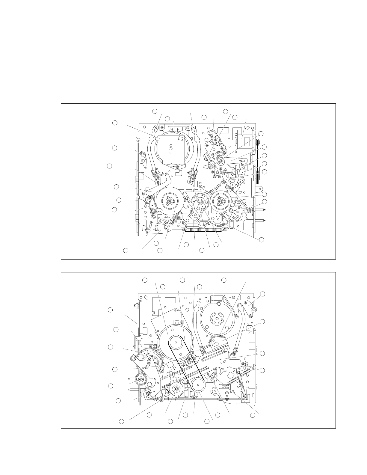
1. Location of major mechanical parts
In this chapter, the two mechanism speeds are described by comparing the speeds of the standard type and the high-speed
FF/REW type.
It is possible to distinguish between these two types of mechanism by the diameters of their capstan pulleys.
The capstan pulley diameter for the standard type is approx. 32 mm.
The capstan pulley diameter for the high-speed FF/REW type is approx. 43 mm.
For information on the different parts used in the two mechanism types, please refer to the “Replacement of major parts”.
UV catcher2 (supply and take-up side)
Stator assembly
T2
Full erase head
T26
Pole base assembly
T25
(supply side)
Tension arm
T24
assembly
T23
Tension brake
T22
assembly
Adjust pin
T1
T3
Drum assembly
T5 T7
Head base
T6
A/C head
Loading motor
Guide pole guard
T8
Pinch roller arm
T9
assembly
Lid guide
T10
Press lever
T11
assembly
Guide arm
T12
assembly
Reel disk
T13
(take-up side)
Sub brake assembly
T14
(take-up side)
Belt
B22
(loading motor)
B21
Control cam
B20
B19
Cassette gear
B18
Worm gear
Brake lever
Link lever
B17
Rec safety lever
Reel disk
T20
(supply side)
Main brake assembly
(supply side)
Idler lever
T17T19T21
Idler arm assembly
T16T18
Pole base assembly (take-up side)
Fig. 2-1-5a Mechanism assembly top side
Capstan motor
B1
Belt (capstan)
B2
Capstan brake assembly
B3 B5
Loading arm gear (take-up side)
B4
Loading arm gear (supply side)
Main brake assembly
T15
(take-up side)
Plate
B6
(supply side)
Control
B7
bracket1
Control plate
B8
Tension arm
B9
bearing
Rotary encoder guide
B16
Rotary encoder
B15
B14
Direct gear
B13
Change lever assembly
B12
B10
Clutch unit
Take-up head
Fig. 2-1-5b Mechanism assembly bottom side
B11
Take-up lever
2-3
Page 16
Guide rail Roller cam assembly
L2L1
Fig. 2-1-5c Mechanism assembly left side
R1
Opener guide
Door
R2
opener
Drive gear
R3
Cassette housing bracket
R4
R5
Limit gear
Loading motor
Worm gear
Belt (loading motor)
Fig. 2-1-5d Mechanism assembly right side
2. Cleaning
Regular cleaning of the transport system parts is desirable
but practically impossible. So make it a rule to carry out cleaning of the tape transport system whenever the machine is
serviced.
When the video head, tape guide and/or brush get soiled,
the playback picture may appear inferior or at worst disappear, resulting in possible tape damage.
(1) When cleaning the upper drum (especially the video
head), soak a piece of closely woven cloth or Kimu-wipe
with alcohol and while holding the cloth onto the upper
drum by the fingers, turn the upper drum
counterclockwise.
Note:
• Absolutely avoid sweeping the upper drum vertically
as this will cause damage to the video head.
(2) To clean the parts of the tape transport system other than
the upper drum, use a piece of closely woven cloth or a
cotton swab soaked with alcohol.
(3) After cleaning, make sure that the cleaned parts are com-
pletely dry before using the video tape.
3. Lubrication
With no need for periodical lubrication, you have only to lubricate new parts after replacement. If any oil or grease on
contact parts is soiled, wipe it off and newly lubricate the
parts.
Note:
• See the “mechanism assembly” diagram of the parts
list for the lubricating or greasing spots, and for the
types of oil or grease to be used.
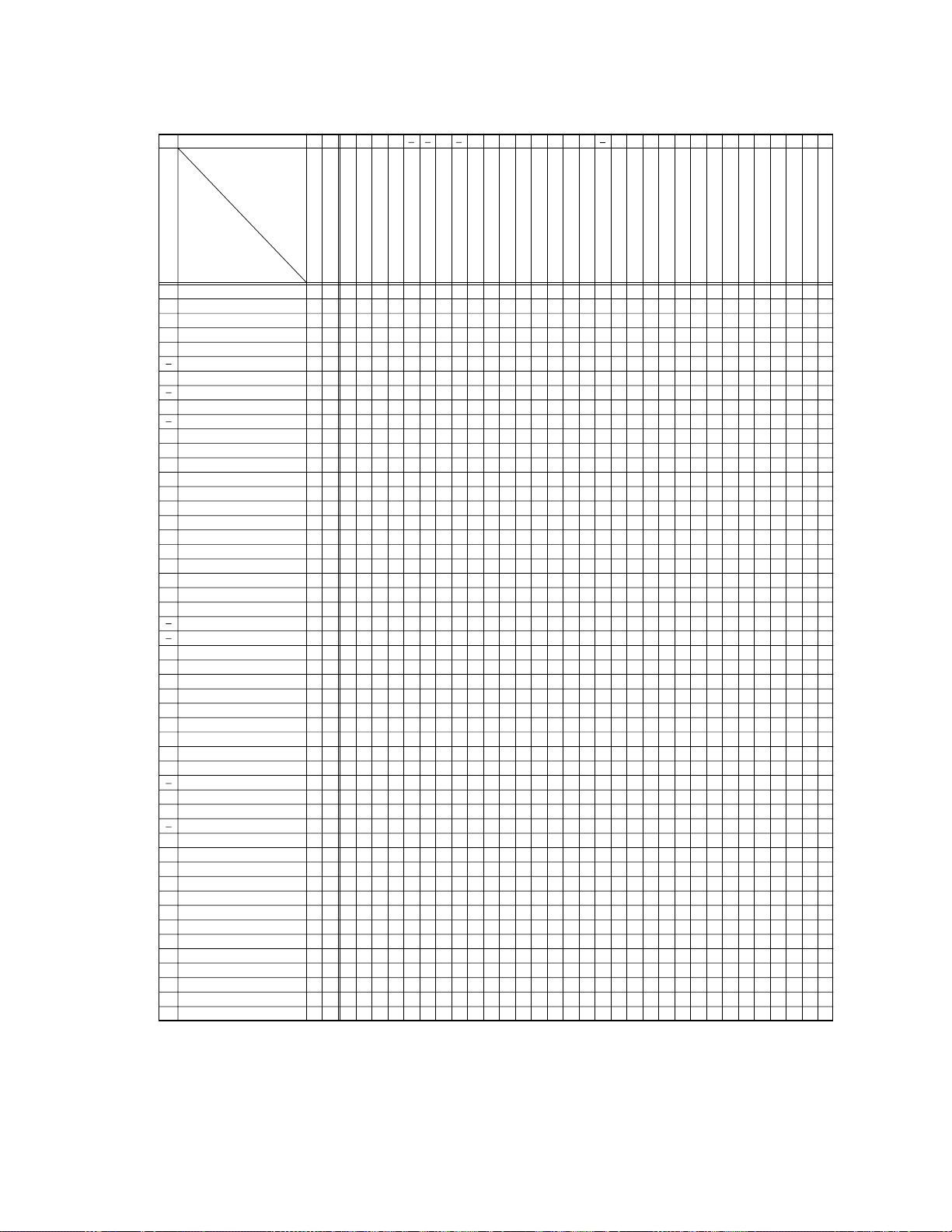
4. Suggested servicing schedule for main components
The following table indicates the suggested period for such
service measures as cleaning,lubrication and replacement.
In practice, the indicated periods will vary widely according
to environmental and usage conditions.However, the indicated components should be inspected when a set is brought
for service and the maintenance work performed if necessary. Also note that rubber parts may deform in time,even if
the set is not used.
System Parts Name
Upper drum assembly
A/C head
Lower drum assembly
Pinch roller arm assembly
Full erase head
Tension arm assembly
Tape transport
Capstan motor (Shaft)
Guide arm assembly
Capstan motor
Capstan brake assembly
Main brake assembly
Belt (Capstan)
Belt (Loading motor)
Loading motor
Clutch unit
Worm gear
Control plate
Brush
Tension brake assembly
Other Drive
Rotary encoder
: Cleaning
¤
: Inspection or replacement if necessary
R
Operation Hours
~1000H ~2000H
¤R R
¤R ¤R
¤¤R
¤¤
¤¤
¤¤
¤¤
¤¤
R
R
R
RR
R
R
R
R
R
¤R ¤R
RR
R
Table 2-1-5a
5. Disassembling procedure table
The following table indicates the order in which parts are removed for replacement. To replace parts, remove them in
the order of 1 to 18 as shown in the table. To install them,
reverse the removal sequence.
The symbols and numbers preceding the individual part
names represent the numbers in the “Location of major mechanical parts” table. Also, the “T”, “B”, and “T/B” on the right
of each part name shows that the particular part is removed
from the front, from the back, and from both sides of the
mechanism, respectively.
2-4
Page 17
R4 R1 R3 T9 T12 T11 B15 B12 B14 B13 B17 B21 B7 B8 B5 B4 B11 T14 T15 T13 T22 T24 T18 B1 9
Symbols and numbers
Removal parts
(Reference items)
Replacement parts
Symbols and numbers
2.2.3 Guide rail T 1
L2
2.2.3 Roller cam assembly T 1
R4
2.2.3 Cassette housing bracket T 1
R1
2.2.3 Opener guide T 2
R2
2.2.3 Door opener T 3
2.2.3 Relay gear T 3
R5
2.2.3 Limit gear T 3
2.2.3 Cassette holder assembly T 6
R3
2.2.3 Drive gear T 4
2.2.3 Drive arm T 8
T9
2.2.4 Pinch roller arm assembly T 1
T12
2.2.5 Guide arm assembly T 1
T11
2.2.5 Press lever assembly T 3
T6
2.2.6 A/C head T 1
T7
2.2.7 Loading motor T 1
B1
2.2.8 Capstan motor T/B 1
T1
2.2.9 UV catcher2 T 1
T17
Pole base assembly (take-up side)
2.2.9
T25
Pole base assembly (supply side)
2.2.9
B15
2.2.10 Rotary encoder B 1
B12
2.2.11 Clutch unit B 1
B14
2.2.12 Change lever assembly B 3
B13
2.2.12 Direct gear B 4
2.2.12 Coupling gear B 5
2.2.12 Clutch gear B 6
B17
2.2.13 Link lever B 1
2.2.14 Cassette gear B 2
B18
B20
2.2.14 Control cam B 2
B21
2.2.14 Worm gear B 1
T10
- Lid guide T/B 5
B7
2.2.15Control bracket1 B 1
B8
2.2.15Control plate B 6
B5
2.2.16Loading arm gear (supply side) B 7
B4
Loading arm gear (take-up side)
2.2.16
2.2.16Loading arm gear shaft B 9
2.2.17Take-up lever T/B 7
B11
B10
2.2.17Take-up head T/B 8
2.2.17Control plate guide T/B 8
B3
2.2.18Capstan brake assembly T/B 7
T14
2.2.19
Sub brake assembly(take-up side)
T15
Main brake assembly(take-up side)
2.2.20
T19
Main brake assembly(supply side)
2.2.20
T13
2.2.20Reel disk (take-up side) T/B 16
T22
2.2.21Tension brake assembly T/B 9
T20
2.2.21Reel disk (supply side) T/B 10
T24
2.2.21Tension arm assembly T/B 10
B9
2.2.21Tension arm bearing T/B 10
T18
2.2.22Idler lever T/B 17
T16
2.2.22Idler arm assembly T/B 18
B19
- Brake lever (
B16
- Rotary encoder guide T/B 19
1
) T/B 18
*
L1L1L2
Number of removal steps
Guide rail
Roller cam assembly
Cassette housing bracket
Opener guide
112
12
12
12 3
3
4 5
5 6
Relay gear
6 7
Front (T)/Back (B) of mechanism
1 2 3 4 5
12
T/B 2
T/B 2
B8
T/B 15
1 2 3 4
T/B 16
1 2 3 4 5 6 7 8
T/B 9
1 2 3 4 5 6 7 8
1 2 3 4 5 6 7 8
1 2 3 4 5 6 7 8
1 2 3 4 5 6 7 8
1 2 3 4 5 6 7 8
1 2 3 4 5 6 7 8
1 2 3 4 5 6 7 8
1 2 3 4 5 6 7 8
1 2 3 4 5 6 7 8
1 2 3 4 5 6 7 8
Cassette holder assembly
Drive gear
7
8
Table 2-1-5b
Note:
• The parts with marked (
nisms (standard type or high-speed FF/REW type).
1: Uses the standard type mechanism only.
*
2:Uses the high-speed FF/REW type mechanism only.
*
) have different types of mecha-
*
T1
Drive arm
Pinch roller arm assembly
Guide arm assembly
Press lever assembly
UV catcher2
Rotary encoder
Clutch unit
Change lever assembly
Direct gear
Coupling gear
Link lever
Worm gear
Control bracket1
Control plate
Loading arm gear (supply side)
Loading arm gear (take-up side)
1
2
1
1
1
2
12
3
12
3
1 2 3 4 5
12
3 4
1 2 3 4
1 2 3 4 5
1 2 3 4 5 6
1 2 3 4 5 6 7
1 2 3 4 5 6
1 2 3 4 5 6
1 2 3 4 5 6
1 2 3 4 5 6
9 10 11 12 13 14
9 10 11 12 13 14 15
9 10 11 12 13 14 15
9 10 11 12 13 14 15 16
9 10 11 12 13 14 15 16 17
9 10 11 12 13 14 15 16 17
9 10 11 12 13 14 15 16 17 18
4
1
1
5
6
7
8
Take-up lever
Sub brake assembly (take-up side)
Main brake assembly (take-up side)
Reel disk (take-up side)
Tension brake assembly
Tension arm assembly
Idler lever
7
7
9
9
9
)
1
*
(
Brake lever
2-5
Page 18
2.2 Replacement of major parts
2.2.1 Before starting disassembling (Phase matching
between mechanical parts)
The mechanism of this unit is closely linked with the rotary
encoder and system controller circuits.
Since the system controller detects the status of mechanical operation in response to phases of the rotary encoder
(internal switch positions), the mechanism may not operate
properly unless such parts as the rotary encoder, control
plate, loading arm gear, control cam, cassette gear, limit gear,
relay gear and drive gear are installed in their correct positions.
Especially, this model is not provided with any cassette housing assembly, so that cassette loading and unloading must
be accomplished by operation of the cassette holder assembly. The latter is in turn driven by such parts as the drive
gear, relay gear and limit gear. Exercise enough care, therefore, to have the phases of all this gear matching one another. (For information on phase matching of the mechanism,
see the instructions on how to install individual parts.)
This unit is provided with a mechanism assembly mode. It is
therefore necessary to enter this mode for assembling and
disassembling procedures.
This mode is usually not in use, manually set it when it is
required.
2.2.2 How to set the “Mechanism assembling mode”
Remove the mechanism assembly and place it bottom side
up. (See SECTION 1 DISASSEMBLY.) Turn the worm gear
toward the front so that the guide hole of the control cam is
brought into alignment with the hole at the mechanism assembly chassis. This position renders the mechanism assembling mode operational. Make sure that the control plate is
located in alignment with the mark E. (See Fig.2-2-2a.)
Worm gear
Chassis hole
2.2.3 Cassette holder assembly
1. How to remove
(1) Remove the guide rail and roller cam assembly. (See
Fig.2-2-3a.)
(3 lugs on the guide rail and one lug on the roller cam
assembly)
Guide rail
Lugs
Roller cam
assembly
Lug
Lug
Fig. 2-2-3a
(2) Remove the two slit washers and remove the cassette
housing bracket. (See Fig.2-2-3b.)
(3) Remove the opener guide, spring(A), door opener, relay
gear and limit gear. (See Fig.2-2-3b.)
Limit gear
Spring(A)
Opener guide
Relay gear
2-6
Control plate
Fig. 2-2-2a
Guide hole
Control cam
Mark E
Door opener
Cassette housing bracket
Slit washers
Fig. 2-2-3b
(4) While swinging the lock levers (R) and (L) of the cassette
holder assembly toward the front, slide the cassette
holder assembly until its legs come to where the guide
rail and the roller cam assembly have been removed (so
that the drive arm is upright). (See Fig.2-2-3c.)
Lock lever (L)
Cassette holder assembly
Leg Legs
Drive arm
(Upright)
Fig. 2-2-3c
Page 19
While holding the left side of the cassette holder, lift the
(5)
cassette holder assembly so that the three legs on the
left side are all released. Then pull the legs (A) and (B)
on the right side out of the rail and also pull up the leg(C).
(See Fig.2-2-3d and Fig.2-2-3e.)
(6) Draw out the drive gear, and remove the drive arm.
Cassette holder assembly
Fig. 2-2-3d
Cassette holder assembly
(A)
2. How to install (Phase matching)
(1) Insert the section (A) of the drive arm into the section (B)
of the main deck.
(2) Insert the section (1) of the drive gear into the round hole,
and the section (2) into the square hole on the drive arm.
(See Fig.2-2-3f.)
(3) Hold the drive arm upright and fit the leg (C) on the right
side of the cassette holder assembly into the groove. (See
Fig.2-2-3g.)
(4) While swinging the lock lever (R) of the cassette holder
assembly toward the front, put the legs (A) and (B) into
the rail. (See Fig.2-2-3g.)
(5) Drop the three legs on the left side of the cassette holder
assembly into the groove at one time. (See Fig.2-2-3h.)
(6) Slide the whole cassette holder assembly toward the front
to bring it to the eject end position.
(7) Install the limit gear so that the notch on the outer cir-
cumference of the limit gear is brought into alignment with
the guide hole on the main deck. (See Fig.2-2-3i.)
(8) Install so that the notch on the periphery of the relay gear
is aligned with the notch of the main deck and that hole
A of the relay gear is aligned with the hole A of the limit
gear and that hole B of the relay gear is aligned with the
hole B of the drive gear. (See Fig.2-2-3i.)
(9) Install the door opener, opener guide, spring(A) and cas-
sette housing bracket and fasten the two slit washers.
Cassette holder assembly
Fig. 2-2-3e
Main deck right side
Drive arm
Hole
Lock lever (R)
(A)
(B)
(C)
(B)
Drive arm
Drive arm
(C)
Fig. 2-2-3g
Cassette holder assembly
Hole
Drive gear
(1)
(2)
(A)
(B)
Fig. 2-2-3h
Fig. 2-2-3f
2-7
Page 20

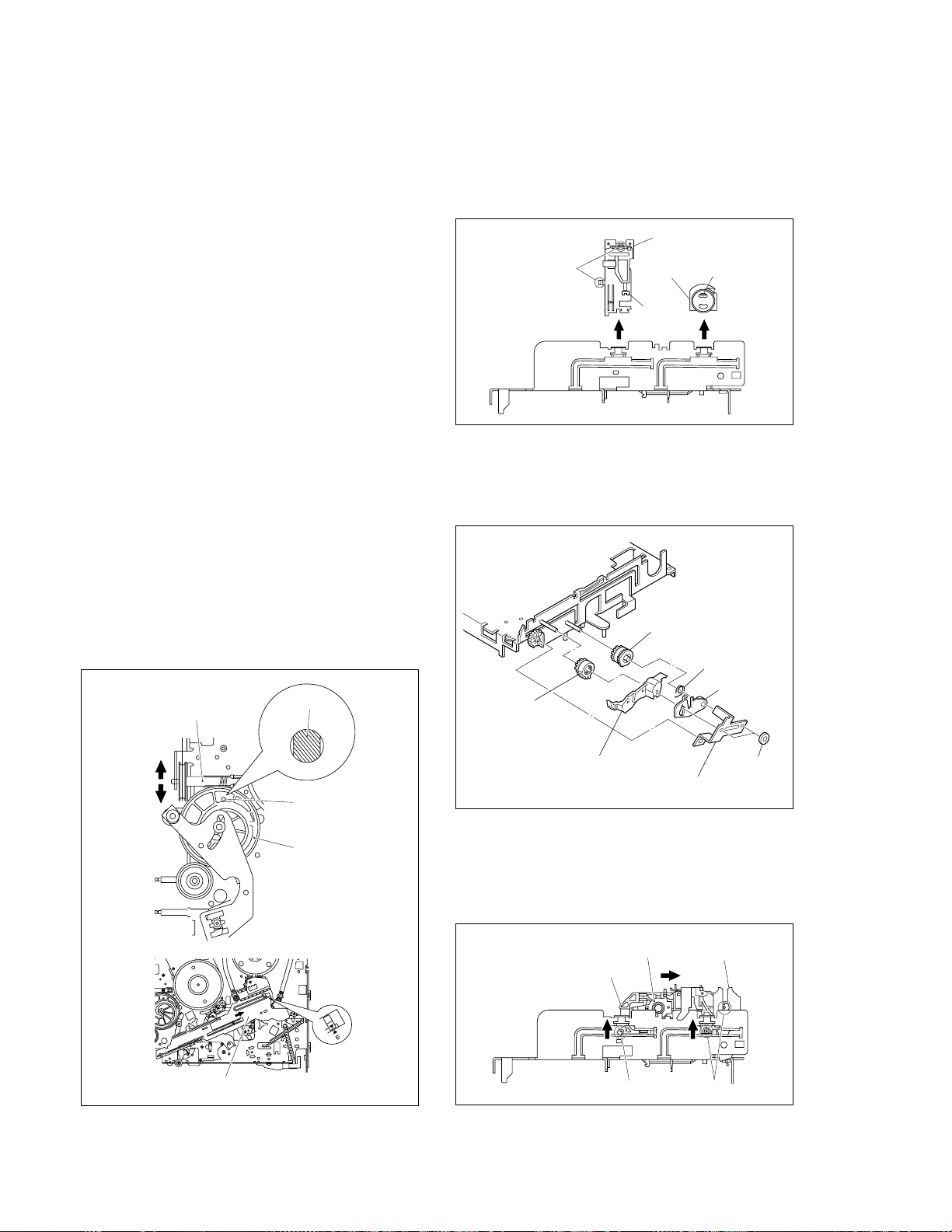
Relay gear
B
Guide holeNotches Notch
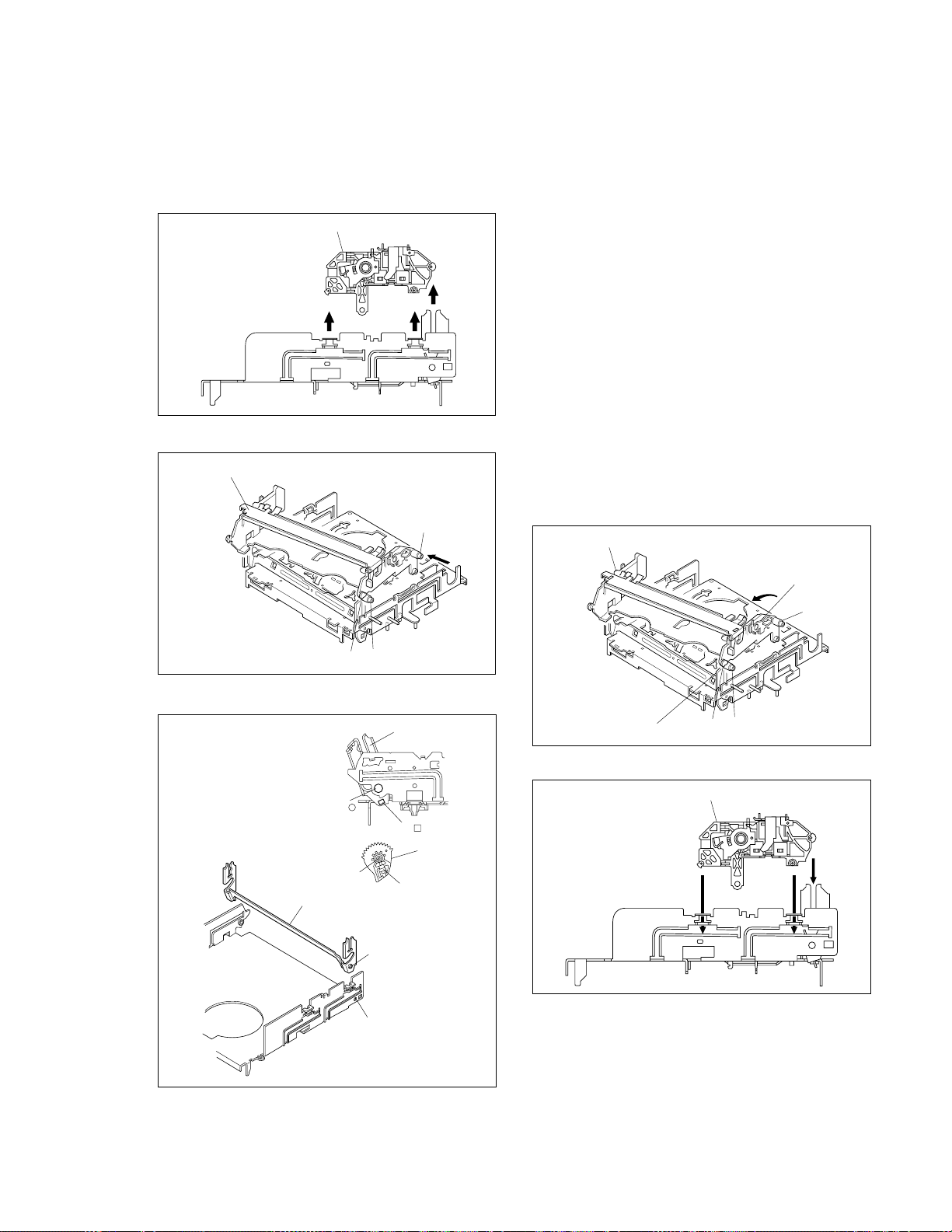
2.2.6 A/C head
1. How to remove
(1) Remove the two screws (A) and remove the A/C head
together with the head base.
(2) When replacing only the A/C head, remove the three
screws (B) while controlling the compression spring.
Head base
B
AA
Drive gear Limit gear
Fig. 2-2-3i
2.2.4 Pinch roller arm assembly
1. How to remove
(1) Remove the spring from the hook of the press lever as-
sembly.
(2) Remove the slit washer and remove the pinch roller seat
2. (See Fig.2-2-4a.)
(3) Remove the pinch roller arm assembly by pulling it up.
Slit washer
Pinch roller seat2
Spring
Pinch roller arm
Press lever assembly
Pinch roller arm assembly
assembly
Fig. 2-2-4a
2.2.5 Guide arm assembly and press lever assembly
1. How to remove
(1) Remove the spring and expand the lug of the lid guide in
the arrow-indicated direction. Then remove the guide arm
assembly by pulling it up.
(2) Remove the press lever assembly by pulling it up. (See
Fig.2-2-5a.)
Screws(A)
A/C head
Fig. 2-2-6a
Screws(B)
A/C head
Compression
A/C head board
assembly
Head base
springs
Fig. 2-2-6b
2. How to install
(1) To make the post-installation adjustment easier, set the
temporary level as indicated in Fig.2-2-6c. Also make sure
that the screw center (centre) is brought into alignment
with the center (centre) position of the slot.
A/C head
12.4 mm
Head base
A/C head
Head base
Screw
2-8
Tension
spring
LugLid guide
Fig. 2-2-5a
Press lever
assembly
Guide arm
assembly
Fig. 2-2-6c
2.2.7 Loading motor
1. How to remove
(1) Remove the belt wound around the worm gear.
(2) Open the two lugs of the motor guide and remove the
loading motor, loading motor board assembly and motor
guide altogether by pulling them up.
(3) When replacing the loading motor board assembly, take
care with the orientation of the loading motor. (Install so
that the loading motor label faces upward.)
(4) When the motor pulley has been replaced, choose the
fitting dimension as indicated in Fig.2-2-7a.
Page 21

Loading motor board assembly
Loading motor
Lugs
Motor guide
6.5 ± 0.2 mm
LABEL
Worm gear
Belt
Motor pulley
Fig. 2-2-7a
2.2.8 Capstan motor
1. How to remove
(1) Remove the belt (capstan) on the mechanism assembly
back side.
(2) Remove the three screws (A) and remove the capstan
motor.
Screws(A)
Screw(A)
Capstan motor
Belt
Fig. 2-2-8a
Spacer
Spacer
2. How to install (Centering the mounting position)
When the capstan motor has once been removed and then
reinstalled out of the initial correct position in the rotational
direction, the capstan motor current may be unstable during
operation in high or low temperatures. This may result in
greater Wow & Flutter and occasionally in power breakdown
because of current over - load. Install the capstan motor while
following the procedure given below.
(The capstan motor is centrally located when the unit is
shipped from the factory.)
(1) Provisionally tighten the three screws (A) securing the
capstan motor.
(2) Install the mechanism assembly to which the capstan
motor is provisionally fastened on the bottom chassis
which incorporates the Main board assembly. (No need
to tighten the screws for mounting the mechanism.)
Make sure that all the connectors for the mechanism assembly and the Main board assembly are correctly installed as indicated in Fig. 2-2-8b.
(3) Making sure that the connector for the capstan motor is
correctly mounted, and securely tighten the three screws
(A).
Note:
• When the capstan motor has been replaced with a new
one, perform recording in the EP(or LP) mode for at
least 2 minutes at normal temperatures immediately before starting the FF/REW or SEARCH operations (Aging).
2.2.9 Pole base assembly (supply or take-up side)
1. How to remove
(1) Remove the UV catcher 2 on the removal side by loos-
ening the screw (A).
(2) Remove the pole base assembly on the supply side from
the mechanism assembly by loosening the screw (B) on
the mechanism assembly back side and sliding the pole
base assembly toward the UV catcher 2.
(3) As for the pole base assembly on the take-up side, turn
the pulley of the loading motor to lower the cassette
holder because the screw (B) is hidden under the control plate. (See the “Procedures for Lowering the Cassette
holder assembly” of 1.3 DISASSEMBLY/ASSEMBLY
METHOD.) Further turn the motor pulley to move the cassette holder until the screw (B) is no longer under the control plate (in the half-loading position). Then remove it as
done for the supply side by removing the screw (B).
Note:
• After reinstalling the Pole base assembly and the UV
catcher2, be sure to perform compatibility adjustment.
Fig. 2-2-8b
Connector for
the capstan motor
Screw(A)
UV catcher2
Screw(A)
UV catcher2
Screw(B)
Fig. 2-2-9a
2-9
Page 22

2.2.10 Rotary encoder
1. How to remove
(1) Remove the screw (A) and remove the rotary encoder
by pulling it up. (See Fig. 2-2-10a.)
Rotary encoder (Front side)
Screw(A)
Guide marks
2.2.12 Change lever assembly, direct gear, clutch gear
and coupling gear
1. How to remove
(1) Release the two lugs of the rotary encoder guide in the
arrow-indicated direction and remove the change lever
assembly.
(2) Remove the slit washer retaining the direct gear and re-
move the latter.
Take care so as not to lose the washer and spring. (See
Fig.2-2-12a.)
Rotary encoder (Back side)
Positioning pin of the rotary encoder
Fig. 2-2-10a
Mark E
Shaft of the rotary encoder guide
Control plate
Fig. 2-2-10b
2. How to install (Phase matching)
(1) Make sure that the mark E of the control plate is in align-
ment with the mark
of the loading arm gear shaft and
bring the guide marks on the rotary encoder into alignment as indicated in Fig.2-2-10a. (See Fig. 2-2-10a and
Fig. 2-2-10b.)
(2) Turn over the rotary encoder with its guide marks kept in
alignment and install it by fitting on the shaft of the rotary
encoder guide and the positioning pin.
(3) Tighten the screw (A) to complete the installation.
2.2.11 Clutch unit
(1) Remove the belt wound around the capstan motor and
the clutch unit.
(2) Remove the slit washer and remove the clutch unit.
Change lever
assembly
Spring(B)
Lugs
Note:
• The parts with marked (
speed FF/REW type).
1 : Uses the standard type mechanism only.
*
2:
Uses the high-speed FF/REW type mechanism only.
*
Slit washer
Washer (*1)
Spacer
Direct gear
Spring(A)
Position the projecting
side down.
) have different types of mechanisms (standard type or high-
*
Coupling gear
Spring (C)
Clutch gear
Spacer
Fig. 2-2-12a
2. How to install
(1) Install the clutch gear, spring (A), spring (C), direct gear,
spacer and others to the individual shafts of the main
deck, and finally the slit washer. (See Fig.2-2-12a.)
(2) Let the spring (B) drops into the rotary encoder guide hole
and install the change lever assembly.(Take care not to
mistake a direction of the spring.) The point is to slightly
lift the coupling gear and catch it from the both sides with
the assembly. (See Fig.2-2-12b.)
Rotary encoder guide
Spring(B)
Change lever assembly
Coupling gear
2-10
Belt
Clutch unit
Fig. 2-2-11a
Slit washer
Main deck Main deck
Fig. 2-2-12b
Page 23

2.2.13 Link lever
1. How to remove
(1) Remove the two slit washers.
(2) Remove the link lever by lifting it from the shaft retained
by the slit washers. Then swing the link lever
counterclockwise and remove it from the locking section
of the control plate.
Slit washers
2.2.14 Cassette gear, control cam and worm gear
1. How to remove
(1) Remove the control cam by lifting it.
(2) Open the two lugs of the cassette gear outward and pull
the latter off.
(3) Remove the belt wound around the worm gear and the
loading motor.
(4) Open the lug of the lid guide outward and remove the
worm gear.
Link lever
Locking section of the
control plate
Fig. 2-2-13a
2. How to install (Phase matching)
(1) Slide the control plate so that its mark E is aligned with
the mark
on the loading arm gear shaft. (See Fig.2-2-
13b.)
(2) Rotate the worm gear until the guide hole of the control
cam is aligned exactly with the guide hole of the main
deck. (See Fig.2-2-13c.)
(3) Insert the link lever into the locking section of the control
plate. (See Fig.2-2-13a.)
(4) Rotate the link lever clockwise so that it is installed on
the shafts in the center (centre) and on the left of the control cam.
(5) Fasten the slit washers at these two points.
Loading motor
Belt
Lug
Worm gear
Lugs
Cassette gear
Lid guide
Control cam
Fig. 2-2-14a
2.2.15 Control plate
1. How to remove
(1) Remove the screw (A) retaining the control bracket 1 and
remove the latter.
(2) Slide the control plate as indicated by the arrow and re-
move the control plate. (See Fig.2-2-15a.)
Shaft of the rotary encoder guide
Fig. 2-2-13b
Worm gear
Main deck
guide hole
Control cam
guide hole
Cassette gear
Fig. 2-2-13c
Control plate
Control cam
Mark E
Screw(A)
Control
bracket1
Control
plate
Fig. 2-2-15a
2. How to install (Phase matching)
(1) Adjust the position of the idler arm assembly pin as indi-
cated in Fig.2-2-15b (to the left of center (centre) of the
R section).
(2) Bring the guide hole of the take-up lever into alignment
with the hole at the control plate guide and fix the position by inserting a 1.5 mm hexagonal wrench.
2-11
Page 24

(3) Install the control plate so that the section A of the load-
ing arm gear shaft fits into the hole (A) of the control plate,
the section B of the control plate guide into the hole (B),
and the control plate comes under the section C of the
rotary encoder guide and the section D of the loading arm
gear shaft while press-fit the pole base assmebly (supply side) as indicated by the arrow. It is important that
the tension arm assembly shaft is positioned closer toward you than the control plate. (See Fig.2-2-15c.)
(4) Make sure that the mark E of the control plate is in align-
ment with the mark
of the loading arm gear shaft. (See
Fig.2-2-15c.)
(5) Pull off the hexagonal wrench for positioning.
(3) Turn the loading arm gear (take-up side) clockwise so
that the notch of the loading arm gear (take-up side) is
in alignment with the projection of the loading arm gear
shaft and lift it.
Likewise, turn the loading arm counterclockwise so that
the notch is in alignment with the projection and remove
the loading arm gear (take-up side). (See Fig.2-2-16a and
Fig. 2-2-16b.)
(4) When removing the loading arm gear shaft, be sure of
first removing the screw retaining the drum assembly (on
the back side of the loading arm gear shaft). Then remove the screw (C) and remove the loading arm gear
shaft by sliding it.
Idler arm assembly
pin
R section
Guide hole of the
control plate guide
Section D
1.5mm hexagonal wrench
Fig. 2-2-15b
Section A
Section D
Hole A
Pressfit
Take-up lever
Insert
Pole base assembly
(supply side)
Section A
Hole A
Pole base assembly
(take-up side)
Screw(B)
Torsion arm
Loading arm gear
(take-up side)
Projection B
Guide marks
Projection A
Pole base assembly
(supply side)
Screw(A)
Loading arm gear
(supply side)
Fig. 2-2-16a
Loading arm gear shaft
Loading arm gear (take-up side)
Fig. 2-2-16b
Notch
Screw(C)
Loading arm gear shaft
Section C
Section C
Section B
Hole B
Hole B
Section B
Control plate
Tension arm assembly
shaft
Fig. 2-2-15c
2.2.16 Loading arm gear (supply or take-up side) and
loading arm gear shaft
1. How to remove
(1) Remove the loading arm gear (supply side) by loosen-
ing the screw (A). (See Fig. 2-2-16a.)
(2) Remove the screw (B) and remove the torsion arm from
the pole base assembly (take-up side). (See Fig.2-2-16a.)
2-12
2. How to install
(1) Align the notch of the loading arm gear (take-up side) to
the projection B of the loading arm gear shaft and slip it
over. Then rotate it clockwise for alignment with the projection A and slip it down to the bottom. (See Fig.2-216b.)
(2) Then turn the loading arm gear (take-up side)
counterclockwise. Hang the torsion arm on the pole base
assembly (take-up side) and tighten the screw (B).
(3) Install the loading arm gear (supply side) so that the guide
mark of the loading arm gear (take-up side) is in alignment with the guide mark of the loading arm gear (supply side). Then hang the torsion arm on the pole base
assembly (supply side) and tighten the screw (A). (See
Fig.2-2-16a.)
Page 25

2.2.17 Take-up lever, take-up head and control plate
guide
(1) Remove the spring of the take-up lever from the main
deck.
(2) Remove the lug (A) of the take-up lever from the main
deck and pull out the take-up lever and the take-up head
together.
(3) Remove the screw (A).
(4) Align the idler arm assembly pin in the center (centre) of
the R section of the control plate guide, remove the con-
trol plate guide lugs (B) and (C) from the main deck, and
remove the control plate guide.
Idler arm assembly pin
Lug(C)
Screw(A)
Take-up lever
Take-up head
Lug(A)
Lug(B)
Control plate guide
Fig. 2-2-17a
2.2.18 Capstan brake assembly
1. How to remove
(1) Move the lug (A) of the capstan brake assembly in the
arrow-indicated direction so that it comes into alignment
with the notch of the main deck. (See Fig. 2-2-18a.)
(2) Remove the lug (B) of the capstan brake assembly from
the main deck and remove the capstan brake assembly.
Spring
Sub brake
Lug(A)
Lug(B)
assembly
(take-up side)
Lug(C)
Fig. 2-2-19a
2.2.20 Main brake assembly (take-up side), reel disk
(take-up side) and main brake assembly (supply
side)
1. How to remove
(1) Move the main brake assembly (take-up side) in the ar-
row-indicated direction and remove the reel disk (takeup side).
(2)
Remove the spring attached to the main brake assembly.
(3) Remove the lug (A) of the main brake assembly (take-
up side) and pull out the lug (B) after bringing it into alignment with the main deck notch.
(4) Remove the lugs (C), (D) and (E) of the main brake as-
sembly (supply side) from the main deck and pull them
off. (See Fig.2-2-20a.)
(5) When installing the main brake assembly (take-up side),
slide the brake lever in the direction as indicated by the
arrow to prevent it from hitting the projection of the main
brake assembly (take-up side). (See Fig.2-2-20b.)
Main brake assembly
(supply side)
Reel disk
(take-up side)
Main brake assembly
(take-up side)
Lug(B)
Lug(A)
Capstan brake assembly
Fig. 2-2-18a
2.2.19 Sub brake assembly (take-up side)
1. How to remove
(1) Remove the spring attached to the lid guide and sub
brake assembly (take-up side).
(2) Bring the lug (A) of the sub brake assembly (take-up side)
into alignment with the notch of the main deck.
(3) Remove the lugs (B) and (C) of the sub brake assembly
(take-up side) from the main deck and remove the sub
brake assembly (take-up side).
Lug(B)
Lug(C)
Lug(D)
SpringLug(E)
Lug(A)
Notch
Fig. 2-2-20a
(
1)
*
Brake
lever
Note:
• The parts with marked ( *) have different types of mechanisms (standard type
or high-speed FF/REW type).
1 : Uses the standard type mechanism only.
*
Rotary encoder guide
Projection of the main
brake assembly
(take-up side)
Fig. 2-2-20b
2-13
Page 26

2.2.21 Tension brake assembly, reel disk (supply side)
and tension arm assembly
1. How to remove
(1) Remove the three lugs of the tension brake assembly
from the main deck and pull them off.
(2) Remove the reel disk (supply side) by loosening in the
arrow-indicated direction the main brake assembly (supply side).
(3) Remove the tension spring on the back of the main deck.
Then release the lug of the tension arm bearing in the
arrow-indicated direction and draw out the tension arm
assembly. (See Fig. 2-2-21a.)
Lug of the tension
arm bearing
Tension arm
assembly
Reel disk
(supply side)
2.2.23 Stator assembly
(1) Remove the flat cable.
(2) Remove the two screws (A), (B) and remove the lug wire.
(3) Remove the stator assembly by lifting in the arrow-indi-
cated direction. (Take care that the brush spring does not
jump out.)
Notes:
• Be careful not to lose the brush and spring.
• There are some models that do not use the lug wire.
Refer to the parts list for these models.
• When tightening the screw (B), place the caulked part
of the lug terminal near to the shaft of the drum and
then tighten it.
• After installation, be sure to perform the switching
point adjustment according to the electrical adjustment
procedure.
Tension brake
assembly
Lugs
Tension spring Main brake assembly
(supply side)
Fig. 2-2-21a
2.2.22 Idler lever, idler arm assembly
1. How to remove
(1) Remove the lug of the idler lever from the main deck and
remove the hook fitted in the idler arm assembly hole by
lifting it.
(2) Remove the slit washer and pull out the idler arm assem-
bly.
Lug Idler lever
Hook
Idler arm
assembly
Slit washer
Screw (A)
Stator assembly
Screw (B)
Lug wire
(Note)
Drum
shaft
Flat cable
(Take care not to mix up the
polar faces when installing.)
Lug wire
Screw (A)
Fig. 2-2-23a
2.2.24 Rotor assembly
1. How to remove
(1) Remove the stator assembly.
(2) Remove the two screws (B) and remove the rotor assem-
bly.
2. How to install
(1) Match the phases of the upper drum assembly and the
rotor assembly as indicated in Fig.2-2-24a.
(2) Place the upper drum assembly hole (a) over the rotor
assembly holes (b) (with three holes to be aligned) and
tighten the two screws (B). (See Fig.2-2-24a.)
Screws (B)
Hole(a)
2-14
Fig. 2-2-22a
Screw holes
Upper drum
assembly
Rotor assembly
Fig. 2-2-24a
The hole is not in
line but is offset
toward the right.
Hole(b)
Page 27

2.2.25 Upper drum assembly
Notes:
• To replace the upper drum assembly only may not be
possible with some models. For upper drum assembly replacement, refer to the parts list. (When the parts
number of the upper drum assembly is not listed on
the parts list, then this cannot be replaced.)
• When replacement is required, control the up- down
movement of the brush. Never apply grease.
• When replacing the upper drum assembly, replace it
the together with the washer.
1. How to remove
(1) Remove the stator assembly and rotor assembly.
(2) Loosen the screw of the collar assembly using a 1.5 mm
hexagonal wrench and remove the collar assembly. Also
remove the brush, spring and cap at one time.
(3) Remove the upper drum assembly and remove the
washer using tweezers.
Lower drum assembly
Coil parts
Upper drum assembly
Fig. 2-2-25b
Spring
Brush
Upper drum
assembly
Collar
assembly
Loosen
Cap
Washer
1.5 mm
hexagonal wrench
Shaft
Lower drum assembly
Fig. 2-2-25a
2. How to install
(1) Clean the coil parts of the lower drum assembly and the
newly installed upper drum assembly with an air brush
in advance. (See Fig.2-2-25b.)
(2) Install a new washer and upper drum assembly on the
drum shaft. (See Fig.2-2-25a.)
(3) Install the cap to the upper drum assembly.
(4) Position the collar assembly as indicated in Fig.2-2-25c
while controlling its up- down movement.
(5) Secure the collar assembly in position with a hexagonal
wrench while pressing its top with the fingers.
(6) After installation, gently turn the upper drum assembly
with your hand to make sure that it turns normally. Then
install the brush and the spring.
(7) Install the rotor assembly and stator assembly according
to Fig 2-2-23a and 2-2-24a.
(8) When installation is complete, clean the upper drum as-
sembly and lower drum assembly and carry out the fol-
lowing adjustments.
• PB switching point adjustment
• Slow tracking adjustment
• Compatibility adjustment (Be sure to check for compatibility for the EP (or LP) mode.)
Upper drum
assembly
Collar
assembly
Fig. 2-2-25c
Press
Fig. 2-2-25d
Collar
assembly
Tighten
2-15
Page 28

2.3 Compatibility adjustment
Notes:
• Although compatibility adjustment is very important,
it is not necessary to perform this as part of the normal servicing work. It will be required when you have
replaced the A/C head, drum assembly or any part of
the tape transport system.
• To avoid any damage to the alignment tape while performing the compatibility adjustment, get a separate
cassette tape (for recording and play back) ready to
be used for checking the initial tape running behavior.
• Unless otherwise specified, all measuring points and
adjustment parts are located on the Main board.
• When using the Jig RCU, it is required to set the VCR
to the Jig RCU mode (the mode in which codes from
the Jig RCU can be received). (See SECTION 1 DISASSEMBLY.)
Jig RCU
[Data transmitting method]
Depress the “ ” ( 3 ) button
after the data code is set.
pole base assembly (supply or take-up side).
(7) Unload the cassette tape once, play back the alignment
tape (A1) again and confirm the V.PB FM waveform.
(8) After adjustment, confirm that the tape wrinkling does not
occur at the roller upper or lower limits. (See Fig. 2-31d.)
[Perform adjustment step (9) only for the models
equipped with SP mode and EP (or LP) mode.]
(9) Repeat steps (1) to (8) by using the alignment tape (A2).
CUSTOM CODE
43: A CODE
53: B CODE
DATA CODE
INITIAL MODE
Fig. 2-3a Jig RCU [PTU94023B]
2.3.1 FM waveform linearity
Signal (A1) •
Mode (B) • PB
Equipment (C) • Oscilloscope
Measuring point (D) • TP106 (PB. FM)
External trigger (E) • TP111 (D.FF)
Adjustment part (F) • Guide roller [Mechanism assembly]
Specified value (G) • Flat V.PB FM waveform
Adjustment tool (H)
Alignment tape(SP, stairstep, PAL) [MHPE]
(A2) •
Alignment tape(LP, stairstep, PAL) [MHPE-L]
• Roller driver [PTU94002]
(1) Play back the alignment tape (A1).
(2) Apply the external trigger signal to D.FF (E), to observe
the V.PB FM waveform at the measuring point (D).
(3) Set the VCR to the manual tracking mode.
(4) Make sure that there is no significant level drop of the
V.PB FM waveform caused by the tracking operation, with
its generally parallel and linear variation ensured. Per-
form the following adjustments when required. (See Fig.
2-3-1a.)
(5) Reduce the V.PB FM waveform by the tracking opera-
tion. If a drop in level is found on the left side, turn the
guide roller of the pole base assembly (supply side) with
the roller driver to make the V.PB FM waveform linear.
If a drop in level is on the right side, likewise turn the guide
roller of the pole base assembly (take-up side) with the
roller driver to make it linear. (See Fig. 2-3-1c.)
(6) Make sure that the V.PB FM waveform varies in parallel
and linearly with the tracking operation again. When re-
quired, perform fine-adjustment of the guide roller of the
Max level
Proper waveform variation
Improper waveform variation
Fig. 2-3-1a
Roller driver
Fig. 2-3-1b
Min level
Guide roller (supply side)
2-16
Page 29

A
B
(4) Adjust the AUDIO OUT waveform and Control pulse
waveform by turning the screws (1), (2) and (3) little by
little until both waveforms reach maximum. The screw (1)
and (3) are for adjustment of tilt and the screw (2) for azimuth.
Level drop at the guide roller (supply side)
C
Level drop at the guide roller (take-up side)
• Proper waveform variation: Always flat
• Improper waveform variation:
Higher Lower
D
Fig. 2-3-1c
Improper
(a) Guide roller
(b) Guide pole
Proper
Fig. 2-3-1d
2.3.2 Height and tilt of the A/C head
Note:
• Set a temporary level of the height of the A/C head in
advance to make the adjustment easier after the A/C
head has been replaced. (See Fig.2-2-6c.)
Signal (A) •
Mode (B) • PB
Equipment (C) • Oscilloscope
Measuring point (D1)
External trigger (E) • TP111 (D.FF)
Adjustment part (F) • A/C head [Mechanism assembly]
Specified value (G)
Alignment tape(SP, stairstep, PAL) [MHPE]
• AUDIO OUT terminal
(D2) • TP4001 (CTL. P)
• Maximum waveform
Head base
(2)
A/C head
(3)
(1)
AUDIO OUT
CTL. P
Fig. 2-3-2a
2.3.3 A/C head phase (X-value)
Signal (A1) •
Mode (B) • PB
Equipment (C) • Oscilloscope
Measuring point (D) • TP106 (PB. FM)
External trigger (E) • TP111 (D.FF)
Adjustment part (F) •
Specified value (G) • Maximum V.PB FM waveform
Adjustment tool (H)
Alignment tape(SP, stairstep, PAL) [MHPE]
A/C head base [Mechanism assembly]
• A/C head positioning tool [PTU94010]
(1) Play back the alignment tape (A1).
(2) Apply the external trigger signal to D.FF (E), to observe
the V.PB FM waveform at the measuring point (D).
(3) Set the VCR to the manual tracking mode.
(4) Loosen the screws (4) and (5), then set the A/C head
positioning tool to the innermost projected part of the A/
C head. (See Fig. 2-3-3a.)
(5) Turn the A/C head positioning tool fully toward the cap-
stan. Then turn it back gradually toward the drum and
stop on the second peak point position of the V.PB FM
waveform output level. Then tighten the screws (4) and
(5).
(6) Perform the tracking operation and make sure that the
V.PB FM waveform is at its maximum.
If it is not at maximum, loosen the screws (4) and (5),
and turn the A/C head positioning tool to bring the A/C
head to a position, around where the waveform reaches
its maximum for the first time. Then tighten the screws
(4) and (5).
(1) Play back the alignment tape (A).
(2) Apply the external trigger signal to D.FF (E), to observe
the AUDIO OUT waveform and Control pulse waveform
at the measuring points (D1) and (D2) in the ALT mode.
(3) Set the VCR to the manual tracking mode.
2-17
Page 30

[Perform adjustment steps (7) to (10) only for 2 Head
models equipped with LP mode.]
(7) Then play back the alignment tape (A2).
(8) Set the VCR to the manual tracking mode.
(9) Perform the tracking operation and make sure that the
V.PB FM waveform is at its maximum.
(10)
If it is not at maximum, loosen the screws (4) and (5),
and turn the A/C head positioning tool to bring the A/C
head to a position, around where the waveform reaches
its maximum for the first time. Then tighten the screws
(4) and (5).
Note:
• After adjusting, always perform the confirmation and
re-adjustment of the item 2.3.4.
Toward the drum
A/C head positioning tool
To the drum
A/C head
Toward the capstan
Head base
Screw
Screw
To the capstan
(4)
(5)
Fig. 2-3-3a
Alignment tape
[SP, stairstep]
played with the
SP head
Alignment tape
[EP(LP), stairstep]
played with the
EP(LP) head
(4) Set the VCR to the Auto adjust mode by transmitting the
code (F) twice from the Jig RCU. When the VCR enters
the stop mode, the adjustment is completed.
(5) If the VCR enters the eject mode, perform adjustment for
the audio control head phase (X-value) again.
2.3.5 Tension pole position
Signal (A) • Back tension cassette gauge
Mode (B) •PB
Adjustment part (F) • Adjust pin [Mechansim assembly]
Specified value (G)
[PUJ48076-2]
• 25 - 51 gf•cm (2.45 – 5 × 10
-3
Nm]
(1) Play back the back tension cassette gauge (A).
(2) Check that the indicated value on the left side gauge is
within the specified value (G).
(3) If the indicated value is not within the specified value (G),
perform the adjustment in a following procedure.
1) Set the VCR to the mechanism service mode. (See
SECTION 1 DISASSEMBLY.)
2) Set the VCR to the play back mode and adjust by turning adjustment pin to align the tension arm assembly
edge with the main deck hole (A) on the right edge
marker. (See Fig. 2-3-5a)
Tension arm
assembly
Marker
Edge
0.5 mm
Adjust pin
Hole (A)
Waveform output
X-value adjustment point
Drum side Control head position Capstan side
Maximum
Fig. 2-3-3b
2.3.4 Standard tracking preset
Signal (A) •
Mode (B) • PB ¥ Auto adjust
Equipment (C) • Oscilloscope
Measuring point (D) • TP106 (PB. FM)
External trigger (E) • TP111 (D.FF)
Adjustment part (F) • Jig RCU: Code “50”
Specified value (G)
Adjustment tool (H)
Alignment tape(LP, stairstep, PAL) [MHPE-L]
• STOP mode
(Maximum V.PB FM waveform)
• Jig RCU [PTU94023B]
(1) Play back the alignment tape (A).
(2) Apply the external trigger signal to D.FF (E), to observe
the V.PB FM waveform at the measuring point (D).
(3) Confirm that the automatic tracking operation is com-
pleted.
Tension arm assembly
Tension brake assembly
Fig. 2-3-5a
2-18
Page 31

Mechanism Timing Chart
Mechanism mode
Control plate mark
Rotary encoder
Control cam angle
EJECT
END
E U CI
HIGH
C CH
LOW
HIGH
B CH
LOW
HIGH
A CH
LOW
0
CASS-
UP
69 136 370 412.
CASS-INS
FF/REW
FR
230
STOP
ST
264.
REV
R
318.
7
7
SLOW/STILLPPLAY
SL
42
Rotary encoder
angle
Pole base
Pinch roller
Guide arm
Tension arm
Main brake S
Main brake T
Sub brake S
Sub brake T
Capstan brake
Direct gear
Change lever 2
Idler position
Take-up lever
Rec safety switch
Operation mode
HALF PRESS
CONTACT
ON PLAY
ON REV
CONTACT
(C-INS)
HALF REV
HALF FF/REW
CONTACT
CONTACT
IN FF/REW
OUT PLAY
SUPPLY
CENTER
TAKE-UP
READY
RESET
ON
OFF
OFF
ON
OFF
ON
OFF
ON
OFF
ON
OFF
ON
OFF
ON
OFF
ON
OFF
OFF
ON
ON
OFF
0
20 42.652.
6
6
114.
150.4167.8178.
8
Timer REC
(drum at stop)
POWER OFF
(cassette loaded)
207.2218.2240.2251.
standby
STOP
Backspace Slow FOR
Search REW
Slow REW
2
293.2304.2320.4335
REC pause
REC
Search FF
STOP
(
drum
in motion)
2-19
Page 32

SECTION 3
ELECTRICAL ADJUSTMENT
3.1 Precaution
The following adjustment procedures are not only necessary
after replacement of consumable mechanical parts or board
assemblies, but are also provided as references to be referred to when servicing the electrical circuitry.
In case of trouble with the electrical circuitry, always begin a
service by identifying the defective points by using the measuring instruments as described in the following electrical adjustment procedures. After this, proceed to the repair , replacement and/or adjustment. If the required measuring instruments
are not available in the field, do not change the adjustment
parts (variable resistor, etc.) carelessly.
3.1.1 Required test equipments
• Color (colour) television or monitor
• Oscilloscope: wide-band, dual-trace, triggered delayed
sweep
• Signal generator: RF / IF sweep / marker
• Frequency counter
• Signal generator: stairstep, color (colour) bar [PAL]
• Recording tape
• Digit-key remote controller(provided)
3.1.2 Required adjustment tools
Jig RCU
PTU94023B
Alignment tape
(SP, stairstep, PAL)
MHPE
3.1.4 Switch settings and standard precautions
The SW settings of the VCR and the standard precautions
for the electrical adjustments are as follows.
When using the Jig RCU, it is required to set the VCR
•
to the Jig RCU mode (the mode in which codes from
the Jig RCU can be received). (See SECTION 1 DISASSEMBLY.)
Jig RCU
[Data transmitting method]
Depress the “ ” ( 3 ) button
after the data code is set.
CUSTOM CODE
43: A CODE
53: B CODE
DATA CODE
INITIAL MODE
Fig. 3-1-4a Jig RCU [PTU94023B]
•
Set the switches as shown below unless otherwise
specified on the relevant adjustment chart. The switches
that are not listed below can be set as desired.
If the VCR is not equipped with the functions detailed
below, setup is not required.
AUTO PICTURE/VIDEO CALIBRATION/
B.E.S.T./D.S.P.C.
PICTURE CONTROL/SMART PICTURE
VIDEO STABILIZER OFF
TBC ON
Digital 3R ON
VIDEO NAVIGATION/TAPE MANAGER
OFF
NORMAL/NATURAL
OFF
3.1.3
Color (colour) bar signal, color (colour) bar pattern
Color(colour) bar signal [PAL]•
•
White(100%)
White(75%)
0.7 V
1V
0.3 V
Horizontal sync
Yellow
Cyan
Green
Magenta
Red
VU
V(R-Y)
U(B-Y)
Blue
Burst
Color(colour) bar pattern [PAL]
(75%)
Cyan
White
Yellow
0.3 V
U Black
V
White
100%
Green
Magenta
Red
Blue
•
If there is a reference to a signal input methed in the
signal column of the adjustment chart, “Ext. S-input”
means the Y/C separated video signal and “Ext. input”
means the composite video signal input.
•
Unless otherwise specified, all measuring points and
adjustment parts are located on the Main board.
3-1
Page 33

3.2 Servo circuit
3.2.1 Switching point
Signal (A1) • Stairstep signal
Mode (B) • PB
Equipment (C) • Oscilloscope
Measuring point (D1) •
External trigger (E) • TP111 (D.FF)/slope : –
Adjustment part (F) • Jig RCU: Code “5A”
Specified value (G) • 6.5 ± 0.5H
Adjustment tool (H) • Jig RCU [PTU94023B]
(A2) •
Alignment tape (SP,stairstep,PAL) [MHPE]
VIDEO OUT terminal (75Ø terminated)
(D2) • TP106 (PB. FM)
(1) Play back the signal (A1) of the alignment tape (A2).
(2) Apply the external trigger signal to D.FF (E) to observe
the VIDEO OUT waveform and V.PB FM waveform at the
measuring points (D1) and (D2).
(3) Set the VCR to the manual tracking mode.
(4) Adjust tracking so that the V.PB FM waveform becomes
maximum.
(5) Set the VCR to the Auto adjust mode by transmitting the
code (F) from the Jig RCU. When the VCR enters the
stop mode, the adjustment is completed.
(6) If the VCR enters the eject mode, repeat steps (1) to (5)
again.
(7) Play back the alignment tape (A2) again, confirm that the
switching point is the specified value (G).
Trigger point
Switching point
V.sync
Note:
For FWD slow (+1/6x) playback, transmit the code “08”
•
from the Jig RCU to enter the slow playback mode, and
transmit the code “D0” for REV slow (–1/6x) mode.
3.3 Video circuit
3.3.1 Auto picture initial setting
Signal (A1) • Ext. input
Mode (B) •
Adjustment part (F) • Jig RCU : Code “58”
Specified value (G) • STOP mode
Adjustment tool (H) • Jig RCU [PTU94023B]
(A2) • Video: Optional
(A3) • VHS tape
EE ¥ Auto adjust (SP/LP REC ¥ PB)
(1) Insert the cassette tape (A3).
(2) Set the VCR to the Auto adjust mode by transmitting the
code (F) from the Jig RCU. When the VCR enters the
stop mode, the adjustment is completed. When the VCR
enters the eject mode, repeat steps (1) to (2) again.
3.4 Syscon circuit [HR-J680EU/J780EU]
Note:
•
When perform this adjustment, remo ve the Mechanism
assembly.
V. rate
Fig. 3-2-1a Switching point
3.2.2 Slow tracking preset
Signal (A1) • Ext. input
(A2) • Color (colour) bar signal [PAL]
Mode (B1) • VHS SP
(B2) • VHS LP
Measuring point (D) • TV-Monitor
Adjustment part (F) • Jig RCU: Code “71“ or “72”
Specified value (G) • Minimum noise
Adjustment tool (H) • Jig RCU [PTU94023B]
(1) Record the signal (A2) in the mode (B1), and play back
the recorded signal.
(2) Set the VCR to the manual tracking mode.
(3) Set the VCR to the FWD slow (+1/6x) mode.
(4) Transmit the code (F) from the Jig RCU to adjust so that
the noise bar becomes the specified value (G) on the TV
monitor in the slow mode.
(5) Set the VCR to the Stop mode.
(6) Confirm that the noise bar is (G) on the TV monitor in
the slow mode.
(7) Repeat steps (3) to (6) in the REV slow (–1/6x) mode.
(8) Repeat steps (1) to (7) in the mode (B2).
3.4.1 Timer clock
Signal (A) • No signal
Mode (B) • EE
Equipment (C) • Frequency counter
Measuring point (D1) • IC3001 pin 61
Short point (D2) • IC3001 pin 24
(D3) • C3026 + and –
Adjustment part (F) • C3025 (TIMER CLOCK)
Specified value (G) • 1024.008 ± 0.001 Hz
(976.5549 ± 0.0010 µsec)
(1) Connect the frequency counter to the measuring point
(D1).
(2) Connect the short wire between the short point (D2) and
Vcc (5V).
(3) Short the leads of capacitor (D3) once in order to reset
the microprocessor of the SYSCON.
(4) Disconnect the short wire between the short point (D2)
and Vcc then connect it again.
(5) Adjust the Adjustment part (F) so that the output fre-
quency becomes the specified value (G).
3-2
Page 34

SECTION 4
CHARTS AND DIAGRAMS
NOTES OF SCHEMATIC DIAGRAM
Safety precautions
The Components identified by the symbol are
critical for safety. For continued safety, replace safety
critical components only with manufacturer's recommended parts.
1. Units of components on the schematic diagram
Unless otherwise specified.
1) All resistance values are in ohm, 1/6 W, 1/8 W (refer to
parts list).
Chip resistors are 1/16 W.
K or k: k
2) All capacitance values are in µF, (P: PF).
3) All inductance values are in µH, (m: mH).
4) All diodes are 1SS133, MA165 or 1N4148M (refer to parts
list).
2. Indications of control voltage
AUX : Active at high
AUX or AUX(L) : Active at low
3. Interpreting Connector indications
(1000 ), M: M (1000k )
1
2
Removable connector
3
1
2
Wire soldered directly on board
3
4) Indication on schematic diagram
Voltage Indications for REC and PB mode on the schematic diagram are as shown below.
REC mode
123
2.5
(5.0)
PB mode
1.8
PB and REC modes
(Voltage of PB and REC modes
are the same)
Note: If the voltages are not indicated on the schematic
diagram, refer to the voltage charts.
5. Waveform measurement
1) Video circuits
REC : Colour bar signal in SP mode, normal VHS mode
PB : Alignment tape, colour bar SP mode, normal VHS
mode
2) Audio circuits
REC : 1KHz, –8 dBs sine wave signal in SP mode, normal
VHS mode
PB : REC then playback it
3) Movie Camera circuits
Measured using a correctly illuminated gray scale or colour
bar test chatrs in the E-E mode
4) Indication on schematic diagram
Waveform indications on the schematic diagram are as
shown below.
24
22201816
Measurement point
1
Non-removable Board connector
2
3
1
2
4
Board to Board
3
Connected pattern on board
The arrows indicate signal path
4. Voltage measurement
1) Video circuits
REC : Colour bar signal in SP mode, normal VHS mode
PB : Alignment tape, colour bar SP mode, normal VHS
mode
— : Unmeasurable or unnecessary to measure
2) Audio circuits
REC : 1KHz, –8 dBs sine wave signal in SP mode, Nor-
mal VHS mode
PB : REC then playback it
3) Movie Camera circuits
Measured using a correctly illuminated gray scale or colour
bar test charts in the E-E mode
C329
C330
0.1/50
R344
47K
R343
18K
0.1/50
C331
11/10
R345
10K
5) Waveform indications
Waveform number
WF25
REC/PB 1.2 Vp-p
50 mV/2 msec/DIV
Oscilloscope Volts and Time/Division, Probe 10 : 1
Mode : REC or PB modes
WF25
R346
15K
ALC OUT
Waveform number
Waveform name or
measurement point
Level : 1.2 Vp-p
4-1
Page 35

6. Signal path Symbols
The arrows indicate the signal path as follows.
Playback signal path
Playback and recording signal path
Recording signal path
(including E-E signal path)
Capstan servo path
Drum servo path
(Example)
R-Y
Playback R-Y signal path
Y
Recording Y signal path
7. Indication of the parts for adjustments
The parts for the adjustments are surrounded with the circle as
shown below.
CIRCUIT BOARD NOTES
1. Foil and Component sides
1) Foil side (B side) :
Parts on the foil side seen from foil face (pattern face)
are indicated.
2) Component side (A side) :
Parts on the component side seen from component face
(parts face) indicated.
2. Parts location guides
Parts location are indicated by guide scale on the circuit board.
REF No. LOCATION
IC
IC101 B C 6A
(A : Component side)
(D : Discrete component)
B : Foil side
C : Chip component
Note:
For general information in service manual, please refer
to the Service Manual of GENERAL INFORMA TION Edition 4 No. 82054D (January 1994).
Category: IC
Horizontal “A” zone
Vertical “6” zone
8. Indication of the parts not mounted on the circuit board
“OPEN” is indicated by the parts not mounted on the circuit
board.
R216
OPEN
4-2
Page 36

4.1 BOARD INTERCONNECTIONS
5
9
2
SAT CTL
(
Page 4-18
91
R.PA USE
(
Page 4-18
4
ONLY USED FOR HR-J780EU
98
P50 I/O
OPEN
3
2
LITHIUM BATTERY
93
R.PAUSE
91
SAT CTL
92
REAR OUT REARIN
J7103 J7104
RR
03
MAIN
(
VIDEO/AUDIO
(
ON SCREEN
(
SYSCON
(
SW.REG
(
TUNER
(
FRONT
(
TERMINAL
)
M
(
QGF1208C1-05
QGF1207C1-05
QGF1201C1-05
DRUM 12V
GND
CN3001
CON1
58
DRUM MO TOR
M
LL
VV
VVL
FOR ARCHi-Fi
FOR ARCMONO
J7101 J7102
AV1 IN/OUT AV2 IN/DECODER
OPEN
)
Page 4-5
)
Page 4-7
)
Page 4-9
Page 4-11
Page 4-13
Page 4-15
Page 4-17
QGF1028C2-08
QGF1028C3-04
QGF1028C1-11
LP CH1
LP CH1
DRUMCTL V
D.PG
D.FG
LP CH2
LP CH2
SP CH1
CN1
41
U.DRUM
LP
LP SP SP
CH1
CH2 CH1 CH2
)
)
)
)
)
L
(
)
)
M
C
(
(
NC
CAP FG
SW5V
CAP REV
CAP CTL V
GND
GND
SP CH1
CN3003
57
CAP MD A
QGB2015M1-08
FMA CH1
FMA COM
FMA CH2
SP CH2
SP CH2
QGB2534J2-04
M12V
CN3004
ROTARY
ENCODER
M
FMA
CH1 CH2
)
)
)
)
OPEN
RAA
FOR ARCMONO
FOR EURO Hi-Fi
FOR ARCHi-Fi
)
FULL ERASE
GND
QGB2532J1-02
CN2002
FULL ERASE HEAD
F.E
RF OUT RF IN
TUNER
TU6001
MATSUSHITA
ALPS
BB(AL5V
)
BB(AL5V
AUDIO IN
AUDIO IN
)
CN7104
SAT CTL
GND
)
CN7106
R.PAUSE
GND
CN7106
P50 I/O
GND
CN7102
SAT CTL
GND
CN7105
R.PAUSE
GND
CN7106
P50 I/O
GND
VIN LIN
FOR Hi-Fi
FRONTIN
ONLY USED FOR
HR-J780EU
MOD SDA
MOD SDA
MOD B(AL5V
)
MOD B(AL5V
MOD SCL
MOD SCL
VIDEO IN
VIDEO IN
NC
)
TU(30V
RF AGC
RF AGC
(BT)
NC
AS
AS
SCL
SCL
SDA
SDA
NC
NC
MB(SW5V
)
MB(SW5V
LOCK
LOCK
TU(30V
)
TU(30V
IF OUT
TP
IF IN
IF OUT
SW 1
SW 1
SW 2
SW 2
AUDIO OUT
AUDIOOUT
SIF OUT
SIF OUT
AFT
AFT
VIDEO OUT
VIDEO OUT
MB(30V
RIN
J7105
LITHIUM
93
BATTERY
(
Page 4-10
FW7006
##QGD2001C1-02
CN3005
)
LI BACK UP
GND
GND
LI BACK UP
ACINPUT
CN5001
QGA7901C3-02
BLU
BRN
OPEN
ONLY USED FOR HR-J780EU/785EK
38
ADV.JOG
(
)
CN7001 CN7003
JSA
T1
T2
T3
T4
GND
T6
KEY OUT
)
)
-
+
(
QGF1207C1-07
QGF1201C1-07
CN1
QGF1208C1-07
REC
QGF1208F1-07
(
PB
GND
AUDIOERASE
GND
CTL HEAD
CTL HEAD
12
A/C HEAD
CTLR/P
A.E
LDM1
LDM2
QGB2532J1-02
CN3002
M
55
LOADING MOTOR
)
C
(
LSB
LSA
LSC
GND
CN2001
JSA
JSBJSB
T1
T2
T3
T4
GND
T6
KEY OUT
28
NC
NC
NC
NC
NC
NC
GND
T6
KEY OUT
Page 4-16
MINI FR ONT
OPEN
1
DRUMMOTOR
58
CAP MDA
57
LOADINGMOTOR
55
U.DRUM
41
38
ADV.JOG
MINI OPE28
A/C HEAD
12
03 MAIN
NO NAME
p10341001a rev0
ABCD EFGH
4-3 4-4
Page 37

4.2
MAIN(VIDEO/AUDIO)SCHEMATIC DIAGRAM
MAIN(VIDEO/AUDIO
FMA CH2
FMA CH1
SP CH2
SP CH1
LP/EP CH2
LP/EP CH1
TOTERMINAL
TOTERMINAL
TOTUNER
TOON SCREEN
TOSYSCON
TOSW.REG
TOU.DRUM
TOSYSCON
TOA/C HEAD
CN1
P/R
A.E
CTL
TOFULL ERASE HEAD
TOSYSCON
FULL E.ON[H]
N.REC ST[H]
TOSECAM
SECAM DET
SECAM REC COLOR
SECAM PB COLOR
NC
LINE OUT[L]
LINE OUT[R]
F.AUDIO[L]
F.AUDIO[R]
LINE V IN
RF AUDIO
TU AUDIO
DEMOD[L]
DEMOD[R]
V TO OSD
A.ENV/ND[L]
A.MUTE[H]
H.REC ST[H]
FE
N.REC[H]
SECAM[H]
V TO OSD
FVIN
RVIN
R2 V IN
PAL PB[H]
CTL[+]
CTL[-]
C.SYNC
A.IN1[L]
A.IN1[R]
A.IN2[L]
A.IN2[R]
GND
GND
GND
2Fsc
GND
A.FF
GND
SW5V
SW12V
CN1
10
L1
GND
CN2001
K2003
K2004
B2051
CN2002
PB FM
EE[L]
Fsc
GND
SW5V
5
4
3
2
)
R2002
2.7K
R2004
3.3K
R2207
3.3K
R2226
12k
R2217
0
R2218
39K
R2219
39K
R2220
39K
12k
R2227
C2228
R2222
R2223
R2224
R2225
0.1
12k
12K
12K
1k
1k
R21
R22
Q2251
DTA144WUA
TP111
D.FF
L2251
R77
10k
C1
0.01
Q2
2SC4081/S/
Q1
2SC4081/S/
2SC4081/S/
Q3
2SC4081/S/
C70
C69
0.01
0.01
330p
C2051
T2052
PELN0861
MY
C2061
0.033
L15
OPEN
C60
OPEN
C6
0.1
C2
0.01
C3
0.01
Q4
C5
220
C4
0.01
/6.3
OPEN
0.047
C8
C7
R2051
T2051
OPEN
R2053
4.7K
MY
C2052
R2052
OPEN
0.0033
C2062
Q2061
27k
R2061
C2064
R2062
C2063
3.3
0.0110
/25
C59
OPEN
R115
1k
Q2052
Q2051
C2053
Q2054
R2056
R2054
C2054C2055
R2055
10
/25
3.3
R2064
47k
R2065
18k
R2063
150
Q2062
R58
OPEN
C78
OPEN
R59
R116
OPEN
1k
L2001
C44
OPEN
SW5V
R2057
47k
R2058
18k
Q2053
R2059
47k
R2060
18k
Q2055
Q2003
DTA144WUA
Q2063
TP106
R12
100
PB FM
OPEN
B22
R24
R23
OPEN
Q31
OPEN
OPEN
B5
0
Q5
OPEN
R65
OPEN
L2252
150
C2255
180P
Q2252
DTC114EUA
C2003 C2251 C2252C2004
/6.3 /6.3OPEN
47 47 0.01
10
SHORT
C2017
OPEN
Q2001
R2018
4.7k
R2019
4.7k
Q2002
L16
OPEN
C57
OPEN
TP2253
R2251
470
C2253
C2254
B28
R2021
C2005
R2015
180
C2008
4.7
R2022
/25
C2226
10
R2012
OPEN
0.1
C2227
SHORT
K2251
0.01
SHORT
K2252
SHORT
K2253
0.01
0
OPEN
4.7
/50
R2014
220k
R2013
6.8k
C2006
C2007
0.012
/16
K2002
22
C2013
C2016
OPEN
/50
33p
K2001
C2010
R2017
0.0015
18k
/50
C2011
4.7
C65
/50
R2016
39k
Q2006
C2009
0.001
5.6k
JCP8020-MSD-2
1000p
C43
C61
0.01
15K
/50
/50
/50
/50
/25
C2225
C2223
C2222
C2220
C2219
4.7
0.47
0.47
4.7
10
C2221
C2224
0.01
0.01
FMMON
NR[L]NR[R]
A.MUTE
ENVDET
A.FF
+
NORDET
PRE/RECGND
CH2
COMMON
CH1
PRE/RECVCC
A.Vcc
BDLGND
COMP
PRE/RECGND
SP2
SP
COMMON
PRE/REC
AMP
SP1
PRE/RECVCC
LP/EP2
LP/EP
COMMON
PRE/REC
AMP
LP/EP1
ENVOUT
D.FF
DET
A.GND
REC
TANK
DCPB
42PIN[L]
IC1
C125
OPEN
L20
OPEN
R33
OPEN
NAEXT IN
REC/PBMON
HIFIFM
SECAM
MUTE
VCA
SECAM
SP
2MLPF
SP
629TRAP
P
R
LPF
MOD
CARR./DEV.ADJ
S-DET
CARREA
OFFSET
MAIN
EMPHA.
INT
W.C./D.C
P
R
D17
CTL
EXT
42PIN[L]
MAIN
DEEMPH.
R1
6.8k
L2
SHORT
C10
C84
150p
C12
OPEN
47p
0.1
OPEN
C11
0.1
C13
R2
C14
C2012
1.5k
/50
4.7
R3
8.2k
R104
6.8k
Q38
R93
R92
2SC4081/QRS/
2.2k
1.5k
C109
0.22
The Parts Number,value and rated voltage etc. in the Schematic Diagram are for references only.
Note :
When replacing the parts,refer to the Parts List.
R2001
680
R2003
100
R2206
R2005
R2006
R2007
R2213
/50
C2218
0.47
OPEN
R71
INPUT SEL INPUT SEL [L][R]
NAINPUT SEL
D1*D18
LPF
D1*D18
P
R
HPF
ET
FBC
ALC
ET
Y
BDL
LPF
L24 L28
27 68
C106
820p 82p
100
0
39K
39K
39K
/50
12K
12k
12K
15K
0.47
R2009
R2008
R2010
R2215
330p
C2230
C2216
/25
/25
C2217
C2002
10
10
2233441
GND
)
L2
EVR
EVR
INPUT SEL
RECLEV.
R
CTL
TRAP
P
SECAM SECAM
C.K.
CTL.P.TRAP
ACC
FhTRAP
COMP
SEP
P
PILOT
BPF
R
ADD
FMA GC
DET
DODET
DEMOD D.LIM.
SUBLPF
SBGAIN
R
D.E.
P.C.
P
N.C.
SQPB
SQPB
EQ
N.L.
P
SQPB
ET
R
LPF
P
R
AGC
YNR
Y-LPF
R
P
CH4
DO DO
&REC
CH2CH3
P
R
-10dB
CLAMPCLAMP
-10dB -10dB
YGND
C62
0.1
R75
OPEN
C16
C51
C17
0.1
113.3 2.2
C18
C52
1
1
/50
/50 /50
C9
OPEN
/50
/50
C15
0.01
C110
R90
390
330p
C2229
/50
4.7
C2215
NC
1
GND
(TU)(TU)(FR)(FR)(L1)(L1)(L2)(
Vcc/2
BSIN[R]
DECOUT[R]
5
OUTPUTSEL
HIFI
DL
C-LPF
MAIN
CONV.2
CONV.1
RR
PP
LEVELDET1 LEVELDET2
BURST
EMPH./DEEMPH.
PEQ
SQPBDL
SQPB SQPB
GEQ
WHITE
LIM.
CLEAR
SYNC
ALC
FBC
AGCDET
PBALC
CH1
-10dB
C23
0.1
C92L22
33p
1
N
C19
C21C20
0.11
/50
C135
OPEN
C-LPF
MAIN
YVCC
NC NC NC
DECOUT[L]
NTonP AL
C.K.
C2208 C2001
4.7 4.7
OPEN
C2210
LOG
BSIN[L]
5
HIFI
P
VCA
R
CCDLPF
MESECAM
DET
1/2
PHASESW.
DOWNCONV.
C.KILLER
IDDET
APCSW
DISCRI
CNV.
PULSE
GEN.
4PHASEGEN.
D4
SQUELCH
CLAMP
D4
SYNCSEP
6dB
C22
C24
47
0.1
/6.3
R50
R5
1k
0
Q23
/50 /50
OPEN
C2209
LOG
LINEOUT[L]
LINEOUT[R]
NAPB
NAREC
C
BDL
D5 D5
FhLOCKCTL
C-SQUELCH
6dB
D1*D24
D1*D24
C81
OPEN
B26
R47
820
B2001
OPEN
R2203
R2202
OPEN
OPEN
R2205
R2204
OPEN
OPEN
C2207 C2206
/16 /25
47 10
D2201
OPEN
DATA
CLK
9V
C2205
/50
1
DET
fscIN
C2203
/25
10
CRDET
BAND GAP
BDLVCC
BDLDET
DATA
IICLOGIC
CLK
LPF2FscVCO
CGND
2FscOUT
CRDET
X’tal
VCO/XO
ACCDET
RECAFC
PBAPC
CVCC
R
RECAPC
P
1/2
2FLVCO
KILLER
DETOUT
OPEN
R112
0.01
R48
1K
B35
Q21
Q34
6.8k
0.01
C79
39p
L14
100
R2228
C97
OPEN
B71
0
R72
33k
C94
R73
C64
22p
C95
C2201
0.1
R2229
10K
56K
C2202
0.033
OPEN
OPEN
C36
4.7
/25
C32
0.1
L11
C25
L12
R46
330
L13
L27
33
33
C108
68p
C112 C113 C114
12p 180p
Q39 Q40
R78
QQR0967-001
C2014
OPEN
C40
C37
R79
C35
0.01
12
L3
10
180p
Q41
R2201
150
D2101
MTZ8.2C
0.001
C2204
10
/25
0.1
C39
L5
10
47
/6.3
C38
1
/50
OPEN
X2
QAX0575
X1
QAX0576
R105
OPEN
Q44
OPEN
L4
10
100
R9
100
R8
R36
OPEN
C53
R37
SHORT
0
0.22
C34
R7
2.2
C33
/50
47
C31
/6.3
0.47
27k
C30
R6
/50
C29
0.033
3.3
C28
/50
C27
0.022
C98
OPEN
Q35
OPEN
TOSW.REG
SW12V
D6C99
MTZJ5.1C
RD5.1ES/B3
B24
0
R42R41
OPEN
OPEN
Q10
OPEN
R43
OPEN
TOSYSCON
SECAM DET
LP/EP SHORT[H]
SP SHORT[H]
D.FF
VIDEO ENV
I2C DATA
I2C CLK
SECAM[H]
V.PULSE
NORM/MESEC/S
C.SYNC
SB GAIN
EE[L]
3.58NTSC[H]
MESECAM[H]
N.PB MUTE[H]
DIFFERENCE TABLE DIFFERENCE TABLE
1
WITH
CH+
W/O
CH+
WITH
RCA
F-IN
W/O
RCA
F-IN
R2005,R2008,R2217,R2222
C2229,C2230
R2006,R2009
R2218,R2223
R2213,R2215,R2220,R2225
,
C2216
C2218
W/O
RCA R-IN
WITH
RCA
R-IN
W/O
RCA
R-IN
R2226,R2227
R2001,R2002
C2228
WITH
RFCONV.
W/O
RFCONV.
C2205,C2206
WITH
NICAM
W/O
NICAM
: Used
: Not used
AUDIO
2063
Q2061
~
R2054 R2056 C2052 C2053 C2054 T2051 T2052
R2061 2065
B2051 B35 Q21
~
C2061 2064
~
WITH
A.DUB
W/O
A.DUB
WITH
LP
W/O
LP
15k
12k
C2010
100820.033
PELN0860
0.0033
0.082
0.0047
PELN0861
0.01
QQR1082-001or
or QQR1083-001
PELN0832
ororPELN0954
0.022
QQR0002-001
C20 C51
C52
WITH
WITH
NONPOLAR
F.IN
CH+
W/O
NONPOLAR
F.IN
WITH
NONPOLAR
F.IN
ARC
W/O
NONPOLAR
F.IN
W/O
CH+
WITH
NONPOLAR
F.IN
EURO
W/O
NONPOLAR
F.IN
C18
4-5 4-6
SECAM
REC/PB
MESECAM
REC/PB
VIDEO
YES
NO
YES
NO
ALL NPN TRANSISTOR ARE 2SC4081/QRS/ or 2SD1819A/QRS/ or2PC4081/R/.
X2
C94
SYMBOLS
0.01
SHORT
Q41,C114
C112
Q39
C113
Q40
YES
NTSC
REC
NO
L11
L12
YES
CE
NO
ALL PNP TRANSISTOR ARE 2SA1576A/QR/ or 2SB1218A/QR/ or2P A1576/R/.
R7
ALL NPNDIGIT AL TRANSISTOR ARE DTC144WU A orUN521E or PDTC144WU or RN1309.
820
680
C92
C43
L22
C25
C97
C99
6p
K2001~K2004 = NQR0403-003X
4p
p10344001a rev0
HGFEDCBA
Page 38

4.3 MAIN(ON SCREEN)SCHEMATIC DIAGRAM
5
4
L201
The Parts Number,value and rated voltage etc. in the Schematic Diagram are for references only.
Note :
When replacing the parts,refer to the Parts List.
R216
R224
10K
B216
OPEN
Q201
2SC4081/QRS/-X
2PC4081/R/-X
R220
OPEN
680
R223
OPEN
C218
R213
0W
C217
56p
1
L206
22m
L204
C226
100
/6.3
C209
0.47
SHORT
C230
C222
OPEN
1
L207
R225
0
1
SHOR
C229
OPEN
T
/50
3
2
1
TO VIDEO/AUDIO
TO TERMINAL
TO VIDEO/AUDIO
TO SYSCON
TO SW.REG
SW5V
GND
V TO OSD
V FROM OSD
2Fsc
P.MUTE[L]
I2C CLK2
I2C DATA2
SYNC DET[H]
OSD CS
S.CLK
S.DATA FRSYS
D201
D202
D203
100W
100W
100W
10k
R202
OPEN
R203
OPEN
R204
B204
0
C201 C202
OPEN OPEN
C204L202
10p33m
VDD1
VSS1
RST
XTAL IN
CDLR
MUTE
I2C DATA
CHABLK
SEO OUT
I2C CLK
SEP C
OSC IN
L203
22m
VDD1
SEP IN
OSC OUT
SYNC DETCSSCLK
C207C206
33p33p
CVCR
VSS2
CV IN
SDATA
VDD3
CVOUT
IC201
LC74775-9750
VDD2
CROUT
R209
5.1k
R210
1.8k
NC
VCO R
C214 C215
C216R211
0.22 0.22
2205.6k
/10
VCO IN1
VSS3
C213C212
4.70.1
/50
MAIN(ON SCREEN
)
p30086001a rev0
ABCD EFGH
4-7 4-8
Page 39

4.4 MAIN(SYSCON)SCHEMATIC DIAGRAM
5
TO
VIDEO/AUDIO
TO
VIDEO/AUDIO
N.REC ST[H]
N.REC[H]
FULL E.ON[H]
NORM/MESEC/S
A.ENV/ND[L]
VIDEO ENV
SB GAIN
TO DRUMMOTOR
CON1
DRUM 12V
DRUM CTL V
C.SYNC
V.PULSE
GND[M]
CTL[+]
CTL[-]
CN3001
D.PG
D.FG
30
4
TO
LOADING MOTOR
TO CAPMDA
GND[C]
CAP FG
CAP CTL V
GND[M]
CAP REV[L]
C3001CN3002
0.1
LDM1
LDM2
CN3003
SW5V
NC
M12V
CP
C3004
CP4001
0.047
ICP-N25-T
3
TO
ROTARY ENCODER
CN3004
LSB
LSC
LSA
GND[C]
TO
SW.REG
GND
M12V
M12V CAP
GND
P.CTL[H]
2
OPEN
AL5.8V SYS
LTBACK UP
BACKUP 5V
BACKUP
SW12V
V.UP[H]
SW5V
48V
CN3005
GND
CN3006
[60min]
QEZ0244-229
D3004
R3221 D3006
1k
[10min]
C3010
D3005
RB721Q-40
11ES2
C3011
QETL0JM-338
11ES2
C3042
1000
/6.3
MAIN[SYSCON]
R3201
10k
B3002
SHORT
B3003
OPEN
R3206 R3207
18k
180
OPEN
1/4W
Q3002 Q3003
OPEN PTZ-NV16A
START
END
SENSOR SENSOR
C3046
D3001
OPEN
LNB2301L01VI
R3215 R3216
R3214
10k
10k 10k
R3224
1.5k
1.5k
R3223
SDA
SCLWPVCCA0
C3022
0.047
A1A2VSS
IC3003
AT24C16N-10SC
R3212
470k
D3002
1SS133
R3218
D3003
RD39ES/B3/
MTZJ39C
4.7k
R3219
4.7k
R3222
10k
[for60min]
C3012 C3013
47 0.01
/6.3
VCC
Vref
LMC2
OUT2
GND
Vs
OUT1
C3002
0.01
C3003
/50
10
R3211 R3209
27k 27k
REELSENSOR REELSENSOR
C3045
100p
SDA
SCLWPVCCA0
A1A2VSS
IC3013
OPEN
R3220
100k
Q3004
R3213
2SD1819A/QRS/
330k
2SC4081/QRS/
2PC4081/R/
Q3005
2SD1819A/QRS/
2SC4081/QRS/
2PC4081/R/
GND
LMC1
R3246
OPEN
R3202
4.7k 10k
Q3001
2SD1819A/QRS/
2SC4081/QRS/
2PC4081/R/
R3208R3210
180180
D3011
OPEN
IC3004
BA6956AN
R3203
R3204
2.2k
R3217
PC3001PC3002
GP3S123GP3S123
SUPPLYTAKE UP
D3010
OPEN
QSW0602-003
5.6k
REC SAFE
The Parts Number,value and rated voltage etc. in the Schematic Diagram are for references only.
Note :
When replacing the parts,refer to the Parts List.
39
LITHIUM
D4001 R4016
1SS133
0.047
100p
R4017
R4001
R4004
560
R4019
10k
R4018
CTL(+
SVss
)
CTL(CTLBIAS
CTLFB
CTLAMPOUT
CTLSMTIN
CFG
SVcc
AVcc
NC
NC
NORM/MESEC/S
A.ENV/ND(L
END SENSOR
KEY1
STARTSENSOR
KEY2
SCR[H]
VIDEO ENV
RF AGC
AFC
AVss
CTL GAIN
CAP REV(L
LSB
LSC
LSA
R3234
10k
)
C3033
C4014
1k
1k
4.7k
1k
R4013
Vcc
Vss
DFG
CTLREF
V.PLUSE
)
)
PROTECT
PROJECT50 IN
PROJECT50 OUT
POWERDET
RC
4.7k00
4.7k
4.7k
4.7k
0
R3029
R3030
R3031
R3032
R3033
D3008
Q3007
UN521E
DTC144WUA
PDTC144WU
RN1309
0.056
C4013
0
0
0
R3105
R3104
R3106
)
H
(
DPG
N.REC[H]
N.REC ST
FULLE ON[H]
IC3001
HD6432194SXD01F[HR-J680EK/J785EK]
HD6432194SXD14F[HR-J680EU/J780EU]
/TEST
LMC1
LMC2
LMC3
STB
0
001k
R3034
R3035
R3036
R3037
R3038
1SS133
R4021
10k
OPEN
R3237
C4005
0.0022
TP4001
CTL.P
C4010
0.022
Q4001
UN5211
DTC114EUA
PDTC114WU
RN1302
OPEN
C3047
C3048
OPEN
R3225
10k
S3001
C4001
C4002
R4005
R4007
C4003
C3014
R3240 OPEN
R3232
R3242 OPEN
R4020
10k
C4015
0.001
R4003
560
47
/6.3
C4004
22
/16
0.01
C4006
47
/6.3
OPEN
C4007
R4006
5.6k
1k
0.001
47
4.7k
R3019
6.8k
1
C4008
/50
N
0.056
C4009
/6.3
R3013
4.7k
R3014
4.7k
R3015
4.7k
1k
R3016
OPEN
R3017
R3018
R3020
4.7k
R3021
4.7k
R3022
4.7k
R4008
0
0
R3026
0
R3027
0
R3028
1SS133
NC
P.CTL[H]
0.22
R4015
D4002
0
R3039
/50
C4012
22k
2.2k
R4012
CAPPWM
DRUMPWM
LOCK[L]
V UP[H]
R3040
0.1
C4016
C4011
OPEN
R4014
4.7k1k1k
R4011
R4010
V.FF
SIDE BANDGAIN
1k 100p
4.7k104.7k
R3041
R3042
C3040
0.047
10k
OPEN
C3039
C3038
OPEN
B3004
0
0
1k
1k1k0
0
1k
1k
1k
R4009
R3089
R3095
R3094
R3088
R3087
R3086
R3085
R3093
R3090
)
)
)
)
L
H
H
(
H
T3
T1
T2
T4
(
(
A.FF
C.SYNC
(
P.MUTE
SECAM
PAL PB[H]
A.MUTE
SECAM DET
3.58NTSC[H]
H.REC ST
N.PB MUTE[H]
SYNC DET(H
MESECAM[H]
TUV MUTE(H
TU AMUTE(H
REC SAFETY
S.DATA OUT
SW1
I2C DATA
I2C CLK
SP FG
S.CLK OUT
P.SAVE[L]
S.CLK
SAT CTL
S.DATA
Vss
Vcc
NC
OPEN
0
100
1001k470
4701k1k
0
0
OPEN
R3046
R3047
R3051
R3044
R3049
R3050
R3052
R3053
R3054
R3048
3.3k
3.3k
R3235
R3236
R3245
33k
R3244
33k
C3016
0.047
NC
R3055
LP SHORT[H]
I2C DATA2
I2C CLK2
OSC2(OUT
OSC1(IN
TU DATA
SW2
4.7k
R3056
SP SHORT[H]
R.PAUSE
OSD CS
TU CLK
TU FG
JSA
0.047
C3032
Vss
Vcc
R3081
R3080
4.7k
1k
R3079
)
EE(L
0
R3078
R3077
0
)
R3076
100
R3075
100
R3074
1k
R3073
1k
)
R3072
1k
)
R3071
MODE
Vcc
)
Vss
)
RES
X1
X2
NMI
FWE
JSB
10k
OPEN
B3001
C3050
R3069
C3037R3205
12p
QAX0527-001
100
QAX0528-001
X3002
QAX0532-001
R3229
(
)
10M
QAX0533-001
1M
18p
C3036
C3025
R3066
1k
30p
X3001
10p
(
)
32k
C3041
C3024
12p
R3062
10k
R3061
1k
1k
R3060
R3059
R3058
1k
R3057
4.7k
Q3008
OPEN
0
B3005
0
1k
4.7k0.01
R3231
R3230C3026
IC3002
C3049
IC-PST3427U
/6.3
OUT
GND
0.047
47
VDD NC
C3027
C3031
C3030
/16
C3028C3029
OPENOPEN
OPEN
CN3010
GND
10k
10k
RESET
FWE
AL5V
R3226
R3227
SIO
SII
BATTERY
R3251
10k
0.1
C3051
BT3001
QNZ0032-001
OPEN
FW7006
LTBACK UP
GND
TO
VIDEO/AUDIO
D.FF
SECAM DET
SECAM[H]
3.58NTSC[H]
PAL P B[H]
A.MUTE[H]
H.REC ST[H]
LP/EP SHORT[H]
SP SHORT[H]
I2C DATA
I2C CLK
N.PB MUTE[H]
EE[L]
A.FF
MESECAM[H]
TO TERMINAL
A.MUTE[H]
EE[L]/N.PB M
R.PAUSE
P50 I/O
SAT CTL
SCR[H]
I2C DATA2
I2C CLK2
AL5V
TO ONSCREEN
OSD CS
SYNC DET[H]
I2C DATA2
I2C CLK2
P.MUTE[L]
S.DATA FRSYS
S.CLK
TO TUNER
TU V MUTE[H]
TU A MUTE[H]
TO TUNER
TU I2C DATA
TU I2C CLK
TO TUNER
I2C CLK2
I2C DATA2
SW2
SW1
LOCK[L]
AFC
RF AGC
S.CLK OUT
S.DATA OUT
AL5V
J3
J4
J5
J6
P.SAVE[L]
JSA
JSB
GND
KEY1
KEY2
STB
RC
TO FRONT
TO FRONT
TO SWREG
FRONT
,
1
LAST NO VACANT NO
R
C
D
Q
L
p10342001a rev0
4-9 4-10
HGFEDCBA
Page 40

4.5 MAIN(SW.REG)SCHEMATIC DIAGRAM
3
0
MAIN[SW.REG]
5
CN5001
NEUTRAL
BRN
LIVE
BLU
F5001
T2AL
VA5003
QAF0026-621
C5001
0.068
/250
/250
4
3
C5003
100p
/250
2
MARK ELEMENTS ARE NOT MOUNTED
HIGH SPEED
FF/REW
-YES-
AUTO
-NOOTHER
B5002
LF5002
MY
B5001
LF5001
PELN1204-01-01
QQR0977-001
GROUND POINT FOR
PRIMARY VOLTAGE
C5208
Q5311
D5209
R5324
Q5301
R5325 D5307
YES YES
C5002
0.033
/250
11ES2
ERA15-02
1A3G
MY
SHORT
S1WB/A/60-4102
S1WB/A/60-X
S1WB(A)60F4072X
C5004
0.0022
/250
D5001
R5101
C5006
68
R5102
/400
R5103
68k
C5104
/50
1
K5101
QQR0678-001
QQR0621-001
Q5101
2SK2632
2SK2129
D
S
R5110
220k
R5106
0.39 0.018
1W
C5107
0.1
G
MY
C5105
/50
Q5102
2SD2144S/UV/
DANGEROUS VOLTAGE
C5201
D5203
D5201
D5204
R5330 T5001
AU01Z
10ELS2
QQS0030-002
ERA18-04
QQS0031-002
1SR153-400
PG104RS
QQS0030-002
QQS0031-002
AU01Z
NONO
10ELS2
QQS0083-001
QQS0084-001
/50
MY
R5104 C5101
68k 0.0047
2W /1k
K5102
QQR0678-001
QQR0621-001
D5101
AU01
1SR153-400
ERA18-04
10ELS4
D5102
AU01
1SR153-400
ERA18-04
10ELS4
R5112D5105
1SS133
1SS270A
R5107
330
1/2W
R5111
R5109
680
DIFFERENCE TABLE2DIFFERENCE TABLE1
POWER
SAVE
-YES-
-NO-
The Parts Number,value and rated voltage etc. in the Schematic Diagram are for references only.
Note :
When replacing the parts,refer to the Parts List.
D5201
AU01Z
1SR153-400
ERA18-02
T5001
10ELS2
PG104RS
R5330
1k
C5201
100
/10
D5210
AU01Z
1SR153-400
ERA18-02
10ELS2
D5209
1SR153-400
C5208
180
R5307
470
R5304
470
GROUND POINT FOR
SECONDARY VOLTAGE
R5101
R5102
D5305
AK04
330k
11EQS04
1S4
11ES2
220k
ERA15-02
1A3G
ERA18-02
10ELS2
PG104RS
/25
R5301
4.7k
R5316
12k
10k
C5102
33p
/1k
220
680
D5103
1SS133
1SS270A
C5106
270p
/50
R5108
1.5k
C5103
PC5101
PS2561L1-1/L/
PC123F2
ON3171/R/
B5301
1SS133
N0
1SS270A
SHORT
PG104RS
C5210
330p
/1k
D5208
RK14LF-B2
21DQ04-F
SB240-F26
D5207
AK04
11EQS04
1S4
D5203
D5204
C5202
680
/16
C5306
MY
R5314
1k
IC5301
L5431
MM1431AT
Q5308
R5320
R5321D5302
YES
CE
N0YES
OTHER
R5302
1k
R5317
C5204
47k
4.7
/100
L5202
33
R5331
C5206
47
100
/10
C5203
L5201
D5301
MTZJ15C
RD15ES/B3/
MY
C5305
0.15
/50
B5001
B5002 LF5001C5002 LF5002
NO
YES
33
YES YES
NO NO
2W
R5333
390
2W
C5207
100
/16
R5334
390
2W
R5315
R5316
QQR0978-001
QQR0608-001
QQR0609-001
QQR0610-001
QQR0532-001
QQR0533-001
QQR0516-001
QQR0932-001
QQR0816-001
R5303
1.2k
R5320
27k
2SC3616/ML/
R5312
3.3k
R5313
3.3k
Q5321
Q5303
2SD1819A/RS/
2SC4081/RS/
2PC4081/R/
Q5306
DTC114EUA
UN5211
RN1302
PDTC114EU
HiFi
MONO
B5301
Q5308
2SA1576A/RS/
R5321
27k
Q5302
2SD2375/QP/
D5302
D5207 D5208
YESNONO
DTA114EUA
UN5111
RN2302
PDTA114EU
Q5312
DTC114EUA
UN5211
RN1302
PDTC114EUA
C5304
0.001
/50
Q5305
Q5301
2SB1256
YES
C5203
1200/10
680/10
R5325R5324
2.2k4.7k
R5306
470
RD5.1JS/B2/
MA4051N/M/
R5310
R5311
47k
Q5309
2SD1450/ST/
2SD1302/ST/
Q5310
UN5111
R5322
DTA114EUA
220
RN2302
PDTA114EU
R5323
47k
D5304
R5305
1SS133
1k
AUTO
2SC3616/ML/
C5302
10
/50
Q5311
DTC114TUA
UN5215
RN1311
PDTC114TU
1SS270A
R5309R5308
10k470
Q5304
C5303
100
/16
D5308
MTZJ11C
RD11ES/B3/
R5333
YES
D5303
470
OTHER
C5309
100
C5301
100
/10
JVC
C5310
100
/16
/16
D5306
MTZJ11C
RD11ES/B3/
SHORT
B5302
D5305
Q5307
2SD2144S/UV/
R5319
220
D5307
VA5003R5334
NO
PH
YESNO
DIFFERENCE TABLE7DIFFERENCE TABLE6DIFFERENCETABLE 5DIFFERENCE TABLE4DIFFERENCE TABLE3
PH/75
OTHER
D5316
SHORT
C5308
100
/10
C5307
47
/10
C5003
TO SYSCON
48V
TO TUNER
BT2
TO SYSCON
P.SAVE[L]
TO TERMINAL
CH+12V
TO SYSCON
AL5.8V SYS
TO
,
VIDEO/AUDIO
SW5V
TO TUNER
RF5V
P.CTL[H]
M12V
M12V CAP
CP
CP5302
ICP-N25
SW12V
GND
TO SYSCON
V.UP[H]
YES
NO
ON SCREEN
SYSCON
TUNER
TO
SYSCON
TO
VIDEO/AUDIO
SYSCON
TUNER
TERMINAL
TO
VIDEO/AUDIO
ON SCREEN
,
SYSCON
,
TUNER
TERMINAL
,
,
,
,
,
,
,
1
p20186001a rev2
ABCD EFGH
4-11 4-12
Page 41

4.6 MAIN(TUNER)SCHEMATIC DIAGRAM
The Parts Number,value and rated voltage etc. in the Schematic Diagram are for references only.
Note :
When replacing the parts,refer to the Parts List.
MAIN(TUNER
ANTIN ANTOUT
TU6001
MATSUSHITA
)
OPEN
AUDIOIN
MOD SDA
MOD B(AL5V
MOD SCL
MB(SW5V
AUDIOOUT
VIDEO OUT
MB(SW5V
BB(AL5V
VIDEO IN
RF AGC
TU(30V
SIF OUT
)
NC
(BT)
AS
SCL
SDA
NC
)
LOCK
)
IF OUT
IF IN
SW 1
SW 2
AFT
)
5
4
3
2
TO
SYSCON
LOCK[L]
TU I2C DATA
TU I2C CLK
I2C CLK2
I2C DATA2
AFC
TU A MUTE[H]
TU V MUTE[H]
SW1
SW2
RF AGC
)
TU6001
ANTIN ANT OUT
ALPS
MOD B(AL5V
MB(SW5V
AUDIOOUT
VIDEO OUT
BB(AL5V
AUDIO IN
MOD SDA
MOD SCL
VIDEO IN
TU(30V
RF AGC
TU(30V
SIF OUT
DIFFERENCE TABLE
TUNER
TO
TUNERUNIT TU6001
SW.REG
GND
RF5V
SW5V
SW12V
BT2
C6502
C6501
R6715 R6713
12k 12k
K6706
C6718
600
C6716
0.0068
C6717
2.2
/50
R6714
R6716
10
R6720C6719
R6050
)
L6003
)
)
NC
AS
SCL
SDA
NC
)
LOCK
)
TP
IF OUT
SW 1
SW 2
100
C6053
100
R6051
C6013
0.01
C6012
100
R6052
C6052
100p
C6016
22p
C6055
K6080
1k
R6020
1k
100p
C6020
R6021
1k
C6021
L6001
CHCH
100p
C6007
C6008
R6023
C6023
0.01
C6006
C6005
10
/50
D6002
HZ30-2L
C6027
0.01
C6028
0.01
AFT
5.6k10
/16
C6721
0.01
C6720
10
/16
C6726
0.01
C6725
C6722
0.01
10
/16
B6702
C6723
0.01
C6724
2.2
/50
K6707
600
L6701
1
R6701
3.9k
C6701
0.01
R6702
6.8k
R6032
NC
VREF1
AHVSUP
CAPL M
SC1 OUT L
AHVSS
AGNDC
NC
R6721
5.6k
NC
NC
SC1 IN L
SC1 IN R
VREFTOP
MONO IN
AVSS
R6707
22
C6702
0.0022
C6037
10
/50
R6033
SC1 OUT R
IC6701
MSP3417D
AVSUP
ANA IN1+
ANA IN-
TESTEN
XTAL IN
K6702
K6701
600
600
C6706
B6701
R6703
47
2SC3936/BC
CH CH
CH
C6707
47p8p1p
C6708
L6702
C6703
3.3
R6704
C6704
1k
0.01
Q6701
C6705
0.001
R6705
R6706
270
150
Q6032
DTC144E
0.047
C6032
1k
TP
DACM L
XTAL OUTTPD CTR OUT1
X6701
18.432MHz
C6709
R6031
270
Q6031
DTC144E
R6712
DACM R
C6714
0.0068
1k
2SB1218A/RS
C6715
2.2
TP
VREF2
D CTR OUT0
ADR SEL
R6719
10k
Q6030
0.01
/50
TP
RESETQ
TP
DVSS
DVSUP
TP
TP
TP
TP
TP
I2C DA
I2C CL
STANDBYQ
R6030
1k
R6711
680k
C6713
0.22
D6701
1SS133
K6705 R6710
600
K6704 R6709
100 SHORT
K6703
100
B6510B6511
C6712
C6711
CHCH
R6708
SHORT
C6710
TO
VIDEO/AUDIO
TERMINAL
DEMOD[L]
GND
DEMOD[R]
TU AUDIO
RF AUDIO
TO TERMINAL
TO TERMINAL
TU VIDEO
RF VIDEO
GND
RFCONVER TER
SW5V
,
)
TU(30V
RFA GC K6080
TUNERPLL
CENELECS2C
AUDIOOUT
AUDIOMUTE Q6032
VIDEOMUTE Q6031
SETHiFi
TUNERMONO
DEMOD
PREAMP
MONOIN
AUDIOLO AD R6713,R6715
R6050-R6052
L6003
C6012
C6013
C6052,C6053
L6001
C6007,C6008
C6005
C6006
C6016
C6020,C6021
R6023,C6023
C6027
C6028
R6032
R6033
C6032
B6510,B6511
C6501
C6502
R6701
R6703-R6706
C6702,C6705
Q6701
L6701,L6702
B6701
R6702
C6701
C6703
C6704
B6702
C6724,K6707
R6707-R6712
R6714,R6716
R6719-R6721
C6707-C6709
C6713-C6717
C6719-C6721
C6723,X6701
K6701,K6702
K6705,K6706
IC6701
C6706,C6710
C6711,C6712
C6718,C6723
C6725,C6726
,
,
EU/EK
HiFi
WithCH+ Without CH+
MATSUSHITA MATSUSHITA
QAU0212
,
1.8k 1.8k 1.8k
2.7k 2.7k 2.7k 2.7k 2.7k
,
,
1.8k 1.8k 1.8k 1.8k 1.8k 1.8k 1.8k 1.8k 1.8k 1.8k 6.8k 6.8k
,
,
,
,
,
,
,
,
,
,
,
,
J580
(D0)
ALPS ALPS
ALPS
QAU0208 QAU0208QAU0212
QAU0209
4747 47
1471471 1 1
1k1k 1k1k 1k 1k1k 1k 1k 1k 1k 1k 1k
4.7k 4.7k 4.7k 4.7k
1.8k 1.8k 1.8k 1.8k
1.8k
: Used
: Not used
FRANCEMS
HiFi MONO
MONO
WithCH+ Without CH+
MATSUSHITA
ALPS ALPS ALPS
LG LG
QAU0212 QAU0208 QAU0210 QAU0210
QAU0211 QAU0211
SHORT SHORT SHORT SHORT SHORT SHORT SHORT
47 47
47 47
SHORT SHORT SHORT SHORT SHORT SHORT SHORT
1 1
1 1
ASIA3SYSTEM ASIA 4SYSTEM
HiFi HiFiMONO MONO
ALPSLG
MATSUSHITA MATSUSHITA MATSUSHITA MATSUSHITA
ALPS ALPS
QAU0210 QAU0211
QAU0212 QAU0212QAU0208 QAU0208 QAU0236 QAU0236
4747
11
4.7k 4.7k
00 0 0 0 0 0 0
1.8k 1.8k
1.8k
000000 0 0 0 0 0
47
1
1.8k
0.01 0.01
33p 33p
1
p1034001a rev0
4-13 4-14
HGFEDCBA
Page 42

4.7 MAIN(FRONT)AND ADJ.JOG SCHEMATIC DIAGRAMS
The Parts Number,value and rated voltage etc. in the Schematic Diagram are for references only.
Note :
When replacing the parts,refer to the Parts List.
(
MAIN03
5
DI7001
DI7001
D1
D2
D3
D4
D5
Da
4
Db
Dc
Dd
De
Df
Dg
3
R7020
10k
R7022R7021
1.8k1.2k
S7016
FRONT
Q7001
R7023
2.2k
S7004
)
TO SYSCON
AL5V
Q7002
Q7003
Q7004
Q7005
0
R7015
1SS133
0.0033
D7003
C7012
C7011
47
IC7002
GP1U291Q
0.0033
C7042
##
IC7042
OPEN
R7033
2.2k 6.8k1.8k1.2k
B7004
VCC
GND
V.OUT
R7046
D7043
47
VCC
GND
V.OUT
S7019
/16
C7041
/16
S7014 S7015S7001 S7013
Da
PGND
DbDcDdDeDfDgSOUT
R7030
R7024
S7010
R7025
B7002 B7001
S7018 S7011
10k
S7008 S7006S7002
SIN
CLK
STB
DGND
VCC
RC
Q7010
C7002
C7001
R7002
R7001
R7032R7031
B7003
B7009
B7010
S7012S7017
IC7001
PT6956
D1D2D3D4D5
10k
10k
10k
10k
R7013
R7012
R7011
R7014
0.01
0.01
C7013
C7014
R7009
R7010
R7034
B7006
R7036
R7035
B7008
B7007
B7005
TPGND
R7037
TP7001
TEST
TO SYSCON
P.SAVE[L]
STB
S.CLK OUT
S.D ATA OU T
RC
AL5V
GND
KEY1
KEY2
J6
J5
J4
J3
JSB
JSA
TO ADJ.JOG
CN7003
CN7001
JSA
JSB
T1
T2
T3
T4
GND
T6
KEY OUT
OPEN
CN7002
TO FRONT
CN7001
CN7003
CN7004
MINI FRONT28
R7043 R7044 R7045
S7021
S7024 S7025
38
ADV.JOG
S7026
ONLY USED FOR HR-J780EU/J785EK
A
C
B
UN7001UN7001UN7001UN7001UN7001
UN7001
UN7001
A
C
B
UN7002UN7002UN7002UN7002
UN7002UN7002UN7002
S7022
S7023
S7027
OPEN
STAND-BY
POWERPOWER
STAND-BY
STAND-BY
: Used
: Not used
A.DUB
REC
CH -CH -
CH -
PAUSE
RECREC
PAUSEPAUSE
REC
PAUSE
CH -TIMER
STOP/EJECT
STOP/EJECTSTOP/EJECT
STOP/EJECT
PLAY
REC LINKREC LINK
SAT.CTL.
E.PROG.
PLAYPLAY
PLAY
REC
PAUSECH +
SAT.CTL. advD1+,D15
REWREW
FFFF
CH +CH +
REW
FF
CH +
SAT.CTL.DISPLAY
STOP/EJECT
S7021
S7024
S7027
J/S R7025 R7034
S7023
R7043
R7035
R7036
B7001 B7002 B7003 B7004
R7045
B7005
B7007 B7008 B7009 B7010
B7006
2
DIFFERENCE TABLE
BRAND TOOL WORKINGNUMBER S7001 S7002 S7004 S7006 S7008 S7010 S7011 S7012 S7013 S7014 S7015 S7016 S7017 S7018 S7019
400HA
JVC
D1,D11,D12
400H
A1,A11,C1,D0+,D1-
360E
1
LAST NO VACANT NO
R
C
D
Q
L
p20201001a rev0
ABCD EFGH
4-15 4-16
Page 43

4.8 MAIN(TERMINAL),SAT CTL AND R.PAUSE SCHEMATIC DIAGRAMS
MAIN[TERMINAL]
0
3
5
TO
VIDEO/AUDIO
TO
VIDEO/AUDIO
TO ON SCREEN
TO
VIDEO/AUDIO
TO VIDEO/AUDIO
TUNER
TO TUNER
,
A.IN2[R]
A.IN2[L]
LINE OUT[L]
LINE OUT[R]
A.IN1[R]
A.IN1[L]
F.AUDIO[R]
F.AUDIO[L]
VFROM OSD
R2 V IN
LINE V IN
RF AUDIO
RF VIDEO
TU AUDIO
DEMOD[L]
DEMOD[R]
TU VIDEO
RVIN
FVIN
##
B7113
OPEN
4
3
2
B7116
SW12V
OPEN
CH+12V
TO SW.REG
GND
AL5V
TO SYSCON
TO SYSCON
P50 I/O
SCR[H]
EE[L]/N.PB M
I2C DATA2
I2C CLK2
A.MUTE[H]
R.PAUSE
SAT CTL
R7101
47k
Q7102
UN521E-X
DTC144WUA-X
PDTC144WU-X
RN1309-X
D7101 D7102
1SS133-T2 1SS133-T2
B7119
B7118
C7154
/16
10
L7107
10
Q7101
B7121
R7102
OPEN
1k
D7103
D7104
SHORT
OPEN
OPEN
0
C7155
10
/16
R7145
IC7101
MM1443
B7115
OPEN
R7132
330
R7133
1/2W
R7131
/16
470
330
R7134
B7120
470
0
Q7106
Q7105
C7129C7128
0.1100
C7133
C7132
100
0.01
/16
1
R7103
75
V.IN V.GND SCRAMBLE
GND GND GND
V.OUT V.GND R/C GND
R7108
75
MTZJ12C-T2
D7105
RD12ES/B3/-T2
C7131
SHORT
C7153
100
100
33p
L7106
R7150
R7149
1
C7152
0.043
SDA
AV2
AV1
SCL
OUT
GND2
)
AV1 IN
(
E1 V
C7134 C7135
0.043 0.043
R7135
NQR0148-002X
OUT
OUT1
TUNER
VLR
)
)
)
VIDEO OUT
AUDIO OUT
(
(
AV2 IN
(
Vcc2
E2 V
Vcc1
EXT V
EXT L
BIAS
C7138C7136
C7139
47
100.043
/16
R7136
NQR0148-002X
L7105
1
C7137
33p
GND
RAPIDSW
AV2/DECODER
R7144
680
C7149
C7151 C7150
1010 10
/25 /25
AV1
AV2
OUT
OUT
OUT1
TUNER
)
)
AV1 IN
AV2 IN
(
(
E2 L
MUTE
E1 LFSEXT R
C7141C7140
1010
/25/25/25
C7172 C7173
R7138R7137
1k
OPEN
100p 100p
C7171
J7102
[L]
[H]
GB
B7109
B7111
B7112
B7110
R7142
R7141R7143
C7148
C7146
C7147
10 10
10
/25 /25
/25/25
10
AV1
AV2
OUT
OUT
OUT1
)
)
AUDIO OUT
(
AV2 IN
(
PORT 1
E2 R
C7142
10
/25
The Parts Number,value and rated voltage etc. in the Schematic Diagram are for references only.
Note :
When replacing the parts,refer to the Parts List.
R7112
R7105
330
C7170
R7106
6.8k
820p
R7107
330
820p
OPEN
OPEN
OPEN
OPEN
/25
C7145
TUNER
PORT 2
A.OUT A.OUT
[L]
L7101
T
SHOR
C7101
OPEN
A.INA.IN A.GND
[R]
[R]
C7102
OPEN
C7104
C7103
680p
680p
R7110
220
B7106
OPEN
R7111
220
R7140
R7139
L7108
100680
0.22
100
NC
GND1
)
AV1 IN
(
E1 R
NC
C7144C7143
1010
/25/25
330
R7113
75
J7101
GND
V.GNDV.IN
RAPIDSW
AV1IN/OUT
##
R7117
75
MTZJ12C-T2
D7106
RD12ES/B3/-T2
C7117
Q7107
UN511E-X
DTA144WUA-X
PDTA144WU-X
RN2309-X
R7146
1K
FUNC.SWP50
R7147
R7148
OPEN
Q7108
UN521E-X
DTC144WUA-X
PDTC144WU-X
RN1309-X
R7114
R7115
6.8k
R7116
100
L7102
0.22
C7109
680p
A.INA.IN A.GND
C7110
[L]
A.OUT A.OUT
[L]
GNDGNDGNDR/CV.GN DV.OUTGND
BG
2.2k
Q7109
OPEN
680p
[R]
[R]
OPEN
C7111
OPEN
C7112
C7168
C7169
R7119
B7108
47
OPEN
R7120
47
Q7110
L7201
100
R7202
220
R7203
C7202
4.7k
470
/6.3
R7126
C7118
75
470
/6.3
C7119 C7120
680p 680p
R7130
C7124
75
OPEN
C7164
680p
C7166 C7167
680p
Q7201
2SD1292
R7204
10
/1W
J7103
R7121
R7122
220
R7123
R7124
220
R7127
100
R7128
100
C7125
OPEN
R7161
100
B7117
OPEN
R7160
330
C7165
OPEN
R7162
330
OPEN
R7163
75
98
CN7103
CN7101
91
CN7106
CN7105
J7104
FRONTIN
J7105
ONLY USED FOR
HR-J780EU
P50 I/O
R.PAUSE
R7167
RCAMONO EUROHi-Fi
REAROUT
A.OUT[R]
A.OUT[L]
A.OUT
V.OU T
V.OUT
REARIN RCA MONO
A.IN[R]
A.IN[L]
A.IN
V.IN
V.IN
RCAST RCAMONO
A.IN[R]
A.IN
A.IN[L]
V.IN
V.IN
J7106
OPEN
SAT CTL
100
A.OUT[R]
A.OUT[L]
OPEN
OPEN
J7108
ONLY USED FOR HR-J780EU
SAT CTL
9
2
CN7104
CN7102
J7107
R.PAUSE
R7166
100
4-17 4-18
p10343001a rev0
HGFEDCBA
Page 44

4.9 REMOTE CONTROLLER SCHEMATIC DIAGRAM
(
)
LP20878-002
PROG
42
43
44
45
46
47
48
9+27
9+32
1+30
1+36
1+26
1+37
1+38
1+40
1+23
1+22
ENTER/ENTREE
PR
DATE
PR
START/DEBUT
STOP/FIN
DATE
START/DEBUT
STOP/FIN
MENU
AUDIO/
X/0000(CANCEL
RE-VIEW
1
OK
REC START
REC PAUSE
POWER
TV/VCR
MUTE
MAIN/SUB
5
R2
X1
4
IC1
VDD
VSS
KI/04
XI
XO
TST
P21
P00
P22
P01
P23
P02
P03
P24
P10
P30
P11
P31
P33
P32
R1
1
9
42
34
18
26
10
2
43
35
19
27
11
3
44
36
20
28
12
4
29
13
45
46
47
48
21
37
38
30
31
40
32
5
14
22
6
15
23
7
16
24
8
?(PROG CHECK
30 SEC
--:--
(
)
REC
(
)
REW
0/AUX
8 / DAILY/QTDN.
4
+
(
/
MUTE
(
)
PLAY
)
7 / VSP/PDC
(
)
/
POWER
5
(
)
PAUSE
2
6
TV/VCR
(
SP/LP)/
-
3
(FF)
(
)
STOP
9 / WEEKLY/HEBDO
TV
TV PR
TV
TV PR
)
)
3
2
1
ABCD
4-19
Page 45

COMPONENT PARTS LOCATION GUIDE
REF.NO. LOCATION REF.NO. LOCATION REF.NO. LOCATION REF.NO. LOCATION REF.NO. LOCATION REF.NO. LOCATION REF.NO. LOCATION REF.NO. LOCATION REF.NO. LOCATION
CAPACITOR
C1 B C 14N
C2 B C 14N
C3 B C 14N
C4 B C 14N
C5 A D 15N
C6 B C 14N
C7 B C 13O
C8 B C 16O
C9 B C 8M
C10 B C 12N
C11 B C 11N
C12 B C 11N
C13 B C 10N
C14 B C 10N
C15 B C 9N
C16 B C 8N
C17 A D 10M
C18 A D 8M
C19 A D 10M
C20 A D 9M
C21 B C 11M
C22 A D 11M
C23 B C 11M
C24 B C 9M
C25 B C 11M
C27 B C 11M
C28 A D 11L
C29 B C 10K
C30 A D 10L
C31 A D 10L
C32 B C 11L
C33 A D 10L
C34 B C 10L
C35 B C 10K
C36 A D 10L
C37 A D 11K
C38 A D 12K
C39 B C 12K
C40 A D 12K
C43 B C 12L
C44 B C 15N
C51 A D 9N
C52 A D 8M
C53 B C 10K
C57 B C 12N
C59 B C 10N
C60 A D 10N
C61 B C 12N
C62 B C 10N
C64 B C 9K
C65 A D 12N
C69 B C 16O
C70 B C 16O
C78 B C 11N
C79 B C 9L
C81 B C 9L
C84 B C 11N
C92 B C 10M
C94 B C 9L
C95 B C 9L
C97 B C 12J
C98 A D 10M
C99 B C 12J
C106 B C 8M
C108 B C 9K
C109 B C 9N
C110 B C 9N
C112 B C 9K
C113 B C 9K
C114 B C 9K
C125 A D 12L
C135 B C 9L
C201 A D 19G
C202 B C 19H
C204 B C 18F
C206 B C 18H
C207 B C 18H
C209 B C 18H
C212 B C 17G
C213 A D 17G
C214 B C 18H
C215 B C 17H
C216 A D 16G
C217 B C 18I
C218 B C 18H
C222 A D 19G
C226 A D 18H
C229 B C 17H
C230 B C 17H
C301 B C 7K
C302 A D 7K
C303 B C 7J
C304 B C 7J
C305 B C 7K
C306 A D 6L
C307 B C 7K
C308 B C 7J
C309 B C 6J
C310 B C 6K
C311 B C 6K
C312 B C 6J
C313 A D 6J
C314 B C 6J
C315 A D 6J
C316 B C 7J
C317 B C 6J
C318 B C 7J
C319 B C 8J
C320 B C 8J
C321 B C 7J
C322 B C 7J
C2001 A D 13K
C2002 A D 13L
C2003 A D 16N
C2004 B C 16N
C2005 A D 13O
C2006 B C 13N
C2007 A D 13O
C2008 A D 13O
C2009 B C 12O
C2010 B C 13O
C2011 A D 12O
C2012 A D 12N
C2013 B C 13N
C2014 B C 12K
C2016 B C 13N
C2017 B C 16O
C2051 B C 9O
C2052 A D 9O
C2053 B C 9O
C2054 B C 9P
C2055 A D 10O
C2061 A D 8P
C2062 B C 8P
C2063 B C 9P
C2064 A D 9P
C2201 B C 12J
C2202 B C 12K
C2203 A D 12J
C2204 B C 10J
C2205 A D 12J
C2206 A D 12K
C2207 A D 13K
C2208 A D 14K
C2209 A D 13K
C2210 A D 14K
C2215 A D 13K
C2216 A D 14L
C2217 A D 14L
C2218 A D 14L
C2219 A D 16L
C2220 A D 16L
C2221 B C 16L
C2222 A D 16L
C2223 A D 16M
C2224 B C 15M
C2225 A D 14L
C2226 A D 15M
C2227 B C 14M
C2228 B C 14L
C2229 B C 14K
C2230 B C 15K
C2251 A D 15M
C2252 A D 15M
C2253 B C 15O
C2254 B C 15O
C2255 B C 16N
C3001 B C 7N
C3002 B C 6M
C3003 A D 5M
C3004 B C 7L
C3010 A D 2D
C3011 A D 2D
C3012 A D 8F
C3013 B C 9G
C3014 A D 7E
C3016 B C 11E
C3022 B C 16D
C3024 B C 12D
C3025 A D 13C
C3026 B C 14C
C3027 A D 13D
C3028 B C 14C
C3029 B C 14C
C3030 A D 13D
C3031 B C 13D
C3032 B C 14E
C3033 B C 12G
C3036 B C 13D
C3037 B C 13D
C3038 B C 14F
C3039 B C 14F
C3040 B C 8D
C3041 B C 13C
C3042 A D 4D
C3045 B C 19I
C3046 B C 4H
C3047 B C 10F
C3048 B C 10G
C3049 B C 15D
C3050 B C 12E
C3051 B C 18C
C3101 A D 7P
C3201 B C 22H
C4001 A D 9G
C4002 A D 11G
C4003 B C 10G
C4004 A D 12G
C4005 B C 10H
C4006 A D 12G
C4007 B C 11G
C4008 A D 11H
C4009 B C 11G
C4010 B C 9G
C4011 B C 13H
C4012 A D 14H
C4013 B C 13H
C4014 B C 12G
C4015 B C 11G
C4016 B C 13G
C5001 A D 2P
C5002 A D 2O
C5003 A D 4P
C5004 A D 1J
C5006 A D 2M
C5101 A D 2M
C5102 A D 1K
C5103 B C 3L
C5104 A D 4M
C5105 A D 3L
C5106 A D 3J
C5107 A D 3L
C5201 A D 1H
C5202 A D 2H
C5203 A D 2G
C5204 A D 3H
C5206 A D 1F
C5207 A D 3G
C5208 A D 3H
C5210 A D 3H
C5301 A D 2E
C5302 A D 2F
C5303 A D 2E
C5304 A D 1F
C5305 A D 4G
C5306 A D 3G
C5307 A D 3D
C5308 A D 4D
C5309 A D 3F
C5310 A D 3E
C6005 A D 21I
C6006 B C 22M
C6007 A D 21M
C6008 B C 22M
C6012 A D 21N
C6013 B C 22P
C6016 B C 22O
C6020 B C 22N
C6021 B C 22N
C6023 B C 22M
C6027 B C 21L
C6028 B C 21K
C6032 B C 22I
C6037 A D 22I
C6052 B C 22O
C6053 B C 22P
C6055 B C 22O
C6501 A D 22E
C6502 B C 22E
C6701 B C 21G
C6702 B C 21G
C6703 B C 21F
C6704 B C 21F
C6705 B C 21G
C6706 B C 22F
C6707 B C 21F
C6708 B C 21G
C6709 B C 21G
C6710 B C 20G
C6711 B C 20F
C6712 B C 19F
C6713 B C 19F
C6714 B C 20E
C6715 A D 20E
C6716 B C 19D
C6717 A D 20D
C6718 B C 20D
C6719 A D 20E
C6720 A D 21D
C6721 B C 21E
C6722 A D 21E
C6723 B C 21E
C6724 A D 21E
C6725 B C 21D
C6726 B C 21D
C7001 B C 11B
C7002 A D 11B
C7011 A D 9A
C7012 B C 10A
C7013 B C 17A
C7014 B C 17A
C7041 A D 14A
C7042 B C 15B
C7101 B C 14P
C7102 B C 14P
C7103 B C 14P
C7104 B C 14P
C7109 B C 18P
C7110 B C 18P
C7111 B C 17P
C7112 B C 18P
C7117 A D 20N
C7118 A D 19N
C7119 B C 21P
C7120 B C 21P
C7124 B C 20O
C7125 B C 19O
C7128 A D 20I
C7129 B C 20J
C7131 A D 19P
C7132 A D 19K
C7133 B C 19K
C7134 B C 19K
C7135 B C 19K
C7136 B C 20K
C7137 B C 20K
C7138 A D 19J
C7139 A D 20K
C7140 A D 19K
C7141 A D 19K
C7142 A D 19L
C7143 A D 17M
C7144 A D 18M
C7145 A D 20M
C7146 A D 20M
C7147 A D 20M
C7148 A D 20M
C7149 A D 19M
C7150 A D 17M
C7151 A D 18M
C7152 B C 20K
C7153 B C 20K
C7154 A D 20J
C7155 A D 21J
C7164 B C 18A
C7165 B C 18A
C7166 B C 19A
C7167 B C 20A
C7168 B C 18P
C7169 B C 19P
C7170 B C 13P
C7171 B C 13P
C7172 B C 17L
C7173 B C 18M
C7174 B C 17P
C7175 B C 17P
C7202 A D 21H
MAIN
CONNECTOR
CN1 A D 14O
CN2001 A D 9O
CN2002 A D 19L
CN3001 A D 7P
CN3002 A D 7N
CN3003 A D 7L
CN3004 A D 9F
CN3005 A D 7O
CN3006 A D 3D
CN3010 A D 10B
CN5001 A D 1P
CN7001 A D 2C
CN7101 A D 19H
CN7102 A D 20H
CN7103 A D 6D
CN7104 A D 18O
CN7105 A D 20G
CN7106 A D 20D
DIODE
D6 A D 14H
D201 A D 18G
D202 A D 18G
D203 A D 18G
D2101 A D 7G
D2201 A D 11I
D3001 A D 12H
D3002 A D 6F
D3003 A D 6G
D3004 A D 5C
D3005 A D 5C
D3006 A D 8H
D3008 A D 8E
D3010 B C 16C
D3011 B C 15C
D4001 A D 13G
D4002 A D 14H
D5001 B C 2M
D5101 A D 1M
D5102 A D 2K
D5103 A D 3K
D5105 A D 3K
D5201 A D 1I
D5203 A D 3I
D5204 A D 2I
D5207 A D 1I
D5208 A D 1I
D5209 A D 3I
D5210 A D 3I
D5301 A D 2H
D5302 A D 2E
D5303 A D 1F
D5304 A D 1E
D5305 A D 3D
D5306 A D 3F
D5307 A D 5G
D5308 A D 2F
D5316 A D 4H
D6002 A D 21M
D6701 A D 19E
D7003 A D 10A
D7043 A D 14B
D7101 A D 17O
D7102 A D 17O
D7103 A D 10P
D7104 A D 10P
D7105 A D 10P
D7106 A D 18P
IC
IC1 B C 13M
IC201 A D 19G
IC301 A D 8J
IC3001 B C 12F
IC3002 B C 14D
IC3003 B C 16D
IC3004 A D 7N
IC3013 A D 19F
IC5301 A D 3G
IC6701 B C 20F
IC7001 B C 12B
IC7002 A D 8A
IC7042 A D 15A
IC7101 B C 20L
JACK
J7101 A D 16P
J7102 A D 12P
J7103 A D 21P
J7104 A D 20P
J7105 A D 20A
J7106 A D 6E
J7107 A D 19O
J7108 A D 20C
COIL
L1 A D 16N
L2 A D 11N
L3 A D 7M
L4 A D 10L
L5 A D 11K
L11 A D 11L
L12 A D 11L
L13 A D 9K
L14 A D 9L
L15 A D 9N
L16 A D 12O
L20 A D 11N
L22 A D 10M
L24 A D 8N
L27 A D 9K
L28 A D 9N
L201 A D 17F
L202 A D 17F
L203 A D 19G
L204 A D 16G
L206 A D 18I
L207 A D 16H
L301 A D 6L
L302 A D 6K
L303 A D 6J
L2001 A D 16N
L2251 A D 15M
L2252 A D 16M
L3101 A D 7O
L5201 A D 2G
L5202 A D 1G
L6001 A D 21M
L6003 A D 21N
L6701 A D 21H
L6702 A D 22F
L7101 B C 13P
L7102 B C 17P
L7105 A D 20K
L7106 A D 20K
L7107 A D 21I
L7108 A D 20L
L7201 A D 21H
TRANSISTOR
Q1 B C 14N
Q2 B C 15N
Q3 B C 14O
Q4 B C 14N
Q5 B C 11N
Q10 B C 10K
Q21 B C 9K
Q23 B C 9L
Q31 B C 11N
Q34 B C 8L
Q35 B C 9K
Q38 B C 8M
Q39 B C 9K
Q40 B C 9K
Q41 B C 9K
Q44 B C 10J
Q201 B C 17I
Q301 B C 6K
Q302 B C 8J
Q311 B C 7J
Q312 B C 8K
Q2001 B C 12O
Q2002 B C 12O
Q2003 B C 12O
Q2006 B C 13O
Q2051 B C 9O
Q2052 B C 11O
Q2053 B C 10O
Q2054 B C 10O
Q2055 B C 12O
Q2061 B C 8P
Q2062 B C 9P
Q2063 B C 9P
Q2251 B C 16M
Q2252 B C 16N
Q3001 B C 6M
Q3002 A D 4I
Q3003 A D 19I
Q3004 B C 8E
Q3005 B C 8G
Q3007 B C 8E
Q3008 B C 13D
Q4001 B C 9G
Q5101 A D 2L
Q5102 A D 3M
Q5301 A D 3G
Q5302 A D 1E
Q5303 B C 1F
Q5304 A D 3F
Q5305 B C 2F
Q5306 B C 4E
Q5307 A D 4D
Q5308 B C 4F
Q5309 A D 3F
Q5310 B C 3F
Q5311 B C 3G
Q5312 B C 3F
Q5321 A D 1E
Q6030 B C 22J
Q6031 B C 22J
Q6032 B C 22H
Q6701 B C 21G
Q7001 B C 10A
Q7002 B C 10A
Q7003 B C 11A
Q7004 B C 11A
Q7005 B C 11A
Q7010 B C 10B
Q7101 B C 21J
Q7102 B C 20J
Q7105 B C 20J
Q7106 B C 20K
Q7107 B C 20N
Q7108 B C 20N
Q7109 B C 20O
Q7110 B C 20N
Q7201 A D 21H
RESISTOR
R1 B C 12N
R2 B C 11N
R3 B C 11N
R5 B C 9M
R6 B C 11L
R7 B C 10L
R8 A D 11K
R9 A D 11K
R12 A D 11O
R21 B C 16O
R22 B C 16O
R23 B C 10N
R24 B C 12O
R33 B C 10N
R36 B C 11K
R37 B C 11K
R41 B C 10L
R42 B C 10L
R43 B C 10K
R46 B C 10L
R47 B C 8L
R48 B C 9L
R50 B C 9L
R58 B C 10N
R59 B C 10N
R65 B C 12N
R71 B C 16L
R72 B C 9L
R73 B C 9K
R75 B C 10M
R77 B C 10P
R78 B C 11J
R79 B C 11K
R90 B C 9N
R92 B C 8N
R93 B C 8N
R104 B C 8M
R105 B C 10K
R112 A D 11N
R115 B C 11N
R116 B C 12N
R202 B C 17G
R203 B C 17G
R204 B C 17G
R209 B C 17G
R210 B C 17G
R211 B C 17H
R213 B C 18H
R216 B C 19H
R220 B C 19I
R223 B C 18H
R224 B C 17H
R225 A D 14H
R301 B C 7K
R302 B C 7K
R303 B C 7K
R304 B C 7K
R305 B C 6K
R306 B C 6J
R307 A D 8L
R308 B C 6K
R309 B C 6J
R310 B C 6J
R311 B C 7J
R312 B C 7J
R313 B C 7J
R314 B C 8J
R315 B C 8J
R316 B C 8J
R321 B C 8K
R328 A D 7J
R329 B C 7J
R2001 A D 12I
R2002 B C 12I
R2003 B C 13K
R2004 B C 13K
R2005 B C 15K
R2006 B C 15K
R2007 B C 15K
R2008 B C 14K
R2009 B C 14K
R2010 B C 15L
R2012 B C 16M
R2013 B C 13N
R2014 B C 13N
R2015 B C 13O
R2016 B C 12O
R2017 B C 13O
R2018 B C 12O
R2019 B C 12O
R2021 B C 13O
R2022 B C 13O
R2051 B C 9O
R2052 B C 9O
R2053 B C 9O
R2054 B C 9O
R2055 B C 8P
R2056 A D 10O
R2057 B C 11O
R2058 B C 11O
R2059 B C 11O
R2060 B C 11O
R2061 B C 8P
R2062 B C 8P
R2063 A D 9P
R2064 B C 9P
R2065 B C 9P
R2201 A D 7G
R2202 B C 13K
R2203 B C 14K
R2204 B C 13K
R2205 B C 14K
R2206 B C 14K
R2207 B C 14K
R2213 B C 15K
R2215 B C 15L
R2217 B C 15L
R2218 B C 15L
R2219 B C 15L
R2220 B C 15L
R2222 B C 15L
R2223 B C 15L
R2224 A D 15L
R2225 A D 15L
R2226 B C 15L
R2227 A D 15L
R2228 B C 12K
R2229 B C 12K
R2251 B C 16M
R3013 B C 10G
R3014 B C 10G
R3015 B C 10F
R3016 B C 11F
R3017 B C 9H
R3018 B C 11F
R3019 B C 9H
R3020 B C 10G
R3021 B C 10F
R3022 B C 10F
R3026 B C 9F
R3027 B C 9F
R3028 B C 9F
R3029 A D 7E
R3030 B C 9E
R3031 B C 9E
R3032 B C 9E
R3033 B C 9E
R3034 A D 8D
R3035 B C 9E
R3036 B C 9E
R3037 B C 9D
R3038 B C 9D
R3039 A D 8D
R3040 B C 9D
R3041 B C 9D
R3042 A D 8D
R3044 B C 11E
R3046 B C 9C
R3047 B C 10D
R3048 B C 10D
R3049 B C 10D
R3050 B C 11D
R3051 B C 11D
R3052 B C 11D
R3053 B C 11D
R3054 B C 11D
R3055 B C 11D
R3056 B C 11D
R3057 B C 11D
R3058 B C 11D
R3059 B C 12D
R3060 B C 12D
R3061 B C 12D
R3062 B C 12D
R3066 B C 12D
R3069 B C 13E
R3071 B C 13E
R3072 B C 15D
R3073 B C 15D
R3074 A D 16D
R3075 B C 15D
R3076 B C 15D
R3077 B C 15D
R3078 B C 14E
R3079 B C 14E
R3080 B C 14E
R3081 B C 14E
R3083 B C 14E
R3085 B C 14F
R3086 B C 14F
R3087 B C 14F
R3088 A D 15F
R3089 B C 15F
R3090 A D 14H
R3093 A D 15F
R3094 B C 14G
R3095 B C 14G
R3104 B C 13G
R3105 B C 12H
R3106 A D 13H
R3201 B C 6M
R3202 B C 6M
R3203 B C 6M
R3204 B C 6M
R3205 A D 12H
R3206 B C 8F
R3207 B C 18I
R3208 A D 17F
R3209 A D 16G
R3210 B C 8H
R3211 B C 8G
R3212 B C 6E
R3213 B C 8E
R3214 B C 8F
R3215 B C 8F
R3216 B C 8F
R3217 B C 8D
R3218 A D 4G
R3219 B C 8E
R3220 B C 7E
R3221 A D 7P
R3222 B C 8F
R3223 B C 16D
R3224 B C 16D
R3225 B C 18C
R3226 B C 15C
R3227 B C 15C
R3229 B C 13D
R3230 B C 14D
R3231 B C 14D
R3232 B C 10G
R3234 A D 8E
R3235 B C 10D
R3236 B C 11D
R3237 B C 10H
R3240 B C 10H
R3242 B C 10F
R3244 B C 5B
R3245 B C 5B
R3246 B C 7M
R3251 B C 16D
R4001 A D 13H
R4003 B C 11G
R4004 B C 11G
R4005 B C 11G
R4006 B C 11G
R4007 A D 10H
R4008 B C 9F
R4009 B C 13F
R4010 B C 13F
R4011 B C 13G
R4012 B C 13G
R4013 B C 12H
R4014 B C 13G
R4015 B C 14H
R4016 B C 13G
R4017 B C 13G
R4018 B C 13H
R4019 B C 12H
R4020 A D 9H
R4021 B C 12G
R5101 A D 4M
R5102 A D 4M
R5103 A D 3M
R5104 A D 1L
R5106 A D 2L
R5107 A D 3K
R5108 B C 3L
R5109 A D 3M
R5110 B C 3L
R5111 B C 3K
R5112
3KC
4HCBR5301
4GCBR5302
4GCBR5303
3HCBR5304
2ECBR5305
1FCBR5306
2HCBR5307
1FCBR5308
2ECBR5309
2FCBR5310
2FCBR5311
4GDAR5312
3GCBR5313
4GCBR5314
3GCBR5315
3GCBR5316
3HCBR5317
3DCBR5319
4FCBR5320
4EDAR5321
3FCBR5322
4FCBR5323
3GCBR5324
4GCBR5325
1HCBR5330
1DDAR5331
2FDAR5333
3FDAR5334
21NCBR6020
21MCBR6021
21MCBR6023
22JCBR6030
22JCBR6031
22JCBR6032
22ICBR6033
21NDAR6050
21PCBR6051
21OCBR6052
21GCBR6701
21GCBR6702
21GCBR6703
21FCBR6704
21GCBR6705
21GCBR6706
22FCBR6707
20GDAR6708
20GDAR6709
20FCBR6710
19ECBR6711
20ECBR6712
20ECBR6713
20DCBR6714
19DCBR6715
20DCBR6716
20GCBR6719
20DCBR6720
21DCBR6721
11BCBR7001
13BCBR7002
2BCBR7009
2CCBR7010
6BCBR7011
5BCBR7012
6BCBR7013
6BCBR7014
9ACBR7015
15BCBR7020
16BCBR7021
15ACBR7022
6BCBR7023
5BCBR7024
5BCBR7025
15BCBR7030
7ACBR7031
7BCBR7032
5BCBR7033
1CCBR7034
1CCBR7035
1CCBR7036
1CCBR7037
14BCBR7046
20JCBR7101
20JCBR7102
11PCBR7103
13PCBR7105
13PCBR7106
14PCBR7107
10PDAR7108
14PCBR7110
13PCBR7111
18NCBR7112
15PCBR7113
17PCBR7114
17PCBR7115
18PCBR7116
19PDAR7117
18PCBR7119
18PCBR7120
21PCBR7121
21PCBR7122
20PCBR7123
20PCBR7124
20OCBR7126
19OCBR7127
19OCBR7128
20PCBR7130
19JCBR7131
20JDAR7132
20JDAR7133
20KCBR7134
4-20
SWITCH
TEST POINT
OTHER
19KCBR7135
19KCBR7136
20KCBR7137
20KDAR7138
20NDAR7139
20MCBR7140
20MCBR7141
19MCBR7142
20MCBR7143
17NCBR7144
21MCBR7145
20NCBR7146
20OCBR7147
20NCBR7148
19MCBR7149
19MCBR7150
18BCBR7160
19ACBR7161
19BCBR7162
21BCBR7163
18OCBR7166
20CCBR7167
22HDAR7202
21HCBR7203
20HDAR7204
21PCBR7205
21PCBR7206
18CDAS3001
22BDAS7001
18BDAS7002
7BDAS7004
6BDAS7006
5BDAS7008
4BDAS7010
4BDAS7011
3BDAS7012
2BDAS7013
2BDAS7014
1BDAS7015
17BDAS7016
16BDAS7017
9BDAS7018
8BDAS7019
6PDATP106
5PDATP111
6PDATP2253
6PDATP4001
3ADATP7001
4ADATPGND
3CDABT3001
5NDACP4001
6LDACP5302
12ADADI7001
2PDAF5001
2PDAFC5001
3PDAFC5002
4CDAFW7006
13NCBK2001
13NCBK2002
9OCBK2003
9OCBK2004
15OCBK2251
15OCBK2252
15NCBK2253
2KDAK5101
1NDAK5102
22JCBK6080
22FCBK6701
21FCBK6702
20FCBK6703
20FCBK6704
20FCBK6705
19ECBK6706
21ECBK6707
20KCBK7001
4PDALF5001
3NDALF5002
16FDAPC3001
8GDAPC3002
4KDAPC5101
10ODAT2051
8PDAT2052
1KDAT5001
22PDATU6001
2ODAVA5003
11LDAX1
11KDAX2
12DDAX3001
13DDAX3002
21GDAX6701
Page 46

4.11 FDP GRID ASSIGNMENT AND ANODE CONNECTION
4.12 WAVEFORMS
GRID ASSIGNMENT
DIGIT 2
DIGIT 1
K3
K2
K1
F
B
CE
A
B
G
C
D
ANODE CONNECTION
No. CONNECTION
1
2
3
4
5
6
7
COMMON ANODE K3,K2,K5,K4,K1,K6,I,J
8
9
10
11
12
GRID ASSIGNMENT
DIGIT 2
DIGIT 1
A
K3
K2
K1
A
B
F
F
E
G
G
C
E
D
D
ANODE CONNECTION
No. CONNECTION
1
2
3
4
5
6
7
COMMON ANODE K3,K2,K5,K4,K1,K6,I,J
8
9
10
11
12
DIGIT 4
DIGIT 3
A
A
B
F
F
I
J
E
CATHODE 2G,3G,4G,I,J
CATHODE 1C,2C,3C,4C,K5
CATHODE 1B,2B,3B,4B,K2
COMMON ANODE DIGIT4
COMMON ANODE DIGIT3
COMMON ANODE DIGIT2
COMMON ANODE DIGIT1
B
C
CATHODE 1G, 2G,3G,4G,I,J
CATHODE 1F, 2F,3F,4F,K6
CATHODE 1E, 2E,3E,4E,K1
CATHODE 1D, 2D,3D,4D,K4
CATHODE 1C,2C,3C,4C,K5
CATHODE 1B,2B,3B,4B,K2
CATHODE 1A, 2A,3A,4A,K3
COMMON ANODE DIGIT4
COMMON ANODE DIGIT3
COMMON ANODE DIGIT2
COMMON ANODE DIGIT1
G
G
C
E
DD
CATHODE 2F,3F,4F,K6
CATHODE 2E,3E,4E,K1
CATHODE 2D,3D,4D,K4
CATHODE 2A,3A,4A,K3
DIGIT 3
A
B
F
F
I
G
J
C
E
E
DD
B
C
DIGIT 4
G
< SYSCON >
CN3003-2
WF1
K6
K5
K4
CAP_FG
REC/PB 2.2 Vp-p
50 mV/0.5 msec/DIV
< VIDEO >
WF1
WF7
IC1-27
REC/PB 2.2 Vp-p
50 mV/20 µsec/DIV
IC1-13
REC/PB 0.48 Vp-p
10 mV/20 µsec/DIV
< AUDIO >
WF1
A
K6
B
K5
K4
C
IC1-80
REC 0.2 Vp-p
5 mV/0.5 msec/DIV
CN3001-4
WF2
REC/PB 4.6 Vp-p
0.2 V/10 msec/DIV
WF2
PB 0.6 Vp-p
20 mV/20 µsec/DIV
WF8
REC/PB 0.48 Vp-p
10 mV/20 µsec/DIV
WF2
REC/PB 0.9 Vp-p
20 mV/0.5 msec/DIV
D.PG
IC1-30
IC1-11
IC1-62
CN3001-5
WF3
REC/PB 4.5 Vp-p
0.1 V/5 msec/DIV
WF3
PB 0.5 Vp-p
20 mV/2 msec/DIV
WF9
REC 0.96 Vp-p
20 mV/20 µsec/DIV
WF3
REC 0.11 Vp-p
2 mV/0.5 msec/DIV
D.FG
TP106
PB.FM
IC1-22
IC1-52
WF4
PB 2.4 Vp-p
50 mV/10 msec/DIV
WF4
PB 0.5 Vp-p
20 mV/5 msec/DIV
IC201-21
WF10
REC/PB 2.1 Vp-p
50 mV/20 µsec/DIV
WF4
PB 0.5 Vp-p
10 mV/0.5 msec/DIV
TP4001
CTL. P
IC1-1
CV_IN
IC1-48
IC3001-1
WF5
REC 3.6 Vp-p
0.1 V/10 msec/DIV
WF5
REC/PB 3.5 Vp-p
0.1 V/10 msec/DIV
IC201-19
WF11
REC/PB 2.1 Vp-p
50 mV/20 µsec/DIV
WF5
REC 1.1 Vp-p
50 mV/0.5 msec/DIV
CTL(+)
TP111
D.FF
CVOUT
IC1-97
WF6
REC/PB 4.2 Vp-p
0.1 V/20 µsec/DIV
WF6
REC 1.4 Vp-p
50 mV/1 msec/DIV
WF6
PB 0.44 Vp-p
20 mV/5 msec/DIV
IC3001-98
C.SYNC
IC1-105
TP2253
A.PB.FM
4-23 4-24
Page 47

VOLTAGE CHARTS4.13
<MAIN>
MODE
REC PLAY
PIN NO.
IC1
1 1.7 2.1
2 2.9 2.9
3 2.6 2.6
4 1.9 1.4
5 1.9 1.4
6 2.4 2.1
7 1.5 0.7
800
9 2.6 2.9
10 2.4 2.4
11 3.1 3.1
12 2.8 2.6
13 3.1 3.1
14 2.3 2.3
15 0 0
16 2.8 2.8
17 1.5 1.5
18 2.8 2.8
19 0 2.6
20 2.8 2.8
21 2.0 1.4
22 2.8 2.8
23 2.8 2.8
24 5.1 5.1
25 0.4 2.8
26 0 0
27 2.3 2.3
28 2.3 2.3
29 1.9 1.9
30 2.1 2.1
31 0 0
32 2.5 2.5
33 5.0 5.0
34 2.7 2.3
35 5.4 5.4
36 2.6 2.6
37 2.3 2.3
38 - 39 1.2 1.2
40 - 41 2.6 2.6
42 - 43 0 0
44 2.2 2.2
45 4.8 4.8
46 4.7 4.7
47 2.9 2.9
48 2.6 2.6
49 5.1 5.1
50 2.5 2.5
51 2.8 2.8
52 2.4 2.4
53 2.3 2.3
54 2.4 2.4
55 2.2 2.2
56 0.4 0.4
57 2.4 2.4
58 8.2 8.2
59 4.8 4.8
60 4.7 4.7
61 4.2 4.2
62 4.2 4.2
63 2.4 2.4
64 2.3 2.3
65 1.8 1.8
66 3.1 3.1
67 4.2 4.2
68 4.2 4.2
69 2.4 2.4
70 0 0
71 3.4 3.4
72 3.4 3.4
73 0.2 0.2
74 2.4 2.4
75 2.8 2.8
76 0 0
77 2.8 2.8
78 3.4 3.4
79 3.4 3.4
80 0.2 0.2
81 2.4 2.4
82 0.8 0
83 0 0
84 2.4 2.4
85 2.4 0
86 2.3 2.3
87 1.7 1.9
88 2.3 2.3
89 2.4 2.4
90 2.4 2.4
91 0.1 0.1
92 0 0
93 0 2.2
94 0 1.8
95 0 0
96 2.5 2.5
97 2.8 2.5
98 2.5 2.5
99 5.4 5.4
100 5.0 0
MODE
REC PLAY
PIN NO.
101 0 0
102 0 0
103 0 0
104 2.5 2.5
105 2.4 2.4
106 2.4 2.4
107 5.4 5.4
108 0 0
109 0 0
110 5.0 0
111 0 3 .4
112 2.5 2.5
113 0.5 0.5
114 0 0
115 2.6 2.6
116 2.5 2.5
117 2.5 2.5
118 0 0
119 2.5 2.5
120 4.7 4.9
IC201
100
2 2.6 2.8
3 4.9 4.9
400
5 4.5 4.5
6 2.5 2.5
7 2.5 2.7
8 5.4 5.4
9 3.1 3.1
10 4.5 4.5
11 0.7 0.7
12 5.4 5.4
13 2.8 3.0
14 2.8 3.0
15 0 0
16 1.2 1.2
17 0 0
18 5.4 5.4
19 2.3 2.3
20 0 0
21 2.3 2.3
22 0.3 0.5
23 5.4 5.4
24 2.9 3.2
25 2.5 2.7
26 5.4 5.4
27 4.6 4.6
28 3.6 4.0
29 5.4 5.4
30 5.4 5.4
IC3001
1 2.7 2.4
200
3 0 2.4
4 2.4 2.4
500
6 2.4 2.4
7 2.4 0
8 2.4 2.4
9 4.9 4.9
10 4.9 4.9
11 0 0
12 0 0
13 0 0
14 0 1.8
15 4.7 4.7
16 4.9 4.9
17 0 0.3
18 4.9 4.9
19 0 0
20 0 3.4
21 4.0 4.3
22 4.6 4.3
23 0 0
24 4.8 4.8
25 0 4.9
26 4.9 4.9
27 4.9 4.9
28 0 0
29 4.9 4.9
30 4.2 4.2
31 4.9 4.9
32 0 0
33 0 0
34 4.8 4.8
35 0 0
36 0 0
37 0 0
38 4.8 4.8
39 0 0
40 0 0
41 0 2.7
42 0 0
43 0 0
44 0 0
45 4.9 4.9
46 0 0
47 0 0
48 4.9 4.9
49 4.7 4.7
MODE
REC PLAY
PIN NO.
50 4.8 4.8
51 4.9 4.9
52 0.8 0.8
53 4.5 4.5
54 - 55 0 0
56 0 0
57 0 0
58 4.9 4.9
59 - 60 0 4.9
61 0 4.9
62 0 0
63 0 0
64 - 65 - 66 - 67 - 68 0 0
69 - 70 4.9 4.9
71 4.9 4.9
72 4.9 4.9
73 4.9 4.9
74 0 0
75 4.5 4.5
76 4.6 4.6
77 5.4 5.4
78 3.1 3.1
79 0 4.9
80 0 0
81 0 0
82 4.9 4.9
83 0 0
84 0 0
85 0 0
86 4.6 4.6
87 4.9 4.9
88 0 0
89 4.9 4.9
90 0 0
91 0 0
92 0 0
93 4.9 4.9
94 0 0
95 0 0
96 0 0
97 0 0
98 0.3 0.3
99 0 2.5
100 2.5 2.5
101 2.5 2.7
102 1.4 1.4
103 0 0
104 4.9 0
105 4.9 0
106 4.9 0
107 0.1 0.1
108 1.5 1.5
109 4.9 4.9
110 0 0
111 0 0
112 2.4 2.4
IC3002
1 4.9 4.9
2 4.9 4.9
300
400
IC3003
100
200
300
400
5 4.6 4.6
6 4.5 4.5
700
8 4.9 4.9
IC3004
1 11.7 1 1.7
2 0.2 0.2
300
4 0.2 0.2
5 11.7 1 1.7
6 11.7 1 1.7
700
800
900
IC5301
1 2.5 2.5
200
3 4.4 4.4
IC6701
1 4.3 4.6
2 1.5 1.5
3 1.5 1.5
400
5-6-7 0.1 0.1
800
900
MODE
REC PLAY
PIN NO.
10 3.6 3.9
11 3.6 3.9
12 4.5 4.5
13 4.5 4.5
14 2.5 2.7
15 2.5 2.7
16 0 0
17 0.1 0.1
18 0.1 0.1
19 4.9 5.3
20 0 0
21 0.1 0.1
22 4.7 5.1
23 0 0
24 0 0
25 0 0
26 0 0
27 0 0
28 0 0
29 0 0
30 2.5 2.5
31 2.5 2.5
32 0 0
33 4.9 5.3
34 4.0 4.4
35 0 0
36 2.5 2.5
37 0 0
38 0 0
39 0 0
40 2.5 2.5
41 2.5 2.5
42 2.6 2.6
43 2.5 2.5
44 0 0
IC7001
100
200
3 4.9 4.9
4 4.9 4.9
5-6-7-8-9-10 - 11 0 0
12 - 13 - 14 - 15 - 16 - 17 - 18 1.0 4.9
19 2.2 2.2
20 4.9 4.9
IC7002
1 4.9 4.9
2 4.9 4.9
300
IC7101
1 3.0 3.0
2 10.4 10.4
3 2.7 2.7
4 10.4 10.4
5 3.1 3.1
6 4.9 4.9
7 4.9 4.9
8 4.8 4.8
900
10 4.8 4.8
11 9.8 9.8
12 4.8 4.8
13 0 0
14 4.8 4.8
15 0 0
16 4.9 4.9
17 0 0
18 0 0
19 0 0
20 4.8 4.8
21 4.9 4.9
22 4.9 4.9
23 4.8 4.8
24 4.8 4.8
25 4.9 4.9
26 4.9 4.9
27 4.8 4.8
28 2.7 2.7
29 2.2 2.2
30 2.0 2.0
31 1.7 1.7
32 4.6 4.6
33 4.5 4.5
34 0 0
CN1
100
200
300
400
5 2.4 2.4
MODE
REC PLAY
PIN NO.
6 2.4 2.4
7 2.4 2.4
8 2.4 2.4
9 2.8 2.5
10 2.8 2.5
11 2.8 2.5
CN2001
100
200
300
400
500
6 2.2 2.4
7 2.4 2.4
CN2002
100
200
CN3001
1 11.7 1 1.7
200
3 1.4 1.4
4 0.1 0.1
5 1.5 1.5
CN3002
1 0.2 0.2
2 0.2 0.2
CN3003
100
2 2.5 2.7
3 2.5 2.5
4 5.4 5.4
500
6 4.9 4.9
7-8 11.7 1 1.7
CN3004
1 4.9 4.9
2 4.9 4.9
300
400
CN7001 - CN7102
100
200
CN7105 - -
<ADV.JOG>
[HR-J780EU/J785EK]
MODE
REC PLAY
PIN NO.
CN7003 - -
<SAT CTL>
MODE
REC PLAY
PIN NO.
CN7104
100
200
<R.PAUSE> [HR-J780EU]
MODE
REC PLAY
PIN NO.
CN7106
--
4-25 4-26
4.14 CPU PIN FUNCTION
<SYSCON IC3001>
PIN NO. LABEL IN/OUT FUNCTION
1 CTL(+) IN/OUT CTL(+)SIGNAL
2 SVSS - GND
3 CTL(-) IN/OUT CTL(-)SIGNAL
4 CTLBIAS - CTL BIAS VOLTAGE
5 CTLFB IN CTL PULSE FEEDBACK [HR-J780EU]
6 CTLAMPOUT OUT CTL PULSE OUTPUT
7 CTLSMTIN IN CTL PULSE INPUT
8 CFG IN CAPSTAN FG PULSE INPUT
9 SVCC - SYSTEM POWER
10 AVCC - SYSTEM POWER FOR ANALOG CIRCUIT
11 NC - NC
12 NC - NC
13 NORM/MESEC/S IN NORMAL MODE:L/MESECAM MODE:M/NC
14 A.ENV/ND(L) IN AUDIO PB FM ENV.INPUT/NON HiFi MODE:L
15 END SENSOR IN END SENSOR
16 KEY1 IN OPERATION CONTROL SIGNAL
17 START SENSOR - NC
18 KEY2 IN OPERATION CONTROL SIGNAL
19 SCR(H) IN SCRAMBLE CONTROL INPUT (SCRAMBLE:H)
20 VIDEO ENV IN A
21 RF AGC IN
22 AFC IN TUNING LOCK
23 AVSS - GND FOR ANALOG CIRCUIT
24 CTL GAIN OUT CONTROL AMP OUT FREQUENCY RESPONSE SWITCHING
25 CAP REV(L) OUT CAPSTAN MOTOR REVERSE CONTROL (FWD:H/REV:L)
26 LSB IN MECHANISM MODE DETECT(B)
27 LSC IN MECHANISM MODE DETECT(C)
28 LSA IN MECHANISM MODE DETECT(A)
29 RC IN REMOTE CONTROL DATA INPUT
30 PROTECT IN DETECTION SIGNAL FOR SW POWER SUPPLY
31 PROJECT 50 IN IN CONTROL SIGNAL FOR TV LINK
32 POWER DET IN DETECTION SIGNAL FOR POWER DOWN OF AC POWER SUPPLY
33 PROJECT 50 OUT OUT CONTROL SIGNAL FOR TV LINK
34 STB/TEST OUT STROBE SIGNAL (FOR FDP DRIVER)
35 LMC1 OUT LOADING MOTOR DRIVE(1)
36 LMC2 OUT LOADING MOTOR DRIVE(2)
37 LMC3 OUT LOADING MOTOR DRIVE(3)
38 P.CTL(H) OUT CONTROL SIGNAL FOR SWITCHING POWER SUPPLY
39 LOCK(L) IN TUNING PLL LOCK DETECT: L
40 V_UP(H) - NC
41 SIDE BAND GAIN OUT
42 SW1 OUT TUNER SYSTEM “L” MODEL: H
43 VSS - GND
44 SAT_CTL OUT REMOTE CONTROL OUTPUT FOR SATELLITE RECEIVER
45 VCC - SYSTEM POWER
46 NC - NC
47 S.DATA_OUT OUT SERIAL DATA INPUT FOR THE FDP DRIVER
48 S.CLK_OUT OUT SERIAL DATA TRANSMISSION CLOCK FOR THE FDP DRIVER
49 I2C DATA IN/OUT SERIAL DATA TRANSFER INPUT/OUTPUT
50 I2C CLK OUT SERIAL DATA TRANSFER CLOCK
51 P.SAVE(L) - NC
52 S.DATA OUT SERIAL DATA TRANSFER OUTPUT TO THE ON-SCREEN IC
53 S.CLK OUT SERIAL DATA TRANSMISSION CLOCK FOR THE ON-SCREEN IC
54 SP FG IN DETECTION SIGNAL FOR SUPPLY REEL ROTATION/TAPE REMAIN
55 SW2 OUT TUNER SYSTEM “L” MODE:L
56 JSA IN INPUT FOR JOG SHUTTLE [HR-J780EU/J785EK]
UTO TRACKING DETECT/INPUT THE AVERAGE OF PLAYBACK VIDEO SIGNAL
CHANGES IN ATS+IC OUTPUT AS CAUSED BY CHANGES IN RECEIVER SENSITIVITY
WHEN THE SAME CHANNEL IS RECEIVED MORE THAN ONCE ARE INPUT.
VOLTAGE CONTROL SIGNAL FOR VIDEO FREQUENCY RESPONSE
PIN NO. LABEL IN/OUT FUNCTION
PIN NO. LABEL IN/OUT FUNCTION
57 JSB IN INPUT FOR JOG SHUTTLE [HR-J780EU/J785EK]
58 REC_SAFETY IN REC SAFETY SWITCH DETECT (SW ON: L)
59 TU FG IN
60 TU CLK OUT CLOCK FOR DATA TRANSFER TO THE TUNER UNIT
61 TU DATA OUT TUNING DATA
62 FWE - NC
63 NMI(L) - NC
64 X2 - TIMER CLOCK (32.768 kHz)
65 X1 - TIMER CLOCK (32.768 kHz)
66 RES(L) - RESET TERMINAL (RESET ON:L)
67 OSC1(IN) - MAIN SYSTEM CLOCK (10MHz)
68 VSS - GND
69 OSC2(OUT) - MAIN SYSTEM CLOCK (10MHz)
70 VCC - SYSTEM POWER
71 MODE - NC
72 TU A MUTE(H) OUT TUNER AUDIO MUTE CONTROL (MUTE:H)
73 TU V MUTE(H) OUT TUNER VIDEO CONTROL (MUTE:H)
74 MESECAM(H) OUT MESECAM:H [HR-J680EU/J780EU]
75 I2C CLK2 OUT SERIAL DATA TRANSFER CLOCK FOR MEMORY IC
76 I2C DATA2 IN/OUT SERIAL DATA TRANSFER OUTPUT FOR MEMORY IC
77 SYNC DET(H) IN DETECTION OF VIDEO SYNC SIGNAL (DETECTED:H)
78 OSD CS OUT CHIP SELECT FOR THE ON-SCREEN IC
79 EE(L) - NC
80 R.PAUSE IN REMOTE PAUSE CONTROL [HR-J780EU]
81 N.PB_MUTE(H) OUT NORMAL AUDIO MUTE CONTROL (MUTE:H)
82 VCC - SYSTEM POWER
83 NC - NC
84 VSS - GND
85 SP_SHORT(H) OUT MODE SELECT
86 LP_SHORT(H) OUT MODE SELECT
87 H.REC ST(H) OUT HiFi AUDIO SOUND RECORDING START
88 A.MUTE(H) OUT AUDIO MUTE CONTROL (MUTE:H)
89 PAL_PB(H) OUT PAL MODE:H
90 3.58NTSC[H] - NC
91 T1 - NC
92 T2 - NC
93 P.MUTE(L) OUT PICTURE MUTE CONTROL (MUTE:L)
94 SECAM(H) - NC
95 SECAM_DET - NC
96 T3 - NC
97 T4 - NC
98 C.SYNC IN COMPOSITE SYNC
99 A.FF OUT AUDIO FF OUTPUT
100 V.FF OUT
101 CAPPWM OUT CAPSTAN MOTOR CONTROL
102 DRUMPWM OUT DRUM MOTOR CONTROL
103 NC - NC
104 N.REC ST(H) OUT NORMAL AUDIO SOUND RECORDING START
105 N.REC(H) OUT NORMAL AUDIO REC MODE CONTROL (REC:H)
106 FULLE_ON[H] OUT FULL ERASE ON:H
107 DPG IN DRUM PICKUP PULSE INPUT (SWITCHING PULSE)
108 DFG IN DRUM FG PULSE INPUT
109 VCC - SYSTEM POWER
110 V.PULSE OUT V.PULSE ADDITION TIMING CONTROL
111 VSS - GND
112 CTLREF - CTL REFERENCE VOLTAGE
DETECTION SIGNAL FOR TAKE-UP REEL ROTATION/TAPE REMAIN
ROTATION DETECTION SIGNAL FOR DRUM MOTOR/TIMING
CONTROL SIGNAL FOR REC
Page 48

SYSTEM CONTROL BLOCK DIA GRAM
4.15
WF5
WF5
WF6
WF6
25
101
8
102
107
108
36
35
37
26
27
28
6
3
1
100
110
20
98
71
62
56
57
IC3001
(
SYSTEM
CAP REV(L
CAPPWM
CFG
DRUMPWM
DPG
DFG
SP54FG
TU59FG
LMC2
LMC1
LMC3
LSB
LSC
LSA
CTLAMPOUT
()
CTL
()
CTL
V.FF
V.PULSE
VIDEO ENV
C.SYNC
MODE
FWE
JSA
JSB
X3001
TIMER CLOCK
(
)
32KHz
X3002
MAIN
SYSTEM
CLOCK
(
)
10MHz
END
SENSOR
MEMORY
5
SDA
6
SCL
IC3002
(2)
RESET
1
RESET
4
ONLY USED
FOR HR-J680EU/J780EU
C3025
Timer Clock
S3001
SAFEREC
Q3007
Q3003
ES
D3008
)
D3004
AL5.8V SYS
ONLY USED FOR
HR-J680EU/J780EU
TO
SCREENON
OSD CS
SYNC DET(H
)
P.MUTE(L
I2C CLK2
I2C DATA2
CLK
.
S
S.DATA FRSYS
TO
FRONT
S.DATA OUT
S.CLK OUT
TO
TERMINAL
P50 I/O
SAT CTL
I2C CLK2
I2C DATA2
EE(L)/N.PB(M
(
A.MUTE)H
TO
VIDEO/A UDIO
I2C DATA
I2C CLK
(
)
H
A.MUTE
A.FF
H.REC ST(H
(EE)
L
N.REC ST(H
)
N.REC(H
)
PAL PB(H
MESECAM(H
TO
TUNER
I2C DATA2
I2C CLK2
TU A MUTE(H
TU V MUTE(H
)
)
)
)
)
)
)
)
PROCESSOR
MICR OCONTROL
65
X1
64
)
OSC2(OUT
OSC1(IN
REC SAFETY
OSD CS
SYNC DET(H
P.MUTE(L
S.CLK
S.DAT A
S.DATA OUT
S.CLK OUT
END SENSOR
PROJECT 50 OUT
PROJECT 50 IN
SAT CTL
I2C D ATA
I2C CLK
A.MUTE
A.FF
H.REC ST(H
EE(L
N.REC ST(H
N.REC(H
PAL PB(H
MESECAM(H
DATA2
I2C
CLK2
I2C
TU A MUTE(H
TU V MUTE(H
RES
X2
69
)
67
)
58
78
77
)
93
)
53
52
47
48
15
33
31
44
49
50
(88)
H
99
87
)
79
)
104
)
105
)
89
)
74
)
IC3003
(
SERIAL
76
75
72
)
73
)
66
3
0 MAIN(SYSCON
)
5
CAP FG
MOTOR
LDM2
LDM1
LSB
LSC
LSA
)
6
2
CN3001
1
1
3
3
3
4
5
2
2
CN3003
CN3002
CN3004
WF1
WF1
WF2
WF2
WF3
WF3
IC3004
(
LOADING
VOLTAGE
2
OUT 2
4
MOTOR
CONTROL
1OUT
LMC2
LMC1
PC3001
PHOTO
SENSOR
PC3002
PHOTO
)
7
9
1
Vref
SENSOR
DRIVE VOLTAGE
CONTROL
Q3001
WF4
WF4
TP4001
CTL.P
MDA
CAP
MOTORDRUM
4
M
55
M
CON1
3
4
5
LOADING
CAP REV(L
CAP CTL V
DRUM CTL V
D.PG
D.FG
M
3
ROTARY
ENCODER
2
A/C1HEAD
HEADA/C
CTL
2
CN1
2
1
TO
VIDEO/
AUDIO
CTL HEAD
CTL HEAD
()
()
D.FF
V.PULSE
VIDEO ENV
C.SYNC
CN2001
6
7
Vcc
83 ADV.JOG
UN7001
1
CN7003
A
9
8
B
2
JSA
JSB
T6
TO
FRONT
CN7001
T6
1
2
8
ONLY USED
FOR HR-J780EU/J785EK
Note : For the w aveforms in this b lock diagram,refer to page 4-24.
4-27 4-28
HGFEDCBA
Page 49

4.16 VIDEO BLOCK DIA GRAM
5
4
3
2
1
TO
SYSCON
V.PULSE
C.SYNC
I2C DATA
I2C CLK
NORM/MESEC/S
I2C CLK2
I2C DATA2
OSD CS
S.CLK
S.DATA FRSYS
TO
TUNER
TU VIDEO
RF VIDEO
FRONT IN
J7105
VIDEO
ONLY USED FOR
HR-J780EU
MAIN(VIDEO,ON SCREEN,TERMINAL
03
IC201
5
I2C CLK
CV IN
27
I2C DATA
CVOUT
9
CS
10
SCLK
XTALIN
11
SDATA
J7102
AV2(L-2)IN/DECODER
V.IN
20
V.OUT
19
V.GND
18
R/C
15
G
11
B
7
J7101
AV1(L-1)IN/OUT
V.IN
20
V.OUT
19
V.GND
18
R/C
15
G
11
B
7
2
1
E1 V
AV1 OUT
AV2 OUT
SCL
)
WF10
21
19
WF11
2
FILTER
Q7106
BUF
IC7101
283129
E2 V
TUNER
SDA
OUT1
3130 3233
WF9
26
25
21
22
20
NOT
USED
18
NOT
USED
16
46
45
Clamp
29
6dB
ATT
(
-10dB
ATT
(
-10dB
ATT
(
-10dB
ATT
(
-10dB
AMP
C.SQUELCH
SQUELCH
)
)
)
)
I2C
Interface
DATA
CLK
CLEAR
SYNC
Y
BUF
27
6dB
Sync.Sep.
P
R
Q23,Q201
AMP
WHITE
LIMITER
WF1
30
C
C.K
PN
B.E
B.D
C
C.K
MIX
LEVEL
ADJ
CTLAPT
Video
AGC
TP106
WF3
PB.FM
NOT
WF2
USED
WF4
12
BDL
C
VCA
BDL
LPF
R
P
LEVEL
C
Det1
C
CLPF
LEVEL
Det2
C
C
EXT
INT
C
L-SECAML-SECAM
PILOT
ADD
REC
AGC Det
PB
D.E.
N.C.
YNR
Y
BDL
BDL
Clamp
LPF
10
11
Y
FILTER
RP
C
C
CLPF
Main
Main
Conv2
Conv1
P
BPF
ALC
Y
DO
Y
P
RR
C
P
C
R
R
N.L.
De.Emph
P
SQPBSQPB
SQPB
EQ
Y
FBC/ALC
DO
/REC
RP
P
R
612 1314
WF8
2fsc VCO
fH LOCK CTL
Delay
APC
SW
C
C
TRAP
N.L.
Emph
DO
Det
DeMOD
ET
LPF
ETET
Sub LPF
De.Emph
RP
Y
Y
Y LPF
PR
Clamp
Y
WF7
Pulse
Gen.
EQ
DLIM
Main
Color Killer
ID Det.
ACC De t
C
G
CTL
fH HPF
P
R
44
LPF
PB
APC
TRAP
C
SQPB
SQPB
34 42
P
REC
APC
1/2
Phase SW
ACC
COMP
SEP
SQPB
DL
FILTER
NOT
USED
CR Det.
2fsc
R
REC
PB/REC
AFC
Discri
DOWN
Conv
.
2FL
.
4Phase
Gen.
P
2M LPF
R
HPF
L-SECAM
LPF
L-SECAM
.
P
FM AGC
EQ
DET
Main Emph
Carrier Offset
.C/D.CW
7
X1
40
X-tal
VCO/OSC
1/2
VCO
REC
MUTE
Y
P
629
TRAP
R
FM MOD
fo/Dev Adj
S-DET
55
38
fsc IN
Head SW1
D.FF CTL
Head SW2
ENV DET
HPF
ME
SECAM
TANC
DET
SP
DET
Comp
DET
EP
(LP)
YCA
REC
Filter
8
SP2
+
SP2
-
CH2
SP1
CH1
-
SP1
+
+
EP2
-
CH2
EP2
CH1
-
EP1
+
EP1
IC1
(
VIDEO & AUDIO
SIGNAL PROCESSOR
WF5
TP111
D.FF
112
TO
SYSCON
D.FF
VIDEO ENV
111
120
101
NOT
USED
WF6
104
105
CN1
8
106
108
7
6
5
4
3
2
1
U.DRUM
7
6
5
4
3
2
1
VIDEO
HEAD
88
SP CH2
7
6
SP CH1
5
4
EP(LP)CH2
3
2
EP(LP)CH1
1
109
110
)
Note : For the w aveforms in this b lock diagram,refer to page 4-24.
ABCD EFGH
4-29 4-30
Page 50

4.17 AUDIO BLOCK DIA GRAM
5
4
3
2
TO
TUNER
J7105
FRONT IN
A.IN(R
A.IN(L
J7103
REAR OUT
A.OUT(R
A.OUT(L
DEMOD(R
DEMOD(L
RF AUDIO
TU AUDIO
)
)
)
)
)
)
8
7
6
5
4
3
L
4
2
1
30
MAIN(VIDEO/AUDIO,TERMINAL
R
L
ONLY USED FOR
HR-J780EU
FILTER
)
A.OUT(R
1
)
A.IN(R
2
)
A.OUT(L
FILTER
3
A.GND
4
)
A.IN(L
6
J7102
AV2(L-2)IN/DECODER
R
A.OUT(R
1
)
A.IN(R
2
A.OUT(L
3
A.GND
4
)
A.IN(L
6
J7101
AV1(L-1)IN/OUT
26
22 14 8 12 6
)
)
L
R
(
(
AV2 OUT
AV2 OUT
E1 L
IC7101
FILTER
)
FILTER
R
L
R
L
)
)
IC1
(
WF1
77
+
TU
78
R
FR
79
L1
R
80
L2
81
)
WF2
NOT
USED
NOT
USED
WF3
NOT
USED
DEC(R
68
)
DEC(L
67
MIX
57
NA IN
53
LINE OUT(R
62
64
LINE OUT(L
61
63
NA REC
52
LOG(L
65
LOG(R
66
82
NA EXT IN
71
TU
L
72
FR
L1
73
L2
74
75
+
MIX
R
L
)
)
NORMAL
)
)
INPUT
SELECT
NOT
USED
R
L
R
23
)
R
(
E2 L
E2 R
EXT L
EXT R
OUT1
)
)
R
L
(
(
)
L
(
OUT1
AV1 OUT
AV1 OUT
E1 R
21 2510 16 27
NOT
USED
L
50
VIDEO & AUDIO SIGNAL PROCESSOR
INPUT
SELECT
(
)
R-CH
R
EVR
NA PB
R
RCH
RCH
OUTPUT
SELECT
LCH
LCH
R
L
INPUT
SELECT
(
L-CH
INPUT
SELECT
L
)
L
EVR
HIFI
L
HIFI
NOISE
REDUCTION
(
R-CH
NOISE
REDUCTION
(
L-CH
48
WF4
)
92
)
A.MUTE(H
93
A.FF
60
DATA
LOGIC
ENV DET
REC/PB
R
R
)
R
L
L
L
)
MON
HIFI
FM
+
NOR DET
PRE/REC AMP
COMMON
SP ON
DET
VCA
P
R
PRE AMP
+
REC ON
EP(LP)ON
REC
EQ
59
CLK
94
TP2253
A.PB .FM
87
WF6
Q2251
Q2252
SW
WF5
98
CH1
97
96
CH2
POWER
Q2052-Q2055
SW
Q2051
115
FILTER
116
OSC
TRANS
5
6
T2051
117
+
SW
Q2001-Q2003
HR-J780EU
POWER
Q2062,Q2063
SW
Q2061
OSC
6
TRANS
4
T2052
CN2002
B2051
HR-J680EK/EU,J785EK
118
119
FILTER
A.MUTE(H
A.FF
I2C DATA
I2C CLK
A.ENV/ND(L
H.REC ST(H
PAL P B(H
N.REC(H
N.REC ST(H
FULL E.ON(H
CN1
9
10
11
FULL ERASE HEAD
1
2
CN2001
4
3
2
1
)
)
)
U.DRUM
9
10
11
A/C HEAD
CN1
4
5
6
7
)
TO
SYSCON
)
)
)
AUDIO HEAD
9
FMA CH1
10
FMA CH2
11
F. ERASE
21
A. ERASE
REC/PB
1
Note : For the w aveforms in this b lock diag ram,ref er to page 4-24.
4-31 4-32
E. & O. E. No. 82847
(
Sanwa)-V14D1/D15/D1
HGFEDCBA
Page 51

SECTION 5
PARTS LIST
SAFETY PRECAUTION
Parts identified by the ! symbol are critical for safety. Replace only with specified part numbers.
5.1 PACKING AND ACCESSORY ASSEMBLY <M1>
The instruction manual to be provided with this product will differ according to the destination.
307
312
(HR-J680EK/J785EK)
SPEC OF BARCODE
318
310
319
306
ADHESIVE TAPE
308
306A
311
313
(HR-J680EK
/J785EK)
302
FUNAL ASSY <M2>
301
# REF No. PART No. PART NAME, DESCRIPTION # REF No. PART No. PART NAME, DESCRIPTION
--------------- ----------------------- ----------------------------------------------------- ---------------- ----------------------- ------------------------------------------------------
SPEC OF BARCODE
311
303
!
******************************
PACKING AND ACCESSORY ASSEMBLY <M1>
301 LP30855-001A PACKING CASE
302 LP30909-001B CUSHION ASSY
303 PQM30021-93 POLY BAG
306 LP20878-002A REMOTE CONTROLLER
306A LP40610-002A COVER(BATTERY)
307 – BATTERY,X2(“R6”TYPE)
308 QPC02202230P POLY BAG
!
310 LPT0474-001A INST BOOK(EN),J680EK
!
!
!
!
!
!
!
!
!
!
!
!
LPT0482-001A INST BOOK(EN),J680EU
LPT0482-002A INST BOOK(GE),J680EU
LPT0482-003A INST BOOK(FR),J680EU
LPT0482-004A INST BOOK(DU),J680EU
LPT0482-005A INST BOOK(SP),J680EU
LPT0482-006A INST BOOK(IT),J680EU
LPT0482-007A INST BOOK(DA),J680EU
LPT0482-008A INST BOOK(FI),J680EU
LPT0482-009A INST BOOK(SW),J680EU
LPT0482-010A INST BOOK(NO),J680EU
LPT0482-011A INST BOOK(PT),J680EU
LPT0482-012A INST BOOK(GR),J680EU
!
!
!
!
!
!
!
!
!
!
!
!
!
!
!
!
!
!
311 QPC02503530P POLY BAG
312 PEAC0300-02 RF CABLE
313 QAL0095-005
316 BT-54013-2 WARRANTY CARD,J680EU/J780EU
318 BT-54008-2 GUARANTY CARD,J680EK/J785EK
319 LYT0194-001B Q.CARD(JUK),J680EK/J785EK
(HR-J680EU/J780EU)
SPEC OF BARCODE
316
310
302
LPT0482-013A INST BOOK(CZ),J680EU
LPT0482-014A INST BOOK(PO),J680EU
LPT0482-015A INST BOOK(HU),J680EU
LPT0483-001A INST BOOK(EN),J780EU
LPT0483-002A INST BOOK(GE),J780EU
LPT0483-003A INST BOOK(FR),J780EU
LPT0483-004A INST BOOK(DU),J780EU
LPT0483-005A INST BOOK(SP),J780EU
LPT0483-006A INST BOOK(IT),J780EU
LPT0483-007A INST BOOK(DA),J780EU
LPT0483-008A INST BOOK(FI),J780EU
LPT0483-009A INST BOOK(SW),J780EU
LPT0483-010A INST BOOK(NO),J780EU
LPT0483-011A INST BOOK(PT),J780EU
LPT0483-012A INST BOOK(GR),J780EU
LPT0483-013A INST BOOK(CZ),J780EU
LPT0483-014A INST BOOK(PO),J780EU
LPT0483-015A INST BOOK(HU),J780EU
LPT0545-001A INST BOOK(EN),J785EK
LED CABLE ASSY(Satellite Controller)J680EK/J785EK
5-1
Page 52

5.2 FINAL ASSEMBLY
<M2>
BEWARE OF BOGUS PARTS
Parts that do not meet specifications may
cause trouble in regard to safety and performance. We recommend that genuine JVC
parts be used.
509
503
504
502
510
516
505F
505E
505
508
507
525
507
505D
505B
505C
506
505A
WR1
A
530
MAIN BOARD
ASSY <03>
527
522
510
B
WR2
515
MECHANISM
ASSY <M4>
528
D
514
R.PAUSE
BOARD ASSY
<91>
(HR-J780EU)
531
524
522
529
H
(Incl <03>)
517
531
B
A
531
C
J
503
J
SAT-CTL
BOARD ASSY
<92>
523
SPEC OF BARCODE
501
532
(HR-J780EU/J785EK)
5-2
516
533
513
D
501A
501B
501C
501
(HR-J680EK/J680EU)
D
501A
501B
C
WR3
ADV. JOG BOARD
ASSY <38>
511
512
H
Page 53

#
REF No. PART No. PART NAME, DESCRIPTION # REF No. PART No. PART NAME, DESCRIPTION
--------------- ----------------------- ----------------------------------------------------- ---------------- ----------------------- ------------------------------------------------------
******************************
FINAL ASSEMBLY <M2>
!
501 LP10333-001B FRONT PANEL ASSY,J680EU
!
!
!
501A LP20961-001A CASSETTE DOOR
501B PQ46448 TORSION SPRING
501C LP30798-001A BUTTON(OPE),J680EK/EU
!
502 LP10013-051A TOP COVER
503 QYTDSF3010R SCREW,X4 TOP COVER(SIDE)
504 QYTDSF3010M SCREW,TOP COVER(REAR)
505 LP20981-002A DRUM SUB ASSY
505A LP20982-002A UPPER DRUM ASSY
505B PDM4439 CAP
505C PDM4444-19-2 WASHER
505D LP40572-001A COLLAR ASSY
505E LP40323-001A CONTACT
505F LP30004-014A COMPRESSION SPRING
506 PDZ0179-1-4 ROTOR ASSY
507 QYSPSP3006Z SCREW,X2
!
508 QAR0169-002 STATOR ASSY
509 QYSPSPH2606Z SCREW,X2
510 QYTDST2610Z SCREW,X3 DRUM
!
511 LP10108-001E BOTTOM CHASSIS
!
512 LP10014-002B BOTTOM COVER
513 LP30312-001B BRACKET(CHASSIS)
514 QYTDSF3010Z SCREW,X2
515 QYTDSF4012Z SCREW,MECHA
516 QYTDSF3010Z SCREW,X2 MECHA
!
517 QMP4A10-170 POWER CORD,J680EU/J780EU
!
522 LP40226-001A PC SUPPORT,X2
523 QYTDSF3010M SCREW,TERMINAL
524 LP40253-001B STOPPER
525 PQ40413 SPECIAL SCREW,MECHA
527 LP30356-002C DRUM SHIELD
528 QYTDST2606Z SCREW,X2 DRUM SHIELD
529 LP30002-042A SPACER
530 QYTDSF3010Z SCREW,MAIN
531 DPSF3010Z SCREW,X3
532 LP30854-001B KNOB(ADV.JOG),J780EU/J785EK
533 QYTPSFG2608Z SCREW,X2,J780EU/J785EK
WR1 QUQ212-0518CG FFC WIRE,DRUM CN3001
WR2 WJT0005-001A E-CARD WIRE,A/C HEAD CN2001
WR3 QUQ112-0914CG
LP10333-005B FRONT PANEL ASSY,J780EU
LP10333-009B FRONT PANEL ASSY,J785EK
LP10333-012B FRONT PANEL ASSY,J680EK
QMP51K0-170-K POWER CORD,J680EK/J785EK
FFC WIRE,FRONT CN7001,J780EU/J785EK
5-3
Page 54

5.3 MECHANISM ASSEMBLY
128
131
143
120
74
104
89
73
88
142
134
78
135
124
<M4>
122
75
AA
130
AA
139
141
138
139
129
137
143
105
121
10
72
132
76
AA
AA
107
BB
7
5
BB
21
6
AA
13
11
4
AA
AA
140
123
51
40
106
13
12107
26
AA
3
AA
86
49
39
127
47
43
44
42
AA
58
55
53
AA
AA
46
A/C HEAD
BOARD ASSY <12>
57
52
AA
54
82
1
LOADING MOTOR
BOARD ASSY <55>
83
59
61
60
AA
62
91
85
5-4
AA
81
AA
34
37
35
103
36
38
Classification drawing
Part No.
32
102
AA
69
AA
80
31
94
108
109
90
92
Symbol in
Grease KYODO-SH-P AA
Oil COSMO-HV56 BB
111
113
1
AA
97
AA
93
95
20
19
22
99
96
BB
100
15
110
84
24
18
16
87
25
27
70
71
67
AA
23
64
65
AA
114
119
66
AA
68
112
AA
63
151
116
115
117
118
NOTE:The section marked in AA and BB
indicate lubrication and greasing areas.
Page 55

#
REF No. PART No. PART NAME, DESCRIPTION # REF No. PART No. PART NAME, DESCRIPTION
--------------- ----------------------- ----------------------------------------------------- ---------------- ----------------------- ------------------------------------------------------
75 PQ46302-1-3 ADJUST PIN
******************************
1 LP20821-006A MAIN DECK ASSY
3 LP30492-002B GUIDE POLE GUARD
4 NAH0001-001 FULL ERASE HEAD
5 LP40098-001B GUIDE POLE(SUPPLY)
6 QYTDST2608Z SCREW,FE HEAD
7 LP40637-002A TENSION STUD BASE ASSY
10 QYTDST2606Z SCREW
11 LP30409-002C UV CATCHER 2
12 LP30409-002C UV CATCHER 2
13 QYTPST2606Z SCREW,X2
15 LP30223-003C LOADING ARM GEAR SHAFT
16 QYTDST2606Z SCREW
18 LP30224-001B LOADING ARM GEAR(SUPPL Y)
19 LP40099-001A TORSION ARM
20 LP40100-001A PIN
21 LP40101-006A POLE BASE ASSY(SUPPLY)
22 QYSPSTG2606Z SCREW
23 LP40103-002B LOADING ARM GEAR(TAKE UP)
24 LP40099-001A TORSION ARM
25 LP40100-001A PIN
26 LP40104-006A POLE BASE ASSY(TAKE UP)
27 QYSPSTG2606Z SCREW
31 LP20233-004B ROTARY ENCODER GUIDE
32 QYTPST2606Z SCREW
34 LP30226-004E CONTROL PLATE GUIDE
35 QYTPST2605Z SCREW
36 LP30249-003B TAKE UP LEVER
37 LP30003-006A TENSION SPRING
38 LP40119-002A TAKE UP HEAD
39 LP20234-004B LID GUIDE
40 QYTDST2606Z SCREW,X2
42 LP40105-003A PINCH ROLLER ARM ASSY
43 LP40753-001A PINCH ROLLER SHEET3
44 LP40148-002A TORSION SPRING
46 LP40149-001C PRESS LEVER ASSY
49 LP40106-007A GUIDE ARM ASSY
51 LP40134-002A TENSION SPRING
52 QAH0058-001 AC HEAD
53 LP30228-001A HEAD BASE
54 LP30004-013A COMPRESSION SPRING,X3
55 LP40236-001A COMPRESSION SPRING
57 LP40213-002B SPECIAL SCREW,X3
58 QYTDST2608Z SCREW,X2
59 QAR0023-001 LOADING MOTOR
60 PQ43546-1-2 MOTOR PULLEY
61 LP30230-001B MOTOR GUIDE
62 QYTPSP3003Z SCREW,X2
63 LP30005-003A BELT,LOADING MOTOR
64 LP20791-002D CONTROL CAM
65 PQM30017-24 SLIT WASHER
66 LP40120-001A WORM GEAR
67 LP40107-002A LINK LEVER ASSY
68 PQM30017-24 SLIT WASHER
69 LP10201-003E CONTROL PLATE
70 LP40379-001B CONTROL BRACKET(1)
71 QYTDSF2608M SCREW
72 LP40108-002A TENSION ARM ASSY
73 LP30003-010A TENSION SPRING
74 LP40109-003D TENSION BRAKE ASSY
MECHANISM ASSEMBLY <M4>
76 LP30232-002A TENSION ARM BEARING
78 LP40532-008B MAIN BRAKE ASSY (SUPPLY)
80 LP40111-011A MAIN BRAKE ASSY (TAKE UP)
81 LP30003-026A TENSION SPRING
82 LP40112-001F SUB BRAKE ASSY(TAKE UP)
83 LP40357-002A TENSION SPRING
84 LP40461-001A CAPSTAN BRAKE ASSY
85 QAR0087-005 CAPSTAN MOTOR
86 QYTDSF2606M SCREW,X3
87 LP30005-007A BELT,CAPSTAN MOTOR
88 LP40114-012A IDLER ARM ASSY
89 LP40599-001A WASHER
90 LP40593-001A CLUTCH UNIT 3
91 LP30002-097A SPACER,CAPSTAN MOTOR
92 PQM30017-47 SLIT WASHER
93 LP30696-002A CLUTCH GEAR 4
94 LP30697-003A COUPLING GEAR
95 LP40554-002A COMPRESSION SPRING
96 LP40442-001A DIRECT GEAR
97 LP30017-019A SPACER
99 LP40483-002A COMPRESSION SPRING
100 LP30016-001A SLIT WASHER
102 LP40484-001J CHANGE LEVER ASSY
103 LP40512-002B COMPRESSION SPRING
104 LP30236-002C IDLER LEVER
105 LP20237-001B REEL DISK (SUPPLY)
106 LP20238-001B REEL DISK (TAKE UP)
107 LP30017-015A SPACER,X2
108 QSW0554-003 ROTARY ENCODER
109 QYTPST2620Z SCREW
110 LP30237-002B CASSETTE GEAR
111 LP30239-002G LIMIT GEAR(1)
112 LP30240-002G LIMIT GEAR(2)
113 LP40136-001E TORSION SPRING
114 LP30242-002A RELAY GEAR
115 LP30339-002E OPENER GUIDE
116 LP40545-001A TORSION SPRING
117 LP40214-001B C.H.BRACKET
118 PQM30017-47 SLIT WASHER,X2
119 LP30243-001D DRIVE GEAR
120 LP20240-001G DRIVE ARM
121 LP40137-001A TORSION SPRING
122 LP10081-002L SIDE HOLDER(L)
123 LP10082-002M SIDE HOLDER(R)
124 LP30255-006A LOCK LEVER(L)
127 LP30256-001H LOCK LEVER(R)
128 LP40168-003A TORSION SPRING(L)
129 LP40218-001B TORSION SPRING(R)
130 LP30257-001G CASSETTE HOLDER
131 LP40852-001A EARTH PLATE
132 LP30244-002G GUIDE RAIL
134 LP30245-002F REC SAFETY LEVER
135 LP30003-004A TENSION SPRING
137 LP20578-001C TOP GUIDE
138 LP30500-001C HOLD PLATE
139 LP40450-003A PAD,X2
140 LP30003-025B TENSION SPRING
141 LP30003-024A TENSION SPRING
142 LP40481-003A ROLLER CAM ASSY
143 LP30019-014A PAD,X2
151 LP20324-003B DOOR OPENER
5-5
Page 56

5.4 ELECTRICAL PARTS LIST
#
REF No. PART No. PART NAME, DESCRIPTION # REF No. PART No. PART NAME, DESCRIPTION
--------------- ----------------------- ----------------------------------------------------- ---------------- ----------------------- ------------------------------------------------------
******************************
MAIN BOARD ASSEMBLY <03>
PW1 LPA10131-01D1 MAIN BOARD ASSY,J680EU
LPA10131-02C1 MAIN BOARD ASSY,J785EK
LPA10131-04D1 MAIN BOARD ASSY,J780EU
LPA10131-05C1 MAIN BOARD ASSY,J680EK
IC1 JCP8020-MSD-2 IC
IC201 LC74775-9750 IC
IC3001 HD6432194SXD01F IC(MCU),J680EK/J785EK
HD6432194SXD14F IC(MCU),J680EU/J780EU
IC3002 IC-PST3427U-X IC
IC3003 AT24C16N-10SC-X IC
or BR24C16F IC
or X24C16S IC
or 24LC16B/SN-X IC
IC3004 BA6956AN IC
IC5301 L5431 IC
or MM1431AT IC
IC6701 MSP3417D IC
or MSP3417DG3 IC
IC7001 PT6956 IC
IC7002 GP1U291Q IR DETECT UNIT
or PIC-28143LJ IR DETECT UNIT
or PNA4652M00YC IR DETECT UNIT
IC7101 MM1443XJ IC
Q1 2SC4081/S/-X TRANSISTOR
Q2 2SC4081/S/-X TRANSISTOR
Q3 2SC4081/S/-X TRANSISTOR
Q4 2SC4081/S/-X TRANSISTOR
Q23 2SA1576A/QR/-X TRANSISTOR
or 2PA1576/R/-X TRANSISTOR
Q38 2SC4081/QRS/-X TRANSISTOR
Q41 UN521E TRANSISTOR,J680EU/J780EU
or RN1309 TRANSISTOR,J680EU/J780EU
or DTC144WU TRANSISTOR,J680EU/J780EU
Q201 2SC4081/QRS/-X TRANSISTOR
or 2PC4081/R/-X TRANSISTOR
Q2001 2SC4081/QRS/-X TRANSISTOR
or 2SD1819A/QRS/-X TRANSISTOR
or 2PC4081/R/-X TRANSISTOR
Q2002 2SC4081/QRS/-X TRANSISTOR
or 2PC4081/R/-X TRANSISTOR
or 2SD1819A/QRS/-X TRANSISTOR
Q2003 DTA144WU TRANSISTOR
or PDTA144WU TRANSISTOR
or RN2309 TRANSISTOR
or UN511E TRANSISTOR
Q2006 2SC4081/QRS/-X TRANSISTOR
or 2SD1819A/QRS/-X TRANSISTOR
or 2PC4081/R/-X TRANSISTOR
Q2051 2SC4081/QRS/-X TRANSISTOR
or 2SD1819A/QRS/-X TRANSISTOR
or 2PC4081/R/-X TRANSISTOR
Q2052 2SA1576A/QR/-X TRANSISTOR
or 2PA1576/R/-X TRANSISTOR
or 2SB1218A/QR/-X TRANSISTOR
Q2053 DTC144WU TRANSISTOR
or PDTC144WU TRANSISTOR
or RN1309 TRANSISTOR
or UN521E TRANSISTOR
Q2054 2SA1576A/QR/-X TRANSISTOR
or 2SB1218A/QR/-X TRANSISTOR
or 2PA1576/R/-X TRANSISTOR
Q2055 DTC144WU TRANSISTOR
or PDTC144WU TRANSISTOR
or RN1309 TRANSISTOR
or UN521E TRANSISTOR
Q2061 2SC4081/QRS/-X TRANSISTOR,J780EU
or 2SD1819A/QRS/-X TRANSISTOR,J780EU
or 2PC4081/R/-X TRANSISTOR,J780EU
Q2062 2SA1576A/QR/-X TRANSISTOR,J780EU
or 2SB1218A/QR/-X TRANSISTOR,J780EU
or 2PA1576/R/-X TRANSISTOR,J780EU
Q2063 DTC144WU TRANSISTOR,J780EU
or PDTC144WU TRANSISTOR,J780EU
or RN1309 TRANSISTOR,J780EU
or UN521E TRANSISTOR,J780EU
Q2251 DTA144WU TRANSISTOR
or PDTA144WU TRANSISTOR
or RN2309 TRANSISTOR
or UN511E TRANSISTOR
Q2252 DTC114EU TRANSISTOR
or PDTC114EU TRANSISTOR
or RN1302 TRANSISTOR
or UN5211 TRANSISTOR
Q3001 2SD1819A/QRS/-X TRANSISTOR
or 2SC4081/QRS/-X TRANSISTOR
or 2PC4081/R/-X TRANSISTOR
Q3003 PTZ-NV16 PHOTO TRANSISTOR
or PTZ-NV16A PHOTO TRANSISTOR
Q3004 2SD1819A/QRS/-X TRANSISTOR
or 2SC4081/QRS/-X TRANSISTOR
or 2PC4081/R/-X TRANSISTOR
Q3005 2SD1819A/QRS/-X TRANSISTOR
or 2PC4081/R/-X TRANSISTOR
or 2SC4081/QRS/-X TRANSISTOR
Q3007 UN521E TRANSISTOR
or PDTC144WU TRANSISTOR
or RN1309 TRANSISTOR
or DTC144WU TRANSISTOR
Q4001 UN5211 TRANSISTOR
or RN1302 TRANSISTOR
or DTC114EU TRANSISTOR
or PDTC114EU TRANSISTOR
Q5101 2SK2632-CB14 POWER MOS FET
or 2SK2632 POWER MOS FET
or 2SK2129 POWER MOS FET
or 2SK2129-LT POWER MOS FET
Q5102 2SD2144S/UV/-T TRANSISTOR
Q5302 2SD2375/QP/ TRANSISTOR
Q5303 2SD1819A/RS/-X TRANSISTOR
or 2SC4081/RS/-X TRANSISTOR
or 2PC4081/R/-X TRANSISTOR
Q5304 2SC3616/ML/-T TRANSISTOR
Q5305 DTA114EU TRANSISTOR
or RN2302 TRANSISTOR
or UN5111 TRANSISTOR
or PDTA114EU TRANSISTOR
Q5306 DTC114EU TRANSISTOR
or PDTC114EU TRANSISTOR
5-6
Page 57

#
REF No. PART No. PART NAME, DESCRIPTION # REF No. PART No. PART NAME, DESCRIPTION
--------------- ----------------------- ----------------------------------------------------- ---------------- ----------------------- ------------------------------------------------------
or RN1302 TRANSISTOR
or UN5211 TRANSISTOR
Q5308 2SA1576A/RS/-X TRANSISTOR
Q6030 2SB1218A/RS/-X TRANSISTOR
Q6031 DTC114EU TRANSISTOR
or PDTC114EU TRANSISTOR
or RN1302 TRANSISTOR
or UN5211 TRANSISTOR
Q6032 DTC114EU TRANSISTOR
or RN1302 TRANSISTOR
or UN5211 TRANSISTOR
or PDTC114EU TRANSISTOR
Q7001 DTA143TU TRANSISTOR
Q7002 DTA143TU TRANSISTOR
Q7003 DTA143TU TRANSISTOR
Q7004 DTA143TU TRANSISTOR
Q7005 DTA143TU TRANSISTOR
Q7101 2SB1218A/QRS/-X TRANSISTOR
or 2SA1576A/QRS/-X TRANSISTOR
or 2PA1576/R/-X TRANSISTOR
Q7102 DTC144WU TRANSISTOR
or PDTC144WU TRANSISTOR,J680EK/EU/J780EU
or RN1309 TRANSISTOR,J680EK/EU/J780EU
or UN521E TRANSISTOR,J680EK/EU/J780EU
Q7106 2SA1576A/QRS/-X TRANSISTOR
or 2PA1576/R/-X TRANSISTOR
Q7107 DTA144WU TRANSISTOR
or PDTA144WU TRANSISTOR
or RN2309 TRANSISTOR
or UN511E TRANSISTOR
Q7108 DTC144WU TRANSISTOR
or PDTC144WU TRANSISTOR
or RN1309 TRANSISTOR
or UN521E TRANSISTOR
Q7109 2SC4081/QRS/-X TRANSISTOR
or 2SD1819A/QRS/-X TRANSISTOR
or 2PC4081/R/-X TRANSISTOR
Q7110 2SC4081/QRS/-X TRANSISTOR
or 2PC4081/R/-X TRANSISTOR
or 2SD1819A/QRS/-X TRANSISTOR
Q7201 2SC1317/RS/-T TRANSISTOR
D6 MTZJ5.6C ZENER DIODE
or RD5.6ES/B3/-T2 ZENER DIODE
D201 QRE141J-101Y RESISTOR 100Ø,1/4W
D202 QRE141J-101Y RESISTOR 100Ø,1/4W
D203 QRE141J-101Y RESISTOR 100Ø,1/4W
D2101 MTZJ8.2C ZENER DIODE
D3001 LNB2301L01VI LE DIODE
D3002 1SS133 DIODE
or 1SS270A DIODE
D3003 RD39ES/B3/-T2 ZENER DIODE
or MTZJ39C ZENER DIODE
D3004 11ES2 DIODE
or 1A3G DIODE
D3005 11ES2 DIODE
or 1A3G DIODE
D3008 1SS133 DIODE
D4001 QUY153-050Y IM BUS WIRE
D4002 QUY153-050Y IM BUS WIRE
D5001 S1WB/A/60-4102 BRIDGE DIODE
or S1WB/A/60-X BRIDGE DIODE
or S1WB(A)60F4072X BRIDGE DIODE
D5101 AU01 FR DIODE
or ERA18-04-T2 FR DIODE
or 10ELS4 FR DIODE
or 1SR153-400-T2 FR DIODE
D5102 AU01 FR DIODE
or ERA18-04-T2 FR DIODE
or 1SR153-400-T2 FR DIODE
or 10ELS4 FR DIODE
D5103 1SS133 DIODE
or 1SS270A DIODE
D5105 1SS133 DIODE
or 1SS270A DIODE
D5203 AU01Z FR DIODE
or 10ELS2 FR DIODE
D5204 AU01Z FR DIODE
or 10ELS2 FR DIODE
D5208 RK14LF-B2 BARRIER DIODE
or SB240-F26 SB DIODE
or 21DQ04 BARRIER DIODE
D5210 AU01Z FR DIODE
or ERA18-02-T2 FR DIODE
or 1SR153-400-T2 FR DIODE
or 10ELS2 FR DIODE
or PG104RS FR DIODE
D5301 MTZJ15C ZENER DIODE
or RD15ES/B3/-T2 ZENER DIODE
D5302 1SS133 DIODE
or 1SS270A DIODE
D5303 RD5.1JS/B2/-T2 ZENER DIODE
or MA4051N/M/-T2 ZENER DIODE
D5304 1SS133 DIODE
or 1SS270A DIODE
D5305 AK04 DIODE
or 11EQS04 SB DIODE
or 1S4 SB DIODE
D5307 QUY160-100Y IM BUS WIRE
D5308 MTZJ11C ZENER DIODE
or RD11ES/B3/-T2 ZENER DIODE
D5316 QUY160-100Y IM BUS WIRE
D6002 HZ30-2L-T2 ZENER DIODE
or HZ30-2LTD Z DIODE (M)
D6701 1SS133 DIODE
D7101 1SS133 DIODE
D7102 1SS133 DIODE
D7103 QUY160-100Y IM BUS WIRE
D7105 MTZJ12C ZENER DIODE
or RD12ES/B3/-T2 ZENER DIODE
D7106 MTZJ12C ZENER DIODE
or RD12ES/B3/-T2 ZENER DIODE
R1 NRSA02J-682X MG RESISTOR 6.8kØ,1/10W
R2 NRSA02J-152X MG RESISTOR 1.5kØ,1/10W
R3 NRSA02J-822X MG RESISTOR 8.2kØ,1/10W
R5 NRSA02J-0R0X MG RESISTOR 0Ø,1/10W
R6 NRSA02J-273X MG RESISTOR 27kØ,1/10W
R7 NRSA02J-681X MG RESISTOR 680Ø,1/10W
R8 QRE141J-101Y RESISTOR 100Ø,1/4W
R9 QRE141J-101Y RESISTOR 100Ø,1/4W
R12 QRE141J-101Y RESISTOR 100Ø,1/4W
R21 NRSA02J-102X MG RESISTOR 1kØ,1/10W
R22 NRSA02J-102X MG RESISTOR 1kØ,1/10W
5-7
Page 58

#
REF No. PART No. PART NAME, DESCRIPTION # REF No. PART No. PART NAME, DESCRIPTION
--------------- ----------------------- ----------------------------------------------------- ---------------- ----------------------- ------------------------------------------------------
R37 NRSA02J-0R0X MG RESISTOR 0Ø,1/10W
R46 NRSA02J-331X MG RESISTOR 330Ø,1/10W
R50 NRSA02J-102X MG RESISTOR 1kØ,1/10W
R77 NRSA02J-103X MG RESISTOR 10kØ,1/10W
R90 NRSA02J-391X MG RESISTOR 390Ø,1/10W
R92 NRSA02J-152X MG RESISTOR 1.5kØ,1/10W
R93 NRSA02J-222X MG RESISTOR 2.2kØ,1/10W
R104 NRSA02J-682X MG RESISTOR 6.8kØ,1/10W
R202 NRSA02J-103X MG RESISTOR 10kØ,1/10W
R209 NRSA02J-512X MG RESISTOR 5.1kØ,1/10W
R210 NRSA02J-182X MG RESISTOR 1.8kØ,1/10W
R211 NRSA02J-562X MG RESISTOR 5.6kØ,1/10W
R213 NRSA02J-0R0X MG RESISTOR 0Ø,1/10W
R216 NRSA02J-103X MG RESISTOR 10kØ,1/10W
R224 NRSA02J-681X MG RESISTOR 680Ø,1/10W
R225 QUY160-100Y IM BUS WIRE
R2001 QRE141J-681Y RESISTOR 680Ø,1/4W
R2002 NRSA02J-272X MG RESISTOR 2.7kØ,1/10W
R2003 NRSA02J-101X MG RESISTOR 100Ø,1/10W
R2004 NRSA02J-332X MG RESISTOR 3.3kØ,1/10W
R2006 NRSA02J-393X MG RESISTOR,J780EU 39kØ,1/10W
R2007 NRSA02J-393X MG RESISTOR 39kØ,1/10W
R2009 NRSA02J-123X MG RESISTOR,J780EU 12kØ,1/10W
R2010 NRSA02J-123X MG RESISTOR 12kØ,1/10W
R2013 NRSA02J-682X MG RESISTOR 6.8kØ,1/10W
R2014 NRSA02J-224X MG RESISTOR 220kØ,1/10W
R2015 NRSA02J-181X MG RESISTOR 180Ø,1/10W
R2016 NRSA02J-393X MG RESISTOR 39kØ,1/10W
R2017 NRSA02J-183X MG RESISTOR 18kØ,1/10W
R2018 NRSA02J-472X MG RESISTOR 4.7kØ,1/10W
R2019 NRSA02J-472X MG RESISTOR 4.7kØ,1/10W
R2022 NRSA02J-562X MG RESISTOR 5.6kØ,1/10W
R2053 NRSA02J-472X MG RESISTOR 4.7kØ,1/10W
R2054 NRSA02J-123X
MG RESISTOR,J680EK/EU/J785EK
12kØ,1/10W
NRSA02J-153X MG RESISTOR,J780EU 15kØ,1/10W
R2055 NRSA02J-3R3X MG RESISTOR 3.3Ø,1/10W
R2056 QRE141J-101Y RESISTOR,J780EU 100Ø,1/4W
QRE141J-820Y
RESISTOR,J680EK/EU/J785EK
82Ø,1/4W
R2057 NRSA02J-473X MG RESISTOR 47kØ,1/10W
R2058 NRSA02J-183X MG RESISTOR 18kØ,1/10W
R2059 NRSA02J-473X MG RESISTOR 47kØ,1/10W
R2060 NRSA02J-183X MG RESISTOR 18kØ,1/10W
R2061 NRSA63J-273X MG RESISTOR,J780EU 27kØ,1/16W
R2062 NRSA63J-3R3X MG RESISTOR,J780EU 3.3Ø,1/16W
R2063 QRE141J-151Y RESISTOR,J780EU 150Ø,1/4W
R2064 NRSA63J-473X MG RESISTOR,J780EU 47kØ,1/16W
R2065 NRSA63J-183X MG RESISTOR,J780EU 18kØ,1/16W
R2201 QRE141J-151Y RESISTOR 150Ø,1/4W
R2206 NRSA02J-101X MG RESISTOR 100Ø,1/10W
R2207 NRSA02J-332X MG RESISTOR 3.3kØ,1/10W
R2218 NRSA02J-393X MG RESISTOR,J780EU 39kØ,1/10W
R2219 NRSA02J-393X MG RESISTOR 39kØ,1/10W
R2223 NRSA02J-123X MG RESISTOR,J780EU 12kØ,1/10W
R2224 QRE141J-123Y RESISTOR 12kØ,1/4W
R2226 NRSA02J-123X MG RESISTOR 12kØ,1/10W
R2227 QRE141J-123Y RESISTOR 12kØ,1/4W
R2228 NRSA02J-103X MG RESISTOR 10kØ,1/10W
R2229 NRSA02J-563X MG RESISTOR 56kØ,1/10W
R2251 NRSA02J-471X MG RESISTOR 470Ø,1/10W
R3013 NRSA02J-472X MG RESISTOR 4.7kØ,1/10W
R3014 NRSA02J-472X MG RESISTOR 4.7kØ,1/10W
R3015 NRSA02J-472X MG RESISTOR 4.7kØ,1/10W
R3016 NRSA02J-102X MG RESISTOR 1kØ,1/10W
R3018 NRSA02J-102X MG RESISTOR 1kØ,1/10W
R3019 NRSA02J-682X MG RESISTOR 6.8kØ,1/10W
R3020 NRSA02J-472X MG RESISTOR 4.7kØ,1/10W
R3021 NRSA02J-472X MG RESISTOR 4.7kØ,1/10W
R3022 NRSA02J-472X MG RESISTOR 4.7kØ,1/10W
R3026 NRSA02J-0R0X MG RESISTOR 0Ø,1/10W
R3027 NRSA02J-0R0X MG RESISTOR 0Ø,1/10W
R3028 NRSA02J-0R0X MG RESISTOR 0Ø,1/10W
R3029 QRE141J-472Y RESISTOR 4.7kØ,1/4W
R3030 NRSA02J-472X MG RESISTOR 4.7kØ,1/10W
R3031 NRSA02J-472X MG RESISTOR 4.7kØ,1/10W
R3032 NRSA02J-472X MG RESISTOR 4.7kØ,1/10W
R3033 NRSA02J-0R0X MG RESISTOR 0Ø,1/10W
R3034 QUY160-100Y IM BUS WIRE
R3035 NRSA02J-0R0X MG RESISTOR 0Ø,1/10W
R3036 NRSA02J-0R0X MG RESISTOR 0Ø,1/10W
R3037 NRSA02J-0R0X MG RESISTOR 0Ø,1/10W
R3038 NRSA02J-0R0X MG RESISTOR 0Ø,1/10W
R3039 QRE141J-102Y RESISTOR 1kØ,1/4W
R3041 NRSA02J-472X MG RESISTOR 4.7kØ,1/10W
R3042 QRE141J-102Y RESISTOR 1kØ,1/4W
R3044 NRSA02J-472X MG RESISTOR 4.7kØ,1/10W
R3046 NRSA02J-0R0X MG RESISTOR,J785EK 0Ø,1/10W
R3047 NRSA02J-0R0X MG RESISTOR 0Ø,1/10W
R3048 NRSA63J-0R0X MG RESISTOR 0Ø,1/16W
R3049 NRSA02J-101X MG RESISTOR 100Ø,1/10W
R3050 NRSA02J-101X MG RESISTOR 100Ø,1/10W
R3051 NRSA02J-102X MG RESISTOR,J785EK 1kØ,1/10W
R3052 NRSA02J-471X MG RESISTOR 470Ø,1/10W
R3053 NRSA02J-471X MG RESISTOR 470Ø,1/10W
R3054 NRSA02J-0R0X MG RESISTOR 0Ø,1/10W
R3055 NRSA02J-102X MG RESISTOR 1kØ,1/10W
R3056 NRSA02J-472X
R3057 NRSA02J-472X
MG RESISTOR,J780EU/J785EK
MG RESISTOR,J780EU/J785EK
4.7kØ,1/10W
4.7kØ,1/10W
R3058 NRSA02J-102X MG RESISTOR 1kØ,1/10W
R3059 NRSA02J-102X MG RESISTOR 1kØ,1/10W
R3060 NRSA02J-102X MG RESISTOR 1kØ,1/10W
R3061 NRSA02J-102X MG RESISTOR 1kØ,1/10W
R3062 NRSA02J-103X MG RESISTOR 10kØ,1/10W
R3066 NRSA02J-102X MG RESISTOR 1kØ,1/10W
R3069 NRSA02J-101X MG RESISTOR 100Ø,1/10W
R3071 NRSA02J-103X MG RESISTOR 10kØ,1/10W
R3072 NRSA02J-102X MG RESISTOR 1kØ,1/10W
R3073 NRSA02J-102X MG RESISTOR 1kØ,1/10W
R3074 QRE141J-102Y RESISTOR 1kØ,1/4W
R3075 NRSA02J-101X MG RESISTOR 100Ø,1/10W
R3076 NRSA02J-101X MG RESISTOR 100Ø,1/10W
R3077 NRSA02J-0R0X MG RESISTOR 0Ø,1/10W
R3078 NRSA02J-0R0X MG RESISTOR 0Ø,1/10W
R3080 NRSA02J-472X MG RESISTOR,J780EU 4.7kØ,1/10W
R3081 NRSA02J-102X MG RESISTOR 1kØ,1/10W
R3085 NRSA02J-102X MG RESISTOR 1kØ,1/10W
R3086 NRSA02J-102X MG RESISTOR 1kØ,1/10W
R3087 NRSA02J-0R0X MG RESISTOR 0Ø,1/10W
R3088 QUY160-100Y IM BUS WIRE
R3089 NRSA02J-0R0X MG RESISTOR 0Ø,1/10W
R3090 QRE141J-102Y RESISTOR 1kØ,1/4W
R3093 QUY160-100Y IM BUS WIRE
R3104 NRSA02J-0R0X MG RESISTOR 0Ø,1/10W
5-8
Page 59

#
REF No. PART No. PART NAME, DESCRIPTION # REF No. PART No. PART NAME, DESCRIPTION
--------------- ----------------------- ----------------------------------------------------- ---------------- ----------------------- ------------------------------------------------------
R3105 NRSA02J-0R0X MG RESISTOR 0Ø,1/10W
R3106 QUY160-100Y IM BUS WIRE,J780EU
R3201 NRSA02J-103X MG RESISTOR 10kØ,1/10W
R3202 NRSA02J-472X MG RESISTOR 4.7kØ,1/10W
R3203 NRSA02J-103X MG RESISTOR 10kØ,1/10W
R3204 NRSA02J-222X MG RESISTOR 2.2kØ,1/10W
R3205 QRE141J-181Y RESISTOR 180Ø,1/4W
R3207 NRSA02J-183X MG RESISTOR 18kØ,1/10W
R3208 QRE141J-181Y RESISTOR 180Ø,1/4W
R3209 QRE141J-273Y RESISTOR 27kØ,1/4W
R3210 NRSA02J-181X MG RESISTOR 180Ø,1/10W
R3211 NRSA02J-273X MG RESISTOR 27kØ,1/10W
R3212 NRSA02J-474X MG RESISTOR 470kØ,1/10W
R3213 NRSA02J-334X MG RESISTOR 330kØ,1/10W
R3214 NRSA02J-103X MG RESISTOR 10kØ,1/10W
R3215 NRSA02J-103X MG RESISTOR 10kØ,1/10W
R3216 NRSA02J-103X MG RESISTOR 10kØ,1/10W
R3217 NRSA02J-562X MG RESISTOR 5.6kØ,1/10W
R3218 QRE141J-472Y RESISTOR 4.7kØ,1/4W
R3219 NRSA02J-472X MG RESISTOR 4.7kØ,1/10W
R3220 NRSA02J-104X MG RESISTOR 100kØ,1/10W
R3222 NRSA02J-103X MG RESISTOR 10kØ,1/10W
R3223 NRSA02J-152X MG RESISTOR 1.5kØ,1/10W
R3224 NRSA02J-152X MG RESISTOR 1.5kØ,1/10W
R3225 NRSA02J-103X MG RESISTOR 10kØ,1/10W
R3226 NRSA02J-103X MG RESISTOR 10kØ,1/10W
R3227 NRSA02J-103X MG RESISTOR 10kØ,1/10W
R3229 NRSA02J-105X MG RESISTOR 1MØ,1/10W
R3230 NRSA02J-472X MG RESISTOR 4.7kØ,1/10W
R3231 NRSA02J-102X MG RESISTOR 1kØ,1/10W
R3232 NRSA02J-472X MG RESISTOR 4.7kØ,1/10W
R3234 QRE141J-103Y RESISTOR 10kØ,1/4W
R3235 NRSA02J-332X MG RESISTOR 3.3kØ,1/10W
R3236 NRSA02J-332X MG RESISTOR 3.3kØ,1/10W
R3240 NRSA02J-105X MG RESISTOR 1MØ,1/10W
R3244 NRSA02J-333X
R3245 NRSA02J-333X
MG RESISTOR,J780EU/J785EK
MG RESISTOR,J780EU/J785EK
33kØ,1/10W
33kØ,1/10W
R3251 NRSA02J-103X MG RESISTOR,J780EU 10kØ,1/10W
R4003 NRSA02J-561X MG RESISTOR 560Ø,1/10W
R4004 NRSA02J-561X MG RESISTOR 560Ø,1/10W
R4005 NRSA02J-562X MG RESISTOR 5.6kØ,1/10W
R4007 QRE141J-102Y RESISTOR 1kØ,1/4W
R4008 NRSA02J-0R0X MG RESISTOR 0Ø,1/10W
R4009 NRSA02J-102X MG RESISTOR 1kØ,1/10W
R4010 NRSA02J-102X MG RESISTOR 1kØ,1/10W
R4011 NRSA02J-472X MG RESISTOR 4.7kØ,1/10W
R4012 NRSA02J-222X MG RESISTOR 2.2kØ,1/10W
R4013 NRSA02J-102X MG RESISTOR 1kØ,1/10W
R4014 NRSA02J-0R0X MG RESISTOR 0Ø,1/10W
R4015 NRSA02J-562X MG RESISTOR 5.6kØ,1/10W
R4017 NRSA02J-102X MG RESISTOR 1kØ,1/10W
R4018 NRSA02J-102X MG RESISTOR 1kØ,1/10W
R4019 NRSA02J-103X MG RESISTOR 10kØ,1/10W
R4020 QRE141J-103Y RESISTOR 10kØ,1/4W
R4021 NRSA02J-103X MG RESISTOR 10kØ,1/10W
R5101 QRE141J-334Y RESISTOR 330kØ,1/4W
R5102 QRE141J-334Y RESISTOR 330kØ,1/4W
R5103 QRE141J-683Y RESISTOR 68kØ,1/4W
R5104 QRG02GJ-683 OMF RESISTOR 68kØ,2W
R5106 QRT01DJ-R39X MF RESISTOR 0.39Ø,1W
R5107 QRE121J-331Y RESISTOR 330Ø,1/2W
R5108 NRSA02J-152X MG RESISTOR 1.5kØ,1/10W
R5109 QRE141J-681Y RESISTOR 680Ø,1/4W
R5110 NRSA02J-224X MG RESISTOR 220kØ,1/10W
R5111 NRSA02J-681X MG RESISTOR 680Ø,1/10W
R5112 NRSA02J-221X MG RESISTOR 220Ø,1/10W
R5301 NRSA02J-472X MG RESISTOR 4.7kØ,1/10W
R5302 NRSA02J-102X MG RESISTOR 1kØ,1/10W
R5303 NRSA02J-122X MG RESISTOR 1.2kØ,1/10W
R5304 NRSA02J-471X MG RESISTOR 470Ø,1/10W
R5305 NRSA02J-102X MG RESISTOR 1kØ,1/10W
R5306 NRSA02J-471X MG RESISTOR 470Ø,1/10W
R5308 NRSA02J-471X MG RESISTOR 470Ø,1/10W
R5309 NRSA02J-103X MG RESISTOR 10kØ,1/10W
R5310 NRSA02J-471X MG RESISTOR 470Ø,1/10W
R5311 NRSA02J-473X MG RESISTOR 47kØ,1/10W
R5312 QRE141J-332Y RESISTOR 3.3kØ,1/4W
R5313 NRSA02D-332X MG RESISTOR 3.3kØ,1/10W
R5314 NRSA02J-102X MG RESISTOR 1kØ,1/10W
R5316 NRSA02D-123X MG RESISTOR 12kØ,1/10W
R5317 NRSA02J-473X MG RESISTOR 47kØ,1/10W
R5320 NRSA02J-273X MG RESISTOR 27kØ,1/10W
R5321 QRE141J-273Y RESISTOR 27kØ,1/4W
R6020 NRSA02J-102X MG RESISTOR 1kØ,1/10W
R6021 NRSA02J-102X MG RESISTOR 1kØ,1/10W
R6030 NRSA02J-102X MG RESISTOR 1kØ,1/10W
R6031 NRSA02J-271X MG RESISTOR 270Ø,1/10W
R6032 NRSA02J-472X MG RESISTOR 4.7kØ,1/10W
R6033 NRSA02J-182X MG RESISTOR 1.8kØ,1/10W
R6050 QRE141J-101Y RESISTOR 100Ø,1/4W
R6051 NRSA02J-101X MG RESISTOR 100Ø,1/10W
R6052 NRSA02J-101X MG RESISTOR 100Ø,1/10W
R6702 NRSA02J-182X MG RESISTOR 1.8kØ,1/10W
R6707 NRSA02J-330X MG RESISTOR 33Ø,1/10W
R6708 QUY153-050Y IM BUS WIRE
R6709 QUY153-050Y IM BUS WIRE
R6710 NRSA02J-0R0X MG RESISTOR 0Ø,1/10W
R6711 NRSA02J-684X MG RESISTOR 680kØ,1/10W
R6712 NRSA02J-102X MG RESISTOR 1kØ,1/10W
R6713 NRSA02J-123X MG RESISTOR 12kØ,1/10W
R6714 NRSA02J-102X MG RESISTOR 1kØ,1/10W
R6715 NRSA02J-123X MG RESISTOR 12kØ,1/10W
R6716 NRSA02J-470X MG RESISTOR 47Ø,1/10W
R6719 NRSA02J-103X MG RESISTOR 10kØ,1/10W
R6720 NRSA02J-562X MG RESISTOR 5.6kØ,1/10W
R6721 NRSA02J-562X MG RESISTOR 5.6kØ,1/10W
R7001 NRSA02J-331X MG RESISTOR 330Ø,1/10W
R7015 NRSA02J-0R0X MG RESISTOR 0Ø,1/10W
R7020 NRSA02J-103X MG RESISTOR 10kØ,1/10W
R7021 NRSA02J-122X MG RESISTOR 1.2kØ,1/10W
R7022 NRSA02J-182X MG RESISTOR 1.8kØ,1/10W
R7023 NRSA02J-222X MG RESISTOR 2.2kØ,1/10W
R7024 NRSA02J-272X MG RESISTOR 2.7kØ,1/10W
R7025 NRSA02J-472X MG RESISTOR 4.7kØ,1/10W
R7030 NRSA02J-103X MG RESISTOR 10kØ,1/10W
R7031 NRSA02J-122X MG RESISTOR 1.2kØ,1/10W
R7032 NRSA02J-182X MG RESISTOR 1.8kØ,1/10W
R7033 NRSA02J-222X MG RESISTOR 2.2kØ,1/10W
R7034 NRSA02J-272X MG RESISTOR 2.7kØ,1/10W
R7035 NRSA02J-472X MG RESISTOR 4.7kØ,1/10W
R7036 NRSA02J-682X MG RESISTOR 6.8kØ,1/10W
R7037 NRSA02J-563X MG RESISTOR 56kØ,1/10W
5-9
Page 60

#
REF No. PART No. PART NAME, DESCRIPTION # REF No. PART No. PART NAME, DESCRIPTION
--------------- ----------------------- ----------------------------------------------------- ---------------- ----------------------- ------------------------------------------------------
R7101 NRSA63J-473X MG RESISTOR 47kØ,1/16W
R7102 NRSA63J-102X MG RESISTOR 1kØ,1/16W
R7103 NRSA02J-750X MG RESISTOR 75Ø,1/10W
R7105 NRSA02J-331X MG RESISTOR 330Ø,1/10W
R7107 NRSA02J-331X MG RESISTOR 330Ø,1/10W
R7108 QRE141J-750Y RESISTOR 75Ø,1/4W
R7110 NRSA02J-221X MG RESISTOR 220Ø,1/10W
R7111 NRSA02J-221X MG RESISTOR 220Ø,1/10W
R7112 NRSA02J-331X MG RESISTOR 330Ø,1/10W
R7113 NRSA02J-750X MG RESISTOR 75Ø,1/10W
R7114 NRSA02J-221X MG RESISTOR 220Ø,1/10W
R7116 NRSA02J-221X MG RESISTOR 220Ø,1/10W
R7117 QRE141J-750Y RESISTOR 75Ø,1/4W
R7119 NQL402M-4R7X COIL 4.7µH
R7120 NQL402M-4R7X COIL 4.7µH
R7122 NRSA02J-331X MG RESISTOR 330Ø,1/10W
R7124 NRSA02J-331X MG RESISTOR 330Ø,1/10W
R7131 NRSA02J-331X MG RESISTOR 330Ø,1/10W
R7133 QRE141J-471Y RESISTOR 470Ø,1/4W
R7134 NRSA02J-471X MG RESISTOR 470Ø,1/10W
R7135 NQR0148-002X FERRITE BEAD
R7136 NQR0148-002X FERRITE BEAD
R7137 NRSA02J-102X MG RESISTOR 1kØ,1/10W
R7139 QRE141J-101Y RESISTOR 100Ø,1/4W
R7140 NRSA02J-101X MG RESISTOR 100Ø,1/10W
R7142 NRSA02J-681X MG RESISTOR 680Ø,1/10W
R7144 NRSA02J-681X MG RESISTOR 680Ø,1/10W
R7146 NRSA02J-102X MG RESISTOR 1kØ,1/10W
R7147 NRSA02J-222X MG RESISTOR 2.2kØ,1/10W
R7148 NRSA02J-222X MG RESISTOR 2.2kØ,1/10W
R7149 NRSA02J-101X MG RESISTOR 100Ø,1/10W
R7150 NRSA02J-101X MG RESISTOR 100Ø,1/10W
R7160 NRSA02J-331X MG RESISTOR,J780EU 330Ø,1/10W
R7161 NRSA02J-101X MG RESISTOR,J780EU 100Ø,1/10W
R7162 NRSA02J-331X MG RESISTOR,J780EU 330Ø,1/10W
R7163 NRSA02J-750X MG RESISTOR,J780EU 75Ø,1/10W
R7202 QRE141J-221Y RESISTOR 220Ø,1/4W
R7203 NRSA02J-472X MG RESISTOR 4.7kØ,1/10W
R7204 QRE123J-100X RESISTOR 10Ø,1/2W
R7205 NRSA02J-223X MG RESISTOR 22kØ,1/10W
R7206 NRSA02J-223X MG RESISTOR 22kØ,1/10W
B5 NRSA02J-0R0X MG RESISTOR 0Ø,1/10W
B24 NRSA02J-0R0X MG RESISTOR 0Ø,1/10W
B28 NRSA02J-0R0X MG RESISTOR 0Ø,1/10W
B35 NRSA02J-0R0X MG RESISTOR 0Ø,1/10W
B71 NRSA02J-0R0X MG RESISTOR 0Ø,1/10W
B204 NRSA02J-0R0X MG RESISTOR 0Ø,1/10W
B2051 NRSA02J-0R0X
MG RESISTOR,J680EU/J785EK
0Ø,1/10W
B3002 QUY153-050Y IM BUS WIRE
B3004 NRSA02J-0R0X MG RESISTOR 0Ø,1/10W
B3005 NRSA02J-0R0X MG RESISTOR 0Ø,1/10W
B5302 QUY153-050Y IM BUS WIRE
B6701 NRSA02J-0R0X MG RESISTOR 0Ø,1/10W
B7003 NRSA02J-0R0X MG RESISTOR 0Ø,1/10W
B7008 NRSA02J-0R0X MG RESISTOR,J680EK/EU 0Ø,1/10W
B7009 NRSA02J-0R0X MG RESISTOR 0Ø,1/10W
B7118 NRSA02J-0R0X MG RESISTOR 0Ø,1/10W
B7120 NRSA02J-0R0X MG RESISTOR 0Ø,1/10W
C1 NCB21HK-103X CAPACITOR 0.01µF,50V
C2 NCB21HK-103X CAPACITOR 0.01µF,50V
C3 NCB21HK-103X CAPACITOR 0.01µF,50V
C4 NCB21HK-103X CAPACITOR 0.01µF,50V
C5 QEKJ0JM-227 E CAPACITOR 220µF,6.3V
C6 NCB21EK-104X CAPACITOR 0.1µF,25V
C8 NCB21EK-473X CAPACITOR 0.047µF,25V
C10 NDC21HJ-151X CAPACITOR 150pF,50V
C11 NCB21EK-104X CAPACITOR 0.1µF,25V
C12 NDC21HJ-470X CAPACITOR 47pF,50V
C14 NCB21EK-104X CAPACITOR 0.1µF,25V
C15 NCB21HK-103X CAPACITOR 0.01µF,50V
C16 NCB21EK-104X CAPACITOR 0.1µF,25V
C17 QEKJ1HM-335 E CAPACITOR 3.3µF,50V
C19 QEKJ1HM-225 E CAPACITOR 2.2µF,50V
C20 QEQF1HM-105 NP E CAPACITOR 1µF,50V
C21 NCB21EK-104X CAPACITOR 0.1µF,25V
C22 QEKJ0JM-476 E CAPACITOR 47µF,6.3V
C23 NCB21EK-104X CAPACITOR 0.1µF,25V
C24 NCB21EK-104X CAPACITOR 0.1µF,25V
C25 NDC21HJ-6R0X CAPACITOR 6pF,50V
C27 NCB21EK-223X CAPACITOR 0.022µF,25V
C28 QEKJ1HM-335 E CAPACITOR 3.3µF,50V
C29 NCB21EK-333X CAPACITOR 0.033µF,25V
C30 QEKJ1HM-474 E CAPACITOR 0.47µF,50V
C31 QEKJ0JM-476 E CAPACITOR 47µF,6.3V
C32 NCB21EK-104X CAPACITOR 0.1µF,25V
C33 QEKJ1HM-225 E CAPACITOR 2.2µF,50V
C34 NCB21CK-224X CAPACITOR 0.22µF,16V
C35 NCB21HK-103X CAPACITOR 0.01µF,50V
C36 QERF1EM-475 E CAPACITOR 4.7µF,25V
C37 QEKJ1HM-105 E CAPACITOR 1µF,50V
C38 QEKJ0JM-476 E CAPACITOR 47µF,6.3V
C39 NCB21EK-104X CAPACITOR 0.1µF,25V
C40 QEKJ1EM-106 E CAPACITOR 10µF,25V
C43 NCB21HK-102X CAPACITOR 0.001µF,50V
C51 QEKJ1HM-105 E CAPACITOR,J780EU 1µF,50V
C53 NRSA02J-0R0X MG RESISTOR 0Ø,1/10W
C62 NCB21EK-104X CAPACITOR 0.1µF,25V
C64 NDC21HJ-220X CAPACITOR 22pF,50V
C65 QEKJ1HM-105 E CAPACITOR 1µF,50V
C69 NCB21HK-103X CAPACITOR 0.01µF,50V
C70 NCB21HK-103X CAPACITOR 0.01µF,50V
C81 NCB21HK-103X CAPACITOR 0.01µF,50V
C92 NDC21HJ-330X CAPACITOR 33pF,50V
C94 NRSA02J-0R0X MG RESISTOR 0Ø,1/10W
C106 NCB21HK-821X CAPACITOR 820pF,50V
C108 NDC21HJ-680X CAPACITOR 68pF,50V
C109 NCB21CK-224X CAPACITOR 0.22µF,16V
C110 NDC21HJ-820X CAPACITOR 82pF,50V
C114 NDC21HJ-181X CAPACITOR,J680EU/J780EU 180pF,50V
C204 NDC21HJ-100X CAPACITOR 10pF,50V
C206 NDC21HJ-330X CAPACITOR 33pF,50V
C207 NDC21HJ-330X CAPACITOR 33pF,50V
C209 NCB21CK-474X CAPACITOR 0.47µF,16V
C212 NCB21EK-104X CAPACITOR 0.1µF,25V
C213 QERF1HM-475 E CAPACITOR 4.7µF,50V
C214 NCB21CK-224X CAPACITOR 0.22µF,16V
C215 NCB21CK-224X CAPACITOR 0.22µF,16V
C216 QERF1AM-227 E CAPACITOR 220µF,10V
C217 NDC21HJ-560X CAPACITOR 56pF,50V
C218 NCB21CK-105X CAPACITOR 1µF,16V
C222 QERF1HM-105 E CAPACITOR 1µF,50V
C226 QERF0JM-107 E CAPACITOR 100µF,6.3V
5-10
Page 61

#
REF No. PART No. PART NAME, DESCRIPTION # REF No. PART No. PART NAME, DESCRIPTION
--------------- ----------------------- ----------------------------------------------------- ---------------- ----------------------- ------------------------------------------------------
C2001 QEKJ1HM-475 E CAPACITOR 4.7µF,50V
C2002 QEKJ1EM-106 E CAPACITOR 10µF,25V
C2003 QEKJ0JM-476 E CAPACITOR 47µF,6.3V
C2005 QEKJ1HM-475 E CAPACITOR 4.7µF,50V
C2006 NCB21HK-123X CAPACITOR 0.012µF,50V
C2007 QEKJ1CM-226 E CAPACITOR 22µF,16V
C2008 QEKJ1HM-475 E CAPACITOR 4.7µF,50V
C2009 NCB21HK-102X CAPACITOR 0.001µF,50V
C2010 NCB21HK-152X CAPACITOR 0.0015µF,50V
C2011 QEKJ1HM-475 E CAPACITOR 4.7µF,50V
C2012 QEKC1HM-475 E CAPACITOR 4.7µF,50V
C2016 NDC21HJ-330X CAPACITOR 33pF,50V
C2051 NCB21HK-331X CAPACITOR 330pF,50V
C2052 QFLC1HJ-333Z F CAPACITOR,J780EU 0.033µF,50V
QFLC1HJ-823Z
F CAPACITOR,J680EK/EU/J785EK
0.082µF,50V
C2053 NCB21HK-332X CAPACITOR,J780EU 0.0033µF,50V
NCB21HK-472X
C2054 NCB21EK-223X
CAPACITOR,J680EK/EU/J785EK
CAPACITOR,J680EK/EU/J785EK
0.0047µF,50V
0.022µF,25V
NCB21HK-103X CAPACITOR,J780EU 0.01µF,50V
C2055 QEKJ1EM-106 E CAPACITOR 10µF,25V
C2061 QFLC1HJ-333Z F CAPACITOR,J780EU 0.033µF,50V
C2062 NCB31HK-332X CAPACITOR,J780EU 0.0033µF,50V
C2063 NCB31EK-103X CAPACITOR,J780EU 0.01µF,25V
C2064 QEKJ1EM-106 E CAPACITOR,J780EU 10µF,25V
C2201 NCB21EK-104X CAPACITOR 0.1µF,25V
C2202 NCB21EK-333X CAPACITOR 0.033µF,25V
C2203 QEKJ1EM-106 E CAPACITOR 10µF,25V
C2204 NCB21HK-102X CAPACITOR 0.001µF,50V
C2205 QEKJ1HM-105 E CAPACITOR 1µF,50V
C2206 QEKJ1EM-106 E CAPACITOR 10µF,25V
C2207 QEKJ1CM-476 E CAPACITOR 47µF,16V
C2208 QEKJ1HM-475 E CAPACITOR 4.7µF,50V
C2215 QEKJ1HM-475 E CAPACITOR 4.7µF,50V
C2217 QEKJ1EM-106 E CAPACITOR 10µF,25V
C2219 QEKJ1EM-106 E CAPACITOR 10µF,25V
C2220 QEKJ1HM-475 E CAPACITOR 4.7µF,50V
C2221 NCB21HK-103X CAPACITOR 0.01µF,50V
C2222 QEKJ1HM-474 E CAPACITOR 0.47µF,50V
C2223 QEKJ1HM-474 E CAPACITOR 0.47µF,50V
C2224 NCB21HK-103X CAPACITOR 0.01µF,50V
C2225 QEKJ1HM-475 E CAPACITOR 4.7µF,50V
C2226 QEKJ1EM-106 E CAPACITOR 10µF,25V
C2227 NCB21EK-104X CAPACITOR 0.1µF,25V
C2228 NCB21EK-104X CAPACITOR 0.1µF,25V
C2251 QEKJ0JM-476 E CAPACITOR 47µF,6.3V
C2252 QDYB1CM-103Y CAPACITOR 0.01µF,16V
C2253 NCB21HK-103X CAPACITOR 0.01µF,50V
C2254 NCB21HK-103X CAPACITOR 0.01µF,50V
C2255 NDC21HJ-181X CAPACITOR 180pF,50V
C3001 NCF21EZ-104X CAPACITOR 0.1µF,25V
C3002 NCB21HK-103X CAPACITOR 0.01µF,50V
C3003 QEKJ1HM-106 E CAPACITOR 10µF,50V
C3004 NCB21EK-473X CAPACITOR 0.047µF,25V
C3011 QETL0JM-338 E CAPACITOR 3300µF,6.3V
C3012 QEKJ0JM-476 E CAPACITOR 47µF,6.3V
C3014 QERF0JM-476 E CAPACITOR 47µF,6.3V
C3016 NCB21EK-473X CAPACITOR 0.047µF,25V
C3022 NCB21EK-473X CAPACITOR 0.047µF,25V
C3024 NDC21HJ-120X CAPACITOR,J785EK 12pF,50V
NDC21HJ-220X
C3025 QAT3725-300Z
CAPACITOR,J680EK/EU/J780EU
TRIM CAPACITOR,TIMER CLOCK,J680EU/J780EU
22pF,50V
C3026 NCB21HK-103X CAPACITOR 0.01µF,50V
C3027 QEKJ1CM-106 E CAPACITOR 10µF,16V
C3030 QEKJ0JM-476 E CAPACITOR 47µF,6.3V
C3031 NCB21EK-473X CAPACITOR 0.047µF,25V
C3032 NCB21EK-473X CAPACITOR 0.047µF,25V
C3033 NCB21EK-473X CAPACITOR 0.047µF,25V
C3036 NDC21HJ-180X CAPACITOR 18pF,50V
C3037 NDC21HJ-120X CAPACITOR 12pF,50V
C3040 NCB21EK-473X CAPACITOR 0.047µF,25V
C3041 NDC21HJ-100X CAPACITOR,J680EK/J785EK 10pF,50V
C3045 NDC21HJ-101X CAPACITOR 100pF,50V
C3050 NCF21EZ-104X CAPACITOR 0.1µF,25V
C3051 NCB21EK-104X CAPACITOR 0.1µF,25V
C3101 QER61CM-106 E CAPACITOR 10µF,16V
C4002 QDYB1CM-103Y CAPACITOR 0.01µF,16V
C4003 NCB21HK-102X CAPACITOR 0.001µF,50V
C4004 QERF1CM-226 E CAPACITOR 22µF,16V
C4005 NCB21HK-222X CAPACITOR 0.0022µF,50V
C4006 QERF0JM-476 E CAPACITOR 47µF,6.3V
C4007 NCB31HK-561X CAPACITOR,J780EU 560pF,50V
C4008 QEQF1HM-105 NP E CAPACITOR 1µF,50V
C4009 NCB21HK-563X CAPACITOR 0.056µF,50V
C4010 NCB21EK-223X CAPACITOR 0.022µF,25V
C4011 NCB21EK-104X CAPACITOR 0.1µF,25V
C4012 QERF1HM-105 E CAPACITOR 1µF,50V
C4013 NCB21HK-563X CAPACITOR 0.056µF,50V
C4014 NDC21HJ-101X CAPACITOR 100pF,50V
C4015 NCB21HK-102X CAPACITOR 0.001µF,50V
C4016 NDC21HJ-101X CAPACITOR 100pF,50V
!
C5001 QFZ9073-683 F CAPACITOR 0.068µF,250V
!
C5002 QFZ9051-333 F CAPACITOR 0.033µF,250V
!
C5004 QCZ9071-222 CAPACITOR 0.0022µF,250V
C5006 QEZ0375-686 E CAPACITOR 68µF,400V
C5101 QCZ0212-472 CAPACITOR 0.0047µF,1kV
C5102 QCZ0302-330Z CAPACITOR 33pF,1kV
C5104 QEKC1HM-105 E CAPACITOR 1µF,50V
C5105 QFN31HJ-183 F CAPACITOR 0.018µF,50V
C5106 QCBB1HJ-271 CAPACITOR 270pF,50V
C5107 QFV91HJ-104 F CAPACITOR 0.1µF,50V
C5202 QEMT1CM-687 E CAPACITOR 680µF,16V
C5203 QEMT1AM-128 E CAPACITOR 1200µF,10V
C5204 QETN2AM-475 E CAPACITOR 4.7µF,100V
C5206 QETN1AM-476 E CAPACITOR 47µF,10V
C5207 QETN1CM-107 E CAPACITOR 100µF,16V
C5301 QEKJ1CM-107 E CAPACITOR 100µF,16V
C5302 QETJ1CM-107 E CAPACITOR 100µF,16V
C5303 QEKJ1CM-107 E CAPACITOR 100µF,16V
C5304 QFLC1HJ-102Z F CAPACITOR 0.001µF,50V
C5305 QFV91HJ-154 F CAPACITOR 0.15µF,50V
C6005 QETJ1HM-106 E CAPACITOR 10µF,50V
C6007 QEKC0JM-227 E CAPACITOR 220µF,6.3V
C6012 QEKJ1AM-107 E CAPACITOR 100µF,10V
C6013 NCB21HK-103X CAPACITOR 0.01µF,50V
C6016 NCB21HK-103X CAPACITOR 0.01µF,50V
C6023 NRSA02J-0R0X MG RESISTOR 0Ø,1/10W
C6027 NCB21HK-103X CAPACITOR 0.01µF,50V
C6032 NCB21EK-473X CAPACITOR 0.047µF,25V
C6037 QEKJ1CM-106 E CAPACITOR 10µF,16V
C6701 NRSA02J-0R0X MG RESISTOR 0Ø,1/10W
C6704 NCB21HK-103X CAPACITOR 0.01µF,50V
C6707 NDC21HJ-470X CAPACITOR 47pF,50V
5-11
Page 62

#
REF No. PART No. PART NAME, DESCRIPTION # REF No. PART No. PART NAME, DESCRIPTION
--------------- ----------------------- ----------------------------------------------------- ---------------- ----------------------- ------------------------------------------------------
C6708 NDC21HJ-8R0X CAPACITOR 8pF,50V
C6709 NDC21HJ-2R0X CAPACITOR 2pF,50V
C6713 NCF21CZ-224X CAPACITOR 0.22µF,16V
C6714 NCB21HK-682X CAPACITOR 0.0068µF,50V
C6715 QEKJ1HM-225 E CAPACITOR 2.2µF,50V
C6716 NCB21HK-682X CAPACITOR 0.0068µF,50V
C6717 QEKJ1HM-225 E CAPACITOR 2.2µF,50V
C6719 QEKJ1EM-106 E CAPACITOR 10µF,25V
C6720 QEKJ1EM-106 E CAPACITOR 10µF,25V
C6721 NCB21HK-103X CAPACITOR 0.01µF,50V
C6723 NCB21HK-103X CAPACITOR 0.01µF,50V
C7001 NCB21HK-103X CAPACITOR 0.01µF,50V
C7002 QEKJ0JM-476 E CAPACITOR 47µF,6.3V
C7011 QEKJ0JM-227 E CAPACITOR 220µF,6.3V
C7012 NCB21HK-103X CAPACITOR 0.01µF,50V
C7103 NCB21HK-681X CAPACITOR 680pF,50V
C7104 NCB21HK-681X CAPACITOR 680pF,50V
C7117 QUY153-050Y IM BUS WIRE
C7119 NCB21HK-471X CAPACITOR 470pF,50V
C7120 NCB21HK-471X CAPACITOR 470pF,50V
C7128 QEKJ1CM-107 E CAPACITOR 100µF,16V
C7129 NCB31CK-104X CAPACITOR 0.1µF,16V
C7131 QUY153-050Y IM BUS WIRE
C7132 QETN1CM-107 E CAPACITOR 100µF,16V
C7133 NCB21HK-103X CAPACITOR 0.01µF,50V
C7134 NCB31CK-473X CAPACITOR 0.047µF,16V
C7135 NCB31CK-473X CAPACITOR 0.047µF,16V
C7136 NCB31CK-473X CAPACITOR 0.047µF,16V
C7137 NDC21HJ-330X CAPACITOR 33pF,50V
C7138 QEKJ1EM-106 E CAPACITOR 10µF,25V
C7139 QEKJ1CM-476 E CAPACITOR 47µF,16V
C7140 QEKJ1EM-106 E CAPACITOR 10µF,25V
C7141 QEKJ1EM-106 E CAPACITOR 10µF,25V
C7142 QEKJ1EM-106 E CAPACITOR 10µF,25V
C7143 QEKJ1EM-106 E CAPACITOR 10µF,25V
C7144 QEKJ1EM-106 E CAPACITOR 10µF,25V
C7145 QEKJ1EM-106 E CAPACITOR 10µF,25V
C7146 QEKJ1HM-475 E CAPACITOR 4.7µF,50V
C7147 QEKJ1EM-106 E CAPACITOR 10µF,25V
C7148 QEKJ1EM-106 E CAPACITOR 10µF,25V
C7149 QEKJ1HM-475 E CAPACITOR 4.7µF,50V
C7150 QEKJ1EM-106 E CAPACITOR 10µF,25V
C7151 QEKJ1EM-106 E CAPACITOR 10µF,25V
C7152 NCB21EK-473X CAPACITOR 0.047µF,25V
C7153 NDC21HJ-330X CAPACITOR 33pF,50V
C7155 QEKJ1EM-106 E CAPACITOR 10µF,25V
C7164 NCB21HK-681X CAPACITOR,J780EU 680pF,50V
C7166 NCB21HK-681X CAPACITOR,J780EU 680pF,50V
C7168 NCB21HK-681X CAPACITOR 680pF,50V
C7169 NCB21HK-681X CAPACITOR 680pF,50V
C7170 NCB21HK-821X CAPACITOR 820pF,50V
C7171 NCB21HK-821X CAPACITOR 820pF,50V
C7172 NDC21HJ-101X CAPACITOR 100pF,50V
C7173 NDC21HJ-101X CAPACITOR 100pF,50V
C7174 NCB21HK-681X CAPACITOR 680pF,50V
C7175 NCB21HK-681X CAPACITOR 680pF,50V
C7202 QETJ0JM-477 E CAPACITOR 470µF,6.3V
L1 QQL29BJ-100Z COIL 10µH
L2 QUY153-050Y IM BUS WIRE
L3 QQL29BJ-100Z COIL 10µH
L4 QQL29BJ-100Z COIL 10µH
L5 QQL29BJ-100Z COIL 10µH
L12 QQR0967-001 COIL 12µH
L13 QQL071J-330Y COIL 33µH
L22 QQL231J-1R0Y COIL 1µH
L24 QQL071J-270Y COIL 27µH
L27 QQL071J-330Y COIL 33µH
L28 QQL071J-680Y COIL 68µH
L201 QQL29BK-1R0Z COIL 1µH
L202 QQL071J-330Y COIL 33µH
L203 QQL29BJ-220Z COIL 22µH
L204 QUY153-050Y IM BUS WIRE
L206 QQL071J-220Y COIL 22µH
L207 QUY153-050Y IM BUS WIRE
L2001 QUY153-050Y IM BUS WIRE
L2251 QQL29BJ-100Z COIL 10µH
L2252 QQL29BJ-151Z COIL 150µH
L3101 QQL29BJ-100Z COIL 10µH
L5201 PELN1184 COIL 33µH
L5202 PELN1184 COIL 33µH
L6001 QQL29BK-1R0Z COIL 1µH
L6003 QQL29BJ-470Z COIL 47µH
L7101 NRSA02J-0R0X MG RESISTOR 0Ø,1/10W
L7102 NQL092M-R22X COIL 0.22µH
L7105 QQL231J-1R0Y COIL 1µH
L7106 QQL231J-1R0Y COIL 1µH
L7107 QQL01BJ-100Z COIL 10µH
L7108 QUY153-050Y IM BUS WIRE
L7109 QQL231J-R22Y COIL 0.22µH
L7201 QQL01BJ-101Z COIL 100µH
X1 QAX0576-001Z CRYSTAL RESONATOR
X3001 QAX0444-001
QAX0445-001
CRYSTAL RESONATOR,J680EK/J785EK
CRYSTAL RESONATOR,J680EU/J780EU
X3002 QAX0527-001 CRYSTAL RESONATOR
X6701 QAX0443-001 CRYSTAL RESONATOR
S3001 QSW0602-004 PUSH SWITCH,REC SAFETY
S7001 QSW0456-002Z TACT SWITCH,STAND-BY
S7002 QSW0456-002Z TACT SWITCH,CH-,J680EK/EU
QSW0456-002Z TACT SWITCH,TIMER,J785EK
QSW0456-002Z TACT SWITCH,A.DUB,J780EU
S7004 QSW0456-002Z TACT SWITCH,REC
S7006 QSW0456-002Z TACT SWITCH,PAUSE
S7008 QSW0456-002Z TACT SWITCH,STOP/EJECT
S7010 QSW0456-002Z TACT SWITCH,SAT.TIMER,J680EK/EU
QSW0456-002Z TACT SWITCH,PLAY,J780EU/J785EK
S7012 QSW0456-002Z TACT SWITCH,PLAY,J680EK/EU
QSW0456-002Z
TACT SWITCH,E.PROG,J780EU/J785EK
S7014 QSW0456-002Z TACT SWITCH,REW,J680EK/EU
S7015 QSW0456-002Z TACT SWITCH,FF,J680EK/EU
S7016 QSW0456-002Z TACT SWITCH,CH+,J680EK/EU
QSW0456-002Z
TACT SWITCH,SAT.TIMER,J780EU/J785EK
K2001 NQL103K-R10X COIL 0.1µH
K2002 NQL103K-R10X COIL 0.1µH
K2003 NQL103K-R10X COIL 0.1µH
K2004 NQL103K-R10X COIL 0.1µH
K2251 NRSA02J-0R0X MG RESISTOR 0Ø,1/10W
K2252 NRSA02J-0R0X MG RESISTOR 0Ø,1/10W
K2253 NRSA02J-0R0X MG RESISTOR 0Ø,1/10W
K5101 QQR0678-001Z FERRITE BEAD
K5102 QQR0678-001Z FERRITE BEAD
K6080 NRSA02J-102X MG RESISTOR 1kØ,1/10W
K6701 NQR0200-003X FERRITE BEAD
5-12
Page 63

#
REF No. PART No. PART NAME, DESCRIPTION # REF No. PART No. PART NAME, DESCRIPTION
--------------- ----------------------- ----------------------------------------------------- ---------------- ----------------------- ------------------------------------------------------
K6702 NQR0200-003X FERRITE BEAD
K6703 NQR0200-003X FERRITE BEAD
K6704 NQR0200-003X FERRITE BEAD
K6705 NQR0200-003X FERRITE BEAD
K6706 NQR0200-003X FERRITE BEAD
K7001 NQR0403-003X FERRITE BEAD
PC3001 GP3S123 IC(PHOTO SENSOR)
PC3002 GP3S123 IC(PHOTO SENSOR)
!
PC5101 PS2561L1-1/L/ IC(PHOTO COUPLER)
T2051 PELN0832
PELN0860 OSC TRANSFORMER,J780EU
T2052 PELN0861 OSC TRANSFORMER,J780EU
!
T5001 QQS0083-001 SW TRANSFORMER
TU6001 QAU0208-001 TUNER
!
TB1 LP20317-005A
!
DI7001 LTG-Y2K16M-J LE DIODE
ET1 PQ21623-2-5 EARTH PLATE(RF)
HS1 LP40090-001A HEAT SINK,Q5101
SD1 LP21033-001A SHIELD CASE(PRE)
OT1 QYTDST3006Z SCREW,Q5101
FC5001 QNG0006-001Z FUSE CLIP,F5001
FC5002 QNG0006-001Z FUSE CLIP,F5001
J7101 PEMC1104 RGB21PIN SOCKET,AV1
J7102 PEMC1104 RGB21PIN SOCKET,AV2
J7103 QNN0292-003 PIN JACK
J7105 QNN0381-002 PIN JACK,FRONT IN,J780EU
!
LF5001 PELN1204-01-01 LINE FILTER
!
LF5002 QQR0978-001 LINE FILTER
CN1 QGF1028C1-11 FPC CONNECTOR,(1-11)U.DRUM
CN2001 QGF1207C1-07 FPC CONNECTOR,(1-7)A/C HEAD
CN2002 QGB2532J1-02 CONNECTOR,(1-2)FE HEAD
CN3001 QGF1207C1-05 FPC CONNECTOR,(1-5)DRUM MDA
CN3002 QGB2532J1-02 CONNECTOR,(1-2)LOADING MOTOR
CN3003 QGB2015M2-08 CONNECTOR,(1-8)CAPSTAN MOTOR
CN3004 QGB2534J2-04 CONNECTOR,(1-4)ROT ARY ENCODER
!
CN5001 QGA7901C3-02 CONNECTOR,(1-2)AC IN
CN7001 QGF1207C1-09
!
CP4001 ICP-N25 CIRCUIT PROTECTOR
!
CP5302 ICP-N25 CIRCUIT PROTECTOR
!
F5001 QMF51E2-2R0J1 FUSE T2.0A,AC250V
LP20317-007A TERMINAL BOARD(PAL),J780EU
OSC TRANSFORMER,J680EK/EU/J785EK
TERMINAL BOARD(PAL),J680EK/EU/J785EK
FPC CONNECTOR,(1-9)FRONT,J780EU/J785EK
******************************
LOADING MOTOR BOARD ASSEMBLY <55>
PW2 LP10122-01A2 LOADING MOTOR BOARD ASSY
CN1 QGB2533K1-02 CONNECTOR
******************************
R.PAUSE BOARD ASSEMBLY(HR-J780EU)<91>
PW3 LPA10131-01A3 R.PAUSE BOARD ASSY
R7167 NRSA02J-101X MG RESISTOR 100Ø,1/10W
J7108 PU60612 MINI JACK,R.PAUSE
CN7106 QUM022-18A4A4 PARA RIBON WIRE
******************************
SAT_CTL BOARD ASSEMBLY <92>
PW4 LPA10131-01A4 SAT_CTL BOARD ASSY
R7166 NRSA02J-101X MG RESISTOR 100Ø,1/10W
J7107 PU60612 MINI JACK,SAT_CTL
CN7104 QUM022-18A4A4 PARA RIBON WIRE
******************************
A/C HEAD BOARD ASSEMBLY <12>
PW1 LP10122-01A1 A/C HEAD BOARD ASSY
CN1 QGF1208F1-07 FPC CONNECTOR
******************************
ADV.JOG BOARD ASSEMBLY(HR-J780EU/J785EK) <38>
PW1 LPA20013-01B ADV.JOG BOARD ASSY
UN7001 QSW0905-001 ROTARY ENCODER
CN7003 QGF1209F1-09 FPC CONNECTOR,(1-9)MAIN
E. & O. E. No. 82847
(Sanwa)-V14D1/D15/D1+
HR-J680EK/EU,J780EU/J785EK
5-13
 Loading...