

Page 1
SERVICE MANUAL
PLASMA DISPLAY MONITOR
5214920038
GM-V42PCE, GM-V42PCEB,
GM-V42PCEG, GM-V42S,
GM-V42UB, GM-V42UG
BASIC CHASSIS
T4
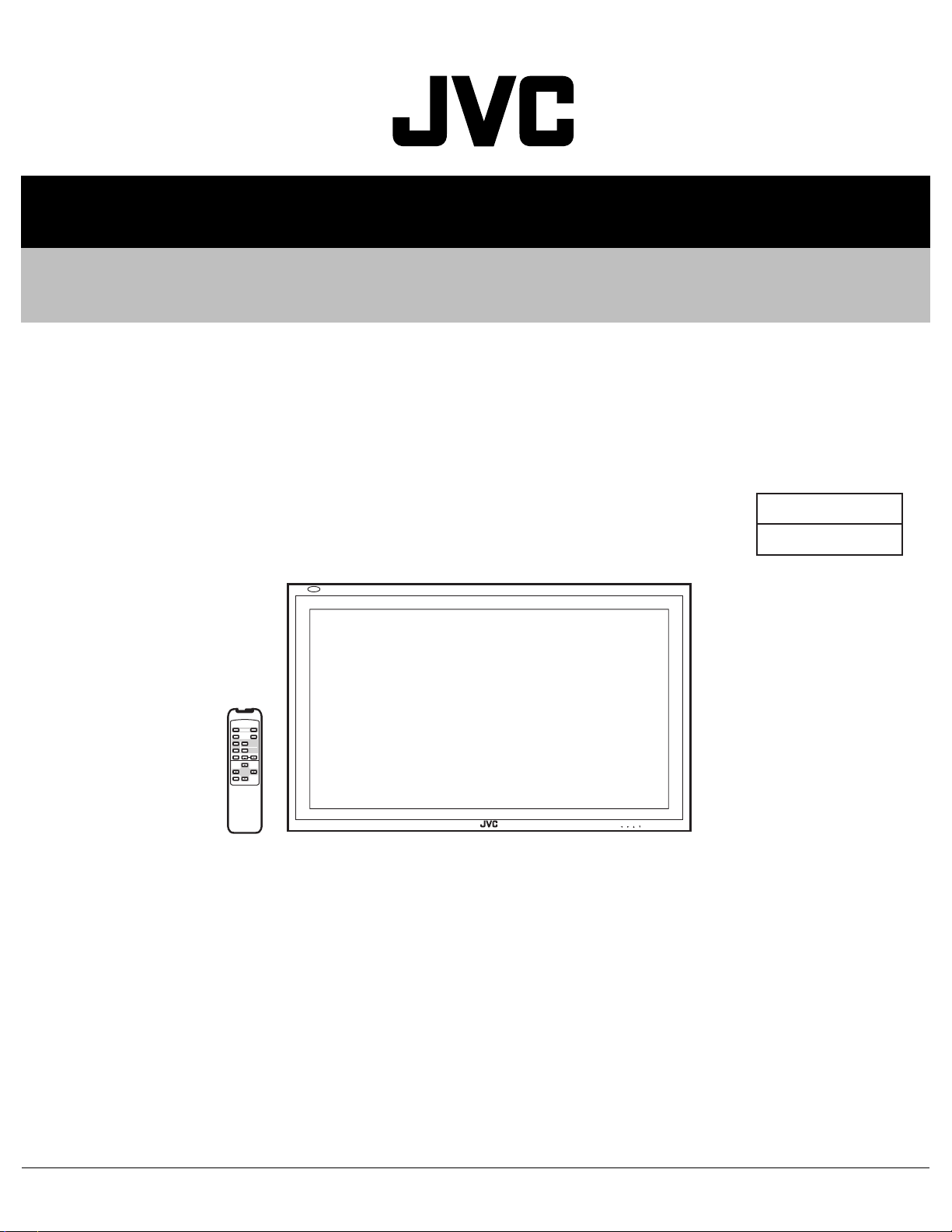
RM-C579 REMOTE CONTROL UNIT
ON
POWER
OFF
ASPECT
DISPLAY
INPUT SELECT
COMPO.
A
/(RGB B)
VIDEO
RGB AB
MUTING
VOLUME
MENU/EXIT
MENU INPUT POWER
TABLE OF CONTENTS
1 PRECAUTION. . . . . . . . . . . . . . . . . . . . . . . . . . . . . . . . . . . . . . . . . . . . . . . . . . . . . . . . . . . . . . . . . . . . . . . . . 1-4
2 SPECIFIC SERVICE INSTRUCTIONS. . . . . . . . . . . . . . . . . . . . . . . . . . . . . . . . . . . . . . . . . . . . . . . . . . . . . . 1-7
3 DISASSEMBLY . . . . . . . . . . . . . . . . . . . . . . . . . . . . . . . . . . . . . . . . . . . . . . . . . . . . . . . . . . . . . . . . . . . . . . 1-12
4 ADJUSTMENT . . . . . . . . . . . . . . . . . . . . . . . . . . . . . . . . . . . . . . . . . . . . . . . . . . . . . . . . . . . . . . . . . . . . . . . 1-23
5 TROUBLESHOOTING . . . . . . . . . . . . . . . . . . . . . . . . . . . . . . . . . . . . . . . . . . . . . . . . . . . . . . . . . . . . . . . . . 1-59
COPYRIGHT © 2003 VICTOR COMPANY OF JAPAN, LIMITED
No.52149
2003/8
Page 2
SPECIFICATION
Items
Type Plasma display
Dimension (W × H × D) 103.5cm × 64.0cm × 8.9cm
Mass 35.1kg
Video System VIDEO A/B NTSC3.58, NTSC4.43, PAL, PAL60, SECAM
COMPONENT 480i, 576i, 480p, 576p, 760/60p, 1080/50i, 1080/60i(1035/60i)
Power Requirements AC220V ~ AC240V, 50Hz / 60Hz
Rated Input Current 1.4A
Operation Environment Temperature : 0°C ~ 40°C
Storage Environment Temperature : -20°C ~ 60°C
Plasma Display Panel
Effective Screen Dimensions
Pixel Number
Pixel Pitch
Cell Pitch
Display Colours
Aspect Ratio
Speaker 4cm × 7cm oval type, Impeadance 8Ω
Audio power output Speaker output : 3W + 3W (TYP at impedance 6Ω)
Input / Output
Terminals
Accessories Remote control unit × 1(RM-C579), AA/R6-size dry cell battery × 2(for operation check)
RGB A (INPUT)
AUDIO OUT Output impedance 600Ω, RCA pin jack × 2
SPEAKER OUT Impedance 6Ω ~ 8Ω (L/R)
REMOTE RS-232C D-sub 9-pin connector × 1
OPTION DC power supply for cooling fan (DC15V), DC jack × 1
GM-V42PCE, GM-V42PCEB (Silver) GM-V42PCEG (Gray)
Relative humidity : 20% ~ 80% (non-condensing)
Pressure : 700hPa ~ 1114hPa
Relative humidity : 10% ~ 85% (non-condensing)
Pressure : 300hPa ~ 1114hPa
Diagonal : 107.4cm, (W) 93.3cm × (H) 53.3cm
Horizontal 852 × Vertical 480 (W-VGA)
Horizontal 1.095mm × Vertical 1.110mm
Horizontal 0.365mm × Vertical 1.110mm
16,777,216 colours (256 colours for each of RGB)
16:9 (Wide format)
D-sub 3-row 15-pin connector × 1
RGB
R / G / B : 0.7V(p-p) / 75Ω
G on sync : 1V(p-p) / 75Ω (negative syncy)
HD [ Horizontal sync ]
Cs [ Composite sync ]
VD [ Vertical sync ]
Audio 500mV(rms) / high impedance, 3.5mm stereo mini jack × 1
MAKE Mini-DIN 4pin connector × 1
WIRED 3.5mm stereo mini jack connector × 1
Remote control cable × 1, Power cord (approx 2.5m) × 3
0.3V(p-p) ~ 5V(p-p) / 470Ω (positive / negative polarity)
0.3V(p-p) ~ 5V(p-p) / 470Ω (positive / negative polarity)
1V(p-p) ~ 5V(p-p) / 470Ω (positive / negative polarity)
Contents
Design and specifications are subject to change without notice.
1-2 (No.52149)
Page 3
Items
Type Plasma display
Dimension (W × H × D) 103.5cm × 64.0cm × 8.9cm (40-3/4" × 25-1/4" × 3-5/8")
Mass 35.1kg (77.4 lbs)
Video System VIDEO A/B NTSC3.58, NTSC4.43, PAL, PAL60, SECAM NTSC3.58
COMPONENT 480i, 576i, 480p, 576p, 720/60p, 1080/50i, 1080/60i (1035/60i)
Power Requirements AC220V ~ AC240V, 50Hz / 60Hz AC120V, 60Hz
Rated Input Current 1. 4A 2.4A
Operation Environment Temperature : 0°C ~ 40°C
Storage Environment Temperature : -20°C ~ +60°C
Plasma Display Panel
Effective Screen Dimensions
Speaker 4cm × 7cm oval type, Impeadance 8Ω
Audio power output Speaker output : 3W+3W (TYP at impedance 6Ω)
Input / Output
Terminals
Accessories Remote control unit (RM-C579) × 1, AA/R6-size dry cell battery × 2(for operation check)
Design and specifications are subject to change without notice.
Pixel Number
Pixel Pitch
Cell Pitch
Display Colours
Aspect Ratio
VIDEO A
(IN / OUT)
VIDEO B
(INPUT)
RGB A (INPUT)
COMPONENT/
RGB B (INPUT)
AUDIO OUT Output impedance 600Ω, RCA pin jack × 2
SPEAKER OUT Impedance 6Ω ~ 8Ω (L/R)
REMOTE RS-232C D-sub 9-pin connector × 1
OPTION DC Power supply for cooling fan (DC15V), DC jack × 1
Relative humidity : 20% ~ 80% (non-condensing)
Pressure : 700hPa ~ 1114hPa
Relative humidity : 10% ~ 85%(non-condensing)
Pressure : 300hPa ~ 1114hPa
Diagonal : 107.4cm, (W) 93.3cm × (H) 53.3cm [Diagonal : 42-3/8", (W) 36-3/4" × (H) 21"]
Horizontal 852 × Vertical 480 (W-VGA)
Horizontal 1.095mm × Vertical 1.110mm
Horizontal 0.365mm × Vertical 1.110mm
16,777,216 colours (256 colours for each of RGB)
16:9 (Wide format)
Video input 1V(p-p) / 75Ω, BNC connector × 1
Video output 1V(p-p) / 75Ω, BNC connector × 1
Audio input 500mV(rms) / high impedance, RCA pin jack connector × 2(L/R)
Y/C Mini-DIN 4pin connector × 1
Video 1V(p-p) / 75Ω, RCA pin jack × 1
Audio 500mV(rms) / high impedance, RCA pin jack × 1
[ Horizontal sync (HD) ]
[ Composite sync (Cs) ]
[ Vertical sync (VD) ]
Audio 500mV(rms) / high impedance, 3.5mm stereo mini jack × 1
COMPONENT BNC connector × 3
RGB
HD [ Horizontal sync ]
Cs [ Composite sync ]
Audio 500mV(rms) / high impedance, RCA pin jack × 2
MAKE Mini-DIN 4pin connector × 1
WIRED 3.5mm stereo mini jack connector × 1
Remote control cable × 1, Power cord (approx 2.5m) × 3
GM-V42S (Silver) GM-V42UB (Silver), GM-V42UG (Gray)
Y : 1V(p-p) / 75Ω
C : 0.286V(p-p) / 75Ω [NTSC]
0.3V(p-p) 75Ω [PAL/SECAM]
D-sub 3-row 15-pin connector × 1
R / G / B : 0.7V(p-p) / 75Ω
RGB
G on sync : 1V(p-p) / 75Ω (negative syncy)
HD : 0.3V(p-p) ~ 5V(p-p) / 470Ω (positive / negative polarity)
Cs : 0.3V(p-p) ~ 5V(p-p) / 470Ω (positive / negative polarity)
VD : 1V(p-p) ~ 5V(p-p) / 470Ω (positive / negative polarity)
Y : 1V(p-p) / 75Ω
Pb/B-Y : 0.7V(p-p) / 75Ω
Pr/R-Y : 0.7V(p-p) / 75Ω
BNC connector × 5
[Analog RGB]
VD [ Vertical sync ]
R : 0.7V(p-p) / 75Ω
G : 0.7V (p-p) / 75Ω
G on sync : 1V(p-p) / 75Ω (negative sync)
B : 0.7V (p-p) / 75Ω
0.3V(p-p) ~ 5V(p-p) / 1kΩ (positive / negative polarity) / 75Ω
0.3V(p-p) ~ 5V(p-p) / 1kΩ (positive / negative polarity) / 75Ω
1 V(p-p) ~ 5V(p-p) / 1kΩ (positive / negative polarity) / 75Ω
Contents
(No.52149)1-3
Page 4
SECTION 1
PRECAUTION
1.1 SAFETY PRECAUTIONS
(1) The design of this product contains special hardware,
many circuits and components specially for safety
purposes. For continued protection, no changes should be
made to the original design unless authorized in writing by
the manufacturer. Replacement parts must be identical to
those used in the original circuits. Service should be
performed by qualified personnel only.
(2) Alterations of the design or circuitry of the products should
not be made. Any design alterations or additions will void
the manufacturer's warranty and will further relieve the
manufacturer of responsibility for personal injury or
property damage resulting therefrom.
(3) Many electrical and mechanical parts in the products have
special safety-related characteristics. These
characteristics are often not evident from visual inspection
nor can the protection afforded by them necessarily be
obtained by using replacement components rated for
higher voltage, wattage, etc. Replacement parts which
have these special safety characteristics are identified in
the parts list of Service manual. Electrical components
having such features are identified by sh ading on the
schematics and by ( ) on the parts list in Service
manual. The use of a substitute repl acement which does
not have the same safety characteristics as the
recommended replacement part shown in the parts list of
Service manual may cause shock, fire, or other hazards.
(4) Don't short between the LIVE side ground and
ISOLATED (NEUTRAL) side ground or EARTH side
ground when repairing.
Some model's power circuit is partly different in the GND.
The difference of the GND is shown by the LIVE : ( ) side
GND, the ISOLATED (NEUTRAL) : ( ) side GND and
EARTH : ( ) side GND.
Don't short between the LIVE side GND and ISOLATED
(NEUTRAL) side GND or EARTH side GND and never
measure the LIVE side GND and ISOLATED (NEUTRAL)
side GND or EARTH side GND at the same time with a
measuring apparatus (oscilloscope etc.). If above note will
not be kept, a fuse or any parts will be broken.
(5) If any repair has been made to the chassis, it is
recommended that the PDP voltage setting should be
checked or adjusted.
(6) When service is required, observe the original lead dress.
Extra precaution should be given to assure correct lead
dress in the high voltage circuit area. Where a short circuit
has occurred, those components that indicate evidence of
overheating should be replaced. Always use the
manufacturer's replacement components.
(7) Isolation Check (Safety for Electrical Shock Hazard)
After re-assembling the product, always perform an
isolation check on the exposed metal parts of the cabinet
(antenna terminals, video/audio input and output terminals,
Control knobs, metal cabinet, screw heads, earphone jack,
control shafts, etc.) to be sure the product is safe to operate
without danger of electrical shock.
a) Dielectric Strength Test
The isolation between the AC primary circuit and all metal
parts exposed to the user, particularly any exposed metal
part having a return path to the chassis should withstand a
voltage of 3000V AC (r.m.s.) for a period of one second. (.
. . . Withstand a voltage of 1100V AC (r.m.s.) to an
appliance rated up to 120V, and 3000V AC (r.m.s.) to an
appliance rated 200V or more, for a period of one second.)
This method of test requires a test equipment not generally
found in the service trade.
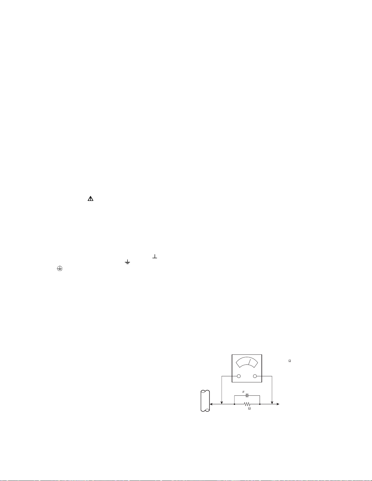
b) Leakage Current Check
Plug the AC line cord directly into the AC outlet (do not use
a line isolation transformer during this check.). Using a
"Leakage Current Tester", measure the leakage current
from each exposed metal part of the cabinet, particularly
any exposed metal part having a return path to the chassis,
to a known good earth ground (water pipe, etc.). Any
leakage current must not exceed 0.5mA AC (r.m.s.).
However, in tropical area, this must not exceed 0.2mA AC
(r.m.s.).
Alternate Check Method
Plug the AC line cord directly into the AC outlet (do not
use a line isolation transformer during this check.). Use
an AC voltmeter having 1000Ω per volt or more
sensitivity in the following manner. Connect a 1500Ω
10W resistor paralleled by a 0.15µF AC-type capacitor
between an exposed metal part and a known good earth
ground (water pipe, etc.). Measure the AC voltage
across the resistor with the AC voltmeter. Move the
resistor connection to each exposed metal part,
particularly any exposed metal part having a return path
to the chassis, and measure the AC voltage across the
resistor. Now, reverse the plug in the AC outlet and
repeat each measurement. Any voltage measured must
not exceed 0.75V AC (r.m.s.). This corresponds to
0.5mA AC (r.m.s.).
However, in tropical area, this must not exceed 0.3V AC
(r.m.s.). This corresponds to 0.2mA AC (r.m.s.).
AC VOLTMETER
(HAVING 1000 /V,
OR MORE SENSITIVITY)
1-4 (No.52149)
0.15 F AC-TYPE
GOOD EARTH GROUND
1500 10W
PLACE THIS PROBE
ON EACH EXPOSED
METAL PART
Page 5
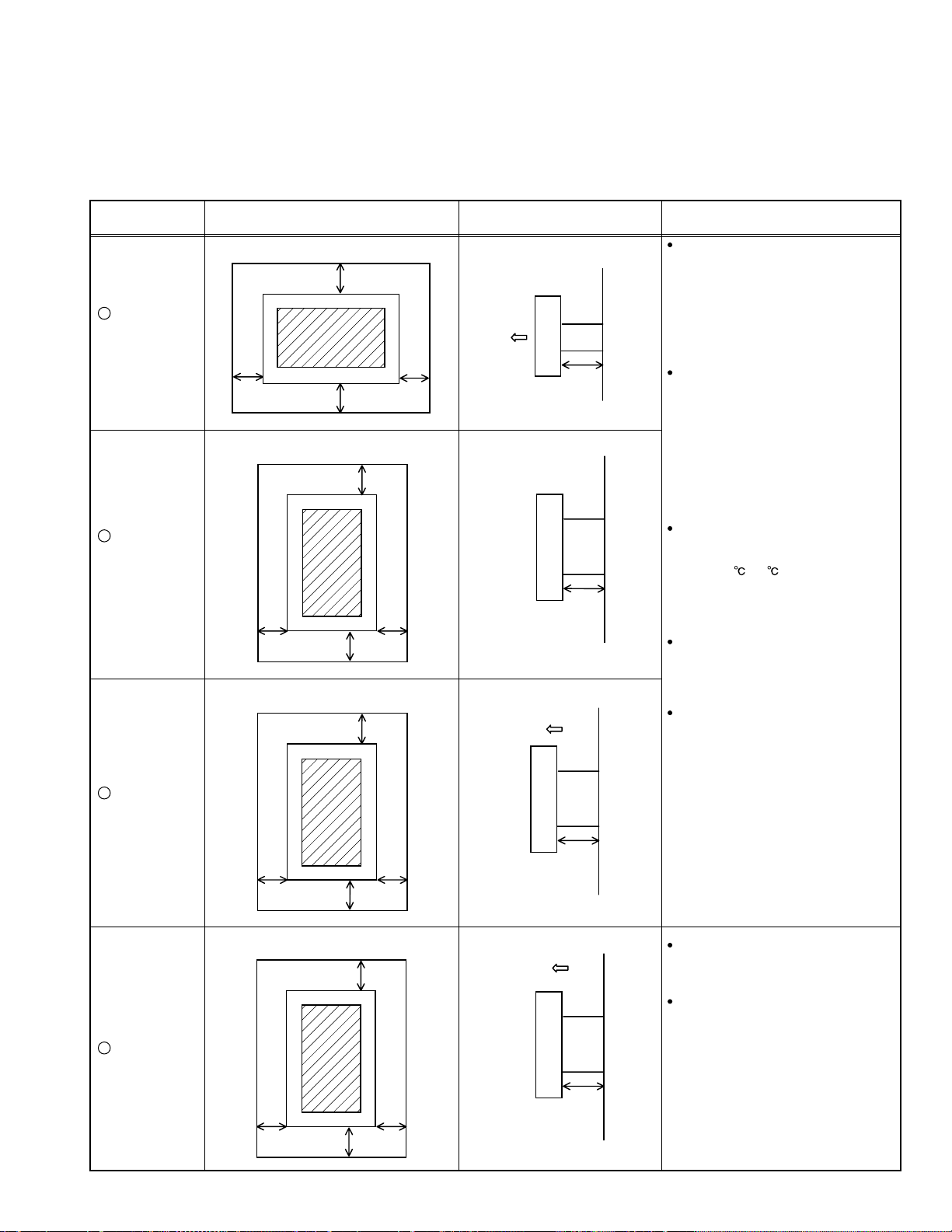
1.2 INSTALLATION
1.2.1 REQUIREMENTS FOR SETTING
The following minimum space must be kept when a PDP is installed.
(The recommended distance should be from the most projected portion when a PDP is inclined.)
An insufficient space reduces cooling efficiency and raises the internal temperature. If the internal temperature rises over the reference
value, the temperature sensor works to turn the power off for protecting the main body. Therefore, vents on the backside of the main
body such as heat dissipation vents must not be blocked, and sufficient spaces for heat dissipation must be kept around the main body.
Methods of
Installation
1
Hanging from
a wall
[Horizontal]
2
Hanging from
a wall
[Vertical]
10cm
10cm
10cm
Front
Wall
Wall
20cm
15cm
10cm10cm
10cm
Flank Remarks
Front Wall
5cm
Wall
5cm
It is necessary to set the cooling fan
where install each side causes high
temperature within a PDP and may
damage the inner circuit.
Do not prevent the radiation of heat
from back, top and flank sides of a PDP.
Preventing the radiation of heat from
each side causes high temperature
within a PDP and may damage the
inner circuit.
Install a PDP in a place where is well
ventilated.
Ambient temperature should be within a
range of 0 ~40 .
An exclusive fixture
(option) should be used.
3
Suspension
from a ceiling
4
Desktop
10cm
10cm
Wall
Wall
15cm
10cm10cm
15cm
10cm10cm
Front
Front
The structure and strength of the wall
where a PDP is installed should be
checked beforehand so as to install the
PDP safety without any accident.
Wall
5cm
A PDP should be installed on a rigid
floor or stand.
In order to prevent a PDP from turning
over by an accident or earthquake,
safety measures should be considered.
Wall
5cm
(No.52149)1-5
Page 6
1.2.2 PRECAUTION DURING NOTES FOR TRANSPORTATION
When transporting the display unit, pressure exerted on the
internal PDP (Plasma Display Panel) due to improper handing
(such as tossing and dropping) may cause damages even when
the unit is carefully packed. To prevent accidents from occurring
during transportation, pay careful attention prior to delivery such
as through exchanging the handing instructions to transporters.
Ensure that the following requirements are met during
transportation, as the PDP of this unit is made of glass and
therefore fragile.
(1) Avoid vibrations and impacts
The unit may be broken if it is toppled sideways even when
properly packed. Ensure that the unit is carried by at least
2 persons and pay careful attention not to exert any
vibration or impact on it.
(2) Do not place equipment lay a PDP on its side.
A PDP should always be placed upright during both
transportation and safekeeping. Don't lay it on its side. The
panel of a PDP is very fragile to the impact in the horizontal
direction.
When a car carries a PDP, load it on board the car in
parallel with the moving direction of the car. Don't lay
several PDPs one on top another.
During safekeeping, don't lay more than two PDPs one on
top another even if they are kept upright.
1.2.4 RETAINED-IMAGE / BURN-IN ON SCREEN
Like CRTs, "burn-ins" may occur when a same image is
continuously displayed over an extended period of time.
As this may also shorten the life span of the PDP. Therefore, turn
off the display when not in use, scroll the screen, make use of
screen-savers, or allow even distribution on the display by
inverting the brightness, switching to complementary colors or
inverting animated images at periodic intervals.
As burn-in is more likely to occur with high brightness and
contrast settings, try to use neutral gradations or medi um tone
colors.
Burn-in dose not occur in the case of animated images.
When switching to another image after continuous display of the
previous image, residual images may become prominent, as
luminance in a part of the display is higher then the other parts.
This is not a defect but is because due to the discharge surfa ce
of the lighted portion has become being relatively activated and
its luminance higher than the unlighted parts.
1.2.5 BRIGHTNESS CHANGE IN THE SCREEN
In order to save the power consumption, the power is controlled
(with APS function) depending on the brightness of the screen.
For this, the brightness may change after a short time when the
picture of the screen is changed. However, this phenomenon is
not a trouble.
1.2.3 PRECAUTIONS ON INSTALLATION
To get good heat dissipation from the rear.
This Monitor is not equipped with cooling fans because it is
designed to operate quietly.
If you install the Monitor in such a way as not instructed,
additional methods are required to cool down the Monitor.
A : Horizontal Installation (Normal)
In the case, the slots and openings in
the cabinet protect the Monitor from
overheating.
* See also "Requirements forsetting"
on page 6 in the instruction.
B : Vertical Installation
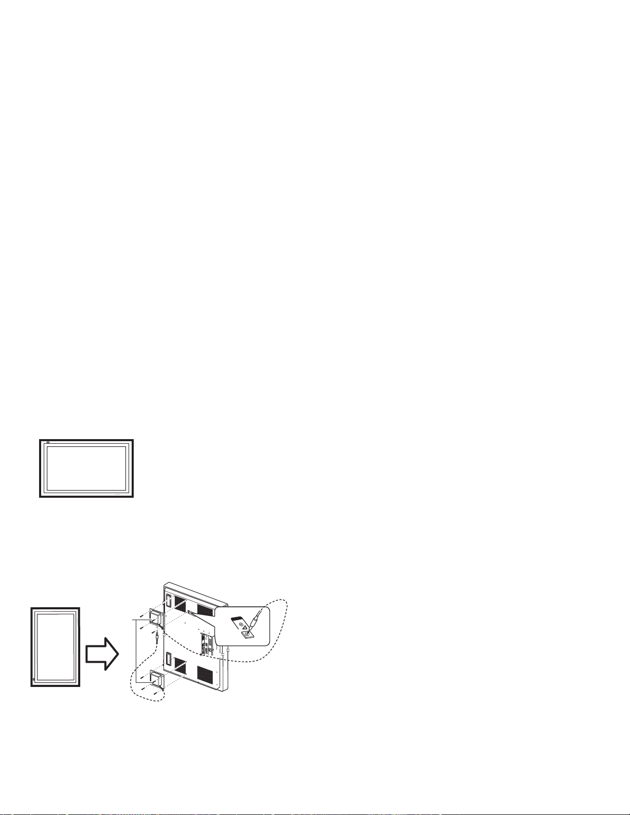
It is required to attach the Cooling Fan Unit (TS-C01FANG : option).
* Refer to the following figure for how to attach the cooling fan unit.
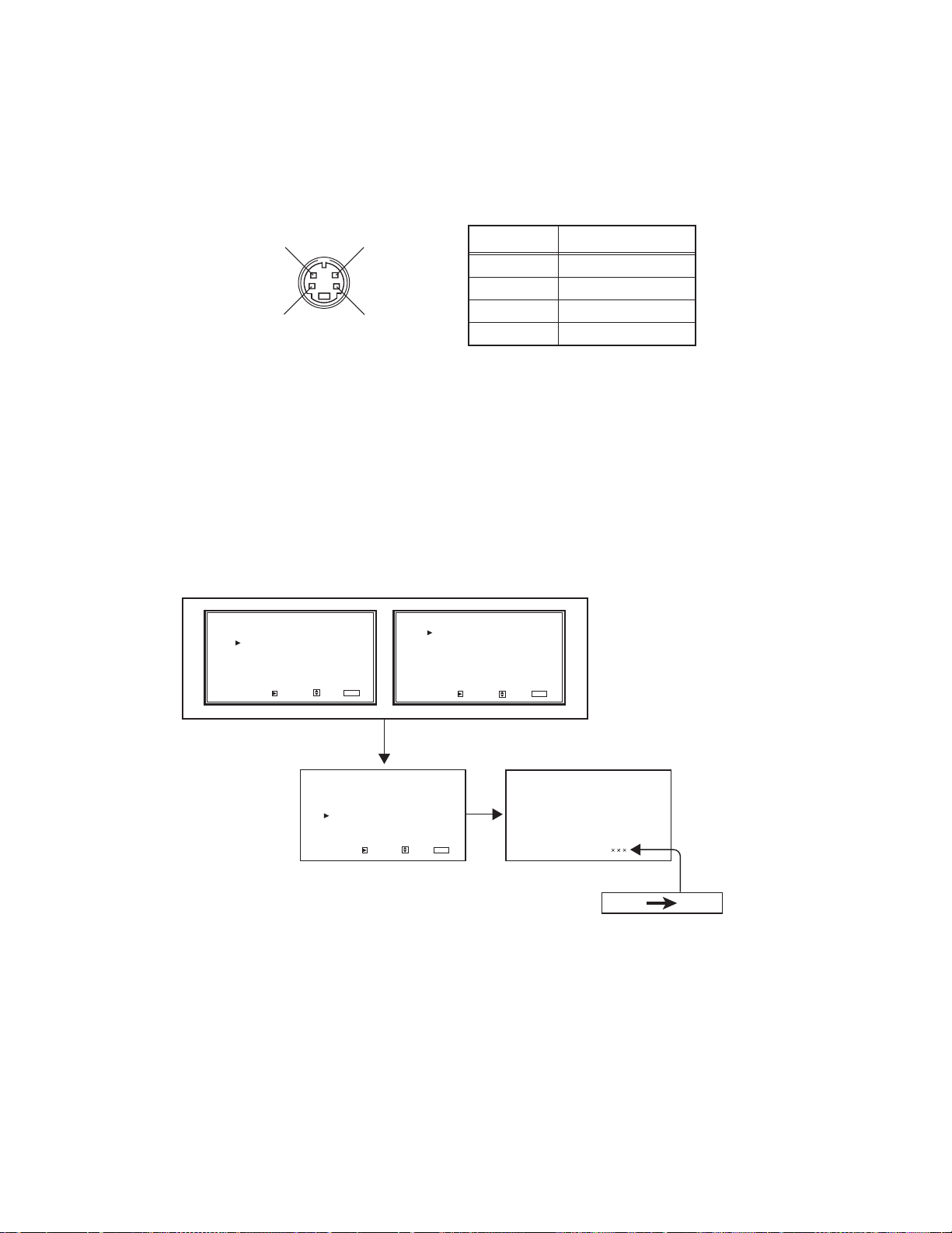
An option terminal is exclusively
for a cooling fan. Please do not
use it for connection with other
apparatus.
Cooling Fan Unit
(Option)
POWERAC INAUDIO
L
R
OUT
MAKE
WIRED
RS-232C
REMOTE
L
SPEAKER OUT
AUDIO
IN
RGB A
OPTION
1.2.6 INFRARED RAYS
Because the near infrared rays (800nm~1000nm) radiate from
the panel face, the neighboring infrared ray remote controllers,
infrared communication systems, etc. may malfunction. In these
cases, take a measure to prevent the trouble to be caused by
direct rays (or reflected rays) from the screen by changing the
direction of the screen face or keeping a safe distance between
a PDP and other devices.
1.2.7 OPTICAL FILTER (FRONT FILTER)
Avoid placing the unit under direct sunlight over a prolonged
period of time. This may cause the optical filter to deteriorate in
quality and color.
Clean the filter surface by wiping it softly lightly with outing
flannels a soft and lightly fuzz cloth (such a flannel).
Do not use solvents such as benzene or thinner to wipe the filter
surface. This may cause the filter to deteriorate in quality or the
coating on the surface to come off.
As the filter surface is fragile. Do not scratch or hit it with hard
materials.
1.2.8 NOTES PRECAUTIONS FOR REPLACEMENT OF
EXTERIOR PARTS
Take note of the following when replacing exterior parts (back
REAR COVER, FRONT PANEL, OPTICAL FILTER):
Do not exert pressure on the front of the PDP(glass surface).
Pay careful attention not to scratch or stain the front of the PDP
(surface) with hands.
When replacing exterior parts, the front of the PDP should be
placed facing downward. Place a met, etc. underneath to avoid
causing scratched to the front surface.
However, never use materials that are too soft (such as blanket
cloth). If replacement is made with the PDP surface facing
downward and in contact with the blanket, pressure may be
exerted on the PDP, thus causing damages to it.
1-6 (No.52149)
Page 7
SPECIFIC SERVICE INSTRUCTIONS
2.1 TIMING SPECIFICATION & SCAN SIZE
Divide Item
COMPOSITE
Y/C
COMPONENT
PC/RGB 15k
PC/VGA 400
PC/VGA 480
PC/SVGA
PC/XGA
NTSC, PAL60,
NTSC4.43
(B/W 60Hz)
PAL, SECAM
(B/W 50Hz)
480i
576i
480p SMPTE 293M 59.94 31.468 27.00 858 525 720 483
576p SMPTE 293M 50.00 31.250 27.00 864 625 720 575
720p SMPTE 296M 60.00 45.000 74.25 1 650 750 1 280 720 FULL 95.00 95.00
1080/50i SMPTE 274M 50.00 28.125 74.25 2640 562.5 192 0 540 FULL 95.00 95.00
1080/60i SMPTE 274M 60.00 33.750 74.25 2200 562.5 192 0 540 FULL 95.00 95.00
1035i BTA S-001A 60.00 33.750 74.25 2200 562.5 1920 517.5 FULL 92.75 92.75
RGB 15k/60Hz 59.94 15.734 14.32 910 525 768 485
RGB 15k/50Hz 50.00 15.625 17.73 1135 625 922 575
PC98 (NEC) 56.42 24.82 21.05 848 440 640 400
VGA400/70 (IBM) 70.09 31.47 25.18 800 449 640 400
VGA-60 (Industry std.) 59.94 31.47 25.17 800 525 640 480
VGA-72 VESA std. 72.81 37.86 31.50 832 520 640 480
VGA-75 VESA std. 75.00 37.50 31.50 840 500 640 480
MAC 13" (Apple) 66.67 35.00 30.24 864 525 640 480
SVGA-56
SVGA-60
SVGA-72
SVGA-75
XGA-60
XGA-70 VESA STD. 70.07 56.48 75.00 1328 806 1024 768
XGA-75 VESA STD. 75.03 60.02 78.75 1312 800 1024 768
XGA-85 VESA STD. 85.00 68.68 94.50 1376 808 1024 768
XGA+-75 VESA STD. 75.00 67.50 108.0 1600 900 1152 864
Standard
SMPTE 244M 59.94 15. 734 14.32 910 525 768 485
ITU-R BT601-4
(CCIR Rec.601)
ITU-R BT601-4
(CCIR Rec.601)
VESA GUIDELINES
VESA GUIDELINES
VESA GUIDELINES
VESA GUIDELINES
VESA GUIDELINES
SECTION 2
Input picture format Scan size
Frequency Total pixel Visible area pixel
Vert. Hor.
fVi fHi fci Hi Vi Hai Vai Kh Kv
Hz kHz MHz
50.00 15.625 17.73 1135 625 922 575
59.94 15.734 13.50 858 525 720 485
50.00 15.625 13.50 864 625 720 575
56.25 35.16 36.00 1024 625 800 600
60.32 37.88 40.00 1056 628 800 600
72.19 48.08 50.00 1040 666 800 600
75.00 46.88 49.50 1056 625 800 600
60.00 48.36 65.00 1 344 806 1024 768
Dot clock
Hor.Vert.Hor.Vert.
pixel/line line/frame pixel/line line/frame
Display mode
REGULAR 95.00 95.00
FULL 95.00 95.00
PANORAMIC 95.00 90.00
ZOOM 95.00 71.25
REGULAR 95.00 95.00
FULL 95.00 95.00
PANORAMIC 95.00 90.00
ZOOM 95.00 71.25
REGULAR 95.00 95.00
FULL 95.00 95.00
PANORAMIC 95.00 90.00
ZOOM 95.00 71.25
REGULAR 95.00 95.00
FULL 95.00 95.00
PANORAMIC 95.00 90.00
ZOOM 95.00 71.25
REGULAR 95.00 95.00
FULL 95.00 95.00
PANORAMIC 95.00 90.00
ZOOM 95.00 71.25
REGULAR 95.00 95.00
FULL 95.00 95.00
PANORAMIC 95.00 90.00
ZOOM 95.00 71.25
REGULAR 95.00 95.00
FULL 95.00 95.00
PANORAMIC 95.00 90.00
ZOOM 95.00 71.25
REGULAR 95.00 95.00
FULL 95.00 95.00
PANORAMIC 95.00 90.00
ZOOM 95.00 71.25
REGULAR 100.00 100.00
FULL 100.00 100.00
REGULAR 100.00 100.00
FULL 100.00 100.00
REGULAR 100.00 100.00
FULL 100.00 100.00
REGULAR 100.00 100.00
FULL 100.00 100.00
REGULAR 100.00 100.00
FULL 100.00 100.00
REGULAR 100.00 100.00
FULL 100.00 100.00
REGULAR 100.00 100.00
FULL 100.00 100.00
REGULAR 100.00 100.00
FULL 100.00 100.00
REGULAR 100.00 100.00
FULL 100.00 100.00
REGULAR 100.00 100.00
FULL 100.00 100.00
REGULAR 100.00 100.00
FULL 100.00 100.00
REGULAR 100.00 100.00
FULL 100.00 100.00
REGULAR 100.00 100.00
FULL 100.00 100.00
REGULAR 100.00 100.00
FULL 100.00 100.00
REGULAR 100.00 100.00
FULL 100.00 100.00
Hor. Vert.
%%
(No.52149)1-7
Page 8
2.2 MAIN DIFFERENCE LIST Item GM-V42PCE GM-V42PCEB GM-V42PCEG GM-V42S GM-V42UB GM-V42UG
Colour Silver Silver Gray Silver Silver Gray
Radiation Class A Class B Class A Class A Class B Class A
Input Terminal VIDEO A Not available Not available Not available Available Available Available
VIDEO B Not available No t avai lable Not available Available Available Available
COMPONENT
/ RGB B
Not available Not available Not available Availab le Available Available
Note :
• GM-V42PCE, GM-V42PCEG and GM-V42PCEB do not have the following input terminal-VIDEO A, VIDEO B and COMPONENT
/ RGB B.
• You need to install the video input unit (IF-C42P1C), which is separately purchased, to select VIDEO A, VIDEO B and
COMPONENT(or RGB) as the input.
• To use the COMPONENT/RGB B terminals either as COMPONENT input terminal or as the RGB input terminal, you need to set
RGB/COMPO. correctly. (Refer to the INSTRUCTIONS)
2.3 TECHNICAL INFORMATION
2.3.1 PDP (PLASMA DISPLAY PANEL) DESCRIPTION
2.3.1.1 CAUTION
Although a PDP is made with highly advanced precision, this does not necessarily mean all of the cells operate correctly.
The PDP inevitably includes cell that do not light or light constantly.
If the specifications (PDP performance) are unclear at the time of shipment, an adequate description cannot be conveyed to the
customer. In event of inquiries from customers regarding PDP performance, check the following specifications in order to offer a
suitable reply.
2.3.1.2 CELL ARRANGEMENT
The PDP is constructed of front and rear glass substrates provided with respe ctive discharge electrod es. Between these, neon for
discharging and xenon for generating ultraviolet rays are enclosed.
One picture element (pixel) is composed of Red, Green and Blue (RGB) cells. The cell pitch is 0.365mm horizontal (1.095mm per
pixel) by 1.110mm vertical.
As shown in Fig. 1, the cells are arranged for each R / G / B colour. A pixel consists of each cell of R/G/B/ colour. The size of a cell is
0.365mm horizontally and 1.110mm vertically.
Direction
Vertical(V)
Horizontal(H)
1st pixel
line
2nd pixel
line
479th pixel
line
480th pixel
line
1st pixel
array
B G R B G R
BG
G RBG R
B
GRBGR
B
2nd pixel
array
RBG R
851th pixel
array
B GRBG R
BGRBGR
G RBG R
B
GRBGR
B
852th pixel
array
V 1.110mm
Pitch of pixel
(Pitch of cell)
1-8 (No.52149)
H 1.095mm
Pitch of pixel
One pixel
(1dot)
B cell
G cell
R cell
Fig.1 PIXEL (CELL) ARRANGEMENT
H 0.365mm
Pitch of cell
Page 9
2.3.1.3 PIXEL FAULT
There are three pixel faults - bright fault , dark fault and flicker fault - that are respectively defined as follows.
(1) BRIGHT FAULT
In this pixel fault, a cell that should not light originally is lighting on and off.
For checking this pixel fault, input ALL BLACK SCREEN and find out the cell that is lighting on and off.
(2) DARK FAULT
In this pixel fault, a cell that should light originally is not lighting or lighting with the brightness twice as brighter as originally lighting.
For checking this pixel fault, input 100% of each R/G/B colour and find out the cell that is not lighting.
(3) FLICKER FAULT
In the pixel fault, a cell that should light originally or not light originally is flashing on and off.
For checking this pixel fault, input ALL BLACK SCREEN signal or 100% of each RGB colour and find out the cell that is flashing on
and off.
2.3.1.4 PIXEL FAULT SPECIFICATION
Fault Screen display Criteria for number of fau lted cell
BRIGHT FAULT All black screen A zone: 0
B zone: 1 or less than 1 in each colour
DARK FAULT Red level 100% on entire screen A zone: 2 or less than 2 in each colour
Green level 100% on entire screen
B zone: 6 or less than 6 in each colour
Blue level 100% on entire screen
FLICKER FAULT Red level 100% on entire screen A zone: 0
Green level 100% on entire screen
B zone: 2 or less than 2 in each colour
Blue level 100% on entire screen
(1) OBJECT RANGE
A-zone : Center portion (area enclosed by 1/4 vertically from the top and bottom and 1/4 horizontally from the right and left sides.)
B-zone : Other area
1/4H 1/4H
B zone
1/4V
1/4V
A zone
1/4V1/4V
(2) JUDGEMENT STANARD
Regardless of A and B zones, the following cases are considered as defects.
• When the distance between the bright fault is less than 15mm.
• When the distance between the bright fault and the dark defect or between the flicker fault is less than 15mm.
• When the distance between the dark fault and the flicker is less than 30mm.
(No.52149)1-9
Page 10
2.3.2 REMOTE THROUGH FUNCTION
The REMOTE THROUGH function is a function that is capable of controlling such equipment as a karaoke system conn ected to the
REMOTE THROUGH terminal by receiving the IR (infrared ray) signal at the sensor of the remote controller unit of this model.
2.3.2.1 REMOTE THROUGH OUTPUT TERMINAL
The REMOTE THROUGH terminal and MAKE (mini DIN 4 pin) terminal at the back of the main body share the same terminal.
Therefore, it is necessary to change the setup at the SERVICE MODE when the REMOTE THROUGH function is used. For the pin
layout at the terminal, the 4 pin will become an output terminal and the 1-3 pins will be GNDs.
REMOTE THROUGH OUTPUT TERMINAL
34
Pin No.
1
2
3
2
1
4
Signal name
GND
GND
GND
OUTPUT
2.3.2.2 HOW TO CHANGE THE SETUP OF THE FUNCTION
(1) Enter the SERVICE MODE.
(2) Select the < CPU BLOCK > with the [/] key.
(3) Press the [] key of the remote control unit to display the < CPU BLOCK >.
(4) Select the "CE: SYSTEM CONSTANT" with the [/] key.
(5) Press the [] key of the remote control unit to display the setup screen for the "SYSTEM CONSTANT".
(6) Display the "CE 05" with the [/] key.
(7) Change the setup value to 001 from 000 with the [/] key.
(8) Press the MENU key of the remote control unit to exit from the SERVICE MODE.
(9) After turning the power off (or at the stand-by mode), turn the power on again.
(10) Then the REMOTE THROUGH function is available.
SERVICE MODE
VCO ADJUST
WHITE BALANCE BLOCK
CPU BLOCK
SIZE/POSITION BLOCK
H POSITION BLOCK
PANEL BLOCK
SIGNAL BLOCK
DEVICE INITIAL VALUE
ENTER: SELECT: EXIT:
[1/2]
MENU
DIAGNOSIS BLOCK
UPDATE CPU PROGRAM
HOUR METER BLOCK
ENHANCER BLOCK
ENTER: SELECT: EXIT:
[2/2]
MENU
1-10 (No.52149)
< CPU BLOCK >
CA:PANORAMA DATA
CB:SIGNAL RANGE
CC:SIZE/POSI. RANGE
CD:FRQENCY DATA
CE:SYSTEM CONSTANT
CF:TEMP. SENSOR DATAs
CG:APS CONTROL DATA
CH:TEST MODE
ENTER: SELECT: EXIT:
<CPU BLOCK> screen
MENU
C(E05)
SYSTEM CONSTANT screen
000 001
Page 11
2.3.3 HOUR METER FUNCTION
This model is equipped with an "HOUR METER" function tha t
displays elapsed time on operating time of the set.
Elapsed time can be checked at the "HOUR METER BLOCK" in
the SERVICE MODE.
Also you can reset elapsed time to zero if needed.
Elapsed time count 1 hour. MAX elapsed time is 65535 hour.
HOW TO RESET ELAPSED TIME
(1) Enter the SERVICE MODE (Fig.1).
(2) Press [/] key, and select "HOUR METER BLOCK" of
SERVICE MODE 2 page (Fig.2).
(3) Press [] key, and display "HOUR METER BLOCK"
screen (Fig.3).
(4) While the "HOUR METER BLOCK" display press []
key and it will display "RESET HOUR METE" (Fig.4).
(5) Press [] key and reset the HOUR METER (Fig.5).
SERVICE MODE
VCO ADJUST
WHITE BALANCE BLOCK
CPU BLOCK
SIZE/POSITION BLOCK
H POSITION BLOCK
PANEL BLOCK
SIGNAL BLOCK
DEVICE INITIAL VALUE
ENTER: SELECT: EXIT:
Fig.1
DIAGNOSIS BLOCK
UPDATE CPU PROGRAM
HOUR METER BLOCK
ENHANCER BLOCK
ENTER: SELECT: EXIT:
Fig.2
[1/2]
MENU
[2/2]
MENU
HOUR METER BLOCK
< HOUR METER BLOCK >
RESET
HOUR METER (X1h) : 12345
ENTER: EXIT:
Fig.3
< RESET HOUR METER >
!
Are you sure ?
"YES" then Key
ENTER: SELECT: EXIT:
MENU
"NO" then Key
Fig.4
< HOUR METER BLOCK >
RESET
HOUR METER (X1h) : 00000
MENU
MENU
2.3.4 REMINDER TO CHANGE A BATTERY
This model with a timer function, is equipped with a batte ry for
the timer.
When the battery is running low, a message of "BATTERY LOW"
is displayed on the [TIMER], [COLOR-REVERSE] and
[REFRESH] setting screen of the < SET-UP MENU >. At the end
of the battery-life, a message of "BATTERY EMPTY" is displayed
same screen. Both cases, you should make a battery change.
Battery is fixed on the battery board. Please exchange the whole
substrate.
BATTERY CHANGE PROCEDURE
(1) Remote the terminal board on the back of the main body.
(Refer to disassembly procedure)
(2) Remove the connector D on the battery board.
(3) Remove the screw A attaching the battery board.
(4) Change the battery board to new one.
Note :
After changing the battery board, the same message before
a battery change will be displayed when the power is turned
on for the first time. Therefore, turn off the power once, then
turn on the power again. The message will be disappeared
and you can use the model with normal functi on s.
AV TERMINAL
CND CONNECTOR
A
BATTERY PWB
ENTER: EXIT:
Fig.5
MENU
THE CAUTIONS ON BATTERY EXCHANGE
Risk of explosion if battery is replaced by incorrect type.
Dispose of used batteries according to the instructions.
(No.52149)1-11
Page 12
SECTION 3
DISASSEMBLY
3.1 DISASSEMBLY PROCEDURE
• Prior to assembly/disassembly procedure of the set, be sure to
disconnect the power cord from the wall outlet.
• Perform the following procedures on a flat and strong place.
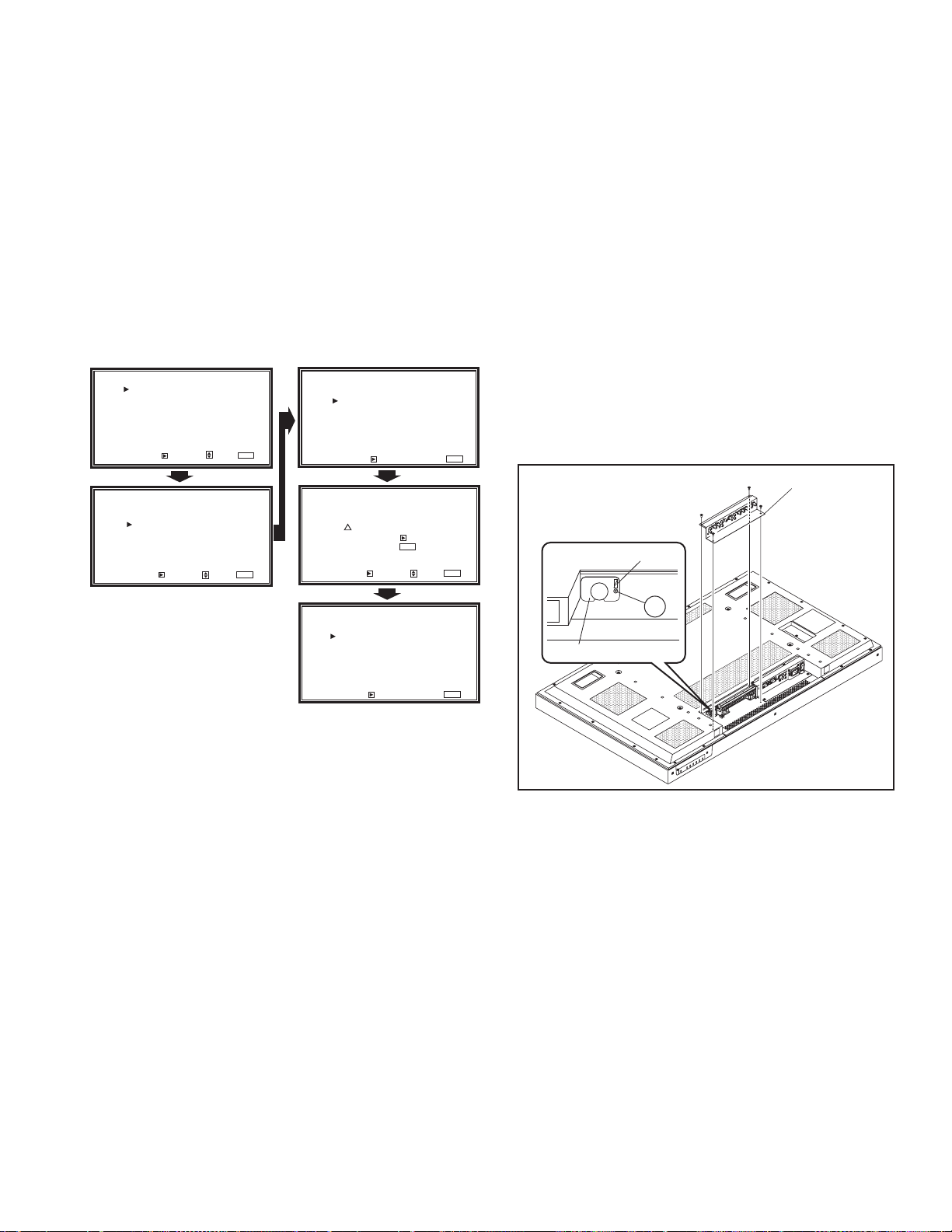
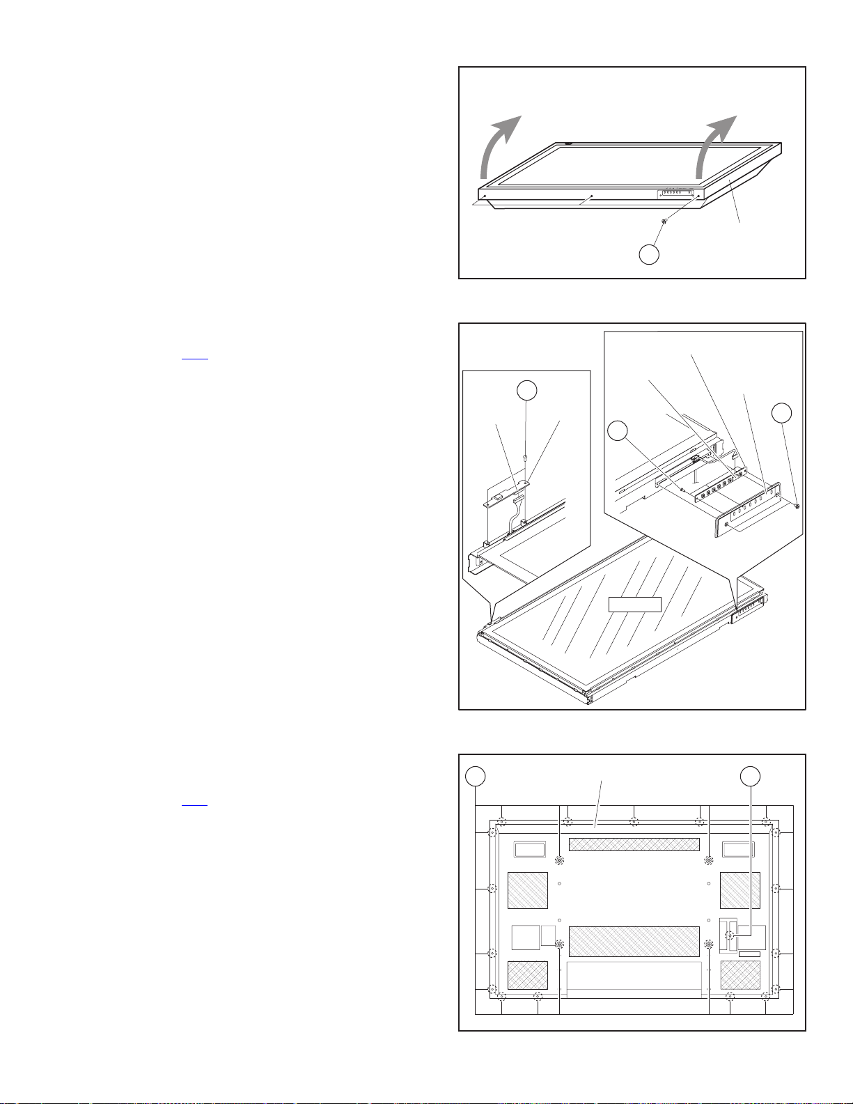
3.1.1 REMOVING THE AV TERMINAL (Fig.1)
(1) Disconnect the power cord from the wall outlet.
(2) Remove the 2 screws [A].
(3) Remove the 2 screws [B].
(4) Lift the both ends of the AV TERMINAL slowly, and remove
the CN1001
PWB. Then, remove the AV TERMINAL.
3.1.2 REMOVING THE PC TERMINAL (Fig.1)
• Remove the AV TERMINAL.
(1) Remove the 2 screws [C].
(2) Remove the 2 screws [D].
(3) Remove the 2 screws [E].
(4) Lift the both ends of the PC TERMINAL slowly, and remove
the CN1003
the MAIN PWB. Then, remove the PC TERMINAL.
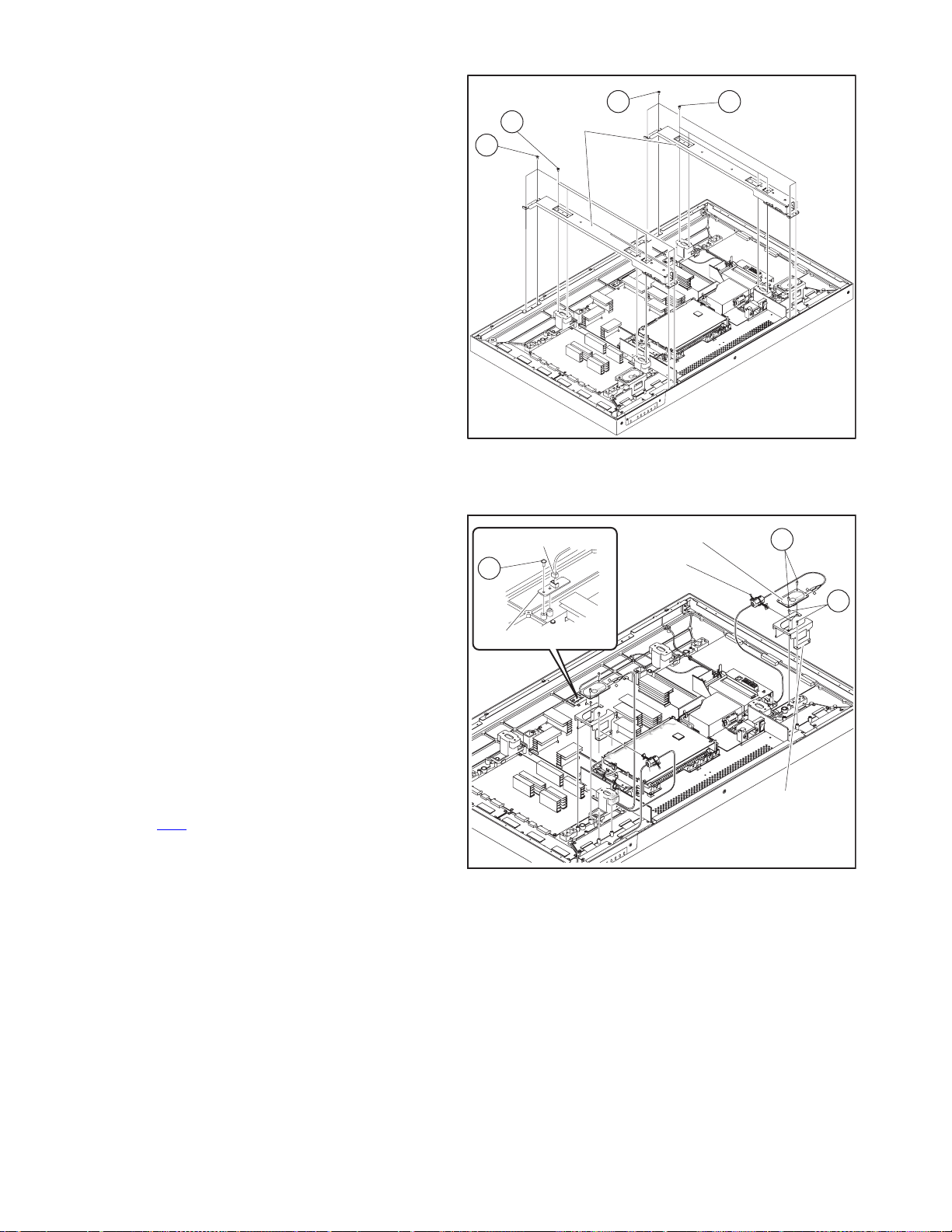
3.1.3 REMOVING THE AV TERMINAL PWB (Fig.2)
[Only GM-V42S, GM-V42UB and GM-V42UG]
• Remove the AV TERMINAL.
(1) Remove the 12 screws [F].
(2) Remove the AV TERMINAL PWB.
3.1.4 REMOVING THE PC TERMINAL PWB (Fig.2)
• Remove the AV TERMINAL.
• Remove the PC TERMINAL.
(1) Remove the 4 screws [G].
(2) Remove the 4 screws [H] with a box wrench.
(3) Remove the AV TERMINAL PWB.
/CN1002 connectors connected to the MAIN
/CN1004/CN1005 connectors connected to
Only Europe model
GM-V42PCE
GM-V42PCEB
GM-V42PCEG
AV TERMINAL
A
B
PC TERMINAL PWB
AV TERMINAL PWB
A
B
Fig.1
AV TERMINAL
C
CN1002
CN1001
H
D
PC
TERMINAL
E
CN1005
CN1004
CN1003
G
3.1.5 REMOVING THE BATTERY PWB (Fig.3)
• Remove the AV TERMINAL.
(1) Remove the CND
(2) Remove the 1 screw [I].
(3) Pull the BATTERY PWB toward you, and remove it.
1-12 (No.52149)
connector.
CND CONNECTOR
I
BATTERY PWB
A
F
Fig.2
AV TERMINAL
B
Fig.3
Page 13
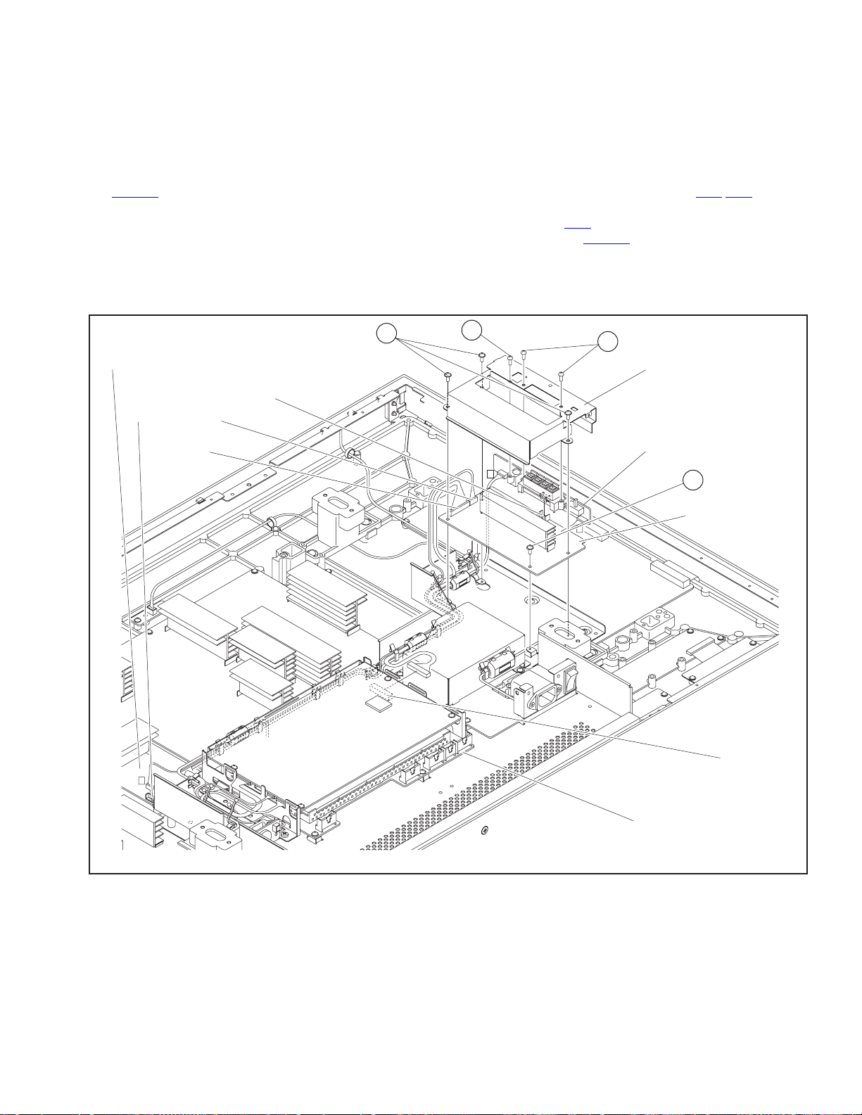
3.1.6 REMOVING THE FRONT PANEL (Fig.4)
• Remove the optional parts such as cooling fan if they are
attached to the rear side of the main body.
• Place the main body with its screen side looking upward.
(1) Remove the 3 screws [J].
(2) Lift the underside of the FRONT PANEL slowly, and
remove the tapes fixing the top part of the FRONT PANEL.
(3) Remove the FRONT PANEL.
3.1.7 REMOVING THE LED PWB (Fig.5)
• Remove the FRONT PANEL.
(1) Remove the 2 screws [K].
(2) Remove the CNX
(3) Remove the LED PWB.
connector.
CNX
K
LED PWB
Fig.4
M
J
CONTROL PWB
CNT
FRONT PANEL
CONTROL
PANEL
L
3.1.8 REMOVING THE CONTROL PWB (Fig.6)
• Remove the FRONT PANEL.
(1) Remove the 2 screws [L].
(2) Remove the 3 screws [M].
(3) Remove the CNT
(4) Remove the CONTROL PWB.
connector.
Surface
Fig.5
N O
REAR PANEL
Fig.6
(No.52149)1-13
Page 14
3.1.9 REMOVING THE REAR COVER (Fig.7)
• Remove the AV TERMINAL.
• Remove the PC TERMINAL.
(1) Remove the 21 screws [N].
(2) Remove the 1 screw [O].
(3) Lift the REAR COVER slowly, and remove it.
3.1.10 REMOVING THE BACK FRAME (LEFT/RIGHT) (Fig.7)
• Remove the AV TERMINAL.
• Remove the PC TERMINAL.
• Remove the REAR COVER.
(1) Remove the 4 screws [P].
(2) Remove the 4 screws [Q].
(3) Lift the BACK FRAME, and remove it.
(4) Remove the BACK FRAME on the other side in the sa me
way.
3.1.11 REMOVING THE SPEAKER / SPEAKER BRACKET (Fig.8)
• Remove the AV TERMINAL.
• Remove the PC TERMINAL.
• Remove the REAR COVER.
(1) Remove the speaker cord.
(2) Remove the 2 screws [R].
(3) Remove the SPEAKER.
(4) Remove the SPEAKER on the other side in the same way.
(5) Remove the clamp fixing the filter from the SPEAKER
BRACKET.
(6) Remove the 2 screws [S].
(7) Remove the SPEAKER BRACKET.
(8) Remove the SPEAKER BRACKET on the other side in the
same way.
P
BACK FRAME
Q
CNV CONNECTOR
T
TEMP. SENSOR PWB
Q P
Fig.7
SPEAKER
CLAMP
+
R
+
S
L
3.1.12 REMOVING THE TEMP. SENSOR PWB (Fig.8)
• Remove the AV TERMINAL.
• Remove the PC TERMINAL.
• Remove the REAR COVER.
(1) Remove the CNV
connector on the TEMP. SENSOR PWB.
(2) Remove the screw [T].
(3) Remove the TEMP. SENSOR PWB.
1-14 (No.52149)
SPEAKER
BRACKET
Fig.8
Page 15
3.1.13 REMOVING THE SPEAKER TERMINAL PWB (Fig.9)
• Remove the AV TERMINAL.
• Remove the PC TERMINAL.
• Remove the REAR COVER.
• Remove the BACK FRAME.
(1) Remove the 3 screws [U], 2 screws [V], and 1 screw [W].
(2) Remove the SPEAKER TERMINAL BRACKET.
(3) Lift the SPEAKER TERMINAL PWB, and remove the
CN6006
connector.
(4) Remove the speaker cord connected to the SPEAKER.
(5) Remove the speaker cord from each clamp.
(6) Remove the SPEAKER TERMINAL PWB.
3.1.14 REMOVING THE AUDIO PWB (Fig.9)
• Remove the AV TERMINAL.
• Remove the PC TERMINAL.
• Remove the REAR COVER.
• Remove the BACK FRAME.
• Remove the SPEAKER TERMINAL BRACKET.
• Remove the SPEAKER TERMINAL PWB.
(1) Remove the 1 screw [X].
(2) Remove the cords connected to the CNF
/CNA connectors
connected to the sound board from each clamp.
(3) Remove the CNA
(4) Disconnect the CN9004
connector on the MAIN PWB.
connector on the VIDEO SMPS
PWB.
(5) Remove the AUDIO PWB.
VIDEO SMPS PWB
CN9004
CNF
CNA
CN6006
U
W
V
SPEAKER TERMINAL
BRACKET
SPEAKER TERMINAL
PWB
R
X
AUDIO PWB
L
CNA
F
MAIN PWB
Fig.9
(No.52149)1-15
Page 16
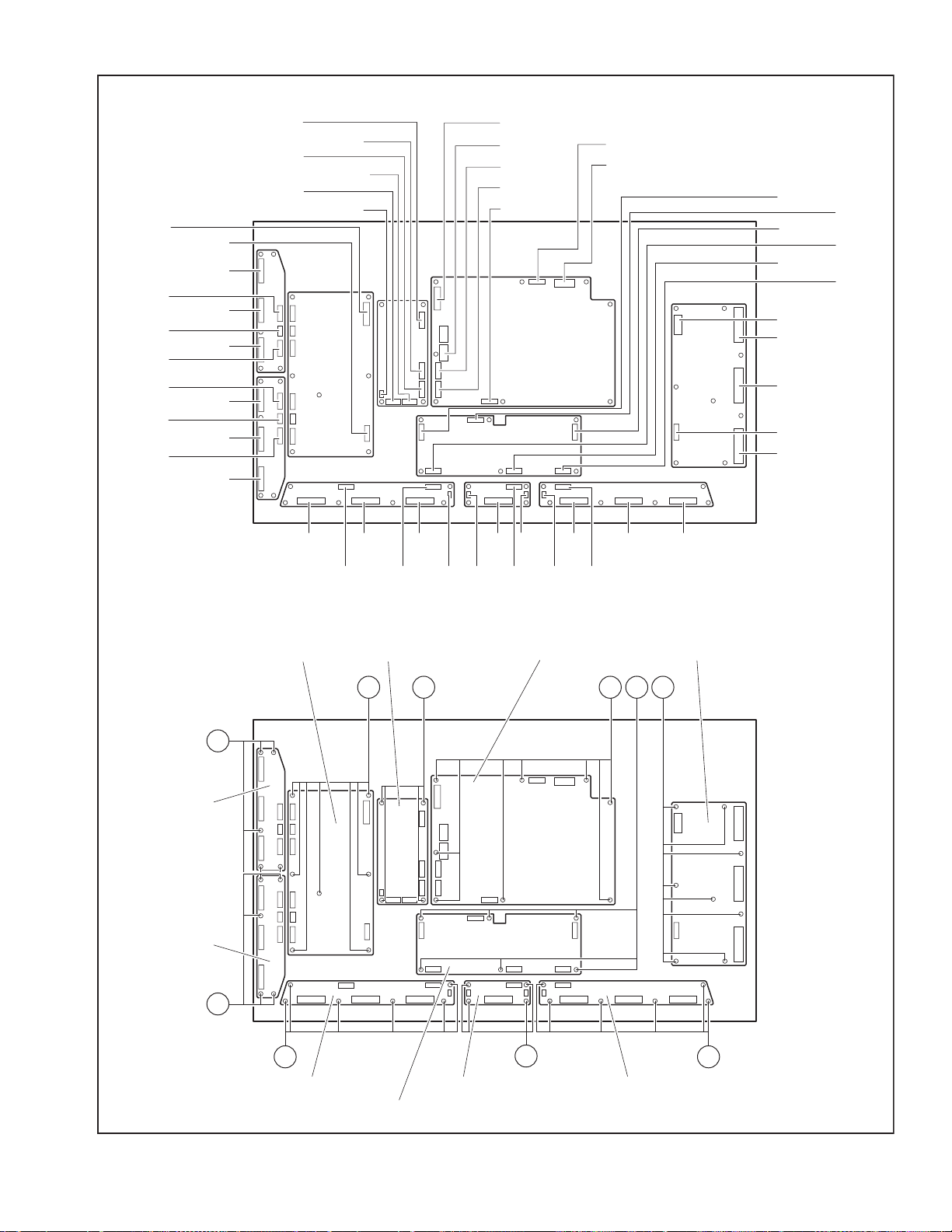
3.1.15 REMOVING THE LINE FILTER PWB (Fig.10)
• Remove the AV TERMINAL.
• Remove the PC TERMINAL.
• Remove the REAR COVER.
• Remove the BACK FRAME.
(1) Remove 1 screw [Y].
(2) Remove the noise filter from the clamp fixed to the SHIELD
COVER.
(3) Remove the 4 screws [Z].
(4) Remove the SHIELD COVER.
(5) Remove the CN8001
connector on the SMPS PWB.
(6) Remove the 3 screws [a] fixing the LINE FILTER PWB.
(7) Remove the LINE FILTER PWB.
3.1.16 REMOVING THE DIGITAL PWB (Fig.11)
• Remove the AV TERMINAL.
• Remove the PC TERMINAL.
• Remove the REAR COVER.
(1) Lift the DIGITAL PWB SHIELD COVER, and remove it.
(2) Remove the CNX
/CNV/CNQ/CND/CNT connectors.
(3) Remove the 4 screws [b].
(4) Turn the DIGITAL PWB upside down, and remove the
CN2201
/CNJ/CNK connectors.
(5) Remove the DIGITAL PWB.
SHIELD COVER
CN8001
SMPS PWB
DIGITAL PWB
SHIELD COVER
CNJ
a
Z
LINE FILTER PWB
NOISE FILTER
#%
Y
#%
Fig.10
CNX
CNK
b
DIGITAL
PWB
CN201
CNQ
CND
CNT
CHASSIS BASE
E
Fig.11
1-16 (No.52149)
Page 17
3.1.17 REMOVING THE MAIN PWB (Fig.12)
• Remove the AV TERMINAL.
• Remove the PC TERMINAL.
• Remove the REAR COVER.
• Remove the DIGITAL PWB SHIELD COVER.
• Remove the DIGITAL PWB.
(1) Remove the CNA
(2) Remove the 5 screws [c].
(3) Remove the MAIN PWB.
/CNE connectors.
MAIN PWB
CNE
CHASSIS
BASE
c
CNA
3.1.18 REMOVING THE CHASSIS BASE (Fig.13)
The CHASSIS BASE can be removed without removing the
MAIN PWB, DIGITAL PWB, LINE FILTER PWB, AUDIO PWB,
and BATTERY PWB from the CHASSIS BASE.
• Remove the AV TERMINAL.
• Remove the PC TERMINAL.
• Remove the REAR COVER.
• Remove the BACK FRAME (right).
• Remove the SPEAKER TERMINAL BRACKET.
• Remove the SPEAKER TERMINAL PWB.
(1) Remove the CN9004
PWB.
(2) Remove the cords from clamps.
(3) Remove the CNX
DIGITAL PWB.
(4) Remove the CNE
(5) Remove the 4 screws [d], 2 screws [e], and 2 screws [f].
(6) Lift the CHASSIS BASE, and remove th e LA03 connector
on the LOGIC-MAIN PWB.
(7) Remove the CHASSIS BASE.
3.1.19 REMOVING THE PDP (PANEL) UNIT (Fig.13)
• Remove the AV TERMINAL.
• Remove the PC TERMINAL.
• Remove the REAR COVER.
• Remove the BACK FRAME (right).
• Remove the SPEAKER TERMINAL BRACKET.
• Remove the SPEAKER TERMINAL PWB.
• Remove the CHASSIS BASE.
(1) Holding BACK FRAME SPACER, Lift the PDP upright and
remove it.
NOTE:
• When you remove the PDP (PANEL) UNIT, be careful not to
give a shock to the PDP (PANEL) UNIT enough. Two or more
people are required to remove the PDP (PANEL) UNIT.
• Do not touch the front side (glass) of the PDP with your
fingers.
/CN8001 connectors on the SMPS
/CNV/CNQ/CNT connectors on the
connector on the MAIN PWB.
CNQ
e
CNE
SMPS PWB
CN9004
BLACK FLAME SPACER
CNT
LA03
Fig.12
d
CHASSIS BASE
CNV
CNX
f
BLACK FLAME
SPACER
CN8001
LOGIC-MAIN PWB
Fig.13
(No.52149)1-17
Page 18

3.1.20 DISASSEMBLY PDP UNIT
3.1.20.1 REMOVING THE SMPS PWB
• Remove the REAR COVER.
(1) Remove the CN8007
CN8009
(2) Remove the 8 screws [g].
(3) Remove the SMPS PWB.
3.1.20.2 REMOVING THE X-MAIN PWB
• Removing the REAR COVER.
(1) Remove the CN4001
connectors on the X-MAIN PWB.
(2) Remove the 8 screws [h].
(3) Remove the X-MAIN PWB.
3.1.20.3 REMOVING THE Y-BUF-U PWB
• Remove the REAR COVER.
(1) Remove the CN5401
connectors on the Y-BUF-U PWB.
(2) Remove the 5 screws [I].
(3) Lift the Y-BUF-U PWB slightly, and remove th e CN5404
CN5405 connectors on the Y-BUF-U PWB.
(4) Remove the Y-BUF-U PWB.
3.1.20.4 REMOVING THE Y-BUF-L PWB
• Remove the REAR COVER.
(1) Remove the CN5501
connectors on the Y-BUF-L PWB.
(2) Remove the 5 screws [j].
(3) Lift the Y-BUF-L PWB slightly, and remove the CN5504/
CN5505
(4) Remove the Y-BUF-L PWB.
3.1.20.5 REMOVING THE Y-MAIN PWB
• Remove the REAR COVER.
• Remove the CHASSIS BASE.
• Remove the Y-BUF-U PWB.
• Remove the Y-BUF-L PWB.
(1) Remove the CN5001
PWB.
(2) Remove the 7 screws [k].
(3) Remove the Y-MAIN PWB.
/CN8002 connectors on the SMPS PWB.
connectors on the Y-BUF-L PWB.
/CN8008/CN8004/BUFFER/CN8003/
/CN4002/CN4003/CN4004/CN4005
/CN5402/CN5403/CN5406
/CN5502/CN5503/CN5506
/CN5008 connectors on the Y-MAIN
3.1.20.6 REMOVING THE LOGIC-MAIN PWB
• Remove the REAR COVER.
• Remove the CHASSIS BASE.
(1) Remove the CN101
connectors on the LOGIC-MAIN PWB.
(2) Remove the 6 screws [l].
(3) Remove the LOGIC-MAIN PWB.
3.1.20.7 REMOVING THE E-BUF PWB
• Remove the REAR COVER.
• Remove the BACK FRAME.
• Remove the CHASSIS BASE.
• Remove the SPEAKER BRACKET (left).
(1) Remove the EC1
connectors on the E-BUF PWB.
(2) Remove the 6 screws [m].
(3) Remove the E-BUF PWB.
3.1.20.8 REMOVING THE F-BUF PWB
/
• Remove the REAR COVER.
• Remove the BACK FRAME.
• Remove the CHASSIS BASE.
(1) Remove the FC4
BUF PWB.
(2) Remove thr 4 screws [n].
(3) Remove the F-BUF PWB.
3.1.20.9 REMOVING THE G-BUF PWB
• Remove the REAR COVER.
• Remove the BACK FRAME.
• Remove the CHASSIS BASE.
• Remove the SPEAKER BRACKET (right).
(1) Remove the GC5
the G-BUF PWB.
(2) Remove the 6 screws [o].
(3) Remove the G-BUF PWB.
3.1.20.10 REMOVING THE VIDEO SMPS PWB
• Remove the REAR COVER.
(1) Remove the CN9001
CN9007
(2) Remove the 4 screws [p].
(3) Remove the VIDEO SMPS PWB.
connectors on the VIDEO SMPS PWB.
/CN201/CN401/CN402/CN403/CN803
/EC2/EC3/CN401/CN806/EF1
/CN402/FE1/FG1 connectors on the F-
/GC6/GC7/CN403/GF1 connectors on
/CN9002/CN9004/CN9005/CN9006/
1-18 (No.52149)
Page 19
CN5008
CN5404
CN5406
CN5405
CN5505
CN5506
CN5504
CN5001
CN5401
CN5402
CN5403
CN5501
CN5502
CN5503
CN9005
CN9006
CN9001
CN9007
CN9002
CN9004
CN8003
BUFFER
CN8004
CN8007
CN8008
CN8009
CN8002
CN201
CN803
CN101
CN401
CN402
CN403
CN4001
CN4003
CN4004
CN4002
CN4005
Y-BUF-U PWB
Y-BUF-L PWB
EC1
Y-MAIN PWB
i
EC2 EC3
CN806 CN401 CN402 CN403
EF1
FC4 FC4
FE1
GC5 GC6 GC7
GF1
SMPS PWBVIDEO SMPS PWB
k
p
g
X-MAIN PWB
l h
j
m
n
o
E-BUF PWB G-BUF PWBF-BUF PWB
LOGIC-MAIN PWB
Fig.14
(No.52149)1-19
Page 20

3.2 REPLACEMENT OF MEMORY ICs
3.2.1 MEMORY IC
This model uses memory IC. In the memory IC is memorized
data for correctly operating the video and drive circuits.
When replacing the memory IC, be sure to use IC written with the
initial values of data.
3.2.2 PROCEDURE FOR REPLACING MEMORY IC
(1) Power off
Switch the power off and unplug the power plug from the
wall outlet.
(2) Replace IC
Be sure to use memory IC written with the initial data
values.
(3) Power on
Connect the power plug into the wall outlet and turn the
power on.
3.2.3 PROCEDURE FOR SET-UP MENU
(1) Press the [MENU / EXIT] key and the [VOLUME-] key
simultaneously.
(2) The SET-UP MENU screen (Fig. 1) will be displayed.
(3) Check the setting value of the SET-UP MENU table. (Refer
to the next page.)
(4) If the value is different, select the setting item with the
SELECT [/] key, and set the correct value with the
ADJUST [/] key.
(5) Press the [MENU / EXIT] key, and return to the normal
screen.
3.2.4 PROCEDURE FOR reset OR all reset
(1) The SET-UP MENU is displayed.
(2) Select "reset" or "all reset" item with SELECT [/] key of
remote control unit.
(3) Press ENTER [] key, and the "reset" (or all reset) menu is
displayed (Fig. 2).
(4) Press ENTER [] key to "reset" the standard settings.
< SET-UP MENU >
STATUS DISPLAY
CONTROL LOCK
REMOTE SWITCH
HD SIGNAL MODE
WHITE BALANCE
TIMER
ADJUST: SELECT: EXIT:
< SET-UP MENU > 2/2
PIXEL SHIFT
POWER SAVE
COLOR-REVERSE
REFRESH
reset
all reset
HOUR METER x100h
MODEL NAME : GM-V42
ADJUST: SELECT: EXIT:
: ON
: OFF
: MODE1
: 1080i
: OFF
: OFF
: OFF
: OFF
: 000
1/2
MENU
MENU
SET-UP MENUscreen
When select the [reset or all
reset] change to [ENTER : ]
mode.
Fig.1
or <reset>
< all reset >
Are you sure
"YES" then Key.
"NO" then Key.
MENU
[reset] / [all reset]
Fig.2
REMOTE CONTROL UNIT KEY ASSIGNMENT
1-20 (No.52149)
MENU/EXIT
key
RM-C579 REMOTE CONTROL UNIT
POWER
OFF ON
DISPLAY
INPUT SELECT
A
VIDEO
MUTING
MENU/EXIT
VOLUME
ASPECT
COMPO.
/(RGB B)
RGB AB
VOLUME key
(-/+)
SELECT key
( )
ENTER key ( )
ADJUST key
( )
Page 21

INITIAL SETTING FACTORY SHIPPING
Setting item Setting value Setting item Setting value
POWER OFF VOLUME 10
INPUT SELECT VIDEO A
MAIN MENU
PICTURE ADJ. CONTRAST 10 SIZE/POSITION ADJ. V POSITION 00
BRIGHT 00 DOT CLOCK (RGB only) 00
CHROMA 00 CLOCK PHASE (RGB only) 00
PHASE 00 FUNCTION SELECT COLOR TEMP HIGH
SHARPNESS 00 ASPECT REGULAR
SIZE/POSITION ADJ. H SIZE 00 SIGNAL MODE AUTO
H POSITION 00 RGB / COMP. COMP.
V SIZE 00 SYNC TERM HIGH
SETUP MENU
STATUS DISPLAY ON REMOTE SWITCH MODE1
CONTROL LOCK OFF HD SIGNAL MODE 1080i
WHITE BALNCE HIGH R GAIN Set M AX at
G GAIN START SET OFF
B GAIN START TIME - - : - -
LOW R GAIN Set MAX at
G GAIN END TIME - - : - B GAIN REFRESH REFRESH OFF
TIMER PRESENT TIME - - : - - START SET OFF
POWER-ON SET OFF START TIME - - : - POWER-ON TIME - - : - - END SET OFF
POWER-OFF SET OFF END TIME - - : - -
POWER-OFF TIME - - : - - MODEL NAME GM-V42
PIXEL SHIFT OFF
POWER SAVE OFF
least one item.
(other is 0)
least one item.
(other is 0)
COLOR-REVERSE COLOR-REVERSE OFF
END SET OFF
SERVICE SETTING ITEMS
Setting item Contents Setting item Contents
VCO ADJUST Video decorder VCO adjustment SIGNAL BLOCK Signal circuit adjustment
WHITE BALANCE BLOCK WHITE BALANCE adjustment DEVICE INITIAL VALUE Initial setting of DEVICE
CPU BLOCK Setting of CPU DIAGNOSIS BLOCK DIAGNOSIS function
SIZE/POSITION BLOCK SIZE/POSITION adjustment HOUR METER BLOCK HOUR METER function
H. POSITION BLOCK H. POSITION adjustment ENHANCER BLOCK Sharpness circuit adjustment
PANEL BLOCK Setting of PDP (panel)
(No.52149)1-21
Page 22

3.3 REPLACEMENT OF CHIP COMPONENT
3.3.1 CAUTIONS
(1) Avoid heating for more than 3 seconds.
(2) Do not rub the electrodes and the resist parts of the pattern.
(3) When removing a chip part, melt the solder adequately.
(4) Do not reuse a chip part after removing it.
3.3.2 SOLDERING IRON
(1) Use a high insulation soldering iron with a thin pointed end of it.
(2) A 30w soldering iron is recommended for ea sily removing parts.
3.3.3 REPLACEMENT STEPS
1. How to remove Chip parts
2. How to install Chip parts
[Resistors, capacitors, etc.]
(1) As shown in the figure, push the part with tweezers and
alternately melt the solder at each end.
(2) Shift with the tweezers and remove the chip part.
[Transistors, diodes, variable resistors, etc.]
(1) Apply extra solder to each lead.
SOLDER
SOLDER
[Resistors, capacitors, etc.]
(1) Apply solder to the pattern as indicated in the figure.
(2) Grasp the chip part with tweezers and place it on the
solder. Then heat and melt the solder at both ends of the
chip part.
[Transistors, diodes, variable resistors, etc.]
(1) Apply solder to the pattern as indicated in the figure.
(2) Grasp the chip part with tweezers and place it on the
solder.
(3) First solder lead A as indicated in the figure.
(2) As shown in the figure, push the part with tweezers and
alternately melt the solder at each lead. Shift and remove
the chip part.
NOTE :
After removing the part, remove remaining solder from the
pattern.
1-22 (No.52149)
A
B
C
(4) Then solder leads B and C.
A
B
C
Page 23

SECTION 4
ADJUSTMENT
4.1 BEFORE ADJUSTMENT
(1) There are 2 ways of adjusting this monitor : One is with the
REMOTE CONTROL UNIT and the other is the conventional
method using adjustment parts and components.
(2) The setting (adjustment) using the REMOTE CONTROL
UNIT is made on the basis of the initial setting values. The
setting values which adjust the screen to the optimum
condition can be different from the initial setting values.
(3) Make sure that connection is correctly made to AC power
source.
(4) Turn on the power of the Plasma display monitor and
measuring instrument for warming up for at least 30
minutes before starting adjustment.
(5) If the input signal is not specified, use the most appropriate
signal for adjustment.
(6) Never touch parts (such as variable resistors, transformers
and condensers) not shown in the adjustment items of this
service adjustment.
4.2 MEASURING INSTRUMENT AND TOOLS
• DC voltmeter (or digital voltmeter)
• Oscilloscope
• Colour analyzer (colour temperature meter)
• Signal generator
- Colour bar : PAL / SECAM / NTSC
- Whale black pattern : 480i, 1080i
- Lamp pattern :
NTSC / 480i / 1080i / VGA640 × 480 dots (H fr 31.5kHz, V fr
60Hz) / RGB 15k (H fr 15.73kHz, V fr 59.94Hz)
- Window patter n :
NTSC /480i / 1080i / VGA640 × 480 dots (H fr 31.5kHz, V fr
60Hz) / RGB 15k (H fr 15.73kHz, V fr 59.94Hz)
- Gray scall pattern :
NTSC/480i / 1080i / VGA640 × 480 dots (H fr 31.5kHz, V fr
60Hz) / RGB 15k (H fr 15.73kHz, V fr 59.94Hz)
• Remote control unit
4.3 PROCEDURE FOR SERVICE MODE
4.3.1 HOW TO ENTER THE SERVICE MODE
(1) Press the [MENU] key, and SELECT [] key
simultaneously (Fig. 1).
(2) The " " mark is appears at the center of the screen (Fig.
2).
(3) While " " mark is appears, press the [MENU] key and
[VOL-] key simultaneously.
(4) The word "PLEASE DON'T TOUCH !" (Fig.3) will be
display on the screen center.
(5) While the words of "PLEASE DON'T TOUCH !" are display
as shown in Fig. 3.
(6) Press the SELECT [] key, SERVICE MODE will be
display as shown in Fig. 4.
4.3.2 SELECT & ADJUSTMENT OF SERVICE MODE ITEM
While the SERVICE MODE is displayed.
(1) Press the up [/] select key to white balance block item.
(2) After selecting the item, press ENTER [] key.
(3) The adjustment menu mode is displayed .
(4) Press the ADJUST [/] key to change the setting value.
(5) Press [MENU / EXIT] key to display the original menu.
(6) Perform in the same manner for others SERVICE MODE
ITEM.
Note :
When the adjustment is made at SERVICE MODE, the
changed data is memorized in a memory simultaneously with
the change.
Fig.1
Fig.2
PLEASE, DON'T TOUCH!
Fig.3
VCO ADJUST
WHITE BALANCE BLOCK
CPU BLOCK
SIZE/POSITION BLOCK
H POSITION BLOCK
PANEL BLOCK
SIGNAL BLOCK
DEVICE INITIAL VALUE
ENTER: SELECT: EXIT:
DIAGNOSIS BLOCK
UPDATE CPU PROGRAM
HOUR METER BLOCK
ENHANCER BLOCK
ENTER: SELECT: EXIT:
Fig.4
[1/2]
MENU
[2/2]
MENU
(No.52149)1-23
Page 24

4.4 COMPOSITION OF A SERVICE MENU SCREEN
MAIN MENU
W(A01)
WHITE BALANCE BLOCK
adjustment item screen
C(A01)
CPU BLOCK
adjustment item screen
VCO ADJUST
WHITE BALANCE BLOCK
CPU BLOCK
SIZE/POSITION BLOCK
H POSITION BLOCK
PANEL BLOCK
SIGNAL BLOCK
DEVICE INITIAL VALUE
ENTER: SELECT: EXIT:
< VCO ADJUST PROGRAM >
Are you sure ?
"YES" then Key.
"NO" then Key.
MENU
< WHITE BALANCE BLOCK >
WA:RGB PS HIGH
WB:RGB PC LOW
WC:VIDEO HIGH
WD:VIDEO LOW
WE:COMPO. 15k HIGH
WF:COMPO. 15k LOW
WG:COMPO. HIGH
WH:COMPO. LOW
ENTER: SELECT: EXIT:
WHITE BALANCE BLOCK
adjustment item select screen
< CPU BLOCK >
CA:PANORAMA DATA
CB:SIGNAL RANGE
CC:SIZE/POSI. RANGE
CD:FRQENCY DATA
CE:SYSTEM CONSTANT
CF:TEMP SENCOR DATA
CG:APS CONTROL DATA
CH:TEST MODE
ENTER: SELECT: EXIT:
CPU BLOCK
adjustment item select screen
< SIZE/POSITION BLOCK >
DA:VIDEO-60Hz (REGULAR)
DB:VIDEO-60Hz (FULL)
DC:VIDEO-60Hz (ZOOM)
DD:VIDEO-60Hz (PANORA.)
DE:VIDEO-50Hz (REGULAR)
DF:VIDEO-50Hz (FULL)
DG:VIDEO-50Hz (ZOOM)
DH:VIDEO-50Hz (PANORA.)
ENTER: SELECT: EXIT:
< H POSITION BLOCK >
PA:VIDEO
PB:Y/C
PC:COMPO.
PD:RGB
ENTER: SELECT: EXIT:
MENU
MENU
MENU
MENU
MENU
[2/2]
MENU
MENU
Are you sure ?
"YES" then Key.
"NO" then Key.
MENU
MENU
DIAGNOSIS BLOCK
< CLEAR >
MENU
Flashing 5 sec.
[1/2]
MENU
DIAGNOSIS BLOCK
UPDATE CPU PROGRAM
HOUR METER BLOCK
ENHANCER BLOCK
ENTER: SELECT: EXIT:
< DIAGNOSIS BLOCK >
CLEAR
I2C SIGNAL BUS
I2C ROM BUS
POWER TEMP. OVER
TEMP. OVER [9Eh]
TEMP. OVER [9Ch]
ENTER: EXIT:
< DIAGNOSIS BLOCK >
CLEAR
I2C SIGNAL BUS
I2C ROM BUS
POWER TEMP. OVER
TEMP. OVER [9Eh]
TEMP. OVER [9Ch]
ENTER: EXIT:
< UPDATE CPU PROGRAM >
Are you sure ?
"YES" then Key.
"NO" then Key.
Necessity ! : PC, cable
& terminal software
CURRENT Ver. 1.02
< HOUR METER BLOCK >
RESET
HOUR METER (X1h) : *****
ENTER: EXIT:
1-24 (No.52149)
< PANEL BLOCK >
BA:VIDEO
BB:PC
ENTER: SELECT: EXIT:
< SIGNAL BLOCK >
SA:VIDEO -NTSC
SB:VIDEO -PAL
SC:VIDEO -SECAM
SD:VIDEO -NTSC4.43
SE:VIDEO -PALM
SF:VIDEO -PALN
SG:VIDEO -PAL-60
SH:Y/C -NTSC
ENTER: SELECT: EXIT:
< DEVICE INITIAL VALUE >
IA:VPC3230D
IB:CXA3506R
IC:TA1318
ID:PEMBRANDT-I
IE:PDP I/F
IF:PDP MODULE
IG:UPD64083GF
ENTER: SELECT: EXIT:
MENU
MENU
MENU
< HOUR METER BLOCK >
RESET
HOUR METER (X1h) : 00000
ENTER: EXIT:
< ENHANCER BLOCK >
EA:SHARPNESS A=-3
EB:SHARPNESS A=-2
EC:SHARPNESS A=-1
ED:SHARPNESS A= 0
EE:SHARPNESS A=+1
EF:SHARPNESS A=+2
EG:SHARPNESS A=+3
EH:SHARPNESS A=+4
ENTER: SELECT: EXIT:
< RESET HOUR METER >
! Are you sure ?
"YES" then Key.
"NO" then Key.
MENU
MENU
MENU
Page 25

4.5 INITIAL SETTING VALUE OF THE SERVICE MENU WHITE BALANCE BLOCK
Setting No. Setting item
WA : RGB PC HIGH
W(A01) DRIVE (R) 255
W(A02) DRIVE (G) 255
W(A03) DRIVE (B) 255
W(A04) CUT OFF (R) -001
W(A05) CUT OFF (G) -001
W(A06) CUT OFF (B) -001
W(A07) BRIGHT 000
W(A08) A-D GAIN (R) 128
W(A09) A-D GAIN (G) 128
W(A10) A-D GAIN (B) 128
W(A11) A-D OFFSET (R) 000
W(A12) A-D OFFSET (G) 000
W(A13) A-D OFFSET (B) 000
WB : RGB PC LOW
W(B01) DRIVE (R) 255
W(B02) DRIVE (G) 255
W(B03) DRIVE (B) 200
W(B04) CUT OFF (R) 000
W(B05) CUT OFF (G) 000
W(B06) CUT OFF (B) 000
W(B07) BRIGHT 000
W(B08) A-D GAIN (R) 000
W(B09) A-D GAIN (G) 000
W(B10) A-D GAIN (B) 000
W(B11) A-D OFFSET (R) 000
W(B12) A-D OFFSET (G) 000
W(B13) A-D OFFSET (B) 000
WC : VIDEO HIGH
W(C01) DRIVE (R) 255
W(C02) DRIVE (G) 255
W(C03) DRIVE (B) 255
W(C04) CUT OFF (R) -003
W(C05) CUT OFF (G) -004
W(C06) CUT OFF (B) -003
W(C07) BRIGHT -011
WD : VIDEO LOW
W(D01) DRIVE (R) 255
W(D02) DRIVE (G) 255
W(D03) DRIVE (B) 200
W(D04) CUT OFF (R) 000
W(D05) CUT OFF (G) 000
W(D06) CUT OFF (B) 000
W(D07) BRIGHT 000
WE : COMPO. 15k HIGH
W(E01) DRIVE (R) 255
W(E02) DRIVE (G) 255
W(E03) DRIVE (B) 255
W(E04) CUT OFF (R) -002
W(E05) CUT OFF (G) -004
W(E06) CUT OFF (B) -002
W(E07) BRIGHT 000
W(E08) A-D GAIN (R) 128
Setting
value
Setting No. Setting item
W(E09) A-D GAIN (G) 128
W(E10) A-D GAIN (B) 128
W(E11) A-D OFFSET (R) -002
W(E12) A-D OFFSET (G) 000
W(E13) A-D OFFSET (B) -002
WF : COMPO. 15k LOW
W(F01) DRIVE (R) 255
W(F02) DRIVE (G) 255
W(F03) DRIVE (B) 200
W(F04) CUT OFF (R) 000
W(F05) CUT OFF (G) 000
W(F06) CUT OFF (B) 000
W(F07) BRIGHT 000
W(F08) A-D GAIN (R) 000
W(F09) A-D GAIN (G) 000
W(F10) A-D GAIN (B) 000
W(F11) A-D OFFSET (R) 000
W(F12) A-D OFFSET (G) 000
W(F13) A-D OFFSET (B) 000
WG : COMPO. HIGH
W(G01) DRIVE (R) 255
W(G02) DRIVE (G) 255
W(G03) DRIVE (B) 255
W(G04) CUT OFF (R) -003
W(G05) CUT OFF (G) -004
W(G06) CUT OFF (B) -003
W(G07) BRIGHT 000
W(G08) A-D GAIN (R) 128
W(G09) A-D GAIN (G) 128
W(G10) A-D GAIN (B) 128
W(G11) A-D OFFSET (R) -002
W(G12) A-D OFFSET (G) 000
W(G13) A-D OFFSET (B) -002
WH : COMPO. LOW
W(H01) DRIVE (R) 255
W(H02) DRIVE (G) 255
W(H03) DRIVE (B) 200
W(H04) CUT OFF (R) 000
W(H05) CUT OFF (G) 000
W(H06) CUT OFF (B) 000
W(H07) BRIGHT 000
W(H08) A-D GAIN (R) 000
W(H09) A-D GAIN (G) 000
W(H10) A-D GAIN (B) 000
W(H11) A-D OFFSET (R) 000
W(H12) A-D OFFSET (G) 000
W(H13) A-D OFFSET (B) 000
Setting
value
(No.52149)1-25
Page 26

Setting No. Setting item
WI : RGB 15k HIGH
W(I01) DRIVE (R) 255
W(I02) DRIVE (G) 255
W(I03) DRIVE (B) 255
W(I04) CUT OFF (R) -001
W(I05) CUT OFF (G) -001
W(I06) CUT OFF (B) -001
W(I07) BRIGHT 000
W(I08) A-D GAIN (R) 125
W(I09) A-D GAIN (G) 128
W(I10) A-D GAIN (B) 128
W(I11) A-D OFFSET (R) 000
W(I12) A-D OFFSET (G) 000
W(I13) A-D OFFSET (B) 000
Setting
value
Setting No. Setting item
WJ : RGB 15k LOW
W(J01) DRIVE (R) 255
W(J02) DRIVE (G) 200
W(J03) DRIVE (B) 198
W(J04) CUT OFF (R) 000
W(J05) CUT OFF (G) 000
W(J06) CUT OFF (B) 000
W(J07) BRIGHT 000
W(J08) A-D GAIN (R) 000
W(J09) A-D GAIN (G) 000
W(J10) A-D GAIN (B) 000
W(J11) A-D OFFSET (R) 000
W(J12) A-D OFFSET (G) 000
W(J13) A-D OFFSET (B) 000
Setting
value
1-26 (No.52149)
Page 27

CPU BLOCK
Setting No. Setting item
CA : PANORAMA DATA
C(A01) INPUT_PIXELS 086
C(A02) OUTPUT_PIXELS 107
C(A03) NL_START 052
C(A04) NL_END 055
C(A05) RATIO_CENTER 076
C(A06) RATIO_SIDES 101
C(A07) Not use 000
C(A08) Not use 000
C(A09) Not use 000
C(A10) Not use 000
CB : SIGNAL RANGE
C(B01) CONTRAST MIN -044
C(B02) CONTRAST MAX +020
C(B03) BRIGHT MIN -012
C(B04) BRIGHT MAX +012
C(B05) CROMA MIN -071
C(B06) CROMA MAX +045
C(B07) FHASE MIN ----C(B08) FHASE MAX ----C(B09) V BRI_GAIN COMP 255
C(B10) G BRI_GAIN COMP 255
C(B11) R GAIN MIN 000
C(B12) R GAIN MAX 255
C(B13) G GAIN MIN 000
C(B14) G GAIN MAX 255
C(B15) B GAIN MIN 000
C(B16) B GAIN MAX 255
CC : SIZE/POSI. RANGE
C(C01) H_POS_MIN -060
C(C02) H_POS_MAX 060
C(C03) V_POS_MIN -030
C(C04) V_POS_MAX 030
C(C05) H_SIZE_MIN -100
C(C06) H_SIZE_MAX 100
C(C07) V_SIZE_MIN -100
C(C08) V_SIZE_MAX 100
C(C09) DOT_CLK_MIN -010
C(C10) DOT_CLK_MAX 010
C(C11) CLK_PHASE_MIN -020
C(C12) CLK_PHASE_MAX 020
C(C13) MARGIN_POS_X -006
C(C14) Not use 000
C(C15) Not use 000
C(C16) H_POS_MIN -055
C(C17) H_POS_MAX 055
C(C18) V_POS_MIN -030
C(C19) V_POS_MAX 030
C(C20) H_SIZE_MIN -060
C(C21) H_SIZE_MAX 060
C(C22) V_SIZE_MIN -060
C(C23) V_SIZE_MAX 060
C(C24) INPUT_X_V60_L 208
C(C25) INPUT_X_V60_H 002
Setting
value
Setting No. Setting item
C(C26) INPUT_Y_V60_L 229
C(C27) INPUT_Y_V60_H 001
C(C28) INPUT_X_V50_L 208
C(C29) INPUT_X_V50_H 002
C(C30) INPUT_Y_V50_L 068
C(C31) INPUT_Y_V50_H 002
C(C32) FREE_RUN 000
C(C33) DS_InX_MARGINE 003
C(C34) DS_OutX_MARGINE 002
C(C35) DS_InY_MARGINE 003
C(C36) DS_OutY_MARGINE 002
C(C37) M_OutX_MARGINE 002
C(C38) Not use 000
C(C39) Not use 000
C(C40) Not use 000
C(C41) Not use 000
C(C42) Not use 000
C(C43) Not use 000
C(C44) Not use 000
C(C45) Not use 000
C(C46) Not use 000
C(C47) Not use 000
C(C48) Not use 000
C(C49) Not use 000
C(C50) Not use 000
C(C51) Not use 000
C(C52) Not use 000
CD : FREQENCY DATA
C(D01) HORI FREQ ERROR 004
C(D02) VERT FREQ ERROR 001
C(D03) STATUS DELAY 050
C(D04) SIGNAL DETECT 010
C(D05) SIGNAL WAIT TIM 040
C(D06) SIGNAL WAIT TIM 000
CE : SYSTEM CONSTANT
C(E01) AREA 002
C(E02) POWER ON DELAY 031
C(E03) POWER ON DELAY 031
C(E04) MODEL No. 001
C(E05) REMOCON THROW 000
C(E06) TIME ERROR COMPENSATION +007
C(E07) VS_MUTE 001
C(E08) GOAL_PLC PW SELECT for 50Hz 000
C(E09) Not use 000
C(E10) Not use 000
Setting
value
(No.52149)1-27
Page 28

Setting No. Setting item
CF : TEMP SENSOR DATA
C(F01) Y ALARM TEMP. : T1 068
C(F02) T1 OVER COUNT 060
C(F03) SHUT DOWN TEMP. : T2 120
C(F04) T2 OVER COUNT 060
C(F05) TEMP. ALARM DISPLAY ON/OFF 000
C(F06) R ALARM TEMP. T3 095
C(F07) T3 OVER COUNT 060
C(F08) T3 SHUT DOWN WAIT TIME 012
C(F09) APS CONT. START TEMP : 4 052
C(F10) Not use 000
CG : APS CONTROL DATA
C(G01) Is COMPENSATION 150
C(G02) Is STANDARD 150
C(G03) APS PANEL IN MOD 010
C(G04) LEVEL ADJ 255
C(G05) AGC ON/OFF 000
C(G06) AGC GAIN MAX 000
C(G07) STOP PLC SELECT : K1 032
C(G08) GOAL PLC (NORMAL) SELECT : n 000
C(G09) SAMPLING CYCLE SETTING 004
C(G10) STOPPER INTERVAL SETTING 020
C(G11) ANIMATION LUMINOSITY
COMPENSATION
C(G12) GOAL PLC SELECT :K2 095
C(G13) SAVE1 LOW SETTING 045
C(G14) POWER CONT. INTERVAL(MAIN) 002
C(G15) POWER CONT. INTERVAL(SUB) 003
C(G16) POWER CONT. COEFFICIENT : K 028
C(G17) KX1 035
C(G18) KX2 065
C(G19) KX3 120
Setting
value
000
Setting No. Setting item
C(G20) KYmax0 005
C(G21) KYmax1 052
C(G22) KYmax2 100
C(G23) KYmax3 215
C(G24) KYmax4[7:0] 000
C(G25) KYmin0 010
C(G26) KYmin1 075
C(G27) KYmin2 141
C(G28) KYmin3 255
C(G29) KYmin4[7:0] 000
C(G30) KYmax4[11:8], KYmin[11:8] 017
CH : TEST MODE
C(H01) FPGA TEST MODE 000
C(H02) 480i MATRIX 000
C(H03) 480p MATRIX 000
C(H04) FREQ CHECK DISP 000
C(H05) APS CHECK DISP 000
C(H06) D TERM DET OFF 000
C(H07) VPC VERSION 000
C(H08) TEST PATTERN 000
C(H09) Not use 000
C(H10) Not use 000
CI : OTHER
C(I01) PIXEL SHIFT INTERVAL 001
C(I02) PIXEL SHIFT H POSI SHIFT 010
C(I03) PIXEL SHIFT V POSI SHIFT 006
C(I04) RS-232 BAUD 000
C(I05) B GAIN VALUE 195
C(I06) Not use 000
C(I07) Not use 000
C(I08) Not use 000
C(I09) Not use 000
C(I10) Not use 000
Setting
value
1-28 (No.52149)
Page 29

SIZE / POSITION BLOCK
Setting No. Setting item
DA : VIDEO-60Hz (REGULAR)
D(A01) FB COUNTER 1 172
D(A02) FB COUNTER 2 006
D(A03) VCO DIVIDE 002
D(A04) DELAY 032
D(A05) CHARGE_PUMP 018
D(A06) AMP MODE 001
D(A07) OUTPUT MODE 006
D(A08) OPLL_MDVI_L 229
D(A09) OPLL_MDVI_H 000
D(A10) OPLL_MDVI 255
D(A11) INPUT_ACT_LINE_START_L 012
D(A12) INPUT_ACT_LINE_START_H 000
D(A13) INPUT_ACT_LINE_L 200
D(A14) INPUT_ACT_LINE_H 001
D(A15) INPUT_ACT_PIXEL_START_L 022
D(A16) INPUT_ACT_PIXEL_START_H 000
D(A17) INPUT_ACT_PIXEL_L 158
D(A18) INPUT ACT_PIXEL_H 002
D(A19) Not use 000
D(A20) Not use 000
D(A21) WIN_X_MARGINE 128
D(A22) WIN_Y_MARGINE 128
D(A23) WIN_Y_POSI_L 001
D(A24) WIN_Y_POSI_H 000
D(A25) WIN_Y_SIZE_L 224
D(A26) WIN_Y_SIZE_H 001
D(A27) WIN_X_POSI_L 106
D(A28) WIN_X_POSI_H 000
D(A29) WIN_X_SIZE_L 128
D(A30) WIN_X_SIZE_H 002
D(A31) Not use 000
D(A32) Not use 000
D(A33) Not use 000
D(A34) Not use 000
D(A35) Not use 000
D(A36) Not use 000
D(A37) Not use 000
D(A38) COAST_ENABLE 000
D(A39) Not use 000
D(A40) INTERLACE 000
D(A41) Not use 000
D(A42) Not use 000
D(A43) Not use 000
D(A44) Not use 000
D(A45) Not use 000
D(A46) Not use 000
D(A47) Not use 000
D(A48) Not use 000
D(A49) Not use 000
D(A50) Not use 000
D(A51) Not use 000
D(A52) Not use 000
Setting
value
Setting No. Setting item
DB : VIDEO-60Hz (FULL)
D(B01) FB COUNTER 1 172
D(B02) FB COUNTER 2 006
D(B03) VCO DIVIDE 002
D(B04) DELAY 032
D(B05) CHARGE_PUMP 018
D(B06) AMP MODE 001
D(B07) OUTPUT MODE 006
D(B08) OPLL_MDVI_L 229
D(B09) OPLL_MDVI_H 000
D(B10) OPLL_MDVI 255
D(B11) INPUT_ACT_LINE_START_L 012
D(B12) INPUT_ACT_LINE_START_H 000
D(B13) INPUT_ACT_LINE_L 200
D(B14) INPUT_ACT_LINE_H 001
D(B15) INPUT_ACT_PIXEL_START_L 023
D(B16) INPUT_ACT_PIXEL_START_H 000
D(B17) INPUT_ACT_PIXEL_L 158
D(B18) INPUT ACT_PIXEL_H 002
D(B19) Not use 000
D(B20) Not use 000
D(B21) WIN_X_MARGINE 128
D(B22) WIN_Y_MARGINE 128
D(B23) WIN_Y_POSI_L 001
D(B24) WIN_Y_POSI_H 000
D(B25) WIN_Y_SIZE_L 224
D(B26) WIN_Y_SIZE_H 001
D(B27) WIN_X_POSI_L 001
D(B28) WIN_X_POSI_H 000
D(B29) WIN_X_SIZE_L 084
D(B30) WIN_X_SIZE_H 003
D(B31) Not use 000
D(B32) Not use 000
D(B33) Not use 000
D(B34) Not use 000
D(B35) Not use 000
D(B36) Not use 000
D(B37) Not use 000
D(B38) COAST_ENABLE 000
D(B39) Not use 000
D(B40) INTERLACE 000
D(B41) Not use 000
D(B42) Not use 000
D(B43) Not use 000
D(B44) Not use 000
D(B45) Not use 000
D(B46) Not use 000
D(B47) Not use 000
D(B48) Not use 000
D(B49) Not use 000
D(B50) Not use 000
D(B51) Not use 000
D(B52) Not use 000
Setting
value
(No.52149)1-29
Page 30

Setting No. Setting item
DC : VIDEO-60Hz (ZOOM)
D(C01) FB COUNTER 1 172
D(C02) FB COUNTER 2 006
D(C03) VCO DIVIDE 002
D(C04) DELAY 032
D(C05) CHARGE_PUMP 018
D(C06) AMP MODE 001
D(C07) OUTPUT MODE 006
D(C08) OPLL_MDVI_L 229
D(C09) OPLL_MDVI_H 000
D(C10) OPLL_MDVI 255
D(C11) INPUT_ACT_LINE_START_L 069
D(C12) INPUT_ACT_LINE_START_H 000
D(C13) INPUT_ACT_LINE_L 087
D(C14) INPUT_ACT_LINE_H 001
D(C15) INPUT_ACT_PIXEL_START_L 023
D(C16) INPUT_ACT_PIXEL_START_H 000
D(C17) INPUT_ACT_PIXEL_L 158
D(C18) INPUT ACT_PIXEL_H 002
D(C19) Not use 000
D(C20) Not use 000
D(C21) WIN_X_MARGINE 128
D(C22) WIN_Y_MARGINE 128
D(C23) WIN_Y_POSI_L 001
D(C24) WIN_Y_POSI_H 000
D(C25) WIN_Y_SIZE_L 224
D(C26) WIN_Y_SIZE_H 001
D(C27) WIN_X_POSI_L 001
D(C28) WIN_X_POSI_H 000
D(C29) WIN_X_SIZE_L 084
D(C30) WIN_X_SIZE_H 003
D(C31) Not use 000
D(C32) Not use 000
D(C33) Not use 000
D(C34) Not use 000
D(C35) Not use 000
D(C36) Not use 000
D(C37) Not use 000
D(C38) COAST_ENABLE 000
D(C39) Not use 000
D(C40) INTERLACE 000
D(C41) Not use 000
D(C42) Not use 000
D(C43) Not use 000
D(C44) Not use 000
D(C45) Not use 000
D(C46) Not use 000
D(C47) Not use 000
D(C48) Not use 000
D(C49) Not use 000
D(C50) Not use 000
D(C51) Not use 000
D(C52) Not use 000
Setting
value
Setting No. Setting item
DD : VIDEO-60Hz (PANORA.)
D(D01) FB COUNTER 1 172
D(D02) FB COUNTER 2 006
D(D03) VCO DIVIDE 002
D(D04) DELAY 032
D(D05) CHARGE_PUMP 018
D(D06) AMP MODE 001
D(D07) OUTPUT MODE 006
D(D08) OPLL_MDVI_L 229
D(D09) OPLL_MDVI_H 000
D(D10) OPLL_MDVI 255
D(D11) INPUT_ACT_LINE_START_L 024
D(D12) INPUT_ACT_LINE_START_H 000
D(D13) INPUT_ACT_LINE_L 176
D(D14) INPUT_ACT_LINE_H 001
D(D15) INPUT_ACT_PIXEL_START_L 020
D(D16) INPUT_ACT_PIXEL_START_H 000
D(D17) INPUT_ACT_PIXEL_L 146
D(D18) INPUT ACT_PIXEL_H 002
D(D19) Not use 105
D(D20) Not use 002
D(D21) WIN_X_MARGINE 113
D(D22) WIN_Y_MARGINE 128
D(D23) WIN_Y_POSI_L 001
D(D24) WIN_Y_POSI_H 000
D(D25) WIN_Y_SIZE_L 224
D(D26) WIN_Y_SIZE_H 001
D(D27) WIN_X_POSI_L 001
D(D28) WIN_X_POSI_H 000
D(D29) WIN_X_SIZE_L 084
D(D30) WIN_X_SIZE_H 002
D(D31) Not use 000
D(D32) Not use 000
D(D33) Not use 000
D(D34) Not use 000
D(D35) Not use 000
D(D36) Not use 000
D(D37) Not use 000
D(D38) COAST_ENABLE 000
D(D39) Not use 000
D(D40) INTERLACE 000
D(D41) Not use 000
D(D42) Not use 000
D(D43) Not use 000
D(D44) Not use 000
D(D45) Not use 000
D(D46) Not use 000
D(D47) Not use 000
D(D48) Not use 000
D(D49) Not use 000
D(D50) Not use 000
D(D51) Not use 000
D(D52) Not use 000
Setting
value
1-30 (No.52149)
Page 31

Setting No. Setting item
DE : VIDEO-50Hz (REGULAR)
D(E01) FB COUNTER 1 184
D(E02) FB COUNTER 2 006
D(E03) VCO DIVIDE 002
D(E04) DELAY 032
D(E05) CHARGE_PUMP 018
D(E06) AMP MODE 001
D(E07) OUTPUT MODE 006
D(E08) OPLL_MDVI_L 229
D(E09) OPLL_MDVI_H 000
D(E10) OPLL_MDVI 255
D(E11) INPUT_ACT_LINE_START_L 013
D(E12) INPUT_ACT_LINE_START_H 000
D(E13) INPUT_ACT_LINE_L 029
D(E14) INPUT_ACT_LINE_H 002
D(E15) INPUT_ACT_PIXEL_START_L 027
D(E16) INPUT_ACT_PIXEL_START_H 000
D(E17) INPUT_ACT_PIXEL_L 153
D(E18) INPUT ACT_PIXEL_H 002
D(E19) Not use 000
D(E20) Not use 000
D(E21) WIN_X_MARGINE 128
D(E22) WIN_Y_MARGINE 128
D(E23) WIN_Y_POSI_L 001
D(E24) WIN_Y_POSI_H 000
D(E25) WIN_Y_SIZE_L 224
D(E26) WIN_Y_SIZE_H 001
D(E27) WIN_X_POSI_L 106
D(E28) WIN_X_POSI_H 000
D(E29) WIN_X_SIZE_L 128
D(E30) WIN_X_SIZE_H 002
D(E31) Not use 000
D(E32) Not use 000
D(E33) Not use 000
D(E34) Not use 000
D(E35) Not use 000
D(E36) Not use 000
D(E37) Not use 000
D(E38) COAST_ENABLE 000
D(E39) Not use 000
D(E40) INTERLACE 000
D(E41) Not use 000
D(E42) Not use 000
D(E43) Not use 000
D(E44) Not use 000
D(E45) Not use 000
D(E46) Not use 000
D(E47) Not use 000
D(E48) Not use 000
D(E49) Not use 000
D(E50) Not use 000
D(E51) Not use 000
D(E52) Not use 000
Setting
value
Setting No. Setting item
DF : VIDEO-50Hz (FULL)
D(F01) FB COUNTER 1 184
D(F02) FB COUNTER 2 006
D(F03) VCO DIVIDE 002
D(F04) DELAY 032
D(F05) CHARGE_PUMP 018
D(F06) AMP MODE 001
D(F07) OUTPUT MODE 006
D(F08) OPLL_MDVI_L 229
D(F09) OPLL_MDVI_H 000
D(F10) OPLL_MDVI 255
D(F11) INPUT_ACT_LINE_START_L 013
D(F12) INPUT_ACT_LINE_START_H 000
D(F13) INPUT_ACT_LINE_L 029
D(F14) INPUT_ACT_LINE_H 002
D(F15) INPUT_ACT_PIXEL_START_L 028
D(F16) INPUT_ACT_PIXEL_START_H 000
D(F17) INPUT_ACT_PIXEL_L 153
D(F18) INPUT ACT_PIXEL_H 002
D(F19) Not use 000
D(F20) Not use 000
D(F21) WIN_X_MARGINE 128
D(F22) WIN_Y_MARGINE 128
D(F23) WIN_Y_POSI_L 001
D(F24) WIN_Y_POSI_H 000
D(F25) WIN_Y_SIZE_L 224
D(F26) WIN_Y_SIZE_H 001
D(F27) WIN_X_POSI_L 001
D(F28) WIN_X_POSI_H 000
D(F29) WIN_X_SIZE_L 084
D(F30) WIN_X_SIZE_H 003
D(F31) Not use 000
D(F32) Not use 000
D(F33) Not use 000
D(F34) Not use 000
D(F35) Not use 000
D(F36) Not use 000
D(F37) Not use 000
D(F38) COAST_ENABLE 000
D(F39) Not use 000
D(F40) INTERLACE 000
D(F41) Not use 000
D(F42) Not use 000
D(F43) Not use 000
D(F44) Not use 000
D(F45) Not use 000
D(F46) Not use 000
D(F47) Not use 000
D(F48) Not use 000
D(F49) Not use 000
D(F50) Not use 000
D(F51) Not use 000
D(F52) Not use 000
Setting
value
(No.52149)1-31
Page 32

Setting No. Setting item
DG : VIDEO-50Hz (ZOOM)
D(G01) FB COUNTER 1 184
D(G02) FB COUNTER 2 006
D(G03) VCO DIVIDE 002
D(G04) DELAY 032
D(G05) CHARGE_PUMP 018
D(G06) AMP MODE 001
D(G07) OUTPUT MODE 006
D(G08) OPLL_MDVI_L 229
D(G09) OPLL_MDVI_H 000
D(G10) OPLL_MDVI 255
D(G11) INPUT_ACT_LINE_START_L 081
D(G12) INPUT_ACT_LINE_START_H 000
D(G13) INPUT_ACT_LINE_L 153
D(G14) INPUT_ACT_LINE_H 001
D(G15) INPUT_ACT_PIXEL_START_L 028
D(G16) INPUT_ACT_PIXEL_START_H 000
D(G17) INPUT_ACT_PIXEL_L 153
D(G18) INPUT ACT_PIXEL_H 002
D(G19) Not use 000
D(G20) Not use 000
D(G21) WIN_X_MARGINE 128
D(G22) WIN_Y_MARGINE 128
D(G23) WIN_Y_POSI_L 001
D(G24) WIN_Y_POSI_H 000
D(G25) WIN_Y_SIZE_L 224
D(G26) WIN_Y_SIZE_H 001
D(G27) WIN_X_POSI_L 001
D(G28) WIN_X_POSI_H 000
D(G29) WIN_X_SIZE_L 084
D(G30) WIN_X_SIZE_H 003
D(G31) Not use 000
D(G32) Not use 000
D(G33) Not use 000
D(G34) Not use 000
D(G35) Not use 000
D(G36) Not use 000
D(G37) Not use 000
D(G38) COAST_ENABLE 000
D(G39) Not use 000
D(G40) INTERLACE 000
D(G41) Not use 000
D(G42) Not use 000
D(G43) Not use 000
D(G44) Not use 000
D(G45) Not use 000
D(G46) Not use 000
D(G47) Not use 000
D(G48) Not use 000
D(G49) Not use 000
D(G50) Not use 000
D(G51) Not use 000
D(G52) Not use 000
Setting
value
Setting No. Setting item
DH : VIDEO-50Hz (PANORA.)
D(H01) FB COUNTER 1 184
D(H02) FB COUNTER 2 006
D(H03) VCO DIVIDE 002
D(H04) DELAY 032
D(H05) CHARGE_PUMP 018
D(H06) AMP MODE 001
D(H07) OUTPUT MODE 006
D(H08) OPLL_MDVI_L 229
D(H09) OPLL_MDVI_H 000
D(H10) OPLL_MDVI 255
D(H11) INPUT_ACT_LINE_START_L 026
D(H12) INPUT_ACT_LINE_START_H 000
D(H13) INPUT_ACT_LINE_L 001
D(H14) INPUT_ACT_LINE_H 002
D(H15) INPUT_ACT_PIXEL_START_L 024
D(H16) INPUT_ACT_PIXEL_START_H 000
D(H17) INPUT_ACT_PIXEL_L 142
D(H18) INPUT ACT_PIXEL_H 002
D(H19) Not use 105
D(H20) Not use 002
D(H21) WIN_X_MARGINE 113
D(H22) WIN_Y_MARGINE 128
D(H23) WIN_Y_POSI_L 001
D(H24) WIN_Y_POSI_H 000
D(H25) WIN_Y_SIZE_L 224
D(H26) WIN_Y_SIZE_H 001
D(H27) WIN_X_POSI_L 001
D(H28) WIN_X_POSI_H 000
D(H29) WIN_X_SIZE_L 084
D(H30) WIN_X_SIZE_H 003
D(H31) Not use 000
D(H32) Not use 000
D(H33) Not use 000
D(H34) Not use 000
D(H35) Not use 000
D(H36) Not use 000
D(H37) Not use 000
D(H38) COAST_ENABLE 000
D(H39) Not use 000
D(H40) INTERLACE 000
D(H41) Not use 000
D(H42) Not use 000
D(H43) Not use 000
D(H44) Not use 000
D(H45) Not use 000
D(H46) Not use 000
D(H47) Not use 000
D(H48) Not use 000
D(H49) Not use 000
D(H50) Not use 000
D(H51) Not use 000
D(H52) Not use 000
Setting
value
1-32 (No.52149)
Page 33

Setting No. Setting item
DI : 480P (REGULAR.)
D(I01) FB COUNTER 1 082
D(I02) FB COUNTER 2 003
D(I03) VCO DIVIDE 002
D(I04) DELAY 032
D(I05) CHARGE_PUMP 018
D(I06) AMP MODE 001
D(I07) OUTPUT MODE 000
D(I08) OPLL_MDVI_L 229
D(I09) OPLL_MDVI_H 000
D(I10) OPLL_MDVI 255
D(I11) INPUT_ACT_LINE_START_L 044
D(I12) INPUT_ACT_LINE_START_H 000
D(I13) INPUT_ACT_LINE_L 201
D(I14) INPUT_ACT_LINE_H 001
D(I15) INPUT_ACT_PIXEL_START_L 114
D(I16) INPUT_ACT_PIXEL_START_H 000
D(I17) INPUT_ACT_PIXEL_L 160
D(I18) INPUT ACT_PIXEL_H 002
D(I19) Not use 000
D(I20) Not use 000
D(I21) WIN_X_MARGINE 153
D(I22) WIN_Y_MARGINE 148
D(I23) WIN_Y_POSI_L 001
D(I24) WIN_Y_POSI_H 000
D(I25) WIN_Y_SIZE_L 224
D(I26) WIN_Y_SIZE_H 001
D(I27) WIN_X_POSI_L 106
D(I28) WIN_X_POSI_H 000
D(I29) WIN_X_SIZE_L 128
D(I30) WIN_X_SIZE_H 002
D(I31) Not use 000
D(I32) Not use 000
D(I33) Not use 000
D(I34) Not use 000
D(I35) Not use 000
D(I36) Not use 000
D(I37) Not use 000
D(I38) COAST_ENABLE 000
D(I39) Not use 000
D(I40) INTERLACE 000
D(I41) Not use 000
D(I42) Not use 000
D(I43) Not use 000
D(I44) Not use 000
D(I45) Not use 000
D(I46) Not use 000
D(I47) Not use 000
D(I48) Not use 000
D(I49) Not use 000
D(I50) Not use 000
D(I51) Not use 000
D(I52) Not use 000
Setting
value
Setting No. Setting item
DJ : 480P (FLL.)
D(J01) FB COUNTER 1 082
D(J02) FB COUNTER 2 003
D(J03) VCO DIVIDE 002
D(J04) DELAY 032
D(J05) CHARGE_PUMP 018
D(J06) AMP MODE 001
D(J07) OUTPUT MODE 000
D(J08) OPLL_MDVI_L 229
D(J09) OPLL_MDVI_H 000
D(J10) OPLL_MDVI 255
D(J11) INPUT_ACT_LINE_START_L 044
D(J12) INPUT_ACT_LINE_START_H 000
D(J13) INPUT_ACT_LINE_L 201
D(J14) INPUT_ACT_LINE_H 001
D(J15) INPUT_ACT_PIXEL_START_L 113
D(J16) INPUT_ACT_PIXEL_START_H 000
D(J17) INPUT_ACT_PIXEL_L 162
D(J18) INPUT ACT_PIXEL_H 002
D(J19) Not use 000
D(J20) Not use 000
D(J21) WIN_X_MARGINE 153
D(J22) WIN_Y_MARGINE 148
D(J23) WIN_Y_POSI_L 001
D(J24) WIN_Y_POSI_H 000
D(J25) WIN_Y_SIZE_L 224
D(J26) WIN_Y_SIZE_H 001
D(J27) WIN_X_POSI_L 001
D(J28) WIN_X_POSI_H 000
D(J29) WIN_X_SIZE_L 084
D(J30) WIN_X_SIZE_H 003
D(J31) Not use 000
D(J32) Not use 000
D(J33) Not use 000
D(J34) Not use 000
D(J35) Not use 000
D(J36) Not use 000
D(J37) Not use 000
D(J38) COAST_ENABLE 000
D(J39) Not use 000
D(J40) INTERLACE 000
D(J41) Not use 000
D(J42) Not use 000
D(J43) Not use 000
D(J44) Not use 000
D(J45) Not use 000
D(J46) Not use 000
D(J47) Not use 000
D(J48) Not use 000
D(J49) Not use 000
D(J50) Not use 000
D(J51) Not use 000
D(J52) Not use 000
Setting
value
(No.52149)1-33
Page 34

Setting No. Setting item
DK : 480P (ZOOM.)
D(K01) FB COUNTER 1 82
D(K02) FB COUNTER 2 003
D(K03) VCO DIVIDE 002
D(K04) DELAY 032
D(K05) CHARGE_PUMP 018
D(K06) AMP MODE 001
D(K07) OUTPUT MODE 000
D(K08) OPLL_MDVI_L 229
D(K09) OPLL_MDVI_H 000
D(K10) OPLL_MDVI 255
D(K11) INPUT_ACT_LINE_START_L 102
D(K12) INPUT_ACT_LINE_START_H 000
D(K13) INPUT_ACT_LINE_L 086
D(K14) INPUT_ACT_LINE_H 001
D(K15) INPUT_ACT_PIXEL_START_L 113
D(K16) INPUT_ACT_PIXEL_START_H 000
D(K17) INPUT_ACT_PIXEL_L 162
D(K18) INPUT ACT_PIXEL_H 002
D(K19) Not use 000
D(K20) Not use 000
D(K21) WIN_X_MARGINE 153
D(K22) WIN_Y_MARGINE 188
D(K23) WIN_Y_POSI_L 001
D(K24) WIN_Y_POSI_H 000
D(K25) WIN_Y_SIZE_L 224
D(K26) WIN_Y_SIZE_H 001
D(K27) WIN_X_POSI_L 001
D(K28) WIN_X_POSI_H 000
D(K29) WIN_X_SIZE_L 084
D(K30) WIN_X_SIZE_H 003
D(K31) Not use 000
D(K32) Not use 000
D(K33) Not use 000
D(K34) Not use 000
D(K35) Not use 000
D(K36) Not use 000
D(K37) Not use 000
D(K38) COAST_ENABLE 000
D(K39) Not use 000
D(K40) INTERLACE 000
D(K41) Not use 000
D(K42) Not use 000
D(K43) Not use 000
D(K44) Not use 000
D(K45) Not use 000
D(K46) Not use 000
D(K47) Not use 000
D(K48) Not use 000
D(K49) Not use 000
D(K50) Not use 000
D(K51) Not use 000
D(K52) Not use 000
Setting
value
Setting No. Setting item
DL : 480P (PANORAMIC.)
D(L01) FB COUNTER 1 082
D(L02) FB COUNTER 2 003
D(L03) VCO DIVIDE 002
D(L04) DELAY 032
D(L05) CHARGE_PUMP 018
D(L06) AMP MODE 001
D(L07) OUTPUT MODE 000
D(L08) OPLL_MDVI_L 229
D(L09) OPLL_MDVI_H 000
D(L10) OPLL_MDVI 255
D(L11) INPUT_ACT_LINE_START_L 056
D(L12) INPUT_ACT_LINE_START_H 000
D(L13) INPUT_ACT_LINE_L 177
D(L14) INPUT_ACT_LINE_H 001
D(L15) INPUT_ACT_PIXEL_START_L 113
D(L16) INPUT_ACT_PIXEL_START_H 000
D(L17) INPUT_ACT_PIXEL_L 164
D(L18) INPUT ACT_PIXEL_H 002
D(L19) DS_OUTX_PANO_L 122
D(L20) DS_OUTX_PANO_H 002
D(L21) WIN_X_MARGINE 148
D(L22) WIN_Y_MARGINE 160
D(L23) WIN_Y_POSI_L 001
D(L24) WIN_Y_POSI_H 000
D(L25) WIN_Y_SIZE_L 224
D(L26) WIN_Y_SIZE_H 001
D(L27) WIN_X_POSI_L 001
D(L28) WIN_X_POSI_H 000
D(L29) WIN_X_SIZE_L 084
D(L30) WIN_X_SIZE_H 003
D(L31) Not use 000
D(L32) Not use 000
D(L33) Not use 000
D(L34) Not use 000
D(L35) Not use 000
D(L36) Not use 000
D(L37) Not use 000
D(L38) COAST_ENABLE 000
D(L39) Not use 000
D(L40) INTERLACE 000
D(L41) Not use 000
D(L42) Not use 000
D(L43) Not use 000
D(L44) Not use 000
D(L45) Not use 000
D(L46) Not use 000
D(L47) Not use 000
D(L48) Not use 000
D(L49) Not use 000
D(L50) Not use 000
D(L51) Not use 000
D(L52) Not use 000
Setting
value
1-34 (No.52149)
Page 35

Setting No. Setting item
DM : 576P (REGULAR)
D(M01) FB COUNTER 1 88
D(M02) FB COUNTER 2 003
D(M03) VCO DIVIDE 002
D(M04) DELAY 032
D(M05) CHARGE_PUMP 018
D(M06) AMP MODE 001
D(M07) OUTPUT MODE 000
D(M08) OPLL_MDVI_L 229
D(M09) OPLL_MDVI_H 000
D(M10) OPLL_MDVI 255
D(M11) INPUT_ACT_LINE_START_L 053
D(M12) INPUT_ACT_LINE_START_H 000
D(M13) INPUT_ACT_LINE_L 035
D(M14) INPUT_ACT_LINE_H 002
D(M15) INPUT_ACT_PIXEL_START_L 129
D(M16) INPUT_ACT_PIXEL_START_H 000
D(M17) INPUT_ACT_PIXEL_L 148
D(M18) INPUT ACT_PIXEL_H 002
D(M19) Not use 000
D(M20) Not use 000
D(M21) WIN_X_MARGINE 158
D(M22) WIN_Y_MARGINE 153
D(M23) WIN_Y_POSI_L 001
D(M24) WIN_Y_POSI_H 000
D(M25) WIN_Y_SIZE_L 224
D(M26) WIN_Y_SIZE_H 001
D(M27) WIN_X_POSI_L 106
D(M28) WIN_X_POSI_H 000
D(M29) WIN_X_SIZE_L 128
D(M30) WIN_X_SIZE_H 002
D(M31) Not use 000
D(M32) Not use 000
D(M33) Not use 000
D(M34) Not use 000
D(M35) Not use 000
D(M36) Not use 000
D(M37) Not use 000
D(M38) COAST_ENABLE 000
D(M39) Not use 000
D(M40) INTERLACE 000
D(M41) Not use 000
D(M42) Not use 000
D(M43) Not use 000
D(M44) Not use 000
D(M45) Not use 000
D(M46) Not use 000
D(M47) Not use 000
D(M48) Not use 000
D(M49) Not use 000
D(M50) Not use 000
D(M51) Not use 000
D(M52) Not use 000
Setting
value
Setting No. Setting item
DN : 576P (FULL)
D(N01) FB COUNTER 1 088
D(N02) FB COUNTER 2 003
D(N03) VCO DIVIDE 002
D(N04) DELAY 032
D(N05) CHARGE_PUMP 018
D(N06) AMP MODE 001
D(N07) OUTPUT MODE 000
D(N08) OPLL_MDVI_L 229
D(N09) OPLL_MDVI_H 000
D(N10) OPLL_MDVI 255
D(N11) INPUT_ACT_LINE_START_L 053
D(N12) INPUT_ACT_LINE_START_H 000
D(N13) INPUT_ACT_LINE_L 035
D(N14) INPUT_ACT_LINE_H 002
D(N15) INPUT_ACT_PIXEL_START_L 129
D(N16) INPUT_ACT_PIXEL_START_H 000
D(N17) INPUT_ACT_PIXEL_L 150
D(N18) INPUT ACT_PIXEL_H 002
D(N19) Not use 000
D(N20) Not use 000
D(N21) WIN_X_MARGINE 158
D(N22) WIN_Y_MARGINE 153
D(N23) WIN_Y_POSI_L 001
D(N24) WIN_Y_POSI_H 000
D(N25) WIN_Y_SIZE_L 224
D(N26) WIN_Y_SIZE_H 001
D(N27) WIN_X_POSI_L 001
D(N28) WIN_X_POSI_H 000
D(N29) WIN_X_SIZE_L 084
D(N30) WIN_X_SIZE_H 003
D(N31) Not use 000
D(N32) Not use 000
D(N33) Not use 000
D(N34) Not use 000
D(N35) Not use 000
D(N36) Not use 000
D(N37) Not use 000
D(N38) COAST_ENABLE 000
D(N39) Not use 000
D(N40) INTERLACE 000
D(N41) Not use 000
D(N42) Not use 000
D(N43) Not use 000
D(N44) Not use 000
D(N45) Not use 000
D(N46) Not use 000
D(N47) Not use 000
D(N48) Not use 000
D(N49) Not use 000
D(N50) Not use 000
D(N51) Not use 000
D(N52) Not use 000
Setting
value
(No.52149)1-35
Page 36

Setting No. Setting item
DO : 576P (ZOOM)
D(O01) FB COUNTER 1 088
D(O02) FB COUNTER 2 003
D(O03) VCO DIVIDE 002
D(O04) DELAY 032
D(O05) CHARGE_PUMP 018
D(O06) AMP MODE 001
D(O07) OUTPUT MODE 000
D(O08) OPLL_MDVI_L 229
D(O09) OPLL_MDVI_H 000
D(O10) OPLL_MDVI 255
D(O11) INPUT_ACT_LINE_START_L 110
D(O12) INPUT_ACT_LINE_START_H 000
D(O13) INPUT_ACT_LINE_L 154
D(O14) INPUT_ACT_LINE_H 001
D(O15) INPUT_ACT_PIXEL_START_L 129
D(O16) INPUT_ACT_PIXEL_START_H 000
D(O17) INPUT_ACT_PIXEL_L 150
D(O18) INPUT ACT_PIXEL_H 002
D(O19) Not use 000
D(O20) Not use 000
D(O21) WIN_X_MARGINE 158
D(O22) WIN_Y_MARGINE 188
D(O23) WIN_Y_POSI_L 001
D(O24) WIN_Y_POSI_H 000
D(O25) WIN_Y_SIZE_L 224
D(O26) WIN_Y_SIZE_H 001
D(O27) WIN_X_POSI_L 001
D(O28) WIN_X_POSI_H 000
D(O29) WIN_X_SIZE_L 084
D(O30) WIN_X_SIZE_H 003
D(O31) Not use 000
D(O32) Not use 000
D(O33) Not use 000
D(O34) Not use 000
D(O35) Not use 000
D(O36) Not use 000
D(O37) Not use 000
D(O38) COAST_ENABLE 000
D(O39) Not use 000
D(O40) INTERLACE 000
D(O41) Not use 000
D(O42) Not use 000
D(O43) Not use 000
D(O44) Not use 000
D(O45) Not use 000
D(O46) Not use 000
D(O47) Not use 000
D(O48) Not use 000
D(O49) Not use 000
D(O50) Not use 000
D(O51) Not use 000
D(O52) Not use 000
Setting
value
Setting No. Setting item
DP : 576P (PANORAMIC)
D(P01) FB COUNTER 1 088
D(P02) FB COUNTER 2 003
D(P03) VCO DIVIDE 002
D(P04) DELAY 032
D(P05) CHARGE_PUMP 018
D(P06) AMP MODE 001
D(P07) OUTPUT MODE 000
D(P08) OPLL_MDVI_L 229
D(P09) OPLL_MDVI_H 000
D(P10) OPLL_MDVI 255
D(P11) INPUT_ACT_LINE_START_L 067
D(P12) INPUT_ACT_LINE_START_H 000
D(P13) INPUT_ACT_LINE_L 007
D(P14) INPUT_ACT_LINE_H 002
D(P15) INPUT_ACT_PIXEL_START_L 124
D(P16) INPUT_ACT_PIXEL_START_H 000
D(P17) INPUT_ACT_PIXEL_L 162
D(P18) INPUT ACT_PIXEL_H 002
D(P19) Not use 122
D(P20) Not use 002
D(P21) WIN_X_MARGINE 153
D(P22) WIN_Y_MARGINE 168
D(P23) WIN_Y_POSI_L 001
D(P24) WIN_Y_POSI_H 000
D(P25) WIN_Y_SIZE_L 224
D(P26) WIN_Y_SIZE_H 001
D(P27) WIN_X_POSI_L 001
D(P28) WIN_X_POSI_H 000
D(P29) WIN_X_SIZE_L 084
D(P30) WIN_X_SIZE_H 003
D(P31) Not use 000
D(P32) Not use 000
D(P33) Not use 000
D(P34) Not use 000
D(P35) Not use 000
D(P36) Not use 000
D(P37) Not use 000
D(P38) COAST_ENABLE 000
D(P39) Not use 000
D(P40) INTERLACE 000
D(P41) Not use 000
D(P42) Not use 000
D(P43) Not use 000
D(P44) Not use 000
D(P45) Not use 000
D(P46) Not use 000
D(P47) Not use 000
D(P48) Not use 000
D(P49) Not use 000
D(P50) Not use 000
D(P51) Not use 000
D(P52) Not use 000
Setting
value
1-36 (No.52149)
Page 37

Setting No. Setting item
DQ : COMPO.-720P
D(Q01) FB COUNTER 1 106
D(Q02) FB COUNTER 2 006
D(Q03) VCO DIVIDE 001
D(Q04) DELAY 035
D(Q05) CHARGE_PUMP 020
D(Q06) AMP MODE 001
D(Q07) OUTPUT MODE 000
D(Q08) OPLL_MDVI_L 229
D(Q09) OPLL_MDVI_H 000
D(Q10) OPLL_MDVI 255
D(Q11) INPUT_ACT_LINE_START_L 037
D(Q12) INPUT_ACT_LINE_START_H 000
D(Q13) INPUT_ACT_LINE_L 173
D(Q14) INPUT_ACT_LINE_H 002
D(Q15) INPUT_ACT_PIXEL_START_L 032
D(Q16) INPUT_ACT_PIXEL_START_H 001
D(Q17) INPUT_ACT_PIXEL_L 184
D(Q18) INPUT ACT_PIXEL_H 004
D(Q19) Not use 000
D(Q20) Not use 000
D(Q21) WIN_X_MARGINE 178
D(Q22) WIN_Y_MARGINE 153
D(Q23) WIN_Y_POSI_L 001
D(Q24) WIN_Y_POSI_H 000
D(Q25) WIN_Y_SIZE_L 224
D(Q26) WIN_Y_SIZE_H 001
D(Q27) WIN_X_POSI_L 001
D(Q28) WIN_X_POSI_H 000
D(Q29) WIN_X_SIZE_L 084
D(Q30) WIN_X_SIZE_H 003
D(Q31) Not use 000
D(Q32) Not use 000
D(Q33) Not use 000
D(Q34) Not use 000
D(Q35) Not use 000
D(Q36) Not use 000
D(Q37) Not use 000
D(Q38) COAST_ENABLE 000
D(Q39) Not use 000
D(Q40) INTERLACE 000
D(Q41) Not use 000
D(Q42) Not use 000
D(Q43) Not use 000
D(Q44) Not use 000
D(Q45) Not use 000
D(Q46) Not use 000
D(Q47) Not use 000
D(Q48) Not use 000
D(Q49) Not use 000
D(Q50) Not use 000
D(Q51) Not use 000
D(Q52) Not use 000
Setting
value
Setting No. Setting item
DR : COMPO.-1080/60i
D(R01) FB COUNTER 1 188
D(R02) FB COUNTER 2 005
D(R03) VCO DIVIDE 001
D(R04) DELAY 040
D(R05) CHARGE_PUMP 020
D(R06) AMP MODE 001
D(R07) OUTPUT MODE 000
D(R08) OPLL_MDVI_L 229
D(R09) OPLL_MDVI_H 000
D(R10) OPLL_MDVI 255
D(R11) INPUT_ACT_LINE_START_L 028
D(R12) INPUT_ACT_LINE_START_H 000
D(R13) INPUT_ACT_LINE_L 001
D(R14) INPUT_ACT_LINE_H 002
D(R15) INPUT_ACT_PIXEL_START_L 155
D(R16) INPUT_ACT_PIXEL_START_H 000
D(R17) INPUT_ACT_PIXEL_L 192
D(R18) INPUT ACT_PIXEL_H 004
D(R19) Not use 000
D(R20) Not use 000
D(R21) WIN_X_MARGINE 208
D(R22) WIN_Y_MARGINE 144
D(R23) WIN_Y_POSI_L 001
D(R24) WIN_Y_POSI_H 000
D(R25) WIN_Y_SIZE_L 224
D(R26) WIN_Y_SIZE_H 001
D(R27) WIN_X_POSI_L 001
D(R28) WIN_X_POSI_H 000
D(R29) WIN_X_SIZE_L 84
D(R30) WIN_X_SIZE_H 003
D(R31) Not use 000
D(R32) Not use 000
D(R33) Not use 000
D(R34) Not use 000
D(R35) Not use 000
D(R36) Not use 000
D(R37) Not use 000
D(R38) COAST_ENABLE 000
D(R39) Not use 000
D(R40) INTERLACE 000
D(R41) Not use 000
D(R42) Not use 000
D(R43) Not use 000
D(R44) Not use 000
D(R45) Not use 000
D(R46) Not use 000
D(R47) Not use 000
D(R48) Not use 000
D(R49) Not use 000
D(R50) Not use 000
D(R51) Not use 000
D(R52) Not use 000
Setting
value
(No.52149)1-37
Page 38

Setting No. Setting item
DS : COMPO.-1080/50i
D(S01) FB COUNTER 1 226
D(S02) FB COUNTER 2 006
D(S03) VCO DIVIDE 001
D(S04) DELAY 035
D(S05) CHARGE_PUMP 020
D(S06) AMP MODE 001
D(S07) OUTPUT MODE 000
D(S08) OPLL_MDVI_L 229
D(S09) OPLL_MDVI_H 000
D(S10) OPLL_MDVI 255
D(S11) INPUT_ACT_LINE_START_L 028
D(S12) INPUT_ACT_LINE_START_H 000
D(S13) INPUT_ACT_LINE_L 001
D(S14) INPUT_ACT_LINE_H 002
D(S15) INPUT_ACT_PIXEL_START_L 132
D(S16) INPUT_ACT_PIXEL_START_H 000
D(S17) INPUT_ACT_PIXEL_L 192
D(S18) INPUT ACT_PIXEL_H 004
D(S19) Not use 000
D(S20) Not use 000
D(S21) WIN_X_MARGINE 208
D(S22) WIN_Y_MARGINE 144
D(S23) WIN_Y_POSI_L 001
D(S24) WIN_Y_POSI_H 000
D(S25) WIN_Y_SIZE_L 224
D(S26) WIN_Y_SIZE_H 001
D(S27) WIN_X_POSI_L 001
D(S28) WIN_X_POSI_H 000
D(S29) WIN_X_SIZE_L 084
D(S30) WIN_X_SIZE_H 003
D(S31) Not use 000
D(S32) Not use 000
D(S33) Not use 000
D(S34) Not use 000
D(S35) Not use 000
D(S36) Not use 000
D(S37) Not use 000
D(S38) COAST_ENABLE 000
D(S39) Not use 000
D(S40) INTERLACE 000
D(S41) Not use 000
D(S42) Not use 000
D(S43) Not use 000
D(S44) Not use 000
D(S45) Not use 000
D(S46) Not use 000
D(S47) Not use 000
D(S48) Not use 000
D(S49) Not use 000
D(S50) Not use 000
D(S51) Not use 000
D(S52) Not use 000
Setting
value
Setting No. Setting item
DT : COMPO.-1035i
D(T01) FB COUNTER 1 188
D(T02) FB COUNTER 2 005
D(T03) VCO DIVIDE 001
D(T04) DELAY 032
D(T05) CHARGE_PUMP 020
D(T06) AMP MODE 001
D(T07) OUTPUT MODE 000
D(T08) OPLL_MDVI_L 229
D(T09) OPLL_MDVI_H 000
D(T10) OPLL_MDVI 255
D(T11) INPUT_ACT_LINE_START_L 047
D(T12) INPUT_ACT_LINE_START_H 000
D(T13) INPUT_ACT_LINE_L 236
D(T14) INPUT_ACT_LINE_H 001
D(T15) INPUT_ACT_PIXEL_START_L 155
D(T16) INPUT_ACT_PIXEL_START_H 000
D(T17) INPUT_ACT_PIXEL_L 192
D(T18) INPUT ACT_PIXEL_H 004
D(T19) Not use 000
D(T20) Not use 000
D(T21) WIN_X_MARGINE 208
D(T22) WIN_Y_MARGINE 148
D(T23) WIN_Y_POSI_L 001
D(T24) WIN_Y_POSI_H 000
D(T25) WIN_Y_SIZE_L 224
D(T26) WIN_Y_SIZE_H 001
D(T27) WIN_X_POSI_L 001
D(T28) WIN_X_POSI_H 000
D(T29) WIN_X_SIZE_L 084
D(T30) WIN_X_SIZE_H 003
D(T31) Not use 000
D(T32) Not use 000
D(T33) Not use 000
D(T34) Not use 000
D(T35) Not use 000
D(T36) Not use 000
D(T37) Not use 000
D(T38) COAST_ENABLE 000
D(T39) Not use 000
D(T40) INTERLACE 000
D(T41) Not use 000
D(T42) Not use 000
D(T43) Not use 000
D(T44) Not use 000
D(T45) Not use 000
D(T46) Not use 000
D(T47) Not use 000
D(T48) Not use 000
D(T49) Not use 000
D(T50) Not use 000
D(T51) Not use 000
D(T52) Not use 000
Setting
value
1-38 (No.52149)
Page 39

H POSITION BLOCK
Setting No. Setting item
PA : VIDEO
P(A01) NTSC REGULAR 000
P(A02) NTSC FULL 000
P(A03) NTSC ZOOM 000
P(A04) NTSC PANARAMIC 000
P(A05) N443 REGULA R 000
P(A06) N443 FUL L 000
P(A07) N443ZOOM 000
P(A08) N443 PAN AR AMIC 000
P(A09) PAL M REGULAR 000
P(A10) PAL M FULL 000
P(A11) PAL M ZOOM 000
P(A12) PAL M PANARAMIC 000
P(A13) PAL60 REGULAR 000
P(A14) PAL60 FULL 000
P(A15) PAL60 ZOOM 000
P(A16) PAL60 PANARAMIC 000
P(A17) BW60 REGULAR 000
P(A18) BW60 FULL 000
P(A19) BW60 ZOOM 000
P(A20) BW60 PANARAMIC 000
P(A21) PAL REGULAR 000
P(A22) PAL FULL 000
P(A23) PAL ZOOM 000
P(A24) PAL PANARAMIC 000
P(A25) PAL N REGULAR 000
P(A26) PAL N FULL 000
P(A27) PAL N ZOOM 000
P(A28) PAL N PANARAMIC 000
P(A29) SECAM REGULAR 000
P(A30) SECAM FULL 000
P(A31) SECAM ZOOM 000
P(A32) SECAM PANARAMIC 000
P(A33) BW50 REGULAR 000
P(A34) BW50 FULL 000
P(A35) BW50 ZOOM 000
P(A36) BW50 PANARAMIC 000
PB : Y/C
P(B01) NTSC REGULAR 000
P(B02) NTSC FULL 000
P(B03) NTSC ZOOM 000
P(B04) NTSC PANARAMIC 000
P(B05) N443 REGULA R 000
P(B06) N443 FUL L 000
P(B07) N443 ZOOM 000
P(B08) N443 PAN AR AMIC 000
P(B09) PAL M REGULAR 000
P(B10) PAL M FULL 000
P(B11) PAL M ZOOM 000
P(B12) PAL M PANARAMIC 000
P(B13) PAL60 REGULAR 000
P(B14) PAL60 FULL 000
P(B15) PAL60 ZOOM 000
P(B16) PAL60 PANARAMIC 000
Setting
value
Setting No. Setting item
P(B17) BW60 REGULAR 000
P(B18) BW60 FULL 000
P(B19) BW60 ZOOM 000
P(B20) BW60 PANARAMIC 000
P(B21) PAL REGULAR 000
P(B22) PAL FULL 000
P(B23) PAL ZOOM 000
P(B24) PAL PANARAMIC 000
P(B25) PAL N REGULAR 000
P(B26) PAL N FULL 000
P(B27) PAL N ZOOM 000
P(B28) PAL N PANARAMIC 000
P(B29) SECAM REGULAR 000
P(B30) SECAM FULL 000
P(B31) SECAM ZOOM 000
P(B32) SECAM PANARAMIC 000
P(B33) BW50 REGULAR 000
P(B34) BW50 FULL 000
P(B35) BW50 ZOOM 000
P(B36) BW50 PANARAMIC 000
PC : COMPO.
P(C01) 480i REGULAR +001
P(C02) 480i FULL +001
P(C03) 480i ZOOM +001
P(C04) 480i PANARAMIC +001
P(C05) 576i REGULAR +003
P(C06) 576i FULL +003
P(C07) 576i ZOOM +003
P(C08) 576i PANARAMIC +003
P(C09) 480p REGULAR 000
P(C10) 480p FULL 000
P(C11) 480p ZOOM 000
P(C12) 480p PANARAMIC 000
P(C13) 576P REGULAR 000
P(C14) 576P FULL 000
P(C15) 576P ZOOM 000
P(C16) 576P PANARAMIC 000
P(C17) 720PREGULAR 000
P(C18) 1080/60i FULL 000
P(C19) 1080/50i ZOOM 000
P(C20) 1035i PANARAMIC 000
Setting
value
(No.52149)1-39
Page 40

Setting No. Setting item
PD : RGB
P(D01) RGB15K60 REGULAR 000
P(D02) RGB15K60 FULL 000
P(D03) RGB15K60 ZOOM 000
P(D04) RGB15K60 PANARAMIC 000
P(D05) RGB15K50 REGULAR 000
P(D06) RGB15K50 FULL 000
P(D07) RGB15K50 ZOOM 000
P(D08) RGB15K50 PANARAMIC 000
P(D09) VGA400/56 REGULAR 000
P(D10) VGA400/56 FULL 000
P(D11) VGA400/70 REGULAR 000
P(D12) VGA400/70 FULL 000
P(D13) VGA/60 REGULAR 000
P(D14) VGA/60 FULL 000
P(D15) VGA/72 REGULAR 000
P(D16) VGA/72 FULL 000
P(D17) VGA/75 REGULAR 000
P(D18) VGA/75 FULL 000
P(D19) MAC13 REGULAR 000
Setting
value
Setting No. Setting item
P(D20) MAC13 FULL 000
P(D21) SVGA/56 REGULAR 000
P(D22) SVGA/56 FULL 000
P(D23) SVGA/60 REGULAR 000
P(D24) SVGA/60 FULL 000
P(D25) SVGA/72 REGULAR 000
P(D26) SVGA/72 FULL 000
P(D27) SVGA/75 REGULAR 000
P(D28) SVGA/75 FULL 000
P(D29) XGA/60 REGULAR 000
P(D30) XGA/60 FULL 000
P(D31) XGA/70 REGULAR 000
P(D32) XGA/70 FULL 000
P(D33) XGA/75REGULAR 000
P(D34) XGA/75 FULL 000
P(D35) XGA/85 REGULAR 000
P(D36) XGA/85 FULL 000
P(D37) XGA+/75 REGULAR 000
P(D38) XGA+/75 FULL 000
Setting
value
1-40 (No.52149)
Page 41

PANEL BLOCK
Setting No. Setting item
BA : VIDEO 50Hz
B(A01) GM_CORR_SEL 000
B(A02) GM_CORR_SW 000
B(A03) JVC_ED 000
B(A04) JVC_DITH 000
B(A05) R_LGE_LOW_BOUND 013
B(A06) R_LGE_HIGH_BOUND 180
B(A07) FCR 000
B(A08) GM 001
B(A09) GT 001
B(A10) ED 002
B(A11) EXT_APS_EN 085
B(A12) EDR 000
B(A13) EDT 001
B(A14) EDP 001
B(A15) GTS_P_HYS 000
B(A16) GTS_N_HYS 000
B(A17) ED_NOISE_QTY 255
B(A18) R_SUS_MIN_APC_0 000
B(A19) R_LGE_SW 001
B(A20) R_LGE_HEIGHT 004
BB : COMPO. -480i/576i
B(B01) GM_CORR_SEL 000
B(B02) GM_CORR_SW 000
B(B03) JVC_ED 000
B(B04) JVC_DITH 000
B(B05) R_LGE_LOW_BOUND 013
B(B06) R_LGE_HIGH_BOUND 180
B(B07) FCR 000
B(B08) GM 001
Setting
value
Setting No. Setting item
B(B09) GT 001
B(B10) ED 002
B(B11) EXT_APS_EN 085
B(B12) EDR 000
B(B13) EDT 001
B(B14) EDP 001
B(B15) GTS_P_HYS 000
B(B16) GTS_N_HYS 000
B(B17) ED_NOISE_QTY 255
B(B18) R_SUS_MIN_APC_0 000
B(B19) R_LGE_SW 001
B(B20) R_LGE_HEIGHT 004
BC : COMPO. -OTHERS
B(C01) CORDING SELECT 001
B(C02) PRIMING CONT. 000
B(C03) CONTRARY GAMMA. 002
B(C04) ERROR DIFFUSION 007
B(C05) NR GAIN 000
BD : RGB -15k
B(D01) CORDING SELECT 002
B(D02) PRIMING CONT. 000
B(D03) CONTRARY GAMMA. 002
B(D04) ERROR DIFFUSION 007
B(D05) NR GAIN 000
BE : RGB -PC
B(E01) CORDING SELECT 001
B(E02) PRIMING CONT. 000
B(E03) CONTRARY GAMMA. 002
B(E04) ERROR DIFFUSION 007
B(E05) NR GAIN 000
Setting
value
(No.52149)1-41
Page 42

SIGNAL BLOCK
Setting No. Setting item
SA : VIDEO -NTSC
S(A01) LPF 000
S(A02) SUB BRIGHT 016
S(A03) SHARPNESS 001
S(A04) SUB CONTRAST 109
S(A05) YC DLAY (H) 15
S(A06) YC DLAY (L) 192
S(A07) VERT PEAK GAIN 001
S(A08) COM FILTER 103
S(A09) SU B COLOR (H) 007
S(A10) SU B COLOR (L) 005
S(A11) SUB TINT (H) 000
S(A12) SUB TINT (L) 000
SB : VIDEO -PAL
S(B01) LPF 000
S(B02) SUB BRIGHT 016
S(B03) SHARPNESS 001
S(B04) SUB CONTRAST 109
S(B05) YC DLAY (H) 15
S(B06) YC DLAY (L) 128
S(B07) VERT PEAK GAIN 001
S(B08) COM FILTER 231
S(B09) SU B COLOR (H) 007
S(B10) SU B COLOR (L) 005
S(B11) SUB TINT (H) 000
S(B12) SUB TINT (L) 000
SC : VIDEO -SECAM
S(C01) LPF 000
S(C02) SUB BRIGHT 016
S(C03) SHARPNESS 001
S(C04) SUB CONTRAST 173
S(C05) YC DLAY (H) 15
S(C06) YC DLAY (L) 128
S(C07) VERT PEAK GAIN 001
S(C08) COM FILTER 231
S(C09) SUB COLOR (H) 007
S(C10) SUB COLOR (L) 005
S(C11) SUB TINT (H) 000
S(C12) SUB TINT (L) 000
SD : VIDEO -NTSC4.43
S(D01) LPF 000
S(D02) SUB BRIGHT 016
S(D03) SHARPNESS 001
S(D04) SUB CONTRAST 173
S(D05) YC DLAY (H) 015
S(D06) YC DLAY (L) 192
S(D07) VERT PEAK GAIN 001
S(D08) COM FILTER 231
S(D09) SUB COLOR (H) 007
S(D10) SUB COLOR (L) 005
S(D11) SUB TINT (H) 000
S(D12) SUB TINT (L) 000
Setting
value
Setting No. Setting item
SE : VIDEO -PALM
S(E01) LPF 000
S(E02) SUB BRIGHT 016
S(E03) SHARPNESS 001
S(E04) SUB CONTRAST 173
S(E05) YC DLAY (H) 15
S(E06) YC DLAY (L) 128
S(E07) VERT PEAK GAIN 001
S(E08) COM FILTER 231
S(E09) SUB COLOR (H) 007
S(E10) SUB COLOR (L) 005
S(E11) SUB TINT (H) 000
S(E12) SUB TINT (L) 000
SF : VIDEO -PALN
S(F01) LPF 000
S(F02) SUB BRIGHT 016
S(F03) SHARPNESS 001
S(F04) SUB CONTRAST 173
S(F05) YC DLAY (H) 015
S(F06) YC DLAY (L) 128
S(F07) VERT PEAK GAIN 001
S(F08) COM FILTER 231
S(F09) SUB COLOR (H) 007
S(F10) SUB COLOR (L) 005
S(F11) SUB TINT (H) 000
S(F12) SUB TINT (L) 000
SG : VIDEO -PAL-60
S(G01) LPF 000
S(G02) SUB BRIGHT 016
S(G03) SHARPNESS 001
S(G04) SUB CONTRAST 173
S(G05) YC DLAY (H) 015
S(G06) YC DLAY (L) 128
S(G07) VERT PEAK GAIN 001
S(G08) COM FILTER 231
S(G09) SUB COLOR (H) 007
S(G10) SUB COLOR (L) 005
S(G11) SUB TINT (H) 000
S(G12) SUB TINT (L) 000
SH : Y/C -NTSC
S(H01) LPF 000
S(H02) SUB BRIGHT 016
S(H03) SHARPNESS 001
S(H04) SUB CONTRAST 109
S(H05) YC DLAY (H) 015
S(H06) YC DLAY (L) 192
S(H07) VERT PEAK GAIN 001
S(H08) COM FILTER 231
S(H09) SUB COLOR (H) 007
S(H10) SUB COLOR (L) 005
S(H11) SUB TINT (H) 000
S(H12) SUB TINT (L) 000
Setting
value
1-42 (No.52149)
Page 43

Setting No. Setting item
SI : Y/C -PAL
S(I01) LPF 000
S(I02) SUB BRIGHT 016
S(I03) SHARPNESS 001
S(I04) SUB CONTRAST 109
S(I05) YC DLAY (H) 015
S(I06) YC DLAY (L) 128
S(I07) VERT PEAK GAIN 001
S(I08) COM FILTER 231
S(I09) SUB COLOR (H) 007
S(I10) SUB COLOR (L) 005
S(I11) SUB TINT (H) 000
S(I12) SUB TINT (L) 000
SJ : Y/C -SECAM
S(J01) LPF 000
S(J02) SUB BRIGHT 016
S(J03) SHARPNESS 001
S(J04) SUB CONTRAST 173
S(J05) YC DLAY (H) 015
S(J06) YC DLAY (L) 128
S(J07) VERT PEAK GAIN 001
S(J08) COM FILTER 231
S(J09) SUB COLOR (H) 007
S(J10) SUB COLOR (L) 005
S(J11) SUB TINT (H) 000
S(J12) SUB TINT (L) 000
SK : Y/C -NTSC4.43
S(K01) LPF 000
S(K02) SUB BRIGHT 016
S(K03) SHARPNESS 001
S(K04) SUB CONTRAST 173
S(K05) YC DLAY (H) 015
S(K06) YC DLAY (L) 192
S(K07) VERT PEAK GAIN 001
S(K08) COM FILTER 231
S(K09) SUB COLOR (H) 007
S(K10) SUB COLOR (L) 005
S(K11) SUB TINT (H) 000
S(K12) SUB TINT (L) 000
SL : Y/C -PALM
S(L01) LPF 000
S(L02) SUB BRIGHT 016
S(L03) SHARPNESS 001
S(L04) SUB CONTRAST 173
S(L05) YC DLAY (H) 015
S(L06) YC DLAY (L) 128
S(L07) VERT PEAK GAIN 001
S(L08) COM FILTER 231
S(L09) SUB COLOR (H) 007
S(L10) SUB COLOR (L) 005
S(L11) SUB TINT (H) 000
S(L12) SUB TINT (L) 000
Setting
value
Setting No. Setting item
SM : Y/C -PALN
S(M01) LPF 000
S(M02) SUB BRIGHT 016
S(M03) SHARPNESS 001
S(M04) SUB CONTRAST 173
S(M05) YC DLAY (H) 015
S(M06) YC DLAY (L) 128
S(M07) VERT PEAK GAIN 001
S(M08) COM FILTER 231
S(M09) SUB COLOR (H) 007
S(M10) SUB COLOR (L) 005
S(M11) SUB TINT (H) 000
S(M12) SUB TINT (L) 000
SN : Y/C -PAL-60
S(N01) LPF 000
S(N02) SUB BRIGHT 016
S(N03) SHARPNESS 001
S(N04) SUB CONTRAST 173
S(N05) YC DLAY (H) 015
S(N06) YC DLAY (L) 128
S(N07) VERT PEAK GAIN 001
S(N08) COM FILTER 231
S(N09) SUB COLOR (H) 007
S(N10) SUB COLOR (L) 005
S(N11) SUB TINT (H) 000
S(N12) SUB TINT (L) 000
SO : COMPO. -480i/576i
S(O01) LPF 000
S(O02) SUB BRIGHT 016
S(O03) SHARPNESS 001
S(O04) SUB CONTRAST 109
Setting
value
(No.52149)1-43
Page 44

DEVICE INITIAL VALUE
Setting No. Setting item
IA : VPC3230D
I(A001) SYNC PIN CONTROL 014
I(A002) 000
I(A003) SYNC GENERATOR CONTROL 000
I(A004) 000
I(A005) OUTPUT STRENGTH 0 00
I(A006) 000
I(A007) V-SYNC DELAY CONTROL 000
I(A008) 027
I(A009) 656 OUTPUT INTERFACE 0 00
I(A010) 032
I(A011) LINE LENGTH 003
I(A012) 089
I(A013) HC START 000
I(A014) 050
I(A015) HC STOP 003
I(A016) 032
I(A017) AVO START 016
I(A018) 105
I(A019) AVO STOP 003
I(A020) 056
I(A021) NEWLINE 000
I(A022) 104
I(A023) VPC MODE 000
I(A024) 000
I(A025) PIP MODE 000
I(A026) 000
I(A027) PIP OPERATION 000
I(A028) 000
I(A029) BACKGROUND COLOR 000
I(A030) 000
I(A031) FRAME COLOR 1 000
I(A032) 000
I(A033) FRAME COLOR 2 000
I(A034) 000
I(A035) LINE OFFSET 000
I(A036) 000
I(A037) PIXEL OFFSET 000
I(A038) 000
I(A039) VERTICAL START 000
I(A040) 000
I(A041) HORIZONTAL START 000
I(A042) 000
I(A043) NUMBER OF LINES 000
I(A044) 000
I(A045) NUMBER OF LINES 000
I(A046) 000
I(A047) NUMBER OF PIXEL PER LINE 000
I(A048) 000
I(A049) SATURATION OF THE RGB/YC r C b 008
I(A050) 097
I(A051) TINT CONTROL OF THE RGB/YUV 000
I(A052) 000
Setting
value
Setting No. Setting item
I(A053) BRIGHTNESS OF THE RGB/YUV 027
I(A054) 088
I(A055) SOFTMIXER CONTROL 000
I(A056) 240
I(A057) SOFTMIXER CONTROL 000
I(A058) 224
I(A059) ADC RANGE 000
I(A060) 196
I(A061) Standard select 0 00
I(A062) 033
I(A063) Enable automatic standard
I(A064) 127
I(A065) Input select 004
I(A066) 070
I(A067) picture start position 000
I(A068) 000
I(A069) luma/chroma delay adjust 000
I(A070) 000
I(A071) helper delay register 000
I(A072) 000
I(A073) VGA mode select 000
I(A074) 000
I(A075) comb filter control register 000
I(A076) 000
I(A077) comb filter test register 000
I(A078) 000
I(A079) Saturation control 008
I(A080) 022
I(A081) ACC PAL+ Helper gain adjust 000
I(A082) 000
I(A083) AC C multiplier value for PAL+Helper
I(A084) 000
I(A085) amplitude killer level 000
I(A086) 015
I(A087) amplitude killer hysteresis 000
I(A088) 005
I(A089) automatic helper disable for
I(A090) 000
I(A091) NTSC tint angle 000
I(A092) 000
I(A093) crystal oscillator center frequency
I(A094) 000
I(A095) crystal oscillator line-locked mode,
I(A096) 000
I(A097) crystal oscillator line-locked mode,
I(A098) 144
I(A099) general purpose control bits 000
I(A100) 032
I(A101) scaler mode register 000
I(A102) 000
I(A103) pip control register 000
I(A104) 000
recognition
Signal
nonstandard signals
adjust
lock command
autolock feature
Setting
value
000
000
000
000
000
001
1-44 (No.52149)
Page 45

Setting No. Setting item
I(A105) active video length for 1H-FIFO 002
I(A106) 208
I(A107) scaler1 coefficient 006
I(A108) 000
I(A109) scaler2 coefficient 004
I(A110) 000
I(A111) scaler1/2 nonlinear scaling coefficient 000
I(A112) 000
I(A113) scaler1 window controls 000
I(A114) 000
I(A115) scaler1 window controls 000
I(A116) 000
I(A117) scaler1 window controls 000
I(A118) 000
I(A119) scaler1 window controls 000
I(A120) 000
I(A121) scaler1 window controls 000
I(A122) 000
I(A123) scaler2 window controls 000
I(A124) 000
I(A125) scaler2 window controls 000
I(A126) 000
I(A127) scaler2 window controls 000
I(A128) 000
I(A129) scaler2 window controls 000
I(A130) 000
I(A131) scaler2 window controls 000
I(A132) 000
I(A133) brightness register 000
I(A134) 016
I(A135) contrast register 000
I(A136) 048
I(A137) vertical freeze start 015
I(A138) 246
I(A139) vertical freeze stop 000
I(A140) 004
I(A141) 20 bit llc clock center frequency 000
I(A142) 042
I(A143) 20 bit llc clock center frequency 010
I(A144) 171
I(A145) pll frequency limiter 000
I(A146) 054
I(A147) llc clock generator control word 000
I(A148) 005
Setting
value
Setting No. Setting item
IB : CXA3506R
I(B01) VCODIV1 n, m(L) 024
I(B02) VCODIV2 m(H) 035
I(B03) DELAY 027
I(B04) Charge Punp 018
I(B05) POLARITY 038
I(B06) SYNC 029
I(B07) TTLOUT ENABLE 127
I(B08) MAIN CONTRAST 078
I(B09) SUB CONTRAST G(Y) 128
I(B10) SUB CONTRAST B(Cb) 128
I(B11) SUB CONTRAST R(Cr) 128
I(B12) SUB BRIGHTNESS G(Y) 128
I(B13) SUB BRIGHTNESS B 128
I(B14) SUB BRIGHTNESS R 128
I(B15) Cb OFFSET 032
I(B16) Cr OFFSET 032
I(B17) AMP MODE 004
I(B18) SYNC SEP 000
I(B19) OUTPUT MODE 000
I(B20) POWER SAVE 048
IC : TA1318
I(C01) Hfreq,HD1/VD1sw,HD2/
VD2sw,SepaLVL
I(C02) DAC1,DAC2,DAC3,test,HD1inv,
HD2inv
I(C03) Vfreq,CLPphase,FREQ DET
SW,INPUTsw
I(C04) HDphase,VD1inv,VD2inv 129
Setting
value
061
167
192
(No.52149)1-45
Page 46

Setting No. Setting item
ID : PEMBRANDT-I
I(D001) OUTPUT CONTROL 001
I(D002) CONFIG 000
I(D003) ADDR CLEAR 0 063
I(D004) ADDR CLEAR_1 255
I(D005) LOAD SHADOW 000
I(D006) IRQ SOURC E 000
I(D007) IRQ MASK 000
I(D008) IRQ CLEAR 001
I(D009) FLAGS 000
I(D010) FLAGS CLEAR 001
I(D011) GP OUTPUT 0 00
I(D012) STATUS1 000
I(D013) STATUS2 000
I(D014) MPLL MDIV L 002
I(D015) MPLL MDIV H 000
I(D016) MPLL NDIV 000
I(D017) PPLL MDIV_L 002
I(D018) PPLL MDIV_H 000
I(D019) PPLL NDIV 000
I(D020) OPLL MDIV L 229
I(D021) OPLL MDIV H 000
I(D022) OPLL NDIV 255
I(D023) NL CONTROL 005
I(D024) NL SWITCH 000
I(D025) NL X 000
I(D026) NL Y 000
I(D027) VIDEO CONFIG 008
I(D028) VIDEO SC 008
I(D029) VIN POLARITY 000
I(D030) VIN CONTROL 000
I(D031) VIN ACTIVE PIXELS L 000
I(D032) VIN ACTIVE LINES L 000
I(D033) VIN FLAGGED LINE 000
I(D034) VIN REGS MSBITS 000
I(D035) VIN FILTER GRP/C0 000
I(D036) VIN FILTER GRP/ C1 000
I(D037) VIN FILTER GRP/C2 000
I(D038) VIN FILTER GRP/C3 000
I(D039) VIN FILTER GRP/C4 064
I(D040) VIN FILTER GRP/C5 000
I(D041) VIN FILTER GRP/C6 000
I(D042) VIN FILTER GRP/C7 000
I(D043) VIN FILTER GRP/C8 000
I(D044) VOUT FILTER GRP/C0 253
I(D045) VOUT FILTER GRP/C1 250
I(D046) VOUT FILTER GRP/ C2 253
I(D047) VOUT FILTER GRP/ C3 250
I(D048) VOUT FILTER GRP/ C4 100
I(D049) VOUT FILTER GRP/C5 250
I(D050) VOUT FILTER GRP/C6 253
I(D051) VOUT FILTER GRP/C7 250
I(D052) VOUT FILTER GRP/C8 253
I(D053) N/A 000
I(D054) N/A 000
Setting
value
Setting No. Setting item
I(D055) VDSCALER TOUTX L 208
I(D056) VDSCALER TOUTX H 002
I(D057) VDSCALER CONTROL 000
I(D058) VDSCALER DELTAX L 000
I(D059) VDSCALER DELTAX H 008
I(D060) VDSCALER DELTAY L 000
I(D061) VDSCALER DELTAY H 008
I(D062) VDSCALER Y0 000
I(D063) VDSCALER X0 000
I(D064) VDSCALER TOUTY L 224
I(D065) VDSCALER TOUTY H 001
I(D066) VUSCALER CONTROL 000
I(D067) VUSCALER DELTAX L 192
I(D068) VUSCALER DELTAX H 006
I(D069) VUSCALER DELTAY L 000
I(D070) VUSCALER DELTAY H 008
I(D071) VUSCALER Y0 000
I(D072) VUSCALER X0 000
I(D073) DI CONTROL 004
I(D074) DI C0 031
I(D075) DI C1 007
I(D076) DI C2 127
I(D077) DI C3 255
I(D078) DI C4 031
I(D079) DATA CONFIG 000
I(D080) DATA SC 008
I(D081) DIN POLARITY 0 041
I(D082) DIN POLARITY 1 000
I(D083) DIN CONTROL 0 004
I(D084) DIN CONTROL 1 064
I(D085) DIN CONTROL 2 002
I(D086) DPLL DIV L 000
I(D087) DPLL DIV H 000
I(D088) DIN THRESHOLD 008
I(D089) CLAMP START 001
I(D090) CLAMP WIDTH 016
I(D091) DIN LINE TRIG 001
I(D092) DIN PIXEL TRIG 001
I(D093) ACTIVE LINE START L 038
I(D094) ACTIVE LINE START H 000
I(D095) ACTIVE LINES L 224
I(D096) ACTIVE LINES H 001
I(D097) ACTIVE PIXEL START L 132
I(D098) ACTIVE PIXEL START H 000
I(D099) ACTIVE PIXELS L 128
I(D100) ACTIVE PIXELS H 002
I(D101) DIN FLAGGED LINE L 000
I(D102) DIN FLAGGED LINE H 0 00
I(D103) DIN CONTROL 3 006
I(D104) N/A 000
I(D105) N/A 000
I(D106) N/A 000
I(D107) DIN FILTER GRP/C0 253
I(D108) DIN FILTER GRP/C1 250
I(D109) DIN FILTER GRP/C2 253
Setting
value
1-46 (No.52149)
Page 47

Setting No. Setting item
I(D110) DIN FILTER GRP/C3 250
I(D111) DIN FILTER GRP/C4 100
I(D112) DIN FILTER GRP/C5 250
I(D113) DIN FILTER GRP/C6 253
I(D114) DIN FILTER GRP/C7 250
I(D115) DIN FILTER GRP/C8 253
I(D116) DDSCALER TOUTX L 128
I(D117) DDSCALER TOUTX H 002
I(D118) DDSCALER CONTROL 000
I(D119) DDSCALER DELTAX L 000
I(D120) DDSCALER DELTAX H 008
I(D121) DDSCALER DELTAY L 000
I(D122) DDSCALER DELTAY H 008
I(D123) N/A 000
I(D124) N/A 000
I(D125) DDSCALER TOUTY L 224
I(D126) DDSCALER TOUTY H 001
I(D127) DUSCALER CONTROL 000
I(D128) DUSCALER DELTAX L 000
I(D129) DUSCALER DELTAX H 006
I(D130) DUSCALER DELTAY L 000
I(D131) DUSCALER DELTAY H 008
I(D132) DUSCALER Y0 001
I(D133) DUSCALER X0 001
I(D134) VIDEO WIN GRP/Y POS L 001
I(D135) VIDEO WIN GRP/Y POS H 000
I(D136) VIDEO WIN GRP/Y SIZE L 224
I(D137) VIDEO WIN GRP/Y SIZE H 001
I(D138) VIDEO WIN GRP/X POS L 001
I(D139) VIDEO WIN GRP/X POS H 000
I(D140) VIDEO WIN GRP/X SIZE L 085
I(D141) VIDEO WIN GRP/X SIZE H 003
I(D142) DATA WIN GRP/Y POS L 001
I(D143) DATA WIN GRP/Y POS H 000
I(D144) DATA WIN GRP/Y SIZE L 224
I(D145) DATA WIN GRP/Y SIZE H 001
I(D146) DATA WIN GRP/X POS L 001
I(D147) DATA WIN GRP/X POS H 000
I(D148) DATA WIN GRP/X SIZE L 085
I(D149) DATA WIN GRP/X SIZE H 003
I(D150) OSDA WIN GRP/Y POS L 000
I(D151) OSDA WIN GRP/Y POS H 000
I(D152) OSDA WIN GRP/Y SIZE L 000
I(D153) OSDA WIN GRP/Y SIZE H 000
I(D154) OSDA WIN GRP/X POS L 000
I(D155) OSDA WIN GRP/X POS H 000
I(D156) OSDA WIN GRP/X SIZE L 000
I(D157) OSDA WIN GRP/X SIZE H 000
I(D158) OSDB WIN GRP/Y POS L 000
I(D159) OSDB WIN GRP/Y POS H 000
I(D160) OSDB WIN GRP/Y SIZE L 000
I(D161) OSDB WIN GRP/Y SIZE H 000
I(D162) OSDB WIN GRP/X POS L 000
I(D163) OSDB WIN GRP/X POS H 000
I(D164) OSDB WIN GRP/X SIZE L 000
Setting
value
Setting No. Setting item
I(D165) OSDB WIN GRP/X SIZE H 000
I(D166) LUT Y 000
I(D167) LUT U 000
I(D168) LUT V 000
I(D169) LUT R L 000
I(D170) LUT R H 000
I(D171) LUT G L 000
I(D172) LUT G H 000
I(D173) LUT B L 000
I(D174) LUT B H 000
I(D175) PALETTE R 000
I(D176) PALETTE G 000
I(D177) PALETTE B 000
I(D178) VIDEO CSC BIAS 000
I(D179) VIDEO CSC GRP/C(0) L 154
I(D180) VIDEO CSC GRP/C(0) H 003
I(D181) VIDEO CSC GRP/C(1) L 000
I(D182) VIDEO CSC GRP/C(1) H 000
I(D183) VIDEO CSC GRP/C(2) L 170
I(D184) VIDEO CSC GRP/C(2) H 001
I(D185) VIDEO CSC GRP/C(3) L 154
I(D186) VIDEO CSC GRP/C(3) H 003
I(D187) VIDEO CSC GRP/C(4) L 184
I(D188) VIDEO CSC GRP/C(4) H 255
I(D189) VIDEO CSC GRP/C(5) L 086
I(D190) VIDEO CSC GRP/C(5) H 255
I(D191) VIDEO CSC GRP/C(6) L 154
I(D192) VIDEO CSC GRP/C(6) H 003
I(D193) VIDEO CSC GRP/C(7) L 153
I(D194) VIDEO CSC GRP/C(7) H 001
I(D195) VIDEO CSC GRP/C(8) L 000
I(D196) VIDEO CSC GRP/C(8) H 000
I(D197) DATA CSC BIAS 000
I(D198) DATA CSC GRP/C(0) L 154
I(D199) DATA CSC GRP/C(0) H 003
I(D200) DATA CSC GRP/C(1) L 000
I(D201) DATA CSC GRP/C(1) H 000
I(D202) DATA CSC GRP/C(2) L 223
I(D203) DATA CSC GRP/C(2) H 001
I(D204) DATA CSC GRP/C(3) L 154
I(D205) DATA CSC GRP/C(3) H 003
I(D206) DATA CSC GRP/C(4) L 217
I(D207) DATA CSC GRP/C(4) H 255
I(D208) DATA CSC GRP/C(5) L 145
I(D209) DATA CSC GRP/C(5) H 255
I(D210) DATA CSC GRP/C(6) L 154
I(D211) DATA CSC GRP/C(6) H 003
I(D212) DATA CSC GRP/C(7) L 172
I(D213) DATA CSC GRP/C(7) H 001
I(D214) DATA CSC GRP/C(8) L 000
I(D215) DATA CSC GRP/C(8) H 000
I(D216) OUT CONFIG 012
I(D217) BACKGND GRP/BLUE 000
I(D218) BACKGND GRP/GREEN 000
I(D219) BACKGRND GRP/RED 000
Setting
value
(No.52149)1-47
Page 48

Setting No. Setting item
I(D220) OSDA CONTROL 0 00
I(D221) KEYSTONE CONTROL 000
I(D222) KEYSTONE CONTROL 000
I(D223) KEYSTONE LINES 255
I(D224) DITHER CONTROL 042
I(D225) DITHER C0 060
I(D226) DITHER C1 056
I(D227) DISPLAY CONTROL 0 032
I(D228) DISPLAY CONTROL 1 000
I(D229) DISPLAY CONTROL 2 003
I(D230) D/F GRP/VSYNC CYCLE L 247
I(D231) D/F GRP/VSYNC CYCLE H 001
I(D232) D/F GRP/HSYNC CYCLE L 128
I(D233) D/F GRP/HSYNC CYCLE H 003
I(D234) D/F GRP/VSYNC WIDTH 004
I(D235) D/F GRP/VSYNC OFFSET H 000
I(D236) D/F GRP/HSYNC WIDTH L 010
I(D237) D/F GRP/HSYNC WIDTH H 000
I(D238) D/F GRP/ACT LINE START L 015
I(D239) D/F GRP/ACT LINE START H 000
I(D240) D/F GRP/ACT LINE S L 224
I(D241) D/F GRP/ACT LINE S H 001
I(D242) D/F GRP/ACT PIX START L 037
I(D243) D/F GRP/ACT PIX START H 000
I(D244) D/F GRP/ACT PIXS L 084
I(D245) D/F GRP/ACT PIXS H 003
I(D246) DISPLAY HV DELAY 0 001
I(D247) DISPLAY HV DELAY 1 001
I(D248) DISPLAY POLARITY 003
I(D249) CONTROL 3D 000
I(D250) X0 3D 000
I(D251) SECT STAT GRP/VIDEO0 L 000
I(D252) SECT STAT GRP/VIDEO0 H 000
I(D253) SECT STAT GRP/VIDEO1 L 180
I(D254) SECT STAT GRP/VIDEO1 H 000
I(D255) SECT STAT GRP/VIDEO2 L 104
I(D256) SECT STAT GRP/VIDEO2 H 001
I(D257) SECT STAT GRP/LDAT0 L 028
I(D258) SECT STAT GRP/LDAT0 H 002
I(D259) SECT STAT GRP/RDAT0 L 1 12
I(D260) SECT STAT GRP/RDAT0 H 003
I(D261) SECT STAT GRP/LDAT1 L 196
I(D262) SECT STAT GRP/LDAT1 H 004
I(D263) SECT STAT GRP/RDAT1 L 0 24
I(D264) SECT STAT GRP/RDAT1 H 006
I(D265) SECT STAT GRP/OSD0 L 000
I(D266) SECT STAT GRP/OSD0 H 000
I(D267) SECT STAT GRP/OSD1 L 000
I(D268) SECT STAT GRP/OSD1 H 000
I(D269) SECT STAT GRP/OSD2 L 000
I(D270) SECT STAT GRP/OSD2 H 000
I(D271) SECT STAT GRP/OSD3 L 000
I(D272) SECT STAT GRP/OSD3 H 000
I(D273) S/S GRP/IDATA OFFSET L 000
I(D274) S/S GRP/IDATA OFFSET H 000
Setting
value
Setting No. Setting item
I(D275) LINE LENG GRP/VIDEO L 144
I(D276) LINE LENG GRP/VIDEO H 000
I(D277) LINE LENG GRP/DATA L 032
I(D278) LINE LENG GRP/DATA H 001
I(D279) LINE LENG GRP/IDATA L 000
I(D280) LINE LENG GRP/IDATA H 000
I(D281) LINE LENG GRP/OSD0 L 000
I(D282) LINE LENG GRP/OSD0 H 000
I(D283) LINE LENG GRP/OSD1 L 000
I(D284) LINE LENG GRP/OSD1 H 000
I(D285) LINE LENG GRP/OSD2 L 000
I(D286) LINE LENG GRP/OSD2 H 000
I(D287) LINE LENG GRP/OSD3 L 000
I(D288) LINE LENG GRP/OSD3 H 000
I(D289) WIN LINE OFFSET GRP/VIDEO L 000
I(D290) WIN LINE OFFSET GRP/VIDEO H 000
I(D291) WIN LINE OFFSET GRP/DATA L 000
I(D292) WIN LINE OFFSET GRP/DATA H 000
I(D293) WIN LINE OFFSET GRP/OSDA L 000
I(D294) WIN LINE OFFSET GRP/OSDA H 000
I(D295) WIN LINE OFFSET GRP/OSDB L 000
I(D296) WIN LINE OFFSET GRP/OSDB H 000
I(D297) WIN DELAY GRP/VIDEO L 000
I(D298) WIN DELAY GRP/VIDEO H 000
I(D299) WIN DELAY GRP/DATA L 000
I(D300) WIN DELAY GRP/DATA H 000
I(D301) WIN DELAY GRP/OSDA L 0 00
I(D302) WIN DELAY GRP/OSDA H 000
I(D303) WIN DELAY GRP/OSDB L 0 00
I(D304) WIN DELAY GRP/OSDB H 000
I(D305) WIN LENG GRP/VIDEO L 208
I(D306) WIN LENG GRP/VIDEO H 002
I(D307) WIN LENG GRP/DATA L 000
I(D308) WIN LENG GRP/DATA H 000
I(D309) WIN LENG GRP/OSDA L 000
I(D310) WIN LENG GRP/OSDA H 000
I(D311) WIN LENG GRP/OSDB L 000
I(D312) WIN LENG GRP/OSDB H 000
I(D313) SC THRESHOLD GRP/VIDEO IN 064
I(D314) SC THRESHOLD GRP/VIDEO OUT 064
I(D315) SC THRESHOLD GRP/DATA IN 032
I(D316) SC THRESHOLD GRP/DATA OUT 032
I(D317) OSD IN ADDR L 000
I(D318) OSD IN ADDR R 000
I(D319) OSD IN BLOCK LENGTH 000
I(D320) OSD SECTIONS 000
I(D321) OSD IN DATA 000
I(D322) OSD IN CONTROL 000
I(D323) SDRAM WINDOW CONTROL 003
I(D324) SDRAM INIT 000
I(D325) MSR AOI GRP/LINE START L 000
I(D326) MSR AOI GRP/LINE START H 000
I(D327) MSR AOI GRP/LINE END L 000
I(D328) MSR AOI GRP/LINE END H 000
I(D329) MSR AOI GRP/PIXEL START L 000
Setting
value
1-48 (No.52149)
Page 49

Setting No. Setting item
I(D330) MSR AOI GRP/PIXEL START H 000
I(D331) MSR AOI GRP/PIXEL END L 000
I(D332) MSR AOI GRP/PIXEL END H 000
I(D333) MSR CONTROL 072
I(D334) MSR ENABLE 001
I(D335) MSR COMMANDS 000
I(D336) MSR STATUS 000
I(D337) MSR HV PARAMETERS
GRP/HSYNC WIDTH L
I(D338) MSR HV PARAMETERS
GRP/HSYNC WIDTH H
I(D339) MSR HV PARAMETERS
GRP/HSYNC CYCLE L
I(D340) MSR HV PARAMETERS
GRP/HSYNC CYCLE H
I(D341) MSR HV PARAMETERS
GRP/VSYNC WIDTH L
I(D342) MSR HV PARAMETERS
GRP/VSYNC WIDTH H
I(D343) MSR HV PARAMETERS
GRP/VSYNC CYCLE L
I(D344) MSR HV PARAMETERS
GRP/VSYNC CYCLE H
I(D345) MSR HV PARAMETERS
GRP/HV DELAY L
I(D346) MSR HV PARAMETERS
GRP/HV DELAY H
I(D347) MSR ACTIVE REGION
GRP/LINE START L
I(D348) MSR ACTIVE REGION
GRP/LINE START H
I(D349) MSR ACTIVE REGION
GRP/LINE END L
I(D350) MSR ACTIVE REGION
GRP/LINE END H
I(D351) MSR ACTIVE REGION
GRP/PIXEL START L
I(D352) MSR ACTIVE REGION
GRP/PIXEL START H
I(D353) MSR ACTIVE REGION
GRP/PIXEL END L
I(D354) MSR ACTIVE REGION
GRP/PIXEL END H
I(D355) MSR YMIN 000
I(D356) MSR YMAX 000
IE : PDP I / F
I(E01) DITHER 008
I(E02) Not use 000
I(E03) Not use 008
I(E04) Not use 000
I(E05) Not use 000
I(E06) Not use 000
I(E07) bit INVERT 000
I(E08) WT BAL OFFSET G 000
I(E09) WT BAL OFFSET B 000
I(E10) WT BAL OFFSET R 000
I(E11) WT BAL ADJ 000
I(E12) TEST MODE BRIGHT 128
Setting
value
000
000
000
000
000
000
000
000
000
000
000
000
000
000
000
000
000
000
Setting No. Setting item
I(E13) BK LEVEL ADJ 010
I(E14) GAIN LEVEL ADJ 165
I(E15) WT BAL GAIN ADJ G 255
I(E16) WT BAL GAIN ADJ B 255
I(E17) WT BAL GAIN ADJ R 255
I(E18) GUMMER 000
IF : PDP MODULE
I(F01) Pattern Select 001
I(F02) Not use 000
I(F03) Data Level 255
I(F04) Not use 000
I(F05) Not use 000
I(F06) Brightness R 000
I(F07) Not use 000
I(F08) Brightness G 000
I(F09) Not use 000
I(F10) Brightness B 000
I(F11) Internal Gamma Enable 001
I(F12) GTS Function Enable 001
I(F13) Not use 128
I(F14) Not use 128
I(F15) Not use 128
I(F16) Not use 000
I(F17) Error-Diffusion 004
I(F18) Not use 000
I(F19) External APC Enable H 000
I(F20) External APC Enable V 085
I(F21) Not use 000
I(F22) Not use 000
I(F23) Internal Pattern Enable 000
I(F24) Not use 000
I(F25) Pattern Select 001
I(F26) Not use 000
I(F27) Data Level 255
I(F28) Not use 000
I(F29) Not use 000
I(F30) Brightness R 000
I(F31) Not use 000
I(F32) Brightness G 000
I(F33) Not use 000
I(F34) Bribhtness B 000
I(F35) Internal Gamma Enable 001
I(F36) GTS Function Enable 001
I(F37) Not use 128
I(F38) Not use 128
I(F39) Not use 128
I(F40) Not use 000
I(F41) Error-Diffusion 004
I(F42) Not use 000
I(F43) External APC Enable H 000
I(F44) External APC Enable V 085
I(F45) Not use 000
I(F46) Not use 000
I(F47) Internal Pattern Enable 000
I(F48) Not use 000
Setting
value
(No.52149)1-49
Page 50

Setting No. Setting item
IG : UPD64083GF
I(G01) SYSTEM SETTING 021
I(G02) CLOCK CONTROL 000
I(G03) DYCO PIN CONTROL 193
I(G04) CLP WIDTH/YC DELAY 034
I(G05) DY CORING 042
I(G06) DC CORING 036
I(G07) NR CONTROL 034
I(G08) ID1 ENABLE 001
I(G09) CORING LEVEL 086
I(G10) ID1 CONTROL 072
I(G11) VERTICAL APARTURE 043
I(G12) Y PEAKING 011
Setting
value
Setting No. Setting item
I(G13) LINE-COMB CONTROL 241
I(G14) DY SENSITIVITY 037
I(G15) Not use 008
I(G16) Not use 068
I(G17) YH CONTROL 112
I(G18) TEST REGISTER 008
I(G19) PLL CONTROL 051
I(G20) SYNC SLICE 200
I(G21) BGP CONTROL 074
I(G22) ADC CONTROL 236
I(G23) SYSTEM POWERDOWN 000
I(G24) TEST REGISTER 008
Setting
value
1-50 (No.52149)
Page 51

ENHACER BLOCK
Setting No. Setting item
EA : SHARPNESS A=-3
E(A01) FILTER COEFF C0 000
E(A02) FILTER COEFF C1 000
E(A03) FILTER COEFF C2 000
E(A04) FILTER COEFF C3 000
E(A05) FILTER COEFF C4 064
E(A06) FILTER COEFF C5 000
E(A07) FILTER COEFF C6 000
E(A08) FILTER COEFF C7 000
E(A09) FILTER COEFF C8 000
EB : SHARPNESS A=-2
E(B01) FILTER COEFF C0 -001
E(B02) FILTER COEFF C1 -002
E(B03) FILTER COEFF C2 -001
E(B04) FILTER COEFF C3 -002
E(B05) FILTER COEFF C4 076
E(B06) FILTER COEFF C5 -002
E(B07) FILTER COEFF C6 -001
E(B08) FILTER COEFF C7 -002
E(B09) FILTER COEFF C8 -001
EC : SHARPNESS A=-1
E(C01) FILTER COEFF C0 -002
E(C02) FILTER COEFF C1 -004
E(C03) FILTER COEFF C2 -002
E(C04) FILTER COEFF C3 -004
E(C05) FILTER COEFF C4 088
E(C06) FILTER COEFF C5 -004
E(C07) FILTER COEFF C6 -002
E(C08) FILTER COEFF C7 -004
E(C09) FILTER COEFF C8 -002
ED : SHARPNESS A=0
E(D01) FILTER COEFF C0 -003
E(D02) FILTER COEFF C1 -006
E(D03) FILTER COEFF C2 -003
E(D04) FILTER COEFF C3 -006
E(D05) FILTER COEFF C4 100
E(D06) FILTER COEFF C5 -006
E(D07) FILTER COEFF C6 -003
E(D08) FILTER COEFF C7 -006
E(D09) FILTER COEFF C8 -003
EE : SHARPNESS A=+1
E(E01) FILTER COEFF C0 -004
E(E02) FILTER COEFF C1 -008
E(E03) FILTER COEFF C2 -004
E(E04) FILTER COEFF C3 -008
E(E05) FILTER COEFF C4 112
E(E06) FILTER COEFF C5 -008
E(E07) FILTER COEFF C6 -004
E(E08) FILTER COEFF C7 -008
E(E09) FILTER COEFF C8 -004
Setting
value
Setting No. Setting item
EF : SHARPNESS A=+2
E(F01) FILTER COEFF C0 -005
E(F02) FILTER COEFF C1 -010
E(F03) FILTER COEFF C2 -005
E(F04) FILTER COEFF C3 -010
E(F05) FILTER COEFF C4 124
E(F06) FILTER COEFF C5 -010
E(F07) FILTER COEFF C6 -005
E(F08) FILTER COEFF C7 -010
E(F09) FILTER COEFF C8 -005
EG : SHARPNESS A=+3
E(G01) FILTER COEFF C0 -010
E(G02) FILTER COEFF C1 -004
E(G03) FILTER COEFF C2 -010
E(G04) FILTER COEFF C3 -008
E(G05) FILTER COEFF C4 127
E(G06) FILTER COEFF C5 -008
E(G07) FILTER COEFF C6 -010
E(G08) FILTER COEFF C7 -004
E(G09) FILTER COEFF C8 -010
EH : SHARPNESS A=+4
E(H01) FILTER COEFF C0 -012
E(H02) FILTER COEFF C1 000
E(H03) FILTER COEFF C2 -012
E(H04) FILTER COEFF C3 -008
E(H05) FILTER COEFF C4 127
E(H06) FILTER COEFF C5 -008
E(H07) FILTER COEFF C6 -012
E(H08) FILTER COEFF C7 000
E(H09) FILTER COEFF C8 -012
EI : SHARPNESS B=-3
E(I01) FILTER COEFF C0 001
E(I02) FILTER COEFF C1 001
E(I03) FILTER COEFF C2 001
E(I04) FILTER COEFF C3 -002
E(I05) FILTER COEFF C4 062
E(I06) FILTER COEFF C5 -002
E(I07) FILTER COEFF C6 001
E(I08) FILTER COEFF C7 001
E(I09) FILTER COEFF C8 001
EJ : SHARPNESS B=-2
E(J01) FILTER COEFF C0 001
E(J02) FILTER COEFF C1 -001
E(J03) FILTER COEFF C2 001
E(J04) FILTER COEFF C3 -003
E(J05) FILTER COEFF C4 068
E(J06) FILTER COEFF C5 -003
E(J07) FILTER COEFF C6 001
E(J08) FILTER COEFF C7 -001
E(J09) FILTER COEFF C8 001
Setting
value
(No.52149)1-51
Page 52

Setting No. Setting item
EK : SHARPNESS B=-1
E(K01) FILTER COEFF C0 000
E(K02) FILTER COEFF C1 000
E(K03) FILTER COEFF C2 000
E(K04) FILTER COEFF C3 -005
E(K05) FILTER COEFF C4 074
E(K06) FILTER COEFF C5 -005
E(K07) FILTER COEFF C6 000
E(K08) FILTER COEFF C7 000
E(K09) FILTER COEFF C8 000
EL : SHARPNESS B=0
E(L01) FILTER COEFF C0 000
E(L02) FILTER COEFF C1 -001
E(L03) FILTER COEFF C2 000
E(L04) FILTER COEFF C3 -007
E(L05) FILTER COEFF C4 080
E(L06) FILTER COEFF C5 -007
E(L07) FILTER COEFF C6 000
E(L08) FILTER COEFF C7 -001
E(L09) FILTER COEFF C8 000
EM : SHARPNESS B=+1
E(M01) FILTER COEFF C0 -001
E(M02) FILTER COEFF C1 -002
E(M03) FILTER COEFF C2 -001
E(M04) FILTER COEFF C3 -008
E(M05) FILTER COEFF C4 080
E(M06) FILTER COEFF C5 -008
E(M07) FILTER COEFF C6 -001
E(M08) FILTER COEFF C7 -002
E(M09) FILTER COEFF C8 -001
Setting
value
Setting No. Setting item
EN : SHARPNESS B=+2
E(N01) FILTER COEFF C0 -001
E(N02) FILTER COEFF C1 -004
E(N03) FILTER COEFF C2 -001
E(N04) FILTER COEFF C3 -009
E(N05) FILTER COEFF C4 094
E(N06) FILTER COEFF C5 -009
E(N07) FILTER COEFF C6 -001
E(N08) FILTER COEFF C7 -004
E(N09) FILTER COEFF C8 -001
EO : SHARPNESS B=+3
E(O01) FILTER COEFF C0 -002
E(O02) FILTER COEFF C1 -005
E(O03) FILTER COEFF C2 -002
E(O04) FILTER COEFF C3 -009
E(O05) FILTER COEFF C4 100
E(O06) FILTER COEFF C5 -009
E(O07) FILTER COEFF C6 -002
E(O08) FILTER COEFF C7 -005
E(O09) FILTER COEFF C8 -002
EP : SHARPNESS B=+4
E(P01) FILTER COEFF C0 -003
E(P02) FILTER COEFF C1 -005
E(P03) FILTER COEFF C2 -003
E(P04) FILTER COEFF C3 -012
E(P05) FILTER COEFF C4 110
E(P06) FILTER COEFF C5 -012
E(P07) FILTER COEFF C6 -003
E(P08) FILTER COEFF C7 -005
E(P09) FILTER COEFF C8 -003
Setting
value
1-52 (No.52149)
Page 53

4.6 ADJUSTMENT PROCEDURE
Item
PDP POWER
SUPPLY
VOLTAGE
NTSC
Va
XX XX XX XX XX
Measuring
instrument
DC voltmeter Va
VOLTAGE LABEL
NTSC/PAL
Ve VsetVsc Vs
Test point Adjustment part Description
Vsca
Vs
Ve
Vset
[SMPS PWB]
VA VR
VSCAN VR
VS VR
VE VR
VSET VR
[SMPS PWB]
• After turning the power on, confirm that "NO SYNC" is
displayed.
• Start making adjustment five minutes or later after
turning the power on.
(1) Connect the DC voltmeter to test points Va, Vsca ,
Vs, Ve, and Vset, and GND on SMPS PWB.
(2) Adjust VA VR, VSCAN VR, VS VR, VE VR, and
VSET respectively so that their voltage becomes the
value in the voltage label attached to the panel.
VOLTAGE ADJUSTMENT POINT
VS
Vs
Vsca
L
Vset
Va
SMPS PWB
Ve
VE
VIDEO
DECODER VCO
Remote
control unit
Signal
generator
[VCO ADJUST
PROGRAM]
VSCANVSET
VA
: Adjustment VR
: Test point
(1) Input an NTSC colour bar signal from VIDEO A
terminal.
(2) Enter the SERVICE MODE, and select "VCO
ADJUST".
(3) Select "YES" and press the [] key. Adjustment is
performed automatically.
(4) After a few seconds, confirm that "ADJUSTMENT
OK" is displayed on the screen.
(5) Turn the power off. Then, turn the power on again,
and confirm that the colour bar signal is properly
displayed.
(No.52149)1-53
Page 54

Item
A-D INPUT
OFFSET (480i)
Offset values
too low
Sate of an
optimum
adjustment
Measuring
instrument
Remote
control unit
Signal
generator
Oscilloscope
Horizontal duration
Picture signal duration
Increase the value
Decrease the value
Test point Adjustment part Description
TP-PR
TP-PB
[MAIN PWB]
[DEVICE INITIAL
BLOCK]
I (B19) : Test mode
(1) Input a 480i whole bla ck signal from COMPONENT
terminal.
(2) Connect the oscilloscope to TP-PR.
(3) Enter the SERVICE MODE, and select "DEVICE
[WHITE BALANCE
BLOCK]
W(E11) : AD offset R
W(E13) : AD offset B
INITIAL VALUE".
(4) Select IB : CXA3506R.
(5) Select < I(B19) > (Test mode), and change the
setting value from 000 to 001 to 000.
(6) Return to the SERVICE MODE, and select "WHITE
BALANCE BLOCK".
(7) Select WE : COMPO 15k HIGH.
3.3V
(8) Select < W(E11) > (AD offset R). As is shown in the
left figure, adjust the setting value of < W(E11) > so
that Low(0V) voltage is as bright as High(3.3V)
0V
voltage in the scanning interval. Adjust the setting
value of < W(E11) > within 2-3 points from the initial
value.
3.3V
(9) Connect the oscilloscope to TP-PB.
(10) Select < W(E13) > (AD offset B) of WHITE BALANCE
BLOCK, and adjust the setting value of < W(E13) > so
0V
3.3V
that Low(0V) image signal voltage is as bright as
High(3.3V) voltage in the same way as for < W(E11) >.
Offset values
too hight
A-D INPUT
OFFSET (1080i)
Remote
control unit
Signal
generator
Oscilloscope
TP-PR
TP-PB
[MAIN PWB]
0V
[DEVICE INITIAL
BLOCK]
I (B19) : Test mode
[WHITE BALANCE
BLOCK]
W(G11) : AD offset R
W(G13) : AD offset B
(1) Input a 1080i whole black signal from COMPONENT
terminal.
(2) Enter the SERVICE MODE, and select "WHITE
BALANCE BLOCK".
(3) Select WG : COMPO HIGH.
(4) Select < W(G11) > (AD offse t R), and adjust in the
same way as for the 480i signal above.
(5) Select < W(G13) > (AD offset B), and adjust in the
same way as for the 480i signal above.
1-54 (No.52149)
Page 55

Item
RGB OFFSET
(NTSC)
Measuring
instrument
Test point Adjustment part Description
Remote
control unit
Signal
generator
(RAMP pattern)
Align the 3 lines on the left part
[CPU BLOCK]
C(H01) : Test mode
[WHITE BALANCE
BLOCK]
W(C04) : R cutoff
W(C06) : B cutoff
(1) Input an NTSC lamp pattern signal from VIDEO A
terminal.
(2) Enter the SERVICE MODE, and select "CPU
BLOCK".
(3) Select CH : Test mode.
(4) Select < C(H01) > (Test mode), and change "0" into
"2", and then enter "RGB BALANCE Test mode".
(5) Return to the MAIN MENU screen.
(6) Select "WHITE BALANCE BLOCK".
(7) Select "WC : VIDEO HIGH".
(8) Select < W(C04) > (R cutoff) and < W(C06) > (B
cutoff), and adjust the setting values so that the three
lines on the left of the lamp pattern screen are lined
in the same line (so that there is no colour zone in
the border between white and black).
∗ Don't change W(C05) : G cutoff value.
(9) After the adjustment finishes, select < C(H01) > of
"CPU BLOCK" again, and return the setting value "2"
to "0".
RGB OFFSET
(480i)
RGB OFFSET
(1080i)
RGB OFFSET
(VGA)
RGB OFFSET
(RGB15k)
Remote
control unit
Signal
generator
Remote
control unit
Signal
generator
Remote
control unit
Signal
generator
Remote
control unit
Signal
generator
[CPU BLOCK]
C(H01) : Test mode
[WHITE BALANCE
BLOCK]
W(E04) : R cutoff
W(E06) : B cutoff
[CPU BLOCK]
C(H01) : Test mode
[WHITE BALANCE
BLOCK]
W(G04) : R cutoff
W(G06) : B cutoff
[CPU BLOCK]
C(H01) : Test mode
[WHITE BALANCE
BLOCK]
W(A04) : R cutoff
W(A06) : B cutoff
[CPU BLOCK]
C(H01) : Test mode
[WHITE BALANCE
BLOCK]
W( I 04) : R cutoff
W( I 06) : B cutoff
(1) Input a 480i lamp pattern signal from COMPONENT
terminal.
(2) Select "WE : COMPO.15k HIGH".
(3) Adjust < W(E04) > (R cutoff) and < W(E06) > (B
cutoff) in the same way as for NTSC.
(1) Input a 1080i lamp pattern signal from
COMPONENT terminal.
(2) Select "WG : COMPO. HIG H".
(3) Adjust < W(G04) > (R cutoff) and < W(G06) > (B
cutoff) in the same way as for NTSC.
(1) Input a VGA(640 × 480 dots) lamp pattern signal
from PC terminal.
(2) Select "WA : RGB PC HIGH".
(3) Adjust < W(A04) > (R cutoff) and < W(A06) > (B
cutoff) in the same way as for NTSC.
(1) Input an RGB15k lamp pattern signal from PC input
terminal.
(2) Select "W I : RGB 15k HIGH".
(3) Adjust < W(I 04) > (R cutoff) and < W(I 06) > (B
cutoff) in the same way as for NTSC.
(No.52149)1-55
Page 56

Item
WHITE
BALANCE
(NTSC)
WHITE
BALANCE (480i)
WHITE
BALANCE
(1080i)
Measuring
instrument
Remote
control unit
Signal
generator
Colour
analyzer
COLOUR
TEMP.
HIGH
LOW
Remote
control unit
Signal
generator
Colour
analyzer
Remote
control unit
Signal
generator
Colour
analyzer
Test point Adjustment part Description
[WHITE BALANCE
BLOCK]
(Colour temperature :
HIGH)
W(C01) : R drive
W(C02) : G drive
W(C03) : B drive
• Keep the set running for twenty minutes or longer. If you
turn the set on again, make adjustment 5 minutes or
later after you turn the set on.
• Set PICTURE ADJ. of MAIN MENU to the initial state.
(1) Input an NTSC window pattern (brilliance 70%)
signal from VIDEO A terminal.
(2) Set COLOUR TEMP at HIGH in FUNCTION
SELECT of < MAIN MENU >.
(Colour temperature :
LOW)
W(D01) : R drive
W(D02) : G drive
W(D03) : B drive
(3) Enter the SERVICE MODE.
(4) Select "WHITE BALANCE BLOCK".
(5) Select "WC : VIDEO HIGH".
(6) Select < W(C01) > (R drive) and < W(C03) > (B
drive).
(7) Adjust < W(C01) > and < W(C03) > by using a colour
Colour temperature
adjustment point
X=0.280
Y=0.282
analyzer so that the colour temperature adjustment
point becomes the value in "HIGH" in the left table.
Don't change < W(C02) > (G drive) values.
(8) If the adjustment method above does not work,
return < W(C01) > and < W(C03) > to 255, and fix
X=0.313
Y=0.329
< W(C01) > at 255.
(9) Adjust WHITE BALANCE by using < W(C02) > and
< W(C03) >.
(10) After the adjustment finishes, escape from the
SERVICE MODE.
(11) Switch COLOUR TEMP of < MAIN MENU > to
"LOW".
(12) Enter the SERVICE MODE again.
(13) Select WHITE BALANCE BLOCK.
(14) Select "WD : VIDEO LOW".
(15) Adjust < W(D01) >(R drive), < W(D02) >(G drive),
and < W(D03) >(B drive) by using a colour analyzer
in the same way as for the COLOUR TEMP HIGH
above.
[WHITE BALANCE
BLOCK]
(Colour temperature :
HIGH)
W(E01) : R drive
W(E02) : G drive
W(E03) : B drive
(1) Input a 480i window pattern (brillian ce 70%) signal
from COMPONENT terminal.
(2) Set COLOUR TEMP at "HIGH".
(3)Select "WE:COMPO.15k HIGH," and adjust
< W(E01) >(R drive), < W(E02) >(G drive),
and < W(E03) >(B drive) in the same way
as for NTSC.
(4) Set COLOUR TEMP at "LOW".
(Colour temperature :
LOW)
W(F01) : R drive
W(F02) : G drive
(5)Select "WF : COMPO.15k LOW," and adjust
< W(F01) >(R drive), < W(F02) >(G drive),
and < W(F03) >(B drive) in the same as for
NTSC.
W(F03) : B drive
[WHITE BALANCE
BLOCK]
(Colour temperature :
HIGH)
W(G01) : R drive
W(G02) : G drive
W(G03) : B drive
(1) Input a 1080i window pattern (brilliance 70%) si gnal
from COMPONENT terminal.
(2) Set COLOUR TEMP at "HIGH".
(3) Select "WG : COMPO. HIGH," and adjust < W(G01)
>(R drive), < W(G02) >(G drive), and < W(G03) >(B
drive) in the same way as for NTSC.
(4) Set COLOUR TEMP at "LOW".
(5) Select "WH : COMPO. LOW," and adjust < W(H01)
(Colour temperature :
LOW)
>(R drive), < W(H02) >(G drive), and < W(H03) >(B
drive) in the same way as for NTSC.
W(H01) : R drive
W(H02) : G drive
W(H03) : B drive
1-56 (No.52149)
Page 57

Item
WHITE
BALANCE
(VGA)
WHITE
BALANCE
(RGB15k)
BRIGHTNESS
(NTSC)
Measuring
instrument
Remote
control unit
Signal
generator
Colour
analyzer
Remote
control unit
Signal
generator
Colour
analyzer
Remote
control unit
Signal
generator
Test point Adjustment part Description
[WHITE BALANCE
BLOCK]
(Colour temperature :
HIGH)
W(A01) : R drive
W(A02) : G drive
W(A03) : B drive
(1) Input a VGA (640 × 480 dots) window pattern
(brilliance 70%) signal from COMPONENT terminal.
(2) Set COLOUR TEMP at "HIGH".
(3) Select "WA : RGB PC HIGH," and adjust < W(A01)
>(R drive), < W(A02) >(G drive), and < W(A03) >(B
drive) in the same way as for NTSC.
(4) Set COLOUR TEMP at "LOW".
(5) Select "WB : RGB PC LOW," and adjust < W(B01)
(Colour temperature :
LOW)
>(R drive), < W(B02) >(G drive), and < W(B03) >(B
drive) in the same way as for NTSC.
W(B01) : R drive
W(B02) : G drive
W(B03) : B drive
[WHITE BALANCE
BLOCK]
(Colour temperature :
HIGH)
W(A01) : R drive
W(A02) : G drive
W(A03) : B drive
(1) Input an RGB 15k wind ow pattern (brilliance 70%)
signal from COMPONENT terminal.
(2) Set COLOUR TEMP at "HIGH".
(3) Select "W I : RGB 15k HIGH," and adjust < W( I 01)
>(R drive), < W( I 02) >(G drive), and < W( I 03) >(B
drive) in the same way as for NTSC.
(4) Set COLOUR TEMP at "LOW".
(5) Select "WJ : RGB 15k LOW," and a djust < W(J01)
(Colour temperature :
LOW)
>(R drive), < W(J02) >(G drive), and < W(J03) >(B
drive) in the same way as for NTSC.
W(B01) : R drive
W(B02) : G drive
W(B03) : B drive
[WHITE BALANCE
BLOCK]
W(C07) : Bright
• Confirm that white balance adjustment is finished.
• Set PICTURE ADJ. of MAIN MENU at the initial state.
(1) Input an NTSC gray scale pattern (1% step) sign al
from VIDEO A terminal.
(2) Enter the SERVICE MODE.
(3) Select WHITE BALANCE BLOCK.
(4) Select "WC : VIDEO HIGH".
(5) Select < W(C07) >(Bright).
(6) Adjust < W(C07) > so that 6% black slightly shines
on the screen.
123456701 2345670
∗ Be careful so that back component does not shine.
Adjust <W(C07)> so that 6% black
5%
shines slightly on the screen.
(No.52149)1-57
Page 58

Item
BRIGHTNESS
(480i)
BRIGHTNESS
(1080i)
BRIGHTNESS
(VGA)
BRIGHTNESS
(RGB15k)
Measuring
instrument
Remote
control unit
Signal
generator
Remote
control unit
Signal
generator
Remote
control unit
Signal
generator
Remote
control unit
Signal
generator
Test point Adjustment part Description
[WHITE BALANCE
BLOCK]
W(E7) : Bright
[WHITE BALANCE
BLOCK]
W(G7) : Bright
[WHITE BALANCE
BLOCK]
W(A7) : Bright
[WHITE BALANCE
BLOCK]
W(I 7) : Bright
(1) Input a 480i gray scale pattern (1% step) signal from
COMPONENT terminal.
(2) Select "WC : VIDEO HIGH," and adjust < W(E07)
>(Bright) in the same way as for NTSC.
(1) Input a 1080i gray scale pattern (1% step) signal
from COMONENT terminal.
(2) Select "WG : COMPO HIGH," and adjust < W(G07)
>(Bright) as in the same way for NTSC.
(1) Input a VGA(640 × 480 dots) scale pattern (1% step)
signal from PC terminal.
(2) Select "WA : RGB PS HIGH," and adjust < W(A07)
>(Bright) as in the same way for NTSC.
(1) Input a RGB 15k scale pattern (1% step) signal from
COMPONENT terminal.
(2) Select "WI : RBG15k HIGH," and adjust < W( I 07)
>(Bright) as in the same way for NTSC.
1-58 (No.52149)
Page 59

SECTION 5
TROUBLESHOOTING
5.1 SELF-DIAGNOSIS FUNCTION
5.1.1 OUTLINE
This model has a "Self-diagnosis function," which checks the
operation state of the circuits and temperature inside the set, and
informs us of a failure and memorize it when a failure occurs.
Diagnosis is performed when the power is turned on, and
information input to the main microcomputer is monitored at all
time.
The diagnosis is displayed on the screen and LED flashing.
Failure detection is based on input state of I
control lines connected to the main microcomputer.
5.1.2 ENTERING SELF-DIAGNOSIS BLOCK
(1) Enter the SERVICE MODE. (See a page for SERVICE
MODE settings).
(2) Select DIAGNOSIS BLOCK in the SERVICE MODE.
(3) Self-diagnosis block screen is displayed.
2
C bus and various
SERVICE MENU SCREEN
VCO ADJUST
WHITE BALANCE BLOCK
CPU BLOCK
SIZE/POSITION BLOCK
H POSITION BLOCK
PANEL BLOCK
SIGNAL BLOCK
DEVICE INITIAL VALUE
ENTER: SELECT: EXIT:
DIAGNOSIS BLOCK
UPDATE CPU PROGRAM
HOUR METER BLOCK
ENHANCER BLOCK
[1/2]
Fig.1
[2/2]
MENU
5.1.3 ESCAPING FROM SELF-DIAGNOSIS BLOCK
(1) To return to the SERVICE MODE screen, press the [EXIT]
key.
5.1.4 INITIALIZATION OF ITEMS IN DIAGNOSIS
(1) Enter the SERVICE MODE. (Fig. 1)
(2) Select DIAGNOSIS BLOCK in the second page (2/2). (Fig.
2)
(3) Adjustment screen for DIAGNOSIS BLOCK is displayed.
(Fig. 3)
(4) Confirm that all the items (except TEMP.OVER) are
displayed as "O".
(5) If an error occurs in an item, "X" and the number of error
times is displayed in the item. Up to nine times of errors are
counted. If errors occur more than nine times, "9" is
displayed. Unless deleted, the number of error times
remains memorized in a memory.
(6) To delete an error, select "CLEAR" and press the [] key.
(Fig. 4)
(7) Then, items in DIAGNOSIS is initialized, and all items
(except TEMP.OVER) are displayed as "O". (Fig. 5)
5.1.5 POINTS TO NOTE WHEN USING THE SELF-DIAGNOSIS
FEATURE
In addition to circuit failures (abnormal operatio n), the following
cases may also be diagnosed as "Abnormal," and displayed and
counted as "X".
(1) Temporary defective transmissions across circuits due to
pulse interruptions
(2) Misalignment in the on/off timing of power for I
2
C bus (Vcc)
when turning on/off the power.
Diagonasis may be impeded if I2C SIGNAL BUS, and I2C ROM
BUS are displayed as "X".
If a failure is expected to reoccur, clear (reset) the failure history
to make the unit record the new diagnosis results.
ENTER: SELECT: EXIT:
MENU
Fig.2
SELF-DIAGNOSIS DISPLAY
< DIAGNOSIS BLOCK >
CLEAR
I2C SIGNAL BUS : X9
I2C ROM BUS O
POWER TEMP. OVER : : O
TEMP. OVER [9Eh]
TEMP. OVER [9Ch]
ENTER: SELECT: EXIT:
Fig.3
< CLEAR >
!
Are you sure ?
"YES" then Key
"NO" then Key
ENTER: SELECT: EXIT:
< DIAGNOSIS BLOCK >
CLEAR
I2C SIGNAL BUS : O
I2C ROM BUS : O
POWER TEMP. OVER : O
TEMP. OVER [9Eh]
TEMP. OVER [9Ch]
ENTER: SELECT: EXIT:
MENU
MENU
Fig.4
Fig.5
MENU
MENU
(No.52149)1-59
Page 60

5.1.6 DETAILS
Type of error Indication Description of detection Detection standard and method Countermeas ure
Communication
error in video
decorder, IP
conversion, PDP
interface etc
Main memory
communication
error
2
I2C SIGNAL BUS I
C communication error
in MAIN PWB
[IC2501]
I2C ROM BUS Communication error for
main memory
[IC2502]
When normal communication is
not available in spite of up to threetime communication in I
2
C
communication, it is judged as an
error.
Memorize the number of error
times in the main memory (up
to nine times).
Memorize the number of error
times in the main memory (up
to nine times), and turn the
power off forcibly.
Temperature
rise in power
supply part
POWER TEMP.
OVER
Alarm signal from SMPS
PWB is detected
[SMPS PWB]
When ten consecutive errors are
detected every 0.5 second, it is
judged as an error.
Memorize the error times in the
main memory (up to nine
times), and turn the power off
forcibly.
Temperature
rise in DIGITAL
PWB
TEMP. OVER
[9Eh]
DIGITAL PWB
[IC2510]
When the temperature in the
DIGITAL PWB is over the setting
63°C centigrade for more than
thirty consecutive seconds
Switch of APC control (Reduce
brilliance when the temperature
rises.)
Display "TEMP/OVER" on the
screen.
Temperature
rise around
power supply
part
TEMP. OVER
[9Eh]
A sensor in upper part of
power supply part detects
an error.
[IC8101]
In addition, when the temperature
in the DIGITAL PWB is over the
setting 120°C for more than thirty
consecutive seconds
When the temperature in and
around the power supply part is
over the setting 95°C centigrade
for more than thirty consecutive
Memorize the number of error
times in the main memory (up
to nine times), and turn the
power off forcibly.
Display "TEMP/OVER" on the
screen.
seconds
In addition, when the temperature
in and around the power supply
part is over the setting 93°C
centigrade for more than one
Memorize the number of error
times in the main memory (up
to nine times), and turn the
power off forcibly.
hundred and twenty consecutive
seconds
5.1.7 INDICATION OF SELF DIAGNOSIS BY USING LED
LED for self-diagnosis indication is located on the upper left of the set (on the right of remote sensor).
SELF-DIAGNOSIS AND FLASHING LED
Diagnosis
Flashing LED
Top Middle Bottom
Priority Indication
Communication error in main memory zz5 Notes :
Abnormal temperature rise in power supply part z z 4
Abnormal temperature rise in DIGITAL PWB z 3
Abnormal temperature rise in panel z 2
Abnormal writing in main memory 1
• Indication color : red
• Flashing interval : 0.25 second
• When two or more errors are detected at
the same time, errors are displayed one
after another, according to the order of
priority.
• All LEDs are lighted while various data
are written in the main memory.
z : Lighting / : Flashing
1-60 (No.52149)
Page 61

(No.52149)1-61
Page 62

VICTOR COMPANY OF JAPAN, LIMITED
AV & MULTIMEDIA COMPANY VIDEO DISPLAY CATEGORY 12, 3-chome, Moriya-cho, kanagawa-ku, Yokohama, kanagawa-prefecture, 221-8528, Japan
(No.52149)
Printed in Japan
WPC
 Loading...