

Page 1
SERVICE MANUAL
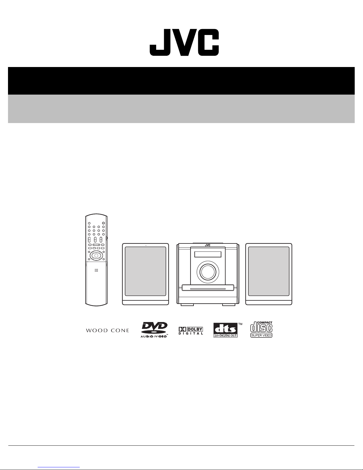
COMPACT COMPONENT SYSTEM
MB54420067
EX-D11J,EX-D11EE,EX-D11A,
EX-D11US,EX-D11UB,EX-D11UP,
EX-D11UT,EX-D11UW,EX-D11UY,
EX-D11UG
Lead free solder used in the board (material : Sn-Ag-Cu, melting point : 219 Centigrade)
1 PRECAUTION. . . . . . . . . . . . . . . . . . . . . . . . . . . . . . . . . . . . . . . . . . . . . . . . . . . . . . . . . . . . . . . . . . . . . . . . . 1-3
2 SPECIFIC SERVICE INSTRUCTIONS . . . . . . . . . . . . . . . . . . . . . . . . . . . . . . . . . . . . . . . . . . . . . . . . . . . . . . 1-6
3 DISASSEMBLY . . . . . . . . . . . . . . . . . . . . . . . . . . . . . . . . . . . . . . . . . . . . . . . . . . . . . . . . . . . . . . . . . . . . . . . 1-7
4 ADJUSTMENT . . . . . . . . . . . . . . . . . . . . . . . . . . . . . . . . . . . . . . . . . . . . . . . . . . . . . . . . . . . . . . . . . . . . . . . 1-23
5 TROUBLESHOOTING . . . . . . . . . . . . . . . . . . . . . . . . . . . . . . . . . . . . . . . . . . . . . . . . . . . . . . . . . . . . . . . . . 1-27
COPYRIGHT © 2006 Victor Company of Japan, Limited
CA-EXD11
TABLE OF CONTENTS
SP-EXD11SP-EXD11
No.MB544
2006/7
Page 2
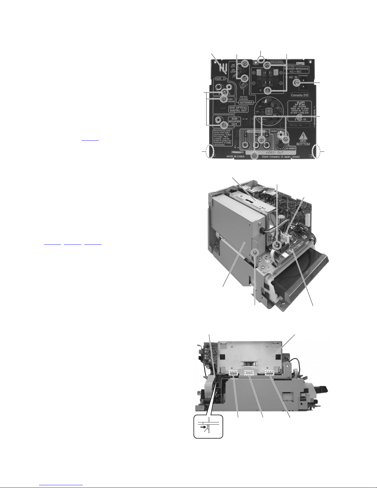
SPECIFICATION
General Power source AC 120 V , 60 Hz (for U.S.A. model)
Power consumption 25 W (in operation)/
Weight: 2.6 kg (5.7 lbs)
External dimensions (W
DVD player Playable discs DVD VIDEO, DVD AUDIO, VCD, SVCD, CD, CD-R/RW (VCD/SVCD/CD/MP3/WMA/JPEG/
Video output Color system NTSC (for U.S.A. model)
Horizontal resolution 500 lines
Composite
S-video
Component × 1 Y output: 1.0 V (p-p)/75 Ω
Audio output Analog sound output Speakers × 2
Output power 20 W per channel min., RMS, at 4
Fitting impedance 4
Headphones × 1 11 mW/32 Ω
Fitting impedance 16 Ω to 1 kΩ
Subwoofer × 1 500 mVrms/10 kΩ
Digital sound output Optical × 1 -21 dBm to -15 dBm
Audio input Sound input AUX 1 400 mV/50 k
Tuner FM tuner Receiving frequency 87.5 MHz to 108.0 MHz
AM (MW) tuner Receiving frequency 531 kHz to 1 710 kHz (9 kHz) (For Singapore/Hong Kong/South and Central America/Australia)
Speaker Type Full range, 1-way bass-reflex type, Magnetically shielded type
Speaker 8cm (3 3/16 inches) wood cone
Frequency response 55 Hz to 20 000 Hz
Power handling capacity 20 W
Impedance 4
Sound pressure level 80 dB/W m
Dimension (W
Weight 1.8 kg (4.0 lbs) each
• Manufactured under license from Dolby Laboratories. "Dolby", "Pro Logic", "MLP lossless", and the double-D symbol are trademarks of Dolby
Laboratories.
• "DTS" and "DTS 2.0+ Digital Out" are trademarks of Digital Theater Systems, Inc.
• "Official DivX® Certified product", "Plays all versions of DivX® video (including DivX® 6) with standard playback of DivX® media files", "DivX,
DivX certified, and associated logos are trademarks of DivX, Inc. and are used under licence.
• USE OF THIS PRODUCT IN ANY MANNER THAT COMPLIES WITH THE MPEG-4 VISUAL STANDARD IS PROHIBITED, EXCEPT FOR USE
BY A CONSUMER ENGAGING IN PERSONAL AND NON-COMMERCIAL ACTIVITIES.
• This product incorporates copyright protection technology that is protected by U.S. patents and other intellectual property rights. Use of this copyright protection technology must be authorized by Macrovision, and is intended for home and other limited viewing uses only unless otherwise
authorized by Macrovision. Reverse engineering or disassembly is prohibited.
× 1 1.0 V (p-p)/75 Ω, synchronization negative
× 1 Y output: 1.0 V (p-p)/75 Ω, synchronization negative
× H × D) 120 mm × 150.5 mm × 243 mm (43/4 in. × 6 in. × 95/8 in.)
× H × D) 150 mm × 152.6 mm × 252.9 mm (5 15/16 in. × 6 1/16 in. × 10 in.)
AUX 2 1.5 V/50 kΩ
USB AUDIO × 1
Antenna 75
Antenna External antenna jack (loop antenna)
AC 110-240 V , 50/60 Hz (for Asian model)
AC 240 V, 50 Hz (for Australian model)
AC 220 V, 50/60 Hz (for Hong Kong model)
4.0 W (on standby/display on)
1.0 W (on standby/display off)
MPEG1/MPEG2 format)
DVD-R/-RW (MP3/WMA/JPEG/DVD VIDEO/DVD VR [CPRM]/MPEG1/ MPEG2 format)
DVD-ROM (MP3/WMA/JPEG/MPEG1/ MPEG2/DVD VR [CPRM] format)
PAL/NTSC (for Asian model)
For PAL 0.3 V (p-p)/75
For NTSC 0.286 V (p-p)/75 Ω
PB/PR output: 0.7 V (p-p)/75 Ω
Ω
Ω at 1 kHz with no more than 10% total harmonic distortion
Ω to 16 Ω
Ω
200 mV/50 kΩ
750 mV/50 kΩ
Ω Unbalanced type
530 kHz to 1 710 kHz (10 kHz) (For Singapore/Hong Kong/South and Central America/Australia)
531 kHz to 1 602 kHz (9 kHz) (For Middle East and South Africa)
530 kHz to 1 600 kHz (10 kHz) (For Middle East and South Africa)
522 kHz to 1 629 kHz (For Russia)
× 1
Ω
• Designs and Specifications are subject to change without notice.
1-2 (No.MB544)
Page 3
SECTION 1
PRECAUTION
1.1 Safety Precautions
(1) This design of this product contains special hardware and
many circuits and components specially for safety purposes. For continued protection, no changes should be made
to the original design unless authorized in writing by the
manufacturer. Replacement parts must be identical to
those used in the original circuits. Services should be performed by qualified personnel only.
(2) Alterations of the design or circuitry of the product should
not be made. Any design alterations of the product should
not be made. Any design alterations or additions will void
the manufacturers warranty and will further relieve the
manufacture of responsibility for personal injury or property
damage resulting therefrom.
(3) Many electrical and mechanical parts in the products have
special safety-related characteristics. These characteristics are often not evident from visual inspection nor can the
protection afforded by them necessarily be obtained by using replacement components rated for higher voltage, wattage, etc. Replacement parts which have these special
safety characteristics are identified in the Parts List of Service Manual. Electrical components having such features
are identified by shading on the schematics and by ( ) on
the Parts List in the Service Manual. The use of a substitute
replacement which does not have the same safety characteristics as the recommended replacement parts shown in
the Parts List of Service Manual may create shock, fire, or
other hazards.
(4) The leads in the products are routed and dressed with ties,
clamps, tubings, barriers and the like to be separated from
live parts, high temperature parts, moving parts and/or
sharp edges for the prevention of electric shock and fire
hazard. When service is required, the original lead routing
and dress should be observed, and it should be confirmed
that they have been returned to normal, after reassembling.
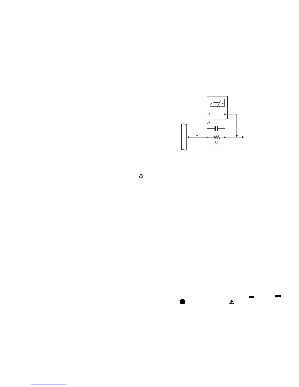
(5) Leakage shock hazard testing
After reassembling the product, always perform an isolation check on the exposed metal parts of the product (antenna terminals, knobs, metal cabinet, screw heads,
headphone jack, control shafts, etc.) to be sure the product
is safe to operate without danger of electrical shock.Do not
use a line isolation transformer during this check.
• Plug the AC line cord directly into the AC outlet. Using a
"Leakage Current Tester", measure the leakage current
from each exposed metal parts of the cabinet, particularly any exposed metal part having a return path to the
chassis, to a known good earth ground. Any leakage current must not exceed 0.5mA AC (r.m.s.).
• Alternate check method
Plug the AC line cord directly into the AC outlet. Use an
AC voltmeter having, 1,000Ω per volt or more sensitivity
in the following manner. Connect a 1,500Ω 10W resistor
paralleled by a 0.15µF AC-type capacitor between an ex-
posed metal part and a known good earth ground.
Measure the AC voltage across the resistor with the AC
voltmeter.
Move the resistor connection to each exposed metal
part, particularly any exposed metal part having a return
path to the chassis, and measure the AC voltage across
the resistor. Now, reverse the plug in the AC outlet and
repeat each measurement. Voltage measured any must
not exceed 0.75 V AC (r.m.s.). This corresponds to 0.5
mA AC (r.m.s.).
AC VOLTMETER
(Having 1000
ohms/volts,
or more sensitivity)
0.15 F AC TYPE
Place this
probe on
1500 10W
Good earth ground
1.2 Warning
(1) This equipment has been designed and manufactured to
meet international safety standards.
(2) It is the legal responsibility of the repairer to ensure that
these safety standards are maintained.
(3) Repairs must be made in accordance with the relevant
safety standards.
(4) It is essential that safety critical components are replaced
by approved parts.
(5) If mains voltage selector is provided, check setting for local
voltage.
1.3 Caution
Burrs formed during molding may be left over on some parts
of the chassis.
Therefore, pay attention to such burrs in the case of preforming repair of this system.
1.4 Critical parts for safety
In regard with component parts appearing on the silk-screen
printed side (parts side) of the PWB diagrams, the parts that are
printed over with black such as the resistor ( ), diode ( )
and ICP ( ) or identified by the " " mark nearby are critical
for safety. When replacing them, be sure to use the parts of the
same type and rating as specified by the manufacturer.
(This regulation dose not Except the J and C version)
each exposed
metal part.
(No.MB544)1-3
Page 4
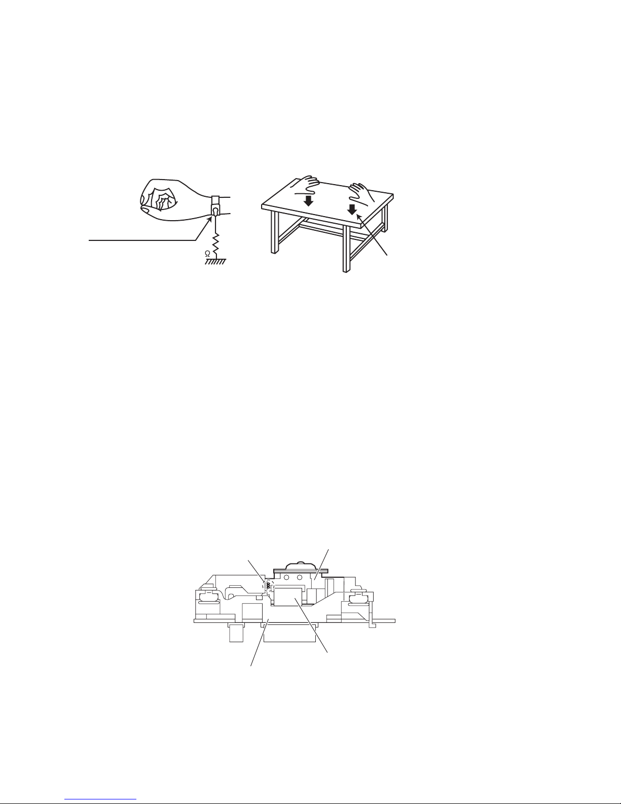
1.5 Preventing static electricity
Electrostatic discharge (ESD), which occurs when static electricity stored in the body, fabric, etc. is discharged, can destroy the laser
diode in the traverse unit (optical pickup). Take care to prevent this when performing repairs.
1.5.1 Grounding to prevent damage by static electricity
Static electricity in the work area can destroy the optical pickup (laser diode) in devices such as laser products.
Be careful to use proper grounding in the area where repairs are being performed.
(1) Ground the workbench
Ground the workbench by laying conductive material (such as a conductive sheet) or an iron plate over it before placing the
traverse unit (optical pickup) on it.
(2) Ground yourself
Use an anti-static wrist strap to release any static electricity built up in your body.
(caption)
Anti-static wrist strap
1M
Conductive material
(conductive sheet) or iron palate
(3) Handling the optical pickup
• In order to maintain quality during transport and before installation, both sides of the laser diode on the replacement optical
pickup are shorted. After replacement, return the shorted parts to their original condition.
(Refer to the text.)
• Do not use a tester to check the condition of the laser diode in the optical pickup. The tester's internal power source can easily
destroy the laser diode.
1.6 Handling the traverse unit (optical pickup)
(1) Do not subject the traverse unit (optical pickup) to strong shocks, as it is a sensitive, complex unit.
(2) Cut off the shorted part of the flexible cable using nippers, etc. after replacing the optical pickup. For specific details, refer to the
replacement procedure in the text. Remove the anti-static pin when replacing the traverse unit. Be careful not to take too long a
time when attaching it to the connector.
(3) Handle the flexible cable carefully as it may break when subjected to strong force.
(4) I t is not possible to adjust the semi-fixed resistor that adjusts the laser power. Do not turn it.
1.7 Attention when traverse unit is decomposed
*Please refer to "Disassembly method" in the text for the pickup unit.
• Apply solder to the short land sections before the card wire is disconnected from the connecto on the servo board. (If the card wire
is disconnected without applying solder, the pickup may be destroyed by static electricity.)
• In the assembly, be sure to remove solder from the short land sections after connecting the card wire.
DVD pickup
short land sections
Traverse mechanism assembly
1-4 (No.MB544)
Card wire
Page 5
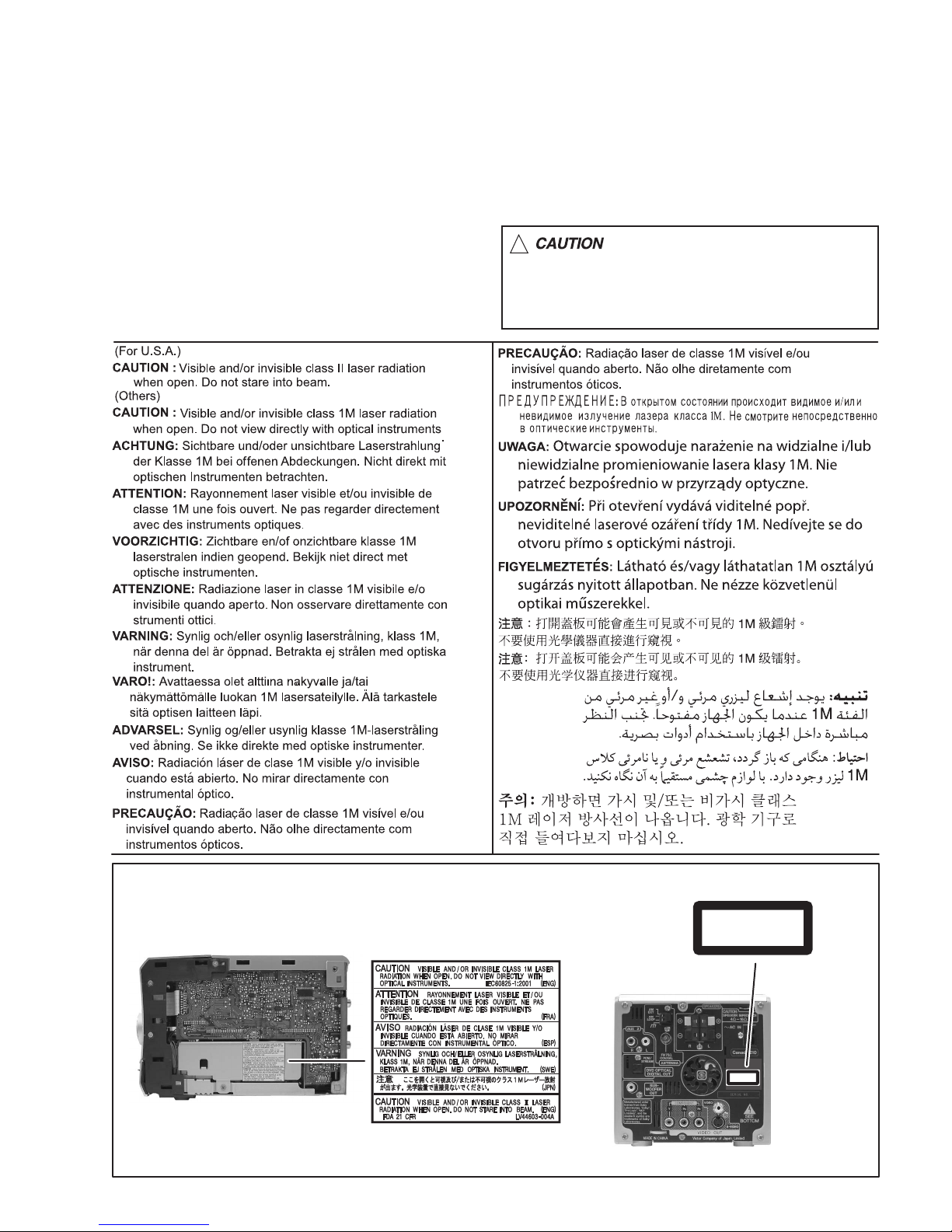
1.8 Important for laser products
1.CLASS 1 LASER PRODUCT
2.CAUTION :
(For U.S.A.) Visible and/or invisible class II laser radiation
when open. Do not stare into beam.
(Others) Visible and/or invisible class 1M laser radiation
when open. Do not view directly with optical instruments.
3.CAUTION : Visible and/or invisible laser radiation when
open and inter lock failed or defeated. Avoid direct
exposure to beam.
4.CAUTION : This laser product uses visible and/or invisible
laser radiation and is equipped with safety switches which
prevent emission of radiation when the drawer is open and
the safety interlocks have failed or are defeated. It is
dangerous to defeat the safety switches.
5.CAUTION : If safety switches malfunction, the laser is able
to function.
6.CAUTION : Use of controls, adjustments or performance of
procedures other than those specified here in may result in
hazardous radiation exposure.
!
Please use enough caution not to
see the beam directly or touch it
in case of an adjustment or operation
check.
REPRODUCTION AND POSITION OF LABELS and PRINT
WARNING LABEL and PRINT
CLASS 1
LASER PRODUCT
CLASS 1
LASER PRODUCT
(No.MB544)1-5
Page 6

SECTION 2
SPECIFIC SERVICE INSTRUCTIONS
This service manual does not describe SPECIFIC SERVICE INSTRUCTIONS.
1-6 (No.MB544)
Page 7
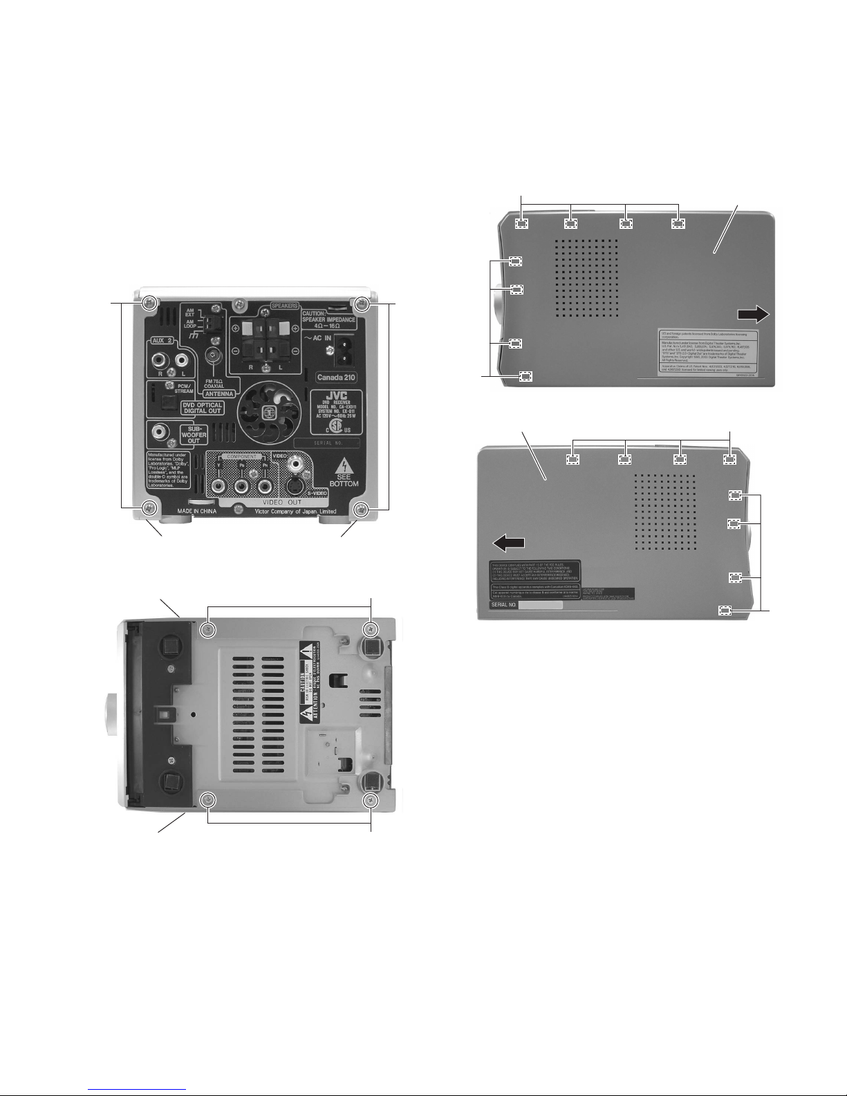
SECTION 3
A
DISASSEMBLY
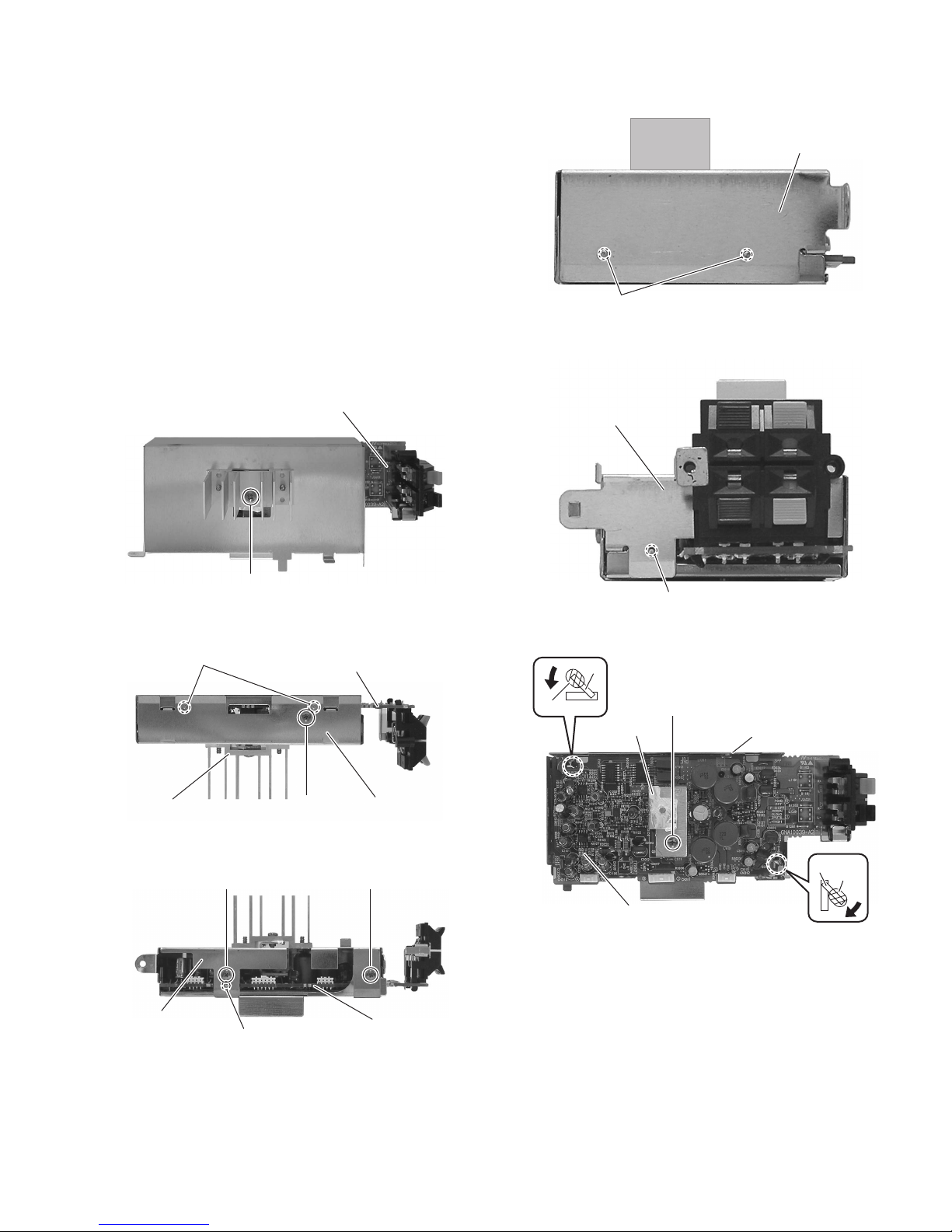
3.1 Main body section
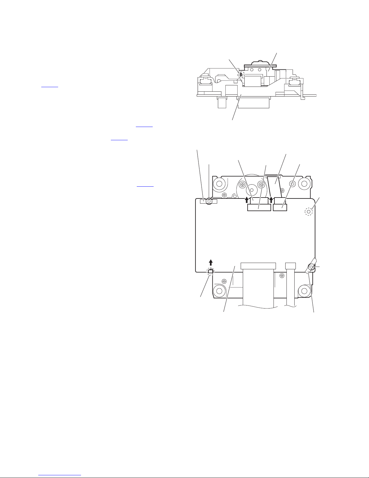
3.1.1 Removing the side panel L and side panel R
(See Figs.1 to 4)
(1) From the back side of the main body, remove the four
screws A attaching the side panels L/R. (See Fig.1.)
(2) From the bottom side of the main body, remove the four
screws B attaching the side panels L/R. (See Fig.2.)
(3) From the both sides of the main body, release the joint a in
the direction of the arrow and remove the side panels L/R
toward this side. (See Figs.3 and 4.)
A
a
a
Side panel L
Side panel R
Fig.3
a
Side panel R Side panel L
Fig.1
Side panel R
Side panel L
Fig.2
B
a
Fig.4
B
(No.MB544)1-7
Page 8
3.1.2 Removing the top panel assembly
(See Figs.5 and 6)
• Remove the side panels L/R.
(1) From the both sides of the main body, remove the two
screws C. (See Figs.5 and 6)
(2) From the back side of the main body, remove the screw D
attaching the top panel assembly. (See Fig.6.)
(3) From the both sides of the main body, release the joints b
and c. (See Figs.5 and 6.)
(4) Take out the top panel assembly in the direction of the ar-
row. (See Fig.6.)
C
c
Fig.5
Top panel assembly
b c
D
Top panel assembly
b
C
1-8 (No.MB544)
Fig.6
Page 9
3.1.3 Removing the front panel assembly
(See Figs.7 and 8)
• Remove the side panels L/R and top panel assembly.
(1) From the bottom side of the main body, remove the two
screws E attaching the front panel assembly. (See Fig.7.)
(2) From the forward side of the micom board, disconnect the
card wire from the connector CN426
(3) From the bottom and both sides of the main body, release
the joints (d, e) of the front panel assembly and remove the
front panel assembly in the direction of the arrow. (See
Figs.7 and 8.)
. (See Fig.8.)
Front panel assembly
E
CN426
d
Fig.7
Micom board
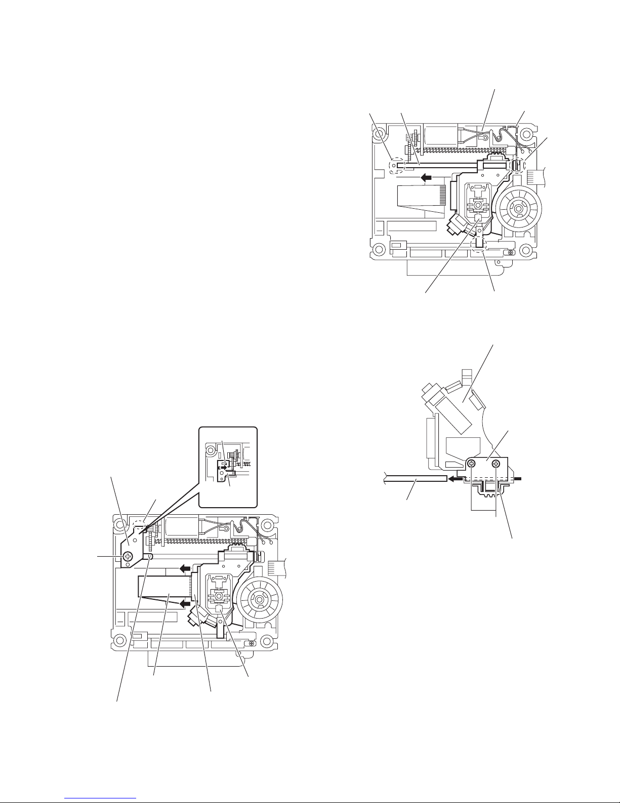
3.1.4 Removing the tuner
(See Fig.9)
• Remove the side panels L/R and top panel assembly.
(1) From the back side of the main body, remove the two
screws F attaching the tuner to the rear panel.
(2) Disconnect the card wire from the connector CN1
tuner.
on the
e
Fig.8
Tuner Rear panelCN1
F
Fig.9
(No.MB544)1-9
Page 10
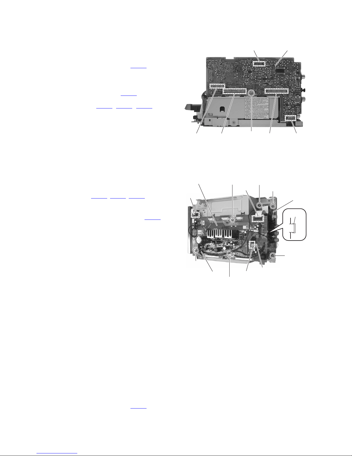
3.1.5 Removing the rear panel
(See Fig.10)
• Remove the side panels L/R and top panel assembly.
(1) From the back side of the main body, remove the ten
screws G and screw H attaching the rear panel.
(2) From the top side of the main body, disconnect the earth
wire from the rear panel.
(3) From the both sides of the main body, release the joints f
and remove the rear panel.
3.1.6 Removing the switching power supply
(See Figs.10 and 11)
• Remove the side panels L/R and top panel assembly.
(1) From the back side of the main body, remove the screw H
attaching the rear panel. (See Fig.10.)
(2) From the top side of the main body, disconnect the wire
from the connector CN200
Fig.11.)
(3) From the left side of the main body, remove the screw J at-
taching the main body. (See Fig.11.)
(4) Take out the switching power supply. (See Fig.11.)
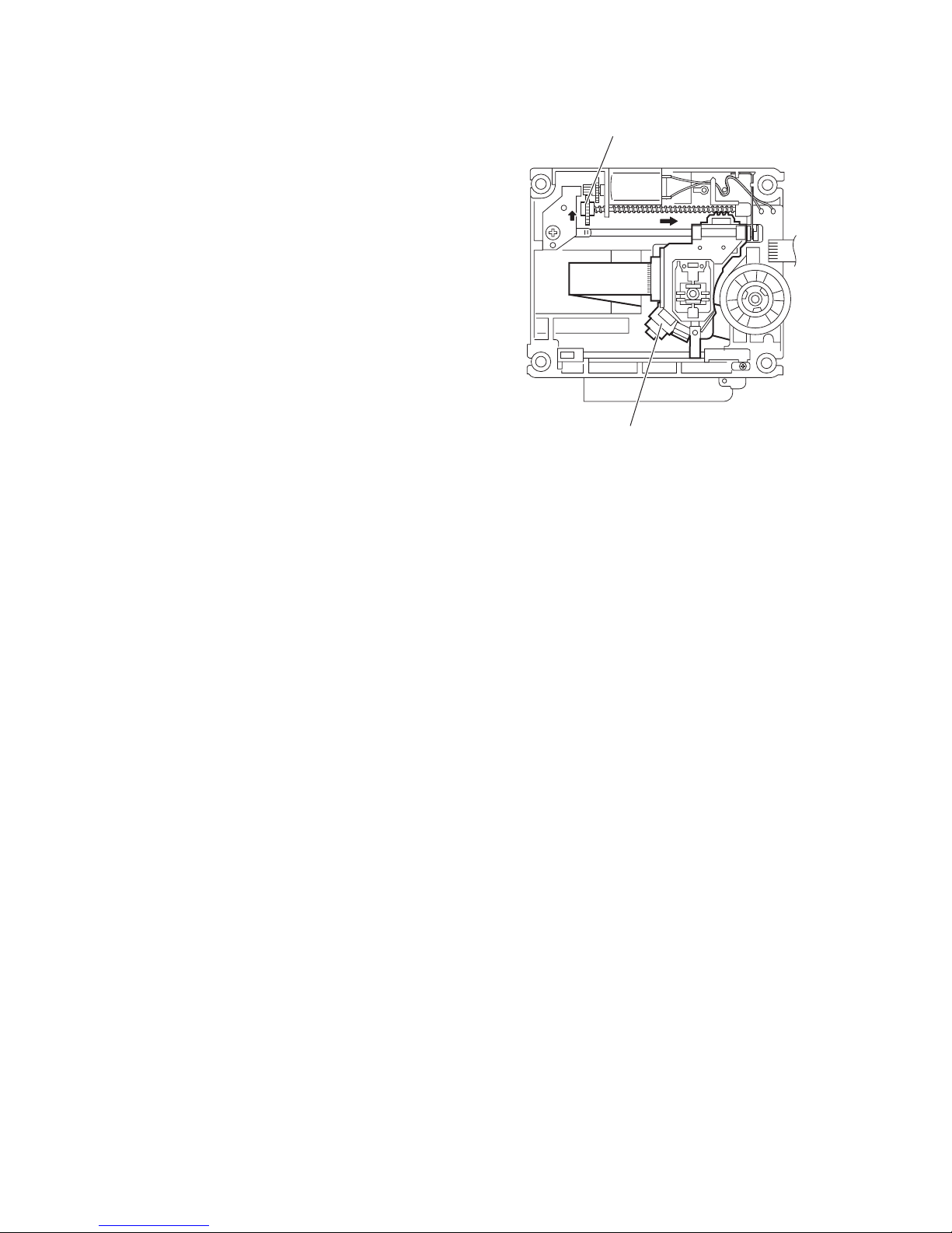
3.1.7 Removing the digital amplifier board assembly
(See Figs.11 and 12)
• Remove the side panels L/R, top panel assembly, rear panel
and switching power supply.
(1) From the top side of the main body, remove the screw K at-
taching the digital amplifier board assembly. (See Fig.11.)
Reference:
When attaching the screw K, attach the earth wire with it.
(2) From the left side of the main body, disconnect the connec-
tors (CN310
assembly from the regulator board. (See Fig.12.)
(3) Release the joint g of the shield case B in the direction of
the arrow and take out the digital amplifier board assembly
from the regulator board. (See Fig.12.)
, CN311, CN312) on the digital amplifier board
on the regulator board. (See
Earth wire
Rear panel
GG
G
f
Fig.10
Digital amplifier board assembly
H
G
f
K
CN200
Switching power supply
Regulator board
CN312 CN311 CN310
g
J
Fig.11
Digital amplifier board assembly
Fig.12
Regulator board
1-10 (No.MB544)
Page 11
3.1.8 Removing the digital amplifier board
(See Figs.13 to 18)
• Remove the side panels L/R, top panel assembly, rear panel,
switching power supply and digital amplifier board assembly.
(1) From the forward side of the digital amplifier board assem-
bly, remove the screw M. (See Fig.13.)
(2) From the top and bottom sides of the digital amplifier board
assembly, remove the three screws N. (See Figs.14 and
15.)
(3) Release the joints (h, j, k, m) and remove the shield case
B with the heat sink in the direction of the arrow. (See
Figs.14 to 17.)
(4) From the forward side of the digital amplifier board, remove
the screw N attaching the heat sink. (See Fig.18.)
(5) Remove the solders from the soldered sections (n, p) and
bend the sections (q, r) of the shield case A in the direction
of the arrow. (See Fig.18.)
(6) Take out the digital amplifier board from the shield case A.
Shield case B
k
Fig.16
Heat sink
Digital amplifier board
M
Fig.13
h
N
Digital amplifier board
Shield case B
N
Fig.14
N
Shield case B
q
n
Heat sink
m
N
Fig.17
Shield case A
r
p
Shield case B
j
Digital amplifier board
Fig.15
Digital amplifier board
Fig.18
(No.MB544)1-11
Page 12
3.1.9 Removing the micom board
(See Fig.19)
• Remove the side panels L/R, top panel assembly, rear panel
and front panel assembly.
(1) From the right side of the main body, remove the screw P
attaching the micom board.
(2) Disconnect the card wire from the connector CN421
forward side of the micom board.
Reference:
Remove the tuner as required. (See Fig.9)
(3) Disconnect the wire from the connector CN501
ward side of the micom board.
(4) Disconnect the connectors (CN423
the micom board from the regulator and video boards toward this side to remove the micom board.
, CN424, CN425) on
on the
on the for-
CN421
Micom board
3.1.10 Removing the regulator board
(See Fig.20)
• Remove the side panels L/R, top panel assembly, tuner, rear
panel, switching power supply, digital amplifier board assembly and micom board.
(1) From the top side of the main body, disconnect the card
wires from the connectors (CN208
regulator board.
Reference:
When connecting the card wire to the connector CN208
pass it through the hole s of the regulator board as before.
(2) Remove the screws Q and Q'.
Reference:
When attaching the screw Q', attach the earth wire with
it.
(3) Remove the screws Q".
Reference:
When attaching the screw Q", attach the earth wire and
the wire holder with it.
(4) Remove the screw R and screw S' attaching the earth wire.
Reference:
When attaching the screw R and S', attach the earth wire
with it.
, CN210, CN212) on the
CN501
Regulator board
CN210
,
CN424 CN423 CN425
Q
P
Fig.19
CN212
R
S'
Video board
CN703
S
Q''
Wire holder
CN208
s
Q'
Fig.20
3.1.11 Removing the video board
(See Fig.20)
• Remove the side panels L/R, top panel assembly, tuner, rear
panel, switching power supply, digital amplifier board assembly and micom board.
Reference:
Remove the regulator board as required.
(1) From the top side of the main body, remove the two screws
S.
Reference:
When attaching the screw S, attach the earth wire with it.
(2) Take out the video board from the main body.
(3) Disconnect the card wire from the connector CN703
video board.
1-12 (No.MB544)
on the
Page 13
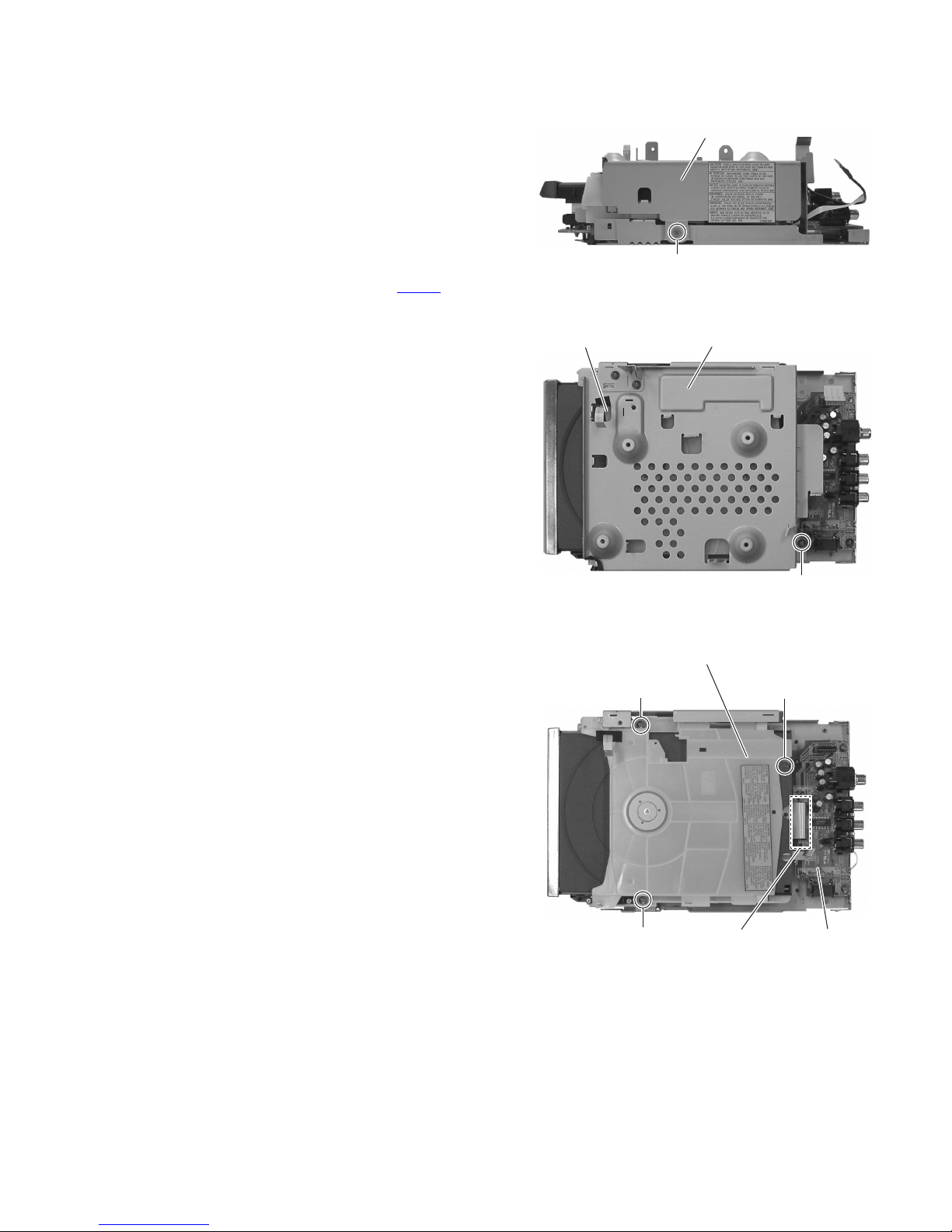
3.1.12 Removing the DVD mechanism assembly
(See Figs.21 to 23)
• Remove the side panels L/R, top panel assembly, front panel
assembly, tuner, rear panel, switching power supply, digital
amplifier board assembly, micom board and regulator board.
(1) From the right side of the main body, remove the screw T
attaching the metal chassis. (See Fig.21.)
(2) From the top side of the main body, remove the screw U
and take out the metal chassis. (See Fig.22.)
Reference:
When attaching the metal chassis, pass the card wire
through the hole t on the metal chassis as before.
(3) Disconnect the card wire from the connector CN703
video board. (See Fig.23.)
(4) Remove the three screws V and take out the DVD mecha-
nism assembly from the bottom chassis. (See Fig.23.)
on the
Metal chassis
T
Fig.21
t
Metal chassis
Fig.22
DVD mechanism assembly
V
V
CN703
Fig.23
V
U
Video board
(No.MB544)1-13
Page 14
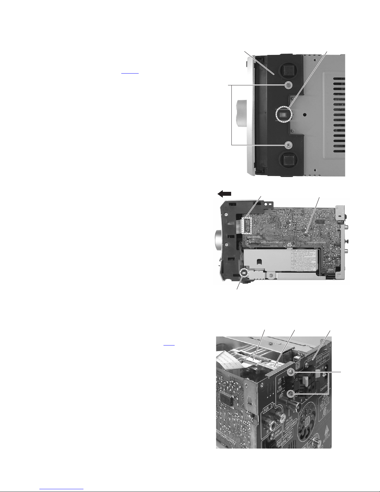
3.1.13 Removing the switch board and front FL board
(See Figs.24 to 26)
• Remove the side panels L/R, top panel and front panel assem-
bly.
(1) From the front side of the main body, pull out the volume
knob assembly in the direction of the arrow. (See Fig.24.)
(2) From the inside of the front panel assembly, remove the
five screws W attaching the switch board. (See Fig.25.)
(3) Remove the six screws X attaching the front FL board.
(See Fig.26.)
(4) Take out the switch board and the front FL board.
Volume knob
assembly
Front panel
assembly
Fig.24
Switch board
W
Fig.25
Front FL board
X
1-14 (No.MB544)
Fig.26
Page 15
3.1.14 Removing the headphone board
(See Fig.27)
• Remove the side panels L/R, top panel assembly, front panel
assembly, tuner, rear panel, switching power supply, digital
amplifier board assembly, micom board, regulator board and
DVD mechanism assembly.
(1) Remove the three screws Y and take out the headphone
board.
(2) Take out the headphone board.
Headphone board
Y
Fig.27
(No.MB544)1-15
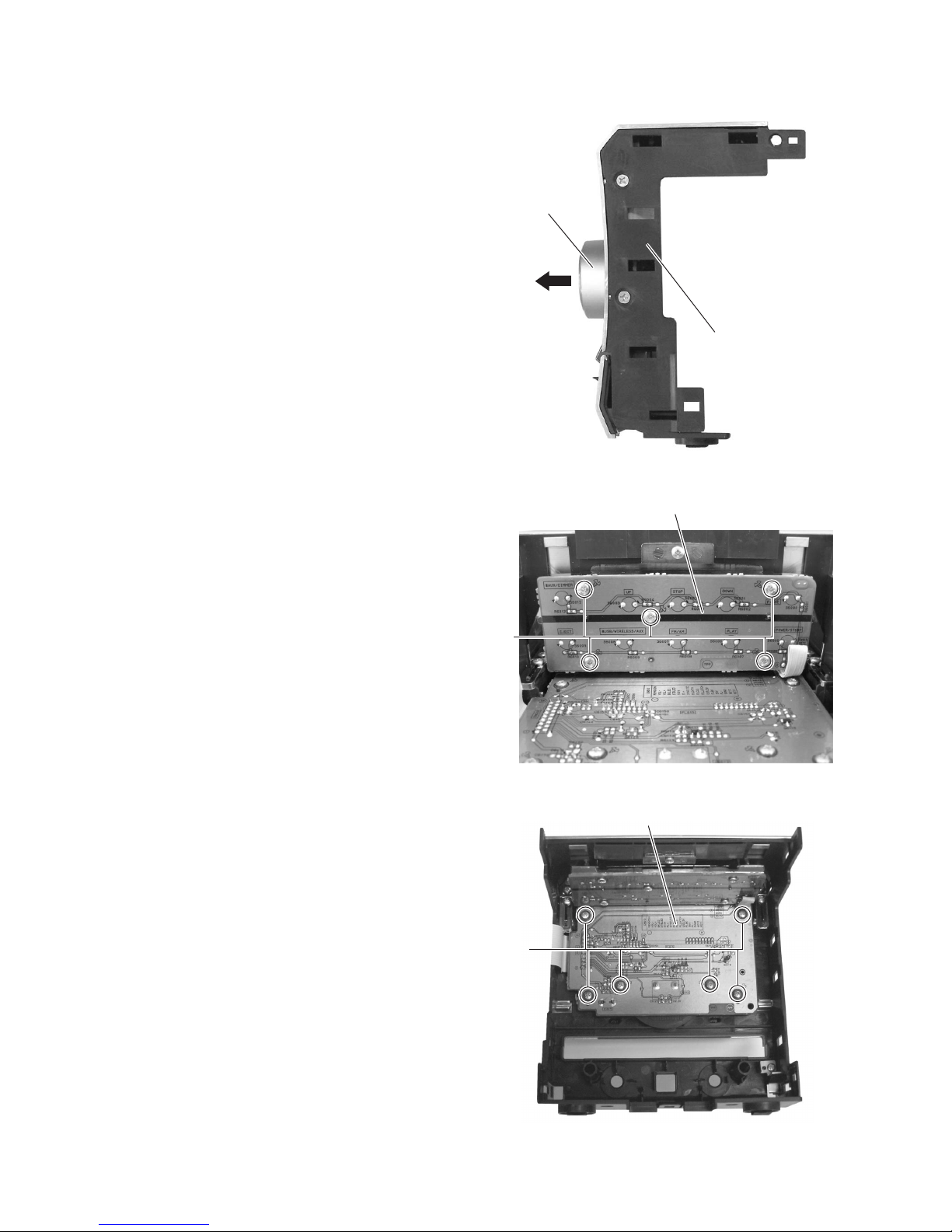
Page 16
3.2 DVD mechanism assembly section
• Remove the DVD mechanism assembly from the main body.
(See "Removing the DVD mechanism assembly" of the DVD player section.)
3.2.1 Removing the clamper base
(See Fig.1)
(1) From the top side of the DVD mechanism assembly, re-
move the two screws A attaching the clamper base.
(2) Take out the clamper base.
A
3.2.2 Removing the tray assembly
(See Figs.2 and 3)
• Remove the clamper base.
(1) From the right side of the DVD mechanism assembly, push
the slide cam and pull the tray assembly out of the DVD
mechanism assembly in the direction of the arrow. (See
Fig.2.)
(2) From the top side of the DVD mechanism assembly, re-
move the two screws B attaching the tray assembly. (See
Fig.3.)
(3) Remove the shaft guide of the tray assembly from the pro-
jections a of the DVD mechanism assembly and take out
the tray assembly. (See Fig.3.)
A
Tray assembly
Slide cam
DVD mechanism assembly
Tray assembly
Clamper base
Fig.1
DVD mechanism assembly
Fig.2
1-16 (No.MB544)
a
Shaft guide
a
B
Fig.3
Page 17
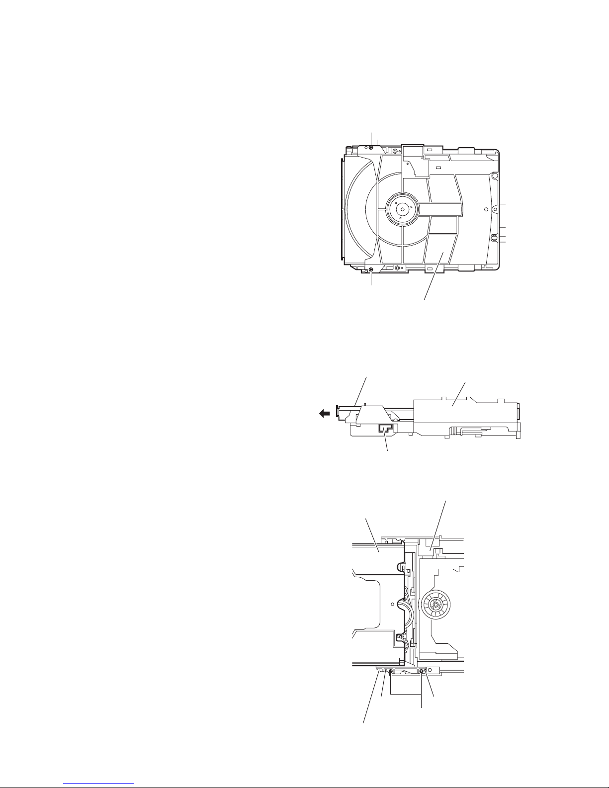
3.2.3 Removing the traverse mechanism assembly
(See Fig.4)
• Remove the clamper base.
(1) From the bottom side of the DVD mechanism assembly, re-
move the four screws C attaching the traverse mechanism
assembly.
(2) Take out the traverse mechanism assembly with the DVD
module board.
Traverse mechanism assembly
DVD module board
CC
Fig.4
(No.MB544)1-17
Page 18
3.2.4 Removing the DVD module board
(See Figs.5 and 6)
• Remove the clamper base and traverse mechanism assembly.
(1) Solder the short land sections b on the DVD pickup. (See
Fig.5.)
Caution:
• Solder the short land sections b on the DVD pickup before disconnecting the card wire from the connector
on the DVD module board. If the card wire is
CN101
disconnected without attaching solders, the DVD pickup may be destroyed by static electricity. (See Figs.5
and 6.)
• When attaching the DVD module board, be sure to remove solders from the short land sections b after connecting the card wire to the connector CN101
DVD module board. (See Figs.5 and 6.)
(2) Release the lock of the connector CN101
ule board in the direction of the arrow and disconnect the
card wire. (See Fig.6.)
(3) Remove the spacers on the DVD module board. (See
Fig.6.)
(4) Remove the two screws D attaching the DVD module
board. (See Fig.6.)
(5) Disconnect the card wire from the connector CN201
DVD module board. (See Fig.6.)
(6) Remove the DVD module board from the engagement sec-
tion c in an upward direction and remove it from the hook d
in the direction of the arrow. (See Fig.6.)
on the DVD mod-
on the
on the
b
Traverse mechanism assembly
Spacer
Card wire
D
Fig.5
CN101
DVD pickup
Card wire
CN201
c
d
DVD module board
D
Spacer
Fig.6
1-18 (No.MB544)
Page 19
3.2.5 Removing the DVD pickup
(See Figs.5, 7 to 9)
• Remove the clamper base and traverse mechanism assembly.
(1) Solder the short land sections b on the DVD pickup. (See
Fig.5.)
Caution:
• Solder the short land sections b on the DVD pickup before disconnecting the card wire from the connector on
the DVD pickup. If the card wire is disconnected without attaching solders, the pickup may be destroyed by
static electricity. (See Figs.5 and 7.)
• When attaching the DVD pickup, be sure to remove
solders from the short land sections b after connecting
the card wire to the connector on the DVD pickup.
(See Figs.5 and 7.)
(2) Disconnect the card wire from the connector on the DVD
pickup. (See Fig.7.)
(3) From the top side of the traverse mechanism assembly, re-
move the screw E and remove the feed bracket from the
section e. (See Fig.7.)
(4) Remove the guide shaft adj. spring from the claw f in the
direction of the arrow and remove the guide shaft adj.
spring. (See Fig.7.)
(5) Remove the section g of the traverse mechanism assem-
bly and remove the guide shaft of the DVD pickup from the
section h while moving it in the direction of the arrow. (See
Fig.8.)
(6) Remove the DVD pickup from the section j of the traverse
mechanism assembly and take out the DVD pickup with
the guide shaft. (See fig.8.)
(7) Remove the two screws F attaching the rack arm and rack
arm spring. (See Fig.9.)
(8) Remove the guide shaft from the DVD pickup. (See Fig.9.)
f
g
Guide shaft
DVD pickup
Traverse mechanism assembly
Rod spring
h
j
Fig.8
DVD pickup
Rack arm
Feed bracket
e
E
Card wire
Guide shaft adj. spring
Fig.7
Guide shaft
adj. spring
DVD pickup
Connector
Guide shaft
F
Rack arm spring
Fig.9
(No.MB544)1-19
Page 20
3.2.6 Attaching the DVD pickup
(See Figs.5, 7 to 10)
• See "3.3.5 Removing the DVD pickup".
(1) Attach the guide shaft, rack arm and rack arm spring to the
DVD pickup. (See Fig.9.)
(2) Align the DVD pickup to the section j of the traverse mech-
anism assembly first, and set the both ends of the guide
shaft of the DVD pickup in the sections (g, h) of the
traverse mechanism assembly. (See Fig.8.)
Reference:
When attaching the guide shaft to the section h, attach it
under the rod spring. (See Fig.8.)
(3) Attach the guide shaft adj. spring and feed bracket. (See
Fig.7.)
(4) Remove solders from the short land sections b on the DVD
pickup after connecting the card wire to the connector on
the DVD pickup. (See Fig.5.)
(5) Turn the screw shaft gear in the direction of the arrow 1 to
move the DVD pickup fully in the direction of the arrow 2.
(See Fig.10.)
Screw shaft gear
1
2
DVD pickup
Fig.10
1-20 (No.MB544)
Page 21

3.2.7 Removing the feed motor
(See Figs.7 and 11)
• Remove the clamper base and traverse mechanism assembly.
(1) From the top side of the traverse mechanism assembly, re-
move the screw E and remove the feed bracket from the
section e. (See Fig.7.)
(2) Remove the guide shaft adj. spring from the claw f in the
direction of the arrow and remove the guide shaft adj.
spring. (See Fig.7.)
(3) Remove the wires (yellow and white) from the soldered
section k on the spindle motor board. (See Fig.11.)
Reference:
• When attaching the feed motor, pass the wires through
the section m on the spindle base. (See Fig.11.)
• Pass the wires through the lower section of the rod
spring. (See Fig.11.)
(4) Remove the screw shaft in the direction of the arrow. (See
Fig.11.)
(5) From the side of the traverse mechanism assembly, re-
move the screw G attaching the feed motor. (See Fig.11.)
(6) Take out the feed motor. (See Fig.11.)
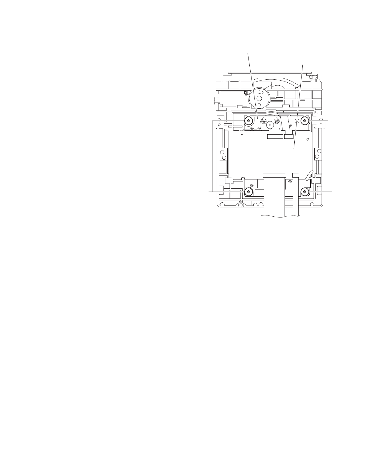
3.2.8 Removing the spindle motor board
(See Figs.11 and 12)
• Remove the clamper base, traverse mechanism assembly and
DVD module board.
(1) From the top side of the traverse mechanism assembly, re-
move the wires (yellow and white) from the soldered section k on the spindle motor board. (See Fig.11.)
(2) From the bottom side of the traverse mechanism assem-
bly, remove the three screws H attaching the spindle motor
board. (See Fig.12.)
Reference:
• When attaching the spindle motor board, pass the card wire
through the section n on the traverse mechanism assembly.
(See Fig.12.)
• When attaching the screws H, apply a locking agent them.
(See Fig.12.)
G
Wire (white)
Screw shaft
Traverse mechanism assembly
Traverse mechanism assembly
n
Rod spring
m
Wire (yellow)
k
Spindle motor board
Fig.11
H
H
Spindle motor board
Fig.12
(No.MB544)1-21
Page 22

3.2.9 Removing the DVD loading switch board
(See Fig.13.)
(1) From the bottom side of the DVD mechanism assembly, re-
move the wires from the soldered sections p on the DVD
loading switch board.
(2) Remove the screw J attaching the DVD loading switch
board.
(3) Lift the DVD loading switch board while pressing the claw
q of the DVD mechanism assembly in the direction of the
arrow and remove it from the section r.
Reference:
Put the wires on the section s after attaching the DVD loading
switch board to the DVD mechanism assembly.
DVD loading switch board
Wires
p
J
q
3.2.10 Removing the motor
(See Figs.13 and 14)
• Remove the clamper base and tray assembly.
(1) From the bottom side of the DVD mechanism assembly, re-
move the wires from the soldered sections p on the DVD
loading switch board. (See Fig.13.)
(2) From the top side of the DVD mechanism assembly, re-
move the belt from the motor pulley. (See Fig.14.)
Note:
Take care not to attach grease on the belt.
(3) Remove the two screws K attaching the motor to the DVD
mechanism assembly and take out the motor from the bottom side of the DVD mechanism assembly. (See Fig.14.)
Reference:
Put the wires on the section s after attaching the motor to the
DVD mechanism assembly. (See Fig.13.)
r
s
DVD mechanism assembly
Fig.13
Motor pulley
Belt
K
1-22 (No.MB544)
DVD mechanism assembly
Fig.14
Page 23

SECTION 4
ADJUSTMENT
*ATTENTION IN SERVICE OF DVD SECTION
(1) When pickup, flash rom, DVD module board were changed, initialize EEPROM all means.
(2) When full initialization was executed, execute learning with a DVD test disc by all means.
Test disc : VT-501, VT-502
Learning method : It is adjusted automatically by normal playback of a DVD disc.
4.1 Test mode 1
Item Operation Management
TUNER AM switch to
9kHz-step
TUNER AM switch to
10kHz-step
Cold start Cold start processing.STOP+'0'+AUDIO POWER (REMOCON)
Clock Fast Forward Make the clock fast forward.STOP+'2'+AUDIO POWER (REMOCON)
Volume change Make the volume from the min to max.STOP+'3'+AUDIO POWER (REMOCON)
Micon Version check Check the micon version.STOP+'9'+AUDIO POWER (REMOCON)
LCD all display All of the icons on the FL are lightened.STOP+'10'+AUDIO POWER (REMOCON)
Tray lock Loader-mecha is locked.
DVD test mode In to the DVD test mode. Test mode contents is refer to
DVD initialize DVD module initialized.
DVD region confirm
mode
compulsion NTSC
mode
DVD region confirm
mode
(Only source TUNER AM)
( Only source TUNER AM)
EJECT is pushed ,
during pushing STOP at STAND-BY
AC input pushing PLAY + PAUSE [key]
3D PHONIC [key] during DVD test mode
AC input pushing B.SKIP I<< +
DVD/CD [key]
AC input pushing STOP + DVD/CD [key]
AC input pushing B.SKIP I<< +
DVD/CD [key]
AM frequency change to 9kHz at U & A-version.|<< [key] + POWER button
AM frequency change to 10kHz at U & A-version.>>| [key] + POWER button
EJECT processing isn't done by pushing EJECT key
at tray lock on state.
Then display to LOCKED / UNLOCKED.
EJECT is pushed , pushing STOP again , tray lock is off.
Back up to tray locked ON/OFF.
module spec.
DVD test mode is canceled by POWER OFF and except
source DVD.
FL segment is light on at initialize completed.
Into the DVD region confirm mode.
Display region code on FL.
Into the compulsive NTSC mode.
Hereafter , only first power-on , start by NTSC unrelated
NTSEL-SW. ( Send command to module )
Mode is clear at POWER OFF.
Into the DVD region confirm mode.
* DVD REGION CHECK CAN ONLY BEEN DISPLAY
DURING SYSTEM POWER ON IN DVD MODE
(WHEN DVD LSI P.ON).
Temporary display region code on FL for 5 seconds.
FL will display "REGION x" where x is the Region
number.
* IF THERE IS NO INFORMATION FEEDBACK,
SYS-CON WILL DISPLAY
"WAIT" BLINKING 0.5SEC ON & OFF.
* FL WILL DISPLAY "AREAxxRy" WHERE "AREAxx" is
the DESTINATION INFO & R is the REGION INFO
After 5 seconds, return to previous display.
4.2 Test mode 2
4.2.1 To enter DVD TEST mode
(1) AC POWER OFF.
(2) Press and hold PLAY + PAUSE keys.
(3) AC POWER ON while holding PLAY + PAUSE keys.
(4) DVD Mecha will start in TEST MODE, FL will display:
xx is the received DESTINATION information. Display as follows:
xx = JC/1U/D/E/2U/3U/UB/UT/4U/UY/EE/UF
y = region number
v = study state information from DVD UNIT
w = initialization state from DVD UNIT
Tx
xy vw
(No.MB544)1-23
Page 24

4.2.2 To exit DVD TEST mode
w
w
(1) During TEST MODE (except for Device Key write & DVD Region Re-write), press POWER KEY .
(2) To exit TEST mode for Device Key Write & DVD Region Re-write, first AC OFF, then AC ON again to return to normal
state.
4.2.3 EEPROM INITIALIZATION
4.2.3.1 NORMAL INITIALIZE
(1) During DVD TEST MODE, Press STOP key on remote control to start NORMAL EEPROM INITIALIZATION.
(2) When received status, FL will display:
Tx
xy vw
= Initialization state from DVD UNIT.
4.2.3.2 FULL INITIALIZE
(1) During DVD TEST MODE, Press >>| key on set 2 seconds control to start FULL EEPROM INITIALIZATION.
(2) When received status, FL will display:
Tx
xy vw
= initialization state from DVD UNIT.
4.2.4 DEVICE KEY CHECKSUM DISPLAY
(1) During DESTINATION INFO display screen (1), press MENU key to enter DEVICE KEY CHECKSUM display.
FL will display (Example):
DK =
xxxx
4.2.5 DVD CHECK MODES
(1) Press MENU key again to enter CHECK MODE.
FL display:
CEHCK
Press '1' key on REMOTE CONTROL to START PLAYBACK.
FL display:
LPYA BACK
Press '2' key on REMOTE CONTROL to perform SEARCH TNO+1.
FL display:
WBOBLE
(2 seconds)
Status: AA 00 cc cc jj jj
ccccjj jj
Press '3' key on REMOTE CONTROL to perform SEARCH TNO-1.
FL display:
CEHCK
Press '4' key on REMOTE CONTROL to light up CD_LD and display laser current.
FL display:
DCDLSLR
(2 seconds)
Status: AA 00 cc cc jj jj
ccccjj jj
(Static)
1-24 (No.MB544)
Page 25

Press '5' key on REMOTE CONTROL to light up DVD_LD and display laser current.
FL display:
VDDDLSLR
(2 seconds)
Status: AA 00 cc cc jj jj
ccccjj jj
(Static)
Press '6' key on REMOTE CONTROL to enter DVD x 2 JITTER MEASUREMENT MODE.
FL display:
ITJ1X
(2 seconds)
Status: AA 00 cc cc jj jj
ccccjj jj
(Static)
Press '7' key on REMOTE CONTROL to view EEPROM (MECHA) content in -1 address step.
FL display:
EPEBDW
(2 seconds)
Status: AA 00 cc cc jj jj
ccccjj jj
(Static)
Press '8' key on REMOTE CONTROL to view EEPROM (MECHA) content in +1 address step.
FL display:
EPEFDW
(2 seconds)
Status: AA 00 cc cc jj jj
ccccjj jj
(Static)
Press '9' key on REMOTE CONTROL to perform TEMPERATURE SENSOR VALUE.
FL display:
TE MP
(2 seconds)
Status: AA 00 cc cc jj jj
ccccjj jj
(Static)
Press '10' key on REMOTE CONTROL to perform SEARCH DVD_DL PARALLEL DISC DESIGNATED POSITION
and JITTER MEASUREMENT.
FL display:
VDD-DL
(2 seconds)
Status: AA 00 cc cc jj jj
ccccjj jj
(Static)
Press '0' key on REMOTE CONTROL to perform monitor output.
FL display:
OMNI RTO
(2 seconds)
Status: AA 00 cc cc jj jj
ccccjj jj
(Static)
Press '+10' key to INITIALIZE EEPROM (MECHA)
FL display:
NIIT
(No.MB544)1-25
Page 26

Press PLAY key on REMOTE CONTROL to start PLAYING and obtain LASER CURRENT and JITTER value.
FL display:
SRLJTI
(2 seconds)
Status: AA 00 cc cc jj jj
ccccjj jj
(Static)
Press STOP key on REMOTE CONTROL to stop JITTER measurement.
Status: AA 00 cc cc jj jj
ccccjj jj
(Static)
(2) During CHECK mode, at any time press MENU key to exit CHECK mode and return to starting screen of
DVD TEST MODE.
1-26 (No.MB544)
Page 27

SECTION 5
TROUBLESHOOTING
This service manual does not describe TROUBLESHOOTING.
(No.MB544)1-27
Page 28

Victor Company of Japan, Limited
Audio/Video Systems Category 10-1,1chome,Ohwatari-machi,Maebashi-city,371-8543,Japan
(No.MB544)
Printed in Japan
VPT
Page 29

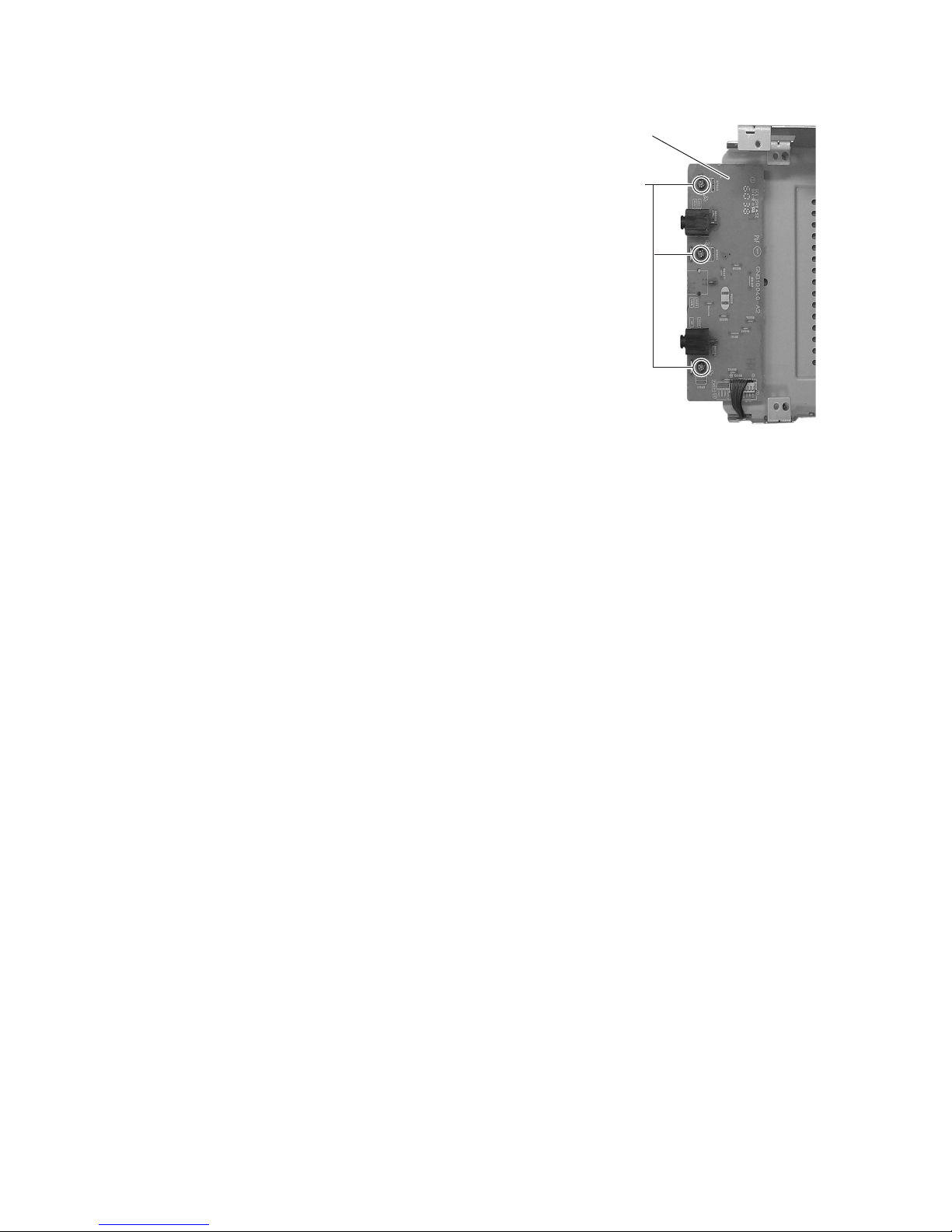
SCHEMATIC DIAGRAMS
COMPACT COMPONENT SYSTEM
EX-D11J,EX-D11EE,EX-D11A
EX-D11US,EX-D11UB,EX-D11UP
EX-D11UT,EX-D11UW,EX-D11UY
EX-D11UG
CD-ROM No.SML200607
Lead free solder used in the board (material : Sn-Ag-Cu, melting point : 219 Centigrade)
Contents
Block diagrams
Standard schematic diagrams
Printed circuit boards
CA-EXD11
COPYRIGHT 2006 Victor Company of Japan, Limited.
SP-EXD11SP-EXD11
2-1
2-2
2-10 to 12
No.MB544SCH
2006/7
Page 30

In regard with component parts appearing on the silk-screen printed side (parts side) of the PWB diagrams, the
parts that are printed over with black such as the resistor ( ), diode ( ) and ICP ( ) or identified by the " "
mark nearby are critical for safety.
Page 31

2-1
Block diagram
SWITCHING
POWER
SUPPLY
AC IN
35V
35V35V
15V
DC regulator and audio output section
IC250,Q2050
DVD5V REG.
D2060,D2064,D2066
D4V,D3.3V,D2V REG.
Q2020
US7V REG.
Q2040 to Q2043
FL1,FL2 REG.
Q4600,Q4601
TU9V REG.
IC202
US3.3V REG.
L+/R+/-
SPEAKER
TERMINAL
Digital amplifier circuit section
IC111 to IC113
IC121 to IC123
IC131
AMP.
IC132
HALF
BRIDGE
D3001,D3003
AHB
Q1101,Q1102
Q1201,Q1202
Q3004 to Q3006
PROTECT
AHBCTL
CN312
IC301
IC302
FREQ.
CONT.
Q1103
Q1203
Q3007
S.MUTE
Q2612
to
Q2614
DVD MUTE
SMUTE
F-SHIFT
OLOAD
PRT
Q3002
Q3003
Q2006
Q2007
MODON
IC303
5V REG.
5V
L,R
CN311
US7V
DVD5V, S5V
M5V, V5V
FL+/-
D4V
D3.3V, D2V
L, R
AHBCTL
SMUTE
OLOAD
MODON
F-SHIFT
PRT
DVD5VCTL
DVDL/R
LRMUTE
TRAY+/-
IC235
OPEN
/CLOSE
TRAY
OPEN
CLOSE
DVDOPSW
DVDCLSW
CN302
15V
CN301
J3001
CN300
CN310
CN201
IC301
DV3.2
A, B, C, D, E1+F1, E2+F2
E3+F3, E4+F4, RF+/-, LPC1, LPC2
Q101 to Q104
LASER DRIVER
FM+/-, UOUT, VOUT
WOUT, COM
IC201
DRIVER
T+/F+/-
SPDRV, TRSDRV
TRDRV, FODRV
FG, /DRVMUTE
/SPMUTE
TRVSW
IC509
FLASH
ROM
EXADT0 to 15
EXDT0 to 15
EXADR16 to 20
NEXCE, NEXWE
NEXOE
IC505
SDRAM
SDA
SCL
WP
MA0 to 11, MDQ0 to 15
BA0, BA1, DQM0, DQM1, MCK
NWE, NCSM, NRAS, NCAS
IC701
DAC
FAOUTL/R
LRMUTE
BCK, LRCLK, DACCK, AOUT0
DAC0CS, DCLK, DATA
TX(SPDIF)
UCS,SCS,U2SDT,S2UDT,UCLK
DAC1OUT(Y2-G), DAC2OUT(CB-B)
DAC3OUT(CR-R), DAC4OUT(Y)
DAC5OUT(C)
DVD servo and DVD system control section
A6V
D2V
A5V
S3.3V
P3.3V
S3.3V
M9V, M5V
S5V, D4V, D2V
PICKUP
UNIT
TRAVERSE
MECHANISM
X301
27MHz
IC510
EEPROM
LPCO1, LPCO2
CDLDCUR, DVDLDCUR
LD(CD)
LD(DVD)
CPURST
DVDPER
IC453
RESET
IC705
A5V REG.
D2V
D1.2V
IC302
D1.2V REG.
IC305
3.3V REG.
CN202
CN208 CN212
SPDIF
OPTICAL OUT
IC295
CN200
CN201CN101
CN701CN712
US3.3V
USB3.3V
CN703
CN702CN705
IC701
VIDEO
DRIVER
C, Y, Y2-G
CR-R, CB-B
COMPONENT
VIDEO OUT
J701
S-VIDEO OUT
/COMPOSITE
VIDEO OUT
J702
Y,Cb,Cr
Y,C,CV
V-MUTE1
V-MUTE2
UCS, SCS, SCLK
U2SDT, S2UDT
CPURST, DVDPWR
Video driver and video out component section
IC400
SYSTEM
MICOM
CN424CN423 CN425
A6V
US7V
SMUTE
OLOAD
MODON
F-SHIFT
10VCTL
PRT
35V,FL+/S10V,US3.3V
IDTRIG
35V, FL+/S10V, US3.3V
OPEN, CLOSE
DVDOPSW, DVDCLSW
FLPOWER, DVD5VCTL
V-MUTE1, V-MUTE2
UCS, SCS, SCLK
U2SDT, S2UDT
CPURST, DVDPWR
VOL+/KEY1
KEY2
BKLED
STBLED
FLBK
FLCLK
FLDATA
FLLATCH
REMOCON
CN426
KEY1
KEY2
IC410
EEPROM
SDA
SCL
FTU
Q4201
Q4202
RESET
RESET
CN421
TUDI,TUDO
TUCLK,TUCE
RDSDATA
RDSCLK
RDSON
FW615
FW615
S6000 to S6003
S6005 to S6009
S6012
KEY MATRIX
User control keys section
CN610
D6113,Q6111
BACK LED
BKLED
D6110,Q6110
STANDBY LED
STBLED
JS612
ENCODER
IC621
USB DECODER
VOL+/-
FL display, Remocon and LED section
IC617
REMOCON
REMOCON
FL615
FL TUBE
FL+/-, 35V
FLBK, FLCLK
FLDATA, FLLATCH
HPL/R
FW621
J623
Headphone, AUX input and USB section
J620
PHONES
HPL/R
HPIN
AUXL1/R1
AUXIN
D+/HOST
USBL/R
USBL/R
TO
TUNER PACK
System control, volume, AHB circuit, HP. circuit
and subwoofer section
CN501
AUXL1/R1
AUXL1/R1
AUXL2/R2
J621
AUX
USB
TUL/R
VOLCE
VOLCLK
VOLDATA
IC500
E.VOL
DVDL/R
DVDL/R
IC510
Q5371
to
Q5373
AHB
LOUT
ROUT
Q5912,Q5913
WOOFER MUTE
IC550,IC560
Q5670
QP LINK
J5001
W OUT
J5000
AUX
WOOFER
IC520
AMP.
Q5812
MUTE
Q5810,Q5811
L/R MUTE
Q5813,Q5814
HP MUTE
HPMUTE
QPL
AHB
L, R
AHBCTL
HPIN
AUXIN
X4100
8MHz
X6200
12MHz
PRT
SPDIF
SPDIF
Used for Area suffix EE/UP
S1
TRAY SWITCH
LOADING MOTOR
DVD loading section
CN1
CN210
FLPOWER
IC200
S10V REG.
10VCTL
S10V
D2011
M9V REG.
M9V
US3.3V
Q5750
USB3.3V
REG.
USB3.3V
Page 32

2-2
Parts are safety assurance parts.
When replacing those parts make
sure to use the specified one.
Standard schematic diagrams
DC regulator /Audio output section
K2089
CN210
IC250
IC202
W201
C2001
C2002
CN202
CN201
D2012
D2011
W202
W203
C2015
W204
CN302
L2000
D2060
D2064 D2066
CN212
K2086
K2095
K2085
CN203
K2084
K2083
K2088
B2085
B2084
B2089
B2088
B2083
C2062
L2050
C2065
R2008
CN300 CN301
B2086
Q2020
CN208
CP250
Q2612
Q2613
R2616
IC235
Q2042
Q2006
R2617
R2095
L2095
R2009
C2095
D2006
R2042
R2045
Q2050
Q2040
Q2043
Q2041
IC200
R2612
R2614
C2612
D2038
D2037
C2614
D2036
Q2614
R2618
CN200
IC295
C2000
C2003
C2004
C2021
R2006R2007
C2051
C2055
R2050
D2026
C2050
R2051
R2052
C2020
D2071
D2050
C2052
D2045
D2078
C2027
C2026
R2021
D2061
D2020
C2022
C2025
C2036
D2035
C2037
D2052
D2007
C2035
C2010
C2011
D2010
R2025
C2613
C2006
C2615
Q2007
R2022
D2022
R2047
R2043
R2044
R2040
R2041
R2046
R2613
C2040
D2042
C2041
C2042
C2043
Q2070
Q2071
R2071
R2072
D2043
R2070
R2073
R2075
R2074
C2012
D2076
D2072
R2037
R2615
D2025
R2036
R2010
C2616
D2051
QQR0621-001Z
QGF1040C1-05
PQ1CG21H2FZ
PQ033ES3MX-T
NI
0.022
QGB2024J1-18S
QGB2024J1-18S
NI
1N4003S-T5
100/16
QGB2024K1-04S
QQLZ003-1R0
2A02-M 1N4003S-T5
1N4003S-T5
QGF1040F1-12
QQR0621-001Z
NQR0007-002X
QQR0621-001Z
NI
QQR0621-001Z
NQR0389-003X
QQR0621-001Z
47/16
QQL50AK-221Z
47/16
10K
QGB2024K1-04S QGB2024K1-06S
KTC2026/Y/
QGF1040C1-05
ICP-N25-T
2SD2114K/VW/-X
2SD2114K/VW/-X
10K
LB1641
RT1N141C-X
2SA1530A/QR/-X
10K
47
QQL231K-4R7Y
390
47/16
MTZJ24B-T2
10K
100
KTC3203/OY/-T
KTB772/Y/
KIA78R10API
2.2K
2.2K
10/63
1N4003S-T5
1N4003S-T5
10/63
1N4003S-T5
RT1P140C-X
1K
QGA3901C1-04
TOTX147
47/25
47/25
0.1/16
36K3K
0.1
0.1
10K
MTZJ3.6B-T2
100/25
3K1K
100/25
NI
11DF2-FD
470/16
NI
1SS133-T2
0.01
47/16
2.2K
MTZJ3.9B-T2
MTZJ7.5B-T2
100/16
100/16
0.01
MTZJ5.6C-T2
0.1
MTZJ6.2C-T2
NI
100/16
47/25
47/25
MTZJ11C-T2
4.7
NI
22/50
NI
2SC3928A/QR/-X
2.2K
MTZJ7.5B-T2
330
NINI
100K10K
820
RT1N141C-X
27K
2SA1530A/QR/-X
0.01
NI
0.01
47/25
47/25
RT1N141C-X
RT1N141C-X
4.7K
NI
MTZJ5.6B-T2
12K
12K
NI
4.7K
0.1
1SS133-T2
1SS133-T2
2.2k
27K
MTZJ3.6B-T2
2.2k
NI
0.1/16
RB161L-40-X
15V
35V
D3.3V
DVDL
DVDR
TRAY+
TRAY-
!
!
!
!
!
!
Page 33

2-3
Parts are safety assurance parts.
When replacing those parts make
sure to use the specified one.
Digital amplifier section
R1227
C1223
IC132
IC122
B3001
R1237
C3034
C1237 C1137
IC112
R1137
IC131
C1238
D1104
R1124
C1140
R1118
IC131
R1224
R1122
R1218
R1222
R1223
R1243
C1242
C1208
IC121
R1217
C1243
R1210
R1123
R1206
R1204 C1202
R1203
R1202
C1244
C1201
R1201
IC123
C1142
R1211
R1212
IC121
R1215
R1216
C3026
C1108
R1213
R1207
C1204 R1208
IC111
R1117
C1301
R1110
C1107
R1106
R1104 C1102
R1103
R1102
C1101
R1101
R1111
R1112
IC111
R1115
R1116
C3027
R1113
R1107
C1104 R1108
C1138 C1144
IC113
C1143
R1143
C1240
CN312
C1206
C1106
IC301
L1201
L1202
L1101
L1102
C1214
C1115
R3011
C1215
C1114
C1216
C1217
C1116
C1117
R3012
C1133
C1233
C1304
C1305
C1303
C1302
C1306
R3013
R3014
R3022
C3012
C3011
D1203
IC303
C1222
IC301
R3003 R3005
X3001 X3002
C3002 C3003 C3004 C3005
R1238
R3004 R3006
IC302
IC302
IC302
IC302
IC301
IC301 IC301
R3007
R1303
Q1202Q1201
R3008 R3009
C3008 C3009
C3010
R1229
L1281
C1245
IC301IC301IC301
C1145
Q3002
CN311
C1307
L1181
R3015
R1304
C1310
R1138
Q3003
C1113
C1224
Q3004
R1129
C1124
R3016
C1123
R3017
R3019
R3018
K3001
K3002
Q1102Q1101
R1231
K3003
K3004
K3005
R1127
C3006
C3017 C3018
R3027
R3029
R1228
C3007
C1105
Q1104
C1213
R3010
R1309 R1310 R1311
R1232 R1131 R1132
C1203
R1205
C1103
R1105
C1209
C1210
C1211
R1219
R1220
C1109
C1110
C1111
R1119
R1120
C1241
C1134
C1234
C1205
R1308
C3016
R3025
C3015
R3023
C1226 C1227
C1228 C1229
C1126 C1127
C1128 C1129
R3037
Q3005
R3035
R3036
C3025
Q3006
R1233
R1234
R1134
R1133
Q3007
R1135
R1235
Q1203
Q1103
C1232 R1236
C1132 R1136
Q1204
C1141
R1242
R1142
C1309
C1308
C3031
R3020
D3001
D3003
C1207
Q3041
C1218C1118
CN310
R1225R1125
R3041R3042
Q3042
C1282
C1286
C1182
C1186
C1285
C1185
C1183
C1284
C1184
C1283
C1281C1181
C1381
J3001
C3013
C1225C1125
C3021
R3033
C3022
R3034
R1301R1302
R1226R1126
C3020
R3032
C3019
R3031
C1230C1130
10K
10/50
STA505-LF-W
NJU7109F3-X
NRSA63J-0R0X
1.5K
1
11
NJU7109F3-X
1.5K
NJM2115V-W
10/63
MA152WK-X
100
0.1
1K
NJM2115V-W
100
100K
1K
100K
100
100
330P
NJM4580M-X
18K
820
100
470K
10K 2200P
820
11K
10/63
1.8K
SN74AHC1G00V-X
8.2K
5.6K
NJM4580M-X
22K
22K
0.1
330P
5.6K
10K
470P
330
NJM4580M-X
18K
1/6.3
820
1200P
470K
10K 2200P
820
11K
10/63
1.8K
SN74AHC1G00V-X
8.2K
5.6K
NJM4580M-X
22K
22K
0.1
5.6K
10K
470P
330
10/63
100
0.1
QGB2024J1-04S
10/50
10/50
SN74HCU04ANS-X
QQLZ037-220QQLZ037-220QQLZ037-220QQLZ037-220
0.1
0.1
4.7K
0.1
0.1
NI
NI
NI
NI
4.7K
470P
470P
0.1/16
0.1/25
0.1/16
0.1/16
0.1/25
4.7K
10K
270
0.33
0.1
UDZS6.8B-X
KIA78S05P-T
33/35
SN74HCU04ANS-X
1M 1M
470P 470P 470P 470P
22K
5.6K 5.6K
SN74LV00ANS-X
SN74LV00ANS-X
SN74LV00ANS-X
SN74HCU04ANS-X SN74HCU04ANS-X
SN74HCU04ANS-X
1.2K
10K
RT1P44HC-X
RT1P44HC-X
680 680
330P 330P
47P
470
QQR0797-002
NI
SN74HCU04ANS-X
NI
KTA1267/YG/-T
QGB2024J1-06S
470/25
QQR0797-002
8.2K
10K
0.1/16
22K
2SC3928A/QR/-X
1/6.3
100P
2SC3928A/QR/-X
470
100P
1k
10/50
1k
1k
1k
NQR0389-003XNQR0389-003X
RT1P44HC-X
RT1P44HC-X
5.6K
NQR0389-003XNQR0389-003XNQR0389-003X
10K
1/6.3
10/50 10/50
4.7K
4.7K
4.7K
1/6.3
4.7/50
UMY1N-W
1/6.3
270
2.7K 2.4K 2.7K
5.6K 5.6K 5.6K
2200P
10K
2200P
10K
22P
22P
22P
2.2K
2.2K
22P
22P
22P
2.2k
2.2k
470P
470P
4.7/50
1K
10/50
4.7K
10/50
4.7K
0.1/50 0.1/50
0.1/50 0.1/50
0.1/50 0.1/50
0.1/50 0.1/50
10K
2SC3928A/QR/-X
10K
220K
10/50
22K
8.2K
8.2K
22K
RT1P241C-X
2.2K
2.2K
2SD2114K/VW/-X
2SD2114K/VW/-X
180P 3.3K
180P 3.3K
UMY1N-W
100
100
0.033
22/50
10/50
220
MA152WK-X
MA152WK-X
1200P
NI
0.1/500.1/50
QGB2024J1-04S
4747
NI
QAX0734-001
NI
QAX0735-001
NI
SN74LV00ANS-X
3300P
NI
3300P
NININI
NI
220P
220P
NI
220P220P
100P
QNB0118-004
100/25
0.68/50
0.68/50
0.47
1.2K
0.47
1.2K
1K1K
4747
0.47
1.2K
0.47
1.2K
0.1/500.1/50
2SA1530A/QR/-X
15V
A.GND
P.GND
P.GND
SMUTE
A15V
L
OLOAD
A15V
5V
15V
R
5V
SW15V
A.GND
P.GND
P.GND
5V
MODON
A15V
A.GND
SW15V
F-SHIFT
A.GND
A.GND
5V
5V
A.GND
AHBCTL
5V
15V
P.GND
PRT
P.GND
S.GND
5V
REFA2.5V
A.GND
A.GND
5V
REFA2.5V
A.GND
REFA2.5V
A.GND
P.GND P.GND
REFA2.5V
15V
P.GND
5V
5V
S.GND
5V
P.GND
A.GND
5V
REFA2.5V
5V
A.GND
5V
A.GND
A.GND
P.GND P.GND
P.GND
!
!
!
!
!
!
!
!
!
!
Page 34

2-4
System control section
CN423
R4004
R4005
R4006
R4000
IC410
K4001
CN425
R4018
CN424
R4019
C4109
CN422
R4043
R4002
R4020
R4156
R4155
CN421
C4210
C4058
R4121
CN426
R4122
R4152
R4123
R4127
R4044
R4045
R4046
R4136
R4137
R4138
C4000
X4100
C4112
R4051
R4042
C4110
C4111
R4041
R4052
R4054
R4058
R4050
R4057
R4150
Q4201
R4009
R4109
R4103
R4104
CN428
Q4202
C4113
IC400
D4600
C4208
Q4601
C4707 C4708
R4148
R4203
R4059
L4001
R4053
R4073
R4001
R4078
R4021
R4022
R4023
R4024
R4084
R4105
R4080
R4061
R4032
D4058
R4034
R4035
R4036
R4037
R4102
R4038
R4039
R4040
R4502
R4166
R4171
R4500
C4500
C4502
R4003
R4068
R4072
R4074
D4201
R4201
K4500
R4090
R4400
R4176
R4402
R4600
R4202
R4602
R4601
C4600
C4602
D4602
D4202
Q4600
R4604
R4075
R4077
C4207
R4071
R4070
R4069
R4067
R4066
R4065
R4063
R4062
R4064
R4079
R4033
R4165
R4169
R4172
R4175
R4026
R4106
QGB2024K1-18S
11K
2.2k
2.2k
2.2k
BR24L08F-W-X
QQR0621-001Z
QGB1214J1-10S
2.2k
QGB2024K1-18S
2.2k
0.01
NI
1K
3.6K
2.2k
10K
10K
QGF1208F1-11
0.1
1/50
NI
QGF1210G1-18
NI
47K
NI
NI
2.2K
2.2K
2.2k
NI
NI
NI
0.1
QAX0912-001Z
22P
2.2K
2.2K
100/16
0.1
2.2K
2.2K
2.2K
2.2K
2.2K
2.2K
10K
RT1P141C-X
2.2K
10K
10K
10K
QGF1210G1-05
RT1N144C-X
22P
MN101C61GAJ
NI
4.7/50
RT1N140C-X
0.1
0.1
GND
10K
10K
2.2K
QQL244K-100Z
2.2K
2.2K
10K
2.2K
2.2K
2.2K
2.2K
2.2K
1K
20k
2.2K
2.2K
2.2K
MTZJ2.4B-T2
2.2k
2.2k
2.2k
2.2k
10K
2.2k
2.2k
2.2k
0
10K
10K
0
180P
180P
2.2K
2.2K
2.2K
2.2K
MTZJ2.2A-T2
1K
NI
2.2K
220
10K
220
47K
10K
1.6K
10K
47/25
47/25
MTZJ3.3B-T2
1SS133-T2
2SA1530A/QR/-X
1.6K
2.2K
2.2K
100/6.3
2.2K
2.2K
2.2K
2.2K
2.2K
2.2K
2.2K
2.2K
2.2K
2.2K
2.2K
10K
10K
10K
10K
2.2K
20k
10VCTL
KEY1
DGND
US3.3V
DVD5VCTL
WLEFT
SCS
CPURST
KEY2
SMUTE
IDTRIG
SAFETY0
SCLK
V-MUTE2
SAFETYDVD
FLPOWER
OLOAD
MODON
F-SHIFT
PRT
AVIN
DVDOPSW
DVDCLSW
OPEN
V-MUTE1
CLOSE
US7V
AVOUT
WOOFER
PRT
VOLDATA
WRIGHT
DVDR
S2UDT
DVDL
U2SDT
UCS
DVDPWR
V-MUTE2
R
L
AHBCTL
SYNC/ID
AHBCTL
F-SHIFT
V-MUTE1
WLSW
VOLCE
A6V
IDTRIG
R
VOLCLK
QPL
DVDPWR
AHB
MODON
L
DVDL
DVDR
WLEFT
WRIGHT
QPL
AGND
OLOAD
SMUTE
10VCTL
FLPOWER
HPIN
HPMUTE
S10V
AUXIN
VOLCLK
VOLCE
VOLDATA
WOOFER
TUL
TUR
FL-
FL+
35V
AHB
SCL
SDA
CPURST
RDSDATA
SCS
SCLK
UCS
U2SDT
S2UDT
RDSCLK
RDSDATA
RDSON
TUR
TUL
TUDC
TUCLK
TUDI
FLCLK
TUCE
FLBK
RDSCLK
REMOCON
TUDO
AFFATCH
FLDATA
VOL+
P53
P54
TUCLK
FTU
TUDI
RDSON
VOL-
STBLED
BKLED
AUXIN
HPIN
HPMUTE
SCL
SDA
DVD5VCTL
SAFETY0
SAFETYDVD
REMOCON
SYNC/ID
FLPOWER
VOL-
DVDOPSW
VOL+
TUCE
BKLED
DVDCLSW
OPEN
CLOSE
WLSW
STBLED
FL+
SYNC/ID
FLDATA
FLCLK
FLLATCH
FLBK
35V
FL-
KEY2
KEY1
AVOUT
AVIN
AVOUT
AVIN
3.3V
TU9V
Page 35

2-5
Parts are safety assurance parts.
When replacing those parts make
sure to use the specified one.
Volume IC/AHB/Subwoofer section
R5916
C5916
Q5750
IC500
R5405
C5530
C5380
C5802
C5804
D5620
CN501
C5918
C5405
R5505
J5001
R5398
C5917
C5667
IC560
IC550
C5668
C5654
R5271
C5273
C5272
Q5670
R5272
R5276
R5275
C5915
R5710
R5711
C5505
R5273
R5172
C5662
C5650
Q5811
R5377
C5173
R5378
R5279
R5179
R5176
R5392
C5669
R5171
Q5371
Q5372
R5650
R5373 R5374
R5277
R5281
R5181
C5670
D5371
R5372
Q5373
R5376
R5375
R5371
C5660
R5660 R5664
R5654
R5666
D5650
R5661
R5911
Q5913
R5913
C5912
R5901
R5902
Q5911
Q5912
C5810
R5817
Q5812
C5812
C5811
C5816
R5823
C5815
R5822
R5821
R5826 C5818
C5817
R5824
R5825
C5820
C5819
R5829
R5827
Q5810
R5830R5832
R5814
R5815
R5810
R5813
J5000
C5730
Q5511
R5601
C5750
R5750
C5602
C5407
C5501
C5531
C5622
C5620
D5501
C5830
R5501
R5503
Q5620
R5402
R5401
R5620
C5532
R5502
R5504
R5404
R5403
R5917
IC510
R5670
C5274 R5274
C5275
R5720R5721
C5710
C5711
D5670
C5174
C5374
R5278
R5178
R5174
C5175
R5175
C5172
R5173
D5372
R5177
Q5814
R5915
C5914
C5371
C5372
C5402
C5373
Q5813
R5668
C5666
R5663
R5662
C5913
R5653
R5652
C5652
R5912
C5911
R5914
R5812
R5811
IC520
R5828
R5831
R5820 R5819
C5814
C5813
C5720C5721
R5507
R5406
C5521
C5520
R5610
C5500
C5504
C5400
C5506
C5406
C5401
R5407
C5604
C5603
C5507
C5404
C5409
C5509
C5408
C5410
C5510
C5508
R5506
C5503
C5502
C5403
2.2K
10/50
RT1P140C-X
LC75345M-X
470
GND
100P
GND
NI
10/50
10/50
MTZJ6.2B-T2
QGA2001C1-12
NI
0.047
470
QNN0793-001
47K
NI
100P
LM358DR-X
LM358DR-X
100P
47/16
1.8K
0.047
0.47
RT1N44HC-X
180K
15K
27K
1
20K
20K
0.047
1.8K
180K
47/16
2.2/50
2SD2114K/VW/-X
1K
0.047
10K
1K
1K
15K
1.5K
0.22
1.8K
2SC3928A/QR/-X 2SC3928A/QR/-X
100K
10K 10K
47K
NI
NI
NI
1SS133-T251K
2SC3928A/QR/-X
100K
270
100
2.2/50
100K
4.7K
4.7K
220K
1SS133-T2
100
1K
2SD2114K/VW/-X
2.2K
10/50
47K
47K
2SC3928A/QR/-X
RT1P44HC-X
4.7/50
100
RT1P431C-X
4.7/50
4.7/50
150P/50
1k
0.0022/50
3.3k
180
1k
150P/50
0.0022/50
3.3k
180
220/10
220/10
22
22
2SD2114K/VW/-X
1k
1k
1k
1k
3.3K
3.3K
QNN0788-001
0.01
KTC3203/OY/-T
100
47/16
47K
100/16
10/50
4.7/50
100P
100/16
100/16
MTZJ10B-T2
0.01
0
4.3K
KTC3200/GL/-T
0
NI
1.2K
100P
NI
8.2K
8.2K
4.3K
470K
NJM4565M-WE
1.2K
0.047 1.5K
10/50
75K75K
220P220P
MTZJ3.3B-T2
0.047
47/25
4.3K
4.3K
1.5K
10/50
27K
0.47
1.8K
MTZJ5.1B-T2
47K
2SD2114K/VW/-X
1K
0.1
100/16
10/50
4.7/50
1/50
2SD2114K/VW/-X
100K
10/50
4.7K
100K
0.1
4.7K
100K
47/16
330
NI
22K
27K
27K
NJM4565M-WE
2.2K
2.2K
10K 9.1K
47/25
100/16
220P220P
3.9K
1.8K
0.1
47/25
470
4.7/50
4.7/50
4.7/50
10/50
10/50
4.7/50
7.5K
22/50
0.01
10/50
4.7/50
0.1
0.1
0.0027
0.1
0.1
0.0027
1.8K
10/63
4.7/50
10/63
DVDR
TUR
WRIGHT
L
HPMUTE
WOOFER
L
R
AHBCTL
S10V
US3.3V
AGND
VOLCLK
WOOFER
AHBCTL
R
AHB
USB3.3V
HPR
HPL
DGND
HPMUTE
A6V
HPL
HPR
DGND
VOLCE
VOLDATA
TUL
WLEFT
DVDL
IDTRIG
AUXIN
HPIN
QPL
US7V
AUXL1
AUXL2
AUXR2
AUXR1
IDTRIG
AUXR2
VOLCLK
DVDR
WRIGHT
TUR
VOLDATA
VOLCE
TUL
WLEFT
DVDL
AUXL2
AUXIN
HPIN
AHB
QPL
!
Page 36

2-6
FL/User control keys/USB section
D6150
C6153
R6009
IC617
R6008
R6181
R6007
C6159
C6170
R6006
S6008
Q6111
C6116
S6007 S6006
FW615
S6005
C6154
S6009
R6010
CN610
C6216
D6140
R6220
Q6140
C6120
JS612
R6221
K6212
C6221
JS612
IC621
K6213
C6172
R6004 R6003
C6160
D6201
S6012
K6214
R6110
R6170
K6215
J621
D6202
R6002 R6001
S6003 S6002 S6001 S6000
R6013
R6012
C6225
C6215
R6219
X6200
C6224
C6223
FL615
FW621
C6222
C6220
C6226
C6214
C6245
R6244
R6243
R6116
C6158
C6157
C6155
C6156
FW615
C6231
D6110
K6211
C6218
K6216
K6200
R6214
R6213
K6205
K6201
K6202
R6200
J620
C6171
R6142
J623
C6140
R6115
C6227
C6121
C6150
R6151
R6111
R6112
C6243
C6151
C6152
D6113
C6241
C6229
C6228
C6244
C6202
C6242
R6222
R6217
R6218
R6241R6242
R6216
R6113
C6113
Q6110
R6150
R6215
C6230
C6219
R6223
C6201
C6203
C6204
C6200
NI
0.1
20k
NJL22H380A
8.2k
330
5.1k
0.1
NI
0
QSW0825-001Z
2SC3928A/QR/-X
47/16
QSW0825-001Z QSW0825-001Z
QUM023-07Z4Z4-E
QSW0825-001Z
1/50
QSW0825-001Z
51k
QGF1205F2-18
10/6.3
SELU2E10C-P
22
KRC102S-X
0.01
QSW1130-001
22
NQR0389-003X
10/6.3
PCM2704DB-X
NQR0022-005X
100/6.3
20k 8.2k
1/50
UDZS6.8B-X
QSW0825-001Z
NQR0022-005X
1.5K
0
NQR0389-003X
QNS0274-001
UDZS6.8B-X
5.1k 0
QSW0825-001Z QSW0825-001Z QSW0825-001Z QSW0825-001Z
1K
51k
1/16
NI
1M
QAX0911-001Z
18P/50
18P/50
QLF0170-002
WJK0231-002A-E
1/16
1/16
1/16
NI
0.01
20K
20K
5.6K
100P
100/16
0.1
0.1
QUM023-07Z4Z4-E
0.01
SLI-343URC3F
NQR0389-003X
0.0022
NI
0.0022
NQR0389-003X
220
220
NQR0389-003X
NQR0389-003X
NQR0389-003X
1K
QNS0274-001
1/16
10K
QNZ0783-002
0.01
NI
1/16
0.01
100P
10
75
NI
220P
100P
100P
SELU1E54CM-P
220P
10P/50
10P/50
220P
1.5/6.3
220P
1.5K
16
16
68K68K
NI
10K
0.01
RT1P141C-X
10
NI
NI
0.1
1.5/6.3
0.1
0.1
KEY1
KEY2
KEY1
KEY2
AGND
FL-
35V
FLBK
S10V
FLLATCH
FLCLK
FLDATA
FL+
STBLED
BKLED
VOL+
VOL-
AUXIN
REMOCON
AUXL1
USB3.3V
SYNC/ID
DGND
DGND
US3.3V
USBL
AUXR1
HPIN
HPR
HPL
AGND
USBR
BKLED
VOL+
35V
VOL-
REMOCON
STBLED
FLDATA
SGND
FL-
FLLATCH
SGND
SGND
FL+
FLBK
FLCLK
Page 37

2-7
Video control section
DVD loader section
R7009
R7010
R7011
C7021
C7005
C7020
C7024
J702
R7006
R7008
R7007
C7016
C7015
C7014
C7032
C7031
CN703
IC701
C7007
J701
CN705
L7006
C7028
C7010
C7011
C7012
C7013
CN702
C7006
C7022
C7023
C7025
C7017
C7019
C7018
R7022
R7021
R7023
R7024
R7025
R7027
R7026
R7028
C7008
R7030
R7029
75
75
75
0.1
0.1/16
470/6.3
470/6.3
QNN0557-002
SGND
75
75
75
470/6.3
470/6.3
470/6.3
NI
0.01
QGF1040C1-25
BH7868FS-X
22/25
QNN0790-001
QGF1040C1-12
QQL25CK-221Z
180P
1/6.3
1/6.3
1/6.3
1/6.3
QGB1214K1-10S
470/6.3
180P
180P
180P
180P 180P
180P
270
200
560
330
200
160
270
240
0.1/16
240
160
V5V
C
V-MUTE1
S5V
CR-R
V-MUTE2
Y2-G
CB-B
UCS
V-MUTE1
D4V
V-MUTE2
DGND
D2V
D2V
U2SDT
S2UDT
SCLK
CPURST
SCS
SPDIF
MGND
MGND
M5V
M9V
DVDPWR
U2SDT
S2UDT
SCLK
SCS
UCS
CPURST
Y
S1
CN1
QSW1074-001
QGF1016F3-05
Page 38

2-8
DVD section (1/2)
IC301
C372
IC302
C374
C329
C315
C307
C373
R363
R361
R356
R355
R354
C375
R331
R330
R327
R332
R318
TP325
TP320
TP328
TP329
TP330
TP331
TP332
TP333
TP334
TP335
TP338
CN301
D301
TP303TP305
C376
C311
C302
R362
R357
R360
R359
R364
R358
R367
R366
R365
R345
C313
R351
C325
C326
C339
C356
C341
C316
C318
R340
R342
R341
C312
TP301
TP300
R347
R346
C393
R392
TH301
TP381
TP337
C324
C340
C352
C303
C328
TP321
C102
C101
C107
C103
C104
R101
R102
R126
Q105
R112
R115
Q103
Q104
R104
R107
Q101
Q102
R201
R202
TP291
TP292
C290
R290
IC201
R213
C211
R215
TP221 TP226
R207
C206
R384
C260
C261
C262
C264
C204
C203
R206
C205
R204
IC510
C300
C383
C379
C378
C305
C377
C386
C306
R303
R307
R306
R352
X301
C354
C353
R319
R325
R326
R324
R316
R383
R353
R310
C308
C319
C314
C321
C320
C322
C323
C348
C347
C337
C338
C332
C333
C331
TP306
TP308
TP309
TP307
TP315
TP314
TP326
TP324
TP323
R335
R334
R337
R336
R393
R394
R339
R338
C349
C330
C335
R349
R348
R323
R322
R321
R320
C309
C334
C351
R372
R373
R374
R377
R308
R371
R375
R376
R309
C310
C350
R350
R542
R541
C564
C301
K352
C772
C770
C359
C336
C304
TP304
CN101CN201
TP113
TP116
TP117
TP118
TP119
TP120
TP121
TP122
TP123
TP124
TP115
TP114
TP108
TP101
TP102
TP103
TP104
TP112
TP111
TP110
TP109
TP107
TP106
TP105
C771
C109
C110
R113
R114
R116
C108
R111
R117
R118
R103
R109
C105
R105
R106 C106
R108
R110
R128
R127
R125
C776
TP201
TP202
TP203
TP204
TP205
TP208
TP207
TP206
R257
R259
C256
R221
R255
TP220
R214
C251
C258
C259
C210
C257
TP231 R220
R254
R205
R219
R385
C371
C202
C201
C777
R208
TP227
R251
R252
C217
C263
C774
MN2DS0009AA
0.1
MM1701CH-X
NI
0.1
0.1
0.1
NI
NI
NI
NI
NI
NI
0.1
NI
NI
330
NI
NI
NI
NI
0.1
NI
47/4
330
220
NI
NI
NI
220
220
NI
NI
220
0.1
680
12P
10P
NAX0741-001X
10/6.3
1
1
0.1
0.1
30K
2.4K
5.1K
0.1
P3.3V
20k
22k
0.01
10k
NAD0025-103X
1
1
0.015
GND
S3.3V
GND
47/6.3
0.01
D1.2V D2V
0.1
0.1
0.1
0.1
0.1
100
100
100
UN2119-X
GND
4.3K
1K
2SC4617/R/-X
4.3K
1K
2SC4617/R/-X
GND
S5V
470
1K
NI
NI
LA6502-X
10K
0.022
NI
47K
150p
1K
0.022
0.022
0.022
M5V
NI
0.1
0.01
GND
30K
270p
27K
GND
M9V
GND
GND
BR24L16FV-W-X
0.1
0.1
0.1
NI
0.1
0.1
0.1
0.1
22
1K
1K
1M
560p
560p
10K
330
330
3301K100
100
100
0.1
0.1
0.1
0.1
0.1
0.1
0.1
0.1
0.1
0.018
0.0056
0.1
0.1
0.033
150
150
150
1500000
0.1
0.1
0.1
150
150
NININI
NI
0.1
0.1
0.01
10K
10K1K1K
10KNI470
1K
100K
0.1
0.01
750
NI
47K
0.1
220/4
NQR0502-001X
NI
NI
1
NI
1
QGF0523F1-25WQGF1016F2-08W
NI
NI
NI
18
2.2
470
22/6.3
2SB1424/R/-W
5.6K
330
NI
5.6K
330
47/6.3
18
2.2
22/6.3
470
NI
2SB1424/R/-W
5.6K
4.3K
1
NI
NI
10K
0.1
6.8K
NI
10K
0.47
0.015
0.01510.0082
24K
NI
27K
18K
1K
1
220p
220p
NI
NI
0.39NI0.1
100/16
NI
EXADT0
NEXCE
NEXOE
EXDT0
EXDT8
EXDT1
EXDT9
EXDT2
EXDT10
EXDT3
EXDT11
EXDT4
EXDT12
EXDT5
EXDT13
EXDT6
EXDT14
EXDT7
EXDT15
EXADR16
EXADT15
EXADT14
EXADT13
EXADT12
EXADT11
EXADT10
EXADT9
EXADT8
EXADR19
NEXWE
EXADR18
EXADR17
EXADT7
EXADT6
EXADT5
EXADT4
EXADT3
EXADT2
EXADT1
CPURST
TEMPDET
VHALF2
DACPDN
ADCRST
DAC1CS
DAC2CS
SWMUTE
RX
TX
AOUT0
DATAM
AOUT1
AOUT2
BCK
BCKM
LRCK
LRCKM
DACCK
DAC5OUT
DAC4OUT
DAC1OUT
DAC2OUT
DAC3OUT
EXADR20
TRDRV
AD4
CDLDCUR
DVDLDCUR
FODRV
DVDPWR
C
VREFH
D
E3+F3
E4+F4
E1+F1
A
B
E2+F2
RF+
RF-
T-
T+
F-
F+
/HFMON
AD4
FM+
FM-
WOUT
VOUT
UOUT
COM
TRVSW
MECHA
CHASSIS
TRSDRV
TRDRV
MA3
MA4
MA2
MA5
MA1
MA6
MA6
MA7
MA10
MA8
BA1
MA9
BA0
MA11
NCSM
NRAS
NCAS
MCK
NWE
DQM1
DQM0
MDQ7
MDQ8
MDQ6
MDQ9
MDQ5
MDQ10
MDQ4
MDQ11
MDQ3
MDQ12
MDQ2
MDQ13
MDQ1
MDQ14
MDQ0
MDQ15
B
D
LPCO2
E1+F1
E2+F2
E3+F3
E4+F4CA
VREFH
LPC2
LPCO1
LPC1
RF+
RF-
TRSDRV
SPDRV
/HFMON
/DRVMUTE
/SPMUTE
FG
CPURST
TRVSW
SCS
S2UDT
U2SDT
UCLK
UCS
LRMUTE
INDEX
TRACK
COPY
DEMP
DAC0CS
DDATA
DCLK
AIN
LPC1
LPC2
CDLDCUR
DVDLDCUR
LPCO2
LPCO1
SPDRV
SPDRV
TRSDRV
FG
FODRV
FODRV
/DRVMUTE
/SPMUTE
COM
UOUT
VOUT
WOUT
FM+
FM-
F-F+T+
T-
TRDRV
Page 39

2-9
DVD section (2/2)
IC505
CN702
IC509
C707
C708
C709
C559
C706
CN712
C701
CN703
C551
C563
C711
R728
R727
R726
IC704
R725
R741
R724
R742
C560
R722
R719
R723
R716
C558
R721
IC454
R715
R720
R714
C742
C741
IC453
C743
K723
C555
C556
R701
C702
C729
C703
C728
C745
IC701
C744
IC702
K726
C739
IC703
K720
C557
R712
R713 K713
R743
C554
CN701
IC706
R732
R731
IC707 K707
K708
K709
K710
K711
C562
R535
C456R460
R458
TP391
K501
K722
K721
R730
K706
K705
K704
K703
K702
K701
TP713
TP711
TP714
TP716
TP702
IC305
C380
C382
K733
K732
K731
IC708
R734
R733
C730
TP750
TP748
TP749
IC705
TP751
TP752
TP755
TP753
TP747
C712
TP745
TP746
C713
C704
TP744
TP733
TP743
TP741
TP742
TP732
TP761
TP731
TP734
D701
TP735
TP736
TP737
TP738
R530
R718
C715
C714
R711
C721
CN704
K712
C740
R740
R462
C455
K751
K753
K754
K755
K756
R729
K763
K765
K762
K761
K759
TP725
TP719
TP720
TP721
TP722
TP723
TP724
C753
C752
C754
C755
C756
C775
C778
C773
TP717
TP718
TP708
TP710
TP701
TP703
TP705
TP707
TP709
R388
C381
TP380
C731
K351
K4S641632H-UC75
NI
SG32M90TFIR3
0.1
NI
NI
0.1
10/16
QGF1016F2-05W
0.1
NI
0.1
0.1
1
NI
NI
NI
NI
NI
NININI
0.1
0
NI
470
NI
22/6.3
470
NI
NI
NI
NI
NI
NI
S-80827CNNB-G-W
NI
NI
0.1
NI
2.2
NI
NI
NI
NI
NI
AK4384VT-X
NI
NI
NI
NI
NI
GND
NQR0022-002X
0.001
NI
NI
NI
NI
0.1
QGF1016F2-25W
NI
1K
1K
NI
NQR0022-002X
NQR0022-002X
NQR0022-002X
NQR0022-002X
NQR0022-002X
1
47k
NI
NI
1K
D1.2V
NQR0502-001X
0
0
GNDGNDGND
GND
M5V
D2V
M9V
D4V S5V
P3.3V
S3.3V
470
NQR0022-005X
NQR0022-002X
NQR0022-002X
NQR0022-002X
NQR0022-002X
NQR0022-002X
MM1563BF-X
1
470p
GND
NI
NI
NI
NI
NI
NI
NI
MM1615AN-X
0.01
1
47/6.3
NI
NI
47K
NI
NI
NI
NI
NI
NI
0.1
NI
NI
0.01
NININININININININININI
NININININI
NININI
NI
2.2
NI
NQR0502-001X
CAOUT
SWMUTE( NC)
EXADT15
MA11
SWAOUT
MA9
EXADT14
AGND
RAOUTL
MA3
MA1
EXADT13
A6V
EXADT12
EXADT11
RAOUTR
LRMUTE
FAOUTL
FAOUTR
A6V
DACCK
CPURST
AINL
AGND
EXADT10
EXADT9
EXADT8
EXADT7
INDEX
EXADT6
EXADT5
EXADT4
EXADT3
EXADT2
EXADT1 EXADT0
EXADR16
AINR
MDQ15
MDQ14
MDQ13
MDQ12
MDQ11
MDQ10
MDQ9
MDQ8
MA8
MA7
MA6
TRACK
COPY
LRCKM
DEMP
DATA
MA5
MA4
MA2
MA0
MA10
MDQ7
MDQ6
MDQ5
MDQ4
MDQ3
MDQ2
MDQ1
MDQ0
LRCK
DAC2CS
DCLK
DAC0CS
EXADR20
DACPDN
AOUT2
DAC1CS
DQM0
NRAS
NCAS
NWE
AOUT1
NCSM
DDATA
BA0
AOUT0
BA1
ADCRST
BCK
DGND
AIN
CPURST
UCS
NEXCE
SCS
UCLK
S2UDT
U2SDT
DQM1
DVDPWR
MCK
DATAM
EXDT15
EXDT7
DAC3OUT
DAC2OUT
EXDT14
DAC1OUT
DAC4OUT
DAC5OUT
TX
RX
EXDT6
EXDT13
EXDT5
EXDT12
EXDAT4
EXDT11
BCK
EXADR19
EXADR18
EXADR17
EXDT3
EXDT10
EXDT2
EXDT9
EXDT1
EXDT8
EXDT0
NEXOE
NEXWE
LRMUTE
SWMUTE
LRCK
AOUT2
AOUT1
BCK
AOUT0
AIN
DAC0CS
DCLK
DAC1CS
DDATA
DAC2CS
BCKM
Page 40

2-10
Main board
Printed circuit boards
C2002
C2004
C2006
C2010
C2000
C2015
C2003
Q2020
C2022
C2025
C2026
C2035
C2042
C2043
C2050
C2052
D2051
K2085
C2095
CN200
CN200
D2071
CN203
K2084
K2086
HS200
HS250
HS202
D2006
D2010
D2011
D2012
K2089
K2088
D2020
D2022
D2025
D2026
D2035
D2036
D2037
D2038
D2042
D2043
D2045
R2025
CN202
D2060
D2072
IC200
CN208
IC202
C2020
IC295
W202
IC250
D2064
CN210
D2052
D2078
L2000
L2050
L2095
D2076
CN201
W201
PP1
Q2040
Q2043
D2066
D2061
C2065
C2062
C2612
CP250
R2045
C2614
C2011
CN300
CN302
D2050
IC235
CN212
W204
CN301
C7005
EP700
C7007
CN702
EP701
C7021
C7022
C7023
C7025
CN703
IC701
L7006
J701
R7009
R7010
R7011
C7020
J702
CN705
C7024
C7006
C7014
C7016
C7015
R4073
R4079
R4005
R4006
IC410
K4001
R4018
CN424
R4019
R4021
C4109
CN422
R4022
R4023
R4024
R4041
R4105
R4080
R4061
R4020
D4058
R4156
R4155
R4035
R4036
R4037
R4038
R4122
R4039
R4040
R4148
R4045
R4046
X4100
R4051
C4110
R4058
R4057
R4068
R4072
R4074
D4201
R4009
R4109
Q4202
IC400
C4208
D4202
R4075
R4077
C4207
R4203
R4059
R4071
R4070
R4069
R4065
R4063
R4062
L4001
R4165
R4172
R4175
R4026
R4053
R4106
R4078
C5654
CN421
D4600
C4600
R4000
C4602
D4602
R4004
R4090
R4176
R4104
C4502
R4500
C4500
R4502
R4084
CN428
C5174
D5371
Q5371
C5812
C5272
R5277
R5814
C5510
C5500
C5818
R5810
C5502
Q5372
R5825
C5274
R5822
R5917
C5371
C5373
C5273
C5501
C5402
R5371
Q5911
C5912
Q5620
R5830
C5407
R5829
CN501
R5815
D5372
R4050
C5504
C5409
C5750
R5398
C5814
C5372
C5503
C5810
C5916
C5620
R5610
C5506
C5604
R5374
C5622
J5001
R5376
Q5814
Q5811
R5826
C5804
C5507
C5172
C5400
C5509
C5602
Q5511
C5820
C5403
C5406
C5811
C5813
R5824
C5405
D5620
C5374
C5275
J5000
R5392
C5819
C5520
R5811
C5404
D5501
C5175
C5410
R5916
C5802
Q5373
C5508
C5505
C5401
R5832
R5821
C5173
C5408
R5601
R5372
R5620
R5650
R5652
IC550
C5652
R5663
R5653
R5660
R5668
D5670
R5662
D5650
C5650
C5660
C5662
B5650
B5660
C5666
R5670
R4150
CN425
R4001
R4034
CN423
CN426
R5817
R5661
C1101
C1102
C1103
C1104
C1105
C1107
C1108
C1109
C1111
C1123
C1125
C1132
C1137
C1141
C1142
C1143
C1144
C1201
C1202
C1203
C1204
C1205
C1207
C1208
C1209
C1211
C1222
C1223
C1225
C1232
C1237
C1241
C1242
C1243
C1244
C1305
C1307
C1308
C1309
C3011
C3012
C3013
C3015
C3016
C3017
C3018
C3019
C3020
C3021
C3022
C3025
C3026
C3031
C1206
C3034
C1238
D1104
D1203
D3001
D3003
IC111
IC112
IC113
IC121
IC122
IC123
IC131
IC132
IC301
IC302
IC303
L1101
L1102
L1201
L1202
Q1101
Q1102
Q1103
Q1104
Q1201
Q1202
Q1203
Q1204
Q3002
Q3004
Q3007
R1101
R1102
R1103
R1104
R1106
R1107
R1108
R1110
R1111
R1112
R1113
R1117
R1118
R1122
R1123
R1124
R1127
R1129
R1131
R1132
R1133
R1134
R1136
R1142
R1143
R1201
R1202
R1203
R1204
R1206
R1207
R1208
R1210
R1211
R1212
R1213
R1215
R1216
R1217
R1218
R1222
R1223
R1224
R1227
R1228
R1229
R1231
R1232
R1233
R1234
R1236
R1242
R1243
R1303
R1304
R1308
R1309
R1310
R3003
R3005
R3008
R3009
R3010
R3020
R3022
R3023
R3025
R3027
R3031
R3032
R3033
R3034
R3036
R3037
X3001
X3002
J3001
R1237
R1137
CN312
L1281
C1106
CN310
R3041
R3042
Q3041
Q3042
C1138
R1138
R1238
CN311
L1181
B1182
Lead free solder used in the board (material : Sn-Ag-Cu, melting point : 219 Centigrade)
(Video board)
(Digital amp board)
(Micon board)
(Regulator board)
forward side
Page 41

2-11
Main board
Lead free solder used in the board (material : Sn-Ag-Cu, melting point : 219 Centigrade)
(Video board)
(Digital amp board)
(Micon board)
(Regulator board)
reverse side
K4001
CN424
CN422
R4043
R4042
R4003
R4002
D4058
R4103
R4102
R4121
R4123
R4127
R4044
R4136
R4137
R4138
R4166
R4171
X4100
C4112
C4110
C4111
R4400
R4052
R4054
Q4201
D4201
R4201
R4202
C4113
C4208
D4202
C4207
R4067
R4066
R4402
R4064
R4152
L4001
R4169
R4032
C5654
C4708
C4707
R4600
CN421
Q4601
D4600
R4601
C4600
Q4600
R4602
R4604
C4602
D4602
C4210
CN428
C5174
D5371
R5902
C5812
R5505
R5403
Q5750
C5272
R5915
C5510
R5507
C5914
C5500
C5521
R5911
C5711
IC500
R5377
C5502
R5402
Q5813
R5913
C5274
C5371
C5603
C5815
C5373
R5901
C5273
C5501
C5402
Q5912
R5281
R5371
R5177
R5501
C5912
R5375
R5406
Q5620
C5407
CN501
R5405
C5721
R5175
R5179
R5172
D5372
R5278
R5828
R5272
C5913
R5502
C5911
IC520
C5817
C5504
C5409
R5710
C5750
C5814
C5372
C5503
R5407
C5810
IC510
C5916
C5620
R5610
C5506
C5604
R5378
C5816
R5273
C5622
J5001
R5274
Q5810
R5750
R5279
R5173
C5804
Q5812
R5373
R5171
C5532
C5530
C5507
C5172
C5400
C5509
C5918
R5174
C5917
C5602
R5823
Q5511
R5831
C5531
C5820
C5403
R5176
R5812
R5720
C5720
R5178
C5406
C5811
C5813
Q5913
C5405
R5711
D5620
C5915
C5710
C5374
C5275
R5819
R5401
C5380
J5000
R5181
C5819
C5520
C5404
C5730
R5275
D5501
R5813
R5827
C5175
R5404
C5410
R5721
R5506
R5271
R5276
C5802
R5914
C5508
C5505
C5401
C5173
R5820
R5503
R5912
C5408
C5830
R5601
R5504
R5620
C5652
R5666
D5670
D5650
C5650
C5660
C5662
R5654
IC560
C5666
R5664
Q5670
CN425
C4000
R4033
CN423
CN426
R5817
R5661
C4058
K4500
B3001
C1101
C1105
C1110
C1113
C1114
C1115
C1116
C1117
C1118
C1123
C1124
C1125
C1126
C1127
C1128
C1129
C1130
C1133
C1134
C1140
C1201
C1205
C1210
C1213
C1214
C1215
C1216
C1217
C1218
C1222
C1223
C1224
C1225
C1226
C1227
C1228
C1229
C1230
C1233
C1234
C1240
C1301
C1302
C1303
C1304
C1306
C1307
C1308
C1310
C3002
C3003
C3004
C3005
C3006
C3007
C3008
C3009
C3010
C3012
C3013
C3015
C3016
C3017
C3018
C3019
C3020
C3021
C3022
C3025
C3027
C3031
C1206
C1238
IC303
K3001
K3002
K3003
K3004
K3005
L1101
L1102
L1201
L1202
Q3002
Q3003
Q3005
Q3006
R1105
R1115
R1116
R1119
R1120
R1125
R1126
R1135
R1205
R1219
R1220
R1225
R1226
R1235
R1301
R1302
R1311
R3004
R3006
R3007
R3010
R3011
R3012
R3013
R3014
R3015
R3016
R3017
R3018
R3019
R3020
R3022
R3029
R3035
X3001
X3002
J3001
CN312
L1281
C1145
C1245
C1186
C1106
CN310
C1185
C1285
C1286
C1281
C1282
C1181
C1284
C1381
C1283
C1184
C1182
C1183
C1138
CN311
L1181
C2001
C2012
C2002
C2055
C2004
C2006
C2010
C2000
C2015
C2003
Q2020
C2021
C2021
C2022
C2025
C2026
C2027
C2035
C2036
C2037
C2040
C2041
C2042
C2043
C2050
C2051
C2052
K2085
C2095
CN200
D2071
CN203
K2084
K2086
HS200
HS250
HS202
D2006
D2007
D2010
D2011
D2012
K2089
K2088
D2020
D2022
D2025
D2026
D2035
D2036
D2037
D2038
D2042
D2043
D2045
R2025
CN202
D2060
D2072
K2083
IC200
CN208
IC202
C2020
IC295
W202
IC250
D2064
CN210
D2052
D2078
L2000
L2050
L2095
Q2006
Q2007
D2076
CN201
W201
PP1
Q2040
Q2041
Q2042
Q2043
Q2050
D2066
D2061
Q2070
Q2071
C2065
R2006
R2007
R2008
R2009
R2010
C2062
R2021
R2022
C2612
CP250
R2036
R2037
R2040
R2041
R2042
R2043
R2044
R2045
R2046
R2047
R2050
R2051
R2052
C2614
Q2612
R2070
R2070
R2071
R2072
R2073
R2074
R2075
R2095
C2011
Q2613
CN300
CN302
D2050
IC235
Q2614
R2612
R2613
R2614
R2615
R2616
K2095
R2617
R2618
C2613
C2615
W204
C2616
CN301
EP700
C7007
C7008
C7010
C7011
C7012
C7013
CN702
EP701
C7017
C7018
C7019
C7028
C7031
CN703
IC701
L7006
J701
R7006
R7007
R7008
R7021
R7022
R7023
R7024
R7025
R7026
R7027
R7028
R7029
R7030
#PC00049
C7032
C7020
J702
CN705
#PC00061
#PC00062
#PC00063
#PC00064
C7024
C7006
C7014
C7016
C7015
Page 42

2-12
Front board
Lead free solder used in the board (material : Sn-Ag-Cu, melting point : 219 Centigrade)
Loader board
Lead free solder used in the board (material : Sn-Ag-Cu, melting point : 219 Centigrade)
DVD board
Lead free solder used in the board (material : Sn-Ag-Cu, melting point : 219 Centigrade)
S6000
R6007
R6012
S6008
R6003
S6005
S6002
S6006
R6010
R6006
R6008
R6004
S6012
R6009
S6007
S6001
S6003
R6001
S6009
R6002
FW615
J623
C6216
C6227
R6220
R6221
K6212
C6221
IC621
K6213
K6214
K6215
C6229
C6228
R6222
C6225
C6215
R6219
X6200
C6224
C6223
C6222
C6220
C6226
C6214
R6217
R6218
R6216
R6215
C6230
C6231
K6211
C6218
K6216
C6219
R6223
R6214
R6213
K6205
C6202
C6203
C6204
K6201
C6200
K6202
J620
R6200
K6200
C6201
J621
R6243
R6244
R6241
C6243
C6244
R6242
C6241
C6242
C6245
FW621
EP603
AGND
AUXL1
AUXIN
HPIN
HPL
AGND
HPR
EP601
EP602
B6102
USBL
DGND
USBR
3.3V
B6104
R6170
C6140
C6157
C6172
JS612
C6170
C6171
R6181
R6116
R6112
FW615
C6120
R6111
C6153
R6151
C6150
C6121
C6151
C6159
C6155
R6115
IC617
D6150
D6113
D6110
R6150
C6113
C6154
Q6140
R6113
R6142
C6158
FL615
C6160
Q6111
C6156
C6116
R6110
C6152
Q6110
CN610
D6140
C101
C108
CN712
C201
C202
C203
C204
C205
C210
C217
C251
C256
C257
C260
C261
C262
C290
C303
C304
C318
C320
C321
C322
C323
C325
C326
C328
C331
C332
C333
C336
C338
C339
C341
C347
C348
C351
C352
C353
C354
C356
C359
C371
C455
C456
C551
C554
C555
C556
C557
C558
C559
C560
D301
C562
C563
C564
C714
C715
C740
C741
CN101
CN201
CN701
CN702
CN703
CN301
CN704
IC201
IC302
IC453
IC454
C739
IC509
IC510
IC701
IC702
IC703
IC704
K501
K701
K702
K703
K704
K705
K706
K707
K708
K709 K710
K711
R101
Q103
Q104
R111
R112
R113
R114
R115
R116
R117
R118
R202
R204
R205
R206
R207
R208
R213
R214
R215
R219
R251
R252
R254
R255
R290
R308
R309
R340
R341
R342
R346
R347
R348
R349
R351
R352
R362
R371
R372
R373
R375
R384
R385
R458
R460
R462
R530
R535
R541
R542
R714
R715
R718
R719
R720
R721
R723
R724
R725
R727
R728
R730
R731
R732
TP105
TP106
TP107
TP108
TP109
TP110
TP111
TP112
TP123
TP124
R740
TP202
TP203
TP204
TP205
TP206
TP207
TP208
TP101
TP102
TP103
TP301
TP303
TP104
TP201
TP220
TP221
TP226
TP227
TP231
TP291
TP292
TP300
TP305
TP306
TP307
TP308
TP309
TP314
TP315
TP320
TP701
TP702
TP703
TP705
TP707
TP708
TP709
TP710
TP711
TP713
TP714
TP716
TP717
TP718
TP719
TP720
TP721
TP722
TP723
TP724
TP725
TP731
TP732
TP733
TP734
TP735
TP736
TP737
TP738
TP741
TP742
TP743
TP744
TP745
TP746
TP747
TP748
TP749
TP750
TP751
TP752
TP753
TP755
TP321
TP323
TP324
TP325
TP326
TP328
TP329
TP330
TP331
TP332
TP333
TP334
TP335
TP337
TP338
TP380
TP381
TP761
X301
IC505
TP391
R319
C102
C103
C104
C105
C106
C107
C109
C110
C206
C211
C258
C259
C263C264
C300
C301
C302
C305
C306
C307
C308
C309
C310
C311
C312
C313
C314
C315
C316
C319
C324
C329
C330
C334
C335
C337
C340
C349
C350
C372
C373
C374
C375
C376
C377
C378 C379
C380
C381
C382
C383
C386
C393
C701C702
C703
C704
C706
C707
C708
C709
C711
C712
C713
C721
C728
C729
C730
C731
C742
C743
C744
C745
C752
C753
C754
C755
C756
D701
IC301
IC305
IC705
IC706
IC707
IC708
K351
K352
K712
K713
K720
K721
K722
K723
K726
K731
K732
K733
K751
K753
K754
K755
K756
K759
K761
K762
K763
K765
Q101
Q102
Q105
R102
R103
R104
R105
R106
R107
R108
R109
R110
R125
R126
R127
R128
R220
R221
R257
R259
R303
R306
R307
R310
R316
R318
R320 R321
R322 R323
R324
R325
R326
R327
R330
R331
R332
R334
R335
R336
R337
R338
R339
R345
R350
R353
R354
R355
R356
R357
R358
R359
R360
R361
R363
R364
R365
R366
R367
R374
R376
R377
R383
R388
R392
R393
R394
R201
R701
R711
R712
R713
R716
R722
R726
R729
R733
R734
R741
R742
R743
TH301
C770
C771
C772
C773
C774
C775
C776
C777
C778
S1
CN1
forward side
reverse side
(Switch board)
(Front FL board)
(Headphone board)
Page 43

< MEMO >
Page 44

Victor Company of Japan, Limited
Audio/Video Systems Category 10-1,1chome,Ohwatari-machi,Maebashi-city,371-8543,Japan
(No.MB544SCH)
Printed in Japan
VPT
Page 45

PARTS LIST
EX-D11J,EX-D11EE,EX-D11A
EX-D11US,EX-D11UB,EX-D11UP
EX-D11UT,EX-D11UW,EX-D11UY,EX-D11UG
* All printed circuit boards and its assemblies are not available as service parts.
- Contents -
Exploded view of general assembly and parts list (Block No.M1)
Speaker assembly and parts list(Front speaker) (Block No.M2)
DVD mechanism assembly and parts list (Block No.MJ)
DVD loading base assembly and parts list (Block No.MN)
Electrical parts list (Block No.01~04)
Packing materials and accessories parts list (Block No.M3)
MB544
3-2
3-6
3-7
3-9
3-11
3-20
3-1
Page 46

Exploded view of general assembly and parts list
1
0
68
73
88
89
Block No.
M
F
M
1
M
42
B
D
F
39
60
G
72
64
H
38
91
25
95
q
62
42
93
Switch board
34
74
94
63
k
61
k
85
H
42
Front LF board
34
9
8
2
3
74
7
11
k
75
65
10
95
3
1
5
4
20
8
17
Headphone board
18
66
67
3-2
6
Page 47

2
B
38
2
34
board
95
board
58
F
56
71
57
55
51
D
27
Digital amp. board
59
77
e
49
54
D
39
44
45
m
34
29
25
C
30
19
34
92
13
c
9
80
k
70
75
34
13
48
26
22
21
24
46
23
13
31
g
36
g
q
78
53
50
52
33
B
n
28
35
A
37
33
40
j
d
c
40
h
42
83
b
m
n
Regulator board
Micom board
f
e
84
82
a
b
79
43
42
12
i
k
32
81
47
a
f
h
j
41
SW power supply board
76
D
72
14
15
G
C
A
86
d
Video board
16
E
E
18
i
90
69
87
73
3-3
Page 48

General Assembly
Block No. [M][1][M][M]
Symbol No. Part No. Part Name Description Local
1 GN10089-007A FRONT PANEL J
1 GN10089-008A FRONT PANEL EE,A,US,UB,UP,UT,UW,UY,UG
2 GN10088-001A FRONT COVER J,A,US,UB,UP,UT,UW,UY,UG
2 GN10088-002A FRONT COVER EE
3 QYSSST3008ZA TAP SCREW M3 x 8mm(x4)
4 GN20191-001A JACK DOOR
5 GN30172-004A DOOR COVER J
5 GN30172-001A DOOR COVER EE,A,US,UB,UP,UT,UW,UY,UG
6 GN30006-012A SPACER
7 E69897-002 CUSHION (x2)
8 GN40129-001A FOOT (x2)
9 QYSDSF2606ZA TAP SCREW M2.6 x 6mm(x6)
10 GN40098-002A DOOR SPRING
11 QYSDSF2606ZA TAP SCREW M2.6 x 6mm
12 GN30006-032A SPACER
13 QYSBSG3008EA TAP SCREW M3 x 8mm(x3)
14 GV10248-003A BOTTOM CHASSIS
15 GN30006-033A SPACER
16 QYSBSGY3006EA TAP SCREW M3 x 6mm(x2)
17 QYSBSG3006EA TAP SCREW M3 x 6mm(x2)
18 GN30173-001A HP BRACKET
19 GV40573-001A MECHA HOLDER
20 QYSBSGY3006EA TAP SCREW M3 x 6mm(x3)
21 QYSBSGY3006EA TAP SCREW M3 x 6mm
22 GV40575-001A HEAT SINK
23 GV40509-001A THERMAL SHEET
24 QYSDST2606EA TAP SCREW M2.6 x 6mm
25 GV10249-002A METAL CHASSIS
26 GN30006-033A SPACER
27 GV30682-003A SHIELD CASE A
28 GV30683-002A SHIELD CASE B
29 QYSBSG3006EA TAP SCREW M3 x 6mm(x2)
30 QYSSST3008EA TAP SCREW M3 x 8mm
31 QYSBSGY3008EA TAP SCREW M3 x 8mm
32 QYSBSTG3006EA TAP SCREW M3 x 6mm
33 QYSDST2606EA TAP SCREW M2.6 x 6mm(x3)
34 GN30006-032A SPACER (x3)
35 GV40616-001A HEAT SINK
36 QYSDSG3008EA TAP SCREW M3 x 8mm(x2)
37 QYSDSG3008EA TAP SCREW M3 x 8mm
38 GV40624-002A BRACKET
39 QYSBSGY3006EA TAP SCREW M3 x 6mm(x2)
40 QYSBSG3008EA TAP SCREW M3 x 8mm(x3)
41 QYSBSG3008EA TAP SCREW M3 x 8mm(x2)
42 GN30006-034A SPACER (x7)
43 QYSBSG3008EA TAP SCREW M3 x 8mm
44 GN40117-001A COPPER PLATE
45 QYSDST2604EA TAP SCREW M2.6 x 4mm(x2)
46 GN30006-035A SPACER
47 GV40632-201A SPACER
48 GN40118-001A PROTECT SHEET
49 GN10093-013A REAR PANEL J
49 GN10093-011A REAR PANEL EE
49 GN10093-012A REAR PANEL A
49 GN10093-004A REAR PANEL US,UT
49 GN10093-007A REAR PANEL UB
49 GN10093-006A REAR PANEL UP
49 GN10093-002A REAR PANEL UW
49 GN10093-014A REAR PANEL UY
49 GN10093-005A REAR PANEL UG
50 QYSBSGY3008EA TAP SCREW M3 x 8mm
51 QYSBSGY3008EA TAP SCREW M3 x 8mm
52 QYSBSGY3008EA TAP SCREW M3 x 8mm
53 QYSBSGY3008EA TAP SCREW M3 x 8mm
54 QYSBSGY3008EA TAP SCREW M3 x 8mm
55 QYSBSGY3008EA TAP SCREW M3 x 8mm
56 QYSBSGY3008EA TAP SCREW M3 x 8mm(x2)
57 QYSBSGY3008EA TAP SCREW M3 x 8mm(x2)
58 QYSBSGY3008EA TAP SCREW M3 x 8mm
59 QAU0412-001 TUNER J,A,US,UB,UT,UW,UY,UG
59 QAU0413-001 TUNER EE,UP
60 GN10090-001A TOP PANEL J
60 GN10090-002A TOP PANEL EE,A,US,UB,UP,UT,UW,UY,UG
61 QYSDSF2606ZA TAP SCREW M2.6 x 6mm(x5)
3-4
Page 49

Symbol No. Part No. Part Name Description Local
62 GN30177-001A TOP BUTTON
63 QYSSST3006ZA TAP SCREW M3 x 6mm(x2)
64 GN30178-002A BUTTON PLATE J,EE,A,US,UB,UT,UW,UY,UG
64 GN30178-003A BUTTON PLATE UP
65 GN20190-001A FRONT LENS J,EE,A,US,UB,UT,UW,UY,UG
65 GN20190-002A FRONT LENS UP
66 GN40097-001A VOLUME CAP
67 GN30175-001A VOLUME KNOB
68 GN10091-001A SIDE PANEL L J
68 GN10091-002A SIDE PANEL L EE,A,US,UB,UP,UT,UW,UY,UG
69 GN10092-001A SIDE PANEL R J
69 GN10092-002A SIDE PANEL R EE,A,US,UB,UP,UT,UW,UY,UG
70 GN30176-001A TRAY FITTING
71 QYSBSG3008EA TAP SCREW M3 x 8mm
72 QYSBSG3008EA TAP SCREW M3 x 8mm(x4)
73 QYSBSG3008EA TAP SCREW M3 x 8mm(x4)
74 QYSSSF3008ZA TAP SCREW M3 x 8mm(x2)
75 QUQ412-1809CJ-E FFC WIRE 18pin 7cm
76 QUQ210-1208DJ-E FFC WIRE 12pin 8cm
77 QUQ412-1109CJ-E FFC WIRE 11pin 9cm J,A,US,UB,UT,UW,UY,UG
77 QUQ412-1509CJ-E FFC WIRE 15pin 9cm EE,UP
78 QUQ210-2510CJ-E FFC WIRE 25pin 8cm
79 QUQ210-0514CJ-E FFC WIRE 5pin 14cm
80 QUQ210-0511DJ-E FFC WIRE 5pin 11cm
81 QAL0813-001 SW P.SUPPLY MOD J
81 QAL0813-002 SW P.SUPPLY MOD EE,A,US,UB,UP,UT,UW,UY,UG
82 QYSBSG3008ZA TAP SCREW M3 x 8mm
83 QYSBSG3008ZA TAP SCREW M3 x 8mm
84 QYSBSG3008ZA TAP SCREW M3 x 8mm
85 GN30006-036A SPACER (x2)
86 QQR0855-003 NOISE FILTER EE,A,US,UB,UP,UT,UW,UY,UG
86 or QQR0491-002 FERRITE CORE TDK (BLACK) EE,A,US,UB,UP,UT,UW,UY,UG
87 GV40623-201A DOLBY LABEL
88 LV41783-001A HHS LABEL J
89 LV43835-001A EMC LABEL J
89 GN30202-005A UP LABEL UP
89 GN30204-001A UT LABEL UT
89 LV44281-001A NOM MARK LABEL UW
89 LV42938-001A LABEL UY
90 GV40526-202A CAUTION LABEL J
91 QYSDSF2606ZA TAP SCREW M2.6 x 6mm
92 GN30006-032A SPACER UP
93 QYSBSG3006EA TAP SCREW M3 x 6mm UP
94 GN40135-001A COPPER SHEET A UP
95 GN40136-001A COPPER SHEET B UP
3-5
Page 50

Speaker assembly and parts list
4
3
Block No.
M
M
2
M
7
2
1
6
10
6
4
8
3
5
9
The parts without symbol number are not service.
Speaker
Symbol No. Part No. Part Name Description Local
1 5100024801 BOX ASSY (x2)
2 1030004601 SPEAKER TERMINAL (x2)
3 5600008001 HOLDER (x8)
4 5800023721 LATCH (x8)
5 E75939-222 JVC MARK (x2)
6 7008142004 TAPPING SCREW (x8)
7 7001841606 TAPPING SCREW (x8)
8 9000005351 FOOT(FRONT/SURROUND) (x8)
9 LV35832-001A SPK NET ASSY (x2)
10 LE10008-034A WOODCONE SPK (x2)
8
Block No. [M][2][M][M]
3-6
Page 51

DVD mechanism assembly and parts list
Grease
=JVG-31N
=JVS-1003
FTU-MM1-11M
Block No.
11
12
M
J
M
M
13
Letter side
15
16
23
24
20
14
10
19
1
17
8
APPLY AREA
6
9
7
21
2.4mm + 0.1mm
-
Reverse side
14
18
4
5
7.0mm + 0.1mm
-
DVD
module board
b
22
a
21
b
2
3
a
21
23
24
The parts without symbol number are not service.
3-7
Page 52

DVD mechanism
Symbol No. Part No. Part Name Description Local
1 LV10984-001A S.TM CHASSIS
2 QAR0334-002 S.MOTOR
3 QYSPSPU1740ZA SCREW M1.7 x 4mm(x3)
4 QAR0144-003 MOTOR
5 VKS5557-001 F.M. GEAR
6 QYSPSPT2025ZA SCREW M2 x 2.5mm
7 LV35461-002A MIDDLE GEAR
8 LV44040-001A SCREW SHAFT
9 LV35462-001A SCREW SHAFT GEA
10 QAL0667-001 DVD PICK
11 LV21869-001A RACK ARM
12 LV35463-001A RACK ARM SPRING
13 QYSPSFU1740ZA TAP SCREW M1.7 x 4mm(x2)
14 LV44041-001A GUIDE SHAFT (x2)
15 LV35464-001A G.SHAFT ADJ.SP
16 QYSDSF2005ZA TAP SCREW M2 x 5mm
17 LV35465-002A THRUST SPRING
18 LV44042-001A ROD SPRING
19 LV35467-001A FEED BRACKET
20 QYSDSF2005ZA TAP SCREW M2 x 5mm
21 LV44046-001A ADJUST SCREW (x4)
22 LV44092-003A PICK FFC
23 LV44209-001A WASHER SCREW (x2)
24 LV30225-0V6A SPACER (x2)
Block No. [M][J][M][M]
3-8
Page 53

DVD loading base assembly and parts list
Grease
JVS-1003
FG-87HS
FMU-AM1-11M
Block No.
M
N
M
M
19
13
18
25
11
20
2
3
h
15
17
14
1
h
16
15
10
9
j
0.10mm
7.75mm
Backside
24
22
4
7
8
6
12
g
DVD loading
switch board
5
e
j
24
c
f
23
26
24
d
22
24
23
c
21
e
f
d
The parts without symbol number are not service.
3-9
Page 54

DVD loadong base
Symbol No. Part No. Part Name Description Local
1 LV11211-003A LOADER SUB ASSY
2 E407140-001SS C.D ROLLER
3 E407149-001SS RUBBER TUBE
4 LV11187-004A TRAY
5 LV35499-003A SHAFT GUIDE
6 LV44022-001A SHAFT
7 QYSSSF2008ZA TAP SCREW M2 x 8mm
8 QYSDSF2008ZA TAP SCREW M2 x 8mm(x2)
9 QAR0197-001 MOTOR
10 LV43844-002A MOTOR PULLEY
11 QYSPSPU1730ZA SCREW M1.7 x 3mm(x2)
12 QYSDSF2008ZA TAP SCREW M2 x 8mm
13 LV43974-001A BELT
14 LV21747-008A CLAMPER BASE
15 QYSDSF2008ZA TAP SCREW M2 x 8mm(x2)
16 LV35056-002A DVD CLAMPER
17 LV42930-003A P.C.MAGNET
17 or LV41118-003A MAGNET
18 LV43848-001A YOKE
19 LE40906-002A SPECIAL SCREW
20 LV44379-001A RING SPACER
21 ------------ SINGLE DVD TRAM
22 LV44043-002A INSULATOR (x2)
23 LV44043-003A INSULATOR (x2)
24 LV44044-001A SPECIAL SCREW (x4)
25 LV30225-011A SPACER
26 LV30225-0V6A SPACER
Block No. [M][N][M][M]
3-10
Page 55

Electrical parts list
Main board
Block No. [0][1]
Symbol No.
IC111 NJM4580M-X IC
IC112 NJU7109F3-X IC
IC113 SN74AHC1G00V-X IC
IC121 NJM4580M-X IC
IC122 NJU7109F3-X IC
IC123 SN74AHC1G00V-X IC
IC131 NJM2115V-W IC
IC132 STA505-LF-W IC
IC200 KIA78R10API IC
IC202 PQ033ES3MX-T IC
IC235 LB1641 IC
IC250 PQ1CG21H2FZ IC Regulator
IC295 GP1FAV30TK0F OPT TRANSMITTER
IC295 or TOTX147 OPT TRANSMITTER
IC301 SN74HCU04ANS-X IC
IC302 SN74LV00ANS-X IC
IC303 KIA78S05P-T IC
IC400 MN101C61GAJ MASK ROM
IC400 or MN101CF61GAJ FLASH ROM
IC410 BR24L08F-W-X IC(DIGITAL)
IC500 LC75345M-X IC
IC510 NJM4565M-WE IC
IC520 NJM4565M-WE IC
IC550 LM358DR-X IC
IC560 LM358DR-X IC
IC701 BH7868FS-X IC
Q1101 KRA109S-X DIGI TRANSISTOR
Q1101 or RT1P44HC-X DIGI TRANSISTOR
Q1102 KRA109S-X DIGI TRANSISTOR
Q1102 or RT1P44HC-X DIGI TRANSISTOR
Q1103 2SD2114K/VW/-X TRANSISTOR
Q1104 UMY1N-W TRANSISTOR
Q1201 KRA109S-X DIGI TRANSISTOR
Q1201 or RT1P44HC-X DIGI TRANSISTOR
Q1202 KRA109S-X DIGI TRANSISTOR
Q1202 or RT1P44HC-X DIGI TRANSISTOR
Q1203 2SD2114K/VW/-X TRANSISTOR
Q1204 UMY1N-W TRANSISTOR
Q2006 2SA1530A/QR/-X TRANSISTOR
Q2007 2SC3928A/QR/-X TRANSISTOR
Q2020 KTC2026/Y/ TRANSISTOR
Q2040 KTC3203/OY/-T TRANSISTOR
Q2041 2SA1530A/QR/-X TRANSISTOR
Q2042 KRC102S-X DIGI TRANSISTOR
Q2042 or RT1N141C-X DIGI TRANSISTOR
Q2043 KTB772/Y/ TRANSISTOR
Q2050 KRC102S-X DIGI TRANSISTOR
Q2050 or RT1N141C-X DIGI TRANSISTOR
Q2070 KRC102S-X DIGI TRANSISTOR
Q2070 or RT1N141C-X DIGI TRANSISTOR
Q2071 KRC102S-X DIGI TRANSISTOR
Q2071 or RT1N141C-X DIGI TRANSISTOR
Q2612 2SD2114K/VW/-X TRANSISTOR
Q2613 2SD2114K/VW/-X TRANSISTOR
Q2614 KRA111S-X D. TRANSISTOR
Q2614 or RT1P140C-X D. TRANSISTOR
Q3002 KTA1267/YG/-T TRANSISTOR
Q3003 2SC3928A/QR/-X TRANSISTOR
Q3004 2SC3928A/QR/-X TRANSISTOR
Q3005 2SC3928A/QR/-X TRANSISTOR
Q3006 2SA1530A/QR/-X TRANSISTOR
Q3007 KRA103S-X DIGI TRANSISTOR
Q3007 or RT1P241C-X DIGI TRANSISTOR
Q4201 KRA102S-X DIGI TRANSISTOR
Q4201 or RT1P141C-X DIGI TRANSISTOR
Q4202 KRC107S-X DIGI TRANSISTOR
Q4202 or RT1N144C-X DIGI TRANSISTOR
Q4600 2SA1530A/QR/-X TRANSISTOR
Q4601 KRC111S-X TRANSISTOR
Q4601 or RT1N140C-X DIGI TRANSISTOR
Q5371 2SC3928A/QR/-X TRANSISTOR
Part No. Part Name Description Local
Symbol No.
Q5372 2SC3928A/QR/-X TRANSISTOR
Q5373 2SC3928A/QR/-X TRANSISTOR
Q5511 KTC3203/OY/-T TRANSISTOR
Q5620 KTC3200/GL/-T TRANSISTOR
Q5670 RT1N44HC-X DIGI TRANSISTOR
Q5750 KRA111S-X D. TRANSISTOR
Q5750 or RT1P140C-X D. TRANSISTOR
Q5810 2SD2114K/VW/-X TRANSISTOR
Q5811 2SD2114K/VW/-X TRANSISTOR
Q5812 KRA101S-X DIGI TRANSISTOR
Q5812 or RT1P431C-X DIGI TRANSISTOR
Q5813 2SD2114K/VW/-X TRANSISTOR
Q5814 2SD2114K/VW/-X TRANSISTOR
Q5911 2SC3928A/QR/-X TRANSISTOR
Q5912 KRA109S-X DIGI TRANSISTOR
Q5912 or RT1P44HC-X DIGI TRANSISTOR
Q5913 2SD2114K/VW/-X TRANSISTOR
D1104 MA152WK-X SI DIODE
D1203 UDZS6.8B-X Z DIODE
D2006 MTZJ24B-T2 Z DIODE
D2010 MTZJ11C-T2 Z DIODE
D2011 1N4003S-T5 SI DIODE
D2020 MTZJ7.5B-T2 Z DIODE
D2022 MTZJ7.5B-T2 Z DIODE
D2025 MTZJ3.6B-T2 S.B.DIODE
D2026 MTZJ3.6B-T2 S.B.DIODE
D2035 MTZJ5.6C-T2 Z DIODE
D2036 1N4003S-T5 SI DIODE
D2037 1N4003S-T5 SI DIODE
D2038 1N4003S-T5 SI DIODE
D2043 MTZJ5.6B-T2 Z DIODE
D2050 11DF2-FD DIODE
D2051 RB161L-40-X SB DIODE
D2052 MTZJ6.2C-T2 Z DIODE
D2060 2A02-M DIODE
D2061 MTZJ3.9B-T2 Z DIODE
D2064 1N4003S-T5 SI DIODE
D2066 1N4003S-T5 SI DIODE
D2072 1SS133-T2 SI DIODE
D2076 1SS133-T2 SI DIODE
D2078 1SS133-T2 SI DIODE
D3001 MA152WK-X SI DIODE
D3003 MA152WK-X SI DIODE
D4058 MTZJ2.4B-T2 Z DIODE
D4201 MTZJ2.2A-T2 S.B.DIODE
D4202 1SS133-T2 SI DIODE
D4602 MTZJ3.3B-T2 Z DIODE
D5371 1SS133-T2 SI DIODE
D5372 MTZJ5.1B-T2 Z DIODE
D5501 MTZJ10B-T2 Z DIODE
D5620 MTZJ6.2B-T2 Z DIODE
D5650 1SS133-T2 SI DIODE
D5670 MTZJ3.3B-T2 Z DIODE
C1101 QTE1J60-106Z E CAPACITOR 10uF 63V
C1102 NCB31HK-222X C CAPACITOR 2200pF 50V K
C1103 NCB31HK-222X C CAPACITOR 2200pF 50V K
C1104 NDC31HJ-471X C CAPACITOR 470pF 50V J
C1105 QTE1H46-475Z E CAPACITOR 4.7uF 50V
C1106 QTE1H53-106Z E CAPACITOR 10uF 50V
C1107 NCB31HK-122X C CAPACITOR 1200pF 50V K
C1108 NDC31HJ-331X C CAPACITOR 330pF 50V J
C1109 NDC31HJ-220X C CAPACITOR 22pF 50V J
C1110 NDC31HJ-220X C CAPACITOR 22pF 50V J
C1111 NDC 31HJ- 220X C CAPACITOR 22pF 50V J
C1113 NCB30JK-105X C CAPACITOR 1uF 6.3V K
C1114 NCB31EK-104X C CAPACITOR 0.1uF 25V K
C1115 NCB31EK-104X C CAPACITOR 0.1uF 25V K
C1118 NCB21HK-104X C CAPACITOR 0.1uF 50V K
C1123 QTE1H53-106Z E CAPACITOR 10uF 50V
C1124 NDC31HJ-101X C CAPACITOR 100pF 50V J
C1125 QFVF1HJ-684Z MF CAPACITOR 0.68uF 50V J
C1126 NCB21HK-104X C CAPACITOR 0.1uF 50V K
C1127 NCB21HK-104X C CAPACITOR 0.1uF 50V K
C1128 NCB21HK-104X C CAPACITOR 0.1uF 50V K
Part No. Part Name Description Local
3-11
Page 56

Symbol No.
Part No. Part Name Description Local
Symbol No.
Part No. Part Name Description Local
C1129 NCB21HK-104X C CAPACITOR 0.1uF 50V K
C1130 NCB21HK-104X C CAPACITOR 0.1uF 50V K
C1132 NDC31HJ-181X C CAPACITOR 180pF 50V J
C1133 NDC31HJ-471X C CAPACITOR 470pF 50V J
C1134 NDC31HJ-471X C CAPACITOR 470pF 50V J
C1137 NCB21CK-105X C CAPACITOR 1uF 16V K
C1138 QTE1J60-106Z E CAPACITOR 10uF 63V
C1140 NCB31CK-104X C CAPACITOR 0.1uF 16V K
C1141 NCB31HK-102X C CAPACITOR 1000pF 50V K
C1142 NCB31HK-102X C CAPACITOR 1000pF 50V K
C1143 NCB31HK-102X C CAPACITOR 1000pF 50V K
C1144 NCB31HK-102X C CAPACITOR 1000pF 50V K
C1181 NDC31HJ-221X C CAPACITOR 220pF 50V J
C1182 NCB31HK-332X C CAPACITOR 3300pF 50V K
C1184 NDC31HJ-221X C CAPACITOR 220pF 50V J J
C1201 QTE1J60-106Z E CAPACITOR 10uF 63V
C1202 NCB31HK-222X C CAPACITOR 2200pF 50V K
C1203 NCB31HK-222X C CAPACITOR 2200pF 50V K
C1204 NDC31HJ-471X C CAPACITOR 470pF 50V J
C1205 QTE1H46-475Z E CAPACITOR 4.7uF 50V
C1206 QTE1H53-106Z E CAPACITOR 10uF 50V
C1207 NCB31HK-122X C CAPACITOR 1200pF 50V K
C1208 NDC31HJ-331X C CAPACITOR 330pF 50V J
C1209 NDC31HJ-220X C CAPACITOR 22pF 50V J
C1210 NDC31HJ-220X C CAPACITOR 22pF 50V J
C1211 NDC31HJ-220X C CAPACITOR 22pF 50V J
C1213 NCB30JK-105X C CAPACITOR 1uF 6.3V K
C1214 NCB31EK-104X C CAPACITOR 0.1uF 25V K
C1215 NCB31EK-104X C CAPACITOR 0.1uF 25V K
C1218 NCB21HK-104X C CAPACITOR 0.1uF 50V K
C1222 QTE1V46-336Z E CAPACITOR 33uF 35V
C1223 QTE1H53-106Z E CAPACITOR 10uF 50V
C1224 NDC31HJ-101X C CAPACITOR 100pF 50V J
C1225 QFVF1HJ-684Z MF CAPACITOR 0.68uF 50V J
C1226 NCB21HK-104X C CAPACITOR 0.1uF 50V K
C1227 NCB21HK-104X C CAPACITOR 0.1uF 50V K
C1228 NCB21HK-104X C CAPACITOR 0.1uF 50V K
C1229 NCB21HK-104X C CAPACITOR 0.1uF 50V K
C1230 NCB21HK-104X C CAPACITOR 0.1uF 50V K
C1232 NDC31HJ-181X C CAPACITOR 180pF 50V J
C1233 NDC31HJ-471X C CAPACITOR 470pF 50V J
C1234 NDC31HJ-471X C CAPACITOR 470pF 50V J
C1237 NCB21CK-105X C CAPACITOR 1uF 16V K
C1238 QTE1J60-106Z E CAPACITOR 10uF 63V
C1240 NCB31CK-104X C CAPACITOR 0.1uF 16V K
C1241 NCB31HK-102X C CAPACITOR 1000pF 50V K
C1242 NCB31HK-102X C CAPACITOR 1000pF 50V K
C1243 NCB31HK-102X C CAPACITOR 1000pF 50V K
C1244 NCB31HK-102X C CAPACITOR 1000pF 50V K
C1281 NDC31HJ-221X C CAPACITOR 220pF 50V J
C1282 NCB31HK-332X C CAPACITOR 3300pF 50V K
C1284 NDC31HJ-221X C CAPACITOR 220pF 50V J J
C1301 NCB30JK-105X C CAPACITOR 1uF 6.3V K
C1302 NCB31CK-104X C CAPACITOR 0.1uF 16V K
C1303 NCB31CK-104X C CAPACITOR 0.1uF 16V K
C1304 NCB31CK-104X C CAPACITOR 0.1uF 16V K
C1305 NCB31EK-104X C CAPACITOR 0.1uF 25V K
C1306 NCB31EK-104X C CAPACITOR 0.1uF 25V K
C1307 QTMN1EM-477Z E CAPACITOR 470uF 25V M
C1308 QTE1H60-226Z E CAPACITOR 22uF 50V
C1309 NFV41HJ-333X MPPS CAPACITOR 0.033uF 50V J
C1310 NCB31CK-104X C CAPACITOR 0.1uF 16V K
C1381 NDC31HJ-101X C CAPACITOR 100pF 50V J
C2000 QTE1E46-476Z E CAPACITOR 47uF 25V
C2002 QFG32AJ-223Z PP CAPACITOR 0.022uF 100V J
C2003 QTE1E61-828 E CAPACITOR 8200uF 25V
C2004 QTE1E60-476Z E CAPACITOR 47uF 25V
C2006 QETN1HM-226Z E CAPACITOR 22uF 50V M
C2010 QETN1EM-476Z E CAPACITOR 47uF 25V M
C2011 QTE1E60-476Z E CAPACITOR 47uF 25V
C2012 NCB31CK-104X C CAPACITOR 0.1uF 16V K
C2015 QETN1CM-107Z E CAPACITOR 100uF 16V M
C2020 QETN1EM-107Z E CAPACITOR 100uF 25V M
C2021 NCB31CK-104X C CAPACITOR 0.1uF 16V K
C2022 QETN1CM-107Z E CAPACITOR 100uF 16V M
C2025 QETN1CM-107Z E CAPACITOR 100uF 16V M
C2026 QETN1CM-476Z E CAPACITOR 47uF 16V M
C2027 NCB31HK-103X C CAPACITOR 0.01uF 50V K
C2035 QETN1CM-107Z E CAPACITOR 100uF 16V M
C2036 NCB31HK-103X C CAPACITOR 0.01uF 50V K
C2037 NCB31CK-104X C CAPACITOR 0.1uF 16V K
C2040 NCB31HK-103X C CAPACITOR 0.01uF 50V K
C2041 NCB31HK-103X C CAPACITOR 0.01uF 50V K
C2042 QETN1EM-476Z E CAPACITOR 47uF 25V M
C2043 QETN1EM-476Z E CAPACITOR 47uF 25V M
C2050 QETN1EM-107Z E CAPACITOR 100uF 25V M
C2051 NCB31CK-104X C CAPACITOR 0.1uF 16V K
C2052 QETN1CM-477Z E CAPACITOR 470uF 16V M
C2055 NCB31CK-104X C CAPACITOR 0.1uF 16V K
C2062 QETN1CM-476Z E CAPACITOR 47uF 16V M
C2065 QETN1CM-476Z E CAPACITOR 47uF 16V M
C2095 QETN1CM-476Z E CAPACITOR 47uF 16V M
C2612 QTE1J60-106Z E CAPACITOR 10uF 63V
C2614 QTE1J60-106Z E CAPACITOR 10uF 63V
C2616 NCB31CK-104X C CAPACITOR 0.1uF 16V K
C3002 NDC31HJ-471X C CAPACITOR 470pF 50V J
C3003 NDC31HJ-471X C CAPACITOR 470pF 50V J
C3004 NDC31HJ-471X C CAPACITOR 470pF 50V J
C3005 NDC31HJ-471X C CAPACITOR 470pF 50V J
C3006 NCB30JK-105X C CAPACITOR 1uF 6.3V K
C3007 NCB30JK-105X C CAPACITOR 1uF 6.3V K
C3008 NDC31HJ-331X C CAPACITOR 330pF 50V J
C3009 NDC31HJ-331X C CAPACITOR 330pF 50V J
C3010 NDC31HJ-470X C CAPACITOR 47pF 50V J
C3011 NCB31CK-104X C CAPACITOR 0.1uF 16V K
C3012 QFVF1HJ-334Z MF CAPACITOR 0.33uF 50V J
C3013 QETN1EM-107Z E CAPACITOR 100uF 25V M
C3015 QER61HM-106Z E CAPACITOR 10uF 50V M
C3016 QER61HM-106Z E CAPACITOR 10uF 50V M
C3017 QER61HM-106Z E CAPACITOR 10uF 50V M
C3018 QER61HM-106Z E CAPACITOR 10uF 50V M
C3019 QFVF1HJ-474Z MF CAPACITOR 0.47uF 50V J
C3020 QFVF1HJ-474Z MF CAPACITOR 0.47uF 50V J
C3021 QFVF1HJ-474Z MF CAPACITOR 0.47uF 50V J
C3022 QFVF1HJ-474Z MF CAPACITOR 0.47uF 50V J
C3025 QER61HM-106Z E CAPACITOR 10uF 50V M
C3026 NCB31CK-104X C CAPACITOR 0.1uF 16V K
C3027 NCB31CK-104X C CAPACITOR 0.1uF 16V K
C3031 QTE1H53-106Z E CAPACITOR 10uF 50V
C3034 NCB30JK-105X C CAPACITOR 1uF 6.3V K
C4000 NCB31CK-104X C CAPACITOR 0.1uF 16V K
C4058 QEKC1HM-475Z E CAPACITOR 4.7uF 50V M
C4109 NCB31HK-103X C CAPACITOR 0.01uF 50V K
C4110 QETN1CM-107Z E CAPACITOR 100uF 16V M
C4111 NCB31CK-104X C CAPACITOR 0.1uF 16V K
C4112 NDC31HJ-220X C CAPACITOR 22pF 50V J
C4113 NDC31HJ-220X C CAPACITOR 22pF 50V J
C4207 QETN0JM-107Z E CAPACITOR 100uF 6.3V M
C4208 QETN1HM-475Z E CAPACITOR 4.7uF 50V M
C4210 NCB30JK-105X C CAPACITOR 1uF 6.3V K
C4500 NDC31HJ-181X C CAPACITOR 180pF 50V J
C4502 NDC31HJ-181X C CAPACITOR 180pF 50V J
C4600 QETN1EM-476Z E CAPACITOR 47uF 25V M
C4602 QETN1EM-476Z E CAPACITOR 47uF 25V M
C4707 NCB31CK-104X C CAPACITOR 0.1uF 16V K
C4708 NCB31CK-104X C CAPACITOR 0.1uF 16V K
C5172 QFVF1HJ-474Z MF CAPACITOR 0.47uF 50V J
C5173 QFZ0225-473Z MYLAR CAPA 0.047uF
C5174 QFZ0225-473Z MYLAR CAPA 0.047uF
C5175 QTE1H53-106Z E CAPACITOR 10uF 50V
C5272 QFVF1HJ-474Z MF CAPACITOR 0.47uF 50V J
C5273 QFZ0225-473Z MYLAR CAPA 0.047uF
C5274 QFZ0225-473Z MYLAR CAPA 0.047uF
C5275 QTE1H53-106Z E CAPACITOR 10uF 50V
C5371 QETN1CM-107Z E CAPACITOR 100uF 16V M
C5372 QETN1HM-106Z E CAPACITOR 10uF 50V M
C5373 QETN1HM-105Z E CAPACITOR 1uF 50V M
C5374 QTE1E60-476Z E CAPACITOR 47uF 25V
C5400 QETN1HM-475Z E CAPACITOR 4.7uF 50V M
C5401 QETN1HM-475Z E CAPACITOR 4.7uF 50V M
C5402 QETN1HM-475Z E CAPACITOR 4.7uF 50V M
C5403 QTE1J60-106Z E CAPACITOR 10uF 63V
C5404 QETN1HM-475Z E CAPACITOR 4.7uF 50V M
C5405 QFZ0225-473Z MYLAR CAPA 0.047uF
C5406 QTE1H53-106Z E CAPACITOR 10uF 50V
C5407 QTE1H53-106Z E CAPACITOR 10uF 50V
3-12
Page 57

Symbol No.
Part No. Part Name Description Local
Symbol No.
Part No. Part Name Description Local
C5408 QFG32AJ-272Z PP CAPACITOR 2700pF 100V J
C5409 QFLC1HJ-104Z M CAPACITOR 0.1uF 50V J
C5410 QFLC1HJ-104Z M CAPACITOR 0.1uF 50V J
C5500 QETN1HM-475Z E CAPACITOR 4.7uF 50V M
C5501 QETN1HM-475Z E CAPACITOR 4.7uF 50V M
C5502 QETN1HM-475Z E CAPACITOR 4.7uF 50V M
C5503 QTE1J60-106Z E CAPACITOR 10uF 63V
C5504 QETN1HM-475Z E CAPACITOR 4.7uF 50V M
C5505 QFZ0225-473Z MYLAR CAPA 0.047uF
C5506 QTE1H53-106Z E CAPACITOR 10uF 50V
C5507 QTE1H53-106Z E CAPACITOR 10uF 50V
C5508 QFG32AJ-272Z PP CAPACITOR 2700pF 100V J
C5509 QFLC1HJ-104Z M CAPACITOR 0.1uF 50V J
C5510 QFLC1HJ-104Z M CAPACITOR 0.1uF 50V J
C5520 QTE1E46-476Z E CAPACITOR 47uF 25V
C5521 NCB31CK-104X C CAPACITOR 0.1uF 16V K
C5530 NDC31HJ-101X C CAPACITOR 100pF 50V J
C5531 NDC31HJ-101X C CAPACITOR 100pF 50V J
C5532 NDC31HJ-101X C CAPACITOR 100pF 50V J
C5602 QTE1C46-107Z E CAPACITOR 100uF 16V
C5603 NCB31HK-103X C CAPACITOR 0.01uF 50V K
C5604 QTE1H60-226Z E CAPACITOR 22uF 50V
C5620 QETN1CM-107Z E CAPACITOR 100uF 16V M
C5622 QETN1CM-107Z E CAPACITOR 100uF 16V M
C5650 QETN1HM-225Z E CAPACITOR 2.2uF 50V M
C5652 QETN1CM-476Z E CAPACITOR 47uF 16V M
C5654 QETN1CM-476Z E CAPACITOR 47uF 16V M
C5660 QETN1HM-225Z E CAPACITOR 2.2uF 50V M
C5662 QETN1CM-476Z E CAPACITOR 47uF 16V M
C5666 QETN1HM-106Z E CAPACITOR 10uF 50V M
C5667 NDC31HJ-101X C CAPACITOR 100pF 50V J
C5668 NDC31HJ-101X C CAPACITOR 100pF 50V J
C5669 NCB31CK-224X C CAPACITOR 0.22uF 16V K
C5710 NDC31HJ-221X C CAPACITOR 220pF 50V J
C5711 NDC31HJ-221X C CAPACITOR 220pF 50V J
C5720 NDC31HJ-221X C CAPACITOR 220pF 50V J
C5721 NDC31HJ-221X C CAPACITOR 220pF 50V J
C5730 NCB31HK-103X C CAPACITOR 0.01uF 50V K
C5750 QETN1CM-476Z E CAPACITOR 47uF 16V M
C5802 QETN1HM-106Z E CAPACITOR 10uF 50V M
C5804 QETN1HM-106Z E CAPACITOR 10uF 50V M
C5810 QETN1HM-475Z E CAPACITOR 4.7uF 50V M
C5811 QETN1HM-475Z E CAPACITOR 4.7uF 50V M
C5812 QETN1HM-475Z E CAPACITOR 4.7uF 50V M
C5813 QETN1CM-107Z E CAPACITOR 100uF 16V M
C5814 QETN1EM-476Z E CAPACITOR 47uF 25V M
C5815 NCB31HK-222X C CAPACITOR 2200pF 50V K
C5816 NDC31HJ-151X C CAPACITOR 150pF 50V J
C5817 NCB31HK-222X C CAPACITOR 2200pF 50V K
C5818 NDC31HJ-151X C CAPACITOR 150pF 50V J
C5819 QETN1AM-227Z E CAPACITOR 220uF 10V M
C5820 QETN1AM-227Z E CAPACITOR 220uF 10V M
C5830 NCB31HK-103X C CAPACITOR 0.01uF 50V K
C5912 QETN1HM-106Z E CAPACITOR 10uF 50V M
C5913 NCB31CK-104X C CAPACITOR 0.1uF 16V K
C5914 NCB31CK-104X C CAPACITOR 0.1uF 16V K
C5915 NCF21CZ-105X C CAPACITOR 1uF 16V Z
C5916 QETN1HM-106Z E CAPACITOR 10uF 50V M
C7005 NCB31CK-104X C CAPACITOR 0.1uF 16V K
C7006 QETN0JM-477Z E CAPACITOR 470uF 6.3V M
C7007 QETN1EM-226Z E CAPACITOR 22uF 25V M
C7008 NCB31CK-104X C CAPACITOR 0.1uF 16V K
C7010 NCB30JK-105X C CAPACITOR 1uF 6.3V K
C7011 NCB30JK-105X C CAPACITOR 1uF 6.3V K
C7012 NCB30JK-105X C CAPACITOR 1uF 6.3V K
C7013 NCB30JK-105X C CAPACITOR 1uF 6.3V K
C7014 QETN0JM-477Z E CAPACITOR 470uF 6.3V M
C7015 QETN0JM-477Z E CAPACITOR 470uF 6.3V M
C7016 QETN0JM-477Z E CAPACITOR 470uF 6.3V M
C7017 NDC31HJ-181X C CAPACITOR 180pF 50V J
C7018 NDC31HJ-181X C CAPACITOR 180pF 50V J
C7019 NDC31HJ-181X C CAPACITOR 180pF 50V J
C7020 QETN0JM-477Z E CAPACITOR 470uF 6.3V M
C7021 NCB31CK-104X C CAPACITOR 0.1uF 16V K
C7022 NDC31HJ-181X C CAPACITOR 180pF 50V J
C7023 NDC31HJ-181X C CAPACITOR 180pF 50V J
C7024 QETN0JM-477Z E CAPACITOR 470uF 6.3V M
C7025 NDC31HJ-181X C CAPACITOR 180pF 50V J
C7028 NDC31HJ-181X C CAPACITOR 180pF 50V J
C7031 NCB31HK-103X C CAPACITOR 0.01uF 50V K
K4500 NCB31CK-104X C CAPACITOR 0.1uF 16V K
R1101 NRSA63J-182X MG RESISTOR 1.8kΩ 1/16W J
R1102 NRSA63J-113X MG RESISTOR 11kΩ 1/16W J
R1103 NRSA63J-821X MG RESISTOR 820Ω 1/16W J
R1104 NRSA63J-103X MG RESISTOR 10kΩ 1/16W J
R1105 NRSA63J-103X MG RESISTOR 10kΩ 1/16W J
R1106 NRSA63J-474X MG RESISTOR 470kΩ 1/16W J
R1107 NRSA63J-103X MG RESISTOR 10kΩ 1/16W J
R1108 NRSA63J-331X MG RESISTOR 330Ω 1/16W J
R1110 NRSA63J-821X MG RESISTOR 820Ω 1/16W J
R1111 NRS A63J -822X MG RESISTOR 8.2kΩ 1/16W J
R1112 NRSA63J-562X MG RESISTOR 5.6kΩ 1/16W J
R1113 NRSA63J-562X MG RESISTOR 5.6kΩ 1/16W J
R1115 NRSA63J-223X MG RESISTOR 22kΩ 1/16W J
R1116 NRSA63J-223X MG RESISTOR 22k
R1117 NRSA63J-183X MG RESISTOR 18k
R1118 NRSA63J-102X MG RESISTOR 1kΩ 1/16W J
R1119 NRSA63J-222X MG RESISTOR 2.2kΩ 1/16W J
R1120 NRSA63J-222X MG RESISTOR 2.2kΩ 1/16W J
R1122 NRSA63J-104X MG RESISTOR 100kΩ 1/16W J
R1123 NRSA63J-101X MG RESISTOR 100Ω 1/16W J
R1124 NRSA63J-101X MG RESISTOR 100Ω 1/16W J
R1125 NRS016J-470X MG RESISTOR 47Ω 1W J
R1126 NRS016J-470X MG RESISTOR 47Ω 1W J
R1127 NRSA63J-103X MG RESISTOR 10kΩ 1/16W J
R1129 NRSA63J-471X MG RESISTOR 470Ω 1/16W J
R1131 NRSA63J-562X MG RESISTOR 5.6kΩ 1/16W J
R1132 NRSA63J-562X MG RESISTOR 5.6kΩ 1/16W J
R1133 NRSA63J-223X MG RESISTOR 22kΩ 1/16W J
R1134 NRSA63J-822X MG RESISTOR 8.2kΩ 1/16W J
R1135 NRSA63J-222X MG RESISTOR 2.2kΩ 1/16W J
R1136 NRSA63J-332X MG RESISTOR 3.3kΩ 1/16W J
R1137 NRSA63J-152X MG RESISTOR 1.5kΩ 1/16W J
R1138 NRSA63J-223X MG RESISTOR 22kΩ 1/16W J
R1142 NRSA02J-101X MG RESISTOR 100Ω 1/10W J
R1143 NRSA02J-101X MG RESISTOR 100Ω 1/10W J
R1201 NRSA63J-182X MG RESISTOR 1.8kΩ 1/16W J
R1202 NRSA63J-113X MG RESISTOR 11kΩ 1/16W J
R1203 NRSA63J-821X MG RESISTOR 820Ω 1/16W J
R1204 NRSA63J-103X MG RESISTOR 10kΩ 1/16W J
R1205 NRSA63J-103X MG RESISTOR 10kΩ 1/16W J
R1206 NRSA63J-474X MG RESISTOR 470kΩ 1/16W J
R1207 NRSA63J-103X MG RESISTOR 10kΩ 1/16W J
R1208 NRSA63J-331X MG RESISTOR 330
R1210 NRSA63J-821X MG RESISTOR 820Ω 1/16W J
R1211 NRSA63J-822X MG RESISTOR 8.2k
R1212 NRSA63J-562X MG RESISTOR 5.6k
R1213 NRSA63J-562X MG RESISTOR 5.6kΩ 1/16W J
R1215 NRSA63J-223X MG RESISTOR 22k
R1216 NRSA63J-223X MG RESISTOR 22k
R1217 NRSA63J-183X MG RESISTOR 18kΩ 1/16W J
R1218 NRSA63J-102X MG RESISTOR 1k
R1219 NRSA63J-222X MG RESISTOR 2.2kΩ 1/16W J
R1220 NRSA63J-222X MG RESISTOR 2.2k
R1222 NRSA63J-104X MG RESISTOR 100k
R1223 NRSA63J-101X MG RESISTOR 100Ω 1/16W J
R1224 NRSA63J-101X MG RESISTOR 100
R1225 NRS016J-470X MG RESISTOR 47Ω 1W J
R1226 NRS016J-470X MG RESISTOR 47Ω 1W J
R1227 NRSA63J-103X MG RESISTOR 10k
R1228 NRSA63J-472X MG RESISTOR 4.7k
R1229 NRSA63J-471X MG RESISTOR 470
R1231 NRSA63J-562X MG RESISTOR 5.6k
R1232 NRSA63J-562X MG RESISTOR 5.6kΩ 1/16W J
R1233 NRSA63J-223X MG RESISTOR 22k
R1234 NRSA63J-822X MG RESISTOR 8.2k
R1235 NRSA63J-222X MG RESISTOR 2.2kΩ 1/16W J
R1236 NRSA63J-332X MG RESISTOR 3.3k
R1237 NRSA63J-152X MG RESISTOR 1.5k
R1238 NRSA63J-223X MG RESISTOR 22kΩ 1/16W J
R1242 NRSA02J-101X MG RESISTOR 100
R1243 NRSA02J-101X MG RESISTOR 100
R1301 NRSA63F-102X MG RESISTOR 1kΩ 1/16W F
Ω
1/16W J
Ω
1/16W J
Ω
1/16W J
Ω
1/16W J
Ω
1/16W J
Ω
1/16W J
Ω
1/16W J
Ω
1/16W J
Ω
1/16W J
Ω
1/16W J
Ω
1/16W J
Ω
1/16W J
Ω
1/16W J
Ω
1/16W J
Ω
1/16W J
Ω
1/16W J
Ω
1/16W J
Ω
1/16W J
Ω
1/16W J
Ω
1/10W J
Ω
1/10W J
J,UB,
UP,UT
,UW,U
Y, U G
3-13
Page 58

Symbol No.
Part No. Part Name Description Local
Symbol No.
Part No. Part Name Description Local
R1302 NRSA63F-102X MG RESISTOR 1kΩ 1/16W F
R1303 NRSA63J-103X MG RESISTOR 10kΩ 1/16W J
R1304 NRSA63J-103X MG RESISTOR 10kΩ 1/16W J
R1308 NRSA63J-102X MG RESISTOR 1kΩ 1/16W J
R1309 NRSA63J-272X MG RESISTOR 2.7kΩ 1/16W J
R1310 NRSA63J-242X MG RESISTOR 2.4k
R1311 NRSA63J-272X MG RESISTOR 2.7k
R2006 NRSA63J-363X MG RESISTOR 36kΩ 1/16W J
R2007 NRSA63J-302X MG RESISTOR 3kΩ 1/16W J
R2008 NRSA63J-103X MG RESISTOR 10kΩ 1/16W J
R2009 NRSA63J-391X MG RESISTOR 390Ω 1/16W J
R2021 NRSA63J-222X MG RESISTOR 2.2kΩ 1/16W J
R2022 NRSA63J-222X MG RESISTOR 2.2kΩ 1/16W J
R2025 QRZ9051-4R7X FUSI RESISTOR 4.7
R2036 NRSA63J-222X MG RESISTOR 2.2kΩ 1/16W J
R2037 NRSA63J-222X MG RESISTOR 2.2kΩ 1/16W J
R2040 NRSA63J-104X MG RESISTOR 100kΩ 1/16W J
R2041 NRSA63J-103X MG RESISTOR 10kΩ 1/16W J
R2042 NRSA63J-103X MG RESISTOR 10kΩ 1/16W J
R2045 QRE141J-101Y C RESISTOR 100Ω 1/4W J
R2046 NRSA63J-821X MG RESISTOR 820
R2047 NRSA63J-331X MG RESISTOR 330
R2050 NRSA63J-103X MG RESISTOR 10kΩ 1/16W J
R2051 NRSA63J-302X MG RESISTOR 3kΩ 1/16W J
R2052 NRSA63J-102X MG RESISTOR 1kΩ 1/16W J
R2070 NRSA63J-123X MG RESISTOR 12kΩ 1/16W J
R2071 NRSA63J-472X MG RESISTOR 4.7kΩ 1/16W J
R2073 NRSA63J-123X MG RESISTOR 12kΩ 1/16W J
R2074 NRSA63J-472X MG RESISTOR 4.7kΩ 1/16W J
R2095 NRSA63J-470X MG RESISTOR 47Ω 1/16W J
R2612 NRSA63J-222X MG RESISTOR 2.2kΩ 1/16W J
R2613 NRSA63J-273X MG RESISTOR 27kΩ 1/16W J
R2614 NRSA63J-222X MG RESISTOR 2.2kΩ 1/16W J
R2615 NRSA63J-273X MG RESISTOR 27kΩ 1/16W J
R2616 NRSA63J-103X MG RESISTOR 10kΩ 1/16W J
R2617 NRSA63J-103X MG RESISTOR 10kΩ 1/16W J
R2618 NRSA63J-102X MG RESISTOR 1kΩ 1/16W J
R3003 NRSA63J-105X MG RESISTOR 1MΩ 1/16W J
R3004 NRSA63J-562X MG RESISTOR 5.6kΩ 1/16W J
R3005 NRSA63J-105X MG RESISTOR 1MΩ 1/16W J
R3006 NRSA63J-562X MG RESISTOR 5.6kΩ 1/16W J
R3007 NRSA63J-122X MG RESISTOR 1.2kΩ 1/16W J
R3008 NRSA63J-681X MG RESISTOR 680Ω 1/16W J
R3009 NRSA63J-681X MG RESISTOR 680Ω 1/16W J
R3010 QRK126J-271X UNF C RESISTOR 270Ω 1/2W J
R3011 NRSA63J-472X MG RESISTOR 4.7kΩ 1/16W J
R3012 NRSA63J-472X MG RESISTOR 4.7kΩ 1/16W J
R3013 NRSA63J-472X MG RESISTOR 4.7kΩ 1/16W J
R3014 NRSA63J-103X MG RESISTOR 10kΩ 1/16W J
R3015 NRSA63J-822X MG RESISTOR 8.2k
R3016 NRSA63J-102X MG RESISTOR 1kΩ 1/16W J
R3017 NRSA63J-102X MG RESISTOR 1k
R3018 NRSA63J-102X MG RESISTOR 1k
R3019 NRSA63J-102X MG RESISTOR 1kΩ 1/16W J
R3020 QRJ146J-221X UNF C RESISTOR 220Ω 1/4W J
R3022 QRK126J-271X UNF C RESISTOR 270Ω 1/2W J
R3023 NRSA63J-472X MG RESISTOR 4.7kΩ 1/16W J
R3025 NRSA63J-472X MG RESISTOR 4.7k
R3027 NRSA63J-472X MG RESISTOR 4.7kΩ 1/16W J
R3029 NRSA63J-472X MG RESISTOR 4.7k
R3031 NRSA63J-122X MG RESISTOR 1.2k
R3032 NRSA63J-122X MG RESISTOR 1.2kΩ 1/16W J
R3033 NRSA63J-122X MG RESISTOR 1.2k
R3034 NRSA63J-122X MG RESISTOR 1.2k
R3035 NRSA63J-103X MG RESISTOR 10kΩ 1/16W J
R3036 NRSA63J-224X MG RESISTOR 220k
R3037 NRSA63J-103X MG RESISTOR 10k
R4000 NRSA63J-222X MG RESISTOR 2.2k
R4001 NRSA63J-103X MG RESISTOR 10k
R4002 NRSA63J-362X MG RESISTOR 3.6kΩ 1/16W J J
R4002 NRSA63J-103X MG RESISTOR 10k
R4002 NRSA63J-822X MG RESISTOR 8.2k
R4002 NRSA63J-163X MG RESISTOR 16k
R4002 NRSA63J-393X MG RESISTOR 39kΩ 1/16W J UG
R4003 NRSA63J-222X MG RESISTOR 2.2k
R4004 NRSA63J-113X MG RESISTOR 11kΩ 1/16W J
Ω
1/16W J
Ω
1/16W J
Ω
Ω
1/16W J
Ω
1/16W J
Ω
1/16W J
Ω
1/16W J
Ω
1/16W J
Ω
1/16W J
Ω
1/16W J
Ω
1/16W J
Ω
1/16W J
Ω
1/16W J
Ω
1/16W J
Ω
1/16W J
Ω
1/16W J
Ω
1/16W J
Ω
1/16W J EE
Ω
1/16W J
Ω
1/16W J
Ω
1/16W J
A,US,
UB
UW,
UY
R4005 NRSA63J-222X MG RESISTOR 2.2kΩ 1/16W J
R4006 NRSA63J-222X MG RESISTOR 2.2kΩ 1/16W J
R4018 NRSA63J-222X MG RESISTOR 2.2kΩ 1/16W J
R4019 NRSA63J-222X MG RESISTOR 2.2kΩ 1/16W J
R4020 NRSA63J-222X MG RESISTOR 2.2kΩ 1/16W J
R4021 NRSA63J-222X MG RESISTOR 2.2k
R4022 NRSA63J-222X MG RESISTOR 2.2k
R4023 NRSA63J-222X MG RESISTOR 2.2kΩ 1/16W J
R4024 NRSA63J-222X MG RESISTOR 2.2kΩ 1/16W J
R4026 NRSA63J-222X MG RESISTOR 2.2kΩ 1/16W J
R4032 NRSA63J-222X MG RESISTOR 2.2kΩ 1/16W J
R4033 NRSA63J-222X MG RESISTOR 2.2kΩ 1/16W J
R4034 NRSA63J-222X MG RESISTOR 2.2kΩ 1/16W J
R4035 NRSA63J-222X MG RESISTOR 2.2kΩ 1/16W J
R4036 NRSA63J-222X MG RESISTOR 2.2kΩ 1/16W J
R4037 NRSA63J-222X MG RESISTOR 2.2kΩ 1/16W J
R4038 NRSA63J-222X MG RESISTOR 2.2kΩ 1/16W J
R4039 NRSA63J-222X MG RESISTOR 2.2kΩ 1/16W J
R4040 NRSA63J-222X MG RESISTOR 2.2kΩ 1/16W J
R4041 NRSA63J-222X MG RESISTOR 2.2kΩ 1/16W J
R4042 NRSA63J-222X MG RESISTOR 2.2k
R4043 NRSA63J-102X MG RESISTOR 1k
R4044 NRSA63J-222X MG RESISTOR 2.2kΩ 1/16W J
R4045 NRSA63J-222X MG RESISTOR 2.2kΩ 1/16W J
R4046 NRSA63J-222X MG RESISTOR 2.2kΩ 1/16W J
R4050 NRSA63J-222X MG RESISTOR 2.2kΩ 1/16W J
R4051 NRSA63J-222X MG RESISTOR 2.2kΩ 1/16W J
R4052 NRSA63J-222X MG RESISTOR 2.2kΩ 1/16W J
R4053 NRSA63J-222X MG RESISTOR 2.2kΩ 1/16W J
R4054 NRSA63J-222X MG RESISTOR 2.2kΩ 1/16W J
R4057 NRSA63J-222X MG RESISTOR 2.2kΩ 1/16W J
R4058 NRSA63J-222X MG RESISTOR 2.2kΩ 1/16W J
R4059 NRSA63J-222X MG RESISTOR 2.2kΩ 1/16W J
R4061 NRSA63J-222X MG RESISTOR 2.2kΩ 1/16W J
R4062 NRSA63J-222X MG RESISTOR 2.2kΩ 1/16W J
R4063 NRSA63J-222X MG RESISTOR 2.2kΩ 1/16W J
R4064 NRSA63J-222X MG RESISTOR 2.2kΩ 1/16W J
R4065 NRSA63J-222X MG RESISTOR 2.2kΩ 1/16W J
R4066 NRSA63J-222X MG RESISTOR 2.2kΩ 1/16W J
R4067 NRSA63J-222X MG RESISTOR 2.2kΩ 1/16W J
R4068 NRSA63J-222X MG RESISTOR 2.2kΩ 1/16W J
R4069 NRSA63J-222X MG RESISTOR 2.2kΩ 1/16W J
R4070 NRSA63J-222X MG RESISTOR 2.2kΩ 1/16W J
R4071 NRSA63J-222X MG RESISTOR 2.2kΩ 1/16W J
R4072 NRSA63J-222X MG RESISTOR 2.2kΩ 1/16W J
R4073 NRSA63J-222X MG RESISTOR 2.2kΩ 1/16W J
R4074 NRSA63J-222X MG RESISTOR 2.2kΩ 1/16W J
R4075 NRSA63J-222X MG RESISTOR 2.2kΩ 1/16W J
R4077 NRSA63J-222X MG RESISTOR 2.2kΩ 1/16W J
R4078 NRSA63J-222X MG RESISTOR 2.2k
R4079 NRSA63J-222X MG RESISTOR 2.2kΩ 1/16W J
R4080 NRSA63J-222X MG RESISTOR 2.2k
R4084 NRSA63J-102X MG RESISTOR 1k
R4090 NRSA63J-222X MG RESISTOR 2.2kΩ 1/16W J
R4102 NRSA63J-103X MG RESISTOR 10k
R4103 NRSA63J-103X MG RESISTOR 10kΩ 1/16W J
R4104 NRSA63J-103X MG RESISTOR 10k
R4105 NRSA63J-103X MG RESISTOR 10kΩ 1/16W J
R4105 NRSA63J-203X MG RESISTOR 20kΩ 1/16W J UP
R4106 NRSA63J-103X MG RESISTOR 10k
R4106 NRSA63J-203X MG RESISTOR 20kΩ 1/16W J UP
R4109 NRSA63J-103X MG RESISTOR 10k
R4148 NRSA63J-103X MG RESISTOR 10k
R4150 NRSA63J-103X MG RESISTOR 10kΩ 1/16W J
R4152 NRSA63J-473X MG RESISTOR 47k
Ω
1/16W J
Ω
1/16W J
Ω
1/16W J
Ω
1/16W J
Ω
1/16W J
Ω
1/16W J
Ω
1/16W J
Ω
1/16W J
Ω
1/16W J
Ω
1/16W J
Ω
1/16W J
Ω
1/16W J
Ω
1/16W J
J,A,U
S,UB,
UP,UT
,UW,U
Y,
UG
J,EE,
A,US,
UB,U
T, UW ,
UY,
UG
J,EE,
A,US,
UB,U
T, UW ,
UY,
UG
3-14
Page 59

Symbol No.
Part No. Part Name Description Local
Symbol No.
Part No. Part Name Description Local
R4155 NRSA63J-103X MG RESISTOR 10kΩ 1/16W J
R4156 NRSA63J-103X MG RESISTOR 10kΩ 1/16W J
R4165 NRSA63J-103X MG RESISTOR 10kΩ 1/16W J
R4166 NRSA63J-103X MG RESISTOR 10kΩ 1/16W J
R4169 NRSA63J-103X MG RESISTOR 10kΩ 1/16W J
R4171 NRSA63J-103X MG RESISTOR 10k
R4172 NRSA63J-103X MG RESISTOR 10k
R4175 NRSA63J-103X MG RESISTOR 10kΩ 1/16W J
R4176 NRSA63J-103X MG RESISTOR 10kΩ 1/16W J
R4201 NRSA63J-102X MG RESISTOR 1kΩ 1/16W J
R4202 NRSA63J-103X MG RESISTOR 10kΩ 1/16W J
R4203 NRSA63J-103X MG RESISTOR 10kΩ 1/16W J
R4400 NRSA63J-221X MG RESISTOR 220Ω 1/16W J
R4402 NRSA63J-221X MG RESISTOR 220Ω 1/16W J
R4500 NRSA63J-0R0X MG RESISTOR 0Ω 1/16W J
R4502 NRSA63J-0R0X MG RESISTOR 0Ω 1/16W J
R4600 NRSA63J-473X MG RESISTOR 47kΩ 1/16W J
R4601 NRSA63J-103X MG RESISTOR 10kΩ 1/16W J
R4602 NRSA63J-162X MG RESISTOR 1.6kΩ 1/16W J
R4604 NRSA63J-162X MG RESISTOR 1.6kΩ 1/16W J
R5171 NRSA63J-182X MG RESISTOR 1.8k
R5172 NRSA63J-184X MG RESISTOR 180k
R5173 NRSA63J-182X MG RESISTOR 1.8kΩ 1/16W J
R5174 NRSA63J-152X MG RESISTOR 1.5kΩ 1/16W J
R5175 NRSA63J-273X MG RESISTOR 27kΩ 1/16W J
R5176 NRSA63J-153X MG RESISTOR 15kΩ 1/16W J
R5177 NRSA63J-473X MG RESISTOR 47kΩ 1/16W J
R5178 NRSA63J-432X MG RESISTOR 4.3kΩ 1/16W J
R5179 NRSA63J-102X MG RESISTOR 1kΩ 1/16W J
R5271 NRSA63J-182X MG RESISTOR 1.8kΩ 1/16W J
R5272 NRSA63J-184X MG RESISTOR 180kΩ 1/16W J
R5273 NRSA63J-182X MG RESISTOR 1.8kΩ 1/16W J
R5274 NRSA63J-152X MG RESISTOR 1.5kΩ 1/16W J
R5275 NRSA63J-273X MG RESISTOR 27kΩ 1/16W J
R5276 NRSA63J-153X MG RESISTOR 15kΩ 1/16W J
R5277 NRSA63J-473X MG RESISTOR 47kΩ 1/16W J
R5278 NRSA63J-432X MG RESISTOR 4.3kΩ 1/16W J
R5279 NRSA63J-102X MG RESISTOR 1kΩ 1/16W J
R5371 QRE141J-101Y C RESISTOR 100Ω 1/4W J
R5372 NRSA63J-513X MG RESISTOR 51kΩ 1/16W J
R5373 NRSA63J-103X MG RESISTOR 10kΩ 1/16W J
R5374 NRSA63J-103X MG RESISTOR 10kΩ 1/16W J
R5375 NRSA63J-271X MG RESISTOR 270Ω 1/16W J
R5376 NRSA63J-104X MG RESISTOR 100kΩ 1/16W J
R5377 NRSA63J-102X MG RESISTOR 1kΩ 1/16W J
R5378 NRSA63J-103X MG RESISTOR 10kΩ 1/16W J
R5392 NRSA63J-152X MG RESISTOR 1.5kΩ 1/16W J
R5398 NRSA63J-473X MG RESISTOR 47kΩ 1/16W J
R5402 NRSA63J-0R0X MG RESISTOR 0Ω 1/16W J
R5403 NRSA63J-432X MG RESISTOR 4.3k
R5404 NRSA63J-822X MG RESISTOR 8.2kΩ 1/16W J
R5405 NRSA63J-471X MG RESISTOR 470
R5406 NRSA63J-182X MG RESISTOR 1.8k
R5407 NRSA63J-752X MG RESISTOR 7.5kΩ 1/16W J
R5501 NRSA63J-0R0X MG RESISTOR 0
R5503 NRSA63J-432X MG RESISTOR 4.3k
R5504 NRSA63J-822X MG RESISTOR 8.2kΩ 1/16W J
R5505 NRSA63J-471X MG RESISTOR 470
R5506 NRSA63J-182X MG RESISTOR 1.8kΩ 1/16W J
R5507 NRSA63J-392X MG RESISTOR 3.9k
R5601 QRE141J-101Y C RESISTOR 100
R5610 QRE141J-471Y C RESISTOR 470Ω 1/4W J
R5620 QRE141J-122Y C RESISTOR 1.2k
R5650 NRSA63J-104X MG RESISTOR 100k
R5652 NRSA63J-104X MG RESISTOR 100kΩ 1/16W J
R5653 NRSA63J-472X MG RESISTOR 4.7k
R5654 NRSA63J-472X MG RESISTOR 4.7k
R5660 NRSA63J-104X MG RESISTOR 100k
R5661 QRE141J-101Y C RESISTOR 100
R5662 NRSA63J-104X MG RESISTOR 100kΩ 1/16W J
R5663 NRSA63J-472X MG RESISTOR 4.7k
R5664 NRSA63J-472X MG RESISTOR 4.7k
R5666 NRSA63J-224X MG RESISTOR 220kΩ 1/16W J
R5668 NRSA63J-104X MG RESISTOR 100k
R5670 NRSA63J-122X MG RESISTOR 1.2k
R5710 NRSA63J-203X MG RESISTOR 20kΩ 1/16W J
R5711 NRSA63J-203X MG RESISTOR 20k
R5720 NRSA63J-753X MG RESISTOR 75k
Ω
1/16W J
Ω
1/16W J
Ω
1/16W J
Ω
Ω
1/16W J
Ω
1/16W J
Ω
1/16W J
Ω
1/16W J
Ω
1/16W J
Ω
1/16W J
Ω
1/16W J
Ω
1/4W J
Ω
1/4W J
Ω
Ω
1/16W J
Ω
1/16W J
Ω
Ω
1/4W J
Ω
1/16W J
Ω
1/16W J
Ω
Ω
1/16W J
Ω
1/16W J
Ω
1/16W J
1/16W J
1/16W J
1/16W J
1/16W J
R5721 NRSA63J-753X MG RESISTOR 75kΩ 1/16W J
R5750 NRSA63J-473X MG RESISTOR 47kΩ 1/16W J
R5810 NRSA63J-332X MG RESISTOR 3.3kΩ 1/16W J
R5811 NRSA63J-273X MG RESISTOR 27kΩ 1/16W J
R5812 NRSA63J-273X MG RESISTOR 27kΩ 1/16W J
R5813 NRSA63J-332X MG RESISTOR 3.3k
R5814 NRSA63J-102X MG RESISTOR 1k
R5815 NRSA63J-102X MG RESISTOR 1kΩ 1/16W J
R5817 QRE141J-101Y C RESISTOR 100Ω 1/4W J
R5819 NRSA63J-912X MG RESISTOR 9.1kΩ 1/16W J
R5820 NRSA63J-103X MG RESISTOR 10kΩ 1/16W J
R5821 NRSA63J-181X MG RESISTOR 180Ω 1/16W J
R5822 NRSA63J-332X MG RESISTOR 3.3kΩ 1/16W J
R5823 NRSA63J-102X MG RESISTOR 1kΩ 1/16W J
R5824 NRSA63J-332X MG RESISTOR 3.3kΩ 1/16W J
R5825 NRSA63J-181X MG RESISTOR 180Ω 1/16W J
R5826 NRSA63J-102X MG RESISTOR 1kΩ 1/16W J
R5827 NRSA63J-220X MG RESISTOR 22Ω 1/16W J
R5828 NRSA63J-222X MG RESISTOR 2.2kΩ 1/16W J
R5829 NRSA63J-220X MG RESISTOR 22Ω 1/16W J
R5830 NRSA63J-102X MG RESISTOR 1k
R5831 NRSA63J-222X MG RESISTOR 2.2k
R5832 NRSA63J-102X MG RESISTOR 1kΩ 1/16W J
R5901 NRSA63J-473X MG RESISTOR 47kΩ 1/16W J
R5902 NRSA63J-473X MG RESISTOR 47kΩ 1/16W J
R5911 NRSA63J-102X MG RESISTOR 1kΩ 1/16W J
R5912 NRSA63J-331X MG RESISTOR 330Ω 1/16W J
R5913 NRSA63J-222X MG RESISTOR 2.2kΩ 1/16W J
R5914 NRSA63J-223X MG RESISTOR 22kΩ 1/16W J
R5915 NRSA63J-102X MG RESISTOR 1kΩ 1/16W J
R5916 NRSA63J-222X MG RESISTOR 2.2kΩ 1/16W J
R5917 NRSA63J-474X MG RESISTOR 470kΩ 1/16W J
R7006 NRSA63J-750X MG RESISTOR 75Ω 1/16W J
R7007 NRSA63J-750X MG RESISTOR 75Ω 1/16W J
R7008 NRSA63J-750X MG RESISTOR 75Ω 1/16W J
R7009 NRSA63J-750X MG RESISTOR 75Ω 1/16W J
R7010 NRSA63J-750X MG RESISTOR 75Ω 1/16W J
R7011 NRSA63J-750X MG RESISTOR 75Ω 1/16W J
R7021 NRSA63J-201X MG RESISTOR 200Ω 1/16W J
R7023 NRSA63J-561X MG RESISTOR 560Ω 1/16W J
R7024 NRSA63J-331X MG RESISTOR 330Ω 1/16W J
R7025 NRSA63J-201X MG RESISTOR 200Ω 1/16W J
R7027 NRSA63J-161X MG RESISTOR 160Ω 1/16W J
R7028 NRSA63J-241X MG RESISTOR 240Ω 1/16W J
R7029 NRSA63J-161X MG RESISTOR 160Ω 1/16W J
R7030 NRSA63J-241X MG RESISTOR 240Ω 1/16W J
L1101 QQLZ037-220 COIL 22uH
L1102 QQLZ037-220 COIL 22uH
L1181 QQR0797-002 COIL
L1201 QQLZ037-220 COIL 22uH
L1202 QQLZ037-220 COIL 22uH
L1281 QQR0797-002 COIL
L2000 QQLZ003-1R0 COIL 1uH
L2050 QQL50AK-221Z COIL 220uH K
L2095 QQL231K-4R7Y INDUCTOR 4.7uH K
L4001 QQL244K-100Z COIL 10uH K
L7006 QQL25CK-221Z COIL 220uH K
CN200 QGA3901C1-04 CONNECTOR W-B (1-4)
CN201 QGB2024J1-18S CONNECTOR B-B (1-18)
CN202 QGB2024J1-18S CONNECTOR B-B (1-18)
CN208 QGF1040C1-05 CONNECTOR FFC/FPC (1-5)
CN210 QGF1040C1-05 CONNECTOR FFC/FPC (1-5)
CN212 QGF1040F1-12 CONNECTOR FFC/FPC (1-12)
CN300 QGB2024K1-04S CONNECTOR B-B (1-4)
CN301 QGB2024K1-06S CONNECTOR B-B (1-6)
CN302 QGB2024K1-04S CONNECTOR B-B (1-4)
CN310 QGB2024J1-04S CONNECTOR B-B (1-4)
Ω
1/16W J
Ω
1/16W J
Ω
1/16W J
Ω
1/16W J
EE,A,
US,U
B,UP,
UT,U
W,U Y,
UG
EE,A,
US,U
B,UP,
UT,U
W,U Y,
UG
3-15
Page 60

Symbol No.
Part No. Part Name Description Local
Symbol No.
Part No. Part Name Description Local
CN311 QGB2024J1-06S CONNECTOR B-B (1-6)
CN312 QGB2024J1-04S CONNECTOR B-B (1-4)
CN421 QGF1208F1-11 CONNECTOR FFC/FPC (1-11)
CN421 QGF1208F1-15 CONNECTOR FFC/FPC (1-15)
CN423 QGB2024K1-18S CONNECTOR B-B (1-18)
CN424 QGB2024K1-18S CONNECTOR B-B (1-18)
CN425 QGB1214J1-10S CONNECTOR B-B (1-10)
CN426 QGF1210G1-18 CONNECTOR FFC/FPC (1-18)
CN428 QGF1210G1-05 CONNECTOR FFC/FPC (1-5)
CN501 QGA2001C1-12 CONNECTOR W-B (1-12)
CN702 QGB1214K1-10S CONNECTOR B-B (1-10)
CN703 QGF1040C1-25 CONNECTOR FFC/FPC (1-25)
CN705 QGF1040C1-12 CONNECTOR FFC/FPC (1-12)
CP250 ICP-N25-T IC PROTECTOR 1.0A
HS200 LV40057-002A HEAT SINK
HS202 LV40057-002A HEAT SINK
HS250 GV40614-001A HEAT SINK
J701 QNN0790-001 PIN JACK
J702 QNN0557-002 PIN JACK
J3001 QNB0118-004 SPK TERMINAL J
J3001 QNB0118-003 SPK TERMINAL
J5000 QNN0788-001 PIN JACK
J5001 QNN0793-001 PIN JACK
K2083 NQR0389-003X FERRITE BEADS
K2084 QQR0621-001Z COIL
K2085 QQR0621-001Z COIL
K2086 QQR0621-001Z COIL
K2088 QQR0621-001Z COIL
K2089 QQR0621-001Z COIL
K2095 NQR0007-002X FERRITE BEADS
K3001 NQR0389-003X FERRITE BEADS
K3002 NQR0389-003X FERRITE BEADS
K3003 NQR0389-003X FERRITE BEADS
K3004 NQR0389-003X FERRITE BEADS
K3005 NQR0389-003X FERRITE BEADS
K4001 QQR0621-001Z COIL
PP1 QZW0007-001 POST PIN
X3001 QAX0734-001 C RESONATOR 400.00kHz
X3002 QAX0735-001 C RESONATOR 420.00kHz
X4100 QAX0912-001Z CRYSTAL
FL board
Block No. [0][2]
Symbol No.
IC617 NJL22H380A IC
IC621 PCM2704DB-X IC
Q6110 KRA102S-X DIGI TRANSISTOR
Q6110 or RT1P141C-X DIGI TRANSISTOR
Q6111 2SC3928A/QR/-X TRANSISTOR
D6110 SLI-343URC3F LED
D6113 SELU1E54CM-P LED
D6201 UDZS6.8B-X Z DIODE
D6202 UDZS6.8B-X Z DIODE
C6113 NCB31HK-103X C CAPACITOR 0.01uF 50V K
C6116 QERF1CM-476Z E CAPACITOR 47uF 16V M
C6120 NCB31HK-103X C CAPACITOR 0.01uF 50V K
C6121 NCB31HK-103X C CAPACITOR 0.01uF 50V K
C6150 NDC31HJ-101X C CAPACITOR 100pF 50V J
C6151 NDC31HJ-101X C CAPACITOR 100pF 50V J
C6152 NDC31HJ-101X C CAPACITOR 100pF 50V J
C6153 NCB31EK-104X C CAPACITOR 0.1uF 25V K
Part No. Part Name Description Local
J,A,U
S,UB,
UT,U
W,U Y,
UG
EE,U
P
EE,A,
US,U
B,UP,
UT,U
W,U Y,
UG
C6154 QERF1HM-105Z E CAPACITOR 1uF 50V M
C6155 NCF21HZ-104X C CAPACITOR 0.1uF 50V Z
C6156 NCF21HZ-104X C CAPACITOR 0.1uF 50V Z
C6157 QERF1CM-107Z E CAPACITOR 100uF 16V M
C6158 NDC31HJ-101X C CAPACITOR 100pF 50V J
C6159 NCB31EK-104X C CAPACITOR 0.1uF 25V K
C6160 QERF1HM-105Z E CAPACITOR 1uF 50V M
C6171 NCF21CZ-105X C CAPACITOR 1uF 16V Z
C6172 QERF0JM-107Z E CAPACITOR 100uF 6.3V M
C6200 NCB31CK-104X C CAPACITOR 0.1uF 16V K
C6201 NCB31CK-104X C CAPACITOR 0.1uF 16V K
C6202 NCB20JK-155X C CAPACITOR 1.5uF 6.3V K
C6203 NCB20JK-155X C CAPACITOR 1.5uF 6.3V K
C6204 NCB31CK-104X C CAPACITOR 0.1uF 16V K
C6216 NCB10JK-106X C CAPACITOR 10uF 6.3V K
C6218 NCB31HK-222X C CAPACITOR 2200pF 50V K
C6219 NCB31HK-222X C CAPACITOR 2200pF 50V K
C6220 NCB11CK-105X C CAPACITOR 1uF 16V K
C6221 NCB10JK-106X C CAPACITOR 10uF 6.3V K
C6222 NCB11CK-105X C CAPACITOR 1uF 16V K
C6223 NDC31HJ-180X C CAPACITOR 18pF 50V J
C6224 NDC31HJ-180X C CAPACITOR 18pF 50V J
C6225 NCB11CK-105X C CAPACITOR 1uF 16V K
C6226 NCB11CK-105X C CAPACITOR 1uF 16V K
C6227 NCB11CK-105X C CAPACITOR 1uF 16V K
C6228 NDC31HJ-100X C CAPACITOR 10pF 50V J
C6229 NDC31HJ-100X C CAPACITOR 10pF 50V J
C6231 NCB31HK-103X C CAPACITOR 0.01uF 50V K
C6241 NDC31HJ-221X C CAPACITOR 220pF 50V J
C6242 NDC31HJ-221X C CAPACITOR 220pF 50V J
C6243 NDC31HJ-221X C CAPACITOR 220pF 50V J
C6244 NDC31HJ-221X C CAPACITOR 220pF 50V J
C6245 NCB31HK-103X C CAPACITOR 0.01uF 50V K
R6001 NRSA63J-0R0X MG RESISTOR 0Ω 1/16W J
R6002 NRSA63J-362X MG RESISTOR 3.6kΩ 1/16W J
R6002 NRSA63J-512X MG RESISTOR 5.1kΩ 1/16W J UP
R6003 NRSA63J-432X MG RESISTOR 4.3kΩ 1/16W J
R6003 NRSA63J-822X MG RESISTOR 8.2kΩ 1/16W J UP
R6004 NRSA63J-822X MG RESISTOR 8.2kΩ 1/16W J
Ω
R6004 NRSA63J-203X MG RESISTOR 20k
R6006 NRSA63J-0R0X MG RESISTOR 0Ω 1/16W J
R6007 NRSA63J-362X MG RESISTOR 3.6kΩ 1/16W J
R6007 NRSA63J-512X MG RESISTOR 5.1k
R6008 NRSA63J-432X MG RESISTOR 4.3k
R6008 NRSA63J-822X MG RESISTOR 8.2k
R6009 NRSA63J-822X MG RESISTOR 8.2k
R6009 NRSA63J-203X MG RESISTOR 20k
1/16W J UP
Ω
1/16W J UP
Ω
1/16W J
Ω
1/16W J UP
Ω
1/16W J
Ω
1/16W J UP
J,EE,
A,US,
UB,U
T, UW ,
UY,
UG
J,EE,
A,US,
UB,U
T, UW ,
UY,
UG
J,EE,
A,US,
UB,U
T, UW ,
UY,
UG
J,EE,
A,US,
UB,U
T, UW ,
UY,
UG
J,EE,
A,US,
UB,U
T, UW ,
UY,
UG
J,EE,
A,US,
UB,U
T, UW ,
UY,
UG
3-16
Page 61

Symbol No.
R6010 NRSA63J-243X MG RESISTOR 24kΩ 1/16W J
R6010 NRSA63J-513X MG RESISTOR 51kΩ 1/16W J UP
R6012 NRSA63J-243X MG RESISTOR 24kΩ 1/16W J
R6012 NRSA63J-513X MG RESISTOR 51kΩ 1/16W J UP
R6013 NRSA63J-132X MG RESISTOR 1.3kΩ 1/16W J UP
R6110 NRSA63J-152X MG RESISTOR 1.5kΩ 1/16W J
R6111 NRSA63J-750X MG RESISTOR 75Ω 1/16W J
R6113 NRSA63J-103X MG RESISTOR 10kΩ 1/16W J
R6116 NRSA63J-562X MG RESISTOR 5.6kΩ 1/16W J
R6150 NRSA63J-100X MG RESISTOR 10Ω 1/16W J
R6151 NRSA63J-100X MG RESISTOR 10Ω 1/16W J
R6170 NRSA63J-0R0X MG RESISTOR 0
R6200 NRSA63J-102X MG RESISTOR 1k
R6213 NRSA63J-221X MG RESISTOR 220Ω 1/16W J
R6214 NRSA63J-221X MG RESISTOR 220Ω 1/16W J
R6217 NRSA63J-160X MG RESISTOR 16Ω 1/16W J
R6218 NRSA63J-160X MG RESISTOR 16Ω 1/16W J
R6219 NRSA63J-105X MG RESISTOR 1MΩ 1/16W J
R6220 NRSA63J-220X MG RESISTOR 22Ω 1/16W J
R6221 NRSA63J-220X MG RESISTOR 22Ω 1/16W J
R6222 NRSA63J-152X MG RESISTOR 1.5kΩ 1/16W J
R6223 NRSA63J-106X MG RESISTOR 10MΩ 1/16W J
R6241 NRSA63J-683X MG RESISTOR 68kΩ 1/16W J
R6242 NRSA63J-683X MG RESISTOR 68kΩ 1/16W J
R6243 NRSA63J-203X MG RESISTOR 20kΩ 1/16W J
R6244 NRSA63J-203X MG RESISTOR 20kΩ 1/16W J
CN610 QGF1208F1-18 CONNECTOR FFC/FPC (1-18)
EP601 QNZ0136-001Z EARTH PLATE
EP602 QNZ0136-001Z EARTH PLATE
EP603 QNZ0136-001Z EARTH PLATE
FL615 QLF0170-002 FL TUBE
FW615 QUM023-07Z4Z4-E WIRE
FW621 WJK0240-001A-E SOCKET
J620 QNS0274-001 JACK J
J620 QNS0272-001 JACK
J621 QNS0274-001 JACK J
J621 QNS0272-001 JACK
J623 QNZ0783-002 USB CONNECTOR
JS612 QSW1130-001 ROTARY ENCODER
K6200 NQR0389-003X FERRITE BEADS
K6201 NQR0389-003X FERRITE BEADS
K6202 NQR0389-003X FERRITE BEADS
K6205 NQR0389-003X FERRITE BEADS
K6211 NQR0389-003X FERRITE BEADS
K6212 NQR0389-003X FERRITE BEADS
K6213 NQR0022-005X FERRITE BEADS
K6214 NQR0022-005X FERRITE BEADS
K6215 NQR0389-003X FERRITE BEADS
S6000 QSW0825-001Z TACT SW
S6001 QSW0825-001Z TACT SW
S6002 QSW0825-001Z TACT SW
S6003 QSW0825-001Z TACT SW
S6005 QSW0825-001Z TACT SW
S6006 QSW0825-001Z TACT SW
S6007 QSW0825-001Z TACT SW
S6008 QSW0825-001Z TACT SW
S6009 QSW0825-001Z TACT SW
S6012 QSW0825-001Z TACT SW
X6200 QAX0911-001Z CRYSTAL
Part No. Part Name Description Local
Ω
1/16W J
Ω
1/16W J
J,EE,
A,US,
UB,U
T, UW ,
UY,
UG
J,EE,
A,US,
UB,U
T, UW ,
UY,
UG
EE,A,
US,U
B,UP,
UT,U
W,U Y,
UG
EE,A,
US,U
B,UP,
UT,U
W,U Y,
UG
DVD Module board
Block No. [0][3]
Symbol No.
IC201 LA6502-X IC
IC301 MN2DS0009AA IC
IC302 MM1701CH-X IC
IC305 MM1563BF-X IC 3.1V Regulator
IC453 S-80827CNNB-G-W IC
IC505 K4S641632H-UC75 IC
IC505 or HY57V641620ETP7 IC(DIGITAL)
IC509 ------------ IC(MICRO C ROM)
IC509 or ------------ IC(MICRO C ROM)
IC510 BR24L16FV-W-X IC
IC701 AK4384VT-X IC
IC701 or AK4384ET-X IC
IC705 MM1615AN-X IC
Q101 KTA1001/Y/-X TRANSISTOR
Q101 or 2SB1424/R/-W TRANSISTOR
Q102 2SC4617/R/-X TRANSISTOR
Q103 KTA1001/Y/-X TRANSISTOR
Q103 or 2SB1424/R/-W TRANSISTOR
Q104 2SC4617/R/-X TRANSISTOR
Q105 UN2119-X TRANSISTOR
Q105 or KRA116S-X TRANSISTOR
C101 NCF31EZ-104X C CAPACITOR 0.1uF 25V Z
C102 NCF31EZ-104X C CAPACITOR 0.1uF 25V Z
C103 NCF31EZ-104X C CAPACITOR 0.1uF 25V Z
C104 NCF31EZ-104X C CAPACITOR 0.1uF 25V Z
C105 NEAF0JM-476X E CAPACITOR 47uF 6.3V M
C106 NBE20JM-226X TA E CAPACITOR 22uF 6.3V M
C107 NCF31EZ-104X C CAPACITOR 0.1uF 25V Z
C108 NBE20JM-226X TA E CAPACITOR 22uF 6.3V M
C201 NDC31HJ-221X C CAPACITOR 220pF 50V J
C202 NDC31HJ-221X C CAPACITOR 220pF 50V J
C203 NCB31HK-103X C CAPACITOR 0.01uF 50V K
C204 NCF31EZ-104X C CAPACITOR 0.1uF 25V Z
C205 NCB31HK-271X C CAPACITOR 270pF 50V K
C206 NDC31HJ-151X C CAPACITOR 150pF 50V J
C210 NCF31AZ-105X C CAPACITOR 1uF 10V Z
C211 NCB31HK-223X C CAPACITOR 0.022uF 50V K
C217 NCF31EZ-104X C CAPACITOR 0.1uF 25V Z
C251 NCB31AK-474X C CAPACITOR 0.47uF 10V K
C256 NCB31CK-104X C CAPACITOR 0.1uF 16V K
C257 NCB31HK-822X C CAPACITOR 8200pF 50V K
C258 NCB31CK-153X C CAPACITOR 0.015uF 16V K
C259 NCB31CK-153X C CAPACITOR 0.015uF 16V K
C260 NCB31HK-223X C CAPACITOR 0.022uF 50V K
C261 NCB31HK-223X C CAPACITOR 0.022uF 50V K
C262 NCB31HK-223X C CAPACITOR 0.022uF 50V K
C263 NEAF1CM-107X E CAPACITOR 100uF 16V M
C300 NCF31EZ-104X C CAPACITOR 0.1uF 25V Z
C301 NEAF0GM-227X E CAPACITOR 220uF 4V M
C302 NEAF0GM-476X E CAPACITOR 47uF 4V M
C303 NBE20JM-476X TA E CAPACITOR 47uF 6.3V M
C304 NCB30JK-105X C CAPACITOR 1uF 6.3V K
C305 NCF31EZ-104X C CAPACITOR 0.1uF 25V Z
C306 NCF31EZ-104X C CAPACITOR 0.1uF 25V Z
C307 NCF31EZ-104X C CAPACITOR 0.1uF 25V Z
C308 NCF31EZ-104X C CAPACITOR 0.1uF 25V Z
C309 NCF31EZ-104X C CAPACITOR 0.1uF 25V Z
C310 NCF31EZ-104X C CAPACITOR 0.1uF 25V Z
C312 NCF31EZ-104X C CAPACITOR 0.1uF 25V Z
C313 NCF31EZ-104X C CAPACITOR 0.1uF 25V Z
C314 NCF31EZ-104X C CAPACITOR 0.1uF 25V Z
C315 NCF31EZ-104X C CAPACITOR 0.1uF 25V Z
C316 NCF31EZ-104X C CAPACITOR 0.1uF 25V Z
C318 NCF31EZ-104X C CAPACITOR 0.1uF 25V Z
C319 NCF31EZ-104X C CAPACITOR 0.1uF 25V Z
C320 NCB31CK-104X C CAPACITOR 0.1uF 16V K
C321 NCB31CK-104X C CAPACITOR 0.1uF 16V K
C322 NCB31CK-104X C CAPACITOR 0.1uF 16V K
C323 NCB31CK-104X C CAPACITOR 0.1uF 16V K
C324 NCB30JK-105X C CAPACITOR 1uF 6.3V K
C325 NDC31HJ-120X C CAPACITOR 12pF 50V J
C326 NDC31HJ-100X C CAPACITOR 10pF 50V J
Part No. Part Name Description Local
3-17
Page 62

Symbol No.
Part No. Part Name Description Local
Symbol No.
Part No. Part Name Description Local
C328 NCB31HK-103X C CAPACITOR 0.01uF 50V K
C329 NCF31EZ-104X C CAPACITOR 0.1uF 25V Z
C330 NCF31EZ-104X C CAPACITOR 0.1uF 25V Z
C331 NCB31CK-333X C CAPACITOR 0.033uF 16V K
C332 NCF31EZ-104X C CAPACITOR 0.1uF 25V Z
C333 NCF31EZ-104X C CAPACITOR 0.1uF 25V Z
C334 NCF31EZ-104X C CAPACITOR 0.1uF 25V Z
C335 NCF31EZ-104X C CAPACITOR 0.1uF 25V Z
C337 NCB31CK-183X C CAPACITOR 0.018uF 16V K
C338 NCB31HK-562X C CAPACITOR 5600pF 50V K
C339 NBE20JM-106X TA E CAPACITOR 10uF 6.3V M
C340 NCB30JK-105X C CAPACITOR 1uF 6.3V K
C341 NCB30JK-105X C CAPACITOR 1uF 6.3V K
C347 NCB31CK-104X C CAPACITOR 0.1uF 16V K
C348 NCB31CK-104X C CAPACITOR 0.1uF 16V K
C349 NCF31EZ-104X C CAPACITOR 0.1uF 25V Z
C350 NCB31HK-103X C CAPACITOR 0.01uF 50V K
C351 NCB31HK-103X C CAPACITOR 0.01uF 50V K
C352 NCB31CK-153X C CAPACITOR 0.015uF 16V K
C353 NCB31HK-561X C CAPACITOR 560pF 50V K
C354 NCB31HK-561X C CAPACITOR 560pF 50V K
C356 NCB30JK-105X C CAPACITOR 1uF 6.3V K
C359 NCB30JK-105X C CAPACITOR 1uF 6.3V K
C371 NCF31AZ-105X C CAPACITOR 1uF 10V Z
C372 NCF31EZ-104X C CAPACITOR 0.1uF 25V Z
C375 NCF31EZ-104X C CAPACITOR 0.1uF 25V Z
C376 NCF31EZ-104X C CAPACITOR 0.1uF 25V Z
C377 NCF31EZ-104X C CAPACITOR 0.1uF 25V Z
C379 NCF31EZ-104X C CAPACITOR 0.1uF 25V Z
C380 NCB21CK-105X C CAPACITOR 1uF 16V K
C381 NCB21AK-225X C CAPACITOR 2.2uF 10V K
C382 NCB31HK-471X C CAPACITOR 470pF 50V K
C383 NCF31EZ-104X C CAPACITOR 0.1uF 25V Z
C386 NCF31EZ-104X C CAPACITOR 0.1uF 25V Z
C393 NCB31HK-103X C CAPACITOR 0.01uF 50V K
C455 NCB31HK-103X C CAPACITOR 0.01uF 50V K
C551 NCF31EZ-104X C CAPACITOR 0.1uF 25V Z
C554 NCF31EZ-104X C CAPACITOR 0.1uF 25V Z
C555 NCF31EZ-104X C CAPACITOR 0.1uF 25V Z
C557 NCB31HK-102X C CAPACITOR 1000pF 50V K
C558 NBE20JM-226X TA E CAPACITOR 22uF 6.3V M
C559 NCF31EZ-104X C CAPACITOR 0.1uF 25V Z
C560 NCF31EZ-104X C CAPACITOR 0.1uF 25V Z
C562 NCF31AZ-105X C CAPACITOR 1uF 10V Z
C563 NCF31EZ-104X C CAPACITOR 0.1uF 25V Z
C564 NCF31EZ-104X C CAPACITOR 0.1uF 25V Z
C701 NCF31EZ-104X C CAPACITOR 0.1uF 25V Z
C704 NEAF0JM-476X E CAPACITOR 47uF 6.3V M
C706 NEAF1CM-106X E CAPACITOR 10uF 16V M
C707 NCF31EZ-104X C CAPACITOR 0.1uF 25V Z
C711 NCB21CK-105X C CAPACITOR 1uF 16V K
C712 NCB31HK-103X C CAPACITOR 0.01uF 50V K
C713 NCB21CK-105X C CAPACITOR 1uF 16V K
C740 NCB31CK-104X C CAPACITOR 0.1uF 16V K
Ω
R101 NRSA63J-101X MG RESISTOR 100
R102 NRSA63J-101X MG RESISTOR 100Ω 1/16W J
R103 NRSA63J-562X MG RESISTOR 5.6k
R104 NRSA63J-432X MG RESISTOR 4.3kΩ 1/16W J
R105 NRS181J-180X MG RESISTOR 18
R106 NRSA63J-2R2X MG RESISTOR 2.2
R107 NRSA63J-102X MG RESISTOR 1kΩ 1/16W J
R108 NRSA63J-471X MG RESISTOR 470
R109 NRSA63J-331X MG RESISTOR 330
R111 NRSA63J-562X MG RESISTOR 5.6kΩ 1/16W J
R112 NRSA63J-432X MG RESISTOR 4.3k
R113 NRS181J-180X MG RESISTOR 18
R114 NRSA63J-2R2X MG RESISTOR 2.2
R115 NRSA63J-102X MG RESISTOR 1k
R116 NRSA63J-471X MG RESISTOR 470Ω 1/16W J
R117 NRSA63J-331X MG RESISTOR 330
R125 NRSA63J-1R0X MG RESISTOR 1
R126 NRSA63J-101X MG RESISTOR 100Ω 1/16W J
R127 NRSA63J-432X MG RESISTOR 4.3k
R128 NRSA63J-562X MG RESISTOR 5.6k
R201 NRSA63J-471X MG RESISTOR 470Ω 1/16W J
R202 NRSA63J-102X MG RESISTOR 1k
R204 NRSA63J-273X MG RESISTOR 27k
1/16W J
Ω
1/16W J
Ω
1/8W J
Ω
1/16W J
Ω
1/16W J
Ω
1/16W J
Ω
1/16W J
Ω
1/8W J
Ω
1/16W J
Ω
1/16W J
Ω
1/16W J
Ω
1/16W J
Ω
1/16W J
Ω
1/16W J
Ω
1/16W J
Ω
1/16W J
R205 NRSA63J-273X MG RESISTOR 27kΩ 1/16W J
R206 NRSA63J-303X MG RESISTOR 30kΩ 1/16W J
R207 NRSA63J-473X MG RESISTOR 47kΩ 1/16W J
R213 NRSA63J-103X MG RESISTOR 10kΩ 1/16W J
R214 NRSA63J-103X MG RESISTOR 10kΩ 1/16W J
R219 NRSA63J-183X MG RESISTOR 18k
R220 NRSA63J-243X MG RESISTOR 24k
R221 NRSA63J-682X MG RESISTOR 6.8kΩ 1/16W J
R251 NRS125J-R39X MG RESISTOR 0.39Ω 1/2W J
R259 NRSA63J-103X MG RESISTOR 10kΩ 1/16W J
R303 NRSA63J-220X MG RESISTOR 22Ω 1/16W J
R306 NRSA63J-102X MG RESISTOR 1kΩ 1/16W J
R307 NRSA63J-102X MG RESISTOR 1kΩ 1/16W J
R308 NRSA63J-103X MG RESISTOR 10kΩ 1/16W J
R309 NRSA63J-104X MG RESISTOR 100kΩ 1/16W J
R310 NRSA63J-101X MG RESISTOR 100Ω 1/16W J
R316 NRSA63J-102X MG RESISTOR 1kΩ 1/16W J
R319 NRSA63J-103X MG RESISTOR 10kΩ 1/16W J
R324 NRSA63J-331X MG RESISTOR 330Ω 1/16W J
R325 NRSA63J-331X MG RESISTOR 330Ω 1/16W J
R326 NRSA63J-331X MG RESISTOR 330
R327 NRSA63J-331X MG RESISTOR 330
R334 NRSA63J-151X MG RESISTOR 150Ω 1/16W J
R335 NRSA63J-151X MG RESISTOR 150Ω 1/16W J
R336 NRSA63J-151X MG RESISTOR 150Ω 1/16W J
R337 NRSA63J-151X MG RESISTOR 150Ω 1/16W J
R338 NRSA63J-0R0X MG RESISTOR 0Ω 1/16W J
R339 NRSA63J-0R0X MG RESISTOR 0Ω 1/16W J
R340 NRSA63D-303X MG RESISTOR 30kΩ 1/16W D
R341 NRSA63D-512X MG RESISTOR 5.1kΩ 1/16W D
R342 NRSA63D-242X MG RESISTOR 2.4kΩ 1/16W D
R345 NRSA63J-221X MG RESISTOR 220Ω 1/16W J
R346 NRSA63J-223X MG RESISTOR 22kΩ 1/16W J
R347 NRSA63J-203X MG RESISTOR 20kΩ 1/16W J
R348 NRSA63J-151X MG RESISTOR 150Ω 1/16W J
R349 NRSA63J-151X MG RESISTOR 150Ω 1/16W J
R350 NRSA63J-751X MG RESISTOR 750Ω 1/16W J
R351 NRSA63J-681X MG RESISTOR 680Ω 1/16W J
R352 NRSA63J-105X MG RESISTOR 1MΩ 1/16W J
R353 NRSA63J-101X MG RESISTOR 100Ω 1/16W J
R357 NRSA63J-221X MG RESISTOR 220Ω 1/16W J
R358 NRSA63J-221X MG RESISTOR 220Ω 1/16W J
R362 NRSA63J-331X MG RESISTOR 330Ω 1/16W J
R367 NRSA63J-221X MG RESISTOR 220Ω 1/16W J
R372 NRSA63J-103X MG RESISTOR 10kΩ 1/16W J
R373 NRSA63J-103X MG RESISTOR 10kΩ 1/16W J
R374 NRSA63J-102X MG RESISTOR 1kΩ 1/16W J
R375 NRSA63J-471X MG RESISTOR 470Ω 1/16W J
R376 NRSA63J-102X MG RESISTOR 1kΩ 1/16W J
R377 NRSA63J-102X MG RESISTOR 1k
R383 NRSA63J-101X MG RESISTOR 100Ω 1/16W J
R384 NRSA63J-102X MG RESISTOR 1k
R385 NRSA63J-102X MG RESISTOR 1k
R392 NRSA63J-103X MG RESISTOR 10kΩ 1/16W J
R393 NRSA63J-0R0X MG RESISTOR 0
R394 NRSA63J-0R0X MG RESISTOR 0
R458 NRSA63J-102X MG RESISTOR 1kΩ 1/16W J
R535 NRSA63J-473X MG RESISTOR 47k
R541 NRSA63J-473X MG RESISTOR 47kΩ 1/16W J
R701 NRSA63J-2R2X MG RESISTOR 2.2
R718 NRSA63J-473X MG RESISTOR 47k
R721 NRSA63J-471X MG RESISTOR 470Ω 1/16W J
R722 NRSA63J-0R0X MG RESISTOR 0
R723 NRSA63J-471X MG RESISTOR 470
R730 NRSA63J-471X MG RESISTOR 470Ω 1/16W J
R731 NRSA63J-102X MG RESISTOR 1k
R732 NRSA63J-102X MG RESISTOR 1k
CN101 QGF0523F3-25W CONNECTOR FFC/FPC (1-25)
CN201 QGF1016F8-08W CONNECTOR FFC/FPC (1-8)
CN701 QGF1016F8-25W CONNECTOR FFC/FPC (1-25)
CN712 QGF1016F8-05W CONNECTOR FFC/FPC (1-5)
K351 NQR0502-001X FERRITE BEADS
K352 NQR0502-001X FERRITE BEADS
K501 NQR0502-001X FERRITE BEADS
K701 NQR0022-002X FERRITE BEADS
K702 NQR0022-002X FERRITE BEADS
K703 NQR0022-002X FERRITE BEADS
Ω
1/16W J
Ω
1/16W J
Ω
1/16W J
Ω
1/16W J
Ω
1/16W J
Ω
1/16W J
Ω
1/16W J
Ω
1/16W J
Ω
1/16W J
Ω
1/16W J
Ω
1/16W J
Ω
1/16W J
Ω
1/16W J
Ω
1/16W J
Ω
1/16W J
Ω
1/16W J
3-18
Page 63

Symbol No.
K704 NQR0022-002X FERRITE BEADS
K705 NQR0022-002X FERRITE BEADS
K706 NQR0022-005X FERRITE BEADS
K707 NQR0022-002X FERRITE BEADS
K708 NQR0022-002X FERRITE BEADS
K709 NQR0022-002X FERRITE BEADS
K710 NQR0022-002X FERRITE BEADS
K711 NQR0022-002X FERRITE BEADS
K720 NQR0022-002X FERRITE BEADS
K721 NRSA63J-0R0X MG RESISTOR 0Ω 1/16W J
K722 NRSA63J-0R0X MG RESISTOR 0Ω 1/16W J
TH301 NAD0025-103X N THERMISTOR 10k
X301 NAX0741-001X CRYSTAL
Part No. Part Name Description Local
Ω
DVD loadingbase switch board
Block No. [0][4]
Symbol No.
CN1 QGF1016F3-05 CONNECTOR FFC/FPC (1-5)
S1 QSW1074-001 DETECT SWITCH
Part No. Part Name Description Local
3-19
Page 64

Packing materials and accessories parts list
No additional / supplemental order of WARRANTY CARDs are available.
Block No.
M
3
M
M
P12
P10
P9
P2
A4
P13
P5
A6
P7
P6
P8
P4
A1,A2,A3,
A5,A7,A8,A9,
A10,A11,A12,
A13,A14,A15,
A16,A17
P3
A11
P11
P1
3-20
A19
A18
Page 65

Packing and Accessories
Block No. [M][3][M][M]
Symbol No. Part No. Part Name Description Local
A 1 GNT0066-001A INST BOOK ENG J
A 1 GNT0066-003A INST BOOK RUS EE
A 1 GNT0066-005B INST BOOK ENG A,US,UB,UW,UG
A 1 GNT0066-007A INST BOOK KOR UP
A 1 GNT0066-008A INST BOOK CHI(TAIWAN) UT
A 1 GNT0066-009A INST BOOK SPA UY
A 2 GNT0066-004B INST BOOK CHI(PEKIN) US,UB
A 2 GNT0066-009A INST BOOK SPA UW
A 2 GNT0066-006A INST BOOK ARA PER UG
A 3 GNT0066-010A INST BOOK POR UW
A 4 QAL0014-003 AM LOOP ANT
A 5 QAL0457-001 ANT.WIRE
A 6 RM-SEEXD11A REMOCON J,A,US,UB,UP,UT,UW,UY,UG
A 6 RM-SEEXD11R REMOCON EE
A 7 ------------ BATTERY 1.5V(x2)
A 8 QMPE180-183-JN POWER CORD(EU) 1.83m BLACK J
A 8 QMPL060-183-JD POWER CORD(EU) 1.83m BLACK EE,US,UW,UG
A 8 QMPH010-183-JD POWER CORD(EU) 1.83m BLACK A
A 8 QMPP060-183-JD POWER CORD(EU) 1.83m BLACK UB
A 8 QMPS200-190-JC POWER CORD(EU) 1.9m BLACK UP
A 8 QMPS310-183-JD POWER CORD(EU) 1.83m BLACK UT
A 8 QMPS190-183-JC POWER CORD(EU) 1.83m BLACK UY
A 9 QAM0530-001 SPEAKER CORD
A 10 QAM0216-001 SIGNAL CORD
A 11 AB080077-01 SPK WITH BOX (x2)
A 12 QAM0112-002 PLUG ADAPTOR US,UW
A 13 ------------ WARRANTY CARD BT-54028-1 EE
A 13 ------------ WARRANTY CARD BT-56016-1 A
A 14 ------------ WARRANTY CARD BT-56017-1 A
A 15 BT-51034-2 REGISTRATION CARD J
A 16 YU20333 SAFETY INST. J
A 17 GN30014-021A UB SHEET UB
A 18 LE40796-001A VERANCE LABEL
A 19 LV44410-001A NOM LABEL UW
P 1 GN10094-008A PACKING CASE J
P 1 GN10094-012A PACKING CASE EE
P 1 GN10094-010A PACKING CASE A,UW,UY
P 1 GN10094-011A PACKING CASE US,UB,UP,UT
P 1 GN10094-009A PACKING CASE UG
P 2 GN10095-001A CUSHION TOP
P 3 GN10096-001A CUSHION BOTTOM
P 4 QPC04504515P POLY BAG 45cm x 45cm
P 5 GV40437-004A CLOTH
P 6 QPC01401830 POLY BAG 14cm x 18cm
P 7 GV40237-209A CARTON SPACER
P 8 QPC02503515P POLY BAG 25cm x 35cm
P 9 QPA01702503P POLY BAG 17cm x 25cm
P 10 LV21976-001A TOP CUSHION
P 11 LV21976-002A BOTTOM CUSHION
P 12 8500048041 MIRROR MAT (x2)
P 13 8500051931 POLY BAG (x2)
3-21
 Loading...