

Page 1
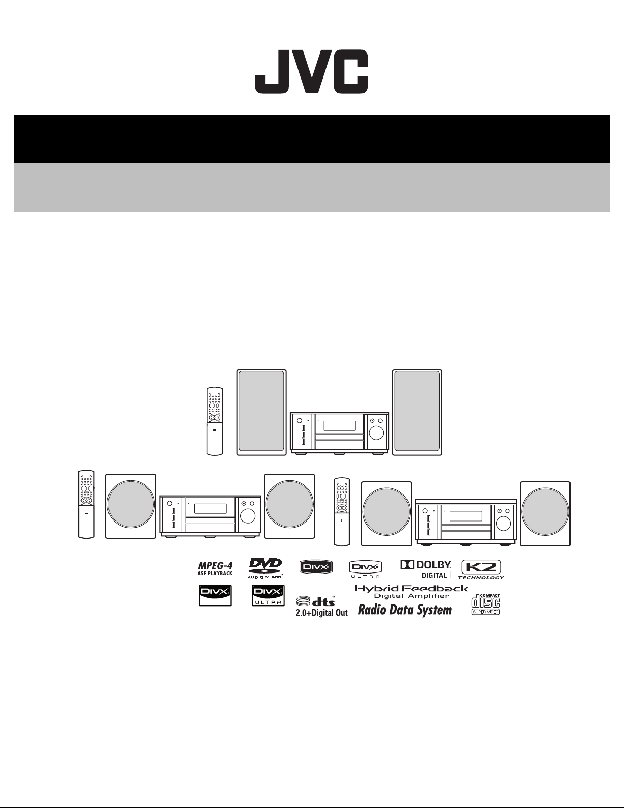
SERVICE MANUAL
COMPACT COMPONENT SYSTEM
MB596<Rev.004>20116SERVICE MANUAL
EX-A3A, EX-A3B, EX-A3E, EX-A3EN,
EX-A3EV, EX-A3UB, EX-A3UJ,
EX-A3US, EX-A3UW, EX-AR3LTDUT,
EX-AR3UF, EX-AR5UF, EX-BR3UF
EX-AR5
EX-AR3
EX-BR3
SP-EXA3
SP-EXBR3
COPYRIGHT © 2011 Victor Company of Japan, Limited
Lead free solder used in the board (material : Sn-Ag-Cu, melting point : 219 Centigrade)
Lead free solder used in the board (material : Sn-Cu, melting point : 230 Centigrade)
CA-EXA3
CA-EXBR3
SP-EXA3
SP-EXBR3
(EX-AR5/BR3)(EX-AR5/BR3)
CA-EXAR5 SP-EXAR5SP-EXAR5
EX-AR3LTD
CA-AR3LTD SP-AR3LTD SP-AR3LTD
(Europe only)
TABLE OF CONTENTS
1 PRECAUTION. . . . . . . . . . . . . . . . . . . . . . . . . . . . . . . . . . . . . . . . . . . . . . . . . . . . . . . . . . . . . . . . . . . . . . . . . 1-6
2 SPECIFIC SERVICE INSTRUCTIONS . . . . . . . . . . . . . . . . . . . . . . . . . . . . . . . . . . . . . . . . . . . . . . . . . . . . . 1-10
3 DISASSEMBLY . . . . . . . . . . . . . . . . . . . . . . . . . . . . . . . . . . . . . . . . . . . . . . . . . . . . . . . . . . . . . . . . . . . . . . 1-11
4 ADJUSTMENT . . . . . . . . . . . . . . . . . . . . . . . . . . . . . . . . . . . . . . . . . . . . . . . . . . . . . . . . . . . . . . . . . . . . . . . 1-18
5 TROUBLESHOOTING . . . . . . . . . . . . . . . . . . . . . . . . . . . . . . . . . . . . . . . . . . . . . . . . . . . . . . . . . . . . . . . . . 1-21
COPYRIGHT © 2011 Victor Company of Japan, Limited
No.MB596<Rev.004>
2011/6
Page 2

SPECIFICATION
Main unit (CA-EXA3)
Tuner FM frequency 87.50 MHz - 108.00 MHz
AM frequency 522 kHz - 1 629 kHz (for Europe)
531 kHz - 1 710 kHz (for Asia and US military) (9 kHz spacing)
530 kHz - 1 710 kHz (for Asia and US military) (10 kHz spacing)
Terminal (front of the main unit) • USB digital input terminal × 1
• Analog input terminal × 1
Stereo mini jack
• Analog output terminal × 1
Stereo mini jack
• Audio output headphone terminal × 1
Impedance: 16 Ω - 1 kΩ
Terminal for Europe (rear of the main unit) • Component video output terminals (3) × 1
Y: 1.0 Vp-p, sync negative, 75 Ω terminated
PB: 0.7 Vp-p, 75 Ω terminated
PR: 0.7 Vp-p, 75 Ω terminated
• Audio output subwoofer terminal × 1
500 mVrms/10 kΩ
• SCART terminal × 1
• Optical digital output terminal × 1
-23 dBm to -15 dBm
• Optical digital input terminal × 1
-23 dBm to -15 dBm
• AV COMPU LINK terminal × 1 (for future use)
• Audio output terminals (2) × 1
500 mV/47 kΩ
• Audio input terminals (2) × 1
500 mV/47 kΩ
• FM antenna terminal × 1
• AM antenna terminal × 1
• Audio output speaker terminals (2) × 2
Output power: 80 W (40 W + 40 W) at 4 Ω (1 kHz/10 % THD)
Impedance: 4 Ω - 16 Ω
Terminal for Asia and US military (rear of the main unit) • Composite video output terminal × 1
Y: 1.0 Vp-p, sync negative, 75 Ω terminated
• S-video output terminal × 1
Y: 1.0 Vp-p, sync negative, 75 Ω terminated
C: 0.286 Vp-p, sync negative, 75 Ω terminated
• Component video output terminals (3) × 1
Y: 1.0 Vp-p, sync negative, 75 Ω terminated
PB: 0.7 Vp-p, 75 Ω terminated
PR: 0.7 Vp-p, 75 Ω terminated
• Audio output subwoofer terminal × 1
500 mVrms/10 kΩ
• Optical digital output terminal × 1
-23 dBm to -15 dBm
• Optical digital input terminal × 1
-23 dBm to -15 dBm
• AV COMPU LINK terminal × 1
• Audio output terminals (2) × 1
500 mV/47 kΩ
• Audio input terminals (2) × 1
500 mV/47 kΩ
• FM antenna terminal × 1
• AM antenna terminal × 1
• Audio output speaker terminals (2) × 2
Impedance: 4 Ω - 16 Ω
1-2 (No.MB596<Rev.004>)
Page 3
USB Compatible with USB 2.0 Full-Speed
Compatible device : USB mass storage class device
Compatible file system : FAT16, FAT32
USB output power : Max. 5 V/500 mA
General Power source (Europe) AC 230 V , 50 Hz
Power source (Australia) AC 240 V , 50 Hz
Power source (Hong Kong) AC 220 V , 50 Hz
Power source (other countries/areas) AC 110 V - 240 V , 50 Hz/60 Hz
Power consumption (in operation) 28 W
Power consumption (on standby) 1.0 W
Dimensions (W × H × D) EX-AR3 245.6 mm × 103.8 mm × 283 mm (including projecting parts)
EX-AR3LTD 246 mm × 114 mm × 283 mm (including projecting parts)
Weight EX-AR3 3.8 kg
EX-AR3LTD 4.4kg
Speaker ( SP-EXA3 / SP-AR3LTD )
Type 1-way bass reflex type
Magnetically shielded type
Speaker driver 8.5 cm wood cone
Power handling capacity 40 W
Impedance 4 Ω
Frequency range 55 Hz - 20 kHz
Sound pressure level SP-EXA3 83 dB/W·m
SP-AR3LTD 82 dB/W·m
Dimensions (W × H × D) 120 mm × 161 mm × 266.5 mm (including projecting parts)
Weight (1 unit) SP-EXA3 1.8 kg
SP-AR3LTD 2.0 kg
Designs and specifications are subject to change without notice.
(No.MB596<Rev.004>)1-3
Page 4
Main unit (CA-EXAR5/CA-EXBR3)
Tuner FM frequency 87.50 MHz - 108.00 MHz
AM frequency 531 kHz - 1 710 kHz (9 kHz spacing)
530 kHz - 1 710 kHz (10 kHz spacing)
Terminal (front of the main unit) • USB digital input terminal × 1
• Analog input terminal × 1
Stereo mini jack
• Analog output terminal × 1
Stereo mini jack
• Audio output headphone terminal × 1
Impedance: 16 Ω - 1 kΩ
Terminal (rear of the main unit) • Composite video output terminal × 1
Y: 1.0 Vp-p, sync negative, 75 Ω terminated
• S-video output terminal × 1
Y: 1.0 Vp-p, sync negative, 75 Ω terminated
C: 0.286 Vp-p, sync negative, 75 Ω terminated
• Component video output terminals (3) × 1
Y: 1.0 Vp-p, sync negative, 75 Ω terminated
PB: 0.7 Vp-p, 75 Ω terminated
PR: 0.7 Vp-p, 75 Ω terminated
• Audio output subwoofer terminal × 1
500 mVrms/10 kΩ
• Optical digital output terminal × 1
-23 dBm to -15 dBm
• Optical digital input terminal × 1
-23 dBm to -15 dBm
• AV COMPU LINK terminal × 1
• Audio output terminals (2) × 1
500 mV/47 kΩ
• Audio input terminals (2) × 1
500 mV/47 kΩ
• FM antenna terminal × 1
• AM antenna terminal × 1
• Audio output speaker terminals (2) × 2
Output power: 40 W + 40 W at 4 Ω
Impedance: 4 Ω - 16 Ω
USB Compatible with USB 2.0 Full-Speed
Compatible device : USB mass storage class device
Compatible file system : FAT16, FAT32
USB output power : Max. 5 V/500 mA
General Power source AC 220 V , 50 Hz
Power consumption (in operation) 28 W
Power consumption (on standby) 1.0 W
Dimensions (W × H × D) 246 mm × 104 mm × 283 mm (including projecting parts)
Weight 3.8 kg
1-4 (No.MB596<Rev.004>)
Page 5

Speaker ( SP-EXAR5 )
Type 2-way bass reflex type
Magnetically shielded type
Speaker driver Low: 10.5 cm wood cone
High: 2.0 cm wood cone
Power handling capacity 100 W
Impedance 4 Ω
Frequency range 55 Hz - 50 kHz
Sound pressure level 82 dB/W·m
Dimensions (W × H × D) 149 mm × 262 mm × 249 mm (including projecting parts)
Weight (1 unit) 4.1 kg
Speaker ( SP-EXBR3 )
Type 1-way bass reflex type
Magnetically shielded type
Speaker driver 8.5 cm wood cone
Power handling capacity 40 W
Impedance 4 Ω
Frequency range 55 Hz - 20 kHz
Sound pressure level 82 dB/W·m
Dimensions (W × H × D) 120 mm × 161 mm × 267 mm (including projecting parts)
Weight (1 unit) 2.2 kg
Designs and specifications are subject to change without notice.
(No.MB596<Rev.004>)1-5
Page 6
SECTION 1
PRECAUTION
1.1 Safety Precautions
(1) This design of this product contains special hardware and
many circuits and components specially for safety purposes. For continued protection, no changes should be made
to the original design unless authorized in writing by the
manufacturer. Replacement parts must be identical to
those used in the original circuits. Services should be performed by qualified personnel only.
(2) Alterations of the design or circuitry of the product should
not be made. Any design alterations of the product should
not be made. Any design alterations or additions will void
the manufacturers warranty and will further relieve the
manufacture of responsibility for personal injury or property
damage resulting therefrom.
(3) Many electrical and mechanical parts in the products have
special safety-related characteristics. These characteristics are often not evident from visual inspection nor can the
protection afforded by them necessarily be obtained by using replacement components rated for higher voltage, wattage, etc. Replacement parts which have these special
safety characteristics are identified in the Parts List of Service Manual. Electrical components having such features
are identified by shading on the schematics and by ( ) on
the Parts List in the Service Manual. The use of a substitute
replacement which does not have the same safety characteristics as the recommended replacement parts shown in
the Parts List of Service Manual may create shock, fire, or
other hazards.
(4) The leads in the products are routed and dressed with ties,
clamps, tubings, barriers and the like to be separated from
live parts, high temperature parts, moving parts and/or
sharp edges for the prevention of electric shock and fire
hazard. When service is required, the original lead routing
and dress should be observed, and it should be confirmed
that they have been returned to normal, after reassembling.
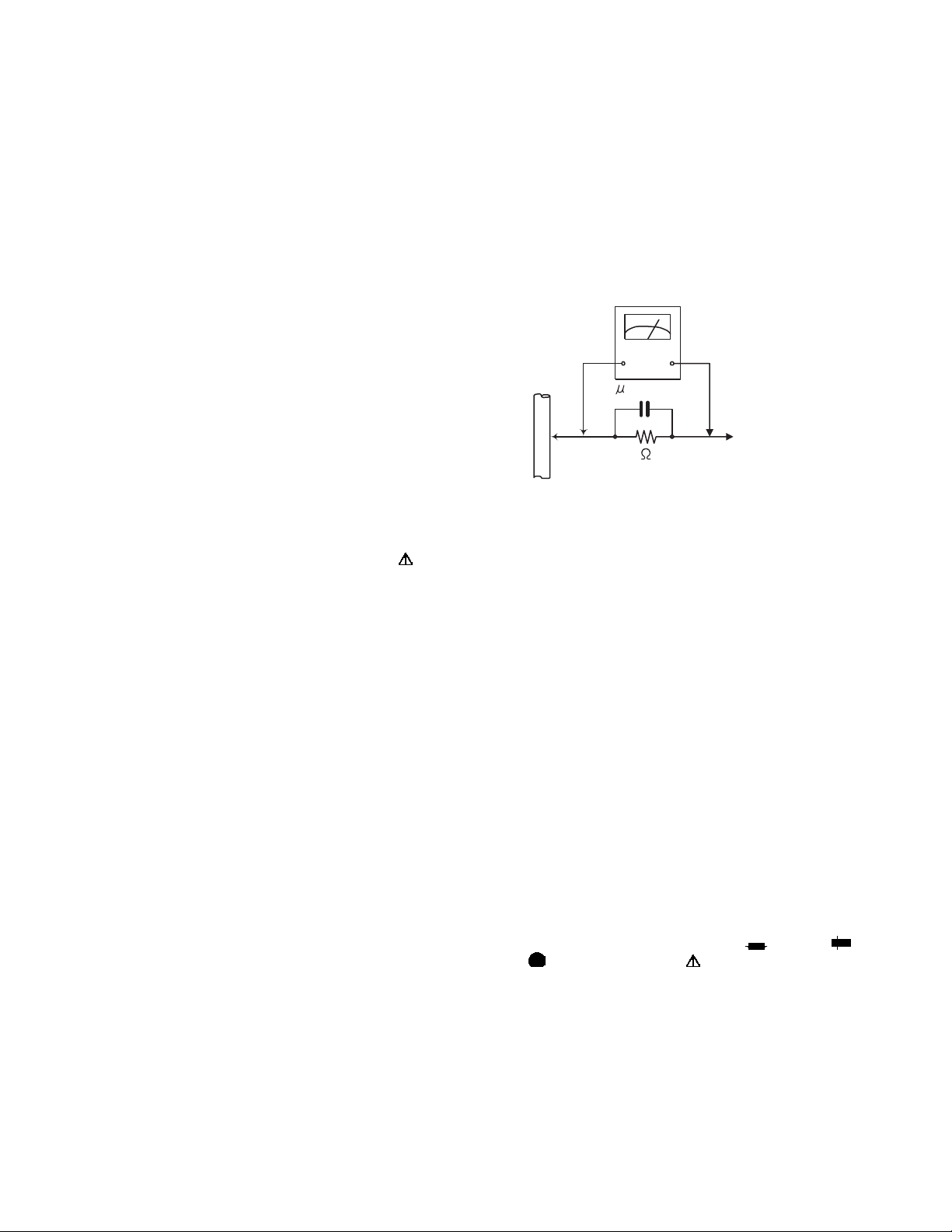
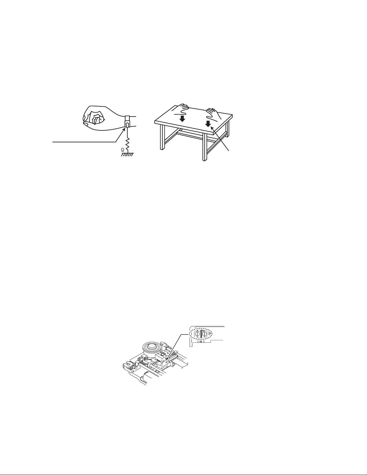
(5) Leakage shock hazard testing
After reassembling the product, always perform an isolation check on the exposed metal parts of the product (antenna terminals, knobs, metal cabinet, screw heads,
headphone jack, control shafts, etc.) to be sure the product
is safe to operate without danger of electrical shock.Do not
use a line isolation transformer during this check.
• Plug the AC line cord directly into the AC outlet. Using a
"Leakage Current Tester", measure the leakage current
from each exposed metal parts of the cabinet, particularly any exposed metal part having a return path to the
chassis, to a known good earth ground. Any leakage current must not exceed 0.5mA AC (r.m.s.).
• Alternate check method
Plug the AC line cord directly into the AC outlet. Use an
AC voltmeter having, 1,000Ω per volt or more sensitivity
in the following manner. Connect a 1,500Ω 10W resistor
paralleled by a 0.15µF AC-type capacitor between an exposed metal part and a known good earth ground.
Measure the AC voltage across the resistor with the AC
voltmeter.
Move the resistor connection to each exposed metal
part, particularly any exposed metal part having a return
path to the chassis, and measure the AC voltage across
the resistor. Now, reverse the plug in the AC outlet and
repeat each measurement. Voltage measured any must
not exceed 0.75 V AC (r.m.s.). This corresponds to 0.5
mA AC (r.m.s.).
AC VOLTMETER
(Having 1000
ohms/volts,
or more sensitivity)
0.15 F AC TYPE
Place this
probe on
1500 10W
Good earth ground
1.2 Warning
(1) This equipment has been designed and manufactured to
meet international safety standards.
(2) It is the legal responsibility of the repairer to ensure that
these safety standards are maintained.
(3) Repairs must be made in accordance with the relevant
safety standards.
(4) It is essential that safety critical components are replaced
by approved parts.
(5) If mains voltage selector is provided, check setting for local
voltage.
1.3 Caution
Burrs formed during molding may be left over on some parts
of the chassis.
Therefore, pay attention to such burrs in the case of preforming repair of this system.
1.4 Critical parts for safety
In regard with component parts appearing on the silk-screen
printed side (parts side) of the PWB diagrams, the parts that are
printed over with black such as the resistor ( ), diode ( )
and ICP ( ) or identified by the " " mark nearby are critical
for safety. When replacing them, be sure to use the parts of the
same type and rating as specified by the manufacturer.
(This regulation dose not Except the J and C version)
each exposed
metal part.
1-6 (No.MB596<Rev.004>)
Page 7

1.5 Safety Precautions (U.K only)
(1) This design of this product contains special hardware and many circuits and components specially for safety purposes. For con-
tinued protection, no changes should be made to the original design unless authorized in writing by the manufacturer. Replacement parts must be identical to those used in the original circuits.
(2) Any unauthorised design alterations or additions will void the manufacturer's guarantee; furthermore the manufacturer cannot
accept responsibility for personal injury or property damage resulting therefrom.
(3) Essential safety critical components are identified by ( ) on the Parts List and by shading on the schematics, and must never
be replaced by parts other than those listed in the manual. Please note however that many electrical and mechanical parts in
the product have special safety related characteristics. These characteristics are often not evident from visual inspection. Parts
other than specified by the manufacturer may not have the same safety characteristics as the recommended replacement parts
shown in the Parts List of the Service Manual and may create shock, fire, or other hazards.
(4) The leads in the products are routed and dressed with ties, clamps, tubings, barriers and the like to be separated from live parts,
high temperature parts, moving parts and/or sharp edges for the prevention of electric shock and fire hazard. When service is
required, the original lead routing and dress should be observed, and it should be confirmed that they have been returned to
normal, after re-assembling.
1.5.1 Warning
(1) Service should be performed by qualified personnel only.
(2) This equipment has been designed and manufactured to meet international safety standards.
(3) It is the legal responsibility of the repairer to ensure that these safety standards are maintained.
(4) Repairs must be made in accordance with the relevant safety standards.
(5) It is essential that safety critical components are replaced by approved parts.
(6) If mains voltage selector is provided, check setting for local voltage.
Burrs formed during molding may be left over on some parts of the chassis. Therefore,
pay attention to such burrs in the case of preforming repair of this system.
(No.MB596<Rev.004>)1-7
Page 8
1.6 Preventing static electricity
Electrostatic discharge (ESD), which occurs when static electricity stored in the body, fabric, etc. is discharged, can destroy the laser
diode in the traverse unit (optical pickup). Take care to prevent this when performing repairs.
1.6.1 Grounding to prevent damage by static electricity
Static electricity in the work area can destroy the optical pickup (laser diode) in devices such as laser products.
Be careful to use proper grounding in the area where repairs are being performed.
(1) Ground the workbench
Ground the workbench by laying conductive material (such as a conductive sheet) or an iron plate over it before placing the
traverse unit (optical pickup) on it.
(2) Ground yourself
Use an anti-static wrist strap to release any static electricity built up in your body.
(caption)
Anti-static wrist strap
1M
Conductive material
(conductive sheet) or iron palate
(3) Handling the optical pickup
• In order to maintain quality during transport and before installation, both sides of the laser diode on the replacement optical
pickup are shorted. After replacement, return the shorted parts to their original condition.
(Refer to the text.)
• Do not use a tester to check the condition of the laser diode in the optical pickup. The tester's internal power source can easily
destroy the laser diode.
1.7 Handling the traverse unit (optical pickup)
(1) Do not subject the traverse unit (optical pickup) to strong shocks, as it is a sensitive, complex unit.
(2) Cut off the shorted part of the flexible cable using nippers, etc. after replacing the optical pickup. For specific details, refer to the
replacement procedure in the text. Remove the anti-static pin when replacing the traverse unit. Be careful not to take too long a
time when attaching it to the connector.
(3) Handle the flexible cable carefully as it may break when subjected to strong force.
(4) I t is not possible to adjust the semi-fixed resistor that adjusts the laser power. Do not turn it.
1.8 Attention when traverse unit is decomposed
*Please refer to "Disassembly method" in the text for the pickup unit.
• Apply solder to the short land sections before the card wire is disconnected from the connecto on the servo board. (If the card wire
is disconnected without applying solder, the pickup may be destroyed by static electricity.)
• In the assembly, be sure to remove solder from the short land sections after connecting the card wire.
Solder short land part
1-8 (No.MB596<Rev.004>)
Page 9
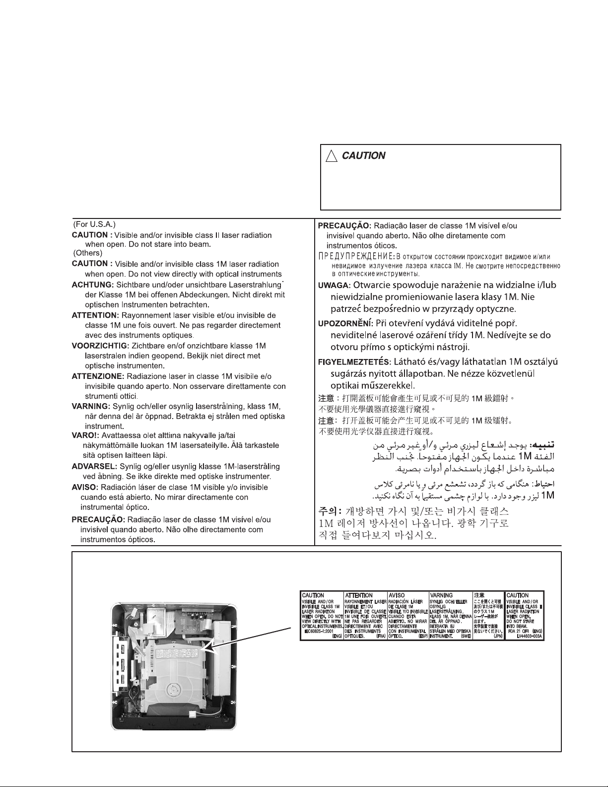
1.9 Important for laser products
1.CLASS 1 LASER PRODUCT
2.CAUTION :
(For U.S.A.) Visible and/or invisible class II laser radiation
when open. Do not stare into beam.
(Others) Visible and/or invisible class 1M laser radiation
when open. Do not view directly with optical instruments.
3.CAUTION : Visible and/or invisible laser radiation when
open and inter lock failed or defeated. Avoid direct
exposure to beam.
4.CAUTION : This laser product uses visible and/or invisible
laser radiation and is equipped with safety switches which
prevent emission of radiation when the drawer is open and
the safety interlocks have failed or are defeated. It is
dangerous to defeat the safety switches.
5.CAUTION : If safety switches malfunction, the laser is able
to function.
6.CAUTION : Use of controls, adjustments or performance of
procedures other than those specified here in may result in
hazardous radiation exposure.
!
Please use enough caution not to
see the beam directly or touch it
in case of an adjustment or operation
check.
REPRODUCTION AND POSITION OF LABELS and PRINT
WARNING LABEL and PRINT
(No.MB596<Rev.004>)1-9
Page 10
SECTION 2
SPECIFIC SERVICE INSTRUCTIONS
2.1 For AL panel
Upper cover, AL SIDEL and AL SIDE R are having 2types.
In the aluminum panel on the TOP COVER, AL SIDE L, and AL SIDE R, there is a combination by two kinds of.
The distinction method is whether the sign of the felt-tipped marker or the line has on the each parts.
The size is different in parts with the sign and parts without signs.
With the commodity that uses parts without the sign, please exchange three parts (TOP COVER, AL SIDE L, and AL SIDE R) for parts
with the sign when you exchange TOP COVER, SIDE L or SIDE R.
Parts number with sign
TOP COVER (for B, E and EN version): LV11346-203A
TOP COVER (for A, US, UB, UW and UJ version): LV11346-202A
AL SIDE L (for B, E and EN version): LV11343-202A
AL SIDE L (for A, US, UB, UW and UJ version): LV11343-201A
AL SIDE R (for all versions): LV11344-201A
AL SIDE L AL SIDE R
markmark
1-10 (No.MB596<Rev.004>)
mark
or
Upper cover
Page 11
SECTION 3
A
DISASSEMBLY
3.1 Main body
3.1.1 Removing the TOP COVER (See Fig.1)
(1) Remove the four screws A attaching the TOP COVER.
(2) Remove the two washers B and two washers C from the
TOP COVER.
CAUTION:
In the aluminum panel on the TOP COVER, AL SIDE L, and
AL SIDE R, there is a combination by two kinds of.
The distinction method is whether the sign of the felt-tipped
marker or the line has adhered like SECTION 2.
The size is different in parts with the sign and parts without
signs.
With the commodity that uses parts without the sign, please
exchange three parts (TOP COVER, AL SIDE L, and AL SIDE
R) for parts with the sign when you exchange TOP COVER,
SIDE L or SIDE R.
Parts number with sign
TOP COVER (for B, E and EN version): LV11346-203A
TOP COVER (for A, US, UB, UW and UJ version):
LV11346-202A
AL SIDE L (for B, E and EN version): LV11343-202A
AL SIDE L (for A, US, UB, UW and UJ version):
LV11343-201A
AL SIDE R (for all versions): LV11344-201A
C
3.1.2 Removing the TOP CHASSIS (See Fig.2, 3)
(1) From the top side of the main body, remove the two screws
D and five screws E attaching the TOP CHASSIS. (See
Fig.2)
E
E
D
CN213
Fig.2
(2) From the back side of the main body, remove the three
screws F attaching the TOP CHASSIS. (See Fig.3)
B
Fig.1
A
F
Fig.3
(3) Disconnect the connector wire from TOP CHASSIS con-
nected to connector CN213
(See Fig.2)
of the Main board assembly.
(No.MB596<Rev.004>)1-11
Page 12
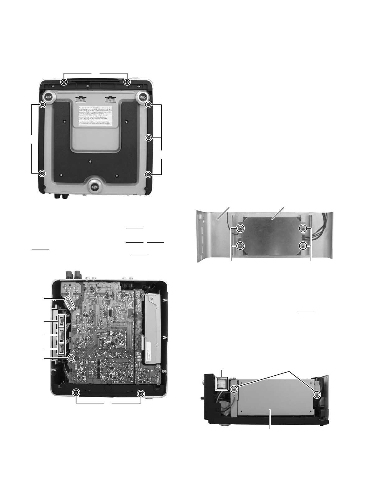
3.1.3 Removing the AL SIDE L and AL SIDE R (See Fig.4, 5)
(1) Remove the volume knob.
(2) From the bottom side of the main body, remove the seven
screws G attaching the AL SIDE L and AL SIDE R. (See
Fig.4)
G
G
G
CAUTION:
In the aluminum panel on the TOP COVER, SIDE L, and SIDE
R, there is a combination by two kinds of.
The distinction method is whether the sign of the felt-tipped
marker or the line has adhered like SECTION 2.
The size is different in parts with the sign and parts without
signs.
With the commodity that uses parts without the sign, please
exchange three parts (TOP COVER, AL SIDE L, and AL SIDE
R) for parts with the sign when you exchange TOP COVER,
SIDE L or SIDE R.
Parts number with sign
TOP COVER (for B, E and EN version):
LV11346-203A
TOP COVER (for A, US, UB, UW and UJ version):
LV11346-202A
AL SIDE L (for B, E and EN version): LV11343-202A
AL SIDE L (for A, US, UB, UW and UJ version):
LV11343-201A
AL SIDE R (for all versions): LV11344-201A
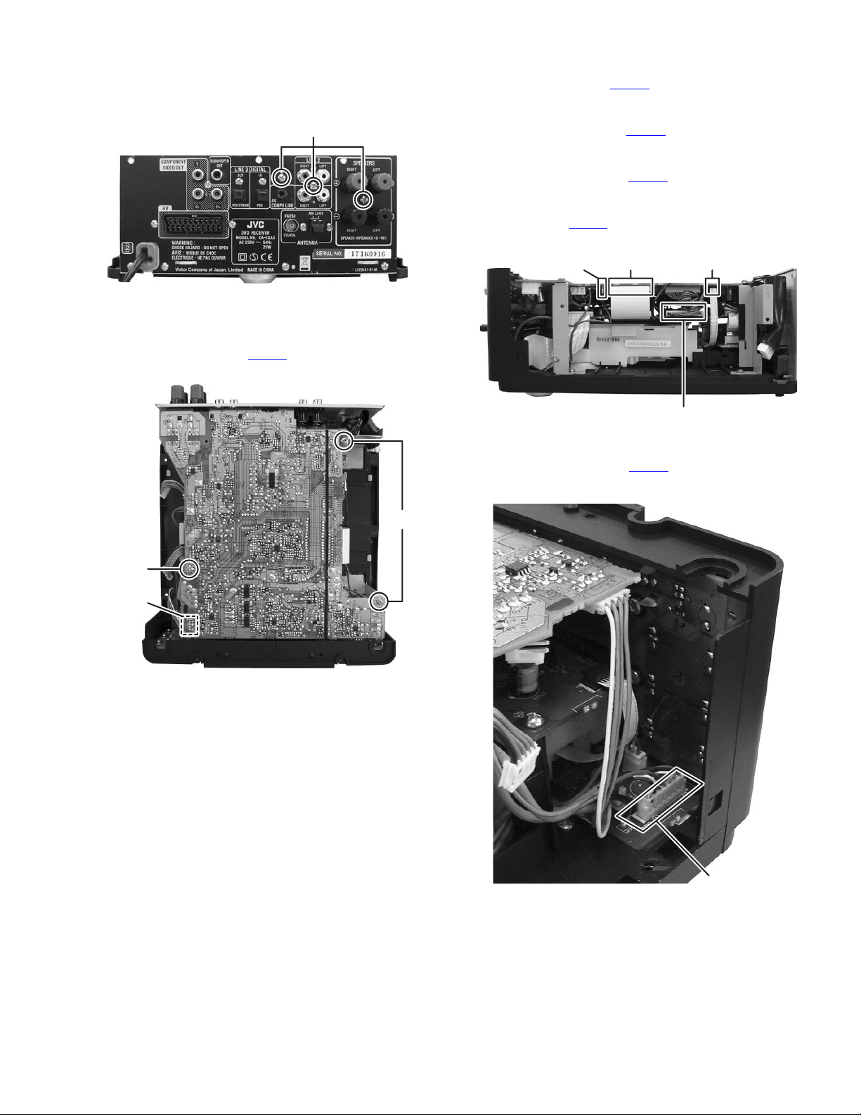
3.1.4 Removing the DEUS board assembly (See Fig.6)
(1) Remove the AL SIDE L.
(2) Remove the four screws J attaching the DEUS board as-
sembly.
Fig.4
(3) From the top side of the main body, remove the two screws
H attaching the AL PANEL L and AL PANEL R. (See Fig.5)
(4) Disconnect the connector wire from CN301
board assembly. (See Fig.5)
(5) Disconnect the connector wires from CN101, CN102 and
of the DEUS board assembly. (See Fig.5)
CN103
(6) Disconnect the earth wire from test point TP202
board assembly. (See Fig.5)
CN301
CN102
CN101
CN103
TP202
of the main
of the main
AL SIDE L DEUS board assembly
JJ
Fig.6
3.1.5 Removing the SWITCHING POWER SUPPLY UNIT
(See Fig.7)
(1) Disconnect the connector wire from SWITCHING POWER
SUPPLY UNIT connected to connector CN201
board assembly.
(2) Remove the two screws K attaching the SWITCHING
POWER SUPPLY UNIT.
(3) Shift the tube from power cord and then disconnect the
power cord from connector of the SWITCHING POWER
SUPPLY UNIT.
CN201
K
of the main
1-12 (No.MB596<Rev.004>)
H
Fig.5
Switching power supply unit
Fig.7
Page 13
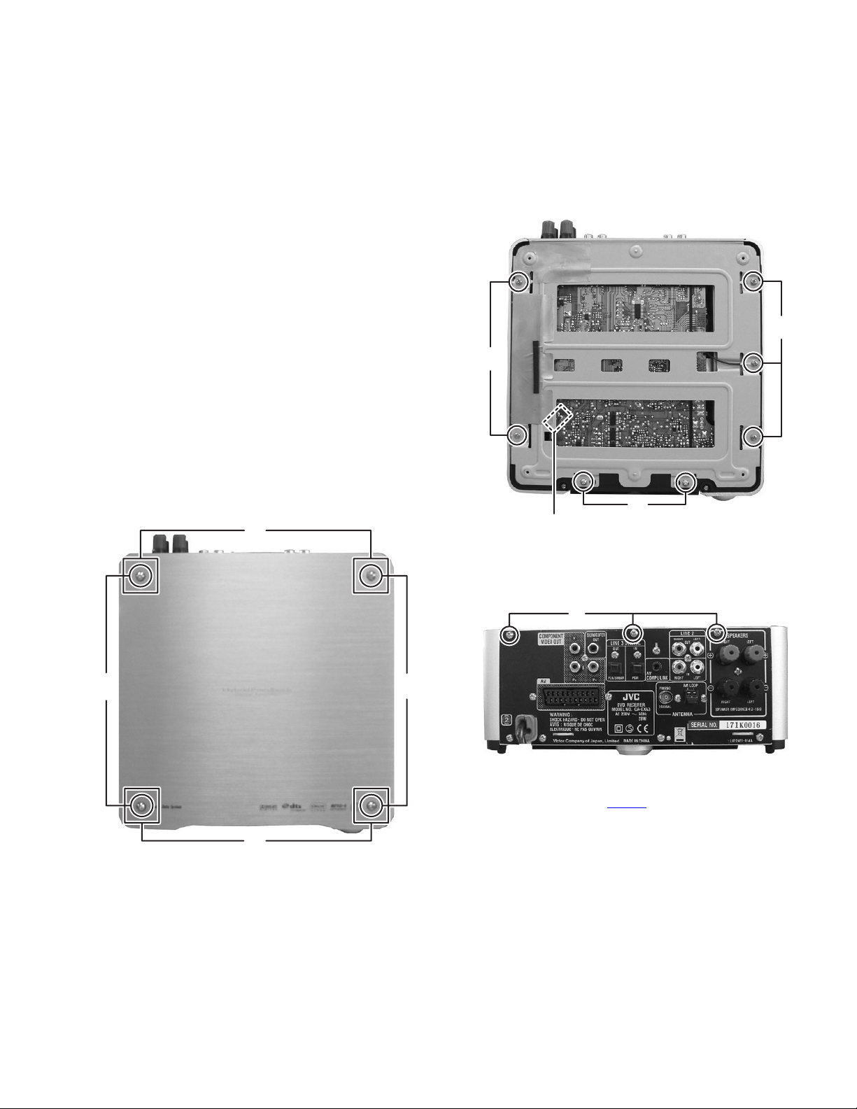
3.1.6 Removing the Main board assembly (See Fig.8 to 12)
(1) From the back sided of the main body, remove the three
screws L attaching the Main board assembly. (See Fig.8)
L
Fig.8
(2) From the top side of the main board, remove the three
screws M attaching the Main board assembly. (See Fig.9)
(3) Disconnect the connector wire from USB board assembly
connected to connector CN208
bly. (See Fig.9)
of the Main board assem-
(4) Disconnect the card wire from Micon board assembly con-
nected to connector CN202 of the Main board assembly.
(See Fig.10)
(5) Disconnect the connector wire from Main board assembly
connected to connector CN714
bly. (See Fig.10)
(6) Disconnect the card wire from DVD mechanism assembly
connected to connector CN206
bly. (See Fig.10)
(7) Disconnect the earth wire from Bottom chassis connected
to test point TP201
Fig.10)
TP201 CN202
(8) Disconnect the connector wire from Main board assembly
connected to connector CN442
bly. (See Fig.11)
of the Main board assembly. (See
Fig.10
of the Micon board assem-
of the Main board assem-
CN206
CN714
of the USB board assem-
M
CN208
M
Fig.9
CN442
Fig.11
(No.MB596<Rev.004>)1-13
Page 14
(9) Lift up the front side of the Main board assembly, and then
pull out the Main board assembly from the Rear panel.
(10) Disconnect the connector wire from Main board assembly
connected to connector CN713 of the Micon board assembly. (See Fig.12)
CN713
Micon board assembly Main board assembly
Fig.12
3.1.7 Removing the Micon board assembly (See Fig.13, 14)
(1) Remove the two screws N attaching the BRACKET A and
BRACKET B. (See Fig.13)
(2) Disconnect the card wire from FL board assembly connect-
ed to connector CN704
Fig.13)
(3) Disconnect the card wire from SCART board assembly
connected to connector CN711
bly. (See Fig.13)
(4) Disconnect the card wire from DVD board assembly con-
nected to connector CN703
assembly. (See Fig.13)
(5) Disconnect the card wire from TUNER PACK connected to
connector CN706
Fig.13)
(6) Disconnect the card wire from Loading switch board as-
sembly connected to connector CN701
assembly. (See Fig.13)
(7) Remove the one screw P and two screws Q attaching the
Micon board assembly. (See Fig.13)
CN703 CN706 CN711
of the Micon board assembly. (See
of the Micon board assem-
and CN708 of the Micon board
of the Micon board assembly. (See
of the Micon board
N
(8) From the back side of main body, remove the three screws
R attaching the Micon board assembly. (See Fig.14)
R
Fig.14
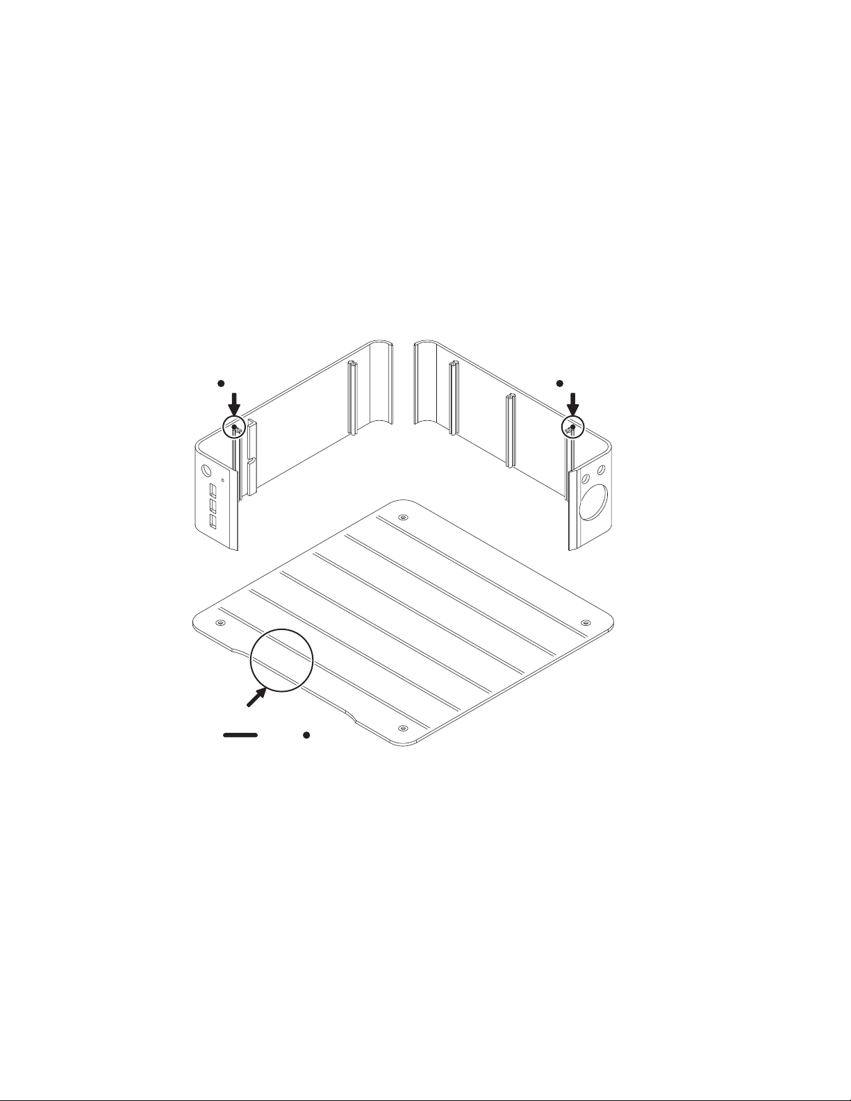
3.1.8 Removing the REAR PANEL (See Fig.15)
(1) From the back side of main board, remove the four screws
S attaching the REAR PANEL.
S
Fig.15
3.1.9 Removing the SCART board assembly (See Fig.16)
(1) Only for European version, remove the two screws T at-
taching the SCART board assembly.
3.1.10 Removing the TUNER PACK (See Fig.16)
(1) Remove the two screws U attaching the TUNER PACK.
TU
Fig.16
3.1.11 Removing the Front panel assembly (See Fig.17, 18)
(1) From the bottom side of main body, remove the three
screws V attaching the Front panel assembly. (See Fig.17)
P
Q
CN701 CN708
1-14 (No.MB596<Rev.004>)
Fig.13
CN704
V
N
Q
Fig.17
Page 15

(2) From the both side of main body, disengage the hooks W
YY
engaged Front panel assembly. (See Fig.18)
hook W
Fig.18
3.1.12 Removing the DVD mechanism assembly (See
Fig.19)
(1) Disconnect the connector wire from DVD board assembly
connected to connector CN441
bly.
(2) Remove the three screws X and two screws Y attaching the
DVD mechanism assembly.
of the USB board assem-
CN441
X
3.2 DVD mechanism assembly
3.2.1 Removing the Clamper base (See Fig.1)
(1) From the top side of DVD mechanism assembly, remove
the two screws A attaching the Clamper base.
(2) Remove the Clamper base.
A
A
3.2.2 Removing the Tray assembly (See Fig.2 to 4)
(1) From the right side of DVD mechanism assembly, press
the slide cam and then pull out the direction of the arrow.
(See Fig.2)
Tray assembly
Clamper base
Fig.1
DVD mechanism assembly
X
Fig.19
3.1.13 Removing the FL board assembly (See Fig.20)
(1) From the back side of front panel assembly, remove the ten
screws Z attaching the FL board assembly.
ZZ ZZ
Fig.20
Slide cam
Fig.2
(2) From the top side of DVD mechanism assembly, remove
the two screws B attaching the Tray assembly. (See Fig.3)
DVD mechanism assembly
Tray assembly
aa
Shaft guide
B
Fig.3
(No.MB596<Rev.004>)1-15
Page 16
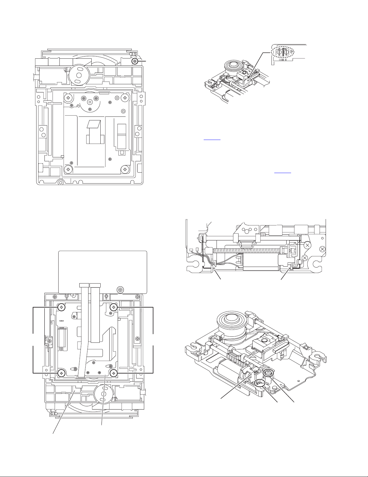
(3) From the bottom side of DVD mechanism assembly, re-
move the one screw C attaching the Tray assembly. (See
Fig.4)
C
Fig.4
(4) Remove the Shaft guide of Tray assembly from hook a of
the DVD mechanism assembly and then take out the Tray
assembly. (See Fig.3)
3.2.3 Removing the Traverse mechanism assembly (See
Fig.5, 6)
(1) From the bottom side of DVD mechanism assembly, re-
move the four screws D attaching the Traverse mechanism
assembly. (See Fig.5)
(2) Solder to short land part b. (See Fig.6)
Solder short land part b
Fig.6
CAUTION:
• Solder the short land section on the DVD pickup before disconnecting the card wire from the connector
on the DVD pickup. If the card wire is discon-
CN101
nected without attaching solders, the pickup may be
destroyed by static electricity.
• When attaching the DVD pickup, be sure to remove
solders from the short land section after connecting
the card wire to the connector CN101
up.
(3) Disconnect the card wire from Traverse mechanism as-
sembly connected to DVD module board.
3.2.4 Removing the DVD pickup (See Fig.7 to 11)
(1) Remove the two Rod spring from the Guide shaft. (See
Fig.7)
on the DVD pick-
DVD module board assembly
CN101CN201
Rod spring Rod spring
Fig.7
(2) Remove the one screw E and F attaching the Spring hold-
er. (See Fig.8)
DD
Spring holder
Traverse mechanism assembly
DVD mechanism assembly
Fig.8
EF
1-16 (No.MB596<Rev.004>)
Fig.5
Page 17
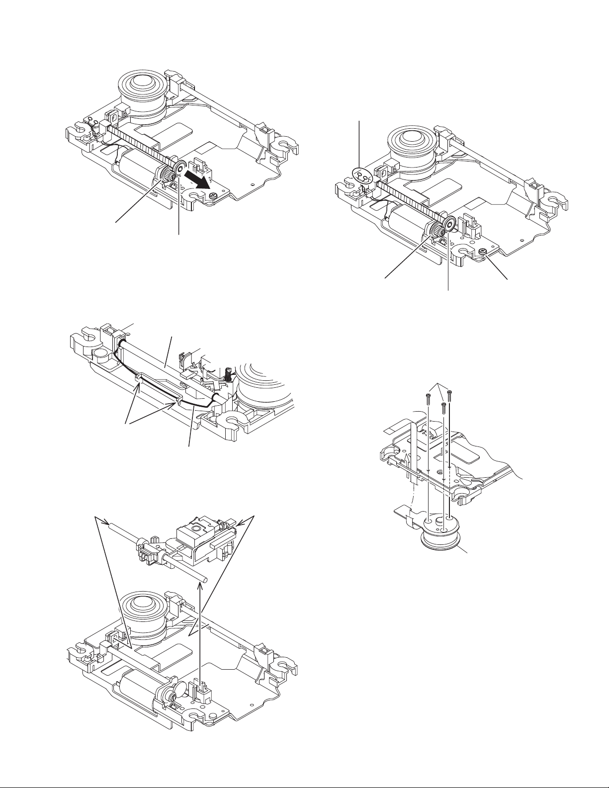
(3) Remove the Lead screw from the Traverse mechanism as-
sembly. (See Fig.9)
Middle gear
Lead screw
Fig.9
CATION:
When remove the Lead screw, do not lost the Middle
gear.
(4) Press and hold the shaft and remove the Bar spring. (See
Fig.10)
(shaft)
3.2.5 Removing the Feed motor assembly (See Fig.12)
(1) Remove the one screw G attaching the Feed motor assem-
bly.
(2) Remove the Feed motor wire from solder part of Spindle
motor board assembly.
Solder part
Middle gear
Lead screw
Fig.12
3.2.6 Removing the Spindle motor assembly (See Fig.13)
From the Spindle motor board assembly, remove the three
screws H attaching the Spindle motor assembly.
G
Hook
(Bar spring)
Fig.10
(5) Remove the Pickup assembly from the Traverse mecha-
nism by order. (See Fig.11)
order 2
order 3
order 1
H
Spindle motor
Fig.13
Fig.11
(No.MB596<Rev.004>)1-17
Page 18
SECTION 4
ADJUSTMENT
4.1 ATTENTION IN SERVICE OF DVD SECTION
(1) When pickup, Flash ROM ,DVD module board were changed, initialize EEPROM by all means.
(2) When full initialization was executed, execute learning with a DVD test disc by all means.
Test disc : VT-501, VT-502
Learning method : It is adjusted automatically by normal playback of a DVD disc.
4.2 DVD TEST MODE
4.2.1 Content of correspondence TEST MODE
(1) Version, Region, Learning status check mode
(2) NORMAL initialize, FULL initialize
(3) Device key write(CPPM, CPRM)
(4) Device key checksum indication mode
(5) Micon version indication mode
(6) FL all on mode
(7) FRONT END check mode
4.2.2 Mode transition
TEST MODE into the press [PLAY key] and [POWER key] together of main body, connect the AC power.
After into the TEST MODE, mode select by [MENU key].
PLAY+POWER+AC
MENU/PL
Version, Region, Learning
status indication mode
STOP key 4sec
>>| key (*1) |<< key(*1)
long press(*1)
Device key
checksum
MENU/PL MENU/PL MENU/PL
Micon version
indication mode
mode
FL all on
mode
FRONT END
check mode
NORMAL
initialize
FULL
initialize
Device key
write
MENU/PL
MENU/PL
(*1):Change from Version, Region, Learning status indication mode to NORMAL initialize, FULL initialize
is effective only main body key.
4.2.3 Processing details
The communication of operated FL(LCD) display and DVD back end microcomputer is shown as follows.
*It is assumed to be OK to differ from the content of the specification because the number of digits is
different according to the set for the FL(LCD) display.
*It is assumed to be OK to differ from the content of the specification because it also has the relation
between arrangement and presence by the set also for the key.
STEP Operation Movement Remarks
1
AC is pulled out, and
double press [PLAY]
and [POWER] key of the
main body
2 Keep step 1, connect AC
Version, Region, Learning
status indication mode
Power on by test mode,
version indication to FL
FL(LCD)indication
132465798
ETSTJC
10 1211 1 3
Version indication
The display to the version code is as
follows.
0x01:JC 0x02:1U 0x03:D 0x04:E
0x05:2U 0x06:3U 0x07:UB 0x08:UT
0x09:4U 0x0a:UY 0x0b:EE 0x0c:UF
Region indication (# part)
Learning from the back end is displayed
in the 11th digit and the 12th digit
of the FL display.
Blank indication at 0xFF
Study status (11th column)
0x07: BCA CHECK OK incomplete
DVD learning incomplete
CD learning incomplete (indication 7)
0x06: BCA CHECK OK incomplete
DVD learning complete
CD learning incomplete (indication 6)
1-18 (No.MB596<Rev.004>)
Page 19

STEP Operation Movement Remarks
Press a [>>|] key of the
main body.
NORMAL initialize
Continue pressing a
[STOP] key of the main
body.(4sec)
FULL initialize
3 Press a [MENU] key of
the remote controller.
4 FL all on mode
Press a [MENU] key of
the remote controller.
5
Press a [MENU] key of
the remote controller.
Press a [1] key of the 10
key on remote controller
Press a [2] key of the 10
key on remote controller
Press a [4] key of the 10
key on remote controller
Press a [5] key of the 10
key on remote controller
Press a [6] key of the 10
key on remote controller
Press a [9] key of the 10
key on remote controller
Press a [10] key of the 10
key on remote controller
Micon version indication
mode
Indicate the version to FL
All FL and all LED to ON
FRONT END check mode
Indicate the front end check
mode to FL
Disc startup and through
playback
(Playback starts from the
start position)
Presence of WOBBLE
0:WOBBLE_NO_CHECK
(un check)
1:WOBBLE_PRESS_MEDIA
(press)
2:WOBBLE_MINUS_MEDIA
(DVD-R/-RW media)
3:WOBBLE_PLUS_MEDIA
(DVD+R/+RW media)
CD_LD lights and laser
current is displayed
DVD_LD lights and laser
current is displayed
DVD_SL x1 jitter
measurement mode
Temperature sensor
(AD value) indication
DVD-DL(parallel, opposite)
Search & jitter
measurement of the
specified position of
DVD-SL
132465798
S
FL(LCD)indication
ETSTJC
ETSTJC
# #U$$$
CEHCK
CEHCK
10 1211 1 3
0x05: BCA CHECK OK complete
DVD learning incomplete
CD learning complete (indication 5)
0x04: BCA CHECK OK incomplete
DVD learning complete
CD leaning complete (indication 4)
0x03: BCA CHECK OK complete
DVD learning incomplete
CD learning incomplete (indication 3)
0x02: BCA CHECK OK complete
DVD learning complete
CD learning incomplete (indication 2)
0x01: BCA CHECK OK complete
DVD learning incomplete
CD learning complete (indication 1)
0x00: BCA CHECK OK complete
DVD learning complete
CD learning complete (indication 0)
(BCA READ CHECK result is only BCA
READ OK, it to complete)
Initialization status (12th column)
0X03: FULL initialize complete
(indication 3)
0x00: NORMAL initialize complete
(indication 0)
0xFF: Initialize incomplete
(blank indication)
: Syscon Version
## : Syscon Romcorr Version
$$$$ : DVD Back end Version
Upper : 0
Lower : WOBBLE detection result
Upper : Laser current value
(BACKUP value,Real measured value)
Lower : 0
Upper : Laser current value
(BACKUP value,Real measured value)
Lower : 0
Upper : Laser current value
(BACKUP value,Real measured value)
Lower : Real measured value
Upper : 0
Lower : Temperature sensor value
Upper : 0x00-0x63(measure at VT501)
Lower : Jitter value
(No.MB596<Rev.004>)1-19
Page 20
STEP Operation Movement Remarks
Press a [ 10] key of the
10key on remote controller
Press a [STOP] key of
the main body or remote
controller
Press a [OPEN/CLOSE]
key of the main body or
remote controller
Press a [PLAY] key of
the main body or remote
controller
Press a [MENU] key of
6 Back to STEP 2
the remote controller
Press a [POWER] key of
the main body
*1 Mode toggle done by press [MENU] key.
*2 STEP2- , STEP3 are only for DVD-AUDIO or VR correspondence model.
BCA READ CHECK
0:During BCA READ
1:BCA READ OK
2:BCA SEEK ERROR
3:BCA READ ERROR
4:SPINUP adjust ERROR
Disc stop, LD-OFF
Tray Open/Close
Disc playback
Release the TEST MODE
FL(LCD)indication
132465798
CEHCK
10 1211 1 3
Upper:Laser current value
(BACKUP value, Real measured value)
Lower:Jitter value
Release at each step
4.3 SYSTEM MICON TEST MODE
"FL & LED all on"
ANY KEY IN
Release FL & LED indication
keep TEST MODE
[STOP]+[POWER]+[1]
or HARD RESET
* TEST MODE
(1) FL & LED all on (Release only indication by Any key)
(2) Clock speed x60 (1min 1sec mode)
(Release the TEST MODE)
TEST MODE should release by detect the HARD RESET or receive the [STOP]+[POWER]+[1].
(CAUTION) Shift to POWER OFF by POWER KEY IN or other, should keep (2).
Normal mode
[STOP]+[POWER]+[1]
TEST MODE
[STOP]+[POWER]+[1]
[STOP]+[POWER]+[10]
[STOP]+[POWER]+[1]
or HARD RESET
MODEL+VERSION CHECK MODE
"SYSTEM MICON & ROMCORR VERSION"
[STOP]+[POWER]+[10]
[STOP]+[POWER]+[10]
"DVD UNIT VERSION+REGION CODE"
[STOP]+[POWER]+[10]
[STOP]+[POWER]+[10]
Normal mode
(mode release)
[STOP]+[POWER]+[2]
[STOP]+[POWER]+[ 10]
"MODEL+VERSION"
Transitory 4 sec
VERSION CHECK MODE 1
VERSION CHECK MODE 2
"BACK END VERSION"
VERSION CHECK MODE 3
VERSION CHECK MODE 4
"DVD MODULE information"
Temp. indication mode
"DVD TEMP."
[STOP]
+
[POWER]
+
[2]
* VERSION CHECK MODE
(1) Indication shift by receive [STOP] + [POWER] + [10]
<SYSTEM MICON & ROMCORR version indication>
=> <BACK END version indication>
=> <DVD UNIT version + REGION CODE indication>
=> <NORMAL indication>
(2) Release the VERSION CHECK MODE by any key
* MODEL + VERSION CHECK MODE
(1) <MODEL + VERSION> indicate transitory 4sec by receive [STOP] + [POWER] + [ 10]
* TEMPERATURE INDICATION MODE
(1) For POWER ON condition, indication shift to <DVD temperature> by receive [STOP] + [POWER] + [2] by
no concern the source.
* DVD information request frequency is 10sec. Except DEVICE KEY, DISC UPGRADE and during
ROMCORR.
(2) <NORMAL indication> to back by receive again [STOP] + [POWER] + [2].
1-20 (No.MB596<Rev.004>)
Page 21

SECTION 5
TROUBLESHOOTING
This service manual does not describe TROUBLESHOOTING.
(No.MB596<Rev.004>)1-21
Page 22

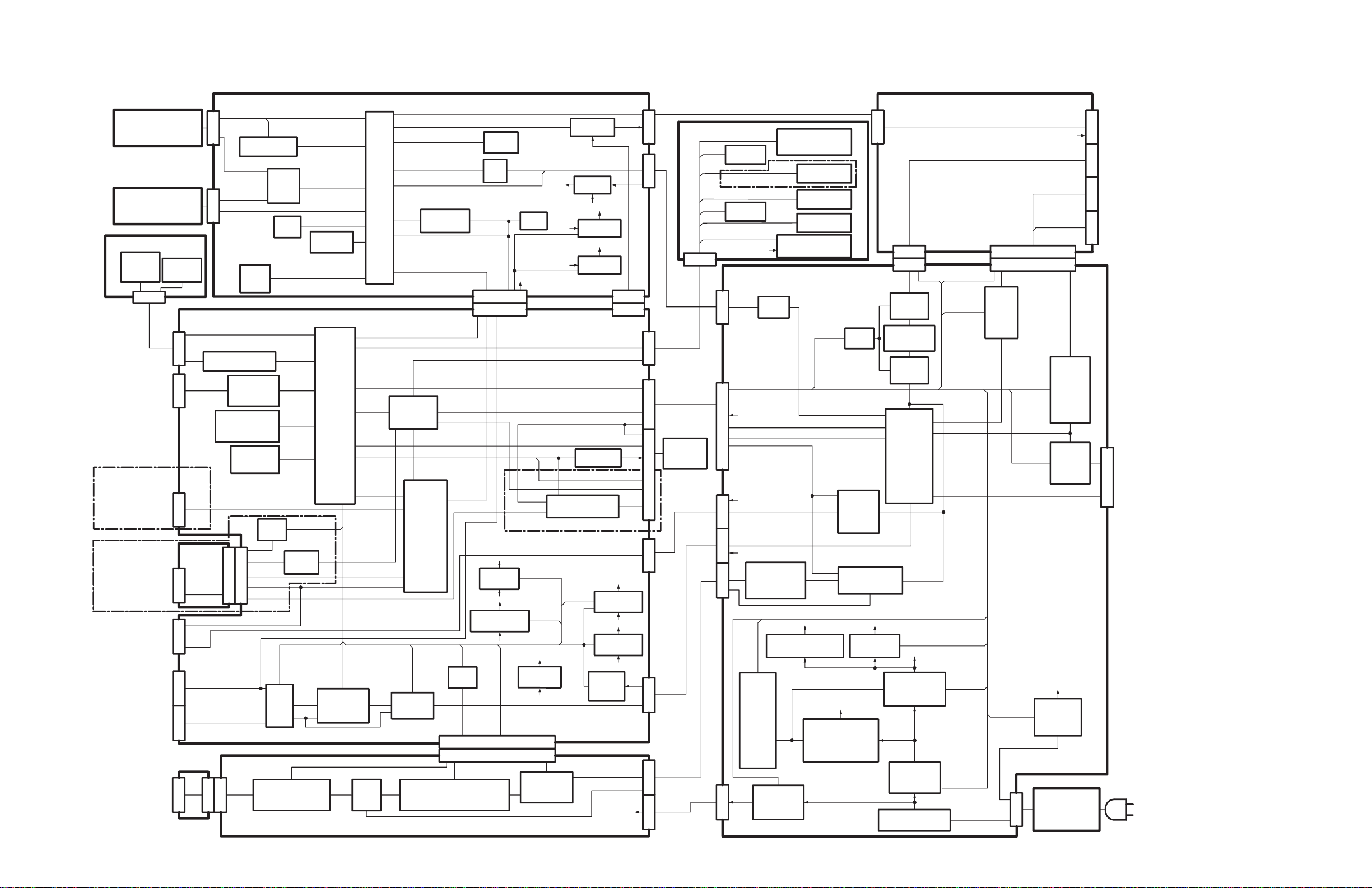
SCHEMATIC DIAGRAMS
65
COMPACT COMPONENT SYSTEM
EX-A3A EX-A3B EX-A3E
EX-A3EN EX-A3EV EX-A3UB
EX-A3UJ EX-A3US EX-A3UW
EX-AR3LTDUT EX-AR3UF EX-AR5UF
EX-BR3UF
(No.MB596<Rev.004>)1/
Page 23
■ PRECAUTIONS ON SCHEMATIC DIAGRAMS
z Due to the improvement in performance, some part numbers shown in the circuit diagrams
may not agree with those indicated in the Parts List.
z The parts numbers, values and rated voltage etc. in the Schematic Diagrams are for
reference only.
z Since the circuit diagrams are standard ones, the circuits and circuit constants may be
subject to change for improvement without any notice.
■ PRECAUTIONS ON PARTS LIST
z
The parts identified by the symbol are critical for safety. Whenever replacing these parts, be sure to
use specified ones to secure the safety.
z
The parts not indicated in this Parts List and those which are filled with lines --- in the Parts No.
columns will not be supplied.
z
P.W. BOARD Ass'y will not be supplied, but those which are filled with the Parts No. in the Parts No.
columns will be supplied.
z
When ordering chips, screws etc., place bulk orders (unit of tens) whenever possible to improve
shipping efficiency.
z
There are cases where the actual implemented parts in the sets and the service parts are different.
When ordering parts, make sure to refer to the Parts List.
■
PRECAUTIONS ON SERVICE
Certain parts of the power circuits and the GNDs differ according to the models. Care must be
taken for the following points as the differences are indicated separately in the LIVE GND ( ) and
the ISOLATED (NEUTRAL) GND ( ).
1. Do not touch the LIVE GND, or do not touch the LIVE GND and the ISOLATED (NEUTRAL)
GND at the same time. It may cause an electric shock.
Before pulling out the chassis or other parts, make sure to pull out the power cord from the
wall outlet first.
2. Do not short circuit between the LIVE GND and ISOLATED (NEUTRAL) GND, or never
measure the LIVE GND and ISOLATED (NEUTRAL) GND at the same time using measuring
instruments (oscilloscope, etc.). It may blow fuses or damage other parts.
■ DEVIATION TOLERANCE RANGE
DEVIATION TOLERANCE RANGE
F G J K M N R H Z P
± 1% ± 2% ± 5% ±10% ±20% ±30%
+30%
-10%
+50%
-10%
+80%
-20%
+100%
-0%
65
(No.MB596<Rev.004>)2/
Page 24
CC LED
Q8201
Q8101
CC LED
Q8001
STANDBY LED
Q7932Q7931
Q7802Q7801
CLOCK SHIFTER
Q7713Q7712
Q7702
BUP/RESET
Q7502Q7501
Q7401
AV
COMPULINK
Q7302Q7301
TU9V REG.
Q7135
Q7035
Q6183
Q6181
Q6002
Q6001
Q5302
Q5301
A10V SW
Q4708
Q4701
Q4373Q4371
Q4341
Q4340
Q4321
Q4313
Q4311
SUB
W.OOFER
MUTE
Q4301
MUTE
Q4292Q4291
Q4241
Q4240
Q4221
Q4202
Q4201
Q4192Q4191
Q4141
Q4140
LINE1OUT
MUTE
Q4121
LINE2OUT
MUTE
Q4102
HP MUTE
Q4101
HP MUTE
Q2901
A10V RIPPLE FILTER
Q2803Q2801
FILAMENT REG.
Q2702Q2701
M9V REG.
Q2601
Q2423
Q2422
Q2421
FLVH SW
Q2411
Q2410Q2409
SAFETY
Q2408Q2403
Q2113Q2111
Q2013Q2011
Q2003Q2001
Q1612Q1611
Q1602Q1601Q1391 Q1305Q1302Q1292Q1291
Q1201
Q1192Q1191
PROTECT
Q1101
S.MUTE
Q801
Q104Q101
LASER DRIVER
IC801
5V REG.
IC801
REMOCON
IC751
TRAY DRIVER
IC705
A5V REG.
IC702
PORT
EXPANDER
IC701
SYSTEM
MICOM
IC701
DAC
IC601
VIDEO
DRIVER
IC555
DAC/LPF
IC554
CC
CONVERTER
IC553
DIR
IC552 IC551
IC511
IC510
EEPROM
IC509
FLASH ROM
IC505
SDRAM
IC502
SELECTOR
IC491
ISOLATION AMP.
IC471
AHB
IC453
RESET
IC452
QP LINK
SW
IC451
FUNCTION
+VOL
IC431
LPF
IC401
HEADPHONE
AMP.
IC305
3.3V REG.
IC303
48MHz
IC302
D1.2V REG.
IC301
DV5
IC295
D3.3V REG.
IC275
DAC5V REG.
IC261
POWER
DOWN SW
IC251
S5V REG.
IC241
V23V REG.
IC233
IC232
IC231
CARRIER
400kHz
/420kHz
CLOCK
GEN.
IC22
1
US4V REG
.
IC202
IC202IC201
SW11V SW REG.
IC201
DRIVER
IC200
US5.4V SW REG.
IC130IC120IC110
AMP.
Used for EX-AR3LTD
RECLED
D8201,
,
,,
,
to
to
,
to
,
,
to
,
,
,
,
,,to
,,
,,
,
,
,,
,
to
,
,
,
,,
to
TRAVERSE
MECHANISM
to
J6006
CN711
CN602
J6002J6001
CN702
CN101
W204
CN102
W205
CN103
CN104
CN301
W209
CN713
J3001
X7411,X7801
J6005
CN1
LOADING
MOTOR
S1
TRAY
SWITCH
D1351
D1352
AHB
CN208
CN443
J4401
CN441
CN811
to
J4101
to
J4402J4403
CN206
J4404
CN801
DI801
FL TUBE
JS801
VOLUME
D8001,
D8101,
S8001,S8101,S8102
S8201 to S8206
KEY MATRIX
W207
CN442
W203
CN714CN706(CN705)
CN202
CN707CN704
CN703
CN801
CN712
CN701
CN708
CN701
CN101 CN201
CN201
X302,
X301
27MHz
TUNER
PACK
PICKUP
UNIT
X2301
X2302
SWITCHING
POWER
SUPPLY
FUNCTION
VS1
VS3
VS1
VS3
Y,C,V
S-VIDEO
/COMPOSITE
VIDEO OUT
Y, CB, CR
Y, CB, CR
Used for Area suffix
A/US/UB/UW/UJ/UT/UF
*CN705;Used for Area suffix B/E/EN/EV
CN706;Used for Other
Used for Area suffix B/E/EN/EV
Used for Area suffix
B/E/EN/EV
V23V
US4V
TUTVL/R
AUX1INDETB
/AHB
AHBCTL
F+/-,VH
MODPRT
AUX1INDET
MODPRT
VMUTE1/2
VIP, S1, S2
CLP/BIAS
UCS, SCS, U2SDT, S2UDT
CLK, CPURST, FDVD
D2IP/LINE2
Y, CB, CR
TVL/R
D2IP/LINE2
FUNCTION
COMP/Y
SWSIG
D2IP/BLK
/DCPRT
MODON, F-SHIFT2
MODSTBY, SMUTE
DVD_DOUT
RX4/DIF2
DVD
DIGITAL
OUTPUT
AUX
DIGITAL
INPUT
DVD_DOUT
DINL/R
DINL/R
BICK
SDTI
LRCK
/C
C
_R
S
T
CC
_C
LK
C
C
_D
AT
A
C
C_
C
S
/DACPDN
DD_DATA
DD_CLK
DD_CS
/DIRPDN, DIRDTO
DIRERF, DIRFS96
DIRAUTO, DD_CS
DD_CLK, DD_DATA
DIN
BCK
LRCK
MCLK
L+/R+/-
A10V
US5.4V
D3.3V
US5.4V
DAC5V
US5.4V
PDOWN
/BUP
/RESET
/QPONSW
/QPDET
QPSENS1/2
L
R
OPENDET, CLOSEDET
LOPEN
LCLOSE
SW11VCTL2
M+/-
AVCI
AVCO
COMPULINK
AV
COMPULINK
/REC1MUTE, /REC2MUTE, REC1LEVEL
/QPONSW, /QPDET, QPSENS1/2
PORTDAT
PORTCLK
STBLED
TU-L/R
TVL/R
TVL/R
FRDS
FRDS
YCMIX
COMPONENT
VIDEO OUT
DVD loading section
V23V
VDD
VDD
/DCPRT
L
R
MODON, F-SHIFT2
MODPRT, MODSTBY
SMUTE
AHBCTL
SW JACK
SCART
TERMINAL
SPEAKER
TERMINAL
D5V
USB
D+/-
DP(D+), DM(D-)
D5V
NEN, NOC
A10V
SAFETY1
FDIN
SAFETY2
FLPOWER
F+/-
A10V
DVD M9V
U
S
5.4
V
U
S
4V
A5.4V
S5V
FDVD
SAFETY4
SAFETY3
FDVD
US5.4V,A5.4V
DVD5.4V,USB5.4V
FLPOWER
L
R
SWSIG
SWSIG
SWSIG
/HPMUTE
OUT1/2
OUT1/2
RDSDA, RDSCL
TUTVL/R
TUTVL/R
/AHB, HPIN, /HPMUTE, F-SHIFT
FLPOWER, SW11VCTL, FDVD
PDOWN, VOLCLK, VOLDATA
VOLCLK, VOLDATA
LINE2
INPUT
LINE2
OUTPUT
LINE1
INPUT
LINE1
OUTPOT
System control and Video output section
REC1
REC2
REC2MUTE
/REC1MUTE
REC1LEVEL
LINE1INL/R
LINE1OUTL/R
LINE1OUTL/R
LINE1INL/R
AUX1INDETB
HPL/R
HPIN
HEADPHONE
Front Input/Output Jack section
FLBK, FLCLK
FLDATA, FLSTB
REM
Front Panel section
VOL+/-
STBLED
CCLED
PIN, KEY1, KEY2
DVDL/R
LRMUTE
FLVH
M11V, V11V
DVDM9V
USB5.4V
US5.4V
A5.4V
DVD5.4V
C1(LINE2), C2(LINE2)
A1(LINE1)
A2(LINE1)
B1(DVD/CD)
B2(DVD/CD)
HPIN
HPL/R
FLBK, FLCLK, FLDATA, FLSTB
VOL+/-, KEY1, KEY2, PIN, REM, CCLED
TUDI, TUDO, TUCK, TUCE
TU9V
FTU
D2V
USB5.4V
D1.2V
DVDPER(FDVD)
CPURST
LD(CD)
LD(DVD)
LPCO1, LPCO2
CDLDCUR
DVDLDCUR
M9V, M5V, S5V, D4V, D2V
P3.3V
S3.3V,P3.3V
A5V
D2V
A6V
DVD servo and DVD system control section
C, Y/G
CB/B, CR/R
Y/COMP
TX(DVD_DOUT), UCS, SCS
U2SDT, S2UDT, UCLK, DAC5OUT(C)
DAC1OUT(Y/G), DAC2OUT(CB/B)
DAC3OUT(CR/R), DAC4OUT(Y/COMP)
BCK, LRCK, AOUT0
DACCK, DAC0CS, DCLK
DDATA, DACPDN
LRMUTE
FAOUTL/R
MA0 to 11, MDQ0 to 15
BA0, BA1, DQM0, DQM1, MCK
NWE, NCSM, NRAS, NCAS
SDA, SCK
EXADT0 to 15, EXDT0 to 15
EXADR16 to 20, NEXCE, NEXWE
NEXOE
TRVSW
SPDRV, TRSDRV
TRDRV, FODRV
FG, SPMUTE
T+/F+/-
FM+/UOUT, VOUT
WOUT, COM
A, B, C, D, E, F, RF+, LPC1, LPC2
SW11VCTL
CARRIER OUT
F-SHIFT
M11V
V11V
SW11V
Digital amplifier section
Main Amp and DC regulator section
20V
FLVH
35V
AC IN
Block diagram
COMP/Y
created date:2011-06-09No.MB596
65
(No.MB596<Rev.004>)3/
Page 25
TO SW POWER MODULE
0V
8.9V
0V0V5.6V
5.7V
0V
27.7V
0V
5.7V
5.7V0V0V
10.8V
20V
7.4V
4.0V
3.2V
3.2V
0V
3.1V
3.2V
3.2V
0.2V0V0V
0.4V
5.6V
0.3V
2.7V
22.9V0V0.1V
5.6V0V4.5V0V0V
4.5V
7.4V
4.2V
4.2V
2.1V
4.2V
4.2V
2.1V
2.1V
0V
2.1V
2.1V
4.2V
7.4V
4.2V
4.2V
0V
0V
4.2V
2.1V
2.1V
2.1V2.1V
4.2V
0V
27.6V
27.7V
27.7V
0V
20.6V
0V
47K
-
4.7K
10K
47K
4.7K
22K
47K
47K
22K
RT1P140C
RT1N241C
RT1N441C
RT1P441C
DGND
DGND
DGND
420kHz400kHz
LVS10550554.cir/002.shtL:/73087/EX-A3/EX-A3.sdm
0V
QPSENS2
/QPONSW
TUTVL
SWSIG
TUTVR
AGND
AGND
US4V
FDVD
QPSENS1
AUX1INDETB
V23V
SWGND
SAFETY3
REC1LEVEL
HPIN
F-SHIFT
VOLCK
PDOWN
/HPMUTE
VOLDATA
/QPDET
SW11VCTL
/REC2MUTE
/AHB
DVDM9V
V11V
USB5.4V
K2GND
MGND
FLVH
10.8V
10.8V 10.2V
A10V RIPPLE FILTER
μ
M9V REG
8.9V
10.8V
2.7V
3.2V
10.3V
US5.4V
NOTES
μ
μ
μ
Ω
(V).
VOLTAGE
F)/RATED
(
CAPACITANCE
OFFORM
THE
INSHOWNARE
E.CAPACITORS
ALL
H(m=mH).
IN
ARE
VALUES
INDUCTANCE
ALL
F(P=pF).
IN
ARE
VALUES
CAPACITANCE
ALL
CAPACITOR.
MYLARORCAPACITOR
CERAMIC
ARE
CAPACITORS
ALL
).
OHM(
IN
ARE
VALUES
RESISTANCEALL
SPECIFIED.OTHERWISE
2.UNLESS
MODESTOPCDCONDITION-
SIGNAL.
INPUTWITHOUT
OSCILLOSCOPE
OR
METER
VOLT
DIGITAL
A WITHDC-MEASURED
ARE1.VOLTAGES
0V
0.6V
1.8V
10.3V
10.9V
20.4V
18.1V
20.5V
18.1V
18.2V
0V
16.2V
2.2V
1.8V
20.7V
0V
2.2V0.7V
2.1V
4.2V
2.1V
2.1V
4.2V
2.1V
0V
2.1V
2.1V
4.2V
2.1V
2.1V
4.2V
0.6V
0V
0V
0V
0V
19.9V
19.9V
5.0V
20.5V
2.2V
0V
15.3V
4.9V
1.9V
17.8V
2.2V
17.6V
20.4V
20.4V
17.5V
5.7V
0V
1.9V
0.6V
5.6V
19.8V
2.7V
3.2V
7.5V
43.8V
27.6V
44.6V
0V
0V
3.2V
0V
20.5V
20.6V
20.5V
0V
34.6V
20.5V
20.5V
20.5V
34.7V
0V
0V
20.5V
0V
RT1P431C
R2R1
44V
R2R1
R2
R2
R1
PGND
VDD
M11V
DVD5.4V
LVB10733-A1
R1
US5.4V
A5.4V
VDD
PGND
FLPOWER
GND
GND
20V
35V
DVD M9V
US5.4V
SW11V
CARRIER
/REC1MUTE
SW11V SW REG
100KHZ
CARRIER OUT
SW11V OUT
US5.4V SW REG
GND
PDOWN
AGND
SW11V
US4V
US4V
QPSENS2
QPSENS2
QPONSW
REC1LEVEL
REC1LEVEL
QPSENS1
QPDET
QPSENS1
QPONSW
QPDET
AUX1INDETB
AUX1INDETB
REC1MUTE
REC1MUTE
REC2MUTE
REC2MUTE
5.4V
VOLDATA
HPIN
SWSIG
SWSIG
F-SHIFT
FDVD
SW11VCTL
PDOWN
TUTVL
A10V
FDVD
HPMUTE
SAFETY3SAFETY3
VOLDATA
VOLCK
HPMUTE
AHB
HPIN
TUTVL
VOLCK
TUTVR
FLPOWER
FLPOWER
SW11VCTL
TUTVR
AHB
SAFETY3
GND
US4V
QPSENS2
REC1LEVEL
QPDET
QPONSW
QPSENS1
AUX1INDETB
REC1MUTE
REC2MUTE
SWSIG
SW11V
AGND
AHB
TUTVL
TUTVR
A10V
VOLDATA
VOLCK
HPMUTE
HPIN
5.4V
!
必ず指定の部品をご使用ください。
交換する場合は、安全および性能維持のため
印の部品は、安全上重要な部品です。!
!
!
!
!
C2411
NI
RT1N241C-X
Q2601
R2603
10K
R2602
10K
R2601
10K
W5
W4
WC202
R2302
1K
C2408
NI
C2703
4.7/50
R2119
2.2K
QUB038-20PPPP-E
W3
WW3
C2901
47/50
2SC3661-X
Q2901
R2901
470
C2902
0.001
C2335
10/50
R2332
1M
QAX0735-001
X2302
C2332
470P
QAX0734-001
X2301
C2334
470P
R2333
5.6k
R2334
5.6k
C2333
470P
C2331
470P
R2331
1M
C2114
0.047
C2014
0.033
1/4W
R2012
680
R2701
470
R2702
2.2K
2SC3928A/QR/-X
Q2702
C2701
0.01
KTB772/Y/
Q2701
MTZJ6.2C-T2
D2701
RT1N441C-X
Q2410
MA111-X
D2303
R2441
47
MA111-X
D2408
2SC3928A/QR/-X
Q2403
R2425
2.2K
RT1P140C-X
Q2423
1/2W
FR
R2424
47
C2424
0.1/50
C2410
0.047
C2423
22/50
TP201
TP202
WW1
WW2
QUB032-22PPPP-E
W1
QUB030-19PPPP-E
W2
C2702
47/25
R2443
68K
MTZJ15B-T2
D2403
MTZJ15B-T2
D2406
RT1P431C-X
Q2409
R2107
39K
R2019
5.6K
R2008
12K
MA111-X
D2015
C2409
47/50
UDZW27B-X
D2421
R2405
10K
MTZJ8.2B-T2
D2405
R2444
10K
R2316
47K
C2304
330P
R2417
4.3K
R2106
22K
R2448
10K
R2449
10K
C2422
22/50
R2422
10K
R2423
2.7K
R2421
27K
2SC3928A/QR/-X
Q2422
KTA1267/YG/-T
Q2421
R2317
10K
R2446
4.7K
R2445
22K
R2010
1K
R2108
NI
D2116
NI
R2412
10K
2SA1530A/QR/-X
Q2411
C2404 8200/25
RT1P441C-X
Q2408
C2407 47/50
R2404
10K
R2403
56k
R2442
10K
R2315
18K
R2416
1K
C2421
220/25
R2303
100
MTZJ4.3B-T2
D2301
C2302
0.068
/1CLR
1
1D
2
1CK
3
/1PR
4
1Q
5
/1Q
6
GND7/2Q
8
2Q
9
/2PR
10
2CK
11
2D
12
/2CLR
13
VDD
14
SN74HC74ANS-X
IC231
C2104
4.7/50
R2104
3.3K
R2105
10K
C2103
0.0022
R2114
2.2K
2SA1530A/QR/-X
Q2112
R2115
10
C2111
0.1/50
R2118
2.2K
R2116
220
2SC3928A/QR/-X
Q2113
R2117
2.2K
C2113
0.01
MTZJ10B-T2
D2114
C2112
470/16
RB161L-40-X
D2113
L2101
47
2SC3928A/QR/-X
Q2111
R2113
2.2K
WC201
C2004
10/50
R2004
12K
2SC3928A/QR/-X
Q2003
R2006
10K
R2005
10K
C2003
0.0015
C2002
470P
2SC3928A/QR/-X
Q2002
R2001
2.2M
R2002
22K
2SA1530A/QR/-X
Q2001
MA111-X
D2001
R2003
100
C2001
0.068
R2014
2.2K
C2405
NI
2SA1530A/QR/-X
Q2012
R2015
10
C2011
0.1/50
R2018
150
R2016
220
2SC3928A/QR/-X
Q2013
R2017
2.2K
C2013
0.01
MTZJ4.7C-T2
D2014
1W
MF
R2411
0.47
QEZ0654-477Z
C2012
470/10
RB050L-40-X
D2013
QQLZ037-470
L2001
47
2SC3928A/QR/-X
Q2011
R2013
2.2K
R2007
47K
2 36 8
1
S
4
G
5
D
RSS090P03-X
IC261
7
432
1
QJK050-040604-E
W204
2
1
QGA3901F1-02
CN213
1514131211
10
987654321
QJK055-150800-E
W203
3
2
1
W212
252423222120191817161514131211
10
987654321
QGF1205F2-25
CN202
14
12
13
11
SN74LV00ANS-X
IC233
2
1
3
IC233
5
4
6
IC233
7
10
9
8
IC233
4
S
3
G
1
D
RSQ035P03-W
IC201
4
S
3
G
1
D
RSQ035P03-W
IC200
3
2
1
QJL005-031503-E
W211
SGD
RSS090N03-X
IC241
43
IC232
89
IC232
10 11
SN74HCU04ANS-X
IC232
12 13
65
IC232
14
7
21
SN74HCU04ANS-X
IC232
4
3
2
1
QGA3901C1-04
CN201
1
3
2
UPC393G2-WE
IC202
+
-
8
4
7
5
6
UPC393G2-WE
IC202
+
-
<Power section (Except EX-AR3LTDUT/AR3UF/AR5UF/BR3UF)>
/AR5UF/BR3UF)
(Except EX-AR3LTDUT/AR3UF
To Main section
(Except EX-AR3LTDUT/AR3UF/AR5UF/BR3UF)
To Micom section 1
(Except EX-AR3LTDUT/AR3UF/AR5UF/BR3UF)
To Micom section 1
(Except EX-AR3LTDUT/AR3UF/AR5UF/BR3UF)
To DEUS section 1
created date:2011-06-09No.MB596
65
(No.MB596<Rev.004>)4/
Page 26

5.4V
3.0V
3.0V
3.0V
0V
3.0V
3.0V
3.0V
3.0V
5.0V
3.0V
0V
0V
5.1V
0V
0V
5.1V
3.0V
3.0V
5.0V
0V
0V
5.6V
5.5V
5.5V
3.2V
0V
0V
5.6V
5.0V
5.5V
5.6V
5.6V
0V
5.6V
5.6V
0V
0V 0V
0V
0V 0V
0V
0V 0V
0V
0V 0V
0V
2.6V
0V
0.5V
0V
2.7V
0V
0V
0V
4.7V
0V
4.7V
4.7V
4.7V
4.7V
4.7V
4.7V
4.7V
4.7V
4.7V
0V
9.4V
4.7V
4.7V
4.7V
4.7V
4.7V
4.7V
4.7V
4.7V
0V
4.7V
4.7V
4.7V
4.7V
4.7V
4.7V
4.7V
4.7V
4.7V
4.7V
5.7V
2.5V
2.5V
0V
0.1V
1.4V
5.7V
5.7V0V
0V
0V 0V
0V
10.2V
4.9V
0V
4.9V
0.3V
0V
0V
0V
4.7K
4.7K
4.7K
10K
RR
L
L
R
L
R
LRMUTE
DVDR
DVDL
AGND
5.4V
QP LINK
QP LINK SW
LINE2OUT
AGND
DINR
DINL
A10V
LINE1INDET
LINE1INL
AGND
LINE1INR
LINE1OUTL
AGND
LINE1OUTR
SW11V
LPF
AMP
ISOLATION
AHB
FUNCTION+VOL
R
AG
L
HPIN
LVS10550554.cir/001.sht
ALL DIODES ARE 1SS133-T2
LVA10733-A1
μ
μ
μ
Ω
1.1V
10.8V
0V
1.1V
0V
9.3V
1.1V
1.1V
0V
0V
2.2V
2.2V
1.1V
1.1V
0V
9.3V
5.0V
5.0V
9.3V
5.0V
5.0V
4.9V
4.9V
0V
9.2V
4.9V
R2R1
4.9V
0V
RT1P14HC
R2R1
DO VER.
EXCEPT
R2
R2
R1
R1
4.8V
4.8V
4.9V
4.9V
10.2V
0V
0.1V
0.1V
0V
0V
0.1V
0V
0V
9.6V
4.9V
4.8V
4.8V
4.8V
4.8V
4.8V
0V
3.2V
5.7V
5.5V
3.8V
4.4V
9.4V
(V).
0.7V
VOLTAGE
0V
0V
10.8V
10.8V
10.3V
0.7V
0.7V
0V
0V
0V
5.4V
5.4V
F)/RATED(CAPACITANCE
OFFORMTHEINSHOWNAREE.CAPACITORSALL
H(m=mH).INAREVALUESINDUCTANCEALL
F(P=pF).INAREVALUESCAPACITANCEALL
CAPACITOR.
MYLARORCAPACITORCERAMICARECAPACITORSALL
10.3V
5.4V
5.14V
5.4V
5.4V
0.7V
0.7V
0V
0V
0V
0V
0V
4.9V
3.6V
2.4V
4.0V
L
HEADPHONE AMP
RT1P431C
H.P.MUTE
L:/73087/EX-A3/EX-A3.sdm
LINE2IN
VCC
VEE
OUTL
OUTR
VINL
VINRVM2
VM1
GND
VCC
AHBCTL
GND
).OHM(INAREVALUESRESISTANCEALL
L
R
L
SPECIFIED.OTHERWISE2.UNLESS
MODESTOPCDCONDITION-
SIGNAL.INPUTWITHOUTOSCILLOSCOPEOR
METERVOLTDIGITALAWITHDC-MEASUREDARE1.VOLTAGES
NOTES
VEE
VCC
VEE
VCC
REC1LEVEL
QPSENS2
QPSENS2
REC1LEVEL
QPONSW
QPDET
QPSENS1
QPSENS1
QPDET
QPONSW
GND
US4V
QPSENS2
REC1LEVEL
QPONSW
QPDET
QPSENS1
REC1MUTE
REC2MUTE
AUX1INDETB
SWSIG
HPIN
AGND
AHB
TUTVR
TUTVL
VOLDATA
VOLCK
A10V
HPMUTE
5.4V
SW11V
C4991
NI
3
2
1
MA152WA-X
D4321
C4315
0.01
C4332
47/25
R4152
120K
R4252
120K
R4151
100
R4251
100
R4341
5.6K
C4341
22/50
2SA1530A/QR/-X
Q4341
C4374
NI
C4375
NI
R4378
NI
R4377
NI
MTZJ10A-T2
D4351
UDZW3.9B-X
D4311
R4356
NI
R4355
NI
470K
R4711
100K
R4716
100K
R4715
2SC3928A/QR/-X
Q4702
R4712
220K
2SA1530A/QR/-X
Q4701
R4708
22K
C4709
820P
C4135
47/25
R4132
8.2K
R4130
8.2K
R4141
2K
R4241
2K
2SC3661-X
Q4140
R4244
2.2K
2SC3661-X
Q4240
R4144
2.2K
R4602
NI
R4501
220K
R4701
2.2K
R4719
10K
C4708
560P
R4702
470K
R4502
NI
R4707
27K
R4722
100K
C4701
0.1/50
C4702
10P
R4709
51K
R4714
220K
C4704
100/50
R4601
220K
2SA1530A/QR/-X
Q4703
R4705
2.2K
10/50
C4713
2SC3928A/QR/-X
Q4705
MA111-X
D4701
C4712
0.047
C4710
270P
470K
R4713
5.6K
R4725
MA111-X
D4702
2SC3928A/QR/-X
Q4704
2SA1530A/QR/-X
Q4706
C4711
0.033
R4721
10K
1/4W
56
R4710
100K
R4717
MA111-X
D4703
R4724
100K
C4706
10P
2SC3928A/QR/-X
Q4707
R4704
1K
C4707
10/50
R4706
10K
C4705
2.2/50
R4720 220K
R4718
100K
2SA1530A/QR/-X
Q4708
R4723
56K
R4703
12K
C4703
22P
R4142
100K
R4242
100K
R4140 2K
C4340
22/50
R4243
2.2K
2SA1530A/QR/-X
Q4340
2SC3661-X
Q4241
R4240 2K
R4143
2.2K
2SC3661-X
Q4141
R4340
5.6K
C4221
220P
C4121
220P
2SA1530A/QR/-X
Q4321
R4321
5.6K
R4227
2.2K
R4123
100K
2SC3661-X
Q4121
2SC3661-X
Q4221
R4127
2.2K
R4223
100K
R4124 2K
C4321
22/50
R4224 2K
MTZJ5.1A-T2
D4171
R4170
1.5K
C4171
100/16
R4222 100
R4122 100
C4262
4.7/50
C4162
4.7/50
C4360
4.7/50
C4354
NI
C4261
4.7/50
C4161
4.7/50
C4158
4.7/100
C4258
4.7/100
C4157
4.7/100
C4257
4.7/100
VIN11SEL12VIN23SEL24A1(LINE1)5A2(LINE1)6B1(DVD/CD)7B2(DVD/CD)8C1(LINE2)9C2(LINE2)10D1(DIN)11D2(DIN)12E1(TU/TV)13E2(TU/TV)14FILTER15GND
16
CLK
17
DATA
18
VCC
19
CAP
20
OUT221OUT1
22
BOUT2
23
BNF2
24
BOUT1
25
BNF1
26
MOUT2
27
MNF2
28
MOUT1
29
MNF1
30
REC231REC1
32
BD3883FS-X
IC451
NQR0007-002X
K4302
C4226
220P
C4126
220P
C4302
100/16
C4301
47/25
R4301
9.1K
R4302
10K
R4112
3.3K
R4212
3.3K
R4110
1K
R4210
1K
R4101
1K
R4201
1K
2SC3661-X
Q4202
R4102
2.2K
R4202
2.2K
R4203
22
R4103
22
C4201
220/10
C4101
220/10
R4207 4.3K
R4206
47K
C4202
220P
C4203
150P
R4205
10K
R4107
4.3K
R4106
47K
C4102
220P
R4105
10K
C4103
150P
C4104
4.7/50
4321
5678
NJM4565M-WE
IC401
C4303
4.7/50
RT1P431C-X
Q4301
R4211
3.3K
R4111
3.3K
C4204
4.7/50
2SC3661-X
Q4201
2SC3661-X
Q4101
R4314
22K
C4311
NI
C4234
22/50
C4134
22/50
R4238
120K
R4138
120K
R4137
1K
R4237
1K
RT1P14HC-X
Q4312
R4312
1K
2SC3928A/QR/-X
Q4311
2SC3661-X
Q4102
C4105 10/50
R4221
47K
R4121
47K
C4312
10/50
R4313
2.2K
C4205 10/50
1/4W
R4391
120
2SC3661-X
Q4313
R4311
1K
C4391
220/16
C4192
10/63
C4292
10/63
C4191
10/63
C4291
100/16
4 3 2 1
5 6 7 8
BA3121F-X
IC491
FR
1/4W
R4351
33
1/4W
R4371
120
R4375
270
C4373
1/50
R4376
100K
2SC3928A/QR/-X
Q4373
R4372
51K
C4372
10/25
MA111-X
D4371
C4351
100/16
C4371
100/16
R4397
1.2K
C4314
0.1
C4331
100/16
R4315
0
R4181
3.3K
R4177
47K
R4281
3.3K
R4277
47K
R4374
10K
R4373
10K
MTZJ5.1A-T2
D4271
C4305
47/25
2SC3928A/QR/-X
Q4372
2SC3928A/QR/-X
Q4371
R4171
1.8K
R4173
1.8K
R4305
470
1/4W
FR
R4306
4.7
C4172
0.47
R4175
27K
C4175
10/63
2SC3928A/QR/-X
Q4191
R4392
1.5K
R4176
12K
R4174
1.2K
R4179 1K
R4279 1K
R4178
3.3K
R4278
3.3K
C4271
100/16
PP
C4173
0.047
PP
C4174
0.047
R4270
1.5K
R4292
22K
C4392
47/25
R4192
22K
R4172 220K
R4394
15K
R4273
1.8K
PP
C4225
220P
1/4W
R4331
120
PP
C4125
220P
R4226
120K
R4126
120K
R4225
1K
R4125
1K
R4275
27K
R4276
12K
C4275
10/63
R4272 220K
R4274
1.2K
R4395
2.2K
PP
C4274
0.047
C4272
0.47
PP
C4273
0.047
R4271
1.8K
R4396
2.2K
4 3 2 1
5 6 7 8
NJM4580E-X
IC471
2SC3661-X
Q4305
2SA1530A/QR/-X
Q4192
R4354
15K
R4353
15K
C4359
0.047
C4358
0.047
C4357
0.047
2SA1530A/QR/-X
Q4292
C4356
0.047
R4304
10K
R4398
47K
C4156
4.7/50
C4256
4.7/50
C4160
4.7/50
C4260
4.7/50
C4159
4.7/100
C4259
4.7/100
2SC3928A/QR/-X
Q4291
C4352
47/25
C4151
4.7/100
C4251
4.7/100
C4353
NI
R4133
18K
R4233
18K
R4231
1.5K
R4235
10K
R4236
12K
R4131
1.5K
R4135
10K
R4193
2.2K
R4293
2.2K
C4235
47/25
R4191
1K
R4291
1K
R4230
8.2K
4 3 2 1
5 6 7 8
NJM4580E-X
IC431
R4136
12K
R4134
1.1K
PP
C4131
820P
PP
C4231
820P
PP
C4132
470P
PP
C4232
470P
R4232
8.2K
R4234
1.1K
8
7
6
5
3
2
1
WJP0098-001A-E
W207
5
4
3
2
1
QJK050-050600-E
W205
E409182-001SM
EP401
1
3
4
2
6
5
QNN0734-001
J4101
7
5
6
NJM4565M-WE
IC452
+
-
8
413
2
IC452
+
-
4
3
2
1
WJP0095-001A-E
W209
4
3
2
1
QGA2501F1-04
CN208
5
4
3
2
1
QGF1036F2-05
CN206
/AR3UF/AR5UF/BR3UF)
(Except EX-AR3LTDUT
section 1
To CC converter
/AR3UF/AR5UF/BR3UF)
(Except EX-AR3LTDUT
To Power section
/AR3UF/AR5UF/BR3UF)
(Except EX-AR3LTDUT
section 2
To CC converter
/AR3UF/AR5UF/BR3UF)
(Except EX-AR3LTDUT
To DVD section (2/3)
/AR3UF/AR5UF/BR3UF)
(Except EX-AR3LTDUT
To DEUS section 1
<Main section (Except EX-AR3LTDUT/AR3UF/AR5UF/BR3UF)>
/AR3UF/AR5UF/BR3UF)
(Except EX-AR3LTDUT
To Power section
/AR3UF/AR5UF/BR3UF)
(Except EX-AR3LTDUT
To Power section
/AR3UF/AR5UF/BR3UF)
(Except EX-AR3LTDUT
section 2
To CC converter
created date:2011-06-09No.MB596
65
(No.MB596<Rev.004>)5/
Page 27

-
1.6V
0.1V
0.4V
0V
0V
0.3V
0V
0.6V
0.9V
5.0V
4.8V
0V
3.2V
3.2V
0V
3.2V
1.7V
3.3V
4.1V
3.3V
3.3V
8.9V
1.7V
0V
3.3V
0V
0V
3.2V
3.3V
0V
3.2V
3.3V
3.2V
2.8V
3.2V
0V
3.3V
3.3V
3.2V
0V
1.7V
3.2V
1.8V
3.2V
1.7V
3.2V
3.0V
0V
0V
0V
0V
0V
3.3V
0V
0.4V
3.2V
0V
0V
0V
0V
0.7V
0V
0V
0V
0V
3.2V
0V
0V
3.2V
3.2V
0V
0V
3.4V
3.3V
3.3V
3.3V
0V0V0V
0V
3.2V
3.2V
0.3V
3.3V
3.3V0V0V
0V0V3.3V
3.3V
3.2V
3.2V
3.2V
3.2V
3.3V
3.2V
0V
0V
3.3V
0V
2.5V
1.2V
1.3V0V1.2V
1.4V
3.3V
3.2V
2.6V0V3.2V
0.2V
0.4V
1.5V
0V0V0V
0V
3.3V
0.5V
3.2V
0V
0.4V
10.8V
0V
8.9V
0V
0V
5.6V
5.7V
0V
27.7V
0V
5.7V
5.7V
0V
0V
10.8V
3.1V
3.2V
0.2V
0V
0V
4.5V
0V
0V
4.5V
20V
7.4V
4.0V
0.1V
5.6V
0V
0.4V
5.6V
0.3V
2.7V
22.9V
0V
3.2V
3.2V
0V
3.2V
0.6
0
5
0
0
0.6
4
3
2
1
3.3V
3.2V
3.3V
0V
0V
3.2V
0V
5.7V
0V
3.4V
5.0V
3.2V
5.6V
0V
0V
0V
2.0V
0V
3.2V
0V
0V
0V
0V
0V
5.7V
5.7V
0V
0V
0V
3.2V
0V
0V
3.2V
0.4V
3.3V
10.2V
7.9V10.8V
2.7V
3.2V3.2V
2.2V
3.2V0V0V0V3.5V
0V
3.4V
3.2V
3.2V
5.6V
3.5V
0V
0.4V0V3.2V
27.5V
0.1V
0V
3.2V
5.7V
2.2V
(PULL-UP)
(PULL-DOWN)
47K 22K
22K 22K
10K 47K
47K 47K
10K10K
R7214,R7215,R7216
R7114,R7115,R7116
--
-
-
10K
30K
10K
UP,UT
UJ
UW
B,E
EN,EV
EE
R7085
*
*
10K
*
*
*
*
*
*
RT1P44HC
RT1N241C
RT1N144C
RT1N441C
DGND
DGND
DGND
0.4V
SAFETY4
SAFETY5
SAFETY6
*
SMUTE
OPEN-DRAIN
24pin-27pi
n
PULL-UP
LVS10552553555.cir/001.sht
L:/73087/EX-A3/EX-A3.sdm
VER:B/E/EN/EV/EE
EXCEPT:B/E/EN/EV/EE
Ver:B/E/EN/EV/EE
EXCEPT:B/E/EN/EV/EE
4.5V
4.5V
10.2V
4.5V
4.5V
4.5V
0V
0V
3.6V
0V
0V
4.4V
10.2V
4.5V
10.8V
4.5V
SELECTOR
SWVDD
EXPANDER
PORT
S5V REG
SWGND
SWSIG
MGND
K2GND
FLVH
M11V
DVDM9V
V11V
A5.4V
DVD5.4V
USB5.4V
US5.4V
2.6V
5.6V
1.5V
0V
5.7V
3.2V
5.0V
FILAMENT REG.
2.7V
0V
1.0V
5.7V
4.0V
5.7V
US4V REG.
MODSTBY
MODPRT
F-SHIFT
MODON
/DCPRT
RDSDA
RDSCL
FRDS
/RESET
FLMD0
DAC3OUT
DGND
DAC2OUT
DGND
DAC1OUT
DGND
DAC4OUT
S5V
DAC5OUT
D4V
D2V
D2V
TX
MGND
MGND
RX
M5V
M9V
DVDPWR
U2SDT
S2UDT
UCLK
SCS
UCS
CPURST
0.8V
IN2
VCC20VVZ
GND
P2
OUT2
0.6V
VCC1
7.9V
0.6V
0.6V
7.9V
OUT1
0.8V
TRAY DRIVE
IN1
0V
0V
P1
18K
-
10K
-
R2R1R2R1
RT1N141C
R2R2
R1R1
- ----
-
E VER.&UP VER. ONLY
0.7V
0V
0V
0V
3.3V
0V
0V
0V
0V
0V
0V
0V
0V
0.4V
2.8V
2.5V
0V
0V
5.6V
0V
0V
3.3V
2.5V
3.3V
3.2V
0V
0V
0V
(3.3V)
(2.8V)
(10.2V)
(9.0V)(10.8)
0V
0V
10.3V
4.0V
10.8V
μ
μ
μ
Ω
(V).VOLTAGEF)/RATED(CAPACITANCE
OFFORMTHEINSHOWNAREE.CAPACITORSALL
H(m=mH).INAREVALUESINDUCTANCEALL
F(P=pF).INAREVALUESCAPACITANCEALL
CAPACITOR.
MYLARORCAPACITORCERAMICARECAPACITORSALL
).OHM(INAREVALUESRESISTANCEALL
SPECIFIED.OTHERWISE2.UNLESS
MODESTOPCDCONDITION-
SIGNAL.INPUTWITHOUTOSCILLOSCOPEOR
METERVOLTDIGITALAWITHDC-MEASUREDARE1.VOLTAGES
10K
* MARK
30K 10K16K
10K10K
-
DO
R7177
R7277
R7006,R7033
0V
NOTES
0V
NC
RDSDATA
UB,A
US,UF
(4.8V)
(5.1V)
J/C
SYSTEM MICON
AV COMPULINK
LVB10732-A1
DGND
CLOCK SHIFTER
0V
0V
(9.0V)
0V
0V
SI/SO
VDD
DG
US5.4V
SW3.3V
K2GND
DGND
DGND
DGND
DGND
DGND
DGND
K2GND
MODPRT
MODPRT
SMUTE
SAFETY6
V21V
TVR
A.GND
A.GND
A.GND
TVL
US4V
CCLED
YCMIX
SW11VCTL2
TU-L
TU-R
MGND
AVCI
DCPRT
OPENDET
CLOSEDET
AUX1INDET
TUTVR
TUTVL
DVD_DOUT
SAFETY3
TUG
TUG
TUCE TUCE
AUX1INDETB
FLPOWER
US5.4V
US5.4V
TU9V
TUDITUDI
TUCKTUCK
TUDOTUDO
TVR
A.GND
TVL
V11V
V11V
M11V
F+
VH
FTU
QPONSW
AUX1INDET
QPSENS2
QPSENS1
REC1LEVEL
AHB
F-SHIFT
QPSENS2
QPSENS1
REC1LEVEL
F-SHIFT
STBLED
VS3
VS1
FRDS
QPONSW
REC2MUTE
REC1MUTE
TRAYGND
QPDET
SAFETY6
SAFETY6
HPIN
PIN
VOL+
VOL-
S5V
DGND
COMPLNK
V11V
KEY1
C
C
Y/COMP
Y/COMP
Y/G
Y/G
CB/B
CB/B
CR/R
CR/R
SAFETY1
SAFETY1
CLP/BIAS
S1
SAFETY5
DVDM9V
SAFETY4
SAFETY5
SAFETY4
FLCLK
FLSTB
FLBK
FLDATA
KEY2
USB5.4V
DGND
DGND
DGND
DGND
USB5.4V
USB5.4V
USB5.4V
A5.4V
FDVD
FDVD
FDVD
DGND
DVD5.4V
MGND
A5.4V
DVD5.4V
DVDM9V
SAFETY2
F-
F-
SAFETY2
SW11VCTL2
US3.3VB
US3.3VC
VOLDATA
QPDET
FLPOWER
HPMUTE
VOLDATA
VOLCK
PDOWN
SW11VCTL
AHB
FRDS
RDSCL
RDSDA
FDVD
U2SDT
S2UDT
SCLK
SCS
UCS
CPURST
UCS
S2UDT
U2SDT
SCLK
SCS
CPURST
RDSCL
TUCE
TUDO
TUCK
TUDI
FTU
CCLED
CLP/BIAS
D2IP/BLK
VIP
VMUTE1
VMUTE2
S2
DACPDN
CC_RST
CC_CS
CC_CLK
CC_DATA
DIRPDN
DD_CS
DD_CLK
DD_DATA
DIRDTO
FDIN
DIRERF
DIRFS96
AVCO
AVCI
DIRAUTO
MODSTBY
MODON
DCPRT
F-SHIFT2
RDSDA
MODSTBY
F-SHIFT2
MODON
SMUTE
LCLOSE
LOPEN
REM
F+
CC_CLK
DIRFS96
CC_RST
DIRDTO
FDIN
DD_CS
DIRERF
DD_CLK
DD_DATA
DIRAUTO
DIRPDN
CC_CS
CC_DATA
DACPDN
M-
M-
LCLOSE
LOPEN
OPENDET
CLOSEDET
M+
M+
SW11VCTL
FLCLK
REM
FDVD
AVCO
D2IP/BLK
HPMUTE
VMUTE1
STBLED
S1
FLSTB
VOL+
KEY1
PIN
REC1MUTE
SAFETY3
VIP
FLDATA
VOL-
FTU
REC2MUTE
S2
VMUTE2
FLBK
VH
KEY2
HPIN
PDOWN
VOLCK
TVL
A.GND
TVR
K2GND
SWGND
SWSIG
SAFETY1
CB/B
CR/R
Y/G
C
Y/COMP
FDIN
DD_CS
DIRAUTO
CC_RST
CC_CS
CC_CLK
CC_DATA
DIRPDN
DACPDN
DIRERF
DIRFS96
DD_CLK
DD_DATA
DIRDTO
S5V
VS3
V11V
YCMIX
VIP
D2IP/BLK
S1
S2
COMPLNK
VMUTE2
DGND
CLP/BIAS
VS1
VMUTE1
US5.4V
DGND
DVD_DOUT
NQR0389-003XK7066
NQR0389-003X
K7031
QZW0112-002
WC702
QZW0112-002
WC701
R7230
100K
R7211
100K
RT1N241C-X
Q7135
RT1P44HC-X
Q7035
R7235
10K
GND
1
DAT
2
CK
3
Q0
4
Q1
5
Q2
6
Q3
7
Q48Q5
9
Q6
10
Q7
11
Q8
12
Q9
13
Q10
14
Q11
15
VDD
16
BU2090FS-X
IC702
R7183
62K
R7283
33K
NI
D7283NIC7283
UDZW12B-X
D7183
C7912 0.1
C7922 0.1
R7217
10K
R7154
2.2K
R7221
10K
R7382
330
C7153
0.1/16
R7135 NI
R7138 10K
R7142 10K
R7141 10K
R7260 100K
0
R7926
0
R7916
R7127
4.7K
R7125
10K
R7124
100K
R7180
100K
C7307
NI
1/4W
R7931
150
C7931
22/25
R7932
1.5K
C7932
100/10
UDZW4.7B-X
D7931
AIN1AOUT2BOUT3BIN4CONTB5CONTC6VSS
7
CIN
8
COUT9DOUT
10
DIN
11
CONTD
12
CONTA
13
VDD
14
BU4066BCF-X
IC502
R7911
120K
R7921
120K
R7938 100K
R7912 220K
1/4W
R7933
150
R7936
100K
C7921
0.1
R7922 220K
R7913 220K
C7933
10/25
R7934
220K
R7937 10K
C7911
0.1
R7923 220K
R7935 220K
62K
R7925
RT1N441C-X
Q7932
RT1N441C-X
Q7931
R7924
12K
R7914
12K
R7915
62K
47k
R7160
2SA1530A/QR/-X
Q7060
R7121 10K
Eonly
R7216
10K
Eonly
R7215
10K
R7112 47K
C7303
0.1
R7220
10K
R7120 10K
MA111-XD2202
MA111-XD2201
R7117 1K
Eonly
R7115 1K
Eonly
R7116 1K
R7119 10K
Eonly
R7114 1K
R7113 10K
R7122 1K
R7111 10K
R7110 10K
R7159
10K
R7083 2.2K
R7065 2.2K
R7056 2.2K
R7162
10K
R7147 10K
R7148 10K
R7149 10K
C7174
0.1/16
R7182
10K
R7282
2.2K
R2501
27K
R2502
18K
C7210
220P
C7209
22P
C7208
220P
C7207
22P
R7277
*MARK
R7177 *MARK
R7175
10K
R7176
10K
1N4003S-T5
D7022
1N4003S-T5
D7021
1N4003S-T5
D7020
CN
4
GND
3
NC
2
VOUT
1
CONT
5
NC
6
NC
7
VIN
8
MM1595AF-X
IC251
C2503
1/10
C2502
470p
C2501
1/10
33K
R2803
47/16
C2803
KTA1273/Y/-T
Q2801
47/16
C2802
2SC3928A/QR/-X
Q2802
KTA1273/Y/-T
Q2803
2.2K
R2801
750
R2806
4.7/25
C2801
560
R2804
270
R2807
15K
R2802
560
R2805
0.033
C2804
R7502
100
2SC3928A/QR/-X
Q7502
C7501
10/25
C7502
NI
UDZW5.1B-X
D7502
RB551V-30-X
D7501
KTB772/Y/
Q7501
R7501
270
C2201
0.1/16
VIN
5
VOUT
4
NOISE3GND2CONT
1
MM1614AN-X
IC221
C2202
0.01
C2203
1/10
R7061 2.2K
Eonly
R7214
10K
R7020
220
R7222
10K
C7003 0.1/16
C7004
10/25
C7219
1/10
R7024
1K
MA111-X
D7801
R7016
100K
R7011
56K
R7010 100
R7009
1K
R7100 2.2K
R7099 2.2K
R7098 2.2K
R7097 2.2K
R7096 2.2K
R7095 2.2K
R7085 2.2K
R7081 2.2K
Eonly
R7033 2.2K
R7035 2.2K
R7036 2.2K
R7037 2.2K
R7075
2.2K
R7072
2.2K
QAX0922-001
X7411
C7412
12P
C7411
12P
DIRDTO
100
DD_DATA99
DD_CLK98
DD_CS97
/DIRPDN96
CC_DATA95
CC_CLK94
CC_CS93
/CC_RST92
/DACPDN91
S290
S189
/VMUTE288
/VMUTE187
VIP86
D2IP/BLK85
CLP/BIAS84
SAFETY6(US21V)83
SAFETY5(DVDM9V)82
SAFETY4(S5V)81
SAFETY3(OTHER)80
SAFETY2(F+/F-)79
SAFETY1(CC3.3V)78
VERSION77
KEY276
KEY1
75
AVSS
74
AVREF0
73
/CPURST
72
SCS
71
AVREF
70
SCLK
69
U2SDT68S2UDT
67
/AHB66/BUP
65
FDVD
64
UCS
63
HPIN
62
/HPMUTE
61
AUX1INDET
60
/QPDET
59
VOLDATA
58
VOLCK
57
F-SHIFT56PDOWN
55
SW11VCTL
54
EVDD
53
/REM
52
FLPOWER
51
PORTDAT 50
PORTCLK 49
CCLED 48
JOGVOL- 47
JOGVOL+ 46
/PIN 45
CBTEST 44
EVSS 43
OPENDET 42
CLOSEDET 41
LOPEN 40
LCLOSE 39
/DCPRT 38
MODON 37
F-SHIFT2 36
MODPRT 35
MODSTBY 34
RDSDA 33
SMUTE 32
FTU 31
TUDI 30
TUCK 29
TUDO 28
TUCE 27
/+BCTL 26
BEATCUT25XKILL24EVDD23VDD22EVSS21VSS20REGC19X118X217FLMDO16XT115XT214/RESET13FLASH12AVCI11FLSTB10FLCLK9FLBK8FLDATA7RDSCL6AVCO5DIRERF4DIRAUTO3DIRFS962FDIN
1
UPD78F1166GC
IC701
C7806
33P
2SA1530A/QR/-X
Q7701
C7704
0.01
C7504
0.1/16
10987654321
LB1641
IC751
C7503
0.01
UDZW4.7B-X
D7503
C7505
220/16
NQR0251-004X
K7009
R7029 2.2K
R7080 2.2K
R7032
2.2K
R7047 2.2K
R7042 2.2K
R7041 2.2K
R7040 2.2K
R7079 2.2K
C7302 4.7/25
R7302
2.2K
R7301
4.7K
NQR0251-004X
K7007
QQR0621-001Z
K7701
R7403
1K
C7401
330P
R7401
10K
R7405
220
R7801
2.2K
R7802
2.2K
QAX0416-001Z
X7801
C7802
0.001
C7801
0.001
R7804
8.2K
R7803
8.2K
KTC3195/O/-T
Q7802
KTC3195/O/-T
Q7801
C7804
39P
C7805
39P
RT1N144C-X
Q7401
C7803
47P
RB521S-30-X
D7401
R7062 2.2K
C7305
0.0082
C7306
0.0082
KTA1271/OY/-TQ7301
C7301
10/25
R7702
33K
R7704
10K
QQL244K-100Z
L7701
MA111-X
D7711C7711
0.047F/5.5
R7711
330
R7712
10K
C7712
2.2/50
R7051 2.2K
R7054 2.2K
R7055 2.2K
R7050 2.2K
R7049 2.2K
R7048 2.2K
QQR0621-001Z
K7501
RT1N141C-X
Q7712
R7713
NI
R7714
NI
MA111-X
D7713
C7701
4.7/25
MA111-X
D7701
R7715
100K
2SC3928A/QR/-X
Q7713
C7001
100/10
C7002
0.1/16
R7052
2.2K
2SC3928A/QR/-X
Q7302
R7701
100K
2SC3928A/QR/-X
Q7702
R7703
47K
R70711KR706947R706847R706747R7064
2.2K
R70631KR7059 2.2K
R7057 2.2K
R7046 2.2K
R7045 2.2K
R7044 100K
R7039 2.2K
R7038 2.2K
R7716
47K
UDZW10B-X
D7702
UDZW6.2B-XD7302
R7008 100
R7030 2.2K
R7026
10K
R7027
2.2K
R7028
2.2K
R7007
1K
Eonly
R7006 2.2K
R7004 2.2K
R7013
10K
R7005 2.2K
R7001 2.2K
R7002 2.2K
R7093 2.2K
R7092 2.2K
C7213
0.01
R7094 2.2K
R7091 2.2K
R7090 2.2K
R7089 2.2K
R7088 2.2K
R7087 2.2K
R7086 2.2K
MA111-X
D7301
R7034 2.2K
R7084 2.2K
R7082 2.2K
R7003 2.2K
QQL244K-100Z
L7024
R7060 2.2K
R7058 2.2K
R7076 2.2K
R7078 2.2K
7
6
5
4
3
2
1
QGA2501C1-07
CN702
15
14
13
12
11
10
9
8
7
6
5
4
3
2
1
QGA2001F1-15
CN714
25
24
23
22
21
20
19
18
17
16
15
14
13
12
11
10
9
8
7
6
5
4
3
2
1
QGF1205F2-25
CN707
65432
1
QGF1205C2-06
CN710
54321
QGF1036F2-05
CN703
25
24
23
22
21
20
19
18
17
16
15
14
13
12
11
10
9
8
7
6
5
4
3
2
1
QGF1036C2-25
CN708
11
10
9
8
7
6
5
4
3
2
1
QGF1205F2-11
CN706
15
14
13
12
11
10
9
8
7
6
5
4
3
2
1
QGF1205F2-15
CN705
2120191817161514131211
10
987654321
QGF1205F2-21
CN704
1
2
3
4
5
QGF1036F2-05
CN701
<Micom section 1 (Except EX-AR3LTDUT/AR3UF/AR5UF/BR3UF)>
/AR3UF/AR5UF/BR3UF)
(Except EX-AR3LTDUT
To DEUS section 1
/AR3UF/AR5UF/BR3UF)
(Except EX-AR3LTDUT
To Video section 1
/AR3UF/AR5UF/BR3UF)
(Except EX-AR3LTDUT
To CC converter section 1
/AR3UF/AR5UF/BR3UF)
(Except EX-AR3LTDUT
To Video section 1
/AR3UF/AR5UF/BR3UF)
(Except EX-AR3LTDUT
To DVD section (2/3)
(Except EX-AR3LTDUT/AR3UF/AR5UF/BR3UF)
To Micom section 2
/AR3UF/AR5UF/BR3UF)
(Except EX-AR3LTDUT
To Video section 1
/AR3UF/AR5UF/BR3UF)
(Except EX-AR3LTDUT
To Power section
/AR3UF/AR5UF/BR3UF)
(Except EX-AR3LTDUT
To Power section
(Except EX-AR3LTDUT/AR3UF/AR5UF/BR3UF)
To DVD section (3/3)
/AR3UF/AR5UF/BR3UF)
(Except EX-AR3LTDUT
To Loader section
created date:2011-06-09No.MB596
65
(No.MB596<Rev.004>)6/
Page 28
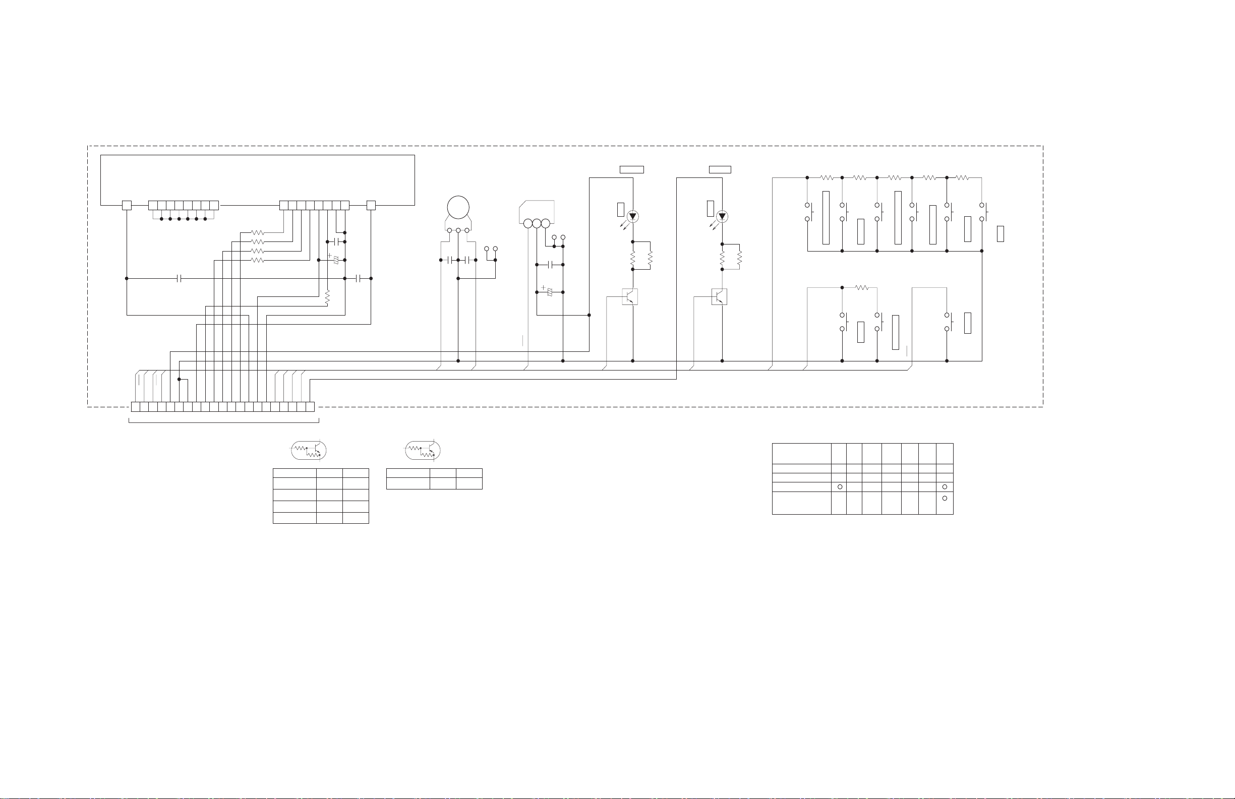
0V
3.6V
0V0V
2.2V
0V
0V
3.5V
3.4V
FL TUBE
2.2V
LVB10733-A2
5.6V
0V
0V
27.6V
3.5V
0.2V
0V
3.2V
0.4V
CC CONVER
EJECT
POWER
F.SKIP
DVD PLAY/PAUSE
B.SKIP
STOP
USB PLAY/PAUSE
FM/AM/LINE
-
(PULL-UP)
(PULL-DOWN)
47K 22K
22K 22K
10K 47K
47K 47K
10K10K
R7214,R7215,R7216
R7114,R7115,R7116
--
-
-
10K
30K
10K
UP,UT
UJ
UW
B,E
EN,EV
EE
R7085
10K
RT1P44HC
RT1N241C
RT1N144C
RT1N441C
18K
-
10K
-
R2R1R2R1
RT1N141C
R2R2
R1R1
- ----
-
μ
μ
μ
Ω
(V).VOLTAGEF)/RATED(CAPACITANCE
OFFORMTHEINSHOWNAREE.CAPACITORSALL
H(m=mH).INAREVALUESINDUCTANCEALL
F(P=pF).INAREVALUESCAPACITANCEALL
CAPACITOR.
MYLARORCAPACITORCERAMICARECAPACITORSALL
).OHM(INAREVALUESRESISTANCEALL
SPECIFIED.OTHERWISE2.UNLESS
MODESTOPCDCONDITION-
SIGNAL.INPUTWITHOUTOSCILLOSCOPEOR
METERVOLTDIGITALAWITHDC-MEASUREDARE1.VOLTAGES
10K
* MARK
30K 10K16K
10K10K
-
DO
R7177
R7277
R7006,R7033
NOTES
UB,A
US,UF
J/C
CCLED
DGND
US5.4V
KEY1
KEY1
REM
REM
PIN
FLVDD
VOL-
VOL-
VOL+
F+
FLGND
US3.3V
KEY2
STBLED
VOL+
PIN
FLCLK
STBLED
FLDATA
CCLED
FLBK
VH
FLSTB
F-
KEY2
RT1N141C-X
Q8101
R8206
3.3K
220
R8102
CCLED
BLUE
SELK6E10C-D-T
D8101
NIR8104
RT1N141C-X
Q8001
180
R8101
STBLED
RED
SLR-343VC/NPQ-T
D8001
NIR8103
C8101
0.01
C8102
22/16
R8004 100
R8205
12K
R8203
3.9K
R8003 2.2K
R8204
6.8K
QSW0683-001Z
S8203
C8003
1
QSW0683-001Z
S8202
R8001
0
QSW0683-001Z
S8201
R8002 2.2K
QSW0683-001Z
S8001
QSW0683-001Z
S8205
R8202
2.7K
R8005 100
R8201
3.3K
C8202
0.1
C8004
1
QSW0683-001Z
S8101
QSW0683-001Z
S8206
C8201
0.1
C8001
0.1/50
C8002
100/16
QSW0683-001Z
S8102
QSW0683-001Z
S8204
321
GP1UE261XKVF
IC801
231
QSW0975-001
JS801
NC11
NC10
NC9
NC8
NC7
NC6
NC5
NC4
LGND33
PGND32
VH31
VDD30
BK29
LAT28
CLK27
SI26
QLF0183-001
DI801
F-1
F+36
21
20
19
18
17
16
15
14
13
12
11
10
9
8765432
1
QGF1205F2-21
CN801
/AR3UF/AR5UF/BR3UF)
(Except EX-AR3LTDUT
To Micom section 1
<Micom section 2 (Except EX-AR3LTDUT/AR3UF/AR5UF/BR3UF)>
created date:2011-06-09No.MB596
65
(No.MB596<Rev.004>)7/
Page 29
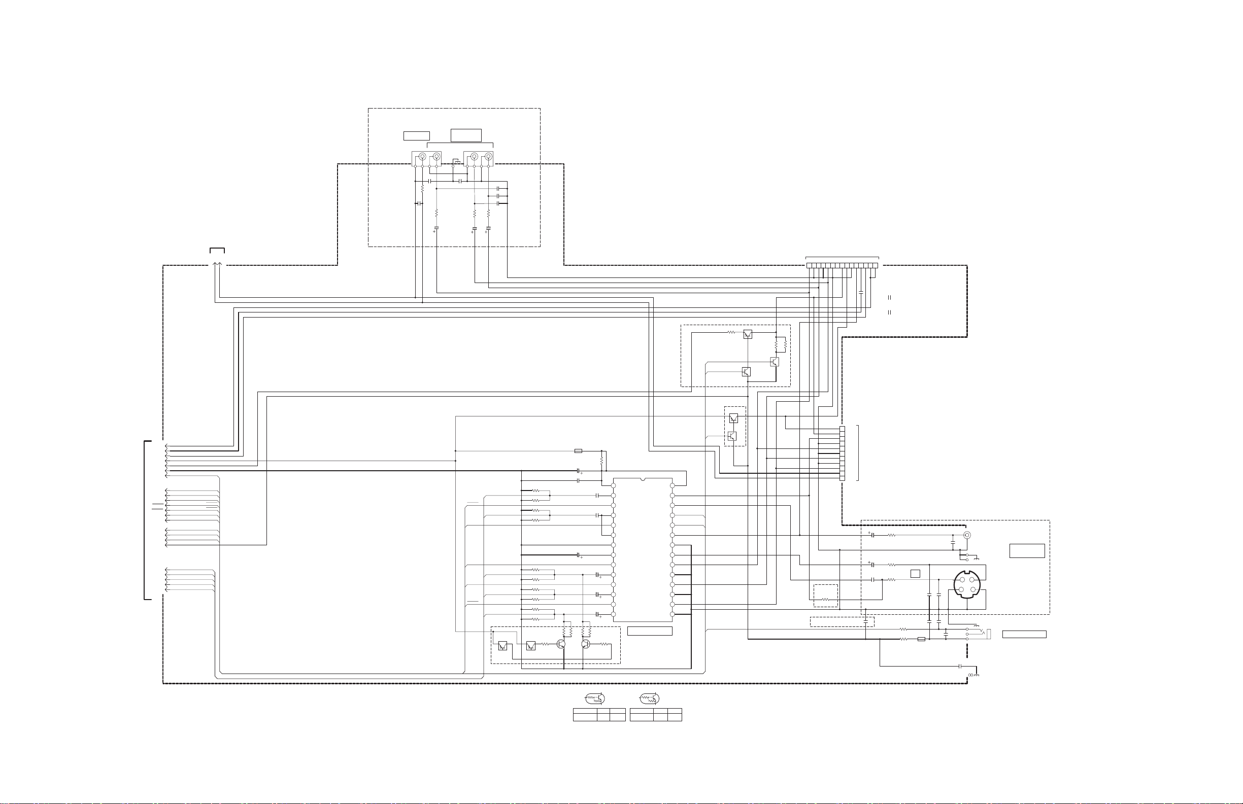
5.0V
0V
0V
0V
0V
10.5V
0V
2.4V
2.5V
0V
2.5V
0V
2.5V
0V
0V
0V
2.4V
5.0V
2.1V
0V
2.5V
0V
10.5V
0V
0V
2.7V
5.0V 5.0V
0V
10K10K47K10K
Ver:B/E/EN/EV/EE
Ver:D
Ver.:B/E/EN/EV/EE/D
LVS10552553555.cir/002.sht
L:/73087/EX-A3/EX-A3.sdm
SW JACK
SW
10.5V
0V
10.5V
1.8V
10.5V
0V
0V
0V
VIDEO DRIVER
2.4V
1.6V
0V
0V
2.4V
2.4V
2.4V
2.4V
NI
2.9V
5.0V
2.9V
0V
5.0V
2.1V
0V
0V
1.6V
0V
0V
2.5V
2.9V
2.4V
2.5V
0V
2.9V
2.4V
0V
2.1V
NOTES
μ
μ
μ
Ω
(V).
VOLTAGE
F)/RATED
(
CAPACITANCE
OFFORM
THE
INSHOWNARE
E.CAPACITORS
ALL
H(m=mH).
IN
ARE
VALUES
INDUCTANCE
ALL
F(P=pF).
IN
ARE
VALUES
CAPACITANCE
ALL
CAPACITOR.
MYLARORCAPACITOR
CERAMIC
ARE
CAPACITORS
ALL
).
OHM(
EXCEPT D Ver.
IN
ARE
VALUES
RESISTANCEALL
SPECIFIED.OTHERWISE
2.UNLESS
MODESTOPCDCONDITION-
SIGNAL.
R2R1
RT1P141C
R2R1
RT1N144C
R2R2
0.5V
0V
1.7V
LVB10732-A1
R1R1
INPUTWITHOUT
OSCILLOSCOPE
OR
METER
VOLT
DIGITAL
A
WITH
DC-MEASURED
ARE
1.VOLTAGES
B/E/EN/EV/EE
EXCEPT
Y
Ver. EXCEPT D
COMPONENT
VIDEO OUT
Y
VIDEO OUT
Cb
Cr
C
S/COMPOSIT
AV COMPULINK
Ver.D
S1
Ver.:B/E/EN/EV/EE
DGND
DGND
DGND
DGND
DGND
TVR
COMP/Y
FUNCTION
FUNCTION
SWGND
SWSIG
YCMIX
YCMIX
S-DCOUT
D2IP/BLK
D2IP/LINE2
D2IP/LINE2
TVG
TVL
CB
CB
CR
CR
Y
Y
VS3
VS1VS1
VMUTE2
CR/R
C
CB/B
Y/G
VS3
VS1
CR/R
CB/B
Y/G
Y/COMP
C
CLP/BIAS
VIP
CLP/BIAS
VIP
COMPLNK
VMUTE1
COMPLNK
S2
D2IP/BLK
Y/COMP S1
S2
VMUTE1
VMUTE2
S1
TVL
TVR
A.GND
SWGND
SWSIG
DGND
DGND
S5V
VMUTE1
COMPLNK
CR/R
CLP/BIAS
VMUTE2
V11V
VS3
VS1
YCMIX
CB/B
Y/G
S2
VIP
Y/COMP
C
D2IP/BLK
S1
NCF21CZ-105X
C9998
NCF21CZ-105X
C9999
C6098
NI
1/10W
R6183
680
RT1N144C-X
Q6002
RT1P141C-X
Q6001
C7308
NI
R6024
100
C6027
0.1
C6029
0.1
1/10W
R6181
680
RT1N144C-X
Q6182
RT1N144C-X
Q6183
RT1P141C-X
Q6181
1/4W
300
R6182
C6003
0.1
R6010
330
R6007 510
R6001
620
R6005 510
R6151
NI
NI
Q6154
NI
R6156
C6004
0.1
C6005
0.47/50
C6008
22/25
1/4WFRR6015
NI
R6008 330
R6004
330
NI
Q6153
R6153
NI
C6007
0.47/50
R6003
560
R6154
NI
NI
Q6152
R6006 330
NI
Q6151
C6006
0.47/50
R6002
330
NI
R6155
C6001
330/6.3
C6002 0.1
VCC1
1
CHROMA IN
2
/MUTE1
3
COMPOSITE IN
4
YC MIX
5
Y IN
6
GND1
7
BIAS
8
I/P
9
CY IN
10
CLP
11
Cb IN
12
/MUTE2
13
Cr IN
14
GND2
15
Cr OUT
16
GND2
17
Cb OUT
18
GND2
19
CY OUT
20
Y OUT
21
GND2
22
COMPOSITE OUT
23
S2
24
S1
25
CHROMA OUT
26
S-DC OUT
27
VCC2
28
MM1623XF-X
IC601
R6009 510
NQR0502-001X
K6001
R6152
NI
C6028
0.01
C6024
100P
C6026
100P
C6025
100P
R6023
75
C6023
330/6.3
C6022
330/6.3
R6022
75
R6021
75
C6021
330/6.3
C6097
0.1
C6101
0.1
R6096
100
R6095
100
C6092
330/6.3
R6092
75
R6093
75
C6091
330/6.3
R6091
75
C6093 0.1
C6099
0.1
C6100
220P
C6095 180p
NQR0022-005X
K6091
C6096
180p
C6094
180p
R6094
10K
1514131211
10
9
8NC7654321
QGF1205F2-15
CN711
658
7
QNN0812-001
J6002
214
3
QNN0812-001
J6002
9
QNN0812-001
J6002
11
10
9
8
7
6
5
4
3
2
1
QGF1205F2-11
CN712
3
1
2
QNS0210-001
J6005
EP601
QNZ0136-001Z
7
8
QNN0676-001
J6006
6
QNN0676-001
5
4 3
2 1
QNN0676-001
J6006
QNN0676-001
(Except EX-AR3LTDUT/AR3UF/AR5UF/BR3UF)
To Video section 2
(Except EX-AR3LTDUT/AR3UF/AR5UF/BR3UF)
To Video section 3
<Video section 1 (Except EX-AR3LTDUT/AR3UF/AR5UF/BR3UF)>
(Except EX-AR3LTDUT/AR3UF/AR5UF/BR3UF)
To Micom section 1
AR3UF/AR5UF/BR3UF)
(Except EX-AR3LTDUT/
To Micom section 1
created date:2011-06-09No.MB596
65
(No.MB596<Rev.004>)8/
Page 30

AUDIO-OUTL
AUDIO-INR
BLANKING
R/C
FUNCTION
GND
AUDIOGND
COMPOSITE/Y
GND
G
GND
NC
NC
GND
B
AUDIO-OUTR
GND
NC
GND
AUDIO-INL
GND
4:3
9.5V-
LL
16:9
4.5-7V
H
STOP
0V
H
L
FUNCTION
VS3
VS1
LVB10733-A4
75
10k
SCART
TERMINAL
RGB
2.1V
H
COMPO/YC
0V
LBLK
L
10K10K47K10K
Ver.:B/E/EN/EV/EE
NOTES
μ
μ
μ
Ω
(V).
VOLTAGE
F)/RATED
(
CAPACITANCE
OFFORM
THE
INSHOWNARE
E.CAPACITORS
ALL
H(m=mH).
IN
ARE
VALUES
INDUCTANCE
ALL
F(P=pF).
IN
ARE
VALUES
CAPACITANCE
ALL
CAPACITOR.
MYLARORCAPACITOR
CERAMIC
ARE
CAPACITORS
ALL
).
OHM(
IN
ARE
VALUES
RESISTANCEALL
SPECIFIED.OTHERWISE
2.UNLESS
MODESTOPCDCONDITION-
SIGNAL.
R2R1
RT1P141C
R2R1
RT1N144C
R2R2
R1R1
INPUTWITHOUT
OSCILLOSCOPE
OR
METER
VOLT
DIGITAL
A
WITH
DC-MEASURED
ARE
1.VOLTAGES
TVR
D2IP/LINE2
TVL
R/PR
B/PB
G/Y
COMP/Y
FUNCTION
R6044
0
R6043
0
R6042
0
C6041 180p
C6042 180p
R6041 330
R6040 330
C6034
180p
R6036
10K
R6039
75
C6035
470/10
R6033
100K
C6036
470/10
C6032
180p
R6037
75
R6034
75
R6032
1K
C6033
180p
R6038
75
R6031
1K
C6038
470/10
C6039
470/10
1/4W
R6035
100
C6031
180p
15
14
13
12
11
10
9
8
7
6
5
4
3
2
1
QGF1205C2-15
CN602
23
J6001
21
20
19
18
17
16
15
14
13
12
11
10
9
8
7
6
5
4
3
2
1
QNZ0625-001
J6001
22
J6001
<Video section 2 (Except EX-AR3LTDUT/AR3UF/AR5UF/BR3UF)>
(Except EX-AR3LTDUT/AR3UF/AR5UF/BR3UF)
To Video section 1
created date:2011-06-09No.MB596
65
(No.MB596<Rev.004>)9/
Page 31

100K 100K
LVB10733-A3
SW JACK
16:94:34:3
LB
4.6V2.1V0V
H LL
HLL
LINE3
S2
1.8V
Pr-GND
SW-GND
Pr
LINE3
Pb-GND
Pb
LINE2
S1
D2 TERMINAL
Y-GND
LINE1
Y
480i
10K10K47K10K
Ver:D
NOTES
μ
μ
μ
Ω
(V).
VOLTAGE
F)/RATED
(
CAPACITANCE
OFFORM
THE
INSHOWNARE
E.CAPACITORS
ALL
H(m=mH).
IN
ARE
VALUES
INDUCTANCE
ALL
F(P=pF).
IN
ARE
VALUES
CAPACITANCE
ALL
CAPACITOR.
MYLARORCAPACITOR
CERAMIC
ARE
CAPACITORS
ALL
).
OHM(
IN
ARE
VALUES
RESISTANCEALL
SPECIFIED.OTHERWISE
2.UNLESS
MODESTOPCDCONDITION-
SIGNAL.
R2R1
RT1P141C
R2R1
RT1N144C
R2R2
R1R1
INPUTWITHOUT
OSCILLOSCOPE
OR
METER
VOLT
DIGITAL
A
WITH
DC-MEASURED
ARE
1.VOLTAGES
R6075
0
R6074
0
R6076
10K
R6080
100
C6079
0.1
C6078
0.1
R6079
10K
R6070
10K
C6073
470/10
C6072
470/10
C6071
470/10
R6071
75
C6074
100P
C6075
100P
C6076
100P
R6072
75
R6073
75
1
2
QNN0811-001
J6004
11
10
9
8
7
6
5
4
3
2
1
QGF1205C2-11
CN651
14
13
12
11
10
9
8
7
6
5
4
3
2
1
QNZ0667-001
J6003
/AR3UF/AR5UF/BR3UF)
(Except EX-AR3LTDUT
To Video section 1
<Video section 3 (Except EX-AR3LTDUT/AR3UF/AR5UF/BR3UF)>
created date:2011-06-09No.MB596
65
(No.MB596<Rev.004>)10/
Page 32

10.2V
0V
4.9V
4.9V
MODESTOPCD
LVS10552553555.cir/003.shtL:/73087/EX-A3/EX-A3.sdm
5.6V
3.2V
0V
3.3V1.3V
5.6V
3.2V
0V
5.0V
DAC5V REG.
1.3V
A10V
D3.3V REG.
DINR
DINL
1.7V
ALL INDUCTANCE VALUES ARE IN μH(m=mH).
RESISTORS ARE 1/16W ±5% METAL GLAZE RESISTOR.
NOTES 1.VOLTAGES ARE CD-MEASURED WITH A DIGITAL VOLT METER WITHOUT INPUT SIGNAL.
2.UNLESS OTHERWISE SPECIFIED.
CONDITION -
ALL E.CAPACITORS ARE SHOWN IN THE FORM RESET OF INH CAPACITANCE(μF)/RATED VOLTAGE(V).
ALL CAPACITANCE VALUES ARE IN μF(P=pF).
ALL CAPACITORS ARE CERAMIC CAPACITOR OR MYLAR CAPACITOR.
ALL RESISTANCE VALUES ARE IN OHM(Ω).
A10V SW
DAC
CC CONVERTER
DIR
AUX
DIGITAL IN
DVD
DIGITAL OUT
LVA10732-A1
2.6V
3.2V
9.4V
10.1V
10.2V
5.0V
0V
2.6V
2.6V
2.6V
2.6V
0V
0V
3.3V
3.3V
1.7V
0V
1.7V
1.6V
1.7V
1.7V
0V
1.6V
0V
0V
0V
0V
0V
3.3V
0V
0V
3.3V
3.3V
0V
3.3V
0V
0V
0V
1.7V
1.7V2.0V
0V
0V
3.3V
1.6V
1.7V
0V
1.7V
0V
0V
0V
0V0.3V
0V
1.6V
0V
0V
3.3V
1.2V
3.3V
3.3V
3.3V
3.3V
0V
0.3V
3.3V
0V
3.3V
0V
AGND
3.8V
3.8V
3.8V
8.8V
5.1V
5.1V
3.8V
LPF
0V
K2GND
FDIN
US5.4V
SAFETY1
DVD_DOUT
DD_DATA
CC_DATA
CC_DATA
CC_CLK
CC_CS
DACPDN
DIRPDN
DD_CLK
DIRAUTO
DIRFS96 CC_CS
CC_CLK
DIRERF
DIRPDN
DD_DATA
CC_RST
DD_CS
DD_CLK
DD_DATA
CC_RST
DIRDTO
DIRERF
DD_CS
DD_CS
DD_CLK
DIRAUTO
DACPDN
DIRFS96
DIRDTO
K2GND
US5.4V
SAFETY1
DVD_DOUT
FDIN
DACPDN
CC_RST
DIRPDN
DIRFS96
DIRERF
DIRAUTO
DIRDTO
DD_DATA
DD_CS
DD_CLK
CC_CS
CC_DATA
CC_CLK
R2951
100
PP
C2952
0.0082
VIN
5
VOUT
4
NOISE3GND2CONT
1
MM1613DN-X
IC295
C2953
1/10
C2951
0.1
PP
C2752
0.0082
VIN
5
VOUT
4
NOISE3GND2CONT
1
MM1615AN-X
IC275
C2753
1/10
C2751
0.1
R2751
100
22K
R2952
22K
R2953
0
R5511
10/25
C5501
NQR0502-001X
K5502
GND
3
VCC
2
VIN
1
GP1FAV30TK0F
IC552
UDZW4.7B-X
D5110
C5110
22/50
R5110
1.5K
C5512
220P
C5506
220P
C5505
220P
C5509
0.047
C5511
22/50
C5503
22/50
MA111-X
D5301
UDZW4.7B-X
D5210
R5304
100
2SA1530A/QR/-X
Q5301
2SC3928A/QR/-X
Q5302
R5305
2.2K
100
R5501
220
R5502
10/25
C5502
NQR0502-001X
K5501
NQR0502-001X
K5504
NQR0502-001X
K5503
0.1
C5510
0.1
C5508
220
R5510
220
R5509
220
R5508
220
R5507
220
R5506
220
R5505
47
R5504
18K
R5503
0.1
C5504
0.1
C5507
VOUT
3
GND
2
VCC
1
GP1FAV30RK0F
IC551
CDTI
8
CCLK
7
CSN
6
PDN
5
LRCK
4
SDTI
3
BICK
2
MCLK
1
AOUTR-
9
AOUTR+
10
AOUTL-
11
AOUTL+
12
VSS
13
VDD
14
DZFR
15
DZFL
16
AK4385ET-X
IC555
LRCK
1
BCK
2
DIN
3
CAD1
4
CAD0
5
VDD
6
VSS
7
RESET
8
MODE
9
MCK
10
MDT
11
MLEN
12
PDN
13
DFR1
14
WAS
15
CKSLN
16
CLK
17
VSS
18
DOUT2
19
BCKO2
20
WCKO2
21
DOUT1
22
BCKO1
23
WCKO1
24
JCV8009-W
IC554
DVDD
1
DVSS
2
TVDD
3
V/TX
4
XTI
5
XTO
6
PDN
7
R
8
AVDD
9
AVSS
10
RX1
11
RX2/DIF0
12
RX3/DIF1
13
RX4/DIF2
14
AUTO
15
P/SN
16
FS96
17
ERF
18
LRCK
19
SDTO
20
BICK
21
DAUX
22
MCKO2
23
MCKO1
24
OCKS0/CSN
25
OCKS1/CCLK
26
CM1/CDTI
27
CM0/CDTO
28
AK4112BVF-X
IC553
R5206
4.7K
R5102
4.3K
PP
C5201
0.0039
R5210
1.5K
R5205
200
1/4W
R5301
150
VEE
4 3 2 1
5 6 7
VCC
8
NJM4580E-X
IC511
R5105
200
R5204
200
C5301
33/35
PP
C5103 330P
PP
C5102
330P
PP
C5202
330P
PP
C5203
330P
C5210
22/50
R5103
4.7K
R5202
4.3K
R5106
4.7K
R5203
4.7K
R5201
4.3K
R5101
4.3K
R5104
200
PP
C5101
0.0039
4
3
2
1
QGA2501C1-04
CN713
<CC converter section 1 (Except EX-AR3LTDUT/AR3UF/AR5UF/BR3UF)>
/AR3UF/AR5UF/BR3UF)
(Except EX-AR3LTDUT
To Main section
/AR3UF/AR5UF/BR3UF)
(Except EX-AR3LTDUT
To Micom section 1
created date:2011-06-09No.MB596
65
(No.MB596<Rev.004>)11/
Page 33

K4435=0
K4411,K4421,
DO VER. :
EXCEPT
DO VER.
other:0.1
DO :NI
LVA10732-A3
USB
0V
0V
GND
0V
0V
D5V
D+
0V
0VD-0V
0V
LINE1OUTLINE1IN
R L LR
R L
DO VER.
EXCEPT
HEADPHONE
EXCEPT DO VER.
0V
2.6V
0.5V
2.7V
0V0V0V
0V
0V
0V
0.3V
MODESTOPCD
ALL INDUCTANCE VALUES ARE IN μH(m=mH).
RESISTORS ARE 1/16W ±5% METAL GLAZE RESISTOR.
NOTES 1.VOLTAGES ARE CD-MEASURED WITH A DIGITAL VOLT METER WITHOUT INPUT SIGNAL.
2.UNLESS OTHERWISE SPECIFIED.
CONDITION -
ALL E.CAPACITORS ARE SHOWN IN THE FORM RESET OF INH CAPACITANCE(μF)/RATED VOLTAGE(V).
ALL CAPACITANCE VALUES ARE IN μF(P=pF).
ALL CAPACITORS ARE CERAMIC CAPACITOR OR MYLAR CAPACITOR.
ALL RESISTANCE VALUES ARE IN OHM(Ω).
D5V
LINEINSW
LINEOUTGND
LINEINGND
USBGND
USBGND
LINE1OUTR
LINE1OUTL
HPL
HPSW
D+
LINE1INL
D-
LINE1INR
HPR
HPGND
QZW0112-002
WC401
2.2K
K4438
OTHER=
DOM=0
NQR0007-002X
K4437
OTHER=
DOM=0
NQR0007-002X
K4436
C4439
NI
R4423
100
R4413
100
0
K4434
NQR0022-002X K4433
15p
C4433
3
2
1
NI
D4431
NQR0022-002X K4432
0.0018
C4431
NQR0502-001X
K4431
0.0018
C4432
15p
C4434
C4423
100P
NI
C4424
1000P
C4436
NI
C4414
C4413
100P
C4435
0.1
C4411
220P
R4422
120K
C4422
220P
R4412
120K
C4412
220P
R4421
1K
R4411
1K
C4421
220P
C4415 NI
NQR0007-002X
K4421
C4438 0.1
C4425 NI
NQR0007-002X
K4435
NQR0007-002X
K4411
R4431
1k
C4437
NI-0.01
765
4
321
QGA2501C1-07
CN442
3
2
1
QNZ0136-001Z
EP441
3
2
1
QNZ0136-001Z
EP442
123
4
5
QGA2001C1-05
CN441
6
1234
QNZ0851-001
J4401
5
3
1
4
2
QNS0240-001
J4402
3
1
4
2
QNS0240-001
J4403
5
2
6
1
3
7
4
QNS0266-001
J4404
4
3
2
1
QGA2501C1-04
CN443
<CC converter section 2 (Except EX-AR3LTDUT/AR3UF/AR5UF/BR3UF)>
/AR3UF/AR5UF/BR3UF)
(Except EX-AR3LTDUT
To Main section
/AR3UF/AR5UF/BR3UF)
(Except EX-AR3LTDUT
To Main section
/AR3UF/AR5UF/BR3UF)
(Except EX-AR3LTDUT
To DVD section (3/3)
created date:2011-06-09No.MB596
65
(No.MB596<Rev.004>)12/
Page 34

10.3V
10.3V
20.4V
10.3V
0V
20.4V
20.4V
0V
10.3V
0V
10.3V
10.3V
0V
0V
10.3V
0V
0V
10.3V
20.4V
10.2V
0V
10.2V
0V
0V
20.4V
20.4V
10.8V
3.3V
2.1V
0V
2.1V
2.1V
1.4V
0V
2.1V
1.5V
10.8V
1.4V
0V
0V
0.5V
1.4V
0.5V
1.4V
4.9V
2.1V
2.1V
1.4V
0V
0
0
0.4
2.5
2.8
0
3.2
0V
3.2V
0V
0V
10.3V
10.3V
10.3V
0V0V
0.6V
10.8V
10.7V
0V
0V
0V
0V
2.1V
0V0.1V
0V
10.8V
1.1V
0V
1.1V
B
C
E
S.MUTE
47K -
47K 22K
22K47K
RT1P44HC
RT1P440C
B
C
E
4.9V
2.1V
B
C
E
B
C
E
L:/73087/EX-A3/EX-A3.sdm LVS10551.cir/001.sht
1.0
1.0
5
3
2
1
4
0
20.5
0
20.5
0
20.5
B
C
E
7
R+
R-
L-
L+
10.8V
100K
RT1N44HC
R1 R2
R2
R1
NG=2.5V
OK=OPEN
14.6V
6.8V
7.1V
6.8V
6.7V
7.1V
6.8V
0V
14.6V
6.7V
6.8V
6.8V
7.1V
6.8V
7.1V
0V
MODESTOP
0.8
0.1
0
19.9
20.6
20.6
0
0
0
0
1.0
0
0
0
20.6
20.6
4
3
2
1
6
5
4
3
2
1
R2R1
R2
R1
CD-CONDITION
μ
μ
μ
±
Ω
(V).VOLTAGEF)/RATED(
CAPACITANCEOFFORMTHEINSHOWNAREE.CAPACITORSALL
H(m=mH).INAREVALUESINDUCTANCEALL
F(P=pF).INAREVALUESCAPACITANCEALL
CAPACITOR.MYLARORCAPACITORCERAMICARECAPACITORSALL
).OHM(INAREVALUESRESISTANCEALL
RESISTOR.METAL GLAZE5%1/16WRESISTORS ARE
SPECIFIED.
NOTES
1.VOLTAGES ARE CD-MEASURED WITH A DIGITAL VOLT METER WITHOUT INPUT SIGNAL.
OTHERWISE2.UNLESS
RESET INH
LVA10732-A2
S.MUTE
LINE
VDD
GND
GND
VDD
2ch
AHB
0V
10.3V
10.3V
10.3V
GND
P.GND
P.GND
POWL+
POWL-
POWR-
POWR+
MODSTBY
MODPRT
SMUTE
MODON
F-SHIFT2
DCPRT
A.GND
P.GND
A.GND
A.GND
P.GND
A.GND
A.GND
SGND3
P.GND
SGND1
P.GND
P.GND
P.GND
SGND4SGND2
P.GND
P.GND
P.GND
A.GND
A.GNDA.GND P.GND
P.GND
23V
23V
23V
23V
必ず指定の部品をご使用ください。
交換する場合は、安全および性能維持のため
印の部品は、安全上重要な部品です。!
!
C1196
470p
C1195
470p
C1295
470p
C1296
470p
NI-UDZW11B-X
D1301
10k
R1306
10k
R1305
RT1P440C-X
Q1305
C1905
1/25
220p
C1311
39p
C1310
2SC3928A/QR/-X
Q1304
R1001
0
R1354
1k
C1358
0.47
C1353
10/25
C1357
0.47
3
1
2
MA152WK-X
D1352
R1353
1k
C1354
10/25
QQLZ037-120
L1271
QQLZ037-120
L1171
QQLZ037-120
L1261
QQLZ037-120
L1161
C1611
0.1
TP101
C1194 2.2
C1904
0.1
C1903
0.1
C1215
NI
C1216
NI
C1276
0.001
C1265
0.001
C1266
0.001
C1294 2.2
C1901
0.1
C1902
0.1
C1176
0.001
C1175
0.001
C1116
NI
C1115
NI
0.0015
C1151
0.0015
C1251
C1166
0.001
C1192
NI
C1293
NI
C1111
0.1
C1211
0.1
C1178
0.22
C1168
0.22
C1268
0.22
3p
C1158
C1278
0.22
C1224
150p
C1223
22p
C1222
22p
C1291
NI
C1191
NI
C1221
22p
C1124
150p
C1123
22p
C1122
22p
C1121
22p
560p
C1153
0.01
C1172
0.01
C1262
56p
C1154
0.01
C1162
56p
C1254
56p
C1155
560p
C1253
560p
C1156
1.5
C1267
0.0068
C1308
0.0015
C1252
3p
C1157
0.22
C1307
1.5
C1277
1/25
C1161
1.5
C1177
0.01
C1272
0.1
C1303
NI-0.1
C1309
1.5
C1167
1/25
C1271
C1275
0.001
C1193
NI
C1292
NI
560p
C1256
1/25
C1171
56p
C1255
10/16
C1305
C1356
0.47
3p
C1257
0.0015
C1152
10/16
C1306
C1355
0.47
1/25
C1261
3p
C1258
C1165
0.001
47/50
C1264
2.2/50
C1212
47/50
C1274
C1214
33/35
2.2/50
C1112
C1114
33/35
C1201
10/63
C1301
100/25
C1352
10/25
10/63
C1304
C1391
10/25
47/50
C1174
C1113
10/63
C1213
10/63
47/50
C1164
C1101
10/63
C1351
10/25
10/63
C1302
RB160M-30-X
D1162
RB160M-30-X
D1261
RB160M-30-X
D1161
RB160M-30-X
D1262
RB160M-30-X
D1172
RB160M-30-X
D1272
RB160M-30-X
D1171
RB160M-30-X
D1271
UDZW6.8B-X
D1111
UDZW6.8B-X
D1211
3
1
2
MA152WK-X
D1351
VEE
4 3 2 1
5 6 7
VCC
8
NJM4580M-X
IC110
VEE
4 3 2 1
5 6 7
VCC
8
NJM4580M-X
IC120
DVDD1
1
DGND1
2
PWM2A1
3
PWM1A1
4
PWM1B1
5
PWM2B1
6
OP1O
7
IN1
8
STBY/MUTE
9
MUTEC
10
SUB
11
VCOR
12
AGND
13
VREF
14
AVCC
15
SUB
16
CLK
17
CLKCTRL
18
IN2
19
OP2O
20
PWM2B2
21
PWM1B2
22
PWM1A2
23
PWM2A2
24
DGND2
25
DVDD2
26
HBA2
27
VDA2
28
VSA2
29
VSA2
30
OUTA2
31
OUTA2
32
VDB2
33
VSB2
34
VSB2
35
OUTB2
36
SUB
37
OUTB2
38
HBB2
39
HBB1
40
OUTB1
41
SUB
42
OUTB1
43
VSB1
44
VSB1
45
VDB1
46
OUTA1
47
OUTA1
48
VSA1
49
VSA1
50
VDA1
51
HBA1
52
R2A15107SP-X
IC130
22
L1304
22
L1303
22
L1302
2SA1530A/QR/-X
Q1611
KTA1267/YG/-T
Q1601
2SC3928A/QR/-X
Q1303
2SC3928A/QR/-X
Q1302
2SC3928A/QR/-X
Q1602
2SC3928A/QR/-X
Q1612
2SC3661-X
Q1101
2SC3661-X
Q1201
RT1P44HC-X
Q1291
RT1P44HC-X
Q1192
RT1P44HC-X
Q1292
RT1P44HC-X
Q1191
RT1N44HC-X
Q1391
R1128
3.3k
R1803 1k
1.5k
R1154
1%
R1123
30k
1%
R1126
3k
56k
R1304
R1807 8.2k
15k
R1252
1%
R1124
3.3k
R1127
20k
20k
R1312
R1228
3.3k
1%
R1225
3k
1%
R1224
3.3k
R1357
5.6k
1%
R1222
30k
1%
R1223
30k
1%
R1121
3.3k
R1801 1k
1%
R1221
3.3k
1.5k
R1255
1%
R1226
3k
R1227
20k
R1358
5.6k
R1213
2.2k
R1804 1k
R1292
18k
R1214
150k
R11111kR1114
150k
R1191
18k
220k
R1253
R1112
0
R1272
22
R1192
18k
1.5k
R1254
R1262
22
15k
R1152 R1162
22
R1172
22
1.5k
R1155
R1604
10k
56k
R1311
R1603
4.7k
150k
R1156
R1352
1k
R1101
39k
R1201
39k
47k
R1307
47k
R1308
1%
R1122
30k
R1805 1k
150k
R1257
R1612
4.7k
R1802 1k
R1806 1k
15k
R1158
15k
R1258
R1602
4.7k
R1113
2.2k
R1212
0
R1601
4.7k
15k
R1251
R1356
5.6k
15k
R1151
R1351
1k
100
R1301
R1355
5.6k
R1611
4.7k
R1316
10k
150k
R1157
150k
R1256
R1614
10k
R1613
4.7k
R1291
18k
R1161
100
R1271
100
220k
R1153
R1211
1k
R1202
10k
R1171
100
R1261
100
R1102
10k
R1104
9.1k
R1103
8.2k
R1203
8.2k
R1204
9.1k
1%
R1125
3k
1/4W
UNF
R1302
560
7
6
5
4
3
2
1
QGA2501F1-07
CN101
4
3
2
1
QGA2501F1-04
CN102
R 5
GND 4
L 3
SW10V 2
AHBCTL 1
QGA2501F1-05
CN103
6
5
4
3
2
1
QGA2501F1-06
CN104
<DEUS section 1 (Except EX-AR3LTDUT/AR3UF/AR5UF/BR3UF)>
/AR3UF/AR5UF/BR3UF)
(Except EX-AR3LTDUT
To Micom section 1
/AR3UF/AR5UF/BR3UF)
(Except EX-AR3LTDUT
To Power section
/AR3UF/AR5UF/BR3UF)
(Except EX-AR3LTDUT
To DEUS section 2
/AR3UF/AR5UF/BR3UF)
(Except EX-AR3LTDUT
To Main section
created date:2011-06-09No.MB596
65
(No.MB596<Rev.004>)13/
Page 35

CN301
2
0
6
3
04
10.3
10.4
5
1
10.3
10.4
GND
L+
L-
R-
R+
)(
DO VER. ONLY
B5501,5502,5503,5504
EXCEPT DO VER.
LVB10733-A1
47K -
47K 22K
22K47K
RT1P44HC
RT1P440C
RT1N44HC
R1 R2
R2
R1
MODESTOP
R2R1
R2
R1
CD-CONDITION
μ
μ
μ
±
Ω
(V).VOLTAGEF)/RATED(
CAPACITANCEOFFORMTHEINSHOWNAREE.CAPACITORSALL
H(m=mH).INAREVALUESINDUCTANCEALL
F(P=pF).INAREVALUESCAPACITANCEALL
CAPACITOR.MYLARORCAPACITORCERAMICARECAPACITORSALL
).OHM(INAREVALUESRESISTANCEALL
RESISTOR.METAL GLAZE5%1/16WRESISTORS ARE
SPECIFIED.
NOTES
1.VOLTAGES ARE CD-MEASURED WITH A DIGITAL VOLT METER WITHOUT INPUT SIGNAL.
OTHERWISE2.UNLESS
RESET INH
P.GND
P.GND
L-
L+
R+
R-
NI
B5504
NI
B5503
NI
B5501
NI
B5502
C1381
NI
C1181
220p
C1281
220p
C1283
NI
C1184
220P
C1284
220P
C1183
NI
C1185NI
C1285
NI
C1186NI
C1182
0.0033
C1286
NI
C1282
0.0033
6
5
4
3
2
1
QGA2501F1-06
CN301
5
4
2
3
1
E/U=QNB0265-002
DOM/J/C/UF=
QNB0045-003
J3001
3
16
4
QQR1659-001
L1281
2
1
34
6
QQR1659-001
L1181
2
<DEUS section 2 (Except EX-AR3LTDUT/AR3UF/AR5UF/BR3UF)>
/AR3UF/AR5UF/BR3UF)
(Except EX-AR3LTDUT
To DEUS section 1
created date:2011-06-09No.MB596
65
(No.MB596<Rev.004>)14/
Page 36

A STOP
μ
6.3V
/RATED VOLTAGE (V).
.
ARE IN H(m=mH).
1
2.
μ
ALL RESISTANCE VALUES ARE
ALL CAPACITANCE VALUES ARE IN
ALL E.CAPACITORS ARE SHOWN IN THE FORM
inDVD
16V
disc
NOTES
or
the
CAPACITANCE( F)
,
3.
5%
1.
Ω
METAL GLAZE RESISTOR.
F(p=pF).
METAL GLAZE RESISTOR.
UNLESS OTHERWISE SPECIFIED.
μ
and
ALL INDUCTANCE VALUES
VOLTAGES ARE DC-MEASURED WITH A DIGITAL
,
Tray
0.5%
ALL CAPACITORS ARE
VOLT METER
50V
CONDITION ---
.
ALL RESISTORS ARE
WITHOUT INPUT SIGNAL.
1/16W
10V,
OR
OF
CERAMIC CAPACITOR
±
25V
IN OHM( ).
,
NI STANDS FOR NOT INSERTED PARTS.
mode
(ADCPDN)
(USB_PHY+)
(USB_PHY-)
SDRAM
(REF_MODE_SET)
(14/15=L:H=64M)
(H:L=USB:ADAC)
(H:L=MULTI:SEPA)
H
G
F
E
D
C
B
(RX)
(for HDMI)
(DISCSET)
(DAC0CS)
(NOC)
(NEN)
/INH
XT /XT
VDD VSS
Qo
48MHz
OSC
Cn
0VNC
Sub0V
REG.
Vout
Cont
GND
Vin
3.9V
3.3V
1.9V
4.0V
3.3V
REG.
3.9V
D1.2V
0V
0V
0V
1.2V
(VCLKO)
(DDATA)
VS
PICKUP
PD(DVD)
FXL-D10-1M
PD(CD)
D
TRVSW
VR(CD)
F+
MOTOR
LD(CD)
QAR0165-001
F-
FEED
UOUT
WOUT
GND
F
+RF
NC
VCC
ASS'Y
SWGND
LD(DVD)
GND
T-
QAR0386-001
MOTOR
QAL0786-***
VCC(HF)
E
TRA
C
A
MECHA
FM-
(OPA-652PH*)
T+
VOUT
FM+
ASS'Y
VR(DVD)
SPINDLE
COM
B
GND
LVA10626-631B (1/3)
(ADIN)
(AOUT2)
(AOUT1)
(AOUT0)
(DAC2CS)
(DAC1CS)
(DACPDN)
(UCLK)
(SCK)
(UCS)
(SDA)
(SPDRV)
(TRVSW)
(TRSDRV)
(SPMUTE)
(MONI6)
(MONI2)
(MONI7)
(MONI3)
(MONI4)
(MONI0)
(MONI5)
(MONI1)
(TRACK)
(COPY)
(DEMP)
(DISCSTP)
(INDEX)
(U2SDT)
(SCS)
(48MHz)
(DCLK)
(S2UDT)
(LRMUTE/TDATA)
27MHz
DRIVER
or
CHASSIS
TRDRV
AMP3IN+
OUT2R
AMP4IN+
BR
0V
NC
9V
AMPIN-
DV5
or
NC
OUT4R
MUTE2
AMPIN+
SPC2
MGND
2SB1424/R/-W
0V
0V
AMP1IN+
2SB1424/R/-W
TRSDRV
SPDRV
FODRV
VHALF2
SPCTL
VCC1
NC
MGND
AMP3IN-
AMP2IN+
LASER
EEPROM
SCLK
MGND
SPCX
DRIVER
OUT2F
SPVCOIN
AMP4IN-
SGND
F
RESET
0V
TEMPDET
0V
FR
0V
VREF
MGND
MUTE3
VOUT
SPFGO
AMP2IN-
OUT1R
0V
WOUT
AMPOUT
OUT4F
MECHA
VCC2
MUTE1
VCC
SPFC
for ICE
OUT1F0VOUT3R
DGND
AMP2OUT
0V
MCOM
AMP1OUT
SDATA
0V
AMP3OUT
9V
UOUT
SPRF
AMP1IN-
DGND
SPC1
0V
OUT3F
ADIN
VREFHFE
ADCPDN
EXADT11
LPC1
SPDRV
EXADT13
RX
DVDPWR
TX
CPURST
AOUT0
AOUT1
AOUT2
LRMUTE
SPMUTE
TRVSW
ROUT
LOUT
DACCK
BCKM
BCK
LRCKM
LRCK
DATAM
DACPDNDACPDN
DAC2CS
NOC
NEN
DAC0CS
SDA
SCK
SDA
SCK
DP
DM
DVDPWR
EXADR20
DAC1CS
EXADT1
DEMP
SPDRV
COPY
EXADR16
EXADT15
EXADT14
EXADT12
EXADR18
DDATA
DCLK
CPURST
FG
INDEX
TRACK
C
A
UCS
UCLK
S2UDT
SCS
U2SDT
TRDRV
FODRV
MCK
TRVSW
DVDLDCUR
EXDT12
EXDT5
DVDLDCUR
AD4
MDQ15
MCK
EXDT13
EXDT6
MDQ7
MDQ11
EXDT0
EXDT8
EXDT1
MA2
MA5
MA1
NCSM
NRAS
LPCO2
LPCO1
FG
EXADT3
EXADT2
EXADT0
T+
F+
EXDT15
UOUT
EXDT7
VREFH
DAC3OUT
EXDT10
DQM1
A
EXDT2
DQM0
WOUT
EXDT9
EXADT10
MDQ8
EXDT14
COM
NEXCE
MDQ6
TRSDRV
FM+
TRDRV
NEXOE
MDQ9
FM-
B
DAC2OUT
T-
RF+
D
MA8
DAC1OUT
MA3
SPMUTE
BA1
DAC4OUT
MA4
NEXWE
VOUT
MA9
DAC5OUT
MA6
EXADR19
FM-
F+
BA0
MA0
EXDT4
EXADT8
LPCO2
MA11
MA7
EXDT11
EXADT9
D
MDQ3
LPC2
MDQ5
B
NCAS
AD4
MDQ12LPCO1
MDQ10
NWE
MA10
MDQ2
LPC1
MDQ14
MDQ13
MDQ1
VOUT
MDQ0
F-
MDQ4
RF+
EXDT3
EXADR17
F
UOUT
EXADT7
COM
CDLDCUR
EXADT6
C
T-
WOUT
EXADT5
FODRV
EXADT4
CDLDCUR
E
TRSDRV
T+
F-
FM+
D1.2V
DGND
D2V
S5V S3.3V
D4V
AGND
P3.3V
M5V
S5V
MGND
M9V
R291
0
C291
NI
R398
NI
R304 4.3k
R344 NI
R343 NI
R349 NI
R350 NI
R379 NI
R378 NI
R396 NI
R397 NI
R395 NI
R394 NI
R130
NI
R393
NI
R332 NI
R129
NI
R131
NI
R132
NI
TP303
TP302
TP301
TP300
0
R314
R371
10k
TP338
NIR370
TP334
NQR0502-001X
K353
C370
0.1
654
3 2 1
XC2164A51FM-X
IC303
NAX0376-002X
X302
R318 22
NQR0022-002X
K354
R307 1k
C364
NI
C367
NI
765
4 3 2 1
NI
IC304
R313
NI
C368
NI
0R704
0R705
C303 47/4
C328
0.01
R541 4.7k
C359
1
C564 0.1
C336 NI
A0
1
A1
2
A2
3
GND4SDA
5
SCL
6
WP
7
VCC
8
BR24L16F-W-X
IC510
C304 1
TP321
TP323
TP324
NQR0502-001X
K101
220/6.3
C391
0R317
NIR320
NIR319
NIR315
0.1
C392
TP322
NIR702
NIR703
R334 0
R337 0
R348 0
C302
47/4
NIR321
R375
470
216EXDT8
215EXDT0
214NEXOE
213NEXCE
212EXADT0
211VDD12
210VSS
209MA3
208MA4
207MA2
206MA5
205VDD33
204VSS
203MA1
202MA6
201MA0
200MA7
199MA10
198MA8
197BA1
196VDD33
195VSS
194MA9
193BA0
192DQM3
191DQM2
190NCSM
189NRAS
188NCAS
187VDD12
186VSS
185MCKI
184VDD33
183MCK
182VSS
181NWE
180DQM1
179DQM0
178MDQ7
177MDQ8
176MDQ6
175MDQ9
174VDD33
173VSS
172MDQ5
171MDQ10
170MDQ4
169MDQ11
168MDQ3
167MDQ12
166VDD33
165VSS
164MDQ2
163MDQ13
162
MDQ1
161
MDQ14
160
MDQ0
159
MDQ15
158
VDD12
157
VSS
156
OSCO
155
OSCI
154
VDD33
153
VSS
152
IECOUT
151
ADOUT
150
LRCK
149
SRCK
148
DACCK
147
AVDDI
146
ROUT
145
AVSSI
144
LOUT
143
AVSSG
142
AVDDG
141
AVDDE
140
AVSSE
139
DAC5OUT
138
DAC4OUT
137
AVSSF
136
COMP2
135
IREF1
134
VREF
133
COMP1
132
AVDDF
131
DAC1OUT
130
DAC2OUT
129
DAC3OUT
128
AVDDH
127
PWM0
126
PWM1
125
AVSSH
124
AD4
123
AD2
122
AD1
121
AD0
120
VIN1
119
VIN2
118
VIN4
117
VIN3
116
VIN8
115
VIN7
114
VIN6
113
VIN5
112
VIN9
111
VIN10
110
VHALF
109
VREFH
108 AVSSB
107 AVDDB
106 LPCO2
105 LPC2
104 LPCO1
103 LPC1
102 VREFL5
101 VREFH5
100 VIN3RF
99 VIN4RF
98 VIN2RF
97 VIN1RF
96 RFINP
95 RFINN
94 ANAMONI2
93 ANAMONI1
92 AVDDC
91 CDATA
90 CCAPA
89 AVSSC
88 VREFL7
87 AVSSD
86 VREFH7
85 PLFIL1
84 AVDDD
83 VDD12
82 VSS
81 TRCST
80 TRVDATA3
79 TRCDATA2
78 TRCDATA1
77 TRCDATA0
76 TRCCLK
75 EXTRG1
74 EXTRG0
73 SDATA
72 SCLOCK
71 FG
70 NRST
69 VDD33
68 VSS
67 DRV0
66 DRV1
65 DRV2
64 DRV3
63 DRV4
62 DRV5
61 P14
60 P13
59 P12
58 S3CLK
57 S3OUT
56 P9
55
S2CLK
54
S2OUT
53
S2IN
52
VDD33
51
VSS
50P549
S1OUT
48
INT0
47
S0CLK46S0OUT
45
EXADR20
44
VDD12
43
VSS
42
EXADT141EXADT240EXADT339EXADT438EXADT537EXADT636EXADT7
35
EXADR1734EXADR18
33
VDD33
32
VSS
31
NEXWE
30
EXADR19
29
EXADT828EXADT9
27
EXADT1026EXADT1125EXADT1224EXADT1323EXADT1422EXADT1521EXADR16
20
VDD12
19
VSS
18
EXDT15
17
EXDT716VDD33
15
VSS
14
EXDT14
13
EXDT6
12
EXDT13
11
EXDT5
10
EXDT12
9
EXDT4
8
EXDT11
7
EXDT36VDD33
5
VSS
4
EXDT10
3
EXDT22EXDT91EXDT1
MN2DS0018MA
IC301
C347 0.1
R368
NI
R369
NI
R316 1k
R201
470
C358 NI
C357
NI
R331
NI
R330
NI
R329
NI
R328
NI
NIR322
NIR312
0.01C350
0.1
C312
0.1
C316
NI
D301
C351
0.01
C257 0.0082
R362 47
TP102
C251 0.47
C354
560p
R207
47k
1/4W
R105
18
R115
1k
R364 NI
R347
20k
R383 100
R118
NI
R257 NI
C320 0.1
C326 10p
TP315
TP208
C330
0.1
R392
10k
TP123
NAD0025-103X
TH301
R310
100
1/2W
R251
0.39
TP330
C372
0.1
C319 0.1
C259 0.015
2SC4617/R/-X
Q102
TP120
C332 0.1
TP115
R365 NI
R309 100k
C315
0.1
C104
0.1
TP110
NI
C342
R110
NI
TP328
F
C371
1
C262 0.022
TP291
C105
47/6.3
R102
100
TP203
R109
330
C313
0.1
C102
0.1
R213
10k
R335
0
C373
0.1
R125
1
1%
R342
2.2k
TP221
C306
0.1
C264
NI
TP105
TP117
F
C210
1 C258 0.015
R324 330
R101
100
TP329
TP327
C205
270p
T
C106
22/6.3
R367 220
R103
5.6k
C301
220/6.3
TP204
TP231
C377
NI
TP202
1%
R341
5.1k
R372 10k
R363
NI
R366 NI
R205
27k
R303
22
C349
0.1
R114
2.2
C206
150p
NI
C344
TP108
C263
100/16
C305
0.1
C314 0.1
C331 0.033
C352
0.015
C101
0.1
R290
0
TP333
R219
18k
C378
0.1
TP226
C340
1
0.1
C345
TP337
C256 0.1
KTA1001/Y/-X
Q101
R259 10k
R108
470
NI
C343
TP201
C341
1
R361
10k
R325 330
TP104
R202
1k
TP227
R352 1M
R116
470
R358 220
TP207
R351 330
C379
0.1
TP119
C333 0.1
C338 0.0056
C103
0.1
TP103
R376 1k
R221
6.8k
C290
NI
TP206
R338 0
TP220
KTA1001/Y/-X
Q103
R104
4.3k
R360
NI
C260 0.022
R339 0
TP106
C375
0.1
R106
2.2
TP122
R306 1k
48474645444342414039383750363534333231302928272625
24 23 22 21 20 19 18 17 16 15 14 13 49 12 11 10 9 8 7 6 5 4 3 2 1
LA6502-X
IC201
NQR0502-001X
K352
TP116
C374
0.1
TP331
TP326
C321 0.1
TP107
TP381
C204
0.1
R336 0
C309
0.1
R311 330
R385
1k
R357
220
C393
0.01
C356
1
TP316
C202
220p
C310
0.1
TP332
R128
5.6k
C217
0.1
C201
220p
C348 0.1
C337
0.018
C353
560p
R326
10k
C107 0.1
TP121
R345 220
C307
0.1
C383
0.1
C261 0.022
R214
10k
R112
4.3k
R346
22k
R107
1k
C323 0.1
TP205
R127
4.3k
TP101
R333 330
2SC4617/R/-X
Q104
1/4W
R113
18
C386
NI
C203
0.01
R323 330
T
C339
10/6.3
C334 0.1
R204
27k
TP112
R220
24k
R117
330
R111
5.6k
TP111
R359 NI
C324 1
1%
R340
30k
C335
0.1
T
C108
22/6.3
C318
0.1
TP118
TP109
R308 NI
C211
0.022
R353 100
R206
30k
R384
1k
C325 12p
C322
0.1
R373 10k
TP292
NAX0741-001X
X301
L301
NI
Vo
1
NC
2
GND
3
Cn4Cont
5
NC
6
NC
7
Vin
8
MM1701CH-X
IC302
9
24
23
22
21
20
19
18
17
16
15
14
13
12
11
10
9
8
7
6
5
4
3
2
1
QGF0523F3-24W
CN101
8
7
6
5
4
3
2
1
QGF1016F8-08W
CN201
6
5
4
3
2
1
NI
CN301
<DVD section (1/3) (Except EX-AR3LTDUT/AR3UF/AR5UF/BR3UF)
(Except EX-AR3LTDUT/AR3UF/AR5UF/BR3UF)
To DVD section (2/3)
(Except EX-AR3LTDUT/AR3UF/AR5UF/BR3UF)
To DVD section (3/3)
created date:2011-06-09No.MB596
65
(No.MB596<Rev.004>)15/
Page 37

G
F
E
D
B
C
LRMUTE
FAOUTL
AGND
FAOUTR
A6V
1.1V
A0
SDOUT
3.3V
DGND
AINL
2.4V
2.
0V
ADC
2.8V
FAOUTL
PDN
2.4V
0.9V
LRCLK
VDD
μ
SDTI
CSN
A4
for
/WE
D2V
3.2V
0.3V
1.6V
DGND
2.4V
LRCK
or
0V
for
0.4V
AUDIO
5%
3.5V
D2
3.3V
VCOM
DAC0CS
3.3V
A15
A6V
1.
DVDD
0V
.
D13
1.6V
1.8V
4.9V
D10
0V
0V
CDTI
0V
0V
OR
OF
CERAMIC CAPACITOR
±
2.7V
VOLTAGES ARE DC-MEASURED WITH A DIGITAL
UCS
AGND
2.8V
0V
/CE
3.9V
1.6V
AUDIO
SYSTEM
FAOUTR
RAOUTL
AINR
0.9V
A13
0V
3.3V
VCOM
Vin
ADIN
DGND
0V
LVA10626-631B (2/3)
0V
Cont
CDTI
DVDD
PDN
1.6V
1.8V
AOUTR
DAC5OUT
3.3V
RX
IN OHM( ).
3.3V
3.3V
2.6V
Serial REC
2.7V
2.8V
1.6V
VPP
BCK
A
BICK
U2SDT
1.6V
0V
A17
D7
2.4V
1.6V
TX
2.4V
P/S
VCOM
CCLK
LRMUTE
DIF
2.0V
0V
A2
*/RST
disc
2.8V
DAC2OUT
D3
CAPACITANCE( F)
3.3V
3.
GND
1.1V
GND
REG
CSN
0.7V
3.3V
0V
AOUTR
0V
1/16W
10V
4.0V
A16
A9
BUFFER
AOUTR
5.0V
,
BICK
1.5V
TRACK
A6
3.1V
CSN
μ
CAOUT
0.8V
OUT
DVD
0.9V
16V
D12
DAC2CS
3.3V
50V
2.4V
VCC
4.9V
MCLK
1.3V
3.3V
VSS
DACCK
DZF
SDTI
0V
AOUTL
AVDD
DVDD
MGND
1.3V
INDEX
D6
F(p=pF).
0V
VSS
3.0V
0V
Noise
3.2V
ALL E.CAPACITORS ARE SHOWN IN THE FORM
3.1V
AINL
A18
A1
2.0V
*/BYTE
DCLK
CKS2
1.8V
S5V
NC
0V
Vout
4.9V
2.7V
1.4V
GND
3.1V
AOUT2
DAC3OUT
0V
1.1V
,
Tray
0.4V
ALL CAPACITORS ARE
VOLT METER
P/S
AVDD
SYSTEM
0V
VSS
2.4V
*R/B
0.2V
VA
6.3V
D15
/RATED VOLTAGE (V).
D14
0.6V
3.3V
2.4V
0.8V
1
2.4V
1.7V
CDTI
MCLK
μ
DZF
DVDPWR
3.3V
DGND
A11
METAL GLAZE RESISTOR.
UNLESS OTHERWISE SPECIFIED.
SDTI
AGND
DZF
A6V
ALL INDUCTANCE VALUES
A20
SWMUTE
2.3V
LRCK
ALL RESISTORS ARE
1.7V
1.6V
2.7V
0.4V
3.3V
4.0V
2.8V
D1
1.3V
0.1V
DET
D4
0V
ALL RESISTANCE VALUES ARE
2.8V
3.3V
in
0V
VSS
0V
SWMUTE
and
0.7V
3.3V
PDN
0.5V
MGND
A5V
STOP
LRMUTE
AOUTL
DDATA
SDRAM
DAC1OUT
0.1V
NC
6.0V
3.0V
ARE IN H(m=mH).
0V
Vin
3.5V
P/S
0.5V
DACCK-
A14
D2V
0.4V
0V
0V
COPY
0V
D4V
0V
3.3V
1.2V
A5
DAC1CS
D0
CKS0
LRCK
0.7V
1.0V
1.3V
A12
D11
A19
2.8V
the
DAC4OUT
VD
Sub
4.0V
CONDITION ---
2.4V
VSS
FLASH ROM
A8
AVDD
1.3V
RAOUTR
DGND
2.8V
Cn
0.7V
SCS
GND
0V
1.3V
AOUT1
DACCK+
2.0V
AGND
AGND
REG
1.6V
SWAOUT
mode
2.4V
6.0V
ALL CAPACITANCE VALUES ARE IN
0V
AINR
0V
CCLK
1.7V
AOUT0
MCLK
A7
3.3V
0V
UCLK
2.4V
2.8V
D5
NOTES
Cont
M9V
0V
1.7V
PDN
3.3V
AOUTL
for
2.4V
M9V or M5V
Ω
METAL GLAZE RESISTOR.
LRCLK
VCOM
0V
Vout
0V
SCLK
CPURST
DATA
0.5%
LRCK
S2UDT
DAC
1.3V
2.7V
.
CKS1
D8
A3
DGND
/OE
0V
DGNG
VSS
WITHOUT INPUT SIGNAL.
0V
1.6V
1.9V
A10
0V
1.6V
CCLK
VCC
1.6V
,
3.3V1.3V
0V
D9
25V
BCK
1.3V
,
VCC
DGND
NI STANDS FOR NOT INSERTED PARTS.
3.3V
1.6V
NC
MCLK
3.3V
0V
DEMP
BICK
DATAM
AOUT0
TX
RX
LOUT
ROUT
LRMUTE
CPURST
AOUT0
EXADR20
DEMP
DATAMDATAM
BCKM
MCK
MCK
MA11
BA1
DQM0
MA0
EXADT3
DAC1CS
EXADT8
NEXWE
EXADT2
EXDT1
AOUT1
DDATA
LRCK
MA9
DVDPWR
MA6
DCLK
LRCK
DACCK
COPY
CPURST
MDQ12
DAC1OUT
DAC2CS
EXADR17
EXADR19
DAC1CS
MA3
AOUT2
DACPDN
MDQ13
EXADT4
MA7
INDEX
MDQ8
EXADT1
EXADT13
MDQ14
EXADT0
AOUT2
LRCKM
MA10
DAC0CS
DAC4OUT
MDQ9
S2UDT
MDQ3
BCK
UCS
BA0
MDQ10
EXDT10
AOUT1
UCLK
DDATA
NWE
MDQ4
BCK
NEXOE
U2SDT
DAC3OUT
ADIN
EXADR16
EXADT10
EXADT14
EXDT9
EXDT0
EXADT12
EXDT3
ADIN
EXDT7
DQM1
EXDT14
MA2
NCAS
EXADT5
EXDT5
NCSMEXDT8
SCS
EXDT6
MDQ15
DAC2OUT
EXADT11
MDQ1
MA4
DAC5OUT
MDQ2
EXDT15
EXDT13
MA5
NRAS
EXDT11
EXDT4
EXADT15
MA8
DAC0CS
ADCPDN
EXADT7
MDQ7
DAC2CS
MDQ6
EXADR18
TRACK
MDQ0
MA1
MDQ11
EXDT12
EXDT2
DCLK
EXADT6
EXADT9
MDQ5
NEXCE
AGND
D4V
D2V
DGND
M9V M5V
S3.3V S5V
MGND
P3.3V
R717
NI
TP467
TP726
TP727
NI
K714
R531
10k
VSS
54
DQ15
53
VDD
1
DQ0
2
VDDQ
3
DQ1
4
DQ2
5
VSSQ
6
DQ3
7
DQ4
8
VDDQ
9
DQ5
10
DQ6
11
VSSQ
12
DQ7
13
VDD
14
LDMQ
15
/WE
16
/CAS
17
/RAS
18
/CS
19
BA0
20
BA1
21
A10/AP
22
A0
23
A1
24
A2
25
A3
26
VSSQ
52
DQ14
51
DQ13
50
VDDQ
49
DQ12
48
DQ11
47
VSSQ
46
DQ10
45
DQ9
44
VDDQ
43
DQ8
42
VSS
41
NC/RFU
40
UDQM
39
CLK
38
CKE
37
NC
36
A11
35
A9
34
A8
33
A7
32
A6
31
A5
30
A4
29
VSS
28
VDD
27
K4S641632K-UC75
IC505
TP723
NIK755
R740 NI
F
C562
1
C554
0.1
TP719
TP761
C701
0.1
C560
0.1
R730 330
R530
NI
TP751
TP713
TP737
TP720
TP714
C382
470p
TP752
C711
1
C703
NI
NQR0022-002XK701
TP708
TP745
NIK765
C744
NI
54
3 2 1
NI
IC706
NQR0022-005XK706
R742
NI
TP710
TP733
12345678
9 10 11 12 13 14 15 16
NI
IC702
R725 NI
TP744
R741
NI
C559
0.1
TP735
C713 1
C743
NI
NQR0022-002XK704
R535
47k
C707
0.1
C740
0.1
C752 NI
NQR0502-001X
K501
NIK751
T
C558
22/6.3
NIK732
NIK753
R715 NI
TP742
C708
NI
R723 470
R713
NI
C704
47/6.3
TP743
NIK731
C380
1
R712
NI
TP716
C712
0.01
TP747
C561
NI
NIK762
NIK754
R716
NI
TP701
NQR0502-001X
K351
R720 NI
NQR0022-002XK703
TP750
NI
K712
TP749
TP711
NQR0022-002X
K720
R729 NI
TP746
TP731
C709
NI
C551
0.1
TP732
TP734
C715
NI
TP736
TP741
TP709
NQR0022-002X
K702
R721 470
C555
0.1
TP702
C756 NI
NI
K726
TP755
765
4 3 2 1
MM1563DF-X
IC305
R711
NI
NIK733
TP707
TP738
R718 47k
12345678
9 10 11 12 13 14 15 16
NI
IC703
TP721
C455
0.01
R719
NI
R728 NI
NIK761
C721
NI
TP753
R701
2.2
12345678
9 10 11 12 13 14 15 16
AK4387ET-X
IC701
NI
K713
NQR0022-002XK705
C753 NI
123456789101112131415161718192021222324
25 26 27 28 29 30 31 32 33 34 35 36 37 38 39 40 41 42 43 44 45 46 47 48
SG32A90TFIR3
IC509
TP748
NIK756
TP722
C557
0.001
NQR0022-002XK710
NIK763
C754 NI
R462
NI
C742
NI
0
K721
C702
NI
TP724
TP703
0
K722
TP705
R458
1k
TP380
TP718
NQR0022-002XK709
C755 NI
C714
NI
TP717
R732 1k
54
3 2 1
MM1615AN-X
IC705
R399
NI
NQR0022-002XK711
C381
2.2
C745
NI
C563
0.1
R731 1k
NIK759
R714
NI
C728
NI
NQR0022-002XK707
R722 0
TP725
NQR0022-002XK708
43
2 1
S-80830CNNB-G-W
IC453
1 2 3 4 5 6 7 8
910111213141516
NI
IC704
R724 NI
F
C741
NI
54
3 2 1
NI
IC707
R726 NI
R727 NI
C706
10/16
5
4
3
2
1
QGF1016F8-05W
CN712
8
7
6
5
4
3
2
1
NI
CN703
25
24
23
22
21
20
19
18
17
16
15
14
13
12
11
10
9
8
7
6
5
4
3
2
1
QGF1016F8-25W
CN701
3
2
1
NI
CN704
15
14
13
12
11
10
9
8
7
6
5
4
3
2
1
NI
CN702
<DVD section (2/3) (Except EX-AR3LTDUT/AR3UF/AR5UF/BR3UF)>
/AR3UF/AR5UF/BR3UF)
(Except EX-AR3LTDUT
To DVD section (1/3)
/AR3UF/AR5UF/BR3UF)
(Except EX-AR3LTDUT
To Micom section 1
/AR3UF/AR5UF/BR3UF)
(Except EX-AR3LTDUT
To Main section
created date:2011-06-09No.MB596
65
(No.MB596<Rev.004>)16/
Page 38

H
or
F(p=pF).
5%
ALL E.CAPACITORS ARE SHOWN IN THE FORM
WITHOUT INPUT SIGNAL.
47k
ALL RESISTANCE VALUES ARE
1.
in .disc
4.DIGITAL TRANSISTOR
and
CAPACITANCE( F)
STOP
OR
3.
ARE IN H(m=mH).
OF
CERAMIC CAPACITOR,
±
Tray
VOLTAGES ARE DC-MEASURED WITH A DIGITAL
ALL CAPACITORS ARE
VOLT METER
1/16W
10V25V
,
ALL CAPACITANCE VALUES ARE IN
UN2113-X
, 6.3V
/RATED VOLTAGE (V).
mode
NI STANDS FOR NOT INSERTED PARTS.
the
,
=
μ
CONDITION --- 1DVD
0.5%
2.
16V
μ
47k
.
NOTES
50V
Ω
METAL GLAZE RESISTOR. METAL GLAZE RESISTOR.
UNLESS OTHERWISE SPECIFIED.
μ
IN OHM( ).
ALL INDUCTANCE VALUES
A
ALL RESISTORS ARE
0V
0V
0V
0V 6V
LVA10626-631B (3/3)
OR
UN2113X
NC
OUT
VDD
VSS
5V REG
DM
DP
NOC
NEN
P3.3V
DGND
KRA104S-X
Q801
C819
NI
R819 0
TP819
1k
R860
C891
NI
R892
NI
R891
NI
43
2 1
NI
IC891
NI
D812
220/6.3
C803
NI
D811
TP813
TP811
TP812
TP814
TP801
TP802
47k
R861
0K812
0K811
C804
470p
TP803
C802
2.2
C801
1
Vin
7
Sub
6
Cont5Cn
4
GND
3
NC
2
Vout
1
MM1565AF-X
IC801
1k
R859
1/2W
33
R812
15k
R813
15k
R814
1/2W
33
R811
5
4
3
2
1
QGA2001F6-05X
CN811
5
4
3
2
1
QGF1016F8-05W
CN801
<DVD section (3/3) (Except EX-AR3LTDUT/AR3UF/AR5UF/BR3UF)>
/AR3UF/AR5UF/BR3UF)
(Except EX-AR3LTDUT
To DVD section (1/3)
(Except EX-AR3LTDUT/AR3UF/AR5UF/BR3UF)
To Micom section 1
(Except EX-AR3LTDUT/AR3UF/AR5UF/BR3UF)
To CC converter section 2
created date:2011-06-09No.MB596
65
(No.MB596<Rev.004>)17/
Page 39

MOTORLOADING
LVA10530-01A
CLOSEDET
OPENDET
DGND
LM-
LM+
SYSTEM
for
QAR0197-001
- +
5
4
3
2
1
CN1
QGF1016F3-05
S1
QSW1074-001
<Loader section (Except EX-AR3LTDUT/AR3UF/AR5UF/BR3UF)>
(Except EX-AR3LTDUT/AR3UF/AR5UF/BR3UF)
To Micom section 1
created date:2011-06-09No.MB596
65
(No.MB596<Rev.004>)18/
Page 40

TO SW POWER MODULE
0V
8.9V
0V0V5.6V
5.7V
0V
27.7V
0V
5.7V
5.7V0V0V
10.8V
20V
7.4V
4.0V
3.2V
3.2V
0V
3.1V
3.2V
3.2V
0.2V0V0V
0.4V
5.6V
0.3V
2.7V
22.9V0V0.1V
5.6V0V4.5V0V0V
4.5V
7.4V
4.2V
4.2V
2.1V
4.2V
4.2V
2.1V
2.1V
0V
2.1V
2.1V
4.2V
7.4V
4.2V
4.2V
0V
0V
4.2V
2.1V
2.1V
2.1V2.1V
4.2V
0V
27.6V
27.7V
27.7V
0V
20.6V
0V
47K
-
4.7K
10K
47K
4.7K
22K
47K
47K
22K
RT1P140C
RT1N241C
RT1N441C
RT1P441C
DGND
DGND
DGND
420kHz400kHz
0V
QPSENS2
/QPONSW
TUTVL
SWSIG
TUTVR
AGND
AGND
US4V
FDVD
QPSENS1
AUX1INDETB
V23V
SWGND
SAFETY3
REC1LEVEL
HPIN
F-SHIFT
VOLCK
PDOWN
/HPMUTE
VOLDATA
/QPDET
SW11VCTL
/REC2MUTE
/AHB
DVDM9V
V11V
USB5.4V
K2GND
MGND
FLVH
10.8V
10.8V 10.2V
A10V RIPPLE FILTER
μ
M9V REG
8.9V
10.8V
2.7V
3.2V
10.3V
US5.4V
NOTES
μ
μ
μ
Ω
(V).
VOLTAGE
F)/RATED
(
CAPACITANCE
OFFORM
THE
INSHOWNARE
E.CAPACITORS
ALL
H(m=mH).
IN
ARE
VALUES
INDUCTANCE
ALL
F(P=pF).
IN
ARE
VALUES
CAPACITANCE
ALL
CAPACITOR.
MYLARORCAPACITOR
CERAMIC
ARE
CAPACITORS
ALL
).
OHM(
IN
ARE
VALUES
RESISTANCEALL
SPECIFIED.OTHERWISE
2.UNLESS
MODESTOPCDCONDITION-
SIGNAL.
INPUTWITHOUT
OSCILLOSCOPE
OR
METER
VOLT
DIGITAL
A WITHDC-MEASURED
ARE1.VOLTAGES
0V
0.6V
1.8V
10.3V
10.9V
20.4V
18.1V
20.5V
18.1V
18.2V
0V
16.2V
2.2V
1.8V
20.7V
0V
2.2V0.7V
2.1V
4.2V
2.1V
2.1V
4.2V
2.1V
0V
2.1V
2.1V
4.2V
2.1V
2.1V
4.2V
0.6V
0V
0V
0V
0V
19.9V
19.9V
5.0V
20.5V
2.2V
0V
15.3V
4.9V
1.9V
17.8V
2.2V
17.6V
20.4V
20.4V
17.5V
5.7V
0V
1.9V
0.6V
5.6V
19.8V
2.7V
3.2V
7.5V
43.8V
27.6V
44.6V
0V
0V
3.2V
0V
20.5V
20.6V
20.5V
0V
34.6V
20.5V
20.5V
20.5V
34.7V
0V
0V
20.5V
0V
RT1P431C
R2R1
44V
R2R1
R2
R2
R1
PGND
VDD
M11V
DVD5.4V
LVB10733-A1
R1
US5.4V
A5.4V
VDD
PGND
FLPOWER
GND
GND
20V
35V
DVD M9V
US5.4V
SW11V
CARRIER
/REC1MUTE
SW11V SW REG
100KHZ
CARRIER OUT
SW11V OUT
US5.4V SW REG
AGND
PDOWN
GND
SW11V
US4V
US4V
QPSENS2
QPSENS2
QPONSW
REC1LEVEL
REC1LEVEL
QPSENS1
QPDET
QPSENS1
QPONSW
QPDET
AUX1INDETB
AUX1INDETB
REC1MUTE
REC1MUTE
REC2MUTE
REC2MUTE
5.4V
VOLDATA
HPIN
SWSIG
SWSIG
F-SHIFT
FDVD
SW11VCTL
PDOWN
TUTVL
A10V
FDVD
HPMUTE
SAFETY3SAFETY3
VOLDATA
VOLCK
HPMUTE
AHB
HPIN
TUTVL
VOLCK
TUTVR
FLPOWER
FLPOWER
SW11VCTL
TUTVR
AHB
SAFETY3
REC1MUTE
REC2MUTE
SWSIG
SW11V
AGND
5.4V
HPIN
TUTVL
TUTVR
A10V
VOLDATA
VOLCK
AUX1INDETB
QPSENS1
HPMUTE
QPDET
GND
US4V
QPSENS2
QPONSW
AHB
REC1LEVEL
!
!
sure to use the specified one.
When replacing those parts make
Parts are safety assurance parts.!
QAX0734-001
X2301
QAX0735-001
X2302
QUB030-19PPPP-E
W2
W4
WW1
NI
WC202
W5
QZW0112-002
WC201
TP202
TP201
WW2
QUB038-20PPPP-E
W3
WW3
QUB032-22PPPP-E
W1
1W
MF
R2411
0.47
1/2W
FR
R2424
47
R2441
47
R2019
5.6K
R2331
1M
R2118
2.2K
R2421
27K
R2105
10K
R2002
22K
1/4W
R2012
680
R2701
470
R2702
2.2K
R2104
3.3K
R2001
2.2M
R2114
2.2K
R2901
470
R2106
22K
R2003
100
R2303
100
R2334
5.6k
R2115
10
R2425
2.2K
R2423
2.7K
R2333
5.6k
R2005
10K
R2006
10K
R2014
2.2K
R2416
1K
R2119
2.2K
R2315
18K
R2016
220
R2442
10K
R2403
56k
R2017
2.2K
R2302
1K
R2404
10K
R2018
150
R2317
10K
R2422
10K
R2412
10K
R2013
2.2K
R2446
4.7K
R2601
10K
R2602
10K
R2603
10K
R2007
47K
R2332
1M
R2443
68K
R2004
12K
R2449
10K
R2448
10K
R2015
10
R2107
39K
R2116
220
R2008
12K
R2417
4.3K
R2113
2.2K
R2108
NI
R2405
10K
R2010
1K
R2445
22K
R2444
10K
R2316
47K
R2117
2.2K
RT1N441C-X
Q2410
RT1N241C-X
Q2601
RT1P431C-X
Q2409
RT1P140C-X
Q2423
RT1P441C-X
Q2408
2SC3928A/QR/-X
Q2013
2SC3928A/QR/-X
Q2422
2SC3928A/QR/-X
Q2113
2SC3928A/QR/-X
Q2702
2SC3928A/QR/-X
Q2002
2SC3928A/QR/-X
Q2111
2SC3661-X
Q2901
2SC3928A/QR/-X
Q2403
2SC3928A/QR/-X
Q2011
2SC3928A/QR/-X
Q2003
2SA1530A/QR/-X
Q2411
2SA1530A/QR/-X
Q2001
2SA1530A/QR/-X
Q2012
2SA1530A/QR/-X
Q2112
KTA1267/YG/-T
Q2421
KTB772/Y/
Q2701
L2101
47
QQLZ037-470
L2001
47
/1CLR
1
1D
2
1CK
3
/1PR
4
1Q
5
/1Q
6
GND7/2Q
8
2Q
9
/2PR
10
2CK
11
2D
12
/2CLR
13
VDD
14
SN74HC74ANS-X
IC231
MTZJ10B-T2
D2114
UDZW27B-X
D2421
MTZJ6.2C-T2
D2701
MTZJ4.7C-T2
D2014
MTZJ15B-T2
D2403
MTZJ4.3B-T2
D2301
MTZJ15B-T2
D2406
MTZJ8.2B-T2
D2405
RB161L-40-X
D2113
MA111-X
D2001
D2116
NI
MA111-X
D2015
MA111-X
D2408
RB050L-40-X
D2013
MA111-X
D2303
C2004
10/50
C2404 8200/25
C2702
47/25
C2423
22/50
QEZ0654-477Z
C2012
470/10
C2409
47/50
C2104
4.7/50
C2112
470/16
C2703
4.7/50
C2407 47/50
C2422
22/50
C2901
47/50
C2335
10/50
C2421
220/25
C2114
0.047
C2331
470P
C2001
0.068
C2333
470P
C2334
470P
C2405
NI
C2332
470P
C2014
0.033
C2011
0.1/50
C2902
0.001
C2701
0.01
C2002
470P
C2103
0.0022
C2408
NI
C2013
0.01
C2003
0.0015
C2424
0.01/50
C2410
0.047
C2113
0.01
C2304
330P
C2111
0.1/50
C2302
0.068
C2411
NI
4
S
3
G
1
D
!
RSQ035P03-W
IC201
4
S
3
G
1
D
!
RSQ035P03-W
IC200
SGD
!
RSS090N03-X
IC241
2 37 86
1
S
4
G
5
D
!
RSS090P03-X
IC261
14
7
21
SN74HCU04ANS-X
IC232
12 13
43
IC232
89
IC232
65
IC232
10 11
SN74HCU04ANS-X
IC232
7
14
12
13
11
SN74LV00ANS-X
IC233
2
1
3
IC233
10
9
8
IC233
5
4
6
IC233
1
3
2
UPC393G2-WE
IC202
+
-
8
4
7
5
6
UPC393G2-WE
IC202
+
-
252423222120191817161514131211
10
987654321
QGF1205F2-25
CN202
1514131211
10
987654321
QJK055-150800-E
W203
432
1
QJK050-040604-E
W204
4
3
2
1
QGA3901C1-04
CN201
3
2
1
W212
3
2
1
QJL005-031503-E
W211
2
1
QGA3901F1-02
CN213
<Power section (EX-AR3LTDUT/AR3UF/AR5UF/BR3UF)>
(EX-AR3LTDUT/AR3UF/AR5UF/BR3UF)
To Main section
(EX-AR3LTDUT/AR3UF/AR5UF/BR3UF)
To Micom section 1
(EX-AR3LTDUT/AR3UF/AR5UF/BR3UF)
To Micom section 1
(EX-AR3LTDUT/AR3UF/AR5UF/BR3UF)
To DEUS section 1
created date:2011-06-09No.MB596
65
(No.MB596<Rev.004>)19/
Page 41

5.4V
3.0V
3.0V
3.0V
0V
3.0V
3.0V
3.0V
3.0V
5.0V
3.0V
0V
0V
5.1V
0V
0V
5.1V
3.0V
3.0V
5.0V
0V
0V
5.6V
5.5V
5.5V
3.2V
0V
0V
5.6V
5.0V
5.5V
5.6V
5.6V
0V
5.6V
5.6V
0V
0V 0V
0V
0V 0V
0V
0V 0V
0V
0V 0V
0V
2.6V
0V
0.5V
0V
2.7V
0V
0V
0V
4.7V
0V
4.7V
4.7V
4.7V
4.7V
4.7V
4.7V
4.7V
4.7V
4.7V
0V
9.4V
4.7V
4.7V
4.7V
4.7V
4.7V
4.7V
4.7V
4.7V
0V
4.7V
4.7V
4.7V
4.7V
4.7V
4.7V
4.7V
4.7V
4.7V
4.7V
5.7V
2.5V
2.5V
0V
0.1V
1.4V
5.7V
5.7V0V
0V
0V 0V
0V
10.2V
4.9V
0V
4.9V
0.3V
0V
0V
0V
4.7K
4.7K
4.7K
10K
RR
L
Use Reverse card
L
R
L
R
LRMUTE
DVDR
DVDL
AGND
5.4V
QP LINK
QP LINK SW
LINE2OUT
AGND
DINR
DINL
A10V
LINE1INDET
LINE1INL
AGND
LINE1INR
LINE1OUTL
AGND
LINE1OUTR
SW11V
LPF
AMP
ISOLATION
AHB
FUNCTION+VOL
R
AG
L
HPIN
ALL DIODES ARE 1SS133-T2
LVA10733-A1
μ
μ
μ
Ω
1.1V
10.8V
0V
1.1V
0V
9.3V
1.1V
1.1V
0V
0V
2.2V
2.2V
1.1V
1.1V
0V
9.3V
5.0V
5.0V
9.3V
5.0V
5.0V
4.9V
4.9V
0V
9.2V
4.9V
R2R1
4.9V
0V
RT1P14HC
R2R1
DO VER.
EXCEPT
R2
R2
R1
R1
4.8V
4.8V
4.9V
4.9V
10.2V
0V
0.1V
0.1V
0V
0V
0.1V
0V
0V
9.6V
4.9V
4.8V
4.8V
4.8V
4.8V
4.8V
0V
3.2V
5.7V
5.5V
3.8V
4.4V
9.4V
(V).
0.7V
VOLTAGE
0V
0V
10.8V
10.8V
10.3V
0.7V
0.7V
0V
0V
0V
5.4V
5.4V
F)/RATED(CAPACITANCE
OFFORMTHEINSHOWNAREE.CAPACITORSALL
H(m=mH).INAREVALUESINDUCTANCEALL
F(P=pF).INAREVALUESCAPACITANCEALL
CAPACITOR.
MYLARORCAPACITORCERAMICARECAPACITORSALL
10.3V
5.4V
5.14V
5.4V
5.4V
0.7V
0.7V
0V
0V
0V
0V
0V
4.9V
3.6V
2.4V
4.0V
L
HEADPHONE AMP
RT1P431C
H.P.MUTE
LINE2IN
VCC
VEE
OUTL
OUTR
VINL
VINRVM2
VM1
GND
VCC
AHBCTL
GND
).OHM(INAREVALUESRESISTANCEALL
L
R
L
SPECIFIED.OTHERWISE2.UNLESS
MODESTOPCDCONDITION-
SIGNAL.INPUTWITHOUTOSCILLOSCOPEOR
METERVOLTDIGITALAWITHDC-MEASUREDARE1.VOLTAGES
NOTES
VEE
VCC
VEE
VCC
REC1LEVEL
QPSENS2
QPSENS2
REC1LEVEL
QPONSW
QPDET
QPSENS1
QPSENS1
QPDET
QPONSW
QPSENS2
VOLCK
VOLDATA
TUTVL
TUTVR
AHB
AGND
A10V
GND
US4V
HPMUTE
REC2MUTE
5.4V
SW11V
HPIN
SWSIG
AUX1INDETB
REC1LEVEL
REC1MUTE
QPSENS1
QPDET
QPONSW
sure to use the specified one.
When replacing those parts make
Parts are safety assurance parts.!
!
!
1/4W
FR
R4306
4.7
R4234
1.1K
100K
R4716
100K
R4715
R4315
0
R4712
220K
R4181
3.3K
R4708
22K
R4232
8.2K
470K
R4711
R4134
1.1K
R4132
8.2K
R4130
8.2K
R4397
1.2K
R4141
2K
R4241
2K
R4177
47K
R4244
2.2K
R4281
3.3K
R4144
2.2K
R4277
47K
R4355NIR4356
NI
R4602
NI
R4501
220K
R4701
2.2K
R4719
10K
R4136
12K
R4702
470K
R4502
NI
R4707
27K
R4722
100K
R4374
10K
R4230
8.2K
R4709
51K
R4714
220K
R4291
1K
R4601
220K
R4152
120K
R4705
2.2K
R4191
1K
R4372
51K
R4252
120K
R4293
2.2K
R4193
2.2K
470K
R4713
5.6K
R4725
R4376
100K
R4373
10K
R4375
270
1/4W
R4371
120
R4135
10K
R4721
10K
1/4W
56
R4710
100K
R4717
FR
1/4W
R4351
33
R4724
100K
R4131
1.5K
R4171
1.8K
R4704
1K
R4236
12K
R4706
10K
R4235
10K
R4720 220K
R4173
1.8K
R4718
100K
R4311
1K
R4723
56K
R4703
12K
R4231
1.5K
1/4W
R4391
120
R4142
100K
R4242
100K
R4140 2K
R4233
18K
R4243
2.2K
R4305
470
R4313
2.2K
R4240 2K
R4143
2.2K
R4175
27K
R4340
5.6K
R4121
47K
R4133
18K
R4221
47K
R4312
1K
R4321
5.6K
R4227
2.2K
R4123
100K
R4279 1K
R4237
1K
R4127
2.2K
R4223
100K
R4124 2K
R4398
47K
R4224 2K
R4137
1K
R4170
1.5K
R4304
10K
R4138
120K
R4377
NI
R4222 100
R4122 100
R4353
15K
R4354
15K
R4238
120K
R4392
1.5K
R4176
12K
R4396
2.2K
R4271
1.8K
R4151
100
R4395
2.2K
R4274
1.2K
R4251
100
R4378
NI
R4272 220K
R4276
12K
R4275
27K
R4125
1K
R4341
5.6K
R4174
1.2K
R4225
1K
R4126
120K
R4226
120K
1/4W
R4331
120
R4301
9.1K
R4302
10K
R4112
3.3K
R4212
3.3K
R4110
1K
R4210
1K
R4101
1K
R4201
1K
R4179 1K
R4102
2.2K
R4202
2.2K
R4203
22
R4103
22
R4273
1.8K
R4394
15K
R4207 4.3K
R4206
47K
R4172 220K
R4192
22K
R4205
10K
R4107
4.3K
R4106
47K
R4292
22K
R4105
10K
R4270
1.5K
R4278
3.3K
R4314
22K
R4178
3.3K
R4111
3.3K
R4211
3.3K
RT1P431C-X
Q4301
RT1P14HC-X
Q4312
2SC3661-X
Q4201
2SC3661-X
Q4101
2SC3661-X
Q4313
2SC3661-X
Q4202
2SC3661-X
Q4140
2SC3661-X
Q4240
2SC3928A/QR/-X
Q4705
2SC3928A/QR/-X
Q4373
2SC3928A/QR/-X
Q4704
2SC3661-X
Q4305
2SC3928A/QR/-X
Q4702
2SC3928A/QR/-X
Q4372
2SC3928A/QR/-X
Q4371
2SC3661-X
Q4221
2SC3661-X
Q4121
2SC3928A/QR/-X
Q4707
2SC3928A/QR/-X
Q4311
2SC3661-X
Q4102
2SC3928A/QR/-X
Q4191
2SC3928A/QR/-X
Q4291
2SC3661-X
Q4241
2SC3661-X
Q4141
2SA1530A/QR/-X
Q4706
2SA1530A/QR/-X
Q4340
2SA1530A/QR/-X
Q4701
2SA1530A/QR/-X
Q4192
2SA1530A/QR/-X
Q4708
2SA1530A/QR/-X
Q4703
2SA1530A/QR/-X
Q4321
2SA1530A/QR/-X
Q4341
2SA1530A/QR/-X
Q4292
NQR0007-002X
K4302
VIN11SEL12VIN23SEL24A1(LINE1)5A2(LINE1)6B1(DVD/CD)7B2(DVD/CD)8C1(LINE2)9C2(LINE2)10D1(DIN)11D2(DIN)12E1(TU/TV)13E2(TU/TV)14FILTER15GND
16
CLK
17
DATA
18
VCC
19
CAP
20
OUT221OUT1
22
BOUT2
23
BNF2
24
BOUT1
25
BNF1
26
MOUT2
27
MNF2
28
MOUT1
29
MNF1
30
REC231REC1
32
BD3883FS-X
IC451
4 3 2 1
5 6 7 8
NJM4580E-X
IC471
4 3 2 1
5 6 7 8
BA3121F-X
IC491
4 3 2 1
5 6 7 8
NJM4580E-X
IC431
4321
5678
NJM4565M-WE
IC401
3
2
1
MA152WA-X
D4321
MTZJ10A-T2
D4351
UDZW3.9B-X
D4311
MTZJ5.1A-T2
D4171
MTZJ5.1A-T2
D4271
MA111-X
D4371
MA111-X
D4703
MA111-X
D4702
MA111-X
D4701
C4331
100/16
C4372
10/25
C4373
1/50
C4291
100/16
C4305
47/25
C4191
10/63
C4292
10/63
C4192
10/63
C4391
220/16
C4205 10/50
C4332
47/25
C4360
4.7/50
C4312
10/50
C4175
10/63
C4105 10/50
C4134
22/50
C4234
22/50
C4341
22/50
C4135
47/25
C4351
100/16
C4303
4.7/50
C4104
4.7/50
C4271
100/16
C4701
0.1/50
C4704
100/16
10/50
C4713
C4235
47/25
C4392
47/25
C4707
10/50
C4705
2.2/50
C4101
220/10
C4201
220/10
C4340
22/50
C4251
4.7/100
C4301
47/25
C4151
4.7/100
C4302
100/16
C4352
47/25
C4259
4.7/100
C4159
4.7/100
C4371
100/16
C4260
4.7/50
C4275
10/63
C4160
4.7/50
C4257
4.7/100
C4157
4.7/100
C4204
4.7/50
C4256
4.7/50
C4258
4.7/100
C4156
4.7/50
C4158
4.7/100
C4161
4.7/50
C4261
4.7/50
C4321
22/50
C4171
100/16
C4162
4.7/50
C4262
4.7/50
C4359
0.047
C4358
0.047
C4357
0.047
C4315
0.01
C4356
0.047
C4172
0.47
C4354
NI
PP
C4273
0.047
C4272
0.47
C4375
NI
C4314
0.1
C4374
NI
C4226
220P
C4121
220P
C4126
220P
PP
C4125
220P
PP
C4274
0.047
C4353
NI
C4221
220P
PP
C4225
220P
C4703
22P
C4202
220P
C4203
150P
C4706
10P
C4711
0.033
C4710
270P
C4712
0.047
C4102
220P
C4103
150P
PP
C4174
0.047
C4702
10P
PP
C4173
0.047
C4991
NI
C4708
560P
C4311
NI
PP
C4131
820P
PP
C4231
820P
PP
C4132
470P
PP
C4232
470P
C4709
820P
E409182-001SM
EP401
1
3
4
2
6
5
QNN0734-001
J4101
7
5
6
NJM4565M-WE
IC452
+
-
8
413
2
IC452
+
-
8
7
6
5
3
2
1
WJP0098-001A-E
W207
5
4
3
2
1
QJK050-050600-E
W205
5
4
3
2
1
QGF1036F2-05
CN206
4
3
2
1
WJP0095-001A-E
W209
4
3
2
1
QGA2501F1-04
CN208
/AR3UF/AR5UF/BR3UF)
(EX-AR3LTDUT
section 1
To CC converter
(EX-AR3LTDUT/AR3UF/AR5UF/BR3UF)
To Power section
/AR3UF/AR5UF/BR3UF)
(EX-AR3LTDUT
section 2
To CC converter
(EX-AR3LTDUT/AR3UF/AR5UF/BR3UF)
To DVD section (2/3)
(EX-AR3LTDUT/AR3UF/AR5UF/BR3UF)
To DEUS section 1
<Main section (EX-AR3LTDUT/AR3UF/AR5UF/BR3UF)>
(EX-AR3LTDUT/AR3UF/AR5UF/BR3UF)
To Power section
(EX-AR3LTDUT/AR3UF/AR5UF/BR3UF)
To Power section
(EX-AR3LTDUT/AR3UF/AR5UF/BR3UF)
section 2
To CC converter
created date:2011-06-09No.MB596
65
(No.MB596<Rev.004>)20/
Page 42

Use Reverse card
Use Reverse card
EXCEPT:B/E/EN/EV/EE
RT1P141C 10K 10K
NI
C7178-C7183
**
**
FLVDD(A3)
RECLED(AR3)
-
1.6V
0.1V
0.4V
0V
0V
0.3V
0V
0.6V
0.9V
5.0V
4.8V
0V
3.2V
3.2V
0V
3.2V
1.7V
3.3V
4.1V
3.3V
3.3V
8.9V
1.7V
0V
3.3V
0V
0V
3.2V
3.3V
0V
3.2V
3.3V
3.2V
2.8V
3.2V
0V
3.3V
3.3V
3.2V
0V
1.7V
3.2V
1.8V
3.2V
1.7V
3.2V
3.0V
0V
0V
0V
0V
0V
3.3V
0V
0.4V
3.2V
0V
0V
0V
0V
0.7V
0V
0V
0V
0V
3.2V
0V
0V
3.2V
3.2V
0V
0V
3.4V
3.3V
3.3V
3.3V
0V0V0V
0V
3.2V
3.2V
0.3V
3.3V
3.3V0V0V
0V0V3.3V
3.3V
3.2V
3.2V
3.2V
3.2V
3.3V
3.2V
0V
0V
3.3V
0V
2.5V
1.2V
1.3V0V1.2V
1.4V
3.3V
3.2V
2.6V0V3.2V
0.2V
0.4V
1.5V
0V0V0V
0V
3.3V
0.5V
3.2V
0V
0.4V
10.8V
0V
8.9V
0V
0V
5.6V
5.7V
0V
27.7V
0V
5.7V
5.7V
0V
0V
10.8V
3.1V
3.2V
0.2V
0V
0V
4.5V
0V
0V
4.5V
20V
7.4V
4.0V
0.1V
5.6V
0V
0.4V
5.6V
0.3V
2.7V
22.9V
0V
3.2V
3.2V
0V
3.2V
0.6
0
5
0
0
0.6
4
3
2
1
3.3V
3.2V
3.3V
0V
0V
3.2V
0V
5.7V
0V
3.4V
5.0V
3.2V
5.6V
0V
0V
0V
2.0V
0V
3.2V
0V
0V
0V
0V
0V
5.7V
5.7V
0V
0V
0V
3.2V
0V
0V
3.2V
0.4V
3.3V
10.2V
7.9V10.8V
2.7V
3.2V3.2V
2.2V
3.2V0V0V0V3.5V
0V
3.4V
3.2V
3.2V
5.6V
3.5V
0V
0.4V0V3.2V
27.5V
0.1V
0V
3.2V
5.7V
2.2V
(PULL-UP)
(PULL-DOWN)
47K 22K
22K 22K
10K 47K
47K 47K
10K10K
R7214,R7215,R7216
R7114,R7115,R7116
--
-
-
10K
30K
10K
UP,UT
UJ
UW
B,E
EN,EV
EE
R7085
*
*
10K
*
*
*
*
*
*
RT1P44HC
RT1N241C
RT1N144C
RT1N441C
DGND
DGND
DGND
0.4V
SAFETY4
SAFETY5
SAFETY6
*
SMUTE
OPEN-DRAIN
24pin-27pin
PULL-UP
VER:B/E/EN/EV/EE
EXCEPT:B/E/EN/EV/EE
Ver:B/E/EN/EV/EE
Use Forward card
4.5V
4.5V
10.2V
4.5V
4.5V
4.5V
0V
0V
3.6V
0V
0V
4.4V
10.2V
4.5V
10.8V
4.5V
SELECTOR
SWVDD
EXPANDER
PORT
S5V REG
SWGND
SWSIG
MGND
K2GND
FLVH
M11V
DVDM9V
V11V
A5.4V
DVD5.4V
USB5.4V
US5.4V
2.6V
5.6V
1.5V
0V
5.7V
3.2V
5.0V
FILAMENT REG.
2.7V
0V
1.0V
5.7V
4.0V
5.7V
US4V REG.
MODSTBY
MODPRT
F-SHIFT
MODON
/DCPRT
RDSDA
RDSCL
FRDS
/RESET
FLMD0
DAC3OUT
DGND
DAC2OUT
DGND
DAC1OUT
DGND
DAC4OUT
S5V
DAC5OUT
D4V
D2V
D2V
TX
MGND
MGND
RX
M5V
M9V
DVDPWR
U2SDT
S2UDT
UCLK
SCS
UCS
CPURST
0.8V
IN2
VCC2
0V
VZ
GND
P2
OUT2
0.6V
VCC1
7.9V
0.6V
0.6V
7.9V
OUT1
0.8V
TRAY DRIVE
IN1
0V
0V
P1
18K
-
10K
-
R2R1R2R1
RT1N141C
R2R2
R1R1
- ----
-
E VER.&UP VER. ONLY
0.7V
0V
0V
0V
3.3V
0V
0V
0V
0V
0V
0V
0V
0V
0.4V
2.8V
2.5V
0V
0V
5.6V
0V
0V
3.3V
2.5V
3.3V
3.2V
0V
0V
0V
(3.3V)
(2.8V)
(10.2V)
(9.0V)(10.8)
0V
0V
10.3V
4.0V
10.8V
μ
μ
μ
Ω
(V).VOLTAGEF)/RATED(CAPACITANCE
OFFORMTHEINSHOWNAREE.CAPACITORSALL
H(m=mH).INAREVALUESINDUCTANCEALL
F(P=pF).INAREVALUESCAPACITANCEALL
CAPACITOR.
MYLARORCAPACITORCERAMICARECAPACITORSALL
).OHM(INAREVALUESRESISTANCEALL
SPECIFIED.OTHERWISE2.UNLESS
MODESTOPCDCONDITION-
SIGNAL.INPUTWITHOUTOSCILLOSCOPEOR
METERVOLTDIGITALAWITHDC-MEASUREDARE1.VOLTAGES
10K
* MARK
30K 10K16K
10K10K
-
DO
R7177
R7277
R7006,R7033
0V
NOTES
0V
NC
RDSDATA
UB,A
US,UF
(4.8V)
(5.1V)
J/C
SYSTEM MICON
AV COMPULINK
LVB10732-A1
DGND
CLOCK SHIFTER
0V
0V
(9.0V)
0V
0V
SI/SO
VDD
DG
DGND
DGND
DGND
DGND
DGND
DGND
SAFETY6
SAFETY5
SAFETY4
SAFETY3
SAFETY2
SAFETY1
TUTVR
SAFETY6
RECLED
RECLED
US5.4V
SW3.3V
K2GND
K2GND
MODPRT
MODPRT
SMUTE
V21V
TVR
A.GND
A.GND
A.GND
TVL
US4V
CCLED
YCMIX
SW11VCTL2
TU-L
TU-R
MGND
AVCI
DCPRT
OPENDET
CLOSEDET
AUX1INDET
TUTVL
DVD_DOUT
TUG
TUG
TUCE TUCE
AUX1INDETB
FLPOWER
US5.4V
US5.4V
TU9V
TUDITUDI
TUCKTUCK
TUDOTUDO
TVR
A.GND
TVL
V11V
V11V
M11V
F+
VH
FTU
QPONSW
AUX1INDET
QPSENS2
QPSENS1
REC1LEVEL
AHB
F-SHIFT
QPSENS2
QPSENS1
REC1LEVEL
F-SHIFT
STBLED
VS3
VS1
FRDS
QPONSW
REC2MUTE
REC1MUTE
TRAYGND
QPDET
HPIN
PIN
VOL+
VOL-
S5V
DGND
COMPLNK
V11V
KEY1
C
C
Y/COMP
Y/COMP
Y/G
Y/G
CB/B
CB/B
CR/R
CR/R
SAFETY1
CLP/BIAS
S1
SAFETY5
DVDM9V
SAFETY4
FLCLK
FLSTB
FLBK
FLDATA
KEY2
USB5.4V
DGND
DGND
DGND
DGND
USB5.4V
USB5.4V
USB5.4V
A5.4V
FDVD
FDVD
FDVD
DGND
DVD5.4V
MGND
A5.4V
DVD5.4V
DVDM9V
F-
F-
SAFETY2
SW11VCTL2
US3.3VC
VOLDATA
QPDET
FLPOWER
HPMUTE
VOLDATA
VOLCK
PDOWN
SW11VCTL
AHB
FRDS
RDSCL
RDSDA
FDVD
U2SDT
S2UDT
SCLK
SCS
UCS
CPURST
UCS
S2UDT
U2SDT
SCLK
SCS
CPURST
RDSCL
TUCE
TUDO
TUCK
TUDI
FTU
CCLED
CLP/BIAS
D2IP/BLK
VIP
VMUTE1
VMUTE2
S2
DACPDN
CC_RST
CC_CS
CC_CLK
CC_DATA
DIRPDN
DD_CS
DD_CLK
DD_DATA
DIRDTO
FDIN
DIRERF
DIRFS96
AVCO
AVCI
DIRAUTO
MODSTBY
MODON
DCPRT
F-SHIFT2
RDSDA
MODSTBY
F-SHIFT2
MODON
SMUTE
LCLOSE
LOPEN
REM
F+
CC_CLK
DIRFS96
CC_RST
DIRDTO
FDIN
DD_CS
DIRERF
DD_CLK
DD_DATA
DIRAUTO
DIRPDN
CC_CS
CC_DATA
DACPDN
M-
M-
LCLOSE
LOPEN
OPENDET
CLOSEDET
M+
M+
SW11VCTL
FLCLK
REM
FDVD
AVCO
D2IP/BLK
HPMUTE
VMUTE1
STBLED
S1
FLSTB
VOL+
KEY1
PIN
REC1MUTE
SAFETY3
VIP
FLDATA
VOL-
FTU
REC2MUTE
S2
VMUTE2
FLBK
VH
KEY2
HPIN
PDOWN
VOLCK
K2GND
DD_DATA
DD_CLK
DIRDTO
DGND
S5V
DIRFS96
VS3
V11V
YCMIX
VIP
D2IP/BLK
S1
S2
COMPLNK
VMUTE2
US5.4V
DIRERF
DGND
VMUTE1
TVL
DACPDN
DIRPDN
CC_DATA
SWGND
CC_CLK
CC_CS
CC_RST
DIRAUTO
DD_CS
FDIN
DVD_DOUT
CLP/BIAS
VS1
SWSIG
SAFETY1
CB/B
CR/R
A.GND
TVR
Y/COMP
Y/G
C
QAX0416-002Z
X7801
QAX0922-001
X7411
QZW0112-002
WC702
QZW0112-002
WC701
R7118 1K
R7085 2.2K
R7071
1K
15K
R2802
R7034 2.2K
R7032
2.2K
R2502
18K
R7080 2.2K
R7029 2.2K
R7007
1K
R7064
2.2K
R7028
2.2K
R7405
220
R7082 2.2K
R7063
1K
R7005 2.2K
R7027
2.2K
R7001 2.2K
R7062 2.2K
R7401
10K
R7002 2.2K
R7004 2.2K
R7403
1K
R7804
8.2K
R7803
8.2K
R7301
4.7K
R7302
2.2K
R7026
10K
R7067
47
R7079 2.2K
R7912 220K
1/4W
R7933
150
R7936
100K
R7008 100
R7922 220K
R7913 220K
R7097 2.2K
R7934
220K
R7937 10K
R7078 2.2K
R7923 220K
R7935 220K
62K
R7925
Eonly
R7006 2.2K
R7501
270
R7924
12K
R7914
12K
R7915
62K
R7052
2.2K
47k
R7160
R7230
100K
R7121 10K
Eonly
R7216
10K
Eonly
R7215
10K
R7938 100K
R7112 47K
R7235
10K
R7076 2.2K
R7220
10K
R7120 10K
R7701
100K
R7715
100K
R7117 1K
Eonly
R7115 1K
Eonly
R7116 1K
R7119 10K
Eonly
R7114 1K
R7113 10K
R7122 1K
R7111 10K
R7110 10K
R7159
10K
R7083 2.2K
R7065 2.2K
R7056 2.2K
R7162
10K
R7147 10K
R7148 10K
R7149 10K
R7921
120K
R7911
120K
R7058 2.2K
R7714
NI
R7713
NI
R7221
10K
R7932
1.5K
R7183
62K
1/4W
R7931
150
R7182
10K
R7282
2.2K
R2501
27K
R7013
10K
R7060 2.2K
R7048 2.2K
R7003 2.2K
R7211
100K
R7277
*MARK
R7177 *MARK
R7175
10K
R7176
10K
R7716
47K
R7049 2.2K
R7050 2.2K
R7055 2.2K
R7283
39K
R7084 2.2K
R7040 2.2K
R7703
47K
33K
R2803
R7038 2.2K
R7802
2.2K
R7039 2.2K
R7030 2.2K
R7217
10K
2.2K
R2801
750
R2806
R7044 100K
560
R2804
270
R2807
R7041 2.2K
560
R2805
R7086 2.2K
R7502
100
R7154
2.2K
R7045 2.2K
R7046 2.2K
R7054 2.2K
R7051 2.2K
R7042 2.2K
R7801
2.2K
R7087 2.2K
R7712
10K
R7088 2.2K
R7089 2.2K
R7061 2.2K
Eonly
R7214
10K
R7020
220
R7222
10K
R7090 2.2K
R7057 2.2K
R7711
330
R7091 2.2K
R7024
1K
R7069
47
R7016
100K
R7011
56K
R7010 100
R7009
1K
R7100 2.2K
R7099 2.2K
R7098 2.2K
R7704
10K
R7096 2.2K
R7095 2.2K
R7047 2.2K
R7081 2.2K
Eonly
R7033 2.2K
R7035 2.2K
R7036 2.2K
R7037 2.2K
R7075
2.2K
R7072
2.2K
R7059 2.2K
R7094 2.2K
R7702
33K
R7092 2.2K
R7180
100K
R7124
100K
R7125
10K
R7127
4.7K
0
R7916
0
R7926
R7260 100K
R7141 10K
R7142 10K
R7138 10K
R7135 NI
R7093 2.2K
R7382
330
R7068
47
RT1N441C-X
Q7932
RT1N141C-X
Q7712
RT1N144C-X
Q7401
RT1N441C-X
Q7931
RT1N241C-X
Q7135
RT1P44HC-X
Q7035
2SC3928A/QR/-X
Q7713
2SC3928A/QR/-X
Q2802
2SC3928A/QR/-X
Q7302
2SC3928A/QR/-X
Q7502
KTC3195/O/-T
Q7802
KTC3195/O/-T
Q7801
2SC3928A/QR/-X
Q7702
KTA1271/OY/-TQ7301
2SA1530A/QR/-X
Q7701
2SA1530A/QR/-X
Q7060
KTA1273/Y/-T
Q2803
KTB772/Y/
Q7501
KTA1273/Y/-T
Q2801
QQL244K-100Z
L7024
QQL244K-100Z
L7701
NQR0251-004X
K7009
QQR0621-001Z
K7701
NQR0251-004X
K7007
NQR0389-003XK7066
NQR0389-003X
K7031
QQR0621-001Z
K7501
DIRDTO100
DD_DATA99
DD_CLK98
DD_CS97
/DIRPDN96
CC_DATA95
CC_CLK94
CC_CS93
/CC_RST92
/DACPDN91
S290
S189
/VMUTE288
/VMUTE187
VIP86
D2IP/BLK85
CLP/BIAS84
SAFETY6(US21V)83
SAFETY5(DVDM9V)82
SAFETY4(S5V)81
SAFETY3(OTHER)80
SAFETY2(F+/F-)79
SAFETY1(CC3.3V)78
VERSION77
KEY276
KEY1
75
AVSS
74
AVREF0
73
/CPURST
72
SCS
71
AVREF
70
SCLK
69
U2SDT68S2UDT
67
/AHB66/BUP
65
FDVD
64
UCS
63
HPIN
62
/HPMUTE
61
AUX1INDET
60
/QPDET
59
VOLDATA
58
VOLCK
57
F-SHIFT56PDOWN
55
SW11VCTL
54
EVDD
53
/REM
52
FLPOWER
51
PORTDAT 50
PORTCLK 49
CCLED 48
JOGVOL- 47
JOGVOL+ 46
/PIN 45
CBTEST 44
EVSS 43
OPENDET 42
CLOSEDET 41
LOPEN 40
LCLOSE 39
/DCPRT 38
MODON 37
F-SHIFT2 36
MODPRT 35
MODSTBY 34
RDSDA 33
SMUTE 32
FTU 31
TUDI 30
TUCK 29
TUDO 28
TUCE 27
/+BCTL 26
BEATCUT25XKILL24EVDD23VDD22EVSS21VSS20REGC19X118X217FLMDO16XT115XT214/RESET13FLASH12AVCI11FLSTB10FLCLK9FLBK8FLDATA7RDSCL6AVCO5DIRERF4DIRAUTO3DIRFS962FDIN
1
UPD78F1166GC
IC701
GND
1
DAT
2
CK
3
Q0
4
Q1
5
Q2
6
Q3
7
Q48Q5
9
Q6
10
Q7
11
Q8
12
Q9
13
Q10
14
Q11
15
VDD
16
BU2090FS-X
IC702
AIN1AOUT2BOUT3BIN4CONTB5CONTC6VSS
7
CIN
8
COUT9DOUT
10
DIN
11
CONTD
12
CONTA
13
VDD
14
BU4066BCF-X
IC502
10987654321
LB1641
IC751
CN
4
GND
3
NC
2
VOUT
1
CONT
5
NC
6
NC
7
VIN
8
MM1595AF-X
IC251
VIN
5
VOUT
4
NOISE3GND2CONT
1
MM1614AN-X
IC221
UDZW4.7B-X
D7931
UDZW10B-X
D7702
UDZW4.7B-X
D7503
NI
D7283
UDZW6.2B-XD7302
UDZW12B-X
D7183
UDZW5.1B-X
D7502
MA111-XD2201
MA111-X
D7801
RB551V-30-X
D7501
MA111-X
D7713
RB521S-30-X
D7401
MA111-X
D7711
MA111-X
D7701
MA111-X
D2202
MA111-X
D7301
1N4003S-T5
D7020
1N4003S-T5
D7021
1N4003S-T5
D7022
C7301
10/25
C7933
10/50
C7711
0.047F/5.5
C7004
10/25
C7502
NI
C7501
10/50
4.7/25
C2801
47/16
C2802
47/16
C2803
C7712
2.2/50
C7931
22/50
C7932
100/16
NI
C7283
C7701
4.7/25
C7001
100/16
C7302 4.7/25
C7505
220/16
C7504
0.1/16
C7911
0.1
C7002
0.1/16
C7912 0.1
C7922 0.1
C7306
0.0027
C7305
0.0027
C7803
27P
C7805
10P
C7804
27P
C7801
0.001
C7802
0.001
C7401
330P
C7503
0.01
C7303
0.1
C7704
0.01
C7806
10P
C7921
0.1
C7153
0.1/16
C7307
NI
C7213
0.01
C7411
12P
C7412
12P
C7219
1/10
C7003 0.1/16
C2203
1/10
C2202
0.01
C2201
0.1/16
0.033
C2804
C2501
1/10
C2502
470p
C2503
1/10
C7207
22P
C7208
220P
C7209
22P
C7210
220P
C7174
0.1/16
25
24
23
22
21
20
19
18
17
16
15
14
13
12
11
10
9
8
7
6
5
4
3
2
1
QGF1036C2-25
CN708
25
24
23
22
21
20
19
18
17
16
15
14
13
12
11
10
9
8
7
6
5
4
3
2
1
QGF1205F2-25
CN707
2120191817161514131211
10
987654321
QGF1205F2-21
CN704
15
14
13
12
11
10
9
8
7
6
5
4
3
2
1
QGF1205F2-15
CN705
15
14
13
12
11
10
9
8
7
6
5
4
3
2
1
QGA2001F1-15
CN714
11
10
9
8
7
6
5
4
3
2
1
QGF1205F2-11
CN706
7
6
5
4
3
2
1
QGA2501C1-07
CN702
65432
1
NICN710
54321
QGF1036F2-05
CN703
1
2
3
4
5
QGF1036F2-05
CN701
<Micom section 1 (EX-AR3LTDUT/AR3UF/AR5UF/BR3UF)>
(EX-AR3LTDUT/AR3UF/AR5UF/BR3UF)
To DEUS section 1
(EX-AR3LTDUT/AR3UF/AR5UF/BR3UF)
To Video section 1
(EX-AR3LTDUT/AR3UF/AR5UF/BR3UF)
To CC converter section 1
(EX-AR3LTDUT/AR3UF/AR5UF/BR3UF)
To Video section 1
(EX-AR3LTDUT/AR3UF/AR5UF/BR3UF)
To DVD section (2/3)
(EX-AR3LTDUT/AR3UF/AR5UF/BR3UF)
To Micom section 2
/AR5UF/BR3UF)
(EX-AR3LTDUT/AR3UF
To Video section 1
/AR5UF/BR3UF)
(EX-AR3LTDUT/AR3UF
To Power section
/AR5UF/BR3UF)
(EX-AR3LTDUT/AR3UF
To Power section
(EX-AR3LTDUT/AR3UF/AR5UF/BR3UF)
To DVD section (3/3)
(EX-AR3LTDUT/AR3UF/AR5UF/BR3UF)
To Loader section
created date:2011-06-09No.MB596
65
(No.MB596<Rev.004>)21/
Page 43
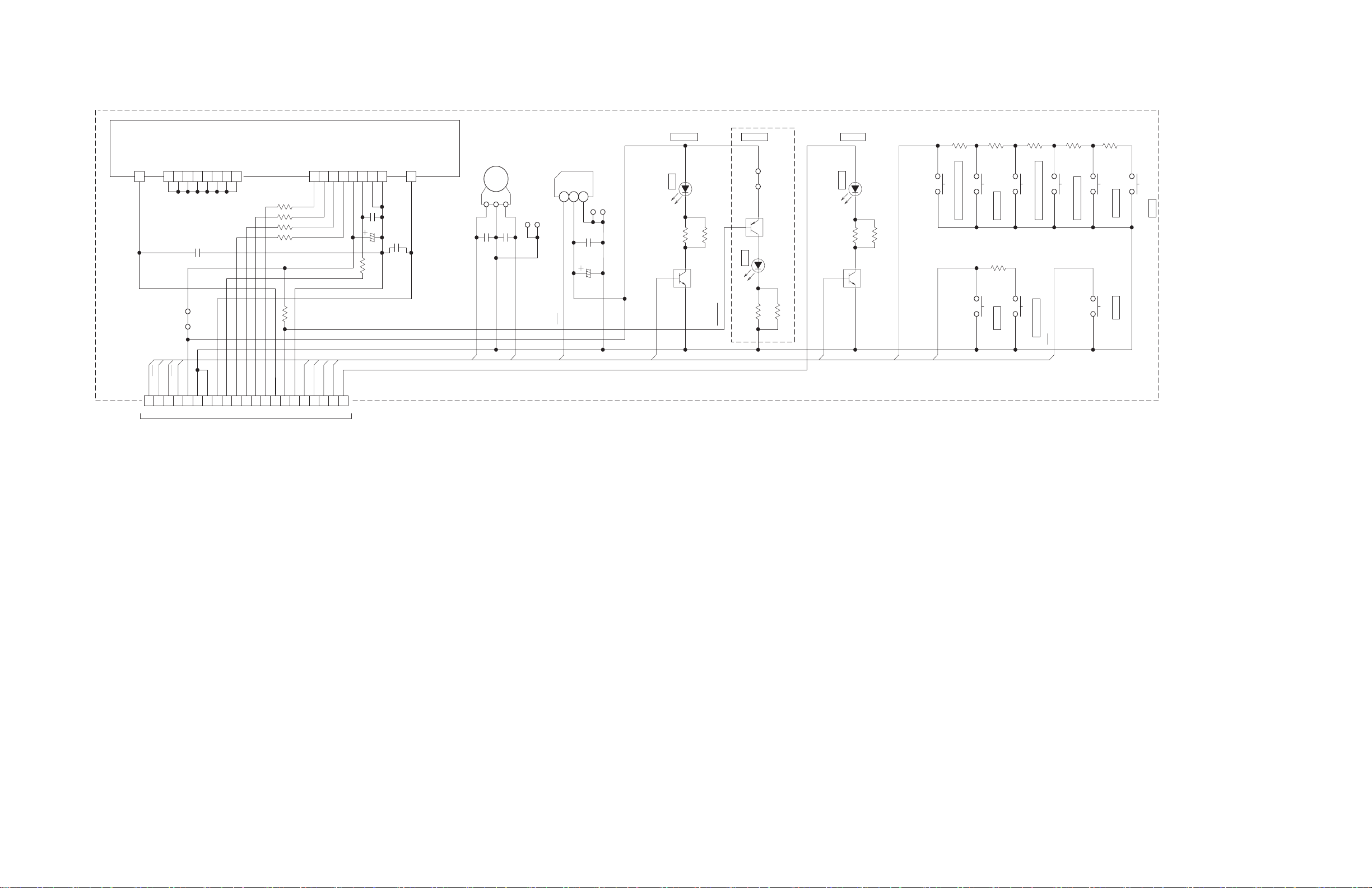
27.6V
0V
B/E/EN/
3.6V
LVB10733-A2
0V
3.5V
CC CONVER
DVD PLAY/PAUSE
** EX-AR3 ONLY
0V
0.2V
FM/AM/LINE
0V
FLVDD(A3)
3.4V
POWER
**
B.SKIP
other:
3.5V
5.6V
680
FL TUBE
EJECT
**
2.2V
0V
STOP
EV/EE:
0V
2.2V
0V
0.4V
F.SKIP
0V
USB PLAY/PAUSE
RECLED(AR3)
3.2V
FLDATA
F-
FLSTB
VH
REM
PIN
STBLED
RECLED
FLBK
CCLED
US3.3V
STBLED
F+
REM
KEY2
KEY1
KEY2
KEY1
PIN
CCLED
VOL-
VOL+
VOL-
FLGND
US5.4V
VOL+
FLCLK
DGND
RT1P141C-X
Q8201
QSW0683-001Z
S8101
C8004 1
QSW0683-001Z
S8202
C8202
0.1
R8005 100
R8203
3.9K
QSW0683-001Z
S8205
CCLED
BLUE
SELK6E10C-D-T
D8101
C8003
1
NIR8104
R8003 2.2K
QSW0683-001Z
S8201
R8002 2.2K
R8206
3.3K
QSW0683-001Z
S8206
180
R8105
R8204
6.8K
220
R8102
RT1N141C-X
Q8001
C8001
0.1/50
QSW0683-001Z
S8001
0
R8006
C8201
0.1
R8202
2.7K
QSW0683-001Z
S8204
C8002
100/16
NIR8106
180
R8101
R8004 100
B2204
R8201
3.3K
NIR8103
B1609
R8001
0
QSW0683-001Z
S8102
RT1N141C-X
Q8101
R8205
12K
RECLED
RED
SLR-343VC-T
D8201
STBLED
RED
SLR-343VC-T
D8001
C8101
0.01
C8102
22/16
QSW0683-001Z
S8203
321
GP1UE261XKVF
IC801
21
20
19
18
17
16
15
14
13
12
11
10
9
876
54321
QGF1205F2-21
CN801
231
QSW0975-001
JS801
LGND33
PGND32
VH31
VDD30
BK29
LAT28
CLK27
SI26
QLF0183-001
DI801
F+36
NC11
NC10
NC9
NC8
NC7
NC6
NC5
NC4
F-1
/AR5UF/BR3UF)
(EX-AR3LTDUT/AR3UF
To Micom section 1
<Micom section 2 (EX-AR3LTDUT/AR3UF/AR5UF/BR3UF)>
created date:2011-06-09No.MB596
65
(No.MB596<Rev.004>)22/
Page 44

5.0V
0V
0V
0V
0V
10.5V
0V
2.4V
2.5V
0V
2.5V
0V
2.5V
0V
0V
0V
2.4V
5.0V
2.1V
0V
2.5V
0V
10.5V
0V
0V
2.7V
5.0V 5.0V
0V
10K10K47K10K
Ver:B/E/EN/EV/EE
Ver:D
Ver.:B/E/EN/EV/EE/D
SW JACK
SW
10.5V
0V
10.5V
1.8V
10.5V
0V
0V
0V
VIDEO DRIVER
2.4V
1.6V
0V
0V
2.4V
2.4V
2.4V
2.4V
NI
2.9V
5.0V
2.9V
0V
5.0V
2.1V
0V
0V
1.6V
0V
0V
2.5V
2.9V
2.4V
2.5V
0V
2.9V
2.4V
0V
2.1V
NOTES
μ
μ
μ
Ω
(V).
VOLTAGE
F)/RATED
(
CAPACITANCE
OFFORM
THE
INSHOWNARE
E.CAPACITORS
ALL
H(m=mH).
IN
ARE
VALUES
INDUCTANCE
ALL
F(P=pF).
IN
ARE
VALUES
CAPACITANCE
ALL
CAPACITOR.
MYLARORCAPACITOR
CERAMIC
ARE
CAPACITORS
ALL
).
OHM(
EXCEPT D Ver.
IN
ARE
VALUES
RESISTANCEALL
SPECIFIED.OTHERWISE
2.UNLESS
MODESTOPCDCONDITION-
SIGNAL.
R2R1
RT1P141C
R2R1
RT1N144C
R2R2
0.5V
0V
1.7V
LVB10732-A1
R1R1
INPUTWITHOUT
OSCILLOSCOPE
OR
METER
VOLT
DIGITAL
A
WITH
DC-MEASURED
ARE
1.VOLTAGES
B/E/EN/EV/EE
EXCEPT
Y
Ver. EXCEPT D
COMPONENT
VIDEO OUT
Y
VIDEO OUT
Cb
Cr
C
S/COMPOSIT
AV COMPULINK
Ver.D
S1
Ver.:B/E/EN/EV/EE
DGND
DGND
DGND
DGND
DGND
TVR
COMP/Y
FUNCTION
FUNCTION
SWGND
SWSIG
YCMIX
YCMIX
S-DCOUT
D2IP/BLK
D2IP/LINE2
D2IP/LINE2
TVG
TVL
CB
CB
CR
CR
Y
Y
VS3
VS1VS1
VMUTE2
CR/R
C
CB/B
Y/G
VS3
VS1
CR/R
CB/B
Y/G
Y/COMP
C
CLP/BIAS
VIP
CLP/BIAS
VIP
COMPLNK
VMUTE1
COMPLNK
S2
D2IP/BLK
Y/COMP S1
S2
VMUTE1
VMUTE2
S1
COMPLNK
Y/G
CB/B
YCMIX
SWGND
SWSIG
VS1
VS3
V11V
VIP
VMUTE2
S2
CR/R
VMUTE1
Y/COMP
C
D2IP/BLK
S5V
A.GND
TVR
TVL
S1
CLP/BIAS
DGND
DGND
EP601
QNZ0136-001Z
9
QNN0812-001
J6002
1/4WFRR6015
NI
1/10W
R6183
680
R6010
330
R6001
620
R6007 510
1/10W
R6181
680
R6151
NI
R6022
75
NI
R6156
R6005 510
NI
R6155
R6093
75
R6002
330
R6024
100
R6006 330
R6009 510
R6023
75
R6092
75
R6021
75
R6094
10K
R6154
NI
R6008 330
R6003
560
1/4W
300
R6182
R6096
100
R6152
NI
R6091
75
R6004
330
R6095
100
R6153
NI
RT1N144C-X
Q6182
RT1N144C-X
Q6002
RT1N144C-X
Q6183
NI
Q6153
RT1P141C-X
Q6181
RT1P141C-X
Q6001
NI
Q6154
NI
Q6152
NI
Q6151
NQR0022-005X
K6091
NQR0502-001X
K6001
VCC1
1
CHROMA IN
2
/MUTE1
3
COMPOSITE IN
4
YC MIX
5
Y IN
6
GND1
7
BIAS
8
I/P
9
CY IN
10
CLP
11
Cb IN
12
/MUTE2
13
Cr IN
14
GND2
15
Cr OUT
16
GND2
17
Cb OUT
18
GND2
19
CY OUT
20
Y OUT
21
GND2
22
COMPOSITE OUT
23
S2
24
S1
25
CHROMA OUT
26
S-DC OUT
27
VCC2
28
MM1623XF-X
IC601
C6091
330/6.3
C6021
330/6.3
C6022
330/6.3
C6092
330/6.3
C6001
330/6.3
C6006
0.47/50
C6008
22/25
C6007
0.47/50
C6005
0.47/50
C6023
330/6.3
C6097
0.1
C6002 0.1
C6028
0.01
C6024
100P
C6093 0.1
C6101
0.1
NCF21CZ-105X
C9999
C6099
0.1
C6100
220P
C6095 180p
C6026
100P
C6096
180p
C6094
180p
C6004
0.1
C6003
0.1
C6029
0.1
NCF21CZ-105X
C9998
C6025
100P
C6027
0.1
C6098
NI
C7308
NI
214
3
QNN0812-001
J6002
658
7
QNN0812-001
J6002
3
1
2
QNS0210-001
J6005
QNN0676-0016QNN0676-001
5
4 3
2 1
QNN0676-001
J6006
7
8
QNN0676-001
J6006
1514131211
10
9
8NC7654321
QGF1205F2-15
CN711
11
10
9
8
7
6
5
4
3
2
1
QGF1205F2-11
CN712
(EX-AR3LTDUT/AR3UF/AR5UF/BR3UF)
To Video section 2
(EX-AR3LTDUT/AR3UF/AR5UF/BR3UF)
To Video section 3
<Video section 1 (EX-AR3LTDUT/AR3UF/AR5UF/BR3UF)>
(EX-AR3LTDUT/AR3UF/AR5UF/BR3UF)
To Micom section 1
/AR5UF/BR3UF)
(EX-AR3LTDUT/AR3UF
To Micom section 1
created date:2011-06-09No.MB596
65
(No.MB596<Rev.004>)23/
Page 45

10k
NC
GND
0V
4:3
FUNCTION
GND
FUNCTION
H
GND
H
AUDIO-INL
B
BLK
75
NC
COMPOSITE/Y
2.1V
AUDIO-OUTR
0V
16:9
VS3
R/C
AUDIO-OUTL
SCART
RGBCOMPO/YC
GND
AUDIO-INR
4.5-7V
VS1
GND
L
L
TERMINAL
GND
L
LH
NC
9.5V-
LVB10733-A4
G
GND
BLANKING
AUDIOGND
STOP
L
TVL
FUNCTION
TVR
COMP/Y
D2IP/LINE2
G/Y
B/PB
R/PR
R6032
1K
1/10W
R6035
100
R6037
75
R6034
75
R6043
0
R6033
100K
R6044
0
C6036
470/10
R6038
75
C6031
180p
C6035
470/10
R6031
1K
C6038
470/10
C6039
470/10
R6042
0
R6039
75
C6032
180p
C6034
180p
C6042 180p
R6036
10K
C6033
180p
R6040 330
R6041 330
C6041 180p
15
14
13
12
11
10
9
8
7
6
5
4
3
2
1
QGF1205C2-15
CN602
23
J6001
21
20
19
18
17
16
15
14
13
12
11
10
9
8
7
6
5
4
3
2
1
QNZ0775-001
J6001
22
J6001
<Video section 2 (EX-AR3LTDUT/AR3UF/AR5UF/BR3UF)>
/AR5UF/BR3UF)
(EX-AR3LTDUT/AR3UF
To Video section 1
created date:2011-06-09No.MB596
65
(No.MB596<Rev.004>)24/
Page 46

LINE1
1.8V
S2
Y-GND
16:94:3
Pb-GND
L
100K
Pr
S1
0V
LB
L
SW-GND
Pb
L
LINE3
SW JACK
Y
4.6V
480i
4:3
LINE2
LINE3
H
2.1V
L
100K
D2 TERMINAL
H
LVB10733-A3
Pr-GND
R6072
75
C6072
470/10
C6071
470/10
R6073
75
R6075
0
C6073
470/10
R6074
0
R6076
10K
R6070
10K
R6080
100
C6078
0.1
C6079
0.1
C6076
100P
C6075
100P
R6071
75
C6074
100P
R6079
10K
11
10
9
8
7
6
5
4
3
2
1
QGF1205C2-11
CN651
1
2
QNN0811-001
J6004
14
13
12
11
10
9
8
7
6
5
4
3
2
1
QNZ0667-001
J6003
/AR5UF/BR3UF)
(EX-AR3LTDUT/AR3UF
To Video section 1
<Video section 3 (EX-AR3LTDUT/AR3UF/AR5UF/BR3UF)>
created date:2011-06-09No.MB596
65
(No.MB596<Rev.004>)25/
Page 47

CONDITION -
NOTES
ALL CAPACITANCE VALUES ARE IN μF(P=pF).
1.VOLTAGES ARE CD-MEASURED WITH A DIGITAL VOLT METER WITHOUT INPUT SIGNAL.
2.UNLESS OTHERWISE SPECIFIED.
RESISTORS ARE 1/16W ±5% METAL GLAZE RESISTOR.
ALL RESISTANCE VALUES ARE IN OHM(Ω).
ALL INDUCTANCE VALUES ARE IN μH(m=mH).
ALL CAPACITORS ARE CERAMIC CAPACITOR OR MYLAR CAPACITOR.
ALL E.CAPACITORS ARE SHOWN IN THE FORM RESET OF INH CAPACITANCE(μF)/RATED VOLTAGE(V).
MODECD STOP
10.2V
0V
4.9V
4.9V
5.6V
3.2V
0V
3.3V1.3V
5.6V
3.2V
0V
5.0V
DAC5V REG.
1.3V
A10V
D3.3V REG.
DINR
DINL
1.7V
A10V SW
DAC
CC CONVERTER
DIR
AUX
DIGITAL IN
DVD
DIGITAL OUT
LVA10732-A1
2.6V
3.2V
9.4V
10.1V
10.2V
5.0V
0V
2.6V
2.6V
2.6V
2.6V
0V
0V
3.3V
3.3V
1.7V
0V
1.7V
1.6V
1.7V
1.7V
0V
1.6V
0V
0V
0V
0V
0V
3.3V
0V
0V
3.3V
3.3V
0V
3.3V
0V
0V
0V
1.7V
1.7V2.0V
0V
0V
3.3V
1.6V
1.7V
0V
1.7V
0V
0V
0V
0V0.3V
0V
1.6V
0V
0V
3.3V
1.2V
3.3V
3.3V
3.3V
3.3V
0V
0.3V
3.3V
0V
3.3V
0V
AGND
3.8V
3.8V
3.8V
8.8V
5.1V
5.1V
3.8V
LPF
0V
K2GND
FDIN
US5.4V
SAFETY1
DVD_DOUT
DD_DATA
CC_DATA
CC_DATA
CC_CLK
CC_CS
DACPDN
DIRPDN
DD_CLK
DIRAUTO
DIRFS96 CC_CS
CC_CLK
DIRERF
DIRPDN
DD_DATA
CC_RST
DD_CS
DD_CLK
DD_DATA
CC_RST
DIRDTO
DIRERF
DD_CS
DD_CS
DD_CLK
DIRAUTO
DACPDN
DIRFS96
DIRDTO
K2GND
DIRPDN
DIRAUTO
DIRDTO
DD_DATA
DD_CS
DD_CLK
CC_CS
CC_DATA
CC_CLK
DIRERF
CC_RST
DACPDN
FDIN
US5.4V
SAFETY1
DVD_DOUT
DIRFS96
R5304
100
R5101
4.3K
R5104
200
R5201
4.3K
47
R5504
220
R5505
100
R5501
R2751
100
22K
R2952
R5305
2.2K
R2951
100
R5203
4.7K
R5202
4.3K
22K
R2953
220
R5510
220
R5506
R5105
200
R5106
4.7K
18K
R5503
220
R5509
R5206
4.7K
R5102
4.3K
R5210
1.5K
R5205
200
1/4W
R5301
150
R5110
1.5K
220
R5508
220
R5507
220
R5502
R5204
200
0
R5511
R5103
4.7K
2SC3928A/QR/-X
Q5302
2SA1530A/QR/-X
Q5301
NQR0502-001X
K5502
NQR0502-001X
K5501
NQR0502-001X
K5503
NQR0502-001X
K5504
DVDD
1
DVSS
2
TVDD
3
V/TX
4
XTI
5
XTO
6
PDN
7
R
8
AVDD
9
AVSS
10
RX1
11
RX2/DIF0
12
RX3/DIF1
13
RX4/DIF2
14
AUTO
15
P/SN
16
FS96
17
ERF
18
LRCK
19
SDTO
20
BICK
21
DAUX
22
MCKO2
23
MCKO1
24
OCKS0/CSN
25
OCKS1/CCLK
26
CM1/CDTI
27
CM0/CDTO
28
AK4112BVF-X
IC553
LRCK
1
BCK
2
DIN
3
CAD1
4
CAD0
5
VDD
6
VSS
7
RESET
8
MODE
9
MCK
10
MDT
11
MLEN
12
PDN
13
DFR1
14
WAS
15
CKSLN
16
CLK
17
VSS
18
DOUT2
19
BCKO2
20
WCKO2
21
DOUT1
22
BCKO1
23
WCKO1
24
JCV8009-W
IC554
CDTI
8
CCLK
7
CSN
6
PDN
5
LRCK
4
SDTI
3
BICK
2
MCLK
1
AOUTR-
9
AOUTR+
10
AOUTL-
11
AOUTL+
12
VSS
13
VDD
14
DZFR
15
DZFL
16
AK4385ET-X
IC555
VEE
4 3 2 1
5 6 7
VCC
8
NJM4580E-X
IC511
VIN
5
VOUT
4
NOISE3GND2CONT
1
MM1613DN-X
IC295
VIN
5
VOUT
4
NOISE3GND2CONT
1
MM1615AN-X
IC275
GND
3
VCC
2
VIN
1
GP1FAV30TK0F
IC552
VOUT
3
GND
2
VCC
1
GP1FAV30RK0F
IC551
UDZW4.7B-X
D5110
UDZW4.7B-X
D5210
MA111-X
D5301
C5511
22/50
C5110
22/50
10/50
C5501
C5503
22/50
C5210
22/50
C5301
33/35
10/50
C5502
C5505
220P
C5506
220P
C5512
220P
PP
C5201
0.0039
0.1
C5508
C5509
0.047
0.1
C5507
PP
C5103 330P
PP
C5102
330P
PP
C5202
330P
PP
C5203
330P
0.1
C5504
0.1
C5510
C2751
0.1
C2753
1/10
PP
C2752
0.0082
C2951
0.1
C2953
1/10
PP
C2952
0.0082
PP
C5101
0.0039
4
3
2
1
QGA2501C1-04
CN713
<CC converter section 1 (EX-AR3LTDUT/AR3UF/AR5UF/BR3UF)>
/AR5UF/BR3UF)
(EX-AR3LTDUT/AR3UF
To Main section
/AR5UF/BR3UF)
(EX-AR3LTDUT/AR3UF
To Micom section 1
created date:2011-06-09No.MB596
65
(No.MB596<Rev.004>)26/
Page 48

L
R
0V
0V
GND
DO VER:NI
DO VER.
0V
0V
EXCEPT DO VER.
0.5V
0V
DO :NI
0.3V
2.6V
DO VER:NI
R
DO VER.
2.7V
0V
LVA10732-A3
D-
0V
R
other:0.1
EXCEPT
L
0V
USB
0V
0V
J/C:NQR0502-001X
HEADPHONE
L
K4435=0
K4411,K4421,
DO VER:
0V
0V
D5V
0V
OTHER:
EXCEPT
LINE1IN
D+
LINE1OUT
0V
0V
LINE1OUTL
LINE1OUTR
LINEOUTGND
USBGND
USBGND
D5V
LINEINSW
HPGND
D-
LINE1INL
HPR
D+
LINEINGND
LINE1INR
HPSW
HPL
3
2
1
NI
D4431
OTHER=
DOM=0
NQR0007-002X
K4437
NI
C4414
C4412
220P
NQR0022-002X K4433
NQR0007-002X
K4435
R4431
1k
QZW0112-002
WC401
1000P
C4436
R4423
100
R4421
1K
C4421
220P
C4415 NI
C4423
100P
C4439
NI
2.2K
K4438
R4412
120K
R4422
120K
15p
C4433
C4435
0.1
C4413
100P
C4422
220P
NI
C4424
NQR0007-002X
K4421
C4437
NI
15p
C4434
0.0018
C4431
OTHER=
DOM=0
NQR0007-002X
K4436
0.0018
C4432
NQR0007-002X
K4411
C4425 NI
R4413
100
NQR0502-001X
K4431
C4438 0.1
R4411
1K
NQR0022-002X K4432
C4411
220P
0
K4434
3
2
1
QNZ0136-001Z
EP442
5
2
6
1
3
7
4
QNS0266-001
J4404
3
1
4
2
QNS0240-001
J4403
3
1
4
2
QNS0240-001
J4402
1
2
3
4
5
QGA2001C1-05
CN441
3
2
1
QNZ0136-001Z
EP441
4
3
2
1
QGA2501C1-04
CN443
1234
QNZ0851-001
J4401
6
5
7
6
5
4
3
2
1
QGA2501C1-07
CN442
<CC converter section 2 (EX-AR3LTDUT/AR3UF/AR5UF/BR3UF)>
/AR5UF/BR3UF)
(EX-AR3LTDUT/AR3UF
To Main section
/AR5UF/BR3UF)
(EX-AR3LTDUT/AR3UF
To Main section
/AR5UF/BR3UF)
(EX-AR3LTDUT/AR3UF
To DVD section (3/3)
created date:2011-06-09No.MB596
65
(No.MB596<Rev.004>)27/
Page 49

10.3V
10.3V
20.4V
10.3V
0V
20.4V
20.4V
0V
10.3V
0V
10.3V
10.3V
0V
0V
10.3V
0V
0V
10.3V
20.4V
10.2V
0V
10.2V
0V
0V
20.4V
20.4V
10.8V
3.3V
2.1V
0V
2.1V
2.1V
1.4V
0V
2.1V
1.5V
10.8V
1.4V
0V
0V
0.5V
1.4V
0.5V
1.4V
4.9V
2.1V
2.1V
1.4V
0V
0
0
0.4
2.5
2.8
0
3.2
0V
3.2V
0V
0V
10.3V
10.3V
10.3V
0V0V
0.6V
10.8V
10.7V
0V
0V
0V
0V
2.1V
0V0.1V
0V
10.8V
1.1V
0V
1.1V
B
C
E
S.MUTE
47K -
47K 22K
22K47K
RT1P44HC
RT1P440C
B
C
E
4.9V
2.1V
B
C
E
B
C
E
1.0
1.0
5
3
2
1
4
0
20.5
0
20.5
0
20.5
B
C
E
7
R+
R-
L-
L+
10.8V
100K
RT1N44HC
R1 R2
R2
R1
NG=2.5V
OK=OPEN
14.6V
6.8V
7.1V
6.8V
6.7V
7.1V
6.8V
0V
14.6V
6.7V
6.8V
6.8V
7.1V
6.8V
7.1V
0V
MODESTOP
0.8
0.1
0
19.9
20.6
20.6
0
0
0
0
1.0
0
0
0
20.6
20.6
4
3
2
1
6
5
4
3
2
1
10.4
10.4
0
0
10.3
1
2
3
4
5
CN301
R2R1
R2
R1
CD-CONDITION
μ
μ
μ
±
Ω
(V).VOLTAGEF)/RATED(
CAPACITANCEOFFORMTHEINSHOWNAREE.CAPACITORSALL
H(m=mH).INAREVALUESINDUCTANCEALL
F(P=pF).INAREVALUESCAPACITANCEALL
CAPACITOR.MYLARORCAPACITORCERAMICARECAPACITORSALL
).OHM(INAREVALUESRESISTANCEALL
RESISTOR.METAL GLAZE5%1/16WRESISTORS ARE
SPECIFIED.
NOTES
1.VOLTAGES ARE CD-MEASURED WITH A DIGITAL VOLT METER WITHOUT INPUT SIGNAL.
OTHERWISE2.UNLESS
RESET INH
LVA10732-A2
S.MUTE
LINE
VDD
GND
GND
VDD
2ch
AHB
0V
10.3V
10.3V
10.3V
GND
6 10.3
P.GND
P.GND
POWL+
POWL-
POWR-
POWR+
MODSTBY
MODPRT
SMUTE
MODON
F-SHIFT2
DCPRT
23V
23V23V
A.GNDA.GND P.GND
23V
P.GND
P.GND
A.GND
A.GND
P.GND
A.GND
P.GND
A.GND
A.GND
SGND3
P.GND
SGND1
P.GND
P.GND
P.GND
SGND4SGND2
P.GND
P.GND
A.GND
sure to use the specified one.
When replacing those parts make
Parts are safety assurance parts.!
TP101
SP
!
1/4W
UNF
R1302
560
R1192
18k
R1604
10k
R1001
0
R1354
1k
1%
R1125
3k
R1204
9.1k
R1203
8.2k
1.5k
R1154
R1353
1k
R1103
8.2k
R1101
150k
1%
R1123
30k
1%
R1126
3k
56k
R1304
15k
R1252
R1104
9.1k
10k
R1305
10k
R1306
R1102
10k
R1261
100
R1171
100
R1202
10k
R1211
1k
220k
R1153
R1271
100
R1161
100
R1291
18k
R1613
4.7k
R1614
10k
150k
R1256
150k
R1157
R1316
10k
R1611
4.7k
R1355
5.6k
100
R1301
R1351
1k
15k
R1151
R1356
5.6k
15k
R1251
R1601
4.7k
R1212
0
R1113
2.2k
R1602
4.7k
15k
R1258
15k
R1158
R1806 1k
R1802 1k
R1612
4.7k
150k
R1257
R1805 1k
1%
R1122
30k
47k
R1308
47k
R1307
R1201
150k
R1807 8.2k
R1352
1k
150k
R1156
R1603
4.7k
68k
R1311
R1128
3.3k
1.5k
R1155
R1172
22
R1162
22
15k
R1152
R1262
22
1.5k
R1254
R1803 1k
R1272
22
R1112
0
220k
R1253
R1191
18k
R1114
39k
R1111
1k
R1214
39k
R1292
18k
R1804 1k
R1213
2.2k
R1358
5.6k
R1227
20k
1%
R1226
3k
1.5k
R1255
1%
R1221
3.3k
R1801 1k
1%
R1121
3.3k
1%
R1223
30k
1%
R1222
30k
R1357
5.6k
1%
R1224
3.3k
1%
R1225
3k
R1228
3.3k
20k
R1312
R1127
20k
1%
R1124
3.3k
RT1N44HC-X
Q1391
RT1P440C-X
Q1305
RT1P44HC-X
Q1291
RT1P44HC-X
Q1191
RT1P44HC-X
Q1292
RT1P44HC-X
Q1192
2SC3928A/QR/-X
Q1612
2SC3928A/QR/-X
Q1304
2SC3928A/QR/-X
Q1602
2SC3661-X
Q1101
2SC3661-X
Q1201
2SC3928A/QR/-X
Q1302
2SC3928A/QR/-X
Q1303
KTA1267/YG/-T
Q1601
2SA1530A/QR/-X
Q1611
22
L1303
22
L1304
QQLZ037-120
L1271
QQLZ037-120
L1171
QQLZ037-120
L1261
QQLZ037-120
L1161
22
L1302
DVDD1
1
DGND1
2
PWM2A1
3
PWM1A1
4
PWM1B1
5
PWM2B1
6
OP1O
7
IN1
8
STBY/MUTE
9
MUTEC
10
SUB
11
VCOR
12
AGND
13
VREF
14
AVCC
15
SUB
16
CLK
17
CLKCTRL
18
IN2
19
OP2O
20
PWM2B2
21
PWM1B2
22
PWM1A2
23
PWM2A2
24
DGND2
25
DVDD2
26
HBA2
27
VDA2
28
VSA2
29
VSA2
30
OUTA2
31
OUTA2
32
VDB2
33
VSB2
34
VSB2
35
OUTB2
36
SUB
37
OUTB2
38
HBB2
39
HBB1
40
OUTB1
41
SUB
42
OUTB1
43
VSB1
44
VSB1
45
VDB1
46
OUTA1
47
OUTA1
48
VSA1
49
VSA1
50
VDA1
51
HBA1
52
R2A15107SP-X
IC130
VEE
4 3 2 1
5 6 7
VCC
8
NJM4580M-X
IC110
VEE
4 3 2 1
5 6 7
VCC
8
NJM4580M-X
IC120
3
1
2
MA152WK-X
D1352
3
1
2
MA152WK-X
D1351
NI-UDZW11B-X
D1301
UDZW6.8B-X
D1211
UDZW6.8B-X
D1111
RB160M-30-X
D1171
RB160M-30-X
D1272
RB160M-30-X
D1172
RB160M-30-X
D1262
RB160M-30-X
D1161
RB160M-30-X
D1271
RB160M-30-X
D1162
RB160M-30-X
D1261
C1101
10/63
47/50
C1164
C1213
10/63
C1113
10/63
47/50
C1174
C1391
10/25
10/63
C1304
C1352
10/25
C1301
100/25
C1201
10/63
C1114
33/35
2.2/50
C1112
C1214
33/35
47/50
C1274
2.2/50
C1212
47/50
C1264
C1351
10/25
10/63
C1302
C1353
10/25
C1354
10/25
10/16
C1306
0.0015
C1152
3p
C1257
C1356
0.47
10/16
C1305
56p
C1255
1/25
C1171
560p
C1256
C1292
NI
C1193
NI
C1275
0.001
1/25
C1271
1.5
C1167
NI-0.1
C1309
0.1
C1303
0.01
C1272
1.5
C1177
1/25
C1161
1.5
C1277
0.22
C1307
3p
C1157
0.0015
C1252
0.0068
C1308
1.5
C1267
560p
C1156
560p
C1253
56p
C1155
56p
C1254
0.01
C1162
56p
C1154
0.01
C1262
0.01
C1172
560p
C1153
C1121
22p
C1122
22p
C1123
22p
C1124
150p
C1221
22p
C1191
NI
C1291
NI
C1222
22p
C1223
22p
C1224
150p
C1278
0.22
3p
C1158
C1268
0.22
C1168
0.22
C1178
0.22
C1211
0.1
C1111
0.1
C1293
NI
C1192
NI
C1166
0.001
0.0015
C1251
0.0015
C1151
C1115
NI
C1116
NI
C1175
0.001
C1176
0.001
C1902
0.1
C1901
0.1
C1294 2.2
C1266
0.001
C1265
0.001
C1276
0.001
C1216
NI
C1215
NI
C1903
0.1
C1904
0.1
C1194 2.2
C1196
470p
C1611
0.1
C1355
0.47
C1357
0.47
1/25
C1261
C1358
0.47
47p
C1310
220p
C1311
3p
C1258
C1905
1/25
C1165
0.001
C1296
470p
C1295
470p
C1195
470p
7
6
5
4
3
2
1
QGA2501F1-07
CN101
6
5
4
3
2
1
QGA2501F1-06
CN104
R 5
GND 4
L 3
SW10V 2
AHBCTL 1
QGA2501F1-05
CN103
4
3
2
1
QGA2501F1-04
CN102
<DEUS section 1 (EX-AR3LTDUT/AR3UF/AR5UF/BR3UF)>
(EX-AR3LTDUT/AR3UF/AR5UF/BR3UF)
To Micom section 1
(EX-AR3LTDUT/AR3UF/AR5UF/BR3UF)
To Power section
(EX-AR3LTDUT/AR3UF/AR5UF/BR3UF)
To DEUS section 2
/AR5UF/BR3UF)
(EX-AR3LTDUT/AR3UF
To Main section
created date:2011-06-09No.MB596
65
(No.MB596<Rev.004>)28/
Page 50

GND
L+
L-
R-
R+
)(
DO VER. ONLY
B5501,5502,5503,5504
EXCEPT DO VER.
LVB10733-A1
P.GND
P.GND
L-
L+
R+
R-
C1282
0.0033
C1184
220P
C1381
NI
C1181
220p
C1281
220p
C1286
NI
C1182
0.0033
C1283
NI
C1186
NI
C1284
220P
C1183
NI
C1185
NI
C1285
NI
NI
B5503
NI
B5502
NI
B5504
NI
B5501
2
1
34
6
QQR1659-001
L1181
2
3
16
4
QQR1659-001
L1281
6
5
4
3
2
1
QGA2501F1-06
CN301
5
4
2
3
1
EX-A3LTD/AR3LTD[DOM/UT]=QNB0045-004
EX-A3/AR3[E/U]=QNB0265-002
EX-A3/AR3[DOM/J/C/UF]=
QNB0045-003
J3001
<DEUS section 2 (EX-AR3LTDUT/AR3UF/AR5UF/BR3UF)>
/AR5UF/BR3UF)
(EX-AR3LTDUT/AR3UF
To DEUS section 1
created date:2011-06-09No.MB596
65
(No.MB596<Rev.004>)29/
Page 51

for ICE
or
RT1N241U-X
2SK3019-X2SK3019-X
OROR
2SC4617R/-X
OR
2SC4617R/-X
OR
1/2WOR
L
L H
H
DVD CD
MSW
DVDCDSW
(B/b)
(C/c)
(A/a)
(D/d)
(B/b)
(C/c)
(A/a)
(D/d)
T+
(DAC2CS)
,
ALL RESISTANCE VALUES ARE
ARE IN H(m=mH).
6.3V
in
.25V
OR
1.
,
OF
CERAMIC CAPACITOR
.
±
VOLTAGES ARE DC-MEASURED WITH A DIGITAL
disc theμandDVD
METAL GLAZE RESISTOR.
UNLESS OTHERWISE SPECIFIED.
F(p=pF).
or
ALL INDUCTANCE VALUES
5%
A
ALL E.CAPACITORS ARE SHOWN IN THE FORM
NI STANDS FOR NOT INSERTED PARTS.
/RATED VOLTAGE (V).
mode1
ALL CAPACITANCE VALUES ARE IN
NOTES
16V
μ
CAPACITANCE( F)
50V
3.
CONDITION ---
Ω
2.
μ
METAL GLAZE RESISTOR.1/16W
10V
0.5%
STOP
,
Tray
ALL CAPACITORS ARE
WITHOUT INPUT SIGNAL.
,
IN OHM( ).
VOLT METER
ALL RESISTORS ARE
(ADCPDN)
(USB_PHY+)
(USB_PHY-)
SDRAM
(REF_MODE_SET)
(14/15=L:H=64M)
(H:L=USB:ADAC)
(H:L=MULTI:SEPA)
H
G
F
E
D
C
B
(RX)
(for HDMI)
(DISCSET)
(DAC0CS)
(NOC)
(NEN)
/INH
XT /XT
VDD VSS
Qo
48MHz
OSC
Cn
0VNC
Sub0V
REG.
Vout
Cont
GND
Vin
3.9V
3.3V
1.9V
4.0V
3.3V
REG.
3.9V
D1.2V
0V
0V
0V
1.2V
(VCLKO)
(DDATA)
DVD-LD
PICKUP
C/c
FXL-S10-1M
Vc
CD-LD
TRVSW
F
T-
MOTOR
B/b
QAR0165-001
FEED
UOUT
WOUT
GND-PD
PD
E
Vcc
NC
ASS'Y
SWGND
A/a
RF
F-
QAR0386-001
MOTOR
QAL1118-001
D/d
NC
TRA
NC
VR-DVD
MECHA
FM-
(KHS-313A)
F+
VOUT
FM+
ASS'Y
MSW
SPINDLE
COM
VR-CD
GND-LD
LVA10824-231B (1/3)
(ADIN)
(AOUT2)
(AOUT1)
(AOUT0)
(DVDCDSW)
(DAC1CS)
(DACPDN)
(UCLK)
(SCK)
(UCS)
(SDA)
(SPDRV)
(TRVSW)
(TRSDRV)
(SPMUTE)
(MONI6)
(MONI2)
(MONI7)
(MONI3)
(MONI4)
(MONI0)
(MONI5)
(MONI1)
(TRACK)
(COPY)
(DEMP)
(DISCSTP)
(INDEX)
(U2SDT)
(SCS)
(48MHz)
(DCLK)
(S2UDT)
(LRMUTE/TDATA)
27MHz
DRIVER
OR
CHASSIS
TRDRV
AMP3IN+
OUT2R
AMP4IN+
BR
0V
NC
9V
AMPIN-
DV5
OR
NC
OUT4R
MUTE2
AMPIN+
SPC2
MGND
KTA1001/Y/-X
0V
0V
AMP1IN+
KTA1001/Y/-X
TRSDRV
SPDRV
FODRV
VHALF2
SPCTL
VCC1
NC
MGND
AMP3IN-
AMP2IN+
LASER
EEPROM
SCLK
MGND
SPCX
DRIVER
OUT2F
SPVCOIN
AMP4IN-
SGND
F
RESET
0V
TEMPDET
0V
FR
0V
VREF
MGND
MUTE3
VOUT
SPFGO
AMP2IN-
OUT1R
0V
WOUT
AMPOUT
OUT4F
MECHA
VCC2
MUTE1
VCC
SPFC
OUT1F0VOUT3R
DGND
AMP2OUT
0V
MCOM
AMP1OUT
SDATA
0V
AMP3OUT
9V
UOUT
SPRF
AMP1IN-
DGND
SPC1
0V
OUT3F
DVDCDSW
VREFH
TRVSW
LPC
VREFH
F
E
B
A
RF
D
C
DVDCDSW
LPC
DAC2CS
ADIN
F
E
ADCPDN
EXADT11
SPDRV
EXADT13
RX
DVDPWR
TX
CPURST
AOUT0
AOUT1
AOUT2
LRMUTE
SPMUTE
ROUT
LOUT
DACCK
BCKM
BCK
LRCKM
LRCK
DATAM
DACPDNDACPDN
NOC
NEN
DAC0CS
SDA
SCK
SDA
SCK
DP
DM
DVDPWR
EXADR20
DAC1CS
EXADT1
DEMP
SPDRV
COPY
EXADR16
EXADT15
EXADT14
EXADT12
EXADR18
DDATA
DCLK
CPURST
FG
INDEX
TRACK
B
D
UCS
UCLK
S2UDT
SCS
U2SDT
TRDRV
FODRV
MCK
TRVSW
DVDLDCUR
EXDT12
EXDT5
DVDLDCUR
AD4
MDQ15
MCK
EXDT13
EXDT6
MDQ7
MDQ11
EXDT0
EXDT8
EXDT1
MA2
MA5
MA1
NCSM
NRAS
LPCO2
LPCO1
FG
EXADT3
EXADT2
EXADT0
F+
T-
EXDT15
UOUT
EXDT7
DAC3OUT
EXDT10
DQM1
EXDT2
DQM0
WOUT
EXDT9
EXADT10
MDQ8
EXDT14
COM
NEXCE
MDQ6
TRSDRV
FM+
TRDRV
NEXOE
MDQ9
FM-
A
DAC2OUT
F-
RF
C
MA8
DAC1OUT
MA3
SPMUTE
BA1
DAC4OUT
MA4
NEXWE
VOUT
MA9
DAC5OUT
MA6
EXADR19
FM-
F+
BA0
MA0
EXDT4
EXADT8
LPCO2
MA11
MA7
EXDT11
EXADT9
MDQ3
MDQ5
NCAS
AD4
MDQ12LPCO1
MDQ10
NWE
MA10
MDQ2
MDQ14
MDQ13
MDQ1
VOUT
MDQ0
T+
MDQ4
EXDT3
EXADR17
UOUT
EXADT7
COM
CDLDCUR
EXADT6
T+
WOUT
EXADT5
FODRV
EXADT4
CDLDCUR
TRSDRV
T-
F-
FM+
D4V
M9V
S5V
D2V
P3.3V
D1.2V
M5V
S3.3V
DGND
AGND
MGND
NAX0376-002X
X302
NAX0741-001X
X301
TP105
TP116
TP206
TP226
TP333
TP114
TP331
TP326
TP109
TP115
TP381
TP202
TP231
TP204
TP110
TP327
TP329
TP316
TP118
TP205
TP103
TP322
TP332
TP117
TP338
TP120
TP334
TP337
TP201
TP221
TP104
TP121
TP227
TP203
TP292
TP291
TP328
TP107
TP113
TP111
TP119
TP101
TP207
TP330
TP324
TP208
TP315
TP102
TP112
TP106
TP108
TP323
TP220
TP321
NAD0025-103X
TH301
TP303
TP302
TP300
TP301
R306 1k
NIR320
NIR319
NIR315
R383 100
0R317
R326
10k
NIR702
NIR703
R334 150
R337 150
R348 150
R338 0
R221
6.8k
NIR321
R375
470
R325 330
R376 1k
R368
NI
R369
NI
R316 1k
R201
470
1%
R340
30k
R359 NI
R358 220
R331
NI
R330
NI
R329
NI
R328
NI
NIR322
R361
10k
R111
5.6k
R117
330
1k
R120
NIR312
R220
24k
10k
R126
R362 47
47k
R119
R204
27k
R104
4.3k
R207
47k
1/2W
R105
10
R115
1k
R364 NI
R347
20k
R398
NI
R118
NI
R257 NI
R323 330
1/2W
R113
10
R308 NI
R353 100
R360
NI
R392
10k
R541 4.7k
R310
100
1/2W
R251
0.39
R206
30k
R333 330
R351 330
R127
4.3k
R108
470
0R705
0R704
R384
1k
R365 NI
R309 100k
R107
1k
R346
22k
R313
NI
R112
4.3k
R110
NI
R259 10k
R214
10k
R345 220
R373 10k
R339 0
R102
100
R307 1k
R304 4.3k
R109
330
R318 22
R291
0
R213
10k
R335
150
R128
5.6k
1%
R342
2.2k
1%
R341
5.1k
R219
18k
R116
470
NIR370
R371
10k
0
R314
R129
10k
R324 330
R101
100
R332 NI
R393
NI
R357
220
R352 1M
R130
NI
R367 220
R103
5.6k
R344 NI
R394 NI
R395 NI
R385
1k
R397 NI
R378 NI
R372 10k
R363
NI
R366 NI
R205
27k
R303
22
R311 330
R336 150
R396 NI
R290
0
R349 NI
R202
1k
R379 NI
R350 NI
R343 NI
UNR9212J-X
Q105
S
G
D
INK0002AU1-X
Q106
S
G
D
INK0002AU1-X
Q107
2SC5383/E/-X
Q104
2SC5383/E/-X
Q102
2SA1363/EF/-X
Q103
2SA1363/EF/-X
Q101
10
L101
L301
NI
NQR0502-001X
K353
NQR0502-001X
K352
NQR0022-002X
K354
216EXDT8
215EXDT0
214NEXOE
213NEXCE
212EXADT0
211VDD12
210VSS
209MA3
208MA4
207MA2
206MA5
205VDD33
204VSS
203MA1
202MA6
201MA0
200MA7
199MA10
198MA8
197BA1
196VDD33
195VSS
194MA9
193BA0
192DQM3
191DQM2
190NCSM
189NRAS
188NCAS
187VDD12
186VSS
185MCKI
184VDD33
183MCK
182VSS
181NWE
180DQM1
179DQM0
178MDQ7
177MDQ8
176MDQ6
175MDQ9
174VDD33
173VSS
172MDQ5
171MDQ10
170MDQ4
169MDQ11
168MDQ3
167MDQ12
166VDD33
165VSS
164MDQ2
163MDQ13
162
MDQ1
161
MDQ14
160
MDQ0
159
MDQ15
158
VDD12
157
VSS
156
OSCO
155
OSCI
154
VDD33
153
VSS
152
IECOUT
151
ADOUT
150
LRCK
149
SRCK
148
DACCK
147
AVDDI
146
ROUT
145
AVSSI
144
LOUT
143
AVSSG
142
AVDDG
141
AVDDE
140
AVSSE
139
DAC5OUT
138
DAC4OUT
137
AVSSF
136
COMP2
135
IREF1
134
VREF
133
COMP1
132
AVDDF
131
DAC1OUT
130
DAC2OUT
129
DAC3OUT
128
AVDDH
127
PWM0
126
PWM1
125
AVSSH
124
AD4
123
AD2
122
AD1
121
AD0
120
VIN1
119
VIN2
118
VIN4
117
VIN3
116
VIN8
115
VIN7
114
VIN6
113
VIN5
112
VIN9
111
VIN10
110
VHALF
109
VREFH
108 AVSSB
107 AVDDB
106 LPCO2
105 LPC2
104 LPCO1
103 LPC1
102 VREFL5
101 VREFH5
100 VIN3RF
99 VIN4RF
98 VIN2RF
97 VIN1RF
96 RFINP
95 RFINN
94 ANAMONI2
93 ANAMONI1
92 AVDDC
91 CDATA
90 CCAPA
89 AVSSC
88 VREFL7
87 AVSSD
86 VREFH7
85 PLFIL1
84 AVDDD
83 VDD12
82 VSS
81 TRCST
80 TRVDATA3
79 TRCDATA2
78 TRCDATA1
77 TRCDATA0
76 TRCCLK
75 EXTRG1
74 EXTRG0
73 SDATA
72 SCLOCK
71 FG
70 NRST
69 VDD33
68 VSS
67 DRV0
66 DRV1
65 DRV2
64 DRV3
63 DRV4
62 DRV5
61 P14
60 P13
59 P12
58 S3CLK
57 S3OUT
56 P9
55
S2CLK
54
S2OUT
53
S2IN
52
VDD33
51
VSS
50P549
S1OUT
48
INT0
47
S0CLK46S0OUT
45
EXADR20
44
VDD12
43
VSS
42
EXADT141EXADT240EXADT339EXADT438EXADT537EXADT636EXADT7
35
EXADR1734EXADR18
33
VDD33
32
VSS
31
NEXWE
30
EXADR19
29
EXADT828EXADT9
27
EXADT1026EXADT1125EXADT1224EXADT1323EXADT1422EXADT1521EXADR16
20
VDD12
19
VSS
18
EXDT15
17
EXDT716VDD33
15
VSS
14
EXDT14
13
EXDT6
12
EXDT13
11
EXDT5
10
EXDT12
9
EXDT4
8
EXDT11
7
EXDT36VDD33
5
VSS
4
EXDT10
3
EXDT22EXDT91EXDT1
MN2DS0018MA
IC301
48474645444342414039383750363534333231302928272625
24 23 22 21 20 19 18 17 16 15 14 13 49 12 11 10 9 8 7 6 5 4 3 2 1
LA6502-X
IC201
A0
1
A1
2
A2
3
GND4SDA
5
SCL
6
WP
7
VCC
8
S-24CS16A0I-G-X
IC510
765
4 3 2 1
NI
IC304
654
3 2 1
XC2164A51FM-X
IC303
NI
D301
220/6.3
C391
C303 47/4
C336 NI
C105
47/6.3
C264
NI
T
C106
22/6.3
C301
220/6.3
T
C108
22/6.3
C263
100/16
C302
47/4
T
C339
10/6.3
C290
NI
C103
0.1
C338 0.0056
C333 0.1
C379
0.1
C341
1
NI
C343
C260 0.022
C256 0.1
0.1
C345
C375
0.1
C340
1
C378
0.1
C101
0.1
C352
0.015
C374
0.1
C331 0.033
C314 0.1
C321 0.1
C305
0.1
NI
C344
C204
0.1
C206
150p
C309
0.1
C349
0.1
C377
NI
C205
270p
C393
0.01
C356
1
C258 0.015
C202
220p
C310
0.1
F
C210
1
C306
0.1
C373
0.1
C217
0.1
C201
220p
C348 0.1
C337
0.018
C353
560p
C102
0.1
C313
0.1
C262 0.022
C307
0.1
C383
0.1
C261 0.022
F
C371
1
NI
C342
C104
0.1
C315
0.1
C323 0.1
C332 0.1
C259 0.015
C319 0.1
C372
0.1
C330
0.1
C326 10p
C386
NI
C203
0.01
C320 0.1
C354
560p
C334 0.1
C251 0.47
C257 0.0082
C351
0.01
0.1
C316
0.1
C312
0.0022C350
C357
NI
C324 1
C358 NI
C335
0.1
C347 0.1
C318
0.1
0.1
C392
C304 1
C564 0.1
C211
0.022
C359
1
C328
0.01
C368
NI
C325 12p
C322
0.1
C367
NI
C364
NI
C370
0.1
C291
NI
9
Vo
1
NC
2
GND
3
Cn4Cont
5
NC
6
NC
7
Vin
8
MM1701CH-X
IC302
24
23
22
21
20
19
18
17
16
15
14
13
12
11
10
9
8
7
6
5
4
3
2
1
QGF0522F3-24W
CN101
8
7
6
5
4
3
2
1
QGF1016F8-08W
CN201
6
5
4
3
2
1
NI
CN301
<DVD section (1/3) (EX-AR3LTDUT/AR3UF/AR5UF/BR3UF)>
(EX-AR3LTDUT/AR3UF/AR5UF/BR3UF)
To DVD section (2/3)
(EX-AR3LTDUT/AR3UF/AR5UF/BR3UF)
To DVD section (3/3)
created date:2011-06-09No.MB596
65
(No.MB596<Rev.004>)30/
Page 52

OR
SG32A90TFIR3
AGND
FAOUTR
A6V
AINL
AGND
AINR
LRMUTE
FAOUTL
NC
G
F
E
D
B
C
LRMUTE
FAOUTL
AGND
FAOUTR
A6V
1.1V
A0
SDOUT
3.3V
DGND
AINL
2.4V
2.
0V
ADC
2.8V
FAOUTL
PDN
2.4V
0.9V
LRCLK
VDD
μ
SDTI
CSN
A4
/WE
D2V
3.2V
0.3V
1.6V
DGND
2.4V
LRCK
or
0V
0.4V
AUDIO
5%
3.5V
D2
3.3V
VCOM
DAC0CS
3.3V
A15
A6V
1.
DVDD
0V
.
D13
1.6V
1.8V
4.9V
D10
0V
CDTI
0V
0V
OR
OF
CERAMIC CAPACITOR
±
2.7V
VOLTAGES ARE DC-MEASURED WITH A DIGITAL
UCS
AGND
2.8V
0V
/CE
3.9V
1.6V
AUDIO
FAOUTR
RAOUTL
AINR
0.9V
A13
0V
3.3V
VCOM
Vin
ADIN
DGND
0V
LVA10824-231B (2/3)
0V
Cont
CDTI
DVDD
PDN
1.6V
1.8V
AOUTR
DAC5OUT
3.3V
RX
IN OHM( ).
3.3V
3.3V
2.6V
2.7V
2.8V
1.6V
VPP
BCK
A
BICK
U2SDT
1.6V
0V
A17
D7
2.4V
1.6V
TX
2.4V
P/S
VCOM
CCLK
LRMUTE
DIF
2.0V
0V
A2
*/RST
disc
2.8V
DAC2OUT
D3
CAPACITANCE( F)
3.3V
3.
1.1V
GND
REG
CSN
0.7V
3.3V
0V
AOUTR
0V
1/16W
10V
4.0V
A16
A9
BUFFER
AOUTR
5.0V
,
BICK
1.5V
TRACK
A6
3.1V
CSN
μ
CAOUT
0.8V
OUT
DVD
0.9V
16V
D12
DAC2CS
3.3V
50V
2.4V
VCC
4.9V
MCLK
1.3V
3.3V
VSS
DACCK
DZF
SDTI
0V
AOUTL
AVDD
DVDD
MGND
1.3V
INDEX
D6
F(p=pF).
0V
VSS
3.0V
0V
Noise
3.2V
ALL E.CAPACITORS ARE SHOWN IN THE FORM
3.1V
AINL
A18
A1
2.0V
*/BYTE
DCLK
CKS2
1.8V
S5V
NC
0V
4.9V
2.7V
1.4V
GND
3.1V
AOUT2
DAC3OUT
0V
1.1V
,
Tray
0.4V
ALL CAPACITORS ARE
VOLT METER
P/S
AVDD
0V
VSS
2.4V
*R/B
0.2V
VA
6.3V
D15
/RATED VOLTAGE (V).
D14
0.6V
3.3V
2.4V
0.8V
1
2.4V
1.7V
CDTI
MCLK
μ
DZF
DVDPWR
3.3V
DGND
A11
METAL GLAZE RESISTOR.
UNLESS OTHERWISE SPECIFIED.
SDTI
AGND
DZF
A6V
ALL INDUCTANCE VALUES
A20
SWMUTE
2.3V
LRCK
ALL RESISTORS ARE
1.7V
1.6V
2.7V
0.4V
3.3V
4.0V
2.8V
D1
1.3V
0.1V
DET
D4
0V
ALL RESISTANCE VALUES ARE
2.8V
3.3V
in
0V
VSS
0V
SWMUTE
and
0.7V
3.3V
PDN
0.5V
MGND
A5V
STOP
LRMUTE
AOUTL
DDATA
SDRAM
DAC1OUT
0.1V
NC
6.0V
3.0V
ARE IN H(m=mH).
0V
3.5V
P/S
0.5V
DACCK-
A14
D2V
0.4V
0V
0V
COPY
0V
D4V
0V
3.3V
1.2V
A5
DAC1CS
D0
CKS0
LRCK
0.7V
1.0V
1.3V
A12
D11
A19
2.8V
the
DAC4OUT
VD
4.0V
CONDITION ---
2.4V
VSS
FLASH ROM
A8
AVDD
1.3V
RAOUTR
DGND
2.8V
0.7V
SCS
GND
0V
1.3V
AOUT1
DACCK+
2.0V
AGND
AGND
REG
1.6V
SWAOUT
mode
2.4V
6.0V
ALL CAPACITANCE VALUES ARE IN
0V
AINR
0V
CCLK
1.7V
AOUT0
MCLK
A7
3.3V
0V
UCLK
2.4V
2.8V
D5
NOTES
M9V
0V
1.7V
PDN
3.3V
AOUTL
2.4V
M9V or M5V
Ω
METAL GLAZE RESISTOR.
LRCLK
VCOM
0V
Vout
0V
SCLK
CPURST
DATA
0.5%
LRCK
S2UDT
DAC
1.3V
2.7V
.
CKS1
D8
A3
DGND
/OE
0V
DGNG
VSS
WITHOUT INPUT SIGNAL.
0V
1.6V
A10
0V
1.6V
CCLK
VCC
1.6V
,
3.3V1.3V
0V
D9
25V
BCK
1.3V
,
VCC
DGND
NI STANDS FOR NOT INSERTED PARTS.
3.3V
1.6V
MCLK
3.3V
0V
DEMP
BICK
ROUT
LOUT
DVDPWR
DATAM
AOUT0
TX
RX
LRMUTE
CPURST
AOUT0
EXADR20
DEMP
DATAMDATAM
BCKM
MCK
MCK
MA11
BA1
DQM0
MA0
EXADT3
DAC1CS
EXADT8
NEXWE
EXADT2
EXDT1
AOUT1
DDATA
LRCK
MA9
MA6
DCLK
LRCK
DACCK
COPY
CPURST
MDQ12
DAC1OUT
DAC2CS
EXADR17
EXADR19
DAC1CS
MA3
AOUT2
DACPDN
MDQ13
EXADT4
MA7
INDEX
MDQ8
EXADT1
EXADT13
MDQ14
EXADT0
AOUT2
LRCKM
MA10
DAC0CS
DAC4OUT
MDQ9
S2UDT
MDQ3
BCK
UCS
BA0
MDQ10
EXDT10
AOUT1
UCLK
DDATA
NWE
MDQ4
BCK
NEXOE
U2SDT
DAC3OUT
ADIN
EXADR16
EXADT10
EXADT14
EXDT9
EXDT0
EXADT12
EXDT3
ADIN
EXDT7
DQM1
EXDT14
MA2
NCAS
EXADT5
EXDT5
NCSMEXDT8
SCS
EXDT6
MDQ15
DAC2OUT
EXADT11
MDQ1
MA4
DAC5OUT
MDQ2
EXDT15
EXDT13
MA5
NRAS
EXDT11
EXDT4
EXADT15
MA8
DAC0CS
ADCPDN
EXADT7
MDQ7
DAC2CS
MDQ6
EXADR18
TRACK
MDQ0
MA1
MDQ11
EXDT12
EXDT2
DCLK
EXADT6
EXADT9
MDQ5
NEXCE
D2V
S5V
M5V
D4V
M9V
P3.3V
S3.3V
DGND
AGND
MGND
TP733
TP711
TP738
TP707
TP755
TP723
TP702
TP722
TP709
TP741
TP719
TP761
TP736
TP725
TP721
TP734
TP751
TP713
TP737
TP748 TP720
TP714
TP752
TP732
TP731
TP746
TP708
TP745
TP727
TP749
TP750
TP724
TP701
TP703
TP710
TP726
TP717
TP747
TP716
TP744
TP705
TP743
TP735
TP467
TP380
TP718
TP742
TP753
R713
NI
R732 1k
R462
NI
R701
2.2
R717
NI
R399
NI
R728 NI
R719
NI
R715 NI
R535
47k
R727 NI
R723 470
R729 NI
R718 47k
R458
1k
R731 1k
R531
10k
R741
NI
R712
NI
R725 NI
R711
NI
R726 NI
R742
NI
R740 NI
R721 470
R716
NI
R724 NI
R730 330
R720 NI
R530
NI
R722 0
R714
NI
0
K721
NQR0502-001X
K501
NQR0022-002XK709
NIK765
NQR0022-002X
K720
NI
K712
NQR0022-002XK701
NQR0022-002XK707
NIK763
NQR0022-002XK710
NIK759
NQR0022-002XK703
NQR0502-001X
K351
NQR0022-002XK708
NQR0022-002XK705
NQR0022-005XK706
NQR0022-002X
K702
NIK754
NIK762
NIK755
NIK756
NI
K726
NI
K714
0
K722
NIK733
NIK761
NIK731
NQR0022-002XK711
NI
K713
NQR0022-002XK704
NIK751
NIK753
NIK732
VSS
54
DQ15
53
VDD
1
DQ0
2
VDDQ
3
DQ1
4
DQ2
5
VSSQ
6
DQ3
7
DQ4
8
VDDQ
9
DQ5
10
DQ6
11
VSSQ
12
DQ7
13
VDD
14
LDMQ
15
/WE
16
/CAS
17
/RAS
18
/CS
19
BA0
20
BA1
21
A10/AP
22
A0
23
A1
24
A2
25
A3
26
VSSQ
52
DQ14
51
DQ13
50
VDDQ
49
DQ12
48
DQ11
47
VSSQ
46
DQ10
45
DQ9
44
VDDQ
43
DQ8
42
VSS
41
NC/RFU
40
UDQM
39
CLK
38
CKE
37
NC
36
A11
35
A9
34
A8
33
A7
32
A6
31
A5
30
A4
29
VSS
28
VDD
27
K4S641632K-UC75
IC505
123456789101112131415161718192021222324
25 26 27 28 29 30 31 32 33 34 35 36 37 38 39 40 41 42 43 44 45 46 47 48
SG32N90TFI03
IC509
12345678
9 10 11 12 13 14 15 16
NI
IC703
1 2 3 4 5 6 7 8
910111213141516
NI
IC704
12345678
9 10 11 12 13 14 15 16
NI
IC702
12345678
9 10 11 12 13 14 15 16
AK4387ET-X
IC701
NC
1
VIN
2
VOUT
3
NC4NC
5
GND
6
CONT
7
NC
8
MM3233DF-X
IC305
54
3 2 1
MM1615AN-X
IC705
54
3 2 1
NI
IC706
54
3 2 1
NI
IC707
43
2 1
S-80830CNNB-G-W
IC453
T
C558
22/6.3
C745
NI
C704
47/6.3
C706
10/16
C744
NI
C702
NI
C742
NI
C708
NI
C754 NI
C755 NI
C714
NI
C752 NI
C740
0.1
C380
1
C707
0.1
C743
NI
C381
2.2
C713 1
C712
0.01
C563
0.1
C559
0.1
C709
NI
C551
0.1
C561
NI
C715
NI
C557
0.001
C728
NI
C703
NI
C711
1
C560
0.1
C701
0.1
C555
0.1
C554
0.1
F
C562
1
F
C741
NI
C756 NI
C753 NI
C721
NI
C455
0.01
25
24
23
22
21
20
19
18
17
16
15
14
13
12
11
10
9
8
7
6
5
4
3
2
1
QGF1016F8-25W
CN701
15
14
13
12
11
10
9
8
7
6
5
4
3
2
1
NI
CN702
9
8
7
6
5
4
3
2
1
NI
CN713
8
7
6
5
4
3
2
1
NI
CN703
5
4
3
2
1
QGF1016F8-05W
CN712
3
2
1
NI
CN704
<DVD section (2/3) (EX-AR3LTDUT/AR3UF/AR5UF/BR3UF)>
/AR5UF/BR3UF)
(EX-AR3LTDUT/AR3UF
To DVD section (1/3)
(EX-AR3LTDUT/AR3UF/AR5UF/BR3UF)
To Micom section 1
(EX-AR3LTDUT/AR3UF/AR5UF/BR3UF)
To Main section
created date:2011-06-09No.MB596
65
(No.MB596<Rev.004>)31/
Page 53

H
or
F(p=pF).
5%
ALL E.CAPACITORS ARE SHOWN IN THE FORM
WITHOUT INPUT SIGNAL.
47k
ALL RESISTANCE VALUES ARE
1.
in .disc
4.DIGITAL TRANSISTOR
and
CAPACITANCE( F)
STOP
OR
3.
ARE IN H(m=mH).
OF
CERAMIC CAPACITOR,
±
Tray
VOLTAGES ARE DC-MEASURED WITH A DIGITAL
ALL CAPACITORS ARE
VOLT METER
1/16W
10V25V
,
ALL CAPACITANCE VALUES ARE IN
RT1P441C-X
, 6.3V
/RATED VOLTAGE (V).
mode
NI STANDS FOR NOT INSERTED PARTS.
the
,
=
μ
CONDITION --- 1DVD
0.5%
2.
16V
μ
47k
.
NOTES
50V
Ω
METAL GLAZE RESISTOR. METAL GLAZE RESISTOR.
UNLESS OTHERWISE SPECIFIED.
μ
IN OHM( ).
ALL INDUCTANCE VALUES
A
ALL RESISTORS ARE
0V
0V
0V
0V 6V
LVA10824-231B (3/3)
OR
KRA104S-X
NC
OUT
VDD
VSS
5V REG
DM
DP
NOC
NEN
P3.3V
DGND
TP811
TP801
TP802
TP813
TP812
TP819
TP803
TP814
R819 0
NIR801
47k
R861
1k
R859
1/2W
33
R812
15k
R813
R891
NI
R892
NI
15k
R814
1/2W
33
R811
1k
R860
NI
Q802
RT1P441C-X
Q801
NQR0360-002X
K812
NQR0360-002X
K811
Vin
7
Sub
6
Cont5Cn
4
GND
3
NC
2
Vout
1
MM1565AF-X
IC801
43
2 1
NI
IC891
NI
D811NID812
220/6.3
C803
C891
NI
C801
1
C802
2.2
C804
470p
C819
NI
DGND5
DGND4
DGND3
D6V2
D6V1
QGF1016F8-05W
CN801
VBUS5
D-4
D+3
DGND2
(DGND)1
QGA2001F6-05X
CN811
<DVD section (3/3) (EX-AR3LTDUT/AR3UF/AR5UF/BR3UF)>
/AR5UF/BR3UF)
(EX-AR3LTDUT/AR3UF
To DVD section (1/3)
(EX-AR3LTDUT/AR3UF/AR5UF/BR3UF)
To Micom section 1
(EX-AR3LTDUT/AR3UF/AR5UF/BR3UF)
To CC converter section 2
created date:2011-06-09No.MB596
65
(No.MB596<Rev.004>)32/
Page 54

MOTORLOADING
LVA10530-01A
CLOSEDET
OPENDET
DGND
LM-
LM+
SYSTEM
for
QAR0197-001
- +
5
4
3
2
1
CN1
QGF1016F3-05
S1
QSW1074-001
<Loader section (EX-AR3LTDUT/AR3UF/AR5UF/BR3UF)>
(EX-AR3LTDUT/AR3UF/AR5UF/BR3UF)
To Micom section 1
created date:2011-06-09No.MB596
65
(No.MB596<Rev.004>)33/
Page 55

<Main board (Except EX-AR3LTDUT/AR3UF/AR5UF/BR3UF)>
(Lead free solder used in the board (material : Sn-Ag-Cu, melting point : 219 Centigrade))
(Lead free solder used in the board (material : Sn-Cu, melting point : 230 Centigrade))
PbF
MARK
UL
S1A
L
+
R
-
P
.
G
N
D
6
1
L
-
P
.
G
N
D
R
+
1
2
8
1
4
1
3
1
3
1
B
E
15
1
4
1
5
1
420kHz
400kHz
5
A1
LVA10733-
24
25
4
4
1
B
E
2
1
1
1
C4991
B1905
B1854
B1141
WC202
W212
B1154
B1155
B1156
B1710
B1157
W5
B1153
B1152
B1151
B1150
B1149
B1148
W4
B1954
B1956
B1532
B1531
B1147
C4375
C4374
B1146
B1530
B1403
B1903
B1802
B1415
B1804
B1145
B1902
B1414
B1529
B1528
B1955
B1204
B1143
B1527
B1142
B1218
B1526
B1525
B1709
B1708
B1413
B1808
B1524
B1523
B1522
B1521
B1520
B1519
B1518
B1517
B1516
B1144
C4341
B1412
B1411
B1410
B1515
CN202
B1514
B1513
B1512
B1852
B1140
B1139
B1138
B1511
B1409
B1137
B1408
B1136
B1135
B1307
C4332
B1510
B1509
B1508
B1133
B1132
B1407
B1406
B1308
B1216
B1309
B1707
B1405
B1404
B1507
B1131
B1807
B1806
B1805
B1606
B1130
B1129
B1306
B1215
B1901
B1128
B1402
B1706
B1605
B1214
B1127
B1126
B1506
B1124
B1534
B1803
B1123
B1505
B1608
B1212
B1122
B1121
B1120
B1604
B1302
C
N
3
0
1
B1536
B1705
B1119
B1118
B1401
B1117
B1535
B1504
B1503
B1116
B1115
B1502
B1114
B1851
B1211
B1113
B1304
B1704
B1703
B1537
B1112
B1210
B1603
B1702
B1111
B1303
B1110
B1209
B1208
B1109
B1108
B1701
B1538
B1602
J3001
EP401
B1107
B1106
B1206
B1205
L1281
B1203
L1181
B1501
C2703
W3
WW3
W204
C2901
C2335
X2302
X2301
C2114
R2012
Q2701
D2701
R2424
C2410
C2423
TP201
TP202
WW1
WW2
W1
W2
C2702
D2403
D2406
W211
C2408
C2409
D2405
B1809
C2422
Q2421
C2404
C2407
B1305
CN213
B1853
B1134
C2421
D2301
B1904
C2104
CN201
D2114
C2112
L2101
WC201
C2004
D2014
R2411
C2012
L2001
J4101
C4135
C4701
C4704
C4713
R4710
C4707
C4705
C4340
C4321
D4171
C4171
W209
C4262
C4162
C4360
C4354
C4261
C4161
C4158
C4258
C4157
C4257
W205
CN208
CN206
B1711
B1125
B1533
W203
C4302
C4301
C4201
C4101
C4104
C4303
C4204
C4234
C4134
C4105
C4312
C4205
R4391
C4391
C4192
C4292
C4191
C4291
D4351
R4351
R4371
C4373
C4372
C4351
C4371
C4331
D4271
C4305
R4306
C4172
C4175
C4271
C4173
C4174
C4392
C4225
R4331
C4125
C4275
C4274
C4272
C4273
C4359
C4358
C4357
C4356
C4156
C4256
C4160
C4260
C4159
C4259
C4352
C4151
C4251
C4353
C4235
C4131
C4231
C4132
C4232
W207
B1951
B1801
B1202
B1105
B1104
B1103
B1102
B1601
B1101
B1201
B1301
created date:2011-06-09No.MB596
65
(No.MB596<Rev.004>)34/
Page 56

P1A
T1A
8
AUX1INDETB
6
4
1
3
6
2
1
LINE1NL
AGND
LINE1NR
LINE1INDET
LINE1OUT
AGND
LINE1OUT
1
4
5
1
8
B
SWSIG
SWGND
FLVH
DGND
DGND
DGND
K2GND
6
1
L
+
L
-
P
.
G
N
D
P
.
G
N
D
R
-
R
+
35V
GND
20V
GND
4
SW11V
AHBCLTL
1 3
14
HPIN
AG
L
R
B
A
A
3
1
224
25
5.4V
DVDR
AGND
DVDL
LRMUTE
4
1
1
15
2
DINR
AGND
DINL
A10V
4
5
8
1
B
8
1
5
4
DVDM9V
M11V
A5.4V
DVD5.4V
US5.4V
USB5.4V
V11V
MGND
L
R
US4V
SAFETY3
SW11VCTL
/QPONSW
/HPMUTE
/REC1MUTE
REC1REVEL
/REC2MUTE
VOLDATA
V23V
F-SHIFT
PDOWN
FDVD
FLPOWER
QPSENS2
QPSENS1
/QPDET
HPIN
/AHB
VOLCK
AGND
TUTVR
AGND
TUTVL
PGND
PGND
VDD
VDD
GND
5
8
1
4
B
1
16
32
17
1
4
1
1
5
481
1
5
8
1
4
5
8
1
E
8
14
14
1
7
1
14
1
8
1
4
5
3
4
E
1
4
P1
C4991
R2602
R2603
Q2601
C4315
WC202
W212
W5
W4
C4375
C4374
R4378
R4377
IC261
D4321
C4341
R4341
Q4341
CN202
C4332
R2601
R4252
R4251
R4152
R4151
C
N
3
0
1
R4356
R4355
J3001
C1381
EP401
C1181C1281
L1281
L1181
C1283
C2703
R2119
W3
WW3
W204
C2901
Q2901
R2901
C2902
C2335
R2332
X2302
C2332
X2301
C2334
R2333
R2334
C2333
C2331
IC233
R2331
IC201
C2114
C2014
R2012
R2701
R2702
Q2702
C2701
Q2701
D2701
Q2410
D2303
R2441
D2408
Q2403
R2425
Q2423
R2424
C2424
C2410
C2423
TP201
TP202
IC200
WW1
WW2
W1
W2
C2702
R2443
D2403
D2406
Q2409
W211
R2107
R2019
R2008
D2015
C2408
C2409
D2421
R2405
D2405
R2444
R2316
C2304
R2417
R2106
R2448
R2449
C2422
R2422
R2423
R2421
Q2422
Q2421
R2317
R2446
R2445
R2010
R2108
D2116
IC241
R2412
Q2411
C2404
Q2408
C2407
R2404
R2403
R2442
C1184
C1284
C1183
C1185
C1285
C1186
R2315
C1182
C1286
CN213
R2416
C2421
R2303
D2301
C2302
R2302
IC231
C2104
R2104
IC232
R2105
C2103
CN201
R2114
Q2112
R2115
C2111
R2118
R2116
Q2113
R2117
C2113
D2114
C2112
D2113
L2101
Q2111
R2113
WC201
C2004
R2004
Q2003
R2006
R2005
C2003
C2002
Q2002
R2001
R2002
Q2001
D2001
R2003
C2001
IC202
R2014
C2405
Q2012
R2015
C2011
R2018
R2016
Q2013
R2017
C2013
D2014
R2411
C2012
D2013
L2001
Q2011
R2013
R2007
J4101
R4711
R4716
R4715
Q4702
R4712
Q4701
R4708
C4709
C4135
R4132
R4130
R4141
R4241
Q4140
R4244
Q4240
R4144
R4602
R4501
R4701
R4719
C4708
R4702
R4502
R4707
R4722
C4701
C4702
R4709
R4714
C4704
R4601
Q4703
R4705
C4713
Q4705
D4701
C4712
C4710
R4713
R4725
D4702
Q4704
Q4706
C4711
R4721
R4710
R4717
D4703
R4724
C4706
Q4707
R4704
C4707
R4706
C4705
R4720
IC452
R4718
Q4708
R4723
R4703
C4703
R4142
R4242
R4140
C4340
R4243
Q4340
Q4241
R4240
R4143
Q4141
R4340
C4221
C4121
Q4321
R4321
R4227
R4123
Q4121
Q4221
R4127
R4223
R4124
C4321
R4224
D4171
R4170
C4171
W209
C2411
R4222
R4122
C4262
C4162
C4360
C4354
C4261
C4161
C4158
C4258
C4157
C4257
IC451
W205
CN208
CN206
W203
K4302
C4226
C4126
C4302
C4301
R4301
R4302
R4112
R4212
R4110
R4210
R4101
R4201
Q4202
R4102
R4202
R4203
R4103
C4201
C4101
R4207
R4206
C4202
C4203
R4205
R4107
R4106
C4102
R4105
C4103
C4104
IC401
C4303
Q4301
R4211
R4111
C4204
Q4201
Q4101
R4314
C4311
C4234
C4134
R4238
R4138
R4137
R4237
Q4312
R4312
Q4311
Q4102
C4105
R4221
R4121
C4312
R4313
C4205
R4391
D4311
Q4313
R4311
C4391
C4192
C4292
C4191
C4291
D4351
IC491
R4351
R4371
R4375
C4373
R4376
Q4373
R4372
C4372
D4371
C4351
C4371
R4397
C4314
C4331
R4315
R4181
R4177
R4281
R4277
R4374
R4373
D4271
C4305
Q4372
Q4371
R4171
R4173
R4305
R4306
C4172
R4175
C4175
Q4191
R4392
R4176
R4174
R4179
R4279
R4178
R4278
C4271
C4173
C4174
R4270
R4292
C4392
R4192
R4172
R4394
R4273
C4225
R4331
C4125
R4226
R4126
R4225
R4125
R4275
R4276
C4275
R4272
R4274
R4395
C4274
C4272
C4273
R4271
R4396
IC471
Q4305
Q4192
R4354
R4353
C4359
C4358
C4357
Q4292
C4356
R4304
R4398
C4156
C4256
C4160
C4260
C4159
C4259
Q4291
C4352
C4151
C4251
C4353
R4133
R4233
R4231
R4235
R4236
R4131
R4135
R4193
R4293
C4235
R4191
R4291
R4230
IC431
R4136
R4134
C4131
C4231
C4132
C4232
R4232
R4234
W207
C1282
<Main board (Except EX-AR3LTDUT/AR3UF/AR5UF/BR3UF)>
(Lead free solder used in the board (material : Sn-Ag-Cu, melting point : 219 Centigrade))
(Lead free solder used in the board (material : Sn-Cu, melting point : 230 Centigrade))
created date:2011-06-09No.MB596
65
(No.MB596<Rev.004>)35/
Page 57

<Front board (Except EX-AR3LTDUT/AR3UF/AR5UF/BR3UF)>
(Lead free solder used in the board (material : Sn-Ag-Cu, melting point : 219 Centigrade))
(Lead free solder used in the board (material : Sn-Cu, melting point : 230 Centigrade))
PbF
MARK
UL
21
20
2
1
CC CONVERTER
FM/AM
STOP
DVD
USB
LVA10733-A2
EJECT
POWER
B.SKIPF.SKIP
DI801
B2102
B2101
B2204
B2501
B2402
B2203
B2202
B2401
B2201
D8101
D8001
C8102
IC801
S8203
S8202
S8201
S8001
S8205
JS801
S8101
S8206
C8002
S8102
S8204
CN801
created date:2011-06-09No.MB596
65
(No.MB596<Rev.004>)36/
Page 58

20
21
2
1
DGND
DGND
US3.3V
REM
STBLED
PIN
KEY1
US5.4V
KEY2
CCLED
VOL+
VOL-
DGND
FLVDD
F-
FLDATA
FLCLK
FLBK
FLSTB
VH
F+
DI801
R8206
R8102
Q8101
D8101
R8104
Q8001
R8101
D8001
R8103
C8101
C8102
IC801
R8004
R8205
R8203
R8003
R8204
S8203
C8003
S8202
R8001
S8201
R8002
S8001
S8205
R8202
JS801
R8005
R8201
C8202
C8004
S8101
S8206
C8201
C8001
C8002
S8102
S8204
CN801
<Front board (Except EX-AR3LTDUT/AR3UF/AR5UF/BR3UF)>
(Lead free solder used in the board (material : Sn-Ag-Cu, melting point : 219 Centigrade))
(Lead free solder used in the board (material : Sn-Cu, melting point : 230 Centigrade))
created date:2011-06-09No.MB596
65
(No.MB596<Rev.004>)37/
Page 59

(Lead free solder used in the board (material : Sn-Cu, melting point : 230 Centigrade))
<SCART board (Except EX-AR3LTDUT/AR3UF/AR5UF/BR3UF)>
(Lead free solder used in the board (material : Sn-Ag-Cu, melting point : 219 Centigrade))
AUDIOGND
GND
R/PR
B/PB
GND
G/Y
GND
NC
FUNCTION
D2IP/BLK
COMP/Y
AUDIOGND
AUDIO-INL
AUDIO-INR
AUDIO-INR
15
14
1
2
LVA10733-A4
1
21
CN602
UL
MARK
PbF
B4101
B4801
B4201
B4501
C6035C6036C6038
J6001
C6039
created date:2011-06-09No.MB596
65
(No.MB596<Rev.004>)38/
Page 60
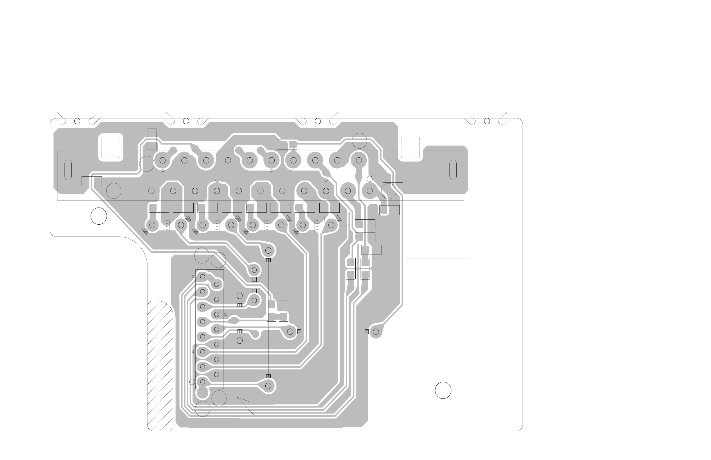
AUDIOGND
AUDIO-INR
14
15
2
1
20
21 1
2
R/PR
GND
B/PB
GND
G/Y
GND
NC
FUNCTION
D2IP/BLK
COMP/Y
AUDIOGND
AUDIO-INL
AUDIO-INR
CN602
C6041
C6042
R6040
R6041
C6034
R6036
R6039
C6035
R6033
R6042
C6036
R6044
C6032
R6037
R6043
R6034
R6032
C6033
R6038
R6031
C6038
J6001
C6039
R6035
C6031
(Lead free solder used in the board (material : Sn-Cu, melting point : 230 Centigrade))
<SCART board (Except EX-AR3LTDUT/AR3UF/AR5UF/BR3UF)>
(Lead free solder used in the board (material : Sn-Ag-Cu, melting point : 219 Centigrade))
created date:2011-06-09No.MB596
65
(No.MB596<Rev.004>)39/
Page 61
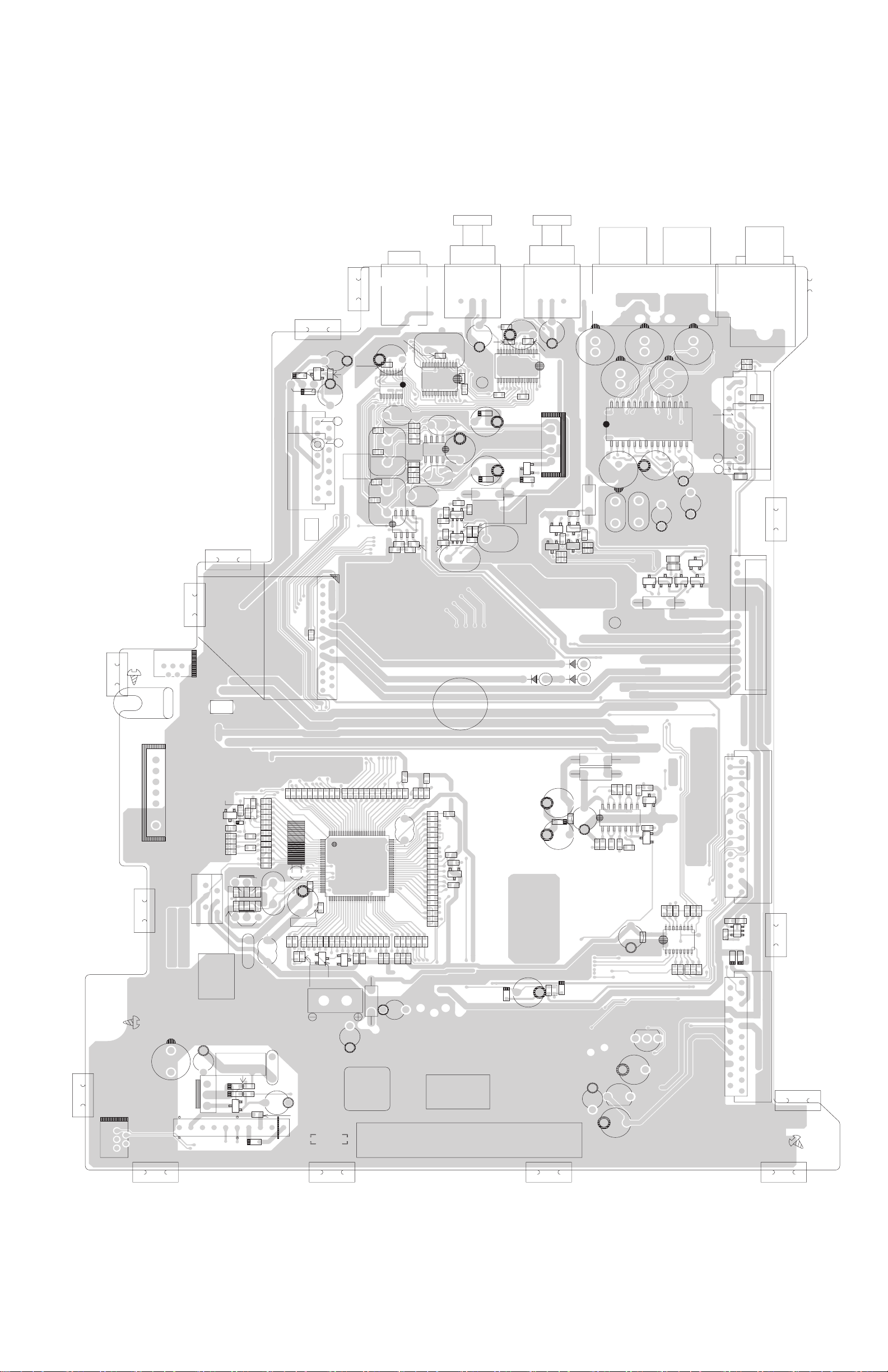
<Micom board (Except EX-AR3LTDUT/AR3UF/AR5UF/BR3UF)>
(Lead free solder used in the board (material : Sn-Ag-Cu, melting point : 219 Centigrade))
(Lead free solder used in the board (material : Sn-Cu, melting point : 230 Centigrade))
F1B
MARK
UL
PbF
N
S1B
41
11(CN706)
15(CN705)
15(CN711)
24
25
21
21
2
1
20
7
25
2
B
E
E
B
5
4
1
7
8
9
1
16
11
(CN712)
1
1
14
15
1
1
E
B
B
B
E
E
LVA10732
-A1
6
5
26
25
50
1
28
1
15
14
8
1
51
75
76
100
1
1
10
1
2
1
5
4
2
4
5
1
2
24
1
1
R7183
R7283
C7283
D7283
D7183
R6183
W9
W19
Q7135
WC702
C7912
R7154
J6002
Q7035
Q6002
Q6001
R7135
R7138
R7142
R7141
R7916
R7926
R7180
R7125
R7127
CN707
CN704
R2951
C2952
IC295
C2953
C2951
C2752
IC275
C2753
C2751
CN713
R2751
R2952
R2953
R5511
C5501
IC552
D5110
C5110
C5512
C5509
C5511
C5503
D5301
D5210
Q5301
C5502
K5504
C5508
R5507
R5506
R5505
R5504
C5504
C5507
IC551
IC555
IC554
IC553
R5206
R5102
C5201
R5205
R5301
IC511
R5105
R5204
C5301
C5103
C5102
R7211
CN711
R7230
C5202
C5203
C5210
R5103
R5202
R5106
R5203
R5201
R5101
R5104
C5101
R7235
IC702
CN712
R6181
Q6182
Q6183
Q6181
R6182
C6003
R6151
Q6154
R6156
C6004
C6005
C6008
R6015
Q6153
R6153
C6007
R6154
Q6152
Q6151
C6006
R6155
C6001
IC601
K6001
R6152
J6005
EP601
C6023
C6022
C6021
C9999
WC701
C6092
C6091
C6093
J6006
R6094
CN714
K7031
R7931
C7931
R7932
C7932
D7931 IC502
R7911
R7921
R7933
R7936
C7921
C7933
C7911
R7925
Q7932
Q7931
R7915
R7160
Q7060
R7121
R7112
CN710
R7120
D2202
D2201
R7117
R7115
R7116
R7119
C9998
R7114
R7113
R7122
R7111
R7110
R7159
R7083
K7066
R7065
R7056
R7162
R7147
R7148
R7149
R2501
R2502
C7210
C7209
C7208
C7207
R7177
R7175
R7176
CN703
D7022
D7021
D7020
IC251
C2503
C2502
C2803
Q2801
C2802
Q2803
C2801
R7502
Q7502
C7501
C7502
D7502
D7501
Q7501
R7501
C2201
IC221
C2202C2203
R7061
R7020
C7003
C7004
CN708
CN702
C7922
R7011
R7010
R7009
R7100
R7099
R7098
R7097
R7096
R7095
R7085
R7081
R7033
R7035
R7036
R7037
R7075
R7072
X7411
CN706
CN705
IC701
C7806
CN701
IC751
C7503
D7503
C7505
K7009
R7029
R7080
R7032
R7047
R7042
R7041
R7040
R7079
C7302
R7302
K7007
K7701
R7403
C7401
R7401
R7405
R7801R7802
X7801
C7802
C7801
R7804 R7803
Q7802
Q7801
C7804
C7805
Q7401
C7803
D7401
R7062
Q7301
C7301
L7701
C7711
R7711
C7712
R7051
R7054
R7055
R7050
R7049
R7048
K7501
C7701
C7001
C7002
R7052
Q7302
R7071
R7069
R7068
R7067
R7064
R7063
R7059
R7057
R7046
R7045
R7039
R7038
D7302
R7008
R7030
R7026
R7027
R7028
R7007
R7006
R7004
R7005
R7001
R7002
R7093
R7092
R7094
R7091
R7090
R7089
R7088
R7087
R7086
D7301
R7034
R7084
R7082
R7003
L7024
R7060
R7058
R7076
R7078
created date:2011-06-09No.MB596
65
(No.MB596<Rev.004>)40/
Page 62

P1B
T1B
DGND
DGND
DGND
14
15
DAC3OUT
DAC2OUT
DAC4OUT
DAC5OUT
DAC1OUT
D2V
TX
MGND
M5V
DVDPWR
S2UDT
SCS
CPURST
DGND
DGND
DGND
S5V
D4V
D2V
MGND
RX
M9V
U2SDT
UCLK
UCS
24 25
12
SI/SO
/RESE
T
SWVD
D
VD
D
FLMDO
DG
FLVH
MGND
K2GND
M11V
V11V
DVDM9V
USB5.4V
US5.4V
A5.4V
DVD5.4V
SWSIG
SWGND
RDSDATA
7
US5.4V
KEY2
COLED
VOL+
VOL-
DGND
US3.3VB
F-
FLDATA
FLCLK
FLSTB
FLBK
VH
F+
DGND
DGND
US3.3VC
/REM
STBLED
/PIN
KEY1
B
E
21
20
2
1
E
B
GND
OUT1P1VZ
IN1
IN2
VCC1
VCC2
P2
DINR
AGND
DINL
A10V
Y
VGND
CB
VGND
CR
SWGND
SWSIG
FUNCTION
S-DCOUT
VGND
TVR
TVL
TVG
COMP/Y
NC
D2IP/LINE2
SI/SO
/RESET
SWVDD
VDD
FLMDO
DG
VGND
VGND
VGND
SMUTE
US4V
1
15
TUCE
TUDO
TUCK
TUDI
TUG
TU-L
TU9V
TU-R
NC
TUG
SW3.3V
FRDS
RDSCL
RDSDA
1
10
B
E
B
B
B
E
4
1
1 1
V23V
F-SHIFT
PDOWN
SAFETY3
FDVD
SW11VCTL
FLPOWER
QPONSW
QPSENS2
QPSENS1
QPDET
HPMUTE
HPIN
REC1MUTE
REC1LEVEL
AUX1INDETB
AHB
OUT2
2
1
5
4
USB5.4V
USB5.4V
CLOSEDET
OPENDET
TRAYGND
M+
M-
1
25
24
1
2
4
5
2
1
/DCPRT
DGND
MODON
/MODPRT
F-SHIFT
MODSTBY
TUTVL
A.GND
TUTVR
A.GND
REC2MUTE
VOLCLK
VOLDATA
1
C7283
W9
W19
WC702
J6002
C6098
R7221
R7260
C7153
R7124
CN707
CN704
C7308
C7307
C2952
C2752
CN713
C5501
K5502
IC552
C5110
R5110
C5506
C5505
C5509
C5511
C5503
R5304
Q5302
R5305
R5501
R5502
C5502
K5501
K5503
C5510
R5510
R5509
R5508
R5503
IC551
C5201
R5210
R5301
C5301
C5103
C5102
CN711
C5202
C5203
C5210
C5101
R6024
C6027
CN712
C6029
R6182
C6003
R6010
R6007
R6001
R6005
C6004
C6005
C6008
R6015
R6008
R6004
C6007
R6003R6006
C6006
R6002
C6001
C6002
R6009
J6005
R7382
C6028
EP601
C6024
C6026C6025
R6023
C6023
C6022
R6022
R6021
C6021
C6097
WC701
C6101
R6096
R6095
C6092
R6092
R6093
C6091
R6091
C6099
C6100
C6095
K6091
C6096
C6094
J6006
CN714
R7931
C7931
C7932
R7938
R7912
R7933
R7922
R7913
C7933
R7934
R7937
R7923
R7935
R7924
R7914
R7216
R7215
CN710
C7303
R7220
C7174
R7182
R7282
R7277
CN703
D7022
D7021
D7020
C2501
R2803
C2803
Q2801
C2802
Q2802
Q2803
R2801
R2806
C2801
R2804
R2807
R2802
R2805
C2804
C7501
C7502
Q7501
R7214
R7222
C7004
CN708
C7219
CN702
R7024
D7801
R7016
X7411
C7412
C7411
CN706
CN705
R7217
Q7701
C7704
C7504
CN701
IC751
C7505
C7302
R7301
K7701
X7801
Q7802
Q7801
C7305
C7306
Q7301
C7301
R7702
R7704
L7701
D7711
C7711
R7711
R7712
C7712
K7501
Q7712
R7713
R7714
D7713
C7701
D7701
R7715
Q7713
C7001
R7701
Q7702
R7703
R7044
R7716
D7702
R7013
C7213
L7024
<Micom board (Except EX-AR3LTDUT/AR3UF/AR5UF/BR3UF)>
(Lead free solder used in the board (material : Sn-Ag-Cu, melting point : 219 Centigrade))
(Lead free solder used in the board (material : Sn-Cu, melting point : 230 Centigrade))
created date:2011-06-09No.MB596
65
(No.MB596<Rev.004>)41/
Page 63

<DEUS board (Except EX-AR3LTDUT/AR3UF/AR5UF/BR3UF)>
(Lead free solder used in the board (material : Sn-Ag-Cu, melting point : 219 Centigrade))
(Lead free solder used in the board (material : Sn-Cu, melting point : 230 Centigrade))
PbF
MARK
UL
8
7
1
R+
RGND
GND
L+
L-
6
LVA10732-A2
AGND
AGND
5
5
1
4
8
1
P.GN
D
P.GND
1
26
VDD
VDD
1
GND
GND
5
4
27
52
1
1
4
SGND4
SGND3
C1358
C1311
C1310
R1306
C1611
L1271
L1161
C1194
C1904
R1305
C1903
C1215
C1216
C1265
C1294
C1901
C1902
D1301
C1175
C1116
C1115
C1151
C1251
C1224
C1222
C1291
C1191
C1124
C1122
C1153
C1172
C1262
C1154
C1162
C1254
C1155
C1253
C1156
C1267
C1308
C1252
C1357
C1307
R1354
C1277
C1177
C1272
C1303
C1309
C1167
C1271
C1275
C1256
C1171
C1255
C1305
C1356
C1152
C1306
C1355
C1165
C1264
C1212
C1274
C1214
C1112
C1114
C1201
C1301
C1352
C1304
C1391
C1174
R1353
C1113
C1213
SGND1
SGND2
C1164
C1101
C1351
C1302
CN102
CN103
CN104
CN101
C1354
IC110
IC120
IC130
C1905
L1304
L1303
L1302
L1171
L1261
Q1611
Q1601
Q1303
Q1302
Q1602
Q1304
Q1612
Q1101
Q1201
Q1291
Q1192
Q1292
Q1191
Q1391
Q1305
R1128
R1803
R1154
R1123
R1126
C1353
R1807
R1252
R1124
R1127
R1228
R1225
R1224
R1357
R1222
R1223
R1121
R1801
R1221
R1255
R1226
R1227
R1358
R1213
R1804
R1292
R1214
R1111
R1114
R1191
R1253
R1112
R1192
R1254
R1152
R1155
R1603
R1156
R1352
R1307
R1308
R1122
R1805
R1257
R1612
R1802
R1806
R1158
R1258
R1602
R1113
R1212
R1601
R1251
R1356
R1151
R1351
R1301
R1355
R1611 R1157
R1256
R1613
R1291
R1161
R1271
R1153
R1211
R1202
R1171
R1261
R1102
R1103
R1203
R1125
R1302
created date:2011-06-09No.MB596
65
(No.MB596<Rev.004>)42/
Page 64

7
SMUTE
6
GND
L+
L-
GND
/DCPRT
GND
1
E
B
R
GND
L
SW10V
AHBCTL
/MODPRT
MODON
F-SHIFT2
MODSTBY
GND
VDD
VDD
R+
R-
GND
1
5
1
1
4
C1358
C1196
C1195
C1296
C1295
TP101
L1271
L1161
R1001
C1276
C1266
C1176
C1151
C1251
C1166
C1192
C1293
C1111
C1211
C1178
C1168
C1268
C1158
C1278
C1223
C1221
C1123
C1121
C1267
C1357
C1157
C1277
C1161
C1177
C1167
C1193
C1292
C1356
C1257
C1355
C1261
C1258
C1264
C1212
C1274
C1214
C1112
C1114
C1201
C1301
C1352
C1304
C1391
C1174
C1113
C1213
C1164
C1101
C1351
C1302
D1352
C
N
1
0
2
CN103
CN104
CN101
D1162
D1261
D1161
D1262
D1172
D1272
D1171
D1271
D1111
D1211
C1354
D1351
L1171
L1261
Q1601
R1304
C1353
R1312
R1272
R1262
R1162
R1172
R1604
R1311
R1101
R1201
R1316
R1614
R1104
R1204
R1302
<DEUS board (Except EX-AR3LTDUT/AR3UF/AR5UF/BR3UF)>
(Lead free solder used in the board (material : Sn-Ag-Cu, melting point : 219 Centigrade))
(Lead free solder used in the board (material : Sn-Cu, melting point : 230 Centigrade))
created date:2011-06-09No.MB596
65
(No.MB596<Rev.004>)43/
Page 65

(Lead free solder used in the board (material : Sn-Ag-Cu, melting point : 219 Centigrade))
<USB and Line board (Except EX-AR3LTDUT/AR3UF/AR5UF/BR3UF)>
(Lead free solder used in the board (material : Sn-Cu, melting point : 230 Centigrade))
PbF
MARK
UL
HPSW
HPR
HPL
HPGND
USBGND
USBGND
D5VD-D+
5
1
LVA10732-A3
LINE1INL
LINE1INGND
LINE1INR
LINE1INSW
LINE1OUTL
LINE1OUTGND
LINE1OUTR
7
1
4
1
7 1
CN443
CN442
CN441
C4439
WC401
K4438
EP441
EP442
J4401
J4402
J4403
J4404
created date:2011-06-09No.MB596
65
(No.MB596<Rev.004>)44/
Page 66

5
D5V
D-
D+
USBGND
USBGND
1
HPSW
HPL
HPGND
HPR
LINE1INL
LINE1INGND
LINE1INR
LINE1INSW
LINE1OUTL
LINE1OUTGND
LINE1OUTR
14
1
7
CN443
CN442
CN441
C4439
WC401
R4423
R4413
EP441
K4434
K4433
C4433
D4431
EP442
K4432
C4431
K4436
K4431
C4432
J4401
C4434
C4423
C4424
C4436
C4414
C4413
C4435
J4402
J4403
J4404
K4437
C4411
R4422
C4422
R4412
C4412
R4421
R4411
C4421
C4415
K4421
C4438
C4425
K4435
K4411
R4431
C4437
(Lead free solder used in the board (material : Sn-Ag-Cu, melting point : 219 Centigrade))
<USB and Line board (Except EX-AR3LTDUT/AR3UF/AR5UF/BR3UF)>
(Lead free solder used in the board (material : Sn-Cu, melting point : 230 Centigrade))
created date:2011-06-09No.MB596
65
(No.MB596<Rev.004>)45/
Page 67

<DVD board (Except EX-AR3LTDUT/AR3UF/AR5UF/BR3UF)>
(Lead free solder used in the board (material : Sn-Ag-Cu, melting point : 219 Centigrade))
(Lead free solder used in the board (material : Sn-Cu, melting point : 230 Centigrade))
1P2A
F S
N
MARK
UL
PbF
SIDE.A
HEAT PROOF FLUX
LVB10626-002A
S2A
LVA10626
B1
1
6
1
25
7
3
5
4
1
1
8
48
6
48
1
8
1
4
1
1
24
25
1
24
1
5
1
1
1
1
27
28
54
1
1
1
1
1
1
1
8
24
C291
R398
R304
R393
R379
R378
R129
C819
R819
TP819
R860
C891
R892
R891
IC891
D812
D811
TP813
TP811
TP812
TP801
TP802
R861
K812
K811
CN801
TP803
R812
R813 R814
R811
TP467
TP726
TP727
CN712
R531
IC505
TP723
R740
C562
C554
TP719
TP761
C701
C560
R730
R530
TP751
TP713
TP737
TP720
TP714
C382
TP752
C703
K701
TP708
TP745
K706
TP710
TP733
IC702
R725
TP744
C559
TP735
C743
K704
R535
C740
K501
C558
R715
TP742
R723
CN703
TP743
C380
TP716
TP747
C561
R716
TP701
K351
K703
CN701
TP750
TP749
CN704
TP711
TP746
TP731
C551
TP732
TP734
C715
TP736
TP741
TP709
K702
R721
C555
TP702
TP755
IC305
TP707
TP738
R718
IC703
TP721
C455
R719
R728
TP753
IC701
K705
IC509
TP748
TP722
C557
K710
R462
C742
C702
TP724
TP703
TP705
R458
TP380
TP718
K709
C714
TP717
R732
R399
K711
C381
C563
R731
R714
CN702
K707
TP725
K708
IC453
IC704
R724
C741
R727
TP303
TP302
TP301
TP300
R371
TP334
K353
C370
IC303
R318
K354
C364
C367
IC304
R313
C368
R704
R705
C328 C359
C304
IC302
TP321
R317
R315
TP322
R702
R703
R334
R337
R348
R375
C347
R368
R316
R201
C358
C357
CN101
D301
CN201
C351
TP102
C354
R105
R347
C320
TP315
TP208
TP123
R310
R251
Q102
TP120
TP115
TP110
R110
TP328
TP203
R109
C102
R335
R342
TP105
TP117
C210
R324
C205
C106
R103
TP204
TP202
R341
R372
R363
TP108
C352
C101
TP226
Q101
R108
TP201
C341
R361
R325
TP104
TP227
TP207
TP119
C338
TP103
R376
TP206
R338
R104
CN301
R360
R339
TP106
R106
TP122
IC201
TP116
C321
TP107
C204
R336
R357
C356
TP316
C202
C217
C201
C348
C337
C353
R326
TP121
R346
R107
C323
TP205
TP101
R333
C203
R204
TP112
TP111
R359
R340
TP118
TP109
R308
R353
R206
C322
R373
created date:2011-06-09No.MB596
65
(No.MB596<Rev.004>)46/
Page 68

4P2A
PT
SIDE.B
T2A
5
1
1
109
1
162
163
108
55
54
216
1
8
7
1
R291
C391
R130
R350
R349
R343
R344
R396
R397
R395
R394
R332
R131
R132
Q801
CN811
C803
TP814
C804
C802
C801
IC801
R859
K714
K755
C711
K765
C744
IC706
R742
R741
C713
C707
C752
K751
K732
K753
C708
R713
C704
K731
R712
C712
K762
K754
R720
K712
K720
R729 C709
C756
K726
R711
K733
K761
C721
R701
K713
C753
K756
K763
C754
K721
K722
C755
IC705
C745
K759
C728
R722
IC707
R726
C706
R314
TP338
R370
X302
R307
C303
R541
C564
C336
IC510
TP323
TP324
K101
R717
R320
R319
C392
C302
R321
IC301
R369
R331
R330
R329
R328
R322
R312
C350
C312
C316
C257
R362
C251
R207
R115
R364
R383
R118
R257
C326
C330
R392
TH301
TP330
C372
C319
C259
C332
R365
R309
C315
C104
C342
C371
C262
TP291
C105
R102
C313
R213
C373
R125
TP221
C306
C264
C258
R101
TP329
TP327
R367
C301
TP231
C377
R366
R205
R303
C349
R114
C206
C344
C263
C305
C314
C331
R290
TP333
R219
C378
C340
C345
TP337
C256
R259
C343
R202
R352
R116
R358
R351
C379
C333
C103
R221
C290
TP220
Q103
C260
C375
R306
K352
C374
TP331
TP326
TP381
C309
R311
R385
C393
C310
TP332
R128
C107
R345
C307
C383
C261
R214
R112
R127
Q104
R113
C386
R323
C339
C334
R220
R117
R111
C324
C335
C108
C318
C211
R384
C325
TP292
X301
L301
<DVD board (Except EX-AR3LTDUT/AR3UF/AR5UF/BR3UF)>
(Lead free solder used in the board (material : Sn-Ag-Cu, melting point : 219 Centigrade))
(Lead free solder used in the board (material : Sn-Cu, melting point : 230 Centigrade))
created date:2011-06-09No.MB596
65
(No.MB596<Rev.004>)47/
Page 69

(Lead free solder used in the board (material : Sn-Ag-Cu, melting point : 219 Centigrade))
(Lead free solder used in the board (material : Sn-Cu, melting point : 230 Centigrade))
<Loader board (Except EX-AR3LTDUT/AR3UF/AR5UF/BR3UF)>
LVA10530-
S1A
A1
PbF
UL
MARK
CN1
S1
created date:2011-06-09No.MB596
65
(No.MB596<Rev.004>)48/
Page 70

P1A
T1A
+
-
CN1
S1
(Lead free solder used in the board (material : Sn-Ag-Cu, melting point : 219 Centigrade))
(Lead free solder used in the board (material : Sn-Cu, melting point : 230 Centigrade))
<Loader board (Except EX-AR3LTDUT/AR3UF/AR5UF/BR3UF)>
created date:2011-06-09No.MB596
65
(No.MB596<Rev.004>)49/
Page 71

<Main board (EX-AR3LTDUT/AR3UF/AR5UF/BR3UF)>
(Lead free solder used in the board (material : Sn-Ag-Cu, melting point : 219 Centigrade))
(Lead free solder used in the board (material : Sn-Cu, melting point : 230 Centigrade))
S1C
L
+
R
-
P
.
G
N
D
6
1
L
-
P
.
G
N
D
R
+
1
2
8
1
4
1
3
1
3
1
B
E
15
1
4
1
5
1
420kHz
400kHz
5
A1
LVA10733-
24
25
4
4
1
B
E
2
1
1
1
UL
MARK
PbF
C4991
B1905
B1854
B1141
WC202
W212
B1154
B1155
B1156
B1710
B1157
W5
B1153
B1152
B1151
B1150
B1149
B1148
W4
B1954
B1956
B1532
B1531
B1147
C4375
C4374
B1146
B1530
B1403
B1903
B1802
B1415
B1804
B1145
B1902
B1414
B1529
B1528
B1955
B1204
B1143
B1527
B1142
B1218
B1526
B1525
B1709
B1708
B1413
B1808
B1524
B1523
B1522
B1521
B1520
B1519
B1518
B1517
B1516
B1144
C4341
B1412
B1411
B1410
B1515
CN202
B1514
B1513
B1512
B1852
B1140
B1139
B1138
B1511
B1409
B1137
B1408
B1136
B1135
B1307
C4332
B1510
B1509
B1508
B1133
B1132
B1407
B1406
B1308
B1216
B1309
B1707
B1405
B1404
B1507
B1131
B1807
B1806
B1805
B1606
B1130
B1129
B1306
B1215
B1901
B1128
B1402
B1706
B1605
B1214
B1127
B1126
B1506
B1124
B1534
B1803
B1123
B1505
B1608
B1212
B1122
B1121
B1120
B1604
B1302
C
N
3
0
1
B1536
B1705
B1119
B1118
B1401
B1117
B1535
B1504
B1503
B1116
B1115
B1502
B1114
B1851
B1211
B1113
B1304
B1704
B1703
B1537
B1112
B1210
B1603
B1702
B1111
B1303
B1110
B1209
B1208
B1109
B1108
B1701
B1538
B1602
J3001
EP401
B1107
B1106
B1206
B1205
L1281
B1203
L1181
B1501
C2703
W3
WW3
W204
C2901
C2335
X2302
X2301
C2114
R2012
Q2701
D2701
R2424
C2410
C2423
TP201
TP202
WW1
WW2
W1
W2
C2702
D2403
D2406
W211
C2408
C2409
D2405
B1809
C2422
Q2421
C2404
C2407
B1305
CN213
B1853
B1134
C2421
D2301
B1904
C2104
CN201
D2114
C2112
L2101
WC201
C2004
D2014
R2411
C2012
L2001
J4101
C4135
C4701
C4704
C4713
R4710
C4707
C4705
C4340
C4321
D4171
C4171
W209
C4262
C4162
C4360
C4354
C4261
C4161
C4158
C4258
C4157
C4257
W205
CN208
CN206
B1711
B1125
W203
C4302
C4301
C4201
C4101
C4104
C4303
C4204
C4234
C4134
C4105
C4312
C4205
R4391
C4391
C4192
C4292
C4191
C4291
D4351
R4351
R4371
C4373
C4372
C4351
C4371
C4331
D4271
C4305
R4306
C4172
C4175
C4271
C4173
C4174
C4392
C4225
R4331
C4125
C4275
C4274
C4272
C4273
C4359
C4358
C4357
C4356
C4156
C4256
C4160
C4260
C4159
C4259
C4352
C4151
C4251
C4353
C4235
C4131
C4231
C4132
C4232
W207
B1951
B1801
B1202
B1105
B1104
B1103
B1102
B1601
B1101
B1201
B1301
created date:2011-06-09No.MB596
65
(No.MB596<Rev.004>)50/
Page 72

P1C
T1C
8
AUX1INDETB
6
4
1
3
6
2
1
LINE1NL
AGND
LINE1NR
LINE1INDET
LINE1OUT
AGND
LINE1OUT
1
4
5
1
8
B
SWSIG
SWGND
FLVH
DGND
DGND
DGND
K2GND
6
1
L
+
L
-
P
.
G
N
D
P
.
G
N
D
R
-
R
+
35V
GND
20V
GND
4
SW11V
AHBCLTL
1 3
14
HPIN
AG
L
R
B
A
A
3
1
224
25
5.4V
DVDR
AGND
DVDL
LRMUTE
4
1
1
15
2
DINR
AGND
DINL
A10V
4
5
8
1
B
8
1
5
4
DVDM9V
M11V
A5.4V
DVD5.4V
US5.4V
USB5.4V
V11V
MGND
L
R
US4V
SAFETY3
SW11VCTL
/QPONSW
/HPMUTE
/REC1MUTE
REC1REVEL
/REC2MUTE
VOLDATA
V23V
F-SHIFT
PDOWN
FDVD
FLPOWER
QPSENS2
QPSENS1
/QPDET
HPIN
/AHB
VOLCK
AGND
TUTVR
AGND
TUTVL
PGND
PGND
VDD
VDD
GND
5
8
1
4
B
1
16
32
17
1
4
1
1
5
4
8
1
1
5
8
1
4
5
8
1
E
8
14
14
1
7
1
14
1
8
1
4
5
3
4
E
1
4
P1
C4991
R2602
R2603
Q2601
C4315
WC202
W212
W5
W4
C4375
C4374
R4378
R4377
IC261
D4321
C4341
R4341
Q4341
CN202
C4332
R2601
R4252
R4251
R4152
R4151
C
N
30
1
R4356
R4355
J3001
C1381
EP401
C1181C1281
L1281
L1181
C1283
C2703
R2119
W3
WW3
W204
C2901
Q2901
R2901
C2902
C2335
R2332
X2302
C2332
X2301
C2334
R2333
R2334
C2333
C2331
IC233
R2331
IC201
C2114
C2014
R2012
R2701
R2702
Q2702
C2701
Q2701
D2701
Q2410
D2303
R2441
D2408
Q2403
R2425
Q2423
R2424
C2424
C2410
C2423
TP201
TP202
IC200
WW1
WW2
W1
W2
C2702
R2443
D2403
D2406
Q2409
W211
R2107
R2019
R2008
D2015
C2408
C2409
D2421
R2405
D2405
R2444
R2316
C2304
R2417
R2106
R2448
R2449
C2422
R2422
R2423
R2421
Q2422
Q2421
R2317
R2446
R2445
R2010
R2108
D2116
IC241
R2412
Q2411
C2404
Q2408
C2407
R2404
R2403
R2442
C1184
C1284
C1183
C1185
C1285
C1186
R2315
C1182
C1286
CN21
3
R2416
C2421
R2303
D2301
C2302
R2302
IC231
C2104
R2104
IC232
R2105
C2103
CN201
R2114
Q2112
R2115
C2111
R2118
R2116
Q2113
R2117
C2113
D2114
C2112
D2113
L2101
Q2111
R2113
WC20
1
C2004
R2004
Q2003
R2006
R2005
C2003
C2002
Q2002
R2001
R2002
Q2001
D2001
R2003
C2001
IC202
R2014
C2405
Q2012
R2015
C2011
R2018
R2016
Q2013
R2017
C2013
D2014
R2411
C2012
D2013
L2001
Q2011
R2013
R2007
J4101
R4711
R4716
R4715
Q4702
R4712
Q4701
R4708
C4709
C4135
R4132
R4130
R4141
R4241
Q4140
R4244
Q4240
R4144
R4602
R4501
R4701
R4719
C4708
R4702
R4502
R4707
R4722
C4701
C4702
R4709
R4714
C4704
R4601
Q4703
R4705
C4713
Q4705
D4701
C4712
C4710
R4713
R4725
D4702
Q4704
Q4706
C4711
R4721
R4710
R4717
D4703
R4724
C4706
Q4707
R4704
C4707
R4706
C4705
R4720
IC452
R4718
Q4708
R4723
R4703
C4703
R4142
R4242
R4140
C4340
R4243
Q4340
Q4241
R4240
R4143
Q4141
R4340
C4221
C4121
Q4321
R4321
R4227
R4123
Q4121
Q4221
R4127
R4223
R4124
C4321
R4224
D4171
R4170
C4171
W209
C2411
R4222
R4122
C4262
C4162
C4360
C4354
C4261
C4161
C4158
C4258
C4157
C4257
IC451
W205
CN208
CN206
W203
K4302
C4226
C4126
C4302
C4301
R4301
R4302
R4112
R4212
R4110
R4210
R4101
R4201
Q4202
R4102
R4202
R4203
R4103
C4201
C4101
R4207
R4206
C4202
C4203
R4205
R4107
R4106
C4102
R4105
C4103
C4104
IC401
C4303
Q4301
R4211
R4111
C4204
Q4201
Q4101
R4314
C4311
C4234
C4134
R4238
R4138
R4137
R4237
Q4312
R4312
Q4311
Q4102
C4105
R4221
R4121
C4312
R4313
C4205
R4391
D4311
Q4313
R4311
C4391
C4192
C4292
C4191
C4291
D4351
IC491
R4351
R4371
R4375
C4373
R4376
Q4373
R4372
C4372
D4371
C4351
C4371
R4397
C4314
C4331
R4315
R4181
R4177
R4281
R4277
R4374
R4373
D4271
C4305
Q4372
Q4371
R4171
R4173
R4305
R4306
C4172
R4175
C4175
Q4191
R4392
R4176
R4174
R4179
R4279
R4178
R4278
C4271
C4173
C4174
R4270
R4292
C4392
R4192
R4172
R4394
R4273
C4225
R4331
C4125
R4226
R4126
R4225
R4125
R4275
R4276
C4275
R4272
R4274
R4395
C4274
C4272
C4273
R4271
R4396
IC471
Q4305
Q4192
R4354
R4353
C4359
C4358
C4357
Q4292
C4356
R4304
R4398
C4156
C4256
C4160
C4260
C4159
C4259
Q4291
C4352
C4151
C4251
C4353
R4133
R4233
R4231
R4235
R4236
R4131
R4135
R4193
R4293
C4235
R4191
R4291
R4230
IC431
R4136
R4134
C4131
C4231
C4132
C4232
R4232
R4234
W207
C1282
<Main board (EX-AR3LTDUT/AR3UF/AR5UF/BR3UF)>
(Lead free solder used in the board (material : Sn-Ag-Cu, melting point : 219 Centigrade))
(Lead free solder used in the board (material : Sn-Cu, melting point : 230 Centigrade))
created date:2011-06-09No.MB596
65
(No.MB596<Rev.004>)51/
Page 73
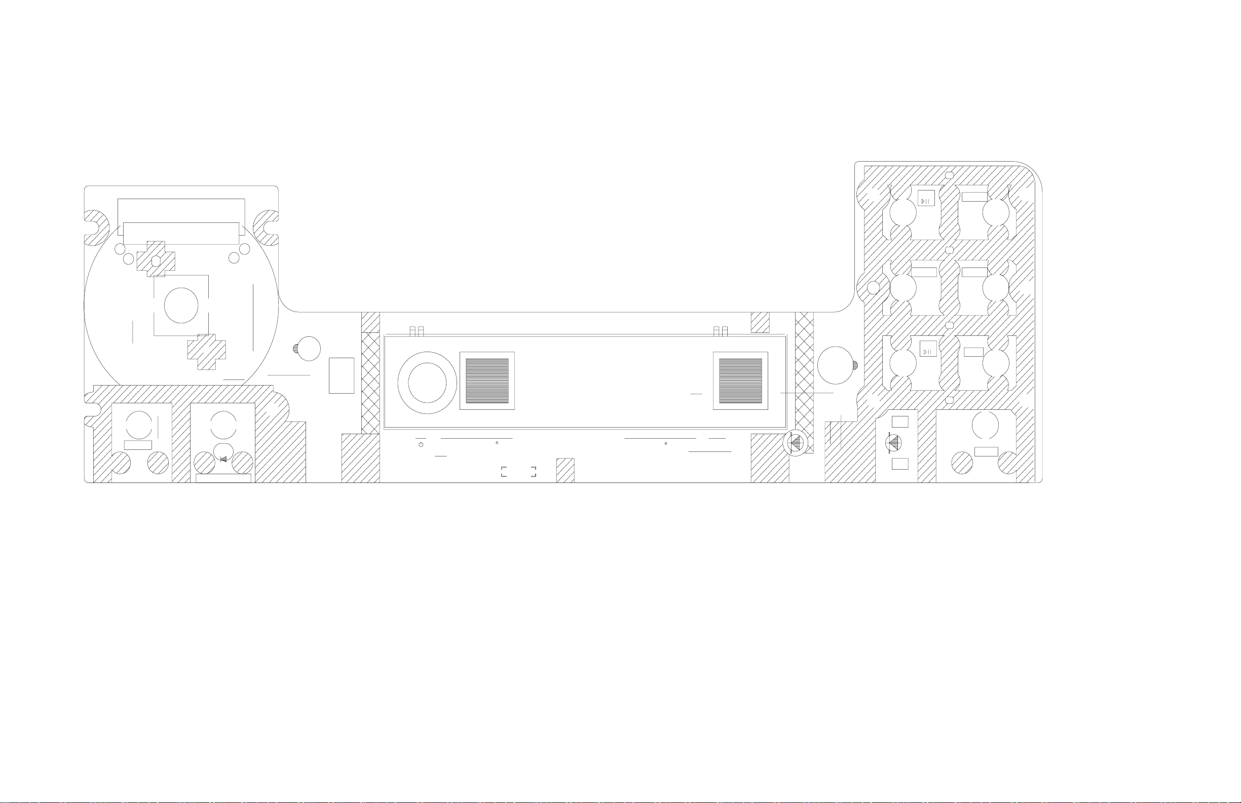
<Front board (EX-AR3LTDUT/AR3UF/AR5UF/BR3UF)>
(Lead free solder used in the board (material : Sn-Ag-Cu, melting point : 219 Centigrade))
(Lead free solder used in the board (material : Sn-Cu, melting point : 230 Centigrade))
PbF
MARK
UL
21
20
2
1
CC CONVERTER
FM/AM
STOP
DVD
USB
LVA10733-A2
EJECT
POWER
B.SKIPF.SKIP
B2301
B1609
D8201
DI801
B2102
B2101
B2204
B2501
B2402
B2203
B2202
B2401
B2201
D8101
D8001
C8102
IC801
S8203
S8202
S8201
S8001
S8205
JS801
S8101
S8206
C8002
S8102
S8204
CN801
created date:2011-06-09No.MB596
65
(No.MB596<Rev.004>)52/
Page 74

20
21
2
1
DGND
DGND
US3.3V
REM
STBLED
PIN
KEY1
US5.4V
KEY2
CCLED
VOL+
VOL-
DGND
FLVDD
F-
FLDATA
FLCLK
FLBK
FLSTB
VH
F+
R8006
R8106
R8105
Q8201
D8201
DI801
R8206
R8102
Q8101
D8101
R8104
Q8001
R8101
D8001
R8103
C8101
C8102
IC801
R8004
R8205
R8203
R8003
R8204
S8203
C8003
S8202
R8001
S8201
R8002
S8001
S8205
R8202
JS801
R8005
R8201
C8202
C8004
S8101
S8206
C8201
C8001
C8002
S8102
S8204
CN801
<Front board (EX-AR3LTDUT/AR3UF/AR5UF/BR3UF)>
(Lead free solder used in the board (material : Sn-Ag-Cu, melting point : 219 Centigrade))
(Lead free solder used in the board (material : Sn-Cu, melting point : 230 Centigrade))
created date:2011-06-09No.MB596
65
(No.MB596<Rev.004>)53/
Page 75

(Lead free solder used in the board (material : Sn-Cu, melting point : 230 Centigrade))
<SCART board (EX-AR3LTDUT/AR3UF/AR5UF/BR3UF)>
(Lead free solder used in the board (material : Sn-Ag-Cu, melting point : 219 Centigrade))
PbF
MARK
UL
AUDIOGND
GND
R/PR
B/PB
GND
G/Y
GND
NC
FUNCTION
D2IP/BLK
COMP/Y
AUDIOGND
AUDIO-INL
AUDIO-INR
AUDIO-INR
15
14
1
2
LVA10733-A4
1
21
CN602
B4101
B4801
B4201
B4501
C6035C6036C6038
J6001
C6039
created date:2011-06-09No.MB596
65
(No.MB596<Rev.004>)54/
Page 76

AUDIOGND
AUDIO-INR
14
15
2
1
20
21 1
2
R/PR
GND
B/PB
GND
G/Y
GND
NC
FUNCTION
D2IP/BLK
COMP/Y
AUDIOGND
AUDIO-INL
AUDIO-INR
CN602
C6041
C6042
R6040
R6041
C6034
R6036
R6039
C6035
R6033
R6042
C6036
R6044
C6032
R6037
R6043
R6034
R6032
C6033
R6038
R6031
C6038
J6001
C6039
R6035
C6031
(Lead free solder used in the board (material : Sn-Cu, melting point : 230 Centigrade))
<SCART board (EX-AR3LTDUT/AR3UF/AR5UF/BR3UF)>
(Lead free solder used in the board (material : Sn-Ag-Cu, melting point : 219 Centigrade))
created date:2011-06-09No.MB596
65
(No.MB596<Rev.004>)55/
Page 77

<Micom board (EX-AR3LTDUT/AR3UF/AR5UF/BR3UF)>
(Lead free solder used in the board (material : Sn-Ag-Cu, melting point : 219 Centigrade))
(Lead free solder used in the board (material : Sn-Cu, melting point : 230 Centigrade))
F1E
MARK
UL
PbF
N
E
S1E
41
11(CN706)
15(CN705)
15(CN711)
24
25
21
21
2
1
20
7
25
2
B
E
B
5
4
1
7
8
9
1
16
11
(CN712)
1
1
14
15
1
1
E
B
B
B
E
E
LVA10732
-A1
6
5
26
25
50
1
28
1
15
14
8
1
51
75
76
100
1
1
10
1
2
1
5
4
2
4
5
1
2
24
1
1
C7178
C7179
C7180
C7181
C7182
C7183
R7118
R7183
R7283
C7283
D7283
D7183
R6183
W9
W19
Q7135
WC702
C7912
R7154
J6002
Q7035
Q6002
Q6001
R7135
R7138
R7142
R7141
R7916
R7926
R7180
R7125
R7127
CN707
CN704
R2951
C2952
IC295
C2953
C2951
C2752
IC275
C2753
C2751
CN713
R2751
R2952
R2953
R5511
C5501
IC552
D5110
C5110
C5512
C5509
C5511
C5503
D5301
D5210
Q5301
C5502
K5504
C5508
R5507
R5506
R5505
R5504
C5504
C5507
IC551
IC555
IC554
IC553
R5206
R5102
C5201
R5205
R5301
IC511
R5105
R5204
C5301
C5103
C5102
R7211
CN711
R7230
C5202
C5203
C5210
R5103
R5202
R5106
R5203
R5201
R5101
R5104
C5101
R7235
IC702
CN712
R6181
Q6182
Q6183
Q6181
R6182
C6003
R6151
Q6154
R6156
C6004
C6005
C6008
R6015
Q6153
R6153
C6007
R6154
Q6152
Q6151
C6006
R6155
C6001
IC601
K6001
R6152
J6005
EP601
C6023
C6022
C6021
C9999
WC701
C6092
C6091
C6093
J6006
R6094
CN714
K7031
R7931
C7931
R7932
C7932
D7931 IC502
R7911
R7921
R7933
R7936
C7921
C7933
C7911
R7925
Q7932
Q7931
R7915
R7160
Q7060
R7121
R7112
CN710
R7120
D2202
D2201
R7117
R7115
R7116
R7119
C9998
R7114
R7113
R7122
R7111
R7110
R7159
R7083
K7066
R7065
R7056
R7162
R7147
R7148
R7149
R2501
R2502
C7210
C7209
C7208
C7207
R7177
R7175
R7176
CN703
D7022
D7021
D7020
IC251
C2503
C2502
C2803
Q2801
C2802
Q2803
C2801
R7502
Q7502
C7501
C7502
D7502
D7501
Q7501
R7501
C2201
IC221
C2202
C2203
R7061
R7020
C7003
C7004
CN708
CN702
C7922
R7011
R7010
R7009
R7100
R7099
R7098
R7097
R7096
R7095
R7085
R7081
R7033
R7035
R7036
R7037
R7075
R7072
X7411
CN706
CN705
IC701
C7806
CN701
IC751
C7503
D7503
C7505
K7009
R7029
R7080
R7032
R7047
R7042
R7041
R7040
R7079
C7302
R7302
K7007
K7701
R7403
C7401
R7401
R7405
R7801R7802
X7801
C7802
C7801
R7804 R7803
Q7802
Q7801
C7804
C7805
Q7401
C7803
D7401
R7062
Q7301
C7301
L7701
C7711
R7711
C7712
R7051
R7054
R7055
R7050
R7049
R7048
K7501
C7701
C7001
C7002
R7052
Q7302
R7071
R7069
R7068
R7067
R7064
R7063
R7059
R7057
R7046
R7045
R7039
R7038
D7302
R7008
R7030
R7026
R7027
R7028
R7007
R7006
R7004
R7005
R7001
R7002
R7093
R7092
R7094
R7091
R7090
R7089
R7088
R7087
R7086
D7301
R7034
R7084
R7082
R7003
L7024
R7060
R7058
R7076
R7078
created date:2011-06-09No.MB596
65
(No.MB596<Rev.004>)56/
Page 78

P1E
T1E
FLVDD
DGND
DGND
DGND
14
15
DAC3OUT
DAC2OUT
DAC4OUT
DAC5OUT
DAC1OUT
D2V
TX
MGND
M5V
DVDPWR
S2UDT
SCS
CPURST
DGND
DGND
DGND
S5V
D4V
D2V
MGND
RX
M9V
U2SDT
UCLK
UCS
24 25
12
SI/SO
/RESET
SWVDD
VDD
FLMDO
DG
FLVH
MGND
K2GND
M11V
V11V
DVDM9V
USB5.4V
US5.4V
A5.4V
DVD5.4V
SWSIG
SWGND
RDSDATA
7
US5.4V
KEY2
COLED
VOL+
VOL-
DGND
F-
FLDATA
FLCLK
FLSTB
FLBK
VH
F+
DGND
DGND
US3.3VC
/REM
STBLED
/PIN
KEY1
B
E
21
20
2
1
E
B
GND
OUT1P1VZ
IN1
IN2
VCC1
VCC2
P2
DINR
AGND
DINL
A10V
Y
VGND
CB
VGND
CR
SWGND
SWSIG
FUNCTION
S-DCOUT
VGND
TVR
TVL
TVG
COMP/Y
NC
D2IP/LINE2
SI/SO
/RESET
SWVDD
VDD
FLMDO
DG
VGND
VGND
VGND
SMUTE
US4V
1
15
TUCE
TUDO
TUCK
TUDI
TUG
TU-L
TU9V
TU-R
NC
TUG
SW3.3V
FRDS
RDSCL
RDSDA
1
10
B
E
B
B
B
E
4
1
1 1
V23V
F-SHIFT
PDOWN
SAFETY3
FDVD
SW11VCTL
FLPOWER
QPONSW
QPSENS2
QPSENS1
QPDET
HPMUTE
HPIN
REC1MUTE
REC1LEVEL
AUX1INDETB
AHB
OUT2
2
1
5
4
USB5.4V
USB5.4V
CLOSEDET
OPENDET
TRAYGND
M+
M-
1
25
24
1
2
4
5
2
1
/DCPRT
DGND
MODON
/MODPRT
F-SHIFT
MODSTBY
TUTVL
A.GND
TUTVR
A.GND
REC2MUTE
VOLCLK
VOLDATA
1
C7283
W9
W19
WC702
J6002
C6098
R7221
R7260
C7153
R7124
CN707
CN704
C7308
C7307
C2952
C2752
CN713
C5501
K5502
IC552
C5110
R5110
C5506
C5505
C5509
C5511
C5503
R5304
Q5302
R5305
R5501
R5502
C5502
K5501
K5503
C5510
R5510
R5509
R5508
R5503
IC551
C5201
R5210
R5301
C5301
C5103
C5102
CN711
C5202
C5203
C5210
C5101
R6024
C6027
CN712
C6029
R6182
C6003
R6010
R6007
R6001
R6005
C6004
C6005
C6008
R6015
R6008
R6004
C6007
R6003R6006
C6006
R6002
C6001
C6002
R6009
J6005
R7382
C6028
EP601
C6024
C6026C6025
R6023
C6023
C6022
R6022
R6021
C6021
C6097
WC701
C6101
R6096
R6095
C6092
R6092
R6093
C6091
R6091
C6099
C6100
C6095
K6091
C6096
C6094
J6006
CN714
R7931
C7931
C7932
R7938
R7912
R7933
R7922
R7913
C7933
R7934
R7937
R7923
R7935
R7924
R7914
R7216
R7215
CN710
C7303
R7220
C7174
R7182
R7282
R7277
CN703
D7022
D7021
D7020
C2501
R2803
C2803
Q2801
C2802
Q2802
Q2803
R2801
R2806
C2801
R2804
R2807
R2802
R2805
C2804
C7501
C7502
Q7501
R7214
R7222
C7004
CN708
C7219
CN702
R7024
D7801
R7016
X7411
C7412
C7411
CN706
CN705
R7217
Q7701
C7704
C7504
CN701
IC751
C7505
C7302
R7301
K7701
X7801
Q7802
Q7801
C7305
C7306
Q7301
C7301
R7702
R7704
L7701
D7711
C7711
R7711
R7712
C7712
K7501
Q7712
R7713
R7714
D7713
C7701
D7701
R7715
Q7713
C7001
R7701
Q7702
R7703
R7044
R7716
D7702
R7013
C7213
L7024
<Micom board (EX-AR3LTDUT/AR3UF/AR5UF/BR3UF)>
(Lead free solder used in the board (material : Sn-Ag-Cu, melting point : 219 Centigrade))
(Lead free solder used in the board (material : Sn-Cu, melting point : 230 Centigrade))
created date:2011-06-09No.MB596
65
(No.MB596<Rev.004>)57/
Page 79
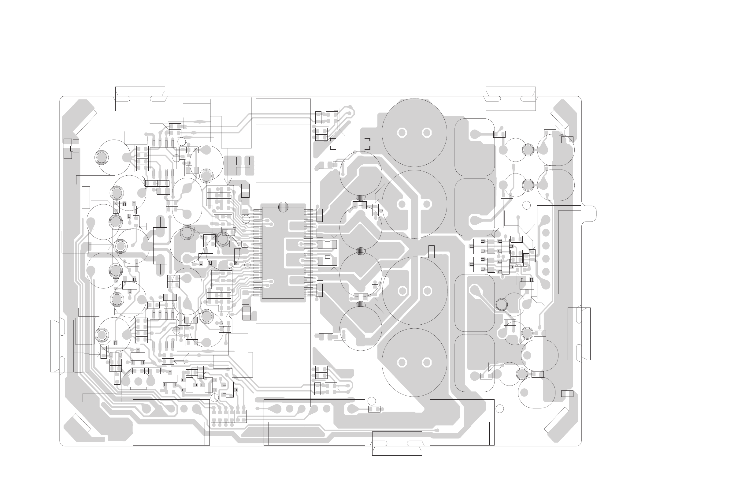
<DEUS board (EX-AR3LTDUT/AR3UF/AR5UF/BR3UF)>
(Lead free solder used in the board (material : Sn-Ag-Cu, melting point : 219 Centigrade))
(Lead free solder used in the board (material : Sn-Cu, melting point : 230 Centigrade))
8
7
1
R+
RGND
GND
L+
L-
6
LVA10732-A2
AGND
AGND
5
5
1
4
8
1
P.GN
D
P.GND
1
26
VDD
VDD
1
GND
GND
5
4
27
52
1
1
4
SGND4
SGND3
C1358
UL
MARK
C1311
C1310
R1306
C1611
L1271
L1161
C1194
C1904
R1305
C1903
C1215
C1216
C1265
C1294
C1901
C1902
D1301
C1175
C1116
C1115
C1151
C1251
C1224
C1222
C1291
C1191
C1124
C1122
C1153
C1172
C1262
C1154
C1162
C1254
C1155
C1253
C1156
C1267
C1308
C1252
C1357
C1307
R1354
C1277
C1177
C1272
C1303
C1309
C1167
C1271
C1275
C1256
C1171
C1255
C1305
C1356
C1152
C1306
C1355
C1165
C1264
C1212
C1274
C1214
C1112
C1114
C1201
C1301
C1352
C1304
C1391
C1174
R1353
C1113
C1213
SGND1
SGND2
C1164
C1101
C1351
C1302
CN102
CN103
CN104
CN101
C1354
IC110
IC120
IC130
C1905
L1304
L1303
L1302
L1171
L1261
Q1611
Q1601
Q1303
Q1302
Q1602
Q1304
Q1612
Q1101
Q1201
Q1291
Q1192
Q1292
Q1191
Q1391
Q1305
R1128
R1803
R1154
R1123
R1126
C1353
R1807
R1252
R1124
R1127
R1228
PbF
R1225
R1224
R1357
R1222
R1223
R1121
R1801
R1221
R1255
R1226
R1227
R1358
R1213
R1804
R1292
R1214
R1111
R1114
R1191
R1253
R1112
R1192
R1254
R1152
R1155
R1603
R1156
R1352
R1307
R1308
R1122
R1805
R1257
R1612
R1802
R1806
R1158
R1258
R1602
R1113
R1212
R1601
R1251
R1356
R1151
R1351
R1301
R1355
R1611 R1157
R1256
R1613
R1291
R1161
R1271
R1153
R1211
R1202
R1171
R1261
R1102
R1103
R1203
R1125
R1302
created date:2011-06-09No.MB596
65
(No.MB596<Rev.004>)58/
Page 80

7
SMUTE
6
GND
L+
L-
GND
/DCPRT
GND
1
E
B
R
GND
L
SW10V
AHBCTL
/MODPRT
MODON
F-SHIFT2
MODSTBY
GND
VDD
VDD
R+
RGND
1
5
1
1
4
C1358
C1196
C1195
C1296
C1295
TP101
L1271
L1161
R1001
C1276
C1266
C1176
C1151
C1251
C1166
C1192
C1293
C1111
C1211
C1178
C1168
C1268
C1158
C1278
C1223
C1221
C1123
C1121
C1267
C1357
C1157
C1277
C1161
C1177
C1167
C1193
C1292
C1356
C1257
C1355
C1261
C1258
C1264
C1212
C1274
C1214
C1112
C1114
C1201
C1301
C1352
C1304
C1391
C1174
C1113
C1213
C1164
C1101
C1351
C1302
D1352
C
N
1
0
2
CN103
CN104
CN101
D1162
D1261
D1161
D1262
D1172
D1272
D1171
D1271
D1111
D1211
C1354
D1351
L1171
L1261
Q1601
R1304
C1353
R1312
R1272
R1262
R1162
R1172
R1604
R1311
R1101
R1201
R1316
R1614
R1104
R1204
R1302
<DEUS board (EX-AR3LTDUT/AR3UF/AR5UF/BR3UF)>
(Lead free solder used in the board (material : Sn-Ag-Cu, melting point : 219 Centigrade))
(Lead free solder used in the board (material : Sn-Cu, melting point : 230 Centigrade))
created date:2011-06-09No.MB596
65
(No.MB596<Rev.004>)59/
Page 81

(Lead free solder used in the board (material : Sn-Ag-Cu, melting point : 219 Centigrade))
<USB and Line board (EX-AR3LTDUT/AR3UF/AR5UF/BR3UF)>
(Lead free solder used in the board (material : Sn-Cu, melting point : 230 Centigrade))
PbF
MARK
UL
HPSW
HPR
HPL
HPGND
USBGND
USBGND
D5VD-D+
5
1
LVA10732-A3
LINE1INL
LINE1INGND
LINE1INR
LINE1INSW
LINE1OUTL
LINE1OUTGND
LINE1OUTR
7
1
4
1
7 1
CN443
CN442
CN441
C4439
WC401
K4438
EP441
EP442
J4401
J4402
J4403
J4404
created date:2011-06-09No.MB596
65
(No.MB596<Rev.004>)60/
Page 82

5
D5V
D-
D+
USBGND
USBGND
1
HPSW
HPL
HPGND
HPR
LINE1INL
LINE1INGND
LINE1INR
LINE1INSW
LINE1OUTL
LINE1OUTGND
LINE1OUTR
14
1
7
CN443
CN442
CN441
C4439
WC401
R4423
R4413
EP441
K4434
K4433
C4433
D4431
EP442
K4432
C4431
K4436
K4431
C4432
J4401
C4434
C4423
C4424
C4436
C4414
C4413
C4435
J4402
J4403
J4404
K4437
C4411
R4422
C4422
R4412
C4412
R4421
R4411
C4421
C4415
K4421
C4438
C4425
K4435
K4411
R4431
C4437
(Lead free solder used in the board (material : Sn-Ag-Cu, melting point : 219 Centigrade))
<USB and Line board (EX-AR3LTDUT/AR3UF/AR5UF/BR3UF)>
(Lead free solder used in the board (material : Sn-Cu, melting point : 230 Centigrade))
created date:2011-06-09No.MB596
65
(No.MB596<Rev.004>)61/
Page 83

<DVD board (EX-AR3LTDUT/AR3UF/AR5UF/BR3UF)>
(Lead free solder used in the board (material : Sn-Ag-Cu, melting point : 219 Centigrade))
(Lead free solder used in the board (material : Sn-Cu, melting point : 230 Centigrade))
1P2A
F
N
UL
MARK
PbF
HEAT PROOF FLUX
S
LVB10824-002A
S2A
1
B1
LVA10824-
28
1
8
1
1
1
6
1
25
7
3
5
4
1
48
6
48
1
8
1
4
1
1
24
25
24
1
5
1
1
27
54
1
1
1
1
1
1
1
8
24
CN713
C291
R291
R398
R304
R393
R379
R378
R129
TP116
C819
R819
TP819
R860
C891
R892
R891
IC891
D812
D811
TP813
TP811
TP812
TP801
TP802
R861
K812
K811
CN801
TP803
R812
R813 R814
R811
TP467
TP726
TP727
CN712
R531
IC505
TP723
R740
C562
C554
TP719
TP761
C701
C560
R730
R530
TP751
TP713
TP737
TP720
TP714
TP752
C703
K701
TP708
TP745
K706
TP710
TP733
IC702
R725
TP744
C559
TP735
C743
K704
R535
C740
K501
C558
R715
TP742
R723
CN703
TP743
C380
TP716
TP747
C561
R716
TP701
K351
K703
CN701
TP750
TP749
CN704
TP711
TP746
TP731
C551
TP732
TP734
C715
TP736
TP741
TP709
K702
R721
C555
TP702
TP755
IC305
TP707
TP738
R718
IC703
TP721
C455
R719
R728
TP753
IC701
K705
IC509
TP748
TP722
C557
K710
R462
C742
C702
TP724
TP703
TP705
R458
TP380
TP718
K709
C714
TP717
R732
R399
K711
C381
C563
R731
R714
CN702
K707
TP725
K708
IC453
IC704
R724
C741
R727
TP303
TP302
TP301
TP300
R371
TP334
K353
C370
IC303
R318
K354
C364
C367
IC304
R313
C368
R704
R705
C328 C359
C304
IC302
TP321
TP105
R317
R315
TP322
R702
R703
R334
R337
R348
R375
C347
R368
R316
R201
C358
C357
CN101
D301
CN201
C351
TP102
C354
R105
R347
C320
TP315
TP208
R310
R251
Q102
TP121
TP120
R110
TP328
TP203
R109
C102
R335
R342
TP119
TP118
C210
R324
C205
C106
R103
TP204
TP202
R341
R372
R363
TP117
C352
TP226
Q101
R108
TP201
C341
R361
R325
TP104
TP227
TP207
TP115
C338
TP103
R376
C290
TP206
R338
R104
CN301
R360
R339
TP114
TP113
IC201
TP112
C321
TP111
C204
R336
R357
C356
TP316
C202
C217
C201
C348
C337
C353
R326
TP110
R346
R107
C323
TP205
TP101
R333
C203
R204
TP109
TP108
R359
R340
TP107
TP106
R308
R353
R206
C322
R373
created date:2011-06-09No.MB596
65
(No.MB596<Rev.004>)62/
Page 84

4P2A
P
T2A
1
1
5
1
109
1
162
163
108
55
54
216
8
7
1
R801
Q802
C391
T
R130
R350
R349
R343
R344
R396
R397
R395
R394
R332
L101
Q801
CN811
C803
TP814
C804
C802
C801
IC801
R859
K714
K755
R126
C711
K765
C744
IC706
R742
R741
C713
C707
C752
K751
K732
K753
C708
R713
C704
K731
R712
C712
K762
K754
R720
K712
K720
R729 C709
C756
K726
R711
K733
K761
C721
R701
K713
C753
K756
K763
C754
K721
K722
C755
IC705
C745
K759
C728
R722
IC707
R726
C706
R314
TP338
R370
X302
R307
C303
R541
C564
C336
IC510
TP323
TP324
R717
R320
R319
C392
C302
R321
IC301
R369
R331
R330
R329
R328
R322
R312
C350
C312
C316
C257
R362
C251
R207
R115
R364
R383
R118
R257
C326
C330
R392
R120
TH301
TP330
C372
C319
C259
R119
C332
R365
R309
C315
C104
C342
C371
C262
C105
R102
C313
R213
C373
TP221
C306
C264
C258
R101
TP329
TP327
R367
C301
TP231
C377
R366
R205
R303
C349
Q105
C206
C344
C263
C305
C314
C331
C101
R290
TP333
R219
C378
C340
C345
TP337
C256
R259
C343
R202
R352
R116
R358
R351
C379
C333
C103
R221
TP220
Q103
C260
C375
Q106
R306
K352
C374
TP331
TP326
TP381
C309
R311
R385
C393
C310
TP332
R128
Q107
R345
C307
C383
C261
R214
R112
R127
Q104
R113
C386
R323
C339
C334
R220
R117
R111
C324
C335
C108
C318
C211
R384
C325
TP292
X301
L301
<DVD board (EX-AR3LTDUT/AR3UF/AR5UF/BR3UF)>
(Lead free solder used in the board (material : Sn-Ag-Cu, melting point : 219 Centigrade))
(Lead free solder used in the board (material : Sn-Cu, melting point : 230 Centigrade))
created date:2011-06-09No.MB596
65
(No.MB596<Rev.004>)63/
Page 85
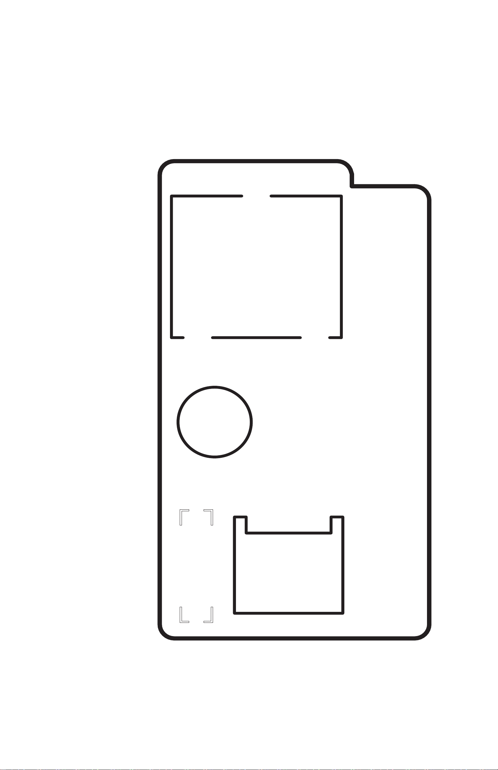
<Loader board (EX-AR3LTDUT/AR3UF/AR5UF/BR3UF)>
(Lead free solder used in the board (material : Sn-Cu, melting point : 230 Centigrade))
(Lead free solder used in the board (material : Sn-Ag-Cu, melting point : 219 Centigrade))
LVA10530-
S1A
A1
PbF
UL
MARK
CN1
S1
created date:2011-06-09No.MB596
65
(No.MB596<Rev.004>)64/
Page 86

P1A
T1A
+
-
CN1
S1
<Loader board (EX-AR3LTDUT/AR3UF/AR5UF/BR3UF)>
(Lead free solder used in the board (material : Sn-Cu, melting point : 230 Centigrade))
(Lead free solder used in the board (material : Sn-Ag-Cu, melting point : 219 Centigrade))
created date:2011-06-09No.MB596
65
(No.MB596<Rev.004>)65/
Page 87

PARTS LIST
59
COMPACT COMPONENT SYSTEM
EX-A3A EX-A3B EX-A3E
EX-A3EN EX-A3EV EX-A3UB
EX-A3UJ EX-A3US EX-A3UW
EX-AR3LTDUT EX-AR3UF EX-AR5UF
EX-BR3UF
(No.MB596<Rev.004>)1/
Page 88

■ PRECAUTIONS ON SCHEMATIC DIAGRAMS
z Due to the improvement in performance, some part numbers shown in the circuit diagrams
may not agree with those indicated in the Parts List.
z The parts numbers, values and rated voltage etc. in the Schematic Diagrams are for
reference only.
z Since the circuit diagrams are standard ones, the circuits and circuit constants may be
subject to change for improvement without any notice.
■ PRECAUTIONS ON PARTS LIST
z
The parts identified by the symbol are critical for safety. Whenever replacing these parts, be sure to
use specified ones to secure the safety.
z
The parts not indicated in this Parts List and those which are filled with lines --- in the Parts No.
columns will not be supplied.
z
P.W. BOARD Ass'y will not be supplied, but those which are filled with the Parts No. in the Parts No.
columns will be supplied.
z
When ordering chips, screws etc., place bulk orders (unit of tens) whenever possible to improve
shipping efficiency.
z
There are cases where the actual implemented parts in the sets and the service parts are different.
When ordering parts, make sure to refer to the Parts List.
■
PRECAUTIONS ON SERVICE
Certain parts of the power circuits and the GNDs differ according to the models. Care must be
taken for the following points as the differences are indicated separately in the LIVE GND ( ) and
the ISOLATED (NEUTRAL) GND ( ).
1. Do not touch the LIVE GND, or do not touch the LIVE GND and the ISOLATED (NEUTRAL)
GND at the same time. It may cause an electric shock.
Before pulling out the chassis or other parts, make sure to pull out the power cord from the
wall outlet first.
2. Do not short circuit between the LIVE GND and ISOLATED (NEUTRAL) GND, or never
measure the LIVE GND and ISOLATED (NEUTRAL) GND at the same time using measuring
instruments (oscilloscope, etc.). It may blow fuses or damage other parts.
■ DEVIATION TOLERANCE RANGE
DEVIATION TOLERANCE RANGE
F G J K M N R H Z P
± 1% ± 2% ± 5% ±10% ±20% ±30%
+30%
-10%
+50%
-10%
+80%
-20%
+100%
-0%
59
(No.MB596<Rev.004>)2/
Page 89

114
113
112
111
110
109
108
107
107
106
106
105
105
104
104
103
102
101
100
99
98
97
96
95
94
93
92
91
90
89
88
87
86
85
84
83
82
81
80
80
80
79
78
78
77
77
76
76
75
74
73
72
71
71
71
71
70
69
68
67
67
67
66
66
66
65
65
64
63
62
61
60
59
58
58
57
56
56
55
54
53
52
51
50
49
48
47
46
46
45
45
44
43
42
41
40
39
38
37
36
35
35
34
33
33
32
32
31
30
29
28
27
26
25
24
23
23
22
21
21
20
19
19
19
18
18
17
17
17
16
15
14
13
12
11
10
9
9
9
9
8
7
6
5
4
3
2
1
BR3
AR3,AR5,
AR3LTD,
Except
AR3,AR5,BR3
AR3LTD,
Except
AR3,AR5,BR3
AR3LTD,
Except
c
The parts without symbol number are not service.
AR3LTD
Only for
AR3LTD
Only for
AR3LTD
Only for
borad
Scart
B,E,EN,EV
Only for
B,E,EN,EV
Only for
AR3LTDUJ,
A,US,UB,UW,
Only for
Only for AR3LTD
L
L
AR3LTDUT
Except
UW,UJ
A,US,UB,
Only for
Fig1
Fig2
Fig2
Fig2
USB & Line borad
Front borad
DEUS borad
Main borad
Micom borad
Block No.M1MM
Exploded view of general assembly
15
54
: Not used
: LV30226-054A
55
marking guiding in page 2-1 of SECTION2 .
(Top cover,AL panel R,AL panel L,)without a
Please use 72 for only an article using a part
: LV30226-053A
please use follows.
a marking guiding in page 2-1 of SECTION2 ,
a part (Top cover,AL panel R,AL panel L,) without
When change only a spacer with an article using
Fig2
Fig1
z
a
J
A
c
b
b
g
g
h
s
s
r
r
q
q
p
x
y
z
y
x
v
v
p
n
n
m
m
k
k
t
w
w
u
u
t
j
j
h
f
f
e
e
d
d
a
B
G
C
C
F
F
E
D
K
E
D
H
K
J
H
G
B
A
created date:2011-06-09No.MB596
59
(No.MB596<Rev.004>)3/
Page 90

MODEL MARK MODEL MARK MODEL MARK MODEL MARK
59
EX-A3A A EX-A3B B EX-A3E C EX-A3EN D
EX-A3EV E EX-A3UB F EX-A3UJ G EX-A3US H
EX-A3UW I EX-AR3LTDUT J EX-AR3UF K EX-AR5UF L
EX-BR3UF M
Safe Symbol No. Parts No. Parts Name Description QTY Local
General assembly <M1MM>
1 LV22448-001A F BASE ASSY 1 A,B,C,D,E,F,G,H,I
1 LV22448-010A F BASE ASSY 1 J
1 LV22448-016A F BASE ASSY 1 K
1 LV22448-015A F BASE ASSY 1 L
1 LV22448-017A F BASE ASSY 1 M
2 LV37335-001A FL LENS(B) 1 A,B,C,D,E,F,G,H,I
2 LV37335-002A FL LENS(A) 1 J
2 LV37335-004A FL LENS(B) 1 K,L,M
3 LV44752-201A BRAND BADGE 1
4 LV42851-011A SCREEN 1
5 LV44754-001A SPRING 1 A,B,C,D,E,F,G,H,I
5 LV44961-001A SPRING 1 J,K,L,M
6 QYSDSF2608ZA TAP SCREW M2.6 x 8mm 1
7 LV30226-042A SPACER 1 A,B,C,D,E,F,G,H,I
8 LV43596-001A INDICATOR 1
9 QYSDSF2608ZA TAP SCREW M2.6 x 8mm 10
10 GV30349-025A SPACER 1
11 LV37281-002A DOOR BASE 1 A,B,C,D,E,F,G,H,I,J
11 LV37281-003A DOOR BASE 1 K,L,M
12 LV37282-001A DOOR LENS 1 A,B,C,D,E,F,G,H,I
12 LV37282-004A DOOR LENS 1 J
12 LV37282-010A DOOR LENS 1 K
12 LV37282-012A DOOR LENS 1 L
12 LV37282-014A DOOR LENS 1 M
13 QZW0020-001 LATCH 1
14 LV30227-098A SPACER 2 A,B,C,D,E,F,G,H,I
15 LV30226-042A SPACER 2 A,B,C,D,E,F,G,H,I
16 LV11341-001A BOTTOM CHASSIS 1
17 LV44755-001A BRASS FOOT 3 A,B,C,D,E,F,G,H,I,K,L,M
17 LV45072-001A BRASS FOOT 3 J
18 LV44885-001A FOOT ASSY 3 A,B,C,D,E,F,G,H,I
18 LV44885-005A FOOT ASSY 3 K
18 LV44885-003A FOOT ASSY 3 L,M
19 QYSBSG3012ZA TAP SCREW M3 x 12mm 3
! 20 LV22449-001A SIDE L 1 A,B,C,D,E,F,G,H,I,J
! 20 LV22449-003A SIDE L 1 K,L,M
21 QYSDSG3006EA TAP SCREW M3 x 6mm 2
! 22 LV22450-001A SIDE R 1 A,B,C,D,E,F,G,H,I,J
! 22 LV22450-003A SIDE R 1 K,L,M
23 QYSDSG3006EA TAP SCREW M3 x 6mm 2
24 LV37273-001A BRACKET A 1 A,B,C,D,E,F,G,H,I
24 LV37273-002A BRACKET A 1 J,K,L,M
25 QYSDSG3006EA TAP SCREW M3 x 6mm 1
26 LV37274-001A BRACKET B 1
27 GV30349-025A SPACER 1 A,B,C,D,E,F,G,H,I
28 QYSDSG3006EA TAP SCREW M3 x 6mm 1
29 LV37275-001A BRACKET C 1
30 QYSDSG3006EA TAP SCREW M3 x 6mm 2
31 QYSDSG3006EA TAP SCREW M3 x 6mm 2
32 GV30349-025A SPACER 2
33 QYSBSFG3010ZA TAP SCREW M3 x 10mm 2
34 QYSBSGY3008EA TAP SCREW M3 x 8mm 3
35 QYSBSG3010ZA TAP SCREW M3 x 10mm 3
! 36 QMPG080-244-JD POWER CORD(EK) 2.44m BLACK 1 A
! 36 QMPN150-200-JC POWER CORD(EK) 2m BLACK 1 B
! 36 QMPK200-200-JD POWER CORD(EK) 2m BLACK 1 C,D,E,G,H,I
! 36 QMPN410-200-JD POWER CORD(EK) 2m BLACK 1 F
! 36 QMPR600-200-JD POWER CORD 2m BLACK 1 J
! 36 QMPR480-200-JC POWER CORD(EU) 2m BLACK 1 K,L,M
! 36 or QMPG150-244-JC POWER CORD(AST) 2.44m BLACK 1 A
! 36 or QMPK190-200-JC POWER CORD(EU) 2m BLACK 1 C,D,E,G,H,I
! 37 QZW0033-001 STRAIN RELIEF 1
38 LV22451-033A REAR PANEL 1 A
38 LV22451-026A REAR PANEL 1 B,C,D,E
38 LV22451-031A REAR PANEL 1 F
38 LV22451-029A REAR PANEL 1 G
38 LV22451-030A REAR PANEL 1 H
38 LV22451-032A REAR PANEL 1 I
38 LV22451-042A REAR PANEL 1 J
38 LV22451-046A REAR PANEL 1 K,L,M
39 QAU0472-001 TUNER TU1 1 A,F,G,H,I
39 QAU0473-001 TUNER TU1 1 B,C,D,E
39 QAU0509-003 TUNER TU1 1 J,K,L,M
40 QYSBSGY3008EA TAP SCREW M3 x 8mm 2
41 QYSBSGY3008EA TAP SCREW M3 x 8mm 2 B,C,D,E
42 QYSBSGY3008EA TAP SCREW M3 x 8mm 4
43 QYSDSG3006EA TAP SCREW M3 x 6mm 1
44 QYSBSG3010ZA TAP SCREW M3 x 10mm 2
45 QYSBSGY3008EA TAP SCREW M3 x 8mm 4 A,F,G,H,I
45 QYSBSGY3008EA TAP SCREW M3 x 8mm 3 B,C,D,E,J,K,L,M
46 QYSDSG3006EA TAP SCREW M3 x 6mm 3
47 QYSBSGY3008EA TAP SCREW M3 x 8mm 2 A,B,C,D,E,F,G,H,I,K,L,M
48 QYSBSGY3008EA TAP SCREW M3 x 8mm 1
49 LV44756-201A HEAT SINK 1
50 QYSDSG3006EA TAP SCREW M3 x 6mm 2
51 LV37277-001A SHIELD CASE 1
52 LV44846-002A THERMAL SHEET 1
(No.MB596<Rev.004>)4/
Page 91

MODEL MARK MODEL MARK MODEL MARK MODEL MARK
59
EX-A3A A EX-A3B B EX-A3E C EX-A3EN D
EX-A3EV E EX-A3UB F EX-A3UJ G EX-A3US H
EX-A3UW I EX-AR3LTDUT J EX-AR3UF K EX-AR5UF L
EX-BR3UF M
Safe Symbol No. Parts No. Parts Name Description QTY Local
53 LV11343-201A AL PANEL L 1 A,F,G,H,I,L
53 LV11343-202A AL PANEL L 1 B,C,D,E
53 LV11343-203A AL PANEL L 1 J,K
53 LV11343-204A AL PANEL L 1 M
54 LV30226-053A SPACER 1 A,B,C,D,E,F,G,H,I
54 or LV30226-054A SPACER It uses it only for AL panel R with
55 LV30226-054A SPACER 1 A,B,C,D,E,F,G,H,I
55 or LV30226-053A SPACER It uses it only for AL panel L with
56 QYSDSG3006EA TAP SCREW M3 x 6mm 4
! 57 QAL0955-001 SW POWER 1 A,B,C,D,E,F,G,H,I
! 57 QAL0955-005 SW POWER 1 J,K,L,M
58 QYSDSG3006EA TAP SCREW M3 x 6mm 2
59 QWTD160-040-E SHRINK TUBE BLACK 1 A,B,C,D,E,F,H
59 QWTDG00-040 SHRINK TUBE BLACK 1 J,K,L,M
60 LV11344-201A AL PANEL R 1 A,B,C,D,E,F,G,H,I,L
60 LV11344-202A AL PANEL R 1 J,K
60 LV11344-203A AL PANEL R 1 M
61 LV11345-002A TOP CHASSIS 1
62 LV44874-001A SHIELD A 1
63 LV44875-001A SHIELD B 1
64 LV30225-076A SPACER 1
65 QYSBST3004EA TAP SCREW M3 x 4mm 2
66 LV30225-0M5A SPACER 3
67 QYSDSG3006EA TAP SCREW M3 x 6mm 5
68 QYSBSG3010ZA TAP SCREW M3 x 10mm 2
69 QYSBSGY3008EA TAP SCREW M3 x 8mm 3
70 QYSDSG3006EA TAP SCREW M3 x 6mm 2 A,B,C,D,E,F,G,H,I
70 QYSSSF3010ZA TAP SCREW M3 x 10mm 2 J,K,L,M
71 LV30227-034A SPACER 4
72 LV30226-054A SPACER It uses it only for AL panel R
73 LV11346-202A TOP COVER 1 A,F,G,H,I
73 LV11346-203A TOP COVER 1 B,C,D,E
73 LV11346-204A TOP COVER 1 J
marking.
marking.
without marking.
1 A,B,C,D,E,F,G,H,I
1 A,B,C,D,E,F,G,H,I
1 A,B,C,D,E,F,G,H,I
73 LV11346-209A TOP COVER 1 K
73 LV11346-208A TOP COVER 1 L
73 LV11346-207A TOP COVER 1 M
74 QYWWB336005 WASHER 6mm/3.3mm x 0.5mm 2 A,B,C,D,E,F,G,H,I,J,K,M
74 QYWWU336005 WASHER 6mm/3.3mm x 0.5mm 2 L
75 QYWWU336005 WASHER 6mm/3.3mm x 0.5mm 2
76 LV43598-002A SPECIAL SCREW 4
77 QYSBSGY3008EA TAP SCREW M3 x 8mm 5
78 QYSBSGY3008EA TAP SCREW M3 x 8mm 2 A,B,C,D,E,F,G,H,I
78 QYSSSF3010ZA TAP SCREW M3 x 10mm 2 J,K,L,M
79 LV11342-001A ARC BASE 1
80 QYSBSG3012ZA TAP SCREW M3 x 12mm 5
81 LV37276-201A FITTING COVER 1 A,B,C,D,E,F,G,H,I,J
81 LV37276-207A FITTING COVER 1 K,M
81 LV37276-206A FITTING COVER 1 L
82 LV22452-001A FITTING BASE 1 A,B,C,D,E,F,G,H,I,J
82 LV22452-002A FITTING BASE 1 K,L,M
83 LV37280-002A VOL KNOB ASSY 1 A,B,C,D,E,F,G,H,I
83 LV37280-005A VOL KNOB ASSY 1 J,K
83 LV37280-004A VOL KNOB ASSY 1 L
83 LV37280-006A VOL KNOB ASSY 1 M
84 LV30227-016A SPACER 2
85 QUQU12-2114AJ-E FFC WIRE 21pin 14cm 1 A,B,C,D,E,F,G,H,I
85 QUQV12-2114AJ-E FFC WIRE 21pin 14cm 1 J,K,L,M
86 WJZ0261-001A-E E-HARNESS ASSY 1
87 QJJ066-061001-E SIN CR C-C WIRE 1 A,B,C,D,E,F,G,H,I,K,L,M
87 QJJ066-062001-E SIN CR C-C WIRE 1 J
88 QQR0917-001 CORE FILTER 1 A,B,C,D,E,F,G,H,I,K,L,M
88 QQR0491-002 FERRITE CORE TDK (BLACK) 1 J
89 QUQU12-2506AJ-E FFC WIRE 25pin 6cm 1 A,B,C,D,E,F,G,H,I
89 QUQV12-2506AJ-E FFC WIRE 25pin 6cm 1 J,K,L,M
90 QJJ067-070803-E SIN CR C-C WIRE 1
91 QUQU12-1505BJ-E FFC WIRE 15pin 5cm 1 B,C,D,E
92 QUQU12-1106BJ-E FFC WIRE 11pin 6cm 1 A,F,G,H,I
92 QUQU12-1506BJ-E FFC WIRE 15pin 6cm 1 B,C,D,E
92 QUQV12-1106BJ-E FFC WIRE 11pin 6cm 1 J,K,L,M
93 QUR110-0507BJ-E FFC WIRE 1 A,B,C,D,E,F,G,H,I
93 QUR310-0507BJ-E FFC WIRE 1 J,K,L,M
94 QUR110-0518BC-E FFC WIRE 1 A,B,C,D,E,F,G,H,I
94 QUR310-0518BC-E FFC WIRE 1 J,K,L,M
95 QUR110-0514AC-E FFC WIRE 1 A,B,C,D,E,F,G,H,I
95 QUR310-0514AC-E FFC WIRE 1 J,K,L,M
96 QUR110-2524AC-E FFC WIRE 1 A,B,C,D,E,F,G,H,I
96 QUR310-2524AC-E FFC WIRE 1 J,K,L,M
97 QJJ067-041104-E SIN CR C-C WIRE 1
98 WJN0208-001A-E E-SH C WIRE C-C 1
99 LV30226-054A SPACER 1 A,B,C,D,E,F,G,H,I
100 LV45083-001A FELT SPACER 3 J
101 QYWWU336005 WASHER 6mm/3.3mm x 0.5mm 3 J
102 LV45082-002A D-STICK TAPE 1 J
103 LV11530-003A WOOD COVER 1 J
104 LV45119-002A SCREW CAP 4 J
(No.MB596<Rev.004>)5/
Page 92

MODEL MARK MODEL MARK MODEL MARK MODEL MARK
59
EX-A3A A EX-A3B B EX-A3E C EX-A3EN D
EX-A3EV E EX-A3UB F EX-A3UJ G EX-A3US H
EX-A3UW I EX-AR3LTDUT J EX-AR3UF K EX-AR5UF L
EX-BR3UF M
Safe Symbol No. Parts No. Parts Name Description QTY Local
105 QYWDL578050 SLIT WASHER 8mm/5.7mm x 0.5mm 4 J
106 LV45121-002A O RING 4 J
107 GV30349-073A SPACER 2 J,K,L,M
108 LV38674-002A UT LABEL 1 J
108 LV38156-029A UF LABEL 1 K
108 LV38156-028A UF LABEL 1 L
108 LV38156-027A UF LABEL 1 M
109 LV45385-002A COPPER SHEET 1 L
110 LV45385-003A COPPER SHEET 1 L
111 GV40993-006A CCC LABEL 1 K
111 GN40099-001A CCC LABEL 1 L,M
112 LV45372-001A IMPEDANCE LABEL 1 K,L,M
113 LV44949-201A RECYCLE LABEL 1 K,L,M
114 LV45614-001A LICENSE LABEL 1 K,L,M
(No.MB596<Rev.004>)6/
Page 93

9
8
8
8
7
6
5
4
3
2
1
The parts without symbol number are not service.
EX-A3,AR3 seriese
Block No.M2MM
Speaker assembly
created date:2011-06-09No.MB596
59
(No.MB596<Rev.004>)7/
Page 94

MODEL MARK MODEL MARK MODEL MARK MODEL MARK
59
EX-A3A A EX-A3B B EX-A3E C EX-A3EN D
EX-A3EV E EX-A3UB F EX-A3UJ G EX-A3US H
EX-A3UW I EX-AR3LTDUT J EX-AR3UF K EX-AR5UF L
EX-BR3UF M
Safe Symbol No. Parts No. Parts Name Description QTY Local
Speaker assembly Except EX-AR3UF/AR5UF/BR3UF<M2MM>
1 5100021611 CABINATE ASSY 2 A,B,C,D,E,F,G,H,I
1 5100031301 CABINATE ASSY 2 J
2 1030004621 TERMINAL 2 A,B,C,D,E,F,G,H,I,J
3 6500027501 FELT RING 2 A,B,C,D,E,F,G,H,I
3 6500028401 FELT RING 2 J
4 7900004901 WOOD BLOCK 2 A,B,C,D,E,F,G,H,I,J
5 7900005001 WOOD BLOCK 2 A,B,C,D,E,F,G,H,I,J
6 LV44715-002A SPECIAL SCREW 8 A,B,C,D,E,F,G,H,I,J
7 7001841606 SCREW 8 A,B,C,D,E,F,G,H,I,J
8 9000007991 FOOT 8 A,B,C,D,E,F,G,H,I,J
9 LE10009-013A WOODDOME SPK 2 A,B,C,D,E,F,G,H,I
9 LE10009-019A WOODDOME SPK 2 J
(No.MB596<Rev.004>)8/
Page 95

18
17
16
15
14
13
12
11
10
10
9
8
7
6
5
4
4
3
3
2
1
Speaker assembly
EX-AR5UF
The parts without symbol number are not service.
Block No.M5MM
created date:2011-06-09No.MB596
59
(No.MB596<Rev.004>)9/
Page 96

MODEL MARK MODEL MARK MODEL MARK MODEL MARK
59
EX-A3A A EX-A3B B EX-A3E C EX-A3EN D
EX-A3EV E EX-A3UB F EX-A3UJ G EX-A3US H
EX-A3UW I EX-AR3LTDUT J EX-AR3UF K EX-AR5UF L
EX-BR3UF M
Safe Symbol No. Parts No. Parts Name Description QTY Local
Speaker assembly EX-AR5UF<M5MM>
1 L5100032201 CABINATE ASSY 2 L
2 L1030004641 TERMINAL 2 L
3 L5600008001 HOLDER 8 L
4 L5800023721 LATCH 8 L
5 L6500027541 FELT RING 2 L
6 L7001841606 SCREW 8 L
7 L7008142504 SCREW 8 L
8 L7008142004 SCREW 8 L
9 L7001543506 SCREW 4 L
10 L9000007941 FOOT 8 L
11 L9910009411 NET 2 L
12 E75939-222 JVC MARK 2 L
13 L7900005001 WOOD BLOCK 2 L
14 L7900005721 WOOD BLOCK 2 L
15 L7900005731 WOOD BLOCK 2 L
16 LE10003-024A WOODDOME SPK 2 L
17 LE10010-080A WOODCONE SPK 2 L
18 L6700023401 NETWORK ASSY 2 L
(No.MB596<Rev.004>)10/
Page 97

11
10
9
8
8
7
6
5
4
3
2
1
EX-BR3UF
The parts without symbol number are not service.
Block No.M6MM
Speaker assembly
created date:2011-06-09No.MB596
59
(No.MB596<Rev.004>)11/
Page 98

MODEL MARK MODEL MARK MODEL MARK MODEL MARK
59
EX-A3A A EX-A3B B EX-A3E C EX-A3EN D
EX-A3EV E EX-A3UB F EX-A3UJ G EX-A3US H
EX-A3UW I EX-AR3LTDUT J EX-AR3UF K EX-AR5UF L
EX-BR3UF M
Safe Symbol No. Parts No. Parts Name Description QTY Local
Speaker assembly EX-BR3UF<M6MM>
1 L5100032301 BOX ASSY 2 M
2 L1030004621 TERMINAL 2 M
3 L5600003301 HOLDER 8 M
4 L7900005001 WOOD SPACER 2 M
5 L7001841606 SCREW 8 M
6 LV44715-002A SCREW 8 M
7 L6500028401 FELT RING 2 M
8 L9000007991 FOOT 6 M
9 L9000014501 COPPER FOIL 2 M
10 L7900004911 WOOD BLOCK 2 M
11 LE10009-013A WOODDOME SPK 2 M
(No.MB596<Rev.004>)12/
Page 99

10
9
9
8
7
6
5
4
3
2
1
EX-AR3UF
The parts without symbol number are not service.
Block No.M7MM
Speaker assembly
created date:2011-06-09No.MB596
59
(No.MB596<Rev.004>)13/
Page 100

MODEL MARK MODEL MARK MODEL MARK MODEL MARK
59
EX-A3A A EX-A3B B EX-A3E C EX-A3EN D
EX-A3EV E EX-A3UB F EX-A3UJ G EX-A3US H
EX-A3UW I EX-AR3LTDUT J EX-AR3UF K EX-AR5UF L
EX-BR3UF M
Safe Symbol No. Parts No. Parts Name Description QTY Local
Speaker assembly EX-AR3UF<M7MM>
1 L5100031301 CABINET ASSY 2 K
2 L1030004621 TERMINAL 2 K
3 L5600003301 HOLDER 2 K
4 L6500028401 FELT RING 2 K
5 L7900005001 WOOD BLOCK 2 K
6 L7900004911 WOOD BLOCK 2 K
7 LV44715-002A SPECIAL SCREW 8 K
8 L7001841606 SCREW 8 K
9 L9000007991 FOOT 6 K
10 LE10009-013A WOODDOME SPK 2 K
(No.MB596<Rev.004>)14/
 Loading...