

Page 1
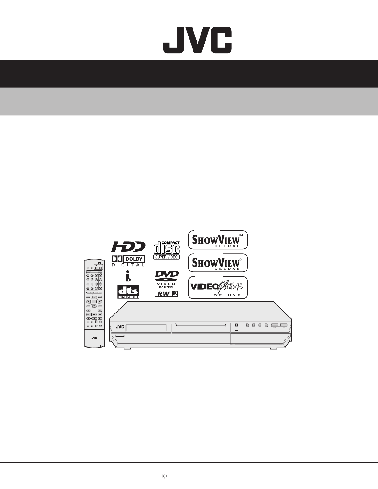
SERVICE MANUAL
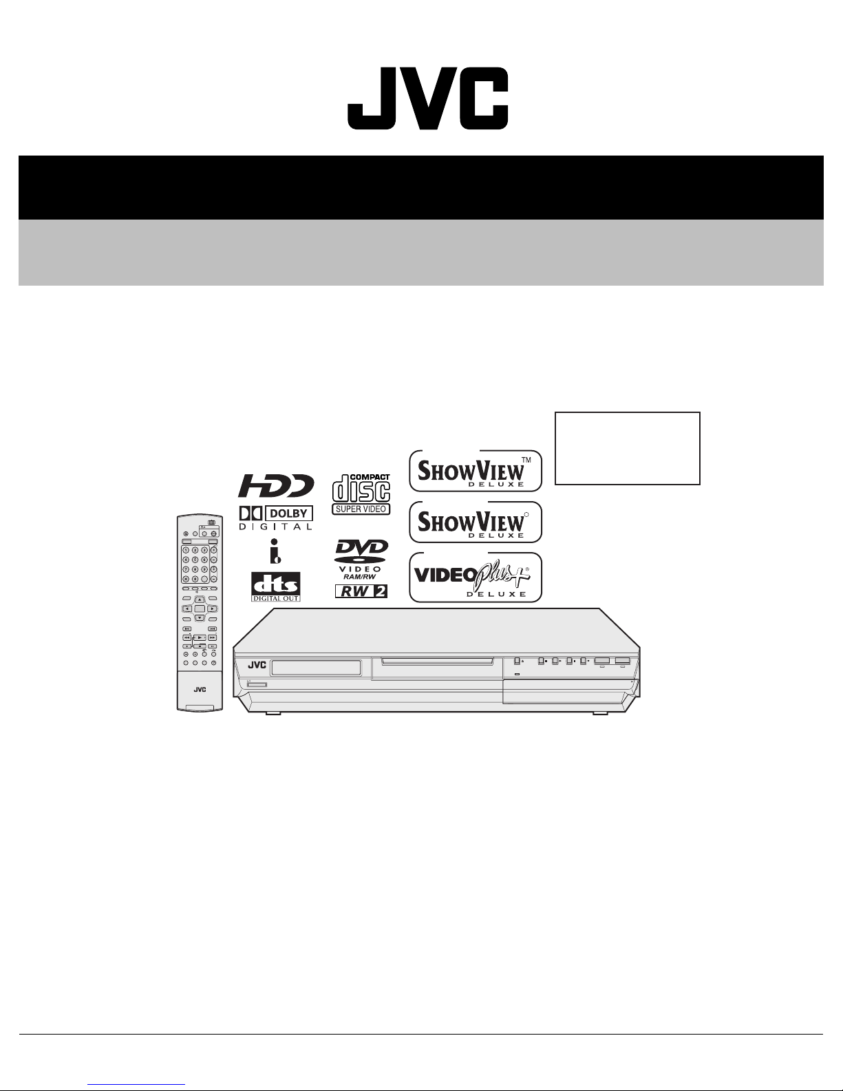
DVD&HDD VIDEO RECORDER
YD07220057
DR-MH200SE,DR-MH200SEF,
DR-MH200SEK
Area Suffix
E ------- Continental Europe
Only ver.E
Northern Europe
EF --------------------- France
EK ------------------------ U.K.
Only ver.EF
OPEN/
TV AV
CLOSE
TV/CBL/SAT
VIDEO
HDD DVD
AUX
CANCEL
MEMO/MARK
EDIT
DUBBING
LIVE
TV
ENTER
MENU
CLEAR
STOP/
JUMP
REC MODE
DISPLAY
ON SCREEN
SAT SET UP
VPS/PDC
AUDIO
SUBTITLE
ANGLE
LIVE CHECK
CABLE/SAT
STANDBY ON
TV
PROGRAMME
NAVIGATIONTOP MENU
RETURN
NEXTPREVIOUS
SLOWSLOW PLAY/SELECT
PAUSEREC
PROGRESSIVE
DVDTV
DVD
PR
HELP
STANDBY/ON
SCAN
Only ver.EK
DR-MH200SE, DR-MH200SEF, DR-MH200SEK [D5HR05]
R
VIDEO
F1
S-VIDEO VIDEO
L(MONO)-AUDIO-R
DV
HDD DVD
DV IN
PULL - OPEN
Since the whole mechanism assembly unit is replaced, the DVD recorder
mechanism of this unit need not be adjusted.
This model has partially changed specifications from the precedent
models DR-MH20SE, DR-MH20SEF, and DR-MH20SEK.
Therefore, this service manual includes only the "Schematic diagrams",
"Parts list", and "Instruction book". For details other than those described
in this manual, please refer to another service manual (DR-MH20SE/EK/EF,
DR-MH30SE/EK/EF/ER ISSUE No.YD027 2004/9)
1 PRECAUTION. . . . . . . . . . . . . . . . . . . . . . . . . . . . . . . . . . . . . . . . . . . . . . . . . . . . . . . . . . . . . . . . . . . . . . . . . 1-3
2 SPECIFIC SERVICE INSTRUCTIONS . . . . . . . . . . . . . . . . . . . . . . . . . . . . . . . . . . . . . . . . . . . . . . . . . . . . . . 1-6
3 DISASSEMBLY . . . . . . . . . . . . . . . . . . . . . . . . . . . . . . . . . . . . . . . . . . . . . . . . . . . . . . . . . . . . . . . . . . . . . . . 1-6
4 ADJUSTMENT . . . . . . . . . . . . . . . . . . . . . . . . . . . . . . . . . . . . . . . . . . . . . . . . . . . . . . . . . . . . . . . . . . . . . . . . 1-6
5 TROUBLESHOOTING . . . . . . . . . . . . . . . . . . . . . . . . . . . . . . . . . . . . . . . . . . . . . . . . . . . . . . . . . . . . . . . . . . 1-6
COPYRIGHT © 2005 Victor Company of Japan, Limited
TABLE OF CONTENTS
No.YD072
2005/7
Page 2
SPECIFICATION
GENERAL
Power requirement AC 220 V - 240 V~, 50 Hz/60 Hz
Power consumption Power on : 37 W
Temperature Operating : 5°C to 35°C
Operating position Horizontal only
Dimensions (W × H × D) 435 mm × 70 mm × 345.5 mm
Input/Output
Video input 0.5- 2.0 Vp-p, 75 ohms (pin jack)
Audio input -8 dB, 50 kilohms (pin jack)
Audio output -8 dB, 1 kilohms (pin jack)
21-pin SCART connectors IN/OUT x 1, IN/DECODER x 1
S-video input Y:0.8-1.2 Vp-p, 75 ohms
S-video output Y : 1.0 Vp-p, 75 ohms
Component video output Y : 1.0 Vp-p, 75 ohms
Digital audio output Optical, Coaxial
VIDEO/AUDIO (DVD Deck)
Recording time
Audio recording system Dolby Digital (2 ch)
Video recording compression system
VIDEO/AUDIO (HDD Deck)
Video recording compression system
Audio recording system Dolby Digital (2 ch)
Recording time
TUNER/TIMER
Signal system PAL-type colour signal and CCIR monochrome signal, 625 lines 50 fields
TV channel storage capacity
Tuning system Frequency synthesized tuner
Channel coverage
(SECAM-L)
Channel coverage(PAL) VHF(LOW): 47 MHz-89 MHz
Memory backup time Approx. 60 seconds
ACCESSORIES
Provided accessories
E.& O.E. Design and specifications subject to change without notice.
• Manufactured under licence from Dolby Laboratories. “Dolby” and double-D symbol are trademarks of Dolby Laboratories.
• “DTS” and “DTS Digital Out” are trademarks of Digital Theater Systems, Inc.
• SHOWVIEW is a trademark of Gemstar Development Corporation. The SHOWVIEW system is manufactured under license from Gemstar Development Corporation.
• This product incorporates copyright protection technology that is protected by method claims of certain U.S. patents and other intellectual property
rights owned by Macrovision Corporation and other rights owners. Use of this copyright protection technology must be authorized by Macrovision
Corporation, and is intended for home and other limited viewing users only unless otherwise authorized by Macrovision Corporation. Reverse engineering or disassembly is prohibited.
• VIDEO Plus+ and PlusCode are registered trademarks of Gemstar Development Corporation. The VIDEO Plus+ system is manufactured under license from Gemstar Development Corporation.
Power off : 19.3 W
Storage : -20°C to 60°C
Weight 6.1 kg
Corresponding to mono (left)
C : 0.2 -0.4 Vp-p, 75 ohms
C : 0.3 Vp-p, 75 ohms
i.Link 4-pin for DV input
CB/CR, PB/PR: 0.7 Vp-p, 75 ohms
Corresponding to copy protection
SAT Control: 3.5 mm Jack
Corresponding to Dolby Digital and DTS Digital Surround
Bit stream
Selectable in digital audio output setting menu
Maximum 8 hours (with 4.7 GB disc)
(XP) : Approx. 1 hour, (SP) : Approx. 2 hours, (LP) : Approx. 4 hours, (EP) : Approx. 6 hours, (FR) : Approx. 1 hour - 8 hours
Linear PCM (XP mode only)
MPEG2 (CBR/VBR)
MPEG2 (VBR)
Linear PCM (XP mode only)
Maximum 300 hours (with 160 GB HDD)
(XP): Approx. 36 hours,(SP): Approx. 72 hours,(LP): Approx. 143 hours,(EP): Approx. 214 hours,(FR): Approx. 300 hours
99 positions (+AUX position)
-
VHF(HIGH):104 MHz -300 MHz
Hyper:302 MHz-470 MHz
UHF 470 MHz-862 MHz
RF cable,21-pin SCART cable,Satellite Controller,Infrared remote control unit,”R6” battery x 2
DR-MH200SE DR-MH200SEK DR-MH200SEF
VHF(LOW):49 MHz-65 MHz(2-4)
VHF(HIGH):104 MHz-300 MHz(5-10CATV)
Hyper:300 MHz-470 MHz(CATV)
UHF:470 MHz-862 MHz(21-69)
VHF(LOW):44.5 MHz-143 MHz
VHF(HIGH):143 MHz-470 MHz
UHF: 470 MHz-862 MHz
RF cable,21-pin SCART cable,Satellite Controller,Infrared remote control unit,”AA” battery x 2
VHF(LOW):47 MHz-89 MHz
(E2-E4,X,Y,Z)
VHF(HIGH):104 MHz-300 MHz
(E5-E12,S1-S20,M1-M10,U1-U10)
Hyper:302 MHz-470 MHz(S21-S41)
UHF:470 MHz-862 MHz(E21-E69)
RF cable,21-pin SCART cable,Satellite Control-
ler,Infrared remote control unit,”R6” battery x 2
1-2 (No.YD072)
Page 3
SECTION 1
PRECAUTION
1.1 Safety Precautions
(1) This design of this product contains special hardware and
many circuits and components specially for safety purposes. For continued protection, no changes should be made
to the original design unless authorized in writing by the
manufacturer. Replacement parts must be identical to
those used in the original circuits. Services should be performed by qualified personnel only.
(2) Alterations of the design or circuitry of the product should
not be made. Any design alterations of the product should
not be made. Any design alterations or additions will void
the manufacturers warranty and will further relieve the
manufacture of responsibility for personal injury or property
damage resulting therefrom.
(3) Many electrical and mechanical parts in the products have
special safety-related characteristics. These characteristics are often not evident from visual inspection nor can the
protection afforded by them necessarily be obtained by using replacement components rated for higher voltage, wattage, etc. Replacement parts which have these special
safety characteristics are identified in the Parts List of Service Manual. Electrical components having such features
are identified by shading on the schematics and by ( ) on
the Parts List in the Service Manual. The use of a substitute
replacement which does not have the same safety characteristics as the recommended replacement parts shown in
the Parts List of Service Manual may create shock, fire, or
other hazards.
(4) The leads in the products are routed and dressed with ties,
clamps, tubings, barriers and the like to be separated from
live parts, high temperature parts, moving parts and/or
sharp edges for the prevention of electric shock and fire
hazard. When service is required, the original lead routing
and dress should be observed, and it should be confirmed
that they have been returned to normal, after reassembling.
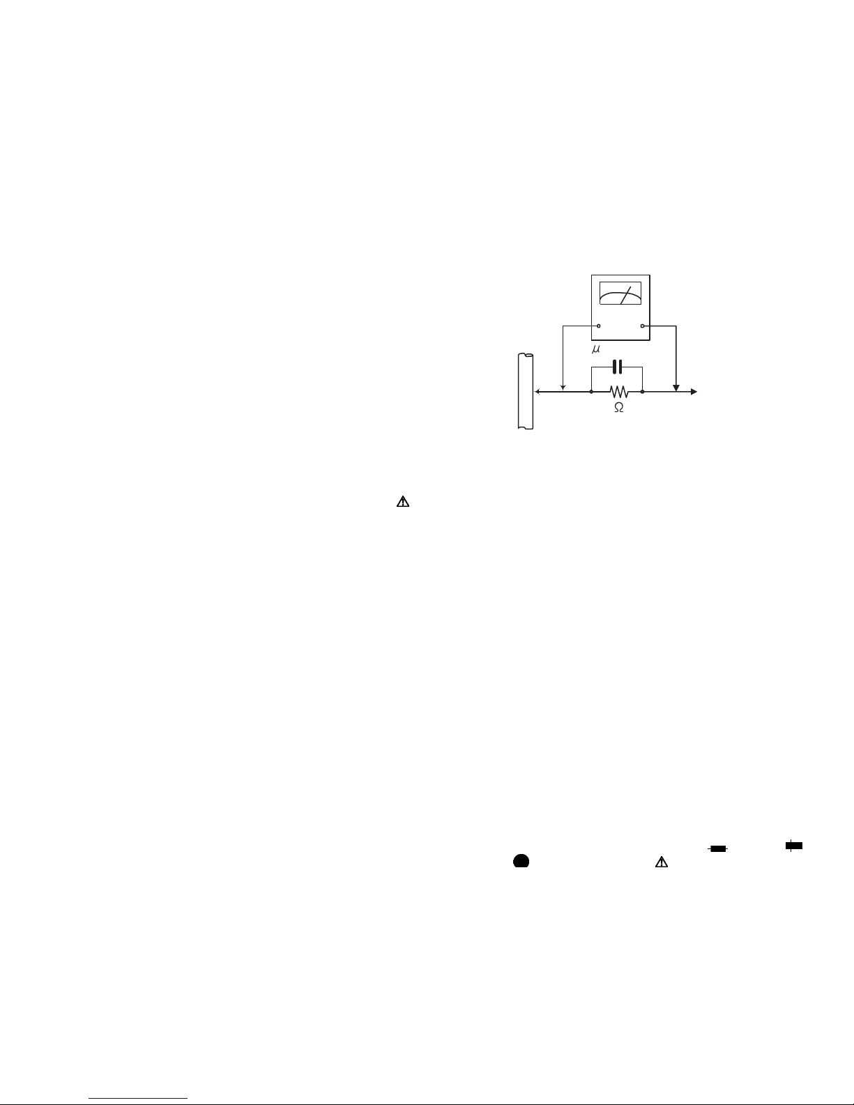
(5) Leakage shock hazard testing
After reassembling the product, always perform an isolation check on the exposed metal parts of the product (antenna terminals, knobs, metal cabinet, screw heads,
headphone jack, control shafts, etc.) to be sure the product
is safe to operate without danger of electrical shock.Do not
use a line isolation transformer during this check.
• Plug the AC line cord directly into the AC outlet. Using a
"Leakage Current Tester", measure the leakage current
from each exposed metal parts of the cabinet, particularly any exposed metal part having a return path to the
chassis, to a known good earth ground. Any leakage current must not exceed 0.5mA AC (r.m.s.).
• Alternate check method
Plug the AC line cord directly into the AC outlet. Use an
AC voltmeter having, 1,000Ω per volt or more sensitivity
in the following manner. Connect a 1,500Ω 10W resistor
paralleled by a 0.15µF AC-type capacitor between an ex-
posed metal part and a known good earth ground.
Measure the AC voltage across the resistor with the AC
voltmeter.
Move the resistor connection to each exposed metal
part, particularly any exposed metal part having a return
path to the chassis, and measure the AC voltage across
the resistor. Now, reverse the plug in the AC outlet and
repeat each measurement. Voltage measured any must
not exceed 0.75 V AC (r.m.s.). This corresponds to 0.5
mA AC (r.m.s.).
AC VOLTMETER
(Having 1000
ohms/volts,
or more sensitivity)
0.15 F AC TYPE
Place this
probe on
1500 10W
Good earth ground
1.2 Warning
(1) This equipment has been designed and manufactured to
meet international safety standards.
(2) It is the legal responsibility of the repairer to ensure that
these safety standards are maintained.
(3) Repairs must be made in accordance with the relevant
safety standards.
(4) It is essential that safety critical components are replaced
by approved parts.
(5) If mains voltage selector is provided, check setting for local
voltage.
1.3 Caution
Burrs formed during molding may be left over on some parts
of the chassis.
Therefore, pay attention to such burrs in the case of preforming repair of this system.
1.4 Critical parts for safety
In regard with component parts appearing on the silk-screen
printed side (parts side) of the PWB diagrams, the parts that are
printed over with black such as the resistor ( ), diode ( )
and ICP ( ) or identified by the " " mark nearby are critical
for safety. When replacing them, be sure to use the parts of the
same type and rating as specified by the manufacturer.
(This regulation dose not Except the J and C version)
each exposed
metal part.
(No.YD072)1-3
Page 4
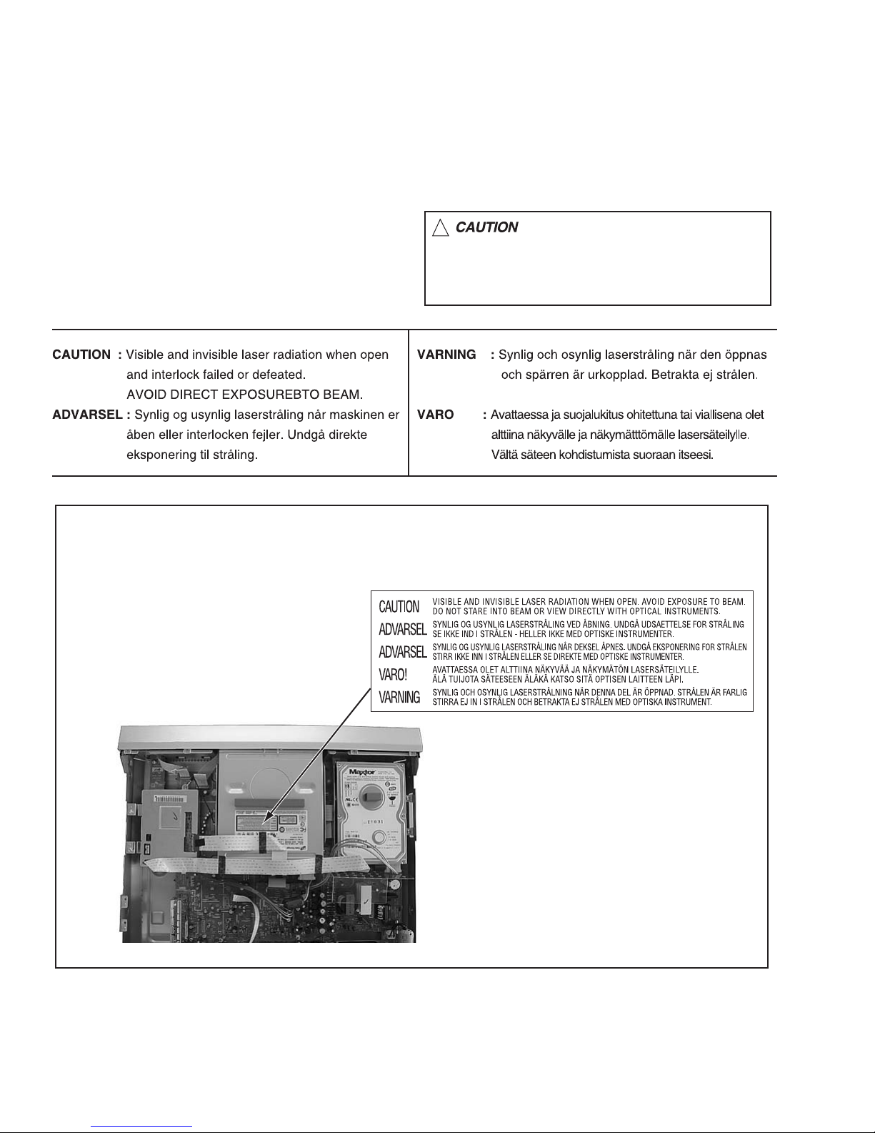
1.5 Important for laser products
!
1.CLASS 1 LASER PRODUCT
2.DANGER : Invisible laser radiation when open and inter
lock failed or defeated. Avoid direct exposure to beam.
3.CAUTION : There are no serviceable parts inside the
Laser Unit. Do not disassemble the Laser Unit. Replace
the complete Laser Unit if it malfunctions.
4.CAUTION : The CD,MD and DVD player uses invisible
laser radiation and is equipped with safety switches which
prevent emission of radiation when the drawer is open and
the safety interlocks have failed or are defeated. It is
dangerous to defeat the safety switches.
5.CAUTION : If safety switches malfunction, the laser is able
to function.
6.CAUTION : Use of controls, adjustments or performance of
procedures other than those specified here in may result in
hazardous radiation exposure.
Please use enough caution not to
see the beam directly or touch it
in case of an adjustment or operation
check.
REPRODUCTION AND POSITION OF LABEL
On mechaism assembly
The photograph might be
different from the actual thing.
1-4 (No.YD072)
Page 5
1.6 Hard Disk Drive (HDD) Handling Precautions
The HDD is a precision device for use in reading and writing a large amount of data on or from a disk rotating at a high speed. If it is
not handled carefully, either abnormal operation may result or it may not be possible to read data. The HDD is sensitive to the following
items and special care is required in safeguarding against them when handling an HDD. Also take care in handling a set incorporating
an HDD.
(1) Vibrations and impacts
(2) Static electricity
(3) Rough handling
1.6.1 Handling in transport, etc.
• Be sure to place the HDD in the manufacturer's specified package carton before transport.
• When receiving a package containing an HDD, check that the
package carton is not damaged (such as having holes in the
carton, crushed corners, etc.).
• Do not impact the packaging carton when loading or unloading
HDD
Do not throw or
drop packages.
it.
• It is not permitted to use the inner package carton only for
transporting an HDD.
• Do not stack package cartons one upon another.
Be sure to package and
transport the HDDs correctly.
1.6.2 Handling an HDD in the stand-alone status
• When handling an HDD on a hard workbench, place an antistatic mat (rubber sheet) or similar object on the hard surface
(to prevent any impacts occurring between the HDD and
bench).
• Do not stack the HDDs one upon another.
• Do not knock an HDD with a hard object (such as a screwdriver).
• Do not place an HDD on its side panel without using a support
(do not place an HDD in an unstable position).
1.6.3 Handling the installation of an HDD
• Place antistatic mats or similar sheets on all of the surfaces on which work is conducted or when the HDD is transported.
• Do not permit the HDD to knock against the set's brackets.
• When screwing the brackets, be careful not to knock the HDD. When using a power screwdriver, use a low-shock model and arrange
the tightening torque properly.
• When mounting an HDD in a main body, take care not to apply excessive force to the brackets.
(No.YD072)1-5
Page 6

SECTION 2
SPECIFIC SERVICE INSTRUCTIONS
Please refer to "DR-MH20SE, DR-MH20SEK, DR-MH20SEF,DR-MH30SE, DR-
MH30SEK,DR-MH30SEF, DR-MH30SER (issue number : YD027 2004/9)"
about this section.
SECTION 3
DISASSEMBLY
Please refer to "DR-MH20SE, DR-MH20SEK, DR-MH20SEF,DR-MH30SE, DR-
MH30SEK,DR-MH30SEF, DR-MH30SER (issue number : YD027 2004/9)"
about this section.
SECTION 4
ADJUSTMENT
Please refer to "DR-MH20SE, DR-MH20SEK, DR-MH20SEF,DR-MH30SE, DR-
MH30SEK,DR-MH30SEF, DR-MH30SER (issue number : YD027 2004/9)"
about this section.
SECTION 5
TROUBLESHOOTING
Please refer to "DR-MH20SE, DR-MH20SEK, DR-MH20SEF,DR-MH30SE, DR-
MH30SEK,DR-MH30SEF, DR-MH30SER (issue number : YD027 2004/9)"
about this section.
1-6 (No.YD072)
Page 7

(No.YD072)1-7
Page 8

Victor Company of Japan, Limited
AV & MULTIMEDIA COMPANY DIGITAL VIDEO STORAGE CATEGORY 12, 3-chome, Moriya-cho, kanagawa-ku, Yokohama, kanagawa-prefecture, 221-8528, Japan
(No.YD072)
Printed in Japan
VPT
Page 9
SCHEMATIC DIAGRAMS
DVD & HDD VIDEO RECORDER
DR-MH200SE, DR-MH200SEF,
DR-MH200SEK,
CD-ROM No.SML200507
Area Suffix
E ------- Continental Europe
Northern Europe
EF --------------------- France
Only ver.E
EK ------------------------ U.K.
Only ver.EF
OPEN/
CLOSE TV AV
TV/CBL/SAT
VIDEO
HDD DVD
AUX
CANCEL
MEMO/MARK
EDIT
DUBBING
LIVE
TV
ENTER
MENU
CLEAR
STOP/
JUMP
REC MODE
DISPLAY
ON SCREEN
SAT SET UP
VPS/PDC
AUDIO
SUBTITLE
ANGLE
LIVE CHECK
CABLE/SAT
STANDBY ON
TV
PROGRAMME
NAVIGATIONTOP MENU
RETURN
NEXTPREVIOUS
SLOWSLOW PLAY/SELECT
PAUSEREC
PROGRESSIVE
DVDTV
DVD
PR
HELP
STANDBY/ON
SCAN
Only ver.EK
DR-MH200SE, DR-MH200SEF, DR-MH200SEK [D5HR05]
R
VIDEO
F1
S-VIDEO VIDEO
L(MONO)-AUDIO-R
DV
HDD DVD
DV IN
PULL - OPEN
Since the whole mechanism assembly unit is replaced, the DVD recorder
mechanism of this unit need not be adjusted.
This model has partially changed specifications from the precedent
models DR-MH20SE, DR-MH20SEF, and DR-MH20SEK.
Therefore, this service manual includes only the "Schematic diagrams",
"Parts list", and "Instruction book". For details other than those described
in this manual, please refer to another service manual (DR-MH20SE/EK/EF,
DR-MH30SE/EK/EF/ER ISSUE No.YD027 2004/9)
COPYRIGHT 2005 Victor Company of Japan, Limited
No.YD072SCH
2005/7
Page 10

Page 11

!
CHARTS AND DIAGRAMS
NOTES OF SCHEMATIC DIAGRAM
Safety precautions
The Components indentified by the symbol are
critical for safety. For continued safety, replace safety
critical components only with manufacturer's recommended parts.
1. Units of components on the schematic diagram
Unless otherwise specified.
1) All resistance values are in ohm. 1/6 W, 1/8 W (refer to
parts list).
Chip resistors are 1/16 W.
K: KΩ(1000Ω), M: MΩ (1000KΩ)
2) All capacitance values are in µF, (P: PF).
3) All inductance values are in µH, (m: mH).
4) All diodes are 1SS133, MA165 or 1N4148M (refer to parts
list).
2. Indications of control voltage
AUX : Active at high.
AUX or AUX(L) : Active at low.
3. Interpreting Connector indications
Note: If the voltages are not indicated on the schematic
diagram, refer to the voltage charts.
123
2.5
(5.0)
1.8
PB and REC modes
(Voltage of PB and REC modes
are the same)
PB mode
REC mode
4. Voltage measurement
1) Regulator (DC/DC CONV) circuits
REC : Colour bar signal.
PB : Alignment tape (Colour bar).
— : Unmeasurable or unnecessary to measure.
2) Indication on schematic diagram
Voltage indications for REC and PB mode on the schematic diagram are as shown below.
6. Indication of the parts for adjustments
The parts for the adjustments are surrounded with the circle
as shown below.
7. Indication of the parts not mounted on the circuit board
“OPEN” is indicated by the parts not mounted on the circuit
board.
R216
OPEN
1
2
3
1
2
3
1
2
3
1
4
2
3
Removable connector
Wire soldered directly on board
Non-removable Board connector
Board to Board
Connected pattern on board
The arrows indicate signal path
Note: The Parts Number, value and rated voltage etc. in
the Schematic Diagram are for references only.
When replacing the parts, refer to the Parts List.
CIRCUIT BOARD NOTES
1. Foil and Component sides
1) Foil side (B side) :
Parts on the foil side seen from foil face (pattern face)
are indicated.
2) Component side (A side) :
Parts on the component side seen from component face
(parts face) indicated.
2. Parts location guides
Parts location are indicated by guide scale on the circuit board.
Parts location are indicated by guide scale on the circuit board.
LOCATION
REF No.
IC101 B C 6 A
IC
Category : IC
Horizontal “A” zone
Vertical “6” zone
B : Foil side
(A : Component side)
C : Chip component
D : Discrete component)
2-1 2-2
Page 12
A
1
2
3
4
5
BCDEFG
Wiring diagram
p10596001a_rev1
S/RCA OUT
CN6901
CN7101
CN1901
CN3002
CN5102
CN1402
CN7301
CN2101
CN4102
CN2201
CN4101
CN5305
CN5001
CN5306
CN4104
CN1003
CN7312
CN1202
2-3 2-4
Page 13

A
1
2
3
4
5
BCD EFG
DDR_DQ0 to 15
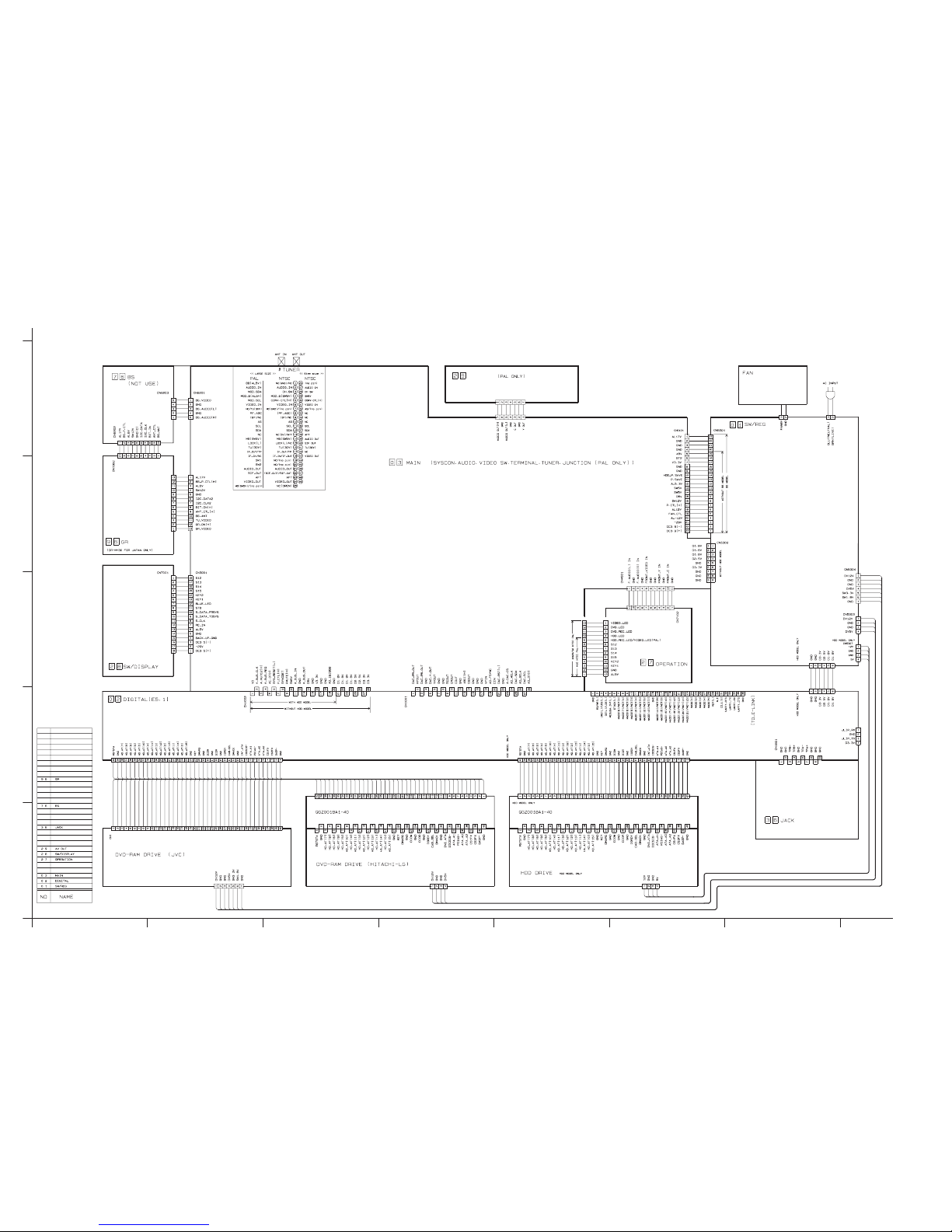
DDR SDRAM Section (SHEET 3)
IEEE1394 Section (SHEET 2)
IEEE1394
Terminal
IEEE1394
Controller
IC1801
TPA+ TPA- TPB+ TPB-
PHY_RESET[L]
PHY_LREQ PHY_CLK
PHY_CNA PHY_CTL[0],[1]
PHY_DATA[0-7] PHY_LPS
PHY_LINK_ON
DDR SDRAM
IC1601
RA1625 to
RA1628
DDR_DQ16 to 31
SDRAM_DQ16 to 31
SDRAM_DQ0 to 15
SDRAM_A0 to 15
SDRAM_CKE
SDRAM_RAS_L
SDRAM_CAS_L
SDRAM_WE_L
SDRAM_DQM0 to 3
SDRAM_DQS0 to 3
SDRAM_CLK0,1
SDRAM_CLK_L0,1
DDR_CLK0,1
DDR_CLK_L0,1
DDR_DQM0 to 3
DDR_DQS0 to 3
DDR_RAS_L DDR_CKE
DDR_CAS_L DDR_WE_L
DDR_BA1,2
DDR_A0 to 12
CN4104
J4112
CN1801
Media processor section (SHEET 4)
Media
processor
IC1401
IC1404
IC1405
ATA2_DMAACK[L] ATA2_INTRQ ATA2_ADD0 to 4
ATA2_DIOR[L] ATA2_DIOW[L] ATA2_IORDY
ATA2_DAT0 to 15 ATA2_RESET ATA2_DMARQ
RD/WR[L] ALE OE[L]/LDS[L] MADD1 to 22 CS[0] E5_RESET[L]
SYS_RESET[L] VIDEO_RXD
K_BUS_CLK K_BUS_REQ K_BUS_IN/OUT
VIDEO_RST[L] SPI_MOSI SPI_CLK VIDEO_CS
ALE MADD6 to 21
16Mbit Flash
IC1201
MADD1 to 22
IC1202
IC1203
ATA_A0 to 2 CS1FX CS3FX
DIOW DIOR DMACK
ATA2_DMAACK[L] ATA2_ADD0 to 4
ATA2_DIOW[L] ATA2_DIOR[L]
FLASH-ROM Section (SHEET 7)
TO
HDD unit
ATAPI Interface section (SHEET 6)
RS TATA DMARQ IORDY
HD_AT0 to 15 INT_ATA
ATA2_DATA0 to 15
ATA2_RESET ATA2_DMARQ
ATA2_IORDY ATA2_INTRQ
CN2101
RD/WR[L] E5_RESET[L] OE[L]/LDS[L] CS[0]
LH_AR6 to 21
Block diagrams
DIGITAL 0 2
Video signal control section (SHEET 5)
TO CN4101
SHEET 10
TO CN4102
SHEET 10
CN1001
CN1002
Video
controller
IC1001
16M SDRAM
IC1002
AO_FSYNC AO_D[0] DAC_RST[L]
AO_SCLK A_DAC_CS AO_MCLKO
DAC_SCL DAC_Y_OUT
DAC_RST[L] 480I[H]
CIN VYIN SYNCDET CROUT CBOUT
YVOUT COUT
AP A0 to A9
UDQM WE
CAS RAS
DQ0 to DQ15
DAC_CVBS_OUT
DAC_SY_OUT
DAC_SC_OUT
VI_D2 to 9 VIDEO_RST[L] VO_D1 to 15 SPI_MOSI
VIDEO_27M VIDEO_CS VIDEO_MUTE[M] SPI_CLK VIDEO_RXD
SYS_RESET[L] K_BUS_CLK K_BUS_REQ K_BUS_IN K_BUS_OUT
AO_IEC958 AI_D[0] A_MUTE2[H] DAC_CSL DAC_SDA
ATA_A0 to 2 CS1FX CS3FX
DIOW DIOR DMACK
ATA_DMAACK[L] ATA_ADD0 to 4
ATA_DIOW[L] ATA_DIOR[L]
20bit FET
Bus switch
IC2201
RS TATA DMARQ IORDY
HD_AT0 to 15 INT_ATA
ATA_DATA0 to 15
ATA_RESET ATA_DMARQ
ATA_IORDY ATA_INTRQ
8bit FET
Bus switch
IC2202
TO
DRIVE UNIT
CN2201
Q2201
P_CTL[H]
ATA_DMAACK[L] ATA_INTRQ ATA_ADD0 to 4
ATA_DIOR[L] ATA_DIOW[L] ATA_IORDY
ATA_DAT0 to 15 ATA_RESET ATA_DMARQ
DDR SDRAM
IC1602
DDR SDRAM
IC1603
DDR SDRAM
IC1604
RA1601 to
RA1604
RA1653 to
RA1660
RA1613 to
RA1616
RA1609 to
RA1612
RA1613 to
RA1616
RA1642
RA1641
DDR_CS0
DDR_CS1
2-5 2-6
Page 14
A
1
2
3
4
5
BCDEFG
Audio signal control section (SHEET 8)
IC8202
IC8301
IC8302
2chDA converter
IC8201
24bit
A/D
combatr
IC8001
A_MUTE1[H]
ACD_RST[L]
I2C_CLK2 I2C_DATA2
TU_AUDIO[L/R]
F_AUDIO[L/R]
AOUTL
AOUTR
AI_D[0]
AO_SCLK AO_FSYNC AO_MCLKO
A_MUTE2[H]
AUDIO_OUT1[L/R]
DAC_SDA
DAC_SCL
A_DAC_CS
DAC_RST[L]
AO_D[0]
TO SHEET 13
AO_IEC958
Optical digital
OUT
J8401
J8501
CN3001
TO CN7001
SHEET 14
SYNC_DET I2C_DATA_A/V I2C_CLK_A/V
SECAM_DET[H] I2C_DATA2 I2C_CLK2 SEPA_IN[H]
STB RC_IN S_CLK
LED_OUT
S_DATA_TOSYS
S_DATA_FRSYS
HDD_REC_LED
HDD_LED
DVD_REC_LED
DVD_LED
VIDEO_LED
ADC_RST[L] A_MUTE[H] AV1_L AV2_H I2C_CLK2 I2C_DATA2
System controller
IC3001
P.MUTE[H] K_BUS_OUT SYS_RESET[L] K_BUS_IN P_CTL[H] K_BUS_CLK FAN_CTL
K_BUS_REQ SYNC_DET VD R.PAUSE SAT_CTL P.SAVE
I2C_DATA2 I2C_CLK2 TU_DATA TU_CLK
TU_V_MUTE[H] SW1 SW2 AFC RF_AGC
System controller section(SHEET 12)
Input/output terminal section
(SHEET 11)
CN3002
TO CN7101
SHEET 14
Muting
Q6031
TV Multiplex
sound processor
IC6701
TO SHEET 8
Tuner section(SHEET 13)
Tuner
TU6001
TU_AUDIO[L/R]
TU_VIDEO
VIDEO_OUT
TU_V_MUTE[H]
TU_DATA
TU_CLK
AFC RF_AGC
SW1 SW2
I2C_DATA2 I2C_CLK2
MAIN 0 3
AUDIO_IN1[L/R]
AUDIO_IN2[L/R]
DEC_OUT[L/R]
LINE_OUT[L/R]
TO SHEET 11
TO SHEET 11
AV1_ L
AV2_ H
Muting
Q8201,Q8202
IC8501
COAXIAL OUT
SCR_ID 4_3[H] RGB_TH[H] AV1_YC_IN[H] BIAS/RGB_CTL AV1_L AV2_H
RAPID_SW V_MUTE[L] TV[H] P50_I/O
J7301
J7302
CN7301
J7307
AUDIO OUT
4_3[H] P50_I/O AV_YC_IN[H] TV[H]
CROUT CBOUT
COUT YVOUT
Q7310 to
Q7312
SWITCH
IC7302
Video driver
IC7301
SWITCH
IC7303 to IC7306
TO
SHEET 8
REAR2_Y_IN
REAR2_C_IN
AV2_H RGB_TH[H]
VMUTE[L]
480I[L] RCOUT RYOUT
SCR_ID
AV1_ L
REAR1_YV_IN
R
G
B
V_OUT
DEC_OUT[L/R] AUDIO_IN2[L/R]
LINE_OUT[L/R]
AUDIO_IN1[L/R]
R
G
B
V_OUT
AUDIO_OUT1[L/R]
L-1 SCART Terminal
L-2 SCART Terminal
RAPID_SW BIAS/RGB_CTL
REAR1_C_IN
J7308
S-VIDEO
COMPONENT
VIDEO OUT
J7309
Video controller
IC4001
I2C_DATA_A/V I2C_CLK_A/V
YTODIGI CTODIGI
F_AUDIO[L/R]
TO CN7102
SHEET 14
FRONT_VIDEO
FRONT_Y_IN
FRONT_C_IN
TU_VIDEO
Audio / video signal input control section (SHEET 9)
SECAM_DET[H] SEPA_IN[H]
SYNC+BGP.IN
HD_FROM_PDC
SYNC_DET
I2C_CLK2 I2C_DATA2
IC4201
IC4301
SECAM
IC4304
REAR1_C_IN REAR 1_YV_IN
REAR2_C_IN REAR 2_YV_IN
CN4001
Input/output relay section(SHEET 10)
CN4101 CN4102 CN5101
TO CN1001
SHEET 5
TO CN1002
SHEET 5
TO CN5301
SHEET 1
SAT CONTROL
AV COMPULINK
J4109
RCOUT COUT 480I[H] RYOUT YVOUT CBOUT CROUT
YTODIGI CTODIGI
SAT_CTL
R.PAUSE
K_BUS_REQ K_BUS_OUT K_BUS_CLK K_BUS_IN SYS_RESET[L]
P_MUTE[H] P_CTL[H] SYNC_DET VD
AO_FSYNC AO_D[0] DAC_RST[L] AO_SCLK A_DAC_CS AO_MCLKO
DAC_SCL DAC_SDA
AI_D[0] A_MUTE2[H] AO_IEC958
FAN_CTL P.CTL[H] P.SAVE
FW7301
2-7 2-8
Page 15
A
1
2
3
4
5
BCD EFG
FL Display section (SHEET 14)
Operation switch section (SHEET 14)
CN7001
FL Display driver
IC7001
FL Display
DI7001
Remote controller
IC7002
TO CN3001
SHEET 12
Operation switch
S7001
LIGHTING
D7043
RC-IN
KEY1,KEY2
STB S_DATA_FRSYS
S_DATA_TOSYS S_CLK
1G to 12G
S1 to S16
S12 to S15
BLUE_LED
Operation switch
S7132 to S7135,
S7113 to S7115
LED
D7123 to D7127
S12 to S15 KEY1,KEY2
HDD_REC_LED
HDD_LED
DVD_REC_LED
DVD_LED
VIDEO_LED
FRONT C/Y
Front S-video IN
Front A/V IN
J7002
J7001
FRONT VIDEO
F.AUDIO[L/R]
CN7101
TO CN3002
SHEET 12
CN7102
TO CN4001
SHEET 9
SW/DISPLAY 2 8
OPERATE 2 7
Power
transformer
T5001
Power supply section (SHEET 1)
AC IN
TO CN5101
SHEET 10
CN5307 CN5303CN5306
CN5301
TO FAN UNIT
Q5301
TO DRIVE unit
TO CN1003
SHEET 5
AC-DC
D5001
Switching
regulator
IC5101
45V
DC3.9V[+/-]
P.SAVE[L]
SW.REG 0 1
CN5305
17V
-29V
AL12V
AL12V[-]
AL5.8V
5V REG
IC5305
D5V
3.3V REG
IC5303
V3.3V
Q5310
Q5316
SW5V
SW12V
P.CTL[H]
Q5304
FAN
FAN_CTL
HDD_P.SAVE[L]
2.5V/1.8V
REG
IC5302
D2.5V
D1.8V
D3.3V
Q5309
HD5V
5V REG
IC5308
HD12V
DV5V
DV12V
TO HDD
Q5306
Q5307
2-9 2-10
Page 16

A
1
2
3
4
5
BCDEFG
SHEET 1
Standard schematic diagrams
p20405001a_rev0
TO CN5101
SHEET 10
Not use
TO HDD unit
TO CN1003
SHEET 5
TO FAN UNIT
TO DVD DRIVE UNIT
* Refer to the "JR2 DRIVE" column of a table for this model.
Power supply section
Parts are safety assurance parts.
When replacing those parts make
sure to use the specified one.
DANGEROUS VOLTAGE
T5001
R5307
D5203
C5002
D5210
D5104
R5305
D5001
D5201
Q5301
IC5302
IC5305
C5308
C5306
R5301
R5303
L5203
R5306
C5104
R5109
C5302
C5301
C5311
C5309
C5001
IC5301
L5207
R5304
R5337
R5333
Q5306
R5324
R5311
D5202
Q5305
R5103
D5101
D5208
C5208
R5107
R5336
B5001
C5202
D5301
Q5310
C5102
PC5101
B5502
LF5001
C5003
R5108
C5105
R5106
C5103
R5105
D5103
R5101
L5206
C5341 C5342
D5304
CP5301
IC5304
VA5001
R5302
C5101
C5343
C5331
R5309
IC5308
D5308
IC5303
R5320
R5310
D5209
Q5307
CN5306
C5325
R5335
C5201
R5319
C5004
Q5309
D5302
R5332
D5303
Q5316
D5317
F5001
CN5001
C5339
D5205
R5308
D5309
CN5305
R5317
D5207
C5310
D5206
R5316
C5312
C5205
C5207
R5313
L5205
Q5304
R5312
R5343
C5334
C5338
C5335
L5204
B5505
L5202
B5503
R5334
D5306
R5329
R5328
D5316
C5330
C5305
B5501
C5106
IC5101
L5201
C5328 C5329
C5005
C5307
D5204
C5204
C5326
C5303
R5318
C5203
D5315
B5401
CN5301
D5211
C5324
C5313
CN5304
D5307
C5206
CP5302
IC5306
R5321
R5323
R5322
C5209
C5314
C5315
C5304
C5317
C5316
C5320
CN5307
C5322C5318 C5319 C5321
C5332
C5333
B5506
D5312D5311
B5507
CN5303
C5323
Q5311
D5310
Q5312
B5301
C5340
B5402
D5313
R5341
D5314
C5210
B5508
R5001
D5212
D5213
D5214
Q5302
D5105
D5106
R5102
R5104
C5107
Q5303
VA5003
SG5001
2-11 2-12
Page 17

A
1
2
3
4
5
BCD EFG
SHEET 2
p30124001a_rev0
TO SHEET 4
TO CN4104
SHEET 10
IEEE1394 Section
IC1801
PHY_LPS
CN1801
R1818
L1801L1802 C1804
RA1801
C1805
C1803C1806
PHY_CTL[0]
X1801
RA1802
B1801B1802
D3.3V
R1820
PHY_CNA
K1801
C1813
C1810
R1801
PHY_DATA[0-7]
PHY_CTL[1]
PHY_CLK
PHY_LINK_ON
PHY_RESET[L]
R1802
R1819
PHY_LREQ
C1814
GND
T1801T1801T1801T1801T1801T1801T1801T1801
R1805
R1810
R1806
R1812
R1808 R1807
R1809
C1801
R1821
R1811
C1808
R1822
C1809
C1807
C1811
C1812
R1813
R1814
R1815
R1816R1817
C1802
R1803
R1804
2-13 2-14
Page 18

A
1
2
3
4
5
BCDEFG
SHEET 3
p10614001a_rev0
TO
SHEET 4
DDR SDRAM Section
IC1601
IC1604IC1604
R1641
IC1603IC1603 IC1604IC1603
GND
C1629
SDRAM_VREF
K1701
SDRAM_CLK[0]
SDRAM_CLK[1]
SDRAM_CLK_L[0]
SDRAM_CLK_L[1]
C1630
R1653
R1654
R1655
R1656
RA1609
IC1602
R1629
R1642
R1643
IC1601IC1601
R1657
IC1601
SSTL2_VDD
D3.3V
R1658
R1630
R1631
SDRAM_DQS[0]
SDRAM_DQS[1]
SDRAM_DQS[2]
SDRAM_DQS[3]
IC1603 IC1604
IC1602IC1602IC1602
R1659
R1660
RA1617
R1617
R1618
R1623
R1608
R1607
R1606
R1605
RA1629
RA1610
R1632
R1705
R1644
R1624
R1619
R1620
R1625
RA1630
C1701
C1703 C1704
RA1613
C1710
RA1622
RA1623
C1702
RA1621
RA1631
RA1632
RA1625
RA1626
C1707
C1604
RA1614
RA1615
RA1616
C1605
C1606
IC1701
C1607
C1608
C1609
C1610
C1611
C1612
C1621
C1622
K1702
C1623
C1624
C1625
C1626
C1627
C1628
C1631
C1632
C1633
C1634
C1635
C1636
C1613
C1614
RA1624
C1615
C1616
C1617
C1618
C1619
C1620
RA1618
RA1619
RA1620
RA1627
RA1628
C1708
C1709
C1603
R1701 R1702
R1703
R1704
C1601 C1602
RA1611
RA1612
R1626
SDRAM_A[0-17]
R1604
R1603
R1602
R1601
SDRAM_CKE
SDRAM_RAS_L
SDRAM_CAS_L
SDRAM_WE_L
R1621
R1622
R1627
R1628
R1613
C1649 C1651 C1643
C1641 C1650
C1652
C1644
C1642
C1661
C1662
C1645
C1646
C1705
R1614
R1615
C1653
C1706
R1616
C1654
SDRAM_DQ[16-31]
SDRAM_DQ[0-15]
SDRAM_DQM[0]
SDRAM_DQM[1]
SDRAM_DQM[2]
SDRAM_DQM[3]
C1657
C1658
C1659
C1660
C1655
C1656
2-15 2-16
Page 19

A
1
2
3
4
5
BCD EFG
TO SHEET 5
TO SHEET 2
TO SHEET 5
TO
SHEET 2
TO
SHEET 5
TO
SHEET 5
TO
SHEET 5
TO SHEET 3
TO SHEET 5
TO SHEET 5
TO SHEET 5
Not use
TO SHEET 3
TO SHEET 6
TO
SHEET 5
TO
SHEET 7
TO
SHEET 7
TO
SHEET 2
TO
SHEET 6
TO
SHEET 3
SHEET 4
p10613001a_rev0
Media processor section
R1409
PHY_CTL[1]
R1410
R1412
R1413
TL1490
SDRAM_A[0-13]
SDRAM_DQ[0-15]
MADD[22]
SDRAM_DQ[16-31]
SDRAM_VREF
SDRAM_CLK_L[1]
AI_D[0]
R1408
AO_SCLK
AO_FSYNC
R1415
AO_D[0]
ATA2_RESET
ATA2_DMAACK[L]
R1417
SDRAM_CLK_L[0]
AO_IEC958
AO_MCLKO
R1469
R1411
ATA2_DMARQ
ATA2_IORDY
TL1407
ATA2_INTRQ
VI_D[2-9]
PHY_DATA[0-7]
PHY_CTL[0]
TL1491
R1459
ATA_DAT[0-15]
WAIT[L]
E5_RESET[L]
R1472R1470
C1459
R1461
ATA_ADD[0-4]
VIDEO_27M
ATA2_DIOR[L]
TL1489
SDRAM_DQS[0-3]
RA1401
ATA2_DIOW[L]
ATA_RESET
R1450
RA1411
RA1410
D1403
R1491
ATA2_ADD[0-4]
CS[0]
CS[1]
RA1405
MADD[1-5]
MADD[6-21]
R1462
ATA2_DAT[0-15]
R1458
TL1484
TL1483
RA1402
RD/WR[L]
R1447
UART2_TX
R1471
ATA_DIOR[L]
ATA_DIOW[L]
VO_D[0-15]
DAC_CVBS_OUT
DAC_SY_OUT
DAC_PR_OUT
C1458C1457
R1420
ELINK_INT[L]
PHY_RESET[L]
R1465
TL1482
RA1403
R1466
R1468
PHY_CLK
PHY_LINK_ON
PHY_LREQ
PHY_LPS
VDDI1.8
DIGI3.3V
R1493
TL1481
C1439
B1403
D2.5V
DAC_PB_OUT
DAC_Y_OUT
R1467
ATA_DMAACK[L]
TL1437
R1453
R1452
DAC_SC_OUT
TL1403
TL1404
R1460
TL1414
R1448
TL1415
TL1480
TL1413
TL1417
TL1418
TL1419
TL1420
R1414
V3.3V
ATA_DMARQ
B1402
R1430
R1431
B1401
TL1479
RA1404
R1429
R1428
ATA_IORDY
LC1401
C1445
TL1478
ATA_INTRQ
R1416
TL1477
C1406
R1494
R1495
D1.8V
C1415
C1416
TL1452
C1409
C1402
TL1402
TL1453
TL1454
TL1455
TL1456
TL1457
C1401
TL1458
C1408
TL1459
K1406
UART2_RX
C1419
K_BUS_OUT
R1446
R1449
DTACK[L]
R1445
UWE[L]/UDS[L]
OE[L]/LDS[L]
ALE
D1.8V
LC1402
C1411
SDRAM_DQM[0-3]
B1404
B1405
R1432
C1430C1429C1428C1427
VIDEO_MUTE[H]
C1438C1437C1436C1434 C1435
K1402
C1417
C1442
C1418
C1444
C1446
D2.5V K1405
C1425C1424C1423
SDRAM_CLK[1]
SDRAM_CLK[0]
SDRAM_WE_L
SDRAM_CKE
SDRAM_RAS_L
SDRAM_CAS_L
C1412
LC1403
C1405
C1413 C1414
C1422
K1404
K1403
K1401
C1421
GND
K_BUS_REQ
K_BUS_IN
K_BUS_CLK
SYS_RESET[L]
PHY_CNA
C1420C1404
IC1401
480I[H]
C1463
C1475
DAC_RST[L]
SDRAM_A[14-17]
C1474
R1402
C1461
R1419
C1473C1472C1471C1469C1468C1467C1466C1465C1464 C1470
GND
X1401
C1450
DIGI3.3V
K1407
R1485
R1486
R1487
R1488
R1489
TL1412
R1441
R1421
R1422
R1423
R1424
R1425
R1426
R1427
C1452
GND
C1453
C1454 D1402D1401
C1455
C1456
K1408
D3.3V
R1490
RA1406
RA1409
RA1408
RA1407
R1451
TL1485
TL1486
D5.0V
R1474
R1478
R1475
R1479
TL1493
R1476
CN1403
R1480
R1481
R1443
R1473
TL1448
S1401
TL1494
TL1495
IC1404
R1444
IC1405
D5.0V
TL1441
R1436
TL1442
CN1402
TL1492
C1447
C1448
R1401
R1483
R1438
R1477
R1482
TL1432
R1437
R1440
TL1438
TL1439
GND
TL1440
D3.3V
TL1433
TL1434
R1434
R1435
R1439
CN1404
A_DAC_CS
VIDEO_RXD
VIDEO_CS
TL1425
TL1423
TL1424
TL1422
TL1436
R1492
VIDEO_RST[L]
A_MUTE2[H]
SPI_CLK
SPI_MOSI
SPI_CLK
SPI_MOSI
SSTL2_VDD
D3.3V
GND
CN1405
2-17 2-18
Page 20

A
1
2
3
4
5
BCDEFG
TO SHEET 4
TO CN5306
SHEET 1
TO CN4102
SHEET 10
TO CN4101
SHEET 10
TO SHEET 4
TO SHEET 4
TO
SHEET 4
SHEET 5
p10612001a_rev0
Video signal control section
R1003
TL1097
Q1001
V3.3V
C1067
RA1002
D2.5V
D1.8V
GND
C1058
C1036
C1080
RA1005RA1003
RA1001
VIDEO_27M
K1020
LC1003
C1081
C1051
CN1001
C1082
R1035
R1038
R1041
C1052
R1044
R1048
VI_D[2-9]
LC1004
R1034
R1052
RA1004
K1001
K_BUS_REQ
SYS_RESET[L]
K_BUS_OUT
K_BUS_IN
K_BUS_CLK
VO_D[0-15]
R1004
A_DAC_CS
SPI_MOSI
SPI_CLK
VIDEO_RXD
SPI_MOSI
SPI_CLK
VIDEO_CS
C1078
DAC_RST[L]
A_MUTE2[H]
C1079
C1070
AO_D[0]
R1033
AO_SCLK
R1006
AO_FSYNC
AO_IEC958
AO_MCLKO
AI_D[0]
C1063
C1041
C1062
C1071
R1005
K1016
IC1002
C1065
R1007
R1009
C1047
TL1098
D5.0V
C1003C1002C1001
R1024
C1046
C1042
TL1099
VIDEO_RST[L]
R1046
C1032
C1033
R1050
TL1031
C1004
C1095
R1010
C1034
C1044
C1043
C1045
R1030
R1031
R1032
D3.3V
L1004
TL1032
480I[H]
C1035
TL1035
C1093
R1028
R1022
P_CTL[H]
DIGI3.3V
B1007
B1008
C1096
K1019
VDDI1.8
R1057
Q1009
R1045
Q1005
R1047
B1004
R1068
R1056
C1083
Q1007
R1053
R1069
R1036
Q1002
R1037
R1021
R1070
Q1010
R1039
R1049
Q1003
Q1006
R1040
R1051
GND
Q1011
R1042
Q1004
R1043
VIDEO_MUTE[H]
C1098C1097
R1066
R1067
R1062
R1054
R1065
C1038
C1039
IC1001
B1001
R1055
R1059
R1019
R1017
R1071
C1094
R1027
C1060
C1090
LC1001
LC1002
C1066
C1069
C1072
C1073
C1074
C1075
C1077
C1076
CN1003
CN1002
K1002
K1003
K1004
K1005
K1006
K1007
K1008
K1009
K1010
K1011
K1012
K1017
K1014
K1015
K1013
K1018
TL1092
C1091
Q1008
C1092
C1088
C1005
C1007
C1008 C1009
C1012
C1014
C1015
C1020
C1026C1030
TL1033
TL1034
DAC_CVBS_OUT
DAC_SY_OUT
DAC_SC_OUT
DAC_Y_OUT
DAC_PB_OUT
DAC_PR_OUT
RA1006
C1053
C1049
C1048
R1061
R1060
R1002
R1015
R1014
R1013
R1072
C1050
D1001
D1002
R1012
R1020 C1023
C1017
R1001
C1018
R1029
R1018
C1019
TL1093
TL1091
C1022
2-19 2-20
Page 21

A
1
2
3
4
5
BCD EFG
SHEET 6
p20418001a_rev0
TO
DRIVE unit
TO
HDD
TO
SHEET 4
TO SHEET 4
TO
SHEET 4
ATAPI Interface section
R2205
R2204
CN2101
IC2201
R2105
R2104
K2101
K2102
R2201
R2207
R2211
R2212
C2202
R2208
R2202
C2201
R2101 R2102 R2103
ATA_IORDY
ATA_DMAACK[L]
ATA_DIOR[L]
ATA_DIOW[L]
ATA_DAT[0-15]
Q2201
R2213
R2215
R2210
R2214
R2209
R2206
IC2101
ATA2_RESET
ATA2_DAT[0-15]
R2107
R2111
R2112
R2108
R2113
ATA_ADD[0-4]
IC2202
R2217
ATA_DMARQ
ATA_RESET
P_CTL[H]
R2115
R2110
R2114
R2109
ATA_INTRQ
R2106
K2103
RA2101
RA2102
RA2103
RA2208
RA2104
ATA2_DMARQ
ATA2_IORDY
ATA2_INTRQ
ATA2_DIOW[L]
ATA2_DIOR[L]
ATA2_DMAACK[L]
ATA2_ADD[0-4]
RA2201
RA2206
K2104
D2101
RA2209
RA2207
RA2210
RA2211
R2116
D2201R2216
RA2202
RA2203
RA2204
RA2205
K2105
K2106
K2107
K2108
K2109
K2110
K2111
K2112
K2113
K2114
K2115
K2116
K2121
K2120
K2119
K2118
K2117
K2201
K2202
K2203
K2204
K2205
K2206
K2207
K2208
K2209
K2210
K2211
K2212
K2213
K2214
K2215
K2216
K2221
K2220
K2219
K2218
K2217
CN2201
C2101
IC2102
C2102
D5.0V
D3.3V
GND
R2203
2-21 2-22
Page 22

A
1
2
3
4
5
BCDEFG
SHEET 7
p20417001a_rev0
Not use
TO
SHEET 4
TO
SHEET 4
FLASH-ROM Section
IC1201
CN1202
B1205
TL1216
UART2_RX
UART2_TX
IC1202
IC1203
MADD[1-5]
TL1220
B1203
B1206
R1227
R1228
RA1203
GND
R1221
R1220
R1219
R1218
R1217
C1207
C1206
WAIT[L]
C1208
TL1221
TL1222
TL1217
DTACK[L]
B1207
MADD[22]
B1208
TL1215
RA1202
R1222
D3.3V
K1201
C1204
R1216
R1223
RA1201
B1204
R1225
B1202
TL1223
CS[0]
CS[1]
TL1224
E5_RESET[L]
R1224
R1226
TL1225
TL1226
C1203
TL1227
ALE
UWE[L]/UDS[L]
ELINK_INT[L]
MADD[6-21]
RA1204
RD/WR[L]
OE[L]/LDS[L]
R1229
R1230
R1231
2-23 2-24
Page 23

A
1
2
3
4
5
BCD EFG
Audio signal control section
SHEET 8
TO
SHEET 12
TO
SHEET 13
TO
SHEET 9
TO
SHEET 11
TO SHEET 10
TO
SHEET 11
TO
SHEET 10
p20424001a_rev0
Q8201
D8201
D8202
Q8202
V3.3V
IC8302
R8302
C8315
IC8301
R8301
C8314
C8313
C8318
C8317
C8308
C8302
C8301
R8315
C8307
J8501
R8206
C8306
C8305
C8304
C8303
C8312
C8311
C8402
C8401
K8401
R8316
R8507
R8041
R8040
IC8303
AV1_L
AV2_H
Q8301
Q8302
Q8303
Q8304
R8303
R8306
C8022
R8304
IC8202
C8203
R8215
C8206
R8221
R8216
R8307
R8305
R8211
R8212
R8308
R8213
C8215
R8214
R8241
C8204
R8242
R8311
R8314
IC8201
R8309
IC8001
C8024
C8023
C8028
C8027
C8026
C8025
R8031
C8210
C8010
R8032
C8021
R8312
L8001
C8011
C8012
C8014
R8310
C8001 C8002
R8019
TU_AUDIO[R]
TU_AUDIO[L]
C8005 R8046
R8047
R8002R8001
R8233
C8029
R8313
R8038
K8002
LINE_OUT[L]
LINE_OUT[R]
R8026
DEC_OUT[L]
C8007
C8008
C8009
R8021
DEC_OUT[R]
I2C_CLK2
I2C_DATA2
ADC_RST[L]
R8323
F_AUDIO[R]
R8325
F_AUDIO[L]
R8013 R8014
AUDIO_IN1[R]
AUDIO_IN1[L]
R8015 R8016
R8321
AUDIO_IN2[R]
R8017
AUDIO_IN2[L]
R8322
R8036
R8035
D5V
D3.3V
GND
R8034
R8201
R8202 R8203 R8204
R8324
A_MUTE2[H]
AO_IEC958
AO_D[0]
AO_SCLK
AO_MCLKO
DAC_SDA
DAC_SCL
A_DAC_CS
DAC_RST[L]
AO_FSYNC
R8037
C8202
C8201
K8201
R8326
R8222
C8322
K8001
R8217
R8218
R8219
R8220
C8207
C8208
C8205
Q8203
R8244
AUDIO_OUT1[L]
C8324 C8323
C8321
C8217
R8249
R8250
Q8205
R8252
AUDIO_OUT1[R]
IC8501
C8501
R8224
R8223
C8211
C8212
C8209
AL-12V
AL12V
R8501
R8234
A_MUTE1[H]
R8007 R8008
C8502
R8022
R8502
R8033
AI_D[0]
R8503
C8503
R8023
R8024
R8020
R8504
C8504
R8505
L8501
R8506
R8205
K8501
C8506
C8505
R8039
C8316
R8045 R8044
R8042R8043 D8001
C8220
2-25 2-26
Page 24

A
1
2
3
4
5
BCDEFG
Audio/Video signal input control section
SHEET 9
TO SHEET 12
TO
SHEET 10
TO
SHEET 12
TO
SHEET 10
TO
SHEET 13
TO
SHEET 8
TO CN7102
SHEET 14
TO
SHEET 12
TO
SHEET 10
TO
SHEET 11
p10602001a_rev0
IC4001
C4008
YTODIGI
C4018 C4019
GND
X4001
CTODIGI
C4027
SW5V
Q4009
Q4006
C4045
I2C_DATA_A/V
C4005
C4006
C4010
I2C_CLK_A/V
C4015
C4016
C4023
R4045
B4001
R4044
C4043
Q4008
R4036
D4001
C4035
L4002
CN4001
C4001
C4002
F_AUDIO[R]
D4002
IC4201
C4036
GND
C4021
R4040
C4024
R4041
C4203
R4003
C4004
R4201
R4208
R4202
R4206
R4001
C4013
R4007
C4068
R4205
R4009
C4007
F_AUDIO[L]
C4069
TU_VIDEO
R4047
C4047
C4014 C4017C4009
C4012
R4046
Q4005
R4042
C4020
L4006
C4071
R4011
R4012
R4043C4067L4007
C4038
B4002
R4048
REAR2_C_IN
R4207
C4204
L4202
L4201
R4204
Q4001
REAR2_Y_IN
C4210
C4211
C4065
R4211
C4205
C4003
R4006
C4011
C4206
X4201
R4312
GND
SYNC_DET
C4201 C4202
C4041
C4209
R4210
C4208
C4207
R4209
I2C_CLK2
I2C_DATA2
R4311
C4022
Q4007
C4025
C4026
R4004
C4310
IC4301
C4301
C4309
C4037
R4309
REAR1_C_IN
REAR1_YV_IN
C4039
C4046
R4010
SECAM_DET[H]
R4319
R4320
Q4301
R4310
C4319
C4307
R4318
C4306
C4308
R4317
D4301
C4040
R4301
L4301
R4302
R4303
C4318
L4302 C4303
C4304
R4304
R4305
Q4302 Q4303
R4306
R4307
R4308
C4305
C4302
IC4304
R4049
R4050
443[H]
R4212
SEPA_IN[H]
SYNC_DET1
R4017
C4051
Q4003
R4018
R4029
R4019
L4003
C4056
C4048
C4050
C4049
L4004 R4021
R4027
R4028
R4026
C4055
C4034
C4031
C4032
C4033
C4028
C4030
L4001
C4072
C4311
R4203
R4052
C4029
R4051
L4008C4073
2-27 2-28
Page 25

A
1
2
3
4
5
BCD EFG
CROUT
CBOUT
YVOUT
RYOUT
480I[H]
COUT
RCOUT
RF5V
AL5.3V
J4109
CN4104
K4105
K4106
J4112
KA4101
KA4102
B4121
B4122
R4147
B4123
B4124
K4107
SW5V
SW12V
AL5.3V
CN5101
B4101
Q4101
AL12V
AL-12V
SAT_CTL
R.PAUSE
48V
V3.3V
C4084
R4104
R4105
C4109C4110
D3.3V
GND
GND
D5V
YTODIGI
Dc3.9[-]
-29V
CN5102
DC3.9[+]
GND
BT2
HDD_P.SAVE
P.CTL[H]
FAN_CTL
P.SAVE
GND
VD
CTODIGI
GND
P.MUTE[H]
SYNC_DET1
SW5V
SW12V
AL-12V
SW5V
GND
P_CTL[H]
K_BUS_REQ
SYS_RESET[L]
K_BUS_OUT
K_BUS_IN
K_BUS_CLK
A_DAC_CS
DAC_SDA
DAC_SCL
DAC_RST[L]
A_MUTE2[H]
AO_D[0]
AO_SCLK
AO_FSYNC
AO_IEC958
AO_MCLKO
AI_D[0]
CN4102
CN4101
C4078
C4085
B4102
C4079
C4080
C4081
C4082
Input/Output relay section
SHEET 10
TO SHEET 8
TO CN1001 SHEET 5 TO CN1002 SHEET 5
TO SHEET 9
TO SHEET 11
TO CN1801
SHEET 2
Not use
TO CN5301
SHEET 1
TO SHEET 12
TO SHEET 9
TO SHEET 12
TO SHEET 9
TO SHEET 11
TO SHEET 8
TO SHEET 14
TO SHEET 12
TO SHEET 13
p20408001a_rev1
K0110
K0120
K0130
Connect to CN4101-1pin
Connect to CN4101-3pin
Connect to CN4101-5pin
Connect to W1011(IC8001 side)
Connect to W619(IC8001 side)
Connect to W815(IC8001 side)
9 9 MAIN SUB
2-29 2-30
Page 26

A
1
2
3
4
5
BCDEFG
Q7301
Q7302
D7304
CN7312
R7337
CN7301
GND
R7360
C7321
R7378
C7340
C7316
C7320
AV2_H
AV1_L
SW5V
R7327
R7336
RAPID_SW
D7302
D7303
R7328
L7301
AV1_YC_IN[H]
R7305
R7303
R7304
R7301
R7302
TV[L]
4_3[L]
REAR1_YV_IN
R7338
R7355
R7356
R7353
R7354
Q7310
Q7311
L7305
L7306
L7308
C7332
R7367
R7368
RF5V
L7309
J7301
C7333
Q7313
J7302
L7313
C7326
L7314
C7352
C7353
L7311
L7312
J7307J7307
C7365
C7367
Q7315
R7311
V_MUTE[L]
REAR2_C_IN
REAR2_Y_IN
REAR1_C_IN
IC7301
COUT
YVOUT
CROUT
CBOUT
GND
IC7304
RGB_TH[H]
C7309
RCOUT
RYOUT
C7356
C7358
C7359
C7360
C7361
C7301
C7302
C7311
AL-12V
R7343
R7309
R7361
C7354 C7355
480I[H]
B7301
L7310
L7302
L7303
C7364
C7366
C7334 C7335
R7365
R7335
R7366
L7307
BIAS/RGB_CTL
P50_I/O
SW12V
TU_VIDEO
SCR_ID
C7337
L7325
R7342
C7368
C7369
Q7317
J7309J7309
B7303
C7315
J7308
Q7312
IC7302
B7304B7305B7306
R7344 R7345
C7339
C7338
C7346C7345
R7341
C7322
L7304
Q7316
Q7314
R7349
R7352
R7340
R7350
C7336
C7347
R7351
R7339
R7347
C7319
AUDIO_IN1[R]
C7318
AUDIO_IN2[R]
AUDIO_IN1[L]
R7358
R7357
R7318
R7319
R7314
C7328
C7329
C7348
C7349
C7327
L7321C7341
AUDIO_IN2[L]
R7320
C7325
C7323
C7331
C7324
R7310
R7312
IC7303
L7315
L7316
R7313
L7317
L7318
L7319
C7304
C7305
L7320
C7306
C7307
C7310
C7357
LINE_OUT[R]
LINE_OUT[L]
C7303
C7308
C7313
C7314
C7312
R7315
B7302
C7350
DEC_OUT[R]
DEC_OUT[L]
AUDIO_OUT1[R]
AUDIO_OUT1[L]
C7330
C7371
R7359
Q7319
C7317
Q7318
Q7320
R7372
R7375
R7369
R7370
R7373 R7376
R7374 R7371
R7377
C7351
R7346
R7348
Input/Output terminal section
SHEET 11
TO
SHEET 12
TO SHEET 8
TO
SHEET 9
TO
SHEET 10
TO
SHEET 13
TO
SHEET 10
TO
SHEET 12
TO
SHEET 10
TO
SHEET 10
TO
SHEET 9
TO
SHEET 12
p10601001a_rev0
2-31 2-32
Page 27

A
1
2
3
4
5
BCD EFG
IC3001
C3017
X3001
SAT_CTL
R3229
B3962
R3012
GND
D3002
R3016
R3018
Q3007
C3018
P.MUTE[H]
R3258
443[H]
R3076
TP3903
TP3905
TP3904
R3073
R3072
R3071
C3025
C3019
R3066
R3017
C3024
R3257
R3062
R3061
R3060
Q3010
R3239
R3256
R3224
CN3901
R3069
Q3901
B3971
R3075
C3050
R3028
C7203
R3240
GND
4_3[L]
HDD_REC_LED
AV1_YC_IN[H]
HDD_LED
R3231
R3230
BIAS/RGB_CTL
TV[L]
C3020
DVD_REC_LED
C3021
DVD_LED
R3237
C3028 C3029
R7204
C3031
Q3009
VIDEO_LED
I2C_DATA2
I2C_CLK2
R3260
P.SAVE
Q7201
R3079
I2C_CLK2
R7202
C3038
L3001
R7203
L7201
X3002
C3037
C3051
IC3002
R3214
R3213
C7202
LED_OUT
RF_AGC
C3030
R3011
C3036
D3008
R3022
C3007
R3233
IC3004
R3223
P50_I/O
D3007
D3004 D3005
SW_1
BACK_UP_GND
C3039
S_CLK
R3248
R3249
S_DATA_FRSYS
STB
S_DATA_TOSYS
RC_IN
C3010 C3011
V_MUTE[L]
P_CTL[H]
AV2_H
ADC_RST[L]
SW12V
HDD_P.SAVE
SW5V
GND
AL5.3V
48V
I2C_DATA2
C3014
SYNC_DET
RGB_TH[H]
C3049
SYS_RESET[L]
GND
P_CTL[H]
R.PAUSE
IC3003
R3234
C3054
FAN_CTL
SW_2
R3235
AV1_L
R3236
K_BUS_IN
SEPA_IN[H]
AV2_H
AV1_L
RAPID_SW
GND
SECAM_DET[H]
K_BUS_CLK
K_BUS_REQ
VD
K_BUS_OUT
SCR_ID
AFC
I2C_DATA_A/V
I2C_CLK_A/V
A_MUTE1[H]
I2C_CLK2
I2C_DATA2
TU_V_MUTE[H]
TU_CLK
TU_DATA
R3219
R3218
D3003
Q3004
R3220
C3015
TP3906
TP3908
TP3907
R3251
AL5V
R3063
R3242 C3041
R3247
R3246
R3252
C3042
C3032
C3016
TP3901
R3094
C3027
TP3902
R3095
R3097
C3033
R3038
R3054
C3034
R3088
C3022
C3026
R3029
R3046
R3047
R3048
R3039
R3040
R3044
C3035
R3049
R3050
R3051
R3052
R3053
R3055
R3096
B3966
R3089
R3090
R3041
R3226
R3225
System controller section
SHEET 12
TO
SHEET 11
TO SHEET 9
TO SHEET 10
TO SHEET 11
TO SHEET 9
TO SHEET 11
TO SHEET 9
TO
SHEET 10
TO
SHEET 10
TO
SHEET 14
TO
SHEET 8
TO
SHEET 9
TO SHEET 10
TO
SHEET 13
TO SHEET 11
p10603001a_rev0
2-33 2-34
Page 28

A
1
2
3
4
5
BCDEFG
TU6001
TU6001
L6001
C6027
C6028
K6708
L6002
L6005
R6020
R6021
C6020
C6021
C6008
C6007
C6022
C6014
TU_DATA
TU_CLK
I2C_CLK2
I2C_DATA2
IC6701
TU_V_MUTE[H]
SW_1
SW_2
AFC
RF_AGC
C6037R6032
R6033
C6032
Q6031
R6031
Q6030
R6030
R6080
C6006
C6005
D6002
C6724
C6723
C6722
K6707
C6721
C6720
R6721
R6720
C6719
K6701
GND
TU_VIDEO
R6707
TU_AUDIO[R]
TU_AUDIO[L]
GND
RF5V
SW5V
SW12V
BT2
C6706
C6701
X6701
R6719
K6703
K6704
K6705
C6710
C6711
R6708
R6709
C6712
R6710
C6713
R6711
D6701
R6712R6714
C6715
C6717
GND
R6716
K6706
C6718
C6752C6751
L6701
L6702
C6753
K6702
C6707
C6708
C6709
R6713
R6715
C6714
C6716
Tuner section
SHEET 13
TO
SHEET 12
TO SHEET 10
TO SHEET 8
TO SHEET 9
p10630001a_rev1
2-35 2-36
Page 29

A
1
2
3
4
5
BCD EFG
C7001
C7007
C7008
D7042
DC3.5[+]
Q7001
R7021
B7108
R7016
C7006
LED_OUT
R7045
IC7001
R7003
C7002
R7044
D7043
D7113
D7112
C7056
CN7101
CN3002
J7001
R7047
DI7001
IC7002
J7002
R7113
R7112
CN7102
S7001
R7111
R7110
R7109
DI7001DI7001DI7001DI7001
R7108
R7107
R7106
B7106
B7104
B7105
B7103
D7126
D7125
D7124
D7123
B7107
R7115
R7114
D7127
R7152 R7151
R7153
R7154R7156
R7155
C7150
C7151 C7152
C7153 C7154
CN7001
CN3001
-29V
DC3.5[-]
BACK_UP_GND
GND
AL5V
S_CLK
S_DATA_FRSYS
STB
VIDEO_LED
DVD_LED
DVD_REC_LED
HDD_LED
HDD_REC_LED
S_DATA_TOSYS
RC_IN
R7013
D7033
D7034
R7015
R7007
R7006
R7005
L7001
C7004
C7005
R7009
D7115
D7114
R7002
R7001
S7132
S7133
S7135 S7115
S7134 S7114
S7113
R7014
D7032
D7035
D7031
B3976
B3975
Q7106Q7105Q7104
Q7103
Q7107
D7001
D7021
C7010
C7011
C7003
R7010
C7012
FL Display and operation switch section
SHEET 14
TO SHEET 12
TO SHEET 10
TO CN4001
SHEET 9
p20404001a_rev1
2-37 2-38
Page 30

Q3004
Q4006
GN1
Q7201
Q8203
Q8205
Q8301
Q8302
Q8303
Q8304
Q4003
Q4301
Q7301
Q7302
IC8001
IC8201
IC3003
IC4301
IC7302
IC3001
IC4001
IC7301
IC6701
R8215
R8216
R8221
R8222
R8031
R8032
R8211
R8212
R8217
R8218
CN5102
CN5101
CN4101
CN4102
R7311
J7301
J7302
Q8202
Q3007
Q3009
Q3010
Q3901
Q7312
Q7313
Q7314
Q8201
B3962
B3966
B3971
B4001
B4002
B4101
B7301
B7302
B7303
B7304
B7305
B7306
C3007
C3010
C3011
C3014
C3015
C3016
C3017
C3018
C3019
C3020
C3021
C3022
C3024
C3025
C3026
C3027
C3028
C3029
C3030
C3031
C3032
C3033
C3034
C3035
C3036
C3037
C3038
C3039
C3041
C3042
C3049
C3050
C3051
C3054
C4001
C4002
C4003
C4004
C4005
C4006
C4007
C4008
C4009
C4010
C4011
C4012
C4013
C4014
C4015
C4016
C4017
C4018
C4019
C4020
C4021
C4022
C4023
C4024
C4025
C4026
C4027
C4028
C4029
C4030
C4031
C4032
C4033
C4034
C4035
C4036
C4037
C4038
C4039
C4040
C4041
C4043
C4045
C4046
C4047
C4048
C4049
C4050
C4051
C4055
C4056
C4065
C4067
C4068
C4069
C4071
C4072
C4073
C4078
C4079
C4080
C4081
C4082
C4084
C4109
C4110
C4201
C4202
C4203
C4204
C4205
C4206
C4207
C4208
C4209
C4210
C4211
C4301
C4302
C4303
C4304
C4305
C4306
C4307
C4308
C4309
C4310
C4311
C4318
C4319
C6005
C6006
C6007
C6008
C6014
C6020
C6021
C6022
C6027
C6028
C6032
C6037
C6701
C6706
C6707
C6708
C6709
C6710
C6711
C6712
C6713
C6714
C6715
C6716
C6717
C6718
C6719
C6720
C6721
C6722
C6723
C6724
C6751
C6752
C6753
C7202
C7203
C7301
C7302
C7303
C7304
C7305
C7306
C7307
C7308
C7309
C7310
C7311
C7312
C7313
C7314
C7315
C7316
C7317
C7317
C7318
C7319
C7320
C7321
C7322
C7323
C7324
C7325
C7327
C7328
C7329
C7330
C7331
C7332
C7333
C7334
C7335
C7336
C7337
C7338
C7339
C7340
C7341
C7345
C7346
C7347
C7348
C7349
C7350
C7351
C7352
C7353
C7354
C7355
C7356
C7357
CN3001
CN3002
CN3901
CN4001
C7358
C7359
C7360
C7361
C7368
C7369
C7371
C8001
C8002
C8005
C8007
C8008
C8009
C8010
C8011
C8012
C8014
C8021
C8022
C8023
C8024
C8025
C8026
C8027
C8028
C8029
C8201
C8202
C8203
C8204
C8205
C8206
C8207
C8208
C8209
C8210
C8211
C8212
C8215
C8217
C8220
C8301
C8302
C8303
C8304
C8305
C8306
C8307
C8308
C8311
C8312
C8313
C8314
C8315
C8316
C8317
C8318
C8321
C8322
C8323
C8324
C8401
C8402
C8501
C8502
C8503
C8504
C8505
C8506
CN7301
D3002
D3003
D3004
D3005
D3007
D3008
D4001
D4002
D4301
D6002
D6701
R7378
D7302
D7303
D7304
D8201
D8202
IC3002
IC3004
IC4201
IC4304
IC7303
IC7304
IC8202
IC8301
IC8302
IC8303
IC8501
J7309
K6701
K6702
K6703
K6704
K6705
K6706
K6707
K8001
K8002
K8201
K8401
K8501
L3001
L4001
L4002
L4003
L4004
L4006
L4007
L4008
L4201
L4202
L4301
L4302
L6001
L6002
L6005
L6701
L6702
L7201
L7301
L7304
L7305
L7306
L7307
L7308
L7309
L7310
L7311
L7312
L7313
L7314
L7315
L7316
L7317
L7318
L7319
L7320
L7321
L7325
L8001
L8501
Q4001
Q4005
Q4007
Q4008
Q4009
Q4101
Q4302
Q4303
Q6030
Q6031
Q7310
Q7311
Q7315
Q7316
Q7317
Q7318
Q7319
Q7320
R3011
R3012
R3016
R3017
R3018
R3022
W1
R3028
R3029
W2
W52
W9
W11
W3
R3038
R3039
R3040
R3041
W7
R3044
R3046
R3047
R3048
R3049
R3050
R3051
R3052
R3053
R3054
R3055
W4
R3060
R3061
R3062
R3063
R3066
R3069
R3071
R3072
R3073
R3075
R3076
W8
W16
R3079
W5
R3088
R3089
R3090
W12
W10
R3094
R3095
R3096
R3097
W13
W15
W14
W18
W20
W56
R3213
R3214
R3218
R3219
R3220
R3223
R3224
R3229
R3230
R3231
R3233
R3234
R3235
R3236
R3237
R3239
R3240
R3242
R3246
R3247
R3248
R3249
R3251
R3252
TU6001
R3256
R3257
R3258
R3260
W53
R4001
R4003
R4004
R4006
R4007
R4009
R4010
R4011
R4012
R4017
R4018
R4019
R4021
R4026
R4027
R4028
R4029
R4036
W37
R4040
R4041
R4042
R4043
R4044
R4045
R4046
R4047
R4048
R4049
R4050
R4051
R4052
R4104
R4105
R4201
R4202
R4203
R4204
R4205
R4206
R4207
R4208
R4209
R4210
R4211
R4212
R4301
R4302
R4303
R4304
R4305
R4306
R4307
R4308
R4309
R4310
R4311
R4312
R4317
R4318
R4319
R4320
R6020
R6021
R6030
R6031
R6032
R6033
R6080
R6707
R6708
R6709
R6710
R6711
R6712
R6713
R6714
R6715
R6716
R6719
R6720
R6721
R7202
R7203
R7204
R7301
R7302
R7303
R7304
R7305
R7309
R7310
R7312
R7313
R7314
R7315
R7318
R7319
R7320
R7335
R7336
R7337
R7338
R7339
R7340
R7341
R7342
R7343
R7344
R7345
R7346
R7347
R7348
R7349
R7350
R7351
R7352
R7353
R7354
R7355
R7356
R7357
R7358
R7359
R7360
R7361
R7367
R7368
R7369
R7370
R7371
R7372
R7373
R7374
R7375
R7376
R7377
R8001
R8002
R8007
R8008
R8013
R8014
R8015
R8016
R8017
R8019
R8020
R8021
R8022
R8023
R8024
R8026
R8033
R8034
R8035
R8036
R8037
R8038
R8039
R8040
R8041
R8042
R8043
R8044
R8045
R8046
R8047
R8201
R8202
R8203
R8204
R8205
R8206
R8213
R8214
R8219
R8220
R8223
R8224
R8233
R8234
R8241
R8242
R8244
R8249
R8250
R8252
R8301
R8302
R8303
R8304
R8305
R8306
R8307
R8308
R8309
R8310
R8311
R8312
R8313
R8314
R8315
R8316
R8321
R8322
R8323
R8324
R8325
R8326
R8501
R8502
R8503
R8504
R8505
R8506
R8507
W48
W49
W40
W39
W33
W47
X3001
X3002
X4001
X4201
X6701
J8501
J4109
R3225
R3226
R4147
C4085
D8001
W29
GN2
GN4
GN5
ZZ1
W51
W57
W54
W55
W23
W27
W24
W38
W41
W42
W50
W35
W28
GN3
W22
W26
W17
W19
W45
W36
W46
W31
W32
W34
W44
W43
W30
W25
W6
W21
B3975
B3976
ST1
ZZ2
ZZ3
ZZ4
ZZ5
ZZ6
ZZ7
B4102
ZZ8
ZZ9
K6708
GN6
Printed circuit boards
Main board
<03> LPB10239-001D
2-39 2-40
Page 31

Switch display board
S/RCA Out board
Jack board
Operation board
<28> LPB10239-001D
<36> LPB10239-001D
<27> LPB10239-001D
<29> LPB10239-001D
J7307
J7308
CN7312
R7327
R7328
C7326
C7364
C7365
C7366
C7367
R7365
R7366
L7302
L7303
B7103
B7104
B7105
B7106
B7107
CN7101
D7112
D7113
D7114
D7115
D7123
D7124
D7125
D7126
D7127
Q7103
Q7104
Q7105
Q7106
Q7107
B7108
R7106
R7107
R7108
R7109
R7110
R7111
R7112
R7113
R7114
R7115
S7113
S7114
S7115
S7132
S7133
S7134
S7135
C7151
C7152
C7153
C7154
CN7102
J7001
J7002
R7151
R7152
R7153
R7154
R7155
R7156
C7150
B7109
W7151
W7152
W7153
W7154
K4101
J4112
CN4104
K4102
K4103
K4104
K4105
K4106
K4107
B4121
B4122
B4123
B4124
KA4101
KA4102
D7031
IC7001
DI7001
D7043
D7042
W7013
C7001
C7002
C7003
C7004
C7005
C7006
C7007
C7008
C7010
C7011
C7012
R7016
C7056
CN7001
D7001
D7021
D7032
D7033
D7034
D7035
IC7002
L7001
Q7001
R7001
R7002
R7003
R7005
R7006
R7007
R7009
R7010
R7013
R7014
R7015
R7021
R7044
R7045
R7047
S7001
W7052
W7009
W7012
W7053
REF.NO. LOCATION REF.NO. LOCATION REF.NO. LOCATION REF.NO. LOCATION REF.NO. LOCATION REF.NO. LOCATION REF.NO. LOCATION
CAPACITOR
C3007 B C 5E
C3010 A D 3M
C3011 B C 3M
C3014 A D 4D
C3015 B C 5E
C3016 B C 5G
C3017 B C 5H
C3018 B C 5H
C3019 B C 5H
C3020 B C 5H
C3021 B C 5H
C3022 B C 3J
C3024 B C 4H
C3025 A D 4H
C3026 B C 3H
C3027 A D 2H
C3028 B C 3I
C3029 B C 3H
C3030 A D 2H
C3031 B C 2H
C3032 B C 3F
C3033 B C 4E
C3034 B C 2J
C3035 B C 2F
C3036 B C 3H
C3037 B C 3G
C3038 A D 4E
C3039 B C 4E
C3041 B C 3H
C3042 A D 3N
C3049 B C 6F
C3050 B C 3G
C3051 B C 7F
C3054 B C 3H
C4001 A D 15H
C4002 B C 15H
C4003 B C 17G
C4004 B C 16G
C4005 B C 16G
C4006 B C 17G
C4007 B C 16G
C4008 B C 17G
C4009 B C 16G
C4010 B C 15G
C4011 B C 16G
C4012 B C 16H
C4013 B C 16H
C4014 B C 16H
C4015 B C 15H
C4016 B C 16H
C4017 B C 15H
C4018 B C 15H
C4019 B C 15H
C4020 B C 15H
C4021 B C 14H
C4022 B C 14H
C4023 B C 14H
C4024 B C 13H
C4025 B C 13G
C4026 B C 13G
C4027 B C 13G
C4028 A D 13G
C4029 A D 14F
C4030 B C 14F
C4031 B C 14F
C4032 B C 14F
C4033 B C 15F
C4034 A D 15F
C4035 B C 15F
C4036 B C 15F
C4037 B C 15F
C4038 B C 15F
C4039 B C 16F
C4040 B C 16F
C4041 B C 16F
C4043 B C 15G
C4045 A D 15G
C4046 B C 16G
C4047 B C 16F
C4048 B C 16F
C4049 B C 16F
C4050 B C 16F
C4051 B C 17F
C4055 B C 17F
C4056 B C 17F
C4065 A D 17F
C4067 B C 13G
C4068 B C 13G
C4069 B C 13G
C4071 B C 12F
C4072 A D 12G
C4073 B C 12G
C4078 B C 4O
C4079 B C 3O
C4080 B C 3O
C4081 B C 4O
C4082 B C 4O
C4084 B C 11G
C4085 B C 4O
C4109 A D 12H
C4110 A D 12I
C4201 A D 13F
C4202 B C 13E
C4203 B C 13E
C4204 B C 12F
C4205 B C 13E
C4206 B C 13E
C4207 B C 11E
C4208 A D 12E
C4209 B C 12E
C4210 A D 12F
C4211 B C 14E
C4301 B C 14E
C4302 A D 14E
C4303 B C 17D
C4304 B C 17E
C4305 B C 17E
C4306 B C 16E
C4307 B C 15E
C4308 B C 15E
C4309 B C 16D
C4310 B C 14E
C4311 B C 16D
C4318 B C 14E
C4319 B C 14D
C6005 A D 15O
C6006 B C 15P
C6007 A D 16O
C6008 B C 16P
C6014 B C 18P
C6020 B C 16P
C6021 B C 16P
C6022 B C 16P
C6027 B C 14P
C6028 B C 14P
C6032 B C 14O
C6037 A D 14O
C6701 B C 13P
C6706 B C 13O
C6707 B C 13P
C6708 B C 12P
C6709 B C 13P
C6710 B C 8P
C6711 B C 8P
C6712 B C 10O
C6713 B C 10O
C6714 B C 11O
C6715 A D 10O
C6716 B C 11N
C6717 A D 11O
C6718 B C 13N
C6719 A D 12N
C6720 A D 12O
C6721 B C 12O
C6722 A D 13O
C6723 B C 13O
C6724 A D 13O
C6751 A D 13O
C6752 B C 13O
C6753 A D 9O
C7001 A D 10B
C7002 A D 12C
C7003 A D 12A
C7004 A D 10C
C7005 A D 10C
C7006 A D 16C
C7007 A D 13B
C7008 A D 10B
C7010 A D 12A
C7011 A D 12A
C7012 A D 13A
C7056 A D 14C
C7202 A D 17D
C7203 A D 18D
C7301 A D 15N
C7302 B C 16N
C7303 B C 16N
C7304 B C 16M
C7305 B C 16N
C7306 B C 17M
C7307 A D 16M
C7308 B C 16N
C7309 B C 17N
C7310 B C 17M
C7311 B C 18K
C7312 B C 12M
C7313 B C 14M
C7314 B C 13M
C7315 A D 12M
C7316 A D 17L
C7317 B C 17L
C7318 A D 14M
C7319 A D 14L
C7320 A D 16L
C7321 A D 17L
C7322 A D 15M
C7323 B C 15L
C7324 B C 16L
C7325 B C 14M
C7327 A D 15N
C7328 B C 18J
C7329 B C 18J
C7330 B C 18K
C7331 B C 18J
C7332 B C 18J
C7333 B C 18K
C7334 B C 18J
C7335 B C 19K
C7336 A D 18M
C7337 A D 18N
C7338 A D 18N
C7339 A D 17N
C7340 A D 18I
C7341 B C 14M
C7345 B C 17L
C7346 A D 18L
C7347 A D 17N
C7348 B C 18F
C7349 B C 18E
C7350 B C 18F
C7351 B C 18E
C7352 B C 18E
C7353 B C 17F
C7354 B C 18F
C7355 B C 19F
C7356 B C 16M
C7357 B C 16M
C7358 B C 16M
C7359 B C 15N
C7360 B C 17M
C7361 B C 17M
C7364 B C 19C
C7365 B C 19C
C7368 B C 14M
C7369 B C 14M
C7371 B C 15M
C8001 B C 7L
C8002 B C 6N
C8005 A D 7M
C8007 A D 7M
C8008 A D 7M
C8009 A D 7N
C8010 A D 7N
C8011 A D 7N
C8012 A D 7N
C8014 A D 6N
C8021 A D 6N
C8022 A D 6N
C8023 A D 5N
C8024 B C 5M
C8025 A D 5N
C8026 B C 5M
C8027 A D 5M
C8028 B C 5M
C8029 A D 5M
C8201 B C 11I
C8202 A D 12I
C8203 B C 13I
C8204 B C 13I
C8205 B C 12J
C8206 B C 13K
C8207 B C 12J
C8208 B C 13J
C8209 B C 12J
C8210 A D 12J
C8211 B C 13J
C8212 A D 12J
C8215 A D 13I
C8217 A D 13J
C8220 B C 6K
C8301 A D 15K
C8302 B C 14K
C8303 A D 14J
C8304 A D 14J
C8305 A D 15J
C8306 A D 14K
C8307 A D 14K
C8308 A D 15J
C8311 A D 16K
C8312 B C 16K
C8313 A D 16L
C8314 A D 16K
C8315 A D 15K
C8316 A D 16K
C8317 A D 17J
C8318 A D 16J
C8321 A D 11M
C8322 B C 11L
C8323 A D 11M
C8324 B C 11M
C8401 A D 19B
C8402 B C 18B
C8501 A D 18C
C8502 B C 17B
C8503 A D 17C
C8504 B C 18B
C8505 B C 18C
C8506 B C 18C
CONNECTOR
CN3001 A D 5B
CN3002 A D 2N
CN3901 A D 3B
CN4001 A D 1O
CN4101 A D 7O
CN4102 A D 5O
CN5101 A D 7A
CN5102 A D 3A
CN7001 A D 11A
CN7301 A D 13K
DIODE
D3002 A D 4J
D3003 A D 7B
D3004 A D 3N
D3005 A D 3N
D3007 B C 7F
D3008 B C 7G
D4001 B C 16G
D4002 B C 16G
D4301 A D 15E
D6002 A D 14O
D6701 A D 10O
D7001 A D 15B
D7021 A D 13A
D7031 A D 13A
D7032 A D 10C
D7033 A D 10C
D7034 A D 10C
D7035 A D 11C
D7042 A D 14C
D7043 A D 8C
D7115 A D 19I
D7124 A D 19G
D7126 A D 19H
D7302 A D 18M
D7303 A D 18I
D7304 A D 12H
D8001 B C 6K
D8201 B C 11K
D8202 B C 11K
DI7001 A D 12C
IC
IC3001 B C 4F
IC3002 B C 3H
IC3003 B C 2H
IC3004 B C 3J
IC4001 B C 14G
IC4201 A D 13E
IC4301 B C 15E
IC4304 B C 14E
IC6701 B C 12O
IC7001 B C 11B
IC7002 A D 16B
IC7301 B C 16N
IC7302 B C 17K
IC7303 B C 12M
IC7304 B C 15M
IC8001 B C 6M
IC8201 B C 11J
IC8202 B C 13J
IC8301 B C 14J
IC8302 B C 16K
IC8303 B C 11L
IC8501 B C 17B
COIL
L3001 A D 6B
L4001 A D 15H
L4002 A D 13F
L4003 A D 16E
L4004 A D 16F
L4006 A D 12F
L4007 A D 13F
L4008 A D 12G
L4201 A D 13F
L4202 A D 12G
L4301 A D 14F
L4302 A D 16D
L6001 A D 16O
L6002 A D 17O
L6005 A D 15O
L6701 A D 13N
L6702 A D 9P
L7001 A D 14A
L7201 A D 18D
L7301 A D 15N
L7302 A D 19C
L7303 A D 20B
L7304 A D 17L
L7305 A D 17K
L7306 A D 18J
L7307 A D 18J
L7308 A D 18J
L7309 A D 18J
L7310 A D 18E
L7311 A D 17F
L7312 A D 18E
L7313 A D 18E
L7314 A D 18F
L7315 A D 16M
L7316 A D 16M
L7317 A D 16M
L7318 A D 15N
L7319 A D 17M
L7320 A D 16M
L7321 A D 14L
L7325 A D 14M
L8001 B C 5L
L8501 A D 18C
TRANSISTOR
Q3004 B C 6H
Q3007 B C 6G
Q3009 B C 6F
Q3010 B C 6F
Q3901 B C 2G
Q4001 B C 16F
Q4003 B C 17F
Q4005 B C 13F
Q4006 B C 12G
Q4007 B C 12H
Q4008 B C 12G
Q4009 B C 12G
Q4101 A D 12I
Q4301 B C 16E
Q4302 B C 17E
Q4303 B C 17E
Q6030 B C 14O
Q6031 B C 14O
Q7001 A D 14C
Q7201 A D 17D
Q7301 B C 11H
Q7302 B C 12H
Q7310 B C 14H
Q7311 B C 14H
Q7312 B C 13H
Q7313 B C 17M
Q7314 B C 17M
Q7315 B C 17M
Q7316 B C 18M
Q7317 B C 14M
Q7318 B C 16M
Q7319 B C 16M
Q7320 B C 14N
Q8201 B C 11K
Q8202 B C 12K
Q8203 B C 14J
Q8205 B C 14J
Q8301 B C 14I
Q8302 B C 15J
Q8303 B C 16J
Q8304 B C 15J
RESISTOR
R3011 B C 5E
R3012 B C 5E
R3016 B C 5E
R3017 B C 5E
R3018 B C 5E
R3022 B C 5F
R3028 B C 6F
R3029 B C 6F
R3038 B C 7G
R3039 B C 6G
R3040 B C 6G
R3041 B C 6H
R3044 B C 6H
R3046 B C 5G
R3047 B C 5G
R3048 B C 5H
R3049 B C 5H
R3050 B C 5H
R3051 B C 5H
R3052 B C 5H
R3053 B C 5H
R3054 B C 5H
R3055 B C 4H
R3060 B C 4H
R3061 B C 4H
R3062 B C 3H
R3063 B C 3H
R3066 B C 3H
R3069 B C 3G
R3071 B C 3G
R3072 B C 3G
R3073 B C 2G
R3075 B C 2G
R3076 B C 2F
R3079 B C 2F
R3088 B C 3F
R3089 B C 3F
R3090 B C 3E
R3094 B C 3E
R3095 B C 3E
R3096 B C 3E
R3097 B C 3D
R3213 B C 6H
R3214 B C 5G
R3218 B C 8B
R3219 B C 6H
R3220 B C 6G
R3223 B C 3I
R3224 B C 3I
R3225 B C 2I
R3226 B C 2I
R3229 B C 3G
R3230 B C 3H
R3231 B C 3H
R3233 B C 7F
R3234 B C 6F
R3235 B C 5H
R3236 B C 5H
R3237 B C 6H
R3239 B C 4I
R3240 B C 4H
R3242 B C 5E
R3246 B C 6F
R3247 B C 6F
R3248 B C 5D
R3249 B C 5E
R3251 B C 6H
R3252 B C 5D
R3256 B C 4H
R3257 B C 4H
R3258 B C 4H
R3260 B C 6F
R4001 B C 16G
R4003 B C 16G
R4004 B C 16G
R4006 B C 16H
R4007 B C 16H
R4009 B C 16H
R4010 B C 13G
R4011 B C 14F
R4012 B C 14F
R4017 B C 16F
R4018 B C 16F
R4019 B C 16F
R4021 B C 15F
R4026 B C 17F
R4027 B C 17F
R4028 B C 17F
R4029 B C 17F
R4036 B C 1P
R4040 B C 1P
R4041 B C 1P
R4042 B C 12G
R4043 B C 13G
R4044 B C 13G
R4045 B C 13G
R4046 B C 13G
R4047 B C 13G
R4048 B C 13G
R4049 B C 12G
R4050 B C 12G
R4051 B C 13H
R4052 B C 11G
R4104 B C 12H
R4105 B C 13H
R4147 B C 4O
R4201 B C 13E
R4202 B C 13F
R4203 B C 13E
R4204 B C 12F
R4205 B C 13F
R4206 B C 12E
R4207 B C 11E
R4208 B C 12E
R4209 B C 12E
R4210 B C 11E
R4211 B C 12E
R4212 B C 11E
R4301 B C 16D
R4302 B C 16E
R4303 B C 17D
R4304 B C 17E
R4305 B C 17E
R4306 B C 17E
R4307 B C 17E
R4308 B C 17E
R4309 B C 15D
R4310 B C 15E
R4311 B C 14E
R4312 B C 16E
R4317 B C 15E
R4318 B C 15E
R4319 B C 14E
R4320 B C 17E
R6020 B C 16P
R6021 B C 16P
R6030 B C 13O
R6031 B C 14P
R6032 B C 14P
R6033 B C 14O
R6080 B C 17P
R6707 B C 13O
R6708 B C 8P
R6709 B C 9P
R6710 B C 9O
R6711 B C 10O
R6712 B C 11O
R6713 B C 11O
R6714 B C 11O
R6715 B C 11N
R6716 B C 13N
R6719 A D 12P
R6720 B C 13N
R6721 B C 12N
R7001 B C 10C
R7002 B C 10C
R7003 B C 11C
R7005 B C 9C
R7006 B C 10C
R7007 B C 10C
R7009 A D 9B
R7010 B C 13A
R7013 B C 9B
R7014 B C 10B
R7015 B C 10C
R7016 A D 16B
R7021 A D 14A
R7044 A D 15C
R7045 A D 14C
R7047 A D 14C
R7108 A D 19G
R7112 A D 19H
R7113 A D 19H
R7202 B C 17E
R7203 B C 18E
R7204 A D 18E
R7301 B C 11H
R7302 B C 12H
R7303 B C 11H
R7304 B C 13H
R7305 B C 13I
R7309 B C 14H
R7310 B C 15L
R7311 A D 12L
R7312 B C 12M
R7313 B C 17K
R7314 B C 16N
R7315 B C 16M
R7318 B C 18O
R7319 B C 18N
R7320 B C 18N
R7335 B C 17K
R7336 B C 18J
R7337 B C 18J
R7338 B C 17J
R7339 A D 13I
R7340 B C 14H
R7341 B C 13H
R7342 B C 14H
R7343 B C 19M
R7344 B C 19L
R7345 B C 18L
R7346 B C 18L
R7347 B C 18N
R7348 B C 13H
R7349 A D 17M
R7350 B C 17M
R7351 B C 17N
R7352 B C 17M
R7353 B C 18E
R7354 B C 17G
R7355 B C 17E
R7356 B C 17F
R7357 B C 18G
R7358 B C 18G
R7359 B C 18G
R7360 B C 18H
R7361 B C 18H
R7367 B C 14M
R7368 B C 15M
R7369 B C 16L
R7370 B C 17M
R7371 B C 15M
R7372 B C 15L
R7373 B C 16L
R7374 B C 15M
R7375 B C 16M
R7376 B C 16L
R7377 B C 15M
R7378 A D 14H
R8001 B C 7L
R8002 B C 6N
R8007 B C 7M
R8008 B C 7N
R8013 B C 7M
R8014 B C 7N
R8015 B C 7N
R8016 B C 8N
R8017 B C 7L
R8019 B C 7L
R8020 B C 7L
R8021 B C 7L
R8022 B C 7M
R8023 B C 7N
R8024 B C 6N
R8026 B C 6N
R8031 B C 6N
R8032 B C 5N
R8033 B C 5L
R8034 B C 5L
R8035 B C 5L
R8036 B C 5L
R8037 B C 5L
R8038 B C 6K
R8039 B C 5L
R8040 B C 6K
R8041 B C 6L
R8042 B C 5L
R8043 B C 6L
R8044 B C 5L
R8045 B C 5L
R8046 B C 5L
R8047 B C 5L
R8201 B C 11J
R8202 B C 11J
R8203 B C 11J
R8204 B C 11J
R8205 B C 10J
R8206 B C 10J
R8211 B C 12I
R8212 B C 12I
R8213 B C 13I
R8214 B C 12J
R8215 B C 13I
R8216 B C 12J
R8217 B C 12K
R8218 B C 12K
R8219 B C 12J
R8220 B C 13J
R8221 B C 13J
R8222 B C 13K
R8223 B C 12J
R8224 B C 12J
R8233 B C 12K
R8234 B C 12K
R8241 B C 13I
R8242 B C 14J
R8244 B C 13J
R8249 B C 13J
R8250 B C 13J
R8252 B C 13J
R8301 B C 15K
R8302 B C 16K
R8303 B C 15I
R8304 B C 15J
R8305 B C 14J
R8306 B C 15J
R8307 B C 15J
R8308 B C 15J
R8309 B C 15K
R8310 B C 15K
R8311 B C 16J
R8312 B C 16J
R8313 B C 16J
R8314 B C 15J
R8315 B C 15K
R8316 B C 16K
R8321 B C 12L
R8322 B C 11M
R8323 B C 11L
R8324 B C 11L
R8325 B C 11L
R8326 B C 12L
R8501 B C 17C
R8502 B C 18B
R8503 B C 18B
R8504 B C 18B
R8505 B C 18C
R8506 B C 18C
R8507 B C 18B
OTHER
GN1 A D 10P
GN2 A D 2P
GN3 A D 9P
GN4 A D 4C
GN5 A D 18O
GN6 A D 1E
J4109 A D 19D
J7301 A D 18L
J7302 A D 18G
J7309 A D 19O
J8501 A D 19C
K6701 B C 13O
K6702 B C 13P
K6703 B C 11P
K6704 B C 11P
K6705 B C 10O
K6706 B C 13N
K6707 B C 14O
K6708 B C 9P
K8001 B C 4M
K8002 B C 5M
K8201 B C 12I
K8401 B C 18B
K8501 B C 18C
PC0958 B C 1A
S7001 A D 16A
TP3901 B C 6G
TP3902 B C 5G
TP3903 B C 3I
TP3904 B C 3G
TP3905 B C 3H
TP3906 B C 4H
TP3907 B C 4H
TP3908 B C 4H
TU6001 A D 19P
X3001 A D 4G
X3002 A D 3G
X4001 A D 13G
X4201 A D 13E
X6701 A D 12P
COMPONENT PARTS LOCATION GUIDE <MAIN> LPB10239-001D
2-41 2-42
Page 32

REF.NO. LOCATION REF.NO. LOCATION REF.NO. LOCATION REF.NO. LOCATION REF.NO. LOCATION REF.NO. LOCATION REF.NO. LOCATION
COMPONENT PARTS LOCATION GUIDE <SWITCHING REGURATOR> LPB10237-001B
CAPACITOR
C5001 A D 14F
C5002 A D 13C
C5003 A D 14A
C5004 A D 12E
C5005 A D 13F
C5101 A D 12B
C5102 A D 12A
C5103 A D 12B
C5104 A D 12C
C5105 A D 12D
C5106 B C 11E
C5107 B C 12D
C5201 A D 8F
C5202 A D 8E
C5203 A D 7E
C5204 A D 7F
C5205 A D 7E
C5206 A D 7D
C5207 A D 9A
C5208 A D 7B
C5209 A D 7C
C5210 A D 8A
C5301 A D 10F
C5302 A D 10F
C5303 A D 5F
C5304 A D 5E
C5305 A D 6D
C5306 A D 6D
C5307 A D 5D
C5308 A D 5C
C5309 A D 2G
C5310 A D 3F
C5311 A D 2F
C5312 A D 3F
C5313 A D 5E
C5314 B C 3D
C5315 B C 3D
C5316 A D 3D
C5317 B C 4D
C5318 A D 5D
C5319 A D 3D
C5320 B C 4D
C5321 A D 3E
C5322 B C 3E
C5323 A D 2E
C5324 B C 1D
C5325 B C 2D
C5326 A D 2D
C5328 B C 6B
C5329 A D 6B
C5330 B C 5B
C5331 A D 5B
C5332 B C 1E
C5333 B C 2E
C5334 B C 5E
C5335 B C 4E
C5338 B C 5C
C5339 B C 4C
C5340 A D 4C
C5341 B C 4D
C5342 B C 4C
C5343 B C 4D
CONNECTOR
CN5001 A D 14G
CN5301 A D 2B
CN5303 A D 1C
CN5304 A D 1C
CN5305 A D 5G
CN5306 A D 3D
CN5307 A D 6B
DIODE
D5001 A D 14C
D5101 A D 12B
D5103 A D 10D
D5104 A D 11E
D5105 A D 10D
D5106 A D 12D
D5201 A D 9E
D5202 A D 8E
D5203 A D 8D
D5204 A D 8E
D5205 A D 8D
D5206 A D 8C
D5207 A D 9B
D5208 A D 8B
D5209 A D 8B
D5210 A D 8C
D5211 A D 9B
D5212 A D 8D
D5213 A D 8C
D5214 A D 8B
D5301 A D 8D
D5302 A D 8F
D5303 A D 9F
D5304 A D 1F
D5306 A D 4B
D5307 A D 5D
D5308 A D 2D
D5309 A D 4F
D5310 A D 3C
D5311 A D 4F
D5312 A D 3E
D5313 A D 2F
D5314 A D 2C
D5315 A D 2F
D5316 A D 5E
D5317 A D 6D
FUSE
F5001 A D 15G
IC
IC5101 A D 12C
IC5301 A D 9F
IC5302 A D 4C
IC5303 B C 3D
IC5304 B C 2D
IC5305 B C 4E
IC5306 B C 2E
IC5308 B C 4C
COIL
L5201 A D 6F
L5202 A D 6F
L5203 A D 6D
L5204 A D 6D
L5205 A D 7B
L5206 A D 6C
L5207 A D 8A
TRANSISTOR
Q5301 A D 8F
Q5302 B C 8G
Q5303 B C 2C
Q5304 A D 8G
Q5305 B C 8H
Q5306 A D 4B
Q5307 A D 5C
Q5309 A D 6C
Q5310 A D 4F
Q5311 B C 3B
Q5312 B C 3B
Q5316 A D 3F
RESISTOR
R5001 A D 13F
R5101 A D 14B
R5102 B C 11D
R5103 A D 12A
R5104 B C 12D
R5105 A D 11E
R5106 B C 12E
R5107 B C 12C
R5108 A D 12B
R5109 A D 13A
R5301 B C 10F
R5302 B C 10F
R5303 B C 10F
R5304 B C 10F
R5305 B C 10F
R5306 B C 10F
R5307 A D 8F
R5308 A D 1F
R5309 A D 1F
R5310 B C 5B
R5311 B C 4B
R5312 B C 5C
R5313 B C 5C
R5316 B C 6C
R5317 A D 6B
R5318 B C 3F
R5319 A D 1B
R5320 A D 6G
R5321 B C 8G
R5322 B C 8H
R5323 B C 8F
R5324 B C 7G
R5328 A D 6E
R5329 A D 5F
R5332 B C 4D
R5333 B C 4D
R5334 B C 4E
R5335 B C 4E
R5336 B C 4B
R5337 B C 4B
R5341 B C 4C
R5343 B C 9B
OTHER
CP5301 A D 9E
CP5302 A D 4C
FC5001 A D 15E
FC5002 A D 15G
GN1 A D 8H
LF5001 A D 13E
PC5101 A D 11F
SG5001 B C 14G
T5001 A D 10D
VA5001 A D 14F
VA5003 A D 15G
D5105
R5103
R5109
R5301
D5310
B5001
D5101
IC5301
R5302
C5302
R5303
R5304
R5105
D5203
F5001
D5106
B5301
R5305
D5001
R5306
D5103
D5104
D5205
C5203
D5201
D5202
R5102
D5204
R5104
R5106
R5107
C5106
D5207
IC5101
R5001
D5206
D5208
CN5301
D5209
D5210
D5211
R5108
CN5303
CN5306
D5212
CN5305
D5214
B5501
IC5302
D5213
R5101
C5207
R5318
L5201
L5202
L5203
L5204
VA5003
L5205
L5206
L5207
C5201
D5308
C5210
C5202
C5204
C5205
C5206
R5323
C5208
C5209
R5324
R5320
C5005
C5307
R5319
Q5316
C5107
C5303
Q5305
C5304
Q5310
C5310
Q5303
C5305
C5001
C5002
C5003
C5004
C5101
C5103
C5104
C5105
Q5304
R5322
C5309
C5308
R5343
C5311
C5312
C5313
C5314
C5315
C5301
C5326
C5306
C5324
C5318
R5336
R5334
C5316
C5325
D5315
D5309
D5301
D5302
D5303
D5304
W5502
C5322
T5001
Q5306
R5335
PC5101
R5333
CP5301
VA5001
C5320
IC5303
IC5304
C5317
CN5001
Q5307
LF5001
Q5301
FC5001
FC5002
Q5302
D5317
Q5309
R5341
R5310
C5102
R5311
R5312
R5307
R5313
R5308
R5309
IC5308
C5340
R5316
R5317
B5502
B5503
C5339
B5505
R5321
D5306
D5307
B5401
IC5305
C5334
IC5306
C5332
GN1
W5503
C5335
C5338
ST1
C5333
CN5304
R5328
R5329
D5316
R5332
R5337
CP5302
C5323
C5328
C5329
C5330
C5331
D5311
D5312
D5313
D5314
C5319
C5321
W5501
CN5307
B5506 B5507
Q5311
Q5312
B5508
B5402
C5341
C5342
C5343
<01> LPB10237-001B
DANGEROUS VOLTAGE
Switching regulator board
2-43 2-44
Page 33

1
A
C
D
E
F
B
567234
R1069 R1070
R1409
R1410
R1412
R1413
R1420
R1449
R1475
R1476
R1477
R1482
R1601
R1602R1603
R1604
R1641 R1642
B1203
R1657
R1658
R1659
R1660
R1813
R1814
R1815
R1816
R1817
R2212
R2213
R2214
R2215
R1217
R1226
R1402
R1481
R1613
R1614
R1615
R1616
R1653
R1654
R1655
R1656
B1001
K1019
K1401
B1401
B1403
C1012
C1026
C1035 C1036 C1038
K1023
C1463
C1465
C1060
C1063
IC2101
1121324253637
48
C1096
C1097
C1406
C1414
C1415
C1423
C1429
C1430
C1436
C1438
C1442
C1450
C1452
C1453
C1455
C1654
C1801
C1802
C1805
C1814
C1203
C1206
C1207
C1065
L1801
L1802
C1095
C1041
C1427
C1434
C1435
C1803
C1806
C1066
Q1008
Q1010
D1401D1402
D1403
RA1401RA1402
RA1407 RA1408 RA1409
RA1617RA1618
RA1619 RA1620
RA1621RA1622
RA1623 RA1624RA1629 RA1632
RA2208 RA2209 RA2210 RA2211
LC1003
LC1401
LC1403
X1401
IC1202
1
10
11
20
IC1203
1
10
11
20
IC1201
1121324253637
48
T1801
CN1001 CN1002
TL1402
TL1403
TL1404
TL1407
TL1412
TL1413
TL1415
TL1418
C1469
C1081
C1417
C1418
C1082
C1083
TM2
TM4
TM1
TM3
TM5 TM6
TM7
K2101 K2102
RA1410 RA1411
R1414
R1416
R1417
R1419
R1493
C1454
C1456
TL1436
TL1437
TL1448 TL1485TL1486
TL1490
TL1491
TL1492TL1493
TL1494
B1801
B1802
TL1495
TM8
K2103 K2104
K2105 K2106
K2107 K2108
K2109 K2110
K2111 K2112
K2113 K2114
K2115 K2116
K2117
K2118
K2119
K2120
K2121
R2101
R2102
R2103
R2104
R2105
R2106
R2107
R2108
R2109
R2110
R2111
R2112
R2113
R2114
R2115
K1021 K1022
C2101
IC2102
1
10
11
20
R1010
R1021
R1022
R1024
R1027
R1028
R1046
R1050
R1054
R1056
R1057
R1059
R1062
R1065
R1066
R1067
R1068
R1071
R1408
R1411
R1440
R1441
R1443
R1444
R1445
R1446
R1447
R1448
R1458
R1459
R1461
R1466
R1467
R1468
R1473
R1474
R1478
R1479
R1483
R1491
R1606
R1607
R1608
R1621
R1622
R1627
R1628
R1644
R2204
R2205
R2206
R2207
R2208
R2209R2210
R2211
R1216
R1223
R1224
R1225
R1480
K1201
B1202
B1204
R1222
K1402
K1403
K1405
K1406
K1407
K1408
K1701
K1702
C1003
C1004
C1005
C1007
C1008
C1009
C1014
C1015
C1020
C1030
C1032
C1033
C1034
C1039
C1052
C1053
C1461
C1058
C1062
C1076 C1077
C1090
C1091
C1092
C1093 C1094
C1098
C1401
C1402
C1405
C1412
C1416
C1421
C1422
C1424
C1425
C1428
C1437
C1439
C1444
C1445
C1446
C1457
C1458
C1605
C1606
C1607
C1608
C1609
C1610
C1611
C1612
C1613
C1614
C1615
C1616
C1617
C1618
C1619
C1620
C1641
C1642
C1643
C1644
C1649
C1650
C1651
C1652
C1655
C1656
C1657
C1658
C2201
C2202
K1011
K1012
K1013
K1014
K1015
K1016
K1017
K1018
K1020
C1001
C1002
C1419
C1420
C1078
C1204
C1467
C1404
C1411
C1413
C1702
C1704
Q1009
Q1011
RA1625 RA1626
RA1627RA1628
RA1201
RA1202
RA1203
RA1204
IC2201112
13
24
25
36
37
48
IC140417814
IC140517814
IC22021101120
IC1601116.5
17.5
33
34
49.5
50.5
66
IC1602116.5
17.5
33
34
49.5
50.5
66
C1601 C1602
CN1801
TL1414TL1417
TL1419TL1420
C1470
C1471
C1472
C1473
C1474
C1475
C1080
CN1003
R1427
LC1004
K2201
K2202
K2203
K2204
K2205
K2206
K2207
K2208
K2209
K2210
K2211
K2212
K2213
K2214
K2215
K2216
K2217
K2218K2219
K2220K2221
RA2101
RA2102
RA2103RA2104
C2102
1
A
C
D
E
F
B
567234
TL1035
R1005
R1007
TL1097TL1099
R1032
R1033
R1705
R1415
R1469
R1494
R1495
TL1441
TL1442
TL1477
R1806
R1807
R1808
R1809
R1810
R1818 R1819
R1820
R1821
R1003
R1004
R1006
R1019
R1072
R1811
R1812
R1013
R1014
R1015
B1402
TL1478
TL1479
TL1480
TL1483
C1023
TL1484
TL1220
TL1221
TL1222
TL1223
TL1224
TL1225
TL1226
C1042
C1043
C1044 C1046
C1047
C1464
TL1227
C1088
C1408
C1409
C1459
ZP197
ZP151
ZP152
ZP153
ZP154
C1804
C1807
C1808
C1809
C1810
C1811
C1812
C1813
R1432
Q1001
Q1002
Q1003 Q1004
Q1005 Q1006 Q1007
Q2201
D1001
IC1701
D2201
RA1403 RA1404
RA1405 RA1406
ZP155
ZP156
ZP157ZP158
ZP159ZP160
ZP161ZP162
RA1630RA1631
RA1801 RA1802
RA2201RA2202RA2203RA2204RA2205
RA2206RA2207
LC1402
IC1002
1
12.5
13.52526
37.5
38.5
50
IC1401
19798
194
195
291
292
388
IC1001
144458889
132
133
176
CN1402
S1401
CN1403
CN2201
CN1202
TL1422
TL1423
TL1424
TL1425
C1468
TL1215TL1216
TL1217
ZP163
D1002
TL1434
ZP164
ZP1
ZP2
ZP3
ZP4
ZP5
ZP6
ZP7
ZP8
ZP9
ZP10
ZP11 ZP12
ZP14
ZP16
ZP18
ZP20
ZP21
ZP22
ZP23
ZP24
ZP25
ZP26
ZP27
ZP28 ZP29
ZP30
ZP31
ZP32
ZP33
ZP34
ZP35
ZP36
ZP37
ZP38
ZP39
ZP40
ZP41
ZP42
ZP43
ZP44
ZP45
ZP46
ZP47
ZP48
ZP49
ZP50
ZP51
ZP52
ZP53
ZP54
ZP55
ZP56ZP58
ZP59
ZP60
ZP61
ZP62
ZP63
ZP64
ZP65
ZP66
ZP67
ZP68
ZP69
ZP70
ZP71
ZP72
ZP73
ZP74
ZP75
ZP76
ZP77
ZP78
ZP79
ZP80
ZP81
ZP82
ZP83
ZP84
ZP85
ZP86
ZP87
ZP88
ZP198
ZP141
ZP142
ZP143
ZP144
ZP145
ZP146
ZP147
ZP148
ZP149
ZP150
TL1454TL1455
TL1456TL1457
TL1459TL1489
R1822
ZP204
ZP205
ZP206
ZP207
ZP165ZP166
ZP167ZP168
ZP169ZP170
ZP171ZP172
ZP173ZP174
ZP175ZP176
ZP177ZP178
ZP179ZP180
ZP181ZP182
ZP183ZP184
ZP185ZP186
ZP187ZP188
ZP189ZP190
ZP191ZP192
ZP193ZP194
ZP195
ZP196
ZP199
ZP200
CN1405
ZP57
ZP13
ZP15 ZP17 ZP19
ZP201
ZP202 ZP203
ZP208
ZP209
ZP210
ZP211
ZP212
TL1031
TL1032
TL1033
TL1034
TL1091
TL1092TL1093
R1001
TL1098
R1009
R1020
R1030R1031
R1034
R1036
R1037
R1039
R1040
R1042
R1043
R1045
R1047
R1048
R1049
R1051
R1052
R1053
R1055
R1060R1061
R1401
R1428
R1429
R1430
R1431
C1621
C1622
R1434
R1435
R1436
R1438
R1439
R1450
R1451
R1452
R1453
R1460
R1462
R1465
R1470
R1471
R1485
R1486
R1487
R1488
R1489
R1490
R1605
D2101
R1617 R1618
R1619
R1620
R1623 R1624
R1625
R1626
R1643
TL1438
TL1439TL1440
C1623
R1701
R1702
R1703
R1704
R1803
R1804
R2201
R2202
R2203
R2216
R2217
R1218
R1219
R1220
R1221
R1227
R1228
R1229
R1230 R1231
R1002
R1012
R1017
R1018
R1029
R1035
R1038
R1041
R1044
K1002
K1003
K1004
K1005
K1006
K1007
R1421
R1422
R1423
R1424
R1425
R1426
R1437
R1472
R1801
R1802
R1805
C1624
C1625
B1205
B1206
B1207
B1208
B1004
B1007
B1008
K1001
K1404
K1801
TL1481
TL1482
C1017C1018
C1019
C1022
C1045
C1048
C1049
C1050
C1466
C1067
C1069
C1070
C1071
C1072
C1073
C1074
C1075
C1079
C1447
C1448
C1645
C1646
C1653
C1701
C1703
C1705
C1706
C1707
C1208
K1008
K1009
K1010
L1004
C1051
C1708
RA1001 RA1002
RA1003RA1004
RA1005RA1006
RA1609 RA1610 RA1611 RA1612 RA1613 RA1614 RA1615 RA1616
LC1001
LC1002
IC1801116
17
32
33
48
49
64
C1709
X1801
TL1432TL1433
CN2101
R1492
TL1452
TL1453
TL1458
C1710
R2116
IC1603116.5
17.5
33
34
49.5
50.5
66
IC1604116.5
17.5
33
34
49.5
50.5
66
C1659
C1660
C1661
C1662
C1626
C1627
C1628
C1629
C1630
C1631
C1632
C1633
C1634
C1635
C1636
C1603 C1604
R1629
R1630
R1631
R1632
B1404
B1405
<02> LPB10247-001C
Digital board
Forward side Reverse side
2-45 2-46
Page 34

REF.NO. LOCATION REF.NO. LOCATION REF.NO. LOCATION REF.NO. LOCATION REF.NO. LOCATION REF.NO. LOCATION REF.NO. LOCATION
CAPACITOR
C1001 A C 1C
C1002 A C 2D
C1003 A C 2D
C1004 A C 1D
C1005 A C 1D
C1007 A C 1D
C1008 A C 1D
C1009 A C 1D
C1012 A C 1D
C1014 A C 1D
C1015 A C 1D
C1017 B C 1E
C1018 B C 1E
C1019 B C 1E
C1020 A C 1D
C1022 B C 1E
C1023 B C 1E
C1026 A C 1D
C1030 A C 1D
C1032 A C 1D
C1033 A C 2D
C1034 A C 1D
C1035 A C 2D
C1036 A C 2D
C1038 A C 1D
C1039 A C 2D
C1041 A C 1C
C1042 B C 1C
C1043 B C 1C
C1044 B C 1C
C1045 B C 1B
C1046 B C 2C
C1047 B C 2C
C1048 B C 3F
C1049 B C 1E
C1050 B C 1E
C1051 B C 3E
C1052 A C 4E
C1053 A C 4E
C1058 A C 2D
C1060 A C 2D
C1062 A C 2D
C1063 A C 3E
C1065 A C 4E
C1066 A C 2E
C1067 B C 2E
C1069 B C 3E
C1070 B C 4E
C1071 B C 4E
C1072 B C 4E
C1073 B C 3E
C1074 B C 4E
C1075 B C 4E
C1076 A C 4E
C1077 A C 4E
C1078 A C 2E
C1079 B C 2E
C1080 A C 2A
C1081 A C 4A
C1082 A C 5A
C1083 A C 3E
C1088 B C 2C
C1090 A C 1D
C1091 A C 1D
C1092 A C 2D
C1093 A C 2D
C1094 A C 2D
C1095 A C 1C
C1096 A C 1C
C1097 A C 3E
C1098 A C 3D
C1203 A C 4A
C1204 A C 6B
C1206 A C 5A
C1207 A C 5A
C1208 B C 4B
C1401 A C 7E
C1402 A C 7E
C1404 A C 7E
C1405 A C 2C
C1406 A C 4C
C1408 B C 7E
C1409 B C 7E
C1411 A C 7D
C1412 A C 7D
C1413 A C 7F
C1414 A C 3C
C1415 A C 2D
C1416 A C 3C
C1417 A C 5E
C1418 A C 7E
C1419 A C 3C
C1420 A C 3D
C1421 A C 2C
C1422 A C 4C
C1423 A C 3D
C1424 A C 4D
C1425 A C 3D
C1427 A C 4C
C1428 A C 4D
C1429 A C 4C
C1430 A C 4C
C1434 A C 3C
C1435 A C 3D
C1436 A C 3D
C1437 A C 3C
C1438 A C 3D
C1439 A C 3C
C1442 A C 2D
C1444 A C 2E
C1445 A C 3C
C1446 A C 4D
C1447 B C 2E
C1448 B C 2E
C1450 A C 2D
C1452 A C 3D
C1453 A C 3D
C1454 A C 3D
C1455 A C 2D
C1456 A C 3D
C1457 A C 3C
C1458 A C 2C
C1459 B C 4B
C1461 A C 1E
C1463 A C 3D
C1464 B C 4E
C1465 A C 4E
C1466 B C 5E
C1467 A C 7E
C1468 B C 3B
C1469 A C 4B
C1470 A C 7B
C1471 A C 8C
C1472 A C 8B
C1473 A C 8B
C1474 A C 7A
C1475 A C 5A
C1601 A C 7C
C1602 A C 7D
C1603 B C 7C
C1604 B C 7D
C1605 A C 5C
C1606 A C 5C
C1607 A C 6C
C1608 A C 6B
C1609 A C 5B
C1610 A C 5C
C1611 A C 6C
C1612 A C 6C
C1613 A C 5E
C1614 A C 5E
C1615 A C 6E
C1616 A C 6C
C1617 A C 5C
C1618 A C 5E
C1619 A C 6E
C1620 A C 6E
C1621 B C 5B
C1622 B C 5B
C1623 B C 6B
C1624 B C 5C
C1625 B C 5C
C1626 B C 5B
C1627 B C 6B
C1628 B C 6B
C1629 B C 5C
C1630 B C 5C
C1631 B C 6C
C1632 B C 5E
C1633 B C 5E
C1634 B C 5C
C1635 B C 6C
C1636 B C 6C
C1641 A C 6C
C1642 A C 6C
C1643 A C 5C
C1644 A C 5C
C1645 B C 7E
C1646 B C 7E
C1649 A C 6B
C1650 A C 6B
C1651 A C 6C
C1652 A C 6C
C1653 B C 5D
C1654 A C 4D
C1655 A C 6B
C1656 A C 6B
C1657 A C 6C
C1658 A C 6C
C1659 B C 6C
C1660 B C 6C
C1661 B C 6E
C1662 B C 6E
C1701 B C 7C
C1702 A C 8C
C1703 B C 7C
C1704 A C 7C
C1705 B C 5D
C1706 B C 5E
C1707 B C 7D
C1708 B C 7D
C1709 B C 7C
C1710 B C 7D
C1801 A C 2A
C1802 A C 2B
C1803 A C 2A
C1804 B C 3A
C1805 A C 2B
C1806 A C 2B
C1807 B C 3A
C1808 B C 3A
C1809 B C 3A
C1810 B C 3A
C1811 B C 1B
C1812 B C 1A
C1813 B C 3B
C1814 A C 2A
C2101 A C 7A
C2102 A C 6B
C2201 A C 6E
C2202 A C 6E
CONNECTOR
CN1001 A C 4F
CN1002 A C 2F
CN1003 A C 8F
CN1202 B C 4A
CN1402 B C 7A
CN1403 B C 5A
CN1405 B C 6A
CN1801 A C 1B
CN2101 B C 8B
CN2201 B C 6F
DIODE
D1001 B C 1E
D1002 B C 1E
D1401 A C 3D
D1402 A C 3D
D1403 A C 2C
D2101 B C 8C
D2201 B C 5F
IC
IC1001 B C 1D
IC1002 B C 1C
IC1201 A C 3A
IC1202 A C 5A
IC1203 A C 5B
IC1401 B C 3C
IC1404 A C 3B
IC1405 A C 2B
IC1601 A C 6C
IC1602 A C 6D
IC1603 B C 6C
IC1604 B C 6D
IC1701 B C 7D
IC1801 B C 2A
IC2101 A C 6B
IC2102 A C 6A
IC2201 A C 6E
IC2202 A C 5E
COIL
L1004 B C 3E
L1801 A C 2A
L1802 A C 2B
TRANSISTOR
Q1001 B C 3F
Q1002 B C 4F
Q1003 B C 4E
Q1004 B C 4E
Q1005 B C 4F
Q1006 B C 4F
Q1007 B C 4F
Q1008 A C 4E
Q1009 A C 4E
Q1010 A C 3D
Q1011 A C 3D
Q2201 B C 4E
RESISTOR
R1001 B C 1E
R1002 B C 1E
R1003 B C 1D
R1004 B C 1D
R1005 B C 1E
R1006 B C 1E
R1007 B C 1E
R1009 B C 1E
R1010 A C 1D
R1012 B C 1E
R1013 B C 2E
R1014 B C 2E
R1015 B C 2E
R1017 B C 2E
R1018 B C 1E
R1019 B C 1E
R1020 B C 1E
R1021 A C 1D
R1022 A C 1D
R1024 A C 2D
R1027 A C 2D
R1028 A C 2D
R1029 B C 2E
R1030 B C 1B
R1031 B C 1B
R1032 B C 2B
R1033 B C 2C
R1034 B C 3F
R1035 B C 5F
R1036 B C 5E
R1037 B C 4E
R1038 B C 4E
R1039 B C 4E
R1040 B C 4E
R1041 B C 4E
R1042 B C 4E
R1043 B C 4E
R1044 B C 4E
R1045 B C 4E
R1046 A C 2D
R1047 B C 4E
R1048 B C 4F
R1049 B C 4E
R1050 A C 2D
R1051 B C 4E
R1052 B C 4F
R1053 B C 4E
R1054 A C 2D
R1055 B C 4E
R1056 A C 4E
R1057 A C 4E
R1059 A C 4E
R1060 B C 1E
R1061 B C 1E
R1062 A C 3E
R1065 A C 3D
R1066 A C 3E
R1067 A C 3D
R1068 A C 3E
R1069 A C 4D
R1070 A C 3D
R1071 A C 2D
R1072 B C 1E
R1216 A C 3A
R1217 A C 5B
R1218 B C 4B
R1219 B C 4B
R1220 B C 4B
R1221 B C 4B
R1222 A C 3A
R1223 A C 3A
R1224 A C 3A
R1225 A C 3A
R1226 A C 5B
R1227 B C 4B
R1228 B C 4B
R1229 B C 4B
R1230 B C 5B
R1231 B C 5B
R1401 B C 2E
R1402 A C 3D
R1408 A C 2D
R1409 A C 3D
R1410 A C 3D
R1411 A C 3E
R1412 A C 3D
R1413 A C 2D
R1414 A C 4D
R1415 B C 4E
R1416 A C 4D
R1417 A C 4D
R1419 A C 3D
R1420 A C 3D
R1421 B C 2E
R1422 B C 2E
R1423 B C 2E
R1424 B C 3E
R1425 B C 3E
R1426 B C 3E
R1427 A C 2D
R1428 B C 2D
R1429 B C 2D
R1430 B C 2D
R1431 B C 2D
R1432 B C 3B
R1434 B C 4B
R1435 B C 5B
R1436 B C 4B
R1437 B C 4B
R1438 B C 4B
R1439 B C 4B
R1440 A C 4C
R1441 A C 2C
R1443 A C 2C
R1444 A C 2C
R1445 A C 3C
R1446 A C 2C
R1447 A C 2C
R1448 A C 2C
R1449 A C 2B
R1450 B C 3B
R1451 B C 2B
R1452 B C 3B
R1453 B C 4B
R1458 A C 3C
R1459 A C 3C
R1460 B C 3B
R1461 A C 3C
R1462 B C 3B
R1465 B C 3B
R1466 A C 3C
R1467 A C 3C
R1468 A C 3C
R1469 B C 3E
R1470 B C 4B
R1471 B C 3B
R1472 B C 4B
R1473 A C 4D
R1474 A C 4D
R1475 A C 4D
R1476 A C 4D
R1477 A C 4D
R1478 A C 4E
R1479 A C 4D
R1480 A C 4D
R1481 A C 4D
R1482 A C 4D
R1483 A C 4E
R1485 B C 2E
R1486 B C 2E
R1487 B C 2E
R1488 B C 3E
R1489 B C 3E
R1490 B C 3E
R1491 A C 2D
R1492 B C 4B
R1493 A C 3D
R1494 B C 5E
R1495 B C 5E
R1601 A C 5C
R1602 A C 4C
R1603 A C 5C
R1604 A C 4C
R1605 B C 6E
R1606 A C 6E
R1607 A C 6E
R1608 A C 6E
R1613 A C 5D
R1614 A C 5C
R1615 A C 5D
R1616 A C 5C
R1617 B C 6B
R1618 B C 6C
R1619 B C 6B
R1620 B C 6C
R1621 A C 6B
R1622 A C 6B
R1623 B C 6C
R1624 B C 6E
R1625 B C 6C
R1626 B C 6E
R1627 A C 6C
R1628 A C 6C
R1629 B C 6C
R1630 B C 6C
R1631 B C 6E
R1632 B C 6E
R1641 A C 5C
R1642 A C 4C
R1643 B C 6C
R1644 A C 6E
R1653 A C 5C
R1654 A C 5D
R1655 A C 5D
R1656 A C 5D
R1657 A C 5C
R1658 A C 5D
R1659 A C 5D
R1660 A C 5D
R1701 B C 8C
R1702 B C 8C
R1703 B C 5D
R1704 B C 5E
R1705 B C 8D
R1801 B C 3B
R1802 B C 3B
R1803 B C 2B
R1804 B C 2B
R1805 B C 2B
R1806 B C 1B
R1807 B C 1B
R1808 B C 1B
R1809 B C 1B
R1810 B C 1B
R1811 B C 1A
R1812 B C 1A
R1813 A C 2A
R1814 A C 2B
R1815 A C 2B
R1816 A C 2B
R1817 A C 2B
R1818 B C 2A
R1819 B C 2A
R1820 B C 3A
R1821 B C 1A
R1822 B C 3A
R2101 A C 6B
R2102 A C 6B
R2103 A C 6B
R2104 A C 7C
R2105 A C 7B
R2106 A C 7B
R2107 A C 7B
R2108 A C 7B
R2109 A C 7B
R2110 A C 7B
R2111 A C 7B
R2112 A C 7A
R2113 A C 7A
R2114 A C 7A
R2115 A C 7A
R2116 B C 7C
R2201 B C 6E
R2202 B C 6E
R2203 B C 6E
R2204 A C 7F
R2205 A C 6F
R2206 A C 6F
R2207 A C 6F
R2208 A C 6F
R2209 A C 6F
R2210 A C 6F
R2211 A C 6E
R2212 A C 6F
R2213 A C 5E
R2214 A C 5E
R2215 A C 5F
R2216 B C 5F
R2217 B C 5E
OTHER
K1001 B C 2E
K1002 B C 3F
K1003 B C 3E
K1004 B C 3F
K1005 B C 3E
K1006 B C 2F
K1007 B C 3E
K1008 B C 2E
K1009 B C 2E
K1010 B C 2E
K1011 A C 4E
K1012 A C 4E
K1013 A C 4E
K1014 A C 4E
K1015 A C 3E
K1016 A C 4E
K1017 A C 3E
K1018 A C 3E
K1019 A C 1C
K1020 A C 2D
K1021 A C 5E
K1022 A C 5E
K1023 A C 5E
K1201 A C 6B
K1401 A C 3C
K1402 A C 2D
K1403 A C 2D
K1404 B C 2E
K1405 A C 3C
K1406 A C 3C
K1407 A C 2E
K1408 A C 3D
K1701 A C 8D
K1702 A C 7D
K1801 B C 3A
K2101 A C 7C
K2102 A C 7C
K2103 A C 7B
K2104 A C 7B
K2105 A C 7B
K2106 A C 7B
K2107 A C 7B
K2108 A C 7B
K2109 A C 7B
K2110 A C 7B
K2111 A C 7B
K2112 A C 7B
K2113 A C 7B
K2114 A C 7B
K2115 A C 7B
K2116 A C 7B
K2117 A C 7B
K2118 A C 7A
K2119 A C 7A
K2120 A C 7A
K2121 A C 7A
K2201 A C 7F
K2202 A C 6F
K2203 A C 6F
K2204 A C 6F
K2205 A C 6F
K2206 A C 6F
K2207 A C 6F
K2208 A C 6F
K2209 A C 6F
K2210 A C 6F
K2211 A C 6F
K2212 A C 6F
K2213 A C 6F
K2214 A C 6F
K2215 A C 6F
K2216 A C 6F
K2217 A C 6F
K2218 A C 5F
K2219 A C 5F
K2220 A C 5F
K2221 A C 5F
LC1001 B C 2E
LC1002 B C 3E
LC1003 A C 2C
LC1004 A C 4E
LC1401 A C 7E
LC1402 B C 7E
LC1403 A C 7F
RA1001 B C 1D
RA1002 B C 1D
RA1003 B C 1C
RA1004 B C 1C
RA1005 B C 2C
RA1006 B C 2C
RA1201 A C 5B
RA1202 A C 5B
RA1203 A C 5A
RA1204 A C 5A
RA1401 A C 3E
RA1402 A C 3E
RA1403 B C 3E
RA1404 B C 4E
RA1405 B C 2B
RA1406 B C 2B
RA1407 A C 4B
RA1408 A C 4B
RA1409 A C 3B
RA1410 A C 3B
RA1411 A C 3B
RA1609 B C 5C
RA1610 B C 5C
RA1611 B C 5C
RA1612 B C 5C
RA1613 B C 5D
RA1614 B C 5D
RA1615 B C 5D
RA1616 B C 5D
RA1617 A C 5B
RA1618 A C 5B
RA1619 A C 6C
RA1620 A C 5C
RA1621 A C 5C
RA1622 A C 5C
RA1623 A C 6E
RA1624 A C 5E
RA1625 A C 4C
RA1626 A C 4C
RA1627 A C 5C
RA1628 A C 5C
RA1629 A C 7E
RA1630 B C 6E
RA1631 B C 6E
RA1632 A C 6E
RA1801 B C 2B
RA1802 B C 2B
RA2101 A C 7C
RA2102 A C 7B
RA2103 A C 7B
RA2104 A C 7B
RA2201 B C 7E
RA2202 B C 7E
RA2203 B C 6E
RA2204 B C 6E
RA2205 B C 6E
RA2206 B C 6E
RA2207 B C 5E
RA2208 A C 7E
RA2209 A C 6E
RA2210 A C 6E
RA2211 A C 6E
S1401 B C 3A
T1801 A C 2B
TM1 A C 1F
TM2 A C 1F
TM3 A C 8A
TM4 A C 8A
TM5 A C 7F
TM6 A C 7F
TM7 A C 1A
TM8 A C 1A
X1401 A C 2D
X1801 B C 3A
COMPONENT PARTS LOCATION GUIDE <DIGITAL BOARD> LPB10247-001C
P.ON P.ON P.ON P.ON P.ON P.ON P.ON P.ON
<MAIN>
MODE
PIN NO.
MODE
PIN NO.
MODE
PIN NO.
MODE
PIN NO.
MODE
PIN NO.
MODE
PIN NO.
MODE
PIN NO.
MODE
PIN NO.
IC3001
1 0
2 0
3 1.6
4 0
5 1.1
6 0
7 4.2
8 0
9 4.8
10 4.9
11 0.1
12 0
13 0
14 0
15 0
16 0
17 0
18 0
19 0
20 2.6
21 4.4
22 0
23 0
24 0
25 0
26 1.1
27 0
28 4.8
29 0
30 0
31 4.8
32 0
33 0
34 0
35 0
36 0
37 0
38 0
39 4.0
40 0
41 4.8
42 4.3
43 0
44 0
45 0
46 0
47 0
48 0
49 0
50 0
51 0
52 0
53 0
54 0
55 0
56 0
57 0
58 0
59 4.8
60 4.8
61 4.8
62 0
63 0
64 1.4
65 1.2
66 4.9
67 2.4
68 0
69 2.4
70 3.4
71 4.9
72 0
73 0
74 4.8
75 4.2
76 4.1
77 0
78 1.0
79 0
80 4.9
81 0
82 4.9
83 0
84 0
85 4.8
86 0
87 0
88 0
89 0
90 -0.1
91 0
92 0.5
93 0
94 0
95 0
96 4.8
97 0
98 0
99 1.3
100 1.3
101 0
102 0
103 0
104 0
105 0
106 0
107 0
108 0
109 4.9
110 1.3
111 0
112 1.7
IC3002
1 4.9
2 4.9
3 0
4 0
IC3004
1 0
2 0
3 0
4 0
5 0
6 4.2
7 0
8 4.8
IC4001
1 0
2 0.1
3 2.1
4 4.9
5 2.8
6 0
7 2.0
8 0
9 2.8
10 0.1
11 2.1
12 0
13 0
14 2.7
15 1.5
16 2.7
17 2.4
18 0
19 1.5
20 0
21 2.6
22 2.7
23 3.0
24 3.4
25 2.8
26 4.9
27 2.8
28 2.2
29 2.3
30 0
31 2.7
32 0.1
33 2.8
34 0.3
35 2.8
36 3.5
37 0
38 4.7
39 4.7
40 2.8
41 2.6
42 2.8
43 3.0
44 1.6
45 2.6
46 5.0
47 0.6
48 2.8
49 0
50 2.8
51 2.9
52 0
53 3.3
54 2.4
55 0
56 2.5
IC4201
1 0
2 2.5
3 5.0
4 4.9
5 0
6 4.1
7 4.2
8 0
9 4.6
10 0
11 2.7
12 2.7
13 1.1
14 1.5
15 5.0
16 3.4
17 2.5
18 4.7
19 5.0
20 4.9
21 0
22 3.5
23 4.9
24 4.9
IC6701
1 4.2
2 1.5
3 1.5
4 0
5 2.0
6 2.0
7 1.3
8 0
9 0
10 3.5
11 3.5
12 4.2
13 4.0
14 1.5
15 1.5
16 1.5
17 1.5
18 1.5
19 4.9
20 0
21 1.5
22 4.2
23 0
24 0
25 0
26 0
27 0
28 0
29 0
30 2.3
31 2.3
32 0
33 4.6
34 3.7
35 0
36 2.3
37 0
38 0
39 0
40 2.3
41 2.3
42 2.5
43 2.3
44 0
IC7301
1 4.9
2 2.3
3 2.8
4 1.6
5 0
6 1.6
7 0
8 2.4
9 3.3
10 1.6
11 0
12 2.3
13 2.7
14 2.3
15 0
16 2.4
17 0
18 2.4
19 0
20 2.3
21 2.1
22 0
23 2.2
24 0
25 0
26 2.4
27 0
28 4.9
IC7302
1 0
2 1.2
3 4.9
4 2.8
5 0
6 1.3
IC7303
1 0
2 0.6
3 0
4 0.6
5 0.6
6 0
7 -4.7
8 0
9 0
10 0
11 0
12 0.6
13 0
14 0
15 0.6
16 4.9
IC7304
1 0
2 2.1
3 4.9
4 2.8
5 0
6 2.8
IC8001
1 2.4
2 0
3 2.5
4 0
5 2.4
6 0
7 2.4
8 0
9 2.4
10 2.4
11 2.4
12 2.4
13 2.4
14 2.4
15 0
16 0
17 0
18 0
19 0
20 3.3
21 0
22 0
23 1.7
24 1.7
25 3.1
26 0
27 0
28 0
29 0
30 0
31 0
32 2.4
33 0
34 3.3
35 0
36 0
37 0
38 0
39 0
40 2.4
41 0
42 2.5
43 0
44 2.4
IC8201
1 1.7
2 1.7
3 1.7
4 1.6
5 3.3
6 3.3
7 2.7
8 0.1
9 2.4
10 2.4
11 2.5
12 2.4
13 0
14 4.9
15 0
16 0
IC8202
1 0
2 1.2
3 1.2
4 -10.8
5 1.2
6 1.2
7 0
8 11.3
IC8301
1 7.6
2 0
3 7.6
4 0
5 6.9
6 6.9
7 0
8 7.6
9 11.5
10 7.6
IC8302
1 7.6
2 0
3 7.6
4 0
5 6.9
6 6.9
7 0
8 7.6
9 11.4
10 7.6
IC8303
1 0
2 0
3 0
4 -10.9
5 0
6 0
7 0
8 11.3
IC8501
1 3.3
2 1.6
3 1.6
4 0
5 0
6 0
7 0
8 1.6
9 1.7
10 3.3
11 1.6
12 1.7
13 3.3
14 3.3
Q3004
E 0
C 0
B 0.7
Q3007
E 0
C 5.6
B 0
Q3009
E 0
C 1.6
B 0
Q3010
E 0
C 4.8
B 0
Q3901
E 0
C 4.9
B 0
Q4001
E 3.0
C 0
B 2.3
Q4003
E 1.8
C 4.9
B 2.4
Q4005
E 3.1
C 5.0
B 3.5
Q4101
E 4.9
C 5.6
B 5.6
Q6030
E 5.0
C 0
B 4.3
Q6031
E 0
C 4.3
B 0
Q7001
E 0.7
C 1.6
B 1.4
Q7201
E 2.5
C 5.6
B 1.0
Q7301
E 0.8
C 0.8
B 1.4
Q7302
E 0.3
C 10.6
B 0.8
Q7310
E 4.9
C 0
B 5.4
Q7311
E -0.5
C 0
B 1.4
Q7312
E 0
C 5.0
B 0
Q7313
E 0
C 0
B 4.8
Q7314
E -0.1
C 0
B 4.9
Q7315
E 0
C 10.6
B 0
Q7316
E 10.6
C 0
B 10.6
Q7317
E 1.9
C 0
B 1.3
Q8201
E 0
C 4.9
B 0.7
Q8202
E 4.9
C -5.9
B 5.0
Q8203
E 0
C 0
B -5.9
Q8205
E 0
C 0
B -5.9
Q8301
E 0
C 0
B -5.9
Q8302
E 0
C 0
B -5.9
Q8303
E 0
C 0
B -5.9
Q8304
E 0
C 0
B -5.9
TU6001
1 2 3 4 5 6 7 8 9 10 11 12 13 14 15 16 17 18 19 20 21 22 23 24 25 26 4.9
27 0
28 1.0
29 0
30 1.4
31 0
32 0
33 4.5
34 0
35 0
36 4.8
37 4.8
38 39 4.9
40 0
41 32.5
42 0
43 0
44 0
45 0
46 2.4
47 0
48 2.7
49 4.3
CN3001
1 -15.6
2 -28.5
3 -19.5
4 0
5 0
6 4.9
7 4.8
8 4.5
9 4.6
10 0
11 4.0
12 4.1
13 0
14 0
15 -26.3
16 -28.7
17 -28.6
18 -23.9
CN3002
1 4.9
2 0.1
3 0
4 0
5 -27.9
6 -27.9
7 -27.9
8 -27.9
9 4.9
10 11 12 13 CN3901
1 0
2 4.9
3 0
4 4.9
5 0.1
6 4.8
CN4001
1 0
2 0
3 0
4 0
5 0
6 0
7 0
8 0
9 -0.1
10 0
11 0
CN4101
1 0
2 1.2
3 0
4 0
5 0
6 1.3
7 0
8 0
9 1.0
10 0.6
11 0.6
12 0
13 3.3
14 0.6
15 0
16 0
17 0
18 3.0
19 1.7
20 1.8
21 3.3
22 0
23 3.3
24 1.7
25 0
26 1.6
27 2.6
28 1.7
CN4102
1 0
2 0
3 0
4 5 1.2
6 4.8
7 4.8
8 0
9 4.5
10 5.0
11 0
12 0
13 0
14 4.9
15 0
16 3.3
17 0
18 0
19 1.6
20 0
21 1.8
22 1.8
23 1.8
24 1.8
25 2.5
26 2.5
27 3.3
28 3.3
CN5101
1 2 3 4 5 52.4
6 32.5
7 0
8 0
9 0
10 -0.1
11 4.8
12 5.6
13 5.0
14 5.0
15 5.0
16 10.6
17 4.8
18 12.2
19 4.8
20 -11.9
21 -29.4
22 -20.3
23 -16.2
CN5102
1 1.9
2 1.9
3 1.9
4 2.6
5 0.1
6 3.4
7 0
8 0
9 0
CN7301
1 0.9
2 0
3 2.0
4 0
5 0
6 0
7 0
<SWITCHING REGULATOR>
MODE
P.ON P.ON
PIN NO.
MODE
PIN NO.
IC5101
1 308.2
2 0
3 0
4 16.7
5 2.4
IC5301
1 2.4
2 0
3 4.6
IC5302
1 0
2 5.8
3 3.0
4 0
5 2.5
6 0.9
7 0
8 5.9
9 3.5
10 0
11 0
12 0
13 0.9
14 1.9
15 1.9
16 4.8
IC5303
1 3.3
2 0
3 0
4 1.9
5 3.8
6 0
7 3.8
IC5305
1 4.9
2 0
3 0
4 3.3
5 4.8
6 0
7 0
8 5.9
IC5308
1 5.0
2 0
3 0
4 3.4
5 4.8
6 0
7 0
8 5.6
Q5301
E -14.4
C -14.3
B -13.5
Q5302
1 0
2 0
3 5.5
4 5.7
5 0
6 0
Q5303
1 0
2 4.9
3 11.6
4 11.7
5 0
6 0
Q5304
E 11.0
C 11.0
B 10.3
Q5305
E 0
C 0
B 0
Q5309
E 5.0
C 4.9
B 4.3
Q5310
E 5.0
C 5.6
B 5.8
Q5311
E 0
C 0
B 4.5
Q5312
E 0
C 0
B 4.8
Q5316
E 11.0
C 12.0
B 11.7
CN5303
1 12.1
2 0
3 0
4 5.0
CN5305
1 11.0
2 0
CN5306
1 -0.1
2 0
3 3.3
4 2.4
5 1.9
6 1.9
CN5307
1 12.0
2 0
3 0
4 4.9
VOLTAGE CHARTS
2-47 2-48
Page 35

Page 36

Victor Company of Japan, Limited
AV & MULTIMEDIA COMPANY DIGITAL VIDEO STORAGE CATEGORY 12, 3-chome, Moriya-cho, kanagawa-ku, Yokohama, kanagawa-prefecture, 221-8528, Japan
No.YD072SCH
Printed in Japan
VPT
Page 37

PARTS LIST
[DR-MH200SE, DR-MH200SEF, DR-MH200SEK]
* SAFETY PRECAUTION
Parts identified by the symbol are critical for safety. Replace only with
specified part numbers.
* BEWARE OF BOGUS PARTS
Parts that do not meet specifications may cause trouble in regard to safety and
performance. We recommend that genuine JVC parts be used.
* (x_) in a description column shows the number of the used part.
Area Suffix
E ------- Continental Europe
Northern Europe
EF --------------------- France
EK ------------------------ U.K.
- Contents -
Exploded view of general assembly and parts list
Electrical parts list
Packing materials and accessories parts list
3-2
3-5
3-17
(No.YD072)3-1
Page 38

Exploded view of general assembly and parts list
11
11
12
12
14
!
12
44
39
12
CN5001
11
37
!
25
Block No.M1MM
30
f
25
k
SWITCHING REGULATOR
BOARD ASSY<01>
CN5305
33
11
50
i
54
!
A drive unit is only unit exchange.
21
a
i
h
32
42
i
i
23
i
e
22
h
33
35
h
35
h
h
31
h
g
g
h
h
g
g
33
33
35
9
23
22
22
23
i
e
i
51
i
e
23
24
24
MAIN BOARD
ASSY<03>
b
b
15
20
16
g
49
49
1
!
!
g
a
e
g
g
!
17
f
19
k
22
S/RCA OUT
BOARD ASSY<03>
DIGITAL BOARD ASSY<02>
24
26
29
26
b
CN4104
J4112
JACK BOARD ASSY<36>
d
40
18
28
28
28
28
28
36
27
b
c
c
27
e
49
49
e
c
c
20
1C
1B
1A
3-2(No.YD072)
d
16
Symbol No.2 to No.8 is not included.
1C
Page 39

Block No.M1MM
CN5001
WR10
43
From FRONT PANEL ASSY
(SWICH/DISPLAY BOARD ASSY CN7001)
SWITCH/DISPLAY BOARD ASSY<28>
10
CN5305
CN5306
WR7
38
47
CN5307
B
WR9
CN5301
A
43
52
CN5101
47
34
WR1
CN3001
BOTTOM SIDE
WR2
CN7001
WR4
10
WR5
CN5304
41
47
52
From FRONT PANEL ASSY
(OPERATION BOARD ASSY CN7101)
OPERATION BOARD ASSY<27>
CN7101
13
10
CN7301
45
CN3002
WR6
E
CN7102
WR11
D
CN2201
CN4001
From FRONT PANEL ASSY
(OPERATION BOARD ASSY CN7102)
WR3
10
CN2101
C
43
46
43
NOTE) WHEN YOU FIX ANY PWB WITH THE SCREW.
PUT IT ON THE JIGS.
DRAWING FROM DIRECTION A
46
DRAWING FROM DIRECTION B
WR8
REAR SIDE
6
FRONT SIDE
NOTE) INSERT FFC WIRE TO THE CONNECTOR BEFORE
TOP SIDE
NOTE) SHIELD CASE and FERRITE CORE
are fixed by SPACER.
It is pasted so that there
is no space.
It is pasted from the edge side
in FERRITE CORE.
DRAWING FROM DIRECTION D
7
3
ATTACHING TO FRONT PANEL.
48
48
2
7
4
DRAWING FROM DIRECTION C
53
Fix the FCC by
a SPACER.
CN4001 CN3002
Be careful not to damage
FFC WIRE with BOTTOM CHASSIS.
DRAWING FROM DIRECTION E
8
6
5
53
SPACER is rolled
on the edge.
(No.YD072)3-3
Page 40

General assembly
Symbol No. Part No. Part Name Description Local
1 LP10533-230A FRONT PANEL ASSY With PUSH BUTTON
1A LP21252-201A DOOR
1B PU60109 CATCHER
1C LP31348-002A FOOT (x2)
2 LP31512-004A LID ASSY
3 LP21246-205A WINDOW SCREEN(L)
4 LP21248-225A WINDOW SCREEN(R) E,EF
4 LP21248-226A WINDOW SCREEN(R) EK
5 LP31383-002A FL SCREEN
6 LP31382-201A STOPPER (x2)
7 QYSBSF2608ZA TAP SCREW M2.6 x 8mm(x2)
8 LP41141-001A SPRING LID
9 LP21347-001B FITTING DRIVE
10 QYTDSF2608ZA TAP SCREW FRONT PWB(x6)
11 QYSBSG3006NA TAP SCREW TOP SIDE(x4)
12 QYSBSG3006NA TAP SCREW TOP REAR(x5)
13 LP41175-001A SPACER DOOR
14 LP21256-006A METAL COVER (SERVICE)
15 LP10564-001A BOTTOM CHASSIS
16 QYSDSG3008NA TAP SCREW B.CHASSIS(x2)
17 LP21321-006A REAR PANEL E,EF
17 LP21321-007A REAR PANEL EK
18 QYSDSF3008MA TAP SCREW FAN(x2)
19 QAR0349-001 COOLING FAN
20 LP31348-002A FOOT (x2)
21 PEME0946-08 SPACER REG PWB
22 QYTDST3006ZA TAP SCREW DRIVE(x4)
23 QYSDSGY3006ZA TAP SCREW BKT(DVD)(x4)
24 QYSPSGG3006ZA TAP SCREW MAIN PWB(x3)
25 QYSPSGG3006ZA TAP SCREW REG PWB(x2)
26 QYSBSGG3008EA TAP SCREW DIGI PWB(x2)
27 QYSBSGG3008EA TAP SCREW DIGI PWB(x2)
28 QYSBSGY3008MA TAP SCREW JACK(x11)
29 QYSPSGG3006ZA TAP SCREW DV PWB
30 QMP4A10-170-K POWER CORD 1.7m BLACK E,EF
30 QMP51K0-170-K POWER CORD(EU) 1.7m BLACK EK
31 LP21280-202A BRACKET(HDD)
32 LPH40267-035A HDD SG160GB(SERVICE)
33 LP40738-001B SCREW (x10)
34 PU43192-4 BINDER
35 QYSDSGY3006ZA TAP SCREW M3 x 6mm(x4)
36 LP41107-002A GASKET REAR PANEL
37 LP31442-001A PROTECT COVER
38 QQR0917-002 CORE FILTER DRIVE REG
39 PU43192-4 BINDER AC CORD
40 LP41165-002A GASKET S/RCA JACK
41 QZW0004-001 WIRE CLAMP QQR0917
42 LP21156-003A BRACKET(DVD DRIVE) DVD DRIVE
43 QQR1439-003 FERRITE CORE ATA DVD/HD(x4)
44 QQR0491-001 FERRITE CORE AC CORD
45 QQR0917-002 CORE FILTER D.PWR WIRE
46 LP30002-0F6A SPACER ATA WIRE(x2)
47 LP30002-0A9A SPACER ATA WIRE(x3)
48 LP30002-0K5A SPACER F.CORE FFC
49 LP30002-0G2A SPACER F.PANEL(x4)
50 LP41107-001A GASKET DVD DRIVE
51 LP30002-0H5A SPACER BRACKET(DVD)
52 LP30002-0A9A SPACER HDD FFC(x2)
53 LP30002-0A9A SPACER FRONT FFC(x2)
54 QAL0704-001 DRIVE UNIT
WR 1 QUQ112-1926CJ-E FFC WIRE REGULATOR CN5301-MAIN CN5101
WR 2 QUQ112-1818CJ-E FFC WIRE SWICH DISPLAY CN7001-MAIN CN3001
WR 3 QUQ112-1312CG-E FFC WIRE OPERATION CN7102-MAIN CN4001
WR 4 QUQ112-1112CG-E FFC WIRE OPERATION CN7101-MAIN CN3002
WR 5 QUQ112-0714CG-E FFC WIRE S/RCA OUT CN7312-MAIN CN7301
WR 6 QUQ105-4022AH-E FFC WIRE DIGITAL CN2201-DVD UNIT
WR 7 QJJ032-041214-E SIN CR C-C WIRE REGULATOR CN5304-DVD UNIT
WR 8 QGZ0021A1-40 CONNECTOR HDD & DVD UNIT(x2)
WR 9 QUQ105-4038AH-E FFC WIRE HDD-DIGITAL CN2101
WR10 QJJ032-042204-E SIN CR C-C WIRE HDD-REGULATOR CNCN5307
WR11 QJJ015-062211-E SIN CR C-C WIRE REGULATOR CN5306-DIGITAL CN1401
Block No. [M][1][M][M]
3-4(No.YD072)
Page 41

Electrical parts list
Switching regulator board
Symbol No.
PW1 LPA10237-04D SW.REG BOARD ASSY
IC5101 STR-G6653-F9 IC
IC5301 TL431/A/-T IC
IC5301 or MM1431AT-T IC
IC5301 or UTCTL431-T IC
IC5301 or L5431-T IC
IC5302 MPD5S017 IC(HYBRID)
IC5303 MM1563DF-X IC
IC5305 MM1565AF-X IC
IC5308 MM1665AH-X IC
Q5301 2SD2144S/UV/-T TRANSISTOR
Q5301 or 2SC3576-JVC-T TRANSISTOR
Q5302 UMD12N-W DIGI TRANSISTOR
Q5302 or XP4313-W DIGI TRANSISTOR
Q5303 UMD12N-W DIGI TRANSISTOR
Q5303 or XP4313-W DIGI TRANSISTOR
Q5304 2SA1585S/QR/-T TRANSISTOR
Q5305 DTC114EKA-X TRANSISTOR
Q5305 or UN2211-X TRANSISTOR
Q5305 or RT1N141C-X DIGI TRANSISTOR
Q5306 2SA1585S/QR/-T TRANSISTOR
Q5307 2SA1585S/QR/-T TRANSISTOR
Q5309 2SA1585S/QR/-T TRANSISTOR
Q5310 2SD1858/QR/-T TRANSISTOR
Q5311 DTC114EUA-X DIGI TRANSISTOR
Q5311 or UN5211-X DIGI TRANSISTOR
Q5311 or PDTC114EU-X DIGI TRANSISTOR
Q5311 or RT1N141M-X DIGI TRANSISTOR
Q5312 DTC114EUA-X DIGI TRANSISTOR
Q5312 or UN5211-X DIGI TRANSISTOR
Q5312 or PDTC114EU-X DIGI TRANSISTOR
Q5312 or RT1N141M-X DIGI TRANSISTOR
Q5316 2SD2144S/UV/-T TRANSISTOR
Q5316 or 2SC3576-JVC-T TRANSISTOR
D5001 D3SBA60 DIODE
D5101 SARS01-T2 SI DIODE
D5103 AU01Z-T2 FR DIODE
D5103 or 10ERB40-T2 FR DIODE
D5103 or 10ERB20-T2 FR DIODE
D5104 1SS133-T2 DIODE
D5104 or 1SS270A-T2 SI DIODE
D5105 AU01Z-T2 FR DIODE
D5105 or 10ERB40-T2 FR DIODE
D5106 AU01Z-T2 FR DIODE
D5106 or 10ERB40-T2 FR DIODE
D5106 or 10ERB20-T2 FR DIODE
D5201 10ERB20-T2 FR DIODE
D5202 AU01Z-T2 FR DIODE
D5202 or 10ERB40-T2 FR DIODE
D5202 or 10ERB20-T2 FR DIODE
D5203 AU01Z-T2 FR DIODE
D5203 or 10ERB20-T2 FR DIODE
D5204 RL2Z-LFB2 FR DIODE
D5205 RK34-LFB2 SB DIODE
D5206 RK34-LFB2 SB DIODE
D5207 AU01Z-T2 FR DIODE
D5207 or 10ERB20-T2 FR DIODE
D5208 RK14-LFB2 SB DIODE
D5210 RK34-LFB2 SB DIODE
D5212 RL2Z-LFB2 FR DIODE
D5213 RK34-LFB2 SB DIODE
D5214 RK34-LFB2 SB DIODE
D5301 MTZJ15A-T2 Z DIODE
D5302 1SS133-T2 DIODE
D5302 or 1SS270A-T2 SI DIODE
D5303 MTZJ27C-T2 Z DIODE
D5304 MTZJ12B-T2 Z DIODE
D5304 or MTZJ12C-T2 Z DIODE
D5306 1SS133-T2 DIODE
Part No. Part Name Description Local
Block No. [0][1]
Symbol No.
D5306 or 1SS270A-T2 SI DIODE
D5307 RK34-LFB2 SB IODE
D5309 MTZJ5.6C-T2 Z DIODE
D5310 10EDB20-T2 SI DIODE
D5310 or ERA15-02-T2 SI DIODE
D5314 AW04-T2 SB DIODE
D5315 MTZJ12A-T2 Z DIODE
PC5101 PC123Y22FZ PHOTO COUPLER
C5001 QFZ9075-683
C5002 QFZ9075-223
C5003 QEZ0374-107 E CAPACITOR 100uF 400V M
C5004 QCZ9079-222 C CAPACITOR 2200pF AC250V M
C5101 QCZ0353-101Z C CAPACITOR 100pF 1kV K
C5102 QCZ0349-472Z C CAPACITOR 4700pF 1kV K
C5103 QEMU1VM-276Z E CAPACITOR 27uF 35V M
C5104 QCZ0136-471Z C CAPACITOR 470pF 1kV K
C5105 QFLC1HJ-471Z M CAPACITOR 470pF 50V J
C5106 NCB31HK-103X C CAPACITOR 0.01uF 50V K
C5107 NCB31HK-221X C CAPACITOR 220pF 50V K
C5201 QEMX0JM-227Z E CAPACITOR 220uF 6.3V M
C5202 QEMU1HM-186Z E CAPACITOR 18uF 50V M
C5203 QEMT1CM-687 E CAPACITOR 680uF 16V M
C5204 QEMT1CM-128 E CAPACITOR 1200uF 16V M
C5205 QEMT1AM-158 E CAPACITOR 1500uF 10V M
C5206 QEMT1AM-128 E CAPACITOR 1200uF 10V M
C5207 QETN2AM-475Z E CAPACITOR 4.7uF 100V M
C5208 QEMT1AM-108 E CAPACITOR 1000uF 10V M
C5209 QEMT1AM-158 E CAPACITOR 1500uF 10V M
C5301 QFVF1HJ-154Z MF CAPACITOR 0.15uF 50V J
C5302 QFLC1HJ-333Z M CAPACITOR 0.033uF 50V J
C5303 QETN1CM-107Z E CAPACITOR 100uF 16V M
C5304 QETN1CM-107Z E CAPACITOR 100uF 16V M
C5305 QETN1AM-107Z E CAPACITOR 100uF 10V M
C5306 QETN1AM-107Z E CAPACITOR 100uF 10V M
C5307 QETN1AM-107Z E CAPACITOR 100uF 10V M
C5308 QETN1AM-107Z E CAPACITOR 100uF 10V M
C5309 QCBB1HK-103Y C CAPACITOR 0.01uF 50V K
C5310 QETN1CM-107Z E CAPACITOR 100uF 16V M
C5311 QETN1HM-225Z E CAPACITOR 2.2uF 50V M
C5312 QETN1AM-107Z E CAPACITOR 100uF 10V M
C5313 QETN1HM-226Z E CAPACITOR 22uF 50V M
C5314 NCB21AK-105X C CAPACITOR 1uF 10V K
C5315 NCB31HK-471X C CAPACITOR 470pF 50V K
C5316 QETN1HM-226Z E CAPACITOR 22uF 50V M
C5317 NCB21AK-105X C CAPACITOR 1uF 10V K
C5318 QECS1CM-477 E CAPACITOR 470uF 16V M
C5319 QECS1CM-477 E CAPACITOR 470uF 16V M
C5321 QECS1CM-477 E CAPACITOR 470uF 16V M
C5322 NCB21AK-105X C CAPACITOR 1uF 10V K
C5328 NCB31HK-104X C CAPACITOR 0.1uF 50V K
C5329 QETN1AM-107Z E CAPACITOR 100uF 10V M
C5330 NCB31HK-104X C CAPACITOR 0.1uF 50V K
C5331 QETN1CM-477Z E CAPACITOR 470uF 16V M
C5334 NCB21AK-105X C CAPACITOR 1uF 10V K
C5335 NCB31HK-471X C CAPACITOR 470pF 50V K
C5338 NCB21AK-105X C CAPACITOR 1uF 10V K
C5339 NCB31HK-103X C CAPACITOR 0.01uF 50V K
C5340 QETN1AM-477Z E CAPACITOR 470uF 10V M
C5341 NCB31HK-102X C CAPACITOR 1000pF 50V K
C5342 NCB31HK-102X C CAPACITOR 1000pF 50V K
R5101 QRG02GJ-683 OMF RESISTOR 68kΩ 2W J
R5102 NRSA63J-122X MG RESISTOR 1.2k
R5103 QRE141J-684Y C RESISTOR 680k
R5104 NRSA63J-102X MG RESISTOR 1kΩ 1/16W J
R5105 QRE141J-680Y C RESISTOR 68
R5106 NRSA63J-392X MG RESISTOR 3.9k
R5107 NRSA63J-681X MG RESISTOR 680Ω 1/16W J
R5108 QRT01DJ-R27X MF RESISTOR 0.27
R5109 QRZ9005-470X FUSI RESISTOR 47Ω 1/4W G
R5301 NRSA63J-221X MG RESISTOR 220Ω 1/16W J
R5302 NRSA63J-472X MG RESISTOR 4.7k
Part No. Part Name Description Local
MPP CAPACITOR
MPP CAPACITOR
0.068uF AC275V M
0.022uF AC275V M
Ω
1/16W J
Ω
1/4W J
Ω
1/4W J
Ω
1/16W J
Ω
1W J
Ω
1/16W J
(No.YD072)3-5
Page 42

Symbol No.
R5303 NRSA63J-152X MG RESISTOR 1.5kΩ 1/16W J
R5304 NRSA63D-682X MG RESISTOR 6.8kΩ 1/16W D
R5305 NRSA63D-223X MG RESISTOR 22kΩ 1/16W D
R5306 NRSA63D-392X MG RESISTOR 3.9kΩ 1/16W D
R5307 QRZ9005-470X FUSI RESISTOR 47Ω 1/4W G
R5308 QRE141J-681Y C RESISTOR 680
R5309 QRE141J-561Y C RESISTOR 560
R5310 NRSA63J-103X MG RESISTOR 10kΩ 1/16W J
R5311 NRSA02J-471X MG RESISTOR 470Ω 1/10W J
R5312 NRSA63J-103X MG RESISTOR 10kΩ 1/16W J
R5313 NRSA02J-471X MG RESISTOR 470Ω 1/10W J
R5316 NRSA63J-103X MG RESISTOR 10kΩ 1/16W J
R5317 QRE141J-181Y C RESISTOR 180Ω 1/4W J
R5318 NRSA63J-471X MG RESISTOR 470Ω 1/16W J
R5319 QRE141J-8R2Y C RESISTOR 8.2Ω 1/4W J
R5320 QRE123J-101X C RESISTOR 100Ω 1/2W J
R5321 NRSA63J-103X MG RESISTOR 10kΩ 1/16W J
R5322 NRSA63J-102X MG RESISTOR 1kΩ 1/16W J
R5323 NRSA63J-222X MG RESISTOR 2.2kΩ 1/16W J
R5324 NRSA63J-102X MG RESISTOR 1kΩ 1/16W J
R5332 NRSA63D-562X MG RESISTOR 5.6k
R5333 NRSA63D-332X MG RESISTOR 3.3k
R5334 NRSA63D-123X MG RESISTOR 12kΩ 1/16W D
R5335 NRSA63D-123X MG RESISTOR 12kΩ 1/16W D
R5336 NRSA63J-122X MG RESISTOR 1.2kΩ 1/16W J
R5337 NRSA63J-102X MG RESISTOR 1kΩ 1/16W J
R5341 NRSA63J-103X MG RESISTOR 10kΩ 1/16W J
R5343 NRSA63J-473X MG RESISTOR 47kΩ 1/16W J
L5201 QQR0934-001 CHOKE COIL
L5202 QQR0934-001 CHOKE COIL
L5203 QQR0934-001 CHOKE COIL
L5204 QQR0934-001 CHOKE COIL
L5205 QQR0934-001 CHOKE COIL
L5206 QQR0934-001 CHOKE COIL
T5001 QQS0268-001 SW TRANSF
B5508 NRSA63J-0R0X MG RESISTOR 0Ω 1/16W J
CN5001 QGA7901C3-02 CONNECTOR AC IN
CN5301 QGF1207C1-19 CONNECTOR MAIN 1-19
CN5303 QGA2501C1-04 CONNECTOR T0 LG DRV
CN5305 QGA2001C1-02 CONNECTOR T0 FAN
CN5306 QGA2001C1-06 CONNECTOR TO DIGITAL
CN5307 QGA2501C1-04 CONNECTOR T0 HDD
CP5301 QMFZ050-1R5X-E FUSE 1.5A 125V
CP5302 QMFZ050-2R0X-E FUSE 2A 125V
F5001 QMF5AE2-2R0-J1 FUSE 2A AC250V
FC5001 QNG0020-001Z FUSE CLIP
FC5002 QNG0020-001Z FUSE CLIP
HS1 QZW0162-001 HEAT SINK FOR IC5101
LF5001 QQR1031-001 LINE FILTER
ST1 QZW0007-001 POST PIN
W5501 NRSA63J-0R0X MG RESISTOR 0Ω 1/16W J
W5502 NRSA63J-0R0X MG RESISTOR 0Ω 1/16W J
W5503 NRSA63J-0R0X MG RESISTOR 0
OT1 QYTDST3008ZA TAP SCREW FOR IC5101
Part No. Part Name Description Local
Ω
1/4W J
Ω
1/4W J
Ω
1/16W D
Ω
1/16W D
Ω
1/16W J
Digital board
Symbol No.
PW1 LPA10247-07A DIGITAL BOARD ASSY
IC1001 JCP8059-2 IC
IC1002
IC1002 or
IC1002 or
IC1201 LPN0877-001A IC(FLASH) (SERVICE)
IC1202
IC1203
IC1401 DMN8652-B0L IC(DIGITAL)
IC1404
IC1405 SN74LV08APW-X IC
IC1601
IC1602
IC1603
IC1604
IC1701 PQ015YZ01Z-X IC
IC1801 TSB41AB1PAP IC
Q1002 2SA1037AK/QR/-X TRANSISTOR
Q1002 or 2SA1530A/QR/-X SI TRANSISTOR
Q1002 or 2SB709A/QR/-X TRANSISTOR
Q1003 2SA1037AK/QR/-X TRANSISTOR
Q1003 or 2SA1530A/QR/-X SI TRANSISTOR
Q1003 or 2SB709A/QR/-X TRANSISTOR
Q1004 2SA1037AK/QR/-X TRANSISTOR
Q1004 or 2SA1530A/QR/-X SI TRANSISTOR
Q1004 or 2SB709A/QR/-X TRANSISTOR
Q1005 2SA1037AK/QR/-X TRANSISTOR
Q1005 or 2SA1530A/QR/-X SI TRANSISTOR
Q1005 or 2SB709A/QR/-X TRANSISTOR
Q1006 2SA1037AK/QR/-X TRANSISTOR
Q1006 or 2SA1530A/QR/-X SI TRANSISTOR
Q1006 or 2SB709A/QR/-X TRANSISTOR
Q1007 2SA1037AK/QR/-X TRANSISTOR
Q1007 or 2SA1530A/QR/-X SI TRANSISTOR
Q1007 or 2SB709A/QR/-X TRANSISTOR
Q1008 UMZ1N-W PAIR TRANSISTOR
Q1008 or BC847PN-X PAIR TRANSISTOR
Q1008 or BC846PN-X PAIR TRANSISTOR
Q1009
Q1009 or
Q1009 or 2SD601A/QRS/-X TRANSISTOR
Q1010
Q1010 or
Q1010 or 2SD601A/QRS/-X TRANSISTOR
Q1011
Q1011 or
Q1011 or 2SD601A/QRS/-X TRANSISTOR
D1001 1SS355-X SI DIODE
D1001 or MA111-X SI DIODE
D1002 1SS355-X SI DIODE
D1002 or MA111-X SI DIODE
D1401 1SS355-X SI DIODE
D1401 or MA111-X SI DIODE
D1402 1SS355-X SI DIODE
D1402 or MA111-X SI DIODE
D1403 1SS355-X SI DIODE
D1403 or MA111-X SI DIODE
C1001 NBE20JM-226X
C1002 NBE20JM-106X
C1003 NCB31CK-104X C CAPACITOR 0.1uF 16V K
C1004 NCB31CK-104X C CAPACITOR 0.1uF 16V K
C1005 NCB31CK-104X C CAPACITOR 0.1uF 16V K
C1007 NCB31CK-104X C CAPACITOR 0.1uF 16V K
C1008 NCB31CK-104X C CAPACITOR 0.1uF 16V K
C1009 NCB31CK-104X C CAPACITOR 0.1uF 16V K
C1012 NCB31CK-104X C CAPACITOR 0.1uF 16V K
C1014 NCB31CK-104X C CAPACITOR 0.1uF 16V K
C1015 NCB31CK-104X C CAPACITOR 0.1uF 16V K
C1017 NCB31CK-104X C CAPACITOR 0.1uF 16V K
C1018 NCB31CK-104X C CAPACITOR 0.1uF 16V K
C1019 NCB31EK-103X C CAPACITOR 0.01uF 25V K
Part No. Part Name Description Local
HY57V161610ET-8
K4S161622H-UC60
HY57V161610ETP7
SN74LVC373APW-X
SN74LVC373APW-X
SN74HCT08APW-X
HY5DU561622DT-J
HY5DU561622DT-J
HY5DU561622DT-J
HY5DU561622DT-J
2SC2412K/QRS/-X
2SC3928A/QRS/-X
2SC2412K/QRS/-X
2SC3928A/QRS/-X
2SC2412K/QRS/-X
2SC3928A/QRS/-X
IC
IC
IC
IC(DIGITAL)
IC(DIGITAL)
IC
IC
IC
IC
IC
TRANSISTOR
TRANSISTOR
TRANSISTOR
TRANSISTOR
TRANSISTOR
TRANSISTOR
TA E CAPACITOR
TA E CAPACITOR
22uF 6.3V M
10uF 6.3V M
Block No. [0][2]
3-6(No.YD072)
Page 43

Symbol No.
Part No. Part Name Description Local
Symbol No.
Part No. Part Name Description Local
C1020 NCB31CK-104X C CAPACITOR 0.1uF 16V K
C1026 NCB31CK-104X C CAPACITOR 0.1uF 16V K
C1030 NCB31CK-104X C CAPACITOR 0.1uF 16V K
C1032 NCB31CK-104X C CAPACITOR 0.1uF 16V K
C1033 NCB31CK-104X C CAPACITOR 0.1uF 16V K
C1034 NCB31CK-104X C CAPACITOR 0.1uF 16V K
C1035 NCB31CK-104X C CAPACITOR 0.1uF 16V K
C1036 NCB31CK-104X C CAPACITOR 0.1uF 16V K
C1038 NCB31CK-104X C CAPACITOR 0.1uF 16V K
C1039 NCB31CK-104X C CAPACITOR 0.1uF 16V K
C1041 NBE20JM-106X
C1042 NCB31CK-104X C CAPACITOR 0.1uF 16V K
C1043 NCB31CK-104X C CAPACITOR 0.1uF 16V K
C1044 NCB31CK-104X C CAPACITOR 0.1uF 16V K
C1045 NCB31CK-104X C CAPACITOR 0.1uF 16V K
C1046 NCB31CK-104X C CAPACITOR 0.1uF 16V K
C1047 NCB31CK-104X C CAPACITOR 0.1uF 16V K
C1051 NBE20JM-106X
C1052 NCB31CK-104X C CAPACITOR 0.1uF 16V K
C1053 NCB31HK-102X C CAPACITOR 1000pF 50V K
C1060 NCB31CK-104X C CAPACITOR 0.1uF 16V K
C1062 NCB31EK-103X C CAPACITOR 0.01uF 25V K
C1065 NCB20JM-475X C CAPACITOR 4.7uF 6.3V M
C1077 NCB31CK-104X C CAPACITOR 0.1uF 16V K
C1080 NCB31CK-104X C CAPACITOR 0.1uF 16V K
C1081 NCB31CK-104X C CAPACITOR 0.1uF 16V K
C1082 NCB31CK-104X C CAPACITOR 0.1uF 16V K
C1083 NCB31CK-104X C CAPACITOR 0.1uF 16V K
C1090 NCB31CK-104X C CAPACITOR 0.1uF 16V K
C1091 NCB31CK-104X C CAPACITOR 0.1uF 16V K
C1092 NCB31CK-104X C CAPACITOR 0.1uF 16V K
C1093 NCB31CK-104X C CAPACITOR 0.1uF 16V K
C1094 NCB31CK-104X C CAPACITOR 0.1uF 16V K
C1095 NBE20JM-106X
C1096 NCB31CK-104X C CAPACITOR 0.1uF 16V K
C1097 NCB31CK-104X C CAPACITOR 0.1uF 16V K
C1098 NCB31CK-104X C CAPACITOR 0.1uF 16V K
C1203 NCB31CK-104X C CAPACITOR 0.1uF 16V K
C1204 NEHM0JM-476X E CAPACITOR 47uF 6.3V M
C1206 NCB31CK-104X C CAPACITOR 0.1uF 16V K
C1207 NCB31CK-104X C CAPACITOR 0.1uF 16V K
C1401 NCB31CK-104X C CAPACITOR 0.1uF 16V K
C1402 NCB31CK-104X C CAPACITOR 0.1uF 16V K
C1404 NEHM0JM-476X E CAPACITOR 47uF 6.3V M
C1405 NCB31CK-104X C CAPACITOR 0.1uF 16V K
C1406 NCB31CK-104X C CAPACITOR 0.1uF 16V K
C1408 NCB31CK-104X C CAPACITOR 0.1uF 16V K
C1409 NCB31CK-104X C CAPACITOR 0.1uF 16V K
C1411 NEHM0JM-107X E CAPACITOR 100uF 6.3V M
C1412 NCB31CK-104X C CAPACITOR 0.1uF 16V K
C1413 NEHM0JM-476X E CAPACITOR 47uF 6.3V M
C1414 NCB31CK-104X C CAPACITOR 0.1uF 16V K
C1416 NCB31CK-104X C CAPACITOR 0.1uF 16V K
C1417 NCB31CK-104X C CAPACITOR 0.1uF 16V K
C1418 NCB31CK-104X C CAPACITOR 0.1uF 16V K
C1420 NBE20JM-106X
C1421 NCB31CK-104X C CAPACITOR 0.1uF 16V K
C1422 NCB31CK-104X C CAPACITOR 0.1uF 16V K
C1423 NCB31CK-104X C CAPACITOR 0.1uF 16V K
C1424 NCB31CK-104X C CAPACITOR 0.1uF 16V K
C1425 NCB31CK-104X C CAPACITOR 0.1uF 16V K
C1427 NBE20JM-106X
C1428 NCB31CK-104X C CAPACITOR 0.1uF 16V K
C1429 NCB31CK-104X C CAPACITOR 0.1uF 16V K
C1430 NCB31CK-104X C CAPACITOR 0.1uF 16V K
C1435 NBE20JM-106X
C1436 NCB31CK-104X C CAPACITOR 0.1uF 16V K
C1437 NCB31CK-104X C CAPACITOR 0.1uF 16V K
C1438 NCB31CK-104X C CAPACITOR 0.1uF 16V K
C1439 NCB31CK-104X C CAPACITOR 0.1uF 16V K
C1442 NCB31CK-104X C CAPACITOR 0.1uF 16V K
C1444 NCB31CK-104X C CAPACITOR 0.1uF 16V K
C1445 NCB31CK-104X C CAPACITOR 0.1uF 16V K
C1446 NCB31CK-104X C CAPACITOR 0.1uF 16V K
C1447 NCB31CK-104X C CAPACITOR 0.1uF 16V K
C1448 NCB31EK-103X C CAPACITOR 0.01uF 25V K
C1450 NCB31CK-104X C CAPACITOR 0.1uF 16V K
C1452 NCB31CK-104X C CAPACITOR 0.1uF 16V K
TA E CAPACITOR
TA E CAPACITOR
TA E CAPACITOR
TA E CAPACITOR
TA E CAPACITOR
TA E CAPACITOR
10uF 6.3V M
10uF 6.3V M
10uF 6.3V M
10uF 6.3V M
10uF 6.3V M
10uF 6.3V M
C1453 NCB31CK-104X C CAPACITOR 0.1uF 16V K
C1455 NCB31CK-104X C CAPACITOR 0.1uF 16V K
C1457 NCB31CK-104X C CAPACITOR 0.1uF 16V K
C1458 NCB31CK-104X C CAPACITOR 0.1uF 16V K
C1461 NCB31CK-104X C CAPACITOR 0.1uF 16V K
C1463 NCB31CK-104X C CAPACITOR 0.1uF 16V K
C1464 NCB31CK-104X C CAPACITOR 0.1uF 16V K
C1465 NCB31CK-104X C CAPACITOR 0.1uF 16V K
C1466 NCB31CK-104X C CAPACITOR 0.1uF 16V K
C1467 NCB31CK-104X C CAPACITOR 0.1uF 16V K
C1468 NCB31CK-104X C CAPACITOR 0.1uF 16V K
C1469 NCB31CK-104X C CAPACITOR 0.1uF 16V K
C1470 NCB31CK-104X C CAPACITOR 0.1uF 16V K
C1471 NCB31CK-104X C CAPACITOR 0.1uF 16V K
C1472 NCB31CK-104X C CAPACITOR 0.1uF 16V K
C1473 NCB31CK-104X C CAPACITOR 0.1uF 16V K
C1474 NCB31CK-104X C CAPACITOR 0.1uF 16V K
C1475 NCB31CK-104X C CAPACITOR 0.1uF 16V K
C1601 NEZ0019-157X
C1602 NEZ0019-157X
C1605 NCB31CK-104X C CAPACITOR 0.1uF 16V K
C1606 NCB31CK-104X C CAPACITOR 0.1uF 16V K
C1607 NCB31CK-104X C CAPACITOR 0.1uF 16V K
C1608 NCB31CK-104X C CAPACITOR 0.1uF 16V K
C1609 NCB31CK-104X C CAPACITOR 0.1uF 16V K
C1610 NCB31CK-104X C CAPACITOR 0.1uF 16V K
C1611 NCB31CK-104X C CAPACITOR 0.1uF 16V K
C1612 NCB31CK-104X C CAPACITOR 0.1uF 16V K
C1613 NCB31CK-104X C CAPACITOR 0.1uF 16V K
C1614 NCB31CK-104X C CAPACITOR 0.1uF 16V K
C1615 NCB31CK-104X C CAPACITOR 0.1uF 16V K
C1616 NCB31CK-104X C CAPACITOR 0.1uF 16V K
C1617 NCB31CK-104X C CAPACITOR 0.1uF 16V K
C1618 NCB31CK-104X C CAPACITOR 0.1uF 16V K
C1619 NCB31CK-104X C CAPACITOR 0.1uF 16V K
C1620 NCB31CK-104X C CAPACITOR 0.1uF 16V K
C1621 NCB31CK-104X C CAPACITOR 0.1uF 16V K
C1622 NCB31CK-104X C CAPACITOR 0.1uF 16V K
C1623 NCB31CK-104X C CAPACITOR 0.1uF 16V K
C1624 NCB31CK-104X C CAPACITOR 0.1uF 16V K
C1625 NCB31CK-104X C CAPACITOR 0.1uF 16V K
C1626 NCB31CK-104X C CAPACITOR 0.1uF 16V K
C1627 NCB31CK-104X C CAPACITOR 0.1uF 16V K
C1628 NCB31CK-104X C CAPACITOR 0.1uF 16V K
C1629 NCB31CK-104X C CAPACITOR 0.1uF 16V K
C1630 NCB31CK-104X C CAPACITOR 0.1uF 16V K
C1631 NCB31CK-104X C CAPACITOR 0.1uF 16V K
C1632 NCB31CK-104X C CAPACITOR 0.1uF 16V K
C1633 NCB31CK-104X C CAPACITOR 0.1uF 16V K
C1634 NCB31CK-104X C CAPACITOR 0.1uF 16V K
C1635 NCB31CK-104X C CAPACITOR 0.1uF 16V K
C1636 NCB31CK-104X C CAPACITOR 0.1uF 16V K
C1642 NCB31CK-104X C CAPACITOR 0.1uF 16V K
C1644 NCB31CK-104X C CAPACITOR 0.1uF 16V K
C1646 NCB31CK-104X C CAPACITOR 0.1uF 16V K
C1650 NCB31CK-104X C CAPACITOR 0.1uF 16V K
C1652 NCB31CK-104X C CAPACITOR 0.1uF 16V K
C1654 NCB31CK-104X C CAPACITOR 0.1uF 16V K
C1656 NCB31CK-104X C CAPACITOR 0.1uF 16V K
C1658 NCB31CK-104X C CAPACITOR 0.1uF 16V K
C1660 NCB31CK-104X C CAPACITOR 0.1uF 16V K
C1662 NCB31CK-104X C CAPACITOR 0.1uF 16V K
C1701 NCB31CK-104X C CAPACITOR 0.1uF 16V K
C1702 NEHM0JM-107X E CAPACITOR 100uF 6.3V M
C1703 NCB31CK-104X C CAPACITOR 0.1uF 16V K
C1704 NEHM0JM-107X E CAPACITOR 100uF 6.3V M
C1706 NCB31CK-104X C CAPACITOR 0.1uF 16V K
C1707 NCB31CK-104X C CAPACITOR 0.1uF 16V K
C1708 NBE20JM-476X
C1710 NBE20JM-476X
C1801 NCB30JK-105X C CAPACITOR 1uF 6.3V K
C1802 NDC31HJ-271X C CAPACITOR 270pF 50V J
C1803 NBE20JM-106X
C1804 NCB31CK-104X C CAPACITOR 0.1uF 16V K
C1805 NCB31CK-104X C CAPACITOR 0.1uF 16V K
C1806 NBE20JM-106X
C1807 NCB31CK-104X C CAPACITOR 0.1uF 16V K
C1808 NDC31HJ-120X C CAPACITOR 12pF 50V J
OS E CAPACITOR
OS E CAPACITOR
TA E CAPACITOR
TA E CAPACITOR
TA E CAPACITOR
TA E CAPACITOR
150uF 4V M
150uF 4V M
47uF 6.3V M
47uF 6.3V M
10uF 6.3V M
10uF 6.3V M
(No.YD072)3-7
Page 44

Symbol No.
Part No. Part Name Description Local
Symbol No.
Part No. Part Name Description Local
C1809 NDC31HJ-120X C CAPACITOR 12pF 50V J
C1811 NCB31CK-104X C CAPACITOR 0.1uF 16V K
C1812 NCB31CK-104X C CAPACITOR 0.1uF 16V K
R1001 NRSA63D-221X MG RESISTOR 220Ω 1/16W D
R1002 NRSA63J-0R0X MG RESISTOR 0
R1003 NRSA63J-0R0X MG RESISTOR 0
R1004 NRSA63J-0R0X MG RESISTOR 0Ω 1/16W J
R1005 NRSA63J-103X MG RESISTOR 10kΩ 1/16W J
R1006 NRSA63J-0R0X MG RESISTOR 0Ω 1/16W J
R1007 NRSA63J-103X MG RESISTOR 10kΩ 1/16W J
R1009 NRSA63J-103X MG RESISTOR 10kΩ 1/16W J
R1012 NRSA63J-0R0X MG RESISTOR 0Ω 1/16W J
R1013 NRSA02J-0R0X MG RESISTOR 0Ω 1/10W J
R1014 NRSA02J-0R0X MG RESISTOR 0Ω 1/10W J
R1015 NRSA02J-0R0X MG RESISTOR 0Ω 1/10W J
R1017 NRSA63J-0R0X MG RESISTOR 0Ω 1/16W J
R1018 NRSA63J-0R0X MG RESISTOR 0Ω 1/16W J
R1019 NRSA63J-0R0X MG RESISTOR 0Ω 1/16W J
R1021 NRSA63D-332X MG RESISTOR 3.3kΩ 1/16W D
R1022 NRSA63D-152X MG RESISTOR 1.5k
R1024 NRSA63D-272X MG RESISTOR 2.7k
R1027 NRSA63J-272X MG RESISTOR 2.7kΩ 1/16W J
R1028 NRSA63J-272X MG RESISTOR 2.7kΩ 1/16W J
R1029 NRSA63J-0R0X MG RESISTOR 0Ω 1/16W J
R1030 NRSA63J-103X MG RESISTOR 10kΩ 1/16W J
R1031 NRSA63J-103X MG RESISTOR 10kΩ 1/16W J
R1032 NRSA63J-103X MG RESISTOR 10kΩ 1/16W J
R1033 NRSA63J-471X MG RESISTOR 470Ω 1/16W J
R1035 NRSA63J-0R0X MG RESISTOR 0Ω 1/16W J
R1036 NRSA63J-102X MG RESISTOR 1kΩ 1/16W J
R1037 NRSA63D-101X MG RESISTOR 100Ω 1/16W D
R1038 NRSA63J-0R0X MG RESISTOR 0Ω 1/16W J
R1039 NRSA63J-102X MG RESISTOR 1kΩ 1/16W J
R1040 NRSA63D-101X MG RESISTOR 100Ω 1/16W D
R1041 NRSA63J-0R0X MG RESISTOR 0Ω 1/16W J
R1042 NRSA63J-102X MG RESISTOR 1kΩ 1/16W J
R1043 NRSA63D-151X MG RESISTOR 150Ω 1/16W D
R1044 NRSA63J-0R0X MG RESISTOR 0Ω 1/16W J
R1045 NRSA63J-102X MG RESISTOR 1kΩ 1/16W J
R1046 NRSA63J-332X MG RESISTOR 3.3kΩ 1/16W J
R1047 NRSA63D-201X MG RESISTOR 200Ω 1/16W D
R1048 NRSA63J-0R0X MG RESISTOR 0Ω 1/16W J
R1049 NRSA63J-102X MG RESISTOR 1kΩ 1/16W J
R1050 NRSA63J-152X MG RESISTOR 1.5kΩ 1/16W J
R1051 NRSA63D-271X MG RESISTOR 270Ω 1/16W D
R1052 NRSA63J-0R0X MG RESISTOR 0Ω 1/16W J
R1053 NRSA63J-102X MG RESISTOR 1kΩ 1/16W J
R1054 NRSA63D-332X MG RESISTOR 3.3kΩ 1/16W D
R1055 NRSA63D-181X MG RESISTOR 180
R1056 NRSA63J-222X MG RESISTOR 2.2kΩ 1/16W J
R1057 NRSA63J-330X MG RESISTOR 33
R1059 NRSA63J-471X MG RESISTOR 470
R1060 NRSA63J-223X MG RESISTOR 22kΩ 1/16W J
R1061 NRSA63J-223X MG RESISTOR 22k
R1065 NRSA63J-121X MG RESISTOR 120
R1066 NRSA63J-101X MG RESISTOR 100Ω 1/16W J
R1067 NRSA63J-121X MG RESISTOR 120
R1068 NRSA63D-222X MG RESISTOR 2.2kΩ 1/16W D
R1069 NRSA63D-222X MG RESISTOR 2.2k
R1070 NRSA63D-122X MG RESISTOR 1.2k
R1071 NRSA63D-152X MG RESISTOR 1.5kΩ 1/16W D
R1072 NRSA63J-0R0X MG RESISTOR 0
R1217 NRSA63J-101X MG RESISTOR 100
R1218 NRSA63J-101X MG RESISTOR 100Ω 1/16W J
R1219 NRSA63J-101X MG RESISTOR 100
R1220 NRSA63J-101X MG RESISTOR 100
R1221 NRSA63J-101X MG RESISTOR 100
R1222 NRSA63J-0R0X MG RESISTOR 0
R1225 NRSA63J-103X MG RESISTOR 10kΩ 1/16W J
R1226 NRSA63J-472X MG RESISTOR 4.7k
R1229 NRSA63J-472X MG RESISTOR 4.7k
R1230 NRSA63J-472X MG RESISTOR 4.7kΩ 1/16W J
R1231 NRSA63J-472X MG RESISTOR 4.7k
R1401 NRSA63F-1181X MG RESISTOR 1.18k
R1402 NRSA63J-0R0X MG RESISTOR 0Ω 1/16W J
R1408 NRSA63J-102X MG RESISTOR 1k
R1409 NRSA63J-103X MG RESISTOR 10k
Ω
1/16W J
Ω
1/16W J
Ω
1/16W D
Ω
1/16W D
Ω
1/16W D
Ω
1/16W J
Ω
1/16W J
Ω
1/16W J
Ω
1/16W J
Ω
1/16W J
Ω
1/16W D
Ω
1/16W D
Ω
1/16W J
Ω
1/16W J
Ω
1/16W J
Ω
1/16W J
Ω
1/16W J
Ω
1/16W J
Ω
1/16W J
Ω
1/16W J
Ω
1/16W J
Ω
1/16W F
Ω
1/16W J
Ω
1/16W J
R1410 NRSA63J-103X MG RESISTOR 10kΩ 1/16W J
R1411 NRSA63J-101X MG RESISTOR 100Ω 1/16W J
R1412 NRSA63J-103X MG RESISTOR 10kΩ 1/16W J
R1413 NRSA63J-103X MG RESISTOR 10kΩ 1/16W J
R1414 NRSA63J-102X MG RESISTOR 1kΩ 1/16W J
R1415 NRSA63J-102X MG RESISTOR 1k
R1416 NRSA63J-102X MG RESISTOR 1k
R1417 NRSA63J-102X MG RESISTOR 1kΩ 1/16W J
R1419 NRSA63J-101X MG RESISTOR 100Ω 1/16W J
R1420 NRSA63J-101X MG RESISTOR 100Ω 1/16W J
R1427 NRSA63J-101X MG RESISTOR 100Ω 1/16W J
R1428 NRSA63J-101X MG RESISTOR 100Ω 1/16W J
R1429 NRSA63J-101X MG RESISTOR 100Ω 1/16W J
R1430 NRSA63J-101X MG RESISTOR 100Ω 1/16W J
R1431 NRSA63J-101X MG RESISTOR 100Ω 1/16W J
R1434 NRSA63J-101X MG RESISTOR 100Ω 1/16W J
R1435 NRSA63J-101X MG RESISTOR 100Ω 1/16W J
R1436 NRSA63J-101X MG RESISTOR 100Ω 1/16W J
R1437 NRSA63J-0R0X MG RESISTOR 0Ω 1/16W J
R1438 NRSA63J-101X MG RESISTOR 100Ω 1/16W J
R1439 NRSA63J-101X MG RESISTOR 100
R1440 NRSA63J-101X MG RESISTOR 100
R1441 NRSA63J-103X MG RESISTOR 10kΩ 1/16W J
R1443 NRSA63J-472X MG RESISTOR 4.7kΩ 1/16W J
R1444 NRSA63J-472X MG RESISTOR 4.7kΩ 1/16W J
R1445 NRSA63J-101X MG RESISTOR 100Ω 1/16W J
R1446 NRSA63J-101X MG RESISTOR 100Ω 1/16W J
R1447 NRSA63J-101X MG RESISTOR 100Ω 1/16W J
R1448 NRSA63J-101X MG RESISTOR 100Ω 1/16W J
R1449 NRSA63J-101X MG RESISTOR 100Ω 1/16W J
R1450 NRSA63J-101X MG RESISTOR 100Ω 1/16W J
R1451 NRSA63J-101X MG RESISTOR 100Ω 1/16W J
R1452 NRSA63J-101X MG RESISTOR 100Ω 1/16W J
R1453 NRSA63J-101X MG RESISTOR 100Ω 1/16W J
R1458 NRSA63J-101X MG RESISTOR 100Ω 1/16W J
R1459 NRSA63J-101X MG RESISTOR 100Ω 1/16W J
R1460 NRSA63J-101X MG RESISTOR 100Ω 1/16W J
R1461 NRSA63J-101X MG RESISTOR 100Ω 1/16W J
R1462 NRSA63J-101X MG RESISTOR 100Ω 1/16W J
R1465 NRSA63J-101X MG RESISTOR 100Ω 1/16W J
R1466 NRSA63J-101X MG RESISTOR 100Ω 1/16W J
R1467 NRSA63J-101X MG RESISTOR 100Ω 1/16W J
R1468 NRSA63J-101X MG RESISTOR 100Ω 1/16W J
R1469 NRSA63J-102X MG RESISTOR 1kΩ 1/16W J
R1470 NRSA63J-102X MG RESISTOR 1kΩ 1/16W J
R1471 NRSA63J-101X MG RESISTOR 100Ω 1/16W J
R1472 NRSA63J-0R0X MG RESISTOR 0Ω 1/16W J
R1473 NRSA63J-101X MG RESISTOR 100Ω 1/16W J
R1474 NRSA63J-331X MG RESISTOR 330Ω 1/16W J
R1475 NRSA63J-331X MG RESISTOR 330
R1476 NRSA63J-101X MG RESISTOR 100Ω 1/16W J
R1477 NRSA63J-101X MG RESISTOR 100
R1478 NRSA63J-331X MG RESISTOR 330
R1479 NRSA63J-101X MG RESISTOR 100Ω 1/16W J
R1480 NRSA63J-331X MG RESISTOR 330
R1481 NRSA63J-331X MG RESISTOR 330
R1482 NRSA63J-101X MG RESISTOR 100Ω 1/16W J
R1483 NRSA63J-331X MG RESISTOR 330
R1491 NRSA63J-102X MG RESISTOR 1kΩ 1/16W J
R1493 NRSA63J-0R0X MG RESISTOR 0
R1494 NRSA63J-103X MG RESISTOR 10k
R1495 NRSA63J-103X MG RESISTOR 10kΩ 1/16W J
R1601 NRSA63J-220X MG RESISTOR 22
R1602 NRSA63J-220X MG RESISTOR 22
R1603 NRSA63J-220X MG RESISTOR 22Ω 1/16W J
R1604 NRSA63J-220X MG RESISTOR 22
R1605 NRSA63J-101X MG RESISTOR 100
R1606 NRSA63J-101X MG RESISTOR 100
R1607 NRSA63J-101X MG RESISTOR 100
R1608 NRSA63J-101X MG RESISTOR 100Ω 1/16W J
R1613 NRSA63J-220X MG RESISTOR 22
R1614 NRSA63J-220X MG RESISTOR 22
R1615 NRSA63J-220X MG RESISTOR 22Ω 1/16W J
R1616 NRSA63J-220X MG RESISTOR 22
R1617 NRSA63J-101X MG RESISTOR 100
R1618 NRSA63J-101X MG RESISTOR 100Ω 1/16W J
R1619 NRSA63J-101X MG RESISTOR 100
R1620 NRSA63J-101X MG RESISTOR 100
Ω
1/16W J
Ω
1/16W J
Ω
1/16W J
Ω
1/16W J
Ω
1/16W J
Ω
1/16W J
Ω
1/16W J
Ω
1/16W J
Ω
1/16W J
Ω
1/16W J
Ω
1/16W J
Ω
1/16W J
Ω
1/16W J
Ω
1/16W J
Ω
1/16W J
Ω
1/16W J
Ω
1/16W J
Ω
1/16W J
Ω
1/16W J
Ω
1/16W J
Ω
1/16W J
Ω
1/16W J
Ω
1/16W J
Ω
1/16W J
3-8(No.YD072)
Page 45

Symbol No.
Part No. Part Name Description Local
Symbol No.
Part No. Part Name Description Local
R1621 NRSA63J-101X MG RESISTOR 100Ω 1/16W J
R1622 NRSA63J-101X MG RESISTOR 100Ω 1/16W J
R1623 NRSA63J-101X MG RESISTOR 100Ω 1/16W J
R1624 NRSA63J-101X MG RESISTOR 100Ω 1/16W J
R1625 NRSA63J-101X MG RESISTOR 100Ω 1/16W J
R1626 NRSA63J-101X MG RESISTOR 100
R1627 NRSA63J-101X MG RESISTOR 100
R1628 NRSA63J-101X MG RESISTOR 100Ω 1/16W J
R1629 NRSA63J-101X MG RESISTOR 100Ω 1/16W J
R1630 NRSA63J-101X MG RESISTOR 100Ω 1/16W J
R1631 NRSA63J-101X MG RESISTOR 100Ω 1/16W J
R1632 NRSA63J-101X MG RESISTOR 100Ω 1/16W J
R1641 NRSA63J-220X MG RESISTOR 22Ω 1/16W J
R1642 NRSA63J-220X MG RESISTOR 22Ω 1/16W J
R1643 NRSA63J-101X MG RESISTOR 100Ω 1/16W J
R1644 NRSA63J-101X MG RESISTOR 100Ω 1/16W J
R1653 NRSA63J-220X MG RESISTOR 22Ω 1/16W J
R1654 NRSA63J-220X MG RESISTOR 22Ω 1/16W J
R1655 NRSA63J-220X MG RESISTOR 22Ω 1/16W J
R1656 NRSA63J-220X MG RESISTOR 22Ω 1/16W J
R1657 NRSA63J-220X MG RESISTOR 22
R1658 NRSA63J-220X MG RESISTOR 22
R1659 NRSA63J-220X MG RESISTOR 22Ω 1/16W J
R1660 NRSA63J-220X MG RESISTOR 22Ω 1/16W J
R1701 NRSA63J-271X MG RESISTOR 270Ω 1/16W J
R1702 NRSA63J-102X MG RESISTOR 1kΩ 1/16W J
R1703 NRSA63D-222X MG RESISTOR 2.2kΩ 1/16W D
R1704 NRSA63D-222X MG RESISTOR 2.2kΩ 1/16W D
R1801 NRSA63J-0R0X MG RESISTOR 0Ω 1/16W J
R1802 NRSA63J-0R0X MG RESISTOR 0Ω 1/16W J
R1803 NRSA63J-103X MG RESISTOR 10kΩ 1/16W J
R1804 NRSA63J-103X MG RESISTOR 10kΩ 1/16W J
R1805 NRSA63J-0R0X MG RESISTOR 0Ω 1/16W J
R1807 NRSA63J-103X MG RESISTOR 10kΩ 1/16W J
R1809 NRSA63J-103X MG RESISTOR 10kΩ 1/16W J
R1810 NRSA63J-394X MG RESISTOR 390kΩ 1/16W J
R1812 NRSA63J-0R0X MG RESISTOR 0Ω 1/16W J
R1813 NRSA63J-560X MG RESISTOR 56Ω 1/16W J
R1814 NRSA63J-560X MG RESISTOR 56Ω 1/16W J
R1815 NRSA63J-560X MG RESISTOR 56Ω 1/16W J
R1816 NRSA63J-560X MG RESISTOR 56Ω 1/16W J
R1817 NRSA63J-512X MG RESISTOR 5.1kΩ 1/16W J
R1818 NRSA63D-562X MG RESISTOR 5.6kΩ 1/16W D
R1819 NRSA63D-751X MG RESISTOR 750Ω 1/16W D
R1820 NRSA63J-103X MG RESISTOR 10kΩ 1/16W J
R1821 NRSA63J-102X MG RESISTOR 1kΩ 1/16W J
R1822 NRSA63J-0R0X MG RESISTOR 0Ω 1/16W J
R2101 NRSA63J-472X MG RESISTOR 4.7kΩ 1/16W J
R2102 NRSA63J-103X MG RESISTOR 10kΩ 1/16W J
R2103 NRSA63J-562X MG RESISTOR 5.6k
R2104 NRSA63J-330X MG RESISTOR 33Ω 1/16W J
R2105 NRSA63J-820X MG RESISTOR 82
R2106 NRSA63J-220X MG RESISTOR 22
R2107 NRSA63J-220X MG RESISTOR 22Ω 1/16W J
R2108 NRSA63J-820X MG RESISTOR 82
R2109 NRSA63J-220X MG RESISTOR 22
R2110 NRSA63J-820X MG RESISTOR 82Ω 1/16W J
R2111 NRSA63J-330X MG RESISTOR 33
R2112 NRSA63J-330X MG RESISTOR 33Ω 1/16W J
R2113 NRSA63J-330X MG RESISTOR 33
R2114 NRSA63J-330X MG RESISTOR 33
R2115 NRSA63J-330X MG RESISTOR 33Ω 1/16W J
R2201 NRSA63J-103X MG RESISTOR 10k
R2202 NRSA63J-562X MG RESISTOR 5.6k
R2203 NRSA63J-472X MG RESISTOR 4.7kΩ 1/16W J
R2204 NRSA63J-330X MG RESISTOR 33
R2205 NRSA63J-820X MG RESISTOR 82
R2206 NRSA63J-220X MG RESISTOR 22
R2207 NRSA63J-220X MG RESISTOR 22
R2208 NRSA63J-820X MG RESISTOR 82Ω 1/16W J
R2209 NRSA63J-220X MG RESISTOR 22
R2210 NRSA63J-820X MG RESISTOR 82
R2211 NRSA63J-330X MG RESISTOR 33Ω 1/16W J
R2212 NRSA63J-330X MG RESISTOR 33
R2213 NRSA63J-330X MG RESISTOR 33
R2214 NRSA63J-330X MG RESISTOR 33Ω 1/16W J
R2215 NRSA63J-330X MG RESISTOR 33
RA1001 NRZ0040-0R0X NET RESISTOR 0
Ω
1/16W J
Ω
1/16W J
Ω
1/16W J
Ω
1/16W J
Ω
1/16W J
Ω
1/16W J
Ω
1/16W J
Ω
1/16W J
Ω
1/16W J
Ω
1/16W J
Ω
1/16W J
Ω
1/16W J
Ω
1/16W J
Ω
1/16W J
Ω
1/16W J
Ω
1/16W J
Ω
1/16W J
Ω
1/16W J
Ω
1/16W J
Ω
1/16W J
Ω
1/16W J
Ω
1/16W J
Ω
1/16W J
Ω
1/16W J x4
RA1002 NRZ0040-0R0X NET RESISTOR 0Ω 1/16W J x4
RA1003 NRZ0034-103W NET RESISTOR 10kΩ 1/32W J x4
RA1004 NRZ0034-103W NET RESISTOR 10kΩ 1/32W J x4
RA1005 NRZ0034-103W NET RESISTOR 10kΩ 1/32W J x4
RA1006 NRZ0034-103W NET RESISTOR 10kΩ 1/32W J x4
RA1201 NRZ0034-103W NET RESISTOR 10k
RA1202 NRZ0034-103W NET RESISTOR 10k
RA1203 NRZ0034-103W NET RESISTOR 10kΩ 1/32W J x4
RA1204 NRZ0034-103W NET RESISTOR 10kΩ 1/32W J x4
RA1401 NRZ0034-101W NET RESISTOR 100Ω 1/32W J x4
RA1402 NRZ0034-101W NET RESISTOR 100Ω 1/32W J x4
RA1403 NRZ0034-101W NET RESISTOR 100Ω 1/32W J x4
RA1404 NRZ0034-101W NET RESISTOR 100Ω 1/32W J x4
RA1405 NRZ0034-101W NET RESISTOR 100Ω 1/32W J x4
RA1406 NRZ0034-101W NET RESISTOR 100Ω 1/32W J x4
RA1407 NRZ0034-101W NET RESISTOR 100Ω 1/32W J x4
RA1408 NRZ0034-101W NET RESISTOR 100Ω 1/32W J x4
RA1409 NRZ0034-101W NET RESISTOR 100Ω 1/32W J x4
RA1410 NRZ0034-101W NET RESISTOR 100Ω 1/32W J x4
RA1411 NRZ0034-101W NET RESISTOR 100Ω 1/32W J x4
RA1609 NRZ0040-220X NET RESISTOR 22
RA1610 NRZ0040-220X NET RESISTOR 22
RA1611 NRZ0040-220X NET RESISTOR 22Ω 1/16W J x4
RA1612 NRZ0040-220X NET RESISTOR 22Ω 1/16W J x4
RA1613 NRZ0040-220X NET RESISTOR 22Ω 1/16W J x4
RA1614 NRZ0040-220X NET RESISTOR 22Ω 1/16W J x4
RA1615 NRZ0040-220X NET RESISTOR 22Ω 1/16W J x4
RA1616 NRZ0040-220X NET RESISTOR 22Ω 1/16W J x4
RA1617 NRZ0040-101X NET RESISTOR 100Ω 1/16W J x4
RA1618 NRZ0040-101X NET RESISTOR 100Ω 1/16W J x4
RA1619 NRZ0040-101X NET RESISTOR 100Ω 1/16W J x4
RA1620 NRZ0040-101X NET RESISTOR 100Ω 1/16W J x4
RA1621 NRZ0040-101X NET RESISTOR 100Ω 1/16W J x4
RA1622 NRZ0040-101X NET RESISTOR 100Ω 1/16W J x4
RA1623 NRZ0040-101X NET RESISTOR 100Ω 1/16W J x4
RA1624 NRZ0040-101X NET RESISTOR 100Ω 1/16W J x4
RA1625 NRZ0040-220X NET RESISTOR 22Ω 1/16W J x4
RA1626 NRZ0040-220X NET RESISTOR 22Ω 1/16W J x4
RA1627 NRZ0040-220X NET RESISTOR 22Ω 1/16W J x4
RA1628 NRZ0040-220X NET RESISTOR 22Ω 1/16W J x4
RA1629 NRZ0040-101X NET RESISTOR 100Ω 1/16W J x4
RA1630 NRZ0040-101X NET RESISTOR 100Ω 1/16W J x4
RA1631 NRZ0040-101X NET RESISTOR 100Ω 1/16W J x4
RA1632 NRZ0040-101X NET RESISTOR 100Ω 1/16W J x4
RA1801 NRZ0034-103W NET RESISTOR 10kΩ 1/32W J x4
RA1802 NRZ0034-103W NET RESISTOR 10kΩ 1/32W J x4
RA2101 NRZ0040-330X NET RESISTOR 33Ω 1/16W J x4
RA2102 NRZ0040-330X NET RESISTOR 33Ω 1/16W J x4
RA2103 NRZ0040-330X NET RESISTOR 33Ω 1/16W J x4
RA2104 NRZ0040-330X NET RESISTOR 33
RA2208 NRZ0040-330X NET RESISTOR 33Ω 1/16W J x4
RA2209 NRZ0040-330X NET RESISTOR 33
RA2210 NRZ0040-330X NET RESISTOR 33
RA2211 NRZ0040-330X NET RESISTOR 33Ω 1/16W J x4
L1004 NQL144K-100X P COIL 10uH K
L1801 NQL144K-100X P COIL 10uH K
T1801 NQR0444-001X CHOKE COIL
B1001 NRSA02J-0R0X MG RESISTOR 0Ω 1/10W J
B1007 NRSA02J-0R0X MG RESISTOR 0
B1008 NRSA02J-0R0X MG RESISTOR 0Ω 1/10W J
B1202 NRSA63J-0R0X MG RESISTOR 0
B1405 NRSA02J-0R0X MG RESISTOR 0
B1802 NRSA02J-0R0X MG RESISTOR 0Ω 1/10W J
CN1001 QGB2027L5-28X CONNECTOR B-B (1-28)
CN1002 QGB2027L5-20X CONNECTOR B-B (1-20)
CN1003 QGA2001F6-06X CONNECTOR W-B (1-6)
CN1402 QGA2001C6-04X CONNECTOR W-B (1-4)
CN1403 QGF1016C2-04W CONNECTOR FFC/FPC (1-4)
CN1801 QGB2027L1-10X CONNECTOR B-B (1-10)
CN2101 QGF0539C1-40W CONNECTOR FFC/FPC (1-40)
CN2201 QGF0539C1-40W CONNECTOR FFC/FPC (1-40)
K1001 NRSA02J-0R0X MG RESISTOR 0
K1002 NRSA63J-0R0X MG RESISTOR 0
K1003 NQR0129-002X FERRITE BEADS
K1004 NRSA63J-0R0X MG RESISTOR 0
K1005 NQR0129-002X FERRITE BEADS
Ω
1/32W J x4
Ω
1/32W J x4
Ω
1/16W J x4
Ω
1/16W J x4
Ω
1/16W J x4
Ω
1/16W J x4
Ω
1/16W J x4
Ω
1/10W J
Ω
1/16W J
Ω
1/10W J
Ω
1/10W J
Ω
1/16W J
Ω
1/16W J
(No.YD072)3-9
Page 46

Symbol No.
K1006 NRSA63J-0R0X MG RESISTOR 0Ω 1/16W J
K1007 NRSA63J-0R0X MG RESISTOR 0Ω 1/16W J
K1008 NRSA63J-0R0X MG RESISTOR 0Ω 1/16W J
K1009 NRSA63J-0R0X MG RESISTOR 0Ω 1/16W J
K1010 NQR0129-002X FERRITE BEADS
K1011 NQR0129-002X FERRITE BEADS
K1012 NQR0129-002X FERRITE BEADS
K1013 NQR0129-002X FERRITE BEADS
K1014 NQR0129-002X FERRITE BEADS
K1015 NQR0129-002X FERRITE BEADS
K1016 NQR0129-002X FERRITE BEADS
K1017 NQR0129-002X FERRITE BEADS
K1018 NQR0129-002X FERRITE BEADS
K1019 NRSA02J-0R0X MG RESISTOR 0Ω 1/10W J
K1020 NQR0129-002X FERRITE BEADS
K1021 NRSA63J-0R0X MG RESISTOR 0Ω 1/16W J
K1022 NRSA63J-0R0X MG RESISTOR 0Ω 1/16W J
K1023 NRSA63J-0R0X MG RESISTOR 0Ω 1/16W J
K1201 NRSA63J-0R0X MG RESISTOR 0Ω 1/16W J
K1401 NRSA02J-0R0X MG RESISTOR 0Ω 1/10W J
K1402 NRSA02J-0R0X MG RESISTOR 0
K1403 NRSA02J-0R0X MG RESISTOR 0
K1404 NQR0339-001X FERRITE BEADS
K1406 NQR0339-001X FERRITE BEADS
K1407 NRSA02J-0R0X MG RESISTOR 0Ω 1/10W J
K1408 NRSA02J-0R0X MG RESISTOR 0Ω 1/10W J
K1701 NRSA02J-0R0X MG RESISTOR 0Ω 1/10W J
K1702 NRSA02J-0R0X MG RESISTOR 0Ω 1/10W J
K1801 NRSA02J-0R0X MG RESISTOR 0Ω 1/10W J
K2101 NQR0129-002X FERRITE BEADS
K2102 NQR0129-002X FERRITE BEADS
K2103 NQR0129-002X FERRITE BEADS
K2104 NQR0129-002X FERRITE BEADS
K2105 NQR0129-002X FERRITE BEADS
K2106 NQR0129-002X FERRITE BEADS
K2107 NQR0129-002X FERRITE BEADS
K2108 NQR0129-002X FERRITE BEADS
K2109 NQR0129-002X FERRITE BEADS
K2110 NQR0129-002X FERRITE BEADS
K2111 NQR0129-002X FERRITE BEADS
K2112 NQR0129-002X FERRITE BEADS
K2113 NQR0129-002X FERRITE BEADS
K2114 NQR0129-002X FERRITE BEADS
K2115 NQR0129-002X FERRITE BEADS
K2116 NQR0129-002X FERRITE BEADS
K2117 NQR0129-002X FERRITE BEADS
K2118 NQR0129-002X FERRITE BEADS
K2119 NQR0129-002X FERRITE BEADS
K2120 NQR0129-002X FERRITE BEADS
K2121 NQR0129-002X FERRITE BEADS
K2201 NQR0129-002X FERRITE BEADS
K2202 NQR0129-002X FERRITE BEADS
K2203 NQR0129-002X FERRITE BEADS
K2204 NQR0129-002X FERRITE BEADS
K2205 NQR0129-002X FERRITE BEADS
K2206 NQR0129-002X FERRITE BEADS
K2207 NQR0129-002X FERRITE BEADS
K2208 NQR0129-002X FERRITE BEADS
K2209 NQR0129-002X FERRITE BEADS
K2210 NQR0129-002X FERRITE BEADS
K2211 NQR0129-002X FERRITE BEADS
K2212 NQR0129-002X FERRITE BEADS
K2213 NQR0129-002X FERRITE BEADS
K2214 NQR0129-002X FERRITE BEADS
K2215 NQR0129-002X FERRITE BEADS
K2216 NQR0129-002X FERRITE BEADS
K2217 NQR0129-002X FERRITE BEADS
K2218 NQR0129-002X FERRITE BEADS
K2219 NQR0129-002X FERRITE BEADS
K2220 NQR0129-002X FERRITE BEADS
K2221 NQR0129-002X FERRITE BEADS
LC1401 NQR0512-008X EMI FILTER
LC1402 NQR0512-008X EMI FILTER
LC1403 NQR0512-008X EMI FILTER
SD1 LP21279-001A SHIELD CASE
X1401 NAX0580-001X CXO 27.0000MHz
X1801 NAX0551-001X CRYSTAL 24.576MHz
OT1 LP40769-001A SPACER FOR IC1401
Part No. Part Name Description Local
Ω
1/10W J
Ω
1/10W J
Main board
Block No. [0][3]
Symbol No.
PW1 LPA10239-17A1 MAIN BOARD ASSY E
PW1 LPA10239-18A1 MAIN BOARD ASSY EF
PW1 LPA10239-19A1 MAIN BOARD ASSY EK
IC3001
IC3002
IC3004 LPN0876-002G-31 IC(EEPROM)
IC3004 LPN0876-003H-33 IC(EEPROM)
IC3004 LPN0876-001G-32 IC(EEPROM)
IC4001 JCP8038-I IC
IC4001 or JCP8038 IC
IC4201 LC74793-E IC
IC4301 LA7357M-E-W IC EF
IC4304 74HC4538D-X IC EF
IC6701
IC7301 MM1623XF-X IC
IC7302 MM1508XN-X IC
IC7303
IC7303 or
IC7304 MM1501XN-X IC
IC8001 AK5365VQ IC
IC8201 AK4385VT-X IC
IC8201 or AK4385ET-X IC
IC8202 BA15218F-XE IC
IC8301 LA7151M-E-X IC
IC8302 LA7151M-E-X IC
IC8303 BA15218F-XE IC
IC8501 SN74LV08APW-X IC
Q3004
Q3004 or 2SD601A/QRS/-X TRANSISTOR
Q3004 or
Q3007 UN221E-X TRANSTSTOR
Q3007 or DTC144WKA-X DIGI TRANSISTOR
Q3007 or RT1N44HC-X DIGI TRANSISTOR
Q3009 UN221E-X TRANSTSTOR
Q3009 or DTC144WKA-X DIGI TRANSISTOR
Q3009 or RT1N44HC-X DIGI TRANSISTOR
Q3010 UN221E-X TRANSTSTOR
Q3010 or DTC144WKA-X DIGI TRANSISTOR
Q3010 or RT1N44HC-X DIGI TRANSISTOR
Q4001 2SB709A/QR/-X TRANSISTOR
Q4001 or 2SA1037AK/QR/-X TRANSISTOR
Q4001 or 2SA1530A/QR/-X SI TRANSISTOR
Q4003 2SD601A/QRS/-X TRANSISTOR
Q4003 or
Q4003 or
Q4006
Q4006 or
Q4101 2SD2144S/UV/-T TRANSISTOR
Q4101 or 2SC3576-JVC-T TRANSISTOR
Q4301 2SD601A/QRS/-X TRANSISTOR EF
Q4301 or
Q4301 or
Q4302 2SB709A/QR/-X TRANSISTOR EF
Q4302 or 2SA1037AK/QR/-X TRANSISTOR EF
Q4302 or 2SA1530A/QR/-X TRANSISTOR EF
Q4303 2SB709A/QR/-X TRANSISTOR EF
Q4303 or 2SA1037AK/QR/-X TRANSISTOR EF
Q4303 or 2SA1530A/QR/-X TRANSISTOR EF
Q6030 2SA1037AK/QR/-X TRANSISTOR
Q6030 or 2SB709A/QR/-X TRANSISTOR
Q6030 or 2SA1530A/QR/-X SI TRANSISTOR
Q6031 UN2211-X TRANSISTOR
Q6031 or DTC114EKA-X TRANSISTOR
Q6031 or RT1N141C-X DIGI TRANSISTOR
Q7201 2SC1317/RS/-T TRANSISTOR
Q7301 2SD601A/QRS/-X TRANSISTOR
Q7301 or
Q7301 or
Q7302 2SD601A/QRS/-X TRANSISTOR
Q7302 or
Q7302 or
Q7310 2SB709A/QR/-X TRANSISTOR
Part No. Part Name Description Local
HD6432194SXE01F
S-80827CNNB-G-W
MSP3417GQGB8V3X
TC74HC4053AF-XE
CD74HC4053NS-X
2SC2412K/QRS/-X
2SC3928A/QRS/-X
2SC2412K/QRS/-X
2SC3928A/QRS/-X
2SC2412K/QRS/-X
2SC3928A/QRS/-X
2SC2412K/QRS/-X
2SC3928A/QRS/-X
2SC2412K/QRS/-X
2SC3928A/QRS/-X
2SC2412K/QRS/-X
2SC3928A/QRS/-X
IC(MCU) MASK
IC
*(REFER TO BELOW)
*(REFER TO BELOW)
*(REFER TO BELOW)
IC
IC
IC
TRANSISTOR
TRANSISTOR
TRANSISTOR
TRANSISTOR
TRANSISTOR
TRANSISTOR
TRANSISTOR EF
TRANSISTOR EF
TRANSISTOR
TRANSISTOR
TRANSISTOR
TRANSISTOR
E
EF
EK
3-10(No.YD072)
After exchanging EEPROMs, a main part does not correspond to some remote control commands at Jig RCU mode.
Please cancel the Jig RCU mode of a main part after exchanging EEPROMs. Please refer to the "Canceling JIG mode"
about the release method.
Page 47

Symbol No.
Part No. Part Name Description Local
Symbol No.
Part No. Part Name Description Local
Q7310 or 2SA1037AK/QR/-X TRANSISTOR
Q7310 or 2SA1530A/QR/-X SI TRANSISTOR
Q7311 2SB709A/QR/-X TRANSISTOR
Q7311 or 2SA1037AK/QR/-X TRANSISTOR
Q7311 or 2SA1530A/QR/-X SI TRANSISTOR
Q7312 UN221E-X TRANSTSTOR
Q7312 or DTC144WKA-X DIGI TRANSISTOR
Q7312 or RT1N44HC-X DIGI TRANSISTOR
Q7313 UN221E-X TRANSTSTOR
Q7313 or DTC144WKA-X DIGI TRANSISTOR
Q7313 or RT1N44HC-X DIGI TRANSISTOR
Q7314 UN221E-X TRANSTSTOR
Q7314 or DTC144WKA-X DIGI TRANSISTOR
Q7314 or RT1N44HC-X DIGI TRANSISTOR
Q7315 DTC114TKA-X TRANSISTOR
Q7315 or RT1N140C-X DIGI TRANSISTOR
Q7315 or UN2215-X TRANSISTOR
Q7316 2SB709A/QR/-X TRANSISTOR
Q7316 or 2SA1037AK/QR/-X TRANSISTOR
Q7316 or 2SA1530A/QR/-X SI TRANSISTOR
Q7317 2SB709A/QR/-X TRANSISTOR
Q7317 or 2SA1037AK/QR/-X TRANSISTOR
Q7317 or 2SA1530A/QR/-X SI TRANSISTOR
Q8201 UN221E-X TRANSTSTOR
Q8201 or DTC144WKA-X DIGI TRANSISTOR
Q8201 or RT1N44HC-X DIGI TRANSISTOR
Q8202 UN211E-X DIGI TRANSISTOR
Q8202 or DTA144WKA-X TRANSISTOR
Q8202 or RT1P44HC-X DIGI TRANSISTOR
Q8203
Q8203 or 2SD601A/QRS/-X TRANSISTOR
Q8203 or
Q8205
Q8205 or 2SD601A/QRS/-X TRANSISTOR
Q8205 or
Q8301
Q8301 or 2SD601A/QRS/-X TRANSISTOR
Q8301 or
Q8302
Q8302 or 2SD601A/QRS/-X TRANSISTOR
Q8302 or
Q8303
Q8303 or 2SD601A/QRS/-X TRANSISTOR
Q8303 or
Q8304
Q8304 or 2SD601A/QRS/-X TRANSISTOR
Q8304 or
D3002 1SS133-T2 DIODE
D3002 or 1SS270A-T2 SI DIODE
D3003 MTZJ39C-T2 Z DIODE
D3004 10EDB20-T2 SI DIODE
D3005 10EDB20-T2 SI DIODE
D3007 1SS355-X SI DIODE
D3007 or MA111-X SI DIODE
D3008 1SS355-X SI DIODE
D3008 or MA111-X SI DIODE
D4001 DA204U-X SI DIODE
D4002 DA204U-X SI DIODE
D4301 1SS133-T2 SI DIODE EF
D6002 HZ30-2L-T2 Z DIODE
D6701 1SS133-T2 DIODE
D6701 or 1SS270A-T2 SI DIODE
D7304 1SS133-T2 DIODE
D8001 1SS355-X SI DIODE
D8001 or MA111-X SI DIODE
D8202 1SS355-X SI DIODE
C3007 NCB30JK-105X C CAPACITOR 1uF 6.3V K
C3010 QEZ0244-229 EDL CAPACITOR 0.022F 5.5V Z
C3014 QEKJ0JM-476Z E CAPACITOR 47uF 6.3V M
C3015 NCB31CK-104X C CAPACITOR 0.1uF 16V K
C3016 NCB31CK-104X C CAPACITOR 0.1uF 16V K
C3022 NCB31CK-104X C CAPACITOR 0.1uF 16V K
C3024 NDC31HJ-220X C CAPACITOR 22pF 50V J E
C3024 NDC31HJ-120X C CAPACITOR 12pF 50V J EF,EK
C3025 QAT3725-300Z
C3027 QERF1CM-106Z E CAPACITOR 10uF 16V M
2SC2412K/QRS/-X
2SC3928A/QRS/-X
2SC2412K/QRS/-X
2SC3928A/QRS/-X
2SC2412K/QRS/-X
2SC3928A/QRS/-X
2SC2412K/QRS/-X
2SC3928A/QRS/-X
2SC2412K/QRS/-X
2SC3928A/QRS/-X
2SC2412K/QRS/-X
2SC3928A/QRS/-X
TRANSISTOR
TRANSISTOR
TRANSISTOR
TRANSISTOR
TRANSISTOR
TRANSISTOR
TRANSISTOR
TRANSISTOR
TRANSISTOR
TRANSISTOR
TRANSISTOR
TRANSISTOR
TRIM CAPACITOR 30pF TIMER CLOCK
E
C3030 QEKJ0JM-476Z E CAPACITOR 47uF 6.3V M
C3031 NCB31CK-104X C CAPACITOR 0.1uF 16V K
C3032 NCB31CK-104X C CAPACITOR 0.1uF 16V K
C3033 NCB31CK-104X C CAPACITOR 0.1uF 16V K
C3036 NDC31HJ-180X C CAPACITOR 18pF 50V J
C3037 NDC31HJ-120X C CAPACITOR 12pF 50V J
C3038 QEKJ0JM-476Z E CAPACITOR 47uF 6.3V M
C3039 NCB31EK-103X C CAPACITOR 0.01uF 25V K
C3041 NDC31HJ-180X C CAPACITOR 18pF 50V J EF,EK
C3042 QETN0JM-477Z E CAPACITOR 470uF 6.3V M
C3050 NCB31CK-104X C CAPACITOR 0.1uF 16V K
C3051 NCB31HK-272X C CAPACITOR 2700pF 50V K
C3054 NCB31EK-103X C CAPACITOR 0.01uF 25V K
C4001 QEKJ0JM-476Z E CAPACITOR 47uF 6.3V M
C4002 NCB31CK-104X C CAPACITOR 0.1uF 16V K
C4003 NCF31AZ-105X C CAPACITOR 1uF 10V Z
C4005 NCB31EK-103X C CAPACITOR 0.01uF 25V K
C4006 NCB31EK-103X C CAPACITOR 0.01uF 25V K
C4008 NCF31AZ-105X C CAPACITOR 1uF 10V Z
C4010 NCB31EK-103X C CAPACITOR 0.01uF 25V K
C4012 NCB31EK-103X C CAPACITOR 0.01uF 25V K
C4013 NCF31AZ-105X C CAPACITOR 1uF 10V Z
C4015 NCB31EK-103X C CAPACITOR 0.01uF 25V K
C4016 NCB31EK-103X C CAPACITOR 0.01uF 25V K
C4018 NCF31AZ-105X C CAPACITOR 1uF 10V Z
C4019 NCF31AZ-105X C CAPACITOR 1uF 10V Z
C4021 NCB31EK-103X C CAPACITOR 0.01uF 25V K
C4022 NCB31EK-103X C CAPACITOR 0.01uF 25V K
C4023 NCB31EK-103X C CAPACITOR 0.01uF 25V K
C4024 NCB31EK-103X C CAPACITOR 0.01uF 25V K
C4025 NCB31EK-103X C CAPACITOR 0.01uF 25V K
C4026 NCB31EK-103X C CAPACITOR 0.01uF 25V K
C4027 NCB31EK-103X C CAPACITOR 0.01uF 25V K
C4028 QERF1CM-106Z E CAPACITOR 10uF 16V M
C4029 QERF0JM-476Z E CAPACITOR 47uF 6.3V M
C4030 NCB31EK-103X C CAPACITOR 0.01uF 25V K
C4033 NCB31EK-103X C CAPACITOR 0.01uF 25V K
C4034 QERF1EM-475Z E CAPACITOR 4.7uF 25V M
C4035 NCB31EK-103X C CAPACITOR 0.01uF 25V K
C4036 NCB31EK-103X C CAPACITOR 0.01uF 25V K
C4037 NCB31EK-103X C CAPACITOR 0.01uF 25V K
C4039 NCB31EK-103X C CAPACITOR 0.01uF 25V K
C4040 NCB31EK-103X C CAPACITOR 0.01uF 25V K
C4041 NCB31EK-103X C CAPACITOR 0.01uF 25V K
C4043 NCB31EK-104X C CAPACITOR 0.1uF 25V K
C4045 QEKJ1HM-225Z E CAPACITOR 2.2uF 50V M
C4046 NCB31EK-103X C CAPACITOR 0.01uF 25V K
C4047 NCB31EK-103X C CAPACITOR 0.01uF 25V K
C4049 NRSA63J-0R0X MG RESISTOR 0Ω 1/16W J
C4055 NCB31EK-104X C CAPACITOR 0.1uF 25V K
C4056 NCB31EK-103X C CAPACITOR 0.01uF 25V K
C4065 QERF0JM-476Z E CAPACITOR 47uF 6.3V M
C4067 NDC31HJ-151X C CAPACITOR 150pF 50V J
C4068 NCB31HK-102X C CAPACITOR 1000pF 50V K
C4069 NDC31HJ-821X C CAPACITOR 820pF 50V J
C4071 NCB31CK-104X C CAPACITOR 0.1uF 16V K
C4072 QERF0JM-107Z E CAPACITOR 100uF 6.3V M
C4081 NCB31HK-102X C CAPACITOR 1000pF 50V K
C4109 QERF1CM-476Z E CAPACITOR 47uF 16V M
C4110 QEKJ0JM-107Z E CAPACITOR 100uF 6.3V M
C4201 QERF1AM-227Z E CAPACITOR 220uF 10V M
C4202 NCB31CK-104X C CAPACITOR 0.1uF 16V K
C4203 NCB30JK-105X C CAPACITOR 1uF 6.3V K
C4204 NCB30JK-105X C CAPACITOR 1uF 6.3V K
C4207 NCB31CK-563X C CAPACITOR 0.056uF 16V K
C4208 QEKJ1HM-475Z E CAPACITOR 4.7uF 50V M
C4209 NCB31AK-224X C CAPACITOR 0.22uF 10V K
C4210 QERF1AM-227Z E CAPACITOR 220uF 10V M
C4211 NCB31EK-103X C CAPACITOR 0.01uF 25V K
C4301 NCB31EK-103X C CAPACITOR 0.01uF 25V K EF
C4302 QERF1CM-476Z E CAPACITOR 47uF 16V M
C4304 NCB31EK-103X C CAPACITOR 0.01uF 25V K EF
C4305 NCB31EK-103X C CAPACITOR 0.01uF 25V K EF
C4306 NCB31EK-103X C CAPACITOR 0.01uF 25V K EF
C4307 NCB31EK-103X C CAPACITOR 0.01uF 25V K EF
C4308 NCB31EK-103X C CAPACITOR 0.01uF 25V K EF
C4309 NCB31EK-103X C CAPACITOR 0.01uF 25V K EF
C4310 NDC31HJ-471X C CAPACITOR 470pF 50V J EF
(No.YD072)3-11
Page 48

Symbol No.
Part No. Part Name Description Local
Symbol No.
Part No. Part Name Description Local
C4318 NCB31CK-104X C CAPACITOR 0.1uF 16V K EF
C4319 NDC31HJ-471X C CAPACITOR 470pF 50V J EF
C6006 NCB21HK-103X C CAPACITOR 0.01uF 50V K E,EK
C6007 QEKJ0JM-337Z E CAPACITOR 330uF 6.3V M
C6014 NCB21HK-103X C CAPACITOR 0.01uF 50V K
C6037 QEKJ1EM-106Z E CAPACITOR 10uF 25V M EF
C6701 NCB21HK-102X C CAPACITOR 1000pF 50V K
C6707 NDC21HJ-470X C CAPACITOR 47pF 50V J
C6708 NDC21HJ-8R0X C CAPACITOR 8pF 50V J
C6709 NDC21HJ-8R0X C CAPACITOR 8pF 50V J
C6713 NCF21CZ-224X C CAPACITOR 0.22uF 16V Z
C6714 NCB21HK-222X C CAPACITOR 2200pF 50V K
C6715 QEKJ1HM-225Z E CAPACITOR 2.2uF 50V M
C6716 NCB21HK-222X C CAPACITOR 2200pF 50V K
C6717 QEKJ1HM-225Z E CAPACITOR 2.2uF 50V M
C6719 QEKJ1CM-106Z E CAPACITOR 10uF 16V M
C6720 QEKJ1CM-106Z E CAPACITOR 10uF 16V M
C6721 NCB21HK-103X C CAPACITOR 0.01uF 50V K
C6723 NCB21HK-103X C CAPACITOR 0.01uF 50V K
C6724 QEKJ1HM-225Z E CAPACITOR 2.2uF 50V M EF
C6753 QEKJ0JM-337Z E CAPACITOR 330uF 6.3V M
C7202 QEKJ0JM-227Z E CAPACITOR 220uF 6.3V M
C7203 QEKJ0JM-107Z E CAPACITOR 100uF 6.3V M
C7301 QEKJ0JM-107Z E CAPACITOR 100uF 6.3V M
C7302 NCB31CK-104X C CAPACITOR 0.1uF 16V K
C7303 NCB31EK-103X C CAPACITOR 0.01uF 25V K
C7304 NCB31EK-103X C CAPACITOR 0.01uF 25V K
C7305 NCB30JK-105X C CAPACITOR 1uF 6.3V K
C7306 NCB30JK-105X C CAPACITOR 1uF 6.3V K
C7307 QEKJ0JM-226Z E CAPACITOR 22uF 6.3V M
C7308 NCB30JK-105X C CAPACITOR 1uF 6.3V K
C7309 NCB30JK-105X C CAPACITOR 1uF 6.3V K
C7310 NCB30JK-105X C CAPACITOR 1uF 6.3V K
C7311 NCB31CK-104X C CAPACITOR 0.1uF 16V K
C7312 NCB31EK-103X C CAPACITOR 0.01uF 25V K
C7313 NCB31CK-104X C CAPACITOR 0.1uF 16V K
C7314 NCB31EK-103X C CAPACITOR 0.01uF 25V K
C7315 QEKJ1CM-476Z E CAPACITOR 47uF 16V M
C7316 QEKC1HM-475Z E CAPACITOR 4.7uF 50V M
C7317 NCB31CK-104X C CAPACITOR 0.1uF 16V K
C7318 QEKJ1HM-475Z E CAPACITOR 4.7uF 50V M
C7319 QEKJ1HM-475Z E CAPACITOR 4.7uF 50V M
C7327 QETN0JM-477Z E CAPACITOR 470uF 6.3V M
C7330 NCB31HK-102X C CAPACITOR 1000pF 50V K
C7331 NCB31HK-102X C CAPACITOR 1000pF 50V K
C7334 NDC31HJ-681X C CAPACITOR 680pF 50V J
C7335 NDC31HJ-681X C CAPACITOR 680pF 50V J
C7336 QETN0JM-477Z E CAPACITOR 470uF 6.3V M
C7337 QETN0JM-477Z E CAPACITOR 470uF 6.3V M
C7338 QETN0JM-477Z E CAPACITOR 470uF 6.3V M
C7339 QETN0JM-477Z E CAPACITOR 470uF 6.3V M
C7340 QETN0JM-477Z E CAPACITOR 470uF 6.3V M
C7345 NCB31EK-103X C CAPACITOR 0.01uF 25V K
C7346 QEKJ1CM-107Z E CAPACITOR 100uF 16V M
C7347 QEKJ1CM-476Z E CAPACITOR 47uF 16V M
C7350 NCB31HK-102X C CAPACITOR 1000pF 50V K
C7351 NCB31HK-102X C CAPACITOR 1000pF 50V K
C7354 NDC31HJ-681X C CAPACITOR 680pF 50V J
C7355 NDC31HJ-681X C CAPACITOR 680pF 50V J
C7368 NDC31HJ-120X C CAPACITOR 12pF 50V J
C7369 NDC31HJ-6R0X C CAPACITOR 6pF 50V J
C7371 NCB31EK-103X C CAPACITOR 0.01uF 25V K
C8001 NDC31HJ-101X C CAPACITOR 100pF 50V J
C8002 NDC31HJ-101X C CAPACITOR 100pF 50V J
C8005 QEKJ1HM-105Z E CAPACITOR 1uF 50V M
C8007 QERF1HM-105Z E CAPACITOR 1uF 50V M
C8008 QEKJ1HM-105Z E CAPACITOR 1uF 50V M
C8009 QEKJ1HM-105Z E CAPACITOR 1uF 50V M
C8010 QEKJ1HM-105Z E CAPACITOR 1uF 50V M
C8011 QEKJ1HM-105Z E CAPACITOR 1uF 50V M
C8012 QERF1HM-105Z E CAPACITOR 1uF 50V M
C8014 QEKJ1HM-105Z E CAPACITOR 1uF 50V M
C8021 QEKJ1HM-475Z E CAPACITOR 4.7uF 50V M
C8022 QEKJ1HM-475Z E CAPACITOR 4.7uF 50V M
C8023 QEKJ0JM-107Z E CAPACITOR 100uF 6.3V M
C8024 NCB31CK-104X C CAPACITOR 0.1uF 16V K
C8025 QEKJ1HM-475Z E CAPACITOR 4.7uF 50V M
C8026 NCB31CK-104X C CAPACITOR 0.1uF 16V K
C8027 QEKJ0JM-107Z E CAPACITOR 100uF 6.3V M
C8028 NCB31CK-104X C CAPACITOR 0.1uF 16V K
C8201 NCB31CK-104X C CAPACITOR 0.1uF 16V K
C8202 QETJ0JM-477Z E CAPACITOR 470uF 6.3V M
C8203 NCB31HK-472X C CAPACITOR 4700pF 50V K
C8204 NDC31HJ-471X C CAPACITOR 470pF 50V J
C8205 NDC31HJ-471X C CAPACITOR 470pF 50V J
C8206 NCB31HK-472X C CAPACITOR 4700pF 50V K
C8207 NDC31HJ-471X C CAPACITOR 470pF 50V J
C8208 NDC31HJ-471X C CAPACITOR 470pF 50V J
C8209 NCB31CK-104X C CAPACITOR 0.1uF 16V K
C8210 QETJ1CM-227Z E CAPACITOR 220uF 16V M
C8211 NCB31CK-104X C CAPACITOR 0.1uF 16V K
C8212 QETJ1CM-227Z E CAPACITOR 220uF 16V M
C8215 QETJ1EM-476Z E CAPACITOR 47uF 25V M
C8217 QETJ1EM-476Z E CAPACITOR 47uF 25V M
C8220 NCF31EZ-104X C CAPACITOR 0.1uF 25V Z
C8301 QETN1CM-477Z E CAPACITOR 470uF 16V M
C8302 NCB31CK-104X C CAPACITOR 0.1uF 16V K
C8303 QEKJ1HM-475Z E CAPACITOR 4.7uF 50V M
C8304 QEKJ1HM-475Z E CAPACITOR 4.7uF 50V M
C8305 QEKJ1HM-475Z E CAPACITOR 4.7uF 50V M
C8306 QEKJ1HM-475Z E CAPACITOR 4.7uF 50V M
C8307 QEKJ1HM-475Z E CAPACITOR 4.7uF 50V M
C8308 QEKJ1HM-475Z E CAPACITOR 4.7uF 50V M
C8311 QETN1CM-477Z E CAPACITOR 470uF 16V M
C8312 NCB31CK-104X C CAPACITOR 0.1uF 16V K
C8313 QEKJ1HM-475Z E CAPACITOR 4.7uF 50V M
C8314 QEKJ1HM-475Z E CAPACITOR 4.7uF 50V M
C8315 QEKJ1HM-475Z E CAPACITOR 4.7uF 50V M
C8316 QEKJ1HM-475Z E CAPACITOR 4.7uF 50V M
C8317 QEKJ1HM-475Z E CAPACITOR 4.7uF 50V M
C8318 QEKJ1HM-475Z E CAPACITOR 4.7uF 50V M
C8321 QETN1CM-227Z E CAPACITOR 220uF 16V M
C8322 NCB31CK-104X C CAPACITOR 0.1uF 16V K
C8323 QETN1CM-227Z E CAPACITOR 220uF 16V M
C8324 NCB31CK-104X C CAPACITOR 0.1uF 16V K
C8401 QEKJ0JM-107Z E CAPACITOR 100uF 6.3V M
C8402 NCB31CK-104X C CAPACITOR 0.1uF 16V K
C8501 QEKC1CM-107Z E CAPACITOR 100uF 16V M
C8502 NCB31CK-104X C CAPACITOR 0.1uF 16V K
C8503 QEKC1HM-475Z E CAPACITOR 4.7uF 50V M
C8504 NDC31HJ-151X C CAPACITOR 150pF 50V J
C8505 NDC31HJ-331X C CAPACITOR 330pF 50V J
C8506 NCB31CK-104X C CAPACITOR 0.1uF 16V K
R3011 NRSA63J-0R0X MG RESISTOR 0Ω 1/16W J
R3012 NRSA63J-0R0X MG RESISTOR 0Ω 1/16W J
R3016 NRSA63J-0R0X MG RESISTOR 0Ω 1/16W J
R3017 NRSA63J-104X MG RESISTOR 100k
R3018 NRSA63J-682X MG RESISTOR 6.8kΩ 1/16W J
R3022 NRSA63J-0R0X MG RESISTOR 0
R3028 NRSA63J-102X MG RESISTOR 1k
R3029 NRSA63J-102X MG RESISTOR 1kΩ 1/16W J
R3038 NRSA63J-0R0X MG RESISTOR 0
R3039 NRSA63J-0R0X MG RESISTOR 0
R3040 NRSA63J-102X MG RESISTOR 1kΩ 1/16W J
R3041 NRSA63J-103X MG RESISTOR 10k
R3044 NRSA63J-102X MG RESISTOR 1kΩ 1/16W J
R3046 NRSA63J-102X MG RESISTOR 1k
R3047 NRSA63J-102X MG RESISTOR 1k
R3048 NRSA63J-102X MG RESISTOR 1kΩ 1/16W J
R3049 NRSA63J-0R0X MG RESISTOR 0
R3050 NRSA63J-0R0X MG RESISTOR 0
R3051 NRSA63J-471X MG RESISTOR 470Ω 1/16W J
R3052 NRSA63J-471X MG RESISTOR 470
R3053 NRSA63J-471X MG RESISTOR 470
R3054 NRSA63J-471X MG RESISTOR 470
R3055 NRSA63J-102X MG RESISTOR 1k
R3060 NRSA63J-0R0X MG RESISTOR 0Ω 1/16W J
R3061 NRSA63J-0R0X MG RESISTOR 0
R3062 NRSA63J-103X MG RESISTOR 10k
R3063 NRSA63J-0R0X MG RESISTOR 0Ω 1/16W J
R3066 NRSA63J-472X MG RESISTOR 4.7k
R3069 NRSA63J-101X MG RESISTOR 100
R3071 NRSA63J-103X MG RESISTOR 10kΩ 1/16W J
R3072 NRSA63J-0R0X MG RESISTOR 0
R3073 NRSA63J-0R0X MG RESISTOR 0
Ω
1/16W J
Ω
1/16W J
Ω
1/16W J
Ω
1/16W J
Ω
1/16W J
Ω
1/16W J
Ω
1/16W J
Ω
1/16W J
Ω
1/16W J
Ω
1/16W J
Ω
1/16W J
Ω
1/16W J
Ω
1/16W J
Ω
1/16W J
Ω
1/16W J
Ω
1/16W J
Ω
1/16W J
Ω
1/16W J
Ω
1/16W J
Ω
1/16W J
3-12(No.YD072)
Page 49

Symbol No.
Part No. Part Name Description Local
Symbol No.
Part No. Part Name Description Local
R3075 NRSA63J-0R0X MG RESISTOR 0Ω 1/16W J
R3076 NRSA63J-0R0X MG RESISTOR 0Ω 1/16W J
R3079 NRSA63J-102X MG RESISTOR 1kΩ 1/16W J
R3088 NRSA63J-0R0X MG RESISTOR 0Ω 1/16W J
R3089 NRSA63J-0R0X MG RESISTOR 0Ω 1/16W J
R3090 NRSA63J-0R0X MG RESISTOR 0
R3094 NRSA63J-0R0X MG RESISTOR 0
R3095 NRSA63J-0R0X MG RESISTOR 0Ω 1/16W J
R3096 NRSA63J-0R0X MG RESISTOR 0Ω 1/16W J
R3097 NRSA63J-102X MG RESISTOR 1kΩ 1/16W J
R3213 NRSA63J-474X MG RESISTOR 470kΩ 1/16W J
R3214 NRSA63J-334X MG RESISTOR 330kΩ 1/16W J
R3218 NRSA63J-472X MG RESISTOR 4.7kΩ 1/16W J
R3219 NRSA63J-472X MG RESISTOR 4.7kΩ 1/16W J
R3220 NRSA63J-104X MG RESISTOR 100kΩ 1/16W J
R3223 NRSA63J-472X MG RESISTOR 4.7kΩ 1/16W J
R3224 NRSA63J-472X MG RESISTOR 4.7kΩ 1/16W J
R3225 NRSA63J-471X MG RESISTOR 470Ω 1/16W J
R3226 NRSA63J-471X MG RESISTOR 470Ω 1/16W J
R3229 NRSA63J-105X MG RESISTOR 1MΩ 1/16W J
R3230 NRSA63J-472X MG RESISTOR 4.7k
R3231 NRSA63J-102X MG RESISTOR 1k
R3233 NRSA63J-103X MG RESISTOR 10kΩ 1/16W J
R3234 NRSA63J-103X MG RESISTOR 10kΩ 1/16W J
R3235 NRSA63J-332X MG RESISTOR 3.3kΩ 1/16W J
R3236 NRSA63J-332X MG RESISTOR 3.3kΩ 1/16W J
R3237 NRSA63J-332X MG RESISTOR 3.3kΩ 1/16W J
R3239 NRSA63J-103X MG RESISTOR 10kΩ 1/16W J
R3240 NRSA63J-103X MG RESISTOR 10kΩ 1/16W J
R3242 NRSA63J-472X MG RESISTOR 4.7kΩ 1/16W J
R3248 NRSA63J-0R0X MG RESISTOR 0Ω 1/16W J
R3249 NRSA63J-0R0X MG RESISTOR 0Ω 1/16W J
R3251 NRSA63J-103X MG RESISTOR 10kΩ 1/16W J
R3252 NRSA63J-0R0X MG RESISTOR 0Ω 1/16W J
R3256 NRSA63J-103X MG RESISTOR 10kΩ 1/16W J
R3257 NRSA63J-103X MG RESISTOR 10kΩ 1/16W J
R3258 NRSA63J-103X MG RESISTOR 10kΩ 1/16W J
R3260 NRSA63J-103X MG RESISTOR 10kΩ 1/16W J
R4001 NRSA63J-0R0X MG RESISTOR 0Ω 1/16W J
R4003 NRSA63J-0R0X MG RESISTOR 0Ω 1/16W J
R4004 NRSA63J-0R0X MG RESISTOR 0Ω 1/16W J
R4006 NRSA63J-0R0X MG RESISTOR 0Ω 1/16W J
R4007 NRSA63J-0R0X MG RESISTOR 0Ω 1/16W J
R4009 NRSA63J-0R0X MG RESISTOR 0Ω 1/16W J
R4010 NRSA63J-332X MG RESISTOR 3.3kΩ 1/16W J
R4011 NRSA63J-0R0X MG RESISTOR 0Ω 1/16W J
R4012 NRSA63J-0R0X MG RESISTOR 0Ω 1/16W J
R4017 NRSA63J-102X MG RESISTOR 1kΩ 1/16W J
R4018 NRSA63J-272X MG RESISTOR 2.7kΩ 1/16W J
R4021 NRSA63J-271X MG RESISTOR 270
R4026 NRSA63J-102X MG RESISTOR 1kΩ 1/16W J
R4027 NRSA63J-562X MG RESISTOR 5.6k
R4028 NRSA63J-562X MG RESISTOR 5.6k
R4029 NRSA63J-222X MG RESISTOR 2.2kΩ 1/16W J
R4044 NRSA63J-471X MG RESISTOR 470
R4045 NRSA63J-821X MG RESISTOR 820
R4046 NRSA63J-332X MG RESISTOR 3.3kΩ 1/16W J
R4047 NRSA63J-103X MG RESISTOR 10k
R4048 NRSA63J-0R0X MG RESISTOR 0Ω 1/16W J
R4051 NRSA63J-0R0X MG RESISTOR 0
R4104 NRSA63J-221X MG RESISTOR 220
R4105 NRSA63J-105X MG RESISTOR 1MΩ 1/16W J
R4201 NRSA63J-103X MG RESISTOR 10k
R4203 NRSA63J-103X MG RESISTOR 10k
R4204 NRSA63J-0R0X MG RESISTOR 0Ω 1/16W J
R4205 NRSA63J-0R0X MG RESISTOR 0
R4207 NRSA63J-0R0X MG RESISTOR 0
R4208 NRSA63J-0R0X MG RESISTOR 0
R4209 NRSA63J-103X MG RESISTOR 10k
R4210 NRSA63J-272X MG RESISTOR 2.7kΩ 1/16W J
R4211 NRSA63J-562X MG RESISTOR 5.6k
R4301 NRSA63J-561X MG RESISTOR 560
R4302 NRSA63J-0R0X MG RESISTOR 0Ω 1/16W J EF
R4304 NRSA63J-223X MG RESISTOR 22k
R4305 NRSA63J-562X MG RESISTOR 5.6k
R4306 NRSA63J-122X MG RESISTOR 1.2kΩ 1/16W J EF
R4307 NRSA63J-103X MG RESISTOR 10k
R4308 NRSA63J-223X MG RESISTOR 22k
Ω
1/16W J
Ω
1/16W J
Ω
1/16W J
Ω
1/16W J
Ω
1/16W J
Ω
1/16W J
Ω
1/16W J
Ω
1/16W J
Ω
1/16W J
Ω
1/16W J
Ω
1/16W J
Ω
1/16W J
Ω
1/16W J
Ω
1/16W J
Ω
1/16W J
Ω
1/16W J
Ω
1/16W J
Ω
1/16W J
Ω
1/16W J
Ω
1/16W J EF
Ω
1/16W J EF
Ω
1/16W J EF
Ω
1/16W J EF
Ω
1/16W J EF
R4309 NRSA63J-222X MG RESISTOR 2.2kΩ 1/16W J EF
R4310 NRSA63J-822X MG RESISTOR 8.2kΩ 1/16W J EF
R4311 NRSA63J-123X MG RESISTOR 12kΩ 1/16W J EF
R4312 NRSA63J-0R0X MG RESISTOR 0Ω 1/16W J EF
R4317 NRSA63J-223X MG RESISTOR 22kΩ 1/16W J EF
R4318 NRSA63J-103X MG RESISTOR 10k
R4319 NRSA63J-123X MG RESISTOR 12k
R4320 NRSA63J-0R0X MG RESISTOR 0Ω 1/16W J EF
R6020 NRSA02J-102X MG RESISTOR 1kΩ 1/10W J
R6021 NRSA02J-102X MG RESISTOR 1kΩ 1/10W J
R6030 NRSA02J-332X MG RESISTOR 3.3kΩ 1/10W J
R6031 NRSA02J-101X MG RESISTOR 100Ω 1/10W J
R6032 NRSA02J-183X MG RESISTOR 18kΩ 1/10W J EF
R6033 NRSA02J-183X MG RESISTOR 18kΩ 1/10W J EF
R6080 NRSA02J-103X MG RESISTOR 10kΩ 1/10W J
R6707 NRSA02J-330X MG RESISTOR 33Ω 1/10W J
R6708 NRSA02J-103X MG RESISTOR 10kΩ 1/10W J
R6709 NRSA02J-102X MG RESISTOR 1kΩ 1/10W J
R6710 NRSA02J-0R0X MG RESISTOR 0Ω 1/10W J
R6711 NRSA02J-104X MG RESISTOR 100kΩ 1/10W J
R6712 NRSA02J-102X MG RESISTOR 1k
R6713 NRSA02J-123X MG RESISTOR 12k
R6714 NRSA02J-102X MG RESISTOR 1kΩ 1/10W J
R6715 NRSA02J-123X MG RESISTOR 12kΩ 1/10W J
R6716 NRSA02J-470X MG RESISTOR 47Ω 1/10W J
R6719 QRE141J-103Y C RESISTOR 10kΩ 1/4W J
R6720 NRSA02J-562X MG RESISTOR 5.6kΩ 1/10W J
R6721 NRSA02J-562X MG RESISTOR 5.6kΩ 1/10W J
R7202 NRSA63J-221X MG RESISTOR 220Ω 1/16W J
R7203 NRSA63J-472X MG RESISTOR 4.7kΩ 1/16W J
R7204 QRE121J-100Y C RESISTOR 10Ω 1/2W J
R7301 NRSA63J-472X MG RESISTOR 4.7kΩ 1/16W J
R7302 NRSA63J-472X MG RESISTOR 4.7kΩ 1/16W J
R7303 NRSA63J-392X MG RESISTOR 3.9kΩ 1/16W J
R7304 NRSA63J-223X MG RESISTOR 22kΩ 1/16W J
R7305 NRSA63J-331X MG RESISTOR 330Ω 1/16W J
R7309 NRSA63J-104X MG RESISTOR 100kΩ 1/16W J
R7311 QRE141J-153Y C RESISTOR 15kΩ 1/4W J
R7312 NRSA63J-103X MG RESISTOR 10kΩ 1/16W J
R7314 NRSA63J-103X MG RESISTOR 10kΩ 1/16W J
R7315 NRSA63J-472X MG RESISTOR 4.7kΩ 1/16W J
R7318 NRSA63D-750X MG RESISTOR 75Ω 1/16W D
R7319 NRSA63D-750X MG RESISTOR 75Ω 1/16W D
R7320 NRSA63D-750X MG RESISTOR 75Ω 1/16W D
R7335 NRSA63J-101X MG RESISTOR 100Ω 1/16W J
R7336 NRSA63J-101X MG RESISTOR 100Ω 1/16W J
R7337 NRSA63J-101X MG RESISTOR 100Ω 1/16W J
R7338 NRSA63J-101X MG RESISTOR 100Ω 1/16W J
R7339 QRE141J-101Y C RESISTOR 100Ω 1/4W J
R7340 NRSA63J-750X MG RESISTOR 75
R7341 NRSA63J-102X MG RESISTOR 1kΩ 1/16W J
R7342 NRSA63J-102X MG RESISTOR 1k
R7343 NRSA63J-750X MG RESISTOR 75
R7344 NRSA63D-750X MG RESISTOR 75Ω 1/16W D
R7345 NRSA63D-750X MG RESISTOR 75
R7346 NRSA63D-680X MG RESISTOR 68
R7347 NRSA63D-750X MG RESISTOR 75Ω 1/16W D
R7349 QRE121J-331Y C RESISTOR 330
R7350 NRSA63J-562X MG RESISTOR 5.6kΩ 1/16W J
R7351 NRSA63J-562X MG RESISTOR 5.6k
R7352 NRSA63J-332X MG RESISTOR 3.3k
R7353 NRSA63J-101X MG RESISTOR 100Ω 1/16W J
R7354 NRSA63J-101X MG RESISTOR 100
R7355 NRSA63J-101X MG RESISTOR 100
R7356 NRSA63J-101X MG RESISTOR 100Ω 1/16W J
R7357 NRSA63J-750X MG RESISTOR 75
R7358 NRSA63J-750X MG RESISTOR 75
R7359 NRSA63J-750X MG RESISTOR 75
R7360 NRSA63J-750X MG RESISTOR 75
R7361 NRSA63J-750X MG RESISTOR 75Ω 1/16W J
R7367 NRSA63J-122X MG RESISTOR 1.2k
R7368 NRSA63J-102X MG RESISTOR 1k
R7378 QRE141J-103Y C RESISTOR 10kΩ 1/4W J
R8001 NRSA63J-513X MG RESISTOR 51k
R8002 NRSA63J-513X MG RESISTOR 51k
R8007 NRSA63J-473X MG RESISTOR 47kΩ 1/16W J
R8008 NRSA63J-473X MG RESISTOR 47k
R8013 NRSA63J-473X MG RESISTOR 47k
Ω
1/16W J EF
Ω
1/16W J EF
Ω
1/10W J
Ω
1/10W J
Ω
1/16W J
Ω
1/16W J
Ω
1/16W J
Ω
1/16W D
Ω
1/16W D
Ω
1/2W J
Ω
1/16W J
Ω
1/16W J
Ω
1/16W J
Ω
1/16W J
Ω
1/16W J
Ω
1/16W J
Ω
1/16W J
Ω
1/16W J
Ω
1/16W J
Ω
1/16W J
Ω
1/16W J
Ω
1/16W J
Ω
1/16W J
Ω
1/16W J
(No.YD072)3-13
Page 50

Symbol No.
Part No. Part Name Description Local
Symbol No.
Part No. Part Name Description Local
R8014 NRSA63J-473X MG RESISTOR 47kΩ 1/16W J
R8015 NRSA63J-473X MG RESISTOR 47kΩ 1/16W J
R8016 NRSA63J-473X MG RESISTOR 47kΩ 1/16W J
R8017 NRSA63J-203X MG RESISTOR 20kΩ 1/16W J
R8019 NRSA63D-473X MG RESISTOR 47kΩ 1/16W D
R8020 NRSA63D-473X MG RESISTOR 47k
R8021 NRSA63D-473X MG RESISTOR 47k
R8022 NRSA63D-473X MG RESISTOR 47kΩ 1/16W D
R8023 NRSA63D-473X MG RESISTOR 47kΩ 1/16W D
R8024 NRSA63D-473X MG RESISTOR 47kΩ 1/16W D
R8026 NRSA63J-203X MG RESISTOR 20kΩ 1/16W J
R8031 NRSA63D-203X MG RESISTOR 20kΩ 1/16W D
R8032 NRSA63D-203X MG RESISTOR 20kΩ 1/16W D
R8033 NRSA63J-470X MG RESISTOR 47Ω 1/16W J
R8034 NRSA63J-470X MG RESISTOR 47Ω 1/16W J
R8035 NRSA63J-470X MG RESISTOR 47Ω 1/16W J
R8036 NRSA63J-470X MG RESISTOR 47Ω 1/16W J
R8039 NRSA63J-472X MG RESISTOR 4.7kΩ 1/16W J
R8040 NRSA63J-563X MG RESISTOR 56kΩ 1/16W J
R8041 NRSA63J-823X MG RESISTOR 82kΩ 1/16W J
R8042 NRSA63J-393X MG RESISTOR 39k
R8043 NRSA63J-823X MG RESISTOR 82k
R8044 NRSA63J-182X MG RESISTOR 1.8kΩ 1/16W J
R8045 NRSA63J-332X MG RESISTOR 3.3kΩ 1/16W J
R8046 NRSA63J-103X MG RESISTOR 10kΩ 1/16W J
R8047 NRSA63J-153X MG RESISTOR 15kΩ 1/16W J
R8201 NRSA63J-100X MG RESISTOR 10Ω 1/16W J
R8202 NRSA63J-470X MG RESISTOR 47Ω 1/16W J
R8203 NRSA63J-470X MG RESISTOR 47Ω 1/16W J
R8204 NRSA63J-470X MG RESISTOR 47Ω 1/16W J
R8206 NRSA63J-104X MG RESISTOR 100kΩ 1/16W J
R8211 NRSA63D-432X MG RESISTOR 4.3kΩ 1/16W D
R8212 NRSA63D-432X MG RESISTOR 4.3kΩ 1/16W D
R8213 NRSA63D-512X MG RESISTOR 5.1kΩ 1/16W D
R8214 NRSA63D-512X MG RESISTOR 5.1kΩ 1/16W D
R8215 NRSA63D-121X MG RESISTOR 120Ω 1/16W D
R8216 NRSA63D-121X MG RESISTOR 120Ω 1/16W D
R8217 NRSA63D-432X MG RESISTOR 4.3kΩ 1/16W D
R8218 NRSA63D-432X MG RESISTOR 4.3kΩ 1/16W D
R8219 NRSA63D-512X MG RESISTOR 5.1kΩ 1/16W D
R8220 NRSA63D-512X MG RESISTOR 5.1kΩ 1/16W D
R8221 NRSA63D-121X MG RESISTOR 120Ω 1/16W D
R8222 NRSA63D-121X MG RESISTOR 120Ω 1/16W D
R8223 NRSA63J-221X MG RESISTOR 220Ω 1/16W J
R8224 NRSA63J-221X MG RESISTOR 220Ω 1/16W J
R8233 NRSA63J-473X MG RESISTOR 47kΩ 1/16W J
R8234 NRSA63J-473X MG RESISTOR 47kΩ 1/16W J
R8241 NRSA63J-273X MG RESISTOR 27kΩ 1/16W J
R8242 NRSA63J-471X MG RESISTOR 470Ω 1/16W J
R8244 NRSA63J-682X MG RESISTOR 6.8k
R8249 NRSA63J-273X MG RESISTOR 27kΩ 1/16W J
R8250 NRSA63J-471X MG RESISTOR 470
R8252 NRSA63J-682X MG RESISTOR 6.8k
R8301 NRSA63J-100X MG RESISTOR 10Ω 1/16W J
R8302 NRSA63J-100X MG RESISTOR 10
R8303 NRSA63J-471X MG RESISTOR 470
R8304 NRSA63J-273X MG RESISTOR 27kΩ 1/16W J
R8305 NRSA63J-682X MG RESISTOR 6.8k
R8306 NRSA63J-471X MG RESISTOR 470Ω 1/16W J
R8307 NRSA63J-273X MG RESISTOR 27k
R8308 NRSA63J-682X MG RESISTOR 6.8k
R8309 NRSA63J-471X MG RESISTOR 470Ω 1/16W J
R8310 NRSA63J-273X MG RESISTOR 27k
R8311 NRSA63J-682X MG RESISTOR 6.8k
R8312 NRSA63J-471X MG RESISTOR 470Ω 1/16W J
R8313 NRSA63J-273X MG RESISTOR 27k
R8314 NRSA63J-682X MG RESISTOR 6.8k
R8315 NRSA63J-470X MG RESISTOR 47
R8316 NRSA63J-470X MG RESISTOR 47
R8321 NRSA63J-221X MG RESISTOR 220Ω 1/16W J
R8322 NRSA63J-221X MG RESISTOR 220
R8323 NRSA63J-103X MG RESISTOR 10k
R8324 NRSA63J-332X MG RESISTOR 3.3kΩ 1/16W J
R8325 NRSA63J-103X MG RESISTOR 10k
R8326 NRSA63J-332X MG RESISTOR 3.3k
R8501 NRSA63J-4R7X MG RESISTOR 4.7Ω 1/16W J
R8502 NRSA63J-561X MG RESISTOR 560
R8503 NRSA63J-561X MG RESISTOR 560
Ω
1/16W D
Ω
1/16W D
Ω
1/16W J
Ω
1/16W J
Ω
1/16W J
Ω
1/16W J
Ω
1/16W J
Ω
1/16W J
Ω
1/16W J
Ω
1/16W J
Ω
1/16W J
Ω
1/16W J
Ω
1/16W J
Ω
1/16W J
Ω
1/16W J
Ω
1/16W J
Ω
1/16W J
Ω
1/16W J
Ω
1/16W J
Ω
1/16W J
Ω
1/16W J
Ω
1/16W J
Ω
1/16W J
Ω
1/16W J
R8504 NRSA63J-820X MG RESISTOR 82Ω 1/16W J
R8505 NRSA63J-100X MG RESISTOR 10Ω 1/16W J
R8506 NRSA63J-100X MG RESISTOR 10Ω 1/16W J
R8507 NRSA63J-561X MG RESISTOR 560Ω 1/16W J
L3001 QQL231J-R22Y COIL 0.22uH J
L4001 QQL29BJ-100Z P COIL 10uH J
L4002 QQL29BJ-100Z P COIL 10uH J
L4006 QQL29BJ-100Z P COIL 10uH J
L4007 QQL071J-8R2Y COIL 8.2uH J
L4201 QQL29BJ-100Z P COIL 10uH J
L4301 QQL29BJ-100Z P COIL 10uH J EF
L6001 QQL29BK-1R0Z P COIL 1uH K
L6002 QQL29BK-1R0Z P COIL 1uH K
L6005 QQL29BK-1R0Z P COIL 1uH K
L6701 QQL29BJ-3R3Z P COIL 3.3uH J
L7201 QQL29BJ-100Z P COIL 10uH J
L7304 QQL29BJ-100Z P COIL 10uH J
L7325 QQL071J-6R8Y COIL 6.8uH J
L8501 QQL071J-1R0Y COIL 1uH J
B4001 NRSA63J-0R0X MG RESISTOR 0Ω 1/16W J
B4002 NRSA63J-0R0X MG RESISTOR 0Ω 1/16W J
B4102 NRSA63J-0R0X MG RESISTOR 0Ω 1/16W J
B7301 NRSA63J-0R0X MG RESISTOR 0Ω 1/16W J
B7304 NRSA63J-0R0X MG RESISTOR 0Ω 1/16W J
B7305 NRSA63J-0R0X MG RESISTOR 0Ω 1/16W J
B7306 NRSA63J-0R0X MG RESISTOR 0Ω 1/16W J
CN3001 QGF1207C1-18 CONNECTOR SW/DISPLAY
CN3002 QGF1207C1-13 CONNECTOR SW
CN4001 QGF1207C1-11 CONNECTOR FRONT IN
CN4101 QGB2027M5-28S CONNECTOR DIGITAL
CN4102 QGB2027M5-20S CONNECTOR DIGI(1-20)
CN5101 QGF1207C1-19 CONNECTOR REG
CN7301 QGF1207C1-07 CONNECTOR S/RCA OUT
GN1 QNZ0136-001Z EARTH PLATE
GN2 QNZ0136-001Z EARTH PLATE
GN5 QNZ0136-001Z EARTH PLATE
GN6 QNZ0136-001Z EARTH PLATE
HD1 PQ34949-1-1 FL HOLDER(L) FOR DI7001 EF,EK
HD2 LP21255-001A FL HOLDER(R) FOR DI7001 EF
J4109 QNS0089-001 3.5 JACK COMPU LINK/SAT
J7301 QNZ0516-001
J7302 QNZ0516-001
J7309 QNN0635-002 PIN JACK COMPONENT
J8501 GP1FP513TKBF
K6701 NQR0200-003X FERRITE BEADS
K6702 NQR0200-003X FERRITE BEADS
K6703 NRSA02J-0R0X MG RESISTOR 0Ω 1/10W J
K6704 NRSA02J-0R0X MG RESISTOR 0
K6705 NQR0200-003X FERRITE BEADS
K6706 NQR0200-003X FERRITE BEADS
K6707 NQR0129-003X FERRITE BEADS EF
K6708 NQR0200-003X FERRITE BEADS
K8001 NRSA63J-4R7X MG RESISTOR 4.7
K8002 NQR0339-001X FERRITE BEADS
K8201 NRSA63J-4R7X MG RESISTOR 4.7
K8401 NQR0339-001X FERRITE BEADS
K8501 NQR0227-004X FERRITE BEADS
TU6001 QAU0299-002 TUNER LG SECAM EF
TU6001 QAU0323-002 TUNER LG PAL E,EK
W1 NRSA63J-0R0X MG RESISTOR 0
W2 NRSA63J-0R0X MG RESISTOR 0
W3 NRSA63J-0R0X MG RESISTOR 0
W4 NRSA63J-0R0X MG RESISTOR 0Ω 1/16W J
W5 NRSA63J-0R0X MG RESISTOR 0
W6 NRSA63J-0R0X MG RESISTOR 0
W7 NRSA63J-0R0X MG RESISTOR 0
W8 NRSA63J-0R0X MG RESISTOR 0
W9 NRSA63J-0R0X MG RESISTOR 0Ω 1/16W J
W10 NRSA63J-0R0X MG RESISTOR 0
W11 NRSA63J-0R0X MG RESISTOR 0
W12 NRSA63J-0R0X MG RESISTOR 0Ω 1/16W J
W13 NRSA63J-0R0X MG RESISTOR 0
W14 NRSA63J-0R0X MG RESISTOR 0
W15 NRSA63J-0R0X MG RESISTOR 0Ω 1/16W J
W16 NRSA63J-0R0X MG RESISTOR 0
W17 NRSA63J-0R0X MG RESISTOR 0
RGB CONNECTOR
RGB CONNECTOR
OPT TRANSMITTER
AV1
AV2
OPTICAL/COAXIAL
Ω
1/10W J
Ω
1/16W J
Ω
1/16W J
Ω
1/16W J
Ω
1/16W J
Ω
1/16W J
Ω
1/16W J
Ω
1/16W J
Ω
1/16W J
Ω
1/16W J
Ω
1/16W J
Ω
1/16W J
Ω
1/16W J
Ω
1/16W J
Ω
1/16W J
Ω
1/16W J
3-14(No.YD072)
Page 51

Symbol No.
W18 NRSA63J-0R0X MG RESISTOR 0Ω 1/16W J
W19 NRSA63J-0R0X MG RESISTOR 0Ω 1/16W J
W20 NRSA63J-0R0X MG RESISTOR 0Ω 1/16W J
W21 NRSA63J-0R0X MG RESISTOR 0Ω 1/16W J
W22 NRSA63J-0R0X MG RESISTOR 0Ω 1/16W J
W23 NRSA63J-0R0X MG RESISTOR 0
W24 NRSA63J-0R0X MG RESISTOR 0
W25 NRSA63J-0R0X MG RESISTOR 0Ω 1/16W J
W26 NRSA63J-0R0X MG RESISTOR 0Ω 1/16W J
W27 NRSA63J-0R0X MG RESISTOR 0Ω 1/16W J
W28 NRSA63J-0R0X MG RESISTOR 0Ω 1/16W J
W29 NRSA63J-0R0X MG RESISTOR 0Ω 1/16W J
W30 NRSA63J-0R0X MG RESISTOR 0Ω 1/16W J
W31 NRSA63J-0R0X MG RESISTOR 0Ω 1/16W J
W32 NRSA63J-0R0X MG RESISTOR 0Ω 1/16W J
W33 NRSA63J-0R0X MG RESISTOR 0Ω 1/16W J
W34 NRSA63J-0R0X MG RESISTOR 0Ω 1/16W J
W35 NRSA63J-0R0X MG RESISTOR 0Ω 1/16W J
W36 NRSA63J-0R0X MG RESISTOR 0Ω 1/16W J
W37 NRSA63J-0R0X MG RESISTOR 0Ω 1/16W J
W38 NRSA63J-0R0X MG RESISTOR 0
W39 NRSA63J-0R0X MG RESISTOR 0
W40 NRSA63J-0R0X MG RESISTOR 0Ω 1/16W J
W41 NRSA63J-0R0X MG RESISTOR 0Ω 1/16W J
W42 NRSA63J-0R0X MG RESISTOR 0Ω 1/16W J
W43 NRSA63J-0R0X MG RESISTOR 0Ω 1/16W J
W44 NRSA63J-0R0X MG RESISTOR 0Ω 1/16W J
W45 NRSA63J-0R0X MG RESISTOR 0Ω 1/16W J
W46 NRSA63J-0R0X MG RESISTOR 0Ω 1/16W J
W47 NRSA63J-0R0X MG RESISTOR 0Ω 1/16W J
W48 NRSA63J-0R0X MG RESISTOR 0Ω 1/16W J
W49 NRSA63J-0R0X MG RESISTOR 0Ω 1/16W J
W50 NRSA63J-0R0X MG RESISTOR 0Ω 1/16W J
W51 NRSA63J-0R0X MG RESISTOR 0Ω 1/16W J
W52 NRSA63J-0R0X MG RESISTOR 0Ω 1/16W J
W53 NRSA63J-0R0X MG RESISTOR 0Ω 1/16W J
W54 NRSA63J-0R0X MG RESISTOR 0Ω 1/16W J
W55 NRSA63J-0R0X MG RESISTOR 0Ω 1/16W J
W56 NRSA63J-0R0X MG RESISTOR 0Ω 1/16W J
W57 NRSA63J-0R0X MG RESISTOR 0Ω 1/16W J
X3001 QAX0445-001 CRYSTAL 32.768kHz E
X3001 QAX0444-001 CRYSTAL 32.768kHz EF,EK
X3002 QAX0527-001 CRYSTAL 10.000000MHz
X4001 QAX0576-001 CRYSTAL 4.433619MHz
X6701 QAX0773-001Z CRYSTAL 18.432000MHz
OT1 PEME0946-04 SPACER (x3)
Part No. Part Name Description Local
Ω
1/16W J
Ω
1/16W J
Ω
1/16W J
Ω
1/16W J
Operation board
Block No. [2][7]
Symbol No.
PW1 LPA10239-17A3 OPERATION BOARD ASSY E
PW1 LPA10239-18A3 OPERATION BOARD ASSY EF
PW1 LPA10239-19A3 OPERATION BOARD ASSY EK
Q7103 DTA114ESA-T DIGI TRANSISTOR
Q7104 DTA114ESA-T DIGI TRANSISTOR
Q7105 DTA114ESA-T DIGI TRANSISTOR
Q7106 DTA114ESA-T DIGI TRANSISTOR
Q7107 DTA114ESA-T DIGI TRANSISTOR
D7112 1SS133-T2 DIODE
D7112 or 1SS270A-T2 SI DIODE
D7113 1SS133-T2 DIODE
D7113 or 1SS270A-T2 SI DIODE
D7114 1SS133-T2 DIODE
D7114 or 1SS270A-T2 SI DIODE
D7115 1SS133-T2 DIODE
D7115 or 1SS270A-T2 SI DIODE
D7123 SLR-343MC-T LED VIDEO LED
D7124 SDPC3DC0 LED DVD LED
D7125 SLI-343URC3F LED DVD REC LE
D7126 SDPB3DC0 LED HDD LED
D7127 SLI-343URC3F LED HDD REC LE
C7150 NRSA63J-0R0X MG RESISTOR 0Ω 1/16W J
C7151 NCB31HK-102X C CAPACITOR 1000pF 50V K
C7153 NCB31HK-102X C CAPACITOR 1000pF 50V K
R7106 QRE141J-181Y C RESISTOR 180Ω 1/4W J
R7108 QRE141J-681Y C RESISTOR 680Ω 1/4W J
R7110 QRE141J-331Y C RESISTOR 330Ω 1/4W J
R7112 QRE141J-471Y C RESISTOR 470Ω 1/4W J
R7114 QRE141J-331Y C RESISTOR 330Ω 1/4W J
R7151 NRSA63J-750X MG RESISTOR 75Ω 1/16W J
R7152 NRSA63J-750X MG RESISTOR 75Ω 1/16W J
R7153 NRSA63J-750X MG RESISTOR 75Ω 1/16W J
R7154 NRSA63J-101X MG RESISTOR 100Ω 1/16W J
R7155 NRSA63J-101X MG RESISTOR 100Ω 1/16W J
R7156 NRSA63J-0R0X MG RESISTOR 0Ω 1/16W J
CN7101 QGF1208F1-13 CONNECTOR FFC/FPC (1-13)
CN7102 QGF1208F1-11 CONNECTOR FFC/FPC (1-11)
J7001 QND0084-001 S JACK
J7002 QNN0364-002 PIN JACK
S7113 QSW0381-001Z TACT SWITCH DVD
S7114 QSW0381-001Z TACT SWITCH HDD
S7115 QSW0381-001Z TACT SWITCH REC
S7132 QSW0381-001Z TACT SWITCH OPEN/CLOSE
S7133 QSW0381-001Z TACT SWITCH STOP
S7134 QSW0381-001Z TACT SWITCH PLAY
S7135 QSW0381-001Z TACT SWITCH PAUSE
W7151 NRSA63J-0R0X MG RESISTOR 0
W7152 NRSA63J-0R0X MG RESISTOR 0Ω 1/16W J
W7153 NRSA63J-0R0X MG RESISTOR 0
W7154 NRSA63J-0R0X MG RESISTOR 0Ω 1/16W J
Part No. Part Name Description Local
Ω
1/16W J
Ω
1/16W J
(No.YD072)3-15
Page 52

Swich display board
Symbol No.
Part No. Part Name Description Local
Block No. [2][8]
S/RCA Out board
Symbol No.
Part No. Part Name Description Local
Block No. [2][9]
PW1 LPA10239-17A2 SWITCH DISPLAY BOARD ASSY E
PW1 LPA10239-18A2 SWITCH DISPLAY BOARD ASSY EF
PW1 LPA10239-19A2 SWITCH DISPLAY BOARD ASSY EK
IC7001 PT6315 IC
IC7002 GP1UM281XKVF IR DETECT UNIT
IC7002 or PNA4652M00XB IR DETECT UNIT 38kHz
Q7001 2SC1740S/QRS/-T TRANSISTOR
Q7001 or KTC3199/YG/-T TRANSISTOR
D7001 1SS133-T2 DIODE
D7001 or 1SS270A-T2 SI DIODE
D7021 MTZJ9.1B-T2 Z DIODE
D7042 1SS133-T2 DIODE
D7042 or 1SS270A-T2 SI DIODE
D7043 SDPB3DC0/Z1/ LED BLUE LIGHT
C7001 QCFB1HZ-104Y C CAPACITOR 0.1uF 50V Z
C7002 QCFB1HZ-104Y C CAPACITOR 0.1uF 50V Z
C7003 QEKJ1HM-106Z E CAPACITOR 10uF 50V M
C7006 QEKJ0JM-476Z E CAPACITOR 47uF 6.3V M
C7007 QCFB1HZ-104Y C CAPACITOR 0.1uF 50V Z
C7008 QEKJ0JM-227Z E CAPACITOR 220uF 6.3V M
C7010 QCFB1HZ-473Y C CAPACITOR 0.047uF 50V Z
C7011 QCFB1HZ-473Y C CAPACITOR 0.047uF 50V Z
C7056 QEKJ1EM-106Z E CAPACITOR 10uF 25V M
R7001 NRSA63J-103X MG RESISTOR 10kΩ 1/16W J
R7002 NRSA63J-103X MG RESISTOR 10kΩ 1/16W J
R7003 NRSA63J-823X MG RESISTOR 82kΩ 1/16W J
R7005 NRSA63J-472X MG RESISTOR 4.7kΩ 1/16W J
R7006 NRSA63J-472X MG RESISTOR 4.7kΩ 1/16W J
R7007 NRSA63J-102X MG RESISTOR 1kΩ 1/16W J
R7009 QRE141J-103Y C RESISTOR 10kΩ 1/4W J
R7010 NRSA63J-103X MG RESISTOR 10kΩ 1/16W J
R7013 NRSA63J-333X MG RESISTOR 33kΩ 1/16W J
R7014 NRSA63J-333X MG RESISTOR 33kΩ 1/16W J
R7015 NRSA63J-102X MG RESISTOR 1kΩ 1/16W J
R7044 QRE141J-182Y C RESISTOR 1.8kΩ 1/4W J
R7045 QRE141J-470Y C RESISTOR 47Ω 1/4W J
R7047 QRE141J-182Y C RESISTOR 1.8kΩ 1/4W J
CN7001 QGF1207C1-18 CONNECTOR FFC/FPC (1-18)
DI7001 QLF0121-001 FL TUBE
S7001 QSW0381-001Z TACT SWITCH OPERATION
HD1 PQ34949-1-1 FL HOLDER(L) FOR DI7001 E
HD2 LP21255-001A FL HOLDER(R) FOR DI7001 E,EK
PW1 LPA10239-17A5 S/RCA OUT BOARD ASSY E
PW1 LPA10239-18A5 S/RCA OUT BOARD ASSY EF
PW1 LPA10239-19A5 S/RCA OUT BOARD ASSY EK
C7326 NCB31EK-103X C CAPACITOR 0.01uF 25V K
C7365 NCB31HK-102X C CAPACITOR 1000pF 50V K
C7367 NCB31HK-102X C CAPACITOR 1000pF 50V K
R7327 NRSA63D-750X MG RESISTOR 75Ω 1/16W D
R7328 NRSA63D-750X MG RESISTOR 75Ω 1/16W D
R7365 NRSA63J-101X MG RESISTOR 100Ω 1/16W J
R7366 NRSA63J-101X MG RESISTOR 100Ω 1/16W J
CN7312 QGF1208F1-07 CONNECTOR FFC/FPC (1-7)
J7307 QNN0631-001 PIN JACK
J7308 QND0009-001 S JACK
Jack board
Block No. [3][6]
Symbol No.
PW1 LPA10239-17A4 JACK BOARD ASSY E
PW1 LPA10239-18A4 JACK BOARD ASSY EF
PW1 LPA10239-19A4 JACK BOARD ASSY EK
CN4104 QGB2027M1-10S CONNECTOR DIGITAL
J4112 QNZ0575-001 D CONNECTOR F-DV
OT1 QZW0021-001 PC SUPPORT
Part No. Part Name Description Local
MAIN SUB board
Block No. [9][9]
Symbol No.
PW1 YB20835G-CS MAIN SUB CM AS
K0110 NQR0129-002X FERRITE BEADS
K0120 NQR0129-002X FERRITE BEADS
K0130 NQR0129-002X FERRITE BEADS
Part No. Part Name Description Local
3-16(No.YD072)
Page 53

Packing materials and accessories parts list
ADHESIVE TAPE
Block No.M2MM
6
5
8
10
9
13
2
FINAL ASSY<M1>
7
12
14
11
15
4
2
3
1
SPEC OF BARCODE
(No.YD072)3-17
Page 54

Packing and accessories
Symbol No. Part No. Part Name Description Local
1 LP31384-041A PACKING CASE E
1 LP31384-042A PACKING CASE EF
1 LP31384-043A PACKING CASE EK
2 LP31387-002A CUSHION ASSY
3 PQM30021-93 POLY BAG
4 LP31399-001A SHEET ASSY EK
5 QAM0503-002 RF CABLE
6 ------------ BATTERY R6TYPE(x2)
7 QPC02202230P POLY BAG CABLE
8 QAL0517-005 LED CABLE ASSY
9 QAM0502-002 PERI CABLE
10 LPT1064-001A INST.BOOK (ENGLISH) E
10 LPT1064-002A INST.BOOK (GERMANY) E
10 LPT1064-003A INST.BOOK (FRENCH) E
10 LPT1064-004A INST.BOOK (DUTCH) E
10 LPT1064-005A INST.BOOK (SPANISH) E
10 LPT1064-006A INST.BOOK (ITALIAN) E
10 LPT1064-007A INST.BOOK (DANISH) E
10 LPT1064-008A INST.BOOK (FINNISH) E
10 LPT1064-009A INST.BOOK (SWEDISH) E
10 LPT1064-010A INST.BOOK (NORWEGIAN) E
10 LPT1064-011A INST.BOOK (PORTUGUESE) E
10 LPT1064-012A INST.BOOK (CZECH) E
10 LPT1064-013A INST.BOOK (POLISH) E
10 LPT1064-014A INST.BOOK (HUNGARIAN) E
10 LPT1066-001A INST.BOOK (FRENCH) EF
10 LPT1065-001A INST.BOOK (ENGLISH) EK
11 QPC02503530P POLY BAG INST
12 ------------ WARRANTY CARD BT-54027-1
13 RM-SDR011E-1 REMOCON UNIT
14 LPT1012-001A SHEET(LOADING) LOADING
15 LYT0194-001B Q.CARD EK
Block No. [M][2][M][M]
3-18(No.YD072)
 Loading...