

Page 1
SERVICE MANUAL
COLOUR TELEVISION
AV-20N83
AV-21D83
BASIC CHASSIS
CH
PICTURE
POWER
BOOSTER
MUTING
SYSTEM
CINEMA
COLOUR SOUND
SURROUND
ECO
SENSOR
DISPLAY
MENU
/
12
TV/VIDEO
123
OFF
TIMER
456
PICTURE
MODE
789
CHANNEL
RETURN+
SCAN
--
0-/
VOLUME
CHANNEL
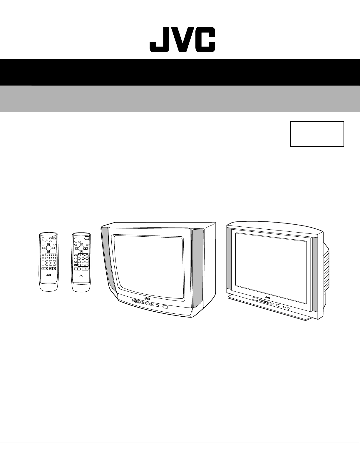
RM-C1017
TV
RM-C1017-1H
/BK
[AV-20N83
[AV-21D83
/BK
]
]
AV-20N83
AV-21D83
P
IC
T
U
R
E
POWER
M
U
T
IN
G
B
O
O
S
T
E
R
S
Y
S
T
E
M
C
O
L
O
U
R
S
O
U
N
D
E
C
O
D
IS
P
L
A
Y
S
E
N
S
O
R
M
ENU
T
V
/V
ID
E
O
123
O
F
F
T
IM
E
R
456
P
IC
T
U
R
E
M
O
D
E
789
C
H
A
N
N
E
L
R
E
T
U
R
N
+
S
C
A
N
-
--
0
/
CHAN
NEL
V
O
LUM
E
R
M
-C
1027
TV
RM-C1027-1H
[AV-21D83
[AV-20N83
/VT
/VT
]
]
[AV-20N83
/BK
, AV-20N83
/BK
/BK
AV-21D83
AV-20N83
/VT
]
[AV-21D83
/BK
, AV-21D83
/VT
/VT
/VT
]
CONTENTS
a SPECIFICATIONS ....................................................................................................................................2
a OPERATING INSTRUCTIONS (APPENDIX)
a SAFETY PRECAUTIONS .........................................................................................................................3
a FEATURES ..............................................................................................................................................4
a FUNCTIONS ............................................................................................................................................. 5
a SPECIFIC SERVICE INSTRUCTIONS ....................................................................................................6
a SERVICE ADJUSTMENTS ....................................................................................................................16
a STANDARD CIRCUIT DIAGRAM (APPENDIX) .................................................................................. 2-1
a PAR TS LIST ...........................................................................................................................................41
COPYRIGHT © 2002 VICTOR COMPANY OF JAPAN, LTD.
No. 52076
Dec. 2002
Page 2
AV-20N83
AV-21D83
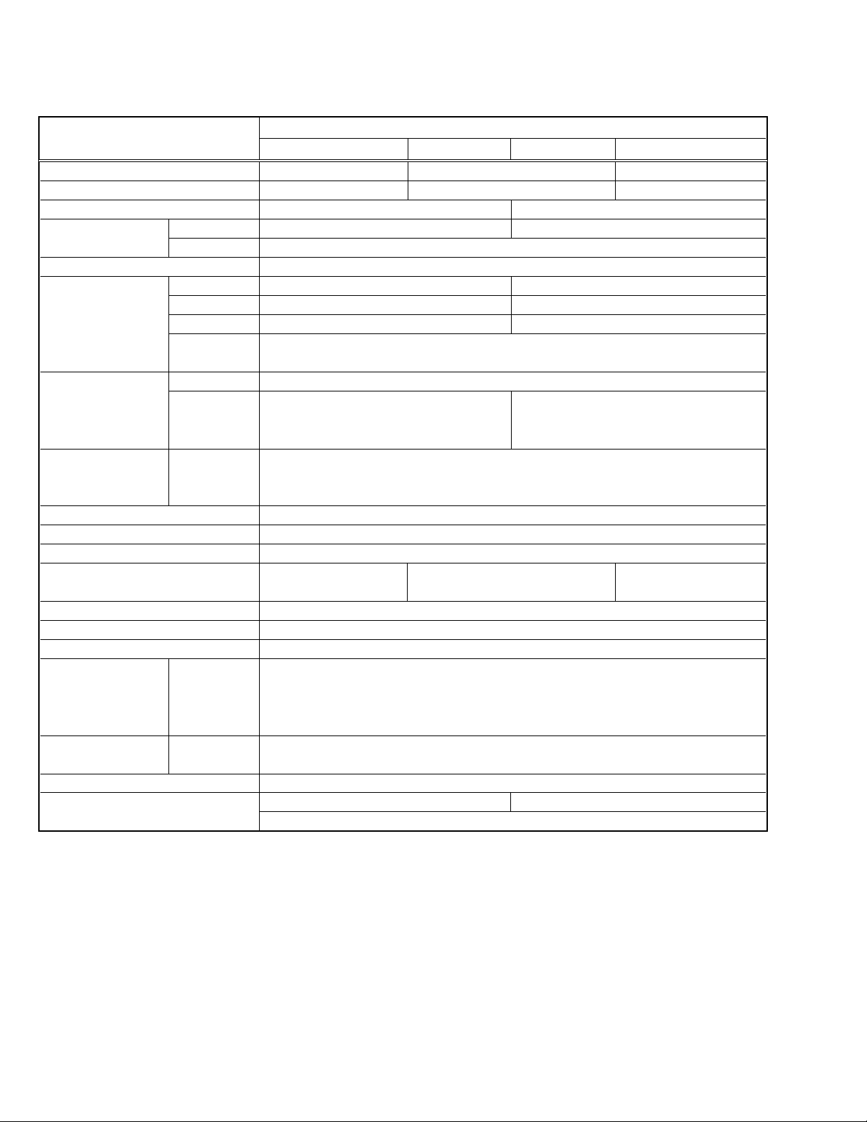
SPECIFICATIONS
Items
AV-20N83/BK
Dimensions (W × H × D)
Mass 19kg 21kg 18kg
TV RF System B, G B, G, D, K, K1, M
Colour System TV Mode PAL / SECAM PAL / SECAM / NTSC3.58 / NTSC4.43
VIDEO Mode PAL / SECAM / NTSC3.58 / NTSC4.43
Stereo System Playback only
Receiving Frequency VHF (VL) 46.25MHz – 140.25MHz (AU0 – S6) 46.25MHz – 168.25MHz (AS0 – S6)
VHF (VH) 147.25MHz – 423.25MHz (S7 – S36) 175.25MHz – 463.25MHz (S7 – S36)
UHF 431.25MHz – 863.25MHz (S37 – CHINA 57) 471.25MHz – 863.25MHz (S37 – CHINA 57)
CATV ● Cable TVs of Mid (X-Z, S1-S10)
Intermediate VIF Carrier 38.0MHz
Frequency SIF Carrier 32.5MHz (5.5MHz) 31.5MHz (6.5MHz)
Colour Sub Carrier PA L 4.43MHz
Frequency SECAM 4.40625MHz / 4.25MHz
NTSC 3.58MHz / 4.43MHz
Aerial Input Terminal 75Ø Unbalanced, coaxial
Power Input AC110V – AC240V, 50Hz / 60Hz
Power Consumption 95W
Picture Tube
High Voltage 26.5kV ± 1.5kV (at cut-off in service mode)
Speaker 5cm X 12cm Oval type x 2
Audio Output 5W + 5W
Video / Audio Input Video (1 / 3) 1V(p-p), 75Ø, RCA pin jack x 2
(1 / 2 / 3) Audio (1 / 2 / 3) 500mV(rms)(-4dBs), High impedance, RCA pin jack x 6
Component Input
(Input 2)
Video / Audio Output VIDEO 1V(p-p), 75Ø, RCA pin jack x 1
AUDIO 500mV(rms)(-4dBs), Low impedance (400Hz when modulated 100%), RCA pin jack x 2
Headphone Jack Stereo mini jack (φ3.5mm)
Remote Control Unit RM-C1017-1H RM-C1027-1H
61.9cm × 45.8cm × 48.8cm 59.8cm × 46.8cm × 47.8cm 61.9cm × 45.8cm × 48.8cm
Super (S11-S20) & Hyper (S21-S41) bands receivable
(Max.)
/ 65W
(Avg.)
Visible size : 48cm measured Visible size : 51cm measured diagonally Visible size : 48cm measured
diagonally diagonally
Y:1V(p-p), positive (negative sync provided), 75Ø, RCA pin jack x 1
CB/CR : 0.7V(p-p), 75Ø, RCA pin jack x 2
(Battery size: AA/R06/UM-3 × 2)
AV-21D83/BK
Contents
AV-21D83/VT AV-20N83/VT
32.5MHz (5.5MHz)
33.5MHz (4.5MHz)
Design & specifications are subject to change without notice.
2No. 52076
Page 3
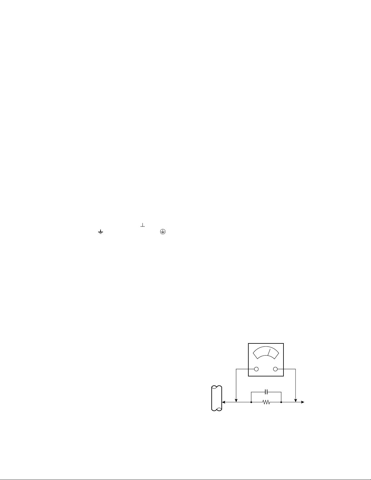
SAFETY PRECAUTIONS
AC VOLTMETER
(HAVING 1000Ω/V,
OR MORE SENSITIVITY)
PLACE THIS PROBE
ON EACH EXPOSED
METAL PAR T
1500Ω 10W
0.15µF AC-TYPE
GOOD EARTH GROUND
1. The design of this product contains special hardware, many circuits
and components specially for safety purposes. For continued protection, no changes should be made to the original design unless
authorized in writing by the manufacturer. Replacement parts must
be identical to those used in the original circuits. Service should be
performed by qualified personnel only.
2. Alterations of the design or circuitry of the products should not be
made. Any design alterations or additions will void the manufacturer's warranty and will further relieve the manufacturer of responsibility for personal injury or property damage resulting therefrom.
3. Many electrical and mechanical parts in the products have special
safety-related characteristics. These characteristics are often not
evident from visual inspection nor can the protection afforded by
them necessarily be obtained by using replacement components
rated for higher voltage, wattage, etc. Replacement parts which have
these special safety characteristics are identified in the parts list of
Service manual. Electrical components having such features are
identified by shading on the schematics and by (!) on the parts
list in Service manual. The use of a substitute replacement which
does not have the same safety characteristics as the recommended
replacement part shown in the parts list of Service manual may
cause shock, fire, or other hazards.
4. Don't short between the LIVE side ground and ISOLATED (NEU-
TRAL) side ground or EARTH side ground when repairing.
Some model's power circuit is partly different in the GND. The difference of the GND is shown by the LIVE : ( ) side GND, the ISOLATED (NEUTRAL) : ( ) side GND and EARTH : ( ) side GND.
Don't short between the LIVE side GND and ISOLATED (NEUTRAL)
side GND or EARTH side GND and never measure the LIVE side
GND and ISOLATED (NEUTRAL) side GND or EARTH side GND
at the same time with a measuring apparatus (oscilloscope etc.).
If above note will not be kept, a fuse or any parts will be broken.
5. If any repair has been made to the chassis, it is recommended that
the B1 setting should be checked or adjusted (See ADJUSTMENT
OF B1 POWER SUPPLY).
6. The high voltage applied to the picture tube must conform with that
specified in Service manual. Excessive high voltage can cause an
increase in X-Ray emission, arcing and possible component damage, therefore operation under excessive high voltage conditions
should be kept to a minimum, or should be prevented. If severe
arcing occurs, remove the AC power immediately and determine
the cause by visual inspection (incorrect installation, cracked or
melted high voltage harness, poor soldering, etc.). To maintain the
proper minimum level of soft X-Ray emission, components in the
high voltage circuitry including the picture tube must be the exact
replacements or alternatives approved by the manufacturer of the
complete product.
AV-20N83
AV-21D83
8. When service is required, observe the original lead dress. Extra
precaution should be given to assure correct lead dress in the high
voltage circuit area. Where a short circuit has occurred, those components that indicate evidence of overheating should be replaced.
Always use the manufacturer's replacement components.
9. Isolation Check
(Safety for Electrical Shock Hazard)
After re-assembling the product, always perform an isolation check
on the exposed metal parts of the cabinet (antenna terminals, video/
audio input and output terminals, Control knobs, metal cabinet, screw
heads, earphone jack, control shafts, etc.) to be sure the product is
safe to operate without danger of electrical shock.
(1) Dielectric Strength Test
The isolation between the AC primary circuit and all metal parts
exposed to the user, particularly any exposed metal part having a
return path to the chassis should withstand a voltage of 3000V AC
(r.m.s.) for a period of one second.
(. . . . Withstand a voltage of 1100V AC (r.m.s.) to an appliance rated
up to 120V, and 3000V AC (r.m.s.) to an appliance rated 200V or
more, for a period of one second.)
This method of test requires a test equipment not generally found in
the service trade.
(2) Leakage Current Check
Plug the AC line cord directly into the AC outlet (do not use a line
isolation transformer during this check.). Using a "Leakage Current
Tester", measure the leakage current from each exposed metal part
of the cabinet, particularly any exposed metal part having a return
path to the chassis, to a known good earth ground (water pipe, etc.).
Any leakage current must not exceed 0.5mA AC (r.m.s.).
However, in tropical area, this must not exceed 0.2mA AC (r.m.s.).
● Alternate Check Method
Plug the AC line cord directly into the AC outlet (do not use a line
isolation transformer during this check.). Use an AC voltmeter having 1000 ohms per volt or more sensitivity in the following manner.
Connect a 1500Ø 10W resistor paralleled by a 0.15µF AC-type capacitor between an exposed metal part and a known good earth
ground (water pipe, etc.). Measure the AC voltage across the resistor with the AC voltmeter. Move the resistor connection to each exposed metal part, particularly any exposed metal part having a return path to the chassis, and measure the AC voltage across the
resistor. Now, reverse the plug in the AC outlet and repeat each
measurement. Any voltage measured must not exceed 0.75V AC
(r.m.s.). This corresponds to 0.5mA AC (r.m.s.).
However, in tropical area, this must not exceed 0.3V AC (r.m.s.).
This corresponds to 0.2mA AC (r.m.s.).
7. Do not check high voltage by drawing an arc. Use a high voltage
meter or a high voltage probe with a VTVM. Discharge the picture
tube before attempting meter connection, by connecting a clip lead
to the ground frame and connecting the other end of the lead through
a 10kØ 2W resistor to the anode button.
No. 52076 3
Page 4
AV-20N83
AV-21D83
FEATURES
s New chassis design enables use of an interactive on-screen control.
s Pure flat CRT produces fine textured picture in every detail.
s Wide range voltage (110V ~ 240V) for AC power input.
s With AUDIO/VIDEO/COMPONENT input terminals.
2
C bus control utilizes single chip ICs.
s I
s By means of AUTO PROGRAM, the TV stations can be selected
automatically and the TV channels can also be rearranged automatically.
s Built-in DIGITAL ECO MODE (ECONOMY, ECOLOGY).
In accordance with the brightness in a room, the brightness and/or
contrast of the picture can be adjusted automatically to make the
optimum picture which is easy on the eye.
s Built-in OFF TIMER & RETURN +.
MAIN DIFFERENCE LIST
!
Part Name
! MAIN PWB SCH-1090A-BK SCH-1122A-BK SCH-1315A-CK SCH-1316A-CK
FRONT CABINET LC10438-028A-H LC11129-024A-H LC11129-025A-HK LC10438-034A-HK
! REAR COVER GG10448-005A-H GG10130-001A-H LC10130-011A-HK LC10448-005A-HK
! PICTURE TUBE A48LWX10X A51LMV10X A51JSW51X07 A48JLL91X01
! DEG COIL QQW0156-001 QQW0157-001 QQW0156-001
! RATING LABEL GG20029-001A-H GG20016-025A-E GG20016-024A-E
REMOTE CONTROL UNIT RM-C1017-1H RM-C1027-1H
MODEL No.
AV-20N83
/BK AV-21D83/BK AV-21D83/VT AV-2 0N83/VT
4No. 52076
Page 5
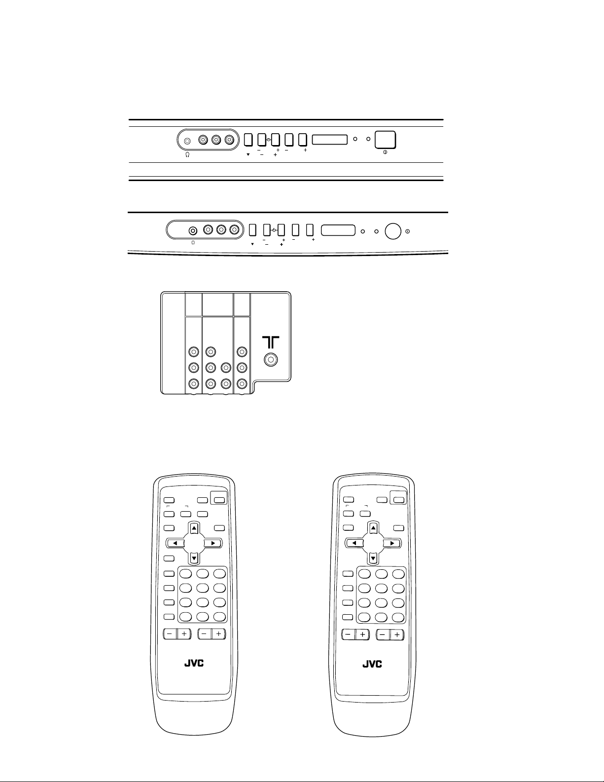
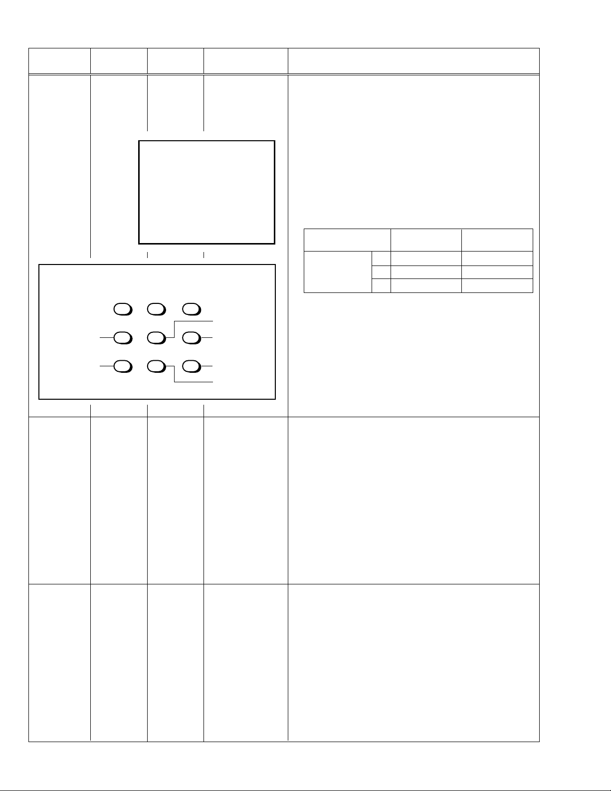
FUNCTIONS
a FRONT PANEL
AV-20N83
AV-21D83
[AV-20N83
/BK, AV-20N83/VT]
[AV-21D83/BK, AV-21D83/VT]
a REAR PANEL
L/MONO
VR
IN (VIDEO-3)
L/MONO
VR
IN (VIDEO-3)
COMPONENT
VIDEO-1
(
)
VIDEO-2
INPUT
INPUT
V
Y
/
V
L
C
B
MONO
L
/
MONO
RRC
R
/
R
MENU
MENU
OUTPUT
V
L
CHANNEL
CHANNEL
VOLUME
EXIT
VOLUME
EXIT
SUB
POWER
SUB
POWER
POWER
POWER
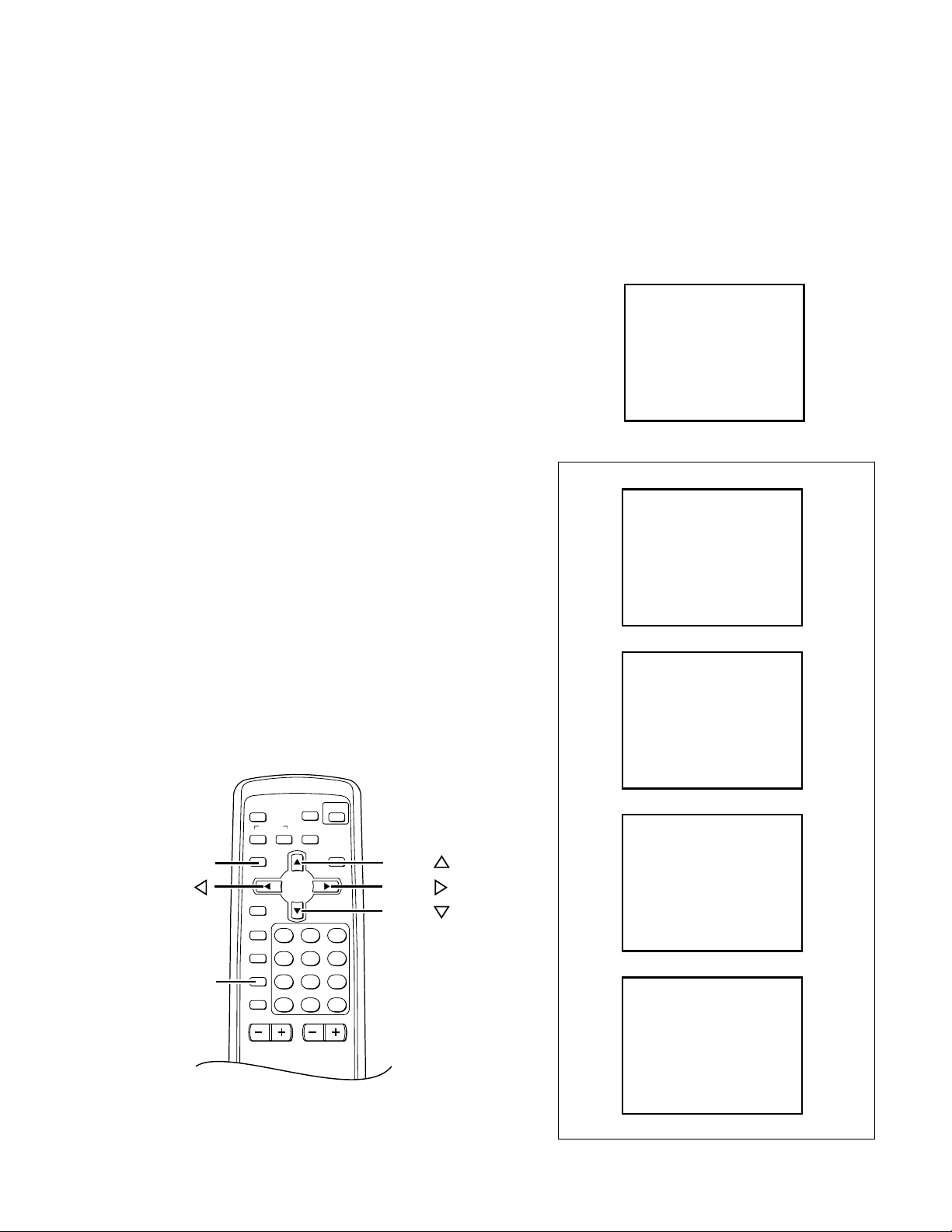
a REMOTE CONTROL UNIT
RM-C1017-1H
[AV-20N83/BK, AV-21D83/BK]
MUTING
SYSTEM
COLOUR SOUND
DISPLAY
/
12
TV/VIDEO
OFF
TIMER
PICTURE
MODE
CHANNEL
RETURN+
SCAN
CHANNEL
PICTURE
POWER
BOOSTER
CINEMA
SURROUND
ECO
SENSOR
MENU
123
456
789
--
0-/
VOLUME
RM-C1017
TV
RM-C1027-1H
[AV-21D83/VT, AV-20N83/VT]
PICTURE
MUTING
SYSTEM
COLOUR SOUND
DISPLAY
TV/VIDEO
OFF
TIMER
PICTURE
MODE
CHANNEL
RETURN+
SCAN
CHANNEL
POWER
BOOSTER
ECO
SENSOR
MENU
123
456
789
-
--
0
/
V
O
LUME
RM-C1027
TV
No. 52076 5
Page 6

AV-20N83
SPECIFIC SERVICE INSTRUCTIONS
DISASSEMBLY PROCEDURE [AV-20N83/BK, AV-20N83/VT]
REMOVING THE REAR COVER
1. Unplug the power supply cord.
2. Remove the 6 screws marked Å and 4 screws marked ı as shown
in Fig.1.
3. Withdraw the Rear cover toward you.
[CAUTION]
When reinstalling the rear cover, carefully push it inward after in-
•
serting the Main PWB into the rear cover groove.
REMOVING THE MAIN PW BOARD
After removing the rear cover.
•
1. Slightly raise the both sides of the Main PWB by hand, take off the
PB Stopper marked Ç from the front cabinet.
2. Withdraw the Main PWB backward.
(If necessary, take off the wire clamp and connectors, etc.)
REMOVING THE SPEAKER [AV-20N83/BK]
After removing the rear cover.
•
1. Remove the 2 screws marked Î and 2 screws marked ´ as shown
in Fig.1.
2. Follow the same steps when removing the other hand speaker.
REMOVING THE SPEAKER [AV-20N83/VT]
After removing the rear cover.
•
1. Remove the 2 screws marked Î as shown in Fig.1.
2. Follow the same steps when removing the other hand speaker.
CHECKING THE MAIN PW BOARD
1. To check the back side of the Main PWB.
1) Pull out the Main PWB. (Refer to REMOVING THE MAIN PW
BOARD).
2) Erect the Main PWB vertically so that you can easily check its
back side.
[CAUTION]
Before turning on power, make sure that the CRT earth wire and
•
other connectors are properly connected.
When repairing, connect the Deg. coil to the DEG. connector on the
•
Main PWB.
WIRE CLAMPING AND CABLE TYING
1. Be sure to clamp the wire.
2. Never remove the cable tie used for tying the wires together.
Should it be inadvertently removed, be sure to tie the wires with a
new cable tie.
6No. 52076
Page 7
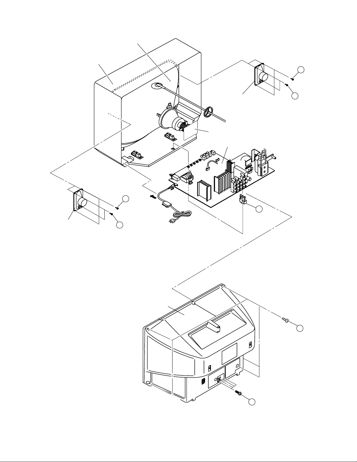
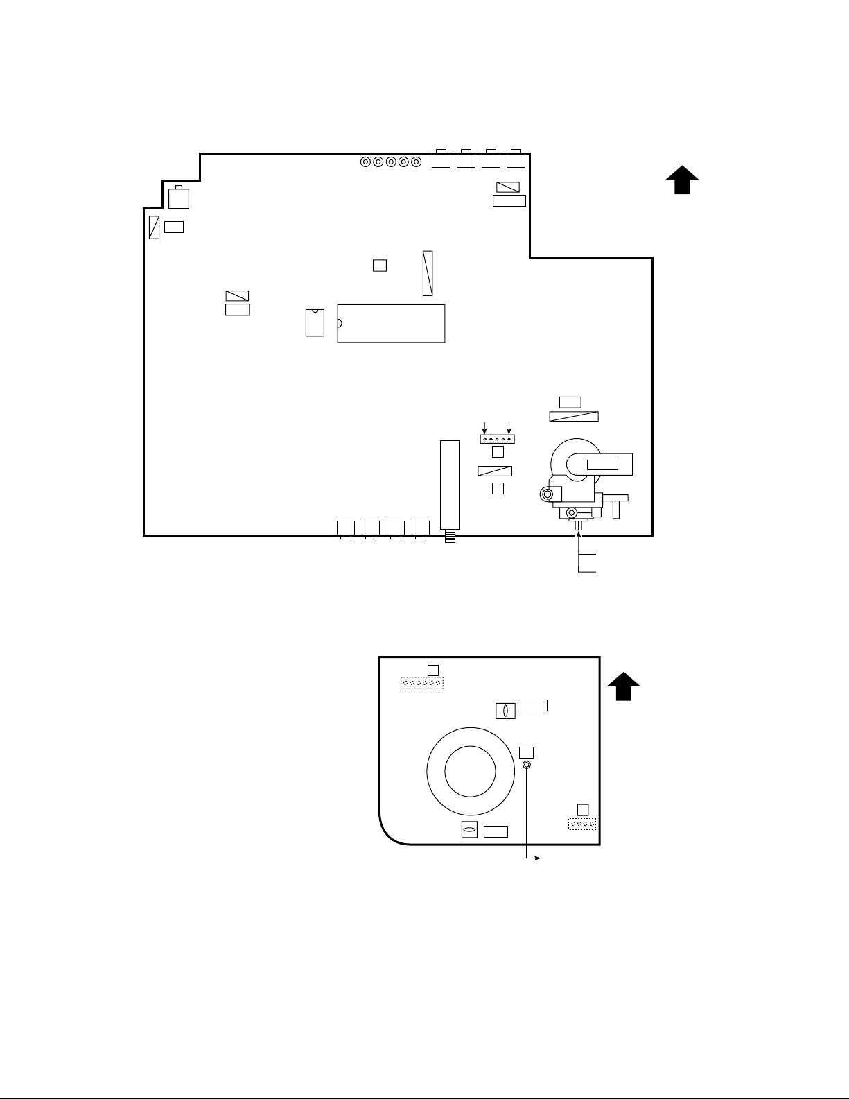
FRONT CABINET
PICTURE TUBE
SPEAKER
MAIN PWB
(CRT SOCKET PWB)
MAIN PWB
AV-20N83
(X2)
E
(X2)
D
SPEAKER
(X2)
D
C
(X2)
E
REAR COVER
A
(X6)
B
Fig.1
No. 52076 7
Page 8

AV-21D83
DISASSEMBLY PROCEDURE [AV-21D83/BK, AV-21D83/VT]
REMOVING THE REAR COVER
1. Unplug the power supply cord.
2. Remove the 7 screws marked
in Fig.1.
3. Withdraw the Rear cover toward you.
[CAUTION]
When reinstalling the rear cover, carefully push it inward after in-
•
serting the Main PWB into the rear cover groove.
REMOVING THE MAIN PW BOARD
After removing the rear cover.
•
1. Slightly raise the both sides of the Main PWB by hand, take off the
PB Stopper marked
2. Withdraw the Main PWB backward.
(If necessary, take off the wire clamp and connectors, etc.)
from the front cabinet.
Ç
and 4 screws marked ı as shown
Å
REMOVING THE SPEAKER [AV-21D83/BK]
After removing the rear cover.
•
1. Remove the 2 screws marked Î as shown in Fig.1.
2. Follow the same steps when removing the other hand speaker.
REMOVING THE SPEAKER [AV-21D83/VT]
After removing the rear cover.
•
1. Remove the 2 screws marked Î and 2 screws marked ´ as shown
in Fig.1.
2. Follow the same steps when removing the other hand speaker.
CHECKING THE MAIN PW BOARD
1. To check the back side of the Main PWB.
1) Pull out the Main PWB. (Refer to REMOVING THE MAIN PW
BOARD).
2) Erect the Main PWB vertically so that you can easily check its
back side.
[CAUTION]
Before turning on power, make sure that the CRT earth wire and
•
other connectors are properly connected.
When repairing, connect the Deg. coil to the DEG. connector on the
•
Main PWB.
WIRE CLAMPING AND CABLE TYING
1. Be sure to clamp the wire.
2. Never remove the cable tie used for tying the wires together.
Should it be inadvertently removed, be sure to tie the wires with a
new cable tie.
8No. 52076
Page 9
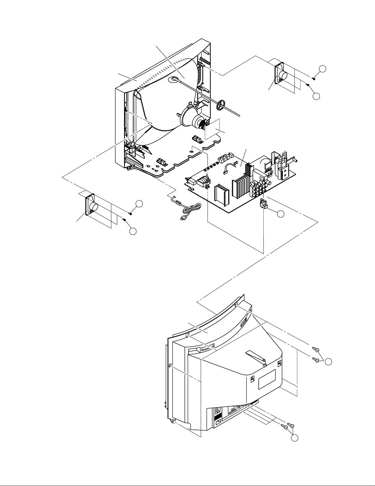
FRONT CABINET
PICTURE TUBE
MAIN PWB
(CRT SOCKET PWB)
MAIN PWB
SPEAKER
SPEAKER
REAR COVER
C
(X2)
D
(X2)
E
B (X4)
A
(X7)
(X2)
E
(X2)
D
AV-21D83
Fig.1
No. 52076 9
Page 10
AV-20N83
AV-21D83
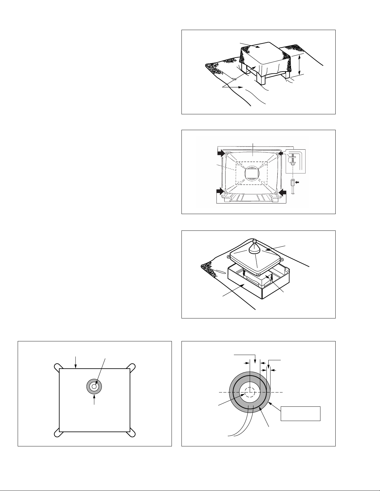
REMOVING THE CRT
* Replacement of the CRT should be performed by 2 or more persons.
After removing the rear cover, chassis etc.,
•
1. Putting the CRT change table on soft cloth, the CRT change table
should also be covered with such soft cloth (shown in Fig. 2).
2. While keeping the surface of CRT down, mount the TV set on the
CRT change table balanced will as shown in Fig. 3.
3. Remove 4 screws marked by arrows with a box type screwdriver as
shown in Fig. 3.
Since the cabinet will drop when screws have been removed, be sure
•
to support the cabinet with hands.
4. After 4 screws have been removed, put the cabinet slowly on cloth
(At this time, be carefully so as not to damage the front surface of the
cabinet) shown in Fig. 4.
The CRT should be assembled according to the opposite sequence
•
of its dismounting steps.
* The CRT change table should preferably be smaller that the CRT sur-
face, and its height be about 35cm.
CRT CHANGE TABLE
CLOTH
CRT
CHANGE
TABLE
Fig. 2
CRT
APPROX.
35cm
BOX
TYPE
SCREW
DRIVER
COATING OF SILICON GREASE FOR ELECTRICAL INSULATION ON THE CRT ANODE CAP SECTION.
Subsequent to replacement of the CRT and HV transformer or repair
•
of the anode cap, etc. by dismounting them, be sure to coat silicon
grease for electrical insulation as shown in Fig. 5.
1. Wipe around the anode button with clean and dry cloth. (Fig. 5)
2. Coat silicon grease on the section around the anode button. At this
time, take care so that any silicon greases does not sticks to the
anode button. (Fig. 6)
夝 Silicon grease product No. KS - 650N
CRT
Anode button
CABINET
Approx.
20mm (Do not
coat grease on
this section
Fig. 3
CRT
CRT
CHANGE TABLE
Fig. 4
Silicon grease
should be coated
by 5mm or more
from the outside
diameter of anode
cap.
Silicon grease
coating
Fig. 5
10 No. 52076
Anode button
(No sticking of
silicon grease)
Coating position
of silicon grease
Anode cap
Fig. 6
Page 11
REPLACEMENT OF MEMORY IC
1. MEMORY IC
This TV uses the following memory IC.
Memory IC: IC1702 on MAIN PW Board
The memory IC memorizes data for correctly operating the video
and deflection circuits. When replacing the memory IC, be sure to
use the same type IC written with the initial values of data. In other
words, use the specific IC listed in “PRINTED WIRING BOARD
PA RTS LIST”. For its mounting location, refer to “ADJUSTMENT
LOCATIONS”.
AV-20N83
AV-21D83
(6) User setting
Check the user setting values in Table 2, and if setting value is
different, set the correct value.
For setting, refer to the OPERATING INSTRUCTIONS.
(7) Setting of SERVICE MENU
Ver ify the setting for each setting item in the SERVICE MENU.(See
Ta ble 3.) If readjustment is necessary, perform adjustment referring to “SERVICE ADJUSTMENTS”.
2. PROCEDURE FOR REPLACING MEMORY IC
(1) Power off
Switch the power off and unplug the power cord from the wall
outlet.
(2) Replacing the memory IC
Replace the memory IC with new one. Be sure to use the memory
IC written with the initial data values.
(3) Power on
Plug the power cord into the wall outlet and switch the power on.
(4) Check and setting of SYSTEM CONSTANT SET:
1) Press the DISPLAY key and the PICTURE MODE key on the
remote control unit simultaneously.
The SERVICE MENU screen will be displayed.(See Fig.1.)
2) In the SERVICE MENU, press the DISPLAY key and PICTURE MODE key simultaneously. Then, the SYSTEM CONSTANT SET screen will be displayed.(See Fig.2.)
3) Check whether the setting values of the SYSTEM CONSTANT
SET are the same as those indicated in Table1.
If the value is different, select the setting item with the MENU
&/^ key, and set the correct value with the MENU */T key.
4) Press the DISPLAY key twice to return to the normal screen.
(5) Receive channel setting
Refer to the OPERATING INSTRUCTIONS and set the receive
channels (channels preset).
NAME OF REMOTE CONTROL KEYS
SERVICE MENU
SERVICE MENU
1. IF
3. DEF
5. PRESET
6. PLUG & PLAY (ON)
1-6 : SELECT DISPLAY : EXIT
******* **** ***** *****
**** **** *** ***
2. VC
4. VSM PRESET
Fig. 1
SYSTEM CONSTANT-
SYSTEM CONSTANT SET 1
SYSTEM
COMB
TILT
TEXT
SUPER BASS
LANGUAGE
>? : SEL -+ : OPE
SYSTEM CONSTANT-
SYSTEM CONSTANT SET 2
MSP
BILINGUAL
B / B SOUND
TUNER
COLOUR AUTO
>? : SEL -+ : OPE
DISP : EXIT
DISP : EXIT
Ι
MULTI
NO
NO
NO
NO
E/R/C/M/I
II
YES
NO
NO
MU
NO
DISPLAY
MENU
PICTURE
MODE
PICTURE
BOOSTER
MUTING
SYSTEM
COLOUR SOUND
DISPLAY
I/II
TV/VIDEO
OFF
TIMER
PICTURE
MODE
CHANNEL
RETURN+
SCAN
CHANNEL
HOLD
REVEAL
SUBPAGE CANCEL
STORE MODE
POWER
CINEMA
SURROUND
ECO
SENSOR
MENU
TV/TEXT
123
456
789
0-/
VOLUME
TEXT
SIZE
INDEX
RM-C1010
TV
SYSTEM CONSTANT-
SYSTEM CONSTANT SET 3
MENU
MENU
MENU
LOCK 1 MHz
>? : SEL -+ : OPE
500 KHz
250 KHz
156. 25 KHz
31.25 KHz
SYSTEM CONSTANT-
--
SYSTEM CONSTANT SET 4
3D SURROUND
3CH VOL/TONE
AMP TUNER
>? : SEL -+ : OPE
: 040
: 040
: 040
: 030
: 030
DISP : EXIT
NO
NO
NO
DISP : EXIT
III
IV
Fig. 2
No. 52076 11
Page 12
AV-20N83
AV-21D83
SETTING OF SYSTEM CONSTANT SET
Setting item Setting content
SYSTEM
COMB
TILT
TEXT
SUPER BASS
LANGUAGE
MSP
BILINGUAL
B/B SOUND
TUNER
COLOUR AUTO
LOCK 1MHz
500KHz
MULTI TRIPLE PAL SINGLE VIET
YES NO
YES NO
EASTERN UKRANIAN RUSSIAN
NO PAN EURO ARABK
YES NO
E/ T E/V E
YES NO
YES NO
YES NO
MU MA
YES NO
000 240
000 240
Setting value
AV-20N83
/BK
AV-21D83
/BK
AV-21D83
SINGLE VIET
NO
NO
NO
NO
E/T
NO
YES
NO
MU
NO
040
040
E/V
NO
/VT
AV-20N83
/VT
250KHz
156.25KHz
31.25KHz
3D SURROUND
3CH VOL/TONE
AMP TUNER
000 240
000 240
000 240
YES NO
YES NO
YES NO
Table 1
040
030
030
YES
NO
YES
NO
12 No. 52076
Page 13

USER SETTING VALUES
Setting item Setting value
SUB POWER ON
CHANNEL POSITION 1 POSITION
CHANNEL PRESET REFER TO OPERATING INSTRUCTIONS
VOLUME 15 ± 2
TV/VIDEO TV
VNR OFF
COMPRESS (16:9) OFF
AUTO SHUTOFF OFF
CHILD LOCK OFF
BLUE BACK ON
VIDEO-2 SET VIDEO
LANGUAGE THAI [AV-20N83
VIET [AV-21D83/VT, AV-20N83/VT only]
3D SURROUND OFF
AI VOLUME ON
ON SCREEN DISPLAY POSITION INDICATION
COLOUR SYSTEM PAL
SOUND SYSTEM B/G
PICTURE MODE-VSM BRIGHT
OFF TIMER 00
ECO SENSOR OFF
BASS CENTRE
TREBLE CENTRE
BALANCE CENTRE
BILINGUAL MODE 1/2 [AV-20N83/BK, AV-21D83/BK only]
/BK, AV-21D83/BK only]
AV-20N83
AV-21D83
Tab le 2
No. 52076 13
Page 14
AV-20N83
AV-21D83
SERVICE MENU SETTING ITEMS
Service menu Setting item
1. IF 1. VCO
2. DELAY POINT
2. VC 1. CUTOFF(R/G)
2. DRIVE(R/G/B)
3. BRIGHT
4. CONT
5. COLOUR
6. TINT
7. SHARP
8. YDELAY
9. AMP T. SHARP
3. DEF 1. VER. SLOPE
2. VER. HEIGHT
3. VER. POSITION
4. VER. SCURVE
5. HOR. POSITION
6. HOR. WIDTH
7. EW-PIN
8. EW-TRAPEZ
9. UP CORNER
10. DW CORNER
11. HOR. PARALL
12. HOR. BOW
13. V. ZOOM
4. VSM PRESET 1. TINT
(BRIGHT/STD/SOFT) 2. COLOUR
Do not adjust
3. BRIGHT
4. CONT
5. SHARP
Do not adjust
Service menu Setting item
5. PRESET 1. PSNS
Do not adjust
6.
PLUG & PLAY(ON)
2. ACL
3. MUS
4. MAT
5. FCO
6. BPS
7. IFLH
8. VID
9. STM
10. AFCW
11. VSW
12. FFI
13. AGC
14. CL
15. AKB
16. HBL
17. BKS
18. READ STATUS
19. VNR
20. PEAK
21. IVG
22. WPL
23. SOFT CLIPPER
24. IF PLL OFFSET
25. OVERSHOOT
26. HCO
27. HP2
28. AI VOLUME ADN
29. SUB BASS 3D
30. SUB TREBLE 3D
31. CCCLOOP
Table 3
14 No. 52076
Do not adjust
Page 15
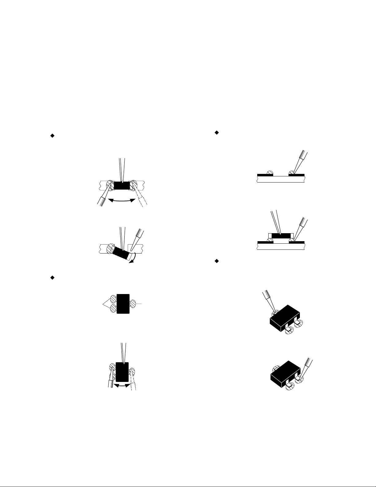
REPLACEMENT OF CHIP COMPONENT
CAUTIONS
a
1. Avoid heating for more than 3 seconds.
2. Do not rub the electrodes and the resist parts of the pattern.
3. When removing a chip part, melt the solder adequately.
4. Do not reuse a chip part after removing it.
SOLDERING IRON
a
1. Use a high insulation soldering iron with a thin pointed end of it.
2. A 30w soldering iron is recommended for easily removing parts.
REPLACEMENT STEPS
a
1. How to remove Chip parts
Resistors, capacitors, etc.
(1) As shown in the figure, push the part with tweezers and alter-
nately melt the solder at each end.
AV-20N83
AV-21D83
2. How to install Chip parts
Resistors, capacitors, etc.
(1) Apply solder to the pattern as indicated in the figure.
(2) Shift with tweezers and remove the chip part.
Transistors, diodes, variable resistors, etc.
(1) Apply extra solder to each lead.
SOLDER
(2) As shown in the figure, push the part with tweezers and alter-
nately melt the solder at each lead. Shift and remove the chip
part.
SOLDER
(2) Grasp the chip part with tweezers and place it on the solder.
Then heat and melt the solder at both ends of the chip part.
Transistors, diodes, variable resistors, etc.
(1) Apply solder to the pattern as indicated in the figure.
(2) Grasp the chip part with tweezers and place it on the solder.
(3) First solder lead A as indicated in the figure.
A
B
C
(4) Then solder leads B and C.
A
Note : After removing the part, remove remaining solder from the
pattern.
No. 52076 15
B
C
Page 16

AV-20N83
AV-21D83
SERVICE ADJUSTMENTS
ADJUSTMENT PREPARATION
1. You can make the necessary adjustments for this unit with either the remote control unit or with the adjustment equipment and parts
as given below.
2. Adjustment with the remote control unit is made on the basis of the initial setting values, however, the new setting values which set the
screen to its optimum condition may differ from the initial settings.
3. Make sure that AC power is turned on correctly.
4. Turn on the power for the set and test equipment before use, and start the adjustment procedures after waiting at least 30 minutes.
5. Unless otherwise specified, prepare the most suitable reception or input signal for adjustment.
6. Never touch any adjustment parts, which are not specified in the list for this adjustment-variable resistors, transformers, capacitors, etc.
7. Presetting before adjustment.
Unless otherwise specified in the adjustment instructions, preset the following functions with the remote control unit.
User mode setting position
•
Setting item Setting value
PICTURE MODE(VSM) BRIGHT
VNR OFF
BASS, TREBLE, BALANCE CENTRE
TINT, COLOUR, BRIGHT, SHARP
CONTRAST MAXIMUM
CENTRE
MEASURING INSTRUMENT
1. DC voltmeter (or Digital voltmeter)
2. Oscilloscope
3. Signal generator (Pattern generator) [PAL/SECAM/NTSC]
4. Remote control unit
ADJUSTMENT ITEMS
B1 POWER SUPPLY
•
FOCUS ADJUSTMENT
•
IF CIRCUIT ADJUSTMENTS
•
Adjustment of VCO (CW)
Adjustment of DELAY POINT (AGC TAKE-OVER)
VC (VIDEO/CHROMA) CIRCUIT ADJUSTMENTS
•
Adjustment of WHITE BALANCE (Low light)
Adjustment of WHITE BALANCE (High light)
Adjustment of SUB BRIGHT
Adjustment of SUB CONTRAST
Adjustment of SUB COLOUR-Ι
Adjustment of SUB COLOUR-ΙΙ
Adjustment of SUB TINT-Ι
Adjustment of SUB TINT-ΙΙ
DEFLECTION CIRCUIT ADJUSTMENTS
•
Adjustment of V. SLOPE
Adjustment of V. POSITION
Adjustment of V. HEIGHT
Adjustment of H. POSITION
Adjustment of H. WIDTH
Adjustment of SIDE PIN
Adjustment of TRAPEZIUM
Adjustment of V. S-CURVE
Adjustment of CORNER
Adjustment of H. PARALLEL
Adjustment of H. BOW
VSM PRESET SETTING
•
PRESET SETTING
•
PURITY ADJUSTMENT
•
CONVERGENCE ADJUSTMENTS
•
Adjustment of STATIC CONVERGENCE
Adjustment of DYNAMIC CONVERGENCE
16 No. 52076
Page 17
ADJUSTMENT LOCATIONS
AV-20N83
AV-21D83
MAIN PWB ASS'Y
POWER SW
S901
PW
DEG
IC702
S783 S781
S784 S782 S780
T
IC701
J804J801 J802 J803
J773
J772 J771
1
6
J770
CN001
GND B1
5
S
41
U
1
S780 : MENU
S781 : CH–
S782 : CH+
S783 : VOL–
S784 : VOL+
HV
FRONT
14
HVT
AV IN/OUT
MAIN PWB ASS'Y
(CRT SOCKET)
(SOLDER SIDE)
TU001
T
61
TP-E
TP-47G
E1
CRT EARTH
(BRAIDED ASS'Y)
UPPER : FOCUS (F1)
LOWER : SCREEN
TOP
U
41
No. 52076 17
Page 18

AV-20N83
AV-21D83
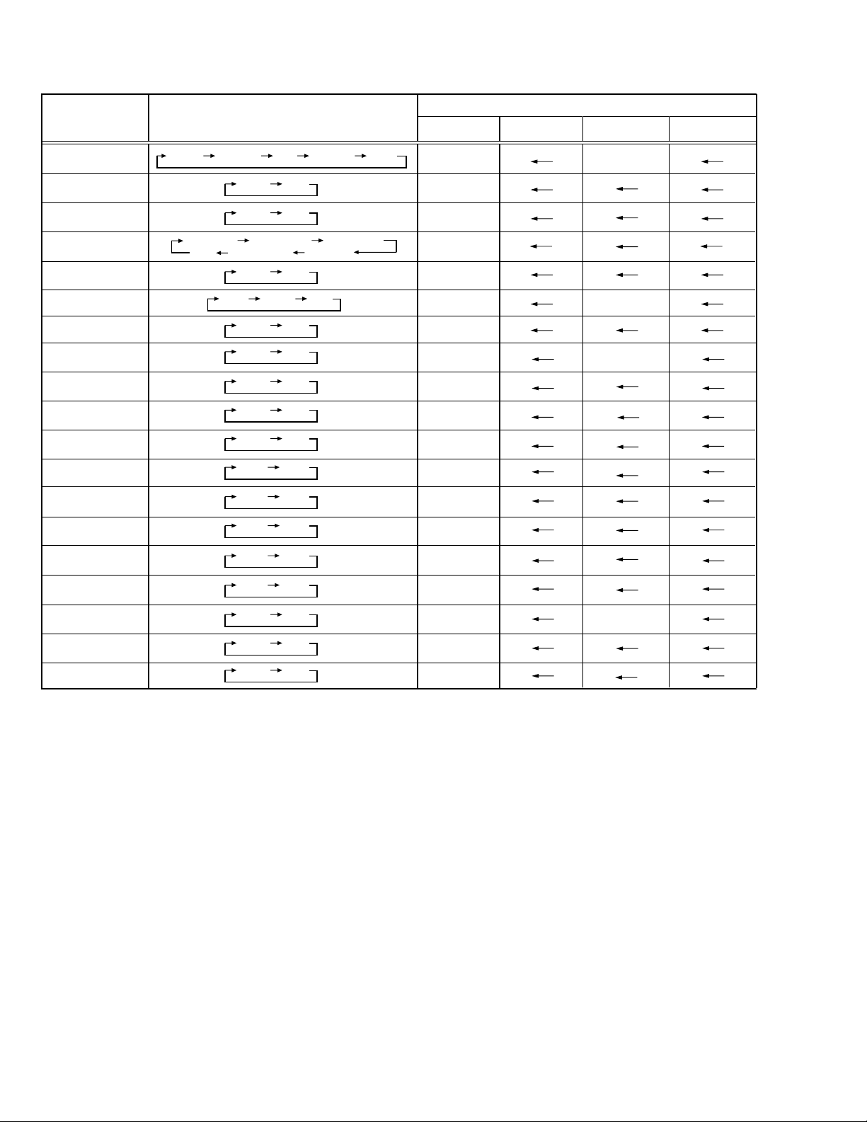
BASIC OPERATION IN SERVICE MENU
1. TOOL OF SERVICE MENU OPERATION
Operate the SERVICE MENU with the remote control unit.
2. SERVICE MENU ITEMS
With the SERVICE MENU,various settings (adjustments)can be made,and they are broadly classified in the following items of settings:
1.IF ......................................For entering/adjusting the setting values (adjustment values)of the IF circuit.
•
2.VC ....................................For entering/adjusting the setting values (adjustment values)of the VIDEO/CHROMA circuit.
•
3.DEF ..................................For entering/adjusting the setting values (adjustment values)of the DEFLECTION circuit.
•
4.VSM PRESET ..................For setting the values of STANDARD,SOFT and BRIGHT.
•
5.PRESET ........................... For setting the values of the preset.
•
6.PLUG & PLAY (ON) ......... This is not used for service.
•
3. BASIC OPERATION IN SERVICE MENU
(1) How to enter SERVICE MENU
Press the DISPLAY key and the PICTURE MODE key on the remote control unit simultaneously.
The SERVICE MENU screen will be displayed. (See Fig. 1 on the next page.)
(2) Selection of SUB MENU SCREEN
Press one of the keys 1 to 6 on the remote control unit,and select the SUB MENU SCREEN from the SERVICE MENU.(See Fig.1 on the next
page.)
(VSM:video status memory)
SERVICE MENU → SUB MENU 1. IF
2. VC
3. DEF
4. VSM PRESET
5. PRESET
6. PLUG & PLAY (ON)
(3) Method of Setting
*Once the setting values are set,they are memorized automatically.
*It must not adjust without inputting a signal.
1) 1. IF
[1.VCO ]
(a) 1 Key......................... Select 1. IF.
(b) 1 Key......................... Select 1. VCO.
(c) DISPLAY Key ............ When this is pressed twice, you will return to the SERVICE MENU.
Under normal conditions, no adjustment is required.
[2.DELAY POINT ]
(a) 1 Key......................... Select 1. IF.
(b) 2 Key......................... Select 2.DELAY POINT.
(c) MENU
(d) DISPLAY Key ............ When this is pressed twice, you will return to the SERVICE MENU.
2) 2. VC, 3. DEF, 4. VSM PRESET and 5. PRESET
(a) 2 ~5 Keys.................. Select one from 2. VC, 3. DEF, 4. VSM PRESET and 5. PRESET
(b) MENU &/^ key........ Select setting items.
(c) MENU
(d) DISPLAY Key ............ When this is pressed, you will return to the SERVICE MENU.
*/T
Key ........ Adjust the setting value.
*/T
Key ........ Adjust the setting values of the setting items.
•
Use the number keys on the remote control unit for setting of WHITE BALANCE.
•
For the setting, refer to each item concerned.
3) 6. PLUG & PLAY (ON)
This is not used for service.
(4) Release of SERVICE MENU
After completing the setting, return to the SERVICE MENU by pressing the DISPLAY key, then again press the DISPLAY key to return to the
normal screen.
18 No. 52076
Page 19
AV-20N83
AV-21D83
SERVICE MENU
SERVICE MENU
1. IF
3. DEF
5. PRESET
6. PLUG & PLAY (ON)
1-6 : SELECT DISPLAY : EXIT
******* **** ***** *****
**** **** *** ***
2. VC
4. VSM PRESET
SUB MENU 1. IF
IF
1. VCO
2. DELAY POINT
1-2 : SELECT DISPLAY : EXIT
SUB MENU 2. VC
V/C
PAL
1. CUTOFF
50 Hz
MENU 89: SELECT
MENU
-
(R)
(G)
/+: OPERATE
**
**
DISPLAY : EXIT
Setting item
1. CUTOFF (R/G)
2. DRIVE (R/G/B)
3. BRIGHT
4. CONT
5. COLOUR
6. TINT
7. SHARP
8. YDELAY
9. AMP T.SHARP
VCO (CW)
TOO HIGH
ABOVE REFERENCE
BELOW REFERENCE
TOO LOW
DELAY POINT VHF
AGC TAKE-OVER
-
/+: OPERATE
MHz
*****
DISPLAY : EXIT
**
DISPLAY : EXIT
SUB MENU 5. PRESET
PRESET 50Hz
1. PSNS
MENU 89: SELECT
MENU
-
/+: OPERATE
DISPLAY : EXIT
SUB MENU 3. DEF
4 : 3 / 16 : 9
DEF 4 : 3
1. VER. SLOPE
50Hz
MENU 89: SELECT
MENU
-
/+: OPERATE
PAL
**
DISPLAY : EXIT
1. VER. SLOPE
2. VER. HEIGHT
3. VER. POSITION
4. VER. SCURVE
5. HOR. POSITION
6. HOR. WIDTH
Setting item
7. EW-PIN
8. EW-TRAPEZ
9. UP CORNER
10. DW CORNER
11. HOR. PARALL
12. HOR. BOW
13. V. ZOOM
SUB MENU 4. VSM PRESET
BRIGHT / STD / SOFT
STANDARD
TINT
COLOUR
BRIGHT
CONT
SHARP
MENU 89: SELECT
MENU
-
/+: OPERATE
PALB/G
*
1. PSNS
2. ACL
3. MUS
4. MAT
5. FCO
6. BPS
7. IFLH
8. VID
9. STM
10. AFCW
11. VSW
12. FFI
13. AGC
14. CL
15. AKB
16. HBL
17. BKS
18. READ STATUS
**
**
**
**
**
DISPLAY : EXIT
Setting item
19. VNR
20. PEAK
21. IVG
22. WPL
23. SOFT CLIPPER
24. IF PLL OFFSET
25. OVERSHOOT
26. HCO
27. HP2
Setting item
1. TINT
2. COLOUR
3. BRIGHT
CONT
4.
5. SHARP
28. AI VOLUME ADN
29. SUB BASS 3D
30. SUB TREBLE 3D
31. CCCLOOP
Fig. 1
No. 52076 19
Page 20
AV-20N83
AV-21D83
ADJUSTMENTS
B1 POWER SUPPLY
Item
Measuring
instrument
Test point Adjustment part Description
Check of
B1 POWER
Signal
generator
SUPPLY
DC voltmeter
FOCUS ADJUSTMENT
Item
Adjustment
of FOCUS
Measuring
instrument
Signal
generator
B1 (pin 1)
GND (pin 5)
[CN00S
connector
1. Receive a black and white signal.
2. Connect a DC voltmeter between B1 and GND
(between pin 1 and 5 of the connector CN00S).
3. Make sure that the voltage is DC115 ± 1.5V.
in MAIN
PWB]
Test point Adjustment part Description
FOCUS VR
[In HVT]
Notes:
• Set PICTURE MODE (VSM) to “BRIGHT”.
• The final adjustment of CONVERGENCE must be done after the
FOCUS adjustment. (CONVERGENCE is changed by FOCUS adjustment.)
When makes difference by FOCUS adjustment, should be reconfirming
PURITY adjustment.
1. Receive a cross-hatch signal.
2. While looking at the screen centre, adjust the FOCUS VR so that
the vertical and horizontal lines will be clear and in fine detail.
3. Make sure that the picture is in focus even when the screen gets
darkened.
IF CIRCUIT ADJUSTMENTS
Item
Adjustment
of VCO (CW)
Adjustment
of DELAY
POINT
(AGC
TAKE-OVER)
DELAY POINT
(AGC TAKE-OVER)
Measuring
instrument
Remote
control unit
VCO (CW)
TOO HIGH
ABOVE REFERENCE
BELOW REFERENCE
TOO LOW
Remote
control unit
Setting
(Adjustment time)
Test point Adjustment part Description
. MHz
DISPLAY : EXIT
VCO (CW)
fv
YELLOW
DELAY POINT
Initial setting value
26
Note:
• Under normal conditions, no adjustment is required.
1. Select 1. IF from the SERVICE MENU.
2. Select 1. VCO by pressing the 1 key on the remote control unit.
3. Receive a broadcast signal.
4. Check the characters colour of the BELOW REFERENCE displayed
to yellow.
5. Press the DISPLAY key three times to return to normal screen.
1. Receive a black and white broadcast signal (colour off).
2. Select 1. IF from the SERVICE MENU.
3. Select 2. DELAY POINT by pressing the 2 key on the remote con-
trol unit.
4. Adjust the MENU */T key in order to eliminate any noise or beat
from the image. Any increase above the initial value produces noise
and any decrease below it produces beat.
5. Press the DISPLAY key three times to return to the normal screen.
6. Turn to other channels and make sure that there are no irregularities.
20 No. 52076
Page 21
VC (VIDEO/CHROMA) CIRCUIT ADJUSTMENTS
The setting (adjustment) using the remote control unit is made on the basis of the initial setting values.
The setting values which adjust the screen to the optimum condition can be different from the initial setting values.
Do not change the initial setting values of the setting (adjustment) items not listed in “ADJUSTMENT”.
•
[SUB MENU 2. VC] : Do not adjust.
Setting (Adjustment)
item
Variable range
PAL SECAM NTSC3.58 NTSC4.43 COMPONENT (V-2)
1 CUT-OFF (R/G) -32 – +31 0/0
2 DRIVE (R/G/B) -32 – +31 0/0/0
3 BRIGHT (TV/V-1/V-2/V-3) -32 – +31 -18/-1/-1/-1 —/—/-2/—
4 CONT -32 – +31 -20 —
5 COLOUR -32 – +31 -5 -3 -12 -2 +10
TINT (TV/VIDEO) *1 — — -15/+2 +1/+1 —
6
TINT (TV/VIDEO) *2
SHARP (TV/VIDEO) *3 -15/+5
7
SHARP (TV/VIDEO) *4
-32 – +31
——-15/-4 +1/+1 —
-32 – +31
-10/+5 —/0
8Y DELAY (TV/VIDEO) -8 – +7 -7/+1 +5/+1 0/+1 -7/0 —
9 AMP T. SHARP -32 – +31 0
Initial setting value
—/0
AV-20N83
AV-21D83
*1: AV-20N83/BK, AV-21D83/VT, AV-20N83/VT *2: AV-21D83/BK *3: AV-20N83/BK, AV-21D83/BK, AV-20N83/VT *4: AV-21D83/VT
Item
Adjustment
of WHITE
Measuring
instrument
Signal
generator
Test point Adjustment part Description
1. CUTOFF (R)
CUTOFF (G)
Note:
• Set PICTURE MODE (VSM) to “BRIGHT”.
BALANCE
(Low light)
Remote
control unit
SCREEN VR
[In HVT]
1. Receive a PAL black and white signal (colour off).
2. Select 2. VC from the SERVICE MENU.
3. Select 1. CUTOFF (R) and (G) with MENU &/^ key, and set each
value to initial setting value with the 4 and 7 keys, or 5 and 8 keys on
V/C
1. CUTOFF
50 Hz
MENU 89: SELECT
MENU
(R)
(G)
-
/+: OPERATE
PAL
**
**
DISPLAY : EXIT
the remote control unit.
4. Press the 1 key on the remote control unit to produce a single hori-
zontal line.
5. Tu rn the SCREEN VR fully counterclockwise, then slowly turn it clockwise to where a red, blue or green colour is faintly visible.
6. Use the keys 4 and 7 or 5 and 8 on the remote control unit and
adjust the other 2 colours to where the single horizontal line appears white.
7. Tu rn the SCREEN VR to where the single horizontal line glows faintly.
8. Press the 2 key to return to 1. CUTOFF screen.
9. Press the DISPLAY key twice to return to the normal screen.
Setting (Adjustment) Variable Initial setting
Item range value
1. CUT OFF
R –32 — +31 0
G –32 — +31 0
H.LINE OFF
H.LINE ON
R. CUTOFF (
REMOTE CONTROL UNIT
12 3
4
8
)
56
G. CUTOFF (8)
R. CUTOFF (
789
)
9
G.CUTOFF (
)
9
No. 52076 21
Page 22
AV-20N83
AV-21D83
Item
Adjustment
of WHITE
BALANCE
(High light)
R. DRIVE (
Measuring
instrument
Signal
generator
Test point Adjustment part Description
2. DRIVE (R)
DRIVE (G)
DRIVE (B)
Remote
control unit
V/C
-
/+: OPERATE
(R)
(G)
(B)
2. DRIVE
50 Hz
MENU 89: SELECT
MENU
PAL
**
**
**
DISPLAY : EXIT
REMOTE CONTROL UNIT
12 3
4
8
) B. DRIVE (8)
56
G. DRIVE (8)
Notes:
• Proceed to the following adjustment after having completed the adjustment of LOW LIGHT WHITE BALANCE.
• Set PICTURE MODE (VSM) to “BRIGHT”.
1. Receive a PAL black and white signal (colour off).
2. Select 2. VC from the SERVICE MENU.
3. Select 2. DRIVE (R), (G) and (B) with MENU &/^ key, and set
each value to initial setting value with the 4 to 9 keys on the remote
control unit.
4. Use the keys 4 to 9 to produce a white screen.
5. Press the DISPLAY key twice to return to the normal screen.
Setting (Adjustment) Variable Initial setting
Item range value
R –32 — +31 0
2. DRIVE G –32 — +31 0
B –32 — +31 0
R. DRIVE (
Adjustment
of
SUB BRIGHT
Adjustment
of
SUB
CONTRAST
789
)
9
Remote
control unit
Remote
control unit
B. DRIVE (
G.DRIVE (
3. BRIGHT
4. CONT
)
9
)
9
Notes:
• Proceed to the following adjustment after having completed the adjustments of LOW LIGHT WHITE BALANCE and HIGH LIGHT WHITE
BALANCE.
• Set PICTURE MODE (VSM) to “BRIGHT”.
1. Receive a broadcast.
2. Select 2. VC from the SERVICE MENU.
3. Select 3. BRIGHT with the MENU &/^ key.
4. Set the initial setting value with the MENU */T key.
5. If the brightness is not best with the initial setting value, make fine
adjustment until you get the best brightness.
6. Press the DISPLAY key twice to return to the normal screen.
Notes:
• Proceed to the following adjustment after having completed the adjustment of SUB BRIGHT.
• Set PICTURE MODE (VSM) to “BRIGHT”.
1. Receive a broadcast.
2. Select 2. VC from the SERVICE MENU.
3. Select 4. CONT with the MENU &/^ key.
4. Set the initial setting value with the MENU */T key.
5. If the contrast is not best with the initial setting value, make fine
6. Press the DISPLAY key twice to return to the normal screen.
22 No. 52076
adjustment until you get the best contrast.
Page 23
AV-20N83
AV-21D83
Item
Adjustment
of
SUB
COLOUR-I
Measuring
instrument
Remote
control unit
Test point Adjustment part Description
5. COLOUR
[Method of adjustment without measuring instrument]
Notes:
• Proceed to the following adjustment after having completed the adjustment of SUB CONT.
• Set PICTURE MODE (VSM) to “BRIGHT”.
– PAL COLOUR –
1. Receive a PAL broadcast.
2. Select 2. VC from the SERVICE MENU.
3. Select 5. COLOUR with the MENU &/^ key.
4. Set the initial setting value for PAL COLOUR with the MENU */Tkey.
5. If the colour is not best with the initial setting value, make fine adjustment until you get the best colour.
6. Press the DISPLAY key twice to return to the normal screen.
– SECAM COLOUR –
7. Receive a SECAM broadcast.
8. Press the COLOUR SYSTEM button on the remote control unit to
select the SECAM colour system.
9. Make fine adjustment of SECAM COLOUR in the same way as for
“PAL COLOUR”.
– NTSC 3.58 COLOUR –
10. Receive a NTSC 3.58MHz broadcast.
11. Press the COLOUR SYSTEM button on the remote control unit to
select the NTSC 3.58 colour system.
12. Make similar fine adjustment of NTSC 3.58 COLOUR in the same
way as for “PAL COLOUR”.
– NTSC 4.43 COLOUR –
When adjustment is done for NTSC 3.58 COLOUR, appropriate
values are automatically set for NTSC 4.43 COLOUR.
Adjustment
of
SUB
COLOUR-II
Signal
generator
Oscilloscope
TP-47G
TP-E (H)
[MAIN
PWB (CRT
SOCKET)]
Remote
control unit
B
Mg
R
(A)
Cy
Y
W
G
A (V
PA L SECAM
AV-20N83/BK, AV-20N83/VT +8V +6V -12V
AV-21D83/BK, AV-21D83/VT +11V +13V +2V
Tab le 1
5. COLOUR [Method of adjustment using measuring instrument]
Notes:
• Proceed to the following adjustment after having completed the adjustment of SUB CONT.
• Set PICTURE MODE (VSM) to “BRIGHT”.
– PAL COLOUR –
1. Receive a PAL colour bar signal (full field colour bar 75% white).
2. Select 2. VC from the SERVICE MENU.
3. Select 5. COLOUR with the MENU &/^ key.
4.
Set the initial setting value of PAL COLOUR with the MENU */Tkey.
5. Connect the oscilloscope between TP-47G and TP-E.
6.
Adjust PAL COLOUR to set the value (A) in the figure to voltage as
shown in Table 1.
– SECAM COLOUR –
7. Receive a SECAM colour bar signal (full field colour bar 75% white).
(–)
0V
(+)
8. Press the COLOUR SYSTEM button on the remote control unit to
select the SECAM colour system.
9.
Set the initial setting value of SECAM COLOUR with the MENU */Tkey.
10. Adjust SECAM COLOUR to set the value (A) in the figure to
age as shown in Table 1.
– NTSC 3.58 COLOUR –
11. Receive a NTSC 3.58 colour bar signal (full field colour bar 75% white).
W-G
)
NTSC3.58
12. Press the COLOUR SYSTEM button on the remote control unit to
select the NTSC 3.58 colour system.
13. Set the initial setting value of NTSC 3.58 COLOUR with the MENU
*/T
key.
14. Adjust NTSC 3.58 COLOUR to set the value (A) in the figure to
voltage as shown in Table 1.
– NTSC 4.43 COLOUR –
When adjustment is done for NTSC 3.58 COLOUR, appropriate
values are automatically set for NTSC 4.43 COLOUR.
volt-
No. 52076 23
Page 24

AV-20N83
AV-21D83
Item
Adjustment
of
SUB TINT-I
Measuring
instrument
Signal
generator
Remote
control unit
Test point Adjustment part Description
6. TINT [Method of adjustment without measuring instrument]
Notes:
• Proceed to the following adjustment after having completed the
adjustment of SUB CONT.
• Set PICTURE MODE (VSM) to “BRIGHT”.
– NTSC 3.58 TINT –
1. Receive a NTSC 3.58 colour bar signal (full field colour bar 75%
white).
2. Press the COLOUR SYSTEM button on the remote control unit
to select the NTSC 3.58 colour system.
3. Select 2. VC from the SERVICE MENU.
4. Select 6. TINT with the MENU &/^ key.
5. Set the initial setting value of NTSC 3.58 with the MENU
6. If you cannot get the best tint with the initial setting value, make fine
adjustment until you get the best tint.
7. Press the DISPLAY key twice to return to the normal screen.
– NTSC 4.43 TINT –
When adjustment is done for NTSC 3.58 TINT, appropriate values
are automatically set for NTSC 4.43 TINT.
*/T
key.
Adjustment
of
SUB TINT-II
Signal
generator
TP-47G
TP-E (H)
[MAIN
Oscilloscope
PWB (CRT
SOCKET)]
Remote
control unit
B
Mg
R
(B)
Cy
Y
Model
G
B (V
W
AV-20N83/BK, AV-20N83/VT -6V
AV-21D83/BK, AV-21D83/VT 0V
Tab le 2
6. TINT [Method of adjustment using measuring instrument]
Notes:
• Proceed to the following adjustment after having completed the
adjustment of SUB CONT.
• Set PICTURE MODE (VSM) to “BRIGHT”.
– NTSC 3.58 TINT –
1. Receive a NTSC 3.58 colour bar signal (full field colour bar 75%
white).
2. Press the COLOUR SYSTEM button on the remote control unit
to select the NTSC 3.58 colour system.
3. Select 2. VC from the SERVICE MENU.
4. Select 6. TINT with the MENU &/^ key.
5. Set the initial setting value of NTSC 3.58 with the MENU
(–)
0V
(+)
6. Connect the oscilloscope between TP-47G and TP-E.
7.
Adjust NTSC 3.58 TINT to set the value (B) in the figure to
shown in Table 2.
8. Press the DISPLAY key twice to return to the normal screen.
– NTSC 4.43 TINT –
When adjustment is done for NTSC 3.58 TINT, appropriate values
W-Cy
)
are automatically set for NTSC 4.43 TINT.
*/T
key.
voltage as
24 No. 52076
Page 25

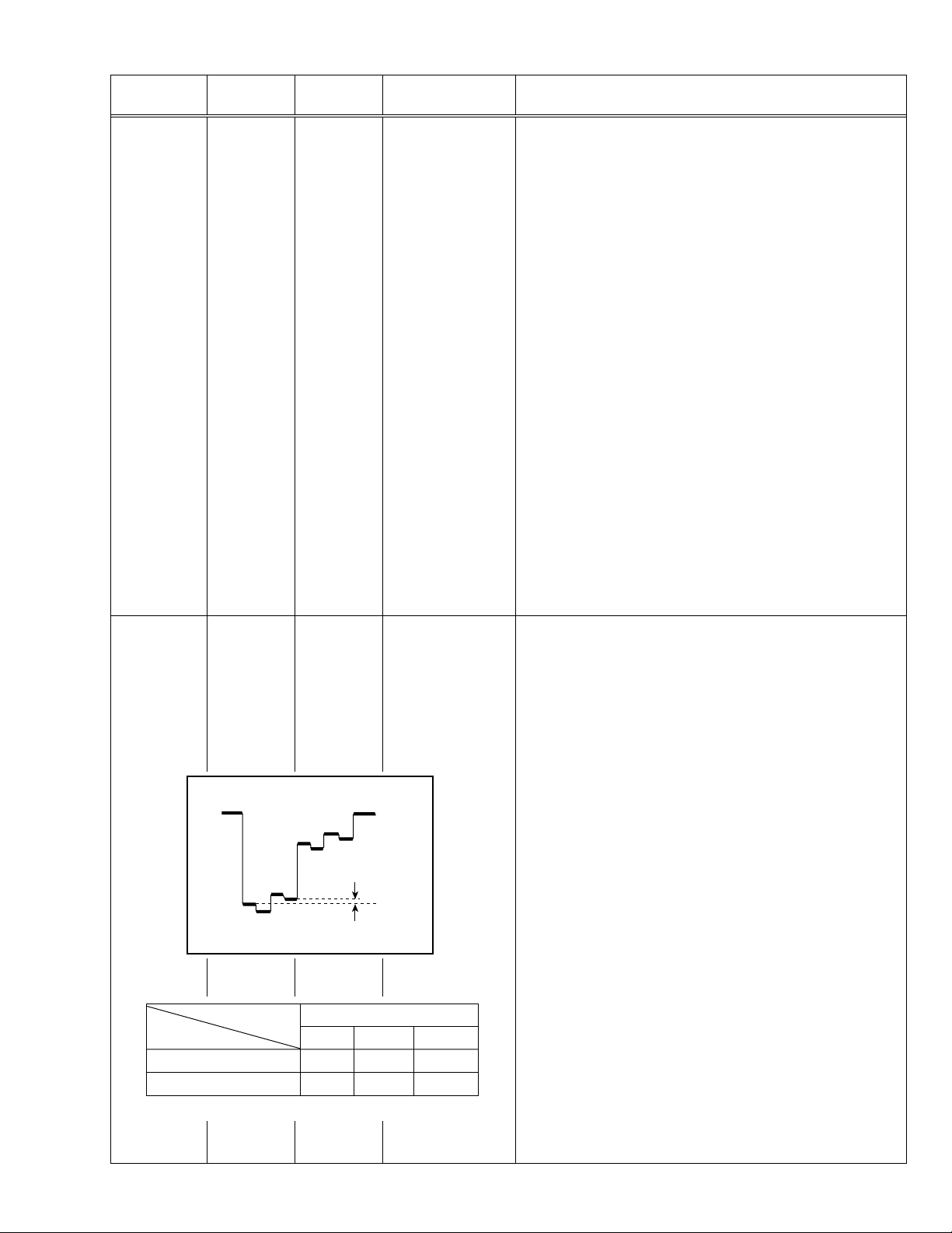
DEFLECTION CIRCUIT ADJUSTMENTS
The setting (adjustment) using the remote control unit is made on the basis of the initial setting values.
The setting values which adjust the screen to the optimum condition can be different from the initial setting values.
Note:
Proceed to the following adjustment after having completed the adjustments of SUB BRIGHT and SUB PICTURE.
[SUB MENU 3. DEF]
Setting
(Adjustment)
item
Variable range
50Hz
4:3
60Hz
1. VER. SLOPE –32 — +31 0 0 0 0 —
2. VER. HEIGHT –32 — +31 +31 +31 0 0 —
3. VER. POSITION –32 — +31 0 0 0 0 —
4. VER. SCURVE –32 — +31 –21 0 -21 0 —
5. HOR. POSITION –32 — +31 0 0 0 0 +7
6. HOR. WIDTH –32 — +31 0 0 0 0 —
7. EW-PIN –32 — +31 0 0 0 0 —
8. EW-TRAPEZ –32 — +31 0 0 0 0 —
9. UP CORNER –32 — +31 0 0 0 0 —
10. DW CORNER –32 — +31 0 0 0 0 —
11. HOR. PARALL –32 — +31 0 0 0 0 —
12. HOR. BOW –32 — +31 0 0 0 0 —
13. V.ZOOM –32 — +31 +2 –1 +7 +9 —
Initial setting value
COMPRESS(16:9)
50Hz
60Hz
COMPONENT
DVD (50Hz)
AV-20N83
AV-21D83
[COMPRESS (16:9) : OFF, fv: 50Hz mode]
Item
Adjustment
of
Measuring
instrument
Signal
generator
Test point Adjustment part Description
V. SLOPE
Remote
control unit
A
B
Adjustment
of
Signal
generator
V. POSITION
Remote
control unit
1. VER. SLOPE 1. Receive a PAL circle pattern signal of vertical frequency 50Hz.
2. Select 3. DEF from the SERVICE MENU.
3. Select 1. VER. SLOPE with the MENU &/^ key.
4. Set the initial setting value of 1. VER. SLOPE with the MENU
key.
5. Adjust 1. VER. SLOPE to make “A = B” with the MENU
Blanking
line
*/T
3. VER. POSITION 6. Select 3. VER. POSITION with the MENU &/^ key.
7. Set the initial setting value of 3. VER. POSITION with the MENU
*/T
key.
8. Adjust 3. VER. POSITION to make “A = B” with the MENU
A
*/T
*/T
key.
key.
(to be continued)
B
No. 52076 25
Page 26

AV-20N83
AV-21D83
Item
Adjustment
of
V. HEIGHT
Screen
size
91%
Adjustment
of
H. POSITION
Measuring
instrument
Signal
generator
Remote
control unit
Signal
generator
Remote
control unit
Test point Adjustment part Description
2. VER. HEIGHT
13. V. ZOOM
9. Receive a PAL cross-hatch signal.
10. Select 2. VER. HEIGHT with the MENU &/^ key.
11. Set the initial setting value of 2. VER. HEIGHT with the MENU
*/T
key.
12. Select 13. V. ZOOM with the MENU &/^ key.
13. Set the initial setting value of 13. V. ZOOM with the MENU
14. Adjust 13. V. ZOOM and make the vertical screen size 91% of the
picture size with the MENU
Picture
size
100%
*/T
key.
5. HOR. POSITION 15. Receive a PAL circle pattern signal.
16. Select 5. HOR. POSITION with the MENU &/^ key.
17.
Set the initial setting value of 5. HOR. POSITION with the MENU
*/T
key.
18. Adjust 5. HOR POSITION to make “C=D” with the MENU
*/T
*/T
key.
key.
Adjustment
of
H. WIDTH
CD
Signal
6. HOR. WIDTH 19. Receive a PAL cross-hatch signal.
generator
Remote
control unit
Screen size 91%
20. Select 6. HOR. WIDTH with the MENU &/^ key.
21. Set the initial setting value of 6. HOR. WIDTH with the MENU
*/T
key.
22. Adjust 6. HOR. WIDTH and make the horizontal screen size 91%
of the picture size with the MENU
*/T
key.
(to be continued)
Picture size 100%
26 No. 52076
Page 27

AV-20N83
AV-21D83
Item
Adjustment
of
SIDE PIN
Adjustment
of
TRAPEZIUM
Measuring
instrument
Signal
generator
Remote
control unit
Signal
generator
Remote
control unit
Test point Adjustment part Description
7. EW-PIN 23. Select 7. EW-PIN with the MENU &/^ key.
24. Set the initial setting value of 7. EW-PIN with the MENU
25. Adjust 7. EW-PIN so that the first vertical lines at the left and right
edges on the screen are straight.
Straight
8. EW-TRAPEZ 26. Select 8. EW-TRAPEZ with the MENU &/^ key.
27. Set the initial setting value of 8. EW-TRAPEZ with the MENU
*/T
key.
28. Adjust 8. EW-TRAPEZ so that the vertical lines at the left and right
edges on the screen are in parallel.
*/T
key.
Adjustment
of
V.S-CURVE
Signal
generator
Remote
control unit
Parallel
4. VER. SCURVE 29. Select 4. VER. SCURVE with the MENU &/^ key.
30. Set the initial setting value of 4. VER. SCURVE with the MENU
*/T
key.
31. Adjust 4. VER. SCURVE so that the spaces of each line on TOP,
CENTRE and BOTTOM become uniform.
TOP
CENTRE
(to be continued)
BOTTOM
No. 52076 27
Page 28

AV-20N83
AV-21D83
Item
Adjustment
of
CORNER
Adjustment
of
H. PARALLEL
Measuring
instrument
Signal
generator
Remote
control unit
Signal
generator
Remote
control unit
Test point Adjustment part Description
9. UP CORNER
10. DW CORNER
11. HOR. PARALL 37. Select 11. HOR. PARALL with the MENU &/^ key.
32. Select 9. UP CORNER with the MENU &/^ key.
33. Set the initial setting value of 9. UP CORNER with the MENU
*/T
key.
34. Select 10. DW CORNER with the MENU &/^ key.
35. Set the initial setting value of 10. DW CORNER with the MENU
*/T
key.
36. Adjust 9. UP CORNER and 10. DW CORNER so that the vertical
lines at the four corners on the screen are straight.
38. Set the initial setting value of 11. HOR. PARALL with the MENU
*/T
key.
39. Adjust 11. HOR. PARALL to optimize the parallelogram distortion.
Adjustment
of
H. BOW
Signal
generator
Remote
control unit
Straight
12. HOR. BOW 40. Select 12. HOR. BOW with the MENU &/^ key.
41. Set the initial setting value of 12. HOR. BOW with the MENU
T
key.
42. Adjust 12. HOR. BOW to optimize the horizontal arc distortion.
43. Press the DISPLAY key twice to return to the normal screen.
*/
28 No. 52076
Page 29

[COMPRESS (16 : 9) : ON, fv: 50Hz mode ]
Item
Measuring
instrument
Test point Adjustment part Description
AV-20N83
AV-21D83
Adjustment
of
V. HEIGHT
Screen
size
Adjustment
of
SIDE PIN
Signal
generator
Remote
control unit
Signal
generator
Remote
control
unit
Screen size
13. V. ZOOM
2. VER. HEIGHT
Vertical
amplitude
7. EW-PIN
1. Receive a PAL cross-hatch signal of vertical frrequency 50Hz.
2. Select COMPRESS from the MENU and set COMPRESS to ON.
3. Select 3. DEF from the SERVICE MENU.
4. Set the initial setting value of 13. V. ZOOM with the MENU
*/T
key.
5. Select 2. VER. HEIGHT with the MENU &/^ key.
6. Set the initial setting value of 2. VER. HEIGHT with the MENU
*/T
key.
7. Adjust 2. VER. HEIGHT to set the vertical amplitude of the image to
the value shown in Table 3.
AV-20N83
Model
/BK, AV-20N83/VT 230mm
Ver tical Amplitude
AV-21D83/BK, AV-21D83/VT 235mm
Tab le 3
8. Select 7. EW-PIN with the MENU &/^ key.
9. Set the initial setting value of 7. EW-PIN with the MENU
*/T
key.
10. Adjust 7. EW-PIN so that the first vertical lines at the left and right
edges on the screen are straight.
Adjustment
of
CORNER
Signal
generator
Remote
control unit
Straight
9. UP CORNER
10. DW CORNER
11. Select 9. UP CORNER with the MENU &/^ key.
12. Set the initial setting value of 9. UP CORNER with the MENU
*/T
key.
13. Select 10. DW CORNER with the MENU &/^ key.
14. Set the initial setting value of 10. DW CORNER with the MENU
*/T
key.
15. Adjust 9. UP CORNER and 10. DW CORNER so that the vertical
lines at the four corners on the screen are straight.
16. Press the DISPLAY key twice to return to the normal screen.
No. 52076 29
Page 30

AV-20N83
AV-21D83
[COMPRESS (16 : 9) : OFF, fv: 60Hz mode ]
Item
Adjustment
of
V. SLOPE
Measuring
instrument
Signal
generator
Remote
control unit
Test point Adjustment part Description
1. VER. SLOPE 1. Receive a NTSC circle pattern signal of vertical frequency 60Hz.
2. Select 3. DEF from the SERVICE MENU.
3. Select 1. VER. SLOPE with the MENU &/^ key.
4. Set the initial setting value of 1. VER. SLOPE with the MENU
key.
5. Adjust 1. VER. SLOPE to make “A = B” with the MENU
A
Blanking
line
B
*/T
*/T
key.
Adjustment
of
V. POSITION
Signal
generator
Remote
control unit
3. VER. POSITION 6. Select 3. VER. POSITION with the MENU &/^ key.
7. Set the initial setting value of 3. VER. POSITION with the MENU
*/T
key.
8. Adjust 3. VER. POSITION to make “A = B” with the MENU
A
B
(to be continued)
*/T
key.
30 No. 52076
Page 31

AV-20N83
AV-21D83
Item
Adjustment
of
V. HEIGHT
Screen
size
91%
Adjustment
of
H. POSITION
Measuring
instrument
Signal
generator
Remote
control unit
Signal
generator
Remote
control unit
Test point Adjustment part Description
2. VER. HEIGHT
13. V. ZOOM
9. Receive a NTSC cross-hatch signal.
10. Select 2. VER. HEIGHT with the MENU &/^ key.
11. Set the initial setting value of 2. VER. HEIGHT with the MENU
*/T
key.
12. Select 13. V. ZOOM with the MENU &/^ key.
13. Set the initial setting value of 13. V. ZOOM with the MENU
14. Adjust 13. V. ZOOM and make the vertical screen size 91% of the
picture size with the MENU
Picture
size
100%
*/T
key.
5. HOR. POSITION 15. Receive a NTSC circle pattern signal.
16. Select 5. HOR. POSITION with the MENU &/^ key.
17.
Set the initial setting value of 5. HOR. POSITION with the MENU
*/T
key.
18. Adjust 5. HOR POSITION to make “C=D” with the MENU
*/T
*/T
key.
key.
Adjustment
of
H. WIDTH
CD
Signal
6. HOR. WIDTH 19. Receive a NTSC cross-hatch signal.
generator
Remote
control unit
Screen size 91%
20. Select 6. HOR. WIDTH with the MENU &/^ key.
21. Set the initial setting value of 6. HOR. WIDTH with the MENU
*/T
key.
22. Adjust 6. HOR. WIDTH and make the horizontal screen size 91%
of the picture size with the MENU
*/T
key.
(to be continued)
Picture size 100%
No. 52076 31
Page 32

AV-20N83
AV-21D83
Item
Adjustment
of
SIDE PIN
Adjustment
of
TRAPEZIUM
Measuring
instrument
Signal
generator
Remote
control unit
Signal
generator
Remote
control unit
Test point Adjustment part Description
7. EW-PIN 23. Select 7. EW-PIN with the MENU &/^ key.
24. Set the initial setting value of 7. EW-PIN with the MENU
25. Adjust 7. EW-PIN so that the first vertical lines at the left and right
edges on the screen are straight.
Straight
8. EW-TRAPEZ 26. Select 8. EW-TRAPEZ with the MENU &/^ key.
27. Set the initial setting value of 8. EW-TRAPEZ with the MENU
*/T
key.
28. Adjust 8. EW-TRAPEZ so that the vertical lines at the left and right
edges on the screen are in parallel.
*/T
key.
Adjustment
of
V.S-CURVE
Signal
generator
Remote
control unit
Parallel
4. VER. SCURVE 29. Select 4. VER. SCURVE with the MENU &/^ key.
30. Set the initial setting value of 4. VER. SCURVE with the MENU
*/T
key.
31. Adjust 4. VER. SCURVE so that the spaces of each line on TOP,
CENTRE and BOTTOM become uniform.
TOP
CENTRE
(to be continued)
BOTTOM
32 No. 52076
Page 33

AV-20N83
AV-21D83
Item
Adjustment
of
CORNER
Adjustment
of
H. PARALLEL
Measuring
instrument
Signal
generator
Remote
control unit
Signal
generator
Remote
control unit
Test point Adjustment part Description
9. UP CORNER
10. DW CORNER
11. HOR. PARALL 37. Select 11. HOR. PARALL with the MENU &/^ key.
32. Select 9. UP CORNER with the MENU &/^ key.
33. Set the initial setting value of 9. UP CORNER with the MENU
*/T
key.
34. Select 10. DW CORNER with the MENU &/^ key.
35. Set the initial setting value of 10. DW CORNER with the MENU
*/T
key.
36. Adjust 9. UP CORNER and 10. DW CORNER so that the vertical
lines at the four corners on the screen are straight.
38. Set the initial setting value of 11. HOR. PARALL with the MENU
*/T
key.
39. Adjust 11. HOR. PARALL to optimize the parallelogram distortion.
Adjustment
of
H. BOW
Signal
generator
Remote
control unit
Straight
12. HOR. BOW 40. Select 12. HOR. BOW with the MENU &/^ key.
41. Set the initial setting value of 12. HOR. BOW with the MENU
T
key.
42. Adjust 12. HOR. BOW to optimize the horizontal arc distortion.
43. Press the DISPLAY key twice to return to the normal screen.
*/
No. 52076 33
Page 34

AV-20N83
AV-21D83
[COMPRESS (16 : 9) : ON, fV: 60Hz mode ]
Item
Measuring
instrument
Test point Adjustment part Description
Adjustment
of
V. HEIGHT
Screen
size
Adjustment
of
SIDE PIN
Signal
generator
Remote
control unit
Signal
generator
Remote
control
unit
Screen size
13. V. ZOOM
2. VER. HEIGHT
Vertical
amplitude
7. EW-PIN
1. Receive a NTSC cross-hatch signal of vertical frrequency 60Hz.
2. Select COMPRESS from the MENU and set COMPRESS to ON.
3. Select 3. DEF from the SERVICE MENU.
4. Set the initial setting value of 13. V. ZOOM with the MENU
*/T
key.
5. Select 2. VER. HEIGHT with the MENU &/^ key.
6. Set the initial setting value of 2. VER. HEIGHT with the MENU
*/T
key.
7. Adjust 2. VER. HEIGHT to set the vertical amplitude of the image to
the value shown in Table 3.
Ver tical Amplitude
AV-20N83
Model
/BK, AV-20N83/VT 230mm
AV-21D83/BK, AV-21D83/VT 235mm
Tab le 3
8. Select 7. EW-PIN with the MENU &/^ key.
9. Set the initial setting value of 7. EW-PIN with the MENU
*/T
key.
10. Adjust 7. EW-PIN so that the first vertical lines at the left and right
edges on the screen are straight.
Adjustment
of
CORNER
Signal
generator
Remote
control unit
Straight
9. UP CORNER
10. DW CORNER
11. Select 9. UP CORNER with the MENU &/^ key.
12. Set the initial setting value of 9. UP CORNER with the MENU
*/T
key.
13. Select 10. DW CORNER with the MENU &/^ key.
14. Set the initial setting value of 10. DW CORNER with the MENU
*/T
key.
15. Adjust 9. UP CORNER and 10. DW CORNER so that the vertical
lines at the four corners on the screen are straight.
16. Press the DISPLAY key twice to return to the normal screen.
34 No. 52076
Page 35

[VIDEO - 2 SET : COMPONENT, fv: 50/60Hz mode]
Item
Measuring
instrument
Test point Adjustment part Description
AV-20N83
AV-21D83
Adjustment
of
H. POSITION
Signal
5. HOR. POSITION 1. Receive a PAL circle pattern signal to VIDEO-2 terminal.
generator
Remote
control unit
CD
2. Select VIDEO-2 SET from the MENU and set VIDEO-2 SET to
COMPONENT.
3. Select 3. DEF from the SERVICE MENU.
4. Select 5. HOR. POSITION with the MENU &/^ key.
5.
Set the initial setting value of 5. HOR. POSITION with the MENU
*/T
key.
6 Adjust 5. HOR POSITION to make “C=D” with the MENU
*/T
key.
7. Press the DISPLAY key twice to return to the normal screen.
VSM PRESET SETTING
Item
Setting of
VSM
PRESET
Measuring
instrument
Remote
control unit
SUB MENU 4. VSM PRESET
BRIGHT
TINT
COLOUR
BRIGHT
CONT
SHARP
MENU 89: SELECT
MENU
-
/+: OPERATE
Test point Adjustment part Description
1. TINT
2. COLOUR
3. BRIGHT
4. CONT
5. SHARP
1. Select 4. VSM PRESET from the SERVICE MENU.
2. Select BRIGHT with the PICTURE MODE key.
3. Adjust the MENU &/^ key and MENU
values of 1. TINT – 5. SHARP to the values shown in the table.
4. Respectively select the VSM PRESET mode for SOFT and STANDARD, and make similar adjustment as in 3 above.
5. Press the DISPLAY key twice to return to the normal screen.
[Setting Values for SUB MENU 4. VSM PRESET]
VSM preset
**
**
VSM mode BRIGHT STANDARD SOFT
Setting item
**
**
**
DISPLAY : EXIT
1. TINT
SETTING VALUE
2. COLOUR
SETTING VALUE
3. BRIGHT
SETTING VALUE
4. CONT
SETTING VALUE
5. SHARP
SETTING VALUE
15
15
15
30
15 0
*/T
key to reset the set
15 11
No. 52076 35
Page 36

AV-20N83
AV-21D83
PRESET SETTING
Do not adjust 5. PRESET in the SERVICE MENU as it requires no adjustment.
•
[SUB MENU 5. PRESET]
Setting item Variable range Initial setting value
AV-20N83/BK AV-21D83/BK AV-21D83/VT AV-20N83/VT
1 PSNS 0/1 0
2ACL 0/1 0
3 MUS 0/1 0
4MAT 0/1 0
5 FCO 0/1 0
6 BPS 0/1 0
7 IFLH 0/1 0
8 VID 0/1 0
9 STM 0/1 0
10 AFCW 0/1 0
11 VSW 0/1 0
12 FFI 0/1 0
13 AGC 00/01/10/11 01
14 CL 50 – 95 83
15 AKB 0/1 0
16 HBL 0/1 0
17 BKS 0/1 1
18 READ STATUS — —
19 VNR 00 – 63 25
20 PEAK 0 – 3 1
21 IVG 0/1 1
22 WPL 0 – F 5
23 SOFT CLIPPER 0 – 3 0
24 IF PLL OFFSET 0 – 63 32
25 OVERSHOOT 0 – 3 3
26 HCO 0/1 0
27 HP2 0/1 0
28 AI VOLUME 00/01/10/11 01
29 SUB BASS 3D –3 – +3 +2
30 SUB TREBLE 3D –3 – +3 +1 +3
31 CCCLOOP 0 – 4 0
36 No. 52076
Page 37

PURITY ADJUSTMENT
Note: The final adjustment of CONVERGENCE must be done after the
FOCUS adjustment. (CONVERGENCE is changed by FOCUS
adjustment.)
When makes difference by FOCUS adjustment, should be
reconfirming PURITY adjustment.
WEDGE
DEFLECTION
YOKE
AV-20N83
AV-21D83
1. Demagnetize CRT with the demagnetizer.
2. Loosen the retainer screw of the deflection yoke.
3. Remove the wedges.
4. Input a green raster signal from the signal generator, and turn the
screen to green raster.
5. Move the deflection yoke backward.
6. Bring the long lug of the purity magnets on the short lug and position
them horizontally. (Fig. 2)
7. Adjust the gap between two lugs so that the GREEN RASTER will
come into the centre of the screen. (Fig. 3)
8. Move the deflection yoke forward, and fix the position of the deflection yoke so that the whole screen will become green.
9. Insert the wedge to the top side of the deflection yoke so that it will
not move.
10. Input a crosshatch signal.
11. Verify that the screen is horizontal.
P
CRT
4 6
P / C
MAGNETS
• P/C MAGNETS
P : PURITY MAGNET
4 : 4 POLES (convergence magnets)
6 : 6 POLES (convergence magnets)
Fig. 1
PURITY MAGNETS
Long lug
12. Input red and blue raster signals, and make sure that purity is properly adjusted.
Short lug
(FRONT VIEW)
Bring the long lug over the short lug
and position them horizontally.
Fig. 2
GREEN RASTER
CENTRE
Fig. 3
No. 52076 37
Page 38

AV-20N83
AV-21D83
CONVERGENCE ADJUSTMENTS
STATIC CONVERGENCE ADJUSTMENT
1. Input a crosshatch signal.
2. Using 4-pole convergence magnets, overlap the red and blue lines in
the centre of the screen (Fig. 4) and turn them to magenta (red/blue).
3. Using 6-pole convergence magnets, overlap the magenta(red/blue)
and green lines in the centre of the screen and turn them to white.
4. Repeat 2 and 3 above, and make best convergence.
(FRONT VIEW)
DYNAMIC CONVERGENCE ADJUSTMENT
1. Move the deflection yoke up and down and overlap the lines in the
periphery. (Fig. 5)
2. Move the deflection yoke left to right and overlap the lines in the
periphery. (Fig. 6)
3. Repeat 1 and 2 above, and make best convergence.
After adjustment, fix the wedge at the original position.
•
Fasten the retainer screw of the deflection yoke.
Fix the P/C magnets with glue.
Fig. 4
(FRONT VIEW)
GREEN
RED
RED
BLUE
BLUE
(FRONT VIEW)
GREEN GREEN
RED
GREEN
Fig. 5
BLUE
BLUE
BLUE
RED
GREENGREEN
BLUE
RED
RED
RED
GREEN
BLUE
38 No. 52076
BLUE
GREEN
RED
Fig. 6
Page 39

AV-20N83
AV-21D83
SELF-CHECK FUNCTIONS
1. Outline
This model has self-check functions given below.When an abnormality has been detected,the SUB POWER is turned off and both ECO and ON
TIMER LEDs flash to inform of the failure.An abnormality is detected by the signal input state of the control line connected to the microcomputer.
2. Self check items
Check item Details of detection Method of detection State of abnormality
Over-current protection
An over-current on the low B line
is detected.
CRT NECK protection
Operation of CRT NECK protection circuit.
3. Self check indicating function
When an abnormality has been detected at about 5 seconds after
the power is turned on,the SUB POWER is turned off immediately
and the LEDs flash.
The main microcomputer detects
the possible abnormality at 30msec.intervals and judges the
results in every 16 time. Of the
16 times, if NG is detected more
than 9 times, it is judged that
there is an abnormality.
DITTO
After about
5 seconds
Powe r o n
Start of
detection
When an abnormality has been
detected, the SUB-POWER is
turned off. While the SUBPOWER is being turned off, the
POWER key on the remote control unit is not operational until the
power cord is taken out and put
in again.
DITTO
Detection of
an abnormality
Flashing LEDs
SUB-POWER OFF
[ Indication by the LEDs]
Item LEDs flashing intervals Priority of detection
1 Over-current protection At 0.2-second intervals 1
2 CRT NECK protection At 1-second intervals 2
Note: In case of 1 + 2, the item 1 is indicated.
No. 52076 39
Page 40

AV-20N83
AV-21D83
SERVICE NOTE :
40 No. 52076
Page 41

VICTOR COMPANY OF JAPAN, LIMITED
12,3-chome,Moriya-cho,Kanagawa-ku,Yokohama,Kanagawa-prefecture,221-8528,JapanHOME AV NETWORK BUSINESS UNIT
AV20N83BK-BK
AV21D83BK-BK
#4
#4
AV21D83VT-CK
AV20N83VT-CK
#4
#4
Printed in Japan
0212 WPC
Page 42

AV-20N83
AV-21D83
PARTS LIST
CAUTION
q The parts identified by the symbol are important for the safety . Whenever replacing these parts, be sure to use specified ones to secure the
safety .
q The parts not indicated in this Parts List and those which are filled with lines --- in the Parts No. columns will not be supplied .
q P. W. Board Ass'y will not be supplied, but those which are filled with the Parts No. in the Parts No. columns will be supplied .
ABBREVIATIONS OF RESISTORS, CAPACITORS AND TOLERANCES
RESISTORS CAPACITORS
C R Carbon Resistor
F R Fusible Resistor
P R Plate Resistor
V R Variable Resistor
HV R High Voltage Resistor
MF R Metal Film Resistor
MG R Metal Glazed Resistor
MP R Metal Plate Resistor
OM R Metal Oxide Film Resistor
CMF R Coating Metal Film Resistor
UNF R Non-Flammable Resistor
CH V R Chip Variable Resistor
CH MG R Chip Metal Glazed Resistor
COMP. R Composition Resistor
LPTC R Linear Positive Temperature Coefficient Resistor
C CAP. Ceramic Capacitor
E CAP. Electrolytic Capacitor
M CAP. Mylar Capacitor
CH CAP. Chip Capacitor
HV CAP. High Voltage Capacitor
MF CAP. Metalized Film Capacitor
MM CAP. Metalized Mylar Capacitor
MP CAP. Metalized Polystyrol Capacitor
PP CAP. Polypropylene Capacitor
PS CAP. Polystyrol Capacitor
TF CAP. Thin Film Capacitor
MPP CAP. Metalized Polypropylene Capacitor
TAN. CAP. Tantalum Capacitor
CH C CAP. Chip Ceramic Capacitor
BP E CAP. Bi-Polar Electrolytic Capacitor
CH AL E CAP. Chip Aluminum Electrolytic Capacitor
CH AL BP CAP. Chip Aluminum Bi-Polar Capacitor
CH TAN. E CAP. Chip Tantalum Electrolytic Capacitor
CH AL BP E CAP. Chip Tantalum Bi-Polar Electrolytic Capacitor
RESISTORS
FGJKMNRHZP
±1% ±2% ±5% ±10% ±20% ±30%
No. 52076 41
+30% +50% +80% +100%
-10% -10% -20% 0%
Page 43

AV-20N83
AV-21D83
CONTENTS
USING P.W. BOARD & REMOTE CONTROL UNIT ................................................................................. 43
EXPLODED VIEW PARTS LIST -1 [AV-20N83/BK, AV-20N83/VT] .............................................................. 43
EXPLODED VIEW -1 [AV-20N83/BK, AV-20N83/VT].................................................................................... 43
EXPLODED VIEW PARTS LIST -2 [AV-20N83/BK, AV-20N83/VT] ............................................................. 44
EXPLODED VIEW -2 [AV-20N83/BK, AV-20N83/VT] .................................................................................. 45
EXPLODED VIEW PARTS LIST -3 [AV-21D83/BK, AV-21D83/VT]............................................................. 46
EXPLODED VIEW -3 [AV-21D83/BK, AV-21D83/VT] .................................................................................. 46
EXPLODED VIEW PARTS LIST -15 [AV-21D83/BK, AV-21D83/VT] ........................................................... 47
EXPLODED VIEW -15 [AV-21D83/BK, AV-21D83/VT] ................................................................................. 48
PRINTED WIRING BOARD PARTS LIST [AV-20N83/BK]
MAIN PW BOARD ASS'Y .....................................................................................................................................49
DIFFERENCE PARTS LIST BETWEEN AV-20N83/BK AND AV-21D83/BK ..................................................... 54
PRINTED WIRING BOARD PARTS LIST [AV-20N83/VT]
MAIN PW BOARD ASS'Y .....................................................................................................................................55
DIFFERENCE PARTS LIST BETWEEN AV-21D83/VT AND AV-20N83/VT...................................................... 60
REMOTE CONTROL UNIT PARTS LIST ............................................................................................................61
PACKING [AV-20N83/BK, AV-20N83/VT] ............................................................................................................... 62
PACKING PARTS LIST [AV-20N83/BK, AV-20N83/VT] ........................................................................................ 62
PACKING [AV-21D83/BK, AV-21D83/VT] ............................................................................................................... 63
PACKING PARTS LIST [AV-21D83/BK, AV-21D83/VT] ........................................................................................ 63
42 No. 52076
Page 44

USING P.W. BOARD & REMOTE CONTROL UNIT
AV-20N83
AV-21D83
P. W.B ASS’Y
MAIN PWB (include CRT SOCKET PWB) SCH-1090A-BK SCH-1122A-BK SCH-1315A-CK SCH-1316A-CK
REMOTE CONTROL UNIT RM-C1017-1H RM-C1027-1H
Model
EXPLODED VIEW PARTS LIST -1 [AV-20N83
!
Ref.No. Part No. Part Name Description Local
16 LC10438-028A-H FRONT CABI [AV-20N83/BK]
16 LC10438-034A-HK FRONT CABI [AV-20N83/VT]
17 LC30665-001A-H REMOCON LENS
18 LC30663-003A-H POWER KNOB
19 LC20318-003A-H CONTROL KNOB
20 LC30664-001B-H E.E. WINDOW
21 CM48006-007-C JVC MARK
22 CM35235-003-H SPRING
AV-20N83/BK
AV-21D83/BK AV-21D83/VT AV-20N83/VT
/BK
, AV-20N83
/VT
]
EXPLODED VIEW -1 [AV-20N83/BK, AV-20N83/VT]
19
16
21
20
22
18
17
No. 52076 43
Page 45

AV-20N83
EXPLODED VIEW PARTS LIST -2 [AV-20N83
!
Ref.No. Part No. Part Name Description Local
! V01 A48LWX10X PICTURE TUBE [AV-20N83/BK]
! V01 A48JLL91X01 PICTURE TUBE (ITC) Inc. DEF YOKE [AV-20N83/VT]
! L01 QQW0156-001 DEG COIL
! DY01 QQD0081-001 DEFLECTION YOKE [AV-20N83/BK]
! T1551 QQH0143-001 FBT [AV-20N83/BK]
! T1551 QQH0142-001 FBT [AV-20N83/VT]
! 1 QMPR420-165-K2 POWER CORD [AV-20N83/BK]
! 1 QMPR400-200-JC POWER CORD [AV-20N83/VT]
! 2 CM47005-A01-H CORD CLAMP
3 CM36623-B01-H CHASSIS RAIL (X2)
4WJY0008-002A BRAIDED ASS’Y
5 A48457-3-H SPRING
6 A75034-B PC MAGNET [AV-20N83/BK]
7 CE40764-00A WEDGE ASS’Y (X3) [AV-20N83/BK]
8 QAS0101-001 SPEAKER (X2) SP01, SP02
9 QYSBSF4012Z TAPPING SCREW (X4)
10 QYSBSF4012Z TAPPING SCREW (X4) [AV-20N83/BK]
! 11 LC10448-005A-H REAR COVER [AV-20N83/BK]
! 11 LC10448-005A-HK REAR COVER [AV-20N83/VT]
12 QYSBSFG4016Z TAPPING SCREW (X6)
13 QYSBSF3010Z TAPPING SCREW (X4)
! 14 GG20029-001A-H RATING LABEL
15 CM48144-002-H PB STOPPER
/BK
, AV-20N83
/VT
]
44 No. 52076
Page 46

EXPLODED VIEW -2 [AV-20N83/BK, AV-20N83/VT]
!
V101
AV-20N83
10
9
8
<PICTURE TUBE (REAR SIDE)>
10
!
DY01
7
6
3
3
!
2
1
!
!
11
8
!
T1551
15
9
!
L01
5
4
13
No. 52076 45
12
!
14
Page 47

AV-21D83
EXPLODED VIEW PARTS LIST -3 [AV-21D83
!
Ref.No. Part No. Part Name Description Local
16 LC11129-024A-H FRONT CABI [AV-21D83/BK]
16 LC11129-025A-HK FRONT CABI [AV-21D83/VT]
17 GG30021-002A-H LED LENS
18 GG30019-003A-H POWER KNOB
19 GG20006-003A-H CONTROL KNOB
20 GG30020-001A-H E.E. WINDOW
21 GG40023-001A-H JVC MARK
22 CM35235-003-H SPRING
/BK
, AV-21D83
EXPLODED VIEW -3 [AV-21D83/BK, AV-21D83/VT]
/VT
]
16
19
21
20
46 No. 52076
18
17
22
Page 48

AV-21D83
EXPLODED VIEW PARTS LIST -
!
Ref.No. Part No. Part Name Description Local
! V01 A51LMV10X PICTURE TUBE [AV-21D83/BK]
! V01 A51JSW51X07 PICTURE TUBE (ITC) Inc. DEF YOKE [AV-21D83/VT]
! L01 QQW0157-001 DEG COIL
! DY01 CE20336-00A DEFLECTION YOKE [AV-21D83/BK]
! T1551 QQH0142-001 FBT
! 1 QMPR420-165-K2 POWER CORD [AV-21D83/BK]
! 1 QMPR400-200-JC POWER CORD [AV-21D83/VT]
! 2 CM47005-A01-H CORD CLAMP
3 CM36623-B01-H CHASSIS RAIL (X2)
4 CHGB0028-0A BRAIDED ASS’Y
5 A48457-3-H SPRING (X2)
6 A75034-B PC MAGNET [AV-21D83/BK]
7 CE42728-00A WEDGE ASS’Y (X3) [AV-21D83/BK]
8 QAS0101-001 SPEAKER (X2) SP01, SP02
9 QYSBSB4012Z TAPPING SCREW (X4)
10 QYSBSB4012Z TAPPING SCREW (X4) [AV-21D83/VT]
! 11 GG10130-001A-H REAR COVER [AV-21D83/BK]
! 11 GG10130-011A-HK REAR COVER [AV-21D83/VT]
12 QYSBSFG4016Z TAPPING SCREW (X7)
13 QYSBSF3010Z TAPPING SCREW (X4)
! 14 GG20029-001A-H RATING LABEL [AV-21D83/BK]
! 14 GG20016-025A-E RATING LABEL [AV-21D83/VT]
15 CM48144-002-H PB STOPPER
15
[AV-21D83
/BK
, AV-21D83
/VT
]
No. 52076 47
Page 49

AV-21D83
EXPLODED VIEW -15 [AV-21D83/BK, AV-21D83/VT]
!
V01
10
!
DY01
7
6
3
9
!
2
8
10
!
3
1
!
8
T1551
15
9
!
11
<PICTURE TUBE (REAR SIDE)>
!
L01
4
5
5
48 No. 52076
12
!
14
13
Page 50

AV-20N83
PRINTED WIRING BOARD PARTS LIST [AV-20N83/BK]
MAIN PW BOARD ASS’Y (SCH-1090A-BK)
! Symbol No. Part No. Part Name Description Local ! Symbol No. Part No. Part Name Description Local
RESISTOR
R1001 NRSA63J-221X MG R 220¸ 1/16W J
R1002 NRSA63J-221X MG R 220¸ 1/16W J
R1003 NRSA63J-392X MG R 3.9k¸ 1/16W J
R1004 NRSA63J-221X MG R 220¸ 1/16W J
R1005 QQR1214-001Y FERRITE BEADS
R1006 NRSA63J-273X MG R 27k¸ 1/16W J
R1007 NRSA63J-750X MG R 75¸ 1/16W J
R1101 NRSA63J-100X MG R 10¸ 1/16W J
R1102 NRSA63J-682X MG R 6.8k¸ 1/16W J
R1103 NRSA63J-272X MG R 2.7k¸ 1/16W J
R1104 NRSA63J-181X MG R 180¸ 1/16W J
R1105 NRSA63J-220X MG R 22¸ 1/16W J
R1106 NRSA63J-101X MG R 100¸ 1/16W J
R1107 NRSA63J-472X MG R 4.7k¸ 1/16W J
R1108 NRSA63J-222X MG R 2.2k¸ 1/16W J
R1109 NRSA63J-222X MG R 2.2k¸ 1/16W J
R1111 NRSA63J-102X MG R 1k¸ 1/16W J
R1117 NRSA63J-102X MG R 1k¸ 1/16W J
R1130 NRSA63J-472X MG R 4.7k¸ 1/16W J
R1131 NRSA63J-471X MG R 470¸ 1/16W J
R1132 NRSA63J-222X MG R 2.2k¸ 1/16W J
R1133 NRSA63J-152X MG R 1.5k¸ 1/16W J
R1134 NRSA63J-182X MG R 1.8k¸ 1/16W J
R1135 NRSA63J-561X MG R 560¸ 1/16W J
R1136 NRSA63J-472X MG R 4.7k¸ 1/16W J
R1137 NRSA63J-103X MG R 10k¸ 1/16W J
R1138 NRSA63J-471X MG R 470¸ 1/16W J
R1139 NRSA63J-222X MG R 2.2k¸ 1/16W J
R1140 NRSA63J-152X MG R 1.5k¸ 1/16W J
R1141 NRSA63J-182X MG R 1.8k¸ 1/16W J
R1142 NRSA63J-561X MG R 560¸ 1/16W J
R1143 NRSA63J-471X MG R 470¸ 1/16W J
R1144 NRSA63J-220X MG R 22¸ 1/16W J
R1145 NRSA63J-821X MG R 820¸ 1/16W J
R1146 NRSA63J-103X MG R 10k¸ 1/16W J
R1147 NRSA63J-101X MG R 100¸ 1/16W J
R1148 NRSA63J-332X MG R 3.3k¸ 1/16W J
R1301 NRSA63J-222X MG R 2.2k¸ 1/16W J
R1302 NRSA63J-222X MG R 2.2k¸ 1/16W J
R1303 NRSA63J-562X MG R 5.6k¸ 1/16W J
R1304 NRSA63J-222X MG R 2.2k¸ 1/16W J
R1305 NRSA63J-222X MG R 2.2k¸ 1/16W J
R1306 NRSA63J-562X MG R 5.6k¸ 1/16W J
R1351 NRSA63J-151X MG R 150¸ 1/16W J
R1352 QRL029J-123 OM R 12k¸ 2W J
R1353 NRSA63J-182X MG R 1.8k¸ 1/16W J
R1354 NRSA63J-331X MG R 330¸ 1/16W J
R1355 NRSA63J-101X MG R 100¸ 1/16W J
R1356 QRE121J-102Y C R 1k¸ 1/2W J
R1357 QRZ0107-152Z C R 1.5k¸ 1W K
R1358 QRE121J-272Y C R 2.7k¸ 1/2W J
R1359 QRE121J-561Y C R 560¸ 1/2W J
R1361 NRSA63J-151X MG R 150¸ 1/16W J
R1362 QRL029J-123 OM R 12k¸ 2W J
R1363 NRSA63J-182X MG R 1.8k¸ 1/16W J
R1364 NRSA63J-331X MG R 330¸ 1/16W J
R1365 NRSA63J-101X MG R 100¸ 1/16W J
R1366 QRE121J-102Y C R 1k¸ 1/2W J
R1367 QRZ0107-152Z C R 1.5k¸ 1W K
R1368 NRSA63J-332X MG R 3.3k¸ 1/16W J
! R1369 QRZ9017-150 F R 15¸ 1/4W J
R1370 NRSA63J-151X MG R 150¸ 1/16W J
R1371 QRL029J-123 OM R 12k¸ 2W J
R1372 NRSA63J-182X MG R 1.8k¸ 1/16W J
R1373 NRSA63J-331X MG R 330¸ 1/16W J
R1374 NRSA63J-101X MG R 100¸ 1/16W J
R1375 QRE121J-102Y C R 1k¸ 1/2W J
R1376 QRZ0107-152Z C R 1.5k¸ 1W K
R1377 NRSA63J-330X MG R 33¸ 1/16W J
R1378 NRSA63J-223X MG R 22k¸ 1/16W J
R1379 NRSA63J-103X MG R 10k¸ 1/16W J
R1383 QRE121J-394Y C R 390k¸ 1/2W J
RESISTOR
R1384 NRSA63J-103X MG R 10k¸ 1/16W J
R1385 QRE141J-393Y C R 39k¸ 1/4W J
R1401 NRSA63J-224X MG R 220k¸ 1/16W J
R1403 NRSA63J-0R0X MG R 0.0¸ 1/16W J
R1405 NRSA63J-682X MG R 6.8k¸ 1/16W J
R1406 NRSA63J-123X MG R 12k¸ 1/16W J
R1408 NRSA63J-682X MG R 6.8k¸ 1/16W J
R1410 NRSA63J-123X MG R 12k¸ 1/16W J
R1411 QRG01GJ-221 OM R 220¸ 1W J
R1412 QRE121J-1R0Y C R 1¸ 1/2W J
R1413 QRX01GJ-3R9 MF R 3.9¸ 1W J
R1414 QRE121J-680Y C R 68¸ 1/2W J
R1425 NRSA63J-683X MG R 68k¸ 1/16W J
R1521 NRSA63J-101X MG R 100¸ 1/16W J
R1522 NRSA63J-102X MG R 1k¸ 1/16W J
R1524 QRL039J-220 OM R 22¸ 3W J
R1526 QRG01GJ-181 OM R 180¸ 1W J
R1527 QRL039J-103 OM R 10k¸ 3W J
R1528 QRX029J-R47 MF R 0.47¸ 2W J
R1529 QRX029J-R47 MF R 0.47¸ 2W J
R1531 NRSA63J-222X MG R 2.2k¸ 1/16W J
! R1532 QRZ9017-4R7 F R 4.7¸ 1/4W J
! R1540 QRZ9021-4R7 F R 4.7¸ 1W J
R1541 QRE121J-124Y C R 120k¸ 1/2W J
R1542 QRE121J-334Y C R 330k¸ 1/2W J
R1545 QRE121J-220Y C R 22¸ 1/2W J
R1546 QRE121J-822Y C R 8.2k¸ 1/2W J
R1591 QRE121J-222Y C R 2.2k¸ 1/2W J
R1594 QRE121J-223Y C R 22k¸ 1/2W J
R1595 NRSA63J-222X MG R 2.2k¸ 1/16W J
R1596 QRT029J-1R8 MF R 1.8¸ 2W J
R1597 QRT029J-1R5 MF R 1.5¸ 2W J
R1621 NRSA63J-0R0X MG R 0.0¸ 1/16W J
R1622 NRSA63J-0R0X MG R 0.0¸ 1/16W J
R1624 NRSA63J-101X MG R 100¸ 1/16W J
R1625 NRSA63J-101X MG R 100¸ 1/16W J
R1627 NRSA63J-102X MG R 1k¸ 1/16W J
R1650 NRSA63J-103X MG R 10k¸ 1/16W J
R1651 NRSA63J-153X MG R 15k¸ 1/16W J
R1654 NRSA63J-103X MG R 10k¸ 1/16W J
R1655 NRSA63J-153X MG R 15k¸ 1/16W J
R1658 QRE121J-2R2Y C R 2.2¸ 1/2W J
R1659 QRE121J-2R2Y C R 2.2¸ 1/2W J
R1660 NRSA63J-103X MG R 10k¸ 1/16W J
R1661 NRSA63J-683X MG R 68k¸ 1/16W J
R1662 NRSA63J-333X MG R 33k¸ 1/16W J
R1663 NRSA63J-103X MG R 10k¸ 1/16W J
R1664 NRSA63J-222X MG R 2.2k¸ 1/16W J
R1686 NRSA63J-102X MG R 1k¸ 1/16W J
R1687 NRSA63J-103X MG R 10k¸ 1/16W J
R1688 NRSA63J-273X MG R 27k¸ 1/16W J
R1690 NRSA63J-104X MG R 100k¸ 1/16W J
R1698 NRSA63J-104X MG R 100k¸ 1/16W J
R1699 NRSA63J-104X MG R 100k¸ 1/16W J
R1701 NRSA63J-101X MG R 100¸ 1/16W J
R1702 NRSA63J-101X MG R 100¸ 1/16W J
R1703 NRSA63J-101X MG R 100¸ 1/16W J
R1704 NRSA63J-102X MG R 1k¸ 1/16W J
R1705 NRSA63J-102X MG R 1k¸ 1/16W J
R1706 NRSA63J-102X MG R 1k¸ 1/16W J
R1707 NRSA63J-472X MG R 4.7k¸ 1/16W J
R1708 NRSA63J-472X MG R 4.7k¸ 1/16W J
R1709 NRSA63J-472X MG R 4.7k¸ 1/16W J
R1710 NRSA63J-472X MG R 4.7k¸ 1/16W J
R1711 NRSA63J-101X MG R 100¸ 1/16W J
R1712 NRSA63J-101X MG R 100¸ 1/16W J
R1713 NRSA63J-101X MG R 100¸ 1/16W J
R1714 NRSA63J-101X MG R 100¸ 1/16W J
R1715 NRSA63J-103X MG R 10k¸ 1/16W J
R1716 NRSA63J-103X MG R 10k¸ 1/16W J
R1717 NRSA63J-103X MG R 10k¸ 1/16W J
R1718 NRSA63J-221X MG R 220¸ 1/16W J
AV-20N83
No. 52076 49
Page 51

AV-20N83
! Symbol No. Part No. Part Name Description Local ! Symbol No. Part No. Part Name Description Local
RESISTOR
R1719 NRSA63J-221X MG R 220¸ 1/16W J
R1720 NRSA63J-102X MG R 1k¸ 1/16W J
R1721 NRSA63J-221X MG R 220¸ 1/16W J
R1722 NRSA63J-221X MG R 220¸ 1/16W J
R1723 NRSA63J-221X MG R 220¸ 1/16W J
R1724 NRSA63J-221X MG R 220¸ 1/16W J
R1725 NRSA63J-103X MG R 10k¸ 1/16W J
R1726 NRSA63J-472X MG R 4.7k¸ 1/16W J
R1727 NRSA63J-104X MG R 100k¸ 1/16W J
R1728 NRSA63J-103X MG R 10k¸ 1/16W J
R1729 NRSA63J-470X MG R 47¸ 1/16W J
R1730 NRSA63J-223X MG R 22k¸ 1/16W J
R1731 NRSA63J-101X MG R 100¸ 1/16W J
R1732 NRSA02F-393X MG R 39k¸ 1/10W F
R1733 NRSA63J-273X MG R 27k¸ 1/16W J
R1734 NRSA63J-391X MG R 390¸ 1/16W J
R1735 NRSA63J-104X MG R 100k¸ 1/16W J
R1736 NRSA63J-333X MG R 33k¸ 1/16W J
R1737 NRSA63J-272X MG R 2.7k¸ 1/16W J
R1738 NRSA63J-0R0X MG R 0.0¸ 1/16W J
R1739 NRSA63J-101X MG R 100¸ 1/16W J
R1740 NRSA63J-101X MG R 100¸ 1/16W J
R1741 NRSA63J-101X MG R 100¸ 1/16W J
R1742 NRSA63J-0R0X MG R 0.0¸ 1/16W J
R1743 NRSA63J-681X MG R 680¸ 1/16W J
R1744 NRSA63J-561X MG R 560¸ 1/16W J
R1745 NRSA63J-105X MG R 1M¸ 1/16W J
R1746 NRSA63J-333X MG R 33k¸ 1/16W J
R1747 NRSA63J-103X MG R 10k¸ 1/16W J
R1748 NRSA02J-475X MG R 4.7M¸ 1/10W J
R1749 NRSA02J-475X MG R 4.7M¸ 1/10W J
R1750 NRSA63J-0R0X MG R 0.0¸ 1/16W J
R1755 NRSA63J-101X MG R 100¸ 1/16W J
R1756 NRSA63J-101X MG R 100¸ 1/16W J
R1757 NRSA63J-222X MG R 2.2k¸ 1/16W J
R1758 NRSA63J-222X MG R 2.2k¸ 1/16W J
R1760 NRSA63J-682X MG R 6.8k¸ 1/16W J
R1770 QRE121J-271Y C R 270¸ 1/2W J
R1771 NRSA63J-102X MG R 1k¸ 1/16W J
R1772 QRE121J-271Y C R 270¸ 1/2W J
R1773 NRSA63J-102X MG R 1k¸ 1/16W J
R1775 NRSA63J-332X MG R 3.3k¸ 1/16W J
R1776 NRSA63J-392X MG R 3.9k¸ 1/16W J
R1777 NRSA63J-682X MG R 6.8k¸ 1/16W J
R1779 NRSA63J-272X MG R 2.7k¸ 1/16W J
R1780 NRSA63J-471X MG R 470¸ 1/16W J
R1781 NRSA63J-122X MG R 1.2k¸ 1/16W J
R1782 NRSA63J-181X MG R 180¸ 1/16W J
R1783 NRSA63J-221X MG R 220¸ 1/16W J
R1784 NRSA63J-331X MG R 330¸ 1/16W J
R1785 NRSA63J-471X MG R 470¸ 1/16W J
R1786 NRSA63J-202X MG R 2k¸ 1/16W J
R1803 NRSA63J-333X MG R 33k¸ 1/16W J
R1804 NRSA63J-750X MG R 75¸ 1/16W J
R1805 NRSA63J-750X MG R 75¸ 1/16W J
R1806 NRSA63J-750X MG R 75¸ 1/16W J
R1807 NRSA63J-750X MG R 75¸ 1/16W J
R1808 NRSA63J-823X MG R 82k¸ 1/16W J
R1809 NRSA63J-391X MG R 390¸ 1/16W J
R1810 NRSA63J-823X MG R 82k¸ 1/16W J
R1811 NRSA63J-391X MG R 390¸ 1/16W J
R1812 NRSA63J-104X MG R 100k¸ 1/16W J
R1813 NRSA63J-222X MG R 2.2k¸ 1/16W J
R1815 NRSA63J-101X MG R 100¸ 1/16W J
R1818 NRSA63J-222X MG R 2.2k¸ 1/16W J
R1820 NRSA63J-101X MG R 100¸ 1/16W J
R1821 NRSA63J-222X MG R 2.2k¸ 1/16W J
R1823 NRSA63J-101X MG R 100¸ 1/16W J
R1824 NRSA63J-222X MG R 2.2k¸ 1/16W J
R1826 NRSA63J-101X MG R 100¸ 1/16W J
R1829 NRSA63J-750X MG R 75¸ 1/16W J
R1830 NRSA63J-222X MG R 2.2k¸ 1/16W J
RESISTOR
R1831 NRSA63J-222X MG R 2.2k¸ 1/16W J
R1832 NRSA63J-122X MG R 1.2k¸ 1/16W J
R1833 NRSA63J-102X MG R 1k¸ 1/16W J
R1834 NRSA63J-562X MG R 5.6k¸ 1/16W J
R1835 NRSA63J-562X MG R 5.6k¸ 1/16W J
R1836 NRSA63J-750X MG R 75¸ 1/16W J
R1837 NRSA63J-101X MG R 100¸ 1/16W J
R1838 QRK126J-121X UNF R 120¸ 1/2W J
R1839 QRE121J-221Y C R 220¸ 1/2W J
R1840 QRE121J-221Y C R 220¸ 1/2W J
R1841 NRSA63J-0R0X MG R 0.0¸ 1/16W J
R1842 NRSA63J-0R0X MG R 0.0¸ 1/16W J
R1843 NRSA63J-821X MG R 820¸ 1/16W J
R1844 NRSA63J-222X MG R 2.2k¸ 1/16W J
R1845 NRSA63J-102X MG R 1k¸ 1/16W J
R1846 NRSA63J-222X MG R 2.2k¸ 1/16W J
R1847 NRSA63J-103X MG R 10k¸ 1/16W J
R1848 NRSA63J-471X MG R 470¸ 1/16W J
R1849 NRSA63J-221X MG R 220¸ 1/16W J
R1880 NRSA63J-202X MG R 2k¸ 1/16W J
R1881 NRSA63J-103X MG R 10k¸ 1/16W J
R1882 NRSA63J-471X MG R 470¸ 1/16W J
R1883 NRSA63J-181X MG R 180¸ 1/16W J
R1902 QRF154K-2R2 UNF R 2.2¸ 15W K
R1904 QRE121J-681Y C R 680¸ 1/2W J
R1905 QRM034J-R22 MP R 0.22¸ 3W J
R1907 NRSA63J-563X MG R 56k¸ 1/16W J
R1908 QRL039J-333 OM R 33k¸ 3W J
R1909 QRE121J-474Y C R 470k¸ 1/2W J
R1910 QRE121J-152Y C R 1.5k¸ 1/2W J
R1911 QRE121J-562Y C R 5.6k¸ 1/2W J
R1912 NRSA63J-122X MG R 1.2k¸ 1/16W J
R1913 QRE121J-120Y C R 12¸ 1/2W J
! R1915 QRZ0111-474 C R 470k¸ 1W K
R1952 NRSA63J-332X MG R 3.3k¸ 1/16W J
R1953 NRSA63J-101X MG R 100¸ 1/16W J
R1957 QRE121J-6R8Y C R 6.8¸ 1/2W J
R1960 NRSA63J-391X MG R 390¸ 1/16W J
R1961 QRL029J-183 OM R 18k¸ 2W J
R1962 NRSA63J-561X MG R 560¸ 1/16W J
R1963 QRE121J-103Y C R 10k¸ 1/2W J
R1964 NRSA63J-473X MG R 47k¸ 1/16W J
R1965 NRSA63J-0R0X MG R 0.0¸ 1/16W J
R1966 NRSA63J-682X MG R 6.8k¸ 1/16W J
R1967 NRSA63J-473X MG R 47k¸ 1/16W J
R1970 NRSA63J-153X MG R 15k¸ 1/16W J
R1971 NRSA63J-183X MG R 18k¸ 1/16W J
R1972 NRSA63J-391X MG R 390¸ 1/16W J
! R1991 QRZ9046-825Z C R 8.2M¸ 1W J
CAPACITOR
C1001 NCB31HK-103X C CAP. 0.01µF 50V K
C1002 QETN1HM-106Z E CAP. 10µF 50V M
C1003 QFV71HJ-104Z MF CAP. 0.1µF 50V J
C1004 QETN1CM-477Z E CAP. 470µF 16V M
C1005 NCB31HK-222X C CAP. 2200pF 50V K
C1006 QETN1CM-336Z E CAP. 33µF 16V M
C1007 NCB31HK-103X C CAP. 0.01µF 50V K
C1101 NCB31HK-472X C CAP. 4700pF 50V K
C1102 NCB31HK-472X C CAP. 4700pF 50V K
C1103 NCB31HK-472X C CAP. 4700pF 50V K
C1104 NCB31HK-472X C CAP. 4700pF 50V K
C1105 NCB31HK-472X C CAP. 4700pF 50V K
C1106 NDC21HJ-180X C CAP. 18pF 50V J
C1107 NCB31HK-103X C CAP. 0.01µF 50V K
C1109 QETN1HM-106Z E CAP. 10µF 50V M
C1130 NCB31HK-103X C CAP. 0.01µF 50V K
50 No. 52076
Page 52

AV-20N83
! Symbol No. Part No. Part Name Description Local ! Symbol No. Part No. Part Name Description Local
CAPACITOR
C1131 NCB31HK-103X C CAP. 0.01µF 50V K
C1132 NCB31HK-103X C CAP. 0.01µF 50V K
C1133 QETN1CM-107Z E CAP. 100µF 16V M
C1134 NCB31HK-103X C CAP. 0.01µF 50V K
C1135 QETN1AM-477Z E CAP. 470µF 10V M
C1136 NCB31HK-103X C CAP. 0.01µF 50V K
C1137 NCB31HK-103X C CAP. 0.01µF 50V K
C1138 NCB31HK-103X C CAP. 0.01µF 50V K
C1140 NCB31HK-103X C CAP. 0.01µF 50V K
C1141 NCB31HK-103X C CAP. 0.01µF 50V K
C1142 NCB31HK-103X C CAP. 0.01µF 50V K
C1143 QETN1HM-106Z E CAP. 10µF 50V M
C1144 NCB31HK-223X C CAP. 0.022µF 50V K
C1308 NCB31HK-103X C CAP. 0.01µF 50V K
C1310 NRSA63J-0R0X MG R 0.0¸ 1/16W J
C1350 NDC21HJ-471X C CAP. 470pF 50V J
C1351 NDC31HJ-681X C CAP. 680pF 50V J
C1352 QETN2EM-475Z E CAP. 4.7µF 250V M
C1353 QETN1HM-107Z E CAP. 100µF 50V M
C1354 QETN1HM-105Z E CAP. 1µF 50V M
C1360 NDC21HJ-471X C CAP. 470pF 50V J
C1361 NDC31HJ-681X C CAP. 680pF 50V J
C1370 NDC21HJ-471X C CAP. 470pF 50V J
C1371 NDC31HJ-821X C CAP. 820pF 50V J
C1372 NRSA63J-273X MG R 27k¸ 1/16W J
C1374 QCZ0364-222 C CAP. 2200pF
C1375 QETN1CM-477Z E CAP. 470µF 16V M
C1401 QETN1HM-105Z E CAP. 1µF 50V M
C1402 QCB31HK-682Z C CAP. 6800pF 50V K
C1403 QEHR1VM-227Z E CAP. 220µF 35V M
C1406 QFLC2AJ-683Z M CAP. 0.068µF 100V J
C1407 QCS32HJ-180Z C CAP. 18pF 500V J
C1408 QFV71HJ-184Z MF CAP. 0.18µF 50V J
C1411 NCF21HZ-334X C CAP. 0.33µF 50V Z
C1412 NCF21HZ-334X C CAP. 0.33µF 50V Z
C1413 QFLC2AJ-563Z M CAP. 0.056µF 100V J
C1422 QEHQ1VM-108 E CAP. 1000µF 35V M
C1521 QETN1VM-476Z E CAP. 47µF 35V M
C1522 QFLC1HJ-332Z M CAP. 3300pF 50V J
C1523 QFLC1HJ-223Z M CAP. 0.022µF 50V J
C1524 QFZ0200-103 MPP CAP. 0.01µF 1.5kVH±3%
C1527 QFZ0199-474 MPP CAP. 0.47µFAC250V J
C1529 QEHR2EM-475Z E CAP. 4.7µF 250V M
C1531 QEHR1EM-108Z E CAP. 1000µF 25V M
C1533 QEHR1EM-108Z E CAP. 1000µF 25V M
C1535 QCB32HK-101Z C CAP. 100pF 500V K
C1536 QFLC1HJ-103Z M CAP. 0.01µF 50V J
C1540 QFV71HJ-104Z MF CAP. 0.1µF 50V J
C1541 QETN2EM-226Z E CAP. 22µF 250V M
C1542 QETN2EM-226Z E CAP. 22µF 250V M
C1550 NCB31CK-104X C CAP. 0.1µF 16V K
C1591 QETN1AM-107Z E CAP. 100µF 10V M
C1592 QEZ0203-107 E CAP. 100µF 160V M
C1593 QETN1EM-476Z E CAP. 47µF 25V M
C1625 QETN1HM-475Z E CAP. 4.7µF 50V M
C1626 QETN1HM-475Z E CAP. 4.7µF 50V M
C1628 NCB31HK-472X C CAP. 4700pF 50V K
C1629 NCB31EK-104X C CAP. 0.1µF 25V K
C1630 QETN1HM-475Z E CAP. 4.7µF 50V M
C1631 NCB31EK-104X C CAP. 0.1µF 25V K
C1632 QETN1HM-475Z E CAP. 4.7µF 50V M
C1633 QETN1HM-475Z E CAP. 4.7µF 50V M
C1634 QETN1HM-475Z E CAP. 4.7µF 50V M
C1635 QETN1HM-107Z E CAP. 100µF 50V M
C1636 QETN1HM-475Z E CAP. 4.7µF 50V M
C1637 QETN1HM-475Z E CAP. 4.7µF 50V M
C1638 NCB31EK-104X C CAP. 0.1µF 25V K
C1639 NCF21CZ-105X C CAP. 1µF 16V Z
C1640 QETN1HM-475Z E CAP. 4.7µF 50V M
C1641 NCB31EK-104X C CAP. 0.1µF 25V K
C1642 NCB31HK-472X C CAP. 4700pF 50V K
C1644 QETN1HM-475Z E CAP. 4.7µF 50V M
CAPACITOR
C1645 QETN1HM-475Z E CAP. 4.7µF 50V M
C1650 QEHR1HM-106Z E CAP. 10µF 50V M
C1651 QEHR1VM-476Z E CAP. 47µF 35V M
C1652 QETN1HM-106Z E CAP. 10µF 50V M
C1655 QEHQ1VM-108 E CAP. 1000µF 35V M
C1656 QEHQ1VM-108 E CAP. 1000µF 35V M
C1659 NCF21HZ-224X C CAP. 0.22µF 50V Z
C1660 NCF21HZ-224X C CAP. 0.22µF 50V Z
C1661 NCF21HZ-224X C CAP. 0.22µF 50V Z
C1662 QEHR1VM-227Z E CAP. 220µF 35V M
C1663 NCF21HZ-224X C CAP. 0.22µF 50V Z
C1681 QETN1CM-227Z E CAP. 220µF 16V M
C1682 QETN1CM-227Z E CAP. 220µF 16V M
C1683 QETN1CM-336Z E CAP. 33µF 16V M
C1684 QETN1HM-106Z E CAP. 10µF 50V M
C1685 NRSA63J-0R0X MG R 0.0¸ 1/16W J
C1686 NRSA63J-0R0X MG R 0.0¸ 1/16W J
C1701 QETN1CM-227Z E CAP. 220µF 16V M
C1702 QETN1HM-106Z E CAP. 10µF 50V M
C1703 NDC31HJ-330X C CAP. 33pF 50V J
C1704 NDC31HJ-330X C CAP. 33pF 50V J
C1705 NCB31HK-102X C CAP. 1000pF 50V K
C1706 NCB21EK-224X C CAP. 0.22µF 25V K
C1707 QETN1CM-107Z E CAP. 100µF 16V M
C1709 QETN1CM-107Z E CAP. 100µF 16V M
C1710 NCB21EK-224X C CAP. 0.22µF 25V K
C1711 NCB31CK-104X C CAP. 0.1µF 16V K
C1713 NCB31CK-104X C CAP. 0.1µF 16V K
C1714 QETN1CM-476Z E CAP. 47µF 16V M
C1720 QETN1CM-476Z E CAP. 47µF 16V M
C1725 NCB31HK-681X C CAP. 680pF 50V K
C1730 NCB21EK-224X C CAP. 0.22µF 25V K
C1731 NCB21EK-224X C CAP. 0.22µF 25V K
C1732 QETN1CM-107Z E CAP. 100µF 16V M
C1733 NCB31CK-104X C CAP. 0.1µF 16V K
C1734 NCB31HK-222X C CAP. 2200pF 50V K
C1735 NCB31HK-222X C CAP. 2200pF 50V K
C1736 QETN1HM-105Z E CAP. 1µF 50V M
C1737 QETN1HM-105Z E CAP. 1µF 50V M
C1738 NCB31CK-104X C CAP. 0.1µF 16V K
C1739 NFV41CJ-104X MPP CAP. 0.1µF 16V J
C1740 QETN1HM-225Z E CAP. 2.2µF 50V M
C1741 NCB31CK-104X C CAP. 0.1µF 16V K
C1742 NCB31CK-104X C CAP. 0.1µF 16V K
C1743 QETN1CM-107Z E CAP. 100µF 16V M
C1744 NCB31HK-102X C CAP. 1000pF 50V K
C1745 NCB31EK-473X C CAP. 0.047µF 25V K
C1746 NCB31EK-473X C CAP. 0.047µF 25V K
C1747 NCB31EK-473X C CAP. 0.047µF 25V K
C1748 QETN1CM-476Z E CAP. 47µF 16V M
C1749 QETN1HM-106Z E CAP. 10µF 50V M
C1751 NCB31CK-104X C CAP. 0.1µF 16V K
C1752 NCB31CK-104X C CAP. 0.1µF 16V K
C1753 NCB31CK-104X C CAP. 0.1µF 16V K
C1760 NCB31HK-104X C CAP. 0.1µF 50V K
C1761 QETN1CM-107Z E CAP. 100µF 16V M
C1770 QETN1HM-106Z E CAP. 10µF 50V M
C1801 QETN1HM-106Z E CAP. 10µF 50V M
C1802 QETN1HM-106Z E CAP. 10µF 50V M
C1803 QETN1HM-106Z E CAP. 10µF 50V M
C1804 QETN1HM-106Z E CAP. 10µF 50V M
C1805 NCB31HK-104X C CAP. 0.1µF 50V K
C1807 NCF31AZ-105X C CAP. 1µF 10V Z
C1808 NCF31AZ-105X C CAP. 1µF 10V Z
C1810 NCF31AZ-105X C CAP. 1µF 10V Z
C1811 NCB31HK-104X C CAP. 0.1µF 50V K
C1812 NCF31AZ-105X C CAP. 1µF 10V Z
C1813 NCB31HK-103X C CAP. 0.01µF 50V K
C1814 NCB31HK-104X C CAP. 0.1µF 50V K
C1815 NCF31AZ-105X C CAP. 1µF 10V Z
C1817 NCF31AZ-105X C CAP. 1µF 10V Z
C1819 NCB31HK-104X C CAP. 0.1µF 50V K
AV-20N83
No. 52076 51
Page 53

AV-20N83
! Symbol No. Part No. Part Name Description Local ! Symbol No. Part No. Part Name Description Local
CAPACITOR
C1820 NCF31AZ-105X C CAP. 1µF 10V Z
C1821 NCF31AZ-105X C CAP. 1µF 10V Z
C1822 QETN1CM-477Z E CAP. 470µF 16V M
C1823 QETN1CM-107Z E CAP. 100µF 16V M
C1824 QETN1CM-107Z E CAP. 100µF 16V M
C1825 NCB31HK-103X C CAP. 0.01µF 50V K
C1826 NCB31HK-104X C CAP. 0.1µF 50V K
C1827 NCB31HK-103X C CAP. 0.01µF 50V K
C1829 NCB31HK-103X C CAP. 0.01µF 50V K
C1830 NCB31HK-103X C CAP. 0.01µF 50V K
C1831 NCB31HK-103X C CAP. 0.01µF 50V K
C1833 QETN1HM-226Z E CAP. 22µF 50V M
C1834 NDC31HJ-181X C CAP. 180pF 50V J
! C1901 QFZ9072-224 MM CAP. 0.22µF
! C1902 QFZ9072-104 MM CAP. 0.1µF
C1903 QCZ9015-102Z C CAP. 1000pF AC250V Z
C1904 QCZ9015-102Z C CAP. 1000pF AC250V Z
C1905 QCZ9015-102Z C CAP. 1000pF AC250V Z
! C1906 QFZ9072-224 MM CAP. 0.22µF
C1907 QEZ0552-227 E CAP. 220µF
C1908 QFZ0209-222 MPP CAP. 2200pF
C1910 NDC31HJ-471X C CAP. 470pF 50V J
C1911 QEHR1EM-227Z E CAP. 220µF 25V M
C1914 QETN1EM-227Z E CAP. 220µF 25V M
C1915 QFLC1HJ-222Z M CAP. 2200pF 50V J
C1952 QCB32HK-471Z C CAP. 470pF 500V K
C1953 QEHQ1VM-108 E CAP. 1000µF 35V M
C1954 NCB31HK-102X C CAP. 1000pF 50V K
C1957 QCB32HK-471Z C CAP. 470pF 500V K
C1958 QEHQ1EM-228 E CAP. 2200µF 25V M
C1959 QCZ0364-561 C CAP. 560pF
C1960 QEZ0203-107 E CAP. 100µF 160V M
C1961 QETN1HM-225Z E CAP. 2.2µF 50V M
C1962 QETN1HM-106Z E CAP. 10µF 50V M
C1964 QETN1CM-476Z E CAP. 47µF 16V M
C1965 QETN1HM-225Z E CAP. 2.2µF 50V M
C1968 NCB31CK-104X C CAP. 0.1µF 16V K
C1972 QEHR1VM-476Z E CAP. 47µF 35V M
C1973 QEHR1CM-107Z E CAP. 100µF 16V M
C1974 NCB31CK-104X C CAP. 0.1µF 16V K
C1975 QEHR1CM-227Z E CAP. 220µF 16V M
C1976 QEHR1CM-107Z E CAP. 100µF 16V M
C1977 QEHR1AM-477Z E CAP. 470µF 10V M
C1978 NCB31HK-104X C CAP. 0.1µF 50V K
C1980 QETN1CM-107Z E CAP. 100µF 16V M
! C1991 QCZ9079-102 C CAP. 1000pF AC250V M
! C1992 QCZ9079-102 C CAP. 1000pF AC250V M
! C1993 QCZ9079-152 C CAP. 1500pF AC250V M
TRANSFORMER
T1521 CE40203-00CJ1 DRIVE TRANSF
! T1551 QQH0143-001 FB TRANSF
! T1901 QQS0182-001 SW TRANSF
COIL
L1001 CE42050-001Z BEADS CORE
L1002 CE42050-001Z BEADS CORE
L1101 QQLZ014-R82 COIL 0.82µH
L1524 QQLZ034-320 COIL 32µH
L1701 QQL244K-100Z COIL 10µHK
L1702 QQL244K-100Z COIL 10µHK
L1731 QQL244J-5R6Z COIL 5.6µHJ
L1732 QQL244J-5R6Z COIL 5.6µHJ
L1951 QQLZ034-460 COIL 46µH
L1953 QQL244J-5R6Z COIL 5.6µHJ
L1954 QQL244J-5R6Z COIL 5.6µHJ
DIODE
D1101 1SS268-X SI. DIODE
D1350 1SS244-T2 SI. DIODE
D1352 RGP10J-5025-T3 SI. DIODE
D1353 MA111-X SI. DIODE
D1354 MA111-X SI. DIODE
D1355 MA111-X SI. DIODE
D1356 MA111-X SI. DIODE
D1357 MA111-X SI. DIODE
D1358 MA111-X SI. DIODE
D1360 1SS244-T2 SI. DIODE
D1370 1SS244-T2 SI. DIODE
D1372 MA3075/M/-X ZENER DIODE
D1373 MA111-X SI. DIODE
D1374 MA111-X SI. DIODE
D1401 RGP10J-5025-T3 SI. DIODE
D1402 MTZJ75-T2 ZENER DIODE
D1405 1N4003-T2 SI. DIODE
D1408 MA111-X SI. DIODE
D1523 RGP10J-5025-T3 SI. DIODE
D1541 RGP10J-5025-T3 SI. DIODE
D1550 MA111-X SI. DIODE
D1551 RGP10J-5025-T3 SI. DIODE
D1553 RGP10J-5025-T3 SI. DIODE
D1554 RGP10J-5025-T3 SI. DIODE
D1592 MA3075/H/-X ZENER DIODE
D1652 MA3330/L/-X ZENER DIODE
D1653 MA3330/L/-X ZENER DIODE
D1655 MA111-X SI. DIODE
D1682 MA111-X SI. DIODE
D1702 MA3024-X ZENER DIODE
D1703 MA3051/M/-X ZENER DIODE
D1704 MA3033-X ZENER DIODE
D1730 MA111-X SI. DIODE
D1731 MA111-X SI. DIODE
D1732 MA111-X SI. DIODE
D1733 MA111-X SI. DIODE
D1760 SLR-342VR-T16 LED
D1761 SLR-342MC-T16 LED
D1770 MA111-X SI. DIODE
D1771 P1241-04 PHOTO CONDUCTOR
D1801 MA3120/M/-X ZENER DIODE
D1802 MA3120/M/-X ZENER DIODE
D1807 MA3100/M/-X ZENER DIODE
D1808 MA3100/M/-X ZENER DIODE
D1901 GSIB460 BRIDGE DIODE
D1903 MTZJ12C-T2 ZENER DIODE
D1904 EG01C-T2 SI. DIODE
D1906 EG01C-T2 SI. DIODE
D1907 MA3150/M/-X ZENER DIODE
D1908 MTZJ27B-T2 ZENER DIODE
D1909 MA111-X SI. DIODE
D1910 NRSA63J-0R0X MG R 0.0¸ 1/16W J
D1911 RGP10J-TS-T3 SI. DIODE
D1912 1SS133-T2 SI. DIODE
D1914 ERC30-02L38 SI. DIODE
D1952 ERC30-02L38 SI. DIODE
D1954 RGP30B-F1 SI. DIODE
D1956 RU3AM-LFC4 SI. DIODE
D1964 MA3330/L/-X ZENER DIODE
D1965 1SS133-T2 SI. DIODE
D1966 MA3068/M/-X ZENER DIODE
D1968 MA111-X SI. DIODE
D1969 MA111-X SI. DIODE
D1971 MA111-X SI. DIODE
52 No. 52076
Page 54

AV-20N83
! Symbol No. Part No. Part Name Description Local ! Symbol No. Part No. Part Name Description Local
TRANSISTOR
Q1101 2SC5083/L-P/-T TRANSISTOR
Q1102 UN2212-X DIGI. TRANSISTOR
Q1104 2SB709A/QR/-X TRANSISTOR
Q1108 2SD601A/QR/-X TRANSISTOR
Q1130 2SB709A/QR/-X TRANSISTOR
Q1131 UN2212-X DIGI. TRANSISTOR
Q1132 2SD601A/QR/-X TRANSISTOR
Q1133 2SB709A/QR/-X TRANSISTOR
Q1134 UN2212-X DIGI. TRANSISTOR
Q1135 UN2212-X DIGI. TRANSISTOR
Q1136 2SD601A/QR/-X TRANSISTOR
Q1137 2SD601A/QR/-X TRANSISTOR
Q1301 2SB709A/QR/-X TRANSISTOR
Q1302 2SB709A/QR/-X TRANSISTOR
Q1350 STC344-T TRANSISTOR
Q1351 2SA1321-T TRANSISTOR
Q1352 2SB709A/QR/-X TRANSISTOR
Q1360 STC344-T TRANSISTOR
Q1361 2SA1321-T TRANSISTOR
Q1370 STC344-T TRANSISTOR
Q1371 2SA1321-T TRANSISTOR
Q1374 2SD601A/QR/-X TRANSISTOR
Q1375 2SD601A/QR/-X TRANSISTOR
Q1376 2SD601A/QR/-X TRANSISTOR
Q1521 2SC2655/Y/-T TRANSISTOR
Q1522 2SD2634-YD POWER TRANSISTOR
Q1591 2SA1208/ST/Z1-T TRANSISTOR
Q1592 UN2212-X DIGI. TRANSISTOR
Q1660 2SD601A/QR/-X TRANSISTOR
Q1661 2SD601A/QR/-X TRANSISTOR
Q1683 2SB709A/QR/-X TRANSISTOR
Q1684 2SB709A/QR/-X TRANSISTOR
Q1685 DTC323TK-X DIGI. TRANSISTOR
Q1686 DTC323TK-X DIGI. TRANSISTOR
Q1701 2SB709A/QR/-X TRANSISTOR
Q1702 2SB709A/QR/-X TRANSISTOR
Q1703 FMC2A-X D.TRANSISTOR
Q1720 2SB709A/QR/-X TRANSISTOR
Q1770 2SB709A/QR/-X TRANSISTOR
Q1801 DTC323TK-X DIGI. TRANSISTOR
Q1802 DTC323TK-X DIGI. TRANSISTOR
Q1803 2SB709A/QR/-X TRANSISTOR
Q1804 2SC1740S/QR/-T TRANSISTOR
Q1860 2SD601A/QR/-X TRANSISTOR
Q1861 2SB709A/QR/-X TRANSISTOR
Q1862 2SB709A/QR/-X TRANSISTOR
Q1952 2SD601A/QR/-X TRANSISTOR
Q1953 2SD601A/QR/-X TRANSISTOR
Q1954 2SD601A/QR/-X TRANSISTOR
IC
IC1130 M52342SP I.C(MONO-ANA)
IC1401 AN5522 I.C(MONO-ANA)
IC1602 NJW1138M-X I.C(MONO-ANA)
IC1650 AN5276 I.C(MONO-ANA)
IC1701 TDA9386N22S0902 I.C(MCU)
IC1702 AT24C08-21WS3 I.C(MEMORY-OTH) (SERVICE)
IC1760 GP1UM281QK IR DETECT UNIT
IC1801 MM1492AF I.C(MONO-ANA)
IC1901 STR-F6707A/F7 I.C(HYBRID)
IC1951 SE115N-LF12 I.C(HYBRID)
IC1972 R1141Q331B-X REGULATE
IC1974 AN80T36 REG I.C
OTHERS
LC30114-001C-H LED HOLDER
CF1130 QAX0694-001Z C FILTER
CF1131 QAX0694-001Z C FILTER
CF1140 QAX0695-001Z C FILTER
CL1001 QZW0027-002 WIRE CLAMP
CL1002 QZW0027-001 WIRE CLAMP
CL1003 QZW0027-004 WIRE CLAMP
! CP1951 ICP-N75-Y IC PROTECTOR
! CP1953 ICP-N75-Y IC PROTECTOR
! F1901 QMF51E2-4R0J4 FUSE
FC1901 CEMG002-001Z FUSE CLIP
J1770 QNS0155-001 3.5 JACK
J1771 QNN0282-003 PIN JACK
J1772 QNN0282-002 PIN JACK
J1773 QNN0282-001 PIN JACK
J1801 QNN0349-001 PIN JACK
J1802 QNN0349-002 PIN JACK
J1803 QNN0348-001 PIN JACK
J1804 QNN0349-001 PIN JACK
K1104 QQR1113-001Z FERRITE BEADS
K1105 QQR1113-001Z FERRITE BEADS
K1106 QQR1113-001Z FERRITE BEADS
K1701 QQR1113-001Z FERRITE BEADS
K1902 QQR1114-001Z FERRITE BEADS
K1903 QQR1114-001Z FERRITE BEADS
K1951 QQR1113-001Z FERRITE BEADS
K1954 QQR1113-001Z FERRITE BEADS
K1955 QQR1214-001Y FERRITE BEADS
! LF1902 QQR1035-001 LINE FILTER
! PC1901 PC123F2 IC(PHOTO COUPLE)
! RY1901 QSK0092-001 RELAY
S1780 QSW0619-003Z TACT SWITCH MENU
S1781 QSW0619-003Z TACT SWITCH CHS1782 QSW0619-003Z TACT SWITCH CH+
S1783 QSW0619-003Z TACT SWITCH VOLS1784 QSW0619-003Z TACT SWITCH VOL+
! S1901 QSW0846-001 PUSH SWITCH POWER
SF1101 QAX0325-001 SAW FILTER
SF1102 QAX0731-001 SAW FILTER
! SK1351 QNZ0537-001 CRT SOCKET
TH1901 QAD0134-4R5 P THERMISTOR
TU1001 QAU0186-002 TUNER
! VA1901 QAF0052-621 VARISTOR
W1010 NRSA63J-0R0X MG R 0.0¸ 1/16W J
W1052 NRSA63J-0R0X MG R 0.0¸ 1/16W J
W1071 NRSA63J-0R0X MG R 0.0¸ 1/16W J
W1096 NRSA63J-0R0X MG R 0.0¸ 1/16W J
W1239 NRSA63J-0R0X MG R 0.0¸ 1/16W J
W1257 NRSA63J-0R0X MG R 0.0¸ 1/16W J
W1307 NRSA63J-0R0X MG R 0.0¸ 1/16W J
W1309 NRSA63J-0R0X MG R 0.0¸ 1/16W J
W1317 NRSA63J-0R0X MG R 0.0¸ 1/16W J
W1322 NRSA63J-0R0X MG R 0.0¸ 1/16W J
W1325 NRSA63J-0R0X MG R 0.0¸ 1/16W J
W1326 NRSA63J-0R0X MG R 0.0¸ 1/16W J
W1330 NRSA63J-0R0X MG R 0.0¸ 1/16W J
W1333 NRSA63J-0R0X MG R 0.0¸ 1/16W J
W1375 NRSA63J-0R0X MG R 0.0¸ 1/16W J
W1379 NRSA63J-0R0X MG R 0.0¸ 1/16W J
W1388 NRSA63J-0R0X MG R 0.0¸ 1/16W J
W1417 NRSA63J-0R0X MG R 0.0¸ 1/16W J
W1418 NRSA63J-0R0X MG R 0.0¸ 1/16W J
W1430 NRSA63J-0R0X MG R 0.0¸ 1/16W J
X1701 QAX0737-001 CRYSTAL
Y1001 NRSA63J-0R0X MG R 0.0¸ 1/16W J
Y1003 NRSA63J-0R0X MG R 0.0¸ 1/16W J
Y1005 NRSA63J-0R0X MG R 0.0¸ 1/16W J
Y1301 NRSA63J-0R0X MG R 0.0¸ 1/16W J
Y1601 NRSA63J-0R0X MG R 0.0¸ 1/16W J
Y1604 NRSA63J-0R0X MG R 0.0¸ 1/16W J
CM35921-B02 CDS HOLDER
AV-20N83
No. 52076 53
Page 55

AV-20N83
AV-21D83
DIFFERENCE PARTS LIST BETWEEN AV-20N83
/BK AND AV-21D83/BK
In the DIFFERENCE PARTS LIST BETWEEN AV-20N83/BK and AV-21D83/BK, only difference points between these
models are written. For other parts not mentioned in the list, please refer to the PARTS LIST (P49 – P53) for the AV20N83
/BK.
DIFFERENCE PARTS LIST
Symbol
!
----------------------------------------------------------------------------------------------------------------------------------------------------
! T1551 QQH0143-001 QQH0142-001 FBT
No.
R1413 QRX01GJ-3R9 (3.9¸, 1W, J) QRX01GJ-2R7 (2.7¸, 1W, J) MF R
R1414 QRE121J-680Y (68¸, 1/2W, J) — CR
R1542 QRE121J-334Y (330k¸, 1/2W, J) QRE121J-274Y (270k¸, 1/2W, J) CR
AV-20N83
SCH-1090A-BK SCH-1122A-BK MAIN PWB
/BK AV-21D83/BK
Part No.
Part Name
54 No. 52076
Page 56

AV-20N83
PRINTED WIRING BOARD PARTS LIST [AV-20N83/VT]
MAIN PW BOARD ASS’Y (SCH-1316A-CK)
! Symbol No. Part No. Part Name Description Local ! Symbol No. Part No. Part Name Description Local
RESISTOR
R1001 NRSA63J-221X MG R 220¸ 1/16W J
R1002 NRSA63J-221X MG R 220¸ 1/16W J
R1003 NRSA63J-392X MG R 3.9k¸ 1/16W J
R1004 NRSA63J-221X MG R 220¸ 1/16W J
R1005 QQR1214-001Y FERRITE BEADS
R1006 NRSA63J-273X MG R 27k¸ 1/16W J
R1007 NRSA63J-750X MG R 75¸ 1/16W J
R1101 NRSA63J-100X MG R 10¸ 1/16W J
R1102 NRSA63J-682X MG R 6.8k¸ 1/16W J
R1103 NRSA63J-272X MG R 2.7k¸ 1/16W J
R1104 NRSA63J-181X MG R 180¸ 1/16W J
R1105 NRSA63J-220X MG R 22¸ 1/16W J
R1106 NRSA63J-101X MG R 100¸ 1/16W J
R1107 NRSA63J-472X MG R 4.7k¸ 1/16W J
R1108 NRSA63J-222X MG R 2.2k¸ 1/16W J
R1109 NRSA63J-222X MG R 2.2k¸ 1/16W J
R1111 NRSA63J-102X MG R 1k¸ 1/16W J
R1112 NRSA63J-103X MG R 10k¸ 1/16W J
R1117 NRSA63J-102X MG R 1k¸ 1/16W J
R1119 NRSA63J-102X MG R 1k¸ 1/16W J
R1120 NRSA63J-471X MG R 470¸ 1/16W J
R1130 NRSA63J-472X MG R 4.7k¸ 1/16W J
R1131 NRSA63J-471X MG R 470¸ 1/16W J
R1132 NRSA63J-222X MG R 2.2k¸ 1/16W J
R1133 NRSA63J-152X MG R 1.5k¸ 1/16W J
R1134 NRSA63J-182X MG R 1.8k¸ 1/16W J
R1135 NRSA63J-561X MG R 560¸ 1/16W J
R1136 NRSA63J-472X MG R 4.7k¸ 1/16W J
R1137 NRSA63J-103X MG R 10k¸ 1/16W J
R1138 NRSA63J-471X MG R 470¸ 1/16W J
R1139 NRSA63J-222X MG R 2.2k¸ 1/16W J
R1140 NRSA63J-152X MG R 1.5k¸ 1/16W J
R1141 NRSA63J-182X MG R 1.8k¸ 1/16W J
R1142 NRSA63J-561X MG R 560¸ 1/16W J
R1143 NRSA63J-471X MG R 470¸ 1/16W J
R1144 NRSA63J-220X MG R 22¸ 1/16W J
R1145 NRSA63J-821X MG R 820¸ 1/16W J
R1146 NRSA63J-103X MG R 10k¸ 1/16W J
R1147 NRSA63J-101X MG R 100¸ 1/16W J
R1148 NRSA63J-332X MG R 3.3k¸ 1/16W J
R1155 NRSA63J-471X MG R 470¸ 1/16W J
R1301 NRSA63J-222X MG R 2.2k¸ 1/16W J
R1302 NRSA63J-222X MG R 2.2k¸ 1/16W J
R1303 NRSA63J-562X MG R 5.6k¸ 1/16W J
R1304 NRSA63J-222X MG R 2.2k¸ 1/16W J
R1305 NRSA63J-222X MG R 2.2k¸ 1/16W J
R1306 NRSA63J-562X MG R 5.6k¸ 1/16W J
R1312 NRSA63J-331X MG R 330¸ 1/16W J
R1314 NRSA63J-331X MG R 330¸ 1/16W J
R1315 NRSA63J-333X MG R 33k¸ 1/16W J
R1316 NRSA63J-682X MG R 6.8k¸ 1/16W J
R1350 NRSA63J-151X MG R 150¸ 1/16W J
R1352 QRL029J-123 OM R 12k¸ 2W J
R1353 NRSA63J-182X MG R 1.8k¸ 1/16W J
R1354 NRSA63J-331X MG R 330¸ 1/16W J
R1355 NRSA63J-101X MG R 100¸ 1/16W J
R1356 QRE121J-102Y C R 1k¸ 1/2W J
R1357 QRZ0107-152Z C R 1.5k¸ 1W K
R1358 QRE121J-272Y C R 2.7k¸ 1/2W J
R1359 QRE121J-561Y C R 560¸ 1/2W J
R1360 NRSA63J-151X MG R 150¸ 1/16W J
R1362 QRL029J-123 OM R 12k¸ 2W J
R1363 NRSA63J-182X MG R 1.8k¸ 1/16W J
R1364 NRSA63J-331X MG R 330¸ 1/16W J
R1365 NRSA63J-101X MG R 100¸ 1/16W J
R1366 QRE121J-102Y C R 1k¸ 1/2W J
R1367 QRZ0107-152Z C R 1.5k¸ 1W K
R1368 NRSA63J-332X MG R 3.3k¸ 1/16W J
! R1369 QRZ9017-150 F R 15¸ 1/4W J
R1370 NRSA63J-151X MG R 150¸ 1/16W J
R1371 QRL029J-123 OM R 12k¸ 2W J
R1372 NRSA63J-182X MG R 1.8k¸ 1/16W J
RESISTOR
R1373 NRSA63J-331X MG R 330¸ 1/16W J
R1374 NRSA63J-101X MG R 100¸ 1/16W J
R1375 QRE121J-102Y C R 1k¸ 1/2W J
R1376 QRZ0107-152Z C R 1.5k¸ 1W K
R1377 NRSA63J-330X MG R 33¸ 1/16W J
R1378 NRSA63J-223X MG R 22k¸ 1/16W J
R1379 NRSA63J-103X MG R 10k¸ 1/16W J
R1383 QRE121J-394Y C R 390k¸ 1/2W J
R1384 NRSA63J-103X MG R 10k¸ 1/16W J
R1385 QRE141J-393Y C R 39k¸ 1/4W J
R1401 NRSA63J-224X MG R 220k¸ 1/16W J
R1403 NRSA63J-0R0X MG R 0.0¸ 1/16W J
R1405 NRSA63J-682X MG R 6.8k¸ 1/16W J
R1406 NRSA63J-123X MG R 12k¸ 1/16W J
R1408 NRSA63J-682X MG R 6.8k¸ 1/16W J
R1410 NRSA63J-123X MG R 12k¸ 1/16W J
R1411 QRG01GJ-221 OM R 220¸ 1W J
R1412 QRE121J-1R0Y C R 1¸ 1/2W J
R1413 QRX01GJ-3R9 MF R 3.9¸ 1W J
R1414 QRE121J-390Y C R 39¸ 1/2W J
R1425 NRSA63J-683X MG R 68k¸ 1/16W J
R1521 NRSA63J-101X MG R 100¸ 1/16W J
R1522 NRSA63J-102X MG R 1k¸ 1/16W J
R1524 QRL039J-220 OM R 22¸ 3W J
R1526 QRG01GJ-181 OM R 180¸ 1W J
R1527 QRL039J-103 OM R 10k¸ 3W J
R1528 QRX029J-R47 MF R 0.47¸ 2W J
R1529 QRX029J-R47 MF R 0.47¸ 2W J
R1531 NRSA63J-222X MG R 2.2k¸ 1/16W J
! R1532 QRZ9017-4R7 F R 4.7¸ 1/4W J
! R1540 QRZ9021-4R7 F R 4.7¸ 1W J
R1541 QRE121J-154Y C R 150k¸ 1/2W J
R1542 QRE121J-334Y C R 330k¸ 1/2W J
R1543 QRE121J-471Y C R 470¸ 1/2W J
R1545 QRE121J-220Y C R 22¸ 1/2W J
R1546 QRE121J-822Y C R 8.2k¸ 1/2W J
R1591 QRE121J-222Y C R 2.2k¸ 1/2W J
R1594 QRE121J-223Y C R 22k¸ 1/2W J
R1595 NRSA63J-222X MG R 2.2k¸ 1/16W J
R1596 QRT029J-1R8 MF R 1.8¸ 2W J
R1597 QRT029J-1R5 MF R 1.5¸ 2W J
R1621 NRSA63J-0R0X MG R 0.0¸ 1/16W J
R1622 NRSA63J-0R0X MG R 0.0¸ 1/16W J
R1624 NRSA63J-101X MG R 100¸ 1/16W J
R1625 NRSA63J-101X MG R 100¸ 1/16W J
R1627 NRSA63J-102X MG R 1k¸ 1/16W J
R1650 NRSA63J-103X MG R 10k¸ 1/16W J
R1651 NRSA63J-153X MG R 15k¸ 1/16W J
R1654 NRSA63J-103X MG R 10k¸ 1/16W J
R1655 NRSA63J-153X MG R 15k¸ 1/16W J
R1658 QRE121J-2R2Y C R 2.2¸ 1/2W J
R1659 QRE121J-2R2Y C R 2.2¸ 1/2W J
R1660 NRSA63J-103X MG R 10k¸ 1/16W J
R1661 NRSA63J-683X MG R 68k¸ 1/16W J
R1662 NRSA63J-333X MG R 33k¸ 1/16W J
R1663 NRSA63J-103X MG R 10k¸ 1/16W J
R1664 NRSA63J-222X MG R 2.2k¸ 1/16W J
R1686 NRSA63J-102X MG R 1k¸ 1/16W J
R1687 NRSA63J-103X MG R 10k¸ 1/16W J
R1688 NRSA63J-273X MG R 27k¸ 1/16W J
R1690 NRSA63J-104X MG R 100k¸ 1/16W J
R1698 NRSA63J-104X MG R 100k¸ 1/16W J
R1699 NRSA63J-104X MG R 100k¸ 1/16W J
R1701 NRSA63J-101X MG R 100¸ 1/16W J
R1702 NRSA63J-101X MG R 100¸ 1/16W J
R1703 NRSA63J-101X MG R 100¸ 1/16W J
R1704 NRSA63J-102X MG R 1k¸ 1/16W J
R1705 NRSA63J-102X MG R 1k¸ 1/16W J
R1706 NRSA63J-102X MG R 1k¸ 1/16W J
R1707 NRSA63J-472X MG R 4.7k¸ 1/16W J
R1708 NRSA63J-472X MG R 4.7k¸ 1/16W J
R1709 NRSA63J-472X MG R 4.7k¸ 1/16W J
AV-20N83
No. 52076 55
Page 57

AV-20N83
! Symbol No. Part No. Part Name Description Local ! Symbol No. Part No. Part Name Description Local
RESISTOR
R1710 NRSA63J-472X MG R 4.7k¸ 1/16W J
R1711 NRSA63J-101X MG R 100¸ 1/16W J
R1712 NRSA63J-101X MG R 100¸ 1/16W J
R1713 NRSA63J-101X MG R 100¸ 1/16W J
R1714 NRSA63J-101X MG R 100¸ 1/16W J
R1715 NRSA63J-103X MG R 10k¸ 1/16W J
R1716 NRSA63J-103X MG R 10k¸ 1/16W J
R1717 NRSA63J-103X MG R 10k¸ 1/16W J
R1718 NRSA63J-221X MG R 220¸ 1/16W J
R1719 NRSA63J-221X MG R 220¸ 1/16W J
R1720 NRSA63J-102X MG R 1k¸ 1/16W J
R1721 NRSA63J-221X MG R 220¸ 1/16W J
R1722 NRSA63J-221X MG R 220¸ 1/16W J
R1723 NRSA63J-221X MG R 220¸ 1/16W J
R1724 NRSA63J-221X MG R 220¸ 1/16W J
R1725 NRSA63J-103X MG R 10k¸ 1/16W J
R1726 NRSA63J-472X MG R 4.7k¸ 1/16W J
R1727 NRSA63J-104X MG R 100k¸ 1/16W J
R1728 NRSA63J-103X MG R 10k¸ 1/16W J
R1729 NRSA63J-470X MG R 47¸ 1/16W J
R1730 NRSA63J-223X MG R 22k¸ 1/16W J
R1731 NRSA63J-101X MG R 100¸ 1/16W J
R1732 NRSA02F-393X MG R 39k¸ 1/10W F
R1733 NRSA63J-273X MG R 27k¸ 1/16W J
R1734 NRSA63J-391X MG R 390¸ 1/16W J
R1735 NRSA63J-104X MG R 100k¸ 1/16W J
R1736 NRSA63J-333X MG R 33k¸ 1/16W J
R1737 NRSA63J-272X MG R 2.7k¸ 1/16W J
R1738 NRSA63J-0R0X MG R 0.0¸ 1/16W J
R1739 NRSA63J-101X MG R 100¸ 1/16W J
R1740 NRSA63J-101X MG R 100¸ 1/16W J
R1741 NRSA63J-101X MG R 100¸ 1/16W J
R1742 NRSA63J-0R0X MG R 0.0¸ 1/16W J
R1743 NRSA63J-681X MG R 680¸ 1/16W J
R1744 NRSA63J-561X MG R 560¸ 1/16W J
R1745 NRSA63J-105X MG R 1M¸ 1/16W J
R1746 NRSA63J-333X MG R 33k¸ 1/16W J
R1747 NRSA63J-103X MG R 10k¸ 1/16W J
R1748 NRSA02J-475X MG R 4.7M¸ 1/10W J
R1749 NRSA02J-475X MG R 4.7M¸ 1/10W J
R1750 NRSA63J-0R0X MG R 0.0¸ 1/16W J
R1755 NRSA63J-101X MG R 100¸ 1/16W J
R1756 NRSA63J-101X MG R 100¸ 1/16W J
R1757 NRSA63J-222X MG R 2.2k¸ 1/16W J
R1758 NRSA63J-222X MG R 2.2k¸ 1/16W J
R1760 NRSA63J-682X MG R 6.8k¸ 1/16W J
R1770 QRE121J-271Y C R 270¸ 1/2W J
R1771 NRSA63J-102X MG R 1k¸ 1/16W J
R1772 QRE121J-271Y C R 270¸ 1/2W J
R1773 NRSA63J-102X MG R 1k¸ 1/16W J
R1775 NRSA63J-332X MG R 3.3k¸ 1/16W J
R1776 NRSA63J-392X MG R 3.9k¸ 1/16W J
R1777 NRSA63J-682X MG R 6.8k¸ 1/16W J
R1779 NRSA63J-272X MG R 2.7k¸ 1/16W J
R1780 NRSA63J-471X MG R 470¸ 1/16W J
R1781 NRSA63J-122X MG R 1.2k¸ 1/16W J
R1782 NRSA63J-181X MG R 180¸ 1/16W J
R1783 NRSA63J-221X MG R 220¸ 1/16W J
R1784 NRSA63J-331X MG R 330¸ 1/16W J
R1785 NRSA63J-471X MG R 470¸ 1/16W J
R1786 NRSA63J-202X MG R 2k¸ 1/16W J
R1803 NRSA63J-333X MG R 33k¸ 1/16W J
R1804 NRSA63J-750X MG R 75¸ 1/16W J
R1805 NRSA63J-750X MG R 75¸ 1/16W J
R1806 NRSA63J-750X MG R 75¸ 1/16W J
R1807 NRSA63J-750X MG R 75¸ 1/16W J
R1808 NRSA63J-823X MG R 82k¸ 1/16W J
R1809 NRSA63J-391X MG R 390¸ 1/16W J
R1810 NRSA63J-823X MG R 82k¸ 1/16W J
R1811 NRSA63J-391X MG R 390¸ 1/16W J
R1812 NRSA63J-104X MG R 100k¸ 1/16W J
R1813 NRSA63J-222X MG R 2.2k¸ 1/16W J
RESISTOR
R1815 NRSA63J-101X MG R 100¸ 1/16W J
R1818 NRSA63J-222X MG R 2.2k¸ 1/16W J
R1820 NRSA63J-101X MG R 100¸ 1/16W J
R1821 NRSA63J-222X MG R 2.2k¸ 1/16W J
R1823 NRSA63J-101X MG R 100¸ 1/16W J
R1824 NRSA63J-222X MG R 2.2k¸ 1/16W J
R1826 NRSA63J-101X MG R 100¸ 1/16W J
R1829 NRSA63J-750X MG R 75¸ 1/16W J
R1830 NRSA63J-222X MG R 2.2k¸ 1/16W J
R1831 NRSA63J-222X MG R 2.2k¸ 1/16W J
R1832 NRSA63J-122X MG R 1.2k¸ 1/16W J
R1833 NRSA63J-102X MG R 1k¸ 1/16W J
R1834 NRSA63J-562X MG R 5.6k¸ 1/16W J
R1835 NRSA63J-562X MG R 5.6k¸ 1/16W J
R1836 NRSA63J-750X MG R 75¸ 1/16W J
R1837 NRSA63J-101X MG R 100¸ 1/16W J
R1838 QRK126J-121X UNF R 120¸ 1/2W J
R1839 QRE121J-221Y C R 220¸ 1/2W J
R1840 QRE121J-221Y C R 220¸ 1/2W J
R1841 NRSA63J-0R0X MG R 0.0¸ 1/16W J
R1842 NRSA63J-0R0X MG R 0.0¸ 1/16W J
R1843 NRSA63J-821X MG R 820¸ 1/16W J
R1844 NRSA63J-222X MG R 2.2k¸ 1/16W J
R1845 NRSA63J-102X MG R 1k¸ 1/16W J
R1846 NRSA63J-222X MG R 2.2k¸ 1/16W J
R1847 NRSA63J-103X MG R 10k¸ 1/16W J
R1848 NRSA63J-471X MG R 470¸ 1/16W J
R1849 NRSA63J-221X MG R 220¸ 1/16W J
R1880 NRSA63J-202X MG R 2k¸ 1/16W J
R1881 NRSA63J-103X MG R 10k¸ 1/16W J
R1882 NRSA63J-471X MG R 470¸ 1/16W J
R1883 NRSA63J-181X MG R 180¸ 1/16W J
R1902 QRF154K-2R2 UNF R 2.2¸ 15W K
R1904 QRE121J-681Y C R 680¸ 1/2W J
R1905 QRM034J-R22 MP R 0.22¸ 3W J
R1907 NRSA63J-563X MG R 56k¸ 1/16W J
R1908 QRL039J-333 OM R 33k¸ 3W J
R1909 QRE121J-474Y C R 470k¸ 1/2W J
R1910 QRE121J-152Y C R 1.5k¸ 1/2W J
R1911 QRE121J-562Y C R 5.6k¸ 1/2W J
R1912 NRSA63J-122X MG R 1.2k¸ 1/16W J
R1913 QRE121J-120Y C R 12¸ 1/2W J
! R1915 QRZ0111-474 C R 470k¸ 1W K
R1952 NRSA63J-332X MG R 3.3k¸ 1/16W J
R1953 NRSA63J-101X MG R 100¸ 1/16W J
R1957 QRE121J-6R8Y C R 6.8¸ 1/2W J
R1960 NRSA63J-391X MG R 390¸ 1/16W J
R1961 QRL029J-183 OM R 18k¸ 2W J
R1962 NRSA63J-561X MG R 560¸ 1/16W J
R1963 QRE121J-103Y C R 10k¸ 1/2W J
R1964 NRSA63J-473X MG R 47k¸ 1/16W J
R1965 NRSA63J-0R0X MG R 0.0¸ 1/16W J
R1966 NRSA63J-682X MG R 6.8k¸ 1/16W J
R1967 NRSA63J-473X MG R 47k¸ 1/16W J
R1970 NRSA63J-153X MG R 15k¸ 1/16W J
R1971 NRSA63J-183X MG R 18k¸ 1/16W J
R1972 NRSA63J-391X MG R 390¸ 1/16W J
! R1991 QRZ9046-825Z C R 8.2M¸ 1W J
CAPACITOR
C1001 NCB31HK-103X C CAP. 0.01µF 50V K
C1002 QETN1HM-106Z E CAP. 10µF 50V M
C1003 QFV71HJ-104Z MF CAP. 0.1µF 50V J
C1004 QETN1CM-477Z E CAP. 470µF 16V M
C1005 NCB31HK-222X C CAP. 2200pF 50V K
C1006 QETN1CM-336Z E CAP. 33µF 16V M
C1007 NCB31HK-103X C CAP. 0.01µF 50V K
C1101 NCB31HK-472X C CAP. 4700pF 50V K
56 No. 52076
Page 58

AV-20N83
! Symbol No. Part No. Part Name Description Local ! Symbol No. Part No. Part Name Description Local
CAPACITOR
C1102 NCB31HK-472X C CAP. 4700pF 50V K
C1103 NCB31HK-472X C CAP. 4700pF 50V K
C1104 NCB31HK-472X C CAP. 4700pF 50V K
C1105 NCB31HK-472X C CAP. 4700pF 50V K
C1106 NDC21HJ-180X C CAP. 18pF 50V J
C1107 NCB31HK-103X C CAP. 0.01µF 50V K
C1109 QETN1HM-106Z E CAP. 10µF 50V M
C1130 NCB31HK-103X C CAP. 0.01µF 50V K
C1131 NCB31HK-103X C CAP. 0.01µF 50V K
C1132 NCB31HK-103X C CAP. 0.01µF 50V K
C1133 QETN1CM-107Z E CAP. 100µF 16V M
C1134 NCB31HK-103X C CAP. 0.01µF 50V K
C1135 QETN1AM-477Z E CAP. 470µF 10V M
C1136 NCB31HK-103X C CAP. 0.01µF 50V K
C1137 NCB31HK-103X C CAP. 0.01µF 50V K
C1138 NCB31HK-103X C CAP. 0.01µF 50V K
C1140 NCB31HK-103X C CAP. 0.01µF 50V K
C1141 NCB31HK-103X C CAP. 0.01µF 50V K
C1142 NCB31HK-103X C CAP. 0.01µF 50V K
C1143 QETN1HM-106Z E CAP. 10µF 50V M
C1144 NCB31HK-223X C CAP. 0.022µF 50V K
C1308 NCB31HK-103X C CAP. 0.01µF 50V K
C1310 NCB31HK-104X C CAP. 0.1µF 50V K
C1313 NCF31AZ-105X C CAP. 1µF 10V Z
C1350 NDC21HJ-471X C CAP. 470pF 50V J
C1351 NDC31HJ-681X C CAP. 680pF 50V J
C1352 QETN2EM-475Z E CAP. 4.7µF 250V M
C1353 QETN1HM-107Z E CAP. 100µF 50V M
C1354 QETN1HM-105Z E CAP. 1µF 50V M
C1360 NDC21HJ-471X C CAP. 470pF 50V J
C1361 NDC31HJ-681X C CAP. 680pF 50V J
C1370 NDC21HJ-471X C CAP. 470pF 50V J
C1371 NDC31HJ-821X C CAP. 820pF 50V J
C1372 NRSA63J-273X MG R 27k¸ 1/16W J
C1374 QCZ0364-222 C CAP. 2200pF
C1375 QETN1CM-477Z E CAP. 470µF 16V M
C1401 QETN1HM-105Z E CAP. 1µF 50V M
C1402 QCB31HK-682Z C CAP. 6800pF 50V K
C1403 QEHR1VM-227Z E CAP. 220µF 35V M
C1406 QFLC2AJ-683Z M CAP. 0.068µF 100V J
C1407 QCS32HJ-180Z C CAP. 18pF 500V J
C1408 QFV71HJ-184Z MF CAP. 0.18µF 50V J
C1411 NCF21HZ-334X C CAP. 0.33µF 50V Z
C1412 NCF21HZ-334X C CAP. 0.33µF 50V Z
C1413 QFLC2AJ-563Z M CAP. 0.056µF 100V J
C1422 QEHQ1VM-108 E CAP. 1000µF 35V M
C1521 QETN1VM-476Z E CAP. 47µF 35V M
C1522 QFLC1HJ-332Z M CAP. 3300pF 50V J
C1523 QFLC1HJ-223Z M CAP. 0.022µF 50V J
C1524 QFZ0200-942 MPP CAP. 9400pF 1.5kVH±3%
C1527 QFZ0199-124 MPP CAP. 0.12µFAC250V J
C1529 QEHR2EM-475Z E CAP. 4.7µF 250V M
C1530 QCB32HK-561Z C CAP. 560pF 500V K
C1531 QEHR1EM-108Z E CAP. 1000µF 25V M
C1533 QEHR1EM-108Z E CAP. 1000µF 25V M
C1535 QCB32HK-101Z C CAP. 100pF 500V K
C1536 QFLC1HJ-103Z M CAP. 0.01µF 50V J
C1540 QFV71HJ-104Z MF CAP. 0.1µF 50V J
C1541 QETN2EM-226Z E CAP. 22µF 250V M
C1542 QETN2EM-226Z E CAP. 22µF 250V M
C1550 NCB31CK-104X C CAP. 0.1µF 16V K
C1591 QETN1AM-107Z E CAP. 100µF 10V M
C1592 QEZ0203-107 E CAP. 100µF 160V M
C1593 QETN1EM-476Z E CAP. 47µF 25V M
C1625 QETN1HM-475Z E CAP. 4.7µF 50V M
C1626 QETN1HM-475Z E CAP. 4.7µF 50V M
C1628 NCB31HK-472X C CAP. 4700pF 50V K
C1629 NCB31EK-104X C CAP. 0.1µF 25V K
C1630 QETN1HM-475Z E CAP. 4.7µF 50V M
C1631 NCB31EK-104X C CAP. 0.1µF 25V K
C1632 QETN1HM-475Z E CAP. 4.7µF 50V M
C1633 QETN1HM-475Z E CAP. 4.7µF 50V M
CAPACITOR
C1634 QETN1HM-475Z E CAP. 4.7µF 50V M
C1635 QETN1HM-107Z E CAP. 100µF 50V M
C1636 QETN1HM-475Z E CAP. 4.7µF 50V M
C1637 QETN1HM-475Z E CAP. 4.7µF 50V M
C1638 NCB31EK-104X C CAP. 0.1µF 25V K
C1639 NCF21CZ-105X C CAP. 1µF 16V Z
C1640 QETN1HM-475Z E CAP. 4.7µF 50V M
C1641 NCB31EK-104X C CAP. 0.1µF 25V K
C1642 NCB31HK-472X C CAP. 4700pF 50V K
C1644 QETN1HM-475Z E CAP. 4.7µF 50V M
C1645 QETN1HM-475Z E CAP. 4.7µF 50V M
C1650 QEHR1HM-106Z E CAP. 10µF 50V M
C1651 QEHR1VM-476Z E CAP. 47µF 35V M
C1652 QETN1HM-106Z E CAP. 10µF 50V M
C1655 QEHQ1VM-108 E CAP. 1000µF 35V M
C1656 QEHQ1VM-108 E CAP. 1000µF 35V M
C1659 NCF21HZ-224X C CAP. 0.22µF 50V Z
C1660 NCF21HZ-224X C CAP. 0.22µF 50V Z
C1661 NCF21HZ-224X C CAP. 0.22µF 50V Z
C1662 QEHR1VM-227Z E CAP. 220µF 35V M
C1663 NCF21HZ-224X C CAP. 0.22µF 50V Z
C1681 QETN1CM-227Z E CAP. 220µF 16V M
C1682 QETN1CM-227Z E CAP. 220µF 16V M
C1683 QETN1CM-336Z E CAP. 33µF 16V M
C1684 QETN1HM-106Z E CAP. 10µF 50V M
C1685 NRSA63J-0R0X MG R 0.0¸ 1/16W J
C1686 NRSA63J-0R0X MG R 0.0¸ 1/16W J
C1701 QETN1CM-227Z E CAP. 220µF 16V M
C1702 QETN1HM-106Z E CAP. 10µF 50V M
C1703 NDC31HJ-330X C CAP. 33pF 50V J
C1704 NDC31HJ-330X C CAP. 33pF 50V J
C1705 NCB31HK-102X C CAP. 1000pF 50V K
C1706 NCB21EK-224X C CAP. 0.22µF 25V K
C1707 QETN1CM-107Z E CAP. 100µF 16V M
C1709 QETN1CM-107Z E CAP. 100µF 16V M
C1710 NCB21EK-224X C CAP. 0.22µF 25V K
C1711 NCB31CK-104X C CAP. 0.1µF 16V K
C1713 NCB31CK-104X C CAP. 0.1µF 16V K
C1714 QETN1CM-476Z E CAP. 47µF 16V M
C1720 QETN1CM-476Z E CAP. 47µF 16V M
C1725 NCB31HK-681X C CAP. 680pF 50V K
C1730 NCB21EK-224X C CAP. 0.22µF 25V K
C1731 NCB21EK-224X C CAP. 0.22µF 25V K
C1732 QETN1CM-107Z E CAP. 100µF 16V M
C1733 NCB31CK-104X C CAP. 0.1µF 16V K
C1734 NCB31HK-222X C CAP. 2200pF 50V K
C1735 NCB31HK-222X C CAP. 2200pF 50V K
C1736 QETN1HM-105Z E CAP. 1µF 50V M
C1737 QETN1HM-105Z E CAP. 1µF 50V M
C1738 NCB31CK-104X C CAP. 0.1µF 16V K
C1739 NFV41CJ-104X MPP CAP. 0.1µF 16V J
C1740 QETN1HM-225Z E CAP. 2.2µF 50V M
C1741 NCB31CK-104X C CAP. 0.1µF 16V K
C1742 NCB31CK-104X C CAP. 0.1µF 16V K
C1743 QETN1CM-107Z E CAP. 100µF 16V M
C1744 NCB31HK-102X C CAP. 1000pF 50V K
C1745 NCB31EK-473X C CAP. 0.047µF 25V K
C1746 NCB31EK-473X C CAP. 0.047µF 25V K
C1747 NCB31EK-473X C CAP. 0.047µF 25V K
C1748 QETN1CM-476Z E CAP. 47µF 16V M
C1749 QETN1HM-106Z E CAP. 10µF 50V M
C1751 NCB31CK-104X C CAP. 0.1µF 16V K
C1752 NCB31CK-104X C CAP. 0.1µF 16V K
C1753 NCB31CK-104X C CAP. 0.1µF 16V K
C1760 NCB31HK-104X C CAP. 0.1µF 50V K
C1761 QETN1CM-107Z E CAP. 100µF 16V M
C1770 QETN1HM-106Z E CAP. 10µF 50V M
C1801 QETN1HM-106Z E CAP. 10µF 50V M
C1802 QETN1HM-106Z E CAP. 10µF 50V M
C1803 QETN1HM-106Z E CAP. 10µF 50V M
C1804 QETN1HM-106Z E CAP. 10µF 50V M
C1805 NCB31HK-104X C CAP. 0.1µF 50V K
AV-20N83
No. 52076 57
Page 59

AV-20N83
! Symbol No. Part No. Part Name Description Local ! Symbol No. Part No. Part Name Description Local
CAPACITOR
C1807 NCF31AZ-105X C CAP. 1µF 10V Z
C1808 NCF31AZ-105X C CAP. 1µF 10V Z
C1810 NCF31AZ-105X C CAP. 1µF 10V Z
C1811 NCB31HK-104X C CAP. 0.1µF 50V K
C1812 NCF31AZ-105X C CAP. 1µF 10V Z
C1813 NCB31HK-103X C CAP. 0.01µF 50V K
C1814 NCB31HK-104X C CAP. 0.1µF 50V K
C1815 NCF31AZ-105X C CAP. 1µF 10V Z
C1817 NCF31AZ-105X C CAP. 1µF 10V Z
C1819 NCB31HK-104X C CAP. 0.1µF 50V K
C1820 NCF31AZ-105X C CAP. 1µF 10V Z
C1821 NCF31AZ-105X C CAP. 1µF 10V Z
C1822 QETN1CM-477Z E CAP. 470µF 16V M
C1823 QETN1CM-107Z E CAP. 100µF 16V M
C1824 QETN1CM-107Z E CAP. 100µF 16V M
C1825 NCB31HK-103X C CAP. 0.01µF 50V K
C1826 NCB31HK-104X C CAP. 0.1µF 50V K
C1827 NCB31HK-103X C CAP. 0.01µF 50V K
C1829 NCB31HK-103X C CAP. 0.01µF 50V K
C1830 NCB31HK-103X C CAP. 0.01µF 50V K
C1831 NCB31HK-103X C CAP. 0.01µF 50V K
C1833 QETN1HM-226Z E CAP. 22µF 50V M
C1834 NDC31HJ-181X C CAP. 180pF 50V J
! C1901 QFZ9075-224 MPP CAP. 0.22µF
! C1902 QFZ9075-104 MPP CAP. 0.1µF
C1903 QCZ9015-102Z C CAP. 1000pF AC250V Z
C1904 QCZ9015-102Z C CAP. 1000pF AC250V Z
C1905 QCZ9015-102Z C CAP. 1000pF AC250V Z
! C1906 QFZ9072-224 MM CAP. 0.22µF
C1907 QEZ0552-227 E CAP. 220µF
C1908 QFZ0209-222 MPP CAP. 2200pF
C1910 NDC31HJ-471X C CAP. 470pF 50V J
C1911 QEHR1EM-227Z E CAP. 220µF 25V M
C1914 QETN1EM-227Z E CAP. 220µF 25V M
C1915 QFLC1HJ-222Z M CAP. 2200pF 50V J
C1952 QCB32HK-471Z C CAP. 470pF 500V K
C1953 QEHQ1VM-108 E CAP. 1000µF 35V M
C1954 NCB31HK-102X C CAP. 1000pF 50V K
C1957 QCB32HK-471Z C CAP. 470pF 500V K
C1958 QEHQ1EM-228 E CAP. 2200µF 25V M
C1959 QCZ0364-561 C CAP. 560pF
C1960 QEZ0203-107 E CAP. 100µF 160V M
C1961 QETN1HM-225Z E CAP. 2.2µF 50V M
C1962 QETN1HM-106Z E CAP. 10µF 50V M
C1964 QETN1CM-476Z E CAP. 47µF 16V M
C1965 QETN1HM-225Z E CAP. 2.2µF 50V M
C1968 NCB31CK-104X C CAP. 0.1µF 16V K
C1972 QEHR1VM-476Z E CAP. 47µF 35V M
C1973 QEHR1CM-107Z E CAP. 100µF 16V M
C1974 NCB31CK-104X C CAP. 0.1µF 16V K
C1975 QEHR1CM-227Z E CAP. 220µF 16V M
C1976 QEHR1CM-107Z E CAP. 100µF 16V M
C1977 QEHR1AM-477Z E CAP. 470µF 10V M
C1978 NCB31HK-104X C CAP. 0.1µF 50V K
C1980 QETN1CM-107Z E CAP. 100µF 16V M
! C1991 QCZ9079-102 C CAP. 1000pF AC250V M
! C1992 QCZ9079-102 C CAP. 1000pF AC250V M
! C1993 QCZ9079-152 C CAP. 1500pF AC250V M
TRANSFORMER
T1521 CE40203-00CJ1 DRIVE TRANSF
! T1551 QQH0142-001 FB TRANSF
! T1901 QQS0182-001 SW TRANSF
COIL
L1001 CE42050-001Z BEADS CORE
L1002 CE42050-001Z BEADS CORE
L1101 QQLZ014-R82 COIL 0.82µH
L1104 QQL244K-180Z COIL 18µHK
L1523 QQR1005-002 LINEARITY COIL
L1524 QQLZ018-760 COIL 76µH
L1701 QQL244K-100Z COIL 10µHK
L1702 QQL244K-100Z COIL 10µHK
L1731 QQL244J-5R6Z COIL 5.6µHJ
L1732 QQL244J-5R6Z COIL 5.6µHJ
L1951 QQLZ034-460 COIL 46µH
L1953 QQL244J-5R6Z COIL 5.6µHJ
L1954 QQL244J-5R6Z COIL 5.6µHJ
DIODE
D1101 ISS268-X SI. DIODE
D1350 1SS244-T2 SI. DIODE
D1352 RGP10J-5025-T3 SI. DIODE
D1353 MA111-X SI. DIODE
D1354 MA111-X SI. DIODE
D1355 MA111-X SI. DIODE
D1356 MA111-X SI. DIODE
D1357 MA111-X SI. DIODE
D1358 MA111-X SI. DIODE
D1360 1SS244-T2 SI. DIODE
D1370 1SS244-T2 SI. DIODE
D1372 MA3075/M/-X ZENER DIODE
D1373 MA111-X SI. DIODE
D1374 MA111-X SI. DIODE
D1401 RGP10J-5025-T3 SI. DIODE
D1402 MTZJ75-T2 ZENER DIODE
D1405 1N4003-T2 SI. DIODE
D1408 MA111-X SI. DIODE
D1523 RGP10J-5025-T3 SI. DIODE
D1541 RGP10J-5025-T3 SI. DIODE
D1550 MA111-X SI. DIODE
D1551 RGP10J-5025-T3 SI. DIODE
D1553 RGP10J-5025-T3 SI. DIODE
D1554 RGP10J-5025-T3 SI. DIODE
D1592 MA3075/H/-X ZENER DIODE
D1652 MA3330/L/-X ZENER DIODE
D1653 MA3330/L/-X ZENER DIODE
D1655 MA111-X SI. DIODE
D1682 MA111-X SI. DIODE
D1702 MA3024-X ZENER DIODE
D1703 MA3051/M/-X ZENER DIODE
D1704 MA3033-X ZENER DIODE
D1730 MA111-X SI. DIODE
D1731 MA111-X SI. DIODE
D1732 MA111-X SI. DIODE
D1733 MA111-X SI. DIODE
D1760 SLR-342VR-T16 LED
D1761 SLR-342MC-T16 LED
D1770 MA111-X SI. DIODE
D1771 P1241-04 PHOTO CONDUCTOR
D1801 MA3120/M/-X ZENER DIODE
D1802 MA3120/M/-X ZENER DIODE
D1807 MA3100/M/-X ZENER DIODE
D1808 MA3100/M/-X ZENER DIODE
D1901 GSIB460 BRIDGE DIODE
D1903 MTZJ12C-T2 ZENER DIODE
D1904 EG01C-T2 SI. DIODE
D1906 EG01C-T2 SI. DIODE
D1907 MA3150/M/-X ZENER DIODE
D1908 MTZJ27B-T2 ZENER DIODE
D1909 MA111-X SI. DIODE
D1910 NRSA63J-0R0X MG R 0.0¸ 1/16W J
D1911 RGP10J-TS-T3 SI. DIODE
D1912 1SS133-T2 SI. DIODE
D1914 ERC30-02L38 SI. DIODE
D1952 ERC30-02L38 SI. DIODE
58 No. 52076
Page 60

AV-20N83
! Symbol No. Part No. Part Name Description Local ! Symbol No. Part No. Part Name Description Local
DIODE
D1954 RGP30B-F1 SI. DIODE
D1956 RU3AM-LFC4 SI. DIODE
D1964 MA3330/L/-X ZENER DIODE
D1965 1SS133-T2 SI. DIODE
D1966 MA3068/M/-X ZENER DIODE
D1968 MA111-X SI. DIODE
D1969 MA111-X SI. DIODE
D1971 MA111-X SI. DIODE
TRANSISTOR
Q1101 2SC5083/L-P/-T TRANSISTOR
Q1102 UN2212-X DIGI. TRANSISTOR
Q1104 2SB709A/QR/-X TRANSISTOR
Q1105 UN2212-X DIGI. TRANSISTOR
Q1106 UN2212-X DIGI. TRANSISTOR
Q1108 2SD601A/QR/-X TRANSISTOR
Q1109 2SB709A/QR/-X TRANSISTOR
Q1110 UN2212-X DIGI. TRANSISTOR
Q1111 2SD601A/QR/-X TRANSISTOR
Q1130 2SB709A/QR/-X TRANSISTOR
Q1131 UN2212-X DIGI. TRANSISTOR
Q1132 2SD601A/QR/-X TRANSISTOR
Q1133 2SB709A/QR/-X TRANSISTOR
Q1134 UN2212-X DIGI. TRANSISTOR
Q1135 UN2212-X DIGI. TRANSISTOR
Q1136 2SD601A/QR/-X TRANSISTOR
Q1137 2SD601A/QR/-X TRANSISTOR
Q1301 2SB709A/QR/-X TRANSISTOR
Q1302 2SB709A/QR/-X TRANSISTOR
Q1305 2SC2412K/QR/-X TRANSISTOR
Q1306 2SC2412K/QR/-X TRANSISTOR
Q1307 2SA1037AK/QR/-X TRANSISTOR
Q1350 STC344-T TRANSISTOR
Q1351 2SA1321-T TRANSISTOR
Q1352 2SB709A/QR/-X TRANSISTOR
Q1360 STC344-T TRANSISTOR
Q1361 2SA1321-T TRANSISTOR
Q1370 STC344-T TRANSISTOR
Q1371 2SA1321-T TRANSISTOR
Q1374 2SD601A/QR/-X TRANSISTOR
Q1375 2SD601A/QR/-X TRANSISTOR
Q1376 2SD601A/QR/-X TRANSISTOR
Q1521 2SC2655/Y/-T TRANSISTOR
Q1522 2SD2634-YD POWER TRANSISTOR
Q1591 2SA1208/ST/Z1-T TRANSISTOR
Q1592 UN2212-X DIGI. TRANSISTOR
Q1660 2SD601A/QR/-X TRANSISTOR
Q1661 2SD601A/QR/-X TRANSISTOR
Q1683 2SB709A/QR/-X TRANSISTOR
Q1684 2SB709A/QR/-X TRANSISTOR
Q1685 DTC323TK-X DIGI. TRANSISTOR
Q1686 DTC323TK-X DIGI. TRANSISTOR
Q1701 2SB709A/QR/-X TRANSISTOR
Q1702 2SB709A/QR/-X TRANSISTOR
Q1703 FMC2A-X D.TRANSISTOR
Q1720 2SB709A/QR/-X TRANSISTOR
Q1770 2SB709A/QR/-X TRANSISTOR
Q1801 DTC323TK-X DIGI. TRANSISTOR
Q1802 DTC323TK-X DIGI. TRANSISTOR
Q1803 2SB709A/QR/-X TRANSISTOR
Q1804 2SC1740S/QR/-T TRANSISTOR
Q1860 2SD601A/QR/-X TRANSISTOR
Q1861 2SB709A/QR/-X TRANSISTOR
Q1862 2SB709A/QR/-X TRANSISTOR
Q1952 2SD601A/QR/-X TRANSISTOR
Q1953 2SD601A/QR/-X TRANSISTOR
Q1954 2SD601A/QR/-X TRANSISTOR
IC
IC1130 M52342SP I.C(MONO-ANA)
IC1401 AN5522 I.C(MONO-ANA)
IC1602 NJW1138M-X I.C(MONO-ANA)
IC1650 AN5276 I.C(MONO-ANA)
IC1701 TDA9386N22S0902 I.C(MCU)
IC1702 AT24C08-21WS3 I.C(MEMORY-OTH) (SERVICE)
IC1760 GP1UM281QK IR DETECT UNIT
IC1801 MM1492AF I.C(MONO-ANA)
IC1901 STR-F6707A/F7 I.C(HYBRID)
IC1951 SE115N-LF12 I.C(HYBRID)
IC1972 R1141Q331B-X REGULATE
IC1974 AN80T36 REG I.C
OTHERS
LC30114-001C-H LED HOLDER
CF1106 QAX0639-001Z C TRAP
CF1130 QAX0642-001Z C FILTER
CF1140 QAX0695-001Z C FILTER
CF1142 QAX0697-001Z C FILTER
CL1001 QZW0027-002 WIRE CLAMP
CL1002 QZW0027-001 WIRE CLAMP
CL1003 QZW0027-004 WIRE CLAMP
! CP1951 ICP-N75-Y IC PROTECTOR
! CP1953 ICP-N75-Y IC PROTECTOR
! F1901 QMF51E2-4R0J4 FUSE
FC1901 CEMG002-001Z FUSE CLIP
J1770 QNS0155-001 3.5 JACK
J1771 QNN0282-003 PIN JACK
J1772 QNN0282-002 PIN JACK
J1773 QNN0282-001 PIN JACK
J1801 QNN0349-001 PIN JACK
J1802 QNN0349-002 PIN JACK
J1803 QNN0348-001 PIN JACK
J1804 QNN0349-001 PIN JACK
K1104 QQR1113-001Z FERRITE BEADS
K1105 QQR1113-001Z FERRITE BEADS
K1106 QQR1113-001Z FERRITE BEADS
K1401 CE42050-001Z BEADS CORE
K1701 QQR1113-001Z FERRITE BEADS
K1902 QQR1114-001Z FERRITE BEADS
K1903 QQR1114-001Z FERRITE BEADS
K1951 QQR1113-001Z FERRITE BEADS
K1954 QQR1113-001Z FERRITE BEADS
K1955 QQR1214-001Y FERRITE BEADS
! LF1902 QQR1035-001 LINE FILTER
! PC1901 PC123F2 IC(PHOTO COUPLE)
! RY1901 QSK0092-001 RELAY
S1780 QSW0619-003Z TACT SWITCH MENU
S1781 QSW0619-003Z TACT SWITCH CHS1782 QSW0619-003Z TACT SWITCH CH+
S1783 QSW0619-003Z TACT SWITCH VOLS1784 QSW0619-003Z TACT SWITCH VOL+
! S1901 QSW0846-001 PUSH SWITCH POWER
SF1101 QAX0325-001 SAW FILTER
SF1102 QAX0731-001 SAW FILTER
! SK1351 QNZ0537-001 CRT SOCKET
TH1901 QAD0134-4R5 P THERMISTOR
TU1001 QAU0186-002 TUNER
! VA1901 QAF0052-621 VARISTOR
W1010 NRSA63J-0R0X MG R 0.0¸ 1/16W J
W1052 NRSA63J-0R0X MG R 0.0¸ 1/16W J
W1071 NRSA63J-0R0X MG R 0.0¸ 1/16W J
W1096 NRSA63J-0R0X MG R 0.0¸ 1/16W J
W1239 NRSA63J-0R0X MG R 0.0¸ 1/16W J
W1257 NRSA63J-0R0X MG R 0.0¸ 1/16W J
W1307 NRSA63J-0R0X MG R 0.0¸ 1/16W J
W1309 NRSA63J-0R0X MG R 0.0¸ 1/16W J
W1317 NRSA63J-0R0X MG R 0.0¸ 1/16W J
W1322 NRSA63J-0R0X MG R 0.0¸ 1/16W J
CM35921-B02 CDS HOLDER
AV-20N83
No. 52076 59
Page 61

AV-20N83
! Symbol No. Part No. Part Name Description Local ! Symbol No. Part No. Part Name Description Local
OTHERS
W1325 NRSA63J-0R0X MG R 0.0¸ 1/16W J
W1326 NRSA63J-0R0X MG R 0.0¸ 1/16W J
W1330 NRSA63J-0R0X MG R 0.0¸ 1/16W J
W1333 NRSA63J-0R0X MG R 0.0¸ 1/16W J
W1375 NRSA63J-0R0X MG R 0.0¸ 1/16W J
W1379 NRSA63J-0R0X MG R 0.0¸ 1/16W J
W1388 NRSA63J-0R0X MG R 0.0¸ 1/16W J
W1417 NRSA63J-0R0X MG R 0.0¸ 1/16W J
W1418 NRSA63J-0R0X MG R 0.0¸ 1/16W J
W1430 NRSA63J-0R0X MG R 0.0¸ 1/16W J
X1701 QAX0737-001 CRYSTAL
Y1001 NRSA63J-0R0X MG R 0.0¸ 1/16W J
Y1002 NRSA63J-0R0X MG R 0.0¸ 1/16W J
Y1005 NRSA63J-0R0X MG R 0.0¸ 1/16W J
Y1130 NRSA63J-0R0X MG R 0.0¸ 1/16W J
Y1601 NRSA63J-0R0X MG R 0.0¸ 1/16W J
Y1604 NRSA63J-0R0X MG R 0.0¸ 1/16W J
60 No. 52076
Page 62

AV-20N83
AV-21D83
DIFFERENCE PARTS LIST BETWEEN AV-21D83
/VT AND AV-20N83/VT
In the DIFFERENCE PARTS LIST BETWEEN AV-21D83/VT and AV-20N83/VT, only difference points between these
models are written. For other parts not mentioned in the list, please refer to the PARTS LIST (P55 – P60) for the AV20N83
/VT.
DIFFERENCE PARTS LIST
Symbol
!
----------------------------------------------------------------------------------------------------------------------------------------------------
No.
R1413 QRX01GJ-3R3 (3.3¸, 1W, J) QRX01GJ-3R9 (3.9¸, 1W, J) MF R
R1414 QRE121J-220Y (22¸, 1/2W, J) QRE121J-390Y (39¸, 1/2W, J) CR
C1524 QFZ0200-902 (9000pF, 1.5kVH±3%) QFZ0200-942 (9400pF, 1.5kVH±3%) MPP CAP
C1527 QFZ0199-564 (0.56µF, AC250V, J) QFZ0199-124 (0.12µF, AC250V, J) MPP CAP
AV-21D83
SCH-1315A-CK SCH-1316A-CK MAIN PWB
/VT AV-20N83/VT
Part No.
Part Name
REMOTE CONTROL UNIT PARTS LIST
RM-C1017-1H [AV-20N83/BK, AV-21D83/BK]
RM-C1027-1H [AV-21D83
! Ref. No. Part No. Part Name Description Local
25-1168F BATTERY COVER
/VT, AV-20N83/VT]
No. 52076 61
Page 63

AV-20N83
PACKING [AV-20N83
3
1
/BK
, AV-20N83
10
2
/VT
]
4
<TV SET SIDE VIEW>
!
5
6
7 8
9
9
3
PACKING PARTS LIST [AV-20N83
!
Ref.No. Part No. Part Name Description Local
1 CP30967-003-H POLY BAG [AV-20N83/BK]
1 GG30033-001A-E POLY BAG [AV-20N83/VT]
2 GG10056-075A-H P CASE [AV-20N83/BK]
2 GG10007-024A-E P CASE [AV-20N83/VT]
3 LC10469-002A-H CUSHION ASSY [AV-20N83/BK]
3LC10469-004A CUSHION ASSY [AV-20N83/VT]
4RM-C1017-1H RC HAND UNIT
5 CP30966-001-H POLY BAG [AV-20N83/BK]
5 GG30034-001A-E POLY BAG [AV-20N83/VT]
! 6LCT1204-001A-H INST BOOK [AV-20N83/BK]
! 6 LCT1211-001A INST BOOK [AV-20N83/VT]
7ATEAB001-00A MATCHING BOX [AV-20N83/BK]
7 CEAB005-00AJ1 MATCHING BOX [AV-20N83/VT]
8 CM35847-00B-H ROD ANTENNA [AV-20N83/VT]
9 GG20025-003A-H CORNER LABEL (x2) [AV-20N83/BK]
10 GG40015-001A-E SERIAL LABEL (x2) [AV-20N83/VT]
/BK
, AV-20N83
/VT
]
10
62 No. 52076
Page 64

AV-21D83
PACKING [AV-21D83
3
4
1
/BK
, AV-21D83
10
2
2
/VT
]
5
<TV SET SIDE VIEW>
!
6
8
7
9
3
3
PACKING PARTS LIST [AV-21D83
!
Ref.No. Part No. Part Name Description Local
1CP30967-003-H POLY BAG [AV-21D83/BK]
1 GG30033-001A-E POLY BAG [AV-21D83/VT]
2 GG10056-078A-H P CASE [AV-21D83/BK]
2 GG10007-025A-E P CASE [AV-21D83/VT]
3 GG10131-001B-H CUSHION ASSY [AV-21D83/BK]
3 GG10131-003A-E CUSHION ASSY [AV-21D83/VT]
4RM-C1027-1H RC HAND UNIT
5CP30966-001-H POLY BAG [AV-21D83/BK]
5 GG30034-001A-E POLY BAG [AV-21D83/VT]
! 6LCT1204-001A-H INST BOOK [AV-21D83/BK]
! 6 LCT1211-001A INST BOOK [AV-21D83/VT]
7ATEAB001-00A MATCHING BOX [AV-21D83/BK]
7 CEAB005-00AJ1 MATCHING BOX [AV-21D83/VT]
8 CM35847-00B-H ROD ANTENNA [AV-21D83/VT]
9 GG20025-003A-H CORNER LABEL (x2) [AV-21D83/BK]
10 GG40015-001A-E SERIAL LABEL (x2) [AV-21D83/VT]
/BK
, AV-21D83
/VT
]
9
10
No. 52076 63
Page 65

AV-20N83
AV-21D83
SCHEMATIC DIAGRAMS
COLOUR TELEVISION
BASIC CHASSIS
CH
PICTURE
POWER
BOOSTER
MUTING
SYSTEM
CINEMA
COLOUR SOUND
SURROUND
ECO
SENSOR
DISPLAY
MENU
/
12
TV/VIDEO
123
OFF
TIMER
456
PICTURE
MODE
789
CHANNEL
RETURN+
SCAN
--
0-/
VOLUME
CHANNEL
RM-C1017
TV
RM-C1017-1H
/BK
[AV-20N83
[AV-21D83
/BK
]
]
AV-20N83
AV-21D83
CD-ROM No. SML200212
P
IC
T
U
R
E
POW
ER
M
U
T
IN
G
B
O
O
S
T
E
R
S
Y
S
T
E
M
C
O
L
O
U
R
S
O
U
N
D
E
C
O
D
IS
P
L
A
Y
S
E
N
S
O
R
M
EN
U
T
V
/V
ID
E
O
123
O
F
F
T
IM
E
R
456
P
IC
T
U
R
E
M
O
D
E
789
C
H
A
N
N
E
L
R
E
T
U
R
N
+
S
C
A
N
-
--
0
/
CHAN
NEL
V
O
LUM
E
RM
-C1027
TV
RM-C1027-1H
[AV-21D83
[AV-20N83
/VT
/VT
]
]
/BK
/BK
AV-21D83
AV-20N83
/VT
/VT
[AV-20N83
/BK
, AV-20N83
/VT
]
[AV-21D83
COPYRIGHT © 2002 VICTOR COMPANY OF JAPAN, LTD.
/BK
, AV-21D83
/VT
]
No. 52076
Dec. 2002
Page 66

AV-20N83/BK
AV-21D83/BK
AV-21D83/VT
AV-20N83
AV-21D83
AV-20N83/VT
q
NOTE ON USING CIRCUIT DIAGRAMS
STANDARD CIRCUIT DIAGRAM
1. SAFETY
The components identified by the symbol and shading are
critical for safety. For continued safety replace safety critical
components only with manufactures recommended parts.
2. SPECIFIED VOLTAGE AND WAVEFORM VALUES
The voltage and waveform values have been measured under the
following conditions.
(1) Input signal : Colour bar signal
(2)
Setting positions of each knob/button and variable resistor
:Original setting position when
shipped
(3) Internal resistance of tester : DC 20kØ/V
(4) Oscilloscope sweeping time : H ⇒ 20µS/div
:V ⇒ 5mS/div
: Others ⇒ Sweeping time is
specified.
(5) Voltage values : All DC voltage values
9Since the voltage values of signal circuit vary to some extent ac-
cording to adjustments, use them as reference values.
3. INDICATION OF PARTS SYMBOL [EXAMPLE]
•In the PW board : R1209
→
R209
Type
•
No indication : Ceramic capacitor
MY : Mylar capacitor
MM : Metalized mylar capacitor
PP : Polypropylene capacitor
MPP : Metalized polypropylene capacitor
MF : Metalized film capacitor
TF : Thin film capacitor
BP : Bipolar electrolytic capacitor
TA N:Tantalum capacitor
(3) Coils
No unit : [µH]
Others : As specified
(4) Power Supply
:B1
: B2(12V)
:9V
:5V
9Respective voltage values are indicated
(5) Test point
:Test point
: Only test point display
4. INDICATIONS ON THE CIRCUIT DIAGRAM
(1) Resistors
Resistance value
•
No unit : [Ø]
k:[kØ]
M:[MØ]
Rated allowable power
•
No indication : 1/16 [W]
Others : As specified
Type
•
No indication : Carbon resistor
OMR : Oxide metal film resistor
MFR : Metal film resistor
MPR : Metal plate resistor
UNFR : Non-Flammable resistor
FR : Fusible resistor
9Composition resistor 1/2 [W] is specified as 1/2S or Comp.
(2) Capacitors
Capacitance value
•
1 or higher : [pF]
less than 1 : [µF]
Withstand voltage
•
No indication : DC50[V]
AC indicated : AC withstand voltage [V]
Others : DC withstand voltage [V]
9 Electrolytic Capacitors
47/50[Example] : Capacitance value [µF]/withstand voltage[V]
(6) Connecting method
: Connector
:Wrapping or soldering
: Receptacle
(7) Ground symbol
: LIVE side ground
: ISOLATED(NEUTRAL) side ground
: EARTH ground
: DIGITAL ground
5. NOTE FOR REPAIRING SERVICE
This model’s power circuit is partly different in the GND. The difference
of the GND is shown by the LIVE : ( ) side GND and the
ISOLATED(NEUTRAL) : ( ) side GND. Therefore, care must be taken
for the following points.
(1) Do not touch the LIVE side GND or the LIVE side GND and the
ISOLATED(NEUTRAL) side GND simultaneously. If the above caution is not respected, an electric shock may be caused. Therefore,
make sure that the power cord is surely removed from the receptacle when, for example, the chassis is pulled out.
(2) Do not short between the LIVE side GND and ISOLATED(NEUTRAL)
side GND or never measure the LIVE side GND and
ISOLATED(NEUTRAL) side GND at the same time with a measuring apparatus ( oscilloscope, etc.). If the above precaution is not
respected , a fuse or any parts will be broken.
Since the circuit diagram is a standard one, the circuit and cir-
•
cuit constants may be subject to change for improvement without any notice.
Dec. 2002 No. 52076
Page 67

AV-20N83
AV-21D83
CONTENTS
SEMICONDUCTOR SHAPES ................................................................................................................................. 2-2
BLOCK DIAGRAM.......................................................................................................................................................... 2-3
CIRCUIT DIAGRAMS
MAIN PWB CIRCUIT DIAGRAM (1/3) [AV-20N83/BK, AV-21D83/BK] ..........................................................................2-5
MAIN PWB CIRCUIT DIAGRAMS (2/3, 3/3) [AV-20N83/BK, AV-21D83/BK] ................................................................ 2-7
MAIN PWB CIRCUIT DIAGRAM (1/3) [AV-21D83/VT, AV-20N83/VT] ........................................................................... 2-9
MAIN PWB CIRCUIT DIAGRAMS (2/3, 3/3) [AV-21D83/VT, AV-20N83/VT] ............................................................... 2-11
PATTERN DIAGRAMS
MAIN PWB PATTERN....................................................................................................................................................... 2-13
MAIN PWB (CRT SOCKET) PATTERN ......................................................................................................................... 2-15
SEMICONDUCTOR SHAPES
TRANSISTOR
TOP VIEWBOTTOM VIEW FRONT VIEW
CHIP TR
E
C
B
ECB
EC
B
(G)(D)(S)
ECB
ECB
C
B
E
IC
CHIP IC
TOP VIEWBOTTOM VIEW FRONT VIEW
OUT
E
IN
IN E OUT
N
N
N
1
N
1N
TOP VIEW
1
N
1N
1N
2-2 No.52076
Page 68

BLOCK DIAGRAM
AV-20N83
AV-21D83
AV-20N83
AV-21D83
J801
VIDEO-1
INPUT
J802,J803
COMPONENT
(VIDEO-2)
INPUT
J804
OUTPUT
TU001
TUNER
VIDEO
AUDIO L/MONO
AUDIO R
V/Y
B
C
C
R
AUDIO L/MONO
AUDIO R
VIDEO OUT
AUDIO L
AUDIO R
SCL
SDA
IF
10
37
36
35
MAIN PWB
SF101
SAW FILTER
SF102
SAW FILTER
29,30
SCL
SDA
7
V1-V
8
V1-L
V1-R
3
V2-Y
1
V2-V
2
V2-L
4
V2-R
Vout2
Lout2
Rout2
Cout1
Yout1
IC801
VIDEO SW
MTV-V
25
27
C
C
AV-21D83
13
Q111 Q109
BUF
B
R
/VT
, AV-20N83
IC702
EEPROM
5,6
/VT
28
29
23
24
2,3
62,63
43
42
47
48
46
CF106
4.5 TRAP
1
SIF IN
2
SIF IN
IF IN1
IF IN2
SCL,SDA
IC701
V/C DEF.
PROCESSOR
SCL1
SDA1
CIN
CVBS/YIN
Y
U
V
7
ROUT
GOUT
BOUT
QSS OUT
(SIF OUT)
VDRB(-)
VDRA(+)
HOUT
IF VOUT
10,64
BUF
51
52
53
35
21,22
33
38
R
G
B
CF140
5.5 FILTER
Q130
BUF
CF140
5.5 FILTER
CF142
6.5 FILTER
Q130
BUF
Q136
BUF
CF130
5.74 FILTER
Q136
BUF
CF130
4.5 FILTER
BUF
BUF
Q132
AV-20N83
Q137
11
BUF
Q132
CF131
5.74 FILTER
AV-21D83
Q137
11
BUF
/BK
, AV-21D83
IC130
SOUND FM
DETECTOR
/VT
, AV-20N83
IC130
SOUND FM
DETECTOR
/BK
10
/VT
10
MAIN (CRT SOCKET)
RGB DRIVE
J770
HEADPHONE
JACK
V01
AC IN
J771-J773
FRONT IN
(VIDEO-3)
VIDEO
AUDIO L/MONO
AUDIO R
VOL+
43
V3-V
44
V3-L
42
V3-R
19
Yin1
VOL- CH+ CH- MENU
REMOCON
RECEIVER
S901
POWER SW
POWER
LED
F901
MTV-R
MTV-L
Lout1
Rout1
Vout1
Q108
BUF
15
14
26
24
23
KEY_IN
REMOTE, LED
D901
RECT
IC901
POWER
REG
Q104
BUF
T901
SW
TRANSF.
PC901
VOLTAGE
FEEDBACK
IC951
ERROR
AMP
SCL
SDA
IC972
3.3V REG
IC974
REG
L951
L
PROCESSOR
(3D SURROUND
R
& VOL/TONE)
IC401
VERT OUT
Q522
H. OUT
IC602
SOUND
3.3V_STB
5V
8V
9V
32V
B1
L, R
L
R
AUDIO AMP
T551
FBT
IC650
FOCUS1
SCREEN
EHV
SP
L
SP
R
V
DY01
DEF YOKE
H
No.520762-4No.52076 2-3
Page 69

CIRCUIT DIAGRAMS
MAIN PWB CIRCUIT DIAGRAM (1/3) [AV-20N83
ER
AK
PE
S
TO
CN001
QGA2501C5-04Z
J770
FRONT INPUT
(VIDEO 3)
VIDEO 1
INPUT
COMPONENT
(VIDEO 2)
INPUT
OUTPUT
QNN0282-003
QNN0282-002
QNN0282-001
QNN0349-002
QNN0348-001
QNS0155-001
R770
QRE121J-271Y
R771
1K
R773
1K
CN01A
R802
R804
MA3120/M/-X
C801
10/50
MA3120/M/-X
C802
10/50
Q804
4.3V
-0.1V
7
R801
X
X
75
∗5
R811
390
Q801
DTC323TK-XDTC323TK-X
-0.1V
)
)
D801
D802
8.9V
5.0V
R838
120
QRK126J-121X
R812
100K
CN00A
R803
33K
Y2
L2
R2
C823
100/16
R837
100
D803C803
X
10/50
C804
10/50
0.2V
Q803
∗6
23
IC801
2.0Vp-p(H
3727
2.0Vp-p(H
R772
QRE121J-271Y
J771
J772
J773
QNN0349-001
J802
J803
QNN0349-001
R774
X
D807
MA3100/M/-X
D808
MA3100/M/-X
J801
NOT
EXIST
R805
75
J802
J804
J804
CN01D
CN00D
R806
75
R807
75
J804
R836
75
C822
470/16
R809
R808
390
82K
R810
0V
82K
0V
Q802
DTC323TK-X
IC801
1.0Vp-p(H
IC801 IC801
1.8Vp-p(H
R769
VIDEO
AUDIO_L
AUDIO_R
CB
CR
X
ECO
R775
3.3K
REMOTE
A.GND
LED
KEYIN
NCB31EK-104X
C640
NCF21CZ-105X
NCB31EK-104X
B.MUTE
A_OUT_R
A_OUT_L
VOUT2
LOUT2
ROUT2
D804
X
)
)
MAIN PWB ASS'Y(1/3
SCH-1090A-BK (AV-20N83
SCH-1122A-BK (AV-21D83
/BK
, AV-21D83
D770
R776
∗2
3.9K
R779
5.5V
2.7K
R777
6.8K
Q770
∗6
SW1
L1
LOUT1
C645
4.7/50
4.7/50
C642
.0047
C641
4.7/50
C639
C638
C637
4.7/50
C636
4.7/50
R625
R624
SDAEWSCL
)
/BK
]
D760
SLR-342VR-T16
IC760
GP1UM281QK
D771
P1241-04
0V
5.1V
R778
5.1V
X
C760
.1
R760
6.8K
C770 R783
10/50 220
C761
100/16
R821
2.2K
L2
Y2
R2
C1
V1
L1
Y1
Y1
R1
C1
SW1
V1
R1
NJW1138M-X
4.5V
C644
4.5V
4.5V
4.5V
4.5V
4.5V
1.4V
4.5V
3.3V
3.3V
2.7V
100
2.6V
100
0V
C811
.1
R824
2.2K
C805
.1
R813
2.2K
C806
X
MY
R818
2.2K
C809
X
R833
1K
NCF31AZ-105X
V
L
R
IC602
A MUTE
W-B2
C625
R622R621
4.7/50
00
4.5V
C626
4.7/50
4.5V
4.5V
4.5V
C628
.0047
4.5V
C629
NCB31EK-104X
4.5V
4.5V
3.8V
C630
C631
NCB31EK-104X
0V
C632
4.7/50
C633
4.7/50
3.7V
C634
4.7/50
4.9V
I/OTH
R626
X 1/16W
0V
R627
1K
8.9V
C635
100/50
W-B1
D682
∗2
1/10
1/10
C808
1/10
ROUT1
220/16
220/16
C810
C812
C807
1/10
R832
1.2K
NCF31AZ-105X
4.7/50
C681
C682
R780
470
R781
1.2K
80%
80%
80%
80%
R786
D761
SLR-342MC-T16
R820
100
R823
100
R815
100
R817
X
R819
X
C821
1/10
C820
1/10
C831
C830
C829
C827
.01
8.9V
R689
X
2K
S780
4.8V
4.3V
D818
X
4.9V
4.3V
D817
X
4.8V
C813
.01
5.2V
4.3V
D816
X
4.3V
D815
X
6.9V
C819
.1
5.9V
R835
5.6K
R834
5.6K
4.8V
.01
4.3V
.01
.01
4.3V
5.7V
4.8V
Y606
BW
Y604
0
D655
∗2
C685
0
C686
0
Q683
∗6
0.2V
8.9V
R688
27K
/BK)
/BK)
A_OUT_L
A.VCC
SCL
SDA
C656
1000/35
D653
MA3330/L/-X
EW
PROTECT
QEHQ1VM-108
PROTECT
AV-20N83
AV-21D83
SCL
SDA
VDRB_
VDRA+
P_ON/OFF
EW
VDRB_
VDRA+
P_ON/OFF
R
L
Y601
0
C620
C622
X
C610
220
220
R722
R721
5.0V0V5.0V
0V0V0V
R007
8V
32V
C621
X
X
QGA2501C5-06Z
R710
4.7K
R709
4.7K
75
CN00F
QGA2501C5-03Z
X
R602
X
C602
X
L601
IC601
X
X601
X
X
X
C608
C609
C607
C606
X
R713
R715
10K
D702
MA3024-X
D704
MA3033-X
0V
0V
2.5V
Q701
∗6
R717
10K
100
5.0V
5.1V
L701
10
CN00C
QQL244K-100Z
R714
100
R743
680
C701
220/16
100
R712
100
R711
C604
X
R603
X
R604
X
K601
X
SCL
C707
100/16
R716
10K
3.3V
Q702
∗6
3.2V
X701
QAX0737-001
C713
.1
33p
C703
CH
C702
10/50
CH
X
12MHZ
33p
C704
C705
Y701
1000p
0V
0V
3.3V
5.0V
1.5V
1.6V
X
TO
C603
SDA
C709
X
CR
10
L702
C710
100/16
MSPRESET
O
T S
QQL244K-100Z
.22
3.3V0V3.3V
T PW
KE
C
QJL001-065631
.22
C706
3.5V
C141
.01
C142
.01
C143
10/50
C144
.022
C
B
CN00T
100
R741
R740
3.4V
5.0V
R725
3.3V
5.4V
R708
4.7K
R707
4.7K
10K
0V
0V
FMC2A-X
L001
CE42050-001Z
0V
IC702
AT24C08-21WS3
Q703
C001
.01
33.6V
3.3V
2.5V
2.6V
3.3V
1K
100
100
R701
100
R702
R703
R704
SCL
REMOTE
SDA
SCL
SDA
0V
P_ON/OFF
5.1V
R101
10
L002
C002
CE42050-001Z
10/50
TF
220
220
R002
R001
.1
C003
C004
470/16
0V
Y101
Y102
Y103
Y104
0V
5.1V
5.1V
2.6V
2.6V
BW
BW
BW
X
K104
QQR1113-001Z
0V0V0V
X
QQLZ014-R82
R104
180
2.8V
0V
R105
22
Q101
TU001
QAU0186-002
2.3V
C730
.22
C732
100/16
Y730
BW
L730
LED
C105
.0047
L101
R107
4.7K
C104
.0047
C109
10/50
C103
.0047
R108
C102
2.2K
.0047
D101
1SS268-X
R003
3.9K
R004
220
C006
33/16
K105
QQR1113-001Z
K106
K108
BW
3.3V
5.0V
3.3V
2.8V
1K
1K
220
R718
R705
R719
220
R706
C715
ECO
KEYIN
MSPRESET
R102
6.8K
0V
C101
.0047
R103
2.7K
R106
100
2SC5083/L-P/-T
C005
R006
27K
.0022
4.5V
4.4V
K101
X
R005
QQR1214-001Y
K103
X
QQR1113-001Z
C619
X
C617
X
C616
X
C615
X
C601
X
C605
X
C613
X
C612
X
C614
X
L602
X
C611
X
220
220
R724
R723
47
R729
.1
MA3051/M/-X
C711
D703
C714
47/16
5V
9V
5V_STB
3.3V_STB
IC130
M52342SP
C140
.01
R147
100
R148
3.3K
R150
X
R151
X
C150
X
X
∗2
D732
QQR1113-001Z
R737
C749
680P
2.2V
3.0V
C734
.0022
C736
1/50
0V
R726
4.7K
0V
Q103
X
R154
X
.1.1.1
C751
R749
4.7MX4.7M
10/50 2.7k
2.6V
2.5V
3.9V
0V
22K
.0022
R730
C735
5.1V
5.1V
Q720
∗6
C106
18p
NDC21HJ-180X
R110
X
R153
X
C752
2.5V
4.0V0V0.8V
C738
C737
1/50
C720R720
47/16
QAX0325-001
C107
.01
Y001
0
C108
X
R746
33K
C753
R747
10K
R748
1.8V
.1/16
R731
R758
R727
100K
SF102
QAX0731-001
SF101
X
3.4V
100
2.2K
VDRB_
Q150
R152
C151
X
00T
N
K701
100
100 0
R739 R738
C725
5.7V
3.4V
7.8V
4.9V
C731
.22
C733
.1/16
X
1K
R109
2.2K
3.2V
Q102
∗4
Y004
X
C133
R143
100/16
470
Q137
∗1
C134
.01
R144
C132
22
.01
R145
C136
.01
C137
.01
C138
.01
R146
10K
C743
100/16
C747
C746
.047/25
.047/25
1.4V
0.9V
1.8V
1.8V
100
R755
100
R756
X
R757
2.2K
C756
VDRA+
PROTECT
R728
10K
820
C135
470/10
L104
X
Q111
X
R121
X
CF106
Q108
∗1
8.9V
4.7V
4.1V
R116
X
R117
1K
R735
C742
.1/16
R732
100K33K
C741
.1/16
390
R734
C745
.047/25
0
R750
R736
1.9V
2.7V
4.2V
7.8V
3.3V0V3.7V
1.9V
1.9V
3.8V
3.7V
4.4V
39K
.01
C007
C739
C755
X
NFV41CJ-104X
X
X 1/16W
L103
C744
R139
2.2K
R140
1.5K
Q135
R132
2.2K
1.5K
R119
X 1/16W
R114
X
Q107
L731
QQL244J-5R6Z
C750
X
R733
27K
IC701
TDA9386N22S0902
C726
X
3.0Vp-p(H
0.7Vp-p(H
2.8Vp-p(H
3.0Vp-p(H
R137
10K
C131
.01
Q134
∗4
∗4
Y130
X
C130
.01
Q131
CF131
∗4
QAX0694-001Z
Q109
X
Y005
0
L102
X
X
R113
X
CF103
X
D730
∗2
D731
∗2
33
)
43
)
51
)
53
)
Q136
∗1
R142
560
R141
1.8K
Q132
∗1
R135
560
R134
R133
1.8K
R120
Q110
X
X
R115
X
CF104
X
CF105
X
R744
560
1000p
0
R742
1.5V
0.4V
2.6V
2.0V
0V
0V
C740
2.2/50
IC701
IC701
IC701
IC701
R136
4.7K
R138
470
R149
C139
X
X
1/16W
R155
X 1/16W
CF140
QAX0695-001Z
CF141
X
CF142
X
Q138
X
R131
R130
470
4.7K
Y003
0
Q130
∗6
CF130
5.74MHz BPF
R112
X 1/16W
Q106
X
D733
∗2
R745
1M
IC701
1.1Vp-p(V
IC701
1.1Vp-p(V
IC701
0.96Vp-p(V
IC701
1.6Vp-p(H
IC701
2.9Vp-p(H
Y002
X
R111
1K
Q104
∗6
4.7V
4.2V
Q105
X
21
)
22
)
42
)
47
)
52
)
QAX0694-001Z
NOTE
2SD601A/QR/-X
∗
1:
∗
2: MA111-X
UN2212-X
∗
4:
∗
5:
2SC1740S/QR/-T
2SB709A/QR/-X
∗
6:
BUS WIREBW:
X: NON MOUNT (OPEN)
0: NRSA63J-0R0X
Q133
∗6
ABL
H_DRIVE
HFB
No.52076
AV-20N83
AV-21D83
S782S781
QSW0619-003ZQSW0619-003ZQSW0619-003Z
R782
180
IC801
MM1492AF
4.8V
4.8V
4.3V
4.3V
0V
0V
COUT1
YOUT1
R304
2.2K
1.7V
R305
2.2K
R301
2.2K
MSPRESET
R784
330
C814
.1
R826
100
4.3V
4.8V
D820
X
4.3V
D819
3.4V
X
8.9V
3.4V
C833
22/50
4.4V
5.0V
4.1V
4.1V
4.9V
4.8V
2.6V
2.6V
0V
4.0V
4.1V
3.4V
4.1V
5.0V
R306
5.6K
2.3V
R303
5.6K
Q302
∗6
0V
C310
2.6V
0V
Q301
∗6
0V
R302
2.2K
0V0V24.6V
C650
R650
10K
R651
15K
R655
15K
Q684
0.3V
C683
33/16
Y603
X
R686
1K
R691
X
D656
X
R660
10K
C651
10/50
47/35
C652
10/50
R699
R698
100K
100K
-0.2V
0V
∗6
-0.2V
Q685
DTC323TK-X
R690
MUTING
100K
R693
X
MUTING
Q687
R692
X
R662
33K
0.7V
Q660
∗1
R661
68k
S783
C815
1/10
C826
.1
0
W-H1 W-H2
0V
R694
X
Y602
X
X
R695
R663
10K
Q661
∗1
0V
R829
75
80%
D805
X
100/16
0V
DTC323TK-X
X
0V
C824
QRE121J-221Y
QRE121J-221Y
Q307
X
Q305
X
Y301
0
R312
X
IC650
AN5276
R654
C660
.22
R658
2.2
Q686
MUTING
Q688
R664
2.2K
17.9V
S784
QSW0619-003ZQSW0619-003Z
R785
470
R830
2.2K
R831
2.2K
C817
80%
1/10
CH
180P
C834
R843
C825
YOUT1
.01
VOUT2
LOUT2
V
ROUT2
R846
2.2k
CR
R840
220
R839
220
R842
0
R841
12.2V
10K
X
R696
X
R687
10K
C684
10/50
R847
10K
YOUT1
R880
LOUT1
2K
COUT1
CB
0
ROUT1
C308
C312
.01
X
R314
X
Q306
X
R313
R316
C313
X
X
X
C311
X
0.7V
25.8V
16.1V
12.2V
.22
C659
C662
220/35
R844
2.2K
6.4V
R883
180
6.5V
R881
10K
R315
C661
.22
C663
.22
R659
2.2
QRE121J-2R2Y
8.9V
3.0V
820
Q860
∗1
2.3V
R845
1K
L732
QQL244J-5R6Z
R849
220
0V
Q861
C748
∗6
47/16
1.6V
R848
470
7.1V
Q862
∗6
1.7V
R882
470
X
A_OUT_R
C655
1000/35
QEHQ1VM-108
D652
MA3330/L/-X
A.GND
2-5No.52076 2-6
Page 70

AV-20N83
AV-21D83
AV-20N83
AV-21D83
MAIN PWB CIRCUIT DIAGRAMS (2/3, 3/3) [AV-20N83
QAD0134-4R5
Y909
X
R909
470K
1/2W
QQR1114-001Z
D907
MA3150/M/-X
R904
680
1/2W
R906
X
R913
12
D912
1SS133-T2
R912
1.2K
R910
1.5K
1/2W
TH901
C903
QCZ9015-102Z
K902
R905
QRM034J-R22
2WMFR
1/2W
/BK
QGZ5003C1-02
!
AC120V-240V
50/60Hz
POWER CORD
CN0PW
QGA7901F1-02
R917
Y910
Y911
Y912
Y913
!
C906
X
X
X
BW
BW
STR-F6707A/F7
MTZJ12C-T2
Y904
BW
Y903
BW
LF901
X
Y902
BW
Y901
BW
QRF154K-2R2
QRL039J-333
IC901
C911
220/25
0V
19.4V
302.2V
0.6V
2.1V
D903
470p
NDC31HJ-471X
C910
15W,UNFR
EG01C-T2
EG01C-T2
QRZ0111-474
QQR1035-001
Y906
X
Y907
X
R902
R908
33K
3WOMR
K901
BW
K903
D904
QQR1114-001Z
D906
D908
MTZJ27B-T2
QFLC1HJ-222Z
D910
0
F901
!
4A
QMF51E2-4R0J4
!
PW
S901
QSW0846-001
!
QAF0052-621
Y918
Y917
Y916
Y915
Y914
VA901
QFZ9072-224
X
X
BW
X
BW
MAIN PWB ASS'Y(2/3
SCH-1090A-BK (AV-20N83
!
R915
!
C901
QFZ9072-224
!
LF902
!
C902
QFZ9072-104
C904
QCZ9015-102Z
C908
QFZ0209-222
ERC30-02L38
D902
X
RGP10J-TS-T3
D909
∗2
D901
GSIB460
C905
QCZ9015-102Z
C907
220/400
QEZ0552-227
R907
56K
C914
220/25
D914
D911
C917
X
C915
R911
5.6K
1/2W
Y908
X
)
/BK
, AV-21D83
DEG COIL
L101
∗
CNDEG
!
R991
8.2M
QRZ9046-825Z
LIVE
QQS0182-001
C916
X
!
PC901
PC123F2
)
QCZ9079-152
QSK0092-001
QCZ9079-102
QCZ9079-102
!
T901
C992
C991
RY901
!
!
C993
400VAC
!
!
Q954
∗1
D968
8.9V
ISOLATED
K951
∗8
Y951
X
QQR1214-001Y
Q521
1.7Vp-p(H
/BK
∗2
R966
6.8K
0V
R967
47K
QCB32HK-471Z
ERC30-02L38
K953
X
QCB32HK-471Z
K954
∗8
RGP30B-F1
K955
RU3AM-LFC4
C959
560p
QCZ0364-561
R952
3.3K
MA3068/M/-X
]
100/16
C952
D952
C955
X
D953
C957
D954
D956
2KV
B
)
1
IC401
)
0.8Vp-p(V
IC401 IC401
)
1.0Vp-p(H
C980
D969
∗2
!
CP951
ICP-N75-Y
CP
C953
1000/35
C954
.001
CP952
X
X
CP
!
C956
X
CP953
ICP-N75-Y
CP
C958
2200/25
L951
46
QQLZ034-460
C960
100/160
R953
100
D966
Q953
∗1
5.8V
0V
R965
0
C979
X
B
Q522
2.1Vp-p(H
C
Q521
28Vp-p(H
C350
R352
470p
Q350
STC344-T
C360
470p
D360
1SS244-T2
D361
Q360
STC344-T
GOUT
R363
1.8K
330
R364
R365
100
132.6V
W-K1
1/4W
R373
330
12K
L350
R357
BW
R356
1K
1/2W
136.7V
Q351
2SA1321-T
R380
135.7V
6.7V
R381
D372
D541
RGP10J-5025-T3
D551
R593
X
0V
L351
BW
X
L352
BW
X
X
R382
C372
27K
U
U
C540
.1
TF
R546
8.2K
1/2W
L540
BW
135.4V
Q591
2SA1208/ST/Z1-T
C593
47/25
1.5K
SK351
QNZ0537-001
CRT SOCKET
R367
1.5K
SK351
QNZ0537-001
R376
1.5K
MAIN (CRT SOCKET)
PWB ASS'Y (3/3)
C352
4.7/250
SCH-1090A-BK
L353
(AV-20N83
BW
SCH-1122A-BK
R383
(AV-21D83
390K
1/2W
CN10U
CHGC04-400-G
CN00U
CHGC04-400-G
R541
120k
1/2W
R542
1/2W
∗
!
R540
1W
4.7
C542
22/250
22/250
D592
MA3075/H/-X
Q592
UN2212-X
!
!
V01
∗
B
G
R
CRT
!
GND
TP-E
1.25KV
SC
C374
.0022
C373
X
QCZ0364-222
/BK)
/BK)
C541
CN00S
QGA2501C5-05Z
FOR ADJ.
CONNECTOR
5.1V
0V
D350
1SS244-T2
D351
X
139.8V
6.7V
12K
R362
R366
1K
1/2W
138.4V
X
Q361
2SA1321-T
6.7V
R371
C361
12K
680p
C370
470p
R375
1K
1/2W
D370
1SS244-T2
D371
130.5V
X
132.6V
BOUT
Q370
Q371
STC344-T
2SA1321-T
3.0V
C371
820p
R374
100
MA3075/M/-X
!
T551
∗
FBT
RGP10J-5025-T3
R591
2.2K
R597
1/2W
1.5
C591
100/10
135.0V
R594
22K
1/2W
R595
2.2K
ABL
VDRB_
HFB
EW
R404
C404
X
52Vp-p(V
R408
6.8K
R409C409
XX
X
X
R487
X
R489
X
X
-0.1V
X
5
7
C481
X
R545
22
1/2W
R526
180
C523
.022
VDRA+
R405
6.8K
R406
12K
)
)
X
Y731
R480
X
R481 R482
XX
R484
X
IC480
X
R491
X
14.5V
Q522
H.OUT
2SD2634-YD
C524
QFZ0200-103
MY
TP-47R/G
R350
139.7V
X
R351
0V
100/50
BW
BW
R543
)
150
C351
680p
D374
∗2
Q352
∗6
C353
C536
.01
MY
D524
X
R353
1.8K
R355
100
D358
∗2
R384
10K
R379
R369
QRZ9017-150
!
R590
X
QRZ9017-4R7
X
C534
X
D553
RGP10J-5025-T3
330
R354
R360
3.4V
X
∗2∗2∗2
D354
D355
D356
D357
∗2
10K
RGP10J-5025-T3
QQLZ034-320
FR
!
R532
4.7
3.4V
2.9V
TP-47G/R
138.4V
2.9V
R361
150
R370
150
3.5V
W-K
R385
39K
R372
1.8K
D352
L524
R533
X
QRT029J-1R8
QRT029J-1R5
R596
1.8
X
R592
C592
QEZ0203-107
TO
MAIN
T
PWB
CN00T
R539
X
R538
X
Q524
R537
X
R536 C538
XX
R535
X
X
1%
MF
X
D480
X
L480
X
C483
X
C525
X
C526
X
4.7/250
4
)
25Vp-p(H
X
D596
D594
X
R534
X
1% MF
QFZ0199-474
C529
T551
X
C527
C528
X
RGP10J-5025-T3
QRL039J-103
54Vp-p(H
C539
X
10K
QJL001-065631
QEHR1EM-108Z
C531
1000/25
QEHR1EM-108Z
D523
R527
8
)
CN10T
1000/25
R528
.47
C375
470/16
R377
33
R378 D373
22K
R368
3.3K
R359
560
1/2W
R358
2.7K
1/2W
100p/500
QCB32HK-101Z
C533
RGP10J-5025-T3
T551
1050Vp-p(H
Q374
∗1
Q375
∗1
Q376
∗1
∗2
8.9V
8.9V
D353
∗2
C354
1/50
C535
R531
2.2K
R530
X
R529
.47
C532
X
D554
Y508
Y507
L523
X
C530
X
10
D595
X
Q523
X
D593
C537
C480
X
R483
X
R492
X
R493
R494
X
X
Q480
X
D521
X
BW
BW
D522
X
Y551
Y552
Y509
BW
Y501
BW
Y502
T551
X
3.3V_STB
5V_STB
A.GND
3
IC401
)
30Vp-p(V
62
)
32Vp-p(H
D971
∗2
R972
390
2.2/50
R960
390
R969
BW
X
BW
Y955
Y956
R962
560
C978
0.1
NCB31HK-104X
R963
10K
1/2W
Q952
R970
∗1
0V
15K
0.6V
R964
47K
R971
18K
6
T551
)
)
101Vp-p(H
T551
7.8Vp-p(V
)
9
)
C961
5.1V
1SS133-T2
SE115N-LF12
5.0V
C965
2.2/50
C974
.1
D965
135.4V
9.9V
0V
IC951
T551
120Vp-p(H
T551
240Vp-p(H
IC974
AN80T36
9.0V 5.1V
C968
.1
C975 C976
220/16 100/16
7
)
2
)
A.VCC
9.9V
C962
10/50
R957
6.8
1/2W
L953
QQL244J-5R6Z
5.1V
C969
X
8V
QRL029J-183
9V
5V
QQL244J-5R6Z
C973
100/16
IC972
R1141Q331B-X
C972
47/35
H_DRIVE
P_ON/OFF
PROTECT
32V
PROTECT
STB
H_DRIVE
32V
9V
5V
8V
A.VCC
9V
3.3V_STB
5V_STB
P_ON/OFF
L954
R961
18K
C977
470/10
3.3V_STB
D964
MA3330/L/-X
5V_STB
C964
47/16
5V
8V
8V
NCF21HZ-334X
NCF21HZ-334X
9V
9V
32V
A.VCC
STB
H_DRIVE
X
Y503
BW
Y504
X
Y505
QCS32HJ-180Z
C411
C412
R412
1/2W
QCB31HK-682Z
1
R521 R522
100 1K
D408
∗2
0.5V
C407
C402
6800p
QFLC2AJ-683Z
13.7V
MTZJ75-T2
.068/100
.056/100
QRL039J-220
C550
.1
K401
R402
D402
C406
BW
R411
R524
220K
R401
-13.7V
220
C413
22
X
MY
R425
68K
-14.7V
R410
12K
2SC2655/Y/-T
RGP10J-5025-T3
IC401
AN5522
1000/35
R407
X
R413
R414
C484
C521
47/35
Q521
0V
D550
∗2
D401
C401
1/50
13.8V0.7V 0.5V
C422
C408
0.18
TF
∗
∗
X
C403
220/35
QEHR1VM-227Z
D405
1N4003-T2
C485
X
CE40203-00CJ1
9.3V
R403
0
IC401
IC401
0.8Vp-p(V
R486
R485
R490
T521
C522
.0033
MY
SCH-1122A-BK (AV-21D83
DIFFERENCE LIST
∗
SCH-1090A-BK
(
DY01
QQD0081-001
CE20336-00A
∗
)
PA RT S
!! !
V01 R413 R414
A48LWX10X
A51LMV10X
QQW0156-001
QQW0157-001
L01
/BK
)
3.9¸ 68¸
2.7¸ NOT USED
!
T551
QQH0143-001
QQH0142-001
R542
330K¸
270K¸SCH-1122A-BK
HV
CN0HV
DEF YOKE
QGZ5003C1-04
NOTE
2SD601A/QR/-X
1:
∗
2:6:MA111-X
∗
2SB709A/QR/-X
∗
8:
QQR1113-001Z
∗
BUS WIREBW:
X:
NON MOUNT (OPEN)
0: NRSA63J-0R0X
!
DY01
∗
No.520762-8No.52076 2-7
Page 71

AV-21D83
AV-20N83
AV-21D83
AV-20N83
MAIN PWB CIRCUIT DIAGRAM (1/3) [AV-21D83
TO SPEAKER
CN001
QGA2501C5-04
J770
FRONT INPUT
(VIDEO 3)
VIDEO 1
INPUT
COMPONENT
(VIDEO 2)
INPUT
OUTPUT
QNN0282-003
QNN0282-002
QNN0282-001
QNS0155-001
J771
J772
J773
QNN0349-001
QNN0349-001
R774
J801
NOT
EXIST
J802
CN00D
J804
J804
J804
DTC323TK-X
IC801
1.0Vp-p(H
IC801 IC801
1.8Vp-p(H
R770
QRE122J-271
R771
1K
R773
R772
QRE122J-271
X
D807
MA3100/M/-X
D808
MA3100/M/-X
R801
X
R802
X
R804
75
R805
75
D801
CN01D
MA3120/M/-X
C801
10/50
R806
75
D802
MA3120/M/-X
C802
R807
10/50
75
Q804
∗5
8.9V
R836
75
R808
82K
R810
82K
Q802
5.0V
R837
4.3V
R838
C822
120
470/16
QRK126J-121X
R809
390
10/50
R811
10/50
390
Q801
0V
DTC323TK-XDTC323TK-X
-0.1V
0V
-0.1V
R812
100K
7
IC801
)
)
1K
R803
100
C804
2.0Vp-p(H
2.0Vp-p(H
B.MUTE
ECO
A_OUT_R
REMOTE
A.GND
A_OUT_L
CN01A
CN00A
33K
Y2
L2
R2
C823
100/16
0.2V
Q803
∗6
23
3727
LED
KEYIN
VIDEO
AUDIO_L
AUDIO_R
CB
CR
VOUT2
LOUT2
D803C803
X
ROUT2
D804
X
)
)
MAIN PWB ASS’Y(1/3
SCH-1315A-CK (AV-21D83
SCH-1316A-CK (AV-20N83
/VT
, AV-20N83
D770
∗2
R769
R779
X
2.7K
R775
3.3K
Q770
∗6
LOUT1
C645
4.7/50
C642
.0047
0.1/50
C641
4.7/50
C640
C639
NCF21CZ-105X
C638
0.1/50
C637
4.7/50
C636
4.7/50
SDAEWSCL
/VT
]
D760
SLR-342VR-T16
IC760
GP1UM281QK
D771
P1241-04
R776
3.9K
5.5V
R777
6.8K
L2
Y2
R2
C1
V1
L1
Y1
Y1
R1
SW1
C1
SW1
V1
L1
R1
4.5V
C644
4.7/50
4.5V
4.5V
4.5V
4.5V
1.4V
4.5V
100
R625
100
R624
0V
5.1V
R778
5.1V
X
C760
.1
R760
6.8K
C770 R783
10/50 220
C761
100/16
R821
2.2K
C811
.1
R824
2.2K
C805
.1
R813
2.2K
C806
X
MY
R818
2.2K
C809
X
R833
1K
NCF21CZ-105X
V
L
R
IC602
NJW1138M-X
4.5V
3.3V
3.3V
2.7V
2.6V
0V
C625
R622R621
4.7/50
00
4.5V
C626
4.7/50
4.5V
4.5V
4.5V
C628
.0047
4.5V
C629
0.1/50
4.5V
C630
4.5V
C631
0.1/50
0V
C632
4.7/50
3.8V
C633
4.7/50
3.7V
C634
4.7/50
4.9V
X
R626
0V
1K
R627
8.9V
W-B2
C635
100/50
W-B1
D682
∗2
1/16
1/16
1/16
C808
1/16
ROUT1
220/16
220/16
R780
C810
C812
C807
R832
1.2K
NCF21CZ-105X
4.7/50
C681
C682
470
1.2K
80%
80%
80%
80%
R781
R786
D761
SLR-342MC-T16
R820
100
R823
100
R815
100
R817
X
R819
X
C821
1/16
C820
1/16
C831
C830
C829
C827
.01
8.9V
R689
X
2K
D818
D817
X
D816
D815
C819
.1
.01
.01
.01
D655
C685
0
C686
0
Q683
)
)
/VT
)
/VT
R
X
220
R724
.1
C711
9V
C620
220
220
R723
R722
MA3051/M/-X
D703
32V
X
C621
C610
X
QGA2501C5-06Z
220
R721
R710
4.7K
R709
4.7K
5.0V0V5.0V
0V0V0V
R007
75
8V
X
C609
CN00C
R708
4.7K
R707
4.7K
R725
10K
0V
3.3V
5.4V
0V
CN00F
QGA2501C5-03Z
L
Y601
C622
X
C608
100
R711
5.0V
0V
FMC2A-X
L001
CE42050-001Z
0
X
X
C607
L701
10
QQL242K-100
R743
680
C701
220/16
R712
100
IC702
AT24C08-21WS3
Q703
IC130
M52342SP
R602
X
C602
X
L601
X
C603
C707
100/16
QAX0737-001
33p
CH
X
Y701
1.6V
5.0V
1K
R706
X
C604
X
R603
X
R604
X
SCL
SDA
10
L702
C710
X701
.22
C713
.1
CH
C709
100/16
12MHZ
33p
C704
C705
1000p
0V
1.5V
0V0V0V
3.3V
2.8V
220
R718
R719
220
C715
X
KEYIN
LED
ECO
IC601
X
X601
X
C606
X
K601
X
D704
MA3033-X
R714
100
MA3024-X
R713
REMOTE
0V
R716
R715
10K
0V
10K
0V
3.3V
Q702
∗6
2.5V
Q701
∗6
3.2V
D702
R717
10K
C703
C702
10/50
100
0V
3.3V
5.0V
5.0V
5.1V
3.3V
2.5V
2.6V
3.3V
3.3V
1K
1K
100
100
R701
100
R702
R703
R704
R705
SDA
SCL
MSPRESET
SCL
SDA
P_ON/OFF
5.1V
L101
QQLZ014-R82
R104
R102
180
6.8K
2.8V
0V
R101
10
L002
C002
CE42050-001Z
10/50
220
220
R002
C001
33.6V
R001
0.1
C003
C004
470/16
.01
0V
Y101
Y102
Y103
Y104
0V
5.1V
BW
BW
BW
X
5.1V
QQR1113-001Z
QQR1113-001Z
4.5V
2.6V
2.6V
R005
K101
X
K103
X
K104
0V
C101
R105
.0047
22
R103
2.7K
C103
.0047
R106
C102
100
.0047
Q101
2SC5083/L-P/-T
C005
R006
27K
.0022
C006
TU001
QAU0186-002
QQR1113-001Z
QQR1113-001Z
33/16
4.4V
MSPRESET
TO CRT SOCKET
QJL001-065631
QQL242K-100
C706
3.3V0V3.3V
Y730
C105
.0047
C104
.0047
R003
3.9K
K105
K106
K108
BW
C143
10/50
PWB CN10T
CN00T
.22
100
R741
3.4V
3.5V
2.3V
C730
.22
C732
100/16
BW
R107
4.7K
C109
10/50
R108
2.2K
D101
1SS268-X
R004
220
C140
.01
C141
.01
C142
.01
R147
100
R148
3.3K
C144
.022
R150
X
R151
X
C150
X
X
*2
D732
QQR1113-001Z
R737
C749
680P
2.2V
3.0V
C734
.0022
C736
1/50
0V
R726
4.7K
0V
Q103
X
R154
X
.1.1.1
C751
R749
4.7MX4.7M
10/50 2.7K
2.6V
2.5V
3.9V
0V
22K
.0022
R730
C735
5.1V
5.1V
Q720
∗6
C106
18p
NDC21HJ-180X
R110
X
R153
X
C752
2.5V
4.0V0V0.8V
C737
1/50
C720R720
47/16
QAX0325-001
C107
.01
Y001
0
C108
X
R746
33K
C753
R747
10K
R748
1.8V
.1
C738
R731
R758
R727
100K
SF102
QAX0731-001
SF101
X
3.4V
100
2.2K
Q150
R152
C151
X
K701
100
100 0
R740
R739 R738
C725
5.7V
3.4V
7.8V
4.9V
C731
.22
C733
.1
L730
X
1K
R109
2.2K
3.2V
Q102
∗4
Y004
X
S784
S783
180
R304
2.2K
IC801
MM1492AF
R305
2.2K
R651
15K
R655
15K
C683
33/16
S782S781
QSW0619-003ZQSW0619-003ZQSW0619-003Z
C814
.1
R826
100
4.3V
4.8V
4.3V
3.4V
8.9V
3.4V
C833
22/50
4.4V
5.0V
4.1V
4.1V
4.9V
4.8V
2.6V
2.6V
0V
4.0V
4.1V
3.4V
4.1V
5.0V
R306
5.6K
2.3V
1.7V
Q302
∗6
0V
2.6V
0V
R301
2.2K
R302
2.2K
0V0V24.6V
C650
R650
10K
10/50
R699
R698
100K
100K
Q684
0V
∗6
0.3V
-0.2V
Q685
DTC323TK-X
R690
MUTING
100K
R693
X
R686
1K
MUTING
R691
X
R692
X
R662
33K
0.7V
R660
R661
10K
68K
QSW0619-003Z
R784
330
D820
X
D819
X
R303
5.6K
C310
0.1/50
Q301
∗6
0V
C651
47/35
C652
10/50
-0.2V
Q687
Q660
∗1
C815
1/16
C826
.1
W-H1 W-H2
0V
R694
X
Y602
X
X
R695
R663
10K
Q661
∗2
0V
R829
75
80%
D805
X
100/16
Q307
Q305
Y301
AN5276
C660
.22
R658
2.2
0V
1/2W
DTC323TK-X
MUTING
X
0V
R785
470
C824
QRE122J-221
QRE122J-221
∗7
∗3
X
R312
330
IC650
R654
Q686
Q688
17.9V
R664
2.2K
C817
1/16
R840
220
R839
220
R842
R841
12.2V
10K
X
R696
X
R687
10K
C684
10/50
QSW0619-003Z
R831
2.2K
80%
C825
.01
0
0
R314
330
R313
X
C311
X
0.7V
.22
C659
C662
220/35
C619
X
C617
X
C616
X
C615
X
R830
2.2K
CH
C834
180P
R843
8.9V
3.0V
820
YOUT1
VOUT2
LOUT2
V
ROUT2
R846
2.2K
CR
R847
10K
YOUT1
R880
LOUT1
2K
COUT1
CB
ROUT1
C308
C312
.01
X
Q306
∗3
C313
R316
6.8K
1/16
80%
25.8V
16.1V
12.2V
Q860
∗1
R844
2.2K
6.4V
R883
180
6.5V
R881
10K
R315
33K
C661
.22
C663
.22
R659
2.2
1/2W
2.3V
R845
1K
L732
QQL242K-5R6
R849
220
0V
Q861
C748
∗6
47/16
1.6V
R848
470
SCL
SDA
7.1V
Q862
∗6
1.7V
R882
470
EW
PROTECT
A_OUT_L
A_OUT_R
C656
C655
1000/35
1000/35
QEHQ1VM-108
QEHQ1VM-108
D653
D652
MA3330/L/-X
MA3330/L/-X
A.GND
A.VCC
PROTECT
C601
X
X
C605
X
C613
C612
X
C614
X
L602
X
C611
SCL
SDA
47
R729
C714
47/16
VDRA+
VDRB_
P_ON/OFF
VDRA+
P_ON/OFF
3.3V_STB
5V_STB
5V
EW
VDRB_
S780
R782
4.8V
4.3V
X
4.9V
4.3V
4.8V
C813
.01
5.2V
4.3V
X
4.8V
4.3V
X
4.8V
6.9V
5.9V
R835
4.3V
5.6K
R834
4.3V
5.6K
4.8V
4.3V
4.3V
5.7V
0V
4.8V
0V
COUT1
YOUT1
Y606
BW
Y604
0
MSPRESET
*2
Y603
*6
X
0.2V
8.9V
R688
27K
D656
X
VDRB_
C133
R143
100/16
470
Q137
∗1
C134
.01
R144
C132
22
.01
R145
C136
.01
C137
.01
C138
.01
R146
10K
C743
100/16
C747
C746
.047/25
.047/25
0V
3.7V
1.4V
0.9V
1.8V
1.8V
100
R732
R755
100
R756
X
R757
2.2K
C756
VDRA+
PROTECT
R728
10K
820
C135
470/10
L104
QQL244K-180Z
Q111
∗1
8.9V
0V
4.1V
R121
X
QAX0639-001Z
Q108
∗1
8.9V
4.7V
4.1V
R116
X
R117
1K
R735
C742
100K33K
.1
.1
C741
390
R734
C745
.047/25
0
R750
R736
1.9V
2.7V
4.2V
7.8V
3.3V
3.7V
1.9V
1.9V
3.8V
4.4V
39K
.01
C007
C739
C755
X
NFV41CJ-104X
R139
2.2K
R140
1.5K
Q135
∗4 ∗4
R132
2.2K
C130
1.5K
Q131
R119
1K
Q109
∗6
4.2V
R114
X
Q107
X
CF103
L731
QQL242K-5R6
C750
X
R733
27K
IC701
TDA9386N22S0902
C726
X
3.0Vp-p(H
0.7Vp-p(H
2.8Vp-p(H
3.0Vp-p(H
R137
10K
C131
.01
Q134
Y130
0
.01
CF131
CF130
∗4
QAX0642-001Z
X
Y005
0
L102
X
R113
X
X
D730
∗2
D731
∗2
33
)
43
)
51
)
53
)
Q136
∗1
R142
560
R141
1.8K
Q132
∗1
R135
560
R134
R133
1.8K
R120
470
0V
0V
3.0V
Q110
∗4
CF106
L103
X
R115
X
CF104
X
CF105
X
R744
560
C744
1000p
0
R742
2.6V
1.5V
0.4V
2.0V
0V
0V
C740
2.2/50
IC701
IC701
IC701
IC701
NOTE
2SD601A/QR/-X
∗
1:
∗
2: MA111-X
2SC2412K/QR/-X
∗
3:
UN2212-X
∗
4:
∗
5:
2SC1740S/QR/
2SB709A/QR/-X
∗
6:
2SA1037AK/QR/-X
∗
7:
BUS WIREBW:
X: NON MOUNT (OPEN)
0: NRSA02J-0R0X
4.8V
0V
IC701
IC701
IC701
IC701
IC701
C139
X
QAX0695-001Z
R131
470
Q130
∗6
4.5MHz BPF
0V
Q106
∗4
D733
∗2
R745
1M
1.1Vp-p(V
1.1Vp-p(V
0.96Vp-p(V
1.6Vp-p(H
2.9Vp-p(H
R138
470
R149
R155
470
CF140
CF141
X
CF142
QAX0697-001Z
Q138
X
R130
4.7K
R112
10K
4.7V
0V
2.9V
Q105
∗4
21
22
42
47
52
R136
4.7K
Q133
X
∗6
Y003
X
Y002
0
R111
1K
Q104
∗6
4.2V
ABL
H_DRIVE
HFB
)
)
)
)
)
2-9No.52076 2-10
No.52076
Page 72

AV-21D83
AV-20N83
AV-21D83
AV-20N83
MAIN PWB CIRCUIT DIAGRAMS (2/3, 3/3) [AV-21D83
C906
QFZ9072-224
R917
Y910
Y911
Y912
Y913
!
X
X
X
BW
BW
IC901
STR-F6707A/F7
MTZJ12C-T2
Y904
BW
Y903
BW
LF901
X
Y902
BW
Y901
BW
QRF154K-2R2
15W,UNFR
QRL039J-333
C911
EG01C-T2
220/25
0V
19.4V
302.2V
0.6V
EG01C-T2
2.1V
D903
C910
470p
NDC21HJ-471X
!
R915
QRZ0111-474
!
C901
QFZ9075-224
!
LF902
QQR1035-001
Y906
X
Y907
X
R902
R908
33K
3WOMR
D904
D906
D910
0
QFZ9075-104
C904
K901
BW
K903
QQR1114-001Z
C908
D902
X
D908
MTZJ27B-T2
D909
∗2
QFLB1HJ-222
!
C902
QCZ9015-102Z
QCZ9015-102Z
QEZ0552-227
QFZ0209-222
ERC30-02L38
RGP10J-TS-T3
Y908
X
D901
GSIB460
C905
C907
220/400
R907
56K
C914
220/25
D914
D911
C917
X
C915
R911
5.6K
1/2W
!
AC120V-240V
50/60Hz
CN0PW
QGAB801F1-02
F901
!
4A
QMF51E2-4R0J4
PW
!
S901
QSW0846-001
!
QAF0052-621
Y918
Y917
Y916
Y915
Y914
VA901
X
X
BW
X
BW
MAIN PWB ASS'Y(2/3
SCH-1315A-CK (AV-21D83
/VT
, AV-20N83
TH901
QAD0134-4R5
Y909
X
C903
QCZ9015-102Z
R909
470K
1/2W
K902
QQR1114-001Z
D907
MA3150/M/-X
R904
680
1/2W
R905
QRM034J-R22
2WMFR
R906
X
R913
1/2W
12
D912
1SS133-T2
R912
1.2K
R910
1.5K
1/2W
)
/VT
CNDEG
QGZ5003C1-02
QRZ9046-825Z
C916
X
)
!
PC123F2
DEG COIL
R991
8.2M
LIVE
!
PC901
QCZ9079-102
QCZ9079-102
!
QQS0182-001
Q521
/VT
C993
400VAC
QCZ9079-152
RY901
QSK0092-001
!
C992
!
C991
T901
1.7Vp-p(H
!
!
Q954
∗1
]
8.9V
ISOLATED
K951
∗8
Y951
QQR1214-001Y
B
)
D968
∗2
QCB32HK-471
K953
K954
X
1
IC401
)
0.8Vp-p(V
IC401 IC401
1.0Vp-p(H
C980
R966
100/16
6.8K
0V
R967
D969
47K
∗2
C952
!
CP951
ICP-N75-Y
CP
D952
ERC30-02L38
C953
1000/35
C955
X
CP952
X
X
D953
X
CP
C957
!
QCB32HK-471
CP953
ICP-N75-Y
∗8
CP
D954
RGP30B-F1
K955
RU3AM-LFC4
560p
QCZ0364-561
R952
3.3K
C959
MA3068/M/-X
D956
2KV
100/160
R953
D966
R965
Q522
2.1Vp-p(H
Q521
28Vp-p(H
QQLZ034-460
C960
100
Q953
5.8V
0V
C979
0
B
C
C350
R352
470p
Q350
STC344-T
C360
470p
1SS244-T2
Q360
STC344-T
2.9V
R363
1.8K
R364
R365
100
132.6V
W-K1
1/4W
R373
330
C592
D351
X
D360
D361
X
C361
680p
330
!
QQH0142-001
R597
1.51.8
1SS244-T2
C370
470p
D370
1SS244-T2
D371
X
3.0V
Q370
STC344-T
T551
FBT
100/10
D350
R362
138.4V
2SA1321-T
132.6V
2SA1321-T
C371
R374
C591
139.8V
Q361
Q371
680p
100
R366
1/2W
130.5V
R591
2.2K
1/2W
12K
6.7V
12K
1K
6.7V
R371
12K
R375
1K
1/2W
6.7V
MA3075/M/-X
RGP10J-5025-T3
135.0V
R594
22K
1/2W
R595
2.2K
R356
1/2W
1K
136.7V
Q351
2SA1321-T
R380
135.7V
R381
D372
D541
RGP10J-5025-T3
D551
R593
X
0V
L350
BW
L351
BW
X
L352
BW
R382
X
C372
27K
U
U
C540
.1
R546
8.2K
1/2W
L540
BW
135.4V
Q591
2SA1208/ST/Z1-T
C593
47/25
1.5K
X
R357
1.5K
R367
1.5K
R376
C352
4.7/250
L353
BW
R383
390K
1/2W
R541
120K
1/2W
R542
270K
1/2W
R540
4.7
C542
22/250
MA3075/H/-X
1W
D592
QNZ0537-001
CRT SOCKET
QNZ0537-001
CN10U
CHGC04-400-G
CN00U
CHGC04-400-G
!
UN2212-X
!
!
SK351
V01
∗
B
G
R
!
SK351
TP-E
C373
C374
X
.0022
1.25KV
QCZ0364-222
MAIN (CRT SOCKET)
PWB ASS'Y (3/3)
SCH-1315A-CK
/VT)
(AV-21D83
SCH-1316A-CK
(AV-20N83
/VT)
C541
22/250
5.1V
0V
Q592
SC
CN00S
QGA2501C5-05Z
FOR ADJ.
CONNECTOR
ABL
VDRB_
HFB
EW
R404
X
C404
X
52Vp-p(V
0.8Vp-p(V
R408
6.8K
R409C409
XX
C481
X
X
R487
X
R489
X
X
-0.1V
R545
1/2W
QFLB1HJ-223
X
22
R526
180
.022
VDRA+
R405
6.8K
R406
12K
5
)
7
)
X
Y731
R480
X
R481 R482
XX
R484
X
IC480
X
R491
X
14.5V
Q522
H.OUT
2SD2634-YD
C524
∗
C523
TP-47R/G
R350
150
139.7V
R351
)
D374
0V
Q352
100/50
X
X
R543
470
1/2W
X
1.8K
C351
680p
R355
100
D358
∗2
R384
∗2
∗6
C353
R369
QRZ9017-150
C536
.01
D524
X
RGP10J-5025-T3
R353
10K
R590
X
C534
D553
330
R354
R360
150
∗2∗2∗2
D354
D355
D357
∗2
R379
10K
RGP10J-5025-T3
QQLZ018-760
R532
4.7
QRZ9017-4R7
X
3.4V
2.9V
TP-47G/R
138.4V
3.4V
R361
X
D356
R370
3.5V
150
W-K
R385
39K
R372
1.8K
D352
!
L524
FR
R533
X
!
QRT029J-1R5
R596
X
R592
QEZ0203-107
T
TO
MAIN
PWB
CN00T
R539
X
R538
X
Q524
R537
X
R536 C538
XX
R535
X
X
1%
MF
X
D480
X
L480
X
C483
X
C525
X
C526
X
4
)
25Vp-p(H
4.7/250
X
D596
X
D594
X
R534
X
1% MF
C529
T551
54Vp-p(H
C539
X
C527
∗
C528
X
RGP10J-5025-T3
10K
QRL039J-103
8
QJL001-065631
QEHQ1EM-108
C531
1000/25
QEHQ1EM-108
D523
R527
)
CN10T
C375
470/16
R377
33
R378 D373
22K
R368
3.3K
R359
560
1/2W
R358
2.7K
1/2W
QCB32HK-101Z
C533
1000/25
R528
.47
QCB32HK-561
T551
1050Vp-p(H
Q374
∗1
Q375
∗1
Q376
∗1
∗2
8.9V
8.9V
D353
∗2
C354
1/50
C535
100p/500
R531
2.2K
R530
X
R529
.47
C532
X
D554
RGP10J-5025-T3
Y508
Y507
L523
QQR1005-002
C530
10
D595
X
Q523
X
D593
C537
C480
X
R483
X
R492
X
R493
R494
X
X
Q480
X
D521
X
BW
BW
D522
X
Y551
Y552
Y509
BW
T551
Y501
BW
Y502
X
8V
P_ON/OFF
5V
47/35
9V
32V
QQL242K-5R6
C973
100/16
R1141Q331B-X
C972
R961
18K
PROTECT
H_DRIVE
PROTECT
3.3V_STB
H_DRIVE
5V_STB
P_ON/OFF
D408
∗2
STB
32V
9V
5V
8V
A.VCC
9V
C407
QCS32HJ-180Z
C402
QCB31HK-682Z
0.5V
13.7V
-13.7V
C407
C402
6800p
MTZJ75-T2
QFLC2AJ-683Z
.068/100
R401
220K
-14.7V
R402
D402
C406
K401
R425
68K
IC401
AN5522
0.7V 0.5V
X
CE42050-001Z
RGP10J-5025-T3
13.8V
C422
1000/35
R407
X
D401
C401
1/50
R403
0
C403
220/35
QEHR1VM-227Z
D405
1N4003-T2
C408
0.18
IC401
IC401
L954
IC972
C977
470/10
3.3V_STB
D964
MA3330/L/-X
5V_STB
C964
47/16
5V
8V
R410
1
R521 R522
100 1K
.056/100
QRL039J-220
C550
.1
R411
220
C413
MY
R524
22
12K
2SC2655/Y/-T
R413
∗
R486
R414
∗
R485
C484
X
C485
X
R490
C521
47/35
T521
CE40203-00CJ1
Q521
9.3V
C522
0V
.0033
D550
MY
∗2
8V
9V
32V
A.VCC
STB
Y503
Y504
Y505
C411
NCF21HZ-334X
C412
NCF21HZ-334X
R412
1/2W
9V
H_DRIVE
X
BW
X
3.3V_STB
5V_STB
A.GND
A.VCC
3
IC401
)
30Vp-p(V
62
)
L951
46
∗1
0V
X
)
)
2200/25
C954
.001
C956
X
C958
32Vp-p(H
R964
47K
T551
101Vp-p(H
T551
7.8Vp-p(V
)
D971
∗2
R972
390
R960
R969
BW
X
BW
Y955
Y956
560
R962
C978
0.1
NCB21HK-104X
R963
10K
1/2W
Q952
R970
∗1
15K
0.6V
R971
0V
18K
6
)
9
)
5.1V
C961
2.2/50
390
T551
120Vp-p(H
T551
240Vp-p(H
5.0V
C965
2.2/50
C974
.1
D965
1SS133-T2
135.4V
9.9V
0V
IC951
SE115N-LF12
9.0V
7
)
2
)
IC974
AN80T36
5.1V
C968
.1
C975 C976
220/16 100/16
9.9V
C962
10/50
R957
6.8
1/2W
L953
QQL242K-5R6
5.1V
C969
X
QRL029J-183
SCH-1316A-CK (AV-20N83
DIFFERENCE LIST
∗
SCH-1315A-CK
(
∗
! !
V01
A51JSW51X07
A48JLL91X01
)
PA RT S
L01 R414 C524
QQW0157-001
QQW0156-001
R413
3.3¸
3.9¸
/VT
22¸
39¸
)
HV
CN0HV
QGZ5003C1-04
!
9000pF
9400pF
C527
0.56µF
0.12µFSCH-1316A-CK
No.520762-12No.52076 2-11
DEF YOKE
(INCLUDED IN PICTURE TUBE)
NOTE
2SD601A/QR/-X
1:
∗
2:6:MA111-X
∗
2SB709A/QR/-X
∗
8:
QQR1113-001Z
∗
BUS WIREBW:
X:
NON MOUNT (OPEN)
0: NRSA02J-0R0X
Page 73

PATTERN DIAGRAMS
MAIN PWB PATTERN
9
()
FRONT
5
3
2
D908
K901
Y909
PW
W192
W391
D902
D914
Y908
C993
W376
R908
D966
D912
C911
R965
D901
LF902
D909
C910
IC901
R906
R904
R912
D911
HS901
1
0
M
Q953
D907
C914
D903
R905
R907
R910
C904
C903
C917
D910
K903
D904
D906
Q952
C902
C901
S901
POWER
D965
R913
R902
Y907
C915
R970
R971
C979
R964
IC951
C916
C908
C905
Y906
3
Y910
2
C978
1
R991
R953
R962
PC901
R952
R911
8
K902
25
R909
C907
C991
C992
W305
TH901
R915
Y902
Y901
LIVE
FC901
R781
R780
D760
F901
Y914
W373
DEG
LF901
C906
VA901
Y912
Y913
Y916
250VT4AL
D761
W363
R963
Y951
W106
W378
Y915
POWER
RY901
Y903
D953
W108
R786
K
Y917
Y904 Y955
Y956
C959
R917
C956
T901
K955
K954
K953
CP952
W366
C960
W005
C955
D704
10
12
C954
18 16
R969
C964
R775
C761
R760
IC760
REMOCON
D956
D954
W029
ISOLATED
W025
Q954
Q720
C661
K951
R777
C952
C957
CP953
C958
C973
Y
C962
W026
D968
R727
W047
C641
R769
R779
C663
R662
Q660
D952
IC972
C720
C635
JKLM
L951
R659
C662
Y602
Q687
W268
D656
W368
R691
Q661 R660
R661 R663R664
12 10 1
D653
CP951
D652
C656
C655
A
31
Y606
C965
C975
C686
C968
D969
C980
C638
C770
C969
R967
C637
C636
C977
W004
C644
J
HS974
L954
C972
R966
R728
C634
W335
IC602
75
W042
W343
W362
C639
D771
W338
W345
W372
W365
C630
IC974
W346
W336
VOL TONE/3D
C628
C633
D770
Q770
R696
C953
R624
R692
R699
MARK
D682R655
R688
Q683
C961
C640
C629
R776
R778
1
W294
C642
C684
W371
W275
P
R960
R690
R711
Q703
L
R687
R694
C976
R972
R709
W317
C660
W307
C711
R722
W024
R621
R695
B
R701
R723
C652
Q684
D971
R724
C
2
C659
R702
6
CI
R686
R693
Q688
W370
R658
W422
R719
S
L701
AV-20N83
AV-21D83
Y911
C651
HS650
W010
R650
R654
5
Q685
R689
W380
W359
L953
W435
W265
C974
R718
R703
R725
IC702
4
1
C714
R710
R721
D702
S
R743
C701
W109
W191
W163
R627
R626
R622
C631
C632
R625
W040
I
J801 J802 J803
R805
W007
AV
C826
R842
R304
R715
W030
R843
1
64
3
W074
W014
R144
R145
C132
C134
R143
R802
C825
R306
W276
W023
R712
Y604
R303
R705
R713
C831
Q301
X701
R714
R716
MARK
W049
P1
W035
R147
W071
W285
C715
C710
R832
W388
R834
C830
R707
W107
1
Q137
Q
W289
C820
K106
R720
R708
60
W196
R813
R803
D816
D815
R833
C819
C312
R314
R315
C313
5
R717
C702
D802
C802
R807
W016
W008
R116
R114 R115
11
10
IC130
C143
R785
C807
C308
Q302
R316
W312
Y
C142
R312
R706
W286
Y701
C703
C704
C705
Q702
C709
W417
W311
W332
Q107
C821
R835
W310
L103
C650
R957
C645
C625
C682
C681
W282
C801
R806
W012
Q138
W361
R698
Q686
C683
Q701
W292
C626
W017
R804
R801
IC650
D655
C827 C829
IC801
R651
R301
C685
R305
H
Y918
W329
Y603
SYNC
CLAMP
R726
W298
W327
5
W331
8
D703
R729
1
W232
D801
D
STEREO
W131
W018
C834
R841
W027
3
C823
W053
Y730
L702
Q
R784
W051
D
R818
K108
C311
10
C713
55
W304
5
C310
L730
C735
R142
15
C141
W430
L
K701
V
Q111
CF1
CH+VOL-
MARK
R824
W239
R302
W105
C706
Q108
W330
4
AV-20N83
AV-21D83
R812
F
1
W061
Q801
Q802
Q803
C812
R821
C810
W021
C806
C809
C805
R819
C808
R817
C813
R815
R823
D819
C833
W257
R844
R830
CL003
Q860
Q306
V
H
W293
K104
C732 C736
R730
15
R731
R756
30C7C7
31
C7
34
C733
D733
R737
W419
C725
D7
32
50
W437
6
T
C707
1
MARK
R738
R739
R740
R741
Y005
R117
L14
R121
W325
Q110
CF103
CF105
L102
Q1
32
R1
34
R135
Q136
20
C133
R141
R140
C136
C137
C138
R146
C131
R139
1
C135
C140
R783
R782
H
G
B
R811
D817
R313
Z
20
R749
CF106
CH-
R
33R1
D818
R748
C749
R882
Q862
Q109
R845
K105
C817
W387
45
R881
R880
Q105
Q307
Q305
W009
R113
W162
R846
R849
Q861
R883
R810
D804
1
Y301
R755
R1
55
R1
38
G
R838
C824
D820
C815
R704
C738
Q1
6
W313
F
R757
T
R148
C804
C811
R820
Z
R831
C105
W322
C752
R1
CF142
R840
R839
D803
C737
25
C755
W324
CF140
J804
R808
R809
R104
L101
C108
Q102
W333
W0
32
32
CF141
D805
Y104
Q103
R732
W309
C743
R826
C751
L732
W319
W3
W043
R836
C803
R
W002
W297
75
S780S781S782S783S784
MENUVOL+
R837
C814
C007
R847
C822
1
5
C760
C741
R848
W001
R130
C144
C103
SF102
C739
R750
Y102
Y103
C006
R006R101
R004
C
R003
C004
C003
W068
C101
L002
F
Q804
13
MARK
R829
W078
W256
W039
R103
C109
E
B
W379
5
D101
Y004
R108
30
C740
32
R758
C756
W431
IC701
40 33
D731
35
R7
L731
34
R742
R733
C750
C746
C747
R746
C753
Y002
Y003
Q104
Q133
W326
R111
R119
R120
R112
R136
R137
Q130
Q134
Q135
R131
Q131
CF131
C130
Y130
R149
C139
W037
E
R593
Q591
R594
1
CL001
MARK
W314
R403
1
C609
R150
V2
C533
R482
R531
R489
N
R773
W315
R538
R539
D595
1
C531
R484
R486
R490
67W0
1
A
C403
Q150
W269
S
C541
R493
X601
C608
D592
B
12
Q592
C606
R406
C604
R604
R537
C537
C402
C407
R494
Q480
HS480
R772
C411
C412
R152
C591
C422
R413
R591
Q523
C406
D541
E
B
D524
R524
W013
R603
C607
C151
R770
34
C619
D807
R005
R487
R409
C481
R492
R485
C621
C616
C615
D964
W062
R402
IC401
HS401
R602
C602
C601
C485
K101
C401
C605
C614
R595
R546
W281
R405
E
R961
4
5
R530
W350
W316
R410
R481
A2
W054
R535
C6
C535
C404
C622
R774
L524
R534
13
45
C592
R542
2
6
R404
D401
C480
D480
W328
IC601
23
R541
C484
W033
C612
3
C610
C593
W019
C726
R771
J771
U
R533
Q524
W084
1
3
5
7
MARK
R483
R491
TU001
Y101
AGC
C001
C005
BT
C002
AS
L001
SCL
SDA
BM
R002
5V
LOCK
R001
32V
W079
NC
W072
R007
IF
TUNER
C
W034
W036
W096
W095
Q101
C104
R102
R105
W418
C102
R106
C107
R107
R109
R110
C106
1
Y001
SF101
IF
W091
W003
N2
N1
W093
W092
W100
R745
C742
R747
R735
C745
W114
W113
W038
W135
MICON
C748
W181
W259
W087
W173
W150
W143
W262
CF130
W031
W046
P2
J773 J770
F
C744
W263
W290
W283
W284
K103
R736
W140
W287
A2
R744
W291
P3
W101
W261
C620
D808
D408
Y601
W302
Y731
R480
C617
W
C409
C408
R408
R425
D730
W270
R401
IC480
W015
J772
C538
D594
Y504
R154
R540
R536
D405
E
L602
D596
R412
L601
R151
D
R529
Y503
Y505
W434
C603
D402
R407
CN001
K601
R153
R414
W219
C611
W127
MARK
14
ABCD F HI
R596
Y507
Y508
6
7
C527
C529
5
#NAME?
#NAME?
8
R532
C536
C528
L480
CKF1672-BH1-1
HEATER
4
GND
HFB
1
D522
/2!
HB
ABL
2
3
FBT
T551
B1
9
HV
D521
Y552
Y551
C483
Y509
02.05'02
I.NATTAPONG
C524
C525
C526
T521
C521
C550
R521
1
Y502
R522
GND
COL
Q522
W425
D550
R597
R592
C540
L540
C542
C539
C534
R528
K401
R411
C530
T
W271
NICAM
C150
HP
R543
DEF
L523
W
D553
D551
C413
D554
R527
4
R590
D523
W058
W057
UL MARK
D593
C532
9
B1
8 8
()
7 7
10
6 6
HS522
5
R545
4 4
Y501
C522
E
Q521
B
W424
3
C523
R526
2-13No.52076 2-14
No.52076
Page 74

MAIN PWB (CRT SOCKET) PATTERN
AV-20N83
AV-21D83
R374
D372
R378
R353
K
C372
R365
C375
R3
D373
R363
C361
L351
64
R373
R355
R372
C371
R368
C360
D360
C353
C
1
Q352
W277
R381
MARK
W052
C351
R380
D353
R354
B
R379
B
Q360
W278
D358
R384
K
D357
SCREEN
R367
TP-47G/R
C
R361
R360
T
R350
D355
R351
C373
RK
2
2
2
202
2
W439
R366
1
1221
1
1001
1001221001
R377
W280
6
D374
Q374
Q375
Q376
W273
R370
R382
W438
D354
C374
D356
W433
GK
G2
Q361
E
D361
HE
RK
G2
GK
G1
G1
HE
R362
TP-E
L350
Q350
C
EB
R357
TP-47R/G
SK351
H
BK
G1
BK
H
E2
D350
B
R356
D351
B
/2!
CKF1672-BH1-1
E
I
C350
Q351
C
C
B
Q371
C
C370
E
Q370
D370
L352
R376
E1
W272
41
U
0
0
A00A
A00A
A
E
R352
R375
D371
C352
C354
R358
R369
I
D352
R383
L353
MARK
TOP
R371
B
R359
C
()
No.52076
2-15
Page 75

VICTOR COMPANY OF JAPAN, LIMITED
12,3-chome,Moriya-cho,Kanagawa-ku,Yokohama,Kanagawa-prefecture,221-8528,JapanHOME AV NETWORK BUSINESS UNIT
AV20N83BK-BK
AV21D83BK-BK
#4
#4
AV21D83VT-CK
AV20N83VT-CK
#4
#4
Printed in Japan
0212 WPC
 Loading...