

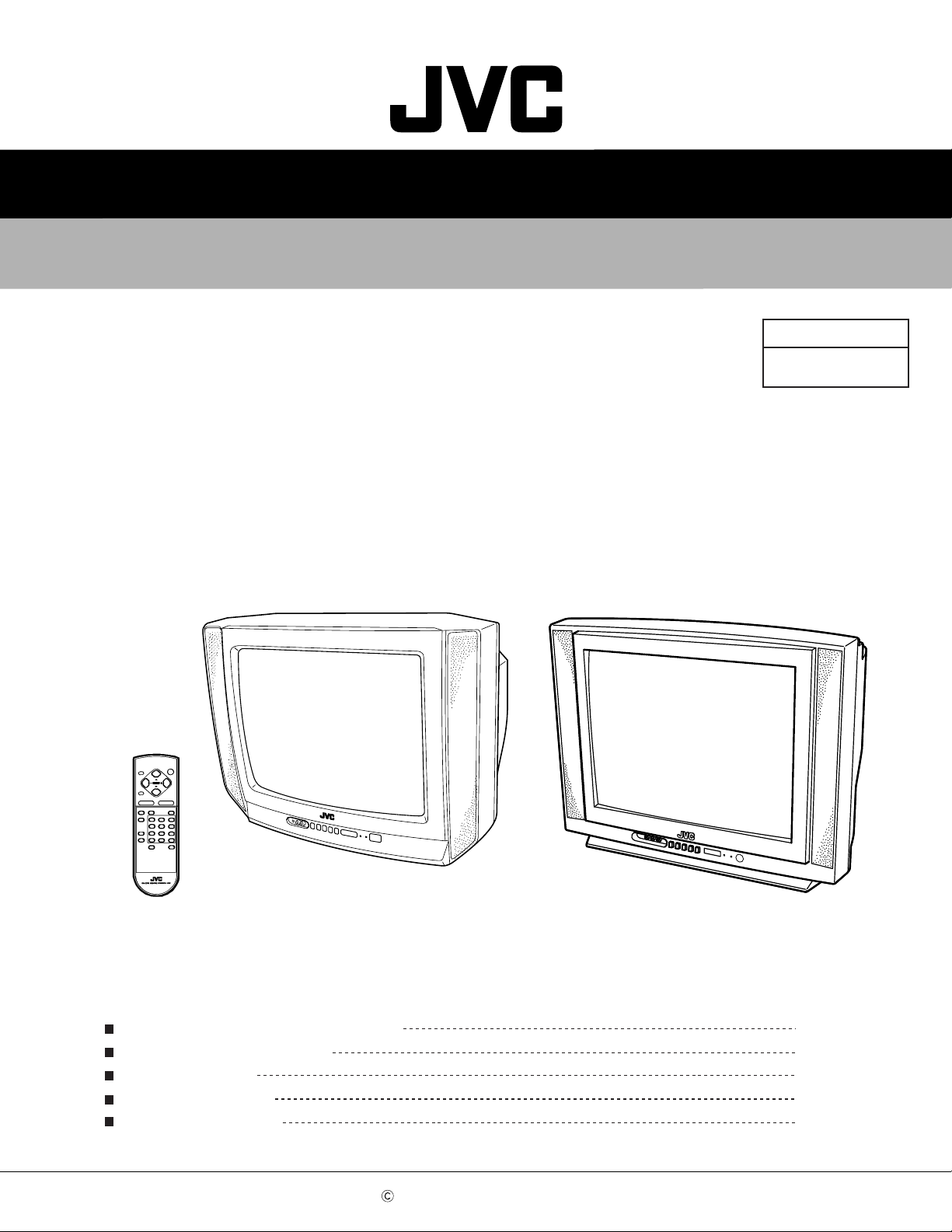
Page 1
SCHEMATIC DIAGRAMS
COLOUR TELEVISION
AV-21D81
AV-20N81
AV-16N81
AV-16N81G
AV-21D81/VT
AV-20N81/VT
AV-16N81/VT
AV-16N81G/VT
CD-ROM No.SML200112
BASIC CHASSIS
CL-M
[AV-16N81G/VT]
CONTENTS
NOTE ON USING CIRCUIT DIAGRAMS
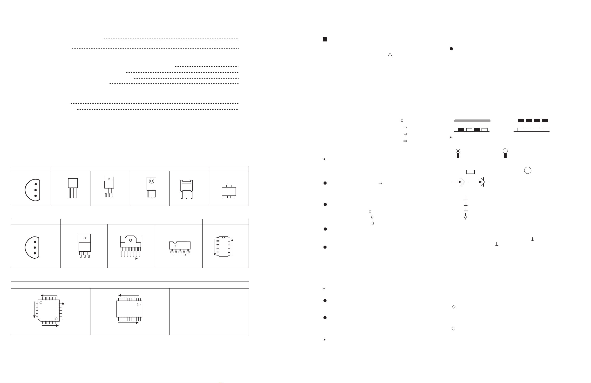
SEMICONDUCTOR SHAPES
BLOCK DIAGRAM
CIRCUIT DIAGRAMS
PATTERN DIAGRAMS
COPYRIGHT 2001 VICTOR COMPANY OF JAPAN, LTD.
[AV-20N81/VT]
[AV-16N81/
VT]
[AV-21D81/
VT]
2-1
2-2
2-3
2-5
2-13
No.51902
Dec. 2001
Page 2
AV-21D81 AV-20N81
STANDARD CIRCUIT DIAGRAM
NOTE ON USING CIRCUIT DIAGRAMS
1.SAFETY
The components identified by the symbol and shading are
critical for safety. For continued safety replace safety critical
components only with manufactures recommended parts.
2.SPECIFIED VOLTAGE AND WAVEFORM VALUES
The voltage and waveform values have been measured under the
following con ditions.
(1)Input signal : Colour bar signal
(2)Setting positions of
each knob/button and
variable resistor
(3)Internal resistance of test er
:DC 20k
/V
(4)Oscilloscope sweepi ng time
:H
20µS/div
:V
5mS/div
:Others
Sweeping time is
specified
(5)Voltage values
:All DC voltage values
Sin ce th e vo l tage val ue s of si gn a l cir cui t va ry to some ex ten t
according to adjustments, use them as reference values.
3.INDICATION OF PARTS SYMBOL [EXAMPLE]
In the PW board
:R1209
R209
4.INDICATIONS ON THE CIRCUIT DIAG RAM
(1)Resistors
Resistance value
No unit :[
]
K
:[K
]
M
Rated allowable power
No indication :1/ 16 [W]
Others :As specified
Type
No indication
:Carbon resistor
OMR
:Oxide metal film resistor
MFR
:Metal film resistor
MPR
:Metal plate resistor
UNFR
:Uninflammable resistor
FR
:Fusible resistor
Composition resistor 1/2 [W] is specified as 1/2S or Comp.
(2)Capacitors
: Original setting position
when shipped
5.NOT E FOR REPAIRING SERVI CE
This mod el's power cir cuit is pa rtly diffe rent in the GND. The
difference of the GND is shown by the LIVE : ( ) side GND and the
ISOLATED(NEUTRAL) : ( ) side GND.Therefore, care must be
taken for the following points.
(1)Do not touch the LIVE side GND or the LIVE side GND and the
ISOLATED(NEUTRAL) side GND simultaneously. If the above
caution is not respected, an electric shock may be caused.
Therefore, make sure that the power cord is surely removed from
the receptacle when, for example, the chassis is pulled out.
(2)Do not short between the LIVE side GND and ISOLATED(NEUTRAL)
side GND or never measure with a measuring apparatus measure
with a measuring apparatus ( oscilloscope, etc.) the LIVE side GND
and ISOLATED(NEUTRAL) side GND at the same time.
If the above precaution is not respected , a fuse or any parts will be broken.
Since the circuit diagram is a standard one, the ci rcuit and
circ uit con stant s may be subj ect to chan ge f or i mprovem ent
without any notice.
NOTE
Due improvement in performance, some part numbers show
in th e ci rcui t diag ram may not agre e wi th tho se i ndic ate d i n
the part list.
When ordering parts, pl ease use t he numbers t hat appear
in the Parts List.
Type
MM
:M eta lized mylar cap ac i tor
PP
:Polypropylene capacitor
MPP
:Metalized polypropylene capacitor
MF
:Metalized film capacitor
TF
:Thin film capacitor
BP
:Bipolar electrolytic capaci tor
TAN
:Tantalum capacitor
(3)Coils
No unit
:[
µ
H]
Others
:As specified
(4)Power Supply
:B1
:9V
:5V
Respective voltage values are indicated
(5)Test point
:T est po int
:Only test point display
(6)Connecting method
:Connector
:Wrapping or soldering
:Receptacle
(7)Ground symbol
:LIVE side ground
:ISOLATED(NEUTRAL) side gro und
:EARTH ground
:DIGITAL ground
:[M ]
Capacitance value
1 or higher :[pF]
less than 1
:[µF]
Withstand voltage
No indication :DC 50[V]
Others :DC withstand voltage [V]
AC indicated
:AC withstand voltage [V]
Electrolytic Capacitors
47/50[Example]:Capacitance value [µF]/withstand voltage[V]
No indication
:Ceramic capacitor
:B2 (12V)
AV-16N81 AV-16N81G
CONTENTS
AV-21D81 AV-20N81
AV-16N81 AV-16N81G
SEMICONDUCTOR SHAPES
BLOCK DIA GRAM
CIRCUIT DIAGRAMS
MAIN PWB CIRCUIT DIAGRAM(Tuner,Micro computer & Front control )
MAIN PWB CIRCUIT DIAGRAM(Picture & Audio)
MAIN PWB CIRCUIT DIAGRAM(Power & Deflection)
CRT SOCKET PWB CIRCUIT DIAGRAM
P ATTERN DIAGRAMS
MAIN PW B PAT TERN
CRT SOCKET PATTERN
SEMICONDUCTOR SHAPES
TRANSISTOR
BOTTOM VIEW
IC
B O TT OM VI EW F R O NT V IEW TO P VI EW
CHIP IC
2-2
E
C
B
OUT
E
IN
N
N
ECB
N
1
N
IN OUTE
BCE
(G)(D)(S)
FRONT VIEW
1 N
TO P VI EW
ECB
1
N
No.51902
TO P VI EW
CHIP TR
ECB
1 N
1
2-2
2-3
2-5
2-7
2-9
2-11
2-13
2-15
C
BE
N
Dec. 2001 No. 51902
Page 3
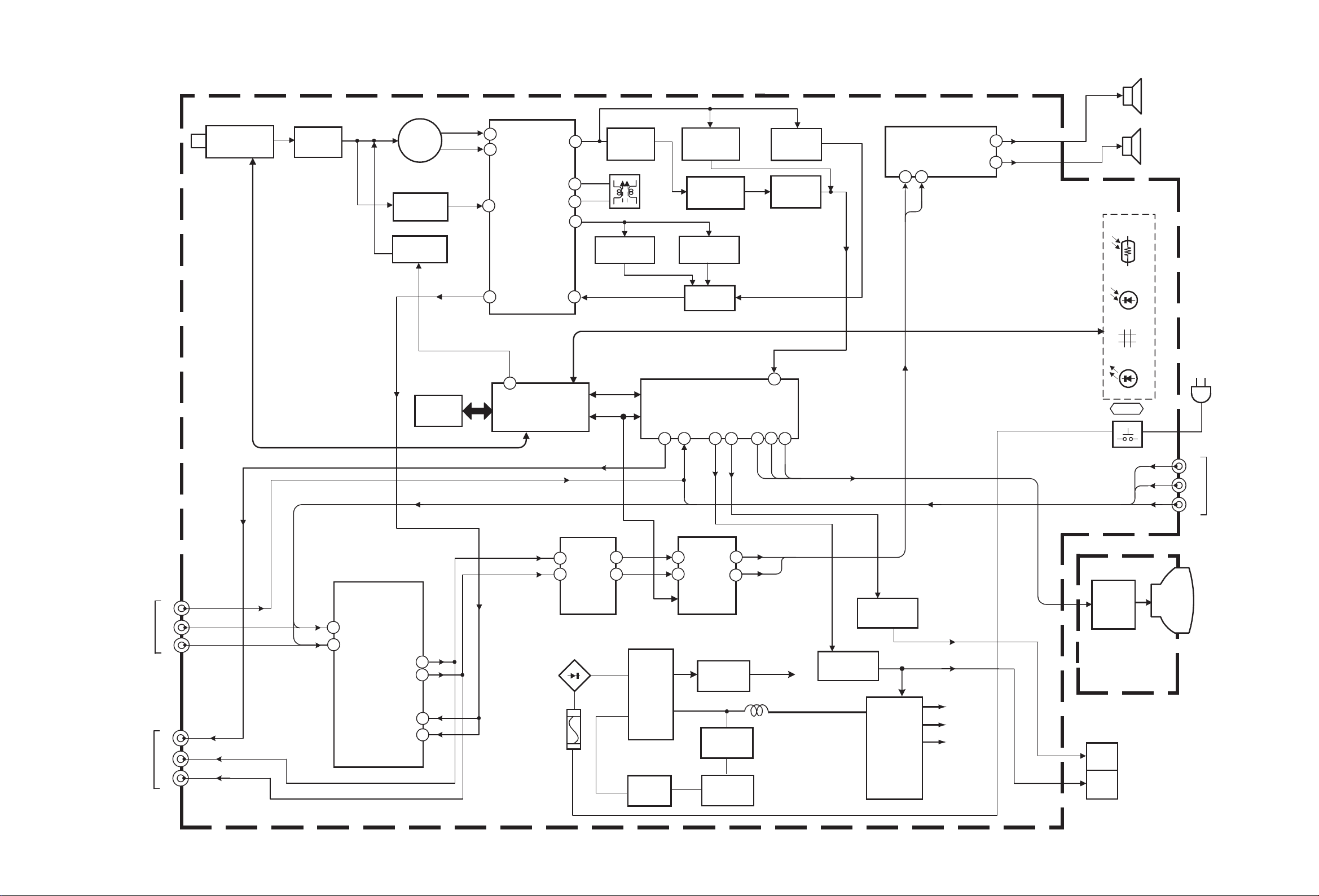
BLOCK DIAGRAM
CF103
4.5MH
Z
VIDEO
AMP
IC701
MICRO
COMPUTER
IC201
V/C DEF.
PROCESSOR
R G B
MAIN PWB
CRT SOCKET
PWB
R / G /B
IC702
MEMORY
IC651
AUDIO AMP
V
L
R
FRONT IN
VIDEO-3
FRONT
CONTROL PWB
L
R
OSD
V01
CRT
SCL
SDA
REG.
T921
SW
TRANSF.
Q971
LOW-B SW
IC941
ERROR AMP
IC921
POWER
REG.
PC921
VOLTAGE
FEEDBACK
D901
RECT
DY(V)
DY(H)
DEF.YOKE
H.
OUT
V.
OUT
ECO
SENSOR
REMOCON
RECEVER
KEY
LED
P SW
SCL
SDA
IC202
AUDIO SW
11
5
12
8
L.OUT
R.OUT
RF-IN
RF-IN
R.IN
L.IN
7
10
IC602
VOL&TONE
IC601
SURROUND
17
11
6
3
5
1
19
16
(L)
(R)
(L)
(R)
(V)
(L/R)
(L)
(R)
6
8
CF106
6.0 TRAP
Q208
BUFFER
IC101
P.IF/S.IF
DETECTOR
SF102
CF601
4.5 TRAP
CF604
5.5MHz FILTER
Q604
SIF AMP
TUNER
SF101
18
13
16
15
T101
VCO
(CW)
Q101
AMP
1110
7
5
4
SAW FILTER
SAW FILTER(PAL)
(A)
(V)
V-IN
V-IN
S-IN
FM OUT
V-OUT
VCC
VCC
SIF OUT
SIF IN
V
L
R
LINE
OUT
V
1
L1
R1
IN
VIDEO-1
4 53 141312
AC IN
ENA,DATA,CLOCK,LOCK
1 13
L
R
B1
IC421
VERT.OUT
Q522
H.OUT
FBT
FOCUS
SCREEN
EHV
H.OUT
V.OUT
V-OUT
V-IN
56 1
TV IN
47
SP
02
SP
01
SCL
SDA
Q 102
SW
13
CF104, 105
5.5/6.5 TRAP
Q107
BUFFER
CF608
6.5MHz FILTER
AV-21D81 AV-20N81
AV-16N81 AV-16N81G
AV-21D81 AV-20N81
AV-16N81 AV-16N81G
No.51902
2-3 2-4
No.51902
Page 4

AV-21D81 AV-20N81
AV-16N81 AV-16N81G
AV-21D81 AV-20N81
AV-16N81 AV-16N81G
CIRCUIT DIAGRAMS MAIN PWB CIRCUIT DIAGRAMS (Tuner,Micro computer & Front control)
VIN
LIN
RIN
J002
CEMN065-001
OR
QNN0281-003
V.IN
J003
CEMN065-002
OR
QNN0281-002
A.IN(L)
J004
CEMN072-003
OR
QNN0282-001
A.IN(R)
D754
P1241-04
ECO
SENSOR
10/50
R751
10k
R754
10k
D751
SLR-342VR-T16
RED
R760
OPT
R757
680
V
L
R
C752
IC751
PIC-37243SR
IR UNITDETECT
R752
3.3K
R753
6.8K
R755
3.3K
C753
BW
5.7V
R758
2.2K
D753
*3
D758
*3
4.9V
4.9V 0V
MENU
S751
QSW0619-003Z
CH-
S752
QSW0619-003Z
CH+
S753
QSW0619-003Z
VOL-
S754
QSW0619-003Z
VOL+
S755
QSW0619-003Z
Q753
OPT
47/16
C751
R762
8.2K
-1.3V
VIN
RIN
LIN
4.9V
4.9V
R759
10k
4.8V
R756
680
D752
SLR-342DU-T16
ORANGE
TU001
QAU0186-002
C015
0.0022
D755
OPT
D756
OPT
D757
OPT
Q752
*1
ECO DRIVE
0V/4.9V
Q751
DTA124ESA-T
LED SW
4.7/50
AGC BT AS SCL SDA BM 5V LOCK
3.2V 0V 0.5V 0.6V 5V 5V 31.3V 0V
C002
470/16
C005
0.1
R102
15K
R101
C001
220K
C122
47/16
R108
75
R112
10K
3.58/OTHER
REMOCON
KEY1
KEY2
P_ON/OFF
ON_TIMER
3.8V
C108
0.01
DIFFERENCE LIST (*PARTS)
SCL- SCL1296A-CK
*
QETM1HM
C704
-475
MAIN PWB
SCL-1296A-CK
SCL-1295A-CK
SCL-1299A-CK
MY
R002
220
SCL1
CF101
OPT
0V
0V
0.0047
QFLB1HJ
-102
L002
8.2
R003
220
SDA2
C101
R107
10
Q102
DTC124ESA-T
SWITCH
1295A-CK
Y001
BW
IC001
TA78L005AP-T
OUT
C124
47/16
C103
0.0047
R110
2.7K
CF102
OPT
SCL1299A-CK
QFLB1HJ
-102
BTPS
-32
NC IF
L001
C003
10/50
D001
MTZJ33A-T2
!
QRZ9017-100
C102
0.0047
12.1V
OPT
C016
OPT
FR001
10 1/4W FR
Y002
OPT
L101
2.2
D101
MA859-T2
D102
MA859-T2
R113
560
R114
560
L78LR05E-MA
IC703
5V REG & RESET
INPUT
5.8V0V4.9V 4.9V
C702
0.1
MY
C135
C704
R105
2.2K
R106
1.2K
0.01
*
C004
OPT
C007
OPT
5V REG
IN
GND
R103
6.8k
2.1V
C10410R109
0.0047
Q101
2SC5083/L-P/-T
C107
0.0047
K001
C006
*4
0.01
C008
10/50
32V
R104
180
7.4V
1.3V
R111
100
IF AMP
C703
47/16
(AV-16N81-VT,AV-16N81G-VT)
(AV-20N81-VT)
(AV-21D81-VT)
GND
C105
0.0047
C106
0.0047
Y704
OPT
Y703
BW
C705
100/16
SF101
QAX0323-001
SAW FILTER
SF102
QAX0325-001
SAW FILTER
RESET
Y003
BW
5VOUTPUT
L701
QQL242K-5R6
C711
0.1 MY
R121
220
R738
68K
5.6
C712
10/50
[1/3]
R119
220K
R120
8.2K
R116
100K
R118
27K
C111
0.01
C112
0.1 MY
.47/50
C601
10/50
D601
MTZJ6.8A-T2
IC702
AT24C0821D81VT
MEMORY
R619
OPT
Q606
OPT
Y601
BW
2.2V
Q607
KEY1
C710
0.01
KEY-1
SCL2
K706*4K705
*4
R734
220
SCL2
OPT
Q111
DTC124ESA-T
MUTE
3.58/OTH
R703
6.8k
3.58/OTH
SCL1
BACK
R733
220
SCL1
C713
180p
5%
GROUND
M52342SP
IC101
PIF/SIF DETECTOR
R117
2.7K
2.1V
RFAGC
EQ
V OUT
NP
A1
Vcc.F
VCO
VCO
Vcc
SIF
OUT
SIF
SW
SIF
ENABLE
4.5/OTH
4.5/OTH
NC
3.5V
2.3V
5V
4V
4V
9V
2.3V
0V
2.1V
IN
R705
560
DATA
CLOCK
5.5/OTH
PROTECTOR
C715
0.047
MY
PROTECT
5.5/OTH
SCL
SDA
A2
A3
C110
0.01
C113
0.01
C114
R601
1.8K
R602
1K
C602
0.047
5.5/OTH
4.5/OTH
X701
CERAMIC RESO.
CST8.00MTW
R706
820
0V 2.2V 2.2V 0V NC NC NC 4.9V 0V NC 4.7V 4.9V NC 0.1V 0V 4.9V
Vss
DD
V
4.9V NC 4.9V 0V 0V 0V 2.2V 5.4V 4.9V 4.3V 4.9V 4.1V NC NC NC
MY
3V
2.7V
1.4V
1.4V
0V
2.4V
2.7V
2V
4.8V
X OUT
OSC2
C714
0.01 MY
DLY
AFC APC
RFAGC
OUT
V IN
V IN
GND
S IN
AGC.F
FM FB
FM OUT
X IN
CNVss
OSC1
RESET
0V
4.9V OV 4.9V 4.9V
VDD
A0
0V 0V 0V 0V
L107
BW
C136
0.01
MY
R135
220K
R124
OPT
C120
47/16
C121
0.01
R603
10K
D602
MTZJ6.2B-T2
P_ON/OFF
P-ON/OFF
RF AFC
R737
120K
D.GND
IC101
3Vp-p (H)
R123
150
C119
47/16
T101
CELT001-303
Y702
OPT
R704
Y701
IIC
H/S
ECO
SENSER
R750
1K
SDA2
C116
.47/50
OPTC117
0.01C118
REMOCON
560
OPT
C724
100p
LOCK
REMOCON
SDA2
SDA1
K708*4K707
*4
R736
R735
220
220
SDA1
C725
180p
5%
5%
18
0V
R125
D104
C123
0.01
Q109
BUFFER
A.MUTE1
TEXT
2.9V
2.3V
1K
*3
*2
R739
6.8K
A-MUTE1
R620
OPT
2.1V
R130
2.2K
C603
R605
47p
220
L601
QQL242K-120
R608
C613
560
0.01
R609
C609
OPT
OPT
Q603
DTC124ESA-T
MUTE
C610
R612
0.01
220
Y606
OPT
R613
4.7K
R126
10K
Q104
*2
BUFFER
0V
2.8V
0V
12
8.3V
2.8V
SFSH4.5MCB
0V
Y605
0V
DTC124ESA-T
R131
TPSH6.0MB
DTC124ESA-T
R749
1K
C723
D710
*3
KEY2
KEY-2
SECAM
/OTH
/OTH
R725
(X8) R-NET
QRB089J-682
SURROUND
SPATIALIZER
C729
6.8K
100/50
R746
ON_TIMER
POWER_BASSA2
47K
0.1V 0.1V 0.1V 0.1V NC4.9V 0V NC 4.7V 4V
ON/OFF
ON/OFF
H/ST/OFF
ON_TIMER
POWER BASS
_FREE
BUS
A2
NC 0V 0V 0V 0V 0V 0V 0V 0V 0V
C728
OPT
MY
R728
OPT
OPT
MY
R724
6.8k
BUS_FREE
CF601
4.5M
Y603
BW
4.9V
BW
R127
220
0V
Q106
SWITCH
270
CF106
Q110
SWITCH
CUT_OFF
TV/OTH
R748
6.8K
TV/OTH
C604
47p
R621
CF604
5.5MHZ
QAX0336-001
CF606
Y604
OPT
4.9V
Q605
DTC124ESA-T
MUTE
L104
QQL242K-150
Q105
DTC124ESA-T
SWITCH
2.8V
L106
QQL242K-100
C721
10/50
D705
*3
ADJ
ECO
NOISE
I/II
R747
OPT
I/II
C730
0.01
39K
OPT
15
CF103
QAX0339-001
4.5MHz
3.4V
10
ON/OFF
V.CENTER
Ys
X.RAY
K704
C720
OPT
R761
BW
X.RAY
R722
5.6K
MY
R622
10K
*4
Q608
*1
OSD_YS
R625
CF608
6.5MHz
QAX0338-001
R128
820
R129
220
Q108
*2
BUFFER
P.MUTE
BCDG
K703
*4
R721
5.6K
R623
180
C611
0.01
R624
100
R610
560
22K
R611
15K
Q103
*1
BUFFER
L105
QQL242K-8R2
R702
6.8k (x8)
R-NET
QRB089J-682
V.SYNC
K702*4K701
*4
OSD_G
OSD_B
R720
5.6K
R604
2.2K
R606
1.5K
C612
Q602
0.01
BUFFER
11.6V
3.5V
R607
1.8K
11.6V
8.2
3.4V
CF104
TPS5.5MW
CF105
TPS6.5MB
H.SYNC
R
IC701
M37212M8-064SP
MICRO COMPUTER
IC701
5Vp-p
OSD_R
R719
5.6K
NOTE
*1 :NPN Tr
*2 :PNP Tr
*3 :SI DIODE
*4 :B.CORE
OPT:NON MOUNT(OPEN)
BW :BUS WIRE
R626
1.8K
*1
Q601
*1
R628
560
2.9V
BUFFER
4V
0V
2.8V
R132
R133
2
Q107
330
330
2.9V
R627
560
*1
R707
R708
10k
C708
0.0022
MY
D704
OPT
-1.2V
Q703
*1
INVERTER
IC701
5Vp-p(VER) (HOR)
2SC1740S/QR/-T
2SA933AS/QR/-T
1SS133-T2
CE41433-001
5V
9V
A2
GND
TV.A
I/II
GND
TV.M
GND
SIF
GND
12V
32V
TV.M
TV.V
A.MUTE
OSD_YS
SCL1
12V
32V
TV.M
TV.V
A.MUTE
SURROUND
STBVcc
CUT_OFF
P_ON/OFF
V.SYNC
H.SYNC
OSD_R
OSD_G
OSD_B
OSD_YS
X.RAY
PROTECT
TV/OTH
D.GND
BUS_FREE
SDA2
SDA1
SCL2
SCL1
R615
470
11.1V
Q604
SIF AMP
2.9V
R616
22
R617
820
I/II
A2
1.6Vp-p (H)
10k
4.7V
0V
R714
10k
C709
56p
5%
1
*1
C608
0.01
Y602
BW
13.3V
R701
47k
D703
*3
!
CP944
ICP-N5
0.5Vp-p
0.1V
Q702
*1
INVERTER
Q703
5.5Vp-p
-2.4V
R711
10k
R713
22k
C607
100/16
CN001
OPT
R712
C
(H)
56k
D.GND
L602
OPT
C606
(V)
C707
0.0027
MY
0.01
D701
*3
D702
*3
Q701
*2
MUTE
13.3V
C701
100/16
R979
27 3W
QRL039J-270
CUT_OFF
R709
22k
R710
6.8K
OSD_R
X.RAY
BUS_FREE
SDA2
A.MUTE1
OSD_G
PROTECT
TV/OTH
SDA1
SURROUND
V.SYNC
H.SYNC
OSD_B
SCL2
No.51902 No.51902
2-5 2-6
Page 5

MAIN PWB CIRCUIT DIAGRAM (Picture & Audio) [2/3]
AV-21D81 AV-20N81
AV-16N81 AV-16N81G
AV-21D81 AV-20N81
AV-16N81 AV-16N81G
TV.M
TV/OTH
SURROUND
A.MUTE
TV.V
OSD_R
OSD_G
OSD_B
OSD_YS
D.GND
BUS_FREE
SDA2
SDA1
SCL2
SCL1
REAR IN
AUDIOVIDEO
J001
J001
CEMN075-001
RIN
LIN
VIN
CN10Z
C633
10/50
CHGE0113
-0A
CN00Z
C233
10/50
D232
*6
12V
9V
R633
D632
R634
1K
1k
C634
10/50
R235
75
IC202
D631
*6
*6
RF_IN
L_OUT
C236
7.5V 7.5V6.8V 12V 6.8V
10/25
BP
R629
C235
220
47/16
C401
OPT
J005
CEMN076-001
C232
470/16
R234
68
D231
R631
R632
*6
680
680
10/50
10/50
C631
C632
AUDIO SWITCHLA7222
NC
R_IN
7.5V 7.5V0V 0V0V/
C234
10/25
BP
R209
820
C202
R403
6.8K
MY
V-NF
V-ra mp
V_OUT
RF_IN
R630
C402
2.2/50
HF
0.1
220
R_OUT
Vcc
L_IN
R208
680
2.9V 0V 4.2V 0.5V 4.4V 2.4V 5.1V 5V 2.7V 2.7V 2.1V 2.2V 0V 3.3V 4.7V 4.1V 2.6V 5.1V 2.2V 1.6V 1.6V 2.2V 2.2V 0V 2.1V 3V
GND
V.OUT
OUT
REAR
VIDEO AUDIO
LEFT
J001J001
CEMN075-001
R637
180
R233
100
1/2W
/VIDEOTVGND
GND
/VIDEO
TV
0V/
4.8V
4.8V
C213
10/16 BP
R501
8.2K
C501
C203
0.01
0.68
TF
NC
V-Sepa
Sync-IN
Sync-OUT
RIGHTLEFT RIGHT
J005
CEMN076-001
R638
180
0V
2.6V 11.6V
C201
100/16
C502
1/50
0.082 MY
TV.IN
AFC1-filter
-0.1V
-0.1
V
3.3V
Q231
BUFFER
R232
100
C301
SDEMO-adj
Q632
MUTE
0V
0V
Q631
MUTE
R231
BW
*1
BUFFER
X301
QAX0354-001
C204
0.1 MY
Video-IN
Y/Composite
*1
Q202
APL
C635
OPT
*2
C205
4.7/50
R636
4.7K
0V
R635
4.7k
220/16
D653
*1
C231
LOUT
ROUT
BOUT-R
BIN-R
BOUT-L
BIN-L
IC602
VOL.&TONETDA7315
3.6V
SCL
3.2V
SDA
0V
4.3V
4.3V
4.3V
4.3V
4.3V
4.3V
4.3V
LIN
SCL1
R671
100
SDA1
R672
100
D.GND
C657
10/50
C656
10/50
0.1 MYC658
R645
5.6K
0.1 MYC659
0.1 MYC660
R646
5.6K
0.1 MYC661
R647
C662
1K
2.2/50
R648
5.6K
Q682
2SA933AS/QR/-T
MUTE
R694
100K
C665
10/50
R655
10k
R654
1.8K
R651
1.8K
R652
IC651
LA4446
AUDIO AMP
LNF
POGND
LBS
LOUT
LIN
DC(MUTE)
0V 21.3V1V 0V 20.3V11.2V21.4V11.2V20.2V0V 1.1BV 0V 0V
C671
10/16
C675
BP
47/16
10k
R653
C670
1.2K
220p
5%
R656
1.2K
Q683
DTC323TS-T
MUTE
21.8V
0V
0V
R662
*
Q681
DTC323TS-T
MUTE
C672
220p
5%
C687
C674
220/25
C673
10/16
BP
R661
100
21.3V
0V
0V
OPT
Q653
MY
C685
0.1
100/25
R668
180
R666
560
*
VCC
C677
ROUT
C678
100/25
C680
1000/25
C679
1000/25
RBS
C686
0.1 MY
R669
180
POGND
MY
MY
C681
C682
0.1
RNF
R667
0.1
PRGND
C676
47/16
560
R665
4.7
QRK129J-4R7
R664
4.7
1/2W
QRK129J-4R7
RIN
Y610
BW
CN00S
QGA2501C5-04Z
1/2W
SP01
SP02
*
R
L
*
MAIN PWB
CN00T
*
SCL-1296A-CK (AV-16N81-VT,AV-16N81G-VT)
GND
RIN
FOUT
VREG
FIN
VCA
VCC
R314
100
B-Y OUT
C209
0.01
IC601
AN7395K
0V
SURROUND
4.3V
8.7V
C645
0.01
2.8V
R641
4.4
8.2K
V
R649
NC
1.8K
1V
0.4V
22/25 BP
8.8V
0.4
V
100/16
L301
QQL242K-470
K201
CE41433-001
C304
0.1
MY
R-Y IN
R-Y OUT
C644
22/25 BP
R642
150K
C648
C684
C650
10/50
47
47L302
C305
0.1
MY
B-Y IN
C646
0.027
C647
1/50
MY
GND
Fsc
C651
22/50
C652
47/16
C653
2700P
C654
2700P
C655
2.2/50
R643
1K
R644
5.6K
C316
100P 5%
C317
100P 5%
L303
QQL242K-4R7
C306
2.2/50
0.1
MY
Y-IN
Filter
APC
R303
C307
4.3
V
CREF
8.7
V
Vs
0V
GND D.GND
4.3
V
TRE
BLE-L
4.3
V
TRE
BLE-R
4.3
V
RIN
LOUD
-R
C663
0.1
NC
MY
LOUD
-L
C664
0.1
NC
MY
C312
220/16
C308
0.01
27k
NC
C637
22/25
BP
4.4V
C641
C642
10/50
C643
10/50
R203
220K
16MHZ Xtal
4.3V
4.4V
4.4V
4.3V
C210
10/50
Black
NC
4.4
4.4
V
0V
0.6
V
Stretch
V
LIN
1/2VCC
LOUT
SOUT
ROUT
SET
ROIN
GND
LOIN
RDET2
C208
10/50
EF201
CE42142-222Z
R315
100
Vdd
Y-OUT
Fsc
MODE
RDET1
C638
100/10
C639
0.056
MY
R640
1M
C640
0.039
MY
Chroma/CVIN
C302
0.01
10/50
C206
0.01
C207
100/16
C303
12p
CH
Y/C-Vcc(5V)
BW
R210
1.2K
GND
SCL-1295A-CK (AV-20N81-VT)
OSD_R
OSD_G
OSD_B
OSD_YS
D.GND
BUS_FREE
SDA2
SDA1
SCL2
SCL1
C405
1/50
TB1226ENIC201
Vcc
Curve
V.IN
VAGC-filter
C503
*
H_OUT
R502
620
C504
0.01
QRG01GJ-121
L552
QQL231J-560Y
C510
0.01
R506
120
Correction
R504
10k
C505
0.01
OMR1W
FBP_IN
Coinsident Det
C506
R505 0.01
100K
C508
47/16
D502
MTZJ5.1B-T2
C507
0.01 MY
D501
MTZJ9.1B-T2
Vdd(5V)
D201
OPT
C509
0.01
V/C DEF. PROCESSOR
GND
SCL
SDA
R304
D202
100
OPT
R205
R204
390
390
Ys
G-IN
B-IN
G-OUT
R306
100
GND
R-OUT
ABCL
RGB-Vcc(9V)
Digital R-IN
Digital
Digital
R309
R308
R307
1K
1K
1K
C212
R206
10/50
10K
D203
*3
R
C311
C310
100/16
0.01
K301
*4
R311
33K
OSD_G
OSD_B
OSD_R
12 13 14 33
IC201 IC201
3Vp-p 3Vp-p 3Vp-p 0.8Vp-p
34 40 42 45
IC201
B-OUT
R305
100
G
B
R-IN
G-IN
B-IN
Analog YS/YM
Analog
Analog
Analog
Color
Limiter
AUDIO IN
Digital
NC NC NC NC NC
R313
R310
10K
1K
OSD_YS
(H) (H) (H) (H)
0.8Vp-p 1.4Vp-p 1.4Vp-p0.7Vp-p
IC201 IC201
AUDIO IN AUDIO OUT
2.2V0V 0V 0V 0V 0V8.7V5.9V0V2.4V 2.5V 2.4V0V3.2V3.1V5.1V4.2V1.3V4.3V2.1V8.8V2.4V2.6V
C309
4.7/50
Y206
OPT
Y205
OPT
Y204
BW
IC201IC201IC201
(H)(H)(H)(H)
B
G
R
SCL-1299A-CK (AV-21D81-VT)
DIFFERENCE LIST (*PARTS)
SCL1296A-CK
*
CN00T
CN00U
Q653
R662
C503
DIFFERENCE LIST (*PARTS)
*
SP01
SP02
CHHB05
CHHB05
-400T-G
-360T-G
CHHB04
CHHB04
-300U-G
-400U-G
2SC1959
DTC363T
/Y/-T
S-T
1.8K IM-BWIM-BW
2200/16 2200/16 2200/16
AV-16N81-VT AV-16N81G-VT
CEBSS09D
-03KJ2
CEBSS09D
-03KJ2
SCL1295A-CK
CEBSS09D
-03KJ2
CEBSS09D
-03KJ2
SCL1299A-CK
CHHB05
-400T-G
CHHB04
-400U-G
DTC363T
S-T
NOTE
*1 :NPN Tr
*2 :PNP Tr
*3 :SI DIODE
*4 :B.CORE
*6 :Z DIODE
OPT:NON MOUNT(OPEN)
BW :BUS WIRE
AV-20N81-VT
CEBSS12D
-04KJ2
CEBSS12D
-04KJ2
AV-21D81-VT
QAS0037
-1
QAS0037
-1
2SC1740S/QR/-T
2SA933AS/QR/-T
1SS133-T2
CE41433-001
MTZJ13B-T2
A_Vcc
A_Vcc
A_GND
A_GND
CN00U
*
GND
HEATER
HB
HB
GND
HEATER
No.51902
SCL2
SCL1
D707
R743
_FREE
CN00C
C
QGA2501F1-06
MTZJ8.2B-T2
D708
MTZJ8.2B-T2
D709
MTZJ8.2B-T2
220R740
220R741
220R742
220R743
220R744
FBP_IN
ABCL
12V
2-7 2-8
BUS_FREE
SDA2
SCL2
SDA1
SCL1
D739
MTZJ8.2B-T2
D706
MTZJ8.2B-T2
5V
V.N F
H_Vcc
V_OUT
H_OUT
GND
SCL1
R744
R740
R741
R742
BUS
SCL2
SDA1
SDA2
No.51902
Page 6

MAIN PWB CIRCUIT DIAGRAM (Power & Deflection) [3/3]
!
POWER CORD
QMP40D0-200J5
!
VA901
ERZV10V621CS
AC120V-240V
50/60Hz
!
F901
QMF51E2-3R15J4
3.15A
QSP4K21-C01
POWER SW
CN0PW
PW
QGAB801C1-02
!
S901
P_ON/OFF
P_ON/OFF
PROTECT
PROTECT
AV-21D81 AV-20N81
AV-16N81 AV-16N81G
V.NF
H_OUT
V_OUT
V.NF
V_OUT
H_OUT
CUT_OFF
CUT_OFF
FBP_IN
FBP_IN
ABCL
ABCL
X.RAY
V.SYNC
H.SYNC
H_Vcc
X.RAY
H_Vcc
12V
5V
9V
AV-21D81 AV-20N81
AV-16N81 AV-16N81G
STBVcc
32V
A_Vcc
A_GND
HB
GND
HEATER
!
L01
DEG-COIL
*
CNDEG
QGZ5003C1-02
IC921
POWER REGULATOR
OVP
TSD
OSC
DRIVE
TH901
QAD0101-9R0
STR-F6654
GND
Vcc
MTZJ15A-T2
CE41433-001
!
R901
3.9
10W UNFR
QRF104K-3R9
R902
68K 3W
QRL039J-683
C905
0.001
250VAC
QCZ9078-102
0V
18.1
V
145.8
V
0.1V
1.5
V
D929
K923
C931
270P
2KV
K923
D928
OPT
!
C903
QFZ9040-473
C907
250VAC
QCZ9078-102
C924
100/35
R921
680
1/2W
D924
1SS133-T2
R935
1.5K
0.047
275VACMF
0.001
C905
C909
220/400
QEZ0199-227
R934
33K
1/2W
MTZJ6.8A-T2
R923
0.22 5W MFR
QRM059J-R22
C922
470P
QRX029J-2R2
C927
OPT
R927
OPT
C908
QRE122J
-824
D927
2.2 2WMFR
R926
1.5K
C926
0.0022
MY
3.3K 1/2W
MAIN PWB
SCL-1296A-CK
(AV-16N81-VT,AV-16N81G-VT
SCL-1295A-CK
SCL-1299A-CK
(AV-21D81-VT)
(AV-20N81-VT)
! C902
0.1 275VACMF
QFZ9040-104
! LF902
QQR0527-002
C904
0.001
250VAC
QCZ9078-102
OPT
R932
820K
1/2W
R922
1SR124-400A-T2
Y903
Q921
OPT
R929
D901
D3SBA60
C906
QCZ9078-102
C929
0.01
C930
220P
EG1A-T3
R931
OPT
CE41433-001
C921
390P 2KV
QCZ0325-391
K922
CE42050-001
C923
D921
BW
R925
OPT
D923
OPT
LIVE
!
C991
470P 250VAC
QCZ9079-471
!
C992
470P 250VAC
QCZ9079-471
0.001
250VAC
R928
CETS128-001JM
47K 3W
QRL039J-473
D926
K921
OPT
R933
3.9
1/2W
QRK129J
-3R9
D922
*3
R924
C925
OPT
OPT
!
C993
*
250VAC
! R991
8.2M 1W
QRZ0057-825
18.1V
C928
OPT
1.5V
LIVE ISOLATED
)
)
!
T921
SW TRANSF
CNX82A
ISOLATED
C947
560p/500
K943
CE42050-001
ERC30-02L38
C944
470P50V
K942
D942
ERC30-02L38
K942
CE41433-001
560p 2KV
QCZ0122-561
K941
CE42050
-001Z
RU3AM-LFC4
100/160
QEZ0203-107
1.5k 1/2W
13.7V
!
PC921
PC123F2
VOLTAGE FEED BACK
12.7V
(())
C941
12.7V
D945
D943
1000/25
D941
C942
R941
R942
BW
*
!
CP942
ICP-N75
C945
0V
(()
L943
2.2
1000/35
C950
0.1
MY
Q941
ERROR AMP
2SC1740S/QR/-T
C951
OPT
!
CP943
ICP-N75
C948
C949
390P
5%
QQL42AK-820
L942
82
C946
220/25
Y909
BW
L941
QQL42AK-820
114.3
V
12.7V
0V
0V
C954
0.01
Y911
BW
82
IC941
S1854A
ERROR AMP
R943
4.7K
Y910
BW
R970
12 2W OMR
QRL029J-120
R973
39 2W OMR
QRL029J-390
C952
OPT
Q971
2SA966/OY/-T
SWITH
13.9V
R971
22k
R972
1.5k
1/2W
PROTECTOR
13.9V
C973
12.3V
C974
1000/25
8.8V
C975
100/25
Q950
OPT
R944
3.3K
QRE122J-332
Q942
DTC144GSA-T
SWITCH
0V
0V
IC971
LM2940CT-12
12V REGULATOR
IN OUT
OPT
IN OUT
IN OUT
13.8V
Q972
13.1V
DTC144GSA-T
SWITCH
0.1V
0.6V
0V
C960
OPT
R954
OPT
R955
OPT
R946
15k
0.6V
11.6V
0V
IC972
AN7809F
9V REGURATOR
9V
0V
4.8V
0V
IC973
AN7805F
5V REGURATOR
1SR124-400A-T2
R974
3.3k
C971
10/50
R950
BW
R951
BW
D950
OPT
D971
R952
OPT
R975
1000/25
12k
2SA933AS/QR/-T
D981
*3
C976
100/16
C977
100/16
C978
100/10
H_Vcc
C972
Q523
X-RAY PROTECTOR
2SC1815/YG/-T
Q981
PROTECTOR
4.1V
R980
820
D982
*3
D983
*3
P_ON/OFF
R981
2.2K
R982
8.2K
FBP_IN
4.3V
R983
1K
0V
PROTECT
X.RAY
18K 2W OMR
QRG029J-183
TP-91
(B1)
QGA2501C5-05Z
R977
CN0S1
C437
0.001
MY
0.5V
Q423
*1
SWITH
V_OUT
V.NF
CUT_OFF
NOTE
*1 :NPN Tr 2SC1740S/QR/-T
*2 :PNP Tr 2SA933AS/QR/-T
*3 :SI DIODE 1SS133-T2
OPT:NON MOUNT(OPEN)
BW :BUS WIRE
H_OUT
R591
27K
R423
0V
R422
4.7k
220
4.1V
.01/100
TP-E
( )
L421
R435
C430
OPT
R440
23
IC421IC421
(V)
45
(V) (V)
11.6V
4.9V
SCL-
SCL-
1295A-CK
1299A-CK
QRE121J
QRE121J
-6R8Y
-6R8Y
QRE122J
QRE122J
-4R7
-4R7
QRG01GJ
QRE122J
-221
-331
QRE122J
QRE122J
-122
-821
2SD1878
2SD2499
-YD
-LB
QQH0070
QQH0022
-001
-003
CE41210
CE41210
-00B
QQLZ018
QQLZ018
-540
-930
QRE122J
-222
-222
QRG029J
QRG029J
-332
-392
QRL039J
QRG029J
-221
10K
QFZ0198
-742
-103
.01 .0074
QFZ0151
QFZ0151
-404
.4
QCZ9079
QCZ9079
-222
-222
.0022
MTZJ5.6
MTZJ5.6
A-T2
A-T2
CE41433-001
C527
*
MPP
200V
8.2K
.4
.0022
(V)
2Vp-p
K422
!
FR552
1 1W FR
QRZ9021-1R0
!
ICP-N50
C552
1000/35
QETM1VM-108
R528
470
1/2W
Y507
OPT
Y508
OPT
R529
*
OMR
L522
CP551
*
! FR551
1/4W FR
QRZ9017-4R7
D551
RGP10J-5025-T3
C530
560p
L551
*
4.7
C551
0.0015
500V
C571
47/160
QEHQ2CM-476
CN0HV
QGZ5003C1-04
DIFFERENCE LIST (*PARTS)
AV-16N81-VT
*
QQW0103-001
L01
!
T522
*
135
(H) (H) (H)
1000Vp-p 50Vp-p
AV-16N81G-VT
QQW0103-001
ANODE
FOCUS
SCREEN
R583
R58112K
BW
R582
*
C581
0.1
MY
D581
D582
RGP10J-5025-T3
C555
D553
RH1S-LFA1
30Vp-p
Y506
BW
Y505
OPT
OPT
OPT
FR554
!
15 1/4W FR
QRZ9017-150
C557
2.2/250
T522T522T522
250Vp-p
79
T522T522
240Vp-p
(H)
Y401
BW
Y504
BW
AV-20N81-VT
QQW0061-001
(H)
AV-21D81-VT
CELD029-004J6
C428
100/35
D423
1SR124-400A-T2
100/16
R451
10K
11.6V
R453
1.2K
PROTECTOR
D425
*3
R455
BW
R456
OPT
117.5V
C524
*
MPP
1.5KVH
SCL1296A-CK
QRE122J
-8R2
QRE122J
-8R2
-221
QRE122J
-821
2SD1878
-YD
QQH0072
-001
CE41807
-00B -00B
QQLZ018
-700
QRE121J QRE122J
-563Y
QRG029J
-332
QRL039J
-221 -391
12K
QFZ0200 QFZ0198
-812
.0081
QFZ0151
-564 -404
.56
QCZ9079
-152
A-T2
55Vp-p 30Vp-p
IC421 IC421
2Vp-p
C450
Q425
*2
C525
OPT
IC421
LA7840
R431
8.2K
R442
8.2K
R444
1/2W
0V
D426
OPT
*
Q522
R526
1/2W
*
0V
22
2Vp-p
PUMP UP
R450
2.2K
R452
2.2K
C433
4.7/50
H.OUT
(H)
DIFFERENCE LIST (*PARTS)
*
R432
R433
R440 QRG01GJ
R444
Q522
T522
L522
L551
R523
R524
R529
R582
C524
C527
C993
D945 MTZJ5.6
THERMAL
PROTECTION
-Vcc Vcc
0V 15.6V26.9V4.4V 4.4V 26.6V2.2V
R427
10k
R428
OPT
D421
*3
0V
QRK129J-1R0
R443
1/2W
0V
150p 500V
QCB32HK-151
114.5V
C431
OPT
R592
OPT
D424
MTZJ36
A-T2
C423
MY
.047/100
R434
18K
1
C436
0.33
TF
C522
0.001 500V
QCB32HK-102
C521
D592
OPT
C592
OPT
D422
MTZJ36
A-T2
C422
0.0018
MY
C424
OPT
R430
10k
C435
QETM1EM-108
R433
1/2W
R523
*
1/2W
C432
OPT
R594
3.3K
C427
100/35
C426
OPT
R441
6.8K
R461
BW
1000/25
R432
*
*
1/2W
T521
CE42034-001
C523
1/160
R524
*
2W OMR
R525
3.3K 2W OMR
QRG029J-332
R424
BW
Q422
*1
DRIVE
R429
0V
5.6k
4.4V
R426
0.1V
33k
R425
0.1V
33k
Q424
*1
SWITH
BW
60Vp-p (H)
MY
Q521
BSN304-T
H.DRIVE
*
R521
BW
R522
4.7K
32.8V
2V
5Vp-p
B1
D591
OPT
C591
R593
220/10
OPT
NC
TP-B1
No.51902 No.51902
2-9 2-10
TP_E
X_RAY1
X_RAY2
Page 7

CRT SOCKET PWB CIRCUIT DIAGRAM
AV-21D81 AV-20N81
AV-16N81 AV-16N81G
AV-21D81 AV-20N81
AV-16N81 AV-16N81G
DIFFERENCE LIST 2 (*PARTS)
QGA2501C5-05
MAIN
PWN
Q351
Q352
Q353
C
120Vp-p
C
125Vp-p
C
110Vp-p
CN00T
(H)
(H)
(H)
9V
GND
AV-16N81-VT
!
V01
R
G
B
SG354
OPT
AV-16N81G-VT
A38JLL91X13
*
G1 G2 G3
C359
0.022
1.25KV
QFZ0097-223
*
V01
12K 2W OMR
R354
QRL029J-123
C351
100/16
C360
0.01 MY
Q351
2SC3620
82
L351
QQL242K-820
G.OUT
R351
150
2.6V
B
G
R
C352
OPT
R355
2.2K
Q352
2SC3620
R.OUT
R352
150
C354
OPT
Q353
2SC3620
2.6
V
R358
2.2K
R360
2WOMR
B.OUT
R353
150
C356
OPT
Y351
BW
Y352
BW
2.7
V
R361
2.2K
140V
2.4V
R356
330
R357
QRL029J-123
L352
QQL242K-820
142V
2.3V
R359
330
QRL029J-123
12K
L353
QQL242K-820
138V
2.4V
R362
330
QGA2501C5-04
R363
1.5K 1/2W
QRZ0111-152
5.6KR364
330pC353
R365
100
12K 2W OMR
82
R366
1.5k 1/2W
QRZ0111-152
330pC355
R367
100
82
R368
1.5k 1/2W
QRZ0111-152
10KR372
390pC357
R369
100
L354
BW
CN00U
U
TP-47G
R370
100k
1/2W
R373
100K
1/2W
GK
RK
BK
H
H
SG351
OPT
VA351
OPT
SG352
OPT
VA352
OPT
CE42554-001
CRT SOCKET
SG353
OPT
VA353
OPT
SK351
!
SK351
PIN 2 :
FOCUS GND
TP-E
CRT SOCKET PWB
SCL-3012A-CK
(AV-16N81-VT,AV-16N81G-VT)
SCL-3013A-CK
(AV-20N81-VT,AV-21D81-VT)
AV-20N81-VT
A48JLL91X01
CRT
CRT
GND
AV-21D81-VT
A51JSW51X07
ANODE
FOCUS
SCREEN
No.51902
2-11 2-12
No.51902
Page 8

PATTERN DIAGRAMS MAIN PWB PATTERN
1
R935
C929
D901
S901
D922
C923
C902
C930
R901
C921
C903
D921
R928
C928
C924
D926
LF902
C931
C906
4
3
PC921
C993
R933
R991
84
7
W416
5
3
21
C992
C991
VA901
21
R757
2
PW
R760
D751
POWER
Y911
C949
T921
W318
C976
W461
OUT
C950
R941
C974
IN
C948
Q751
D752
Y910
OUT
D983
D982
R980
CL003
IN
D981
IC941
C942
C977
IC
O
ISOLATED
OUT
G
OUTIN
R942
E
Q941
W031
C941
K941
1112 10 9
13
141516
C947
L943
CP943
IC971
C
IN
W233
973
T
U
C978
W261
C662
W276
C655
T3.15AL 250V
R648
F901
C643
G
Q753
C751
R756
TIMER
R925
R924
R927
W019
D929
R923
C907
R926
W033
POWER
R902
R929
D924
C927
E
Y903
Q921
C925
4
2
R922
R934
C909
W039
TH901
DEG
B
W020
D928
R921
K923
W040
C926
D923
H003
W024
5
3
IC921
K921
1
K922
D927
C922
R931
R932
W058
C908
C904
C905
LIVE
21
OUT
R943
IN
BE
D945
C951
W005
L941
R944
W023
C946
D941
L942
R970
R644
D942
IN
R643
R647
C945
CP942
K942
C952
K943
D943
IN
C
C975
R973
C
W263
Q981
C664
C663
C654
C653
C972
W262
C944
R982
123
G
OUT
Q972
IC972
OUT
EB
W442
C973
W470
W313
C651
D758
IC751
W441
C642
D971
R983
W383
C673
R981
W314
1051
W312
Q971
R974
IN
W207
C686
C672
C652
IC602
W462
R762
C971
R667
Y610
R656
C661
11
20 15
R946
W015
R669
R665
R506
Q681
R975
R971
R972
E
Q942
W216
R646
EB
C670
C684
W465
W464
Y909
R977
C954
W363
B
R635
W220
W445
C676
C680
R664
41
C682
W434
W432
W427
EB
W437
W438
W413
Q682
B
R694
W436
R653
C660
C656
C659
C658
R645
R671
R672
C650
C641
D753
R758
D754
C635
C657
C681
R654
B
IC651
C678
11
C679
Q632
Y003
E
Q631
R668
S
C646
C648
W454
R636
R631
B
R
R649
W309
10
C015
R632
C631
979
R655
R641
C685
E
D001
R651
E
C002
L001
C006
511013
R662
C005
C007
R666
C677
Q683
C639
W248
C665
C647
R642
R003
C644
15
IC601
C632
E
C236
R652
10512
VOL+
S755
R002
C003
C674
W439
W450
C645
5
W380
Q653
C687
D632
R630
R101
C004
C671
B
W257
W254
W283
C001
K001
C016
W378
C675
E
R629
C633
AV-21D81 AV-20N81
AV-16N81 AV-16N81G
W045
R108
AGC
AUDIO
R661
W425
R633
C234
IC202
1
R634
W259
NC
ENA
SCL
SDA
BM
5V
NC
BT
NC
IF
H004
W404
R640
W429
W284
W322
C752
TU001
CF101
C602
W401
C136
W466
K201
W447
W448
VOL-
S754
W392
C634
W011
Y001
W009
C209
W316
R111
R109
W043
R107
R303
1
C638
W290
R637
Q102
C008
W275
C235
L002
C510
Q752
L303
W446
D631
OUTIN
W218
E
B
E
B
W279
Y602
GOUTIN
C101
Q101
L552
W414
W419
W018
W010
D653
W234
W256
C637
20
W305
C640
W258
C108
W197
C102
C104
C124
R105
D101
R113
R121
L101
R104
R112
R103
C103
R110
R102
R118
CF102
R119
IC 1
Y002
FR001
15
C307
W471
C208
W433
W467
W403
W449
W222
W307
C723
W306
D710
W304
W291
W292
W451
R754
R755
D602
L107
C316
C317
W468
R751
R120
10
CN001
IN
Q110
C308
EF201
W405
Q701
CH+
S753
W282
W281
L302
16R1
R123
C116
W2 80
E
Q109
R130
B
W059
L301
R315
C305
C304
2528 20
D502
C201
T
5
W178
W411
C701
R701
B
D702
W410
W159
W114
W118
R749
R703
W453
W460
R117
R314
W459
R752
R106
C105
C112
D601
R619
R131
3529 30
R313
CL002
W443
W440
C135
C107
C111
R602
W418
C118
E
W035
G
L106
R203
W104
C309
MARK
D703
E
D701
W407
R753
R114
20 15
C122
B
C210
C306
W073
W396
R739
R759
CH-
R124
W085
V/C
W426
E
B
C311
2
C711
C206
C310
15
R306
C703
C702
T101
C303
C106
51
W351
3
R750
R706
E
Q108
C207
R305
W061
R235
Q606
4
27
26
B
5
W458
W007
C120
R132
R129
D202
R304
C704
CH
PRESET
B
W221
W187
C714
W374
S751
J005
C121
Y601
W051
Q107
IC201
J001
D102
SF101
C110
IC101
R135
VCO
C119
R133
R128
Q104
CF106
X301
40 45 50
K301
W129
1
CP944
C712
1
IC703
L701
W133
R748
W145
W452
S752
AV-21D81 AV-20N81
AV-16N81 AV-16N81G
3
Z
1
WHT
R234
B
Q231
C608
E
R615
W046
R610
L602
BE
Q602
CF608
Y604
CF606
Y605
Y606
G
C610
Q605
W008
IN
G
W364
OUT
Q111
9
IN
R604
CF601
27
R1
C604
C603
R605
D104
IN
Q105
IN
R208
C202
R209
Q202
E
C401
56
W206
C504
C503
W191
1
C405
R504
D501
C506
R505
D203
R733
R206
8
W229
1
R725
K706
K707
K705
W077
Y701
15
10
C710
C724
MICOM
J004
R638
C113
B
L105
C302
10
10
11
Q607
C205
D201
R205
30
W086
X701
D757
SF102
E
C204
R738
C705
R601
Q103
CF104
W212
C509
W140
C715
W381
C606
E
W117
R608
R204
R233
C232
C114
C601
R611
CF604
Y603
C613
C609
R603
R6
R612
C312
E
R620
L104
CF103
B
R125
R126
CF105
R210
B
C213
R501
W359
W002
W444
5
C508
W181
C212
IC702
5
4
9
R737
K708
35 40 45
IC701
W435
20
R704
R705
Y702
R617
IN
R625
E
Q601
B
C505
R735
C730
1
D232
B
G
Q106
R310
1
E
R232
Q604
B
Q603
G
R308
W097
R702
D231
C611
W190
J003
W349
L601
C301
R311
R734
C612
C123
R722
R231
R616
W107
C725
W098
C231
W260
W116
Z
R736
C607
W423
G
C507
R502
C402
3
W372
Y206
R622
C233
W267
C728
R743
C501
C502
R309
K704
7
R6
R742
R613
R606
Q608
E
R621
W408
C720
D756
R761
Y704
D739
Y205
R741
R623
W131
R740
D709
W094
R626
R307
W066
W134
K703
5250
W004
15
9
R744
W370
R627
R628
R624
TUNER/IF
W417
C203
WHT1
W070
W088
W079
W082
R747
J002
W421
W103
R721
R720
K702
W463
C
R955
R593
W105
D950
E3
Y204
W090
W412
W110
TP-E
C552
C450
R724
R452
W099
W089
D707
D708
R591
R594
W071
W092
W027
W109
R455
R456
K422
Q523
R719
Q702
K701
FR554
C592
R581
X-ray2
R712
R710
R711
R950
R952
R951
16
C
D706
R954
C557
U
41
MARK
L551
D592
R592
W106
W068
15
NC
S1
TP-91
X-ray1
D425
R432
D591
R433
R453
C428
R427
D423
W064
R430
C423
R434
R450
E
R451
R422
R425
R426
R403
E
W108
W132
W420
C709
B
R713
C713
W430
R714
D704
R709
B
R707
W195
W240
R746
R708
W111
W112
D705
C721
C729
R728
D755
C753
W469
B
W100
E
Q425
R429
C707
W049
Q950
D581
CP551
FR552
W353
D426
W101
C708
C427
R423
B
E
D553
Y703
B
R582
R583
R444
H001
R461
W063
D421
R424
Q424
EB
Q703
UL MARK
W028
R431
Y401
R443
D551
CL001
W056
W055
Q422
C424
FR551
Y504
D582
W054
CKF1316-BH1-1
4
C431
R440
W053
R435
R529
R521
R525
R524
ABL
7
HEATER
6
GND
5
24V
4
NC
3
H.PULSE
C432
HV
C430
Y508
R523
Y507
R528
G
R522
C522
L522
C530
L421
C527
C523
Y505
C571
W365
C960
C581
C555
C551
C435
R442
C433
R441
7
C422
R428
C426
D422
15
D424
IC421
C436
BE
C437
Q423
E
EB
C591
CRT SOCET PWB PATTERN
L351
R351
C352
R356
R365
R355
R352
R358
W301
W300
C354
51
R364
R363
TP-47G
R354
C
Q351
EB
R357
C353
Q352
EB
R359
W302
T
CKF0867-
SCREEN
ORG
C
L352
C355
R367
C351
UL MARK
/2!
9
HB
10
GND
00.05.20
NATTAPONG
8
T522
TP-E
TP-91
1 COL
2
B1
1
C525
C524
DEF
C
B
Q521
D
3
S
2
1
C521
T521
W052
Q522
E2
H002
E
Y506
4
R526
5
(B1)
FRONT
TOP
TP-E
VA351
SG351
R366
SG354SG352
C360
Group No.
W311
G2
R372
C359
GK
RK
G1
HE
VA352
W309
Y351
W310
H
W307
TP-E
BK
SK351
Y352
E2
E1
R368
SG353
97.11.05
VA353
NOZAKI
L353
R353
C356
R362
R361
4
C
R369
C357
BE
Q353
R373
R370
U
1
R360
L354
No.51902 No.51902
2-13
82
,2$$
Page 9

VICTOR COMPANY OF JAPAN, LIMITED
HOME AV NETWORK BUSINESS UNIT. 12, 3-chome, Moriya-cho, Kanagawa-ku, Yokohama, Kanagawa-prefecture, 221-8528, Japan
AV21D81VT-CK #3,AV20N81VT-CK #3
AV16N81VT-CK #3,AV16N81GVTCK #999
Printed in Japan
VP 0112
DP6060
 Loading...