

JRC NJG1519KC1 Datasheet
NJG1519KC1
03/07/2000 Ver 1
TENTATIVE
ON Pass
V
V
V
V
PC-P1
HLLLPC-P2
LHLLPC-P3
LLHLPC-P4
LLL
H
KC1Type
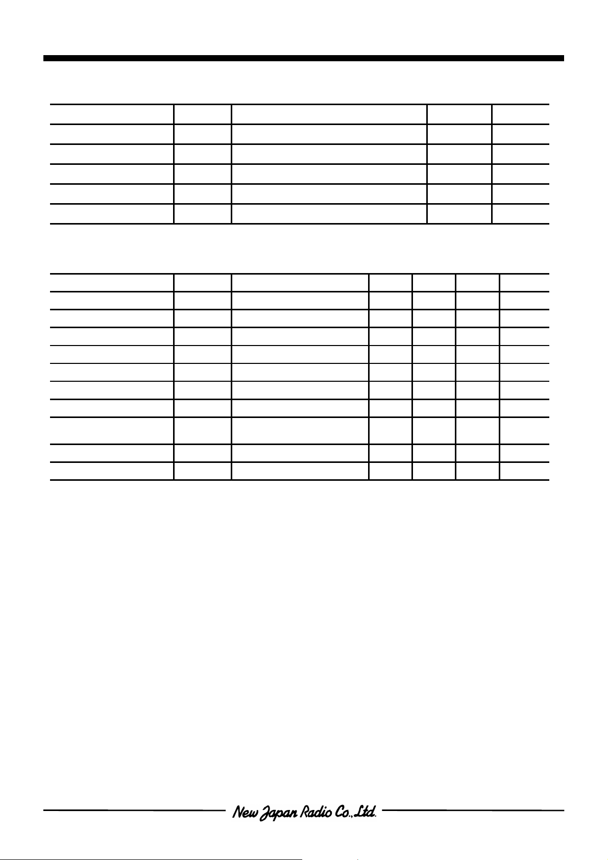
Pin Connection
SP4T SWITCH GaAs MMIC
nGENERAL DESCRIPTION nPACKAGE OUTLINE
NJG1519KC1 is a GaAs high power SP4T switch MMIC
for antenna switch of dual mode cellular phone application
such as GSM/DCS1800.
This switch is designed for an antenna switch between
an antenna and one of two Tx ports or two Rx ports to
control RF signals up to 2.5GHz.
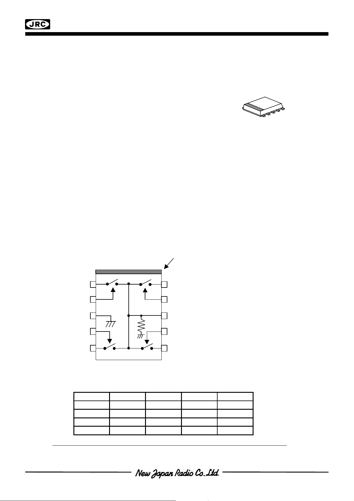
The ultra small & ultra thin FLP10 package is applied.
n
FEATURES
lLow insertion loss 0.6dB typ. @f=0.9GHz, Pin=34dBm
0.85dB typ. @f=1.9GHz, Pin=32dBm
lHigh isolation 24dB typ. @f=0.9GHz
18dB typ. @f=1.9GHz
lHigh handling power P
lLow control voltage V
=35dBm typ. @f=1.9GHz
-0.2dB
=3.0V typ.
CTL (H)
lUltra small & ultra thin package FLP10-C1 (Mount Size: 2.8x3.0x0.75mm)
NJG1519KC1
n
PIN CONFIGURATION
nTRUTH TABLE
(Top View)
1
2
3
4
5 6
CTL1
CTL2
Orientation Mark
10
1. P1
2. V
9
3. GND
4. V
8
5. P2
6. P3
7
7. V
8. PC
9. V
10. P4
CTL3
CTL1
CTL2
CTL3
CTL4
CTL4
NOTE: Please note that any information on this catalog will be subject to change.
- 1 -
NJG1519KC1
nABSOLUTE MAXIMUM RATINGS
(Ta=+25°C, Zs=Zl=50Ω)
PARAMETER SYMBOL CONDITIONS RATINGS UNITS
RF Input Power P
Operating Voltage V
Power Dissipation P
Operating Temp. T
Storage Tempe. T
n
ELECTRICAL CHARACTERISTICS
in
CTL
D
opr
stg
General Conditions: Ta=+25°C, Zs=Zl=50Ω, V
V
=0V, V
CTL(L)
V
CTL(H)-VCTL(L)
=3V 38 dBm
CTL(H)
12 V
550 mW
-40~+85 °C
-55~+125 °C
=0V, V
CTL (L)
PARAMETER SYMBOL CONDITIONS MIN TYP MAX UNITS
Control Voltage (Low) V
Control Voltage (High) V
Control Current I
CTL(L)
CTL(H)
CTL
f=0.01~2.5GHz -0.2 0 0.2 V
f=0.01~2.5GHz 2.5 3.0 6.5 V
f=0.9GHz, Pin=34dBm - 10 30 uA
Insertion loss 1 LOSS1 f=0.9GHz, Pin=34dBm - 0.6 0.8 dB
Insertion loss 2 LOSS2 f=1.9GHz, Pin=32dBm - 0.85 1.0 dB
Isolation 1 ISL1 f=0.9GHz, Pin=34dBm 22 24 - dB
Isolation 2 ISL2 f=1.9GHz, Pin=32dBm 16 18 - dB
Pin at 0.2dB
compression point
P
-0.2dB
f=1.9GHz 34 35 - dBm
VSWR VSWRion-state ports, f=1.9GHz - 1.2 1.4
CTL (H)
=3V
Switching time T
SW
f=0.1~2.5GHz - 60 100 ns
- 2 -
 Loading...