

NJG1312PC1
SPDT SWITCH DRIVER AMPLIFIRE GaAs MMIC
NJG1312PC1
FFP16 Type
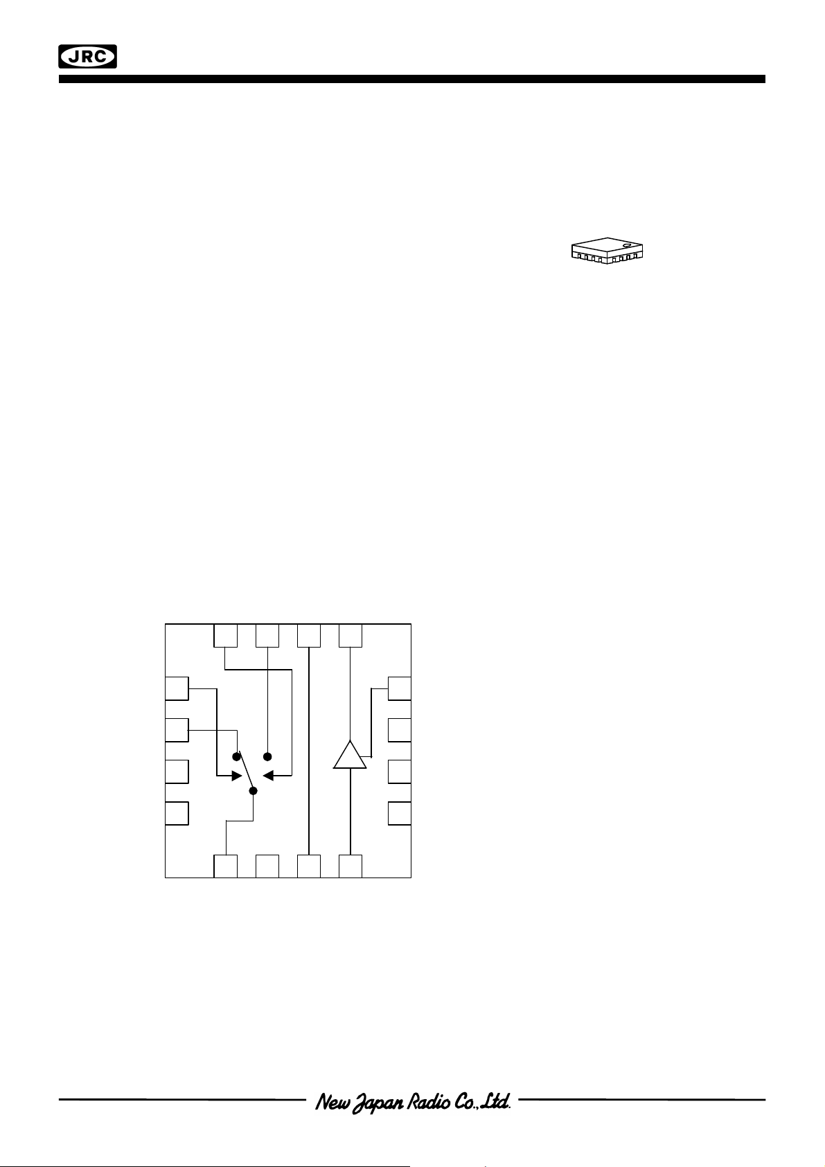
nGENERAL DESCRIPTION nPACKAGE OUTLINE
NJG1312PC1 is a GaAs MMIC mainly designed for CDMA
800MHz band cellular phone handsets.
This Ic features low current consumption and variable gain.
An ultra small & thin FFP package is adopted.
n
FEATURES
lLow supply voltage operation +2.9V typ.
lLow current consumption 17mA typ. @ P
lHigh gain 19dB typ. @ 900MHz
lPout at 1dB Gain Compression point +10dBm typ. @ 900MHz
lUltra small & thin package FFP16-C1 (Mount Size: 2.5x2.5x0.85mm)
n
PIN CONFIGURATION
=+5.6dBm
out
13
14
15
16
12
1
(Top View)
10
11
2
3 4
9
Pin Connection
8
1.PC 9.RF
out
2.GND 10.GND
7
6
3.GND 11.P2
4.RFin12. V
5.NC 13. V
6.GND 14.P1
CTR2
CTR1
7.GND 15.GND
5
8.BPC 16.GND
- 1 -
NJG1312PC1
n
ABSOLUTE MAXIMUM RATINGS
(Ta=+25°C, Zs=Zl=50Ω)
PARAMETER SYMBOL CONDITIONS RATINGS UNITS
Drain Voltage V
Control Voltage V
Input Power P
Power Dissipation P
Operating Temperature T
Storage Temperature T
n
ELECTRICAL CHARACTERISTICS
(VDD=2.9V, V
DD
CTL
in
D
opr
stg
=2.7V, f=900MHz, Ta=-20~+80°C, Zs=Zl=50Ω, Rs (External)=180Ω)
CTR
VDD=2.9V 15 dBm
6 V
6 V
400 mW
-40~+85 °C
-55~+125 °C
PARAMETER SYMBOL CONDITIONS MIN TYP MAX UNITS
Operating Frequency Freq 887 900 925 MHz
Drain Voltage V
Operating Current I
DD
DD
RF SW ON
P
=+5.6dBm
out
2.7 2.9 5.0 V
−
17 22 mA
Control Current
Control Voltage(LOW) V
Control Voltage(HIGH) V
Small Signal Gain Gain
I
CTL
CTL
CTL
(L)
(H)
RF SW ON
Pin=-15dBm
RF SW ON
Gain Flatness G
flat
Pin=-15dBm
f=887~925MHz
Gain Control Range G
Pout at 1dB Gain
Compression point
cont
P
-1dB
IN-Band Spurious1 IBS1
IN-Band Spurious2 IBS2
Pin=-15dBm -28.5 -27 -25.5 dB
RF SW ON
RF SW ON,
P
=+5.6dBm
out
OFFSET 900kHz
RF SW ON,
P
=+5.6dBm
out
OFFSET 1.98MHz
Input VSWR VSWRiRF SW ON
Output VSWR VSWRoRF SW ON
−
1.0 2.0
uA
-0.2 0 0.2 V
2.5 2.7 5.5 V
17 19 22 dB
−
−
−
−
−
−
0.5
+10
−
−
-55 -51 dBc
-73 -68 dBc
2.4 3.0
1.4 2.0
dB
dBm
Note) RF SW ON/OFF in the table above: Control voltages (V
RF SW ON P1: V
RF SW OFF P1: V
- 2 -
P2: V
P2: V
=0V, V
CTL1
=2.7V, V
CTL1
=2.7V, V
CTL1
=0V, V
CTL1
CTL2
CTL2
CTL2
CTL2
CTL1
=2.7V
=0V
=0V
=2.7V
, V
) are as follows
CTL2
NJG1312PC1
n
TERMINAL INFORMATION
No. SYMBOL DESCRIPTIONS
1 PC RF output terminal of SW.
2 GND Ground terminal.
3 GND Ground terminal.
4 RF
5 NC Neutral terminal. Should be connected to the ground.
6 GND Ground terminal.
7 GND Ground terminal.
8 BPC
9 RF
10 GND Ground terminal.
11 P2 RF input terminal 2 of SW.
12 V
13 V
14 P1 RF input terminal 1 of SW.
15 GND Ground terminal.
16 GND Ground terminal.
out
CTL2
CTL1
in
RF signal input terminal of driver amplifier.
Source electrode terminal of driver amplifier.
The operating current is chosen by a resistor connected
between this terminal and ground.
RF signal output terminal of driver amplifier.
Please use choke coil for power supply of driver amplifier at
this terminal.
Control terminal 2 of RF signal. Please see the truth table.
Control terminal 1 of RF signal. Please see the truth table.
Notice: PC terminal at pin 1 should be connected to the GND
through high resistance for pull-down (Max 560KΩ).
n
TRUTH TABLE
V
CTL1
V
CTL2
P1-PC P2-PC
0V 2.7V ON OFF
2.7V 0V OFF ON
- 3 -
 Loading...