

Page 1
UPI-C42/UPI-L42
UNIVERSAL PERIPHERAL INTERFACE
CHMOS 8-BIT SLAVE MICROCONTROLLER
Y
Pin, Software and Architecturally
Compatible with all UPI-41 and UPI-42
Products
Y
Low Voltage Operation with the UPIL42
Ð Full 3.3V Support
Y
Hardware A20 Gate Support
Y
Suspend Power Down Mode
Y
Security Bit Code Protection Support
Y
8-Bit CPU plus ROM/OTP EPROM, RAM,
I/O, Timer/Counter and Clock in a
Single Package
Y
4096 x 8 ROM/OTP, 256 x 8 RAM 8-Bit
Timer/Counter, 18 Programmable I/O
Pins
Y
DMA, Interrupt, or Polled Operation
Supported
The UPI-C42 is an enhanced CHMOS version of the industry standard Intel UPI-42 family. It is fabricated on
Intel’s CHMOS III-E process. The UPI-C42 is pin, software, and architecturally compatible with the NMOS UPI
family. The UPI-C42 has all of the same features of the NMOS family plus a larger user programmable memory
array (4K), hardware A20 gate support, and lower power consumption inherent to a CHMOS product.
The UPI-L42 offers the same functionality and socket compatibility as the UPI-C42 as well as providing low
voltage 3.3V operation.
The UPI-C42 is essentially a ‘‘slave’’ microcontroller, or a microcontroller with a slave interface included on the
chip. Interface registers are included to enable the UPI device to function as a slave peripheral controller in the
MCS Modules and iAPX family, as well as other 8-, 16-, and 32-bit systems.
To allow full user flexibility, the program memory is available in ROM and One-Time Programmable EPROM
(OTP).
Y
One 8-Bit Status and Two Data
Registers for Asynchronous Slave-toMaster Interface
Y
Fully Compatible with all Intel and Most
Other Microprocessor Families
Y
Interchangeable ROM and OTP EPROM
Versions
Y
Expandable I/O
Y
Sync Mode Available
Y
Over 90 Instructions: 70% Single Byte
Y
Quick Pulse Programming Algorithm
Ð Fast OTP Programming
Y
Available in 40-Lead Plastic, 44-Lead
Plastic Leaded Chip Carrier, and
44-Lead Quad Flat Pack Packages
(See Packaging Spec., OrderÝ240800, Package Type P, N,
and S)
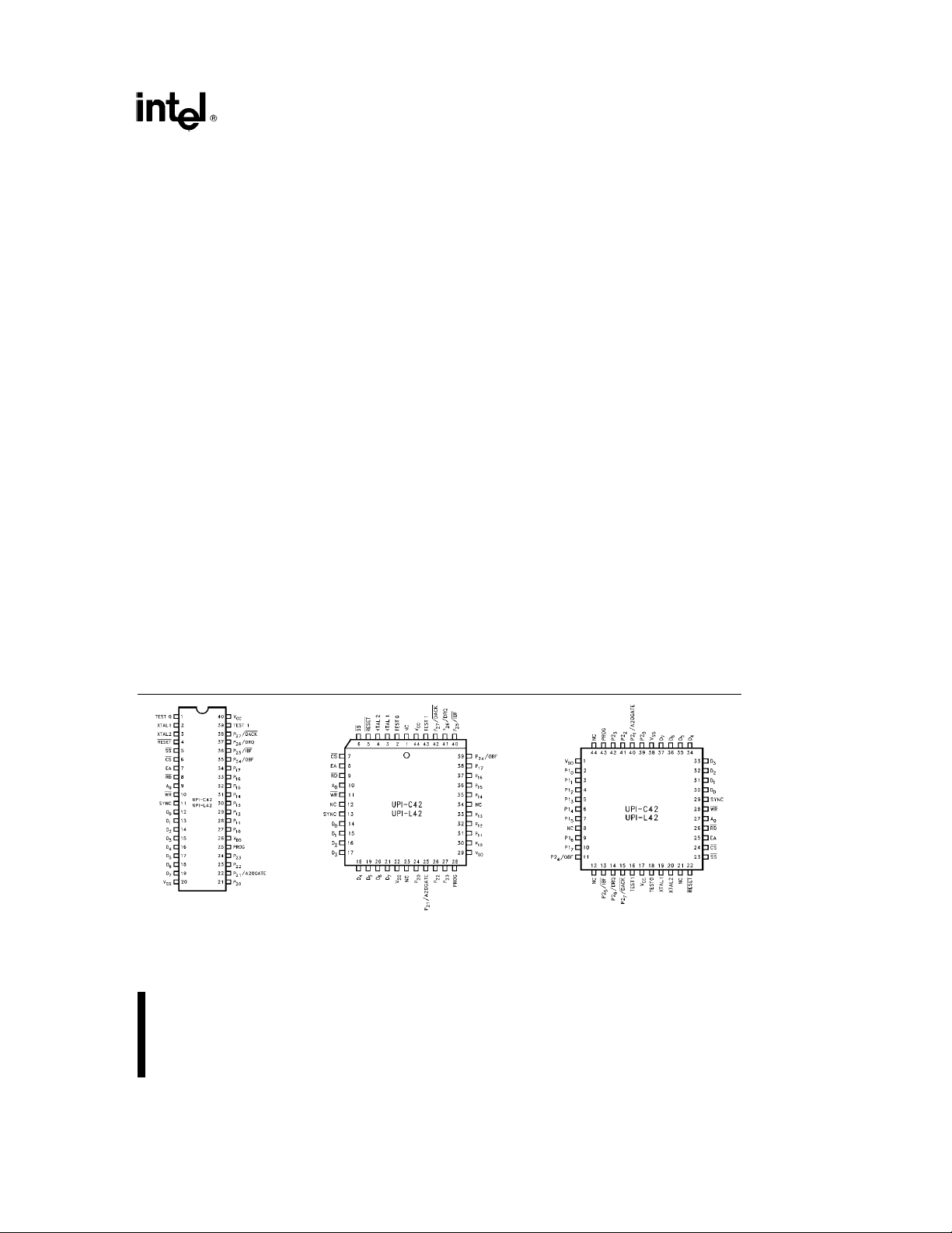
Figure 1. DIP Pin
Configuration
*Other brands and names are the property of their respective owners.
Information in this document is provided in connection with Intel products. Intel assumes no liability whatsoever, including infringement of any patent or
copyright, for sale and use of Intel products except as provided in Intel’s Terms and Conditions of Sale for such products. Intel retains the right to make
changes to these specifications at any time, without notice. Microcomputer Products may have minor variations to this specification known as errata.
290414– 1
Figure 2. PLCC Pin Configuration
290414– 2
December 1995COPYRIGHT©INTEL CORPORATION, 1996 Order Number: 290414-003
Figure 3. QFP Pin Configuration
290414– 3
Page 2
UPI-C42/UPI-L42
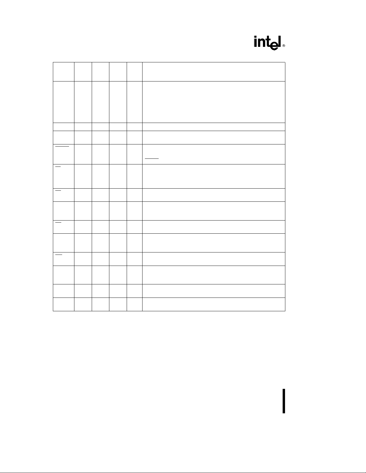
Table 1. Pin Description
Symbol Pin Pin Pin Type Name and Function
TEST 0, 1 2 18 I TEST INPUTS: Input pins which can be directly tested using conditional
TEST 1 39 43 16
XTAL 1 2 3 19 O OUTPUT: Output from the oscillator amplifier.
XTAL 2 3 4 20 I INPUT: Input to the oscillator amplifier and internal clock generator
RESET 4 5 22 I RESET: Input used to reset status flip-flops, set the program counter to
SS 5 6 23 I SINGLE STEP: Single step input used in conjunction with the SYNC output
CS 6 7 24 I CHIP SELECT: Chip select input used to select one UPI microcomputer
EA 7 8 25 I EXTERNAL ACCESS: External access input which allows emulation,
RD 8 9 26 I READ: I/O read input which enables the master CPU to read data and
A
0
WR 10 11 28 I WRITE: I/O write input which enables the master CPU to write data and
SYNC 11 13 29 O OUTPUT CLOCK: Output signal which occurs once per UPI instruction
D0–D
(BUS)
P10–P1727–34 30–33 2–10 I/O PORT 1: 8-bit, PORT 1 quasi-bidirectional I/O lines. P10–P17access the
DIP PLCC QFP
No. No. No.
branch instructions.
FREQUENCY REFERENCE: TEST 1 (T
input (under software control). TEST 0 (T
during PROM programming and ROM/EPROM verification, during Sync
) functions as the event timer
1
) is a multi-function pin used
0
Mode to reset the instruction state to S1 and synchronize the internal clock
to PH1.
circuits.
zero, and force the UPI-C42 from the suspend power down mode.
is also used during EPROM programming and verification.
RESET
to step the program through each instruction (EPROM). This should be tied
a
5V when not used. This pin is also used to put the device in Sync
to
Mode by applying 12.5V to it.
out of several connected to a common data bus.
testing and ROM/EPROM verification. This pin should be tied low if
unused.
status words from the OUTPUT DATA BUS BUFFER or status register.
91027ICOMMAND/DATA SELECT: Address Input used by the master processor
e
to indicate whether byte transfer is data (A
e
(A
0
1, F1 is set). A
e
0 during program and verify operations.
0
0, F1 is reset) or command
0
command words to the UPI INPUT DATA BUS BUFFER.
cycle. SYNC can be used as a strobe for external circuitry; it is also used to
synchronize single step operation.
12–19 14–21 30–37 I/O DATA BUS: Three-state, bidirectional DATA BUS BUFFER lines used to
7
35–38
interface the UPI microcomputer to an 8-bit master system data bus.
signature row and security bit.
2
Page 3
UPI-C42/UPI-L42
Table 1. Pin Description (Continued)
Symbol Pin Pin Pin Type Name and Function
P20–P2721–24 24–27 39–42 I/O PORT 2: 8-bit, PORT 2 quasi-bidirectional I/O lines. The lower 4 bits
PROG 25 28 43 I/O PROGRAM: Multifunction pin used as the program pulse input during
V
CC
V
DD
V
SS
DIP PLCC QFP
No. No. No.
) interface directly to the 8243 I/O expander device and
35–38 39–42 11,13–15
(P
20–P23
contain address and data information during PORT 4 – 7 access. P
can be programmed to provide hardware A20 gate support. The upper
4 bits (P24–P27) can be programmed to provide interrupt Request and
DMA Handshake capability. Software control can configure P
Output Buffer Full (OBF) interrupt, P
interrupt, P
(DACK
as DMA Request (DRQ), and P27as DMA ACKnowledge
26
).
as Input Buffer Full (IBF)
25
24
PROM programming.
During I/O expander access the PROG pin acts as an address/data
strobe to the 8243. This pin should be tied high if unused.
40 44 17 POWER:a5V main power supply pin.
26 29 1 POWER:a5V during normal operation.a12.75V during programming
operation. Low power standby supply pin.
20 22 38 GROUND: Circuit ground potential.
21
as
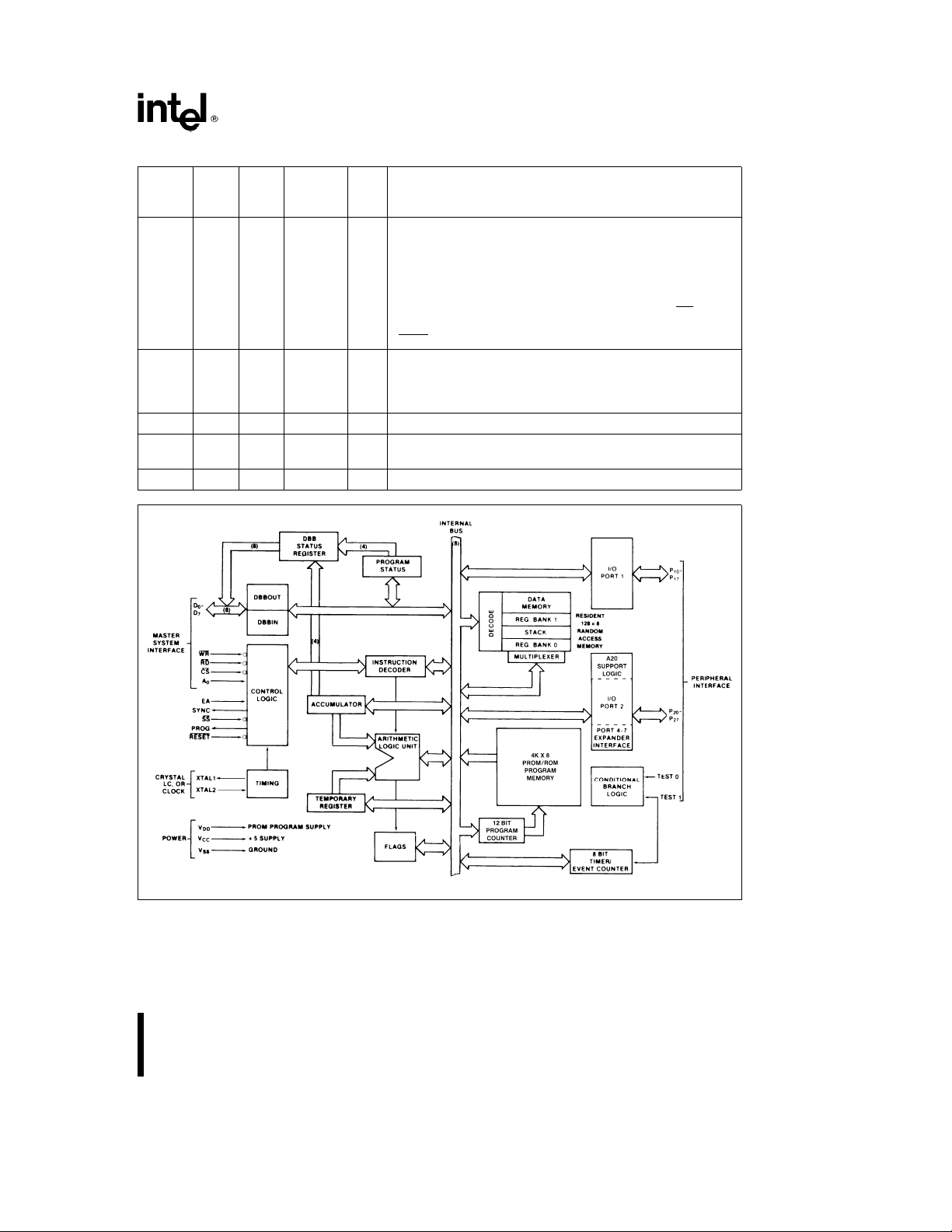
Figure 4. Block Diagram
290414– 4
3
Page 4
UPI-C42/UPI-L42
UPI-C42/L42 PRODUCT SELECTION GUIDE
UPI-C42: Low power CHMOS version of the UPI-42.
Device Package ROM OTP Comments
80C42 N, P S 4K ROM Device
82C42PC N, P, S Phoenix MultiKey/42 firmware, PS/2 style mouse support
82C42PD N, P, S Phoenix MultiKey/42L firmware, KBC and SCC for portable apps.
82C42PE N, P, S Phoenix MultiKey/42G firmware, Energy Efficient KBC solution
87C42 N, P, S 4K One Time Programmable Version
UPI-L42: The low voltage 3.3V version of the UPI-C42.
Device Package ROM OTP Comments
80L42 N, P S 4K ROM Device
82L42PC N, P, S Phoenix MultiKey/42 firmware, PS/2 style mouse support
82L42PD N, P, S Phoenix MultiKey/42L firmware, KBC and SCC for portable apps.
87L42 N, P, S 4K One Time Programmable Version
Ne44 lead PLCC, Pe40 lead PDIP, Se44 lead QFP, De40 lead CERDIP
e
Key Board Control, SCCeScan Code Control
KBC
THE INTEL 82C42
As shown in the UPI-C42 product matrix, the UPIC42 is offered as a pre-programmed 80C42 with various versions of MultiKey/42 keyboard controller
firmware developed by Phoenix Technologies Ltd.
The 82C42PC provides a low powered solution for
industry standard keyboard and PS/2 style mouse
control. The 82C42PD provides a cost effective
means for keyboard and scan code control for notebook platforms. The 82C42PE allows a quick time to
market, low cost solution for energy efficient desktop designs.
4
Page 5
UPI-C42/UPI-L42
UPI-42 COMPATIBLE FEATURES
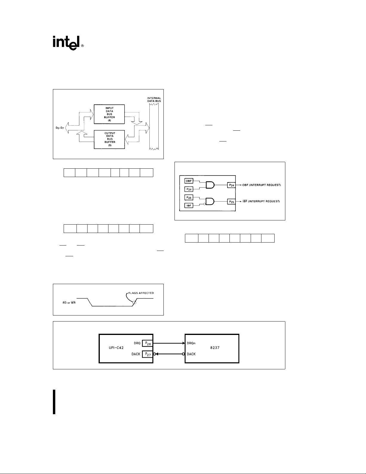
1. Two Data Bus Buffers, one for input and one for
output. This allows a much cleaner Master/Slave
protocol.
290414– 5
2. 8 Bits of Status
ST7ST6ST5ST4F1F0IBF OBF
D7D6D5D4D3D2D1D
ST4–ST7are user definable status bits. These
bits are defined by the ‘‘MOV STS, A’’ single
byte, single cycle instruction. Bits 4 – 7 of the
acccumulator are moved to bits 4–7 of the status
register. Bits 0 – 3 of the status register are not
affected.
MOV STS, A Op Code: 90H
1 001000 0
D
7
3. RD and WR are edge triggered. IBF, OBF, F1and
INT change internally after the trailing edge of RD
or WR.
During the time that the host CPU is reading the
status register, the UPI is prevented from updating this register or is ‘locked out.’
0
D
0
290414– 6
4. P24and P25are port pins or Buffer Flag pins
which can be used to interrupt a master processor. These pins default to port pins on Reset.
If the ‘‘EN FLAGS’’ instruction has been executed, P
pin. A ‘‘1’’ written to P
pin outputs the OBF Status Bit). A ‘‘0’’ written to
P
This pin can be used to indicate that valid data is
becomes the OBF (Output Buffer Full)
24
disables the OBF pin (the pin remains low).
24
enables the OBF pin (the
24
available from the UPI (in Output Data Bus Buffer).
If ‘‘EN FLAGS’’ has been executed, P
comes the IBF
ten to P
the inverse of the IBF Status Bit. A ‘‘0’’ written to
disables the IBF pin (the pin remains low).
P
25
This pin can be used to indicate that the UPI is
(Input Buffer Full) pin. A ‘‘1’’ writ-
enables the IBF pin (the pin outputs
25
be-
25
ready for data.
Data Bus Buffer Interrupt Capability
290414– 7
EN FLAGS Op Code: 0F5H
1 111010 1
D
7
D
0
5. P26and P27are port pins or DMA handshake
pins for use with a DMA controller. These pins
default to port pins on Reset.
If the ‘‘EN DMA’’ instruction has been executed,
P
becomes the DRQ (DMA Request) pin. A ‘‘1’’
26
written to P
activated). DRQ is deactivated by DACK
DACK
#
causes a DMA request (DRQ is
26
#
RD,
WR, or execution of the ‘‘EN DMA’’ in-
struction.
DMA Handshake Capability
290414– 8
5
Page 6
UPI-C42/UPI-L42
If ‘‘EN DMA’’ has been executed, P27becomes
the DACK
as a chip select input for the Data Bus Buffer
registers during DMA transfers.
EN DMA Op Code: 0E5H
6. When EA is enabled on the UPI, the program
counter is placed on Port 1 and the lower four
bits of Port 2 (MSB
UPI this information is multiplexed with PORT
DATA (see port timing diagrams at end of this
data sheet).
7. The UPI-C42 supports the Quick Pulse Programming Algorithm, but can also be programmed
with the Intelligent Programming Algorithm. (See
the Programming Section.)
(DMA ACKnowledge) pin. This pin acts
1 110010 1
D
7
e
P23, LSBeP10). On the
D
0
UPI-C42 FEATURES
Programmable Memory Size Increase
The user programmable memory on the UPI-C42 will
be increased from the 2K available in the NMOS
product by 2X to 4K. The larger user programmable
memory array will allow the user to develop more
complex peripheral control micro-code. P2.3 (port 2
bit 3) has been designated as the extra address pin
required to support the programming of the extra 2K
of user programmable memory.
The new instruction SEL PMB1 (73h) allows for access to the upper 2K bank (locations 2048– 4095).
The additional memory is completely transparent to
users not wishing to take advantage of the extra
memory space. No new commands are required to
access the lower 2K bytes. The SEL PMB0 (63h)
has also been added to the UPI-C42 instruction set
to allow for switching between memory banks.
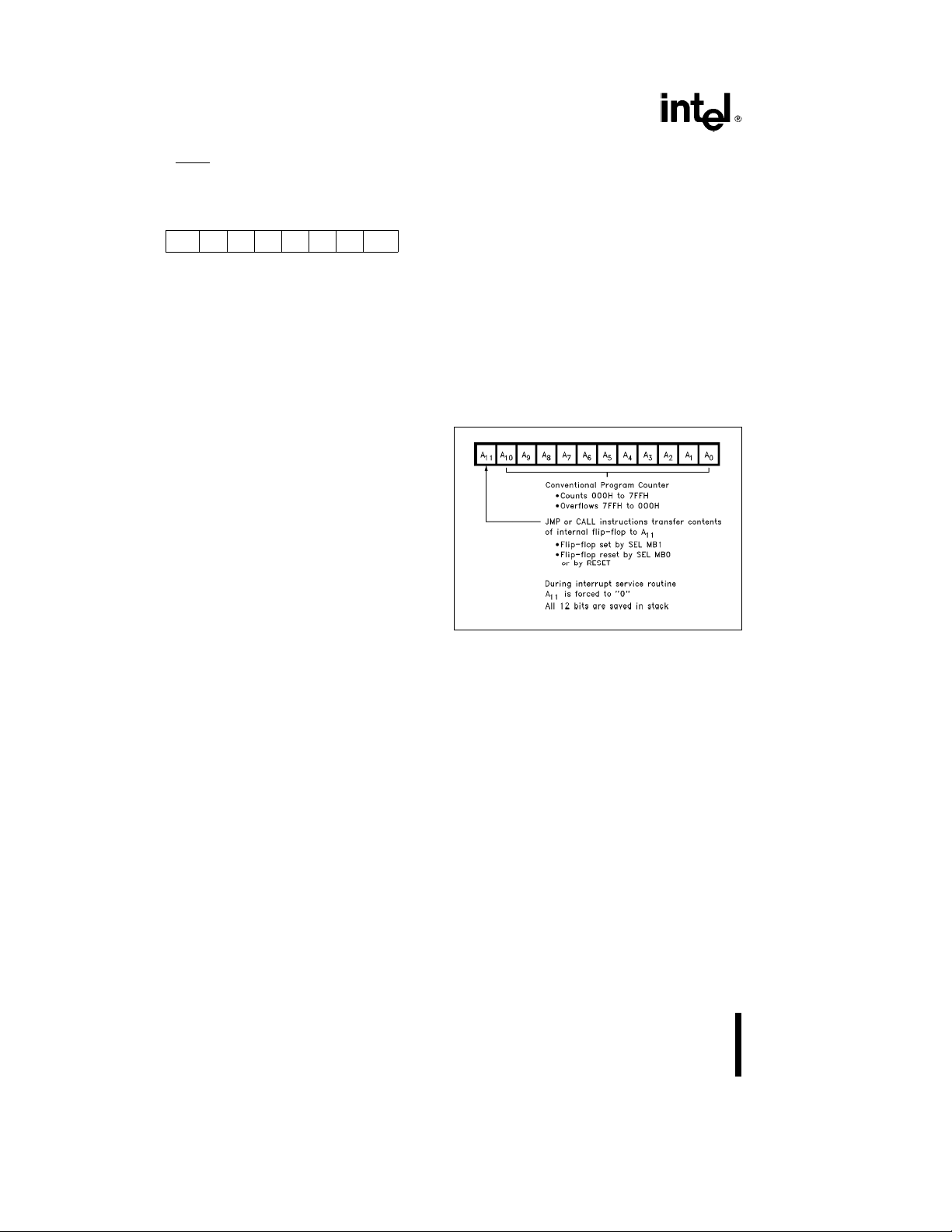
Extended Memory Program
Addressing (Beyond 2K)
For programs of 2K words or less, the UPI-C42 addresses program memory in the conventional manner. Addresses beyond 2047 can be reached by executing a program memory bank switch instruction
(SEL PMB0, SEL PMB1) followed by a branch instruction (JMP or CALL). The bank switch feature
extends the range of branch instructions beyond
their normal 2K range and at the same time prevents
the user from inadvertently crossing the 2K boundary.
PROGRAM MEMORY BANK SWITCH
The switching of 2K program memory banks is accomplished by directly setting or resetting the most
significant bit of the program counter (bit 11); see
Figure 5. Bit 11 is not altered by normal incrementing of the program counter, but is loaded with the
contents of a special flip-flop each time a JMP or
CALL instruction is executed. This special flip-flop is
set by executing an SEL PMB1 instruction and reset
by SEL PMB0. Therefore, the SEL PMB instruction
may be executed at any time prior to the actual bank
switch which occurs during the next branch instruction encountered. Since all twelve bits of the program counter, including bit 11, are stored in the
stack, when a Call is executed, the user may jump to
subroutines across the 2K boundary and the proper
PC will be restored upon return. However, the bank
switch flip-flop will not be altered on return.
290414– 30
Figure 5. Program Counter
INTERRUPT ROUTINES
Interrupts always vector the program counter to location 3 or 7 in the first 2K bank, and bit 11 of the
program counter is held at ‘‘0’’ during the interrupt
service routine. The end of the service routine is signaled by the execution of an RETR instruction. Interrupt service routines should therefore be contained
entirely in the lower 2K words of program memory.
The execution of a SEL PMB0 or SEL PMB1 instruction within an interrupt routine is not recommended
since it will not alter PC11 while in the routine, but
will change the internal flip-flop.
Hardware A20 Gate Support
This feature has been provided to enhance the performance of the UPI-C42 when being used in a keyboard controller application. The UPI-C42 design
has included on chip logic to support a hardware
GATEA20 feature which eliminates the need to provide firmware to process A20 command sequences,
6
Page 7
UPI-C42/UPI-L42
thereby providing additional user programmable
memory space. This feature is enabled by the
A20EN instruction and remains enabled until the device is reset. It is important to note that the execution of the A20EN instruction redefines Port 2, bit 1
as a pure output pin with read only characteristics.
The state of this pin can be modified only through a
valid ‘‘D1’’ command sequence (see Table 1). Once
enabled, the A20 logic will process a ‘‘D1’’ command sequence (write to output port) by setting/resetting the A20 bit on port 2, bit 1 (P2.1) without
requiring service from the internal CPU. The host
can directly control the status of the A20 bit. At no
time during this host interface transaction will the
IBF flag in the status register be activated. Table 1
gives several possible GATEA20 command/data sequences and UPI-C42 responses.
Table 1. D1 Command Sequences
A0 R/W DB Pins IBF A20 Comments
1 W D1h 0 n
0 W DFh 0 1 Only DB1 Is Processed
1 W FFH
1 W D1h 0 n Clear A20 Sequence
0 W DDh 0 0
1 W FFh 0 n
1 W D1h 0 n Double Trigger Set
1 W D1h 0 n Sequence
0 W DFh 0 1
1 W FFh 0 n
1 W D1h 0 n Invalid Sequence
1 W XXh
0 W DDh 1 n of A20 Bit
(2)
(3)
(1)
Set A20 Sequence
0n
1 n No Change in State
SUSPEND
The execution of the suspend instruction (82h or
E2h) causes the UPI-C42 to enter the suspend
mode. In this mode of operation the oscillator is not
running and the internal CPU operation is stopped.
The UPI-C42 consumes
mode. This mode can only be exited by RESET.
CPU operation will begin from PC
s
40 mA in the suspend
e
000h when the
UPI-C42 exits from the suspend power down mode.
Suspend Mode Summary
Oscillator Not Running
#
CPU Operation Stopped
#
Ports Tristated with Weak (E2–10 mA) Pull-Up
#
Micropower Mode (I
#
This mode is exited by RESET
#
CC
s
40 mA)
NOTES:
1. Indicates that P2.1 remains at the previous logic level.
2. Only FFh commands in a valid A20 sequence have no
effect on IBF. An FFh issued at any other time will activate
IBF.
3. Any command except D1.
The above sequences assume that the GATEA20
logic has been enabled via the A20EN instruction.
As noted, only the value on DB 1 (data bus, bit 1) is
processed. This bit will be directly passed through to
P2.1 (port 2, bit 1).
7
Page 8
UPI-C42/UPI-L42
Table 2 covers all suspend mode pin states. In addition to the suspend power down mode, the UPI-C42
will also support the NMOS power down mode as
outlined in Chapter 4 of the UPI-42AH users manual.
Table 2. Suspend Mode Pin States
Pins Suspend
Ports 1 and 2
Outputs Tristate
Inputs Weak Pull-Up
Disabled
(1)
DBB
Outputs Normal
Inputs Normal
System Control Disabled
Ý
(RD
,WRÝ,
Ý
, A0)
CS
Ý
Reset
Enabled
Crystal Osc. Disabled
(XTAL1, XTAL2)
Test 0, Test 1 Disabled
Prog High
Sync High
EA Disabled,
No Pull-Up
Ý
SS
Disabled,
Weak Pull-Up
I
CC
NOTES:
1. DBB outputs are Tristate unless CS
tive. DBB inputs are disabled unless CS
active.
2. A ‘‘disabled’’ input will not cause current to be drawn
regardless of input level (within the supply range).
3. Weak pull-ups have current capability of typically 5 mA.
k
40 mA
Ý
and RDÝare ac-
Ý
and WRÝare
NEW UPI-C42 INSTRUCTIONS
The UPI-C42 will support several new instructions to
allow for the use of new C42 features. These instructions are not necessary to the user who does
not wish to take advantage of any new C42 functionality. The C42 will be completely compatible with all
current NMOS code/applications. In order to use
new features, however, some code modifications will
be necessary. All new instructions can easily be inserted into existing code by use of the ASM-48 macro facility as shown in the following example:
Macname MACRO
DB 63H
ENDM
New Instructions
The following is a list of additions to the UPI-42 instruction set. These instructions apply only to the
UPI-C42. These instructions must be added to existing code in order to use any new functionality.
SEL PMB0 Select Program Memory Bank 0
OPCODE 0110 0011 (63h)
PC Bit 11 is set to zero on next JMP or CALL instruction. All references to program memory fall within
the range of 0– 2047 (0 – 7FFh).
SEL PMB1 Select Program Memory Bank 1
OPCODE 0111 0011 (73h)
PC Bit 11 is set to one on next JMP or CALL instruction. All references to program memory fall within
the range of 2048– 4095 (800h – FFFh).
ENA20 Enables Auto A20 hardware
OPCODE 0011 0011 (33h)
Enables on chip logic to support Hardware A20 Gate
feature. Will remain enabled until device is reset.
8
Page 9

UPI-C42/UPI-L42
This circuitry gives the host direct control of port 2
bit 1 (P2.1) without intervention by the internal CPU.
When this opcode is executed, P2.1 becomes a dedicated output pin. The status of this pin is read-able
but can only be altered through a valid ‘‘D1’’ command sequence (see Table 1).
SUSPEND Invoke Suspend Power Down Mode
OPCODE 1000 0010 (82h) or 1110 0010
(E2h)
Enables device to enter micro power mode. In this
mode the external oscillator is off, CPU operation is
stopped, and the Port pins are tristated. This mode
can only be exited via a RESET signal.
PROGRAMMING AND VERIFYING THE
UPI-C42
The UPI-C42 programming will differ from the NMOS
device in three ways. First, the C42 will have a 4K
user programmable array. The UPI-C42 will also be
programmed using the Intel Quick-Pulse Programming Algorithm. Finally, port 2 bit three (P2.3) will be
used during program as the extra address pin required to program the upper 2K bank of additional
memory. None of these differences have any effect
on the full CHMOS to NMOS device compatibility.
The extra memory is fully transparent to the user
who does not need, or want, to use the extra memory space of the UPI-C42.
In brief, the programming process consists of: activating the program mode, applying an address,
latching the address, applying data, and applying a
programming pulse. Each word is programmed completely before moving on to the next and is followed
by a verification step. The following is a list of the
pins used for programming and a description of their
functions:
Pin Function
XTAL 2 Clock Input
Reset Initialization and Address Latching
Test 0 Selection of Program or Verify Mode
EA Activation of Program/Verify Signature
Row/Security Bit Modes
BUS Address and Data Input
Data Output During Verify
P
20–23
V
DD
Address Input
Programming Power Supply
PROG Program Pulse Input
WARNING
An attempt to program a missocketed UPI-C42 will result in
severe damage to the part. An indication of a properly
socketed part is the appearance of the SYNC clock output.
The lack of this clock may be used to disable the programmer.
The Program/Verify sequence is:
1. Insert 87C42 in programming socket
e
2. CS
5V, V
e
0V, TEST 0e5V, clock applied or inter-
A
0
nal oscillator operating, BUS floating, PROG
CC
e
5V, V
e
5V, RESETe0V,
DD
5V.
3. TEST 0e0V (select program mode)
4. EAe12.75V (active program mode)
e
5. V
6. V
7. Address applied to BUS and P
6.25V (programming supply)
CC
e
12.75V (programming power)
DD
20–23
8. RESETe5V (latch address)
9. Data applied to BUS
10. PROGe5V followed by one 100 ms pulse to
0V
11. TEST 0
e
5V (verify mode)
12. Read and verify data on BUS
13. TEST 0e0V
14. RESETe0V and repeat from step 6
15. Programmer should be at conditions of step 1
when the 87C42 is removed from socket
e
Please follow the Quick-Pulse Programming flow
chart for proper programming procedure shown in
Figure 6.
9
Page 10

UPI-C42/UPI-L42
flow chart of the Quick-Pulse Programming Algorithm is shown in Figure 6.
The entire sequence of program pulses and byte
verifications is performed at V
e
12.75V. When programming has been com-
V
DD
pleted, all bytes should be compared to the original
data with V
CC
e
e
V
5V.
DD
CC
e
6.25V and
A verify should be performed on the programmed
bits to ensure that they have been correctly programmed. The verify is performed with T0e5V,
e
V
5V, EAe12.75V, SS
DD
e
0V, and CS
A0
e
Ý
5V.
e
Ý
5V, PROGe5V,
In addition to the Quick-Pulse Programming Algorithm, the UPI-C42 OPT is also compatible with Intel’s Inteligent Programming Algorithm which is used
to program the NMOS UPI-42AH OTP devices.
The entire sequence of program pulses and byte
verifications is performed at V
e
V
cycle has been completed, all bytes should be com-
12.75V. When the inteligent Programming
DD
pared to the original data with V
5V.
CC
CC
e
6.25V and
e
5.0, V
DD
e
Verify
A verify should be performed on the programmed
bits to determine that they have been correctly programmed. The verify is performed with T0
e
5V, EAe12.75V, SSe5V, PROGe5V,
V
DD
e
A0
0V, and CSe5V.
e
5V,
290414– 14
Figure 6. Quick-Pulse Programming Algorithm
Quick-Pulse Programming Algorithm
As previously stated, the UPI-C42 will be programmed using the Quick-Pulse Programming Algorithm, developed by Intel to substantially reduce the
thorughput time in production programming.
The Quick-Pulse Programming Algorithm uses initial
pulses of 100 ms followed by a byte verification to
determine when the address byte has been successfully programmed. Up to 25 100 ms pulses per
byte are provided before a failure is recognized. A
10
SECURITY BIT
The security bit is a single EPROM cell outside the
EPROM array. The user can program this bit with the
appropriate access code and the normal programming procedure, to inhibit any external access to the
EPROM contents. Thus the user’s resident program
is protected. There is no direct external access to
this bit. However, the security byte in the signature
row has the same address and can be used to
check indirectly whether the security bit has been
programmed or not. The security bit has no effect on
the signature mode, so the security byte can always
be examined.
SECURITY BIT PROGRAMMING/
VERIFICATION
Programming
a. Read the security byte of the signature mode.
Make sure it is 00H.
Page 11

UPI-C42/UPI-L42
b. Apply access code to appropriate inputs to put
the device into security mode.
c. Apply high voltage to EA and V
d. Follow the programming procedure as per the
Quick-Pulse Programming Algorithm with known
data on the databus. Not only the security bit, but
also the security byte of the signature row is programmed.
e. Verify that the security byte of the signature
mode contains the same data as appeared on
the data bus. (If DB0 – DB7
byte will contain FFH.)
f. Read two consecutive known bytes from the
EPROM array and verify that the wrong data are
retrieved in at least one verification. If the
EPROM can still be read, the security bit may
have not been fully programmed though the security byte in the signature mode has.
pins.
DD
e
high, the security
Verification
Since the security bit address overlaps the address
of the security byte of the signature mode, it can be
used to check indirectly whether the security bit has
been programmed or not. Therefore, the security bit
verification is a mere read operation of the security
byte of the signature row (0FFH
grammed; 00H
that during the security bit programming, the reading
of the security byte does not necessarily indicate
that the security bit has been successfully programmed. Thus, it is recommended that two consecutive known bytes in the EPROM array be read and
the wrong data should be read at least once, because it is highly improbable that random data coincides with the correct ones twice.
e
security bit unprogrammed). Note
e
security bit pro-
SIGNATURE MODE
The UPI-C42 has an additional 64 bytes of EPROM
available for Intel and user signatures and miscellaneous purposes. The 64 bytes are partitioned as follows:
A. Test code/checksumÐThis can accommodate
up to 25 bytes of code for testing the internal
nodes that are not testable by executing from the
external memory. The test code/checksum is
present on ROMs, and OTPs.
B. Intel signatureÐThis allows the programmer to
read from the UPI-41AH/42AH/C42 the manufacturer of the device and the exact product
name. It facilitates automatic device identification
and will be present in the ROM and OTP versions. Location 10H contains the manufacturer
code. For Intel, it is 89H. Location 11H contains
the device code.
The code is 43H and 42H for the 8042AH/80C42
and OTP 8742AH/87C42, respectively. The
code is 44H for any device with the security bit
set by Intel.
C. User signatureÐThe user signature memory is
implemented in the EPROM and consists of 2
bytes for the customer to program his own signature code (for identification purposes and quick
sorting of previously programmed materials).
D. Test signatureÐThis memory is used to store
testing information such as: test data, bin number, etc. (for use in quality and manufacturing
control).
E. Security byteÐThis byte is used to check
whether the security bit has been programmed
(see the security bit section).
F. UPI-C42 Intel SignatureÐApplies only to
CHMOS device. Location 20H contains the manufacturer code and location 21H contains the device code. The Intel UPI-C42 manufacturer’s
code is 99H. The device ID’s are 82H for the
OTP version and 83H for the ROM version. The
device ID’s are the same for the UPI-L42.
The signature mode can be accessed by setting
e
0, P11 – P17e1, and then following the pro-
P10
gramming and/or verification procedures. The location of the various address partitions are as shown in
Table 3.
SYNC MODE
The Sync Mode is provided to ease the design of
multiple controller circuits by allowing the designer
to force the device into known phase and state time.
The Sync Mode may also be utilized by automatic
test equipment (ATE) for quick, easy, and efficient
synchronizing between the tester and the DUT (device under test).
Sync Mode is enabled when SS
voltage level of
tion, T0 is raised to 5 volts at least four clock cycles
after SS
. T0 must be high for at least four X2 clock
cycles to fully reset the prescaler and time state
generators. T0 may then be brought down during
low state of X2. Two clock cycles later, with the rising edge of X2, the device enters into Time State 1,
Phase 1. SS
later after T0. RESET is allowed to go high 5 tCY (75
clocks) later for normal execution of code.
a
12 volts. To begin synchroniza-
is then brought down to 5 volts 4 clocks
pin is raised to high
11
Page 12

UPI-C42/UPI-L42
Table 3. Signature Mode Table
Address
Device No. of
Type Bytes
Test Code/Checksum 0 0FH ROM/OTP 25
16H 1EH
Intel Signature 10H 11H ROM/OTP 2
User Signature 12H 13H OTP 2
Test Signature 14H 15H ROM/OTP 2
Security Byte 1FH or 3FH ROM/OTP 2
UPI-C42 Intel Signature 20H 21H ROM/OTP 2
User Defined UPI-C42 OTP EPROM Space 22H 3EH ROM/OTP 30
ACCESS CODE
The following table summarizes the access codes required to invoke the Sync Mode, Signature Mode,
and the Security Bit, respectively. Also, the programming and verification modes are included for
comparison.
Modes Port 2 Port 1
T0 RST SS EA PROG VDDVCC0123456701230 1 234567
Programming 0 0 1 HV 1 V
Mode
Verification 0 0 1 HV 1 VCCV
Mode
Sync Mode STB 0 HV 0 X VCCVCCXXXXXXXXXXX XXXXXXXX
Signature Prog 0 0 1 HV 1 V
Mode
Security Prog 0 0 1 HV 1 V
Bit/Byte
NOTE:
e
1. a
0
High
Verify 0 0 1 HV 1 VCCV
Verify 0 0 1 HV 1 VCCV
0or1;a
1
Control Signals Data Bus
DDHVCC
0 1 1 HV STB V
111HV1V
0 1 1 HV STB V
111HV1VCCV
0 1 1 HV STB V
111HV1VCCV
e
0or1.a0mustea1.
DDHVCC
CC
CCVCC
DDHVCC
DDHVCC
CC
CC
DDHVCC
DDHVCC
CC
CC
Address Addr a0a1XXXXXX
Data In Addr
Address Addr a0a1XXXXXX
Data Out Addr
Addr. (see Sig Mode Table) 0 0 0 0 1 1 1 1 X X 1
Data In 0 0 0
Addr. (see Sig Mode Table) 0 0 0
Data Out 0 0 0
Address 0 0 0
Data In 0 0 0
Address 0 0 0
Data Out 0 0 0
Access Code
12
Page 13

SYNC MODE TIMING DIAGRAMS
Minimum Specifications
SYNC Operation Time, t
NOTE:
The rising and falling edges of T0 should occur during low state of XTAL 2 clock.
e
3.5 XTAL 2 Clock cycles. Reset Time, t
SYNC
RS
e
UPI-C42/UPI-L42
290414– 15
4tCY.
APPLICATIONS
290414– 12
Figure 7. UPI-C42 Keyboard Controller
290414– 9
Figure 8. 8088-UPI-C42 Interface
13
Page 14

UPI-C42/UPI-L42
APPLICATIONS (Continued)
290414– 10
Figure 9. 8048H-UPI-C42 Interface
14
290414– 11
Figure 10. UPI-C42-8243 Keyboard Scanner
290414– 13
Figure 11. UPI-C42 80-Column Matrix Printer Interface
Page 15

UPI-C42/UPI-L42
ABSOLUTE MAXIMUM RATINGS*
Ambient Temperature Under Bias ÀÀÀÀ0§Ctoa70§C
Storage Temperature ААААААААААb65§Ctoa150§C
Voltage on Any Pin with
Respect to GroundАААААААААААААА
Power Dissipation ААААААААААААААААААААААААА1.5 W
DC CHARACTERISTICS T
Symbol Parameter
V
V
V
V
V
V
V
V
I
IL
I
OFL
I
LI
I
LI1
I
HI
I
DD
Input Low Voltage
IL
Input High Voltage 2.0 V
IH
(Except XTAL2, RESET)
Input High Voltage 3.5 V
IH1
(XTAL2, RESET)
Output Low Voltage (D0–D7) 0.45 0.45 V I
OL
Output Low Voltage 0.45 0.45 V I
OL1
(P
10P17,P20P27
Output Low Voltage (PROG) 0.45 0.45 V I
OL2
Output High Voltage (D0–D7) 2.4 2.4 V I
OH
Output High Voltage 2.4 2.4 I
OH1
, Sync) I
(All Other Outputs) I
Input Leakage Current
(T0,T1, RD, WR, CS, A0, EA)
Output Leakage Current
(D0–D7, High Z State)
Low Input Load Current
(P
10P17,P20P27
) Min V
Low Input Load Current
(RESET, SS)
Port Sink Current
(P
10P17,P20P27
)V
VDDSupply Current 4 2.5 mA
b
0.5V toa7V
e
0§Ctoa70§C, V
A
UPI-C42 UPI-L42
Min Max Min Max
b
0.5 0.8b0.3
CC
CC
g
g
b50b
250b35
b
NOTICE: This is a production data sheet. The specifications are subject to change without notice.
*
WARNING: Stressing the device beyond the ‘‘Absolute
Maximum Ratings’’ may cause permanent damage.
These are stress ratings only. Operation beyond the
‘‘Operating Conditions’’ is not recommended and extended exposure beyond the ‘‘Operating Conditions’’
may affect device reliability.
e
ea
CC
V
DD
5Vg10%;a3.3Vg10% UPI-L42
Units Notes
a
0.8 V All Pins
2.0 V
2.0 V
10
10
40
a
0.3 V
CC
a
0.3 V
CC
I
I
I
g
10 mAV
g
10 mAV
b
175 mA Port Pins
Max V
b
40 mAV
5.0 mA
V
e
2.0 mA UPI-C42
OL
e
1.3 mA UPI-L42
OL
e
1.6 mA UPI-C42
OL
e
1 mA UPI-L42
OL
e
1.0 mA UPI-C42
OL
e
0.7 mA UPI-L42
OL
eb
OH
eb
OH
eb
OH
eb
OH
s
V
SS
a
0.45sV
SS
IN
IN
s
V
IN
IL
e
3.0V
CC
e
5.0V
IH
400 mA UPI-C42
260 mA UPI-L42
50 mA UPI-C42
25 mA UPI-L42
s
IN
e
2.4V
e
0.45V
V
CC
s
V
OUT
CC
15
Page 16

UPI-C42/UPI-L42
DC CHARACTERISTICS
e
T
0§Ctoa70§C, V
A
Symbol Parameter
a
I
I
CC
Total Supply Current:
DD
Active Mode
Suspend Mode 40 26 mA Osc. Off
IDDStandby Power Down 5 3.5 mA NMOS Compatible
Supply Current
I
IH
Input Leakage Current 100 100 mAV
(P10–P17,P20–P27)
C
IN
C
IO
NOTE:
1. Sampled, not 100% tested.
Input Capacitance 10 10 pF T
I/O Capacitance 20 20 pF T
e
ea
V
CC
DD
@
12.5 MHz 30 20 mA Typical 14 mA UPI-C42,
5Vg10%;a3.3Vg10% UPI-L42 (Continued)
UPI-C42 UPI-L42
Min Max Min Max
Units Notes
9 mA UPI-L42
Power Down Mode
e
IN
e
A
e
A
(1, 4)
V
CC
25§C
25§C
(1)
(1)
DC CHARACTERISTICSÐPROGRAMMING (UPI-C42 AND UPI-L42)
e
T
25§Cg5§C, V
A
Symbol Parameter Min Max Units
V
DDH
V
DDL
V
PH
V
PL
V
EAH
V
EAL
I
DD
I
EA
NOTES:
1. Voltages over 13V applied to pin V
must be applied to EA before V
2. V
EAH
must be applied simultaneously or before VDDand must be removed simultaneously or after VDD.
3. V
CC
4. Sampled, not 100% tested.
e
6.25Vg0.25V, V
CC
e
12.75Vg0.25V
DD
VDDProgram Voltage High Level 12.5 13 V
VDDVoltage Low Level 4.75 5.25 V
PROG Program Voltage High Level 2.0 5.5 V
PROG Voltage Low Level
b
0.5 0.8 V
Input High Voltage for EA 12.0 13.0 V
EA Voltage Low Level
b
0.5 5.25 V
VDDHigh Voltage Supply Current 50.0 mA
EA High Voltage Supply Current 1.0 mA
will permanently damage the device.
DD
and removed after V
DDH
DDL
.
(1)
(2)
(4)
16
Page 17

AC CHARACTERISTICS
e
T
0§Ctoa70§C, V
A
NOTE:
All AC Characteristics apply to both the UPI-C42 and UPI-L42
DBB READ
Symbol Parameter Min Max Units
t
AR
t
RA
t
RR
t
AD
t
RD
t
DF
DBB WRITE
Symbol Parameter Min Max Units
t
AW
t
WA
t
WW
t
DW
t
WD
e
0V, V
SS
CS, A0Setup to RD
CS, A0Hold After RD
RD Pulse Width 160 ns
CS, A0to Data Out Delay 130 ns
RDvto Data Out Delay 0 130 ns
RDuto Data Float Delay 85 ns
CS, A0Setup to WR
CS, A0Hold After WR
WR Pulse Width 160 ns
Data Setup to WR
Data Hold After WR
CC
e
ea
V
DD
5Vg10%;a3.3Vg10% for the UPI-L42
v
u
v
u
u
u
0ns
0ns
0ns
0ns
130 ns
0ns
UPI-C42/UPI-L42
17
Page 18

UPI-C42/UPI-L42
AC CHARACTERISTICS
e
T
0§Ctoa70§C, V
A
CLOCK
Symbol Parameter Min Max Units
tCYUPI-C42/UPI-L42 Cycle Time 1.2 9.20 ms
t
UPI-C42/UPI-L42 Clock Period 80 613 ns
CYC
t
PWH
t
PWL
t
R
t
F
NOTE:
e
15/f(XTAL)
1. t
CY
SS
e
0V, V
e
ea
CC
V
DD
5Vg10%;a3.3Vg10% for the UPI-L42 (Continued)
Clock High Time 30 ns
Clock Low Time 30 ns
Clock Rise Time 10 ns
Clock Fall Time 10 ns
AC CHARACTERISTICS DMA
Symbol Parameter Min Max Units
NOTE:
1. C
L
e
t
ACC
t
CAC
t
ACD
t
CRQ
150 pF.
DACK to WR or RD 0 ns
RD or WR to DACK 0 ns
DACK to Data Valid 0 130 ns
RD or WR to DRQ Cleared 110 ns
(1)
(1)
AC CHARACTERISTICS PORT 2
Symbol Parameter f(tCY)
t
CP
t
PC
t
PR
t
PF
t
DP
t
PD
t
PP
NOTES:
1. C
L
2. C
L
3. t
CY
18
e
e
e
Port Control Setup Before Falling Edge of PROG 1/15 t
Port Control Hold After Falling Edge of PROG 1/10 t
PROG to Time P2 Input Must Be Valid 8/15 t
Input Data Hold Time 0 150 ns
Output Data Setup Time 2/10 t
Output Data Hold Time 1/10 t
PROG Pulse Width 6/10 t
80 pF.
20 pF.
1.25 ms.
CY
CY
CY
(3)
b
CY
b
CY
b
CY
Min Max Units
28 55 ns
125 ns
16 650 ns
250 ns
80 45 ns
750 ns
(1)
(2)
(1)
(2)
(1)
(2)
Page 19

UPI-C42/UPI-L42
AC CHARACTERISTICSÐPROGRAMMING (UPI-C42 AND UPI-L42)
e
T
25§Cg5§C, V
A
(87C42/87L42 ONLY)
Symbol Parameter Min Max Units
t
AW
t
WA
t
DW
t
WD
t
PW
t
TW
t
WT
t
DO
t
WW
tr,t
f
t
CY
t
RE
t
OPW
t
DE
NOTES:
1. This variation is a function of the iteration counter value, X.
2. If TEST 0 is high, t
e
6.25Vg0.25V, V
CC
Address Setup Time to RESET
Address Hold Time after RESET
Data in Setup Time to PROG
Data in Hold Time after PROG
DDL
ea
5Vg0.25V, V
u
v
u
e
12.75Vg0.25V
DDH
4t
CY
u
4t
CY
4t
CY
4t
CY
Initial Program Pulse Width 95 105 ms
Test 0 Setup Time for Program Mode 4t
Test 0 Hold Time after Program Mode 4t
Test 0 to Data Out Delay 4t
RESET Pulse Width to Latch Address 4t
CY
CY
CY
CY
PROG Rise and Fall Times 0.5 100 ms
CPU Operation Cycle Time 2.5 3.75 ms
RESET Setup Time before EA
u
4t
CY
Overprogram Pulse Width 2.85 78.75 ms
EA High to VDDHigh 1t
can be triggered by RESETu.
DO
CY
(1)
AC TESTING INPUT/OUTPUT WAVEFORM
INPUT/OUTPUT
290414– 16
AC TESTING LOAD CIRCUIT
290414– 17
19
Page 20

UPI-C42/UPI-L42
DRIVING FROM AN EXTERNAL SOURCE
NOTE:
See XTAL1 Configuration Table.
LC OSCILLATOR MODE
L C NOMINAL
45 H 20 pF 5.2 MHz
120 H 20 pF 3.2 MHz
Each C Should be Approximately 20 pF, including Stray Capacitance.
290414– 18
1
e
f
2q0LC
Ê
Ca3Cpp
e
C
Ê
2
Cppj5–10 pF
Pin-to-Pin Capacitance
290414– 20
Rise and Fall Times Should Not
Exceed 10 ns. Resistors to V
are Needed to Ensure V
if TTL Circuitry is Used.
CRYSTAL OSCILLATOR MODE
C1 5 pF (STRAY 5 pF)
C2 (CRYSTAL
C3 20–30 pF INCLUDING STRAY
Crystal Series Resistance Should
be Less Than 30X at 12.5 MHz.
290414– 19
290414– 21
a
STRAY) 8 pF
IH
XTAL1 Configuration Table
XTAL1 Connection
1) to Ground
2) 10 KX Resistor
to Ground
3) Not Connected
Not recommended for CHMOS Recommended configuration for Low power configuration
designs. Causes approximately designs which will use both recommended for CHMOS only
16 mA of additional current flow NMOS and CHMOS parts. This designs to provide lowest
through the XTAL1 pin on UPI- configuration limits the additional possible power consumption.
C42 and approximately 11 mA of current through the XTAL1 pin to This configuration will not work
additional current through XTAL1 approximately 1 mA, while with the NMOS device.
on the UPI-L42. maintaining compatibility with the
NMOS device.
CC
e
3.5V
20
Page 21

WAVEFORMS
READ OPERATIONÐDATA BUS BUFFER REGISTER
WRITE OPERATIONÐDATA BUS BUFFER REGISTER
UPI-C42/UPI-L42
290414– 22
CLOCK TIMING
290414– 23
290414– 24
21
Page 22

UPI-C42/UPI-L42
WAVEFORMS (Continued)
COMBINATION PROGRAM/VERIFY MODE
NOTES:
must be held low (0V) during program/verify modes.
1. A
0
2. For V
IH,VIH1,VIL,VIL1,VDDH
3. When programming the 87C42, a 0.1 mF capacitor is required across V
transients which can damage the device.
, and V
, please consult the D.C. Characteristics Table.
DDL
290414– 25
and ground to suppress spurious voltage
DD
VERIFY MODE
NOTES:
1. PROG must float if EA is low.
2. PROG must float or
3. P
4. P
5. A
e
10–P17
e
24–P27
must be held low during programming/verify modes.
0
e
5V or must float.
5V or must float.
5V when EA is high.
22
290414– 26
Page 23

WAVEFORMS (Continued)
DMA
PORT 2
UPI-C42/UPI-L42
290414– 27
290414– 28
PORT TIMING DURING EXTERNAL ACCESS (EA)
On the Rising Edge of SYNC and EA is Enabled, Port Data is Valid and can be Strobed. On the Trailing Edge of Sync
the Program Counter Contents are Available.
290414– 29
23
Page 24

UPI-C42/UPI-L42
Table 4. UPI Instruction Set
Mnemonic Description Bytes Cycles
ACCUMULATOR
ADD A, Rr Add register to A 1 1
@
Rr Add data memory 1 1
ADD A,
Ý
data Add immediate to A 2 2
ADD A,
ADDC A, Rr Add register to A 1 1
@
ADDC A,
Ý
ADDC A,
ANL A, Rr AND register to A 1 1
@
Rr AND data memory 1 1
ANL, A
ANL A,Ýdata AND immediate to A 2 2
ORL A, Rr OR register to A 1 1
@
ORL, A,
Ý
data OR immediate to A 2 2
ORL A,
XRL A, Rr Exclusive OR regis- 1 1
@
Rr Exclusive OR data 1 1
XRL A,
Ý
data Exclusive OR imme- 2 2
XRL A,
INC A Increment A 1 1
DEC A Decrement A 1 1
CLR A Clear A 1 1
CPL A Complement A 1 1
DA A Decimal Adjust A 1 1
SWAP A Swap nibbles of A 1 1
RL A Rotate A left 1 1
RLC A Rotate A left through 1 1
RR A Rotate A right 1 1
RRC A Rotate A right 1 1
INPUT/OUTPUT
IN A, Pp Input port to A 1 2
OUTL Pp, A Output A to port 1 2
Ý
ANL Pp,
Ý
ORL Pp,
IN A, DBB Input DBB to A, 1 1
OUT DBB, A Output A to DBB, 1 1
MOV STS, A A
MOVD A, Pp Input Expander 1 2
MOVD Pp, A Output A to 1 2
ANLD Pp, A AND A to Expander 1 2
ORLD Pp, A OR A to Expander 1 2
24
to A
with carry
Rr Add data memory 1 1
to A with carry
data Add immediate 2 2
to A with carry
to A
Rr OR data memory 1 1
to A
ter to A
memory to A
diate to A
carry
through carry
data AND immediate to 2 2
port
data OR immediate to 2 2
port
clear IBF
set OBF
to Bits 4– 7 of 1 1
4–A7
Status
port to A
Expander port
port
port
Mnemonic Description Bytes Cycles
DATA MOVES
MOV A, Rr Move register to A 1 1
@
MOV A,
Rr Move data memory 1 1
to A
Ý
MOV A,
data Move immediate to A 2 2
MOV Rr, A Move A to register 1 1
MOV@Rr, A Move A to data 1 1
memory
Ý
MOV Rr,
MOV
Ý
data Move immediate to 2 2
@
Rr, Move immediate to 2 2
register
data data memory
MOV A, PSW Move PSW to A 1 1
MOV PSW, A Move A to PSW 1 1
XCH A, Rr Exchange A and 1 1
XCH A,
XCHD A,
MOVP A,
@
Rr Exchange A and 1 1
@
@
register
data memory
Rr Exchange digit of A 1 1
and register
A Move to A from 1 2
current page
MOVP3, A,@A Move to A from 1 2
page 3
TIMER/COUNTER
MOV A, T Read Timer/Counter 1 1
MOV T, A Load Timer/Counter 1 1
STRT T Start Timer 1 1
STRT CNT Start Counter 1 1
STOP TCNT Stop Timer/Counter 1 1
EN TCNTI Enable Timer/ 1 1
Counter Interrupt
DIS TCNTI Disable Timer/ 1 1
Counter Interrupt
CONTROL
*EN A20 Enable A20 Logic 1 1
EN DMA Enable DMA Hand- 1 1
shake Lines
EN I Enable IBF Interrupt 1 1
DIS I Diable IBF Inter- 1 1
rupt
EN FLAGS Enable Master 1 1
Interrupts
*SEL PMB0 Select Program 1 1
memory bank 0
*SEL PMB1 Select Program 1 1
memory bank 1
SEL RB0 Select register 1 1
bank 0
SEL RB1 Select register 1 1
bank 1
* UPI-C42/UPI-L42 Only.
Page 25

Table 4. UPI Instruction Set (Continued)
Mnemonic Description Bytes Cycles
CONTROL (Continued)
*SUSPEND Invoke Suspend Power- 1 2
down mode
NOP No Operation 1 1
REGISTERS
INC Rr Increment register 1 1
INC@Rr Increment data 1 1
memory
DEC Rr Decrement register 1 1
SUBROUTINE
CALL addr Jump to subroutine 2 2
RET Return 1 2
RETR Return and restore 1 2
status
FLAGS
CLR C Clear Carry 1 1
CPL C Complement Carry 1 1
CLR F0 Clear Flag 0 1 1
CPL F0 Complement Flag 0 1 1
CLR F1 Clear F1 Flag 1 1
CPL F1 Complement F1 Flag 1 1
*UPI-C42/UPI-L42 Only.
REVISION SUMMARY
The following has been changed since Revision
-003:
1. Delete all references to standby power down
mode.
UPI-C42/UPI-L42
Mnemonic Description Bytes Cycles
BRANCH
JMP addr Jump unconditional 2 2
@
A Jump indirect 1 2
JMPP
DJNZ Rr, addr Decrement register 2 2
JC addr Jump on Carry
JNC addr Jump on Carrye02 2
JZ addr Jump on A Zero 2 2
JNZ addr Jump on A not Zero 2 2
JT0 addr Jump on T0
JNT0 addr Jump on T0
JT1 addr Jump on T1
JNT1 addr Jump on T1
JF0 addr Jump on F0 Flag
JF1 addr Jump on F1 Flage12 2
JTF addr Jump on Timer Flag 2 2
JNIBF addr Jump on IBF Flag 2 2
JOBF addr Jump on OBF Flag 2 2
JBb addr Jump on Accumula- 2 2
and jump
e
1, Clear Flag
e
0
e
1
for Bit
e
12 2
e
122
e
022
e
122
e
022
e
12 2
The following has been changed since Revision
-002:
1. Added information on keyboard controller product family.
2. Added I
specification for the UPI-L42.
HI
The following has been changed since Revision
-001:
1. Added UPI-L42 references and specification.
25
 Loading...