

Page 1
查询STEL-2176供应商
STEL-2176
User Manual
STel-MAN-97709
STEL-2176
Digital Mod/Demod ASIC
16/64/256 QAM Receiver
with FEC
QPSK/16 QAM Transmitter
with FEC
R
Page 2

TRADEMARKS
Stanford Telecom and STEL are registered trademarks of Stanford Telecommunications, Incorporated.
STEL-2176 User Manual
Page 3

FOREWORD
The Telecom Component Products Division of Stanford Telecommunications, Inc., is pleased to provide its
customers with this copy of the STEL 2176 User Manual.
This User Manual contains product information for the STEL 2176 and is being provided to assist our customers in
understanding the advantages to be gained by integrating both the receiver and transmitter functions as an integral
portion of their cable modem chip.
Recipients of this User Manual should note that the content contained here-in is subject to change. The content of
this User Manual will be updated to reflect the latest technical data, without notice to the recipients of this
document.
User Manual STEL-2176
Page 4
Supported Modes of Operation:
Downstream
FEC 16 QAM 64 QAM 256 QAM
Annex A X X
Annex B X X
Annex C X X
Upstream
STD BPSK QPSK 16 QAM
MCNS X X
ERRATA for STEL-2176
DAVIC X X
STEL-2176 User Manual
Page 5

TABLE OF C ON TENTS
PARAGRAPH PAGE
KEY FEATURES..................................................................................................................................... 1
RECEIVER........................................................................................................................................... 1
TRANSMITTER................................................................................................................................... 1
INTRODUCTION .................................................................................................................................. 2
RECEIVER OVERVIEW........................................................................................................................ 2
TRANSMITTER OVERVIEW................................................................................................................ 2
MECHANICAL SPECIFICATIONS ........................................................................................................ 3
208-PIN SQFP PACKAGE..................................................................................................................... 3
ELECTRICAL SPECIFICATIONS........................................................................................................ 8
RECEIVER ............................................................................................................................................. 10
OVERVIEW......................................................................................................................................... 10
FUNCTIONAL BLOCKS ...................................................................................................................... 11
ADC.............................................................................................................................................. 11
Microcontroller Interface................................................................................................................. 11
Master Receive Clock Generator...................................................................................................... 12
QAM Demodulator Blocks.............................................................................................................. 13
FEC Decoder Blocks ....................................................................................................................... 14
RECEIVE AND UNIVERSAL REGISTER DESCRIPTIONS .................................................................... 20
PROGRAMMING THE 2176 RECEIVE FUNCTIONS ............................................................................. 20
REGISTER DESCRIPTIONS.................................................................................................................. 20
Bank 0 - Universal Registers (Group 1)............................................................................................. 20
Bank 0 - QAM Demodulator Registers Universal Registers (Group 2) ................................................ 22
Bank 1 - FEC Registers (Group 3)..................................................................................................... 30
TIMING................................................................................................................................................. 35
NO GAP, PARALLEL MODE ............................................................................................................... 35
NO GAP, SERIAL MODE..................................................................................................................... 35
GAPS, PARALLEL MODE.................................................................................................................... 35
GAPS, SERIAL MODE ......................................................................................................................... 35
TRANSMITTER..................................................................................................................................... 39
INTRODUCTION ................................................................................................................................39
FUNCTIONAL BLOCK DIAGRAM DESCRIPTIONS ............................................................................. 39
DATA PATH DESCRIPTION ............................................................................................................... 39
Bit SYNC Block .............................................................................................................................. 39
Bit Encoder Block ........................................................................................................................... 41
Symbol Mapper Block..................................................................................................................... 45
Nyquist FIR Filter........................................................................................................................... 50
Interpolating Filter ......................................................................................................................... 50
Modulator ..................................................................................................................................... 51
10-Bit DAC..................................................................................................................................... 52
User Manual i STEL-2176
Page 6

TABLE OF C ON TENTS
PARAGRAPH PAGE
CONTROL UNIT DESCRIPTION.......................................................................................................... 52
Bus Interface Unit ........................................................................................................................... 52
Master Transmit Clock Generator .................................................................................................... 52
Clock Generator ............................................................................................................................. 53
NCO.............................................................................................................................................. 53
TRANSMIT REGISTER DESCRIPTIONS................................................................................................ 54
Programming the 2176 Transmit and Receive Functions.................................................................... 54
Block 2, Upstream Registers (Group 4) ............................................................................................. 54
TIMING DIAGRAMS ............................................................................................................................ 57
BURST TIMING EXAMPLES ................................................................................................................. 65
RECOMMENDED INTERFACE CIRCUITS ............................................................................................ 70
STEL-2176 ii User Manual
Page 7

LIST OF FIGU RES
FIGURE PAGE
1 Reference A/D Wiring............................................................................................... 7
2 Example Output Load Schematic................................................................................ 7
3 STEL-2176 Receiver Block Diagram ............................................................................ 11
4 Master Receive Clock Generator................................................................................. 12
5 QAM Demodulator Blocks......................................................................................... 13
6 ITU-T (J.83) Annex A FEC Subsystem ......................................................................... 14
7 16 QAM Constellation ............................................................................................... 15
8 64 QAM Constellation ............................................................................................... 15
9 256 QAM Constellation (DAVIC)................................................................................ 15
10 256 QAM Constellation (DVB/IEEE 802.14) ................................................................ 15
11 Demapper................................................................................................................. 15
12 De-Interleaver........................................................................................................... 16
13 ITU-T (J.83) Annex B FEC Subsystem.......................................................................... 16
14 Trellis Coded Demodulator........................................................................................ 17
15 64 QAM Mapping ..................................................................................................... 17
16 256 QAM Mapping.................................................................................................... 18
17 Derandomizer........................................................................................................... 19
18 De-Interleaver........................................................................................................... 19
19. Downstream Output Timing (Parallel Data Output) .................................................... 36
20. Downstream Output Timing (Serial Output)............................................................... 36
21. Downstream Output Timing (Parallel Data Output) .................................................... 37
22. Downstream Output Timing (Parallel Data Output) .................................................... 38
23. De-Interleaver External SRAM Timing........................................................................ 38
24 STEL-2176 Transmitter Block Diagram........................................................................ 40
25 Bit Encoder Functional Diagram................................................................................. 42
26 Scrambler Block Diagram........................................................................................... 43
27 DAVIC Scrambler...................................................................................................... 43
28 Mapping Block Functional Diagram ........................................................................... 45
29 BPSK Constellation.................................................................................................... 47
30 QPSK Constellation ................................................................................................... 47
31 Natural Mapping Constellation.................................................................................. 48
32 Gray Coded Constellation.......................................................................................... 49
33 Left Coded Constellation ........................................................................................... 49
34 DAVIC Coded Constellation ...................................................................................... 49
35 Right Coded Constellation ......................................................................................... 49
36 Nyquist FIR Filter...................................................................................................... 50
37 Interpolation Filter Block Diagram.............................................................................. 51
38. Master Clock Generation ........................................................................................... 53
User Manual iii STEL-2176
Page 8

LIST OF TABLES
TABLE PAGE
1 STEL-2176 Pin Assignments ....................................................................................... 3
2 Absolute Maximum Ratings ....................................................................................... 8
3 Recommended Operating Conditions ......................................................................... 8
4 ADC Performance Specifications ................................................................................ 9
5 DC Characteristics ..................................................................................................... 9
6 Read/Write Register Set............................................................................................. 20
7 Write Only Registers:................................................................................................. 20
8 Group 2, Sub-Group 'A' Read/Write Registers............................................................. 22
9 Sub-Group 'A' Read-Only Registers ............................................................................ 22
10 SNR to ErrPwr Conversion......................................................................................... 23
11 Group 2, Sub-Group 'B' Read/Write Registers ............................................................. 24
12 Group 2, Sub-Group 'B' Read-Only Registers............................................................... 24
13 Group 2, Sub-Group 'C' Read/Write Registers............................................................. 26
14 Group 2, Sub-Group 'C' Read-Only Registers............................................................... 26
15 Group 2, Sub-Group 'D' Read/Write Registers............................................................. 26
16 Group 2, Sub-Group 'D' Read-Only Registers .............................................................. 27
17 Group 2, Sub-Group 'E' Read/Write Registers ............................................................. 28
18 Group 2, Sub-Group 'E' Read-Only Registers............................................................... 28
19 Group 2, Sub-Group 'F' Read/Write Registers ............................................................. 29
20 Group 2, Sub-Group 'F' Read-Only Registers ............................................................... 30
21 Group 3, Sub-Group 'A' Read/Write Registers............................................................. 30
22 Group 3, Sub-Group 'B' Read-Only Registers............................................................... 31
23 Group 3, Sub-Group 'C' Read/Write Registers............................................................. 31
24 Group 3, Sub-Group 'C' Read-Only Registers............................................................... 31
25 Group 3, Sub-Group 'D' Read/Write Registers............................................................. 32
26 Group 3, Sub-Group 'D' Read-Only Registers .............................................................. 32
27 Group 3, Sub-Group 'E' Read/Write Registers ............................................................. 33
28 Group 3, Sub-Group 'E' Read-Only Registers............................................................... 33
29 Group 3, Sub-Group 'F' Read/Write Registers ............................................................. 34
30 Group 3, Sub-Group 'G' Read/Write Registers............................................................. 34
31 Group 3, Sub-Group 'G' Read-Only Registers .............................................................. 34
32 Transmit Features...................................................................................................... 40
33 Data Latching Options ............................................................................................... 41
34 BIT Encoding Data Path Options................................................................................. 42
35 Scrambler Parameters ................................................................................................ 43
36 Sample Scramble Register Values................................................................................ 43
37 Reed-Solomon Encoder Parameters............................................................................. 44
38 Bit Mapping Options ................................................................................................. 45
39 Differential Encoder Control....................................................................................... 46
40 QPSK Differential Encoding and Phase Shift................................................................ 46
41 Symbol Mapping Selections........................................................................................ 48
42 Symbol Mapping ....................................................................................................... 48
43 FIR Filter Configuration Options ................................................................................ 50
STEL-2176 iv User Manual
Page 9

LIST OF TABLES
TABLE PAGE
44 FIR Filter Coefficient Storage...................................................................................... 50
45 Interpolation Filter Bypass Control............................................................................. 51
46 Interpolation Filter Signal Level Control ..................................................................... 51
47 Signal Inversion Control ............................................................................................ 52
48 FCW Selection........................................................................................................... 54
49 Addresses of the STEL-2176 Register Groups .............................................................. 54
50 Transmit Block 2 Register Data Fields ......................................................................... 55
51 Clock Timing AC Characteristics................................................................................ 57
52 Pulse Width AC Characteristics.................................................................................. 58
53 Bit Clock Synchronization AC Characteristics.............................................................. 59
54 Input Data and Clock AC Characteristics .................................................................... 60
55 Write Timing AC Characteristics ................................................................................ 61
56 Read Timing AC Characteristics................................................................................. 62
57 NCO Loading AC Characteristics ............................................................................... 63
58 Digital Output Timing AC Characteristics................................................................... 64
59 TXDATAENI to TXDATAENO Timing AC Characteristics .......................................... 65
User Manual v STEL-2176
Page 10

KEY FEATURES
RECEIVER
n 10-bit A/D on chip
n 16/64/256 QAM demodulation
n Selectable ITU-T (J.83), Annex A/Annex B
forward error correction (FEC)
n MCNS, IEEE 802.14 (preliminary),
DAVIC/DVB compliant
n Parallel or serial output data with or
without gaps
n Viterbi decoder for Annex B
n Selectable Reed-Solomon decoder for
Annex A and Annex B
n Programmable De-Interleaver
n Programmable De-Randomizer
n MPEG-2 Framing
Introduction
n Programmable control registers for
maximum flexibility
n FIFO for optional removal of inter-frame
gaps
n Automatic frequency control (± 200 kHz)
n Highly integrated receiver functions
n Up to 50 MHz IF input
n Uses inexpensive Crystal in the 25 MHz
range
n Adaptive Channel Equalizer (ACE) to
compensate for channel distortion
n Selectable Nyquist filter
n Fast acquisition
TRANSMITTER
n Patented (U.S. Patent #5,412,352)
Complete BPSK/QPSK/16QAM modulator
n Complete upstream modulator
solution—serial data in, RF signal out
n Programmable over a wide range of data
rates
n Numerically Controlled Oscillator (NCO)
modulator provides fine frequency
resolution
n Carrier frequencies programmable from 5
to 65 MHz
n Uses inexpensive crystal in 25 MHz range
n Operates in continuous and burst modes
n Differential Encoder, Programmable
Scrambler, and Programmable ReedSolomon FEC Encoder
n Programmable 64-tap FIR filter for signal
shaping before modulation
n 10-bit DAC on chip
n Compatible with DAVIC, IEEE 802.14
(preliminary), Intelsat IESS-308, MCNS
Standards
n Supports low data rates for voice
applications and high data rates for
wideband applications
STEL-2176 1 User Manual
Page 11

INTRODUCTION
The STEL-2176 is a complete subscriber-side cable
modem chip that integrates both receiver and
transmitter functions. It is offered in CMOS .35 micron
geometry operating at 3.3 Volts with integrated DAC
and ADC. Its programmable register set offers a flexible
solution to meet current and evolving standards.
RECEIVER OVERVIEW
A 10-bit A/D converts the analog input signal. The
analog input signal may be up to 50ÊMHz. For MCNS
and DAVIC standards 44 MHz and 36 MHz are the two
typical IF frequencies used. For 44ÊMHz the
corresponding bandwidth is 6 MHz; for 36ÊMHz the
corresponding bandwidth is 8 MHz. Sampling of the
input may be set for 25 MHz for the 6ÊMHz bandwidth
or 29 MHz for the 8 MHz bandwidth.
The downstream receiver offers 16/64/256 QAM
demodulation for Annex A, associated with DAVIC, or
Annex B, associated with MCNS. It also offers a variety
of choices for the data and clock outputs: frames with
or without gaps and parallel or serial data.
The incoming signal is sampled. The timing recovery
circuit determines the epoch of each symbol. Automatic
frequency and gain control circuitry correct the
frequency and amplitude of the signal, and a Digital
Down Converter (DDC) brings the alias band
associated with sampling down to zero. A Nyquist filter
eliminates inter-symbol interference, and an Adaptive
Channel Equalizer (ACE) corrects for channel distortion
while fine tuning the signal. A demapper transforms
the modulated signal back into symbols and a De-
Interleaver puts the data bits back into the original
order, while Trellis and Reed-Solomon decoders handle
error correction.
For Annex A, a Reed-Solomon decoder decodes and
corrects every 204 bytes in 188 bytes. For Annex B, there
is a Viterbi decoder and a 128, 122 (code word length,
information) 7-bit Reed-Solomon decoder. A derandomizer is used to unscramble the data stream.
Format of the receiver output is MPEG-2 frames.
TRANSMITTER OVERVIEW
The transmitter is highly integrated and flexible. It
receives serial data, randomizes the data, performs
Forward Error Correction (FEC) and differential
encoding, maps the data to a constellation before
modulation, and outputs an analog RF signal.
It includes a 10-bit DAC and is capable of operating at
data rates up to 20 Mbps in QPSK mode and 40ÊMbps in
16QAM mode.
The transmitter uses a digital FIR filter to optimally
shape the spectrum of the modulating data prior to
modulation. Signal level scaling is provided after the
FIR filter to allow maximum arithmetic dynamic range.
The transmitter side offers QPSK and 16QAM
modulation with frequencies from 5 to 65 MHz. It can
operate in continuous or burst mode. And it can
operate with very short gaps between bursts less than
four symbols.
All digital interfaces support 3.3 volt and 5 volt logic.
STEL-2176 2 User Manual
Page 12
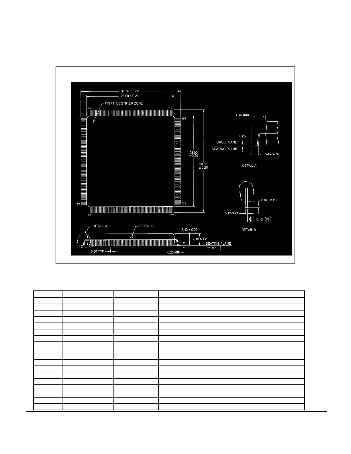
MECHANICAL SPECIFICATIONS
208-PIN SQFP PACKAGE
Dimensions are in millimeters.
Introduction
TPG 53310.c-7/29/97
Table 1. STEL-2176 Pin Assignments
Pin No. Pin Name Pin Type Pin Description
1 VSS Ground
2 VDD Power Dedicated to crystal oscillator at pins 3 & 4
3 RXOSCIN Input Receiver oscillator input
4 RXOSCOUT Output Receiver oscillator output
5 VSS Ground Dedicated to crystal oscillator at pins 3 & 4
6 VDD Power Dedicated to digital section of receive clock multiplier
7 VDDA Power (Analog) Dedicated to analog section of receive clock multiplier
8 RXMULTEN Input Enable receive clock multiplier
9 VSSA Ground
(Analog)
10 VSS Ground Dedicated to receive clock multiplier
11 RXMULTCLK Output Receive clock multiplier output; enabled by pin 58
12 VDD Power
13 ADCDATASEL[2] Input ADC/DAC bypass mode select; 111=normal operation
14 ADCDATASEL[1] Input ADC/DAC bypass mode select; 110=bypass ADC
15 ADCDATASEL[0] Input ADC/DAC bypass mode select; 101=bypass DAC
16 VSS Ground
17 ADDATA[9] Bi-directional Bypass/test ADC/DAC
Dedicated to receive clock multiplier
User Manual 3 STEL-2176
Page 13

Introduction
Pin No. Pin Name Pin Type Pin Description
18 ADDATA[8] Bi-directional Bypass/test ADC/DAC
19 ADDATA[7] Bi-directional Bypass/test ADC/DAC
20 ADDATA[6] Bi-directional Bypass/test ADC/DAC
21 ADDATA[5] Bi-directional Bypass/test ADC/DAC
22 VDD Power
23 ADDATA[4] Bi-directional Bypass/test ADC/DAC
24 ADDATA[3] Bi-directional Bypass/test ADC/DAC
25 ADDATA[2] Bi-directional Bypass/test ADC/DAC
26 ADDATA[1] Bi-directional Bypass/test ADC/DAC
27 ADDATA[0] Bi-directional Bypass/test ADC/DAC
28 VSS Ground
29 RXAGCOUTB Output AGC output B
30 RXAGCOUTA Output AGC output A
31 VDD5 Power 3.3V or 5V for AGC pins 29 & 30
32 V3OP Input Must set high if pin 31 is 3.3V or low if pin 31 is 5V
33 VSS Ground
34 IC Internal connection - leave open
35 SO Output SPI data out
36 VDD Power
37 SI Input SPI data in
38 SCK Input SPI clock
39 VSS Ground
40 ADDR[7] Input Control/Status register parallel address bus
41 ADDR[6] Input Control/Status register parallel address bus
42 ADDR[5] Input Control/Status register parallel address bus
43 ADDR[4] Input Control/Status register parallel address bus
44 VDD Power
45 ADDR[3] Input Control/Status register parallel address bus
46 ADDR[2] Input Control/Status register parallel address bus
47 ADDR[1] Input Control/Status register parallel address bus
48 ADDR[0] Input Control/Status register parallel address bus
49 VSS Ground
50 INTSEL[1] Input Serial/parallel inter. sel.: 00=parallel, 01=SPI (serial)
51 INTSEL[0] Input Serial/parallel interface select: 10=reserved, 11=res.
52 VDD Power
53 VSS Ground
54
55
56
57 VDD Power
58 ENCLKOUT Input Enables output pins 11 & 102
59 VSS Ground
60 DATA[7] Bi-directional Control/Status register parallel data in/out
61 DATA[6] Bi-directional Control/Status register parallel data in/out
62 DATA[5] Bi-directional Control/Status register parallel data in/out
63 DATA[4] Bi-directional Control/Status register parallel data in/out
64 VDD Power
65 DATA[3] Bi-directional Control/Status register parallel data in/out
66 DATA[2] Bi-directional Control/Status register parallel data in/out
67 DATA[1] Bi-directional Control/Status register parallel data in/out
68 DATA[0] Bi-directional Control/Status register parallel data in/out
69 VSS Ground
70 RXRESCLK Output FEC test clock output (8 times RX symbol rate)
71 VDD Power
72 RXTSTDOUT[9] Output Test mux output
73 RXTSTDOUT[8] Output Test mux output
74 RXTSTDOUT[7] Output Test mux output
75 RXTSTDOUT[6] Output Test mux output
CS
WRB
DSB
Input Control/Status register chip select (active low)
Input Control/Status register read/write (low=write)
Input Control/Status register data strobe signal (active low)
STEL-2176 4 User Manual
Page 14

Pin No. Pin Name Pin Type Pin Description
76 VSS Ground
77 RXTSTDOUT[5] Output Test mux output
78 RXTSTDOUT[4] Output Test mux output
79 RXTSTDOUT[3] Output Test mux output
80 RXTSTDOUT[2] Output Test mux output
81 VDD Power
82 RXTSTDOUT[1] Output Test mux output
83 RXTSTDOUT[0] Output Test mux output
84 RXTSTCLK Output Test mux output clock
85 VSS Ground
86 VDD Power Dedicated to digital portion of DAC
87 VDDA Power (analog) Dedicated to analog portion of DAC
88 DACOUTP Analog output Output of DAC. Terminate in 37.5 ohms to ground
89 DACOUTN Analog output Comp. output of DAC. Terminate in 37.5 ohms to ground
Figure 2)
90 VSSA Power (analog) Dedicated to analog portion of DAC
91 VSS Ground Dedicated to digital portion of DAC
92 VDD Power Dedicated to crystal oscillator at pins 93 & 94
93 TXOSCIN Input TX oscillator input
94 TXOSCOUT Output TX oscillator output
95 VSS Ground Dedicated to crystal oscillator at pins 93 & 94
96 VDD Power Dedicated to digital section of transmit clock PLL
97 VDDA Power (analog) Dedicated to analog section of transmit clock PLL
98 TXPLLEN Input Enable transmit clock PLL
99 VSSA Ground (analog) Dedicated to analog section of transmit clock PLL
100 TXBYPCLK Input High speed transmit bypass clock
101 VDD Power Dedicated to digital section of transmit clock PLL
102 TXPLLCLK Output Transmit clock PLL output; enabled by pin 58
103 VSS Ground Dedicated to digital section of transmit clock PLL
104 VDD Power
105 VSS Ground
106
TXRSTB
Input Transmit reset (active low)
107 VDD Power
108 TXTSDATA Input Transmit data input
109 TXDATAENI Input Transmit data enable input
110 TXTCLK Input Transmit tclk
111 VSS Ground
112 TXFCWSEL[1] Input Transmit frequency control word (FCW) select
113 TXFCWSEL[0] Input Transmit frequency control word (FCW) select
114 VDD Power
115 TXCLKEN Input Transmit clock enable
116 TXDIFFEN Input Transmit differential encoder enable
117 TXRDSLEN Input Transmit Reed-Solomon enable
118 TXSCRMEN Input Transmit scrambler enable
119 VSS Ground
120 TXCKSUM Output Transmit Reed-Solomon check sum
121 TXACLK Output Transmit auxiliary clock output
122 TXDATAENO Output Transmit data enable output
123 VDD Power
124 TXBITCLK Output Transmit bit clock
125 TXSYMPLS Output Transmit symbol pulse output
126 TXNCOLD Input Transmit NCO load
127 VDD5 Power Input buffer bias. Set to 3.3V or 5V dep. on max. input V.
voltage.
128 RXRSTB Input Receiver reset (active low)
129 VSS Ground
130 RXPDATAOUT[7] Output Receive parallel output data
131 RXPDATAOUT[6] Output Receive parallel output data
132 RXPDATAOUT[5] Output Receive parallel output data
Introduction
(See Figure 2)
(See
User Manual 5 STEL-2176
Page 15

Introduction
Pin No. Pin Name Pin Type Pin Description
133 RXPDATAOUT[4] Output Receive parallel output data
134 VDD Power
135 RXPDATAOUT[3] Output Receive parallel output data
136 RXPDATAOUT[2] Output Receive parallel output data
137 RXPDATAOUT[1] Output Receive parallel output data
138 RXPDATAOUT[0] Output Rec. par. output data or serial data if in serial mode
139 VSS Ground
140 RXOUTCLK Output Receive output data clock
141 VDD Power
142 RXACQFLAG Output Receive demod. acquisition flag
143 RXACQFAIL Output Receive demod. acquisition failure flag
144 RXDECDFLG Output Receive FEC decodable flag
145 FRAMESYNC Output Receive output frame sync flag
146 VSS Ground
147 SRAMADDR[15] Output De-Interleaver optional external SRAM address
148 SRAMADDR[14] Output De-Interleaver optional external SRAM address
149 SRAMADDR[13] Output De-Interleaver optional external SRAM address
150 SRAMADDR[12] Output De-Interleaver optional external SRAM address
151 VDD Power
152 SRAMADDR[11] Output De-Interleaver optional external SRAM address
153 SRAMADDR[10] Output De-Interleaver optional external SRAM address
154 SRAMADDR[9] Output De-Interleaver optional external SRAM address
155 SRAMADDR[8] Output De-Interleaver optional external SRAM address
156 VSS Ground
157 VDD Power
158 VSS Ground
159 SRAMADDR[7] Output De-Interleaver optional external SRAM address
160 SRAMADDR[6] Output De-Interleaver optional external SRAM address
161 SRAMADDR[5] Output De-Interleaver optional external SRAM address
162 SRAMADDR[4] Output De-Interleaver optional external SRAM address
163 VDD Power
164 SRAMADDR[3] Output De-Interleaver optional external SRAM address
165 SRAMADDR[2] Output De-Interleaver optional external SRAM address
166 SRAMADDR[1] Output De-Interleaver optional external SRAM address
167 SRAMADDR[0] Output De-Interleaver optional external SRAM address
168 VSS Ground
169 SRAMDATA[7] Bi-Directional De-Interleaver optional external SRAM data bus
170 SRAMDATA[6] Bi-Directional De-Interleaver optional external SRAM data bus
171 SRAMDATA[5] Bi-Directional De-Interleaver optional external SRAM data bus
172 SRAMDATA[4] Bi-Directional De-Interleaver optional external SRAM data bus
173 VDD Power
174 SRAMDATA[3] Bi-Directional De-Interleaver optional external SRAM data bus
175 SRAMDATA[2] Bi-Directional De-Interleaver optional external SRAM data bus
176 SRAMDATA[1] Bi-Directional De-Interleaver optional external SRAM data bus
177 SRAMDATA[0] Bi-Directional De-Interleaver optional external SRAM data bus
178 VSS Ground
179 SRAMWEB Output De-Interleaver SRAM write enable (active low)
180 SRAMCSB Output De-Interleaver SRAM chip select (active low)
181 SRAMOEB Output De-Interleaver SRAM output enable (active low)
182 VDD Power
183 RXIENBLE Input FEC test input I clock
184 RXQENBLE Input FEC test input Q clock
185 VSS Ground
186 RXBYPCLK Bi-directional Receiver bypass clock input; output reserved
187 VDD Power
188 VSSA Ground (analog) Dedicated to analog section of ADC
189 VDDA Power (analog) Dedicated to analog section of ADC
190 VCMA Analog output From ADC
(See Figure 1)
191 VDD Power Dedicated to digital section of ADC
(See Figure 1)
(See Figure 1)
(See Figure 1)
STEL-2176 6 User Manual
Page 16
Introduction
Pin No. Pin Name Pin Type Pin Description
192 VREFN Analog output From ADC
193 VSSA Ground (analog) Dedicated to analog section of ADC
194 VSS Ground Dedicated to digital section of ADC
195 VDDA Power (analog) Dedicated to analog section of ADC
196 VDDA Power (analog) Dedicated to analog section of ADC
197 ADCINP Analog input ADC input
198 ADCINN Analog input Complementary ADC input
199 VSSA Ground (analog) Dedicated to analog section of ADC
200 VSSA Ground (analog) Dedicated to analog section of ADC
201 VDD Power Dedicated to digital section of ADC
202 VDDA Power (analog) Dedicated to analog section of ADC
203 VREFP Analog output From ADC
204 VSS Ground Dedicated to digital section of ADC
205 VCMB Analog output From ADC
206 VSSA Ground (analog) Dedicated to analog section of ADC
207 VDDA Power (analog) Dedicated to analog section of ADC
(See Figure 1)
(See Figure 1)
(See Figure 1)
(See Figure 1)
(See Figure 1)
(See Figure 1)
(See Figure 1)
(See Figure 1)
(See Figure 1)
(See Figure 1)
(See Figure 1)
(See Figure 1)
(See Figure 1)
(See Figure 1)
(See Figure 1)
(See Figure 1)
208 VDD Power
Analog In (P)Analog In (N)
0.1
µF
0.1µF0.1
µF
0.1
µF
0.1
0.1
µF
µF
0.1
µF
0.1
0.1
µF
µF
Digital GND
(VSS)
Analog GND
(VSSA)
DACOUTP
DACOUTN
STEL-2176
Figure 1. Reference A/D Wiring
T1-6TKK81
0.1 µF
50
AV
SS
0.1 µF
Mini-
50
AV
SS
Circuits
1:1
0.1 µF
50 line
X
Note 1
Digital Supply
(VDD)
50
load
Note 1: Normally some application dependent alias filtering and
amplitude control appear at this point in the circuit
WCP 53807.c-12/5/97
Figure 2. Example Output Load Schematic
User Manual 7 STEL-2176
Page 17
Introduction
ELECTRICAL SPECIFICATIONS
The STEL-2176 electrical characteristics are provided by Table 2 through Table 4.
WARNING
Stresses greater than those shown in Table 2 may cause permanent damage to the STEL-2176.
Exposure to these conditions for extended periods may also affect the STEL-2176 reliability.
Table 2. Absolute Maximum Ratings
Symbol Parameter Range Units
T
stg
V
DDmax
A
VDDmax
5V
AV
V
I(max)
I
i
P
Diss (max)
DDmax
SS
Storage Temperature Ð40 to +125 °C
Supply voltage on VDD Ð0.3 to +4.6 volts
Supply voltage on AVDD Ð0.3 to +4.6 volts
Supply voltage on 5VDD Ð0.3 to +7.0 volts
Analog supply return for AVDD ± 10% of VDD volts
Input voltage Ð0.3 to 5VDD+0.3 volts
DC input current ± 30 mA
Power dissipation 1500 mW
Note:
All voltages are referenced to V
5V
must be greater than or equal to VSS. This rule can be violated for a maximum of 100 msec
DD
during power up.
.
SS
Note 1
Note 2
Table 3. Recommended Operating Conditions
Symbol Parameter Range Units
AV
5V
V
DD
C
LOAD
R
LOAD
DD
DD
Supply Voltage +3.3 ± 10% Volts
Supply Voltage +5.0 ± 10% Volts
Supply Voltage +3.3 ± 10% Volts
DAC Load Capacitance
DAC Load Resistance
≤ 20
≤ 30K
pF
ohms
Recommended DAC Load 37.5 ohms
V
LOAD
T
a
DAC Output Voltage
≤ 1.25
Volts
Operating Temperature (Ambient) Ð40 to +85 °C
Note:
1. All voltages with respect to VSS and assume AV
ss
= V
ss
2. If interface logic is to be driven by VDD then connect the 5VDD pin to the VDD supply and set
pin 32 to correct value.
3. Duty Cycle Derating is required from +70° to +85° C.
Note 1
Note 2
Note 3
STEL-2176 8 User Manual
Page 18
Introduction
Table 4. ADC Performance Specifications
Parameter Min Nom Max Units
Sampling Frequency 50 MHz
Resolution 10 bits
Input Differential Signal Range -0.75 +0.75 Volts
Analog Input Bandwidth 60 MHz
Signal to Distortion Ratio 10 MHz
54 dB
signal over 25 MHz BW
Input Common Mode 1.4 1.5 1.6 Volts
Table 5. DC Characteristics
(V
= 3.3 V ±10%, V
DD
Symbol Parameter Min. Nom. Max. Units Conditions
I
VDDQ
I
VDD
I
5V
DD
I
AV
DD
V
IH
CLK
V
IL
CLK
V
IH
V
IL
I
IH
I
IL
V
OH(min)
V
OL(max)
I
OS
C
IN
C
OUT
I
OFS
V
O
R
O
C
O
Supply Current, Quiescent 1.0 mA Static, no clock
Supply Current, Operational, V
Supply Current, Operational, 5V
Supply Current, Operational, AV
DD
DD
DD
Clock High Level Input Voltage 2.0 volts CLK, Logic '1'
Clock Low Level Input Voltage 0.8 volts CLK, Logic '0'
High Level Input Voltage 2.0 volts Other inputs, Logic '1'
Low Level Input Voltage 0.8 volts Other inputs, Logic '0'
High Level Input Current 10 µAV
Low Level Input Current Ð10 µAV
High Level Output Voltage 2.4 3.0 VDD volts IO = Ð2.0 mA
Low Level Output Voltage 0.2 0.4 volts IO = +2.0 mA
Output Short Circuit CurrentÊ 40 mA V
Input Capacitance 2 pF All inputs
Output Capacitance 4 10 pF All outputs
Output Full Scale DAC Current 16 19 22 mA Single output
DAC Compliance Voltage
(Differential)
DAC Output Resistance
1
DAC Output Capacitance 4 8 pF
= 0 V, T
SS
= -40° to 85° C)
a
1.9 mA/MHz
0.2 mA
12.0 mA
±0.96
Volts Based on 50 ohms load
N/A
= 5V
IN
IN
OUT
= V
= VDD,
DD
SS
VDDÊ=Êmax
resistance to ground.
NOTES:
1. Current source to ground output.
User Manual 9 STEL-2176
Page 19

Receiver Description
RECEIVER
OVERVIEW
The STEL-2176 is a complete subscriber-side cable
modem ASIC which integrates both the downstream
receiver and upstream transmitter functions. The
receiver includes a high performance 10-bit Analog-toDigital Converter (ADC) with a direct Intermediate
Frequency (IF) interface. The receiver also includes a
QAM demodulator and both ITU-T (J.83) Annex A and
Annex B Forward Error Correction (FEC). The
upstream transmitter includes a BPSK/QPSK/16QAM
modulator with highly flexible FEC and scrambling,
and a 10-bit low spurious digital to analog converter
(DAC) for direct synthesis of an upstream 5 to 65 MHz
signal. Both the receiver and transmitter are highly
flexible and programmable; the STEL-2176 Digital
Mod/Demod ASIC offers a solution to meet current
and evolving standards.
The input to the STEL-2176 receiver is an analog IF
signal of up to 50 MHz. Typically, the IF signal has 44
MHz center frequency with a 6 MHz bandwidth for
NTSC based systems, or a 36 MHz center frequency
with an 8 MHz bandwidth for PAL based systems. In
typical applications, the input signal is sampled by the
ADC at approximately 25 MHz for the 44 MHz IF, or at
approximately 29 MHz for the 36 MHz IF
This type of sub-sampling technique works by
intentionally undersampling the carrier frequency so
that aliased signal appears at a lower frequency. The
sampling rate is still high enough to capture all of the
modulation bandwidth without distortion. In the case
of a 44 MHz IF and a 25 MHz clock, the resulting digital
signal is centered at 6 MHz. In the case of a 36 MHz IF
and 29 MHz clock, the resulting digital signal is
centered at 7 MHz. For more information on subsampling techniques, please see Stanford Telecom
Application Note A-117.
The digital samples from the ADC are downconverted
to baseband I and Q signals in the Digital Down
Converter (DDC) block. Since the RF tuner sections of a
cable modem may have large frequency errors, an
Automatic Frequency Control (AFC) block is used in
the STEL-2176 for coarse tuning of the DDC. This
allows rapid acquisition of the input signal even with
frequency errors of ±200 kHz. Fine tuning of the DDC is
done using a carrier Phase-Lock Loop (PLL).
An Automatic Gain Control (AGC) function provides
two output signals to adjust the RF and IF analog gain
stages of circuitry external to the STEL-2176, so that the
ADC input is in the optimal range. The two outputs can
be programmed to create a sequential AGC system
which maximizes RF gain for improved receiver noise
figure. The two AGC outputs and the external gain
adjust blocks work together to maximize ADC
performance, but when large adjacent channels are
present, the power of the desired signal may change. A
second digital AGC tracks and adjusts the level of the
desired signal after the adjacent channel energy is
removed by filtering.
Following the DDC, a square root raised cosine Nyquist
filter eliminates adjacent channel signals, and performs
matched filtering to eliminate intersymbol interference.
The filter excess bandwidth or alpha is programmable
from 0.12 to 0.20. The Timing Recovery block finds the
exact location in the center of each symbol using a
special low-jitter discriminator. These values are fed to
the Adaptive Channel Equalizer.
An Adaptive Channel Equalizer (ACE) compensates for
any multipath distortion on the input signal introduced
in the channel. The equalizer uses one sample per
symbol (T spaced taps). The output of the equalizer is
baseband I and Q signals with carrier frequency and
phase errors, symbol timing errors, gain errors, and
multipath effects removed.
The Demapper takes the baseband I and Q signals
representing the QAM symbols, and translates each
symbol back into a series of binary values based on one
of the selectable constellation maps.
Following the Demapper is the Forward Error
Correction (FEC) system. This programmable system
supports both the ITU-T (J.83) Annex A (see page 14)
and Annex B (see page 16) standards. In general, both
FEC systems employ Reed Solomon Decoders, Frame
Sync circuits that determine the FEC code block
boundaries, and a De-Interleaver. Interleaving is used
in the FEC standards to improve performance when the
channel contains bursty noise. Since the transmitter
Interleaver spreads the data over a large time, when the
receiver performs the matched operation to the
Interleaver in order to bring the data back into the
correct time sequence, any burst errors appear to be
spread out in time. This helps makes these errors
STEL-2176 10 User Manual
Page 20
Receiver Description
correctable by the FEC. The STEL-2176 internal memory
can support all MCNS Interleaver configurations. For
deeper interleaving, a direct interface to external
memory is provided.
The output of the receiver is typically arranged as
MPEG-2 frames, although the MPEG-2 framing can be
Fo=44/36 MHz
BW= 6/8 MHz
A
10 bits/
Sample
4Samples/Symbol
ADC
~25 MHz
44 MHz
36 MHz
Interpolator
AFC
AGC
DDC
1st IF Output
Programmable
Nyquist
(0.12 to 0.2)
by-passed for ATM applications. The output can be 8bit parallel with a byte clock or serial with a bit clock.
The data can be output in a smooth fashion without
inter-frame gaps or with the pauses in output data
caused by the FEC system passed through to the output
(see Receiver Timing discussion).
A
Clock
Recovery
Adaptive
Channel
Equalizer
(20 taps)
De-mapper
Viterbi
Diff. Decoder
Reed-Solomon
Decoder
(204,188 and
128,122)
Micro Controller Interface
Micro Controller ( SPI, Parallel)
Figure 3. STEL-2176 Receiver Block Diagram
FUNCTIONAL BLOCKS
ADC
The ADC uses differential analog signal inputs
ADCINP and ADCINN. Differential coupling to the
ADC is important to prevent common mode noise from
the digital sections of the ASIC from coupling into the
input. The recommended input signal level is ± 0.75V.
The input is sampled by the ADC, and the samples are
converted into 10-bit digital values. The sampling rate
is typically 25 MHz for an input of 44 MHz ± 3 MHz
with a symbol rate of about 5 MHz (i.e., the MCNS
standard) or 29 MHz for an input of 36 MHz ± 4 MHz
with a symbol rate of about 7 MHz (i.e., the DAVIC and
DVB standards). The sampling rate is controlled the
choice of crystal connected between RXOSCIN and
RXOSCOUT or by the clock frequency applied to
Clock
Synthesizer
~25 MHz XO
Frame Sync
Deinterleaver
External RAM
WCP 52861.c-5/07/97
RXOSCIN. The sample rate must be slightly more than
4 samples per symbol. The sample clock generated by
the crystal/receive clock oscillator or applied to
RXOSCIN must be a low phase noise signal. For this
reason, dedicated power and ground connections for
the receive oscillator and input buffer are adjacent to
the RXOSCIN and RXOSCOUT pins.
Microcontroller Interface
The microcontroller interface provides access to the
internal programmable Universal, Downstream
(Receive), and Upstream (Transmit) registers (see page
20) via a parallel or a SPI interface. The interface used is
selected by the interface select lines (INTSEL[1-0]).
User Manual 11 STEL-2176
Page 21
Receiver Description
The parallel interface consists of an 8-bit address bus
(ADDR[7-0]), an 8-bit bi-directional data bus (DATA[70]), and the control signals chip select (CS), read/write
(WRB), and data strobe (DSB).
The SPI interface consists of a serial input (SI), serial
output (SO), and a serial clock (SCK).
Master Receive Clock Generator
The STEL-2176 uses a master clock (MCLK) to control
the receive timing functions. MCLK can be generated in
either of three ways as shown in Figure 4.
A receive bypass clock can be applied to the
RXBYPCLK input and selected to drive CLK. The
RXMULTEN should be held high to select the
RXBYPCLK input.
An external clock can be applied to the RXOSCIN input
or a crystal can be connected across the RXOSCIN and
RXOSCOUT inputs. The oscillator circuit outputs a 2050 MHz signal to a frequency multiplier PLL, which
upconverts the signal to a 100-150 MHz clock. When the
bypass clock is not used, RXMULTEN is driven high to
select the output of the frequency multiplier to drive
the MCLK signal. The frequency multiplier output
frequency is controlled by the formula:
MCLK OscillatorOutput
=∗
N
M
where:
• The Oscillator signal (RXOSCIN and
RXOSCOUT) is four times the signal symbol rate.
• The value of M and N should be selected so
MCLK is four times the value of the Oscillator
signal.
• N is the value stored in RxFsynN (bits 6-0 of Bank
0 Register F7H), and M is the value stored in
RxFsynM (bits 6-0 of Bank 0 Register F6H).
• The recommended values for DAVIC, DVB, and
IEEE 802.14 are Oscillator Frequency = 29 MHz,
M = 2, and N = 8. The recommended values for
MCNS are Oscillator Frequency = 25 MHz, M = 2,
and N = 8.
ENCLKOUT
RXOSCIN
RXOSCOUT
RXMULTEN
RXBYPCLK
RXBYPASSFSYN
OSCILLATOR
FREQUENCY
MULTIPLIER
PLL
Figure 4. Master Receive Clock Generator
MUX
WCP 53852.c-12/7/97
RXMULTCLK
To ADC
MCLK
STEL-2176 12 User Manual
Page 22
Receiver Description
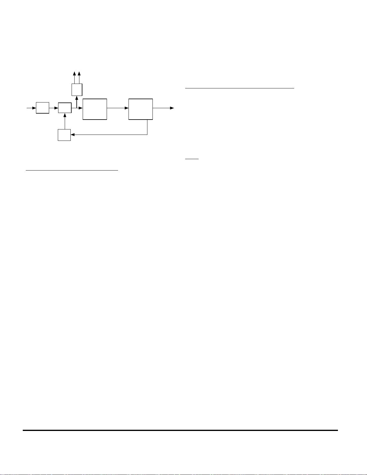
QAM Demodulator Blocks
The following diagram shows the major QAM circuit
blocks.
OutA OutB
AGC
S(t)
ADC
DDC
AFC
I,Q
Timing
Recovery
& SRRC
Filter
I,Q
(1 sample/
symbol)
Adaptive
Equalize
WCP 53702.c-10/28/97
I,Q
(to FEC)
Figure 5. QAM Demodulator Blocks
Digital Down Converter (DDC)
The digital samples from the ADC are mixed down to
baseband I and Q signals in the Digital Down
Converter (DDC) block. The input analog signal is subsampled at the rate set by the receive crystal oscillator
or a clock applied directly to the RXOSCIN input. The
resultant sub-sampled input signalÕs spectrum is
aliased to a lower frequency. In typical cases, with a 44
MHz _ 3 MHz input and a 25 MHz sample rate, the
digital signal appears to the input of the DDC as a 6
MHz _ 3 MHz signal. For a 36 MHz _ 4 MHz input and
a 29 MHz sample rate, the digital signal appears to the
input of the DDC as a 7 MHz _ 4 MHz signal. Other
input frequencies and sample rates are also possible.
The digital signal is down converted to baseband I and
Q by mixing with cos 2π fct and sin 2π f
t where fc is the
c
center frequency of the digital signal.
The Digital Down Converter contains a numerically
controlled oscillator (NCO) with cosine and sine
outputs, a pair of mixers, and an image filter. The
frequency f
is a combination of a starting value that is
c
set using DeltaTheta_in [13:0] (bits 7-2 of Bank 0
Register 10H and Bank 0 Register 11H) and any
frequency error terms computed by the Automatic
Frequency Control block. The value for DeltaTheta_in
[13:0] is given by:
DeltaTheta_in [13:0] = f
/ADC sample rate _214
c
For fc = 6 MHz and ADC sample rate = 25 MHz,
DeltaTheta_in [13:0] = 0F5C
H
For fc = 7 MHz and ADC sample rate = 29 MHz,
DeltaTheta_in [13:0] = 0F73
H
The complex NCO drives a pair of multipliers which
serve as mixers. The products of the ADC samples and
the sine and cosine outputs of the NCO produce the
desired baseband I and Q signals plus undesired higher
frequency image terms. These higher frequency terms
are removed by an image filter.
Automatic Frequency control (AFC)
The STEL-2176 can accommodate up to ±200 kHz
uncertainty in the carrier frequency. The carrier
frequency recovery is divided into two steps. The first
step is a coarse frequency estimation during initial
signal acquisition. This estimation is performed by the
AFC section. The estimated carrier frequency offset is
calculated by the AFC and fed to the DDC NCO.
AGC
The AGC takes the output from the Image Filter in the
DDC and estimates the power of the signal. The AGC
discriminator compares the estimate to one or two
different thresholds that can be set via the registers
values AGC_ThresholdA (Bank 0 Register 14
AGC_ThresholdB (Bank 0 Register 15
). Thresholds
H
) and
H
should be set to optimize ADC performance. The range
of the AGC`s power thresholds is 0 to 128 (2
8-1
). For 256-
QAM, the value ranges from about 75 to 100 (default is
96), depending on the desired A/D clipping level. The
trade off for selecting the value weighs occasional ADC
clipping with a large input versus loss of signal fidelity
with a small input. The power of the input signal
depends upon adjacent channel interference, AM hum,
burst noise, etc.
The AGC generates two 1-bit outputs OUTA and OUTB
that indicate whether that the input analog signal is too
high or too low. The OUTA and OUTB signals should
be smoothed using low pass filters. These filters can
each be a series resistor of ___ ohms and a shunt
capacitor of ___ _F. OUTA and OUTB can be set to
have a logic high voltage of either 3.3V or 5V. For 3.3V
operation, connect the power source's +3.3V output to
pins 31 and 32 and its return to VSS. For 5V operation,
connect the power source's +5V output to pin 31 and its
return to pin 32 and VSS.
The polarity of OUTA and OUTB may be controlled
with AGC_InvertOutputA (bit 0 of Bank 0 Register 12
H
and AGC_InvertOutputB (bit 1 of Bank 0 Register 12H).
For variable gain stages where a higher control voltage
at the input to the filter produces higher gain, set the
AGC_InvertOutput bit to 0. For variable gain stages
)
User Manual 13 STEL-2176
Page 23
Receiver Description
where a higher control voltage at the input to the filter
produces lower gain, set the AGC_InvertOutput bit to
1.
The two outputs can be programmed to create a
sequential AGC system which maximizes RF gain for
improved receiver noise figure. This is accomplished by
setting AGC_ThresholdA (Bank 0 Register 14H) and
AGC_ThresholdB (Bank 0 Register 15H) to slightly
different values. The threshold which is set to a lower
value will cause its associated output to command
increase gain first. This output is typically connected to
the RF variable gain stages so that the best receiver
noise figure is achieved.
Timing Recovery and Nyquist Filter
The sampled signal (> 4 times the symbol rate in I and
Q format) is fed to this block to:
¥ Eliminate inter-symbol interference (ISI) by filtering it
with a square route raised cosine filter (SRRC) of a
selectable excess bandwidth (a) for 12%<= a<=20%.
¥ Recover the exact symbol rate, within 100 ppm of the
nominal value.
The adaptive equalizer control registers are Block 1
Registers 21H to 24H.
FEC Decoder Blocks
The purpose of the FEC subsystem is to improve the bit
error rate performance of the data link. The
arrangement of the FEC blocks in the receiver is in
reverse order from the transmitter. The STEL-2176 FEC
subsystem can decode signals which are generated in
conformance with either the ITU-T (J.83) Annex A or
Annex B FEC standards.
There are two different though similar set of blocks
used for ITU-T (J.83) Annex A (Figure 6) and Annex B
(Figure 13).
The STEL-2176 supports the MPEG-2 standard.
MPEG-2 uses 188 byte packets with a sync byte and
three header bytes containing service identification,
scrambling, and control information. The 184 bytes of
data follows the sync and header bytes. Normally this
header information flows through to the receiver
output, but with ITU-T (J.83) Annex B there is an option
of bypassing the MPEG-2 outer layer of processing.
¥ Resample and transmit one composite sample (I and
Q for each symbol) to the equalizer. These samples
are taken at the epoch of each symbol.
Adaptive Channel Equalizer
The output of the Timing Recovery block is fed to the
Adaptive Equalizer at a rate of one complex
sample/symbol. The Adaptive Equalizer will:
1. Compensate for channel distortion including:
a. Multipath
b. AM hum
c. FM hum
d. Phase noise
2. Fine tune to the carrier frequency and phase offset.
3. Set the acquisition flag ÒtrueÓ, after the equalizer
successfully locks on to the signal.
4. Write to ErrPwr (Block 0 Register 44H) the estimated
output SNR.
Annex A FEC
The ITU-T (J.83) Annex A FEC subsystem consists of
the following blocks:
I,Q from
Adaptive
Equalizer
De-mapper De-Interleaver
Reed-Solomon
Decoder
De-Randomizer
Frame
Sync
To Output Clock
WCP 53703.c-10/28/97
Figure 6. ITU-T (J.83) Annex A FEC Subsystem
Demapper
This block maps the Adaptive Channel Equalizer I and
Q outputs for each symbol into 4, 6, or 8 bits for 16, 64,
or 256 QAM respectively. The mapping tables are as
follows:
STEL-2176 14 User Manual
Page 24
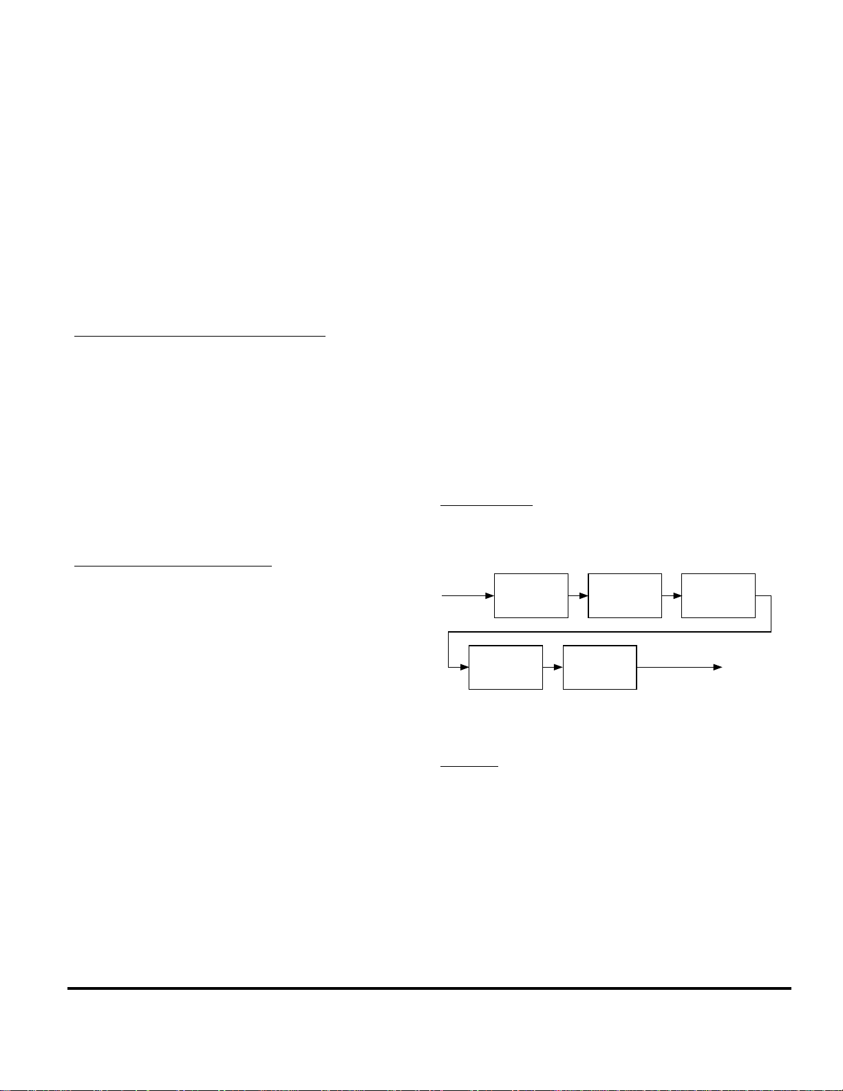
Receiver Description
Q
Q
110100 111100 101100 100100000100 001100 011100 010100
10
01
11
IkQk=10
0111
IkQk=10
00
00
=11 IkQk=01
I
kQk
10
10
IkQk=00
00
00
01 11
WCP 53711.c-10/29/97
Figure 7. 16 QAM Constellation
1100
1110 0110 0100 1000 1001 1101 1100
1101 1111 0111 0101 1010 1011 1111 1110
1001 1011 0011 0001 0010 0011 0111 0110
1000 1010 0010 0000 0000 0001 0101 0100
0100 0101 0001 0000 0000 0010 1010 1000
0110 0111 0011 0010 0001 0011 1011 1001
1110 1111 1011 1010 0101 0111 1111 1101
1100 1101 1001 1000 0100 0110 1110 1100
Q
I
IIIIIIIIIIIII
11
01
I
10
IkQk=00
I
I
=01IkQk=11
kQk
WCP 53712.c-10/29/97
110101 111101 101101 100101000101 001101 011101 010101
110111 111111 101111 100111000111 001111 011111 010111
110110 111110 101110 100110000110 001110 011110 010110
110010 111010 101010 100010000010 001010 011010 010010
110011 111011 101011 100011000011 001011 011011 010011
110001 111001 101001 100001000001 001001 011001 010001
rotate 90 degrees
IkQk=10
rotate 180 degrees
=11
I
kQk
rotate 270 degrees
=01
I
kQk
110000 111000 101000 100000000000 001000 011000 010000
IIIIIIIIIIIIII
I
Figure 9. 256 QAM Constellation (DAVIC)
Q
110100 110101 110001 110000100000 100001 100101 100100
110110 100111 110011 110010100010 100011 100111 100110
111110 111111 111011 111010101010 101011 100111 101110
111100 111101 111001 111000101000 101001 101101 101100
011100 011101 011001 011000001000 001001 001101 001100
011110 011111 011011 011010001010 001011 001111 001110
010110 010111 010011 010010000010 000011 000111 000110
rotate 90 degrees
IkQk=10
rotate 180 degrees
=11
I
kQk
rotate 270 degrees
=01
I
kQk
010100 010101 010001 010000000000 000001 000101 000100
IIIIIIIIIIIIII
I
IkQk=00
I
WCP 53713.c-10/29/97
IkQk=00
I
WCP 53839.c-12/5/97
Figure 8. 64 QAM Constellation
Two bits are the same for each modulation type, and
are identified as IKQK. The remaining bits are identified
as [b
q-1
. . . b
where q = 2, 4, and 6 for 16, 64 or 256
o],
QAM.
IKQK are processed by the differential decoder before
being fed to the frame sync block. The remaining bits
[b
q-1
. . . b
are fed directly to the frame sync.
o]
Differential Decoder
Two bits (IKQK) of each symbol are differentially
Figure 10. 256 QAM Constellation (DVB/IEEE 802.14)
b
= Ak = (I
q+1
bq = Bk = (Q
I
Demapper
Q
k
⊕ Q
k
⊕ I
Q
k
I
k
) ⊕ (I
k-1
) ⊕ (I
k-1
Q bits (b
Differential
Decoder
q-1
k-1
k-1
... b0)
⊕ Q
⊕ Q
Bk=b
Ak=b
) ¥ (1⊕Ik ⊕ Q
k-1
) ¥ (1⊕Ik ⊕ Q
k-1
M-tuple
q
Conversion
q+1
to
Byte
WCP 53708.c-10/28/97
Figure 11. Demapper
decoded according to the equation:
User Manual 15 STEL-2176
)
k
)
k
To Frame
Sync
Page 25

Receiver Description
Frame Sync
The frame sync receives symbols from the mapper.
Each symbol represents 4, 6 or 8 bits for 16 QAM, 64
QAM, and 256 QAM respectively. These bits are
collected into bytes. For 16 QAM, every two symbols
are converted into one byte. For 64 QAM, every 4
symbols to are converted into 3 bytes, and for 256 QAM
each symbol gives one byte..
Once bytes are formed, the frame sync block looks for a
sequence of fixed byte values separated by 203 bytes of
data.
47H (203 bytes) B8H (203 bytes) 47H (203 bytes) 47H (203
bytes) 47
47
. . .
H
H
. . .
47
. . . .
H
47
47
47
. .
. . .
H
H
H
. . .
B8
. . .
H
When the frame sync finds this pattern HIT (Block 1
Register 55H) times, the frame sync block declares
ÒacquisitionÓ and starts feeding the bytes to the DeInterleaver. The frame sync stays in the ÒacquisitionÓ
state until it misses this pattern MISS (Block 1 Register
56H) times.
De-I nterleaver
This block is a convolutional De-Interleaver, as shown:
Input
12
1
J J J J J
J
2
J J J J J
I-4
J J J J
I-3
J J J J
I-2
J J J J
I-1
J J J J
I
4 I-2 I-1
3
Output
WCP 53704.c-10/28/97
followed by 16 bytes of checksum. The code blocks are
assumed to be coded according to ITU-T (J.83) Annex A
FEC shortened R-S algorithm.
If the decoder fails to decode a code block, the decoder
sets the undecodable flag ÒtrueÓ for this block. This flag
propagates to the STEL-2176 output as RXDECDFLG.
In addition, the number of errors in each decodable
block accumulates in Error_cnt[15:0] (Block 1 Registers
72H and 73H). This register can be reset by writing a 1 to
CLR_ERR (bit 0 of Block 1 Register 74H).
De- R andomizer
The de-randomizer is exactly the same as the
randomizer described by the ITU-T (J.83) Annex A
standard.
Output Clock Block
The function of the output clock block is to evenly
distribute the output receive data of the STEL-2176 and
to eliminate gaps caused by the FEC subsystem. The
output of the Reed-Solomon decoder is 188 bytes of
data for every 204 input bytes. Therefore, there is a gap
of 16 bytes where the checksum information is
removed.
The STEL-2176 output can send the received data in
bytes on an 8-bit wide buss, or in bits on a single line as
shown in Downstream Output Timing Diagrams
(Figure 19 through Figure 21). Selecting between
ÒbytewiseÓ versus ÒbitwiseÓ can be done by setting
Serial Mode (bit 0 of Bank 1 Register 69H) to 1.
ANNEX B
The ITU-T (J.83) Annex B FEC subsystem consists of the
following blocks:
Figure 12. De-Interleaver
I and J are programmable (Block 1 Registers 47H and
I,Q from
Adaptive
Equalizer
Trellis
Coded
De-modulator
Frame
Sync
De-Randomizer
48H).
A total memory of J _ (I-1) _ I/2 is required. The STEL-
2176 has 8K internal memory. Up to 64K memory can
be added externally without any additional logic, as
shown.
De-Interleaver
Reed-Solomon
Decoder
MPEG-2
Framing
To Output Clock
WCP 53705.c-10/28/97
Figure 13. ITU-T (J.83) Annex B FEC Subsystem
Reed-Solomon Decoder
This function decodes Reed-Solomon blocks. Each code
block is 204 bytes long and contains 188 bytes of data
STEL-2176 16 User Manual
Page 26
I, Q
Demapping
C
C
C
C
C
C
C
q
q/2+1
q/2-1
2
1
q/2
0
1/2 Binary
Convolutional
Decoder
X
Differential
Y
Decoder
(4/5) punctured
Figure 14. Trellis Coded Demodulator
W
Receiver Description
Buffer
28 bits (64QAM)
Frame
Sync
38 bits (256 QAM)
Z
WCP 53706.c-10/28/97
The demapping block maps the Adaptive Channel
Equalizer I and Q outputs for each symbol into 4, 6, or 8
Q
110,111 111,011 010,111 011,011100,101 101,111 110,101 111,111
110,100 111,000 010,100 011,000 100,000101,010 110,000 111,010
100,111 101,011 000,100 001,011 000,101 001,111 010,101 011,111
100,100 101,000 000,100 001,000 000,000 001,010 010,000 011,010
010,011 011,001 000,011 001,001 000,001 001,101 100,001 101,101
010,110 011,100 000,110 001,100 000,010 001,110 100,010 101,110
110,011 111,001 100,011 101,001 010,001 011,101 110,001 111,101
bits for 16, 64, or 256 QAM respectively. The mapping
tables are as follows:
3
C5C4C
I
,
C2C1C
0
110,110 111,100 100,110 101,100 010,010 011,110 110,010 111,110
WCP 53709.c-10/29/97
Figure 15. 64 QAM Mapping
User Manual 17 STEL-2176
Page 27
Receiver Description
1110,
1111
1100,
1110
1010,
1111
1000,
1110
0110,
1111
0100,
1110
0010,
1111
0000,
1110
1110,
0001
1110,
0010
1110,
0101
1110,
0110
1110,
1001
1110,
1010
1110,
1101
1110,
1110
1111,
1101
1101,
1100
1011,
1101
1001,
1100
0111,
1101
0101,
1100
0011,
1101
0001,
1100
1101,
0001
1101,
0010
1101,
0101
1101,
0110
1101,
1001
1101,
1010
1101,
1101
1101,
1110
1110,
1011
1100,
1010
1010,
1011
1000,
1010
0110,
1011
0100,
1010
0010,
1011
0000,
1010
1010,
0001
1010,
0010
1010,
0101
1010,
0110
1010,
1001
1010,
1010
1010,
1101
1010,
1110
1111,
1001
1101,
1000
1011,
1001
1001,
1000
0111,
1001
0101,
1000
0011,
1001
0001,
1000
1001,
0001
1001,
0010
1001,
0101
1001,
0110
1001,
1001
1001,
1010
1001,
1101
1001,
1110
1110,
0111
1100,
0110
1010,
0111
1000,
0110
0110,
0111
0100,
0110
0010,
0111
0000,
0110
0110,
0001
0110,
0010
0110,
0101
0110,
0110
0110,
1001
0110,
1010
0110,
1101
0110,
1110
1111,
0101
1101,
0100
1011,
0101
1001,
0100
0111,
0101
0101,
0100
0011,
0101
0001,
0100
0101,
0001
0101,
0010
0101,
0101
0101,
0110
0101,
1001
0101,
1010
0101,
1101
0101,
1110
1110,
0011
1100,
0010
1010,
0011
1000,
0010
0110,
0011
0100,
0010
0010,
0011
0000,
0010
0010,
0001
0010,
0010
0010,
0101
0010,
0110
0010,
1001
0010,
1010
0010,
1101
0010,
1110
1111,
0001
1101,
0000
1011,
0001
1001,
0000
0111,
0001
0101,
0000
0011,
0001
0001,
0000
0001,
0001
0001,
0010
0001,
0101
0001,
0110
0001,
1001
0001,
1010
0001,
1101
0001,
1110
Q
0000,
1111
0000,
1100
0000,
1011
0000,
1000
0000,
0111
0000,
0100
0000,
0011
0000,
0000
0000,
0001
0010,
0000
0100,
0001
0110,
0000
1000,
0001
1010,
0000
1100,
0001
1110,
0000
0011,
1111
0011,
1100
0011,
1011
0011,
1000
0011,
0111
0011,
0100
0011,
0011
0011,
0000
0001,
0011
0011,
0010
0101,
0011
0111,
0010
1001,
0011
1011,
0010
1101,
0011
1111,
0010
0100,
1111
0100,
1100
0100,
1011
0100,
1000
0100,
0111
0100,
0100
0100,
0011
0100,
0000
0000,
0101
0010,
0100
0100,
0101
0110,
0100
1000,
0101
1010,
0100
1100,
0101
1110,
0100
0111,
1111
0111,
1100
0111,
1011
0111,
1000
0111,
0111
0111,
0100
0111,
0011
0111,
0000
0001,
0111
0011,
0110
0101,
0111
0111,
0110
1001,
0111
1011,
0110
1101,
0111
1111,
0110
1000,
1111
1000,
1100
1000,
1011
1000,
1000
1000,
0111
1000,
0100
1000,
0011
1000,
0000
0000,
1001
0010,
1000
0100,
1001
0110,
1000
1000,
1001
1010,
1000
1100,
1001
1110,
1000
1011,
1111
1011,
1100
1011,
1011
1011,
1000
1011,
0111
1011,
0100
1011,
0011
1011,
0000
0001,
1011
0011,
1010
0101,
1011
0111,
1010
1001,
1011
1011,
1010
1101,
1011
1111,
1010
1100,
1111
1100,
1100
1100,
1011
1100,
1000
1100,
0111
1100,
0100
1100,
0011
1100,
0000
0000,
1101
0010,
1100
0100,
1101
0110,
1100
1000,
1101
1010,
1100
1100,
1101
1110,
1100
1111,
1111
1111,
1100
1111,
1011
1111,
1000
1111,
0111
1111,
0100
1111,
0011
1111,
0000
0001,
1111
0011,
1110
0101,
1111
0111,
1110
1001,
1111
1011,
1110
1101,
1111
1111,
1110
C7C6C5C
C3C2C1C
I
4
0
Figure 16. 256 QAM Mapping
The de-mapper generates ÒqÓ bits for each symbol
where q = 6 for 64 QAM and q = 8 for 256 QAM. Two
bits (bo and b
) are processed by the binary
q/2
convolutional decoder and the differential decoder. The
remaining bits are passed directly to the output buffer.
Viterbi Decoder
The binary convolutional decoder is a 1:2 Viterbi
decoder (4/5 punctured). For every 5 consecutive input
bo or bq/2 bits, the Viterbi decoder produces only 4
output bits. With this type of punctured code there are
5 possibilities for synchronization. The synchronization
can occur automatically, or under manual control using
the programmable registers. Setting VitFeedBackEn (bit
4 of Bank 0 Register F4H) to 1 selects the automatic
mode, while setting it to 0 selects the manual mode. In
the manual mode, the decoder starts at any point in the
puncturing sequence. To skip to the next state, write 1
to VitFeedBack (bit 7 of Bank 0, Register FCH).
WCP 53710.c-10/29/97
decoder uses the following formula to produce its
output:
Wk = (X
• (X
k-1
Zk = (X
Buffer
⊕ Y
⊕ Y
k
⊕ X
k
k-1
k-1
) • (1 ⊕ X
k-1
)
) ⊕ (Yk ⊕ Y
k-1
k-1
⊕ Y
)
) ⊕ (Yk ⊕ Y
k-1
k-1
The trellis coded demodulator buffer converts groups
of 5 symbols into a bitstream (28 bits for 64 QAM, or 38
bits for 256 QAM) following Annex B convention.
Frame Sync
This block receives data from the buffer. The frame sync
looks for Annex B frame sync patterns which are
different for 64 QAM and 256 QAM. Also, the
separation distance between successive patterns is
different (60 R-S code words for 64 QAM and 88 R-S
code words for 256 QAM).
)
Differential Decoder
When the frame sync finds this pattern HIT (Bank 1
Register 55H) times, the frame sync block declares
The two bit streams coming out of the Viterbi decoder
ÒacquisitionÓ and starts further processing of the data.
are fed into the differential decoder. The differential
STEL-2176 18 User Manual
Page 28

Receiver Description
The frame sync stays in the ÒacquisitionÓ state until it
misses this pattern MISS (Bank 1 Register 56H) times.
When in the "acquisition" state, the frame sync patterns
are deleted, except the 4 bits identifying the
interleaving parameters. These can be used by the DeInterleaver to automatically select the De-Interleaving
parameters.
The remaining data, that is all bits between frame syncs,
are formed in 7-table bits symbols and passed to the derandomizer.
Derandomizer
The Derandomizer uses a linear feedback shift register
as shown below. It works in GF (128). The delay
elements are initialized at the beginning of each frame
to 7FH, 7FH and 7FH.
Data In Data Out
-1
z
3
α
7
-1
z
-1
z
7
7
WCP 53707.c-10/29/97
Figure 17. Derandomizer
De-I nterleaver
This block is a convolutional De-Interleaver, as shown:
Input
12
1
J J J J J
J
2
J J J J J
I-4
J J J J
I-3
J J J J
I-2
J J J J
I-1
J J J J
I
4 I-2 I-1
3
Output
WCP 53704.c-10/28/97
A total memory of J _ (I-1) _ I/2 is required. The STEL-
2176 has 8K internal memory. Up to 64K memory can
be added externally without any additional logic, as
shown.
Reed-Solomon Decoder
This function decodes Reed-Solomon blocks. Each code
block is 128 (7 bits symbols) long and contains 122
(7Êbits symbols) of data followed by 6 (7 bits symbols)
of checksum. The code blocks are assumed to be coded
according to ITU-T (J.83) Annex B FEC R-S algorithm.
If the decoder fails to decode a code block, the decoder
sets the undecodable flag ÒtrueÓ for this block. This flag
propagates to the STEL-2176 RXDECDFLG output.
In addition, the number of errors in each decodable
block accumulates in Error_cnt[15:0] (Bank 1 Registers
72H and 73H). This register can be reset by writing a 1 to
CLR_ERR (bit 0 of Bank 1 Register 74H).
MPEG Framing
The R-S decoderÕs output is serialized and fed through
the ITU-T (J.83) Annex B MPEG-2 syndrome converter.
The output of the syndrome generator is monitored for
the pattern of 47H separated by 1496 bits. When ÒnÓ (n
is a programmable number) successive occurrences of
this pattern are found, MPEG-2 frame sync is declared.
MPEG-2 packets are framed by converting every 8 bits
into one byte.
After declaring successful MPEG-2 frame sync, the
absence of a valid code word at the expected location is
indicated as a packet error.
MPEG-2 framing can be bypassed if so selected. In this
case, the output of the R-S decoder will be reformed
into bytes starting at the beginning of each frame.
Output Clock Block
The output clock block functionally the same as the
Annex A output clock block. However, the gaps
between data bytes occur due to eliminating the R-S
checksum symbols, the frame sync information, and the
bits that were added to support Viterbi decoding.
Figure 18. De-Interleaver
I and J (Bank 1 Registers 47H and 48H) are
programmable, however in Level II, the I and J values
are determined by the 4-bit pattern of the frame sync.
User Manual 19 STEL-2176
Page 29

Receiver Description
RECEIVE AND UNIVERSAL REGISTER DESCRIPTIONS
bank of registers. Register location FFH can be accessed
PROGRAMMING THE 2176 RECEIVE
FUNCTIONS
The STEL-2176 has a combination of universal, receive
and transmit registers. The registers are arranged as
three banks of registers (Bank 0, Bank 1, and Bank 2).
The Bank 0 registers are divided into Group 1 and
Group 2 registers. The Bank 1 and 2 registers form
separate groups (Groups 3 and 4 respectively). The
Bank 0 and 1 registers (Groups 1, 2, and 3) are
described by the following paragraphs. The Bank 2
registers (Group 4) are described in the Transmitter
section (see page 54).
The Bank/Group address, shown below, must be
written to register location FFH to access the respective
from each register bank/group. The registers can be
accessed using the Microcontroller Interface's parallel
or serial interface (see page 11).
REGISTER DESCRIPTIONS
Bank 0 - Universal Registers (Group 1)
The Universal Registers (Bank 0, Group 1) consist of
three sets of registers: Read/Write (see Table 6), Readonly, and Write-only (see Table 7). The Read-only
register set (Bank 0 Register F2) is for factory use only
and not described by this User Manual.
Bank Group Group Name Bank/Group Address
(location FFH)
0 1 Universal Registers (Group 1) 00
0 2 QAM Demodulator Registers Universal Registers (Group 2) 00
1 3 Downstream FEC Registers 01
2 4 Upstream, or transmitter, Registers 02
H
H
H
H
Table 6. Read/Write Register Set
Address 7 6 5 4 3 2 1 0
F1
F4
F5
F6
F7
F8
F9
FA
FB
FD
FE
H
H
H
H
H
H
H
H
H
H
H
Not Used BypassMPE
Not Used RxFsynM
Not Used RxFsynN
Not Used TxFsynM
Not Used TxFsynN
Not Used Factory Use Only
Not Used QAMEnable QAMType FEC Type
Not Used FECTestMode
(Bypass QAM)
VitFeedBackEn Factory Defined Value - 0
Gframe
(write only)
Not Used Factory Defined Value - 2HRxBypassFsyn TxBypassFsyn
Not Used
QAMAcquisitionMaxTries
Factory Use Only
Program to 0
H
H
Table 7. Write Only Registers:
Address 7 6 5 4 3 2 1 0
F3
FC
H
H
VitFeedBack Factory Defined Value - 0
Not Used Reset_OutputFIFO Factory
LoadRxM LoadRxN LoadTxM LoadTxN QAM Start
H
Defined
Value - 0
STEL-2176 20 User Manual
H
Page 30

Receiver Description
y
y
y
y
Bank 0, Group 1 Register Data Field Descriptions
BypassMPEGframe This data field is a write only register. Setting it to 1 will bypass MPEG framing.
Factory Use Only This data field is used by the factory and must be programmed to the value indicated
above.
FEC Type Used to select the type of FEC encoding:
00 _ Annex A
01 _ Annex B
10 _ STel use only
FECTestMode For test purposes, the QAM can be bypassed by setting the value to 1. Data is then fed
directly to the FEC.
LoadRxM Setting the value to 1 loads the value of RxFsynM into the Receiver frequenc
synthesizer.
LoadRxN Setting the value to 1 loads the value of RxFsynN into the Receiver frequenc
synthesizer.
LoadTxM Setting the value to 1 loads the value of TxFsynM into the Transmitter frequenc
synthesizer.
LoadTxN Setting the value to 1 loads the value of TxFsynN into the Transmitter frequenc
synthesizer.
QAM Start Setting the value to 1 starts the QAM acquisition.
QAMAcquisitionMaxTries The programmed value determines the number of acquisition tries the QAM makes
before it declares an acquisition failure. The acquisition process will be restarted.
QAMEnable QAMEnable must be set to 1 to enable the QAM circuitry, before programming QAM
Start.
QAMType Used to select 16, 64, or 256 QAM
00 _ 16 QAM
01 _ 64 QAM
10 _ 256 QAM
Reset_OutputFIFO Setting the value to 1 resets the FIFO of the output clock in case of overflow.
RxBypassFsyn Setting value to 1 bypasses the frequency synthesizer in the Master Receive Clock
Generator.
RxFsynM Value controls the Receiver Frequency Synthesizer output.
RxFsynN Value controls the Receiver Frequency Synthesizer output.
TxBypassFsyn Setting value to 1 bypasses the frequency synthesizer in the Master Transmit Clock
Generator.
TxFsynM Value controls the Transmitter Frequency Synthesizer output.
TxFsynN Value controls the Transmitter Frequency Synthesizer output.
VitFeedBack When use of Viterbi Decoder feedback is enabled, setting the value to 1 forces the
Frame Sync circuit to begin shifting by one symbol and testing for the start of the
symbol group. Once the search is externally initiated the value should be returned to
0.
VitFeedBackEn Setting the value to 1 enables the use of Viterbi Decoder feedback for using the
VitFeedBack register to force the Frame Sync circuit to search for the start of the
symbol group.
User Manual 21 STEL-2176
Page 31
Receiver Description
Bank 0 - QAM Demodulator Registers Universal
Registers (Group 2)
group has two sets of registers: a Read/Write set which
is used for control purposes, and a Read-only set for
monitoring purposes. The sub-groups are:
The QAM Demodulator Registers Universal Registers
are divided into 6 sub-groups of registers. Each sub-
Sub-Group Name Read/Write
Register Addresses
A Control, address range 00H to 0E
B DDC, Nyquist, AGC, and AFC address range 0FH to 1B
C Timing, address range 1CH to 20
D FFE, address range 21H to 24
E FBE, address range 25H to 26
F PLL, address range 27H to 3F
H
H
H
H
H
H
Read-only
Register Addresses
40H to 45
46H to 52
53H to 5B
5CH to 5FH and 6BH to 9A
9BH to B2
60H to 6A
H
H
H
H
H
Bank 0, Group 2, Sub-Group 'A' - Control Address Range Registers
Table 8. Group 2, Sub-Group 'A' Read/Write Registers
Address 7 6 5 4 3 2 1 0
00
01
02
03
04
05
06
07
08
09
0A
0B
0C
0D
0E
H
H
H
H
H
H
H
H
H
H
H
H
QAM_Enable QAM_SoftR
esetEnable
Pwrlvl_corre
ctEn
Decimate_Gai
nSel
Factory Defined Value - 19
Factory Defined Value - 44
Factory Defined Value - 19
Factory Defined Value - A
H
H
H
H
CMA1_Ksym
AFC1_Ksym
CMA2_Ksym
AFC2_Ksym
Factory Defined Value - 64
Factory Defined Value - 00
H
Factory Defined Value - 00
Factory Defined Value - 64
H
H
Factory Defined Value - 40H = 16 QAM, 53H = 64 QAM, or 87H = 256 QAM
Factory Defined Value - 33H = 16 QAM, 37H = 64 QAM, or 54H = 256 QAM
H
H
H
H
Factory Defined Value - 5FH = 16 QAM, 76H = 64 QAM, or A4H = 256 QAM
H
Table 9. Sub-Group 'A' Read-Only Registers
Address 7 6 5 4 3 2 1 0
40
H
41
H
42
H
43
H
44
H
45
H
SymbolCnt[1:0] AcquisitionLock AcquisitionFail State
SymbolCnt[9:2]
SymbolKCnt
AcquireCnt
ErrPwr
JitPwr
STEL-2176 22 User Manual
Page 32
Receiver Description
p
Bank 0, Group 2, Sub-Group 'A' Register Data Field Descriptions
AcquireCnt The value indicates the number of times the STEL-2176 has attempted to acquire the
signal.
AcquisitionFail The value is set to 1 when an acquisition failure is declared due to excessive error power;
the STEL-2176 is also returned to the idle mode.
AcquisitionLock The value is set to 1 when acquisition lock is detected.
Decimate_GainSel If GainSel is low (the default), the Nyquist filter output (10 bits plus 1 fractional bit) is
multiplied by a factor of 1.25 (+2 dB power); if GainSel is high, the scale factor is 1.5 (+3.5
dB power).
ErrPwr Provides an indication of the SNR. The conversion between ErrPwr and the SNR can be
determined from Table 10 (intermediate values can be found by interpolation).
Factory Defined Value The specified value must be written to the data field. In a few cases, several values are
rovided for selecting a specific mode and one of the specified values must be written to
the data field.
JitPwr
Pwrlvl_correctEn Enables the power level adjuster to correct for deviations in the signal power due to
adjacent channel interference.
QAM_Enable
QAM_SoftResetEnable The value is set to 1 to enable soft reset of the QAM.
State
SymbolCnt[9:0]
SymbolKCnt
Table 10. SNR to ErrPwr Conversion
ErrPwr
SNR(dB) 256 QAM 64 QAM 16 QAM
34 18
33 23
32 28
31 36
30 44
29 55
28 69
27 84 23
26 100 28
25 118 35
24 135 44
23 151 55
22 164 68
21 176 83 20
20 185 101 26
19 118 33
18 137 41
17 155 51
16 171 64
15 185 78
14 198 95
13 113
12 131
11 148
10 163
9 174
8 184
User Manual 23 STEL-2176
Page 33

Receiver Description
Bank 0, Group 2, Sub-Group ‘B’ - DDC, Nyquist, AGC, and AFC Address Range Registers
Table 11. Group 2, Sub-Group 'B' Read/Write Registers
Address 7 6 5 4 3 2 1 0
0F
10
11
12
13
14
15
16
17
18
19
1A
1B
H
H
H
H
H
H
H
H
H
H
H
H
H
AGC_GainSel Nyquist_AlphaSel AGC_InvertOu
Factory Defined Value - 34
H
UpdateEn Correct_
DeltaTheta_in[5:0] CorrectEn Update_
DeltaTheta_in[13:6]
Factory Defined Value - 00
H
AGC_ThresholdA
AGC_ThresholdB
Factory Defined Value - 22H = 16 QAM, 2BH = 64 QAM, or 35H = 256 QAM
Factory Defined Value - 26H 16 QAM, 37H 64 QAM, or 3CH 256 QAM
Factory Defined Value - 52H = Signal BW ~5MHz or 3BH = Signal BW ~7MHz
AFC_Cntr_stop1
AFC_Cntr_stop2
WARNING: SHOULD NOT BE PROGRAMMED BY THE USER
tputB
AGC_Invert
addsub
addsub
OutputA
Table 12. Group 2, Sub-Group 'B' Read-Only Registers
Address 7 6 5 4 3 2 1 0
46
47
48
49
4A
4B
4C
4D
4E
4F
50
51
52
H
H
H
H
H
H
H
H
H
H
H
H
H
DDC_DeltaTheta[3:0]
Factory Use Only DDC_DeltaTheta
Factory Use Only AGC_PowerEstimate[9:8]
Factory Use Only
Factory Use Only
DDC_DeltaTheta[11:4]
[13:12]
Factory Use Only
Factory Use Only
Factory Use Only
Factory Use Only
AGC_PowerEstimate[7:0]
Factory Use Only
Factory Use Only
STEL-2176 24 User Manual
Page 34

Receiver Description
p
y
p
Bank 0, Group 2, Sub-Group 'B' Register Data Field Descriptions
AFC_Cntr_stop1[7:0] Set the upper limit for the first frequency offset estimate.
AFC_Cntr_stop2[7:0] Set the upper limit for the second frequency offset estimate.
AGC_GainSel[3:0] Sets the gain of the AGC. The effective gain is 1/(2
GainSel
). GainSel defaults to 2, and will
normally range from 2 to 8.
AGC_InvertOutputA InvertOutputA is a checkbutton that inverts the polarity of the AGC's output bits
(default is off). When InvertOutput is off, then a low AGC output bit means that the
current power estimate is greater than the corresponding Threshold.
AGC_InvertOutputB InvertOutputB is a checkbutton that inverts the polarity of the AGC's output bits
(default is off). When InvertOutput is off, then a low AGC output bit means that the
current power estimate is greater than the corresponding Threshold.
AGC_PowerEstimate[9:0]
AGC_ThresholdA[7:0] There are two gain amplifiers. ThresholdA sets the AGC`s power threshold (0 to 2^8-1)
of one amplifier. For 256-QAM, the value ranges from about 75 to 100 (default is 96),
depending on the desired A/D clipping level.
AGC_ThresholdB[7:0] There are two gain amplifiers. ThresholdB sets the AGC`s power threshold (0 to 2^8-1)
of one amplifier. For 256-QAM, the value ranges from about 75 to 100 (default is 96),
depending on the desired A/D clipping level.
Correct_addsub
Update_addsub
Correct_addsub should always be the opposite of Update_addsub. Update_addsub
controls which way the NCO rotates, thereby selecting either the positive or negative
assband sidelobe. This allows spectrum inversion. The hardware default value is 1,
which selects the positive sidelobe (spectrum inversion off).
CorrectEn CorrectEn should be set to 1. When set to 0, the DDC ignores the AFC's frequenc
correction.
DDC_DeltaTheta
DeltaTheta_in[13:0] DeltaTheta_in[13:0] sets the initial phase increment of the NCO, thereby specifying the
carrier frequency, fc. DeltaTheta_in should be initialized depending on the carrier and
the sampling frequencies:
DeltaTheta_in = round (fc/fs *214), where fs is the sample clock frequency.
Note that fs will be 25 to 30 MHz and fc will be 6 MHz or 7 MHz.
E.g., for fc = 6 and fs = 25, DeltaTheta_in = 6/25 *214 = 3932
fc = (DeltaTheta_in/214) * fs,
Factory Defined Value The specified value must be written to the data field. In a few cases, several values are
rovided for selecting a specific mode and one of the specified values must be written
to the data field.
Factory Use Only This data field is used by the factory and its function is not related to the STEL-2176
receive and transmit characteristics.
Nyquist_AlphaSel[1:0] Selects the excess BW of the Nyquist matched filter:
00 -> 12%
01 -> 15%
10 -> 18%
11 -> not valid
UpdateEn Should be set to 1. When set to 0, the DDC's NCO is frozen.
WARNING: SHOULD
NOT BE PROGRAMMED
BY THE USER
This data field is used by the factory and the programmed value will affect the STEL-
2176 receive and transmit characteristics. The factory programmed value should not be
changed by the user. If inadvertently changed, the receiver must be reset.
User Manual 25 STEL-2176
Page 35

Receiver Description
Bank 0, Group 2, Sub-Group 'C' - Timing Address Range Register
Table 13. Group 2, Sub-Group 'C' Read/Write Registers
Address 7 6 5 4 3 2 1 0
1C
1D
1E
1F
20
H
H
H
H
H
Ratio_in[5:2] Factory Defined Value - 3
Factory Defined Value - 14
Ratio_in[13:6]
Ratio_in[21:14]
Factory Defined Value - 42
H
H
H
Table 14. Group 2, Sub-Group 'C' Read-Only Registers
Address 7 6 5 4 3 2 1 0
53
54
55
56
57
58
59
5A
5B
H
H
H
H
H
H
H
H
H
Ratio_out[1:0] Factory Use Only
Factory Use Only Ratio_out[21:18]
Pwrlvl_PowerEstimate[6:0] Factory Use
Factory Use Only Pwrlvl_powerEstimate[10:7]
Factory Use Only
Factory Use Only
Factory Use Only
Ratio_out[9:2]
Ratio_out[17:10]
Only
Bank 0, Group 2, Sub-Group 'C' Register Data Field Descriptions
Factory Defined Value The specified value must be written to the data field. In a few cases, several values
are provided for selecting a specific mode and one of the specified values must be
written to the data field.
Factory Use Only This data field is used by the factory and its function is not related to the STEL-2176
receive and transmit characteristics.
Pwrlvl_powerEstimate[10:0]
Ratio_in[21:2]
Ratio_out[21:0]
Bank 0, Group 2, Sub-Group 'D' - FFE Address Range Registers
Table 15. Group 2, Sub-Group 'D' Read/Write Registers
Address 7 6 5 4 3 2 1 0
21
H
22
H
23
H
24
H
Factory Defined Value -
DDenable UpdateEn CenterTapAddr
2H = 16 QAM,
0H = 64 QAM, or
3H = 256 QAM
Factory Defined Value - 1AH =16 QAM, 1DH = 64 QAM, or 1DH = 256 QAM
ShiftSel_W3[1:0] ShiftSel_W2[2:0] ShiftSel_W1[2:0] Factory
Factory
ShiftSel_W5[2:0] ShiftSel_W4[2:0] ShiftSel_W3[2]
Defined Value
- 0
H
Defined Value
- 0
H
STEL-2176 26 User Manual
Page 36

Receiver Description
Table 16. Group 2, Sub-Group 'D' Read-Only Registers
Address 7 6 5 4 3 2 1 0
5C
5D
5E
5F
6B
6C
6D
6E
6F
70
71
72
73
74
75
76
77
78
79
7A
7B
7C
7D
7E
7F
80
81
82
83
84
85
86
87
88
89
8A
8B
8C
8D
8E
8F
90
91
92
93
94
95
96
97
98
99
9A
H
H
H
H
H
H
H
H
H
H
H
H
H
H
H
H
H
H
H
H
H
H
H
H
H
H
H
H
H
H
H
H
H
H
H
H
H
H
H
H
H
H
H
H
H
H
H
H
H
H
H
H
Factory Use Only
Factory Use Only
Factory Use Only
Factory Use Only
WI0[7:0]
WI0[15:8]
WQ0[7:0]
WQ0[15:8]
WI1[7:0]
WI1[15:8]
WQ1[7:0]
WQ1[15:8]
WI2[7:0]
WI2[15:8]
WQ2[7:0]
WQ2[15:8]
WI3[7:0]
WI3[15:8]
WQ3[7:0]
WQ3[15:8]
WI4[7:0]
WI4[15:8]
WQ4[7:0]
WQ4[15:8]
WI5[7:0]
WI5[15:8]
WQ5[7:0]
WQ5[15:8]
WI6[7:0]
WI6[15:8]
WQ6[7:0]
WQ6[15:8]
WI7[7:0]
WI7[15:8]
WQ7[7:0]
WQ7[15:8]
WI8[7:0]
WI8[15:8]
WQ8[7:0]
WQ8[15:8]
WI9[7:0]
WI9[15:8]
WQ9[7:0]
WQ9[15:8]
WI10[7:0]
WI10[15:8]
WQ10[7:0]
WQ10[15:8]
WI11[7:0]
WI11[15:8]
WQ11[7:0]
WQ11[15:8]
User Manual 27 STEL-2176
Page 37

Receiver Description
Bank 0, Group 2, Sub-Group 'D' Register Data Field Descriptions
CenterTapAddr Defines which the taps address that will be set as the "center-tap". There are 12
taps in the FFE that can be designated as the center-tap (0 to 11).
DDenable Allows the FFE to switch to Òdecision-directedÓ (DD) mode; otherwise the FFE
will remain in its "blind" equalization mode, aka CMA (constant modulus
algorithm) mode.
Factory Defined Value The specified value must be written to the data field. In a few cases, several values
are provided for selecting a specific mode and one of the specified values must be
written to the data field.
Factory Use Only This data field is used by the factory and its function is not related to the STEL-
2176 receive and transmit characteristics.
ShiftSel_W1[2:0] The setting specifies the step size of the FFE, the nominal value is 2.
ShiftSel_W2[2:0] The setting specifies the step size of the FFE, the nominal value is 2.
ShiftSel_W3[2:0] The setting specifies the step size of the FFE, the nominal value is 2.
ShiftSel_W4[2:0] The setting specifies the step size of the FFE, the nominal value is 2.
ShiftSel_W5[2:0] ShiftSel_W5[2:0] sets the step size when the PLL is acquiring.
UpdateEn Enables update of the feedforward equalizer (FFE).
WI0[15:0] to WI11[15:0] Current in-phase feedforward equalizer coefficients.
WQ0[15:0] to WO11[15:0] Current quadratic feedforward equalizer coefficients.
Bank 0, Group 2, Sub-Group 'E' - FBE Address Range Registers
Table 17. Group 2, Sub-Group 'E' Read/Write Registers
Address 7 6 5 4 3 2 1 0
25
H
26
H
Factory Defined Value - 7
H
Update_En Factory Defined Value -
1
H
Factory Defined Value - 7F
H
ShiftSel_W_DD[1:0]
Table 18. Group 2, Sub-Group 'E' Read-Only Registers
Address 7 6 5 4 3 2 1 0
9B
9C
9D
9E
9F
A0
A1
A2
A3
A4
A5
A6
A7
H
H
H
H
H
H
H
H
H
H
H
H
H
WQ0[3:0] WI0[11:8]
WQ1[3:0] WI1[11:8]
WQ2[3:0] WI2[11:8]
WQ3[3:0] WI3[11:8]
WI0[7:0]
WQ0[[11:4]
WI1[7:0]
WQ1[[11:4]
WI2[7:0]
WQ2[[11:4]
WI3[7:0]
WQ3[[11:4]
WI4[7:0]
STEL-2176 28 User Manual
Page 38

Receiver Description
A8
A9
AA
AB
AC
H
H
H
H
H
WQ4[3:0] WI4[11:8]
WQ4[[11:4]
WI5[7:0]
WQ5[3:0] WI5[11:8]
WQ5[[11:4]
Bank 0, Group 2, Sub-Group 'E' Register Data Field Descriptions
Factory Defined Value The specified value must be written to the data field. In a few cases, several values
are provided for selecting a specific mode and one of the specified values must be
written to the data field.
ShiftSel_W_DD Sets the step size for the FBE when the system initially switches the equalizers to
DD mode.
Update_En Enables update of the feedback equalizer (FBE).
WI0[11:0] to WI5[[11:0] Current in-phase feedback equalizer coefficients.
WQ0[11:0] to WQ5[[11:0] Current quadratic feedback equalizer coefficients.
Bank 0, Group 2, Sub-Group 'F' - PLL Address Range Registers
Table 19. Group 2, Sub-Group 'F' Read/Write Registers
Address 7 6 5 4 3 2 1 0
27
28
29
2A
2B
2C
2D
2E
2F
30
31
32
33
34
35
36
37
38
39
3A
3B
3C
3D
3E
3F
H
H
H
H
H
H
H
H
H
H
H
H
H
H
H
H
H
H
H
H
H
H
H
H
H
FBE_ShiftSel_W_Lock FFE_ShiftSel_W_Lock FFE_ShiftSel_W_DD
Factory Defined Value - 3
H
Factory Defined Value - 1F
Factory Defined Value - 64
Factory Defined Value - 2A
Factory Defined Value - F4
Factory Defined Value - D6
Factory Defined Value - 64
Factory Defined Value - 2A
Factory Defined Value - F4
Factory Defined Value - D6
Factory Defined Value - 64
Factory Defined Value - 2A
Factory Defined Value - F4
Factory Defined Value - D6
Factory Defined Value - 3F
Factory Defined Value - 80
Factory Defined Value - 00
Factory Defined Value - 3F
Factory Defined Value - 1F
H
Factory Defined Value - 88
Factory Defined Value - 14
Factory Defined Value - 88
Factory Defined Value - 14
Factory Defined Value - 88
Factory Defined Value - 14
H
H
H
H
H
H
H
H
H
H
H
H
H
H
H
H
H
Factory Defined Value - 7
H
H
H
H
H
H
UpdateEn
H
User Manual 29 STEL-2176
Page 39

Receiver Description
Table 20. Group 2, Sub-Group 'F' Read-Only Registers
Address 7 6 5 4 3 2 1 0
60H to 68
69
H
6A
H
H
Factory Use Only
[7:0]
DeltaPhase[15:8]
Bank 0, Group 2, Sub-Group 'F' Register Data Field Descriptions
DeltaPhase[15:0] Specifies the initial value for the PLL's phase increment.
Factory Defined Value The specified value must be written to the data field. In a few cases, several values
are provided for selecting a specific mode and one of the specified values must be
written to the data field.
Factory Use Only This data field is used by the factory and its function is not related to the STEL-
2176 receive and transmit characteristics.
FBE_ShiftSel_W_Lock[1:0] Sets the step size of the FBE when the system has "locked" (steady-state operation).
FFE_ShiftSel_W_DD[2:0] Sets the step size of the FFE when the system initially switches the equalizers to
DD mode
FFE_ShiftSel_W_Lock[2:0] Sets the step size of the FFE when the system has "locked" (steady-state operation).
UpdateEn UpdateEn should be high; if UpdateEn is low, the PLL is disabled.
Bank 1 - FEC Registers (Group 3)
The QAM Demodulator Registers Universal Registers
are divided into 7 sub-groups of registers. Each sub-
Sub-Group Name Read/Write
A Viterbi and De-Mapper 00
B De-Randomizer Not Used 41
C De-Interleaver 45H to 48
D MPEG Frame Sync 4BH to 4E
E Frame Sync 53H to 57
F Output Clk 66H to 6A
G Reed-Solomon Decoder 70H ,71H, and 74
group can have a Read/Write set of registers which are
used for control purposes, a Read-only set which are
used for monitoring purposes, or a combination of both
types of registers. The sub-groups are:
Register Addresses
H
H
H
H
H
H
Read-only
Register Addresses
Not Used
H
43H to 44H and 49H to 4A
4FH to 52
58H to 65
H
H
Not Used
72H to 73
H
Bank 1, Group 3, Sub-Group 'A' - Viterbi and De-Mapper Registers
Table 21. Group 3, Sub-Group 'A' Read/Write Registers
Address 7 6 5 4 3 2 1 0
00
H
DVB & IEEE
802.14 map
Factory Defined Value - 3
H
H
STEL-2176 30 User Manual
Page 40

Receiver Description
Bank 1, Group 3, Sub-Group 'A' Register Data Field Descriptions
DVB & IEEE 802.14 map Set the value to 1 to select 256 QAM DVB & IEEE 802.14 demapper, 0 selects the
DAVIC 256 QAM demapper.
Factory Defined Value The specified value must be written to the data field. In a few cases, several values
are provided for selecting a specific mode and one of the specified values must be
written to the data field.
Bank 1, Group 3, Sub-Group 'B' - De-Randomizer Registers
Table 22. Group 3, Sub-Group 'B' Read-Only Registers
Address 7 6 5 4 3 2 1 0
41
H
Not Used DataOut[6:0]
Bank 1, Group 3, Sub-Group 'B' Register Data Field Descriptions
DataOut
Bank 1, Group 3, Sub-Group 'C' - De-I nterleaver Registers
Table 23. Group 3, Sub-Group 'C' Read/Write Registers
Address 7 6 5 4 3 2 1 0
45
H
46
H
47
H
48
H
Not used J_test
Not used ShadowMode Level2
Not used TestMode
I_test
Table 24. Group 3, Sub-Group 'C' Read-Only Registers
Address 7 6 5 4 3 2 1 0
43
44
49
4A
H
H
H
H
I_test
J_test
SRAM_addr[15:8]
SRAM_addr[7:0]
User Manual 31 STEL-2176
Page 41
Receiver Description
g
g
g
Bank 1, Group 3, Sub-Group 'C' Register Data Field Descriptions
I_test (Read/Write) The I value used during test mode.
I_test (Read-Only) Read register that permits looking at I value when the interleaver is runnin
during test.
J_test (Read/Write) The J value used during test mode.
J_test (Read-Only) Read register that permits looking at J value when the interleaver is runnin
during test.
Level2 There are two distinct operating modes of interleaving for Annex B. If Level2 is 1,
the depth of interleaving is variable and depends on a control word from Frame
Sync. If Level2 is 0 (level 1), interleaving is always 128 X 1; the control word does
not matter.
ShadowMode There is 8 Kbytes of internal memory for the interleaver. In normal operation, the
interleaver first fills up its internal memory, then uses external memory. If
Shadow mode is 1, internal memory is bypassed.
SRAM_addr[15:0] The address is used by the interleaver to access the SRAM. For Annex A, 256-
QAM requires external SRAM.
TestMode The Interleaving type is set elsewhere by selecting QAM and Annex type. Settin
this register to 1, enables use of the I and J values stored in the I_test and J_test
Read/Write registers.
Bank 1, Group 3, Sub-Group 'D' - MPEG FrameSync Registers
Table 25. Group 3, Sub-Group 'D' Read/Write Registers
Address 7 6 5 4 3 2 1 0
4B
4C
4D
4E
H
H
H
H
Not used OP_ERR
HIT
MISS
SyncSymbol
Table 26. Group 3, Sub-Group 'D' Read-Only Registers
Address 7 6 5 4 3 2 1 0
4F
50
51
52
H
H
H
H
Factory Use Only
Factory Use Only
Factory Use Only
Factory Use Only
STEL-2176 32 User Manual
Page 42

Receiver Description
Bank 1, Group 3, Sub-Group 'D' Register Data Field Descriptions
Factory Use Only This data field is used by the factory and its function is not related to the STEL-
2176 receive and transmit characteristics.
HIT The number of Syncs that must be detected before data is output.
MISS The number of misses before the MPEG Frame Sync state machine goes into idle.
OP_ERR Setting the value to 1 enables flagging of data errors via the checksum in the
Frame Sync byte.
SyncSymbol Used in Annex A only to input an arbitrary MPEG FRAME sync symbol; normally
47H.
Bank 1, Group 3, Sub-Group 'E' - FrameSync Registers
Table 27. Group 3, Sub-Group 'E' Read/Write Registers
Address 7 6 5 4 3 2 1 0
53
H
54
H
55
H
56
H
57
H
ErrorTolerance[5:0] ErrorTolEn NoMissMode
TRACK[7:0]
HIT[7:0]
MISS[7:0]
SyncSymbol[7:0]
Table 28. Group 3, Sub-Group 'E' Read-Only Registers
Address 7 6 5 4 3 2 1 0
58H to 65
H
Factory Use Only
Bank 1, Group 3, Sub-Group 'D' Register Data Field Descriptions
Factory Use Only This data field is used by the factory and its function is not related to the STEL-
2176 receive and transmit characteristics.
NoMissMode If NoMissMode is 1, then once Frame Sync is acquired the state machine will
never go to the idle mode, even if all data is bad.
ErrorTolEn If ErrorTolEn is 1, then all bits in the Frame Sync sequence must match the
expected pattern. This is for Annex B only.
ErrorTolerance Sets the number of bits that can be wrong in the Frame Sync sequence and have
the sequence considered valid.
TRACK The number of frames the Frame Sync state machine must detect before telling the
Viterbi that data should be realigned. This is for Annex B only.
HIT The number of Syncs that must be detected before data is output.
MISS The number of misses before the Frame Sync state machine goes into idle.
SyncSymbol Used in Annex A only to input an arbitrary FRAME sync symbol; normally 47H.
User Manual 33 STEL-2176
Page 43
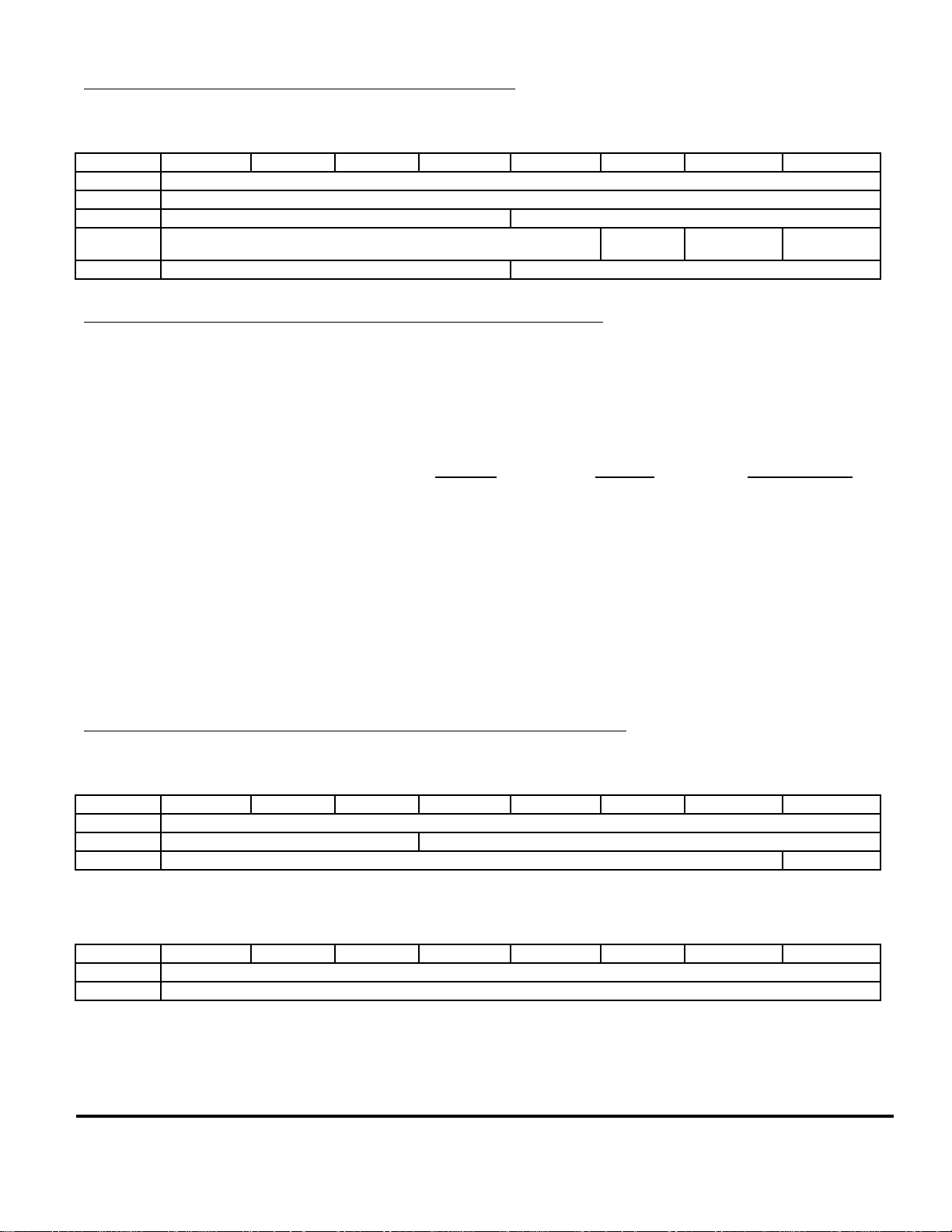
Receiver Description
Bank 1, Group 3, Sub-Group 'F' - OutputClk Registers
Table 29. Group 3, Sub-Group 'F' Read/Write Registers
Address 7 6 5 4 3 2 1 0
66
67
68
69
6A
H
H
H
H
H
Not Used ByPass
Not Used Scale[3:0]
Nominal_value[7:0]
Nominal_Value[15:8]
Nominal_Value[19:16]
LSB_First Serial Mode
Mode
Bank 1, Group 3, Sub-Group 'F' Register Data Field Descriptions
ByPass Mode Setting to 0, enables output clock block to eliminate gaps between MPEG frames.
LSB_First set
Nominal_Value[19:0] The 20-bit value is programmed according to the Annex and QAM type, as shown
below. It controls how fast the output clock is operating by setting the ratio of the
high speed clock to the output clock.
Annex A Annex B STEL Use Only
16-QAM
64-QAM
256-QAM
Scale Controls the amount of jitter in the output clock. If Scale is set to low, acquisition
of the input data will be slower (i.e., locking onto it will take longer) but the clock
will be smoother.
Serial Mode If Serial Mode is 1, the data is serial.
Bank 1, Group 3, Sub-Group 'G' - Reed-Solomon Decoder Registers
Table 30. Group 3, Sub-Group 'G' Read/Write Registers
Address 7 6 5 4 3 2 1 0
70
H
71
H
74
H
Not Used OutputDataRate
Factory Defined Value - CCH = Annex A:, 80H = Annex B:
Not Used CLR_ERR
Table 31. Group 3, Sub-Group 'G' Read-Only Registers
Address 7 6 5 4 3 2 1 0
72
H
73
H
Error_cnt[7:0]
Error_cnt[15:8]
STEL-2176 34 User Manual
Page 44

Receiver Description
Bank 1, Group 3, Sub-Group 'G' Register Data Field Descriptions
Factory Defined Value The specified value must be written to the data field. In a few cases, several values
are provided for selecting a specific mode and one of the specified values must be
written to the data field.
CLR_ERR Clears the Error_cnt register
Error_cnt[15:0] Error_cnt[7:0] is byte 0 of the number of errors found in a block and
Error_cnt[15:8] is byte 1 of the number of errors found in a block.
OutputDataRate The value to be written to the OutputDataRate data field is dependent on the value of
Register FEH[3:0].
When Register FE
0
H
1
H
2
H
4
H
5
H
6
H
8
H
9
H
A
H
[3:0] is: OutputDataRate[4:0] should be set to:
H
10
H
Not Valid
10
H
0A
H
08
H
0A
H
08
H
07
H
Not Valid
with one byte per symbol.
TIMING
The basic input to the receiver is an analog input;
basic outputs consist of data (serial or parallel), an
output clock and a frame sync. These outputs are
shown in the four timing diagrams that follow.
NO GAP, SERIAL MODE
This is similar to the above. Here the frame length is
8ÊX 188 bits, and the Output Clock is for a bit period
rather than a byte period.
There are four output modes depending on whether
there are gaps between frames and depending on
whether the data output is parallel (8 bit) or serial.
The addition of the Read-Solomon checksum creates
gaps in the transmission of the MPEG-2 frame. But
the STEL-2176 provides the option of spreading the
gap over a frame so there appears to be no gap. For
GAPS, PARALLEL MODE
In this mode there are two differences:
The Output Clock is now approximately
8Ênanoseconds.
The Output Clock goes for 188 bytes, then the data
and clock stop until Frame-Sync/ is asserted again.
gap or no-gap mode, data may be parallel or serial.
The four modes are as follows:
GAPS, SERIAL MODE
This mode is the same as above, but here the bytes are
NO GAP, PARALLEL MODE
Here Frame-Sync/ indicates the first byte of an
serialized. There are 8 X 188 clocks and 8 X 188 bits
per Frame-Sync/.
MPEG-2 frame, and Output Clock is approximately
50% of the byte period. There are 188 bytes in a frame
User Manual 35 STEL-2176
Page 45

Receiver Description
DOWNSTREAM OUTPUT TIMING (SERIAL DATA OUTPUT)
Case 1: No Gaps between MPEG-2 Frames.
Frame-Sync/
Data (7..0)
MPEG-2 Sync
Output Clock
~50%
of
Byte’s
Period
Figure 19.
DOWNSTREAM OUTPUT TIMING (SERIAL OUTPUT)
Case 1: No Gaps between MPEG-2 Frames.
Frame-Sync/
TPG 53298.c-7/28/97
Data, MSB, or
LSB first
Output Clock
~50%
of
bits’s
Period
TPG 53300.c-7 /28 /9 7
Figure 20.
STEL-2176 36 User Manual
Page 46

DOWNSTREAM OUTPUT TIMING (PARALLEL DATA OUTPUT)
Case 1: Gaps between MPEG-2 Frames.
188 Bytes, and 204 Clocks
Frame-Sync/
Receiver Description
Data (7..0)
MPEG-2 Sync
Output Clock
~8 n.sec
After 188 clocks and bytes, starting from the Frame Sync,
The output clock will stay ‘low’ till next Frame Sync.
Figure 21.
DOWNSTREAM OUTPUT TIMING (SERIAL DATA OUTPUT)
Case 1: No Gaps between MPEG-2 Frames.
TPG 53299.c-7/28/97
Frame-Sync/
Dat a, MSB, or
LSB first
Output Clock
~8 n.sec
After 8*204 clocks and 8*204 bITS, starting from the Frame Sync,
The output clock will stay ‘low’ till next Ftame Sync.
TPG 53297.c-7/28/97
User Manual 37 STEL-2176
Page 47

Receiver Description
Figure 22.
DE-INTERLEAVER EXTERNAL SRAM TIMING
Internal clock (RES_CLK)
SRAM ADDRESS
SRAMOEb_
SRAMWEb_
SRAMDATA
15 nsec max
15 nsec min. 15 nsec min.
0 nsec min. 15 nsec min. 15 nsec min. 15 nsec min.
15 nsec min.
WCP 53888.C-12/6/97
Figure 23.
STEL-2176 38 User Manual
Page 48

TRANSMITTER
INTRODUCTION
The STEL-21761 contains a highly integrated,
maximally flexible, burst transmitter targeted to the
cable modem market. It receives serial data,
randomizes the data, performs FEC and differential
encoding, maps the data to a constellation before
modulation, and outputs an analog RF signal.
The STEL-2176 is the latest in a series of modulator
chips that comprise the STEL-1103 through
STEL-1109 modulators. Several key components (e.g.,
a 64-bit FIR and a clock multiplier) have been
incorporated in the STEL-2176 and the enhancements
have resulted in significant improvements to the
chipÕs performance.
The STEL-2176 is capable of operating at data rates of
up to 10 Mbps in BPSK mode, 20 Mbps in QPSK
mode, and 40 Mbps in 16QAM mode. It operates at
clock frequencies of up to 165 MHz, which allows its
internal, 10-bit Digital-to-Analog Converter (DAC) to
generate RF carrier frequencies of 5 to 65 MHz.
The STEL-2176 also uses digital FIR filtering to
optimally shape the spectrum of the modulating data
prior to modulation. This optimizes the spectrum of
the modulated signal, and minimizes the analog
filtering required after the modulator. The filters are
designed to have a symmetrical (mirror image)
polynomial transfer function, thereby making the
phase response of the filter linear. This also eliminates
the inter-symbol interference that results from group
delay distortion. In this way, it is possible to change
the carrier frequency over a wide frequency range
without having to change filters, thus providing the
ability to operate a single system in many channels.
The STEL-2176 can operate with very short gaps
between transmitted bursts to increase the efficiency
of Time Division Multiple Access (TDMA) systems.
The STEL-2176 operates properly even when the
interburst gap is less than four (4) symbols (half the
length of the FIR filter response). In this case the
Transmitter Description
postcursor of the previous burst overlaps and is
superimposed on the precursor of the following
burst.
Signal level scaling is provided after the FIR filter to
allow the STEL-2176Õs maximum arithmetic dynamic
range to be utilized. Signal levels can be changed over
a wide range depending on how the device is
programmed.
In addition, the STEL-2176 is designed to operate
from a 3.3 Vdc power supply and the chip can be
interfaced with logic that operates at 5 Vdc.
FUNCTIONAL BLOCK DIAGRAM
DESCRIPTIONS
The STEL-2176 is comprised of the Data Path (see
page 39) and Control Unit (see page 52) sections
shown in Figure 24. The Data Path is comprised of a
Bit Sync Block, Bit Encoder Block (i.e.,Êthe Scrambler,
Reed-Solomon Encoder, and two Multiplexers shown
in Figure 25), Symbol Mapper Block (i.e., the Bit
Mapper, Differential Encoder, and Symbol Mapper
are shown in Figure 28), two channels (one for I and
one for Q), a Combiner, and a 10-bit DAC. Each
channel consists of a Nyquist Filter, Interpolation
Filter, and Modulator. The Control Unit is comprised
of a Bus Interface Unit (BIU), Clock Generator, and
NCO.
Table 32 summarizes the main features of the circuits
described by the remaining paragraphs of this
section.
DATA PATH DESCRIPTION
Bit SYNC Block
The Bit Sync Block has two functions: latching input
data, and synchronizing the STEL-2176 TXBITCLK
and symbol counters to the user data.
1
The STEL-2176 utilizes advanced signal processing
techniques which are covered by U.S. Patent Number
5,412,352.
PRODUCT INFORMATION 39 STEL-2176
Page 49

Transmitter Description
Table 32. Transmit Features
Feature Characteristic
Carrier frequency: 5 to 65 MHz (maximum of approximately 40% of master clock)
Symbol rate: From Master clock divided by 16 down to Master clock divided by 16384
FIR filter tap coefficients: 64 programmable taps (10 bits each), symmetric response
Modulation: BPSK, QPSK, or 16QAM
16QAM constellation: Eight selectable bit-to-symbol mappings
I and Q modulator signs / Spectral
Inversion
Reed-Solomon Encoder: Selectable on/off
Scrambler: Selectable on/off
Differential Encoder: Selectable on/off
(in steps of 4) yielding a maximum symbol rate of 10 Msps with a 160 MHz clock.
Five selectable symbol-to-constellation mappings
Signs of I and Q plus the mapping to Sine and Cosine carriers is programmable.
Two selectable generator polynomials
Block length shortened any amount
Error correction capability T = 1 to 10
Self-synchronizing or frame synchronized (sidestream)
Location before or after RS Encoder
Programmable generator polynomial
Programmable length up to 2
24
- 1
Programmable initial seed
TXDIFFEN
TXTCLK
TXTSDATA
TXDATAENI
TXRDSLEN
TXSCRMEN
V
DDA
V
DD5
V
DD
TXRSTB
TXCLKEN
TXCLK
TXNCOLD
TXFCWSEL
DATA
7-0
ADDR
5-0
DSB
WRB
CS
COS 2πFT
DATA PATH
Modulator
SIN 2πFT
10-Bit
DAC
DACOUTP
DACOUTN
TXDATAENO
TXCKSUM
TXBITCLK
TXSYMPLS
TXACLK
BIT
Sync
Block
I
,
Symbol
[1:0]
Mapper
Q
[1:0]
4
BIT
Encoder
Block
SAMPLS
MASTER CLOCK (CLK)
Master
Clock
Generator
1-0
Bus
Interface
Unit
(Group 2
Registers)
Block
Numerically
Controlled
Oscillator
I
[1:0]
2
Q
2
[1:0]
Nyquist
Filter
Nyquist
Filter
Interpolating
Filter
Interpolating
Filter
WCP 53806.c-12/7/97
Figure 24. STEL-2176 Transmitter Block Diagram
STEL-2176 40 User Manual
Page 50

Transmitter Description
Table 33. Data Latching Options
Data Source Latched By Register 2C Bit 7 Register 2D Bits 1,0 Mode Name
TXTSDATA TXBITCLK 0 X,0 Master Mode
TXTSDATA TXTCLK 1 X,0 Slave Mode
PN Code 10, 3 TXBITCLK 0 0,1 Test Mode
PN Code 23, 18 TXBITCLK 0 1,1 Test Mode
Latching Input Data
Latching of input data is accomplished in one of three
modes:
• Externally supplied TXTSDATA is latched by the
internal TXBITCLK (Master mode).
• Externally supplied TXTSDATA is latched by an
externally provided TXTCLK (Slave mode).
• Internally generated PN code data is latched by the
internal TXBITCLK (Test mode).
See Table 33 for register settings to implement each
mode.
TXBITCLK latches data on its falling edge. TXTCLK
latches data on its rising edge.
Whenever the TXCLKEN input is low, the TXBITCLK
output will stop. There is also an auxiliary continuous
clock (TXACLK) output which is discussed later in the
clock generator section. The TXACLK output is
primarily for use in master mode where users may
need a clock to run control circuits during the time
between bursts.
When using slave mode, the data that is latched by the
rising edge of TXTCLK is re-latched internally by the
next falling edge of TXBITCLK which re-synchronizes
the data to the internal master clock.
Synchronizing TXBITCLK / TXSYMPLS
The synchronization circuit aligns the STEL-2176
TXBITCLK and its TXSYMPLS counter circuits to the
beginning of the first user data symbol. The circuit has
two parts, an arming circuit and a trigger circuit. Once
armed, the first rising edge on the TXTCLK input will
activate (trigger) the synchronization process.
The circuit can be armed in two ways; taking
TXCLKEN from low to high, or toggling Block 2
Register 2EH bit 0 from low to high to low again. In a
normal burst mode application, the circuit is
automatically re-armed between bursts because
TXCLKEN goes low. For applications that will not
allow TXCLKEN to cycle low between bursts, some
system level precautions should be observed to
maintain synchronization of user data to the STEL-2176
TXBITCLK.
Once triggered, the sync circuit re-starts the TXBITCLK
and TXSYMPLS counters. The TXBITCLK output starts
high, and TXSYMPLS resets to the start of a symbol.
There is a delay equal to about three cycles of the
master clock from the rising edge of the TXTCLK input
before this re-start occurs. During this brief delay
period, the TXBITCLK and TXSYMPLS counters are
still free running and may or may not have transitions.
In master mode, the rising edge of TXTCLK normally
marks the transition of the first user data bit (which will
be latched in by the next falling edge of TXBITCLK). In
slave mode, the first user data bit must already be valid
at this first rising edge of TXTCLK.
Bit Encoder Block
The Bit Encoder Block consists of a Scrambler, a
Reed-Solomon Encoder, and data path controls
(multiplexers), as shown in Figure 25.
Data Path Control (Multiplexers)
The STEL-2176 provides a great deal of flexibility and
control over the routing of data through or around the
encoding functions. With appropriate register
selections, data can be routed around (bypass) both
encoders, through either one and around the other,
through the scrambler then the RS Encoder, or through
the RS Encoder and then the scrambler. Control over
the bypassing can be set for software control or external
(user) input signal control. Generally, if an encoding
function will be left either on or off continuously, then
software control is appropriate. If the function must be
turned on and off dynamically (typically in order to
send the preamble Ôin the clearÕ i.e. unencoded), then
external (user) input control is required. If the ReedSolomon encoder will not be used at all, then a separate
User Manual 41 STEL-2176
Page 51

Transmitter Description
bypass option can be activated to remove an 8-bit delay
register from the data path that is required if the
possibility of turning on the encoder exists. Each of the
external (user) input control pins (if enabled) turns on
the encoding function when high and bypasses the
function when low.
The TXDATAENI input signal determines whether or
not data will advance (shift through) the encoding
blocks. The presence of a high on the TXDATAENI
input when the TXBITCLK output goes low allows the
circuits to advance data through them. The
TXDATAENI signal is delayed internally to allow the
rising edge of TXDATAENI to coincide with the first
rising edge of TXTCLK.
Table 34. BIT Encoding Data Path Options
Data Path Register 36 Bits 6,5 Register 38 Bits 7-2
Data stopped (continuously) X,X 01 XXÊXX
Data path on (continuously) X,X 11 XXÊXX
Data path enabled by pin 109 X,X X0 XXÊXX
Scrambler off (continuously) X,X XXÊXX 01
Scrambler on (continuously) X,X XXÊXX 11
Scrambler enabled by pin 118 X,X XXÊXX X0
RS Encode off (continuously) 1,X XX 01 XX
RS Encode on (continuously) 1,X XXÊ11 XX
RS Encode enabled by pin 117 1,X XXÊX0 XX
Scrambler then RS Encoder 1,1 XXÊXXÊXX
RS Encoder then Scrambler 1,0 XXÊXXÊXX
Bypass RS Encoder 0,X XXÊXXÊXX
TXSCRMEN
SERIAL
DATA
TXDATAEN
TXRDSLEN
S-RS
Input
Scrambler
Reed-Solomon
Multiplexer
Encoder
ENCODED
SERIAL DATA
Output
Multiplexer
WCP 53808.c-12/5/97
CHKSUM
SIGNAL
Figure 25. Bit Encoder Functional Diagram
See Table 34 for a summary of register settings required
to achieve the various data path possibilities.
Scrambler
generate a PN code pattern. All 24 registers are
presettable and any combination of the registers can be
The scrambler can be used to randomize the serial data
in order to avoid a strong spectral component that
might otherwise arise from the occurrence of repeating
patterns in the input data. The Scrambler (Figure 26)
connected (tapped) to form any polynomial of up to 24
bits. The scrambler may be either frame synchronized
or self synchronized. Table 35 shows the registers
involved.
uses a Pseudo-Random (PN) generator to
STEL-2176 42 User Manual
Page 52

Transmitter Description
24-bit Mask Reg
24-bit INIT Reg
24-bit Shift Reg
TXSCRMEN
SERIAL INPUT
SSYNC
123 222324
123 222324
123 222324
XOR
AND
XOR
SELF
SYNC
MUX
FRAME
SYNC
SERIAL OUTPUT
WCP 53809.c-12/2/97
Figure 26. Scrambler Block Diagram
The value in the INIT registers is loaded into the
scrambler shift registers whenever the scrambler is at
disabled. The scrambler will scramble data one bit a
time at each falling edge of TXBITCLK that occurs
while both the scrambler and TXDATAENI are active
(enabled). Internal delays on the TXSCRMEN control
signal input allow for a rising edge to occur coincident
with the rising edge of TXBITCLK that precedes the
latching of the first data bit to be scrambled.
The Mask, Init, and SSync fields can be programmed
for different scrambler configurations. For example, the
DAVIC Scrambler configuration shown in Figure 27 can
be implemented by programming the Mask, Init, and
SSync fields with the values indicated by Table 36.
100101010000000
123456789101112131415
EX-OR
Enable
AND
EX-OR
Clear Data Input
Randomized Data
WCP 52984.c-4/26/97
Figure 27. DAVIC Scrambler
Table 35. Scrambler Parameters
Parameter Characteristic Block 2 Register Setting
Generator
Polynomial
(Mask Reg)
Seed
(INIT Reg)
Scrambler
Type
Scrambler
Type
p(x) = c24x24 + c23x23 + É + c1x + 1
where c
Any 24-bit binary value, s
is a binary value (0, 1)
i
24-1
Frame synchronized (sidestream) Register 36 Bit 4
Self-synchronized Register 36 Bit 4
Register 35
Bit 7 to Bit 0
c
to c
24
17
Register 32
Bit 7 to Bit 0
s
to s
24
17
Set to zero
Set to one
Register 34
Bit 7 to Bit 0
c
to c
16
9
Register 31
Bit 7 to Bit 0
s
to s
16
9
Table 36. Sample Scramble Register Values
Parameter Characteristic Block 2 Register Setting
Generator
Polynomial
(Mask Reg)
Seed
(INIT Reg)
Scrambler
Type
p(x) = x15 + x14 + 1 Register 35
Bit 7 to Bit 0
0000Ê0000
0000A9
H
Register 32
Bit 7 to Bit 0
0000Ê0000
Frame synchronized (sidestream) Register 36 Bit 4
Set to zero
Register 34
Bit 7 to Bit 0
0110Ê0000
Register 31
Bit 7 to Bit 0
0000Ê0000
Register 33
Bit 7 to Bit 0
c8 to c
1
Register 30
Bit 7 to Bit 0
s
to s
8
1
Register 33
Bit 7 to Bit 0
0000Ê0000
Register 30
Bit 7 to Bit 0
1010 1001
User Manual 43 STEL-2176
Page 53

Transmitter Description
Reed - Solomon Encoder
the RS Encoder inserts its checksum (2T bytes of data)
into the data path. There is no adverse effect to letting
The STEL-2176 uses a standard Reed-Solomon (RS)
Encoder for error correction encoding of the serial data
stream. The error correction encoding uses GF (256) and
can be programmed for an error correction capability of
1 to 10, a block length of 3 to 255, and one of two
primitive polynomials using the data fields listed in
TXTCLK or TXTSDATA continue to run during the
checksum; the data input will be ignored. TXCKSUM
will be asserted high to indicate that the checksum
bytes are being inserted into the data stream and will be
lowered at the end of the checksum data insertion. The
width of the TXCKSUM pulse is 2T bytes.
Table 37
The STEL-2176 registers include two bits for
When TXDATAENI is high and the RS Encoder is
enabled, the serial data stream both passes straight
through the RS Encoder and also into encoding
circuitry. The encoding circuitry computes a checksum
determining the bit order for data into and checksum out
of the RS Encoder circuitry. Set these to match the ReedSolomon decoding circuitry along with the other
parameters.
that is 2T bytes long for every K bytes of input data.
After the last bit of each block of K bytes of input data,
.
Table 37. Reed-Solomon Encoder Parameters
Field Name Block 2 Register Description
PP 36H (bit 7) 1-bit field for selecting Primitive Polynomial:
8
0 ⇒ p(x) = x
1 ⇒ p(x) = x
T36
K37
LDLSBF 39H (bit 4) Determines whether the first bit of the serial input is to be the MSB (bit 4 = 0) or
TRLSBF 39H (bit 5) Determines whether the MSB (bit 5 = 0) or LSB (bit 5 = 1) of the RS Encoder
Notes:
GF (256).
Code generator polynomial 1 is used when PP=1:
Code generator polynomial 2 is used when PP=0.
(bits 3-0) 4-bit field for setting Error Correction Capability. Programmable over the range of
H
(bits 7-0) 8-bit field for setting User Data Packet Length (K) in bytes.
H
1 to 10.
Programmable over the range of 1 to (255 - 2T). [ Net block length, N = K + 2T ]
LSB (bit 4 = 1) of the byte applied to the RS Encoder.
checksum byte is to be the first bit of the serial output data.
+ x4 + x3 + x2 + 1
8
+ x7 + x2 + x + 1
119 2
T
+
Gx x
() ( )=−
∏
120
i
Gx x
() ( )=−
=
T
−
21
∏
i
=
0
i
α
i
α
α
α 02
=
= 02H
H
STEL-2176 44 User Manual
Page 54

Transmitter Description
Symbol Mapper Block
The Symbol Mapper Block (Figure 28) maps the serial
data bits output by the Bit Encoder Block to symbols,
differentially encodes the symbols, and (in 16QAM)
maps the symbols to one of five constellations. The
Symbol Mapper Block functions are modulation
dependent. The modulation mode also defines the
number of bits per symbol. The Symbol Mapper Block
outputs 2 bits for each symbol to each of the two
Nyquist (FIR) Filters.
ENCODED
SERIAL DATA
1
TXDIFFEN
1
Bit
Mapper
I
[1:0]
Q
[1:0]
4
**
**
Differential
Encoder
I
[1:0]
Q
[1:0]
4
*
*
Symbol
Mapper
I
[1:0]
2
Q
[1:0]
2
WCP 53810.c-12/2/97
Figure 28. Mapping Block Functional Diagram
Bit Mapper
The Bit Mapper receives serial data and maps the serial
data bits to output symbol bits (I
, I
1
**
, Q
0
, and Q
1
**
0
**
**
There are four output bits per symbol even in BPSK and
QPSK modes. In BPSK, all bits are set equal to each
other. In QPSK, each input symbol bit drives a pair of
output bits. The four symbol bits are routed to the
Differential Encoder in parallel.
For BPSK modulation, each bit (symbol = b0) of the
**
input serial data stream is mapped directly to I
**
I
, and Q
0
**
(i.e., I
0
**
**
**
= I
0
= Q
1
1
**
= Q
= b0). Thus, bit
0
**
, Q
1
1
mapping has no affect on the respective value of the
symbolÕs four bits, as shown in Table 38.
For QPSK modulation, each pair of bits (a dibit) forms a
symbol (b0 b1). The QPSK dibit is mapped so that
**Ê
**
I
=ÊI
and Q
1
0
1
** =
**,
Q
as shown in Table 38.
0
For 16QAM, every four bits (a nibble) forms a symbol
**
**
(b0b1b2b3). The 16QAM nibble is mapped to I
**
and Q
, as shown in Table 38.
0
, Q
1
**
, I
1
0
).
,
,
Table 38. Bit Mapping Options
Bit-To-Symbol Mapping Bit Mapping Mod Mode
Mode
BPSK I
**
Q
1
QPSK I
QPSK Q
16QAM I
16QAM Q
16QAM I
16QAM Q
16QAM I
16QAM Q
16QAM I
16QAM Q
b
0
**
**
**
I
Q
1
0
0
**
**
I
1
0
**
**
Q
1
0
**
1
**
1
**
0
**
0
**
1
**
1
**
0
**
0
b
1
N/A N/A N/A XXX 1X
**
**
Q
Q
1
0
**
**
I
I
1
0
**
I
0
**
Q
0
**
I
1
**
Q
1
**
Q
1
**
I
1
**
Q
0
**
I
0
Note: b0 is the first serial data bit to arrive at the Bit Mapper
Differential Encoder
The Differential Encoder encodes the bits (i.e., I
**
Q
1
, and Q
**
) of each symbol received from the Bit
0
Mapper to determine the output bit values (i.e., I
*
I
, and Q
0
*
), which are routed to the Symbol Mapper.
0
b
2
b
3
bits 6-4
N/A N/A XX0 00
N/A N/A XX1 00
Register 2D
**
Q
1
**
I
1
**
Q
0
**
I
0
**
I
0
**
Q
0
**
I
1
**
Q
1
**
**
, I
1
The differential encoder can be either enabled or
,
0
**
Q
0
**
I
0
**
Q
1
**
I
1
**
Q
0
**
I
0
**
Q
1
**
I
1
000 01
001 01
010 01
011 01
100 01
101 01
110 01
111 01
bypassed under the control of either a register bit or a
*
*
1
, Q
user supplied control signal (TXDIFFEN). The selection
,
1
between user input pin control or register control is
made in another register bit, as shown in Table 39.
Register 2C bits
3,2
User Manual 45 STEL-2176
Page 55
Transmitter Description
Table 39. Differential Encoder Control
Register 38
Level/Value
Bits 1,0
Encoding off (continuously) 0,1
Encoding on (continuously) 1,1
Encoding enabled by pin 116
X,0
high - enable the Differential Encoder
low - disable the Differential Encoder
For any modulation mode, if differential encoding is
disabled then:
*
*
*
I
Q
I
1
1
0
Q
0*Ê=ÊI1
**
**
**
I
0
**
Q
Q
1
0
If differential encoding is enabled, then the results are
described below for each modulation type.
BPSK
In BPSK mode, the next output bit is found by XORing
the input bit with the current output bit. The result is a
Table 40. QPSK Differential Encoding and Phase Shift
180 degree phase change if the output is high and
0Êdegrees if the output is low.
QPSK
In QPSK mode, the next output dibit is found by
XORing the input dibit with the current output dibit.
Table 40 shows the results of the differential encoding
performed for QPSK modulation and the resulting
phase shift. In the table, I = I1 = I0 and Q = Q1= Q0.
16 QAM
In 16QAM mode, the differential encoding algorithm is
the same as in QPSK. Only the two MSBÕs, I
are encoded. The output bits I
the inputs bits I
**
and Q
0
**
.
0
*
and Q
0
*
are set equal to
0
1**
and Q
1
**
Current Input
(IQ)
Current Output
(IQ)
Next Output
(IQ)
00 00 00 0
01 01 -90 (CW)
10 10 90 (CCW)
11 11 180
01 00 01 -90 (CW)
01 11 180
10 00 0
11 10 90 (CCW)
10 00 10 90 (CCW)
01 00 0
10 11 180
11 01 90 (CCW)
11 00 11 180
01 10 90 (CCW)
10 01 -90 (CW)
11 00 0
Phase Shift
(degrees)
STEL-2176 46 User Manual
Page 56

Symbol Mapper
*
*
The Symbol Mapper receives I
1
, Q
*
, I
, Q
1
0
of each
0*
symbol. Based on the signal modulation and the symbol
mapping selection, the Symbol Mapper block maps the
symbol to a constellation data point (I1,Q1,I0,Q0). The
Symbol Mapping field (bits 7-5 of Block 2 Register 2EH)
will map the four input bits to a new value, as indicated
in Table 41.
BPSK and QPSK
For BPSK and QPSK, the settings of the symbol to
constellation mapping bits is ignored. The
constellations for BPSK (Figure 29) and QPSK (Figure
30) are shown below. I1Q1 values are indicated by large,
bold font (00 and 11) and I0Q0 values by the smaller
font (00 and 11).
16 QAM
For 16QAM modulation, the Symbol Mapper maps
each input symbol to one of the 16QAM constellations.
The specific constellation is programmed by the Symbol
Transmitter Description
Mapping field (bits 7-5 of Block 2 Register 2EH) to select
the type of symbol mapping. If the MSB of the Symbol
Mapping field is set to 0, the mapping will be bypassed
*
*
*
and I1Q1I0Q0 = I
Q
1
*
I
Q
. The resulting constellation
1
0
0
(Figure 31) is the natural constellation for the
STEL-2176.
If the MSB of the Symbol Mapping field is set to 1, bits
6-5 can select any of four possible types of symbol
mapping (Gray, DAVIC, Left, or Right), as indicated by
Table 41.
Table 42 summarizes the symbol mapping and the
resulting constellations are shown in Figure 31 and
Figure 32. In these figures, I1Q1 are indicated by large,
bold font (00, 01, 10, and 11) and I0Q0 by the
smaller font (00, 01, 10, and 11).
Q
3
1
-3 -1 1 3
-1
00
-3
00
Figure 29. BPSK Constellation
11
WCP 52999.c-10/29/97
11
Q
01 11
3
1101
1
I
-3 -1 1 3
I
-1
00 10
00
-3
Figure 30. QPSK Constellation
10
WCP 52986.c-10/29/97
User Manual 47 STEL-2176
Page 57

Transmitter Description
Q
10
10
11
-3 -1 1 3
10
11
11
00
01
00
01
10
00
1
11
10
01
11 01
WCP 52987.c-10/29/97
Figure 31. Natural Mapping Constellation
Table 41. Symbol Mapping Selections
00
01
Mapping
Selection
Natural 0XX
Gray 100
DAVIC 101
Left 110
Right 111
I
00
Table 42. Symbol Mapping
Register 2E
Bits 7-5
Input Code
Natural
Mapping
(Bypass)
*
*
I
Q
1
1
*
*
I
Q
0
0
Gray DAVIC Left Right
*
*
*
I
Q
1
*
I
Q
1
0
0
*
*
*
I
Q
1
*
I
Q
1
0
0
*
*
*
I
Q
1
*
I
Q
1
0
0
*
*
*
I
Q
1
*
I
Q
1
0
0
0000 0011 0011 0011 0011 0000
0001 0010 0001 0010 0001 0001
0010 0001 0010 0001 0010 0010
0011 0000 0000 0000 0000 0011
0100 0110 0110 0101 1010 0100
0101 0111 0111 0111 1011 0101
0110 0100 0100 0100 1000 0110
0111 0101 0101 0110 1001 0111
1000 1001 1001 1010 0101 1000
1001 1000 1000 1000 0100 1001
1010 1011 1011 1011 0111 1010
1011 1010 1010 1001 0110 1011
1100 1100 1100 1100 1100 1100
1101 1101 1110 1101 1110 1101
1110 1110 1101 1110 1101 1110
1111 1111 1111 1111 1111 1111
Output
Code
I
Q
1
1
I0 Q
0
STEL-2176 48 User Manual
Page 58
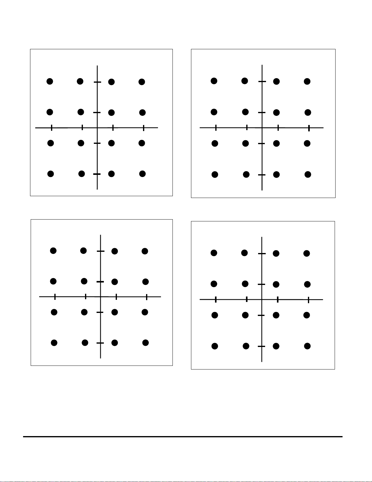
Transmitter Description
Q
11
01
-3 -1 1 3
00
11
01
0010
0010
11
1
10
01
Figure 32. Gray Coded Constellation
Q
1101
1000
I
1000
1101
WCP 52988.c-10/29/97
Q
11
10
-3 -1 1 3
11
11
01
0010
0001
00
1
10
10
WCP 52990.c-4/26/97
Figure 34. DAVIC Coded Constellation
Q
1110
0100
I
1000
1101
11
10
-3 -1 1 3
11
11
10
0001
0010
00
1
01
01
Figure 33. Left Coded Constellation
1101
1000
0100
1110
WCP 52989.c-4/26/97
11
01
I
-3 -1 1 3
11
11
01
0010
0001
10
1110
00
1
0100
I
1000
10
1101
WCP 52991.c-4/26/97
Figure 35. Right Coded Constellation
User Manual 49 STEL-2176
Page 59

Transmitter Description
Nyquist FIR Filter
The finite impulse response (FIR) filters are used to
shape each transmitted symbol pulse by filtering the
pulse to minimize the sidelobes of its spectrum. The
Symbol Mapper Block outputs the I1I0 data to a pair of
I-channel FIR filters and the Q1Q0 data to a pair of
Q-channel FIR filters. Figure 36 shows the filter block
diagram for a channel pair (I or Q). The FIR filter can
be bypassed altogether or, in BPSK or QPSK modes,
individual channels can be turned on and off which
changes the effective filter gain. Table 43 shows the
various FIR configuration options.
Table 43. FIR Filter Configuration Options
Mode Gain
Bits 4-1
No FIR Filter N/A XXXX 1
16QAM Unity 1010 0
BPSK/QPSK Unity 0000 0
BPSK/QPSK x2 1111 0
BPSK/QPSK x3 1010 0
Register 2E
Register 2C
Bit 1
Each of the 32-tap, linear phase, FIR filters use
16Êten-bit, coefficients, which are completely programmable for any symmetrical (mirror image) polynomial. The FIR filter coefficients are stored in
addresses 09H - 28H, using two addresses for each 10-bit
coefficient as shown in Table 50. The coefficients are
stored as TwoÕs Complement numbers in the range -512
to +511 (200H to 1FFH). The filter is always constrained
to have symmetrical coefficients, resulting in a linear
phase response. This allows each coefficient to be stored
once for two taps, as shown in Table 44.
Interpolating Filter
The Interpolating Filter, shown in Figure 37, is a
configurable, three-stage, interpolating filter. The filter
increases the STEL-2176Õs sampling rate (to permit the
wide range of RF carrier frequencies possible) by
interpolating between the FIR filter steps at the master
clock frequency. This smoothes the digital
representation of the signal which removes spurious
signals from the spectrum
The interpolation filter contains accumulators. As the
interpolation ratio grows larger, the number of
accumulations per period of time increases. If the
interpolation ratio becomes too large, the accumulator
Table 44. FIR Filter Coefficient Storage
MSB
(Bits 9-8)
0A
H
0C
H
0E
H
10
H
ÉÉ É
ÉÉ É
26
H
28
H
3B
H
3D
H
ÉÉ É
ÉÉ É
56
H
58
H
5A
H
Note: For MSB storage, only bits 1-0 are used.
I
1/Q1
COEFFICIENT
I
0/Q0
CLRFIR
BYPASS
FIR
FIR
2
LSB
(Bits 7-0) Filter Taps
X2
0
09
H
0B
H
0D
H
0F
H
25
H
27
H
3A
H
3C
H
55
H
57
H
59
H
1
M
0
1
M
U
X
Taps 16 and 47
Taps 17 and 46
Taps 18 and 45
Taps 19 and 44
Taps 30 and 33
Taps 31 and 32
Taps 0 and 63
Taps 1 and 62
Taps 13 and 50
Taps 14 and 49
Taps 15 and 48
U
X
WCP-52992.c-4/26/97
L
O
OUT
G
I
C
Figure 36. Nyquist FIR Filter
STEL-2176 50 User Manual
Page 60

Transmitter Description
Data Enable
16
2
3-Stage
Differentiator
4
16
G
a
i
n
3-Stage
Integrator
1132
WCP 52993.c-5/2/97
Bypass
Sample
Clock
Gain Control
Master Clock
Figure 37. Interpolation Filter Block Diagram
will overflow which will destroy the output spectral
characteristics. To compensate for this, the interpolation
filter has a gain function. This gain is normally set
empirically. If the output spectrum is broad band noise
or if it appears correct but has regular momentary
ÒhitsÓ of broad band spectral noise, then the digital gain
is too high. The interpolation filter gain is the first place
to adjust gain because it does not directly affect the
shape of the signal spectrum and it has a very wide
adjustment range. Overall, gain can affected in the FIR
filter function, the interpolation gain function, and by
the number of interpolation stages (and therefore
accumulators) used.
Normally, three interpolation stages are used, but there
is a bypass option for use when the interpolation is very
high. It should be used only as a last resort after all
other gain reduction options have been exercised
because of the severe impact to spurious performance.
The register bits that affect the interpolation filter
functions are shown in Table 45 and Table 46.
Modulator
The interpolated I and Q data signals are input from the
Interpolation Filter, fed into two complex modulators,
and multiplied by the sine and cosine carriers which are
generated by the NCO. The I channel signal is
multiplied by the cosine output from the NCO and the
Q channel signal is multiplied by the sine output. The
resulting modulated sine and cosine carriers are
applied to an adder and either added or subtracted
together according to the register settings shown in
Table 47. This provides control over the characteristics
of the resulting RF signal by allowing either or both of
the two products to be inverted prior to the addition.
Data Enable Output. The TXDATAENO output is a
modified replica of the TXDATAENI input.
TXDATAENO is asserted as a high 2 symbols after
TXDATAENI goes high and it is asserted as a low 13
symbols after TXDATAENI goes low. In this way, a
high on the TXDATAENO line indicates the active
period of the DAC during transmission of the data
burst. However, if the guard time between the current
and next data burst is less than 13 symbols, then the
TXDATAENO line will be held high through the next
burst.
Table 45. Interpolation Filter Bypass Control
Number of
Interpolation Stages
Selected
3 0Ê0
2 0Ê1
2 1Ê0
1 1Ê1
Interpolation Filter Bypass
Register 2B Bits 5,4
Table 46. Interpolation Filter Signal Level Control
Gain Factor
(Relative)
0
2
1
2
2
2
3
2
4
2
5
2
6
2
7
2
8
2
9
2
10
2
11
2
12
2
13
2
14
2
15
2
Filter Gain Control
Register 2A Bits 7-4
0
H
1
H
2
H
3
H
4
H
5
H
6
H
7
H
8
H
9
H
A
H
B
H
C
H
D
H
E
H
F
H
User Manual 51 STEL-2176
Page 61

Transmitter Description
Table 47. Signal Inversion Control
Output of Adder Block
Sum = I
Sum = ÐI
Sum = I
Sum = ÐI
.
cos(ωt) + Q
.
cos(ωt) + Q
.
cos(ωt) Ð Q
.
cos(ωt) Ð Q
.
sin(ωt) 0Ê0
.
sin(ωt) 0Ê1
.
sin(ωt) 1Ê0
.
sin(ωt) 1Ê1
Invert I/Q Channel
Register 2B Bits 1,0
10-Bit DAC
The 10-bit Digital-to-Analog Converter (DAC) receives
the modulated digital data and the Master clock. The
DAC samples the digital data at the rate of the Master
CONTROL UNIT DESCRIPTION
Bus Interface Unit
The Bus Interface Unit (BIU) is part of the
Microcontroller Interface (see page 11). If contains the
Block 2 Registers (90 programmable 8-bit registers). The
Reset (
STEL-2176. Asserting a low on
contents of all Block 2 Registers to 00H (as well as
clearing the data path registers). Asserting a high on
TXRSTB enables normal operation. After power is
applied and prior to configuring the STEL-2176, a low
should be asserted on
asynchronous, the TXCLKEN input should be held low
whenever
The parallel address bus (ADDR
of the 90 Block 2 Registers by placing its address on the
ADDR
bi-directional data bus for writing data into or reading
data from the selected Block 2 Register.
TXRSTB ) input signal is the master reset for the
TXRSTB will reset the
TXRSTB . Since TXRSTB is
TXRSTB is low.
) is used to select one
5-0
bus lines. The data bus (DATA
5-0
) is an 8-bit,
7-0
clock and outputs a direct analog RF signal at a
frequency of 5 to 65 MHz. The DAC outputs,
DACOUTP and DACOUTN, are complementary
current sources designed to drive double terminated
50Ω or 75Ω (25Ω or 37.5Ω total) load to ground. The
nature of digitally sampled signals creates an image
spur at a frequency equal to the Master Clock minus the
output RF frequency. This image spur should be
filtered by a user supplied low pass filter. For best
overall spurious performance, the gain of the STEL2176 should be the highest possible (before digital
overflow occurs - see Interpolation Filter discussion).
Register selected by ADDR
. The Write/Read (
5-0
WRB )
input signal is used to control the direction of the Block
2 Register access operation. When
WRB is high, the
data in the selected Block 2 Register is output onto the
DATA
DSB is used to latch the data on the DATA
bus. When
7-0
WRB is low, the rising edge of
bus into
7-0
the selected Block 2 Register. (Refer to the Write and
Read Timing diagrams in the Timing Diagrams
section.)
Some of the Block 2 Register data fields are used for
factory test and must be set to specific values for
normal operation. These values are noted in Table 50.
Master Transmit Clock Generator
The STEL-2176 uses a master clock (CLK) to control the
transmit timing functions. CLK can be generated in
either of three ways as shown in Figure 38.
The access operation is performed using the control
signals
DSB , CS , and WRB . The Chip Select ( CS ) input
signal is used to enable or disable access operations to
the STEL-2176. When a high is asserted on
CS , all
access operations are disabled and a low is asserted to
enable the access operations. The
CS input only affects
Block 2 Register access and has no effect on the data
path.
The Data Strobe (
data that is on the data bus (DATA
DSB ) input signal is used to write the
) into the Block 2
7-0
A transmit bypass clock can be applied to the
TXBYPCLK input and selected to drive CLK.
An external clock can be applied to the TXOSCIN input
or a crystal can be connected across the TXOSCIN and
TXOSCOUT inputs. The oscillator circuit outputs a
20-50 MHz signal to a frequency multiplier PLL, which
upconverts the signal to a 100-150 MHz clock. When the
bypass clock is not used, the multiplexer is set to select
the output of the frequency multiplier to drive the CLK
signal. The frequency multiplier output can also be
routed to the TXPLLCLK output for test purposes.
STEL-2176 52 User Manual
Page 62
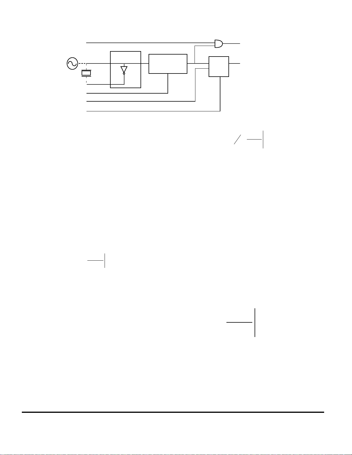
Transmitter Description
ENCLKOUT
TXOSCIN
(20-50 MHz)
TXOSCOUT
TXPLLEN
TXBYPCLK
TXBYPASSFSYN
OSCILLATOR
FREQUENCY
MULTIPLIER
Figure 38. Master Clock Generation
Clock Generator
The timing of the STEL-2176 is controlled by the Clock
Generator, which uses an master clock (CLK) and
programmable dividers to generate all of the internal
and output clocks. There are primarily two clock
systems, the auxiliary clock and the data path timing
signals (bit, symbol, and sampling rate signals).
The auxiliary clock (TXACLK) output is primarily for
use in master mode where users may need a clock to
run control circuits during the guard time between
bursts (when TXCLKEN is low and TXBITCLK has
stopped). The output clock rate is set by the frequency
(f
) of the external master clock and the value (N) of
CLK
the Auxiliary Clock Rate Control field (bits 3-0 of Block
2 Register 2AH). The clock rate is set to:
f
TXACLK =
CLK
N+1
2 N 15
≤≤
If N is set to 1 or 0, the TXACLK output will remain set
high, thereby disabling this function. If the TXACLK
signal is not required, it is recommended that it be set
in this mode to conserve power consumption. The
TXACLK output is a pulse that will be high for 2 cycles
of CLK and low for (N-1) CLK cycles. Unlike other
functions, the TXACLK output is not affected by
TXCLKEN.
The data path timing is based on the ratio of the master
clock frequency to the symbol data rate. The ratio must
be a value of four times an integer number (N+1). The
value of N must be in the range of 3 to 4095. This value
is represented by a 12-bit binary number that is
programmed by LSB and MSB Sampling Rate Control
fields [Block 2 Register 29H (LSB) and bits 3-0 of Block 2
Register 39H (MSB)], which sets the TXSYMPLS
frequency [based on the frequency (f
) of the external
CLK
master clock] to:
TXPLLCLK
CLK
PLL
MUX
Symbol Rate =
(100-165 MHz)
WCP 53854.c-12/8/97
f
CLK
1
∗
4
N1
3 N 4095
≤≤
+
The symbol pulse (TXSYMPLS) signal output is
intended to allow the user to verify synchronization of
the external serial data (TXTSDATA) with the
STEL-2176 symbol timing. TXSYMPLS is normally low
and pulses high for a period of one CLK cycle at the
point where the last bit of the current symbol is
internally latched by the falling edge of the internal BIT
Clock (TXBITCLK) signal. (Refer to the Timing
Diagrams section.)
The internal TXBITCLK period is a function of the
MOD field (bits 3-2 of Block 2 Register 2CH), which
determines the signal modulation. TXBITCLK has a
50% duty cycle for BPSK and QPSK modes. It also has
a 50% duty cycle in 16QAM mode when N+1 is even. If
N+1 is odd, then TXBITCLK will be high for (N÷2)+1
clocks and then low for N÷2 clocks. (Refer to the Bit
Clock Synchronization Timing diagram in the Timing
Diagrams section.)
The TXBITCLK frequency is determined by :
BITCLK =
CLK
(N+1) K
K = 1 for 16QAM,
2 for QPSK,
∗
4 for BPSK
3 N 4095
≤≤
NCO
A 24-bit, Numerically Controlled Oscillator (NCO) is
used to synthesize a digital carrier for output to the
Modulator. The NCO gives a frequency resolution of
about 6 Hz at a clock frequency of 100 MHz. The NCO
also uses 12-bit sine and cosine lookup tables (LUTs) to
synthesize a carrier with very high spectral purity, typically better than -75 dBc at the digital outputs.
User Manual 53 STEL-2176
Page 63

Transmitter Description
The STEL-2176 provides register space for three
different carrier frequencies. The carrier frequency that
will drive the modulator is selected by the TXFCWSEL
control pin input signals. A high on the TXNCOLD
0
input pin causes the registers selected by TXFCWSEL to
drive the NCO at the frequency determined by the
register value.
The NCOÕs frequency is programmable using the NCO
field (Block 2 Registers 08H -00H). The nine 8-bit
registers at addresses 00H through 08H are used to store
the three 24-bit frequency control words FCW ÔAÕ, FCW
ÔBÕ and FCW ÔCÕ as shown in Table 48.
Table 48. FCW Selection
TXFCWSEL
00 FCW A Register 02H Bits 7 - 0 Register 01H Bits 7 - 0 Register 00H Bits 7 - 0
01 FCW B Register 05H Bits 7 - 0 Register 04H Bits 7 - 0 Register 03H Bits 7 - 0
10 FCW C Register 08H Bits 7 - 0 Register 07H Bits 7 - 0 Register 06H Bits 7 - 0
11 Zero Frequency
FCW Selected 23 - 16 15 - 8 7 - 0
1-0
The output carrier frequency of the NCO (f
.
f FCW
1-
where, f
f =
CARR
is the frequency of the CLK input signal.
CLK
CLK
24
2
CARR
The FZSINB field (bit 7 Block 2 Register 2DH) controls
the sine component output of the NCO. This can be
used in BPSK to rotate the constellation 45 degrees (to
Ôon axisÕ modulation). For normal operation, it should
be set to one.
FCW Value Bits
) will be:
TRANSMIT REGISTER DESCRIPTIONS
Programming the 2176 Transmit and Receive
Functions
The STEL-2176 has a total of xxx registers and they are
arranged as three banks of registers. As indicated in
Table 49, Bank 0 is sub-divided into two groups of
registers which yields a total of four register groups.
Table 49 shows the Bank Address that must be written
to location FFH in order to access the respective register
Table 49. Addresses of the STEL-2176 Register Groups
Group Bank Group Name Bank Address
1 0 Universal Registers 00
2 0 QAM Demodulator Registers Universal Registers 00
3 1 Downstream FEC Registers 01
4 2 Upstream, or transmitter, Registers 02
Block 2, Upstream Registers (Group 4)
Description
Each of the Block 2 registers (see Table 50) is an 8-bit,
Read/Write register and each register contains one or
more data fields, described below. The data fields are
group. The registers comprising The Bank 0 and Bank 1
registers are described in the Receiver Section (see page
20). The registers comprising Bank 2 are described
below. When the Bank 2 (Group 4) registers are
accessed, the hexadecimal register addresses listed in
Table 50 are sent to the Microcontroller Interface (see
page 11) for doing a read or write operation on a
specific register.
(location FFH)
H
H
H
H
the transmit parameters which control the transmit
characteristics of the STEL-2176. When a transmit
parameter requires more than 8 bits, it is stored in
multiple data fields and stored used two or more
registers.
STEL-2176 54 User Manual
Page 64

Transmitter Description
C
Table 50. Transmit Block 2 Register Data Fields
Address Bit7 Bit6 Bit5 Bit4 Bit3 Bit2 Bit1 Bit0
08-00 NCO Frequency Control Word
28-09 FIR Filter Coefficients
29 Sampling Rate Control
2A CIC Filter Gain Control Auxiliary Clock Rate Control
2B DCINB ICIN Int. Filt. Bypass MSB ACCIN Invert I/Q Chan.
2C TCLK Sel. ENDAC FWDB GAINB PN Sel PN Mod
2D FZSIN NITV LSB REV GAINB PN Sel PN Mod
2E MAPBPB MAPSEL CLRFIR Sync
2F TEST
30 SCRAMBLER Init Reg [7:0]
31 SCRAMBLER Init Reg [15:8]
32 SCRAMBLER Init Reg[23:16]
33 SCRAMBLER Mask Reg [7:0]
34 SCRAMBLER Mask Reg[15:8]
35 SCRAMBLER Mask Reg[23:16]
36 PP BPB S-RS ssync T
37 K
38 DATA-
ENBP
39 TRLSBP LDLSBF MSB Sampling rate
3A-59 FIR Filter Coefficients
DATAENSEL
RSENBP RSENS-
EL
SCRME-
NBP
SCRMENSEL
DiffDC-BP DiffDCS-EL
Transmit Parameter Descriptions
Auxiliary Clock Rate
Divider
Sets the divide-by ratio of f
control circuits.
for generating an output clock for use with external
LK
Bit Mapping Selects the Bit-to-Symbol mapping option when QPSK or 16QAM modulation is selected.
Bit Sync Re-arm Used to arm the TXBITCLK synchronization circuit when TXCLKEN cannot be applied
low between bursts.
BypassB Allows the Scrambler and Reed-Solomon Encoder to be bypassed.
CLRFIR Controls the Gain of the FIR Filter.
DATAENBPB Continuously enables or disables the input multiplexer of the Bit Encoder Block.
DATAENSEL Selects software (DATAENBPB) or hardware (input pin 109) control for enabling the
input multiplexer of the Bit Encoder Block.
DiffDCBPB Allows the Differential Encoder to be bypassed.
DiffDCSEL Selects software (DiffDCBPB) or hardware (input pin 116) control for enabling the
Differential Encoder.
ENDAC Setting this bit to 0 will make the DAC output enable controlled by the TXDATAENO
signal (see page 65). Setting it to 1 will make the DAC enabled all the time. The default
is 0.
FIR bypass Controls routing of I/Q data through or around the FIR filters.
FIR Filter
Coefficients
Sixteen 10-bit FIR coefficients. Each coefficient is applied to two taps of the FIR filter to
control its filter characteristics.
FZSINB Controls the sine component of the NCO output. Setting the field to 0 rotates the
constellation by 45° for on-axis modulation of a BPSK signal.
User Manual 55 STEL-2176
Page 65

Transmitter Description
Interpolation Filt.
Bypass
Interpolation Filter
Gain Control
Invert I/Q Chan. Controls the signal inversion of the I and Q channels by using an adder to add or
K Defines the length of the User Data Packet in bytes.
LDLSBF Determines whether the MSB or LSB of the checksum byte is to be output as the first bit
LSB Sampling Rate
Control
MOD Selects type of modulation (BPSK, QPSK, or 16QAM).
NCO Three 24-bit frequency control words. The word selected for setting the frequency of the
PN Code Sel Selects one of two PN codes when pseudo-random generator is enabled.
PN On/Off Enables or disables the pseudo-random generator
PPolynomial Selects one of two primitive polynomials for use with the Reed-Solomon Encoder for
RSENBPB Allows the Reed-Solomon Encoder to be bypassed.
RSENSEL Selects software (RSENBPB) or hardware (input pin 117) control for enabling the Reed-
SCRAMBLER Init
Registers
SCRAMBLER Mask
Registers
SCRMENBPB Allows the Scrambler to be bypassed.
SCRMENSEL Selects software (SCRMENBPB) or hardware (input pin 118) control for enabling the
Self-Sync Controls selection of the self sync or frame sync signal for routing back to the PN
S-RS Controls whether the input data is to be scrambled then encoded by the Scrambler and
Symbol Mapping Selects one of five symbol mapping options when 16QAM modulation is selected.
T Sets the error correction capability of the error correction encoding.
TCLK Sel. Selects an externally generated clock for external control of data latching.
TRLSBF Determines whether the first input bit is the MSB or LSB of the byte applied to the RS
Controls the number of filter stages the Interpolation Filter will use for filtering the
signal.
Sets the gain of the Interpolation Filter.
subtract the two channels.
of the serial output data.
A 12-bit word that controls the sampling rate of the 10-Bit DAC. Register 29 contains the
8 LSBs and Register 39 contains the 4 MSBs.
NCO carrier is selected by the input pins TXFCWSEL[1-0] .
encoding data.
Solomon Encoder.
A 24-bit word that is loaded into the PN generator to initialize its shift register.
A 24-bit word that is masks the output of the PN generator shift register.
Scrambler.
generator shift circuit.
Reed-Solomon Encoder or whether it is to be encoded then scrambled.
Encoder.
STEL-2176 56 User Manual
Page 66

TIMING DIAGRAMS
CLOCK TIMING
CLK
t
CLK
Transmitter Description
t
CLKH
t
r
t
f
t
CLKL
WCP 52787.c-12/5/97
Table 51. Clock Timing AC Characteristics
(V
= 3.3 V ±10%, V
DD
Symbol Parameter Min. Nom. Max. Units Conditions
1
)
t
CLK
t
CLK
t
CLKH
t
CLKL
t
R
t
F
Clock Frequency (
Clock Period 6 nsec
Clock High Period 2.5 nsec
Clock Low Period 2.5 nsec
Clock Rising Time 0.5 nsec
Clock Falling Time 0.5 nsec
= 0 V, T
SS
= Ð40° to 85° C)
a
165 MHz
User Manual 57 STEL-2176
Page 67
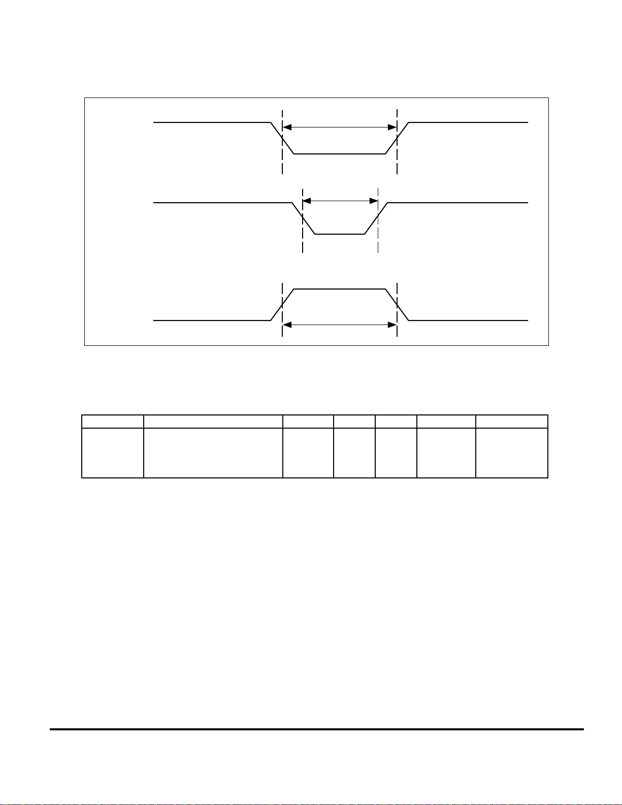
Transmitter Description
TRANSMIT PULSE WIDTH
TXCLKEN
TXRSTB
t
CEL
t
RSTL
TXNCOLD
t
NLDH
WCP 53811.c-12/5/97
Table 52. Pulse Width AC Characteristics
(V
= 3.3 V ±10%, V
DD
Symbol Parameter Min. Nom. Max. Units Conditions
t
CEL
t
RSTL
t
NLDH
Clock Enable (TXCLKEN) Low 4 nsec
Reset (TXRSTB) Low 5 nsec
NCO Load (TXNCOLD) High 1 CLK cycles
= 0 V, T
SS
= Ð40° to 85° C)
a
STEL-2176 58 User Manual
Page 68

BIT CLOCK SYNCHRONIZATION
TXACLK
Transmitter Description
TXCLKEN
t
CESU
TXTCLK
t
CO
t
CO
TXBITCLK
2 (N +1) BPSK
(N +1) QPSK
16QAM
N +1
n = Odd
2
16QAM
N +2
n = Even
2
Note 1: TXBITCLK will be forced high on the second rising edge of CLK following the rising edge of TXTCLK.
Note 2: The period of time that TXBITCLK is high is measured in cycles of CLK (e.g. (N + 1) in QPSK). "N" is a
12-bit binary number formed by taking bits 3-0 of Block 2 Register 39H as the MSB's and taking bits 7-0 of
Block 2 Register 29H as the LSB's. The TXBITCLK low period is the same except for 16QAM when "N" is
even in which case the low period is (N/2) yielding the correct TXBITCLK period but not a perfect
squarewave.
See Note 2 See Note 1
WCP 53826.c-12/5/97
Table 53. Bit Clock Synchronization AC Characteristics
(V
= 3.3 V ±10%, V
DD
Symbol Parameter Min. Nom. Max. Units Conditions
t
t
CO
CESU
Clock to TXBITCLK, TXSYMPLS, TXDATAENO, or
TXACLK edge
Clock Enable (TXCLKEN to TXTCLK Setup) 3 nsec
= 0 V, T
SS
= Ð40° to 85° C)
a
2 nsec
User Manual 59 STEL-2176
Page 69

Transmitter Description
TRANSMIT INPUT DATA AND CLOCK TIMING
NOTE 1
TXAUXCLK
TXTCLK DON'T CARE
TXBITCLK DON'T CARE
TXTSDATA
NOTE 2
t
SU
t
HD
TXTCLK
TXBITCLK NOTE 3
TXTSDATA
MASTER MODESLAVE MODE
t
CLK
NOTE 1
t
SU
t
HD
Note 1: Mode is determined by setting of BIT 7 in Block 2 Register 2CH. Bit 7 high is slave mode; Bit 7 low is
master mode.
Note 2: In slave mode, even though TXBITCLK is shown as ÒDon't CareÓ, it should be noted that internally the
STELÊ2176 will relatch the data on the next falling edge of TXBITCLK. Thus, avoid changing the control
signal inputs (TXDATAENI, TXDIFFEN, TXRDSLEN, TXSCRMEN) at the falling edges of TXBITCLK.
Note 3: In the STEL-2176, data is latched on the rising edge of the CLK that follows the falling edge of
TXBITCLK. Thus, the data validity window is one CLK period (t
) delayed. CLK not shown.
CLK
Table 54. Input Data and Clock AC Characteristics
(V
= 3.3 V ±10%, V
DD
Symbol Parameter Min. Nom. Max. Units Conditions
t
CLK
t
SU
t
HD
Clock Period 6 nsec
TXTSDATA to Clock Setup 2 nsec
TXTSDATA to Clock Hold 2 nsec
= 0 V, T
SS
= Ð40° to 85° C)
a
STEL-2176 60 User Manual
Page 70
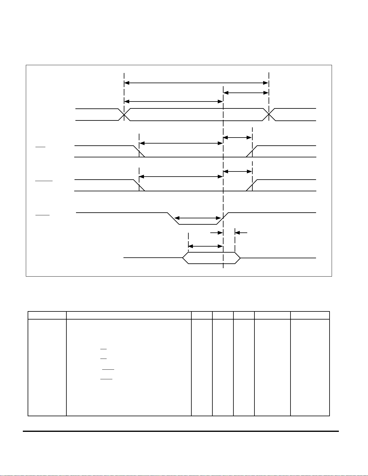
WRITE TIMING
Address
ADDR
[5-0]
CS
WRB
t
WASU
t
t
CSSU
WRSU
t
AVA
t
WAHD
t
CSHD
t
WRHD
Transmitter Description
t
DSBL
DSB
t
DH
t
DSU
Data
DATA
t
WASU
t
WAHD
t
AVA
t
CSSU
t
CSHD
t
WRSU
t
WRHD
t
DSBL
t
DH
t
DSU
[7-0]
WCP 53814.c-12/5/97
Table 55. Write Timing AC Characteristics
(V
= 3.3 V ±10%, V
DD
Symbol Parameter Min. Nom. Max. Units Conditions
Write Address Setup 10 nsec
Write Address Hold 6 nsec
Address Valid Period
Chip Select ( CS ) Setup
Chip Select ( CS ) Hold
Write Setup ( WRB ) 5 nsec
Write Hold ( WRB ) 3 nsec
Data Strobe Pulse Width 10 nsec
Data Hold Time 1 nsec
Data Setup Time 3 nsec
= 0 V, T
SS
= Ð40° to 85° C)
a
20 nsec
5 nsec
3 nsec
User Manual 61 STEL-2176
Page 71

Transmitter Description
READ TIMING
t
ADV
t
AVA
Address
7-0
CS
WRB
t
DICSH
t
DVCSL
Data
7-0
Table 56. Read Timing AC Characteristics
(V
= 3.3 V ±10%, V
DD
Symbol Parameter Min. Nom. Max. Units Conditions
t
AVA
t
ADV
t
ADIV
t
DVCSL
t
DICSH
Address Valid Period 20 nsec
Address to Data Valid Delay 9 nsec
Address to Data Invalid Delay 6 nsec
Data Valid After Chip Select Low 2 nsec
Data Invalid After Chip Select High 1 nsec
= 0 V, T
SS
t
ADIV
= Ð40° to 85° C)
a
WCP 53815.c-12/2/97
STEL-2176 62 User Manual
Page 72

NCO LOADING (USER CONTROLLED)
Transmitter Description
OUTPUT
t
FCWSU
TXFCWSEL
DON'T CARE
1-0
TXNCOLD
NOTE 1
NCO LOADING (AUTOMATIC)
OUTPUT
TXFCWSEL
TXDATAENO
1-0
DON'T CARE
ZERO
t
FCWHD
VALID DON'T CARE
t
LDPIPE
SELECTED FREQUENCY ZERO
t
DENHV
VALID DON'T CARE
OLD FREQ.
t
DENLZ
NEW FREQ.
WCP 53816.c-12/5/97
t
DOFCWV
t
DOFCWI
WCP 53817.c-12/5/97
NOTE 1: The first rising edge of CLK after TXNCOLD goes high initiates the load process.
Table 57. NCO Loading AC Characteristics
(V
= 3.3 V ±10%, V
DD
Symbol Parameter Min. Nom. Max. Units Conditions
t
LDPIPE
NCO-LD to Change in Output Frequency Pipeline
Delay
t
FCWSU
t
FCWHD
t
DENLZ
t
DENHV
TXFCWSEL
TXFCWSEL
to NCO-LD Setup 3 CLK cycles
1-0
to NCO-LD Hold 10 CLK cycles
1-0
TXDATAENO Low to Zero Frequency Out Delay 23 CLK cycles
TXDATAENO High to Valid Frequency Out
Delay
t
DOFCWV
t
DOFCWI
TXDATAENO to TXFCWSEL
TXDATAENO to TXFCWSEL
Valid 3 CLK cycles
1-0
Invalid 10 CLK cycles
1-0
= 0 V, T
SS
= Ð40° to 85° C)
a
23 CLK cycles
23 CLK cycles
User Manual 63 STEL-2176
Page 73

Transmitter Description
DIGITAL OUTPUT TIMING
CLK
t
CO
t
TXACLK
Note 1
TXBITCLK
TXSYMPLS
TXDATAENO
CO
t
ACKH
t
ACKL
t
CO
t
SPH
t
CO
t
DENOD
t
CO
WCP 53818.c-12/7/97
NOTE 1: TXACLK shown for "n" equal to 2: where n is the 4-bit binary value in Block 2 Register 2AH,
BITSÊ3-0.
Table 58. Digital Output Timing AC Characteristics
(V
= 3.3 V ±10%, V
DD
Symbol Parameter Min. Nom. Max. Units Conditions
t
CO
t
ACKH
t
ACKL
t
SPH
t
DENOD
Notes:
1. ÒnÓ is the 4-bit binary value in Block 2 Register 2A
Clock to TXBITCLK, TXSYMPLS, TXDATAENO,
or TXACLK edge
Auxiliary Clock (TXACLK) High 2 CLK cycles
Auxiliary Clock (TXACLK) Low
Symbol Pulse (TXSYMPLS) High 1 CLK cycles
TXBITCLK Low to TXDATAENO edge 1 CLK cycles
H ,
= 0 V, T
SS
bits 3-0.
= Ð40° to 85° C)
a
2 nsec
(n-1) CLK cycles Note 1
STEL-2176 64 User Manual
Page 74
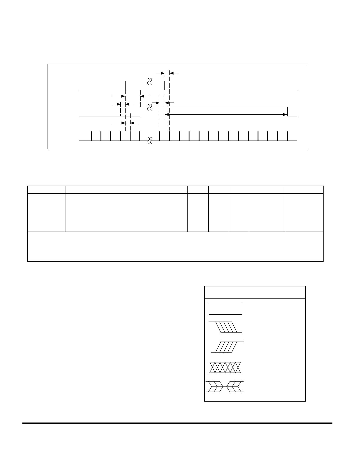
Transmitter Description
TXDATAENI TO TXDATAENO TIMING
t
DENSP
TXDATAENI
t
DIHDO
t
SPDEN
TXDATAENO
t
DENSP
TXSYMPLS
Table 59. TXDATAENI to TXDATAENO Timing AC Characteristics
(V
= 3.3 V ±10%, V
DD
Symbol Parameter Min. Nom. Max. Units Conditions
t
DIHDO
t
DLDO
t
SPDEN
t
DENSP
Notes:
1. Shown for Block 2 Register 36
TXDATAENO will be delayed from those illustrated by 8, 4, or 2 TXSYMPLS for BPSK, QPSK, or 16QAM, respectively.
TXDATAENI High to TXDATAENO High 2
TXDATAENI Low to TXDATAENO Low 13
TXSYMPLS (trailing edge) to TXDATAENI Setup 3 nsec
TXDATAENI to TXSYMPLS (trailing edge) Setup 5 nsec
, bit 6=0 (No Reed-Solomon). If bit 6 of Register 36H is a Ò1Ó, then the edges of
H
t
SPDEN
= 0 V, T
SS
t
DLDO
= Ð40° to 85° C)
a
nd
th
WCP 53819.c-12/5/97
TXSYMPLS Note 1
TXSYMPLS Note 1
BURST TIMING EXAMPLES
The following seven timing diagrams are qualitative in
nature and meant to illustrate the functional
relationships between the control inputs and signal
outputs in various modes of burst operation. Use the
key at right to interpret the timing marks. Only the first
diagram is of a complete and realistic burst. The
remaining diagrams are too short in duration to show
TXDATAENO and TXCLKEN going low.
Key:
WAVEFORM INPUTS OUTPUTS
Must be
Steady
May
Change
from H to L
May
Change
from L to H
Don't Care.
Any Change
Permitted
Does Not
Apply
Will be
Steady
Will be
Changing
from H to L
Will be
Changing
from L to H
Changing.
State
Unknown
Center
Line is HighImpedance
“Off” State
WCP 53036.c-5/6/97
User Manual 65 STEL-2176
Page 75
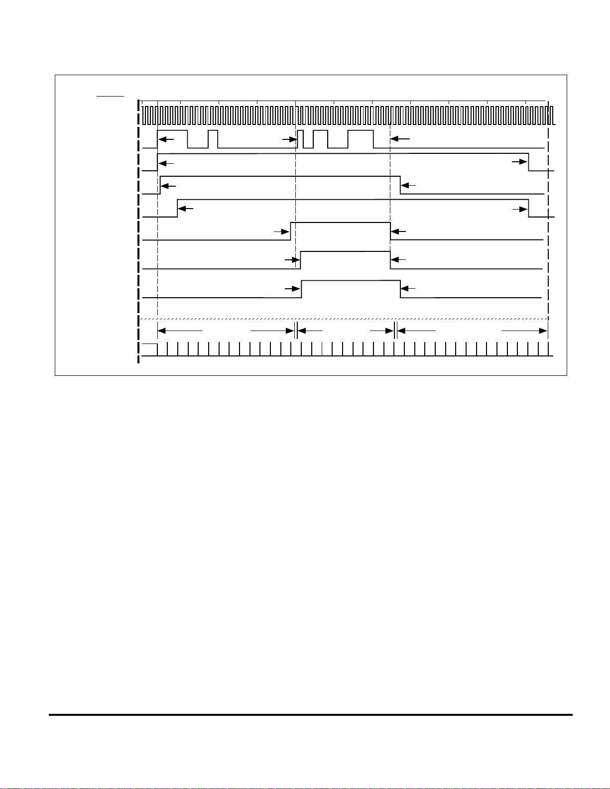
SLAVE MODE, QPSK - BURST TIMING: FULL BURST
NAME
Introduction
TXTCLK
TXTSDATA
TXCLKEN
TXDATAENI
TXDATAENO
TXDIFFEN
TXRDSLEN
TXSCRMEN
TXSYMPLS
NOTES:
(1)
(G)
(J)
(I)
(K)
(H)
(M)
(N)
(2)
(3)
(A)
(F)
(B)
(C)
(D)
(E)
(L)
(L)
User Data Guard TimePreamble
WCP 53820.c -12/5/97
(1) All input signals shown are derived from TXTCLK . Each edge is delayed from a TXTCLK edge by typically 6 to 18 nsec.
DATAENO does not depend on TXTCLK but its edges are synchronized to TXTCLK. TXTCLK itself can be turned off after
TXDATAENI goes low.
(2) DATAENO shown at its minimum pipeline delay position. This is achieved by setting bit 6 of Block 2 Register 36H to zero.
Reed-Solomon cannot be used in this mode. If bit 6 is set high, allowing Reed-Solomon an additional pipeline delay of 8Êbits is
inserted into the data path. This will shift both edges of DATAENO to the right by 8 cycles of TXTCLK.
(3) If the preamble is not encoded the same as the user data, the TXDIFFEN control can be toggled in mid transmission as shown.
Otherwise, the TXDIFFEN control can be held high or low depending on encoding desired.
(A) First data bit transition on falling edge of TXTCLK (first of 14 preamble symbols). The data will be valid on the next rising edge
of TXTCLK.
(B) TXCLKEN rises on the same falling edge of TXTCLK that the data starts on. TXCLKEN is allowed to rise any time earlier than
shown.
(C) TXDATAENI rises on the first rising edge of TXTCLK (middle of the first preamble bit).
(D) DATAENO rises on the falling edge of TXTCLK (at the end of the second symbol).
(E) TXDIFFEN rises on the rising edge of TXTCLK one symbol before the first user data symbol.
(F) User data bits change on the falling edge of TXTCLK and must be valid during the next rising edge of TXTCLK .
(G) End of user data. Note that the data is allowed to go away immediately after it is latched in by the rising of TXTCLK which
occurs in the middle of the last user data bit.
(H) TXDIFFEN goes low on rising edge of TXTCLK (last user data symbol).
(I) TXDATAENI goes low on rising edge of TXTCLK (on the cycle of TXTCLK after the last user data bit).
(J) TXCLKEN must stay high until any time on or after the point where DATAENO goes low.
(K) DATAENO stays high until the 13th TXSYMPLS after TXDATAENI goes low.
(L) TXRDSLEN and TXSCRMEN go high on the first rising edge of TXTCLK in the User Data.
(M) TXRDSLEN goes low on the rising edge of TXTCLK (last user data symbol).
(N) TXSCRMEN goes low on the rising edge of TXTCLK (on the cycle of TXTCLK after the last user data bit).
STEL-2176 66 User Manual
Page 76

MASTER MODE, BPSK - BURST TIMING SIGNAL RELATIONSHIPS
TXCLKEN
TXBITCLK
TXTCLK
TXDATAEN
TXTSDATA
GUARD TIME GUARD TIMEUSER DATA
TXDIFFEN
TXRDSLEN
TXSCRMEN
TXSYMPLS
TXDATAENO
PI PI PI PI UI UI UI UI GI GI GI GI
PREAMBLE
NOTE 1
NOTE 2
SLAVE MODE, BPSK - BURST TIMING SIGNAL RELATIONSHIPS
TXCLKEN
TXBITCLK
TXTCLK
TXDATAEN
WCP 53837.c-12/5/97
TXTSDATA
TXDIFFEN
TXRDSLEN
TXSCRMEN
TXSYMPLS
TXDATAENO
GUARD
TIME
PI PI PI PI UI UI UI UI GI GI GI GI
PREAMBLE
NOTE 1
NOTE 2
GUARD TIMEUSER DATA
WCP 53838.c-12/5/97
NOTE 1: STEL receivers differentially decode relative to the last preamble symbol. To encode the
first symbol against a "zero" symbol reference instead, bring TXDIFFEN high at the
leading edge of the user data packet (dotted line).
NOTE 2: If bit 6 of Block 2 Register 36H is a "1" then the rising edge of DATAENO will be
delayed by eight cycles of TXBITCLK (dotted line). This is required if the ReedSolomon encoder is used.
STEL-2176 67 User Manual
Page 77
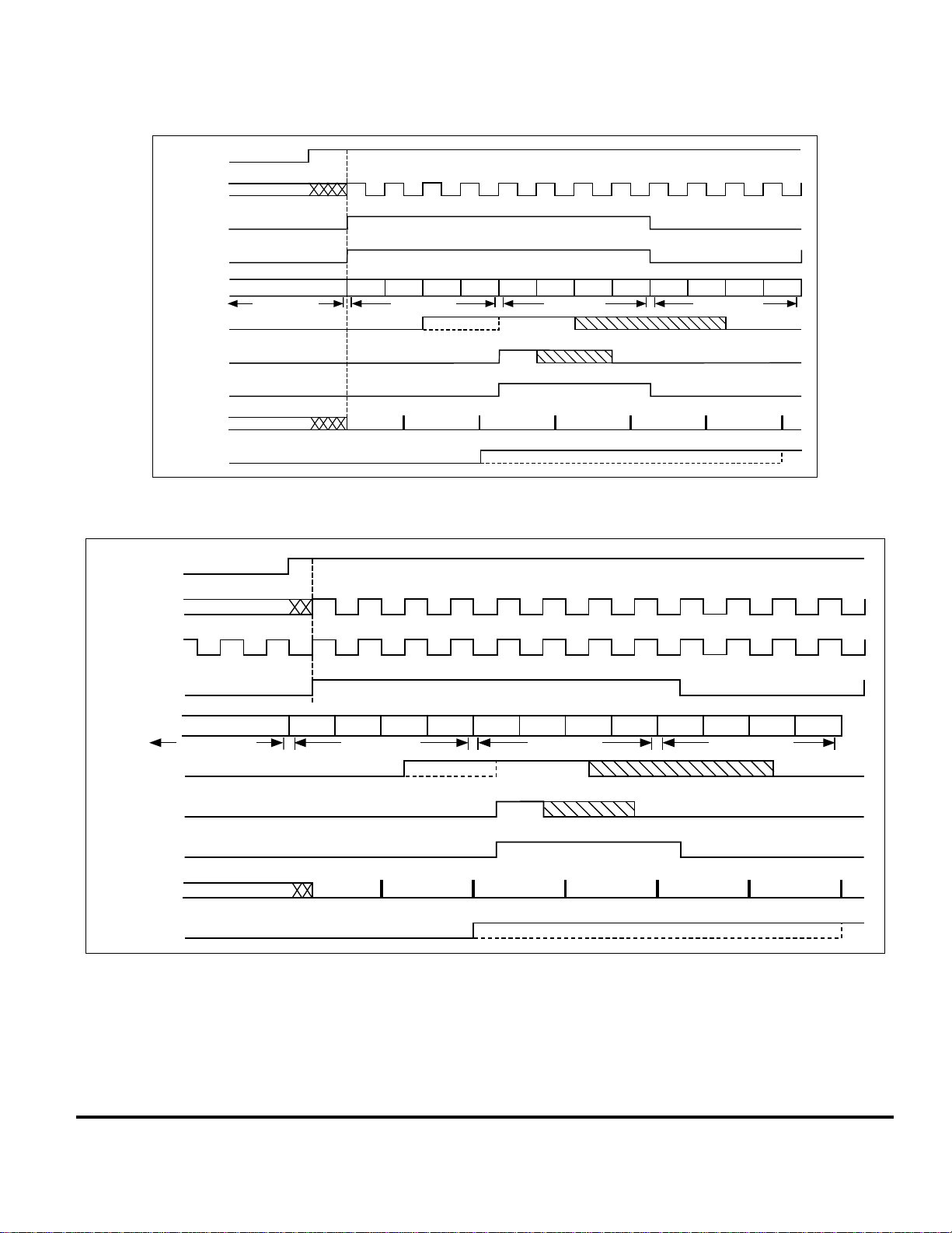
Transmitter Description
MASTER MODE, QPSK - BURST TIMING SIGNAL RELATIONSHIPS
TXCLKEN
TXBITCLK
TXTCLK
TXDATAEN
TXTSDATA
TXDIFFEN
TXRDSLEN
TXSCRMEN
TXSYMPLS
TXDATAENO
GUARD TIME
PI PQ PI PQ UI UQ UI UQ GI GQ GI
GUARD TIMEUSER DATAPREAMBLE
NOTE 1
NOTE 2
GQ
WCP 53821.c-12/5/97
SLAVE MODE, QPSK: FULL VIEW - BURST TIMING SIGNAL RELATIONSHIPS
TXCLKEN
TXBITCLK
TXTCLK
TXDATAENI
TXTSDATA
GUARD TIME
TXDIFFEN
PI PQ PI PQ UI UQ UI UQ GI GQ GI GQ
GUARD TIMEUSER DATAPREAMBLE
NOTE 1
TXRDSLEN
TXSCRMEN
TXSYMPLS
TXDATAENO
NOTE 2
WCP 53822.c-12/5/97
NOTE 1: STEL receivers differentially decode relative to the last preamble symbol. To encode the
first symbol against a "zero" symbol reference instead, bring TXDIFFEN high at the
leading edge of the user data packet (dotted line).
NOTE 2: If bit 6 of Block 2 Register 36H is a "1" then the rising edge of DATAENO will be
delayed by eight cycles of TXBITCLK (dotted line). This is required if the ReedSolomon encoder is used.
STEL-2176 68 User Manual
Page 78

MASTER MODE, 16QAM - BURST TIMING SIGNAL RELATIONSHIPS
TXCLKEN
TXBITCLK
TXTCLK
TXDATAENI
TXTSDATA
GUARD TIME GUARD TIMEUSER DATA
TXDIFFEN
PI1PQ1PI0PQ0PI1PQ1PI0PQ0UI1UQ1UI0UQ0UI1UQ1UI0UQ0GI1GQ1GI0GQ0GI1GQ1GI0GQ
PREAMBLE
NOTE 1
TXRDSLEN
TXSCRMEN
TXSYMPLS
TXDATAENO
NOTE 1: STEL receivers differentially decode relative to the last preamble symbol. To encode the
first symbol against a "zero" symbol reference instead, bring TXDIFFEN high at the
leading edge of the user data packet (dotted line).
NOTE 2: If bit 6 of Block 2 Register 36H is a "1" then the rising edge of DATAENO will be
delayed by eight cycles of TXBITCLK (dotted line). This is required if the ReedSolomon encoder is used.
NOTE 2
SLAVE MODE, 16QAM - BURST TIMING SIGNAL RELATIONSHIPS
TXCLKEN
0
WCP 53823.c-12/5/97
TXBITCLK
TXTCLK
TXDATAENI
TXTSDATA
TXDIFFEN
PI1PQ1PI0PQ0PI1PQ1PI0PQ0UI1UQ1UI0UQ0UI1UQ1UI0UQ0GI1GQ1GI0GQ0GI1GQ1GI0GQ
GUARD TIME GUARD TIMEUSER DATAPREAMBLE
NOTE 1
0
TXRDSLEN
TXSCRMEN
TXSYMPLS
TXDATAENO
NOTE 2
NOTE 2
WCP 53824.c-12/5/97
STEL-2176 69 User Manual
Page 79
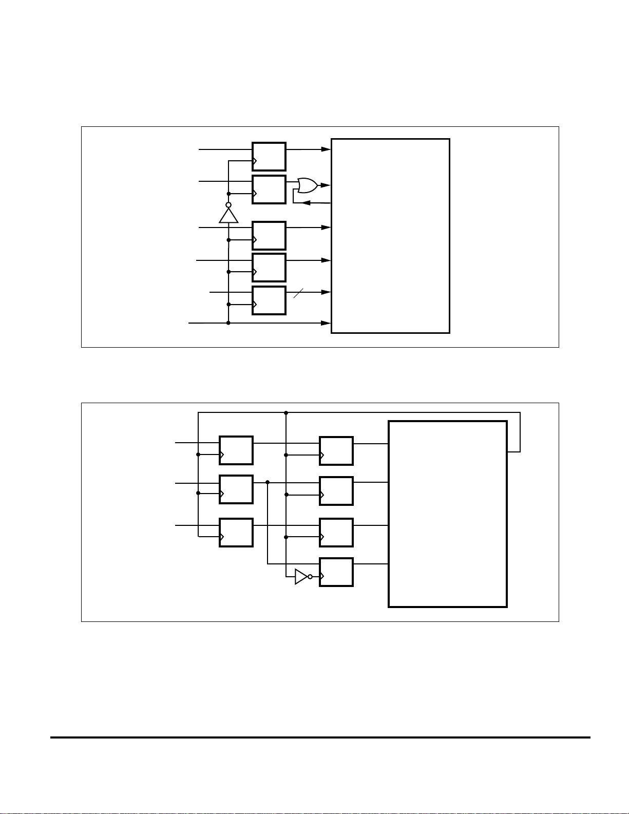
Transmitter Description
RECOMMENDED INTERFACE CIRCUITS
SLAVE MODE INTERFACE
D
TSDATA
Q
TXTSDATA
CLKEN
DATAEN
DIFFEN
FCWSEL
TCLK
1-0
MASTER MODE INTERFACE
TSDATA
D Q
D Q
D Q
D Q
D Q
OR
2
TXCLKEN
TXDATAENO
TXDATAEN
TXDIFFEN
TXFCWSEL
TXTCLK
D Q
STEL-2176
1-0
TXTSDATA
WCP 52995.c-5/2/97
BITCLK
DATAENI
DIFFEN
D Q
D Q
D Q
D Q
D Q
TXDATAENI
STEL-2176
TXDIFFEN
TXTCLK
TXCLKEN*
WCP 52115A.c 5/2/97
* TXCLKEN may be turned off between bursts to conserve power as long as it is kept on until after TXDATAENO
goes low. Note that the TXBITCLK output goes inactive whenever TXCLKEN is low.
STEL-2176 70 User Manual
Page 80

Information in this document is provided in connection with
Intel® products. No license, express or implied, by estoppel
or otherwise, to any intellectual property rights is granted by
this document. Except as provided in Intels Terms and Conditions of Sale for such products, Intel assumes no liability
whatsoever, and Intel disclaims any express or implied
Intel may make changes to specifications and product descriptions at any time, without notice.
For Further Information Call or Write
INTEL CORPORATION
Cable Network Operation
350 E. Plumeria Drive, San Jose, CA 95134
Customer Service Telephone: (408) 545-9700
Technical Support Telephone: (408) 545-9799
FAX: (408) 545-9888
Copyright © Intel Corporation, December 15, 1999. All rights reserved
warranty, relating to sale and/or use of Intel® products including liability or warranties relating to fitness for a particular purpose, merchantability, or infringement of any patent,
copyright or other intellectual property right. Intel products
are not intended for use in medical, life saving, or life sustaining applications.
WCP 970317
 Loading...