

Page 1
查询STEL-1209供应商
STEL-1209
Data Sheet
STEL-1209/CE
BPSK/QPSK/16 QAM
Burst Modulator Assembly
R
Page 2
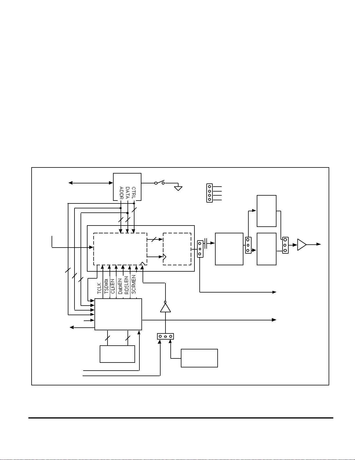
KEY FEATURES
n Evaluation tool for STEL-1109 digital
modulator ASICs
n Burst or continuous BPSK, QPSK, 16QAM
modulator at rates up to 10 Msps
n On-board or external clock capability
– Up to 165 MHz
n Up to 65 MHz output frequency
n High frequency resolution
– 24 bits, 10 Hz @ 165 MHz
n Digitally filtered data results in low
modulation side lobes
– Typically -52 dBc
n High spectral purity
– Typically -50 dBc
BLOCK DIAGRAM
µPROC.
Control I/F
RS-232C
P2
10
6 8
S1
Reset
BURST MODE PARAMETERS:
n Default at burst QPSK modulation
– Data rate at 2.56 Mbps
n Programmable packet length
– 1 to 16,381 symbols of data
n Programmable guard time
– 2 to 16,382 symbols
n Programmable burst quantity
– 1 to 10 million and auto repeat
n Programmable preamble size
– 0 to 255 symbols of data
n Master or slave mode
JP1
1
-5V
2
AGnd
3
DGnd
4
+5V
LP
Filter
65 MHz
5VDD*
EXTERNAL DATAJ1
EXTERNAL
J6
DATA CLK
EXTERNAL TCLK
J16
MASTER CLOCK
J2
10
STEL 1109
10
PSK/QAM
A
Modulator
U
X
6
8
Burst
Controller
(FPGA)
8 11
DATA ADDR
SRAM
10 Bit
DAC
JP4
C
JP3
Xtal. Osc.
102.4 MHz
Prog.
ATTEN.
LP
Filter
42 MHz
JP5
Aux. Output
SYNC
*Driven by 5 Volt
on STEL-1209
J8
J7
JP6
IF Out
J5
75Ω
WCP 52841.c-5/9/97
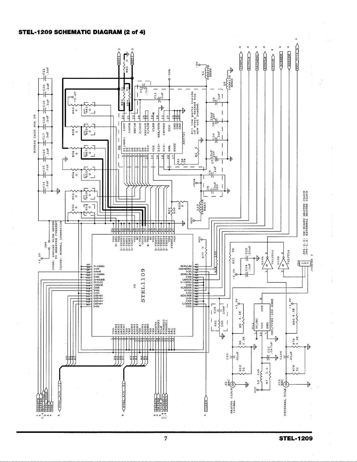
STEL-1209 2
Page 3

DESCRIPTION
The STEL-1209 is the latest member in Stanford
Telecom's line of BPSK/QPSK Burst Modulator board
level products. It uses the STEL-1109 ASIC to provide
all the convenience of supporting BPSK, QPSK, or
16QAM up-stream modulation with a maximum data
rate of 10 Mbps, 20 Mbps, and 40 Mbps; respectively.
The STEL-1109 has a Reed-Solomon encoder, a
scrambler, a differential encoder, a 10 bit DAC, and
many more features needed to build robust
communication systems that satisfy today's demanding
requirements. For further feature details please refer to
the STEL-1109 ASIC data sheet.
Besides the STEL-1109, there is additional logic circuitry
implemented in Altera's FPGA to provide burst BPSK,
QPSK, and 16QAM modulation modes. Several
improvements in these burst modulation modes are
included; e.g. external/internal preamble and data
sources; variable bursts quantity (includes single to
10 -million and auto repeat); variable packet length,
guard time, and preamble size (including zero
preamble size). This flexibility allows the STEL-1209 to
be customized easily into customers' specific
environment. Connectors J3 and J4 are digital test pins
provided for easy monitoring of the burst
control/signal timing relationships.
With a 0.35 micron ASIC process the STEL-1109 can
support a maximum clock frequency of 165 MHz. The
frequency of the output modulated carrier is
programmable between 5 to 65 MHz; the upper limit is
approximately 40% of the master clock. The STEL-1209
has a 102.4 MHz crystal oscillator on-board. Hence, its
maximum modulated carrier frequency can be set to
40 MHz. However, an external clock (+10 to +13 dBm)
can be selected as the master (through connector J2 and
jumper JP4) and carrier frequency of 65 MHz can be
achieved easily. An obvious difference between this
board and its predecessor (STEL-1208) is the absence of
a DAC. A 10 bit DAC is built in the STEL-1109 and
observable spur level is -50 dB or better. It has a pair of
differential current outputs which swings ±0.96 volt
peak-to-peak at 50 ohm termination. Single-ended
output of the DAC (using transformer T1 as a double to
single-ended converter) can be obtained from J7
(expects 50 or 75 ohm termination impedance from
instrumentation). Also included is a choice between
two output low pass filters (jumper JP5 and JP6) with
cut-off frequency at 42 and 65 MHz. The output of the
filter is amplified and is obtainable from J5 (75 ohm
source impedance). JP3 routes the DAC output to
either J7 or J5.
The board (running at 102.4 MHz in continuous
modulation mode) takes about 430 mA at the 5 volt
supply. Power is supplied to the board through JP1. Its
pins are clearly labeled on the board (pin 1 = -5 volt, pin
2 = AGND, pin 3 = DGND, pin 4 = VCC (+5 volt)).
Reversing the polarity of the supply pins would cause
damage to the board. When clock enable line is taken
low (grounded), the board consumes 200 mA or less.
Current drawn on the -5 volt supply is 10 mA. There
are two 5 volt to 3.3 volt converters on the board and
the design serves to demonstrate the inter-operability of
the STEL-1109 in a 5 volt or 3.3 volt system. The STEL1109 ASIC, which is a 3.3V device, consumes 1.8
mA/MHz in continuous mode. Current consumption
by the ASIC can be easily measured by connecting pin 2
of JP9 (see package outline) to a 3.3 V power supply
that has a current meter.
STEL-1209's operating mode can be modified by
writing new values to the STEL-1109 and the burst
controller's registers. These registers can be read and
written through a Graphical User Interface (GUI)
program that comes with the STEL-1209 board. The
GUI software allows the user to select different
modulation methods, preamble size, interpolation ratio,
etc. with the ease of button clicking on a Personal
Computer running Microsoft's Windows 95 operating
system. A serial cable with 9 pin D-sub connector must
be connected between P2 of the STEL -1209 and the
PC's COM port for the GUI software to work. At power
up or upon reset, the STEL -1209 is automatically
loaded with default values to give repeating QPSK
burst modulation (50% duty cycle) centered at 10 MHz
(master mode). This default mode allows the STEL1209 to communicate with the STEL -9244, up-stream
burst demodulator. External data must be provided to
connector J1 (75 ohm unipolar unbalance) to complete
the communication loop. Clock for the external data is
provided through connector J6 (75 ohm unipolar
unbalance).
3 STEL-1209
Page 4

SPECIFICATIONS
f
π•f
OUT
f
CLK
Output Frequency Range:
5 MHz to 65 MHz using an external clock frequency of
165 MHz (or up to 40 MHz using the provided onboard clock at 102.4 MHz).
Resolution:
10 Hz @ f
J2 -- Master Clock Input:
To use the on-board 102.4 MHz crystal oscillator, jump
pin 2 and pin 3 on JP4.
To use an external master clock, jump pin 1 and pin 2
on JP4.
Maximum Frequency, f
BNC connector, input power at +10 dBm to +13 dBm,
A.C. coupled, 50 Ohms
J16 -- External TCLK Input:
BNC connector, HCMOS levels.
J7 -- Aux. Output:
SMB connector for single ended DAC output.
Transformer T1 is used to do the double-to-single
ended conversion.
JP3 is used to route the single ended output to either J7
or J5.
J8 -- SYNC Output:
BNC connector, HCMOS levels
Pulse covering the period of bursting symbols. This
signal (equivalent to DATAENO inverted) can be used
as a scope trigger.
J5 -- IF Output:
BNC connector, 75 Ohms.
Output power: + 0 dBm @ default settings
Return loss: ≥ 15 dB
Stop band: ≥ 30 dB at 85 MHz with 65 MHz LPF
Note: The output level of the DAC falls as the carrier
frequency rises according to the equation:
V
OUT
165 MHz (24 bits)
CLK
V
OUT(DC)
=
CLK(MAX)
(sine f)
= 165 MHz
where : f =
Note: The on-board low pass filter (LPF) cut-off
frequency can be selected between 42 MHz or 65 MHz
by properly configuring JP5 and JP6.
J1 -- External Serial Data Input:
BNC connector, HCMOS levels.
Output Level Control:
The output level can be controlled over a range of 15 dB
in 1 dB steps by means of the control software supplied.
P2 -- RS-232C Control Interface:
Connector Type: 9-pin Subminiature ‘D’, female (DCE).
Pin 2 TXD Pin 3 RXD
Pin 5 GND Pin 7 GND
Power Requirements (Typical):
JP1, pin 1: -5 volts ±5%, 10 mA
JP1, pin 2: Analog GND
JP1, pin 3: Digital GND
JP1, pin 4: +5 volts ±5%, 330 mA
(@ fclk = 100 MHz)
Temperature Range, Ambient:
0-70° Operating
Connector J3:
Pin 1 NC Pin 2 NC
Pin 3 AUXCLK Pin 4 RDSLEN
Pin 5 SCRMEN Pin 6 CLKEN
Pin 7 TCLK Pin 8 DATAEN
Pin 9 TSDATA Pin 10 WRB
Pin 11 DSB Pin 12 DIFFEN
Pin 13 TXCLK_B Pin 14 TXDATA_B
Pin 15 BURSTGATE_B Pin 16 CKSUM
Pin 17 DATAENO Pin 18 SYMPLS
Pin 19 BITCLK Pin 20 GND
Connector J4:
Pin 1 NC Pin 2 NC
Pin 3 EXT_TCLK_B Pin 4 SYMCLK
Pin 5 uP_WRB Pin 6 uP_RDB
Pin 7 CLKEN_LOW Pin 8 (SPARE)
Pin 9 BURST Pin 10 (SPARE)
Pin 11 PREAMBLE_SRAM Pin 12 LOAD_RUN
Pin 13 (SPARE) Pin 14 uP_BURSTGATE
Pin 15 Burst/Done Pin 16 (SPARE)
Pin 17 VCC (SPARE) Pin 18 VCC (SPARE)
Pin 19 NCO_LOAD Pin 20 GND
STEL-1209 4
Page 5
ORDERING INFORMATION
To order, specify Model Number STEL-1209/CE. “CE” indicates a commercial grade, board-level product.
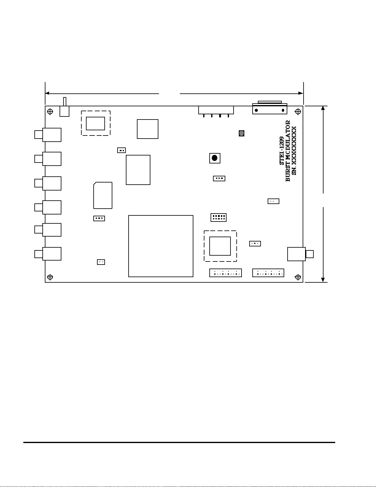
PACKAGE OUTLINE
6.3"
(16 cm)
Reset
S1
J8
SYNC
J1
EXT DATA
J6
EXT DATA CLK
J2
MASTER CLK
J5
BURST GATE
J16
EXT TCLK
EPROM
U11
Xtal.
Osc.
JP4
JP8
U2
JP9
Micro
U5
STEL1109
Burst Controller
MOLEX 4455C-A
U3
-5V +5V
J7
JP3
U19 JP7
EEPROM
2
J3
1
U8
JP1
Rp
P2: 9‘D’
JP5
JP6
2
1
WCP 52850.c-4/25/97
4.7"
(12 cm)
IF OUT
J5
J4
5 STEL-1209
Page 6
Page 7
Page 8

Page 9

Page 10

STEL-1209 EVALUATION BOARD SOFTWARE INTERFACE USER’S GUIDE
This Windows 95™ based software package is designed
to make programming and debugging the operation of
the STEL-1109 ASIC as easy as possible. It allows the
desired configuration to be derived while working at a
high level, eliminating the need to program the STEL1109 at the register level. In addition, it gives the user
the flexibility to select programmable features and
settings in connection with our upstream demodulator;
the STEL-9244. However, it is still necessary to have a
good understanding of the capability of both the STEL1209 and the STEL-1109 to be able to use this software
tool effectively. Standard Windows 95 procedures are
used in operating the menus and controls. Many of the
buttons require only a single click to activate.
Remember to press the Enter key for those buttons that
require numerical or keyboard entry. Pressing the
Enter key is essential for proper operation of the STEL1209 board.
To install the software, run the program named,
"a:\setup" and follow the instructions given on the
screen.
When the software is started, a window will be opened
with the default parameter settings. These parameters
are also loaded into the STEL-1109 and the Burst
Controller FPGA on the STEL-1209 board on power-up.
The window incorporates a Menu Bar, three soft
buttons, and a parameter entry area with bit mapped
graphics near the top that resemble three folder tabs.
Menu Bar Items
The menu bar is displayed at the top of the window
and contains three menu items: File, View Registers,
and Windows.
FILE:
Under the File menu the following items can be
accessed:
Save Parameters As - Saves the active window with its
parameter settings for future use as a new file.
Save Parameters - Saves the active window with its
parameter settings for future use, overwriting the
previous values of the file with this name.
Load Parameters - Opens previously saved file with its
parameter settings.
View Parameters - looking at contents of saved
parameters in a text file format.
Load User File - Opens an ASCII hex/character format
user supplied data file (text) for use as the input data
source. This allows the user to transmit a fixed known
data pattern. The user can load either ASCII hex or
ASCII character (or both) formats within a single file
such as the USERFILE.txt file comes with the GUI
software installation disks. In burst mode, the data file
contains both the preamble and the data information
with preamble being loaded first and followed by the
data.
Exit - Causes the program to terminate.
VIEW REGISTERS:
This gives the user the capability to access both the
write and the read registers of STEL-1109 ASIC.
Read Registers - When this item is selected, a new
window showing the STEL-1109 read registers is
opened. Each individual register value can be read
from the board by hitting the <Enter> key at each
register box. To read all register values at once, click
the Query Registers command button.
Write Registers - When this item is selected, a new
window showing the STEL-1109 write registers is
opened. Each individual register can be programmed
by entering a new value and then hitting the <Enter>
key. To write all register values at once, click the
Configure command button.
WINDOWS:
This is a standard window menu.
The Parameter Entry Area:
There are three screens to the Parameter Entry area.
Each one of these screens can be accessed simply by
clicking on the left mouse button once the cursor is
positioned on the desired "folder tab". These folder
tabs are labeled Main Parameters, Scrambler and FEC,
and Filters; located at top of the screen. All the fields
in the three taps can be individually downloaded by
clicking an event choice or changing a value and
pressing the <Enter> key. All the changes made on the
three tabs will be updated in the Write Registers
window, but not vice versa.
The Main Parameters screen is shown in the following
page. The TAB key moves the cursor from field to field.
STEL-1209 10
Page 11

MAIN PARAMETERS SCREEN
SAMPLING RATE
Master Clock Frequency
The Master Clock Frequency window must be set (in
Hz) to match the actual clock rate. The clock frequency
to specify is either the external oscillator source
connected to the J2 connector, or the on-board 102.4
MHz crystal oscillator (selected by JP4). The software
enforced limit to this field is set (above the rated
performance of the hardware) at 200 MHz. The
following relationship must be formed between the
master clock, interpolation ratio, and symbol rate:
Master Clock = 4 * Interpolation Ratio * Symbol Rate
Interpolation Ratio
Symbol Rate
For QPSK modulation, the symbol rate is half of the
data rate. For 16QAM modulation, the symbol rate is
one forth the data rate. When choosing a symbol rate,
be sure that the requirement is met with Master Clock
and Interpolation Ratio as mentioned above in the
Master Clock Frequency description. Symbol rate is a
calculated field.
BURST PARAMETERS
Note that the sum of the lengths of the preamble,
packet size, and guard time must not exceed 16384.
Preamble Size
STEL-1209's preamble size is programmable between 0
and 255 symbols.
The interpolation ratio determines the sampling rate of
the FIR filter and the symbol rate of the modulator. The
symbol rate will be equal to the Master Clock rate
divided by four times the interpolation ratio.
Packet Size
Minimum packet length is one and maximum packet
length is given by Packet Length(max) = 16383 - Guard
Time - Preamble. Default value for packet size is 512.
11 STEL-1209
Page 12

Guard Time
The minimum guard time required between each burst
is 2 symbols. The maximum guard time available is
given by Guard Time (max) = 16383 - Packet Length Preamble. The default guard time is 526 symbols which
equals the sum of 14 preamble and 512 data symbols.
This will burst on and off at a 50% duty cycle.
In conjunction with the STEL-9244 burst receiver, a 50%
duty cycle makes it easy to test BER performance.
MODULATOR OUTPUT
There are three Frequency Code Word registers in the
STEL-1109. The active Frequency Code Word is
indicated by the selected button (default is labeled A
located just beneath the label “NCO Frequency (Hz)”).
The content of the three Frequency Code Words are
shown through the three boxes below the three buttons.
Their content are modifiable but it will only take effect
after the Enter key is pressed.
Attenuation Step
This controls the attenuator on the STEL-1209 board in
1 dB steps, from 0 to 15 dB.
Freeze NCO SIN output
This button collapses the constellation onto the I axis. It
can be used in BPSK mode to rotate the constellation by
45°.
Invert Spectrum
The output of the I- and Q-channel adder block in the
STEL-1109 normally provides an output of the form
Icos(wt) + Qsin(wt). By selecting the Invert Spectrum
button this will be changed to -Icos(wt) + Qsin(wt).
This interchanges the upper and lower sidebands of the
signal, thereby inverting the spectrum.
MODULATION FORMAT
Modulation Type
Four buttons are provided to allow selection of any one
of four modulation types; 16QAM, QPSK, BPSK, and
continuous waveform (CW).
Modulation Mode
Three modulation modes for each modulation type
(expect CW) are provided; Continuous, Burst Auto
repeat, and Burst Qty. To transmit a fixed number of
bursts, the desired number can be specified in the box
provided below the Burst Qty button. The <Enter> key
sends the specified number of bursts each time it is
pressed but only when the Burst Qty box is the active
box. When other parameters are edited, the Enter key
will not cause another burst cycle. For example, if the
Burst Qty box has a value of 5, changing the preamble
value to 2 and pressing the Enter key does not cause the
Burst Controller to fire 5 bursts with 2 preamble
symbols. Instead, the cursor has to re-select the Burst
Qty box and the Enter key must be pressed again.
DATA AND TIMING
Preamble Source
The user has a choice of preamble sources. A specific
pattern for the preamble can be pre-stored in internal
SRAM or taken from J1 (external data source). Default
preamble bit pattern is 11 11 11 00 00 11 00 00 00 00 00
00 00 00.
Data Source
Likewise, data can be stored in internal SRAM or taken
from external data source (J1). The STEL-1209 also has
capability to generate two types of pseudo random
codes; [10,3] and [23,18] that can be used in place of the
data.
Data Clock Source
The STEL-1209 can be configured to be self sufficient in
terms of clock signals. In this state, the on-board 102.4
MHz crystal oscillator generates the master clock and
all other clocks are derived from it. This state is called
the master mode. It is also possible to configure the
STEL-1209 board into slave mode in which an external
continuous bit rate clock must be applied to J6 (EXT
TCLK). This feature is useful in applications where
data must be synchronized to an external reference
clock. Select External TCLK if this is warranted by the
application.
Bit and Symbol Mapping
16QAM modulation requires all internal resources to
map its constellation. In QPSK or BPSK, less constellation is needed and it is therefore possible to map these
constellations (QPSK and BPSK’s) to those vacated by
the 16QAM constellation. Some amount of gain could
thus be gained by the QPSK or the BPSK modulation.
CONFIGURE
This button which is located at the lower right hand
corner of the main screen can be used to do an overall
loading of all the registers with values as presented by
the GUI software.
RESET 1209
This button resets the STEL-1209 board by software
command.
STEL-1209 12
Page 13

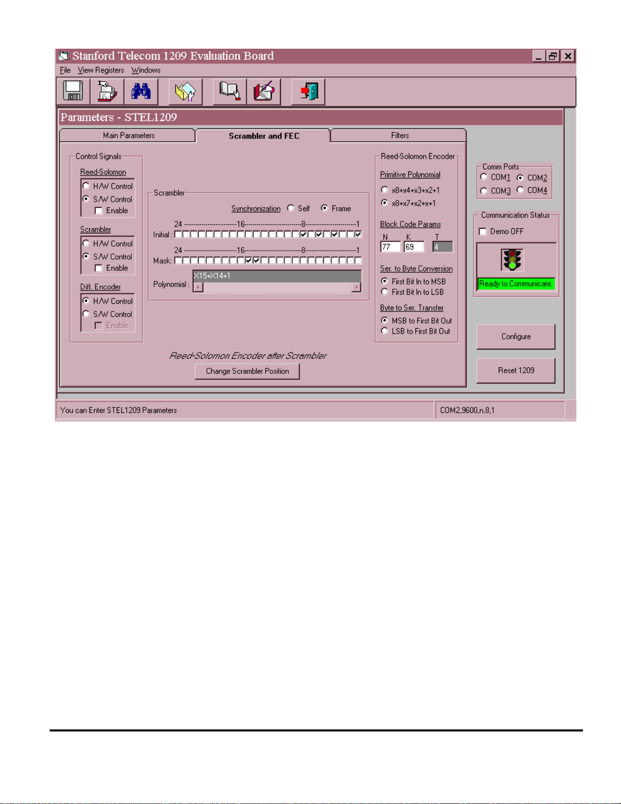
SCRAMBLER AND FEC SCREEN
This screen provides all the buttons that can be used to
exercise the different features of the STEL-1109 like
Reed-Solomon, Scrambler, and Differential Encoder.
CONTROL SIGNALS
Reed-Solomon Enable
RSDLEN signal can be used to tell the STEL-1109 to
turn on the Reed-Solomon engine. This is the H/W
Control method and the corresponding button should
be selected. Without using the RSDLEN signal, the
Reed-Solomon engine can also be turned on by
selecting the S/W Control and Enable buttons.
Scrambler Enable
SCRMEN signal can be used to tell the STEL-1109 to
turn on the Scrambler engine. This is the H/W Control
method and the corresponding button should be
selected. Without using the SCRMEN signal, the
Scrambler engine can also be turned on by selecting the
S/W Control and Enable buttons.
Differential Encoder Enable
DIFFEN signal can be used to tell the STEL-1109 to turn
on the Diff. Encoder engine. This is the H/W Control
method and the corresponding button should be
selected. Without using the DIFFEN signal, the Diff.
Encoder engine can also be turned on by selecting the
S/W Control and Enable buttons.
Initial and Mask Registers
The Scrambler can be programmed using 24-bit mask
registers and its initialization words as seed. The
Polynomial Display updates the randomizer selection
in a polynomial form. The default is set for Davic
standard.
REED-SOLOMON ENCODER
Primitive Polynomial
There are two RS Encoder polynomials embedded in
the STEL-1109 ASIC to choose from.
Block Code Parameters
N is the block length which can be programmed in the
ranged of 3 to 255 bytes. K represents the number of
actual message bytes in a block code. T tells the error
correction capability in bytes ranging from 0 to 10. T is
a calculated field based on the selection of N and K.
The values chosen for N and K have to satisfy the
condition that N-k must be an even number.
Conversion and Transfer
The serial input data stream is converted into 8-bit
parallel words at the front end of RS Encoder. The
serial to parallel converter can be programmed to make
the first serial input bit the MSB or the LSB of 8-bit RS
symbol. Likewise, the encoded words are converted
back to serial data at the output of the RS Encoder. The
parallel to serial converter can be programmed as well.
SCRAMBLER
Synchronization
There are two scrambling types. Refer to STEL-1109
for more detail information on Frame and Self
synchronization method.
13 STEL-1209
CHANGE SCRAMBLER POSITION
The Scrambler and Reed-Solomon Encoder's position is
interchangeable inside of STEL-1109 and this feature
will give the user more flexibility towards specific
applications.
Page 14
STEL-1209 14
Page 15

FILTERS SCREEN
The STEL-1109 provides a total of 32 taps for the FIR
filter coefficients. The FIR filter architecture as
provided calls for a symmetrical number of taps; thus,
one only needs to enter the FIR coefficients 16 times.
FIR AND INTERPOLATION FILTER
FIR Filter Bypass
This button allows the user data to bypass FIR filter
processing. A useful feature in testing.
FIR Filter Shape
This GUI provides two commonly used FIR filter
shapes for evaluation; Raised Cosine and Root Raised
Cosine. The user has further flexibility to provide
their own FIR filter shape by choosing the custom
button.
FIR Bandwidth
Allow user to program the FIR filter with 'alpha' in the
range of 0 to 1. With each value entered, a new set of
FIR Filter coefficients is calculated and displayed.
FIR Scaling
The calculated coefficients can be scaled down by
entering a value from 1 to 0. This can avert the
saturation of accumulators (internal to the STEL-1109) if
a specific FIR Bandwidth is required (fixed), and the
user wants to get as much power as possible from the
IF output of the STEL-1209.
15 STEL-1209
Page 16

Interpolation Filter Gain
Interpolation Stages
This controls the gain through the interpolator. This
gain needs to be set according to the interpolation ratio
factor and the number of interpolation stages selected.
Care must be taken in setting this parameter. For best
spur performance and maximum output power, the
filter gain should be maximized. However, if it is too
large, the digital data will overflow internally (in the
STEL-1109) and the output will be severely distorted.
The gain factor can be set from 0 to 15, the actual gain
doubling each time the factor is incremented by one.
BER TEST SETUP
BER Tester
(Fireberd)
TXData
EXT_TXClk In
The number of interpolation stages used in the STEL1109 can be varied from 1 to 3 by means of this field.
Three stages should be used whenever possible, to
minimize spur levels. However, it may be necessary to
use fewer than three stages when the data rate is very
slow relative to the master clock frequency. Otherwise,
the interpolator gain will be too high and FIR filter
coefficients will have to be scaled down to compensate.
This will result in poor filter characteristics due to
coefficient quantization.
RXData
RXClk
J1 J6
Reset
S1
STel-1209
Modulator
P2 JP1
Burst
IF Out
J5
5-65 MHz
Attenuator
(~40 dB)
Power Supply
-5V
AGND
DGND
+5V
STEL-1209
Com1
Software
Interface
IBM PC Compatible/Window 95
8 dBmV ± 5 dBmV
+12V
+5V
GND
STEL-9244
Software
Interface
Com2
J3-31 J3-24
STel-9244
J1
Burst
Demodulator
J3 J3-6
4.7k
J3-11
Reset
100Ω
6.2k
WCP 51966.c-4/25/97
+5V
STEL-1209 16
Page 17

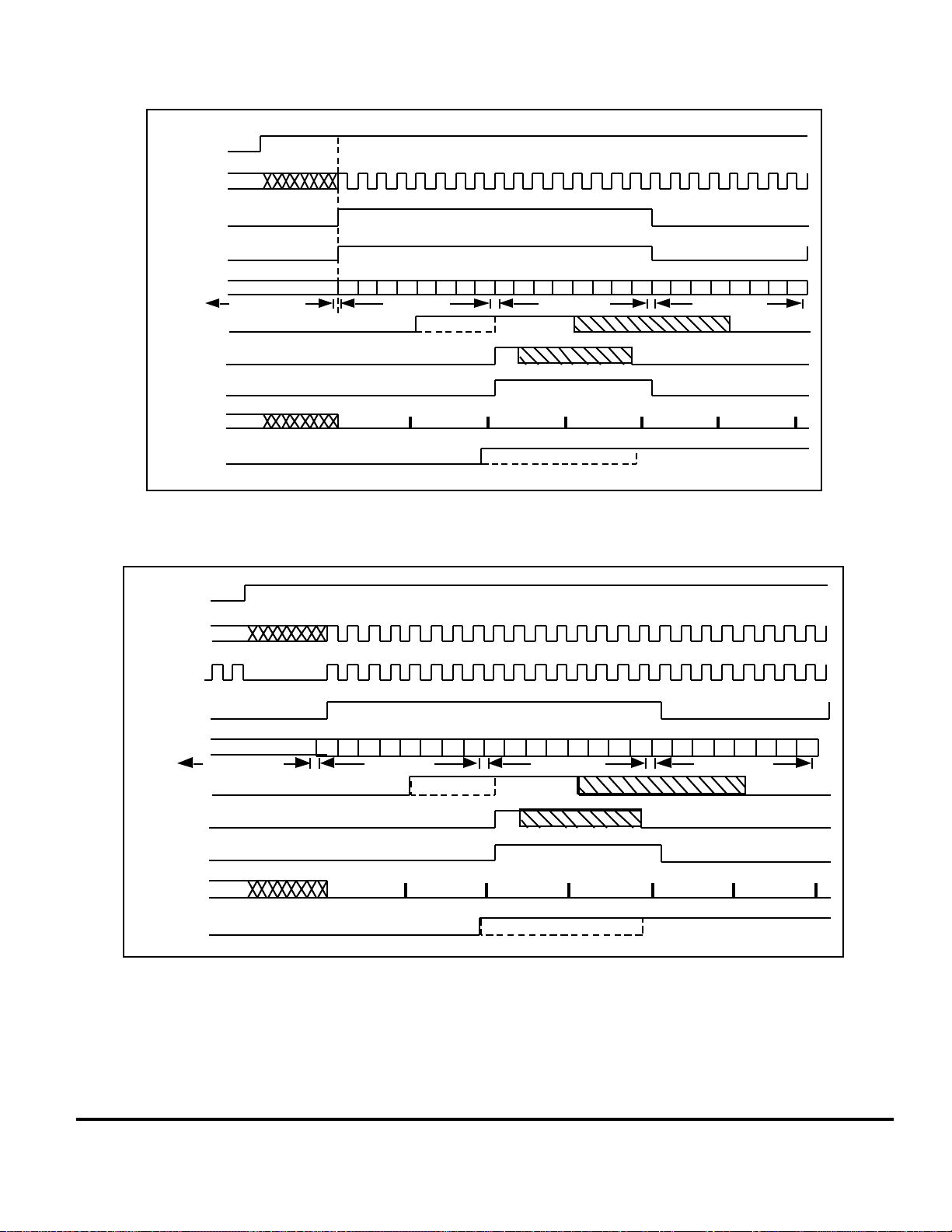
Slave Mode, QPSK
Burst Timing: Full Burst
NOTES:
PIN
19
17
26
18
39
70
NAME
TCLK
TSDATA
CLKEN
DATAEN
DATAENO
DIFFEN
RDSLEN29
SCRMEN32
(2)
(1)
(3)
(A)
(B)
(C)
(D)
(E)
(F)
(L)
(L)
(G)
(J)
(I)
(K)
(H)
(M)
(N)
User Data Guard TimePreamble
SYMPLS42
WCP 52934.c -5/7/97
(1) All input signals shown are derived from TCLK. Each edge is delayed from a TCLK edge by typically 6 to 18 nsec.
DATAENO does not depend on TCLK but its edges are synchronized to TCLK. TCLK itself can be turned off after DATAENI
goes low.
(2) DATAENO shown at its minimum pipeline delay position. This is achieved by setting bit 6 of Configuration Register 36H to
zero. Reed-Solomon cannot be used in this mode. If bit 6 is set high, allowing Reed-Solomon an additional pipeline delay of
8 bits is inserted into the data path. This will shift both edges of DATAENO to the right by 8 cycles of TCLK.
(3) If the preamble is not encoded the same as the user data, the DIFFEN control can be toggled in mid transmission as shown.
Otherwise, the DIFFEN control can be held high or low depending on encoding desired.
(A) First data bit transition on falling edge of TCLK (first of 14 preamble symbols). The data will be valid on the next rising edge of
TCLK.
(B) CLKEN rises on the same falling edge of TCLK that the data starts on. CLKEN is allowed to rise any time earlier than shown.
(C) DATAEN rises on the first rising edge of TCLK (middle of the first preamble bit).
(D) DATAENO rises on the falling edge of TCLK (at the end of the second symbol).
(E) DIFFEN rises on the rising edge of TCLK one symbol before the first user data symbol.
(F) User data bits change on the falling edge of TCLK and must be valid during the next rising edge of TCLK.
(G) End of user data. Note that the data is allowed to go away immediately after it is latched in by the rising of TCLK which
occurs in the middle of the last user data bit.
(H) DIFFEN goes low on rising edge of TCLK (last user data symbol).
(I) DATAEN goes low on rising edge of TCLK (on the cycle of TCLK after the last user data bit).
(J) CLKEN must stay high until any time on or after the point where DATAENO goes low.
(K) DATAENO stays high until the 13th SYMPLS after DATAEN goes low.
(L) RDSLEN and SCRMEN go high on the first rising edge of TCLK in the User Data.
(M) RDSLEN goes low on the rising edge of TCLK (last user data symbol).
(N) SCRMEN goes low on the rising edge of TCLK (on the cycle of TCLK after the last user data bit).
17 STEL-1209
Page 18

Master Mode, BPSK
BURST TIMING SIGNAL RELATIONSHIPS
CLKEN
BITCLK
TCLK
DATAEN
TSDATA
GUARD TIME
DIFFEN
RDSLEN
SCRMEN
SYMPLS
PI PI PI PI UI UI UI UI GI GI GI GI
PREAMBLE
GUARD TIMEUSER DATA
NOTE 1
DATAENO
Slave Mode, BPSK
BURST TIMING SIGNAL RELATIONSHIPS
CLKEN
BITCLK
TCLK
DATAEN
TSDATA
DIFFEN
RDSLEN
SCRMEN
SYMPLS
DATAENO
GUARD
TIME
PI PI PI PI UI UI UI UI GI GI GI GI
PREAMBLE
NOTE 2
WCP 52911.c-5/6/97
GUARD TIMEUSER DATA
NOTE 1
NOTE 2
NOTE 1: STEL receivers differentially decode relative to the last preamble symbol. To encode the
first symbol against a "zero" symbol reference instead, bring DIFFEN high at the
leading edge of the user data packet (dotted line).
NOTE 2: If bit 6 of Configuration Register 36H is a "1" then the rising edge of DATAENO will be
delayed by eight cycles of BITCLK (dotted line). This is required if the Reed-Solomon
encoder is used.
STEL-1209 18
WCP 52912.c-5/6/97
Page 19

Master Mode, QPSK
BURST TIMING SIGNAL RELATIONSHIPS
CLKEN
BITCLK
TCLK
DATAENI
TSDATA
GUARD TIME
DIFFEN
RDSLEN
SCRMEN
SYMPLS
DATAENO
PI PQ PI PQ UI UQ UI UQ GI GQ GI
Slave Mode, QPSK
BURST TIMING SIGNAL RELATIONSHIPS
CLKEN
BITCLK
TCLK
DATAEN
TSDATA
GUARD TIME
DIFFEN
PI PQ PI PQ UI UQ UI UQ GI GQ GI GQ
GQ
GUARD TIMEUSER DATAPREAMBLE
NOTE 1
NOTE 2
WCP 52840.c-5/2/97
GUARD TIMEUSER DATAPREAMBLE
NOTE 1
RDSLEN
SCRMEN
SYMPLS
DATAENO
NOTE 2
WCP 52839.c-5/7/97
NOTE 1: STEL receivers differentially decode relative to the last preamble symbol. To encode the
first symbol against a "zero" symbol reference instead, bring DIFFEN high at the
leading edge of the user data packet (dotted line).
NOTE 2: If bit 6 of Configuration Register 36H is a "1" then the rising edge of DATAENO will be
delayed by eight cycles of BITCLK (dotted line). This is required if the Reed-Solomon
encoder is used.
19 STEL-1209
Page 20
Master Mode, 16QAM
BURST TIMING SIGNAL RELATIONSHIPS
CLKEN
BITCLK
TCLK
DATAEN
TSDATA
GUARD TIME
PI1PQ1PI0PQ0PI1PQ1PI0PQ0UI1UQ1UI0UQ0UI1UQ1UI0UQ0GI1GQ1GI0GQ0GI1GQ1GI0GQ
PREAMBLE
DIFFEN
RDSLEN
SCRMEN
SYMPLS
DATAENO
Slave Mode (16QAM Shown)
BURST TIMING SIGNAL RELATIONSHIPS
CLKEN
BITCLK
TCLK
DATAEN
GUARD TIMEUSER DATA
0
NOTE 1
NOTE 2
WCP 52913.c-5/6/97
TSDATA
GUARD TIME
DIFFEN
PI1PQ1PI0PQ0PI1PQ1PI0PQ0UI1UQ1UI0UQ0UI1UQ1UI0UQ0GI1GQ1GI0GQ0GI1GQ1GI0GQ
PREAMBLE
NOTE 1
RDSLEN
SCRMEN
SYMPLS
DATAENO
NOTE 1: STEL receivers differentially decode relative to the last preamble symbol. To encode the
first symbol against a "zero" symbol reference instead, bring DIFFEN high at the
leading edge of the user data packet (dotted line).
NOTE 2: If bit 6 of Configuration Register 36H is a "1" then the rising edge of DATAENO will be
delayed by eight cycles of BITCLK (dotted line). This is required if the Reed-Solomon
encoder is used.
NOTE 2
STEL-1209 20
0
GUARD TIMEUSER DATA
WCP 52914.c-5/7/97
Page 21

INITIAL SET-UP DIAGRAM
Reset
S1
J8
SYNC
J1
EXT DATA
J6
EXT DATA CLK
J2
MASTER CLK
J5
BURST GATE
J16
EXT TCLK
EPROM
Xtal.
Osc.
JP4
JP8
U2
U11
*
JP9
*
Micro
U5
STEL1109
Burst Controller
U3
U19
Power Supply
-5V
@10 mA
GND
MOLEX 4455C-A
-5V +5V
J7
JP3
JP7
EPROM
2
1
J3 1
*
+5V
@330 mA
JP1
Rp
U8
JP6
*
2
RS232
P2: 9‘D’
JP5
*
PC
IF OUT
J5
J4
IF= 5-42 MHz
PD
Spectrum Analyzer
CLK
DATA
DATA
CLK
STEL 9257
Burst Receiver
WCP 53170.c-6/26/97
FIREBERD 6000
BER Tester
STEL-1209 Default Setting:
1. Place All Jumpers As Shown With The
*
21 STEL-1209
Page 22

STEL-1209 IC PARTS LIST
Reference Designator Part Number Manufacture
U8 AT17C256 Atmel
U15 CLC404AJE Comlinear
U18 AT-210 M/A-COM
U7,U17 LT1117CST Linear Technology
T1 T1-6T-KK81 Mini-Circuit
U20 IDT6116SA35SO IDT
U4 MAX707CSA Maxim
U16 MAX232CSE Maxim
U2 27C256-120JC AMD
U1 MC74HC573ADW Motorola
U10 74LVT14D Philips
U3 P80C32EBA Intel
U19 EPF81188AQC240-4 Altera
Page 23

Information in this document is provided in connection with
Intel® products. No license, express or implied, by estoppel
or otherwise, to any intellectual property rights is granted by
this document. Except as provided in Intels Terms and Conditions of Sale for such products, Intel assumes no liability
whatsoever, and Intel disclaims any express or implied
Intel may make changes to specifications and product descriptions at any time, without notice.
For Further Information Call or Write
INTEL CORPORATION
Cable Network Operation
350 E. Plumeria Drive, San Jose, CA 95134
Customer Service Telephone: (408) 545-9700
Technical Support Telephone: (408) 545-9799
FAX: (408) 545-9888
Copyright © Intel Corporation, December 15, 1999. All rights reserved
warranty, relating to sale and/or use of Intel® products including liability or warranties relating to fitness for a particular purpose, merchantability, or infringement of any patent,
copyright or other intellectual property right. Intel products
are not intended for use in medical, life saving, or life sustaining applications.
WCP 970092A
 Loading...