

Page 1
查询STEL-1108供应商
STEL-1108
Data Sheet
STEL-1108/CR
126 MHz BPSK/QPSK
Digital Modulator
R
Page 2

TCP 960257
TABLE OF CONTENTS
FEATURES/BENEFITS ................................................................................................................ 3
BLOCK DIAGRAM....................................................................................................................... 3
PACKAGE OUTLINE................................................................................................................... 4
PIN CONFIGURATION................................................................................................................ 4
INTRODUCTION......................................................................................................................... 5
FUNCTION BLOCKS – DESCRIPTION......................................................................................... 6
Clock Generator Block ...................................................................................................... 6
Input Data Processor Block................................................................................................ 6
FIR Filter Block................................................................................................................. 6
Interpolating Filter Block................................................................................................... 6
Frequency Control Word Buffer Block................................................................................ 6
Phase Accumulator & Sine/Cosine Lookup Table Block...................................................... 6
Complex Modulator Block................................................................................................. 6
Adder Block..................................................................................................................... 6
INPUT SIGNAL DESCRIPTIONS.................................................................................................. 7
OUTPUT SIGNAL DESCRIPTIONS............................................................................................... 9
MODE CONTROL REGISTERS..................................................................................................... 10
DECIMAL, HEX AND BINARY ADDRESS EQUIVALENTS ........................................................... 13
REGISTER SUMMARY................................................................................................................. 14
ELECTRICAL CHARACTERISTICS............................................................................................... 15
ABSOLUTE MAXIMUM RATINGS................................................................................... 15
RECOMMENDED OPERATING CONDITIONS................................................................. 15
D.C. CHARACTERISTICS................................................................................................. 15
FREQUENCY CHANGE AND OUTPUT TIMING.............................................................. 16
REGISTER WRITE TIMING............................................................................................... 16
INPUT DATA AND CLOCK TIMING ............................................................................... 17
BURST MODE TIMING.................................................................................................... 19
RECOMMENDED INTERFACE CIRCUIT...................................................................................... 21
SYNCHRONIZING THE 1108 BIT CLOCK .................................................................................... 21
STEL-1108 2
Page 3
FEATURES
BENEFITS
■ Complete BPSK/DBPSK/QPSK/DQPSK
modulator in a CMOS ASIC
■ Operates at up to 6.3 Mbps in BPSK mode
and up to 12.6 Mbps in QPSK mode.
■ Programmable over a wide range of data
rates
■ NCO modulator provides fine frequency
resolution
■ 126 MHz maximum clock rate generates
modulated carrier at frequencies to 50 MHz
■ Eliminates most analog circuitry
■ Operates in continuous and burst mode
■ Selectable 10- or 12-bit outputs
■ 32-tap FIR filter for signal shaping before
modulation
■ 80-Pin MQFP Package
■ High performance and high reliability with
reduced manufacturing costs
■ Supports data rates for voice and other
applications
■ Supports multiple data rate applications
■ Rapidly retunable to any frequency in the
operating band
■ Simplifies upconversion of signal to higher
frequencies
■ Low cost, small, allows quick prototyping
■ Optimizes performance in all modes
■ Optimum interfacing to suitable DAC
■ Optimum spectral purity of output
minimizes external filtering
■ Small Footprint, Surface Mount
BLOCK DIAGRAM
3 STEL-1108
Page 4
PACKAGE OUTLINE
WCP 51833.c-8/21/96
Top View
Pin 1 Identifier
0.012"/0.018"0.0315"
±0.008"
65
64
80
1
40
41
24
25
0.130" max.
Note: Tolerance on pin spacing is not cumulative
Package style: 80-pin MQFP. Thermal coefficient, θja = 58° C/W
Detail of pins
0.01" max.
0.029"/
0.041"
0.551"
± 0.008"
0.677"
± 0.008"
0.913"
±0.008"
0.787"
±0.008"
PIN CONFIGURATION
1 V
DD
2 DATA
3 DATA
4 DATA
5 DATA
6 V
7 V
8 ADDR
9 ADDR
10 ADDR
11 V
12 ADDR
13 ADDR
14 ADDR
15 V
16 V
SS
SS
DD
SS
SS
4
5
6
7
5
4
3
2
1
0
Notes: I.C. denotes Internal Connection. Do not use for vias.
17 TSDATA
18 DATAENI
19 TCLK
20 FCWSEL
21 FCWSEL
22 I.C.
23 I.C.
24 I.C.
25 V
26 CLKEN
27 V
28 CLK
29 NC
30 V
31 5V
32 N.C.
DD
SS
DD
DD
0
1
33 V
SS
34 I.C.
35 I.C.
36 I.C.
37 ACLKOUT
38 V
DD
39 DATAENO
40 BITCLK
41 V
DD
42 RFCLK
43 V
SS
44 RFDATA
45 RFDATA
46 V
SS
47 RFDATA
48 RFDATA
49 V
50 RFDATA
51 V
52 RFDATA
53 V
54 RFDATA
55 V
56 RFDATA
57 RFDATA
58 V
59 RFDATA
0
1
60 RFDATA
61 V
62 RFDATA
2
3
63 V
64 V
SS
DD
SS
SS
SS
SS
DD
SS
––––––––
65 RFCLKD
4
5
66 V
––––––
67 RESET
68 RFCLKD
69 V
6
7
8
70 DIFFEN
71 NCO LD
–––––
72 CSEL
–––
73 WR
SS
SS
74 I.C.
9
10
11
75 V
DD
76 DATA
77 DATA
78 DATA
79 DATA
80 V
SS
0
1
2
3
STEL-1108 4
Page 5

INTRODUCTION
The STEL-1108 is a BPSK/QPSK modulator in a single
ASIC.* It is capable of operating at data rates up to
6.3 Mbps in BPSK mode and 12.6 Mbps in QPSK
mode. The STEL-1108 will operate at a clock
frequency of up to 126 MHz, allowing it to generate
output signals at carrier frequencies up to 50 MHz.
The STEL-1108 uses digital FIR filtering to optimally
shape the spectrum of the modulating data prior to
modulation, thereby optimizing the spectrum of the
modulated signal while minimizing the analog
filtering required after the modulator. The filters are
designed to have a symmetrical (mirror image)
polynomial transfer function, thereby making the
phase response of the filter linear and eliminating
inter symbol interference as a result of group delay
distortion. In this way it is possible to change the
carrier frequency over a wide range without having to
*The STEL-1108 utilizes advanced signal processing
techniques which are covered by U.S. Patent Number
5,412,352.
change filters, providing the ability to operate a single
system in many channels. Signal level scaling is
provided after the FIR filter to allow the maximum
dynamic range of the arithmetic to be utilized since
the signal levels can be changed over a wide range
according to how the device is programmed. To
facilitate interfacing the STEL-1108 to a Digital to
Analog Converter (DAC) an output clock with
programmable delay is provided. In addition, the
STEL-1108 is designed to operate from a 3.3 volt
power supply; provision is made to allow the device
to interface with other logic operating at 5 volts.
See Application Note 125 for example calculations of
control register values.
5 STEL-1108
Page 6

FUNCTION BLOCKS – DESCRIPTION
Clock Generator Block
The timing of the STEL-1108 is controlled by the Clock
Generator Block. This block generates all the clocks
required in the device from the CLK input, as well as
the output clocks. The divider which determines the bit
rate, symbol rate and sampling rate of the FIR filter is
programmed by the data “n” written into address 29H,
with the sampling frequency set to f
/(n+1), where n
CLK
can be from 4 to 255. A second divider is used to
generate the auxiliary output clock (ACLKOUT) from
the clock input. This divider is controlled by the data,
“n”, stored in bit 3-0 in address 2AH, with the frequency
set to f
/(n+1), where n can be from 2 to 15. Of all
CLK
the clock signals generated, only the auxiliary clock
continues to run when the clock enable is low. The bit
clock output runs at twice the symbol rate, even in
BPSK mode.
Input Data Processor Block
The STEL-1108 is designed to operate as a BPSK, QPSK,
DBPSK or DQPSK modulator according to the setting of
bit 3 in address 2CH and the DIFFEN input. When
operating in QPSK mode the input data processor
assembles pairs of data bits for each symbol to be
modulated. The symbol data can then be differentially
encoded in a way which depends on whether the
modulation format is to be DBPSK or DQPSK. For
DBPSK, the encoding algorithm is straightforward:
output bit(k) = input bit(k) ⊕ output bit(k–1),
where ⊕ represents the logical EXOR function. For
DQPSK, however, the differential encoding algorithm is
more complex since there are now sixteen possible new
states depending on the four possible previous output
states and four possible new input states, as shown in
the table below:
New Input Previously Encoded OUT(I, Q)
IN(I, Q)
k
0 0 0 1 1 1 1 0
k–1
0 0 0 0 0 1 1 1 1 0
0 1 0 1 1 1 1 0 0 0
1 1 1 1 1 0 0 0 0 1
1 0 1 0 0 0 0 1 1 1
Newly Encoded OUT(I, Q)
k
FIR Filter Block
The encoded data is filtered to minimize the sidelobes of
its spectrum using a 32-tap, linear phase FIR filter. The
10-bit filter coefficients are completely programmable
for any symmetrical (mirror image) polynomial and are
stored in the registers at addresses 09H to 28H, giving
the user full control (apart from the symmetry
constraint) of the filter response. The clock (sampling)
frequency of the FIR filter is set to be four times the
symbol rate. This frequency is determined by the data,
“n”, written into address 29H, with the sampling
frequency set to f
/(n+1), where n can be from 4 to
CLK
255.
Interpolating Filter Block
The output of the FIR filter is interpolated up to the
clock frequency, f
, in a one, two or three stage
CLK
interpolating filter. Since the gain of the integrators in
the interpolating filter can vary over a wide range, a
gain control function is provided at its input to select
the significance of the 14-bit outputs of the FIR filter
relative to the 24-bit inputs of the interpolating filter.
This level shift function is controlled by the data stored
in bit 7-4 in address 2AH.
Frequency Control Word Buffer Block
The STEL-1108 incorporates a Numerically Controlled
Oscillator (NCO) to synthesize the carrier in the modulator. The frequency of the NCO is programmed by
means of the Frequency Control Word (FCW) registers
at addresses 00H through 08H. The STEL-1108
incorporates provision for three separate FCWs (FCW
A, FCW B and FCW C) to be stored in these registers.
The modulator frequency can be switched between
these values by means of the FCWSEL
inputs. The
1-0
fourth setting of this 2-bit input selects a zero-frequency
value, causing the modulator output to stop instantly at
its current phase.
Phase Accumulator and Sine/Cosine
Lookup Table Block
The 24-bit NCO gives a frequency resolution of
approximately 6 Hz at a clock frequency of 100 MHz.
The 12-bit sine and cosine lookup tables (LUTs)
synthesize a carrier with very high spectral purity, typically better than 75 dBc at the digital outputs.
Complex Modulator Block
The interpolated I and Q data signals are fed into the
Complex Modulator Block to be multiplied by the sine
and cosine carriers from the Sin/Cos LUT Block.
Adder Block
The modulated sine and cosine carriers are fed into the
Adder Block where they are either added or subtracted
together to form the sum:
Sum = ± I
.
cos(ωt) ± Q
The signs of the I and Q components can be controlled
by the settings of bits 0 and 1 in address 2BH, giving
complete control over the characteristics of the RF signal
generated.
.
sin(ωt)
STEL-1108 6
Page 7
INPUT SIGNAL DESCRIPTIONS
–––––––
RESET
Reset. RESET
clears or presets all registers when it is set low. Setting
––––––
RESET
the STEL-1108 is powered up, it is necessary to assert
the RESET
configuring the chip.
CLK (Pin 28)
Master Clock. CLK is the master clock of all the blocks.
Its frequency must be an integer multiple of four times
the data rate used (i.e., an integer multiple of the FIR
Filter sampling rate) so that the programmable binary
divider in the Clock Generator Block can generate the
bit clock from the CLK signal.
CLKEN (Pin 26)
Clock Enable. CLKEN provides a gate to control the
master clock. Setting CLKEN low will disable all
functions in the STEL-1108 (except for the auxiliary
clock output) by stopping the clock internally, thereby
reducing the power consumption almost to the static
level. Setting CLKEN high enables normal operation.
When bit 7 is set high in address 2CH, the STEL-1108
will be configured to operate with an externally
provided data clock, TCLK. When CLKEN is set high
BITCLK will be resynchronized to the first rising edge
of TCLK after the rising edge of CLKEN.
CAUTION: CLKEN must be held low continuously while programming addresses 2AH and
2BH. Failure to do so will cause the interpolator
to lock up, requiring the STEL-1108 to be reset
before normal operation resumes.
––––
WR
Write. WR
DATA
by the ADDR
data on the DATA
goes high again.
DATA
Data Bus. DATA
bus that provides access to all internal mode control
register inputs for programming. DATA
conjunction with WR
information into the control and coefficient registers.
ADDR
Address Bus. ADDR
selects the mode control register location into which the
information provided on the DATA
written. ADDR
DATA
coefficient registers.
(Pin 67)
––––––
is the master reset of the STEL-1108 and
high enables operation of the circuitry. After
––––––
pin low for greater than 100 nS prior to
(Pin 73)
–––
is used to control the writing of data to the
bus. When WR
7-0
(Pins 2 - 5, 76 - 79)
7-0
(Pins 8 - 10, 12 - 14)
5-0
to write the information into the control and
7-0
–––
is set low the register selected
lines will become transparent and the
5-0
bus will be latched in when WR
7-0
is an 8-bit microprocessor interface
7-0
is used in
–––
and ADDR
is a 6-bit address bus that
5-0
is used in conjunction with WR
5-0
7-0
to write the
5-0
bus will be
7-0
–––
–––
and
––––––
CSEL
(Pin 72)
Chip Select. CSEL
the microprocessor operation of the STEL-1108. When
–––––
CSEL
is set high all write operations are disabled.
–––––
When CSEL
–––––
is provided to enable or disable
is set low the data bus become active and
write operations are enabled.
NCO LD (Pin 71)
NCO Load Input. The frequency control word selected
by the FCWSEL
inputs will be loaded into the NCO
1-0
on the rising edge of NCO LD. This function is also
executed automatically each time the DATAENI input
is set high. There is a pipeline delay of 16 CLK cycles
from the rising edges of both NCO LD and
DATAENI to the point where the NCO outputs are
multiplied by the modulating signal in the Modulator
Block. There is a further pipeline delay of 11 CLK
cycles to the output pins, making a total of 27 CLK
cycles from the load command to the output.
FCWSEL
(Pins 20, 21)
1-0
Frequency Control Word Select. FCWSEL
input that permits the selection of one of four frequency
control words for the NCO. In this way the NCO can be
rapidly switched between these four frequencies
without having to reload the FCW data in the FCW
registers. The FCW is selected as follows:
FCWSEL
1-0
FCW data register/addresses
00 FCW ’A’
01 FCW ’B’
10 FCW ’C’
11 FCW = 0 (zero frequency)
Whenever FCWSEL
is changed the NCO frequency
1-0
will change after the NCO is reloaded with a rising edge
on either the NCO LD or the DATAENI inputs.. When
FCWSEL
= 11 the FCW data is unconditionally set to
1-0
00 00 00 00H, setting the NCO to zero frequency. When
this occurs the NCO output will remain at its current
phase value until FCWSEL
is changed and the NCO
1-0
is reloaded.
DATAENI (Pin 18)
Data Enable Input. The DATAENI input is used to
signify the beginning and end of a burst of data. It
should be set high before the first (when the STEL-1108
is configured for BPSK modulation by setting bit 3 in
address 2CH high) or second (when the STEL-1108 is
configured for QPSK modulation by setting bit 3 in
address 2CH low) falling edge of BITCLK (the edge on
which the Q-channel bit is loaded in the QPSK mode) of
each burst and set low again after the last falling edge of
BITCLK of each burst. DATAENO will go high after
the first two symbol periods of eachburst. At this time
the NCO will be reloaded according to the current
setting of FCWSEL
1-0
.
is a 2-bit
1-0
7 STEL-1108
Page 8

DIFFEN (Pin 70)
Differential Encode enable Input. When DIFFEN is set
low the data will be transmitted without any differential
encoding. When this pin is set high the data will be
differentially encoded before modulation and
transmission as follows:
DBPSK modulation (bit 3 in address 2CH set high):
The data will be differentially encoded starting with the
bit entering the TSDATA input during the symbol in
which DIFFEN goes high. This bit will be differentially
encoded relative to a logic zero, regardless of the value
of the previous bit. The differential encoding
algorithms:
output bit(k) = input bit(k) ⊕ output bit(k–1)
where ⊕ represents the logical XOR function.
DQPSK modulation (bit 3 in address 2CH set low):
The data will be differentially encoded starting with the
bit pair entering the TSDATA input during the symbol
in which DIFFEN goes high. The bits in that symbol
will be differentially encoded relative to a 00 symbol,
regardless of the value of the previous symbol. The
differential encoding algorithm is shown in the table
below:
New Input Previously Encoded OUT(I, Q)
IN(I, Q)
k
0 0 0 0 0 1 1 1 1 0
0 1 0 1 1 1 1 0 0 0
1 1 1 1 1 0 0 0 0 1
1 0 1 0 0 0 0 1 1 1
0 0 0 1 1 1 1 0
Newly Encoded OUT(I, Q)
k–1
k
TSDATA (Pin 17)
Transmit Serial Data Input. The data to be transmitted
is input at this pin. When bit 7 is set low in address
2CH, the data is latched in on the falling edges of the
BITCLK output. When this bit is set high the data is
latched in on the rising edges of the TCLK input.
TCLK (Pin 19)
Transmit Clock Input. The STEL-1108 is designed to
operate either in a slave mode, when an external bit
clock is required, or in a master mode, when it provides
its own clock, according to the setting of bit 7 in address
2CH. Although the TSDATA signal is sampled
internally on the falling edges of the internally
generated BITCLK signal, a synchronizing circuit is
provided to allow the use of the external data clock,
TCLK, by setting bit 7 high in address 2CH. The TCLK
input must be set to the correct frequency in relation to
the CLK input, i.e., its frequency must be the same as
the bit rate. In this mode the clock generator will freerun until the first rising edge on TCLK and will then
synchronize BITCLK to this edge to allow TCLK to be
used as the data input clock. The falling edges of
BITCLK will occur n+4 cycles of CLK after the rising
edges of TCLK, where n is the value of the data stored
in the Sampling Rate Control Register at address 29H.
The data will then be latched in on the rising edges of
TCLK before being re-sampled internally with BITCLK.
In the event that the mutual synchronization of the
clocks is lost, the clock generator can be made to
resynchronize itself to TCLK by setting bit 0 in address
2EH high and then low again. BITCLK will be
resynchronized to the first rising edge of TCLK after bit
0 is set low.
5VDD (Pin 31)
To allow the STEL-1108 to be operated with drive
circuits operating from conventional +5 volt logic levels
the input buffers are powered from a separate power
supply pin called 5VDD. This pin should be connected
to the supply from which the drive circuits are powered.
If the drive circuits operate from the same supply
voltage as the STEL-1108 then 5VDD and VDD (+3.3
volts) should be connected together.
STEL-1108 8
Page 9

OUTPUT SIGNAL DESCRIPTIONS
RFDATA
(Pins 44, 45, 47, 48, 50, 52,
11-0
54, 56, 57, 59, 60, 62)
RF Output Data. The 12 MSBs of the internal 15-bit sum
of the I.cos and Q.sin products are brought out as
RFDATA
to use a 10-bit DAC with the STEL-1108. In this case the
two MSBs, RFDATA
3 high in address 2BH. The signal should then be scaled
after the FIR filter so that the peak amplitude of the
output is no more than 10 bits and the DAC connected
to pins RFDATA
. In some applications it may be desirable
11-0
, can be disabled by setting bit
11-10
.
9-0
DATAENO (Pin 39)
Data Enable Output. DATAENO is a modified replica
of the DATAENI input. It will be set high two symbols
after DATAENI goes high and it will be set low eleven
symbols after DATAENI goes low. In this way,
DATAENO indicates the entire activity period of the
RFDATA
output during the burst.
11-0
BITCLK (Pin 40)
Bit Clock Output. BITCLK is a 50% duty cycle clock at
twice the symbol rate, which is determined by the value
of the data stored in the Sampling Rate Control Register
at address 29H. If an external transmit data clock is not
available, BITCLK can be used as the clock in QPSK
mode (divide by 2 externally for BPSK mode). When bit
7 in address 2CH is set high the TSDATA signal is first
sampled internally on the rising edges of the TCLK
signal The falling edges of BITCLK will then occur n+4
cycles of CLK after the rising edges of TCLK, where n is
the value of the data stored in the Sampling Rate
Control Register at address 29H. When bit 7 in address
2CH is set low the TSDATA signal will be sampled
directly on the falling edges of BITCLK.
RFCLK (Pin 42)
The RFCLK output is a replica of the input clock signal,
CLK. It is intended to be used to strobe the DAC
connected to the RFDATA
different DAC characteristics and requirements it is
possible to set the actual timing of RFCLK by means of
bits 6-5 in address 2CH, as shown in the following table:
RFCLK Delay
Bits 6-5 (TYP)
0 0 5 nsec
0 1 7 nsec
1 0 9 nsec
1 1 Disabled
Setting 11 disables the RFCLK output, making it possible to turn off the DAC output in this way. Please refer
to the timing diagrams for further details.
–––––––––
RFCLKD
The RFCLKD
replicas of the output clock signal, RFCLK. They are
not normally used and are not shown in the block
diagram.
, RFCLKD (Pins 65, 68)
––––––––
and RFCLKD outputs are delayed
output. To cater for
11-0
ACLKOUT (Pin 37)
Auxiliary Clock Output. CLK is divided by a factor of
3 to 16 to generate the ACLKOUT signal. The division
factor is determined by the data stored in bits 3-0 of
address 2AH. The frequency is then set to the frequency
of CLK/(n+1), where n is the value stored in address
2AH and must range from 2 to 15. In all cases,
ACLKOUT will be high for two cycles of CLK and low
for (n–1) cycles of CLK.
9 STEL-1108
Page 10

MODE CONTROL REGISTERS - WRITE ADDRESSES
Addresses 00H - 08H:
NCO Frequency Control Words
The internal Carrier NCO is driven by a frequency
control word that is stored in the FCW registers. The
nine 8-bit registers at addresses 00H through 08H are
used to store the three 24-bit frequency control words
FCW ‘A’, FCW ‘B’ and FCW ‘C’ as shown in Table 1.
The LSB of each byte is stored in bit 0 of each register.
Address FCW Data
00
01
02
03
04
05
06
07
08
H
H
H
H
H
H
H
H
H
FCW ‘A’, bits 7-0
FCW ‘A’, bits 15-8
FCW ‘A’, bits 23-16
FCW ‘B’, bits 7-0
FCW ‘B’, bits 15-8
FCW ‘B’, bits 23-16
FCW ‘C’, bits 7-0
FCW ‘C’, bits 15-8
FCW ‘C’, bits 23-16
Table 1. Carrier NCO FCW Storage
The frequency of the NCO will be:
f
. FCW
=
CLK
24
2
f
CARR
where:
f
is the frequency of the CLK input.
CLK
and FCW is the FCW data stored in addresses 00
through 08H as selected by the setting of the FCWSEL
inputs. When FCWSEL
is set to 11 the frequency of
1-0
1-0
the NCO is set to zero.
Addresses 09H - 28H:
FIR Filter Coefficients
The coefficients of the FIR filter are stored in addresses
09H - 28H, using two addresses for each 10-bit coefficient
as shown in Table 2. The LSB of each byte is stored in
bit 0 of each register, so that bits 9-8 of each coefficient
are stored in bits 1-0 of the corresponding register. The
coefficients are stored as Two’s Complement numbers
in the range –512 to +511 (200H to 1FFH).
Address FCW Data
09
0A
0B
0C
H
H
H
H
Taps 0 and 31, bits 7-0
Taps 0 and 31, bits 9-8
Taps 1 and 30, bits 7-0
Taps 1 and 30, bits 9-8
… …
… …
25
26
27
28
H
H
H
H
Taps 14 and 17, bits 7-0
Taps 14 and 17, bits 9-8
Taps 15 and 16, bits 7-0
Taps 15 and 16, bits 9-8
Table 2. FIR Filter Coefficient Storage
The filter is always constrained to have symmetrical
coefficients, resulting in a linear phase response. This
allows each coefficient to stored once for two taps, as
shown in the table.
Address 29H:
Sampling Rate, Symbol Rate and Bit Rate
Control
The timing of the STEL-1108 is controlled by the Clock
Generator Block. This block generates all the clocks
required in the device from the CLK input, as well as
the output clocks. The divider which determines the bit
rate, symbol rate and sampling rate of the FIR filter is
programmed by the data written into address 29H, with
the sampling frequency ranging from f
f
/256. The sampling rate is then set to the frequency
CLK
of CLK/(n+1), where n is the value stored in address
H
29H and must range from 4 to 255, unless n is a multiple
of 16. If n is a multiple of 16 the sampling rate will be
set to the frequency of CLK/(n+17) In all cases this is
further divided by 2 to generate BITCLK. Note that at
CLK frequencies below approximately 64 MHz it is also
permissible to set the sampling rate to 3, giving a
sampling frequency of f
CLK
/4.
Address 2AH:
CAUTION: CLKEN must be held low continuously while programming address 2AH.
Failure to do so will cause the interpolator to lock
up, requiring the STEL-1108 to be reset before
normal operation resumes.
CLK
/5 to
STEL-1108 10
Page 11

Bits 0 through 3 -- Auxiliary Clock Rate
Control
The timing of the ACLKOUT signal is controlled by the
Clock Generator Block. The divider which determines
the frequency of ACLKOUT is programmed by the data
written into bits 3-0 in address 2AH, with the frequency
ranging from f
set to the frequency of CLK/(n+1), where n is the value
stored in address 2AH and the valid range is 2 to 15. If
n is set to 1 the ACLKOUT output will remain set high,
thereby disabling this function. If the ACLKOUT signal
is not required, it is recommended that it be set in this
mode to conserve power consumption.
CLK
/3 to f
/16. The frequency is then
CLK
Bits 4 through 7 -- Interpolation Filter
Input Gain Control
Since the gain of the integrators in the interpolation
filter can vary over a wide range, a gain control function
is provided at its input to select the significance of the
14-bit outputs of the FIR filter relative to the 24-bit
inputs of the interpolation filter. This function is
controlled by the data stored in bit 7-4 in address 2AH,
as shown in Table 3:
Bits 7-4 Input signal level of Interpolation Filter
0
H
1
H
..... ....
..... ....
7
H
8
H
Table 3. Interpolation Filter Signal Level Control
Bits 13-0 Lowest Gain
Bits 14-1
Bits 20-7
Bits 21-8 Highest Gain
Address 2BH:
CAUTION: CLKEN must be held low continuously while programming address 2BH.
Failure to do so will cause the interpolator to lock
up, requiring the STEL-1108 to be reset before
normal operation resumes.
Bits 1 - 0 -- Invert I/Q Channels
The I channel signal is multiplied by the cosine output
from the NCO and the Q channel Signal is multiplied by
the sine output prior to being added together. Bits 0
and 1 in address 2BH allow the two products to be
inverted prior to the addition, as shown in Table 4:
Bits 1-0 Output of Adder Block
0 0 Sum = I . cos(ωt) + Q
0 1 Sum = –I . cos(ωt) + Q
1 0 Sum = I . cos(ωt) – Q
1 1 Sum = –I . cos(ωt) – Q
Table 4. Signal Inversion Control
This capability gives complete flexibility to the control
of the output signal.
.
sin(ωt)
.
sin(ωt)
.
sin(ωt)
.
sin(ωt)
Bit 2 -- Test Mode
Bit 2 in address 2BH sets the STEL-1108 into a test mode
and should always be set low during normal operation.
Bit 3 -- Disable Output MSBs
The STEL-1108 generates a 12-bit output signal OUT
and is designed to be used with a 12-bit DAC. In some
applications it may be desirable to use a 10-bit DAC; in
this case the output signal level should be set so that the
2 MSBs of the output, OUT
bits can then be disabled to reduce power consumption
by setting bit 3 high in address 2BH. Care should be
taken when this feature is used since no overflow
protection is provided.
, are unused. These two
11-10
11-0
Bits 5 - 4 -- Interpolation Filter Bypass
Control
Bits 4 and 5 in address 2BH determine the number of
stages of interpolation used in the Interpolation Filter
Block. Three cascaded sections of interpolation are
provided and up to two of these can be bypassed
according to the settings of bits 4 and 5, as shown in
Table 5:
Bits 5-4 Number of Interpolations selected
0 0 3
0 1 2
1 0 2
1 1 1
Table 5. Interpolation Filter Bypass Control
Bits 7 - 6 -- Test Mode
Bits 6 and 7 in address 2BH set the STEL-1108 into a test
mode and should always be set low.
11 STEL-1108
Page 12

Address 2CH:
Bit 0 -- Test Mode
Bit 0 in address 2CH sets the STEL-1108 into a test mode
and should always be set low during normal operation.
Bit 1 -- FIR Filter Bypass Control
The FIR filters in the STEL-1108 can be bypassed by
setting bit 1 high in address 2CH.
Bit 2 -- Test Mode
Bit 2 in address 2CH sets the STEL-1108 into a test mode
and should always be set low during normal operation.
Bit 3 -- BPSK Select
The STEL-1108 is capable of operating as either a BPSK
or a QPSK modulator according to the setting of bit 0 in
address 2CH. Setting this bit low puts the device into the
QPSK mode, generating the output signal:
RFOUT = ± I . cos(ωt) ± Q
Setting this bit high puts the device into the BPSK
mode, generating the output signal:
RFOUT = ± I . cos(ωt)
In this case many of the circuits in the Q channel signal
path are disabled to conserve power.
.
sin(ωt)
Bit 4 -- Test Mode
Bit 4 in address 2CH sets the STEL-1108 into a test mode
and should normally be set low. Setting this bit high
complements the frequency control word.
Bits 6 - 5 -- RFCLK Delay Control
Bits 5 and 6 in address 2CH control the delay or phase of
the RFCLK output, as shown in Table 6:
RFCLK Delay
Bits 6-5 (TYP)
0 0 5 nsec
0 1 7 nsec
1 0 9 nsec
1 1 Disabled
Table 6. RFCLK Delay Control
Bit 7 -- External Transmit Clock Select
The STEL-1108 is designed to operate either in a slave
mode, when an external bit clock is required, or in a
master mode, when it provides its own clock, according
to the setting of bit 7 in address 2CH. Although the
TSDATA signal is sampled internally on the falling
edges of the internally generated BITCLK signal, a
synchronizing circuit is provided to allow the use of the
external data clock, TCLK, by setting bit 7 high in
address 2CH. The TCLK input must be set to the correct
frequency in relation to the CLK input, i.e., its frequency
must be the same as the bit rate. In this mode
the clock generator will free-run until the first rising
edge on TCLK and will then synchronize BITCLK to
this edge to allow TCLK to be used as the data input
clock. The data will then be latched in on the rising
edges of TCLK before being re-sampled internally with
BITCLK. In the event that the mutual synchronization
of the clocks is lost, the clock generator can be made to
resynchronize itself to TCLK by setting bit 0 in address
2EH high and then low again. BITCLK will be
resynchronized to the first rising edge of TCLK after bit
0 is set low. When bit 7 is set low in address 2CH the
TSDATA signal will be sampled directly by the falling
edges of BITCLK.
Address 2DH:
Bit 0 -- PN Data Mode
The STEL-1108 incorporates a pseudo random number
(PN) generator, primarily for test purposes.
When bit 0 is set high in address 2DH the PN generator
will be connected to the data path in place of the normal
input data at the TSDATA input. When this bit is set
low the device will operate in the normal mode,
transmitting the input data.
Bit 1 -- PN Code Select
When bit 0 is set high in address 2DH the STEL-1108 PN
generator will be connected to the data path in place of
the normal input data at the TSDATA input. Two
different PN codes can be selected, according the setting
of bit 1 in address 2DH. When this bit is set low the
code will be (10,3) and when it is set high the code will
be (23,18). The latter code is the same as that used in a
TTC FIREBERD 6000 BER test set, allowing the system
to be tested without a second FIREBERD at the transmit
site when the transmitter and receiver are located at
different sites.
Bit 2 -- Offset Binary Select
The output signal RFOUT
complement or offset binary format , according to the
setting of bit 2 in address 2DH. Setting this bit high
selects two’s complement and setting it low selects
offset binary, as shown in Table 7:
Signal
level
Max. + 7FFH (12-bit mode) FFF
Zero 000
Max. – 800H (12-bit mode) 000
Table 7. RFOUT
Bit 2 = 1 (2’s Comp) Bit 2 = 0 (O. Bin)
H
Signal Formats
11-0
can be in either two’s
11-0
RFOUT
11-0
800
H
H
H
STEL-1108 12
Page 13

Bits 7 - 3 -- Not Used
Address 2E
H
Bit 0 -- Bit Clock Sync Control
When bit 7 is set high in address 2CH, the STEL-1108
will be configured to operate with an externally
provided data clock, TCLK. The internally generated
this clock. In the event that the mutual synchronization
of the clocks is lost, the clock generator can be made to
resynchronize itself to TCLK by setting bit 0 in address
2EH high and then low again. BITCLK will be
resynchronized to the first rising edge of TCLK after bit
0 is set low.
BITCLK will be synchronized to the first rising edge of
––––––––––––––––––––––––––––––––––––––––––––––––––––
DECIMAL, HEX AND BINARY ADDRESS EQUIVALENTS
Dec. Hex. Binary Dec. Hex. Binary Dec. Hex. Binary
0 00
1 01
2 02
3 03
4 04
5 05
6 06
7 07
8 08
9 09
10 0A
11 0B
12 0C
13 0D
14 0E
15 0F
000000
H
000001
H
000010
H
000011
H
000100
H
000101
H
000110
H
000111
H
001000
H
001001
H
001010
H
001011
H
001100
H
001101
H
001110
H
001111
H
16 10
17 11
18 12
19 13
20 14
21 15
22 16
23 17
24 18
25 19
26 1A
27 1B
28 1C
29 1D
30 1E
31 1F
010000
H
010001
H
010010
H
010011
H
010100
H
010101
H
010110
H
010111
H
011000
H
011001
H
011010
H
011011
H
011100
H
011101
H
011110
H
011111
H
32 20
33 21
34 22
35 23
36 24
37 25
38 26
39 27
40 28
41 29
42 2A
43 2B
44 2C
45 2D
46 2E
100000
H
100001
H
100010
H
100011
H
100100
H
100101
H
100110
H
100111
H
101000
H
101001
H
101010
H
101011
H
101100
H
101101
H
101110
H
13 STEL-1108
Page 14
REGISTER SUMMARY - WRITE ADDRESSES
Address Contents
Bit 7 Bit 6 Bit 5 Bit 4 Bit 3 Bit 2 Bit 1 Bit 0
00-02
03-05
06-08
09-28
29
2A
2B
2C
H
H
H
H
H
H
H
H
Interpolation Filter Input Gain Control Auxiliary Clock Rate Control
Set to zero Int. Filt. Bypass Control Dis. MSBs Set to zero Invert I/Q Channels
Ext. Tx
RFCLK Control Set to zero BPSK
NCO Frequency Control Word ‘A’ (24 bits)
NCO Frequency Control Word ‘B’ (24 bits)
NCO Frequency Control Word ‘C’ (24 bits)
FIR Filter Coefficients
Sampling Rate, Symbol Rate and Bit Rate Control
Clock Sel.
2D
H
2E
H
EXAMPLE SOFTWARE INITIALIZATION SEQUENCE
Select
Set to zero FIR
Bypass
Control
Offset Bin.
Select
PN Code
Select
Set to zero
PN Data
Mode
Bit Clock
Sync Cont.
1. Disable the clock by setting pin 26 (CLKEN) low
2. Reset the STEL-1108 by pulsing pin 67 (RESETB) low (this clears all internal registers)
3. Write to all 47 registers
4. Enable the clock by setting pin 26 (CLKEN) high
5. Force the internal NCO to load the new frequency register data by pulsing pin 71 (NCO LD) high
STEL-1108 14
Page 15

ELECTRICAL CHARACTERISTICS
ABSOLUTE MAXIMUM RATINGS
Warning: Stresses greater than those shown below may cause permanent damage to
the device. Exposure of the device to these conditions for extended periods may also
affect device reliability. All voltages are referenced to VSS.
Symbol Parameter Range Units
T
stg
V
DDmax
V
I(max)
I
i
P
Diss (max)
P
Diss (max)
RECOMMENDED OPERATING CONDITIONS
Symbol Parameter Range Units
V
DD
T
a
Storage Temperature –40 to +125 °C
Supply voltage on V
DD
–0.3 to + 7 volts
Input voltage –0.3 to 5VDD+0.3 volts
DC input current ± 30 mA
Power dissipation, CLKEN = 1 690 mW
Power dissipation, CLKEN = 0 50 mW
Supply Voltage +3.3 ± 10% volts
Operating Temperature (Ambient) –40 to +85 °C
D.C. CHARACTERISTICS Operating Conditions: V
= 3.3 V ±10%, VSS = 0 V, Ta = –40° to 85° C
DD
Symbol Parameter Min. Typ. Max. Units Conditions
I
DDQ
I
DD
V
IH(min)
V
IL(max)
V
IH(min)
V
IL(max)
I
IH
I
IL
V
OH(min)
V
OL(max)
V
OH(min)
Supply Current, Quiescent 1.0 mA Static, no clock
Supply Current, Operational 2.2 mA/MHz f
= 126 MHz
CLK
Clock High Level Input Voltage 2.0 volts CLK, Logic '1'
Clock Low Level Input Voltage 0.8 volts CLK, Logic '0'
High Level Input Voltage 2.0 volts Other inputs, Logic '1'
Low Level Input Voltage 0.8 volts Other inputs, Logic '0'
High Level Input Current 10 µA V
Low Level Input Current –10 µA V
High Level Output Voltage 2.4 3.0 V
volts IO = –4.0 mA, RFDATA, RFCLK
DD
IN
IN
= 5V
= V
Low Level Output Voltage 0.2 0.4 volts IO = + 4.0 mA, RFDATA, RFCLK
High Level Output Voltage 2.4 3.0 V
volts IO = –2.0 mA, All other
DD
outputs
V
OL(max)
Low Level Output Voltage 0.2 0.4 volts IO = +2.0 mA, All other
outputs
I
C
C
OS
IN
OUT
Output Short Circuit Current 20 65 130 mA V
OUT
Input Capacitance 2 pF All inputs
Output Capacitance 4 10 pF All outputs
DD
SS
= VDD, V
DD
= max
15 STEL-1108
Page 16
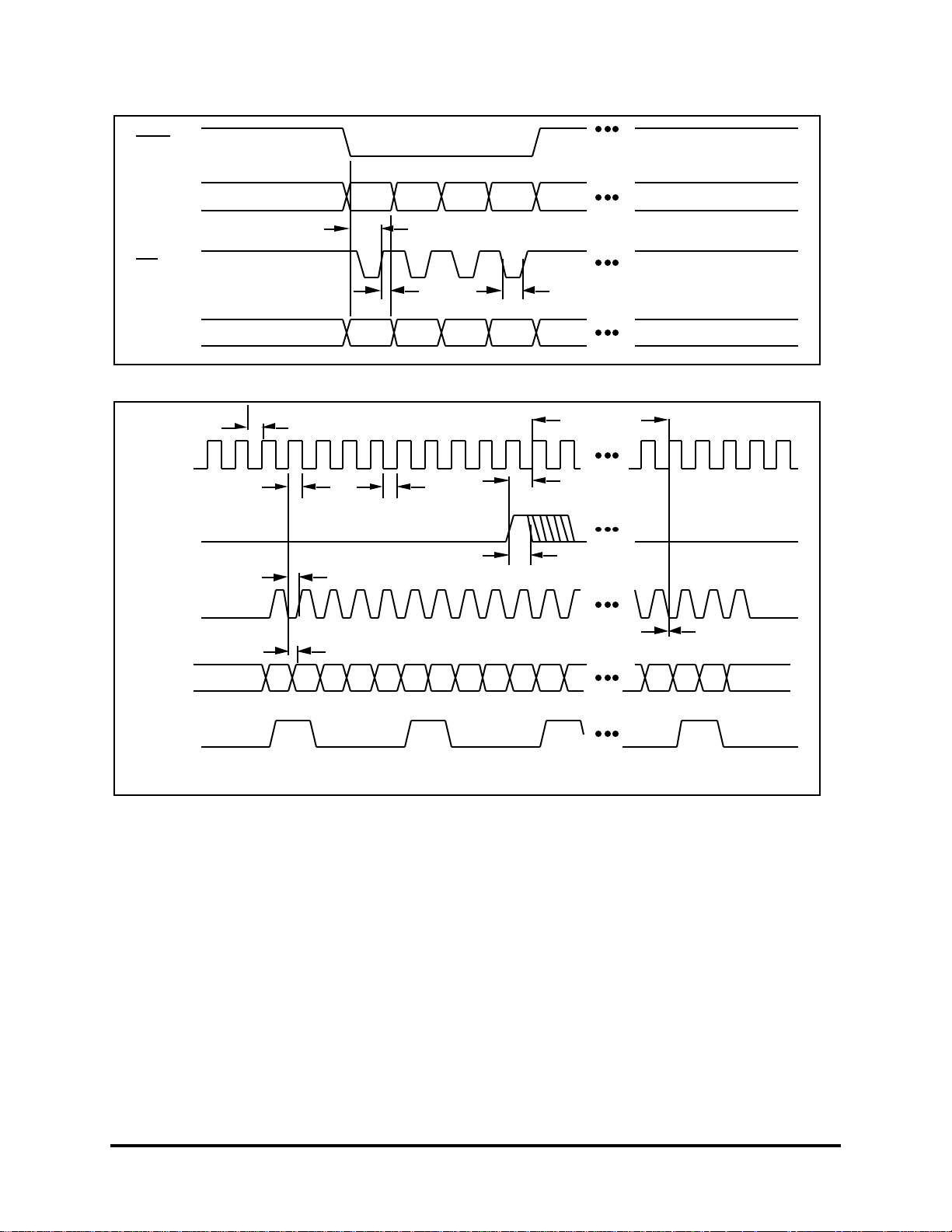
REGISTER WRITE TIMING
CSEL
ADDR 5-0
WR
DATA 7-0
DON'T CARE DON'T CARE
tSU1
tHD1 tWR
DON'T CARE
DON'T CARE
FREQUENCY CHANGE AND OUTPUT SIGNAL TIMING
CLK
**
NCO LD
RFCLK
tSU
tCLK
tCRC
tCRD
tCLK
tSU2
tW
27 CLOCK
EDGES
OLD FREQUENCY NEW FREQUENCY
RFDATA 11-0
ACLKOUT *
* Shown for ÷5 case (n = 4)
**Insert NCOLD when CLKEN is "HIGH."
TCP 52113.c 9/6/96
STEL-1108 16
Page 17

INPUT DATA AND CLOCK TIMING
MASTER MODESLAVE MODE
TCLK
BITCLK
DON'T CARE
tSU3
TSDATA
External Clock ( slave) mode Internal Clock (master) mode
BITCLK*
TCLK*
DON'T CARE
DON'T CARE
DATAENI
TSDATA DON'T CARE
DON'T CARE
tHD3 tSU3 tHD3
tSU3
tHD3
Q I Q
DON'T
CARE
DON'T
CARE
DON'T CAREQ I QI
* Depending on clock mode selected
TCP 52111.c 11/25/96
A.C. CHARACTERISTICS
Operating Conditions: VDD = 3.3 V ±10%, V
Symbol Parameter Min. Max. Units Conditions
f
CLK
t
CLK
t
WR
t
SU1
t
HD1
t
W
t
CRC
t
CRD
t
SU3
t
HD3
*These are the minimum and maximum nominal values programmable.
CLK Frequency 126 MHz See Note
CLK Pulse width, High or Low 2 nsec.
–––
WR
Pulse width 10 nsec.
DATA
DATA
, ADDR
7-0
, ADDR
7-0
, CSEL
5-0
, CSEL
5-0
–––––
–––––
–––
to WR
–––
to WR
setup 5 nsec.
hold 5 nsec.
NCO LD Pulse width 10 nsec.
CLK to RFCLK delay, bits 6-5 in Address 2C
CLK to RFDATA
delay 12 nsec. Load = 10 pF
11-0
TSDATA to TCLK or BITCLK setup 2.5 nsec.
TSDATA to TCLK or BITCLK hold 2.5 nsec.
= 0 V, Ta = –40° to 85° C,
SS
H
5* 9* nsec. Load = 10 pF
17 STEL-1108
Page 18

INPUT DATA AND CLOCK TIMING
CLKEN
DATAENI
DATAENO
TCLK
DON'T
CARE
tCT
DON'T CARE (AFTER DATAENI GOES LOW)
tDC
TCP 52112.c 11/25/96
A.C. CHARACTERISTICS
Operating Conditions: VDD = 3.3 V ±10%, V
Symbol Parameter Min. Max. Units Conditions
t
CT
t
DC
CLKEN to TCLK setup 2 cycles of CLK
DATAENO to CLKEN hold 0 cycles of CLK
= 0 V, Ta = –40° to 85° C,
SS
STEL-1108 18
Page 19

BURST TIMING (Slave Mode): FULL VIEW
PIN
19
17
26
18
39
70
NAME
(1)
TCLK
TSDATA
CLKEN
DATAENI
DATAENO
DIFFEN
(2)
(A)
(B)
(C)
(D)
(F)
(E)
(G)
(J)
(I)
(K)
(H)
User Data Guard TimePreamble
TCP 52032.c 8/22/96
NOTES:
(1) All input signals shown are derived from TCLK. Each edge is delayed from a TCLK edge by typically 6 to 18
nsec. DATAENO does not depend on TCLK but its edges are synchronized to TCLK. TCLK itself can be turned
off after DATAENI goes low.
(2) If the preamble is not encoded the same as the user data, the DIFFEN control can be toggled in mid transmission
as shown. Otherwise, the DIFFEN control can be held high or low depending on encoding desired.
(A) First data bit transition on falling edge of TCLK (first of 14 preamble symbols). The data will be valid on the next
rising edge of TCLK.
(B) CLKEN rises on the same edge of TCLK that the data starts on. CLKEN is allowed to rise any time earlier than
shown.
(C) DATAENI rises on the first rising edge of TCLK (middle of the first preamble bit).
(D) DATAENO rises on the falling edge of TCLK (at the end of the second symbol).
(E) DIFFEN rises on the rising edge of TCLK immediately preceding the first user data bit.
(F) User data bits are clocked by the falling edge of TCLK and must be valid during the next rising edge of TCLK.
(G) End of user data. Note that the data is allowed to go away immediately after it is latched in by the rising of
TCLK which occurs in the middle of the last user data bit.
H) DIFFEN goes low on rising edge of TCLK (middle of last user data bit).
(I) DATAENI goes low on rising edge of TCLK (on the cycle of TCLK after the last user data bit).
(J) CLKEN must stay high until any time on or after the point where DATAENO goes low.
(K) DATAENO stays high for a period of time about 11 symbols long after DATAENI goes low.
19 STEL-1108
Page 20

TCP 52033.c 8/22/96
(F)
(E)
(I)
(G)
(H)
NAME
TCLK
(1)
TSDATA
CLKEN
DATAENI
DATAENO
DIFFEN
(2)
BURST MODE TIMING: USER BURST DATA INPUT DETAIL
1 0 0 1 1 1 0 0 0 0 1 1 1 1 1 0 0 0 0 0
PIN
19
17
26
18
39
70
BURST MODE TIMING: PREAMBLE START DETAIL
PIN NAME
19 TCLK
17 TSDATA
26 CLKEN
18 DATAENI
39 DATAENO
70 DIFFEN
(1)
(2)
(A)
I Q I Q I
(B)
(C)
(D)
TCP 52034.c-8/22/96
STEL-1108 20
Page 21
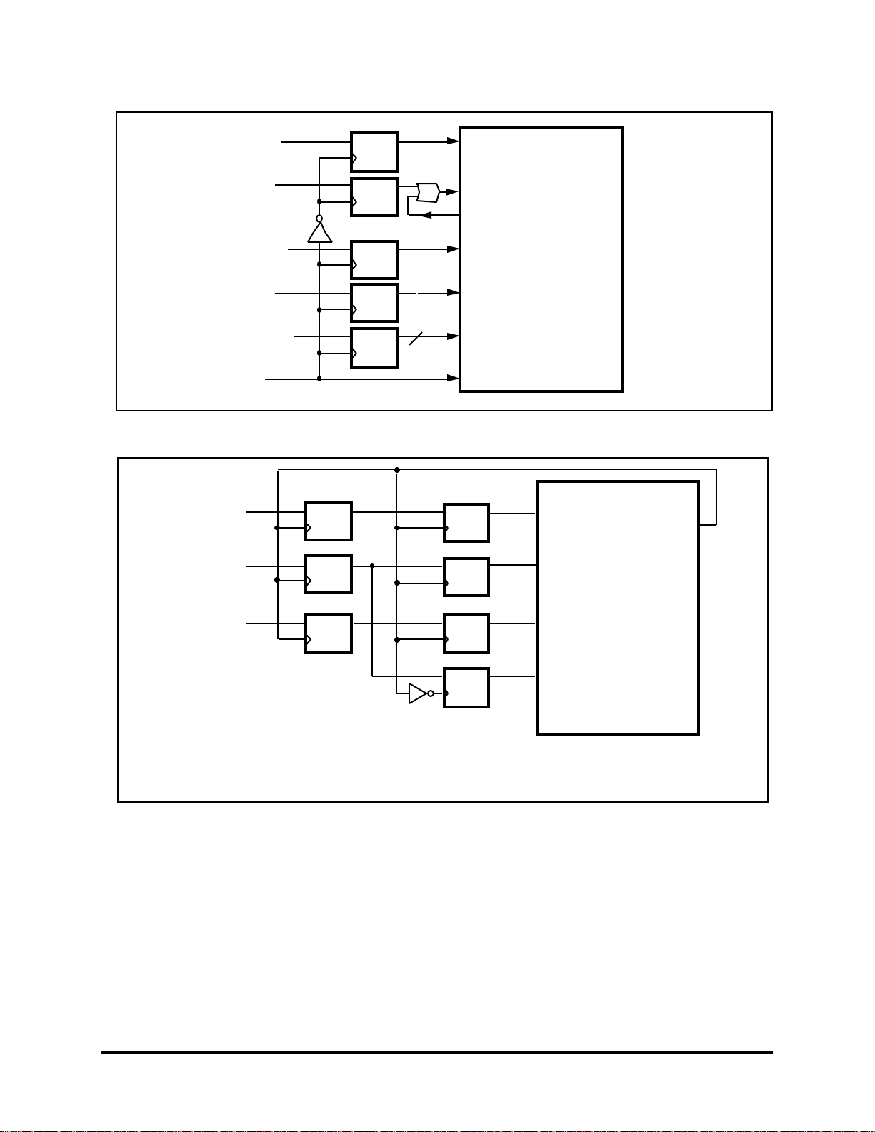
RECOMMENDED INTERFACE CIRCUIT (Slave Mode)
D
TSDATA
Q
TSDATA
CLKEN
DATAENI
DIFFEN
FCWSEL 1-0
TCLK
D Q
D Q
D Q
D Q
OR
2
CLKEN
DATAENO
DATAENI
DIFFEN
FCWSEL 1-0
TCLK
STEL-1108
RECOMMENDED INTERFACE CIRCUIT (Master Mode)
STEL-1108
TSDATA
DATAENI
D Q
D Q
D Q
D Q
TSDATA
DATAENI
TCP 52118.c 8/16/96
BITCLK
DIFFEN
D Q
D Q
D Q
DIFFEN
TCLK
CLKEN*
*CLKEN may be turned off between bursts to conserve power as long as it is turned on at least
three cycles of BITCLK before TSDATA arrives and kept on until after DATAENO goes low.
Note that the BITCLK output goes inactive whenever CLKEN is low.
TCP 52115.c 9/6/96
SYNCHRONIZING THE 1108 BIT CLOCK (Master Mode)
1) With TCLK Low
2) Preset the bit clock sync circuit by either
A) cycling clock enable from low to high
B) cycling software bit 0 in address 2EH from zero to one and back to zero
3) Bit clock will be in sync after first rising edge of TCLK
4) To keep I/Q bits synchronized with symbol boundaries, either have an integer number of symbols
(i.e. an even # of bit clocks) between bursts, or resynchronize at the beginning of each burst.
21 STEL-1108
Page 22

Information in this document is provided in connection with
Intel® products. No license, express or implied, by estoppel
or otherwise, to any intellectual property rights is granted by
this document. Except as provided in Intels Terms and Conditions of Sale for such products, Intel assumes no liability
whatsoever, and Intel disclaims any express or implied
Intel may make changes to specifications and product descriptions at any time, without notice.
For Further Information Call or Write
INTEL CORPORATION
Cable Network Operation
350 E. Plumeria Drive, San Jose, CA 95134
Customer Service Telephone: (408) 545-9700
Technical Support Telephone: (408) 545-9799
FAX: (408) 545-9888
Copyright © Intel Corporation, December 15, 1999. All rights reserved
warranty, relating to sale and/or use of Intel® products including liability or warranties relating to fitness for a particular purpose, merchantability, or infringement of any patent,
copyright or other intellectual property right. Intel products
are not intended for use in medical, life saving, or life sustaining applications.
WCP 970301A
015-140258
 Loading...