

Page 1

Intel® Server Board
SE7520JR2
Technical Product Specification
Revision 1.0
October 2004
Enterprise Platforms and Services Marketing
Page 2
Revision History Intel® Server Board SE7520JR2
Revision History
Date Revision
Number
December 2003 0.5 Preliminary Release
June 2004 0.9 Memory Sub-system rewrite, BIOS Chapter Updated, Management Chapter
re-write, Error Handling chapter re-write, several changes made to better
reflect final design
October 2004 1.0 First non-NDA release; Updated IRQ routing diagrams, Updated mBMC
Sensor tables, Updates to Regulatory Information, Updated Sensor data
tables
Modifications
Revision 1.0
ii
C78844-002
Page 3

Intel® Server Board SE7520JR2 Disclaimers
Disclaimers
Information in this document is provided in connection with Intel® products. No license, express or
implied, by estoppel or otherwise, to any intellectual property rights is granted by this document. Except
as provided in Intel's Terms and Conditions of Sale for such products, Intel assumes no liability
whatsoever, and Intel disclaims any express or implied warranty, relating to sale and/or use of Intel
products including liability or warranties relating to fitness for a particular purpose, merchantability, or
infringement of any patent, copyright or other intellectual property right. Intel products are not intended for
use in medical, life saving, or life sustaining applications. Intel may make changes to specifications and
product descriptions at any time, without notice.
Designers must not rely on the absence or characteristics of any features or instructions marked
"reserved" or "undefined." Intel reserves these for future definition and shall have no responsibility
whatsoever for conflicts or incompatibilities arising from future changes to them.
This document contains information on products in the design phase of development. Do not finalize a
design with this information. Revised information will be published when the product is available. Verify
with your local sales office that you have the latest datasheet before finalizing a design.
The Intel® Server Board SE7520JR2 may contain design defects or errors known as errata which may
cause the product to deviate from published specifications. Current characterized errata are available on
request.
This document and the software described in it are furnished under license and may only be used or
copied in accordance with the terms of the license. The information in this manual is furnished for
informational use only, is subject to change without notice, and should not be construed as a commitment
by Intel Corporation. Intel Corporation assumes no responsibility or liability for any errors or inaccuracies
that may appear in this document or any software that may be provided in association with this document.
Except as permitted by such license, no part of this document may be reproduced, stored in a retrieval
system, or transmitted in any form or by any means without the express written consent of Intel
Corporation.
Intel Corporation server boards contain a number of high-density VLSI and power delivery components
that need adequate airflow to cool. Intel’s own chassis are designed and tested to meet the intended
thermal requirements of these components when the fully integrated system is used together. It is the
responsibility of the system integrator that chooses not to use Intel developed server building blocks to
consult vendor datasheets and operating parameters to determine the amount of air flow required for their
specific application and environmental conditions. Intel Corporation cannot be held responsible if
components fail or the server board does not operate correctly when used outside any of their published
operating or non-operating limits.
Intel, Pentium, Itanium, and Xeon are trademarks or registered trademarks of Intel Corporation.
*Other brands and names may be claimed as the property of others.
Copyright © Intel Corporation 2004.
Revision 1.0
C78844-002
iii
Page 4

Table of Contents Intel® Server Board SE7520JR2
Table of Contents
1. Introduction ........................................................................................................................19
1.1 Chapter Outline...................................................................................................... 19
1.2 Server Board Use Disclaimer ................................................................................20
2. Server Board Overview...................................................................................................... 21
2.1 Server Board SE7520JR2 SKU Availability ........................................................... 21
2.2 Server Board SE7520JR2 Feature Set.................................................................. 21
3. Functional Architecture ..................................................................................................... 26
3.1 Processor Sub-system........................................................................................... 27
3.1.1 Processor Voltage Regulators ............................................................................... 27
3.1.2 Reset Configuration Logic .....................................................................................27
3.1.3 Processor Module Presence Detection .................................................................27
3.1.4 GTL2006................................................................................................................ 27
3.1.5 Common Enabling Kit (CEK) Design Support........................................................ 28
3.1.6 Processor Support ................................................................................................. 28
3.1.6.1 Processor Mis-population Detection ..................................................................29
3.1.6.2 Mixed Processor Steppings ...............................................................................29
3.1.6.3 Mixed Processor Models.................................................................................... 29
3.1.6.4 Mixed Processor Families .................................................................................. 29
3.1.6.5 Mixed Processor Cache Sizes ........................................................................... 29
3.1.6.6 Jumperless Processor Speed Settings .............................................................. 29
3.1.6.7 Microcode........................................................................................................... 30
3.1.6.8 Processor Cache................................................................................................ 30
3.1.6.9 Hyper-Threading Technology............................................................................. 30
3.1.6.10 Intel® SpeedStep® Technology....................................................................... 30
3.1.6.11 EM64T Technology Support ............................................................................30
3.1.7 Multiple Processor Initialization .............................................................................30
3.1.8 CPU Thermal Sensors........................................................................................... 31
3.1.9 Processor Thermal Control Sensor .......................................................................31
3.1.10 Processor Thermal Trip Shutdown ........................................................................ 31
3.1.11 Processor IERR ..................................................................................................... 31
3.2 Intel® E7520 Chipset............................................................................................. 31
3.2.1 Memory Controller Hub (MCH) .............................................................................. 32
3.2.1.1 Front Side Bus (FSB) ......................................................................................... 32
3.2.1.2 MCH Memory Sub-System Overview................................................................. 32
3.2.1.3 PCI Express ....................................................................................................... 32
3.2.1.4 Hub Interface...................................................................................................... 33
Revision 1.0
iv
C78844-002
Page 5

Intel® Server Board SE7520JR2 Table of Contents
3.2.2 PCI-X Hub (PXH)................................................................................................... 33
3.2.2.1 Full-height Riser Slot.......................................................................................... 33
3.2.2.2 Low Profile Riser Slot......................................................................................... 33
3.2.2.3 I/OxAPIC Controller............................................................................................ 34
3.2.2.4 SMBus Interface................................................................................................. 34
3.2.3 I/O Controller Hub (ICH5-R) .................................................................................. 34
3.2.3.1 PCI Interface ...................................................................................................... 34
3.2.3.2 IDE Interface (Bus Master Capability and Synchronous DMA Mode) ................ 34
3.2.3.3 SATA Controller ................................................................................................. 35
3.2.3.4 Low Pin Count (LPC) Interface ..........................................................................35
3.2.3.5 Compatibility Modules (DMA Controller, Timer/Counters, Interrupt Controller) .35
3.2.3.6 Advanced Programmable Interrupt Controller (APIC)........................................ 36
3.2.3.7 Universal Serial Bus (USB) Controller ............................................................... 36
3.2.3.8 RTC.................................................................................................................... 36
3.2.3.9 General Purpose I/O (GPIO).............................................................................. 36
3.2.3.10 Enhanced Power Management........................................................................ 36
3.2.3.11 System Management Bus (SMBus 2.0) ........................................................... 36
3.3 Memory Sub-System ............................................................................................. 37
3.3.1 Memory Sizing ....................................................................................................... 37
3.3.2 Memory Population................................................................................................ 38
3.3.3 ECC Memory Initialization ..................................................................................... 40
3.3.4 Memory Test.......................................................................................................... 40
3.3.5 Memory Monitoring ................................................................................................ 41
3.3.6 Memory RASUM Features.....................................................................................42
3.3.6.1 DRAM ECC – Intel® x4 Single Device Data Correction (x4 SDDC) .................42
3.3.6.2 Integrated Memory Scrub Engine ...................................................................... 42
3.3.6.3 Retry on Uncorrectable Error ............................................................................. 43
3.3.6.4 Integrated Memory Initialization Engine ............................................................. 43
3.3.6.5 DIMM Sparing Function .....................................................................................44
3.3.6.6 Memory Mirroring ............................................................................................... 45
3.3.6.7 Logging Memory RAS Information to the SEL ...................................................47
3.4 I/O Sub-System .....................................................................................................47
3.4.1 PCI Subsystem ...................................................................................................... 47
3.4.1.1 P32-A: 32-bit, 33-MHz PCI Subsystem.............................................................. 48
3.4.1.2 P64-A and P64-B: 64-bit, 100MHz PCI Subsystem ........................................... 48
3.4.1.3 P64-Express: Dual x4 PCI Bus Segment........................................................... 48
3.4.1.4 PCI Riser Slots................................................................................................... 48
3.4.1.5 PCI Scan Order.................................................................................................. 49
3.4.1.6 PCI Bus Numbering ...........................................................................................49
3.4.1.7 Device Number and IDSEL Mapping .................................................................50
3.4.1.8 Resource Assignment ........................................................................................ 52
3.4.1.9 Automatic IRQ Assignment ................................................................................ 52
3.4.1.10 Option ROM Support........................................................................................ 52
3.4.1.11 PCI APIs........................................................................................................... 52
3.4.2 Split Option ROM................................................................................................... 52
Revision 1.0
C78844-002
v
Page 6

Table of Contents Intel® Server Board SE7520JR2
3.4.3 Interrupt Routing .................................................................................................... 52
3.4.3.1 Legacy Interrupt Routing.................................................................................... 52
3.4.3.2 APIC Interrupt Routing ....................................................................................... 53
3.4.3.3 Legacy Interrupt Sources ................................................................................... 54
3.4.3.4 Serialized IRQ Support ......................................................................................54
3.4.3.5 IRQ Scan for PCIIRQ ......................................................................................... 55
3.4.4 SCSI Support......................................................................................................... 58
3.4.4.1 LSI* 53C1030 Dual Channel Ultra320 SCSI Controller ..................................... 58
3.4.4.2 Zero Channel RAID............................................................................................ 60
3.4.5 IDE Support ........................................................................................................... 60
3.4.5.1 Ultra ATA/100..................................................................................................... 61
3.4.5.2 IDE Initialization .................................................................................................61
3.4.6 SATA Support........................................................................................................ 61
3.4.6.1 SATA RAID ........................................................................................................ 62
3.4.6.2 Intel® RAID Technology Option ROM................................................................ 62
3.4.7 Video Support ........................................................................................................ 62
3.4.7.1 Video Modes ...................................................................................................... 62
3.4.7.2 Video Memory Interface ..................................................................................... 63
3.4.7.3 Dual video .......................................................................................................... 64
3.4.8 Network Interface Controller (NIC) ........................................................................ 64
3.4.8.1 NIC Connector and Status LEDs .......................................................................65
3.4.9 USB 2.0 Support.................................................................................................... 65
3.4.10 Super I/O Chip ....................................................................................................... 65
3.4.10.1 GPIOs ..............................................................................................................65
3.4.10.2 Serial Ports....................................................................................................... 67
3.4.10.3 Removable Media Drives ................................................................................. 69
3.4.10.4 Floppy Disk Support......................................................................................... 69
3.4.10.5 Keyboard and Mouse Support .........................................................................69
3.4.10.6 Wake-up Control .............................................................................................. 69
3.4.11 BIOS Flash ............................................................................................................69
3.5 Configuration and Initialization............................................................................... 70
3.5.1 Memory Space....................................................................................................... 70
3.5.1.1 DOS Compatibility Region ................................................................................. 71
3.5.1.2 Extended Memory .............................................................................................. 73
3.5.1.3 Memory Shadowing ........................................................................................... 74
3.5.1.4 System Management Mode Handling ................................................................ 75
3.5.2 I/O Map .................................................................................................................. 76
3.5.3 Accessing Configuration Space............................................................................. 78
3.5.3.1 CONFIG_ADDRESS Register............................................................................ 79
3.6 Clock Generation and Distribution ......................................................................... 79
4. System BIOS....................................................................................................................... 80
4.1 BIOS Identification String....................................................................................... 80
4.2 Flash Architecture and Flash Update Utility........................................................... 81
Revision 1.0
vi
C78844-002
Page 7

Intel® Server Board SE7520JR2 Table of Contents
4.3 BIOS Power On Self Test (POST)......................................................................... 81
4.3.1 User Interface ........................................................................................................ 81
4.3.1.1 System Activity Window ..................................................................................... 82
4.3.1.2 Splash Screen/Diagnostic Window .................................................................... 82
4.3.1.3 POST Activity Window ....................................................................................... 83
4.3.2 BIOS Boot Popup Menu ........................................................................................ 83
4.4 BIOS Setup Utility .................................................................................................. 84
4.4.1 Localization............................................................................................................ 84
4.4.2 Entering BIOS Setup .............................................................................................85
4.4.2.1 Main Menu .........................................................................................................85
4.4.2.2 Advanced Menu ................................................................................................. 86
4.4.2.3 Boot Menu.......................................................................................................... 95
4.4.2.4 Security Menu .................................................................................................... 98
4.4.2.5 Server Menu....................................................................................................... 99
4.4.2.6 Exit Menu ......................................................................................................... 102
4.5 Rolling BIOS and On-line Updates ...................................................................... 102
4.5.1 Flash Update Utility.............................................................................................. 103
4.5.1.1 Flash BIOS....................................................................................................... 103
4.5.1.2 User Binary Area.............................................................................................. 103
4.5.1.3 Recovery Mode ................................................................................................ 103
4.5.1.4 BIOS Recovery ................................................................................................104
4.5.2 .Configuration Reset ............................................................................................ 104
4.6 OEM Binary .........................................................................................................105
4.7 Security................................................................................................................105
4.7.1 Operating Model .................................................................................................. 106
4.7.2 Password Clear Jumper ......................................................................................108
4.8 Extensible Firmware Interface (EFI) .................................................................... 108
4.8.1 EFI Shell .............................................................................................................. 108
4.9 Operating System Boot, Sleep, and Wake .......................................................... 108
4.9.1 Microsoft* Windows* Compatibility ...................................................................... 108
4.9.2 Advanced Configuration and Power Interface (ACPI) ......................................... 109
4.9.2.1 Sleep and Wake Functionality.......................................................................... 109
4.9.2.2 Power Switch Off to On.................................................................................... 110
4.9.2.3 On to Off (OS absent) ...................................................................................... 110
4.9.2.4 On to Off (OS present) ..................................................................................... 110
4.9.2.5 On to Sleep (ACPI) ..........................................................................................110
4.9.2.6 Sleep to On (ACPI) ..........................................................................................111
4.9.2.7 System Sleep States........................................................................................ 111
4.10 PXE BIOS Support .............................................................................................. 112
4.11 Console Redirection ............................................................................................112
5. Platform Management...................................................................................................... 113
Revision 1.0
C78844-002
vii
Page 8

Table of Contents Intel® Server Board SE7520JR2
5.1 Platform Management Architecture Overview ..................................................... 115
5.1.1 5V Standby .......................................................................................................... 116
5.1.2 IPMI Messaging, Commands, and Abstractions xxx............................................ 116
5.1.3 IPMI ‘Sensor Model’............................................................................................. 117
5.1.4 Private Management Busses............................................................................... 118
5.1.5 Management Controllers .....................................................................................118
5.2 On-Board Platform Management Features and Functionality..............................121
5.2.1 Server Management I2C Buses ...........................................................................122
5.2.2 Power Control Interfaces ..................................................................................... 122
5.2.3 External Interface to the mBMC........................................................................... 122
5.3 mBMC Hardware Architecture ............................................................................. 123
5.3.1 Power Supply Interface Signals........................................................................... 124
5.3.2 Power Control Sources........................................................................................ 126
5.3.3 Power-up Sequence ............................................................................................ 126
5.3.4 Power-down Sequence........................................................................................ 126
5.3.5 System Reset Control.......................................................................................... 126
5.3.5.1 Reset Signal Output ......................................................................................... 126
5.3.5.2 Reset Control Sources ..................................................................................... 127
5.3.5.3 Control Panel System Reset ............................................................................ 127
5.3.5.4 Control Panel Indicators................................................................................... 128
5.3.5.5 Control Panel Inputs......................................................................................... 129
5.3.6 Secure Mode Operation....................................................................................... 131
5.3.7 Baseboard Fan Control........................................................................................ 131
5.3.8 mBMC Peripheral SMBus.................................................................................... 131
5.3.9 Watchdog Timer ..................................................................................................131
5.3.10 System Event Log (SEL) ..................................................................................... 131
5.3.10.1 SEL Erasure................................................................................................... 132
5.3.10.2 Timestamp Clock ...........................................................................................132
5.3.11 Sensor Data Record (SDR) Repository ............................................................... 132
5.3.11.1 Initialization Agent .......................................................................................... 132
5.3.12 Field Replaceable Unit (FRU) Inventory Devices ................................................133
5.3.12.1 mBMC FRU Inventory Area Format ............................................................... 133
5.3.13 NMI Generation ...................................................................................................133
5.3.14 SMI Generation.................................................................................................... 133
5.3.15 Event Message Reception................................................................................... 133
5.3.16 mBMC Self Test................................................................................................... 134
5.3.17 Messaging Interfaces........................................................................................... 134
5.3.17.1 Channel Management.................................................................................... 134
Revision 1.0
viii
C78844-002
Page 9

Intel® Server Board SE7520JR2 Table of Contents
5.3.17.2 User Model..................................................................................................... 134
5.3.17.3 Request/Response Protocol ..........................................................................134
5.3.17.4 Host to mBMC Communication Interface....................................................... 134
5.3.17.5 LAN Interface ................................................................................................. 135
5.3.18 Event Filtering and Alerting.................................................................................. 136
5.3.18.1 Platform Event Filtering (PEF) ....................................................................... 136
5.3.18.2 Alert over LAN................................................................................................ 137
5.3.19 mBMC Sensor Support........................................................................................ 137
5.3.20 IMM BMC Sensor Support................................................................................... 142
5.4 Wired For Management (WFM) ........................................................................... 148
5.5 Vital Product Data (VPD) ..................................................................................... 148
5.6 System Management BIOS (SMBIOS)................................................................ 148
6. Error Reporting and Handling......................................................................................... 149
6.1 Fault Resilient Booting (FRB) .............................................................................. 149
6.1.1 FRB1 – BSP Self-Test Failures ........................................................................... 149
6.1.2 FRB2 – BSP POST Failures................................................................................ 149
6.1.3 FRB3 – BSP Reset Failures ................................................................................ 150
6.1.4 AP Failures .......................................................................................................... 151
6.1.5 Treatment of Failed Processors........................................................................... 151
6.1.6 Memory Error Handling in RAS Mode.................................................................. 152
6.1.7 Memory Error Handling in non-RAS Mode ..........................................................153
6.1.8 DIMM Enabling .................................................................................................... 154
6.1.9 Single-bit ECC Error Throttling Prevention .......................................................... 154
6.2 Error Logging ....................................................................................................... 155
6.2.1.1 PCI Bus Error ................................................................................................... 155
6.2.1.2 Processor Bus Error......................................................................................... 155
6.2.1.3 Memory Bus Error ............................................................................................ 156
6.2.1.4 System Limit Error............................................................................................ 156
6.2.1.5 Processor Failure ............................................................................................. 156
6.2.1.6 Boot Event........................................................................................................ 156
6.3 Error Messages and Error Codes ........................................................................ 156
6.3.1 POST Error Messages......................................................................................... 156
6.3.2 POST Error Codes............................................................................................... 162
6.3.3 BIOS Generated POST Error Beep Codes..........................................................165
6.3.4 Boot Block Error Beep Codes.............................................................................. 166
6.3.5 BMC Generated Beep Codes (Professional/Advanced only) ..............................166
6.4 Checkpoints ......................................................................................................... 167
6.4.1 System ROM BIOS POST Task Test Point (Port 80h Code)............................... 167
Revision 1.0
C78844-002
ix
Page 10

Table of Contents Intel® Server Board SE7520JR2
6.4.2 Diagnostic LEDs .................................................................................................. 167
6.4.3 POST Code Checkpoints..................................................................................... 168
6.4.4 Bootblock Initialization Code Checkpoints........................................................... 170
6.4.5 Bootblock Recovery Code Checkpoint ................................................................ 171
6.4.6 DIM Code Checkpoints........................................................................................ 172
6.4.7 ACPI Runtime Checkpoints ................................................................................. 173
6.4.8 POST Progress FIFO (Professional / Advanced only)......................................... 173
6.4.9 Memory Error Codes ........................................................................................... 173
6.5 Light Guided Diagnostics.....................................................................................174
7. Connectors and Jumper Blocks ..................................................................................... 175
7.1 Power Connectors ............................................................................................... 175
7.2 Riser Slots ...........................................................................................................176
7.2.1 Low Profile PCI-X Riser Slot................................................................................ 176
7.2.2 Full Height PCI-X Riser Slot ................................................................................179
7.3 System Management Headers ............................................................................ 184
7.3.1 Intel® Management Module Connector ............................................................... 184
7.3.2 ICMB Header ....................................................................................................... 187
7.3.3 IPMB Header ....................................................................................................... 187
7.3.4 OEM RMC Connector (J3B2) ..............................................................................189
7.4 Control Panel Connectors.................................................................................... 189
7.5 I/O Connectors..................................................................................................... 192
7.5.1 VGA Connector.................................................................................................... 192
7.5.2 NIC Connectors ................................................................................................... 193
7.5.3 SCSI Connectors ................................................................................................. 193
7.5.4 ATA-100 Connector ............................................................................................. 194
7.5.5 SATA Connectors ................................................................................................ 195
7.5.6 Floppy Controller Connector................................................................................ 195
7.5.7 Serial Port Connectors......................................................................................... 196
7.5.8 Keyboard and Mouse Connector ......................................................................... 197
7.5.9 USB Connector.................................................................................................... 197
7.6 Fan Headers ........................................................................................................ 198
7.7 Misc. Headers and Connectors ...........................................................................200
7.7.1 Chassis Intrusion Header ....................................................................................200
7.7.2 Hard Drive Activity LED Header........................................................................... 200
7.8 Jumper Blocks ..................................................................................................... 201
Revision 1.0
x
C78844-002
Page 11

Intel® Server Board SE7520JR2 Table of Contents
8. Design and Environmental Specifications..................................................................... 202
8.1 Server Board SE7520JR2 Design Specification.................................................. 202
8.2 Power Supply Requirements ............................................................................... 202
8.2.1 Output Connectors............................................................................................... 202
8.2.2 Grounding ............................................................................................................ 205
8.2.3 Remote Sense ..................................................................................................... 206
8.2.4 Standby Outputs .................................................................................................. 206
8.2.5 Voltage Regulation ..............................................................................................207
8.2.6 Dynamic Loading ................................................................................................. 207
8.2.7 Capacitive Loading .............................................................................................. 208
8.2.8 Closed Loop Stability ........................................................................................... 208
8.2.9 Common Mode Noise .......................................................................................... 208
8.2.10 Ripple / Noise ......................................................................................................208
8.2.11 Soft Starting ......................................................................................................... 209
8.2.12 Zero Load Stability Requirements .......................................................................209
8.2.13 Timing Requirements........................................................................................... 209
8.2.14 Residual Voltage Immunity in Standby Mode ...................................................... 211
8.3 Product Regulatory Compliance .......................................................................... 212
8.3.1 Product Safety Compliance ................................................................................. 212
8.3.2 Product EMC Compliance – Class A Compliance ............................................... 212
8.3.3 Certifications / Registrations / Declarations ......................................................... 213
8.3.4 Product Regulatory Compliance Markings .......................................................... 213
8.4 Electromagnetic Compatibility Notices ................................................................214
8.4.1 FCC (USA)........................................................................................................... 214
8.4.2 Industry Canada (ICES-003) ............................................................................... 214
8.4.3 Europe (CE Declaration of Conformity) ............................................................... 215
8.4.4 Taiwan Declaration of Conformity (BSMI)............................................................ 215
8.4.5 Korean Compliance (RRL)................................................................................... 215
9. Miscellaneous Board Information................................................................................... 216
9.1 Updating the System Software ............................................................................ 216
9.2 Programming FRU and SDR Data....................................................................... 216
9.3 Clearing CMOS.................................................................................................... 217
9.3.1 CMOS Clear Using J1H2 Jumper Block .............................................................. 217
9.3.2 CMOS Clear using Control Panel ........................................................................ 217
9.4 BIOS Recovery Operation ................................................................................... 218
Revision 1.0
C78844-002
xi
Page 12

Table of Contents Intel® Server Board SE7520JR2
Appendix A: Integration and Usage Tips.............................................................................. 221
Glossary................................................................................................................................... 222
Reference Documents ............................................................................................................225
Revision 1.0
xii
C78844-002
Page 13

Intel® Server Board SE7520JR2 List of Figures
List of Figures
Figure 1. SE7520JR2 Board Layout ........................................................................................... 23
Figure 2. Server Board Dimensions............................................................................................ 25
Figure 3. Server Board SE7520JR2 Block Diagram ................................................................... 26
Figure 4. CEK Processor Mounting ............................................................................................28
Figure 5. Identifying Banks of Memory .......................................................................................38
Figure 6. Four DIMM Memory Mirror Configuration .................................................................... 45
Figure 7. Six DIMM Memory Mirror Configuration (DDR2 Only) ................................................. 46
Figure 8. Interrupt Routing Diagram (ICH5-R Internal) ............................................................... 55
Figure 9. Interrupt Routing Diagram ...........................................................................................56
Figure 10. PCI Interrupt Mapping Diagram ................................................................................. 57
Figure 11. PCI Interrupt Mapping Diagram for 2U Active Riser Card .........................................57
Figure 12. Serial Port Mux Logic................................................................................................. 68
Figure 13. RJ45 Serial B Port Jumper Block Location and Setting............................................. 68
Figure 14. Intel® Xeon™ Processor Memory Address Space..................................................... 70
Figure 15. DOS Compatibility Region ......................................................................................... 71
Figure 16. Extended Memory Map.............................................................................................. 73
Figure 17. BIOS Identification String...........................................................................................80
Figure 18. POST Console Interface............................................................................................ 82
Figure 19. On-Board Platform Management Architecture......................................................... 115
Figure 20. mBMC in a Server Management System................................................................. 121
Figure 21. External Interfaces to mBMC................................................................................... 123
Figure 22. mBMC Block Diagram .............................................................................................124
Figure 23. Power Supply Control Signals ................................................................................. 125
Figure 24. Location of Diagnostic LEDs on Baseboard ............................................................ 168
Figure 25. 34-Pin SSI Compliant Control Panel Header........................................................... 192
Figure 26. System Configuration (J1H2) Jumper Block Settings.............................................. 201
Figure 27. Power Harness Specification Drawing..................................................................... 203
Figure 28. Output Voltage Timing ............................................................................................. 210
Figure 29. Turn On/Off Timing (Power Supply Signals)............................................................ 211
Revision 1.0
C78844-002
xiii
Page 14

List of Tables Intel® Server Board SE7520JR2
List of Tables
Table 1: Baseboard Layout Reference ....................................................................................... 24
Table 2: Processor Support Matrix .............................................................................................28
Table 3: Supported DDR-266 DIMM Populations ....................................................................... 39
Table 4: Supported DDR-333 DIMM Populations ....................................................................... 39
Table 5: Supported DDR2-400 DIMM Populations ..................................................................... 40
Table 6: Memory Monitoring Support by Server Management Level.......................................... 41
Table 7: PCI Bus Segment Characteristics................................................................................. 48
Table 8: PCI Configuration IDs and Device Numbers................................................................. 51
Table 9: PCI Interrupt Routing/Sharing....................................................................................... 53
Table 10: Interrupt Definitions.....................................................................................................54
Table 11: Video Modes ............................................................................................................... 63
Table 12: Video Memory Interface.............................................................................................. 63
Table 13: Super I/O GPIO Usage Table ..................................................................................... 65
Table 14: Serial A Header Pin-out .............................................................................................. 67
Table 15: SMM Space Table ......................................................................................................75
Table 16: I/O Map ....................................................................................................................... 76
Table 17: Sample BIOS Popup Menu........................................................................................ 84
Table 18: BIOS Setup Keyboard Command Bar Options .......................................................... 84
Table 19: BIOS Setup, Main Menu Options............................................................................... 85
Table 20: BIOS Setup, Advanced Menu Options....................................................................... 86
Table 21: BIOS Setup, Processor Configuration Sub-menu Options ........................................ 87
Table 22: BIOS Setup IDE Configuration Menu Options ........................................................... 88
Table 23: Mixed P-ATA-S-ATA Configuration with only Primary P-ATA.................................... 89
Table 24: BIOS Setup, IDE Device Configuration Sub-menu Selections .................................. 90
Table 25: BIOS Setup, Floppy Configuration Sub-menu Selections.......................................... 91
Table 26: BIOS Setup, Super I/O Configuration Sub-menu....................................................... 91
Table 27: BIOS Setup, USB Configuration Sub-menu Selections ............................................. 92
Table 28: BIOS Setup, USB Mass Storage Device Configuration Sub-menu Selections.......... 92
Table 29: BIOS Setup, PCI Configuration Sub-menu Selections .............................................. 93
Table 30: BIOS Setup, Memory Configuration Sub-menu Selections........................................ 94
Table 31: BIOS Setup, Boot Menu Selections ........................................................................... 95
Table 32: BIOS Setup, Boot Settings Configuration Sub-menu Selections ............................... 96
Revision 1.0
xiv
C78844-002
Page 15

Intel® Server Board SE7520JR2 List of Tables
Table 33: BIOS Setup, Boot Device Priority Sub-menu Selections ...........................................97
Table 34: BIOS Setup, Hard Disk Drive Sub-Menu Selections.................................................. 97
Table 35: BIOS Setup, Removable Drives Sub-menu Selections.............................................. 97
Table 36: BIOS Setup, CD/DVD Drives Sub-menu Selections.................................................. 97
Table 37: BIOS Setup, Security Menu Options.......................................................................... 98
Table 38: BIOS Setup, Server Menu Selections........................................................................ 99
Table 39: BIOS Setup, System Management Sub-menu Selections....................................... 100
Table 40: BIOS Setup, Serial Console Features Sub-menu Selections .................................. 101
Table 41: BIOS Setup, Event Log Configuration Sub-menu Selections .................................. 101
Table 42: BIOS Setup, Exit Menu Selections ..........................................................................102
Table 43: Security Features Operating Model ......................................................................... 106
Table 44: Supported Wake Events .......................................................................................... 111
Table 45: Suppoted Management Features by Tier .................................................................113
Table 46: Server Management I2C Bus ID Assignments .......................................................... 122
Table 47: Power Control Initiators............................................................................................. 126
Table 48: System Reset Sources and Actions.......................................................................... 127
Table 49: SSI Power LED Operation ........................................................................................ 128
Table 50: Fault / Status LED.....................................................................................................129
Table 51: Chassis ID LED......................................................................................................... 129
Table 52: Suported Channel Assignments ...............................................................................134
Table 53: LAN Channel Capacity.............................................................................................. 135
Table 54: PEF Action Priorities ................................................................................................. 137
Table 55: Platform Sensors for On-Board Platform Instrumentation ........................................ 138
Table 56. Platform Sensors for Intel Management Modules - Professional and Advanced...... 142
Table 57: Memory Error Handling mBMC vs Sahalee .............................................................. 153
Table 58: Memory Error Handling in non-RAS mode................................................................ 154
Table 59: Memory BIOS Messages ......................................................................................... 156
Table 60: Boot BIOS Messages............................................................................................... 157
Table 61: Storage Device BIOS Messages .............................................................................157
Table 62: Virus Related BIOS Messages ................................................................................160
Table 63: System Configuration BIOS Messages.................................................................... 160
Table 64: CMOS BIOS Messages ........................................................................................... 161
Table 65: Miscellaneous BIOS Messages ............................................................................... 161
Table 66: USB BIOS Error Messages...................................................................................... 161
Table 67: SMBIOS BIOS Error Messages ............................................................................... 162
Revision 1.0
C78844-002
xv
Page 16

List of Tables Intel® Server Board SE7520JR2
Table 68: Error Codes and Messages ...................................................................................... 162
Table 69: Error Codes Sent to the Management Module ......................................................... 164
Table 70: BIOS Generated Beep Codes................................................................................... 165
Table 71: Troubleshooting BIOS Beep Codes.......................................................................... 166
Table 72: Boot Block Error Beep Codes .................................................................................. 166
Table 73: BMC Beep Code ....................................................................................................... 167
Table 74: POST Progress Code LED Example ........................................................................167
Table 75: POST Code Checkpoints.......................................................................................... 168
Table 76: Bootblock Initialization Code Checkpoints ................................................................ 170
Table 77: Bootblock Recovery Code Checkpoint .....................................................................171
Table 78: DIM Code Checkpoints ............................................................................................. 172
Table 79: ACPI Runtime Checkpoints ......................................................................................173
Table 80: Memory Error Codes................................................................................................. 173
Table 81: Power Connector Pin-out.......................................................................................... 175
Table 82: 12V Power Connector (J4J1).................................................................................... 175
Table 83: Power Supply Signal Connector (J1G1) ................................................................... 176
Table 84: IDE Power Connector Pinout (U2E1)........................................................................ 176
Table 85: Low Profile Riser Slot Pinout ....................................................................................176
Table 86: Full-height Riser Slot Pinout .....................................................................................180
Table 87: IMM Connector Pinout (J1C1) ..................................................................................184
Table 88: ICMB Header Pin-out (J1D1) .................................................................................... 187
Table 89: IPMB Connector Pin-out (J3F1)................................................................................ 188
Table 90: OEM RMC Connector Pinout (J3B2) ........................................................................ 189
Table 91: 100-Pin Flex Cable Connector Pin-out (For Intel Chassis w/Backplane) (J2J1)....... 189
Table 92: 50-Pin Control Panel Connector (Intel Chassis w/No Backplane) (J1J2) ................. 190
Table 93: Control Panel SSI Standard 34-Pin Header Pin-out ................................................. 191
Table 94: VGA Connector Pin-out ............................................................................................192
Table 95: RJ-45 10/100/1000 NIC Connector Pin-out .............................................................. 193
Table 96: Internal/External 68-pin VHDCI SCSI Connector Pin-out .........................................193
Table 97: ATA-100 40-pin Connector Pin-out (J3K1) ............................................................... 194
Table 98: SATA Connector Pin-out (J1H1 and J1H5) ..............................................................195
Table 99: Legacy 34-pin Floppy Drive Connector Pin-out (J3K2)............................................. 196
Table 100: External RJ-45 Serial B Port Pin-out....................................................................... 196
Table 101: Internal 9-pin Serial A Header Pin-out (J1A3)......................................................... 196
Table 102: Stacked PS/2 Keyboard and Mouse Port Pin-out ................................................... 197
Revision 1.0
xvi
C78844-002
Page 17

Intel® Server Board SE7520JR2 List of Tables
Table 103: External USB Connector Pin-out ............................................................................197
Table 104: Internal 1x10 USB Connector Pin-out (J1F1) .........................................................198
Table 105: Internal 2x5 USB Connector (J1G1) ....................................................................... 198
Table 106: CPU1/CPU2 Fan Connector Pin-out (J5F2, J7F1) ................................................. 199
Table 107: Intel Server Chassis Fan Header Pin-out (J3K6).................................................... 199
Table 108: 3-Pin Fan Speed Controlled Fan Header (J3K3) .................................................... 200
Table 109: Chassis Intrusion Header (J1A1) ............................................................................ 200
Table 110: Hard Drive Activity LED Header(J1A2) ................................................................... 200
Table 111: Jumper Block Definitions ........................................................................................201
Table 112: Board Design Specifications ................................................................................... 202
Table 113: P1 Main Power Connector ...................................................................................... 204
Table 114: P2 Processor Power Connector.............................................................................. 204
Table 115: P3 Baseboard Signal Connector............................................................................. 205
Table 116: Peripheral Power Connectors ................................................................................. 205
Table 117: P7 Hard Drive Power Connector............................................................................. 205
Table 118: Voltage Regulation Limits ....................................................................................... 207
Table 119: Transient Load Requirements................................................................................. 207
Table 120: Capacitve Loading Conditions ................................................................................ 208
Table 121: Ripple and Noise..................................................................................................... 208
Table 122: Output Voltage Timing ............................................................................................ 209
Table 123: Turn On/Off Timing ................................................................................................. 210
Table 124: Product Certification Markings ............................................................................. 213
Revision 1.0
C78844-002
xvii
Page 18

List of Tables Intel® Server Board SE7520JR2
< This page intentionally left blank. >
Revision 1.0
xviii
C78844-002
Page 19

Intel® Server Board SE7520JR2 Introduction
1. Introduction
This Technical Product Specification (TPS) provides detail to the architecture and feature set of
the Intel
®
Server Board SE7520JR2.
The target audience for this document is anyone wishing to obtain more in depth detail of the
server board than what is generally made available in the board’s Users Guide. It is a technical
document meant to assist people with understanding and learning more about the specific
features of the board.
This is one of several technical documents available for this server board. All of the functional
sub-systems that make up the board are described in this document. However, some low-level
detail of specific sub-systems is not included. Design level information for specific sub-systems
can be obtained by ordering the External Product Specification (EPS) for a given sub-system.
The EPS documents available for this server board include the following:
®
• Intel
• Intel
• mini Baseboard Management Controller (mBMC) Core EPS for IPMI-based Systems
• Sahalee Core BMC EPS for IPMI v1.5
Server Board SE7520JR2 BIOS EPS
®
Server Board SE7520JR2 Baseboard Management Controller EPS
These documents are not publicly available and must be ordered by your local Intel
representative.
1.1 Chapter Outline
This document is divided into the following chapters
• Chapter 1 – Introduction
• Chapter 2 – Product Overview
• Chapter 3 – Board Architecture
• Chapter 4 – System BIOS
• Chapter 5 – Platform Management Architecture
• Chapter 6 – Error Reporting and Handling
• Chapter 7 – Connector Pin-out and Jumper Blocks
• Chapter 8 – Environmental Specifications
• Chapter 9 – Miscellaneous Board Information
• Appendix A – Integration and Usage Tips
Revision 1.0
C78844-002
19
Page 20

Introduction Intel® Server Board SE7520JR2
1.2 Server Board Use Disclaimer
Intel Corporation server boards contain a number of high-density VLSI and power delivery
components that need adequate airflow to cool. Intel ensures through its own chassis
development and testing that when Intel server building blocks are used together, the fully
integrated system will meet the intended thermal requirements of these components. It is the
responsibility of the system integrator who chooses not to use Intel developed server building
blocks to consult vendor datasheets and operating parameters to determine the amount of air
flow required for their specific application and environmental conditions. Intel Corporation
cannot be held responsible, if components fail or the server board does not operate correctly
when used outside any of their published operating or non-operating limits.
Revision 1.0
20
C78844-002
Page 21

Intel® Server Board SE7520JR2 Server Board Overview
2. Server Board Overview
The Intel® Server Board SE7520JR2 is a monolithic printed circuit board with features that were
designed to support the high density 1U and 2U server markets.
2.1 Server Board SE7520JR2 SKU Availability
In this document, the name SE7520JR2 is used to describe the family of boards that are made
available under a common product name. The core features for each board will be common;
however each board will have the following distinctions:
Product Code Feature Distinctions
SE7520JR2SCSID2 Onboard SCSI + Onboard SATA (RAID) + DDR2 – 400 MHz
SE7520JR2SCSID1 Onboard SCSI + Onboard SATA (RAID) + DDR – 266/333 MHz
SE7520JR2ATAD2 Onboard SATA (RAID) + DDR2 – 400 MHz
SE7520JR2ATAD1 Onboard SATA (RAID) + DDR – 266/333 MHz
Throughout this document, all references to the Server Board SE7520JR2 will refer to all four
board SKUs unless specifically noted otherwise. The board you select to use, may or may not
have all the features described based on the listed board differences.
2.2 Server Board SE7520JR2 Feature Set
• Dual processor slots supporting 800MHz Front Side Bus (FSB) Intel
• Intel E7520 Chipset (MCH, PXH, ICH5-R)
• Two PCI riser slots
o Riser Slot 1: Supports low profile PCI-X 66/100MHz PCI-X cards
o Riser Slot 2: Using Intel® adaptive slot technology and different riser cards, this
slot is capable of supporting full height PCI-X 66/100/133 or PCI-Express cards.
• Six DIMM slots supporting DDR2 – 400MHz DIMMs or DDR – 266/333 MHz
• Dual channel LSI* 53C1030 Ultra320 SCSI Controller with integrated RAID 0/1 support
(SCSI SKU only)
• Dual Intel
• On board ATI* Rage XL video controller with 8MB SDRAM
• On-board platform instrumentation using a National* PC87431M mini-BMC
• External IO connectors
1
The use of DDR2 - 400 MHz or DDR - 266/333 MHz DIMMs is dependant on which board SKU is used. DDR-2
DIMMs cannot be used on a board designed to support DDR. DDR DIMMs cannot be used on boards designed to
support DDR-2.
®
82546GB 10/100/1000 Network Interface Controllers (NICs)
o Stacked PS2 ports for keyboard and mouse
®
Xeon™ processors
1
DIMMs
Revision 1.0
C78844-002
21
Page 22

Server Board Overview Intel® Server Board SE7520JR2
o RJ45 Serial B Port
o Two RJ45 NIC connectors
o 15-pin video connector
o Two USB 2.0 ports
o U320 High density SCSI connector (Channel B) (SCSI SKU only)
• Internal IO Connectors / Headers
o Two onboard USB port headers. Each header is capable of supporting two USB
2.0 ports.
o One 10-pin DH10 Serial A Header
o One Ultra320 68-pin SCSI Connector (Channel A) (SCSI SKU only)
o Two SATA connectors with integrated chipset RAID 0/1 support
o One ATA100 connector
o One floppy connector
o SSI-compliant (34-pin) and custom control panel headers (50-pin and 100-pin)
o SSI-compliant 24-pin main power connector. This supports ATX-12V standard in
the first 20 pins
o Intel® Management Module (IMM) connector supporting both Professonal Edition
and Advanced Edition management modules
• Intel
• Port-80 Diagnostic LEDs displaying POST codes
®
Light-Guided Diagnostics on all FRU devices (processors, memory, power)
The following figure shows the board layout of the Server Board SE7520JR2. Each connector
and major component is identified by number and is identified in Table 1.
Revision 1.0
22
C78844-002
Page 23
Intel® Server Board SE7520JR2 Server Board Overview
1
11
29
19
24
16
20
30
2
21
28
3
12
17
31
25
13
14
4
22
5
26
18
9 8 7
6
15
23
27
10
38
34
36
40
39
35
32
33
37
Figure 1. SE7520JR2 Board Layout
Revision 1.0
C78844-002
23
Page 24

Server Board Overview Intel® Server Board SE7520JR2
Table 1: Baseboard Layout Reference
Ref # Description Ref # Description
(J1A1) 2-Pin Chassis Intrusion Header
1
2 10-Pin DH10 Serial A Header 23 CPU #1 Fan Header
3 Ext SCSI Channel B Connector 24 5-pin Power Sense Header
4 USB Port 2 25 PXH – Chipset Component
5 USB Port 1 26 CPU #2 Socket
6 Video Connector 27 CPU #1 Socket
7 NIC #2 28 ICH5-R – Chipset Component
8 NIC #1 29 SATA Ports
9 RJ-45 Serial B Port 30
10 Stacked PS/2 Keyboard and Mouse Ports 31 Legacy ATA-100 connector
11 Intel Management Module Connector 32 50-pin Control Panel Header
12 CMOS Battery 33 100-pin Control Panel, Floppy, IDE Connector
13 Full Height Riser Card Slot 34 Legacy Floppy Connector
14 Low Profile Riser Card Slot 35 SSI 34-pin Control Panel Header
15 DIMM Slots 36 8-Pin AUX Power Connector
16 68-pin SCSI Channel A Connector 37 24-Pin Main Power Connector
17 LSI 53C1030 SCSI Controller 38 SSI System Fan Header
18 MCH – Chipset Component 39 SR1400/SR2400 System Fan Header
19 1x10 USB Header 40 Processor Voltage Regulator Circuitry
20 2x5 USB Header
21 ATI RageXL Video Controller
(J1A2) 2-Pin Hard Drive Act LED Header
(J1A4) Rolling BIOS Jumper
22 CPU #2 Fan Header
(J1H2) Recovery Boot Jumper
(J1H3) Password Clear Jumper
(J1H4) CMOS Clear Jumper
Revision 1.0
24
C78844-002
Page 25
Intel® Server Board SE7520JR2 Server Board Overview
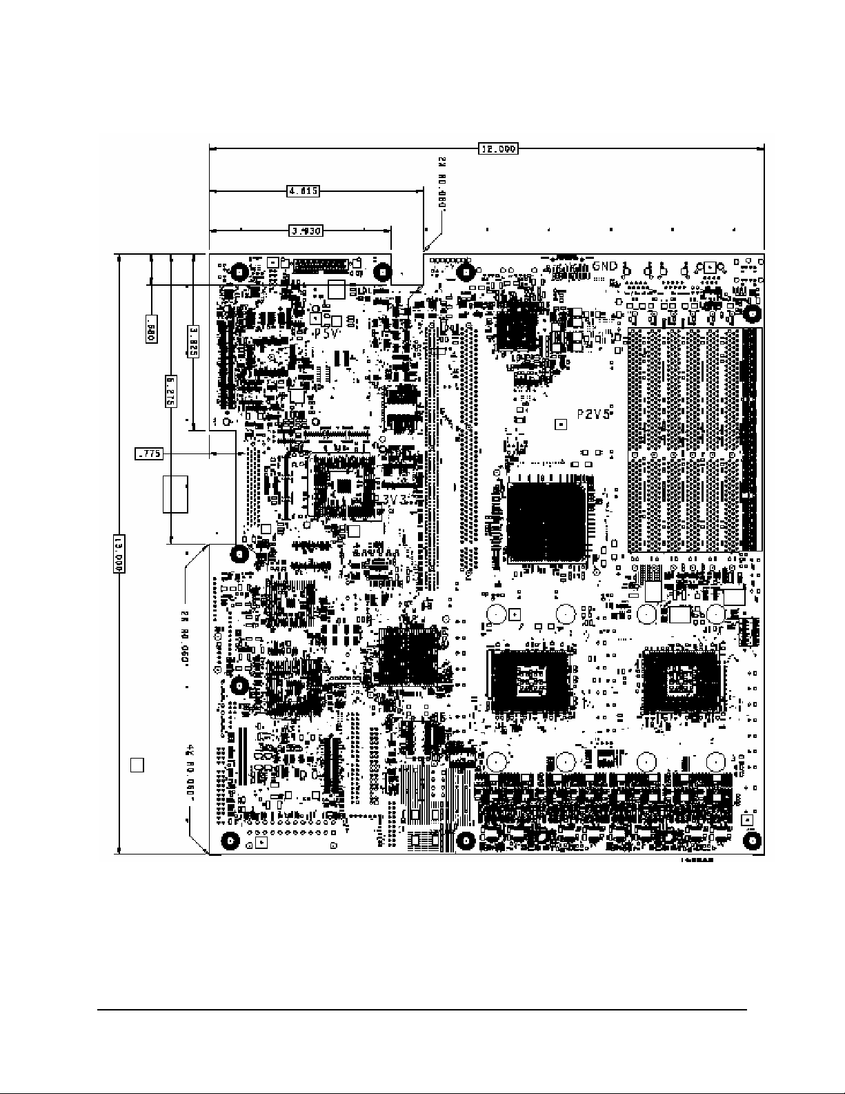
The following mechanical drawing shows the physical dimensions of the baseboard.
Figure 2. Server Board Dimensions
Revision 1.0
C78844-002
25
Page 26
Functional Architecture Intel® Server Board SE7520JR2
3. Functional Architecture
This chapter provides a high-level description of the functionality associated with the
architectural blocks that make up the Intel Server Board SE7520JR2.
Note: This document describes the features and functionality of the Server Board SE7520JR2
when using standard on-board platform instrumentation. Some functionality and feature
descriptions change when using either the Professional Edition or Advanced Edition Intel
Management Modules. Functional changes when either of these two options are used are
described in a separate document.
Figure 3. Server Board SE7520JR2 Block Diagram
Revision 1.0
26
C78844-002
Page 27

Intel® Server Board SE7520JR2 Functional Architecture
3.1 Processor Sub-system
The support circuitry for the processor sub-system consists of the following:
• Dual 604-pin zero insertion force (ZIF) processor sockets
• Processor host bus AGTL+ support circuitry
• Reset configuration logic
• Processor module presence detection logic
• BSEL detection capabilities
• CPU signal level translation
• Common Enabling Kit (CEK) CPU retention support
3.1.1 Processor Voltage Regulators
The baseboard has two VRDs (Voltage Regulator Devices) providing the appropriate voltages
to the installed processors. Each VRD is compliant with the VRD 10.1 specification and is
designed to support Intel
AMPs and peak support of 120A.
The baseboard supports the current requirements and processor speed requirements defined in
the Flexible Mother Board (FMB) specification for all 800 MHz FSB Intel Xeon processors. FMB
is an estimation of the maximum values the 800 MHz FSB versions of the Intel Xeon processors
will have over their lifetime. The value is only an estimate and actual specifications for future
processors may differ. At present, the current demand per FMB is a sustained maximum of a
105 Amps and peak support of 120 Amps.
®
Xeon™ processors that require up to a sustained maximum of 105
3.1.2 Reset Configuration Logic
The BIOS determines the processor stepping, cache size, etc through the CPUID instruction. All
processors in the system must operate at the same frequency; have the same cache sizes; and
same VID. No mixing of product families is supported. Processors run at a fixed speed and
cannot be programmed to operate at a lower or higher speed.
3.1.3 Processor Module Presence Detection
Logic is provided on the baseboard to detect the presence and identity of installed processors.
In dual-processor configurations, the on-board mini Baseboard Management Controller (mBMC)
must read the processor voltage identification (VID) bits for each processor before turning on
the VRD. If the VIDs of the two processors are not identical, then the mBMC will not turn on the
VRD. Prior to enabling the embedded VRD, circuitry on the baseboard ensures that the
following criteria are met:
• In a uni-processor configuration, CPU 1 is installed
• Only supported processors are installed in the system to prevent damage to the MCH
• In dual processor configurations, both processors support the same FSB frequency
3.1.4 GTL2006
The GTL2006 is a 13-bit translator designed for 3.3V to GTL/GTL+ translations to the system
bus. The translator incorporates all the level shifting and logic functions required to interface
between the processor subsystem and the rest of the system.
Revision 1.0
C78844-002
27
Page 28
Functional Architecture Intel® Server Board SE7520JR2
g
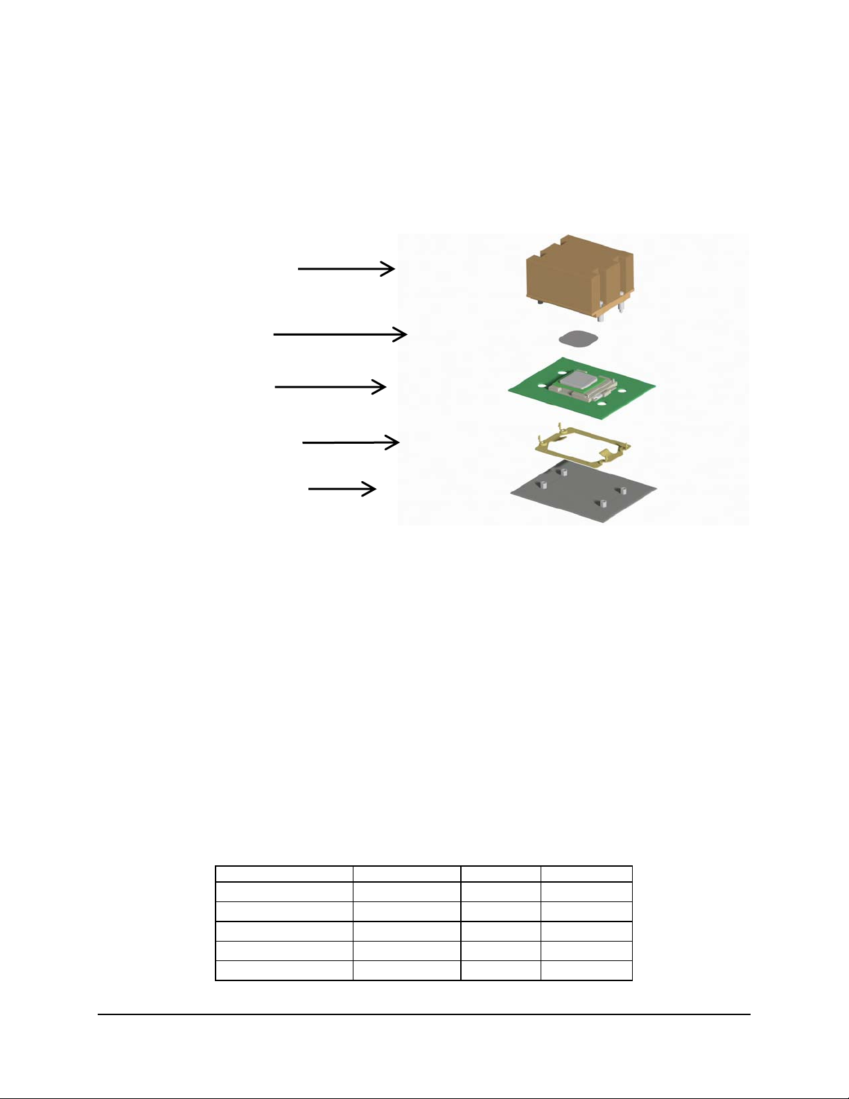
3.1.5 Common Enabling Kit (CEK) Design Support
The baseboard has been designed to comply with Intel’s Common Enabling Kit (CEK)
processor mounting and heat sink retention solution. The baseboard will ship with a CEK spring
snapped onto the bottom side of the board beneath each processor socket. The CEK spring is
removable, allowing for the use of non-Intel heat sink retention solutions.
Heatsink assembly with
inte
rated hardware
Thermal Interface
Material (TIM)
Baseboard
CEK Spring
Chassis
Figure 4. CEK Processor Mounting
3.1.6 Processor Support
The Server Board SE7520JR2 is designed to support one or two Intel® Xeon™ processors
utilizing an 800 MHz front side bus with frequencies starting at 2.8 GHz. Previous generations of
Intel Xeon processor are not supported on the Server Board SE7520JR2.
The server board is designed to provide up to 120A peak per processors. Processors with
higher current requirements are not supported.
Note: Only Intel
the Server Board SE7520JR2. See the following table for a list of supported processors and
their operating frequencies.
®
Xeon™ processors that support an 800MHz Front Side Bus are supported on
Table 2: Processor Support Matrix
Processor Family FSB Frequency Frequency Support
Intel® Xeon™ 533 MHz 2.8 GHz No
Intel® Xeon™ 533 MHz 3.06 GHz No
Intel® Xeon™ 533 MHz 3.2 GHz No
Intel® Xeon™ 800 MHz 2.8 GHz Yes
Intel® Xeon™ 800 MHz 3.0 GHz Yes
Revision 1.0
28
C78844-002
Page 29

Intel® Server Board SE7520JR2 Functional Architecture
Processor Family FSB Frequency Frequency Support
Intel® Xeon™ 800 MHz 3.2 GHz Yes
Intel® Xeon™ 800 MHz 3.4 GHz Yes
Intel® Xeon™ 800 MHz 3.6 GHz Yes
3.1.6.1 Processor Mis-population Detection
The processors must be populated in the correct order for the processor front-side bus to be
correctly terminated. CPU socket 1 must be populated before CPU socket 2. Baseboard logic
will prevent the system from powering up if a single processor is present but it is not in the
correct socket. This protects the logic against voltage swings or unreliable operation that could
occur on an incorrectly terminated front-side bus.
If processor mis-population is detected when using standard on-board platform instrumentation,
the mBMC will log an error against processor 1 to the System Event Log; Configuration Error,
and the baseboard hardware will illuminate both processor error LEDs. If an IMM (Professional
or Advanced editions) is used in systems, the Sahalee BMC will generate a series of beep
codes when this condition is detected and the BMC will illuminate the processor 1 fault LED.
3.1.6.2 Mixed Processor Steppings
For optimum system performance, only identical processors should be installed in a system.
Processor steppings within a common processor family can be mixed in a system provided that
there is no more than a 1 stepping difference between them. If the installed processors are
more than 1 stepping apart, an error is reported. Acceptable mixed steppings are not reported
as errors by the BIOS.
3.1.6.3 Mixed Processor Models
Processor models cannot be mixed in a system. If this condition is detected an error (8196) is
logged in the SEL. An example of a faulty processor configuration may be when one installed
processor supports a 533MHz front side bus while the other supports an 800MHz front side bus.
3.1.6.4 Mixed Processor Families
Processor families cannot be mixed in a system. If this condition is detected an error (8194) is
logged in the SEL.
3.1.6.5 Mixed Processor Cache Sizes
If the installed processors have mixed cache sizes, an error (8192) will be logged in the SEL
and an error (196) is reported to the Management Module. The size of all cache levels must
match between all installed processors. Mixed cache processors are not supported.
3.1.6.6 Jumperless Processor Speed Settings
The Intel
®
XeonTM processor does not utilize jumpers or switches to set the processor
frequency. The BIOS reads the highest ratio register from all processors in the system. If all
processors are the same speed, the Actual Ratio register is programmed with the value read
from the High Ratio register. If all processors do not match, the highest common value between
Revision 1.0
C78844-002
29
Page 30

Functional Architecture Intel® Server Board SE7520JR2
High and Low Ratio is determined and programmed to all processors. If there is no value that
works for all installed processors, all processors not capable of speeds supported by the BSP
are disabled and an error is displayed.
3.1.6.7 Microcode
IA-32 processors have the capability of correcting specific errata through the loading of an Intelsupplied data block (i.e., microcode update). The BIOS is responsible for storing the update in
non-volatile memory and loading it into each processor during POST. The BIOS allows a
number of microcode updates to be stored in the flash, limited by the amount of free space
available. The BIOS supports variable size microcode updates. The BIOS verifies the
signature prior to storing the update in the flash.
3.1.6.8 Processor Cache
The BIOS enables all levels of processor cache as early as possible during POST. There are no
user options to modify the cache configuration, size or policies. The largest and highest level
cache detected is reported in BIOS Setup.
3.1.6.9 Hyper-Threading Technology
Intel® Xeon
TM
processors support Hyper-Threading Technology. The BIOS detects processors
that support this feature and enables the feature during POST. BIOS Setup provides an option
to selectively enable or disable this feature. The default behavior is “Enabled”.
The BIOS creates additional entries in the ACPI MP tables to describe the virtual processors.
The SMBIOS Type 4 structure shows only the physical processors installed. It does not
describe the virtual processors because some operating systems are not able to efficiently
utilize the Hyper-Threading Technology.
3.1.6.10 Intel® SpeedStep® Technology
Intel® Xeon™ processors support the Geyserville3 (GV3) (whether Geyserville3 is an Intel
internal code name?) feature of the Intel® SpeedStep® Technology. This feature changes the
processor operating ratio and voltage similar to the Thermal Monitor 2 (TM2) feature. It must be
used in conjunction with the TM1 or TM2 feature. The BIOS implements the GV3 feature in
conjunction with the TM2 feature.
3.1.6.11 EM64T Technology Support
The system BIOS on the Server Board SE7520JR2 supports the Intel Extended Memory 64
technology (EM64T) of the Intel® Xeon™ Processors. There is no BIOS setup option to enable
or disable this support. The system will be in IA-32 compatibility mode when booting to an OS.
To utilize this feature, a 64-bit capable OS and OS specific drivers are needed.
3.1.7 Multiple Processor Initialization
IA-32 processors have a microcode-based bootstrap processor (BSP) arbitration protocol. On
reset, all of the processors compete to become the BSP. If a serious error is detected during its
Built-in Self-Test (BIST), that processor does not participate in the initialization protocol. A
single processor that successfully passes BIST is automatically selected by the hardware as the
Revision 1.0
30
C78844-002
Page 31

Intel® Server Board SE7520JR2 Functional Architecture
BSP and starts executing from the reset vector (F000:FFF0h). A processor that does not
perform the role of BSP is referred to as an application processor (AP).
The BSP is responsible for executing the BIOS power-on self-test (POST) and preparing the
machine to boot the operating system. At boot time, the system is in virtual wire mode and the
BSP alone is programmed to accept local interrupts (INTR driven by programmable interrupt
controller (PIC) and non-maskable interrupt (NMI)).
As a part of the boot process, the BSP enables the application processor. When enabled, the
AP programs its Memory Type Range Registers (MTRRs) to be identical to those of the BSP.
The AP executes a halt instruction with its local interrupts disabled. If the BSP determines that
an AP exists that is a lower-featured processor or that has a lower value returned by the CPUID
function, the BSP switches to the lowest-featured processor in the system.
3.1.8 CPU Thermal Sensors
The CPU temperature will be indirectly measured via thermal diodes. These are monitored by
the LM93 sensor monitoring device. The mBMC configures the LM93 to monitor these sensors.
The temperatures are available via mBMC IPMI sensors.
3.1.9 Processor Thermal Control Sensor
The Intel Xeon processors generate a signal to indicate throttling due to a processor over temp
condition. The mBMC implements an IPMI sensor that provides the percentage of time a
processor has been throttled over the last 1.46 seconds. Baseboard management forces a
thermal control condition when reliable system operation requires reduced power consumption.
3.1.10 Processor Thermal Trip Shutdown
If a thermal overload condition exists (thermal trip), the processor outputs a digital signal that is
monitored by the baseboard management sub-system. A thermal trip is a critical condition and
indicates that the processor may become damaged if it continues to run. To help protect the
processor, the management controller automatically powers off the system. In addition the
System Status LED will change to Amber and the error condition will be logged to the System
Event Log (SEL).
If either the Intel Management Module Professional Edition or Advanced Edition is present in the
system, the Fault LED fro the affected processor will also be illuminated.
3.1.11 Processor IERR
The IERR signal is asserted by the processor as the result of an internal error. The mBMC
configures the LM93 device to monitor this signal. When this signal is asserted, the mBMC
generates a processor IERR event.
3.2 Intel® E7520 Chipset
The architecture of the Server Board SE7520JR2 is designed around the Intel E7520 chipset.
The chipset consists of three components that together are responsible for providing the
interface between all major sub-systems found on the baseboard, including the processor,
memory, and I/O sub-systems. These components are:
Revision 1.0
C78844-002
31
Page 32

Functional Architecture Intel® Server Board SE7520JR2
• Memory Controller Hub (MCH)
• I/O Controller Hub (ICH5-R)
• PCI-X Hub (PXH)
The following sub-sections provide an overview of the primary functions and supported features
of each chipset component as they are used on the Server Board SE7520JR2. Later sections in
this chapter provide more detail on the implementation of the sub-systems.
3.2.1 Memory Controller Hub (MCH)
The MCH integrates four functions into a single 1077-ball FC-BGA package:
• Front Side Bus
• Memory Controller
• PCI-Express Controller
• Hub Link Interface
3.2.1.1 Front Side Bus (FSB)
The E7520 MCH supports either single or dual processor configurations using 800MHz FSB
Intel Xeon processors. The MCH supports a base system bus frequency of 200 MHz. The
address and request interface is double pumped to 400 MHz while the 64-bit data interface
(+ parity) is quad pumped to 800 MHz. This provides a matched system bus address and data
bandwidths of 6.4 GB/s
3.2.1.2 MCH Memory Sub-System Overview
The MCH provides an integrated memory controller for direct connection to two channels of
registered DDR-266, DDR-333 or DDR2-400 memory (stacked or unstacked). Peak theoretical
memory data bandwidth using DDR266 technology is 4.26 GB/s and 5.33 GB/S for DDR333
technology. For DDR2-400 technology, this increases to 6.4 GB/s.
Several RASUM (Reliability, Availability, Serviceability, Usability, and Manageability) features
are provided by the E7520 MCH memory interface.
• Memory mirroring allows two copies of all data in the memory subsystem to be maintained
(one on each channel).
• DIMM sparing allows one DIMM per channel to be held in reserve and brought on-line if
another DIMM in the channel becomes defective. DIMM sparing and memory mirroring are
mutually exclusive.
• Hardware periodic memory scrubbing, including demand scrub support.
• Retry on uncorrectable memory errors.
• x4 SDDC for memory error detection and correction of any number of bit failures in a single
x4 memory device.
3.2.1.3 PCI Express
The E7520 MCH is the first Intel chipset to support the new PCI Express* high-speed serial I/O
interface for superior I/O bandwidth. The scalable PCI Express interface complies with the PCI
Express Interface Specification, Rev 1.0a. On the Server Board SE7520JR2, two of the three
available x8 PCI Express interfaces are used, each with a maximum theoretical bandwidth of 4
Revision 1.0
32
C78844-002
Page 33

Intel® Server Board SE7520JR2 Functional Architecture
GB/s. One x8 interface is used as the interconnect between the MCH and PXH, while the other
is configured as two separate x4 interfaces to the full height riser slot.
The E7520 MCH is a root class component as defined in the PCI Express Interface
Specification, Rev 1.0a. The PCI Express interfaces of the MCH support connection to a variety
of bridges and devices compliant with the same revision of the specification. Refer to the Server
Board SE7520JR2 Tested Hardware and OS List for the add-in cards tested on this platform.
3.2.1.4 Hub Interface
The MCH interfaces with the Intel 82801ER I/O Controller Hub 5-R (ICH5-R) via a dedicated
Hub Interface which supports a peak bandwidth of 266MB/s using a x4 base clock of 66 MHz.
3.2.2 PCI-X Hub (PXH)
The PXH provides the data interface between the MCH and two PCI-X bus segments over a
high-speed PCI-Express x8 link. The PCI-Express interface is compliant with the PCI Express
Base Specification rev 1.0 and provides a maximum realized bandwidth of 2GB/s in each
direction simultaneously, for an aggregate of 4 GB/s.
The PCI-X interfaces of the PXH comply with the following:
• PCI-X Addendum to the PCI Local Bus Specification Revision 1.0b
• Mode 1 of the PCI-X Electrical and Mechanical Addendum to the PCI Local Bus
Specification Revision 2.0a
• PCI-X Protocol Addendum to the PCI Local Bus Specification Revision 2.0a
For conventional PCI Mode, the PXH supports PCI bus frequencies of 66 MHz, 100 MHz, and
133 MHz.
On the Server Board SE7520JR2 each of the two PCI-X interfaces (PCI Bus A and PCI Bus B)
is independently controlled to operate in either a conventional PCI or PCI-X mode. PCI Bus A is
routed to control I/O from the full-height riser slot and the LSI* 53C1030 Dual Channel SCSI
controller and is capable of supporting both PCI-X Mode 1 and Mode 2 interfaces depending on
the riser card used. PCI Bus B is routed to control I/O from the low profile riser slot and the
82546GB Dual GB Ethernet controllers.
3.2.2.1 Full-height Riser Slot
Using Intel® Adaptive Slot Technology, the full height riser slot is a proprietary 280-pin slot
connector with both PCI-X signals from the PXH and PCI-Express signals from the MCH routed
to it. Depending on the riser card used, the slot is able to support both PCI-X and/or PCIExpress add-in cards. The board placement of this slot allows risers to support full-height, fulllength add-in cards.
3.2.2.2 Low Profile Riser Slot
The low profile riser slot is a standard 202-pin slot connector supporting PCI-X signals from the
PXH. Because of available board clearances, riser cards can only support low-profile add-in
cards with this slot.
Revision 1.0
C78844-002
33
Page 34

Functional Architecture Intel® Server Board SE7520JR2
3.2.2.3 I/OxAPIC Controller
The PXH contains two I/OxAPIC controllers, both of which reside on the primary bus. The
intended use of these controllers is to have the interrupts from PCI bus A connected to the
interrupt controller on device 0, function 1 and have the interrupts on PCI bus B connected to
the interrupt controller on device 0, function 3.
3.2.2.4 SMBus Interface
The SMBus interface can be used for system and power management related tasks. The
interface is compliant with System Management Bus Specification Revision 2.0. The SMBus
interface allows full read/write access to all configuration and memory spaces in the PXH.
3.2.3 I/O Controller Hub (ICH5-R)
The ICH5-R is a multi-function device providing an upstream hub interface for access to several
embedded I/O functions and features including:
• PCI Local Bus Specification, Revision 2.3 with support for 33 MHz PCI operations.
• ACPI power management logic support
• Enhanced DMA controller, interrupt controller, and timer functions
• Integrated IDE controller with support for Ultra ATA100/66/33
• Integrated SATA controller
• USB host interface with support for eight USB ports; four UHCI host controllers; one EHCI
high-speed USB 2.0 host controller
• System Management Bus (SMBus) Specification, Version 2.0 with additional support for I
devices
• Low Pin Count (LPC) interface
• Firmware Hub (FWH) interface support
Each function within the ICH5-R has its own set of configuration registers. Once configured,
each appears to the system as a distinct hardware controller sharing the same PCI bus
interface.
2
C
3.2.3.1 PCI Interface
The ICH5-R PCI interface provides a 33 MHz, Revision 2.3 compliant implementation. All PCI
signals are 5-V tolerant, except PME#. The ICH5 integrates a PCI arbiter that supports up to six
external PCI bus masters in addition to the internal ICH5 requests. On the Server Board
SE7520JR2 this PCI interface is used to support on-board PCI devices including the ATI* video
controller, Super I/O chip, and hardware monitoring sub-system.
3.2.3.2 IDE Interface (Bus Master Capability and Synchronous DMA Mode)
The fast IDE interface supports up to four IDE devices, providing an interface for IDE hard disks
and ATAPI devices. Each IDE device can have independent timings. The IDE interface supports
PIO IDE transfers up to 16 Mbytes/sec and Ultra ATA transfers up 100 Mbytes/sec. It does not
consume ISA DMA resources. The IDE interface integrates 16x32-bit buffers for optimal
transfers. The ICH5-R’s IDE system contains two independent IDE signal channels. They can
be electrically isolated independently. They can be configured to the standard primary and
secondary channels (four devices). The Server Board SE7520JR2 provides interfaces to both
Revision 1.0
34
C78844-002
Page 35

Intel® Server Board SE7520JR2 Functional Architecture
IDE channels of the ICH5R. One channel is accessed through the 40-pin connector on the
baseboard. The signals of the second channel are routed to the 100-pin backplane connector
for use in either the Intel Server Chassis SR1400 or SR2400 when integrated with a backplane
for slim-line optical drive use.
3.2.3.3 SATA Controller
The SATA controller supports two SATA devices, providing an interface for SATA hard disks
and ATAPI devices. The SATA interface supports PIO IDE transfers up to 16 Mb/s and Serial
ATA transfers up to 1.5 Gb/s (150 MB/s). The ICH5-R’s SATA system contains two independent
SATA signal ports. They can be electrically isolated independently. Each SATA device can have
independent timings. They can be configured to the standard primary and secondary channels.
3.2.3.4 Low Pin Count (LPC) Interface
The ICH5-R implements an LPC Interface as described in the Low Pin Count Interface
Specification, Revision 1.1. The Low Pin Count (LPC) bridge function of the ICH5-R resides in
PCI Device 31:Function 0. In addition to the LPC bridge interface function, D31:F0 contains
other functional units including DMA, interrupt controllers, timers, power management, system
management, GPIO, and RTC.
3.2.3.5 Compatibility Modules (DMA Controller, Timer/Counters, Interrupt
Controller)
The DMA controller incorporates the logic of two 82C37 DMA controllers, with seven
independently programmable channels. Channels 0–3 are hardwired to 8-bit, count-by-byte
transfers, and channels 5–7 are hardwired to 16-bit, count-by-word transfers. Any two of the
seven DMA channels can be programmed to support fast Type-F transfers.
The ICH5-R supports two types of DMA: LPC and PC/PCI. LPC DMA and PC/PCI DMA use the
ICH5-R’s DMA controller. The PC/PCI protocol allows PCI-based peripherals to initiate DMA
cycles by encoding requests and grants via two PC/PC REQ#/GNT# pairs. LPC DMA is handled
through the use of the LDRQ# lines from peripherals and special encoding on LAD[3:0] from the
host. Single, Demand, Verify, and Increment modes are supported on the LPC interface.
Channels 0–3 are 8 bit channels. Channels 5–7 are 16 bit channels. Channel 4 is reserved as a
generic bus master request.
The timer/counter block contains three counters that are equivalent in function to those found in
one 82C54 programmable interval timer. These three counters are combined to provide the
system timer function, and speaker tone. The 14.31818 MHz oscillator input provides the clock
source for these three counters.
The ICH5-R provides an ISA-compatible Programmable Interrupt Controller (PIC) that
incorporates the functionality of two 82C59 interrupt controllers. The two interrupt controllers are
cascaded so 14 external and two internal interrupts are possible. In addition, the ICH5-R
supports a serial interrupt scheme. All of the registers in these modules can be read and
restored. This is required to save and restore the system state after power has been removed
and restored to the platform.
Revision 1.0
C78844-002
35
Page 36

Functional Architecture Intel® Server Board SE7520JR2
3.2.3.6 Advanced Programmable Interrupt Controller (APIC)
In addition to the standard ISA-compatible PIC described in the previous section, the ICH5-R
incorporates the Advanced Programmable Interrupt Controller (APIC).
3.2.3.7 Universal Serial Bus (USB) Controller
The ICH5-R contains an Enhanced Host Controller Interface (EHCI) for Universal Serial Bus,
Revision 1.0-compliant host controller that supports USB high-speed signaling. The high-speed
USB 2.0 allows data transfers up to 480 Mb/s, which is 40 times faster than full-speed USB.
The ICH5-R also contains four Universal Host Controller Interface (UHCI) controllers that
support USB full-speed and low-speed signaling. On the Server Board SE7520JR2, the ICH5-R
provides six USB 2.0 ports. All six ports are high-speed, full-speed, and low-speed capable.
ICH5-R’s port-routing logic determines whether a USB port is controlled by one of the UHCI
controllers or by the EHCI controller.
3.2.3.8 RTC
The ICH5-R contains a Motorola* MC146818A-compatible real-time clock with 256 bytes of
battery backed RAM. The real-time clock performs two key functions: keeping track of the time
of day and storing system data, even when the system is powered down. The RTC operates on
a 32.768 KHz crystal and a separate 3 V lithium battery.
The RTC supports two lockable memory ranges. By setting bits in the configuration space, two
8-byte ranges can be locked to read and write accesses. This prevents unauthorized reading of
passwords or other system security information.
The RTC supports a date alarm that allows for scheduling a wake up event up to 30 days in
advance.
3.2.3.9 General Purpose I/O (GPIO)
Various general-purpose inputs and outputs are provided for custom system design. The
number of inputs and outputs varies depending on the ICH5-R configuration. All unused GPI
pins are either pulled high or low, so that they are at a predefined level and do not cause undue
side effects.
3.2.3.10 Enhanced Power Management
The ICH5-R’s power management functions include enhanced clock control, local and global
monitoring support for 14 individual devices, and various low-power (suspend) states, such as
Suspend-to-DRAM and Suspend-to-Disk. A hardware-based thermal management circuit
permits software-independent entrance to low-power states. The ICH5-R contains full support
for the Advanced Configuration and Power Interface (ACPI) Specification, Revision 2.0b.
3.2.3.11 System Management Bus (SMBus 2.0)
The ICH5-R contains an SMBus host interface that allows the processor to communicate with
SMBus slaves. This interface is compatible with most I
2
C devices. Special I2C commands are
implemented. The ICH5-R’s SMBus host controller provides a mechanism for the processor to
initiate communications with SMBus peripherals (slaves).
Revision 1.0
36
C78844-002
Page 37

Intel® Server Board SE7520JR2 Functional Architecture
The ICH5-R supports slave functionality, including the Host Notify protocol. Hence, the host
controller supports eight command protocols of the SMBus interface: Quick Command, Send
Byte, Receive Byte, Write Byte/Word, Read Byte/Word, Process Call, Block Read/Write, and
Host Notify. See the System Management Bus (SMBus) Specification, Version 2.0 for more
information.
3.3 Memory Sub-System
The MCH provides an integrated memory controller for direct connection to two channels of
registered DDR-266, DDR-333 or DDR2-400 memory (stacked or unstacked). Peak theoretical
memory data bandwidth using DDR266 technology is 4.26 GB/s and 5.33 GB/S for DDR333
technology. For DDR2-400 technology, this increases to 6.4 GB/s
The MCH supports a burst length of four, whether in single or dual channel mode. In dual
channel mode this results in eight 64-bit chunks (64-byte cache line) from a single read or write.
In single channel mode, two reads or writes are required to access a cache line of data.
3.3.1 Memory Sizing
The memory controller is capable of supporting up to 4 loads per channel for DDR-333 and
DDR2-400. Memory technologies are classified as being either single rank or dual rank
depending on the number of DRAM devices that are used on any one DIMM. A single rank
DIMM is a single load device, ie) Single Rank = 1 Load. Dual rank DIMMs are dual load
devices, ie) Dual Rank = 2 loads.
The Server Board SE7520JR2 provides the following maximum memory capacities based on
the number of DIMM slots provided and maximum supported memory loads by the chipset:
• 24GB maximum capacity for DDR-266
• 16GB maximum capacity for DDR-333 and DDR2-400
The minimum memory supported with the system running in single channel memory mode is:
• 256MB for DDR-266, DDR-333 and DDR2-400
Supported DIMM capacities are as follows:
• DDR-266 Memory DIMM sizes include: 256MB, 512MB, 1GB, 2GB, and 4GB.
• DDR-333 Memory DIMM sizes include: 256MB, 512MB, 1GB, 2GB, and 4GB.
• DDR2-400 Memory DIMM sizes include: 256MB, 512MB, 1GB, 2GB, and 4GB.
DIMM Module Capacities:
SDRAM Parts / SDRAM Technology Used 128Mb 256Mb 512Mb 1Gb
X8, single row 128MB 256MB 512MB 1GB
Revision 1.0
C78844-002
37
Page 38

Functional Architecture Intel® Server Board SE7520JR2
A
A
A
X8, double row 256MB 512MB 1GB 2GB
X4, single row 256MB 512MB 1GB 2GB
X4, Stacked, double row 512MB 1GB 2GB 4GB
DIMMs on channel ‘A’ are paired with DIMMs on channel ‘B’ to configure 2-way interleaving.
Each DIMM pair is referred to as a bank. The bank can be further divided into two rows, based
on single-sided or double-sided DIMMs. If both DIMMs in a bank are single-sided, only one row
is said to be present. For double-sided DIMMs, both rows are said to be present.
The Server Board SE7520JR2 has six DIMM slots, or three DIMM banks. Both DIMMs in a bank
should be identical (same manufacturer, CAS latency, number of rows, columns and devices,
timing parameters etc.). Although DIMMs within a bank must be identical, the BIOS supports
various DIMM sizes and configurations allowing the banks of memory to be different. Memory
sizing and configuration is guaranteed only for qualified DIMMs approved by Intel.
MCH
3B3
2B2
Bank 2 Bank 3
Figure 5. Identifying Banks of Memory
The BIOS reads the Serial Presence Detect (SPD) SEEPROMs on each installed memory
module to determine the size and timing of the installed memory modules. The memory-sizing
algorithm determines the size of each bank of DIMMs. The BIOS programs the Memory
Controller in the chipset accordingly. The total amount of configured memory can be found
using BIOS Setup.
3.3.2 Memory Population
Mixing of DDR-266 and DDR-333 DIMMs is supported between banks of memory. However,
when mixing DIMM types, DDR-333 will run at DDR-266 speeds.
1B1
Bank 1
Revision 1.0
38
C78844-002
Page 39

Intel® Server Board SE7520JR2 Functional Architecture
Using the following algorithm, BIOS configures the memory controller of the MCH to run in
either dual channel mode or single channel mode:
(1) If 1 or more fully populated DIMM banks are detected, the memory controller is set to
dual channel mode. Otherwise, go to step (2)
(2) If DIMM 1A is present, set memory controller to single channel mode A. Otherwise,
go to step (3)
(3) If Channel 1B DIMM is present, set memory controller to single channel mode B.
Otherwise, generate a memory configuration error
DDR-266 & DDR-333 DIMM population rules are as follows:
(1) DIMM banks must be populated in order starting with the slots furthest from MCH
(2) Single rank DIMMs must be populated before dual rank DIMMs
(3) A maximum of four DIMMs can be populated when all four DIMMs are dual rank DDR-333
DIMMs.
DDR2 400 DIMM population rules are as follows:
(1) DIMMs banks must be populated in order starting with the slots furthest from MCH
(2) Dual rank DIMMs are populated before single rank DIMMs
(3) A maximum of four DIMMs can be populated when all four DIMMs are dual rank DDR2-400
DIMMs
The following tables show the supported memory configurations.
• s/r = single rank
• d/r = dual rank
• E = Empty
MCH
MCH
Table 3: Supported DDR-266 DIMM Populations
Bank 3 – DIMMs 3A, 3B Bank 2 – DIMMs 2A, 2B Bank 1 – DIMMs 1A, 1B
S/R S/R S/R
E S/R S/R
E E S/R
D/R D/R D/R
E D/R D/R
E E D/R
D/R S/R S/R
D/R D/R S/R
E D/R S/R
Table 4: Supported DDR-333 DIMM Populations
Bank 3 – DIMMs 3A, 3B Bank 2 – DIMMs 2A, 2B2 Bank 1 – DIMMs 1A, 1B
S/R S/R S/R
E S/R S/R
E E S/R
Revision 1.0
C78844-002
39
Page 40

Functional Architecture Intel® Server Board SE7520JR2
E D/R D/R
E E D/R
D/R S/R S/R
E D/R S/R
Table 5: Supported DDR2-400 DIMM Populations
Bank 3 – DIMMs 3A, 3B Bank 2 – DIMMs 2A, 2B Bank 1 – DIMMs 1A, 1B
S/R S/R S/R
E S/R S/R
E E S/R
MCH
E D/R D/R
E E D/R
E S/R D/R
S/R S/R D/R
Note: On the Server Board SE7520JR2, when using all dual rank DDR-333 or DDR2-400
DIMMs, a total of four DIMMs can be populated. Configuring more than four dual rank DDR333 or DDR2-400 DIMMs will result in the BIOS generating a memory configuration error.
Note: Memory between 4GB and 4GB minus 512MB will not be accessible for use by the
operating system and may be lost to the user, because this area is reserved for BIOS, APIC
configuration space, PCI adapter interface, and virtual video memory space. This means that if
4GB of memory is installed, 3.5GB of this memory is usable. The chipset should allow the
remapping of unused memory above the 4GB address, but this memory may not be accessible to
an operating system that has a 4GB memory limit.
3.3.3 ECC Memory Initialization
ECC memory must be initialized by the BIOS before it can be used. The BIOS must initialize all
memory locations before using them. The BIOS uses the auto-initialize feature of the MCH to
initialize ECC. ECC memory initialization cannot be aborted and may result in a noticeable delay
in the boot process depending on the amount of memory installed in the system.
3.3.4 Memory Test
System memory is classified as base and extended memory. Base memory is memory that is
required for POST. Extended memory is the remaining memory in the system. Extended
memory may be contiguous or may have one or more holes. The BIOS memory test accesses
all memory except for memory holes.
Memory testing consists of separate base and extended memory tests. The base memory test
runs before video is initialized to verify memory required for POST. The BIOS enables video as
early as possible during POST to provide a visual indication that the system is functional. At
some time after video output has been enabled, BIOS executes the extended memory test. The
Revision 1.0
40
C78844-002
Page 41

Intel® Server Board SE7520JR2 Functional Architecture
status of the extended memory test is displayed on the console. The status of base and
extended memory tests are also displayed on an LCD control panel if present.
The extended memory test is configured using the BIOS Setup Utility. The coverage of the test
can be configured to one of the following:
• Test every location (Extensive)
• Test one interleave width per kilo-byte of memory (Sparse)
• Test one interleave width per mega-byte of memory (Quick).
The “interleave width” of a memory subsystem is dependent on the chipset configuration. By
default, both the base and extended memory tests are configured to the Disabled setting. The
extended memory test can be aborted by pressing the <Space> key during the test.
3.3.5 Memory Monitoring
Both the baseboard management controller and BIOS provide support for memory inventory,
memory failure LEDs, and failure/state transition events. Memory monitoring features are
supported differently depending on which level of server management is used. The following
table shows how each feature is supported by management level.
Table 6: Memory Monitoring Support by Server Management Level
Memory Feature On-board Professional Advanced
Inventory No Yes Yes
Correctable Error Reporting No Yes Yes
Uncorrectable Error Reporting Yes Yes Yes
With either Professional or Advanced IMMs installed, the Sahalee BMC maintains one sensor
per DIMM. The sensor is IPMI type 21h, Slot/Connector. The Sahalee BMC directly detects the
presence or absence of each DIMM and records this in offset 2 of these sensors.
DIMM failure can be detected at BIOS POST or during system operation. POST detected DIMM
failures or mis-configuration (incompatible DIMM sizes/speeds/etc) cause the BIOS to disable
the failed/affected DIMMs and generate IPMI SEL events, which are sent to the BMC in use.
In addition, using Professional or Advanced IMMs, the BIOS communicates this failure to the
Sahalee BMC so that it can be incorporated in the BMC’s DIMM sensor state. DIMM presence
and failure states are stored persistently by the Sahalee BMC.
In all management levels, the BIOS is responsible for DIMM FRU LED management and
illuminates the LEDs associated with failed or disabled DIMMs.
Correctable memory errors are non-critical errors that do not cause the system to fail. They are
detected by the BIOS and are logged as IPMI SEL events when either the Professional or
Advanced IMMs are installed. Logging is throttled by error frequency. If more than a certain
number of correctable errors occur in an hour, logging is turned off.
Revision 1.0
C78844-002
41
Page 42

Functional Architecture Intel® Server Board SE7520JR2
Uncorrectable memory errors are critical errors that may cause the system to fail. The BIOS
normally detects and logs these errors as IPMI SEL events for all management levels, except in
the case described below.
It is possible that a critical hardware error (uncorrectable memory or bus error) may prevent the
BIOS from running, reporting the error, and restarting the system. In Professional and Advanced
management models, the Sahalee BMC monitors the SMI signal, which, if it stays asserted for a
long period of time, is an indication that BIOS cannot run. In this case, the Sahalee BMC logs
an SMI Timeout event and probes for errors. If one is found it will log data against the IPMI type
0Ch Memory Sensor and will log against the IPMI 13h Critical Interrupt sensor for a bus error.
Both of these can include additional data in bytes 2 and 3 depending on the exact nature of the
error and what the chipset reports to the Sahalee BMC.
3.3.6 Memory RASUM Features
The Intel E7520 MCH supports several memory RASUM (Reliability, Availability, Serviceability,
Usability, and Manageability) features. These features include the Intel® x4 Single Device Data
Correction (x4 SDDC) for memory error detection and correction, Memory Scrubbing, Retry on
Correctable Errors, Integrated Memory Initialization, DIMM Sparing, and Memory Mirroring. The
following sections describe how each is supported.
Note: The operation of the memory RASUM features listed below is supported regardless of the
platform management model used. However, with no Intel® Management Module installed, the
system has limited memory monitoring and logging capabilities. It is possible for a RASUM
feature to be initiated without notification that the action has occurred when standard Onboard
Platform Instrumentation is used.
3.3.6.1 DRAM ECC – Intel® x4 Single Device Data Correction (x4 SDDC)
The DRAM interface uses two different ECC algorithms. The first is a standard SEC/DED ECC
across a 64-bit data quantity. The second ECC method is a distributed, 144-bit S4EC-D4ED
mechanism, which provides x4 SDDC protection for DIMMS that utilize x4 devices. Bits from x4
parts are presented in an interleaved fashion such that each bit from a particular part is
represented in a different ECC word. DIMMs that use x8 devices, can use the same algorithm
but will not have x4 SDDC protection, since at most only four bits can be corrected with this
method. The algorithm does provide enhanced protection for the x8 parts over a standard SECDED implementation. With two memory channels, either ECC method can be utilized with equal
performance, although single-channel mode only supports standard SEC/DED.
When memory mirroring is enabled, x4 SDDC ECC is supported in single channel mode when
the second channel has been disabled during a fail-down phase. The x4 SDDC ECC is not
supported during single-channel operation outside of DIMM mirroring fail-down as it does have
significant performance impacts in that environment.
3.3.6.2 Integrated Memory Scrub Engine
The Intel E7520 MCH includes an integrated engine to walk the populated memory space
proactively seeking out soft errors in the memory subsystem. In the case of a single bit
correctable error, this hardware detects, logs, and corrects the data except when an incoming
write to the same memory address is detected. For any uncorrectable errors detected, the scrub
Revision 1.0
42
C78844-002
Page 43

Intel® Server Board SE7520JR2 Functional Architecture
engine logs the failure. Both types of errors may be reported via multiple alternate mechanisms
under configuration control. The scrub hardware will also execute “demand scrub” writes when
correctable errors are encountered during normal operation (on demand reads, rather than
scrub-initiated reads). This functionality provides incremental protection against time-based
deterioration of soft memory errors from correctable to uncorrectable.
Using this method, a 16GB system can be completely scrubbed in less than one day. The effect
of the scrub writes do not cause any noticeable degradation to memory bandwidth, although
they will cause a greater latency for that one very infrequent read that is delayed due to the
scrub write cycle.
Note that an uncorrectable error encountered by the memory scrub engine is a “speculative
error.” This designation is applied because no system agent has specifically requested use of
the corrupt data, and no real error condition exists in the system until that occurs. It is possible
that the error resides in an unmodified page of memory that will be simply dropped on a swap
back to disk. Were that to occur, the speculative error would simply “vanish” from the system
undetected without adverse consequences.
3.3.6.3 Retry on Uncorrectable Error
The Intel E7520 MCH includes specialized hardware to resubmit a memory read request upon
detection of an uncorrectable error. When a demand fetch (as opposed to a scrub) of memory
encounters an uncorrectable error as determined by the enabled ECC algorithm, the memory
control hardware will cause a (single) full resubmission of the entire cache line request from
memory to verify the existence of corrupt data. This feature is expected to greatly reduce or
eliminate the reporting of false or transient uncorrectable errors in the DRAM array.
Note that any given read request will only be retried a single time on behalf of this error
detection mechanism. If the uncorrectable error is repeated, it will be logged and escalated as
directed by device configuration. In the memory mirror mode, the retry on an uncorrectable error
will be issued to the mirror copy of the target data, rather than back to the devices responsible
for the initial error detection. This has the added benefit of making uncorrectable errors in
DRAM fully correctable unless the same location in both primary and mirror happens to be
corrupt. This RASUM feature may be enabled and disabled via configuration.
3.3.6.4 Integrated Memory Initialization Engine
The Intel E7520 MCH provides hardware managed ECC auto-initialization of all populated
DRAM space under software control. Once internal configuration has been updated to reflect
the types and sizes of populated DIMM devices, the MCH will traverse the populated address
space initializing all locations with good ECC. This not only speeds up the mandatory memory
initialization step, but also frees the processor to pursue other machine initialization and
configuration tasks.
Additional features have been added to the initialization engine to support high speed
population and verification of a programmable memory range with one of four known data
patterns (0/F, A/5, 3/C, and 6/9). This function facilitates a limited, very high speed memory test,
as well as provides a BIOS accessible memory zeroing capability for use by the operating
system.
Revision 1.0
C78844-002
43
Page 44

Functional Architecture Intel® Server Board SE7520JR2
3.3.6.5 DIMM Sparing Function
To provide a more fault tolerant system, the Intel E7520 MCH includes specialized hardware to
support fail-over to a spare DIMM device in the event that a primary DIMM in use exceeds a
specified threshold of runtime errors. One of the DIMMs installed per channel, greater than or
equal in size than all installed, will not be used but kept in reserve. In the event of significant
failures in a particular DIMM, it and its corresponding partner in the other channel (if applicable),
will, over time, have its data copied over to the spare DIMM(s) held in reserve. When all the
data has been copied, the reserve DIMM(s) will be put into service and the failing DIMM will be
removed from service. Only one sparing cycle is supported. If this feature is not enabled, then
all DIMMs will be visible in normal address space.
Note: The DIMM Sparing feature requires that the spare DIMM be at least the size of the largest
primary DIMM in use.
Hardware additions for this feature include the implementation of tracking register per DIMM to
maintain a history of error occurrence, and a programmable register to hold the fail-over error
threshold level. The operational model is straightforward: if the fail-over threshold register is set
to a non-zero value, the feature is enabled, and if the count of errors on any DIMM exceeds that
value, fail-over will commence. The tracking registers themselves are implemented as “leaky
buckets,” such that they do not contain an absolute cumulative count of all errors since poweron; rather, they contain an aggregate count of the number of errors received over a running time
period. The “drip rate” of the bucket is selectable by software, so it is possible to set the
threshold to a value that will never be reached by a “healthy” memory subsystem experiencing
the rate of errors expected for the size and type of memory devices in use.
The fail-over mechanism is slightly more complex. Once fail-over has been initiated the MCH
must execute every write twice; once to the primary DIMM, and once to the spare. The MCH will
also begin tracking the progress of its built-in memory scrub engine. Once the scrub engine has
covered every location in the primary DIMM, the duplicate write function will have copied every
data location to the spare. At that point, the MCH can switch the spare into primary use, and
take the failing DIMM off-line.
Note that this entire mechanism requires no software support once it has been programmed and
enabled, until the threshold detection has been triggered to request a data copy. Hardware will
detect the threshold initiating fail-over, and escalate the occurrence of that event as directed
(signal an SMI, generate an interrupt, or wait to be discovered via polling). Whatever software
routine responds to the threshold detection must select a victim DIMM (in case multiple DIMMs
have crossed the threshold prior to sparing invocation) and initiate the memory copy. Hardware
will automatically isolate the “failed” DIMM once the copy has completed. The data copy is
accomplished by address aliasing within the DDR control interface, thus it does not require
reprogramming of the DRAM row boundary (DRB) registers, nor does it require notification to
the operating system that anything has occurred in memory.
The memory mirroring feature and DIMM sparing are exclusive of each other, only one may be
activated during initialization. The selected feature must remain enabled until the next powercycle. There is no provision in hardware to switch from one feature to the other without
rebooting, nor is there a provision to “back out” of a feature once enabled without a full reboot.
Revision 1.0
44
C78844-002
Page 45

Intel® Server Board SE7520JR2 Functional Architecture
A
A
A
3.3.6.6 Memory Mirroring
The memory mirroring feature is fundamentally a way for hardware to maintain two copies of all
data in the memory subsystem, such that a hardware failure or uncorrectable error is no longer
fatal to the system. When an uncorrectable error is encountered during normal operation,
hardware simply retrieves the “mirror” copy of the corrupted data, and no system failure will
occur unless both primary and mirror copies of the same data are corrupt simultaneously.
Mirroring is supported on dual-channel DIMM populations symmetric both across channels and
within each channel. As a result, on the Server Board SE7520JR2 there are two supported
configurations for memory mirroring:
• Four DIMM population of completely identical devices (two per channel). Refer to Figure 6,
DIMMs labeled 1A, 2A, 1B and 2B must all be identical.
D
D
D
D
D
D
MC
I
M
M
3
Empt Mirror
I
I
M
M
M
M
M
M
2
2
3
B
B
I
I
M
M
1
Primar
I
M
M
1
B
Figure 6. Four DIMM Memory Mirror Configuration
•
Six DIMM population with identical devices in slot pairs 1 and 2/3 on each channel. DIMM
slots labeled 1A, 1B must be populated with identical dual ranked DIMMs, while DIMMs in
the remaining slots must be identical single rank DIMMs. DIMMs between the two groups
do not have to be identical. This configuration is only valid with DDR2 memory.
DDR266/333 mirrored memory configurations are only capable of supporting 2 DIMMs per
channel.
Revision 1.0
45
C78844-002
Page 46

Functional Architecture Intel® Server Board SE7520JR2
A
A
A
D
D
D
D
D
D
MC
I
M
M
3
Mirror Primar Primar
I
I
M
M
M
M
M
M
2
2
3
B
B
I
I
M
M
1
/Mirror
I
M
M
1
B
Figure 7. Six DIMM Memory Mirror Configuration (DDR2 Only)
These symmetry requirements are a side effect of the hardware mechanism for maintaining two
copies of all main memory data while ensuring that each channel has a full copy of all data in
preparation for fail-down to single-channel operation. Every write to memory is issued twice,
once to the “primary” location, and again to the “mirror” location, and the data interleaved across
the channel pair are swapped for the second write (1A is a copy of 2B, 1B is a copy of 2A etc.).
The resulting memory image has two full copies of all data, and a complete copy available on
each channel.
Hardware in the MCH tracks which DIMM slots are primaries, and which are mirrors, such that
data may be internally realigned to correctly reassemble cache lines regardless of which copy is
retrieved. There are four distinct cases for retrieval of the “even” and “odd” chunks of a cacheline of data:
• Interleaved dual-channel read to the primary DIMM with “even” data on channel A
• Interleaved dual-channel read to the mirror DIMM with “even” data on channel B
• Non-interleaved single-channel read pair to channel A with “even” data on the primary
DIMM
• Non-interleaved single-channel read pair to channel B with “even” data on the mirror DIMM
When mirroring is enabled via MCH configuration, the memory subsystem maintains two copies
of all data as described above, and will retrieve requested data from either primary or mirror
based on the state of system address bit 15 (SA[15]). Software may toggle which SA[15]
polarity selects primary vs. mirror via a configuration register bit setting. SA[15] was chosen
because it is the lowest system address bit that is always used to select the memory row
address across all DRAM densities and technologies supported by the E7520 MCH. The
toggling of the primary read location based on an address bit will distribute request traffic across
Revision 1.0
46
C78844-002
Page 47

Intel® Server Board SE7520JR2 Functional Architecture
the primary and mirror DIMMs, thereby distributing the thermal image of the workload across all
populated DIMM slots, and reducing the chances of thermal-based memory traffic throttling.
In the “Mirrored” operating state, the occurrence of correctable and uncorrectable ECC errors
are tracked and logged normally by the MCH, and escalated to system interrupt events as
specified by the configuration register settings associated with errors on the memory
subsystem. Counters implementing the “leaky bucket” function just described for on-line DIMM
sparing track the aggregate count of single-bit and multiple-bit errors on a per DIMM basis.
3.3.6.7 Logging Memory RAS Information to the SEL
In systems configured with either a Professional or Advanced IMM, the system BIOS is
responsible for sending the current memory RAS configuration to the Sahalee BMC in
accordance with Sahalee BMC spec.
Note: The operation of the memory RASUM features described is supported regardless of the
platform management model used. However, with no Intel® Management Module installed, the
system has limited memory monitoring and logging capabilities. It is possible for a RASUM
feature to be initiated without notification that the action has occurred when using standard onboard platform instrumentation.
BIOS will send the initial memory RAS state during POST memory configuration using the SMS
commands. BIOS will update the memory RAS state when memory errors occur that affect the
RAS state using the SMM commands.
3.4 I/O Sub-System
The I/O sub-system is made up of several components:
• The MCH provides the PCI-Express interface to the full-height riser slot
• The PXH provides the PCI-X interfaces for the two riser slots, the on-board SCSI controller
and on-board Ethernet controllers
• The ICH5-R provides the interface for the onboard video controller, super IO chip, and
management sub-system.
This section describes the function of each I/O interface and how they operate on the Server
Board SE7520JR2.
3.4.1 PCI Subsystem
The primary I/O interface for the Server Board SE7520JR2 is PCI, with four independent PCI
bus segments.
• A PCI 33MHz/32-bit bus segment (P32-A) is controlled through the ICH5-R.
• Two PCI-X 100MHz/64-bit bus segments (P64-A and P64-B) are controlled through PXH
PCI bridge.
• One dual x4 PCI-Express (P64-Express) bus segment is controlled from the MCH.
The table below lists the characteristics of the four PCI bus segments.
Revision 1.0
C78844-002
47
Page 48

Functional Architecture Intel® Server Board SE7520JR2
Table 7: PCI Bus Segment Characteristics
PCI Bus Segment Voltage Width Speed Type PCI I/O Card Slots
P32-A 5 V 32-bits 33 MHz PCI None. Internal component use only
P64-A 3.3 V 64-bits 100 MHz PCI-X
P64-B 3.3 V 64-bits 100 MHz PCI-X
P64-Express Differential 64-bits Dual x4 PCI-E
Common riser slot capable of supporting fulllength PCI-X or PCI-E add-in cards
One riser slot supporting only low-profile addin cards
Common riser slot capable of supporting fulllength PCI-X or PCI-E add-in cards
3.4.1.1 P32-A: 32-bit, 33-MHz PCI Subsystem
All 32-bit, 33-MHz PCI I/O is directed through the ICH5-R. The 32-bit, 33-MHz PCI segment
provided by the ICH5-R is known as the P32-A segment. The P32-A segment supports the
following embedded devices:
• 2D/3D Graphics Accelerator: ATI Rage XL Video Controller
• SIO Chip: National Semiconductor* PC87417 Super I/O
• Hardware monitoring sub-system: SMBUS
3.4.1.2 P64-A and P64-B: 64-bit, 100MHz PCI Subsystem
Two peer 64-bit PCI-X bus segments are directed through the PXH PCI Bridge. The first PCI-X
segment, P64-A, supports the interface for the on-board LSI* 53C1030 Ultra320 SCSI controller,
in addition to supporting up to three PCI-X add-in cards from the full-height PCI riser slot. The
second PCI-X segment, P64-B, supports the interface to the on-board Intel
®
82546GB dual port
Gigabit network controller, in addition to up to three PCI-X add-in cards from the low profile PCI
riser slot.
3.4.1.3 P64-Express: Dual x4 PCI Bus Segment
The full height riser slot supports both X4 and X8 PCI-E type widths. In a 2U system, the
baseboard supports two x4 PCI-E slots. In a 1U system, the baseboard supports one x8 PCI-E
slot.
The BIOS performs link training with PCI-E devices during boot and checks the resulting status.
If it detects that a port is not connected to a PCI-E device, it disables the port.
3.4.1.4 PCI Riser Slots
The Server Board SE7520JR2 has two riser slots capable of supporting riser cards for both 1U
and 2U system configurations. Because of board placement resulting in different pin
orientations, and expanded technology support associated with the full-height riser, the riser
slots are proprietary and require different riser cards.
The low profile riser slot (J5F1) utilizes a 202-pin connector. It is capable of supporting up to
three low profile PCI-X add-in cards, depending on the riser card used. The P64-B bus can
support bus speeds of up to 100MHz with up to two PCI-X 100MHz cards installed. The bus
speed will drop to 66MHz when three PCI-X 100MHz cards are installed, or will match the card
speed of the lowest speed card on the bus. Ie) If any of the add-cards installed on the P64B bus
Revision 1.0
48
C78844-002
Page 49

Intel® Server Board SE7520JR2 Functional Architecture
supports a maximum of 66MHz, the entire bus will throttle down to 66MHz to match the
supported frequency of that card. When populating add-in cards, the add-in cards must be
installed starting with the slot furthest from the baseboard. Ie) When using a three slot riser, a
single PCI-X add-in card must be installed in the top PCI slot. A second add-in card must be
installed in the middle slot, and so on. These population rules must be followed to maintain the
signal integrity of the bus.
The full-height riser slot implements Intel® Adaptive Slot Technology. This 280-pin connector is
capable of supporting riser cards that meet either the PCI-X or PCI-Express technology
specifications. As a PCI-X only bus, using a baseboard with integrated SCSI and passive riser
card, the P64-A bus can support bus speeds of up to 100MHz with up to two PCI-X 100MHz
cards installed. The bus speed will drop to 66MHz when three PCI-X 100MHz cards are
installed, or will match the card speed of the lowest speed card on the bus. Ie) If any of the addcards installed on the P64A bus supports a maximum of 66MHz, the entire bus will throttle down
to 66MHz to match the supported frequency of that card. When populating add-in cards, the
add-in cards must be installed starting with the slot furthest from the baseboard. Ie) When using
a three slot passive riser, a single PCI-X add-in card must be installed in the top PCI slot. A
second add-in card must be installed in the middle slot, and so on. These population rules must
be followed to maintain the signal integrity of the bus. On a baseboard with no integrated SCSI,
the P64-A bus is capable of supporting a bus speed of up to 133MHz when a 1U, single slot
riser card is used. I
Intel also makes available an active three slot PCI-X riser which utilizes a separate on board
PXH chip. This riser is capable of supporting up to two PCI-X 133MHz cards in addition to a
third PCI-X 100MHz card. If used in a baseboard with no on-board SCSI controller, the third
add-in slot can also operate at 133MHz.
When configured with a riser card supporting PCI-Express technology, the full height riser slot
can support riser cards that have either one x 8 PCI-Express card, or two x 4 PCI-Express
cards. Intel makes available a 1U single slot x8 riser card and a 2U three slot riser card which
provides two x8 connectors each supporting x4 data widths. The third slot is a PCI-X slot. Using
a baseboard configured with an integrated SCSI controller, the PCI-X add-in slot is capable of
supporting a bus speed of up to 100MHz. Installed in a baseboard with no integrated SCSI
controller, this PCI-X add-in slot is capable of supporting a bus speed of up to 133MHz.
3.4.1.5 PCI Scan Order
The BIOS assigns PCI bus numbers in a depth-first hierarchy, in accordance with the PCI Local
Bus Specification. When a bridge device is located, the bus number is incremented in exception
of a bridge device in the chipsets. Scanning continues on the secondary side of the bridge until
all subordinate buses are defined. PCI bus numbers may change when PCI-PCI bridges are
added or removed. If a bridge is inserted in a PCI bus, all subsequent PCI bus numbers below
the current bus are increased by one.
3.4.1.6 PCI Bus Numbering
PCI configuration space protocol requires that all PCI buses in a system be assigned a bus
number. Bus numbers must be assigned in ascending order within hierarchical buses. Each PCI
bridge has registers containing its PCI bus number and subordinate PCI bus number, which
must be loaded by POST code. The subordinate PCI bus number is the bus number of the last
Revision 1.0
C78844-002
49
Page 50

Functional Architecture Intel® Server Board SE7520JR2
hierarchical PCI bus under the current bridge. The PCI bus number and the subordinate PCI
bus number are the same in the last hierarchical bridge.
3.4.1.7 Device Number and IDSEL Mapping
Each device under a PCI bridge has its IDSEL input connected to one bit out of the PCI bus
address/data signals AD[31::11] for the PCI bus. Each IDSEL-mapped AD bit acts as a chip
select for each device on PCI. The host bridge responds to a unique PCI device ID value that,
along with the bus number, cause the assertion of IDSEL for a particular device during
configuration cycles. The following table shows the correspondence between IDSEL values and
PCI device numbers for the PCI bus. The lower five bits of the device number are used in
CONFIG_ADDRESS bits [15::11].
Revision 1.0
50
C78844-002
Page 51

Intel® Server Board SE7520JR2 Functional Architecture
Table 8: PCI Configuration IDs and Device Numbers
PCI Device IDSEL Bus# / Device# / Function#
MCH host-HI bridge/DRAM controller 00 / 00 / 0
MCH DRAM Controller Error Reporting 00/00/1
MCH DMA controller 00/01/00
MCH EXP Bridge A0 00/02/00
MCH EXP Bridge A1 00/03/00
MCH EXP Bridge B0 00/04/00
MCH EXP Bridge B1 00/05/00
MCH EXP Bridge C0 00/06/00
MCH EXP Bridge C1 00/07/00
MCH Extended Configuration 00/08/00
ICH5R Hub interface to PCI bridge 00 / 30 / 00
ICH5R PCI to LPC interface 00 / 31 / 00
ICH5R IDE controller 00 / 31 / 01
ICH5R Serial ATA 00 / 31 / 02
ICH5R SMBus controller 00 / 31 / 03
ICH5R USB UHCI controller #1 00 / 29 / 00
ICH5R USB UHCI controller #2 00 / 29 / 01
ICH5R USB UHCI controller #3 00 / 29 / 02
ICH5R USB 2.0 EHCI controller 00 / 29 / 07
FL Slot1 (64-bit, PCIX-100) P1A_AD17 / 01 /
FL Slot2(64-bit, PCI-X-100) P1A_AD18 / 02 /
FL Slot3 (64-bit, PCI-X-100) P1A_AD19 / 03 /
FL PXH Slot1 P2A_AD17 /01/
FL PXH Slot 2 P2B_AD17 /01/
FL PCI-E x8 Slot1 /00/
FL PCI-E x4 Slot1 /00/
FL PCI-E x4 Slot2 /00/
LP Slot1 (64-bit, PCI-X-100) P1B_AD17 / 01 /
LP Slot2 (64-bit, PCI-X-100) P1B_AD18 / 02 /
LF Slot3 (64-bit, PCI-X-100) P1B_AD19 / 03 /
On board device
Intel 82546GB(1Gb) NIC w/ dual channel P1B_AD20 / 04 /0,1
LSI53C1030 Ultra 320 SCSI w/ dual
channel
ATI Rage XL (PCI VGA) PC_AD28 / 12 /0
P1A_AD21 /05/0,1
Note: Bus Numbers may change depending on the type of riser card used.
Revision 1.0
C78844-002
51
Page 52

Functional Architecture Intel® Server Board SE7520JR2
3.4.1.8 Resource Assignment
The resource manager assigns the PIC-mode interrupt for the devices that will be accessed by
the legacy code. The BIOS configures the PCI Base Address Registers (BAR) and the
command register of each device. Software must not make assumptions about the scan order of
devices or the order in which resources are allocated to them. The BIOS supports the INT 1Ah
PCI BIOS interface calls.
3.4.1.9 Automatic IRQ Assignment
The BIOS automatically assigns IRQs to devices in the system for legacy compatibility. No
method is provided to manually configure the IRQs for devices.
3.4.1.10 Option ROM Support
The BIOS dispatches the option ROMs to available memory space in the address range
0c0000h-0e7fffh. Given the limited space for option ROMs, the BIOS allows for disabling of
legacy ROM posting via the BIOS Setup. Onboard and per-slot option ROM disable options are
also available in BIOS Setup. The option to disable the onboard video option ROM is not
available.
The option ROM space is also used by the console redirection binary (if enabled) and the user
binary (if present and configured for runtime usage).
The SE7520JR2 BIOS integrates option ROMs for the Intel® 82546GB, the ATI* Rage XL, and
the LSI* 53C1030 SCSI controller.
3.4.1.11 PCI APIs
The system BIOS supports the INT 1Ah, AH = B1h functions as defined in the PCI BIOS
Specification. The system BIOS supports the real mode interfaces and does not support the
protected mode interfaces.
3.4.2 Split Option ROM
The BIOS supports the split option ROM algorithm per the PCI 3.0 specification.
3.4.3 Interrupt Routing
The Server Board SE7520JR2 interrupt architecture accommodates both PC-compatible PIC
mode and APIC mode interrupts through use of the integrated I/O APICs in the ICH5-R.
3.4.3.1 Legacy Interrupt Routing
For PC-compatible mode, the ICH5-R provides two 82C59-compatible interrupt controllers. The
two controllers are cascaded with interrupt levels 8-15 entering on level 2 of the primary
interrupt controller (standard PC configuration). A single interrupt signal is presented to the
processors, to which only one processor will respond for servicing. The ICH5-R contains
configuration registers that define which interrupt source logically maps to I/O APIC INTx pins.
Revision 1.0
52
C78844-002
Page 53

Intel® Server Board SE7520JR2 Functional Architecture
Both PCI and IRQ types of interrupts are handled by the ICH5-R. The ICH5-R translates these
to the APIC bus. The numbers in the table below indicate the ICH5-R PCI interrupt input pin to
which the associated device interrupt (INTA, INTB, INTC, INTD) is connected. The ICH5-R I/O
APIC exists on the I/O APIC bus with the processors.
Table 9: PCI Interrupt Routing/Sharing
Interrupt INT A INT B INT C INT D
Video ICH5R_PIRQB
IDE RAID ICH5R_PIRQC
NIC 10/100 (Not used on
SE7520JR2)
SIO ICH5R_SERIRQ
Legacy IDE ICH5R_PIRQ14
Legacy IDE ICH5R_PIRQ15
82546GB #1 P64A_IRQ6
82546GB #2 P64A_IRQ7
SCSI Controller #1 P64B_IRQ2
SCSI Controller #2 P64B_IRQ1
FL Riser TCK & TCO P64A_IRQ0 P64A_IRQ3 P64A_IRQ5 P64A_IRQ4
P64-A Slot 1 P64A_IRQ0 P64A_IRQ3 P64A_IRQ5 P64A_IRQ4
P64-A Slot 2 P64A_IRQ3 P64A_IRQ5 P64A_IRQ4 P64A_IRQ0
P64-A Slot 3 P64A_IRQ5 P64A_IRQ4 P64A_IRQ2 P64A_IRQ1
LP Riser P64B_IRQ4 P64B_IRQ3 P64B_IRQ2 P64B_IRQ1
P64-B Slot 1 P64B_IRQ4 P64B_IRQ3 P64B_IRQ2 P64B_IRQ1
P64-B Slot 2 P64B_IRQ3 P64B_IRQ2 P64B_IRQ1 P64B_IRQ4
P64-B Slot 3 P64B_IRQ2 P64B_IRQ1 P64B_IRQ4 P64B_IRQ3
ICH5R_PIRQD
3.4.3.2 APIC Interrupt Routing
For APIC mode, the Server Board SE7520JR2 interrupt architecture incorporates three Intel I/O
APIC devices to manage and broadcast interrupts to local APICs in each processor. The Intel
I/O APICs monitor each interrupt on each PCI device including PCI slots in addition to the ISA
compatibility interrupts IRQ(0-15). When an interrupt occurs, a message corresponding to the
interrupt is sent across a three-wire serial interface to the local APICs. The APIC bus minimizes
interrupt latency time for compatibility interrupt sources. The I/O APICs can also supply greater
than 16 interrupt levels to the processor(s). This APIC bus consists of an APIC clock and two
bidirectional data lines.
Revision 1.0
C78844-002
53
Page 54

Functional Architecture Intel® Server Board SE7520JR2
3.4.3.3 Legacy Interrupt Sources
The table below recommends the logical interrupt mapping of interrupt sources on the Server
Board SE7520JR2. The actual interrupt map is defined using configuration registers in the
ICH5-R.
Table 10: Interrupt Definitions
ISA
Interrupt
IRQ0 Timer/counter, HPET #0 in legacy replacement Mode. In APIC mode, cascade from 8259 controller #1
IRQ1 Keyboard
IRQ2 Slave controller INTR output. In APIC mode timer/counter, HPET#0
IRQ3 Serial port A
IRQ4 Serial port B
IRQ5 Parallel Port (Not implemented)
IRQ6 Floppy
IRQ7 Parallel port, generic (Not implemented)
IRQ8 RTC/HPET#1 in legacy replacement mode
IRQ9 Generic, Option for SCI
IRQ10 Generic, Option for SCI
IRQ11 HPET#2, option for SCSI, TCO*
IRQ12 PS2 Mouse
IRQ13 FERR
IRQ14 Primary ATA, legacy mode
IRQ15 Secondary ATA, legacy mode
PIRQA USB 2.0 Controller #1 and #4
PIRQB Video
PIRQC USB 2.0 Controller #3, Native IDE, S-ATA
PIRQD USB 2.0 Controller #2
PIRQE Option for SCI, TCO, HPET#0,1,2
PIRQF Option for SCI, TCO, HPET#0,1,2
PIRQG Option for SCI, TCO, HPET#0,1,2
PIRQH USB 2.0 EHCI controller #1, option for SCI, TCO, HPET#0,1,2
Ser IRQ SIO3
Description
3.4.3.4 Serialized IRQ Support
The Server Board SE7520JR2 supports a serialized interrupt delivery mechanism. Serialized
Interrupt Requests (SERIRQ) consists of a start frame, a minimum of 17 IRQ / data channels,
and a stop frame. Any slave device in quiet mode may initiate the start frame. While in
continuous mode, the start frame is initiated by the host controller.
Revision 1.0
54
C78844-002
Page 55

Intel® Server Board SE7520JR2 Functional Architecture
3.4.3.5 IRQ Scan for PCIIRQ
The IRQ / data frame structure includes the ability to handle up to 32 sampling channels with
the standard implementation using the minimum 17 sampling channels. The Server Board
SE7520JR2 has an external PCI interrupt serializer for PCIIRQ scan mechanism of ICH5-R to
support 16 PCIIRQs.
-
IRQ0
IRQ1
IRQ2
IRQ3
IRQ4
IRQ5
IRQ6
IRQ7
IRQ8
IRQ9
IRQ10
IRQ11
IRQ12
IRQ13
IRQ14
IRQ15
IRQ16
ICH5-R
ICH5-R
8259PIC
HI1.5
INTERFACE
IRQ0
IRQ1
IRQ2
IRQ3
IRQ4
IRQ5
IRQ6
IRQ7
IRQ8
IRQ9
IRQ10
IRQ11
IRQ12
IRQ13
IRQ14
IRQ15
IRQ16
IRQ0
IRQ1
IRQ2
IRQ3
IRQ4
IRQ5
IRQ6
IRQ7
IRQ8
IRQ9
IRQ10
IRQ11
IRQ12
IRQ13
IRQ14
IRQ15
IRQ16
PXH
IOAPIC 1
PXH
IOAPIC 2
PCI-E INTERFACE
PCI-E INTERFACE
MCH
HI 1.5
INTR
CPU1
INTR
CPU2
Figure 8. Interrupt Routing Diagram (ICH5-R Internal)
Revision 1.0
C78844-002
55
Page 56

Functional Architecture Intel® Server Board SE7520JR2
A
ppy
Super I/O
Timer
Keyboard
Cascade
Serial
Serial
ISA
Flo
/IS
ISA
RTC
SCI/ISA
ISA
ISA
Mouse/IS
Coprocessor
P_IDE/IS
Not Used
Serialized IRQ Interface
SERIR
SERIRQ
ICH5-R Interrupt Routing
USB 1.1 Controller #1 and #4
Video
USB 1.1 Controller #3, Native IDE
PIRQ
PIRQB
PIRQ
and SATA
USB 1.1 Controller #2
Option for SCI, TCO, HPET#0,1,2
Option for SCI, TCO, HPET#0,1,2
Option for SCI, TCO, HPET#0,1,2
USB 2.0 EHCI Controller #1,
PIRQ
PIRQE
PIRQF
PIRQ
PIRQ
Option for SCI, TCO, HPET#0,1,2
Figure 9. Interrupt Routing Diagram
Revision 1.0
56
C78844-002
Page 57

Intel® Server Board SE7520JR2 Functional Architecture
Figure 10. PCI Interrupt Mapping Diagram
Figure 11. PCI Interrupt Mapping Diagram for 2U Active Riser Card
Revision 1.0
C78844-002
57
Page 58

Functional Architecture Intel® Server Board SE7520JR2
3.4.4 SCSI Support
The SCSI sub-system consists of the LSI 53C1030 Dual Channel Ultra320 SCSI controller, one
internal 80-pin connector (SCSI Channel A), one external high 80-pin density SCSI connector
(SCSI channel B), and on-board termination for both SCSI channels.
3.4.4.1 LSI* 53C1030 Dual Channel Ultra320 SCSI Controller
The LSI53C1030 is a PCI-X to Dual Channel Ultra320 SCSI Multifunction Controller that
supports the PCI Local Bus Specification, Revision 2.2, and the PCI-X Addendum to the PCI
Local Bus Specification, Revision 1.0a.
The LSI53C1030 supports up to a 64-bit, 133 MHz PCI-X bus. DT clocking enables the
LSI53C1030 to achieve data transfer rates of up to 320 megabytes per second (MB/s) on each
SCSI channel, for a total bandwidth of 640 MB/s on both SCSI channels.
SureLINK* Domain Validation detects the SCSI bus configuration and adjusts the SCSI transfer
rate to optimize bus interoperability and SCSI data transfer rates. SureLINK Domain Validation
provides three levels of domain validation, assuring robust system operation.
The LSI53C1030 integrates two high-performance SCSI Ultra320 cores and a 64-bit, 133 MHz
PCI-X bus master DMA core. The LSI53C1030 employs three ARM* ARM966E-S processors to
meet the data transfer flexibility requirements of the Ultra320 SCSI, PCI, and PCI-X
specifications. Separate ARM processors support each SCSI channel and the PCI/PCI-X
interface.
These processors implement the LSI* Logic Fusion-MPT* architecture, a multithreaded I/O
algorithm that supports data transfers between the host system and SCSI devices with minimal
host processor intervention. Fusion-MPT technology provides an efficient architecture that
solves the protocol overhead problems of previous intelligent and non-intelligent adapter
designs. LVDlink* technology is the LSI Logic implementation of Low Voltage Differential (LVD)
SCSI. LVDlink transceivers allow the LSI53C1030 to perform either Single-Ended (SE) or LVD
transfers.
The LSI* 53C1030 SCSI controller implements a regular SCSI solution or a RAID On
MotherBoard (ROMB) solution. This RAID functionality is included in the LSI option rom and
allows the user to select either Integrated Mirroring (IME) or Integrated Striping (IS) RAID mode.
The system BIOS provides a setup option to allow the user to select one of these two modes
The LSI Logic BIOS Configuration Utility or the IM DOS Configuration Utility is used to configure
the IME and IS firmware attributes. Using the LSI Logic BIOS and drivers adds support of
physical device recognition for the purpose of Domain Validation and Ultra320 SCSI expander
configuration. Host-based status software monitors the state of the mirrored drives and reports
error conditions as they arise.
3.4.4.1.1 53C1030 Summary of Features
The Ultra320 SCSI features for the LSI53C1030 include:
• Double transition (DT) clocking
• Packetized protocol
• Paced transfers
Revision 1.0
58
C78844-002
Page 59

Intel® Server Board SE7520JR2 Functional Architecture
• Quick arbitrate and select (QAS)
• Skew compensation
• Inter-symbol interference (ISI) compensation
• Cyclic redundancy check (CRC)
• Domain validation technology
The LSI53C1030 contains the following SCSI performance features:
• Supports Ultra320 SCSI
• Paced transfers using a free running clock
• 320 MB/s data transfer rate on each SCSI channel
• Mandatory packetized protocol
• Quick arbitrate and select (QAS)
• Skew compensation with bus training
• Transmitter precompensation to overcome ISI effects for SCSI data signals
• Retained training information (RTI)
• Offers a performance optimized architecture
• Three ARM966E-S processors provide high performance with low latency
• Two independent Ultra320 SCSI channels
• Designed for optimal packetized performance
• Uses proven integrated LVDlink transceivers for direct attach to either LVD or SE SCSI
buses with precision-controlled slew rates
• Supports expander communication protocol (ECP)
• Uses the Fusion-MPT (Message Passing Technology) drivers to provide support for
Windows*, Linux, and NetWare* operating systems
The LSI53C1039 has a 133 MHz, 64-bit PCI/PCI-X interface that supports the following PCI
features:
• Operates at 33 MHz or 66 MHz PCI
• Operates at up to 133 MHz PCI-X
• Supports 32-bit or 64-bit data
• Supports 32-bit or 64-bit addressing through Dual Address Cycles (DAC)
• Provides a theoretical 1066 Mbytes/s zero wait state transfer rate
• Complies with the PCI Local Bus Specification, Revision 2.2
• Complies with the PCI-X Addendum to the PCI Local Bus Specification, Revision 1.0a
• Complies with the PCI Power Management Interface Specification, Revision 1.1
• Complies with the PC2001 System Design Guide
• Offers unmatched performance through the Fusion-MPT architecture
• Provides high throughput and low CPU utilization to off load the host processor
• Presents a single electrical load to the PCI Bus (True PCI Multifunction Device)
• Uses SCSI Interrupt Steering Logic (SISL) to provide alternate interrupt routing for RAID
applications
Revision 1.0
C78844-002
59
Page 60

Functional Architecture Intel® Server Board SE7520JR2
• Reduces Interrupt Service Routine (ISR) overhead with interrupt coalescing
• Supports 32-bit or 64-bit data bursts with variable burst lengths
• Supports the PCI Cache Line Size register
• Supports the PCI Memory Write and Invalidate, Memory Read Line, and Memory Read
Multiple commands
• Supports the PCI-X Memory Read Dword, Split Completion, Memory Read Block, and
Memory Write Block commands
• Supports up to 8 PCI-X outstanding split transactions
• Supports Message Signaled Interrupts (MSI)
3.4.4.2 Zero Channel RAID
The Server Board SE7520JR2 has support for Zero Channel RAID (ZCR) which follows the
RUBI2 standard. It will not have support for zero channel RAID cards that follow the RADIOS
standard. See the SE7520JR2 Tested Hardware and OS list for a list of supported ZCR cards.
Zero channel RAID (ZCR) capabilities enable the LSI 53C1030 to respond to accesses from a
PCI RAID controller card or chip that is able to generate ZCR cycles. The LSI53C1030’s ZCR
functionality is controlled through the ZCR_EN/ and the IOPD_GNT/ signals. Both of these
signals have internal pull-ups and are active LOW. The ZCR_EN/ signal enables ZCR support
on the LSI53C1030. Pulling ZCR_EN/ LOW enables ZCR operation. When ZCR is enabled, the
LSI53C1030 responds to PCI configuration cycles when the IOPD_GNT/ and IDSEL signal are
asserted. Pulling ZCR_EN/ HIGH disables ZCR support on the LSI53C1030 and causes the
LSI53C1030 to behave as a normal PCI-X to Ultra320 SCSI controller. When ZCR is disabled,
the IOPD_GNT/ signal has no effect on the LSI53C1030 operation. The IOPD_GNT/ pin on the
LSI53C1030 should be connected to the PCI GNT/ signal of the external I/O processor. This
allows the I/O processor to perform PCI configuration cycles to the LSI53C1030 when the I/O
processor is granted the PCI bus. This configuration also prevents the system processor from
accessing the LSI53C1030 PCI configuration registers.
On the Server Board SE7520JR2, a ZCR card is only supported on the full-height riser slot.
When installing the card, it MUST be populated in the PCI-X add-in slot furthest from the
baseboard. No other add-in card slot has support for a ZCR card.
3.4.5 IDE Support
Integrated IDE controllers of the ICH5-R provide two independent IDE channels. Each is
capable of supporting up to two devices. A standard 40-pin IDE connector on the baseboard
interfaces with one channel. The signals of the second IDE channel are routed to the highdensity 100-pin backplane connector for use in either the Intel
chassis) or the Intel Server Chassis SR2400 (2U chassis). Both IDE channels can be
configured and enabled or disabled by accessing the BIOS Setup Utility during POST.
The BIOS supports the ATA/ATAPI Specification, version 6. It initializes the embedded IDE
controller in the chipset south-bridge and the IDE devices that are connected to these devices.
The BIOS scans the IDE devices and programs the controller and the devices with their
optimum timings. The IDE disk read/write services that are provided by the BIOS use PIO
mode, but the BIOS will program the necessary Ultra DMA registers in the IDE controller so that
the operating system can use the Ultra DMA Modes.
Revision 1.0
60
C78844-002
®
Server Chassis SR1400 (1U
Page 61

Intel® Server Board SE7520JR2 Functional Architecture
The BIOS initializes and supports ATAPI devices such as LS-120/240, CDROM, CD-RW and
DVD.
The BIOS initializes and supports S-ATA devices just like P-ATA devices. It initializes the
embedded the IDE controllers in the chipset and any S-ATA devices that are connected to these
controllers. From a software standpoint, S-ATA controllers present the same register interface
as the P-ATA controllers. Hot plugging of S-ATA drives during the boot process is not supported
by the BIOS and may result in undefined behavior.
3.4.5.1 Ultra ATA/100
The IDE interfaces of the ICH5R DMA protocol redefines signals on the IDE cable to allow both
host and target throttling of data and transfer rates of up to 100MB/s.
3.4.5.2 IDE Initialization
The BIOS supports the ATA/ATAPI Specification, version 6 or later. The BIOS initializes the
embedded IDE controller in the chipset (ICH5-R) and the IDE devices that are connected to
these devices. The BIOS scans the IDE devices and programs the controller and the devices
with their optimum timings. The IDE disk read/write services that are provided by the BIOS use
PIO mode, but the BIOS programs the necessary Ultra DMA registers in the IDE controller so
that the operating system can use the Ultra DMA Modes.
3.4.6 SATA Support
The integrated Serial ATA (SATA) controller of the ICH5-R provides two SATA ports on the
baseboard. The SATA ports can be enabled/disabled and/or configured by accessing the BIOS
Setup Utility during POST.
The SATA function in the ICH5-R has dual modes of operation to support different operating
system conditions. In the case of native IDE-enabled operating systems, the ICH5-R has
separate PCI functions for serial and parallel ATA. To support legacy operating systems, there
is only one PCI function for both the serial and parallel ATA ports. The MAP register provides
the ability to share PCI functions. When sharing is enabled, all decode of I/O is done through
the SATA registers. A software write to the Function Disable Register (D31, F0, offset F2h, bit 1)
causes Device 31, Function 1 (IDE controller) to hidden, and its configuration registers are not
used. The SATA Capability Pointer Register (offset 34h) will change to indicate that MSI is not
supported in combined mode.
The ICH5-R SATA controller features two sets of interface signals that can be independently
enabled or disabled. Each interface is supported by an independent DMA controller. The ICH5R SATA controller interacts with an attached mass storage device through a register interface
that is equivalent to that presented by a traditional IDE host adapter. The host software follows
existing standards and conventions when accessing the register interface and follows standard
command protocol conventions.
SATA interface transfer rates are independent of UDMA mode settings. SATA interface transfer
rates will operate at the bus’s maximum speed, regardless of the UDMA mode reported by the
SATA device or the system BIOS.
Revision 1.0
C78844-002
61
Page 62

Functional Architecture Intel® Server Board SE7520JR2
3.4.6.1 SATA RAID
The Intel
®
RAID Technology solution, available with the 82801ER ICH5 R (ICH5R), offers data
striping for higher performance (RAID Level 0), alleviating disk bottlenecks by taking advantage
of the dual independent SATA controllers integrated in the ICH5R. There is no loss of PCI
resources (request/grant pair) or add-in card slot.
Intel RAID Technology functionality requires the following items:
• ICH5-R
• Intel RAID Technology Option ROM must be on the platform
• Intel
• Two SATA hard disk drives
®
Application Accelerator RAID Edition drivers, most recent revision
Intel RAID Technology is not available in the following configurations:
• The SATA controller in compatible mode
• Intel RAID Technology has been disabled
3.4.6.2 Intel® RAID Technology Option ROM
The Intel RAID Technology for SATA Option ROM provides a pre-OS user interface for the Intel
RAID Technology implementation and provides the ability for an Intel RAID Technology volume
to be used as a boot disk as well as to detect any faults in the Intel RAID Technology volume(s)
attached to the Intel RAID controller.
3.4.7 Video Support
The Server Board SE7520JR2 provides an ATI* Rage XL PCI graphics accelerator, along with 8
MB of video SDRAM and support circuitry for an embedded SVGA video subsystem. The ATI
Rage XL chip contains a SVGA video controller, clock generator, 2D and 3D engine, and
RAMDAC in a 272-pin PBGA. One 2Mx32 SDRAM chip provides 8 MB of video memory.
The SVGA subsystem supports a variety of modes, up to 1600 x 1200 resolution in 8/16/24/32
bpp modes under 2D, and up to 1024 x 768 resolution in 8/16/24/32 bpp modes under 3D. It
also supports both CRT and LCD monitors up to 100 Hz vertical refresh rate.
Video is accessed using a standard 15-pin VGA connector found on the back edge of the server
board. Video signals are also made available through either of two control panel connectors
allowing for an optional video connector to be present on the platform’s control panel. Video is
routed to the rear video connector by default. Circuitry on the baseboard disables the rear video
connector when a monitor is plugged in to the control panel video connector. “Hot plugging” the
video while the system is still running, is supported.
On-board video can be disabled using the BIOS Setup Utility or when an add-in video card is
installed. System BIOS also provides the option for dual video operation when an add-in video
card is configured in the system.
3.4.7.1 Video Modes
The Rage XL chip supports all standard IBM VGA modes. The following table shows the 2D/3D
modes supported for both CRT and LCD.
Revision 1.0
62
C78844-002
Page 63

Intel® Server Board SE7520JR2 Functional Architecture
Table 11: Video Modes
2D Video Mode Support 2D Mode Refresh Rate (Hz)
8 bpp 16 bpp 24 bpp 32 bpp
640x480 60, 72, 75, 90, 100 Supported Supported Supported Supported
800x600 60, 70, 75, 90, 100 Supported Supported Supported Supported
1024x768 60, 72, 75, 90, 100 Supported Supported Supported Supported
1280x1024 43, 60 Supported Supported Supported Supported
1280x1024 70, 72 Supported – Supported Supported
1600x1200 60, 66 Supported Supported Supported Supported
1600x1200 76, 85 Supported Supported Supported –
3D Video Mode Support with Z Buffer Enabled 3D Mode Refresh Rate (Hz)
8 bpp 16 bpp 24 bpp 32 bpp
640x480 60,72,75,90,100 Supported Supported Supported Supported
800x600 60,70,75,90,100 Supported Supported Supported Supported
1024x768 60,72,75,90,100 Supported Supported Supported Supported
1280x1024 43,60,70,72 Supported Supported – –
1600x1200 60,66,76,85 Supported – – –
3D Video Mode Support with Z Buffer Disabled 3D Mode Refresh Rate (Hz)
8 bpp 16 bpp 24 bpp 32 bpp
640x480 60,72,75,90,100 Supported Supported Supported Supported
800x600 60,70,75,90,100 Supported Supported Supported Supported
1024x768 60,72,75,90,100 Supported Supported Supported Supported
1280x1024 43,60,70,72 Supported Supported Supported –
1600x1200 60,66,76,85 Supported Supported – –
3.4.7.2 Video Memory Interface
The memory controller subsystem of the Rage XL arbitrates requests from direct memory
interface, the VGA graphics controller, the drawing coprocessor, the display controller, the video
scalar, and hardware cursor. Requests are serviced in a manner that ensures display integrity
and maximum CPU/coprocessor drawing performance.
The Server Board SE7520JR2 supports an 8MB (512Kx32bitx4 Banks) SDRAM device for
video memory. The following table shows the video memory interface signals:
Table 12: Video Memory Interface
Signal Name I/O Type Description
CAS# O Column Address Select
Revision 1.0
C78844-002
63
Page 64

Functional Architecture Intel® Server Board SE7520JR2
CKE O Clock Enable for Memory
CS#[1..0] O Chip Select for Memory
DQM[7..0] O Memory Data Byte Mask
DSF O Memory Special Function Enable
HCLK O Memory Clock
[11..0] O Memory Address Bus
MD[31..0] I/O Memory Data Bus
RAS# O Row Address Select
WE# O Write Enable
3.4.7.3 Dual video
The BIOS supports single and dual video modes. The dual video mode is enabled by default.
• In single mode (Dual Monitor Video=Disabled), the onboard video controller is disabled
when an add-in video card is detected.
• In dual mode (Onboard Video=Enabled, Dual Monitor Video=Enabled), the onboard
video controller is enabled and will be the primary video device. The external video card
will be allocated resources and is considered the secondary video device. BIOS Setup
provides user options to configure the feature as follows:
•
Onboard Video
Enabled
Disabled
Dual Monitor Video
Enabled
Disabled
Shaded if onboard video is set
to "Disabled"
3.4.8 Network Interface Controller (NIC)
The Intel 82546GB dual-channel gigabit network interface controller supplies the baseboard
with two network interfaces. The 82546GB is a highly integrated PCI LAN controller in a 21 mm
PBGA package. Each channel is capable of supporting 10/100/1000 operation and alert-on-LAN
functionality. Both channels can be disabled by using the BIOS Setup utility, which is accessed
during POST. The 82546GB supports the following features:
• 64-bit PCI-X Rev. 1.0 master interface
• Integrated IEEE 802.3 10Base-T, 100Base-TX and 1000Base-TX compatible PHY
• IEEE 820.3ab auto-negotiation support
• Full duplex support at 10 Mbps, 100Mbps and 1000 Mbps operation
• Integrated UNDI ROM support
• MDI/MDI-X and HWI support
• Low power +3.3 V device
2
Revision 1.0
64
C78844-002
Page 65

Intel® Server Board SE7520JR2 Functional Architecture
3.4.8.1 NIC Connector and Status LEDs
The 82546GB drives the two LEDs that are located on each network interface connector. The
link/activity LED to the left of the connector indicates network connection when on, and
transmit/receive activity when blinking. The speed LED to the right of the connector indicates
1000Mbps operations when amber, 100Mbps operations when green, and 10-Mbps when off.
3.4.9 USB 2.0 Support
The USB controller functionality integrated into ICH5-R provides the baseboard with the
interface for up to six USB 2.0 ports. Two external connectors are located on the back edge of
the baseboard. Two 10 pin internal on-board headers are provided which are each capable of
supporting an additional two optional connectors.
Legacy USB
The BIOS supports PS/2 emulation of USB 1.1 keyboards and mice. During POST, the BIOS
initializes and configures the root hub ports and then searches for a keyboard and mouse. If
detected, the USB hub enables them.
3.4.10 Super I/O Chip
Legacy I/O support is provided by using a National Semiconductor* PC87427 Super I/O device.
This chip contains all of the necessary circuitry to control two serial ports, one parallel port,
floppy disk, and PS/2-compatible keyboard and mouse. Of these, the Server Board SE7520JR2
supports the following:
• GPIOs
• Two serial ports
• Floppy Controller
• Keyboard and mouse controller
• Wake up control
3.4.10.1 GPIOs
The National Semiconductor* PC87427 Super I/O provides nine general-purpose input/output
pins that the Server Board SE7520JR2 utilizes. The following table identifies the pin and the
signal name used in the schematic:
Table 13: Super I/O GPIO Usage Table
Pin Name IO/GPIO SE7520JR2 Use
124 GPIO00/CLKRUN_L I/O TP
125 GPIO01/KBCLK I/O KB_CLK
126 GPIO02/KBDAT I/O KB_DAT
127 GPIO03/MCLK I/O MS_CLK
128 GPIO04/MDAT I/O MS_DAT
9 GPIO05/XRDY I/O TP
10 GPIO06/XIRQ I/O BMC_SYSIRQ
13 GPIO07/HFCKOUT I/O SIO_CLK_40M_BMC
1 GPIOE10/XA11 I/O,I(E)1 XBUS_A<11>
Revision 1.0
C78844-002
65
Page 66

Functional Architecture Intel® Server Board SE7520JR2
Pin Name IO/GPIO SE7520JR2 Use
2 GPIOE11/XA10 I/O,I(E)1 XBUS_A<10>
3 GPIOE12/XA9 I/O,I(E)1 XBUS_A<9>
4 GPIOE13/XA8 I/O,I(E)1 XBUS_A<8>
5 GPIOE14/XA7 I/O,I(E)1 XBUS_A<7>
6 GPIOE15/XA6 I/O,I(E)1 XBUS_A<6>
7 GPIOE16/XA5 I/O,I(E)1 XBUS_A<5>
8 GPIOE17/XA4 I/O,I(E)1 XBUS_A<4>
14 GPIO20/XRD_XEN_L I/O XBUS_XRD_L
15 GPIO21/XWR_XRW_L I/O XBUS_XWR_L
16 GPIO22/XA3 I/O XBUS_A<3>
17 GPIO23/XA2 I/O XBUS_A<2>
18 GPIO24/XA1 I/O XBUS_A<1>
19 GPIO25/XA0 I/O XBUS_A<0>
22 GPIO26/XCS1_L I/O TP
23 GPIO27/XCS0_L I/O XBUS_XCS0_L
24 GPIO30/XD7 I/O XBUS_D<7>
25 GPIO31/XD6 I/O XBUS_D<6>
26 GPIO32/XD5 I/O XBUS_D<5>
27 GPIO33/XD4 I/O XBUS_D<4>
28 GPIO34/XD3 I/O XBUS_D<3>
29 GPIO35/XD2 I/O XBUS_D<2>
30 GPIO36/XD1 I/O XBUS_D<1>
31 GPIO37/XD0 I/O XBUS_D<0>
20 GPIOE40/XCS3_L I/O,I(E)1 TP
21 GPIOE41/XCS2_L I/O,I(E)1 TP
35 GPIOE42/SLBTIN_L I/O,I(E)1 TP
49 GPIOE43/PWBTOUT_L I/O,I(E)1 ZZ_POST_CLK_LED_L
50 GPIOE44/LED1 I/O,I(E)1 ZZ_BIOS_ROLLING
51 GPIOE45/LED2 I/O,I(E)1 FP_PWR_LED_L
52 GPIOE46/SLPS3_L I/O,I(E)1 TP
53 GPIOE47/SLPS5_L I/O,I(E)1 TP
36 GPIO50/PWBTN_L I/O TP
37 GPIO51/SIOSMI_L I/O TP
38 GPIO52/SIOSCI_L I/O SIO_PME_L
45 GPIO53/LFCKOUT/MSEN0 I/O TP
54 GPIO54/VDDFELL I/O ZZ_POST_DATA_LED_L
56 GPIO55/CLKIN I/O CLK_48M_SIO
32 GPO60/XSTB2/XCNF2_L O PU_XBUS_XCNF2
33 GPO61/XSTB1/XCNF1_L O XBUS_XSTB1_L
34 GPO62/XSTB0/XCNF0_L O PU_XBUS_XCNF0
48 GPO63/ACBSA O PU_SIO_ACBSA
55 GPO64/WDO_L/CKIN48 O PU_SIO_CKIN48
Revision 1.0
66
C78844-002
Page 67

Intel® Server Board SE7520JR2 Functional Architecture
3.4.10.2 Serial Ports
The baseboard provides two serial ports: an external RJ45 Serial B port, and an internal DH10
Serial A header. The following sub-sections provide details on the use of the serial ports.
3.4.10.2.1 Serial Port A
Serial A is an optional port, accessed through a 9-pin internal DH-10 header. A standard DH10
to DB9 cable is used to direct Serial A out the back of a given chassis. The Serial A interface
follows the standard RS232 pin-out as defined in the following table.
Table 14: Serial A Header Pin-out
Pin Signal Name Serial Port A Header Pin-out
1 DCD
2 DSR
3 RX
4 RTS
5 TX
6 CTS
7 DTR
8 RI
9 GND
3.4.10.2.2 Serial Port B
Serial B is an external 8-pin RJ45 connector that is located on the back edge of the baseboard.
For serial devices that require a DB-9 connector, an appropriate RJ45-to-DB9 adapter is
necessary.
3.4.10.2.3 Serial Port Multiplexer Logic
The Server Board SE7520JR2 has a multiplexer to connect the rear RJ45 connector to either
Serial Port A or Serial Port B. This facilitates the routing of Serial Port A to the rear RJ45
connector if Serial Port B is used for Serial Over LAN (SOL). This serial port selection can be
done through the BIOS setup option.
The figure below shows the serial port mux functionality.
Revision 1.0
C78844-002
67
Page 68

Functional Architecture Intel® Server Board SE7520JR2
Serial B
SIO
Serial A
2 to 1
Mux
Level
Shifter
Header
Figure 12. Serial Port Mux Logic
Level
shifter
Rear
RJ45
3.4.10.2.4 Rear RJ45 Serial B Port Configuration
Bus
Exchange
BMC
The rear RJ45 Serial B port is a fully functional serial port that can support any standard serial
device. Using an RJ45 connector for a serial port gives direct support for serial port
concentrators, which are widely used in the high-density server market. For server applications
that use a serial concentrator to access the server management features of the baseboard, a
standard 8-pin CAT-5 cable from the serial concentrator is plugged directly into the rear RJ45
serial port.
To support either of two serial port configuration standards which require either a DCD or DSR
signal, a jumper block (J7A1), located near the back IO ports, is used to configure the RJ45
serial port to the desired standard. The following diagram shows the jumper block location and
its jumper settings.
Pins 1&3 – DCD to DTR
3
1
4
2
*Pins 2&4 – DSR to DTR
* = Factory Default
Figure 13. RJ45 Serial B Port Jumper Block Location and Setting
Revision 1.0
68
C78844-002
Page 69

Intel® Server Board SE7520JR2 Functional Architecture
Note: The appropriate RJ45-to-DB9 adapter should match the configuration of the serial device
used. One of two pin-out configurations is used, depending on whether the serial device requires
a DSR or DCD signal. The final adapter configuration should also match the desired pin-out of
the RJ45 connector, as it can also be configured to support either DSR or DCD.
3.4.10.3 Removable Media Drives
The BIOS supports removable media devices, including 1.44MB floppy removable media
devices and optical devices such as a CD-ROM drive or DVD drive (read only). The BIOS
supports booting from USB mass storage devices connected to the chassis USB port, such as a
USB key device.
The BIOS supports USB 2.0 media storage devices that are backward compatible to the USB
1.1 specification.
3.4.10.4 Floppy Disk Support
The floppy disk controller (FDC) in the SIO is functionally compatible with floppy disk controllers
in the DP8473 and N844077. All FDC functions are integrated into the SIO including analog
data separator and 16-byte FIFO. On the Server Board SE7520JR2, floppy controller signals
are directed to two separate connectors. When the baseboard is used with any of the
backplanes designed for either the Server Chassis SR1400 or SR2400, the floppy signals are
directed through the 100-pin backplane connector (J2J1). If no backplane is present, a floppy
drive can be attached to the on-board legacy 36-pin connector (J3K2).
Note: Using both interfaces in a common configuration is not supported.
3.4.10.5 Keyboard and Mouse Support
Dual stacked PS/2 ports, located on the back edge of the baseboard, are provided for keyboard
and mouse support. Either port can support a mouse or keyboard. Neither port will support “Hot
Plugging” or connector insertion while the system is turned on.
The system can boot without a keyboard. If present, the BIOS detects the keyboard during
POST and displays the message “Keyboard Detected” on the POST Screen
3.4.10.6 Wake-up Control
The Super I/O contains functionality that allows various events to control the power-on and
power-off the system.
3.4.11 BIOS Flash
The BIOS supports the Intel® 28F320C3B flash part. The flash part is a 4-MB flash ROM with
2MB programmable. The flash ROM contains system initialization routines, setup utility, and
runtime support routines. The exact layout is subject to change, as determined by Intel. A 128KB block is available for storing OEM code (user binary) and custom logos.
Revision 1.0
C78844-002
69
Page 70

Functional Architecture Intel® Server Board SE7520JR2
A
g
A
A
A
3.5 Configuration and Initialization
This section describes the initial programming environment including address maps for memory
and I/O, techniques and considerations for programming ASIC registers, and hardware options
configuration.
3.5.1 Memory Space
At the highest level, the Intel Xeon processor address space is divided into four regions, as
shown in the following figure. Each region contains the sub-regions that are described in
following sections. Attributes can be independently assigned to regions and sub-regions using
registers. The Intel E7520 chipset supports 64GB of host-addressable memory space and
64KB+3 of host-addressable I/O space. The Server Board SE7520JR2 supports only the main
memory up to 24GB for DDR-266 or up to 16GB for DDR333/DDR2-400.
64GB
Hi PCI Memory
ddress Range
Upper Memory
Ranges
Lo PCI Memory
Space Range
Main Memory
ddress Range
DOS Legacy
ddress Range
dditional Main
Memory Address
Ran
e
TSEG SMRAM Space
Optional ISA Hole
4GB
Top of Low Memory (TOLM)
16MB
15MB
1MB
640KB
512KB
0
Figure 14. Intel® Xeon™ Processor Memory Address Space
Revision 1.0
70
C78844-002
Page 71

Intel® Server Board SE7520JR2 Functional Architecture
A
A
3.5.1.1 DOS Compatibility Region
The first region of memory below 1 MB was defined for early PCs, and must be maintained for
compatibility reasons. The region is divided into sub-regions as shown in the following figure.
0FFFFFh 1MB
System BIOS
0F0000h
0EFFFFh
0E0000h
0DFFFFh
0C0000h
0BFFFFh
0A0000h
09FFFFh
080000h
07FFFFh
Extended
System BIOS
dd-in Card BIOS and
Buffer Area
PCI/ISA Video or SMM
rea
ISA Window Area
DOS Area
960KB
896KB
768KB
640KB
512KB
= Shadowed in main memory
= Mappable to PCI or ISA memory
= Main memory only
000000h
0
= PCI only
Figure 15. DOS Compatibility Region
Revision 1.0
71
C78844-002
Page 72

Functional Architecture Intel® Server Board SE7520JR2
3.5.1.1.1 DOS Area
The DOS region is 512 KB in the address range 0 to 07FFFFh. This region is fixed and all
accesses go to main memory.
3.5.1.1.2 ISA Window Memory
The ISA Window Memory is 128 KB between the address of 080000h to 09FFFFh. This area
can be mapped to the PCI bus or main memory.
3.5.1.1.3 Video or SMM Memory
The 128 KB Graphics Adapter Memory region at 0A0000h to 0BFFFFh is normally mapped to
the VGA controller on the PCI bus. This region is also the default region for SMM space.
3.5.1.1.4 Add-in Card BIOS and Buffer Area
The 128 KB region between addresses 0C0000h to 0DFFFFh is divided into eight segments of
16 KB segments mapped to ISA memory space, each with programmable attributes, for
expansion cards buffers. Historically, the 32 KB region from 0C0000h to 0C7FFFh has
contained the video BIOS location on the video card
3.5.1.1.5 Extended System BIOS
This 64 KB region from 0E0000h to 0EFFFFh is divided into four blocks of 16 KB each, and may
be mapped with programmable attributes to map to either main memory or to the PCI bus.
Typically this area is used for RAM or ROM. This region can also be used extended SMM
space.
3.5.1.1.6 System BIOS
The 64 KB region from 0F0000h to 0FFFFFh is treated as a single block. By default, this area is
normally read/write disabled with accesses forwarded to the PCI bus. Through manipulation of
read/write attributes, this region can be shadowed into main memory.
Revision 1.0
72
C78844-002
Page 73

Intel® Server Board SE7520JR2 Functional Architecture
A
3.5.1.2 Extended Memory
Extended memory is defined as all address space greater than 1MB. Extended Memory region
covers 8GB maximum of address space from addresses 0100000h to FFFFFFFh, as shown in
the following figure. PCI memory space can be remapped to top of memory (TOM).
64GB
Extended
lntel E7520 chipset
region
High BIOS Area
PCI Memory Space
PIC Space
Top Of Memory (TOM)
FFFFFFFFh
FFE00000h
FEC0FFFFh
FEC00000h
Main Memory Address
Region
512KB Extended System
Management RAM
Optional Fixed Memory
Hole
Top of Low Memory (TOLM)
Depends on installed DIMMs
16MB
15MB
100000h
Figure 16. Extended Memory Map
Revision 1.0
73
C78844-002
Page 74

Functional Architecture Intel® Server Board SE7520JR2
3.5.1.2.1 Main Memory
All installed memory greater than 1MB is mapped to local main memory, up to 8GB of physical
memory. Memory between 1MB to 15MB is considered to be standard ISA extended memory.
1MB of memory starting at 15MB can be optionally mapped to the PCI bus memory space.
The remainder of this space, up to 8GB, is always mapped to main memory, unless TBSG SMM
is used which is just under TOLM. The range can be from 128KB till 1MB. 1MB depends on the
BIOS setting C SMRAM is used which limits the top of memory to 256MB. The BIOS occupies
512KB for the 32-bit SMI handler.
3.5.1.2.2 PCI Memory Space
Memory addresses below the 4GB range are mapped to the PCI bus. This region is divided into
three sections: High BIOS, APIC configuration space, and general-purpose PCI memory. The
General-purpose PCI memory area is typically used memory-mapped I/O to PCI devices. The
memory address space for each device is set using PCI configuration registers.
3.5.1.2.3 High BIOS
The top 1MB of extended memory under 4GB is reserved for the system BIOS, extended BIOS
for PCI devices, and A20 aliasing by the system BIOS. The lntel Xeon processor begins
executing from the high BIOS region after reset.
3.5.1.2.4 High Memory Gap Reclaiming
The BIOS creates a region immediately below 4 GB to accommodate memory-mapped I/O
regions for the system BIOS Flash, APIC memory and 32-bit PCI devices. Any system memory
in this region is remapped above 4GB.
3.5.1.2.5 I/O APIC Configuration Space
A 64KB block located 20MB below 4GB (0FEC00000 to 0FEC0FFFFh) is reserved for the I/O
APIC configuration space. The first I/O APIC is located at FEC00000h. The second I/O APIC is
located at FEC80000h. The third I/O APIC is located at FEC80100h.
3.5.1.2.6 Extended lntel
®
Xeon™ Processor Region (above 4GB)
An lntel Xeon processor based system can have up to 64 GB of addressable memory. With the
chipset only supporting 16GB of addressable memory, the BIOS uses an extended addressing
mechanism to use the address ranges.
3.5.1.3 Memory Shadowing
System BIOS and option ROM can be shadowed in main memory. Typically this is done to allow
ROM code to execute more rapidly out of RAM. ROM is designated read-only during the copy
process while RAM at the same address is designated write-only. After copying, the RAM is
designated read-only. After the BIOS is shadowed, the attributes for that memory area are set to
read only so that all writes are forwarded to the expansion bus.
Revision 1.0
74
C78844-002
Page 75

Intel® Server Board SE7520JR2 Functional Architecture
3.5.1.4 System Management Mode Handling
The chipset supports System Management Mode (SMM) operation in one of three modes.
System Management RAM (SMRAM) provides code and data storage space for the SMI_L
handler code, and is made visible to the processor only on entry to SMM, or other conditions
that can be configured using Intel Lindenhurst PF chipset.
The MCH supports three SMM options:
• Compatible SMRAM (C_SMRAM)
• High Segment (HSEG)
• Top of Memory Segment (TSEG)
Three abbreviations are used later in the table that describes SMM Space Transaction
Handling.
SMM Space
Enabled
Compatible (C) A0000h to BFFFFh A0000h to BFFFFh
High (H) 0FEDA0000h TO 0FEDBFFFFh A0000h to BFFFFh
TSEG (T) (TOLM-TSEG_SZ) to TOLM (TOLM-TSEG_SZ) to
Transaction Address Space
(Adr)
DRAM Space (DRAM)
TOLM
Note: High SMM is different than in previous chipsets. In previous chipsets the high segment
was the 384KB region from A_0000h to F_FFFFh. However C_0000h to F_FFFFh was not
useful so it is deleted in MCH.
Note: TSEG SMM is different than in previous chipsets. In previous chipsets, the TSEG address
space was offset by 256MB to allow for simpler decoding and the TSEG was remapped to
directly under the TOLM. In the MCH, the TSEG region is not offset by 256MB and it is not
remapped.
Table 15: SMM Space Table
Global Enable
G_SMRAME
0 X X Disable Disable Disable
1 0 0 Enable Disable Disable
1 0 1 Enable Disable Enable
1 1 0 Disable Enable Disable
1 1 1 Disable Enable Enable
High Enable
H_SMRAME
TSEG Enable
TSEG_EN
Compatible
(C) Range
High (H)
Range
TSEG (T)
Range
Revision 1.0
75
C78844-002
Page 76

Functional Architecture Intel® Server Board SE7520JR2
3.5.2 I/O Map
The baseboard I/O addresses are mapped to the processor bus or through designated bridges
in a multi-bridge system. Other PCI devices, including the ICH5-R, have built-in features that
support PC-compatible I/O devices and functions, which are mapped to specific addresses in
I/O space. On SE7520JR2, the ICH5-R provides the bridge to ISA functions.
The I/O map in the following table shows the location in I/O space of all direct I/O-accessible
registers. PCI configuration space registers for each device control mapping in I/O and memory
spaces, and other features that may affect the global I/O map.
Table 16: I/O Map
Address (es) Resource Notes
0000h – 000Fh DMA Controller 1
0010h – 001Fh DMA Controller 2 Aliased from 0000h – 000Fh
0020h – 0021h Interrupt Controller 1
0022h – 0023h
0024h – 0025h Interrupt Controller 1 Aliased from 0020 – 0021h
0026h – 0027h
0028h – 0029h Interrupt Controller 1 Aliased from 0020h – 0021h
002Ah – 002Bh
002Ch – 002Dh Interrupt Controller 1 Aliased from 0020h – 0021h
002Eh – 002Fh Super I/O (SIO) index and Data ports
0030h – 0031h Interrupt Controller 1 Aliased from 0020h – 0021h
0032h – 0033h
0034h – 0035h Interrupt Controller 1 Aliased from 0020h – 0021h
0036h – 0037h
0038h – 0039h Interrupt Controller 1 Aliased from 0020h – 0021h
003Ah – 003Bh
003Ch – 003Dh Interrupt Controller 1 Aliased from 0020h – 0021h
003Eh – 003Fh
0040h – 0043h Programmable Timers
0044h – 004Fh
0050h – 0053F Programmable Timers
0054h – 005Fh
0060h, 0064h Keyboard Controller Keyboard chip select from 87417
0061h NMI Status & Control Register
0063h NMI Status & Control Register Aliased
0065h NMI Status & Control Register Aliased
0067h NMI Status & Control Register Aliased
0070h NMI Mask (bit 7) & RTC address (bits 6::0)
0072h NMI Mask (bit 7) & RTC address (bits 6::0) Aliased from 0070h
0074h NMI Mask (bit 7) & RTC address (bits 6::0) Aliased from 0070h
0076h NMI Mask (bit 7) & RTC address (bits 6::0) Aliased from 0070h
Revision 1.0
76
C78844-002
Page 77

Intel® Server Board SE7520JR2 Functional Architecture
Address (es) Resource Notes
0071h RTC Data
0073h RTC Data Aliased from 0071h
0075h RTC Data Aliased from 0071h
0077h RTC Data Aliased from 0071h
0080h – 0081h BIOS Timer
0080h – 008F DMA Low Page Register
0090h – 0091h DMA Low Page Register (aliased)
0092h System Control Port A (PC-AT control Port) (this port not
aliased in DMA range)
0093h – 009Fh DMA Low Page Register (aliased)
0094h Video Display Controller
00A0h – 00A1h Interrupt Controller 2
00A4h – 00A5h Interrupt Controller 2 (aliased)
00A8h – 00A9h Interrupt Controller 2 (aliased)
00ACh – 00ADh Interrupt Controller 2 (aliased)
00B0h – 00B1h Interrupt Controller 2 (aliased)
00B4h – 00B5h Interrupt Controller 2 (aliased)
00B8h – 00B9h Interrupt Controller 2 (aliased)
00BCh – 00BDh Interrupt Controller 2 (aliased)
00C0h – 00DFh DMA Controller 2
00F0h Clear NPX error Resets IRQ13
00F8h – 00FFh X87 Numeric Coprocessor
0102h Video Display Controller
0170h – 0177h Secondary Fixed Disk Controller (IDE)
01F0h – 01F7h Primary Fixed Disk Controller (IDE)
0200h – 0207h Game I/O Port
0220h – 022Fh Serial Port A
0238h – 023Fh Serial Port B
0278h – 027Fh Parallel Port 3
0290h – 0298h NS HW monitor
02E8h – 02EFh Serial Port B
02F8h – 02FFh Serial Port B
0338h – 033Fh Serial Port B
0370h – 0375h Secondary Floppy
0376h Secondary IDE
0377h Secondary IDE/Floppy
0378h – 037Fh Parallel Port 2
03B4h – 03Bah Monochrome Display Port
03BCh – 03BFh Parallel Port 1 (Primary)
03C0h – 03CFh Video Display Controller
03D4h – 03Dah Color Graphics Controller
03E8h – 03Efh Serial Port A
03F0h – 03F5h Floppy Disk Controller
03F6h – 03F7h Primary IDE – Sec Floppy
Revision 1.0
77
C78844-002
Page 78

Functional Architecture Intel® Server Board SE7520JR2
Address (es) Resource Notes
03F8h – 03FFh Serial Port A (primary)
0400h – 043Fh DMA Controller 1, Extended Mode Registers
0461h Extended NMI / Reset Control
0480h – 048Fh DMA High Page Register
04C0h – 04CFh DMA Controller 2, High Base Register
04D0h – 04D1h Interrupt Controllers 1 and 2 Control Register
04D4h – 04D7h DMA Controller 2, Extended Mode Register
04D8h – 04DFh Reserved
04E0h – 04FFh DMA Channel Stop Registers
051Ch Software NMI (051Ch)
0678h – 067Ah Parallel Port (ECP)
0778h – 077Ah Parallel Port (ECP)
07BCh – 07Beh Parallel Port (ECP)
0CF8h PCI CONFIG_ADDRESS Register
0CF9h Intel® Server Board SE7520JR2 Turbo and Reset
Control
0CFCh PCI CONFIG_DATA Register
3.5.3 Accessing Configuration Space
All PCI devices contain PCI configuration space, accessed using mechanism #1 defined in the
PCI Local Bus Specification. If dual processors are used, only the processor designated as the
Boot Strap Processor (BSP) should perform PCI configuration space accesses. Precautions
must be taken to guarantee that only one processor performs system configuration.
Two Dword I/O registers in the chipset are used for the configuration space register access:
• CONFIG_ADDRESS (I/O address 0CF8h)
• CONFIG_DATA (I/O address 0CFCh)
When CONFIG_ADDRESS is written to with a 32-bit value selecting the bus number, device on
the bus, and specific configuration register in the device, a subsequent read or write of
CONFIG_DATA initiates the data transfer to/from the selected configuration register. Byte
enables are valid during accesses to CONFIG_DATA; they determine whether the configuration
register is being accessed or not. Only full Dword reads and writes to CONFIG_ADDRESS are
recognized as a configuration access by the chipset. All other I/O accesses to
CONFIG_ADDRESS are treated as normal I/O transactions.
Revision 1.0
78
C78844-002
Page 79

Intel® Server Board SE7520JR2 Functional Architecture
3.5.3.1 CONFIG_ADDRESS Register
CONFIG_ADDRESS is 32 bits wide and contains the field format shown in the following figure.
Bits [23::16] choose a specific bus in the system. Bits [15::11] choose a specific device on the
selected bus. Bits [10:8] choose a specific function in a multi-function device. Bit [7::1] select a
specific register in the configuration space of the selected device or function on the bus.
3.6 Clock Generation and Distribution
All buses on the baseboard operate using synchronous clocks. Clock synthesizer/driver circuitry
on the baseboard generates clock frequencies and voltage levels as required, including the
following:
• 200MHz differential clock at 0.7V logic levels. For Processor 0, Processor 1, Debug Port
and MCH.
• 100MHz differential clock at 0.7V logic levels on CK409B. For DB800 clock buffer.
• 100MHz differential clock at 0.7 Vlogic levels on DB800. For PCI Express Device it is the
MCH, PXH and full-length riser, which includes x4 PCI Express Slot. For SATA it is the
ICH5-R.
• 66MHz at 3.3V logic levels: For MCH and ICH5-R.
• 48MHz at 3.3V logic levels: For ICH5-R and SIO.
• 33MHz at 3.3V logic levels: For ICH5-R, Video, BMC and SIO.
• 14.318MHz at 2.5V logic levels: For ICH5-R and video.
• 10Mhz at 5V logic levels: For mBMC.
The PCI-X slot speed on the full-length riser card and on the low-profile riser card is determined
by the riser card in use.
Revision 1.0
C78844-002
79
Page 80

System BIOS Intel® Server Board SE7520JR2
g
4. System BIOS
The BIOS is implemented as firmware that resides in the Flash ROM. It provides hardwarespecific initialization algorithms and standard PC-compatible basic input/output (I/O) services,
and standard Intel
embedded devices. These images are supplied by the device manufacturers and are not
specified in this document.
The system BIOS includes the following components:
• IA-32 Core – The IA-32 core contains standard services and components such as the
PCI Resource manager, ACPI support, POST, and runtime functionality.
• Manageability Extensions – Intel servers build server management into the BIOS
through the Intelligent Platform Management Interface (IPMI) and baseboard
management hardware.
• Extensible Firmware Interface – “EFI” provides an abstraction layer between the
operating system and system hardware.
®
Server Board features. The Flash ROM also contains firmware for certain
• Processor Microcode – BIOS includes microcode for the latest processors.
• Option ROMs – BIOS includes option ROMs to enable on-board devices during boot.
4.1 BIOS Identification String
The BIOS Identification string is used to uniquely identify the revision of the BIOS being used on
the system. The string is formatted as illustrated in the following figure.
BoardId.OEMID.BuildType.Major.Minor.BuildID.BuildDateTime.Mod
Build Date and time in
MMDDYYYYHHMM format
Four digits:
Increment
on each build
One digit:
non-zero if any Separately
Updateable
Module has been updated
N character ID:
AN430TX, etc.
Dxx = Development
Xxx = Power On
Axx = Alpha BIOS
Bxx = Beta BIOS
RCxx= Release Candidate
P = Production
xx = 2 di
it number N/A for Production
Three characters:
86A = Intel DPG
86B = Intel EPG
10A = Some OEM, etc.
two digits:
two digits:
Figure 17. BIOS Identification String
Revision 1.0
80
C78844-002
Page 81

Intel® Server Board SE7520JR2 System BIOS
As such, the BIOS ID for this platform takes the following form:
• SE7520JR2 supporting DDR memory
SE7520JR22.86B.P.01.00.0002.081320031156
• SE7520JR2 supporting DDR2 memory
SE7520JR23.86B.P.01.00.0002.081320031156
4.2 Flash Architecture and Flash Update Utility
The flash ROM contains system initialization routines, the BIOS Setup Utility, and runtime
support routines. The exact layout is subject to change, as determined by Intel. A 64-KB user
block is available for user ROM code or custom logos. The flash ROM also contains initialization
code in compressed form for onboard peripherals, like SCSI, NIC and video controllers. It also
contains support for the rolling single-boot BIOS update feature.
4.3 BIOS Power On Self Test (POST)
The BIOS Power On Self Test (POST) begins when the system is powered on. During POST,
the BIOS initializes and tests various sub-systems, sets up all major system operating
parameters, and gives the opportunity for any optionally installed add-in cards to execute setup
code. When complete, and if no errors are encountered, BIOS turns control of the system over
to the installed operating system.
As video is initialized during POST, the opportunity to view and alter the POST process is made
available through either a locally attached monitor or through remote console redirection.
4.3.1 User Interface
During the system boot-up POST process, there are two types of consoles used for displaying
the user interface: graphical or text based. Graphics consoles are in 640x480 mode; text
consoles use 80x25 mode.
The console output is partitioned into three windows: the System Activity/State, Splash
Screen/Diagnostic, and POST Activity. The POST Activity window displays information about
the current state of the system. The Splash Screen / Diagnostic window displays the OEM
splash screen or a diagnostic information screen. The POST Activity window displays
information about the currently executing portion of POST as well as user prompts and status
messages.
Revision 1.0
C78844-002
81
Page 82

System BIOS Intel® Server Board SE7520JR2
Splash Screen / Diagnostic Screen
POST Activity
Figure 18. POST Console Interface
4.3.1.1 System Activity Window
The top row of the screen is reserved for the system state window. On a graphics console, the
window is 640x48. On a text console, the window is 80x2.
The system state window may be in one of three forms, either an activity bar that scrolls while
the system is busy, a progress bar that measures percent complete for the current task, or an
attention required bar. The attention bar is useful for tasks that require user attention to
continue.
4.3.1.2 Splash Screen/Diagnostic Window
The middle portion of the screen is reserved for either a splash screen or diagnostic screen. On
a graphics console, the window is 640x384. On a text console, the window is 80x20.
In the BIOS Setup Utility, The Quiet Boot option is used to select which of the two screens is
displayed. If Quiet Boot is set to Enabled, a splash screen programmed into the BIOS is
displayed, hiding any POST progress information. If the Quiet Boot option is Disabled, all POST
progress information will be displayed to the screen. The factory default is to have the Quiet
Boot option enabled, displaying the Splash Screen. However, if during the POST process the
<ESC> key is pressed while the Splash Screen is being displayed, the view will change to the
diagnostic screen for the current boot only
4.3.1.2.1 System Diagnostic Screen
The diagnostic screen is the console where boot information, options and detected hardware
information are displayed.
Revision 1.0
82
C78844-002
Page 83

Intel® Server Board SE7520JR2 System BIOS
The Static Information Display area presents the following information:
• Copyright message
• BIOS ID
• Current processor configuration
• Installed physical memory size
4.3.1.2.2 Quiet Boot / OEM Splash Screen
The BIOS implements Quiet Boot, providing minimal startup display during BIOS POST.
System start-up must only draw the end user’s attention in the event of errors or when there is a
need for user action. By default, the system must be configured so that the local screen does
not display memory counts, device status, etc. It must present a "clean" BIOS start-up. The
only screen display allowed is the OEM splash screen and copyright notices.
The Quiet Boot process is controlled by a Setup Quiet-Boot option. If this option is set, the
BIOS displays an activity indicator at the top of the screen and a logo splash screen in the
middle section of the screen on the local console. The activity indicator measures POST
progress and continues until the operating system gains control of the system. The splash
screen covers up any diagnostic messages in the middle section of the screen. While the logo
is being displayed on the local console, diagnostic messages are being displayed on the remote
text consoles.
Quiet Boot may be disabled by disabling the Setup Quiet-Boot option or by the user pressing
the <Esc> key while in Quiet Boot mode. If Quiet Boot is disabled, the BIOS displays diagnostic
messages in place of the activity indicator and the splash screen.
With the use of an Intel supplied utility, the BIOS allows OEMs to override the standard Intel
logo with one of their own design
4.3.1.3 POST Activity Window
The bottom portion of the screen is reserved for the POST Activity window. On a graphics
console, the window is 640x48. On a text console, the window is 80x2.
The POST Activity window is used to display prompts for hot keys, as well as provide
information on system status.
4.3.2 BIOS Boot Popup Menu
The BIOS Boot Specification (BBS) provides for a Boot Menu Popup invoked by pressing the
<ESC> key during POST. The BBS Popup menu displays all available boot devices. The list
order in the popup menu is not the same as the boot order in BIOS setup; it simply lists all the
bootable devices from which the system can be booted.
Revision 1.0
C78844-002
83
Page 84

System BIOS Intel® Server Board SE7520JR2
Table 17: Sample BIOS Popup Menu
Please select boot device:
1st Floppy
Hard Drives
ATAPI CDROM
LAN PXE
EFI Boot Manager
↓and↑ to move selection
Enter to select boot device
ESC to boot using defaults
4.4 BIOS Setup Utility
The BIOS Setup utility is provided to perform system configuration changes and to display
current settings and environment information.
The BIOS Setup utility stores configuration settings in system non-volatile storage. Changes
affected by BIOS Setup will not take effect until the system is rebooted. The BIOS Setup Utility
can be accessed during POST by using the <F2> key.
4.4.1 Localization
The BIOS Setup utility uses the Unicode standard and is capable of displaying Setup screens in
English, French, Italian, German, and Spanish. The BIOS supports these languages for
console strings as well.
Keyboard Commands
While in the BIOS Setup utility, the Keyboard Command Bar supports the keys specified in the
following table.
Table 18: BIOS Setup Keyboard Command Bar Options
Key Option Description
Enter Execute Command The Enter key is used to activate sub-menus, pick lists, or to select a sub-field. If a pick
list is displayed, the Enter key will select the pick list highlighted item, and pass that
selection in the parent menu.
ESC Exit The ESC key provides a mechanism for backing out of any field. This key will undo the
pressing of the Enter key. When the ESC key is pressed while editing any field or
selecting features of a menu, the parent menu is re-entered.
When the ESC key is pressed in any sub-menu, the parent menu is re-entered. When
the ESC key is pressed in any major menu, the exit confirmation window is displayed
and the user is asked whether changes can be discarded. If “No” is selected and the
Enter key is pressed, or if the ESC key is pressed, the user is returned to where they
were before ESC was pressed without affecting any existing any settings. If “Yes” is
selected and the Enter key is pressed, setup is exited and the BIOS continues with
POST.
↑
↓
Select Item The up arrow is used to select the previous value in a pick list, or the previous options
in a menu item's option list. The selected item must then be activated by pressing the
Enter key.
Select Item The down arrow is used to select the next value in a menu item’s option list, or a value
field’s pick list. The selected item must then be activated by pressing the Enter key.
Revision 1.0
84
C78844-002
Page 85

Intel® Server Board SE7520JR2 System BIOS
Key Option Description
↔
Tab Select Field The Tab key is used to move between fields. For example, Tab can be used to move
- Change Value The minus key on the keypad is used to change the value of the current item to the
+ Change Value The plus key on the keypad is used to change the value of the current menu item to the
F9 Setup Defaults Pressing F9 causes the following to appear:
F7 Discard Changes Pressing F7 causes the following message to appear:
F10 Save Changes and
Select Menu The left and right arrow keys are used to move between the major menu pages. The
keys have no affect if a sub-menu or pick list is displayed.
from hours to minutes in the time item in the main menu.
previous value. This key scrolls through the values in the associated pick list without
displaying the full list.
next value. This key scrolls through the values in the associated pick list without
displaying the full list. On 106-key Japanese keyboards, the plus key has a different
scan code than the plus key on the other keyboard, but will have the same effect.
Load Setup Defaults?
[OK] [Cancel]
If “OK” is selected and the Enter key is pressed, all setup fields are set to their default
values. If “Cancel” is selected and the Enter key is pressed, or if the ESC key is
pressed, the user is returned to where they were before F9 was pressed without
affecting any existing field values.
Discard Changes?
[OK] [Cancel]
If “OK” is selected and the Enter key is pressed, all changes are not saved and setup is
exited. If “Cancel” is selected and the Enter key is pressed, or the ESC key is pressed,
the user is returned to where they were before F7 was pressed without affecting any
existing values.
Pressing F10 causes the following message to appear:
Exit
Save configuration changes and exit setup?
[OK] [Cancel]
If “OK” is selected and the Enter key is pressed, all changes are saved and setup is
exited. If “Cancel” is selected and the Enter key is pressed, or the ESC key is pressed,
the user is returned to where they were before F10 was pressed without affecting any
existing values.
4.4.2 Entering BIOS Setup
The BIOS Setup utility is accessed by pressing the <F2> hotkey during POST
4.4.2.1 Main Menu
The first screen displayed when entering the BIOS Setup Utility is the Main Menu selection
screen. This screen displays the major menu selections available. The following tables describe
the available options on the top level and lower level menus. Default values are shown in bold
text.
Table 19: BIOS Setup, Main Menu Options
Feature Options Help Text Description
Revision 1.0
C78844-002
85
Page 86

System BIOS Intel® Server Board SE7520JR2
Feature Options Help Text Description
System Overview
AMI BIOS
Version N/A N/A BIOS ID string (excluding the build
time and date)
Build Date N/A N/A BIOS build date
Processor
Type N/A N/A Processor brand ID string
Speed N/A N/A Calculated processor speed
Count N/A N/A Detected number of physical
processors
System Memory
Size N/A N/A Amount of physical memory
detected
System Time HH:MM:SS Use [ENTER], [TAB] or [SHIFT-
TAB] to select a field.
Use [+] or [-] to configure system
Time.
System Date DAY MM/DD/YYYY Use [ENTER], [TAB] or [SHIFT-
TAB] to select a field.
Use [+] or [-] to configure system
Date.
Language
English
French
German
Italian
Spanish
Select the current
default language used
by the BIOS.
Configures the system time on a 24
hour clock. Default is 00:00:00
Configures the system date.
Default is [Build Date]. Day of the
week is automatically calculated.
Select the current default language
used by BIOS.
4.4.2.2 Advanced Menu
Table 20: BIOS Setup, Advanced Menu Options
Feature Options Help Text Description
Advanced Settings
WARNING: Setting wrong values in below sections may cause system to malfunction.
Processor Configuration N/A Configure processors. Selects submenu.
IDE Configuration N/A Configure the IDE device(s). Selects submenu.
Floppy Configuration N/A Configure the Floppy drive(s). Selects submenu.
Super I/O Configuration N/A Configure the Super I/O Chipset. Selects submenu.
USB Configuration N/A Configure the USB support. Selects submenu.
PCI Configuration N/A Configure PCI devices. Selects submenu.
Memory Configuration N/A Configure memory devices. Selects submenu.
Revision 1.0
86
C78844-002
Page 87

Intel® Server Board SE7520JR2 System BIOS
4.4.2.2.1 Processor Configuration Sub-menu
Table 21: BIOS Setup, Processor Configuration Sub-menu Options
Feature Options Help Text Description
Configure Advanced Processor Settings
Manufacturer Intel N/A Displays processor
manufacturer string
Brand String N/A N/A Displays processor brand ID
string
Frequency N/A N/A Displays the calculated
processor speed
FSB Speed N/A N/A Displays the processor front-
side bus speed.
CPU 1
CPUID N/A N/A Displays the CPUID of the
processor.
Cache L1 N/A N/A Displays cache L1 size.
Cache L2 N/A N/A Displays cache L2 size.
Cache L3 N/A N/A Displays cache L3 size. Visible
only if the processor contains
an L3 cache.
CPU 2
CPUID N/A N/A Displays the CPUID of the
processor.
Cache L1 N/A N/A Displays cache L1 size.
Cache L2 N/A N/A Displays cache L2 size.
Cache L3 N/A N/A Displays cache L3 size. Visible
only if the processor contains
an L3 cache.
Processor Retest
Max CPUID Value Limit
Hyper-Threading Technology Disabled
Intel ® Speed Step ™ Tech Auto
Disabled
Enabled
Disabled
Enabled
Enabled
Disabled
If enabled, all processors will
be activated and retested on
the next boot. This option will
be automatically reset to
disabled on the next boot.
This should be enabled in
order to boot legacy OSes that
cannot support processors
with extended CPUID
functions.
Enable Hyper-Threading
Technology only if OS
supports it.
Select disabled for maximum
CPU speed. Select enabled
to allow the OS to reduce
power consumption.
Rearms the processor sensors.
Only displayed if the Intel
Management Module is
present.
Controls Hyper-Threading state.
Primarily used to support older
Operating Systems that do not
support Hyper Threading.
Note: This option may not be
present in early Beta releases.
Revision 1.0
87
C78844-002
Page 88

System BIOS Intel® Server Board SE7520JR2
4.4.2.2.2 IDE Configuration Sub-menu
Table 22: BIOS Setup IDE Configuration Menu Options
Feature Options Help Text Description
IDE Configuration
Onboard P-ATA
Channels
Disabled
Primary
Secondary
Both
Disabled: disables the
integrated P-ATA Controller.
Primary: enables only the
Primary P-ATA Controller.
Secondary: enables only the
Secondary P-ATA Controller.
Both: enables both P-ATA
Controllers.
Onboard S-ATA
Channels
Disabled
Enabled
Disabled: disables the
integrated S-ATA Controller.
Enabled: enables the integrated
S-ATA Controller.
Configure S-ATA as
RAID
Disabled
Enabled
When enabled the S-ATA
channels are reserved to be
used as RAID.
S-ATA Ports
Definition
A1-3
A1-4
rd
th
M/A2-3
M/A2-4
th
M
rd
M
Defines priority between S-ATA
channels.
Mixed P-ATA / S-ATA N/A Lets you remove a P-ATA and
replace it by S-ATA in a given
channel. Only 1 channel can be
S-ATA.
Primary IDE Master N/A While entering setup, BIOS auto
detects the presence of IDE
devices. This displays the
status of auto detection of IDE
devices.
Primary IDE Slave N/A While entering setup, BIOS auto
detects the presence of IDE
devices. This displays the
status of auto detection of IDE
devices.
Secondary IDE
Master
N/A While entering setup, BIOS auto
detects the presence of IDE
devices. This displays the
status of auto detection of IDE
devices.
Secondary IDE Slave N/A While entering setup, BIOS auto
detects the presence of IDE
devices. This displays the
status of auto detection of IDE
devices.
Controls state of integrated PATA controller.
Controls state of integrated SATA controller.
Default set the S-ATA Port0 to 3
IDE Master channel & Port1 to 4
IDE Master channel.
Otherwise set S-ATA Port0 to 4th
IDE Master channel & Port1 to 3
IDE Master channel.
Selects submenu for configuring
mixed P-ATA and S-ATA.
Selects submenu with additional
device details.
Selects submenu with additional
device details.
Selects submenu with additional
device details.
Selects submenu with additional
device details.
rd
th
rd
Revision 1.0
88
C78844-002
Page 89

Intel® Server Board SE7520JR2 System BIOS
Feature Options Help Text Description
Third IDE Master N/A While entering setup, BIOS auto
detects the presence of IDE
devices. This displays the
status of auto detection of IDE
devices.
Fourth IDE Master N/A While entering setup, BIOS auto
detects the presence of IDE
devices. This displays the
status of auto detection of IDE
devices.
Hard Disk Write
Protect
IDE Detect Time Out
(Sec)
Disabled
Enabled
0
5
Disable/Enable device write
protection. This will be effective
only if device is accessed
through BIOS.
Select the time out value for
detecting ATA/ATAPI device(s).
10
15
20
25
30
35
ATA(PI) 80Pin Cable
Detection
Host & Device
Host
Select the mechanism for
detecting 80Pin ATA(PI) Cable.
Device
Selects submenu with additional
device details.
Selects submenu with additional
device details.
Primarily used to prevent
unauthorized writes to hard
drives.
Primarily used with older IDE
devices with longer spin up times.
The 80 pin cable is required for
UDMA-66 and above. BIOS
detects the cable by querying the
host and/or device.
Table 23: Mixed P-ATA-S-ATA Configuration with only Primary P-ATA
Feature Options Help Text Description
Mixed P-ATA / S-ATA
First ATA
Channel
P-ATA M-S
S-ATA M-S
Configure this channel to P-ATA or S-ATA.
P-ATA: Parallel ATA Primary channel.
S-ATA: Serial ATA.
Defines the S-ATA
device for this
channel. If the
Second ATA is
assigned S-ATA, this
option reverts to PATA.
Second ATA
Channel
P-ATA M-S
S-ATA M-S
Configure this channel to P-ATA or S-ATA.
P-ATA: Parallel ATA Primary channel.
S-ATA: Serial ATA.
Defines the S-ATA
device for this
channel. If the First
ATA is assigned SATA, this option
reverts to P-ATA.
3rd & 4th ATA
Channels
A1-3
A1-4
None
rd
th
M/A2-3
M/A2-4
th
rd
Configure this channel to P-ATA or S-ATA.
M
P-ATA: Parallel ATA Primary channel.
M
S-ATA: Serial ATA.
Display only. If the
First ATA or Second
ATA is assigned SATA, this option
reverts to None.
Revision 1.0
89
C78844-002
Page 90

System BIOS Intel® Server Board SE7520JR2
Table 24: BIOS Setup, IDE Device Configuration Sub-menu Selections
Feature Options Help Text Description
Primary/Secondary/Third/Fourth IDE Master/Slave
Device N/A N/A Display detected device info
Vendor N/A N/A. Display IDE device vendor.
Size N/A N/A Display IDE DISK size.
LBA Mode N/A N/A Display LBA Mode
Block Mode N/A N/A Display Block Mode
PIO Mode N/A N/A Display PIO Mode
Async DMA N/A N/A Display Async DMA mode
Ultra DMA N/A N/A Display Ultra DMA mode.
S.M.A.R.T. N/A N/A Display S.M.A.R.T. support.
Type Not Installed
Auto
CDROM
ARMD
LBA/Large Mode Disabled
Auto
Block (Multi-Sector
Transfer) Mode
PIO Mode
DMA Mode
S.M.A.R.T.
32Bit Data Transfer
Disabled
Auto
Auto
0
1
2
3
4
Auto
SWDMA0-0
SWDMA0-1
SWDMA0-2
MWDMA0-0
MWDMA0-1
MWDMA0-2
UWDMA0-0
UWDMA0-1
UWDMA0-2
UWDMA0-3
UWDMA0-4
UWDMA0-5
Auto
Disabled
Enabled
Disabled
Enabled
Select the type of device connected
to the system.
Disabled: Disables LBA Mode.
Auto: Enabled LBA Mode if the
device supports it and the device is
not already formatted with LBA
Mode disabled.
Disabled: The Data transfer from
and to the device occurs one sector
at a time.
Auto: The data transfer from and to
the device occurs multiple sectors at
a time if the device supports it.
Select PIO Mode. The Auto setting should work in
Select DMA Mode.
Auto :Auto detected
SWDMA :SinglewordDMAn
MWDMA :MultiwordDMAn
UWDMA :UltraDMAn
Self-Monitoring, Analysis and
Reporting Technology.
Enable/Disable 32-bit Data Transfer
The Auto setting should work in
most cases.
The Auto setting should work in
most cases.
The Auto setting should work in
most cases.
most cases.
The Auto setting should work in
most cases.
The Auto setting should work in
most cases.
Revision 1.0
90
C78844-002
Page 91

Intel® Server Board SE7520JR2 System BIOS
4.4.2.2.3 Floppy Configuration Sub-menu
Table 25: BIOS Setup, Floppy Configuration Sub-menu Selections
Feature Options Help Text Description
Floppy Configuration
Floppy A Disabled
720 KB 3 1/2"
1.44 MB 3 1/2"
2.88 MB 3 1/2"
Onboard Floppy Controller Disabled
Enabled
Select the type of floppy drive
connected to the system.
Allows BIOS to Enable or
Disable Floppy Controller.
Note: Intel no longer
validates 720Kb &
2.88Mb drives.
4.4.2.2.4 Super I/O Configuration Sub-menu
Table 26: BIOS Setup, Super I/O Configuration Sub-menu
Feature Options Help Text Description
Configure Nat42x Super IO Chipset
Serial Port A Address Disabled
3F8/IRQ4
2F8/IRQ3
3E8/IRQ4
2E8/IRQ3
Serial Port B Address Disabled
3F8/IRQ4
2F8/IRQ3
3E8/IRQ4
2E8/IRQ3
Allows BIOS to Select Serial Port A
Base Addresses.
Allows BIOS to Select Serial Port B
Base Addresses.
Option that is used by other serial port
is hidden to prevent conflicting
settings.
Option that is used by other serial port
is hidden to prevent conflicting
settings.
Revision 1.0
91
C78844-002
Page 92

System BIOS Intel® Server Board SE7520JR2
4.4.2.2.5 USB Configuration Sub-menu
Table 27: BIOS Setup, USB Configuration Sub-menu Selections
Feature Options Help Text Description
USB Configuration
USB Devices
Enabled
USB Function Disabled
Legacy USB Support Disabled
Port 60/64 Emulation
USB 2.0 Controller Disabled
USB 2.0 Controller
mode
USB Mass Storage
Device Configuration
N/A N/A List of USB
devices detected
by BIOS.
Enables USB HOST controllers. When set to
Enabled
Enables support for legacy USB. AUTO option
Keyboard only
Auto
Keyboard and Mouse
Disabled
Enabled
Enabled
FullSpeed
HiSpeed
N/A Configure the USB Mass Storage Class
disables legacy support if no USB devices are
connected. If disabled, USB Legacy Support will
not be disabled until booting an OS.
Enables I/O port 60/64h emulation support.
This should be enabled for the complete USB
keyboard legacy support for non-USB aware
OSes.
N/A
Configures the USB 2.0 controller in HiSpeed
(480Mbps) or FullSpeed (12Mbps).
Devices.
disabled, other
USB options are
grayed out.
Selects submenu
with USB Device
enable.
a. USB Mass Storage Device Configuration Sub-menu
Table 28: BIOS Setup, USB Mass Storage Device Configuration Sub-menu Selections
Feature Options Help Text Description
USB Mass Storage Device Configuration
USB Mass Storage
Reset Delay
Device #1 N/A N/A Only displayed if a device
Emulation Type
Revision 1.0
92
10 Sec
20 Sec
30 Sec
40 Sec
Auto
Floppy
Forced FDD
Hard Disk
CDROM
Number of seconds POST waits for the USB
mass storage device after start unit command.
If Auto, USB devices less than 530MB will be
emulated as Floppy and remaining as hard drive.
Forced FDD option can be used to force a HDD
formatted drive to boot as FDD (Ex. ZIP drive).
C78844-002
is detected, includes a
DeviceID string returned
by the USB device.
Page 93

Intel® Server Board SE7520JR2 System BIOS
Feature Options Help Text Description
Device #n N/A N/A Only displayed if a device
is detected, includes a
DeviceID string returned
by the USB device.
Emulation Type
Auto
Floppy
Forced FDD
Hard Disk
CDROM
If Auto, USB devices less than 530MB will be
emulated as Floppy and remaining as hard drive.
Forced FDD option can be used to force a HDD
formatted drive to boot as FDD (Ex. ZIP drive).
4.4.2.2.6 PCI Configuration Sub-menu
This sub-menu provides control over PCI devices and their option ROMs. If the BIOS is
reporting POST error 146, use this menu to disable option ROMs that are not required to boot
the system.
Table 29: BIOS Setup, PCI Configuration Sub-menu Selections
Feature Options Help Text Description
PCI Configuration
Onboard Video Disabled
Enabled
Dual Monitor Video
Onboard NIC 1 (Left) Disabled
Onboard NIC 1 ROM Disabled
Onboard NIC 2 (Right) Disabled
Onboard NIC 2 ROM Disabled
Onboard SCSI Disabled
Onboard SCSI ROM Disabled
Onboard SCSI Mode
Disabled
Enabled
Enabled
Enabled
Enabled
Enabled
Enabled
Enabled
IM/IME
IS
Enable/Disable on board VGA
Controller
Select which graphics controller to use
as the primary boot device. Enabled
selects the on board device.
Grayed out if device is
Grayed out if device is
IM/IME = Integrated
Mirroring/Integrated Mirroring
Enhanced
IS = Integrated Striping
Before changing modes, back up
array data and delete existing arrays,
if any. Otherwise, loss of all data may
occur.
Grayed out if Onboard
Video is set to "Disabled."
disabled.
disabled.
Grayed out if device is
disabled.
After OS installation with a
selected SCSI RAID mode,
only change this mode
selection if prepared to
rebuild RAID array.
Changing the mode could
damage current OS
installation on RAID volume.
Grayed out if device is
disabled.
Revision 1.0
93
C78844-002
Page 94

System BIOS Intel® Server Board SE7520JR2
Feature Options Help Text Description
Slot 1 Option ROM Disabled
Enabled
Slot 2 Option ROM Disabled
Enabled
Slot 3 Option ROM Disabled
Enabled
Slot 4 Option ROM Disabled
Enabled
Slot 5 Option ROM Disabled
Enabled
Slot 6 Option ROM Disabled
Enabled
PCI-X 64/133
PCI-X 64/133
PCI-X 64/133 Visible only when installed
riser supports this slot.
PCI-X 64/133 Visible only when installed
riser supports this slot.
PCI-X 64/133 Visible only when installed
riser supports this slot.
PCI-X 64/133 Visible only when installed
riser supports this slot.
4.4.2.2.7 Memory Configuration Sub-menu
This sub-menu provides information about the DIMMs detected by the BIOS. The DIMM
number is printed on the baseboard next to each device.
Table 30: BIOS Setup, Memory Configuration Sub-menu Selections
Feature Options Help Text Description
System Memory Settings
DIMM 1A Installed
Not Installed
Disabled
Mirror
Spare
DIMM 1B Installed
Not Installed
Disabled
Mirror
Spare
DIMM 2A Installed
Not Installed
Disabled
Mirror
Spare
DIMM 2B Installed
Not Installed
Disabled
Mirror
Spare
Informational display.
Informational display.
Informational display.
Informational display.
Revision 1.0
94
C78844-002
Page 95

Intel® Server Board SE7520JR2 System BIOS
Feature Options Help Text Description
DIMM 3A Installed
Not Installed
Disabled
Mirror
Spare
DIMM 3B Installed
Not Installed
Disabled
Mirror
Spare
Extended Memory Test 1 MB
1 KB
Every Location
Disabled
Memory Retest
Memory Remap Feature Disabled
Memory Mirroring / Sparing
Disabled
Enabled
Enabled
Disabled
Spare
Mirror
Informational display.
Informational display.
Settings for extended memory test
If "Enabled", BIOS will activate and
retest all DIMMs on the next
system boot.
This option will automactically
reset to "Disabled" on the next
system boot.
Enable: Allow remapping of
overlapped PCI memory above the
total physical memory.
Disable: Do not allow remapping of
memory.
Disabled provides the most
memory space. Sparing reserves
memory to replace failures.
Mirroring keeps a second copy of
memory contents.
Sparing or Mirroring is
grayed out if the installed
DIMM configuration does
not support it.
4.4.2.3 Boot Menu
Table 31: BIOS Setup, Boot Menu Selections
Feature Options Help Text Description
Boot Settings
Boot Settings Configuration N/A Configure settings during system boot. Selects submenu.
Boot Device Priority N/A Specifies the boot device priority sequence. Selects submenu.
Hard Disk Drives N/A Specifies the boot device priority sequence from
available hard drives.
Removable Drives N/A Specifies the boot device priority sequence from
available removable drives.
CD/DVD Drives N/A Specifies the boot device priority sequence from
available CD/DVD drives.
Selects submenu.
Selects submenu.
Selects submenu.
Revision 1.0
C78844-002
95
Page 96

System BIOS Intel® Server Board SE7520JR2
4.4.2.3.1 Boot Settings Configuration Sub-menu Selections
Table 32: BIOS Setup, Boot Settings Configuration Sub-menu Selections
Feature Options Help Text Description
Boot Settings Configuration
Quick Boot Disabled
Enabled
Quiet Boot Disabled
Enabled
(this is
conflict with
previous
words in this
doc. Based
on my
memory, it is
enabled by
default)
Bootup Num-Lock
PS/2 Mouse Support Disabled
POST Error Pause Disabled
Hit ‘F2’ Message Display Disabled
Scan User Flash Area
Off
On
Enabled
Auto
Enabled
Enabled
Disabled
Enabled
Allows BIOS to skip certain tests while booting. This
will decrease the time needed to boot the system.
Disabled: Displays normal POST messages.
Enabled: Displays OEM Logo instead of POST
messages.
Select power-on state for Numlock.
Select support for PS/2 mouse.
If enabled, the system will wait for user intervention
on critical POST errors. If disabled, the system will
boot with no intervention, if possible.
Displays "Press ‘F2’ to run Setup" in POST.
Allows BIOS to scan the Flash ROM for user
binaries.
Revision 1.0
96
C78844-002
Page 97

Intel® Server Board SE7520JR2 System BIOS
4.4.2.3.2 Boot Device Priority Sub-menu Selections
Table 33: BIOS Setup, Boot Device Priority Sub-menu Selections
Feature Options Help Text Description
Boot Device Priority
1st Boot Device Varies Specifies the boot sequence from the
available devices.
A device enclosed in parenthesis has
been disabled in the corresponding type
menu.
nth Boot Device Varies Specifies the boot sequence from the
available devices.
A device enclosed in parenthesis has
been disabled in the corresponding type
menu.
Number of entries will vary based on
system configuration.
4.4.2.3.3 Hard Disk Drive Sub-menu Selections
Table 34: BIOS Setup, Hard Disk Drive Sub-Menu Selections
Feature Options Help Text Description
Hard Disk Drives
1st Drive Varies Specifies the boot sequence from the available
devices.
nth Drive Varies Specifies the boot sequence from the available
devices.
Varies based on system configuration.
Varies based on system configuration.
4.4.2.3.4 Removable Drive Sub-menu Selections
Table 35: BIOS Setup, Removable Drives Sub-menu Selections
Feature Options Help Text Description
Removable Drives
1st Drive Varies Specifies the boot sequence from the available
devices.
nth Drive Varies Specifies the boot sequence from the available
devices.
Varies based on system configuration.
Varies based on system configuration.
4.4.2.3.5 ATAPI CDROM drives sub-menu selections
Table 36: BIOS Setup, CD/DVD Drives Sub-menu Selections
Feature Options Help Text Description
CD/DVD Drives
1st Drive Varies Specifies the boot sequence from the available
devices.
Revision 1.0
Varies based on system configuration.
97
C78844-002
Page 98

System BIOS Intel® Server Board SE7520JR2
nth Drive Varies Specifies the boot sequence from the available
devices.
Varies based on system configuration.
4.4.2.4 Security Menu
Table 37: BIOS Setup, Security Menu Options
Feature Options Help Text Description
Security Settings
Administrator
Password is
User Password is N/A Install / Not installed Informational display.
Set Admin
Password
Set User Password N/A Set or clear User password Pressing enter twice will clear the
User Access Level No Access
Clear User
Password
Fixed disk boot
sector protection
Password On Boot
Secure Mode Timer
Secure Mode Hot
Key (Ctrl-Alt- )
N/A Install / Not installed Informational display.
N/A Set or clear Admin password Pressing enter twice will clear the
password. This option is grayed
our when entering setup with a
user password.
password.
LIMITED: allows only limited fields
View Only
Limited
Full Access
N/A Immediately clears the user
Disabled
Enabled
Disabled
Enabled
1 minute
2 minutes
5 minutes
10 minutes
20 minutes
60 minutes
120 minutes
[L]
[Z]
to be changed such as Date
and Time.
NO ACCESS: prevents User
access to the Setup Utility.
VIEW ONLY: allows access to the
Setup Utility but the fields can not
be changed.
FULL: allows any field to be
changed.
password.
Enable/Disable Boot Sector Virus
Protection.
If enabled, requires password
entry before boot.
Period of key/PS/2 mouse
inactivity specified for Secure
Mode to activate. A password is
required for Secure Mode to
function. Has no effect unless at
least one password is enabled.
Key assigned to invoke the secure
mode feature. Cannot be enabled
unless at least one password is
enabled. Can be disabled by
entering a new key followed by a
backspace or by entering delete.
This node is grayed out and
becomes active only when Admin
password is set.
Admin uses this option to clear
User password (Admin password
is used to enter setup is required).
This node is gray if Administrator
password is not installed.
This node is grayed out if a user
password is not installed.
This node is grayed out if a user
password is not installed.
This node is grayed out if a user
password is not installed.
Revision 1.0
98
C78844-002
Page 99

Intel® Server Board SE7520JR2 System BIOS
Feature Options Help Text Description
Secure Mode Boot
Diskette Write
Protect
Video Blanking
Power Switch Inhibit
NMI Control
Disabled
Enabled
Disabled
Enabled
Disabled
Enabled
Disabled
Enabled
Disabled
Enabled
When enabled, allows the host
system to complete the boot
process without a password. The
keyboard will remain locked until a
password is entered. A password
is required to boot from diskette.
Disable diskette write protection
when Secure mode is activated. A
password is required to unlock the
system.
Blank video when Secure mode is
activated. A password is required
to unlock the system. This option
controls the embedded video
controller only.
Disable the Front Panel Power
Switch when Secure mode is
activated. A password is required
to unlock the system.
Enable / disable NMI control for
the front panel NMI button.
This node is grayed out if a user
password is not installed.
This node is grayed out if a user
password is not installed. This
node is hidden if the Intel
Management Module is not
present.
This node is grayed out if a user
password is not installed. This
node is hidden if the Intel
Management Module is not
present.
This node is grayed out if a user
password is not installed. This
node is hidden if the Intel
Management Module is not
present.
4.4.2.5 Server Menu
Table 38: BIOS Setup, Server Menu Selections
Feature Options Help Text Description
System management N/A N/A Selects submenu.
Serial Console Features N/A N/A Selects submenu.
Event Log configuration N/A Configures event logging. Selects submenu.
Assert NMI on SERR Disabled
Enabled
Assert NMI on PERR Disabled
Enabled
Resume on AC Power Loss
FRB-2 Policy
Stays Off
Power On
Last State
Disable BSP
Do not disable BSP
Retry on Next Boot
Disable FRB2 Timer
If enabled, NMI is generated on
SERR and logged.
If enabled, NMI is generated.
SERR option needs to be
enabled to activate this option.
Determines the mode of
operation if a power loss occurs.
Stays off, the system will remain
off once power is restored. Power
On, boots the system after power
is restored.
This controls action if the boot
processor will be disabled or not.
Grayed out if “NMI on
SERR” is disabled.
“Last State” is only
displayed if the Intel
Management Module is
present. When
displayed, “Last State” is
the default.
When set to “Stays Off,”
“Power Switch Inhibit” is
disabled.
“Disable BSP” and “Do
not disable BSP” are only
displayed if the Intel
Management Module is
present.
Revision 1.0
99
C78844-002
Page 100

System BIOS Intel® Server Board SE7520JR2
Feature Options Help Text Description
Late POST Timeout
Hard Disk OS Boot Timeout
PXE OS Boot Timeout
OS Watchdog Timer Policy
Platform Event Filtering Disabled
Disabled
5 minutes
10 minutes
15 minutes
20 minutes
Disabled
5 minutes
10 minutes
15 minutes
20 minutes
Disabled
5 minutes
10 minutes
15 minutes
20 minutes
Stay On
Reset
Power Off
Enabled
This controls the time limit for
add-in card detection. The system
is reset on timeout.
This controls the time limit
allowed for booting an operating
system from a Hard disk drive.
The action taken on timeout is
determined by the OS Watchdog
Timer policy setting.
This controls the time limit
allowed for booting an operating
system using PXE boot. The
action taken on timeout is
determined by OS Watchdog
Timer policy setting.
Controls the policy upon timeout.
Stay on action will take no overt
action. Reset will force the
system to reset. Power off will
force the system to power off.
Disable trigger for system sensor
events.
4.4.2.5.1 System Management Sub-menu Selections
Table 39: BIOS Setup, System Management Sub-menu Selections
Feature Options Help Text Description
Server Board Part Number N/A N/A Field contents varies
Server Board Serial Number N/A N/A Field contents varies
NIC 1 MAC Address N/A N/A Field contents varies
NIC 2 MAC Address N/A N/A Field contents varies
System Part Number N/A N/A Field contents varies
System Serial Number N/A N/A Field contents varies
Chassis Part Number N/A N/A Field contents varies
Chassis Serial Number N/A N/A Field contents varies
BIOS Version N/A N/A BIOS ID string (excluding the
build time and date).
BMC Device ID N/A N/A Field contents varies
BMC Firmware Revision N/A N/A Field contents varies
BMC Device Revision N/A N/A Field contents varies
PIA Revision N/A N/A Field contents varies
SDR Revision N/A N/A Field contents varies
HSC FW Revision (HSBP) N/A N/A Firmware revision of the Hot-
swap controller. Displays n/a if
the controller is not present.
Revision 1.0
100
C78844-002
 Loading...