


Intel® Server Board Set
SE8500HW4
Technical Product Specification
Intel order number D22893-001
Enterprise Platforms and Services – Marketing
Revision 1.0
May, 2005

Revision History Intel® Server Board Set SE8500HW4
Revision History
Date Revision
Number
May 2005 1.0 Initial release.
Modifications
Disclaimers
Information in this document is provided in connection with Intel® products. No license, express
or implied, by estoppel or otherwise, to any intellectual property rights is granted by this
document. Except as provided in Intel's Terms and Conditions of Sale for such products, Intel
assumes no liability whatsoever, and Intel disclaims any express or implied warranty, relating to
sale and/or use of Intel products including liability or warranties relating to fitness for a particular
purpose, merchantability, or infringement of any patent, copyright or other intellectual property
right. Intel products are not intended for use in medical, life saving, or life sustaining
applications. Intel may make changes to specifications and product descriptions at any time,
without notice.
Designers must not rely on the absence or characteristics of any features or instructions marked
"reserved" or "undefined." Intel reserves these for future definition and shall have no
responsibility whatsoever for conflicts or incompatibilities arising from future changes to them.
This document contains information on products in the design phase of development. Do not
finalize a design with this information. Revised information will be published when the product is
available. Verify with your local sales office that you have the latest datasheet before finalizing a
design.
The Intel® Server Board Set SE8500HW4 may contain design defects or errors known as errata
which may cause the product to deviate from published specifications. Current characterized
errata are available on request.
Intel Corporation server baseboards contain a number of high-density VLSI and power delivery
components that need adequate airflow to cool. Intel’s own chassis are designed and tested to
meet the intended thermal requirements of these components when the fully integrated system
is used together. It is the responsibility of the system integrator that chooses not to use Intel
developed server building blocks to consult vendor datasheets and operating parameters to
determine the amount of air flow required for their specific application and environmental
conditions. Intel Corporation can not be held responsible if components fail or the Server Board
does not operate correctly when used outside any of their published operating or non-operating
limits.
Intel, Xeon and XScale are trademarks or registered trademarks of Intel Corporation.
*Other brands and names may be claimed as the property of others.
Copyright © Intel Corporation 2005.
Revision 1.0
ii
Intel order number D22893-001

Intel® Server Board Set SE8500HW4 Product Overview
Table of Contents
1. Product Overview.................................................................................................................1
1.1 Board Set Features..................................................................................................2
2. Processor and Chipset ........................................................................................................5
2.1 Processors Supported.............................................................................................5
2.1.1 Heat Sink.................................................................................................................6
2.1.2 Installation Order .....................................................................................................7
2.2 Intel® E8500 Chipset................................................................................................8
2.2.1 North Bridge (NB)....................................................................................................8
2.2.2 eXtended Memory Bridge (XMB).............................................................................8
2.2.3 Intel® IOP332 Storage I/O Processor.......................................................................9
2.2.4 Intel® 82801EB I/O Controller Hub 5 (ICH5)............................................................9
2.2.5 Intel® 6700 PXH 64-bit Hub (PXH)..........................................................................9
3. I/O Subsystems ..................................................................................................................11
3.1 PCI Subsystem......................................................................................................11
3.1.1 PCI Interrupts.........................................................................................................11
3.1.2 PCI IDSEL Signal ..................................................................................................12
3.1.3 Bus Arbitration Signals ..........................................................................................13
3.1.4 Wake On LAN........................................................................................................13
3.1.5 PCI Hot Plug* Support...........................................................................................14
3.2 Ultra320 SCSI Subsystem.....................................................................................16
3.3 Intel® RAID On Motherboard (ROMB) ..................................................................17
3.3.1 Intel® RAID Activation Key (RAK)..........................................................................17
3.3.2 DDR2 RAID DIMM.................................................................................................17
3.3.3 Intel® RAID Smart Battery (RSB)...........................................................................17
3.4 Gigabit Ethernet.....................................................................................................18
3.5 Serial ATA (SATA).................................................................................................18
3.6 Fibre Channel........................................................................................................18
3.7 Firmware Hubs ......................................................................................................18
3.8 Video......................................................................................................................19
3.9 USB 2.0 .................................................................................................................19
3.10 Serial......................................................................................................................19
4. Intel® Server Board Set SE8500HW4 Memory Board ......................................................21
Revision 1.0
Intel order number D22893-001
iii

Product Overview Intel® Server Board Set SE8500HW4
4.1 DDR2 DIMM Support.............................................................................................22
4.2 Installation Order ...................................................................................................22
4.3 Memory Initialization..............................................................................................22
4.4 Data Correction and Scrubbing .............................................................................23
4.5 Memory Board Components..................................................................................23
4.5.1 Button, Retention Latch and LEDs ........................................................................24
4.5.2 Temperature Sensors and FRU.............................................................................25
4.5.3 I2C..........................................................................................................................25
4.5.4 Independent Memory Interface (IMI) .....................................................................25
4.5.5 Serial Presence Detect (SPD)...............................................................................25
4.5.6 Power.....................................................................................................................26
4.6 Memory Hot Plug...................................................................................................26
4.6.1 Prerequisite for Memory Hot Plug..........................................................................26
4.6.2 Memory Board Hot Remove ..................................................................................26
4.6.3 Memory Board Hot Add .........................................................................................26
5. Server Management ...........................................................................................................27
5.1 Sahalee Baseboard Management Controller (BMC) .............................................29
5.1.1 Sensor Data Record SDR (SDR) Repository.........................................................30
5.1.2 Field Replaceable Unit (FRU) Inventory Devices ..................................................30
5.1.3 System Event Log (SEL) .......................................................................................31
5.1.4 Rolling BIOS..........................................................................................................31
5.1.5 First Boot with a New IMM.....................................................................................31
5.2 Fan Control and Temperature Monitoring..............................................................32
5.2.1 Memory Throttling..................................................................................................33
5.2.2 Processor Throttling...............................................................................................33
5.3 ACPI Power Control...............................................................................................34
5.3.1 S1 Sleep State Support.........................................................................................34
5.3.2 S5 Sleep State Support.........................................................................................34
5.3.3 Secure Mode Operation.........................................................................................34
5.4 Fault Resilient Booting (FRB)................................................................................35
5.4.1 FRB3......................................................................................................................35
5.4.2 FRB2......................................................................................................................36
5.5 Reset Control.........................................................................................................36
5.5.1 Front Panel Reset..................................................................................................36
5.5.2 Warm Reset...........................................................................................................36
Revision 1.0
iv
Intel order number D22893-001

Intel® Server Board Set SE8500HW4 Product Overview
5.6
Remote Management and External Interfaces to the BMC ...................................37
5.6.1 Intelligent Platform Management Buses (IPMB)....................................................38
5.6.2 Keyboard Controller Style (KCS)/Low Pin Count (LPC) Bus.................................38
5.6.3 Inter-Chassis Management Bus (ICMB)................................................................38
5.6.4 Serial Over LAN (SOL) ..........................................................................................39
5.6.5 Emergency Management Port (EMP) Interface.....................................................39
5.7 Event Filtering and Alerting....................................................................................40
5.7.1 Platform Event Filtering (PEF)...............................................................................40
5.7.2 Dial Page Alerting..................................................................................................41
5.7.3 Alert over LAN .......................................................................................................41
5.7.4 Alert over Serial/PPP.............................................................................................42
6. Jumpers ..............................................................................................................................43
6.1 Mainboard..............................................................................................................43
6.1.1 Circuit Breaker Type Jumper.................................................................................44
6.1.2 Intel® Management Module....................................................................................45
7. Connectors .........................................................................................................................47
7.1 SCSI ......................................................................................................................47
7.2 100-pin Front Panel...............................................................................................48
7.3 COM2 Serial Port...................................................................................................49
7.4 USB .......................................................................................................................50
7.5 SATA .....................................................................................................................50
7.6 Power.....................................................................................................................51
7.7 Rear Panel Connectors .........................................................................................52
7.7.1 Video......................................................................................................................52
7.7.2 Network..................................................................................................................52
7.7.3 COM1 Serial Port...................................................................................................54
7.7.4 USB .......................................................................................................................55
7.8 Server Management and Diagnostics....................................................................55
7.8.1 5-pin ICMB Header................................................................................................55
7.8.2 3-pin IPMB Header................................................................................................55
7.8.3 3-pin Chassis Intrusion..........................................................................................56
7.8.4 I2C POST Code Headers.......................................................................................56
8. Electrical Specifications....................................................................................................57
8.1 Power Generartion.................................................................................................57
8.2 Power Timing.........................................................................................................58
Revision 1.0
Intel order number D22893-001
v

Product Overview Intel® Server Board Set SE8500HW4
8.2.1 Power-Up Sequence..............................................................................................58
8.2.2 Power-Down Sequence.........................................................................................59
8.3 Reset .....................................................................................................................60
8.4 Interrupts................................................................................................................61
8.5 Clocks....................................................................................................................62
8.6 Programmable Logic Devices................................................................................63
9. Mechanical and Thermal Specifications ..........................................................................65
9.1 Mechanical Specifications .....................................................................................65
9.1.1 Mainboard..............................................................................................................65
9.1.2 Memory Board .......................................................................................................67
9.2 Thermal Specifications ..........................................................................................68
10. System BIOS.......................................................................................................................69
10.1 Advanced Memory Modes.....................................................................................69
10.1.1 Sparing ..................................................................................................................70
10.1.2 Maximum Compatibility..........................................................................................70
10.1.3 Maximum Performance..........................................................................................71
10.1.4 Memory Mirroring...................................................................................................71
10.1.5 Memory RAID ........................................................................................................71
10.2 Rolling BIOS..........................................................................................................73
10.3 Initialization............................................................................................................73
10.3.1 Processors.............................................................................................................73
10.3.2 Memory..................................................................................................................75
10.3.3 I/O Devices............................................................................................................77
10.3.4 Operating System..................................................................................................78
10.4 Remote Management ............................................................................................78
10.4.1 Serial Configuration Settings.................................................................................78
10.4.2 Keystroke Mappings..............................................................................................79
10.4.3 Limitations..............................................................................................................79
10.4.4 Interface to Server Management ...........................................................................79
10.5 IPMI Serial/Modem Interface .................................................................................80
10.5.1 Channel Access Modes.........................................................................................80
10.5.2 Interaction with BIOS Console Redirection............................................................80
10.5.3 Serial Over LAN.....................................................................................................80
10.6 Wired For Management.........................................................................................81
10.6.1 PXE BIOS Support ................................................................................................81
Revision 1.0
vi
Intel order number D22893-001

Intel® Server Board Set SE8500HW4 Product Overview
10.7
System Management BIOS ...................................................................................81
10.8 Security..................................................................................................................81
11. BIOS User Interface............................................................................................................83
11.1 Overview................................................................................................................83
11.1.1 System State Window............................................................................................83
11.1.2 Logo/Diagnostic Window.......................................................................................83
11.1.3 Current Activity Window.........................................................................................84
11.2 System Diagnostic Screen.....................................................................................84
11.3 Systems Options Menu Screen .............................................................................85
11.4 Error Manager........................................................................................................85
11.5 Boot Maintenance Manager...................................................................................86
11.6 BIOS Setup Utility..................................................................................................94
11.6.1 Setup Utility Layout................................................................................................94
11.6.2 Keyboard Commands............................................................................................95
11.6.3 Server Platform Formset........................................................................................96
12. Error Handling ..................................................................................................................111
12.1 LEDs....................................................................................................................111
12.1.1 POST Progress LEDs..........................................................................................111
12.1.2 CPU Diagnostic LEDs..........................................................................................113
12.2 Beeps...................................................................................................................114
12.2.1 BIOS Recovery Beep Codes ...............................................................................114
12.3 POST Messages..................................................................................................115
Reference Documents............................................................................................................120
Revision 1.0
Intel order number D22893-001
vii

Product Overview Intel® Server Board Set SE8500HW4
List of Figures
Figure 1. Intel® Server Board Set SE8500HW4, Populated.........................................................2
Figure 2. Intel® Server Board Set SE8500HW4 Interconnect Diagram........................................3
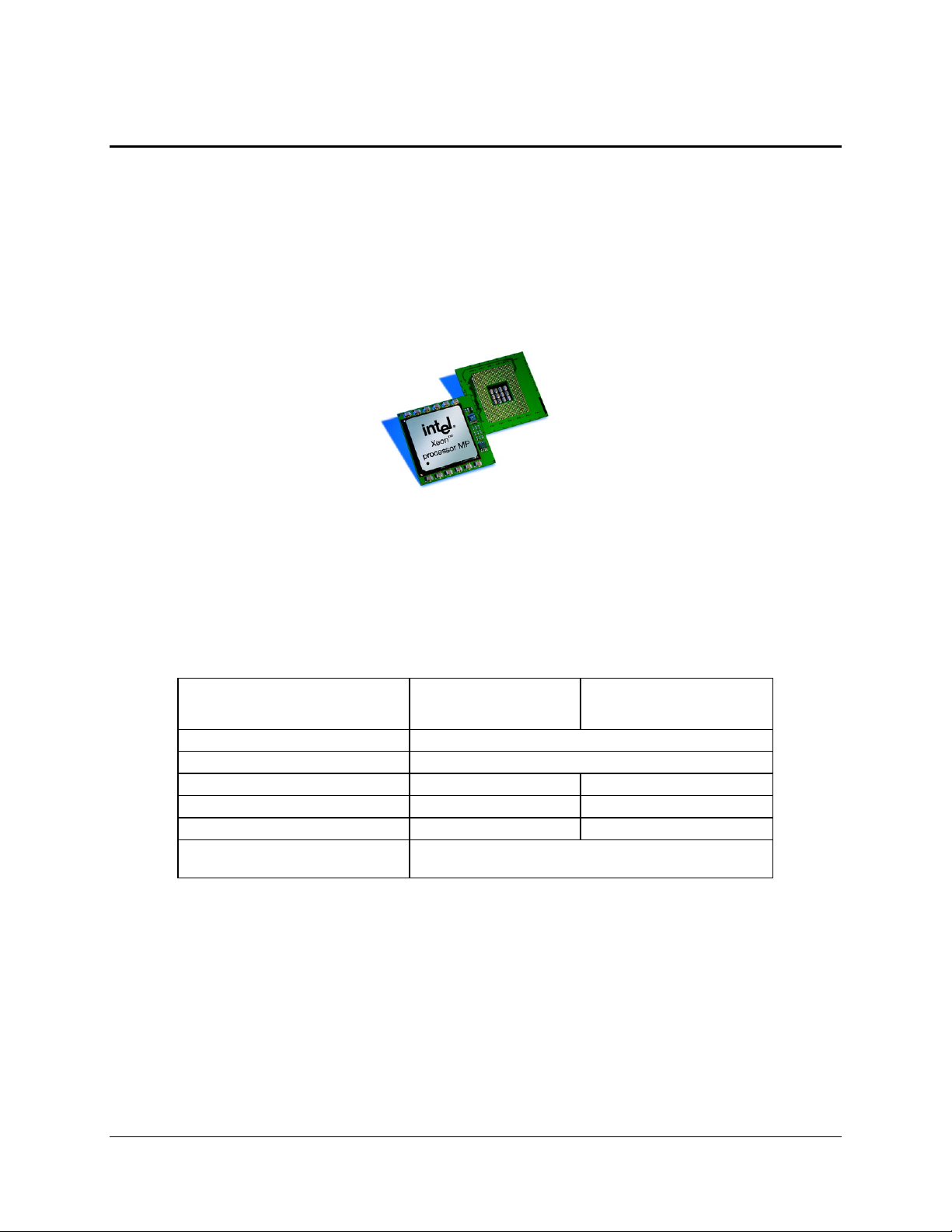
Figure 3. 64-bit Intel® Xeon™ Processors MP............................................................................5
Figure 4. Memory Board Outline Diagram .................................................................................21
Figure 5. Memory Board Component Diagram..........................................................................22
Figure 6. Memory Board Block Diagram....................................................................................23
Figure 7. Server Management Block Diagram...........................................................................28
Figure 8. I2C Block Diagram.......................................................................................................29
Figure 9. External Interfaces to the BMC...................................................................................37
Figure 10. Mainboard Jumper Locations ...................................................................................43
Figure 11. 68-Pin SCSI Connector ............................................................................................47
Figure 12. Stacked Ethernet Connector.....................................................................................52
Figure 13. Power Distribution Block Diagram............................................................................57
Figure 14. Typical Power-Up Sequence....................................................................................58
Figure 15. Typical Power-Down Sequence................................................................................59
Figure 16. Reset Block Diagram................................................................................................60
Figure 17. Interrupt Block Diagram............................................................................................61
Figure 18. PLD Connections......................................................................................................63
Figure 19. Mainboard Outline and Hole Location Drawing........................................................65
Figure 20. Mainboard Pin 1 Location Drawing...........................................................................66
Figure 21. Memory Board Mechanical Outline Drawing ............................................................67
Figure 22. Memory Board Pin 1 Location Drawing ....................................................................67
Figure 23. BIOS Display ............................................................................................................83
Figure 24. System Diagnostics Display ....................................................................................84
Revision 1.0
viii
Intel order number D22893-001

Intel® Server Board Set SE8500HW4 Product Overview
List of Tables
Table 1. Processor Feature Overview .........................................................................................5
Table 2. Processor Installation Order ..........................................................................................7
Table 3. PCI Expansion Slot Features.......................................................................................11
Table 4. PCI Interrupt Mapping..................................................................................................11
Table 5. IDSEL Mapping............................................................................................................12
Table 6. Arbitration Connections................................................................................................13
Table 7. PCI Hot Plug LEDs ......................................................................................................14
Table 8. Memory Board LEDs....................................................................................................25
Table 9. FRU Device Location and Size....................................................................................30
Table 10. Example Rolling BIOS Behavior with a New IMM......................................................31
Table 11. Fan States..................................................................................................................32
Table 12. Secure Mode Affect on ACPI States..........................................................................34
Table 13. System Reset Sources and Actions...........................................................................36
Table 14. Platform I2C Buses.....................................................................................................38
Table 15. Default Event Filters...................................................................................................40
Table 16. Mainboard Jumpers...................................................................................................44
Table 17. 68-Pin SCSI Connector Pinout ..................................................................................47
Table 18. 100-pin Front Panel Connector Pinout.......................................................................48
Table 19. COM2 Serial Header Pinout ......................................................................................49
Table 20. 4-pin Internal USB Header.........................................................................................50
Table 21. SATA Connector Pinout.............................................................................................50
Table 22. 12-pin Power Connector Pinout.................................................................................51
Table 23. 30-pin Power Signal Header Pinout...........................................................................51
Table 24. Video Connector Pinout.............................................................................................52
Table 25. Stacked Ethernet Connector Pinout...........................................................................53
Table 26. Server Management Ethernet Connector Pinout.......................................................54
Table 27. COM1 Serial Port Pinout............................................................................................54
Table 28. Stacked USB Connector Pinout.................................................................................55
Table 29. 5-pin ICMB Header Pinout.........................................................................................55
Table 30. 3-pin IPMB Header Pinout.........................................................................................55
Table 31. 3-pin Chassis Intrusion Pinout...................................................................................56
Table 32. 5-pin I2C POST Code Header Pinout.........................................................................56
Revision 1.0
Intel order number D22893-001
ix

Product Overview Intel® Server Board Set SE8500HW4
Table 33. Power Budget ............................................................................................................58
Table 34. Typical Power-Up Timings.........................................................................................59
Table 35. Typical Power-Down Timings ....................................................................................60
Table 36. Reset Types...............................................................................................................61
Table 37. PLD Functions ...........................................................................................................63
Table 38. Thermal Specifications...............................................................................................68
Table 39. Memory Hot Plug Support Under Different Memory Modes.......................................70
Table 40. Memory Modes Supporting Sparing ..........................................................................70
Table 41. System Options Menu................................................................................................85
Table 42. Error Manager Menu...................................................................................................85
Table 43. Boot Maintenance Manager Menu.............................................................................86
Table 44. Boot Options Menu....................................................................................................86
Table 45. Change Boot Order Menu...........................................................................................87
Table 46. Add Boot Option Menu...............................................................................................87
Table 47. Delete Boot Option Menu...........................................................................................88
Table 48. Select Legacy Floppy Order Menu ............................................................................88
Table 49. Select Legacy Hard Drive Order Menu......................................................................89
Table 50. Select Legacy CD-ROM Order Menu.........................................................................89
Table 51. Set Embedded NIC Order Menu................................................................................90
Table 52. Select Legacy BEV Order Menu................................................................................90
Table 53. Driver Options Menu..................................................................................................90
Table 54. Add Driver Option Menu .............................................................................................91
Table 55. Add Driver Option Using File Menu ...........................................................................91
Table 56. Add Driver Option Using Handle Menu......................................................................92
Table 57. Delete Driver Option Menu ........................................................................................93
Table 58. Change Driver Order Menu........................................................................................93
Table 59. Set Time Out Value Menu..........................................................................................94
Table 60. BIOS Setup Utility Layout ..........................................................................................94
Table 61. BIOS Setup: Keyboard Command Bar.......................................................................95
Table 62. Main Menu.................................................................................................................96
Table 63. Time and Date Menu .................................................................................................97
Table 64. Processor Menu.........................................................................................................97
Table 65. Processor #n Information Menu.................................................................................98
Table 66. Memory Menu............................................................................................................98
Table 67. Configure System RAS and Performance Menu........................................................99
Revision 1.0
x
Intel order number D22893-001

Intel® Server Board Set SE8500HW4 Product Overview
Table 68. View Memory Configure Details Menu.....................................................................100
Table 69. Memory Board #n Menu ..........................................................................................101
Table 70. DIMM Labels Menu...................................................................................................102
Table 71. Devices Menu..........................................................................................................102
Table 72. IDE Controller Menu ................................................................................................102
Table 73. Mass Storage Menu.................................................................................................103
Table 74. LAN Menu................................................................................................................104
Table 75. Video Menu..............................................................................................................104
Table 76. USB Menu................................................................................................................104
Table 77. Serial Ports Menu .....................................................................................................105
Table 78. PCI Menu.................................................................................................................105
Table 79. Server Management Menu ......................................................................................106
Table 80. Console Redirection Menu.......................................................................................106
Table 81. COM1 Console Redirection Menu...........................................................................107
Table 82. FRU Information Menu..............................................................................................107
Table 83. LAN Management Menu..........................................................................................108
Table 84. SEL Menu................................................................................................................108
Table 85. FRB Information Menu.............................................................................................109
Table 86. Security Menu..........................................................................................................109
Table 87. Save, Restore and Exit Menu..................................................................................110
Table 88. POST Progress LED Location and Example ...........................................................111
Table 89. POST Progress LED Codes ....................................................................................111
Table 90. Processor Diagnostic LED Locations.......................................................................113
Table 91. Beep Codes.............................................................................................................114
Table 92. BIOS Recovery Beep Codes ...................................................................................114
Table 93. POST Messages......................................................................................................115
Revision 1.0
Intel order number D22893-001
xi

Product Overview Intel® Server Board Set SE8500HW4
< This page intentionally left blank. >
Revision 1.0
xii
Intel order number D22893-001

Intel® Server Board Set SE8500HW4 Product Overview
1. Product Overview
The Intel® Server Board Set SE8500HW4 is the fourth generation of four-way Intel® IA32 Server
Boards. The board set uses the Intel
processor technologies. This product diverges from other Intel
®
E8500 Chipset, and the next generation of memory and
®
server boards and platforms in
the following ways:
Addition of PCI Express* technology
Addition of Double Data Rate Two (DDR2) memory
Memory implemented across up to four Memory Boards, with enhanced performance
and reliability features
Optional mass storage expansion for Fibre Channel and RAID
Removal of IDE, floppy, and PS/2* ports
The Intel
MP with up to 8MB L3 cache and incorporates features that clearly differentiate it as a high
availability server. Building on previous server platforms, the Intel
®
Server Board Set SE8500HW4 supports up to four 64-bit Intel® Xeon™ Processors
®
Server Board Set
SE8500HW4 introduces redundant memory, networking, and the BIOS flash in addition to the
enterprise features of hot-swap PCI slots, standards-based server management and serveroriented embedded I/O. Remote monitoring and management features are also included,
providing a new level of user tools for server administration.
The Intel
to four Memory Boards plug vertically into the Mainboard. The board set was designed to work
with the Intel
SR6850HW4, a 6U chassis. The board set may also be used in a non-Intel chassis that meets
the power and cooling requirements found in this specification. Please refer to the Intel
Platform SR4850HW4 Technical Product Specification and Intel
®
Server Board Set SE8500HW4 consists of two primary boards: Main and Memory. Up
®
Server Platform SR4850HW4, a 4U chassis, and the Intel® Server Platform
®
®
Server Platform SR6850HW4
Server
Technical Product Specification for more information on these products.
Revision 1.0
Intel order number D22893-001
1

Product Overview Intel® Server Board Set SE8500HW4
This document describes the Mainboard and Memory Board components of the Intel® Server
Board Set SE8500HW4.
Figure 1. Intel® Server Board Set SE8500HW4, Populated
1.1 Board Set Features
This chapter discusses the features for the Intel® Server Board Set SE8500HW4, which
includes:
Up to four 64-bit Intel
Xeon™ Processors MP with up to 8MB L3 cache
Intel
®
E8500 Chipset:
- Intel
®
E8500 Chipset North Bridge (NB): provides two processor buses and
connection to I/O and memory subsystems
- Intel
®
E8500 eXtended Memory Bridge (XMB): provides hot-plug support for up to
64GB of DDR2 memory
- Intel
- Intel
®
6700 PXH 64-bit PCI Hub: provides support for PCI-X* I/O
®
IOP332 Storage I/O Processor : provides support for PCI-X adapters and
contains Intel
(ROMB)
- Intel
®
81801EB I/O Controller Hub 5 (ICH5): provides support for the system BIOS,
video, USB 2.0, and Serial ATA (SATA).
Advanced I/O slots including PCI Express* and PCI-X and support circuits:
- One hot-plug PCI Express x8 slot
- Three hot-plug PCI Express x4 slots
- One hot-plug 64-bit PCI-X 133MHz, 1.0 slot
- Two 64-bit PCI-X 100MHz, 1.0 slots (not hot-plug)
®
Xeon™ Processors MP with 1MB L2 cache or 64-bit Intel®
®
XScale™ technology to support optional RAID On Motherboard
Revision 1.0
2
Intel order number D22893-001

Intel® Server Board Set SE8500HW4 Product Overview
Server management with either the Intel
®
Management Module Professional or Intel®
Management Module Advanced
ATI* Radeon* 7000 video controller, with 16MB SDRAM
Broadcom* BCM5704 NetXtreme* Gigabit Ethernet controller: provides two ports on the
rear of the Mainboard
LSI Logic* 53C1030 Ultra320* SCSI Controller: provides two independent Ultra320 SCSI
interfaces
Optional ROMB support: provides two channels of RAID 0, 1, 5, 10 or 50
Optional custom Intel
®
Fibre Channel Module: provides two 2Gbps optical connectors
Intel® Server Board SE8500HW4 Main Board
CPU
1
CPU2CPU
FSB 1
E8500
North Bridge
(NB)
4
FSB 0
CPU
3
IMI D
IMI C
IMI B
IMI A
Memory Board
Memory Board
Memory Board
SE8500HW4 Memory Board
XMB
XMB
XMB
XMB
DIMM
DIMM
DIMM
DIMM
DDR2 DIMM
DIMM
DIMM
DDR2 DIMM
DIMM
DIMM
DIMM
DIMM
DDR2 DIMM
DIMM
DIMM
DDR2 DIMM
PCI-X 100 MHz
SCSI
Connector
DDR2 RAID DIMM
LSI*
53C1030
Ultra320*
SCSI
Controller
SCSI Channel A
Fibre Channel Module
BRCM5704*
Ethernet
Controller
SCSI Channel B
USB
Front Panel
Connector
PCIe x8
PCIe x4
PCIe x4
Act Key
RAID
PCIe x4
PCIe x4
PCIe x4
IOP332
Processor
6700
PXH
PCI-X* 100 MHz
PCI Express x4 (hot-plug)
PCI Express x4 (hot-plug)
PCI-X 133 MHz (hot-plug)
PCI Express* x8 (hot-plug)
PCI Express x4 (hot-plug)
IMM
RAID Smart
Battery
82801EB
ICH5
SATA
LPC
SATA
Connector
PCI-33
FWH
ATI*
Radeon*
7000
Video
Controller
SIO
10/100
Ethernet Port
Ethernet Port
External SCSI
Connector
(optional)
USB Port
USB Port
Video Port
COM1/EMP
GCM
(optional)
Figure 2. Intel® Server Board Set SE8500HW4 Interconnect Diagram
Revision 1.0
3
Intel order number D22893-001

Product Overview Intel® Server Board Set SE8500HW4
< This page intentionally left blank. >
Revision 1.0
4
Intel order number D22893-001
Intel® Server Board Set SE8500HW4 Processor and Chipset
2. Processor and Chipset
2.1 Processors Supported
The Intel® Server Board Set SE8500HW4 supports 64-bit Intel® Xeon™ Processors MP which
are based on the Intel
®
NetBurst™ microarchitecture. Several architectural and
microarchitectural enhancements have been added to this processor, including an increased L2
cache size and, for some models, an integrated L3 cache. Table 1 provides a feature set
overview of the 64-bit Intel
®
Xeon™ Processors MP.
Figure 3. 64-bit Intel® Xeon™ Processors MP
Table 1. Processor Feature Overview
Feature 64-bit Intel® Xeon™
Processors MP with
1MB L2 cache
Package FC-mPGA4
L2 cache size 1MB
L3 cache size N/A 4MB or 8MB
Core operating voltage 1.0975 to 1.4V 1.171 to 1.3250V
Cache operating voltage N/A 1.1 to 1.25V
Front side bus 667MHz with data-bus Error Correcting Code (ECC),
bandwidth up to 5.33GB/s
64-bit Intel® Xeon™
Processors MP with up to
8MB L3 cache
Revision 1.0
Intel order number D22893-001
5

Processor and Chipset Intel® Server Board Set SE8500HW4
The 64-bit Intel® Xeon™ Processors MP includes the following advanced features:
Intel
®
Extended Memory 64 Technology (EM64T) for executing both 32-bit and 64-bit
applications simultaneously
Intel
Intel
Execute-Disable Bit for hardware support of security features
Quad-channel DDR2 400MHz memory support
PCI Express for faster serial interconnects
Streaming Single Instruction, Multiple Data (SIMD) Extensions 2 and 3 (SSE2, SSE3)
For more information, please refer to the 64-bit Intel
cache Datasheet, 64-bit Intel
bit Intel
®
Hyper-Threading (HT) technology providing two logical processors
®
Demand-Based Switching (DBS) for power savings
®
®
®
Xeon™ Processors MP with 1MB L2 cache Specification Update, and 64-bit Intel®
Xeon™ Processors MP with up to 8MB L3 cache Datasheet, 64-
Xeon™ Processors MP with 1MB L2
Xeon™ Processors MP with up to 8MB L3 cache Specification Update.
2.1.1 Heat Sink
The Intel® Server Board Set SE8500HW4 uses the reference design Common Enabling Kit
(CEK) heatsinks, which meet the 64-bit Intel
targets. Each CEK heatsink consists of the following components:
Passive heatsink (with captive standoff and screws)
Thermal Interface Material (TIM-2) – to cover the entire processor Integrated Heat
Spreader (IHS) and the heatsink base
Hat spring – mounted below the Intel
®
Xeon™ Processors MP thermal performance
®
Server Board Set SE8500HW4 Mainboard
Revision 1.0
6
Intel order number D22893-001

Intel® Server Board Set SE8500HW4 Processor and Chipset
2.1.2 Installation Order
Some processor signals do not have on-die termination and must be terminated at an end
agent. The Intel
Front Side Buses (FSBs). For each bus with a processor installed, the first socket on that bus
must be used to ensure proper signal termination. A processor must be installed in socket 1
before socket 2, and socket 3 before socket 4. Refer to Table 2 for processor installation order.
®
Server Board Set SE8500HW4 Mainboard was designed with two separate
Table 2. Processor Installation Order
Sockets Number of
Processors
Four Installed Installed Installed Installed Installed Installed Installed
1 2 3 4
Installed One
Installed Installed Installed
Installed Installed Two1
Installed Installed Installed Installed
Installed Installed Installed Installed Installed Three1
Installed Installed Installed Installed Installed Installed
VRM 10.2
J1F1
VRM 9.1
J1H22
VRM
10.2
J3F1
1. There is no performance gained by splitting the processors across the FSBs. Intel has
validated sequential process installation, with a one-processor configuration using
socket 1; a two-processor configuration using sockets 1 and 2; and a three-processor
configuration using sockets 1, 2 and 3.
2. The 9.1 VRM is only required when installing 64-bit Intel
®
Xeon™ Processors MP with
up to 8MB of L3 cache.
Revision 1.0
7
Intel order number D22893-001

Processor and Chipset Intel® Server Board Set SE8500HW4
2.2 Intel® E8500 Chipset
The Intel® E8500 Chipset is the highest performance, most scalable platform offering in the 64bit Intel
®
Xeon™ Processor MP family. The chipset represents the sixth-generation Intel fourway multi-processor platform, is architected for multi-core processors and includes these
advanced features:
Support for up to four 64-bit Intel
Maintains coherency across both buses
Double-pumped 40-bit address buses with a total address bandwidth of 167 million
®
Xeon™ Processors MP FSB operating at 667 MHz
addresses/second
Quad-pumped, 64-bit data bus providing a bandwidth of 5.3 GB/s per bus
x8 Single Device Data Correction (x8 SDDC) technology for memory error correction
Hardware memory initialization
ECC protection on data signals and parity protection on address signals
Support for hot-plug memory and performance operations
This section provides an overview of the chipset components, for more detailed information
refer to the Intel
®
E8500 Chipset Datasheets referenced in the Appendix.
2.2.1 North Bridge (NB)
The Intel® E8500 Chipset North Bridge (NB) is the center of the system architecture and
provides interconnection to:
Up to four 64-bit Intel
®
Xeon™ Processors MP via two 667 MHz FSBs optimized for
server applications
Up to 64GB memory via four Independent Memory Interfaces (IMI)
I/O subsystem components via one PCI Express and the Intel
®
82801EB I/O Controller
Hub 5 (ICH5)
2.2.2 eXtended Memory Bridge (XMB)
The Intel® E8500 Chipset eXtended Memory Bridge (XMB) provides interface between the NB
and DDR2 400MHz DIMMs. The Intel
Memory Boards, each with an XMB and four DDR2 400MHz DIMM locations.
®
Server Board Set SE8500HW4 includes up to four
Revision 1.0
8
Intel order number D22893-001

Intel® Server Board Set SE8500HW4 Processor and Chipset
2.2.3 Intel® IOP332 Storage I/O Processor
The Intel® IOP332 Storage I/O Processor contains a PCI Express-to-PCI-X bridge and performs
bridging functions between the PCI Express interface of the NB and PCI-X devices. The Intel
Server Board Set SE8500HW4 contains one Intel
®
IOP332 Storage I/O Processor that has two
PCI bus interfaces which provide:
Slots 6 and 7 (PCI-X 100MHz, non-Hot Plug)
LSI Logic 53C1030 Ultra320 SCSI controller
Intel
®
Fibre Channel Module connector
®
2.2.4 Intel® 82801EB I/O Controller Hub 5 (ICH5)
The Intel® 82801EB I/O Controller Hub 5 (ICH5) provides a hub interface-to-PCI bridge, PCI-toLPC bridge and legacy I/O controllers. Some of the features of the ICH5 are not used in this
board set. The Intel
Integrated Serial ATA (SATA) controller
High-speed USB 2.0 host controller
ATI Radeon 7000 video controller
Support for System Management Bus (SMBus) specification, version 2.0 and I
ACPI power management logic support
Firmware Hub (FWH) interface support
®
Server Board Set SE8500HW4 contains one ICH5 which provides:
2
C
2.2.5 Intel® 6700 PXH 64-bit Hub (PXH)
The Intel® 6700 PXH 64-bit Hub performs bridging functions between the PCI Express interface
of the NB and PCI-X devices. The Intel
has two PCI bus interfaces which provide:
Slot 2 (PCI-X 133Mhz Hot Plug)
Broadcom BCM5704C dual channel Gigabit Ethernet controller
®
Server Board Set SE8500HW4 contains one PXH that
Revision 1.0
9
Intel order number D22893-001

Processor and Chipset Intel® Server Board Set SE8500HW4
< This page intentionally left blank. >
Revision 1.0
10
Intel order number D22893-001

Intel® Server Board Set SE8500HW4 I/O Subsystems
3. I/O Subsystems
3.1 PCI Subsystem
The PCI subsystem consists of eight slots, seven available to standard PCI adapters and one
for the Intel
®
Server Board Set SE8500HW4-specific Intel® Fibre Channel Module.
Table 3. PCI Expansion Slot Features
Segment Slot Hot Plug Technology Width Bandwidth
(GB/s)
North Bridge (C) 1 Yes PCI Express* x8 4
PXH (A) 2 Yes PCI-X* 133 64-bit 1
North Bridge (D) 3 Yes PCI Express x4 2
North Bridge (B) 4 Yes PCI Express x4 2
North Bridge (B) 5 Yes PCI Express x4 2
Intel® IOP332 Storage I/O
Processor (B)
Intel IOP332 Storage I/O
Processor (B)
Intel IOP332 Storage I/O
Processor (A)
6 No PCI-X 100 64-bit 0.8
7 No PCI-X 100 64-bit 0.8
Fibre Channel No PCI-X 100 64-bit 0.8
3.1.1 PCI Interrupts
PCI Express interrupts are delivered in-band over the PCI Express bus via the Message Signal
Interrupt (MSI) mechanism.
PCI and PCI-X devices can deliver interrupts either by asserting IRQ signals that are routed to
the PXH or Intel
®
IOP332 Storage I/O Processor IOxAPIC, or over the PCI-X bus via MSI. In
either case, the PXH and/or Intel® IOP332 Storage I/O Processor forward the interrupt to the
NB as an Inbound Write for the processor to handle the event.
Table 4 describes how the interrupts for each of the PCI devices are mapped to the PXH and
®
Intel
IOP332 Storage I/O Processor.
Table 4. PCI Interrupt Mapping
Device APIC INTA# INTB# INTC# INTD#
Broadcom*
BCM5704
Slot 2 PXH (A) PX2A_IRQ0_N PX2A_IRQ1_N PX2A_IRQ2_N PX2A_IRQ3_N
Slot 6 Intel® IOP332 Storage I/O
Slot 7 Intel IOP332 Storage I/O
Revision 1.0
PXH (B) PX2B_IRQ0_N PX2B_IRQ1_N
PX1B_XINT4_N PX1B_XINT5_N PX1B_XINT6_N PX1B_XINT7_N
Processor (B)
PX1B_XINT6_N PX1B_XINT7_N PX1B_XINT4_N PX1B_XINT5_N
Processor (B)
11
Intel order number D22893-001

I/O Subsystems Intel® Server Board Set SE8500HW4
Device APIC INTA# INTB# INTC# INTD#
LSI Logic*
53C1030
Intel® Fibre
Channel
Module
Intel IOP332 Storage I/O
Processor (A)
Intel IOP332 Storage I/O
Processor (A)
PX1A_XINT0_N PX1A_XINT1_N
PX1A_XINT2_N PX1A_XINT3_N
- -
- -
3.1.2 PCI IDSEL Signal
The IDSEL signal is used as a chip-select for devices during read and write transactions. The
PXH and Intel® IOP332 Storage I/O Processor assert a specific address bit on a given PCI bus
to toggle the IDSEL signal to the PCI device. For the Intel
Mainboard the address bit to IDSEL mapping is shown in Table 5.
Table 5. IDSEL Mapping
Device Device # IDSEL Host Bridge
Broadcom* BCM5704 2 PX2B_AD<18> PXH (B)
Slot 2 2 PX2A_AD<18> PXH (A)
Slot 6 6 PX1B_AD<22> Intel® IOP332 Storage I/O
Slot 7 7 PX1B_AD<23> Intel IOP332 Storage I/O
LSI Logic* 53C1030 5 PX1A_AD<21> Intel IOP332 Storage I/O
Intel® Fibre Channel Module 15 PX1A_AD<31> Intel IOP332 Storage I/O
ROMB enabled on Intel IOP332
Storage I/O Processor
14 n/a Internal to Intel IOP332
®
Server Board Set SE8500HW4
Processor (B)
Processor (B)
Processor (A)
Processor (A)
Storage I/O Processor
Note: When the ROMB solution is enabled, the IDSEL to the LSI Logic 53C1030 is inhibited by
the Intel
system and the Intel
Since the Intel
Intel
®
IOP332 Storage I/O Processor. This effectively hides the SCSI controller from the
®
Fibre Channel Module is set to device 15 so that it is not affected by the device hiding
®
®
IOP332 Storage I/O Processor acts as the SCSI (or RAID) controller.
Fibre Channel Module is attached to the same bus as the SCSI controller, the
operation required for the ROMB solution.
Revision 1.0
12
Intel order number D22893-001

Intel® Server Board Set SE8500HW4 I/O Subsystems
3.1.3 Bus Arbitration Signals
Request (REQ#) signals indicate to the bus arbiter that an agent/device desires use of the bus.
The Grant (GNT#) signal indicates to the agent/device that access to the bus has been granted.
Every master has its own REQ#, which must be tri-stated while RST# is asserted. These are
point-to-point signals which are assigned to every bus master.
In the Intel
and Intel
BCM5704 and the Intel
Logic 53C1030, and the Intel
®
Server Board Set SE8500HW4 there is one arbiter for each PCI bus on the PXH
®
IOP332 Storage I/O Processor. The PXH contains an arbiter for slot 2 and the
®
IOP332 Storage I/O Processor contains an arbiter for slots 6 and 7, LSI
®
Fibre Channel Module.
Table 6. Arbitration Connections
Device REQ# GNT# Host Bridge
Broadcom* BCM5704 PX2B_REQ0_N PX2B_GNT0_N PXH (B)
Slot 2 PX2A_REQ0_N PX2A_GNT0_N PXH (A)
Slot 6 PX1B_REQ1_N PX1B_GNT1_N Intel® IOP332 Storage I/O
Processor (B)
Slot 7 PX1B_REQ0_N PX1B_GNT0_N Intel IOP332 Storage I/O
Processor (B)
LSI Logic* 53C1030 PX1A_REQ0_N PX1A_GNT0_N Intel IOP332 Storage I/O
Processor (A)
Intel® Fibre Channel Module PX1A_REQ1_N PX1A_GNT1_N Intel IOP332 Storage I/O
Processor (A)
3.1.4 Wake On LAN
Wake On LAN (WOL) is supported on the Intel® Server Board Set SE8500HW4 either from PCI
devices through the PME# signal, or PCI Express via the WAKE# signal.
Any PCI Express adapter can generate a wake event by asserting the WAKE# signal. This
signal is OR’d to all other PCI Express WAKE# signals and routed to the ICH5 after being
qualified with intrusion and a prior graceful shutdown. The assertion of a WAKE# signal will
cause the system to return to the ACPI S0 sleep state. Once system power is up and the PCI
Express devices are configured, a PME message is sent to the NB identifying the device that
woke the system.
For all the PCI devices or the Ethernet controller, PME# is handled similarly to the PCI Express
WAKE# signal. All PME# signals are OR’d together and routed to the ICH5 after being qualified
with intrusion and a prior graceful shutdown. The PME assertion wakes the system but does not
generate an interrupt from the ICH5. Once the system is powered up, the PXH or Intel
Storage I/O Processor generate a PME interrupt message to the operating system. The
operating system determines which slot is the PME source by polling the PXH and Intel
®
IOP332
®
IOP332 Storage I/O Processor.
Revision 1.0
Intel order number D22893-001
13

I/O Subsystems Intel® Server Board Set SE8500HW4
3.1.5 PCI Hot Plug* Support
PCI Hot Plug* is the concept of removing a standard PCI adapter card from a system without
stopping the software or powering down the system as a whole.
In the Intel
®
Server Board Set SE8500HW4, PCI Slot 2 supports the PCI Hot-Plug Specification,
Revision 1.1 and is configured so that the PXH isolates the slot from the PCI bus when no
adapter is present. The four PCI Express slots support the PCI Express Base Specification,
Revision 1.0a.
3.1.5.1 Hardware Components
The Intel
®
Server Board Set SE8500HW4 contains buttons and LEDs to assist a user for hot
plug operations. Buttons provide isolation circuitry to physically disconnect the hot plug adapter
from the PCI buses while LEDs provide slot power and status. The LEDs have enough luminous
intensity to pass through system-level light pipes and be visible at the top of a system. An
attention button can be used to invoke a hot-plug sequence to remove or add an adapter
without the use of an operating system/software interface.
Table 7. PCI Hot Plug LEDs
LED State Meaning
Power
(Green)
Attention
(Amber)
Off Power off: All main rails have been removed from slot. Card can be inserted or removed.
On Power on: Slot is powered on. Card cannot be inserted or removed.
Blinking Power transition: Slot is in the process of changing state. Card cannot be inserted or
removed.
Off Normal: Normal operation.
On Attention: Power fault or operational problem at this slot.
Blinking Locate: Slot is being identified at the user’s request.
3.1.5.2 Software Components
PCI hot plug operations are supported by the system BIOS, an operating system driver and an
optional operating system administrative interface. The Intel
®
Server Board Set SE8500HW4
BIOS provides initialization of the hot plug hardware components, logging of hot plug events
through server management and ACPI table generation. Microsoft* Windows* Server 2003,
Enterprise Edition includes support for PCI hot plug through the taskbar “Unplug or Eject
Hardware” interface but may require an updated adapter device driver. Refer to other operating
systems’ manuals for more information on how to perform hot-plug operations. Reference the
PCI adapter release notes for specific information on support and driver requirements.
Revision 1.0
14
Intel order number D22893-001

Intel® Server Board Set SE8500HW4 I/O Subsystems
3.1.5.3 Hot Removal Example
3.1.5.3.1 Under Microsoft Windows Server 2003, Enterprise Edition:
1. Open the cover of the system to access the adapters and status LEDs.
2. Double-click “Unplug/Eject” in the taskbar to open the “Unplug or Eject Hardware” menu.
3. Select the device to be removed and click “Stop”.
4. Wait for the power LED to turn off.
5. Dis-engage rocker, retention, and/or safety devices.
6. Remove the adapter.
3.1.5.3.2 Under other operating systems:
1. Open the cover of the system to access the adapters and status LEDs.
2. Press the attention button for the slot. (press the attention button within five seconds to abort
the hot plug operation)
3. Wait for the power LED to turn off.
4. Dis-engage rocker, retention, and/or safety devices.
5. Remove the adapter.
3.1.5.4 Hot Addition Example
3.1.5.4.1 Under Microsoft Windows Server 2003, Enterprise Edition:
1. Open the cover of the system to access adapters and view the status LEDs.
2. Install the adapter into the slot.
3. Engage rocker, retention, and/or safety devices.
4. Wait for the software user interface to open. Confirm the device to be enabled.
5. Wait for the power LED to turn on.
Note: If the attention LED is blinking, a power fault has occurred. The user may need to remove
the adapter, wait for the LED to turn off, and re-start the hot add operation.
3.1.5.4.2 Under other operating systems:
1. Open the cover of the system to access adapters and view the status LEDs.
2. Install the adapter into the slot.
3. Engage rocker, retention, and/or safety devices.
4. Press the attention button for the slot. (press the attention within five seconds to abort the
hot plug operation)
5. Wait for the power LED to turn on.
6. Enable the device in your operating system.
Note: If the attention LED is blinking, a power fault has occurred. The user may need to remove
the adapter, wait for the LED to turn off, and re-start the hot add operation.
Revision 1.0
Intel order number D22893-001
15

I/O Subsystems Intel® Server Board Set SE8500HW4
3.2 Ultra320 SCSI Subsystem
A single LSI Logic* 53C1030 controller provides the on-board Ultra320 SCSI interface. The
controller resides on the PCI Bus Segment A (PX1A), off the Intel® IOP332 Storage I/O
Processor. For optimal performance, the controller is configured as a 64-bit PCI-X 100MHz
device.
The LSI Logic 53C1030 supports two Ultra320 SCSI channels, both validated for LVDS
operation. In the Intel
hot-swap hard disk drive bay and the second is optionally connected to an external connector.
In the Intel
®
Server Platform SR6850HW4 both channels are routed to the internal hot-swap
®
Server Platform SR4850HW4 the first channel is routed to the internal
hard disk drive bay. Intel has not validated Single Ended (SE) operation for this device.
The Mainboard provides active terminators, termination voltage, auto re-sealable fuse, and
protection diode for both SCSI channels. The SCSI ROM allows for the configuration of onboard termination.
PCI Express and PCI-X adapter cards based on a LSI Logic 53C1030 controller should have
the option ROM for the slot turned off in the system BIOS setup. This will allow the embedded
LSI Logic 53C1030 controller firmware to manage the add-in adapters. The Intel
®
Server Board
Set SE8500HW4 Mainboard does not have a physical flash device, so the system BIOS loads
the required RISC F/W into the embedded LSI Logic 53C1030 controller during POST. A
53C1030-based adapter cannot take control of the embedded SCSI controller since those cards
do not have the required RISC F/W to start the embedded SCSI device. Starting with the LSI
Logic Fusion-MPT* SCSI BIOS 5.10.02, the embedded LSI Logic 53C1030 SCSI controller can
control additional LSI Logic 53C1030-based adapter cards.
Revision 1.0
16
Intel order number D22893-001

Intel® Server Board Set SE8500HW4 I/O Subsystems
3.3 Intel® RAID On Motherboard (ROMB)
The Intel® IOP332 Storage I/O Processor, in conjunction with the LSI Logic 53C1030, provides
an optional RAID On Motherboard (ROMB) solution which supports RAID levels 0, 1, 5, 10, and
50. A 2MB flash component and a non-volatile SRAM store the code and hardware
configuration information.
To activate the ROMB solution, a physical Intel
RAID DIMM must be installed on the Intel
contains a registration code required to unlock the LSI Mega RAID* solution. The DDR2
400MHz RAID DIMM serves as memory for the Intel
cache to store write data for the drives. In addition to these components an Intel
®
®
RAID Activation Key (RAK) and DDR2 400MHz
Server Board Set SE8500HW4 Mainboard. The RAK
®
IOP332 Storage I/O Processor and a disk
®
RAID Smart
Battery (RSB) may also be installed to refresh the RAID DIMM when system power drops below
specifications.
After installing a RAK and DDR2 400MHz RAID DIMM, and optional RSB, the system BIOS
setup allows the user to enable the ROMB solution. During option ROM scan, an option to
configure the RAID is displayed. The following three chapters provide an overview of the Intel
ROMB solution, however, for more information refer to the Intel
®
RAID Smart Battery Technical
Product Specification.
3.3.1 Intel® RAID Activation Key (RAK)
The RAK is a round one-wire serial EEPROM device programmed by Intel. This key has a
registration code required to enable the LSI Mega RAID* solution.
3.3.2 DDR2 RAID DIMM
The ROMB solution only supports 400MHz registered ECC, with a CAS latency of four clock
cycles. Please refer to the Intel
supported memory.
®
Server Board SE8500HW4 Memory Qualification List for
3.3.3 Intel® RAID Smart Battery (RSB)
The RSB keeps the contents of the DDR2 400MHz RAID DIMM preserved if power drops below
specifications. When the Intel
specifications, it initiates a power fail sequence that safely puts the RAID DIMM into self-refresh
state. The power subsystem generates enough of a delay to allow the Intel
Processor to complete its power fail sequence, even in the event of total system power loss.
After the power fail sequence is completed, additional logic keeps the RAID DIMM in selfrefresh mode. When power is restored, data from the RAID DIMM is safely written to the disk
array.
Revision 1.0
®
IOP332 Storage I/O Processor senses power has dropped below
®
IOP332 Storage I/O
Intel order number D22893-001
17

I/O Subsystems Intel® Server Board Set SE8500HW4
3.4 Gigabit Ethernet
A single Broadcom* BCM5704C controller provides the on-board Gigabit Ethernet interface.
This controller has two ports that can independently operate at 1000/100/10 Mbps and support
failover and teaming for greater reliability and performance. The two Media Access Controllers
support full-duplex and half-duplex modes at all speeds and have their own PCI configuration
space and on-chip memory for higher performance with load balancing and packet buffering.
For optimal performance, the controller is configured as a 64-bit PCI-X 133MHz device. The
ICH5 contains an Ethernet controller, but this device is not used by the Intel
®
Server Board Set
SE8500HW4.
3.5 Serial ATA (SATA)
The ICH5 provides a Serial ATA (SATA) interface with a transfer rate of up to 1.5GB/s. The
®
Intel
Server Board Set SE8500HW4 Mainboard has a standard 7-pin vertical connector for this
feature. SATA cables should be 1m (40 inches) or less in length.
3.6 Fibre Channel
The Intel® Fibre Channel Module seats into a custom-wired PCI Express x16 slot on the Intel®
Server Board Set SE8500HW4 Mainboard, which is attached to the Intel
®
IOP332 Storage I/O
Processor. The module uses a Qlogic* ISP2322 FC-PCI-X controller and has the following
features:
Two independent 2 Gbps Fibre Channel ports
Support for Fibre Channel virtual interface (VI) protocol
Automatically negotiates Fibre Channel bit rate (1 or 2 Gbps)
Supports up to 400 MBps sustained Fibre Channel data transfer rate
1 MB SRAM per port
Data and code parity protection
Host intervention not required to execute complete SCSI, IP, or VI operations
LC-style optical connectors
Works with the Qlogic SANsurfer* Management Suite and other Qlogic FC cards
For more information, please refer to the Intel
®
Fibre Channel Module User Guide.
3.7 Firmware Hubs
The Intel® Server Board Set SE8500HW4 Mainboard has a combined total of 4MB flash
memory that serves as the firmware hub (FWH) for the system BIOS. The system BIOS fits into
2MB of flash, but twice that is required to support the rolling BIOS feature. See Chapter 5 for
more information on the rolling BIOS.
Revision 1.0
18
Intel order number D22893-001

Intel® Server Board Set SE8500HW4 I/O Subsystems
3.8 Video
A single ATI* Radeon* 7000 video controller provides the on-board video interface. The ATI
Radeon 7000 features the following technologies:
2D/3D video accelerator
Dual DAC for integrated, cost-effective multi-panel support
Resolutions from VGA up to UXGA (1600x1200)
16MB SDRAM video memory
32-bit/33MHz PCI host interface
Using the default operating system video driver options, the VGA signal is mirrored between the
rear panel and the front panel connector. This design consideration was made to facilitate user
debug of an operating system hard failure. When the system is in a failure state a portable
monitor can be attached to the front of the system to determine root cause. Since this is an
enterprise server, Intel has not validated the video driver configured with the front panel I/O
board VGA connector in a non-mirrored, extended desktop, state.
3.9 USB 2.0
The ICH5 provides four USB 2.0 interfaces with one internal connector on the Intel® Server
Board Set SE8500HW4 Mainboard, a dual-stack USB connector on the rear panel, and one
interface routed to the front panel connector.
3.10 Serial
The SIO provides two RS232 serial communication ports (COM1 and COM2). COM1 is
provided through DB9 connector on the rear panel of the Intel
Mainboard while COM2 is internal to the chassis and available as an unshielded 9-pin header (2
x 5, with pin 10 removed for keying). COM1 is available as an Emergency Management Port
(EMP) for remote server management, and when used in this mode, it is unavailable to the
BIOS/operating system. When server management is setup for Serial Over LAN (SOL) remote
server management, COM2 is unavailable to the BIOS/operating system.
®
Server Board Set SE8500HW4
Revision 1.0
Intel order number D22893-001
19

I/O Subsystems Intel® Server Board Set SE8500HW4
< This page intentionally left blank. >
Revision 1.0
20
Intel order number D22893-001

Intel® Server Board Set SE8500HW4 Intel® Server Board Set SE8500HW4 Memory Board
4. Intel® Server Board Set SE8500HW4 Memory
Board
One to four Intel® Server Board Set SE8500HW4 Memory Boards plug vertically into the Intel®
Server Board Set SE8500HW4 Mainboard. The Memory Board has the following features:
Intel
Two DDR2 400MT/s buses
Four 240-pin DDR2 400Mhz registered ECC DIMM sockets
Support for both single-rank and dual-rank DIMMs
Independent Memory Interface (IMI), a high-speed differential bus
PCI Express x16 card edge connector that plugs into the Intel
®
E8500 Chipset eXtended Memory Bridge (XMB)
®
Server Board Set
SE8500HW4 Mainboard
LED error indicators for each DIMM and an attention LED for hot plug events
LED indicator for both memory mirroring and RAID configurations
Memory hot plug at the card level, based on the PCI Hot Plug model
On board power converters for 0.9V, 1.5V, and 1.8V
Field Replaceable Unit (FRU) device
Two temperature sensors
Safety mechanism for instant power shut-down to the Memory Board
Figure 4. Memory Board Outline Diagram
Revision 1.0
Intel order number D22893-001
21

Intel® Server Board Set SE8500HW4 Memory Board Intel® Server Board Set SE8500HW4
Figure 5. Memory Board Component Diagram
4.1 DDR2 DIMM Support
DDR2 memory offers an effective doubling of the clock rate over DDR memory since data
transfers happen on both the rising and falling edge of the clock (double pumped). Due to the
lower clock frequency, and improved manufacturing technology, a significant power savings can
be achieved, especially when the data bus is not active.
The Intel
®
Server Board Set SE8500HW4 Memory Board supports DDR2 400MHz (also referred
to as PC2-3200) registered ECC SDRAM with On Die Termination (ODT). Both single-rank and
dual-rank technologies are supported, however unbuffered and non-ECC will not function in the
®
Intel
Server Board Set SE8500HW4. Within a single bank, both DIMMs must be identical. (The
DIMMs must be identical in size and in the number of devices on the DIMM.)
Speeds less than DDR2 400MHz may be used, but performance will be reduced. Intel has only
validated DDR2 400MHz SDRAM for specific memory parts; refer to the Intel
®
Server Board Set
SE8500HW4 Board Memory Qualification List
4.2 Installation Order
When only using two memory DIMMs, the first pair of sockets, DIMM_1A and DIMM_1B, must
be populated. When using a mixture of single-rank and dual-rank memory DIMMs on one
Memory Board, the dual-rank DIMMs must be installed in the first pair of sockets.
4.3 Memory Initialization
The XMB provides hardware memory initialization. The initialization engine performs two
passes. On the first pass, it writes the entire segment. On the second pass, it reads and tests
the entire segment. Any errors are logged with the failing DIMM being flagged for BIOS.
Revision 1.0
22
Intel order number D22893-001

Intel® Server Board Set SE8500HW4 Intel® Server Board Set SE8500HW4 Memory Board
4.4 Data Correction and Scrubbing
The XMB employs a Single Device Data Correction (x8 SDDC) algorithm for the memory
subsystem that will recover from a component failure during read and write transactions. This
corrects and logs a correctable memory error, and logs uncorrectable memory errors.
A patrol scrub can be turned on in the system BIOS that scrubs roughly 64GB of memory
behind each XMB every day. The patrol scrub confirms the data for one cache line every 16k
core cycles and then increments the address one cache line. During patrol scrub, an erroneous
read will be logged and re-read. If the re-read is correctable, it is corrected (scrubbed) in
memory. A conflicting read or write request pending issue will be held until the scrub is finished.
4.5 Memory Board Components
DIMM_1B
Remote
Temperature
Sensor
DIMM_1A
DIMM_2B
DIMM_2A
Channel A Channel B
E8500 eXtended Memory
Bridge
IMI
Main Board Connector
I2C
FRU
Figure 6. Memory Board Block Diagram
Temperature
Sensor
Controller
Revision 1.0
23
Intel order number D22893-001

Intel® Server Board Set SE8500HW4 Memory Board Intel® Server Board Set SE8500HW4
4.5.1 Button, Retention Latch and LEDs
The following sections provide an overview of the hardware required to support memory hot
plug. See Section 10.1 for more information about memory hot plug support on the Intel
Board Set SE8500HW4.
4.5.1.1 Attention Button
This is a user accessible push button that initiates the proper shut down of the Memory Board
during a memory hot plug event. When pushed, a notification is sent to the memory hot plug
controller on the Mainboard. The system blinks the attention LED until the request can be
serviced. The BIOS interprets the request as a hot removal if the Memory Board is included in
the current system memory configuration or as a hot add if it is not.
If the system rejects the removal request, the power LED remains lit. A removal request may be
rejected if the current memory mode does not support hot removal. For example if only three
good boards in a memory RAID mode remain, the system will reject a removal request to any of
those three boards. If the system accepts the removal request it blinks the power LED, deinitializes the board, then turns off the power LED. After the power LED is turned off, the user
may open the retention latch to remove the Memory Board.
®
Server
4.5.1.2 Retention Latch
The retention latch is a mechanical lock and handle used to remove the Memory Board from a
chassis and the Mainboard. In the event of an unexpected memory hot plug operation, nonaccessible buttons under the retention latch will turn off power to the Memory Board. This safety
feature is included to protect the user and circuits in the event that the attention button was not
used properly.
Revision 1.0
24
Intel order number D22893-001

Intel® Server Board Set SE8500HW4 Intel® Server Board Set SE8500HW4 Memory Board
4.5.1.3 LEDs
All LEDs are controlled by the BIOS through the Independent Memory Interface (IMI). Table 8
describes the LEDs on the Memory Board.
Table 8. Memory Board LEDs
Name Color Description
Mirror Green Memory Board is in a mirror mode
RAID Green Memory Board is in a RAID mode
Attention Amber When flashing, the Memory Board is in a hot plug event
Power1 Green Memory Board is powered on, all rails are on
1B Amber DIMM_1B has had an error and needs to be replaced
1A Amber DIMM_1A has had an error and needs to be replaced
2B Amber DIMM_2B has had an error and needs to be replaced
2A Amber DIMM_2A has had an error and needs to be replaced
1- The power LED provides indication of Memory Board state. It is cleared when the Memory
Board is inactive and set when the Memory Board is included in the current memory
configuration. It blinks when a request is being serviced during a hot removal or hot add event.
4.5.2 Temperature Sensors and FRU
A dual temperature sensing device provides a sensor at the left and right of the DIMM sockets.
Server management sees this as one sensor, measuring the temperature drop across the board
which estimates the heat generated by the DIMMs.
An EEPROM device provides 256 bytes of programmable Field-Replaceable Unit (FRU) space.
Like all Intel server boards, this FRU is programmed during manufacturing to contain the board
version and serial number but may be programmed to meet integrator-specific needs.
4.5.3 I2C
The XMB, temperature sensor controller and FRU device are connected to the Mainboard
Baseboard Management Controller. The I
and located on private I
2
C bus 3.
2
C bus addressing for these devices is slot dependant
4.5.4 Independent Memory Interface (IMI)
The Independent Memory Interface (IMI) is simultaneous and bi-directional, with a read
bandwidth of up to 5.3 GB/s and a write bandwidth of up to 2.7 GB/s. The IMI also provides
support for Memory Board hot plug signals and protects all transfers with a combination of
packet-based CRC and/or x8 SDDC.
4.5.5 Serial Presence Detect (SPD)
The Serial Presence Detect (SPD) bus is a low frequency serial chain that is routed to each
DDR2 memory channel. The XMB acts as a master for the SPD bus and uses it to detect and
configure the DIMMs.
Revision 1.0
Intel order number D22893-001
25

Intel® Server Board Set SE8500HW4 Memory Board Intel® Server Board Set SE8500HW4
4.5.6 Power
The Baseboard supplies 12V and 3.3V power to the Memory Board. The Memory Board has on
board regulators to generate 1.8V, 1.5V and 0.9V. The XMB requires 1.5V and 1.8V, the DIMMs
require 1.8V and DIMM termination requires 0.9V. The I
2
C devices use the 3.3V
from the
stby
Mainboard.
4.6 Memory Hot Plug
4.6.1 Prerequisite for Memory Hot Plug
Before performing a Memory Board hot remove or add, ensure the system BIOS is configured to
support this operation, and the operating system supports this capability. See Chapter 10.1 for
more information about memory modes and their support for memory hot plug operations.
4.6.2 Memory Board Hot Remove
If the board is already powered on, the following steps are required to ensure proper removal:
1. Press the attention button. The attention LED will begin flashing to indicate that the BIOS is
preparing the board for a hot remove. The System BIOS will copy the data off the board and
the attention LED will continue to flash as this operation completes.
2. When the attention LED stops flashing and turns off and the power LED has turned off,
disengage the retention latch and remove the Memory Board. If the power LED does not
turn off, the memory configuration may not support memory hot plug events, see Section
10.1 for more information.
4.6.3 Memory Board Hot Add
1. Plug the Memory Board into the Mainboard and engage the retention latch.
2. Press the attention button to alert the BIOS that a Memory Board has been added to the
system. The BIOS will prepare the board for operation and, depending on the memory
mode, may blink the power LED to indicate the board is not yet available. When the power
LED is on the board is in use. If the power LED does not stay solid green, the BIOS has
rejected the Memory Board, see Section 10.1 for more information.
Revision 1.0
26
Intel order number D22893-001

Intel® Server Board Set SE8500HW4 Server Management
5. Server Management
Intel server management consists of many embedded technologies that consist of a
combination of board instrumentation, sensors, interconnects, server management controllers,
firmware algorithms, and the system BIOS. The Intel Server Management (ISM) 8.x application
provides a systems management application for monitoring server hardware and operating
system performance and health. The Intel Server Deployment Toolkit provides utilities that help
integrate server building blocks for optimal operation. This toolkit includes tools for configuring
FRU, SDR, firmware and BIOS; viewing the SEL; and capturing personality (settings) of one
server and transferring the personality to another identical server.
The Intel
®
Server Board Set SE8500HW4 platform management system is based on the IPMI
v2.0 Specification and includes the following major elements:
Baseboard Management Controller (BMC)
IPMI messaging, commands, and abstractions
Sensors for status, voltage, temperature and fan speed
Sensor Data Records (SDRs) and SDR repository
Field Replaceable Unit (FRU) information and System Globally Unique ID (GUID)
Autonomous event logging
System Event Log (SEL) [3276 events]
BMC watchdog timer, covering the BIOS and run-time software
IPMI channels, sessions, and users
EMP (Emergency Management Port): IPMI messaging over serial/modem. This feature
is also referred to as Direct Platform Control (DPC) over serial/modem.
Serial/modem paging
Serial/modem/LAN alerting using the Platform Event Trap (PET) format
DPC (Direct Platform Control): IPMI messaging over LAN (available via on-board
network controllers)
Platform Event Filtering (PEF)
ICMB (Intelligent Chassis Management Bus) - IPMI messaging between chassis
IPMI Terminal Mode support
PCI SMBus support
Fault Resilient Booting (FRB)
Magic Packet* and Wake On LAN (WOL) / Power On LAN support
BIOS logging of POST progress and POST errors
Integration with the BIOS console redirection via IPMI v1.5 serial port sharing
Serial Over LAN (SOL) support
Wake On Ring (WOR) support
Figure 7 shows a logical block diagram of the server management for the Intel
Set SE8500HW4 and both the Intel
®
Server Platform SR4850HW4 and Intel® Server Platform
®
Server Board
SR6850HW4.
Revision 1.0
Intel order number D22893-001
27

Server Management Intel® Server Board Set SE8500HW4
Power LED
Reset Button
System Identify Button
Front Panel SDI Switch
Power Button
Identify LED
System Status LED
Drive Activity/Fault LED
Network Activity LEDs
FRU EEPROM
Temp Sensor
BASEBOARD
Aux. IPMB
Connector
Hot-swap
Backplane
Header
ICMB
Transceiver
Header
COM 1
COMM MUX
5V
12V
3.3V
-12V
1.25V
3.3V Standby
LVDS-A Term
LVDS-B Term
Front Panel Connectors
BBD COM1
EMP
TCO
DIMM SPD (16)
FRU EEPROM
Private Management Busses
PROCESSOR SOCKETS(4)
CPU 'Core' Temp
CPU OEM NV
Baseboard
Temp 1
Logic 2.5V
FANs (6)
Chip Set
PCI PME
DUAL
NIC
spkr
INTELLIGENT PLATFORM MANAGEMENT BUS (IPMB)
Non-volatile, read-write storage
SYSTEM
EVENT
LOG
CODE
(updateable)
IMM
System I/F
PORTS
SMM
I/F
BASEBOARD
MANAGEMENT
CONTROLLER
(BMC)
SMS
I/F
System LPC Bus
CPU FRU
SENSOR
RECORDS
DATA
RAM
FRU INFO
& CONFIG
DEFAULTS
Thermal Trip
CPU Voltage
- Chassis ID
- Baseboard ID
- Power State
To Power
Distribution
Power Connector
Board
Figure 7. Server Management Block Diagram
Note: The interconnections and blocks shown are to illustrate the functional relationships
between the system management elements. They do not map directly to the exact circuit
implementation of the architecture.
Revision 1.0
28
Intel order number D22893-001

Intel® Server Board Set SE8500HW4 Server Management
5.1 Sahalee Baseboard Management Controller (BMC)
The Sahalee Baseboard Management Controller (BMC) contains a 32-bit RISC processor and
associated peripherals used to monitor the system for critical events. The Sahalee BMC is
designed to be the central server management controller in an enterprise server system and is
common to several Intel
platform implementations. The Sahalee BMC contains the logic needed for executing the
firmware, controlling the system, monitoring sensors, and communicating with other systems
and devices via various external interfaces.
®
Architecture 32-bit-based and Intel Itanium™ Processor-based
The Sahalee BMC resides on an Intel
Server Board Set SE8500HW4 Mainboard. Either an IMM Professional or IMM Advanced is
required to boot and use the Intel
®
Management Module (IMM) that mounts onto the Intel®
®
Server Board Set SE8500HW4. See the Intel® Management
Module Installation and User’s Guide for a description of these parts.
Figure 8 shows the I
®
Intel
Server Platform SR4850HW4 and Intel® Server Platform SR6850HW4.
IMI C IMI D
2
C block diagram for Intel® Server Board Set SE8500HW4 and both the
Temp
Addr: 90
FRU
IO EXP
PCA9555
Addr: 42
INTEL
LCD Module
Addr: XX
USB HUB
SMSC
USB20H04D
Addr: 5A
Addr: A0
System Type,
Fan presence,
Fan fail LEDs
IPMB
HDR
PCI Slots
LM93
Addr: 5C
Addr: 18 Addr: C2 Addr: C0
ICH5
SMBUS
LM93
Addr: 58
Addr: AA & 86
PIROM
Temp
Addr: 84
I2C_IPMB_SDA
I2C_IPMB_SCL
IO EXP
PCA9555
Addr: 40
CPU PIROM TEMP
------ --------- ------- 1 A4 9 8
2 A6 9 C
3 A0 3 4
4 A2 3 0
I2C_PCI_SDA
I2C_PCI_SCL
I2C_IO_SDA
I2C_IO_SCL
2
I
C
_
C
N
_
I
S
2
I
C
_
S
N
C
_
I
I2C_CS_SDA
I2C_CS_SCL
I2C_CPU_SDA
I2C_CPU_SCL
I
2
_
C
F
M
L
_
S
2
I
_
C
F
M
L
_
S
I2C(0)
I2C(1)
I2C(2)
D
A
I2C(5)
C
L
I2C(3)
I2C(4)
A
D
FML
L
C
FRU
Addr: A4
TEMP
Addr: 34
Addr: A2
Addr: 98
TEMP
Temp
Addr: 90
INTEL
LCD Module
Addr: XX
Temp
Addr: 90
IO EXP
PCA9555
Addr: 42
FRU
Addr: A6
TEMP
Addr: 9C
Addr: A0
TEMP
Addr: 30
FRU
Addr: A0
Addr: AA
FRU
Addr: C0
IMI AIMI B
FRU
I2C_IPMB_SDA
I2C_IPMB_SCL
I2C_SEG2_SDA
I2C_SEG2_SCL
System Type,
Fan presence,
Fan fail LEDs
AT24C128
FRU
Addr: A0
FRU
Addr: AA
ICH5_SMBDAT
ICH5_SMBCLK
Clock
Synth
Addr: D2
Addr: C2
Debug
Header
ROMB
Addr: AE
USB20H04D
DIMM
USB HUB
SMSC
Addr: 5A
Addr: 40
Addr: A6
LM75
Addr: 90
LT
Addr: C0
FRU
LM75
Addr: 98
IO EXP
PCA9555
Addr: 48
Figure 8. I2C Block Diagram
Revision 1.0
29
Intel order number D22893-001

Server Management Intel® Server Board Set SE8500HW4
5.1.1 Sensor Data Record SDR (SDR) Repository
The BMC implements a logical Sensor Data Record (SDR) repository device, as specified in the
Intelligent Platform Management Interface Specification, Version 2.0. The SDR repository is
accessible via all communication transports, even while the system is powered off.
5.1.2 Field Replaceable Unit (FRU) Inventory Devices
The BMC implements the interface for logical FRU inventory devices, as specified in the
Intelligent Platform Management Interface Specification, Version 2.0. This functionality provides
commands used for accessing and managing FRU inventory information. These commands can
be delivered via all interfaces.
The BMC provides FRU command access to its own FRU device, as well as to the FRU devices
throughout the system. The FRU device ID mappings are shown in Figure 8 and Table 9. The
BMC controls the mapping of the FRU device ID to the physical device. Per the IPMI
specification, FRU device 0 is always located on the Mainboard. By convention, the IMM Board
FRU will always be FRU device 1. All Intel-designed Server boards maintain on-board nonvolatile storage to hold the FRU data.
Table 9. FRU Device Location and Size
FRU Device ID I2C Bus I2C Addr Device Read
Only
0 2 0xA0 Mainboard 256
1 2 0xA8 IMM 256
2 4 0xA4 Processor 1 Yes 128
3 4 0xA6 Processor 2 Yes 128
4 4 0xA0 Processor 3 Yes 128
5 4 0xA2 Processor 4 Yes 128
6 4 0xA4 Processor 1 OEM 128
7 4 0xA6 Processor 2 OEM 128
8 4 0xA0 Processor 3 OEM 128
9 4 0xA2 Processor 4 OEM 128
10 2 0xA0 LAN 128
11 2 0xA6 F r ont Panel Board 256
12 3 0xAA Power Distribution Board 256
13 3 0xAC Power Supply Unit 1 Yes 256
14 3 0xAE Power Supply Unit 2 Yes 256
15 5 0xAA Intel® Fibre Channel Module Yes 256
16 3 0xA0 Memory Board A 256
17 3 0xA2 Memory Board B 256
18 3 0xA4 Memory Board C 256
19 3 0xA6 Memory Board D 256
Size (bytes)
Revision 1.0
30
Intel order number D22893-001

Intel® Server Board Set SE8500HW4 Server Management
5.1.3 System Event Log (SEL)
The BMC allocates 65,536 bytes of non-volatile space for storing system events. Each event
record is padded with an additional four bytes of timestamp, resulting in 20 bytes of storage
space per record. A total of 3,276 SEL records can be stored in the system. When an attempt is
made to add a SEL record after 3,276 records, the BMC fails the request, an out of space
completion code is returned and the new event is not added to the SEL. The SEL can be
cleared in the system BIOS setup, or by using the SEL viewer utility or ISM application.
5.1.4 Rolling BIOS
The Intel® Server Board Set SE8500HW4 Mainboard provides two firmware hubs that can
contain two independent BIOS versions. This allows BIOS updates without a system reboot as
well as failover to a good BIOS image in the event of BIOS corruption. BMC support for this
feature includes the following:
Persistent storage of the currently selected the BIOS image (firmware hub) and the
validity of each image, on the IMM
OEM command support for the BIOS to query/change the currently selected the BIOS
image (firmware hub)
Physical control of the currently selected the BIOS image (firmware hub)
5.1.5 First Boot with a New IMM
Since the IMM is shared among several Intel server products, a new IMM may not be initially
programmed with the Intel
installing a new IMM, the user is required to load the Intel
specific BMC firmware, SDRs and the BIOS during the first system boot.
The IMM module contains a persistent flag indicating the firmware hub that contains the primary
the BIOS image. During a BIOS update, the new BIOS image overwrites the inactive
(secondary) firmware hub. The IMM flag is updated to reference the inactive firmware hub as
the primary BIOS image and, after a reboot, the updated BIOS image will load.
A new IMM is programmed to boot using the BIOS image on firmware hub 0. For this reason,
users should always update BMC, SDRs and the BIOS when first installing a module. See
Table 10 for an example of rolling BIOS behavior with a new IMM.
Table 10. Example Rolling BIOS Behavior with a New IMM
Events Newest BIOS
Server received BIOS P02 BIOS P01 BIOS P01
New IMM installed BIOS P02
BMC, SDRs, and BIOS
updated due to new IMM
installation
Server is in use for
months …
BIOS updated because a BIOS P03
®
Server Board Set SE8500HW4 SDRs and BMC code. After
available from
support.intel.com
BIOS P01 (primary)
BIOS P02 BIOS P01 (secondary)
BIOS P03 BIOS P01 (secondary)
BIOS P03 (primary)
®
Server Board Set SE8500HW4-
Firmware Hub 0 Firmware Hub 1
BIOS P01 (secondary)
BIOS P02 (primary)
BIOS P02 (primary)
BIOS P02 (secondary)
Revision 1.0
Intel order number D22893-001
31

Server Management Intel® Server Board Set SE8500HW4
Events Newest BIOS
available from
support.intel.com
new version is available
Server is in use for
months
BIOS updated because a
new version is available
Server is in use for
months
New IMM installed BIOS P05
BMC, SDRs, and BIOS
updated due to new IMM
installation
BIOS P04
BIOS P04 BIOS P03 (secondary)
BIOS P05 BIOS P03 (secondary)
BIOS P05 BIOS P03 (secondary)
Firmware Hub 0 Firmware Hub 1
BIOS P03 (primary)
BIOS P03 (primary)
BIOS P02 (secondary)
BIOS P04 (primary)
BIOS P04 (primary)
BIOS P04 (secondary)
BIOS P05 (primary)
Early in POST, the BIOS communicates a unique platform ID to the BMC and the BMC will
confirm that the firmware installed matches the indicated platform type. If a platform mismatch
occurs, the BMC will log an error to the SEL and configure the system fans to a predefined
speed. Near the end of POST, the BIOS will again check for a platform mismatch and display a
warning message on the video. To clear this error, new BMC firmware, SDRs and the BIOS
should be loaded onto the system.
5.2 Fan Control and Temperature Monitoring
The BMC monitors and controls system fans, with each fan having a tachometer sensor used to
determine cooling system health. The fan subsystem has three states: sleep, nominal and
boost. Nominal is the default state, in this state fan speeds are based on the ambient system
temperature. A system temperature threshold is set via an SDR which, when exceeded, linearly
ramps the fan speeds either until the fan speed reaches maximum saturation or the temperature
reduces below the threshold. If the system temperature stays below the threshold, fan speed
will ramp back to the default speed. If system temperature remains above the threshold the
system may throttle memory to reduce heat dissipation. Fans are in the sleep state when no fan
boost conditions exist and the system is in ACPI S1 sleep state. Table 11 describes when
system fans enter the boost state.
Table 11. Fan States
Condition System Fans Memory Throttle
Normal power and fan conditions Vary based on ambient system
temperature
System intrusion sensor engaged All high speed (boost) Yes
System fan failure or removal All high speed (boost) Yes
Power supply unit fan failure or removal All high speed (boost) No
Platform requires two power supplies,
both are installed, but only one AC
power cord is connected
Power supply failure All high speed (boost) No
All high speed (boost) No
No
Note: If there are multiple fan failures, the most recent failure will take precedence.
Revision 1.0
32
Intel order number D22893-001

Intel® Server Board Set SE8500HW4 Server Management
Fan settings are configurable via SDRs to allow for the specific cooling requirements needed by
system integrators. A test command can also be issued to manually force the fan speed to a
selected value, overriding any other control or policy.
Ambient system temperature is determined from address 0x90 on private I
the Intel
®
Server Platform SR4850HW4 and Intel® Server Platform SR6850HW4 is a sensor on
2
C bus 0, which for
the SCSI Backplane Board. The temperature value used by server management is this sensor
reading minus 3°C. This sensor address is hard-coded in the BMC and not configured via an
SDR value.
5.2.1 Memory Throttling
Memory throttling is the ability of the chipset to reduce bandwidth of the DIMMs when their
generated heat exceeds the normal thermal threshold. Each Memory Board has a temperature
sensing device that provides the difference between left and right side of the DIMMs. This
difference estimates the heat generated by the DIMMs and is continuously monitored by the
BMC. Depending on Memory Board temperature readings, memory may be throttled back and
fans nearby to the Memory Board(s) may be boosted. Whenever this temperature reaches the
upper critical threshold, the BMC requests the XMB on the Memory Board to enable DIMM
throttling. Memory throttling is also enabled when the system intrusion sensor is engaged and in
the event of a system fan failure or removal.
5.2.2 Processor Throttling
Processor throttling is the ability of the processor to reduce core speed, and thereby its heat,
when generated heat exceeds normal thermal thresholds. The processor can throttle itself, and
under the following conditions the Intel
to throttle:
®
Server Board Set SE8500HW4 will request a processor
A processor voltage regulator (onboard or module) asserts a thermal trip
The power consumption threshold of the system is crossed
BMC requests all processors to throttle
In the Intel
®
Server Board Set SE8500HW4 the BIOS will force all processors into a throttled
condition when any one processor enters this state. Processor throttling is reset after a system
reboot.
Revision 1.0
Intel order number D22893-001
33

Server Management Intel® Server Board Set SE8500HW4
5.3 ACPI Power Control
The Intel® Server Board Set SE8500HW4 supports ACPI S0, S1 and S5 sleep states. When the
system is operating in ACPI mode, the operating system retains control of the powering on of
the system. During ACPI mode, operating system policy determines the entry methods and
wakeup sources for each sleep state. An ACPI-enabled operating system generates a System
Management Interrupt (SMI) to request that the system enables ACPI support. The BIOS
responds to the SMI by communicating to the BMC that ACPI support is required.
5.3.1 S1 Sleep State Support
During this state, the following events take place:
The front panel power LED blinks at a rate of 1 Hz with a 50% duty cycle.
The front panel reset button is protected by the BMC to prevent accidental system resets
while in this mode.
If enabled via the set ACPI configuration mode command, the system fans are set to
sleep speed.
The watchdog timer is stopped.
The BMC detects that the system has exited the ACPI S1 sleep state when the S1 sleep signal
de-asserted. The BMC passes the state of the front panel power button to the chipset during the
S1 sleep state. The chipset then de-asserts the S1 sleep signal when the button is pressed.
Sleep state indication ceases whenever the system is powered down (S5).
5.3.2 S5 Sleep State Support
Network adapters hold the wake configuration state for Wake On LAN (WOL). This is typically
configured by the operating system and is not cleared by a system reset, though WOL date
information should be cleared when going into S5 sleep state. When a WOL Magic Packet* is
received by the BMC, the system will power on. The BMC will power on the system to S0 sleep
state only when WOL is enabled by the BIOS and the chassis intrusion switch is not engaged.
The WOL feature is supported for the onboard, PCI Express and PCI-X network adapters.
5.3.3 Secure Mode Operation
The BMC is logically located between the power button and the chipset so that it can implement
a secure mode by disabling front panel buttons and add additional power control sources to the
system. The BMC passes power control requests to the power button input of the chipset to
utilize chipset support for ACPI power control.
Secure mode can be controlled via the Secure Mode KB signal from the keyboard controller.
The BMC will log secure mode violation events into the SEL when secure mode is enabled and
a user presses front panel buttons that are in a protected state. Secure mode is cleared
whenever AC power or system power is applied, when a system reset occurs, or when a BMC
reset occurs.
Table 12. Secure Mode Affect on ACPI States
Revision 1.0
34
Intel order number D22893-001

Intel® Server Board Set SE8500HW4 Server Management
ACPI Sleep State Power Switch Reset Switch
S0 Protected Protected
S1 Partial1 Protected
S5 Unprotected Unprotected
1. The system will wake from the power switch but holding the button for four seconds is
blocked.
5.4 Fault Resilient Booting (FRB)
When a system reset signal is recognized by the chipset, all processors execute initialization
microcode and one is chosen as the bootstrap processor (BSP). The BSP executes the Power
On Self Test (POST) for the BIOS and remains the only processor executing commands until
control is handed over to an operating system.
Fault Resilient Booting (FRB) is a set of BIOS/BMC algorithms and hardware support that allow,
in certain conditions, a multiprocessor system to boot even in the event of a failure with the
bootstrap processor (BSP). The FRB algorithms detect a BSP failure, then disable that
processor and reset the system so another processor will be selected as the BSP. For FRB3,
the BMC relies on the BIOS to assert the FRB3 timer halt signal, which indicates to the BMC
that the BSP is successfully running code.
5.4.1 FRB3
The BMC starts a five second timer when the system is powered on or hard reset. The BIOS
requests the BMC to stop this timer during POST. If the BIOS were able to stop this timer, the
BMC assumes that the BSP processor had no errors. If is not stopped and expires, the BMC will
reset the system. If the timer expires on the second boot, the BMC disables the current BSP,
logs the event, selects another BSP, and resets the system.
This process repeats until either the system boots without an FRB3 timeout, or all of the
processors have been disabled. The BMC will enter a desperation mode if all the processors
have been disabled. In this mode the BMC will ignore the processor error history and attempt to
boot the system one processor at a time. If all the processors have failed in desperation mode,
the BMC will enter final desperation mode, where the FRB3 algorithm is disabled and the first
processor is allowed to boot into POST. In this mode, a beep code will be generated to notify
the user the system has reached an FRB3 failure.
FRB3 requires multiple processors. The BMC verifies that there are at least two processors
installed in the system. If only one processor is present the FRB3 timer will not be started. The
®
Intel
Server Board Set SE8500HW4 Mainboard also includes a jumper to disable the FRB3
timer.
Revision 1.0
Intel order number D22893-001
35

Server Management Intel® Server Board Set SE8500HW4
5.4.2 FRB2
The BIOS requests the BMC to start a second 10-minute timer to ensure the system completes
the BIOS POST. The FRB2 timer is enabled before the FRB3 timer is disabled to prevent a gap
in FRB coverage. The BIOS requests the BMC to disable the FRB2 timer before the option
ROMs are scanned, the BIOS setup is entered, or prior to displaying a request for a boot
password.
If the FRB2 timer expires and the BIOS is configured with reset as the action to take on the
timeout, the BMC will log an FRB2 timeout event with the last POST code generated and reset
the system. By default the BSP processor will not be disabled on an FRB2 timeout. There is a
BIOS option to disable the processor in an FRB2 timeout, but since this timeout may not be a
processor failure, the default behavior is to only reset the system. If during the next boot the
BIOS can determine that the last boot failure was processor related, the BIOS requests the
BMC to disable the BSP and reset the system.
5.5 Reset Control
Reset circuitry on the Mainboard is aware of resets from several sources and determines the
proper reset sequence for the different types of resets. Table 13 defines all the reset sources
and the actions taken by the system.
Table 13. System Reset Sources and Actions
Reset Source System Reset? BMC Reset?
Standby power comes up No (no DC power) Yes
Main system power comes up Yes No
Reset button pushed Yes No
Warm reset Yes No
Set processor state or chasis control command Yes No
Watchdog timer configured for reset Yes No
FRB3 timeout Yes No
PEF action Optional No
Exit BMC firmware update mode No Yes
5.5.1 Front Panel Reset
The reset button is a momentary contact button on the front panel. It is routed through the front
panel connector to the BMC, which monitors and de-bounces the signal.
If secure mode is enabled, or the button is forced protected, the reset button does not reset the
system, and a platform security violation attempt event message is logged. The reset button is
also disabled in sleep mode.
5.5.2 Warm Reset
A warm reset does not remove power from the system and is usually triggered by software or
from the ICH5 (e.g. when Ctrl-Alt-Del is pressed). This reset can also result if the BMC detects
Revision 1.0
36
Intel order number D22893-001

Intel® Server Board Set SE8500HW4 Server Management
that the FRB3 timer halt signal has become de-asserted after having previously been asserted
by the BIOS to disable the FRB3 timer.
5.6 Remote Management and External Interfaces to the BMC
Several external BMC interfaces are available to enable a variety of options for remote server
management. Additional detail on most of these interfaces can be obtained from the IPMI 2.0
Specification. Figure 9 provides an overview of the interfaces and the chapters that follow
describe platform-specific implementation.
Local Host
PCI
PCI Slots
RS 485
KCS/LPC
Interface
PCI SMBus
SCSI Bus
Virtual
ICMB
BMC
IPMB
Connector
Aux
EMP
COM
Modem
i2c
Figure 9. External Interfaces to the BMC
PCI
LAN
EthernetHSC
Revision 1.0
37
Intel order number D22893-001

Server Management Intel® Server Board Set SE8500HW4
5.6.1 Intelligent Platform Management Buses (IPMB)
The IPMB is a communication protocol that utilizes a 100 KB/s I2C bus. The IPMB
implementation in the BMC is compliant with the IPMB v1.0, revision 1.0, with the BMC having
an IPMB slave address of 0x20.
The BMC both sends and receives IPMB messages over the IPMB interface. Non-IPMB
messages received via the IPMB interface are discarded. In addition to the public IPMB, the
BMC has six private I
buses in the Intel
SR4850HW4/SR6850HW4, and Figure 8 shows a graphical representation of these buses.
2
C buses that extend throughout the system. Table 14 shows all the I2C
®
Server Board Set SE8500HW4 and Intel® Server Platform
Table 14. Platform I2C Buses
Physical
I2C Bus #
0 Y - 0 IPMB
1 Y - 2 PCI PCI Bus slots
2 Y 2 5 IO
3 N 3 7 CS
4 Y 4 9 Processors Processors (4)
5 Y 5 B NIC On-board Networking
Active with
Standby
Power Only
Private
Bus ID
Logical
I2C Bus ID
Bus Name Devices Connected
Hot Swap Controllers, IPMB Aux
connector, LCD Module
PCA9555, LM93 (2), LM75, FRU,
Power Distribution Board, Power
Supply Units (2)
XMB (4), FC module, NB, PXH,
Intel® IOP332 Storage I/O Processor
5.6.2 Keyboard Controller Style (KCS)/Low Pin Count (LPC) Bus
The BMC has three KCS interface ports as described in the IPMI 2.0 specification. These
interfaces are used to communicate SMI handling for error logging, BIOS POST, utility access
and power management communication. The BMC also acts as a bridge between the SMS and
IPMB interfaces.
5.6.3 Inter-Chassis Management Bus (ICMB)
The Intelligent Chassis Management Bus (ICMB) defines a character-level transport for interchassis communications between intelligent chassis. This includes the ability to use the ICMB to
bridge messages from the IPMB in one chassis to the IPMB in another. At any given time, only
one chassis can be driving the bus. Each must arbitrate to gain control of the bus when it has
something to send. ICMB messages are IPMI compatible with an implicit net function of bridge.
Refer to Intelligent Chassis Management Bus, Version 1.0, Revision 1.20 for the definition of
commands and responses. The Intel
interface as an add-in transceiver card connected to the 5-pin ICMB header.
®
Server Board Set SE8500HW4 provides the ICMB
Revision 1.0
38
Intel order number D22893-001

Intel® Server Board Set SE8500HW4 Server Management
5.6.4 Serial Over LAN (SOL)
Serial Over LAN (SOL) provides bi-directional transport of system COM2 serial data
encapsulated in IPMI over LAN packets. This provides out-of-band LAN access to the BIOS
console redirection, service partition application communication, or operating system console
interaction without the BIOS or software being LAN-enabled or aware of anything beyond a
serial port interface. The console type will be set to VT100+ and data bits will be set to
8bits/charatecter, no parity and 1 stop bit as per IPMI messaging requirement.
The BMC supports the Intel proprietary SOL (now known as SOL 1.0) as well as the IPMI 2.0defined SOL feature, implemented as a standard payload type over RMCP+. The Intel
®
Server
Board Set SE8500HW4 provides the SOL interface via the GCM port and IMM Advanced.
5.6.5 Emergency Management Port (EMP) Interface
The EMP interface is the Intel implementation of the IPMI 2.0 over serial/modem feature,
providing an out-of-band RS232 connection into the server management subsystem. This gives
system administrators the ability to access low-level server management firmware functions by
using commonly available tools. To make it easy to use and provide the most compatibility with
LAN and IPMB protocols, the protocol adopts some features of both protocols.
Both the basic and PPP/UDP proxy modes of IPMI over serial/modem are supported and are
available regardless of the system DC power state. The callback feature is also supported to
provide another level of server security. Hardware handshaking, Ring Indicate (RI) and Data
Carrier Detect (DCD) signals are also supported.
The Intel
connector. The BMC has control over which agent (BMC or system) has access to COM1.
®
Server Board Set SE8500HW4 provides the EMP interface through the COM1
Revision 1.0
Intel order number D22893-001
39

Server Management Intel® Server Board Set SE8500HW4
5.7 Event Filtering and Alerting
The BMC implements the following IPMI 2.0 alerting features:
Platform Event Filtering (PEF)
Dial Page Alerting
Alert over LAN
Alert over Serial/PPP
5.7.1 Platform Event Filtering (PEF)
The Platform Event Filtering (PEF) feature provides a configurable mechanism to allow SEL
events to trigger alert actions. PEF provides a flexible, general mechanism that enables the
BMC to perform selectable actions triggered by a configurable set of platform events. The BMC
supports the following PEF actions:
Power Off
Power Cycle
Reset
Diagnostic Interrupt
OEM Action
Alerts
Both PEF startup delay disable and alert/non-alert actions after power low are not supported by
the BMC.
The Intel
®
Server Board Set SE8500HW4 supports a maximum of 20 PEF table entries. Table
15 describes the 12 default configured event filters. The remaining eight entries are configurable
via software. Each PEF entry contains four bytes of data for a maximum table size of 80 bytes.
Associated with each PEF entry is an alert policy that determines whether the alert is a dial
page or PPP alert, and over which IPMI channel the alert should to be sent. There is a
maximum of 20 alert policy entries, with no pre-configured entries in the alert policy table.
Table 15. Default Event Filters
Event
Filter #
1 Non-critical, Critical & Non-recoverable Temperature Sensor out of range
2 Non-critical, Critical & Non-recoverable Voltage Sensor out of range
3 Non-critical, Critical & Non-recoverable Fan Failure
4 General Chassis Intrusion Chassis Intrusion [Security Violation]
5 Failure & Predictive Failure Power Supply Failure
6 Uncorrectable ECC BIOS (MCA Handler)
7 POST Error BIOS: Post Code Error
8 FRB2 & FRB3 FRB Failure
9 - Reserved (no source for Fatal NMI on this platform)
Offset Mask Events
Revision 1.0
40
Intel order number D22893-001

Intel® Server Board Set SE8500HW4 Server Management
Event
Filter #
10 Power Down, Power Cycle & Reset Watchdog Timer
11 OEM System Boot Event System Restart (Reboot)
12 - Reserved
Offset Mask Events
5.7.2 Dial Page Alerting
Dial page alerting operates using an external modem connected to the system’s onboard EMP
serial connection on COM2. With dial paging, the system can be configured to automatically dial
up a paging service when a platform event occurs. Dial page alerting is an alert type supported
by Platform Event Filtering (PEF). A dial page alert can be initiated by the arrival of an event
that triggers the PEF Dial Page action or it can be initiated by an Alert Immediate command with
appropriate parameters.
The following Dial Page resource sizes are platform-specific. Refer to the platform BMC EPS for
their values.
Alert String Count
Dial String Count (shared with Alert over Serial/PPP)
Serial/Modem Alert Destination Count (shared with Alert over Serial/PPP)
Refer to the IPMI 1.5 Specification for additional details on this feature.
5.7.3 Alert over LAN
Two types of alerts are supported over LAN.
Platform Event Trap (PET) alerts – Standard and Advanced
SMTP Alerts – Advanced (Dedicated NIC only)
The alert over LAN feature is used to notify remote system management application of PEF
selected events regardless of the state of the host’s operating system. LAN alerts may be sent
over any of the LAN channels supported by a platform, modulo the specific channel capabilities.
The BMC implements three OEM PEF parameters associated with PET Alerts over LAN.
PET OEM String (parameter 96)
This string, if defined, is included as part of the PET packet OEM data field.
Infinite Retry Alert Behavior (parameter 97)
A byte value where if equal to 1, indicates that the Alert over LAN feature should retry Alerts
until they succeed.
UTC Offset (parameter 98)
This parameter provides a value for the UTC Offset field in the PET packet.
Revision 1.0
Intel order number D22893-001
41

Server Management Intel® Server Board Set SE8500HW4
The following Alert over LAN resource sizes are platform-specific. Refer to the platform BMC
EPS for their values.
LAN Alert Destination Count
Refer to IPMI 2.0 Specification for additional details on PET Alerts feature.
5.7.4 Alert over Serial/PPP
Alert over Serial/PPP uses the same IP/UDP packet encapsulation as Alert over LAN, but
allows alerts to be delivered via modem to a PPP enabled destination. An alert can trigger a dial
out to one or more destinations as specified in the Alert Policy table, Serial/Modem Destination,
and PPP Account parameters.
The following Alert over Serial/PPP resource sizes are platform-specific. Refer to the platform
BMC EPS for their values.
Alert String Count
Alert String Size
Dial String Count (shared with Dial Page Alerting)
Serial/Modem Alert Destination Count (shared with Dial Page Alerting)
Serial/Modem Destination IP Address Count
PPP Account Count
Microsoft CBCP (Callback Control Protocol) is not supported.
Refer to IPMI 2.0 Specification for additional details on this feature.
Revision 1.0
42
Intel order number D22893-001

Intel® Server Board Set SE8500HW4 Jumpers
6. Jumpers
6.1 Mainboard
Password
Clear
3
J4A1
Circuit
Breaker Type
3
J4J3
Default
Enabled
Default
100 V
15 A
BIOS Write
Protect
3
J4A2
B
Default
Enabled
BIOS
Recovery
3
J4A3
Default
Enabled
NVRAM
Clear
3
J4A4
A
Default
Enabled
CPU 1CPU 2CPU 4CPU 3
TP01446
Figure 10. Mainboard Jumper Locations
Revision 1.0
43
Intel order number D22893-001

Jumpers Intel® Server Board Set SE8500HW4
Table 16. Mainboard Jumpers
Name Location Default Stuffed Jumper State
(Default in Bold)
Password Disable or Clear J4A1 Stuff
Empty
BIOS WP J4A2 Stuff
Empty
BIOS Recovery J4A3 Stuff
Empty
BIOS Clear CMOS/NVRAM J4A4 Stuff
Empty
CB_TYPE (circuit breaker type) J4G3 Stuff
Empty
PHPDIS (PCI Hot Plug* diable) J4G5 Stuff
Empty
FRB3 Disable J8C1 Stuff
Empty
BMC RESET J8C2 Stuff
Empty
FWHID J8C3 Stuff
Empty
1 – 2 = Password Enabled
2 – 3 = Password Disabled / Cleared
1 – 2 = BIOS Unprotected
2 – 3 = BIOS write protected
1 – 2 = Normal Boot
2 – 3 = BIOS Recovery
1 – 2 = BIOS_CLR_CMOS
2 – 3 = Forced CMOS/NVRAM clear
1 – 2 = Circuit Breaker – Other
2 – 3 = Circuit Breaker – 100V 15Amp
1 – 2 = PHP Enabled
2 – 3 = PHP Disabled
1 – 2 = FRB3 timer enabled
2 – 3 = FRB3 timer disabled
1 – 2 = BMC enabled
2 – 3 = BMC Disabled
1 – 2 = Enables BMC controls FWHID swap
2 – 3 = Force FWHID swap
6.1.1 Circuit Breaker Type Jumper
Jumper J4G3, shown by letter “B” in Figure 10 , is used to set a threshold for power
consumption when operating the server with a single power supply on a lot-line
100/110/115/120/127VAC power circuit. This threshold is required to ensure the power
consumption of the server does not exceed the power that can be supplied by a single AC
power circuit. When the system has two power supplies installed, a separate AC power circuit is
needed for each power supply to guarantee the AC power circuit capability is not exceeded.
When a server is connected to low-line power, the J4G3 jumper sets the following power
consumption thresholds:
Pins 1-2 covered: Sets the power consumption threshold to 1350 watts
Pins 2-3 covered: Sets the power consumption threshold to 1100 watts
Power consumption is based on the power consumed within the system. Power factors for
inefficiency are not included in the above figures.
Revision 1.0
44
Intel order number D22893-001

Intel® Server Board Set SE8500HW4 Jumpers
Servers connected to high-line power (200/208/220/230/240VAC) do not have a power
consumption threshold. Under these conditions, the J4G3 jumper should be set as follows:
100/110VAC rated circuit: Cover pins 2-3
115/120/127VAC rated circuit: Cover pins 1-2
200/208/220/230/240VAC rated circuit: Cover pins 1-2
The power consumption threshold is most likely to be exceeded when all of the following
conditions are met:
The server is connected to a low-line power circuit
The server has a single power supply installed
The server is fully configured with four processors, 16 x4 GB DIMMs, and all PCI slots
are filled
The server is running at maximum performance
If the power consumption threshold is crossed, the hardware throttles the processors to reduce
the power consumption to below the set threshold. The processor performance can be returned
to the full performance level by power cycling the server.
When two power supplies are installed, the required power is divided between them. By using
both circuits, the server can draw more power than the threshold limit for a single power supply.
The hardware reduces the amount of power consumed if one of the power supplies fails. This
ensures the system consumes less power than the threshold from the single operating power
supply. When a failed power supply is replaced, the system is again able to share the power
load and operate at full performance.
If the J4G3 jumper is set incorrectly, the following may occur:
If the jumper is covering pins 1-2 on a 100/110VAC circuit, the server is allowed to consume up
to 1350 watts. This setting may cause a circuit breaker to trip.
If the jumper is covering pins 2-3 on a 115/120/127VAC circuit, the server power consumption
threshold is set to 1100 watts. The lower power threshold may be exceeded, limiting system
performance.
6.1.2 Intel® Management Module
The BMC boot block area of the IMM flash device is physically protected by a jumper. This
jumper must be changed in order to enable updating the boot block. The BMC firmware transfer
code does sense the state of this jumper and will always allow writes to the boot block area. If
the jumper is not in the enabled position, the boot block writes will fail. Please refer to BMC
release notes and the Intel
information.
®
Management Module Technical Product Specification for more
Revision 1.0
Intel order number D22893-001
45

Jumpers Intel® Server Board Set SE8500HW4
< This page intentionally left blank. >
Revision 1.0
46
Intel order number D22893-001

Intel® Server Board Set SE8500HW4 Connectors
7. Connectors
7.1 SCSI
The Intel® Server Board Set SE8500HW4 Mainboard has two unshielded 68-pin SCSI
connectors for SCSI channel A and B.
SOCKET 34
SOCKET 68
68 POSITION DEVICE CONNECTOR
SOCKET 1
SOCKET 35
Figure 11. 68-Pin SCSI Connector
Table 17. 68-Pin SCSI Connector Pinout
Pin Signal Pin Signal
1 SCSI(A:B)_DB_P12 35 SCSI(A:B)_DB_N12
2 SCSI(A:B)_DB_P13 36 SCSI(A:B)_DB_N13
3 SCSI(A:B)_DB_P14 37 SCSI(A:B)_DB_N14
4 SCSI(A:B)_DB_P15 38 SCSI(A:B)_DB_N15
5 SCSI(A:B)_DB_PP1 39 SCSI(A:B)_DB_NP1
6 SCSI(A:B)_DB_P0 40 SCSI(A:B)_DB_N0
7 SCSI(A:B)_DB_P1 41 SCSI(A:B)_DB_N1
8 SCSI(A:B)_DB_P2 42 SCSI(A:B)_DB_N2
9 SCSI(A:B)_DB_P3 43 SCSI(A:B)_DB_N3
10 SCSI(A:B)_DB_P4 44 SCSI(A:B)_DB_N4
11 SCSI(A:B)_DB_P5 45 SCSI(A:B)_DB_N5
12 SCSI(A:B)_DB_P6 46 SCSI(A:B)_DB_N6
13 SCSI(A:B)_DB_P7 47 SCSI(A:B)_DB_N7
14 SCSI(A:B)_DP0_P 48 SCSI(A:B)_DP0_N
15 GND 49 GND
16 SCSI(A:B)_DIFFSENSE 50 GND
17 SCSI(A:B)_TERMPWR 51 SCSI(A:B)_TERMPWR
18 SCSI(A:B)_TERMPWR 52 SCSI(A:B)_TERMPWR
19 RESERVED (NC) 53 RESERVED
20 GND 54 GND
21 SCSI(A:B)_ATN_P 55 SCSI(A:B)_ATN_N
22 GND 56 GND
23 SCSI(A:B)_BSY_P 57 SCSI(A:B)_BSY_N
24 SCSI(A:B)_ACK_P 58 SCSI(A:B)_ACK_N
25 SCSI(A:B)_RST_P 59 SCSI(A:B)_RST_N
Revision 1.0
47
Intel order number D22893-001

Connectors Intel® Server Board Set SE8500HW4
Pin Signal Pin Signal
26 SCSI(A:B)_MSG_P 60 SCSI(A:B)_MSG_N
27 SCSI(A:B)_SEL_P 61 SCSI(A:B)_SEL_N
28 SCSI(A:B)_CD_P 62 SCSI(A:B)_CD_N
29 SCSI(A:B)_REQ_P 63 SCSI(A:B)_REQ_N
30 SCSI(A:B)_IO_P 64 SCSI(A:B)_IO_N
31 SCSI(A:B)_DB_P8 65 SCSI(A:B)_DB_N8
32 SCSI(A:B)_DB_P9 66 SCSI(A:B)_DB_N9
33 SCSI(A:B)_DB_P10 67 SCSI(A:B)_DB_N10
34 SCSI(A:B)_DB_P11 68 SCSI(A:B)_DB_N11
7.2 100-pin Front Panel
The Intel® Server Board Set SE8500HW4 has one 100-pin connector.
Table 18. 100-pin Front Panel Connector Pinout
Pins Signals
1,3,7,10,14,20,27,42,51,52,54,58,62,65,73,77,79,82,83,85,87,89,91,93,95,100 Ground
4,6,8,12,13,15,17,19,22,24,26,29,31,33,35,37,41,44,46,48,50,53,56,59,61,66,68,70,72 Unused
Pin Signal Name Signal Description
2 GND – RESISTOR Ground through zero ohm resistor
5 GND – RESISTOR Ground through zero ohm resistor
9 GND – RESISTOR Ground through zero ohm resistor
11 GND – RESISTOR Ground through zero ohm resistor
16 FAN1_TACH Fan 1 Tachometer signal – edges per revolution
18 FAN2_TACH Fan 2 Tachometer signal – edges per revolution
21 FAN3_TACH Fan 3 Tachometer signal – edges per revolution
23 FAN4_TACH Fan 4 Tachometer signal – edges per revolution
25 RESET_BTN Front panel reset button signal
28 FAN5_TACH Fan 5 Tachometer signal – edges per revolution
30 FAN6_TACH Fan 6 Tachometer signal – edges per revolution
32 FAN_PWM1 Zone 1 Fan PWM control signal
34 5VSTANDBY 5Vstandby to front panel
36 BP_D2D_EN Backplane D2D enable
38 5VSTANDBY 5Vstandby to front panel
39 ICH5_PDD8 IDE primary disk data 8
40 HD_ACT_N SATA Hard Drive Activity
43 BP_PWRGOOD Back Plane power good signal
45 PCI_RST_BP_N PCI reset to backplane
47 CP_PWR_LED Control Panel Power LED signal
Revision 1.0
48
Intel order number D22893-001

Intel® Server Board Set SE8500HW4 Connectors
Pin Signal Name Signal Description
49 CP_SPKR_OUT_N Speaker signal to front panel
55 NIC1_LED NIC 1 activity LED signal
57 ID_LED ID LED Signal
60 CP_BTN_PWR_ON Control panel Power Button signal
63 SYS_STATUS_AMB_LED System Status amber LED signal
64 CD_PRES_N CD drive presence signal
67 CP_ID_BUTTON_RAW Control panel ID button signal
69 CP_BTN_NMI Control panel NMI button
71 NIC2_LED NIC2 activity LED signal
74 I2C_IPMB_SCL IPMB I2C bus clock
75 BP_PRES_N SCSI Backplane Board presence signal
76 I2C_IPMB_SDA IPMB I2C bus data
78 SYS_PWRGD4 Mainboard power good signal to SCSI Backplane Board
80 USB_FRONT_N USB port 2 differential negative signal to front bezel
81 USB_FRONT_P USB port 2 differential positive signal to front bezel
84 VID_RED_FRONT Video DAC 2 RED signal
86 VID_BLUE_FRONT Video DAC 2 BLUE signal
88 VID_GREEN_FRONT Video DAC 2 GREEN signal
90 VID_HS_OUT_FRONT Video DAC 2 horizontal synchronization signal
92 VID_VS_OUT_FRONT Video DAC 2 vertical synchronization signal
94 VID_DDC_OUT_SCLK_FRONT Video monitor detection I2C bus clock
96 VID_DDC_OUT_SDA_FRONT Video monitor detection I2C bus data
97 I2C_CP_SDA Control panel I2C bus data (I2C segment 2)
98 SYS_STATUS_GRN_LED System status green LED signal
99 I2C_CP_SCL Control panel I2C bus data (I2C segment 2)
7.3 COM2 Serial Port
The Intel® Server Board Set SE8500HW4 has one internal serial header that serves as the
interface to the COM2 serial port.
Table 19. COM2 Serial Header Pinout
Pin Signal Description
1 DCD_N Data Carrier Detect
2 DSR_N Data Set Ready
3 RXD Receive Data
4 RTS_N Request T o Send
5 TXD Transmit Data
6 CTS_N Clear T o Send
7 DTR_N Data Terminal Ready
8 RI_N Ring Indicator
9 GND GND
Revision 1.0
Intel order number D22893-001
49

Connectors Intel® Server Board Set SE8500HW4
7.4 USB
The Intel® Server Board Set SE8500HW4 has one internal USB 2.0 header.
Table 20. 4-pin Internal USB Header
Pin Signal
1 Fused Voltage Controlled Current (VCC) (+5 V with over-current
monitoring)
2 USBP2N (differential data line)
3 USBP2P (differential data line)
4 GND (ground)
7.5 SATA
The Intel® Server Board Set SE8500HW4 has one Serial ATA (SATA) header.
Table 21. SATA Connector Pinout
Pin Signal
1 Ground
2 A+
3 A4 Ground
5 B6 B+
7 Ground
Revision 1.0
50
Intel order number D22893-001

Intel® Server Board Set SE8500HW4 Connectors
7.6 Power
The Intel® Server Board Set SE8500HW4 has three connectors for the power subsystem, two
12-pin connectors which provide primary power and one 2x15 header for power subsystem
signals and 3.3V
stby.
Table 22. 12-pin Power Connector Pinout
Pins Signal
1-6 GND
7-12 +12V
Table 23. 30-pin Power Signal Header Pinout
Pins Sig n al Descriptio n
1,17,25,30 GND
6,7,10,12,14,15,24 3.3V
stby
2 PS1 present
3 PS2 AC good
4 PS Fan control
5 PS1 AC good
8 PS1 AC range
9 PS on
11 I2C SCL
13 I2C SDA
16 12V Sense return
18 PS 90% utilization
19 PS 74% utilization
20 PS 45% utilization
21 PS 37% utilization
22 Int alert
23 PS2 AC range
26 PS1 AC good
27 12V Sense
28 PS1 power OK
29 PS2 present
Revision 1.0
51
Intel order number D22893-001

Connectors Intel® Server Board Set SE8500HW4
5 1
15 11
610
7.7 Rear Panel Connectors
7.7.1 Video
The Intel® Server Board Set SE8500HW4 has one standard 15-pin video connector.
Table 24. Video Connector Pinout
Pin Signal Name and Descriptio n Video Connector
1 VID_R (analog color signal red)
2 VID_G (analog color signal green)
3 VID_B (analog color signal blue)
4 No connection
5 GND
6 GND
7 GND
8 GND
9 No connection
10 GND
11 No connection
12 MONID1 (to support DDCx, Display Data Channel* standard)
13 VID_HSYNC (horizontal sync)
14 VID_VSYNC (vertical sync)
15 MONID2 (to support DDCx, Display Data Channel standard)
7.7.2 Network
The Intel® Server Board Set SE8500HW4 has two stacked RJ45 networking ports with integrated
LEDs. LAN1 is on the top, LAN2 on the bottom.
Figure 12. Stacked Ethernet Connector
Revision 1.0
52
Intel order number D22893-001

Intel® Server Board Set SE8500HW4 Connectors
Table 25. Stacked Ethernet Connector Pinout
Pin Signal Description
LED Signals
27 DNW_LINKB10_N Lower (LAN2) green status LED cathode signal indicating LAN2 activity
28 DNW1_ACT_N_R Lower (LAN2) green status LED anode to 100-ohm pullup to 3.3V Standby
29 DNW_LINKB100_N Lower (LAN2) green speed LED cathode, yellow LED anode
30 LANB1000_N_R Lower (LAN2) yellow speed LED cathode, green LED anode
31 DNW_LINKA10_N Upper (LAN1) green status LED cathode signal indicating LAN1 activity
32 DNW0_ACT_N_R Upper (LAN1) green status LED anode to 100-ohm pullup to 3.3V Standby
33 DNW_LINKA100_N Upper (LAN1) green speed LED cathode, yellow LED anode
34 LANA1000_N_R Upper (LAN1) yellow speed LED cathode, green LED anode
Ethernet Signals
15 DNW_MDIB_DP<0> LAN2 transceiver 0 positive of differential pair
21 DNW_MDIB_DN<0> LAN2 transceiver 0 negative of differential pair
23 DNW_MDIB_DP<1> LAN2 transceiver 1 positive of differential pair
16 DNW_MDIB_DN<1> LAN2 transceiver 1 negative of differential pair
18 DNW_MDIB_DP<2> LAN2 transceiver 2 positive of differential pair
24 DNW_MDIB_DN<2>> LAN2 transceiver 2 negative of differential pair
26 DNW_MDIB_DP<3> LAN2 transceiver 3 positive of differential pair
19 DNW_MDIB_DN<3> LAN2 transceiver 3 negative of differential pair
6 DNW_MDIA_DP<0> LAN1 transceiver 0 positive of differential pair
13 DNW_MDIA_DN<0> LAN1 transceiver 0 negative of differential pair
11 DNW_MDIA_DP<1> LAN1 transceiver 1 positive of differential pair
5 DNW_MDIA_DN<1> LAN1 transceiver 1 negative of differential pair
3 DNW_MDIA_DP<2> LAN1 transceiver 2 positive of differential pair
10 DNW_MDIA_DN<2> LAN1 transceiver 2 negative of differential pair
8 DNW_MDIA_DP<3> LAN1 transceiver 3 positive of differential pair
2 DNW_MDIA_DN<3> LAN1 transceiver 3 negative of differential pair
Power Signals
4, 7, 9, 12, 14,
17, 22, 25
1, 20, 35, 36,
37, 38
+1.8V Standby
Chassis
Ground
Ground
Revision 1.0
53
Intel order number D22893-001

Connectors Intel® Server Board Set SE8500HW4
The Intel® Server Board Set SE8500HW4 also provides an RJ45 connector that connects to the
IMM Advanced for out-of-band server management features. This out-of-band connector is also
referred to as the Generic Communication Module (GCM), or server management Ethernet
controller.
Table 26. Server Management Ethernet Connector Pinout
Pins Signal Description Server Management Ethernet
Connector
1 GCM_NIC_RDM
2 GCM_NIC_RDP
3-6 Magnetics Tap
7 GCM_NIC_TDM
8 GCM_NIC_TDP
A1 TP_GCM_RJ45_YEL_LED_A Yellow LED Anode
C1 TP_GCM_RJ45_YEL_LED_C Yellow LED Cathode
A2 GCM_NIC_ACTLED_N Green LED Anode
C2 GCM_NIC_ACTLED_R_N Green LED Cathode
Green LED
Yellow LED
7.7.3 COM1 Serial Port
The Intel® Server Board Set SE8500HW4 has one DB9 port that can be either COM1 or the
Emergency Management Port for remote server management.
Table 27. COM1 Serial Port Pinout
Pin Signal Description
1 DCD_N Data Carrier Detect
2 RXD Receive Data
3 TXD Transmit Data
4 DTR_N Data Terminal Ready
5 GND GND
6 DSR_N Data Set Ready
7 RTS_N Request To Send
8 CTS_N Clear To Send
9 RI_N Ring Indicator
Revision 1.0
54
Intel order number D22893-001

Intel® Server Board Set SE8500HW4 Connectors
7.7.4 USB
The Intel® Server Board Set SE8500HW4 has one stacked USB 2.0 connector.
Table 28. Stacked USB Connector Pinout
Pin Signal USB Connector
A1 Fused Voltage Controlled Current (VCC) (+5 V with over-
current monitoring)
A2 USBPxN (differential data line)
A3 USBPxP (differential data line)
A4 GND (ground)
B1 Fused VCC (+5 V with over-current monitoring)
B2 USBPxN (differential data line)
B3 USBPxP (differential data line)
B4 GND (ground)
Dual Stacked USB Connector
1
2
7.8 Server Management and Diagnostics
7.8.1 5-pin ICMB Header
Table 29. 5-pin ICMB Header Pinout
Pin Signal
1 5V
2 ICMB Tx
3 ICMB Tx EN
4 ICMB Rx
5 GND
7.8.2 3-pin IPMB Header
Table 30. 3-pin IPMB Header Pinout
Pin Signal
1 IPMB SDA
2 GND
3 IPMB SCL
stby
Revision 1.0
55
Intel order number D22893-001

Connectors Intel® Server Board Set SE8500HW4
7.8.3 3-pin Chassis Intrusion
Table 31. 3-pin Chassis Intrusion Pinout
Pin Signal
1 Intrusion event
2 GND
3 Intrusion button attached
7.8.4 I2C POST Code Headers
The Mainboard has a 5-pin header (with the fourth pin removed) for an I2C POST-code card.
2
The I
C signals are from the SMB bus in the ICH5. The data and clock signals are pulled up to
3.3V
stby
.
Table 32. 5-pin I2C POST Code Header Pinout
Pin Signal
1 12 V Standby
2 SMBDATA
3 SMBCLK
4 NC – pin removed
5 Ground
Revision 1.0
56
Intel order number D22893-001

Intel® Server Board Set SE8500HW4 Electrical Specifications
8. Electrical Specifications
8.1 Power Generartion
Input power to the Mainboard is 12V and 3.3V
; all other required voltages are generated by
stby
Voltage Regulator Down (VRD) circuits and Voltage Regulator Modules (VRMs) on the
Mainboard. The processor core voltages for processor sockets 1 and 2 are generated by VRDs
and processors 3 and 4 get their core voltage from VRMs. One VRD generates the cache
voltage for processors 1 and 2, and a VRM 9.1 provides cache voltage for processors 3 and 4,
when those sockets are used by 64-bit Intel
Figure 13 illustrates the power generation in the Intel
®
Xeon™ Processors MP with up to 8MB L3 cache.
®
Server Board Set SE8500HW4.
Figure 13. Power Distribution Block Diagram
Revision 1.0
Intel order number D22893-001
57

Electrical Specifications Intel® Server Board Set SE8500HW4
Table 33. Power Budget
Subsystem Qty +12V +3.3V
Mainboard 1 147W 15W
Processors 4 448W
Memory 16 192W
PCI-X* slots 3 45W
PCI Express* slots 4 80W
Intel® Fibre Channel Module 1 15W
Intel® Server Board Set SE8500HW4
Total
8.2 Power Timing
8.2.1 Power-Up Sequence
POWER_SW_L
(I)
t1
SM_PWRBTN_L
(O)
t2
SLP_S5P_L
(I)
stby
927W 15W
PS_ON_L
(O)
SYS_PWROK
(I)
t3
t4
Figure 14. Typical Power-Up Sequence
Revision 1.0
58
Intel order number D22893-001

Intel® Server Board Set SE8500HW4 Electrical Specifications
Table 34. Typical Power-Up Timings
Ref Description Max Typical Min
t1 Time from front-panel power button push to BMC asserting the power button to the
2s 1s 50ms
chipset. This includes the private store update for Pwr State change, which is on the
order of 500ms + overhead, which accounts for other task completion time like Init
Agent. BMC also debounces signal for 50ms.
t2 Time from BMC asserting power button to chipset, until chipset responds with
– 16ms 60µs
SLP_S5.
t3 Time from when SLP_S5 is asserted, to when BMC asserts PS_ON_L to complete
1s 97ms 50ms
system power-on.
t4 Time from when BMC has completed driving its power-on signals, to when system
– 500ms 250ms
asserts power good back to BMC.
8.2.2 Power-Down Sequence
POWER_SW_L
(I)
SM_PWRBTN _L
(O)
SLP_S5P_L
(I)
PS_ON_L
(O)
SYS_PWROK
(I)
t1
t2
t3
t4
Figure 15. Typical Power-Down Sequence
Revision 1.0
59
Intel order number D22893-001

Electrical Specifications Intel® Server Board Set SE8500HW4
p
_S5_
Table 35. Typical Power-Down Timings
Ref Description Max Typical Min
t1 Time from front-panel power button push, to BMC asserting the power button to the
chi
set. BMC debounces the power button input for 50ms
t2 Time from BMC asserting power button to chipset, until chipset responds with
SLP
L. Dependent on chipset setup.
t3 Time from when SLP_S5_L is asserted, to when BMC deasserts PS_ON_L to
1s 90ms 50ms
5s 4.5s –
1s 160ms 50ms
complete system power-off.
t4 Time from BMC deasserting D2D enable, to when it deasserts PS_ON_L to
– 100µs 0µs
complete system power-off.
8.3 Reset
Figure 16 and Table 36 illustrate the reset routing in the Intel® Server Board Set SE8500HW4.
OR
GATE
PB1_RESET_N
PB0_RESET_N
IMI_A_ISO_RST_N
IMI_B_ISO_RST_N
IMI_C_ISO_RST_N
IMI_D_ISO_RST_N
PS1_PWROK
PS2_PWROK
PB1_RESET
PB0_RESET
TRANSLATOR
LEVEL
Power
Connector
Proc1
Proc2
Proc3
Proc4
IMI CONN 1
IMI CONN 2
IMI CONN 3
IMI CONN 4
RESET BUTTON
Video
VID_PCI_RST_N
ITP_DBR_RESET_N
XDP1
XDP2
LPC_FWH_LRESET_N
NB_RESETI_N
FP_RST_BTN_N
PCI_RST_BUFF1_N
FWH1
FWH2
ITP_CPU_RESET_N
ICH5_SYS_RST_N
NB_R_RESETI_N
SIO_VID_RST
LPC_SIO_LRESET_N
SIO_NIC_RST
SIO
ICH5
PLD 3
PCI_RESET_N
PLD 1
BUFFER
PCI_IDE_RST_N
Front Panel
Connector
IMI<D:A>_RST_EN_N
PX2B_RST_N
NIC_RST_N
Network
IMI_D_RST_N
PLD 1
NB
IMI_C_RST_N
IOP332_RESETI_N
IMI_A_RST_N
IMI_B_RST_N
PXH_RESETI_N
PXH
IOP332
IMI Hotplug
Figure 16. Reset Block Diagram
Revision 1.0
60
Intel order number D22893-001

Intel® Server Board Set SE8500HW4 Electrical Specifications
Table 36. Reset Types
Reset Type Description
Front Panel Power Button De-asserts PS_ON_L to the power supply and causes the system to shut down.
FP_RST_BTN_N
ITP_RST
NB_RST This signal is controlled through the BIOS in ICH5.
These signals are connected to the “Sources of Reset” logic inside the PLD. Any
time any one of these signals is transitions LOW, the output of the logic
SYS_ICH_RST asserts the SYS_RST_N to ICH5. Upon which ICH5 asserts
PCI_RST_N back to PLD. Then PLD asserts the RESET# input to NB, PXH and
Intel® IOP332 Storage I/O Processor.
8.4 Interrupts
The Intel® E8500 Chipset supports both XAPIC and 8259 interrupt delivery mechanisms.
IOxAPIC controllers are located in the PXH, Intel
®
IOP332 Storage I/O Processor, and the ICH5.
The 8259 controller is located in the ICH5. Figure 17 illustrates the interrupt routing in the Intel
Server Board Set SE8500HW4.
®
Figure 17. Interrupt Block Diagram
Revision 1.0
61
Intel order number D22893-001

Electrical Specifications Intel® Server Board Set SE8500HW4
8.5 Clocks
The Intel® Server Board Set SE8500HW4 clock tree is generated from a single CK409 with
spread spectrum capability. The CK409 generates multiple copies of differential pair high-speed
clocks. Low skew DB800 buffers generate additional copies.
The FSB clocks must be length-matched. Skew control is also required on the 166HMz MPCLK
going to the XMBs and NB, the 66MHz Hub link clocks, and the legacy / LPC 33MHz clocks.
Spread spectrum capability is enabled via an I
the ICH5’s I
2
C bus and controlled by the system BIOS.
2
C access to the CK409, which is connected to
Revision 1.0
62
Intel order number D22893-001

Intel® Server Board Set SE8500HW4 Electrical Specifications
8.6 Programmable Logic Devices
The Intel® Server Board Set SE8500HW4 has three Programmable Logic Devices (PLDs) for
fundamental logic on the Mainboard, including power, reset, hot-plug, and miscellaneous
signaling. Due to the nature of these devices, they are not programmable by an end user.
Table 37. PLD Functions
PLD Description
1
2
3
System PLD:
Processor detection logic
Power sequencing
Reset
Server management diagnostic LEDs
BMC PLD:
Thermal management
32kHz clock generation
PCI Express* Hot Plug
Clock debounce logic
Power safety monitoring
PLD-to-server management link
IMI hot plug PLD:
Support for Memory Board hot plug events
CPLD_TMS
CPLD_TCK
CPLD_TDI
CPLD_TDO
BMC_PLD_TMS
BMC_PLD_TCK
BMC SIO
BMC_PLD_TDI
BMC_PLD_TDO
STBY
PLD2PLD1
8.2K
STBY
PLD3
8.2K
0
Figure 18. PLD Connections
Revision 1.0
63
Intel order number D22893-001

Electrical Specifications Intel® Server Board Set SE8500HW4
< This page intentionally left blank. >
Revision 1.0
64
Intel order number D22893-001

Intel® Server Board Set SE8500HW4 Mechanical and Thermal Specifications
9. Mechanical and Thermal Specifications
9.1 Mechanical Specifications
9.1.1 Mainboard
Figure 19. Mainboard Outline and Hole Location Drawing
Revision 1.0
Intel order number D22893-001
65

Mechanical and Thermal Specifications Intel® Server Board Set SE8500HW4
Figure 20. Mainboard Pin 1 Location Drawing
Revision 1.0
66
Intel order number D22893-001

Intel® Server Board Set SE8500HW4 Mechanical and Thermal Specifications
9.1.2 Memory Board
Figure 21. Memory Board Mechanical Outline Drawing
Figure 22. Memory Board Pin 1 Location Drawing
Revision 1.0
Intel order number D22893-001
67

Mechanical and Thermal Specifications Intel® Server Board Set SE8500HW4
9.2 Thermal Specifications
Table 38. Thermal Specifications
Component Target Velocity Target Ambient Temp Specification
Processors
Sockets 400 lfm 50 °C 100 °C, T
Cache VRD 400 lfm 50 °C 90°C, T
Core VRD 400 lfm 50 °C 90°C, T
North Bridge 400 lfm 50 °C 105 °C, THIS
PXH 400 lfm 50 °C 105 °C, T
XMB 400 lfm 50 °C 105 °C, T
Intel® IOP332 Storage I/O
400 lfm 50 °C 105 °C, T
Processor
ICH5 400 lfm 50 °C 85 °C, T
LSI* 53C1030 SCSI 400 lfm 50 °C 85 °C, T
ATI* Radeon* 7000 Video 400 lfm 50 °C 85 °C, T
Broadcom* BCM5704 Ethernet 400 lfm 50 °C 105 °C, T
DDR2 400MHz RAID DIMM 400 lfm 50 °C 85 °C, T
Mainboard 400 lfm 50 °C 100 °C, T
See Processors Thermal Specifications
socket
@ MAX
sink
@ MAX
sink
die
case
die
case
case
case
die
case
board
Revision 1.0
68
Intel order number D22893-001

Intel® Server Board Set SE8500HW4 System BIOS
10. System BIOS
The system BIOS is implemented as firmware that resides in flash ROM. It provides hardwarespecific initialization algorithms, basic input/output (I/O) services, and standard Intel Server
Board features. The flash ROM also contains firmware for certain embedded devices that are
supplied by the device manufacturers and are not covered in this document.
The Intel
®
Server Board Set SE8500HW4 BIOS implementation is fully compliant to the Intel®
Platform Innovation Framework for EFI architecture specifications. This Framework is a set of
robust architectural interfaces that have been designed to accelerate the evolution of innovative,
differentiated, platform designs. The Framework is Intel's recommended implementation of the
EFI Specification for platforms based on all members of the Intel Architecture (IA) family.
A BIOS identification string is used to uniquely identify the revision of the BIOS being used on
the system. The following is an example BIOS identification string:
SHW40.86B.P01.01.00.0001.031820051839
Board ID, ‘SHW40’ for Intel
OEMID, ’86B’ is used for Intel Server Boards
Build type and version, ‘P01’ for production version 1
Major revision, ‘01’
Minor revision, ‘00’
Build ID, ‘0001’
Build date and time, March 18, 2005 at 18:39
®
Server Board Set SE8500HW4
10.1 Advanced Memory Modes
The Intel® Server Board Set SE8500HW4 supports several new memory features that allow
flexibility in performance, redundancy, and the ability to upgrade. The System BIOS can be
configured for maximum performance, where memory is up to four-way interleaved; maximum
compatibility, where memory can be hot-added; memory mirroring, where two or four boards are
used to keep a copy of system memory; memory RAID, where four boards are used in a RAID4like mode. Only one of these memory modes can be selected at one time, and the BIOS
defaults to maximum performance mode. For the non-redundant modes, support is also
included for memory sparing, where a portion of each Memory Board is reserved for failover.
Hot-replace means the user can replace a Memory Board with another Memory Board of
identical total size. This operation is supported in memory RAID and memory mirroring modes.
Hot-add means the user can add a Memory Board to a previously unoccupied slot. This requires
operating system support and is supported in maximum compatibility and memory mirroring
modes.
Hot-upgrade means the user can replace an existing Memory Board with a Memory Board that
contains more memory capacity. This requires operating system support and is supported by
the memory RAID mode only.
Revision 1.0
Intel order number D22893-001
69

System BIOS Intel® Server Board Set SE8500HW4
Table 39. Memory Hot Plug Support Under Different Memory Modes
Memory Hot Plug Operation Maximum
Compatibility
Hot-add Supported Supported
Hot-replace Supported Supported
Hot-upgrade Supported
Maximum
Performance
Memory
Mirroring
Memory
RAID
10.1.1 Sparing
Sparing allows for memory to be set aside to replace memory under use when a DIMMs
correctable error count has reached a specified threshold. Unlike mirror or RAID configurations,
spared memory configurations do not provide redundant copies of memory and the system
cannot continue to operate when an uncorrectable error occurs.
DIMMs in the Intel
a bank, DIMM_1B and DIMM_1A form one bank, while DIMM_2B and DIMM_2A form another.
A DIMM pair may consist of one rank or two ranks. When the memory mode is maximum
performance or maximum compatibility, the BIOS Setup supports setting one rank aside to
serve as a spare for each Memory Board. When the correctable error rate for a failing rank
exceeds the error threshold for switching to spare, the contents of the failing rank are copied to
the spare rank. At the completion of the copy, the failing rank is disabled and the spare rank is
used in its place. The BIOS reports the failing rank with a SEL event, updates the DIMM error
LED on the Memory Board, and sends memory RAS commands to the BMC to update the
system memory state. The DIMMs with the failed rank are disabled on subsequent boots. The
spare rank is no longer used for spare, but instead used as system memory.
®
Server Board Set SE8500HW4 are installed in pairs, and are referred to as
When the BIOS Setup is configured for sparing, the largest rank is chosen to serve as the
spare. This ensures that the contents of any failing rank will fit on the spare rank. The amount of
available memory in the system is reduced by the size of the spare rank. If only one rank is
available on a Memory Board, the system BIOS will not configure this rank as a spare.
Table 40. Memory Modes Supporting Sparing
Memory Mode Support For
Sparing
Maxium Compatibility Yes
Maxium Performance Yes
Memory Mirroring No
Memory RAID No
10.1.2 Maximum Compatibility
The maximum compatibility mode allows the most flexibility in installing DIMMs and Memory
Boards and allows for Memory Boards to be hot added. This memory mode is one-way
interleaved, allows sparing configuration, but results in the lowest performance of the supported
configurations.
Revision 1.0
70
Intel order number D22893-001

Intel® Server Board Set SE8500HW4 System BIOS
10.1.3 Maximum Performance
The maximum performance mode is the default memory configuration and provides the best
performance. With four Memory Boards installed, the BIOS will configure memory as four-way
interleaved, across all the Memory Boards. With less than four Memory Boards installed, the
BIOS will attempt to configure two-way interleaving. If memory cannot be configured for two-way
interleaving, the BIOS will default to one-way. This memory mode allows sparing configuration
but does not support any Memory Board hot plug operations.
10.1.4 Memory Mirroring
The mirror memory mode requires either two or four same size Memory Boards and provides
redundancy at the cost of halving the effective memory size. The mirror configuration allows for
the hot replacement of an existing board for a board containing an equal amount of memory or
the hot addition of two Memory Boards to a pair of empty Memory Board slots only.
A pair of Memory Boards in memory mirror mode forms a redundant group. One of the Memory
Boards is designated the primary image and the other the secondary image. For memory writes,
the write request is issued to both boards. For memory reads, the read request is issued to the
primary Memory Board. In the event of a detected correctable error, the primary image will
toggle and the read will be issued to what was the old secondary image. In the event of a
detected uncorrectable error, the primary and secondary images will switch with each other and
the failed image cannot become the primary image again until the failed DIMMs have been
replaced and the image re-built. The first redundant group consists of Memory Board A mirrored
with Memory Board B. The second redundant group consists of Memory Board C mirrored with
Memory Board D. The BIOS sets the Memory Board mirror LED to indicate that the Memory
Board is operating in the memory mirror mode.
Supported Memory Board configurations for this mode are:
Memory Board A mirrored with Memory Board B, both of equal size
Memory Board C mirrored with Memory Board D, both of equal size
Memory Board A mirrored with Memory Board B, both of equal size; and Memory Board
C mirrored with Memory Board D, both of equal size.
Memory Board hot replace is supported in the following way:
Memory Board A mirrored with Memory Board B, both of equal size. Remove Memory
Board A or B and replace with an equal sized Memory Board
Memory Board C mirrored with Memory Board D, both of equal size. Remove Memory
Board C or D and replace with an equal sized Memory Board
Memory Board hot add is supported in the following way:
Memory Board A and B previously installed with Memory Board slots C and D empty.
Equal sized Memory Boards can be installed in slot C then D, one at a time.
Memory Board C and D previously installed with Memory Board slots A and B empty.
Equal sized Memory Boards can be installed in slot A then B, one at a time.
10.1.5 Memory RAID
The memory RAID mode requires four same size Memory Boards and provides redundancy at
the cost of quartering (¼) the effective memory size. Memory RAID mode acts similar to the
Revision 1.0
Intel order number D22893-001
71

System BIOS Intel® Server Board Set SE8500HW4
Redundant Array of Inexpensive Disks (RAID) level 4, where data is striped across three
Memory Boards and parity information is kept on the fourth.
When one board fails, the memory subsystem operates in non-redundant mode. The data from
the remaining three boards is used to reconstruct the data that was on the failed Memory Board.
When the failed Memory Board location is hot-replaced, the BIOS rebuilds the RAID by
reconstructing the data that was on the previously failed Memory Board and writs the data to the
newly installed board. When the re-build is complete, the system is once again in redundant
mode. The BIOS sets the Memory Board RAID LED to indicate that the Memory Board is
operating in the memory RAID mode.
Memory hot upgrade is performed with the following steps:
1. Confirm in the BIOS Setup the RAID Upgrade Gap size, which is the size of memory BIOS
allocates on each Memory Board for RAID memory capacity addition.
2. Hot remove one Memory Board
3. Upgrade the removed board, with up to the gap size set in the BIOS Setup
4. Hot add the higher capacity Memory Board
5. Perform 2-4 with the remaining three Memory Boards.
6. When the last Memory Board has been upgraded, the BIOS sends an ACPI notification of
the new memory size to the operating system.
Supported Memory Board configurations for this mode are:
Memory Board A, B, C and D all of equal size.
Memory Board hot replace is supported in the following way:
Memory Board A, B, C and D are installed and are of equal size. Remove Memory
Board A, B, C, or D and replace with an equal sized Memory Board.
Memory Board hot upgrade is supported in the following way:
Memory Boards A, B, C and D are installed and of equal size. The BIOS Setup has been
configured with a RAID Upgrade Gap size corresponding to the planned size update.
One at a time, remove Memory Board A, B, C, and D and replace with an updated size
(that does not exceed the RAID Update Gap size) of Memory Board.
Revision 1.0
72
Intel order number D22893-001

Intel® Server Board Set SE8500HW4 System BIOS
10.2 Rolling BIOS
The Intel® Server Board Set SE8500HW4 BIOS can be updated while the server is online, as
opposed to immediately turning off the server after a BIOS update. This rolling BIOS features is
supported by having two copies of the BIOS, the one in use, and a secondary copy, to which an
updated BIOS version can be written. When ready, the system can roll forward to the new
BIOS. In case of a failure with the new version, the system can roll back to the previous version.
The Intel
®
Server Board Set SE8500HW4 does not automatically use the new BIOS, a reboot
must happen to move to the new BIOS.
The Firmware Hub (BIOS flash) is divided into two partitions: primary and secondary. The active
partition from which the system boots shall be referred to as the primary partition. The BIOS
updates are written to the secondary partition. After the update, a notification flag will is set, and
after subsequent boot following the BIOS update, the system will boot from the new primary
BIOS partition. If the new BIOS fails to boot, specialized hardware will switch back to the BIOS
on the other partition, thus affecting a “Roll Back”. BMC logs events associated with the BIOS
updates to the SEL.
10.3 Initialization
10.3.1 Processors
The Intel® Server Board Set SE8500HW4 has two processor front-side buses, each
accommodating two processors. At reset, hardware arbitration will choose one BSP per FSB.
However, the BIOS POST code requires only one processor for execution. This requires the
BIOS to elect a “system BSP” using registers in the NB. The BIOS cannot guarantee which
processor will be the system BSP, only that a system BSP will be selected. From this point
forward, the system BSP will be referred to as just the BSP.
The BSP is responsible for executing the BIOS power-on self-test (POST) and preparing the
machine to boot the operating system. At boot time, the system is in virtual wire mode and the
BSP alone is programmed to accept local interrupts (INTR driven by programmable interrupt
controller) and non-maskable interrupt (NMI)).
As a part of the boot process, the BSP wakes each AP. When awakened, an AP programs its
Memory Type Range Registers (MTRRs) to be identical to those of the BSP. All APs execute a
halt instruction with their local interrupts disabled. If the BSP determines that an AP exists that
is a lower-featured processor or that has a lower value returned by the CPUID function, the BSP
will switch to the lowest-featured processor in the system. This algorithm is described in
[IA32_BWG]. The System Management Mode (SMM) handler expects all processors to respond
to a Server Management Interrupt (SMI).
See Section 5.4 for more information on the BIOS and BMC interaction during the initial fault
resilient booting process.
An FRB3 failure is recorded automatically by the BMC while AP failures are logged to the SEL
by the BIOS.
The BMC maintains failure history for each processor in nonvolatile storage. There are three
possible states for each processor slot:
Revision 1.0
Intel order number D22893-001
73

System BIOS Intel® Server Board Set SE8500HW4
Processor installed (status only, indicates processor has passed the BIOS POST).
Processor failed. The processor may have failed FRB-3, and has been disabled.
Processor not installed (status only, indicates the processor socket has no processor).
Once a processor is marked failed, it remains marked failed until “Processor Retest” option is
chosen in the BIOS Setup. The BIOS displays an informational message on the console to
remind the user about a previous processor failure until all processors have been retested and
successfully pass FRB an AP initialization. If all the processors are marked failed, the system
does not alter the BSP and attempts to boot from the original BSP. In the case of a failure, the
BIOS displays and error message on the console and the logs the errors in the system event
log.
If the user replaces a processor that has been marked failed by the system, the system must be
informed about this change. Selecting the “Processor Retest” option in the BIOS Setup causes
all processors to be retested.
10.3.1.1 Mixed Processor Steppings
For optimum system performance, only identical processors should be installed in a system.
Processor steppings can be mixed in a system provided that there is no more than a one
stepping difference in all processors installed. If the installed processors are more than one
stepping apart an error is reported. Acceptable mixed steppings are not reported as errors by
the BIOS.
10.3.1.2 Unsupported Processor Configurations
In the following configurations the BIOS will report an error:
BIOS detects a processor for which a microcode update is not available
Mixed processor models are installed
Mixed processor families
Mixed processor cache sizes. The size of all cache levels must match between all
installed processors.
10.3.1.3 Jumperless Processor Speed Settings
The 64-bit Intel
®
Xeon™ Processors MP does not utilize jumpers or switches to set the
processor frequency. The BIOS reads the highest ratio register from all processors in the
system. If all processors are the same speed, the actual speed will be the highest speed
probed. If all processors do not match, the highest common value between high and low ratio is
determined and programmed for all processors. If there is no value that works for all installed
processors, all processors not capable of speeds supported by the BSP are disabled and an
error is displayed.
Revision 1.0
74
Intel order number D22893-001

Intel® Server Board Set SE8500HW4 System BIOS
10.3.1.4 Microcode Update API
Recent Intel processors have the capability of correcting specific errata through the loading of
an Intel-supplied data block (i.e. microcode update). The BIOS is responsible for storing the
update in nonvolatile memory and loading it into each processor during POST. The BIOS will
allow a number of microcode updates to be stored in the Flash, limited by the amount of free
space available. The BIOS performs the recommended update signature verification prior to
storing the update in the Flash. The system BIOS supports the real mode INT 15, D042
interface for updating the microcode updates in the flash.
10.3.1.5 Intel® Hyper-Threading Technology
64-bit Intel® Xeon™ Processors MP support Intel® Hyper-Threading Technology. By default,
the BIOS will detect processors that support this feature and enable it during POST. The BIOS
Setup provides an option to selectively enable or disable this feature.
The BIOS will create additional entries in the ACPI MP tables to describe the virtual processors.
The SMBIOS Type 4 structure will only show the physical processors installed. It will not
describe the virtual processors.
Because some operating systems are not able to efficiently utilize the Intel® Hyper-Threading
Technology, the BIOS will not have entries in the MP tables to describe the virtual processors.
10.3.1.6 Intel
64-bit Intel
SpeedStep
®
Xeon™ Processors MP support the Geyserville3 (GV3) feature of Intel®
®
Technology. This feature changes the processor operating ratio and voltage similar
to the Thermal Monitor 2 (TM2) feature. It must be used in conjunction with the TM1 or TM2
feature. The Intel
®
SpeedStep® Technology
®
Server Board Set SE8500HW4 supports the GV3 feature in conjunction with
TM2 feature.
10.3.1.7 Intel
The Intel
®
Server Board Set SE8500HW4 BIOS supports Intel® Extended Memory 64
®
Extended Memory 64 Technology
Technology (EM64T) for executing both 32-bit and 64-bit applications simultaneously.
10.3.2 Memory
ECC memory must be initialized by the BIOS before it can be used. The BIOS executes a
hardware memory test before configuring memory during POST and during runtime when a
Memory Board is hot inserted to the system. The memory test can be enabled or disabled
based on a BIOS setup option. During POST the hardware memory test is executed in parallel
on all Memory Boards before video is available. Hardware memory testing tests every byte of
memory location and cannot be stopped once initiated. The hardware isolates an uncorrectable
error down to a DIMM pair and a correctable error to a DIMM.
When the memory initialization test encounters bad DIMM(s), it disables the bad DIMM(s) and
turns on the corresponding DIMM error LED indicator on the Memory Board. The BIOS also
reports the correctable or uncorrectable error on the bad DIMM(s) and that the bad DIMM and
its bank partner DIMM has disabled. If bad DIMM(s) from the memory test results in the BIOS
Revision 1.0
Intel order number D22893-001
75

System BIOS Intel® Server Board Set SE8500HW4
not being able to set the desired configuration during POST, the BIOS reports this error and
continues booting with the maximum performance configuration.
During a hot insertion operation, if the bad DIMM(s) from the memory test results in the system
not being able to set the desired memory mode during runtime, the BIOS rejects the new
Memory Board addition request and powers down the newly inserted board.
After the BIOS successfully executes the hardware memory test, it zeros out the contents of
memory. The BIOS also sends BMC memory RAS commands to update the system memory
state.
10.3.2.1 Disabling Failed Memory
The BIOS and chipset disable memory when one of the following occurs:
The initialization locates a bad DIMM and disables the DIMM bank.
An uncorrectable ECC error has occurred on a DIMM during runtime. The BIOS disables
the DIMM bank for subsequent boots.
A DIMM rank surpasses an error threshold for switching to spare during runtime.
Hardware disables the DIMM rank after its contents are copied to a spare rank. The
BIOS disables the DIMM bank for subsequent boots.
A failed Memory Board is disabled by the system hardware and the BIOS.
On subsequent boots, the disabled memory is not initialized the DIMM error LED will relight
after system initialization. If all memory in a system has been disabled, the BIOS generates
beep codes to indicate that the system has no usable memory.
Disabled memory may be re-enabled and retested by enabling the setup option for “Retest All
System Memory” or “Retest Board Memory”. “Retest All System Memory” re-enables
initialization and test of all Memory Boards and slots whereas “Retest Board Memory” reenables and retests only the slots on the desired board.
The BIOS records the disabled memory to the SEL.
10.3.2.2 Handling ECC Errors and XMB Fail During Runtime
The BIOS handles ECC errors based on whether the error is correctable or uncorrectable and if
the current memory mode is redundant. A RAID configuration with all good Memory Boards
operates in redundant mode. A redundant group in a mirror configuration is redundant if each of
its boards operates in redundant mode. The maximum performance and maximum compatibility
modes operate in a non-redundant state. RAID configurations and mirror board pairs with failed
or missing boards also operate in a non-redundant state.
If the system is operating in a non-redundant state during runtime and an uncorrectable ECC
error occurs during runtime, the BIOS reports the error to the SEL, sets the Memory Board LED
to indicate a bad DIMM and disables the DIMM(s) for subsequent boots. The BIOS triggers a
non-maskable interrupt to halt the system.
If the system is operating in a redundant state during runtime and an uncorrectable ECC error
occurs, hardware marks the bad memory location and the system continues to function by
reading from the redundant copy of memory. The BIOS ECC error handler increments the
Revision 1.0
76
Intel order number D22893-001

Intel® Server Board Set SE8500HW4 System BIOS
DIMM bank’s uncorrectable error count. If the error count is less than 10 per hour, the BIOS
reports the uncorrectable ECC error to the SEL. When the DIMM uncorrectable error count
reaches 10, BIOS lights the bad DIMMs LEDs and disables the DIMM bank for subsequent
boots. The system continues to function from redundant memory.
Multiple consecutive uncorrectable ECC errors may cause a XMB fail condition and the entire
Memory Board to be disabled. When the XMB fail occurs, the BIOS is no longer able to access
the XMB registers in order to locate the failing DIMM(s). Hence, the BIOS does NOT light the
bad DIMM LED, log the failed DIMM information or disable the failed DIMMs.
If XMB failed due to uncorrectable ECC errors while system is operating in a redundant state,
the system continues operation in a non-redundant state. The BIOS logs a SEL event to
indicate that an uncorrectable ECC error has occurred on the failed Memory Board. The BIOS
also sends commands to the BMC update the DIMM state as “Not Present”. The user may
perform a memory hot replace operation to replace the bad Memory Board with a good Memory
Board to restore the system to redundant mode.
If multiple uncorrectable ECC errors occur while the system is operating in non-redundant
mode, the system will hang.
When a correctable ECC error occurs during runtime, the DIMM correctable error count is
incremented. If the error count is less than the error stop report threshold, the BIOS reports the
correctable ECC error to the SEL. If the board containing the DIMM with the correctable error
has available spares, the error stop report threshold shall be the same as the error threshold for
switching to spare. If the board has no available spare, the error stop report threshold shall be
10 errors per hour. When the error count reaches the error stop report threshold, the BIOS
reports to the SEL that the correctable error stop report threshold has been reached and stops
report of subsequent correctable ECC errors for the DIMM. If a spare Rank is available on the
Memory Board with the error when error threshold for switching to spare is reached, the system
copies the contents of the bad Rank to the spare Rank, switches to the spare Rank, sets the
Memory Board LED to indicate the bad DIMM(s) and disables the bad DIMM bank and sparing
for subsequent boots. With sparing disabled, the ranks previously reserved for spares are used
for system memory.
Any disabled event reporting will be re-enabled on the next reboot.
10.3.3 I/O Devices
Revision 1.0
Intel order number D22893-001
77

System BIOS Intel® Server Board Set SE8500HW4
10.3.4 Operating System
The Intel® Server Board Set SE8500HW4 BIOS provides another timer that acts after the
processor FRB stages have completed. By enabling this option in the BIOS Setup, the system
BIOS will enable a timer in the BMC with the requested number of minutes. This OS Boot Timer
option is disabled by default. It is the responsibility of the operating system, or application, to
disable this timer once it has successfully loaded.
NOTE: Enabling this option without having an operating system or server management
application installed that supports this feature will cause the system to reboot when the timer
expires. Refer to operating system documentation to confirm this feature is supported.
10.4 Remote Management
The BIOS supports redirection of both video and keyboard via a serial link (COM port). When
console redirection is enabled, local (host server) keyboard input and video output are passed
both to the local keyboard and video connections and to the remote console via the serial link.
Keyboard inputs from both sources are considered valid and video is displayed to both outputs.
Optionally, the system can be operated without a host keyboard or monitor attached to the
system and run entirely via the remote console. Setup and any other text-based utilities can be
accessed via console redirection.
10.4.1 Serial Configuration Settings
When redirecting through a modem (as opposed to a null modem cable), the modem needs to
be configured with the following:
Auto-answer (for example, ATS0=2, to answer after two rings).
No parity, 8-bit data, 1 stop bit (N, 8, 1 mode)
Modem reaction to DTR set to return to command state (e.g., AT&D1).
Not setting the second item will result in the modem either dropping the link when the server
reboots (if AT&D0) or becoming unresponsive to server baud rate changes (if AT&D2).
The option for handshaking must be set to CTS/RTS + Carrier Detect (CD) for optimum
performance. If EMP is sharing the COM port with serial redirection, the handshaking must be
set to Xon/Xoff + CD. With this form of handshaking, the server is prevented from sending video
updates to a modem that is not connected to a remote modem. If this is not selected, video
update data being sent to the modem inhibits many modems from answering an incoming call.
An EMP option utilizing CD should not be used if a modem is not used and the CD is not
connected.
The BIOS supports multiple consoles, some of which are in graphics mode and some in text
mode. The graphics consoles will display the splash logo while the text consoles receive the
redirected text.
The console redirection ends at the beginning of the Legacy OS boot (INT 19h).
The remote console refresh rate depends on the selected Baud rate.
Revision 1.0
78
Intel order number D22893-001

Intel® Server Board Set SE8500HW4 System BIOS
10.4.2 Keystroke Mappings
During console redirection, the remote terminal (which may be a dumb terminal or a system with
a modem running a communication program) sends keystrokes to the local server. The local
server passes video back over this same link. The keystroke mappings follow VT-UTF8 format
with the following extensions.
10.4.2.1 Setup Alias Keys
The <Del> and <Ctrl>-F key combinations are synonyms for the <F2> or “Setup” key. They are
implemented, but do not appear in prompted screen messages. These hotkeys are only defined
for console redirection support, and do not work for locally attached keyboards
10.4.2.2 Standalone <Esc> Key for Headless Operation
The Intel
Design Guidelines which describe a very specific implementation for the <Esc> key as a single
standalone keystroke:
®
Server Board Set SE8500HW4 BIOS is configured to support the Microsoft Headless
<ESC> followed by a two-second pause must be interpreted as a single escape.
<ESC> followed within two seconds by one or more characters that are not forming a
sequence described in this specification must be interpreted as <ESC> plus the
character or characters, not an escape sequence.
When enabled in the BIOS Setup, and sent from a remote terminal, the key sequence
“<esc>R<esc>r<esc>R” will perform a Remote Console Reset.
10.4.3 Limitations
The BIOS console redirection terminates after an EFI-aware operating system calls EFI boot
service ExitBootServices. The operating system is responsible for continuing the console
redirection after this point.
The BIOS console redirection is a text console and any graphical data, such as a logo, are not
redirected.
10.4.4 Interface to Server Management
If the BIOS determines that console redirection is enabled, it will read the current baud rate and
pass this value to the appropriate management controller via the IPMB.
Revision 1.0
Intel order number D22893-001
79

System BIOS Intel® Server Board Set SE8500HW4
10.5 IPMI Serial/Modem Interface
The BMC controls whether the COM2 internal connector is electrically connected to the BMC or
the standard serial port of the SIO. Refer to the IPMI 2.0 Specification for more information, with
®
Intel
Server Board Set SE8500HW4-specific implementation described in this section.
10.5.1 Channel Access Modes
The BIOS supports the four different channel access modes described in the IPMI 2.0
Specification.
10.5.2 Interaction with BIOS Console Redirection
The BIOS console redirection uses VT-UTF8 console redirection support. This implementation
was chosen to meet the functional requirements. The requirements are set forth in the Microsoft
Windows 2003 WHQL requirements for headless operation of servers. It was also chosen to
maintain a necessary degree of backward compatibility with existing Intel server BIOS products.
The server BIOS has a console that is intended to interact with a display and keyboard
combination. The BIOS instantiates sources and sinks of input/output data in the form of BIOS
Setup screens, Boot Manager Screens, Power On Self Test (POST) informational messages
and hotkey/escape sequence action requests.
Output is displayed locally at the computer on video display devices, currently limited to VGA
displays in text or graphics mode. Input locally may come from a USB keyboard, without mouse
support.
The use of serial port console redirection allows a single serial cable to be drawn in for each
server system, and then the serial cables from a number of servers can be connected to a serial
concentrator or to a switch which will allow access to each server system individually. The
system administrator can switch from one server to another to manage large numbers of
servers without having to physically interact with the individual servers.
10.5.3 Serial Over LAN
The BIOS will automatically start console redirection on COM2 if it detects SOL is enabled in the
BMC. BIOS will set COM2 flow control and baud rate from BMC’s IPMI Serial/Modem
configuration. Data bits will be set to 8 bits/character, no parity and 1 stop bit as per IPMI
messaging requirement. And the console type will be set to VT100+.
The BIOS console redirection on COM2 supports an extra control escape sequence to force the
COM2 port to the BMC. After this command is sent, the COM2 port attaches to the BMC
channel access serial port and the SIO COM2 data is ignored. This feature allows a remote user
to monitor the status of POST using the standard BIOS console redirection features and then
takes control of the system reset or power using the channel mode features. If an error occurs
during POST, a watchdog time-out feature in the BMC automatically takes control of the COM2
port.
Revision 1.0
80
Intel order number D22893-001

Intel® Server Board Set SE8500HW4 System BIOS
10.6 Wired For Management
Wired for Management (WFM) is an industry-wide initiative to increase overall manageability
and reduce total cost of ownership by allowing a server to be managed over a network. To meet
WFM requirements, the system BIOS supports the System Management BIOS Reference
Specification.
10.6.1 PXE BIOS Support
The BIOS will support EFI PXE implementation with the Universal Network Device Interface
driver included on the network card. The BIOS will also support legacy PXE option ROMs in
legacy mode. The legacy PXE ROM is required to boot a non-EFI Operating System over the
network.
10.7 System Management BIOS
There are two access methods defined for the System Management BIOS (SMBIOS) structures.
The Intel
accessing SMBIOS structures can be accessed under 32-bit protected-mode operating
systems. The PnP function interface is not supported by the Intel
®
Server Board Set SE8500HW4 BIOS supports the table access method, where
®
Server Board Set
SE8500HW4 BIOS.
The total number of structures can be obtained from the SMBIOS entry-point structure. The
system information is presented to an application as a set of structures that are obtained by
traversing the SMBIOS structure table referenced by the SMBIOS entry-point structure. Please
refer to the System Management BIOS Reference for more information.
10.8 Security
The Intel® Server Board Set SE8500HW4 BIOS can use two different levels of password
security to prevent unauthorized use of the system. Setting a user password allows for
modification of only the time, date, language and the user password. Setting an administrator
password allows full access to all setup fields. An administrator password should be set and
saved, before a user password can be set. The maximum length of the password can have up
to seven alphanumeric characters (a-z, A-Z, 0-9) and is not case sensitive.
Once set, a password can be cleared by changing it to an empty value. If only one password is
set, this password is required to enter the BIOS Setup.
If the administrator password is cleared, the user password will also be cleared. Passwords are
not enabled until the next reboot.
If the user enters three consecutive wrong passwords during the boot sequence, the system will
be placed into a halt state. A system reset is required to exit out of the halt state. This feature
makes it difficult to break the password by “trial and error” method.
If the user or administrator password(s) are lost, both passwords may be cleared by moving the
password clear jumper into the “clear” position. The BIOS determines if the password clear
jumper is in the “clear” position during the BIOS POST and, if required, clears both passwords.
The password clear jumper must be restored to its original position before a new password(s)
can be set.
Revision 1.0
Intel order number D22893-001
81

System BIOS Intel® Server Board Set SE8500HW4
< This page intentionally left blank. >
Revision 1.0
82
Intel order number D22893-001

Intel® Server Board Set SE8500HW4 BIOS User Interface
11. BIOS User Interface
11.1 Overview
There are two types of consoles used for displaying the user interface, graphical or textual.
Graphics consoles are in 800x600 mode (pixels). Text consoles are 80 characters x 25 lines.
Console output is partitioned into three areas, the System Activity/State, Logo/Diagnostic, and
Current Activity windows. The System Activity Window displays information about the current
state of the system. It provides indication to the user if the system is active, hung, or requires
user intervention. The Logo/Diagnostic Window displays the OEM splash screen logo or a
diagnostic screen. The Current Activity Window displays information about the currently
executing portion of POST as well as user prompts or status messages.
System State Window
Logo/Diagnostic Window
Current Activity Window
Figure 23. BIOS Display
11.1.1 System State Window
The top row of the screen is reserved for the system state window. On a graphics console, the
row is 800x19. On a text console the row is 80x1.
The system state window may be in one of three forms, either an activity bar that scrolls while
the system is busy, a progress bar that measures percent complete for the current task, or an
attention required bar. The attention bar is useful for tasks that require user attention to
continue.
11.1.2 Logo/Diagnostic Window
The middle portion of the screen is reserved for the Logo/Diagnostic Window. On a graphics
console the screen is 800x486. On a text console the window is 80x19.
The Logo/Diagnostic Window may be in one of two forms; either a logo splash screen is
displayed, in Quiet Boot mode, or a system summary and diagnostic screen is displayed, in
verbose mode. The default is to display the logo in Quiet Boot mode. If no logo is present in the
flash ROM, or Quiet Boot mode is disabled in the system configuration, the summary and
diagnostic screen is displayed. During a Quiet Boot, if the user presses <Esc>, the system
transfers from the logo screen to the diagnostic screen.
Revision 1.0
Intel order number D22893-001
83

BIOS User Interface Intel® Server Board Set SE8500HW4
11.1.3 Current Activity Window
The bottom portion of the screen is reserved for the Current Activity Window. On a graphics
console the screen is 800x95. On a text console the window is 80x5.
11.2 System Diagnostic Screen
The diagnostic screen is the console area where boot information, options, and diagnostic
utilities are displayed. All built in utilities use this area in a similar manner to provide for
consistent user interaction. The System Diagnostic Screen is divided into four areas:
Static Information Display
Menu Display
User Interface Help
Context Sensitive Help
Figure 24. System Diagnostics Display
The Static Information Display contains basic information about the system, including copyrights
and the BIOS ID.
The Menu Display Area contains menu-driven access to system options and utilities. This
includes Boot Manager, Boot Maintenance Manager for managing Boot options/Devices/Files,
BIOS Setup Utility and Error Manager. Options can be highlighted using the up and down arrow
keys and the current highlighted option can be executed by pressing the <Enter> key.
The Context Sensitive Help area displays user oriented information specific to the currently
highlighted option in the Menu Display Area.
The User Interface Help area displays information about navigation keys based on the current
menu in the Menu Display Area.
Revision 1.0
84
Intel order number D22893-001

Intel® Server Board Set SE8500HW4 BIOS User Interface
11.3 Systems Options Menu Screen
Table 41. System Options Menu
Item Options Default Help Text Comment
Continue
Booting
Boot
Manager
Boot
Maintenance
Manager
BIOS Setup
Utility
Error
Manager
n/a n/a Select this to boot from the first boot
option now.
n/a n/a Select this to boot from one of the
available boot options. To modify these
Boot Options, select Boot Maintenance
Manager option in System Options
Menu.
n/a n/a Select this to modify the available boot
options, modify Floppy, Hard Drive,
CDROM, NIC and BEV boot order. Only
one Legacy Hard Drive and one Legacy
Floppy Drive in the system can be
selected to become the boot drive.
n/a n/a Select this to view and configure
platform settings.
n/a n/a Select this to review errors detected this
boot.
Selects Boot Options submenu.
Selects sub-menu.
Opens up the BIOS Setup
Utility.
Selects sub-menu .
11.4 Error Manager
Table 42. Error Manager Menu
Item Options Default Help Text Comment
Boot
Option
Menu
< Ist Boot
Option>
<nth Boot
Option>
[EFI Shell] n/a n/a n/a EFI Shell boot option present by default.
n/a n/a
n/a n/a n/a This is the 1st Boot Option in the boot
n/a n/a n/a The available Boot Options vary based on
↑↓ to select to
change option,
ENTER to select an
option, ESC to exit
Not an active link.
This menu provides a list of Boot Options
which can be selected for booting.
order. The system by default boots to this
Boot Option.
the system configuration. Examples of boot
options are Legacy CDROM, Hard Drive
etc.
The number of Boot options and their order
can be configured using Boot Maintenance
Manager menu.
Revision 1.0
85
Intel order number D22893-001

BIOS User Interface Intel® Server Board Set SE8500HW4
11.5 Boot Maintenance Manager
Table 43. Boot Maintenance Manager Menu
Item Options Default Help Text Comment
Boot Options n/a n/a Modify the system boot order and
add/delete Boot Options. System
reboot is required after any Boot
Option change.
Driver Options n/a n/a Modify the EFI driver Boot options Link to Driver Options menu
Set Time out
Value
Reset System n/a n/a Reset system Selecting this option Resets
n/a n/a Modify the automatic boot time-
out value.
Table 44. Boot Options Menu
Link to Boot Options menu
Link to Set Time out Value
the system
Item Options Default Help Text Comment
F2= Previous
Page
Go Back To Main
Page
Add Boot Option n/a n/a Add EFI Application or
Delete Boot
Option
Change Boot
Order
Select Legacy
Floppy Order
Select Legacy
Hard Drive Order
Select Legacy
CD-ROM
Set Embedded
NIC Order
Set Legacy BEV
Order
n/a n/a Go Back To Main Page Go back to Boot Maintenance Manager
Removable FS as Boot
Option. This is for an EFI
aware OS contained that
supports Simple File
protocol.
n/a n/a Will be valid on next boot Link to Delete Boot Option screen
n/a n/a Boot the system from a file
or a device.
n/a n/a Select Legacy Floppy
Order. Only the first floppy
in the list will become the
Boot floppy.
n/a n/a Select Legacy Hard Drive
Order. Only the first Hard
Drive in the list will become
the Boot Hard Drive.
n/a n/a Select Legacy CD-ROM
Order.
n/a n/a Set Embedded NIC Order Link to Set Embedded NIC Order
n/a n/a Set Legacy BEV Order Link to select Set Legacy BEV Order
Takes back to the previous page
Screen
Link to Add Boot Option screen
Adds EFI applications and devices
supporting EFI File system application
as Boot Options.
This option does not support adding any
Legacy Boot Devices.
Deletes added Boot Option.
Link to Change Boot Order screen
Changes the Boot Order of the Boot
Manager boot options.
Link to Select Legacy Floppy Order
screen
Link to Select Legacy Hard Drive screen
Link to Select Legacy CD-ROM screen
screen
Changes the boot order of [BBS]
Specification compliant boot devices
supporting BootStrap Entry Vector(BEV)
Revision 1.0
86
Intel order number D22893-001

Intel® Server Board Set SE8500HW4 BIOS User Interface
Table 45. Change Boot Order Menu
Item Options Default Help Text Comment
F2= Previous Page
Change this option’s
order
(Repeats ‘n’ times for
number of devices)
Apply Changes
Discard Changes
Varies varies
Go back to Main Page Takes back to the
previous page
Other options will change
accordingly
Select the Boot Options
to define the Boot Order.
Table 46. Add Boot Option Menu
Item Options Default Help Text Comment
F2= Previous Page
Go Back To Main Page n/a n/a Go Back To Main Page Go back to Boot
String specifying a
Boot Option that can
be added. (Repeats ‘n’
times for number of
drivers)
<string varies>
Input the description “-“ Appears once a boot
Input Optional data “-“ Appears once a boot
Apply Changes n/a n/a Selecting this option
n/a n/a Select this option to add
Takes back to the
previous page
Maintenance Manager
Screen
it as a Boot Option.
Whether any options
appear and what they
are varies with system
configuration. Once an
option is selected, all
other options will
disappear.
option is selected.
User can enter a
descriptive name string
for the Added Boot
option.
option is selected
Optional input data for
the corresponding added
Boot Option. This data is
specific to the added
Boot Option.
prompts user to return to
the previous menu or go
back to the main page.
User changes are
applied if user returns to
the main page
Revision 1.0
87
Intel order number D22893-001

BIOS User Interface Intel® Server Board Set SE8500HW4
Table 47. Delete Boot Option Menu
Item Options Default Help Text Comment
F2= Previous Page
Go Back To Main Page n/a n/a Go Back To Main Page Go back to Boot Maintenance
String specifying a boot
option that can be
deleted.
[ ] or [X] [ ] String specifying boot option.
May not be present for some
boot options. <string varies>
(Repeats ‘n’ times for
number of drivers)
<string varies>
Apply Changes n/a n/a Selecting this option prompts
Discard Changes n/a n/a Selecting this option prompts
Takes back to the previous
page
Manager Screen
Whether any options appear
and what they are varies with
system configuration.
Toggle the checkbox using
<Space bar> or <Enter> key for
one or more of the listed boot
options. When Apply Changes
is selected, those boot options
will be removed.
user to return to the previous
menu or go back to the main
page. User changes are applied
if user returns to the main page
user to return to the previous
menu or go back to the main
page. User changes are
discarded if user returns to the
main page
Table 48. Select Legacy Floppy Order Menu
Item Options Default Help Text Comment
F2= Previous Page
Go Back To Main Page n/a n/a Go back to Main Page Go back to Boot Maintenance
Floppy Drive #00
<varies> <varies> Select Floppy Drive #00 First device of type Floppy
<string - varies>
Floppy Drive #n <string
<varies> <varies> Select Floppy Drive #n Varies with System
- varies>
Apply Changes n/a n/a
Discard Changes n/a n/a
Takes back to the previous
page
Manager Screen
Disk in the Boot order, (as per
[BBS] specification). This drive
gets listed in the Boot
Manager screen as a user
selectable Boot Option.
Selecting this Option prompts
user to select another Floppy
Drive
Configuration.
Revision 1.0
88
Intel order number D22893-001
 Loading...