

Page 1

Intel® Server Board
SE7505VB2
Technical Product Specification
Intel part number C32194-002
Enterprise Platforms and Services Marketing
Revision 1.2
April 2004
Page 2
Revision History Intel® Server Board SE7505VB2
Revision History
Date Revision Number Modifications
January 2003 1.0 Initial Release
Added memory cooling duct information, added section on BIOS event
March 2003 1.1
April 2004 1.2 New graphics for Mechanical Changes.
log, incorporated Technology Leadership terminology, and corrected
miscellaneous minor technical details.
Revision 1.2
ii
Intel part number C32194-002
Page 3

Intel® Server Board SE7505VB2 Disclaimers
Disclaimers
Information in this document is provided in connection with Intel® products. No license, express
or implied, by estoppel or otherwise, to any intellectual property rights is granted by this
document. Except as provided in Intel's Terms and Conditions of Sale for such products, Intel
assumes no liability whatsoever, and Intel disclaims any express or implied warranty, relating to
sale and/or use of Intel products including liability or warranties relating to fitness for a particular
purpose, merchantability, or infringement of any patent, copyright or other intellectual property
right. Intel products are not intended for use in medical, life saving, or life sustaining
applications. Intel may make changes to specifications and product descriptions at any time,
without notice.
Designers must not rely on the absence or characteristics of any features or instructions marked
"reserved" or "undefined." Intel reserves these for future definition and shall have no
responsibility whatsoever for conflicts or incompatibilities arising from future changes to them.
The SE7505VB2 server system may contain design defects or errors known as errata that may
cause the product to deviate from published specifications. Current characterized errata are
available on request.
Intel and Xeon are trademarks or registered trademarks of Intel Corporation.
*Other brands and names may be claimed as the property of others.
Copyright © Intel Corporation 2003.
Revision 1.2
Intel part number C32194-002
iii
Page 4

Table of Contents Intel® Server Board SE7505VB2
Table of Contents
1. Introduction ........................................................................................................................13
2. SE7505VB2 Server Board Overview ................................................................................. 14
2.1 Intel® Server Board SE7505VB2 Feature Set................................................................ 14
3. Functional Architecture ..................................................................................................... 16
3.1 Processor and Memory Subsystem............................................................................... 16
3.1.1 Processor Support ...................................................................................................16
3.1.2 Memory Subsystem .................................................................................................17
3.2 The Intel® E7505 Chipset............................................................................................... 21
3.2.1 MCH Memory Architecture Overview....................................................................... 22
3.2.2 Memory Controller Hub (MCH) ................................................................................ 23
3.2.3 P64H2 ...................................................................................................................... 24
3.2.4 ICH4 ......................................................................................................................... 24
3.3 Super I/O .......................................................................................................................28
3.3.1 GPIOs ......................................................................................................................29
3.3.2 Serial Ports............................................................................................................... 29
3.3.3 BIOS Flash............................................................................................................... 30
4. Clock Generation and Distribution ................................................................................... 31
5. PCI I/O Subsystem .............................................................................................................33
5.1 PCI Subsystem ..............................................................................................................33
5.1.1 P32-A: 32-bit/33-MHz PCI Subsystem..................................................................... 33
5.1.2 P64-B and P64-C: 64-bit/100- or 66-MHz PCI Subsystem ...................................... 34
5.2 Serial ATA Controller .....................................................................................................35
5.3 Video Controller ............................................................................................................. 36
5.3.1 Video Modes ............................................................................................................ 37
5.3.2 Video Memory Interface ........................................................................................... 37
5.3.3 Host Bus Interface.................................................................................................... 38
5.4 Network Interface Controller (NIC) ................................................................................ 39
5.4.1 NIC Connector and Status LEDs .............................................................................39
5.5 Interrupt Routing ............................................................................................................ 40
5.5.1 Legacy Interrupt Routing.......................................................................................... 40
5.5.2 APIC Interrupt Routing ............................................................................................. 40
5.5.3 Serialized IRQ Support ............................................................................................41
Revision 1.2
iv
Intel part number C32194-002
Page 5

Intel® Server Board SE7505VB2 Table of Contents
5.5.4 IRQ Scan for PCIIRQ ...............................................................................................41
5.6 PCI Error Handling......................................................................................................... 41
6. Hardware Monitoring ......................................................................................................... 45
6.1 Monitored Components .................................................................................................45
6.2 Fan Speed Control......................................................................................................... 46
6.3 Chassis Intrusion ........................................................................................................... 46
7. SE7505VB2 ACPI Implementation .................................................................................... 48
7.1 ACPI ..............................................................................................................................48
7.1.1 Front Panel Switches ............................................................................................... 48
7.1.2 Wake up Sources (ACPI and Legacy) .....................................................................49
8. SE7505VB2 Connectors..................................................................................................... 50
8.1 Main Power Connector .................................................................................................. 50
8.2 Memory Module Connector ........................................................................................... 51
8.3 Processor Socket........................................................................................................... 52
8.4 I2C Header ..................................................................................................................... 55
8.5 PCI Slot Connector ........................................................................................................55
8.6 AGP 3.0 Pro50 Connector .............................................................................................58
8.7 Front Panel Connector................................................................................................... 59
8.8 VGA Connector.............................................................................................................. 59
8.9 NIC Connector ...............................................................................................................60
8.10 IDE Connector ............................................................................................................ 60
8.11 SATA Connector......................................................................................................... 61
8.12 USB Connector........................................................................................................... 62
8.13 Floppy Connector ....................................................................................................... 63
8.14 Serial Port Connector ................................................................................................. 63
8.15 Keyboard and Mouse Connector................................................................................ 64
8.16 Miscellaneous Headers .............................................................................................. 64
8.16.1 Fan Header ............................................................................................................64
8.16.2 Intrusion Cable Connector...................................................................................... 65
9. Configuration Jumpers...................................................................................................... 66
9.1 System Recovery and Update Jumpers ........................................................................66
10. BIOS..................................................................................................................................... 67
10.1 Using the BIOS Setup Utility....................................................................................... 67
10.1.1 If You Cannot Access Setup ..................................................................................67
10.1.2 Starting Setup......................................................................................................... 67
Revision 1.2
Intel part number C32194-002
v
Page 6

Table of Contents Intel® Server Board SE7505VB2
10.1.3 Setup Menus .......................................................................................................... 67
10.1.4 Menu Selection Bar ................................................................................................69
10.1.5 Main Menu.............................................................................................................. 70
10.1.6 Advanced Menu ..................................................................................................... 72
10.1.7 Security Menu ........................................................................................................ 83
10.1.8 Power Menu ........................................................................................................... 84
10.1.9 Boot Menu ..............................................................................................................85
10.1.10 System Menu......................................................................................................... 86
10.1.11 Exit Menu............................................................................................................... 87
10.2 Upgrading the BIOS ...................................................................................................88
10.2.1 Preparing for the Upgrade...................................................................................... 88
10.2.2 Upgrading the BIOS ............................................................................................... 89
10.2.3 Crisis Recovery Diskette ........................................................................................ 90
10.3 Error Handling and Reporting.....................................................................................93
10.3.1 POST Error Beep Codes........................................................................................ 93
10.3.2 BIOS Event Log...................................................................................................... 93
11. Absolute Maximum Ratings .............................................................................................. 94
12. Power Information.............................................................................................................. 95
12.1 SE7505VB2 Server Board Power Budget .................................................................. 95
12.2 Power Supply Specifications ...................................................................................... 96
12.2.1 Power Timing ......................................................................................................... 96
12.2.2 Voltage Recovery Timing Specifications ................................................................ 99
13. Product Regulatory Compliance..................................................................................... 100
13.1.1 Product Safety Compliance.................................................................................. 100
13.1.2 Product EMC Compliance .................................................................................... 100
13.1.3 Mandatory / Standard: Certifications; Registration; Declarations......................... 100
13.1.4 Other Product Mandatory Regulations to Consider due to new Emerging
International Requirements ................................................................................................ 101
13.1.5 Important Product Regulation Requirements .......................................................101
13.1.6 Product Regulatory Compliance Markings ........................................................... 101
13.2 Electromagnetic Compatibility Notices ..................................................................... 102
13.2.1 Europe (CE Declaration of Conformity)................................................................ 102
13.2.2 Australian Communications Authority (ACA) (C-Tick Declaration of Conformity)102
13.2.3 Ministry of Economic Development (New Zealand) Declaration of Conformity .... 102
13.2.4 BSMI (Taiwan)...................................................................................................... 102
Revision 1.2
vi
Intel part number C32194-002
Page 7

Intel® Server Board SE7505VB2 Table of Contents
13.3 Replacing the Back up Battery ................................................................................. 102
14. Mechanical Specifications............................................................................................... 104
Glossary................................................................................................................................... 106
Reference Documents ............................................................................................................108
Index................................................................................................. Error! Bookmark not defined.
Revision 1.2
Intel part number C32194-002
vii
Page 8

List of Figures Intel® Server Board SE7505VB2
List of Figures
Figure 1. The Board Block Diagram............................................................................................ 15
Figure 2. Memory Sub-system Block Diagram............................................................................ 18
Figure 3. Memory Bank Label Definition..................................................................................... 20
Figure 4. SE7505VB2 Clock Distribution Diagram...................................................................... 32
Figure 5. Video Controller PCI Bus Interface.............................................................................. 38
Figure 6. Interrupt Routing Diagram (ICH4 Internal)................................................................... 42
Figure 7. Interrupt Routing Diagram ...........................................................................................43
Figure 8. The Board PCI Interrupt Mapping Diagram ................................................................. 44
Figure 9. Hardware Monitoring ...................................................................................................47
Figure 10. System Recovery and Update Jumpers (J4J1) ......................................................... 66
Figure 11. BIOS Recovery Jumper ............................................................................................. 92
Figure 12. Output Voltage Timing ............................................................................................... 97
Figure 13. Turn on / off Timing.................................................................................................... 98
Figure 14. Intel Server Board SE7505VB2 Mechanical Drawing.............................................. 104
Figure 15. Board Photograph (Reference Only) ....................................................................... 105
Revision 1.2
viii
Intel part number C32194-002
Page 9

Intel® Server Board SE7505VB2 List of Tables
List of Tables
Table 1. Processor Support Matrix .............................................................................................16
Table 2. Memory Bank Labels .................................................................................................... 20
Table 3. I2C Addresses for Memory Module SMB ......................................................................21
Table 4. Supported DDRs...........................................................................................................23
Table 5. ICH4 GPIO Usage Table ..............................................................................................26
Table 6. Super I/O GPIO Usage Table ....................................................................................... 29
Table 7. PCI Bus Segment Characteristics................................................................................. 33
Table 8. P32-A Configuration IDs ............................................................................................... 33
Table 9. P32-A Arbitration Connections...................................................................................... 34
Table 10. P64-B Configuration IDs ............................................................................................. 34
Table 11. P64-C Configuration IDs .............................................................................................34
Table 12. P64-B Arbitration Connections.................................................................................... 35
Table 13. P64-C Arbitration Connections ...................................................................................35
Table 14. sATA RAID Level ........................................................................................................36
Table 15. Video Modes ............................................................................................................... 37
Table 16. PCI Interrupt Routing/Sharing..................................................................................... 40
Table 17. Interrupt Definitions.....................................................................................................41
Table 18. Monitored Components............................................................................................... 45
Table 19. Supported Wake Events ............................................................................................. 49
Table 20. Power Connector Pin-out (J9B1) ................................................................................ 50
Table 21. Auxiliary Signal Connector (J7K1) .............................................................................. 50
Table 22. Auxiliary CPU Power Connector Pin-out (J9K1) ......................................................... 50
Table 23. DIMM Connectors (J9H1, J9J1, J9H2, J9J2).............................................................. 51
Table 24. Socket 604 Processor Socket Pin-out (U8C1, U5C1)................................................. 52
Table 25. SCSI HDD Header Pin-out (J3K2, J4K1).................................................................... 55
Table 26. P32-A 5V 32-bit/33-MHz PCI Slot Pin-out (J4B1, J3B1)............................................. 55
Table 27. P64-B 3.3V 64-bit/100-MHz PCI-X Slot Pin-out (J2B1, J2B2) .................................... 56
Table 28. P64-C 3.3V 64-bit/66-MHz PCI Slot Pin-out (J1B1).................................................... 57
Table 29. AGP 3.0 Pro Connector Pin-out (J4C1) ......................................................................58
Table 30. Front Panel 34-Pin Header Pin-out (J1J1).................................................................. 59
Table 31. VGA Connector Pin-out (J7A1)................................................................................... 59
Table 32. NIC1 (10/100) Connector Pin-out (J5A1).................................................................... 60
Revision 1.2
Intel part number C32194-002
ix
Page 10

List of Tables Intel® Server Board SE7505VB2
Table 33. NIC2 (Gbit 10/100/1000) Connector Pin-out (J6A1) ................................................... 60
Table 34. ATA 40-pin Connector Pin-out (J3K2, J4K1) .............................................................. 60
Table 35. SATA Connector Pin-out (J1H1)................................................................................. 61
Table 36. SATA Connector Pin-out (J1H2)................................................................................. 61
Table 37. USB Connectors Pin-out (J9A2) ................................................................................. 62
Table 38. Optional USB Connection Header Pin-out (J5K1) ...................................................... 62
Table 39. Legacy 34-pin Floppy Connector Pin-out (J3K1) ........................................................63
Table 40. External DB9 Serial A Port Pin-out (J8A1).................................................................. 63
Table 41. 9-pin Header Serial B Port Pin-out (J1J2)................................................................... 64
Table 42. Keyboard and Mouse PS/2 Connectors Pin-out (J9A1).............................................. 64
Table 43. Three-pin Fan Headers Pin-out (J8A3, J7B1, J5K2, J5K3, J8A2, J5A2).................... 64
Table 44. Intrusion Cable Connector Pin-Out ............................................................................. 65
Table 45. System Recovery and Update Jumper Options.......................................................... 66
Table 46. Keyboard Commands ................................................................................................. 68
Table 47. On-Screen Options .....................................................................................................69
Table 48. Menu Selection Bar..................................................................................................... 69
Table 49. Main Menu .................................................................................................................. 70
Table 50. Primary/Secondary, Master/Slave Submenu .............................................................. 71
Table 51. Advanced Menu .......................................................................................................... 72
Table 52. I/O Device Configuration Submenu ............................................................................74
Table 53. On Board Device Submenu ........................................................................................ 76
Table 54. PCI Configuration Submenu ....................................................................................... 77
Table 55. Onboard Serial ATA Submenu ...................................................................................78
Table 56. Onboard NICs Submenu............................................................................................. 78
Table 57. Option ROM Scan Submenu ...................................................................................... 78
Table 58. Server Menu Submenu ...............................................................................................79
Table 59. Console Redirection Submenu ................................................................................... 80
Table 60. Event Logging Submenu............................................................................................. 81
Table 61. Hardware Monitor Submenu .......................................................................................82
Table 62. Security Menu ............................................................................................................. 83
Table 63. Power Menu................................................................................................................84
Table 64. Boot Menu................................................................................................................... 85
Table 65. System Menu ..............................................................................................................86
Table 66. Exit Menu .................................................................................................................... 87
Table 67. POST Error Beep Codes ............................................................................................93
Revision 1.2
x
Intel part number C32194-002
Page 11

Intel® Server Board SE7505VB2 List of Tables
Table 68. BIOS Event Log Error Messages................................................................................ 93
Table 69. Absolute Maximum Ratings ........................................................................................ 94
Table 70. The Board Power Budget............................................................................................ 95
Table 71. The Board Power Supply Voltage Specification .........................................................96
Table 72. Voltage Timing Parameters ........................................................................................97
Table 73. Turn On / Off Timing ................................................................................................... 98
Table 74. Transient Load Requirements..................................................................................... 99
Revision 1.2
Intel part number C32194-002
xi
Page 12

List of Tables Intel® Server Board SE7505VB2
<This page intentionally left blank>
Revision 1.2
xii
Intel part number C32194-002
Page 13

Intel® Server Board SE7505VB2 Introduction
1. Introduction
The Intel® Server Board SE7505VB2 Technical Product Specification (TPS) provides technical
details for the server board’s functional architecture and feature set. It also provides a high-level
detail of some of the board’s functional sub-systems.
This document is intended to be the technical reference for this board. Updates to this
document will be made via the Specification Update published monthly from the date of product
launch. Please refer to the Intel Server Board SE7505VB2 support website for any updates to
this document: http://support.intel.com/support/motherboards/server/se7505vb2
.
Revision 1.2
Intel part number C32194-002
13
Page 14

SE7505VB2 Server Board Overview Intel® Server Board SE7505VB2
2. SE7505VB2 Server Board Overview
The Intel® Server Board SE7505VB2 is a monolithic printed circuit board with features that were
designed to support the general purpose, pedestal server market and meet the needs of a high
end workstation system as well. The architecture is based around the Intel
is capable of supporting one or two Intel
®
Xeon™ processors with 512KB L2 cache and up to
8GB of memory.
2.1 Intel® Server Board SE7505VB2 Feature Set
The Intel Server Board SE7505VB2 supports the following feature set:
Processor/FSB support
- Dual Intel Xeon processors with 512KB L2 cache using the 604-pin FCPGA
processor package
- 533 MHz FSB or 400 MHz FSB support
- 4.2 GB/sec Bus Bandwidth
- One version 9.1 compliant VRD to supply CPU core voltage
Intel E7505 chipset components
- MCH memory controller
- P64H2 64-bit I/O Hub
- ICH4 I/O controller
- FWH Firmware Hub
Glue4-PAL
Support for up to four DDR266 compliant ECC DDR DIMMs providing up to 8 GB of
memory
Three separate and independent PCI buses:
- Segment A: Two PCI 32-bit/33-MHz, 5 V connectors supporting full length PCI add-in
cards and three embedded devices:
• 2D/3D graphics controller: ATI Rage XL video controller with 8 MB of SDRAM
• One Intel 10/100 82550PM Fast Ethernet Controller
• Dual port Serial ATA controller: Silicon Image 3112A
- Segment B: Two PCI-X 64-bit/100-MHz, 3.3 V slots supporting full length PCI / PCI-X
add-in cards
- Segment C: One PCI 64-bit/66-MHz, 3.3 V slot supporting full length PCI add-in
cards and one embedded component:
• Intel 82540EM 10/100/1000 gigabit Ethernet controller
LPC (Low Pin Count) bus segment with two embedded devices:
- Super I/O (sIO) controller chip, Winbond* 83627HF, providing all PC-compatible I/O
(floppy, serial, keyboard, mouse, parallel) and integrated hardware monitoring
- Flash ROM device for system BIOS: Intel 8 megabit N82802AC Flash ROM
®
E7505 chipset and
Revision 1.2
14
Intel part number C32194-002
Page 15
Intel® Server Board SE7505VB2 SE7505VB2 Server Board Overview
Graphic AGP 3.0 Pro50 watt support
- Support 2X, 4X and 8X AGP protocol
- AGP Pro50 supported by additional power pins in 4X and 8X mode
- Support 1.5V signal levels only
- Maximum of 2.03 GB/sec Bus Bandwidth
Three external Universal Serial Bus (USB) ports with an additional internal header
providing one optional USB ports for front panel support.
Two IDE connectors, supporting up to four ATA-100 compatible devices
Support for up to four system fans and two processor fans
SSI-compliant connectors for SSI interface support: front panel and power connectors.
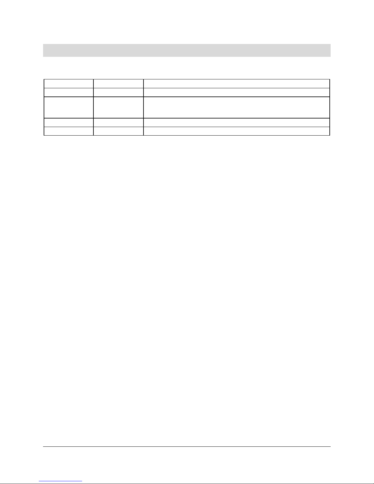
The following figure below shows the functional blocks of the server board and the plug-in
modules that it supports.
Revision 1.2
Intel part number C32194-002
Figure 1. The Board Block Diagram
15
Page 16
Functional Architecture Intel® Server Board SE7505VB2
3. Functional Architecture
This chapter provides a high-level description of the functionality distributed between the
architectural blocks of the Intel
®
Server Board SE7505VB2.
3.1 Processor and Memory Subsystem
The Intel® chipset E7505 provides a 36-bit address, 64-bit data processor host bus interface,
operating at 533 MHz in the AGTL+ signaling environment. The MCH component of the chipset
provides an integrated memory controller, an 8-bit hub interface, and one 16-bit hub interfaces.
The hub interface provides the interface to two 64-bit/100-MHz PCI-X buses and one 64-bit/66MHz PCI bus via the P64H2, and the interface to two 32-bit/33-MHz PCI buses via the ICH4.
The board directly supports up to 8 GB of ECC memory, using four DDR266 compliant ECC
DIMMs. The ECC implementation in the MCH can detect and correct single-bit errors (SBE),
detect multiple-bit errors (MBE), and supports Intel
SDDC) feature with x4 DIMMs.
3.1.1 Processor Support
The Intel Server Board SE7505VB2 supports one or two processors in the 604-pin FCPGA
package. When two processors are installed, all processors must be of identical revision, core
voltage, and bus/core speed. When only one processor is installed, it should be in the socket
labeled CPU1 and the other socket must be empty. The support circuitry on the server board
consists of the following:
®
x4 Single Data Device Correction (Intel x4
Dual 604-pin processor sockets supporting 533MHz FSB Intel Xeon processors.
Processor host bus AGTL+ support circuitry.
Table 1. Processor Support Matrix
Processor Family Package Type Frequency Cache Size Front Side Bus Speed
Intel Xeon FCPGA 3.06GHz 512KB 533
Intel Xeon FCPGA 2.8 GHz 512KB 400 / 533
Intel Xeon FCPGA 2.67 GHz 512KB 400 / 533
Intel Xeon mPGA / FCPGA 2.4 GHz 512KB 400 / 533
Intel Xeon mPGA / FCPGA 2.2 GHz 512KB 400 / 533
Intel Xeon mPGA / FCPGA 2.0GHz 512KB 400 / 533
Intel Xeon mPGA / FCPGA 1.8GHz 512KB 400
Notes:
Processors must be populated in sequential order. Processor socket 1 must be
populated before processor socket 2.
The board is designed to provide up to 65A of current per processor. Processors with
higher current requirements are not supported.
No terminator is required in the second processor socket when using a uni-processor
configuration.
Revision 1.2
16
Intel part number C32194-002
Page 17

Intel® Server Board SE7505VB2 Functional Architecture
In addition to the circuitry described above, the processor subsystem contains the following:
Reset configuration logic
Processor module presence detection logic
Server management registers and sensors
3.1.1.1 Processor VRD
The Intel Server Board SE7505VB2 has a single VRD (Voltage Regulator Down) to support two
processors. It is compliant with the VRM 9.1 specification and provides a maximum of
130 AMPs, which is capable of supporting the requirements for two Intel
®
Xeon™ processors.
The board hardware and PMC (Power Management Controller) must read the processor VID
(voltage identification) bits for each processor before turning on the VRD. If the VIDs of the two
processors are not identical, then the PMC will not turn on the VRD.
3.1.1.2 Reset Configuration Logic
The BIOS determines the processor stepping, cache size, etc through the CPUID instruction.
The requirements are as follows:
All processors in the system must operate at the same frequency, have the same cache
sizes, and same VID. No mixing of product families is supported.
Processors run at a fixed speed and cannot be programmed to operate at a lower or
higher speed.
The processor information is read at every system power-on.
Note: The processor speed is the processor power on reset default value. No manual processor
speed setting options exist either in the form of a BIOS setup option or jumpers.
3.1.1.3 Processor Module Presence Detection
Logic is provided on the baseboard to detect the presence and identity of installed processors.
The PMC checks the logic and will not turn on the system DC power unless the VIDs of both the
processors match in a DP configuration.
3.1.1.4 Interrupts and APIC
Interrupt generation and notification to the processors is done by the APICs in the ICH4 and the
P64H2 using messages on the front side bus.
3.1.2 Memory Subsystem
The baseboard supports up to four DIMM slots for a maximum memory capacity of 8 GB. The
DIMM organization is x72, which includes eight ECC check bits. The memory interface runs at
266MT/s. The memory controller supports memory scrubbing, single-bit error correction and
multiple-bit error detection and Intel x4 SDDC support with x4 DIMMs. Memory can be
implemented with either single sided (one row) or double-sided (two row) DIMMs.
Revision 1.2
Intel part number C32194-002
17
Page 18
Functional Architecture Intel® Server Board SE7505VB2
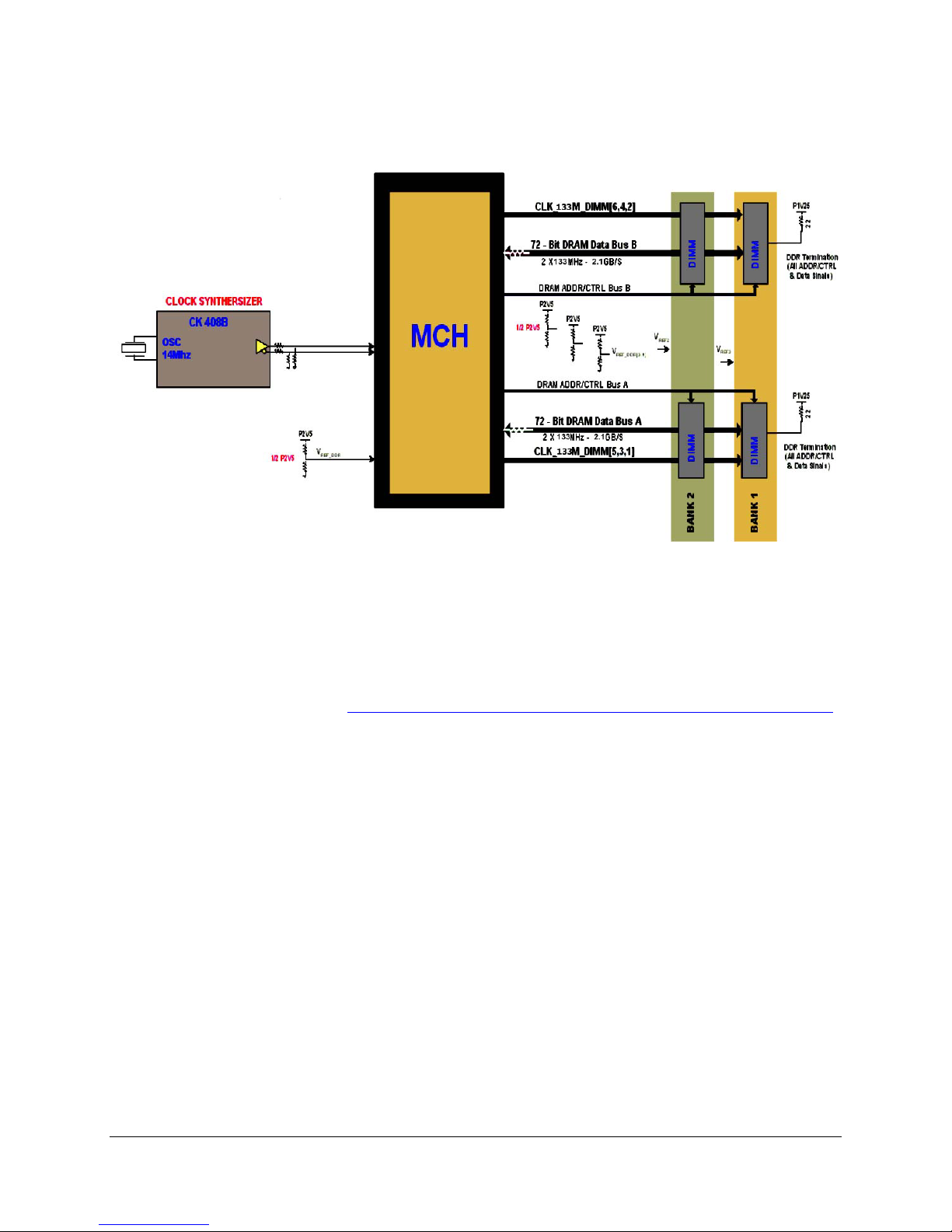
The figure below provides a block diagram of the memory sub-system implemented on the
board.
Figure 2. Memory Sub-system Block Diagram
3.1.2.1 Memory DIMM Support
The board supports DDR266-compliant ECC DIMMS operating at 266MT/s. Only DIMMs tested
and qualified by Intel or a designated memory test vendor are supported on this board. A list of
qualified DIMMs is available at http://support.intel.com/support/motherboards/server/se7505vb2
Note that all DIMMs are supported by design, but only fully qualified DIMMs will be supported on
the board.
The minimum supported DIMM size is 128 MB. Therefore, the minimum main memory
configuration is 1 x 128 MB or 128 MB. The largest size DIMM supported is a 2 GB registered
DDR266 ECC DIMM based on 512 megabit technology. Therefore the maximum main memory
configuration is 4 x 2 GB or 8 GB.
Only registered DDR266 compliant, ECC, DDR memory DIMMs will be supported
ECC single-bit errors (SBE) will be corrected and multiple-bit error (MBE) will be
detected.
Intel server board also supports Intel x4 SDDC with x4 DIMMs.
The maximum memory capacity is 8 GB
The minimum memory capacity is 128 MB
.
Revision 1.2
18
Intel part number C32194-002
Page 19

Intel® Server Board SE7505VB2 Functional Architecture
3.1.2.2 Memory Configuration
The memory interface between the MCH and the DIMMs is 144-bits wide (72-bits for each
bank).
There are two banks of DIMMs, labeled 1 and 2. Bank 1 contains DIMM socket locations 1A and
1B. Bank 2 contains 2A and 2B. The sockets associated with each bank are located next to
each other and the DIMM socket identifiers are marked on the baseboard silkscreen, near the
DIMM socket.
For designs that require a lower price point, a single 128 MB DIMM can be populated in the
DIMM1A socket. When a single DIMM is installed, interleaving and Intel x4 SDDC are not
available. Bank 2 will only operate with two DIMMs installed.
The baseboard’s signal integrity and cooling are optimized when memory banks are populated
in order. Before populating either DIMM socket in bank 2, both DIMMs in bank 1 must be
populated. No empty DIMM sockets are allowed between populated DIMMs.
DIMM and memory configurations must adhere to the following:
DDR266 ECC, registered, DDR DIMM modules
DIMM organization: x72 ECC
Pin count: 184
DIMM capacity: 128 MB, 256 MB, 512 MB, 1 GB, 2GB DIMMs
Serial PD: JEDEC Rev 2.0
Voltage options: 3.3 V (VDD/VDDQ)
Interface: SSTL2
3.1.2.3 Memory Cooling
The SE7505VB2 server board supports DDR memory in a variety of sizes and densities (see
Table 4). Due to the specific orientation of the memory on the SE7505VB2 server board,
certain memory densities and configurations are more difficult to cool in chassis that provide
traditional front to back airflow such as the Intel SC5200 and SC5250-E server chassis. To
ensure the memory used with this board has sufficient thermal margin to operate within
specifications, Intel has designed a memory cooling duct specifically for the SE7505VB2 server
board. Intel’s testing has shown only 2GB and stacked 1GB (low profile) DIMMs are thermally
at risk. If your specific design uses either of these size memory parts, contact Intel Customer
Support and request the SE7505VB2 server board memory cooling duct, part number C28482-
001.
Revision 1.2
Intel part number C32194-002
19
Page 20
Functional Architecture Intel® Server Board SE7505VB2
Table 2. Memory Bank Labels
Memory DIMM Bank
J9H1 (DIMM 1A), J9H2 (DIMM 1B) 1
J9J1 (DIMM 2A), J9J2 (DIMM 2B) 2
J9H1 J9H2 J9J1 J9J2
Revision 1.2
20
1A 2A1B 2B
Bank 2
Figure 3. Memory Bank Label Definition
Intel part number C32194-002
Page 21

Intel® Server Board SE7505VB2 Functional Architecture
2
3.1.2.4 I
2
The I
C bus is used by the system BIOS to retrieve DIMM information needed to program the
C Bus
MCH memory registers, which are required to boot the system.
The following table provides the I
Table 3. I2C Addresses for Memory Module SMB
2
C addresses for each DIMM slot.
Device Address
DIMM 1A 0xA0
DIMM 1B 0xA2
DIMM 2A 0xA4
DIMM 2B 0xA6
3.1.2.5 DRAM ECC
The ECC used for DRAM provides Intel x4 SDDC technology for x4 SDRAMs. DRAMs that are
x8 use the same algorithm but will not have Intel x4 SDDC technology, since at most only four
bits can be corrected with this ECC.
The method provides more ECC bits so each ECC word can correct more than a single-bit
failure. This is possible because different mathematical algorithms provide multiple-bit
correction with the right number of data bits and ECC bits. For example, a 144-bit ECC word
that consists of 128 data bits and 16 ECC bits can be used to correct up to 4 bit errors within
certain bit fields of data. These four bits must be adjacent, not random. Even though the ratio of
the ECC bits to data bits is the same as the previous example (16/128 vs. 8/64), the longer ECC
word allows for a correction and detection algorithm that is more efficient.
3.2 The Intel® E7505 Chipset
The Intel Server Board SE7505VB2 is designed around the Intel E7505 chipset. The chipset
provides an integrated I/O bridge and memory controller, and a flexible I/O subsystem core (PCI
/ PCI-X) . This is targeted for multiprocessor systems and standard high-volume servers. The
chipset consists of three components:
MCH: Memory Control Hub. The MCH accepts access requests from the host
(processor) bus and directs those accesses to memory or to one of the PCI buses. The
MCH monitors the host bus, examining addresses for each request. Accesses may be
directed to a memory request queue for subsequent forwarding to the memory
subsystem, or to an outbound request queue for subsequent forwarding to one of the
PCI buses. The MCH also accepts inbound requests from the P64H2 and the ICH4. The
MCH is responsible for generating the appropriate controls to control data transfer to and
from memory.
P64H2: PCI-X 64bit Hub 2.0 I/O Bridge. The P64H2 provides the interface for two PCI-
X buses capable of 133MHz operation. The P64H2 is both master and target on both
buses.
Revision 1.2
Intel part number C32194-002
21
Page 22

Functional Architecture Intel® Server Board SE7505VB2
ICH4: I/O Controller Hub 4. The ICH4 controller has several components. It provides
the interface for a 32-bit/33-MHz PCI bus. The ICH4 can be both a master and a target
on that PCI bus. The ICH4 also includes a USB 2.0 controller and an IDE controller. The
ICH4 is also responsible for much of the power management functions, with ACPI
control registers built in. The ICH4 also provides a number of GPIO pins and has the
LPC bus to support low speed legacy I/O.
The MCH, P64H2, and ICH4 chips provide the pathway between processor and I/O systems.
The MCH is responsible for accepting access requests from the host (processor) bus, and
directing all I/O accesses to one of the PCI buses or legacy I/O locations. If the cycle is directed
to one of the 64-bit PCI segments, the MCH communicates with the P64H2 through a private
interface called the HI (Hub Interface). If the cycle is directed to the ICH4, the cycle is output
on the MCH’s 8-bit HI 1.5 bus. The P64H2 translates the HI 2.0 bus operation to a 64-bit PCI
signaling environment operating between 133 MHz and 33 MHz.
The HI 2.0 bus is 16 bits wide and operates at 66 MHz with 512MT/s, providing over 1 GB per
second of bandwidth.
All I/O for the board, including PCI and PC-compatible I/O, is directed through the MCH and
then through either the P64H2 or the ICH4 provided PCI buses.
The ICH4 provides one 32-bit/33-MHz PCI bus hereafter called P32-A.
The P64H2 provides one 64-bit/100-MHz PCI-X bus, hereafter called P64-B, and one
64bit/66MHz PCI bus, hereafter called P64-C.
This independent bus structure allows all three PCI buses to operate independently and
concurrently providing additional bandwidth to the system.
3.2.1 MCH Memory Architecture Overview
The MCH supports a 144-bit wide memory sub-system that can support a maximum of 8 GB of
DDR266 memory using 2 GB DIMMs. This configuration needs external registers for buffering
the memory address and control signals. The four chip selects are registered inside the MCH
and need no external registers for chip selects.
The memory interface runs at 266MT/s. The memory interface supports a 72-bit or 144-bit wide
memory array. It uses fifteen address lines (BA [1:0] and MA [12:0]) and supports 64 Mb,
128 Mb, 256 Mb, 512 Mb DRAM densities. The DDR DIMM interface supports memory
scrubbing, single-bit error correction, and multiple bit error detection and Intel x4 SDDC with x4
DIMMs.
Revision 1.2
22
Intel part number C32194-002
Page 23

Intel® Server Board SE7505VB2 Functional Architecture
3.2.1.1 DDR Configurations
The DDR interface supports up to 8 GB of main memory and supports single- and doubledensity DIMMs. The DDR can be any industry-standard DDR. The following table shows the
DDR DIMM technology supported.
Table 4. Supported DDRs
DIMM
Capacity
128MB 16M x 72 128Mbit 16M x 8 9/1/4 12/2/10
256MB 32M x 72 64Mbit 16M x 4 36/2/4 12/2/10
256MB 32M x 72 128Mbit 32M x 4 18/1/4 12/2/11
256MB 32M x 72 128Mbit 16M x 8 18/2/4 12/2/10
256MB 32M x 72 256Mbit 32M x 8 9/1/4 13/2/10
512MB 64M x 72 256Mbit 64M x 4 18/1/4 13/2/11
512MB 64M x 72 256Mbit 32M x 8 18/2/4 13/2/10
512MB 64M x 72 512Mbit 64M x 8 9/1/4 13/2/11
1GB 128M x 72 256Mbit 64M x 4 36/2/4 13/2/11
1GB 128M x 72 512Mbit 64M x 8 18/2/4 13/2/11
1GB 128M x 72 512Mbit 128M x 4 18/1/4 13/2/12
2GB 256M x 72 512Mbit 128M x 4 36/2/4 13/2/12
DIMM
Organization
SDRAM Density
SDRAM
Organization
# SDRAM Devices /
Rows / Banks
# Address Bits
Rows / Banks /
Column
3.2.2 Memory Controller Hub (MCH)
The MCH is a 1005-ball FC-BGA device and uses the proven components of previous
generations like the Intel Xeon processor bus interface unit, the hub interface unit, and the DDR
memory interface unit. In addition, the MCH incorporates a hub interface (HI) . The HI interface
allows the MCH to directly interface with the P64H2. The MCH also increases the main memory
interface bandwidth and maximum memory configuration with a 144-bit wide memory interface.
The MCH integrates the following main functions:
An integrated high performance main memory subsystem.
An HI 2.0 bus which provides an interface to the P64H2
An HI 1.5 bus which provides an interface to the ICH4
AGP pro slot: Video controller with 3D/2D graphics accelerator
Other features provided by the MCH include the following:
Full support of ECC on the processor bus
Full support of Intel x4 SDDC on the memory interface with x4 DIMMs
Twelve deep in-order queue, two deep defer queue
Full support of registered DDR266 ECC DIMMs.
Support for 2 GB DDR memory modules
Memory scrubbing
Revision 1.2
Intel part number C32194-002
23
Page 24

Functional Architecture Intel® Server Board SE7505VB2
3.2.2.1 AGP 8X Bus
The AGP 8X bus features include the following:
Single AGP device
AGP interface asynchronously coupled to core
AGP 3.0 specification compliant
AGP 8X / 4X / 2X at 1.5V
0.8V and 1.5V AGP electrical. No 3.3V support
Isochronous support for AGP 8X, non-snooped
32 deep AGP request queue
32-bit upstream address support for inbound AGP and PCI cycles
32-bit downstream address support for outbound PCI and fast write cycles
3.2.3 P64H2
The P64H2 is a 567-ball FC-BGA device that provides an integrated I/O bridge for a highperformance data flow path between the HI 2.0 bus and the 64-bit I/O subsystem. This
subsystem supports peer 64-bit PCI-X segments. Because it has two PCI interfaces, the P64H2
can provide large and efficient I/O configurations. The P64H2 functions as the bridge between
the HI 2.0 interface and the two 64-bit PCI-X I/O segments. The HI interface can support 1GB/s
of data bandwidth.
3.2.3.1 PCI Bus P64-B I/O Subsystem
P64-B supports two 184-pin, 3.3-volt keyed, 64-bit PCI expansion slot connectors running at
100MHz. Both of the slots support 184-pin, 3.3V keyed, 64-bit PCI-X expansion cards. Both
slots support full-length PCI-X or PCI add-in cards.
The BIOS is responsible for setting the bus speed of P64-B. The bus speed runs at the speed of
the slowest card installed.
3.2.3.2 PCI Bus P64-C I/O Subsystem
P64-C supports the following embedded devices and connectors:
One 184-pin, 3.3-volt keyed, 64-bit PCI expansion slot connector running at 66MHz. This
slot is capable of supporting a full-length add-in PCI card
One integrated Intel
®
82540EM fast Ethernet gigabit (10/100/1000) controller
The BIOS is responsible for setting the bus speed of P64-C. The bus speed runs at the speed
of the slowest card installed.
3.2.4 ICH4
The ICH4 is a multi-function device, housed in a 421-pin BGA device, providing a HI 1.5 to PCI
bridge, a PCI IDE interface, a PCI USB controller, and a power management controller. Each
function within the ICH4 has its own set of configuration registers. Once configured, each
appears to the system as a distinct hardware controller sharing the same PCI bus interface.
Revision 1.2
24
Intel part number C32194-002
Page 25

Intel® Server Board SE7505VB2 Functional Architecture
The primary role of the ICH4 is to provide the gateway to all PC-compatible I/O devices and
features. The board uses the following the ICH4 features:
PCI bus interface
LPC bus interface
IDE interface, with Ultra DMA 100 capability
Universal Serial Bus (USB) 2.0 interface
PC-compatible timer/counter and DMA controllers
APIC and 8259 interrupt controller
Power management
System RTC
General purpose I/O (GPIO)
The following are the descriptions of how each supported feature is used on the board .
3.2.4.1 PCI Bus P32-A I/O Subsystem
The ICH4 provides a legacy 32-bit PCI subsystem and acts as the central resource on this PCI
interface. P32-A supports the following embedded devices and connectors:
An ATI Rage XL video controller with 3D/2D graphics accelerator
Silicon Image 3112A dual channel SATA controller
One Intel
Two expansion slots capable of supporting full length PCI add-in cards operating at 33 MHz
®
82550PM network controller
3.2.4.2 PCI Bus Master IDE Interface
The ICH4 acts as a PCI-based Ultra DMA 100 IDE controller that supports programmed I/O
transfers and bus master IDE transfers. The ICH4 supports two IDE channels, supporting two
drives each (drives 0 and 1). The baseboard provides two 40-pin (2x20) IDE connectors to
access the IDE functionality.
The IDE interface supports Ultra DMA 100 Synchronous DMA Mode transfers on each 40-pin
connector.
3.2.4.3 USB Interface
The ICH4 contains three USB 2.0 controllers and four USB hubs. The USB controller moves
data between main memory and up to six USB connectors. All ports function identically and with
the same bandwidth. The SE7505VB2 server board implements four ports on the board.
The baseboard provides three external USB ports on the back of the server board. The triplestack USB connector is located within the standard ATX I/O panel area next to the keyboard
and mouse housing. The USB specification defines the external connectors.
The fourth USB port is optional and can be accessed by cabling from an internal 9-pin
connector located on the baseboard to an external USB port located either in front or the rear of
a given chassis.
Revision 1.2
Intel part number C32194-002
25
Page 26

Functional Architecture Intel® Server Board SE7505VB2
3.2.4.4 Compatibility Interrupt Control
The ICH4 provides the functionality of two 82C59 PIC devices for ISA-compatible interrupt
handling.
3.2.4.5 APIC
The ICH4 integrates an I/O APIC capability with 24 interrupts.
3.2.4.6 General Purpose Input and Output Pins
The ICH4 provides a number of general purpose input and output pins. Many of these pins have
alternate functions, and thus all are not available. The following table lists the GPI and GPO
pins used on the board and gives a brief description of their function.
Table 5. ICH4 GPIO Usage Table
Pin Name
(Powe Well)
GPI0 / REQA#
(Core)
GPI1 / REQB#
(Core)
GPI2 / PIRQE#
(Core)
GPI3 / PIRQF#
(Core)
GPI4 / PIRQG#
(Core)
GPI5 / PIRQH#
(Core)
GPI6
(Core)
GPI7
(Core)
GPI8
(Resume)
GPI9 ~ GPI10 N/A
GPI11
(Resume)
Used As GPI /
GPO /
Function
BUS P1 Parity
DETECT
(P1_PERR#)
BUS P2/ICH4 Parity
DETECT
(P2_PERR#)
PIRQ_E GPIO:R00h[2]=0 (PIRQ_E)
PIRQ_F GPIO:R00h[3]=0 (PIRQ_F)
PIRQ_G GPIO:R00h[4]=0 (PIRQ_G)
PIRQ_H GPIO:R00h[5]=0 (PIRQ_H)
IDE ATA66/100
Detect (IDES_DET)
IDE ATA66/100
Detect (IDEP_DET)
CPU_HOT# GPI (GPIO:R04h[8] always = 1)
NC GPI GPIO:R00h[11]=1 (GPIO)
GPI GPIO:R00h[0]=1 (GPIO)
GPI GPIO:R00h[1]=1 (GPIO)
GPI (GPIO:R04h[6] always = 1)
GPI (GPIO:R04h[7] always = 1)
Function Select Data. Pin Description
PM:R2Eh[0] 1: Normal
(GPIO:R04h[0] always = 1)
GPIO:R2Ch[0]=1 (Active
Low)
PM:R2Eh[1] 1: Normal
(GPIO:R04h[1] always = 1)
GPIO:R2Ch[1]=1 (Active
Low)
PM:R2Eh[6] 1: ATA33
GPIO:R2Ch[6]=0 (Active
High)
PM:R2Eh[7] 1: ATA33
GPIO:R2Ch[7]=0 (Active
High)
PM:R2Eh[8] 1: Normal
GPIO:R2Ch[8]=1 (Active
Low)
PM:R2Eh[11]
(GPIO:R04h[11] always = 1)
GPIO:R2Ch[11]=0 (Active
High)
0: SMI or SCI or
Wakeup event
0: SMI or SCI or
Wakeup Event
0: ATA66/100
0: ATA66/100
0: SMI or SCI or
Wakeup Event
Revision 1.2
26
Intel part number C32194-002
Page 27

Intel® Server Board SE7505VB2 Functional Architecture
Pin Name
(Powe Well)
GPI12
(Resume)
GPI13
(Resume)
GPI14 ~ GPI15 N/A
GPO16 /
GNTA#
(Core)
GPO17 /
GNTB#
(Core)
GPO18:19
(Core)
GPO20:23
(Core)
GPIO24
(Resume)
GPIO25
(Resume)
GPIO26 N/A
GPIO27
(Resume)
GPIO28
(Resume)
GPIO29:31 N/A
GPIO32 /
USBLED_A#
(Core)
GPIO33 /
USBLED_B#
(Core)
GPIO34 /
USBLED_C#
(Core)
GPIO35 /
USBLED_D#
(Core)
GPIO36 /
USBLED_E#
(Core)
Used As GPI /
GPO /
Function
Overtemperature
shutdown for CPU 1
& 2
GPI (GPIO:R04h[13] always = 1)
N/C GPO GPIO:R00h[16]=1 (GPIO)
N/C GPO GPIO:R00h[17]=1 (GPIO)
N/C GPO GPIO:R18h[18:19] for
N/C GPO (GPIO:R04h[18:23] always =
N/C GPO GPIO:R04h[24] = 0 GPIO:R0Ch[24] TTL Driver Output
CPU1 SKTOCC# GPI GPIO:R04h[25] = 1
NC GPI GPIO:R04h[27] = 1
NC GPI GPIO:R04h[28] = 1
NC GPI GPIO:R30h[0]=1
CPU2_SKTOCC# GPI GPIO:R30h[1]=1
CPU1_604# GPI GPIO:R30h[2]=1
CPU2_604# GPI GPIO:R30h[3]=1
NC GPO GPIO:R30h[4]=1
GPI (GPIO:R04h[12] always = 1)
Function Select Data. Pin Description
PM:R2Eh[12]
GPIO:R2Ch[12]=0 (Active
High)
PM:R2Eh[13] NC
GPIO:R2Ch[13]=1 (Active
Low)
GPIO:R0Ch[16] TTL Driver Output
(GPIO:R04h[16] always = 0)
GPIO:R0Ch[17] TTL Driver Output
(GPIO:R04h[16] always = 0)
GPIO:R0Ch[18:19] TTL Driver Output
Blinking
(GPIO:R04h[18:19] always =
0)
GPIO:R0Ch[18:23] TTL Driver Output
0)
GPIO:R0Ch[25]
GPIO:R0Ch[25]=0(Active
Low)
GPIO:R0Ch[27]
GPIO:R0Ch[27]=0 (Active
Low)
GPIO:R0Ch[28]
GPIO:R0Ch[28]=0 (Active
Low)
GPIO:R38h[0] 0: present
GPIO:R34h[0]=1
GPIO:R38h[1] 0: present
GPIO:R34h[1]=1
GPIO:R38h[2] 0: CPU1 w/604
GPIO:R34h[2]=1
GPIO:R38h[3] 0: CPU2 w/604
GPIO:R34h[3]=1
GPIO:R38h[4] 0:Disabled
GPIO:R34h[4]=0
1: non-present
1: non-present
1: CPU1 w/603
1: CPU2 w/603
1:Enable
Revision 1.2
Intel part number C32194-002
27
Page 28

Functional Architecture Intel® Server Board SE7505VB2
Pin Name
(Powe Well)
GPIO37 /
USBLED_F#
(Core)
GPIO38 /
USBLED_G#
(Core)
GPIO39 /
USBLED_H#
GPIO40 /
USBLED_I#
GPIO41 /
USBLEDJ
GPIO42 /
USBLED_K#
(Core)
GPIO43 /
USBLED_L#
(Core)
Used As GPI /
GPO /
Function
NC GPO GPIO:R30h[5]=1
RASERR# GPI GPIO:R30h[6]=1
PWR_Alert# GPI GPIO:R30h[7]=1b
AGP_PRST#2 (bit2) GPI GPIO:R30h[8]=1b
AGP_PRST#1 (bit1) GPI GPIO:R30h[9]=1b
DIS_NIC1 GPO GPIO:R30h[10]=1b
NC GPO GPIO:R30h[11]=1b
Function Select Data. Pin Description
GPIO:R38h[5] 0:Disabled
GPIO:R34h[5]=0
GPIO:R38h[5] 0: Disabled
GPIO:R34h[6]=1
GPIO:R38h[7]
GPIO:R34h[7]=1b
GPIO:R38h[8]
GPIO:R34h[8]=1b
GPIO:R38h[9]
GPIO:R34h[9]=1b
GPIO:R38h[10] 0: Disabled
GPIO:R34h[10]=0b
GPIO:R38h[11]
GPIO:R34h[11]=0b
1:Enable
1: Enabled
1: Enabled
3.2.4.7 Power Management
One of the embedded functions of the ICH4 is a power management controller. This is used to
implement ACPI-compliant power management features. The baseboard does support sleep
states S0, S1, S4, and S5.
3.3 Super I/O
The Winbond 83627HF sIO device contains all of the necessary circuitry to control two serial
ports, one parallel port, floppy disk, PS/2-compatible keyboard and mouse and hardware
monitor controller. The baseboard implements the following features:
GPIOs
Two serial ports
Floppy
Keyboard and mouse
Local hardware monitoring
Wake up control
Revision 1.2
28
Intel part number C32194-002
Page 29

Intel® Server Board SE7505VB2 Functional Architecture
3.3.1 GPIOs
The sIO provides a number of general-purpose input/output pins that the baseboard utilizes.
The following table identifies the pin and the signal name used in the schematic:
Table 6. Super I/O GPIO Usage Table
Pin
Name
Pin No.
GPIO12
(Pin 126)
GPIO13
(Pin 125)
GPIO15
(Pin 123)
GPIO17
(Pin 121)
GPIO20
(Pin 119)
GPIO25
(Pin 88)
GPIO26
(Pin 87)
GPIO35
(Pin 64)
GPI/GPO
Used as
CLRPAS# GPI
FanSlct1# GPO
FanSlct2# GPO
MAG_jmpr GPI
RECRYMD# GPI
Flash_EN# GPO
Btn_dsabl# GPO
Blink_LED SUSLED
/
Function
Function Select Data Description
CR2A<7>=1 & CR2A<4>=1 & LD7
[F0h]<2>=1
CR2A<7>=1 & CR2A<3>=1 & LD7
[F0h]<3>=0
CR2A<7>=1 & LD7 [F0h]<7>=1 LD7[F1h]<7>
CR2A<0>=1 & LD8[F0h]<0>=1 LD8[F1h]<0>
CR2B<3>=1 & LD8[F0h]<5>=0 LD8[F1h]<5>
CR2B<2>=1 & LD8[F0h]<6>=0 LD8[F1h]<6>
CR29h<7>=0
LD7[F1h]<2>
LD7[F1h]<3>
0: Clear Password
1: Normal
0: Factory mode
1: normal
0: Recovery mode
1:Normal
0: Flash ROM
Write En
1: normal
0: Power button
Disabled
1: normal
3.3.2 Serial Ports
The board provides two serial ports, an external serial port, and an internal serial header. The
following sections provide details on the use of the serial ports.
3.3.2.1 Serial A
Serial A is a standard DB9 interface located at the rear I/O panel of the server board, to the left
of the video connector below the parallel port connector. Serial A is designated by as “Serial A”
on the silkscreen. The reference designator is J8A1.
3.3.2.2 Serial B
Serial B is an optional port, accessed through a 9-pin internal header (J1J2). A standard DH-10
to DB9 cable can be used to direct serial B to an external connector on any given chassis. The
serial B interface follows the standard RS232 pinout. The baseboard has a “Serial B” silkscreen
label next to the connector and is located below the floppy connector.
Revision 1.2
Intel part number C32194-002
29
Page 30

Functional Architecture Intel® Server Board SE7505VB2
3.3.2.3 Floppy Disk Controller
The floppy disk controller (FDC) in the sIO is functionally compatible with floppy disk controllers
in the DP8473 and N844077. All FDC functions are integrated into the sIO including analog data
separator and 16-byte FIFO. The baseboard provides a standard 34-pin interface for the floppy
disk controller.
3.3.2.4 Keyboard and Mouse
Two external PS/2 ports, located on the back of the baseboard, are provided to access the
keyboard or mouse functions. The two ports are interchangeable and will automatically detect
and configure a keyboard or mouse plugged into either port.
3.3.2.5 Wake-up Control
The sIO contains functionality that allows various events to control the power-on and power-off
the system.
3.3.3 BIOS Flash
The board incorporates an Intel® N82802AC (FWH8) flash memory component. The N82802AC
is a high-performance 8-megabit memory component that provides 1024K x 8 of BIOS and nonvolatile storage space. The flash device is connected through the LPC Bus from the ICH4 from
the sIO.
Revision 1.2
30
Intel part number C32194-002
Page 31

Intel® Server Board SE7505VB2 Clock Generation and Distribution
4. Clock Generation and Distribution
All buses on the Intel Server Board SE7505VB2 operate using synchronous clocks. Clock
synthesizer/driver circuitry on the baseboard generates clock frequencies and voltage levels as
required, including the following:
100 MHz at 3.3 V logic levels. For Processor 0, Processor 1, Debug Port and MCH.
66 MHz at 3.3 V logic levels: For MCH, ICH4, AGP, and P64H2
48 MHz at 3.3V logic levels: For ICH4
33 MHz at 3.3V logic levels: For ICH4, PCI Connector, sIO and FWH
14.318 MHz at 2.5 V logic levels: For ICH4 and sIO
The following figure illustrates clock generation and distribution on the board.
Revision 1.2
Intel part number C32194-002
31
Page 32

Clock Generation and Distribution Intel® Server Board SE7505VB2
Figure 4. SE7505VB2 Clock Distribution Diagram
Revision 1.2
32
Intel part number C32194-002
Page 33

Intel® Server Board SE7505VB2 PCI I/O Subsystem
5. PCI I/O Subsystem
5.1 PCI Subsystem
The primary I/O bus for the server board SE7505VB2 is PCI, with three independent PCI bus
segments. The PCI buses comply with the PCI Local Bus Specification, Rev 2.3. The P32-A bus
segment is directed through the ICH4 while the two 64-bit segments, P64-B and P64-C, are
directed through the P64H2 I/O Bridge. The table below lists the characteristics of the three PCI
bus segments.
Table 7. PCI Bus Segment Characteristics
PCI Bus Segment Voltage Width Speed Type PCI I/O Card Slots
P32-A 5 V 32-bits 33 MHz PCI Two slots, support full-length cards
P64-B 3.3 V 64-bits 100 MHz PCI-X Two slots, support full-length cards
P64-C 3.3 V 64-bits 66 MHz PCI One slot, supports full-length cards
5.1.1 P32-A: 32-bit/33-MHz PCI Subsystem
All 32-bit/33-MHz PCI I/O for the board is directed through the ICH4. The 32-bit/33-MHz PCI
segment created by the ICH4 is known as the P32-A segment. The P32-A segment supports
the following embedded devices and connectors:
Serial ATA controller: Silicon Image* 3112A.
One 10/100 Network Interface Controller: Intel 82550PM Fast Ethernet Controller.
2D/3D Graphics Accelerator: ATI Rage XL Video Controller
The Serial ATA controller and the NIC will each be allocated a GPIO to disable the device. The
video controller will be disabled when an off-board video device is detected in either the AGP or
PCI bus segments
5.1.1.1 Device IDs (IDSEL)
Each device under the PCI hub bridge has its IDSEL signal connected to one bit of AD[31:16],
which acts as a chip select on the PCI bus segment in configuration cycles. This determines a
unique PCI device ID value for use in configuration cycles. The following table shows the bit to
which each IDSEL signal is attached for P32-A devices and the corresponding device
description.
Table 8. P32-A Configuration IDs
IDSEL Value Device
16 PCI 33MHz Slot 1
17 PCI 33MHz Slot 2
18 ATI Rage XL Video Controller
19
20 SATA controller Silicon Image 3112A
Intel 82550PM Fast Ethernet Controller (NIC1)
Revision 1.2
Intel part number C32194-002
33
Page 34

PCI I/O Subsystem Intel® Server Board SE7505VB2
5.1.1.2 P32-A Arbitration
P32-A supports six PCI devices: the ICH4 and five PCI bus masters (one NIC, one sATA RAID
controller, two PCI slots and one ATI Rage XL video controller). All PCI masters must arbitrate
for PCI access, using resources supplied by the ICH4. The host bridge PCI interface (ICH4)
arbitration lines REQx* and GNTx* are a special case in that they are internal to the host bridge.
The following table defines the arbitration connections.
Table 9. P32-A Arbitration Connections
Baseboard Signals Device
P32_REQ0*/P32_GNT0* PCI 33MHz Slot 1
P32_REQ1*/P32_GNT1* PCI 33MHz Slot 2
P32_REQ2*/P32_GNT2* ATI Rage XL video controller
P32_REQ3*/P32_GNT3* Intel 82550PM Fast Ethernet Controller (NIC1)
P32_REQ4*/P32_GNT4* Silicon Image Serial ATA Controller
5.1.2 P64-B and P64-C: 64-bit/100- or 66-MHz PCI Subsystem
Two peer 64-bit bus segments are directed through the P64H2 I/O Bridge. The first PCI
segment, P64-B, provides two 3.3V 64-bit PCI-X slots capable of 100 MHz operation and
support full-length PCI cards.
The second PCI segment, P64-C, provides a single 3.3V 64-bit PCI slot operating at 66 MHz.
This segment supports full-length PCI cards. P64-C also has an embedded Intel 82540EM fast
Ethernet gigabit controller.
5.1.2.1 Device IDs (IDSEL)
Each device under the PCI hub bridge has its IDSEL signal connected to one bit of AD[31:16],
which acts as a chip select on the PCI bus segment in configuration cycles. This determines a
unique PCI device ID value for use in configuration cycles. The following table shows the bit to
which each IDSEL signal is attached for P64-B devices and corresponding device description.
Table 10. P64-B Configuration IDs
IDSEL Value Device
17 PCI-X 100MHz Slot 4
18 PCI-X 100MHz Slot 3
Table 11. P64-C Configuration IDs
IDSEL Value Device
17 PCI 66MHz Slot 5
18
Intel 82540EM Fast Ethernet Controller (NIC2)
Revision 1.2
34
Intel part number C32194-002
Page 35

Intel® Server Board SE7505VB2 PCI I/O Subsystem
5.1.2.2 P64-B Arbitration
P64-B supports three PCI masters: two PCI-X slots and the P64H2. All PCI masters must
arbitrate for PCI access using resources supplied by the P64H2. The host bridge PCI interface
(P64H2) arbitration lines REQx* and GNTx* are a special case in that they are internal to the
host bridge. The following table defines the arbitration connections.
Table 12. P64-B Arbitration Connections
Baseboard Signals Device
P64_P_REQ0*/P64_P_GNT0* PCI-X 100MHz Slot 4
P64_P_REQ1*/P64_P_GNT1* PCI-X 100MHz Slot 3
5.1.2.3 P64-C Arbitration
P64-C supports three PCI masters: one PCI slot, Intel 82540EM controller and the P64H2. All
PCI masters must arbitrate for PCI access, using resources supplied by the P64H2. The host
bridge PCI interface (P64H2) arbitration lines REQx* and GNTx* are a special case in that they
are internal to the host bridge. The following table defines the arbitration connections.
Table 13. P64-C Arbitration Connections
Baseboard Signals Device
P64_S_REQ0*/P64_S_GNT0* PCI 66MHz Slot 5
P64_S_REQ1*/P64_S_GNT1* Intel 82540EM Fast Ethenet Controller (NIC 2)
5.2 Serial ATA Controller
The board provides an embedded dual port Serial ATA controller through the use of the Silicon
Image* 3112A ASIC. The Silicon Image 3112A provides a single 32-bit / 33-MHz PCI bus
master interface as a multifunction device, packaged in a 128-pin PQFP. It supports two modes:
base mode and RAID mode.
The Silicon Image 3112A controller supports the following features:
Automatically selects highest available transfer speed for all devices
Supports:
- UDMA up to 150MB/second
- All UDMA and PIO modes
- Up to two SATA devices
- ACPI and ATA/ATAPI6
RAID 0 and 1
On-line mirror rebuilding
RAID set accommodates multiple size HDDs
HDDs function normally when not in RAID sets
Adjustable stripe size for RAID 0
1
1
RAID functionality available under most operating systems. Check the SE7505VB2 support website at
http://support.intel.com/support/motherboards/server/se7505vb2
Revision 1.2
Intel part number C32194-002
for details.
35
Page 36

PCI I/O Subsystem Intel® Server Board SE7505VB2
The baseboard ships with the Silicon Image controller set to Base ATA mode. To switch the
controller to RAID mode, a utility needs to be downloaded from the SE7505VB2 support website
or run from the resource CD. This utility switches the controller from one mode to the other.
Appropriate drivers need to be loaded, depending on the mode the controller is set to.
This method was chosen over a BIOS F2 setup switch to allow the controller settings to be
maintained in the event of a Clear CMOS operation. If the RAID drivers were loaded and a
Clear CMOS operation was executed, but the device was not reset to RAID mode, the operating
system would not load. Refer to the SE7505VB2 support website for details on which operating
systems support RAID mode.
Note: The onboard NICs need to be enabled for the ATA mode/RAID mode utility to properly
program the device. The utility toggles the Sub-System ID (SSID) in the NIC EEPROM between
two different values. The BIOS will load the appropriate Silicon Image Option ROM based on
the SSID that is set in the NIC EEPROM. The NICs need to be enabled for the BIOS to know
which SSID is set and subsequently which option ROM to load.
When in RAID mode, the Silicon Image controller can support the following RAID levels:
Table 14. sATA RAID Level
RAID Level Performance Capacity # of
Drives
RAID 0 (Striping) Highest Number of drives multiplied
by the smallest drive size
RAID 1
(Mirroring)
Normal 50% min 2
2
RAID 0 configurations are primarily used for high performance applications, as it doubles the
sustained transfer rate of its drives. RAID 1 configurations are primarily used for data protection.
RAID 1 creates an identical backup of the primary drive to a secondary drive. Whenever a disk
write is performed, the controller sends data simultaneously to a second drive located on a
different data channel.
5.3 Video Controller
The baseboard provides an ATI Rage XL PCI graphics accelerator, along with 8 MB of video
SDRAM and support circuitry for an embedded SVGA video subsystem. The ATI Rage XL chip
contains a SVGA video controller, clock generator, 2D and 3D engine, and RAMDAC in a 272pin PBGA. One 2Mx32 SDRAM chip provides 8 MB of video memory.
The SVGA subsystem supports a variety of modes, up to 1600 x 1200 resolution in 8/16/24/32
bpp modes under 2D, and up to 1024 x 768 resolution in 8/16/24/32 bpp modes under 3D. It
supports both CRT and LCD monitors with up to 100 Hz vertical refresh rate.
The baseboard provides a standard 15-pin VGA connector at the rear of the system, in the
standard ATX I/O opening area. The video controller disabled by default in BIOS Setup when an
off-board video adapter is detected in either the AGP or PCI slots. Optionally, the video
controller can be set to support dual monitor mode when an off-board AGP adapter is detected.
The onboard controller would act as the primary video controller and the AGP adapter becomes
the secondary adapter under an operating system that supports this functionality.
Revision 1.2
36
Intel part number C32194-002
Page 37

Intel® Server Board SE7505VB2 PCI I/O Subsystem
5.3.1 Video Modes
The ATI Rage XL chip supports all standard IBM VGA modes. The following table shows the
2D/3D modes supported for both CRT and LCD. The table specifies the minimum memory
requirement for various display resolution, refresh rates and color depths.
Table 15. Video Modes
SE7505VB2 2D Video Mode Support 2D Mode Refresh Rate (Hz)
8 bpp 16 bpp 24 bpp 32 bpp
640x480 60, 72, 75, 90, 100 Supported Supported Supported Supported
800x600 60, 70, 75, 90, 100 Supported Supported Supported Supported
1024x768 60, 72, 75, 90, 100 Supported Supported Supported Supported
1280x1024 43, 60 Supported Supported Supported Supported
1280x1024 70, 72 Supported – Supported Supported
1600x1200 60, 66 Supported Supported Supported Supported
1600x1200 76, 85 Supported Supported Supported –
3D Mode Refresh Rate (Hz) SE7505VB2 3D Video Mode Support with Z Buffer Enabled
640x480 60,72,75,90,100 Supported Supported Supported Supported
800x600 60,70,75,90,100 Supported Supported Supported Supported
1024x768 60,72,75,90,100 Supported Supported Supported Supported
1280x1024 43,60,70,72 Supported Supported – –
1600x1200 60,66,76,85 Supported – – –
3D Mode Refresh Rate (Hz) SE7505VB2 3D Video Mode Support with Z Buffer Disabled
640x480 60,72,75,90,100 Supported Supported Supported Supported
800x600 60,70,75,90,100 Supported Supported Supported Supported
1024x768 60,72,75,90,100 Supported Supported Supported Supported
1280x1024 43,60,70,72 Supported Supported Supported –
1600x1200 60,66,76,85 Supported Supported – –
5.3.2 Video Memory Interface
The memory controller subsystem of the ATI Rage XL arbitrates requests from direct memory
interface, the VGA graphics controller, the drawing coprocessor, the display controller, the video
scalar, and hardware cursor. Requests are serviced in a way that ensures display integrity and
maximum CPU/coprocessor drawing performance.
The board supports an 8 MB (512Kx32bitx4 Banks) SDRAM device for video memory.
Revision 1.2
Intel part number C32194-002
37
Page 38

PCI I/O Subsystem Intel® Server Board SE7505VB2
K
A
5.3.3 Host Bus Interface
The ATI Rage XL supports a PCI 33 MHz bus. The following diagram shows the signals for the
PCI interface:
PCICL
D[31..0] AD[31..0]
C/BE#[3..0] C/BE[3..0]
PAR PAR
FRAME# FRAME#
IRDY# IRDY#
IDSEL IDSEL
PCIRST# RESET#
TRDY# TRDY#
STOP# STOP#
INTR# INTR#
DEVSEL# DEVSEL#
REQ# REQ#
GNT# GNT#
CPUCLK
Revision 1.2
38
Figure 5. Video Controller PCI Bus Interface
Intel part number C32194-002
Page 39

Intel® Server Board SE7505VB2 PCI I/O Subsystem
5.4 Network Interface Controller (NIC)
The server board SE7505VB2 supports one 10Base-T/100Base-TX network interface controller
(NIC) based on the Intel 82550PM controller (NIC 1) and one gigabit network interface controller
based on the Intel 82540EM controller (NIC 2).
The 82550PM is a highly integrated PCI LAN controller in a thin BGA 15 mm
controller’s baseline functionality is equivalent to that of the Intel 82559 with the addition of
Alert-on-LAN functionality. The 82550PM supports the following features:
Glueless 32-bit PCI, CardBus master interface (Direct Drive of Bus), compatible with PCI
local Bus Specification, Revision 2.2.
Integrated IEEE 802.3 10Base-T and 100Base-TX compatible PHY
IEEE 820.3u auto-negotiation support
Full duplex support at both 10 Mbps and 100 Mbps operation
Integrated UNDI ROM support
MDI/MDI-X and HWI support
Low power +3.3 V device
2
package. The
The 82540EM is a single, compact component with integrated gigabit Ethernet MAC and PHY
layer functions and is packaged in a 15mm
2
TFBGA. The baseboard supports independent
disabling of the two NIC controllers using the BIOS setup menu. The 82540EM supports the
following features:
Support for the 33/66MHz bus segment
Integrated 10/100/1000 Mb/s full and half duplex operation
SMBUS. ASF 1.0, ACPI, WoL and PXE management functions
Compliant w/ PCI Power Management v1.1 and ACPI v2.0
5.4.1 NIC Connector and Status LEDs
The NICs drive two LEDs located on each network interface connector.
For the NIC 1 connector, the green LED indicates network connection when on, and
Transmit/Receive activity when blinking. The green LED indicates 100-Mbps operation when lit,
and 10-Mbps when off.
For the NIC 2 connector, the amber LED indicates network connection when on, and
Transmit/Receive activity when blinking. The green LED indicates 1000-Mbps operation when
lit, the orange LED indicates 100-Mbps operation when lit and 10-Mbps when off.
Revision 1.2
Intel part number C32194-002
39
Page 40

PCI I/O Subsystem Intel® Server Board SE7505VB2
5.5 Interrupt Routing
The board interrupt architecture accommodates both PC-compatible PIC mode and APIC mode
interrupts through use of the integrated I/O APICs in the ICH4.
5.5.1 Legacy Interrupt Routing
For PC-compatible mode, the ICH4 provides two 82C59-compatible interrupt controllers. The
two controllers are cascaded with interrupt levels 8-15 entering on level 2 of the primary
interrupt controller (standard PC configuration). A single interrupt signal is presented to the
processors, to which only one processor will respond for servicing. The ICH4 contains
configuration registers that define which interrupt source logically maps to I/O APIC INTx pins.
The ICH4 handles both PCI and IRQ interrupts. The ICH4 translates these to the APIC bus. The
numbers in the table below indicate the ICH4 PCI interrupt input pin to which the associated
device interrupt (INTA, INTB, INTC, INTD) is connected. The ICH4 I/O APIC exists on the I/O
APIC bus with the processors.
Table 16. PCI Interrupt Routing/Sharing
Interrupt INT A INT B INT C INT D
AGPA# ICH4_PIRQA#
AGPB# ICH4_PIRQB#
VGA# ICH4_PIRQB#
sATA# ICH4_PIRQD#
NIC1# ICH4-PIRQC#
NIC2# P1-IRQ4#
P64H2-A# [P1/P2] ICH4_PIRQE#
P64-C Slot 5 P1_IRQ0# P1_IRQ1# P1_IRQ2# P1_IRQ3#
P64-B Slot 4 P2_IRQ0# P2_IRQ1# P2_IRQ2# P2_IRQ3#
P64-B Slot 3 P2_IRQ4# P2_IRQ5# P2_IRQ6# P2_IRQ7#
P32-A Slot 2 ICH4_PIRQG# ICH4_PIRQF# ICH4_PIRQE# ICH4_PIRQH#
P32-A Slot 1 ICH4_PIRQF# ICH4_PIRQG# ICH4_PIRQH# ICH4_PIRQE#
5.5.2 APIC Interrupt Routing
For APIC mode, the baseboard interrupt architecture incorporates three Intel® I/O APIC devices
to manage and broadcast interrupts to local APICs in each processor. The Intel I/O APICs
monitor each interrupt on each PCI device, including PCI slots in addition to the ISA
compatibility interrupts IRQ(0-15).
When an interrupt occurs, a message corresponding to the interrupt is sent across a three-wire
serial interface to the local APICs. The APIC bus minimizes interrupt latency time for
compatibility interrupt sources. The I/O APICs can also supply greater than 16 interrupt levels to
the processor(s). This APIC bus consists of an APIC clock and two bidirectional data lines.
Revision 1.2
40
Intel part number C32194-002
Page 41

Intel® Server Board SE7505VB2 PCI I/O Subsystem
5.5.2.1 Legacy Interrupt Sources
The table below recommends the logical interrupt mapping of interrupt sources on the board.
The actual interrupt map is defined using configuration registers in the ICH4.
Table 17. Interrupt Definitions
ISA Interrupt Description
INTR Processor interrupt.
NMI NMI to processor.
IRQ0 System timer
IRQ1 Keyboard interrupt.
IRQ2 Slave PIC
IRQ3 Serial port 1 or 2 interrupt from SIO device, user-configurable.
IRQ4 Serial port 1 or 2 interrupt from SIO device, user-configurable.
IRQ5 Parallel Port / Generic
IRQ6 Floppy disk.
IRQ7 Parallel Port / Generic
IRQ8_L Active low RTC interrupt.
IRQ9 SCI*
IRQ10 Generic
IRQ11 Generic
IRQ12 Mouse interrupt.
IRQ13 Floaty processor.
IRQ14 Compatibility IDE interrupt from primary channel IDE devices 0 and 1.
IRQ15 Secondary IDE Cable
SMI* System Management Interrupt. General purpose indicator sourced by the ICH4 to the processors.
5.5.3 Serialized IRQ Support
The SE7505VB2 server board supports a serialized interrupt delivery mechanism. Serialized
Interrupt Requests (SERIRQ) consists of a start frame, a minimum of 17 IRQ / data channels,
and a stop frame. Any slave device in the quiet mode may initiate the start frame. While in the
continuous mode, the start frame is initiated by the host controller.
5.5.4 IRQ Scan for PCIIRQ
The IRQ / data frame structure includes the ability to handle up to 32 sampling channels with
the standard implementation using the minimum 17 sampling channels. The board has an
external PCI interrupt serializer for PCIIRQ scan mechanism of ICH4 to support 16 PCIIRQs.
5.6 PCI Error Handling
The PCI bus defines two error pins, PERR# and SERR#, for reporting PCI parity errors and
system errors, respectively. In the case of PERR#, the PCI bus master has the option to retry
the offending transaction, or to report it using SERR#. All other PCI-related errors are reported
by SERR#. SERR# is routed to NMI if enabled by BIOS.
Revision 1.2
Intel part number C32194-002
41
Page 42

PCI I/O Subsystem Intel® Server Board SE7505VB2
IRQ0
IRQ1
IRQ2
IRQ3
IRQ4
IRQ5
IRQ6
IRQ7
IRQ8
IRQ9
IRQ10
IRQ11
IRQ12
IRQ13
IRQ14
IRQ15
IRQ16
IRQ17
IRQ18
IRQ19
IRQ20
IRQ21
IRQ22
IRQ23
IRQ0
IRQ1
IRQ2
IRQ3
IRQ4
IRQ5
IRQ6
IRQ7
IRQ8
IRQ9
IRQ10
IRQ11
IRQ12
IRQ13
IRQ14
IRQ15
IRQ16
IRQ17
IRQ18
IRQ19
IRQ20
IRQ21
IRQ22
IRQ23
ICH4
HI2.0 INTERFACE
P64H2
IOAPIC 1
ICH4 IOAPIC 0
HI1.5 INTERFACE
ICH4
8259PIC
INTR
CPU1
MCH
IRQ0
IRQ1
IRQ2
IRQ3
IRQ4
IRQ5
IRQ6
IRQ7
IRQ8
IRQ9
IRQ10
IRQ11
IRQ12
IRQ13
IRQ14
IRQ15
IRQ16
IRQ17
IRQ18
IRQ19
IRQ20
IRQ21
IRQ22
IRQ23
P64H2
IOAPIC 2
HI2.0 INTERFACE
Hub-Link B
INTR
CPU2
Figure 6. Interrupt Routing Diagram (ICH4 Internal)
Revision 1.2
42
Intel part number C32194-002
Page 43

Intel® Server Board SE7505VB2 PCI I/O Subsystem
y
ppy
p
Q
Timer
Ke
board
Cascade
Serial Port2/ISA
Serial Port1/ISA
ISA
Flo
/ISA
ISA
RTC
SCI/ISA
ISA
ISA
Mouse/ISA
Co
rocessor Error
P IDE/ISA
Not Used
Super I/O
NIC1#
P64H2-A# [P1/P2]
Serialized IRQ Interface
SERIR
SERIRQ
ICH4 Interrupt Routing
PIRQA#
PIRQB#
PIRQC#
PIRQD#
PIRQE#
PIRQF#
Slot 1 C / Slot 2 D
PIRQG#
PIRQH#
Figure 7. Interrupt Routing Diagram
Revision 1.2
43
Intel part number C32194-002
Page 44

PCI I/O Subsystem Intel® Server Board SE7505VB2
SLOT #1
SLOT #2
SLOT #3
SLOT #4
SLOT #5
INT A
INT B
INT C
INT D
ICH4
PIRQD#
PIRQC#
ICH4
ICH4
PIRQG#
ICH4
PIRQE#
ICH4
PIRQH#
P64H2-A#
[P1/P2]
Note: P1 is P64H2 PCI-bus B, P2 is P64H2 PCI-bus C
ICH4
PIRQF#
P2-IRQ4
P2-IRQ5
P2-IRQ6
P2-IRQ7
ICH4
PIRQB#
VGA#
P2-IRQ0
P2-IRQ1
P2-IRQ2
P2-IRQ3
ICH4
PIRQA#
AGPA# NIC1# sATA# AGPB#
P1-IRQ0
P1-IRQ1
P1-IRQ2
P1-IRQ3
P1-IRQ4
NIC2#
Figure 8. The Board PCI Interrupt Mapping Diagram
Revision 1.2
44
Intel part number C32194-002
Page 45

Intel® Server Board SE7505VB2 Hardware Monitoring
6. Hardware Monitoring
6.1 Monitored Components
The Intel Server Board SE7505VB2 has an integrated Winbond* Heceta chip that is responsible
for hardware monitoring. The Winbond Heceta chip provides basic server hardware monitoring
which alerts a system administrator if a hardware problem occurs on the board. The retail boxed
board ships with a copy of LANDesk* Client Manager, which can monitor the management bus
for these alerts and help administrators identify a problem on the board. Below is a table of
monitored headers and sensors on the board.
Table 18. Monitored Components
Item Description
Voltage Vcpu Monitors processor voltage (sIO)
1.8V Monitors +1.8V (sIO)
3.3V Monitors +3.3V (sIO)
5V Monitors 5VSB (Internal) (sIO)
SB3V Monitors +12Vin (sIO)
ENG12V Monitors –12Vin (should be same as 12V @ Power-Supply) (sIO)
2.5V Monitors –5V (sIO)
Vbat Monitors battery voltage (sIO)
SB5V Monitors 5VSB (sIO)
Fan Speed PWM1 Controls system fans (sIO)
CPU fans (invariable speed) (sIO)
TACH1 Monitors system fan 1 (front) (sIO)
TACH2 Monitors system fan 2 (front) (sIO)
TACH3 Monitors system fan 4 (rear) (sIO)
TACH4 Monitors system fan 3 (rear) (sIO)
TACH5 Monitors CPU fan 2 (sIO)
TACH6 Monitors CPU fan 1 (sIO)
Temperature CPU0 Monitors primary processor temperature (sIO)
CPU1 Monitors secondary processor temperature (sIO)
Ambient Monitors Ambient temperature (sIO)
The LANDesk Client Manager software and a white paper that provides more information on
using LDCM are available on the Intel
Revision 1.2
Intel part number C32194-002
Server Board SE7505VB2 Resource CD.
45
Page 46

Hardware Monitoring Intel® Server Board SE7505VB2
6.2 Fan Speed Control
The Winbond W83627HF can be used to monitor several critical hardware parameters of the
system, including power supply voltages, fan speeds, and temperatures. Fan speed control is to
use the Pulse Width Modulation (PWM) technical knowledge to control the Fan's RPM.
The following shows the temperature range vs. output voltage for controlling the speed of all
system fans.
Temperature Range Output Voltage
Temperature >= 37°C
33°C <= temperature < 37°C
30°C <= temperature < 33°C
Temperature < 30°C
The following is to setup fan count limit for rear and front system fans and CPU fans.
12V
10.5V
7.5V
6.2V
Voltage Duty
Cycle
6.2V 26h 1750 RPM 1222 RPM 8Ah
7.5V 27h 2300 RPM 1607 RPM 69h
10.5V 2Ah 3250 RPM 2250 RPM 4Bh
12.0V 2Fh 3700 RPM 2556 RPM 42h
Rear System Fan
(Delta 8012)
Rear System Fan Limit
(~70%)
Rear System Fan
Count Limit
Voltage Duty
Cycle
6.2V 26h 2650 RPM 1854 RPM 5Bh
7.5V 27h 3100 RPM 2163 RPM 4Eh
10.5V 2Ah 4000 RPM 2766 RPM 3Dh
12.0V 2Fh 4300 RPM 2960 RPM 39h
Front System Fan
(NMB)
Front System Fan Limit
(~70%)
Front System Fan
Count Limit
CPU Fan Speed Limit CPU Fan Count Limit
2766 RPM 3Dh
6.3 Chassis Intrusion
The SE7505VB2 server board supports a chassis security feature that detects if the chassis
cover is removed. For the chassis intrusion circuit to function, the chassis’ power supply must
be connected to AC power. The security feature uses a mechanical switch on the chassis that
attaches to the chassis intrusion connector. When the chassis cover is removed the mechanical
switch is in the closed position.
Revision 1.2
46
Intel part number C32194-002
Page 47

Intel® Server Board SE7505VB2 Hardware Monitoring
Below is a diagram explaining what the Winbond W83627HF controller monitors on the
baseboard and how the monitoring is accomplished.
Ambient Temperature
CPU1
VTIN1
VTIN2 Temperature Sensor 2 High Byte (Index 50h, Bank 1)
CPU2
VTIN3 Temperature Sensor 3 High Byte (Index 50h, Bank 2)
Vcpu
VCOREA (Index 20h)
+1.8V
VCOREB (Index 21h)
+3.3V
V3.3 (Index 22h)
+5V
AVCC
SB3V
+12VIN (Index 24h)
ENG12V
-12VIN (Index 25h)
+2.5V
-5VIN (Index 26h)
Battery
Vbat
SB5V
5VSB
System fans (J5K2, J5K3,
J8A2, J5A2)
PWM1
W83627HF
NC
PWM2
ICH4
Sys fan 1 (J5K3)
Sys fan 2 (J5K2)
Sys fan 4 (J5A2)
Sys fan 3 (J8A2)
CPU fan 2 (J8A3)
CPU fan 1 (J7B1)
Revision 1.2
Intel part number C32194-002
TACH1
TACH2
TACH3
TACH4
TACH5
TACH6
Figure 9. Hardware Monitoring
47
Page 48

SE7505VB2 ACPI Implementation Intel® Server Board SE7505VB2
7. SE7505VB2 ACPI Implementation
7.1 ACPI
An ACPI-aware operating system generates an SMI to request that the system be switched into
ACPI mode. The BIOS responds to enable ACPI mode. The system automatically returns to
legacy mode upon hard reset or power-on reset.
The SE7505VB2 platform supports S0, S1, S4, and S5 states. When the system is operating in
ACPI mode, the OS retains control of the system and OS policy determines the entry methods
and wake up sources for each sleep state
Note: Sleep entry and wake up event capabilities are provided by the hardware but are enabled
by the operating system.
S0 Sleep State
S1 Sleep State
S4 Sleep State
S5 Sleep State
The S0 sleep state is when everything is on. This is the state that no sleep is
enabled.
The S1 sleep state is a low wake-up latency sleep state. In this state, no
system context is lost (Processor or chipset). The system context is
maintained by the hardware.
The S4 Non-Volatile Sleep state (NVS) is a special global system state that
allows system context to be saved and restored (relatively slowly) when
power is lost to the baseboard. If the system has been commanded to enter
the S4 sleep state, the operating system will write the system context to a
non-volatile storage file and leave appropriate context markers.
The S5 sleep state is similar to the S4 sleep state except the operating
system does not save any context nor enable any devices to wake the
system. The system is in the “soft” off state and requires a complete boot
when awakened.
7.1.1 Front Panel Switches
The baseboard supports two front panel buttons:
Power button
Reset button
Revision 1.2
48
Intel part number C32194-002
Page 49

Intel® Server Board SE7505VB2 SE7505VB2 ACPI Implementation
The power button input (SW2#) provides PWRBTN_IN signal to the sIO. The power button input
behaves differently depending on whether or not the operating system supports ACPI.
Power Button Off to On:
The sIO may be configured to generate wakeup events for several
different system events: Wake on LAN*, PCI Power Management
Interrupt, and Real Time Clock Alarm are examples of these
events. Since the processors are not executing, the BIOS does not
participate in this sequence. The sIO provides ONSTL# signal to
the power supply. The ICH4 and receive power good and reset and
then transition to an ON state.
Power Button On to Off
(Legacy):
The ICH4 is configured to generate an SMI due to a power button
event. The BIOS services this SMI and sets the state of the
machine in the ICH4 and sIO to the OFF state.
Power Button On to Off
(ACPI):
If an ACPI operating system is loaded, the power button switch
generates a request (via SCI) to the OS to shutdown the system.
The OS retains control of the system and determines what sleep
state (if any) the system transitions to.
Reset Button:
NMI Button:
The reset button will generate a hard reset to the system.
The NMI button will force an NMI to the processors.
7.1.2 Wake up Sources (ACPI and Legacy)
The baseboard is capable of wake up from several sources under a non-ACPI configuration,
such as when the operating system does not support ACPI. The wake up sources are defined in
the following table.
Table 19. Supported Wake Events
Wake Event Supported via ACPI
(by sleep state)
Power Button Always wakes system Always wakes system
Ring indicate from serial1 S1, S4, S5 S5
Ring indicate from serial2 S1, S4, S5 S5
PME from PCI 32/33 S1, S4, S5 S5
PME from PCI secondary 64/100 S1, S4, S5 S5
PME from primary PCI 64/66 S1, S4, S5 S5
RTC Alarm S1, S4 No
Mouse S1 No
Keyboard S1 No
USB S1 No
Supported Via Legacy Wake
Under ACPI, the operating system programs the ICH4 and sIO to wake up on the desired event,
but in legacy mode, the BIOS enables/disables wake up sources based on an option in BIOS
Setup. The operating system or a driver must clear any pending wake up status bits in the
associated hardware (such as the Wake on LAN status bit in the LAN application specific
integrated circuit (ASIC), or PCI Power Management Event (PME) status bit in a PCI device.
The legacy wake up feature is disabled by default.
Revision 1.2
Intel part number C32194-002
49
Page 50

SE7505VB2 Connectors Intel® Server Board SE7505VB2
8. SE7505VB2 Connectors
8.1 Main Power Connector
The main power supply connection is obtained using the 24-pin connector. The following table
defines the pin-outs of the connector.
Table 20. Power Connector Pin-out (J9B1)
Color Signal Pin Pin Signal Color
Orange 3.3V 13 1 3.3V Orange
Blue -12V 14 2 3.3V Orange
Black GND 15 3 GND Black
Green DC_ON# 16 4 +5V Red
Black GND 17 5 GND Black
Black GND 18 6 +5V Red
Black GND 19 7 GND Black
White 20 8 PS_GOOD Gray
Red +5V 21 9 SB5V Purple
Red +5V 22 10 +12V Yellow
Red +5V 23 11 +12V Yellow
Black GND 24 12 3.3V Orange
Table 21. Auxiliary Signal Connector (J7K1)
Pin Signal Color
1 SCL Green
2 SDA Yellow
3 PWR_Alert# Red
4 GNDsens Black
5 3.3Vsens Orange
Table 22. Auxiliary CPU Power Connector Pin-out (J9K1)
Signal Pin Pin Signal
+12ENG 5 1 GND
+12ENG 6 2 GND
+12ENG 7 3 GND
+12ENG 8 4 GND
Revision 1.2
50
Intel part number C32194-002
Page 51

Intel® Server Board SE7505VB2 SE7505VB2 Connectors
8.2 Memory Module Connector
The board has four DDR266 DIMM connectors and supports registered ECC DDR modules
(Rev 1.0).
Table 23. DIMM Connectors (J9H1, J9J1, J9H2, J9J2)
Pin Front Front Pin Front Pin Back Pin Pin Back
1 VREF 32 62 VDDQ 93 VSS 124 VSS /RAS
2 DQ0 33 DQ24 /WE 94 DQ4 125 A6 155
3 VSS 34 VSS 64 95 DQ5 126 DQ28 156 VDDQ
4 DQ1 35 DQ25 65 /CAS VDDQ 127 DQ29 157 /CS0
DQS0 36 DQS3 66 VSS 97 128 VDDQ 158 */CS1
5 DM0
6 37 A4 67 DQS5 98 DQ6 DM3 159 DM5
DQ2 129
7 VDD VDD 68 DQ42 99 DQ7 130 160 VSS
8 DQ3 39 69 DQ43 100 VSS 131 DQ30 DQ46
9 NC 40 DQ27 VDD 101 NC 132 VSS 162
10 /RESET 41 A2 71 102 NC 133 DQ31 163 */CS3
11 VSS 42 VSS 72 DQ48 *A13 134 CB4 164 VDDQ
DQ8 43 A1 73 DQ49 104 135 CB5 165 DQ52
12 VDDQ
13 44 CB0 74 VSS 105 DQ12 VDDQ 166 DQ53
DQ9 136
14 DQS1 CB1 75 */CK2 106 DQ13 137 167 NC
15 VDDQ 46
16 *CK1 47 DQS8 VDDQ 108 VDD 139 VSS 169 DM6
17 48 A0 78 DQS6 109 DQ14 140 DM8 170
*/CK1 DQ54
18 VSS 49 CB2 79 DQ50 110 DQ15 A10 171 DQ55
19 DQ10 50 VSS 80 111 *CKE1 142 CB6 172 VDDQ
20 DQ11 CB3 81 VSS 112 VDDQ 143 VDDQ 173 NC
21 CKE0 52 BA1 82 VDDID 113 *BA2 144 174 DQ60
22 VDDQ KEY 83 DQ56 114 KEY 175 DQ61
23 DQ16 53 DQ32 84 115 A12 145 VSS 176 VSS
24 DQ17 VDDQ 85 VDD 116 VSS 146 DQ36 177 DM7
25 DQS2 55 DQ33 86 DQS7 117 DQ21 147 178 DQ62
26 VSS 56 DQS4 87 DQ58 A11 148 VDD 179 DQ63
27 A9 57 88 DQ59 119 DM2
28 DQ18 58 VSS 89 VSS 120 VDD 150 DQ38 181 SA0
29 A7 59 BA0 90 NC 121 DQ22 151 DQ39 182 SA1
30 VDDQ 60 DQ35 91 SDA 122 A8 152 VSS 183 SA2
31 DQ19 61 DQ40 92 SCL 123 DQ23 153 DQ44 184 VDDSPD
Note:
* These pins are not used in this module.
Pin Back
A5 154
63 DQ45
DQ41
96
38 A3
DQ26 161
70 DQ47
*/CS2
103
45 CK0
VDD 76 *CK2 107 DM1 138 /CK0 168 VDD
77
141
DQ51
51
CB7
DQ20
DQ57
54
DQ37
118
DQ34 149 DM4 180 VDDQ
Revision 1.2
Intel part number C32194-002
51
Page 52

SE7505VB2 Connectors Intel® Server Board SE7505VB2
8.3 Processor Socket
The board has two Socket 604 processor sockets. The following table provides the processor
socket pin numbers and pin names:
Table 24. Socket 604 Processor Socket Pin-out (U8C1, U5C1)
Pin No Pin Name Pin No Pin Name Pin No Pin Name Pin No Pin Name Pin No Pin Name
A1 Reserved D29 VCC K3 VCC T29 VSS
A2 VCC D30 VSS K4 VSS T30 VCC AB4 VCCA
A3 SKTOCC# D31 VCC K5 VCC T31 VSS AB5 VSS
A4 Reserved E1 VSS K6 VSS U1 VCC AB6 D63#
A5 VSS E2 VCC K7 VCC U2 VSS AB7 PWRGOOD
A6 A32# E3 VID1 K8 VSS U3 VCC AB8 VCC
A7 A33# E4 BPM5# K9 VCC U4 VSS AB9 DBI3#
A8 VCC E5 IERR# K23 VCC U5 VCC AB10 D55#
A9 A26# E6 VCC K24 VSS U6 VSS AB11 VSS
A10 A20# E7 BPM2# K25 VCC U7 VCC AB12 D51#
A11 VSS E8 BPM4# K26 VSS U8 VSS AB13 D52#
A12 A14# E9 VSS K27 VCC U9 VCC AB14 VCC
A13 A10# E10 AP0# K28 VSS U23 VCC AB15 D37#
A14 VCC E11
A15 Reserved E12 VCC K30 VSS U25 VCC AB17 D31#
A16 Reserved E13 A28# K31 VCC U26 VSS AB18 VCC
A17 LOCK# E14 A24# L1 VSS U27 VCC AB19 D14#
A18 VCC E15 VSS L2 VCC U28 VSS AB20 D12#
A19 A7# E16 COMP1 L3 VSS U29 VCC AB21 VSS
A20 A4# E17 VSS L4 VCC U30 VSS AB22 D13#
A21 VSS E18 DRDY# L5 VSS U31 VCC AB23 D9#
A22 A3# E19 TRDY# L6 VCC V1 VSS AB24 VCC
A23 HITM# E20 VCC L7 VSS V2 VCC AB25 D8#
A24 VCC E21 RS0# L8 VCC V3 VSS AB26 D7#
A25 TMS E22 HIT# L9 VSS V4 VCC AB27 VSS
A26 Reserved E23 VSS L23 VSS V5 VSS AB28 SM_EP_A2
A27 VSS E24 TCK L24 VCC V6 VCC AB29 SM_EP_A1
A28 VCC E25 TDO L25 VSS V7 VSS AB30 VCC
A29 VSS E26 VCC L26 VCC V8 VCC AB31 VSS
A30 VCC E27 FERR# L27 VSS V9 VSS AC1 Reserved
A31 VSS E28 VCC L28 VCC V23 VSS AC2 VSS
B1 Reserved E29 VSS L29 VSS V24 VCC AC3 VCC
B2 VSS E30 VCC L30 VCC V25 VSS AC4 VCC
B3 VID4 E31 VSS L31 VSS V26 VCC AC5 D60#
B4 VCC F1 VCC M1 VCC V27 VSS AC6 D59#
B5 OTDEN F2 VSS M2 VSS V28 VCC AC7 VSS
B6 VCC F3 VID0 M3 VCC V29 VSS AC8 D56#
B7 A31# F4 VCC M4 VSS V30 VCC AC9 D47#
B8 A27# F5 BPM3# M5 VCC V31 VSS AC10 VCC
BR2# 1
K29 VCC U24 VSS AB16 D32#
AB3 2
BSEL1
Revision 1.2
52
Intel part number C32194-002
Page 53

Intel® Server Board SE7505VB2 SE7505VB2 Connectors
Pin No Pin Name Pin No Pin Name Pin No Pin Name Pin No Pin Name Pin No Pin Name
B9 VSS F6 BPM0# M6 VSS W1 VCC AC11 D43#
B10 A21# F7 VSS M7 VCC W2 VSS AC12 D41#
B11 A22# F8 BPM1# M8 VSS W3 Reserved AC13 VSS
B12 VCC F9 GTLREF M9 VCC W4 VSS AC14 D50#
B13 A13# F10 VCC M23 VCC W5 BCLK1 AC15 DP2#
B14 A12# F11 BINIT# M24 VSS W6 TESTHI0 AC16 VCC
B15 VSS F12 BR1# M25 VCC W7 TESTHI1 AC17 D34#
B16 A11# F13 VSS M26 VSS W8 TESTHI2 AC18 DP0#
B17 VSS F14 ADSTB1# M27 VCC W9 GTLREF AC19 VSS
B18 A5# F15 A19# M28 VSS W23 GTLREF AC20 D25#
B19 REQ0# F16 VCC M29 VCC W24 VSS AC21 D26#
B20 VCC F17 ADSTB0# M30 VSS W25 VCC AC22 VCC
B21 REQ1# F18 DBSY# M31 VCC W26 VSS AC23 D23#
B22 REQ4# F19 VSS N1 VCC W27 VCC AC24 D20#
B23 VSS F20 BNR# N2 VSS W28 VSS AC25 VSS
B24 LINT0 F21 RS2# N3 VCC W29 VCC AC26 D17#
B25 PROCHOT# F22 VCC N4 VSS W30 VSS AC27 DBI0#
B26 VCC F23 GTLREF N5 VCC W31 VCC AC28 SM_CLK
B27 VCCSENSE F24 TRST# N6 VSS Y1 VSS AC29 SM_DAT
B28 VSS F25 VSS N7 VCC Y2 VCC AC30 VSS
B29 VCC F26 THERMTRIP# N8 VSS Y3 Reserved AC31 VCC
B30 VSS F27 A20M# N9 VCC Y4 BCLK0 AD1 Reserved
B31 VCC F28 VSS N23 VCC Y5 VSS AD2 VCC
C1 VSS F29 VCC N24 VSS Y6 TESTHI3 AD3 VSS
C2 VCC F30 VSS N25 VCC Y7 VSS AD4 VCCIOPLL
C3 VID3 F31 VCC N26 VSS Y8 RESET# AD5 TESTHI5
C4 VCC G1 VSS N27 VCC Y9 D62# AD6 VCC
C5 Reserved G2 VCC N28 VSS Y10 VCC AD7 D57#
C6 RSP# G3 VSS N29 VCC Y11 DSTBP3# AD8 D46#
C7 VSS G4 VCC N30 VSS Y12 DSTBN3# AD9 VSS
C8 A35# G5 VSS N31 VCC Y13 VSS AD10 D45#
C9 A34# G6 VCC P1 VSS Y14 DSTBP2# AD11 D40#
C10 VCC G7 VSS P2 VCC Y15 DSTBN2# AD12 VCC
C11 A30# G8 VCC P3 VSS Y16 VCC AD13 D38#
C12 A23# G9 VSS P4 VCC Y17 DSTBP1# AD14 D39#
C13 VSS G23 LINT1 P5 VSS Y18 DSTBN1# AD15 VSS
C14 A16# G24 VCC P6 VCC Y19 VSS AD16 COMP0
C15 A15# G25 VSS P7 VSS Y20 DSTBP0# AD17 VSS
C16 VCC G26 VCC P8 VCC Y21 DSTBN0# AD18 D36#
C17 A8# G27 VSS P9 VSS Y22 VCC AD19 D30#
C18 A6# G28 VCC P23 VSS Y23 D5# AD20 VCC
C19 VSS G29 VSS P24 VCC Y24 D2# AD21 D29#
C20 REQ3# G30 VCC P25 VSS Y25 VSS AD22 DBI1#
C21 REQ2# G31 VSS P26 VCC Y26 D0# AD23 VSS
C22 VCC H1 VCC P27 VSS Y27 Reserved AD24 D21#
Revision 1.2
Intel part number C32194-002
53
Page 54

SE7505VB2 Connectors Intel® Server Board SE7505VB2
Pin No Pin Name Pin No Pin Name Pin No Pin Name Pin No Pin Name Pin No Pin Name
C23 DEFER# H2 VSS P28 VCC Y28 Reserved AD25 D18#
C24 TDI H3 VCC P29 VSS Y29 SM_TS1_A1 AD26 VCC
C25 VSS H4 VSS P30 VCC Y30 VCC AD27 D4#
C26 IGNNE# H5 VCC P31 VSS Y31 VSS AD28 SM_ALERT#
C27 SMI# H6 VSS R1 VCC AA1 VCC AD29 SM_WP
C28 VCC H7 VCC R2 VSS AA2 VSS AD30 VCC
C29 VSS H8 VSS R3 VCC AA3
C30 VCC H9 VCC R4 VSS AA4 VCC AE2 VSS
C31 VSS H23 VCC R5 VCC AA5 VSSA AE3 VCC
D1 VCC H24 VSS R6 VSS AA6 VCC AE4 Reserved
D2 VSS H25 VCC R7 VCC AA7 TESTHI4 AE5 TESTHI6
D3 VID2 H26 VSS R8 VSS AA8 D61# AE6 SLP#
D4 STPCLK# H27 VCC R9 VCC AA9 VSS AE7 D58#
D5 VSS H28 VSS R23 VCC AA10 D54# AE8 VCC
D6 INIT# H29 VCC R24 VSS AA11 D53# AE9 D44#
D7 MCERR# H30 VSS R25 VCC AA12 VCC AE10 D42#
D8 VCC H31 VCC R26 VSS AA13 D48# AE11 VSS
D9 AP1# J1 VSS R27 VCC AA14 D49# AE12 DBI2#
D10
D11 VSS J3 VSS R29 VCC AA16 D33# AE14 VCC
D12 A29# J4 VCC R30 VSS AA17 VSS AE15 Reserved
D13 A25# J5 VSS R31 VCC AA1 D24# AE16 Reserved
D14 VCC J6 VCC T1 VSS AA19 D15# AE17 DP3#
D15 A18# J7 VSS T2 VCC AA20 VCC AE18 VCC
D16 A17# J8 VCC T3 VSS AA21 D11# AE19 DP1#
D17 A9# J9 VSS T4 VCC AA22 D10# AE20 D28#
D18 VCC J23 VSS T5 VSS AA23 VSS AE21 VSS
D19 ADS# J24 VCC T6 VCC AA24 D6# AE22 D27#
D20 BR0# J25 VSS T7 VSS AA25 D3# AE23 D22#
D21 VSS J26 VCC T8 VCC AA26 VCC AE24 VCC
D22 RS1# J27 VSS T9 VSS AA27 D1# AE25 D19#
D23 BPRI# J28 VCC T23 VSS AA28 SM_TS1_A0 AE26 D16#
D24 VCC J29 VSS T24 VCC AA29 SM_EP_A0 AE27 VSS
D25 Reserved J30 VCC T25 VSS AA30 VSS AE28 SM_VCC
D26 VSSSENSE J31 VSS T26 VCC AA31 VCC AE29 SM_VCC
D27 VSS K1 VCC T27 VSS AB1 VSS AE30
D28 VSS K2 VSS T28 VCC AB2 VCC
Notes:
BR3# 1
1. These are “Reserved ” pins on the Intel
the system designer must terminate these signals to the processor VCC.
2. Baseboards treating AA3 and AB3 as Reserved will operate correctly with a bus clock of 100 MHz.
3. The FC-mPGA2P package contains an extra pin (located at location AE30) compared to the INT-mPGA
package. This additional pin serves as a keying mechanism to prevent the FC-mPGA2P package from being
installed in the 603-pin socket. Since the additional contact for pin AE30 is electrically inert, the 604-pin
socket will not have a solder ball at this location.
J2 VCC R28 VSS AA15 VSS AE13 D35#
®
Xeon™ processor. In systems utilizing the Intel® Xeon™ processor,
BSEL0 2
AD31 VSS
Inert 3
Revision 1.2
54
Intel part number C32194-002
Page 55

Intel® Server Board SE7505VB2 SE7505VB2 Connectors
8.4 I2C Header
Table 25. SCSI HDD Header Pin-out (J3K2, J4K1)
Pin Signal Name Description
1 3VSB SDA Data Line
2 GND
3 3VSB SCL Clock Line
4 +5VSB Power Line
8.5 PCI Slot Connector
There are three PCI buses implemented on the baseboard. PCI segment A supports 5V 32bit/33MHz PCI, segment B supports 3.3V 64-bit/100MHz PCI-X, and segment C supports 3.3V
64-bit/66MHz PCI operation. All segments support full-length PCI add-in cards. The pin-out for
each segment is below.
Table 26. P32-A 5V 32-bit/33-MHz PCI Slot Pin-out (J4B1, J3B1)
Pin Side B Side A Pin Side B Side A
1 -12V TRST# 32 AD[17] AD[16]
2 TCK +12V 33 C/BE[2]# +3.3V
3 Ground TMS 34 Ground FRAME#
4 TDO TDI 35 IRDY# Ground
5 +5V +5V 36 +3.3V TRDY#
6 +5V INTA# 37 DEVSEL# Ground
7 INTB# INTC# 38 Ground STOP#
8 INTD# +5V 39 LOCK# +3.3V
9 PRSNT1# Reserved 40 PERR# SMBCLK
10 Reserved +5V (I/O) 41 +3.3V SMBDAT
11 PRSNT2# Reserved 42 SERR# Ground
12 Ground Ground 43 +3.3V PAR
13 Ground Ground 44 C/BE[1]# AD[15]
14 Reserved 3.3Vaux 45 AD[14] +3.3V
15 Ground RST# 46 Ground AD[13]
16 CLK +5V (I/O) 47 AD[12] AD[11]
17 Ground GNT# 48 AD[10] Ground
18 REQ# Ground 49 Ground AD[09]
19 +5V (I/O) PME# 50 CONNECTOR KEY
20 D[31] AD[30] 51 CONNECTOR KEY
21 AD[29] +3.3V 52 AD[08] C/BE[0]#
22 Ground AD[28] 53 AD[07] +3.3V
23 AD[27] AD[26] 54 +3.3V AD[06]
24 AD[25] Ground 55 AD[05] AD[04]
25 +3.3V AD[24] 56 AD[03] Ground
26 C/BE[3]# IDSEL 57 Ground AD[02]
27 AD[23] +3.3V 58 AD[01] AD[00]
28 Ground AD[22] 59 +5V (I/O) +5V (I/O)
29 AD[21] AD[20] 60 ACK64# REQ64#
30 AD[19] Ground 61 +5V +5V
31 +3.3V AD[18] 62 +5V +5V
Revision 1.2
Intel part number C32194-002
55
Page 56

SE7505VB2 Connectors Intel® Server Board SE7505VB2
Table 27. P64-B 3.3V 64-bit/100-MHz PCI-X Slot Pin-out (J2B1, J2B2)
Pin Side B Side A Pin Side B Side A
1 -12V TRST# 49 M66EN AD[09]
2 TCK +12V 50 Ground Ground
3 Ground TMS 51 Ground Ground
4 TDO TDI 52 AD[08] C/BE[0]#
5 +5V +5V 53 AD[07] +3.3V
6 +5V INTA# 54 +3.3V AD[06]
7 INTB# INTC# 55 AD[05] AD[04]
8 INTD# +5V 56 AD[03] Ground
9 PRSNT1# Reserved 57 Ground AD[02]
10 Reserved +3.3V (I/O) 58 AD[01] AD[00]
11 PRSNT2# Reserved 59 +3.3V (I/O) +3.3V (I/O)
12 CONNECTOR KEY 60 ACK64# REQ64#
13 CONNECTOR KEY 61 +5V +5V
14 Reserved 3.3Vaux 62 +5V +5V
15 Ground RST# CONNECTOR KEY
16 CLK +3.3V (I/O) CONNECTOR KEY
17 Ground GNT# 63 Reserved Ground
18 REQ# Ground 64 Ground C/BE[7]#
19 +3.3V (I/O) PME# 65 C/BE[6]# C/BE[5]#
20 AD[31] AD[30] A 66 C/BE[4]# +3.3V (I/O)
21 AD[29] +3.3V 67 Ground PAR64
22 Ground AD[28] 68 AD[63] AD[62]
23 AD[27] AD[26] 69 AD[61] Ground
24 AD[25] Ground 70 +3.3V (I/O) AD[60]
25 +3.3V AD[24] 71 AD[59] AD[58]
26 C/BE[3]# IDSEL 72 AD[57] Ground
27 AD[23] +3.3V 73 Ground AD[56]
28 Ground AD[22] 74 AD[55] AD[54]
29 AD[21] AD[20] 75 AD[53] +3.3V (I/O)
30 AD[19] Ground 76 Ground AD[52]
31 +3.3V AD[18] 77 AD[51] AD[50]
32 AD[17] AD[16] 78 AD[49] Ground
33 C/BE[2]# +3.3V 79 +3.3V (I/O) AD[48]
34 Ground FRAME# 80 AD[47] AD[46]
35 IRDY# Ground 81 AD[45] Ground
36 +3.3V TRDY# 82 Ground AD[44]
37 DEVSEL# Ground 83 AD[43] AD[42]
38 PCIXCAP STOP# 84 AD[41] +3.3V (I/O)
39 LOCK# +3.3V 85 Ground AD[40]
40 PERR# SMBCLK 86 AD[39] AD[38]
41 +3.3V SMBDAT 87 AD[37] Ground
42 SERR# Ground 88 +3.3V (I/O) AD[36]
43 +3.3V PAR 89 AD[35] AD[34]
Revision 1.2
56
Intel part number C32194-002
Page 57

Intel® Server Board SE7505VB2 SE7505VB2 Connectors
44 C/BE[1]# AD[15] 90 AD[33] Ground
45 AD[14] +3.3V 91 Ground AD[32]
46 Ground AD[13] 92 Reserved Reserved
47 AD[12] AD[11] 93 Reserved Ground
48 AD[10] Ground 94 Ground Reserved
Table 28. P64-C 3.3V 64-bit/66-MHz PCI Slot Pin-out (J1B1)
Pin Side B Side A Pin Side B Side A
1 -12V TRST# 49 M66EN AD[09]
2 TCK +12V 50 Ground Ground
3 Ground TMS 51 Ground Ground
4 TDO TDI 52 AD[08] C/BE[0]#
5 +5V +5V 53 AD[07] +3.3V
6 +5V INTA# 54 +3.3V AD[06]
7 INTB# INTC# 55 AD[05] AD[04]
8 INTD# +5V 56 AD[03] Ground
9 PRSNT1# Reserved 57 Ground AD[02]
10 Reserved +3.3V (I/O) 58 AD[01] AD[00]
11 PRSNT2# Reserved 59 +3.3V (I/O) +3.3V (I/O)
12 CONNECTOR KEY 60 ACK64# REQ64#
13 CONNECTOR KEY 61 +5V +5V
14 Reserved 3.3Vaux 62 +5V +5V
15 Ground RST# CONNECTOR KEY
16 CLK +3.3V (I/O) CONNECTOR KEY
17 Ground GNT# 63 Reserved Ground
18 REQ# Ground 64 Ground C/BE[7]#
19 +3.3V (I/O) PME# 65 C/BE[6]# C/BE[5]#
20 AD[31] AD[30] A 66 C/BE[4]# +3.3V (I/O)
21 AD[29] +3.3V 67 Ground PAR64
22 Ground AD[28] 68 AD[63] AD[62]
23 AD[27] AD[26] 69 AD[61] Ground
24 AD[25] Ground 70 +3.3V (I/O) AD[60]
25 +3.3V AD[24] 71 AD[59] AD[58]
26 C/BE[3]# IDSEL 72 AD[57] Ground
27 AD[23] +3.3V 73 Ground AD[56]
28 Ground AD[22] 74 AD[55] AD[54]
29 AD[21] AD[20] 75 AD[53] +3.3V (I/O)
30 AD[19] Ground 76 Ground AD[52]
31 +3.3V AD[18] 77 AD[51] AD[50]
32 AD[17] AD[16] 78 AD[49] Ground
33 C/BE[2]# +3.3V 79 +3.3V (I/O) AD[48]
34 Ground FRAME# 80 AD[47] AD[46]
35 IRDY# Ground 81 AD[45] Ground
36 +3.3V TRDY# 82 Ground AD[44]
37 DEVSEL# Ground 83 AD[43] AD[42]
38 Ground STOP# 84 AD[41] +3.3V (I/O)
Revision 1.2
Intel part number C32194-002
57
Page 58

SE7505VB2 Connectors Intel® Server Board SE7505VB2
Pin Side B Side A Pin Side B Side A
39 LOCK# +3.3V 85 Ground AD[40]
40 PERR# Reserved* 86 AD[39] AD[38]
41 +3.3V Reserved* 87 AD[37] Ground
42 SERR# Ground 88 +3.3V (I/O) AD[36]
43 +3.3V PAR 89 AD[35] AD[34]
44 C/BE[1]# AD[15] 90 AD[33] Ground
45 AD[14] +3.3V 91 Ground AD[32]
46 Ground AD[13] 92 Reserved Reserved
47 AD[12] AD[11] 93 Reserved Ground
48 AD[10] Ground 94 Ground Reserved
8.6 AGP 3.0 Pro50 Connector
The AGP 3.0 Pro connector is designed as an extension to the existing AGP connectors. The
standard AGP connector is extended on each end to build the AGP Pro connector. Below is the
pin-out of the AGP connector on the baseboard.
Table 29. AGP 3.0 Pro Connector Pin-out (J4C1)
Pin# B A Pin# B A Pin# B A
1 OVRCNT# 12V 23 GND GND 45 KEY KEY
2 5.0V
3 5.0V
4 USB+ USB- 26 AD31 AD30 48 PERR PME#
5 GND GND 27 AD29 AD28 49 GND GND
6 INTB# INTA# 28 VCC3.3 VCC3.3 50 SERR PAR
7 CLK RST# 29 AD27 AD26 51 C#/BE1 AD15
8 REQ GNT 30 AD25 AD24 52 Vddq1.5 Vddq1.5
9 VCC3.3 VCC3.3 31 GND GND 53 AD14 AD13
10 ST0 ST1 32 AD_STBF1 AD_STBS1 54 AD12 AD11
11 ST2 MB_DET# 33 AD23 C#/BE3 55 GND GND
12 RBF DBI_HI 34 Vddq1.5 Vddq1.5 56 AD10 AD9
13 GND GND 35 AD21 AD22 57 AD8 C#/BE0
14 DBI_LO WBF 36 AD19 AD20 58 Vddq1.5 Vddq1.5
15 SBA0# SBA1# 37 GND GND 59 AD_STBF0 AD_STBS0
16 VCC3.3 VCC3.3 38 AD17 AD18 60 AD7 AD6
17 SBA2# SBA3# 39 C#/BE2 AD16 61 GND GND
18 SB_STBF SB_STBS 40 Vddq1.5 62 AD5 AD4
19 GND GND 41 IRDY FRAME 63 AD3 AD2
20 SBA4# SBA5# 42 KEY KEY 64 Vddq1.5 Vddq1.5
21 SBA6# SBA7# 43 KEY KEY 65 AD1 AD0
22
Notes:
Reserved 1 Reserved 1
1. Reserved pins are only for future use by the AGP3.0 interface specification.
2. TYPEDET# and GC_DET# should be both grounded by AGP3.0 and Universal AGP3.0 cards.These will be
pulled up to the appropriate voltage by the motherboard.
3. IDSEL# is not a pin on the AGP3.0 connector. AGP3.0 graphics components should connect the AD16
signal to the IDSEL# function internal to the component.
TYPEDET# 2
GC_DET# 2
24 3.3VAUX
25 VCC3.3 VCC3.3 47 Vddq1.5 STOP
Vddq1.5
44 KEY KEY 66 AGPVrefcg AGPVrefgc
Reserved 1
46 DEVSEL TRDY
Revision 1.2
58
Intel part number C32194-002
Page 59

Intel® Server Board SE7505VB2 SE7505VB2 Connectors
8.7 Front Panel Connector
A standard SSI 34-pin header is provided to support a system front panel. The header contains
reset, NMI, power control buttons, and LED indicators. The following table details the pin-out of
this header.
Table 30. Front Panel 34-Pin Header Pin-out (J1J1)
Signal Name Pin Pin Signal Name
ACPI_LEDgrn 1 2 SB5V
KEY 3 4 *FAN_FAULT LED
ACPI_LEDamber 5 6 *FAN_FAULT LED#
HDD_LED 7 8 *SYS_FAULT LED
HDD_LED# 9 10 *SYS_FAULT LED#
ACPI switch 11 12 NIC2 ACT_LED
ACPI switch (GND) 13 14 NIC2 ACT_LED#
RESET switch 15 16 SMB SDA
RESET switch (GND) 17 18 SMB SCL
*Sleep switch 19 20 *INDRUDER
*Sleep switch (GND) 21 22 NIC1 ACT_LED
NMI switch# 23 24 NIC1 ACT_LED#
Key 25 26 Key
NC 27 28 NC
NC 29 30 NC
NC 31 32 NC
NC 33 34 NC
Note:
* => NC (No Connect) in this project
8.8 VGA Connector
The following table details the pin-out of the VGA connector.
Table 31. VGA Connector Pin-out (J7A1)
Signal Name Pin Pin Signal Name
RED 1 9 Fused VCC (+5V)
GREEN 2 10 NC
BLUE 3 11 NC
NC 4 12 DDCDAT
GND 5 13 HSY
GND 6 14 VSY
GND 7 15 DDCCLK
GND 8 16 NC
17 NC
Note:
NC (No Connect) in this project
Revision 1.2
Intel part number C32194-002
59
Page 60

SE7505VB2 Connectors Intel® Server Board SE7505VB2
8.9 NIC Connector
The server board SE7505VB2 supports two NIC RJ45 connectors. The following table details
the pin-out of the connector.
Table 32. NIC1 (10/100) Connector Pin-out (J5A1)
Signal Name Pin Pin Signal Name
GND 1 10 NIC_GIGA_MDI_0N
NIC_GIGA_MDI_2N 2 11 NIC_GIGA_MDI_0P
NIC_GIGA_MDI_2P 3 12 GND
NIC_GIGA_MDI_1P 4 13 NIC_GIGA_LINKUP_L
NIC_GIGA_MDI_1N 5 14 NIC_GIGA_ACT_L
GND 6 15 NIC_GIGA_LINK1000_L
GND 7 16 NIC_GIGA_LINK100_L
NIC_GIGA_MDI_3P 8 17 GND
NIC_GIGA_MDI_3N 9 18 GND
Table 33. NIC2 (Gbit 10/100/1000) Connector Pin-out (J6A1)
Signal Name Pin Pin Signal Name
NIC_TXUP 1 8 GND
GND 2 9 P3V_STAY
NIC_TXUN 3 10 NIC_100_L
NIC_RXIP 4 11 NIC_ACT_L
GND 5 12 LK_STATUS2_L
NIC_RXIN 6 13 GND
NC 7 14 GND
8.10 IDE Connector
The board provides two 40-pin ATA-100 IDE connectors
Table 34. ATA 40-pin Connector Pin-out (J3K2, J4K1)
Pin Signal Name Pin Signal Name
1 RESET# 2 GND
3 IDE_DD7 4 IDE_DD8
5 IDE_DD6 6 IDE_DD9
7 IDE_DD5 8 IDE_DD10
9 IDE_DD4 10 IDE_DD11
11 IDE_DD3 12 IDE_DD12
13 IDE_DD2 14 IDE_DD13
15 IDE_DD1 16 IDE_DD14
17 IDE_DD0 18 IDE_DD15
19 GND 20 KEY
21 IDE_DMAREQ 22 GND
Revision 1.2
60
Intel part number C32194-002
Page 61

Intel® Server Board SE7505VB2 SE7505VB2 Connectors
Pin Signal Name Pin Signal Name
23 IDE_IOW# 24 GND
25 IDE_IOR# 26 GND
27 IDE_IORDY 28 GND
29 IDE_DMAACK# 30 GND
31 IRQ_IDE 32 Test Point
33 IDE_A1 34 DIAG
35 IDE_A0 36 IDE_A2
37 IDE_DCS0# 38 IDE_DCS1#
39 IDE_HD_ACT# 40 GND
8.11 SATA Connector
Integrated on the baseboard is the Silicon Image 3112A dual port serial ATA controller with two
serial ATA connectors. The pin-out for these two connectors is listed below.
Table 35. SATA Connector Pin-out (J1H1)
Pin Signal Name
1 GND
2 S_TXP2N
3 S_TXN2N
4 GND
5 S_RXN2N
6 S_RXP2N
7 GND
8 GND
9 GND
Revision 1.2
Intel part number C32194-002
Table 36. SATA Connector Pin-out (J1H2)
Pin Signal Name
1 GND
2 S_TXP1N
3 S_TXN1N
4 GND
5 S_RXN1N
6 S_RXP1N
7 GND
8 GND
9 GND
61
Page 62

SE7505VB2 Connectors Intel® Server Board SE7505VB2
8.12 USB Connector
The following table provides the pin-out for the three external USB connectors.
Table 37. USB Connectors Pin-out (J9A2)
Pin Signal Name
1 Fused VCC (+5V /w over current monitor of both port 0 and 1)
2 DATAL0 (Differential data line paired with DATAH0)
3 DATAH0 (Differential data line paired with DATAL0)
4 GND
5 Fused VCC (+5V /w over current monitor of both port 0 and 1)
6 DATAL1 (Differential data line paired with DATAH1)
7 DATAH1 (Differential data line paired with DATAL1)
8 GND
9 Fused VCC (+5V /w over current monitor of both port 0 and 1)
10 DATAL2 (Differential data line paired with DATAH2)
11 DATAH2 (Differential data line paired with DATAL2)
12 GND
13 GND
14 GND
15 GND
16 GND
A header on the server board provides an option to support one additional USB connector. The
pin-out of the header is detailed in the following table.
Table 38. Optional USB Connection Header Pin-out (J5K1)
Signal Name Pin Pin Signal Name
NC 1 2 USB2_VBUS2
NC 3 4 USB_ICH4_P3N_CONN_IND
NC 5 6 USB_ICH4_P3P_CONN_IND
NC 7 8 GND
Key 9 10 NC
Revision 1.2
62
Intel part number C32194-002
Page 63

Intel® Server Board SE7505VB2 SE7505VB2 Connectors
8.13 Floppy Connector
The board provides a standard 34-pin interface to the floppy drive controller. The following
tables detail the pin-out of the 34-pin floppy connector.
Table 39. Legacy 34-pin Floppy Connector Pin-out (J3K1)
Signal Name Pin Pin Signal Name
GND 1 2 FDDENSEL
GND 3 4 Unused
KEY 5 6 FDDRATE0
GND 7 8 FDINDEX#
GND 9 10 FDMTR0#
GND 11 12 FDR1#
GND 13 14 FDR0#
GND 15 16 FDMTR1#
Unused 17 18 FDDIR
GND 19 20 FDSTEP#
GND 21 22 FDWDATA#
GND 23 24 FDWGATE#
GND 25 26 FDTRK0#
Unused 27 28 FLWP#
GND 29 30 FRDATA#
GND 31 32 FHDSEL#
GND 33 34 FDSKCHG#
8.14 Serial Port Connector
Two serial ports are provided on the Server Board SE7505VB2.
A standard, external DB9 serial connector is located on the back edge of the baseboard
to supply a Serial A interface
A Serial B port is provided through a 9-pin header on the server board.
The following tables detail the pin-outs of these two ports.
Table 40. External DB9 Serial A Port Pin-out (J8A1)
Signal Name Pin Pin Signal Name
SERIAL_DCD1_FB 1 6 SERIAL_DSR1_FB
SERIAL_RX1_FB 2 7 SERIAL_RTS1_FB
SERIAL_TX1_FB 3 8 SERIAL_CTS1_FB
SERIAL_DTR1_FB 4 9 SERIAL_RING1_FB
GND 5 10 GND
11 GND
Revision 1.2
Intel part number C32194-002
63
Page 64

SE7505VB2 Connectors Intel® Server Board SE7505VB2
Table 41. 9-pin Header Serial B Port Pin-out (J1J2)
Signal Name Pin Pin Signal Name
SERIAL_DCD2_FB 1 2 SERIAL_DSR2_FB
SERIAL_RX2_FB 3 4 SERIAL_RTS2_FB
SERIAL_TX2_FB 5 6 SERIAL_CTS2_FB
SERIAL_DTR2_FB 7 8 SERIAL_RING2_FB
GND 9 10 Key
8.15 Keyboard and Mouse Connector
Two PS/2 ports are provided for use by a keyboard and a mouse. The following table details the
pin-out of the PS/2 connectors.
Table 42. Keyboard and Mouse PS/2 Connectors Pin-out (J9A1)
PS/2 Connectors Pin Signal Name
Keyboard
Mouse
13,14,15,16,17 GND
1 PS2_KBDATA_FB
2 TP_PS2_2
3 GND
4 PS2_KMPWR_FB
5 PS2_FBCLK_FB
6 TP_PS2_6
7 PS2_MSEDATA_FB
8 TP_PS2_8
9 GND
10 PS2_KMPWR_RT
11 PS2_PSECLK_FB
12 TP_FS2_12
8.16 Miscellaneous Headers
8.16.1 Fan Header
There are six 3-pin fan headers. All fans provide speed monitoring. The fan headers are
labeled, CPU Fan 1 and 2, and SysFan 1 - 4. All fan headers have the same pin-out and are
detailed below.
Table 43. Three-pin Fan Headers Pin-out (J8A3, J7B1, J5K2, J5K3, J8A2, J5A2)
Pin Signal Name Type Description
1 Ground Power GROUND is the power supply ground
2 Fan Power Power Fan Power
3 Fan Tach Out FAN_TACH signal is connected to the sIO to monitor the FAN speed.
Revision 1.2
64
Intel part number C32194-002
Page 65

Intel® Server Board SE7505VB2 SE7505VB2 Connectors
8.16.2 Intrusion Cable Connector
Table 44. Intrusion Cable Connector Pin-Out
Pin Signal Name
1 Intruder_FET_L
2 P3V_STBY
Revision 1.2
Intel part number C32194-002
65
Page 66

Configuration Jumpers Intel® Server Board SE7505VB2
9. Configuration Jumpers
This section describes configuration jumper options on the Intel Server Board SE7505VB2.
9.1 System Recovery and Update Jumpers
A 10-pin block (J4J1), located just below the DIMM connectors, provides a total of four 2-pin
jumper blocks that are used to configure several system recovery and update options. The
figure below shows the jumper pins and their functions. The factory defaults are set to a
protected mode for each function.
Two jumpers are stored on four pins during normal operation. The BIOS bootblock write protect
jumper on pins 7-8 should be left on these pins at all times except when instructed by the BIOS
release notes to remove it. The jumper stored on pins 9-10 is used to perform different functions
depending on the pins it is placed. For normal operation, this jumper should be on the storage
pins.
2 10
1-2 Clear Password
3-4 Recovery Mode
1 9
5-6 Clear CMOS
7-8 BIOS Boot Block Protect
9-10 Reserved
Figure 10. System Recovery and Update Jumpers (J4J1)
The following table describes each jumper option.
Table 45. System Recovery and Update Jumper Options
Function Pin – Pin Off
(open=1)
Clear Password 1 – 2 (J4J1 pin 1-2)
Recovery Mode 3 – 4 (J4J1 pin 3-4)
Clear CMOS 5 – 6 (J4J1 Pin 5-6)
BIOS boot block protect 7 – 8 (J4J1 pin 7-8) Disable
Storage location 9 – 10 (J4J1 pin 9-10) N/A
Disable
Disable
Disable
On
(close=0)
Enable
Enable
Enable
Enable
N/A
Description
These four pins are connected to GPIs
of SIO. The system BIOS reads these
GPIs status and decides whether or not
to execute related task. The clear
CMOS status is reflected to ICH4.
Defaults are in bold.
Revision 1.2
66
Intel part number C32194-002
Page 67

Intel® Server Board SE7505VB2 BIOS
10. BIOS
10.1 Using the BIOS Setup Utility
This section describes the BIOS Setup Utility options. For more details on the BIOS and its
functionality, contact your Intel field representative to obtain the Intel Server Board SE7505VB2
BIOS External Product Specification (Note that access to this document is restricted). Use BIOS
Setup to change the server configuration defaults. You can run BIOS Setup with or without an
operating system being present.
10.1.1 If You Cannot Access Setup
If you are not able to access BIOS Setup, you might need to clear the CMOS memory.
10.1.2 Starting Setup
You can enter and start BIOS Setup under several conditions:
When you turn on the server, after POST completes the memory test
When you have moved the CMOS jumper on the server board to the “Clear CMOS”
position (enabled)
In the two conditions listed above, after rebooting, you will see this prompt:
Press <F2> to enter SETUP
In a third condition, when CMOS/NVRAM has been corrupted, you will see other prompts but
not the <F2> prompt:
Warning: CMOS checksum invalid
Warning: CMOS time and date not set
When this happens, the BIOS will load default values for CMOS and attempt to boot.
10.1.3 Setup Menus
Each BIOS Setup menu page contains a number of features. Except for those that are provided
for informational purposes, each feature is associated with a value field that contains userselectable parameters. Parameters may be changed depending upon the security option
chosen. If a value is not changeable due to insufficient security privileges (or other reasons), the
feature’s value field becomes inaccessible.
The bottom portion of the BIOS Setup screen provides a list of commands that are used for
navigating the Setup utility. Table 46 describes the keyboard commands you can use in the
BIOS Setup menus.
Revision 1.2
Intel part number C32194-002
67
Page 68

BIOS Intel® Server Board SE7505VB2
Table 46. Keyboard Commands
Press Description
<F1> Help - Pressing F1 on any menu invokes the general Help window.
← →
↑
↓
F5/- Change Value - The minus key or the F5 function key is used to change the value of the current item to
F6/+ Change Value - The plus key or the F6 function key is used to change the value of the current menu
<Enter> Execute Command - The Enter key is used to activate submenus when the selected feature is a
<Esc> Exit - The ESC key provides a mechanism for backing out of any field. This key will undo the pressing
<F9> Setup Defaults - Pressing F9 causes the following to appear:
<F10> Save and Exit - Pressing F10 causes the following message to appear:
The left and right arrow keys are used to move between the major menu pages. The keys have no
affect if a submenu or pick list is displayed.
Select Item up - The up arrow is used to select the previous value in a menu item’s option list, or a
value field pick list. Pressing the Enter key activates the selected item.
Select Item down - The down arrow is used to select the next value in a menu item’s option list, or a
value field pick list. Pressing the Enter key activates the selected item.
the previous value. This key scrolls through the values in the associated pick list without displaying the
full list.
item to the next value. This key scrolls through the values in the associated pick list without displaying
the full list. On 106-key Japanese keyboards, the plus key has a different scan code than the plus key
on the other keyboard, but it has the same effect.
submenu, or to display a pick list if a selected feature has a value field, or to select a sub-field for multivalued features like time and date. If a pick list is displayed, the Enter key will undo the pick list, and
allow another selection in the parent menu.
of the Enter key. When the ESC key is pressed while editing any field or selecting features of a menu,
the parent menu is re-entered. When the ESC key is pressed in any submenu, the parent menu is reentered. When the ESC key is pressed in any major menu, the exit confirmation window is displayed
and the user is asked whether changes can be discarded.
Setup Confirmation
Load default configuration now?
[Yes] [No]
If “Yes” is selected and the Enter key is pressed, all Setup fields are set to their default values. If “No”
is selected and the Enter key is pressed, or if the ESC key is pressed, the user is returned to where
they were before F9 was pressed without affecting any existing field values.
Setup Confirmation
Save Configuration changes and exit now?
[Yes] [NO]
If “Yes” is selected and the Enter key is pressed, all changes are saved and Setup is exited. If “No” is
selected and the Enter key is pressed, or the ESC key is pressed, the user is returned to where they
were before F10 was pressed without affecting any existing values.
Revision 1.2
68
Intel part number C32194-002
Page 69

Intel® Server Board SE7505VB2 BIOS
Table 47 describes the on-screen options you will see in BIOS Setup and what they mean.
Table 47. On-Screen Options
When you see this: What it means:
On screen, an option is shown but you
cannot select it or move to that field.
On screen, the phrase Press Enter
appears next to the option.
You cannot change or configure the option in that menu screen. Either the
option is auto-configured or auto-detected, or you must use a different
Setup screen.
Press <Enter> to display a submenu that is either a separate full screen
menu or a popup menu with one or more choices.
The following sections describe the menus and options available in BIOS Setup. Default
settings are indicated in bold.
10.1.4 Menu Selection Bar
The Menu Selection Bar is located at the top of the screen and displays the major menu
selections available to the user. The menu bar is shown below.
Main Advanced Security Power Boot System Exit
Table 48 lists the menus available in BIOS Setup.
Table 48. Menu Selection Bar
Main Advanced Security Power Boot System Exit
Allocates
resources for
hardware
components
Configures
advanced
features
available
through the
chipset
Configures
passwords
and diskette
access
Determines
what should
happen if
power is lost
and how the
power button
operates
Specifies
device from
which the
system boots
Provides
information
about vendor,
processor,
memory,
peripherals
Saves or
discards
changes to
Setup
program
options
Revision 1.2
Intel part number C32194-002
69
Page 70

BIOS Intel® Server Board SE7505VB2
10.1.5 Main Menu
To access this menu, select Main on the menu bar at the top of the screen.
Main
Advanced Power Boot System Exit
Security
Primary Master
Primary Slave
Secondary Master
Secondary Slave
Table 49 lists the options available on the Main menu. This menu allocates resources for
hardware components.
Table 49. Main Menu
Feature Choices Description
System Time HH:MM:SS Sets the system time (hour, minutes, and seconds, on a
24-hour clock).
System Date MM/DD/YYYY Sets the system date (month, day, year).
Legacy Diskette A
Primary Master Select to display
Primary Slave Select to display
Secondary Master Select to display
Secondary Slave Select to display
• Disabled
• 1.44 MB, 3 ½”
(default)
submenu
submenu
submenu
submenu
Selects the diskette type.
Displays IDE device selection.
Displays IDE device selection.
Displays IDE device selection.
Displays IDE device selection.
Revision 1.2
70
Intel part number C32194-002
Page 71

Intel® Server Board SE7505VB2 BIOS
10.1.5.1 Primary/Secondary, Master/Slave Submenus
To access this submenu, select Main on the menu bar at the top of the screen and then the
master or slave to be configured.
Main
Advanced Security Power Boot System Exit
Primary Master
Primary Slave
Secondary Master
Secondary Slave
There are four IDE submenus: primary master, primary slave, secondary master, and secondary
slave. Table 50 shows the format of the IDE submenus. For brevity, only one example is shown.
Table 50. Primary/Secondary, Master/Slave Submenu
Feature Choices Description
Type No options Automatically detects the type of IDE device installed.
Multi-Sector Transfers No options Specifies the number of sectors that are transferred per block
during multiple sector transfers. This option is disabled by
default.
LBA Mode Control No options Enables Large Block Addressing (LBA) instead of cylinder,
head, sector addressing. This option is disabled by default.
32 Bit I/O
Transfer Mode No options Selects the method of moving data to and from the hard drive.
Ultra DMA Mode No options Enables Ultra DMA mode.
• Disabled (default)
• Enabled
Enables 32-bit IDE data transfers.
Automatically set to Standard, which selects the optimum
transfer mode.
Revision 1.2
Intel part number C32194-002
71
Page 72

BIOS Intel® Server Board SE7505VB2
10.1.6 Advanced Menu
To access this menu, select Advanced on the menu bar at the top of the screen.
Main
Advanced
I/O Device Configuration
On Board Devices
PCI Configuration
Server Menu
Console Redirection
Event Logging
Hardware Monitor
Table 51 lists the selections available on the Advanced menu. This menu configures advanced
features available through the chipset.
Security Power Boot System Exit
Table 51. Advanced Menu
Feature Choices Description
I/O Device Configuration
Onboard Devices Select to display
PCI Configuration Select to display
Server Menu Select to display
Console Redirection Select to display
Event Logging Select to display
Hardware Monitor Select to display
Installed O/S
Boot-time Diagnostic
Screen
Select to display
submenu
submenu
submenu
submenu
submenu
submenu
submenu
• Other
• Win2000/.NET/
XP (default)
• NT4
• NetWare
• Disabled
(default)
• Enabled
Configures the I/O ports.
Configures the onboard RAID, network, and USB controllers.
Configures PCI or RAID devices.
Sets options for server features.
Provides additional options to configure the console.
Displays the event logs.
Displays voltages, temperatures, and fan speeds for the system.
Specifies the primary operating system. An incorrect setting can
cause some operating systems to behave erratically.
Note: If you select NT4, an additional submenu item, NT4
Installation Workaround, will appear. It is disabled by default. To
install Windows NT
Workaround option to Enabled. Disable it to install pertinent service
packs.
Enables or disables the boot-time diagnostic screen.
Disabled will display the splash screen over the diagnostic screen.
This splash screen can be changed to show an OEM-based logo.
†
4.0, you need to change the NT4 Installation
Revision 1.2
72
Intel part number C32194-002
Page 73

Intel® Server Board SE7505VB2 BIOS
Feature Choices Description
Reset Configuration Data
Large Disk Access Mode UNIX†, NetWare†, and other operating systems require this option
PS/2 Mouse
Summary Screen
Legacy USB Support
Hyper-Threading
• No (default)
• Yes
• Other
• DOS (default)
• Disabled
• Enabled
• Auto Detect
(default)
• Disabled
• Enabled
(default)
• Disabled
• Enabled
(default)
• Disabled
• Enabled
(default)
Specifies if the extended server configuration data will be reset
during the next boot.
Yes clears the extended server configuration data during the next
boot. The system automatically resets this field to No during the
next boot.
be set to Other. If you install an operating system and the hard
drive fails to install, change this setting and try again. Different
operating systems require different representations of drive
geometries.
Configures the PS/2 mouse.
Disabled prevents any installed PS/2 mouse from functioning but
frees up IRQ 12.
Enabled forces the PS/2 mouse port to be enabled even if a mouse
is not present.
Auto Detect will enable the PS/2 mouse only if one is present.
Enables or disables the boot-time hardware/BIOS summary screen.
Enables support for legacy USB. It may be necessary to set this
option to Disable to install NetWare 6.0 SP1.
Allows Intel Xeon processors to run in hyperthreading mode.
Enabling this setting will improve throughput significantly on certain
applications.
10.1.6.1 I/O Device Configuration Submenu
To access this submenu, select Advanced on the menu bar at the top of the screen and then
I/O Device Configuration.
Main
Advanced
I/O Device Configuration
On Board Device
PCI Configuration
Server Menu
Console Redirection
Event Logging
Hardware Monitor
Security Power Boot System Exit
Revision 1.2
Intel part number C32194-002
73
Page 74

BIOS Intel® Server Board SE7505VB2
Table 52 lists the options available through the I/O Device Configuration submenu. This
submenu configures the I/O ports on the board.
Table 52. I/O Device Configuration Submenu
Feature Choices Description
Serial port A
Base I/O Address
(This feature is present
only when Serial Port A is
set to Enabled)
Interrupt
(This feature is present
only when Serial Port A is
set to Enabled)
Serial port B
Base I/O Address
(This feature is present
only when Serial Port B is
set to Enabled)
Interrupt
(This feature is present
only when Serial Port B is
set to Enabled)
Parallel port
Mode
(This feature is present
only when Parallel Port is
set to Enabled)
• Disabled
• Enabled
(default)
• 3F8 (default)
• 2F8
• 3E8
• 2E8
• IRQ3
• IRQ4 (default)
• Disabled
• Enabled
(default)
• 3F8
• 2F8 (default)
• 3E8
• 2E8
• IRQ3 (default)
• IRQ4
• Disabled
• Enabled
(default)
• Output only
• Bi-directional
• EPP
• ECP (default)
Enables or disables serial port A.
Two devices cannot share the same IRQ. Choosing Disabled
makes serial port A unusable.
Sets the base I/O address for serial port A.
Sets the interrupt for serial port A.
Enables or disables onboard serial port B.
Two devices cannot share the same IRQ. Choosing Disabled
makes serial port B unusable.
Sets the base I/O address for serial port B.
Sets the interrupt for serial port B.
Enables or disables the onboard parallel port.
Two devices cannot share the same IRQ. Also, choosing Disabled
makes the parallel port unusable.
Sets the mode for the parallel port.
Output only is the standard printer connection mode.
Bi-directional is the standard bidirectional mode.
EPP is Enhanced Parallel Port mode, a high-speed
bidirectional mode. Selection based on what EPP version the
printer supports. Only choose a mode that the parallel port device
(such as a printer) supports. Check the parallel port device
documentation for this information. If this information cannot be
located, use the default setting.
ECP is Extended Capabilities Port mode, a high-speed bidirectional
mode.
Revision 1.2
74
Intel part number C32194-002
Page 75

Intel® Server Board SE7505VB2 BIOS
Depending on the Mode is selected above, the parallel port configuration options are different:
Output only option selected
Base I/O address Set the base I/O address for parallel port.
Interrupt Set the interrupt for parallel port
• 378 (default)
• 278
• 3BC
• IRQ 5
• IRQ 7 (default)
Bi-directional option selected
Base I/O address Set the base I/O address for the parallel port
Interrupt Set the interrupt for parallel port
• 378 (default)
• 278
• 3BC
• IRQ 5
• IRQ 7 (default)
EPP option selected
Interrupt Set the interrupt for parallel port
• IRQ 5
• IRQ 7 (default)
Note: The “Base I/O address” cannot be changed. Its default value is set to [378]
ECP option selected
Base I/O address Set the base I/O address for parallel port.
Interrupt
DMA Channel Set the DMA Channel for parallel port
• 378 (default)
• 278
• 3BC
• IRQ 5
• IRQ 7 (default)
• DMA 1
• DMA 3 (default)
Set the interrupt for parallel port
Feature Choices Description
Floppy disk controller
• Disabled
• Enabled
(default)
Configure using these options
[Disabled] No Configuration
[Enabled] User Configuration
Revision 1.2
Intel part number C32194-002
75
Page 76

BIOS Intel® Server Board SE7505VB2
10.1.6.2 On Board Device Submenu
To access this submenu, select Advanced on the menu bar at the top of the screen and then
select On Board Device.
Main
Advanced
Security Power Boot System Exit
I/O Device Configuration
On Board Device
PCI Configuration
Server Menu
Console Redirection
Event Logging
Hardware Monitor
Table 53 lists the options available through the On Board Device submenu. This submenu
configures the RAID, network, and USB controllers on the board.
Table 53. On Board Device Submenu
Feature Choices Description
Onboard Serial
ATA
Onboard NIC 1 Enables the onboard PCI Intel 82550PM Controller.
Onboard NIC 2
(Gbit)
Onboard VGA
Behavior
Onboard USB
1.1
Onboard USB
2.0
• Disabled
• Enabled (default)
• Disabled
• Enabled (default)
• Disabled
• Enabled (default)
• Single (default)
• Dual
• Disabled
• Enabled (default)
• Disabled (default)
• Enabled
Enables the onboard serial ATA.
Enables the onboard PCI Intel 82540EM Controller.
Determines behavior of on board video:
If [Single] is selected, then the onboard video controller will be disabled
when an add-in video card is detected.
If [Dual] is chosen, then the onboard video controller will be enabled
and the primary video controller in a dual video configuration.
Enables the ICH4 USB controller.
Enables the onboard USB controller.
Revision 1.2
76
Intel part number C32194-002
Page 77

Intel® Server Board SE7505VB2 BIOS
10.1.6.3 PCI Configuration Submenu
To access this submenu, select Advanced on the menu bar at the top of the screen and then
PCI Configuration.
Main
Advanced
Security Power Boot System Exit
I/O Device Configuration
On Board Device
PCI Configuration
Onboard Serial ATA
Onboard NICs
Slot 1 PCI 32 / 33
Slot 2 PCI 32 / 33
Slot 3 PCI-X 64 / 100
Slot 4 PCI-X 64 / 100
Slot 5 PCI 64 / 66
Server Menu
Console Redirection
Event Logging
Hardware Monitor
Table 54 lists the options available through the PCI Configuration submenu. This submenu
configures the option ROM area for onboard PCI devices.
Table 54. PCI Configuration Submenu
Feature Choices Description
Onboard Serial ATA Select to
display
submenu
Onboard NICs Select to
display
submenu
Slot 1 PCI 32 / 33 Select to
display
submenu
Slot 2 PCI 32 / 33 Select to
display
submenu
Slot 3 PCI-X 64 / 100 Select to
display
submenu
Slot 4 PCI-X 64 / 100 Select to
display
submenu
Slot 5 PCI 64 / 66 Select to
display
submenu
Revision 1.2
Enables the onboard Serial ATA. See the Option ROM Scan Submenu.
Configures the onboard NICs. See the Onboard NICs Submenu.
Configures the specific PCI device expansion ROM. See the Option ROM
Scan Submenu.
Configures the specific PCI device expansion ROM. See the Option ROM
Scan Submenu.
Configures the specific PCI device expansion ROM. See the Option ROM
Scan Submenu.
Configures the specific PCI device expansion ROM. See the Option ROM
Scan Submenu.
Configures the specific PCI device expansion ROM. See the Option ROM
Scan Submenu.
77
Intel part number C32194-002
Page 78

BIOS Intel® Server Board SE7505VB2
Table 55
lists the options available in the Onboard Serial ATA submenu. This submenu
appears for the Onboard Serial ATA option available in the Advanced PCI Configuration
submenu above (see Table 54)
Table 55. Onboard Serial ATA Submenu
Feature Description
Option ROM Scan
Onboard Serial ATA Mode
Choices
• Enabled
(default)
• Disabled
No options
Initializes the device expansion ROM.
User information area showing which mode the SATA controller is in:
Base ATA or RAID
Table 56 lists the options available in the Onboard NICs submenu. This submenu appears for
the Onboard NICs option available in the Advanced PCI Configuration submenu above (see
Table 54).
Table 56. Onboard NICs Submenu
Feature Choices Description
Onboard NIC1 PXE
Onboard NIC2 (Gbit) PXE
• Enabled
• Disabled
(default)
• Enabled
• Disabled
(default)
Enabled support for onboard Intel 82550PM NIC PXE.
Note: Once PXE boot is enabled, it will not be selectable in the boot
order until after a restart.
Enabled support for onboard Intel 82540EM NIC PXE.
Note: Once PXE boot is enabled, it will not be selectable in the boot
order until after a restart.
Table 57 lists the options available in the PCI Devices, Slots # 1~5 submenus. This submenu
appears for several options available on the Advanced PCI Configuration submenu above (see
Table 54). For brevity, only one example is shown.
Table 57. Option ROM Scan Submenu
Feature Choices Description
Option ROM Scan
• Enabled
(default)
• Disabled
Enables/Disables add-in card option ROM expansion by slot.
10.1.6.4 Server Menu Submenu
To access this submenu, select Advanced on the menu bar at the top of the screen and then
select the Server Menu.
Revision 1.2
78
Intel part number C32194-002
Page 79

Intel® Server Board SE7505VB2 BIOS
Main
Advanced
Security Power Boot System Exit
I/O Device Configuration
On Board Device
PCI Configuration
Server Menu
Console Redirection
Event Logging
Hardware Monitor
Table 58 lists the options available through the Server Menu submenu. This submenu allows
you to set options for server features.
Table 58. Server Menu Submenu
Feature Choices Description
NMI on PERR
NMI on SERR
• Disabled
• Enabled
(default)
• Disabled
• Enabled
(default)
Enables or disables nonmaskable interrupts (NMI) on parity errors on
the PCI bus (PERRs).
Enables or disables NMI on system errors on the PCI bus (SERRs).
10.1.6.5 Console Redirection Submenu
To access this submenu, select Advanced on the menu bar at the top of the screen and then
Console Redirection.
Main Security Power Boot System Exit
I/O Device Configuration
On Board Device
PCI Configuration
Server Menu
Event Logging
Hardware Monitor
Advanced
Console Redirection
Revision 1.2
Intel part number C32194-002
79
Page 80

BIOS Intel® Server Board SE7505VB2
Table 59 lists the options available through the Console Redirection submenu. This submenu
provides options to configure console redirection.
Table 59. Console Redirection Submenu
Feature Choices Description
COM Port Address When enabled, console redirection uses the I/O port specified. All
Baud Rate
Console Type
Flow Control
Console Connection
Continue C.R. after
POST
• Disabled
(default)
• On-board
COM A
• On-board
COM B
• 300
• 1200
• 2400
• 9600
• 19.2k
(default)
• 38.4k
• 57.6K
• 115.2k
• VT100
• PC ANSI
(default)
• None
• XON/XOFF
• CTS/RTS
(default)
• Direct
(default)
• Via modem
• Off
(default)
• On
keyboard/mouse and video will be directed to this port. This setting is
designed to be used only under DOS in text mode.
When console redirection is enabled, specifies the baud rate to be used.
Enables the specified console type.
None disallows flow control.
XON/XOFF is software-based asynchronous flow control.
CTS/RTS is hardware-based flow control.
When EMP is sharing the COM port as console redirection, the flow
control must be set to CTS/RTS.
Indicates whether the console is connected directly to the system or
whether a modem is used.
Enables console redirection (C.R.) after the operating system has been
loaded.
Revision 1.2
80
Intel part number C32194-002
Page 81

Intel® Server Board SE7505VB2 BIOS
10.1.6.6 Event Logging Submenu
To access this submenu, select Advanced on the menu bar at the top of the screen and then
Event Logging.
Main
Advanced
Security Power Boot System Exit
I/O Device Configuration
On Board Device
PCI Configuration
Server Menu
Console Redirection
Event Logging
Hardware Monitor
Table 60 lists the options available through the Event Logging submenu. This submenu allows
you to view the event logs.
Table 60. Event Logging Submenu
Feature Choices Description
Event log validity No options Indicates if the contents of the event log are valid.
Event log capacity No options Indicates if there is space available in the event log.
View event log <Enter> Select <Enter> to display the current event log. Only single bit error
(SBE) and multi bit error (MBE) events on the memory bus are
supported. No Winbond W83627HF Super I/0 information is available.
Event Logging
ECC Event Logging
Clear all event logs
• Disabled
• Enabled
(default)
• Disabled
• Enabled
(default)
• No
(default)
• Yes
Enables logging of events.
Enables logging of ECC events.
Clears the event log after booting. Automatically resets itself to No after
boot.
Must be set to Yes if the Event Log Validity option is invalid.
Revision 1.2
Intel part number C32194-002
81
Page 82

BIOS Intel® Server Board SE7505VB2
10.1.6.7 Hardware Monitor Submenu
To access this submenu, select Advanced on the menu bar at the top of the screen and then
Hardware Monitor.
Main
Advanced
Security Power Boot System Exit
I/O Device Configuration
On Board Device
PCI Configuration
Server Menu
Console Redirection
Event Logging
Hardware Monitor
Table 61 lists the settings displayed in the Hardware Monitor submenu. This submenu displays
temperature, voltages, and fan speeds for the onboard Super I/O Winbond ASIC (the values
listed below are for reference only). Use the up and down arrow keys to scroll through the
readings.
Table 61. Hardware Monitor Submenu
Feature Choices Description
Hardware Monitor IO
index / data
VCC_CPU_A No options Value fluctuates. Example: 1.45 V
+1_8V_A No options Value fluctuates. Example: 1.79 V
+3.3_V_A No options Value fluctuates. Example: 3.24 V
AVCC No options Value fluctuates. Example: 5.02 V
+3V_STBY_A No options Value fluctuates. Example: 3.28 V
-12V_CPU_A No options Value fluctuates. Example: 11.12 V
+2_5V_A No options Value fluctuates. Example: 2.49 V
AUX5V No options Value fluctuates. Example: 4.94 V
Ambiance No options Value fluctuates. Example: 35 °C /95 °F
CPU1 No options Value fluctuates. Example: 51 °C/123 °F
CPU2 No options Value fluctuates. Example: 34 °C/93 °F
CPU FAN 1 speed No options Value fluctuates. Example: 4560 RPM
CPU FAN 2 speed
Sys FAN 1 speed No options Value fluctuates. Example: 5260 RPM
Sys FAN 2 speed No options Value fluctuates. Example: 4560 RPM
Sys FAN 3 speed No options Value fluctuates. Example: 4560 RPM
Sys FAN 4 speed No options Value fluctuates. Example: 4560 RPM
No options Value fluctuates. Example: 0295h/0296h
No options Value fluctuates. Example: 4560 RPM
Revision 1.2
82
Intel part number C32194-002
Page 83

Intel® Server Board SE7505VB2 BIOS
10.1.7 Security Menu
To access this menu, select Security on the menu bar at the top of the screen.
Main Advanced
Security
Power Boot System Exit
Table 62 lists the options available on the Security menu. Enabling the Supervisor Password
field requires a password for entering Setup. The passwords are not case-sensitive.
Table 62. Security Menu
If no password entered previously:
Feature Choices Description
Set Supervisor
Password
Set User
Password
Password on boot
Diskette access
<Enter> The supervisor password controls access to the BIOS Setup utility. When
the <Enter> key is pressed, you are prompted for a password; press the
ESC key to abort.
This password can be set only if a supervisor password is entered.
When the user has entered his or her name but the supervisor is not
logged in, only the following information is accessible:
• Supervisor password is set to Enabled.
• User password is set to Enabled.
• Set user password [press enter] to enter a user password.
• Password on boot is set to Enabled/Disabled (whichever is in effect).
This option is not allowed to change.
<Enter> The user password controls access to the system at boot. When the
<Enter> key is pressed, you are prompted for a password; press the ESC
key to abort.
The supervisor password must be set if a user password is to
be used.
NOTE: Entering Setup with a supervisor password provides full access to
all BIOS Setup utility menus.
• Disabled
(default)
• Enabled
• User (default)
Requires password entry before boot. System will remain in secure mode
until password is entered. If a user or supervisor password is not entered,
the operating system cannot be accessed.
Controls who can access diskette drives.
Supervisor limits access to the diskette drive to the supervisor, who must
enter a password.
User allows access to the diskette drive by entering either the supervisor
or the user password.
Whatever setting is chosen, it becomes functional only if both a supervisor
password and a user password have been set (if the User setting is
chosen).
Revision 1.2
Intel part number C32194-002
83
Page 84

BIOS Intel® Server Board SE7505VB2
10.1.8 Power Menu
To access this menu, select Power on the menu bar at the top of the screen
Main Advanced Security
Power
Boot System Exit
Table 63 lists the options available on the Power menu. This menu is designed to configure
various aspects of the powering on or off of the board.
Table 63. Power Menu
Feature Choices Description
Power Loss Control
Power Button
• Stay Off
• Last State
(default)
• Disabled
• Enabled
(default)
Specifies the power level the system returns to after AC power is lost.
Stay Off leaves the server power disabled and ACPI does not function
to reboot the server in the event of a power failure.
Last State reboots the system according to ACPI standards.
Enables or disables the power button functionality.
Revision 1.2
84
Intel part number C32194-002
Page 85

Intel® Server Board SE7505VB2 BIOS
10.1.9 Boot Menu
To access this menu, select Boot on the menu bar at the top of the screen
Main Advanced Power
Boot
System Exit Security
Table 64 lists the options available on the Boot menu. This menu allows you to set the boot
priority of devices installed in the system. Use the following key combinations to navigate
between or view the devices and change the boot priority:
<Enter> expands or collapses devices with a “+” or “-.”
<Ctrl+Enter> expands all devices.
<Shift+1> enables or disables devices.
<+> and <-> moves the device up or down.
<n> may move the removable device between the hard drive or removable disk.
<d> removes a device that is not installed.
Table 64. Boot Menu
Boot Priority Device Description
1st Boot Device
nd
2
Boot Device
rd
3
Boot Device
th
4
Boot Device
• Removable
Devices
• Hard Drive
• CD-ROM
Drive
• Network
Boot
Specifies the boot sequence according to the device type. The
computer will attempt to boot from up to four devices as specified here.
Only one of the devices can be an IDE hard disk drive.
The default settings for the first through fourth boot devices are,
respectively:
• Removable Devices: Attempts to boot from the diskette drive or a
removable device, such as the floppy.
• Hard Drive: Attempts to boot from a hard drive device.
• CD-ROM Drive: Attempts to boot from a CD-ROM drive containing
bootable media. This entry appears if there is a bootable CD-ROM
that is in a BIOS Boot Specification (BBS)–compliant SCSI CD-ROM.
• Network Boot: If the network card ROM contains the string $PnP, it
uses the correct BBS and the device will appear the Boot menu as an
independent device.
Revision 1.2
Intel part number C32194-002
85
Page 86

BIOS Intel® Server Board SE7505VB2
10.1.10 System Menu
To access this menu, select System on the menu bar at the top of the screen
Main Advanced Security Power Boot
System
Exit
Table 65 lists the options available on the System menu. This menu displays information on
vendor, processor, memory, peripherals, and BIOS.
Table 65. System Menu
Feature Choices Description
Machine Vendor <Enter> Provides basic information on the machine vendor:
• Manufacturer: Intel Corporation
• Product: SE7505VB2
• Version: 1.00
• Serial Number: [varies]
CPU <Enter> Provides basic information on the processor
Boot Strap Processor:
• Installed Speed: 2.8 GHz (for example)
• Socket Name: BSP
• Manufacturer: GenuineIntel
• Version: Intel(R) XEON(TM)
• CPUID: 3FEBFBFF00000F24
• L2 Cache: 512 KB
Application Processor:
• Installed Speed: 2.8 GHZ (for example)
• Socket Name: AP
• Manufacturer: GenuineIntel
• Version: Intel(R) XEON(TM)
• CPUID: 3FEBFBFF00000F24
• L2 Cache: 512 KB
Memory <Enter> Provides basic information on the memory:
• System Memory: 640 KB
• Extended Memory: 1023 MB (BIOS based memory)
• Shadow RAM: 384 KB
• Cache RAM: 512 KB
• Installed Size—DIMM 1A, 1B, 2A, and 2B: DIMM size in MB
Revision 1.2
86
Intel part number C32194-002
Page 87

Intel® Server Board SE7505VB2 BIOS
Feature Choices Description
Peripherals <Enter>
BIOS <Enter> ROM SIZE: 1024 KB
Provides the port connectors for onboard designators. None of these
can be modified in user mode
Port
Connector
J8A1 &
J2J4
J7A2 Parallel
J9A1 KB/MS J5A1 NIC2 (Gbit)
J3K3 Primary IDE J6A1 NIC1
J4K1 Secondary IDE
J1H2 &
J1H1
Vendor: Phoenix Technologies LTD
Version: 1.01
Release Date: 01/15/2003
On Board
Designator
Serial A &
Serial B
SATA1 &
SATA2
Port
Connector
J3K2 Floppy
J7A1 Video
J9A2 &
J5K1
On Board Designator
USB
10.1.11 Exit Menu
To access this menu, select Exit on the menu bar at the top of the screen
Main Advanced Security Power Boot System
Table 66 lists the options available in the Exit menu. Select an option using the up or down
arrow keys; then press <Enter> to execute the option. Pressing <Esc> does not exit this menu.
You must select one of the items from the menu or menu bar to exit.
Table 66. Exit Menu
Choices Description
Exit Saving Changes Exits after writing all modified Setup item values to CMOS.
Exit Discarding Changes Exits leaving CMOS unmodified. User is prompted if any of the setup fields were
modified.
Load Setup Defaults Loads default values for all Setup items.
Discard Changes Reads previous values of all Setup items from CMOS.
Save Changes Writes all Setup item values to CMOS.
Load Custom Default Loads custom default values for all setup items.
Save Custom Default Saves all Setup item values to NVRAM as a custom default.
Exit
Revision 1.2
Intel part number C32194-002
87
Page 88

BIOS Intel® Server Board SE7505VB2
10.2 Upgrading the BIOS
10.2.1 Preparing for the Upgrade
Before you upgrade the BIOS, prepare for the upgrade by recording the current BIOS settings,
obtaining the upgrade utility, reviewing the release notes, and making a copy of the current
BIOS.
10.2.1.1 Recording the Current BIOS Settings
1. Boot the computer and press <F2> when you see the message:
Press <F2> Key if you want to run SETUP
2. Write down the current settings in the BIOS Setup program or go to the Exit menu and
choose to “Save Custom Defaults”.
Note: Do not skip step 2. You will need these settings to configure your computer at the end of
the procedure.
If you chose to “Save Custom Defaults,” after the new BIOS is flashed, you can restore your
settings from the “Load Custom Default” option.
10.2.1.2
Obtaining the Upgrade Utility
You can upgrade to a new version of the BIOS using the new BIOS files and the BIOS upgrade
utility, PHLASH16.EXE. You can obtain the BIOS upgrade file and the PHLASH.EXE utility from
the Intel Customer Support Web site:
http://support.intel.com/support/motherboards/server/SE7505VB2
Note: Please review the instructions distributed with the upgrade utility before attempting a
BIOS upgrade. Review also any release notes that accompany the new version of the BIOS.
The release notes may contain critical information regarding jumper settings, specific fixes, or
other information to complete the upgrade.
Note: The PHLASH16.EXE program will not work in a HIMEM controlled DOS environment by
default. You’ll need to add the ‘/X’ switch after the PHLASH16.EXE command to enable your
BIOS Update to work if HIMEM is loaded.
This upgrade utility allows you to upgrade the BIOS in flash memory. The following steps
explain how to upgrade the BIOS.
Revision 1.2
88
Intel part number C32194-002
Page 89

Intel® Server Board SE7505VB2 BIOS
10.2.1.3 Creating a Bootable Diskette
1. Use a DOS system to create the diskette.
2. Insert a diskette in diskette drive A.
3. At the C:\ prompt, for an unformatted diskette, type:
format a:/s
or, for a diskette that has already been formatted, type:
sys a:
4. Press <Enter>.
10.2.1.4 Creating the BIOS Upgrade Diskette
The BIOS upgrade file is a compressed self-extracting archive that contains the files you need
to upgrade the BIOS.
1. Download the BIOS image file to a temporary folder on your hard drive. The image is
available from http://support.intel.com/support/motherboards/server/SE7505VB2
2. Execute the BIOS.EXE file to extract the update files from the image file.
3. Insert the bootable diskette you created in the steps above into the diskette drive.
4. Copy the BIOS update files from the temporary folder onto the bootable diskette.
10.2.2 Upgrading the BIOS
Note: Make sure to read your BIOS release notes for any specific instructions on updating
the BIOS (i.e. special jumper settings).
1. Place the bootable diskette containing the BIOS update files into the diskette drive of
your system. Boot the system with the diskette in the drive.
2. A menu will appear with two options. Use option 1 to automatically update the system
BIOS (See step 3).
Use option 2 to manually update the system BIOS and the User Binary (See step 4).
3. If you selected option 1, to automatically update the system BIOS:
The system will execute the Phlash update utility and update the BIOS. When the
update is complete, the utility will display a green box with a message that says
“Completed Successfully.” The system will then reboot. Skip to step 5.
Revision 1.2
Intel part number C32194-002
89
Page 90

BIOS Intel® Server Board SE7505VB2
4. If you selected option 2, to manually update the BIOS or to update the flash memory,
you can either select “Update Flash Memory From a File” or “Update System BIOS”:
Update Flash Memory From a File: When prompted for a file name, type BIOS.wph
and press Enter.
Update System BIOS: The system will warn you that the BIOS will be updated.
Verify the BIOS version is correct and press Enter to continue. When the update is
complete, the utility will display a green box with a message that says “Completed
Successfully.” The system will then reboot.
5. Wait while the BIOS files are updated. Do not power down the system during the BIOS
update process! The system should reset automatically when the BIOS update process
is completed. If it does not and the green box is displayed, go ahead and reboot the
machine manually. Remove the diskette from the diskette drive.
6. Check to make sure the BIOS version displayed during POST is the new version as the
system reboots.
7. Enter Setup by pressing the F2 key during boot. Once in Setup, press the F9 and
<Enter> to set the parameters back to default values. If you do not set the CMOS
values back to defaults using the F9 key, the system may function erratically.
8. Re-enter the values you wrote down at the beginning of this process, or if you saved
your Custom Defaults, reload them by choosing from the Exit menu, the Load Custom
Defaults option. Press F10 and <Enter> to exit BIOS Setup and Save Changes.
Note: You may encounter a CMOS Checksum error or other problem after reboot. Try shutting
down the system and booting up again. CMOS checksum errors require that you enter Setup,
check your settings, save your settings, and exit Setup.
10.2.3 Crisis Recovery Diskette
It is unlikely that anything will damage the BIOS; however, a recovery disk should be created to
ensure a quick recovery should it happen. The following steps explain how to create the crisis
recovery diskette.
You can obtain the Crisdisk.exe file needed to create the crisis disk from the Intel Customer
Support Web site: http://support.intel.com/support/motherboards/server/SE7505VB2
Revision 1.2
90
Intel part number C32194-002
Page 91

Intel® Server Board SE7505VB2 BIOS
10.2.3.1 Creating the Crisis Recovery Diskette
Note: The crisis recovery diskette must be created on a Windows 98, Windows 2000, or
Windows XP system.
Use the following steps to create the diskette:
1. Create an empty folder at the Windows workstation.
2. Copy the Crisdisk.exe folder into the folder and execute the command Crisdisk to extract
the contents of the self-extracting file into the folder.
3. Insert an empty diskette into the A: drive.
4. While in the folder with the Crisdisk contents, type Wincris.
5. You will be prompted by a screen that contains three options:
Create MINIDOS Crisis Disk: Installs the necessary recovery files onto the A: drive.
Use this option if the diskette you are using is already formatted and bootable.
Create FULLDOS Crisis Disk: Makes the floppy disk in A: bootable and then installs
the necessary recovery files. Use this option if the diskette you are using is blank,
but not bootable.
Format the A: Drive Diskette: Formats the diskette in the A: drive. Use this option if
the diskette is not blank. When this option is complete, you will then need to use the
“Create FULLDOS Crisis Disk option.”
When the crisis diskette has been created, you will be prompted with a message to remove the
diskette. You will then be asked whether you want to create additional crisis diskettes.
Revision 1.2
Intel part number C32194-002
91
Page 92

BIOS Intel® Server Board SE7505VB2
10.2.3.2 Manually Recovering the BIOS
A BIOS recovery can also be manually initiated. This option would be used only when the BIOS
is corrupt, but the ROM checksum error does not occur during POST. To manually initiate a
BIOS recovery, use the following steps:
1. Power down and unplug the system from the AC power source.
2. Move the recovery jumper at J4J1 from the storage position at pins 9 and 10 to cover
pins 3 and 4. See the figure below.
Figure 11. BIOS Recovery Jumper
3. Insert the Crisis Recovery Diskette into the A: diskette drive.
4. Plug the system into the AC power source and power it on.
5. A blue screen will be displayed and the recovery process will automatically run. The
system will continue to beep throughout the recovery process. The recovery process is
complete when the beeping stops.
6. Remove the diskette.
7. Power down and unplug the system from the AC power source.
8. Move the BIOS recovery jumper at J4J1 back to the original position, covering storage
pins 9 and 10.
9. Plug the system into the AC power source and power it up to confirm that the recovery
was successful.
Revision 1.2
92
Intel part number C32194-002
Page 93

Intel® Server Board SE7505VB2 BIOS
10.3 Error Handling and Reporting
10.3.1 POST Error Beep Codes
Table 67. POST Error Beep Codes
Beeps Reason
4-3-1-2 No memory DIMM(s)
4-3-1-3 Memory type is mismatch
4-3-1-4 No DIMM Pair(s) in System
4-3-3-1
4-3-3-2 Memory Error Internal Banks
4-3-3-3 Memory Error Timing
4-3-3-4 Memory Error Register CAS 3
4-3-4-1 Memory Error Register NonReg Mix
4-3-4-2 Memory Error CAS Latency
4-3-4-3 Memory Error Size Not Supported
1-3-4-3 Memory Failure prior to 4MB
Memory Error Row Address Bits
10.3.2 BIOS Event Log
The SE7505VB2 contains a small amount of space in the BIOS to record errors or failures
during post. Below is a table of these events and their meaning:
Table 68. BIOS Event Log Error Messages
The event The Event Log Message Post Code
Timer failed Channel 2 Timer Not Functional A0h
CMOS Battery Failure CMOS Battery Failure 09h
CMOS Checksum Error CMOS Checksum Error 09h
Floppy failure Floppy Drive A Error 8Ch
Keybord stuck key Keyboard not functional – stuck key 52h
Keyboard not functional Keyboard not functional 70h
The keyboard controller failed Keyboard Controller not functional 70h
The memory size decreased Memory size decreased C2h
Invalide date and time of RTC CMOS Time not set 09h
Different speed of CPUs Different speed of CPUs installed 70h
Different type of CPUs Different type of CPUs installed 70h
CPU BIST failed CPU BIST failure 93h
Invalid NIC 1 (100Mb) Invalid NIC1 (100Mb) SSID/SSVID 70h
Single bit error Correctable memory errors After 62h (uses SMI to log event)
Multiple bit error Un-correctable memory errors After 62h
Revision 1.2
Intel part number C32194-002
93
Page 94

Absolute Maximum Ratings Intel® Server Board SE7505VB2
11. Absolute Maximum Ratings
Operating the board at conditions beyond those shown in the following table may cause
permanent damage to the system. The table is provided for stress testing purposes only.
Exposure to absolute maximum rating conditions for extended periods may affect system
reliability.
Table 69. Absolute Maximum Ratings
Operating Temperature
Storage Temperature
Voltage on any signal with respect to ground -0.3 V to Vdd + 0.3V 2
3.3 V Supply Voltage with Respect to ground -0.3 V to 3.63 V
5 V Supply Voltage with Respect to ground -0.3 V to 5.5 V
Notes:
1. Chassis design must provide proper airflow to avoid exceeding the processor maximum case
temperature.
2. VDD means supply voltage for the device
5 °C to 50 °C 1
-55 °C to +150 °C
11.1 Mean Time Between Failures (MTBF) Test Results
This section provides results of MTBF testing done by a 3rd party testing facility. MTBF is a
standard measure for the reliability and performance of the board under extreme working
conditions. For the SE7505VB2 server board, MTBF was measured at 108,000 hours at 55
degrees Centigrade.
Revision 1.2
94
Intel part number C32194-002
Page 95

Intel® Server Board SE7505VB2 Power Information
12. Power Information
12.1 SE7505VB2 Server Board Power Budget
The following table shows the power consumed on each supply line for the SE7505VB2
baseboard that is configured with two processors (each 68W max) and Intel Xeon processors
w/512k cache FMB TDP. This configuration includes four 2GB DDR DIMMs stacked burst at
70% max. The numbers provided in the table should be used for reference purposes only.
Different hardware configurations will produce different numbers. The numbers in the table
reflect a common usage model operating at a higher than average stress levels.
Table 70. The Board Power Budget
Max
Items Q'ty
System Board +5 +3.3 +12 -12 -5
Processor Vcore 2 177.22 160.00 18.46 16.67
Processor VRD Eff@ 80% 35.44 20% 32.00
NB (Intel E7505 MCH)
1.5V / 0.6A 1 0.90 80% 0.72 1.04 0.833
E7505 Vcore (1.475V /
2.1A) 1 3.10 65% 2.01 1.41 0.92
2.5V/6.8 A 1 65% 11.05 3.63 2.36
1.475 V VRD Eff @80% 0.18 20% 0.14
1.2 V VRD Eff @80% 0.62 20% 0.40
2.5 V VRD Eff @80% 3.40 20% 2.21
SB (ICH4)
Vcc 3.3 V 2.01 65% 1.31 0.61 0.397
Vcc 1.5 V 1.46 65% 0.95 0.97 0.631
Memory DDR 2662 4
DDR 2.5V (FAN 5057) 51.88 70% 36.31 12.969 9.08
Vtt 1.25V (FAN 5066 ) 7.75 70% 5.43 2.94 2.055
2.5 V VRD Eff @80% 10.38 20% 7.26
1.25 V VRD Eff @80% 1.55 20% 1.09
P64H2
Vcc 3.3V 2 17.16 70% 12.01 2.60 1.820
Vcc1.8V (SC 1548) 2 19.15 70% 13.41 5.32 3.724
1.8 V VRD Eff @80% 3.83 20% 2.68
82540 GIGABIT
3.3V 1 0.48 70% 0.33 0.15 0.102
2.5V 1 0.00 70% 0.00 0.12 0.09
1.5V 1 0.32 70% 0.22 0.21 0.150
VGA RAGE II XL 1 1.15 80% 0.92 0.23 0.39 0.18 0.312
Power factor
17.00
Utilize
Average
power
Output Max Current (V) Output Average Current (V)
+5
VSB +5 +3.3 +12 -12 -5 +5 VSB
Revision 1.2
Intel part number C32194-002
95
Page 96

Power Information Intel® Server Board SE7505VB2
BMC AUX5V 1 0.42 65% 0.27 0.08 0.054
AUX3.3V 1 0.30 65% 0.20 0.09 0.059
Super I/O (W83627HF) 1 0.75 80% 0.60 0.23 0.15 0.181 0.121
NIC 82559 Network chip 2 1.95 80% 1.25 0.39 0.250
CLK3.3 (CY28329
Generator) 1 1.35 80% 1.08 0.27 0.216
Video RAM (2MX 32) 1 0.99 80% 0.79 0.30 0.240
System ROM (FWH) 1 0.04 80% 0.03 0.01 0.010
Others 7.50 50% 3.75 1.50 0.75
USB 2 5.00 50% 2.50 1.00 0.50
Keyboard 1 0.75 50% 0.38 0.15 0.08
Mouse 1 0.63 50% 0.31 0.13 0.06
System Fan 4 9.90 75% 7.43 1.98 1.49
CPU Fan 2 4.80 75% 3.60 0.48 0.36
Board Level output current 13.09 11.585 18.51 0.484
12.2 Power Supply Specifications
This section provides power supply design guidelines for the baseboard, including voltage and
current specifications, and power supply on/off sequencing characteristics.
Power Supply voltage specification is based on the SSI EPS12V (Entry Power Supply)
specification, Revision 1.6.
Table 71. The Board Power Supply Voltage Specification
Parameter Min Nom Max Units Tolerance
+3.3 V 3.20 V +3.30 3.46 V V
+5 V 4.80 V +5.00 5.25 V V
+12 V 11.52 V +12.00 12.6 V V
-12 V -11.40 -12.20 -13.08 V
+5 VSB 4.80 V +5.00 5.25 V V
+5 / -3 %
rms
+5 / -4 %
rms
+5 / -4 %
rms
+9 / -5 %
rms
+5 / -4 %
rms
12.2.1 Power Timing
This section discusses the timing requirements for operation with a single power supply. The
output voltages must rise from 10% to within regulation limits (T
The +3.3 V, +5 V and +12 V output voltages start to rise approximately at the same time. All
outputs must rise monotonically. The +5 V output must be greater than the +3.3 V output during
any point of the voltage rise, however, never by more than 2.25 V. Each output voltage shall
reach regulation within 50 ms (T
) of each other and begin to turn off within 400 ms (T
vout_on
of each other. The following figure shows the output voltage timing parameters.
) within 5 ms to 70 ms.
vout_rise
vout_off
)
Revision 1.2
96
Intel part number C32194-002
Page 97

Intel® Server Board SE7505VB2 Power Information
Vout
10%
V1
V2
V3
Vout
T
vout rise
T
vout_on
T
vout_off
Figure 12. Output Voltage Timing
The following tables show the timing requirements for a single power supply being turned on
and off via the AC input, with PSON held low and the PSON signal, with the AC input applied.
The ACOK# signal is not being used to enable the turn on timing of the power supply.
Table 72. Voltage Timing Parameters
Item Description Min Max Units
T
Output voltage rise time from each main output. 5 70 msec
vout_rise
T
All main outputs must be within regulation of each other within this time. 50 msec
vout_on
T
All main outputs must leave regulation within this time. 400 msec
vout_off
Revision 1.2
Intel part number C32194-002
97
Page 98

Power Information Intel® Server Board SE7505VB2
A
A
AC Input
Vout
T
sb_on_delay
PWOK
5VSB
T
AC_on_delay
T
sb_vout
C turn on/off cycle
T
pwok_on
T
pwok_holdup
T
vout_holdup
T
pwok_off
T
pwok_low
T
sb_on_delay
T
pson_on_delay
T
pwok_on
T
T
pson_pwok
pwok_off
PSON turn on/off cycle
Figure 13. Turn on / off Timing
Table 73. Turn On / Off Timing
Item Description Min Max Units
T
sb_on_delay
T
ac_on_delay
T
vout_holdup
T
pwok_holdup
T
pson_on_delay
T
pson_pwok
T
pwok_on
T
pwok_off
T
pwok_low
T
sb_vout
Delay from AC being applied to 5VSB being within regulation. 1500 msec
Delay from AC being applied to all output voltages being within regulation. 2500 msec
Time all output voltages stay within regulation after loss of AC. 18 msec
Delay from loss of AC to de-assertion of PWOK 17 msec
Delay from PSON# active to output voltages within regulation limits. 5 400 msec
Delay from PSON# deactive to PWOK being de-asserted. 50 msec
Delay from output voltages within regulation limits to PWOK asserted at turn on. 200 1000 msec
Delay from PWOK de-asserted to output voltages (3.3V, 5V, 12V, -12V)
1 msec
dropping out of regulation limits.
Duration of PWOK being in the de-asserted state during an off/on cycle using
100 msec
C or the PSON signal.
Delay from 5 V SB being in regulation to O/Ps being in regulation at AC turn on. 50 1000 msec
Revision 1.2
98
Intel part number C32194-002
Page 99

Intel® Server Board SE7505VB2 Power Information
12.2.2 Voltage Recovery Timing Specifications
The power supply must conform to the following specifications for voltage recovery timing under
load changes:
Voltage shall remain within +/- 5% of the nominal set voltage on the +5 V, +12 V, 3.3 V, -
5 V and -12 V output, during instantaneous changes in load shown in the following table.
Voltage regulation limits shall be maintained over the entire AC input range and any
steady state temperature and operating conditions specified.
Voltages shall be stable as determined by bode plot and transient response. The
combined error of peak overshoot, set point, regulation, and undershoot voltage shall be
less than or equal to +/-5% of the output voltage setting. The transient response
measurements shall be made with a load changing repetition rate of 50 Hz to 5 kHz. The
load slew rate shall not be greater than 0.2 A /µs.
Table 74. Transient Load Requirements
Output Step Load
Size
+3.3 V 4.8 A 30Min. Load
+5 V 3.0 A 30Min. Load
+12 V
+5 VSB 500 mA Min. Load
-12 V 325 mA Min. Load
10.4 A Min. Load
Starting Level Finishing Level Slew Rate
Min. load + 4.8 A and step up to max. load
Min. load + 3.0 A and step up to max. load
Min. load + 10.4 A and step up to max. load
Min. load + 500 mA and step up to max. load
Min load +325 mA and step up to max. load
0.50 A/µs
0.50 A/µs
0.50 A/µs
0.50 A/µs
0.50 A/µs
Revision 1.2
Intel part number C32194-002
99
Page 100

Product Regulatory Compliance Intel® Server Board SE7505VB2
13. Product Regulatory Compliance
13.1.1 Product Safety Compliance
The Intel Server Board SE7505VB2 complies with the following safety requirements:
UL60 1950 – CSA60 950 (USA/Canada)
EN 60 950 (CENELEC Europe)
IEC60 950 (International)
CE – Low Voltage Directive 73/23/EEE (CENELEC Europe)
CB Certificate & Report, IEC60 950
GOST R (Russia)
13.1.2 Product EMC Compliance
The board system has been tested and verified to comply with the following electromagnetic
compatibility (EMC) regulations when installed in a compatible Intel host system. For information
on compatible host system(s), contact your local Intel representative.
FCC /ICES-003, Class A Emissions (USA/Canada) Verification
CISPR 22Class A Emissions (International)
EN55022, Class A Emissions (CENELEC Europe)
EN55024: 1998, Immunity (CENELEC Europe)
CE – EMC Directive 89/336/EEC (CENELEC Europe)
VCCI, Class A Emissions (Japan)
AS/NZS 3548 Class A Emissions (Australia / New Zealand)
BSMI CNS13438 Class A Emissions (Taiwan)
GOST R 29216-91, Class A Emissions (Russia)
GOST R 50628-95, Immunity
RRL, MIC Notice No. 1997-41 (EMC) & 1997-42 (EMI) (Korea)
13.1.3 Mandatory / Standard: Certifications; Registration; Declarations
cURus Certification (US/Canada) – Server Baseboards Only (UL Recognition)
CE Declaration of Conformity (CENELEC Europe)
C-Tick Declaration of Conformity (Australia)
MED Declaration of Conformity (New Zealand)
BSMI Certification (Taiwan)
GOST R Certification (Russia)
RRL Certification (Korea)
Revision 1.2
100
Intel part number C32194-002
 Loading...