

Page 1

Intel® Server Board
S875WP1-E
Technical Product Specification
Intel order number C40538-003
Revision 4.0
November 2003
Enterprise Platforms and Services Marketing
Page 2

Revision History S875WP1-E TPS
Revision History
Date Revision
May 2003 1.0 Initial Release.
June 2003 2.0 Updated mechanical drawing and I/O shield drawing.
June 2003 3.0
November
2003
Number
Added correct calculated MTBF numbers and additional notes about ATX12V
power supply support.
4.0 Additional notes regarding Serial ATA controller for S875WP1LX sku
Modifications
This product specification applies to the Intel® Server Board S875WP1-E with BIOS identifier
WP87510A.86B.
Changes to this specification will be published in the Intel Server Board S875WP1-E
Specification Update before being incorporated into a revision of this document.
Revision 4.0
ii
Page 3

S875WP1-E TPS Disclaimers
Disclaimers
Information in this document is provided in connection with Intel® products. No license, express
or implied, by estoppel or otherwise, to any intellectual property righ ts is granted by this
document. Except as provided in Intel's Terms and Conditions of Sale for such products, Intel
assumes no liability whatsoever, and Intel disclaims any express or implied warranty, relating to
sale and/or use of Intel products including liability or warranties relating to fitness for a particular
purpose, merchantability, or infringement of any patent, copyright or oth er intellectual property
right. Intel products are not intended for use in medical, li fe saving, or life sustaining
applications. Intel may make changes to specifications and product descriptions at any time,
without notice.
The S875WP1-E may contain design defects or errors known as errata which ma y cause the
product to deviate from published specifications.
Current characterized errata are available on
request.
Intel, Pentium, Itanium, and Xeon are trademarks or registered trademarks of Inte l Corporation.
*Other brands and names may be claimed as the property of others.
Copyright © Intel Corporation 2003.
Revision 4.0
iii
Page 4

Table of Contents S875WP1-E TPS
Table of Contents
1. Introduction ..........................................................................................................................6
2. Server Board Overview........................................................................................................6
2.1 S875WP1-E Feature Set................................................................................................. 6
3. Functional Architecture.......................................................................... .............................6
3.1 Processor and Memory Subsystem.................................................................................6
3.1.1 Processor Support .....................................................................................................6
3.1.2 Memory Subsystem ............................ .......................................... .... .........................6
3.1.3 Memory Configurations..............................................................................................6
3.2 Intel 875P Chipset ...........................................................................................................6
3.2.1 AGP............................................................................................................................6
3.2.2 USB ............................................................................................................................6
3.2.3 IDE Interfaces ............................................................................................................6
3.2.4 Real-Time Clock, CMOS SRAM, and Battery............................................................6
3.2.5 Intel 82802AC 8 Megabit Firmware Hub (FWH) ........................................................6
3.3 Serial ATA (SATA) Support............................................................ .................................6
3.3.1 SATA Interfaces......................................................................................................... 6
3.3.2 SATA RAID with ICH5-R Controller...........................................................................6
3.3.3 SATA RAID with Promise Technology* PDC20319....................................................6
3.4 I/O Controller ...................................................................................................................6
3.4.1 Serial Ports.................................................................................................................6
3.4.2 Parallel Port................................................................................................................6
3.4.3 Diskette Drive Controller............................................................................................6
3.4.4 Keyboard and Mouse Interface..................................................................................6
3.5 Hardware Management Subsystem.................................................................................6
3.5.1 Hardware Monitoring and Fan Control ASIC..............................................................6
3.5.2 Fan Monitoring............................................... ... .........................................................6
3.5.3 Chassis Intrusion and Detection ................................................................................6
3.6 Power Management....................................................... ..................................................6
3.6.1 Advanced Configuration and Power Interface (ACPI) ................................................6
3.6.2 Hardware Support......................................................................................................6
3.6.3 Standby Power (+5 V) Indicator LED.........................................................................6
3.7 Clock Generation and Distribution...................................................................................6
Revision 4.0
iv
Page 5

S875WP1-E TPS Table of Contents
3.8 PCI I/O Subsystem..........................................................................................................6
3.8.1 32-bit, 33-MHz PCI Subsystem..................................................................................6
3.8.2 Video Controller .........................................................................................................6
3.9 Network Interface Controller (NIC) Subsystem................................................................6
3.9.1 RJ-45 LAN Connectors with Integrated LEDs............................................................6
4. Maps and Interrupts.............................................................................................................6
4.1 Memory Map....................................................................................................................6
4.2 I/O Map............................................................................................................................6
4.3 DMA Channels.................................................................................................................6
4.4 PCI Configuration Space Map.........................................................................................6
4.5 Interrupts..........................................................................................................................6
4.6 PCI Interrupt Routing Map...............................................................................................6
5. Connectors and Jumper Blocks.........................................................................................6
5.1 Power Connectors............................................................. ............................................. .6
5.2 PCI Bus Connectors........................................................................................................6
5.3 AGP Connector................................................................................................................6
5.4 Front Panel Connector.....................................................................................................6
5.5 VGA Connector................................................................................................................6
5.6 NIC /USB Connector............................................................. ...........................................6
5.7 SATA/SATA RAID Connectors........................................................................................6
5.8 ICH5-R IDE Connectors ............................................................................................. .....6
5.9 Front Panel USB Header.................................................................................................6
5.10 Floppy Connector.........................................................................................................6
5.11 Serial Port Connector...................................................................................................6
5.12 Keyboard and Mouse Connector..................................................................................6
5.13 Miscellaneous Headers................................................................................. ...............6
5.13.1 Fan Headers............................................................................................................. 6
5.14 System Recovery and Update Jumper.........................................................................6
5.15 Clear CMOS Jumper....................................................................................................6
6. BIOS Features....................................................... ................................................................6
6.1 BIOS Flash Memory Organization...................................................................................6
6.2 Resource Configuration...................................................................................................6
6.2.1 PCI Autoconfiguration................................................................................................6
6.2.2 PCI IDE Support.........................................................................................................6
6.3 System Management BIOS (SMBIOS)................................................................ ............6
Revision 4.0
v
Page 6

Table of Contents S875WP1-E TPS
6.4 Legacy USB Support.......................................................................................................6
6.5 BIOS Updates..................................................................................................................6
6.5.1 Language Support......................................................................................................6
6.5.2 Custom Splash Screen ..............................................................................................6
6.6 Recovering BIOS Data ....................................................................................................6
6.7 Boot Options...................................................................... ... ...........................................6
6.7.1 CD-ROM and Network Boot .......................................................................................6
6.7.2 Booting Without Attached Devices.............................................................................6
6.8 Fast Booting Systems with Intel® Rapid BIOS Boot .......................................................6
6.8.1 Intel Rapid BIOS Boot.......................................................................... ......................6
6.9 BIOS Security Features...................................................................................................6
7. BIOS Setup Program............................................................................................................6
7.1.1 Maintenance Menu.....................................................................................................6
7.1.2 Main Menu ................................................................................ .................................6
7.1.3 Advanced Menu.........................................................................................................6
7.1.4 Security Menu............................................................................................................6
7.1.5 Power Menu.......................................................................................................... .... .6
7.1.6 Boot Menu.................................... ..............................................................................6
7.1.7 Exit Menu...................................................................................................................6
8. Error Reporting and Handling............................................... ..............................................6
8.1 Error Sources and Types.................................................................................................6
8.1.1 PCI Bus Errors...........................................................................................................6
8.1.2 Processor Bus Errors.................................................................................................6
8.1.3 Single-Bit ECC Error Throttling Prevention................................................................ 6
8.1.4 Memory Bus Errors....................................................................................................6
8.2 BIOS Error Messages, POST Codes, and BIOS Beep Codes ........................................6
8.2.1 BIOS Error Messages................................................................................................6
8.2.2 Port 80h POST Codes ...............................................................................................6
8.3 Bus Initialization Checkpoints..........................................................................................6
9. General Specifications....................................................... ..................................................6
9.1 Absolute Maximum Ratings.............................................................................................6
9.2 S875WP1-E Power Budget .............................................................................................6
9.3 Product Regulatory Compliance......................................................................................6
9.3.1 Product Safety Compliance........................................................................................6
Revision 4.0
vi
Page 7

S875WP1-E TPS Table of Contents
9.3.2 Product EMC Compliance..........................................................................................6
9.3.3 Product Regulatory Compliance Markings.................................................................6
9.4 Electromagnetic Compatibility Notices ............................................................................6
9.4.1 FCC (USA).................................................................................................................6
9.4.2 INDUSTRY CANADA (ICES-003)..............................................................................6
9.4.3 Europe (CE Declaration of Conformity)......................................................................6
9.4.4 Taiwan Declaration of Conformity..............................................................................6
9.4.5 Korean RRL Compliance ...........................................................................................6
9.4.6 Australia / New Zealand.............................................................................................6
9.5 Replacing the Back-Up Battery........................................................................................6
9.6 Calculated Mean Time Between Failures (MTBF) ...........................................................6
9.7 Mechanical Specifications ...............................................................................................6
Glossary......................................................................................................................................VI
Revision 4.0
vii
Page 8

List of Figures S875WP1-E TPS
List of Figures
Figure 1. Intel Server Board S875WP1-E Diagram ...................................................................... 6
Figure 2. Examples of Dual Channel Configuration with Dynamic Mode..................................... .6
Figure 3. Example of Dual Channel Configuration without Dynamic Mode..................................6
Figure 4. Examples of Single Channel Configuration with Dynamic Mode...................................6
Figure 5. Examples of Single Channel Configuration without Dynamic Mode..............................6
Figure 6. Intel 875P Chipset Block Diagram.................................................................................6
Figure 7. USB Port Configuration .................................................................................................6
Figure 8. Location of the Standby Power Indicator LED (CR7J1)................................................ .6
Figure 9. LAN Connector LED Locations......................................................................................6
Figure 10. S875WP1-E Server Board Mechanical Drawing .........................................................6
Figure 11. Intel Server Board S875WP1-E I/O Shield Drawing....................................................6
Revision 4.0
viii
Page 9

S875WP1-E TPS List of Tables
List of Tables
Table 1. Processor Support Matrix ...............................................................................................6
Table 2. Supported Memory Configurations................................................................................. 6
Table 3. Supported System Bus Frequency and Memory Speed Combinations..........................6
Table 4. Characteristics of Dual/Single Channel Configuration with/without Dynamic Mode.......6
Table 5. Effects of Pressing the Power Switch.............................................................................6
Table 6. Power States and Targeted System Power....................................................................6
Table 7. Wake-up Devices and Events.........................................................................................6
Table 8. Fan Connector Function/Operation.................................................................................6
Table 9. PCI Bus Characteristics..................................................................................................6
Table 10. PCI Bus Configuration IDs............................................................................................6
Table 11. Video Modes.................................................................................................................6
Table 12. 10/100 Ethernet LAN Connector LEDs.........................................................................6
Table 13. 10/100/1000 LAN Connector LED States.....................................................................6
Table 14. System Memory Map....................................................................................................6
Table 15. I/O Map...................................................................................................... ...................6
Table 16. DMA Channels..............................................................................................................6
Table 17. PCI Configuration Space Map ......................................................................................6
Table 18. Interrupts.......................................................................................................................6
Table 19. PCI Interrupt Routing Map............................................................................................6
Table 20. Power Connector Pin-out (J2J2)...................................................................................6
Table 21. 12V CPU Power Connector (J4C1) ..............................................................................6
Table 22. Auxiliary Power Connector (J4J1).................................................................................6
Table 23. PCI Bus Connectors .....................................................................................................6
Table 24. AGP Connector.............................................................................................................6
Table 25. High-Density Front Panel 34-Pin Header Pin Out (J7J1)..............................................6
Table 26. VGA Connector Pin-out (J3A1).....................................................................................6
Table 27. Magjack3 Connector (dual USB + RJ45, Gbe) Pin Out (JA4A1)..................................6
Table 28. Magjack3 Connector (dual USB + RJ45, 10/100) Pin Out (JA5A1)..............................6
Table 29. SATA 7-pin Connectors Pin Out (J9E1, J9F1, J9G1, J9H1, J9H2, J9J2).....................6
Table 30. ICH5-R IDE 40-pin Connector Pin Out (J5J1, J6J1).....................................................6
Table 31. Front Panel USB Connector Pin-out (J7E1) .................................................................6
Table 32. 34-pin Floppy Connector Pin Out (J3J1)............................................................... ... .....6
Revision 4.0
ix
Page 10

List of Tables S875WP1-E TPS
Table 33. 9-pin Serial A Port Pin Out (J2A1) ................................................................................6
Table 34. 10-pin Header Serial B Port Pin Out (J6J4).................................................................. 6
Table 35. Keyboard /Mouse PS/2 Connector Pin Out (J1A1).......................................................6
Table 36. Three-Pin Fan Headers Pin-Out................................................................................... 6
Table 37. BIOS Setup Configuration Jumper Settings (J8J2).......................................................6
Table 38. Clear CMOS Jumper Settings (J8G1)...........................................................................6
Table 39. Supervisor and User Password Functions....................................................................6
Table 40. BIOS Setup Program Menu Bar....................................................................................6
Table 41. BIOS Setup Program Function Keys ............................................................................6
Table 42. Maintenance Menu ........................................... ... .........................................................6
Table 43. Main Menu....................................................................................................................6
Table 44. Advanced Menu............................................................................................................6
Table 45. PCI Configuration Submenu.........................................................................................6
Table 46. Boot Configuration Submenu........................................................................................6
Table 47. Peripheral Configuration Submenu ...............................................................................6
Table 48. Drive Configuration Submenu.......................................................................................6
Table 49. Primary/Secondary Master/Slave Submenus...............................................................6
Table 50. Floppy Configuration Submenu ....................................................................................6
Table 51. Event Log Configuration Submenu...............................................................................6
Table 52. Video Configuration Submenu......................................................................................6
Table 53. USB Configuration Submenu ........................................................................................6
Table 54. Chipset Configuration Submenu...................................................................................6
Table 55. Fan Control Configuration Submenu ............................................................................6
Table 56. Hardware Monitoring Submenu....................................................................................6
Table 57. Remote Access Configuration Submenu......................................................................6
Table 58. Security Menu...............................................................................................................6
Table 59. Power Menu..................................................................................................................6
Table 60. ACPI Submenu.............................................................................................................6
Table 61. Boot Menu.....................................................................................................................6
Table 62. Boot Device Priority Submenu......................................................................................6
Table 63. Hard Disk Drives Submenu...........................................................................................6
Table 64. Removable Devices Submenu......................................................................................6
Table 65. ATAPI CDROM Drives Submenu..................................................................................6
Table 66. Exit Menu......................................................................................................................6
Table 67. BIOS Error Messages...................................................................................................6
Revision 4.0
x
Page 11

S875WP1-E TPS List of Tables
Table 68. Uncompressed INIT Code Checkpoints........................................................................6
Table 69 Boot Block Recovery Code Checkpoints.......................................................................6
Table 70. Runtime Code Uncompressed in F000 Shadow RAM..................................................6
Table 71. BIOS Beep Codes.........................................................................................................6
Table 72. Bus Initialization Checkpoints.......................................................................................6
Table 73. Upper Nibble High Byte Functions................................................................................6
Table 74. Lower Nibble High Byte Functions................................................................................6
Table 75. Absolute Maximum Ratings..........................................................................................6
Table 76. S875WP1-E Power Budget...........................................................................................6
Revision 4.0
xi
Page 12

List of Tables S875WP1-E TPS
This page intentionally left blank
Revision 4.0
xii
Page 13

S875WP1-E Introduction
1. Introduction
The S875WP1-E Technical Product Specification (TPS) provides a high-level technical
description for the Intel
®
Server Board S875WP1-E. It details the architecture and feature set for
all functional sub-systems that make up the server board.
This TPS covers both versions of the Intel Server Board S875WP1-E, which includes pro du c t
codes: S875WP1 and S875WP1LX. When appropriate, the specific product code is used to
relay information that pertains only to a specific version of the Intel Server Board S875WP1-E.
This document is divided into the following mai n cate gories:
Chapter 2: Server Board Overview
Chapter 3: Functional Architecture
Chapter 4: Technical Reference
Chapter 5: Connectors and Jumper Blocks
Chapter 6: Overview of BIOS Features
Chapter 7: BIOS Setup Program
Chapter 8: Error Reporting and Handling
Chapter 9: General Specifications
Revision 4.0
1
Page 14

Server Board Overview S875WP1-E
2. Server Board Overview
2.1 S875WP1-E Feature Set
The Intel Server Board S875WP1-E provides the following feature set:
®
• Support for an Intel
socket.
• 400/533/800 MHz System Bus
• Intel
®
875P chipset
− Intel
− Intel
− Intel
®
82875P Memory Controller Hub (MCH)
®
82801ER I/O Controller Hub (ICH5-R)
®
82802AC 8 Megabit Firmware Hub (FWH)
• Support for single-sided or double-sided dual inline memory module (DIMM) double-data
rate (DDR) memory providing up to 4 GB of system memory with four 184-pin DIMM
sockets.
− PC3200 (400 MHz): to run 400 MHz memory at full speed requires an Intel Pentium 4
processor with 800 MHz system bus frequency.
− PC2700 (333 MHz): to run 333 MHz memory at full speed requires an Intel Pentium 4
processor with 533 MHz system bus frequency.
Note: PC2700 (333 MHZ) memory will run at 320 MHz frequency when using an Intel
Pentium 4 processor with 800 MHz system bus frequency.
− PC2100 (266 MHZ): PC2100 (266 MHZ) memory may only be used with an Intel
Pentium 4 processor with 400 MHz or 533 MHz system bus frequency only.
• One AGP bus with AGP connector, supporting 1.5 V and 0.8V AGP cards at 4X and 8X.
• One independent PCI bus (32-bit, 33 MHz, 5 V) with three PCI connec tors and two
embedded devices:
− Integrated 2D/3D graphics controller: ATI Rage* XL Video Controller with 8 MB of
SDRAM
− Optional 4-port Serial ATA (SATA) controller (on S875WP1LX): Promise Technology*
PDC20319
Pentium® 4 processor with hyper-threading technology in a µPGA478
• LPC (Low Pin Count) bus segment with one embedded device: SMSC LPC47M172 LPC
Bus I/O controller controller chip providing all PC-compatible I/O (floppy, serial, keyboard,
mouse)
• Four external USB 2.0 ports on the back panel with an additional internal header, which
provides support for an additional two USB ports for front panel support (six total possible
USB 2.0 ports)
• One serial port and one serial port header
• One parallel port
• Two IDE interfaces with UDMA 33, ATA-66/100 support
• Support for up to four system fans and one processor fan
Revision 4.0
2
Page 15

S875WP1-E Server Board Overview
• Server System Infrastructure (SSI)-compliant connectors for SSI interface support: front
panel, power connector
• Hardware Monitor Subsystem:
− Voltage sense to detect out of range power supply voltages
− Thermal sense to detect out of range thermal values
− Four fan sense inputs used to monitor fan activity
Revision 4.0
3
Page 16
Server Board Overview S875WP1-E
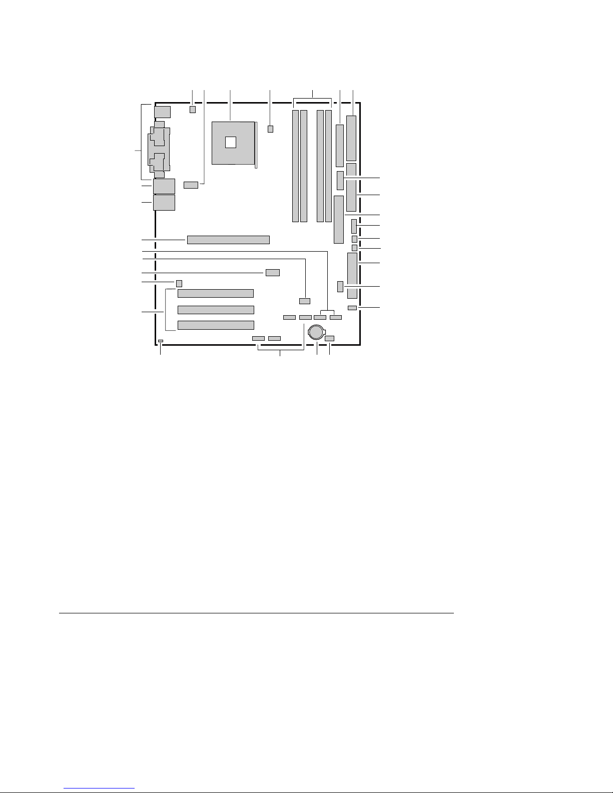
The figure below shows the functional blocks of the server board and the plug-in modules that it
supports.
A BC D E FG
CC
BB
AA
Z
Y
X
W
V
U
A. System Fan 4 Header
B. +12V CPU Power Connector
C. Processor Socket
D. CPU Fan
E. DIMM Sockets
F. Main Power Connector
G. Floppy Drive Connector
H. Auxiliary Power Connector
I. Primary IDE Connector
J. Secondary IDE Connector
K. Serial B Header
L. System Fan 1 Header
M. System Fan 2 Header
N. Front Panel Connector
O. BIOS Configuration Jumper (J8J2)
P. SCSI LED Header
Q. Hot Swap Backplane Header
H
I
J
K
L
M
N
O
P
S
QRT
TP00182
R. Battery
S. SATA-A1 through SATA-A4 Connector
(S875WP1LX only, slots numbered from left to
right)
T. Chassis Intrusion Header
U. PCI 32/33 Slots 1 – 3
(slots numbered from top to bottom)
V. System Fan 3 Header
W. Front Panel USB Header
X. Clear CMOS Jumper J8G1
Y. SATA-B1 and SATA-B2 Connectors
(slots numbered from left to right)
Z. AGP Connector
AA. NIC2 (10/100 Mb), USB
BB. NIC1 (1 Gb), USB
CC. Back Panel I/O Ports
Figure 1. Intel Server Board S875WP1-E Diagram
Revision 4.0
4
Page 17

S875WP1-E TPS Functional Architecture
3. Functional Architecture
This chapter provides a high-level description of the functionality distributed between the
architectural blocks of the Intel Server Board S875WP1-E.
3.1 Processor and Memory Subsystem
The Intel 82875P Memory Controller Hub (MCH) is one component of the Inte l 875P chipset.
The MCH is a centralized controller for the system bus, the memory bus, the AGP bus, and the
accelerated hub architecture interface.
3.1.1 Processor Support
The Intel Server Board S875WP1-E supports a single Pentium 4 processo r (in a µPGA478
socket) with a system bus of 400 /533 /800 MHz. The server board supports the processors
listed in Table 1.
Table 1. Processor Support Matrix
Pentium® 4 processor with
Hyperthreading (HT) Technology
Pentium 4 processor with
Hyperthreading Technology
Pentium 4 processor 2.0, 2.26, 2.4, 2.53, 2.6, 2.66, and 2.8
Type Designation System Bus L2 Cache Size
2.40, 2.60, 2.80, and 3.0 GHz 800 MHz 512 KB
3.06 GHz 533 MHz 512 KB
400 / 533 MHz 512 KB
GHz
CAUTION
Use only the processors listed above. Use of unsupported processors can dama ge the board,
the processor, and the power supply. See the Intel® Server Boar d S875WP1-E Specification
Update or go to http://support.intel.com/support/motherboards/server/S875WP1-E/
for the
current list of supported processors for this board.
NOTE
Use only ATX12V or EPS12V compliant power supplies with the server board S875WP1-E.
ATX12V and EPS12V power supplies have an additional powe r lead that provides required
supplemental power for the Intel Pentium 4 processor. The board will not boot if you do not
connect the 20-pin (or 24-pin) and 4-pin (or 8-pin) leads of ATX12V or EPS12V power supplies
to the corresponding connectors.
Do not use a standard ATX power supply. The board will not boot with a standard ATX power
supply.
Revision 4.0
5
Page 18

Functional Architecture S875WP1-E TPS
3.1.1.1 Reset Configuration Logic
The BIOS determines the processor stepp in g, cache size, and other processor information
through the CPUID instruction. The requirement is for the processor to run at a fixed speed. The
processor cannot be programmed to operate at a lower or highe r speed.
On the S875WP1-E platform, the BIOS is responsible for configuring the processor speed. The
BIOS uses CMOS settings to determine which speed to program into the speed setting device.
The processor information is read at every system power-on.
3.1.2 Memory Subsystem
The server board S875WP1-E provides four DIMM slots and supports a maximum memory
capacity of 4 GB. The DIMM organization is x72, which includes eight ECC check bits. ECC from
the DIMMs are passed through to the processor’s system bus. Memory scrubbing, single-bit
error correction and multiple-bit error detection is supported. Memory ca n be implemented with
either single-sided (one row) or double-sided (two row) DIMMs.
Table 2. Supported Memory Configurations
DIMM Capacity Configuration DDR SDRAM
Density
64 MB SS 64 Mbit 8 M x 8/empty 8
64 MB SS 128 Mbit 8 M x 16/empty 4
128 MB DS 64 Mbit 8 M x 8/8 M x 8 16
128 MB SS 128 Mbit 16 M x 8/empty 8
128 MB SS 256 Mbit 16 M x 16/empty 4
256 MB DS 128 Mbit 16 M x 8/16 M x 8 16
256 MB SS 256 Mbit 32 M x 8/empty 8
256 MB SS 512 Mbit 32 M x 16/empty 4
512 MB DS 256 Mbit 32 M x 8/32 M x 8 16
512 MB SS 512 Mbit 64 M x 8/empty 8
1024 MB DS 512 Mbit 64 M x 8/64 M x 8 16
Note: In the second column, “DS” refers to double-sided memory modules (containing two rows of DDR
SDRAM) and “SS” refers to single-sided memory modules (cont aining one row of DDR SDRAM).
DDR SDRAM
Organization
Front-side/Back-side
Number of DDR
SDRAM Devices
DIMM and memory configurations must adhere to the following:
• 2.5 V (only) 184-pin DDR SDRAM DIMMs with gold-plated contacts
• Unbuffered, single-sided or double-sided DIMMs with the following restriction:
• Double-sided DIMMS with x16 organization are no t supported.
• Maximum total system memory: 4 GB
• Minimum total system memory: 128 MB
• ECC and non-ECC DIMMs supported
• Serial Presence Detect
• PC3200 (400 MHZ), PC2700 (333 MHZ), and PC2100 (266 MHZ) SDRAM DIMMs
Revision 4.0
6
Page 19

S875WP1-E TPS Functional Architecture
Table 3 lists the supported system bus frequency and memory speed combinations.
Table 3. Supported System Bus Frequency and Memory Speed Combinations
To use this type of DIMM… The processor's system bus frequency must be…
PC3200 (400 MHZ) 800 MHz
PC2700 (333 MHZ) 800 or 533 MHz (Note)
PC2100 (266 MHZ) 800, 533, or 400 MHz
Note: When using PC2700 (333 MHZ) memory with an 800 MHz system bus frequency processor, the memory
channel will be set to 320 MHz.
Only DIMMs tested and qualified by Intel or a designated memo ry test vendor will be supported
on the Intel Server Board S875WP1-E. A list of qualified DIMMs will be made available through
http://support.intel.com/support/motherboards/server/S875WP1-E/
. Note that all DIMMs are
supported by design, but only fully qualified DIMMs will be supported.
NOTES
• Remove the AGP video card while installing or upg rading memory to avoid interference
with the memory retention mechanism.
• To be fully compliant with all applicable DDR SDRAM memory specifications, the board
should be populated with DIMMs that support the Serial Presence Detect (SPD) data
structure. This allows the BIOS to read the SPD data and program the chipset to
accurately configure memory settings for optimum performance. If non-SPD memory is
installed, the BIOS will attempt to correctly configure the memory settings, but
performance and reliability may be impacted or the DIMMs may not function under the
determined frequency.
• For ECC functionality, all installed DIMMs must be ECC. If both ECC and non-ECC
DIMMs are used, ECC will be disabled and will not function.
• Only low profile DIMMs can be supported in a 1U server chassis.
3.1.3 Memory Configurations
The Intel 82875P MCH component provides two features fo r enhancing memory throughput:
• Dual Channel memory interface. The board has two memory channels, each with two
DIMM sockets.
• Dynamic Addressing Mode. Dynamic mode minimizes overhead by reducing memory
accesses.
Revision 4.0
7
Page 20
Functional Architecture S875WP1-E TPS
Table 4 summarizes the characteristics of dual and single channel configuratio ns with and
without the use of Dynamic Mode.
Table 4. Characteristics of Dual/Single Channel Configuration with/without Dynamic Mode
Throughput
Level
Highest Dual Channel with Dynamic Mode All DIMMs matched
Dual Channel without Dynamic Mode DIMMs matched from Channel A to Channel B
Single Channel with Dynamic Mode Single DIMM or DIMMs matched with a channel
Lowest Single Channel without Dynamic Mode DIMMs not matched
Configuration Characteristics
(Example configurations are shown in Figure 2)
DIMMs not matched within channels
(Example configuration is shown in Figure 3)
(Example configurations are shown in Figure 4)
(Example configurations are shown in Figure 5)
Revision 4.0
8
Page 21
S875WP1-E TPS Functional Architecture
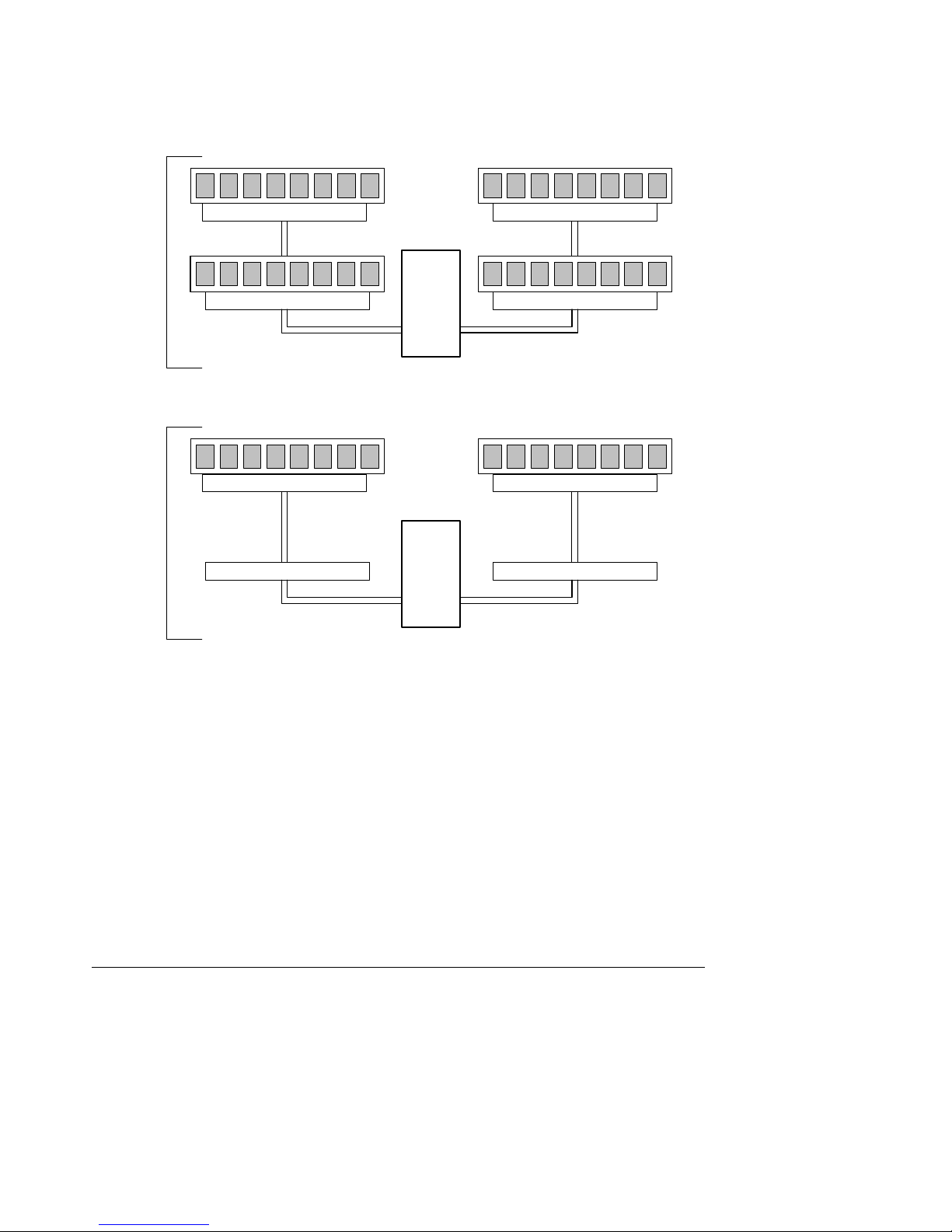
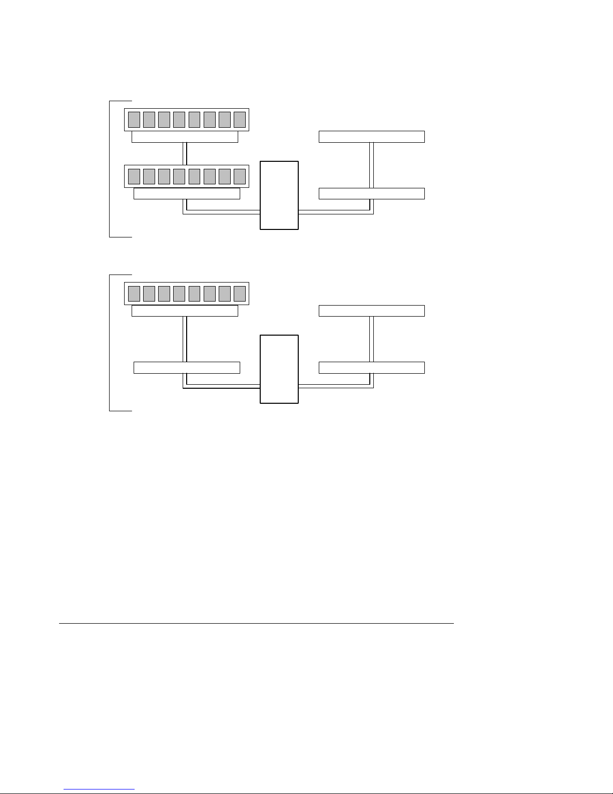
Dual Channel Configuration with Dynamic Mode
(All DIMMs matched)
Channel A - DIMM 0 Channel B - DIMM 0
Example
1
Channel A - DIMM 1
Channel A - DIMM 0 Channel B - DIMM 0
Intel
82875P
MCH
Channel B - DIMM 1
Example
2
Channel A - DIMM 1
Intel
82875P
MCH
Channel B - DIMM 1
Figure 2. Examples of Dual Channel Configuration with Dynamic Mode
OM15978
Revision 4.0
9
Page 22
Functional Architecture S875WP1-E TPS
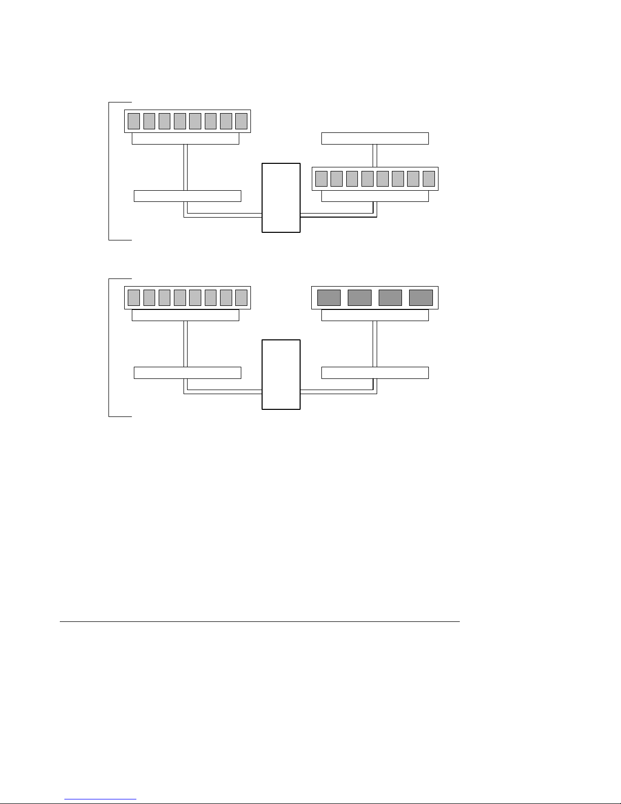
Dual Channel Configuration without Dynamic Mode
- DIMMs not matched within channel
- DIMMs match Channel A to Channel B
Channel A - DIMM 0 Channel B - DIMM 0
Channel A - DIMM 1 Channel B - DIMM 1
Intel
82875P
MCH
OM15979
Figure 3. Example of Dual Channel Configuration without Dynamic Mode
Revision 4.0
10
Page 23
S875WP1-E TPS Functional Architecture
Single Channel Configuration with Dynamic Mode
(Single DIMM or DIMMs matched within Channel)
Channel A - DIMM 0 Channel B - DIMM 0
Example
1
Channel A - DIMM 1
Channel A - DIMM 0 Channel B - DIMM 0
Intel
82875P
MCH
Channel B - DIMM 1
Example
2
Channel A - DIMM 1
Intel
82875P
MCH
Channel B - DIMM 1
Figure 4. Examples of Single Channel Configuration with Dynamic Mode
OM15980
Revision 4.0
11
Page 24
Functional Architecture S875WP1-E TPS
Single Channel Configuration without Dynamic Mode
(DIMMs not matched)
Channel A - DIMM 0 Channel B - DIMM 0
Example
1
Channel A - DIMM 1
Channel A - DIMM 0 Channel B - DIMM 0
Intel
82875P
MCH
Channel B - DIMM 1
Example
2
Channel A - DIMM 1
Intel
82875P
MCH
Channel B - DIMM 1
OM15981
Figure 5. Examples of Single Channel Configuration without Dynamic Mode
Revision 4.0
12
Page 25
S875WP1-E TPS Functional Architecture
A
A
A
A
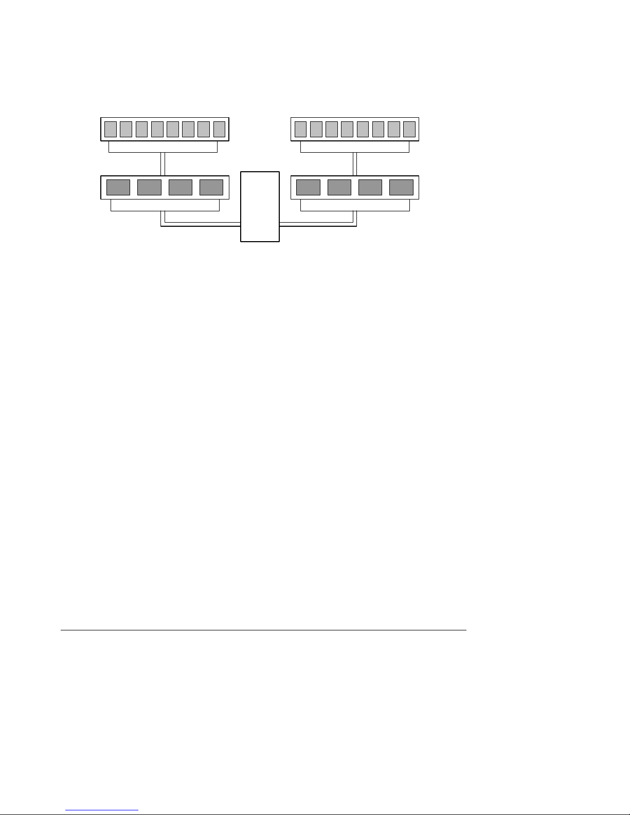
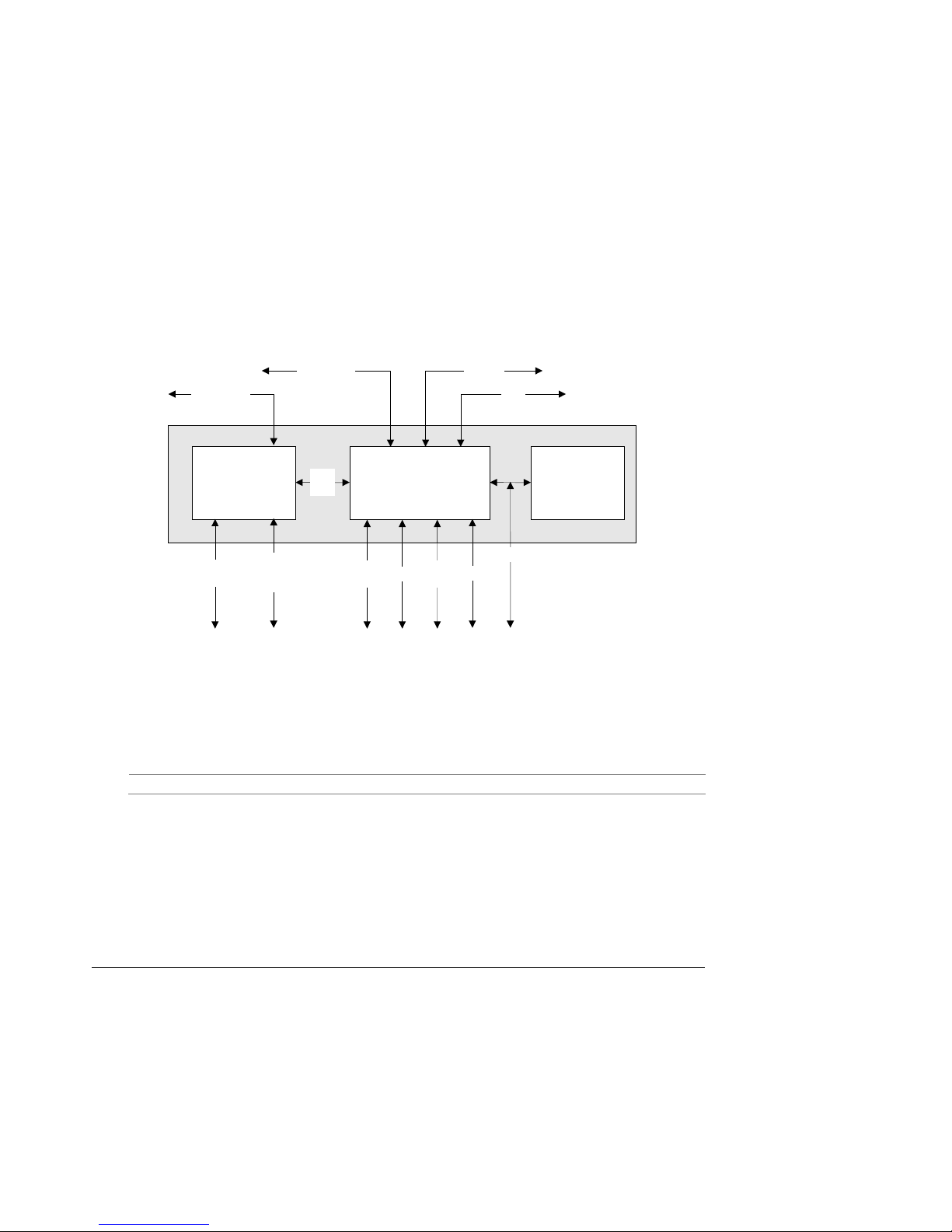
3.2 Intel 875P Chipset
The Intel 875P chipset consists of the following devices:
• Intel 82875P Memory Controller Hub (MCH) with Accelerated Hub Architecture (AHA)
bus
• Intel 82801ER I/O Controller Hub (ICH5-R) with AHA bus
• Intel 82802AC (8 Mbit) Firmware Hub (FWH)
The MCH is a centralized controller for the system bus, the memory bus, the AGP bus, and the
Accelerated Hub Architecture interface. The ICH5-R is a centralized controller for the Server
Board S875WP1-E’s I/O paths. The FWH provides the nonvolatile sto rage of the BIOS. The
component combination provi d es the chipset interfaces as shown in Figure 6.
System Bus
82875P
Memory Controller
Hub (MCH)
Dual-Channel
GP
Interface
DDR SDRAM
875P Chipset
Bus
UDMA 33
TA-66/100
HA
Bus
I/O Controller Hub
SATA
SMBus
Ports
82801ER
(ICH5-R)
PCI
Bus
Network
USB
82802AC
8 Mbit Firmware
Hub (FWH)
LPC Bus
C Link
OM15967
Figure 6. Intel 875P Chipset Block Diagram
For information about Refer to
The Intel 875P chipset http://developer.intel.com
Revision 4.0
13
Page 26

Functional Architecture S875WP1-E TPS
3.2.1 AGP
The AGP connector supports the following:
• 4x, 8x AGP 3.0 add-in cards with 0.8 V I/O
• 1x, 4x AGP 2.0 add-in cards with 1.5 V I/O
AGP is a high-performance interface for graphics-intensive applications, such as 3D
applications. While based on the PCI Local Bus Specification, Rev. 2.2, AGP is independent of
the PCI bus and is intended for exclusive use with graphical display devices. AGP overcomes
certain limitations of the PCI bus related to handling large amounts of graphics data with the
following features:
• Pipelined memory read and write operations that hide memory access la tency
• Demultiplexing of address and data on the bus for nearly 100 percent efficiency
NOTES
• AGP 2x operation is not supported.
• Install memory in the DIMM sockets prior to installing the AGP video card to avoid
interference with the memory retention mechanism.
• The AGP connector is keyed for Universal 0.8 V AGP 3.0 cards or 1.5 V AGP 2.0 cards
only. Do not attempt to install a legacy 3.3 V AGP card. The AGP connector is not
mechanically compatible with legacy 3.3 V AGP cards.
For information about Refer to
The AGP connector Section 5.3
3.2.2 USB
The Intel Server Board S875WP1-E supports up to six USB 2.0 ports, supports Universal Host
Controller Interface (UHCI) and En hanced Host Controller Interface (EHCI), and uses UHCIand EHCI-compatible drivers.
The ICH5-R provides the USB controller for all ports, as shown in Figure 7. The port
arrangement is as follows:
• Two ports are implemented with stacked back panel connectors, above NIC1
• Two ports are implemented with stacked back panel connectors, above NIC2
• Two ports are routed to the front panel USB header
14
Revision 4.0
Page 27

S875WP1-E TPS Functional Architecture
I/O Controller Hub
82801ER
(ICH5-R)
USB
USB
USB ports [2]
USB ports [2]
USB
USB ports [2]
Back panel USB connectors
above NIC1
Back panel USB connectors
above NIC2
Front panel USB header
Providing up to 2 USB ports
OM16101
Figure 7. USB Port Configuration
NOTES
• Computer systems that have an unshielded cable atta ched to a USB port may not meet
FCC Class B requirements, even if no device is attached to the cable. Use shielded
cable that meets the requirements for full-speed devices.
• Native USB 2.0 support has been tested with Windows* 2000 and Windows XP drivers
and is not currently supported by any other operating system. See the Intel server board
support website at http://support.intel.com/support/motherboards/server/s875wp1-e for
possible driver updates for other operating systems.
For information about Refer to
The location of the USB connectors on the back panel Figure 1
The location of the front panel USB connector Figure 1
The signal names of the front panel USB header Section 5.9
Legacy USB support Section 6.4
Wake from USB Section 3.6
3.2.3 IDE Interfaces
The ICH5-R IDE controller has two independent bus-mastering IDE interfaces that can be
independently enabled. The IDE interfaces support the follo wing modes:
• Programmed I/O (PIO): processor controls data transfer.
• 8237-style DMA: DMA offloads the processor, supporting transfer rates of up to 16 MB/se c .
• Ultra DMA: DMA protocol on IDE bus supporting host and target throttling and transfer rates
of up to 33 MB/sec.
• ATA-66: DMA protocol on IDE bus supporting host and target throttli ng and transfer
rates of up to 66 MB/sec. The ATA-66 protocol is similar to Ultra DMA and is device
driver compatible.
• ATA-100: DMA protocol on IDE bus allows host and target throttling. The ICH5-R ATA-
100 logic can achieve read transfer rates up to 100 MB/sec and write transfer rates up to
88 MB/sec.
Revision 4.0
15
Page 28

Functional Architecture S875WP1-E TPS
NOTE
ATA-66 and ATA-100 are faster timings and require a specialized 40-pin, 80-wire cable to
reduce reflections, noise, and inductive coupling.
The IDE interfaces also support ATAPI devices (such as CD-ROM drives) and ATA devices
using the transfer modes. The BIOS supports Logical Block Addressing (LBA) and Extended
Cylinder Head Sector (ECHS) translation modes. The drive reports the tran sfer rate and
translation mode to the BIOS.
The Server Board S875WP1-E supports Laser Servo (LS-120) diskette technol ogy through the
IDE interfaces. The BIOS supports booting from an LS-120 drive.
NOTE
The BIOS will always recognize an LS-120 drive as an ATAPI floppy drive. To ensure correct
operation, do not configure the drive as a hard disk drive.
For information about Refer to
The location of the IDE connectors Figure 1
The signal names of the IDE connectors Table 30
BIOS Setup program’s Boot Configuration menu Section 7.1.3.2
Drive Configuration Submenu Section 7.1.3.4
3.2.3.1 SCSI Hard Drive Activity LED Connec t or
The SCSI hard drive activity LED connector is a 1 x 2-pin connector that allows an add-in
SCSI controller to use the same LED as the on-board IDE controller. For proper ope ration, this
connector should be wired to the LED output of the add-in SCSI controller. Th e LED indicates
when data is being read from, or written to, both the add-in SCSI controller an d the IDE
controller.
For information about Refer to
The location of the SCSI hard drive activity LED connector Figure 1
16
Revision 4.0
Page 29

S875WP1-E TPS Functional Architecture
3.2.4 Real-Time Clock, CMOS SRAM, and Batt ery
The real-time clock provides a time-of-day clock and a multi-century calen dar with alarm
features. The real-time clock supports 256 bytes of battery-backed CMOS SRAM in two banks
that are reserved for BIOS use.
A coin-cell battery (CR2032) powers the real-time clock and CMOS memory. When the
computer is not plugged into a wall socket, the battery has an estimated life of three yea rs.
When the computer is plugged in, the standby current from the power supply extends the life of
the battery. The clock is accurate to ± 13 minutes/year at 25 ºC with 3.3 VSB applied.
The time, date, and CMOS values can be specified in the BIOS Setup program. The CMOS
values can be returned to their defaults by using the BIOS Setup program.
NOTE
If the battery and AC power fail, custom defaults, if previously saved, will be loaded into CMOS
RAM at power-on.
3.2.5 Intel 82802AC 8 Megabit Firmw are Hub (FWH)
The FWH provides the following:
• System BIOS program
• Logic that enables protection for storing and updating of platform information
Revision 4.0
17
Page 30

Functional Architecture S875WP1-E TPS
3.3 Serial ATA (SATA) Support
3.3.1 SATA Interfaces
The Serial ATA controller provided by the ICH5-R offers two independent SATA ports with a
theoretical maximum transfer rate of 150MB/s per port. One device can be installed on each
port for a maximum of two SATA devices when using ICH5-R. Server board with order code of
S875WP1 includes only two SATA ports through the ICH5-R. Server board with order code
S875WP1LX includes an additional four SATA ports using an onbo ard Promise* Serial ATA
controller, for a maximum of six SATA drives. A point-to- point interface is used for host to device
connections, unlike IDE which supports a master/slave configuration an d two devices per
channel.
For compatibility, the underlying SATA functionality is transparent to the operating system. The
SATA controller can operate in both legacy and native modes. In legacy mode, standard IDE I/O
and IRQ resources are assigned (IRQ 14 and 15). In native mode, standard PCI resource
steering is used. Native mode is the preferred mode for configurations using the Win do ws XP
and Windows 2000 operating systems.
Key features include:
• Two SATA ports
• Maximum throughput of 150MB/s
• Smaller cable
NOTE
• Many SATA drives use new low-voltage power connectors and require adaptors or
power supplies equipped with low-voltage power connectors. For more information, see:
http://www.serialata.org/
• ATA and SATA add-in controllers may experience resource conflicts IRQ 14 and 15.
Refer to the tested hardware and operating system list at (URL). In some instances,
onboard SATA controller may need to be disable to use those add-in controllers.
3.3.2 SATA RAID with ICH5-R Controller
Support for RAID (Redundant Array of Independent Disks) on the two SATA ports from the
ICH5-R controller is planned for a future date. See
http://support.intel.com/support/motherboards/server/S875WP1-E/
information.
18
for the availability
Revision 4.0
Page 31

S875WP1-E TPS Functional Architecture
3.3.3 SATA RAID w ith Promise Technology* PDC20319
The Intel Server Board S875WP1LX provides additional four port Serial ATA through the use of
the Promise* Technology PDC20319 ASIC. The PDC20319 SATA-150 controller contains four
independent SATA channels that share a single 32-bit, 33-MHz PCI bus master inte rface as a
multifunction device, packaged in a 144-pin LQFP.
The PDC 20319 controller supports the following features:
• Burst bus mastering and advanced packet command based scatter/gather engine to
enhance overall system performance
• Built in 4 channels SATA PHY, which meets the SATA 1.0 specification and can transfer
data with 1.5GHz speed
• Capable to support multiple arrays and quad master mode for dedicated SATA channel,
up to four physical drive can operated at master mode.
• Quad independent data paths with read ahead and write posting supported for quad IDE
channels to have high performance
• PCI interface that complies with PCI Local Bus Specification Revision 2.3 an d PCI power
management 1.1
• Support 48-bit LBA format for drives larger than 128GB
• 32-bit, 33-MHz bus speed and 150 MB/sec sustained transfer rate.
The Promise* PDC20319 supports SATA RAID through four SATA Channels. The RAID
Engine supports advance chained packet commands for XOR and fou r independent ATA
operations improving performance for all RAID levels. In a RAID configuration, multiple SATA
hard drives are placed into one or more arrays of disks. Each array is seen as an independent
disk, though the array may include upwards of two, three, or four drive s . The SATA RAID can
be configured as follows:
• RAID 0: Striping one to four drives.
• RAID 1: Mirroring two drives.
• RAID 10: Striping and mirroring of data concurrently (requires 4 drives)
RAID 0 configurations are used for high-performance applications, as it doubles the sustained
transfer rate of its drives. RAID 1 configurations are primarily used for data protection. It creates
an identical drive backup to a secondary drive. Whenever a disk write is performed, the
controller sends data simultaneously to a second drive located on a different data channel. With
four drives attached to four SATA channels, one pair of striped drives can mi rror themselves to
another pair (RAID 10) for storage capacity and data redundancy.
Revision 4.0
19
Page 32

Functional Architecture S875WP1-E TPS
3.4 I/O Controller
The SMSC* LPC47M102 I/O Controller provides the following features:
• One serial port
• One parallel port with Extended Capabilities Port (ECP) and Enhanced Parallel Port
(EPP) support
• Serial IRQ interface compatible with serialized IRQ support for PCI systems
• PS/2-style mouse and keyboard interfaces
• Interface for one 1.44 MB diskette drive
• Intelligent power management, includin g a programmable wake-up event interface
• PCI power management support
The BIOS Setup program provides configuration options for the I/O contro ller.
For information about Refer to
SMSC LPC47M172 I/O controller http://www.smsc.com
3.4.1 Serial Ports
The Intel Server Board S875WP1-E has one 9-pin D-sub serial port connector and one 2 x 5
serial port header. The serial port A connector is located in the rear I/O area. The serial port B
header is located near the main power connector. The serial ports’ NS16C550-compatible
UART supports data transfers at speeds up to 115.2 kbits/sec with BIOS support. The serial
ports can be assigned as COM1 (3F8h), COM2 (2F8h), COM3 (3E8h), or COM4 (2E8h).
For information about Refer to
The signal names of the serial port A connector Table 33
The location of the serial port B header Figure 1
The signal names of the serial port B header Table 34
20
Revision 4.0
Page 33

S875WP1-E TPS Functional Architecture
3.4.2 Parallel Port
The 25-pin D-Sub parallel port connector is located in the rear I/O area. In the BIOS Setup
program, the parallel port can be set to the following modes:
1 Output only (PC AT-compatible mode)
2 Bi-directional (PS/2 compatible)
3 EPP
• ECP
For information about Refer to
The location of the parallel port connector Figure 1
Setting the parallel port’s mode Table 47
3.4.3 Diskette Drive Controller
The I/O controller supports one diskette drive that is compatible with the 82077 diskette drive
controller and supports both PC-AT and PS/2 modes.
For information about Refer to
The location of the diskette drive connector Figure 1
The signal names of the diskette drive connector Section 5.10
The supported diskette drive capacities and sizes Table 50
3.4.4 Keyboard and Mouse Interface
PS/2 keyboard and mouse connectors are located on the back panel. The +5 V lines to these
connectors are protected with a PolySwitch* fuse circuit that, like a self-heali ng fuse ,
reestablishes the connection after an overcurrent condition is removed.
The keyboard is supported in the bottom PS/2 connector and the mouse is sup po r ted in the top
PS/2 connector. Power to the computer should be turned off before a keyboard or mouse is
connected or disconnected.
The keyboard controller contains the American MegaTrends* (AMI) keyboard and mouse
controller code, provides the keyboard and mouse control functions, and supports password
protection for power-on/reset. A power-on/reset password can be specified in the BIOS Setup
program.
Revision 4.0
NOTE
For information about Refer to
The location of the keyboard and mouse connectors Section 3.4.4
The signal names of the keyboard and mouse connectors Table 35
21
Page 34

Functional Architecture S875WP1-E TPS
3.5 Hardware Management Subsystem
The hardware management features enable the Intel Server Board S875WP1-E to be
compatible with the Wired for Management (WfM) specification 2.0. The server board c omp lies
with DMI specification 2.0 and has several hardware management features , inclu ding the
following:
4 Fan monitoring
5 Thermal and voltage monitoring
• Chassis intrusion detection
3.5.1 Hardwar e Monitoring and Fan Control ASIC
The features of the hardware monitoring and fan control ASIC (Standard Microsystems
SMSC EMC6D101 or equivalent) include:
6 Internal ambient temperature sensor
7 Two remote thermal diode sensors for direct monitoring of processor temperature and
ambient temperature sensing
8 Power supply monitoring of five voltages (+5 V, +12 V, +3.3 V Standby, +1.5 V, and
+VCCP) to detect levels above or below acceptable values
9 Thermally monitored closed-loop fan control, for four fans, that can adjust the fan speed
or switch the fans on or off as needed
• SMBus interface
For information about Refer to
The Standard Microsystems SMSC EMC6D101 http://www.smsc.com
3.5.2 Fan Monitoring
The Hardware Management ASIC provides four fan tachometer inputs. Monitoring can be
implemented using LANDesk* Client Manager or third-party software.
For information about Refer to
The location of the fan connectors Figure 1
The signal names of the fan connectors Section 5.13.1
22
Revision 4.0
Page 35

S875WP1-E TPS Functional Architecture
3.5.3 Chassis Intrusion and Detection
The Intel Server Board S875WP1-E supports a chassis security feature that detects if the
chassis cover is removed. For the chassis intrusion circuit to function, the chassis’ power supply
must be connected to AC power. The security feature uses a mechanical switch on the chassis
that attaches to the chassis intrusion connector. When the chassis cover is removed the
mechanical switch is in the closed position.
For information about Refer to
The location of the chassis intrus ion connector Figure 1
NOTE
Chassis intrusion detection may be implemented using LANDesk* Client Manager or other thirdparty software.
3.6 Power Management
Power management is implemented at several levels, including:
10 Software support through Advanced Configuration and Power Interface (ACPI)
11 Hardware support:
Power connector
Fan connectors
LAN wake capabilities
Instantly Available PC technology
Wake from USB
Wake from PS/2 devices
Power Management Event (PME#) wake-up support
3.6.1 Advanced Configuration and Power Interface (ACPI)
ACPI gives the operating system direct control over the power management and Plug and Play
functions of a computer. The use of ACPI with the Intel Server Board S875WP1-E requires an
operating system that provides full ACPI support. ACPI features include:
12 Plug and Play (including bus and device enumeration)
13 Power management control of individual devices, add-in boards (some add-i n boards
may require an ACPI-aware driver), video displays, and hard disk drives
14 Methods for achieving less than 15-watt system operation in the standby or
sleeping state
15 A Soft-off feature that enables the operating system to power-off the computer
16 Support for multiple wake-up events (see Table 7)
• Support for a front panel power and sleep mode switch
Revision 4.0
23
Page 36

Functional Architecture S875WP1-E TPS
Table 5 lists the system states based on how long the power switch is pressed, depending on
how ACPI is configured with an ACPI-aware operating system.
Table 5. Effects of Pressing the Power Switch
If the system is in this state…
Off
(ACPI S5 – Soft off)
On
(ACPI S0 – working state)
On
(ACPI S0 – working state)
Sleep
(ACPI S1 or S3 – sleeping state)
Sleep
(ACPI S1 or S3 – sleeping state)
…and the power switch is
Less than four seconds Power-on
pressed for
Less than four seconds Soft-off/Standby
More than four seconds Fail safe power-off
Less than four seconds Wake-up
More than four seconds Power-off
…the system enters this state
(ACPI S0 – working state)
(ACPI S1 or S3 – sleeping state)
(ACPI S5 – Soft off)
(ACPI S0 – working state)
(ACPI S5 – Soft off)
3.6.1.1 System States and Power States
Under ACPI, the operating system directs all system and device power state transitions. The
operating system puts devices in and out of low-power states based on user preferences and
knowledge of how devices are being used by applications. Devices that are not being used can
be turned off. The operating system uses information from applications and user settings to put
the system as a whole into a low-power state.
Table 6 lists the power states supported by the Server Board S875WP1-E along with the
associated system power targets. See the ACPI specification for a complete description of the
various system and power states.
Table 6. Power States and Targeted System Power
Global States Sleeping States
G0 – working
state
G1 – sleeping
state
G1 – sleeping
state
G1 – sleeping
state
G2/G5 S5 – Soft off.
24
S0 – working C0 – working D0 – working state. Full power > 30 W
S1 – Processor
stopped
S3 – Suspend to
RAM. Context
saved to RAM.
S4 – Suspend to
disk. Context saved
to disk.
Context not saved.
Cold boot is
required.
Processor
States
C1 – stop
grant
No power D3 – no power
No power D3 – no power
No power D3 – no power
D1, D2, D3 –
device specification
specific.
except for wake-up
logic.
except for wake-up
logic.
except for wake-up
logic.
Device States
Targeted System
Power (Note 1)
5 W < power < 52.5 W
Power < 5 W (Note 2)
Power < 5 W (Note 2)
Power < 5 W (Note 2)
Revision 4.0
Page 37

S875WP1-E TPS Functional Architecture
Global States Sleeping States
G3 – mechanical
off
AC power is
disconnected
from the
computer.
Notes:
1. Total system power is dependent on the system configuration, including add-in boards and peripherals
powered
by the system chassis’ power supply.
2. Dependent on the standby power consumption of wake-up devices used in the system.
No power to the
system.
Processor
States
No power D3 – no power for
wake-up logic,
except when
provided by battery
or external source.
Device States
Targeted System
Power (Note 1)
No power to the system.
Service can be performed
safely.
3.6.1.2 Wake-up Devices and Events
Table 7 lists the devices or specific events that can wake the computer from specific states.
Table 7. Wake-up Devices and Events
These devices/events can wake up the
computer…
LAN S1, S3, S4, S5 (Note)
Modem (back panel Serial Port A) S1, S3
PME# S1, S3, S4, S5 (Note)
Power switch S1, S3, S4, S5
PS/2 devices S1, S3
RTC alarm S1, S3, S4, S5
USB S1, S3
…from this state
NOTE
• For LAN and PME#, S5 is disabled by default in the BIOS Setup program. Setting this
option to Power On will enable a wake-up event from LAN in the S5 state.
• The use of these wake-up events from an ACPI state requires an operating syst em that
provides full ACPI support. In addition, software, drivers, and peripherals must fully
support ACPI wake events.
3.6.1.3 Plug and Play
In addition to power management, ACPI provides control information so that operating systems
can facilitate Plug and Play. ACPI is used only to configure devices that do not use other
hardware configuration standards. PCI devices for example, are not confi gured by ACPI.
Revision 4.0
25
Page 38

Functional Architecture S875WP1-E TPS
3.6.2 Hardware Support
CAUTION
Ensure that the power supply provides adequate +5 V standby current if LAN wake capabilities
and Instantly Available PC technology features are used. Failure to do so can damage the
power supply. The total amount of standby current required dep ends on the wake devices
supported and manufacturing options.
The Server Board S875WP1-E provides power management hardware featu res, including:
17 Power connector
18 Fan connectors
19 LAN wake capabilities
20 Instantly Available PC technology
21 Wake from USB
22 Wake from PS/2 keyboard
• PME# wake-up support
LAN wake capabilities and Instantly Available PC technology require power from the +5 V
standby line. The sections discussing these features describe the incremental standby power
requirements for each.
3.6.2.1 Power Connector
ATX12V or EPS12V compliant power supplies and the Intel Server Board S875WP1-E can turn
off the system power through software control. When the system receives the correct command
from the operating system, the power supply removes non-standby voltages from the system.
When power to the computer is interrupted by a power outage or a disco nnected power cord,
when power resumes, the computer returns to the power state it was in before power was
interrupted (on or off). The computer’s response can be set using the After Power Failure in the
BIOS Setup program’s Boot menu.
For information about Refer to
The location of the power connectors Figure 1
The signal names of the power connector Section 5.1
The BIOS Setup program’s Boot menu Section 7.1.5
26
Revision 4.0
Page 39

S875WP1-E TPS Functional Architecture
3.6.2.2 Fan Connectors
CAUTION
The processor fan must be connected to the processor fan connector, not to a chassis fan
connector. Connecting the processor fan to a chassis fan connector may resul t i n on board
component damage that will halt fan operation.
Table 8 summarizes the fan connector function/operation.
Table 8. Fan Connector Function/Operation
Connector Description
Processor fan
System fans
• +12 V DC connection for a processor fan or active fan heatsink.
• Fan is on in the S0 or S1 state.
Fan is off when the system is off or in the S3, S4, or S5 state.
• Wired to a fan tachometer input of the hardware monitoring and fan control ASIC.
• Closed-loop fan control that can adjust the fan speed or switch the fan on or off as
needed.
• +12 V DC connection for a system or chassis fan.
• Fan is on in the S0 or S1 state.
Fan is off when the system is off or in the S3, S4, or S5 state.
• Wired to a fan tachometer input of the hardware monitoring and fan control ASIC.
• Closed-loop fan control that can adjust the fan speed or switch the fan on or off as
needed.
For information about: Refer to:
The location of the fan connectors Figure 1
The signal names of the fan connectors Section 5.13.1
3.6.2.3 LAN Wake Capabilities
CAUTION
For LAN wake capabilities, the +5 V standby from the power supply must be capable of
providing adequate +5 V standby current. Failure to provide adequate standby curren t when
implementing LAN wake capabilities can damage the power supply.
LAN wake capabilities enable remote wake-up of the computer through a network. The LAN
subsystem PCI bus network adapter monitors network traffic at the Media Independent
Interface. Upon detecting a Magic Packet* frame, the LAN subsystem asserts a wake-up signal
that powers up the computer. Depending on the LAN implementation, the server board
S875WP1-E supports LAN wake capabilities with ACPI in the following ways:
23 PCI bus PME# signal for PCI 2.2 compliant LAN designs
• Onboard LAN subsystem
Revision 4.0
27
Page 40

Functional Architecture S875WP1-E TPS
3.6.2.4 Instantly Available PC Technology
CAUTION
For Instantly Available* PC technology, the +5 V standby from the power supply must be
capable of providing adequate +5 V standby current. Failure to provide adequate standby
current when implementing Instantly Available PC technology can damage the power supply.
Instantly Available PC technology enables the server board S875WP1-E to enter the ACPI S3
(Suspend-to-RAM) sleep-state. While in the S3 sleep-state, the se rver will appear to be off (the
power supply is off, and the front panel LED is amber if dual colored, or off if single colore d.)
When signaled by a wake-up device or event, the system quickly returns to its last known wake
state. Table 7 lists the devices and events that can wake the computer from the S3 state.
The server board supports the PCI Bus Power Management Interface Specification. Add-in
boards that also support this specification can participate in power management and can be
used to wake the computer.
The use of Instantly Available PC technology requires operating system support and PCI 2.2
compliant add-in cards and drivers.
3.6.3 Standby Power (+5 V) Indicator LED
The standby power indicator LED (CR7J1) shows that power is still present even when the
computer appears to be off. Figure 8 shows the location of the standby power indicator LED.
CAUTION
If AC power has been switched off and the standby power indicator is still lit, disconnect the
power cord before installing or removing any devices connected to the board. Failure to do so
could damage the board and any attached devices.
28
Revision 4.0
Page 41
S875WP1-E TPS Functional Architecture
CR7J1
TP00185
Figure 8. Location of the Standby Power Indicator LED (CR7J1)
3.6.3.1 Wake from USB
USB bus activity wakes the computer from an ACPI S1 or S3 state.
NOTE
Wake from USB requires the use of a USB peripheral that supports it.
3.6.3.2 Wake from PS/2 Devices
PS/2 device activity wakes the computer from an ACPI S1 or S3 state.
3.6.3.3 PME# Wake-up Support
When the PME# signal on the PCI bus is asserted, the computer wakes from an ACPI S1, S3,
S4, or S5 state (with Wake on PME enabled in BIOS).
Revision 4.0
29
Page 42

Functional Architecture S875WP1-E TPS
3.7 Clock Generation and Distribution
All buses on the S875WP1-E baseboard operate using synchronous clocks. Clock
synthesizer/driver circuitry on the baseboard generates clock frequencies and voltage levels as
required, including the following:
24 100/133-MHz at 2.5 V & 3.3 V logic levels: For the mPGA478 socket, the MCH, and the
ITP port.
25 66 MHz at 3.3 V logic levels: For the MCH and the AGP clocks.
26 33.3 MHz at 3.3 V logic levels: For the PCI slots and devices.
• 14.318 MHz at 3.3V logic levels: ICH5-R and Super I/O clocks.
The synchronous clock sources on the S875WP1-E baseboard are:
27 100/133-MHz host clock generator for processor, MC H, Memory DIMMs, and the ITP.
28 66-MHz clock for MCH and the AGP clocks.
29 48-MHz clock for USB.
30 33.3-MHz PCI reference clock.
• 14.318 MHz ICH5-R and Super I/O clocks.
The S875WP1-E baseboard also provides asynchronous clock generators:
31 25-MHz clocks for the embedded network interface controllers.
32 29.498928-MHz clock for the embedded video controller.
33 20-MHz clock for the Promise PDC20319 controller.
• 32-KHz clock for the RTC.
3.8 PCI I/O Subsystem
The primary I/O bus for the Intel Server Board S875WP1-E is PCI, with one independent PCI
bus. The PCI bus complies with the PCI Local Bus Specification, Rev 2.2. The PCI bus is
directed through the Intel 82801ER I/O Controller Hub (ICH5-R). The tab le below lists the
characteristics of the PCI bus.
Table 9. PCI Bus Characteristics
Voltage Width Speed Type Comments
5 V 32-bits 33 MHz Independent Bus Supports full-length cards
30
Revision 4.0
Page 43

S875WP1-E TPS Functional Architecture
3.8.1 32-bit, 33-MHz PCI Subsystem
All 32-bit, 33-MHz PCI I/O for the Intel Server Board S875WP1-E is directed through the Intel
82801ER I/O Controller Hub (ICH5-R). The PCI bus supports the following embedded d evices
and connectors:
34 2D/3D Graphics Accelerator: ATI Rage XL Video Controller
35 SATA controller: Promise Technology PDC20319
• Three PCI Slots
Each of the embedded devices listed above will be allocated a GPIO to disable the device.
3.8.1.1 Device IDs (IDSEL)
Each device under the PCI hub bridge has its IDSEL signal connected to one bit of AD[31:16 ],
which acts as a chip select on the PCI bus segment in configuration cycles. This determines a
unique PCI device ID value for use in configuration cycles. The following table shows each IDSEL
value for the PCI bus devices and the corresponding device description.
Table 10. PCI Bus Configuration IDs
IDSEL Value Device
16 PCI slot 1 (closest to AGP connector)
17 PCI slot 2 (middle slot)
18 PCI slot 3 (closest to left edge of board)
22 ATI Rage XL Video Controller
23 ATA-100 control ler Promise Technology PDC20319
3.8.2 Video Controller
The Intel Server Board S875WP1-E provides an ATI Rage XL PCI graphics accelerator, along
with 8 MB of video SDRAM and support circuitry for an embedded SVGA video subsystem . The
ATI Rage XL chip contains a SVGA video controller, clock generator, 2D and 3D engine, and
RAMDAC in a 272-pin PBGA.
The SVGA subsystem supports a variety of mo des, up to 1600 x 1200 resolution in 8/16/24/32
bpp modes under 2D, and up to 1024 x 768 resolution in 8/16/24/32 bpp modes under 3D. It
also supports both CRT and LCD monitors up to 100 Hz vertical refresh rate.
The server board provides a standard 15-pin VGA connector and supports disabling of the onboard video through the BIOS Setup menu or when a plug-in video c ard is installed in the AGP
slot or any of the PCI slots.
3.8.2.1 Video Modes
The Rage XL chip supports all standard IBM VGA modes. The following table shows the 2D/3D
modes supported for both CRT and LCD, as well as various display resolution , refresh rates,
and color depths.
Revision 4.0
31
Page 44

Functional Architecture S875WP1-E TPS
Table 11. Video Modes
S875WP1-E 2D Video Mode Support 2D Mode Refresh Rate (Hz)
8 bpp 16 bpp 24 bpp 32 bpp
640x480 60, 72, 75, 90, 100 Supported Supported Supported Supported
800x600 60, 70, 75, 90, 100 Supported Supported Supported Supported
1024x768 60, 72, 75, 90, 100 Supported Supported Supported Supported
1280x1024 43, 60 Supported Supported Supported Supported
1280x1024 70, 72 Supported – Supported Supported
1600x1200 60, 66 Supported Supported Supported Supported
1600x1200 76, 85 Supported Supported Supported –
3D Mode Refresh Rate (Hz) S875WP1-E 3D Video Mode Support with Z Buffer Enabled
640x480 60,72,75,90,100 Supported Supported Supported Supported
800x600 60,70,75,90,100 Supported Supported Supported Supported
1024x768 60,72,75,90,100 Supported Supported Supported Supported
1280x1024 43,60,70,72 Supported Supported – –
1600x1200 60,66,76,85 Supported – – –
3D Mode Refresh Rate (Hz) S875WP1-E 3D Video Mode Support with Z Buffer Disabled
640x480 60,72,75,90,100 Supported Supported Supported Supported
800x600 60,70,75,90,100 Supported Supported Supported Supported
1024x768 60,72,75,90,100 Supported Supported Supported Supported
1280x1024 43,60,70,72 Supported Supported Supported –
1600x1200 60,66,76,85 Supported Supported – –
3.8.2.2 Video Memory Interface
The memory controller subsystem of the Rage XL arbitrates requests from direct memory
interface, the VGA graphics controller, the drawing coprocessor, the displa y controller, the video
scalar, and hardware cursor. Requests are serviced in a manner that ensures display integrity
and maximum CPU/coprocessor drawing performance.
The S875WP1-E supports an 8 MB SDRAM device for video memory.
32
Revision 4.0
Page 45

S875WP1-E TPS Functional Architecture
3.9 Network Interface Controller (NIC) Subsystem
The Intel Server Board S875WP1-E supports two Network Interface Co ntrollers (NICs), one that
runs at 10/100Mb and is based on the Intel 82562ET NIC and the other that runs at one gigabit
and is based on the Intel 82547EI NIC. When looking at the rear of the chassis, the gigabit NIC
is at the left (closest to the video port) and the 10/100Mb NIC is at the right. The Intel Server
Board S875WP1-E supports independent disabling of the two NIC controllers using the BIOS
Setup menu.
The NIC subsystem consists of the following:
36 Intel 82801ER ICH5-R device with an integrated LAN Media Access Controller (MAC)
37 Intel 82547EI Platform LAN Connect (PLC) device for 10/100/1000 Mbits/se c Eth ern et
LAN connectivity
• RJ-45 LAN connector with integrated status LEDs
The 82562ET is controlled by the ICH5 and supports the following features:
38 Integrated IEEE 802.3 10Base-T and 100Base-TX compatible PHY
39 IEEE 802.3u auto-negotiation support
40 Full duplex support at both 10 Mbps and 100 Mb ps operation
41 Low power +3.3 V device with reduced power in unplugged mode and automatic
detection of unplugged mode
• 3-port LED support
The 82547EI is controlled by the CSA interface off of the MCH and supports the following
features:
42 Basic 10/100/1000 Ethernet LA N connectivity
43 Integrated Gigabit Ethernet Media Access Control (MAC) and physical laye r (PHY)
44 IEEE 802.3 10BASE-T/100BASE-TX/1000BASE-T compliant physical layer interface
45 IEEE 802.3ab Auto-Negotiation support
46 Low power (less than 350mW in active transmit mode)
47 Reduced power in “unplugged mode” (less than 50mW)
48 Automatic detection of “unplugged mode”
49 Communication Streaming Architecture (CSA) port provides higher throughput and lower
latencies resulting in up to 30% higher bus throughput (up to wire speed)
50 Full device driver compatibility
51 Programmable transit threshold
52 Configuration EEPROM that contains the MAC address
• Teaming and Fai l ov e r support
Revision 4.0
33
Page 46

Functional Architecture S875WP1-E TPS
Additional features of the NIC subsystem include:
53 PCI bus master interface
54 CSMA/CD protocol engine
55 PCI power management
Supports ACPI technology
Supports LAN wake capabilities
3.9.1 RJ-45 LAN Connectors w i th Integrated LEDs
Two LEDs are built into each RJ-45 LAN connector (as shown in Figure 9). For the 82562ET
NIC, the yellow LED indicates a link to the LAN and th e gr e en LED indicates the connection
speed. Table 12 describes the LED states when the board is powered up and the 82562ET
10/100 Ethernet LAN subsystem is operating.
Table 12. 10/100 Ethernet LAN Connector LEDs
LED Color LED State Indicates
LED)
Yellow
(right LED)
Off 10 Mbit/sec data rate is selected. Green (left
On 100 Mbit/sec data rate is selected.
Off LAN link is not established.
On (steady state) LAN link is established.
On (brighter and pulsing) The computer is communicating with another computer on the
LAN.
Table 13 describes the LED states when the board is powered up and the 10 /100/1000
Mbits/sec LAN subsystem is operating.
Green LED
Figure 9. LAN Connector LED Locations
Table 13. 10/100/1000 LAN Connector LED States
LED Color LED State Condition
Left Green
Right
Green
Orange On 1000 Mbit/sec data rate is selected.
Off LAN link is not established.
On (steady state) LAN link is established.
On (brighter and pulsing) The computer is communicating with
Off 10 Mbit/sec data rate is selected.
On 100 Mbit/sec data rate is selected.
Green/Orange LED
OM15977
another computer on the LAN.
34
Revision 4.0
Page 47

S875WP1-E TPS Maps and Interrupts
4. Maps and Interrupts
In this section, Table 14 describes the system memory map, Table 15 shows the I/O map, Table
16 lists the DMA channels, Table 17 defines the PCI configuration space map, and Table 18
describes the interrupts.
4.1 Memory Map
Table 14. System Memory Map
Address Range
(decimal)
1024 K - 4194304 K 100000 - FFFFFFFF 4095 MB Extended memory
960 K - 1024 K F0000 - FFFFF 64 KB Runtime BIOS
896 K - 960 K E0000 - EFFFF 64 KB Reserved
800 K - 896 K C8000 - DFFFF 96 KB Available high DOS memory (open to the PCI bus)
640 K - 800 K A0000 - C7FFF 160 KB Video memory and BIOS
639 K - 640 K 9FC00 - 9FFFF 1 KB Extended BIOS data (movable by memory manager
512 K - 639 K 80000 - 9FBFF 127 KB Extended conventional memory
0 K - 512 K 00000 - 7FFFF 512 KB Conventional memory
Address Range
(hex)
Size Description
software)
4.2 I/O Map
Table 15. I/O Map
Address (hex) Size Description
0000 - 00FF 256 bytes Used by the Server Board S875WP1-E. Refer to the ICH5-R data
0170 - 0177 8 bytes Secondary IDE channel
01F0 - 01F7 8 bytes Primary IDE channel
0228 - 022F
0278 - 027F
02E8 - 02EF
02F8 - 02FF
0376 1 byte Secondary IDE channel command port
0377, bits 6:0 7 bits Secondary IDE channel status port
0378 - 037F 8 bytes LPT1
03B0 - 03BB 12 bytes Intel 82875P MCH
03C0 - 03DF 32 bytes Intel 82875P MCH
03E8 - 03EF 8 bytes COM3
03F0 - 03F5 6 bytes Diskette channel 1
(Note 1)
(Note 1)
(Note 1)
(Note 1)
8 bytes LPT3
8 bytes LPT2
8 bytes COM4/video (8514A)
8 bytes COM2
sheet for dynamic addressing information.
Revision 4.0
35
Page 48

Maps and Interrupts S875WP1-E TPS
Address (hex) Size Description
03F6 1 byte Primary IDE channel command port
03F8 - 03FF 8 bytes COM1
04D0 - 04D1 2 bytes Edge/level triggered PIC
LPTn + 400 8 bytes ECP port, LPTn base address + 400h
(Note 3)
(Note 2)
0CF8 - 0CFB
0CF9
0CFC - 0CFF 4 bytes PCI configuration data register
FFA0 - FFA7 8 bytes Primary bus master IDE registers
FFA8 - FFAF 8 bytes Secondary bus master IDE registers
Notes:
1. Default, but can be changed to another address range
2. Dword access only
3. Byte access only
4 bytes PCI configuration address register
1 byte Reset control r eg is t e r
4.3 DMA Channels
Table 16. DMA Channels
DMA Channel
Number
0 8 or 16 bits Open
1 8 or 16 bits Parallel port
2 8 or 16 bits Diskette drive
3 8 or 16 bits Parallel port (for ECP or EPP)
4 8 or 16 bits DMA controller
5 16 bits Open
6 16 bits Open
7 16 bits Open
Data Width System Resource
36
Revision 4.0
Page 49

S875WP1-E TPS Maps and Interrupts
4.4 PCI Configuration Space Map
Table 17. PCI Configuration Space Map
Bus
Number (hex)
00 00 00 Memory controller of Intel 82875P component
00 01 00 Host to AGP bridge (virtual P2P)
00 1E 00 Hub link to PCI bridge
00 1F 00 Intel 82801ER ICH5-R PCI-to-LPC bridge
00 1F 01 IDE controller
00 1F 03 SMBus controller
00 1F 05 AC ’97 audio controller
00 1F 06 AC ’97 modem controller (optional)
00 1D 00 USB UHCI controller 1
00 1D 01 USB UHCI controller 2
00 1D 02 USB UHCI controller 3
00 1D 07 EHCI controller
01 00 00 AGP add-in card
02 08 00 LAN controller
02 00 00 PCI bus connector 1
02 01 00 PCI bus connector 2
02 02 00 PCI bus connector 3
02 03 00 PCI bus connector 4
02 04 00 PCI bus connector 5
02 06 00 SATA/SATA RAID
Device
Number (hex)
Function
Number (hex)
Description
Revision 4.0
37
Page 50

Maps and Interrupts S875WP1-E TPS
4.5 Interrupts
The interrupts can be routed through the Advanced Programmable Interrupt Controller (APIC)
portion of the ICH5-R component. The APIC is supported in Windows 2000 Server and
Windows XP and supports a total of 24 interrupts.
Table 18. Interrupts
IRQ System Resource
NMI I/O channel check
0 Reserved, interval timer
1 Reserved, keyboard buffer full
2 Reserved, cascade interrupt from slave PIC
3
4
5 LPT2 (Plug and Play option)/User available
6 Diskette drive
7
8 Real-time clock
9 Reserved for ICH5-R system management bus
10 User available
11 User available
12 Onboard mouse port (if present, else user available)
13 Reserved, math coprocessor
14 Primary IDE (if present, else user available)
15 Secondary IDE (if present, else user available)
16 USB UHCI controller 1 (through PIRQA)
17 User available (through PIRQB)
18 ICH5-R USB controller 3 (through PIRQC)
19 ICH5-R USB controller 2 (through PIRQD)
20 ICH5-R LAN (through PIRQE)
21 User available (through PIRQF)
22 User available (through PIRQG)
23 ICH5-R USB 2.0 EHCI controller/User available (through PIRQH)
Notes:
1. Default, but can be changed to another IRQ.
COM2
COM1
LPT1
(Note 1)
(Note 1)
(Note 1)
38
Revision 4.0
Page 51

S875WP1-E TPS Maps and Interrupts
4.6 PCI Interrupt Routing Map
This section describes interrupt sharing and how the interrupt s ignals are connected between
the PCI bus connectors and onboard PCI devices. The PCI specification specifies how
interrupts can be shared between devices attached to the PCI bus. In most cases, the small
amount of latency added by interrupt sharing does not affect the operation or throughput of the
devices. In some special cases where maximum performance is needed from a device, a PCI
device should not share an interrupt with other PCI devices. Use the following information to
avoid sharing an interrupt with a PCI add-in car d .
PCI devices are categorized as follows to specify their interrupt grouping :
56 INTA: By default, all add-in cards that require only one interrupt are in this category. For
almost all cards that require more than one interrupt, the first interrupt on the card is also
classified as INTA.
57 INTB: Generally, the second interrupt on add-in cards that require two or more interrupts
is classified as INTB. (This is not an absolute requirement.)
• INTC and INTD: Generally, a third interrupt on add-in cards is classified as INTC and a
fourth interrupt is classified as INTD.
The ICH5-R has eight programmable interrupt request (PIRQ) input signals. All PCI interrupt
sources either onboard or from a PCI add-in card connect to one of these PIRQ signals. Some
PCI interrupt sources are electrically tied together on the Server Board S875WP1-E and
therefore share the same interrupt. Table 19 shows an example of how the PIRQ signals are
routed.
For example, using Table 19 as a reference, assume an add-in card using INTB is plugged into
PCI bus connector 3. In PCI bus connector 3, INTB is connected to PIRQA, which is already
connected to the Promise PDC20319 Controller. The add-in card in PCI bus connector 3 now
shares an interrupt with the onboard interrupt source.
Table 19. PCI Interrupt Routing Map
ICH5-R PIRQ Signal Name PCI Interrupt Source
AGP connector INTA INTB
PCI bus connector 1 INTF INTG INTH INTE
PCI bus connector 2 INTG INTF INTE INTH
PCI bus connector 3 INTB INTC INTD INTA
LAN_10/100 INTE
ATI Rage XL INTE
Promise PD20319 Controller INTB
NOTE
PIRQA PIRQB PIRQC PIRQD PIRQE PIRQF PIRQG PIRQH
In PIC mode, the ICH5-R can connect each PIRQ line internally to one of the IRQ signals (3, 4,
5, 6, 7, 9, 10, 11, 12, 14, and 15). Typically, a device that does not share a PIRQ line will have a
unique interrupt. However, in certain interrupt-constrained situations, it is possible for two or
more of the PIRQ lines to be connected to the same IRQ signal. See Table 18 for the alloc ation
of PIRQ lines to IRQ signals in APIC mode.
Revision 4.0
39
Page 52

Connectors and Jumper Blocks S875WP1-E TPS
5. Connectors and Jumper Blocks
5.1 Power Connectors
The main power supply connection is obtained using either the 20-pin connector from an
ATX12V power supply, or the 24-pin connector from an EPS12V power supply. The following
table defines the pin-outs of the connector (For a 20-pin connector, the first 20 pins apply).
Table 20. Power Connector Pin-out (J2J2)
Pin Signal Color Pin Signal Color
1 +3.3Vdc Orange 13 +3.3Vdc Orange
2 +3.3Vdc Orange 14 -12Vdc Blue
3 COM Black 15 COM Black
4 +5Vdc Red 16 PS_ON# Green
5 COM Black 17 COM Black
6 +5Vdc Red 18 COM Black
7 COM Black 19 COM Black
8 PWR_OK Gray 20 RSVD_(-5V) White
9 5VSB Purple 21 +5Vdc Red
10 +12Vdc Yellow 22 +5Vdc Red
11 +12Vdc Yellow 23 +5Vdc Red
12 +3.3Vdc Orange 24 COM Black
Table 21. 12V CPU Power Connector (J4C1)
Pin Signal
1 Ground
2 Ground
3 Ground
4 Ground
5 +12V
6 +12V
7 +12V
8 +12V
NOTE
The board will not boot if the 12V CPU power connector is not attached to the b oard. The 12V
CPU power from an ATX12V power supply will only have 4 pi ns.
40
Revision 4.0
Page 53

S875WP1-E TPS Connectors and Jumper Blocks
Table 22. Auxiliary Power Connector (J4J1)
Pin Signal
1 SMB_CLK_MAIN_CON
2 SMB_DATA_MAIN_CON
3 PS_ALERT#
4 GND
5 3.3V
5.2 PCI Bus Connectors
Table 23. PCI Bus Connectors
Pin Signal Name Pin Signal Name Pin Signal Name Pin Signal Name
A1 Ground (TRST#)
(See Note)
A2 +12 V B2 Ground (TCK)
A3 +5 V (TMS)
(See Note)
A4 +5 V (TDI)
(See Note)
A5 +5 V B5 +5 V A36 TRDY# B36 +3.3 V
A6 INTA# B6 +5 V A37 Ground B37 DEVSEL#
A7 INTC# B7 INTB# A38 STOP# B38 Ground
A8 +5 V B8 INTD# A39 +3.3 V B39 LOCK#
A92 Reserved B9 Not connected
A10 +5 V (I/O) B10 Reserved3 A41 SMBus Data
A11 Reserved B11 Not connected
A12 Ground B12 Ground A43 PAR B43 +3.3 V
A13 Ground B13 Ground A44 AD15 B44 C/BE1#
A14 +3.3 V aux B14 Reserved4 A45 +3.3 V B45 AD14
A15 RST# B15 Ground A46 AD13 B46 Ground
A16 +5 V (I/O) B16 CLK A47 AD11 B47 AD12
A17 GNT# B17 Ground A48 Ground B48 AD10
A18 Ground B18 REQ# A49 AD09 B49 Ground
A19 PME# B19 +5 V (I/O) A50 Key B50 Key
A20 AD30 B20 AD31 A51 Key B51 Key
A21 +3.3 V B21 AD29 A52 C/BE0# B52 AD08
A22 AD28 B22 Ground A53 +3.3 V B53 AD07
A23 AD26 B23 AD27 A54 AD06 B54 +3.3 V
B1 -12 V A32 AD16 B32 AD17
(See Note)
B3 Ground A34 FRAME# B34 Ground
B4 Not connected (TDO)* A35 Ground B35 IRDY#
(PRSNT1#) (See Note)
(PRSNT2#) (See Note)
A33 +3.3 V B33 C/BE2#
A40 SMBus Clock
Line
Line
A42 Ground B42 SERR#
B40 PERR#
B41 +3.3 V
Revision 4.0
41
Page 54

Connectors and Jumper Blocks S875WP1-E TPS
Pin Signal Name Pin Signal Name Pin Signal Name Pin Signal Name
A24 Ground B24 AD25 A55 AD04 B55 AD05
A25 AD24 B25 +3.3 V A56 Ground B56 AD03
A26 IDSEL B26 C/BE3# A57 AD02 B57 Ground
A27 +3.3 V B27 AD23 A58 AD00 B58 AD01
A28 AD22 B28 Ground A59 +5 V (I/O) B59 +5 V (I/O)
A29 AD20 B29 AD21 A60 REQ64# B60 ACK64#
A30 Ground B30 AD19 A61 +5 V B61 +5 V
A31 AD18 B31 +3.3 V A62 +5 V B62 +5 V
Note:
1. The signals (in parentheses) are optional in the PCI specification and are not currently implemented.
2. On PCI Slot 3, A9 becomes P_REQ5#
3. On PCI Slot 3, B10 becomes P_GNT5#
4. On PCI Slot 3, B14 becomes CK_P_33M_S3_RISER
5.3 AGP Connector
Table 24. AGP Connector
Pin Signal Name Pin Signal Name Pin Signal Name Pin Signal Name
A1 +12 V B1 Not connected A34 Vddq B34 Vddq
A2 TYPEDET# B2 +5 V A35 AD22 B35 AD21
A3 Reserved B3 +5 V A36 AD20 B36 AD19
A4 Not connected B4 Not connected A37 Ground B37 Ground
A5 Ground B5 Ground A38 AD18 B38 AD17
A6 INTA# B6 INTB# A39 AD16 B39 C/BE2#
A7 RST# B7 CLK A40 Vddq B40 Vddq
A8 GNT1# B8 REQ# A41 FRAME# B41 IRDY#
A9 Vcc3.3 B9 Vcc3.3 A42 Reserved B42 +3.3 V (aux)
A10 ST1 B10 ST0 A43 Ground B43 Ground
A11 Reserved B11 ST2 A44 Reserved B44 Reserved
A12 PIPE# B12 RBF# A45 Vcc3.3 B45 Vcc3.3
A13 Ground B13 Ground A46 TRDY# B46 DEVSEL#
A14 WBF# B14 Reserved A47 STOP# B47 Vddq
A15 SBA1 B15 SBA0 A48 PME# B48 PERR#
A16 Vcc3.3 B16 Vcc3.3 A49 Ground B49 Ground
A17 SBA3 B17 SBA2 A50 PAR B50 SERR#
A18 SBSTB# B18 SB_STB A51 AD15 B51 C/BE1#
A19 Ground B19 Ground A52 Vddq B52 Vddq
A20 SBA5 B20 SBA4 A53 AD13 B53 AD14
A21 SBA7 B21 SBA6 A54 AD11 B54 AD12
A22 Reserved B22 Reserved A55 Ground B55 Ground
A23 Ground B23 Ground A56 AD9 B56 AD10
A24 Reserved B24 +3.3 V (aux) A57 C/BE0# B57 AD8
42
Revision 4.0
Page 55

S875WP1-E TPS Connectors and Jumper Blocks
Pin Signal Name Pin Signal Name Pin Signal Name Pin Signal Name
A25 Vcc3.3 B25 Vcc3.3 A58 Vddq B58 Vddq
A26 AD30 B26 AD31 A59 AD_STB0# B59 AD_STB0
A27 AD28 B27 AD29 A60 AD6 B60 AD7
A28 Vcc3.3 B28 Vcc3.3 A61 Ground B61 Ground
A29 AD26 B29 AD27 A62 AD4 B62 AD5
A30 AD24 B30 AD25 A63 AD2 B63 AD3
A31 Ground B31 Ground A64 Vddq B64 Vddq
A32 AD_STB1# B32 AD_STB1 A65 AD0 B65 AD1
A33 C/BE3# B33 AD23 A66 VRREFG_C B66 VREFC_G
NOTE
The AGP connector is keyed for 1.5 V AGP cards only. Do not attempt to install a legacy
3.3 V AGP card. The AGP connector is not mechanically compatib le with legacy 3.3 V AGP
cards.
5.4 Front Panel Connector
A high density, 34-pin SSI header is provided to support a system front panel. Th e header
contains reset, NMI, power control buttons, and LED indicators. The foll owing table details the
pin out of the header.
Table 25. High-Density Front Panel 34-Pin Header Pin Out (J7J1)
Pin Signal Name Pin(s) Function
1 Power LED Anode 2 5VSB
3 Key 4 Unused
5 GND 6 Unused
7 HDD Activity LED Anode 8 Unused
9 HDD Activity LED Cathode 10 Unused
11 Power Switch 12 NIC#1 Activity LED Anode
13 GND (Power Switch) 14 NIC#1 Activity LED Cathode
15 FP_RST* 16 I1C SDA
17 GND (Reset Switch) 18 I2C SDA
19 ACPI Sleep Switch 20 Chassis Intrusion
21 GND (ACPI Sleep Switch 22 NIC#2 Activity LED Anode
23 Unused 24 NIC#2 Activity LED Cathode
25 Key 26 Key
27 Unused 28 Unused
29 Unused 30 Unused
31 Unused 32 Unused
33 Unused 34 Unused
Revision 4.0
43
Page 56

Connectors and Jumper Blocks S875WP1-E TPS
5.5 VGA Connector
The following table details the pin out of the VGA connector.
Table 26. VGA Connector Pin-out (J3A1)
Pin Signal Name
1 Red (analog color signal R)
2 Green (analog color signal G)
3 Blue (analog color signal B)
4 No connection
5 GND
6 GND
7 GND
8 GND
9 Fused VCC(+5V)
10 GND
11 No connection
12 V_MONID1
13 HSYNC (horizontal sync)
14 VSYNC (vertical sync)
15 V_MONID2
5.6 NIC /USB Connector
The Intel Server Board S875WP1-E supports two Magjack3* connectors (dual USB + RJ45).
The following table details the pin out of the connector.
Table 27. Magjack3 Connector (dual USB + RJ45, Gbe) Pin Out (JA4A1)
Pin Signal Name Pin Signal Name
1 VREG_USB_BP_RIGHT 16 LAN_MDI_3
2 USB_BACK1_R# 17 LAN_MDI_3#
3 USB_BACK1_R 18 GND
4 GND 19 LAN_LINK_UP#
5 VREG_USB_BP_RIGHT 20 LAN_ACTLED#
6 USB_BACK2_R# 21 LAN_LINK_100#
7 USB_BACK2_R 22 LAN_LINK
8 GND 23 GND
9 LAN_VCT 24 GND
10 LAN_MDI_0 25 GND
11 LAN_MDI_0# 26 GND
12 LAN_MDI_1 27 GND
13 LAN_MDI_1# 28 GND
14 LAN_MDI_2 29 GND
15 LAN_MDI_2# 30 GND
44
Revision 4.0
Page 57

S875WP1-E TPS Connectors and Jumper Blocks
Table 28. Magjack3 Connector (dual USB + RJ45, 10/100) Pin Out (JA5A1)
Pin Signal Name Pin Signal Name
1 VREG_USB_BP_LEFT 16 NC
2 USB_BACK5_R# 17 NC
3 USB_BACK5_R 18 GND
4 GND 19 LAN_SPEEDLED#
5 VREG_USB_BP_LEFT 20 3.3V Stdby
6 USB_BACK6_R# 21 LAN_LILED#
7 USB_BACK6_R 22 LAN_ACT_LED#
8 GND 23 GND
9 NC 24 GND
10 LAN_TDP 25 GND
11 LAN_TDN 26 GND
12 LAN_RDP 27 GND
13 LAN_RDN 28 GND
14 NC 29 GND
15 NC 30 GND
5.7 SATA/SATA RAID Connectors
The S875WP1-E board provides two (S875WP1) or six (S875WP1LX) SATA/SATA RAID
connectors. The pin out for all connectors is identical and is listed in the following table.
Table 29. SATA 7-pin Connectors Pin Out (J9E1, J9F1, J9G1, J9H1, J9H2, J9J2)
Pin Signal Name
1 Ground
2 TXP
3 TXN
4 Ground
5 RXN
6 RXP
7 Ground
Revision 4.0
45
Page 58

Connectors and Jumper Blocks S875WP1-E TPS
5.8 ICH5-R IDE Connectors
The S875WP1-E board provides two 40-pin, low-density ICH5-R IDE connectors. The pin out
for both connectors is identical and is listed in the following table.
Table 30. ICH5-R IDE 40-pin Connector Pin Out (J5J1, J6J1)
Pin Signal Name Pin Signal Name
1 Reset IDE 2 Ground
3 Data 7 4 Data 8
5 Data 6 6 Data 9
7 Data 5 8 Data 10
9 Data 4 10 Data 11
11 Data 3 12 Data 12
13 Data 2 14 Data 13
15 Data 1 16 Data 14
17 Data 0 18 Data 15
19 Ground 20 Key
21 DDRQ0 [DDRQ1] 22 Ground
23 I/O Write# 24 Ground
25 I/O Read# 26 Ground
27 IOCHRDY 28 Ground
29 DDACK0# [DDACK1#] 30 Ground
31 IRQ 14 [IRQ 15] 32 Not connected
33 PDA1 (Address 1) 34 GPIO_DMA66_Detect_Pri
35 PDA0 (Address 0) 36 PDA2 (Address 2)
37 Chip Select 1P#
[Chip Select 1S#]
39 Activity# 40 Ground
(GPIO_DMA66_Detect_Sec)
38 Chip Select 3P#
[Chip Select 3S#]
5.9 Front Panel USB Header
A header on the server board provides an option to support two additi onal USB connectors. The
pin out of the header is detailed in the following table.
Table 31. Front Panel USB Connector Pin-out (J7E1)
Pin Signal Name Pin Signal Name
1 USB_FNT1_PWR 2 USB_FNT1_PWR
3 USB_FRONT1_L# 4 USB_FRONT2_L#
5 USB_ FRONT1_L 6 USB_FRONT2_L
7 Ground 8 Ground
9 Key 10 USB_ OC_FNT_R1
Note: USB ports may be assigned as needed.
46
Revision 4.0
Page 59

S875WP1-E TPS Connectors and Jumper Blocks
5.10 Floppy Connector
The Intel Server Board S875WP1-E provides a 34-pin connector interface to the flopp y drive
controller. The following table details the pin out of the 34-pin fl oppy connector.
Table 32. 34-pin Floppy Connector Pin Out (J3J1)
Pin Signal Name Pin Signal Name
1 GND 2 DENSEL
3 Key 4 NC
5 Key 6 DRVDEN1
7 GND 8 FDINDX#
9 GND 10 MTR0# (Motor Enable A)
11 GND 12 NC
13 GND 14 DS0# (Drive Select A)
15 GND 16 NC
17 NC 18 DIR# (Stepper Motor Direction)
19 GND 20 STEP# (Step Pulse)
21 GND 22 WDATA# (Write Data)
23 GND 24 WGATE# (Write Enable)
25 GND 26 TRK0# (Track 0)
27 NC 28 WRTPRT# (Write Protect)
29 GND 30 RDATA# (Read Data)
31 GND 32 HDSEL# (Side 1 Select)
33 GND 34 DSKCHG# (Diskette Change)
5.11 Serial Port Connector
The Intel Server Board S875WP1-E has one 9-pin D-sub serial port connector and one 2 x 5
serial port connector. The following tables detail the pin outs of these two ports.
Table 33. 9-pin Serial A Port Pin Out (J2A1)
Pin Signal Name
1 DCD (Data Carrier Detect)
2 RXD (Receive Data)
3 TXD (Transmit Data)
4 DTR (Data Terminal Ready)
5 GND
6 DSR (Data Set Ready)
7 RTS (Request to Send)
8 CTS (Clear to Send)
9 RI (Ring Indicator)
Revision 4.0
47
Page 60

Connectors and Jumper Blocks S875WP1-E TPS
Table 34. 10-pin Header Serial B Port Pin Out (J6J4)
Pin Signal Name
1 DCD (Data Carrier Detect)
2 RXD (Receive Data)
3 TXD (Transmit Data)
4 DTR (Data Terminal Ready)
5 GND
6 DSR (Data Set Ready)
7 RTS (Request to Send)
8 CTS (Clear to Send)
9 RI (Ring Indicator)
10 Key
5.12 Keyboard and Mouse Connector
PS/2 keyboard and mouse connectors are located on the back panel. The +5 V lines to these
connectors are protected with a PolySwitch* circuit that, like a self-healing fuse, reestablishes
the connection after an overcurrent condition is removed.
NOTE
The keyboard is supported in the bottom PS/2 connector and the mouse is sup po r ted in the top
PS/2 connector. Power to the computer should be turned off before a keyboard or mouse is
connected or disconnected.
The keyboard controller contains the AMI keyboard and mouse controller code, provid es th e
keyboard and mouse control functions, and supports password protection for po wer-on/reset. A
power-on/reset password can be specified in the BIOS Setup prog ram.
Table 35. Keyboard /Mouse PS/2 Connector Pin Out (J1A1)
Pin Signal Name
1 Data
2 NC
3 GND
4 +5 V (Fused)
5 Clock
6 NC
48
Revision 4.0
Page 61

S875WP1-E TPS Connectors and Jumper Blocks
5.13 Miscellaneous Headers
5.13.1 Fan Headers
The Intel Server Board S875WP1-E provides four 3-pin fan headers. All fans use dire ct 12 volts.
Four of the five fans, labeled “CPU_FAN”, “SYSFAN1”, “SYSFAN2” and “SYSFAN4” are wired
to a fan tachometer input of the Hardware Management ASIC. The third system fan, labeled
“SYSFAN3” is not wired to the input of the Hardware Management ASIC and therefor e is not
monitored by any server management software.
Table 36. Three-Pin Fan Headers Pin-Out
Pin Signal Name Type Description
1 CNTL Power GROUND is the power supply ground
2 VREG_12V_POWER Power 12 V
3 Fan Tach Out FAN_TACH signal is connected to the Hardware Management ASIC to
monitor the fan speed
5.14 System Recovery and Update Jumper
CAUTION
Do not move any jumpers with the power on. Always turn off the power and unplug the power cord
from the computer before changing a jumper setting. Otherwise, the board coul d be damaged.
This 3-pin jumper block determines the BIOS Setup program mode. Table 37 describes the
jumper settings for the three modes: normal, configure, and recover y. Whe n the jumper is set to
configuration mode and the computer is powered-up, the BIOS compares the CPU version and
the microcode version in the BIOS and reports if the two match.
Table 37. BIOS Setup Configuration Jumper Settings (J8J2)
Function/Mode Jumper Setting Configuration
Normal
1-2
Configure
2-3
Recovery
None
3
1
3
1
3
1
The BIOS uses current configuration information and passwords for
booting.
After the POST runs, Setup runs automatically. The maintenance
menu is displayed.
The BIOS attempts to recover the BIOS configuration. A recovery
diskette is required.
Revision 4.0
49
Page 62

Connectors and Jumper Blocks S875WP1-E TPS
For information about Refer to
How to access the BIOS Setup program Section 7
BIOS recovery Section 6.6
5.15 Clear CMOS Jumper
CAUTION
Do not move any jumpers with the power on. Always turn off the power and unplug the power
cord from the computer before changing a jumper setting. Othe rwise, the board could be
damaged.
This 3-pin jumper block allows the user to clear CMOS. Table 38 describes the jumper settings
for the two modes: normal and clear CMOS. When the jumper is set to Clear CMOS mode and
the computer is powered-up, the contents of the CMOS are cleared.
Table 38. Clear CMOS Jumper Settings (J8G1)
Function/Mode Jumper Setting Configuration
Normal
1-2
Clear CMOS
2-3
3
1
3
1
Normal Operation.
Clears contents of CM O S ar ea .
50
Revision 4.0
Page 63

S875WP1-E TPS BIOS Features
6. BIOS Features
The Intel Server Board S875WP1-E uses an Intel/AMI* BIOS that is stored in the Firmware Hub
(FWH) and can be updated using a disk-based program. The FWH contain s the BIOS Setup
program, POST, the PCI auto-configuration utility, and Plug and Play support.
The Intel Server Board S875WP1-E supports system BIOS shadowing, allowing the BIOS to
execute from 64-bit on-board write-protected system memory.
The BIOS displays a message during POST identifying the type of BIOS and a revision code.
The initial production BIOS is identified as WP87510A.86B.
When the Intel Server Board S875WP1-E’s jumper is set to configuration mode and the server
is powered-up, the BIOS compares the processor version and the microcode version in the
BIOS and reports if the two match.
For information about Refer to
The Intel Server Board S875WP1-E’s compliance level with Plug and Play Section 3.6.1.3
6.1 BIOS Flash Memory Organization
The Intel 82802AC Firmware Hub (FWH) includes an 8 megabit symmetrical flash memory
device. Internally, the device is grouped into eight 64-KB blocks that are individually erasable,
lockable, and unlockable.
6.2 Resource Configuration
6.2.1 PCI Autoconfiguration
The BIOS can automatically configure PCI devices. PCI devices may be on-board or add-in
cards. Autoconfiguration lets a user insert or remove PCI cards without having to configure the
system. When a user turns on the system after adding a PCI card, the BIOS automatically
configures interrupts, the I/O space, and othe r system resources. Any interrupts set to Available
in Setup are considered to be available for use by the add-in card. Autoconfigura ti on informatio n
is stored in ESCD format.
Revision 4.0
51
Page 64

BIOS Features S875WP1-E TPS
6.2.2 PCI IDE Support
If Auto is selected from the BIOS Setup program, the BIOS automatically sets up the two
PCI IDE connectors with independent I/O channel support. The IDE interface supports hard
drives up to ATA-66/100 and recognizes any ATAPI compliant devices, including CD-ROM
drives, tape drives, and Ultra DMA drives (see Section 3. 2.3). The BIOS determines the
capabilities of each drive and configures them to optimize capacity and performance.
To take advantage of the high capacities typically available today, hard drives are automatically
configured for Logical Block Addressing (LBA) and to PIO Mode 3 or 4, depending on the
capability of the drive. The user can override the auto-configuration options by specifying
manual configuration in the BIOS Setup program.
To use ATA-66/100 features the following items are required:
58 An ATA-66/100 peripheral device
59 An ATA-66/100 compatible cable
• ATA-66/100 operating system device drivers
NOTES
• ATA-66/100 compatible cables are backward compatible with drives using slower IDE
transfer protocols. If an ATA-66/100 disk drive and a disk drive using any other IDE
transfer protocol are attached to the same cable, the maximum transfer rate between the
drives is reduced to that of the slowest device.
• Do not connect an ATA device as a slave on the same IDE cable as an ATAPI master
device. For example, do not connect an ATA hard drive as a slave to an ATAPI CDROM drive.
6.3 System Management BIOS (SMBIOS)
SMBIOS is a Server Management Interface (DMI) compliant method for managing computers in
a managed network.
The main component of SMBIOS is the Management Information Format (MIF) database, which
contains information about the computing system and its components. Using SMBIOS, a system
administrator can obtain the system types, capabilities, operational status, and installation dates
for system components. The MIF database defines the data and provides the method for
accessing this information. The BIOS enables applications such as third-party management
software to use SMBIOS. The BIOS stores and reports the following SMBIOS information:
60 BIOS data, such as the BIOS revision level
61 Fixed-system data, such as peripherals, ser i al num bers, and asset tags
62 Resource data, such as memory size, cache size, and processor spe ed
• Dynamic data, such as event detection and error logging
52
Revision 4.0
Page 65

S875WP1-E TPS BIOS Features
Non-Plug and Play operating systems, such as Windows NT, require an additional inte rface for
obtaining the SMBIOS information. The BIOS supports an SMBIOS table interface for such
operating systems. Using this support, an SMBIOS service-level application running on a
non-Plug and Play operating system can obtain the SMBIOS information.
6.4 Legacy USB Support
Legacy USB support enables USB devices such as keyboard, mice, and hubs to be used even
when the operating system’s USB drivers are not yet available. Legacy USB support is used to
access the BIOS Setup program, and to install an operating system that supports USB. By
default, Legacy USB support is set to Enabled.
Legacy USB support operates as follows:
1. When the user applies power to the computer, legacy support is disabled.
2. POST begins.
3. Legacy USB support is enabled by the BIOS allowing the us er to use a USB keyboard to
enter and configure the BIOS Setup program and the maintenance menu.
4. POST completes.
5. The operating system loads. While the operating system is loading, USB keyboard and
mice are recognized and may be used to configure the operating system. (Keyboard a nd
mice are not recognized during this period if Legacy USB support was set to disabled in
the BIOS Setup program.)
6. After the operating system loads the USB drivers, all legacy and non-legacy USB
devices are recognized by the operating system, and Legacy USB support from the
BIOS is no longer used.
To install an operating system that supports USB, verify that Legacy USB support in the BIOS
Setup program is set to Enabled and follow the operating system’s installation instru ctions.
Legacy USB support is for keyboard, mice, and hubs only. Other USB devices are not
supported in legacy mode.
Revision 4.0
NOTE
53
Page 66

BIOS Features S875WP1-E TPS
6.5 BIOS Updates
The BIOS can be updated using either of the following utilities, which are available on the Intel
World Wide Web site:
®
• Intel
• Intel
Both utilities support the following BIOS maintenanc e functions:
63 Verifying that the updated BIOS matches the target system to prevent accidentally
64 Updating both the BIOS boot block and the main BIOS. This process is fault tolerant to
65 Updating the BIOS boot block separately.
66 Changing the language section of the BIOS.
67 Updating replaceable BIOS modules, such as the video BIOS module.
• Inserting a custom splash screen.
Express BIOS update utility, which enables automated updating while in the
Windows environment. Using this utility, the BIOS can be updated from a file on a hard
disk, a 1.44 MB diskette, a CD-ROM, or from the file location on the Web.
®
Flash Memory Update Utility, which requires creation of a boot diskette and
manual rebooting of the system. Using this utility, the BIOS can be updated from a file
on a 1.44 MB diskette (from a legacy diskette drive or an LS-120 diskette drive) or a
CD-ROM.
installing an incompatible BIOS.
prevent boot block corruption.
Review the instructions distributed with the up gr a de utility before attempting a BIOS update .
NOTE
6.5.1 Language Support
The BIOS Setup program and help messages are supporte d in two languages: US English and
Spanish. Additional languages may be flashed in if desi red (German, Italian and French
available). The default language is US English, which is present unless another lan guage is
selected in the BIOS Setup program.
6.5.2 Custom Splash Screen
During POST, an Intel splash screen is displayed by default. This splash screen can be
replaced with a custom splash screen. A utility is available from Intel to assist with crea ting a
custom splash screen. The custom splash screen can be programmed into the flash memory
using the BIOS upgrade utility. Information about this capabili ty is available on the Intel Support
World Wide Web site.
54
Revision 4.0
Page 67

S875WP1-E TPS BIOS Features
6.6 Recovering BIOS Data
Some types of failure can destroy the BIOS. For example, the data can be lost if a power outage
occurs while the BIOS is being updated in flash memory. The BIOS can be recovered from a
diskette using the BIOS recovery mode. When recovering the BIOS, be aware of the following:
• Because of the small amount of code available in the non-erasable boot block area,
there is no video support. The user can only monitor this procedure by listening to the
speaker or looking at the diskette drive LED.
• The recovery process may take several minutes; larger BIOS flash memory devices
require more time.
• Two beeps and the end of activity in the diskette drive indicate successful BIOS
recovery.
• A series of continuous beeps indicates a failed BIOS recovery.
To create a BIOS recovery diskette, a bootable diskette must be created and the BIOS update
files copied to it. BIOS upgrades and the Intel Flash Memory Update Utility are available from
Intel Customer Support through the Intel World Wide Web site.
Even if the computer is configured to boot from an LS-120 diskette (in the Setup progra m’s
Removable Devices submenu), the BIOS recovery diskette must be a standard 1.44 MB
diskette not a 120 MB diskette.
NOTE
For information about Refer to
The BIOS recovery mode jumper settings Section 5.14
The Boot Device Priority menu in the BIOS Setup program Section 7.1.6.1
6.7 Boot Options
In the BIOS Setup program, the user can choose to boot from a diskette drive, hard drives,
CD-ROM, or the network. The default setting is for the diskette drive to be the first boot device,
the hard drive second, the ATAPI CD-ROM third, and the network fourth. The fifth device is
disabled.
6.7.1 CD-ROM and Netw ork Boot
Booting from CD-ROM is supported in compliance to the El Torito bootable CD-ROM format
specification. Under the Boot menu in the BIOS Setup program, ATAPI CD-ROM is listed as a
boot device. Boot devices are defined in priority order. Accordingly, if there is not a bootable CD
in the CD-ROM drive, the system will attempt to boot from the next defined drive.
The network can be selected as a boot device. This selection allows booting from the on-board
NIC or a network add-in card with a remote boot ROM installed.
Revision 4.0
55
Page 68

BIOS Features S875WP1-E TPS
6.7.2 Booting Without Attached Devices
For use in embedded applications, the BIOS has been designed so that after passing the
POST, the operating system loader is invoked even if the following devices are not p resent:
68 Video adapter
69 Keyboard
• Mouse
56
Revision 4.0
Page 69

S875WP1-E TPS BIOS Features
6.8 Fast Booting Systems with Intel® Rapid BIOS Boot
These factors affect system boot speed:
70 Selecting and configuring peripherals properly
• Using an optimized BIOS, such as the Intel Rapid BIOS
6.8.1 Intel Rapid BIOS Boot
Using the following BIOS Setup program settings reduces the POST execution time. In the Bo ot
Menu:
• Set the hard disk drive as the first boot device. As a result, the POST does not first seek
a diskette drive, which saves about one second from the POST execution time.
• Disable Quiet Boot, which eliminates display of the logo splash screen. This could save
several seconds of painting complex graphic images and changing video modes.
• Enabled Intel Rapid BIOS Boot. This feature bypasses memory count and the search for
a diskette drive.
NOTES
• It is possible to optimize the boot process to the point where the system boots so quickly
that the Intel logo screen (or a custom logo splash screen) will no t be see n. Mon itors
and hard disk drives with minimum initialization times can also contribute to a boot time
that might be so fast that necessary logo screens and POST messages cannot be seen.
• This boot time may be so fast that some drives might be not be initialized at all. If this
condition should occur, it is possible to introduce a programmable delay ranging from
three to 30 seconds (using the Hard Disk Pre-Delay feature of the Advanced Menu in the
Drive Configuration Submenu of the BIOS Setup program).
For information about Refer to
Drive Configuration Submenu in the BIOS Setup program Section 7.1.3.4
6.9 BIOS Security Features
The BIOS includes security features that restrict access to the B IO S Setup program and who
can boot the computer. A supervisor password and a user password can be set for the BIOS
Setup program and for booting the computer, with the following restrictions:
• The supervisor password gives unrestricted access to view and change all the Setup
options in the BIOS Setup program. This is the supervisor mode.
• The user password gives restricted access to view and change Setup options in the
BIOS Setup program. This is the user mode.
Revision 4.0
57
Page 70

BIOS Features S875WP1-E TPS
• If only the supervisor password is set, pressing the <Enter> key at the password pro mpt
of the BIOS Setup program allows the user restricted access to Setup.
• If both the supervisor and user passwords are set, users can enter e ither the supervisor
password or the user password to access Setup. Users have access to Setup respective
to which password is entered.
• Setting the user password restricts who can boot the computer. The password prompt
will be displayed before the computer is booted. If only the supervisor password is set,
the computer boots without asking for a password. If both passwords are set, the user
can enter either password to boot the computer.
Table 39 shows the effects of setting the supervisor password and user password. This table is
for reference only and is not displayed on the screen.
Table 39. Supervisor and User Password Functions
Password Set Supervisor
Neither Can change all
Supervisor only Can change all
User only N/A Can change all
Supervisor and
user set
Note: If no password is set, any user can change all Setup options.
Mode
options (Note)
options
Can change all
options
User Mode Setup Options Password to
Can change all
options (See
Note)
Can change a
limited number
of options
options
Can change a
limited number
of options
None None None
Supervisor Password Supervisor None
Enter Password
Clear User Password
Supervisor Password
Enter Password
Enter Setup
User User
Supervisor or
user
For information about Refer to
Setting user and supervisor passwords Section 7.1.4
Password
During Boot
Supervisor or
user
58
Revision 4.0
Page 71

S875WP1-E TPS BIOS Setup Program
7. BIOS Setup Program
The BIOS Setup program can be used to view and change the BIOS settings for the computer.
The BIOS Setup program is accessed by pressing the <F2> key after the Power-On Self-Test
(POST) memory test begins and before the operating system boot begins. The menu b ar is
shown below.
Maintenance Main Advanced Security Power Boot Exit
Table 40 lists the BIOS Setup program menu features.
Table 40. BIOS Setup Program Menu Bar
Maintenance Main Advanced Security Power Boot Exit
Clears passwords
and BIS
credentials and
enables extended
configuration
mode
Allocates
resources for
hardware
components
Configures
advanced
features
available
through the
chipset
Sets
passwords
and security
features
Configures
power
management
features
Selects boot
options and
power supply
controls
Saves or
discards
changes to
Setup
program
options
NOTE
In this chapter, all examples of the BIOS Setup program menu bar in clude the maintenance
menu; however, the maintenance menu is displayed only when the board is in configuration
mode. Section 5.14 shows how to put the board into configuration mode.
Table 41 lists the function keys available for menu screens.
Table 41. BIOS Setup Program Function Keys
BIOS Setup Program Function
<←> or <→>
<↑> or <↓>
<Tab> Selects a field (Not impl emented)
<Enter> Executes command or selects the submenu
<F9> Load the default configuration values for the current menu
<F10> Save the current values and exits the BIOS Setup program
<Esc> Exits the menu
Key
Selects a different menu screen (Moves the cursor left or right)
Selects an item (Moves the cursor up or down)
Description
Revision 4.0
59
Page 72

BIOS Setup Program S875WP1-E TPS
7.1.1 Maintenance Menu
This menu is used to clear passwords and to access processor information. Setup only displays
this menu when the BIOS Configuration jumper is in the configure mode. See page Error!
Bookmark not defined. for information abou t setting the configure mode. To access this menu,
select Maintenance on the menu bar at the top of the screen.
Maintenance
Main Advanced Security Power Boot Exit
Table 42. Maintenance Menu
Feature Options Description
CPU Frequency
Clear All Passwords • Ok (default)
Clear BIS Credentials
CPU Stepping Signature No options Displays CPU’s Stepping Signature.
CPU Microcode Update
Revision
• 8 to 1 ratio (default)
• 12 to 1 ratio through
26 to 1 ratio
• No
• Ok (default)
• No
No options Displays CPU’s Microcode Update Revision.
Clears the user and administrative passwords.
Clears the Wired for Management Boot Integrity Service (BIS)
credentials.
7.1.2 Main Menu
To access this menu, select Main on the menu bar at the top of the screen.
Maintenance
Table 43 describes the Main Menu. This menu reports processor and memory information and
is for configuring the system date and system time.
Main
Advanced Security Power Boot Exit
Table 43. Main Menu
Feature Options Description
BIOS Version No options Displays the version of the BIOS.
Processor Type No options Displays processor type.
Processor Speed No options Displays processor speed.
System Bus Speed No options Displays the system bus speed.
System Memory Speed No options Displays the memory speed.
Cache RAM No options Displays the size of second-level cache.
Total Memory No options Displays the total amount of RAM.
60
Revision 4.0
Page 73

S875WP1-E TPS BIOS Setup Program
Feature Options Description
Memory Mode No options Displays whether interleaved or single-channel memory mode is
DIMM Slot 1A
DIMM Slot 2A
DIMM Slot 1B
DIMM Slot 2B
Memory Configuration • Non-ECC
Language
System Time
System Date
No options Displays the amount and type of DIMMs in the memory banks.
• ECC
• English (default)
• Español
• Hour, minute, and
second
• Day of week
Month/day/year
in place.
Allows the user to enable error reporting in the system and all
installed memory supported ECC. If non-ECC memory is
installed, BIOS will detect and change the setting to non-ECC.
Selects the current default language used by the BIOS
(Deutsch, Italiano, and Français available via .lng files).
Set current time. Use the Tab key to navigate fields
Set current date. Use the Tab key to navigate fields.
NOTE
Additional language support is available. For more information visit Intel’s support web site at:
www.support.intel.com/support/motherboards/server/S875WP1-E
Revision 4.0
61
Page 74

BIOS Setup Program S875WP1-E TPS
7.1.3 Advanced Menu
To access this menu, select Advanced on the menu bar at the top of the screen.
Maintenance Main
Advanced
Security Power Boot Exit
PCI Configuration
Boot Configuration
Peripheral Configuration
Drive Configuration
Floppy Configuration
Event Log Configuration
Video Configuration
USB Configuration
Chipset Configuration
Fan Control Configuration
Hardware Monitoring
Remote Access Configuration
Table 44 describes the Advanced Menu. This menu is used for setting advanced features that
are available through the chipset.
Table 44. Advanced Menu
Feature Options Description
PCI Configuration Select to display
submenu
Boot Configuration Select to display
submenu
Peripheral Configu ration Select to display
submenu
Drive Configuration Select to display
submenu
Floppy Configuration Select to display
submenu
Event Log Configuration Select to display
submenu
Video Configuration Select to display
submenu
USB Configuration Select to display
submenu
Chipset Configuration Select to display
submenu
Fan Control Configuration Select to display
submenu
Hardware Monitoring Select to display
submenu
Remote Access Configuration Select to display
submenu
Displays the PCI Configuration submenu.
Displays the Boot Configuration submenu.
Displays the Peripheral Configuration submenu.
Displays the Drive Configuration submenu.
Displays the Floppy Configuration submenu.
Displays the Event Log Configuration submenu.
Displays the Video Configuration submenu
Displays the USB Configuration submenu
Displays the Chipset Configuration submenu
Displays the Fan Control Configuration submenu
Displays the Hardware Monitoring submenu.
Displays the Remote Access Configuration submenu.
62
Revision 4.0
Page 75

S875WP1-E TPS BIOS Setup Program
7.1.3.1 PCI Configuration Submenu
To access this submenu, select Advanced on the menu bar, then PCI Configuration.
Maintenance Main
Advanced
Security Power Boot Exit
PCI Configuration
Boot Configuration
Peripheral Configuration
Drive Configuration
Floppy Configuration
Event Log Configuration
Video Configuration
USB Configuration
Chipset Configuration
Fan Control Configuration
Hardware Monitoring
Remote Access Configuration
The submenu represented by Table 45 is for configuring the IRQ priority of PCI slots
individually.
Table 45. PCI Configuration Submenu
Feature Options Description
PCI Slot 1 IRQ Priority
PCI Slot 2 IRQ Priority
(Note 1)
PCI Slot 3 IRQ Priority
(Note 1)
Notes:
1. Additional interrupts may be available if certain on-board devices (such as the serial and parallel ports) are
disabled.
• Auto (default)
• 5
• 9
• 10
• 11
• Auto (default)
• 5
• 9
• 10
• 11
• Auto (default)
• 5
• 9
• 10
• 11
Allows selection of IRQ priority.
Allows selection of IRQ priority.
Allows selection of IRQ priority.
Revision 4.0
63
Page 76

BIOS Setup Program S875WP1-E TPS
7.1.3.2 Boot Configuration Submenu
To access this submenu, select Advanced on the menu bar, then Boot Configuration.
Maintenance Main
Advanced
Security Power Boot Exit
PCI Configuration
Boot Configuration
Peripheral Configuration
Drive Configuration
Floppy Configuration
Event Log Configuration
Video Configuration
USB Configuration
Chipset Configuration
Fan Control Configuration
Hardware Monitoring
Remote Access Configuration
The submenu represented by Table 46 is for setting Plug and Play (Pn P) options, resetting
configuration data, and the power-on state of the Numlock key.
Table 46. Boot Configuration Submenu
Feature Options Description
Plug and Play O/S • No (default)
• Yes
Numlock
• Off
• On (default)
Specifies if manual configuration is desired.
No lets the BIOS configure all devices. This setting is appropriate
when using a Plug and Play operating system.
Yes lets the operating system configure Plug and Play devices not
required to boot the system. This option is available for use during
lab testing.
Specifies the power-on state of the Numlock feature on the numeric
keypad of the keyboard.
64
Revision 4.0
Page 77

S875WP1-E TPS BIOS Setup Program
7.1.3.3 Peripheral Configuration Submenu
To access this submenu, select Advanced on the menu bar, then Peripheral Configuration .
Maintenance Main
Advanced
Security Power Boot Exit
PCI Configuration
Boot Configuration
Peripheral Configuration
Drive Configuration
Floppy Configuration
Event Log Configuration
Video Configuration
USB Configuration
Chipset Configuration
Fan Control Configuration
Hardware Monitoring
Remote Access Configuration
The submenu represented in Table 47 is used for configuring server peripherals.
Table 47. Peripheral Configuration Submenu
Feature Options Description
Serial Port A
Base I/O Address
Interrupt
Serial Port B
Mode
• Disabled
• Enabled
• Auto (default)
• 3F8 (default)
• 2F8
• 3E8
• 2E8
• IRQ 3
• IRQ 4 (default)
• Disabled
• Enabled
• Auto (default)
• Normal
• IrDA SIR-A
• ASK_IR
Configures serial port A.
Auto assigns the first free COM port, normally COM1, the address
3F8h, and the interrupt IRQ4.
An * (asterisk) displayed next to an address indicates a conflict with
another device.
This option is available only when Serial Port A is set to Enabled.
Specifies the base I/O address for serial port A.
This option is available only when Serial Port A is set to Enabled.
Specifies the interrupt for serial port A.
Configures serial port B.
Auto assigns the first free COM port, normally COM 2, the address
3F8h, and the interrupt IRQ4.
An * (asterisk) displayed next to an address indicates a conflict with
another device.
This option is available to set Serial Port B Mode. This includes
Normal and Infared Modes.
Revision 4.0
65
Page 78

BIOS Setup Program S875WP1-E TPS
Feature Options Description
Base I/O address
Interrupt • IRQ 3 (default)
Parallel Port
Mode • Output Only
Base I/O Address
Interrupt
DMA
10/100 NIC
Gigabit NIC
ATI Rage XL Video
Promise PDC20319
S150 TX4
• 3F8
• 2F8 (default)
• 3E8
• 2E8
• IRQ 4
• Disabled
• Enabled
• Auto (default)
• Bi-directional
• EPP
• ECP
• 378 (default)
• 278
• IRQ 5
• IRQ 7 (default)
• 1
• 3 (default)
• Disabled
• Enabled
• Disabled
• Enabled
• Disabled
• Enabled
• Disabled
• Enabled
(default)
(default)
(default)
(default)
(default)
This option is displayed only if Serial Port B is set to Enabled.
Specifies the base I/O address for serial port B.
This option is displayed only if Serial Port B is set to Enabled
Specifies the interrupt for serial port B.
Configures the parallel port.
Auto assigns LPT1 the address 378h and the interrupt IRQ7.
An * (asterisk) displayed next to an address indicates a conflict with
another device.
Selects the mode for the parallel port. Not available if the parallel port
is disabled.
Output Only operates in AT-compatible mode.
Bi-directional operates in PS/2-compatible mode.
EPP is Extended Parallel Port mode, a high-speed
bi-directional mode.
ECP is Enhanced Capabilities Port mode, a high-speed bi-directional
mode.
This feature is present only when Parallel Port is set to Enabled
Specifies the base I/O address for the parallel port.
This feature is present only when Parallel Port is set to Enabled
Specifies the interrupt for the parallel port.
This feature is present only when Parallel Port Mode is set to ECP
Specifies the DMA channel.
Enables or disables the on-board LAN#1 device.
Enables or disables the on-board LAN#2 device.
Enables or disables the on-board ATI* Rage XL video controller.
Enables or disables RAID support.
66
Revision 4.0
Page 79

S875WP1-E TPS BIOS Setup Program
7.1.3.4 Drive Configuration Submenu
To access this submenu, select Advanced on the menu bar, then Drive Configuration.
Maintenance Main
Advanced
Security Power Boot Exit
PCI Configuration
Boot Configuration
Peripheral Configuration
Drive Configuration
Floppy Configuration
Event Log Configuration
Video Configuration
USB Configuration
Chipset Configuration
Fan Control Configuration
Hardware Monitoring
Remote Access Configuration
The menu represented in Table 48 is used to configure drive device options.
Table 48. Drive Configuration Submenu
Feature Options Description
ATA / Drive
Configuration
Legacy IDE Channels
PCI IDE Bus Master
• Disabled
• Legacy
• Enhanced (default)
• PATA Pri Only
• PATA Sec Only
• PATA Pri and Sec
(default)
• P0 / P1 Only
• SATA P0 / P1, PATA
Sec
• SATA P0 / P1, PATA
Pri
• Enabled (default)
• Disabled
Selects the mode for the integrated IDE controller. When Legacy is
selected, a maximum of 4 drives can be installed. When Enhanced
is selected, a maximum of 6 drives can be installed.
This option is available only when Legacy is selected as the IDE
Mode.
Revision 4.0
67
Page 80

BIOS Setup Program S875WP1-E TPS
Feature Options Description
Hard Disk Pre-Delay • Disabled (default)
• 3 Seconds
• 6 Seconds
• 9 Seconds
• 12 Seconds
• 15 Seconds
• 21 Seconds
• 30 Seconds
Intel (R) RAID
Technology
SATA Port -0 Select to display sub-
SATA Port -1 Select to display
PATA Primary Master Select to display
PATA Primary Slave Select to display
PATA Secondary
Master
PATA Secondary
Slave
• Disabled (default)
• Enabled
menu
sub-menu
sub-menu
sub-menu
Select to display
sub-menu
Select to display
sub-menu
Specifies the hard disk drive pre-delay.
Reports type of connected SATA device. When selected, displays
SATA Port-0 submenu.
Reports type of connected SATA device. When selected, displays
SATA Port-1 submenu.
Reports type of connected IDE device. When selected, displays
the Primary IDE Master submenu.
Reports type of connected IDE device. When selected, displays
the Primary IDE Slave submenu.
Reports type of connected IDE device. When selected, displays
the Secondary IDE Master submenu.
Reports type of connected IDE device. When selected, displays
the Secondary IDE Slave submenu.
7.1.3.4.1 Primary/Secondary/Third/Fourth Master/Slave Submenus
To access these submenus, select Advanced on the menu bar, then Drive Configurati on , an d
then the master or slave to be configured.
Maintenance Main
PCI Configuration
Boot Configuration
Peripheral Configuration
Floppy Configuration
Event Log Configuration
Video Configuration
USB Configuration
Chipset Configuration
Fan Control Configuration
Hardware Monitoring
Remote Access Configuration
Advanced
Security Power Boot Exit
Drive Configuration
There are four IDE submenus: primary master, primary slave, secondary master, and secondary
slave. Table 49 shows the format of the IDE submenus. For brevity, only one example is shown.
68
Revision 4.0
Page 81

S875WP1-E TPS BIOS Setup Program
Table 49. Primary/Secondary Master/Slave Submenus
Feature Options Description
Drive Installed No options Displays the type of drive installed.
Type
Maximum Capacity No options Displays the capacity of the drive. (SATA only)
LBA / Large Mode
Block Mode
PIO Mode
DMA Mode
• User
• Auto (default)
• Disabled
• Auto (default)
• Disabled
• Auto (default)
• Auto (default)
• 0
• 1
• 2
• 3
• 4
• Auto (default)
• SWDMA 0, 1, or 2
• MWDMA 0, 1, or 2
• UDMA 0, 1, 2, 3, 4, 5
Specifies the drive configuration.
User allows capabilities to be changed.
Auto fills-in capabilities from the device.
This option can be changed only if User is selected as the type.
This option can be changed only if User is selected as the type.
This option can be changed only if User is selected as the type.
This option can be changed only if User is selected as the type.
SWDMA = Single Word DMA
MWDMA = Multi Word DMA
UDMA = Ultra DMA
Feature Options Description
S.M.A.R.T
Cable Detected
Note: These configuration options appear only if an IDE device is installed.
(Note)
• Auto (default)
• Disabled
• Enabled
No options Displays the type of cable connected to the IDE interface: 40-
This option can be changed only if User is selected as the type.
If Auto is selected, this option is not displayed.
Enables or disables Self-monitoring, Analysis, and Reporting
Technology.
conductor or 80-condu c t or
(for ATA-66/100 devices).
Revision 4.0
69
Page 82

BIOS Setup Program S875WP1-E TPS
7.1.3.5 Floppy Configuration Submenu
To access this menu, select Advanced on the menu bar, then Floppy Configuration.
Maintenance Main
Advanced
Security Power Boot Exit
PCI Configuration
Boot Configuration
Peripheral Configuration
Drive Configuration
Floppy Configuration
Event Log Configuration
Video Configuration
USB Configuration
Chipset Configuration
Fan Control Configuration
Hardware Monitoring
Remote Access Configuration
The submenu represented by Table 50 is used for configuring the diskette drive.
Table 50. Floppy Configuration Submenu
Feature Options Description
Diskette Controller
Floppy A
Diskette Write-Protect • Disabled (default)
• Disabled
• Enabled (default)
• Disabled
• 360 KB 5¼ inch
• 1.2 MB 5¼ inch
• 720 KB 3½ inch
• 1.44 MB 3½ inch (default)
• 2.88 MB 3½ inch
• Enabled
Disables or enables the integrated diskette
controller.
Specifies the capacity and physical size of diskette
drive A.
Disables or enables write-protect for the diskette
drive.
70
Revision 4.0
Page 83

S875WP1-E TPS BIOS Setup Program
7.1.3.6 Event Log Configuration Submenu
To access this menu, select Advanced on the menu bar, then Event Log Configuration.
Maintenance Main
Advanced
Security Power Boot Exit
PCI Configuration
Boot Configuration
Peripheral Configuration
Drive Configuration
Floppy Configuration
Event Log Configuration
Video Configuration
USB Configuration
Chipset Configuration
Fan Control Configuration
Hardware Monitoring
Remote Access Configuration
The submenu represented by Table 51 is used to configure the event logging features.
Table 51. Event Log Configuration Submenu
Feature Options Description
Event Log No op tions Indicates if there is space available in the event log.
View Event Log [Enter] Displays the event log.
Clear Event Log
Event Logging
ECC Event Logging • Disabled
Mark Events As Read
• OK (default)
• Cancel
• Disabled
• Enabled (default)
• Enabled (default)
• OK (default)
• Cancel
Clears the event log after rebooting.
Enables logging of events.
Enables logging of ECC events.
Marks all events as read.
Revision 4.0
71
Page 84

BIOS Setup Program S875WP1-E TPS
7.1.3.7 Video Configuration Submenu
To access this menu, select Advanced on the menu bar, then Video Configuration.
Maintenance Main
Advanced
Security Power Boot Exit
PCI Configuration
Boot Configuration
Peripheral Configuration
Drive Configuration
Floppy Configuration
Event Log Configuration
Video Configuration
USB Configuration
Chipset Configuration
Fan Control Configuration
Hardware Monitoring
Remote Access Configuration
The submenu represented by Table 52 is used to configure the video features.
Table 52. Video Configuration Submenu
Feature Options Description
AGP Aperture Size
Primary Video Adapter • AGP
• 4MB
• 8MB
• 16MB
• 32MB
• 64MB (default)
• 128MB
• 256MB
• PCI (default)
Sets the aperture size for the AGP video controller.
Allows selecting an AGP or PCI video controller as the display
device that will be active when the system boots.
If using an AGP card and multi-monitor support is required,
leave PCI as the default.
72
Revision 4.0
Page 85

S875WP1-E TPS BIOS Setup Program
7.1.3.8 USB Configuration Submenu
To access this menu, select Advanced on the menu bar, then USB Configuration.
Maintenance Main
Advanced
Security Power Boot Exit
PCI Configuration
Boot Configuration
Peripheral Configuration
Drive Configuration
Floppy Configuration
Event Log Configuration
Video Configuration
USB Configuration
Chipset Configuration
Fan Control Configuration
Hardware Monitoring
Remote Access Configuration
The submenu represented by Table 52 is used to configure the USB features.
Table 53. USB Configuration Submenu
Feature Options Description
High-Speed USB
Legacy USB support
USB 2.0 Legacy Support
USB Data Area
Relocation
• Enabled (default)
• Disabled
• Disabled
• Enabled (default)
• FullSpeed (default)
• HiSpeed
• Disabled (default)
• Enabled
Enables or disables the USB 2.0 driver. Disable this option if
the driver is not available.
Allows the use of legacy USB accessories.
FullSpeed = 480 Mbps
HiSpeed = 12 Mbps
Revision 4.0
73
Page 86

BIOS Setup Program S875WP1-E TPS
7.1.3.9 Chipset Configuration Submenu
To access this menu, select Advanced on the menu bar, then Chipset Configuration.
Maintenance Main
Advanced
Security Power Boot Exit
PCI Configuration
Boot Configuration
Peripheral Configuration
Drive Configuration
Floppy Configuration
Event Log Configuration
Video Configuration
USB Configuration
Chipset Configuration
Fan Control Configuration
Hardware Monitoring
Remote Access Configuration
The submenu represented by Table 52 is used to configure the chipset features.
Table 54. Chipset Configuration Submenu
Feature Options Description
ISA Enable Bit
PCI Latency Timer
Extended Configuration
SDRAM Frequency
• Disabled
• Enabled (default)
• 32
• 64
• 96
• 128
• 160
• 192
• 224
• 248
• Default (default)
• User Defined
• Auto (default)
• 266
• 333
• 400
This option is required by some IDE expansion devices.
This option is available only if User Defined is selected as the
Extended Configuration option. It allows the user to override
the detected memory frequency value.
74
Revision 4.0
Page 87

S875WP1-E TPS BIOS Setup Program
Feature Options Description
SDRAM Timing Control • Auto (default)
• Manual – Aggressive
• Manual – User Defined
CPC Override
SDRAM RAS Act. To Pre.
SDRAM CAS# Latency
SDRAM RAS# to CAS
delay
SDRAM RAS# Precharge
• Auto (default)
• Enable
• Disable
No options
No options
No options
No options
This option is available only if User Defined is selected as the
Extended Configuration option.
Auto: Timings are programmed according to the memory
detected.
Manual – Aggressive: Selects the most aggressive userdefined timings.
Manual – User Defined: Allows manual override of detected
SDRAM settings.
Command Per Clock. When enabled, it allows the DRAM
controller to attempt chip select assertions in two consecutive
common clocks.
Revision 4.0
75
Page 88

BIOS Setup Program S875WP1-E TPS
7.1.3.10 Fan Control Configuration Submenu
To access this menu, select Advanced on the menu bar, then Fan Cont rol Configuration.
Maintenance Main
Advanced
Security Power Boot Exit
PCI Configuration
Boot Configuration
Peripheral Configuration
Drive Configuration
Floppy Configuration
Event Log Configuration
Video Configuration
USB Configuration
Chipset Configuration
Fan Control Configuration
Hardware Monitoring
Remote Access Configuration
The submenu represented by Table 52 is used to configure the fan control fea tu res.
Table 55. Fan Control Configuration Submenu
Feature Options Description
Fan Control
Lowest Fan Speed
• Disabled
• Enabled (default)
• Slow (default)
• Off
This option is available only if Enabled is selected as the Fan
Control.
Slow: At low system temperatures, the fans will continue to
run at a slow speed.
Off: At low system temperatures, the fans will turn off.
76
Revision 4.0
Page 89

S875WP1-E TPS BIOS Setup Program
7.1.3.11 Hardware Monitoring Submenu
To access this menu, select Advanced on the menu bar, then Hardwa re Monitoring.
Maintenance Main
Advanced
Security Power Boot Exit
PCI Configuration
Boot Configuration
Peripheral Configuration
Drive Configuration
Floppy Configuration
Event Log Configuration
Video Configuration
USB Configuration
Chipset Configuration
Fan Control Configuration
Hardware Monitoring
Remote Access Configuration
The submenu represented by Table 52 is used to view the hardware that is monitored. These
options can be viewed only, not changed.
Table 56. Hardware Monitoring Submenu
Feature Options Description
Processor Zone
Temperature
System Zone 1
Temperature
System Zone 2
Temperature
Processor Fan Speed
VReg Fan Speed
Front Fan Speed
+1.5Vin
Vccp
+3.3Vin
+5Vin
+12Vin
No options
No options
No options
No options
No options
No options
No options
No options
No options
No options
No options
Displays processor zone temperature.
Displays system zone 1 temperature.
Displays system zone 2 temperature.
Displays the speed at which the processor fan is running.
Displays the speed for the rear fan.
Displays the speed for the front fan.
Displays voltage level.
Displays voltage level.
Displays voltage level.
Displays voltage level.
Displays voltage level.
Revision 4.0
77
Page 90

BIOS Setup Program S875WP1-E TPS
7.1.3.12 Remote Access Configuration Submenu
To access this menu, select Advanced on the menu bar, then Remote Access Configur ation .
Maintenance Main
Advanced
Security Power Boot Exit
PCI Configuration
Boot Configuration
Peripheral Configuration
Drive Configuration
Floppy Configuration
Event Log Configuration
Video Configuration
USB Configuration
Chipset Configuration
Fan Control Configuration
Hardware Monitoring
Remote Access Configuration
The submenu represented by Table 52 is used to configure the remote access features.
Table 57. Remote Access Configuration Submenu
Feature Options Description
Remote Access
Serial Port Number
Serial Port Mode
Terminal Type
Post Boot Support
• Disabled (default)
• Enabled
• COM1 (default)
• COM2
• 115200 8,n,1
• 57600 8,n,1 (default)
• 19200 8,n,1
• VT100
• Disabled (default)
• Enabled
Permits or denies the ability to remotely manage the system.
This option is available only if Enabled is set for the Remote
Access option.
Specifies the se rial port to use for console redirectio n. In
addition to selecting the port number in BIOS setup, make
sure the selected port is enabled for use.
This option is available only if Enabled is set for the Remote
Access option.
Specifies the modem parameters for the selected Com port.
This option is available only if Enabled is set for the Remote
Access option.
This option is available only if Enabled is set for the Remote
Access option.
Specifies whether redirection should remain active after
booting to DOS. When enabled, redirection remains active.
When disabled, redirection is disabled upon booting to DOS.
78
Revision 4.0
Page 91

S875WP1-E TPS BIOS Setup Program
7.1.4 Security Menu
To access this menu, select Security from the menu bar at the top of the screen.
Maintenance Main Advanced
Security
Power Boot Exit
The menu represented by Table 58 is for settin g passwo r ds and security features.
Table 58. Security Menu
If no password entered previously:
Feature Options Description
Supervisor Password Is No options Reports if there is a supervisor password set.
User Password Is No options Reports if there is a user password set.
Set Supervisor Password Password can be up to seven
Set User Password Password can be up to seven
Clear User Password
User Access Level
Chassis Intrusion
Notes:
1. This feature appears only if a user password has been set.
2. This feature appears only if both a user password and a supervisor password have been set.
(Note 2)
alphanumeric characters.
alphanumeric characters.
(Note 1)
• Ok (default)
• No
• No Access
• View Only
• Limited
• Full (default)
• Disabled (default)
• Log
• Log, notify once
• Log, notify till cleared
Specifies the supervisor password.
Specifies the user password.
Clears the user password.
Sets BIOS Setup Utility access rights for user level.
No Access: User cannot access BIOS Setup.
View Only: User can view BIOS Setup, but cannot
make any changes.
Limited: User can make limited changes in BIOS
Setup.
Full: User can change any field in BIOS Setup, except
for the Supervisor Password.
Determines whether the chassis will be monitored for
intrusions and how intrusion logging should be
handled.
Revision 4.0
79
Page 92

BIOS Setup Program S875WP1-E TPS
7.1.5 Power Menu
To access this menu, select Power from the menu bar at the top of the screen.
Maintenance Main Advanced Security
ACPI
Power
Boot Exit
The menu represented in Table 59 is for setting the power management features.
Table 59. Power Menu
Feature Options Description
ACPI
After Power Failure
Wake on PCI PME
No Options
• Stays Off
• Last State (default)
• Power On
• Stay Off (default)
• Power On
When selected, displays the ACPI submenu.
Specifies the mode of operation if an AC power loss occurs.
Power On restores power to the server.
Stay Off keeps the power off until the power button is pressed.
Last State restores the previous power state before power loss
occurred.
Specifies how the computer responds to a PCI power management
event.
7.1.5.1 ACPI Submenu
To access this menu, select Power on the menu bar, then ACPI.
Maintenance Main Advanced Security
Power
ACPI
Boot Exit
The submenu represented in Table 60 is for setting the ACPI features.
Table 60. ACPI Submenu
Feature Options Description
ACPI Suspend State
Wake on LAN from S5
• S1 State
• S3 State (default)
• Stay Off (default)
• Power On
Specifies the ACPI sleep state.
In ACPI soft-off mode only, determines how the system
responds to a LAN wake-up event.
80
Revision 4.0
Page 93

S875WP1-E TPS BIOS Setup Program
7.1.6 Boot Menu
To access this menu, select Boot from the menu bar at the top of the screen.
Maintenance Main Advanced Security Power
Boot
Exit
The menu represented in Table 61 is used to set the boot features and the boot sequence.
Table 61. Boot Menu
Feature Options Description
Silent Boot
AddOn ROM Display
Mode
Intel® Rapid BIOS Boot
Scan User Flash Area
PXE Boot to LAN
USB Boot
Boot Device Priority Select to display
Removable Devices Select to display
ATAPI CD-ROM Drives Select to display
• Disabled (default)
• Enabled
• Enabled (default)
• Disabled
• Disabled
• Enabled (default)
• Disabled
• Enabled (default)
• Disabled (default)
• Enabled
• Disabled
• Enabled (default)
submenu
submenu
submenu
Disabled displays normal POST messages.
Enabled displays OEM graphic instead of POST messages.
Enables the computer to boot without running certain POST tests.
Enables the BIOS to scan the flash memory for user binary files
that are executed at boot time.
Enables PXE boot.
Enables the computer to boot from USB boot devices.
Specifies the boot sequence from the available types of boot
devices.
Specifies the boot sequence from the available removable devices.
Specifies the boot sequence from the available ATAPI
CD-ROM drives.
Revision 4.0
81
Page 94

BIOS Setup Program S875WP1-E TPS
7.1.6.1 Boot Device Priority Submenu
To access this menu, select Boot on the menu bar, then Boot Device s Priority.
Maintenance Main Advanced Security Power Boot Exit
Boot Device Priority
Hard Disk Drives
Removable Devices
ATAPI CDROM Drives
The submenu represented in Table 62 is for setting boot devices priority.
Table 62. Boot Device Priority Submenu
Feature Options Description
1st Boot Device
nd
Boot Device
2
rd
3
Boot Device
th
Boot Device
4
(Note 1)
• Removable Dev.
• Hard Drive
• ATAPI CD-ROM
®
• Intel
UNDI, PXE
• Disabled
Specifies the boot sequence from the available types of boot
devices. To specify boot sequence:
1. Select the boot device with <
2. Press <Enter> to set the selection as the intended boot
device.
The default settings for the first through fourth boot devices are,
respectively:
• Removable Dev.
• Hard Drive
• ATAPI CD-ROM
• Intel UNDI, PXE-2.0
↑> or <↓>.
82
Revision 4.0
Page 95

S875WP1-E TPS BIOS Setup Program
7.1.6.2 Hard Disk Drives Submenu
To access this menu, sel ect Boot on the menu bar, then Hard Dis k Drives.
Maintenance Main Advanced Security Power Boot Exit
Boot Device Priority
Hard Disk Drives
Removable Devices
ATAPI CDROM Drives
The submenu represented in Table 63 is for setting hard disk drive priority.
Table 63. Hard Disk Drives Submenu
Feature Options Description
1st Hard Disk Drive
Note:
This boot device submenu appears only if at least one boot device of this type is installed. This list will display up to
twelve hard disk drives, the maximum number of hard disk drives supported by the BIOS.
(Note)
Dependent on installed
hard drives
Specifies the boot sequence from the available hard disk
drives. To specify boot sequence:
1. Select the boot device with <
2. Press <Enter> to set the selection as the intended boot
device.
↑> or <↓>.
Revision 4.0
83
Page 96

BIOS Setup Program S875WP1-E TPS
7.1.6.3 Removable Devices Submenu
To access this menu, select Boot on the menu bar, then Removable Devices.
Maintenance Main Advanced Security Power Boot Exit
Boot Device Priority
Hard Disk Drives
Removable Devices
ATAPI CDROM Drives
The submenu represented in Table 64 is for setting removable device prio rity.
Table 64. Removable Devices Submenu
Feature Options Description
1st Removable Device
(Note)
Note:
This boot device submenu appears only if at least one boot device of this type is installed. This list will display up to
four removable devices, the maximum number of removable devices supported by the BIOS.
Dependent on installed
removable devices
Specifies the boot sequence from the available removable
devices. To specify boot sequence:
1. Select the boot device with <
2. Press <Enter> to set the selection as the intended boot
device.
↑> or <↓>.
84
Revision 4.0
Page 97

S875WP1-E TPS BIOS Setup Program
7.1.6.4 ATAPI CDROM Drives Submenu
To access this menu, select Boot on the menu bar, then ATAPI CDROM Drives.
Maintenance Main Advanced Security Power Boot Exit
Boot Device Priority
Hard Disk Drives
Removable Devices
ATAPI CDROM Drives
The submenu represented in Table 65 is for setting ATAPI CDROM drive priority.
Table 65. ATAPI CDROM Drives Submenu
Feature Options Description
1st ATAPI CDROM Drive
(Note)
Note:
This boot device submenu appears only if at least one boot device of this type is installed. This list will display up to
four ATAPI CDROM drives, the maximum number of ATAPI CDROM drives support ed by the BIOS.
Dependent on installed
ATAPI CDROM drives
Specifies the boot sequence from the available ATAPI
CDROM drives. To specify boot sequence:
1. Select the boot device with <
2. Press <Enter> to set the selection as the intended
boot device.
↑> or <↓>.
7.1.7 Exit Menu
To access this menu, select Exit from the menu bar at the top of the screen.
Maintenance Main Advanced Security Power Boot
Exit
The menu represented in Table 66 is for exiting the BIOS Setup progra m, saving changes, and
loading and saving defaults.
Table 66. Exit Menu
Feature Description
Exit Saving Changes Exits and saves the changes in CMOS SRAM.
Exit Discarding Changes Exits without saving any changes made in the BIOS Setup program.
Load Setup Defaults Loads the factory default values for all the Setup options.
Load Custom Defaults Loads the custom defaults for Setup options.
Save Custom Defaults Saves the current values as custom defaults. Normally, the BIOS reads the Setup values
Discard Changes Discards changes without exiting Setup. The option values present when the server was
Revision 4.0
from flash memory. If this memory is corrupted, the BIOS reads the custom defaults. If no
custom defaults are set, the BIOS reads the factory defaults.
turned on are used.
85
Page 98

Error Reporting and Handling S875WP1-E TPS
8. Error Reporting and Handling
This section documents the types of system bus error conditions monitored by the Intel Server Board
S875WP1-E.
8.1 Error Sources and Types
One of the major requirements of server management is to correctly and consistently handle
system errors. System errors, which can be disabled and enabled individually or as a group, can
be categorized as follows:
71 PCI bus
72 Memory single- and multi-bit errors
73 Sensors
74 Processor internal errors, bus/address errors, thermal trip errors, temperatures and
voltages, and GTL voltage levels
• Errors detected during POST, logged as ‘POST errors’
On the S875WP1-E platform, the Heceta chip manages general hardware monitoring sensors
on a hardware level; however action is only taken by software (i.e., an application such as
LANDesk™ Client Manager).
8.1.1 PCI Bus Errors
The PCI bus defines two error pins, PERR# and SERR#, for reporting PCI parity errors and
system errors, respectively. In the case of PERR#, the PCI bus master has the option to retry
the offending transaction, or to report it using SERR#. All other PCI-related errors are reported
by SERR#. SERR# is routed to NMI if enabled by BIOS.
8.1.2 Processor Bus Errors
The MCH supports the data integrity features supported by the Pentium® Pro bus, including
address, request, and response parity. The 87 5P chipset always generates ECC data while it is
driving the processor data bus, although the data bus ECC can be disable d or enabled by BIOS.
It is enabled by default.
86
Revision 4.0
Page 99

S875WP1-E TPS Error Reporting and Handling
8.1.3 Single-Bit ECC Error Throttling Prevention
The system detects, corrects, and logs correctable errors as long as these errors occur
infrequently, the system should continue to operate without a problem.
Occasionally, correctable errors are caused by a persistent failure of a single component.
Although these errors are correctable, continual calls to the error logger can throttle the system,
preventing further useful work.
For this reason, the system counts certain types of correctable errors and disables reporting if
errors occur too frequently. Error correction remains enabled, but calls to the error handler are
disabled. This allows the system to continue running, despite a persistent correctable failure.
The BIOS adds an entry to the event log to indicate that logging for that type of error has been
disabled. This entry indicates a serious hardware problem that must be repaired at the earliest
possible time.
The system BIOS implements this feature for correctable bus errors. If ten errors occur within 30
minutes, the corresponding error handler disables further reporting of that type of error. The
BIOS re-enables logging and SMIs the next time the system is rebooted.
8.1.4 Memory Bus Errors
The MCH is programmed to flag and log single-bit errors (SBEs) and multi-bit errors (MBEs).
The MCH then triggers an SMI to the ICH5-R and the ICH5-R asserts the SMI# signal. BIOS
then logs the errors in the event log.
8.2 BIOS Error Messages, POST Codes, and BIOS Beep Codes
The BIOS indicates the current testing phase during POST by writing a hex code to I/O location
80h. If errors are encountered, error messages or codes will either be displayed to the video
screen, or if an error has occurred prior to video initialization, errors will be reported through a
series of audio beep codes. POST errors are logged in to the SEL.
The error codes are defined by Intel and, whenever possible, are backward compatible with
error codes used on earlier platforms.
Revision 4.0
87
Page 100

Error Reporting and Handling S875WP1-E TPS
8.2.1 BIOS Error Messages
During POST, if an error is detected, the BIOS will display an error code and message to the
screen. The following table defines POST error codes and their associated messages. The
BIOS prompts the user to press a key in case of serious errors. Some of the error messages are
preceded by the string "Error” to highlight the fact that the syste m ma y be malfunctioning. All
POST errors and warnings are logged in the SEL.
Table 67. BIOS Error Messages
Comment [JK1]: •
•If a BIOS vendor specific error code
is encountered, how is anyone going
to know what it means if they are not
defined in this doc?
GA20 Error An error occurred with Gate A20 when switching to protected mode
Pri Master HDD Error
Pri Slave HDD Error
Sec Master HDD Error
Sec Slave HDD Error
Pri Master Drive - ATAPI Incompatible Pri
Slave Drive - ATAPI Incompatible Sec
Master Drive - ATAPI Incompatible Sec
Slave Drive - ATAPI Incompatible
A: Drive Error No response from diskette drive A.
B: Drive Error No response from diskette drive B.
Cache Memory Bad An error occurred when testing L2 cache. Cache memory may be bad.
CMOS Battery Low The battery may be losing power. Replace the battery soon.
CMOS Display Type Wrong The display type is different than what has been stored in CMOS.
CMOS Checksum Bad The CMOS checksum is incorrect. CMOS memory may have been
CMOS Settings Wrong CMOS values are not the same as the last boot. These values have
CMOS Date/Time Not Set The time and/or date values stored in CMOS are invalid. Run Setup to
DMA Error Error during read/write test of DMA controller.
FDC Failure Error occurred trying to access diskette drive controller.
HDC Failure Error occurred trying to access hard disk controller.
Checking NVRAM..... NVRAM is being checked to see if it is valid.
Update OK! NVRAM was invalid and has been updated.
Updated Failed NVRAM was invalid but was unable to be updated.
Keyboard Error Error in the keyboard connection. Make sure keyboard is connected
KB/Interface Error Keyboard interface test failed.
Memory Size Decreased Memory size has decreased sinc e the last boot. If no memory was
Memory Size Increased Memory size has increased since the last boot. If no memory was
Memory Size Changed Memory size has changed since the last boot. If no memory was added
No Boot Device Available System did not find a device to boot.
Error Message Explanation
during the memory test.
Could not read sector from corresponding drive.
Corresponding drive in not an ATAPI device. Run Setup to make sure
device is selected correctly.
Check Setup to make sure type is correct.
corrupted. Run Setup to reset values.
either been corrupted or the battery has failed.
set correct values.
properly.
removed then memory may be bad.
added there may be a problem with the system.
or removed then memory may be bad.
88
Revision 4.0
 Loading...