

Page 1
Intel® Workstation Board S5000XVN
Technical Product Specification
Intel order number: D66403-006
Revision 1.5
August 2010
Enterprise Platforms and Services Division – Marketing
Page 2
Intel® Workstation Board S5000XVN TPS Revision History
Revision History
Date Revision Number Modifications
August 2006 1.0 First production S5000XVN Technical Product Specification.
March 2007 1.1 Updated Table 1, Figure 1, and Section 3.1.2.
Added Section 3.6.6.
Updated Section 6.1 and 6.2.
Updated Table 33, Appendix A and Table 44.
Added Section 8.2.
June 2007 1.2 Updated to reflect new processor support and new product codes whereever
applicable.
April 2009 1.3 Updated Section 6.3 BIOS Select Jumper.
Updated the Front Panel SSI Standard 24-pin Connector Pin-out (J1E4) table.
Updated Table 1 and Table 8.
Removed ‘dual-core’ from the processor definition.
April 2010 1.4 Removed section 9.3.7 CNCA (CCC-China).
August 2010 1.5 Added Table 6 for quad rank memory and corrected the title of Table 16.
Disclaimers
Information in this document is provided in connection with Intel® products. No license, express or implied, by
estoppel or otherwise, to any intellectual property rights is granted by this document. Except as provided in Intel's
Terms and Conditions of Sale for such products, Intel assumes no liability whatsoever, and Intel disclaims any
express or implied warranty, relating to sale and/or use of Intel products including liability or warranties relating to
fitness for a particular purpose, merchantability, or infringement of any patent, copyright or other intellectual property
right. Intel products are not intended for use in medical, life saving, or life sustaining applications. Intel may make
changes to specifications and product descriptions at any time, without notice.
Designers must not rely on the absence or characteristics of any features or instructions marked "reserved" or
"undefined." Intel reserves these for future definition and shall have no responsibility whatsoever for conflicts or
incompatibilities arising from future changes to them.
The Intel
product to deviate from published specifications. Current characterized errata are available on request.
Intel Corporation server baseboards contain a number of high-density VLSI and power delivery components that need
adequate airflow to cool. Intel’s own chassis are designed and tested to meet the intended thermal requirements of
these components when the fully integrated system is used together. It is the responsibility of the system integrator
that chooses not to use Intel developed server building blocks to consult vendor datasheets and operating parameters
to determine the amount of air flow required for their specific application and environmental conditions. Intel
Corporation cannot be held responsible if components fail or the server board does not operate correctly when used
outside any of their published operating or non-operating limits.
Intel, Pentium, Itanium, and Xeon are trademarks or registered trademarks of Intel Corporation.
®
Workstation Board S5000XVN may contain design defects or errors known as errata which may cause the
*Other brands and names may be claimed as the property of others.
Copyright © Intel Corporation 2010.
Revision 1.5
ii
Intel order number: D66403-006
Page 3

Intel® Workstation Board S5000XVN TPS Table of Contents
Table of Contents
1. Introduction ..........................................................................................................................1
1.1 Chapter Outline........................................................................................................ 1
1.2 Server Board Use Disclaimer .................................................................................. 1
2. Overview ...............................................................................................................................2
2.1 Workstation Board Feature Set ...............................................................................2
2.2 Workstation Board Layout .......................................................................................3
2.2.1 Workstation Board Connector and Component Layout ........................................... 4
2.2.2 Workstation Board Mechanical Drawings................................................................ 6
2.2.3 Workstation Board ATX I/O Layout........................................................................ 12
3. Functional Architecture.....................................................................................................13
3.1 Intel® 5000X Memory Controller Hub (MCH) ......................................................... 14
3.1.1 System Bus Interface............................................................................................. 14
3.1.2 Processor Support.................................................................................................14
3.1.3 Memory Subsystem............................................................................................... 16
3.1.4 Snoop Filter ........................................................................................................... 24
3.2 Enterprise South Bridge (ESB2-E) ........................................................................ 24
3.2.1 PCI Subsystem...................................................................................................... 24
3.2.2 Serial ATA Support................................................................................................ 26
3.2.3 Parallel ATA (PATA) Support ................................................................................ 27
3.2.4 USB 2.0 Support.................................................................................................... 27
3.3 Audio Codec .......................................................................................................... 28
3.4 SAS Controller ....................................................................................................... 29
3.4.1 SAS RAID Support ................................................................................................ 29
3.4.2 SAS/SATA Connector Sharing .............................................................................. 29
3.5 Network Interface Controller (NIC) ........................................................................ 29
3.5.1 Intel® I/O Acceleration Technolgy (Intel® I/OAT).................................................... 30
3.5.2 MAC Address Definition......................................................................................... 30
3.6 Super I/O ...............................................................................................................31
3.6.1 Serial Ports ............................................................................................................ 31
3.6.2 Floppy Disk Controller ........................................................................................... 31
3.6.3 Keyboard and Mouse Support............................................................................... 31
3.6.4 Wake-up Control.................................................................................................... 31
3.6.5 System Health Support.......................................................................................... 32
3.6.6 Trusted Platform Module (TPM) ............................................................................32
4. Platform Management........................................................................................................33
Revision 1.5
Intel order number: D66403-006
iii
Page 4

Table of Contents Intel® Workstation Board S5000XVN TPS
5. Connector/Header Locations and Pin-outs......................................................................35
5.1 Board Connector Information................................................................................. 35
5.2 Power Connectors ................................................................................................. 36
5.3 System Management Headers ..............................................................................37
5.3.1 LCP/AUX IPMB Header......................................................................................... 37
5.3.2 IPMB Header ......................................................................................................... 38
5.3.3 HSBP Header ........................................................................................................ 38
5.3.4 SGPIO Header....................................................................................................... 38
5.3.5 SES I2C..................................................................................................................38
5.3.6 HDD Activity LED Header...................................................................................... 38
5.4 Front Panel Connector........................................................................................... 39
5.5 I/O Connectors....................................................................................................... 39
5.5.1 NIC Connectors ..................................................................................................... 39
5.5.2 IDE Connector ....................................................................................................... 40
5.5.3 SATA/SAS Connectors.......................................................................................... 41
5.5.4 Serial Port Connectors...........................................................................................41
5.5.5 Keyboard and Mouse Connector........................................................................... 42
5.5.6 USB Connector...................................................................................................... 42
5.5.7 CD-IN Header........................................................................................................ 43
5.5.8 Audio Connectors .................................................................................................. 43
5.6 Fan Headers .......................................................................................................... 44
6. Jumper Blocks....................................................................................................................46
6.1 CMOS Clear and Password Reset Usage Procedure ...........................................47
6.2 BMC Force Update Procedure .............................................................................. 47
6.3 BIOS Select Jumper .............................................................................................. 48
7. Intel® Light Guided Diagnostics........................................................................................49
7.1 5 Volt Standby LED ...............................................................................................49
7.2 Fan Fault LEDs......................................................................................................50
7.3 System ID LED and System Status LED ...............................................................51
7.3.1 System Status LED – BMC Initialization................................................................ 53
7.4 DIMM Fault LEDs .................................................................................................. 53
7.5 Processor Fault LEDs............................................................................................54
7.6 Post Code Diagnostic LEDs ..................................................................................54
8. Design and Environmental Specifications.......................................................................56
8.1 Intel® Workstation Board S5000XVN Design Specifications.................................. 56
8.2 Board-level MTBF.................................................................................................. 57
Revision 1.5
iv
Intel order number: D66403-006
Page 5

Intel® Workstation Board S5000XVN TPS Table of Contents
8.3 Workstation Board Power Requirements............................................................... 57
8.3.1 Processor Power Support...................................................................................... 59
8.4 Power Supply Output Requirements ..................................................................... 59
8.4.1 Grounding..............................................................................................................60
8.4.2 Standby Outputs.................................................................................................... 60
8.4.3 Remote Sense....................................................................................................... 60
8.4.4 Voltage Regulation ................................................................................................ 60
8.4.5 Dynamic Loading................................................................................................... 61
8.4.6 Capacitive Loading ................................................................................................ 61
8.4.7 Ripple/Noise .......................................................................................................... 62
8.4.8 Timing Requirements............................................................................................. 63
8.4.9 Residual Voltage Immunity in Standby Mode........................................................ 65
9. Regulatory and Certification Information.........................................................................66
9.1 Product Regulatory Compliance ............................................................................ 66
9.1.1 Product Safety Compliance ................................................................................... 66
9.1.2 Product EMC Compliance – Class A Compliance................................................. 66
9.1.3 Certifications/Registrations/Declarations...............................................................67
9.2 Product Regulatory Compliance Markings ............................................................ 67
9.3 Electromagnetic Compatibility Notices ..................................................................68
9.3.1 FCC Verification Statement (USA) ........................................................................68
9.3.2 ICES-003 (Canada) ............................................................................................... 68
9.3.3 Europe (CE Declaration of Conformity) .................................................................69
9.3.4 VCCI (Japan)......................................................................................................... 69
9.3.5 BSMI (Taiwan)....................................................................................................... 69
9.3.6 RRL (Korea)...........................................................................................................69
9.4 Restriction of Hazardous Substances (RoHS) Compliance................................... 70
Appendix A: Integration and Usage Tips................................................................................71
Appendix B: BMC Sensor Tables............................................................................................72
Appendix C: POST Code Diagnostic LED Decoder...............................................................87
Appendix D: POST Code Errors ..............................................................................................91
Appendix E: Supported Intel® Server Chassis.......................................................................94
Glossary.....................................................................................................................................95
Reference Documents..............................................................................................................98
Revision 1.5
Intel order number: D66403-006
v
Page 6

List of Figures Intel® Workstation Board S5000XVN TPS
List of Figures
Figure 1. Workstation Board Photograph...................................................................................... 3
Figure 2. Major Board Components.............................................................................................. 5
Figure 3. Mounting Hole Positions ................................................................................................ 6
Figure 4. Component Positions..................................................................................................... 7
Figure 5. Restricted Areas on Side 1 ............................................................................................8
Figure 6. Restricted Areas on Side 2 ............................................................................................9
Figure 7. Restricted Areas on Side 2, “Detail B” ......................................................................... 10
Figure 8. CPU and Memory Duct Keepout ................................................................................. 11
Figure 9. ATX I/O Layout ............................................................................................................ 12
Figure 10. Functional Block Diagram..........................................................................................13
Figure 11. CEK Processor Mounting ..........................................................................................16
Figure 12. Memory Layout .......................................................................................................... 17
Figure 13. Minimum 2-DIMM Memory Configuration .................................................................. 21
Figure 14. Recommended Four DIMM Configuration ................................................................. 22
Figure 15. Single Branch Mode Sparing DIMM Configuration .................................................... 23
Figure 16. Audio Subsystem Block Diagram ..............................................................................28
Figure 17. Rear I/O Panel Audio Connector ............................................................................... 29
Figure 18. SMBUS Block Diagram.............................................................................................. 34
Figure 19. Jumper Blocks (J1C3, J1D1, J1D2, and J1E32) .......................................................46
Figure 20. 5 Volt Standby Status LED Location.......................................................................... 49
Figure 21. Fan Fault LED Locations ........................................................................................... 50
Figure 22. System ID LED and System Status LED Locations................................................... 51
Figure 23. DIMM Fault LED Locations........................................................................................ 53
Figure 24. Processor Fault LED Locations ................................................................................. 54
Figure 25. POST Code Diagnostic LED Location ....................................................................... 55
Figure 26. Power Distribution Block Diagram ............................................................................. 58
Figure 27. Output Voltage Timing ............................................................................................... 64
Figure 28. Turn On/Off Timing (Power Supply Signals).............................................................. 65
Figure 29. Diagnostic LED Placement Diagram .........................................................................87
Revision 1.5
vi
Intel order number: D66403-006
Page 7

Intel® Workstation Board S5000XVN TPS List of Tables
List of Tables
Table 1. Workstation Board Features ........................................................................................... 2
Table 2. Processor Support Matrix .............................................................................................14
Table 3. I2C Addresses for Memory Module SMB ......................................................................17
Table 4. Maximum Eight-DIMM System Memory Configruation – x8 Single Rank ..................... 18
Table 5. Maximum Eight-DIMM System Memory Configuration – x4 Dual Rank........................ 18
Table 6. Maximum Eight-DIMM System Memory Configuration – x2 Quad Rank ...................... 18
Table 7. DIMM Population Rules ................................................................................................ 20
Table 8. PCI Bus Segment Characteristics................................................................................. 25
Table 9. NIC2 Status LED........................................................................................................... 30
Table 10. Serial B Header Pin-out .............................................................................................. 31
Table 11. Board Connector Matrix .............................................................................................. 35
Table 12. Power Connector Pin-out (J9B5) ................................................................................ 36
Table 13. 12-V Power Connector Pin-out (J3J2) ........................................................................ 37
Table 14. Power Supply Signal Connector Pin-out (J9D1) ......................................................... 37
Table 15. P12V4 Power Connector Pin-out (J5A2) ....................................................................37
Table 16. LCP/AUX IPMB Header Pin-out (J2J1)....................................................................... 37
Table 17. IPMB Header Pin-out (J4J1) ....................................................................................... 38
Table 18. HSBP Header Pin-out (J1J7, J1J2) ............................................................................38
Table 19. SGPIO Header Pin-out (J2H1, J1J5) .......................................................................... 38
Table 20. SES I2C Header Pin-out (J1J3)...................................................................................38
Table 21. HDD Activity LED Header Pin-out (J2J3).................................................................... 38
Table 22. Front Panel SSI Standard 24-pin Connector Pin-out (J1E4) ......................................39
Table 23. RJ-45 10/100/1000 NIC Connector Pin-out (JA6A1, JA6A2)...................................... 39
Table 24. IDE 40-pin Connector Pin-out (J2J2) .......................................................................... 40
Table 25. SATA/SAS Connector Pin-out (J1J1, J1H2, J1H1, J1G2, J1G1, J1F2) ..................... 41
Table 26. External DB9 Serial A Port Pin-out (J7A1).................................................................. 41
Table 27. Internal 9-pin Serial B Header Pin-out (J1B1)............................................................. 42
Table 28. Stacked PS/2 Keyboard and Mouse Port Pin-out (J9A1) ........................................... 42
Table 29. External USB Connector Pin-out (JA6A1, JA6A2)...................................................... 43
Table 30. Internal USB Connector Pin-out (J3J1)....................................................................... 43
Table 31. CD-IN Header Pin-out (J4A1) ..................................................................................... 43
Table 32. SSI 4-pin Fan Header Pin-out (J9J1, J5J1, J9B3, and J9B4).....................................44
Revision 1.5
Intel order number: D66403-006
vii
Page 8

List of Tables Intel® Workstation Board S5000XVN TPS
Table 33. SSI 6-pin Fan Header Pin-out (J3H1, J3H2, J3H3, and J3H4)................................... 44
Table 34. Server Board Jumpers (J1C3, J1D1, J1D2, and J1E3) .............................................. 46
Table 35. System Status LED.....................................................................................................52
Table 36. Workstation Board Design Specifications ................................................................... 56
Table 37. Intel® Xeon® Processor Dual Processor TDP Guidelines ........................................... 59
Table 38. 550 W Load Ratings ...................................................................................................59
Table 39. Voltage Regulation Limits ........................................................................................... 61
Table 40. Transient Load Requirements..................................................................................... 61
Table 41. Capacitive Loading Conditions ...................................................................................62
Table 42. Ripple and Noise......................................................................................................... 63
Table 43. Output Voltage Timing ................................................................................................ 63
Table 44. Turn On/Off Timing ..................................................................................................... 64
Table 45. BMC Sensors..............................................................................................................74
Table 46. POST Progress Code LED Example ..........................................................................87
Table 47. Diagnostic LED POST Code Decoder ........................................................................ 88
Table 48. POST Error Messages and Handling.......................................................................... 91
Table 49. POST Error Beep Codes ............................................................................................93
Table 50. BMC Beep Codes ....................................................................................................... 93
Revision 1.5
viii
Intel order number: D66403-006
Page 9

Intel® Workstation Board S5000XVN TPS List of Tables
<This page is intentionally left blank.>
Revision 1.5
Intel order number: D66403-006
ix
Page 10

Intel® Workstation Board S5000XVN TPS Introduction
1. Introduction
This Technical Product Specification (TPS) provides board-specific information about the
features, functionality, and high-level architecture of the Intel
See the Intel
®
S5000 Server Board Family Datasheet for details about board subsystems,
®
Workstation Board S5000XVN.
including the chipset, BIOS, and server management.
In addition, design level information for specific subsystems can be obtained by ordering the
External Product Specifications (EPS) for a given subsystem. EPS documents are not publicly
available and must be ordered through your local Intel representative.
The Intel
which may cause the product to deviate from published specifications. Refer to the Intel
®
Workstation Board S5000XVN may contain design defects or errors known as errata
®
Server
Board S5000XVN Specification Update for published errata.
1.1 Chapter Outline
This document is divided into the following chapters
Chapter 1 – Introduction
Chapter 2 – Workstation Board Overview
Chapter 3 – Functional Architecture
Chapter 4 – Platform Management
Chapter 5 – Connector and Header Location and Pin-out
Chapter 6 – Configuration Jumpers
Chapter 7 – Light-Guided Diagnostics
Chapter 8 – Power and Environmental specifications
Chapter 9 – Regulatory and Certification Information
Appendix A – Integration and Usage Tips
Appendix B – BMC Sensor Tables
Appendix C – POST Code Diagnostic LED Decoder
Appendix D – POST Code Errors
Appendix E – Supported Intel
Glossary
Reference Documents
®
Server Chassis
1.2 Server Board Use Disclaimer
Intel Corporation server boards support add-in peripherals and contain a number of high-density
VLSI and power delivery components that need adequate airflow to cool. Intel ensures through
its own chassis development and testing that when Intel server building blocks are used
together, the fully integrated system will meet the intended thermal requirements of these
components. It is the responsibility of the system integrator who chooses not to use Inteldeveloped server building blocks to consult vendor datasheets and operating parameters to
determine the amount of air flow required for their specific application and environmental
conditions. Intel Corporation cannot be held responsible if components fail or the server board
does not operate correctly when used outside any of their published operating or non-operating
limits.
Revision 1.5
Intel order number: D66403-006
1
Page 11

Overview Intel® Workstation Board S5000XVN TPS
2. Overview
The Intel® Workstation Board S5000XVN is a monolithic printed circuit board (PCB) with
features that support the pedestal workstation market.
2.1 Workstation Board Feature Set
Table 1. Workstation Board Features
Feature Description
Processors Socket J (771-pin LGA sockets) supporting one or two Intel® Xeon® processors 5000
sequence, with system bus speeds of 667 MHz, 1066 MHz, and 1333 MHz.
Memory Eight DIMM sockets supporting fully buffered DIMM technology (FBDIMM) memory.
240-pin DDR2-533 and DDR2-677 FBDIMMs can be used.
Chipset Intel® 5000X Memory Controller Hub
Intel
Onboard
Connectors/Headers
Add-in PCI, PCI-X*, and
PCI Express* Cards
Audio Realtec* ALC260 2-channel high-definition audio codec with universal audio
Hard Drive Support for six SATA-2 hard drives
LAN Two 10/100/1000 Intel® 82563EB PHYs supporting Intel® I/O Acceleration Technology
External connections:
Stacked PS/2* ports for keyboard and mouse
DB9 serial port A connector
Two RJ-45/2xUSB connectors for 10/100/1000 Mb and USB 2.0 support
One USB 2x5 pin header, which supports two USB ports
One USB port Type A connector
One DH10 serial port B header
Six SATA-2 connectors with integrated RAID 0, 1, and 10 support
Software RAID 5 support through an optional SATA RAID KEY
Two SATA-2 connectors and four SATA-2/SAS connectors with integrated RAID 0,
Software RAID 5 support through an optional SAS RAID KEY (order codes
Stacked audio connectors (audio in, audio out, microphone)
One ATA100 40-pin connector
SSI-compliant front panel header
SSI-compliant 24-pin main power connector, supporting the ATX-12 V standard on
One full-length/full-height PCI-X 64-bit slot with up to 100 MHz support
One full-length/full-height PCI-X 64-bit slot with up to 133-MHz support when only
One full-length/full-height PCI Express* x4 (x4 throughput) - (x8 (x8 throughput)
One half-length/full-height PCI Express* x4 (x4 Throughput) slot
One full-length/full-height PCI Express* x16 (x16 throughput) slot
architecture (24-bit, 2-channel DAC, two stereo 20-bit ADCs)
Support for four SAS hard drives (order codes S5000XVNSASR and BB5000XVNSASR
only)
®
ESB2-E I/O Controller
(order codes S5000XVNSATAR & BB5000XVNSATAR only)
1, and 10 support (order codes S5000XVNSASR & BB5000XVNSASR only)
S5000XVNSASR and BB5000XVNSASR only)
the first 20 pins
one PCI-X slot is populated
with order codes S5000XVNSATAR & BB5000XVNSATAR only) slot
Revision 1.5
2
Intel order number: D66403-006
Page 12
Intel® Workstation Board S5000XVN TPS Overview
Feature Description
Fans Support for
Two processor fans
Four front hot-swap fans
Two rear system fans
Server Management Support for Intel® System Management Software
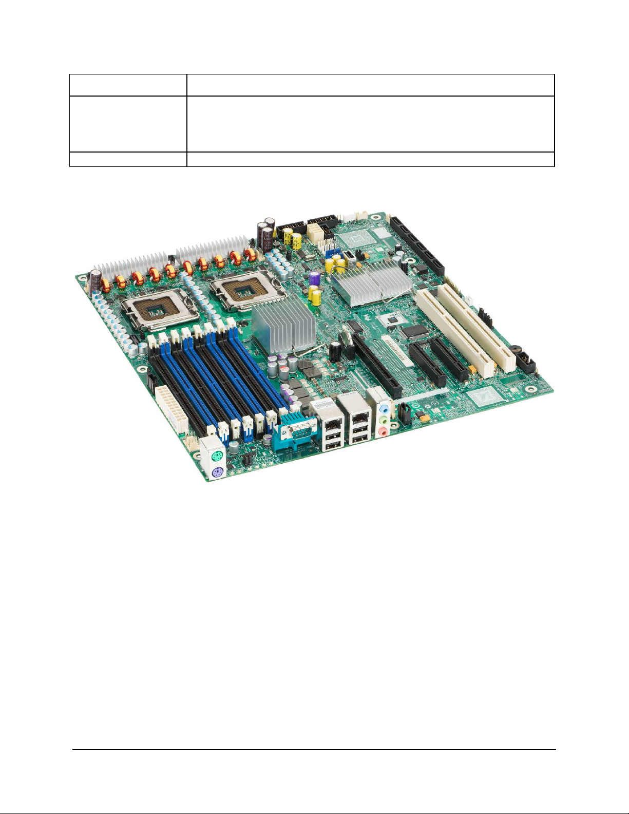
2.2 Workstation Board Layout
Figure 1. Workstation Board Photograph
Revision 1.5
Intel order number: D66403-006
3
Page 13
Overview Intel® Workstation Board S5000XVN TPS
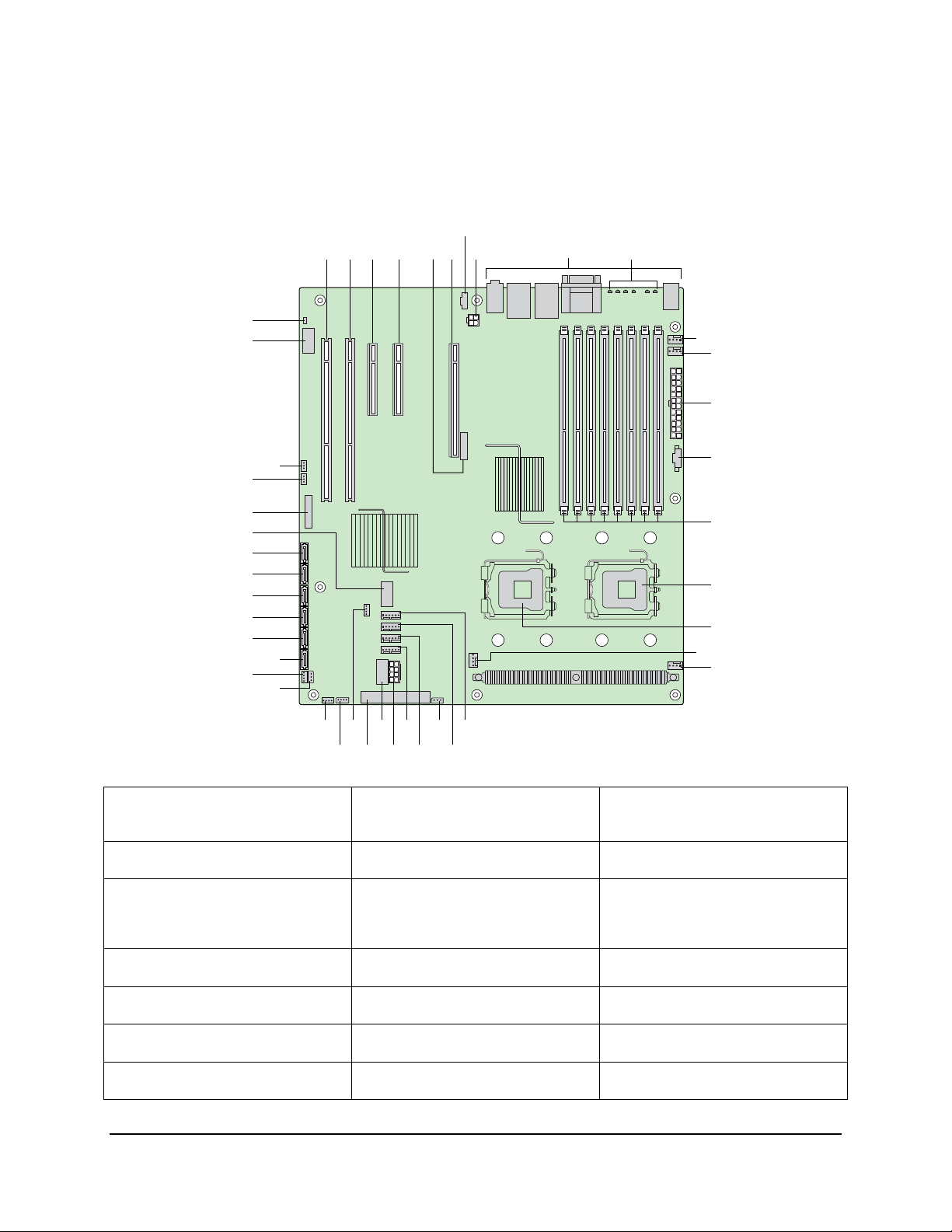
2.2.1 Workstation Board Connector and Component Layout
The following figure shows the board layout of the workstation board. Each connector and major
component is identified by a letter. A component descriptions table follows the figure.
G
A B
DC
E
H
F
I
J
RR
QQ
K
L
M
PP
N
OO
NN
MM
O
LL
KK
JJ
II
P
Q
HH
GG
FF
R
S
EE
T
YXW
V
U
AF000499
2
SES I
C (order code
S5000XVNSASR only)
code S5000XVNSASR only)
order code S5000XVNSASR only)
order code S5000XVNSASR only)
DD ZBB
AACC
A. PCI-X* 64-bit, 100-MHz fulllength/full-height slot 1
B. PCI-X 64-bit, 133-/100-MHz fulllength/full-height slot 2
C. PCI Express* x4
(S5000XVNSASR) or x8
(S5000XVNSATAR) full-length/fullheight slot 3 (x8 connector)
D. PCI Express* x4 half-length/fullheight slot 4 (x8 connector)
E. CMOS battery T. System fan 4 header II. SATA 2 or SAS 0 (SAS 0 on order
F. PCI Express x16 full-length/fullheight slot 6 (x16 connector)
G. CD-ROM line-in connector V. IPMB connector KK. SATA 4 or SAS 2 (SAS 2 on
P. Processor 1 socket EE. Enclosure management SAS
Q. Processor 2 socket FF. Hot-swap backplane A header
R. Processor 2 fan header GG. SATA 0
S. Processor 1 fan header HH. SATA 1
U. System fan 3 header JJ. SATA 3 or SAS 1 (SAS 1 on
Revision 1.5
4
Intel order number: D66403-006
Page 14
Intel® Workstation Board S5000XVN TPS Overview
H. P12V4 connector W. System fan 2 header LL. SATA 5 or SAS 3 (SAS 3 on
order code S5000XVNSASR only)
I. Back panel I/O ports X. System fan 1 header MM. USB port
J. Diagnostic and Identify LEDs Y. Processor power connector NN. Front control panel header
K. System fan 6 header Z. USB header OO. SATA software RAID 5 key
connector
L. System fan 5 header AA. IDE connector PP. SAS software RAID 5 key
connector (order code
S5000XVNSASR only)
M. Main power connector BB. Enclosure management SATA
SGPIO header
N. Auxilliary power signal connector CC. Hot-swap backplane B header RR. Chassis intrusion header
O. DIMM sockets DD. Enclosure management SAS
SGPIO header (order code
S5000XVNSASR only)
QQ. Serial B/emergency
management port header
Figure 2. Major Board Components
Revision 1.5
5
Intel order number: D66403-006
Page 15
Overview Intel® Workstation Board S5000XVN TPS
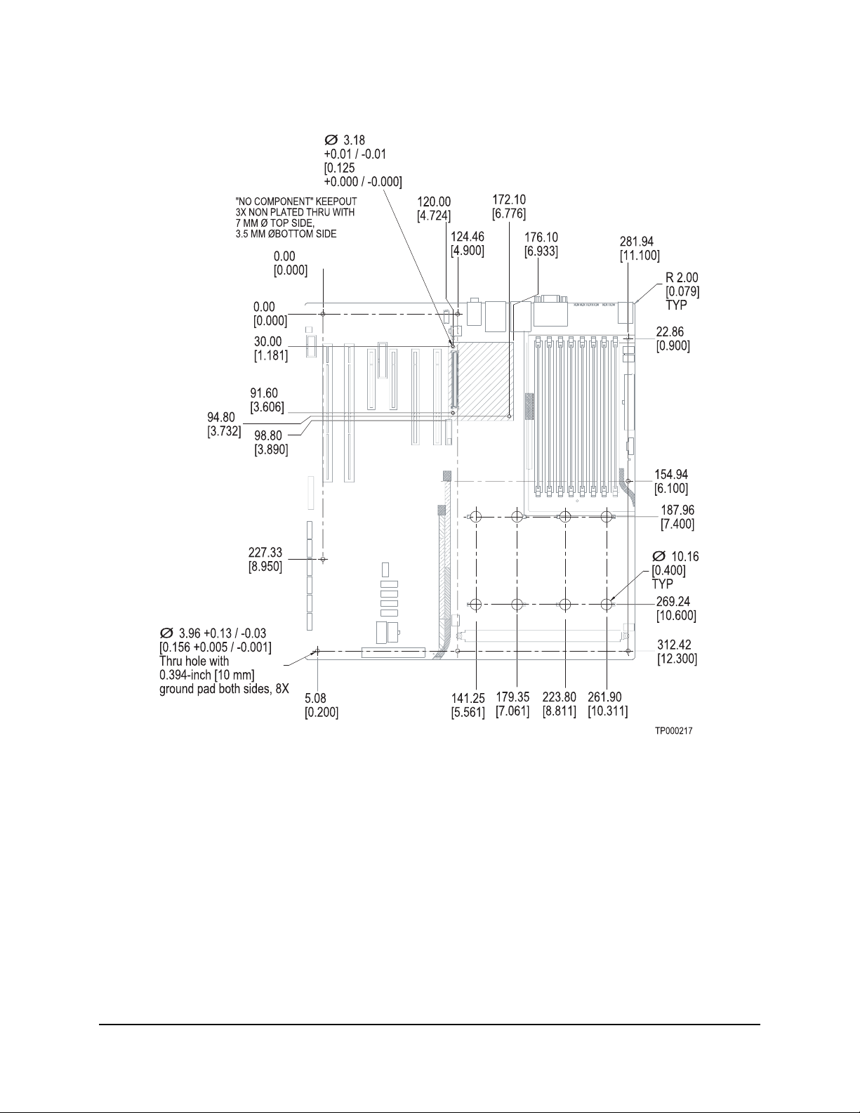
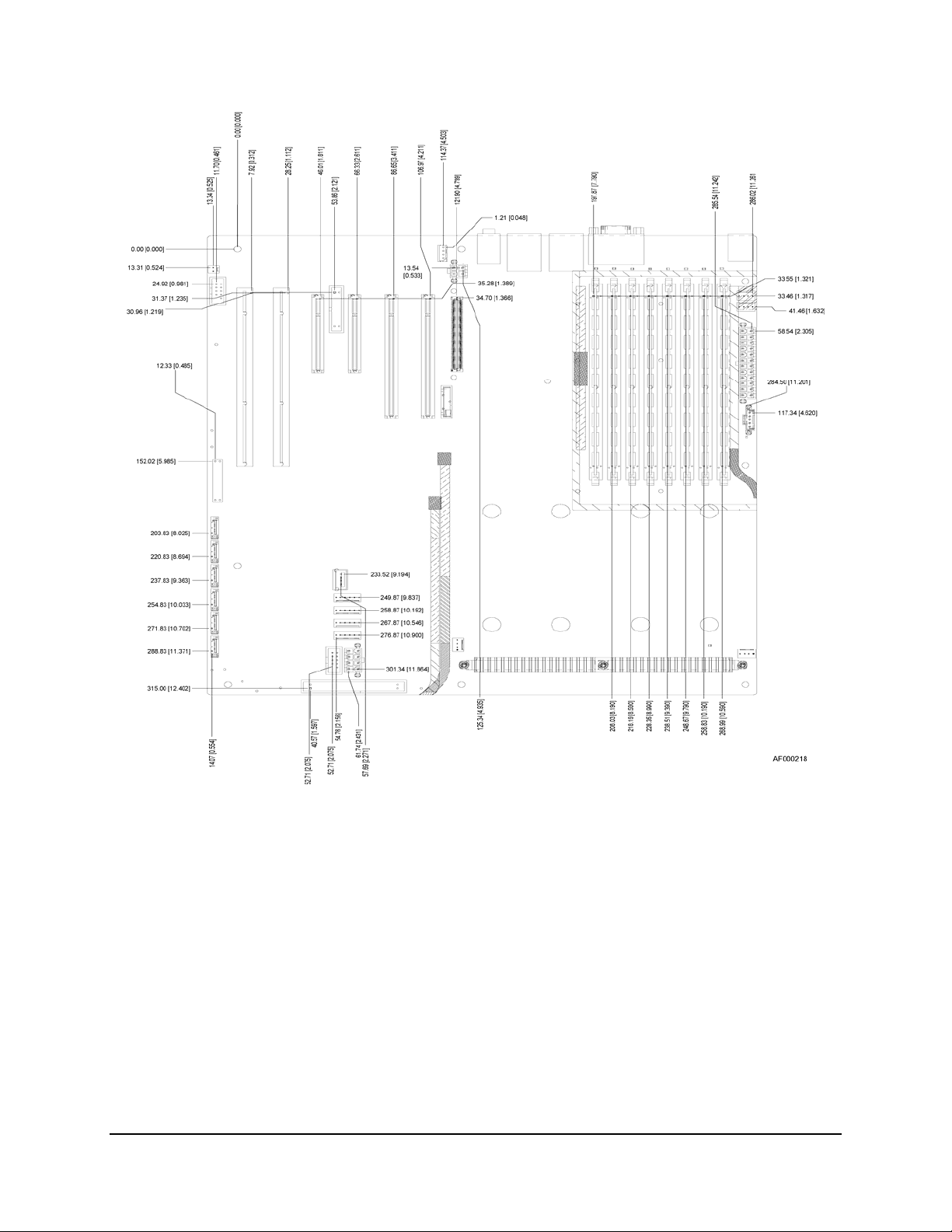
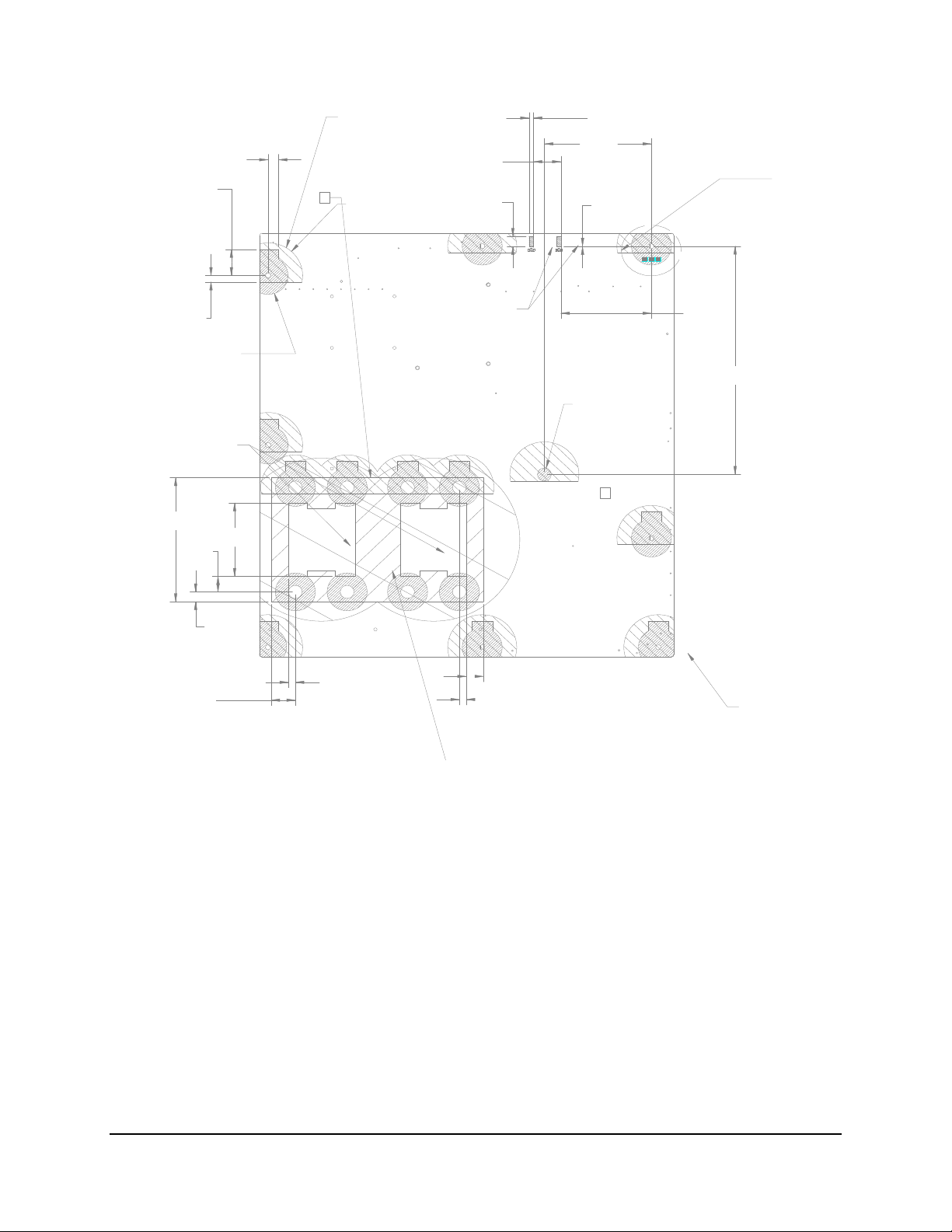
2.2.2 Workstation Board Mechanical Drawings
Figure 3. Mounting Hole Positions
Revision 1.5
6
Intel order number: D66403-006
Page 16
Intel® Workstation Board S5000XVN TPS Overview
Figure 4. Component Positions
Revision 1.5
Intel order number: D66403-006
7
Page 17
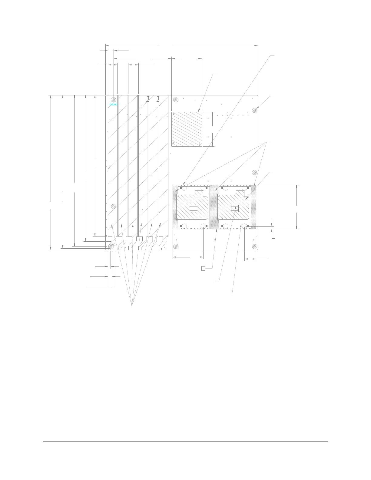
Overview Intel® Workstation Board S5000XVN TPS
304.80
12.000[]
20.32
0.800[]
TYP
60.100
2.3661[]
IMM3 COMPONENT
HEIGHT 3.6 MM
72.800
2.8661[]
HEATSINK DISSASEMBLY AREA,
.275" [8.26mm] MAX COMPONENT
HEIGHT RESTRICTION, 4 PLACES
Ø
10.160
0.4000[]
GROUND PAD BOTH SIDES
NO COMPONENT
8 PLCS
.433" [14mm] MAX COMPONENT
HEIGHT RESTRICTION
SOCKET AREA, NO COMPONENT
PLACEMENT ALLOWED, 2 PLACES
93.98
3.700[]
326.57
12.857[]
TYP
330.20
13.000[]
18.72
0.737[]
311.66
12.270[]
TYP
322.40
12.693[]
TYP
TYP
301.50
11.870[]
TYP
11.20
0.441[]
116.000
4.5669[]
5.33
0.210[]
TYP
7.92
0.312[]
TYP
16.05
0.632[]
TYP
60.96
2.400[]
3
.118" [3.81mm] MAX COMPONENT
HEIGHT RESTRICTION, 2 PLACES
HEATSINK AREA. .325" [8.26mm] MAX
COMPONENT HEIGHT RESTRICTIO, 2 PLACES
MAX HEIGHT OF COMPONENTS AND MATING COMPONENTS
SHALL NOT EXCEED 15.24mm [.600"]
Figure 5. Restricted Areas on Side 1
22.86
6.35
0.250[]
Revision 1.5
8
Intel order number: D66403-006
Page 18
Intel® Workstation Board S5000XVN TPS Overview
0.3000[]
20.320
0.8000[]
11 PLCS
5.08
0.200[]
TYP
R TYP14.730
0.5799[]
.100 [2.54<<] MAX COMPONENT
HEIGHT IN THESE ZONES
96.52
3.800[]
12.07
0.475[]
TYP7.620
57.15
2.250[]
LIMITED COMPONENT HEIGHT
.058" MAXIMUM 13 PLACES
3
R
25.40
1.000[]
TYP
20.320
0.8000[]
2X 8.000
0.3150[]
NO COMPONENTS ALLOWED
TRACES OKAY IN THIS REGION
2X 3.120
0.1228[]
78.74
3.100[]
2X 0.350
0.0138[]
Ø
GROUND PAD
10.160
0.4000[]
NO COMPONENT
1 PLACE
2
66.554
2.6202[]
177.80
7.000[]
SEE DETAIL B
7.62
0.300[]
12.70
0.500[]
5.08
0.200[]
CEK HEATSINK SPRING PLATE ZONE
NO COMPONENT PLACEMENT OR
THROUGH HOLE LEADS ALLOWED
NO COMPONENTS
THIS ZONE 16 PLCS
17.78
0.700[]
5.08
0.200[]
Figure 6. Restricted Areas on Side 2
Revision 1.5
9
Intel order number: D66403-006
Page 19
Overview Intel® Workstation Board S5000XVN TPS
3X 4.00
3X 10.13
0.399[]
5.00
0.197[]
0.157[]
5.00
0.197[]
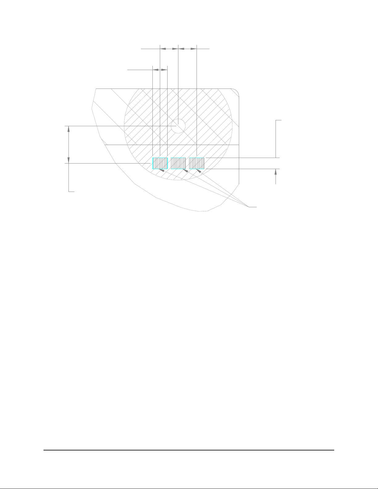
Figure 7. Restricted Areas on Side 2, “Detail B”
3X 3.00
CHASSIS ID PADS
0.118[]
Revision 1.5
10
Intel order number: D66403-006
Page 20
Intel® Workstation Board S5000XVN TPS Overview
10.160 [0.4000]
0.000 [0.0000]
320.040
[12.6000]
16.510 [0.6500]
0.000 [0.0000]
14.0mm COMPONENT HEIGHT
LIMIT DEFINED BY DUCT DETAIL
SUPPORT AREA,
NO COMPONENT
ALLOWED
145.600 [5.7323]
154.685 [6.0900]
15.0mm COMPONENT HEIGHT
LIMIT DEFINED BY DUCT DETAIL
235.085 [9.2553]
9.0 mm COMPONENT HEIGHT
LIMIT DEFINED BY DUCT DETAIL
27.0 mm COMPONENT HEIGHT
LIMIT DEFINED BY DUCT DETAIL
13.0 mm COMPONENT HEIGHT
LIMIT DEFINED BY DUCT DETAIL
317.580 [12.5032]
14.0mm COMPONENT HEIGHT
LIMIT DEFINED BY DUCT DETAIL
26.635
[1.0486]
73.482
[2.8930]
97.846
[3.8522]
118.351
[4.6595]
111.351 [4.3839]
143.732
[5.6588]
282.585
[11.1254]
188.152 [7.4076]
193.152 [7.6044]
SUPPORT AREA,
NO COMPONENT
ALLOWED
194.152
[7.6438]
187.152
[7.3682]
288.290 [11.3500]
273.091 [10.7516]
26.578 [1.0464]
43.302 [1.7048]
143.136 [5.6353]
168.123 [6.6190]
178.578 [7.0306]
16.5mm COMPONENT HEIGHT
LIMIT DEFINE BY DUCT DETAIL
1.25mm COMPONENT HEIGHT
LIMIT DEFINE BY DUCT DETAIL
NO COMPONENT ALLOWED
107.920 [4.2488]
117.851 [4.6398]
101.402 [3.9922]
112.851 [4.4430]
Figure 8. CPU and Memory Duct Keepout
Revision 1.5
Intel order number: D66403-006
11
Page 21
Overview Intel® Workstation Board S5000XVN TPS
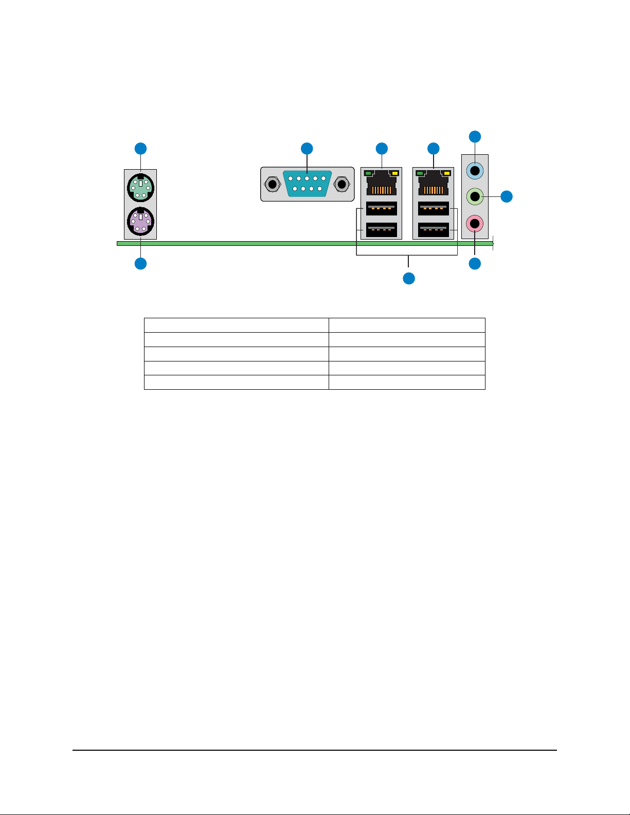
2.2.3 Workstation Board ATX I/O Layout
The following drawing shows the layout of the rear I/O components for the workstation board:
E
BA
C D
F
I G
H
AF001037
A. PS/2 mouse F. Audio out
B. Serial A port G. Microphone
C. NIC 1 (1 Gb) H. ID LED
D. NIC 2 I. Keyboard port
E. Audio in
Figure 9. ATX I/O Layout
Revision 1.5
12
Intel order number: D66403-006
Page 22
Intel® Workstation Board S5000XVN TPS Functional Architecture
3. Functional Architecture
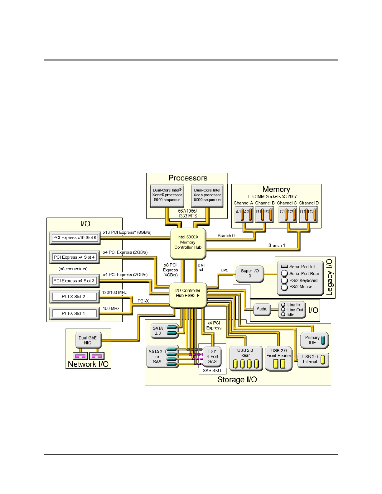
The architecture and design of the Intel® Workstation Board S5000XVN is based on the Intel®
S5000X chipset. This chipset is designed for systems that use the Intel
®
Xeon® processor with
system bus speeds of 667 MHz, 1066 MHz, and 1333 MHz.
The chipset contains two main components: the Memory Controller Hub (MCH) for the host
bridge and the I/O controller hub for the I/O subsystem. The chipset uses the Enterprise South
Bridge (ESB2-E) for the I/O controller hub. This chapter provides a high-level description of the
functionality associated with each chipset component and the architectural blocks that make up
the server board.
For more information about the functional architecture blocks, see the Intel
®
S5000 Server
Board Family Datasheet.
Figure 10. Functional Block Diagram
Revision 1.5
Intel order number: D66403-006
13
Page 23
Functional Architecture Intel® Workstation Board S5000XVN TPS
3.1 Intel
®
5000X Memory Controller Hub (MCH)
The Memory Controller Hub (MCH) is a single 1432-pin FCBGA package, which includes the
following core platform functions:
System Bus Interface for the processor subsystem
Memory Controller
PCI-Express Ports including the Enterprise South Bridge Interface (ESI)
FBD Thermal Management
SMBUS Interface
This section provides a high-level overview of some of these core functions as they pertain to
this workstation board. You can obtain additional information from the Intel S5000 Server Board
Family Datasheet and the Intel 5000 Series Chipset Memory Controller Hub Datasheet.
3.1.1 System Bus Interface
The MCH is configured for symmetric multi-processing across two independent front side bus
(FSB) interfaces that connect to the Intel
uses a 64-bit wide 667, 1066, or 1333 MHz data bus. The 1333-MHz data bus is capable of
transferring data at up to 10.66 GB/s. The MCH supports a 36-bit wide address bus, capable of
addressing up to 64 GB of memory. The MCH is the priority agent for both front side bus
interfaces, and is optimized for one processor on each bus.
®
Xeon® processors. Each front side bus on the MCH
3.1.2 Processor Support
The workstation board supports one or two Intel® Xeon® processors 5000 sequence with system
bus speeds of 667 MHz, 1066 MHz, and1333 MHz, and core frequencies starting at 2.66 GHz.
This workstation board does not support previous generations of the Intel
Note: Only Intel
®
Xeon® processors 5000 Sequence that support system bus speeds of 667
MHz, 1066 MHz, and 1333 MHz are supported on this workstation board. For a list of supported
processors, refer to the following table.
Table 2. Processor Support Matrix
Processor Family System Bus Speed Core Frequency Cache Watts Support
Intel® Xeon® Processor 533 MHz All No
Intel® Xeon® Processor 800 MHz All No
Intel® Xeon® Processor 5030 667 MHz 2.66 2 MB 95 Yes
Intel® Xeon® Processor 5050 667 MHz 3.0 GHz 2 MB 95 Yes
Intel® Xeon® Processor 5060 1066 MHz 3.2 GHz 2 MB 130 Yes
Intel® Xeon® Processor 5063 1066 MHz 3.2 GHz 2 MB 95 Yes
Intel® Xeon® Processor 5080 1066 MHz 3.73 GHz 2 MB 130 Yes
Intel® Xeon® Processor 5110 1066 MHz 1.60 GHz 4 MB 65 Yes
Intel® Xeon® Processor 5120 1066 MHz 1.86 GHz 4 MB 65 Yes
Intel® Xeon® Processor 5130 1333 MHz 2.00 GHz 4 MB 65 Yes
Intel® Xeon® Processor 5140 1333 MHz 2.33 GHz 4 MB 65 Yes
®
Xeon® processor.
Revision 1.5
14
Intel order number: D66403-006
Page 24
Intel® Workstation Board S5000XVN TPS Functional Architecture
Processor Family System Bus Speed Core Frequency Cache Watts Support
Intel® Xeon® Processor 5148 1333 MHz 2.33 GHz 4 MB 40 Yes
Intel® Xeon® Processor 5150 1333 MHz 2.66 GHz 4 MB 65 Yes
Intel® Xeon® Processor 5160 1333 MHz 3.00 GHz 4 MB 80 Yes
Intel® Xeon® Processor E5310 1333 MHz 1.6 GHz 8 MB 80 Yes
Intel® Xeon® Processor E5320 1333 MHz 1.86 GHz 8 MB 80 Yes
Intel® Xeon® Processor E5335 1333 MHz 2.00 GHz 8 MB 80 Yes
Intel® Xeon® Processor E5345 1333 MHz 2.33 GHz 8 MB 80 Yes
Intel® Xeon® Processor X5355 1333 MHz 2.66 GHz 8 MB 120 Yes
3.1.2.1 Processor Population Rules
When two processors are installed, both must be of identical revision, core voltage, and
bus/core speed. When only one processor is installed, it must be in the socket labeled CPU1.
The other socket must be empty.
The board is designed to provide up to 130 A of current per processor. This board does not
support processors with higher current requirements.
No terminator is required in the second processor socket when using a single processor
configuration.
3.1.2.2 Common Enabling Kit (CEK) Design Support
The workstation board complies with Intel’s Common Enabling Kit (CEK) processor mounting
and heatsink retention solution. The workstation board ships with a CEK spring snapped onto
the underside of the workstation board beneath each processor socket. The heatsink attaches
to the CEK over the top of the processor and the thermal interface material (TIM). Refer to the
following figure for the stacking order of the chassis, CEK spring, workstation board, TIM, and
heatsink.
The CEK spring is removable, which allows for the use of non-Intel heatsink retention solutions.
Note: The processor heatsink and CEK spring shown in the following diagram are for reference
purposes only. The actual processor heatsink and CEK solutions compatible with this
generation server board may be of a different design.
Revision 1.5
Intel order number: D66403-006
15
Page 25
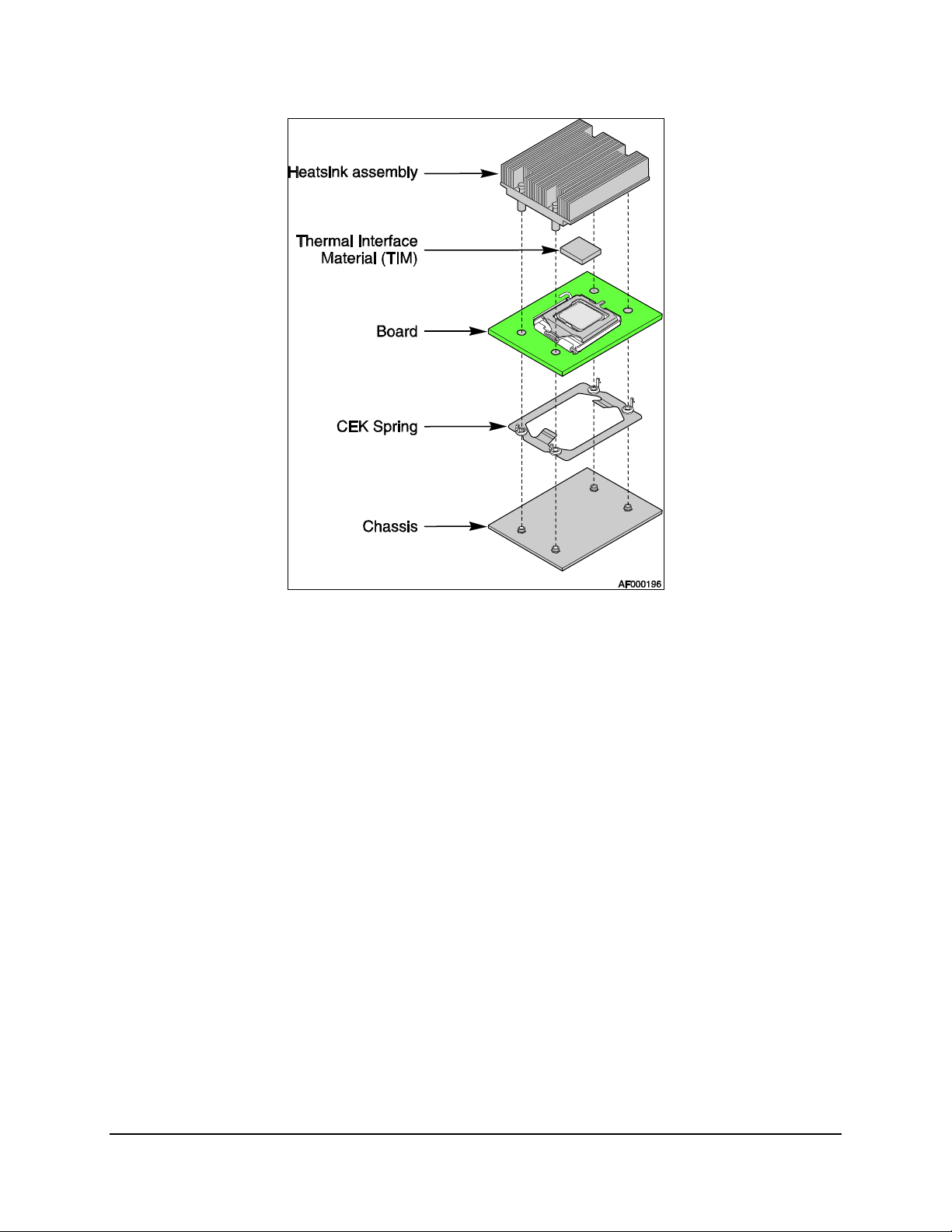
Functional Architecture Intel® Workstation Board S5000XVN TPS
Figure 11. CEK Processor Mounting
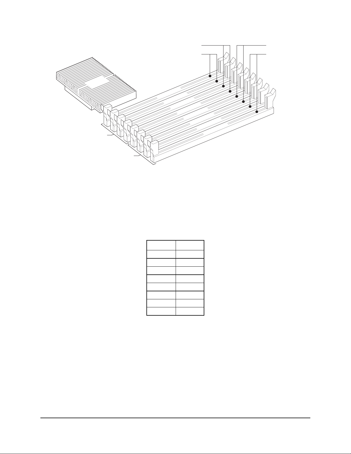
3.1.3 Memory Subsystem
The MCH supports four fully buffered DIMM (FBD) memory channels. FBD memory uses a
narrow, high–speed, frame-oriented interface referred to as a channel. The four FBD channels
are organized into two branches of two channels per branch. Each branch is supported by a
separate memory controller. The two channels on each branch operate in lock-step to increase
FBD bandwidth. The four channels are routed to eight DIMM sockets and are capable of
supporting registered DDR2-533 and DDR2-667 FBDIMM memory (stacked or unstacked).
Peak theoretical memory data bandwidth is 6.4GB/s with DDR2-533 and 8.0GB/s with DDR2-
667.
On the Intel
Branch 0 consists of channels A and B, and Branch 1 consists of channels C and D. FBD
memory channels are organized into two branches for support of RAID 1 (mirroring).
®
Workstation Board S5000XVN, a pair of channels becomes a branch where
Revision 1.5
16
Intel order number: D66403-006
Page 26
Intel® Workstation Board S5000XVN TPS Functional Architecture
Channel B
Channel A
Channel C
Channel D
MCH
DIMM A1
DIMM A2
DIMM B1
DIMM B2
DIMM C1
DIMM C2
DIMM D1
Branch 0
DIMM D2
Branch 1
TP02299
Figure 12. Memory Layout
To boot the system, the system BIOS on the workstation board uses a dedicated I2C bus to
retrieve DIMM information needed to program the MCH memory registers. The following table
provides the I
2
C addresses for each DIMM socket.
Table 3. I2C Addresses for Memory Module SMB
Device Address
DIMM A1 0xA0
DIMM A2 0xA2
DIMM B1 0xA0
DIMM B2 0xA2
DIMM C1 0xA0
DIMM C2 0xA2
DIMM D1 0xA0
DIMM D2 0xA2
Revision 1.5
17
Intel order number: D66403-006
Page 27
Functional Architecture Intel® Workstation Board S5000XVN TPS
3.1.3.1 Memory RASUM Features
The MCH supports several memory RASUM (Reliability, Availability, Serviceability, Usability,
and Manageability) features. These features include the Intel
®
(Intel
x4 SDDC) for the following:
®
x4 Single Device Data Correction
Memory error detection and correction
Memory scrubbing
Retry on correctable errors
Memory built-in self-test
DIMM sparing
Memory mirroring
®
For more information about these features, refer to the Intel
S5000 Server Board Family
Datasheet.
3.1.3.2 Supported Memory
The workstation board supports up to eight DDR2-533 or DDR2-667 fully-buffered DIMMs (FBD
memory). The following tables show the maximum memory configurations supported with the
specified memory technology.
Table 4. Maximum Eight-DIMM System Memory Configruation – x8 Single Rank
DRAM Technology
x8 Single Rank
Maximum Capacity
Mirrored Mode
Maximum Capacity
Non-mirrored Mode
256 Mb 1 GB 2 GB
512 Mb 2 GB 4 GB
1024 Mb 4 GB 8 GB
2048 Mb 8 GB 16 GB
Table 5. Maximum Eight-DIMM System Memory Configuration – x4 Dual Rank
DRAM Technology
x4 Dual Rank
256 Mb 4 GB 8 GB
512 Mb 8 GB 16 GB
1024 Mb 16 GB 32 GB
2048 Mb 16 GB 32 GB
Maximum Capacity
Mirrored Mode
Maximum Capacity
Non-mirrored Mode
Table 6. Maximum Eight-DIMM System Memory Configuration – x2 Quad Rank
DRAM Technology
x2 Quad Rank
1024 Mb 16 GB 32 GB
2048 Mb 16 GB 32 GB
Maximum Capacity
Mirrored Mode
Maximum Capacity
Non-mirrored Mode
Revision 1.5
18
Intel order number: D66403-006
Page 28

Intel® Workstation Board S5000XVN TPS Functional Architecture
Note: This workstation board supports only fully buffered DDR2 DIMMs (FBDIMMs. See the
®
Intel
Workstation Board S5000XVN Tested Memory List for a list of supported memory for this
server board.
3.1.3.3 DIMM Population Rules and Supported DIMM Configurations
DIMM population rules depend on the operating mode of the memory controller, which is
determined by the number of DIMMs installed. You must populate DIMMs in pairs. DIMM pairs
are populated in the following DIMM socket order:
A1 and B1
C1 and D1
A2 and B2
C2 and D2
DIMMs within a given pair must be identical with respect to size, speed, and organization.
However, DIMM capacities can be different between different DIMM pairs. For example, a valid
mixed DIMM configuration may have 512 MB FBDIMMs installed in DIMM sockets A1 and B1,
and 1 GB FBDIMMs installed in DIMM sockets C1 and D1.
Revision 1.5
Intel order number: D66403-006
19
Page 29
Functional Architecture Intel® Workstation Board S5000XVN TPS
In the following table, the following codes are used:
VP: Validated configuration and the slot is populated
SP: Supported, but not validated configuration, and the slot is populated
NP: Slot is not populated
Table 7. DIMM Population Rules
Branch 0 Branch 1
Channel A Channel B Channel C Channel D
DIMM_A1 DIMM_A2 DIMM_B1 DIMM B2 DIMM C1 DIMM C2 DIMM D1 DIMM D2
VP NP NP NP NP NP NP NP No No
VP NP VP NP NP NP NP NP No No
SP SP SP SP NP NP NP NP No SP, Yes, Branch 0 only
VP NP VP NP VP NP VP NP VP, Yes No
SP SP SP SP SP NP SP NP No SP, Yes, Branch 0 only
VP VP VP VP VP VP VP VP VP, Yes VP, Yes, Branch 0 and
Notes:
Single channel mode is only tested and supported with a 512 MB x8 FBDIMM installed in DIMM Socket A1.
The supported memory configurations must meet population rules defined above.
For best performance, you should install a minimum of four DIMMs across memory branches.
Although mixed DIMM capacities between channels are supported, Intel
®
does not validate FBDIMMs in mixed DIMM configurations.
Mirroring Possible Sparing Possible
Branch 1
Revision 1.5
20
Intel order number: D66403-006
Page 30
Intel® Workstation Board S5000XVN TPS Functional Architecture
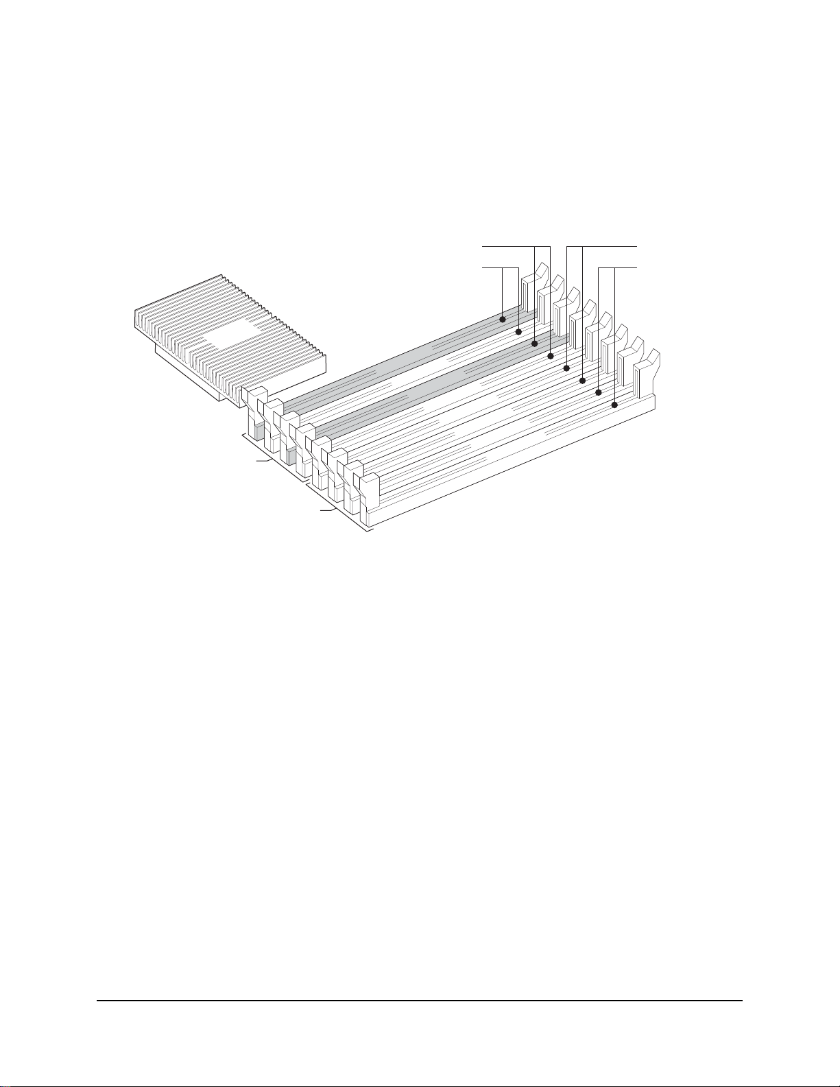
3.1.3.3.1 Minimum Non-Mirrored Mode Configuration
The workstation board is capable of supporting a minimum of one DIMM installed. However, for
system performance reasons, Intel’s recommendation is that at least two DIMMs are installed.
The following diagram shows the recommended minimum DIMM memory configuration.
Populated DIMM slots are shown in gray.
MCH
Branch 0
Channel B
Channel A
DIMM A1
DIMM A2
DIMM B1
DIMM B2
DIMM C1
DIMM C2
DIMM D1
DIMM D2
Branch 1
Figure 13. Minimum 2-DIMM Memory Configuration
Channel C
Channel D
TP02300
Note: The workstation board supports single DIMM mode operation. Intel will only validate and
support this configuration with a single 512 MB x8 FBDIMM installed in DIMM socket A1.
3.1.3.4 Non-mirrored Mode Memory Upgrades
The minimum memory upgrade increment is two DIMMs per branch. The DIMMs must cover the
same slot position on both channels. DIMMs pairs must be identical with respect to size, speed,
and organization. DIMMs that cover adjacent slot positions do not need to be identical.
When adding two DIMMs to the configuration shown in Figure 13 (above), you should populate
the DIMMs in DIMM sockets C1 and D1 as shown in the following diagram. Populated DIMM
sockets are shown in gray.
Revision 1.5
Intel order number: D66403-006
21
Page 31

Fuctional Architecture Intel® Workstation Board S5000XVN TPS
MCH
Branch 0
Channel B
Channel A
DIMM A1
DIMM A2
DIMM B1
DIMM B2
DIMM C1
DIMM C2
DIMM D1
DIMM D2
Branch 1
Figure 14. Recommended Four DIMM Configuration
Channel C
Channel D
TP02301
Functionally, DIMM sockets A2 and B2 could have been populated instead of DIMM sockets C1
and D1. However, the system would not achieve equivalent performance. Figure 13, on the
previous page, shows the supported DIMM configuration that is recommended because it allows
both branches to operate independently and simultaneously. FBD bandwidth is doubled when
both branches operate in parallel.
3.1.3.4.1 Mirrored Mode Memory Configuration
When operating in mirrored mode, both branches operate in lock step. In mirrored mode, branch
1 contains a replicate copy of the data in branch 0. The minimum DIMM configuration to support
memory mirroring is four DIMMs, populated as shown in Figure 14. All four DIMMs must be
identical with respect to size, speed, and organization.
To upgrade a four DIMM mirrored memory configuration, you must add four additional DIMMs to
the system. All four DIMMs in the second set must be identical to the first with the exception of
speed. The MCH adjusts to the lowest speed DIMM.
3.1.3.4.2 Sparing Mode Memory Configuration
The MCH provides memory sparing capabilities. Sparing is a RAS feature that involves
configuring a DIMM to be placed in reserve so it can be used to replace a DIMM that fails.
DIMM sparing occurs within a given bank of memory and is not supported across branches.
There are two supported memory sparing configurations.
Single Branch Mode Sparing
Dual Branch Mode Sparing
Revision 1.5
22
Intel order number: D66403-006
Page 32

Intel® Workstation Board S5000XVN TPS Functional Architecture
3.1.3.4.2.1 Single Branch Mode Sparing
Slot 2
Slot 1
DIMM_A2
DIMM_A1
Channel A Channel B Channel C Channel D
DIMM_B2
DIMM_B1
DIMM_C2
DIMM_C1
DIMM_D2
DIMM_D1
Branch 0 Branch 1
Intel® 5000X Memory Controller Hub
Figure 15. Single Branch Mode Sparing DIMM Configuration
DIMM_A1 and DIMM_B1 must be identical in organization, size, and speed.
DIMM_A2 and DIMM_B2 must be identical in organization, size, and speed.
DIMM_A1 and DIMM_A2 need not be identical in organization, size, and speed.
DIMM_B1 and DIMM_B2 need not be identical in organization, size, and speed.
Sparing should be enabled in the BIOS setup.
The BIOS will configure Rank Sparing Mode.
The larger of the pairs {DIMM_A1, DIMM_B1} and {DIMM_A2, DIMM_B2} are selected
as the spare pair unit.
3.1.3.4.2.2 Dual Branch Mode Sparing
Dual branch mode sparing requires that all eight DIMM sockets be populated and must comply
with the following population rules.
DIMM_A1 and DIMM_B1 must be identical in organization, size, and speed.
DIMM_A2 and DIMM_B2 must be identical in organization, size, and speed.
DIMM_C1 and DIMM_D1 must be identical in organization, size, and speed.
DIMM_C2 and DIMM_D2 must be identical in organization, size, and speed.
DIMM_A1 and DIMM_A2 need not be identical in organization, size, and speed.
DIMM_B1 and DIMM_B2 need not be identical in organization, size, and speed.
DIMM_C1 and DIMM_C2 need not be identical in organization, size, and speed.
DIMM_D1 and DIMM_D2 need not be identical in organization, size, and speed.
Sparing should be enabled in the BIOS setup.
The BIOS will configure Rank Sparing Mode.
The larger of the pairs {DIMM_A1, DIMM_B1}, {DIMM_A2, DIMM_B2},
{DIMM_C1, DIMM_D1}, and {DIMM_C2, DIMM_D2} are selected as the spare pair units.
Revision 1.5
Intel order number: D66403-006
23
Page 33

Fuctional Architecture Intel® Workstation Board S5000XVN TPS
3.1.4 Snoop Filter
The 5000X version of the MCH includes a snoop filter. Depending on the application of the
workstation, you can use this feature to enhance the performance of the workstation by
eliminating traffic on the snooped system bus of the processor being snooped. By removing
snoops from the snooped bus, the full bandwidth is available for other transactions.
3.2 Enterprise South Bridge (ESB2-E)
The ESB2-E is a multi-function device that provides four distinct functions: an I/O controller, a
PCI-X* bridge, GB Ethernet controller, and baseboard management controller (BMC). Each
function has its own set of configuration registers. Once configured, each appears to the system
as a distinct hardware controller.
The ESB2-E provides the gateway to all PC-compatible I/O devices and features. The
workstation board uses the following ESB2-E features:
PCI-X bus interface
Six-channel SATA interface with SATA Busy LED Control
Dual GbE MAC
Baseboard Management Controller (BMC)
Single ATA interface, with Ultra DMA 100 capability
Universal Serial Bus 2.0 (USB) interface
Removable media drives
LPC bus interface
PC-compatible timer/counter and DMA controllers
APIC and 8259 interrupt controller
Power management
System RTC
General purpose I/O
This section describes the function of most of the listed features as they pertain to this
workstation board. For more detailed information, see the Intel 631xESB/632xESB I/O
Controller Hub Datasheet.
3.2.1 PCI Subsystem
The primary I/O buses for the server board are PCI, PCI Express*, and PCI-X* with six
independent PCI bus segments. The PCI buses comply with the PCI Local Bus Specification,
Revision 2.3. The following table lists the characteristics of the PCI bus segments. Details about
each bus segment follow the table.
Revision 1.5
24
Intel order number: D66403-006
Page 34

Intel® Workstation Board S5000XVN TPS Functional Architecture
Table 8. PCI Bus Segment Characteristics
PCI Bus Segment Voltage Width Speed Type PCI I/O Card Slots
PCI32
ESB2-E
PXA
ESB2-E
PXA
ESB2-E
PE0
ESB2-E PCI Express*
Port0
PE1
ESB2-E PCI Express*
Port1
PE2
ESB2-E PCI Express*
Port2
PE4, PE5, PE6, PE7
BNB PCI Express*
Ports 4, 5, 6, 7
3.3 V 32 bit 33 MHz PCI None
3.3 V/5.0 V 64 bit 100 MHz PCI-X* PCI-X Slot 1
3.3 V/5.0 V 64 bit 133 MHz PCI-X PCI-X Slot 2
3.3 V X4 10 Gb/S PCI
Express*
3.3 V X4 10 Gb/S PCI Express x4 throughput PCI Express* Slot 3
3.3 V X4 10 Gb/S PCI Express x4 throughput to onboard SAS (re-
3.3 V X16 40 Gb/S PCI Express X16 throughput PCI Express* Slot
X4 throughput PCI Express* Slot 4
(x8 throughput for workstation
boards that do not support SAS by
combining PE2 with PE1)
routed to Slot 3 for workstation
boards that do not support SAS)
6
3.2.1.1 PCI32: 32-bit, 33-MHz PCI Subsystem
All 32-bit, 33-MHz PCI I/O is directed through the ESB2-E ICH6. The 32-bit, 33-MHz PCI
segment created by the ESB2-E-ICH6 is known as the PCI32 segment. The PCI32 segment is
not connected to any devices on the workstation board S5000XVN.
3.2.1.2 PXA: 64-bit, 133-MHz PCI Subsystem
One 64-bit PCI-X bus segment is directed through the ESB2-E ICH6. This PCI-X segment, PXA,
is routed to PCI-X Slots 1 and 2. With only one PCI-X adapter populated in Slot 2 and Slot 1 left
empty, PCI-X Slot 2 supports a maximum speed of 133MHz. With both Slot 1 and Slot 2
populated, Slot 2 supports a maximum speed of 100 MHz. PCI-X Slot 1 supports a maximum
speed of 100 MHz even when Slot 2 is not populated.
3.2.1.3 PE0: One x4 PCI Express* Bus Segment
One x4 PCI Express* bus segment is directed through the ESB2-E. This PCI Express* segment,
PE0, is routed to PCI Express* Slot 4.
3.2.1.4 PE1: One x4 PCI Express* Bus Segment
One x4 PCI Express* bus segment is directed through the ESB2-E. This PCI Express* segment,
PE1, is routed to PCI Express* Slot 3. This becomes a x8 PCI Express* bus segment for
workstation boards that do not support SAS by combining PE2 with PE1.
Revision 1.5
Intel order number: D66403-006
25
Page 35

Functional Architecture Intel® Workstation Board S5000XVN TPS
3.2.1.5 PE2: One x4 PCI Express* Bus Segment
One x4 PCI Express* bus segment is directed through the ESB2-E. This PCI Express* segment,
PE2, is routed to PCI Express* Slot 3 for workstation boards that do not support SAS, or to the
onboard SAS controller for workstation boards that do support SAS.
3.2.1.6 PE4, PE5, PE6, PE7: Four x4 PCI Express* Bus Segments
Four x4 PCI Express* bus segments are directed through the MCH. These PCI Express*
segments, PE4, PE5, PE6 and PE7, are routed to PCI Express* Slot 6, making it a x16 slot.
3.2.1.7 PCI Express* Riser Slot
PCI Express* Slot 6 supports third-party riser cards for both 1U and 2U system configurations.
Two PCI Express* pins are designated as riser type pins with the definitions noted in the
following table:
Slot 6 Setup 1
2U Riser, 2 x8 PCI Express* Slots2 0 1
1U Riser, 1 x16 PCI Express* Slot3 1 0
Notes:
1. The workstation board contains a weak pull-up resistor on the two Riser Type nets.
2. The 2U riser card needs to pull-down the PCI Express* pin B48 with a 0 ohm resistor and leave as a NoConnect (NC) PCI Express* pin B49.
3. The 1U riser card needs to follow the standard PCI Express* Adapter pin-out by leaving pin B48 as a NoConnect (NC) and pin B49 as ground.
LP Riser Type 1 LP Riser Type 0
GPI: ESB2 GPI 28 GPI: ESB2 GPI 27
PCI-E Pin: B48 [RSVD] PCI-E Pin: B49 [GND]
The following table provides the supported bus throughput for the given riser card used and the
number of add-in cards installed.
PCI Express* Slot 6 Riser Support One Add-in Card Two Add-in Cards
1U Riser Card X16 NA
2U Riser Card X8 X8
Note: There are no population rules for installing a single add-in card in the 2U riser card; you
can install a single ad- in card in either PCI Express* slot.
3.2.2 Serial ATA Support
The ESB2-E has an integrated Serial ATA (SATA) controller that supports independent DMA
operation on six ports and supports data transfer rates of up to 3.0 Gb/s. The six SATA ports on
the server board are numbered SATA-0 through SATA-5. You can enable/disable and/or
configure the SATA ports by accessing the BIOS Setup utility during POST.
3.2.2.1 Intel
The onboard storage capability of this workstation board includes support for Intel
®
Embedded Server RAID Technology II Support
®
Embedded
Server RAID Technology II, which provides three standard software RAID levels: data stripping
(RAID Level 0), data mirroring (RAID Level 1), and data stripping with mirroring (RAID Level
10).
Revision 1.5
26
Intel order number: D66403-006
Page 36

Intel® Workstation Board S5000XVN TPS Functional Architecture
For higher performance, you can use data stripping to alleviate disk bottlenecks by taking
advantage of the dual independent DMA engines that each SATA port offers. Data mirroring is
used for data security. If a disk fails, a mirrored copy of the failed disk is brought on-line. There
is no loss of either PCI resources (request/grant pair) or add-in card slots.
With the addition of an optional Intel
®
RAID Activation Key, Intel® Embedded Server RAID
Technology II is also capable of providing fault tolerant data stripping (software RAID Level 5),
such that if a SATA hard drive fails, you can restore the lost data on a replacement drive from
the other drives that make up the RAID 5 pack.
See Figure 2 for the location of Intel
®
Intel
Embedded Server RAID Technology functionality requires the following items:
Intel
Intel
Intel
®
ESB-2 I/O Controller Hub
®
Embedded Server RAID Technology Option ROM
®
Application Accelerator RAID Edition drivers, most recent revision
®
RAID Activation Key connector location.
At least two SATA hard disk drives
®
Intel
Embedded Server RAID Technology is not available in the following configurations:
The SATA controller in compatible mode
Intel
3.2.2.2 Intel
The Intel
system user interface for the Intel
provides the ability for an Intel
boot disk and detect any faults in the Intel
attached to the Intel
®
Embedded Server RAID Technology has been disabled
®
Embedded Server RAID Technology Option ROM
®
Embedded Server RAID Technology for SATA Option ROM provides a pre-operating
®
RAID controller.
®
Embedded Server RAID Technology implementation and
®
Embedded Server RAID Technology volume to be used as a
®
Embedded Server RAID Technology volume(s)
3.2.3 Parallel ATA (PATA) Support
The integrated IDE controller of the ESB2-E ICH6 provides one IDE channel. It redefines
signals on the IDE cable to allow both host and target throttling of data and transfer rates of up
to 100 MB/s. For this workstation board, the IDE channel was designed to provide optical drive
support to the platform. The BIOS initializes and supports ATAPI devices such as LS-120/240,
CD-ROM, CD-RW, and DVD-ROM. The IDE channel is accessed through a single standard 40pin IDE connector (J2J2) that provides the I/O signals. You can configure and enable/disable
the ATA channel by accessing the BIOS Setup utility during POST.
3.2.4 USB 2.0 Support
The USB controller functionality integrated into ESB2-E provides the workstation board with the
interface for up to seven USB 2.0 ports. Four external connectors are located on the back edge
of the workstation board. One internal 2x5 header (J3J1) is provided, capable of supporting two
optional USB 2.0 ports. One USB port Type A connector (J3G1) is provided to support
installation of a USB device inside the server chassis.
Revision 1.5
Intel order number: D66403-006
27
Page 37

Functional Architecture Intel® Workstation Board S5000XVN TPS
3.3 Audio Codec
The workstation board supports the Intel® High Definition audio subsystem based on the
Realtek* ALC260 audio codec. The ALC260 is a 2-channel HD Audio codec featuring a 24-bit,
2-channel DAC and two stereo 20-bit ADCs.
LINE OUT
LINE IN
ESB2
Intel High Definition
Audio Link
ALC260
Audio Codec
MIC IN
Figure 16. Audio Subsystem Block Diagram
The ALC260 provides two output channels with flexible mixing, mute, and fine gain controls to
provide a complete integrated audio solution. The ALC260 provides high-quality audio using
S/PDIF to output analog data or multiple-source recording applications. Jack-sensing allows
inputs and output device loads to be auto-detected. Analog IOs are both input and output
capable. The ALC260 supports 32-bit S/PDIF input/ output functions.
The feature list for the ALC260 is as follows:
Single-chip multi-bit Sigma-Delta converters with high S/N ratio
One stereo DAC that supports 16/20/24-bit PCM format with 44.1K/48K/96K/ 192kHz
sample rate
Two stereo ADCs that support 16/20-bit PCM format with 44.1K/48K/96kHz sample rate
High-quality differential CD analog input
–64dB ~ +30dB with 1dB mixer gain for fine volume control
Impedance-sensing capability for each re-tasking jack
Built-in headphone amplifier for each re-tasking jack
Meets Microsoft WHQL/WLP 2.0* audio requirements
Emulation of 26 sound environments to enhance the gaming experience
10-band software equalizer
Enhanced configuration panel and device sensing wizard to improve user experience
Mono/stereo microphone noise suppression
Revision 1.5
28
Intel order number: D66403-006
Page 38

Intel® Workstation Board S5000XVN TPS Functional Architecture
The workstation board supports the following audio connections through the rear I/O:
LINE OUT
LINE IN
MIC IN
Figure 17. Rear I/O Panel Audio Connector
The workstation board supports ATAPI CD-ROM (a 1x4-pin ATAPI-style connector for
connecting an internal ATAPI CD-ROM drive to the audio mixer, connector J4A1) audio
connection inside the chassis.
3.4 SAS Controller
The LSI Logic* SAS1064e controller supports x4 PCI Express* link widths and is a singlefunction PCI Express* end-point device. The SAS controller supports the SAS protocol as
described in the Serial Attached SCSI Standard, version 1.0. The controller also supports SAS
1.1 features.
The SAS1064e controller supports a 32-bit external memory bus that provides an interface for
Flash ROM and NVSRAM devices.
3.4.1 SAS RAID Support
RAID modes 0, 1, and 10 are supported. You can use an optional SAS RAID Key to support SW
RAID 5.
3.4.2 SAS/SATA Connector Sharing
Four SATA connectors are shared between SATA and SAS, depending on the version of the
workstation board. For SAS workstation boards, four of the six SATA connectors are used for
SAS functionality. For SATA workstation boards, all six SATA connectors are used for SATA
functionality.
3.5 Network Interface Controller (NIC)
Network interface support is provided from the built in Dual GbE MAC features of the ESB2 in
®
conjunction with the Intel
82563EB compact Physical Layer Transceiver (PHY). Together, they
provide the workstation board with support for dual LAN ports designed for 10/100/1000 Mbps
operation.
Revision 1.5
Intel order number: D66403-006
29
Page 39

Functional Architecture Intel® Workstation Board S5000XVN TPS
The 82563EB device is based upon proven PHY technology integrated into Intel’s gigabit
Ethernet controllers. The physical layer circuitry provides a standard IEEE 802.3 Ethernet
interface for 1000BASE-T, 100BASE-TX, and 10BASE-T applications (802.3, 802.3u, and
802.3ab). The 82563EB device is capable of transmitting and receiving data at rates of
1000 Mbps, 100 Mbps, or 10 Mbps.
Each network interface controller (NIC) drives two LEDs located on each network interface
connector. The link/activity LED (at the left of the connector) indicates network connection when
on and transmit/receive activity when blinking. The speed LED (at the right of the connector)
indicates 1000-Mbps operation when amber; 100-Mbps operation when green; and 10-Mbps
when off. The following table provides an overview of the LEDs.
Table 9. NIC2 Status LED
LED Color LED State NIC State
Off 10 Mbps
Green/Amber (Right)
Green (Left)
Green 100 Mbps
Amber 1000 Mbps
On Active Connection
Blinking Transmit/Receive activity
3.5.1 Intel
Intel® I/O Acceleration Technology (Intel® I/OAT) moves network data more efficiently through
®
Intel
Xeon® processor 5000 sequence-based servers for improved application responsiveness
across diverse operating systems and virtualized environments. Intel I/OAT improves network
application responsiveness by using the power of Intel
®
I/O Acceleration Technolgy (Intel® I/OAT)
®
Xeon® processors 5000 sequence using
more efficient network data movement and reduced system overhead.
Intel multi-port network adapters with Intel
®
I/OAT provide high-performance I/O for server
consolidation and virtualization via stateless network acceleration that seamlessly scales across
multiple ports and virtual machines. Intel I/OAT provides safe and flexible network acceleration
through tight integration into popular operating systems and virtual machine monitors, avoiding
the support risks of third-party network stacks and preserving existing network requirements,
such as teaming and failover.
3.5.2 MAC Address Definition
Each Intel® Workstation Board S5000XVN has four MAC addresses assigned to it at the Intel
factory. During the manufacturing process, each workstation board will have a white MAC
address sticker placed on the board. The sticker displays the MAC address in both bar code
and alphanumeric formats. The printed MAC address is assigned to NIC 1 on the workstation
board. NIC 2 is assigned the NIC 1 MAC address + 1.
Two additional MAC addresses are assigned to the baseboard management controller (BMC)
that is embedded in the ESB-2. These MAC addresses are used by the BMC’s embedded
network stack to enable IPMI remote management over LAN. BMC LAN Channel 1 is assigned
the NIC1 MAC address + 2, and BMC LAN Channel 2 is assigned the NIC1 MAC address + 3
Revision 1.5
30
Intel order number: D66403-006
Page 40

Intel® Workstation Board S5000XVN TPS Functional Architecture
3.6 Super I/O
Legacy I/O support is provided by using a National Semiconductor* PC87427 Super I/O device.
This chip contains all of the necessary circuitry to support the following functions:
GPIOs
Two serial ports
Keyboard and mouse support
Wake up control
System health support
3.6.1 Serial Ports
The workstation board provides two serial ports: an external DB9 serial port and an internal
DH10 serial header. The rear DB9 serial A port is a fully-functional serial port that can support
any standard serial device.
Serial B is an optional port that is accessed through a 9-pin internal DH-10 header. A standard
DH10 to DB9 cable can be used to direct serial B to the rear of a chassis. The serial B interface
follows the standard RS232 pin-out as defined in the following table.
Table 10. Serial B Header Pin-out
Pin Signal Name Serial Port B Header Pin-out
1 DCD
2 DSR
3 RX
4 RTS
5 TX
6 CTS
7 DTR
8 RI
9 GND
3.6.2 Floppy Disk Controller
The workstation board does not support a floppy disk controller interface. However, the system
BIOS recognizes USB floppy devices.
3.6.3 Keyboard and Mouse Support
Dual-stacked PS/2* ports are provided on the back edge of the workstation board for keyboard
and mouse support. Either port can support a mouse or keyboard. Neither port supports hot
plugging.
3.6.4 Wake-up Control
The super I/O contains functionality that allows various events to power on and power off the
system.
Revision 1.5
Intel order number: D66403-006
31
Page 41

Functional Architecture Intel® Workstation Board S5000XVN TPS
3.6.5 System Health Support
The super I/O provides an interface via GPIOs for BIOS and system management firmware to
activate the diagnostic LEDs, the FRU fault indicator LEDs for processors, FBDIMMS, fans, and
the system status LED. See section 7 for the location of the LEDs on the workstation board.
The super I/O provides PMW fan control to the system fans, monitors tach and presence signals
for the system fans, and monitors server board and front panel temperature.
3.6.6 Trusted Platform Module (TPM)
The TPM 1.2 component is specifically designed to enhance platform security above and
beyond the capabilities of today’s software by providing a protected space for key operations
and other security critical tasks. Using both hardware and software, the TPM protects encryption
and signature keys at their most vulnerable stages — operations when the keys are being used
unencrypted in plain-text form. The TPM is specifically designed to shield unencrypted keys and
platform authentication information from software-based attacks.
Revision 1.5
32
Intel order number: D66403-006
Page 42

Intel® Workstation Board S5000XVN TPS Platform Management
4. Platform Management
The platform management subsystem is based on the integrated Baseboard Management
Controller features of the ESB2-E. The onboard platform management subsystem consists of
communication buses, sensors, system BIOS, and server management firmware. The following
diagram provides an overview of the Server Management Bus (SMBUS) architecture used on
this workstation board.
See Appendix B for onboard sensor data.
For more detailed platform management information, see the Intel
Datasheet.
®
S5000 Server Board Family
Revision 1.5
Intel order number: D66403-006
33
Page 43

Platform Management Intel® Workstation Board S5000XVN TPS
Figure 18. SMBUS Block Diagram
Revision 1.5
34
Intel order number: D66403-006
Page 44

Intel® Workstation Board S5000XVN TPS Connector/Header Locations and Pin-outs
5. Connector/Header Locations and Pin-outs
5.1 Board Connector Information
The following section provides detailed information regarding all connectors, headers and
jumpers on the workstation board. The following table lists all connector types available on the
board and the corresponding reference designators printed on the silkscreen:
Table 11. Board Connector Matrix
Connector Quantity Reference Designators Connector Type Pin Count
Power supply 4 J9B5
J3J2
J9D1
J5A2
CPU 2 J8G1, J5G1 CPU sockets 771
Main memory 8 J7B1, J7B2, J7B3, J8B1, J8B2, J8B3, J9B1, J9B2 DIMM sockets 240
PCI-X 2 J1B2, J2B1 Card edge
PCI Express* x8 2 J2B2, J3B1 Card edge
PCI Express* x16 1 J4B2 Card edge
RAID Key 2 J1E1, J1D3 Key holder 3
IDE 1 J2J2 Shrouded header 40
System fans 4 J3H1, J3H2, J3H3, J3H4 Header 6
System fans 2 J9B3, J9B4 Header 4
CPU fans 2 J9J1, J5J1 Header 4
Battery 1 XBT4D1 Battery holder 3
Keyboard/mouse 1 J9A1 PS2, stacked 12
Stacked
RJ45/2xUSB
Audio 2 J5A1
Serial port A 1 J7A1 External DB9 9
Serial port B 1 J1B1 Header 10
Front panel 1 J1E4 Header 24
Internal USB 1 J3J1 Header 10
Internal USB 1 J3G1 Type A connector 4
Chassis Intrusion 1 J1A1 Header 2
Serial ATA/SAS 6 J1G1, J1F2, J1H1, J1G2, J1J1, J1H2 Header 7
HSBP/SGPIO 4 J1J2, J1J7, J2H1, J1J5 Header 4
SES I2C 1 J1J3 Header 3
LCP/AUX IPMB 1 J2J1 Header 4
IPMB 1 J4J1 Header 3
HDD Activity 1 J2J3 Header 2
2 JA6A1, JA6A2 External LAN built-
J4A1
Main power
CPU power
P/S aux/IPMB
P12V4 power
in magnetic and
dual USB
Audio, stacked
CD In
24
8
5
4
22
3 jacks
4
Revision 1.5
35
Intel order number: D66403-006
Page 45

Connector/Header Locations and Pin-outs Intel® Workstation Board S5000XVN TPS
Connector Quantity Reference Designators Connector Type Pin Count
Configuration
jumpers
4 J1D2 (Password Clear), J1D1 (CMOS Clear), J1C3
(BIOS Bank Select), J1E3 (BMC Force Update)
Jumper 3
5.2 Power Connectors
The main power supply connection uses an SSI-compliant 2x12 pin connector (J9B5). In
addition, there are three additional power related connectors:
One SSI-compliant 2x4 pin power connector (J3J2) provides 12V power to the CPU
Voltage Regulators
One SSI-compliant 1x5 pin connector (J9D1) provides I
supply
One SSI-compliant 2x2 pin connector (J5A2) provides additional 12V power to the
server board
The following tables define the connector pin-outs.
Table 12. Power Connector Pin-out (J9B5)
Pin Signal Color Pin Signal Color
1 +3.3 Vdc Orange 13 +3.3 Vdc Orange
2 +3.3 Vdc Orange 14 -12 Vdc Blue
3 GND Black 15 GND Black
4 +5 Vdc Red 16 PS_ON# Green
5 GND Black 17 GND Black
6 +5 Vdc Red 18 GND Black
7 GND Black 19 GND Black
8 PWR_OK Gray 20 RSVD_(-5 V) White
9 5 VSB Purple 21 +5 Vdc Red
10 +12 Vdc Yellow 22 +5 Vdc Red
11 +12 Vdc Yellow 23 +5 Vdc Red
12 +3.3 Vdc Orange 24 GND Black
2
C monitoring of the power
Revision 1.5
36
Intel order number: D66403-006
Page 46

Intel® Workstation Board S5000XVN TPS Connector/Header Locations and Pin-outs
Table 13. 12-V Power Connector Pin-out (J3J2)
Pin Signal Color
1 GND Black
2 GND Black
3 GND Black
4 GND Black
5 +12 Vdc Yellow/black
6 +12 Vdc Yellow/black
7 +12 Vdc Yellow/black
8 +12 Vdc Yellow/black
Table 14. Power Supply Signal Connector Pin-out (J9D1)
Pin Signal Color
1 SMB_CLK_ESB_FP_PWR_R Orange
2 SMB_DAT_ESB_FP_PWR_R Black
3 SMB_ALRT_3_ESB_R Red
4 3.3 V SENSE- Yellow
5 3.3 V SENSE+ Green
Table 15. P12V4 Power Connector Pin-out (J5A2)
Pin Signal Color
1 GND Black
2 GND Black
3 +12 Vdc Yellow/black
4 +12 Vdc Yellow/black
5.3 System Management Headers
5.3.1 LCP/AUX IPMB Header
Table 16. LCP/AUX IPMB Header Pin-out (J2J1)
Pin Signal Name Description
1 SMB_IPMB_5VSB_DAT BMC IMB 5V standby data line
2 GND Ground
3 SMB_IPMB_5VSB_CLK BMC IMB 5V standby clock line
4 P5V_STBY +5 V standby power
Revision 1.5
37
Intel order number: D66403-006
Page 47

Connector/Header Locations and Pin-outs Intel® Workstation Board S5000XVN TPS
5.3.2 IPMB Header
Table 17. IPMB Header Pin-out (J4J1)
Pin Signal Name Description
1 SMB_IPMB_5VSB_DAT BMC IMB 5 V Standby Data Line
2 GND Ground
3 SMB_IPMB_5VSB_CLK BMC IMB 5 V Standby Clock Line
5.3.3 HSBP Header
Table 18. HSBP Header Pin-out (J1J7, J1J2)
Pin Signal Name Description
1 SMB_IPMB_5V_DAT BMC IMB 5 V Data Line
2 GND Ground
3 SMB_IPMB_5V_CLK BMC IMB 5V Clock Line
4 GND – HSBP_A
P5V – HSBP_B
Ground for HSBP A
+5 V for HSBP B
5.3.4 SGPIO Header
Table 19. SGPIO Header Pin-out (J2H1, J1J5)
Pin Signal Name Description
1 SGPIO_CLOCK SGPIO Clock Signal
2 SGPIO_LOAD SGPIO Load Signal
3 SGPIO_DATAOUT SGPIO Data Out
4 SGPIO_DATAIN SGPIO Data In
5.3.5 SES I
2
C
Table 20. SES I2C Header Pin-out (J1J3)
Pin Signal Name Description
1 SMB_SAS_3V3_DAT BMC SAS 3V Data Line
2 GND Ground
3 SMB_SAS_3V3_CLK BMC SAS 3V Clock Line
5.3.6 HDD Activity LED Header
Table 21. HDD Activity LED Header Pin-out (J2J3)
Pin Signal Name Description
1 LED_SCSI_CONN_N HDD Activity LED Input
2 GND Ground
Revision 1.5
38
Intel order number: D66403-006
Page 48

Intel® Workstation Board S5000XVN TPS Connector/Header Locations and Pin-outs
5.4 Front Panel Connector
The workstation board provides a 24-pin SSI front panel connector (J1E4) for use with Intel® and
third-party chassis. The following table provides the pin-out for this connector:
Table 22. Front Panel SSI Standard 24-pin Connector Pin-out (J1E4)
Pin Signal Name Description Pin
1 P3V3_STBY
(Power_LED_Anode)
3 Key No Connection 4 P5V_STBY (ID LED
5 FP_PWR_LED_N Power LED - 6 FP_ID_LED_BUF_N ID LED -
7 P3V3
(HDD_ACTIVITY_Anod
e)
9 LED_HDD_ACTIVITY_N HDD Activity
11 FP_PWR_BTN_N Power Button 12 NIC1_ACT_LED_N NIC 1 Activity
13 GND (Power Button
GND)
15 BMC_RST_BTN_N Reset Button 16 SMB_SENSOR_3V
17 BND (Reset GND) Reset Button
19 FP_ID_BTN_N ID Button 20 FP_CHASSIS_INTRU Chassis
21 FM_SIO_TEMP_SENS
OR
23 FP_NMI_BTN_N NMI Button 24 NIC2_LINK_LED_N NIC 2 Link LED
Power LED + 2 P3V3_STBY Front Panel
HDD Activity
LED +
LED -
Power Button
Ground
Ground
Front Panel
Temperature
Sensor
8 FP_LED_STATUS_
10 FP_LED_STATUS_
14 NIC1_LINK_LED_N NIC 1 Link LED -
18 SMB_SENSOR_3V
22 NIC2_ACT_LED_N NIC 2 Activity
Signal Name Description
Power
ID LED +
Anode)
Status LED
GREEN_N
AMBER_N
3STB_DATA
3STB_CLK
Green -
Status LED
Amber -
LED -
SMB Sensor
DATA
SMB Sensor
Clock
Intrusion
LED
5.5 I/O Connectors
5.5.1 NIC Connectors
The workstation board provides two stacked RJ-45/2xUSB connectors side-by-side on the back
edge of the board (JA6A1, JA6A2). The pin-out for NIC connectors is identical and defined in
the following table:
Table 23. RJ-45 10/100/1000 NIC Connector Pin-out (JA6A1, JA6A2)
Pin Signal Name
1 GND
2 P1V8_NIC
3 NIC_A_MDI3P
4 NIC_A_MDI3N
5 NIC_A_MDI2P
6 NIC_A_MDI2N
Revision 1.5
Intel order number: D66403-006
39
Page 49

Connector/Header Locations and Pin-outs Intel® Workstation Board S5000XVN TPS
Pin Signal Name
7 NIC_A_MDI1P
8 NIC_A_MDI1N
9 NIC_A_MDI0P
10 NIC_A_MDI0N
11 (D1) NIC_LINKA_1000_N (LED
12 (D2) NIC_LINKA_100_N (LED)
13 (D3) NIC_ACT_LED_N
14 NIC_LINK_LED_N
15 GND
16 GND
5.5.2 IDE Connector
The workstation board provides one legacy IDE ATA100 40-pin connector (J2J2). The pin-out is
defined in the following table:
Table 24. IDE 40-pin Connector Pin-out (J2J2)
Pin Signal Name Pin Signal Name
1 ESB_PLT_RST_IDE_N 2 GND
3 RIDE_DD_7 4 RIDE_DD_8
5 RIDE_DD_6 6 RIDE_DD_9
7 RIDE_DD_5 8 RIDE_DD_10
9 RIDE_DD_4 10 RIDE_DD_11
11 RIDE_DD_3 12 RIDE_DD_12
13 RIDE_DD_2 14 RIDE_DD_13
15 RIDE_DD_1 16 RIDE_DD_14
17 RIDE_DD_0 18 RIDE_DD_15
19 GND 20 KEY
21 RIDE_DDREQ 22 GND
23 RIDE_DIOW_N 24 GND
25 RIDE_DIOR_N 26 GND
27 RIDE_PIORDY 28 GND
29 RIDE_DDACK_N 30 GND
31 IRQ_IDE 32 TP_PIDE_32
33 RIDE_DA1 34 IDE_PRI_CBLSNS
35 RIDE_DA0 36 RIDE_DA2
37 RIDE_DCS1_N 38 RIDE_DCS3_N
39 LED_IDE_N 40 GND
Revision 1.5
40
Intel order number: D66403-006
Page 50

Intel® Workstation Board S5000XVN TPS Connector/Header Locations and Pin-outs
5.5.3 SATA/SAS Connectors
The workstation board provides up to six SATA/SAS connectors:
SATA-0 (J1J1)
SATA-1 (J1H2)
SATA-2/SAS-0 (J1H1)
SATA-3/SAS-1 (J1G2)
SATA-4/SAS-2 (J1G1)
SATA-5/SAS-3 (J1F2)
The pin configuration for each connector is identical and is defined in the following table:
Table 25. SATA/SAS Connector Pin-out (J1J1, J1H2, J1H1, J1G2, J1G1, J1F2)
Pin Signal Name Description
1 GND Ground
2 SATA/SAS_TX_P_C Positive side of transmit differential pair
3 SATA/SAS_TX_N_C Negative side of transmit differential pair
4 GND Ground
5 SATA/SAS_RX_N_C Negative side of receive differential pair
6 SATA/SAS_RX_P_C Positive side of receive differential pair
7 GND Ground
5.5.4 Serial Port Connectors
The workstation board provides one external DB9 Serial A port (J7A1) and one internal 9-pin
serial B header (J1B1). The following tables define the pin-outs.
Table 26. External DB9 Serial A Port Pin-out (J7A1)
Pin Signal Name Description
1 SPA_DCD DCD (carrier detect)
2 SPA_SIN_L RXD (receive data)
3 SPA_SOUT_N TXD (Transmit data)
4 SPA_DTR DTR (Data terminal ready)
5 GND Ground
6 SPA_DSR DSR (data set ready)
7 SPA_RTS RTS (request to send)
8 SPA_CTS CTS (clear to send)
9 SPA_RI RI (Ring Indicate)
Revision 1.5
41
Intel order number: D66403-006
Page 51

Connector/Header Locations and Pin-outs Intel® Workstation Board S5000XVN TPS
Table 27. Internal 9-pin Serial B Header Pin-out (J1B1)
Pin Signal Name Description
1 SPB_DCD DCD (carrier detect)
2 SPB_DSR DSR (data set ready)
3 SPB_SIN_L RXD (receive data)
4 SPB_RTS RTS (request to send)
5 SPB_SOUT_N TXD (Transmit data)
6 SPB_CTS CTS (clear to send)
7 SPB_DTR DTR (Data terminal ready)
8 SPB_RI RI (Ring indicate)
9 SPB_EN_N Enable
5.5.5 Keyboard and Mouse Connector
Two stacked PS/2* ports (J9A1) support a keyboard and a mouse. Either PS/2 port can support
a mouse or keyboard. The following table details the pin-out of the PS/2 connectors.
Table 28. Stacked PS/2 Keyboard and Mouse Port Pin-out (J9A1)
Pin Signal Name Description
1 KB_DATA_F Keyboard data
2 TP_PS2_2 Test point – keyboard
3 GND Ground
4 P5V_KB_F Keyboard/mouse power
5 KB_CLK_F Keyboard clock
6 TP_PS2_6 Test point – keyboard/mouse
7 MS_DAT_F Mouse data
8 TP_PS2_8 Test point – keyboard/mouse
9 GND Ground
10 P5V_KB_F Keyboard/mouse power
11 MS_CLK_F Mouse clock
12 TP_PS2_12 Test point – keyboard/mouse
13 GND Ground
14 GND Ground
15 GND Ground
16 GND Ground
17 GND Ground
5.5.6 USB Connector
The following table describes the pin-out of the external USB connectors (JA6A1, JA6A2) found
on the back edge of the workstation board:
Revision 1.5
42
Intel order number: D66403-006
Page 52

Intel® Workstation Board S5000XVN TPS Connector/Header Locations and Pin-outs
Table 29. External USB Connector Pin-out (JA6A1, JA6A2)
Pin Signal Name Description
1 USB_OC USB_PWR
2 USB_PN DATAL0 (Differential data line paired with DATAH0)
3 USB_PP DATAH0 (Differential data line paired with DATAL0)
4 GND Ground
One 2x5 connector on the workstation board (J3J1) provides an option to support an additional
two USB ports. The pin-out of the connector is detailed in the following table:
Table 30. Internal USB Connector Pin-out (J3J1)
Pin Signal Name Description
1 USB2_VBUS5 USB power (port 5)
2 USB2_VBUS4 USB power (port 4)
3 USB_ESB_P5N_CONN USB port 5 negative signal
4 USB_ESB_P4N_CONN USB port 4 negative signal
5 USB_ESB_P5P_CONN USB port 5 positive signal
6 USB_ESB_P4P_CONN USB port 4 positive signal
7 Ground
8 Ground
9 Key No pin
10 TP_USB_ESB_NC Test point
5.5.7 CD-IN Header
The following table details the pin-out of the internal CD-IN header (J4A1) found near the audio
connector.
Table 31. CD-IN Header Pin-out (J4A1)
Pin Signal Name Description
1 AUD_CD_L CD Input Left Channel
2 AUD_CD_CMN CD Input Reference Ground
3 AUD_CD_CMN CD Input Reference Ground
4 AUD_CD_R CD Input Right Channel
5.5.8 Audio Connectors
The workstation board provides one stacked audio connector on the back edge of the board
(J5A1). This stacked connector provides three jacks for audio connections (Line In, Line Out,
and MIC In).
Revision 1.5
43
Intel order number: D66403-006
Page 53

Connector/Header Locations and Pin-outs Intel® Workstation Board S5000XVN TPS
5.6 Fan Headers
The workstation board provides four SSI-compliant 4-pin and four SSI-compliant 6-pin fan
headers to be used as CPU, and I/O cooling fans.
3-pin fans are supported on all fan headers. 6-pin fans are supported on headers J3H4, J3H3,
J3H2, and J3H1.
4-pin fans are supported on headers J9J1, J5J1, J3H4, J3H3, J9B4, and J9B3. 4-pin fans are
not supported on headers J3H2 and J3H1, since these headers are tied to the CPU1 PWM. Do
not use these fan headers for CPU cooling fans. The pin configuration for each of the 4-pin and
6-pin fan headers is identical and is defined in tables below.
Two 4-pin fan headers are designated as processor cooling fans:
o CPU1 fan (J9J1)
o CPU2 fan (J5J1)
Four 6-pin fan headers are designated as hot-swap system fans:
o Hot-swap system fan 1 (J3H4)
o Hot-swap system fan 2 (J3H3)
o Hot-swap system fan 3 (J3H2)
o Hot-swap system fan 4 (J3H1)
Two 4-pin fan headers are designated as rear system fans:
o System fan 5 (J9B4)
o System fan 6 (J9B3)
Table 32. SSI 4-pin Fan Header Pin-out (J9J1, J5J1, J9B3, and J9B4)
Pin Signal Name Type Description
1 Ground GND Ground is the power supply ground
2 12V Power Power supply 12 V
3 Fan Tach In FAN_TACH signal is connected to the BMC to monitor the fan speed
4 Fan PWM Out FAN_PWM signal to control fan speed
Table 33. SSI 6-pin Fan Header Pin-out (J3H1, J3H2, J3H3, and J3H4)
Pin Signal Name Type Description
1 Ground GND Ground is the power supply ground
2 12V Power Power supply 12 V
3 Fan Tach In FAN_TACH signal is connected to the BMC to monitor the fan speed
4 Fan PWM Out FAN_PWM signal to control fan speed
5 Fan Presence In Indicates the fan is present
6 Fan Fault LED Out Lights the fan fault LED
Revision 1.5
44
Intel order number: D66403-006
Page 54

Intel® Workstation Board S5000XVN TPS Connector/Header Locations and Pin-outs
Note: Intel Corporation workstation boards support peripheral components and contain a
number of high-density VLSI and power delivery components that need adequate airflow to
cool. Intel’s own chassis are designed and tested to meet the intended thermal requirements of
these components when the fully integrated system is used together. It is the responsibility of
the system integrator that chooses not to use Intel developed server building blocks to consult
vendor datasheets and operating parameters to determine the amount of air flow required for
their specific application and environmental conditions. Intel Corporation can not be held
responsible if components fail or the server board does not operate correctly when used outside
any of their published operating or non-operating limits.
Revision 1.5
Intel order number: D66403-006
45
Page 55

Jumper Blocks Intel® Workstation Board S5000XVN TPS
6. Jumper Blocks
The workstation board has several 3-pin jumper blocks that you can use to configure, protect, or
recover specific features of the server board. Pin 1 on each jumper block can be identified by
the following symbol on the silkscreen: ▼
BIOS Bank Select
Bank 0
Normal
Operation
(default)
J1C3
CMOS Clear
Disable
Enable
J1D1
Password Clear
Protect
Clear
J1D2
BMC Force Update
Disable
Enable
J1E3
2
3
2
3
2
3
2
3
AF000500
Figure 19. Jumper Blocks (J1C3, J1D1, J1D2, and J1E32)
Table 34. Server Board Jumpers (J1C3, J1D1, J1D2, and J1E3)
Jumper Name Pins System Results
1-2 If these pins are jumper the system will boot from an alternate BIOS image. J1C3: BIOS Bank
Select
J1D1: CMOS
Clear
2-3
1-2
System is configured for normal operation. (Default)
These pins should have a jumper in place for normal system operation. (Default)
2-3 If these pins are jumpered, the CMOS settings are cleared immediately upon removal of
AC power. These pins should not be jumpered for normal operation
J1D2: Password
Clear
1-2
These pins should have a jumper in place for normal system operation. (Default)
2-3 If these pins are jumpered, administrator and user passwords are cleared immediately
upon upon removal of AC power. These pins should not be jumpered for normal
operation.
J1E3: BMC
Forced Update
Revision 1.5
46
1-2
BMC Firmware Force Update Mode – Disabled (Default)
2-3 BMC Firmware Force Update Mode – Enabled
Intel order number: D66403-006
Page 56

Intel® Workstation Board S5000XVN TPS Jumper Blocks
6.1 CMOS Clear and Password Reset Usage Procedure
The CMOS Clear (J1D1) and Password Reset (J1D2) recovery features are designed such that
the necessary operation can be achieved with minimal system down time. The usage procedure
for these two features has changed from previous generation Intel server boards. The following
procedure outlines the new usage model.
1. Power down server. Do not unplug the power cord.
2. Open the server chassis. For instructions, see your server chassis documentation.
3. Move jumper from the default operating position, covering pins 1 and 2, to the reset/clear
position, covering pins 2 and 3.
4. Remove AC power.
5. Wait five seconds.
6. Move the jumper back to default position, covering pins 1 and 2.
7. Close the server chassis.
8. Apply AC power.
9. Power up the server.
The password and/or CMOS is now cleared. You can reset it by going into the BIOS setup.
Note: Removing AC Power before performing the CMOS Clear operation causes the system to
automatically power up and immediately power down, after the procedure is followed and AC
power is re-applied. If this happens, remove the AC power cord again, wait 30 seconds, and reinstall the AC power cord. Power up the system and proceed to the <F2> BIOS Setup Utility to
reset the required settings.
6.2 BMC Force Update Procedure
When performing a standard BMC firmware update procedure, the update utility places the
BMC into update mode, allowing the firmware to load safely onto the flash device. In the unlikely
event the BMC firmware update process fails due to the BMC not being in the proper update
state, the server board provides a BMC Force Update jumper (J1E3) which forces the BMC into
the proper update state. The following procedure should be followed in the event the standard
BMC firmware update process fails.
1. Power down and remove the AC power cord.
2. Open the server chassis. See your server chassis documentation for instructions.
3. Move jumper from the default operating position, covering pins1 and 2, to the enabled
position, covering pins 2 and 3.
4. Close the server chassis.
5. Reconnect the AC cord and power up the server.
6. Perform the BMC firmware update procedure as documented in the README.TXT file
that is included in the given BMC firmware update package. After successful completion
of the firmware update process, the firmware update utility may generate an error stating
the BMC is still in update mode.
Revision 1.5
Intel order number: D66403-006
47
Page 57

Jumper Blocks Intel® Workstation Board S5000XVN TPS
7. Power down and remove the AC power cord.
8. Open the server chassis.
9. Move jumper from the enabled position, covering pins 2 and 3 to the disabled position,
covering pins 1 and 2.
10. Close the server chassis.
11. Reconnect the AC cord and power up the server.
Note: Normal BMC functionality is disabled with the Force BMC Update jumper set to the
enabled position. You should never run the server with the BMC Force Update jumper set in this
position. You should only use this jumper setting when the standard firmware update process
fails. This jumper should remain in the default/disabled position when the server is running
normally.
6.3 BIOS Select Jumper
The jumper block at J1C3, located at the left of PCI-X* slot 1, is used to select which BIOS
image the system will boot to. Pin 1 on the jumper is identified with a ‘▼’. You should only move
this jumper to force the BIOS to boot to the secondary bank, which may hold a different version
of BIOS.
The BIOS update is supported when the Recovery jumper is set on either pins 1-2 (recovery
mode), or pins 2-3 connected (normal mode).
To perform a normal BIOS update, perform the following steps:
1. Boot the system with the jumper covering pins 2 and 3.
2. Update the BIOS using iFlash or the Intel
®
One Flash Update (OFU) utility.
3. Reset the system.
The current BIOS will validate and then boot from the new BIOS.
If the system cannot boot, perform the following steps to recover:
1. Boot the system with the jumper covering pins 1 and 2.
2. Update the BIOS using iFlash or the Intel
®
One Flash Update (OFU) utility.
3. Power down the server and unplug the AC power cord.
4. Move the recovery jumper back to the normal position.
5. Plug in the power cord and power on the system.
The system will boot from the new BIOS.
Revision 1.5
48
Intel order number: D66403-006
Page 58

Intel® Workstation Board S5000XVN TPS Intel® Light Guided Diagnostics
7. Intel
®
Light Guided Diagnostics
The workstation boards have several onboard diagnostic LEDs to assist in troubleshooting
board-level issues. This section provides a description the location and function of each LED on
the workstation board. For a more detailed description of what drives the diagnostic LED
operation, see the Intel
®
S5000 Server Board Family Datasheet.
7.1 5 Volt Standby LED
Several server management features of this workstation board require that a 5 volt stand-by
voltage be supplied from the power supply. Some of the features and components that require
this voltage be present when the system is “Off” include the BMC within the ESB2-E and
onboard NICs.
The LED is located just to the right of the CMOS Battery in the center of the workstation board
(labeled 5VSB_LED) is illuminated when AC power is applied to the platform and 5-V standby
voltage is supplied to the server board by the power supply.
AF001031
Figure 20. 5 Volt Standby Status LED Location
Revision 1.5
Intel order number: D66403-006
49
Page 59

Intel® Light Guided Diagnostics Intel® Workstation Board S5000XVN TPS
7.2 Fan Fault LEDs
Fan fault LEDs are present for the two CPU fans and the two rear system fans. The two CPU
fan fault LEDs are located next to each CPU fan header. The two rear system fan fault LEDs
are located next to each rear system fan header are shown in the following figure:
AF001032
Figure 21. Fan Fault LED Locations
Revision 1.5
50
Intel order number: D66403-006
Page 60

Intel® Workstation Board S5000XVN TPS Intel® Light Guided Diagnostics
7.3 System ID LED and System Status LED
The workstation board provides LEDs for both system ID and system status. These LEDs are
located in the rear I/O area of the workstation board between the PS/2* mouse/keyboard
stacked connectors and the video/serial stacked connectors. The following figure shows the
locations of these LEDs:
A B
AF001033
A. System ID LED
B. System Status LED
Figure 22. System ID LED and System Status LED Locations
You can illuminate the blue System ID LED using either of two mechanisms:
By pressing the System ID Button on the system front panel, the ID LED will display a
solid blue color, until the button is pressed again.
By issuing the appropriate hex IPMI “Chassis Identify” value, the ID LED will either blink
blue for 15 seconds and turn off or will blink indefinitely until the appropriate hex IPMI
Chassis Identify value is issued to turn it off.
Revision 1.5
Intel order number: D66403-006
51
Page 61

Intel® Light Guided Diagnostics Intel® Workstation Board S5000XVN TPS
The bi-color System Status LED operates as follows:
Table 35. System Status LED
Color State Criticality Description
Off N/A Not ready AC power off
Green/
Amber
Green Solid on System OK System booted and ready.
Green Blink Degraded System degraded
Amber Blink Non-critical Non-fatal alarm – system is likely to fail
Amber Solid on Critical, non-
Alternating
Blink
Not ready Pre DC Power On – 15-20 second BMC Initialization when AC is
applied to the server. Control Panel buttons are disabled until BMC
initialization is complete.
Unable to use all of the installed memory (more than one DIMM
installed).
Correctable errors over a threshold of 10 and migrating to a
spare DIMM (memory sparing). This indicates the user no longer
has spared DIMMs indicating a redundancy lost condition.
Corresponding DIMM LED should light up.
In mirrored configuration, when memory mirroring takes place
and system loses memory redundancy.
Redundancy loss such as power-supply or fan. This does not
apply to non-redundant subsystems.
PCI Express* link errors
CPU failure/disabled – if there are two processors and one of
them fails.
Fan alarm – Fan failure. Number of operational fans should be
more than minimum number needed to cool the system.
Non-critical threshold crossed – Temperature and voltage
Critical voltage threshold crossed
VRD hot-asserted
Minimum number of fans needed to cool the system not present
or failed
In non-sparing and non-mirroring mode if the threshold of ten
correctable errors is crossed within the window
Fatal alarm – system has failed or shut down
recoverable
DIMM failure when there is one DIMM present, no good memory
is present
Run-time memory uncorrectable error in non-redundant mode
IERR signal asserted
Processor 1 missing
Temperature (CPU ThermTrip, memory TempHi, critical
threshold crossed)
No power good – power fault
Processor configuration error (for example, processor stepping
mismatch)
Revision 1.5
52
Intel order number: D66403-006
Page 62

Intel® Workstation Board S5000XVN TPS Intel® Light Guided Diagnostics
7.3.1 System Status LED – BMC Initialization
When the AC power is first applied to the system and 5V-STBY is present, the BMC on the
server board requires 20-30 seconds to initialize. During this time, the system status LED will
blink, alternating between amber and green, and the power button functionality of the control
panel is disabled, preventing the server from powering up. Once BMC initialization is completed,
the status LED will stop blinking and the power button functionality is restored and can be used
to turn on the server.
7.4 DIMM Fault LEDs
The workstation board provides a memory fault LED for each DIMM socket. These LEDs are
located towards the rear of the server board next to each DIMM connector.
AF001034
Figure 23. DIMM Fault LED Locations
Revision 1.5
Intel order number: D66403-006
53
Page 63

Intel® Light Guided Diagnostics Intel® Workstation Board S5000XVN TPS
7.5 Processor Fault LEDs
The workstation board provides a fault LED for each processor socket. These LEDs are located
near the processor sockets.
AF001035
Figure 24. Processor Fault LED Locations
7.6 Post Code Diagnostic LEDs
POST code diagnostic LEDs are located on the back edge of the workstation board in the rear
I/O area of the workstation board between the PS/2 mouse/keyboard stacked connectors and
the serial connector.
During the system boot process, the BIOS executes a number of platform configuration
processes, each of which is assigned a specific hex POST code number. As each configuration
routine is started, the BIOS displays the given POST code to the POST code diagnostic LEDs
on the back edge of the workstation board. To assist in troubleshooting a system hang during
the POST process, you can use the Diagnostic LEDs to identify the last POST process
executed. See Appendix C for a complete description of how these LEDs are read and for a list
of all supported POST codes.
Revision 1.5
54
Intel order number: D66403-006
Page 64

Intel® Workstation Board S5000XVN TPS Intel® Light Guided Diagnostics
B D F
A C E
A. Status LED D. Bit 2 LED (POST LED)
B. ID LED E. Bit 1 LED (POST LED)
C. MSB LED (POST LED) F. LSB LED (POST LED)
Figure 25. POST Code Diagnostic LED Location
AF001036
Revision 1.5
55
Intel order number: D66403-006
Page 65

Design and Environmental Specifications Intel® Workstation Board S5000XVN TPS
8. Design and Environmental Specifications
8.1 Intel
®
Workstation Board S5000XVN Design Specifications
The operation of the workstation board at conditions beyond those shown in the following table
may cause permanent damage to the system. Exposure to absolute maximum rating conditions
for extended periods may affect system reliability.
Table 36. Workstation Board Design Specifications
Operating Temperature 0º C to 55º C 1 (32º F to 131º F)
Non-Operating Temperature -40º C to 70º C (-40º F to 158º F)
DC Voltage ± 5% of all nominal voltages
Shock (Unpackaged) Trapezoidal, 50 G, 170 inches/sec
Shock (Packaged)
<20 pounds
20 to <40 pounds
40 to <80 pounds
80 to <100 pounds
100 to <120 pounds
120 pounds
Vibration (Unpackaged) 5 Hz to 500 Hz 3.13 g RMS random
Note:
1
Chassis design must provide proper airflow to avoid exceeding the Dual-Core Intel® Xeon® processor 5000
sequence maximum case temperature.
36 inches
30 inches
24 inches
18 inches
12 inches
9 inches
Disclaimer Note: Intel Corporation workstation boards contain a number of high-density VLSI
and power delivery components that need adequate airflow to cool. Intel ensures through its
own chassis development and testing that when Intel server building blocks are used together,
the fully integrated system will meet the intended thermal requirements of these components. It
is the responsibility of the system integrator who chooses not to use Intel developed workstation
building blocks to consult vendor datasheets and operating parameters to determine the amount
of air flow required for their specific application and environmental conditions. Intel Corporation
cannot be held responsible, if components fail or the workstation board does not operate
correctly when used outside any of their published operating or non-operating limits.
Revision 1.5
56
Intel order number: D66403-006
Page 66

Intel® Workstation Board S5000XVN TPS Design and Environmental Specifications
8.2 Board-level MTBF
The predicted board Mean Time Between Failures is 97,549 hours of operation. As of this
writing, actual MTBF testing across multiple systems is complete with a demonstrated 25,222
hours. Since our validation test is only run up to about 25,000 hours across multiple servers, we
still maintain that actual MTBF data will likely be over 97,549 hours of operation based on
statistical regression.
8.3 Workstation Board Power Requirements
This section provides power supply design guidelines for a system using the Intel® Workstation
Board S5000XVN including voltage and current specifications, and power supply on/off
sequencing characteristics. The following diagram shows the power distribution implemented on
this workstation boards:
Revision 1.5
Intel order number: D66403-006
57
Page 67

Design and Environmental Specifications Intel® Workstation Board S5000XVN TPS
Figure 26. Power Distribution Block Diagram
58
Intel order number: D66403-006
Revision 1.5
Page 68

Intel® Workstation Board S5000XVN TPS Design and Environmental Specifications
8.3.1 Processor Power Support
The workstation board supports the Thermal Design Point (TDP) guideline for Intel® Xeon®
processors. The Flexible Motherboard Guidelines (FMB) also were followed to help determine
the suggested thermal and current design values for anticipating future processor needs. The
following table provides maximum values for Icc, TDP power, and T
processor 5000 sequence family:
Table 37. Intel® Xeon® Processor Dual Processor TDP Guidelines
TDP Power Max TCASE Icc MAX
130 W 70º C 150 A
Note: These values are for reference only. The Intel
Datasheet contains the actual specifications for the processor. If the values found in the Intel(r)
®
Xeon
Core Intel
processor 5000 sequence Datasheet are different than those published here, the Dual-
®
Xeon® processor 5000 sequence Datasheet values will supersede these, and should
®
Xeon®) processor 5000 sequence
be used.
for the Intel® Xeon®
CASE
8.4 Power Supply Output Requirements
This section is for reference purposes only. The intent is to provide guidance to system
designers to determine a power supply for use with this server board. This section specifies the
power supply requirements Intel used to develop a power supply for its workstation system.
The combined power of all outputs shall not exceed the rated output power of the power supply.
The power supply must meet both static and dynamic voltage regulation requirements for the
minimum loading conditions.
Table 38. 550 W Load Ratings
Voltage Minimum Continuous Maximum Continuous Peak
+3.3 V 1.5 A 24 A
+5 V 1.0 A 24 A
+12 V1 0.5 A 16 A 18 A
+12 V2 0.5 A 16 A 18 A
+12 V3 0.5 A 14 A
+12 V4 0.5 A 8 A 13 A
-12 V 0 A 0.5 A
+5 VSB 0.1 A 3.0 A 3.5 A
Note:
1. Maximum continuous total DC output power should not exceed 550 W.
2. Maximum continuous combined load on +3.3 VDC and +5 VDC outputs shall not exceed 140
W.
3. Maximum peak total DC output power should not exceed 660 W.
4. Peak power and current loading shall be supported for a minimum of 12 seconds.
5. Maximum combined current for the 12 V outputs shall be 41 A.
6. Peak current for the combined 12 V outputs shall be 50 A.
Revision 1.5
59
Intel order number: D66403-006
Page 69

Design and Environmental Specifications Intel® Workstation Board S5000XVN TPS
8.4.1 Grounding
The grounds of the pins of the power supply output connector provide the power return path. The
output connector ground pins is connected to safety ground (power supply enclosure). This
grounding should is designed to ensure passing the maximum allowed common mode noise levels.
8.4.2 Standby Outputs
The 5 VSB output shall be present when an AC input greater than the power supply turn on
voltage is applied.
8.4.3 Remote Sense
The power supply has remote sense return to regulate out ground drops for all output voltages:
+3.3 V, +5 V, +12 V1, +12 V2, +12 V3, -12 V, and 5 VSB. The power supply uses remote sense
(3.3 VS) to regulate out drops in the system for the +3.3 V output.
The +5 V, +12 V1, +12 V2, +12 V3, –12 V and 5 VSB outputs only use remote sense referenced
to the remote sense return signal. The remote sense input impedance to the power supply must
be greater than 200 on 3.3 VS and 5 VS. This is the value of the resistor connecting the
remote sense to the output voltage internal to the power supply.
Remote sense must be able to regulate out a minimum of a 200 mV drop on the +3.3 V output.
The remote sense return must be able to regulate out a minimum of a 200 mV drop in the power
ground return. The current in any remote sense line shall be less than 5 mA to prevent voltage
sensing errors.
The power supply must operate within specification over the full range of voltage drops from the
power supply’s output connector to the remote sense points.
8.4.4 Voltage Regulation
The power supply output voltages must stay within the following voltage limits when operating at
steady state and dynamic loading conditions. These limits include the peak-peak ripple/noise.
Revision 1.5
60
Intel order number: D66403-006
Page 70

Intel® Workstation Board S5000XVN TPS Design and Environmental Specifications
Table 39. Voltage Regulation Limits
Parameter Tolerance Minimum Nominal Maximum Units
+3.3V - 5%/+5% +3.14 +3.30 +3.46 V
+5V - 5%/+5% +4.75 +5.00 +5.25 V
+12V 1 - 5%/+5% +11.40 +12.00 +12.60 V
+12V 2 - 5%/+5% +11.40 +12.00 +12.60 V
+12V 3 - 5%/+5% +11.40 +12.00 +12.60 V
+12V 4 - 5%/+5% +11.40 +12.00 +12.60 V
- 12V - 5%/+9% - 11.40 -12.00 -13.08 V
+5VSB - 5%/+5% +4.75 +5.00 +5.25 V
Notes:
1. Maximum continuous total output power should not exceed 670 W.
2. Maximum continuous load on the combined 12 V output shall not exceed 48 A.
3. Peak load on the combined 12 V output shall not exceed 52 A.
4. Peak total DC output power should not exceed 730 W.
rms
rms
rms
rms
rms
rms
rms
rms
8.4.5 Dynamic Loading
The output voltages shall remain within limits for the step loading and capacitive loading
specified in the table below. The load transient repetition rate shall be tested between 50 Hz
and 5 kHz at duty cycles ranging from 10%-90%. The load transient repetition rate is only a test
specification. The step load may occur anywhere within the minimum load to the maximum
load conditions.
Table 40. Transient Load Requirements
Output Step Load Size 1 Load Slew Rate Test Capacitive Load
+3.3 V 7.0 A
+5 V 7.0 A
+12 V 25 A
+5 VSB 0.5 A
Note:
Step loads on each 12 V output may happen simultaneously.
0.25 A/ sec 4700 F
0.25 A/ sec 1000 F
0.25 A/ sec 4700 F
0.25 A/ sec 20 F
8.4.6 Capacitive Loading
The power supply shall be stable and meet all requirements with the following capacitive
loading ranges.
Revision 1.5
61
Intel order number: D66403-006
Page 71

Design and Environmental Specifications Intel® Workstation Board S5000XVN TPS
Table 41. Capacitive Loading Conditions
Output Minimum Maximum Units
+3.3 V 250 6800
+5 V 400 4700
1, 2, 3, 4
+12 V
-12 V 1 350
+5 VSB 20 350
Note:
1. Maximum continuous total output power should not exceed 670 W.
2. Maximum continuous load on the combined 12 V output shall not exceed 48 A.
3. Peak load on the combined 12 V output shall not exceed 52 A.
4. Peak total DC output power should not exceed 730 W.
500 each 11,000
F
F
F
F
F
8.4.7 Ripple/Noise
The maximum allowed ripple/noise output of the power supply is defined in the following table.
This is measured over a bandwidth of 0Hz to 20MHz at the power supply output connectors. A
10 F tantalum capacitor in parallel with a 0.1 F ceramic capacitor are placed at the point of
measurement.
Revision 1.5
62
Intel order number: D66403-006
Page 72

Intel® Workstation Board S5000XVN TPS Design and Environmental Specifications
Table 42. Ripple and Noise
+3.3 V +5 V +12 V 1, 2, 3, 4 -12 V +5 VSB
50mVp-p 50mVp-p 120mVp-p 120mVp-p 50mVp-p
Note:
1. Maximum continuous total output power should not exceed 670 W.
2. Maximum continuous load on the combined 12 V output shall not exceed 48 A.
3. Peak load on the combined 12 V output shall not exceed 52 A.
4. Peak total DC output power should not exceed 730 W.
8.4.8 Timing Requirements
The following are the timing requirements for the power supply operation. The output voltages
must rise from 10% to within regulation limits (T
rise from 1.0 to 25 ms. All outputs must rise monotonically. Each output voltage shall reach
regulation within 50 ms (T
) of each other during turn on of the power supply. Each output
vout_on
voltage shall fall out of regulation within 400 msec (T
The following tables and diagrams show the timing requirements for the power supply being
turned on and off via the AC input with PSON held low, and the PSON signal with the AC input
applied.
) within 5 to 70 ms. 5 VSB is allowed to
vout_rise
) of each other during turn off.
vout_off
Table 43. Output Voltage Timing
Item Description Minimum Maximum Units
T
Output voltage rise time from each main output. 5.0 1 70
vout_rise
T
All main outputs must be within regulation of each other within this
vout_on
T
vout_off
Note:
The 5VSB output voltage rise time is from 1.0 ms to 25 ms.
time.
All main outputs must leave regulation within this time. N/A 400 ms
N/A 50 ms
1
ms
Revision 1.5
63
Intel order number: D66403-006
Page 73

Design and Environmental Specifications Intel® Workstation Board S5000XVN TPS
V out
10% V out
V1
V2
V3
V4
T
T
vout_rise
T
vout_on
vout_off
TP02313
Figure 27. Output Voltage Timing
Table 44. Turn On/Off Timing
Item Description Minimum Maximum Units
T
sb_on_delay
T
ac_on_delay
T
vout_holdup
T
pwok_holdup
T
pson_on_delay
T
pson_pwok
T
pwok_on
T
pwok_off
T
pwok_low
T
sb_vout
T
5VSB_holdup
Delay from AC being applied to 5VSB being within regulation. 1500 ms
Delay from AC being applied to all output voltages being within
regulation.
2500
Time all output voltages stay within regulation after loss of AC. 21 ms
Delay from loss of AC to de-assertion of PWOK. 20 ms
Delay from PSON# active to output voltages within regulation
limits.
5 400
Delay from PSON# deactivate to PWOK being de-asserted. 50 ms
Delay from output voltages within regulation limits to PWOK
asserted at turn on.
Delay from PWOK de-asserted to output voltages (3.3 V, 5 V,
12 V, -12 V) dropping out of regulation limits.
Duration of PWOK being in the de-asserted state during an
off/on cycle using AC or the PSON signal.
Delay from 5 VSB being in regulation to O/Ps being in
regulation at AC turn on.
Time the 5 VSB output voltage stays within regulation after loss
of AC.
100 500
1
100
50 1000
70
ms
ms
ms
ms
ms
ms
ms
Revision 1.5
64
Intel order number: D66403-006
Page 74

Intel® Workstation Board S5000XVN TPS Design and Environmental Specifications
AC Input
Vout
T
PWOK
5VSB
PSON
sb_on_delay
T
AC_on_delay
T
sb_vout
T
vout_holdup
T
T
T
pwok_on
T
pwok_h oldup
T
5VSB_holdup
pwok_off
pwok_low
T
sb_on_delay
T
pson_on_delay
T
pwok_on
T
T
pson_pwok
pwok_off
AC turn on/off cycle
PSON turn on/off cycle
Figure 28. Turn On/Off Timing (Power Supply Signals)
8.4.9 Residual Voltage Immunity in Standby Mode
The power supply should be immune to any residual voltage placed on its outputs (typically, a
leakage voltage through the system from standby output) up to 500 mV. There shall be no
additional heat generated or stressing of any internal components with this voltage applied to
any individual output and all outputs simultaneously. It also should not trip the power supply
protection circuits during turn on.
Residual voltage at the power supply outputs for a no load condition shall not exceed 100 mV
when AC voltage is applied and the PSON# signal is de-asserted.
Revision 1.5
65
Intel order number: D66403-006
Page 75

Regulatory and Certification Information Intel® Workstation Board S5000XVN TPS
9. Regulatory and Certification Information
To help ensure EMC compliance with your local regional rules and regulations, before computer
integration, make sure that the chassis, power supply, and other modules have passed EMC
testing using a workstation board with a microprocessor from the same family (or higher) and
operating at the same (or higher) speed as the microprocessor used on this workstation board.
The final configuration of your end system product may require additional EMC compliance
testing. For more information please contact your local Intel Representative.
This is an FCC Class A device. Integration of it into a Class B chassis does not result in a Class
B device.
9.1 Product Regulatory Compliance
Intended Application – This product was evaluated as Information Technology Equipment
(ITE), which may be installed in offices, schools, computer rooms, and similar commercial type
locations. The suitability of this product for other product categories and environments (such as:
medical, industrial, telecommunications, NEBS, residential, alarm systems, test equipment,
etc.), other than an ITE application, may require further evaluation.
9.1.1 Product Safety Compliance
UL60950 – CSA 60950(USA/Canada)
EN60950 (Europe)
IEC60950 (International)
CB Certificate & Report, IEC60950 (report to include all country national deviations)
GOST R 50377-92 – Listed on one System License (Russia)
Belarus License – Listed on System License (Belarus)
CE - Low Voltage Directive 73/23/EEE (Europe)
IRAM Certification (Argentina)
9.1.2 Product EMC Compliance – Class A Compliance
FCC /ICES-003 - Emissions (USA/Canada) Verification
CISPR 22 – Emissions (International)
EN55022 - Emissions (Europe)
EN55024 - Immunity (Europe)
CE – EMC Directive 89/336/EEC (Europe)
VCCI Emissions (Japan)
AS/NZS 3548 Emissions (Australia/New Zealand)
BSMI CNS13438 Emissions (Taiwan)
Belarus License – Listed on one System License (Belarus)
RRL MIC Notice No. 1997-41 (EMC) & 1997-42 (EMI) (Korea)
Revision 1.5
66
Intel order number: D66403-006
Page 76

Intel® Workstation Board S5000XVN TPS Regulatory and Certification Information
9.1.3 Certifications/Registrations/Declarations
UL Certification or NRTL (US/Canada)
CB Certifications (International)
CE Declaration of Conformity (CENELEC Europe)
FCC/ICES-003 Class A Attestation (USA/Canada)
C-Tick Declaration of Conformity (Australia)
MED Declaration of Conformity (New Zealand)
BSMI Certification (Taiwan)
RRL Certification (Korea)
Ecology Declaration (International)
9.2 Product Regulatory Compliance Markings
The Intel® Server Board bears the following regulatory marks:
Regulatory Compliance Region
UL Mark USA/Canada
CE Mark Europe
EMC Marking (Class A) Canada
BSMI Marking (Class A) Taiwan
C-tick Marking Australia/New Zealand
RRL MIC Mark Korea
Marking
CANADA ICES-003 CLASS A
CANADA NMB-003 CLASSE A
Country of Origin Exporting Requirements Made in China (Provided by label, not silkscreen)
Model Designation Regulatory Identification Examples (Server Board S5000PSL) for boxed
type boards; or Board PB number for non-boxed
boards (typically high-end boards)
Revision 1.5
67
Intel order number: D66403-006
Page 77

Regulatory and Certification Information Intel® Workstation Board S5000XVN TPS
9.3 Electromagnetic Compatibility Notices
9.3.1 FCC Verification Statement (USA)
This device complies with Part 15 of the FCC Rules. Operation is subject to the following two
conditions: (1) This device may not cause harmful interference, and (2) this device must accept
any interference received, including interference that may cause undesired operation.
Intel Corporation
5200 N.E. Elam Young Parkway
Hillsboro, OR 97124-6497
Phone: 1-800-628-8686
This equipment has been tested and found to comply with the limits for a Class B digital device,
pursuant to Part 15 of the FCC Rules. These limits are designed to provide reasonable
protection against harmful interference in a residential installation. This equipment generates,
uses, and can radiate radio frequency energy and, if not installed and used in accordance with
the instructions, may cause harmful interference to radio communications. However, there is no
guarantee that interference will not occur in a particular installation. If this equipment does
cause harmful interference to radio or television reception, which can be determined by turning
the equipment off and on, the user is encouraged to try to correct the interference by one or
more of the following measures:
Reorient or relocate the receiving antenna.
Increase the separation between the equipment and the receiver.
Connect the equipment into an outlet on a circuit different from that to which the receiver
is connected.
Consult the dealer or an experienced radio/TV technician for help.
Any changes or modifications not expressly approved by the grantee of this device could void
the user’s authority to operate the equipment. The customer is responsible for ensuring
compliance of the modified product.
All cables used to connect to peripherals must be shielded and grounded. Operation with
cables, connected to peripherals that are not shielded and grounded may result in interference
to radio and TV reception.
9.3.2 ICES-003 (Canada)
Cet appareil numérique respecte les limites bruits radioélectriques applicables aux
appareils numériques de Classe B prescrites dans la norme sur le matériel brouilleur:
“Appareils Numériques”, NMB-003 édictée par le Ministre Canadian des Communications.
English translation of the notice above:
This digital apparatus does not exceed the Class B limits for radio noise emissions from digital
apparatus set out in the interference-causing equipment standard entitled “Digital Apparatus,”
ICES-003 of the Canadian Department of Communications.
Revision 1.5
68
Intel order number: D66403-006
Page 78

Intel® Workstation Board S5000XVN TPS Regulatory and Certification Information
9.3.3 Europe (CE Declaration of Conformity)
This product has been tested in accordance too, and complies with the Low Voltage Directive
(73/23/EEC) and EMC Directive (89/336/EEC). The product has been marked with the CE Mark
to illustrate its compliance.
9.3.4 VCCI (Japan)
English translation of the notice above:
This is a Class B product based on the standard of the Voluntary Control Council for
Interference (VCCI) from Information Technology Equipment. If this is used near a radio or
television receiver in a domestic environment, it may cause radio interference. Install and use
the equipment according to the instruction manual.
9.3.5 BSMI (Taiwan)
The BSMI Certification Marking and EMC warning is located on the outside rear area of
the product.
9.3.6 RRL (Korea)
Following is the RRL certification information for Korea.
English translation of the notice above:
1. Type of Equipment (Model Name): On License and Product
2. Certification No.: On RRL certificate. Obtain certificate from local Intel representative
3. Name of Certification Recipient: Intel Corporation
4. Date of Manufacturer: Refer to date code on product
5. Manufacturer/Nation: Intel Corporation/Refer to country of origin marked on product
Revision 1.5
Intel order number: D66403-006
69
Page 79

Regulatory and Certification Information Intel® Workstation Board S5000XVN TPS
9.4 Restriction of Hazardous Substances (RoHS) Compliance
Intel has a system in place to restrict the use of banned substances in accordance with the
European Directive 2002/95/EC. Compliance is based on declaration that materials banned in
the RoHS Directive are either (1) below all applicable substance threshold limits or (2) an
approved/pending RoHS exemption applies.
Note: RoHS implementation details are not fully defined and may change.
Threshold limits and banned substances are noted below.
Quantity limit of 0.1% by mass (1000 PPM) for:
- Lead
- Mercury
- Hexavalent Chromium
- Polybrominated Biphenyls Diphenyl Ethers (PBDE)
Quantity limit of 0.01% by mass (100 PPM) for:
- Cadmium
Revision 1.5
70
Intel order number: D66403-006
Page 80

Intel® Workstation Board S5000XVN TPS Appendix A: Integration and Usage Tips
Appendix A: Integration and Usage Tips
When adding or removing components or peripherals from the workstation board, you
must remove AC power. With AC power plugged into the workstation board, 5-volt
standby is still present even though the workstation board is powered off.
You must install processors in order. CPU 1 is located near the edge of the workstation
board and must be populated to operate the board.
On the back edge of the workstation board are four diagnostic LEDs that display a
sequence of red, green, or amber POST codes during the boot process. If the
workstation board hangs during POST, the LEDs display the last POST event run before
the hang.
This workstation board supports only Fully Buffered DIMMs (FBDIMMs). For a list of
supported memory for this workstation board, see the Intel
S5000XVN, and Server System SC5400RA Tested Memory List.
For a list of Intel supported operating systems, add-in cards, and peripherals for this
workstation board, see the Intel
®
S5000PSL, S5000XSL, S5000XVN, and Server
System SC5400RA Tested Hardware and OS List.
For a list of Intel supported hard disk drives for this workstation board, see the Intel
Server Board/Systems Tested Hard Drive List.
This workstation board supports only Intel
system bus speeds of 667, 1066, or 1333 MHz. This workstation board does not support
previous generation Intel
For the best performance, you should balance the number of FBDIMMs installed across
®
Xeon® processors.
®
Xeon® processors 5000 sequence with
both memory branches. For example: a four-DIMM configuration performs better than a
two DIMM configuration. In a four-DIMM configuration, FBDIMMs should be installed in
DIMM sockets A1, B1, C1, and D1. An eight-DIMM configuration performs better then a
six-DIMM configuration.
Removing AC power before performing the CMOS Clear operation causes the system to
automatically power up and immediately power down after the CMOS Clear procedure is
followed and AC power is re-applied. If this happens, remove the AC power cord, wait 30
seconds, and then re-connect the AC power cord. Power up the system and proceed to
the <F2> BIOS Setup Utility to reset the required settings.
Normal BMC functionality is disabled with the force BMC update jumper set to the
“enabled” position (pins 2-3). You should never run the workstation with the BMC force
update jumper set in this position and should only use when the standard firmware
update process fails. This jumper should remain in the default (disabled) position (pins
1-2) when the workstation is running normally.
When performing a BIOS update procedure, the BIOS select jumper must be set to its
default position (pins 2-3).
®
S5000PSL, S5000XSL,
®
Revision 1.5
Intel order number: D66403-006
71
Page 81

Appendix B: BMC Sensor Tables Intel® Workstation Board S5000XVN TPS
Appendix B: BMC Sensor Tables
This appendix lists the sensor identification numbers and information about the sensor type,
name, supported thresholds, assertion and de-assertion information, and a brief description of
the sensor purpose. See the Intelligent Platform Management Interface Specification, Version
1.5, for sensor and event/reading-type table information.
Sensor Type
The Sensor Type is the values enumerated in the Sensor Type Codes table in the IPMI
specification. The Sensor Type provides the context in which to interpret the sensor,
such as the physical entity or characteristic that is represented by this sensor.
Event/Reading Type
The Event/Reading Type values are from the Event/Reading Type Code Ranges and
Generic Event/Reading Type Codes tables in the IPMI specification. Digital sensors are
a specific type of discrete sensor, which have only two states.
Event Offset/Triggers
Event Thresholds are event-generating thresholds for threshold types of sensors.
- [u,l][nr,c,nc]: upper nonrecoverable, upper critical, upper noncritical, lower
nonrecoverable, lower critical, lower noncritical
- uc, lc: upper critical, lower critical
Event Triggers are supported event-generating offsets for discrete type sensors. The
offsets can be found in the Generic Event/Reading Type Codes or Sensor Type Codes
tables in the IPMI specification, depending on whether the sensor event/reading type is
generic or a sensor-specific response.
Assertion/De-assertion Enables
Assertion and de-assertion indicators reveal the type of events the sensor generates:
- As: Assertions
- De: De-assertion
Readable Value/Offsets
- Readable Value indicates the type of value returned for threshold and other non-
discrete type sensors.
- Readable Offsets indicate the offsets for discrete sensors that are readable with the
Get Sensor Reading command. Unless otherwise indicated, all event triggers are
readable; Readable Offsets consist of the reading type offsets that do not generate
events.
Event Data
Event data is the data that is included in an event message generated by the sensor. For
threshold-based sensors, the following abbreviations are used:
- R: Reading value
- T: Threshold value
Revision 1.5
72
Intel order number: D66403-006
Page 82

Intel® Workstation Board S5000XVN TPS Appendix B: BMC Sensor Tables
Rearm Sensors
The rearm is a request for the event status for a sensor to be rechecked and updated
upon a transition between good and bad states. Rearming the sensors can be done
manually or automatically. This column indicates the type supported by the sensor. The
following abbreviations are used in the comment column to describe a sensor:
- A: Auto-rearm
- M: Manual rearm
Default Hysteresis
The hysteresis setting applies to all thresholds of the sensor. This column provides the
count of hysteresis for the sensor, which can be 1 or 2 (positive or negative hysteresis).
Criticality
Criticality is a classification of the severity and nature of the condition. It also controls the
behavior of the Control Panel Status LED
Standby
Some sensors operate on standby power. These sensors may be accessed and/or
generate events when the main (system) power is off, but AC power is present.
Revision 1.5
Intel order number: D66403-006
73
Page 83

Appendix B: BMC Sensor Tables Intel® Workstation Board S5000XVN TPS
Table 45. BMC Sensors
Sensor
Name
Power Unit
Status
Power Unit
Redundancy
Watchdog 03h All Watchdog
Sensor
Number
01h All Power Unit
02h Chassis-
System
Applicability
specific
Sensor Type Event/Reading
09h
Power Unit
09h
2
23h
Type
Sensor
Specific
6Fh
Generic
0Bh
Sensor
Specific
6Fh
Event Offset
Triggers
Power down
Power cycle
A/C lost
Soft power control
failure
Power unit failure
Predictive failure Non-Crit
Redundancy
regained
Non-red: suff res
from redund
Redundancy lost
Redundancy
degraded
Non-red: suff from
insuff
Non-red:
insufficient
Redun degrade
from full
Redun degrade
from nonredundant
Timer expired,
status only
Hard reset
Power down
Power cycle
Timer interrupt
Criticality Assert/
OK
Crit
OK
Degraded
OK
Critical
OK
OK As – Trig Offset A X
Readable
De-assert
As – Trig Offset A X
As – Trig Offset A X
Value/Offsets
Event Data Rearm Standby
Revision 1.5
74
Intel order number: D66403-006
Page 84

Intel® Workstation Board S5000XVN TPS Appendix B: BMC Sensor Tables
Sensor
Name
Platform
Security
Violation
Physical
Security
FP Diag
Interrupt
(NMI)
System
Event Log
Session
Audit
System
Event
('System
Event')
BB +1.2V
Vtt
BB+1.9V
NIC Core
BB +1.5V
AUX
BB +1.5V 13h All Voltage
BB +1.8V 14h All Voltage
Sensor
Number
04h All Platform
05h Chassis
07h All Critical
09h All Event
0Ah All Session
0Bh All System
10h All Voltage
11h All Voltage
12h All Voltage
System
Applicability
Intrusion is
chassisspecific
Sensor Type Event/Reading
Security
Violation
Attempt
06h
Physical
Security
05h
Interrupt
13h
Logging
Disabled
10h
Audit
2Ah
Event
12h
02h
02h
02h
02h
02h
Type
Sensor
Specific
6Fh
Sensor
Specific
6Fh
Sensor
Specific
6Fh
Sensor
Specific
6Fh
Sensor
Specific
6Fh
Sensor
Specific
6Fh
Threshold
01h
Threshold
01h
Threshold
01h
Threshold
01h
Threshold
01h
Event Offset
Triggers
Secure mode
violation attempt
Out-of-band
access password
violation
Chassis intrusion
LAN leash lost 1
Front panel
NMI/diagnostic
interrupt
Bus uncorrectable
error
Log area
reset/cleared
00h – Session
activation
01h – Session
deactivation
00 – System
reconfigured
04 – PEF action
[u,l] [c,nc] Threshold
[u,l] [c,nc] Threshold
[u,l] [c,nc] Threshold
[u,l] [c,nc] Threshold
[u,l] [c,nc] Threshold
Criticality Assert/
OK As – Trig Offset A X
OK As and
OK As – Trig Offset A –
OK As – Trig Offset A X
OK As – As defined
OK As – Trig Offset A X
defined
defined
defined
defined
defined
De-assert
De
As and
De
As and
De
As and
De
As and
De
As and
De
Readable
Value/Offsets
– Trig Offset A X
Analog R, T A –
Analog R, T A X
Analog R, T A
Analog R, T A
Analog R, T A –
Event Data Rearm Standby
A X
by IPMI
–
–
Revision 1.5
75
Intel order number: D66403-006
Page 85

Appendix B: BMC Sensor Tables Intel® Workstation Board S5000XVN TPS
Sensor
Name
BB +3.3V 15h All Voltage
BB +3.3V
STB
BB +1.5V
ESB
BB +5V 18h All Voltage
BB +1.2V
NIC
BB +12V
AUX
BB 0.9V 1Bh All Voltage
BB Vbat 1Eh All Voltage
BB Temp 30h All Temperatur
Front
Panel
Temp
BNB Temp 33h All Temperatur
CPU 1
FAN
CPU 2
FAN
SYS FAN
1 TACH
Sensor
Number
16h All Voltage
17h All Voltage
19h All Voltage
1Ah All Voltage
32h All Temperatur
50h Chassis-
51h Chassis-
52h Chassis-
System
Applicability
specific
specific
specific
Sensor Type Event/Reading
02h
02h
02h
02h
02h
02h
02h
02h
e
01h
e
01h
e
01h
Fan
04h
Fan
04h
Fan
04h
Type
Threshold
01h
Threshold
01h
Threshold
01h
Threshold
01h
Threshold
01h
Threshold
01h
Threshold
01h
Digital
Discrete
05h
Threshold
01h
Threshold
01h
Threshold
01h
Threshold
01h
Threshold
01h
Threshold
01h
Event Offset
Triggers
[u,l] [c,nc] Threshold
[u,l] [c,nc] Threshold
[u,l] [c,nc] Threshold
[u,l] [c,nc] Threshold
[u,l] [c,nc] Threshold
[u,l] [c,nc] Threshold
[u,l] [c,nc] Threshold
01h – Limit
exceeded
[u,l] [c,nc] Threshold
[u,l] [c,nc] Threshold
[u,l] [c,nc] Threshold
[l] [c,nc] Threshold
[l] [c,nc] Threshold
[l] [c,nc] Threshold
Criticality Assert/
defined
defined
defined
defined
defined
defined
defined
Critical As and
defined
defined
defined
defined
defined
defined
De-assert
As and
De
As and
De
As and
De
As and
De
As and
De
As and
De
As and
De
De
As and
De
As and
De
As and
De
As and
De
As and
De
As and
De
Readable
Value/Offsets
Analog R, T A –
Analog R, T A X
Analog R, T A X
Analog R, T A –
Analog R, T A –
Analog R, T A –
Analog R, T A –
– R, T A X
Analog R, T A X
Analog R, T A X
Analog R, T A –
Analog R, T M –
Analog R, T M –
Analog R, T M –
Event Data Rearm Standby
Revision 1.5
76
Intel order number: D66403-006
Page 86

Intel® Workstation Board S5000XVN TPS Appendix B: BMC Sensor Tables
Sensor
Name
SYS FAN
2 TACH
SYS FAN
3 TACH'
SYS FAN
4 TACH
SYS FAN
5 TACH'
SYS FAN
6 TACH
Tach Fan
(Not used
on this
server)
Tach Fan
(Not used
on this
server)
Fan 1
Present
Fan 2
Present
Fan 3
Present
Fan 4
Present
Fan 5
Present
Fan 6
Present
Fan 7
Present
Sensor
Number
53h Chassis-
54h Chassis-
55h Chassis-
56h Chassis-
57h Chassis-
58h Chassis-
59h Chassis-
60h Chassis-
61h Chassis-
62h Chassis-
63h Chassis-
64h Chassis-
65h Chassis-
66h Chassis-
System
Applicability
specific
specific
specific
specific
specific
specific
specific
specific
specific
specific
specific
specific
specific
specific
Sensor Type Event/Reading
Type
Fan
04h
Fan
04h
Fan
04h
Fan
04h
Fan
04h
Fan
04h
Fan
04h
Fan
04h
Fan
04h
Fan
04h
Fan
04h
Fan
04h
Fan
04h
Fan
04h
Threshold
01h
Threshold
01h
Threshold
01h
Threshold
01h
Threshold
01h
Threshold
01h
Threshold
01h
Generic
08h
Generic
08h
Generic
08h
Generic
08h
Generic
08h
Generic
08h
Generic
08h
Event Offset
Triggers
[l] [c,nc] Threshold
[l] [c,nc] Threshold
[l] [c,nc] Threshold
[l] [c,nc] Threshold
[l] [c,nc] Threshold
[l] [c,nc] Threshold
[l] [c,nc] Threshold
Device present OK As and
Device present OK As and
Device present OK As and
Device present OK As and
Device present OK As and
Device present OK As and
Device present OK As and
Criticality Assert/
De-assert
As and
defined
defined
defined
defined
defined
defined
defined
De
As and
De
As and
De
As and
De
As and
De
As and
De
As and
De
De
De
De
De
De
De
De
Readable
Value/Offsets
Analog R, T M –
Analog R, T M –
Analog R, T M –
Analog R, T M –
Analog R, T M –
Analog R, T M –
Analog R, T M –
– T A –
– T A –
– T A –
– T A –
– T A –
– T A –
– T A –
Event Data Rearm Standby
Revision 1.5
77
Intel order number: D66403-006
Page 87

Appendix B: BMC Sensor Tables Intel® Workstation Board S5000XVN TPS
Sensor
Name
Fan 8
Present
Fan 9
Present
Fan 10
Present
Fan
Redundancy
Power
Supply
Status 1
Power
Supply
Status 2
Sensor
Number
67h Chassis-
68h Chassis-
69h Chassis-
6Fh Chassis-
70h Chassis-
71h Chassis-
System
Applicability
specific
specific
specific
specific
specific
specific
Sensor Type Event/Reading
Type
Fan
04h
Fan
04h
Fan
04h
Fan
04h
Power
Supply
08h
Power
Supply
08h
Generic
08h
Generic
08h
Generic
08h
Generic
0Bh
Sensor
Specific
6Fh
Sensor
Specific
6Fh
Event Offset
Triggers
Device present OK As and
Device present OK As and
Device present OK As and
Redundancy
regained
Redundancy lost
Redundancy
degraded
Non-red: suff res
from redund
Non-red: suff from
insuff
Non-red:
insufficient
Redun degrade
from full
Redun degrade
from nonredundant
Presence OK
Failure Critical
Predictive fail Non-Crit
A/C lost Critical
Configuration
error
Presence OK
Failure Critical
Predictive fail Non-Crit
A/C lost Critical
Configuration
error
Criticality Assert/
De-assert
De
De
De
OK
Degraded
OK
Critical
OK
Non-Crit
Non-Crit
As – Trig Offset A X
As and
De
As and
De
Readable
Value/Offsets
– T A –
– T A –
– T A –
– Trig Offset A X
– Trig Offset A X
Event Data Rearm Standby
Revision 1.5
78
Intel order number: D66403-006
Page 88

Intel® Workstation Board S5000XVN TPS Appendix B: BMC Sensor Tables
Sensor
Name
Power
Nozzle
Power
Supply 1
Power
Nozzle
Power
Supply 2
Power
Gauge
V1 rail
(+12v)
Power
Supply 1
Power
Gauge
V1 rail
(+12v)
Power
Supply 2
Power
Gauge
(aggregate
power)
Power
Supply 1
Power
Gauge
(aggregate
power)
Power
Supply 2
Sensor
Number
78h Chassis-
79h Chassis-
7Ah Chassis-
7Bh Chassis-
7Ch Chassis-
7Dh Chassis-
System
Applicability
specific
specific
specific
specific
specific
specific
Sensor Type Event/Reading
Type
Current
03h
Current
03h
Current
03h
Current
03h
Other Units
0Bh
Other Units
0Bh
Threshold
01h
Threshold
01h
Threshold
01h
Threshold
01h
Threshold
01h
Threshold
01h
Event Offset
Triggers
[u] [c,nc] Threshold
[u] [c,nc] Threshold
[u] [c,nc] Threshold
[u] [c,nc] Threshold
[u] [c,nc] Threshold
[u] [c,nc] Threshold
Criticality Assert/
defined
defined
defined
defined
defined
defined
De-assert
As and
De
As and
De
As and
De
As and
De
As and
De
As and
De
Readable
Value/Offsets
Analog R, T A –
Analog R, T A –
Analog R, T A –
Analog R, T A –
Analog R, T A –
Analog R, T A –
Event Data Rearm Standby
Revision 1.5
79
Intel order number: D66403-006
Page 89

Appendix B: BMC Sensor Tables Intel® Workstation Board S5000XVN TPS
Sensor
Name
System
ACPI
Power
State
Button 84h All Button
SMI
Timeout
Sensor
Failure
NMI Signal
State
SMI Signal
State
Proc 1
Status
Sensor
Number
82h All System
85h All SMI
86h All Sensor
87h All OEM
88h All OEM
90h All Processor
System
Applicability
Sensor Type Event/Reading
ACPI
Power
State
22h
14h
Timeout
F3h
Failure
F6h
C0h
C0h
07h
Type
Sensor
Specific
6Fh
Sensor
Specific
6Fh
Digital
Discrete
03h
OEM Sensor
Specific
73h
Digital
Discrete
03h
Digital
Discrete
03h
Sensor
Specific
6Fh
Event Offset
Triggers
S0/G0
S1
S3
S4
S5/G2
G3 mechanical off
Power button
Reset button
01h – State
asserted
I2C device not
found
I2C device error
detected
I2C bus timeout
01h – State
asserted
01h – State
asserted
IERR Critical
Thermal trip Non-rec
Config error Critical
Presence OK
Disabled Degraded
Criticality Assert/
De-assert
OK As – Trig Offset A X
OK As – Trig Offset A X
Critical As and
De
OK As – Trig Offset A X
OK – 01h – – –
OK – 01h – – –
As and
De
Readable
Value/Offsets
– Trig Offset A –
– Trig Offset M X
Event Data Rearm Standby
Proc 2
Status
Revision 1.5
80
91h All Processor
07h
Sensor
Specific
6Fh
IERR Critical
Thermal trip Non-rec
Config error Critical
Presence OK
Disabled Degraded
As and
De
– Trig Offset M X
Intel order number: D66403-006
Page 90

Intel® Workstation Board S5000XVN TPS Appendix B: BMC Sensor Tables
Sensor
Name
Proc 1
Temp
Proc 2
Temp
Sensor
Number
98h All Temperatur
9Ah All Temperatur
System
Applicability
Interrupt
13F
Interrupt
13F
Interrupt
13F
Interrupt
13F
Interrupt
13F
Interrupt
13F
Interrupt
13F
Sensor Type Event/Reading
e
01h
e
01h
Sensor
Specific
6Fh
Sensor
Specific
6Fh
Sensor
Specific
6Fh
Sensor
Specific
6Fh
Sensor
Specific
6Fh
Sensor
Specific
6Fh
Sensor
Specific
6Fh
Type
Threshold
01h
Threshold
01h
PCIe Link0
PCIe Link1
PCIe Link2
PCIe Link3
PCIe Link4
PCIe Link5
PCIe Link6
Event Offset
Triggers
[u,l] [c,nc] Threshold
[u,l] [c,nc] Threshold
Bus correctable
error
Bus uncorrectable
error
Bus correctable
error
Bus uncorrectable
error
Bus correctable
error
Bus uncorrectable
error
Bus correctable
error
Bus uncorrectable
error
Bus correctable
error
Bus uncorrectable
error
Bus correctable
error
Bus uncorrectable
error
Bus correctable
error
Bus uncorrectable
error
Criticality Assert/
defined
defined
OK PCIe Link0 A0h Critical
Degraded
OK PCIe Link1 A1h Critical
Degraded
OK PCIe Link2 A2h Critical
Degraded
OK PCIe Link3 A3h Critical
Degraded
OK PCIe Link4 A4h Critical
Degraded
OK PCIe Link5 A5h Critical
Degraded
OK PCIe Link6 A6h Critical
Degraded
Readable
De-assert
As and
De
As and
De
As – See the
As – See the
As – See the
As – See the
As – See the
As – See the
As – See the
Value/Offsets
Analog R, T A –
Analog R, T A –
Event Data Rearm Standby
A –
BIOS EPS
A –
BIOS EPS
A –
BIOS EPS
A –
BIOS EPS
A –
BIOS EPS
A –
BIOS EPS
A –
BIOS EPS
Revision 1.5
81
Intel order number: D66403-006
Page 91

Appendix B: BMC Sensor Tables Intel® Workstation Board S5000XVN TPS
Sensor
Name
Link10
Link11
Link12
Link13
Proc 1
Thermal
Control
Proc 2
Thermal
Control
Sensor
Number
AAh Critical
ABh Critical
ACh Critical
ADh Critical
C0h All Temperatur
C1h All Temperatur
System
Applicability
Interrupt
13F
Interrupt
13F
Interrupt
13F
Interrupt
13F
Interrupt
13F
Interrupt
13F
Interrupt
13F
Sensor Type Event/Reading
Sensor
Specific
6Fh
Sensor
Specific
6Fh
Sensor
Specific
6Fh
Sensor
Specific
6Fh
Sensor
Specific
6Fh
Sensor
Specific
6Fh
Sensor
Specific
6Fh
e
01h
e
01h
Type
PCIe Link7
PCIe Link8
PCIe Link9
PCIe Link10
PCIe Link11
PCIe Link12
PCIe Link13
Threshold
01h
Threshold
01h
Event Offset
Triggers
Bus correctable
error
Bus uncorrectable
error
Bus correctable
error
Bus uncorrectable
error
Bus correctable
error
Bus uncorrectable
error
Bus correctable
error
Bus uncorrectable
error
Bus correctable
error
Bus uncorrectable
error
Bus correctable
error
Bus uncorrectable
error
Bus correctable
error
Bus uncorrectable
error
[u] [c,nc] Threshold
[u] [c,nc] Threshold
Criticality Assert/
OK PCIe Link7 A7h Critical
Degraded
OK PCIe Link8 A8h Critical
Degraded
OK PCIe Link9 A9h Critical
Degraded
OK PCIe
Degraded
OK PCIe
Degraded
OK PCIe
Degraded
OK PCIe
Degraded
defined
defined
Readable
De-assert
As – See the
As – See the
As – See the
As – See the
As – See the
As – See the
As – See the
As and
De
As and
De
Value/Offsets
Analog Trig Offset M –
Analog Trig Offset M –
Event Data Rearm Standby
A –
BIOS EPS
A –
BIOS EPS
A –
BIOS EPS
A –
BIOS EPS
A –
BIOS EPS
A –
BIOS EPS
A –
BIOS EPS
Revision 1.5
82
Intel order number: D66403-006
Page 92

Intel® Workstation Board S5000XVN TPS Appendix B: BMC Sensor Tables
Sensor
Name
Proc 1
VRD Over
Temp
Proc 2
VRD Over
Temp
Proc 1 Vcc D0h All Voltage
Proc 2 Vcc D1h All Voltage
Proc 1 Vcc
Out-ofRange
Proc 2
Vcc Outof-Range
CPU
Population
Error
DIMM A1 E0h All Slot
Sensor
Number
C8h All Temperatur
C9h All Temperatur
D2h All Voltage
D3h All Voltage
D8h All Processor
System
Applicability
Sensor Type Event/Reading
e
01h
e
01h
02h
02h
02h
02h
07h
Connector
21h
Type
Digital
Discrete
05h
Digital
Discrete
05h
Threshold
01h
Threshold
01h
Digital
Discrete
05h
Digital
Discrete
05h
Generic
03h
Sensor
Specific
6Fh
Event Offset
Triggers
01h – Limit
exceeded
01h – Limit
exceeded
[u,l] [c,nc] Threshold
[u,l] [c,nc] Threshold
01h – Limit
exceeded
01h – Limit
exceeded
01h –- State
asserted
Fault status
asserted
Device installed OK
Disabled Degraded
Criticality Assert/
De-assert
NonCritical
NonCritical
defined
defined
NonCritical
NonCritical
Critical As and
Degraded
As and
De
As and
De
As and
De
As and
De
As and
De
As and
De
De
As – Trig Offset A –
Readable
Value/Offsets
– Trig Offset M –
– Trig Offset M –
Analog R, T A –
Analog R, T A –
Discrete R, T A –
Discrete R, T A –
– R, T A –
Event Data Rearm Standby
Sparing OK
DIMM A2 E1h All Slot
Connector
21h
DIMM B1 E2h All Slot
Connector
21h
Revision 1.5
Sensor
Specific
6Fh
Sensor
Specific
6Fh
Fault status
asserted
Device installed OK
Disabled Degraded
Sparing OK
Fault status
asserted
Device installed OK
Disabled Degraded
Degraded
Degraded
As – Trig Offset A –
As – Trig Offset A –
83
Intel order number: D66403-006
Page 93

Appendix B: BMC Sensor Tables Intel® Workstation Board S5000XVN TPS
Sensor
Name
DIMM B2 E3h All Slot
DIMM C1 E4h All Slot
DIMM C2 E5h All Slot
DIMM D1 E6h All Slot
DIMM D2 E7h All Slot
Memory A
Error
Memory B
Error
Sensor
Number
ECh All Memory
EDh System-
System
Applicability
specific
Sensor Type Event/Reading
Connector
21h
Connector
21h
Connector
21h
Connector
21h
Connector
21h
0Ch
Memory
0Ch
Type
Sensor
Specific
6Fh
Sensor
Specific
6Fh
Sensor
Specific
6Fh
Sensor
Specific
6Fh
Sensor
Specific
6Fh
Sensor
Specific
6Fh
Sensor
Specific
6Fh
Event Offset
Triggers
Sparing OK
Fault status
asserted
Device installed OK
Disabled Degraded
Sparing OK
Fault status
asserted
Device installed OK
Disabled Degraded
Sparing OK
Fault status
asserted
Device installed OK
Disabled Degraded
Sparing OK
Fault status
asserted
Device installed OK
Disabled Degraded
Sparing OK
Fault status
asserted
Device installed OK
Disabled Degraded
Sparing OK
Correctable ECC
Uncorrectable
ECC
Correctable ECC
Uncorrectable
ECC
Criticality Assert/
De-assert
Degraded
Degraded
Degraded
Degraded
Degraded
OK As – Trig Offset A –
OK As – Trig Offset A –
As – Trig Offset A –
As – Trig Offset A –
As – Trig Offset A –
As – Trig Offset A –
As – Trig Offset A –
Readable
Value/Offsets
Event Data Rearm Standby
Revision 1.5
84
Intel order number: D66403-006
Page 94

Intel® Workstation Board S5000XVN TPS Appendix B: BMC Sensor Tables
Sensor
Name
Memory C
Error
Memory D
Error
B0 DIMM
Sparing
Enabled
B0 DIMM
Sparing
Redundancy
B1 DIMM
Sparing
Enabled
B1 DIMM
Sparing
Redundancy
B01 DIMM
Mirroring
Enabled
Mirroring
Redundancy
Sensor
Number
EEh System-
EFh System-
F0h All Entity
F1h All Memory
F2h All Entity
F3h All Memory
F4h All Entity
F5h All Memory
System
Applicability
specific
specific
Sensor Type Event/Reading
Memory
0Ch
Memory
0Ch
Presence
25h
0Ch
Presence
25h
0Ch
Presence
25h
0Ch
Sensor
Specific
6Fh
Sensor
Specific
6Fh
Sensor
Specific
6Fh
Discrete 0Bh
Sensor
Specific
6Fh
Discrete 0Bh
Sensor
Specific
6Fh
Discrete 0Bh
Type
Event Offset
Triggers
Correctable ECC
Uncorrectable
ECC
Correctable ECC
Uncorrectable
ECC
Entity present OK As – Trig Offset A –
Fully redundant OK
Non-red: suff res
from redund
Non-red: suff res
from insuff res
Non-red: Insuff
res
Entity present OK As – Trig Offset A –
Fully redundant OK
Non-red: suff res
from redund
Non-red: suff res
from insuff res
Non-red: insuff
res
Entity present OK As – Trig Offset A –
Fully redundant OK B01 DIMM
Non-red:suff res
from redund
Non-red:suff res
from insuff res
Criticality Assert/
De-assert
OK As – Trig Offset A –
OK As – Trig Offset A –
As – Trig Offset A –
Degraded
Crtical
As – Trig Offset A –
Degraded
Crtical
As – Trig Offset A –
Degraded
Readable
Value/Offsets
Event Data Rearm Standby
Revision 1.5
85
Intel order number: D66403-006
Page 95

Appendix B: BMC Sensor Tables Intel® Workstation Board S5000XVN TPS
Sensor
Name
Note 1: Not supported except for ESB2 embedded NICs.
Sensor
Number
System
Applicability
Sensor Type Event/Reading
Type
Event Offset
Triggers
Non-red: insuff
res
Criticality Assert/
De-assert
Crtical
Readable
Value/Offsets
Event Data Rearm Standby
Revision 1.5
86
Intel order number: D66403-006
Page 96

Intel® Workstation Board S5000XVN TPS Appendix C: POST Code Diagnostic LED Decoder
Appendix C: POST Code Diagnostic LED Decoder
During the system boot process, the BIOS executes a number of platform configuration
processes, each of which is assigned a specific hex POST code number. As each configuration
routine is started, the BIOS displays the POST code to the POST Code Diagnostic LEDs on the
back edge of the workstation board. To assist in troubleshooting a system hang during the
POST process, you can use the Diagnostic LEDs to identify the last POST process executed.
Each POST code is represented by a combination of colors from the four LEDs. The LEDs are
capable of displaying three colors: green, red, and amber. The POST codes are divided into two
nibbles, an upper nibble and a lower nibble. Each bit in the upper nibble is represented by a red
LED and each bit in the lower nibble is represented by a green LED. If both bits are set in the
upper and lower nibbles, then both red and green LEDs are lit, resulting in an amber color. If
both bits are clear, then the LED is off.
B D F
AF001036
A C E
A. Status LED D. Bit 2 LED (POST LED)
B. ID LED E. Bit 1 LED (POST LED)
C. MSB LED (POST LED) F. LSB LED (POST LED)
Figure 29. Diagnostic LED Placement Diagram
In the following example, the BIOS sends a value of ACh to the diagnostic LED decoder. The
LEDs are decoded as follows:
Red bits = 1010b = Ah
Green bits = 1100b = Ch
Since the red bits correspond to the upper nibble and the green bits correspond to the lower
nibble, the two are concatenated as ACh.
Table 46. POST Progress Code LED Example
8h 4h 2h 1h
LEDs Red Green Red Green Red Green Red Green
ACh 1 1 0 1 1 0 0 0
Result Amber Green Red Off
MSB Bit 2 Bit 1 LSB
Revision 1.5
Intel order number: D66403-006
87
Page 97

Appendix C: POST Code Diagnostic LED Decoder Intel® Workstation Board S5000XVN TPS
Table 47. Diagnostic LED POST Code Decoder
Diagnostic LED Decoder
Checkpoint
Host Processor
0x10h Off Off Off R Power-on initialization of the host processor (bootstrap processor)
0x11h Off Off Off A Host processor cache initialization (including AP)
0x12h Off Off G R Starting application processor initialization
0x13h Off Off G A SMM initialization
Chipset
0x21h Off Off R G Initializing a chipset component
Memory
0x22h Off Off A Off Reading configuration data from memory (SPD on DIMM)
0x23h Off Off A G Detecting presence of memory
0x24h Off G R Off Programming timing parameters in the memory controller
0x25h Off G R G Configuring memory parameters in the memory controller
0x26h Off G A Off Optimizing memory controller settings
0x27h Off G A G Initializing memory, such as ECC init
0x28h G Off R Off Testing memory
PCI Bus
0x50h Off R Off R Enumerating PCI buses
0x51h Off R Off A Allocating resources to PCI buses
0x52h Off R G R Hot Plug PCI controller initialization
0x53h Off R G A Reserved for PCI bus
0x54h Off A Off R Reserved for PCI bus
0x55h Off A Off A Reserved for PCI bus
0x56h Off A G R Reserved for PCI bus
0x57h Off A G A Reserved for PCI bus
USB
0x58h G R Off R Resetting USB bus
0x59h G R Off A Reserved for USB devices
ATA/ATAPI/SATA
0x5Ah G R G R Resetting PATA/SATA bus and all devices
0x5Bh G R G A Reserved for ATA
SMBUS
0x5Ch G A Off R Resetting SMBUS
0x5Dh G A Off A Reserved for SMBUS
Local Console
0x70h Off R R R Resetting the video controller (VGA)
0x71h Off R R A Disabling the video controller (VGA)
0x72h Off R A R Enabling the video controller (VGA)
Remote Console
0x78h G R R R Resetting the console controller
0x79h G R R A Disabling the console controller
G=Green, R=Red, A=Amber
MSB Bit 2 Bit 1 LSB
Description
Revision 1.5
88
Intel order number: D66403-006
Page 98

Intel® Workstation Board S5000XVN TPS Appendix C: POST Code Diagnostic LED Decoder
Diagnostic LED Decoder
Checkpoint
0x7Ah G R A R Enabling the console controller
Keyboard (PS2 or USB)
0x90h R Off Off R Resetting the keyboard
0x91h R Off Off A Disabling the keyboard
0x92h R Off G R Detecting the presence of the keyboard
0x93h R Off G A Enabling the keyboard
0x94h R G Off R Clearing keyboard input buffer
0x95h R G Off A Instructing keyboard controller to run Self Test (PS2 only)
Mouse (PS2 or USB)
0x98h A Off Off R Resetting the mouse
0x99h A Off Off A Detecting the mouse
0x9Ah A Off G R Detecting the presence of mouse
0x9Bh A Off G A Enabling the mouse
Fixed Media
0xB0h R Off R R Resetting fixed media device
0xB1h R Off R A Disabling fixed media device
0xB2h
0xB3h R Off A A Enabling/configuring a fixed media device
Removable Media
0xB8h A Off R R Resetting removable media device
0xB9h A Off R A Disabling removable media device
0xBAh
0xBCh A G R R Enabling/configuring a removable media device
Boot Device Selection
0xD0 R R Off R Trying boot device selection
0xD1 R R Off A Trying boot device selection
0xD2 R R G R Trying boot device selection
0xD3 R R G A Trying boot device selection
0xD4 R A Off R Trying boot device selection
0xD5 R A Off A Trying boot device selection
0xD6 R A G R Trying boot device selection
0xD7 R A G A Trying boot device selection
0xD8 A R Off R Trying boot device selection
0xD9 A R Off A Trying boot device selection
0XDA A R G R Trying boot device selection
0xDB A R G A Trying boot device selection
0xDC A A Off R Trying boot device selection
0xDE A A G R Trying boot device selection
0xDF A A G A Trying boot device selection
Pre-EFI Initialization (PEI) Core
0xE0h R R R Off Started dispatching early initialization modules (PEIM)
G=Green, R=Red, A=Amber
MSB Bit 2 Bit 1 LSB
R Off A R
A Off A R
Detecting presence of a fixed media device (IDE hard drive detection,
and so forth)
Detecting presence of a removable media device (IDE CD-ROM
detection, and so forth)
Description
Revision 1.5
89
Intel order number: D66403-006
Page 99

Appendix C: POST Code Diagnostic LED Decoder Intel® Workstation Board S5000XVN TPS
Diagnostic LED Decoder
Checkpoint
0xE2h R R A Off Initial memory found, configured, and installed correctly
0xE1h R R R G Reserved for initialization module use (PEIM)
0xE3h R R A G Reserved for initialization module use (PEIM)
Driver Execution Environment (DXE) Core
0xE4h R A R Off Entered EFI driver execution phase (DXE)
0xE5h R A R G Started dispatching drivers
0xE6h R A A Off Started connecting drivers
DXE Drivers
0xE7h R A A G Waiting for user input
0xE8h A R R Off Checking password
0xE9h A R R G Entering BIOS setup
0xEAh A R A Off Flash Update
0xEEh A A A Off Calling Int 19. One beep unless silent boot is enabled.
0xEFh A A A G Unrecoverable boot failure/S3 resume failure
Runtime Phase/EFI Operating System Boot
0xF4h R A R R Entering Sleep state
0xF5h R A R A Exiting Sleep state
0xF8h
0xF9h
0xFAh
Pre-EFI Initialization Module (PEIM)/Recovery
0x30h Off Off R R Crisis recovery has been initiated because of a user request
0x31h Off Off R A Crisis recovery has been initiated by software (corrupt flash)
0x34h Off G R R Loading crisis recovery capsule
0x35h Off G R A Handing off control to the crisis recovery capsule
0x3Fh G G A A Unable to complete crisis recovery.
G=Green, R=Red, A=Amber
MSB Bit 2 Bit 1 LSB
A R R R
A R R A
A R A R
Operating system has requested EFI to close boot services
(ExitBootServices ( ) has been called)
Operating system has switched to virtual address mode
(SetVirtualAddressMap ( ) has been called)
Operating system has requested the system to reset (ResetSystem ()
has been called)
Description
Revision 1.5
90
Intel order number: D66403-006
Page 100

Intel® Workstation Board S5000XVN TPS Appendix D: POST Code Errors
Appendix D: POST Code Errors
Whenever possible, the BIOS outputs the current boot progress codes on the video screen.
Progress codes are 32-bit quantities plus optional data. The 32-bit numbers include class,
subclass, and operation information. The class and subclass fields point to the type of hardware
being initialized. The operation field represents the specific initialization activity. Based on the
data bit availability to display progress codes, you can customize a progress code to fit the data
width. The higher the data bit, the higher the granularity of information that can be sent on the
progress port. The progress codes may be reported by the system BIOS or option ROMs.
The response column in the following table is divided into two types:
Pause: The message displays in the Error Manager screen, an error is logged to the
SEL, and user input is required to continue. The user can take immediate corrective
action or choose to continue booting.
Halt: The message displays in the Error Manager screen, an error is logged to the SEL,
and the system cannot boot unless the error is resolved. The user must replace the
faulty part and restart the system.
Table 48. POST Error Messages and Handling
Error Code
004C Keyboard/interface error Pause
0012 CMOS date/time not set Pause
5220 Configuration cleared by jumper Pause
5221 Passwords cleared by jumper Pause
5223 Configuration default loaded Pause
0048 Password check failed Halt
0141 PCI resource conflict Pause
0146 Insufficient memory to shadow PCI ROM Pause
8110 Processor 01 internal error (IERR) on last boot Pause
8111 Processor 02 internal error (IERR) on last boot Pause
8120 Processor 01 thermal trip error on last boot Pause
8121 Processor 02 thermal trip error on last boot Pause
8130 Processor 01 disabled Pause
8131 Processor 02 disabled Pause
8160 Processor 01 unable to apply BIOS update Pause
8161 Processor 02 unable to apply BIOS update Pause
8190 Watchdog timer failed on last boot Pause
8198 Operating system boot watchdog timer expired on last boot Pause
0192 L3 cache size mismatch Halt
0194 CPUID, processor family are different Halt
0195 Front side bus mismatch Pause
0197 Processor speeds mismatched Pause
8300 Baseboard management controller failed self-test Pause
8306 Front panel controller locked Pause
Error Message Response
Revision 1.5
91
Intel order number: D66403-006
 Loading...