

Page 1
iSBC®
546/547/548
HIGH
TERMINAL CONTROLLERS
HARDWARE
Order Number: 122704-001
PERFORMANCE
REFERENCE
MANUAL
I
Intel Corporation,
Copyright
1986,
3065
Intel
Corporation,
Bowers
Avenue,
All
Santa
Rights
Clara,
Reserved
California
95051
r
Page 2

Additional copies
Literature Department
Intel Corporation
3065 Bowers Avenue
Santa Clara,
The
int(lrmation
of
this manual
CA
95051
in
this document
or
other Intclliterature may be obtained from:
is
subject to change without notice.
Intel Corporation makes no warranty
implied warranties
sibility for any
of
merchantability and
errors
that may appear
to keep current the information contained
Intel Corporation assumes no responsibility for the usc
of
any kind with regard to this material. including, but not limited to, the
fitne~s
in
for a particular purpose. Intel Corporation assumes no
this document. Intel Corporation makes no commitment to update nor
in
this dDcument.
of
any circuitry other than circuitry embodied
product. No other circuit patent licenses arc implied.
Intel software
or
disclosure
No part
consent
products arc copyrighted by and shall remain the property
is
subject to restrictions stated
of
this document may be copied
of
Intel Corporation.
in
Inters
or
reproduced
Intel Corporation makes no warranty for the usc
which may appear
in
this document nor docs
it
software license.
in
any form
of
its products and assumes no responsibility for any
make a commitment to update the information contained herein.
of
Intel Corporation. Use, duplication
or
as defined
or
by any means without
in
Intel retains the right to make changes to these specifications at any time, without notice.
Contact your
The
local sales office to ohtain the latest specifications bef()re placing your order.
following are trademarks
of
Intel Corporation and its affiliates and may be used only
products:
Above iLBX
BITBLJS
COMMputer
CREDIT
Data Pipeline lnsite
GENIUS
-'
i
ICICE
ICE
rCEL
iCS
iDBP
iDIS
im
iMDDX
iMMX
Intel
inte
intclBOS
lntelcvision
intc1igcnt
intcligent Programming
lntcllec
Intcllink
iOSP
l
Identifier
iPDS
iPSC
iRMX
iSBC
iSBX
iSDM
iSXM
Library Manager
MCS
Megachassis
MICROMAINFRAME
MLJLTIBUS
MULTICHANNEL
MULTIMODULE
respon~
in
an Intel
ASPR
7~104.9(a)(9).
prior
to
identify Intel
ONCE
OpenNET
Plug~A~Bubblc
PROMPT
Promware
QucX
QUEST
Ripplcmodc
RMX/SO
RUPI
Seamless
SLD
UPI
VLSiCEL
written
errors
MDS is an ordering code only and is not used as a product name or trademark.
of
trademark
*MULTlBlJS
Copyright
11
Mohawk Data Sciences Corporation.
is
a patented Intel bus.
1985, Intel Corporation, All
Righb
Reserved
MDS"
is
a regi,tered
Page 3
REV.
REVISION
HISTORY
DATE
-001
Original Issue.
2/86
iii/tv
Page 4

Page 5
PREFACE
This
Eight
Printer
functionally
(10"
is
printer
General
1.
of
install
4
all
schematic
For
the
In
material
see
manual
Channel
x
a
four
Chapter
the
as
well
boards
reference
boards.
addition
page
Controller.
12")
interface.
information
boards.
the
o
provides
Terminal
identical,
board
channel
2
provides
board.
as
in
is
shown
diagrams
purposes
Appendix
to
(
all
ii
for
Intel
information
The iSBC 548
with
board
about
Chapter
Programming
Appendix
in
see
B
this
are
manual
available
address).
MULTIBUS
about
Controllers
but
the
backpanel
with
a
block
3
Chapter
Chapter
Appendix A provides
covers
a
all
three
diagrams
provides
A
and
the
you
from
Handbook,
and
and
iSBC 547
iSBC 547
connectors
clock
information
B.
5.
6.
will
calendar
boards
the
information
Connector
If
you
board
need
the
Intel
Order
the
iSBC
the
iSBC
boards
is
a
larger
on-board.
and a centronix
is
provided
and
functional
is
provided
pin-out
need
firmware.
the
to
jumper
following
Literature
Number 210883
54B
and
546
Terminal
are
form
The iSBC 546
descriptions
required
information
refer
information
iSBC 547
and
factor
in
Chapter
to
in
Chapter
to
the
for
reference
Department,
for
Microsystem
o
Serial
o
Order
Components
Communications
Number
230834.
Handbook,
Controller
v
Order
Technical
Number 230843
Manual,
Page 6

Page 7
CHAPTER 1
GENERAL
1.
1
1.2
1.3
1.3.1
1.3.2
1.3.3
1.4
CHAPTER 2
BOARD
2 • 1
2.2
2.3
CHAPTER 3
INSTALLATION
3 • 1
3.2
3.3
3.4
3.4.1
3.4.2
3.4.3
3.5
INFORMATION
Introduction
Board
Board
iSBC
iSBC 547
iSBC 548
Specifications
OPERATION
Introduction
iSBC
iSBC
Introduction
Unpacking
Compatible
Installation
Connector
Battery
Cabling
Installation
....................................
Features
Description
546
...................................
................................
Board
Board
Board
...................................
....................................
547
and
iSBC 548
546
Functional
.....................................
And
Inspection
Equipment
Considerations
Configurations
Backup
.......................................
................................
Procedures
Description
Description
Description
..................
..................
..................
Functional
Description
.................
.........................
.......•.....................
......................
......................
..........................
Descriptions
CONTENTS ]
PAGE
"
1-1
l-l
1-2
1-2
1-3
1-3
1-8
"
2-1
..
2-l
2-4
3-1
3-l
3-l
3-2
3-2
3-3
3-6
3-9
CHAPTER 4
PROGRAMMING
4.1
4 • 2
4.3
4.4
4.4.1
4.4.2
4.4.3
4.4.4
4.5
Introduction
Jumpers
Addressing
Programming
Firmware
80186
8255
DSR
Baud
CONSIDERATIONS
.....................................
..........................................
.......................................
Considerations
......................................
Processor
Programming
Port
Rate
......................................
Programming
Programming
..............................
(All
.......................
Considerations
Boards)
vii
...............
....
4-1
4-1
4-1
4-3
4-3
4-3
4-6
4-7
4-7
Page 8
CONTENTS
CHAPTER 5
INTERFACING
5.1
5.2
5.3
5.4
CHAPTER 6
SERVICE ASSISTANCE INFORMATION
6
-1
6-2
6-3
APPENDIX A
JUMPER INFORMATION
A.1
A.2
A.3
A.4
Introduction
MULTI
serial
Printer
Introduction
Service
Service
Introduction
Flag
MULTIBUS
Memory
INFORMATION
....
BUS
Information
Interfaces
InterfaCE~
......................................
and
Repair
Diagrams
......................................
Byte
Address
Interrupt
Mapping
to
•••••••••••••••••••••••••••••••
...........................
................................
(iSBC
Assistance
..................................
Jumpers
Jumpers
Jumpers
...........................
(continued)
546
Only)
...............
....................
........................
.....................
PAGE
•
5-1
5-1
5-6
5-11
6-1
6-1
6-3
A-1
A-4
A-5
A-5
APPENDIX B
FIRMWARE
B.1
B.2
B.2.1
B.2.2
B.3
B.3.1
B.3 . 1.
Introduction
Firmware
Firmware
Recommendations
Functional
structures
1
B.3.1.2
B.3.1.3
B . 3 . 1 . 4
B.3.1.5
B.3.1.6
B.3.2
Inter-Processor
B.3.2.l
B.3.2.1.1
B.3.2.1.2
B.3.2.1.3
B.2.2.1.4
B.3.2.1.5
B.3.2.1.6
B.3.2.1.7
B.3.2.1.8
......................................
Overvie'iliT
Operation
................................
............................
For
Architecture
of
Test
EnginE~ering
static
Dynamic
Queue.
Receive
Transmit
Dual
Structures
Structures
. . . . " . . . . . . . . . . . . . . . . . . . . . . . . . . . . . . . .
Buffers
Buffers
Ported
............................
...........................
Messages
Host
CPU
to
Controller
Initialize
Enable
Disable. ~ ........................
Conf
igurE~
Transmit
Abort
Suspend
Resume
...............................
..
~I
••••••••••••••••••••••
......................
Buffer
Transmit
...........................
Transmit
Transmit
High
Performance
..........................
RAM
.................
Boot
Area
.................
..........................
.........................
......................
Messages
..........................
...............
................
..........
............
"
•••••••••
'
........
"
.........
"
.........
"
.........
B-1
B-1
B-4
B-5
B-6
B-6
B-7
B-8
B-10
B-1
B-11
B-11
B-11
B-ll
B-12
B-13
.
B-14
B-15
B-20
B-2
B-23
B-24
0
2
viii
Page 9
TABLEfJ
(continued)
3-2
5-1
5-2
5-3
5-4
5-5
5-6
5-7
5-8
A-l
A-2
A-3
A-4
B-1
B-2
1-1
1-2
1-3
1-4
2-1
2-2
3-1
3-2
3-3
3-4
4-1
6-1
6-2
6-3
6-4
A-l
A-2
A-3
B-1
B-2
B-3
B-4
B-5
B-6
Pin
to
Pin
MULTI
MULTI
BUS
BUS
Connector
Serial
Connectors
Board
Serial
Connectors
Board
Serial
Connectors
Board
Printer
Connector
Jumper
Jumper
Flag
Memory
iSBC
Combinations
Combinations
Byte
Map
546/547/548
Confidence
iSBC
Block
iSBC
iSBC
iSBC
iSBC
iSBC
iSBC
iSBC
iSBC
iSBC
iSBC
546,
Diagram
548
547
548
547
546
546
547
548
548
546/547/548
Territorial
iSBC
iSBC
iSBC
iSBC
iSBC
iSBC
548
547
546
546
547
548
Layout
Test
Engineering
static
Dynamic
Layout
Initialize
Wiring
Connector
Connector
P2
Pin
Interface
J5
Signal
Address
jumpers
Test
iSBC
High
High
High
and
Functional
Board
Board
Board
RS232
Service
Schematic
Schematic
Schematic
Board
Board
Board
of
Shared
Structure
Structure
of
Queue
Message
List
•.....•.......•..•.•...•....
Pl
Pl
Assignments
Pin
Assignments,
Pin
A!;signments,
Pin
Assignments,
Connec:::tor
Desc:::riptions
iSBC
iSBC
options
and
Addresses
Firmware
Result
547
Codes
FIGUlRES
and
Performance
Performance
Performance
iSBC
548
BLock
Connector
Connector
Connector
Cable
Construction
Boards
Telephone
Diagram
Diagram
Diagram
Jumper
Jumper
Jumper
(Dual
Boot
Area
Area
Layout
Layout
Area
.............................
Format
Pin
Assignments
Signal
Descriptions
......................
J5
Pin
..................
546
Boards
547/548
And
Boards
Jumpers
..................
Features
..•..........•........
iSBC
548
Terminal
Terminal
Terminal
Functional
Diagram
Locations
Locations
Locations
Memory
Map
Numbers
......................
......................
......................
Location
Location
Location
Port)
..................
..................
..................
Memory
Layout
................
.....................
.........................
........................
......•....
.......
iSBC
iSBC
iSBC
546
547
548
......
......
......
Assignments
.....••.......
..........
.............
...............
Boards
........
Controller
Controller
Controller
Block
Diagram.2-2
...............
.............
..............
..............
...............
..............
............
..............
....
...
...
...
3-7
5-l
5-3
5-5
5-6
5-7
5-9
5-ll
5-12
A-l
A-3
A-4
A-6
B-2
B-59
1-5
1-6
1-6
1-7
2-6
3-4
3-5
3-6
3-8
4-2
6-2
6-4
6-l5
6-27
A-7
A-8
A-9
B-6
B-7
B-9
B-10
B-10
B-12
x
Page 10
FIGURES
(continued)
PAGE
B-7
B-8
B-9
B-10
B-11
B-12
B-13
B-14
B-15
B-16
B-17
B-18
B-19
B-20
B-21
B-22
B-23
B-24
B-25
B-26
B-27
B-28
B-29
B-30
B-31
B-32
B-33
B-34
B-35
B-36
B-37
B-38
B-39
Enable
Disable
Message
Message
Configure
Transmit
Abort
Suspend
Resume
Assert
Set
CTS
Clear
Set
DSR
Clear
Set
RI
Clear
Clear
Set
Break
Clear
Download
Execute
Clear
Transmit
Input
Download
Carrier
Carrier
Buffer
Transmit
Transmit
Transmit
DTR
and
CTS
Report
DSR
Report
RI
Report
DTR
Break
Message
Command
Receive
Complete
Available
Complete
Detect
Loss
Initialization
Autobaud
Special
DSR
Detected
DSR
Lost
RI
Detected
RI
Lost
EPROM
Complete
Character
Message
Message
Checksum
F0rIl1at
Format
Message
Message
Message
Message
Message
CD
GatE~s
and
CD
Message
Report
Message
Message
Message
Message
Message
Message
Buffer
message
Message
Message
Responses
Message
Message
Format
.... " ..............................
...................
..................
Pormat
Format
Message
Format
Message
Gates
Message
Format
Message
Format
Format
Format
Format
Format
Command
Message
'Message
Format
Format
Message
Received
Format
Format
Format
...........................
................
Format
..........
...........
Format
Format
.........
..........
•..............
Format
.....
Format
...........
Format
•........
............
Format
..........
................
................
.......................
.................
Format
...................
Message
Format
Format
Format
.................
...................
.................
....................
.....••.•.............
Message
Format
Message
Format
.................
Format
......................
..........................
.......................
"
........
"
........
"
........
"
........
"
........
"
........
"
........
"
........
"
........
... " ........
"
........
"
........
'
.........
'
.........
,
.........
'
.........
'
.........
Format
......
..........
........
B-13
B-14
B-15
B-21
B-22
B-23
B-24
B-25
B-2 6
B-27
B-28
B-29
B-3 0
B-31
B-32
B-3 3
B-34
B-3 7
B-38
B-40
B-41
B-43
B-44
B-45
B-46
B-47
B-48
B-49
B-50
B-51
B-52
B-53
B-60
xi
Page 11

Page 12
CHAPTER
1
1.1
The iSBC
INTRODUCTION
548,
controllers
and
iSBC 547
channels
The
purpose
boards.
plus
The
information
features,
a
specifications.
1.2
This
and
BOARD
section
iSBC 547
iSBC 547
to
be
used
are
eight
a
line
of
this
remaining
on
all
the
brief
FEATURES
description
provides
boards.
and
in
channel
printer
chapter
chapters
boards.
a
brief
GENERAL
iSBC 546
the
MULTIBUS I environment.
controllers.
i.nterface
is
to
This
of
list
are
introduce
will
chapter
each
of
three
and
provide
board
key
features
clock/ca.lendar.
INFORMATION
single
The iSBC 546
you
to
more
gives
and a list
board
The iSBC 548
all
three
detailed
a.
list
of
of
the
terminal
has
four
of
the
iSBC 548
key
o
Eight
o
Supports
Mhz
configuration,on
o 32K
up
Byte
to
64K
Boards)
o
Each
serial
Baud.
Up
to
0
96K
Character
Jumper
0
0
Jumper
0
Jumper
80186
asynchronous
dual-ported
Byte
EPROM
channel
Baud
or
Tandem
selectable
selectable
selectable
Microprocessors.
RS232C
eight
channels.
B~,
sites
96K
populated
supports
(per
board)
Mode
memory
I/O
MUL'l'IBUS
mapping
throughput
not
mapping
interrupts
1-1
interface
Byte
local
transfer
used)
in
with
rates
rate
DTE
RAM
and
:i:irmware
up
to
(Special
supports
(All
19.2K
Page 13
The
iSBC
follows:
o
546
o
o
o
The
iSBC
on-board
board
Four
Line
channels
printer
Clock
547
backpanel
differs
calendar
GENERAL
is
a
10"x
connectors.
from
of
RS232C
interface
with
:rNl~ORMATION
12"
the
instead
battery
form
iSBC
factor
548
of
back-up
and
eight
board
iSBC
channels
with
548
boards
as
1.3
BOARD
sections
iSBC
a
and
548,
much
1-4
simplified
show
respectively.
1.3.1
ThE:
boa.rd
The
its
or
the
the
the
reset
The:
iSBC
iSBC
communicates
board
cpu.
receiving
attention
MULTIBUS
MULTIBUS
an
iSBC
Controllers
generators,
separate
Baud.
9-pin
Two
connectors
DESCRIPTIONS
1.3.1,
iSBC
the
1.3.2
547
iSBC
548
548
board
uses
The
an
80186
data
of
the
interface
host
interrupt
548
board
(SCC).
allowing
baud
rates.
40-pin
and
and
iSBC
diagram
548,
BOARD
is
with
Intel
DESCRIPTION
a MULTIBUS
a MULTIBUS
80186
controls
from
the
MULTI
to
to
interrupt
to
the
has
four
Each
82530
each
The
connectors
via
ribbon
1.3.3
for
iSBC
546
all
provide
boards
three
547
based
host
microprocessor,
eight
MUL'TIBUS
BUS
host
the
host.
MULTIBUS
the
by
board,
host
on-·board
SCC
contains
channE~l
maximum
can
to
baud
be
attached
cable.
general
respectively.
boards.
and
iSBC
terminal
as
serial
host.
The
generating
A
flag
generated
82530
be
independently
rate
546
a
slave
operating
channels
on-board
byte
to
reset
Serial
two
per
to
descriptions
Figure
Figures
boards
con1:roller.
boa.rd.
sending
80186
an
interrupt
mechanism
thE!
board,
by
the
Communications
on-chip
baud
programmed
channel
IBM
PCAT
of
1-1
1-2,
1-3
The
at
8 Mhz
data
gains
over
allows
or
board.
rate
is
19.2K
compatible
the
is
as
to
to
for
ThE!
total
by
iSBC
of
other
548
board
128
KBytes
MULTIBUS
has
per
boards.
four
board.
64K x 4
The
J.-2
DRAM
upper
(Dynamic
32K
Bytes
RAM)
can
devices,
be
addressed
a
Page 14
The
board
populated
also
with
includes
firmware
GENERAL
two
28-pin
EPROMs.
INFORMATION
sockets.
These
sockets
are
1.3.2
The iSBC 547
system
iSBC
320.
547
board
The
board.
The
board
its
CPU.
or
receiving
t~e
attention
the
MULTIBUS
the
MULTIBUS
reset
The
eight
9-pin
the
IBM
The iSBC 547
Controllers
uses
The 80186
data
of
interface
host
an
interrupt
serial
connectors.
PCAT
connections.
board
(SCC).
an
generators,allowing
separate
baud
rates.
Baud.
The iSBC 547
total
by
of
other
board
128
KBytes
MULTIBUS
BOARD
is
a
board
communicates
Intel
controls
from
the
MULTI
to
interrupt
to
the
interfaces
The
9-pin
has
Each
each
The maximum
has
per
boards.
DESCRIP'l~ION
terminal
controller
with
80186
microprocessor,
eight
the
MULTIBUS
BUS
to
the
MULTIBUS
host
host.
on
the
the
by
board,
host
iSBC 547
connections
four
on-~)oard
82530
sec
channel
contains
to
baud
four
64K
board.
x 4
~~he
upper
a
MULTIBUS
serial
host.
channels
The
generating
A
flag
byte
to
generated
are
82530
Serial
two
be
independently
rate
DRAM
(Dynamic
32K
expansion
host
operating
on-board
an
mechanism
reset
the
by
board
fully
are
compatible
communications
on-chip
per
channel
RAM)
Bytes
can
to
the
as
a
at
8
sending
data
80186
interrupt
allows
board,
the
board.
through
baud
rate
programmed
is
19.2K
devices,
be
addressed
Intel
slave
Mhz
gains
over
or
eight
with
for
as
to
to
a
The
board
populated
1.3.3
also
with
iSBC
The iSBC 546
board
communicates
includes
firmware
546
board
BOARD
is
a
with
two
28-pin
EPROMs.
DESCRIPTION
terminal
a
MULTIBUS
and
1-3
sockets.
line
host
as
These
printer
a
slave
sockets
controller.
board.
are
The
Page 15
The
board
its
cpu. The 80186
or
receiving
uses
interface.
host
host.
the
MULTI
by
generating
A
flag
board,
BUS
host
data
The
byte
to
reset
generated
an
Intel
controls
from
on-board
an
mechanism
the
GENERAL
80186
the
MULTIBUS
80186
interrupt
allows
board,
by
the
INFORMATION
microprocessor,
four
ga.ins
over
or
serial
host,
the
the
to
channels,
and a line
attention
the
MULTI
MULTIBUS
reset
l:Jioard.
operating
BUS
an
interrupt
sending
of
interface
host
at
printer
t.he
MULTIBUS
to
interrupt
to
8
Mhz
data
to
the
as
to
the
The
9-pin
the
The
four
serial
connectors.
IBM
PCAT
line
printer
connections.
interface.
The iSBC 546
Controllers
board
(SCC).
generators,allowing
separate
baud
rates.
Baud.
The iSBC 546
total
by
The
of
other
board
populated
A
clock/calendar
board
128
KBytes
MULTIBUS
also
with
non-rechargeable
for
six
months
interfaces
The
interface
has
Each
each
has
per
boards.
includes
firmware
circuit,
battery
with
all
on
the
9-pin
two
connections
is
compatible
on-board
82530 sec
channel
The maximum
four
64K
board.
two
28-pin
The
EPROMs.
unique
which
other
keeps
power
iSBC 546
82530
contains
to
be
baud
x 4
DRAM
upper
sockets.
to
the
the
off.
are
with
Serial
board
fully
two
are
the
Communications
on-chip
independently
rate
per
channel
(Dynamic
32K
Bytes
These
iSBC
546,
clock/calendar
through
compatible
IBM
line
baud
programmed
is
RAJ~)
can
devices,
be
sockets
is
backed
operating
four
with
printer
rate
for
19.2K
a
addressed
are
up
by
a
1-4
Page 16
INTERFACE
CHLS 7 AND
(iSBC'
,------
INTERFACE
CHlS
(iSBe'
548
548
RS232
ONLY)
RS232
5 AND 6
ONLY)
5471
5471
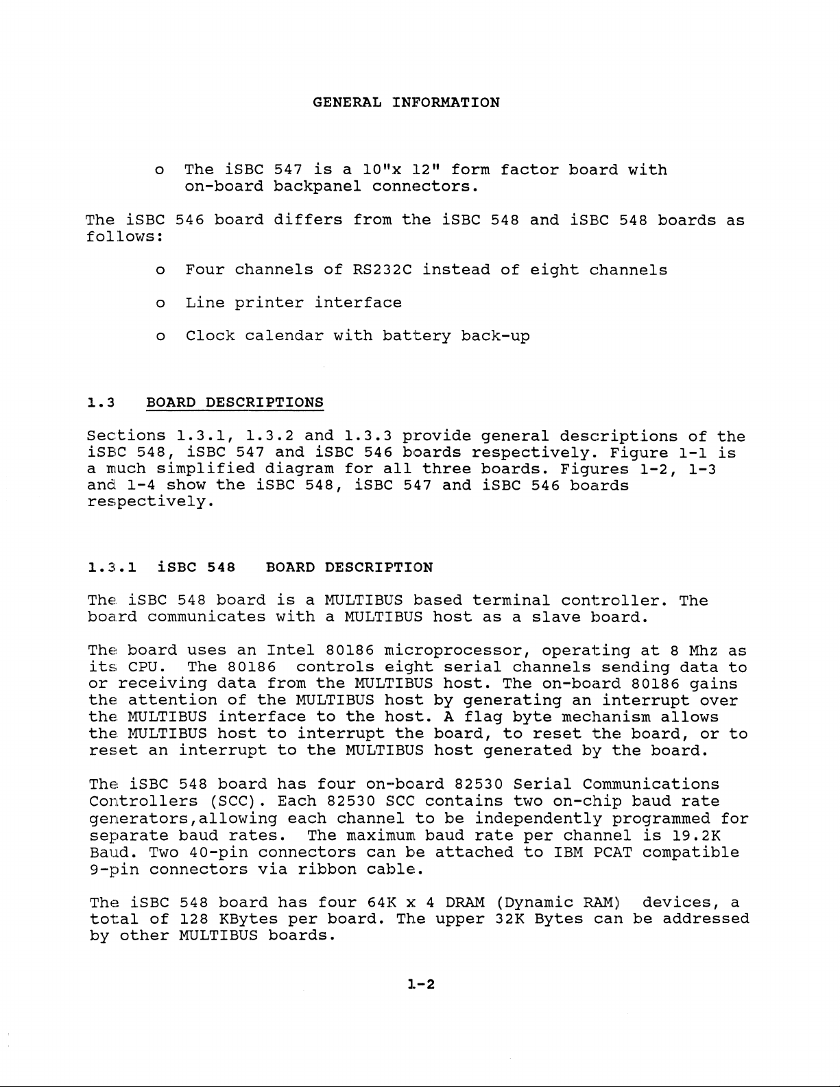
GENERAL
8
---
-
INFORMATION
REFRESH
LOGIC
(ALL
BOARDS)
5
MULTIBUS'
3
r
'"
RAM
(ALL
BOARDS)
REFRESH
CONTROL
SIGNALS
I RAM CONTROL
SIGNALS
RAM
CONTROL
(ALL
BOARDS)
PAINTER
INTERFACE
(iSBe
ONLY)
Figure
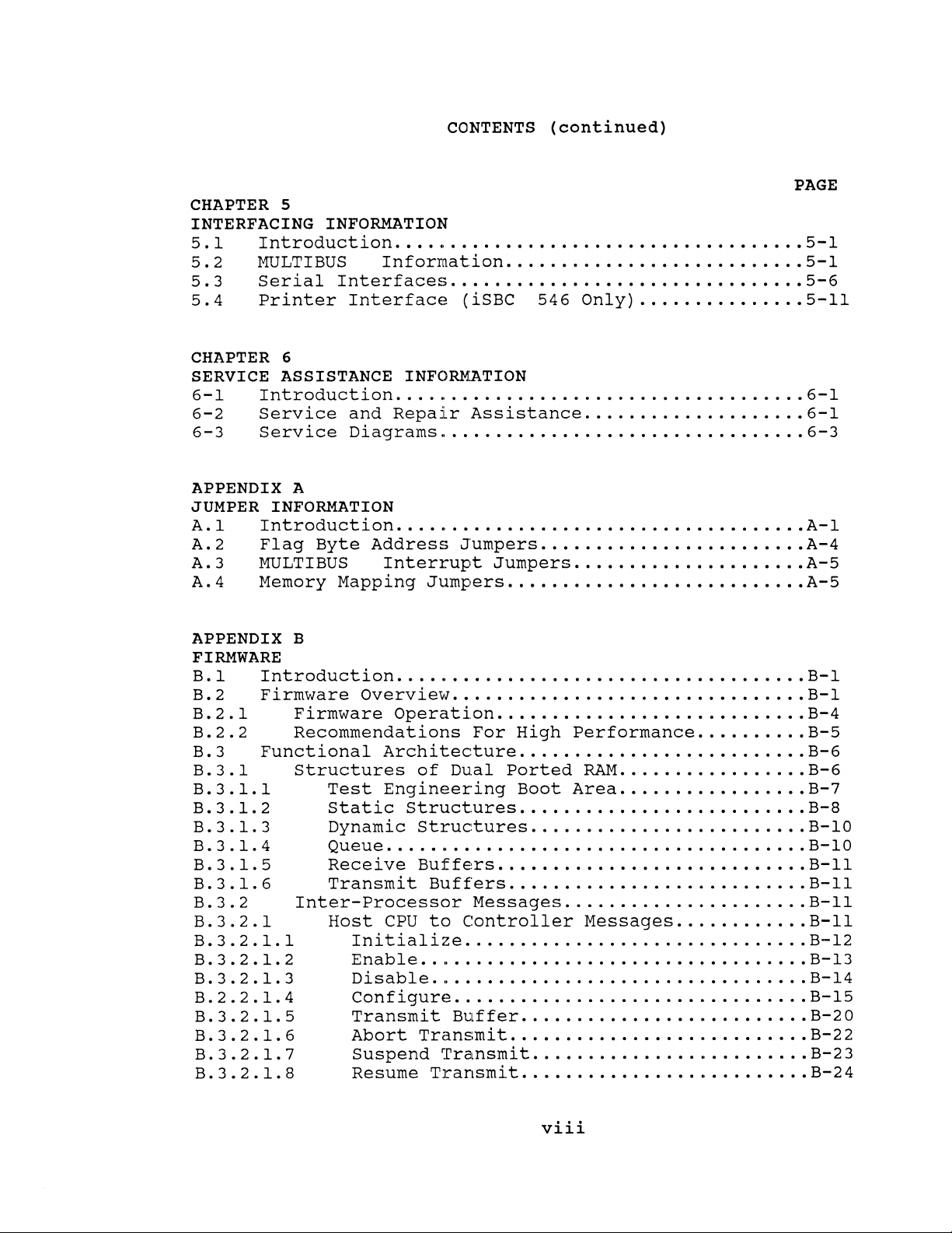
546
1-1.
I
I
L
CLOCK!
CALENDAR
INTERFACE
(iSBC'
546
ONLY)
iSBC
Block
__
546,
Diagram
iSBC
MICROPROCESSOR
_
(ALL
547
80186
(ALL
ROM
and
BOARDS)
BOARDS)
iSBC
548
2335
Boards,
1-5
Page 17
GENERAL
INFORMATION
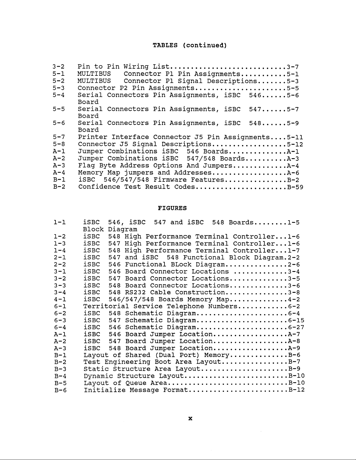
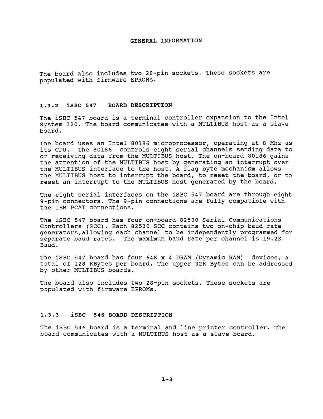
Figure
PIN 1
TOP
PIN2
BOTTOM
CONNECTOR
1-2.
MULTIBUS'
P1
iSBC
PIN 39
TOP
PIN 40
BOTTOM
548
SERIAL
CONNECTOR
High
PIN 1
TOP
PIN2
J1
BOTTOM
MULTIBUS'
CONNECTOR
Performance
P2
Terminal
PIN 39
TOP
PIN
BOTTOM
40
SERIAL
CONNECTOR
J2
Controller
Figure
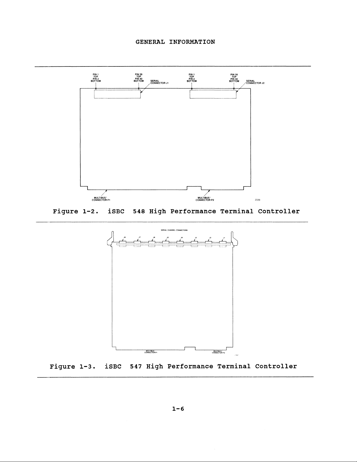
1-3.
iSBC
547
High
Performance
1-6
Terminal
Controller
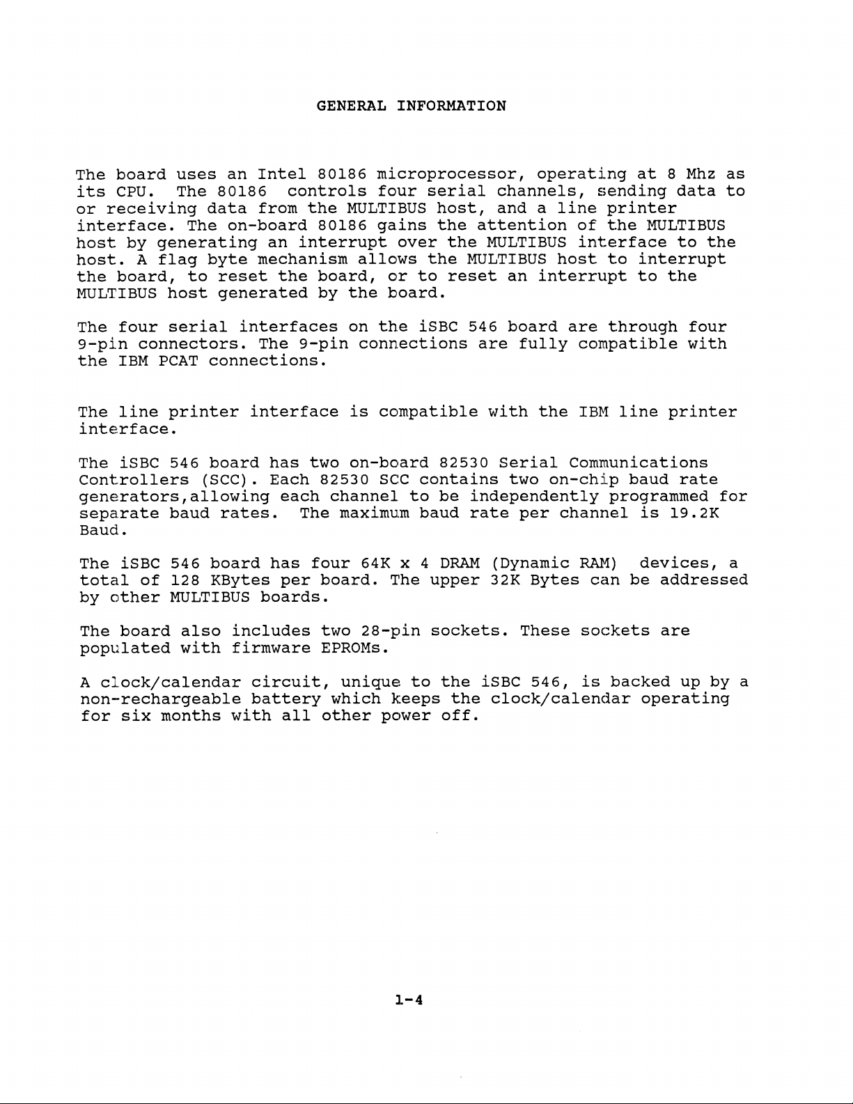
Page 18
GENERAL
INFORMATION
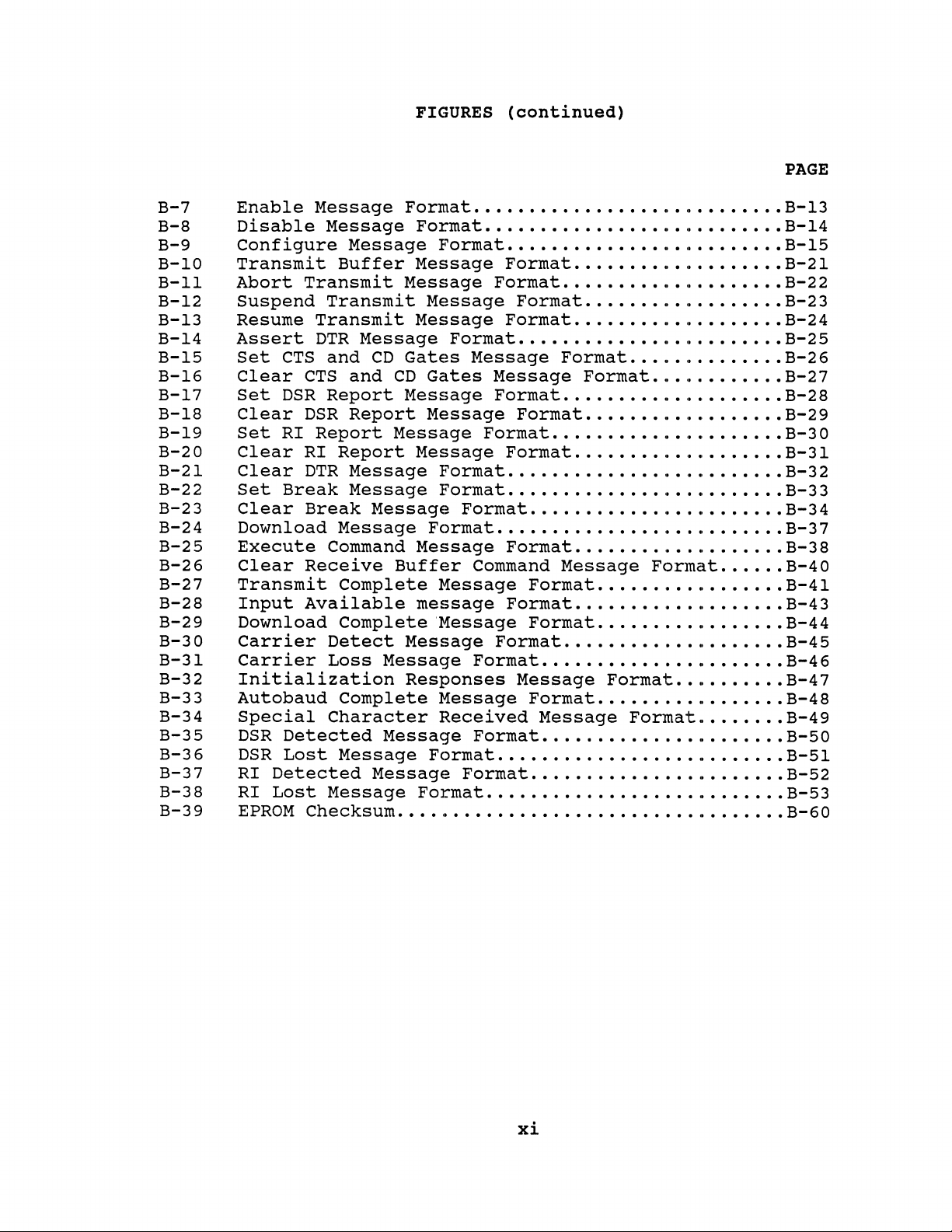
PRINTER
INTERFACE
CONNECTOR
J5
SERIAL
CONNECTOR
J4
/
SERIAL
CONNECTOR
J3
/
SERIAL
CONNECTOR
J2
/
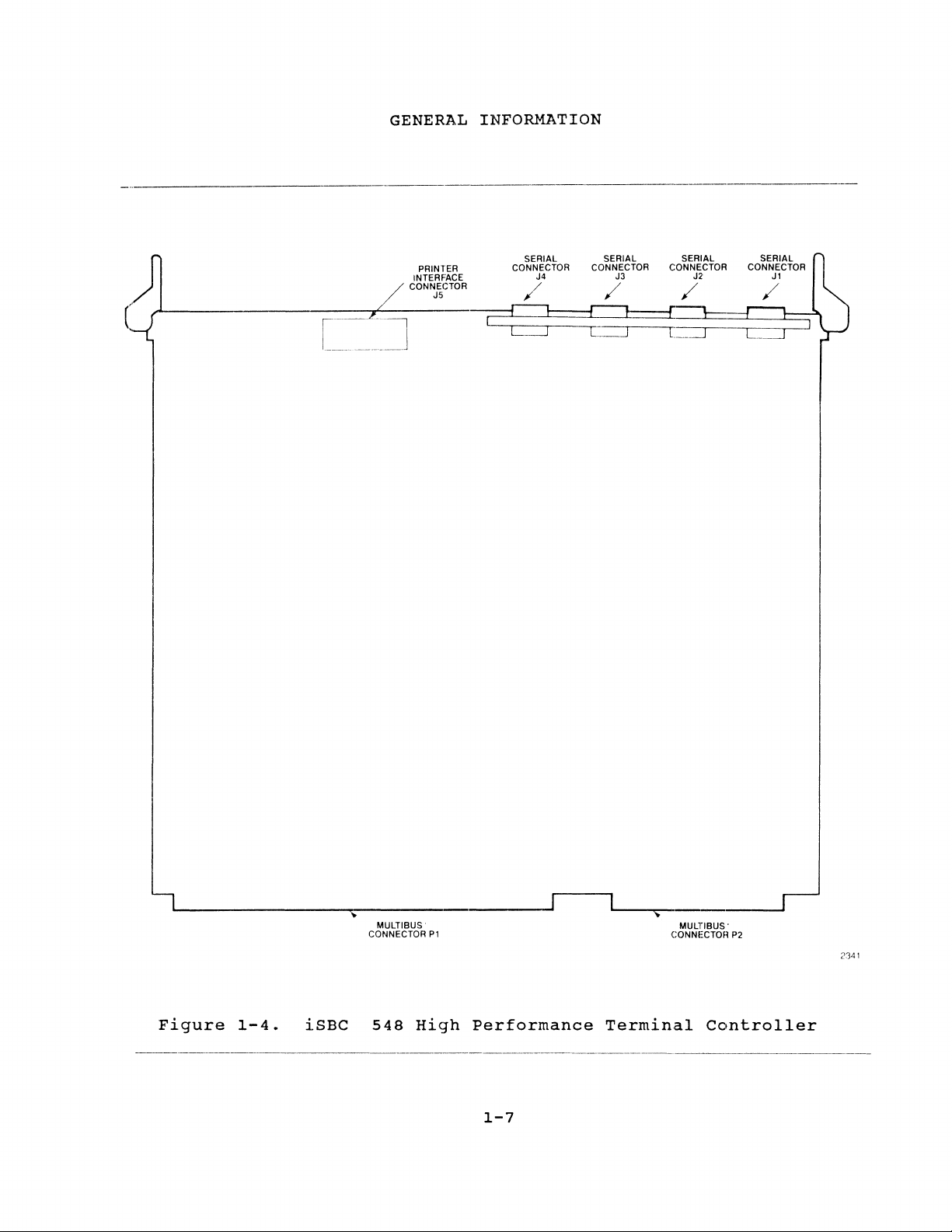
Figure
1-4.
iSBC
MULTI BUS .
CONNECTOR
548
High
P1
Performance
1-7
GONNECTOR P2
Terminal
MULTIBUS'
2341
Controller
Page 19
GENERAL
INFORMATION
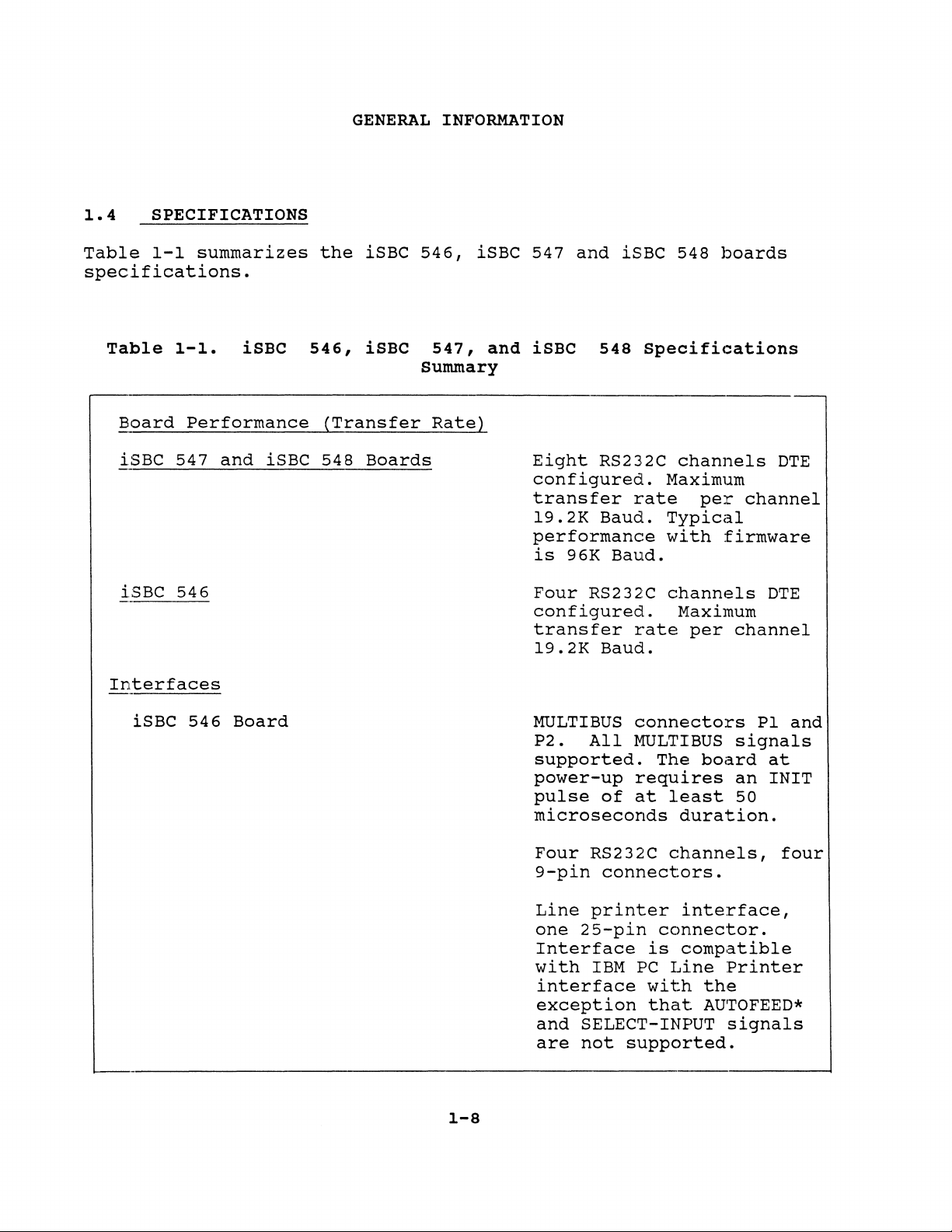
1.4
Table
SPECIFICATIONS
1-1
specifications.
Table
Board
iSBC
iSBC
1-1.
Performance
547
546
summarizes
iSBC
and
iSBC
the
546,
(Transfer
548
iSBC
iSBC
Boards
546,
summary
547,
iSBC
and
Rate)
547
and
iSBC
iSBC
Eight
548
RS232C
configured.
transfer
19.2K
Baud.
performance
is
96K
Baud.
Four
RS232C
configured.
transfer
19.2K
Baud.
548
boards
Specifications
channels
Maximum
rate
per
Typical
with
:firmware
channels
Maximum
rate
per
channel
DTE
channel
DTE
Interfaces
iSBC
546
Board
1-8
MULTI
P2.
BUS
All
connectors
MUL'I'IBUS
supported.
power-up
pulse
of
requires
at
microseconds
Four
9-pin
Line
one
RS232C
connectors.
printer
25-pin
Interface
with
IBM
interface
exception
and
SELECT-INPUT
are
not
supported.
The
least
duration.
channels,
interface,
connector.
is
compatible
PC
Line
with
that.
PI
signals
board
an
at
INIT
50
four
Printer
the
AU'rOFEED*
signals
and
Page 20
GENERAL
INFORMATION
Table
iSBC 547
iSBC 548
1-1.
iSBC
Board
Board
546,
iSBC
Sumlllary
S47,
and
iSBC
(continued)
MULTI
P2.
supported.
board
pulse
microseconds
Eight
eight
MULTI
P2.
supported.
board
pulse
microseconds
Eight
40-pin
548
BUS
connectors
All
MULTIBUS
requires
of
at
RS232C
9-pin
BUS
connectors
All
MULTIBUS
requires
of
RS232C
connectors.
specifications
signals
On
power-up
an
least
duration.
channels
connectors.
signals
At
power-up
an
at
least
duration.
channels,
PI
INIT
50
Pl
INIT
50
and
the
and
the
two
Electrical
Requirements
+5.00V + 0.25V
+l2.00V
-12.00V
+
0.60V
+
0.60V
Environmental
Temperature
Humidity
Characteristics
(Max. )
(Typ.
(Max. )
(Typ.
(Max. )
(Typ.
1-9
iSBC 546 iSBC 547 iSBC 548
3.260A
1.
)
0.075A
)
0.390A
0.069A
)
0.041
o
200
5%
(25
700A
to
55
LFM
to
to
degrees
of
90%,
55
3.490A
1.
870A
0.l50A
0.082A
0.l38A
0.082A
3.490A
1.
0.150A
0.082A
0.138A
0.082A
C, minimum,
airflow
non-condensing
degrees
C)
870A
Page 21
GENERAL
INFORMATION
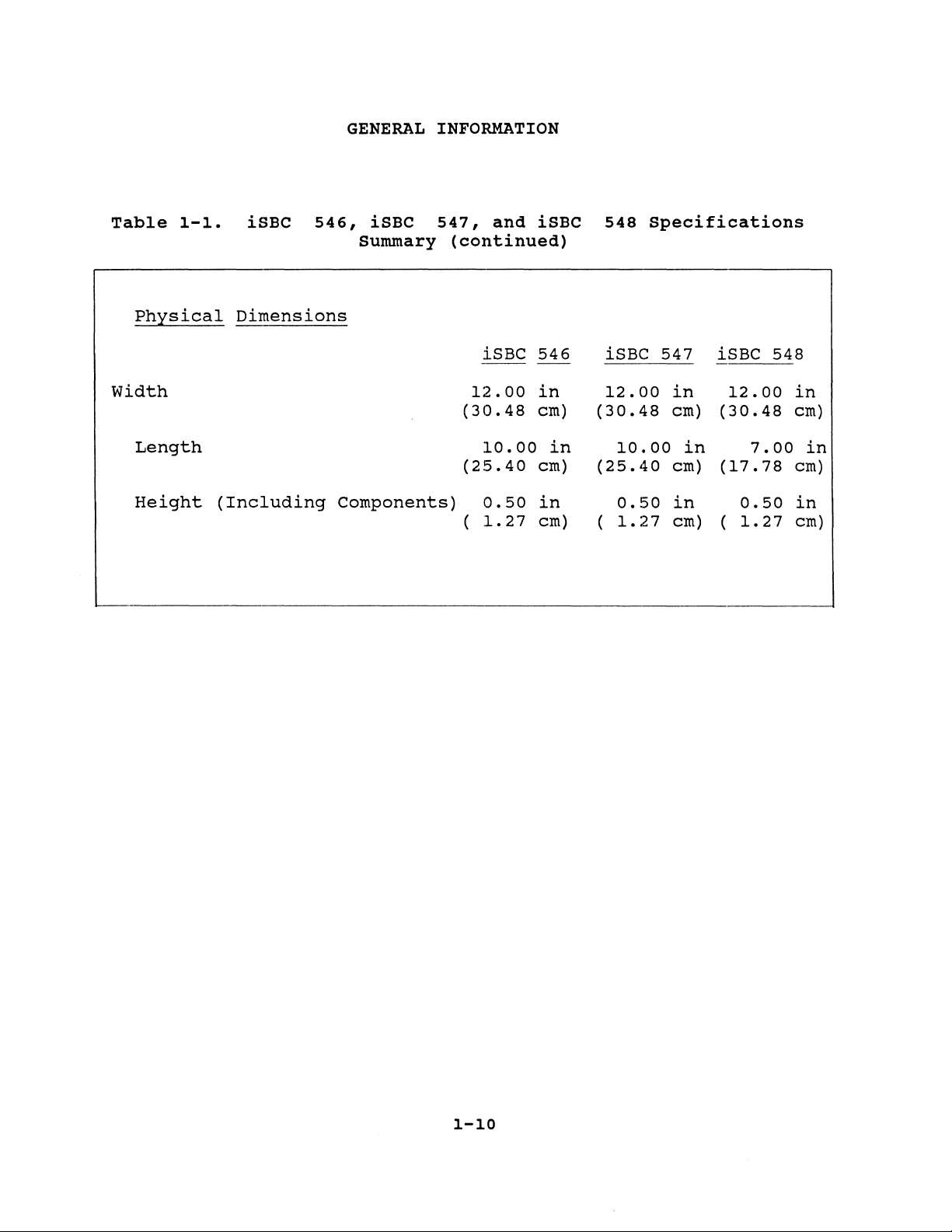
Table
Physical
width
Length
Height
1-1.
(Including
iSBC
546,
Dimensions
iSBC
Summary
Components)
547,
and
(continued)
iSBC
1:2.00
(30.48
10.00
(25.40
0.50
(
1.
27
iSBC
546
in
cm)
in
cm)
in
cm)
548
iSBC
12.00
(30.48
10,,00
(25.40
0.50
(
1.
27
specifications
547
in
cm)
in
cm)
in
cm)
iSBC
12.00
(30.48
7.00
(17.78
0.50
(
1.
548
27
in
cm)
in
cm)
in
cm)
1-10
Page 22
CHAPTER 2
2.1
This
boards,
and
will
INTRODUCTION
chapter
the
iSBC 548
be
described
separately.
2.2
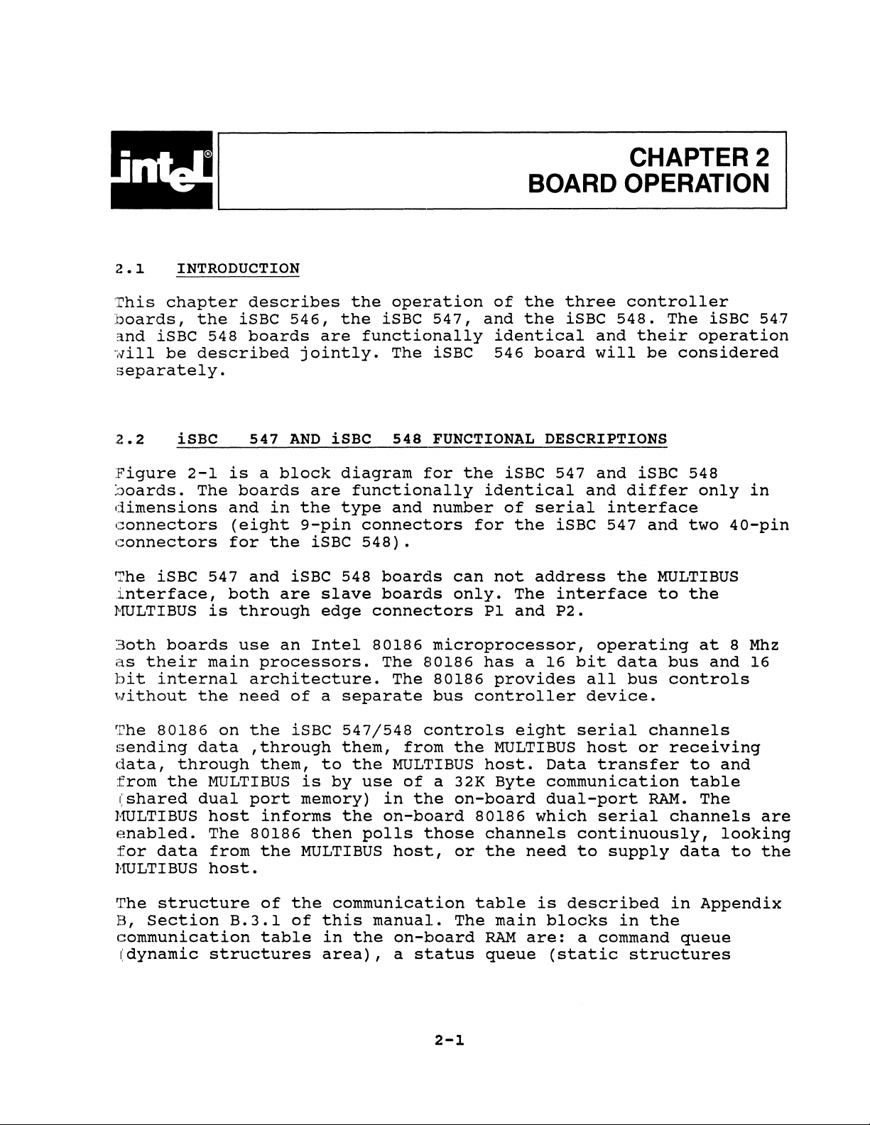
Figure
boards.
iSBC
2-1
The
dimensions
connectors
connectors
The
iSBC 547
interface,
~ruLTIBUS
is
describes
iSBC
boards
547
is
a
boards
and
in
(eight
for
the
and
both
through
546,
are
jointly.
AND
iSBC
block
are
the
9-pin
iSBC
iSBC 548
are
slave
edge
the
operation
the
iSBC
functionally
The iSBC
548
diagram
functionally
type
and
connectors
548).
boards
boards
connectors
of
547,
and
identical
546
FUNCTIONAL
for
the
iSBC 547
identical
number
of
for
can
not
only.
PI
BOARD
the
three
the
iSBC
and
board
DESCRIPTIONS
serial
the
address
The
and
will
and
and
iSBC 547
interface
P2.
OPERATION
controller
548.
interface
the
The
their
be
considered
iSBC 548
differ
and
MULTIBUS
to
iSBC 547
operation
only
two
40-pin
the
in
30th
as
bit
without
'rhe
sending
data,
from
(shared
HULTIBUS
enabled.
for
HULTIBUS
The
B,
boards
their
internal
the
80186
data
through
the
dual
data
structure
section
main
on
MULTIBUS
host
The
from
host.
B.3.1
communication
(dynamic
structures
use
an
Intel
processors.
architecture.
need
the
of
a
iSBC
,through
them,
to
is
port
memory)
informs
80186
the
of
table
then
MULTIBUS
the
of
this
in
area),
80186
The
separate
547/548
them,
the
by
use
the
polls
in
on-bc)ard
microprocessor,
80186
The
80186
bus
controls
from
MUL'l~IBUS
of
a 32K
the
those
host,
communication
manual.
the
on-board
a
status
2-1
has
provides
controller
eight
the
MULTIBUS
host.
Byte
on-board
80186
channels
or
the
table
The
main
RAM
queue
operating
a
16
bit
data
all
device.
serial
host
Data
transfer
communication
dual-port
which
serial
continuously,
need
are:
to
is
described
blocks
a command
supply
in
(static
bus
bus
controls
channels
or
receiving
to
table
RAM.
channels
data
in
the
queue
structures
at
8
Mhz
and
16
and
The
are
looking
to
the
Appendix
Page 23
CHANNEL
CHANNEL 4
BOARD
8
OPERATION
80186
PROCESSOR
,-------------
REFREQ
,-~~----
C
SELMBL,
REFRESH
LOGIC
______
HOST
M_V_L,T,',B_V_S_' ____
·:-----1
,---'"'----,
RAS',eM,'
RAM
CONTROL
AND
ARBITRATION
LOGIC
----
WRLWRH'
---
AD'
128 K
AAM
BYTES
o~-o15
A1·A8
----<J
CHANNEL
2
CHANNEL
RS23~1
CKT
NOTE:
ISBC'
547 AND
ISBC"
FUNCTIONALLY IDENTICAL
EIGHT SERIAL CHANNELS OF THF
Isac"
THROUGH 8 PIN CONNECTORS THE
EIGHT SERIAL CHANNELS OF THE
ISSC' 548 ARE BROUGHT OUT
THROUGH TWO 40·PIN
CONNECTORS
548 ARE
BROUGHT
THE
our
547
ARE-
Figure
2-1.
IOB~·IOB7
I/O
BUFFER
iSBC
547
ENLCL, ENLCH, LDCOEN
~-~-l
-
,.---------"'-=~·I
L-----,JJ
and
iSBC
548
'~=-l-""
[I"'"''
I
Functicmal
F~==-d
-='
.
Block
Diagram
j
2338
2-2
Page 24
BOARD
OPERATION
a~ea),
rE:!cei
board
board
queue
the
Table
T::1e
a
ve
80186
80186
by
host.
A-2.
flag
transmission
buffers.
generating
The
byte
controller
t::le
MULTIBUS
interrupt,
eige
The
a::idress
tile
through
Ea.ch
triggered
flag
byte
(see
MULTIBUS
PCS5*
of
the
populated
firmware.
dl:~tail.
Although
boards
with
o:E
250
the
can
zero
ns
different
The
to
the
gains
interrupt
mechanism
board,
host
sent
by
input
is
mapped
Appendix
host
(asterisk
controller
by
two
Appendix
controller
support
wait
or
size
states.
less.
EPROMs
area
MULTIBUS
command
the
attention
an
interrupt
to
reset
generated
the
MULTIBUS
to
A ,
is
done
boards
Intel
B
2764
of
27128
The
No
jumper
are
(transmit
host
queUE!
line
is
allows
the
by
the
interrupt
to
I/O
Table
by
writing
indicates
include
EPROMs
this
manual
boards
and
27256
optional
changes
used.
gains
by a flag
of
the
over
jumper
the
MULTIBUS
board,
the
board.
host
space
A-2
of
signal
which
describes
are
supplied
EPROMs
EPROMs
buffers),
the
byte
MULTIBUS
the
MULTIBUS
selectable
or
to
The
to
the
line
at
a
jumper
of
this
data
to
is
two
28-pin
contain
as
must
need
be
and a set
attention
interrupt.
host
interface
as
host
reset
to
an
flag
controller
the
on-board
selectable
manual).
an
I/O
active
low).
sockets
the
the
firmware
with
well.
2764
The
have
made when
of
of
the
The
to
the
shown
in
interrupt
interrupt
byte
board
80186.
Interrupting
port
addressed
which
controller
in
EPROMs
EPROM
access
the
on-
on-
status
to
the
to
is
are
the
runs
times
an
Each
of
RAM
b::>ard
at
are
of
128K
can
processor.
several
jumper
manual).
'Il:1e
RAM
device.
arbitrate
80186
H
..
hl1
is
the
on-board
even
when
the
boards
Bytes
be
addressed
different
selectable
The
is
controlled
The
PAL
between
and
enables
selected
the
of
on-board
The
RAM
operates
generates
by
80186.
memory
has
by
dual-port
starting
the
the
the
The
is
four
64K x 4
RAM.
other
(see
Table
with
with
a
PAL
all
MULTIBUS
address
LCS
(Lowler
memory
locked.
DRAMs
~rhe
upper
MULTI
HAM
BUS
can
addresses.
A-3
in
:z:ero
wait
(Programmable
signals
host,
the
lbuffers
Chip
arbiter
2-3
(Dynamic
32K
boards
be
seen
The
Appendix
states.
needed
refresh
as
required.
Select)
allows
Bytes
as
well
from
starting
A
Array
to
control
logic
signal
refresh
RAMs), a
of
the
on-board
as
the
the
MULTIBUS
addresses
of
this
Logic)
the
and
The
on-board
generated
of
the
total
on-
RAM,
the
by
RAM
Page 25
RAM
refresh
80186.
to
the
addresses
The
serial
flour
rate
secs.
82530
clock
Each
allowing
this
manual
A
PAL
each
uses
divide
arbiter
the
RAM.
channels
Serial
for
the
channel
channel
describes
BOARD
a 1
Mhz
output
by
15
counter
every
of
15
the
controller
Communication
serial
has
its
to
be
baud
channels
own
rate
OPERATION
from
causes
Timer 1 of
a
microseconds.
boards
Controller
is
generated
two
on-chip
programmed
programming.
refresh
An
eight
are
(SCC)
baud
separately.
the
on-board
request
bit
to
counter
implemented
chips.
by
the
rate
The
82530
generators,
Chapter
be
baud
4
sent
in
of
The
82530
through
the
RS232
by
the
2.3
The
and
iSBC
iSBC 546
548
interface
circuit
The
iSBC
boards;
as
the
same
SCC
The
manner
devices
line
8255A
output
SCCs
PCS4*
serial
PCSo*
boards.
connector
and
546
it
other
printer
Programmable
mode).
Approximately
the
PAL
generates
printer
active
indicating
for
Acknowledge)
allows
more
are
selected
outputs
of
connectors
line
546
board,
of
the
FUNCTIONAL DESCRIPTION
Figure
It
differs
and
supports
processes
has
the
boards.
as
on
are
used.
same
the
only
data
The
iSBC
interface
by
the
are
80186.
2-2,
primarily
associated
four
in
on-board
serial
547/548
is
Peripheral
A
PAL
two
one
microsecond.
is
returned
data
to
device
microseconds
a
LP
data
be
STB*
to
by
sent.
controls
the
When
the
the
PCSl*
on-board
all
tied
is
similar
circuitry,
serial
the
same
RAM
channels
boards
implemented
Interfa,ce
timing
after
(Line
Printer
printer
LP
ACK
printer
(Peripheral
80186.
to
in
that
channels.
manner
and
controls
are
except
through
(PPI
data
is
Strobe)
is
valid.
(Line
it
The
one
to
both
it
a
as
controlled
operated
and
the
written
Printer
clears
DSR
input
the
has
Chip
signals
a
Select)
port
iSBC 547
line
clock/calendar
the
other
it
in
same way
in
only
LP
two
port
line
to
signal
STB*
the
port
A
of
in
strobed
printer.
port
to
stays
82530
from
decoded
printer
two
the
an
A
the
and
The
board
map
8255A
80186.
for
the
PPI
is
The
controller
selected
PPI
replaces
by
boards.
the
one
2-4
PCS3*
of
signal
the
SCC
generated
devices
in
by
the
the
I/O
on-
Page 26
The
interface
bits
of
status
SELECT
The
line
interface
printer.
rrhe
clock
KHz
crystal.
as
does
used
by
in
the
Coding
the
lines
(Line
printer
and
calendar
the
both
8255A
of
the
does
DSR
LP
Printer
with
The
line
input
inform
two
not
port.
BUSY
Select).
interface
proper
circuit
interface
printer
or
the
bits
have
These
(Line
output
is
BOARD
OPERATION
RS2:32
four
Printer
is
compatible
cabling
uses
to
the
interface.
strobed
PAL
of
as
follows:
lines
lines
Busy),
interfaces
a
MM58167
MM58167
Port
mode. PC4*
either
5
through
are
NO
with
clock
uses
B
input
used
PAPER,
to
of
or
for
the
a
chip
the
the
and
output
8,
freeing
line
printer
FAULT
IBM
line
Centronix
and
a
same
8255A
PC5*
PAL
device
generated
mode.
four
and
printer
line
32.768
device
LP
is
Output
Input
Reset
Interface
Reset
Only
1;'1henever a new
,.3.nd
PC5*
::node,
correct
clock
'the
clock
clock
'rhe
PAL
sent
must
input
logic
by
chip
generates
to
the
or
order,
internal
are
clock
::.')ytes.
'rhe
clock/calendar
'ilhich
power.
insures
The
battery
Function
to
Clock
From
LP
and
Clock
clock
be
set
reset
output.
level
and
starting
RAM
addressable.
the
or
received
is
at
least
back-up
Mode
Clock
Mode
Clock
Interface
is
issued
to
0,0
Then
area.
the
from
PC~~*
hardware
milliseconds
Only
control
backed-up
six
months
is
PC4* PC5*
1
0 1
1 1
0 0
or a clock
and
the
port
and
PC5*
supplies
the
first
~;ignals
from
the
for
clock
read
set
are
programmed
the
and
all
16
the
8255A
consists
by a non-rechargeable
operation
~iumper
selectable.
with
0
is
to
the
address
the
addresses
PPI.
no
off-board
started
PC4
appropriate
to
the
to
the
way
up
to
in
the
The
data
of
eleven
battery
*
2-5
Page 27
BOARD
OPERATION
PRINTER
CONNECTOR
CHANNEL 4
LOAlO·
LDAT7,
OSR5·0SRs
TRANSCEIVER
IOBP-9
PROGRAMMABLE
PERIPHERAL
INTERFACE
ClKBUSO-
CLKBUS7
CLOCK
AND
CALENDER
CKT
110
BUFFER
10BO-
IOB7
'r----------
ADO-AD?
80186
PROCESSOR
ADO-.I\.015
'------
MUlTiBUS"
t)
~
MULTIBUS"
BUFFER
AORO-.IORF
DATO-CIATF
]
SELMBL,
REFRESH
LOGIC
(~
HOS
T
~
Ii
U
00-015
Al-AB
LOC
DEW
:::)
RAS·. CAS'
r--------
WRl',
WRH'
~
1
RAM
BUFFERS
128K
RAM
BYTES
00-015
i
~
~
AAMCONTROL
AND
ARBITRATION
LOGIC
ADO-AD15
Figure
2-2.
iSBC
546
Board
2-6
Functional
Block
2336
Diagram
Page 28
CHAPTER 3
INSTALLATION
3.1
This
iSBC
INTRODUCTION
chapter
548,
installation
and
Appendix
according
procedures
3.2
Inspect
of
water
carton
carton
packing
United
UNPACKING
the
mishandling
stained,
is
is
material
states
contacting
(see
states
Chapter
should
authorized
assistance.
explains
iSBC 547
to
you
A
your
in
should
Jumper
this
AND
shipping
during
request
opened.
opened
and
for
customers
the
Intel
6
for
contact
distributor)
how
and
iSBC 546
read
Information.
system
requirements
chapter.
INSPECTION
carton
transit.
the
If
the
carrier's
the
contents
the
agents
can
product
more
information).
their
for
to
receive,
boards.
Chapter
immediately
If
carrier's
inspection.
obtain
service
sales
service
inspect
However,
4
Programming
Once
you
proceed
upon
the
shipping
agent
agent
are
damaged,
service
hotline
customers
source
information
have
be
is
not
and
(Intel
and
before
set
with
receipt
carton
present
present
keep
repair
in
Phoenix,
outside
sales
and
then
install
Considerations
up
the
jumpers
the
installation
for
evidence
is
damaged
when
the
when
the
carton
assistance
Arizona
the
United
office
repair
the.
or
the
and
by
or
3.3
COMPATIBLE
The iSBC 548
The iSBC 547
the
Intel
System
The iSBC 546
EQUIPMENT
can
be
board
320.
is
part
installed
serves
of
the
in
any
MULTIBUS
as a terminal
basic
Intel
3-1
Compatible
controller
System
320.
chassis.
expansion
to
Page 29
INSTALLATION
3.4
The
INSTALLATION CONSIDERATIONS
following
consideration
THe
different
iSBC
space.
548,
address
The
selectable
MULTIBUS
each
I/O
mapping,
lines.
used
In
a
required
same
cannot
As
an
unused
unused
address
controller
Under
in
a
system
the
I/O
address
share
example,
I/O
address
configured
can
be
installed
interrupt
sections
for
547,
board's
(see
Table
board
different
these
system.
application
boards
the
if
address
locations
to
(see
line
and
the
three
and
locations
flag
A-3)
space.
(iSBC
conditions
are
and
the
same
a
system
address
lines,
Table
in
the
use
describe
some
boards.
546
boards
(see
byte
with
Table
address
eight
The iSBC 548
548,
memory
where
grouped
same
mapping
up
to
more
so
interrupt
space.
has
one
in
the
in
the
range
A-4),
system.
either
than
The
one
can
547
eight
than
that
unused
8AO
20
boards
or
of
the
be
configured
A-4)
(wake-up
options
and
iS4H
or
546)
and
different
controller
eight
several
line.
interrupt
through
the
controller
different
will
two
I/O
installation
to
in
the
MULTIBUS
address)
available
In
the
would
have
.interrupt
controller
boards
The
boards
line,
8A7
range,
controller
share
addresses.
reside
is
in
most
different
boards
boards
share
however
and
boards
the
in
address
jumper
the
ideal
can
the
two
20
can
boards
same
32
mult
be
are
be
3.4.1
On
all
CONNECTOR
three
connectors.
Table
5-1
connector
Table
On
5-1
the
iSBC 548
connectors
Pin
and
on
and
(see
CONFIGURATIONS
boards
assignments
Table
each
board
Table
board
Table
connectors
5-3
respectively.
is
shown
5-3
respectively.
connectors
5-6
for
for
PI
and
each
in
Figures
Jl
and
pin
assignments).
3-2
P2
are
connector
The
location
3-1,
J2
are
the
MULTIBUS
are
the
provided
of
3-2,
serial
each
and
in
3-3.
I/O
Page 30
On
the
iSBC 547
connectors
On
the
iSBC 546
connectors
the
printer
and
Table
(see
(see
interface
5-8
for
board
Table
board
Table
signal
INSTALLATION
connectors
5-5
for
connectors
5-4
for
connector
descriptions).
Jl
through
pin
assignments)
Jl
through
pin
assignments).
(see
Table
J8
J4
5-7
are
the
.
are
the
connector
for
pin
serial
serial
J5
I/O
I/O
is
assignments
3.4.2
In
order
iSBC 546
the
user.
the
backup
BATTERY
to
use
board
In
the
battery
BACKUP
the
the
jumper
default
is
battery
installed
backup
between
condition
E30
but
for
(as
the
the
clock/calendar
and
E3l
delivered
jumper
must
from
is
be
not.
on
installed
the
factory)
the
by
3-3
Page 31

PIN 1
TOP
PIN2
BOTTOM
PIN
39
TOP
PIN 40
BOTTOM
INSTALLATION
SERIAL
CONNECTOR
J1
PIN 1
TOP
PIN2
BOTTOM
PIN 39
TOP
PIN 40
BOTTOM
SERIAL
CONNECTOR
J2
MULTIBUS®
CONNECTOR
Figure
P1
3-1.
iSBC
548
Board
3-4
MULTIBUS@
CONNECTOR P2
Connector
2339
Locations
Page 32

INSTALLATION
SERIAL
CIHANNEL
CONNECTORS
Figure
3-2.
MULTIBUS®
CONNECTOR
iSBC
Pl
547
Board
:3-5
Connector
Locations
MULTIBUS~
CONNECTOR
P2
2342
Page 33

INSTALLATION
PRINTER
INTERFACE
CONNECTOR
J5
SERIAL
CONNECTOR
J4
/
SERIAL
CONNECTOR
J3
/
SERIAL
CONNECTOR
J2
/
3.4.3
The
to
the
of
the
3-1
for
Table
3-4.
Figure
CABLING
iSBC 548
back
Intel
summarizes
the
iSBC 548
3-2
lists
3-3.
board
panel.
310
the
the
MULTIBUS®
CONNECTOR
iSBC
requires
These
Cable
Kit
recommended
board.
pin
Figure
to
Pl
546
Board
two
cables
or
pin
flat
can
can
cable
3-4
wiring
3-6
Connector
40
conductor
be
acquired
be
fabricated
and
shows
for
MULTIBUS®
CONNECTOR
Locations
connector
the
cable
the
cable
P2
cables
from
by
Intel
the
part
construction.
shown
2341
to
as
user.
numbers
in
connect
part
Table
Figure
Page 34

INSTALLATION
The
iSBC
is
made
Connector
40
40
40
40
Pin
Pin
Pin
9
Pin
Pin
546
directly
Table
or
or
or
and
iSBC
on
3-1.
Manufacturer
3M
3M
T&B
T&B
T&B
Table
40
Connector Connector
10
11
12
13
14
15
16
17
18
547
boards
the
card
Recommended
Ansley
Ansley
Ansley
3-2.
Pin
1
2 9
3 4
4 8
5 3
6 7
7 2
8 6
9 1
P4
5
-
-
-
-
-
-
-
-
-
do
edge.
Part
3417··6000
3417-6040
609-4000M
609-400lM
609-9P-ML
Pin
to
P3
Number
Pin
-
-
-
-
-
-
-
-
-
5
9
4
8
3
7
2
6
1
not
Cables
(without
(with
(without
(with
(metal
wiring
40
19
20
21
22
23 3
24
25
26
27
28
29
30
31
32
33
34
35
36
require
and
Pin
Connectors
strain
strain
strain
strain
shroud,
List
P2
5
9
4
8
7
2
6
1
-
-
-
-
-
-
-
-
-
cables.
relief)
relief
male)
P1
-
-
-
-
-
-
-
-
-
5
9
4
8
3
7
2
6
1
Connection
relief)
relief)
P1ns
used.
37
P1
through
through
40
P4
of
3-7
are
40
p1n
9-pin
connector
connectors.
not
Page 35

EACH 9
CONDUCTOR
IS 5 INCHES
LENGTH
INSTALLATION
r---~-5
BOTTOM
iSBC® 548
COMPONENT SIDE
Figure
3-4.
LAST
PINS OPEN
MALE
40 PIN
CONNECTOR
iSBC
FOUR
548
RS232C
3-8
Cable
2334
Construction
Page 36

INSTALLATION
3.5
The
INSTALLATION
following
controller
is
boards.
1.
2.
3.
4.
PROCEDURE
a
general
Check
Ensure
For
40
Install
Appendix A for
that
the
iSBC 548
pin
connectors.
the
appropriate
connectors
cardcage.
procedure
power
board
terminal
slot
Pl
in
and
for
the
to
your
controller
your
P2
are
installing
jumper
system
install
cardcage.
fully
the
configuration.
is
turned
the
I/O
cables
board
into
Ensure
seated
in
terminal
off.
to
the
that
the
the
3-9
Page 37

Page 38

CHAPTER 4
PROGRAMMING CONSIDERATIONS
4.1
This
the
INTRODUCTION
chapter
users
information
on
the
boards,
4.2
JUMPERS
Appendix
three
should
have
install
4.3
Figure
controller
reference
been
his
ADDRESSING
4-1
describes
of
the
can
A
of
installed
own
is
the
iSBC
be
using
this
boards)
this
546,
used
by a user
the
manual
appendix
by
the
download
and
configuration.
a memory map
programming
iSBC 547
wishing
feature.
locates
the
describes
to
verify
factory
for
the
(the
iSBC
considerations
and
iSBC 548
to
various
their
that
default
546/547/548
boards.
run
his
jumpers
functions.
the
required
condition)
controllers.
applicable
This
own
software
(for
all
The
jumpers
or
to
user
to
The
controller
either
is
done
Because
for
this
EPROM
2764
27128
27256
There
128K
Bytes.
2764,
by
of
are
27128
the
the
memory
four
The
boards
or
80185
different
portion
64K
x 4
upper
include
27256
EPROMs.
processors
EPROMs
will
Memory
16K
32K
64K
DRAMS
32K
Bytes
two
UCS
vary
Size
on
each
can
4-1
28
pin
Decoding
(Upper
capacities
as
follows:
controller
be
addressed
sockets
of
Chip
the
that
this
memory
Select)
starting
Starting
FCOOO(H)
F8000(H)
FOOOO(H)
board,
by
other
can
signal.
addresses
Address
a
total
MULTIBUS
support
portion
of
Page 39

PROGRAMMING
INFORMATION
OFFFFF(H)
FCOOO(H),
2764
EPROM/
FBOOO(H),
2712B
FOOOO
27256
EPROM/
(H),
EPROM
BOIB6
Microprocessor
~-===
__
~
UCS
64K
Bytes
/
On-Board
Memory
16/32~64
K
Bytes
EPROM
MULTI
BUS
FFBOOO(H)
-:..-
- - - -
32K
Bytes
'------
FSOOOO(H)
OFFFFF
(H)
I
Figure
LCS
12BK
4-1.
Bytes
iSBC
64K
Dual
Dual-ported
MULTIBUS
or
FBOOOO(H)
boundary.
546/547/548
4-2
Bytes
Port
RAM
RAM
RAM
between
and
Boards
r:,.-
- - - -
32K
Bytes
--
- - - -
OSOOOO(H) ~ ______
NOTE
can
be
accessed
SOOOO(H)
FFBOOO(H)
Memory
and
on
Map
FSOOO(H)
any
on
~
the
32K
Page 40

PROGRAMMING
CONSIDERATIONS
master
boards.
MULTIBUS
and
F8000(H)
jumper
determined
default
boards
4.4
the
PROGRAMMING
sections
for
the
4.4.1
The
FIRMWARE
firmware
Appendix
description
The
80186
control
controls
channel
transmitted
MULTIBUS
enable
and
channels
The
interface
or
between
see
starting
address
default
CONSIDERATIONS
4.4.1
three
B
through
controller
for
of
this
of
firmware
the
microprocessors
eight
four
is
host
looking
serial
serial
communicated
to
the
informs
which
not.
for
dual-ported
at
any
32K
F80000
Appendix
is
starting
4.4.3
boards
controller
manual.
The
operation.
on
data
data
channel
data
to
the
The
channels.
channels.
the
is
controller's
80186
or
RAM
can
boundary
and
FF8000.
A).
For
OFAOOOO(H).
address
discuss
is
the
boards
following
the
iSBC 547
The
The
MULTI
BUS
received
continuously
the
request
be
addressed
starting
The
the
iSBC 546
For
the
between
starting
iSBC 547
OF90000(H).
programming
is
described
paragraphs
and
iSBC 548
80186
data
host
from
80186
on
received
and
the
MULTIBUS
which
polls
for
data.
from
board
considerations
in
detail
provide
boards
the
iSBC 546
from
the
data
channels
the
enabled
the
80000(H)
address
the
and
548
in
a
brief
the
host.
to
is
The
On
the
are
treated
4.4.2
When
programming
following
1.
iSBC 546
like
80186
PROCESSOR
guidelines
The
LCS
128K
board
serial
the
Byte
the
controller's
should
(Lower
size
line
printer
channels.
PROGRAMMING
80186
be
followed:
Chip
and
Select)
zero
4-3
wait
channel
CONSIDERATIONS
and
microprocessor
should
be
programmed
states.
clock/calendar
the
for
Page 41

2.
3.
The
UCS
64K
Byte
The
PCS
configured
PROGRAMMING
(Upper
size
Chip
and
(Peripheral
as
follows:
CONSIDER1!.TIONS
Select)
zero
Chip
wait
Select)
should
states.
be
should
programmed
be
I/O
for
mapped
and
PCS
o
1
2
3
4
5
One
wait
state:
should
Function
Selects
to
be
Selects
Selects
Selects
iSBC
printer
used
547
DSR
serial
serial
serial
and
interface
clock/calendar
board.
Selects
547
sets
used
be
used
be
and
MULTI
as
used
serial
548
an
as
port.
for for
548
only)
BUS
interrupt
output.
an
input.
for
the
ports
ports
ports
boards
on
ports
PCSO
an
1
and
the
PCS5
PCS
is
output.
and
3
and
5
and
and
iSBC
7
and
port
is
lines.
not
2.
4.
6
546
8
not
to
on
line
(iSBC
when
to
If
will
the
PCS
be
as
0000 0000
0000 0000
0000 0000
0000
0000
lines
follows:
Address
0000
0000
base
OXXX
1XXX
1XXX
1XXX
1XXX
address
XXXX
XOOO
X010
X100
X110
4-4
is
O(H)
Port
DSR
Serial
control
Serial
data
Serial
control
Serial
data
Port
then
Line
Line
Line
Line
the
2,
2,
1,
1,
I/O
map
Type
I
I/O
I/O
I/O
I/O
Page 42

PROGRAMMING
CONSIDERATIONS
0000
0000
0001
0001
0000 0001
0000 0001
0000 0001
0000 0001
0000
0001
0000 0001
0000
0000
0000
0000
0000
0010
0010
0010
0010
0010
OXXX
OXXX
OXXX
OXXX
lXXX
lXXX
lXXX
lXXX
OXXX
OXXX
OXXX
OXXX
lXXX
XOOO
XOIO
XIOO
XIIO
XOOO
XOIO
XIOO
XIIO
XOOO
XOIO
0100
0110
XXXX
serial
Line
control
Serial
Line
data
Serial
Line
control
Serial
Line
data
Serial
control
Line
serial
data
Line
or
Printer
Line
or
clock/calendar
Serial
control
Printer
calendar
Serial
or
Serial
8255
Line
or
and
controls
Line
control
Line
control
Serial
Line
data
Serial
Line
control
Serial
Line
data
MULTI
BUS
Interrupt
4,
4,
3,
3,
6,
6,
5,
Line
clock/
5
8,
8,
7,
7,
data
I/O
I/O
I/O
I/O
I/O
0
I/O
I/O
I/O
0
I/O
I/O
I/O
I/O
0
In
the
INTERNAL
state
The
the
must
A2
same
larger
RAM
case
RDY
is
be
address
components.
number
EXTERNAL
active
inserted.
line
is
selected.
but
selects
When
4-5
RDY
overrides
EXTERNAL
between
A2
equals
INTERNAL
RDY
serial
a
the
is
port
RDY.
not,
a
channels
with
If
wait
on
the
Page 43

The
80186
follows:
PROGRAMMING
address
mapping
CONSIDERATIONS
I/O
should
be
programmed
as
4.4.3
4.
5.
8255
UMCS
LMCS
PACS
MPCS
Chip
Timer
(Upper
(Lower Memory
(Peripheral
(Mid-Range
Select)
1
control
OC003(H)
should
The
be
interrupt
interrupt.
routine.
Except
for
interrupts
firmware.
PROGRAMMING
Port
Memory
is
programmed
(I/O
and
address
the
written
controller
INTI
software
available,
Chip
Chip
Chip
Select)
Peripheral
for
5E(H»
count
with
from
register
00001(H).
the
interrupts
timers
Select)
Select)
a 1
should
should
flag
Address
OFFAO(H}
OFFA2(H)
OFFA4(H)
OFFA8(H)
Mhz
output.
be
(I/O
have
byte
activates
there
0
and 2 can
Its
written
address
only
are
one
only
be
Data
OF038(H)
IFF8(H)
0039(H)
80B9
mode
with
5A(H»
external
interrupt
two
used
by
(H)
13
timer
the
Programming
Interface
The
8255
OA4(H)
be
read.
PPI
when
To
addressing
To
determine
input
port
available.
To
determine
port
read.
184(H)
A 1
considerations
(PPI)
are
control
the
clock
set
PC4
should
if
184(H)
if
bits
for
be
data
should
the
0
either
(for
as
follows:
word
is
and
used.
from
clock
bit
for
(address
to
be
PC5
to
the
be
checked.
or
clock)
indicate
the
set,
desired
clock
line
and
4-6
8255
186(H»
and
is
If
printer
3
(for
a
readiness
Programmable
should
OA6(H)
levels,
when
single
available
bit
0
is
are
ready
line
printer)
for
Peripheral
be
programmed
the
bit
bit
0
1
data
for
more
clock
of
the
is
more
should
data.
is
data,
be
to
Page 44

4.4.4
The
DSR
below:
DSR
port
PORT
control
PROGRAMMING
word
format
CONSIDERATIONS
for
each
controller
board
is
shown
D7 D6 D5
Line
Fault
D7
DSR8 DSR7
4.5
To
program
be
written
calculated
BAUD
Printer
Select
D6
RATE
the
to
its
as
follows:
No
Paper
D5
I
DSR6
lSBC
PROGRAMMING
baud
rate
time
I
547
of
constant
D4
Llne
Printer
Busy
lSBC
D4
DS~5
and
lSBC
(ALL
a
specific
D3 D2
DSR4
546
Board
D3 D2
DSR4
I
548
BOARDS)
register.
DSR3
I
DSR3
Boards
channel
The
a
time
Dl
DSR2
DSR2
time
constant
Dl
constant
DO
DSRI
DO
DSRI
must
is
Baud
rates
Time
and
Constant
Where:
their
Baud
=
------=-=-~-=~-----
32 X
Clock
corresponding
Rate
19,200
9,600
4,800
2,400
1,200
600
300
=
4-7
Clock
Baud
4.9152
time
Time
Rate
Mhz
constants
Constant
14
30
62
126
254
510
(Decimal)
6
- 2
are
as
follows:
Page 45

Page 46

CHAPTER
5
5.1
This
of
5.2
All
connectors
assignments,
Table
INTRODUCTION
chapter
the
iSBC
MULTIBUS
three
5-3
Table
(Component
Pin
provides
546,
boards
PI
lists
Mneumonic
iSBC
INFORMATION
connect
and
Table
MULTIBUS
5-1.
pin
547
P2.
Table
5-2
MULTIBUS
Side)
Description
assignments
and
iSBC
to
the
5-1
describes
connector
INTERFACING
for
all
connector
548
boards.
MULTI
lists
Connector
the
P2
BUS
interface
MULTIBUS
functions
pin
assignments.
P1
Pin
Pin
(Circuit
Mnemonic
INFORMATION
interfaces
through
connector
of
the
Assignments
Side)
Description
PI
board
PI
pin
signals.
I
3
5
7
9
11
13
15
17
19
21
23
25
27
29
31
33 34
GND
+5V
+5V
+12V
GND
MRDC*
XACK*
LOCK*
BHEN*
Signal
+5
+5
+12
Reserved
Signal
Mem
XFER
Bus
Byte
Vdc
Vdc
Vdc
Read
Ack
Lock
High
GND
GND
Cmd
En
2
4
6
8
10
12
14
16
18
20
22
24
26
28
30
32 ADR12*
GND
+5V
+5V
+12V
GND
INIT
MWTC*
IOWC*
INHl*
ADRI0*
ADRll*
ADR13*
Signal
+5
+5
+12
Reserved
Signal
Initialize
Mem
I/O
~nhibit
Reserved
Address
GND
Vdc
Vdc
Vdc
GND
Write
Write
I
Bus
Cmd
Cmd
5-1
Page 47

INTERFACING
INForumTIoN
Table
Pin
35
37
39
41
43
45
47
49
51
53
55
57
59
61
63
65
67
69
71
73
5-1.
Mneumonic
INT6*
INT4*
INT2*
INTO*
ADRE*
ADRC*
ADRA*
ADR8*
ADR6*
ADR4*
ADR2*
ADRO*
DATE*
DATC*
DATA*
DAT8*
DAT6*
DAT4*
DAT2*
DATO*
MULTIBUS
(Component
Parallel
Interrupt
Requests
Connector
S~de)
Description
}~ddress
Data
Bus
Bus
P1
Pin
Pin
36
38
40
42
44
46
48
50
52
54
56
58
60
62
64
66
68
70
72
74
Assignments
(C~rcu~t
Mnemonic
INT7*
INT5*
INT3*
INT1*
ADRF*
ADRD*
ADRB*
ADR9*
ADR7*
ADR5*
ADR3*
ADR1*
DATF*
DATD*
DATB*
DAT9*
DAT7*
DAT5*
DAT3*
DAT1*
(continued)
S~de)
Description
Parallel
Interrupt
Requests
Address
Data
Bus
Bus
75
77
79
81
83
85
s~gnals
not
GND
-12V
+5V
+5V
GND
shown
Signal
Reserved
-1~!
+5
+5
Signal
are
not
Vdc
Vdc
Vdc
GND
GND
used
~n
5-2
76
78
80
82
84
86
th~s
GND
-12V
+5V
+5V
GND
appl~cat~on
.
signal
Reserved
-12
Vdc
+5
Vdc
+5
Vdc
Signal
GND
GND
Page 48

INTERFACING
INFORMATION
Table
5-2.
Signal
ADRO* -ADRF*
ADRIO* -ADR13*
DATO* -DATF*
INH1*
INIT*
MULTIBUS
Address.
of
the
accessed.
address
Data.
transmit
addressed
is
the
Inhibit
the
RAM
RAM
or
Initialize.
system
iSBC
slave
These
microseconds
connector
memory
bit.
These
and
most
RAM.
addresses
ROM
to
546,
boards
boards
Functional
These
20
location
ADR13
is
16
bidirectional
receive
memory
significant
For
in
the
This
a known
iSBC 547
and
require
or
longer
Pl
signal
lines
the
data
location
system
to
be
system.
signal
internal
and
will
never
an
Descriptions
Description
transmit
or
I/O
port
most
significant
data
to
and
or
I/O
bit.
application,
overlaid
resets
state.
iSBC 548
generate
INIT*
for
pulse
proper
the
to
lines
from
port.
allows
by
another
the
entire
The
boards
INIT*.
of
operation.
address
be
the
DATF*
are
50
IOWC*
LOCK*
MRDC*
I/O
write.
port
lines
is
and
interface
addressed
Lock.
When
on-board
the
on-board
dual
port
removes
Memory
Read
location
address
location
interface
Indicates
on
the
that
data
port.
the
dual
resources
RAM
LOCK*.
Command.
address
lines
are
to
data
5-3
MULTI
the
BUS
contents
lines
MULTIBUS
port
until
and
is
be
RAM
the
on
that
read
lines.
the
address
interface
are
to
master
and
are
MULTI
Indicates
the
the
on
of
address
on
the
be
accepted
accesses
activates
locked
BUS
out
master
that
MULTIBUS
contents
the
MULTIBUS
an
I/O
MULTIBUS
by
the
LOCK*
by
the
a memory
interface
of
that
the
Page 49

INTERFACING
INFOru~TION
Table
Signal
MWTC*
XACK*
5-2.
MULTIBUS
Memory
location
address
MULTI
BUS
written
Transfer
master
completed
valid
interface.
Connector
(continued)
Functional
write
Command.
address
lines
interface
into
that
Acknowledge.
that
data
by
is
the
the
Pl
is
on
and
that
data
location.
read
generating
available
signal
Description
Indicates
the
MULTI
the
contents
lines
Indicates
or
write
on
the
Descriptions
that
BUS
are
to
to
operation
device
MULTIBUS
a memory
interface
on
the
be
the
bus.
is
and
that
5-4
Page 50

INTERFACING
INFORMATION
Connector
Side)
Description
,
"
!
Pin
Table
5-3.
(Component
Mnemonic
1
3
5 6
7 8
9
11
13
15
17
19
21
23
25
27
29
31
33
,
35
37
39
41
I
43
45
47
49
51
53
55
57
ADR16*
ADR14*
Address
Bus
59
P2
Pin
2
4
10
12
14
16
18
20
22
24
26
28
30
32
34
36
38
40
42
44
46
48
50
52
54
56
58
60
Pin
Assignments
(Circuit
Mnemonic
ADR17*
ADR15*
Sl.de)
Description
Address
Bus
Note:
I
I
1-
2.
If
address
specific
connector
Signals
lines
system
P2,
not
applications
by
shown
ADR14
the
are
5-5
through
iSBC
not
ADR17
they
are
546/547/548
used
in
this
are
not
held
high
boards.
application.
used
in
at
Page 51

INTERFACING
INFORMATION
5.3
All
SERIAL INTERFACES
three
interface
with
each
iSBC 546
iSBC 547
iSBC 548
Pin
assignments
Table
boards
5-4.
serial
assignments
boards,
connectors.
board
are
Board
for
Table
interface
for
the
iSBC
shown
the
5-5
shows
iSBC 548
546,
The
serial
below:
iSBC 546
the
connectors
547
and
interface
Four 9 pin
Eight
Two
40
board
pin
boards
548
have
connectors
connectors
connectors,
9
pin
connectors,
pin
connectors,
connectors
assignments
and
Table
serial
interface
RS232C
for
5-6
shows
serial
associated
JI
JI
JI
are
shown
the
iSBC 547
the
connectors.
through
through
and
J2
in
pin
J4
J8
Table
Pin
1
2
3
4
5
5-4.
Mnemonic
CDI
RXDI
TXDI
DTRI
GND
6 DSRI
7 RTSI
8
9
CTSI
RII
Note:
Serial
Connector
Carrier
Receive
Transmit
Data
Ground
Data
Request
Ring
1.
Number
Jl
Description
Clear
at
Connectors
Detect
Data
Data
Terminal
Set
Ready
to
Send
to
Send
Indicator
the
end
Rdy
of
Pin
1
2
3
4
5
6
7
8
9 RI2
the
mnemon~c
5-6
Assignments,
Connector
Mnemonic
CD2
RXD2
TXD2
DTR2
GND
DSR2
RTS2
CTS2
. .
~nd~cates
iSBC
J2
Description
Description
Connector
.
546
Board
See
Jl
channel.
Page 52

INTERFACING INFORMATION
Table
Pin
Mnemonic
1
2
3
4
5
6
7
8
9 RI3
-
Note:
Table
5-4.
connector
CD3
RXD3
TXD3
DTR3
GND
DSR3
RTS3
CTS3
1.
Number
5-5.
Connector
serial
J3
Description
Carrier
Receive
Transmit
Data
Terminal
Ground
Data
Set
Request
Clear
Ring
to
Indicator
at
the
serial
Jl
Connectors
(continued)
Detect
Data
Data
Rdy 4
Ready
to
Send
Send
end
of
Connectors
Pin
1
2
3
5
6
7
8
9
the
Pin
Assignments,
connector
Mnemonic
CD4
RXD4
TXD4
DTR4
GND
DSR4
RTS4
CTS4
RI4
mnemon1C
Assignments,
Connector
iSBC 546
J4
Description
Description
Connector
1nd1cates
iSBC 547
J2
Board
See
J3
channel.
Board
Pin
-
Mnemonic
1 CDl
2
3
RXDl
TXDI
4 DTRl
5
6 DSRl
7
8 CTSl
9
--
Pin
1
2
3
4
GND
RTSl
RIl
Mnemonic
CD3
RXD3
TXD3
DTR3
Note:
Connector
1.
Number
Description
Carrier
Receive
Transmit
Data
terminal
Ground
Data
Set
Request
Clear
Ring
to
Indicator
J3
Description
Description
Connector
at
the
Detect
Data
Data
Ready
to
Send
See
end
Rdy
Send
Jl
of
1
2
3
4
5
6
7
8
9 RI2
1
2
3
4
the
mnemon1C
Mnemonic
CD2
RXD2
TXD2
DTR2
GND
DSR2
RTS2
CTS2
Connector
Mnemonic
CD4
RXD4
TXD4
DTR4
1nd1cates
Description
Description
Connector
J4
Description
Description
Connector
.
See
Jl
See
Jl
channel.
5-7
Page 53

INTERFACING
INFORMA'rION
Table
5-5.
serial
connectors
Pin
Assignments,
(continued)
Pin
Mnemonic
5
6
7 RTS3
GND
DSR3
connector
J3
Description
See
Description
Connector
Jl
l'1nemonic
5
6
7 RTS4
GND
DSR4
8 CTS3 8 CTS4
9
Pin
1
2
3
4
5
6
7
8 CTS5 8
9
RI3
Connector
Mnemonic
CD5
RXD5
TXD5
DTR5
GND
DSR5
RTS5
RI5
J5
Deseription
See
Description
Connector
Jl
9
RI4
I1nemonic
1
2
3
4
5
6
CD6
RXD6
TXD6
DTR6
GND
DSR6
7 RTS6
CTS6
9
RI6
connector
Connector
iSBC
547
J4
Description
See
Description
Connector
J6
Description
See
Description
Connector
Board
Jl
Jl
Pin
1
2
3
4
5
6
Connector
Mnemonic
CD7
RXD7
TXD7
DTR7
GND
DSR7
J7
Description
See
Description
Connector
Jl
7 RTS7 7
8 CTS7
9
Note:
RI7
1.
Number
at
the
end
of
the
5-8
Hnemonic
1
2
3
4
5
6
CD8
RXD8
TXD8
DTR8
GND
DSR8
RTS8
8
9
CTS8
RI8
mnemonlC
Connector
lndlcates
J8
Description
See
Description
Connector
channel.
Jl
Page 54

INTERFACING
INFORMATION
Table
5-6.
serial
Pin
10
11
12
13
14
15
16
17
18
19
20
21
22 CTS6
23
24
25
26
27
28
29
30
31
32
33
34
35
36
37
38
39
40
Connectors
Mnemonic
1
2
3
4 CTS8
5
6
7
8
9
Connector
GND
RI8
DTR8
TXD8
RTS8
RXD8
DSR8
CD8
GND
RI7
DTR7
CTS7
TXD7
RTS7
RXD7
DSR7
CD7
GND
RI6
DTR6
TXD6
RTS6
RXD6
DSR6
CD6
GND
RI5
DTR5
CTS5
TXD5
RTS5
RXD5
DSR5
CD5
-
-
-
-
Pin
Jl
Description
Ground
Ring
Data
Clear
Transmit
Reg
Receive
Data
Carrier
Ground
Ring
Data
Clear
Transmit
Reg
Receive
Data
Carrier
Ground
Ring
Data
Clear
Transmit
Reg
Receive
Data
Carrier
Ground
Ring
Data
Clear
Transmit
Reg
Receive
Data
Carrier
Indicator,Ch8
Term
to
Set
Indicator,Ch7
Term
to
Set
indicator,Ch6
Term
to
Set
Indicator,Ch5
Term
to
Set
Assignments,
Rdy,Ch8
to
Send,Ch8
Data,Ch8
Send,Ch8
Data,Ch8
Rdy,Ch8
Detect,Ch8
Rdy,Ch7
to
Send,Ch7
Data,Ch7
Send,Ch7
Data,Ch7
Rdy,Ch7
Detect,Ch7
Rdy,Ch6
to
Send,Ch6
Data,Ch6
Send,Ch6
Data,Ch6
Rdy,Ch6
Detect,Ch6
Rdy,Ch5
to
Send,Ch5
Data,Ch5
Send,Ch5
Data,Ch5
Rdy,Ch5
Detect,Ch5
iSBC
RS232C
Pin
1
22
20
5
2
4
3
6
8
1
22
20
5
2
4
3
6
8
1
22
20
5
2
4
3
6
8
1
22
20
5
2
4
3
6
8
1
548
Board
5-9
Page 55

INTERFACING
INFORMATION
Table
5-6.
serial
Pin
1
2
3
4
5
6
7
8
9
10
11
12
13
14
15
16
17
18
19
20
21
22
23
24
25
26
27
28
29
30
31
32
33
34
35
36
37
38
39
40
connectors
connector
Mnemonic
GND
RI4
DTR4
CTS4
TXD4
RTS4
RXD4
DSR4
CD4
GND
RI3
DTR3
CTS3
TXD3
RTS3
HXD3
DSR3
CD3
GND
RI2
DTR2
CTS2
TXD2
RTS2
RXD2
DSR2
CD2
GND
Rl1
DTR1
CTS1
TXD1
RTS1
RXDI
DSR1
COl
-
-
-
-
Pin
J2
Description
Ground
Ring
Data
Clear
Transmit
Req
Receive
Data
Carrier
Ground
Ring
Data
Clear
Transmit
Req
Receive
Data
Carrier
Ground
Ring
Data
Clear
Transmit
Req
Receive
Data
Carrier
Ground
Ring
Data
Clear
Transmit
Req
Receive
Data
Carrier
Indicator,Ch4
Term
to
to
set
Indicator,Ch3
Term Rdy,Ch3
to
to
Set
Indicator,Ch2
Term Rdy,Ch2
to
to
Set
Indicator,Ch1
Term
to
to
Set
Assignments,
Rdy,Ch4
Send,Ch4
Data,Ch4
Send,Ch4
Data,ch4
Rdy,Ch4
Detect,Ch4
Send,Ch3
Data,Ch3
Send,Ch3
Data,Ch3
Rdy,Ch3
Detect,Ch3
Send,CH2
Data,Ch2
Send,Ch2
Data,Ch2
Rdy,Ch2
Detect,Ch2
Rdy,Ch1
Send,
Data,Ch1
Send,
Data,Chl
Rdy,Ch1
Detect,CH1
ChI
ChI
iSBC
RS232C
Pi.n
1
22
20
5
2
4
3
6
8
1
22
20
5
2
4
3
6
8
1
22
20
5
2
4
3
6
8
1
22
20
5
2
4
3
6
8
548
Board
5-10
Page 56

INTERFACING
INFORMATION
5.4
The
Table
describes
PRINTER
iSBC
5-7
Table
INTERFACE
546
board
shows
the
function
5-7
Pl.n Mnemonic
1
2
3
4
5
6
7
8
9
10
11
12
13
14
15
16
17
18
19
20
21
22
23
24
25
has
the
Printer
LP
LDATO
LDATI
LDAT2
LDAT3
LDAT4
LDAT5
LDAT6
LDAT7
LP
LP
NO
LP
FAULT
LP
GND
GND
GND
GND
GND
GND
GND
GND
a
pin
assignments
of
STB*
ACK
BUSY
PAPER
SELECT
-
RST
-
(iSBC
line
Interface
the
printer
printer
546
ONLY)
interface
for
the
interface
Connector
Line
Line
Line
Line
Line
Line
Line
Line
Line
Line
Line
No
Line
Not
Fault
Line
Not
Ground
Ground
Ground
Ground
Ground
Ground
Ground
Ground
Printer
Printer
Printer
Printer
Printer
Printer
Printer
Printer
Printer
Printer
Printer
Paper
Printer
Used
Printer
Used
connector
connector.
connector
J5
Pin
Assignments
Descriptl.on
strobe
Data
Data
Data
Data
Data
Data
Data
Data
Acknowledge
Busy
Select
Reset
Bit
Bit
Bit
Bit
Bit
Bit
Bit
Bit
(J5).
Table
signals.
0
1
2
3
4
5
6
7
5-8
5-11
Page 57

INTERFACING
INFOru~TION
Signal
LP
STB*
LPDATO
LPDAT7
LP
ACK*
LP
BUSY
Table
through
5-8.
Connector
Line
to
Printer
the
strobe
through
Data
Bus.
iSBC 546
contents
line
Line
printer
Printer
activates
accepted
Line
by
Printer
the
cannot
line
the
data
LDAT7)
This
board
of
this
the
line
accept
J5
signal
Functional
Strobe.
printer
into
and
the
by
on
is
data
LP
and
the
the
the
the
bus
STB*.
Acknowledge.
signal
data
Busy.
printer
more
strobed
This
to
data.
Descriptions
Description
This
signal
causes
data
lines
printer.
data
line
are
bus
printer.
strobed
The
to
indicate
off
signal
indicate
is
the
between
line
it
the
data
is
it
sent
printer
(LDATO
The
into
printer
has
lines.
activated
is
busy
to
to
the
the
and
NO
PAPER
LP
SELECT
FAULT
LP
RST
No
Paper.
indicates
Line
by
for
Fault.
Printer
the
use.
line
This
a-j;)roblem
further
Line
by
the
printer
Printer
iSBC 546
printer.
This
it
printer
signal
has
5-12
is
Select.
Reset.
signal
out
of
This
to
from
developed
operation.
This
board
from
paper.
signal
indicate
the
which
signal
to
reset
the
printer
it
printer
will
the
is
activated
is
indicates
prevent
is
generated
line
ready
Page 58

CHAPTER
6
6.1
This
repair
iSBC 546
6.2
Intel
Replacement
(DRA)
The
the
replace
not
and
to
defective
INTRODUCTION
chapter
assistance
boards.
SERVICE
customer
service.
RRA
service
defective
the
offered
is
available
ship
90%
provides
instructions
AND
REPAIR ASSISTANCE
Support
Authorization
provides
board
board
on
of
board.
with
all
to
these
SERVICE
a
list
Service
(RRA)
replacement
to
Intel,
a new
products.
customers
products
ASSISTANCE
of
service
for
the
Engineering
and
freight
serial
It
is
subject
in
non-service
within
diagrams
iSBC
Direct
of a defective
prepaid,
number
48
hours
INiFORMATION
a.nd
548,
provide!s
Return
board.
to
iSBC
Authorization
and
board
areas~.
of
receiving
service
547,
both
board.
Intel
This
availability,
Intel
a
will
service
and
and
Return
Return
is
expects
the
The
DRA
Intel,
board,
serial
six
Determine
customer
number
freight
with
number
weeks.
in
service
all
which
Support
your
1.
Part
2.
Purchase
charges.
3.
If
required.
the
services
provides
prepaid,
mandatory
will
not
service
Service
area)
and
it
is
service
repair
and
Engineering
change.
fits
(Refer
have
serial
order
a
will
the
warranty
Purchase
request.
be
work.
Intel
Normal
your
to
following
number
number,
repair,
must
without
billed
6-1
Return
will
Change
turn-around
needs,
Figure
of
the
needed
have
at
the
repair,
Orders.
RRA
or
6-1
for
information
board.
for
rep~Lir
proof
been
proof
the
of
within
current:
defective
tes~t
of
and
The
time
DF~.
Before
the
ready:
and
purchase
90
purchase
rate.
board
update
boards
is
four
calling
telephone
shipping
is
days
of
date
to
the
to
Page 59

4.
5.
In
correspondence
authorization
other
related
SERVICE
Your
Your
shipping
Intel
with
number
documents.
ASSISTANCE
and
contact
customer
on
the
Canada - 416·675·2105
billing
and
support
packing
INFORMATION
address.
your
telephone
Engineering,
slip,
the
number.
purchase
reference
order,
the
and
Before
from
Figure
shipping
damage
1.
602·869·4023
6-1.
remove
in
transit
Boards
in
padded
in
anti-static
602·869·4951
,
j\,
I
I-j
I i 1-
602·869·4392
~.1~
!'
I \
'\J
International - 602·869·4862
Territorial
all
as
should
be
shipping
user
follows:
material.
Service
modifications.
placed
bags.
in
Large
anti-static
602·869·4045
Telephone
Protect
items
M·01H
Numbers
bags,
should
the
and
be
product
then
wrapped
2.
3.
4.
Allow
pack,
write
the
box,
Damage
return
room
foam
the
in
etc.
return
and
sustained
packaging
the
box
authorization
label
the
due
could
6-2
for
box
to
result
protective
"FRAGILE".
the
lack
number
of
in
ext.ra
padding,
on
the
compliance
repair
e.g.
outside
safe
charges.
flow
of
Page 60

5.
SERVICE ASSISTANCE
Forward
the
board
and
INFORMATION
all
correspondence
to:
6.3
Figure
6-3
is
On
indicates
mnemonic
state.
SERVICE
6-2
is
the
the
schematic
the
schematic
Intel
customer
Billing
2402
Phoenix,
Authorization
DIAGRAMS
is
the
schematic
a
signal
without
Corporation
Support
Department
W.
Beardsley
Arizona
schematic
diagram
diagram
diagrams
active
an
asterisk
Marketing
*
-----
diagram
for
a
signal
in
DV-1-704A
Road
85027
for
the
the
iSBC 546
mnemonic
the
low
indicates
Ad.
for
the
iSBC 547
board.
state.
a
signal
iSBC 548
board
followed
Conversely
and
active
board.
Figure
by
an
a
signal
in
Figure
asterisk
the
high
6-4
6-3
Page 61

I:
.j.~Z
A""':
,,,;c
D~~[
. :
.,
"'
,c
r
.~H:>
~'
L-__
!
.":1:,
~
to:!
m
r
LJ
1'Y,/tr~')-?4r
I
I?---:-
I'
o
H
to:!
I
1J'7,,;
,
160.<J.c~"'~'
[CO
L
, ! I I
r
""'"
P:"'O
COG"
IJ~'TF'Lr~
:-:.::.
'.~
'~'.",n
'"
)-::
::0:
!Ii<:Y;CE:
R(T(REHCE
PO_C'
i
'::-
•.
&
I
;'(PI:
D(SIGNol,TJON$
!
-1
"6~
E.
'14(-"':"
f I
...
I
!
~
If'
If'
i
16RE-1
Pk
~
€
r~5;>8i'
:J:II
H
m
m
t-3
m
~~
I
74ASO,"
7.,:;,--sn~
1
l'3S
u"
U28,
~
to:!
o
5~.
tARADS.
1/4U
lED:
I r
I1IeRO
OHI1S,
IH
IH
SP[C
SE
ARE
1
ARE
OT~ERL.:
VALUES
VALUES
UNLESS
RESISTOR
CAPAC1TOR
1.
2.
7'4ALS32
7'4L573
U25,1.I6'3
~
H
bj
DAISY
AT
PARTIAL
OH
NAME
PRIHTS.)
SIGNAL
SUPPLIED
A
Of
HOT
DOClIl1EHTATIOH
ARE
THE END
rOR
AT
•••
JUI1PERS
AND
BY·.·
ICES
DEli
DENOTED
TRANSL.ATED TO
IS
(THIS
NE&ATIOH
PRO&RAMI'!ED
3.
4.
..
7'04L.SI32
U04S
U4e,
Ul1,
U51
U<l
o
DEIiIC£'
PROGRAMMED
[II
136
74L$
U7L'
U5'"
U27,
~
t-3
H
SHEET
PLOCK.
PR(VIOUS
TITLE
SHEET
TO
ARE fROM THE
t:ltJACEHT
COHN£CTION
NOTEr
CONNECT;ONS
SHEET
TO
HIERARCHICAL
S"ECItICALLY
REPRESEtHATION:
&
SHEET
ALL
S'r'M:Ei)~
UH,-ESS
S.
7.
!
[
EO
74ALS245
74LS257 ~ 74L$256
U04'"
U48,
U13·
U5E
U6.
U1E!,
o
~
CONNECTION
CONNECTION
SHEET
Lt:I"ER~L
BIDIRECTIOHAL
SAI1E
ON
SHEET
TO
HiERARCHICAL'
SHEET
a
"COf.!HECTION
a ..
-¢
<D
<>-
C
74ALS373
U4?
U3'3,
U57
US9
U5S,
U31,U32,
V3S,
1488
V22
V21,
U18,
17,
U
Ul',U20,U23
U1S,
95~1
CLARA
CALIF".
SANTA
®
inteJ
J"
~:::v
HUMBER I SHE:ET I
MCUMENT
CODE 1
CL
I
S:A~E
I
SIZE
.
t:lV:::.
BOUERS
31)'65
INfORt':AnON
PI<O<'RIETAR'r'
:N~E~
IA
HElZER
https://manualmachine.com/VrtrfTITLE
Z.
t:lPVD,
BY
DRN
[N&II:
1488
liS
V9
U3, U4, U7,
liS,
V5,
ve,
Co
t
0F"II
1
44.crr:;l2
- i
~
~
B I
~
A",'!-
2·'
..
",-
--
:~;;'
["
1
i
I
i
I
I
'"
I
I i I
'T1
~.
~I
I '
o i i
....
~
~I
(")
I I I
.j:> I I
VI
00
0\
! & I I I
9.
II.i
1 I
en
[
sa,
Page 62

SERVICE ASSISTANCE
INFORMATION
,'j ~ ,'
... " ,:,
(~ ,~
""
II,
,',
-~.I--
~~-
I-------~.-=
n _
z ,"
FO
i:
~i
~
/1'
a.
t
••
.,
I
....
.,
,~,
......
(I.
UI
...
,-.--,.--
...
:il;~~;;;~;:~
..............
Q
~.g:
-
,.
e,···oJ'"".-
••
,
.::.
..,
.... w '"
--
N
,....
..
...
""
"",
..
(',
N
......
..
.,
..
'*
.....
...
N
l~'
.......
'"
.g:
'"
([
<l«
...........
.
....
....
"'"
I ....
oI
<l ~ .,
'1
<l
a:
""
....
""
~.
""
'"' .......
,..,
(IJ
.....
_---
'-
r.
a:
I-;;,t-------t+-
~
-----------------------~---.--
,.....
*
r,-,,~
--+-+t--------
..
."....
++---F------f--.
..
__
Figure 6-2 iSBC 548 Schematic Diagram (Sheet 2
6-5
.~~--.--,..
of
11)
....
---.-.
Page 63

Dl
t'!I
~
o
H
t'!I
)II
Dl
Dl
H
Dl
~
t'!I
H
!2:
h;.I
o
~
t-i
o
H
!2:
--;-,
o!..-,'-
lA:I'5:.(',
-------~~
I
------~
i I
-=-=-=-:
..
F:._ •
:-------
L,:;:,~.~~
,-
~
fC~--
I"~":'"
,-------'
:
I,'H'
IDE':'
101
;~:.~
H'I'~
10l>~
1011-
It
I:;
le.
I:
:~::
!l~
:&2
8&1
ICE
:8:
At
j;I~
Af
,
3
~
;:!
9
AD"
4D
~~
eD
:!iI'
Eo
13
!;
ADa
AIlI.o
:~;!
,
IS
..
AD:~
;;~
:~;D
PLI
OC.
,,'
__
U3~
74J:il.S;o-:,
Ie
17
E:
~Il
r----
e .
III
3
ADEl
L.+
-+....-l-!~,-Iil
-'
AS(\'i'
U"
74
.Ir--,.
, U
___
i :
II
I
I
4
~4A:"'S(l~
::.....
~,?,~
I'
,I
I!
~
','
",
~/
_~'.
,"7~2.:..::~::':
•
:~-+~
~"""I
r:.
i,
: r
,--.
I'
'.'"
'--'-'----f-
- - ' I
r"~
~
r:~:':"<~'
I , ",'
I
II
I I
i
,! I
..
"
:
~-
I
~lJ
~
r
["
!
I
II
ruc<
! ?"ALS,?""
I
un
i"4AL.S373
i
~
[.1;'(£*
..
,
..
~[''''t·
lllill
·-;OIl;:"·
j I
A:~::.
••
o.t.I<A
:)t.
R[IF • '!':
l!-:ln
AfJ(
n.A6INT
741i1LS32
.~.
1
74~_$32
• 704Al.S.ci3 9
Les.
~
~~
"!lieu
JADRF"
I
II
-~
-J
I
18
lY2~
IY4~
, "'LJ:' I
IAZ
..
I '"
I~~
~!::
-
~
XACtc6EN'
[H)(ACI('
DENf
c
S
2.4,
4,:;
'!'tilDe.
I II'IOJTCf
3
12
I
~13
13
~"i
12
11
~
I vee
I
3
;~!;
Z'YJ:;
2'14
74ALS24:
~:~
2~
2A:;
ZA'"
~
1~
!!
17
19
"Rile.
PUP:;
DATe.
DTR.
~~:~:
,UHe.
"!.
I
SH~ET
I
DOCU:!~;3~U~jE-R
[SIzt I
..
~
RES.
J
,.
~::LS.,
u'e
74AL50'2
~.
US!
74L.S13~
7'HILSge
~
74LS13i:
27.(JPF"
58\1
~
:r
Sl::
I.
Q.J
! "
'
~D
IMln
PCS,'
~".,
1
R£~
~
N
~
....
'N
•
USI
~
U D > 6
litl 22:-"':
CRI
C4,O'
1 I -
111;
IU! ...
22
lie
us,
74DE>
7"'FlLSD'Z I
U62
~
IIATD'. : 1 1 2
'Tl
~
QQ'
@
0'1
N
VI
t:I:l
en
00
.j::o.
(')
(')
en
::r
G\
t:I
0'
i
I
G\
iO
~
go
en
~
w
0
....,
.....
c
Page 64

SERVICE ASSISTANCE
I-~-~~-
INFORMATION
i
:1
""
Ii>';
M
N
••
<::'~~JM""'"
J:V!'''''''''tnVl<Jl'f.
J:UUU<..)UUUU
_::l..J
Il..
a;I
r..
"-
~ ~
f')
M
"-
0..
II..
Q..
CO-
l.~
..
-1f-;;.J_.
U
'\J
Q
.,.
U '\J I/'l Il>
-If-..
--<>
if'
.
'-------+-+-+-H-H-"
•
'*
U
L'
Z Q
I-
I(l
Q
>-
W
0:
:I
0.
u:
Vl
~j
C;
.
" .
0
"
~
"
~~
,
Q
~~~~5
Or:
~
•••
~-
-~-
---
---'--
..
ro
..
--~--~~-;.-_-~~~-.
Figure 6-2 iSBC 548 Schematic Diagram (Sheet 4
6-7
of
---,-::;-;---.---
11)
Page 65

SERVICE ASSISTANCE
INFORMATION
~----------------------------,"---.----
Figure 6-2 iSBC 548 Schematic Diagram (Sheet 5
6-8
....
-<.Ju
.:I:
....
j:I::I.
Z:I~O
... ~ II: _
",·j
I
-
.,
A
9~~
l~~
j--Q~~
o.
,
" .
~~";L_
....
%
,
of
11)
Page 66

I
i I
SERVICE ASSISTANCE
i i
I.
! I
INFORMATION
.u~,~,,
___
_
Q
,."c,."[
""
'"
"" ,;,
.::.
<=<
'"
,J:
<t
::
~
OJ
',
I
.,., -,,'
"««
Q
••
'"
R
~~~~~a:~?i~Q'Q'Q'««a
.J . .J
""
oJ:
,_
u <I <I
<t
'""
~~,
~ ~
Ci
Co
'->
woo
':>
-"
.,
" " . "
'" " ,/)
<D
''-
"[,a
u««««««««
00;
...J
III
'"
Ill
...
(')
1\1
..J
....J
..J
..J
_, ...l
III
_.
_____
~
_
(\J
",.,.
'"
_ _ _ _ _ w w
... _ M
<JJ
"-
N N N
'"
ru
ru
I:<
_ N
('").,
III
...J ...J
...J
.J .J .J
:-
if'
l
••
"--"
C\J
<\I
to
C\J
...
'Ii
u,
"'
(")
---'
r,
f\,I
Figure 6-2 iSBC 548 Schematic Diagram (Sheet 6
6-9
of
11)
Page 67

SERVICE ASSISTANCE
-------~------------------------------.-
I
INFORMATION
-f--
.
w
..
J'
c'
:1
F-~'I
-
1-
I I
, 1 I
"~
kL~h
I
i I
-
1-
J," ,
~-=~-~
-- -
[=
"~l-~
1;:tL--::j:~=t=~--J
~L
i~H{11~;~~1
I":-~
~
~-
"
i
I;
0
!
J--
""
:,;
:
-,-
I
"--;,':----.".""
_ _
=-J~]
__
L~_-_+-+-
+---'-I+--~~----'-
--
t--
~I:
:J=-~1'
~
~"~
c,j.l
!
~ ~ ~
!
~ ~
!
~~
_:r-u
;"
::~::~~~
"_"."
__
ru ru
."'
~y
.~
""
:M
"""
e
~
"
0"
J
ru
I '
''',,'
..
'<t<'lCl.-IL
(,
- .-, -
...
::J ::J
"-
"'£l<Qr:£l<lLo..
Figure 6-2 iSBC 548 Schematic Diagram (Sheet 7
6-10
of
[1
11)
Page 68

SERVICE ASSISTANCE
INFORMATION
~~-"'-"'--~'-----------'--~----'~~-""---
......
''':.' --:--
,.,
f"') o,j)
~
In
,
V'>
II"
In
..;
_'c'~'
"':
,
'"
- •
\>~1
._-
•
"
.,
i,;.::
I_I
I
'"
~~,
',:
"
-:.~-'
--
....
:~
,,/,,'
-=~~==---
/"
'
-,---_:
--.
~
'l
:'1"
I:
\
,
i.:
'"
:1
'
_
n.J..,"
If).j)
(I
ONM
"'---
'-----------=--~-~-~---~~,---,-,--~-,-
I'\, Q)
([(['I:
<I
<r
<I:
<I
•
"I
... ~ ".
..
,)
III"'''''',
.",,,..., ........ ".
",,'"
" " " "
::::::::::.::.:::
Figure
6-2
iSBC
548
Schematic
Diagram
,.,
'"
..
..
(Sheet
8 of
11)
6-11
Page 69

.'
.'.'
SERVICE ASSISTANCE
.'.'c.
'.'
.',','.'.'.'.'.'.""'e,~r.,,,,,
,V,,,','.'""",·"
INFORMATION
r.'.
".'HeN.V".'",r,
"''':'
:f..
\.
.
!.,
I·
+
~
~-:~~ ~-:~~
-
II-,,;-~
-
I-,,~,
-
1;;;-:,.
~
Figure
6-2
iSBC
548
Schematic
6-12
Diagram
(Sheet
9 of
11)
Page 70

!
I
I I
.!
SERVICE ASSISTANCE
" T -
,!
....
,"
I
I:;:'·
I,·
112
_-=='
INFORMATION
t=t±::±tJ
I I
,
,1,1
I
U]
I
I -
l
nH:
~
':;
I'>
-
I
I j
>:~<:
1
:
1
;
I
!
i
1
i
I
i
1
t;-~
li"
"j
Jl
~
I
i
I
,I
i: :
Figure 6-2 iSBC 548 Schematic Diagram (Sheet
10
of
11)
6-13
Page 71

--'''''-'--
,11~n
"
1.
____
!,
~l'
_
.:
SERVICE ASSISTANCE
---=--~-"
-~-~--'=-------"-~:-I:
INFORMATION
,)..--
4-
,
.~,
'I
--+4+4-11--1---1--1---1--1--+---1--1-----
'++++-++-.
------+++.~
~---------
'-----------
~-:~~========++ttt+=,~,
II
,
, i I
i I
Ii
II
::
,: ~ :,1"1'1
......
'>. ....
1.
I,,·
"""
,I. ,I,
,.
~:
~--'-.
~-.~
._-
:-:.
::
~~
----_._-
~
~
,...g
-
--~
"
"
"
I.
",
,~
<,
'"
.......
0:.:"',....
...
Q:I'lIInI¥A<n
I-XI-I-Xt-
0::1.1-l1li:1'111-111:
. .
NNN~
__
""~U')llr.o::t.lII
1':1"'111[""1-111:
£1
"
9E
"
"
_
...
_----
..
-
-.----.--=.----,----=~---------,--~.~------,~.-
Figure 6-2 iSBC 548 Schematic Diagram (Sheet
6-14
11
of
11)
Page 72

l~
D",
~e21)"
__
~
IjJ
-.1
DOTE
__
I
I
1
~Ul1
CH~
_____
I/~
I
1]
'D'7
3'"
I
I
N_
N.
,::''1':::,
,,:
'"
1
1
:0"
'ESC"""
I
1-,:
PlNS
!Ur-oUSED LOG-IC ELEMENT
!OUTPUT
i
i";2'"
F;NS
0
l~:>
PO..:E"
D[sr&~I'\,:"!O"S
~
tr:I
m
I.'
- I·,
I"
tr:I
o
H
~:
Q'
.,
r~
'Y,irFFr'~
I
~
!
''''
" , 1
I
I.
I I
I
I'
I;F
/%,
H.
'"
i
16DCC-:
[CO
,
I I 1
I I I I I
1
------1
'I
I
<;
14
31
, 1
1"'''1''''
I-I
..l...
27ti,.4
276"
'D,,,
441)";::'24
44toC25
'24
..
15,
:.0, U
~
lIl,
""
l'3"
I i I I I
'0
! 9 !----+-
I
'0
18
!
17
""".1
<;(E.4-1~
!
Uf.'hl'6~,Ut<-';,U67
7('Al.SO;;'
1~'~7~O
~
m
was-1::!
u"
m
H
1-
"
74ALSC"S
4-
U~:
m
1
1 I
74Al.S:.c
74LSII
I
u"
1-3
I
I
~
5:':.
1/4\J
OHI"IS,
IN
SPECIfIED:
ARE
OTHERI.I1SE
VALUES
UNLESS
RESISTOR
1.
HOTES;
!
1 I
J~
1 r 1
74ALS3e
Uf5,U63
".
tr:I
o
INPUT.
DAISY
AT
NAI1E
SJ&NAL
A
0,
END
rARADS,
THE
AT
.nCRO
11'1
ARE
BY·.·
VALUES
NE&l=ITlON DENOTED
CAPACITOR
2.
3.
"
___
7
74LS73
I,I~~
Ll'i::>-,
!.J~:,
H
I'Zj
!2:
t
PARTtAL
OH
PR!!HS_)
SUPPLIED
ARE NOT
DOC:';M£NTAHOH
FO;;;
"."
JUMPERS
TO
AHD
DEVICES
TRAHSLATldJ
IS
<THIS
PRO~AMMED
4.
8dl
"
"
:-'-i-
133
74LS
74LSI32
U<1
o
CEo
PROGRAMMED DE'" I
@J
74F17'
U.s
SHEEl
PRE"'IOUS
COHHECT!OtolS APE rROM THE
SHEET
TO
ALL SHE:ET
6.
"
1-3
~
H
BLOCle.
TITLE
SHEET
CO"lNECT10"
TO
A!!JACEtH
BIDIRECTIONCIL
COtolHECTIOtol
toIOTE!!
HIERARCHICAL
HIERARCHICAL,
SPECIFICALLY
..
R[PRES[NTATIOtol:
..
UN:"~S::
SYMBOL
7.
e<
aD
,.
I.
74ALS245
74LS257
74LSe58
6,U49
..
U57
U56,
U"
U12.U13,U
o
!2:
SHEET
LATERA:.. COHr-oECTtOt-l
SAI'IE
ON
SHEET
TO
COtolHECTION
S;,EET
..
..
c;l
-0
CD
0-
c:>
11
U)',
'9.
U36-8,
"
'"
,.
74LS393
U47
U33,
U32,
U3l,
1486
1488
U2Z
U9 i
U", U", U",
UI9,Uao,U2:3
U5,U6,
Ul6,
I
A'lL
95C'51
CLARA
BOIJERS
SA~HA
3fi'65
INf"ORMATIOH
PROPI':IETARY
INTEL
®
ir.teJ
DATE
HETZER
Z.
BY
DRN
Ue,U3.U4,U7,U8
TITLE
~.
BY
CHK
~
I'"
0.,.12
1
SHEET
115785
CODE I DOCUM(NT NUMBER I
CL.
I
SCALE
I
ZE
B - -
SI
'Y-:/IS'
/~
'PYD
APVll
EHOR
1'i6ll
1'1.0(1"
-'
i----=-._~~~
-~.--
__
:
~_
----=----=-----~-~
_2..- _-
e i
j=
1
1
1
1
01
"I
'Tl
~
(')
...,
oq'
9"-
VJ
tp
en
n
~
VI
-.I
Vl
()
::r
0\
·1
(')
:3
~
t;I
ri'
~.
I
0'1
....
~I
·1
...,
3
I
::r
en
(')
~
J
~I
0
....,
1
J
N
-
~
1
1
·1
i
~I
Page 73

SERVICE ASSISTANCE
INFORMATION
i~-±-
·1
I
J
........
., * ..
Q:
<0
([([<l
....
<l<I<J:
(I:
t-..
ru
N
1-1-1-1-1-1-
...
<t
"'" "'"
'"
,.,.,
M ...
'-""'
'"
... v
<I
([<I
1'1,
...
If)
aaa:a:
U
A"",,",
.
... ...
....
<I
([
,~
N
<I
A
1'1
....
-
If)
'"
"-
'"
f\.
wa-«
,-1-1-1-1-1-1-
<L
A ~ "'"
~,
~--:::':....Cl.i...--
...............
tl-N!'I"'~..o"-
1-1-1-1-1-1--1-1<J:
""1'11"1""1'1
<1'00"'''''''.('')(1,1
------
................
Q
'-1"11»0>1"'-""",,,,,
...............
Q'"
.........
«
"'>1=01=1""''''0:11'1'''''
q,m"''''on.MI\I
--------
................
~;;;~:;::;~~~
...
Q
«
Q
.
~
~
"
"
. L
---
Z
~
-
"
~~,.-
--~--~~.--=:-~~.-~-,;
Figure 6-3 iSBC 547 Schematic Diagram (Sheet 2
6-16
%
E.
%.
",
..
-~-;--,,,-,.~--,
of
12)
~
~
.
,
«
0
Page 74

SERVICE ASSISTANCE
b ...
(\)
1')"
In ~ "-
'-''''!''l
III
"',., n III
",;,
D C'I 0 a a 0
~-"---"-
INFORMATION
'I
?'
"J
.
~,
···~'.'I
~:
..
'
l
i,,~-'
~I.
-
-~--t---
Figure 6-3 iSBC 547 Schematic Diagram (Sheet 3
6-17
of
12)
Page 75

SERVICE ASSISTANCE
INFORMATION
-----------
" r
ww
z z
" "
Figure 6-3 iSBC 547 Schematic Diagram (Sheet 4
6-18
of
12)
Page 76

SERVICE ASSISTANCE
II
1
I
W-=:l~
~~
"
INFORMATION
L
V;~
. "
• " u
I
t
w w
o 'f
-
--
w w w
-f
"f
• ~ Q
Q
.
,.
..
....
..
(J
U U
:r
I-
R:l
%
:I
'"
-Ell:_
r-
'--;:
R,..
b\~
=!'~b\
_o(uOI("Io
0 • 0 • 0 • 0 •
I
RRRR~-':J
_ N M •
0
o
Z U
~
..
a
_
(U
I:
1"1"
I/')
UU
-~
-----~--------------------------------'
Figure 6-3 iSBC 547 Schematic Diagram (Sheet 5
6-19
of
12)
Page 77

SERVICE ASSISTANCE
INFORMATION
t:l
...
(l,I
(")
......
In
"<-"'('"·
...
"'",,""11"'
<IQ:<t<J:<tQ:G:<t<l:a:G:4¢<l(l:
-n!-l[.;::~
'.
"
" U
~---t---
I::!""
<\I
.'
.......
i:lo:lo:l'-'1QI:II=IR
([([G:<I:<J:<I<I<E
....
'"
P'l
In
------
""
_____
,...,,..,.
"-
W
'"
......
.......
au~
I'.
("I(IJ
a
~
ct
CI
o:lRl=lo:l
Q_<\IM
......
<I
<l
<I a: ([ <I
----0;0
_
ru(y,v
In'4lI'..QJ
]J~
I-
<tCI<J:<rG:<tG:Q:
t--
0
.
dl
0
.
0-
W"'
I
' , w
••
..
~
"'
" 0
,.,"-
qq
<I:
<I
Il(
U:I!b::)
....
"'_
10
....
~~~.
;l::l:l
¢<l0:".::I
I>:
U:J:
••
_
iI;
0::
",.
'---------
Figure 6-3 iSBC 547 Schematic Diagram (Sheet 6
6-20
------
of
------
12)
Page 78

r
..
I
I
I;
SERVICE ASSISTANCE
J
INFORMATION
~.
~
tl
~
D[
g
~
~-
I
i
• I
I
~
~!
~I~
-or
Q (to
0-
~ ~
L-
~
.~
0_
0-
•
N~
-
NN
\f,
N _
..
PI
I)... I)...
u
...............
jj
a..Co:Cll:tlQ(CLG.
:
16"
u u
«
: :
u
:
~~~~~~~~
'fJ.
.nA,~1
~ _ ~ N ~
jO) ~ ..
,,~
;;:!;
9
~
•
CJ
••
..
UI
CJ
« "
• • u
o u _
.
N~
..
0
uo
u
..
:
111:-
,
.
.
o
Figure 6-3 iSBC 547 Schematic Diagram (Sheet 7
6-21
of
12)
Page 79

til
~
:g
H
~
o
til
>'
til
H
til
~
o
~
o
H
bj
!2l
H
e
1-3
o
!2l
i
REF"Ri:Q'
J g •
'1
sJ~n
·
U43
'14LS73
'
CLU
rt°'
A(811)
10'(710)
YCC
.,
22K
RP2
\6
,
c
o 3
o ,
PL;PI!t
RES'
PUP2
PUP2!
" >
~i:!
\'
')
:
?
~
~
I:
I
~1:l::l:
r<,v"1
••
- N M • " • ,
I
I!
..
C UJ
;,:,,"'i';::T~"
ACIH~'
PuPZJ
.:IDI<I-.
PLP32
i"O(;
I
fil3
:!
1114
",
A7
AS
A6
16
IS
14
13
12
87
A8 B8 11
r-!3.::!R
~A7
~
r-----t
~
.. S
".ALS2
.2
85
8'
A2
A6
;~::
of
5:: ::
'1
'AS
II~
~
74AL.S2.a
US8
13
12
:.
'
..
•
GIl
oc
II
ur
•
QD
LU9J
U36
..
eL.R
'
e
r;j~J
: 9
••
PRE
12 D
• I
OC
::
0'
U69
CLR
III
1
.2
J]II
8
?ofFl.
.3
liI~r
CLR.
CIC
11
UII
'Tl
..
01
7"LS393
A
~3
=
(l)
....
0\
oti·
•
OC
2 eLR lID 6
~
~
Vi
?4L.S393
ENRF'*
SII'IHZ
t::t:1
()
PUP7
<JI
~
-..J
en
()
::r
0\
1081
17
12
PlZ
2~181,"!l3
3
DSRI
DSR2
II
(l)
8
~.
()
I
I\)
I\)
10Ie
;~;;
:OB3
16
BJ
I .. "
:!:;
A3
Fl4
~::
5
..
DS~5
DSR3
DSR4
nSR",
t:1
JJ"
~~:~
:~;~
U\3
:i'
'---
::~
19
~:llQ
DSRB
DSR7
PCS.<r-..
II
8
::r
;
(l)
Cil
74ALS24~
~
00
0
....,
-
~
Page 80

-'
.'.'.'.'.'
SERVICE ASSISTANCE
,'.'
-,,'H,',',',',',',',',',.',',',',','.','.'",,',','
,',','.',',',',',',','",,',',"""""'"mr·'
INFORMATION
:
~~~~ 8-~;
ilTI
___
_
'------------------------------
Figure
6-3
iSBC
547
Schematic
6-23
Diagram
(Sheet
9 of
12)
Page 81

~
~
SERVICE ASSISTANCE
~
~
~
INFORMATION
0,
,
~
n
m·
n
x
... ...
G:
..
n
~
~
I\l
111111
...... ......
A
..
UO
.
ru
RR W Ill"
......
. .
~
.
..
N W
II)
>
::l
...
,
x
«
1<--_-+-
__
.
.
.
~
x
j--
~
.n
.
.A
•
~
~XA
u.u
..
~
~l
~
e
~
L.....,~----~~_~~~
Figure
.
A.
UU
6-3
..
aua
" . "
___
iSBC
-
547
.
M
..
0
.
.
m
/\JCUNru
~
_______________
Schematic
6-24
1-'
.,
..
u
~
Diagram
~~~
u
...
~
(Sheet
10
«
of
12)
..
_.__
_
Page 82

SERVICE ASSISTANCE
INFORMATION
:
l'
~
.
.u
..
o.
ru"'
_e"
.uo
.u
""nc:<.
xo
~I~
.uo
,1
,>,ot
, -
~"
,-
~
.
, -
~.
~
.
o _
~~~
9;;
~"
x 0
C<
U
101
~~1
(j
,;
-
r·'
j.
~
_
ru
~b;'
l~"
Figure
'-l--
-+
-+ -+ -+
-+ -+
~
t~
~
,
-
• 0 "
6-3
iSBC
6-25
""x
'0"
547
Schematic
'-l-r-
~
J-.
~
~
~
~
+r- +r-
~
-+ -+
~
~
k=
~
c
~
~.~-
«.01,
~e
','
Diagram
(Sheet
L
.0"
-+-
r+-
,
,
,
~--=
,
~
11
of
,
12)
Page 83

SERVICE ASSISTANCE
INFORMATION
w "
L N
,
"''''0<
"""
-
t-
0:
0
(:l
in
VI
X Q
I:l
Il< U
...
>DVlIII<""'"
"'!-VlXIOI
III<
U
o::l
III<
U
.
;
~.,
~-
..
N
~
. . .
~
I')
..
~
0_
..
'"
;
~-
..
J)
@
m m
M..
0_ 0_
...
1\1
-~·ll'
~
~-
o
_
."
r--
-
9
"
'.
_
..
,_
~-
Figure 6-3 iSBC 547 Schematic Diagram (Sheet
-11
j
6-26
~
l!
.
12
of
12)
Page 84

SERVICE ASSISTANCE
iii
INFORMATION
.
U
N
L
"
-
--
e--~---
l~
"
~
I
Q
U .
>
o
·t-t-t-~-+-t-t-r~~-+-t--1-~-t-~-+~~~j-1-~-~-~~-+~+-I-+~~
~T-+-+-t-t-+-
--t-I-t-t-t--t-t-t-t-+-1-+-+-+-H-t---j
~
~
"
,--
r---
, ,
S
I--r--
-
~r--
,
,
.
,
,.
'"
<D
0.
Q<
<')
If)
(~
••
VI
U
Q<
(.<;
_
U
W"
>-
':II'"
Figure 6-4 iSBC 546 Schematic Diagram (Sheet 1
of
;
11)
-
--
6-27
Page 85

. . .
~~g
i
SERVICE ASSISTANCE
.......
u w
u:.:
..
A
I-::J
u::r
0
111::::100:;1:
.
I:E_...I
....
.
.
...............
Q;I
'"
q
III
U R
1-1-1-1-1-1-1-1-
(I<;[([(I([(tctG:
RRAARAAA
",Q)""'U')YMN
.................
f1\ml'\...,
......
........................
......
·
Q-IUM,..IO>D"-
r
",,111111l1li111l1li111111
'---
INFORMATION
w.
t!
~
n
h'
g ,
~!
...
I..
...
MIIJ
.
-ll
~+.=====~~---+-------
~
................
Q-ruM.,Ifl.,ol'..
l1li111111111""l1li"'111
t:I_CIIM""I(l",,,
ARARAARA
E"
•
z.
W,
I
I
0
1
Figure 6-4 iSBC 546 Schematic Diagram (Sheet 2
6-28
of
11)
Page 86
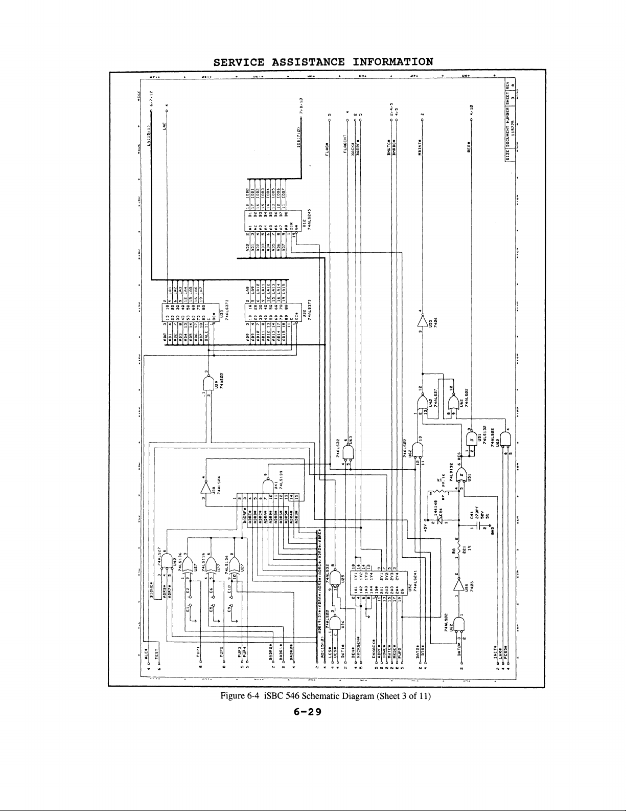
6,7,1£,
~
~::
LAl
LAc
~
6
.
IQ
eo
i!::
il
"ID
::
_.
ADI
ADZ ., 2D
:::
lAt>
16
?Q
17;oD
ADt>
til
t!:J
o
~
H
t!:J
::::
:to'
til
lOBi"
til
H
til
7,9,10
10El(7=O)
1-3
t!:J
o
~
~
o
l2:
H
2,4,5
o
~
H
1-3
4,'5
l2:
R~'"
I
SH~ET
I
DOCU~~~;7~UMBER
I
SIZE
I
tl
g
ADS 10115
AD,
::~
LA?
19
8Q
~~
C
74ALS373
SD
c
18
,
8D
~;~
18
11
~;
~ll>o"
__
AlliS
~~;~
:~;!
L.....+-
II
6
II
""
,_
1 OI..lC'
II
ADR}!""
ADR7.
~~~
d I
..
,~~
PUP!
74ASOC
~==========t{::~~--t+~~~'~'
..
f!--
.,"ALS04
~
I!;;;
lIADRFI
B
'"
EI0974LS136
~
=t:::m:
~
~
I
I r
PUP"'
PUF2
ADR9,
ADRii
"
E
ADR""
15
111
'V
r-+--
p.LN..
Iii
J
II
ADRE'
"ADRC" ADRD"
ADRo>.';ADlfs"
3).,
9:
ADR(
ISl{J)
AD(
lU I i
rl~
I
~8~
.,~32
••
cc>o
m,
,:~:~:
?4ALS.0'2
~
I
7 I
Iy"..!...2
~~~~
2Y4
en
U'52
IG-* 9
IA4
2AI
!:~
~:4
~
13
:~
19
~
•
~IA31Y3-;':;:~'
ENI<ACKIII
11~~~~~~'11
~
u,
INIT.
~
~
'Tl
riQ.
~
rt>
'"1
./:..
0\
to
en
n
VI
~
rt>
en
0\
a
::r
~.
V
>-1
(")
I
\0
0\
I\)
'"1
(")
iii·
""
a
Vi
(JQ
::r
....,
rt>
~
v:>
0
-
'-'
Page 87

SERVICE ASSISTANCE
«
~
..
w 0
••
t!~
'"''
. .
" " 0
" , "
ru
<
0'
J
r
INFORMATION
.
..
~
xl
Z 2
L
:§
;:;
«
~
" M "
Figure 6-4 iSBC 546 Schematic Diagram (Sheet 4
6-30
.
" "
~
of
11)
x 0
ruru
1:;:>1:
<'I""",,,,,,,
.0
0«
"
.
Page 88

SERVICE ASSISTANCE
INFORMATION
w.
t:
.
.
.
ill
t
~
~
~l
ill
ill:
~:
,~
-------.
~.=,.--~~~"'=,.~-~~~"="
Figure 6-4 iSBC 546 Schematic Diagram (Sheet 5
..
~--.~-="
0
.
--
~
~
o.
~
..
~--~--=""~.---~--~"-.-------~"=---~--~
of
11)
6-31
Page 89

SERVICE ASSISTANCE
INFORMATION
..............
'"
QQ
""
~
In".
(')
--------
l1li000000>11
• D D
"""
'"
D
~------------.
tl
....
CU
_____
«<I<l<J:<I<J:
-~----
(')
dl
-(\J(")..-..,-.{J""OO(J',
<I<I<l:<I:<J:<l<:l\I(I
~~~...J...J...J...J...J_I...J...J...J....I...J...J
o
U
" «
~ ~
u
u «
~~
uu
" 0
0_
~
Figure 6-4 iSBC 546 Schematic Diagram (Sheet 6
6-32
".
In
_
t---
c
;i1
~
1
~
__
0
~I~
~ 5 ~ ~
6
----~-~~~--.-
of
11)
Page 90

t-3
2:
o
h:j
2:
o
H
()
~
t-3
m
tJ:oI
tzJ
m
H
~
H
tzJ
m
"
II
c
0
m
()
11
c
tzJ
H
e
R~V
I
SH~ET
I
IHSI
DTRI C
T<'"
·12V
1 •
S
OB~
181
2~;13
--i-
R~;::~
~~II~I
RxDA
3
t:J
ocl
OD
ID2
~~~
ID1
lD2
~
~
r--=--
1---
Il2~
L~
~:
l'U
hDBl.F!~
RQA'FM"
DR(UI'~-
TRCA'~
S'r'CA'
...
;;;;;:"~
~-I-~
RACA'
RxDII
ICTSA
: DCDA'
4
L
1489
~
TXD3t
RTS2
DTR2
4
""
U13
~
! 1
3D
~~~::
OIRC:U
"".m---
GrSBi
2
4 6
:5
'~DCO"
1
lOll
IOB0
I
40
;.
DD
1E0t-=-
IT::::
:::::
R.
3
;
ittIEIH
I 3t:.. D
""
seeRD'
SCCUIU
13
:::,
,/
OAr.
10B2
39
D1
UR,
Ut4
RTSJ
" I
1
DC '
I
~
I I I
IOB6
1087
37
~! ~8 :~:;
~~..
DS
D221083
DC'
peLI(
~;:
34
~
OD
82530
U24
DB
~
I
I I I I I
~-.J
u,
74ALS.{l'2
~::LSD2
~
:
r
..
---
..
t-
T)(D4*
DTR3
OA
Hit
I
[
I III 2 3
II
I I I
I
L.......,
DTR4
RTS4
'
oc
t
Ice
lei
m
10'
';I
~I.I
'----+-
DOC~:;~~~U"'BER
ZE I
51
1
;>'4ALSO"
II
U29
;>'''ALS04
82530
U,"
:~~~:
2D'PCLIC
I I
_
~.2
UIO
Va
!
CD
~--~~~~~~~-
leeTSI
I
IC
j I 2
l12
" "
13
'XC"
UI8
12
a
--~
10489
TS
~~~.
~---
:
I:
~
...,
(1)
0-
ciF
CK<
elK.
.;,..
, K
,,'
eo
en
(")
_OUT
108<7:1)')
LA2
L.Al
:~:u
pupal
RI1
RI4
RI3
RESET
.j>.
tZl
(")
0-
Ul
~
0\
11
a
I
11
11
~.
(")
w
w
PUP22
11
t:I
~.
~
a
0-
(1)
en
~
pcse.
CD.
PuPi
1\
-.I
0
....,
-
'--"
,.
TSTHOLD'
Page 91

SERVICE ASSISTANCE
INFORMATION
ITt
6
• • U
N N •
· . ,
,
, .
·
. "
-
ru
<')".
III
'IJ
I\.
<r:<I:<I:<'.I:<1<I<r<r
(]I "-'"
---
'------i--
~g';"~\
~r';,
J~:
([
~
-
~g~g~·~·~~~l~~!
U
"-
ru
-...
l-~:~f~·'-----l--;---------J-..W
Q)
10
..
'"
ru
....
....
_---
L~
'-----
(tl"
<D
1"1
...
'"
--------
_NO'".,.
""""""""""""""'"
(I
u"
~
~
;Mrlg'~"g\
~
...
~
U
"-
ru
c
"'
L<:t
I
-ruM"'I/l"""m~.
a:
<t
<I
<r <I
NO'"·'··l
~
<l
...
IV
M'"
II>
D..
II<
0:.:
D<
Ill: f I I
Vl
'"
'"
(f)
D.. 0 D..
Q
'"
""
'"
-.J Z
:::::::::
Figure 6-4 iSBC 546 Schematic Diagram (Sheet 8
ru
_
a:«
<I
""
t!l
'"
>--
Vl-J
~
<1
...J
...
...
of
11)
6-34
Page 92

SERVICE ASSISTANCE
INFORMATION
Figure 6-4 iSBC 546 Schematic Diagram (Sheet 9
6-35
of
11)
Page 93

SERVICE
ASSISTANC:E: INFORMATION
« ,
- . " . " . ,
l-t;l"'(U(O)""n",,,"
VI
~~~~~~~~~
OJ "-'"
--------
I-l-f-->--
.. ~ TIk-
~: ! !:l~
.....
I-l-I-
10
".
M
(\J
...
~
~I:;·
~
~lTI
~ ~ ~ ~ ~ ~ ! ~
L__
~ ~
~AlrbF:
.--
"JZJ
f~~
• ol.ln • , •
--=
=
-
C!
_
(\J
(')
...
In
'"
"-
::>::>::>::>::>
...J...J...J...J---'
"-
I\J
0:0
'"
t:l _
,~
....
(\J
,:qI'lPlPlPlPlPlPl
:Lo..o..a.
..
o •
. ,
..
o.
. ,
JJ
ULJUUU
ruM
(\/!'\J(UOJOJ
M
...
...
11'"1"',,-
CLo..a. 0..
In
I...
U
Pl<XNu):J
a I Q.
n J •
...
..., f\J ....
~~~~~~~~
...
M ru
....
(>')
M M M M
'"
....
0..
0-
/;1"'00,,-
".
t'l
,.,
"",
ru ru
M M
'"
Figure 6-4 iSBC 546 Schematic Diagram (Sheet
6-36
::::::::
~r
10
of
11)
J1~
-If
~
Lf---t-------H-.
I
.J
~;
L-]
I~w"
~
Page 94

SERVICE ASSISTANCE
INFORMATION
=
.
.
••
0
R.
XR
OU
OUR
,-
" .
M~O
-,.
OUR
,-
~"
-.
,-
-.
,-
~;'
·
~
_~O
-,~
OUR
OU
~
~"
_ .
~"
r
.
R •
• ~ 0
OUR
OU
..
,-
~;
--
..
,-
~;
RM
~;'
~
~;'
,-+r-
~
r--'--
!--+
J..
.
It
~
&
•
L-
U;;;:i:::
"~X
OR'
Figure 6-4 iSBC 546 Schematic Diagram (Sheet
~
.
...
~OR
"~X
OR'
L',-"-
R:
,
,
·
•
•
6-37
'--b-'--
~
~
~
,
•
~OR
"""
"X
OR'
,
~
•
•
'-
...
~OR
"~X
OR'
~
'--
~
r--'--
!--+
L',-r-
,.;..
tt
!!-
•
11
~
L--
of
11)
Page 95

Page 96

APPENDIX A
JUMPER INFORMATION
A.l
This
boards,
leave
configuration.
jumpers
the
Default
jumpers
more
A-3 show
Jumper
EI -E2
E3
E5
INTRODUCTION
appendix
iSBC
the
factory
can
same
-
-
for
column
installed
detailed
the
Table
E4
E6
provides
546,
Table
be
installed)
the
of
information
location
A-l.
Default
No
Yes
No
jumper
iSBC 547
in
a
specific
A-I
iSBC 547
Table
by
A-lor
the
of
Jumper
Flag
Dual
Flag
information
and
lists
for
the
and
iSBC 548
factory.
about
the
stake
Combinations
Byte
Port
Byte
iSBC
all
Table
Address
RAM
Address
548.
configuration
stake
iSBC 546
boards.
A-2
sections
the
jumpers.
pins
Address
on
Function
Jumper
Jumper
for
the
The
controller
called
pin
combinations
board.
A
indicates
A-3
through
Figures
each
iSBC
Jumper
three
Table
"Yes"
of
546
the
the
controller
boards
the
default
A-2
in
default
A-6
A-I,
boards
Board
(on
which
does
the
provide
A-2
and
E7
-
E8
E9
- EIO
Ell
El3
El5
El9
E25 - E24 Yes
- E12 Yes
- E14 Yes
- E17 Yes
- E24
No
No
No
Dual
Flag
Dual
Dual
80186
factory
Makes INTI*
installed.
Makes INT2*
installed.
Port
Byte
Port
Port
RAM
Address
RAM
RAM
Clockout
test)
A-l
Address
Address
Address
Jumper
the
the
Jumper
Jumper
Jumper
Jumper
(Removed
MULTIBUS
MULTIBUS
only
Interrupt
Interrupt
during
when
when
Page 97

JUMPER
INFORMATION
Table
Jumper
E27 - E24
E23
- E24
E28 - E29
E30 -
E3l
A-l.
Default
No
No
No
No
Jumper
Combinations
(continued)
Makes INT3*
installed.
Makes INT4*
when
Dual
select
installed.
Port
mapping
installed
MByte.
Selects
Battery
circuit.
Functl.on
the
the
RAM
;~ddress
in
to
select
iSBC
MULTIBUS
MULTIBUS
Jumper,
the
lower
mapping
Back-up
546
Board
Interrupt
Interrupt
installed
MByte,
in
the
for
clock/calendar
when
when
to
not
upper
A-2
Page 98

JUMPER
INFORMATION
Table
Jumper
El
- E2
E3 - E4
E5 - E6
E7 - E8
E9 Ell
E13 -
E10
- E12
E14
E15 -E17
E18 -
E2l
A-2.
Default
No
Yes
No
Yes
Yes
No
Yes
Yes
No
Jumper
Flag
Dual
Flag
Dual
Flag
Dual
Dual
80186
factory
Makes
installed.
Combinations
Function
Byte
Port
Byte
Port
Byte
Port
Port
Address
RAM
Address
Address
RAM
Address
Address
RAM
Address
RAM
Address
Clockout
test)
INT5*
the
iSBC
Jumper
Jumper
Jumper
Jumper
MULTI
547/548
Jumper
Jumper
Jumper
Jumper
(Removed
BUS
Interrupt
Boards
only
during
when
E19 -E24
E20 -E2l
E22 -
E23 -
E2l
E24
E25 -E24
No
No
No
No
No
Makes
installed.
Makes
installed.
Makes
installed.
Makes
installed.
Makes
installed.
INT1*
INTO*
INT6*
INT4*
INT2*
the
the
the
the
the
MULTIBUS
MULTIBUS
MULTIBUS
MULTIBUS
MULTIBUS
Interrupt
Interrupt
Interrupt
Interrupt
Interrupt
when
when
when
when
when
A-3
Page 99

JUMPER
INFORMATION
Table
E26 -E2l
E27 -E24
E2S -
A-2
I/O
three
configurations
A-2.
Jumper
E29
FLAG
mapping
controller
Jumper
Default
No
Yes
No
BYTE
of
the
available
Combinations
Makes
installed.
Makes
installed.
Dual
select
installed
MByte.
ADDRESS
flag
boards.
(continued)
INT7*
INT3*
Port
mapping
JUMPERS
byte
is
Table
iSBC
Function
the
the
RAM
Address
in
to
select
a
jumper
A-3
shows
547/548
MULTI
MULTI
the
Boards
BUS
Interrupt
BUS
Interrupt
Jumper,
lower
mapping
configurable
the
MByte,
in
jumpers
when
when
installed
not
the
upper
option
and
to
on
the
Table
Flag
Addresses
X
*
**
A-3.
Byte
SAO
(H)
SAl
(H)
SA2(H)
SA3(H)
SA4(H)
SA5(H)
8A6(H)*
8A7(H)**
=
Jumper
=
Jumper
=
Default
=
Default
Flag
El
lnstalled
not
flag
flag
Byte
AddrE~ss
- E2
X
X
X
X
-
-
-
-
installed
byte
byte
address
address
A-4
options
Jumpers
E5
- E6
X
X
-
-
X
X
-
-
for
for
and
iSBC
iSBC
Jumpers
E9
-
X
-
X
-
X
-
X
-
547
546
EIO
and
iSBC
54S
Page 100

JUMPER
INFORMATION
A.3
The
host
MULTIBUS
selection
is
associated
shown
A.4
below:
MEMORY
jumper
jumpers
Interru:et
INTERRUPT
of
which
selectable.
INTO*
INTl*
INT2*
INT3*
INT4*
INT5*
INT6*
INT7*
MAPPING
MULTI
(the
JUMPERS
JUMPERS
BUS
A
list
jumper
E20 -E21
E19
- E24
E25
- E24
E27
- E24
E23 - E24
E18
-
E22
-
E26
-
Interrupt
of
installed
Selectable
Selectable
Default
Default
Selectable
Selectable
E21
Selectable
E21
Selectable
E21
is
interrupts
selects
Jum:eer
Selectable
and
iSBC
Selectable
used
to
and
its
on
iSBC
on
all
installation
on
all
installation
548
on
all
on
all
on
iSBC
on
iSBC
on
iSBC
interrupt
there
interrupt)
547/548
boards
iSBC
boards
iSBC
boards
boards
547/548
547/548
547/548
the
is
only
546
547
only
only
only
Memory
three
they
select
identical
mapping
controller
are
on
all
of
boards.
shown
boards.
the
DRAM
The
in
Table
is
jumper
a
jumper
A-4.
A-5
configurable
combinations
The
jumpers
and
and
option
the
addresses
addresses
on
all
are
 Loading...