


Intel® IQ80333 I/O Processor
Customer Reference Board Manual
February 2005
Intel Part Number: C90183-001
Document Number: 306690001US

Intel® IQ80333 I/O Processor
INFORMATION IN THIS DOCUMENT IS PROVIDED IN CONNECTION WITH INTEL® PRODUCTS. NO LICENSE, EXPRESS OR IMPLIED, BY
ESTOPPEL OR OTHERWISE, TO ANY INTELLECTUAL PROPERTY RIGHTS IS GRANTED BY THIS DOCUMENT. EXCEPT AS PROVIDED IN
INTEL'S TERMS AND CONDITIONS OF SALE FOR SUCH PRODUCTS, INTEL ASSUMES NO LIABILITY WHATSOEVER, AND INTEL DISCLAIMS
ANY EXPRESS OR IMPLIED WARRANTY, RELATING TO SALE AND/OR USE OF INTEL PRODUCTS INCLUDING LIABILITY OR WARRANTIES
RELATING TO FITNESS FOR A PARTICULAR PURPOSE, MERCHANTABILITY, OR INFRINGEMENT OF ANY PATENT, COPYRIGHT OR OTHER
INTELLECTUAL PROPERTY RIGHT.
Intel products are not intended for use in medical, life saving, life sustaining applications.
Intel may make changes to specifications and product descriptions at any time, without notice.
Designers must not rely on the absence or characteristics of any features or instructions marked “reserved” or “undefined.” Intel reserves these for
future definition and shall have no responsibility whatsoever for conflicts or incompatibilities arising from future changes to them.
®
Intel
internal code names are subject to change.
THIS SPECIFICATION, THE Intel® IQ80333 I/O Processor IS PROVIDED "AS IS" WITH NO WARRANTIES WHATSOEVER, INCLUDING ANY
WARRANTY OF MERCHANTABILITY, NONINFRINGEMENT, FITNESS FOR ANY PARTICULAR PURPOSE, OR ANY WARRANTY OTHERWISE
ARISING OUT OF ANY PROPOSAL, SPECIFICATION OR SAMPLE.
Intel disclaims all liability, including liability for infringement of any proprietary rights, relating to use of information in this specification. No license,
express or implied, by estoppel or otherwise, to any intellectual property rights is granted herein.
Copyright © Intel Corporation, 2005
AlertVIEW, i960, AnyPoint, AppChoice, BoardWatch, BunnyPeople, CablePort, Celeron, Chips, Commerce Cart, CT Connect, CT Media, Dialogic,
DM3, EtherExpress, ETOX, FlashFile, GatherRound, i386, i486, iCat, iCOMP, Insight960, InstantIP , Intel, Intel logo, Intel386, Intel486, Intel740,
IntelDX2, IntelDX4, IntelSX2, Intel ChatPad, Intel Create&Share, Intel Dot.Station, Intel GigaBlade, Intel InBusiness, Intel Inside, Intel Inside logo, Intel
NetBurst, Intel NetStructure, Intel Play, Intel Play logo, Intel Pocket Concert, Intel SingleDriver, Intel SpeedStep, Intel StrataFlash, Intel TeamStation,
Intel WebOutfitter, Intel Xeon, Intel XScale, Itanium, JobAnalyst, LANDesk, LanRover, MCS, MMX, MMX logo, NetPort, NetportExpress, Optimizer
logo, OverDrive, Paragon, PC Dads, PC Parents, Pentium, Pentium II Xeon, Pentium III Xeon, Performance at Your Command, ProShare,
RemoteExpress, Screamline, Shiva, SmartDie, Solutions960, Sound Mark, StorageExpress, The Computer Inside, The Journey Inside, This Way In,
TokenExpress, Trillium, Vivonic, and VTune are trademarks or registered trademarks of Intel Corporation or its subsidiaries in the United States and
other countries.
The ARM* and ARM Powered logo marks (the ARM marks) are trademarks of ARM, Ltd., and Intel uses these marks under license from ARM, Ltd.
*Other names and brands may be claimed as the property of others.
2 February, 2005 Customer Reference Board Manual

Intel® IQ80333 I/O Processor
Contents
Contents
1 Introduction....................................................................................................................................9
1.1 Document Purpose and Scope.............................................................................................9
1.2 Other Related Documents ....................................................................................................9
1.3 Electronic Informati o n........ .......... ................... ......... .......... ......... ................... .......... ...........10
1.4 Component References......................................................................................................10
1.5 Terms and Def initions...... ......... .......... ................... ......... .......... ................... ......... .......... ....11
1.6 Intel
1.7 Intel
2 Getting Started.............................................................................................................................15
2.1 Kit Content.......................................................................................................................... 15
2.2 Hardware Installation..........................................................................................................15
2.3 Factor y Se ttings........................ .......... ......... .......... ................... ......... .......... ......... ..............17
2.4 Development Strategy ........................................................................................................17
2.5 Target Monitors................................................................................................................... 18
2.6 Host Communications Examples........................................................................................19
®
80333 I/O Processor.................................................................................................12
®
IQ80333 I/O Processor Evaluation Platform Board Features ...................................14
2.2.1 First-Time Installati on and Test.......... ................... ......... .......... ......... ................... ..15
2.2.2 Power Requireme n ts...... ................... ......... .......... ................... ......... .......... ...........16
2.4.1 Supported Tool Buckets ........................................................................................17
2.4.2 Contents of the Flash .............................................................................................17
2.5.1 RedHat RedBoot....................................................................................................18
2.6.1 Serial-UART Communication.................................................................................19
2.6.2 JTAG Debug Com m unicat ion . ...............................................................................19
2.6.3 Network Communication........................................................................................20
2.6.4 GNUPro GDB/Insight............................................................................................. 21
2.6.4.1 Communicating with RedBoot................................................................21
2.6.4.2 Co n necting with GDB......... ......... .......... ................... ......... .......... ...........23
3 Hardware Reference Section......................................................................................................25
3.1 Functional Diagram............... ......... .......... ......... .......... ................... ......... ......... .......... .........25
3.2 Board For m-Factor/Connectivity....... ................... ......... ......... ................... .......... ......... .......26
3.3 Power..................................................................................................................................27
3.4 Memory Subsystem............................................................................................................28
3.4.1 DDR SDRAM.........................................................................................................28
3.4.1.1 Battery Backup.......................................................................................28
3.4.2 Flash Memory Requir e men ts... ................... .......... ......... .......... ................... ......... ..29
3.5 Inte r ru p t Routing............................... ......... .......... ......... ................... ......... .......... ......... ....... 30
3.6 Intel
3.7 Debug Interface ..................................................................................................................35
Customer Reference Board Manual February, 2005 3
®
IQ80333 I/O Processor Evaluation Platform Board Peripheral Bus.. ........................31
3.6.1 Flash ROM........................... ......... .......... ......... ................... ......... .......... ................32
3.6.2 UART.....................................................................................................................33
3.6.3 Non-Volatile RAM ...... .......... ......... .......... .................. .......... ......... .......... ................33
3.6.4 Audio Buzzer .........................................................................................................33
3.6.5 HEX Display........................................................................................................... 33
3.6.6 Rotary Switch.........................................................................................................33
3.6.7 Battery Status ................. ......... .......... ......... ................... .......... ......... .......... ...........34

Intel® IQ80333 I/O Processor
Contents
3.7.1 Console Serial Port................................................................................................35
3.7.2 JTAG Debug.......................................................................................... ................36
3.7.2.1 JTAG Port..............................................................................................36
3.8 Board Reset Sche me ................. .......... ......... .......... .................. .......... ......... ................... ....37
3.9 Switches and Jumpers........................................................................................................38
3.9.1 Switch Summary.................................................................................................... 38
3.9.2 Default Switch Settings of S7A1- Visual................................................................38
3.9.3 Jumper Summary ..................................................................................................39
3.9.4 Connector Summary................................................................................... ....... ....39
3.9.5 General Purpose Input/Output Header..................................................................39
3.9.6 Detail Descri pt ions of Switches/Jump ers................... .......... .................. .......... ......40
3.9.6.1 Switch S1C2: Intel
®
80333 I/O Processor Reset...................................40
3.9.6.2 Switch S6A1: BPCI-X Reset..................................................................40
3.9.6.3 Switch S8A1: Rotary..............................................................................40
3.9.6.4 Switch S7A1...........................................................................................40
3.9.6.4.1 S7A1-1: PCI-X Bus A Speed Enable Corresponding to
Signal Name PBI_AD3.......................................................40
3.9.6.4.2 S7A1-2: Reset I/O Processor Core Corresponding to
Signal Name PBI_AD5.......................................................40
3.9.6.4.3 S7A1-3: Configration Cycle Enable Corresponding to
Signal Name PBI_AD6.......................................................41
3.9.6.4.4 S7A1-4: PCI-X Bus B Speed Enable Corresponding to
Signal Name PBI_AD10.....................................................41
3.9.6.4.5 S7A1-5: PCI-X Bus B Hot-Plug Reset Disable
Corresponding to Signal Name PBI_AD11.........................41
3.9.6.4.6 Switch S7A1- 6: Hot Plug Capable Disabled Corresponding to
Signal Name PBI_AD15.....................................................41
3.9.6.4.7 Switch S7A1 - 7: SMBUS Managea bilit y Address Bit 0
Corresponding to Signal Name PBI_AD17.........................42
3.9.6.4.8 Switch S7A1 - 8: SMBUS Managea bilit y Address Bit 3
Corresponding to Signal Name PBI_AD18.........................42
3.9.6.4.9 Switch S7A1- 9:SMBUS Ma nageability Address Bit 2
Corresponding to Signal Name PBI_AD17.........................42
3.9.6.4.10 Switch S7A1- 10: SMBUS Manageability Address Bit 1
Corresponding to Signal Name PBI_AD16.........................42
3.9.6.5 Jumper J7D1: Flash bit-width................................................................43
3.9.6.6 Jumper J1C1: JTAG Chain....................................................................43
3.9.6.7 Jumper J1D2: UART Control.................................................................43
3.9.6.8 Ju mper J7B4: SMBus Header............ ................... ......... .......... ......... ....44
3.9.6.9 Jumper J9D3: Buzzer Volume Control...................................................44
4 Software Referen ce.....................................................................................................................45
4.1 DRAM.................................................................................................................................45
4.2 Components on the Peripheral Bus....................................................................................45
4.2.1 Flash ROM.............................................................................................................46
4.2.2 Peripheral Bus Memory Map......... ......... ................... .......... ......... ......... ................47
4.3 Board Support Package (BSP) Examples.......................................................... .......... ......48
4.3.1 Intel
4.3.2 RedBoot* Intel
4.3.3 R edB oot Intel
4.3.4 R edB oot Intel
®
80333 I/O Processor Memory Map..............................................................48
®
80333 I/O Processor Memory Map .............................................49
®
80333 I/O Processor Files ...................................................... ......49
®
80332 I/O Processor DDR
Memory Initialization Sequence............................................... ....... ..... ....... ....... ....50
4 February, 2005 Customer Reference Board Manual

Intel® IQ80333 I/O Processor
Contents
A IQ80321 and IQ80333 Compariso ns...........................................................................................51
B Getting Started and Debugger ...................................................................................................53
B.1 Introduction.........................................................................................................................53
B.1.1 Purpose .................................................................................................................53
B.1.2 Necessary Hardware and Software................. ......... ................... .......... ................53
B.1.3 Related Documents ...............................................................................................53
B.1.4 Related Web Sites................................................................................................. 54
B.2 Setup .................................................................................................................................. 55
B.2.1 Hardware Setup.....................................................................................................55
B.2.2 Software Setup ......................................................................................................56
B.3 New Project Setup..............................................................................................................57
B.3.1 Creating a New Proj ec t...................... ......... .......... ................... ......... .......... ...........57
B.3.2 Configuration .........................................................................................................58
B.4 Flashing with JTAG.............................................................................................................59
B.4.1 Overview................................................................................................................59
B.4.2 Using Flash Programmer....................................................................................... 60
B.5 Debugging Out of Flash......................................................................................................61
B.6 Bui lding an Executable File Fro m Examp l e Code ...................... ................... .......... ......... ..61
B.7 Running the Code|Lab Debugger..................................................................................... ..62
B.7.1 Launchi ng and Configuring Debu gger ...................................................................62
B.7.2 Manuall y Loading and E xecu ting an Application Program. ....................................62
B.7.3 Displaying So urce Code ............... ................... ......... .......... ................... ......... .......63
B.7.4 Using Breakpoints..................................................................................................63
B.7.5 Stepping Through the Code ...................................................................................64
B.7.6 Setting Code |Lab Debug Options ..........................................................................64
B.8 Exploring the Code|Lab Debug Windows...........................................................................65
B.8.1 Toolbar Icons.........................................................................................................65
B.8.2 Workspace Window...............................................................................................65
B.8.3 Source Code..................... ................... .......... ......... .......... .................. .......... .........65
B.8.4 4 Debug and Console Windows ............................................................................65
B.8.5 Memory Window....................................................................................................65
B.8.6 Registers Window..................................................... ............ ....... ............ ............ ..66
B.8.7 Watch Window.................................................................................... ...................66
B.8.8 Variables Window.................................................................................................. 66
B.9 Debugging Basics. ..............................................................................................................67
B.9.1 Overview................................................................................................................67
B.9.2 Hardware and Software Break points .....................................................................67
B.9.2.1 Software Breakpoints .............................................................................67
B.9.2.2 Ha r d ware Breakpoints ..................... ......... .......... ................... ......... .......67
B.9.3 Exceptions/Trapping..............................................................................................68
Customer Reference Board Manual February, 2005 5

Intel® IQ80333 I/O Processor
Contents
Figures
1Intel® 80333 I/O Processor Block Diagram ................................................................................13
2 Serial-UART Communication .....................................................................................................19
3 JTAG Debug Comm unicat ion.....................................................................................................19
4 Network Communication Example .............................................................................................20
5Intel
6 Board Form Factor .............................. .......... ......... ................... .......... ......... .......... ......... ...........26
7Intel
8 Flash Connection on Peripheral Bus.................... ................... ......... .......... ................... ......... ....32
9 JTAG Port Pin-out ......................................................................................................................36
10 RESET Sources ................ ......... ......... ................... .......... ......... ................... .......... ......... ...........37
11 Default Switch Setting Switch S7A1...........................................................................................38
12 Flash Connection to Peripheral Bus.................................................................... ....... ............ ....46
13 Intel
14 Intel
15 Software Flow Diagram..............................................................................................................56
®
80333 I/O Processor Functional Block Diagram...............................................................25
®
IQ80333 I/O Processor Evaluation Platform Board Peripheral Bus Topology..................31
®
80333 I/O Processor Memory Map...................................................................................48
®
80333 I/O Processor Hardware Setup Flow Chart ...........................................................55
6 February, 2005 Customer Reference Board Manual

Intel® IQ80333 I/O Processor
Contents
Tables
1Intel® 80333 I/O Processor Related Documentation List..................................................... .........9
2 Electronic Information.................................................................................................................10
3 Component Reference ................................................................................................................10
4 Terms and Definitions.................................................................................................................11
5 Summary of Features.................................................................................................................14
6 Form-Factor/Connectivity Features ......................................................... ....... ......... .......... ....... ..26
7 Power Features ..........................................................................................................................27
8 Flash Memory Requirements ......................................................................................................29
9 External Interrupt Routing to Intel
10 Peripher al Bu s Feat u re s............... ......... .......... ................... ......... .......... ......... ................... .........31
11 Flash ROM Features ..................................................................................................................32
12 Rotary Switch Requirements .............................................................. ..... ....... .. ....... ..... ....... .......33
13 Battery Status Buffer Requirements ........................................................................................... 34
14 Reset Requirements/Schemes.................................................................. ....... ....... .......... .........37
15 Switch Summary........ ......... .......... ................... ......... .......... ................... ......... ......... ...................38
16 Switch S7A1................... .................. .......... ......... .......... ................... ......... .......... ......... ..............38
17 Jumper Summary .......................................................................................................................39
18 Connector Summary................................................................................................................... 39
19 J2D2 GPIO Header Definition.....................................................................................................39
20 Rotary Switch Se tti n g s. ................... .......... ................... ......... ......... ................... .......... ................ 40
21 S7A1-1: PCI- X Bus A Speed En abl e........ ......... .......... ......... ................... ......... .......... ......... .......40
22 Switch S7A1-2: Reset IOP: Settings and Operation Mode.........................................................41
23 Switch S7A1-3: RETRY: Settings and Operation Mode .............................................................41
24 S7A1-4: PCI- X Bus B Speed En able: Settings and Oper a ti o n Mode.................... .......... ......... ..41
25 S7A1-5: PCI- X Bus B Hot-Plug Reset Disable: Setti n g s and Ope r a ti o n Mode...................... ....41
26 Switch S7A1- 6: Hot Plug Ca pable Disabled: Settings a n d Operation Mode........................... ..41
27 Switch S7A1 - 7: SMBUS Manageability Addres s Bit 0: Settings and Operation Mode.............42
28 Switch S7A1 - 8: SMBUS Manageability Addres s Bit 3: Settings and Operation Mode.............42
29 Switch S7A1 - 9: SMBUS Manageability Addres s Bit 2: Settings and Operation Mode.............42
30 Switch S7A1 - 10: SMBUS Slave Address 0: Settings and Operation Mode .............................42
31 Jumper J7D1: Descriptions.........................................................................................................43
32 Jumper J7D1: Settings and Operation Mode..............................................................................43
33 Jumper J1C1: Descriptions.........................................................................................................43
34 Jumper J1C1: Settings and Operation Mode..............................................................................43
35 Jumper J1D2: Descriptions.........................................................................................................43
36 Jumper J1D2: Settings and Operation Mode..............................................................................43
37 Jumper J7B4: Descriptions.........................................................................................................44
38 Jumper J7B4: Settings and Operation Mode..............................................................................44
39 Jumper J9D3: Descriptions.........................................................................................................44
40 Jumper J9D3: Settings and Operation Mode..............................................................................44
41 Peripheral Bus Memory Map......................................................................................................47
42 Intel
43 Related Documen ts............................... .......... ................... ......... ................... ......... .......... .........53
®
IQ80321 Evaluation Platform Board and
®
IQ80333 I/O Processor Evaluation Platform Board Comparisons....................................51
Intel
®
80333 I/O Processor........................................................... 30
Customer Reference Board Manual February, 2005 7

Intel® IQ80333 I/O Processor
Contents
Revision History
Date Revision Description
March 2005 001
Initial Intel® Developer Web Site Release
(http://developer.intel.com/design/iio/
).
8 February, 2005 Customer Reference Board Manual
Introduction 1
1.1 Document Purpose and Scope
This documen t descr ibes the Inte l® IQ80333 I/O processor evaluation platform board (IQ80333)
using DDR-II 400 MHz SDRAM. The Intel
®
80333 I/O processor (80333) is intended for rapid,
intelligent I/O development. The 80333 is a multi-function device that integrates the Intel XScale
core (ARM* architecture compliant) with intelligent peripherals including a PCI Express bus
application bridge.
1.2 Other Related Documents
Table 1. Intel® 80333 I/O Processor Related Documentation List
Document Number
®
Intel
80333 I/O Processor Developer’s Manual 305432
®
80333 I/O Processor Datasheet 305433
Intel
®
80333 I/O Processor Design Guide 305434
Intel
®
80333 I/O Processor Specification Update 305435
Intel
®
Flash Recovery Utility (FRU) Reference Manual 274071
Intel
IEEE Standard Test Access Port and Boundary-Scan Architecture (IEEE JTAG-1149.1-1 99 0) http://www.ieee.org
PCI Local B us Sp ec if ic ation, Rev is io n 2.3 - PCI Special Interest Group
PCI Expre ss Sp ec if ic at ion, Revis io n 1.0a - PCI Special Interest Group
PCI Express Base Sp ecification 1.0a - PCI Special Int ere st Group
PCI Express Card Electromechanical Specification 1.0a - PCI Special Interest Group
PCI Local B us Sp ec if ic ation, Rev is io n 2.3 - PCI Special Interest Group
PCI-X Specification, Revision 1.0b - PC I Specia l I nte r e st Group
PCI Bus Power Management Interface Specification, Revision 1.1 - PCI Special Interest Group
PCI Bus Hot-Plug Specification, Revision 1.1 - PCI Special Interest Group
http://www.pcisig.com
/specifications
®
Intel documentation is available from the local Intel Sales Representative or Intel Literature Sales.
To obtain Intel literature write to or call:
Intel Corpo r at io n
Literature Sales
P.O. Box 5937
Denver, CO 80217-9808
(1-800-548-4725 ) or vis it the Intel website at http://www.intel.com
Customer Reference Boar d M anual 9
Intel® IQ80333 I/O Processor
Introduction
1.3 Electronic Information
Table 2. Electronic Information
Supp ort Type Location/Contact
The Intel World-Wide Web (WWW) Location: http://www.intel.com
Customer Support (US and Canada): 1-916-377-7000
1.4 Component References
Table 3 provides additional information on the major components of 80333.
Table 3. Comp onent Reference
Compo nent Part Number Additional Inf or m ation
Intel
StrataFlash®
Memory
Intel(R)
Gigabit
Ethernet
Controller
Rotary Switch DR FC 16
Hex Display HDSP-A103
AudioBuzzer
NVSRAM
CPLD
T emperature
Sensor
Program-
mable Rese t
IC
Registered
Buffer
Program-
mable PLL
256 bit 1-wir e
EEPROM
3.3V
Transceiver
Battery
Charger
28F640J3C
82545EM
DMT 1206
SMT
STK14C88-3
N 35
XC9572XL -
10TQ100C
LM75CIMX-3
MAX6306UK
29D3
IDT74SSTU3
2864BF
IDTCSPU877
BV
DS2430A_TS
OC
MAX561
ADP3801
• Manufacturer: Intel Corporation
• URL: http://developer.intel.com/design/flcomp/prodbref/298044.htm
• Manufacturer: Intel Corporation
• URL: http://developer.intel.com/design/network/products/lan/controllers/82545.htm
• Manufact urer : G ray hi ll *
• URL:
http://embrace.grayhill.com/embrace/Item/ASP/Item-Detail.asp?PartNo=94HAB16W&Catalog
GroupID=Series94HBinaryCoded&GroupDisplayLabel=&RestSes=No
• Manufacturer: Agilent Technologies*
• URL: http://www.semiconductor.agilent.com/cgi-bin/morpheus/home/home.jsp?pSection=LED
• Manufact urer : R DI*
• URL: http://www.rdi-electronics.com/products/Audio/DMT-1206-SMT.html
• Manufacturer: SIMTEK*
• URL: http://www.simtek.com/product-information/datasheets/256K-PDF/STK14C88-3.pdf
• Manufacturer: XILINK*
• URL: http://www.xilinx.com/bvdocs/publications/ds057.pdf
• Manufacturer: National*
• URL: http://www.national.com/pf/LM/LM75.html
• Manufacturer: Maxim*
• URL: http://www.maxim-ic.com/quick_view2.cfm/qv_pk/1524
• Manufacturer: IDT* (Integrated Device Technology)
• URL: http://www1.idt.com/pcms/products.taf?catID=97&genID=74SSTU32864
• Manufacturer: IDT* (Integrated Device Technology
• URL: http://www1.idt.com/pcms/products.taf?catID=112&genID=CSPU877
• Manufacturer: Maxim*
• URL: http://www.maxim-ic.com/quick_view2.cfm?qv_pk=2913
• Manufacturer: Maxim*
• URL: http://www.maxim-ic.com/quick_view2.cfm?qv_pk=1544
• Manufacturer: Analog Devices*
• URL: http://www.analog.com/UploadedFiles/Data_Sheets/308746738ADP3801_2_0.pdf
10 Customer Referen ce Board Manual

1.5 Terms an d Def initions
T able 4. Terms and Definitions
Acronym/Term Definition
ARM Refers to both the microprocessor architecture a nd the company that licenses it.
CRB Customer Reference Board
ICE
IOP I/O processor
JTAG
PPCI-X Primary PCI-X.
PSU Power Supply Unit
SPCI-X Secondary PCI-X.
In-Circuit Emulator – A piece of hardware used to mimic all the functions of a
microprocessor.
Joint Test Action Group – A hardware port supplied on Intel XScale
evaluation boards used for in-depth testing and debugging.
Intel® IQ80333 I/O Processor
Introduction
®
microarchitecture
Customer Reference Boar d M anual 11

Intel® IQ80333 I/O Processor
Introduction
1.6 Intel® 80333 I/O Processor
The 80333 is a follow-on product to the Intel® 80332 I/O processor (80332). It is a multi-function
device that combines the Intel XScale
PCI Express to PCI-X Bridges. The 80333 consolidates into a single system:
• Intel XScale
®
core with an internal bus operating at 333 MHz.
®
core with intelligent peripherals, and integrates two
• x8 PCI Express Upstream Link.
• Two PCI Express-to-PCI Bridges supporting PCI-X interface on both segments.
• PCI Standard Hot Plug Controller (segment B).
• Address T ranslation Unit (ATU): PCI-to-Internal Bus Application Bridge, interfaced to the
segment A.
• High-Performance Memory Controller.
• Interrupt Controller with 17 external interrupt inputs.
• Two Direct Memory Access (DMA) Controller.
• Peripheral Bus Interface (PBI) Unit.
• Enhanced Application Accelerator Unit (AAU) which supports RAID 6 funct ionality.
• Two I
2
C Bus Interface Units (BIU).
• Two 16550 Compatible UARTs with flow control (4 pins).
• Eight General Purpose Input Output (GPIO) Ports.
The 80333 is an integrated processor that addresses the needs of intelligent I/O applications and helps
reduce intelligent I/O system costs.
PCI Express is an industry standard, high performance, low latency system interconnect. The 80333
PCI Express upstream link is capable of x8 lane widths at 2.5 GHz operation as defined by the PCI
Express Specification, Revisio n1.0a. The ad d iti o n of the I nte l X Sca l e
PCI Express-to-PCI Bridges.
The 80333 integrates dual PCI Express-to-PCI-X Bridges with the ATU as an integrated secondary
PCI device. The Upstream PCI Express port implements the PCI-to-PCI Bridge programming model
according to the PCI Express Specification, Revision 1.0. The Primary Address Translation Unit is
compliant with the PCI-X Addendum to the PCI Local Bus Specification, Revision 1.0a definitions of
an ‘application bridge’.
For more in depth information in regards to the 80333, please see the Intel
Developer’s Manual.
®
core brings intelligence to the
®
80333 I/O Processor
12 Customer Referen ce Board Manual
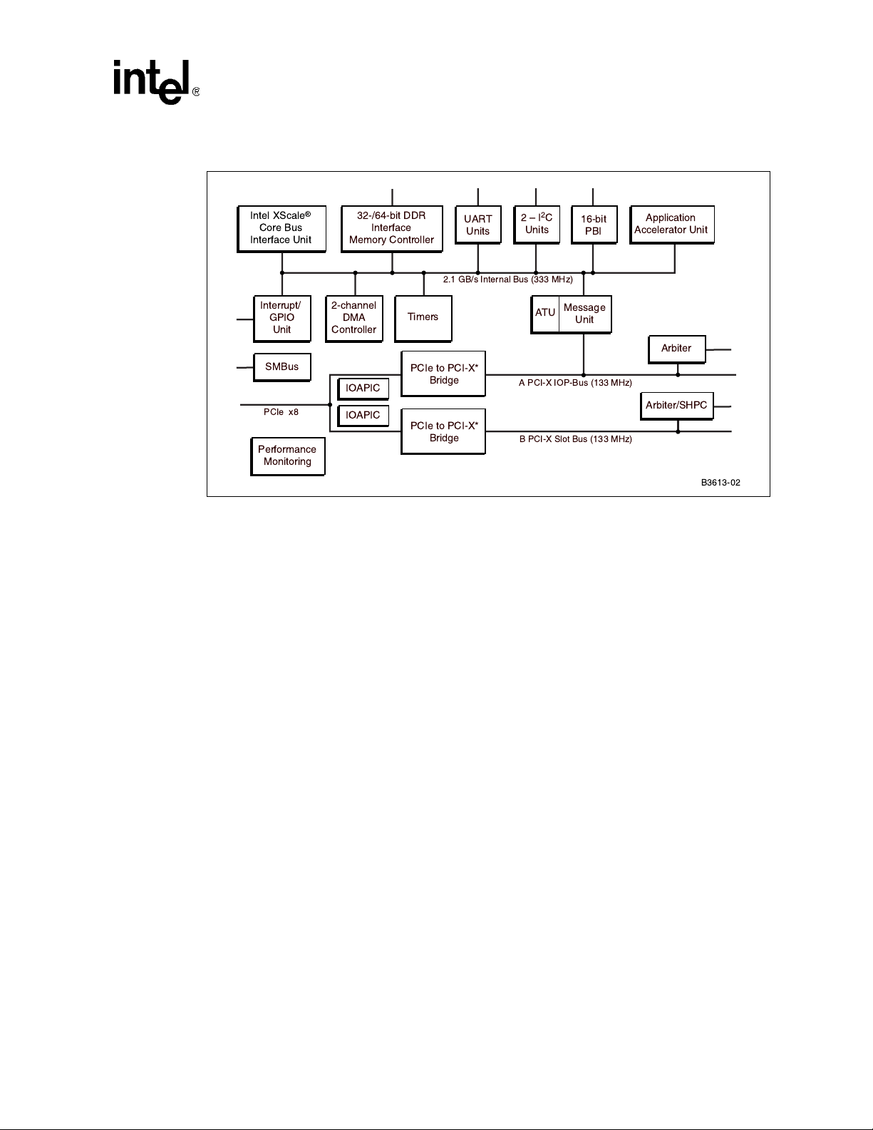
Figure 1. Intel® 80333 I/O Processor Block Diagram
Intel® IQ80333 I/O Processor
Introduction
%
&'
"
#
"3
!
"#$
.
"(
'(
'(
(!/
- & ) "*+,
/#
1
23
1
23
0
(/
( ' ) "*+,
) "*+,
"3
(%%
(
(
(*
Customer Reference Boar d M anual 13

Intel® IQ80333 I/O Processor
Introduction
1.7 Intel® IQ80333 I/O Processor Evaluation Platform Board Features
Table 5. Summary of Features
Feature Definition
Battery Backup Unit: Battery back up circuit for SDRAM.
Ethernet Intel(R) 825 45EM Gigabit Etherne t Controller
Flash ROM: 8 MB Flash ROM 3.3 V – 16-bit Flash I/F.
Form Factor: PCI-Express card (312 X 107 mm)
General Purpose I/O: GPIO Pins are used as described in the appropriate section in this document
Hex Display: Two 7-segment Hex LED displays.
JTAG Port: A R M co mpliant JTAG Hea de r.
Logic Analyzer:
Memory:
Onboard Power:
Power LED: Power on (green).
Primary PCI: PCI Express - x8 lane
RAID Support
Secondary PCI:
Serial Port:
Logic analyzer connectors on the DDRII SDRAM interface.
Interpo s er Card may be used for the memory bus – Information supplied separately.
• 256 MB (512 Mb x 16) DDRII SDRAM 400 MHz DIMM.
•ECC
•Registered
Board sources +1.25 V, +2.5 V, +3.3 V, +5 V, +12 V, and -12 V from primary PCI
connector.
• All core voltages are derived from 3.3 V supply.
• Auxiliary power for the Secondary PCI slot.
Support for “RAID” 6 functionality– Ability to make the devices plugged in the
secondary expansio n slots “Private”.
Integrated XOR engine and two iSCSI CRC32C off-load engines.
• 1 64-bit PCI-X connector - 133 MHz.
• 1 64 bit 100 MHz PCI-X
• Intel(R) 82 545EM Gigabit Ethernet Controller also on the 100 MHz PCI.
Dual RJ11 serial port connectors . The 80333 has two integrated UART serial ports
which are 16550 compatible.
14 Customer Referen ce Board Manual

Getting Started 2
The 80333 is a software development environment for IQ80333. Software updates and additional
offerings from vendors can change frequently. To keep up-to-date, please visit
http://www.intel-ioprocessortools.com/kshowcase/view
2.1 Kit Content
The 80333 Kit contains the following items:
• IQ80333 with 400 MHz DDRII SDRAM DIMMs
• Code|Lab* Develo pment Environment from Accelerate d Techno logy Incorporated*
• JTAG Emul a t i o n unit
• Serial Cable and RJ11 Adapter
2.2 Hardware Installation
Warning: S tatic char ges can seve rely da mage the boa rds. Be sure yo u ar e properl y grounde d be fore removi ng
the boar d f rom the anti-static bag.
for the latest updates.
2.2.1 First-Time Installation and Test
For first-time installation, visually inspect the 80333 for any damage made during shipment. Follow
the host system manufacturer’s instructions for installing a PCI Express adapter card. The board is a
full-length host bus adapter card that requires a PCI Express slot free from obstructions. The IQ80333
has a x8 (read as ‘by eight’) edge connector.
Note: Please note, at this tim e the IQ80333 does NOT work in a passive backplane. This is due to the
nature of the PCI Express linking protocol. For the I/O processor to successfully come out of reset,
a link must be established on the PCI Express bus. Without another device on a passive backplane
to ‘talk to’, a link is not established.
Customer Reference Boar d M anual 15

Intel® IQ80333 I/O Processor
Getting Started
2.2.2 Power Requirements
The 80333 requires a 3.3 V supply coming through the PCI Express primary connector. Plug the
board into a desktop with a PCI Express slot.
The 80333 has an auxiliary power receptacle (J1A1, see Section 3.9.4, “Connector Summary”) that
is used to power the secondary PCI-X slot. This connector is compatible with a standard ATX hard
drive power connector.
Caution: Before connecting power to the entir e system, ver i fy that the auxiliar y system power to the
secondary P CI-X slot a nd t he main po wer to t he 8 0333 are both connec ted. Both powe r rails sho uld
come up at the s ame ti me. W hen there is not a ca rd pl ug ged in to the se con dary PCI-X slot , th en th e
auxiliary power can be left unconnected.
16 Customer Referen ce Board Manual

2.3 Factory Settings
Make sure that the switch/jumper settings are set to proper positions as explained in Section 3.9,
“Switches and Jumpers” on page 38.
2.4 Development Strategy
2.4.1 Supported Tool Buckets
For developing and debugging software application, the production version of the 80333 kit includes
the Code|Lab Development Environment. Support for the Code|Lab development environment is
available from MGC*. Please refer to the enclosed package.
The following tools are available for evaluation purposes (please contact appropriate vendor). These
tools are for evaluation purposes and do not include any support. Please contact the vendor directly
for additional information and support. They include, but are not limited to:
• RedHat* GNUPro tools
Intel® IQ80333 I/O Processor
Getting Started
• ARM RealView Developer Suite
• WindRi ver* VxW orks* RTOS and Tornado* Development Tools
• W a sabi Systems NetBSD* OS
• TimeSys* Linux* RTOS
• Accelerated Technology Inc.*, Nucleus Plus* RTOS and Development Tools
Please contact your Intel representative for the latest updates or visit
http://www.intel-ioprocessortools.com/kshowcase/view
2.4.2 Contents of the Flash
The production version of the board conta ins an i mage fo r RedHat RedBoot* target monitor.
.
Customer Reference Boar d M anual 17

Intel® IQ80333 I/O Processor
Getting Started
2.5 Target Monitors
2.5.1 RedHat RedBoot
RedBoot* is an acronym for “RedHat Embedded Debug and Bootstrap”, and is the standard
embedded system debug/bootstrap environment from RedHat, replacing the previous generation of
debug firmware: CygMon and GDB stubs. It provides a bootstrap environment for a range of
embedded operating systems, such as embedded Linux and eCos*, and includes facilities such as
network downloading and debugging. It also provides a simple Flash file system for boot images.
RedBoot provides a set of tools for downloading and executing programs on embedded target
systems, as well as tools for manipulating the target system's environment. It can be used for both
product development (debug support) and for end product deployment (Flash and network booting).
Here are some highlights of RedBoot capabilities:
• Boot scripting support
• Simple command line interface for RedBoot configu r ation and management, accessible via
serial (terminal) or Ethernet (telnet) (see Section 2.6.4, “GNUPro GDB/Insight” on page 21)
• Integrated GDB stubs for connection to a host-based debugger (GBD/Insight) via seria l or
Ethernet. (Ethernet connectivity is limited to local network only)
• Attribute Configuration - user control of aspe cts such as system time and date (when
applicable), default Flash image to boot from, default fail-safe image, sta tic IP address, etc.
• Configurable and extensible, specifically adapted to the target environment
• Network bootstrap support including setu p and download, via BOOTP, DHCP and TFTP
• X/Y-Modem support for image download via serial
• Power On Self Test
18 Customer Referen ce Board Manual
2.6 Host Commu nicati ons Exampl es
How to communicate to the host.
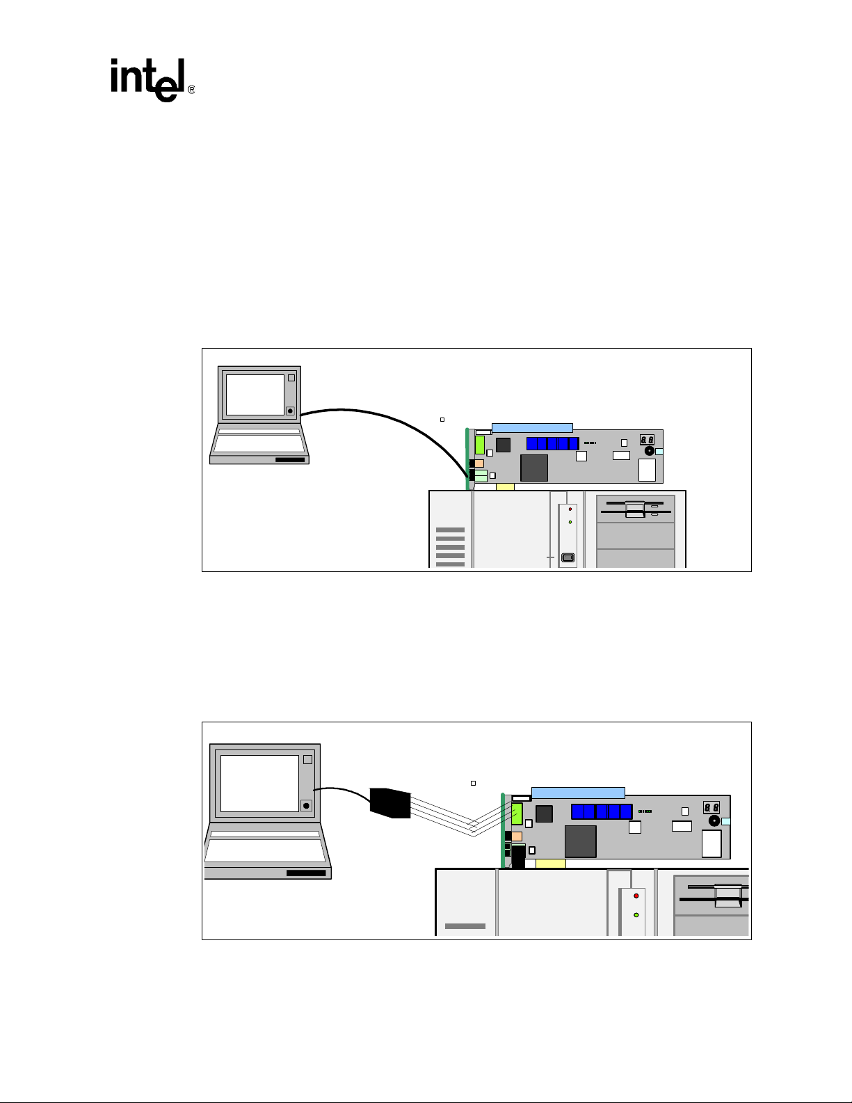
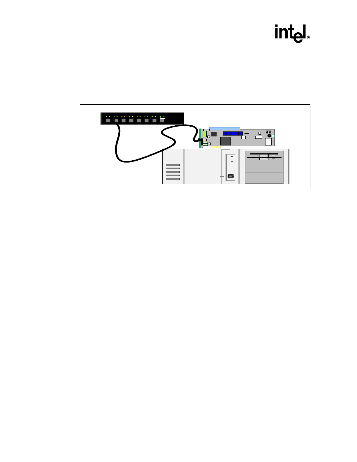
2.6.1 Serial-UART Communication
Using a serial connection to communicate with the board (Figure 2). Please note that the evlaution
board is plugged into a host machine, as in the figure below. You can use an additional laptop
computer, but it is not necessary. The host computer, when loaded with the proper software can
communicate with the board.
Figure 2. Serial-UART Communication
Intel® IQ80333 I/O Processor
Getting Started
Laptop c om pu t er
2.6.2 JTAG Deb ug Communication
Using a JTAG Emulator to communicate with the board (Figure 3). Please note that the evaluation
board is plugged into a host machine, as in the figure below. You can use an additional laptop
computer, but it is not necessary. The host computer, when loaded with the proper software can
communicate with the board.
Figure 3. JTAG Debug Communication
Laptop computer
Customer Reference Boar d M anual 19
Intel® IQ80333 I/O Processor
Getting Started
2.6.3 Network Communication
Using a standard network connection, the user can communicate with the board via the ethernet port.
Redboot also allows the user to remotely boot the platform using a BOOTP server through the
network Connection.
Figure 4. Netwo rk Comm uni cation E xample
A B C D E F G H
SELECTED
ON-LINE
20 Customer Referen ce Board Manual

2.6.4 GNUPro GDB/Insight
2.6.4.1 Communicating with RedBoot
Hardwa re Setup:
• Host with UNIX/Linux or Win32 installed
• IQ80333 with seria l ca ble
• RedHat RedBoot monit or Fl as hed to the platform board
Recommended Mapping of UART Ports to Host Com Ports
• Host port connected to the platform board UART.
The following communication tools can be used:
• Win32 using HyperTerminal
• UNIX using Kermit
• Linux using Minicom
• Solaris using Tip
Intel® IQ80333 I/O Processor
Getting Started
RedBoot Monitor startup:
Descriptio n: terminal emulator runs on host and communicates with the board via the serial cable .
Start: Power up th e IQ80333. Whil e the 'res et' is asserted, the two 7-segment LEDs
sequentially displ ay “88”, “A0” th rough “A6” , f ollowed b y “SL” (Scrub loop ). When
RedBo o t is su ccessf ull y b oo t ed , it disp l ay s the ch aracter s “A 1” on the LEDs. When
the final state of “A1” does not occur, reset the processor again.
The time for reset is approximately 1 or 2 seconds.
Win32 on Host Conn ecting with HyperTerminal.
Customer Reference Boar d M anual 21

Intel® IQ80333 I/O Processor
Getting Started
To bring up a HyperTerminal session on a Win32 platform: Go to Start, Programs, Accessories,
Communicati ons, Hy perTerminal
• HyperTerminal setup screens:
— “Connection Description” Panel:
• Enter name.
— “Connect To” Panel:
• Select host com2 port (or whic hever port you are using).
— Port Settings:
• Bits per second : 115200
• Data Bi t s : 8
• Parity: none
• Stop Bits: 1
• Flow Control: none
— Start HyperTerminal:
• Select Call from HyperTerminal panel.
— Reset or power up IQ80333.
— The Ho st sc re en r ead s :
RedBoot(tm) debug environment - built dd:mm:yy, Mon dd 2004
Platform: 80333
Copyright (C) 2004, RedHat, Inc.
RAM: 0xa0000000-0xa2000000
FLASH: 0x00000000 - 0x00800000, 64 blocks of 0x00020000 bytes each.
IP: 192.168.0.1, Default server: 0.0.0.0
RedBoot>
For further information on the GDB/Insight Debugger, refer to the content of the GNUPro CD and/or
the GNUPro Debugging Tools manual. This setup assumes that RedBoot is Flashed on the board.
22 Customer Referen ce Board Manual

2.6.4.2 Connecting with GDB
Below are the GDB commands entered from the command prompt. Be sure system path is set to
access “xscale-elf-gdb.exe”. File name in example “hello”. Bold type represents input by user:
Intel® IQ80333 I/O Processor
Getting Started
>xscale-elf-gdb -nw hello
1
• Start GDB executable, loads debug inform ation and symbols.
(GDB) set remotebaud 115200
• Set baud rate for the 80333.
Connect COM port:
• When using Windows command prompt:
(GDB) target rem o te co m1
Example: screen output from board to host (GDB) targe t remote com1:
Remote debugging using com1.
(GDB)
• When using Linux
(GDB) target rem o te /de v/ t t yS 0
(GDB) load
• Load the program to the board, may have to wait a few seconds.
(GDB) b reak main
• Set breakpoint at main.
(GDB) continue
• Start the program using 'continue' verse the usual 'run'.
• Program hits break at main() and wait.
1. To be supplied separately.
Customer Reference Boar d M anual 23

Intel® IQ80333 I/O Processor
Getting Started
This Page Left Intentionally Blank
24 Customer Referen ce Board Manual
Intel® IQ80333 I/O Processor
Hardware Reference Section
Hardware Reference Sect ion 3
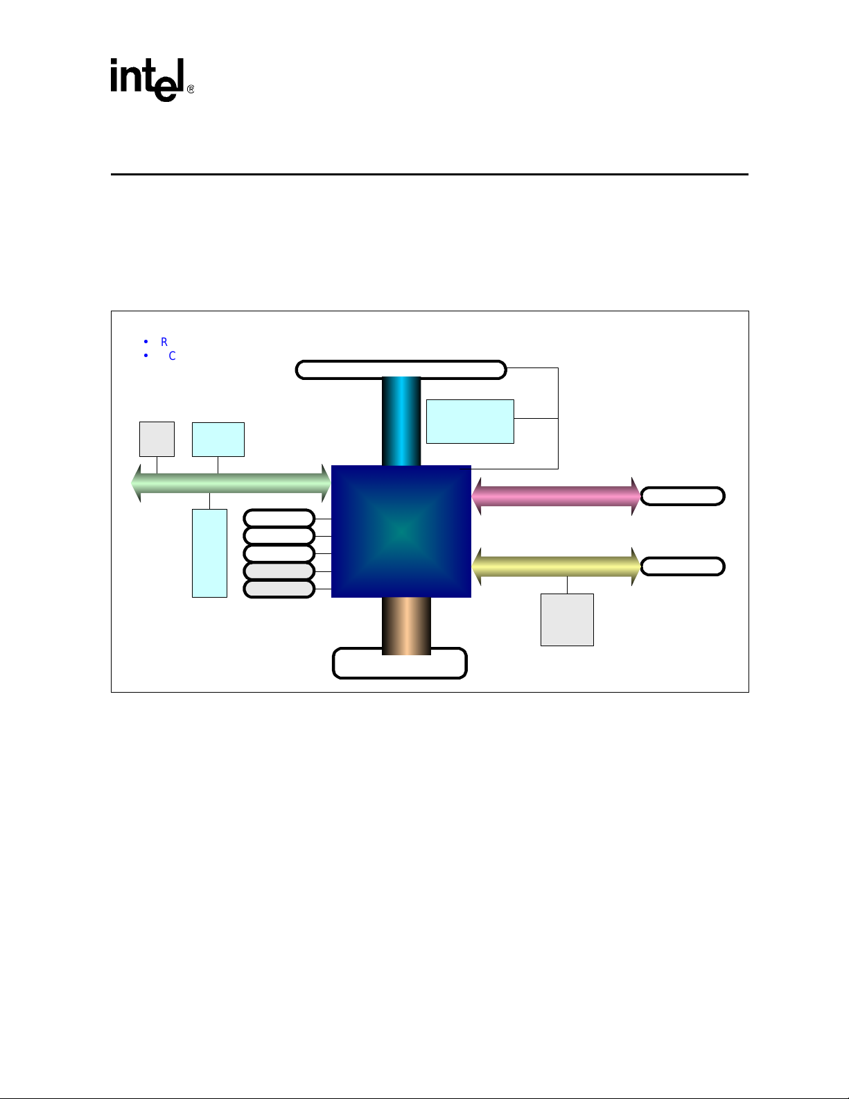
3.1 Functional Diagram
Figure 5 shows the functional block for the 80333.
Figure 5. Intel
Target M arket
ROMB
PCI Express RAID card
HEX
LED
®
80333 I/O Processor Functional Block Diag ram
DDR II 400
DDR SDRAM
Battery
Buzzer
Backup
Local B us
StrataFLASH
8 MB
RS-232
RS-232
I2C
GPIOs
JTAG
Intel®
80333
I/O
Processor
PCI
Express
X8 Edge Co nnector
PCI-X Bus IOP (100 MHz)
Gig-E
SlotPCI-X Bus Sl ot (133 MHz)
Slot
Customer Reference Boar d M anual 25

Intel® IQ80333 I/O Processor
s
Rotary
Switch
Hardware Reference Section
3.2 Board Form-Factor/C onnecti vity
Table 6 summarizes the form-factor and connectivity features for the 80333.
Table 6. Form-Factor/Connectivity Features
Description
The IQ 80333 is a x8 PCI Express card with form factor depicted by Figure 6.
The 80333 connec ts to the Primary PCI-Express bus of t he host machine.
The 80333 has two PCI-X expansion slot.
The 80333 has two serial ports and one RJ-45 Ethernet port.
The 80333 has one JTAG port compliant with ARM Multi-ICE 20-pin co nnector standard. The JT AG is targeted for the Intel
®
XScale
Figure 6. Board Form Factor
core and the CPLD, and is used for software debug purposes.
107
Aux
Power
JTAG
RJ-45
Etherne
t
RJ-11
Serial ports
Serial
EEPROM
PCI-X Slot (straddles board edge)
82545EM
GbE
Processor
Buffer
PCI-E
Edge
Inte l®
80333
I/O
DDR II DIMM
Peripheral Bus Header
I2C
CPLD
DIP Switch
PCI-X Rt Angle Slot
(Mounted on Back Side of PCB)
312
Flash
Intr/G P IO
Header
Power Statu
Buz
zer
Battery
26 Customer Referen ce Board Manual

3.3 Power
The 80333 draws power from the PCI Express bus. The power requirements for the 80333 are shown
in Table 7 below. The numbers do not include the power required by a PCI-X card mounted on the
expansion slot.
Table 7. Power Features
Voltage Rail Maxim um Cu r ren t
+3.3 V 6971 mA
+5 V 7 mA
+12 V 105 mA
Note: The maximum current was calcul ated, but not measured. This numbers do not include the power
required by a PCI-X card mounted on the expansion slot(s).
Customer Reference Boar d M anual 27

Intel® IQ80333 I/O Processor
Hardware Reference Section
3.4 Memory Subsystem
The Memory Controller of 80333 controls the DDR SDRAM memory subsystem. It features programmable chip sele cts and support for error correction code s ( ECC ). Th e memory controller can
be configured for DDR SDRAM at 333 MHz and DDR-II at 400 MHz. The memory controller
supports pipel ined a ccess and arbi trati on co ntrol to m aximiz e perform ance. T he memory controll er
interface configuration support includes Unbuffered DIMMs, Registered DIMMs, and discrete
DDR SDRAM devices.
This IQ80333 has DDR-II at 400 MHz DIMM on the board. The memory subsystem of the
evaluation board consists of the SDRAM as well as the Flash memory subsystems.
3.4.1 DDR SDRAM
The DDR SDRAM interface consists of a 64-bit wide data path to support up to 3.2 Gbytes/sec
throughput. An 8-bit Error Correction Code (ECC) is stored into the DDRII SDRAM array along
with the data and is checked when the data is read.
The IQ80333 features on board registered DDRII 400 MHz SDRAM, arranged 512 Mbit x16 in
density (256 MB), and with ECC.
3.4.1.1 Battery Backup
Battery backup is provided to save any information in DDR during a power failure. The evaluation
board contains a 4 V Li-ion battery, a charging circuit and a regulator circuit.
DDRII technology provides enabling data preservation through the self-refresh command. When the
processor receives an active Primary PCI-X reset, the self-refresh command issues, driving SCKE
signals low. Upon seeing this condition, the board logic circuit holds SCKE low before the processor
loses power. Batteries maintain power to DDRII and logic, to ensure self-refresh mode. When the
circuit detects PRST# returning to inactive state, the circuit releases the hold on SCKE. Removing the
battery can disable the battery circuit. When the battery remains in the platform when it is de-powered
and/or removed from the chassis, the battery maintains DDRII for about four hours. Once power is
reapplied, the battery is fully charged.
The CPLD contains information in regards to the battery status. Please see Section 3.6.7, “Battery
Status” on pa ge 34 for mor e details.
28 Customer Referen ce Board Manual

Intel® IQ80333 I/O Processor
Hardware Reference Section
3.4.2 Flash Memory Requirements
T o tal Flash memory size is 8 MB.
Table 8. Flash Memory Requirements
Description
IQ80333 Total Flash size is 8 MB
80333 Flash technology is based on Intel StrataFlas h
80333 Flash uses a 16-bit interface
80333 Flash utilizes the 80333 Peripheral Bus
80333 May be programmed using the PCI-X interface – Flash Recovery Utility (FRU) Utility
80333 May be programmed using a RAM based software target monitor – RedHat RedBoot and ARM Firmwar e Suite
80333 May be programmed using a JTAG emulation/debug device
®
family
Customer Reference Boar d M anual 29
Intel® IQ80333 I/O Processor
Hardware Reference Section
3.5 Interrup t Rout ing
The 80333 Interrupt routing.
Table 9. External Interrupt Routing to Intel
Interrupt System Resource
HPI# Temperature Sensor, Header
S_INTA# PCI-X S lot INTB#, Header
S_INTB# PCI-X Slot INTC#, Header
S_INTC# PCI-X Slot INTD#, Header
S_INTD# PCI-X Slot INTA#, Header
P_INTA# PCI-X Card Edge INTA#, Header
P_INTB# PCI-X Card Edge INTB#, Header
P_INTC# PCI-X Card Edge INTC#, Header
P_INTD# PCI-X Card Edge INTD#, Header
®
80333 I/O Processor
30 Customer Referen ce Board Manual
Intel® IQ80333 I/O Processor
Hardware Reference Section
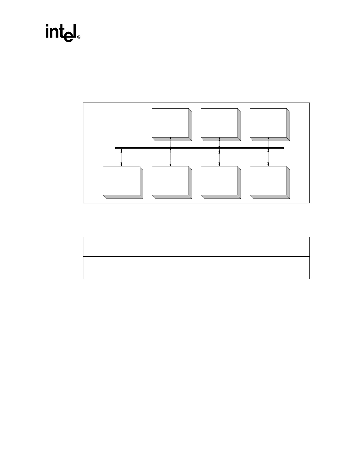
3.6 Intel® IQ80333 I/O Processor Evaluation Platform Board Peripheral Bus
The 80333 populates the peripheral bus as depicted by Figure 7.
Figure 7. Intel
®
IQ80333 I/O Processor Evaluation Platform Board Peripheral Bus Topology
Intel® 80333
I/O Processor PB I Bu s
PC 104
Conne ctor
The devices on the bus include Flash ROM, audio buzzer, CPLD, HEX display, NVSRAM, and
rotary switch.
Table 10. Peripheral Bus Features
The bus width can be 8-bit or 16-bit and runs at 66 MHz.
The bus is uti li ze d f or att a ch in g de bug and Fla sh dev ic es .
The interfaces/devices that are utilized include an audio buzzer, CPLD, a rotary switch, a HEX Display, and
NVSRAM.
Agilent*
HDSP-A103 Hex
Display
Grayhill
HAB 16W
Ro tary S witch
Description
FLASH 28F640J3C
16-bit
8 Mb
XILINX
XC9572XL-
10TQ1 00C
CPLD
RDI
DMT-120 6-SMT
Audio Buzzer
SIMTEK
STK14 C88-3 N 35
NVSRAM
Customer Reference Boar d M anual 31

Intel® IQ80333 I/O Processor
Hardware Reference Section
3.6.1 Flash ROM
Table 11. Flash ROM Features
Flash i s an Intel Strat aFlash
Flash size is 8 MB
The connection to the peripheral bus is depicted by Figure 8
Figure 8. Flash Con nection on Pe ri ph e ral Bu s
Intel® 80333
I/O Processor
®
technology – Part number: 28F640J3C
Description
Flash
28F640J3C
16-bit
8 Mb
CS
PCE0
® 80333 I/O Processor
Intel
32 Customer Referen ce Board Manual

3.6.2 UART
The 80333 has two integrated UARTs. Each asynchronous serial ports supports all the functions of a
16550 UART. The UART signals are connected to a dual RS-232 buffer and then to a RJ-11 serial
port connector mounted on the bracket of the evaluation board. The serial port and GPIO signals are
muxed on the same pins. Jumper J1D2, located next to the serial port buffer can disable the buffer to
allow the signals to be used as GPIO signals. Please see Section 3.9.3, “Jumper Summary” on
page 39 for more details.
3.6.3 Non-Volatile RAM
In addition to the 8MB Flash device, the IQ80333 has a separate 32 K by 8 non-volatile RAM device
on the peripheral bus. The NVRAMs address range is from CE87 0000 to CE87 FFFF (in hex).
Please see Section 4.2.2, “Periph er al Bus Memory Map” on page 47 for more details.
3.6.4 Audio Buzzer
The 80333 evaluation board has an audio buzzer that is turned on and off by writing to the Buzzer
Control Register located in the CPLD. Jumper J9D3 adjusts the volume from off, to soft, to loud.
Please see Section 3.9.3, “Jumper Summary” on page 39 for more details. The audio buzzer’s
address range is from CE86 0000 to CE86 FFFF (in hex). Please see Section 4.2.2, “Periph er a l Bus
Memory Map” on page 47 for more details.
Intel® IQ80333 I/O Processor
Hardware Reference Section
3.6. 5 HEX Display
The two pairs of Agil ent HDS P - A103 seven segment LED s are used for displaying POST codes or
other software generated debug codes. Both HEX displays are individually addressed. The left HEX
display address range is CE84 0000 to CE84 FFFF (in hex). The right HEX display address range is
CE85 0000 to CE85 FFFF (in hex). Please see Section 4.2.2, “Periphera l Bus Memory Map” on
page 47 for more details.
3.6.6 Rotary Switch
The 80333 provides a Rotary Switch (S8A1) for the user to selec t from different boot-up flavors.
Setting ‘0’ enables private devices on the secondary PCI-X bus. Setting ‘0’ allows Redboot to
configure and use devices in slot A. Position ‘1’ allows the host to see all the devices on the
secondary PCI bus. The default setting is position 0. Other settings are currently not validated with
Redboot. Other settings may be used with other software applications. Please see Section 4.2.2,
“Peripheral Bus Memory Map” on page 47 for more details on addressing the rotary switch.
Table 12. Rotary Switch Requirements
Rotary switch has a 4-bit resolution ( 16 positions).
The connection to the peripheral bus is depicted by Figure 7.
Default setting is ‘0’. This enables private devices on PCI-X bus.
Position ‘1’ allows host to see all devices on the secondary bus.
Description
Customer Reference Boar d M anual 33
Intel® IQ80333 I/O Processor
Hardware Reference Section
3.6.7 Battery Status
A CPLD on the IQ80333 provides the following status for the battery. Please see Section 4.2.2, “Peripheral
Bus Memory Map” on page 47 for more details on addressing the CPLD.
Table 13. Battery Status Buffer Requirements
Read/
BIT
Write
Name Description
0 R Battery Present
1 R Battery Charged
2 R Battery Discharged
3 R/W Battery Enable
4-7 * Reserved Undefined
• 0 = No backup bat tery
• 1 = Battery backup is present
• 0 = Battery is not fully charged
• 1 = Battery is fully charged
• 0 = Battery backup is not fully discharged
• 1 = Battery backup is fully discharged
• 0 = Disable battery backup
• 1 = Enable battery ba cku p
34 Customer Referen ce Board Manual

3.7 Debug Interface
3.7.1 Console Serial Port
The platform has two serial ports for debug purposes as described in Section 3.6, “Intel® IQ80333
I/O Processor Evaluation Platform Board Peripheral Bus ” on page 31.
Intel® IQ80333 I/O Processor
Hardware Reference Section
Customer Reference Boar d M anual 35

Intel® IQ80333 I/O Processor
1
Hardware Reference Section
3.7.2 JTAG Debug
The 80333 has a 20-pin JTAG connector (J7D2) that is in compliant with ARM Multi-ICE guidelines.
3.7.2.1 JTAG Port
Figure 9. JTAG Port Pin-out
VTref 1
nTRST 3
TDI 5
TMS 7
TCK 9
RTCK 11
TDO 13
nSRST 15
DBGRQ 17
DBGACK 19
Vsupply2
GND4
GND6
GND8
GND10
GND12
GND14
GND16
GND18
GND20
A9457-0
36 Customer Referen ce Board Manual

3.8 Board Reset Scheme
Figure 10 depicts the reset scheme for the 80333. Table 14 list the reset schemes for the 80333.
Table 14. Reset Requirements/Schemes
Primary PCI reset, resets all devices on the board. It occurs during the power-up.
The SRST signal from the JTAG connector is a bi-directional signal that can force a reset similar to the
power-up reset on the board.
Figure 10. RESET Sources
DDR II SDRAM
Reset
Button
Debounce
Power
Delay
JTAG
Con
Voltage
Monitor
TRST
#
SRST
#
M_RST#
RESETIN
#
PWRDELAY
Intel® 80333 I/O
Processor
TRST
#
PWRGD
Isolation
Description
B_RST#
A_RST#
Pwrgood
Intel® IQ80333 I/O Processor
Hardware Reference Section
PCI-X Con B
PCI-X Con A
CPLD
RST#
LAN_PWR_GOOD
82545EM
PCI-E Con
Customer Reference Boar d M anual 37

Intel® IQ80333 I/O Processor
Hardware Reference Section
3.9 Switches and Jumpers
3.9.1 Switch Summary
Please note that the term ‘open’ refers to the individual pin of switch S7A1 being pushed in at bottom
(small dot on pin away from the ‘open’ label on the switch). The term ‘closed’ refers to the pin being
pushed in at the top. Please see Figure 11, “Default Switch Setting Switch S7A1” on page 38, for
more details.
Table 15. Switch Sum mary
Switch Association Description
S1C1 80333 Reset
S6A1 BPCI-X Reset
S7A1-1 APCI-X Bus PCI-XBus A Speed Set Closed
S7A1-2 IOP RESET : Sets IOP Reset-Mode operation Open
S7A1-3 IOP RETRY: Sets IOP RETRY-Mode operation Open
S7A1-4 BPCI-X Bus PCI-X Bus B speed set Closed
S7A1-5 BPCI-X Bus PCI-X Bus B Hot Plug Reset Closed
S7A1-6 BPCI-X Bus Hot Plug Capable Disable Closed
S7A1-7 SMBUS Bus SMBUS Managea bility addre ss bit 5 Open
S7A1-8 SMBUS Bus SMBUS Manageability address bit 3 Open
S7A1-9 SMBUS Bus SMBUS Manageability address bit 2 Open
S7A1-10 S MBUS Bus SMBUS Manageability address bit 1 Open
S8A1 CPLD Rotary Switch Position 1
3.9.2 Default Switch Settings of S7A1- Visual
Table 16. Switch S7A1
Closed Open Open Closed Closed Closed Open Open Open Open
S7A11S7A1
2
S7A13S7A14S7A1
5
S7A1
6
S7A17S7A18S7A1
Factory
Default
S7A1
9
10
Figure 11. Default Switch Setting Switch S7A1
165432
78
10
9
Open
38 Customer Referen ce Boar d Manu al

3.9.3 Jumper Summary
Table 17. Jumper Summary
Jumper Descri ption Factor y Default
J1C1 JTAG Chain Enable 1-2
J1D2 Disables UART Open
J7B4 SM_SCLK to EEPROM, SM_SDTA to EEPROM 1-2, 3-4
J7D1 16-bit Flash Enable Open
J9D3 Buzzer Volume Open
3.9.4 Connector Summary
Table 18. Co n nector Summary
Connector Description
J1D1 RJ45 Network Connector for GbE NIC.
J1E1 RJ11 Dual Serial Port Connector.
J1L1, J1M1 ,
J1M2, J1N1,
J2M1, J2M2
J1R1 Secondary PCI-X Expansion bus Slot
J2A1 Secondary PCI-X Expansion bus Slot.
J2D1 Power header for fan.
J2D2 GPIO tap-in Header
J1B1, J5D1,
J5C1
J2E1 Edge connector for primary PCI Express Bus.
J5B1 DIMM
J7A1 PC104 Mod connector.
J7B1, J7B2 I
J7B3
J7C1 Test head er (empty)
J7D2 JTAG CPLD Header.
J9D1 Power header for battery.
SMA connectors
Test headers
2
C 4 pin connectors.
Secondary PCI-X Expansion Slot Power. Please see Section 2.2.2, “Power Requirements”
for more details
Intel® IQ80333 I/O Processor
Hardware Reference Section
3.9.5 General Purpose Input/Output Header
Table 19, “J2D2 GPIO Header Definition” on page 39 shows the GPIO signal assignments. The
GPIO signals are muxed with the serial port signals. The serial port must be disabled to use the GPIO
signals. These pins corespond to Jumper J2D2.
Table 19. J2D2 GPIO Header Definition
Pin Signal Pin Signal Pin Signal
1 GND 4GPIO57GPIO2
2GPIO75GPIO48GPIO1
3GPIO66GPIO39GPIO0
Customer Reference Boar d M anual 39

Intel® IQ80333 I/O Processor
Hardware Reference Section
3.9.6 Detail Descriptions of Switches/Jumpers
3.9.6.1 Switch S1C2: Intel® 80333 I/O Processor Reset
This switch resets 80333.
3.9.6.2 Switch S6A1: BPCI-X Reset
This switch resets the PCI-X B segment bus.
3.9.6.3 Switch S8A1: Rotary
Table 20. Rotary Switch Settings
Position Description
0
Factory Defa ul t
1
2-F
Enables p r ivat e de vic es on t he sec on dar y PC I -X s lot . Re db oo t use s t h is sett in g to co nf igur e
privat e device s
Disable s priv at e de vi ces on t he second ar y PC I-X slo t . Thi s set tin g al lo ws th e ho st to see al l
the devices on the secondary PCI bus.
These settings are meaningless to Redboot. Other applications may use these settings for
configuration or software utilization.
For more information, please see Section 3.6.6, “Rotar y Swi tch” on page 33.
3.9.6.4 Switch S7A1
This 10 pin switch that allows the user to enable or disable various features. Please see specifics
below.
3.9.6.4.1 S7A1-1: PCI-X Bus A Speed Enable Corresponding to Signal Name PBI_AD3
This switch allows the user to force the PCI-X bus A to run at 133 MHz or 100 MHz.
Table 21. S7A1-1: PCI-X Bus A Speed Enable
S7A1-1 Operation Mode
Open Enables 133 MHz on PCI-X bus A
Closed Enables 100 MHz on PCI-X bus A (Default Mode)
3.9.6.4.2 S7A1-2: Reset I/O Processor Core Correspon ding to Signal Name PBI_AD5
RESET MODE is latched at the de-asserting edge of P_RST# and it determines when the 80333 is held
in reset until the Intel XScale
40 Customer Referen ce Boar d Manu al
®
core Reset bit is cleared in the PCI Configuration and Status Register.

Intel® IQ80333 I/O Processor
Hardware Reference Section
Table 22. Switch S7A1-2: Reset IOP: Settings and Operation Mode
S7A1-2 Operation Mode
Open Don't hold in reset, enab le IOP co re ( D ef au lt mo de ).
Closed Hold IOP core in reset.
3.9.6.4.3 S7A1-3: Configration Cycle Enable Correspo nding to Signal Name PBI_AD6
Configuration Cycle Enable or RETRY is latched at the de-asserting edge of P_RST# and it
determines when the Primary PCI interface disable PCI configuration cycles by signaling a Retry
until the Configuration Cycle Retry bit is cleared in the PCI Configuration and Status Register.
Table 23. Switch S7A1-3: RETRY: Settings and Operation Mode
S7A1-3 Operation Mode
Open Configuration Retry Enabled. - use when booting in a host (Default mode).
Closed Configuratio n Retry Disabled.
3.9.6.4.4 S7A1-4: PCI-X Bus B Speed Enable Corresponding to Signal Name PBI_AD 1 0
This switch allows the user to enables 133 MHz on PCI-X segment B.
Table 24. S7A1-4: PCI-X Bus B Speed Enable: Settings and Operation Mode
S7A1-4 Operation Mode
Open Enables 133 MHz on PCI-X bus B.
Closed Enables 100 MHz on PCI-X bus B (Default Mode).
3.9.6.4.5 S7A1-5: PCI-X Bus B Hot-Plug Reset Disable Corresp onding to Sig nal Name PBI _A D 11
This switch allows the user to enables or disable Hot-Plug Reset on PCI-X segment B.
Table 25. S7A1-5: PCI-X Bus B Hot-Plug Reset Disable: Settings and Operation Mode
S7A1-5 Operation Mode
Open PCI-X Bus B Hot-Plug Enable, normal reset mode disabled
Closed PCI-X Bus B Hot-Plug Disable, normal re set mode (Default Mode).
3.9.6.4.6 Switch S7A1- 6: Hot Plug Capable Disabled Corresponding to Signal Name PBI_AD 1 5
This switch allows the user to enable hot plug devices on the secondary PCI-X bus B.
Table 26. Switch S7A1- 6: Hot Plug Capable Disabled: Settings and Operation Mode
S7A1-6 Operation Mode
Open Hot Plug on Bus B Enabled
Closed Disables Hot Plug on Bus B(Default mode)
Customer Reference Boar d M anual 41
Intel® IQ80333 I/O Processor
Hardware Reference Section
3.9.6.4.7 Switch S7A1 - 7: SMBUS Manageability Address Bit 0 Corresponding to Signal Name PBI_AD17
This allows 80333 to address SMBus Slave Address bit 0 (PBI_A17).
Table 27. Switch S7A1 - 7: SMBUS Manageability Address Bit 0: Settings and Operation Mode
S7A1-6 Operation Mode
Open SMBus Manageab lity Addre ss Bit 0 = “1” (Default Mode)
Closed SMBus Mana geablity Address Bit 0 = “0”
3.9.6.4.8 Switch S7A1 - 8: SMBUS Manageability Address Bit 3 Corresponding to Signal Name PBI_AD18
This allows 80333 to address SMBus Slave Address bit 3 (PBI_A18).
Table 28. Switch S7A1 - 8: SMBUS Manageability Address Bit 3: Settings and Operation Mode
S7A1-8 Operation Mode
Open SMBus Manageab lity Addre ss Bit 3 = “1” (Default Mode)
Closed SMBus Mana geablity Address Bit 3 = “0”.
3.9.6.4.9 Switch S7A1- 9:SMBUS Manageability Address Bit 2 Corresponding to Signal Name PBI_AD17
This allows 80333 to address SMBus Slave Address2 (PBI_A17).
Table 29. Switch S7A1 - 9: SMBUS Manageability Address Bit 2: Settings and Operation Mode
S7A1-9 Operation Mode
Open SMBus Manageab lity Addre ss Bit 2 = “1” (Default Mode)
Closed SMBus Mana geablity Address Bit 2 = “0”.
3.9.6.4.10 Sw itch S7A1- 10: SMBUS Manag eability Address Bit 1 Corresponding to Signal Name PBI_AD16
This allows 80333 to address SMBus Slave Address 1 (PBI_A16).
Table 30. Switch S7A1 - 10: SMBUS Slave Address 0: Settings and Operation Mode
S7A1-10 Operation Mode
Open SMBus Manageab lity Addre ss Bit 1 = “1” (Default Mode)
Closed SMBus Mana geablity Address Bit 1 = “0”.
42 Customer Referen ce Boar d Manu al

3.9.6.5 Jumper J7D1: Flash bit-width
The IQ80333 expects an 8-bit Flash enable.
Table 31. Jumper J7D1: Descr iptio ns
Jumper Descr ipt ion Factor y D efau l t
J7D1 8-bit Flash Enable Open
Table 32. Jumper J7D1: S ettings and Oper ation Mode
Pins Operation Mode
1-2 Enables 16-bit Flash
NC 8-bit Flash ( default mode)
3.9.6.6 Jumper J1C1: JTAG Chain
Table 33. Jumper J1C1: Descr iptio ns
Jumper Descr ipt ion Factor y D efau l t
J1C1 JTAG Chain Enable 1-2
Intel® IQ80333 I/O Processor
Hardware Reference Section
Table 34. Jumper J1C1: S ettings and Oper ation Mode
J1C1 Operation Mode
Pins 1, 2 Enables JTAG Chain for IOP only (Default Mode).
Pins 3, 4 Enables JTAG Chain for IOP + CPLD
Pins 5, 6 Enables JTAG Chain for IOP + CPLD + GBE
Pins 7, 8 Enables TRST# pull-down resistor
3.9.6.7 Jumper J1D2: UART Control
Table 35. Jumper J1D2: Descr iptio ns
Jumper Descr ipt ion Factor y D efau l t
J1D2 UART Control Open
Table 36. Jumper J1D2: S ettings and Oper ation Mode
J1D2 Operation Mode
Pins 1, 2 Disables UART/RS-232 port
NC Enables UART/RS-232 port (Default Mode)
Customer Reference Boar d M anual 43

Intel® IQ80333 I/O Processor
Hardware Reference Section
3.9.6.8 Jumper J7B4: SMBus Header
Table 37. Jumper J7B4: Description s
Jumper Description Factory Default
J7B4 SMBus Header 1-2, 3-4
Table 38. Jumper J7B4: Setting s and Operati on Mod e
J7B4 Operati on Mode
Pins 1, 2 Connects SM_SCLK to EEPROM U7B2 (Default Mode).
Pins 3, 4 Conne cts SM_SDTA to EEPROM U7B2 (Default Mo de).
Pins 5, 6 Conne cts SM_SCLK to GE_SMCLK ( for GBE control)
Pins 7, 8 Conne cts SM_SDTA to GE_SMDAT(for GB E control)r
Pins 9, 10 Connects SM_SCLK to PE_SMCLK (for PCI-E bus control)
Pins 11, 12 Connects SM_SDT A to PE_SM_SDAT (for PCI-E bus control)
3.9.6.9 Jumper J9D3: Buzzer Volume Control
Table 39. Jumper J9D3: Description s
Jumper Description Factory Default
J9D3 Buzzer Volume Open
Table 40. Jumper J9D3: Setting s and Operati on Mod e
J9D3 Operation Mode
Pins 2, 3
Pins 1, 2
NC
Buzzer Volume Soft
Buzzer Volume Loud.
Buzzer Volume Off.
44 Customer Referen ce Boar d Manu al

Intel® IQ80333 I/O Processor
Software Reference
Software Reference 4
4.1 DRAM
For DDR SDRAM Sizes and Configurations, see theIntel® 80333 I/O Processor Developer’s
Manual. This section also contains multiple examples of Address Register Programming.
See the Intel
DDR-II configurations.
For all registers relating to DRAM and other MCU relat ed re gis ters, see the Intel
Processor Developer’s Manual.
®
80333 I/O Processor Design Guide, section 8, table 3 4 for supported DD R333 and
4.2 Components on the Peripheral Bus
The 80333 has a peripheral bus which contains the following peripheral devices:
• Flash ROM
• CPLD
• Audio Buzzer
• Rotary Switch
• Hex Display
Peripheral memory-Mapped Register Locations and all registers associated with PBI or the Peripheral
Bus Interface Unit can be found in the Intel
®
80333 I/O Processor Developer’s Manual.
®
80333 I/O
Customer Reference Boar d M anual 45
Intel® IQ80333 I/O Processor
Software Reference
4.2.1 Flash ROM
The Flash ROM is an 8 MB Intel StrataFlash® (part# 28F640) that sits on the Peripheral Bus and is
accessed using PCE0.
Figure 12. Flash Con ne ction to Peripheral Bus
Intel® 80333
I/O Processor
Flash
28F640J3C
16-bit
8 Mb
Intel
® 80333 I/O Processor
CS
PCE0
Under normal operation, the very first instruction access by the Intel XScale
0x0 on the 80333 Internal Bus. By default, address 0x0 is pointing to PCE0 where Flash is located.
Currently, the Intel Flash Recovery Utility (FRU) can be used with the IQ80333. Another alternative
to FRU would be to reprogram the Flash through JTAG or using Redboot commands, when Redboot
is currently loaded onto the board. For more information on using Redboot to program the Flash,
please see Redboot Manual.
®
core begins at location
46 Customer Referen ce Boar d Manu al

4.2.2 Peripheral Bus Memory Map
The Table 41 is the physical memory map of the devices on the 80333 Peripheral Bus:
Table 41. Per iph eral Bu s M emory Ma p
Address Range (in H ex) Size Data Bus Widt h Description
C0000000 - C07F FFFF 8 MB 8-bit or 16-bit Flash me mory (re-m apped)
CE800000 -CE8 0 FFFF 64 KB 8-bit Product Code
CE810000 -CE81 FFFF 64 KB 8-bit Board Stepping
CE82 0000 -CE82 FFFF 64 KB 8-bit CPLD Firmware Revision
CE830000 -CE83 FFFF 64 KB 8-bi t Discrete LEDs
CE84 0000 -CE8 4 FFFF 64 KB 8-bit Hex Display Left
CE85 0000 -CE85 FFFF 64 KB 8-bit Hex Display Right
CE86 0000 -CE86 FFFF 64 KB 8-bit Buzzer Control
CE870000 -CE87 FFFF 64 KB 8-bit 32 KB NV RAM
CE8D 0000 -CE8D FFFF 64 KB 8-bit Rotary Switch
CE8E 0000 -CE8E FFFF 64 KB 8-bit ESN I/O
CE8F 0000 -CE8F FFFF 64 KB 8-bit Battery Status
Intel® IQ80333 I/O Processor
Software Reference
Customer Reference Boar d M anual 47

Intel® IQ80333 I/O Processor
Software Reference
4.3 Board Support Packag e (BSP ) Examp les
Examples provided in this section are based on the RedHat* RedBoot software running on the
IQ80333.
4.3.1 Intel® 80333 I/O Processor Memory Map
Figure 13 depicts the memory space for the 80333 (before RedBoot boots):
Figure 13. Intel
®
80333 I/O Processor Memory Map
ADDRESS
0000 0000H
0000 0040H
Memoryless Boot Registers
ATU Outbound Direct Addressing Window
8000 0000H
8800 0000H
9000 0000H
9001 0000H
FFFF E000H
FFFF E900H
ATU Outbound Memory Transla tion Windows
Code / Data External Memory
ATU Outbound I/O Translation Window
Code/Data
External Memory
Peripheral Memory-Mapped Regi sters
I/O Processor Reserved
FFFF FFFFH
Reserved
Address
Space
External Memory
48 Customer Referen ce Boar d Manu al

Intel® IQ80333 I/O Processor
Software Reference
4.3.2 RedBoot* Intel® 80333 I/O Processor Memory Map
Virtual Address Physical Address
0x0000 0000 0x00000000 2048 SDRAM - 64-bit ECC
0x8000 0000 0x80000000 128 ATU Outbound Memory Translation Windows
0x88000000 * 128 Unused
0x9000 0000 0x9000 0000 1 ATU OUtbound I/O Translation Window.
0x9010 0000 * 255 Unused
0xA000 0000 0x0000 0000 512 SDRAM - 64 bit ECC Uncached
0xC000 0000 0xC000 0000 8 Flash (PCE0#)
0xC080 0000 * 224 Unused
0xCE80 0000 0xCE80 0000 1 PCE1# - Uncached
0xCE900000 * 23 Unused
0xD000 0000 * 512 Unused
0xF00 0000 0xF00 0000 1 Cache flush
0xF010 0000 * 254 Unused
0xFFF0 0000 0xFFF0 0000 1
4.3.3 RedBoot Intel
Size
(MB)
®
PMMR - Intel
Registers. Please see Chapter 17 of the Intel
Processor Developer’s Manual for more details.
®
80333 I/O Processor Files
80333 I/O processor Memory Mapped
Description
®
80333 I/O
Attached in the kit, find a copy of the RedHat eCos for IQ80333 CD. Once the CD is installed, you
may find:
• The RedBoot initialization code source files from the following location:
From the installed directory:
..\RedHat\eCos\packages\hal\arm\xscale\iq80333\current\include
• The RedBoot binary image files (downloadable onto Fla sh) from the following location:
From the installed directory:
..\RedHat\eCos\loaders\iq80333
To access RedHat GNUPro tools including RedBoot binaries and source code, you may also go to the
following location on the Intel site:
• http://developer.intel.com/design/intelxscale/dev_tools/021022/index.htm
Customer Reference Boar d M anual 49

Intel® IQ80333 I/O Processor
Software Reference
4.3.4 RedBoot Intel® 80332 I/O Processor DDR Memory Initialization Sequence
In order to set the correct ECC bits, a DDR memory system (DIMM or discrete components) must be
written to with a known value. This process requires 64-bit writes to the entire DDR memory intended
for use. The following explains the sequence for memory initialization by RedBoot on an 80333 board
with an ECC DIMM. It also includes an example for the scrub (ECC initialization) cod e.
Initialization Sequence:
1. Disable interrupts. (Technically they are disabled at reset, but for soft reset this is included.
2. Init PBIU (Peripheral Bus Interface Unit) chip selects.
3. Enab l e I cach e .
4. Move Flash to 0xF0000000.
5. Set TTB and Enable MMU.
6. Read DIM for memory parameters.
7. Set Memory Parameters.
8. Delay.
9. Turn DDRAM on.
10. Delay.
11. Enable Data Cache.
12. Enable BTB.
13. Flush all.
14. Clear ECC error logs.
15. Battery Test.
16. Enable ECC.
17. Scrub loop: Wri te zeros to all memory locations
mov r8, r4 // save DRAM size
mov r0, #-1
mov r1, #-1
mov r2, #-1
mov r3, #-1
mov r4, #-1
mov r5, #-1
mov r6, #-1
mov r7, #-1
ldr r11, = SDRAM_BASE
// scrub Loop
0:
stmia r11!, {r0-r7}
subs r12, r12, #32
bne 0
50 Customer Referen ce Boar d Manu al

Intel® IQ80333 I/O Processor
IQ80321 and IQ80333 Compari son s
IQ80321 and IQ80333 Comparisons A
This appendix provides a brief description for differences between IQ80333 and IQ80321.
®
Table 42. Intel
Features
I/O Processor 80333 Intel
Core/Microprocessor
Technology
Memory Technology DDRII 400 MHz SDRAM DIMM PC1600 DDR SDRAM (100 MHz Clock)
Form Factor
PC/Server/Backplane
Connection
Expa nsion Card Slot
PCI/PCI-X Bridge
Interrupt Routing
Timers
Local/Periph er a l Bus
Flash Memory
Serial Debug Port Two UARTs integrated within the 80333.
Network Debug Port Int el® 82545EM G bE on the 100 MHz PCI-X bus Intel® 82544 GbE o n the PCI-X b us
Rotary Switch Same Same
LED HEX Dis pla y Same S am e
JTAG 20-PIN ARM Compliant 20-PIN ARM Compliant
Logic Analyzer Connection Through P CI-X or PCI Express Var ious Mictors
IQ80321 Evaluation Platform Board and
®
Intel
IQ80333 I/O Processor Evaluation Platform Board Comparisons
®
Intel
IQ80333 I/O Processor Evaluation
Platform Board
Intel XScale
PC board that attaches to a PC /Server/Backplane
by a PCI Express slot – Two PCI-X Expansion Slot
PCI Expres s
One PCI- X 100 M H z /6 4- b its
One PCI- X 133 MHz/64-b it
PCI-X to PCI-X Bridge inte gr ated with the
IQ80333l
External interrupts are routed through the XINT
pins on the 80333. Please see Table 9 for more
details.
Internal to 80333 – Refer to Intel
Processor Developer’s Manual
66 MHz multiplexed bus with two chip-enables,
Synch/As ynchro nous (80 333 o perat es i n 66 MHz
Asynchronous mode) – Refer to PB I section in
Intel
8-bit o r 1 6- b it, 8 MB acc es sed t h rou gh Per i pher a l
Bus with chip-enable 0 (PCE0)
®
microarchitect ure Intel XScale® microarchitecture
®
80333 I /O
®
80333 I/O Processor Developer’s Manual
®
Intel
IQ80321 Evaluation Platform Boa rd
®
80321 I /O Processor
Extended PC board that attaches to a
PC/Server/Backplane – One PCI-X Expansion Slot
PCI-X 133 MHz/64-Bits or
PCI 66 MHz/64 Bits
One PCI- X 13 3 M H z /64-bit
IBM PCI-X Bridge
Refere nce: IBM 133 PCI-X Bridge
http://www.chips.ibm.com/
External inter rupts are routed through the XINT
pins on the 80321. They include INTA, INTB form
PCI-X expansion slot, INT A from 82544 GBE, and
UART interrupt – Steer ing and S ta tus register s are
in 803 21 – s e e Intel
Developer’s Manual
Internal to th e 80321 - please refer to th e Intel®
80321 I/O Processor Developer’s Manual
2-bit/ 3 3- 100MHz mult iplexe d bu s w ith six
chip-enables, Synch/Asynchronous (IQ80321
operates in 33 MHz Asynchro nous mode) –
Refer to PBI section in the IIntel
Processor Developer’s Manual.
16-bit, 8 MB accessed through Peripheral Bus
with chip-enable 0 (PCE0))
One UART on the Peripheral bus – 16C550
device
®
80321 I /O Processor
®
80321 I/O
Customer Reference Boar d M anual 51

Intel® IQ80333 I/O Processor
IQ80321 and IQ80333 Compariso ns
This Page Left Intentionally Blank
52 Customer Referen ce Boar d Manu al

Intel® IQ80333 I/O Processor
Getting Started and Debugger
Getting Started and Debugger B
B.1 Introduction
This appendix pertains to Code|Lab version 2.3 and later which uses Microsoft's Visual Studio .NET.
For Co de|Lab version 2.2 and e arlier, refer to appendi x B.
For more detailed information on JTAG and the 80333, please see the Intel
JTAG Support White Paper.
B.1.1 Purpose
The purpose of this appendix is to help the user setup and become familiar with the IQ80333 and
other related hardware and software. This appendix steps the user through an example program using:
• Code|Lab EDE • Code|Lab EDE debugger • Macraigor* Raven* JTAG
This programming also includes:
• software setup • compiling • linking • debugging example code
The user tours the major features of the debugger and explores some of the basics of debugging. By
the end of this exercise, the user has been given a general understanding of the MGC* development
tools and can begin working on new applications.
B.1.2 Necessary Hardware and Software
This example uses the MGC Code|Lab plug-in for Microsoft* Visual Studio, the GNU* Pro compiler,
the Macraigor Raven JTAG connector, and the 80333.
B.1.3 Related Documents
®
80333 I/O Processor
T able 43. Related Documents
Document Title Document #
®
Intel
80333 I/O Processor Developer’s Manual 305432
®
80200 Processor based on Intel® XScale™ Microarchitecture Developer’s Manual 273411
Intel
Hot-Debug for Intel
ARM Assemblers Guide (http://www.arm.com/support/574FKU/$File/ADS_AssemblerGuide_B.pdf
ADS Debug Target Guide (http://www.arm.com/support/574FWT/$File/ADS_DebugTargetGuide_D.pdf
Code|Lab Debug for ARM
a. This document installs to C:\MGC\docs\codelab debug.pdf.
®
XScale™ Core Debug White Paper 273539
)
a
)
Many of these documents load as part of MGC Code|Lab install (Start/Programs/ Accelerated
Technology/Documen tation). This menu c ontains both the ARM* ADS and Code|Lab documents.
Customer Reference Boar d M anual 53

Intel® IQ80333 I/O Processor
Getting Started and Debugger
B.1.4 Related Web Sites
• Macraigor: http://www.ocdemon.net/
• http://developer.intel.com/design/intelxscale/dev_tools/021022/index.htm
• http://developer.intel.com/design/iio/
• http://developer.intel.com/design/iio/papers/273961.htm
54 Customer Referen ce Boar d Manu al

B.2 Setup
r
B.2.1 Hardware Se tup
Use Figure 14 and the rest of the Intel® 80333 I/O Processor Evaluation Platform Board Manual, to
set up the hardware.
• Connect the Raven to the host via the parallel port and to the evaluation boa rd via the 20-pin
JTAG connector.
Note: The parallel port must be configured to EPP mode for the Macraigor Raven to work properly.
The parallel port setting can be changed in the BIOS setup program or in Control Panel. More
information on the Raven can be found at the Macraigor web site. Test software for the Raven is free
and available for download at:
http://www.ocdemon.net/Merchant2/merchant.mv?Screen=CTGY&Store_Code=MTS&Category_C
ode=pinouts.
• Connect a serial cable from the evaluation board to the host.
Note: The serial cable connects to the evaluation board with an RJ11 connec tor and connects to the host
computer serial por t via an RJ11 to DB9F adaptor. The serial port configuration i s covered in th e
configuration section below.
Intel® IQ80333 I/O Processor
Getting Started and Debugger
• The 80333 plugs into a bus master PCI Express slot on the backplane or platform.
Figure 14. Intel
®
80333 I/O Processor Hardware S etup Flo w Chart
Host
Serial Cable
JTAG
Evaluation Board
Backplane or PCI-X Platform
Parallel Port Cable
20-Pin JTAG Connecto
Customer Reference Boar d M anual 55

Intel® IQ80333 I/O Processor
Getting Started and Debugger
B.2.2 Software Setup
MGC Code|Lab is a plug- in to Micro soft Visual Studio .NET, there fore Micros oft Visual Studio .NET
must alread y be loaded on th e sys tem. To load MGC Code|Lab, run setup. exe unde r the progra m
directory.
Note: Do not install over an old version of MGC Code|Lab. When necessary, uninstall Code|Lab with
Add/Remove prog rams under the Control Panel before reins talling.
T o view the soft copies of document, Adobe Acrobat Reader is needed. The latest version can be
downloaded at (http://www.adobe.com
Figure 15. Software Flow Diagram
Debug Monito r Cod e
Resi de s in t he Flash
).
MGC Code|Lab
Macraigor DLL
Applic a tion Code
Loads in to Memory
Evalua tio n B oa r d
MemoryFlash
56 Customer Referen ce Boar d Manu al

B.3 New Project Setup
B.3.1 Creating a N ew Project
1. Launch Code|Lab EDE for .NET.
2. O n th e Star t Page, sel ec t “N ew Proj ec t”.
a. The “New Projects” window appears.
b. Select “Code|Lab Projects” under Project Types and name the project “Project8033 3” in
the name field.
Note: The directory “Project80333” is created under the path specified in the Location box.
c. Click OK.
3. In the Code|Lab EDE Project Wizard Window:
a. Select “RedHat GNU Tools for XScale” under “Build Toolset”.
b. Select 80333 under “Project Template”.
c. Select “Application” under “P roject Type”.
Intel® IQ80333 I/O Processor
Getting Started and Debugger
d. Click “Finish”.
4. Close the “Sta rt Page” by clicking on the X in the top right corner of the Start Page window.
5. The new project is now in the “Solution Explorer” window. When this window is not open,
open it by “View, Solution Explor er”.
6. Right click on “Project80333” and select “Save Project80333”.
7. From h
These files can be placed in any directory on the hard drive.
8. Add the newly downloaded files to the project:
ttp://developer.intel.com/design/iio/swsup/Tester1LED.htm, download the following
zip file (…/Tester1LED) from the Software Support secti on, cont aining the exampl e code fi les
to the newly created project folder:
Tester1LED.zip
blink.c
blink.h
led.c
led.h
a. In the “Solution Explorer” window, right click on “Project80333” and select “Add, Add
Existing Item”.
b. In the “Add Existing Item” window, use the drop-down menu under “L ook In” to find the
four files liste d in step 7 on the hard drive. Select all four files and c lick “open”. The
“Solution Explorer” window now shows these files under “Project80333”.
Customer Reference Boar d M anual 57

Intel® IQ80333 I/O Processor
Getting Started and Debugger
B.3.2 Configuration
Examine the main menu of Code|Lab EDE for .NET.
• File • Project • code| l ab EDE • Tools • Help
• Edit • View • Build, Debug • Window
Since Code|Lab is a plug-in to Visual S tudio, some of these menu items are Visual Studio and some
are specific to Code|Lab. Click on any of these menu items and the drop-down menu displays the
subordinate menu items. Many of these items have defined tool bar symbols, function keys, and
keyboard patterns as alternatives.
Note: Projects can be built under the “code|lab EDE” menu or under the “build” menu. Always use the
“code|lab EDE” menu to perform Code|Lab project builds. Builds under the “build” menu invoke
the Visual Studio C compiler.
1. On the main menu, select “code|lab EDE, Configur ation”.
2. When the “code|lab EDE Configuration” window appears , click on each of the words in the
left box. Notice tha t the rest of the window changes when you click on different parts of the
menu tree. This is a typical feature of Code|Lab EDE for . N ET.
3. Click on Toolsets.
4. Click on the drop-down arrow and select “RedHat GNU Tools for XScale”. The build tool
paths now appear in the box and must be modified as stated below in bold. Note that the
assembler and the linker are invoked by GCC.
a. “Compiler path: $(ToolDir)\BIN\XSCALE-ELF-GCC.EXE”.
b. “Assembler path: $(ToolDir)\BIN\XSCALE-ELF-GCC.EXE”.
c. “Linker path: $(Tool Dir)\BIN\XSCALE-ELF-GCC.EXE”.
d. “Librarian path: $(ToolDir)\BIN\XSCALE-ELF-AR.EXE”.
5. In the left box, clic k on “Debugging, General”. When the checkboxes are available in your
version, set all four debug options to “false”.
6. Click “Apply” and cl ick “OK”.
7. On the main menu, click “code|lab EDE, Project Settings”.
8. When the “cod e|l ab P roj ec t S etti n gs” w in dow ap p ear s, cl ic k on “C /C+ +/ Asse mb ler ” in t he l eft
box. Use the dro p - do wn ar r o w to se le ct “C compi le r ” f or “Build Tool”.
9. Edit the command line box at the bottom so that it contains the following:
-v -Wall -specs=redboot.specs -gdwarf-2 -O0 -c -mcpu=xscale $(InputRelPath) -o
$(OutDir)\$(InputName)$(OutputExt)
10. Use the drop-down arrow to select “As semble r” for “Buil d Tool. Edit the command line box at
the bottom so that it contains the following:
-v -specs=redboot.specs -o $(OutDir)\$(InputName)$(OutputExt) $(InputRelPath)
11. In the left box, clic k on “Li nker”. Edit the command line box at the bottom so that it contains
the following:
-v -specs=redboot.specs -o $(OutDir)\$(ProjectName).elf $(ObjectFiles) $(Libraries)
12. Click “Apply” and then click “OK”.
13. In the “Solution Explorer” window, right click “Project80333” a nd se lect “Save
Project80333”.
58 Customer Referen ce Boar d Manu al

B.4 Flashing with JTAG
B.4.1 Overview
Code|Lab and Raven are capable of reading from, writing to, and erasing the contents of the Flash on
the evaluation board. The board comes with RedBoot loaded in the Flash. RedBoot is the RedHat
debug monitor which initializes the board and has some debug and diagnostic functions. It is capable
of serial communication with the console of a debug program or with Microsoft HyperTerminal, and
it prepares the board for accepting an application program.
Code|Lab invokes a Flash programmer written by Macraigor. More information on the Flash
programmer is located at:
h
ttp://www.ocdemon.net/Merchant2/merchant.mv?Screen=CTGY&Store_Code=MTS&Categ
ory_C ode=Software.
This Flash programmer only supports certain file formats: Intel Hex, Motorola srec and standard elf
(executable and linking format). RedBoot.s19 and RedBoot.srec are both srec files.
Macraigor offers conversion tools to convert existing file types to a supported file type. These
conversion tools are located at:
C:\MGC\codelab\ codelab Debug\Macraigor\Flash Programmer
Intel® IQ80333 I/O Processor
Getting Started and Debugger
The ReadMe.txt file describes the conversions tools. BinToS19.exe converts binary files to srec files
and MakeIntelHex.exe converts a.out files to Intel Hex files. When using the BinToS19.exe
conversion tool, use 0x0 for the starting address. For example, at the CMD prompt in the directory
where BinToS19.exe is located, the command line looks like this:
C:\MGC\codelab\ codelab Debug\Macraigor\Flash Programmer>bintos19
C:\temp\redboot_ROM.bin 0x0 c:\temp\redboot_ROM.s19
Customer Reference Boar d M anual 59

Intel® IQ80333 I/O Processor
Getting Started and Debugger
B.4.2 Using Flash Programmer
Note: The parallel port must be se t to EPP mode or the Macraigor Raven does not work properly.
Download the RedBoot executable files from the following location:
http://developer.intel.com/design/intelxscale/dev_tools/021022/index.htm
for the IQ80333.
1. Double click on the “Code|Lab Debug” icon on the deskto p.
The Connection Window appears.
2. Select Macraigor JTAG Connect
a. Click Setup.
3. Select “ARM XScale”, correct LPT port, and “Raven” (do not press OK).
4. Click Additional Options…, check Enable Option , then press Configure
The Console Options windows now appears.
5. Console Port: (Se t appropriately)
Baud Rate: 115200
Data Bits: 8
Parity: None
Stop Bits: 1
Then Press OK, OK, OK (this returns to the Connect window).
RedBo ot D ebug Moni tor
6. Now press Connect.
Assembly code now visible.
7. Select “Memory/Flash…”
The OCDemon Flash Memory Programmer window appears.
8. The Flash programmer needs a file which is architecture specific, in this case. In the Flash
programmer window, select “File/Open”, then choos e the file “XscaleIQ80333.ocd” at:
“C:\MGC\Embed d ed\codelab\codelab Debug \ M acraigor\”.
9. Click the Program button.
10. Click Browse and “Files of type:” All Files, then choos e the “redboot_ROM.srec ” file
(downloaded and unc ompressed from developer.com).
11. Check box “Erase Target Flash Sector(s) Before Programming”.
12. Click Program.
The Flash now programs and verifies; click Clos e when 100% complete.
13. Cycle power to the board to see that the LEDs on the board sequence “8.8.”, “A5”, “A6”,
“S.L”, then “A1”.
This is the normal LED sequence of RedBoot. The board may need to be reset more than once.
Explore the other features of the Flash programming window. The contents of the Flash can be
erased, copied to a file on the host, and verified against a file on the host.
60 Customer Referen ce Boar d Manu al

Intel® IQ80333 I/O Processor
Getting Started and Debugger
B.5 Debugging Out of Flas h
JTAG debuggers can be used on two levels; with or without the source code. When the Flash is
programmed, the debugger can monitor the executable code, halt it, step through it, and monitor the
memory and registers. The executable code is disassembled so that the assembly code can be
examined.
Debugging with source code allows the user to examine the C code that is being executed. This
requires that the source code is available and linked by the debugger to the executable code that is
running on the evaluation board.
B.6 Building an Executable File From Example Code
1. Launch Code|Lab EDE and open “Pr oject80333”.
2. Select “code|lab EDE, Rebuild Project”.
Note: A project can have more than one solution, but in this example, there is only one solution for the
project, so there is no difference between “Build Project” and “Build Solution” in this example.
Note: Rebuild cleans and bu ild s. Cl ean de letes the old . o file s in t he p roje ct an d build c ompil es, lin ks, a nd
produces the exec utable files.
3. When there are errors, carefully go back through Section B .3.2, “Configuration”.
Customer Reference Boar d M anual 61

Intel® IQ80333 I/O Processor
Getting Started and Debugger
B.7 Running the Code|Lab Debugge r
This section is provided to get the system up and running in the Code|Lab Debug environment, but it
is not intended as a full-functional tutorial. Please refer to the MGC Code|Lab Debug Reference
Manual for more detailed information.
B.7.1 Launching and Configuring Debugge r
1. In EDE, click on the icon that looks like a red bug. The “Connect” window appears.
2. When not configured from Sectio n B.4.2, “Using Flash Programmer”, go to Section B.4.2 and
perform steps 2-5.
3. Press Connect to enter debug mode.
a. The Code|Lab Debug environment appears with the Assembly window open.
Note: Mouseovers are available for most of the toolbar icons. (Leave the mouse over the debug icons
across the top on the toolbar to see a brief explanation of each.)
4. Click on the go icon and le t RedBoot boot (takes a minute) until the RedBoot promp t
“RedBoot>” appears in the Console wi ndow (click the Console tab a t the bottom of the Debug
window to view the Console window).
5. From the console window:
a. type “diag”.
b. hit “Enter”.
The RedBoot Diagnostic function is invoked.
Try out a few of the tests as desired.
6. Close the Debugger and EDE environment.
7. Reset the board (cycle power).
B.7.2 Manually Loading and Executing an Application Program
1. Launch the Code|Lab Debug Environment from the desktop icon.
2. Ensure “File…/Progra m Load Options/Load Executable a nd Sy mbols” is checked.
3. file, program loa d options, load executable and symbols.
a. Select “file, open program, browse”.
b. go find c:\<RedBoot downloaded Files>…\Test1LED\O\Test1LED.elf.
4. Hit Go (80, 3, 32, and 21 cycle on the LEDs).
5. Cycle power on the board.
62 Customer Referen ce Boar d Manu al

B.7.3 Displaying Source Code
1. Launch the Code|Lab EDE Debugger and open the “Tester1LED” ELF program.
Note: Use th e Fil e/Recen t P r o g ram s m e n u f o r qui c k ac cess.
2. Select the “Files” view in the lower tab of the WorkSpace window.
3. Bring up “blink.c” and “led.c” source code by double-clicking each filename.
4. Use the “Windows” Menu to arrange the windows, or maximize, minimize, and resize
manually as desir ed.
5. Press the “Mixed” tab a t the bottom of the “blink.c” window. Notice that the assembly along
with ea ch C statement.
6. Press the “Source” tab to revert back to C code only.
B.7.4 Using Breakpoints
Note the small gray circles on the sidebar beside each line of source code. Single-click any of these
gray circles and a red dot appears. The red dot represents a break point. Single-click the red dot to
remove it, or click the “Remove all breakpoints” icon.
Intel® IQ80333 I/O Processor
Getting Started and Debugger
Place a breakpoint on the following lines of code in “blink.c”:
displayLED(leds[8],leds[0]); /* LED display '80' */
displayLED(leds[0],leds[3]); /* LED display '03' */
displayLED(leds[3],leds[2]); /* LED Display '32' */
displayLED(leds[2],leds[1]); /* LED display '21' */
displayLED(leds[16],leds[16]); /* LED display ' ' */
1. Click the “Go” icon.
The yellow arrow stops at th e firs t break point and the HEX display does not change.
2. Click the “Go” icon again.
The last instr uction has now been executed and a n “80” is displayed.
3. Continue on in this f ash ion, watching the lines execute only as they are call ed, while the
yellow arrow shows exactly what line is up next in execution.
4. Click the “Remove all breakpoints” icon.
5. Press “Go” again and notice that the program loop is infinite.
6. Press the “Halt” icon to stop execution.
7. Close the debugger and cycle power to the board.
Customer Reference Boar d M anual 63

Intel® IQ80333 I/O Processor
Getting Started and Debugger
B.7.5 Stepping Th rough the Code
The “led.c” file contains a function that is called from code in “blink.c”. This exercise steps through
the code and utilizes a few of the most common step tools.
1. Launch the debugger, open Tester1LED, and open the “blink.c” and “led.c ” files.
2. Set a breakpoint on the fol lowing line in “blink.c”: displayLED(leds[8],leds[0]); /* LED
display '80'*/
3. Press Go.
Program execution sit on the first breakpoint.
4. Press the “Ste p Over” icon and notice how execution jumps over the function call to the next
line of execution.
5. Now try the “Step Into” icon and note that the pointe r has now jumped into the function
“disp la yLED” , w h ic h is locat e d in the “led .c” file.
6. Press the “Step Over” icon again and watch the pointer advance within the function to the next
executable line.
7. Now press the “Step Out of” ic on and notice how execution leaves the called funct ion and
waits on the next exe cutable line in “blink.c”.
8. Th e an i mate icon can als o b e us ed to pr o v ide a “S te p I n to ” effe ct th at oc cu r s at a s p ec if i ed
time interval (default of 1 second). This can be modified in the “Settings” section of the
“V iew/Options” menu. Experim ent with this as desired.
9. Use Halt to stop the animate mode before the next breakpoint.
10. Also note that Go can be pressed at any time to continue execution from the current line to the
next breakpoi nt or program end.
B.7.6 Setting Code|Lab Debug Options
Besides the Animate debug time interval setting briefly mentioned in step 8 of the previous exercise,
many useful options can be accessed from the “View/Options” menu.
1. Experiment here by bring ing up the Registers window (click and change the view options
between binary and decimal; for example).
Hint: Settings tab, Interface, Radix
2. Also try bringing up the Memory window (click) and change the number of columns between
4 and 2 and notice the cha nges .
Hint: Settings tab, Memory Window, Number of Columns
Note: Press window icons a second time to re move them from view.
Again, there are many features of the debug environment not discussed here. Please see the Code|Lab
manuals for a full description of debug features.
64 Customer Referen ce Boar d Manu al

B.8 Exploring the Code| La b Debug Windows
This section discusses some basics of the debug environment. Some of these windows and concepts
have been dealt with during previous exercises in this manual. However, many new windows are also
discussed and basic interaction exercises are given. Begin this section by launching the Code|Lab
Debugger environment and connection via the JTAG port.
B.8.1 Toolbar Icons
Placing the mouse arrow on any icon displays the text function of that icon. When the icon launches a
special window (i.e., Watch, Memory, Call Trace, etc.), the icon brings that window up on the first
click and re moves the window when pressed again.
B.8.2 Workspace Window
Click on the W orkspace icon. Click on the Files and Browse tabs and examine the contents. Note that
there are more files than the original source files. When you double-click on the source files, blink.c
and led.c, the source window appears for that file. When you double-click on an included file, the
debugger is not be able to find the file.
B.8.3 Source Code
The source code windows are opened by double-clicking on the source files in the Workspace
window under the files tab. Viewing of mixed Assembly and C code or C code only, is controlled by
the tabs at the bottom of these windows.
B.8.4 4 Debug and Console Windows
The Debug window displays debugger activity messages while the Debug tab is displayed. Script
commands can be entered manually at the top of the window. Serial output is displayed while the
Console tab is active. Commands for the running application can be entered at the top of this window.
B.8.5 Memory Window
Click on the Memory window icon. Change the address at the top of the window to 0xffffe100 and
click on the green arrow to the right (or press Enter). This changes the viewable starting address of the
Memory window. The ATU header begins at 0xffffe100 and contains a known number (8086). Also
look at the base and limit registers for the memory and Flash devices, at 0xffffe508 and ffffe688
respectively, since they were initialized by RedBoot. Use the Intel
Manual, to see what the values mean.
Note: The tabs at the bottom allow the selection of two memory regions to observe.
®
80333 I/O Processor Developer’ s
Customer Reference Boar d M anual 65

Intel® IQ80333 I/O Processor
Getting Started and Debugger
B.8.6 Registers Window
Close all the active windows, then bring up the Registers window. Resize the this window and its
columns to get a good view of all the registers. Notice that there is a Flags tab at the bottom of this
window. This is useful for seeing the system flags defined by the CPSR. These are important
especially during conditional code execution (see the ARM Architecture Reference Manual for more
detail), but the flags are not changed during this exercise.
Click on the registers tab of the registers window and click the Animate icon. Notice how the register
values change during program execution (red values are those that were modified during the last
execution cycle). Click the Halt icon at any time, then try right clicking a register row and selecting
“Go To Memory”. Notice how the Memory window is brought up and the address contained in that
register is shown.
Click on the registers tab. Red means that the register value changed since the last fetch as opposed to
black which represents no change. Register values can be manually changed in this window.
B.8.7 Watch Window
It is often useful during the debugging process to keep an eye on a few select program variables.
1. Open the Tester1LED Program and bring up “led.c”.
2. Click the “Watch” icon to brin g up the Watch window .
3. Now add the “left” and “right ” vari ables from “led.c” to the watch window.
Note: For each variable double click the variable name to highlight it, then drag it to the watch window.
4. Click the “Animate” icon and observe the changes.
Note: When focus goes back to the Assembly window during this process, tr y putting a breakpoint in
led.c, then hit Go.
B.8.8 Variables Window
The Variables behaves very similarly to the Watch window, except that it shows all active variables.
Bring up the V ar iables window, click Animate, and watch the changes.
66 Customer Referen ce Boar d Manu al

B.9 Debugging Basics
B.9.1 Overview
Debuggers allow developers to interrogate application code by allowing program flow control, data
observation, and data manipulation. The flow control functions include the ability to single-step
through the code, step into functions, step over functions, and run to breakpoint (hardware or
software). The data observation and manipulation functions include access to memory, registers, and
variables. The combination of the flow control and data functions allows the developer to debug
problems as they occur or to validate the application code. As the size of an application grows, the
need to be able to narrow down the cause of a problem to a few lines of code is imperative.
Debuggers have a finite set of capabilities and limitations. Debuggers can give insight that is difficult
to obtain without them, but they can fail when they are not used within the limits of their
functionality. They are intrusive by definition. They are software programs that interact with software
monitors or hardware (JTAG) to control a target program. Ultimately, the debugger works best when
the developer understands what it can and can not do and uses it within those constraints.
B.9.2 Hardware and Software Breakpoints
The following section provides a brief overview of breakpoints. See the Intel® 80333 I/O Pro c essor
Developer’s Manual, for more detailed information.
B.9.2.1 Sof twa re Break po ints
Software breakpoints are setup and utilized via debugger utilities (such as Code|Lab). The abilities of
softw are breakpoints were seen in Section B.7 of this Guide. Program execution can be halted at a
particular line of code, stepped through, and executed again to the next breakpoint via debuggers.
During this process, register values, memory address contents, variable contents, and many other
useful pieces of information can be monitored.
B.9.2.2 Hardware Breakpoints
Hardware breakpoints step and breakpoint in code in either ROM or RAM without altering the code,
stacks, or other target information. Hardware breakpoints handle difficult issues, by providing the
ability to set the processor conditions that cause the program to halt. Use hardware breakpoints to
locate problems such as reentrance, obscure timing, etc.
The 80333 contains two instruction breakpoint address registers (IBCR0 and IBCR1), one data
breakpoint address register (DBR0), one configurable data mask/address register (DBR1), and one
data breakpoint control register (DBCON). The 80333 also supports a 256 entry, trace buffer, that
records program execution information. The registers to control the trace buffer are located in CP14.
Customer Reference Boar d M anual 67

Intel® IQ80333 I/O Processor
Getting Started and Debugger
B.9.3 Exceptions/Trapping
A debug exception causes the processor to re-direct execution to a debug event handling routine. The
®
80200 processor debug architecture defines the following debug exceptions:
Intel
• instruction breakpoint
• data breakpoint
• software breakpoint
• external debug break
• exception vector trap
• trace-buffer full break
When a debug exception occurs, the processor actions depend on whether the debug unit is
configured for Halt mode or Monitor mode.
68 Customer Referen ce Boar d Manu al
 Loading...