

Page 1

HDMI Intel® FPGA IP User Guide
Updated for Intel® Quartus® Prime Design Suite: 21.1
IP Version: 19.6.0
Subscribe
Send Feedback
UG-HDMI | 2021.04.01
Latest document on the web: PDF | HTML
Page 2

Contents
Contents
1. HDMI Intel® FPGA IP Quick Reference............................................................................ 4
2. HDMI Overview...............................................................................................................6
2.1. Release Information............................................................................................. 12
2.2. Device Family Support..........................................................................................13
2.3. Feature Support...................................................................................................14
2.4. Resource Utilization..............................................................................................14
3. HDMI Intel FPGA IP Getting Started............................................................................. 17
3.1. Installing and Licensing Intel FPGA IP Cores............................................................ 17
3.1.1. Intel FPGA IP Evaluation Mode................................................................... 18
3.2. Specifying IP Parameters and Options.....................................................................20
4. HDMI Hardware Design Examples................................................................................. 21
4.1. HDMI Hardware Design Examples for Intel Arria 10, Intel Cyclone 10 GX, and Intel
Stratix 10 Devices.............................................................................................21
4.2. HDCP Over HDMI Design Example for Intel Arria 10 and Intel Stratix 10 Devices.......... 21
4.3. HDMI Hardware Design Examples for Arria V and Stratix V Devices.............................22
4.3.1. HDMI Hardware Design Components.......................................................... 22
4.3.2. HDMI Hardware Design Requirements.........................................................37
4.3.3. Design Walkthrough................................................................................. 38
5. HDMI Source.................................................................................................................42
5.1. Source Functional Description................................................................................42
5.1.1. Source Scrambler, TMDS/TERC4 Encoder.....................................................43
5.1.2. Source Video Resampler........................................................................... 44
5.1.3. Source Window of Opportunity Generator....................................................46
5.1.4. Source Auxiliary Packet Encoder.................................................................46
5.1.5. Source Auxiliary Packet Generators............................................................ 48
5.1.6. Source Auxiliary Data Path Multiplexers...................................................... 48
5.1.7. Source Auxiliary Control Port..................................................................... 48
5.1.8. Source Audio Encoder...............................................................................53
5.1.9. HDCP 1.4 TX Architecture......................................................................... 59
5.1.10. HDCP 2.3 TX Architecture........................................................................63
5.1.11. FRL Packetizer....................................................................................... 69
5.1.12. FRL Character Block and Super Block Mapping........................................... 69
5.1.13. Reed-Solomon (RS) Forward Error Correction (FEC) Generation and
Insertion.................................................................................................69
5.1.14. FRL Scrambler and Encoder..................................................................... 69
5.1.15. Source FRL Resampler............................................................................ 69
5.1.16. TX Oversampler..................................................................................... 70
5.1.17. Clock Enable Generator...........................................................................70
5.1.18. I2C Master.............................................................................................71
5.2. Source Interfaces................................................................................................ 71
5.3. Source Clock Tree................................................................................................ 83
5.4. Link Training Procedure.........................................................................................84
5.5. FRL Clocking Scheme........................................................................................... 85
5.6. Valid Video Data.................................................................................................. 87
5.7. Source Deep Color Implementation When Support FRL = 0........................................88
HDMI Intel® FPGA IP User Guide
2
Send Feedback
Page 3

Contents
5.8. Source Deep Color Implementation When Support FRL = 1.......................................89
6. HDMI Sink.....................................................................................................................91
6.1. Sink Functional Description................................................................................... 91
6.1.1. Sink Word Alignment and Channel Deskew.................................................. 92
6.1.2. Sink Descrambler, TMDS/TERC4 Decoder.................................................... 95
6.1.3. Sink Video Resampler...............................................................................95
6.1.4. Sink Auxiliary Decoder..............................................................................96
6.1.5. Sink Auxiliary Packet Capture.................................................................... 97
6.1.6. Sink Auxiliary Data Port............................................................................ 98
6.1.7. Sink Audio Decoder.................................................................................. 99
6.1.8. Status and Control Data Channel (SCDC) Interface.......................................99
6.1.9. HDCP 1.4 RX Architecture........................................................................100
6.1.10. HDCP 2.3 RX Architecture......................................................................105
6.1.11. FRL Depacketizer..................................................................................109
6.1.12. Sink FRL Character Block and Super Block Demapper................................ 109
6.1.13. Sink FRL Descrambler and Decoder.........................................................110
6.1.14. Sink FRL Resampler.............................................................................. 110
6.1.15. RX Oversampler................................................................................... 110
6.1.16. I2C Slave............................................................................................ 110
6.1.17. I2C and EDID RAM Blocks......................................................................110
6.2. Sink Interfaces.................................................................................................. 111
6.3. Sink Clock Tree.................................................................................................. 124
6.4. Link Training Procedure....................................................................................... 126
6.5. Sink Deep Color Implementation When Support FRL = 0......................................... 127
6.6. Sink Deep Color Implementation When Support FRL = 1......................................... 129
7. HDMI Parameters....................................................................................................... 131
7.1. HDMI Source Parameters.................................................................................... 131
7.2. HDMI Sink Parameters........................................................................................133
8. HDMI Simulation Example...........................................................................................136
8.1. Simulation Walkthrough......................................................................................137
9. HDMI Intel FPGA IP User Guide Archives.................................................................... 140
10. Document Revision History for the HDMI Intel FPGA IP User Guide.......................... 141
Send Feedback
HDMI Intel® FPGA IP User Guide
3
Page 4

UG-HDMI | 2021.04.01
Send Feedback
1. HDMI Intel® FPGA IP Quick Reference
The Intel® FPGA High-Definition Multimedia Interface (HDMI) IP provides support for
next-generation video display interface technology. The HDMI Intel FPGA IP is part of
the Intel FPGA IP Library, which is distributed with the Intel Quartus® Prime software.
Note: All information in this document refers to the Intel Quartus Prime Pro Edition software,
unless stated otherwise.
Information Description
Core Features • Conforms to the High-Definition Multimedia Interface
IP Information
Typical Application • Interfaces within a PC and monitor
Device Family Supports Intel Stratix 10 (H-tile and L-tile), Intel Arria 10,
Design Tools • Intel Quartus Prime software for IP design instantiation
(HDMI) Specification versions 1.4, 2.0b, and 2.1
• Supports transmitter and receiver on a single device
transceiver quad
• Supports pixel frequency up to 600 MHz for HDMI 2.0
and 1,200 MHz for HDMI 2.1
• Supports fixed rate link (FRL) for HDMI 2.1
• Supports RGB and YCbCr 444, 422, and 420 color modes
• Accepts standard H-SYNC, V-SYNC, data enable, RGB
video format, and YCbCr video format
• Supports up to 32 audio channels in 2-channel and 8channel layouts.
• Supports 8, 10, 12, or 16 bits per component (bpc)
• Supports single link Digital Visual Interface (DVI)
• Supports High Dynamic Range (HDR) InfoFrame
insertion and filter through the provided design
examples
• Supports the High-bandwidth Digital Content Protection
(HDCP) feature for Intel Arria® 10 and Intel Stratix® 10
devices
• Supports Variable Refresh Rate (VRR) and Auto Low
Latency Mode (ALLM) for HDMI 2.1
• External display connections, including interfaces
between a PC and monitor or projector, between a PC
and TV, or between a device such as a DVD player and
TV display
Intel Cyclone® 10 GX, Arria V, and Stratix V FPGA devices
Note: HDMI 2.1 with FRL enabled supports only Intel
Stratix 10 and Intel Arria 10 devices.
and compilation
• Timing Analyzer in the Intel Quartus Prime software for
timing analysis
• ModelSim* - Intel FPGA Edition or ModelSim - Intel FPGA
Starter Edition, NCSim, Riviera-PRO*, VCS*, VCS MX,
and Xcelium* Parallel software for design simulation
Intel Corporation. All rights reserved. Agilex, Altera, Arria, Cyclone, eASIC, Intel, the Intel logo, MAX, Nios,
Quartus and Stratix words and logos are trademarks of Intel Corporation or its subsidiaries in the U.S. and/or
other countries. Intel warrants performance of its FPGA and semiconductor products to current specifications in
accordance with Intel's standard warranty, but reserves the right to make changes to any products and services
at any time without notice. Intel assumes no responsibility or liability arising out of the application or use of any
information, product, or service described herein except as expressly agreed to in writing by Intel. Intel
customers are advised to obtain the latest version of device specifications before relying on any published
information and before placing orders for products or services.
*Other names and brands may be claimed as the property of others.
ISO
9001:2015
Registered
Page 5

1. HDMI Intel® FPGA IP Quick Reference
UG-HDMI | 2021.04.01
Note: The High-bandwidth Digital Content Protection (HDCP) feature is not included in the
Intel Quartus Prime Pro Edition software. To access the HDCP feature, contact Intel at
https://www.intel.com/content/www/us/en/broadcast/products/programmable/
applications/connectivity-solutions.html.
Related Information
• HDMI Intel Arria 10 FPGA IP Design Example User Guide
For more information about the Intel Arria 10 design examples.
• HDMI Intel Cyclone 10 GX FPGA IP Design Example User Guide
For more information about the Intel Cyclone 10 GX design examples.
• HDMI Intel Stratix 10 FPGA IP Design Example User Guide
For more information about the Intel Stratix 10 design examples.
• HDMI Intel FPGA IP User Guide Archives on page 140
Provides a list of user guides for previous versions of the HDMI Intel FPGA IP.
Send Feedback
HDMI Intel® FPGA IP User Guide
5
Page 6

UG-HDMI | 2021.04.01
Send Feedback
2. HDMI Overview
The HDMI Intel FPGA IP provides support for next generation video display interface
technology.
The HDMI standard specifies a digital communications interface for use in both
internal and external connections:
• Internal connections—interface within a PC and monitor
• External display connections—interface between a PC and monitor or projector,
between a PC and TV, or between a device such a DVD player and TV display.
The HDMI system architecture consists of sinks and sources. A device may have one
or more HDMI inputs and outputs.
The HDMI cable and connectors carry four differential pairs that make up the
Transition Minimized Differential Signaling (TMDS) data and clock channels for HDMI
1.4 and HDMI 2.0. For HDMI 2.1, HDMI cable and connectors carry four fixed rate link
(FRL) lanes of data. You can use these channels to carry video, audio, and auxiliary
data.
The HDMI also carries a Video Electronics Standards Association (VESA) Display Data
Channel (DDC) and Status and Control Data Channel (SCDC). The DDC configures and
exchanges status between a single source and a single sink. The source uses the DDC
to read the sink's Enhanced Extended Display Identification Data (E-EDID) to discover
the sink's configuration and capabilities.
The optional Consumer Electronics Control (CEC) protocol provides high-level control
functions between various audio visual products in your environment.
The optional HDMI Ethernet and Audio Return Channel (HEAC) provides Ethernet
compatible data networking between connected devices and an audio return channel
in the opposite direction of TMDS. The HEAC also uses Hot-Plug Detect (HPD) line for
link detection.
Intel Corporation. All rights reserved. Agilex, Altera, Arria, Cyclone, eASIC, Intel, the Intel logo, MAX, Nios,
Quartus and Stratix words and logos are trademarks of Intel Corporation or its subsidiaries in the U.S. and/or
other countries. Intel warrants performance of its FPGA and semiconductor products to current specifications in
accordance with Intel's standard warranty, but reserves the right to make changes to any products and services
at any time without notice. Intel assumes no responsibility or liability arising out of the application or use of any
information, product, or service described herein except as expressly agreed to in writing by Intel. Intel
customers are advised to obtain the latest version of device specifications before relying on any published
information and before placing orders for products or services.
*Other names and brands may be claimed as the property of others.
ISO
9001:2015
Registered
Page 7
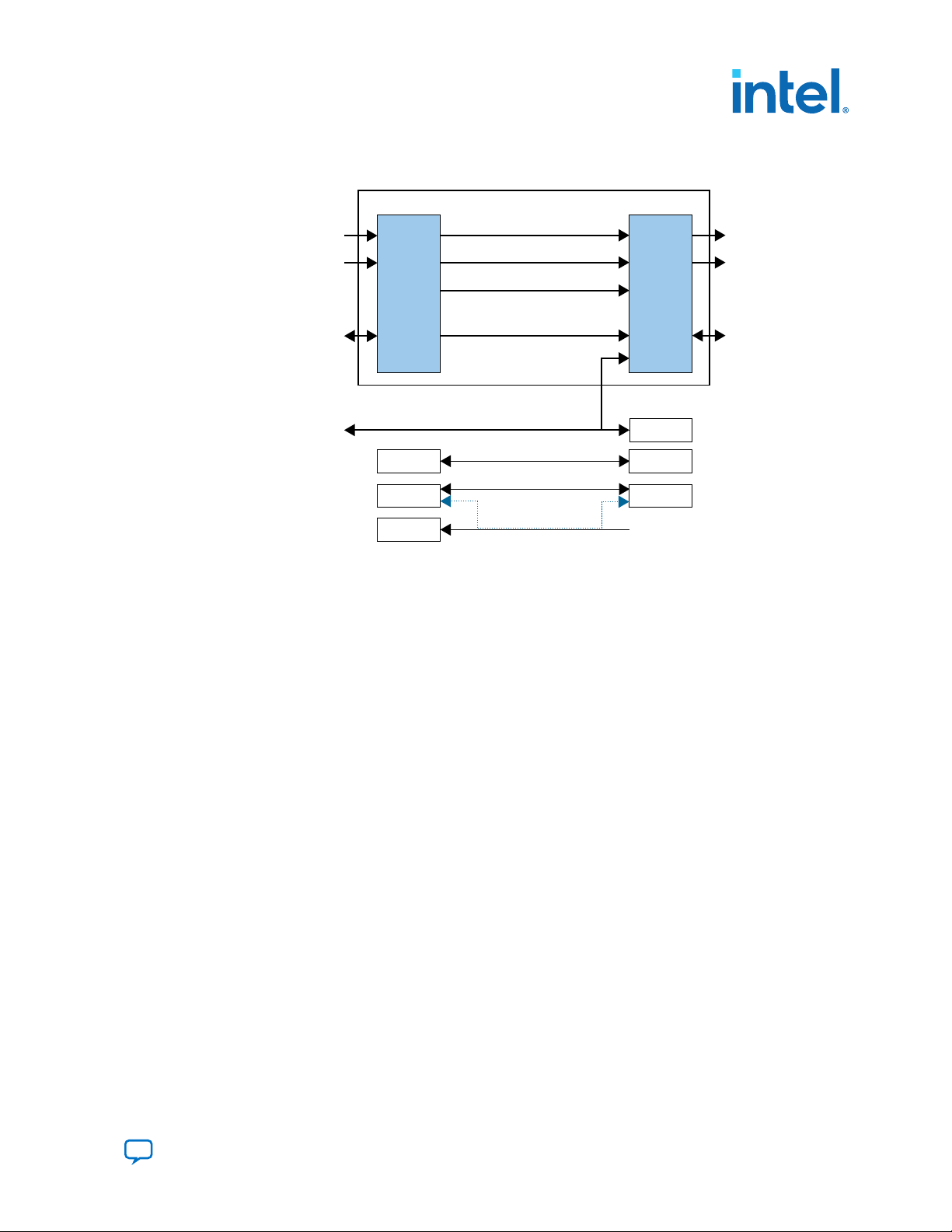
HDMI
Transmitter
HDMI
Receiver
TMDS Channel 0
HDMI Intel FPGA IP Core
TMDS Channel 1
TMDS Channel 2
TMDS Clock Channel
Video
Audio
Control/Status
Video
Audio
Control/Status
Detect
CEC
HEAC
EDID ROM
CEC
HEAC
CEC Line
Utility Line
HPD Line
Display Data Channel (DDC)
Status and Control Data Channel (SCDC)
High/Low
2. HDMI Overview
UG-HDMI | 2021.04.01
Figure 1. HDMI Intel FPGA IP Block Diagram for TMDS Mode
The figure below illustrates the blocks in the HDMI Intel FPGA IP for TMDS Mode.
Based on TMDS encoding, the HDMI protocol allows the transmission of both audio
and video data between source and sink devices.
An HDMI interface consists of three color channels accompanied by a single clock
channel. You can use each color line to transfer both individual RGB colors and
auxiliary data.
Note: Refer to AN 837: Design Guidelines for Intel FPGA HDMI to know more about the
channel mapping to the RGB colors for HDMI 1.4 and HDMI 2.0.
The receiver uses the TMDS clock as a frequency reference for data recovery on the
three TMDS data channels. This clock typically runs at the video pixel rate.
TMDS encoding is based on an 8-bit to 10-bit algorithm. This protocol attempts to
minimize data channel transition, and yet maintain sufficient transition so that a sink
device can lock reliably to the data stream.
Send Feedback
HDMI Intel® FPGA IP User Guide
7
Page 8
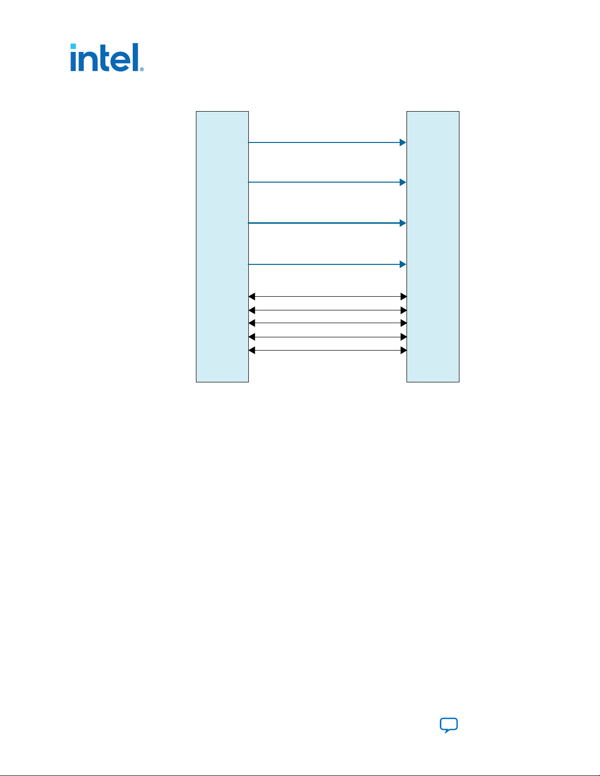
Figure 2. Fixed Rate Link (FRL)
HDMI TX
FRL mode of
operation
SCL
CEC
Utility
HPD
SDA
HDMI RX
FRL mode of
operation
FRL Lane 0
FRL Lane 1
FRL Lane 2
FRL Lane 3
2. HDMI Overview
UG-HDMI | 2021.04.01
In HDMI 1.4 and HDMI 2.0, 3 lanes carry data and 1 lane carries TMDS clock. When
operating in FRL mode, the clock channel carries data as well. As the HDMI 2.1
specification requires backward compatibility with HDMI 1.4 and HDMI 2.0, you need
to configure the 4th lane to carry data or clock during run time.
You can configure the FRL mode to 3 lanes and 4 lanes. In 3-lane FRL mode, each lane
can operate at 3 Gbps or 6 Gbps. In 4-lane FRL mode, each lane can operate at 6
Gbps, 8 Gbps, 10 Gbps, or 12 Gbps.
Use category 3 (Cat 3) cable for FRL mode to ensure good signal integrity.
HDMI Intel® FPGA IP User Guide
8
Send Feedback
Page 9
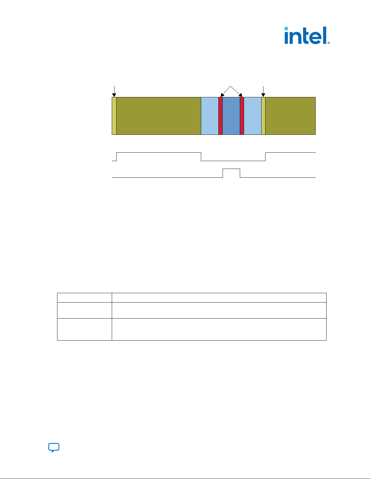
Active Video
Data Island
Preamble
Active
Aux/Audio
Video
Preamble
Active Video
Video
Guard
Band
Video
Guard
Band
Data Island
Guard
Band
vid_de
aux_de
Video Guard Band
Case (TMDS Channel Number):
0:q_out[9:0] = 10’b1011001100;
1:q_out[9:0] = 10’b0100110011;
2:q_out[9:0] = 10’b1011001100;
endcase
Video Preamble
{c3, c2, c1, c0} = 4’b0001
Data Island Guard Band
Case (TMDS Channel Number):
0:q_out[9:0] = 10’bxxxxxxxxxx;
1:q_out[9:0] = 10’b0100110011;
2:q_out[9:0] = 10’b0100110011;
endcase
Data Island Preamble
{c3, c2, c1, c0} = 4’b0101
2. HDMI Overview
UG-HDMI | 2021.04.01
Figure 3. HDMI Intel FPGA IP Video Stream Data
The figure above illustrates two data streams:
• Data stream in green—transports color data
• Data stream in dark blue—transports auxiliary data
Table 1. Video Data and Auxiliary Data
The table below describes the function of the video data and auxiliary data.
Data
Video data • Packed representation of the video pixels clocked at the source pixel clock.
Auxiliary data • Transfers audio data together with a range of auxiliary data packets.
• Encoded using the TMDS 8-bit to 10-bit algorithm.
• Sink devices use auxiliary data packets to correctly reconstruct video and audio data.
• Encoded using the TMDS Error Reduction Coding–4 bits (TERC4) encoding algorithm.
Description
Each data stream section is preceded with guard bands and pre-ambles. The guard
bands and pre-ambles allow for accurate synchronization with received data streams.
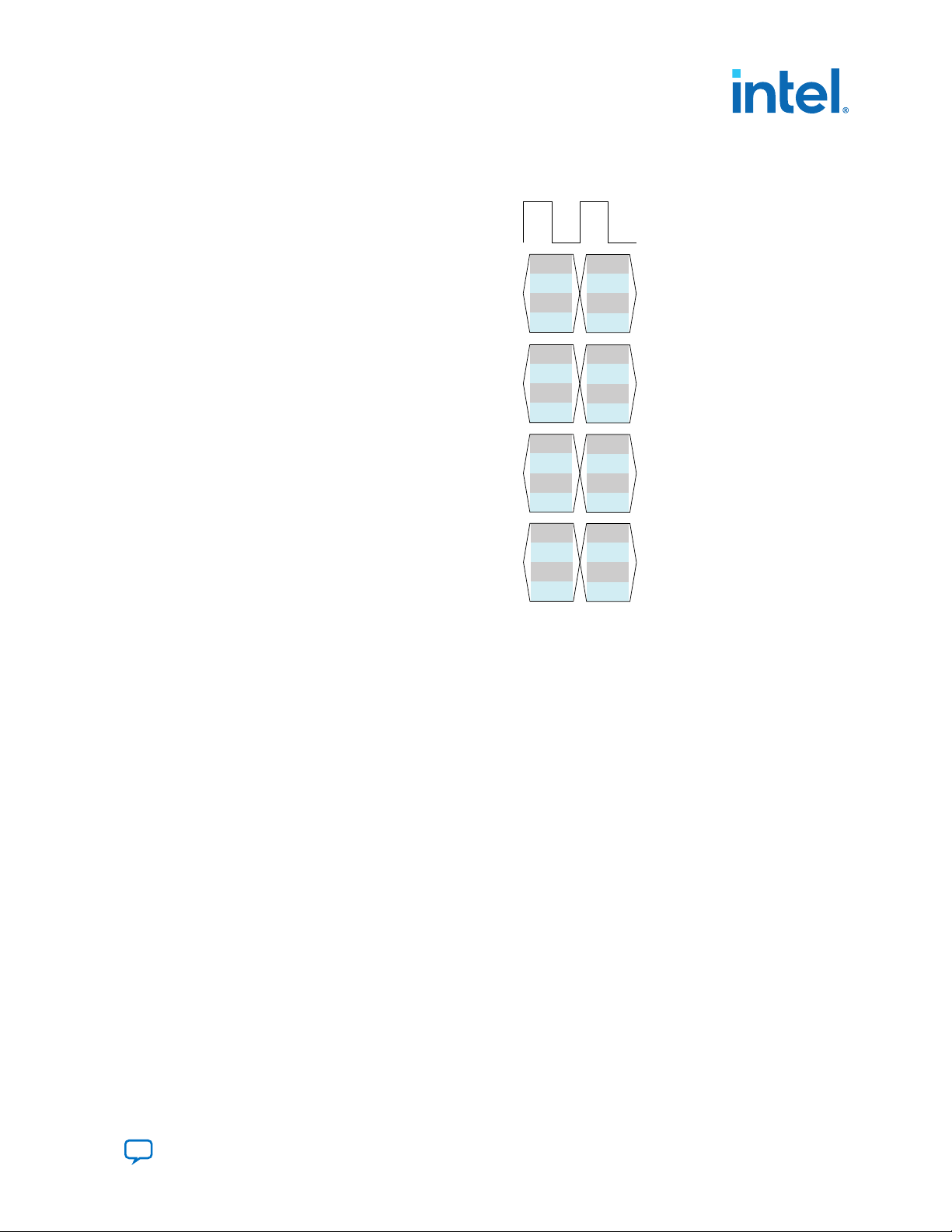
The following figures show the arrangement of the video data, video data enable,
video H-SYNC, and video V-SYNC in 1, 2, 4, and 8 pixels per clock.
Send Feedback
HDMI Intel® FPGA IP User Guide
9
Page 10
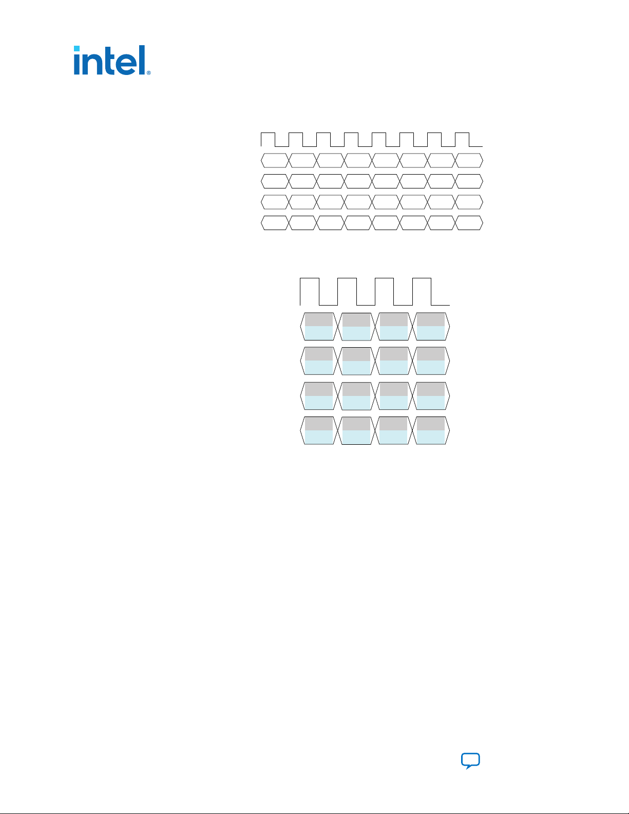
D0 D1 D2 D3 D4 D5 D6 D7
E0 E1 E2 E3 E4 E5 E6 E7
H0 H1 H2 H3 H4 H5 H6 H7
V0 V1 V2 V3 V4 V5 V6 V7
vid_clk
vid_data[47:0]
vid_de[0]
vid_hsync[0]
vid_vsync[0]
One Pixel per Clock
vid_clk
vid_data[95:0]
vid_de[1:0]
vid_hsync[1:0]
vid_vsync[1:0]
Two Pixels per Clock
V1
V0
V3
V2
V5
V4
V7
V6
H1
H0
H3
H2
H5
H4
H7
H6
E1
E0
E3
E2
E5
E4
E7
E6
D1
D0
D3
D2
D5
D4
D7
D6
2. HDMI Overview
UG-HDMI | 2021.04.01
Figure 4. Video Data, Video Data Valid, H-SYNC, and V-SYNC—1 Pixel per Clock
Figure 5. Video Data, Video Data Valid, H-SYNC, and V-SYNC—2 Pixels per Clock
HDMI Intel® FPGA IP User Guide
10
Send Feedback
Page 11
vid_clk
vid_data[191:0]
vid_de[3:0]
vid_hsync[3:0]
vid_vsync[3:0]
Four Pixels per Clock
V3
V2
V1
V0
V7
V6
V5
V4
H3
H2
H1
H0
H7
H6
H5
H4
E3
E2
E1
E0
E7
E6
E5
E4
D3
D2
D1
D0
D7
D6
D5
D4
2. HDMI Overview
UG-HDMI | 2021.04.01
Figure 6. Video Data, Video Data Valid, H-SYNC, and V-SYNC—4 Pixels per Clock
Send Feedback
HDMI Intel® FPGA IP User Guide
11
Page 12
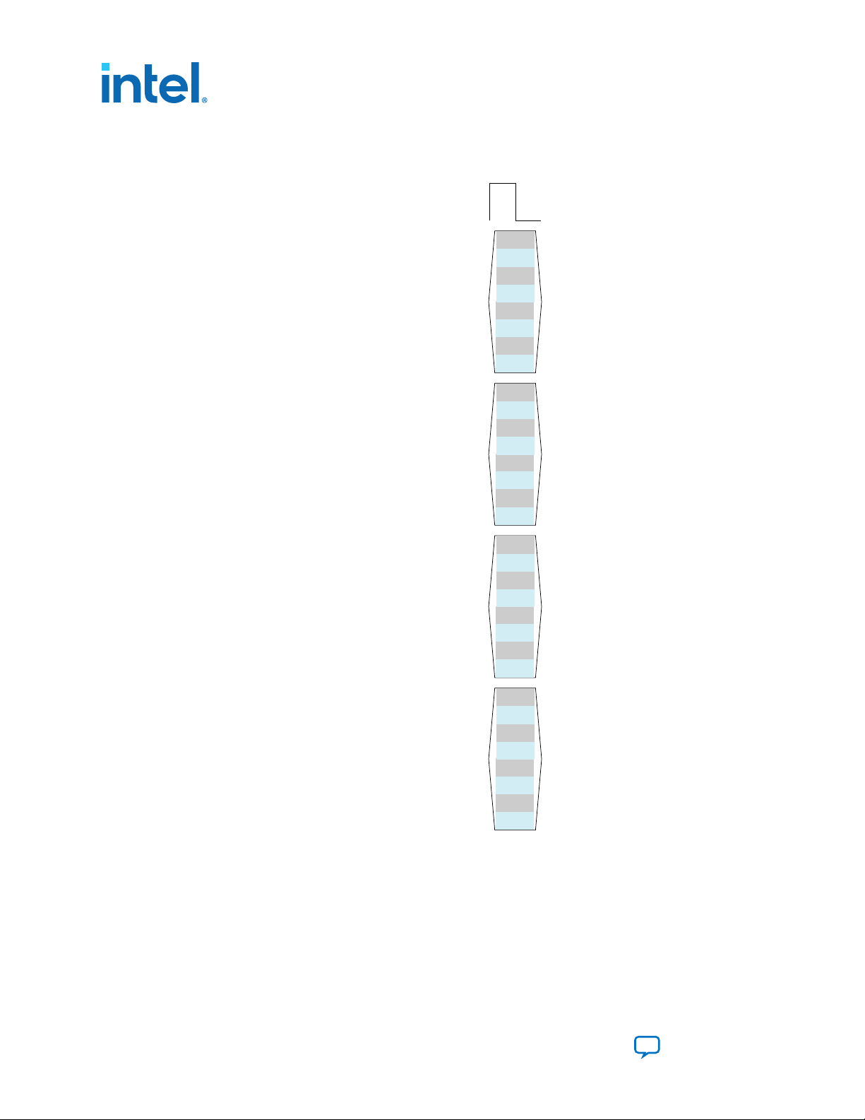
vid_clk
Eight Pixels per Clock
vid_data[383:0]
D3
D2
D1
D0
D7
D6
D5
D4
vid_de[7:0]
E3
E2
E1
E0
E7
E6
E5
E4
vid_hsync[7:0]
H3
H2
H1
H0
H7
H6
H5
H4
vid_vsync[7:0]
V3
V2
V1
V0
V7
V6
V5
V4
2. HDMI Overview
UG-HDMI | 2021.04.01
Figure 7. Video Data, Video Data Valid, H-SYNC, and V-SYNC—8 Pixels per Clock
Related Information
AN 837: Design Guidelines for Intel FPGA HDMI
2.1. Release Information
Intel FPGA IP versions match the Intel Quartus Prime Design Suite software versions
until v19.1. Starting in Intel Quartus Prime Design Suite software version 19.2, Intel
FPGA IP has a new versioning scheme.
HDMI Intel® FPGA IP User Guide
12
Send Feedback
Page 13
2. HDMI Overview
UG-HDMI | 2021.04.01
The Intel FPGA IP version (X.Y.Z) number can change with each Intel Quartus Prime
software version. A change in:
• X indicates a major revision of the IP. If you update the Intel Quartus Prime
software, you must regenerate the IP.
• Y indicates the IP includes new features. Regenerate your IP to include these new
features.
• Z indicates the IP includes minor changes. Regenerate your IP to include these
changes.
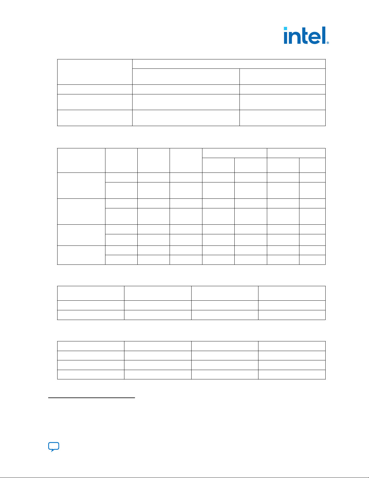
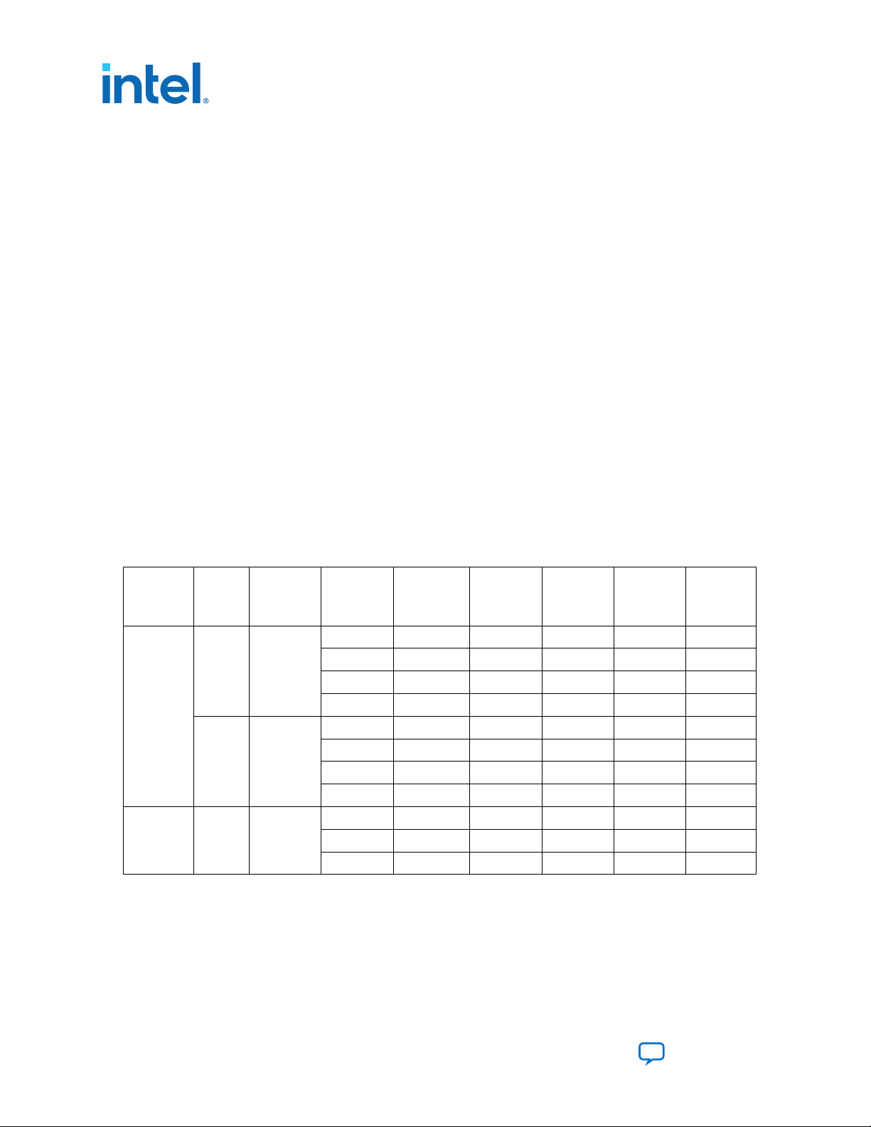
Table 2. HDMI Intel FPGA IP Release Information
Item Description
IP Version 19.6.0
Intel Quartus Prime Version 21.1 (Intel Quartus Prime Pro Edition)
Release Date 2021.01.04
Ordering Code IP-HDMI
Related Information
HDMI Intel FPGA IP Release Notes
Describes changes to the IP in a particular release.
2.2. Device Family Support
Table 3. Intel Device Family Support
Device Family Support Level
Intel Stratix 10 (H-tile and L-tile) (Intel Quartus Prime Pro Edition) Final
Intel Arria 10 (Intel Quartus Prime Pro Edition) Final
Intel Cyclone 10 GX (Intel Quartus Prime Pro Edition) Final
Arria V (Intel Quartus Prime Standard Edition) Final
Stratix V (Intel Quartus Prime Standard Edition) Final
Send Feedback
HDMI Intel® FPGA IP User Guide
13
Page 14
2. HDMI Overview
UG-HDMI | 2021.04.01
The following terms define device support levels for Intel FPGA IP cores:
• Advance support—the IP core is available for simulation and compilation for this
device family. Timing models include initial engineering estimates of delays based
on early post-layout information. The timing models are subject to change as
silicon testing improves the correlation between the actual silicon and the timing
models. You can use this IP core for system architecture and resource utilization
studies, simulation, pinout, system latency assessments, basic timing assessments
(pipeline budgeting), and I/O transfer strategy (data-path width, burst depth, I/O
standards tradeoffs).
• Preliminary support—the IP core is verified with preliminary timing models for this
device family. The IP core meets all functional requirements, but might still be
undergoing timing analysis for the device family. It can be used in production
designs with caution.
• Final support—the IP core is verified with final timing models for this device family.
The IP core meets all functional and timing requirements for the device family and
can be used in production designs.
2.3. Feature Support
Table 4. HDMI Intel FPGA IP FRL Feature Support in Intel Stratix 10 and Intel Arria 10
Devices
Feature Support Level
Support FRL = 1 Preliminary
Support FRL = 0 Final
The following terms define IP feature support levels for HDMI Intel FPGA IP:
• Preliminary support—The IP meets the functional requirement for the feature set
as listed in this user guide. Additional features, characterization, and system level
design guidelines shall be covered in future releases. The IP can be used in
production designs for the supported device family with caution.
• Final support—The IP is compliant to the protocol CTS requirement for the
supported device family and can be used in production design. Characterization
report and system level design guidelines are available to facilitate meeting PHY
CTS requirements.
2.4. Resource Utilization
The resource utilization data indicates typical expected performance for the HDMI Intel
FPGA IP in the Intel Quartus Prime Pro Edition software.
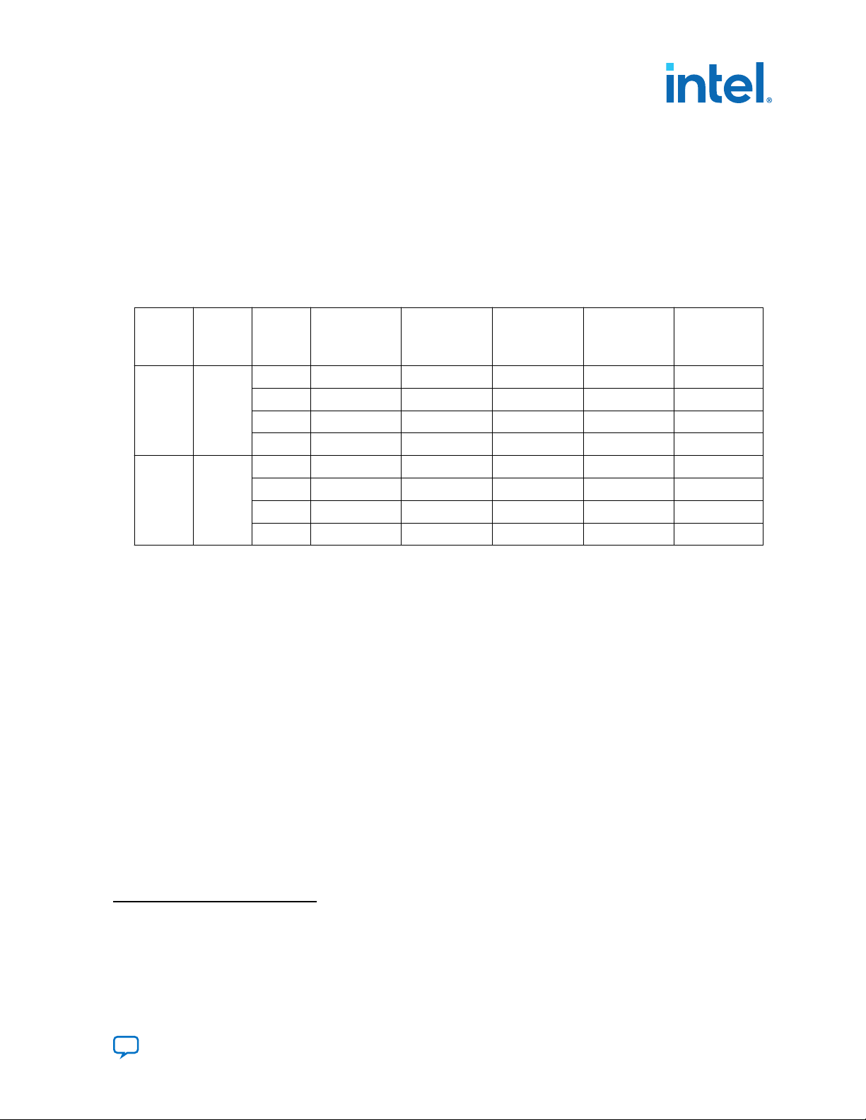
Table 5. HDMI Data Rate
The table lists the maximum data rates for HDMI Intel FPGA IP configurations.
Devices
Intel Stratix 10 5,940 12,000
Maximum Data Rate (Mbps)
2 Pixels per Clock
(Support FRL = 0)
8 Pixels per Clock
(Support FRL = 1)
continued...
HDMI Intel® FPGA IP User Guide
14
Send Feedback
Page 15
2. HDMI Overview
UG-HDMI | 2021.04.01
Maximum Data Rate (Mbps)
Devices
Intel Arria 10
Intel Cyclone 10 GX
2 Pixels per Clock
(Support FRL = 0)
(Example: 4Kp60 8 bpc) (Example: 8Kp30 12 bpc)
5,940
(Example: 4Kp60 8 bpc)
5,940
(Example: 4Kp60 8 bpc)
Table 6. HDMI Intel FPGA IP Resource Utilization
The table lists the performance data for the different Intel FPGA devices.
Device Pixels per
Intel Stratix 10 H-
tile
(Support FRL = 0)
(1)
Clock
2 RX 5.041 6,633 902 38,400 14
2 TX 4,975 7,559 1,368 37,568 13
Direction ALMs Logic Registers Memory
8 Pixels per Clock
(Support FRL = 1)
12,000
(Example: 8Kp30 12 bpc)
Not Supported
Primary Secondary Bits M10K or
M20K
Intel Stratix 10 L-
tile
(Support FRL = 0)
(1)
Intel Arria 10
(Support FRL = 0)
(1)
Intel Cyclone 10 GX
2 RX 5,025 6,584 967 38,400 14
2 TX 4,966 7,539 1,425 37,568 13
2 RX 3,768 5,716 1,049 36,352 14
2 TX 4,445 7,016 1,701 36,968 13
2 RX 4,000 5,768 965 38,400 14
2 TX 4,484 7,167 1,629 36,968 13
Table 7. Recommended Speed Grades for Intel Stratix 10 and Intel Arria 10 Devices
(Support FRL = 1)
Device Lane Rate (Mbps) Transceiver Interface
Width (bits)
Intel Stratix 10 12,000 40 -1, -2
Intel Arria 10 12,000 40 -1, -2
Speed Grade
(2)
Table 8. Recommended Speed Grades for Intel Stratix 10, Intel Arria 10, and Intel
Cyclone 10 GX Devices (Support FRL = 0)
Device Lane Rate (Mbps) Interface Width (bits) Speed Grades
Intel Stratix 10 6,000 20 -1, -2
Intel Arria 10 6,000 20 -1, -2
Intel Cyclone 10 GX 6,000 20 -5
(1)
Resource data for Support FRL = 1 design is not finalized.
(2)
Contact Intel Sales if you need to use -2 speed grade.
Send Feedback
HDMI Intel® FPGA IP User Guide
15
Page 16
Table 9. HDCP Resource Utilization
The table lists the HDCP resource data for Intel Arria 10 and Intel Stratix 10 devices.
Device HDCP IP Support
Intel Arria10HDCP 2.3
Intel
Stratix 10
TX
HDCP 2.3
RX
HDCP 1.4
TX
HDCP 1.4
RX
HDCP 2.3
TX
HDCP 2.3
RX
HDCP 1.4
TX
HDCP 1.4
RX
FRL
0 2 6,479 10,548 12,015 10 3
0 2 7,119 11,685 12,673 11 3
0 2 1,665 2,626 4,411 2 0
0 2 1,170 1,850 3,407 3 0
0 2 7,213 11,582 12,810 10 3
1 8 17,755 29,784 24,428 10 3
0 2 8,145 12,691 13,438 11 3
1 8 18,482 30,881 25,422 11 3
0, 1 2 2,320 2,937 4,544 2 0
0, 1 2 1,784 2,135 3,605 3 0
Pixels/
TMDS
Symbols
Per Clock
ALMs Combinational
ALUTs
2. HDMI Overview
UG-HDMI | 2021.04.01
Registers M20K DSP
HDMI Intel® FPGA IP User Guide
16
Send Feedback
Page 17

intelFPGA(_pro)
quartus - Contains the Intel Quartus Prime software
ip - Contains the Intel FPGA IP library and third-party IP cores
altera - Contains the Intel FPGA IP library source code
<IP name> - Contains the Intel FPGA IP source files
UG-HDMI | 2021.04.01
Send Feedback
3. HDMI Intel FPGA IP Getting Started
This chapter provides a general overview of the Intel IP core design flow to help you
quickly get started with the HDMI Intel FPGA IP. The Intel FPGA IP Library is installed
as part of the Intel Quartus Prime installation process. You can select and
parameterize any Intel FPGA IP from the library. Intel provides an integrated
parameter editor that allows you to customize the HDMI Intel FPGA IP to support a
wide variety of applications. The parameter editor guides you through the setting of
parameter values and selection of optional ports.
Related Information
• Introduction to Intel FPGA IP Cores
Provides general information about all Intel FPGA IP cores, including
parameterizing, generating, upgrading, and simulating IP cores.
• Creating Version-Independent IP and Platform Designer Simulation Scripts
Create simulation scripts that do not require manual updates for software or IP
version upgrades.
• Project Management Best Practices
Guidelines for efficient management and portability of your project and IP files.
3.1. Installing and Licensing Intel FPGA IP Cores
The Intel Quartus Prime software installation includes the Intel FPGA IP library. This
library provides many useful IP cores for your production use without the need for an
additional license. Some Intel FPGA IP cores require purchase of a separate license for
production use. The Intel FPGA IP Evaluation Mode allows you to evaluate these
licensed Intel FPGA IP cores in simulation and hardware, before deciding to purchase a
full production IP core license. You only need to purchase a full production license for
licensed Intel IP cores after you complete hardware testing and are ready to use the
IP in production.
The Intel Quartus Prime software installs IP cores in the following locations by default:
Figure 8. IP Core Installation Path
Intel Corporation. All rights reserved. Agilex, Altera, Arria, Cyclone, eASIC, Intel, the Intel logo, MAX, Nios,
Quartus and Stratix words and logos are trademarks of Intel Corporation or its subsidiaries in the U.S. and/or
other countries. Intel warrants performance of its FPGA and semiconductor products to current specifications in
accordance with Intel's standard warranty, but reserves the right to make changes to any products and services
at any time without notice. Intel assumes no responsibility or liability arising out of the application or use of any
information, product, or service described herein except as expressly agreed to in writing by Intel. Intel
customers are advised to obtain the latest version of device specifications before relying on any published
information and before placing orders for products or services.
*Other names and brands may be claimed as the property of others.
ISO
9001:2015
Registered
Page 18
3. HDMI Intel FPGA IP Getting Started
UG-HDMI | 2021.04.01
Table 10. IP Core Installation Locations
Location Software Platform
<drive>:\intelFPGA_pro\quartus\ip\altera
<drive>:\intelFPGA\quartus\ip\altera
<home directory>:/intelFPGA_pro/quartus/ip/altera
<home directory>:/intelFPGA/quartus/ip/altera
Intel Quartus Prime Pro Edition Windows*
Intel Quartus Prime Standard
Edition
Intel Quartus Prime Pro Edition Linux*
Intel Quartus Prime Standard
Edition
Windows
Linux
Note: The Intel Quartus Prime software does not support spaces in the installation path.
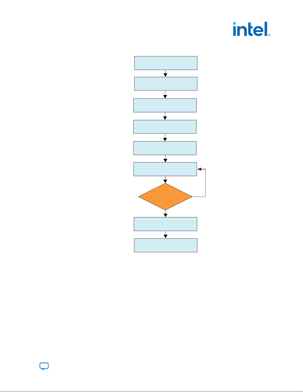
3.1.1. Intel FPGA IP Evaluation Mode
The free Intel FPGA IP Evaluation Mode allows you to evaluate licensed Intel FPGA IP
cores in simulation and hardware before purchase. Intel FPGA IP Evaluation Mode
supports the following evaluations without additional license:
• Simulate the behavior of a licensed Intel FPGA IP core in your system.
• Verify the functionality, size, and speed of the IP core quickly and easily.
• Generate time-limited device programming files for designs that include IP cores.
• Program a device with your IP core and verify your design in hardware.
Intel FPGA IP Evaluation Mode supports the following operation modes:
• Tethered—Allows running the design containing the licensed Intel FPGA IP
indefinitely with a connection between your board and the host computer.
Tethered mode requires a serial joint test action group (JTAG) cable connected
between the JTAG port on your board and the host computer, which is running the
Intel Quartus Prime Programmer for the duration of the hardware evaluation
period. The Programmer only requires a minimum installation of the Intel Quartus
Prime software, and requires no Intel Quartus Prime license. The host computer
controls the evaluation time by sending a periodic signal to the device via the
JTAG port. If all licensed IP cores in the design support tethered mode, the
evaluation time runs until any IP core evaluation expires. If all of the IP cores
support unlimited evaluation time, the device does not time-out.
• Untethered—Allows running the design containing the licensed IP for a limited
time. The IP core reverts to untethered mode if the device disconnects from the
host computer running the Intel Quartus Prime software. The IP core also reverts
to untethered mode if any other licensed IP core in the design does not support
tethered mode.
When the evaluation time expires for any licensed Intel FPGA IP in the design, the
design stops functioning. All IP cores that use the Intel FPGA IP Evaluation Mode time
out simultaneously when any IP core in the design times out. When the evaluation
time expires, you must reprogram the FPGA device before continuing hardware
verification. To extend use of the IP core for production, purchase a full production
license for the IP core.
You must purchase the license and generate a full production license key before you
can generate an unrestricted device programming file. During Intel FPGA IP Evaluation
Mode, the Compiler only generates a time-limited device programming file (<project
name>_time_limited.sof) that expires at the time limit.
HDMI Intel® FPGA IP User Guide
18
Send Feedback
Page 19
Install the Intel Quartus Prime
Software with Intel FPGA IP Library
Parameterize and Instantiate a
Licensed Intel FPGA IP Core
Purchase a Full Production
IP License
Verify the IP in a
Supported Simulator
Compile the Design in the
Intel Quartus Prime Software
Generate a Time-Limited Device
Programming File
Program the Intel FPGA Device
and Verify Operation on the Board
No
Yes
IP Ready for
Production Use?
Include Licensed IP
in Commercial Products
3. HDMI Intel FPGA IP Getting Started
UG-HDMI | 2021.04.01
Figure 9. Intel FPGA IP Evaluation Mode Flow
Note: Refer to each IP core's user guide for parameterization steps and implementation
details.
Intel licenses IP cores on a per-seat, perpetual basis. The license fee includes firstyear maintenance and support. You must renew the maintenance contract to receive
updates, bug fixes, and technical support beyond the first year. You must purchase a
full production license for Intel FPGA IP cores that require a production license, before
generating programming files that you may use for an unlimited time. During Intel
FPGA IP Evaluation Mode, the Compiler only generates a time-limited device
programming file (<project name>_time_limited.sof) that expires at the time
limit. To obtain your production license keys, visit the Self-Service Licensing Center.
The Intel FPGA Software License Agreements govern the installation and use of
licensed IP cores, the Intel Quartus Prime design software, and all unlicensed IP cores.
Send Feedback
HDMI Intel® FPGA IP User Guide
19
Page 20

Related Information
• Intel FPGA Licensing Support Center
• Introduction to Intel FPGA Software Installation and Licensing
3.2. Specifying IP Parameters and Options
Follow these steps to specify the HDMI Intel FPGA IP parameters and options.
1. Create a Intel Quartus Prime project using the New Project Wizard available
from the File menu.
2. On the Tools menu, click IP Catalog.
3.
Under Installed IP, double-click Library ➤ Interface ➤ Protocols ➤
Audio&Video ➤ HDMI Intel FPGA IP.
The parameter editor appears.
4. Specify a top-level name for your custom IP variation. This name identifies the IP
variation files in your project. If prompted, also specify the targeted FPGA device
family and output file HDL preference. Click OK.
5. Specify parameters and options in the HDMI parameter editor:
• Optionally select preset parameter values. Presets specify all initial parameter
values for specific applications (where provided).
• Specify parameters defining the IP functionality, port configurations, and
device-specific features.
• Specify options for generation of a timing netlist, simulation model, testbench,
or example design (where applicable).
• Specify options for processing the IP files in other EDA tools.
6. Click Generate to generate the IP and supporting files, including simulation
models.
7. Click Close when file generation completes.
8. Click Finish.
9. If you generate the HDMI Intel FPGA IP instance in a Intel Quartus Prime project,
you are prompted to add Intel Quartus Prime IP File (.qip) and Intel
Quartus Prime Simulation IP File (.sip) to the current Intel Quartus
Prime project.
3. HDMI Intel FPGA IP Getting Started
UG-HDMI | 2021.04.01
HDMI Intel® FPGA IP User Guide
20
Send Feedback
Page 21

UG-HDMI | 2021.04.01
Send Feedback
4. HDMI Hardware Design Examples
Intel offers design examples that you can simulate, compile, and test in hardware.
The implementation of the HDMI Intel FPGA IP on hardware requires additional
components specific to the targeted device.
4.1. HDMI Hardware Design Examples for Intel Arria 10, Intel Cyclone 10 GX, and Intel Stratix 10 Devices
The HDMI Intel FPGA IP offers design examples that you can generate through the IP
catalog in the Intel Quartus Prime Pro Edition software.
Related Information
• HDMI Intel Arria 10 FPGA IP Design Example User Guide
For more information about the Intel Arria 10 design examples.
• HDMI Intel Cyclone 10 GX FPGA IP Design Example User Guide
For more information about the Intel Cyclone 10 GX design examples.
• HDMI Intel Stratix 10 FPGA IP Design Example User Guide
For more information about the Intel Stratix 10 design examples.
4.2. HDCP Over HDMI Design Example for Intel Arria 10 and Intel Stratix 10 Devices
The High-bandwidth Digital Content Protection (HDCP) over HDMI hardware design
example helps you to evaluate the functionality of the HDCP feature and enables you
to use the feature in your Intel Arria 10 and Intel Stratix 10 designs.
For detailed information about the HDCP over HDMI design examples, refer to the
Intel Arria 10 and Intel Stratix 10 design example user guides.
Note: The HDCP feature is not included in the Intel Quartus Prime Pro Edition software. To
access the HDCP feature, contact Intel at https://www.intel.com/content/www/us/en/
broadcast/products/programmable/applications/connectivity-solutions.html.
Related Information
• HDMI Intel Arria 10 FPGA IP Design Example User Guide
For more information about the HDCP over HDMI design example for Intel Arria
10 devices and the security considerations when using the HDCP features.
• HDMI Intel Stratix 10 FPGA IP Design Example User Guide
For more information about the HDCP over HDMI design example for Intel
Stratix 10 devices and the security considerations when using the HDCP
features.
Intel Corporation. All rights reserved. Agilex, Altera, Arria, Cyclone, eASIC, Intel, the Intel logo, MAX, Nios,
Quartus and Stratix words and logos are trademarks of Intel Corporation or its subsidiaries in the U.S. and/or
other countries. Intel warrants performance of its FPGA and semiconductor products to current specifications in
accordance with Intel's standard warranty, but reserves the right to make changes to any products and services
at any time without notice. Intel assumes no responsibility or liability arising out of the application or use of any
information, product, or service described herein except as expressly agreed to in writing by Intel. Intel
customers are advised to obtain the latest version of device specifications before relying on any published
information and before placing orders for products or services.
*Other names and brands may be claimed as the property of others.
ISO
9001:2015
Registered
Page 22

4. HDMI Hardware Design Examples
UG-HDMI | 2021.04.01
4.3. HDMI Hardware Design Examples for Arria V and Stratix V Devices
The HDMI hardware design example helps you evaluate the functionality of the HDMI
Intel FPGA IP and provides a starting point for you to create your own design for Arria
V and Stratix V devices in the Intel Quartus Prime Standard Edition software.
The design example runs on the following device kits:
• Arria V GX starter kit
• Stratix V GX development kit
• Bitec HDMI HSMC 2.0 Daughter Card Revision 8
Related Information
AN 837: Design Guidelines for Intel FPGA HDMI
4.3.1. HDMI Hardware Design Components
The demonstration designs instantiate the Video and Image Processing (VIP) Suite IP
cores or FIFO buffers to perform a direct HDMI video stream passthrough between the
HDMI sink and source.
The hardware demonstration design comprises the following components:
• HDMI sink
— Transceiver Native PHY (RX)
— Transceiver PHY Reset Controller (RX)
— PLL
— PLL Reconfiguration
— Multirate Reconfiguration Controller (RX)
— Oversampler (RX)
— DCFIFO
• Sink Display Data Channel (DDC) and Status and Control Data Channel (SCDC)
• Transceiver Reconfiguration Controller
HDMI Intel® FPGA IP User Guide
22
Send Feedback
Page 23
RX TMDS Clock
TX Transceiver Reference Clock
TX Transceiver Clock Out
TX Link Speed Clock
TX Video Clock
I C Clock
Memory Clock
RX Transceiver Reference Clock
RX Transceiver Recovered Clock
RX Link Speed Clock
RX Video Clock
Management Clock
VIP Main Clock
2
Sink DDC and SCDC
PLL Intel
FPGA IP
PLL Reconfig
Intel FPGA IP
Transceiver PHY
Reset Controller
(RX)
Transceiver
Native PHY
(RX)
Oversampler
(RX)
HDMI Source
Avalon-MM Master
Translator
(13)
Platform Designer System
(HDMI Source SCDC Control,
and VIP Passthrough)
Avalon-MM Slave
Translator
Avalon-MM Slave
Translator
Nios II CPU
Video Frame Buffer
InteL FPGA IP
Clocked Video Input
InteL FPGA IP
Clocked Video Output
InteL FPGA IP
External Memory
Controller
Transceiver Reconfiguration
Controller
External Memory
(DDR3)
VIP Bypass and
Audio/Aux/IF Buffers
Source SCDC
(14)
(5)
(6)
(7)
Clock Enable
Generator
Transceiver Native
PHY (TX)
(2)
(2)
FPGA IP (RX)
HDMI Intel
Rate
Detect
Multirate
Reconfiguration
Controller (RX)
(12)
(1)
(3)
HDMI Sink
I2C Slave
(SCDC)
(15)
I2C Slave
(EDID)
RAM 1-Port
Intel FPGA IP
I2C Master
(SCDC)
DCFIFO
(8)
Oversampler
(TX)
(8)
(9)
Transceiver PHY
Reset Controller
(TX)
(10)
(14)
(5)(4)
(11)
Data
Avalon-ST Video
Avalon-MM
Control/Status
Arrow Legend
Clock Legend
FPGA IP (RX)
HDMI Intel
PLL Intel
FPGA IP
PLL Reconfig
Intel FPGA IP
DCFIFO
DCFIFO
DCFIFO
4. HDMI Hardware Design Examples
UG-HDMI | 2021.04.01
• VIP bypass and Audio, Auxiliary and InfoFrame buffers
• Platform Designer system
— VIP passthrough for HDMI video stream
— Source SCDC controller
— HDMI source reconfiguration controller
• HDMI source
— Transceiver Native PHY (TX)
— Transceiver fPLL
— Transceiver PHY Reset Controller (TX)
— PLL
— PLL Reconfiguration
— Oversampler (TX)
— DCFIFO
— Clock Enable Generator
Figure 10. HDMI Hardware Design Example Block Diagram
The figure below shows a high level architecture of the design.
The following details of the design example architecture correspond to the numbers in
the block diagram.
1. The sink TMDS data has three channels: data channel 0 (blue), data channel 1
2. The Oversampler (RX) and dual-clock FIFO (DCFIFO) instances are duplicated for
Send Feedback
3. The video data input width for each color channel of the HDMI RX core is
(green), and data channel 2 (red).
each TMDS data channel (0,1,2).
equivalent to RX transceiver PCS-PLD parallel data width per channel.
HDMI Intel® FPGA IP User Guide
23
Page 24

4. HDMI Hardware Design Examples
UG-HDMI | 2021.04.01
4. Each color channel is fixed at 16 bpc. The video data output width of the HDMI RX
core is equivalent to the value of symbols per clock*16*3.
5. The video data input width of the Clocked Video Input (CVI) and Clocked Video
Output (CVO) IP cores are equivalent to the value of
NUMBER_OF_PIXELS_IN_PARALLEL * BITS_PER_PIXEL_PER_COLOR_PLANE *
NUMBER_OF_COLOR_PLANES. To interface with the HDMI core, the values of
NUMBER_OF_PIXELS_IN_PARALLEL, BITS_PER_PIXEL_PER_COLOR_PLANE, and
NUMBER_OF_COLOR_PLANES must match the symbols per clock, 16 and 3
respectively.
6. The video data input width of the HDMI TX core is equivalent to the value of
symbols per clock*16*3. You can use the user switch to select the video data from
the CVO IP core (VIP passthrough) or DCFIFO (VIP bypass).
7. The video data output width for each color channel of the HDMI TX core is
equivalent to TX transceiver PCS-PLD parallel data width per channel.
8. The DCFIFO and the Oversampler (TX) instances are duplicated for each TMDS
data channel (0,1,2) and clock channel.
9. The Oversampler (TX) uses the clock enable signal to read data from the DCFIFO.
10. The source TMDS data has four channels: data channel 0 (blue), data channel 1
(green), data channel 2 (red), and clock channel.
11. The RX Multirate Reconfiguration Controller requires the status of
TMDS_Bit_clock_Ratio port to perform appropriate RX reconfiguration between
the TMDS character rates below 340 Mcsc (HDMI 1.4b) and above 340 Mcsc
(HDMI 2.0b). The status of the port is also required by the Nios II processor and
the HDMI TX core to perform appropriate TX reconfiguration and scrambling.
12. The reset control and lock status signals from HDMI PLL, RX Transceiver Reset
Controller and HDMI RX core.
13. The reset and oversampling control signals for HDMI PLL, TX Transceiver Reset
Controller, and HDMI TX core. The lock status and rate detection measure valid
signals from the HDMI sink initiate the TX reconfiguration process.
14. The I2C SCL and SDA lines with tristate buffer for bidirectional configuration. Use
the ALTIOBUF IP core for Arria V and Stratix V devices.
15. The SCDC is mainly designed for the source to update the
TMDS_Bit_Clock_Ratio and Scrambler_Enable bits of the sink TMDS
Configuration register. .
HDMI Intel® FPGA IP User Guide
24
Send Feedback
Page 25
4. HDMI Hardware Design Examples
UG-HDMI | 2021.04.01
4.3.1.1. Transceiver Native PHY (RX)
• Transceiver Native PHY in Arria V devices
— To operate the TMDS bit rate up to 3,400 Mbps, configure the Transceiver
Native PHY at 20 bits at PCS – PLD interface with the HDMI RX core at 2
symbols per clock. When the PCS – PLD interface width is 20 bits, the
minimum link rate is 611 Mbps.
— To operate the TMDS bit rate up to 6,000 Mbps, configure the Transceiver
Native PHY at 40 bits with the HDMI RX core at 4 symbols per clock. When the
PCS – PLD interface width is 40 bits, the minimum link rate is 1,000 Mbps.
— Oversampling is required for TMDS bit rate which is below the minimum link
rate.
• Transceiver Native PHY in Stratix V devices
— To operate the TMDS bit rate up to 6,000 Mbps, configure the Transceiver
Native PHY at 20 bits at PCS – PLD interface with the HDMI RX core at 2
symbols per clock. When the PCS – PLD interface width is 20 bits, the
minimum link rate is 611 Mbps.
Table 11. Arria V and Stratix V Transceiver Native PHY (RX) Configuration Settings
(6,000 Mbps)
This table shows an example of Arria V and Stratix V Transceiver Native PHY (RX) configuration settings for
TMDS bit rate of 6,000 Mbps.
Parameters Settings
Datapath Options
Enable TX datapath Off
Enable RX datapath On
Enable Standard PCS On
Initial PCS datapath selection Standard
Number of data channels 3
Enable simplified data interface On
RX PMA
Data rate 6,000 Mbps
Enable CDR dynamic reconfiguration On
Number of CDR reference clocks 2
Selected CDR reference clock 0
Selected CDR reference clock frequency 600 MHz
PPM detector threshold 1,000 PPM
(3)
The Bitec HDMI HSMC 2.0 daughter card routes the TMDS clock pin to the transceiver serial
(3)
(3)
data pin. To use the TMDS clock to drive the HDMI PLL, the TMDS clock must also drive the
transceiver dedicated reference clock pin. The number of CDR reference clocks is 2 with
reference clock 1 (unused) driven by the TMDS clock and reference clock 0 driven by the
HDMI PLL output clock. The selected CDR reference clock will be fixed at 0.
Send Feedback
HDMI Intel® FPGA IP User Guide
continued...
25
Page 26
4. HDMI Hardware Design Examples
UG-HDMI | 2021.04.01
RX PMA
Enable rx_pma_clkout port On
Enable rx_is_lockedtodata port On
Enable rx_is_lockedtoref port On
Enable rx_set_locktodata and rx_set_locktoref ports On
Standard PCS
Standard PCS protocol Basic
Standard PCS/PMA interface width
Enable RX byte deserializer
• 10 (for 1 symbol per clock)
• 20 (for 2 and 4 symbols per clock)
• Off (for 1 and 2 symbols per clock)
• On (for 4 symbols per clock)
Table 12. Arria V and Stratix V Transceiver Native PHY (RX) Common Interface Ports
This table describes the Arria V and Stratix V Transceiver Native PHY (RX) common interface ports.
Signals Direction Description
Clocks
rx_cdr_refclk[1:0]
rx_std_clkout[2:0]
rx_std_coreclkin[2:0]
rx_pma_clkout[2:0]
Input Input reference clock for the RX CDR circuitry.
• To support arbitrary wide data rate range from 250 Mbps
to 6,000 Mbps, you need a generic core PLL to obtain a
higher clock frequency from the TMDS clock. You need a
higher clock frequency to create oversampled stream for
data rates below the minimum transceiver data rate—for
example, 611 Mbps or 1,000 Mbps).
• If the TMDS clock pin is routed to the transceiver
dedicated reference clock pin, you only need to create
one transceiver reference clock input. You can use the
TMDS clock as reference clock for a generic core PLL to
drive the transceiver.
• If you use Bitec HDMI HSMC 2.0 daughter card, the
TMDS clock pin is routed to the transceiver serial data
pin. In this case, to use the TMDS clock as a reference
clock for a generic core PLL, the clock must also drive
the transceiver dedicated reference clock. Connect bit 0
to the generic core PLL output and bit 1 to the TMDS
clock and set the selected CDR reference clock at 0.
Output RX parallel clock output.
• The CDR circuitry recovers the RX parallel clock from the
RX data stream when the CDR is configured at lock-todata mode.
• The RX parallel clock is a mirror of the CDR reference
clock when the CDR is configured at lock-to-reference
mode.
Input RX parallel clock that drives the read side of the RX phase
compensation FIFO.
Connect to rx_std_clkout ports.
Output RX parallel clock (recovered clock) output from PMA.
Leave unconnected.
rx_analogreset[2:0]
HDMI Intel® FPGA IP User Guide
26
Resets
Input Active-high, edge-sensitive, asynchronous reset signal.
continued...
Send Feedback
Page 27
4. HDMI Hardware Design Examples
UG-HDMI | 2021.04.01
rx_digitalreset[2:0]
rx_set_locktoref[2:0]
rx_set_locktodata[2:0]
rx_is_lockedtoref[2:0]
rx_is_lockedtodata[2:0]
rx_serial_data[2:0]
Resets
When asserted, resets the RX CDR circuit, deserializer.
Connect to Transceiver PHY Reset Controller IP core.
Input Active-high, edge-sensitive, asynchronous reset signal.
When asserted, resets the digital component of the RX data
path.
Connect to the Transceiver PHY Reset Controller IP core.
PMA Ports
Input When asserted, programs the RX CDR to lock to reference
mode manually. The lock to reference mode enables you to
control the reset sequence using rx_set_locktoref and
rx_set_locktodata.
The Multirate Reconfiguration Controller (RX) sets this port
to 1 if oversampling mode is required. Otherwise, this port
is set to 0.
Refer "Transceiver Reset Sequence" in Transceiver Reset
Control in Arria V/Stratix V Devices for more information
about manual control of the reset sequence.
Input
Output When asserted, the CDR is locked to the incoming reference
Always driven to 0. When rx_set_locktoref is driven to
1, the CDR is configured to lock-to-reference mode.
Otherwise, the CDR is configured to lock-to-data mode.
clock. Connect this port to rx_is_lockedtodata port of
the Transceiver PHY Reset Controller IP core when
rx_set_locktoref is 1.
Output When asserted, the CDR is locked to the incoming data.
Connect this port to rx_is_lockedtodata port of
Transceiver PHY Reset Controller IP core when
rx_set_locktoref is 0.
Input RX differential serial input data.
unused_rx_parallel_data
rx_parallel_data[S*3*10-1:
0]
rx_cal_busy[2:0]
reconfig_to_xcvr[209:0]
reconfig_from_xcvr[137:0]
Send Feedback
PCS Ports
Output Leave unconnected.
Output PCS RX parallel data.
Note: S=Symbols per clock.
Calibration Status Port
Output When asserted, indicates that the initial RX calibration is in
progress. This port is also asserted if the reconfiguration
controller is reset. Connect to the Transceiver PHY Reset
Controller IP core.
Reconfiguration Ports
Input Reconfiguration signals from the Transceiver Reconfiguration
Controller.
Output Reconfiguration signals to the Transceiver Reconfiguration
Controller.
HDMI Intel® FPGA IP User Guide
27
Page 28
4.3.1.2. PLL Intel FPGA IP Cores
Use the PLL Intel FPGA IP core as the HDMI PLL to generate reference clock for RX or
TX transceiver, link speed, and video clocks for the HDMI RX or TX IP core.
The HDMI PLL is referenced by the arbitrary TMDS clock. For HDMI source, you can
reference the HDMI PLL by a separate clock source in the VIP passthrough design,
which contains frame buffer. The HDMI PLL for TX has the same desired output
frequencies as RX across symbols per clock and color depth.
• For TMDS bit rates ranging from 3,400 Mbps to 6,000 Mbps (HDMI 2.0), the TMDS
clock rate is 1/40 of the TMDS bit rate. The HDMI PLL generates reference clock
for RX/TX transceiver at 4 times the TMDS clock.
• For TMDS bit rates below 3,400 Mbps (HDMI 1.4b), the TMDS clock rate is 1/10 of
the TMDS bit rate. The HDMI PLL generates reference clock for RX/TX transceiver
at identical rate as the TMDS clock.
If the TMDS link operates at TMDS bit rates below the minimum RX/TX transceiver link
rate, your design requires oversampling and a factor of 5 is chosen. The minimum link
rate of the RX/TX transceiver vary across device families and symbols per clock. The
HDMI PLL generates reference clock for RX/TX transceiver at 5 times the TMDS clock.
4. HDMI Hardware Design Examples
UG-HDMI | 2021.04.01
Note:
Place the PLL Intel FPGA block on the transmit path (pll_hdmi_tx) in the physical
location next to the transceiver PLL.
Table 13. HDMI PLL Desired Output Frequencies for 8-bpc Video
This table shows an example of HDMI PLL desired output frequencies across various TMDS clock rates and
symbols per clock for all supported device families using 8-bpc video.
Device
Family
Arria V
Stratix V 2 611
Symbols
Per
Clock
Minimum
Link Rate
(Mbps)
2 611
4 1,000
TMDS Bit
Rate
(Mbps)
270 Yes 27 135 13.5 13.5
742.5 No 74.25 74.25 37.125 37.125
1,485 No 148.5 148.5 74.25 74.25
2,970 No 297 297 148.5 148.5
270 Yes 27 135 6.75 6.75
742.5 Yes 74.25 371.25 18.5625 18.5625
1,485 No 148.5 148.5 37.125 37.125
5,940 No 148.5 594 148.5 148.5
540 Yes 54 270 27 27
1,620 No 162 162 81 81
5,934 No 296.7 593.4 296.7 296.7
Oversampli
ng (5x)
Required
TMDS Clock
Rate (MHz)
RX/TX
Transceiver
Refclk
(MHz)
RX/TX Link
Speed
Clock
(MHz)
RX/TX
Video
Clock
(MHz)
The color depths greater than 8 bpc or 24 bpp are defined to be deep color. For a color
depth of 8 bpc, the core carries the pixels at a rate of one pixel per TMDS clock. At
deeper color depths, the TMDS clock runs faster than the source pixel clock to provide
the extra bandwidth for the additional bits.
HDMI Intel® FPGA IP User Guide
28
Send Feedback
Page 29
4. HDMI Hardware Design Examples
UG-HDMI | 2021.04.01
The TMDS clock rate is increased by the ratio of the pixel size to 8 bits:
• 8 bits mode—TMDS clock = 1.0 × pixel or video clock (1:1)
• 10 bits mode—TMDS clock = 1.25 × pixel or video clock (5:4)
• 12 bits mode—TMDS clock = 1.5 × pixel or video clock (3:2)
• 16 bits mode—TMDS clock = 2 × pixel or video clock (2:1)
Table 14. HDMI PLL Desired Output Frequencies for Deep Color Video
This table shows an example of HDMI PLL desired output frequencies across symbols per clock and color
depths.
Symbols
Per Clock
Oversam
pling
(5x)
Required
2 Yes
4 No
Bits Per
Compone
10
12
16
10
12
16
TMDS Bit Rate
(Mbps)
nt
8 270 27 135 13.5 13.5
(5)
(5)
(5)
8 1,485 148.5 148.5 37.125 37.125
(5)
(5)
(5)
(4)
337.5 33.75 168.75 16.875 13.5
405 40.5 202.5 20.25 13.5
540 54 270 27 13.5
1,856.25 185.625 185.625 46.40625 37.125
2,227.5 222.75 222.75 55.6875 37.125
2,970 297 297 74.25 37.125
TMDS Clock
Rate (MHz)
RX/TX
Transceiver
Refclk (MHz)
RX/TX Link
Speed Clock
(MHz)
RX/TX Video
Clock (MHz)
The default frequency setting of the HDMI PLL is fixed at possible maximum value for
each clock for appropriate timing analysis.
Note: This default combination is not valid for any HDMI resolution. The core will reconfigure
to the appropriate settings upon power up.
4.3.1.3. PLL Reconfig Intel FPGA IP Core
The PLL Reconfig Intel FPGA IP core facilitates dynamic real-time reconfiguration of
PLLs in Intel FPGAs.
Use the IP core to update the output clock frequency, PLL bandwidth in real-time,
without reconfiguring the entire FPGA.
You can run this IP core at 100 MHz in Stratix V devices. In Arria V devices, you need
to run at 75 MHz for timing closure. To simplify clocking in Arria V devices, the entire
management clock domain is capped at 75 MHz.
(4)
The TMDS bit rate is 10x the TMDS character rate. For information about how the TMDS
character rate is derived from the pixel clock rate, refer to the HDMI Specifications.
(5)
For this release, deep color video is only demonstrated in VIP bypass mode. It is not available
in VIP passthrough mode.
Send Feedback
HDMI Intel® FPGA IP User Guide
29
Page 30
4.3.1.4. Multirate Reconfig Controller (RX)
Reset the RX HDMI PLL and RX transceiver.
Enable the rate detection circuit to measure incoming TMDS clock.
Accept acknowledgement with clock frequency band and desired
RX HDMI PLL and RX transceiver settings.
Determine if RX HDMI PLL and/or RX transceiver reconfiguration is
required based on the previous and current detected clock
frequency band and color depth. Different color depths may fall
within the same clock frequency band.
Request RX HDMI PLL and/or RX transceiver
reconfiguration if the previous and current
clock frequency band or color depth differs.
The controller reconfigures the RX HDMI PLL
and/or RX transceiver.
When all reconfiguration processes complete or the previous and
current clock frequency band and color depth do not differ, reset
the RX HDMI PLL and RX transceiver.
Enable rate the detection circuit periodically to monitor the
reference clock frequency. If the clock frequency band changes or
the RX HDMI PLL or RX transceiver or HDMI core lose lock, repeat
the process.
Reconfiguration Is Required Reconfiguration Is Not Required
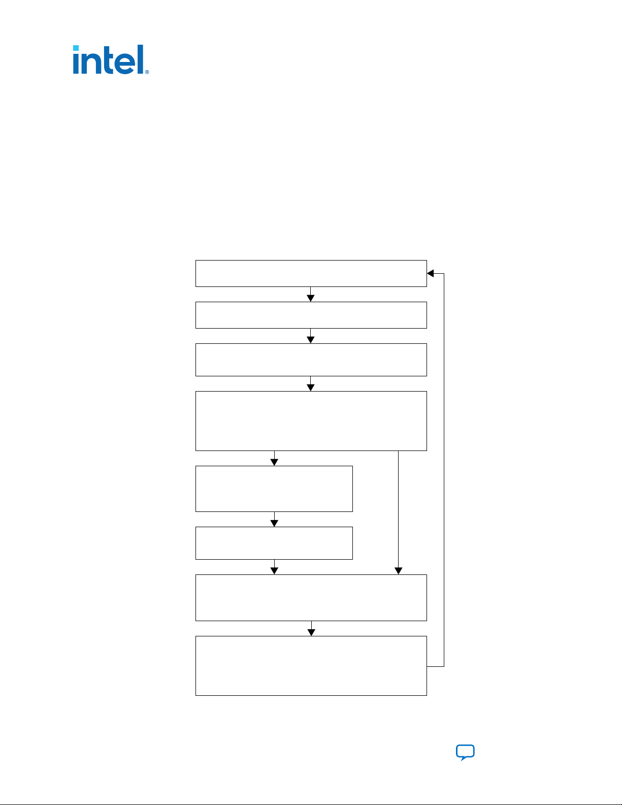
The Multirate Reconfig Controller implements rate detection circuitry with the HDMI
PLL to drive the RX transceiver to operate at any arbitrary link rates ranging from 250
Mbps to 6,000 Mbps. Link rate of 6,000 Mbps is not the absolute maximum but the
intention is to support HDMI 2.0b link rate.
The Multirate Reconfig Controller performs rate detection on the HDMI PLL arbitrary
reference clock, which is also the TMDS clock, to determine the clock frequency band.
Based on the detected clock frequency band, the circuitry dynamically reconfigures
the HDMI PLL and transceiver settings to accommodate for the link rate change.
Figure 11. Multirate Reconfiguration Sequence Flow
This figure illustrates the multirate reconfiguration sequence flow of the controller when it receives input data
stream and reference clock frequency, or when the transceiver is unlocked.
4. HDMI Hardware Design Examples
UG-HDMI | 2021.04.01
HDMI Intel® FPGA IP User Guide
30
Send Feedback
Page 31

4. HDMI Hardware Design Examples
UG-HDMI | 2021.04.01
4.3.1.5. Oversampler (RX)
The Oversampler (RX) extracts data from the oversampled incoming data stream
when the detected clock frequency band is below the transceiver minimum link rate.
The oversampling factor is fixed at 5 and you can program the data width to support
different number of symbols. The supported data width is 20 bit for 2 symbols per
clock and 40 bits for 4 symbols per clock. The extracted bit will be accompanied by
data valid pulse which asserts every 5 clock cycles.
4.3.1.6. DCFIFO
The DCFIFO transfers data from the RX transceiver recovered clock domain to the RX
link speed clock domain. The DCFIFO transfers data from the TX link speed clock
domain to the TX transceiver parallel clock out domain.
• Sink
— When the Multirate Reconfig Controller (RX) detects an incoming input stream
that is below the transceiver minimum link rate, the DCFIFO accepts the data
from the Oversampler with data valid pulse as write request asserted every 5
clock cycles.
— Otherwise, it accepts data directly from the transceiver with write request
asserted at all times.
• Source
— When Nios II processor determines the outgoing data stream is below the TX
transceiver minimum link rate, the TX transceiver accepts the data from the
Oversampler (TX).
— Otherwise, the TX transceiver reads data directly from the DCFIFO with read
request asserted at all times.
4.3.1.7. Sink Display Data Channel (DDC) & Status and Control Data Channel (SCDC)
The HDMI source uses the DDC to determine the capabilities and characteristics of the
sink by reading the Enhanced Extended Display Identification Data (E-EDID) data
structure.
The E-EDID memory is stored using the RAM 1-Port IP core. A standard two-wire
(clock and data) serial data bus protocol (I2C slave-only controller) is used to transfer
CEA-861-D compliant E-EDID data structure.
The 8-bit I2C slave addresses for the E-EDID are 0xA0/0xA1. The LSB indicates the
access type: 1 for read and 0 for write. When an HPD event occurs, the I2C slave
responds to E-EDID data by reading from the RAM.
The I2C slave-only controller is also used to support SCDC for HDMI 2.0b operation.
The 8-bit I2C slave addresses for the SCDC are 0xA8/0xA9. When an HPD event
occurs, the I2C slave performs write/read transaction to/from SCDC interface of HDMI
RX core. This I2C slave-only controller for SCDC is not required if HDMI 2.0b is not
intended.
Send Feedback
HDMI Intel® FPGA IP User Guide
31
Page 32
4. HDMI Hardware Design Examples
4.3.1.8. Transceiver Reconfiguration Controller
You can use the Transceiver Reconfiguration Controller IP core to change the device
transceiver settings at any time.
You can selectively reconfigure any portion of the transceiver. The reconfiguration of
each portion requires a read-modify-write operation (read first, then write). The readmodify-write operation modifies only the appropriate bits in a register and does not
affect the other bits.
The Transceiver Reconfiguration Controller is only available and required in Arria V and
Stratix V devices. Because the RX and TX transceivers share a single controller, the
controller requires Platform Designer interconnects, such as Avalon-MM Master
Translator and Avalon-MM Slave Translator, in the Platform Designer system.
• The Avalon-MM Master Translator provides an interface between this controller and
the RX Multirate Reconfig Controller.
• The Avalon-MM Slave Translator arbitrates the RX and TX reconfiguration event for
this controller.
4.3.1.9. VIP Bypass and Audio, Auxiliary and InfoFrame Buffers
The video data output and synchronization signals from HDMI RX core is looped
through a DCFIFO across RX and TX video clock domains. The General Control Packet
(GCP), InfoFrames (AVI, VSI, and AI), auxiliary data and audio data are looped
through DCFIFOs across RX and TX link speed clock domains.
UG-HDMI | 2021.04.01
The auxiliary data port of the HDMI TX core controls the auxiliary data that flow
through DCFIFO through backpressure. The backpressure ensures there is no
incomplete auxiliary packet on the auxiliary data port. This block also performs
external filtering on the audio data and audio clock regeneration packet from the
auxiliary data stream before sending to the HDMI TX core auxiliary data port.
4.3.1.10. Transceiver Native PHY (TX)
The Arria V and Stratix V Transceiver Native PHY (TX) configuration settings are
typically the same as RX.
Table 15. Arria V and Stratix V Transceiver Native PHY (TX) Configuration Settings
(6,000 Mbps)
This table shows an example of Arria V and Stratix V Transceiver Native PHY (TX) configuration settings for
TMDS bit rate of 6,000 Mbps.
Parameters
Datapath Options
Enable TX datapath On
Enable RX datapath Off
Enable Standard PCS On
Initial PCS datapath selection Standard
Number of data channels 4
Bonding mode xN
Enable simplified data interface On
Settings
HDMI Intel® FPGA IP User Guide
32
Send Feedback
Page 33
4. HDMI Hardware Design Examples
UG-HDMI | 2021.04.01
TX PMA
Data rate 6,000 Mbps
TX local clock division factor 1
Enable TX PLL dynamic reconfiguration On
Use external TX PLL Off
Number of TX PLLs 1
Main TX PLL logical index 0
Number of TX PLL reference clocks 1
PLL type CMU
Reference clock frequency 600 MHz
Selected reference clock source 0
Selected clock network xN
Standard PCS
Standard PCS protocol Basic
Standard PCS/PMA interface width
Enable TX byte serializer
• 10 (for 1 symbol per clock)
• 20 (for 2 and 4 symbols per clock)
• Off (for 1 and 2 symbols per clock)
• On (for 4 symbols per clock)
Table 16. Arria V and Stratix V Transceiver Native PHY (TX) Common Interface Ports
This table describes the Arria V and Stratix V Transceiver Native PHY (TX) common interface ports.
Signals
tx_pll_refclk
tx_std_clkout[3:0]
tx_std_coreclkin[3:0]
tx_analogreset[3:0]
tx_digitalreset[3:0]
pll_powerdown
pll_locked
Direction Description
Clocks
Input The reference clock input to the TX PLL.
Output TX parallel clock output.
Input TX parallel clock that drives the write side of the TX phase
compensation FIFO.
Connect to tx_std_clkout[0] ports.
Resets
Input When asserted, resets all the blocks in TX PMA.
Connect to Transceiver PHY Reset Controller (TX) IP core.
Input When asserted, resets all the blocks in TX PCS.
Connect to the Transceiver PHY Reset Controller (TX) IP
core.
TX PLL
Input When asserted, resets the TX PLL.
Connect to the Transceiver PHY Reset Controller (TX) IP
core.
Output When asserted, indicates that the TX PLL is locked.
Connect to the Transceiver PHY Reset Controller (TX) IP
core.
Send Feedback
HDMI Intel® FPGA IP User Guide
33
Page 34
unused_tx_parallel_data
tx_parallel_data[S*4*10-1:
0]
tx_serial_data[3:0]
tx_cal_busy[3:0]
reconfig_to_xcvr[349:0]
reconfig_from_xcvr[229:0]
4. HDMI Hardware Design Examples
UG-HDMI | 2021.04.01
PCS Ports
Input Leave unconnected.
Input PCS TX parallel data.
Note: S=Symbols per clock.
PMA Port
Output TX differential serial output data.
Calibration Status Port
Output When asserted, indicates that the initial TX calibration is in
progress. This port is also asserted if the reconfiguration
controller is reset. Connect to the Transceiver PHY Reset
Controller (TX) IP core.
Reconfiguration Ports
Input Reconfiguration signals from the Transceiver Reconfiguration
Controller.
Output Reconfiguration signals to the Transceiver Reconfiguration
Controller.
4.3.1.11. Transceiver PHY Reset Controller
The Transceiver PHY Reset Controller IP core ensures a reliable initialization of the RX
and TX transceivers.
The reset controller has separate reset controls per channel to handle synchronization
of reset inputs, lagging of PLL locked status, and automatic or manual reset recovery
mode.
4.3.1.12. Oversampler (TX)
The Oversampler (TX) transmits data by repeating each bit of the input word a given
number of times and constructs the output words.
The oversampling factor is fixed at 5. The Oversampler (TX) assumes that the input
word is only valid every 5 clock cycles. This block enables when the outgoing data
stream is determined to be below the TX transceiver minimum link rate by reading
once from the DCFIFO every 5 clock cycles.
4.3.1.13. Clock Enable Generator
The Clock Enable Generator is a logic that generates a clock enable pulse.
This clock enable pulse asserts every 5 clock cycles and serves as a read request
signal to clock the data out from DCFIFO.
4.3.1.14. Platform Designer System
The Platform Designer system consists of the VIP passthrough for HDMI video stream,
source SDC controller, and source reconfiguration controller blocks.
HDMI Intel® FPGA IP User Guide
34
Send Feedback
Page 35
4. HDMI Hardware Design Examples
UG-HDMI | 2021.04.01
4.3.1.14.1. VIP Passthrough for HDMI Video Stream
For certain example designs, you can loop the video data output and synchronization
signals from HDMI RX core through the VIP data path.
The Clocked Video Input II (CVI II) Intel FPGA IP core converts clocked video formats
to Avalon-ST video by stripping incoming clocked video of horizontal and vertical
blanking, leaving only active picture data.
• The IP core provides clock crossing capabilities to allow video formats running at
different frequencies to enter the system.
• The IP core also detects the format of the incoming clocked video and provides
this information in a set of registers.
• The Nios II processor uses this information to reconfigure the video frame mode
registers of the CVO IP core in the VIP passthrough design.
The Video Frame Buffer II Intel FPGA IP core buffers video frames into external RAM.
• The IP core supports double and triple buffering with a range of options for frame
dropping and repeating.
• You can use the buffering options to solve throughput issues in the data path and
perform simple frame rate conversion.
In a VIP passthrough design, you can reference the HDMI source PLL and sink PLL
using separate clock sources. However, in a VIP bypass design, you must reference
the HDMI source PLL and sink PLL using the same clock source.
The Clocked Video Output II (CVO II) Intel FPGA IP core converts data from the flowcontrolled Avalon-ST video protocol to clocked video.
• The IP core provides clock crossing capabilities to allow video formats running at
different frequencies to be created from the system.
• It formats the Avalon-ST video into clocked video by inserting horizontal and
vertical blanking and generating horizontal and vertical synchronization
information using the Avalon-ST video control and active picture packets.
• The video frame is described using the mode registers that are accessed through
the Avalon-MM control port.
Table 17. Difference between VIP Passthrough Design and VIP Bypass Design
VIP Passthrough Design VIP Bypass Design
• Can reference the HDMI source PLL and sink PLL using
separate clock sources
• Demonstrates only certain video formats—640×480p60,
720×480p60, 1280×720p60, 1920×1080p60, and
3840×2160p24
• Must reference the HDMI source PLL and sink PLL
using the same clock source
• Demonstrates all video formats.
Table 18. VIP Passthrough and VIP Bypass Options for the Supported Devices
Device
Family
Arria V 2 1.4b HSMC (Rev8) av_sk Supported Supported
Stratix V 2 2.0b HSMC (Rev8) sv_hdmi2 Not supported Supported
Symbols Per
Clock
4 2.0b HSMC (Rev8) av_sk_hdmi2 Not supported Supported
HDMI
Specification
Support
Bitec HDMI HSMC
2.0 Daughter Card
Directory VIP
Passthrough
VIP Bypass
Send Feedback
HDMI Intel® FPGA IP User Guide
35
Page 36

4.3.1.14.2. Source SCDC Controller
The source SCDC Controller contains the I2C master controller. The I2C master
controller transfers the SCDC data structure from the FPGA source to the external sink
for HDMI 2.0b operation.
4. HDMI Hardware Design Examples
UG-HDMI | 2021.04.01
For example, if the outgoing data stream is 6,000 Mbps, the Nios II processor
commands the I
2
C master controller to update the TMDS_Bit_Clock_Ratio and
Scrambler_Enable bits of the sink TMDS configuration register to 1. The same I
master can also transfer the DDC data structure (E-EDID) between the HDMI source
and external sink.
4.3.1.14.3. Source Reconfiguration Controller
The Nios II CPU acts as the multirate reconfiguration controller for the HDMI source.
The CPU relies on the periodic rate detection from the Multirate Reconfig Controller
(RX) to determine if TX requires reconfiguration. The Avalon-MM slave translator
provides the interface between the Nios II processor Avalon-MM master interface and
the Avalon-MM slave interfaces of the externally instantiated HDMI source's PLL
Reconfig Intel FPGA IP and Transceiver Native PHY (TX).
2
C
HDMI Intel® FPGA IP User Guide
36
Send Feedback
Page 37

Reset the TX HDMI PLL and TX transceiver. Initialize the I2C master controller core.
Poll periodic measure valid signal from RX rate detection circuit to determine whether TX
reconfiguration is required. Also, poll the T X hot-plug request to determine whether a TX
hot-plug event has occurred.
Read TMDS_Bit_Clock_Ratio value from the HDMI
sink and the measure value.
Send SCDC via the I2C interface based on the
TMDS_Bit_Clock_Ratio register value from
the HDMI sink.
Retrieve the clock frequency band based on the
measure and TMDS_Bit_Clock_Ratio values and read
the color depth information from the HDMI sink to
determine whether TX HDMI PLL and TX transceiver
reconfiguration and oversampling is required.
The Nios II processor sends sequential commands to
reconfigure the TX HDMI PLL and TX transceiver and
reset sequence after reconfiguration. It then sends
a reset to the HDMI TX core.
The Nios II processor commands the I2C master to
send SCDC information.
Retrieve incoming video width and height from the
CVI to determine whether the CVO should be updated
to adjust the outgoing video frame resolution.
The Nios II processor sends commands to update the
CVO video frame resolution.
Reconfiguration Is Required
Reconfiguration
Is Not Required
Measure Valid Received
A TX Hot-Plug Event
Has Occurred
CVO Update Is Required
CVO Update
Is Not Required
4. HDMI Hardware Design Examples
UG-HDMI | 2021.04.01
Figure 12. Nios II Software Flow
The reconfiguration sequence flow for TX is the same as RX, except that the PLL and transceiver
reconfiguration, and the reset sequence is performed sequentially. The figure illustrates the Nios II software
flow that involves the controls for CVO, I2C master and HDMI source.
4.3.2. HDMI Hardware Design Requirements
The HDMI design requires an Intel FPGA board and supporting hardware.
• Intel FPGA board
• Bitec HDMI HSMC 2.0 daughter card
• Standard HDMI source—for example, PC with a graphic card and HDMI output
• Standard HDMI sink—for example, monitor with HDMI input
• 2 HDMI cables
— A cable to connect the graphics card to the Bitec daughter card RX connector.
— A cable to connect the Bitec daughter card TX connector to the monitor.
Send Feedback
HDMI Intel® FPGA IP User Guide
37
Page 38

4. HDMI Hardware Design Examples
UG-HDMI | 2021.04.01
Table 19. Intel FPGA Boards and Bitec HDMI HSMC 2.0 Daughter Cards Supported for
the Design
Design Example Intel FPGA Board
Arria V (av_sk) Arria V GX FPGA Starter Kit HSMC (Rev8)
Arria V (av_sk_hdmi2) Arria V GX FPGA Starter Kit HSMC (Rev8)
Stratix V (sv_hdmi2) Stratix V GX FPGA Development Kit HSMC (Rev8)
Related Information
• Arria V GX Starter Kit User Guide
• Stratix V GX FPGA Development Kit User Guide
4.3.3. Design Walkthrough
Setting up and running the HDMI hardware design consists of four stages.
You can use the Intel-provided scripts to automate these stages.
1. Set up the hardware.
2. Copy the design files to your working directory.
3. Build and compile the design.
4. View the results.
4.3.3.1. Set Up the Hardware
The first stage of the demonstration is to set up the hardware.
Bitec HDMI HSMC 2.0 Daughter
Card
To set up the hardware for the demonstration:
1. Connect the Bitec HDMI HSMC 2.0 daughter card to the FPGA development board.
2. Connect the FPGA board to your PC using a USB cable.
Note: The Arria V GX FPGA Starter Kit and Stratix V GX FPGA Development Kit
have an On-Board Intel FPGA Download Cable II connector. If your version
of the board does not have this connector, you can use an external Intel
FPGA Download Cable cable.
3. Connect an HDMI cable from the HDMI RX connector on the Bitec HDMI HSMC 2.0
daughter card to a standard HDMI source, in this case a PC with a graphic card
and HDMI output.
4. Connect another HDMI cable from the HDMI TX connector on the Bitec HDMI
HSMC 2.0 daughter card to a standard HDMI sink, in this case a monitor with
HDMI input.
4.3.3.2. Copy the Design Files
After you set up the hardware, you copy the design files. Copy the hardware
demonstration files from one of the following paths to your working directory:
HDMI Intel® FPGA IP User Guide
38
Send Feedback
Page 39

4. HDMI Hardware Design Examples
UG-HDMI | 2021.04.01
• Arria V
—
2 symbols per clock (HDMI 1.4b) demonstration: <IP root directory>/
altera_hdmi/hw_demo/av_sk
—
4 symbols per clock (HDMI 2.0b) demonstration: <IP root directory>/
altera_hdmi/hw_demo/av_sk_hdmi2
• Stratix V
—
2 symbols per clock (HDMI 2.0b) demonstration: <IP root directory>/
altera_hdmi/hw_demo/sv_hdmi2
4.3.3.3. Build and Compile the Design
After you copy the design files, you can build the design.
You can use the provided Tcl script to build and compile the FPGA design.
1. Open a Nios II Command Shell.
2. Change the directory to your working directory.
3.
Type the command and enter source runall.tcl.
This script executes the following commands:
• Generate IP catalog files
• Generate the Platform Designer system
• Create an Intel Quartus Prime project
• Create a software work space and build the software
• Compile the Intel Quartus Prime project
• Run Analysis & Synthesis to generate a post-map netlist for DDR assignments
—for VIP passthrough design only
• Perform a full compilation
Note:
If you are a Linux user, you will get a message cygpath: command not
found. You can safely ignore this message; the script will proceed to
generate the next commands.
4.3.3.4. View the Results
At the end of the demonstration, you will be able to view the results on the standard
HDMI sink (monitor).
To view the results of the demonstration, follow these steps:
1. Power up the Intel FPGA board.
2. Type the following command on the Nios II Command Shell to download the
Software Object File (.sof) to the FPGA.
nios2-configure-sof output_files/<Quartus project name>.sof
3. Power up the standard HDMI source and sink (if you haven't done so).
The design displays the output of your video source (PC).
Send Feedback
HDMI Intel® FPGA IP User Guide
39
Page 40

Note:
If the output does not appear, press cpu_resetn to reinitialize the system
or perform HPD by unplugging the cable from the standard source and plug
it back again.
4. Open the graphic card control utility (if you are using a PC as source). Using the
control panel, you can switch between various video resolutions.
The av_hdmi2 and sv_hdmi2 demonstration designs allow any video resolutions
up to 4Kp60. The av_sk design allows 640×480p60, 720×480p60, 1280×720p60,
1920×1080p60, and 3840×2160p24 when you select the VIP passthrough mode
(user_dipsw[0] = 0). If you select the VIP bypass mode (user_dipsw[0] =
1, the design allows any video resolutions up to 4Kp60.
4.3.3.4.1. Push Buttons, DIP Switches and LED Functions
Use the push buttons, DIP switches, and LED functions on the board to control your
demonstration.
Table 20. Push Buttons, DIP Switches and LEDs Functions
4. HDMI Hardware Design Examples
UG-HDMI | 2021.04.01
Push Button/
DIP Switch/LED
cpu_resetn D5 AM34 Press once to perform system reset.
user_pb[0] A14 A7
user_pb[1] B15 B7
user_pb[2] B14 C7
user_dipsw[0] D15 Unused
user_led[0] F17 J11
user_led[1] G15 U10
user_led[2] G16 U9
user_led[3] G17 AU24
user_led[4] D16 AF28 TX HDMI PLL lock status.
av_sk/av_sk_hdmi2 sv_hdmi2
Pins
Functions
Press once to turn on and turn off HPD
signal to the standard HDMI source.
Press and hold to instruct the TX to
send DVI encoded signal and release to
send HDMI encoded signal.
Press and hold to instruct the TX to
stop sending InfoFrames and release to
resume sending.
Only used in av_sk design which
demonstrates the VIP passthrough
feature.
• 0: VIP passthrough
• 1: VIP bypass
RX HDMI PLL lock status.
• 0: Unlocked
• 1: Locked
RX transceiver ready status.
• 0: Not ready
• 1: Ready
RX HDMI core lock status
• 0: At least 1 channel unlocked
• 1: All 3 channels locked
RX oversampling status.
• 0: Non-oversampled (more than
611 Mbps for av_sk and sv_hdmi2,
more than 1,000 Mbps for
av_sk_hdmi2)
• 1: Oversampled (less than 611
Mbps for av_sk and sv_hdmi2, less
than 1,000 Mbps for av_sk_hdmi2)
continued...
HDMI Intel® FPGA IP User Guide
40
Send Feedback
Page 41

4. HDMI Hardware Design Examples
UG-HDMI | 2021.04.01
Push Button/
DIP Switch/LED
user_led[5] C13 AE29
user_led[6] C14 AR7
user_led[7] C16 AV10
av_sk/av_sk_hdmi2 sv_hdmi2
Pins
Functions
• 0: Unlocked
• 1: Locked
TX transceiver ready status.
• 0: Not ready
• 1: Ready
TX transceiver PLL lock status.
• 0: Unlocked
• 1: Locked
TX oversampling status.
• 0: Non-oversampled (more than
611 Mbps for av_sk and sv_hdmi2,
more than 1,000 Mbps for
av_sk_hdmi2)
• 1: Oversampled (less than 611
Mbps for av_sk and sv_hdmi2, less
than 1,000 Mbps for av_sk_hdmi2)
Send Feedback
HDMI Intel® FPGA IP User Guide
41
Page 42

AUX
AUX
AUX
TMDS Data (Red Channel)
TMDS Data (Green Channel)
TMDS Data (Blue Channel)
TMDS Data (Clock Channel)
AVI InfoFrame
Vendor-Specific
Infoframe
Auxiliary Data Port
Audio Metadata
Audio Clock
Regeneration (N, CTS)
Audio Infoframe
Audio Sample
Auxiliary
Control
Port
Audio
Port
Audio Encoder
TMDS
Data
Port
Multiplexer
Multiplexer
vid_clk domain
Is_clk domain
HDCP clocks domain
Timestamp
Scheduler
AI Control
Audio Packetizer
AM Control
Auxiliary Packet
Dropper
VSI Control
AVI Control
Auxiliary Packet
Generator
Auxiliary Packet
Generator
Auxiliary Packet
Generator
Auxiliary Packet
Generator
Auxiliary Packet
Generator
Auxiliary Packet
Generator
WOP
Generator
Video Data (Red Channel)
Video Data (Green Channel)
Video Data (Blue Channel)
General Control Packet
Video
Data
Port
Multiplexer
Encoder Control Port
HDCP Port
Auxiliary Packet
Generator
Video
Resampler
HDCP 2.3
TX
HDCP 1.4
TX
Scrambler,
TMDS/TERC4
Encoder
Auxiliary
Packet
Encoder
UG-HDMI | 2021.04.01
Send Feedback
5. HDMI Source
5.1. Source Functional Description
The HDMI source core provides direct connection to the Transceiver Native PHY
through a 20-bit or 40-bit parallel data path. The clock domains for the auxiliary and
audio ports, and the internal modules are different for Support FRL = 1 and Support
FRL = 0.
Figure 13. HDMI Source Signal Flow Diagram for TMDS (Support FRL = 0) Design
The figure below shows the flow of the HDMI source signals. The figure shows the various clocking domains
used within the core.
The source core provides four 20-bit parallel data paths corresponding to the 3 color
channels and the clock channel.
The source core accepts video, audio, and auxiliary channel data streams. The core
produces a scrambled and TMDS/TERC4 encoded data stream that would typically
connect to the high-speed transceiver parallel data inputs.
Note: The scrambled data only applies for HDMI 2.0b stream with TMDS Bit Rate higher than
3.4 Gbps.
Central to the core is the Scrambler, TMDS/TERC4 Encoder. The encoder processes
Intel Corporation. All rights reserved. Agilex, Altera, Arria, Cyclone, eASIC, Intel, the Intel logo, MAX, Nios,
Quartus and Stratix words and logos are trademarks of Intel Corporation or its subsidiaries in the U.S. and/or
other countries. Intel warrants performance of its FPGA and semiconductor products to current specifications in
accordance with Intel's standard warranty, but reserves the right to make changes to any products and services
at any time without notice. Intel assumes no responsibility or liability arising out of the application or use of any
information, product, or service described herein except as expressly agreed to in writing by Intel. Intel
customers are advised to obtain the latest version of device specifications before relying on any published
information and before placing orders for products or services.
*Other names and brands may be claimed as the property of others.
either video or auxiliary data.
ISO
9001:2015
Registered
Page 43
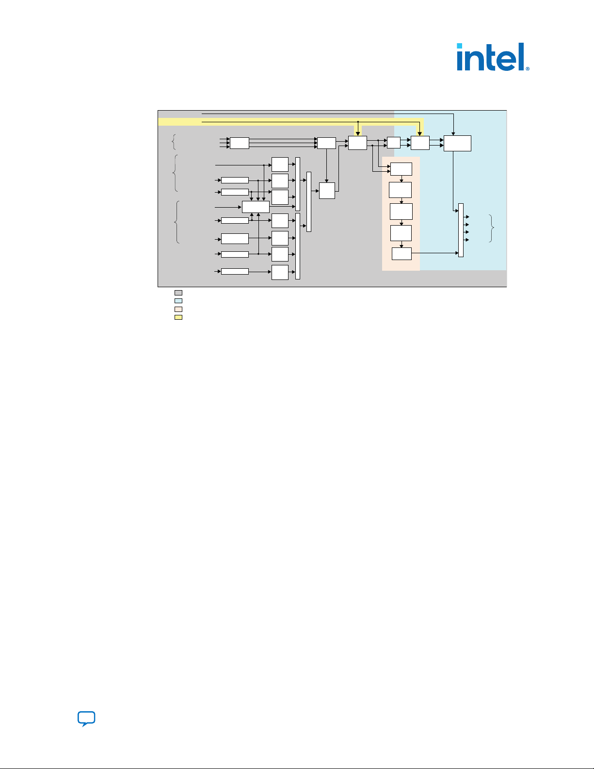
AUX
Video Data (Red Channel)
Video Data (Green Channel)
Video Data (Blue Channel)
General Control Packet
AVI InfoFrame
Vendor-Specific
Infoframe
Auxiliary Data Port
Audio Metadata
Audio Clock
Regeneration (N, CTS)
Audio Infoframe
Audio Sample
Video
Data
Port
Auxiliary
Control
Port
Audio
Port
Encoder Control Port
Multiplexer
Multiplexer
Multiplexer
vid_clk domain (pixels per clock)
tx_clk domain (transceiver width per lane)
Data Lane 0
Data Lane 1
Data Lane 2
Data Lane 3
TMDS
Data
Port
Multiplexer
Scrambler,
TMDS/TERC4
Encoder
Timestamp
Scheduler
AI Control
Audio Packetizer
AM Control
Auxiliary Packet
Dropper
VSI Control
AVI Control
Auxiliary
Packet
Generator
Auxiliary
Packet
Generator
Auxiliary
Packet
Generator
Auxiliary
Packet
Generator
Auxiliary
Packet
Generator
Auxiliary
Packet
Generator
Auxiliary
Packet
Generator
Video
Resampler
Auxiliary
Packet
Encoder
FRL
Packetizer
FRL
Resampler
FRL Scrambler
and Encoder
FRL Character
block and Super
Block Mapping
RS FEC Parity
Generation and
Insertion
WOP
Generator
frl_clk domain (FRL characters per clock)
DCFIFO
HDCP Port
HDCP 1.4
TX
HDCP 2.3
TX
HDCP clocks domain
5. HDMI Source
UG-HDMI | 2021.04.01
Figure 14. HDMI Source Signal Flow Diagram for Support FRL = 1 Design
For FRL path design, the video resampler and WOP generator operating at video clock
domain accept video data running in the video clock (vid_clk) domain. The auxiliary
data port, audio data port, and the auxiliary sideband signals also run in the video
clock domain.
• A DCFIFO clocks the HDMI data stream from the WOP generator in the video clock
domain to the scrambler, TMDS/TERC4 encoder in the transceiver recovered clock
(tx_clk) domain to create a TMDS data stream.
•
The HDMI data stream is also fed into the FRL path in FRL clock (frl_clk)
domain to create an FRL data stream.
The multiplexer selects either TMDS data stream or FRL data stream as output data
for lanes 0–3 based on the FRL rate.
• If FRL rate is 0, the multiplexer selects TMDS data streams as output.
• If FRL rate is non-zero, the multiplexer selects FRL data streams as output.
5.1.1. Source Scrambler, TMDS/TERC4 Encoder
The TMDS/TERC4 encoder implements 8-bit to 10-bit and 4-bit to 10-bit algorithms as
defined in the HDMI 1.4b Specification Section 5.4. Each data channel, with exception
of the clock channel, has its own encoder. You can configure the core to enable
scrambling, as defined in the HDMI 1.4b Specification Section 6.1.2, before TMDS/
Send Feedback
TERC4 encoding.
The encoder processes symbol data at 1, 2, or 4 symbols per clock. When the encoder
operates in 2 or 4 symbols per clock, it also produces the output in the form of two or
four encoded symbols per clock.
The TMDS/TERC4 encoder also produces digital visual interface (DVI) signaling when
you deassert the mode input signal. DVI signaling is identical to HDMI signaling,
except for the absence of data and video islands and TERC4 auxiliary data.
HDMI Intel® FPGA IP User Guide
43
Page 44

5.1.2. Source Video Resampler
1
vid_clk
DCFIFO
ls_clk
data
wr
wrclk
q
rd
rdclk
de
H-SYNC
V-SYNC
b[15:0]
r[15:0]
g[15:0]
b[7:0]
r[7:0]
g[7:0]
Phase
Counter
Gearbox
H-SYNC
V-SYNC
de
Resampled
packing-phase (pp)
bits per pixel (bpp)
47 32 31 16 15 0
vid_data[47:0]
24 bpp RGB/YCbCr 4:4:4 (8 bpc)
30 bpp RGB/YCbCr 4:4:4 (10 bpc)
36 bpp RGB/YCbCr 4:4:4 (12 bpc)
48 bpp RGB/YCbCr 4:4:4 (16 bpc)
The video resampler consists of a dual-clock FIFO (DCFIFO) and a gearbox.
The gearbox converts data of 8, 10, 12, or 16 bits per component to 8-bit per
component data based on the current color depth. The General Control Packet (GCP)
conveys the color depth information.
Figure 15. Source Video Resampler Signal Flow Diagram
The figure below shows the components of the video resampler and the signal flow between these components.
The resampler adheres to the recommended phase encoding method described in
HDMI 1.4b Specification Section 6.5.
• The phase counter must register the last pixel packing-phase (pp) of the last pixel
of the last active line.
• The core then transmits the pp value to the attached sink device in the GCP for
packing synchronization.
5. HDMI Source
UG-HDMI | 2021.04.01
The HDMI cable may send across four different pixel encodings: RGB 4:4:4, YCbCr
4:4:4, and YCbCr 4:2:2 (as described in HDMI 1.4b Specification Section 6.5), and
YCbCr 4:2:0 (as described in HDMI 2.0b Specification Section 7.1).
Figure 16. Pixel Data Input Format RGB/YCbCr 4:4:4
The figure below shows the RGB/YCbCr 4:4:4 color space pixel bit-field mappings per symbol. When the actual
color depth is below 16 bpc, the unused LSBs are set to zero.
HDMI Intel® FPGA IP User Guide
44
Send Feedback
Page 45

47 40 31 24 15 8 0
Cb/Cr[11:4] Y[11:4]
Cb/Cr[3:0] Y[3:0]
47 32 31 16 15 0
vid_data[47:0]
12 bpp YCbCr 4:2:0 (8 bpc)
15 bpp YCbCr 4:2:0 (10 bpc)
18 bpp YCbCr 4:2:0 (12 bpc)
24 bpp YCbCr 4:2:0 (16 bpc)
n + 1
n
n = Pixel Index
n
n
n
n + 1
n + 1
n + 1
5. HDMI Source
UG-HDMI | 2021.04.01
Figure 17. Pixel Data Input Format YCbCr 4:2:2 (12 bpc)
The figure below shows the YCbCr 4:2:2 color space pixel bit-field mappings per symbol. As with 4:4:4 color
space, the unused LSBs are set to zero.
The higher order 8 bits of the Y samples are mapped to the 8 bits of Channel 1 and
the lower order 4 bits are mapped to the lower order 4 bits of Channel 0.
The first pixel transmitted within a Video Data Period contains three components, Y0,
Cb0 and Cr0. The Y0 and Cb0 components are transmitted during the first pixel period
while Cr0 is transmitted during the second pixel period. This second pixel period also
contains the only component for the second pixel, Y1. In this way, the link carries one
Cb sample for every two pixels and one Cr sample for every two pixels. These two
components (Cb and Cr) are multiplexed onto the same signal paths on the link.
Figure 18. Pixel Data Input Format YCbCr 4:2:0
The figure shows the YCbCr 4:2:0 color space pixel bit-field mappings. As with 4:4:4 color space, the unused
LSBs are set to zero.
The two horizontally successive 8-bit Y components are transmitted in TMDS Channels
1 and 2, in that order. The 8-bit Cb or Cr components are transmitted alternately in
TMDS Channel 0, line by line.
For even lines starting with line 0:
•
vid_data[47:32] always transfer the Yn+1 component
•
vid_data[31:16] always transfer the Yn component
•
vid_data[15:0] always transfer the Cbn component
For odd lines:
•
vid_data[47:32] always transfer the Yn+1 component
•
vid_data[31:16] always transfer the Yn component
•
vid_data[15:0] always transfer the Crn component
Send Feedback
The frequency of vid_clk must be halved when YCbCr 4:2:0 is used, because two
pixels are fed into a single clock cycle.
HDMI Intel® FPGA IP User Guide
45
Page 46

Figure 19. YCbCr 4:2:0 Transport Using 1 Symbol Per Clock Mode
Y01 Y03 Y05 Y07
Y00 Y02 Y04 Y06
Cb00 Cb02 Cb04 Cb06
Y11 Y13 Y15 Y17
Y10 Y12 Y14 Y16
Cr10 Cr12 Cr14 Cr16
Even Line (0) Odd Line (1)
vid_clk = pixel clock / 2
(Channel 2) vid_data[47:32]
(Channel 1) vid_data[31:16]
(Channel 0) vid_data[15:0]
For example:
Y00 = Y Component, Line 0, Pixel 0
Y01 = Y Component, Line 0, Pixel 1
Component
Line number
Pixel number
Video Data Enable
V Sync
H Sync
Data Island Output Enable
Vertical
Blanking
Active
Video
Horizontal
Blanking
Active
Video
Control Period Data Island Guard Band Video Guard Band Data Island
The figure below shows the YCbCr 4:2:0 transmission when the core operates in 1 symbol per clock mode.
5.1.3. Source Window of Opportunity Generator
The source Window of Opportunity (WOP) generator creates valid data islands within
the blanking regions.
During horizontal blanking region, the WOP generator creates a leading region to hold
at least 12 period symbols that include eight preamble symbols. The generator also
creates a trailing region to hold two data island trailing guard band symbols, at least
12 control period symbols that include eight preamble symbols and two video leading
guard band symbols.
5. HDMI Source
UG-HDMI | 2021.04.01
Figure 20. Typical Window of Opportunity
5.1.4. Source Auxiliary Packet Encoder
HDMI Intel® FPGA IP User Guide
46
During vertical blanking region, the source cannot send more than 18 auxiliary
packets consecutively. The WOP generator deasserts the data island output enable
(aux_wop) line after every 18th auxiliary packet for 32-symbol clocks.
The WOP generator also has an integral number of auxiliary packet cycles: 24 clocks
when processing in 1-symbol mode, 16 clocks when processing in 2-symbol mode,
and 8 clocks when processing in 4-symbol mode.
The figure below shows a typical output from the WOP generator.
Auxiliary packets are encoded by the source auxiliary packet encoder.
The auxiliary packets originate from several sources, which are multiplexed into the
auxiliary packet encoder in a round-robin schedule. The auxiliary packet encoder
converts a standard stream into the channel data format required by the TERC4
encoder.
Send Feedback
Page 47

PB22
PB21
PB15
PB14
PB8
PB7
PB1
PB0
HB0
Phase 0
PB24
PB23
PB17
PB16
PB10
PB9
PB3
PB2
HB1
Phase 1
PB26
PB25
PB19
PB18
PB12
PB11
PB5
PB4
HB2
Phase 2
0
PB27
0
PB20
0
PB13
0
PB6
0
Phase 3
BCH Block 3
BCH Block 2
BCH Block 1
BCH Block 0
Input Data
Byte[8]
Byte[0]
Startofpacket
Endofpacket
Valid
Clock
0 - - 8 - - 16 - - 24Cycle 1 Symbol
0 - - 4 - - 8 - - 12Cycle 2 Symbol
0 - - 2 - - 4 - - 6Cycle 4 Symbol
Phase 0 Phase 1
Phase 2
Phase 3
5. HDMI Source
UG-HDMI | 2021.04.01
The auxiliary packet encoder also calculates and inserts the Bose-ChaudhuriHocquenghem (BCH) error correction code.
Figure 21. Auxiliary Packet Encoder Input
The figure below shows the auxiliary packet encoder input from a 72-bit input data.
The encoder assumes the data valid input will remain asserted for the duration of a
packet to complete. A packet is always 24 clocks (in 1-symbol mode), 12 clocks (in 2symbol mode), or 6 clocks (in 4-symbol mode).
Send Feedback
HDMI Intel® FPGA IP User Guide
47
Page 48

Figure 22. Typical Auxiliary Packet Stream During Blanking Interval
AD
aux_wop
aux_de
Auxilliary Packet
Clock Cycle
AD: Audio Data
AVI: Auxilliary Video Infoframe
AI: Audio Information Infoframe
VSI: Vendor Specific Infoframe
0 31 63 95 575
AD AD AD AD AD AD AD AD AD AI VSIAVI
19th Packet Skipped
The figure below shows a typical auxiliary packet stream in 1-symbol per clock mode, where 0 denotes a null
packet.
5.1.5. Source Auxiliary Packet Generators
The source core uses various auxiliary packet generators. The packet generators
convert the packet field inputs to the auxiliary packet stream format.
The packet generator propagates backpressure from the output ready signal to the
input ready signal. The generator asserts the input valid signal when a packet is ready
to be transmitted. The input valid signal remains asserted until the end of the packet
and the generator receives a ready acknowledgment.
5. HDMI Source
UG-HDMI | 2021.04.01
5.1.6. Source Auxiliary Data Path Multiplexers
The auxiliary data path multiplexers provide paths for the various auxiliary packet
generators.
The various auxiliary packet generators traverse a multiplexed routing path to the
auxiliary packet encoder. The multiplexers obey a round-robin schedule and propagate
backpressure.
5.1.7. Source Auxiliary Control Port
To simplify the user logic, the source core has control ports to send the most common
auxiliary control packets.
These packets are: General Control Packet, Auxiliary Video Information (AVI)
InfoFrame, and HDMI Vendor Specific InfoFrame (VSI).
The core sends the default values in the auxiliary packets. The default values allow the
core to send video data compatible with the HDMI 1.4b Specification with minimum
description.
You can also override the generators using the customized input values. The override
values replace the default values when the input checksum is non-zero.
HDMI Intel® FPGA IP User Guide
48
Send Feedback
Page 49

5. HDMI Source
UG-HDMI | 2021.04.01
Table 21. Insertion and Filtration
Auxiliary Packets Insertion/Filtration Frequency of
General Control Packet
(GCP)
Auxiliary Video
Information (AVI)
InfoFrame
Vendor Specific
InfoFrame (VSI)
info_avi[112]=1'b0
info_avi[112] =1'b1
info_avi[122]=1'b1
– The core always inserts GCP packets from the
Support FRL=0:
Support FRL =1:
info_vsi[61]=1'b0
GCP sideband upon the rising edge of vsync.
The core always removes the GCP in the
Auxiliary Data Port.
You must provide the pixel packing and color
depth information through the gcp port.
The core inserts info_avi when there is a
non-zero bit upon the rising edge of vsync.
The core send default values when all bits are
zero. The core filters the AVI InfoFrame packet
on the Auxiliary Data Port.
The core does not insert info_avi.
The AVI InfoFrame packet on the Auxiliary Data
Port passes through.
The core inserts info_vsi[60:0] when there
is a non-zero bit upon the rising edge of
vsync.
The core sends default values when all bits are
zero. The core filters the VSI InfoFrame packet
on the Auxiliary Data Port.
info_vsi[61]=1'b1
Audio Metadata (AM) audio_metadata[165]=1'b0 The core inserts audio_metadata[164:0] when
The core does not insert info_vsi[60:0].
The VSI InfoFrame packet on the Auxiliary Data
Port passes through.
audio_format[3:0] is 3D audio or MST
audio upon the rising edge of vsync.
The core filters the AM packet on the Auxiliary
Data Port.
audio_metadata[165]=1'b1 The core does not insert
audio_metadata[164:0].
The AM packet on the Auxiliary Data Port
passes through.
Audio InfoFrame (AI) audio_info_ai[48]=1'b0
The core inserts audio_info_ai[47:0] when
there is a non-zero bit upon the rising edge of
vsync.
The core sends default values when all bits are
zero. The core filters the AI packet on the
Auxiliary Data Port.
audio_info_ai[48]=1'b1 The core does not insert
audio_info_ai[47:0].
The AI packet on the Auxiliary Data Port passes
through.
Audio Control
Regeneration (ACR)
Audio Sample –
–
The core always inserts the audio_N and
audio_CTS.
The core does not filter the ACR packet in the
auxiliary. If there is ACR packet in the Auxiliary
Data Port, you must remove it before passing
into the Auxiliary Data Port.
The core always inserts audio_data.
Insertion
Once per frame.
Once per frame.
Once per frame.
Once per frame.
Once per frame.
Every 1 ms.
Based on audio
sample rate.
continued...
Send Feedback
HDMI Intel® FPGA IP User Guide
49
Page 50
5. HDMI Source
UG-HDMI | 2021.04.01
Auxiliary Packets Insertion/Filtration Frequency of
The core does not filter the audio sample
packet in the Auxiliary Data Port. If there is
audio sample packet in the Auxiliary Data Port,
you must remove it before passing into the
Auxiliary Data Port.
5.1.7.1. Source General Control Packet (GCP)
Table 22. Source GCP Bit-Fields
This table lists the controllable bit-fields for the Source gcp[5:0] port.
Bit Field Name Value Comment
gcp[3:0] Color Depth
(CD)
gcp[4] Set_AVMUTE Refer to HDMI 1.4b Specification Section 5.3.6.
gcp[5] Clear_AVMUTERefer to HDMI 1.4b Specification Section 5.3.6.
CD3 CD2 CD1 CD0 Color depth
0 0 0 0 Color depth not
0 1 0 0 8 bpc or 24 bits per
0 1 0 1 10 bpc or 30 bpp
0 1 1 0 12 bpc or 36 bpp
0 1 1 1 16 bpc or 48 bpp
Others Reserved
Insertion
indicated
pixel (bpp)
All other fields for the source GCP, (for example, Pixel Packing Phase and Default
Phase as described in HDMI 1.4b Specification Section 5.3.6) are calculated
automatically inside the core. You must provide the bit-field values in the table above
through the source gcp[5:0] port. The GCP on the Auxiliary Data Port will always be
filtered.
5.1.7.2. Source Auxiliary Video Information (AVI) InfoFrame Bit-Fields
Table 23. Source Auxiliary Video Information (AVI) InfoFrame for Support FRL = 0
Designs
The signal bundle is clocked by ls_clk for Support FRL = 0 designs.
Bit-field
7:0 Checksum Checksum 8’h67
9:8 S Scan information 2’h0
11:10 B Bar info data valid 2’h0
12 A0 Active information present 1’h0
14:13 Y RGB or YCbCr indicator 2’h0
15 Reserved Returns 0 1’h0
19:16 R Active format aspect ratio 4’h8
Name Description Default Value
continued...
HDMI Intel® FPGA IP User Guide
50
Send Feedback
Page 51

5. HDMI Source
UG-HDMI | 2021.04.01
Bit-field Name Description Default Value
21:20 M Picture aspect ratio 2’h0
23:22 C Colorimetry (for example: ITU BT.601, BT.709) 2’h0
25:24 SC Non-uniform picture scaling 2’h0
27:26 Q Quantization range 2’h0
30:28 EC Extended colorimetry 3’h0
31 ITC IT content 1’h0
38:32 VIC Video format identification code 7’h00
39 Reserved Returns 0 1’h0
43:40 PR Picture repetition factor 4’h0
45:44 CN Content type 2’h0
47:46 YQ YCC quantization range 2’h0
63:48 ETB Line number of end of top bar 16’h0000
79:64 SBB Line number of start of bottom bar 16’h0000
95:80 ELB Pixel number of end of left bar 16’h0000
111:96 SRB Pixel number of start of right bar 16’h0000
112 Control Disables the core from inserting the InfoFrame
packet.
• 1: The core does not insert
info_avi[111:0]. The AVI InfoFrame
packet on the Auxiliary Data Port passes
through.
•
0: The core inserts info_avi[111:0] when
there is a non-zero bit. The core sends default
values when all bits are zero. The core filters
the AVI InfoFrame packet on the Auxiliary
Data Port.
–
By default, the HDMI source sets the AVI version to version 2. If the value of
info_avi[30:28] (EC2, EC1, EC0) is 3’b111, then the HDMI source sets the AVI
version to version 4. If the value of info_avi[39] is 1’b1 (VIC >= 128) or
info_avi[15] (Y2) is set to 1, the HDMI source sets the AVI version to version 3.
Table 24. Source Auxiliary Video Information (AVI) InfoFrame for Support FRL = 1
Designs
This signal bundle is clocked by vid_clk for Support FRL = 1 designs.
Bit-field
7:0 Checksum Checksum 8’h67
9:8 S Scan information 2’h0
11:10 B Bar info data valid 2’h0
12 A0 Active information present 1’h0
15:13 Y RGB or YCbCr indicator 3’h0
19:16 R Active format aspect ratio 4’h8
21:20 M Picture aspect ratio 2’h0
Send Feedback
Name Description Default Value
continued...
HDMI Intel® FPGA IP User Guide
51
Page 52

5. HDMI Source
UG-HDMI | 2021.04.01
Bit-field Name Description Default Value
23:22 C Colorimetry (for example: ITU BT.601, BT.709) 2’h0
25:24 SC Non-uniform picture scaling 2’h0
27:26 Q Quantization range 2’h0
30:28 EC Extended colorimetry 3’h0
31 ITC IT content 1’h0
39:32 VIC Video format identification code 8’h00
43:40 PR Picture repetition factor 4’h0
45:44 CN Content type 2’h0
47:46 YQ YCC quantization range 2’h0
63:48 ETB Line number of end of top bar 16’h0000
79:64 SBB Line number of start of bottom bar 16’h0000
95:80 ELB Pixel number of end of left bar 16’h0000
111:96 SRB Pixel number of start of right bar 16’h0000
115:112 F143-F140 Future use 14 4’h0
119:116 ACE3-ACE0 Additional colorimetry extension 4’h0
121:120 – Reserved –
122 Control Disables the core from inserting the InfoFrame
packet.
• 1: The core does not insert
2’h0
info_avi[120:0]. The AVI InfoFrame
packet on the Auxiliary Data Port passes
through.
•
0: The core inserts info_avi[120:0] when
there is a non-zero bit. The core sends default
values when all bits are zero. The core filters
the AVI InfoFrame packet on the Auxiliary
Data Port.
5.1.7.3. Source HDMI Vendor Specific InfoFrame (VSI)
Table 25. Source HDMI Vendor Specific InfoFrame Bit-Fields
The table below lists the bit-fields for VSI (as described in HDMI 1.4b Specification Section 8.2.3).
The signal bundle is clocked by ls_clk.
Note:
Bit-field Name Description Default Value
4:0 Length Length of HDMI VSI payload 5’h06
12:5 Checksum Checksum 8’h69
36:13 IEEE 24-bit IEEE registration identifier (0×000C03) 24’h000C03
41:37 Reserved Reserved (0) 5’h00
HDMI Intel® FPGA IP User Guide
52
For the HDMI Forum-VSI InfoFrame (HF-VSIF) transmission, use external VSI by asserting
control bit to 1 and send the data through the Auxiliary Data Port.
continued...
Send Feedback
Page 53

5. HDMI Source
UG-HDMI | 2021.04.01
Bit-field Name Description Default Value
44:42 HDMI_Video_Format Structure of extended video formats exclusively
52:45 HDMI_VIC or
3D_Structure
56:53 Reserved Reserved (0) 4’h00
60:57 3D_Ext_Data 3D extended data 4’h0
61 Control Disables the core from inserting the InfoFrame
5.1.8. Source Audio Encoder
defined in HDMI 1.4b Specification
• If HDMI_Video_Format = 3’h1, [52:45] =
HDMI proprietary video format identification
code
• If HDMI_Video_Format = 3’h2, [52:49] =
3D_Structure and [48:45] = Reserved (0)
packet.
• 1: The core does not insert
info_vsi[60:0]. The VSI InfoFrame packet
on the Auxiliary Data Port passes through.
•
0: The core inserts info_vsi[60:0] when
there is a non-zero bit. The core sends default
values when all bits are zero. The core filters
the VSI InfoFrame packet on the Auxiliary
Data Port.
3’h0
8’h00
–
Audio transport allows four packet types:
• Audio Clock Regeneration
• Audio InfoFrame
• Audio Metadata
• Audio Sample
The Audio Clock Regeneration packet contains the CTS and N values.
Note: You need to provide these values as recommended in HDMI 1.4b Specification, Section
7.2.1 through 7.2.3 and HDMI 2.0b Specification, Section 9.2.1 for TMDS mode and
HDMI 2.1 Specification, Section 9.2.2 for FRL mode.
The core schedules this packet to be sent every ms. The timestamp scheduler uses
the audio_clk and N value to determine a 1-ms interval. The audio data queues on a
DCFIFO. The core also uses the DCFIFO to synchronize its clock to ls_clk when you
turn off Support FRL and synchronized to vid_clk when you turn on Support FRL.
The Audio Packetizer packs the audio data into the Audio Sample packets according to
the specified audio format (as described in HDMI 1.4b Specification Section 5.3.4). An
Audio Sample packet can contain up to 4 audio samples, based on the required audio
sample clock. The core sends the Audio Sample packets whenever there is an
available slot in the auxiliary packet stream.
The core determines the payload data packet type from the audio_format[3:0]
signal.
Send Feedback
HDMI Intel® FPGA IP User Guide
53
Page 54

SP x x B P C U V Audio Sample
31
The fields are defined as:
SP
x
B
P
C
U
V
: Sample Present
: Not Used
: Start of 192-bit IEC-60958 Channel Status
: Parity Bit
: Channel Status
: User Data Bit
: Valid Bit
24 0
5. HDMI Source
UG-HDMI | 2021.04.01
Table 26. Definition of the Supported audio_format[3:0]
Value Name Description
0 Linear Pulse-Code Modulation (LPCM) Use packet type 0x02 to transport payload data
4 3D Audio (LPCM) Use packet type 0x0B to transport payload data
6 Multi-Stream(MST) Audio for LPCM Use packet type 0x0E to transport payload data
Others – Reserved
The 32-bit audio data is packed in IEC-60958 standard. The least significant word is
the left channel sample.
Figure 23. Audio Data Packing
The audio_data port is always at a fixed value of 256 bits. In the LPCM format, the
core can send up to 8 channels of audio data.
•
Channel 1 audio data should be present at audio_data[31:0].
•
Channel 2 audio data should be present at audio_data[63:32] and so on.
The Sample Present (SP) bit determines whether to use 2-channel or 8-channel
layout. If the SP bit from Channel 3 is high, then the core uses the 8-channel layout.
If otherwise, the core uses the 2-channel layout. The core ignores all other fields if the
SP bit is 0.
The core requires an audio_de port for designs in which the audio_clk port
frequency is higher than the actual audio sample clock. The audio_de port qualifies
the audio data. If audio_clk is the actual audio sample clock, you can tie the
audio_de signal to 1. For audio channels fewer than 8, insert 0 to the respective
audio data of the unused audio channels.
The Audio Clock Regeneration and Audio Sample packets on the Auxiliary Data Port
are not filtered by the core. You must filter these packets externally if you want to
loop back the auxiliary data stream from the sink.
HDMI Intel® FPGA IP User Guide
54
Send Feedback
Page 55

S0_Ch8 S0_Ch16 S0_Ch24 S0_Ch32
S0_Ch7 S0_Ch15 S0_Ch23 S0_Ch31
S0_Ch6 S0_Ch14 S0_Ch22 S0_Ch30
audio_de
audio_data[255:224]
audio_data[223:192]
audio_data[191:160]
S0_Ch5 S0_Ch13 S0_Ch21 S0_Ch29
S0_Ch4 S0_Ch12 S0_Ch20 S0_Ch28
S0_Ch3 S0_Ch11 S0_Ch19 S0_Ch27
audio_data[159:128]
audio_data[127:96]
audio_data[95:64]
S0_Ch2 S0_Ch10 S0_Ch18 S0_Ch26
S0_Ch1 S0_Ch9 S0_Ch17 S0_Ch25
audio_data[63:32]
audio_data[31:0]
4
audio_format[3:0]
audio_format[4]
32 Channels
S0_Ch8 S0_Ch16 S0_Ch24
S0_Ch7 S0_Ch15 S0_Ch23
S0_Ch6 S0_Ch14 S0_Ch22
S0_Ch5 S0_Ch13 S0_Ch21
S0_Ch4 S0_Ch12 S0_Ch20
S0_Ch3 S0_Ch11 S0_Ch19
S0_Ch2 S0_Ch10 S0_Ch18
S0_Ch1 S0_Ch9 S0_Ch17
4
24 Channels
S0_Ch8 0
S0_Ch7 0
S0_Ch6 0
S0_Ch5 0
S0_Ch4 S0_Ch12
S0_Ch3 S0_Ch11
S0_Ch2 S0_Ch10
S0_Ch1 S0_Ch9
4
12 Channels
S1_Ch8 0
S1_Ch7 0
S1_Ch6 0
S1_Ch5 0
S1_Ch4 S1_Ch12
S1_Ch3 S1_Ch11
S1_Ch2 S1_Ch10
S1_Ch1 S1_Ch9
4
audio_de
audio_data[255:224]
audio_data[223:192]
audio_data[191:160]
audio_data[159:128]
audio_data[127:96]
audio_data[95:64]
audio_data[63:32]
audio_data[31:0]
audio_format[3:0]
0
6
0
0
0
ST2-R0
ST2-L0
ST1-R0
ST1-L0
2 Streams
0
6
0
0
0
ST2-R1
ST2-L1
ST1-R1
ST1-L1
0
6
0
ST3-R0
ST3-L0
ST2-R0
ST2-L0
ST1-R0
ST1-L0
3 Streams
0
6
0
ST3-R1
ST3-L1
ST2-R1
ST2-L1
ST1-R1
ST1-L1
6
ST3-R0
ST3-L0
ST2-R0
ST2-L0
ST1-R0
ST1-L0
4 Streams
6
ST3-R1
ST3-L1
ST2-R1
ST2-L1
ST1-R1
ST1-L1
ST4-R0
ST4-L0
ST4-R1
ST4-L1
5. HDMI Source
UG-HDMI | 2021.04.01
3D Audio Format
In 3D format, the core sends up to 32 channels audio data by consuming up to 4
writes of 8 channels. Assert audio_format[4] to indicate the first 8 channels of
each sample. For audio channels greater than 8, do not drive audio_clk at actual
audio sample clock; instead drive audio_clk with ls_clk and qualify audio_data
with audio_de.
Figure 24. 3D Audio Input Example
Figure below shows the three examples of 3D audio: Full 32 channels, 24 channels, and 12 channels. In the 12
channels example, the 4 most significant audio channels of the last beat are zero.
MST Audio Format
In MST format, the core sends 2, 3, or 4 streams of audio. For audio streams fewer
than 4, you must set the respective audio data to zero for the unused streams as
shown in the figure below.
Figure 25. MST Audio Input Example
Send Feedback
HDMI Intel® FPGA IP User Guide
55
Page 56

5.1.8.1. Audio InfoFrame (AI) Bundle Bit-Fields
The core sends the AI default values in the auxiliary packets.
The default values are overridden by the customized input values
(audio_info_ai[47:0]) when the input checksum is non-zero. The core sends the
AI packet on the active edge of the V-SYNC signal to ensure that the packet is sent
once per field.
Table 27. Source Audio InfoFrame Bundle Bit-Fields
Table below lists the AI signal bit-fields (as described in HDMI 1.4b Specification Section 8.2.2). The signal
bundle is clocked by ls_clk for Support FRL = 0 designs and by vid_clk for Support FRL = 1 designs.
Bit-field Name Description Default Value
7:0 Checksum Checksum 8’h71
10:8 CC Channel count 3’h0
11 Reserved Returns 0 1’h0
15:12 CT Audio format type 4’h0
17:16 SS Bits per audio sample 2’h0
20:18 SF Sampling frequency 3’h0
23:21 Reserved Returns 0 3’h0
31:24 CXT Audio format type of the
audio stream
39:32 CA Speaker location allocation
FL, FR
41:40 LFEPBL LFE playback level
information, dB
42 Reserved Returns 0 1’h0
46:43 LSV Level shift information, dB 4’h0
47 DM_INH Down-mix inhibit flag 1’h0
48 Control Disables the core from
inserting the AI packet.
• 1: The core does not
insert
audio_info_ai[47:0
]. The AI packet on the
Auxiliary Data Port
passes through.
• 0: The core inserts
audio_info_ai[47:0
] when there is a non-
zero bit. The core sends
default values when all
bits are zero. The core
filters the AI packet on
the Auxiliary Data Port.
5. HDMI Source
UG-HDMI | 2021.04.01
8’h00
8’h00
2’h0
–
5.1.8.2. Audio Metadata Bundle Bit-Fields
The Audio Metadata (AM) packet carries additional information related to 3D Audio
and Multi-Stream Audio (MST).
HDMI Intel® FPGA IP User Guide
56
Send Feedback
Page 57

5. HDMI Source
UG-HDMI | 2021.04.01
The core sends the AM packet on the active edge of the V-SYNC signal to ensure that
the packet is sent once per field. The signal bundle of audio_metadata[165:0] is
clocked by ls_clk for Support FRL = 0 designs and by vid_clk for Support FRL =
1 designs.
Table 28. Audio Metadata Bundle Bit-Fields for Packet Header and Control
Table below lists the AM signal bit-fields for packet header (as described in the HDMI 2.0b Specification Section
8.3) and control.
Bit-field Name Description
0 3D_AUDIO • 1: Transmits 3D audio
• 0: Transmits MST audio
2:1 NUM_VIEWS Number of views for an MST stream
4:3 NUM_AUDIO_STR Number of audio streams - 1
165 Control Disables the core from inserting the AM packet.
•
1: The core does not insert audio_metadata[164:0]. The
AM packet on the Auxiliary Data Port passes through.
•
0: The core inserts audio_metadata[164:0] when audio
format[3:0] is 3D audio or MST audio. The core filters the
AM packet on the Auxiliary Data Port.
Table 29. Audio Metadata Bundle Bit-Fields for Packet Content when 3D_AUDIO = 1
Table below lists the AM signal bit-fields for packet content when 3D_AUDIO = 1 (as described in the HDMI
2.0b Specification Section 8.3.1).
Bit-field
9:5 3D_CC Channel count of the transmitted 3D audio
12:10 Reserved Reserved (0)
16:13 ACAT Audio channel allocation standard
20:17 Reserved Reserved (0)
28:21 3D_ACAT Channel/Speaker allocation for 3D audio
164:29 Reserved Reserved (0)
Name Description
Table 30. Audio Metadata Bundle Bit-Fields for Packet Content when 3D_AUDIO = 0
Table below lists the AM signal bit-fields for packet content when 3D_AUDIO = 0 (as described in the HDMI
2.0b Specification Section 8.3.2).
Bit-field
5 Multiview_Left_0 Left stereoscopic picture (Subpacket 0 in MST Audio Sample
6 Multiview_Right_0 Right stereoscopic picture (Subpacket 0 in MST Audio Sample
12:7 Reserved Reserved (0)
15:13 Suppl_A_Type_0 Supplementary audio type (Subpacket 0 in MST Audio Sample
16 Suppl_A_Mixed_0 Mix of main audio components and a supplementary audio track
Name Description
Packet)
Packet)
Packet)
(Subpacket 0 in MST Audio Sample Packet)
continued...
Send Feedback
HDMI Intel® FPGA IP User Guide
57
Page 58
5. HDMI Source
UG-HDMI | 2021.04.01
Bit-field Name Description
17 Suppl_A_Valid_0 Audio stream contains a supplementary audio track (Subpacket 0
19:18 Reserved Reserved (0)
20 LC_Valid_0 Validity of Language_Code (Subpacket 0 in MST Audio Sample
44:21 Language_Code_0 Audio stream language (Subpacket 0 in MST Audio Sample Packet)
45 Multiview_Left_1 Left stereoscopic picture (Subpacket 1 in MST Audio Sample
46 Multiview_Right_1 Right stereoscopic picture (Subpacket 1 in MST Audio Sample
52:47 Reserved Reserved (0)
55:53 Suppl_A_Type_1 Supplementary audio type (Subpacket 1 in MST Audio Sample
56 Suppl_A_Mixed_1 Mix of main audio components and a supplementary audio track
57 Suppl_A_Valid_1 Audio stream contains a supplementary audio track (Subpacket 1
59:58 Reserved Reserved (0)
60 LC_Valid_1 Validity of Language_Code (Subpacket 1 in MST Audio Sample
84:61 Language_Code_1 Audio stream language (Subpacket 1 in MST Audio Sample Packet)
85 Multiview_Left_2 Left stereoscopic picture (Subpacket 2 in MST Audio Sample
86 Multiview_Right_2 Right stereoscopic picture (Subpacket 2 in MST Audio Sample
92:87 Reserved Reserved (0)
95:93 Suppl_A_Type_2 Supplementary audio type (Subpacket 2 in MST Audio Sample
96 Suppl_A_Mixed_2 Mix of main audio components and a supplementary audio track
97 Suppl_A_Valid_2 Audio stream contains a supplementary audio track (Subpacket 2
99:98 Reserved Reserved (0)
100 LC_Valid_2 Validity of Language_Code (Subpacket 2 in MST Audio Sample
124:101 Language_Code_2 Audio stream language (Subpacket 2 in MST Audio Sample Packet)
125 Multiview_Left_3 Left stereoscopic picture (Subpacket 3 in MST Audio Sample
126 Multiview_Right_3 Right stereoscopic picture (Subpacket 3 in MST Audio Sample
132:127 Reserved Reserved (0)
135:133 Suppl_A_Type_3 Supplementary audio type (Subpacket 3 in MST Audio Sample
in MST Audio Sample Packet)
Packet)
Packet)
Packet)
Packet)
(Subpacket 1 in MST Audio Sample Packet)
in MST Audio Sample Packet)
Packet)
Packet)
Packet)
Packet)
(Subpacket 2 in MST Audio Sample Packet)
in MST Audio Sample Packet)
Packet)
Packet)
Packet)
Packet)
continued...
HDMI Intel® FPGA IP User Guide
58
Send Feedback
Page 59
5. HDMI Source
UG-HDMI | 2021.04.01
Bit-field Name Description
136 Suppl_A_Mixed_3 Mix of main audio components and a supplementary audio track
137 Suppl_A_Valid_3 Audio stream contains a supplementary audio track (Subpacket 3
139:138 Reserved Reserved (0)
140 LC_Valid_3 Validity of Language_Code (Subpacket 3 in MST Audio Sample
164:141 Language_Code_3 Audio stream language (Subpacket 3 in MST Audio Sample Packet)
5.1.9. HDCP 1.4 TX Architecture
The HDCP 1.4 transmitter block encrypts video and auxiliary data prior to the
transmission over serial link that has HDCP 1.4 device connected.
The HDCP 1.4 TX core consists of the following entities:
• Control and Status Registers Layer
• Authentication Layer
• Video Stream and Auxiliary Layer
(Subpacket 3 in MST Audio Sample Packet)
in MST Audio Sample Packet)
Packet)
Send Feedback
HDMI Intel® FPGA IP User Guide
59
Page 60

Figure 26. Architecture Block Diagram of HDCP 1.4 TX IP
Regs
CTL
(KM Gen)
SHA-1
TRNG
Control & Status Port
(Avalon-MM)
Stream Mapper
HDCP Cipher
Video & Aux
Control Port
Video & Aux Data
Input Port
Authentication
Layer
Control & Status
Register Layer
HDCP
Key Port
Video Stream &
Auxiliary Layer
Video & Aux Data
Output Port
Color Legend:
csr_clk
Is_clk
5. HDMI Source
UG-HDMI | 2021.04.01
The Nios II processor typically drives the HDCP 1.4 TX core. The processor implements
the authentication protocol. The processor accesses the IP through the Control and
Status Port using Avalon Memory Mapped (Avalon-MM) interface.
The HDCP specifications requires the HDCP 1.4 TX core to be programmed with the
DCP-issued production keys – Device Private Keys (Akeys) and Key Selection Vector
(Aksv). The IP retrieves the key from the on-chip memory externally to the core
through the HDCP Key Port. The on-chip memory must store the key data in the
arrangement in the table below.
Table 31. HDCP 1.4 TX Key Port Addressing
Address Content
6'h28 {16’d0, Aksv[39:0]}
6'h27 Akeys39[55:0]
6'h26 Akeys38[55:0]
HDMI Intel® FPGA IP User Guide
60
continued...
Send Feedback
Page 61
5. HDMI Source
UG-HDMI | 2021.04.01
When authenticating with the HDCP 1.4 repeater device, the HDCP 1.4 TX core must
perform the second part of the authentication protocol. This second part corresponds
to the computation of the SHA-1 hash digest for all downstream device KSVs which
are written to the registers in Control and Status Register Layer using the Control and
Status Port (Avalon-MM).
The Video Stream and Auxiliary layer receives audio and video content over its Video
and Aux Data Input Port, and performs the encryption operation. The Video Stream
and Auxiliary Layer detects the Encryption Status Signaling (ESS) provided by the
HDMI TX core to determine when to encrypt frames.
You can use the HDCP 1.4 registers to customize your design configurations. The
HDCP 1.4 TX core supports full handshaking mechanism for authentication. Every
issued command should be followed by polling of the assertion of its corresponding
status bit before proceeding to issuing the next command. The value of AUTH_CMD
must be in one-hot format that only one bit can be set at a time.
Address Content
... ...
6'h01 Akeys01[55:0]
6'h00 Akeys00[55:0]
Table 32. HDCP 1.4 TX Registers Mapping
Address Register R/W Reset Bit Bit Name Description
0x00
0x01
AUTH_CMD (one-hot)
AUTH_MSGDATAIN
WO 0x00000
000
WO 0x00000
000
31:6 Reserved Reserved.
5
4 Reserved Reserved.
3
2
1
0
31:8 Reserved Reserved.
7:0
GO_V
GEN_RI
GO_KM
GEN_AKSV
GEN_AN
MSGDATAIN
Set to 1 to compute V and
compare against V’ during
authentication with repeater.
Self-cleared.
Set to 1 to generate and receive
R0 during authentication
exchange or Ri during link
integrity verification. Ri-Ri’
comparison should be performed
by Nios® II processor. Selfcleared.
Set to 1 to compute master key
(km). Self-cleared.
Set to 1 to request and receive
Aksv. Self-cleared.
Set to 1 to generate and receive
new true random An. Selfcleared.
Write messages (in byte) from
receiver in burst mode.
1. Master key computation:
Prior to setting GO_KM to 1,
the BCAPS.REPEATER bit had
continued...
Send Feedback
HDMI Intel® FPGA IP User Guide
61
Page 62
5. HDMI Source
UG-HDMI | 2021.04.01
Address Register R/W Reset Bit Bit Name Description
to be set and the following
messages had to be written in
this sequence:
a. 5 bytes of Bksv with least
significant byte (lsb) first.
2. V generation: Prior to setting
GO_V to 1, the following
messages had to be written in
this sequence:
a. 20 bytes of V’ with lsb first
b. Variable length of KSV list
with lsb first
c. 2 bytes of Bstatus with lsb
first
0x02
AUTH_STATUS
RO 0x00000
000
31
KM_OK
Asserted by the core to indicate
the received Bksv is valid. Poll
KM_DONE until it is set before
reading KM_OK.
30
V_OK
Asserted by the core to indicate
V-V’ comparison is passed. Poll
V_DONE until it is set before
reading V_OK.
29:6 Reserved Reserved.
5
4 Reserved Reserved
3
2
1
V_DONE
RI_DONE
KM_DONE
AKSV_DONE
Asserted by the core when V is
generated. Self-cleared upon
next GO_V is set.
Asserted by the core when Ri is
generated. Self-cleared upon
next GEN_RI is set.
Asserted by the core when Km is
generated. Self-cleared upon
next GO_KM is set.
Asserted by the core when Aksv
is ready to be read from
MSGDATAOUT. Self-cleared upon
next GEN_AKSV is set.
0
AN_DONE
Asserted by the core when new
random An is generated and
ready to be read from
MSGDATAOUT. Self-cleared upon
next GEN_AN is set.
0x03
AUTH_MSGDATAOUT
RO 0x00000
000
31:8 Reserved Reserved.
continued...
HDMI Intel® FPGA IP User Guide
62
Send Feedback
Page 63
5. HDMI Source
UG-HDMI | 2021.04.01
Address Register R/W Reset Bit Bit Name Description
7:0
MSGDATAOUT
Read messages (in byte) from
the IP in burst mode.
1. An generation: When
AN_DONE is set to 1, reading
this offset 8 times to obtain
An with lsb first.
2. Aksv request: When
AKSV_DONE is set to 1,
reading this offset 5 times to
obtain Aksv with lsb first.
3.
Ri request: When RI_DONE
is set to 1, reading this offset
2 times to obtain Ri with lsb
first.
0x04
0x05
VID_CTL
BCAPS
RW 0x00000
000
RW 0x00000
000
31:1 Reserved Reserved.
0
HDCP_ENABLE
31:2 Reserved Reserved.
1
0 Reserved Reserved.
REPEATER
Set to 1 to enable HDCP 1.4
encryption. Set to 0 if HDCP 1.4
encryption is not required
especially when it is in
unauthenticated state.
Downstream repeater capability.
Write bit 6 (REPEATER) of Bcaps
received from downstream to
this offset.
5.1.10. HDCP 2.3 TX Architecture
The HDCP 2.3 transmitter block encrypts video and auxiliary data prior to the
transmission over serial link that has HDCP 2.3 device connected.
The HDCP 2.3 TX core consists of the following entities:
• Control and Status Registers Layer
• Authentication and Cryptographic Layer
• Video Stream and Auxiliary Layer
Send Feedback
HDMI Intel® FPGA IP User Guide
63
Page 64
Figure 27. Architecture Block Diagram of HDCP 2.3 TX IP
Regs
Authenticator
(MGF1, HMAC)
Authentication &
Cryptographic Layer
Control & Status
Register Layer
Control & Status Port
(Avalon-MM)
HDCP
Key Port
HDCP Cipher
Video & Aux
Control Port
Video Stream &
Auxiliary Layer
Video & Aux Data
Output Port
Video & Aux Data
Input Port
AES128 (Stream)
AES128 (Block)
RSA
TRNG
SHA256
Dual Port Memories
Color Legend:
csr_clk
crypto_clk
Is_clk
5. HDMI Source
UG-HDMI | 2021.04.01
The Nios II processor typically drives the HDCP 2.3 TX core. The processor implements
the authentication protocol. The processor accesses the IP through the Control and
Status Port using Avalon Memory Mapped (Avalon-MM) interface.
The HDCP specifications requires the HDCP 2.3 TX core to be programmed with the
DCP-issued production key – Global Constant (lc128). The IP retrieves the key from
the on-chip memory externally to the core through the HDCP Key Port. The on-chip
memory must store the key data in the arrangement in the table below.
Table 33. HDCP 2.3 TX Key Port Addressing
Address Content
2'h3 lc128[127:96]
2'h2 lc128[95:64]
2'h1 lc128[63:32]
2'h0 lc128[31:0]
The Video Stream and Auxiliary Layer receives audio and video content over its Video
and Aux Data Input port, and performs the encryption operation. The Video Stream
and Auxiliary Layer detects the Encryption Status Signaling (ESS) provided by the
HDMI TX core to determine when to encrypt frames.
You can use the HDCP 2.3 registers to perform authentication. The HDCP 2.3 TX core
supports full handshaking mechanism for authentication. Every issued command
should be followed by polling of the assertion of its corresponding status bit before
proceeding to issuing the next command. The value of CRYPTO_CMD must be in onehot encoding format that only one bit can be set at a time.
HDMI Intel® FPGA IP User Guide
64
Send Feedback
Page 65

5. HDMI Source
UG-HDMI | 2021.04.01
Table 34. HDCP 2.3 TX Registers Mapping
Address Register R/W Reset Bit Bit Name Description
0x00
0x01
CRPYTO_CMD (one-
hot)
CRYPTO_MSGDATAIN
WO 0x00000
000
WO 0x00000
000
31:11 Reserved Reserved
10
9
8
7
6
5
4
3
2
1
0
31:8 Reserved Reserved
7:0
GO_HMAC_M
GO_HMAC_V
GEN_RIV
GEN_EDKEYKS
GO_HMAC_L
GEN_RN
GO_HMAC_H
GO_KD
GEN_EKPUBKM
GO_SIG
GEN_RTX
MSGDATAIN
Set to 1 to compute M and verify
against M’. Self-cleared upon
operation is busy.
Set to 1 to compute V and verify
against V’. Self-cleared upon
operation is busy.
Set to 1 to generate and receive
new random riv. Self-cleared
upon operation is busy.
Set to 1 to generate and receive
new random Edkey(ks). Selfcleared upon operation is busy.
Set to 1 to compute L and verify
against L’. Self-cleared upon
operation is busy.
Set to 1 to generate and receive
new random rn. Self-cleared
upon operation is busy.
Set to 1 to compute H and verify
against H’. Self-cleared upon
operation is busy.
Set to 1 to compute kd (dkey0,
dkey1). Self-cleared upon
operation is busy.
Set to 1 to generate and receive
new random Ekpub(km). Selfcleared upon operation is busy.
Set to 1 to verify signature
(certrx or SRM). Self-cleared
upon operation is busy.
Set to 1 to generate and receive
new random rtx. Self-cleared
upon operation is busy.
Write messages (in byte) from
receiver in burst mode.
1. Signature verification
(certrx): Prior to setting
GO_SIG to 1, the following
messages had to be written in
this sequence:
continued...
Send Feedback
HDMI Intel® FPGA IP User Guide
65
Page 66
5. HDMI Source
UG-HDMI | 2021.04.01
Address Register R/W Reset Bit Bit Name Description
a. 384 bytes of signature
with least significant byte
(lsb) first
b. 5 bytes of Receiver ID
with most significant byte
(msb) first
c. 128 bytes of Receiver
Public Key modulus (n)
with msb first
d. 3 bytes of Receiver Public
Key exponent (e) with
msb first
e. 2 bytes of Reserved with
msb first
2. Signature verification (SRM):
Prior to setting GO_SIG to 1,
the following messages had
to be written in this
sequence:
a. 384 bytes of signature
with lsb first
b. All preceding fields of the
SRM (except signature)
with msb first
3. Master Key encryption: Prior
to setting GEN_EKPUBKM to
1, the following messages
had to be written in this
sequence:
a. 128 bytes of Receiver
Public Key modulus (n)
with msb first
b. 3 bytes of Receiver Public
Key exponent (e) with
msb first.
4. Compute kd for HMAC: Prior
to setting GO_KD to 1, the
following messages had to be
written in this sequence:
a. 8 bytes of rrx with msb
first
b. 3 bytes of RxCaps with
msb first
5. H-H’ comparison: Prior to
setting GO_HMAC_H to 1, the
following messages had to be
written in this sequence:
a. 32 bytes of H’ with msb
first
6. L-L’ comparison: Prior to
setting GO_HMAC_L to 1, the
following messages had to be
written in this sequence:
a. 32 bytes of L’ with msb
first
7. V-V’ comparison: Prior to
setting GO_HMAC_V to 1, the
following messages had to be
written in this sequence:
continued...
HDMI Intel® FPGA IP User Guide
66
Send Feedback
Page 67
5. HDMI Source
UG-HDMI | 2021.04.01
Address Register R/W Reset Bit Bit Name Description
a. 16 bytes of V’ with msb
first
b. Variable length of
ReceiverID_List with msb
first
c. 2 bytes of RxInfo with
msb first
d. 3 bytes of seq_num_V
with msb first
8. M-M’ comparison: Prior to
setting GO_HMAC_M to 1, the
following messages had to be
written in this sequence:
a. 32 bytes of M’ with msb
first
b. 2 bytes of StreamID_Type
with msb first
c. 3 bytes of seq_num_M
with msb first
0x02
CRYPTO_STATUS
RO 0x00000
000
31
30
SIG_OK
H_OK
Asserted by the core to indicate
signature verification is passed.
Poll SIG_DONE until it is set
before reading SIG_OK.
Asserted by the core to indicate
H-H’ comparison is passed. Poll
H_DONE until it is set before
reading H_OK.
29
L_OK
Asserted by the core to indicate
L-L’ comparison is passed. Poll
L_DONE until it is set before
reading L_OK.
28
V_OK
Asserted by the core to indicate
V-V’ comparison is passed. Poll
V_DONE until it is set before
reading V_OK.
27
M_OK
Asserted by the core to indicate
M-M’ comparison is passed. Poll
M_DONE until it is set before
reading M_OK.
26:11 Reserved Reserved
10
9
8
7
M_DONE
V_DONE
RIV_DONE
EDKEYKS_DON
E
Asserted by the core when M-M’
comparison is done. Self-cleared
upon next GO_HMAC_M is set.
Asserted by the core when V-V’
comparison is done. Self-cleared
upon next GO_HMAC_V is set.
Asserted by the core when riv is
generated and ready to be read
from MSGDATAOUT. Self-cleared
upon next GEN_RIV is set.
Asserted by the core when
Edkey(ks) is generated and
ready to be read from
MSGDATAOUT. Self-cleared upon
next GEN_EDKEYKS is set.
continued...
Send Feedback
HDMI Intel® FPGA IP User Guide
67
Page 68

5. HDMI Source
UG-HDMI | 2021.04.01
Address Register R/W Reset Bit Bit Name Description
6
5
4
3
2
L_DONE
RN_DONE
H_DONE
KD_DONE
EKPUBKM_DON
E
Asserted by the core when L-L’
comparison is done. Self-cleared
upon next GO_HMAC_L is set.
Asserted by the core when rn is
generated and ready to be read
from MSGDATAOUT. Self-cleared
upon next GEN_RN is set.
Asserted by the core when H-H’
comparison is done. Self-cleared
upon next GO_HMAC_H is set.
Asserted by the core when kd is
generated. Self-cleared upon
next GO_KD is set.
Asserted by the core when
Ekpub(km) is generated and
ready to be read from
MSGDATAOUT. Self-cleared upon
next GEN_EKPUBKM is set.
0x03
CRYPTO_MSGDATAOU
T
RO 0x00000
000
1
0
31:8 Reserved Reserved.
7:0
SIG_DONE
RTX_DONE
MSGDATAOUT
Asserted by the core when
signature verification is done.
Self-cleared upon next GO_SIG
is set.
Asserted by the core when rtx is
generated and ready to be read
from MSGDATAOUT. Self-cleared
upon next GEN_RTX is set.
Read messages (in byte) from IP
core in burst mode.
1. Rtx generation: When
RTX_DONE is set to 1, reading
this offset 8 times to obtain
rtx with msb first.
2. Master Key generation: When
EKPUBKM_DONE is set to 1,
reading this offset 128 times
to obtain Ekpub(km) with
msb first.
3. Rn generation: When
RN_DONE is set to 1, reading
this offset 8 times to obtain
rn with msb first.
4. Session Key generation:
When EDKEYKS_DONE is set
to 1, reading this offset 16
times to obtain Edkey(ks)
with msb first.
5. Riv generation: When
RIV_DONE is set to 1, reading
this offset 8 times to obtain
riv with msb first.
0x04
VID_CTL
RW 0x00000
000
31:1 Reserved Reserved.
0
HDCP_ENABLE
Set to 1 to enable HDCP 2.3
encryption. Set to 0 if HDCP 2.3
encryption is not required
especially when it is in
unauthenticated state.
HDMI Intel® FPGA IP User Guide
68
Send Feedback
Page 69

5. HDMI Source
UG-HDMI | 2021.04.01
5.1.11. FRL Packetizer
The FRL packetizer separates HDMI data into FRL packets.
Each FRL packet comprises a single map character of 0 to 1022 data characters.
5.1.12. FRL Character Block and Super Block Mapping
An FRL Super Block contains four FRL Character Blocks. FRL Character Blocks
transport one or more FRL packets.
Each Character Block contains up to 502 FRL characters transporting FRL packets and
eight FRL characters carrying Reed-Solomon parity data.
Each FRL Super Block is preceded by a group of three or four Start Super Blocks (SSB)
or a group of three or four Scrambler Reset (SR) characters. SSB and SR characters
are comma characters used by a receiver for character alignment.
5.1.13. Reed-Solomon (RS) Forward Error Correction (FEC) Generation and Insertion
FEC protects the FRL stream by using the Reed-Solomon (RS) encoding with an RS
(255,251) code over GF (256).
The IP demultiplexes the data on the link into four RS blocks to create the RS parity
words. The parity data are interleaved onto the data lanes.
The primitive polynomial used to form the GF (256) field is:
p(x)= X8 + x4 + x3 + x2 + 1
The corresponding RS code generator polynomial used by the encoder is:
g(x) = x4 + 15x3 + 54x2 + 120x + 64
5.1.14. FRL Scrambler and Encoder
The IP scrambles all FRL data, except the SSB and SR special characters, for EMI/RFI
reduction.
The IP then encodes the scrambled data into FRL characters using 16B/18B encoding.
5.1.15. Source FRL Resampler
FRL resampler consists of the mixed-width DCFIFO to clock the FRL characters from
the frl_clk domain to tx_clk domain.
In FRL path, the IP processes video data in FRL characters per clock*18 bits. FRL
characters per clock are always 16. The mixed-width FIFO converts the data width into
(Number of lanes*Effective transceiver width) bits width. For each link rate, the
frl_clk and tx_clk frequency is reconfigured to the specific ratio to keep the
throughput of the data the same from frl_clk domain to tx_clk domain.
Send Feedback
HDMI Intel® FPGA IP User Guide
69
Page 70
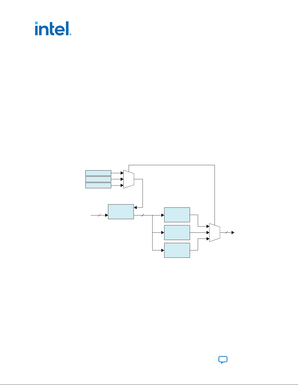
Oversample
(x5)
Oversample
(x4)
Oversample
(x3)
Clock Enable (x3)
Clock Enable (x4)
Clock Enable (x5)
DCFIFO
tx_os
tx_os:
0 (No oversample) - rate ≥ 1 Gbps
1 (Oversample x3) - 350 Mbps ≤ rate < 500 Mbps
2 (Oversample x4) - 300 Mbps ≤ rate < 350 Mbps
3 (Oversample x5) - 250 Mbps ≤ rate < 300 Mbps
or 500 Mbps ≤ rate < 1 Gbps
rd_req
Inner core video out
20 20
20
Core video out
5. HDMI Source
UG-HDMI | 2021.04.01
5.1.16. TX Oversampler
The TX oversampler transmits data by repeating each bit of the input word a given
number of times and constructs the output words.
There are three possible oversampling factors: 3, 4, and 5. The oversampler assumes
that the input word is only valid for the number of clock cycles defined by the
oversampling factor. The oversampler is enabled when the outgoing data stream is
determined to be below the TX transceiver minimum data rate. The oversampler then
reads the DCFIFO once every number of clock cycles determined by the oversampling
factor.
5.1.17. Clock Enable Generator
The clock enable generator is a logic block that generates a clock enable pulse.
This clock enable pulse asserts every number of clock cycles defined by the
oversampling factor and serves as a read request signal to clock the data out from the
DCFIFO.
Figure 28. Oversampling Blocks and Clock Enable Blocks When Support FRL = 0
HDMI Intel® FPGA IP User Guide
70
Send Feedback
Page 71

Oversample
(x2)
DCFIFO
Oversample
(x4)
Clock Enable (x4)
tx_os:
0 - FRL mode
1 - TMDS mode (1 Gbps < rate ≤ 6 Gbps)
2 - TMDS mode (rate ≤ 1 Gbps)
rd_req
(tx_os = = 2)
(tx_os ! = 0)
Enable
Enable
Inner core video out:
FRL mode - 40b
TMDS mode - 20b
(actual data width)
4040
40 40
Core video out
5. HDMI Source
UG-HDMI | 2021.04.01
Figure 29. Oversampling Blocks and Clock Enable Block When Support FRL = 1
5.1.18. I2C Master
When you enable the Include I2C parameter, the HDMI source includes the Intel
FPGA Avalon® I2C core in the design.
The HDMI source uses the I2C core to communicate with the SCDC and EDID from the
HDMI sink through the DDC signals.
5.2. Source Interfaces
Table 35. HDMI Source Interfaces
Interface
Reset Reset –
Clock Clock –
Related Information
Embedded Peripherals IP User Guide
For more information about the Intel FPGA Avalon I2C core.
The table lists the port interfaces of the source.
N is the number of pixels per clock.
Port Type Clock
Domain
Reset –
Port Direction Description
reset
reset_vid
ls_clk
Input Main asynchronous reset
input.
Input Reset input for the video
domain.
Note: This signal is only
available when
Support FRL = 0.
Input Link speed clock input.
The out_c(3), out_r(2),
out_g(1), and
out_b(0)TMDS encoded
data outputs run at this
clock frequency.
ls_clk frequency = data
rate per lane/ 20
This signal connects to the
transceiver output clock
only if TMDS bit rate is
continued...
Send Feedback
HDMI Intel® FPGA IP User Guide
71
Page 72

5. HDMI Source
UG-HDMI | 2021.04.01
Interface Port Type Clock
Domain
Clock –
Port Direction Description
above the minimum
transceiver data rate, which
means no oversampling is
required.
This signal should connect
to a PLL output clock that
supplies the ls_clk
frequency if the TMDS bit
rate is below the minimum
transceiver data rate, which
means oversampling is
required.
In TMDS mode, data rate
per lane is a function of
pixel frequency and color
depth ratio.
Data rate per lane = Pixel
frequency x 10 x Color
depth ratio.
• 8 bpc: Color depth ratio
= 1
• 10 bpc: Color depth ratio
= 1.25
• 12 bpc: Color depth ratio
= 1.5
• 16 bpc: Color depth ratio
= 2
Note: This port is not
available when the
SUPPORT_FRL
parameter is
enabled.
vid_clk
Input Video data clock input.
When Support FRL = 0,
vid_clk frequency = data
rate per lane/transceiver
width/color depth ratio.
• For RGB and YCbCr
4:4:4/4:2:2 transport:
vid_clk frequency =
(data rate per lane/
transceiver width)/color
depth ratio.
• For YCbCr 4:2:0
transport: vid_clk
frequency = ((data rate
per lane/transceiver
width)/color depth
ratio)/2.
•
vid_clk needs to be
synchronous to ls_clk.
continued...
HDMI Intel® FPGA IP User Guide
72
Send Feedback
Page 73

5. HDMI Source
UG-HDMI | 2021.04.01
Interface Port Type Clock
Clock
Clock –
Clock
Domain
–
–
Port Direction Description
When Support FRL =
1,vid_clk frequency =
225 MHz.
•
vid_clk runs at the
maximum frequency
across all resolutions
and FRL rates.
• The video data is
qualified by the
vid_valid signal.
•
vid_clk can be
asynchronous to ls_clk
and frl_clk.
tx_clk
frl_clk
Input Transceiver recovered clock.
Connect this signal to the
output clock of the TX
transceiver output clock.
Input Clock supplied to the FRL
path.
FRL clock frequency = (data
rate * number of lane)s /
(FRL characters per clock *
18).
frl_clk needs to be
synchronous to tx_clk.
Note: The number of lanes
is always 4. For FRL
rates 3, 4, 5, and 6,
all 4 FRL lanes are
used to transmit
data. For FRL rates 1
and 2, only 3 FRL
lanes are used to
transmit data, and
the 4th lane is
unused.
audio_clk
Input Audio clock input. Connect
this signal to ls_clk when
Support FRL = 0 or to
vid_clk when Support
FRL = 1 by qualifying the
slower frequency of
audio_data with
audio_de.
If you connect this signal to
a clock at actual audio
sample frequency, you must
tie audio_de to 1.
For audio channels greater
than 8, do not drive
audio_clk at actual audio
sample clock; instead drive
audio_clk with ls_clk
when Support FRL = 0 or
to vid_clk when Support
FRL = 1, and qualify
audio_data with
audio_de.
continued...
Send Feedback
HDMI Intel® FPGA IP User Guide
73
Page 74
5. HDMI Source
UG-HDMI | 2021.04.01
Interface Port Type Clock
Clock –
Video Data Port Conduit
Conduit
Conduit
Conduit
Conduit
Conduit
Domain
vid_clk vid_data[N*48-1:0]
vid_clk vid_de[N-1:0]
vid_clk vid_hsync[N-1:0]
vid_clk vid_vsync[N-1:0]
vid_clk vid_ready
vid_clk vid_valid
Port Direction Description
Note: Applicable only when
you turn on the
Support auxiliary
and Support audio
parameters.
mgmt_clk
Input Free-running system clock
input (100 MHz). This clock
connects to the I2C master
and HPD debouncing logic.
Note: This signal is not
available if you turn
off the Include I2C
parameter.
Input Video 48-bit pixel data input
port. For N pixels per clock,
this port accepts N 48-bit
pixels per clock.
Input Video data enable input that
indicates active picture
region.
Input Video horizontal sync input.
Input Video vertical sync input.
Output Indicates if the TX core is
ready to process new data.
When vid_ready is
asserted, the TX core is
ready to process new data.
Note: This signal is only
available when
Support FRL = 1.
vid_ready is always high
for 8 bits per component
(BPC). This signal toggles
for different color depths.
•
For 10 bpc, vid_ready
is high for 4 out of 5
clock cycles.
•
For 12 bpc, vid_ready
is high for 2 out of 3
clock cycles.
•
For 16 bpc, vid_ready
is high for 1 out of 2
clock cycles.
Input Indicates if the video data is
valid. When in TMDS mode
and vid_clk is running at
the actual pixel clock, this
signal should always be
asserted.
Note: This signal is only
available when
Support FRL = 1.
When you generate the
video data at a frequency
higher than the actual pixel
clock, use vid_valid to
qualify the validity of the
continued...
HDMI Intel® FPGA IP User Guide
74
Send Feedback
Page 75
5. HDMI Source
UG-HDMI | 2021.04.01
Interface Port Type Clock
Conduit
TMDS/FRL Data
Port
Conduit
Conduit
Conduit
Domain
Port Direction Description
vid_clk vid_overflow
tx_clk/
ls_clk
tx_clk/
ls_clk
tx_clk/
ls_clk
out_b[transceiver
width-1:0]
out_g[transceiver
width-1:0]
out_r[transceiver
width-1:0]
video data. vid_valid and
vid_clk guarantee the
exact pixel clock rate.
Output Indicates if the FIFO
clocking the data from the
video path to the FRL path
is overflowing.
Applicable only for FRL
mode.
Output When in TMDS mode, this
signal is TMDS encoded blue
channel (0) output.
When in FRL mode, this
signal is FRL lane 0.
• When Support FRL = 0,
transceiver width is
configured to 20 bits.
• When Support FRL = 1,
transceiver width is
configured to 40 bits.
Note: For TMDS mode,
only the 20 bits from
the least significant
bits are used. For
FRL mode, all 40 bits
are used.
Output When in TMDS mode, this
signal is TMDS encoded
green channel (1) output.
When in FRL mode, this
signal is FRL lane 1.
• When Support FRL = 0,
transceiver width is
configured to 20 bits.
• When Support FRL = 1,
transceiver width is
configured to 40 bits.
Note: For TMDS mode,
only the 20 bits from
the least significant
bits are used. For
FRL mode, all 40 bits
are used.
Output When in TMDS mode, this
signal is TMDS encoded red
channel (2) output.
When in FRL mode, this
signal is FRL lane 2.
• When Support FRL = 0,
transceiver width is
configured to 20 bits.
• When Support FRL = 1,
transceiver width is
configured to 40 bits.
continued...
Send Feedback
HDMI Intel® FPGA IP User Guide
75
Page 76

5. HDMI Source
UG-HDMI | 2021.04.01
Interface Port Type Clock
Conduit
Conduit
Encoder Control
Port
Conduit
Conduit
Conduit
Conduit
Domain
Port Direction Description
tx_clk/
ls_clk
out_c[transceiver
width-1:0]
ls_clk in_lock
tx_clk/
mode
ls_clk
tx_clk/
TMDS_Bit_clock_Ratio
ls_clk
tx_clk/
Scrambler_Enable
ls_clk
tx_clk/
ctrl[N*6-1:0]
ls_clk
Note: For TMDS mode,
only the 20 bits from
the least significant
bits are used. For
FRL mode, all 40 bits
are used.
Output When in TMDS mode, this
signal is TMDS encoded
clock channel (3) output.
When in FRL mode, this
signal is FRL lane 3.
• When Support FRL = 0,
transceiver width is
configured to 20 bits.
• When Support FRL = 1,
transceiver width is
configured to 40 bits.
Note: For TMDS mode,
only the 20 bits from
the least significant
bits are used. For
FRL mode, all 40 bits
are used.
Input When asserted, the HDMI
TX core begins to operate.
Input Encoding mode input.
• 0: DVI
• 1: HDMI
Input Indicates if TMDS Bit Rate is
greater than 3.4 Gbps in
TMDS mode.
• 0: (TMDS Bit Rate) /
(TMDS Clock Rate) ratio
is 10
• 1 = (TMDS Bit Rate) /
(TMDS Clock Rate) ratio
is 40
Input Enables scrambling.
• 0: Instructs the source
device not to perform
scrambling
• 1: Instructs the source
device to perform
scrambling
Input DVI control side-band
inputs to override the
necessary control and
synchronization data in the
green and red channels.
Bit-Field Name
N*6+5 CTL3
N*6+4 CTL2
N*6+3 CTL1
N*6+2 CTL0
continued...
HDMI Intel® FPGA IP User Guide
76
Send Feedback
Page 77
5. HDMI Source
UG-HDMI | 2021.04.01
Interface Port Type Clock
Link Training
Control Port
Auxiliary Data
Port (Applicable
only when you
enable
Conduit
Conduit
Conduit
Conduit
Domain
Port Direction Description
frl_clk scdc_frl_start
frl_clk scdc_frl_rate[3:0]
frl_clk scdc_frl_pattern[15:0]
aux_clk aux_ready
N*6+1 Reserved (0)
N*6 Reserved (0)
Input • When set to 1, the TX
Input Specifies the FRL rate (link
Input Indicates the link training
core transmits normal
video data.
• When set to 0, the TX
core transmits link
training pattern data.
rate and number of lanes)
that the TX core is running.
• 0: Disable FRL
• 1: Fixed rate link at 3
Gbps per lane on 3 lanes
• 2: Fixed rate link at 6
Gbps per lane on 3 lanes
• 3: Fixed rate link at 6
Gbps per lane on 4 lanes
• 4: Fixed rate link at 8
Gbps per lane on 4 lanes
• 5: Fixed rate link at 10
Gbps per lane on 4 lanes
• 6: Fixed rate link at 12
Gbps per lane on 4 lanes
pattern that each lane on
the TX core is transmitting .
•
scdc_frl_pattern[3:
0]: Link training pattern
for lane 0
•
scdc_frl_pattern[7:
4]: Link training pattern
for lane 1
•
scdc_frl_pattern[11
:8]: Link training
pattern for lane 2
•
scdc_frl_pattern[15
:12]: Link training
pattern for lane 3
• 4’d0: No link training
pattern
• 4’d1: All 1’s pattern
• 4’d2: All 0’s pattern
• 4’d3: Nyquist clock
pattern
• 4’d4: TxFFE Compliance
Test Pattern
• 4’d5: LFSR 0
• 4’d6: LFSR 1
• 4’d7: LFSR 2
• 4’d8: LFSR 3
Output Auxiliary data channel ready
output. Asserted high to
indicate that the core is
ready to accept data.
continued...
Send Feedback
HDMI Intel® FPGA IP User Guide
77
Page 78
5. HDMI Source
UG-HDMI | 2021.04.01
Interface Port Type Clock
Support
auxiliary
parameter)
Auxiliary
Control Port
(Applicable only
when you
enable
Support
auxiliary
parameter)
Audio Port
(Applicable only
when you
enable
Support
auxiliary and
Support audio
parameters)
(6)
(6)
Conduit
Conduit
Conduit
Conduit
Conduit
Conduit
Conduit
Conduit
Conduit
Conduit
(6)
Conduit
Conduit
Conduit
Domain
aux_clk aux_valid
aux_clk aux_data[71:0]
aux_clk aux_sop
aux_clk aux_eop
aux_clk gcp[5:0]
aux_clk info_avi[122:0] (Support
aux_clk info_vsi[61:0]
audio_clk audio_CTS[19:0]
audio_clk audio_N[19:0]
audio_clk audio_data[255:0]
audio_clk audio_de
audio_clk audio_mute
aux_clk audio_info_ai[48:0]
Port Direction Description
FRL = 1)
info_avi[112:0] (Support
FRL = 0)
Input Auxiliary data channel valid
input to qualify the data.
Input Auxiliary data channel data
input.
For information about the
bit-fields, refer to Figure 21
on page 47.
Input Auxiliary data channel start-
of-packet input to mark the
beginning of a packet.
Input Auxiliary data channel end-
of-packet input to mark the
end of a packet.
Input General Control Packet user
input.
For information about the
bit-fields, refer to Table 22
on page 50.
Input Auxiliary Video Information
InfoFrame user input.
For information about the
bit-fields, refer to Table 23
on page 50.
Input Vendor Specific Information
InfoFrame user input.
For information about the
bit-fields, refer to Table 25
on page 52.
Input Audio CTS value input.
Input Audio N value input.
Input Audio data input.
For audio channel values,
refer to Table 38 on page
83.
Input Audio data valid input.
Input Audio mute input. No audio
will be transmitted when
this signal is asserted high.
Input Audio InfoFrame user input.
Note: If you provide
audio_info_ai[48:0]
using audio_clk with
actual audio sample
frequency, you must
synchronize the clock
domain to ls_clk
externally.
continued...
(6)
aux_clk = ls_clk (Support FRL = 0)
aux_clk = vid_clk (Support FRL = 1)
HDMI Intel® FPGA IP User Guide
78
Send Feedback
Page 79
5. HDMI Source
UG-HDMI | 2021.04.01
Interface Port Type Clock
Conduit
PHY Interface
Control Port
Conduit
Conduit
audio_clk audio_format[4:0]
Domain
Port Direction Description
aux_clk audio_metadata[165:0]
tx_clk/
os[1:0]
ls_clk
For information about the
bit-fields, refer to Table 27
on page 56.
Input Carries additional
information related to 3D
audio and MST audio.
Note: If you provide
audio_metadata[165:0]
using audio_clk with
actual audio sample
frequency, you must
synchronize the clock
domain to ls_clk
externally.
For information about the
bit-fields, refer to Table 28
on page 57, Table 29 on
page 57, and Table 30 on
page 57.
Input Controls the transmission of
the 3D audio and indicates
the audio format to be
transmitted.
Bit-Field Description
4 Assert to
indicate the
first 8 channels
of each 3D
audio sample.
3:0 For information
about the bit-
fields, refer to
Table 26 on
page 54.
Input Oversampling control signal
to control the oversampling
factor.
Support FRL = 1
• 0: No oversample. Send
this when you are
transmitting FRL.
• 1: 2x oversampling:
Send this when you are
transmitting TMDS rate
between 1 Gb/s < rate ≤
6 Gb/s
• 2: 8x oversampling:
Send this when you are
transmitting TMDS rate
≤ 1 Gb/s
Support FRL = 0
continued...
Send Feedback
HDMI Intel® FPGA IP User Guide
79
Page 80

5. HDMI Source
UG-HDMI | 2021.04.01
Interface Port Type Clock
Hot Plug Detect Conduit –
I2C Master
Interface Port
Conduit –
Conduit –
Avalon
MM
Avalon
MM
Avalon
MM
Avalon
MM
Avalon
MM
Domain
mgmt_clk i2c_master_address[3:0]
mgmt_clk i2c_master_write
mgmt_clk i2c_master_read
mgmt_clk i2c_master_writedata[31
mgmt_clk i2c_master_readdata[31:
Port Direction Description
• 0: No oversample. Send
this when you are
transmitting TMDS rate
≥ 1 Gb/s.
• 1: 3x oversampling:
Send this when you are
transmitting data rate
between 350 Mb/s ≤
rate < 500 Gb/s
• 2: 4x oversampling:
Send this when you are
transmitting data rate
between 300 Mb/s ≤
rate < 350 Gb/s
• 3: 5x oversampling:
Send this when you are
transmitting data rate
between 250 Mb/s ≤
rate < 300 Gb/s or data
rate between 500 Mb/s
≤ rate < 1 Gb/s
tx_hpd
–
tx_hpd_req
Input Detects the Hot Plug Detect
(HPD) status. This signal
should be driven with the
same signal to the HPD pin
on the HDMI connector.
Output The core asserts the
tx_hpd_req signal if the
tx_hpd signal holds for
more than 100 milliseconds,
indicating a valid HPD. The
tx_hpd_req signal
deasserts if the tx_hpd
signal is not detected.
i2c_scl
i2c_sda
:0]
0]
Inout The SCL signal from the I2C
Inout The SDA signal from the I2C
Input The Avalon memory-
Input
Input
Input
Output
bus on the HDMI connector.
Note: This signal is not
available if you turn
off the Include I2C
parameter.
bus on the HDMI connector.
Note: This signal is not
available if you turn
off the Include I2C
parameter.
mapped interface signals to
the I2C master. Connect
these signals to an Avalon
memory-mapped slave such
as the Nios processor to
perform read and write
operations to the EDID
block.
Note: These signals are
not available if you
turn off the Include
I2C parameter.
continued...
HDMI Intel® FPGA IP User Guide
80
Send Feedback
Page 81
5. HDMI Source
UG-HDMI | 2021.04.01
Interface Port Type Clock
HDCP Port
(Applicable only
when you
enable
Support HDCP
2.3 or Support
HDCP 1.4
parameters)
Reset –
Clock –
Avalon-
MM
Conduit
(Key)
Conduit
crypto_cl
Domain
Port Direction Description
hdcp_reset
csr_clk
–
crypto_clk
csr_clk csr_addr[7:0]
csr_wr
csr_rd
csr_wrdata[31:0]
csr_rddata[31:0]
kmem_wait
k
kmem_addr[3:0] (HDCP 2.3)
kmem_addr[9:4] (HDCP 1.4)
kmem_q[31:0] (HDCP 2.3)
kmem_q[87:32] (HDCP 1.4)
ls_clk hdcp1_enabled
Input Main asynchronous reset.
Input HDCP clock for control and
Input HDCP 2.3 clock for
Input The Avalon-MM slave port
Input
Input
Input
Output
Input Always keep this signal
Output Key read address bus.
Input 32-bit (HDCP 2.3) or 56-bit
Output This signal is asserted by
status registers.
Typically, shares the Nios II
processor clock (100 MHz).
authentication and
cryptographic layer.
You can use any clock with
a frequency of up to 200
MHz.
Not applicable for HDCP 1.4.
Note: The clock frequency
determines the
authentication
latency.
that provides access to
internal control and status
register, mainly for
authentication messages
transfer. This interface is
expected to operate at Nios
II processor clock domain.
Because of the extremely
large bit portion of
message, the IP transfers
the message in burst mode
with full handshaking
mechanism.
Write transfers always have
a wait time of 0 cycle while
read transfers have a wait
time of 1 cycle.
The addressing should be
accessed as word
addressing in the Platform
Designer flow. For example,
addressing of 4 in the Nios
II software selects the
address of 1 in the slave.
asserted until the key is
ready to be read.
[3:2] = Reserved.
(HDCP 1.4) data for read
transfers.
Read transfer always have a
wait time of 1 cycle.
the IP if the outgoing video
and auxiliary data are HDCP
1.4 encrypted.
continued...
Send Feedback
HDMI Intel® FPGA IP User Guide
81
Page 82

5. HDMI Source
UG-HDMI | 2021.04.01
Interface Port Type Clock
Domain
csr_clk hdcp1_disable
Port Direction Description
hdcp2_enabled
hdcp2_disable
Output This signal is asserted by
the IP if the outgoing video
and auxiliary data are HDCP
2.3 encrypted.
Input Assert this signal to disable
the HDCP 1.4 IP.
Note: You must reset the
Input Assert this signal to disable
the HDCP 2.3 IP.
Note: You must reset the
HDCP IP
(hdcp_reset) after
toggling this signal.
You must not call the
software API
hdcp_main() while
this signal is
asserted. You must
call the software API
hdcp_unauth()
after deasserting
this signal.
HDCP IP
(hdcp_reset) after
toggling this signal.
You must not call the
software API
hdcp_main() while
this signal is
asserted. You must
call the software API
hdcp_unauth()
after deasserting
this signal.
Table 36. out_c Value for TMDS Bit Rate Less than 3.4 Gbps
TMDS_Bit_clock_Ratio = 0 and out_c value is constant.
N
1 10'b1111100000
2 20'b1111100000_1111100000
4 40'b1111100000_1111100000 1111100000_1111100000
out_c Value
Table 37. out_c Value for TMDS Bit Rate Greater than 3.4 Gbps in TMDS Mode
TMDS_Bit_clock_Ratio = 1 and out_c value is repeated indefinitely.
N
t t+1 t+2 t+3
1 10’h000 10’h000 10’h3ff 10’h3ff
2 20’h00000 20’hfffff 20'h00000 20’hfffff
4 40’hfffff 00000 40’hfffff 00000 40’hfffff 00000 40’hfffff 00000
HDMI Intel® FPGA IP User Guide
82
out_c Value
Send Feedback
Page 83

vid_clk frl_clk ls_clk tx_clk
tx_clk[1]
tx_clk[3]
tx_clk[0]
tx_clk[2]
HDMI Source Core
wrclk rdclk
DCFIFO
HSSI[0]
DCFIFO
Oversampling
Logic
Oversampling
Logic
HSSI[1]
DCFIFO
Oversampling
Logic
HSSI[2]
1
0
1
0
1
0
1
0
DCFIFO
Oversampling
Logic
HSSI[3]
wrclk rdclk
wrclk rdclk
wrclk rdclk
5. HDMI Source
UG-HDMI | 2021.04.01
Table 38. Audio Channels
Bit-Field Audio Channel
255:224 8 or 16 or 24 or 32 Stream 4 right channel
223:192 7 or 15 or 23 or 31 Stream 4 left channel
191:160 6 or 14 or 22 or 30 Stream 3 right channel
159:128 5 or 13 or 21 or 29 Stream 3 left channel
127:96 4 or 12 or 20 or 28 Stream 2 right channel
95:64 3 or 11 or 19 or 27 Stream 2 left channel
63:32 2 or 10 or 18 or 26 Stream 1 right channel
31:0 1 or 9 or 17 or 25 Stream 1 left channel
5.3. Source Clock Tree
The source uses various clocks.
Figure 30. Source Clock Tree
The figure shows how the different clocks connect in the source core.
LPCM and 3D Audio (LPCM) MST Audio (LPCM)
For HDMI source, you must instantiate 4 transceiver channels: 3 channels to transmit
data and 1 channel to transmit clock information.
Send Feedback
HDMI Intel® FPGA IP User Guide
83
Page 84

5. HDMI Source
UG-HDMI | 2021.04.01
The core uses a general purpose phase-locked loop (GPLL), that is referenced by a
transceiver output clock, to generate the link speed clock (ls_clk), FRL clock
(frl_clk), and video clock (vid_clk). The transceiver PLL has two reference clocks:
• Reference clock 0 which supplied with arbitrary TMDS clock frequency
• Reference clock 1 supplied with free running 100 MHz clock
The link speed clock (ls_clk) is not required when you turn on the Support FRL
parameter, and the FRL clock (frl_clk) is not required when you turn off the
Support FRL parameter. When you turn on the Support FRL parameter, you can fix
the video clock (vid_clk) at a static frequency of 225 MHz.
The transceiver PLL switches between reference clock 0 and reference clock 1 in TMDS
and FRL modes.
The video data clocks into the core at vid_clk, the TMDS or FRL data clocks out from
the core at tx_clk/ls_clk, and the FRL data clocks with frl_clk.
If an application requires low TMDS Bit Rate (below the transceiver minimum data rate
requirement), then the application needs a user logic consisting of a DCFIFO and
oversampling logic.
•
The DCFIFO synchronizes the TMDS data from ls_clk to a faster transceiver
output clock (tx_clk[0]).
• The oversampling logic repeats each bit of the TMDS data a given number of
times.
• When you enable the oversampling control bit, the transceiver transmits the TMDS
data between the HDMI source core and the oversampling logic.
•
You can use tx_clk[0] across four channels if the transceiver is in bonding
mode.
If an application does not require low TMDS Bit Rate, you can connect the core output
directly to the transceiver with tx_clk[0] driving the core ls_clk. You do not
require the GPLL to generate CLK1 (ls_clk).
Related Information
• HDMI Hardware Design Examples for Arria V and Stratix V Devices on page 22
• HDMI Hardware Design Examples for Intel Arria 10, Intel Cyclone 10 GX, and Intel
Stratix 10 Devices on page 21
5.4. Link Training Procedure
The HDMI TX core does not handle the link training process.
Instead, the Nios II software manages the link training process, which is
demonstrated in the Intel Arria 10 FRL design example.
Implement the link training external to the HDMI TX core according to the TX link
training flow diagram shown below. The HDMI TX core generates different link training
patterns on each lane based on your input through the scdc_frl_pattern port
when scdc_frl_start is deasserted. When scdc_frl_start is asserted, the
source core generates normal video.
HDMI Intel® FPGA IP User Guide
84
Send Feedback
Page 85

No
No
Yes
Yes
Yes
Yes
Yes
Yes
Yes
No
No
No
No
No
No
No
Check flt_ready
Set the frl rate
LTS:0
LTS:1
LTS:L
Set frl rate = 0
If FLT_Update == 1?
Clear FLT_Update
LTS:2
LTS:3
FLT_update == 1?
LTP_chx == 0?
LTP_chx == 0xF?
FRL rate == 0?
Indicate link
training failed
LTS:4
Lower FRL rate
Set new FRL rate
Wait for TX transceiver to be ready
Clear FLT Update
Clear FLT update
Set LTP to 0x2 to stop
data transmission
Set frl_start to 0
Clear FRL start
Set frl_start to 1 to
send normal video
FLT_start == 1?
LTS:P
Clear
FLT_UPDATE
Write LTP
TX Transceiver is ready?
Check the sink SCDC:
MAX_FRL_RATE >1 AND
SCDC_present == 1 AND
SCDC_SINK_VERSION !=0
If SCDC_Present == 1?
FLT_update == 1?
5. HDMI Source
UG-HDMI | 2021.04.01
Figure 31. Source Link Training Flow Diagram
5.5. FRL Clocking Scheme
The HDMI 2.1 design is not limited to run at the actual pixel clock, but the data can be
processed at a faster clock rate.
The vid_valid signal at the HDMI TX core qualifies the validity of the data for every
Send Feedback
clock cycle. Due to the timing consideration on maximum FRL data rate, the
transceiver width is set to 40 bits.
HDMI Intel® FPGA IP User Guide
85
Page 86
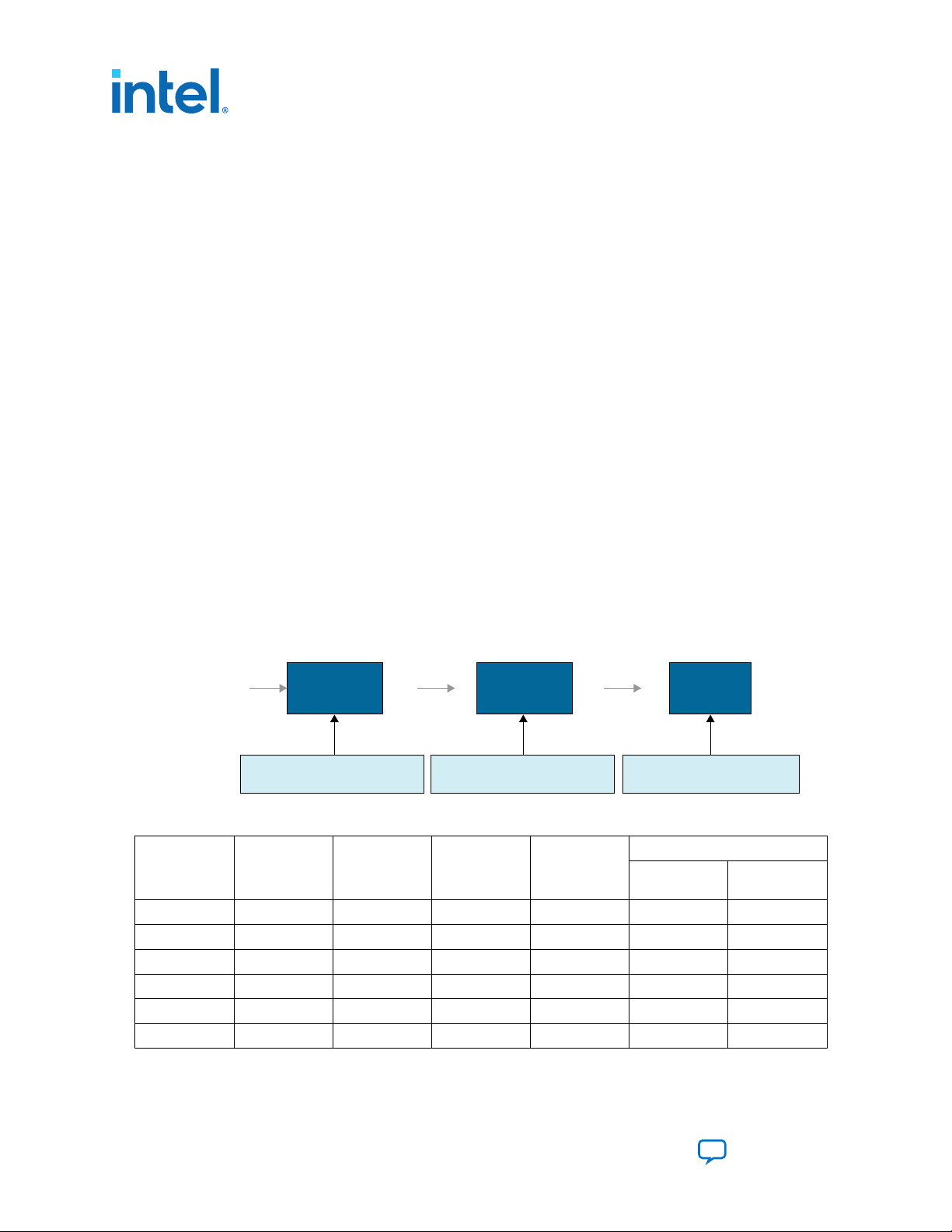
VID
Pixels per clock*24 bits width
Number of FRL characters per clock*18 bits width
No of lanes*Transceiver width
FRL LS
vid_clk = (Data rate per lane*number of lanes/
(Pixels per clock*24)
frl_clk = (Data rate per lane*4)/
(Number of FRL characters per clock*18)
Is_clk = (Data rate per lane*number of lanes)/
(Number of lanes*transceiver witdh)
5. HDMI Source
UG-HDMI | 2021.04.01
In the FRL clock domain, the TX core always processes the data in multiple of 18 bits
because of the 16B/18B encoder in the FRL path. The FRL modules can process N (FRL
char per clock) FRL characters in parallel. However, the FRL modules always process 8
or 16 FRL characters per clock due to timing considerations.
Hence, frl_clk frequency = (data rate per lane * number of lanes) / (FRL char per
clock*18)
The number of lanes is always four.
• For FRL rates 3–6, all four lanes carry the FRL characters.
• For FRL rates 1 and 2, only 3 lanes carry the FRL characters and 1 lane is unused.
Similarly, in the vid_clk domain, the TX core processes data in multiples of pixels
(24 bits) in parallel. You can configure the number of pixels to be processed in parallel
through the pixels per clock GUI parameter. However, due to timing consideration and
backward compatibility, the IP sets the pixels per clock to 2 when you turn off
Support FRL, and to 8 when you turn on Support FRL. Because the actual pixel
clock may differ based on different resolutions, you can configure vid_clk to the
maximum frequency per the specified link rate according to the following calculation:
vid_clk frequency = (data rate per lane * number of lanes) / (pixels per clock * 24)
Note:
Because vid_clk can be asynchronous to frl_clk and ls_clk, you can set the
vid_clk frequency according to the maximum pixel frequency of the highest allowed
resolution divided by 8, to simplify the clocking scheme. Intel recommends that you
set the vid_clk frequency to 225 MHz, as demonstrated in the HDMI Intel FPGA IP
FRL design example.
Table 39. Clock Frequencies for FRL Mode at Different Link Rates
FRL Rate TX PLL Refclk
Frequency
(MHz)
1 100.00 75.00 75.00 62.50 41.665 83.33
2 100.00 150.00 150.00 125.00 83.33 166.67
3 100.00 150.00 150.00 125.00 83.33 166.67
4 100.00 200.00 200.00 166.67 111.11 222.22
5 100.00 250.00 250.00 208.33 138.89 277.78
6 100.00 300.00 300.00 250.00 166.67 333.33
TX Clkout
Frequency
(MHz)
ls_clk
Frequency
(MHz)
Maximum
vid_clk
Frequency
(MHz)
frl_clk Frequency (MHz)
Intel Arria 10
Devices
Intel Stratix
10 Devices
HDMI Intel® FPGA IP User Guide
86
Send Feedback
Page 87

FIFO
empty
frl_clk Domain
(16 FRL characters
per clock)
200 MHz166.67 MHz
vid_clk Domain
(8 pixels in parallel)
vid_valid
111 MHz
148.5 MHz
Test Pattern Generator
(8Kp30 RGB)
(8 pixels in parallel)
ls_clk Domain
(40-bit transceiver width)
vid_clk Domain
(8 pixels in parallel)
frl_clk Domain
(16 FRL characters
per clock)
200 MHz111 MHz
148.5 MHz
1’b1
vid_valid
Test Pattern Generator
(8Kp30 RGB)
(8 pixels in parallel)
ls_clk Domain
(40-bit transceiver width)
5. HDMI Source
UG-HDMI | 2021.04.01
Table 40. Clock Frequencies for TMDS Mode at Different Link Rates
TMDS_BIT_
CLOCK_RAT
IO
TMDS_BIT_
CLOCK_RAT
IO = 0
TMDS_BIT_
CLOCK_RAT
IO = 0
TMDS_BIT_
CLOCK_RAT
IO = 1
TMDS Refclk
(MHz)
Min Max Min Max Min Max Min Max Min Max
25.00 100.00 25.00 100.00 100.00 400.00 12.50 50.00 3.13 12.5
100.00 340.00 100.00 340.00 50.00 170.00 50.00 170.00 12.50 42.50
85.00 150.00 85.00 150.00 170.00 300.00 170.00 300.00 42.50 75.00
5.6. Valid Video Data
You can generate video data using a different clock, other than vid_clk used in the
HDMI TX core.
To generate video data, you need to use the actual pixel clock but vid_clk runs at a
faster frequency. You can use a FIFO buffer to clock the data between the actual pixel
clock and vid_clk while generating the valid video data (vid_valid) based on the
inverted empty FIFO buffer.
For example, when operating at 8 Gbps link rate while transmitting 7680 x 4320p30
RGB resolution, a test pattern generator configured at 8 pixels in parallel runs at
148.5 MHz with the vid_clk domain of the HDMI TX core operating at 166.67 MHz.
Like this case, not every vid_clk has valid video data. You can handle similar cases
using the inverted empty signal of the DCFIFO.
TX PLL Refclk
Frequency (MHz)
TX Clkout
Frequency (MHz)
ls_clk Frequency
(MHz)
vid_clk Frequency
(MHz)
When vid_clk runs at a faster frequency than the actual pixel clock frequency/pixels
per clock, toggle vid_valid to qualify the video data.
Figure 32. Video Clock Running at Faster Frequency
When vid_clk runs at the actual pixel clock frequency/pixels per clock, vid_valid
should always remain asserted.
Figure 33. Video Clock Running at Actual Frequency
Send Feedback
HDMI Intel® FPGA IP User Guide
87
Page 88

Programmable Oscillator
(TMDS clock frequency)
data
vid_clk
Is_clk tx_clk
TX PLL refclk
IOPLL
data
serial data
data
DCFIFOHDMI TX Core
TX Transceiver
(TX PLL + PMA + PCS)
ls_clk
vid_clk
ls_clk
vid_clk
5. HDMI Source
UG-HDMI | 2021.04.01
5.7. Source Deep Color Implementation When Support FRL = 0
When Support FRL = 0, you need to provide the ls_clk and vid_clk clocks
according to the color depth ratio. The HDMI TX core carries 24, 30, 36 or 48 bits per
pixel (bpp).
ls_clk frequency = data rate per lane / effective transceiver width = data rate per
lane / 20
Note: The effective transceiver width in TMDS mode is also 20.
vid_clk frequency = (data rate per lane / effective transceiver width) / color depth
ratio
Table 41. Color Depth Ratio for Bits per Color
Bits per Color Color Depth Ratio
8 1.6
10 1.25
12 1.5
16 2.0
Figure 34. Deep Color Implementation When Support FRL = 0
Figure 35. 10 Bits per Component (30 Bits per Pixel)
When operating in 10 bits per component, the vid_clk frequency to ls_clk frequency ratio is 4:5. For every
5 ls_clk cycles, there should be 4 vid_clk cycles.
Figure 36. 12 Bits per Component (36 Bits per Pixel)
When operating in 12 bits per component, the vid_clk frequency to ls_clk frequency ratio is 2:3. For every
3 ls_clk cycles, there should be 2 vid_clk cycles.
HDMI Intel® FPGA IP User Guide
88
Send Feedback
Page 89
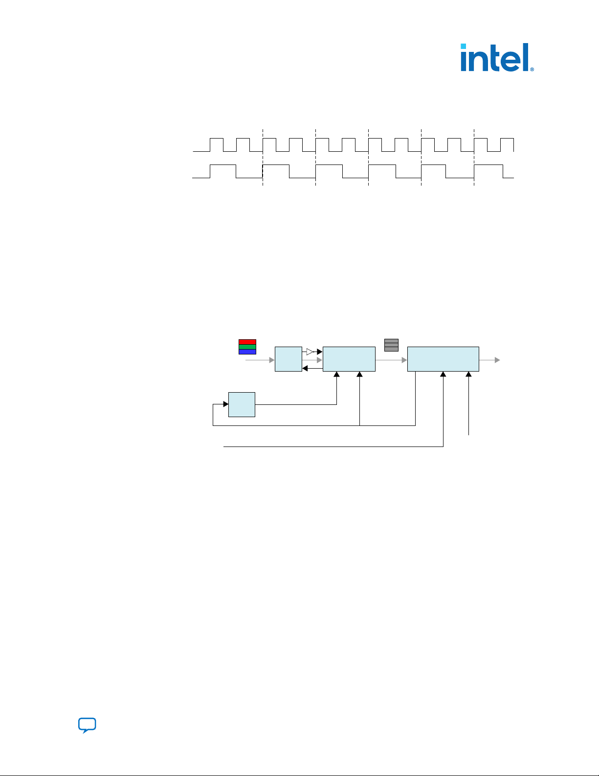
ls_clk
vid_clk
Programmable Oscillator
(TMDS clock frequency)
vid_clk
tx_clk
IOPLL
data Showahead
Mode
data
serial data
HDMI TX Core
vid_valid
vid_ready
TX Transceiver
(TX PLL + PMA + PCS)
DCFIFO
empty
rden
TX PLL
refclk 0
TX PLL
refclk 1
100 MHz
5. HDMI Source
UG-HDMI | 2021.04.01
Figure 37. 16 Bits per Component (48 Bits per Pixel)
When operating in 16 bits per component, the vid_clk frequency to ls_clk frequency ratio is 1:2. For every
1 ls_clk cycle, there should be 2 vid_clk cycles.
5.8. Source Deep Color Implementation When Support FRL = 1
When Support FRL = 1, you can drive vid_clk regardless of the color depth ratio.
• In TMDS mode:
vid_clk frequency = (data rate per lane / effective transceiver width) / 4
• In FRL mode:
vid_clk frequency = 225 MHz
Figure 38. Deep Color Implementation When Support FRL = 1
Send Feedback
The vid_ready signal toggles to indicate if the HDMI TX core is ready to take in new
video data. In this case, you can use a DCFIFO IP to store the video data when the
HDMI TX core is not ready (vid_ready is low). You need to configure the DCFIFO IP
to show-ahead mode, with the vid_ready signal connected to the rden signal of
the DCFIFO IP.
When vid_ready is low, the DCFIFO IP holds the video data immediately. When
vid_ready goes high, the HDMI TX core processes the stored data without losing any
valid video data.
The inverted empty signal from the DCFIFO IP sets the vid_valid signal to the HDMI
TX core.
HDMI Intel® FPGA IP User Guide
89
Page 90
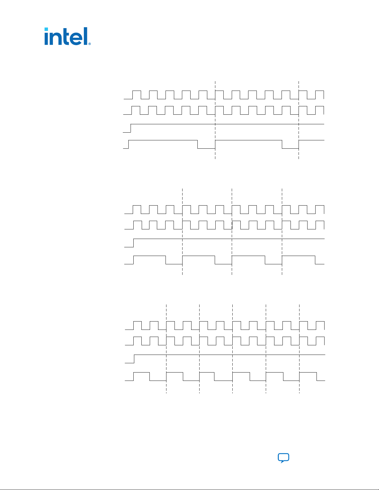
Figure 39. 10 Bits per Component (30 Bits per Pixel)
tx_clk
vid_clk
vid_valid
vid_ready
tx_clk
vid_clk
vid_valid
vid_ready
tx_clk
vid_clk
vid_valid
vid_ready
When operating in 10 bits per component, the vid_ready signal is high for 4 out of 5 clock cycles. For every 5
clock cycles, the HDMI TX core processes 4 video data with 10 bits per component.
Figure 40. 12 Bits per Component (36 Bits per Pixel)
When operating in 12 bits per component, the vid_ready signal is high for 2 out of 3 clock cycles. For every 3
clock cycles, the HDMI TX core processes 2 video data with 12 bits per component.
5. HDMI Source
UG-HDMI | 2021.04.01
Figure 41. 16 Bits per Component (48 Bits per Pixel)
When operating in 16 bits per component, the vid_ready signal is high for 1 out of 2 clock cycles. For every 2
clock cycles, the HDMI TX core processes 1 video data with 16 bits per component.
HDMI Intel® FPGA IP User Guide
90
Send Feedback
Page 91
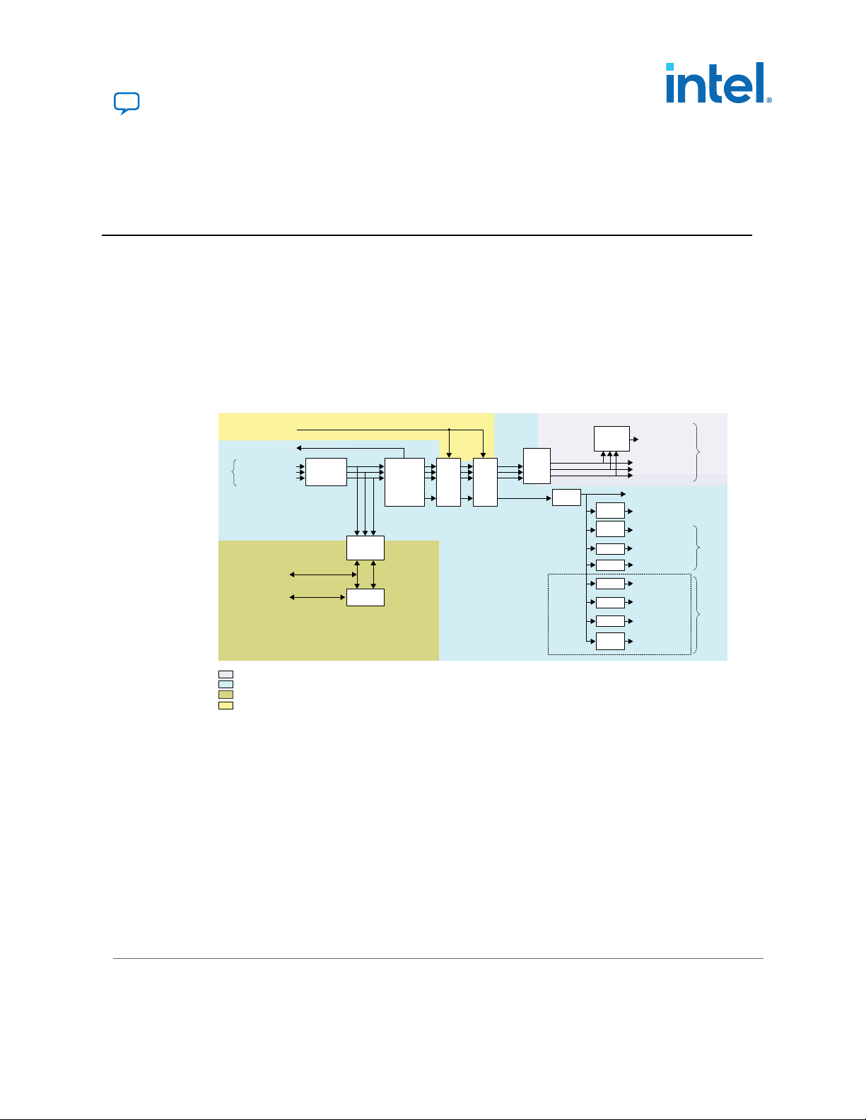
Video Lock
Video
Data Port
Character
Error
Detection
SCDC
Register
Video Data (Red Channel)
Video Data (Green Channel)
Video Data (Blue Channel)
Auxiliary Data Port
Capture AM
Auxiliary Memory Interface
General Control Packet
AVI InfoFrame
Audio InfoFrame
Audio Clock Regeneration
(N, CTS)
Audio Metadata
Audio Sample
Audio Decoder
Vendor Specific InfoFrame
Descrambler,
TMDS and TERC4
Decoder
World Alignment
and Channel
Deskew
Video Timing
Geometry
Measurement
Memory
Map
Capture
GCP
Capture AVI
Capture AI
Capture ACR
Audio
Depacketizer
Capture VSI
Auxiliary
Decoder
AUX
AUXAUX
vid_clk domain
ls_clk domain
i2c_clk domain
HDCP clocks domain
HDCP 1.4
RX
HDCP 2.3
RX
Video
Resampler
Auxiliary
Status Port
Audio
Port
TMDS Data (Red Channel)
TMDS Data (Green Channel)
TMDS Data (Blue Channel)
TMDS
Data
Port
SCDC Control and
Status Port
Avalon-MM SCDC
Management
Interface
HDCP Port
Decoder Status Port
UG-HDMI | 2021.04.01
Send Feedback
6. HDMI Sink
6.1. Sink Functional Description
The HDMI sink core provides direct connection to the Transceiver Native PHY through
a 20-bit or 40-bit parallel data path. The clock domains for the auxiliary and audio
ports, and the internal modules are different for FRL path and non-FRL path.
Figure 42. HDMI Sink Signal Flow Diagram for TMDS (Support FRL = 0) Design
The figure below shows the flow of the HDMI sink signals. The figure shows the various clocking domains used
within the core.
The sink core provides three (TMDS mode) or four (FRL mode) 20-bit or 40-bit data
input paths corresponding to the color channels. The sink core clocks the three 20-bit
or 40-bit channels from the transceiver outputs using the respective transceiver clock
outputs.
• Blue channel: 0
• Green channel: 1
• Red channel: 2
Intel Corporation. All rights reserved. Agilex, Altera, Arria, Cyclone, eASIC, Intel, the Intel logo, MAX, Nios,
• Clock channel: 3
Quartus and Stratix words and logos are trademarks of Intel Corporation or its subsidiaries in the U.S. and/or
other countries. Intel warrants performance of its FPGA and semiconductor products to current specifications in
accordance with Intel's standard warranty, but reserves the right to make changes to any products and services
at any time without notice. Intel assumes no responsibility or liability arising out of the application or use of any
information, product, or service described herein except as expressly agreed to in writing by Intel. Intel
customers are advised to obtain the latest version of device specifications before relying on any published
information and before placing orders for products or services.
*Other names and brands may be claimed as the property of others.
ISO
9001:2015
Registered
Page 92

Figure 43. HDMI Sink Signal Flow Diagram for Support FRL = 1 Design
vid_clk domain (pixels per clock)
transceiver recovered clock domain (transceiver width per lane)
i2c_clk domain
HDCP clocks domain
frl_clk domain (FRL characters per clock)
Video Lock
AUX
AUX
AUX
AUX
Character
Error
Detection
Video Data (Red Channel)
Video Data (Green Channel)
Video Data (Blue Channel)
Auxiliary Data Port
Auxiliary Memory Interface
General Control Packet
AVI InfoFrame
Audio InfoFrame
Audio Clock Regeneration
(N, CTS)
Audio Metadata
Audio Sample
Vendor Specific InfoFrame
FRL
Descrambler
and Decoder
FRL Data (Channel 3)
FRL Data (Channel 2)
FRL Data (Channel 1)
FRL Data (Channel 0)
TMDS Data (Red Channel)
TMDS Data (Green Channel)
TMDS Data (Blue Channel)
SCDC Control and Status Port
Link Training Control and Status Port
SCDC
Register
FRL
Resampler
World Alignment
and Channel
Deskew
Video Timing
Geometry
Measurement
Memory
Map
Capture
GCP
Capture AVI
Capture AI
Capture ACR
Audio
Depacketizer
Capture VSI
Capture AM
Video
Resampler
FRL Word
Alignment and
Channel Deskew
FRL Character
Block and Super
Block Demapper
DCFIFO
Auxiliary
Decoder
FRL
Depacketizer
TMDS/FRL
Data Port
Video
Data Port
Auxiliary
Status Port
Audio Port
Audio Decoder
Avalon Memory-Mapped SCDC Management Interface
Link Training
State Machine
Decoder Status Port
AUX
AUX
Descrambler,
TMDS and
TERC4 Decoder
HDCP 1.4
RX
HDCP 2.3
RX
HDCP Port
For Support FRL = 1 design, in TMDS mode, a DCFIFO clocks the HDMI data stream
from the scrambler, TMDS/TERC4 decoder in the transceiver recovered clock domain
to vid_clk domain. All the blocks in the FRL path and video data operate in vid_clk
domain.
6. HDMI Sink
UG-HDMI | 2021.04.01
When operating TMDS mode, the sink core accepts three 20-bit data input paths
corresponding to each color channel. The sink core clocks the three 20-bit channels
from the transceiver outputs using respective transceiver clock outputs.
• Blue channel: Data channel 0
• Green channel: Data channel 1
• Red channel: Data channel 2
Note: Data channel 3 is unused in TMDS mode. Data channels 0–3 are always 40-bit wide,
but only 20 bits from the least significant bits are used in TMDS mode.
When operating in FRL mode, the sink core accepts four 40-bit data input paths
corresponding to each FRL channel. The sink core clocks the four 40-bit channels from
the transceiver outputs using respective transceiver clock outputs.
• FRL channel 0: Data channel 0
• FRL channel 1: Data channel 1
• FRL channel 2: Data channel 2
• FRL channel 3: Data channel 3
The sink core provides N*48 bit video data per channel for each color channel, where
N is number of pixels per clock.
6.1.1. Sink Word Alignment and Channel Deskew
HDMI Intel® FPGA IP User Guide
The input stage of the sink is responsible for synchronizing the incoming parallel data
channels correctly. The synchronization is split to two stages: word alignment and
channel deskew.
92
Send Feedback
Page 93
6. HDMI Sink
UG-HDMI | 2021.04.01
Table 42. Synchronization Stages
Stage Description
Word Alignment TMDS Mode • Correctly aligns the incoming parallel data to word boundaries using
FRL Mode • Correctly aligns the incoming parallel data to word boundaries using
Channel Deskew • When the data channels are aligned, the core then attempts to deskew each channel.
• The sink core deskews at the rising edge of the marker insertion.
• For every correct deskewed lane, the marker insertion will appear in all three TMDS encoded
streams.
• The sink core deskews using three dual-clock FIFOs.
• The dual-clock FIFOs also synchronize all three data streams to the blue channel clock to be
used later throughout the decoder core.
bit-slip and pattern-matching technique.
• TMDS encoding does not guarantee unique control codes, but the
core can still use the sequence of continuous symbols found in data
and video preambles to align.
• The alignment algorithm searches for 8 consecutive 0×54 or 0×ab
corresponding to the data and video preambles.
Note: The preambles are also present in Digital Video Interface
(DVI) coding.
• The alignment logic asserts a marker indicator when the 8
consecutive signals are detected. Similarly, the logic infers alignment
loss when 8K symbol clocks elapse without a single marker assertion.
Note: If you are using Intel Arria 10 or Intel Cyclone 10 GX devices,
soft word alignment logic in the HDMI RX core is disabled for
HDMI 2.0 resolution (data rate >3.4 Gbps). Hard transceiver
PCS word alignment is used with some control logic to
achieve faster word alignment with more optimized resource
utilization. Refer to the design example user guides for more
information.
Note: If you are using Intel Stratix 10 devices, the HDMI RX core
uses a new word alignment algorithm logic to achieve fast
word alignment time for HDMI 2.0 resolution (data rate
>3.4Gbps).
bit-slip and pattern-matching technique.
• FRL encoding uses unique Scrambler Reset (SR) and Start of Super
Block (SSB) characters to achieve alignment.
• The FRL encoding loses lock when it does not receive the SR or SSB
on one lane while other lane receive SR or SSB continuously for
seven times.
Send Feedback
HDMI Intel® FPGA IP User Guide
93
Page 94
Figure 44. Channel Deskew DCFIFO Arrangement
Alignment
Detection
DCFIFO
Channel 0
rdreq
wrclk rdclk
DCFIFO
Channel 1
rdreq
wrclk rdclk
ls_clk[0]
ls_clk[0]
ls_clk[1]
ls_clk[0]
marker_in[0]
data_in[0] data[0]
marker_in[1]
data_in[1] data[1]
DCFIFO
Channel 2
rdreq
wrclk rdclk
ls_clk[0]
ls_clk[2]
marker_in[2]
data_in[2] data[2]
DCFIFO
Channel 3*
rdreq
wrclk rdclk
ls_clk[0]
ls_clk[3]
marker_in[3]
data_in[3] data[3]
marker[2]
marker[1]
marker[0]
marker[3]
* Channel 3 is applicable only for FRL mode.
The figure below shows the signal flow diagram of the deskew logic.
6. HDMI Sink
UG-HDMI | 2021.04.01
HDMI Intel® FPGA IP User Guide
94
Send Feedback
Page 95
H-SYNC
V-SYNC
de
1
vid_clk
DCFIFO
ls_clk
q
rd
rdwrclk
data
wr
wrclk
Phase
Counter
Gearbox
H-SYNC
V-SYNC
de
Resampled
pp
bpp
b[15:0]
r[15:0]
g[15:0]
b[7:0]
r[7:0]
g[7:0]
6. HDMI Sink
UG-HDMI | 2021.04.01
The FIFO read signal of the channels is normally asserted. The sink core deasserts a
particular FIFO read signal if a marker appears at its output and not in the other two
FIFO outputs. By deasserting, the sink core stalls the data stream for sufficient cycles
to remove the channel skew. If any of the FIFO channels overflow, the sink core
asserts a reset signal which propagates backwards to the word alignment logic.
6.1.2. Sink Descrambler, TMDS/TERC4 Decoder
The sink TMDS/TERC4 decoder follows the HDMI/DVI specification. The core enable
descrambling automatically when it detects the Scramble_Enable bit of the SCDC
registers.
The sink core feeds the aligned channels into the TMDS/TERC4 decoder. You can
parameterize the decoder to operate in 1, 2, or 4 TMDS symbols per clock. If you
choose 2 or 4 TMDS symbols per clock, the decoder will produce 2 or 4 decoded
symbols per clock. The decoded symbols per clock output supports high pixel clock
resolutions on low-end FPGA devices.
6.1.3. Sink Video Resampler
The video resampler consists of a gearbox and a dual-clock FIFO (DCFIFO).
The gearbox converts 8-bpc data to 8-, 10-, 12- or 16-bpc data based on the current
color depth. The GCP conveys the color depth (bpp) information.
Figure 45. Sink Resampler Signal Flow Diagram
The resampler adheres to the recommended phase count method described in HDMI
1.4b Specification Section 6.5.
• To keep the source and sink resamples synchronized, the source must send the
packing-phase (pp) value to the sink during the vertical blanking phase, using the
general control packet.
• The pp corresponds to the phase of the last pixel in the last active video line.
• The phase-counter logic compares its own pp value to the pp value received in the
general control packet and slips the phase count if the two pp values do not agree.
The output from the resampler is fixed at 16 bpc. When the resampler operates in
lower color depths, the low order bits are zero. The pixel data output format across
color space are are described in Figure 10-12.
HDMI Intel® FPGA IP User Guide
95
Send Feedback
Page 96

6.1.4. Sink Auxiliary Decoder
The sink core decodes the auxiliary data path into a 72-bit wide standard packet
stream. The stream contains a valid, start-of-packet (SOP) and end-of-packet (EOP)
marker.
Table 43. Auxiliary Packet Memory Map
This table lists the addresses corresponding to the captured packets.
Memory Start Address Packet Name
0 NULL PACKET
4 Audio Clock Regeneration (N/CTS)
8 Audio Sample
12 General Control
16 ACP Packet
20 ISRC1 Packet
24 ISRC2 Packet
28 One Bit Audio Sample Packet 5.3.9
32 DST Audio Packet
36 High Bit rate (HBR) Audio Stream Packet
40 Gamut Metadata Packet
44 3D Audio Sample Packet
48 One Bit 3D Audio Sample Packet
52 Audio Metadata Packet
56 Multi-Stream Audio Sample Packet
60 One Bit Multi-Stream Audio Sample Packet
64 Vendor-Specific InfoFrame
68 AVI InfoFrame
72 Source Product Descriptor InfoFrame
76 Audio InfoFrame
80 MPEG Source InfoFrame
84 TSC VBI InfoFrame
88 Dynamic Range and Mastering InfoFrame
6. HDMI Sink
UG-HDMI | 2021.04.01
HDMI Intel® FPGA IP User Guide
96
Send Feedback
Page 97

PB22
PB21
PB15
PB14
PB8
PB7
PB1
PB0
HB0
Phase 0
PB24
PB23
PB17
PB16
PB10
PB9
PB3
PB2
HB1
Phase 1
PB26
PB25
PB19
PB18
PB12
PB11
PB5
PB4
HB2
Phase 2
BCH3
PB27
BCH2
PB20
BCH1
PB13
BCH0
PB6
0
Phase 3
BCH Block 3
BCH Block 2
BCH Block 1
BCH Block 0
Output Data
Byte[8]
Byte[0]
Startofpacket
Endofpacket
Valid
Clock
0 - - 8 - - 16 - - 24
Cycle 1 Symbol
0 - - 4 - - 8 - - 12
Cycle 2 Symbol
0 - - 2 - - 4 - - 6
Cycle 4 Symbol
Phase 0 Phase 1
Phase 2
Phase 3
6. HDMI Sink
UG-HDMI | 2021.04.01
Table 44. Packet Payload Data Byte
This table shows the representation of each packet payload data byte.
Word Offset
0 PB22 PB21 PB15 PB14 PB8 PB7 PB1 PB0 HB0
1 PB24 PB23 PB17 PB16 PB10 PB9 PB3 PB2 HB1
2 PB26 PB25 PB19 PB18 PB12 PB11 PB5 PB4 HB2
3 BCH3 PB27 BCH2 PB20 BCH1 PB13 BCH0 PB6 HBCH0
8 7 6 5 4 3 2 1 0
Figure 46. Auxiliary Data Stream Signal
The figure below shows the relationship between the data bit-field and its clock cycle based on 1-, 2-, or 4symbol per clock mode.
Byte Offset
Note: You can find the bit-field nomenclature in the HDMI 2.0b Specification.
6.1.5. Sink Auxiliary Packet Capture
The data output at EOP contains the received BCH error correcting code. The sink core
does not perform any error correction within the core. The auxiliary data is available
outside the core.
To simplify user applications and minimize external logic, the core captures 3 different
packet types and presents the packets outside the core.
These packets are: General Control Packet (GCP), Auxiliary Video Information (AVI)
InfoFrame, and HDMI Vendor Specific InfoFrame (VSI).
Send Feedback
HDMI Intel® FPGA IP User Guide
97
Page 98

The GCP, AVI and VSI bit-fields (excluding control bit) are defined in Table 22 on page
data[71:0]
HDMI Sink Core
wr
addr[6:0]
On-Chip
Memory
data[71:8]
rd
addr[6:0]
From 64 bit
Nios II
Avalon-MM
50. Table 23 on page 50. and Table 25 on page 52 respectively with reserved bits
return 0.
6.1.6. Sink Auxiliary Data Port
The auxiliary port is attached to external memory. This port allows you to write
packets to memory for use outside the HDMI core.
The core calculates the address for the data port using the header byte of the received
packet. The core writes packet types 0–15 into a contiguous memory region.
Figure 47. Typical Application of AUX Packet Register Interface
The figure below shows a typical application of the auxiliary data port.
6. HDMI Sink
UG-HDMI | 2021.04.01
Table 45. Auxiliary Packet Memory Map
Memory Start Address Packet Name
0 NULL PACKET
4 Audio Clock Regeneration (N/CTS)
8 Audio Sample
12 General Control
16 ACP Packet
20 ISRC1 Packet
24 ISRC2 Packet
28 One Bit Audio Sample Packet 5.3.9
32 DST Audio Packet
36 High Bitrate (HBR) Audio Stream Packet
40 Gamut Metadata Packet
44 3D Audio Sample Packet
48 One Bit 3D Audio Sample Packet
52 Audio Metadata Packet
56 Multi-Stream Audio Sample Packet
60 One Bit Multi-Stream Audio Sample Packet
64 Vendor-Specific InfoFrame
68 AVI InfoFrame
continued...
HDMI Intel® FPGA IP User Guide
98
Send Feedback
Page 99

6. HDMI Sink
UG-HDMI | 2021.04.01
Memory Start Address Packet Name
72 Source Product Descriptor InfoFrame
76 Audio InfoFrame
80 MPEG Source InfoFrame
84 TSC VBI InfoFrame
88 Dynamic Range and Mastering InfoFrame
Table 46. Packet Payload Data Byte
The table below lists the representation of each packet payload data byte.
Word
Offset
0 PB22 PB21 PB15 PB14 PB8 PB7 PB1 PB0 HB0
1 PB24 PB23 PB17 PB16 PB10 PB9 PB3 PB2 HB1
2 PB26 PB25 PB19 PB18 PB12 PB11 PB5 PB4 HB2
3 BCH3 PB27 BCH2 PB20 BCH1 PB13 BCH0 PB6 HBCH0
8 7 6 5 4 3 2 1 0
Byte Offset
Note: The packet fields (PB0-PB26) are described in the HDMI 1.4b Specification (Chapter
8.2.1).
6.1.7. Sink Audio Decoder
The Audio Clock Regeneration packet transmits the CTS and N values required to
synthesize the audio sample clock. The core also makes the CTS and N values
available outside the core.
An audio clock synthesizer uses a phase-counter to recover the audio sample rate. The
output from the audio clock synthesizer generates a valid pulse at the same rate as
the audio sample clock from the attached source device. This valid pulse is available
outside the core as an audio sample valid signal. This signal reads from a FIFO, which
governs the rate of audio samples. The audio depacketizer drives the input to the
FIFO.
The audio depacketizer extracts the 32-bit audio sample data from the incoming Audio
Sample packets. The Audio Sample packets can hold from one to four sample data
values. The audio format indicates the format of the received audio data as defined in
Table 26 on page 54.
The Audio InfoFrame and Audio Metadata packets are not used within the core. The
packets are captured and presented outside the core. The bit fields (excluding control
bit) are defined in Table 27 on page 56, Table 28 on page 57, Table 29 on page 57,
and Table 30 on page 57 with reserved bits return 0.
6.1.8. Status and Control Data Channel (SCDC) Interface
For applications using the HDMI 2.0b feature, the core provides a memory slave port
to the SCDC registers.
Send Feedback
HDMI Intel® FPGA IP User Guide
99
Page 100
This memory slave port connects to an I2C slave component. The
Regs Rpt Regs
Ctl
(KM Gen)
SHA-1
HDCP Register Port
(Avalon-MM)
Repeater Message Port
(Avalon-MM)
Stream Mapper
HDCP Cipher
Video & Aux
Control Port
Video & Aux Data
Input Port
Authentication
Layer
Control & Status
Register Layer
HDCP
Key Port
Video Stream &
Auxiliary Layer
Video & Aux Data
Output Port
Color Legend:
hdcp_reg_clk
rpt_msg_clk
Is_clk
TMDS_Bit_clock_Ratio output from the SCDC interface indicates when the core
requires the TMDS Bit Rate/TMDS Clock Rate ratio of 40. This bit is also stored in its
corresponding field in the SCDC registers.
The HDMI 2.0b Specification requires the core to respond to the presence of the 5V
input from the connector and the state of the HPD signal. The 5V input and HPD signal
are used in the register mechanism updates. The signals are synchronous to the
i2c_clk clock domain. You must create a 100-ms delay on the HPD signal externally
to the core.
For more information about the Status and Control Data Channel, you may refer to
HDMI 2.0b Specification Chapter 10.4. You can obtain the address map for the
registers in the HDMI 2.0b Specification.
6.1.9. HDCP 1.4 RX Architecture
The HDCP 1.4 receiver block decrypts the protected video and auxiliary data from the
connected HDCP 1.4 device. The HDCP 1.4 receiver block has identical structure layers
as the HDCP 1.4 transmitter block.
Figure 48. Architecture Block Diagram of HDCP 1.4 RX IP
6. HDMI Sink
UG-HDMI | 2021.04.01
HDMI Intel® FPGA IP User Guide
100
Send Feedback
 Loading...