

Page 1
Evaluation board user guide
– enpirion® power solutions
EN29A0QI 10A PowerSoC
Step-Down DC-DC Switching Converter with Integrated Inductor
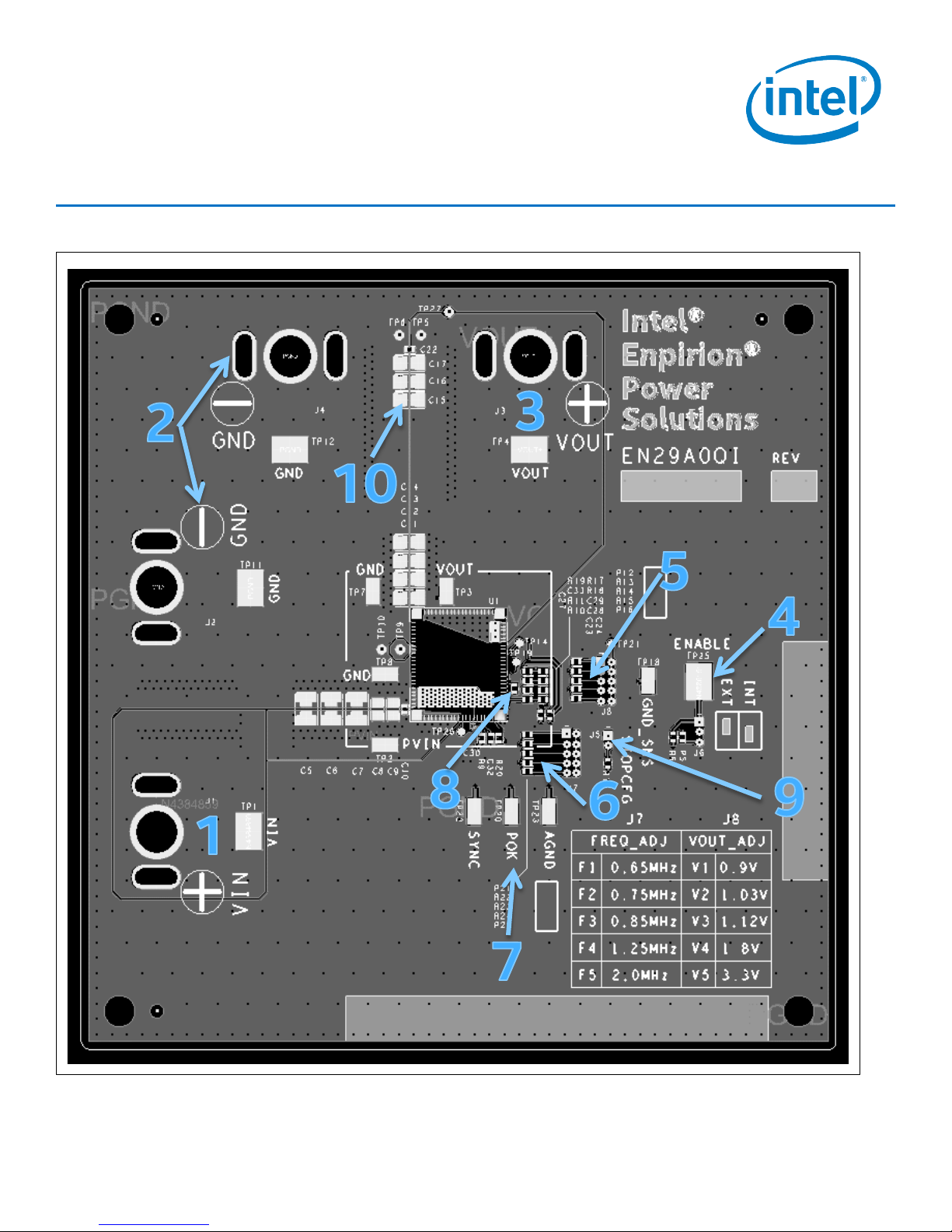
EVALUATION BOARD OVERVIEW
Figure 1: Evaluation Board (EVB) Features (Top View)
NOTE A: The EN29A0QI Evaluation Board is shown in Figure 1 with the important features numbered.
NOTE B: The following instructions will directly correlate with the numbers shown in Figure 1.
Page 1
Page 2
Evaluation Board User Guide | Intel Enpirion® Power Solutions: EN29A0QI
V
OUT
VOUT
PGND
EN29A0QI
VFB
R
A
4kΩ
R
CA
C
A
VFB=0.6V
C
OUT
(150-1000) µF
GND SNS
LOAD
COMP
R
E
RXC
RX
C
X
FB A
B
OUT FB
V ×R
R=
V -V
EVALUATION BOARD INSTRUCTIONS
1) Input Supply (VIN) – Connect 9V to 16V supply on VIN
(J1). Pay attention to input polarity and do not turn on
until everything is connected correctly.
2) Ground (GND) – Connect the input and output ground
to GND (J2, J4).
3) Output Voltage (VOUT) – Connect the load to VOUT
(J3). If the instructions were followed up to this point, the
device may be powered on. Wait to turn on ENABLE
signal in case of using external ENABLE.
4) ENABLE (ENA) – ENABLE may be tied to AVIN through
a resistor or controller externally. If J6 is connected
between positions 2-3, ENABLE is tied to AVIN. Placing a
jumper in position 1-2 of J6 disables the device. An
external signal (3.3V/1.8V logic) may be applied to TP25
with J6 in position 1-2.
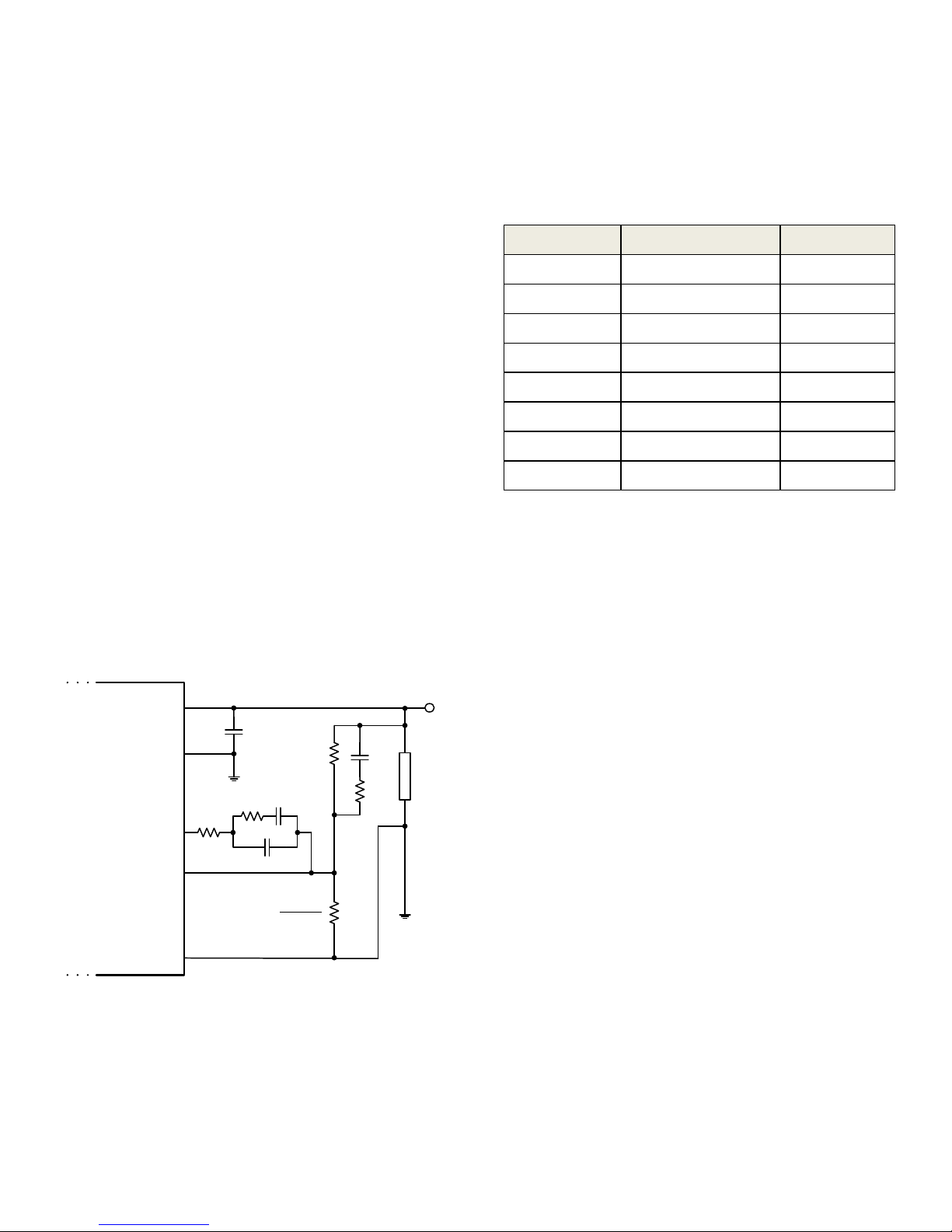
5) Output Voltage Settings (J8) - The output voltage
may be adjusted quickly by placing a jumper one of the
selections on J8. The voltages are pre-set by the
resistors R12, R13, R14, R15 and R16 which correspond
to 0.9V, 1.03V, 1.12V, 2.5V and 3.3V respectively. The
output voltage may also be adjusted to any voltage as
indicated by the equation for R
frequency and compensation network may need to be
adjusted for best results.
shown in Figure 2. The
B
respectively. The switching frequency is adjusted to
match the recommended frequency for the set output
voltage. Tabe 1 shows the recommended frequencies
for some commonly used output voltages.
Table 1: Frequency Recommendations
VOUT (V) Frequency (MHz) R
FREQ
(kΩ)
0.75 0.5 60.4
0.9 0.65 46.4
1.03 0.75 40.2
1.12 0.85 35.7
1.5 1 29.4
1.8 1.25 23.3
2.5 1.6 17.4
3.3 2 13.7
7) Power OK (POK) – This is an open drain Power OK
flag, pulled up to VCC through R20. When VOUT is over
92% of regulation, POK will be pulled high.
8) Soft Start Capacitor (C
(C27) is 33nF by default and can be between 3.3nF to
680nF. The output rise time is controlled by C
voltage rise time calculation is shown:
Rise Time t
[ms] = Css [nF] x 0.03
RISE
) – The soft start capacitor
SS
. The
SS
Figure 2: VOUT Resistor Divider & Compensation
6) Frequency Settings (J7) – The switching frequency
may be adjusted quickly by placing a jumper one of the
selections on J7. The frequencies are pre-set by the
resistors R21, R22, R23, R24 and R25 which correspond
to 0.65MHz, 0.75MHz, 0.85MHz, 1.2MHz and 2MHz
Capacitor
C
= 33nF t
SS
C
= 330nF t
SS
≈ 0.99ms
RISE
≈ 9.9ms
RISE
9) Soft Shutdown Resistor (J5) – Placing a jumper on J5
enables soft shutdown. The soft shutdown resistor (R7)
is 6kΩ by default and can be between 6kΩ to 100kΩ. The
output fall time is controlled by R
and CSS. The
STOP
voltage fall time calculation is shown:
Fall Time t
C
= 33nF, R
SS
C
= 330nF, R
SS
10) Optional Bulk Capacitors – Bulk capacitors may be
[µs] = 3 x Css [nF] x R
STOP
= 6kΩ t
STOP
STOP
= 10kΩ t
FALL
≈ 594µs
≈ 9900µs
FALL
STOP
[kΩ]
used on the output to improve load transient response.
However, the compensation network must be adjusted
accordingly. A downloadable compensation calculation
tool is also provided at EN29A0QI’s product page at
https://www.intel.com/enpirion for easier calculation
and optimization of the compensation components.
Page 2
Page 3

Evaluation Board User Guide | Intel Enpirion® Power Solutions: EN29A0QI
Page 3
EVALUATION BOARD SCHEMATIC
Page 4

Evaluation Board User Guide | Intel Enpirion® Power Solutions: EN29A0QI
Page 4
BILL OF MATERIALS (B.O.M.)
Quantity
Reference
Description
Manufacturer
Part Number
7
C1,C2,C3,C4,C5,C6,C7
CAP CER 22UF 25V X7R 1210
Murata
GRM32ER71E226KE15L
4
C8,C9,C37,C38
CAP CER 4.7UF 25V X7R 0805
Murata
GRM21BR71E475KA73L
2
C10,C39
CAP CER 330PF 25V C0G/NP0 0402
Murata
GRM1555C1E331JA01D
4
C11,C12,C13,C17
CAP CER 47UF 6.3V X5R 0805
Taiyo Yuden
JMK212BJ476MG-T
1
C21
CAP TANT POLY 470UF 6.3V 2917
Panasonic
6TPE470MAZU
1
C22
0.10UF 6.3V CERAMIC CAPACITOR X7R 0603
Murata
GRM188R70J104KA01D
2
C23,C24
CAP, CERAMIC CAPACITOR, 10NF 25V 10% X7R 0402
Murata
GRM155R71E103KA01D
1
C26
CAP CER 10UF 25V X7S 0805
Murata
GRM21BC71E106ME11L
1
C27
33NF X7R 0402 25V 10% CERAMIC CAPACITOR
Murata
GRM155R71E333KA88D
1
C28
CAP CER 33PF 50V NP0 0402
TDK
CGA2B2NP01H330J050BA
1
C29
CAP, CERAMIC, 3300PF, 5%, 50V, X7R, 0402
Murata
GRM155R71H332JA01D
1
C30
CAP CER 330PF 25V 5% C0G 0201
Murata
GRM0335C1E331JA01D
1
C31
CAP, 10UF 0805 X7R 10% 10V CERAMIC
Murata
GRM21BR71A106KE51L
1
C32
CAP CER 0.22UF 16V X7R 0402
Murata
GRM155R71C224KA12D
1
C33
CAP CER 1500PF 50V X7R 0402
Murata
GRM155R71H152JA01D
1
FB1
FERRITE BEAD 680 OHM 1812 1LN
Taiyo Yuden
FBMH4532HM681-T
3
J1,J2,J3,J4
TERMINAL, SCREW, 30A, LOW PROFILE
Keystone
1202
1
J5
2 POSITIONS HEADER, UNSHROUDED CONNECTOR 0.050" (1.27MM) THROUGH HOLE GOLD
Sullins
GRPB021VWVN-RC
1
J6
CONN HEADER 3POS .05" SNGL TIN
Sullins
GRPB031VWVN-RC
2
J7,J8
CONN HEADER .050" 10PS DL PCB AU
Sullins
GRPB052VWVN-RC
2
R3,R4
RES SMD 4.99 OHM 1% 1/16W 0402
Stackpole Electro nics Inc
RMCF0402FT4R99
1
R5
RES 100K OHM 1/16W 1% 0402 SMD
Panasonic
ERJ-2RKF1003X
3
R6,R14,R17
RES 4.02K OHM 1/16W 1% 0402
Yageo
RC0402FR-074K02L
1
R7
RES SMD 6.04K OHM 1% 1/10W 0402
Panasonic
ERJ-2RKF6041X
3
R8,R10,R19
RESISTOR ZERO OHM 1/10W 5% 0402 SMD
Panasonic
ERJ-2GE0R00X
1
R9
RES 10.0 OHM 1/16W 1% 0402 SMD
Panasonic
ERJ-2RKF10R0X
2
R11,R15
RES 2K OHM 1/16W 1% 0402
Panasonic
ERJ-2RKF2001X
1
R12
RES SMD 16K OHM 1% 1/16W 0402
Vishay Dale
CRCW040216K0FKED
1
R13
RES - 8.06K OHM, 1/16W, 1%, 0402 SMD
Vishay
CRCW04028K06FKED
1
R16
RES - 887 OHM, 1%, 1/16W, 0402 SMD
Panasonic
ERJ-2RKF8870x
1
R18
RES 150 OHM 1% 1/16W 0402 SMD
Panasonic
ERJ-2RKF1500X
1
R20
RES SMD 51K OHM 5% 1/10W 0402
Panasonic
ERJ-2GEJ513X
1
R21
RES, 66.5K OHM, 1%, 1/16W, 0402
Panasonic
ERJ-2RKF6652X
1
R22
RES - 40.2K OHM, 1/16W, 1%, 0402, SMD
Panasonic
ERJ-2RKF4022x
1
R23
RES 29.4K OHM 1/16W 1% 0402 SMD
Vishay/Dale
CRCW040229K4FKED
Page 5

Evaluation Board User Guide | Intel Enpirion® Power Solutions: EN29A0QI
Page 5
1
R24
RES - 19.1K OHM, 1%, 1/16W 0402 SMD
Panasonic
ERJ-2RKF1912x
1
R25
RES - 13.7KOHM, 1/16W, 1%, 0402, SMD
Vishay
CRCW040213K7FKED
1
R28
0 OHM JUMPER 1/8W 0.125W 0805 THICK FILM CHIP RESISTOR
Panasonic
ERJ-6GEY0R00V
5
TP1,TP4,TP11,TP12,TP25
TEST POINT SURFACE MOUNT
Keystone
5016
8
TP2,TP3,TP7,TP8,TP18,TP20,TP22,TP23
TEST POINT SURFACE MOUNT
Keystone
5015
25
C14,C15,C16,C18,C19,C20,C34,C35,C36,R1,
R2,R26,R27,R29,R30,R31,
TP5,TP6,TP9,TP10,TP14,TP19,TP21,TP26,TP27
COMPONENT NOT USED ** DO NOT INSTALL **
1
U1
EN29A0QI 10A 12V 84-pin QFN
Intel
EN29A0QI
Page 6

Evaluation Board User Guide | Intel Enpirion® Power Solutions: EN29A0QI
Page 6
WHERE TO GET MORE INFORMATION
For more information about Intel and Intel Enpirion PowerSoCs, visit:
https://www.intel.com/enpirion
© 2017 Intel Corporation. Al l rights reserved. Intel, the Intel logo, Altera, ARRI A, CYCLONE, ENPIRION, MAX, ME GACORE, NIOS, QUARTUS, and STRATI X words and logos are trademarks of Intel Corporation or its sub sidiaries in the U.S. and/or other countries. Other
marks and brands may be claimed as the property of others. Intel reserves the r ight to make changes to any p roducts and services at any time without notice. Intel ass umes no responsibility or l iability arising out of the appl ication or use of any info rmation, product, or
service described herein except as expressly agreed to in writing by Intel. Intel customers are advised to obtain the latest version of device specifications before relying on any published info rmation and before placing o rders for products or services.
* Other marks and brands may be claimed as the property of others.
 Loading...