

Page 1

Intel® Xeon™ Processor and
Intel® E7500/E7501 Chipset
Compatible Platform
Design Guide Addendum for Embedded Applications
July 2003
Order Number: 273707-004
Page 2

INFORMATION IN THIS DOCUMENT IS PROVIDED IN CONNECTION WITH INTEL® PRODUCTS. NO LICENSE, EXPRESS OR IMPLIED, BY
ESTOPPEL OR OTHERWISE, TO ANY INTELLECTUAL PROPERTY RIGHTS IS GRANTED BY THIS DOCUMENT. EXCEPT AS PROVIDED IN
INTEL'S TERMS AND CONDITIONS OF SALE FOR SUCH PRODUCTS, INTEL ASSUM ES NO LIABILIT Y WHA T SOEVER, AND INTE L DISCLAIMS
ANY EXPRESS OR IMPLIED WARRANTY, RELATING TO SALE AND/OR USE OF INTEL PRODUCTS INCLUDING LIABILITY OR WARRANTIES
RELATING T O FITNESS FOR A PARTICULAR PURPOSE, MERCHANTABILITY, OR INFRINGEMENT OF ANY PATENT, COPYRIGHT OR OTHER
INTELLECTUAL PROPERTY RIGHT. Intel products are not intended for use in medical, life saving, life sustaining applications.
Intel may make changes to specifications and product descriptions at any time, without notice.
Designers must not rely on the absence or characteristics of any features or instructions marked “reserved” or “undefined.” Intel reserves these for
future definition and shall have no responsibility whatsoever for conflicts or incompatibilities arising from future changes to the m.
®
The Intel
as errata which may cause the product to deviate from published specifications. Current characterized errata are available on request.
Contact your local Intel sales office or your distributor to obtain the latest specifications and before placing your product order.
Copies of documents which have an ordering number and are referenced in this document, or other Intel literature may be obtained by calling
1-800-548-4725 or by visiting Intel's website at http://www.intel.com.
AlertVIEW, AnyPoint, AppChoice, BoardWatch, BunnyPeople, CablePort, Celeron, Chips, CT Connect, CT Media, Dialogic, DM3, EtherExpress,
ETOX, FlashFile, i386, i486, i960, iCOMP, InstantIP, Intel, Intel logo, Intel386, Intel486, Intel740, IntelDX2, IntelDX4, IntelSX2, Intel Create & Share,
Intel GigaBlade, Intel InBusiness, Intel Inside, Intel Inside logo, Intel NetBurst, Intel NetMerge, Intel NetStructure, Intel Play, Intel Play logo, Intel
SingleDriver, Intel SpeedStep, Intel StrataFlash, Intel TeamStation, Intel Xeon, Intel XScale, IPLink, Itanium, LANDesk, LanRover, MCS, MM X, MMX
logo, Optimizer logo, OverDrive, Paragon, PC Dads, PC Parents, PDCharm, Pentium, Pentium II Xeon, Pentium III Xeon, Performance at Your
Command, RemoteExpress, Shiva, SmartDie, Solutions960, Sound Mark, StorageExpress, The Computer Inside., The Journey Inside,
TokenExpress, Trillium, VoiceBrick, Vtune, and Xircom are trademarks or registered trademarks of Intel Corporation or its subsidiaries in the United
States and other countri es.
*Other names and brands may be claimed as the property of others.
Copyright © Intel Corporation, 2003
Xeon™ Processor with 512 KB L2 Cache, the Intel®E7500 chipset and the Intel® 7501 chipset may contain design defects or errors known
2 Platform Design Guide Addendum
Page 3

Contents
Contents
1.0 Introduction......................................................................................................................................7
1.1 Reference Documentation ....................................................................................................7
2.0 Uni-processor System Bus Routing Guidelines...............................................................................9
2.1 Routing Guidelines for the 2X and 4X Signal Groups.........................................................11
2.1.1 Design Recommendations.....................................................................................12
2.2 Routing Guidelines for Common Clock Signals..................................................................13
2.2.1 Wired-OR Signals..................................................................................................13
2.3 Routing Guidelines for Asynchronous GTL+ and Miscellaneous Signals...........................14
2.3.1 Asynchronous GTL+ Signals Driven by the Processor..........................................15
2.3.1.1 Voltage Translation for FERR#..............................................................15
2.3.1.2 Proper THERMTRIP# Usage.................................................................16
2.3.2 Asynchronous GTL+ Signals Driven by the Chipset..............................................17
2.3.2.1 Voltage Translation for INIT#.................................................................17
2.3.3 BR[3:0] Routing Guidelines for Uni-processor Designs.........................................18
3.0 Memory Interface Routing Guidelines ...........................................................................................21
3.1 DIMM Types .......................................................................................................................22
3.2 Dual Channel DDR Overview .............................................................................................22
3.2.1 Dual Channel Source Synchronous Signal Group Routing ...................................23
3.2.2 Dual Channel Command Clock Routing................................................................25
3.2.3 Dual Channel Source Clocked Signal Group Routin g ...........................................26
3.2.4 Dual Channel Chip Select Routing ........................................................................27
3.2.5 Dual Channel Clock Enable Routing .....................................................................28
3.2.6 2.5 Volt Decoupling Requirements ........................................................................28
3.3 Single Channel DDR Overview...........................................................................................30
3.3.1 Unused Channel B.................................................................................................31
3.3.2 Single Channel Source Synchronous Signal Group Routing.................................32
3.3.3 Single Channel Command Clock Routing..............................................................36
3.3.4 Single Channel Source Clocked Signal Group Routing.........................................37
3.3.5 Single Channel Chip Select Routing......................................................................38
3.3.6 Single Channel Clock Enable Routing...................................................................39
3.3.7 Single Channel DC Biasing Signals.......................................................................40
3.3.7.1 Single Channel Receive Enable Signal (RCVEN#) ...............................40
3.3.7.2 Single Channel DDRCOMP...................................................................41
3.3.7.3 Single Channel DDRVREF and ODTCOMP..........................................41
3.3.7.4 Single Channel DDRCVO......................................................................41
3.3.8 Single Channel DDR Signal Termination and Decoupling.....................................42
3.3.9 2.5 V Decoupling Requirements ............................................................................42
Platform Design Guide Addendum 3
Page 4

Contents
Figures
1 Uni-processor System Bus Topology .........................................................................................10
2 Topology for Asynchronous GTL+ Signals Driven by the Processor..........................................15
3 FERR# Routing Topology for Low Voltage Intel
1 Recommended THERMTRIP# Circuit .......................................... ...... ....... ...... ...........................16
4 Topology for Asynchronous GTL+ Signals Driven by the Chipset..............................................17
5 INIT# Routing Topology for a Uni-processor System .................................................................18
6 Voltage Translator Circuit...........................................................................................................18
7 BR[3:0]# Connection for UP Configuration.................................................................................19
8 DIMM Connector Styles Supported............................................................................................22
9 1-DIMM per Channel Implementation.........................................................................................23
10 2-DIMMs per Channel Implementation.......................................................................................23
11 Dual Channel 2-DIMM Command Clock Topology.....................................................................26
12 1-DIMM Per Channel Decoupling...............................................................................................29
13 2-DIMMs Per Channel Decoupling.............................................................................................30
14 Single Channel 2-DIMM Implementation....................................................................................31
15 Single Channel 4-DIMM Implementation....................................................................................31
16 Single Channel Source Synchronous Topology DIMM Solution ................................................35
17 Trace Length Matching Requirements for Single Channel Source Synchronous Routing.........35
18 Single Channel 2-DIMM Command Clock Topology ..................................................................36
19 SIngle Channel Source Clocked Signal Topology......................................................................37
20 Single Channel Chip Select Topology........................................................................................38
21 Single Channel CKE Topology...................................................................................................39
22 Single Channel Receive Enable Signal Routing Guidelines.......................................................40
23 Single Channel DDRCOMP Resistive Compensation................................................................41
24 Single Channel DDRCVO Single Channel Routing Guidelines..................................................42
25 Single Channel 2-DIMM Decoupling ..........................................................................................43
26 Single Channel 4-DIMM Decoupling ..........................................................................................44
®
Xeon™ Processors.......................................16
Tables
1 Reference Documents..................................................................................................................7
2 System Bus Signal Groups...........................................................................................................9
3 Uni-processor System Bus Routing Summary ...........................................................................10
4 2X and 4X Signal Groups...........................................................................................................11
5 Source Synchronous Signals and Associated Strobes ..............................................................11
6 Common Clock Signals ..............................................................................................................13
7 Asynchronous GTL+ and Miscellaneous Signals .......................................................................14
8 Dual Channel Source Synchronous Signal Group Routing Guidelines......................................24
9 Dual Channel Command Clock Pair Routing Guidelines ...........................................................25
10 Dual Channel Source Clocked Signal Group Routing Guidelines..............................................26
11 Dual Channel Chip Select Routing Guidelines ...........................................................................27
12 Dual Channel Clock Enable Routing Guidelines ........................................................................28
13 Channel B Signal Terminations..................................................................................................32
14 Single Channel DQ/CB to DQS Mapping ...................................................................................32
15 Single Channel Source Synchronous Signal Group Routing Guidelines ...................................34
16 Single Channel Command Clock Pair Routing Guidelines.........................................................36
4 Platform Design Guide Addendum
Page 5
Contents
17 Single Channel Source Clocked Signal Group Routing Guidelines............................................37
18 Single Channel Chip Select Routing Guidelines.........................................................................38
19 Single Channel Clock Enable Routing Guidelines......................................................................39
20 Single Channel Receive Enable Routing Guidelines..................................................................40
21 DDRCOMP Routing Guidelines..................................................................................................41
22 DDRCVO Routing Guidelines.................... ...... ....... ...... ...... .............................................. ...... ... .42
Revision History
Date Revision Description
July 2003 -004
January 2003 -003
June 2002 -002 Document Update
January 2002 -001 Initial Release
Updated memory interface routing information and added Low
Voltage Intel
Updated and expanded memory interface routing information.
Added E7501 chipset information.
®
XeonTM processor information.
Platform Design Guide Addendum 5
Page 6

Contents
This page intentionally left blank.
6 Platform Design Guide Addendum
Page 7
Intel® Xeon™ Processor and Intel® E7500/E7501 Chipset Compatible Platform
1.0 Introduction
This document is an addendum to the Intel® Xeon™ Processor and Intel® E7500/E7501 Chipset
Compatible Platform Design Guide. It contains applied computing-specific guidelines, such as uni-
processor design guidelines, angl ed Double Data Rate (DDR) guidelines and single channel DDR
guidelines.
Carefully follow the design information and recommendations provided in this document. These
design guidelines have been developed to ensure maximum flexibility for system designers while
reducing the risk of board-related issues.
Note that the guidelines recommended in this document are based on experience and preliminary
simulation work done at Intel.
1.1 Reference Documentati on
T a ble 1. Reference Documents (Sheet 1 of 2)
Document Location
®
Intel
E7501 Chipset Memory Controller Hub (MCH)
Datasheet
Intel® Xeon™ Processor and Intel® E7500/E7501
Chipset Compatible Platform Design Guide
Intel® Xeon™ Processor with 512 KB L2 Cache and
Intel E7500 Chipset Platform Design Guide
Intel® Xeon™ Processor with 512 KB L2 Cache at
1.80 GHz to 2.40 GHz Datasheet
Intel® E7500 Chipset Memory Controller Hub (MCH)
Datasheet
Intel® 82870P2 PCI/PCI-X 64-bit Hub 2 (P64H2)
Datasheet
Intel 82801CA I/O Controller Hub 3 (ICH-3) Datasheet
Intel® 82870P2 PCI/PCI-X 64-bit Hub 2 (P64H2)
Specification Update
Intel® 82801CA I/O Controller Hub 3 (ICH3-S)
Specification Update
603-Pin Socket Design Guidelines
VRM 9.1 DC-DC Converter Design Guidelines
Intel® Xeon™ Processor Voltage Regulator Down
(VRD) Design Guidelines
Intel® Xeon™ Processor with 512 KB L2 Cache
System Compatibility Guidelines
Intel® Xeon™ Processor Thermal Design Guidelines
Intel® E7500 Chipset Thermal and Mechanical Design
Guidelines
http://developer.intel.com/design/chipsets/datashts/
251927.htm
http://developer.intel.com/design/chipsets/designex/
251929.htm
http://developer.intel.com/design/chipsets/e7500/
guides/298649.htm
http://developer.intel.com/design/Xeon/datashts/
298642.htm
http://developer.intel.com/design/chipsets/e7500/
datashts/290730.htm
http://developer.intel.com/design/chipsets/e7500/
datashts/290732.htm
http://developer.intel.com/design/chipsets/e7500/
datashts/290733.htm
http://www.intel.com/design/chipsets/e7500/
specupdt/290735.htm
http://www.intel.com/design/chipsets/e7500/
specupdt/290739.htm
http://developer.intel.com/design/Xeon/guides/
249672.htm
http://developer.intel.com/design/Xeon/guides/
298646.htm
http://developer.intel.com/design/Xeon/guides/
298644.htm
http://developer.intel.com/design/Xeon/guides/
298645.htm
http://developer.intel.com/design/Xeon/guides/
298348.htm
http://developer.intel.com/design/chipsets/e7500/
guides/298647.htm
Platform Design Guide Addendum 7
Page 8
Intel® Xeon™ Processor and Intel® E7500/E7501 Chipset Compatible Platform
T able 1. Reference Documents (Sheet 2 of 2)
Document Location
Intel® Xeon™ Processor Thermal Solution Functional
Specifications
Intel® Xeon™ Processor with 512 KB L2 Cache
Thermal Models
Intel® Xeon™ Processor with 512 KB L2 Cache
Mechanical Model in IGES
Intel® Xeon™ Processor with 512 KB L2 Cache
Mechanical Model in ProE* Format
AP-728 Intel ® ICH Family Real Time Clock (RTC)
Accuracy and Considerations Under Test Conditions
ITP700 Debug Port Design Guide
Intel® Xeon™ Processor with 512 KB L2 Cache Signal
Integrity Models
PCI Bus Power Management Interface Specification,
Revision 1.1
PCI Hot Plug Specification, Revision 1.1
PCI Local Bus Specification, Revision 2.2
PCI-PCI Bridge Architecture Specification, Revision
1.1
PCI Standard Hot-Plug Controller and Subsystem
Specification, Revision 1.0
PCI-X Specification, Revision 1.0a http://www.pcisig.com/specifications/pcix_20/pci_x/
System Management Bus Specification (SMBus),
Revision 1.1
Universal Serial Bus Specification, Revision 1.1 http://www.usb.org/developers/docs/
Low Voltage Intel® XeonTM processor at 1.6 GHz and
2.0 GHz Datasheet
Intel® XeonTM processor with 533 MHz System Bus at
2.0 GHz to 2.8 GHz Datasheet
Low Voltage Intel® XeonTM processor for Embedded
Applications Thermal Design Guidelines
http://developer.intel.com/design/Xeon/applnots/
249673.htm
http://developer.intel.com/design/Xeon/devtools/
http://developer.intel.com/design/Xeon/devtools/
http://developer.intel.com/design/Xeon/devtools/
http://developer.intel.com/design/chipsets/applnots/
292276.htm
http://developer.intel.com/design/Xeon/guides/
249679.htm
http://developer.intel.com/design/Xeon/devtools
http://www.pcisig.com/specifications/conventional/
pci_bus_power_management_interface
http://www.pcisig.com/specifications/conventional/
pci_hot_plug
http://www.pcisig.com/specifications/conventional/
conventional_pci
http://www.pcisig.com/specifications/conventional/
pci_to_pci_bridge_architecture
http://www.pcisig.com/specifications/conventional/
pci_hot_plug
http://www.sbs-forum.org/
http://www.intel.com/design/intarch/datashts/
273766.htm
http://www.intel.com/design/xeon/datashts/
252135.htm
http://www.intel.com/design/intarch/designgd/
273764.htm
8 Platform Design Guide Addendum
Page 9
Intel® Xeon™ Processor and Intel® E7500/E7501 Chipset Compatible Platform
2.0 Uni-processor System Bus Routing Guidelines
This section covers the system bus source synchronous (data, address, and associated strobes) and
common clock signal routing for Intel
FSB)/Low Voltage Intel
®
Xeon™ processor (400 MHz FSB) and Intel® E7500/E7501 chipsetbased systems, in a uni-processor (UP) configuration. Table 2 lists the signals and their
corresponding signal types .
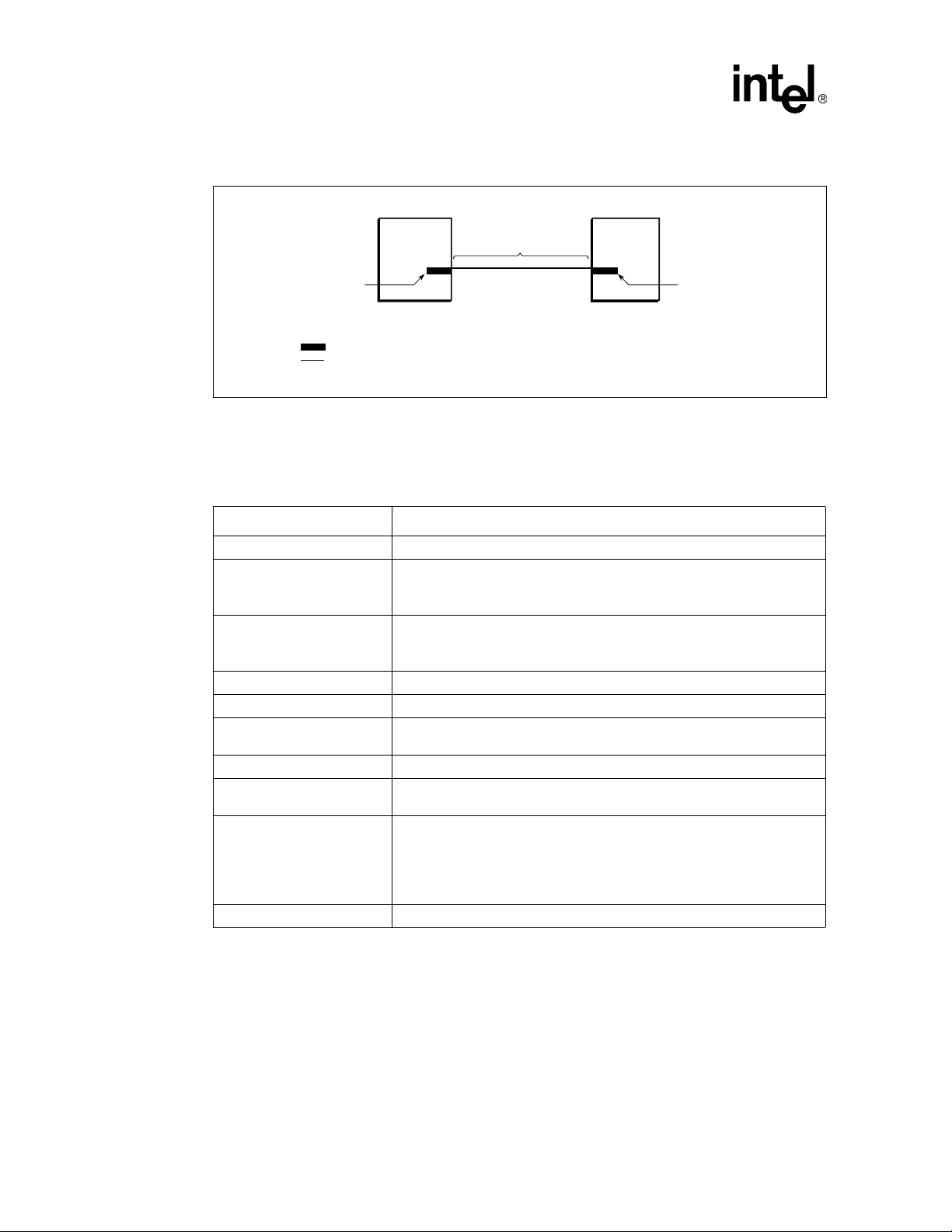
Figure 1 describes the uni-processor system bus topology.
T a ble 2. System Bus Signal Groups
Signal Group Type Signals
AGTL+ Common Clock Input Synchronous to BCLK
AGTL+ Common Clock I/O Synchronous to BCLK
AGTL+ Source Synchronous I/O:
4X Group
AGTL+ Source Synchronous I/O:
2X Group
AGTL+ Strobes
Async GTL+ Input
Async GTL+ Output
System Bus Clock Clock BCLK0, BCLK1
TAP Input
TAP Output
SMBus Interface
Power/Other Power/Other
NOTES:
1. These signals do not have on-die termination on the processor. They must be terminated properly on the
system board. If the signal is not connected, it must be pulled to the appropriate voltage level t hrough a 1
kΩ ± 5% resistor.
2. Xeon processors use only BR0# and BR1#.
3. These signals are ‘wired-OR’ signals and may be driven simultaneously by multiple agents. For further
details on how to implement wired-OR signals, refer to the routing guidelines in Section 2.2.1.
4. The value of these pins driving the active edge of RESET# determine processor configuration options.
5. SM_V
6. Terminations and routing for TAP signals and all debug port signals are found in the ITP700 Debug Port
Design Guide.
7. PROCHOT # is input/output on Low Voltage Intel® Xeon™ processor D-stepping and beyond.
1
1
6
6
1
has critical power sequencing requirements.
CC
®
Xeon™ processor with 512 KB L2 cache (400/533 MHz
BPRI#, BR[3:1]#
1,2
, DEFER#, RESET#1,
RS[2:0]#, RSP#, TRDY#
3
, BNR#3,
4
, LINT0/INT R,
Synchronous to
associated strobe
Synchronous to
associated strobe
Synchronous to BCLK
[1:0]
Asynchronous
ADS#, AP[1:0]#, BINIT#
BPM[5:0]#
DRDY#, HIT#
MCERR#
1
, BR0#1, DBSY#, DP[3:0]#,
3
, HITM#3, LOCK#,
3
D[63:0]#, DBI[3:0]#
4
A[35:3]#
, REQ[4:0]#
ADSTB[1:0]#, DSTBN[3:0]#, DSTBP[3:0]#
A20M#, IGNNE#, INIT#
LINT1/ NMI, PWRGOOD, SMI#
STPCLK#
Asynchronous
FERR#, IERR#, THERMTRIP#,
PROCHOT#
7
Synchronous to TCK TCK, TDI, TMS, TRST#
Synchronous to TCK TDO
Synchronous to SM_CLK
SM_EP_A[2:0], SM_TS_A[1:0], SM_DA T,
SM_CLK, SM_ALERT#, SM_WP
GTLREF[3:0], COMP[1:0], OTDEN ,
RESERVED, SKTOCC#, TESTHI[6:0],
VID[4:0], VCC_CPU, SM_V
V
SSA
V
SSSENSE
, V
CCIOPLL
, VSS, V
CC
CCSENSE
4
, SLP#,
5
, V
,
CCA
,
Platform Design Guide Addendum 9
Page 10
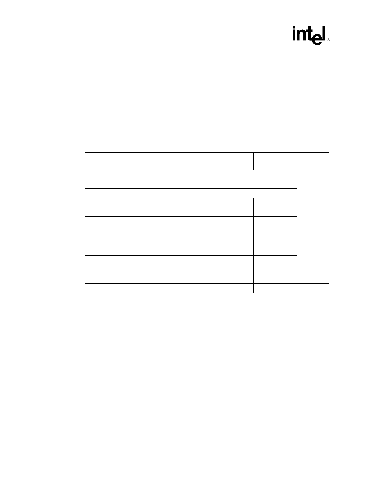
Intel® Xeon™ Processor and Intel® E7500/E7501 Chipset Compatible Platform
Figure 1. Uni-processor System Bus Topology
Note:
Package trace
Motherboard PCB trace
Processor MCH
Pad
Length L1 = 3.5 - 10"
Refer to Table 3 for a summary of the uni-processor system bus routing recommendations. Use this
as a quick reference only. The following sections provide more information for each parameter.
Intel strongly recommends simulation of all signals to ensure that setup and hold times are met.
T a ble 3. Uni-processor System Bus Routing Summary
Parameter Platform Routing Guidelines
Trace width/spacing 5/15 mils
3.5“– 10“pin-to-pin
4X signal group line lengths
DSTBn/p[3:0]# line lengths
2X signal group line lengths Address signals should follow the same routing rules as the data signals.
ADSTB[1:0]# line lengths ADSTB# signals should follow the same routing rules as the DSTB# signals.
Common clock signal line
lengths
Topology The processor must have on-die termination enabled.
Routing priorities
Reference plane requirements
System board Impedance 50 Ω ± 10%
Length must be added to the system board trace between agents to
compensate for the stub created by the processor package
DSTB# signals should follow the same routing rules as the data signals
A 25 mil spacing should be maintained around each strobe signal (between
DSTBp# and DSTBn#, and any other signal.)
Common clock signals should follow the same routing rules as the data
signals, however no length compensation is necessary.
All signals within the same strobe group must be routed on same layer for the
entire length of the bus.
Ground reference only.
Avoid changing layers when routing system bus signals.
If a layer change must occur, use vias connecting the two reference planes to
provide a low impedance path for the return current. Vias should be as close
as possible to the signal via.
Pad
A9044-01
10 Platform Design Guide Addendum
Page 11
Intel® Xeon™ Processor and Intel® E7500/E7501 Chipset Compatible Platform
2.1 Routing Guidelines fo r the 2X and 4X Signal Groups
The 4X group of signals uses four times the frequency of the base clock, or 400 MHz. The 2X
group uses twice the frequency of t h e bas e cloc k, o r 20 0 MHz. The 2 X and 4 X si gn als are l i st ed i n
Table 4. Table 5 lists the 2X and 4X signals with their associated strobes.
Table 4. 2X and 4X Signal Groups
2X Group 4X Group
HA[35:3]#
REQ[4:0]#
Table 5. Source Synchronous Signals and Associated Strobes
Signals Associated Strobe
REQ[4:0]#, HA[16:3]# ADSTB0#
HA[35:17]# ADSTB1#
HD[15:0]#, DBI0# DSTBP0#, DSTBN0#
HD[31:16]#, DBI1# DSTBP1#, DSTBN1#
HD[47:32]#, DBI2# DSTBP2#, DSTBN2#
HD[63:48]#, DBI3# DSTBP3#, DSTBN3#
HD[63:0]#
DBI[3:0]#
Routing guidelines for the 2X and 4X signal groups are given below:
• Trace impedance = 50 Ω ± 10%
• Route traces using 5/15 mil spacing
• Route all traces at least 25 mils away from the strobes
• Route all traces with at least 50% of the trace width directly over the reference plane for short
distances only when needed in the interposer socket region.
• Route signals and their associated strobes on the same layer for the entire length of the bus.
• A strobe and its complement must be routed within 25 mils of the same length over the entire
length of the buses.
• All 2X and 4X signals of the same group (refer to Table 5) m ust be routed within ±25 mils of
the same length between the agents and within ±50 mils of the entire length of the bus.
• Total bus length must not exceed 10”.
• Trace length matching is required. Please contact your Intel field representative for a length
matching spreadsheet.
Trace length matching is required within each source synchronous group to compensate for the
package trace length differences between data signals and the associated strobe. This will balance
the strobe- t o-signal skew in the middle of the setup and hold window. Figure 1 shows how t o
implement trace length matching. An example of trace length matching is given in Equation 1.
Platform Design Guide Addendum 11
Page 12

Intel® Xeon™ Processor and Intel® E7500/E7501 Chipset Compatible Platform
2.1.1 Design Recommendations
Below are the design recommendations for the data, address, strobes, and common clock signals.
For the following discussion, the pad is defined as the attach point of the silicon pad to the package
substrate.
DATA:
• The pin to pin distance from the processor to the chipset should be between 3.5" to 10" (i.e.,
3.5" < L1 < 10"). Data signals of the same source synchronous group should be routed to the
same pad to pad length within ± 100 mils of the associated strobes. As a result, additional
traces will be added to some data nets on the system board in order for all trace lengths within
the same data group to be the same length (± 100 mils) from the pad of the processor to the pad
of the chipset. This length compensation will result in minimizing the source sync hro nou s
skew that exists on the system bus. Without the length compensation the flight times between
a data signal and its strobe is different, which results in an inequity between the s etup and ho ld
times.
Equation 1. Calculating Package Delta Addition to System Board Length for UP Systems
delta
net,strobe
ADDRESS:
= (cpu_pkglen
† Strobe package length is the average of the strobe pair.
- cpu_pkglen
net
) + (chipset_pkglen
strobe†
- chipset_pkglen
net
strobe
• Address signals follow the same rules as data signals except they should be routed to the same
pad to pad length within ±200 mils of the associated strobes. Address signals may change
layers if the reference plane remains Vss and as long as the layers for a given group are all of
the same configuration (all stripline or all microstrip).
STROBE:
• A strobe and its complement should be routed to a length equal to their corresponding data
group's median pad-to-pad length ±25 mils. This causes the strobe to be received closer to the
center of the data pulse, which results in reasonably comparable setup and hold times. A strobe
and its complement (xSTBp/n#) should be routed to ±25 mils of the same length. It is
recommended to simulate skew in order to determine the length that best centers the strobe for
a given system.
COMMON CL OCK:
• Common clock signals should be routed to a minimum pin-to-pin system board length of 6"
and a maximum motherboard length of 10".
)
12 Platform Design Guide Addendum
Page 13
Intel® Xeon™ Processor and Intel® E7500/E7501 Chipset Compatible Platform
2.2 Routing Guidelines for Common Clock Signals
Table 6 lists the common clock signals.
Table 6. Common Clock Signals
Signal Type Signals
BPRI#
BR[3:1]#
DEFER#
AGTL+ Common Clock Input
AGTL+ Common Clock I/O
RESET#
RS[2:0]#
RSP#
TRDY#
ADS#
AP[1:0]#
BINIT#
BNR#
BPM[5:0]#
BR0#
DBSY#
DP[3:0]#
DRDY#
HIT#
HITM#
LOCK#
MCERR#
Routing guidelines for the source synchronous signal group are given below:
• Trace impedance = 50 Ω ±10%
• Route traces using 5/15 mil spacing
• Keep signals on the same layer for the entire length of the bus
• Route traces with at least 50% of the trace width directly over a reference plane
• Total bus length must not exceed 10"
2.2.1 Wired-OR Signals
There are five wired-OR signals on the system bus. These signals are HIT#, HITM#, MCERR#,
BINIT#, and BNR#. These signals differ from the other fr ont-side bus signals in that more than one
agent can be driving the signal at the same time. Timing and signal integrity must be met for the
case where one agent is driving, all agents are driving, or any combination of agents are driving.
The wired-OR signals should follow the same routing rules as the common clock signals. Intel
recommends that simulations for these signals be performed for a given system.
Platform Design Guide Addendum 13
Page 14

Intel® Xeon™ Processor and Intel® E7500/E7501 Chipset Compatible Platform
2.3 Routing Guidelines for Asynchronous GTL+ and Miscellaneous Signals
This section provides routing guidelines for the sign als listed in Table 7.
Table 7. Asynchronous GTL+ and Miscellaneous Signals
Signal Name Type CPU I/O Type Driven by Received by
A20M# Async GTL+ I ICH3-S Processor
BINIT# AGTL+ I/O Processor Processor
BR[3:1]# AGTL+ I Processor Processor
BR0# AGTL+ I/O Processor/MCH Processor/Chipset
COMP[1:0] Analog I Pull-down Proc e ssor
FERR# Async GTL+ O Processor Chipset
IERR# Async GTL+ O P rocessor External Logic
IGNNE# Async GTL+ I ICH3-S Processor
INIT# Async GTL+ I ICH3-S Processor
LINT[1:0] Async GTL+ I ICH3-S Processor
ODTEN Other I Pull-up/Pull-down Processor
PROCHOT# Async GTL+ O Processor External Logic
PWRGOOD Async GTL+ I External Logic Processor
SLP# Async GTL+ I ICH3-S Processor
SM_ALERT# SMBUS (3.3 V) O Processor/Controller Controller
SM_CLK SMBUS (3.3 V) I/O Processor/Controller Processor/Controller
SM_DAT SMBUS (3.3 V) I/O Processor/Controller Processor/Controller
SM_EP_A[2:0] SMB US (3.3 V) I Pull-up/Pull-down Processor
SM_TS_A[1:0] SMBUS (3.3 V) I Pull-up/Pull-down Processor
SM_WP SMB US (3.3 V) I External Logic Processor
SMI# Async GTL+ I ICH3-S Processor
STPCLK# Async GTL+ I ICH3-S Processor
THERMTRIP# Async GTL+ O Processor External Logic
VCCA Power I Pull-up/Pull-down Processor
VCCIOPLL Power I Pull-up/Pull-down Processor
VCCSENSE Other O Processor Voltage Regulator
VID[4:0] Other O Processor Voltage Regulator
GTLREF Po wer I Pu ll-up/Pull-down Processor
VSSA Power I Pull-up/Pull-down Processor
14 Platform Design Guide Addendum
Page 15

Intel® Xeon™ Processor and Intel® E7500/E7501 Chipset Compatible Platform
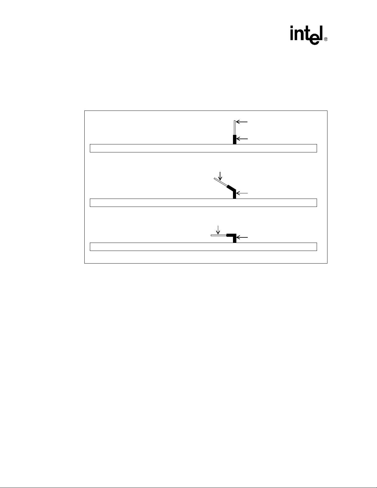
2.3.1 Asynchronous GTL+ Signals Driven by the Processor
Follow the topology shown in Figure 2 when routing FERR#, IERR#, PROCHOT# and
THERMTRIP#. Note that FERR# is the only signal in this group that connects the processors to the
ICH3-S. IERR#, PROCHOT# an d THER MTRIP # conn ect t o o ther motherboard logic (such as the
Baseboard Management Controller) and may need voltage translation logic, depending on the
motherboard receiver logic devices used. Do not route a stub when routing to the processors.
Figure 2. Topology for Asynchronous GTL+ Signals Driven by the Processor
VCC_CPU
56Ω ± 5% 56Ω ± 5%
®
Processor
0
3 inches max 3 inches max1 to 12 inches
Note: Trace Zo - 50Ω
Trace Spacing = 10 ml
Intel
ICH3-S
or other
Logic
2.3.1.1 Voltage Translation for FERR#
A voltage translator circuit is required for the FERR# sign al when VCC_CPU is less than 1. 3 V, as
it is for the Low Voltage Intel
given in Figure 3. Figure 6 shows the voltage translator circuit.
®
Xeon™ Processor. The required routing topology for FERR# is
VCC_CPU
A9045-01
Platform Design Guide Addendum 15
Page 16

Intel® Xeon™ Processor and Intel® E7500/E7501 Chipset Compatible Platform
Figure 3. FERR# Routing Topology for Low Voltage Intel
VCC_CPU VCC_CPU
56Ω 56Ω
Processor
0
3 inches max 3 inches max1 to 12 inches
NOTE:
1. Refer to Figure 6 for voltage translator information.
2.3.1.2 Proper THERMTRIP# Usage
To protect the processors fro m damage in over-temperature situations, power to the processor core
must be removed within 0.5 s econds o f the asserti on of the THERMTRI P#. If po wer is ap plied t o a
processor when no thermal solution is attached, normal leakin g currents caus es the die temperatur e
to rapidly rise to levels at which permanent silicon damage is possible. This high temperature
causes THERMTRIP# to go active. Use dual termination on the THERMTRIP# signal. Each
processor’s THERMTRIP# can be routed to its own receiver, or they can be wire-OR’d together. If
routed separately, each signal must be terminated at the receiver end only. All power supply
sources to all processors must be dis abled when any install processor signals THERMTRIP#. In the
reference schematic, the 74AHC74 flip-flop latches the THERMTRIP# signal HIGH after a
PWRGOOD assertion, and LOW after a THERMTRIP# assertion. The recommended
THERMTRIP# circuit is shown in Figure 1.
®
Xeon™ Processors
ICH3-S
(FERR#)
Voltage
Translator
(1)
A9046-01
Figure 1. Recommended THERMTRIP# Circuit
12 V
3VSBY
VCC_CPU
THERMTRIP#
62 Ω
3904
1 KΩ 10 KΩ
3904
1 KΩ
74AHC74
VCC=3VSBY
SET
Q
D
Q#
CLR
100 KΩ
3.3 KΩ
1 KΩ
THERM_EN to VR
A9844-01
16 Platform Design Guide Addendum
Page 17

Intel® Xeon™ Processor and Intel® E7500/E7501 Chipset Compatible Platform
2.3.2 Asynchronous GTL+ Signals Driven by the Chipset
Follow the topology shown in Figure 4 when routing A20M#, IGNNE#, INIT#, NMI, INTR,
CPUSLP#, SMI#, STPCLK#, LINIT[1:0] and PWRGOOD.
Figure 4. Topology for Asynchronous GTL+ Signals Driven by the Chipset
VCC_CPU
200Ω ± 5%
Processor
0
3 inches max 1 to 12 inches
Note: Trace Zo - 50Ω
Trace Spacing = 10 ml
ICH3-S
2.3.2.1 Voltage Translation for INIT#
A voltage translator circuit is required for the INIT# signal for all platforms that use FWH. The
required routing topology for INIT# is given in Figure 5. Do not route a stub when routing to the
processors. Figure 6 shows the voltage translator circuit.
A9047-02
Platform Design Guide Addendum 17
Page 18

Intel® Xeon™ Processor and Intel® E7500/E7501 Chipset Compatible Platform
Figure 5. INIT# Routing Topology for a Uni-processor System
VCC_CPU
200Ω
®
Processor
0
3 inches max
This page intentionally left blank.
NOTE: 1. Refer to Figure 6 for voltage translator information.
1 to 12 inches
Intel
ICH3-S
2 inches
Translator
max
FWH
Voltage
(1)
A9048-01
Figure 6. Voltage Translator Circuit
Vcc_of_Receiver
300 Ω
+- 5%
470 Ω
+- 5%
T1
3904
T1 = 10" max
T2 = 3" max
VT BOX
From_Driver
470 Ω
+- 5%
Note: T1 and T2 must be referenced to ground
3904
2.3.3 BR[3:0] Routing Guidelines for Uni-pr ocessor Designs
Connect BR[3:0] as shown in Figure 7. The total bus length must be less than 10". The agent-to-
Rpu stub must be 1" or short er.
T2
To_Receiver
Note: BR3#, BR2# and BR1# are not used and pulled to VCC_CPU.
18 Platform Design Guide Addendum
Page 19

Intel® Xeon™ Processor and Intel® E7500/E7501 Chipset Compatible Platform
Figure 7. BR[3:0]# Connection for UP Configuration
MCH
Note: Rpu = RT = 50Ω ± 5%
Processor
0
BR0#
BR1#
BR2#
BR3#
VCC_CPU
RTRpu
A9049-01
Platform Design Guide Addendum 19
Page 20

Intel® Xeon™ Processor and Intel® E7500/E7501 Chipset Compatible Platform
20 Platform Design Guide Addendum
Page 21

Intel® Xeon™ Processor and Intel® E7500/E7501 Chipset Compatible Platform
3.0 Memory Interface Routing Guidelines
This section documents the configurations Intel simulated to sup por t the memory routing
guidelines detailed in the following sections. The customer should simulate any deviations from
these recommendations.
The Intel
mode. These configurations are defined as follows:
®
E7501 chipset may operate in a dual or single DDR channel configuration in DDR200
• Dual channel configuration: The MCH cons ist of two DDR memory channels , channels A and
B, that operate in ‘lock-step’. Each channel consists of 64 data and eight ECC bits. Logically,
this is one, 144-bit wide memory bus; however, each channel is separate electrically. Intel
E7500 supports only dual channel.
• Single channel configuration: The MCH consists of one DDR memory channel, channel A.
The channel consists of 64 data and 8 ECC bits.
To differentiate between dual and single channel requirements this section is divided into two
subsections:
• Section 3.2, “Dual Channel DDR Overview” describes the requirements for a dual channel
configuration.
• Section 3.3, “Single Channel DDR Overview” describes the req uiremen ts fo r a single chan nel
configuration.
Each section covers its associated routing guidelines for the memory interface. Note that these
guidelines apply to channel A and channel B for dual channel operation or channel A for single
channel operation.
Refer to the Intel
251927) for details on the signals.
®
E7501 Chipset Memory Controller Hub (MCH) Datasheet (order number
®
Platform Design Guide Addendum 21
Page 22
Intel® Xeon™ Processor and Intel® E7500/E7501 Chipset Compatible Platform
3.1 DIMM Types
To allow flexibility in platform design this design guide supports three different DIMM connector
types: 0-degree, 25-degree and 90-degree (see Figure 8). Routing guidelines are provided for each
DIMM connector type in the following sections.
Figure 8. DIMM Connector Styles Supported
DIMM
90° DIMM Connector
Motherboard
DIMM
25° DIMM Connector
Motherboard
Motherboard
3.2 Dual Channel DDR Overview
In a dual channel DDR configuration, channel A and B are active and operate in lock-step which
logically appears to be one 144-bit wide memory bus; however, each channel is separate
electrically. Figure 9 and Figure 10 show both channels being routed to a single bank of DIMMs.
The letters ‘A’ and ‘B’ in the DIMM figure refer to the DIMM channel. The number following ‘A’
or ‘B’ refers to the DIMM logical group. Th e DIMMs are physically interleav ed. Intel recommends
using this ordering, starting with Channel B closes t to the MCH, for optimal routing.
The platform requires DDR DIMMs to be populated in-order, starting with the two DIMMs
furthest from the MCH in a ‘fill-farthest’ approach (see Figure 10). This recommendation is based
on the signal integrity requirements of the DDR interface. Intel’s recommendation is to check for
correct DIMM placement during BIOS initialization. Additionally, it is strongly recommended that
all designs follow the DIMM ordering, SMBus Addressing, Command Clock routing and Chip
Select routing documented in Figure 9 and Figure 10. This addressing must be maintained to be
compliant with the reference BIOS code supplied by Intel.
DIMM
0° DIMM Connector
22 Platform Design Guide Addendum
Page 23

Intel® Xeon™ Processor and Intel® E7500/E7501 Chipset Compatible Platform
Figure 9. 1-DIMM per Channel Implementation
MCH
SMBus Address:
Command Clock:
Figure 10. 2-DIMMs per Channel Implementation
D
I
M
M
B1
04h
0/0#
Ch ip Select:
Fill Second Fill First
0/1
D
I
M
M
A1
00h
0/0#
0/1
D
D
D
MCH
SMBus Address:
Command Clock:
Chip Select:
D
I
M
M
B1
04h
0/0#
0/1
I
M
M
A1
00h
0/0#
0/1
B2
05h
1/1#
2/3
I
I
M
M
M
M
A2
01h
1/1#
2/3
3.2.1 Dual Channel Source Synchronous Signal Group Routing
Table 8 states the routing requirements for the DQ, DQS and CB signals. All signals in a data group
must be length matched to the associated DQSs, as described in the Intel
®
Intel
E7500/E7501 Chipset Compatible Platform Design Guide. Length matching past the last
DIMM connector is not critical. Route all data signals and their associated strobes on the same
layer. Try to maintain routing the signals on the same layer. When a layer transition must occur,
minimize the discontinuity in the ground reference plane. The source synchronous signals require
series termination resistors (Rs) placed close to the first DIMM connector, and parallel termination
resistors (Rtt) placed after the last DIMM connector. These solutions do not require DQS to
CMDCLK pair length matching.
When resistor packs are used for the termination resistors, it is suggested that data group signals
not be mixed with Source Clocked, Chip Select, or Clock Enable signals within the same resistor
pack for purposes.
®
Xeon™ Processo r and
Platform Design Guide Addendum 23
Page 24

Intel® Xeon™ Processor and Intel® E7500/E7501 Chipset Compatible Platform
Table 8. Dual Channel Source Synchronous Signal Group Routing Guidelines
Parameter
Signal Group
1-DIMM Solution
5
0°
, 25°5, 90°
2
2-DIMM Solution
25°
5
DQ[63:0], CB[7:0], DQS[17:0]
2-DIMM Solution
90°
Reference
Topology Daisy Chain
Reference Plane Ground
MCH to Rs Trace Impedance
(Zo)
Rs to Rtt Trace Impedance (Zo) 50
Ω ± 10% 50 Ω ± 10% 50 Ω ± 10%
50
Ω ± 10% 50 Ω ± 10% 50 Ω ± 10%
MCH to Rs Trace Width 5 mils 5 mils 5 mils
Rs to Rtt Trace Width 5 mils 5 mils 5 mils
Nominal Trace Spacing 15 mils ± 1 mil 15 mils ± 1 mil 15 mils ± 1 mil
MCH to DIMM1 Trace Length
3
1.8" to 5.5" 1.8" to 4.5" 1.8" to 6.0"
Note 6
Rs to DIMM1 Trace Length 0.1" to 0.8" 0.1" to 0.8" 0.1" to 0.8"
DIMM to DIMM Trace Length Not Supported
1.8" to 2.2”
4
± 50 mil
1.0" to 1.2”
± 50 mil
4
DIMM to Rtt Trace Length < 0.8” < 0.8” < 0.8”
Series Resistor (Rs) 10
Termination Resistor (Rtt) 39.2
Ω ± 2% 10 Ω ± 2% 10 Ω ± 2%
Ω ± 1% 39.2 Ω ± 1% 39.2 Ω ± 1%
MCH Breakout Guidelines 5/5, < 500 mils 5/5, < 500 mils 5/ 5, < 500 mils
Length Tuning Requirements
DQ to DQS:
1
±25 mil
DQ to DQS: ±25 mil
DQ to DQS: ±25
1
mil
1
NOTES:
1. The DQS pair in the group must also be tuned to each other with this parameter. The DQ and DQS lines in
the same group must be length tuned to all DIMMs. Tune all lengths to the Intel E7501 chipset MCH
package trace lengths.
2. Route all data signals and their associated strobes on the sam e layer from MCH to Rtt.
3. The MCH to DIMM1 trace length is defined as Intel E7501 chipset MCH die pad (PCB trace velocity
equivalent, see the
) to DIMM1 pin.
Guide
Intel® Xeon™ Processor and Intel® E7500/E7501 Chipset Compatible Platform Design
4. Within the same group, this length range should not vary by more than 50 mils. However, the length may be
anywhere from 1.0” to 1.2”.
5. Ensure angled DIMM connector pin length differences are accounted for when tuning lengths.
6. See the
Intel® Xeon™ Processor and Intel® E7500/E7501 Chipset Compatible Platform Design Guide.
24 Platform Design Guide Addendum
Page 25

Intel® Xeon™ Processor and Intel® E7500/E7501 Chipset Compatible Platform
3.2.2 Dual Channel Command Clock Routing
Only one differential clock pair is routed to each DIMM connector because the MCH only supports
registered DDR DIMMs. All CMDCLK/CMDCLK# termination is on the DIMM modules. Route
each clock and its compliment adjacent to each other. The two complimentary signals
(e.g., CMDCLK0 and CMDCLK0#) must be length matched to each other within ± 2 mils and
must be routed on the same layer. When a layer transition must occur , mini mize the discontinuity in
the ground reference plane.
Table 9. Dual Channel Command Clock Pair Routing Guidelines
Parameter
Signal Group CMDCLK[3:0], CMDCLK[3:0]#
Topology Point to point Figure 11
Reference Plane Ground
Differential Trace
Impedance (Zo)
Nominal Trace Width 5 mils 5 mils 5 mils
Differential Trace
Spacing
Group Trace Spacing 20 mils 20 mils 20 mils
MCH to DIMM1 Trace
Length
MCH to DIMM2 Trace
Length
MCH to DIMM3 Trace
Length
MCH to DIMM4 Trace
Length
MCH Breakout
Guidelines
Length Tuning
Requirements
NOTES:
1. Ensure angled DIMM connector pin length differences are accounted for when tuning lengths.
2. See the
Intel® Xeon™ Processor and Intel® E7500/E7501 Chipset Compatible Platform Design Guide.
1-DIMM Solution
1,
0°
25°1, 90°
Ω
100
± 10%
7.5 mils 7.5 mils 7.5 mils
3.0” to 4.0” 3.0” to 4.0” 3.0” to 4.0”
Not Supported 4.0” to 6.0” 4.0” to 6.0”
Not Supported Not Supported Not Supported
Not Supported Not Supported Not Supported
5/5, < 500 mils 5/5, < 500 mils 5/5, < 500 mils
CMDCLK to
CMDCLK#:
± 2 mils
2-DIMM Solution
1
25°
100
Ω ± 10% 100 Ω ± 10%
CMDCLK to
CMDCLK#:
±2 mils
2-DIMM Solution
90°
CMDCLK to
CMDCLK#:
±2 mils
Reference
Note 2
Figure 11
Figure 11
Platform Design Guide Addendum 25
Page 26

Intel® Xeon™ Processor and Intel® E7500/E7501 Chipset Compatible Platform
Figure 11. Dual Channel 2-DIMM Command Clock Topology
A_CMDCLK0 & CMDCLK0#
Channel A
A_CMDCLK1 & CMDCLK1#
MCH
B_CMDCLK0 & CMDCLK0#
Channel B
B_CMDCLK1 & CMDCLK1#
NOTES:
1. CMDCLK/CMDCLK# must be matched to within ± 2 mils using package trace length compensation.
2. Unused CMDCLK/CMDCLK# pairs are no connects.
3. Indicated lengths measure from the MCH component pin to the DIMM connector pin.
DIMMs
3.2.3 D ual Channel Source Clocked Signal Group Routing
The MCH drives the command clock signals and the source-clocked signals together. That is, the
MCH drives the command clock in the center of the valid window, and the source-clocked signals
propagate with the command clock signal. Therefore, the critical timing is the difference between
the command clock flight time and the source clocked signa l flight time. The absolute f light time is
not as critical.
When resistor packs are used for the termination resistors, it is suggested that data group signals
not be mixed with Source Clocked, Chip Select, or Clock Enable signals within the same resistor
pack for validation purposes.
T a ble 10. Dual Channel Source Clocked Signal Group Routing Guidelines
Parameter
Signal Group
Topology Daisy Chain
Reference Plane Ground
Trace Impedance (Zo) 50
Nominal Trace Width 5 mils 5 mils 5 mils
Nominal Trace Spacing 15 mils 15 mils 15 mils
MCH to DIMM1 Trace
Length
DIMM to DIMM Trace
Length
DIMM to Rtt Trace Length < 0.8” < 0.8” < 0.8”
Termination Resi st or (Rtt ) 39.2
MCH Breakout Guidelines 5/5, < 500 mils 5/5, < 500 mils 5/5, < 500 mils
NOTES:
1. No length tuning required.
2. See the
1,2
Intel® Xeon™ Processor and Intel® E7500/E7501 Chipset Compatible Platform Design Guide.
1-DIMM Solution
0°, 25°, 90°
RAS#, CAS#, WE#, MA[12:0], BA[1:0]
Ω ± 10% 50 Ω ± 10% 50 Ω ± 10%
1.8” to 5.5” 1.8” to 5.5” 1.8” to 5.5”
Not Applicable 1.8” to 2.2” 1.0” to 1.2”
Ω ± 1% 39.2 Ω ± 1% 39.2 Ω ± 1%
2-DIMM Solution
25°
2-DIMM Solution
90°
Reference
Note 2
26 Platform Design Guide Addendum
Page 27

Intel® Xeon™ Processor and Intel® E7500/E7501 Chipset Compatible Platform
3.2.4 Dual Channel Chip Select Routing
The MCH provides eight chip select signals. Two chip selects must be routed to each DIMM (one
for each side). Chip selects for each DIMM must be length matched to the corresponding clock
within ± 875 mils and require parallel termination resistors (Rtt) to DDR VTERM.
Table 11. Dual Channel Chip Select Routing Guidelines
Parameter
Signal Group
Topology Point to Point
Reference Plane Ground
Trace Impedance (Zo) 50
Nominal Trace Width 5 mils 5 mils 5 mils
Nominal Trace Spacing 15 mils 15 mils 15 mils
MCH to DIMM1 Trace
Length
MCH to DIMM2 Trace
Length
MCH to DIMM3 Trace
Length
MCH to DIMM4 Trace
Length
Trace Length - DIMM to
Rtt
Termination Resistor
(Rtt)
MCH Breakout
Guidelines
NOTES:
1. No length tuning required.
2. See the
1,2
Intel® Xeon™ Processor and Intel® E7500/E7501 Chipset Compatible Platform Design Guide.
1-DIMM Solution
0°, 25°, 90°
Ω ± 10% 50 Ω ± 10% 50 Ω ± 10%
3.0” to 4.0” 3.0” to 4.0” 3.0” to 4.0”
Not Applicable 4.0” to 6.0” 4.0” to 6.0”
Not Applicable Not Applicable Not Applicable
Not Applicable Not Applicable Not Applicable
0.3" to 1.5” 0.3" to 1.5” 0.3" to 1.5”
Ω ± 1% 39.2 Ω ± 1% 39.2 Ω ± 1 %
39.2
5/5, < 500 mils 5/5, < 500 mils 5/5, < 500 mils
2-DIMM Solution
25°
CS[7:0]#
2-DIMM Solution
90°
Reference
Note 2
Platform Design Guide Addendum 27
Page 28
Intel® Xeon™ Processor and Intel® E7500/E7501 Chipset Compatible Platform
3.2.5 D ual Channel Clock Enable Routing
The MCH provides a single clock enable (CKE) signal. This signal is used during initialization to
indicate that valid power and clocks are being applied to the DIMMs. Because the CKE signal has
higher loading, it requires a lower impedance. The recommended impedance for the CKE signal is
40 Ω. This may be achieved using a 7.5 mils wide trace on the recommended stack-up (refer to the
®
Intel
Xeon™ Processor and Intel® E7500/E7501 Chipset Compatible Platform Design Guide). It
is acceptable to route the CKE signal 5 mils wide and 5 mils spacing when breaking out of the
MCH. However, the trace must be widened to 7.5 mils before widening the s pacing to 15 mils. Th e
CKE signal requires a parallel termination resistor (Rtt) to DDR VTERM placed as close to the last
DIMM connector as possible.
Table 12. Dual Channel Clock Enable Routing Guidelines
Parameter
Signal Group
Topology Daisy Chain with Stubs
Reference Plane Ground
Trace Impedance (Zo) 40
Nominal Trace Width 7.5 mils 7.5 mils 7.5 mils
Nominal Trace Spacing 15 mils 15 mils 15 mils
MCH to DIMM1 Trace
Length
DIMM to DIMM Trace
Length
CKE Stub Trace Length < 300 mils < 300 mils < 300 mils
DIMM to Rtt Trace Length < 0.8” < 0.8” < 0.8”
Termination Resi st or (Rtt ) 39.2
MCH Breakout Guidelines 5/5, < 500 mils 5/5, < 500 mils 5/5, < 500 mils
NOTES:
1. No length tuning required.
2. See the
1,2
Intel® Xeon™ Processor and Intel® E7500/E7501 Chipset Compatible Platform Design Guide.
1-DIMM Solution
0°, 25°, 90°
Ω ± 10% 40 Ω ± 10% 40 Ω ± 10%
1.8” to 6.0” 1.8” to 6.0” 1.8” to 6.0”
Not Applicable 1.8” to 2.2” 1.0” to 1.2”
Ω ± 1% 39. 2 Ω ± 1% 39.2 Ω ± 1%
3.2.6 2.5 Volt Decoupling Requirements
2-DIMM Solution
25°
CKE
2-DIMM Solution
90°
Reference
Note 2
Decouple the DIMM connectors as shown in Figure 12 or Figure 13. Place six ceramic 0.1 µF
(0603) capacitors between each pair of DIMM connectors. Place two Tantalum 100 µF capacitors
around each DIMM connector and two additional Tantalum 100 µF capacitors per channel, keeping
them within 0.5 inch of the DIMM connectors. Figure 12 depicts a 1-DIMM per channel
decoupling scheme and Figure 13 depicts a 2-DIMM per channel decoupling scheme. When more
DIMMs per channel may be used, continue the decoupling scheme fo r each additional DIMM
connector.
28 Platform Design Guide Addendum
Page 29

Intel® Xeon™ Processor and Intel® E7500/E7501 Chipset Compatible Platform
Figure 12. 1-DIMM Per Channel Decoupling
8 Tantulum 100 µF Capacitors
Around The DIMMs
DIMM
DIMM
2 Vias Per Capacitor to
Internal Ground Plane
6 Ceramic 0.10 µF Caps
(0603) Between DIMM
Pairs
NOTE: For each additional DIMM added per channel, add two additional 100 µF Tantalum capacitors around
the DIMM, and add six additional 0.01 µF ceramic capacitors between each DIMM pair.
Platform Design Guide Addendum 29
Page 30

Intel® Xeon™ Processor and Intel® E7500/E7501 Chipset Compatible Platform
Figure 13. 2-DIMMs Per Channel Decoupling
12 Tantulum 100 µF Capacitors
Around The DIMMs
DIMM
DIMM
DIMM
DIMM
2 Vias Per Capacitor to
Internal Ground Plane
6 Ceramic 0.10 µF Caps
(0603) Between DIMM
Pairs
3.3 Single Channel DDR Overview
In a single channel DDR configuration, channel A is the only channel that is active. Figure 14 and
Figure 15 show channel A being routed to a single bank of DIMMs. The letter ‘A’ in the DIMM
figure refers to the DIMM channel. The number following ‘A’ refers to the DIMM logical group.
The platform requires DDR DIMMs to be populated in-order, starting with the DIMM furthest
from the MCH in a ‘fill-farthest’ approach (see Figure 14 and Figure 15). This recommendation is
based on the signal integrity requirements of the DDR interface. Intel’s recommendation is to
check for correct DIMM placement during BIOS initialization. Additionally, it is strongly
recommended that all designs follow the DIMM ordering, SMBus Addressing, Command Clock
routing and Chip Select routing documented in Figure 14 and Figure 15. This addressing must be
maintained to be compliant with the reference BIOS code supplied by Intel.
30 Platform Design Guide Addendum
Page 31

Intel® Xeon™ Processor and Intel® E7500/E7501 Chipset Compatible Platform
Single Channel routing guidelines listed in the followin g s ections are described for one or two
DIMMs. When single channel three or fou r DIMMs guidelines ar e needed, f ollow the dual chan nel
guidelines for three or four DIMMs listed in Section 3.2, “Dual Channel DDR Overview”.
Figure 14. Single Channel 2-DIMM Implementation
Fill First
MCH
SMBus Address:
Command Clock:
Chip Select:
Figure 15. Single Channel 4-DIMM Implementation
MCH
D
M
M
A1
D
M
M
A1
00h
0/0#
0/1
D
I
I
M
M
A2
D
I
I
M
M
A2
01h
1/1#
2/3
Fill First
D
D
I
I
M
M
M
M
A4
A3
SMBus Address:
Command Clock:
Chip Select:
00h
0/0#
0/1
1/1#
2/3
2/2#
4/5
3/3#
6/7
03h
02h
01h
3.3.1 Unused Channel B
Channel B is not used in a single-channel co nfigu ration. Ther efor e, C hann el B’s associated signals
should terminate as described in Table 13.
Platform Design Guide Addendum 31
Page 32

Intel® Xeon™ Processor and Intel® E7500/E7501 Chipset Compatible Platform
Table 13. Channel B Signal Terminations
Signal Name Single Channel PCB Recommended Connection
Bidirectional Sign al Group
CB_B[7:0] 47 Ω +- 1% pullup to DDR Vterm (1.25 V). See Section 3.3.2.
DQ_B[63:0] 47 Ω +- 1% pullup to DDR Vterm (1.25 V). See Section 3.3.2.
DQS_B[17:0] 47 Ω +- 1% pullup to DDR Vterm (1.25 V). See Section 3.3.2.
RCVENOUT_B# 47 Ω pullup to DDR Vterm (1.25 V). See Section 3.3.7.1.
Output Signal Group
CMDCLK_B[3:0]
CMDCLK_B[3:0]#
MA_B[12:0]
BA_B[1:0]
RAS_B#
CAS_B#
WE_B#
CS_B[7:0]#
CKE_B[1:0]
DDRCOMP_B 24.9 Ω +-1% pull-down to Ground. See Section 3.3.7.2.
DRCVO_B Connect to resistor divider network. See Section 3.3.7.4.
DDRVREF_B[3:0] Connect to DDR VREF (1.25 V). See Section 3.3.7.3.
No connect or connect each associated CMDCLK_Bx to
CMDCLK_Bx# through a 120
No connect.
Input Signal Group
Ω resistor.
3.3.2 Single Channel Source Synchronous Signal Group Routing
The MCH source synchronous signals are divided into groups consisting of data bits (DQ) and
check bits (CB). An associated strobe (DQS) exists for each DQ and CB group, as shown in
Table 14. The MCH supports both x4 and x8 devices, and the number of signals in each data group
depends on the type of devices that are populated. For example, when x4 devices are populated, the
72-bit channel is divided into 18 data groups (16 groups consisting of four data bits each, and two
groups consisting of four check bits each). One DQS is associated with each of these groups (18
total). Likewise, when x8 devices are populated, the 72-bit channel is divided into a total of nine
data groups. In this case, only nine of the 18 strobes are used.
Table 14. Single Channel DQ/CB to DQS Mapping
Data Group Associated Strobe
DQ[7:0] DQS0, DQS9
DQ[15:8] DQS1, DQS10
DQ[23:16] DQS2, DQS11
DQ[31:24] DQS3, DQS12
DQ[39:32] DQS4, DQS13
† In x4 configurations, the high DQS is associated with the high nibble and the low DQS is
associated with the low nibble. In x8 configurations, only the low DQS is used.
†
32 Platform Design Guide Addendum
Page 33

Intel® Xeon™ Processor and Intel® E7500/E7501 Chipset Compatible Platform
Table 14. Single Channel DQ/CB to DQS Mapping
Data Group Associated Strobe
DQ[47:40] DQS5, DQS14
DQ[55:48] DQS6, DQS15
DQ[63:56] DQS7, DQS16
CB[7:0] DQS8, DQS17
† In x4 configurations, the high DQS is associated with the high nibble and the low DQS is
associated with the low nibble. In x8 configurations, only the low DQS is used.
†
Table 15 states the routing requirements for the DQ, DQS and CB signals. All signals in a data
group must be length matched to the associated DQSs, as described in the Intel
and Intel
®
E7500/E7501 Chipset Compatible Platform Design Guide. Length matching past the
®
Xeon™ Processo r
last DIMM connector is not critical. Route all data signals and their associated strobes on the s ame
layer. Try to maintain routing the signals on the same layer. When a layer transition must occur,
minimize the discontinuity in the ground reference plane. The source synchronous signals require
series termination resistors (Rs) placed close to the first DIMM connector, and parallel termination
resistors (Rtt) placed after the last DIMM connector. These solutions do not require DQS to
CMDCLK pair length matching.
When resistor packs are used for the termination resistors, it is suggested that data group signals
not be mixed with Source Clocked, Chip Select, or Clock Enable signals within the same resistor
pack for validation purposes.
Platform Design Guide Addendum 33
Page 34

Intel® Xeon™ Processor and Intel® E7500/E7501 Chipset Compatible Platform
Table 15. Single Channel Source Synchronous Signal Group Routing Guidelines
Parameter
Signal Group
2
1-DIMM Solution
5
0°
, 25°5, 90°
Topology Daisy Chain
Reference Plane Ground
MCH to Rs Trace
Impedance (Zo)
Rs to Rtt Trace
Impedance (Zo)
MCH to Rs Trace
Width
Rs to Rtt Trace
Width
Nominal Trace
Spacing
MCH to DIMM1
Trace Length
3
Rs to DIMM1 Trace
Length
DIMM to DIMM
Trace Length
DIMM to Rtt Trace
Length
Series Resistor (Rs) 10
T ermination Resistor
(Rtt)
MCH Breakout
Guidelines
Length Tuning
Requirements
Ω ± 10% 50 Ω ± 10% 50 Ω ± 10%
50
Ω ± 10% 50 Ω ± 10% 50 Ω ± 10%
50
5 mils 5 mils 5 mils
5 mils 5 mils 5 mils
15 mils ± 1 mil 15 mils ± 1 mil 15 mils ± 1 mil
1.8” to 5.5" 1.8” to 5.5" 1.8” to 6.0"
0.1" to 0.8" 0.1" to 0.8" 0.1" to 0.8"
Not Supported 1.0” to 1.2”
< 0.8” < 0.8” < 0.8”
Ω ± 2% 10 Ω ± 2% 10 Ω ± 2%
Ω ± 1% 39.2 Ω ± 1% 39.2 Ω ± 1%
39.2
5/5, < 500 mils 5/5, < 500 mils 5/5, < 500 mils
DQ to DQS: ± 25 mil
2-DIMM Solution
25°
5
2-DIMM Solution
90°
DQ[63:0], CB[7:0], DQS[17:0]
4
1
DQ to DQS: ± 25 mil1DQ to DQS: ± 25 mil
1.0” to 1.2”
Reference
Figure 16
Table 14
Figure 16
4
Figure 17,
1
Note 6
NOTES:
1. The DQS pair in the group must also be tuned to each other with this parameter. The DQ and DQS lines in
the same group must be length tuned to all DIMMs. Tune all lengths to the Intel E7501 chipset MCH
package trace lengths.
2. Route all data signals and their associated strobes on the same layer from MCH to Rtt.
3. The MCH to DIMM1 trace length is defined as Intel E7501 chipset MCH die pad (PCB trace velocity
equivalent, see the
)) to DIMM1 pin.
Guide
Intel® Xeon™ Processor and Intel® E7500/E7501 Chipset Compatible Platform Design
4. Within the same group, this length range should not vary by more than 50 mils. However, the length may
be anywhere from 1.0” to 1.2”.
5. Ensure angled DIMM connecto r pin length differences are accounted for when tuning lengths.
6. See the
Intel® Xeon™ Processor and Intel® E7500/E7501 Chipset Compatible Platform Design Guide.
34 Platform Design Guide Addendum
Page 35

Intel® Xeon™ Processor and Intel® E7500/E7501 Chipset Compatible Platform
Figure 16. Single Channel Source Synchronous Topology DIMM Solution
DDR VTERM
DIMM
to Rtt
(1.25V)
Rtt
Rtt
Channel A
MCH
DQ/CB Data Group
Associated DQS
MCH to DIMM1
Rs
Rs
Rs to
DIMM1
DIMM to
DIMM
DIMMs
NOTE: Indicated lengths measure from the MCH component die pad (PCB trace velocity equivalent, see the
Intel® Xeon™ Processor and Intel® E7500/E7501 Chipset Compatible Platform Design Guide) to the
DIMM connector pin (including the series resistor).
Figure 17. T race Length Matching Requirements for Single Channel Source Synchronous
Routing
any DIMM
Rs
s
l
i
m
5
2
+
X
=
)
Q
D
(
a
MCH
t
a
D
t
s
e
g
n
o
L
Y
=
)
S
Q
D
(
e
b
o
r
t
S
t
s
e
g
n
o
L
Shortest Strobe (DQ S) = X
Shorte s t D a ta (D Q ) = Y – 25 mils
Rs
Rs
Rs
NOTES:
1. The DIMM displayed represents any DIMM. The two strobes must be within the same tolerance.
All DIMMs must be length matched to the MCH within the specified tolerance. A simple method to do
2.
this is to length match the DIMM to DIMM signals, then length match the MCH to the first DIMM within the
specified tolerance.
3. There are eight Data lines (DQ) per group. For simplicity, only the longest and the shortest are represented
here.
4. Indicated lengths measure from the MCH die pad to the DIMM connector pin (including the series resistor).
Intel® Xeon™ Processor and Intel® E7500/E7501 Chipset Compatible Platform Design Guide
The
describes how to calculate the correct tuned lengths.
5. Rs only applies to the first DIMM in each channel.
Platform Design Guide Addendum 35
Page 36

Intel® Xeon™ Processor and Intel® E7500/E7501 Chipset Compatible Platform
3.3.3 Single Channel Command Clock Routing
Only one differential clock pair is routed to each DIMM connector bec ause the MCH only supports
registered DDR DIMMs. All CMDCLK/CMDCLK# termination is on the DIMM modules. Route
each clock and its compliment adjacent to each other. The two complimentary signals
(e.g., CMDCLK0 and CMDCLK0#) must be length matched to each other within ± 2 mils and
must be routed on the same layer. When a layer transition must occur, minimize the discontinuity in
the ground reference plane.
Table 16. Single Channel Command Clock Pair Routing Guidelines
Parameter
Signal Group
Topology Point to point Figure18
Reference Plane Ground
Differential Trace
Impedance (Zo)
Nominal Trace Width 5 m i ls 5 mils 5 mils
Differential Trace Spacing 7.5 mils 7.5 mils 7.5 mils
Group Trace Spacing 20 mils 20 mils 20 mils
MCH to DIMM1 Trace
Length
MCH to DIMM2 Trace
Length
MCH Breakout Guidelines 5/5, < 500 mils 5/5, < 500 mils 5/5, < 500 mils
Length Tuning
Requirements
NOTES:
1. Ensure angled DIMM connecto r pin length differences are accounted for when tuning lengths.
2. See the
2
Intel® Xeon™ Processor and Intel® E7500/E7501 Chipset Compatible Platform Design Guide.
1-DIMM Solution
1,
1,
0°
25°
90°
Ω ± 10% 100 Ω ± 10% 100 Ω ± 10%
100
3.0” to 4.0” 3.0” to 4.0” 3.0” to 4.0”
Not Supported 4.0” to 6.0” 4.0” to 6.0”
CMDCLK to
CMDCLK#:
± 2 mils
2-DIMM Solution
1
CMDCLK[3:0], CMDCLK[3:0]#
1
25°
CMDCLK to
CMDCLK#:
± 2 mils
Figure 18. Single Channel 2-DIMM Command Clock Topology
2-DIMM Solution
90°
CMDCLK to
CMDCLK#:
±2 mils
Reference
Figure 20
Figure 18
Figure 18
Channel A
CMDCLK0 & CMDCLK0#
CMDCLK1 & CMDCLK1#
MCH
NOTES:
1. CMDCLK/CM DCLK# mus t be matched to within ± 2 mils using package trace length compensation.
2. Unused CMDCLK/CMDCLK# pairs are no connects.
3. Indicated lengths measure from the MCH component pin to the DIMM connector pin.
36 Platform Design Guide Addendum
DIMMs
Page 37

Intel® Xeon™ Processor and Intel® E7500/E7501 Chipset Compatible Platform
3.3.4 Single Channel Source Clocked Signal Group Routing
The MCH drives the command clock signals and the source-clocked signals together. That is, the
MCH drives the command clock in the center of the valid window, and the source-clocked signals
propagate with the command clock signal. Therefore, the critical timing is the difference between
the command clock flight time and the source clocked signal flight time. The absolute flight time is
not as critical.
When resistor packs are used for the termination resistors, it is suggested that data group signals
not be mixed with Source Clocked, Chip Select, or Clock Enable signals within the same resistor
pack for validation purposes.
Table 17. Single Channel Source Clocked Signal Group Routing Guidelines
Parameter
Signal Group
Topology Daisy Chain Figure 19
Reference Plane Ground Figure 16
Trace Impedance (Zo) 50
Nominal Trace Width 5 mils 5 mils 5 mils Figure 16
Nominal Trace Spacing 15 mils 15 mils 15 mils Note 2
MCH to DIMM1 Trace Length 1.8” to 5.5” 1.8” to 5.5” 1.8” to 5.5”
DIMM to DIMM Trace Length Not Applicable 1.0” to 2.2” 0.5” to 1.2”
DIMM to Rtt Trace Length < 0.8” < 0.8” < 0.8”
Termination Resistor (Rtt) 39.2
MCH Breakout Guidelines 5/5, < 500 mils 5/5, < 500 mils 5/5, < 500 mils
NOTES:
1. No length tuning required.
2. See the
1,2
Intel® Xeon™ Processor and Intel® E7500/E7501 Chipset Compatible Platform Design Guide.
1-DIMM Solution
0°, 25°, 90°
RAS#, CAS#, WE#, MA[12:0], BA[1:0]
Ω ± 10% 50 Ω ± 10% 50 Ω ± 10% Note 2
Ω ± 1% 39.2 Ω ± 1% 39.2 Ω ± 1%
2-DIMM Solution
25°
Figure 19. SIngle Channel Source Clocked Signal Topology
Channel A
RAS#, CAS#, WE#
MA[12:0], BA[1:0]
MCH
2-DIMM Solution
90°
DDR VTERM
(1.25V)
Rtt
Rtt
Reference
Figure 19
MCH to DIMM1
DIMM to
DIMM
DIMM
to Rtt
DIMMs
NOTE: Indicated lengths measure from the MCH component pin to the DIMM connector pin.
Platform Design Guide Addendum 37
Page 38

Intel® Xeon™ Processor and Intel® E7500/E7501 Chipset Compatible Platform
3.3.5 Single Channel Chip Select Routing
The MCH provides eight chip select signals. Two chip selects must be routed to each DIMM (one
for each side). Chip selects for each DIMM must be length matched to the corresponding clock
within ± 875 mils and require parallel termination resistors (Rtt) to DDR VTERM.
Table 18. Single Channel Chip Select Routing Guidelines
Parameter
Signal Group
Topology Point to Point Figure 20
Reference Plane Ground Figure 16
Trace Impedance (Zo) 50
Nominal Trace Width 5 mils 5 mils 5 mils
Nominal Trace Spacing 15 mils 15 mils 15 mils
MCH to DIMM1 Trace
Length
MCH to DIMM2 Trace
Length
Trace Length - DIMM to Rtt 0.3" to 1.5” 0.3" to 1.5” 0.3" to 1.5”
Termination Resistor (Rtt) 39.2
MCH Breakout Guidelines 5/5, < 500 mils 5/5, < 500 mils 5/5, < 500 mils
NOTES:
1. No length tuning required.
2. See the
1,2
Intel® Xeon™ Processor and Intel® E7500/E7501 Chipset Compatible Platform Design Guide.
1-DIMM Solution
0°, 25°, 90°
Ω ± 10% 50 Ω ± 10% 50 Ω ± 10% Note 2
3.0” to 4.0” 3.0” to 4.0” 3.0” to 4.0”
Not Applicable 4.0” to 6.0” 4.0” to 6.0”
Ω ± 1% 39.2 Ω ± 1% 39.2 Ω ± 1%
Figure 20. Single Channel Chip Select Topology
2-DIMM Solution
25°
CS[7:0]#
DDR VTERM (1.25V)
2-DIMM Solution
90°
Reference
Figure 16
Figure 20
Rtt
Channel A
CS0#
CS1#
CS2#
CS3#
DIMM
to Rtt
MCH
MCH to DIMM
DIMMs
NOTES:
1. Unused CSn# signals are no connects.
2. Indicated lengths measure from the MCH component pin to the DIMM connector pin.
38 Platform Design Guide Addendum
Page 39

Intel® Xeon™ Processor and Intel® E7500/E7501 Chipset Compatible Platform
3.3.6 Single Channel Clock Enable Routing
The MCH provides a single clock enable (CKE) signal. This signal is used during initialization to
indicate that valid power and clocks are being applied to the DIMMs. Because the CKE signal has
higher loading, it requires a lower impedance. The recommended impedance fo r the CKE signal is
40 Ω. This may be achieved using a 7.5-mils wide trace on the recommended stack-up (refer to
Figure 16). It is acceptable to route the CKE si gnal 5 mils wide with 5 m ils s pacing when b reaking
out of the MCH. However, the trace must be widened to 7.5 mils before widening the spacing to 15
mils. The CKE signal requires a parallel termination resisto r (Rtt) to DDR VTERM placed as close
to the last DIMM connector as possible.
Table 19. Single Channel Clock Enable Routing Guidelines
Parameter
Signal Group
Topology Daisy Chain with Stubs Figure 21
Reference Plane Ground Figure 16
Trace Impedance (Zo) 40
Nominal Trace Width 7.5 mils 7.5 mils 7.5 mils
Nominal Trace Spacing 15 mils 15 mils 15 mils
MCH to DIMM1 Trace Length 1.8” to 6.0” 1. 8” to 6.0” 1.8” to 6.0”
DIMM to DIMM Trace Length Not Applicable 1.0” to 2.2” 0.50” to 1.2”
CKE Stub Trace Length < 300 mils < 300 mils < 300 mils
DIMM to Rtt Trace Length < 0.8” < 0.8” < 0.8”
Termination Resistor (Rtt) 39.2
MCH Breakout Guidelines 5/5, < 500 mils 5/5, < 500 mils 5/5, < 500 mils
NOTES:
1. No length tuning required.
2. See the
.
1,2
Intel® Xeon™ Processor and Intel® E7500/E7501 Chipset Compatible Platform Design Guide.
1-DIMM Solution
0°, 25°, 90°
Ω ± 10% 40 Ω ± 10% 40 Ω ± 10% Note 2
Ω ± 1% 39.2 Ω ± 1% 39.2 Ω ± 1%
2-DIMM Solution
25°
CKE
2-DIMM Solution
90°
Reference
Figure 16
Figure 21
Figure 21. Single Channel CKE Topology
DDR VTERM
(1.25V)
MCH
Channel A
CKE
CKE Stub
MCH to DIMM1 DIMM
DIMM to
DIMM
to Rtt
Rtt
DIMMs
NOTE: Indicated lengths measure from the MCH component pin to the DIMM connector pin.
Platform Design Guide Addendum 39
Page 40

Intel® Xeon™ Processor and Intel® E7500/E7501 Chipset Compatible Platform
3.3.7 Single Channel DC Biasing Signals
The DC Biasing signals are DDR signals which are not channel configuration specific. The
following sections describe the DC Biasing signals.
3.3.7.1 Single Channel Receive Enable Signal (RCVEN#)
The Intel E7501 chipset MCH requires a pull-up resistor (Rtt) to DDR VTERM on RCVEN.
Table 20 lists the guidelines. Figure 22 summarizes these options.
T a ble 20. Single Channel Receive Enable Routing Guidelines
Parameter Intel® E7501 Chipset MCH
Signal Group Receive Enable
Topology Pull-up
Trace Impedance (Zo) 50
Nominal Trace Width 5 mils
Nominal Trace Spacing 15 mils
Trace Length - MCH RCVENIN to Rtt No Requirement
Termination Resistor (Rtt) 49.9
Total Length No Requirement
Ω ± 10%
Ω ± 1%
Figure 22. Single Channel Receive Enable Signal Routing Guidelines
DDR VTERM
(1.25V)
MCH
49.9 Ω ± 1%
RCVEN_A
40 Platform Design Guide Addendum
Page 41

Intel® Xeon™ Processor and Intel® E7500/E7501 Chipset Compatible Platform
3.3.7.2 Single Cha nnel DDRCOMP
The MCH uses DDRCOMP_A to calibrate the DDR channel buffers. This is periodically done by
sampling the DDRCOMP pin on the MCH. The Intel E7501 chipset MCH calibrates using a
24.9 Ω ± 1% pull-down to ground. This may be implemented by routing a 15 mils wide trace to a
resistive network as depicted in Figure 23. Place a decoupling capacitor between the pull-down and
any other terminations.
Table 21. DDRCOMP Routing Guidelines
®
E7501 Chipset
Parameter
Topology pull-down
Nominal Trace Width 15 mils
Nominal Trace Spacing 20 mils
Trace Length - MCH to Rtt < 1.0”
Termination Resistor (Rtt) 24.9
Termination Voltage Ground
Figure 23. Single Channel DDRCOMP Resistive Compensation
Intel
MCH
Ω ± 1%
MCH
DDRCOMP_A
<1"
24.9 Ω ± 1%
3.3.7.3 Single Channel DDRVREF and ODTCOMP
Follow design guidelines provided in the Intel® Xeon™ Processor and Intel® E7500/E7501
Chipset Compatible Platform Design Guide.
3.3.7.4 Single Channel DDRCVO
The MCH uses a compensation signal to adjust buf fer characteristics and output voltag e swing over
temperature, process, and voltage skew. Calibration is done periodically by sampling the
DDRCVO_A pins on the MCH. Place the voltage divider network (see Figure 24) within one inch
of the MCH.
Platform Design Guide Addendum 41
Page 42

Intel® Xeon™ Processor and Intel® E7500/E7501 Chipset Compatible Platform
Table 22. DDRCVO Routing Guidelines
Parameter Intel® E7501 Chipset MCH
Topology Resistor Divider
Nominal Trace Width 15 mils
Nominal Trace Spacing 20 mils
Trace Length - MCH to Divider < 1.0”
Figure 24. Single Channel DDRCVO Single Channel Routing Guidelines
DDR VDD
(2.5V)
MCH
49.9 ΩΩΩΩ ± 1%
DDRCVO_A
< 1"
49.9 Ω ± 1%
Ω ± 1%
Ω ± 1%Ω ± 1%
1 nF
3.3.8 Single Channel DDR Signal Termination and Decoupling
Follow design guidelines provided in the Intel® Xeon™ Processor and Intel® E7500/E7501
Chipset Compatible Platform Design Guide.
3.3.9 2.5 V Decoupling Requirements
Decouple the DIMM connectors as shown in Figure 25 or Figure 26. Place six ceramic 0.1 µF
(0603) capacitors between each pair of DIMM connectors. Place two Tantalum 100 µF capacitors
around each DIMM connector and two additional Tantalum 100 µF capacitors per channel, keeping
them within 0.5 inch of the DIMM connectors. Figure 25 depicts a single Channel 2-DIMM
decoupling scheme and Figure 26 depicts a single channel 4-DIMM decoupling scheme.
42 Platform Design Guide Addendum
Page 43
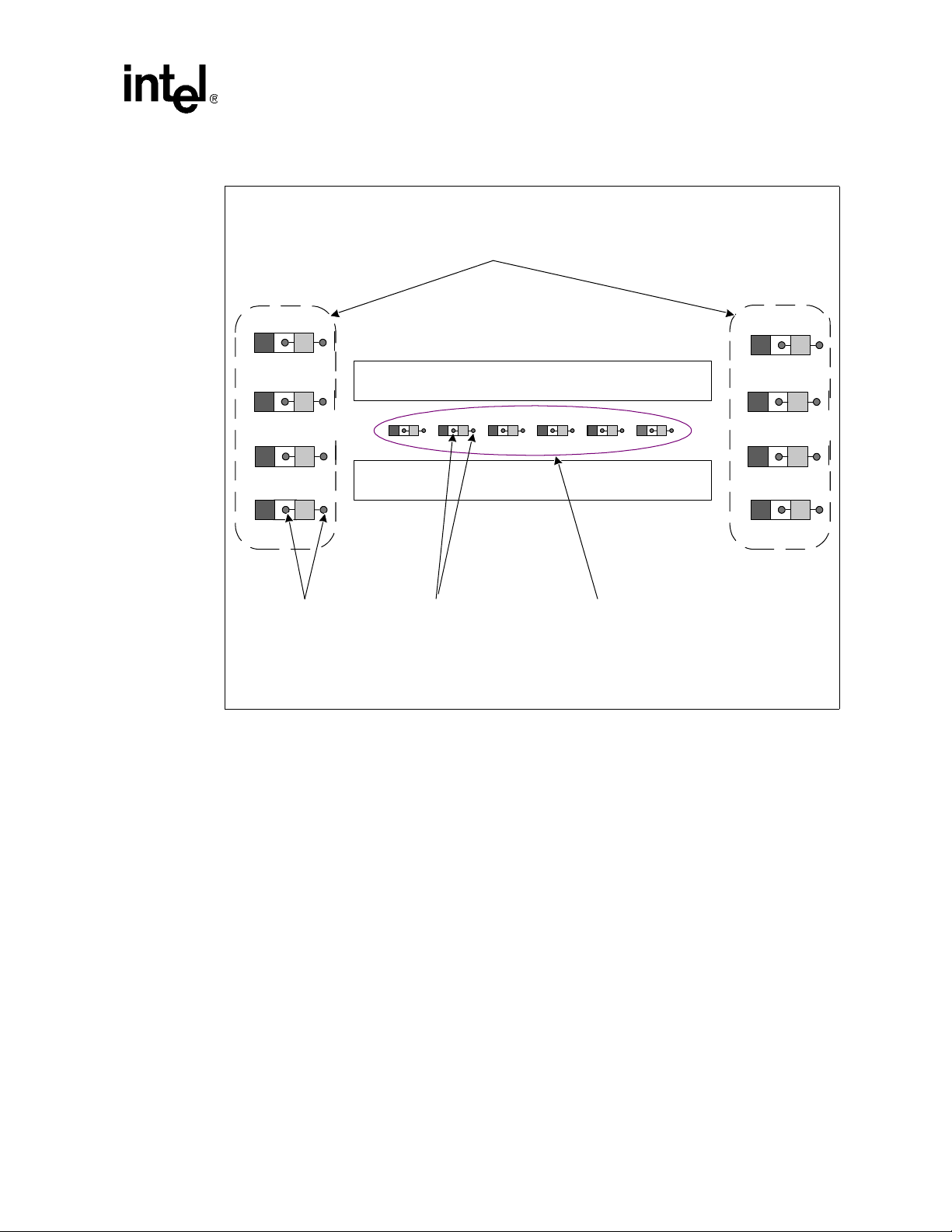
Intel® Xeon™ Processor and Intel® E7500/E7501 Chipset Compatible Platform
Figure 25. Single Channel 2-DIMM Decoupling
8 Tantulum 100 µF Capacitors
Around The DIMMs
DIMM
DIMM
2 Vias Per Capacitor to
Internal Ground Plane
6 Ceramic 0.10 µF Caps
(0603) Between DIMM
Pairs
NOTE: For each additional DIMM added per channel, add two additional 100 µF Tantalum capacitors around
the DIMM, and add six additional 0.01 µF ceramic capacitors between each DIMM pair.
Platform Design Guide Addendum 43
Page 44
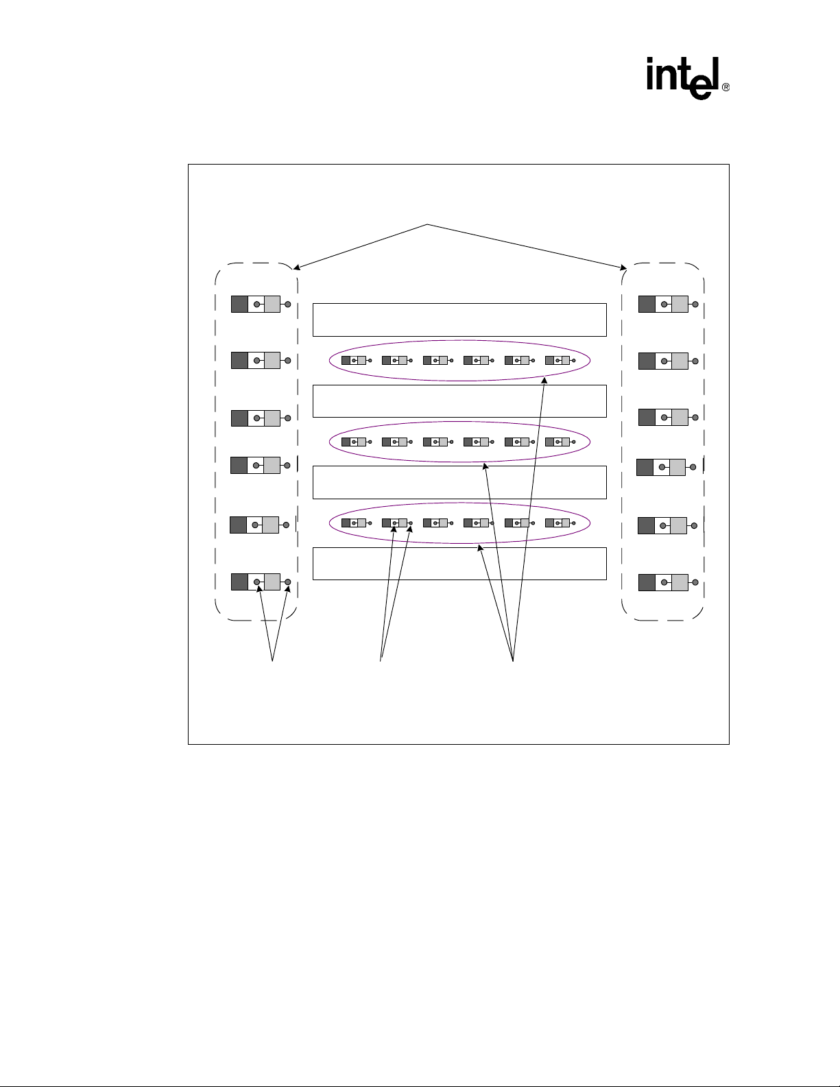
Intel® Xeon™ Processor and Intel® E7500/E7501 Chipset Compatible Platform
Figure 26. Single Channel 4-DIMM Decoupling
12 Tantulum 100 µF Capacitors
Around The DIMMs
DIMM
DIMM
2 Vias Per Capacitor to
Internal Ground Plane
DIMM
DIMM
6 Ceramic 0.10 µF Caps
(0603) Between DIMM
Pairs
44 Platform Design Guide Addendum
 Loading...