

Intel CN430TX User Manual

CN430TX Motherboard
Technical Product Specification
August, 1997
Order Number 677606-001
The CN430TX motherboard may contain design defects or errors known as errata which may cause the product to deviate from published specifications. Current characterized
errata are documented in the CN430TX Motherboard Specification Update.

Revision History
Revision Revision History Date
-001 First release of the CN430TX Technical Product Specification. August, 1997
This product specification applies only to standard CN430TX motherboards with BIOS
identifier 4C3NT0X0.86A.
Changes to this specification will be published in the CN430TX Motherboard
Specification Update before being incorporated into a revision of this document.
Information in this document is provided in connection with Intel products. No license, express or implied, by estoppel or
otherwise, to any intellectual property rights is granted by this document. Except as provided in Intel's Terms and Conditions of
Sale for such products, Intel assumes no liability whatsoever, and Intel disclaims any express or implied warranty, relating to
sale and/or use of Intel products including liability or warranties relating to fitness for a particular purpose, merchantability, or
infringement of any patent, copyright or other intellectual property right. Intel products are not intended for use in medical, life
saving, or life sustaining applications.
Intel retains the right to make changes to specifications and product descriptions at any time, without notice.
The CN430TX motherboard may contain design defects or errors known as errata which may cause the product to deviate
from published specifications. Current characterized errata are available on request.
Contact your local Intel sales office or your distributor to obtain the latest specifications and before placing your product order.
Copies of documents which have an ordering number and are referenced in this document, or other Intel literature, may be
obtained from:
Intel Corporation
P.O. Box 7641
Mt. Prospect IL 60056-764
or call 1-800-879-4683
† Third-party brands and names are the property of their respective owners.
Copyright 1997, Intel Corporation. All rights reserved.

Contents
1 Motherboard Description
1.1 Overview......................................................................................................................7
1.2 Motherboard Manufacturing Options............................................................................9
1.3 Form Factor..................................................................................................................9
1.4 I/O Shield ...................................................................................................................11
1.5 Microprocessor...........................................................................................................11
1.5.1 Microprocessor Upgrade..............................................................................12
1.6 Memory......................................................................................................................12
1.6.1 Main Memory...............................................................................................12
1.6.2 Second-level Cache.....................................................................................13
1.7 Chipset.......................................................................................................................14
1.7.1 430TX System Controller (MTXC)................................................................14
1.7.2 430TX PCI ISA IDE Xcelerator (PIIX4)........................................................14
1.7.3 Universal Serial Bus (USB) Support.............................................................15
1.7.4 IDE Support.................................................................................................16
1.8 Super I/O Controller ...................................................................................................17
1.8.1 Serial Ports ..................................................................................................17
1.8.2 Parallel Port .................................................................................................17
1.8.3 Floppy Controller..........................................................................................18
1.8.4 Keyboard and Mouse Interface ....................................................................18
1.9 Graphics Subsystem..................................................................................................18
1.9.1 Memory Type and Size................................................................................18
1.9.2 Resolutions and Refresh Rates ...................................................................18
1.9.3 Graphics Drivers and Utilities.......................................................................19
1.10 Audio Subsystem .......................................................................................................19
1.10.1 Audio Drivers and Utilities............................................................................20
1.10.2 Audio Connectors ........................................................................................20
1.11 Hardware Monitor.......................................................................................................20
1.12 Motherboard Connectors............................................................................................21
1.12.1 Chassis Security Connector.........................................................................21
1.12.2 Fan Connector.............................................................................................22
1.12.3 NLX Card Edge Connectors ........................................................................22
1.12.4 Back Panel Connectors ...............................................................................30
1.13 Jumper Settings .........................................................................................................34
1.13.1 Normal Mode ...............................................................................................35
1.13.2 Configure Mode ...........................................................................................35
1.13.3 Recovery Mode............................................................................................36
1.13.4 Processor Configuration (J4A1)...................................................................36
1.14 Reliability....................................................................................................................37
1.15 Environmental ............................................................................................................37
iii

1.16 Power Consumption...................................................................................................37
1.16.1 Power Supply Considerations......................................................................38
1.17 Regulatory Compliance..............................................................................................39
1.17.1 Product Certification Markings.....................................................................39
2 Motherboard Resources
2.1 Memory Map ..............................................................................................................41
2.2 DMA Channels...........................................................................................................41
2.3 I/O Map ......................................................................................................................42
2.4 PCI Configuration Space Map....................................................................................44
2.5 Interrupts....................................................................................................................44
2.6 PCI Interrupt Routing Map..........................................................................................45
3 Overview of BIOS Features
3.1 Introduction ................................................................................................................47
3.1.1 BIOS Flash Memory Organization ...............................................................47
3.1.2 BIOS Upgrades............................................................................................47
3.1.3 Plug and Play: PCI Auto-configuration........................................................48
3.1.4 PCI IDE Support ..........................................................................................48
3.1.5 ISA Plug and Play........................................................................................49
3.1.6 ISA Legacy Devices .....................................................................................49
3.1.7 Desktop Management Interface...................................................................49
3.1.8 Advanced Power Management....................................................................50
3.1.9 Advanced Configuration and Power Interface (ACPI)..................................50
3.1.10 Language Support.......................................................................................52
3.1.11 Boot Options................................................................................................52
3.1.12 OEM Logo or Scan Area..............................................................................52
3.1.13 USB Support................................................................................................52
3.1.14 Security Screen............................................................................................53
3.1.15 Recovering BIOS Data.................................................................................54
3.2 BIOS Setup Program .................................................................................................55
3.2.1 Maintenance Menu ......................................................................................55
3.2.2 Overview of the Setup Menu Screens..........................................................56
3.2.3 Main Menu...................................................................................................57
3.2.4 Advanced Menu...........................................................................................59
3.2.5 Security Menu..............................................................................................62
3.2.6 Power Menu.................................................................................................63
3.2.7 Boot Menu ...................................................................................................63
3.2.8 Exit Menu.....................................................................................................64
4 Error Messages
4.1 BIOS Error Messages ................................................................................................65
4.2 Port 80h POST Codes ...............................................................................................66
iv

5 Specifications and Customer Support
5.1 Online Support...........................................................................................................73
5.2 Specifications.............................................................................................................73
Figures
1. Motherboard Components............................................................................................8
2. Motherboard Dimensions.............................................................................................9
3. Heatsink Keep Out Zone Dimensions ........................................................................10
4. Back Panel I/O Shield Dimensions.............................................................................11
5. Motherboard Connectors............................................................................................21
6. Back Panel I/O Connectors........................................................................................31
7. Jumper Block Locations.............................................................................................34
Tables
1. S3 ViRGE/GX Resolutions and Refresh Rates..........................................................19
2. Chassis Security Connector (J6A1)............................................................................21
3. Processor Fan Connector (J7A1)...............................................................................22
4. PCI Segment, Riser Interconnect Pin-out...................................................................23
5. ISA Segment, Riser Interconnect Pin-out...................................................................25
6. IDE, Floppy, and Front Panel Section, Riser Interconnect Pin-out.............................27
7. Signals, NLX Riser with Supplemental Connector......................................................29
8. Serial Port Connectors...............................................................................................31
9. PS/2 Keyboard / Mouse Connectors..........................................................................32
10. Parallel Port Connector..............................................................................................32
11. VGA Video Monitor Connector...................................................................................32
12. Stacked USB Connectors...........................................................................................33
13. Audio Mic In Connector..............................................................................................33
14. Audio Line Out/Headphone Connector .....................................................................33
15. Jumper Settings.........................................................................................................35
16. Jumper Settings for Processor Frequency.................................................................36
17. Motherboard Environmental Specifications................................................................37
18. DC Voltage .................................................................................................................38
19. Power Usage..............................................................................................................38
20. Safety Regulations.....................................................................................................39
21. EMI Regulations.........................................................................................................39
22. Memory Map ..............................................................................................................41
23. DMA Channels...........................................................................................................41
24. I/O Map ......................................................................................................................42
25. PCI Configuration Space Map....................................................................................44
26. Interrupts....................................................................................................................44
27. PCI Interrupt Routing Map..........................................................................................45
28. Flash Memory Organization .......................................................................................47
29. Recommendations for Configuring an ATAPI Device.................................................49
30. Supported ACPI-1.0 Power States.............................................................................51
31. ACPI 1.0 Wake up Events..........................................................................................51
v

32. Supervisor and User Password Functions .................................................................54
33. Setup Menu Bar.........................................................................................................55
34. Setup Function Keys..................................................................................................55
35. Maintenance Menu.....................................................................................................55
36. Overview of the Setup Menu Screens........................................................................56
37. BIOS Error Messages ................................................................................................65
38. Port 80h Codes..........................................................................................................67
39. Compliance with Specifications..................................................................................73
vi

1 Motherboard Description
1.1 Overview
The CN430TX motherboard supports Pentium® processors, Pentium OverDrive® processors, and
Pentium processors with MMX technology. Features of the motherboard include the following:
• NLX form factor
• Socket 7 Pentium processor socket
Main Memory
• Two 168-pin DIMM sockets
• Support for up to 256 MB DRAM
Second Level Cache Memory
• 256 KB or 512 KB Pipeline Burst SRAM (PBSRAM) soldered to the motherboard
Chipset and PCI/IDE Interface
• Intel 82430TX PCIset
• Integrated PCI bus mastering controller
I/O Features
• National Semiconductor PC87307 SuperI/O controller
• Integrates the following I/O functions: floppy drive interface, one multimode parallel port, two
FIFO serial ports, real-time clock, keyboard and mouse controller
• Support for two Universal Serial Bus (USB) interfaces
Expansion Slots
• Riser connector supports up to three PCI slots and up to two ISA slots
Audio Subsystem
• Yamaha OPL3-SA3 audio codec
Graphics Subsystem
†
• S3
Other Features
• Plug and Play compatible
• Support for Advanced Power Management (APM)
• Support for Advanced Configuration and Power Interface (ACPI)
• Hardware monitor ASIC
Software drivers and utilities are available from Intel.
ViRGE/GX† graphics controller
7

CN430TX Motherboard Technical Product Specification
A
U
B
C
T
D
E
F
S
R
G
H
I
OMP
KLQN J
OM06110
Figure 1. Motherboard Components
A Back panel I/O connectors L Chassis security connector
B Battery M Speaker
C Yamaha OPL3-SA3 audio codec N Socket 7 Pentium processor socket
D Bus frequency / BIOS recovery jumper O Clock multiplier jumper
E National 87307 I/O controller P Voltage regulator jumper
F 430TX PCI ISA IDE Xcelerator (PIIX4) Q Voltage regulator
G NLX Riser connector R DIMM connectors
H 2 Mbit Flash BIOS S 430TX System Controller (MTXC)
I 256 or 512 KB L2 PBSRAM cache T S3 ViRGE/GX graphics controller
J Hardware monitor ASIC U SGRAM video memory
K Fan connector
8
Motherboard Description
1.2 Motherboard Manufacturing Options
Motherboard manufacturing includes the following option - 256 or 512 KB PBSRAM second-level
cache (L2) soldered onto the motherboard.
1.3 Form Factor
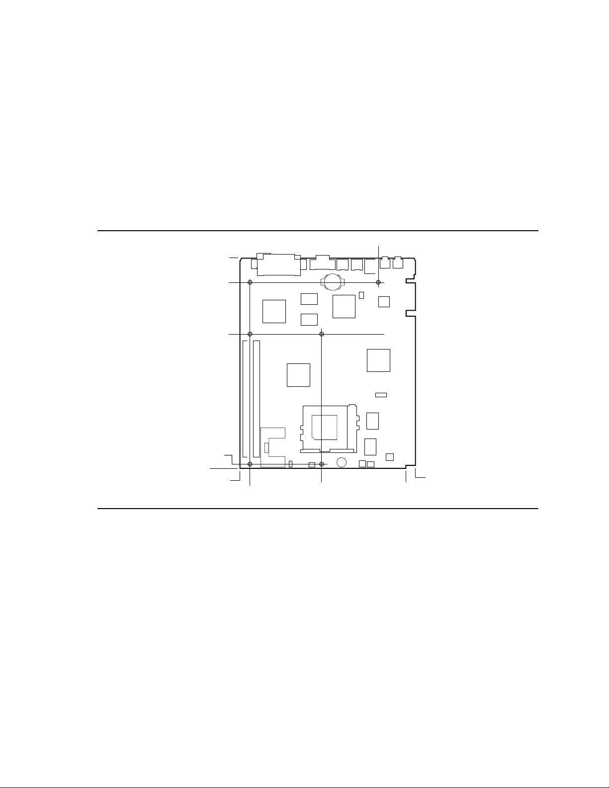
The motherboard is designed to fit into an NLX form factor chassis. Figure 2 illustrates the
mechanical form factor for the motherboard. Location of the I/O connectors, riser slot, and
mounting holes is in compliance with the NLX specification (see Section 5.2).
6.05
9.80
8.70
0.20
6.225
0.00
0.45
0.00
3.40
Figure 2. Motherboard Dimensions
7.80
7.34
OM06111
9
CN430TX Motherboard Technical Product Specification
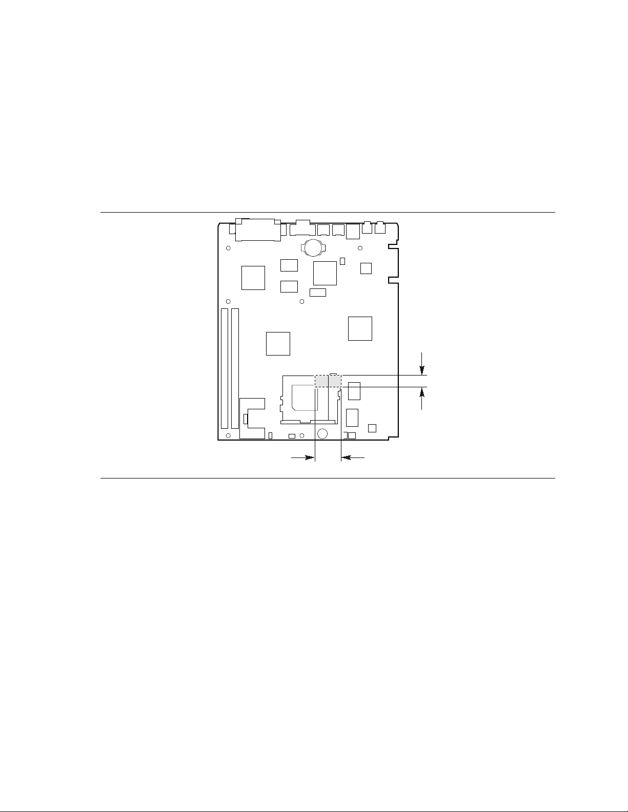
Figure 3 specifies the dimensions of the heatsink keep out zone.
NOTE
✏
Processor heatsinks used with this motherboard may interfere with add-in cards in the lower NLX
riser card slot. This is a deviation from the NLX specification keepout zone C. The actual
encroachment is 1.870 inches wide and 0.613 inches deep as shown in Figure 3. The total height
of the processor socket, the microprocessor, and the heatsink must be no higher than 0.8 inches
above the motherboard plane in order to avoid interference in this zone.
0.613
1.870
OM06336
Figure 3. Heatsink Keep Out Zone Dimensions
10
Motherboard Description
1.4 I/O Shield
The back panel I/O shield for the motherboard must meet specific dimensional and material
requirements. Computers built with this motherboard need the I/O shield to pass EMI certification
testing. Figure 4 shows the critical dimensions for the I/O shield and indicates the position of each
cutout. For more chassis design requirements, see the NLX specification.
7.274
7.429
7.908
8.853
0.530
0.948
0.456
0.00
1.175
0.570
0.168
0.456
0.366(2) 0.490(2)
0.00
1.838
2.504
3.179
0.543
0.208
4.532
4.637
5.997
Figure 4. Back Panel I/O Shield Dimensions
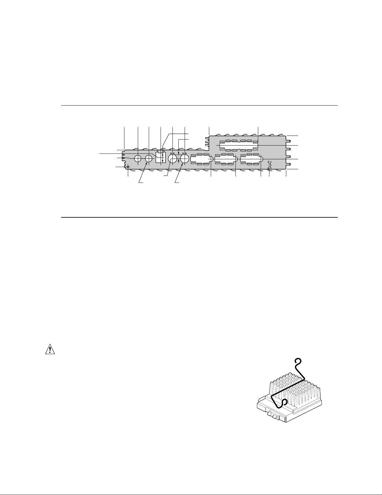
1.5 Microprocessor
The motherboard supports the following:
• Pentium processors with MMX technology operating at 166, 200, and 233 MHz.
• Pentium processors operating at 90, 100, 120, 133, 150, 166, and 200 MHz.
An onboard voltage regulator derives the necessary voltage from the computer's power supply. For
Pentium processors, a jumper enables the use of VR-, or VRE-specified processors. For Pentium
processors with MMX technology, the required voltage is automatically detected by onboard
circuitry. There are no separate or additional jumpering requirements for Pentium processors with
MMX technology.
1.752
1.197
0.447
0.143
OM06463
CAUTION
If you use clips to secure a heat sink to the processor, do not use
bail-wire style heat sink clips. These clips have been known to
damage the motherboard when installed or removed incorrectly.
The figure to the right shows an example of the bail-wire style
heat sink clip.
OM05554
11

CN430TX Motherboard Technical Product Specification
1.5.1 Microprocessor Upgrade
The motherboard has a 321-pin Socket 7 zero insertion force (ZIF) microprocessor socket.
Socket 7 supports upgrades to higher performance Pentium OverDrive processors.
1.6 Memory
1.6.1 Main Memory
The motherboard has two Dual Inline Memory Module (DIMM) sockets. Memory can be installed
in one or two sockets. The minimum memory size is 8 MB, and the maximum is 256 MB. The
BIOS automatically detects memory type, size, and speed so no jumper settings are required.
The motherboard supports the following:
• 168-pin 3.3 V DIMMs with gold-plated contacts
• 60 and 66 MHz bus speeds
• 60 ns 3.3 V unbuffered EDO memory
• 60 ns CAS Latency 2 unbuffered 4-clock 3.3 V SDRAM
• Caching for the first 64 MB of main memory
• 64-bit data path
• Single- or double-sided DIMMs in the following sizes:
DIMM Size Type Configuration Technology
8 MB 60 ns EDO 1M x 64 16 Mbit
16 MB 60 ns EDO 2M x 64 16 Mbit
32 MB 60 ns EDO 4M x 64 16 Mbit
64 MB 60 ns EDO 8M x 64 16 Mbit
128 MB 60 ns EDO 16M x 64 64 Mbit
8 MB CAS Latency 2 SDRAM 1M x 64 16 Mbit
16 MB CAS Latency 2 SDRAM 2M x 64 16 Mbit
32 MB CAS Latency 2 SDRAM 4M x 64 16 Mbit
64 MB CAS Latency 2 SDRAM 8M x 64 64 Mbit
128 MB CAS Latency 2 SDRAM 16M x 64 64 Mbit
Memory type, size, and speed can vary between sockets so EDO and SDRAM memory can be
installed on the same motherboard. Parity (x 72) DIMMs are not recommended because the
motherboard does not provide parity checking or ECC functionality.
12

Motherboard Description
1.6.1.1 EDO DRAM
EDO DRAM improves memory read performance by holding the memory data valid until the next
CAS# falling edge. With EDO DRAM, the CAS# precharge overlaps the data-valid time, which
allows CAS# to negate earlier while still satisfying the memory data-valid window. EDO DIMMs
must meet the Intel EDO DRAM DIMM v1.2 Specification.
NOTE
✏
Due to loading anomalies, using SDRAM DIMMs with a n x 4 DRAM base are not supported. For
example, a DIMM that uses sixteen 16 Mbit x 4 devices should not be used.
1.6.1.2 SDRAM
Synchronous DRAM (SDRAM) improves memory performance. Unlike EDO memory, SDRAM
is synchronous with the memory clock. This simplifies the timing design and increases memory
speed because all timing is dependent on the number of memory clock cycles. To function
correctly, SDRAM DIMMs must meet the Intel 4-clock 66 MHz 64-bit unbuffered SDRAM
DIMM v1.0 Specification.
NOTE
✏
Due to loading anomalies, using SDRAM DIMMs with a n x 4 DRAM base are not supported.
For example, a DIMM that uses sixteen 16 Mbit x 4 devices should not be used.
NOTE
✏
The board supports unbuffered, 4-clock 3.3 V SDRAM DIMMs only. Buffered, 5 V, or 2-clock
SDRAM DIMMs cannot be used.
1.6.2 Second-level Cache
The 512 KB direct-mapped write-back L2 cache consists of two 64 Kbit x 32 global write enable
(GWE) Pipeline PBSRAM devices soldered to the motherboard. A 32 Kbit x 8 external Tag
SRAM provides caching support for up to 64 MB of main memory.
The 256KB L2 cache substitutes two 32 Kbit x 32 PBSRAMs and an 8 Kbit x 8 external Tag
SRAM.
13

CN430TX Motherboard Technical Product Specification
1.7 Chipset
The Intel 82430TX PCIset consists of the TX System Controller (MTXC) device and the PCI ISA
IDE Xcelerator (PIIX4) device.
1.7.1 430TX System Controller (MTXC)
The MTXC integrates the cache and main memory DRAM control functions and provides bus
control to handle transfers between the processor, cache, main memory, and the PCI bus. The
MTXC allows PCI masters to achieve full PCI bandwidth by using the snoop ahead feature. For
increased system performance the MTXC integrates posted write and read prefetch buffers. The
MTXC features include:
• Microprocessor interface control
• Integrated L2 write-back cache controller
Supports pipeline burst SRAM
64 MB maximum DRAM cacheability
Direct mapped organization—write back only
Cache hit read/write cycle timings at 3-1-1-1
Back to back read/write cycles at 3-1-1-1-1-1-1-1
• Integrated DRAM controller
8 MB to 256 MB main memory
64-Mbit DRAM/SDRAM technology support
3.3 V EDO and unbuffered synchronous DRAM support
Non-parity (x64) support only
• Fully synchronous minimum latency PCI bus interface
PCI compliance (see Section 5.2 for compliance level)
30 and 33 MHz bus speeds
PCI to DRAM data throughput or greater than 100 MB/sec
Up to four PCI masters in addition to the PIIX4
• Power management control
Provides PCI CLKRUN# signal to control memory clock on the PCI bus (on/off)
Internal clock control (gated off if no host or PCI bus activity)
1.7.2 430TX PCI ISA IDE Xcelerator (PIIX4)
The Intel 430TX PCI ISA IDE Xcelerator (PIIX4) is a multifunction PCI device implementing a
PCI to ISA bridge, PCI IDE functionality, a Universal Serial Bus (USB) host/hub function, and
Enhanced Power Management. The PIIX4 features include:
• Multifunction PCI to ISA bridge
Supports the PCI bus at 30 and 33 MHz
PCI compliant (see Section 5.2 for compliance level)
Full ISA or extended I/O (EIO) bus support
14

Motherboard Description
• USB controller
Two USB ports (see Section 5.2 for compliance level)
Supports legacy keyboard and mouse
Supports UHCI design guide revision 1.1 interface
• Integrated dual-channel enhanced IDE interface
Support for up to four IDE devices
PIO Mode 4 transfers at up to 14 MB/sec
Supports “Ultra DMA/33” synchronous DMA mode transfers up to 33 MB/sec
Integrated 8 x 32-bit buffer for bus master PCI IDE burst transfers
Bus master mode
• Enhanced DMA controller
Two 8237-based DMA controllers
Supports PCI DMA with three PC/PCI channels and distributed DMA protocols
Fast type-F DMA for reduced PCI bus usage
• Interrupt controller based on 82C59
Support for 15 interrupts
Programmable for edge/level sensitivity
• Power management logic
Sleep/resume logic
Supports thermal alarm
Support for Wake On Modem through Ring Indicate input
†
Support for Wake on LAN
through LID input
• Real-Time Clock
256 byte battery-backed CMOS SRAM
Includes date alarm
• 16-bit counters/timers based on 82C54
1.7.3 Universal Serial Bus (USB) Support
The motherboard features two USB ports. The ports permit the direct connection of two USB
peripherals without an external hub. If more devices are required, an external hub can be
connected to either of the built-in ports. The motherboard fully supports the standard universal
host controller interface (UHCI) and uses standard software drivers that are UHCI-compatible.
Features of the USB include:
• Self-identifying, hot pluggable peripherals
• Automatic mapping of function to driver and configuration
• Support for isochronous and asynchronous transfer types over the same set of wires
• Support for up to 127 physical devices
• Guaranteed bandwidth and low latencies appropriate for telephony, audio, and other
applications
• Error handling and fault recovery mechanisms built into protocol
15

CN430TX Motherboard Technical Product Specification
NOTE
✏
Computers that have an unshielded cable attached to the USB port might not meet FCC Class B
requirements, even if no device or a low speed USB device is attached to the cable. Use shielded
cable that meets the requirements for full speed devices.
NOTE
✏
Advanced Power Management will not function as expected when a USB keyboard or mouse is
used. USB activity is not monitored by the APM event counter, therefore, activity from a USB
keyboard or mouse will not keep the system awake or bring a system out of APM sleep mode. If a
USB keyboard or mouse is being used, APM should be disabled.
1.7.4 IDE Support
The motherboard has two independent bus mastering PCI IDE interfaces that support PIO Mode 3,
PIO Mode 4, ATA-33 (Ultra DMA-33), and ATAPI (e.g., CD-ROM) devices. The BIOS supports
Logical Block Addressing (LBA) and Extended Cylinder Head Sector (ECHS) translation modes.
IDE device transfer rate and translation mode are automatically detected by the BIOS.
Normally, programmed I/O operations require a substantial amount of processor bandwidth;
however, in multi-tasking operating systems like Windows
mastering IDE can be devoted to other tasks while disk transfers are occurring.
†
95, the bandwidth freed by bus
1.7.4.1 LS-120 Support
LS-120 MB Diskette technology enables users to store 120 MB of data on a single, 3.5-inch
removable diskette. LS-120 technology is backward (both read and write) compatible with
1.44 MB and 720 KB DOS-formatted diskettes and is supported by Windows 95 and
Windows NT
The motherboard allows connection of an LS-120 compatible drive and a standard 3.5-inch diskette
drive. The LS-120 drive can be configured as a boot device, if selected in the BIOS setup utility.
NOTE
✏
If you connect an LS-120 drive to an IDE connector and configure it as the "A" drive and
configure a standard 3.5-inch floppy as a "B" drive, the standard floppy must be connected to the
floppy drive cable's "A" connector (the connector at the end of the cable).
†
operating systems.
16

Motherboard Description
1.8 Super I/O Controller
The PC87307VUL Super I/O Controller from National Semiconductor is an ISA Plug and Play
compatible (see Section 5.2 for compliance level), multifunction I/O device that provides the
following features:
• Serial ports:
Two 16450/16550A-software compatible UARTs
Send/receive 16-byte FIFO
Four 8-bit DMA options for the UART with Slow Infrared Support (USI)
Ring indicator support for both serial ports
• Multimode bi-directional parallel port
Standard mode, IBM and Centronics compatible
Enhanced Parallel Port (EPP) mode with BIOS and driver support
High-speed Extended Capabilities Port (ECP) mode
• Floppy disk controller
DP8473 and N82077 compatible
16 byte FIFO
†
PS/2
CMOS disk input and output logic
High performance digital data separator (DDS)
PC-AT
• Keyboard and mouse controller
Industry standard 8042A compatible
General purpose microcontroller
8 bit internal data bus
• Support for an IrDA
diagnostic register support
†
and PS/2 drive mode support
†
and Consumer IR-compliant infrared interface
By default, the I/O controller interfaces are automatically configured during boot up. The I/O
controller can also be manually configured in the Setup program.
1.8.1 Serial Ports
The 16450/16550A compatible UART’s support data transfers at speeds up to 115.2 Kbaud with
BIOS serial port support. The ports are implemented with two 9-pin D-Sub serial port connectors
located on the back panel.
1.8.2 Parallel Port
The motherboard supports one multimode bi-directional parallel port. The port is implemented
with a one 25-pin D-Sub connector located on the back panel. In the Setup program, there are four
options for parallel port operation:
• Compatible (standard mode)
• Bi-directional (PS/2 compatible)
• Bi-directional Enhanced Parallel Port (EPP)
• Bi-directional Extended Capabilities Port (ECP)
17

CN430TX Motherboard Technical Product Specification
1.8.3 Floppy Controller
The I/O controller is software compatible with the DP8473 and N82077 floppy drive controllers
and supports both PC-AT and PS/2 modes. The floppy interface can be configured for the
following floppy drive capacities and sizes:
• 360 KB, 5.25-inch
• 1.2 MB, 5.25-inch
• 720 KB, 3.5-inch
• 1.2 MB, 3.5-inch (driver required)
• 1.25/1.44 MB, 3.5-inch
• 2.88 MB, 3.5-inch
1.8.4 Keyboard and Mouse Interface
NOTE
✏
The mouse and keyboard can be plugged into either of the PS/2 connectors.
The keyboard controller contains keyboard and mouse controller code from American Megatrends
Incorporated (AMI). The code provides the traditional keyboard and mouse control functions,
including Power On/Reset password protection. A password can be specified in the Setup
program.
The keyboard controller also supports a three-key (<Ctrl><Alt><Del> software reset function. The
key sequence resets the computer’s software by jumping to the beginning of the BIOS code and
running the Power-on Self Test (POST).
1.9 Graphics Subsystem
The onboard graphics subsystem uses the S3 ViRGE/GX graphics controller, with the following
features:
• 3-D graphics capability
• SGRAM-based chip optimized for synchronous operation
• 64-bit graphics engine with accelerator core
• 170 MHz 24-bit RAMDAC/clock synthesizer
• Dual programmable clock generators
• DCI-based linear addressing scheme
• S3 Streams Processor provides high video playback quality
1.9.1 Memory Type and Size
The controller is supported by 2 MB of SGRAM soldered to the motherboard.
18

Motherboard Description
1.9.2 Resolutions and Refresh Rates
Table 1. S3 ViRGE/GX Resolutions and Refresh Rates
Refresh Rate (Hz) At:
4-bit Color
Resolution
640 x 480 60 60, 70, 72, 75, 85 60, 72, 75, 85 60, 72, 75, 85
800 x 600 56, 60, 72, 75, 85 56, 60, 72, 75, 85 56, 60, 72, 75, 85 56, 60, 72, 75, 85
1024 x 768 43(IL), 60, 70, 75, 85 43(IL), 60 ,70, 75, 85 43(IL), 60, 70, 75, 85 not supported
1152 x 864 not supported 60 not supported not supported
1280 x 1024 43(IL), 60, 75, 80 43(IL), 60, 75, 85 not supported not supported
1600 x 1200 not supported 48.5(IL), 60 not supported not supported
IL = Interlaced
(16 Colors)
8-bit Color
(256 Colors)
15/16-bit Color
(32K/64K Colors)
24-bit Color
(16M Colors)
1.9.3 Graphics Drivers and Utilities
Graphics drivers and common graphics utilities are available for Windows 3.x, Windows 95, and
Windows NT. Drivers and utilities are available from Intel’s World Wide Web site (see
Section 5.1).
1.10 Audio Subsystem
The onboard audio subsystem features the Yamaha OPL3-SA3 audio codec. The chip integrates a
16-bit audio codec, OPL3 FM synthesis and its DAC, 3-D enhanced stereo controller, and an
interface for MPU-401 and a joystick. The chip provides all the digital audio and analog mixing
functions needed for recording and playing sound. Features of the chip include the following:
• Integrated 3-D enhanced stereo controller including all required analog components
• Stereo analog-to-digital and digital-to-analog converters
• Analog mixing, anti-aliasing, and reconstruction filters
• Support for 16-bit address decode
• ADPCM, A-law, or µlaw digital audio compression/decompression
• Full digital control of all mixer and volume control functions
• Plug and Play compatibility
†
• Sound Blaster
and Windows Sound System compatibility
19

CN430TX Motherboard Technical Product Specification
The following table shows the IRQ, DMA channel, and base I/O address options for the audio
subsystem. These options are automatically chosen by the Plug and Play interface, so there are no
default settings.
Resource IRQ (Options) DMA Channel (Options) I/O Address (Options)
Sound Blaster
(DMA playback, DMA shared with
Windows Sound System capture)
Windows Sound System
(DMA playback)
MPU-401
(IRQ shared with Sound Blaster)
MIDI / Game Port 201h
†
AdLib
5
7
9
10
11
5
7
9
10
11
0
1
3
0
1
3
220h
240h
220-280h
530h
E80h
530-F48h
330h
300h
300-334h
201-211h
388h
388-3F8h
Note: The MIDI/Game Port feature is not implemented.
1.10.1 Audio Drivers and Utilities
Audio software and utilities are available from Intel’s World Wide Web site (see Section 5.1).
1.10.2 Audio Connectors
The motherboard has Mic In and Line Out connectors on the back panel.
1.11 Hardware Monitor
The hardware monitor component (National Semiconductor LM78) provides low-cost
instrumentation capabilities designed to reduce the total cost of owning a PC when used with
LANDesk
include:
• An integrated ambient temperature sensor
• Fan speed sensors
• Power supply voltage monitoring to detect levels above or below acceptable values
• Registers for storing POST hardware test results and error codes
• Remote reset capabilities from a remote peer or server through LANDesk Client Manager,
®
Client Manager. The hardware implementation is a single-chip ASIC. Features
Version 3.0 and service layers (when available)
When suggested ratings for temperature, fan speed, or voltage are exceeded, an interrupt is
activated. The hardware monitor component (LM78) connects to the ISA bus as an 8-bit I/O
mapped device.
20
1.12 Motherboard Connectors
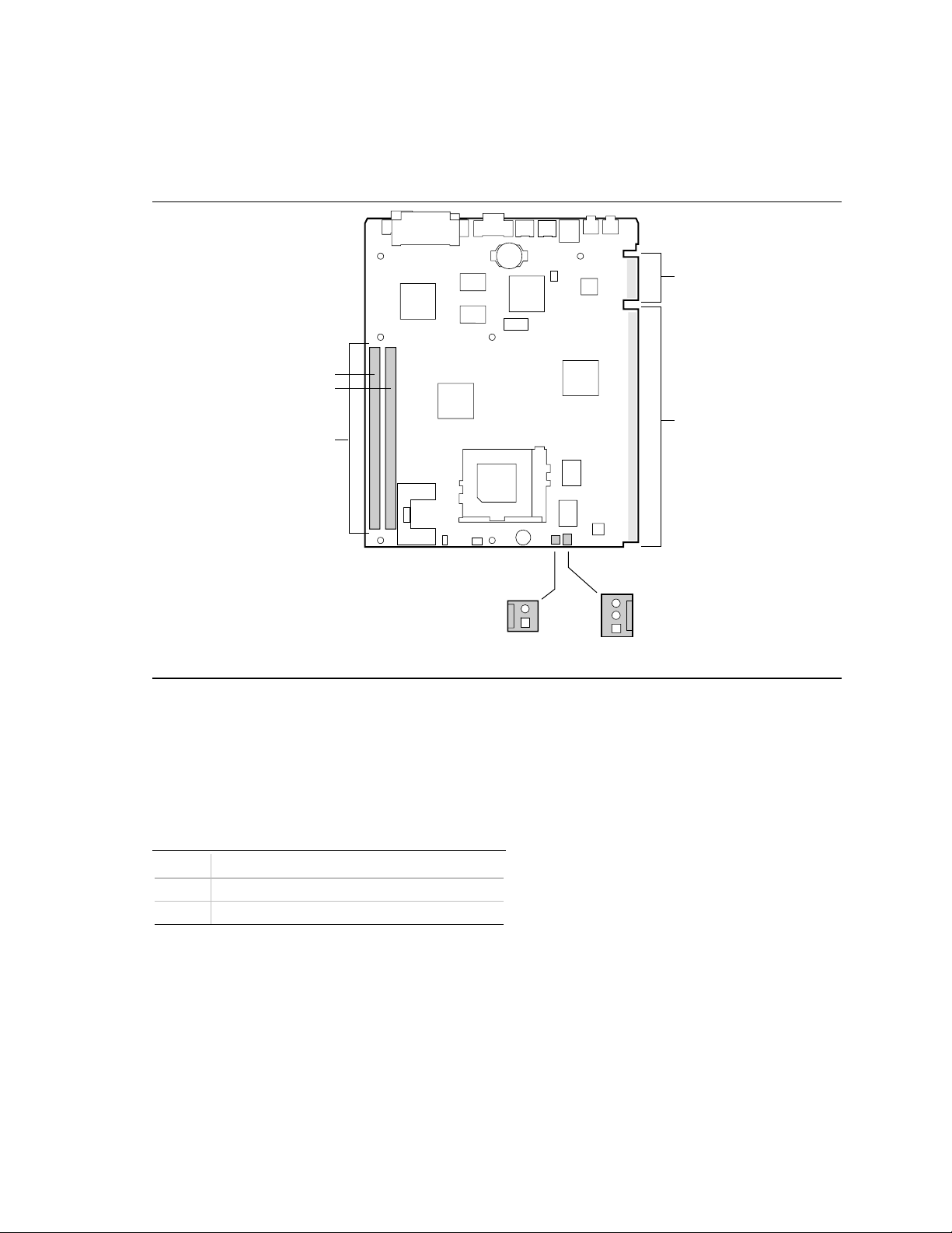
Figure 5 shows the connectors on the motherboard.
Bank 0
Bank 1
DIMM Sockets(2)
J1D1, J1D2
Motherboard Description
Supplemental
Connector
Riser
Connector
J7A1
1
Chassis
Security
Connector
J6A1
1
Figure 5. Motherboard Connectors
1.12.1 Chassis Security Connector
A 1 x 2-pin connector that supports an intrusion switch (or alarm) on the chassis.
Table 2. Chassis Security Connector (J6A1)
Pin Signal Name
1 Ground
2 CHS_SEC
Fan
Connector
OM06114
21

CN430TX Motherboard Technical Product Specification
1.12.2 Fan Connector
A 1 x 3-pin fan connector can support a processor or chassis fan. Pin 3 on the connector can be
used to implement a sensor that monitors fan operation.
Table 3. Processor Fan Connector (J7A1)
Pin Signal Name
1 Ground
2 +12 V
3 Fan_sense (tachometer)
1.12.3 NLX Card Edge Connectors
The NLX motherboard connects to the riser with a 340 pin (2x170) pin, 1mm pitch, card edge
connector. The pin-out for the riser interconnect is shown below. The “A” side is the bottom
(secondary) side of the motherboard, and the “B” side is the top (primary) side of the motherboard.
Pin 1 is toward the back of the motherboard (back panel I/O connectors). In addition, there is a
26 pin (2x13) supplemental gold finger contact. According to the NLX specification, the riser
must provide signals for the following:
• PCI expansion slots
• ISA expansion slots
• IDE headers
• 1 floppy drive header
• Miscellaneous front panel signals
For power requirements, see Section 1.16.
Table 4, Table 5, and Table 6 specify the pinouts located on the primary connector; Table 7
specifies the pinouts located on the supplemental connector. All edge connector pin definitions are
defined in the NLX specification, version 1.2.
22

Motherboard Description
Table 4. PCI Segment, Riser Interconnect Pin-out
Pin# Signal Name Type I/O Termination Pin Signal Name Type I/O Termination
A1 -12V PWR NA NA B1 PCSPKR_RT AUDIO O NA
A2 REQ4# PCI I RIS B2 +12V PWR NA NA
A3 +12V PWR NA NA B3 PCSPKR_LFT AUDIO O NA
A4 GNT4# PCI O RIS B4 +12V PWR NA NA
A5 3.3VDC PWR NA NA B5 PCICLK0 PCI O MB
A6 PCIINT3# PCI I RIS B6 GND PWR NA NA
A7 3.3VDC PWR NA NA B7 PCICLK1 PCI O MB
A8 PCIINT0# PCI I RIS B8 SER_IRQ MISC I/O MB
A9 PCIINT1# PCI I RIS B9 PCIINT2# PCI I RIS
A10 PCICLK2 PCI O MB B10 3.3VDC PWR NA NA
A11 3.3VDC PWR NA NA B11 PCICLK3 PCI O MB
A12 PCI_RST# PCI O MB B12 GND PWR NA NA
A13 GNT0# PCI O RIS B13 GNT3# PCI O RIS
A14 PCICLK4 PCI O MB B14 3.3VDC PWR NA NA
A15 GND PWR NA NA B15 GNT2# PCI O RIS
A16 GNT1# PCI O RIS B16 AD[31] PCI I/O RIS
A17 3.3VDC PWR NA NA B17 REQ0# PCI I RIS
A18 REQ2# PCI I RIS B18 GND PWR NA NA
A19 REQ3# PCI I RIS B19 AD[29] PCI I/O RIS
A20 AD[30] PCI I/O RIS B20 AD[28] PCI I/O RIS
A21 GND PWR NA NA B21 AD[26] PCI I/O RIS
A22 AD[25] PCI I/O RIS B22 3.3VDC PWR NA NA
A23 REQ1# PCI I RIS B23 AD[24] PCI I/O RIS
A24 AD[27] PCI I/O RIS B24 C/BE[3]# PCI I/O RIS
A25 3.3VDC PWR NA NA B25 AD[22] PCI I/O RIS
A26 AD[23] PCI I/O RIS B26 GND PWR NA NA
A27 AD[20] PCI I/O RIS B27 AD[21] PCI I/O RIS
A28 AD[18] PCI I/O RIS B28 AD[19] PCI I/O RIS
A29 GND PWR NA NA B29 AD[16] PCI I/O RIS
A30 AD[17] PCI I/O RIS B30 3.3VDC PWR NA NA
A31 IRDY# PCI I/O RIS B31 C/BE[2]# PCI I/O RIS
A32 DEVSEL# PCI I/O RIS B32 FRAME# PCI I/O RIS
A33 3.3VDC PWR NA NA B33 TRDY# PCI I/O RIS
A34 STOP# PCI I/O RIS B34 GND PWR NA NA
A35 PERR# PCI I/O RIS B35 SDONE PCI I/O RIS
A36 SERR# PCI I/O RIS B36 LOCK# PCI I/O RIS
A37 GND PWR NA NA B37 SBO# PCI I/O RIS
continued
☛
23
 Loading...