

Page 1

查询80C152JA供应商
UNIVERSAL COMMUNICATION CONTROLLER
Y
Superset of 80C51 Architecture
Y
Multi-Protocol Serial Communication
I/O Port (2.048 Mbps/2.4 Mbps Max)
Ð SDLC/HDLC Only
Ð CSMA/CD and SDLC/HDLC
Ð User Definable Protocols
Y
Full Duplex/Half Duplex
Y
MCSÉ-51 Compatible UART
Y
16.5 MHz Maximum Clock Frequency
Y
Multiple Power Conservation Modes
Y
64KB Program Memory Addressing
8XC152JA/JB/JC/JD
8-BIT MICROCONTROLLER
X
8K Factory Mask Programmable ROM Available
Y
64KB Data Memory Addressing
Y
256 Bytes On-Chip RAM
Y
Dual On-Chip DMA Channels
Y
Hold/Hold Acknowledge
Y
Two General Purpose Timer/Counters
Y
5 or 7 I/O Ports
Y
56 Special Function Registers
Y
11 Interrupt Sources
Y
Available in 48 Pin Dual-in-Line Package
and 68 Pin Surface Mount PLCC
Package
(See Packaging Spec. OrderÝ231369)
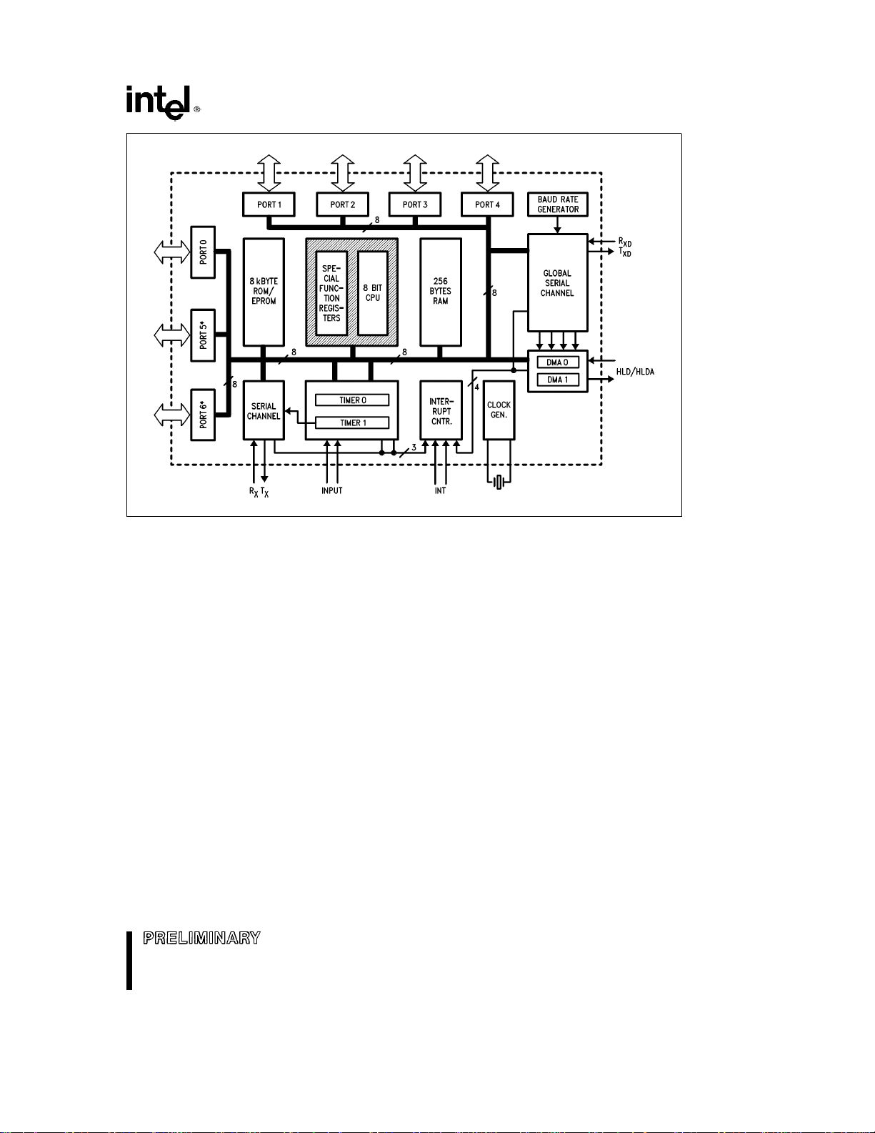
The 80C152, which is based on the MCSÉ-51 CPU, is a highly integrated single-chip 8-bit microcontroller
designed for cost-sensitive, high-speed, serial communications. It is well suited for implementing Integrated
Services Digital Networks (ISDN), emerging Local Area Networks, and user defined serial backplane applications. In addition to the multi-protocol communication capability, the 80C152 offers traditional microcontroller
features for peripheral I/O interface and control.
Silicon implementations are much more cost effective than multi-wire cables found in board level parallel-toserial and serial-to-parallel converters. The 83C152 contains, in silicon, all the features needed for the serialto-parallel conversion. Other 83C152 benefits include: 1) better noise immunity through differential signaling or
fiber optic connections, 2) data integrity utilizing the standard, designed in CRC checks, and 3) better modularity of hardware and software designs. All of theseÐcost, network parameter and real estate improvementsÐ
apply to 83C152 serial links between boards or systems and 83C152 serial links on a single board.
*Other brands and names are the property of their respective owners.
Information in this document is provided in connection with Intel products. Intel assumes no liability whatsoever, including infringement of any patent or
copyright, for sale and use of Intel products except as provided in Intel’s Terms and Conditions of Sale for such products. Intel retains the right to make
changes to these specifications at any time, without notice. Microcomputer Products may have minor variations to this specification known as errata.
October 1989COPYRIGHT©INTEL CORPORATION, 1995 Order Number: 270431-003
Page 2
8XC152JA/JB/JC/JD
270431– 2
270431– 1
270431– 3
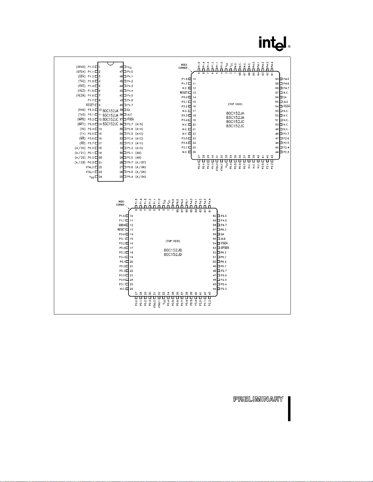
Figure 1. Connection Diagrams
2
Page 3
8XC152JA/JB/JC/JD
*On 80C152JB/JD Only 270431– 18
Figure 2. Block Diagram
3
Page 4
8XC152JA/JB/JC/JD
is used in conjunction with Port 5 and Port 6
80C152JB/JD General Description
The 80C152JB/JD is a ROMless extension of the
80C152 Universal Communication controller. The
80C152JB has the same five 8-bit I/O ports of the
80C152, plus an additional two 8-bit I/O ports, Port 5
and Port 6. The 80C152JB/JD also has two additional control pins, EBEN (EPROM Bus ENable), and
EPSEN
(EPROM bus Program Store ENable).
EBEN selects the functionality of Port 5 and Port 6.
When EBEN is low, these ports are strictly I/O, similar to Port 4. The SFR location for Port 5 is 91H and
Port 6 is 0A1H. This means Port 5 and Port 6 are not
bit addressable. With EBEN low, all program memory fetches take place via Port 0 and Port 2. (The
80C152 is a ROMless only product). When EBEN is
high, Port 5 and Port 6 form an address/data bus
called the E-Bus (EPROM-Bus) for program memory
operations.
Table 1. Program Memory Fetches
EBEN EA
0 0 P0, P2 Active Inactive Addresses 0–0FFFFH
0 1 N/A N/A N/A Invalid Combination
1 0 P5, P6 Inactive Active Addresses 0–0FFFFH
1 1 P5, P6 Inactive Active Addresses 0–1FFFH
Program
Fetch via
P0, P2 Active Inactive Addresses
EPSEN
program memory operations. EPSEN
during program memory operation, but sup-
PSEN
ports Port 5 and Port 6. EPSEN
external program memory for Port 5 and Port 6.
EPSEN
is activated twice during each machine cycle
unless an external data memory operation occurs on
Port(s) 0 and Port 2. When external data memory is
accessed the second activation of EPSEN
skipped, which is the same as when using PSEN
Note that data memory fetches cannot be made
through Ports 5 and 6.
When EBEN is high and EA is low, all program memory operations take place via Ports 5 and 6. The high
byte of the address goes out on Port 6, and the low
byte is output on Port 5. ALE is still used to latch the
address on Port 5. Next, the op code is read on Port
5. The timing is the same as when using Ports 0 and
2 for external program memory operations.
PSEN
EPSEN Comments
is the read strobe to
functions like
t
2000H
is
.
Table 2. 8XC152 Product Differences
ROMless
Version
80C152JA
80C152JB
80C152JC
80C152JD
NOTES:
e
options available
*
0 standard frequency range 3.5 MHz to 12 MHz
b
1’’ frequency range 3.5 MHz to 16.5 MHz
0‘‘
4
CSMA/CD
and
HDLC/SDLC Available DIP
HDLC/SDLC
Only
**
***
ROM PLCC
Version and
(83C152JA)
**
(83C152JC)
PLCC 5 I/O 7 I/0
Only Ports Ports
**
**
***
Page 5
8XC152JA/JB/JC/JD
Ý
Pin
DIP PLCC
(1)
48 2 VCCÐSupply voltage.
24 3,33
(2)
VSSÐCircuit ground.
18-21, 27-30, Port 0ÐPort 0 is an 8-bit open drain bidirectional I/O port. As an output port each pin
25-28 34-37 can sink 8 LS TTL inputs. Port 0 pins that have 1s written to them float, and in that
state can be used as high-impedance inputs.
Port 0 is also the multiplexed low-order address and data bus during accesses to
external program memory if EBEN is pulled low. During accesses to external Data
Memory, Port 0 always emits the low-order address byte and serves as the multiplexed
data bus. In these applications it uses strong internal pullups when emitting 1s.
Port 0 also outputs the code bytes during program verification. External pullups are
required during program verification.
1-8 4-11 Port 1ÐPort 1 is an 8-bit bidirectional I/O port with internal pullups. Port 1 pins that
have 1s written to them are pulled high by the internal pullups, and in that state can be
used as inputs. As inputs, Port 1 pins that are externally being pulled low will source
current (I
, on the data sheet) because of the internal pullups.
IL
Port 1 also serves the functions of various special features of the 8XC152, as listed
below:
Pin Name Alternate Function
P1.0 GRXD GSC data input pin
P1.1 GTXD GSC data output pin
P1.2 DEN GSC enable signal for an external driver
P1.3 TXC
P1.4 RXC
P1.5 HLD
P1.6 HLDA DMA hold acknowledge input/output
29-36 41-48 Port 2ÐPort 2 is an 8-bit bidirectional I/O port with internal pullups. Port 2 pins that
have 1s written to them are pulled high by the internal pullups, and in that state can be
used as inputs. As inputs, Port 2 pins that are externally being pulled low will source
current (IIL, on the data sheet) because of the internal pullups.
Port 2 emits the high-order address byte during fetches from external Program
Memory if EBEN is pulled low. During accesses to external Data Memory that use 16bit addresses (MOVX
@
DPTR and DMA operations), Port 2 emits the high-order
address byte. In these applications it uses strong internal pullups when emitting 1s.
During accesses to external Data Memory that use 8-bit addresses (MOVX
Port 2 emits the contents of the P2 Special Function Register.
Port 2 also receives the high-order address bits during program verification.
10- 17 14-16, Port 3ÐPort 3 is an 8-bit bidirectional I/O port with internal pullups. Port 3 pins that
18, 19, have 1s written to them are pulled high by the internal pullups, and in that state can be
23-25 used as inputs. As inputs, Port 3 pins that are externally being pulled low will source
current (I
, on the data sheet) because of the pullups.
IL
Port 3 also serves the functions of various special features of the MCS-51 Family, as
listed below:
Pin Name Alternate Function
P3.0 RXD Serial input line
P3.1 TXD Serial output line
P3.2 INT0
P3.3 INT1
P3.4 T0 Timer 0 external input
P3.5 T1 Timer 1 external input
P3.6 WR External Data Memory Write strobe
P3.7 RD
Pin Description
GSC input pin for external transmit clock
GSC input pin for external receive clock
DMA hold input/output
External Interrupt 0
External Interrupt 1
External Data Memory Read strobe
@
Ri),
5
Page 6
8XC152JA/JB/JC/JD
Pin Description (Continued)
Ý
Pin
47-40 65-58 Port 4ÐPort 4 is an 8-bit bidirectional I/O port with internal pullups. Port 4 pins that
have 1s written to them are pulled high by the internal pullups, and in that state can
be used as inputs. As inputs, Port 4 pins that are externally being pulled low will
source current (I
Port 4 also receives the low-order address bytes during program verification.
, on the data sheet) because of the internal pullups. In addition,
IL
913RSTÐReset input. A logic low on this pin for three machine cycles while the
oscillator is running resets the device. An internal pullup resistor permits a power-on
reset to be generated using only an external capacitor to VSS. Although the GSC
recognizes the reset after three machine cycles, data may continue to be
transmitted for up to 4 machine cycles after Reset is first applied.
38 55 ALEÐAddress Latch Enable output signal for latching the low byte of the address
during accesses to external memory.
In normal operation ALE is emitted at a constant rate of (/6 the oscillator
frequency, and may be used for external timing or clocking purposes. Note,
however, that one ALE pulse is skipped during each access to external Data
Memory. While in Reset, ALE remains at a constant high level.
37 54 PSENÐProgram Store Enable is the Read strobe to External Program Memory.
When the 8XC152 is executing from external program memory, PSEN
(low). When the device is executing code from External Program Memory, PSEN
activated twice each machine cycle, except that two PSEN
during each access to External Data Memory. While in Reset, PSEN
constant high level.
39 56 EAÐExternal Access enable. EA must be externally pulled low in order to enable
the 8XC152 to fetch code from External Program Memory locations 0000H to
0FFFH.
EA
must be connected to VCCfor internal program execution.
23 32 XTAL1ÐInput to the inverting oscillator amplifier and input to the internal clock
generating circuits.
22 31 XTAL2ÐOutput from the inverting oscillator amplifier.
N/A 17, 20 Port 5ÐPort 5 is an 8-bit bidirectional I/O port with internal pullups. Port 5 pins that
21, 22 have 1s written to them are pulled high by the internal pullups, and in that state can
38, 39 be used as inputs. As inputs, Port 5 pins that are externally being pulled low will
40, 49 source current (I
Port 5 is also the multiplexed low-order address and data bus during accesses to
, on the data sheet) because of the internal pullups.
IL
external program memory if EBEN is pulled high. In this application it uses strong
pullups when emitting 1s.
N/A 67, 66 Port 6ÐPort 6 is an 8-bit bidirectional I/O port with internal pullups. Port 6 pins that
52, 57 have 1s written to them are pulled high by the internal pullups, and in that state can
50, 68 be used as inputs. As inputs, Port 6 pins that are externally pulled low will source
1, 51 current (I
, on the data sheet) because of the internal pullups.
IL
Port 6 emits the high-order address byte during fetches from external Program
Memory if EBEN is pulled high. In this application it uses strong pullups when
emitting 1s.
N/A 12 EBENÐE-Bus Enable input that designates whether program memory fetches take
place via Ports 0 and 2 or Ports 5 and 6. Table 1 shows how the ports are used in
conjunction with EBEN.
N/A 53 EPSENÐE-bus Program Store Enable is the Read strobe to external program
memory when EBEN is high. Table 2 shows when EPSEN
depending on the status of EBEN and EA.
Pin Description
is active
activations are skipped
remains at a
is used relative to PSEN
is
6
Page 7

8XC152JA/JB/JC/JD
OSCILLATOR CHARACTERISTICS
XTAL1 and XTAL2 are the input and output, respectively, of an inverting amplifier which can be configured for use as an on-chip oscillator, as shown in
Figure 3.
To drive the device from an external clock source,
XTAL1 should be driven, while XTAL2 is left unconnected, as shown in Figure 4. There are no requirements on the duty cycle of the external clock signal,
since the input to the internal clocking circuitry is
through a divide-by-two flip-flop, but minimum and
Figure 4. External Clock Drive
270431– 6
maximum high and low times specified on the Data
Sheet must be observed.
An external oscillator may encounter as much as a
100 pF load at XTAL1 when it starts-up. This is due
to interaction between the amplifier and its feedback
capacitance. Once the external signal meets the V
and VIHspecifications the capacitance will not exceed 20 pF.
IDLE MODE
In Idle Mode, the CPU puts itself to sleep while most
of the on-chip peripherals remain active. The major
peripherals that do not remain active during Idle, are
the DMA channels. The Idle Mode is invoked by
IL
software. The content of the on-chip RAM and all
the Special Function Registers remain unchanged
during this mode. The Idle Mode can be terminated
by any enabled interrupt or by a hardware reset.
POWER DOWN MODE
In Power Down Mode, the oscillator is stopped and
all on-chip functions cease except that the on-chip
RAM contents are maintained. The mode Power
Down is invoked by software. The Power Down
270431– 5
Figure 3. Using the On-Chip Oscillator
Table 3. Status of the External Pins During Idle and Power Down Modes
80C152JA/83C152JA/80C152JC/83C152JC
Mode
Program
Memory
ALE PSEN Port 0 Port 1 Port 2 Port 3 Port 4
Idle Internal 1 1 Data Data Data Data Data
Idle External 1 1 Float Data Address Data Data
Power Down Internal 0 0 Data Data Data Data Data
Power Down External 0 0
²
Mode can be terminated only by a hardware reset.
Float Data Data Data Data
80C152JB/80C152JD
Mode
Instruction
Bus
ALE PSEN EPSEN Port 0 Port 1 Port 2 Port 3 Port 4 Port 5 Port 6
Idle P0, P2 1 1 1 Float Data Address Data Data 0FFH 0FFH
Idle P5, P6 1 1 1 Data Data Data Data Data 0FFH Address
Power Down P0, P2 0 0 1 Float Data Data Data Data 0FFH 0FFH
Power Down P5, P6 0 1
NOTE:
For more detailed information on the reduced power modes refer to the Embedded Controller Handbook, and Application
Note AP-252, ‘‘Designing with the 80C51BH.’’
²
Note difference of logic level of PSEN during Power Down for ROM JA/JC and ROM emulation mode for JC/JD.
²
0 Data Data Data Data Data 0FFH 0FFH
7
Page 8

8XC152JA/JB/JC/JD
ABSOLUTE MAXIMUM RATINGS*
Ambient Temperature Under Bias ÀÀÀÀ0§Ctoa70§C
Storage Temperature ААААААААААb65§Ctoa150§C
Voltage on Any pin to V
ÀÀb0.5V to (V
SS
Voltage on VCCto VSSАААААААААААb0.5V toa6.5V
Power Dissipation ААААААААААААААААААААААА1.0W
CC
a
0.5V)
(9)
NOTICE: This data sheet contains preliminary information on new products in production. The specifications are subject to change without notice. Verify with
your local Intel Sales office that you have the latest
data sheet before finalizing a design.
*
WARNING: Stressing the device beyond the ‘‘Absolute
Maximum Ratings’’ may cause permanent damage.
These are stress ratings only. Operation beyond the
‘‘Operating Conditions’’ is not recommended and extended exposure beyond the ‘‘Operating Conditions’’
may affect device reliability.
D.C. CHARACTERISTICS (T
e
0§Ctoa70§C; V
A
Symbol Parameter Min
V
V
V
V
V
Input Low Voltage
IL
(All Except EA
Input Low Voltage
IL1
IH
, EBEN)
(EA
Input High Voltage 0.2V
(Except XTAL1, RST
Input High Voltage 0.7V
IH1
(XTAL1, RST
Output Low Voltage 0.45 V I
OL
, EBEN)
)
)
b
b
CC
0.5 0.2V
0.5 0.2V
a
0.9 V
CC
e
CC
Typ
(Note 3)
5Vg10%; V
SS
Max Unit Test Conditions
b
0.1 V
CC
b
0.3 V
CC
a
0.5 V
CC
a
V
0.5 V
CC
(Ports 1, 2, 3, 4, 5, 6) (Note 4)
V
V
Output Low Voltage 0.45 V I
OL1
(Port 0, ALE, PSEN
Output High Voltage 2.4 V I
OH
, EPSEN) (Note 4)
(Ports 1, 2, 3, 4, 5, 6 COMM9 V
V
ALE, PSEN, EPSEN)
Output High Voltage 2.4 V I
OH1
0.9V
CC
(Port 0 in External V
Bus Mode)
I
IL
Logical 0 Input
0.9V
CC
b
50 mAV
Current (Ports 1, 2, 3, 4, 5, 6)
I
TL
Logical 1 to 0
b
650 mAV
Transition Current
(Ports 1, 2, 3, 4, 5, 6)
I
LI
Input Leakage
g
10 mA 0.45kV
(Port 0, EA)
RRST Reset Pullup Resistor 40 kX
I
IH
I
CC
Logical 1 Input Current (EBEN)
Power Supply Current :
a
60 mA
Active (16.5 MHz) 31 41.1 mA (Note 6)
Idle (16.5 MHz) 8 15.4 mA (Note 6)
Power Down Mode 10 mAV
e
0V)
OL
OL
OH
e
CC
VI
VI
OH
CC
OH
eb
OH
e
CC
eb
IN
e
2.0V to 5.5V
e
1.6 mA
e
3.2 mA
eb
60 mA
5Vg10%
eb
10 mA
400 mA
5Vg10%
40 mA (Note 5)
e
0.45V
e
2V
IN
k
V
IN
CC
8
Page 9

MAX Icc(ACTIVE)e(2.24cFREQ)a4.16 (Note 6)
MAX I
(IDLE)e(0.8cFREQ)a2.2 (Note 6)
cc
Figure 5. ICCvs Frequency
EXPLANATION OF THE AC SYMBOLS
Each timing symbol has 5 characters. The first character is always a ‘T’ (stands for time). The other
characters, depending on their positions, stand for
the name of a signal or the logical status of that
signal. The following is a list of all the characters and
what they stand for.
A: Address.
C: Clock
D: Input data.
H: Logic level HIGH.
I: Instruction (program memory contents).
L: Logic level LOW, or ALE.
8XC152JA/JB/JC/JD
P: PSEN
Q: Output data.
R: READ
T: Time.
V: Valid.
W: WRITE
X: No longer a valid logic level.
Z: Float.
For example,
TAVLL
TLLPL
.
signal.
signal.
e
Time for Address Valid to ALE Low.
e
Time for ALE Low to PSEN Low.
270431– 7
9
Page 10

8XC152JA/JB/JC/JD
A.C. CHARACTERISTICS (T
Port 0, ALE, and PSEN
e
100 pF; Load Capacitance for All Other Outputse80 pF)
e
0§Ctoa70§C; V
A
CC
e
5Vg10%; V
e
0V; Load Capacitance for
SS
EXTERNAL PROGRAM AND DATA MEMORY CHARACTERISTICS (Note 7, 10)
Symbol Parameter
1/TCLCL Oscillator Frequency 3.5 12 MHz
80C152JA/JC
83C152JA/JC
80C152JB/JD
80C152JA/JC-1 3.5 16.5 MHz
83C152JA/JC-1
80C152JB/JD-1
TLHLL ALE Pulse Width 81 2TCLCL-40 ns
TAVLL Address Valid to ALE Low 5 TCLCL-55 ns
TLLAX Address Hold After ALE Low 25 TCLCL-35 ns
TLLIV ALE Low to Valid 142 4TCLCL-100 ns
Instruction In
TLLPL ALE Low to PSEN Low 20 TCLCL-40 ns
TPLPH PSEN Pulse Width 137 3TCLCL-45 ns
TPLIV PSEN Low to Valid 77 3TCLCL-105 ns
Instruction In
TPXIX Input Instruction 0 0 ns
Hold After PSEN
TPXIZ Input Instruction 35 TCLCL-25 ns
Float After PSEN
TAVIV Address to Valid 198 5TCLCL-105 ns
Instruction In
TPLAZ PSEN Low to Address 10 10 ns
Float
TRLRH RD Pulse Width 263 6TCLCL-100 ns
TWLWH WR Pulse Width 263 6TCLCL-100 ns
TRLDV RD Low to Valid 138 5TCLCL-165 ns
Data In
TRHDX Data Hold After RD 00 ns
TRHDZ Data Float After RD 51 2TCLCL-70 ns
TLLDV ALE Low to Valid 335 8TCLCL-150 ns
Data In
TAVDV Address to Valid 380 9TCLCL-165 ns
Data In
TLLWL ALE Low to RD or 132 232 3TCLCL-50 3TCLCLa50 ns
Low
WR
TAVWL Address to RD or 112 4TCLCL-130 ns
Low
WR
(8)
TQVWX
Data Valid to WR 196 6TCLCL-167 ns
Transition
TWHQX Data Hold After WR 10 TCLCL-50 ns
TRLAZ RD Low to Address 0 0 ns
Float
TWHLH RD or WR High to 20 100 TCLCL-40 TCLCLa40 ns
ALE High
16.5 MHz Variable Oscillator
Min Max Min Max
Unit
10
Page 11

EXTERNAL PROGRAM MEMORY READ CYCLE
EXTERNAL DATA MEMORY READ CYCLE
8XC152JA/JB/JC/JD
270431– 8
270431– 9
11
Page 12

8XC152JA/JB/JC/JD
EXTERNAL DATA MEMORY WRITE CYCLE
EXTERNAL CLOCK DRIVE
Symbol Parameter Min Max Units
1/TCLCL Oscillator Frequency 3.5 16.5 MHz
TCHCX High Time 20 ns
TCLCX Low Time 20 ns
TCLCH Rise Time 20 ns
TCHCL Fall Time 20 ns
270431– 10
EXTERNAL CLOCK DRIVE WAVEFORM
12
270431– 11
Page 13

8XC152JA/JB/JC/JD
LOCAL SERIAL CHANNEL TIMINGÐSHIFT REGISTER MODE
Symbol Parameter
TXLXL Serial Port Clock Cycle 727 12TCLCL ns
Time
TQVXH Output Data Setup to 473 10TCLCL-133 ns
Clock Rising Edge
TXHQX Output Data Hold After 4 2TCLCL-117 ns
Clock Rising Edge
TXHDX Input Data Hold After 0 0 ns
Clock Rising Edge
TXHDV Clock Rising Edge to 473 10TCLCL-133 ns
Input Data Valid
SHIFT REGISTER MODE TIMING WAVEFORMS
16.5 MHz Variable Oscillator
Min Max Min Max
Units
A.C. TESTING:
INPUT, OUTPUT WAVEFORMS
270431– 13
b
AC Inputs During Testing are Driven at V
and 0.45V for a Logic ‘‘0’’. Timing Measurements are made at V
Min for a Logic ‘‘1’’ and VILMax for a Logic ‘‘0’’.
0.5 for a Logic ‘‘1’’
CC
FLOAT WAVEFORM
For Timing Purposes a Port Pin is no Longer Floating when a
IH
100 mV change from Load Voltage Occurs, and Begins to Float
when a 100 mV change from the Loaded V
I
OL/IOH
270431– 12
270431– 14
Level occurs
t
g
20 mA.
OH/VOL
13
Page 14

8XC152JA/JB/JC/JD
GLOBAL SERIAL PORT TIMINGSÐInternal Baud Rate Generator
Symbol Parameter
16.5 MHz (BAUD
Min Max Min Max
HBTJR Allowable jitter on 0.0375 (0.125
the Receiver for (/2 (BAUD
bit time (Manchester 8TCLCL)
encoding only)
FBTJR Allowable jitter on 0.10 (0.25
the Receiver for one (BAUDa1)
full bit time (NRZI 8TCLCL)
and Manchester)
HBTJT Jitter of data from
Transmitter for (/2
bit time (Manchester
encoding only)
FBTJT Jitter of data from
Transmitter for one
full bit time (NRZI
and Manchester)
DRTR Data rise time for 20 20 ns
Receiver
(11)
DFTR Data fall time for 20 20 ns
Receiver
(12)
e
0) Variable Oscillator
g
10
g
10
c
a
c
1)
b
25 ns
c
c
b
25 ns
g
10 ns
g
10 ns
Unit
ms
ms
GSC RECEIVER TIMINGS (INTERNAL BAUD RATE GENERATOR)
14
270431– 15
Page 15

8XC152JA/JB/JC/JD
GSC TRANSMIT TIMINGS (INTERNAL BAUD RATE GENERATOR)
270431– 16
GLOBAL SERIAL PORT TIMINGSÐExternal Clock
Symbol Parameter
1/ECBT GSC Frequency with an 2.4 0.009 F
External Clock
ECH External Clock High 170 2TCLCL ns
(13)
ECL
External Clock Low 170 2TCLCL ns
ECRT External Clock Rise 20 20 ns
(11)
Time
ECFT External Clock Fall 20 20 ns
(12)
Time
ECDVT External Clock to Data ns
Valid Out - Transmit 150 150
(to External Clock
Negative Edge)
ECDHT External Clock Data ns
Hold - Transmit 0 0
(to External Clock
Negative Edge)
ECDSR External Clock Data 45 45 ns
Set-up - Receiver
(to External Clock
Positive Edge)
ECDHR External Clock to Data 50 50 ns
Hold - Receiver
(to External Clock
Positive Edge)
16.5 MHz Variable Oscillator
Min Max Min Max
c
OSC
a
45 ns
a
45 ns
0.145 MHz
Unit
15
Page 16

8XC152JA/JB/JC/JD
GSC TIMINGS (EXTERNAL CLOCK)
270431– 17
NOTES:
1. N.C. pins on PLCC package may be connected to internal die and should not be used in customer applications.
2. It is recommended that both Pin 3 and Pin 33 be grounded for PLCC devices.
3. ‘‘Typicals’’ are based on samples taken from early manufacturing lots and are not guaranteed. The measurements were
made with V
4. Capacitive loading on Ports 0 and 2 may cause spurious noise pulses to be superimposed on the V
1 and 3. The noise is due to external bus capacitance discharging into the Port 0 and Port 2 pins when these pins make 1to-0 transitions during bus operations. In the worst cases (capacitive loading
exceed 0.8V. In such cases it may be desirable to qualify ALE with a Schmitt Trigger, or use an address latch with a Schmitt
Trigger STROBE input.
5. Capacitive loading on Ports 0 and 2 may cause the V
cation when the address bits are stabilizing.
is measured with all output pins disconnected; XTAL1 driven with TCLCH, TCHCLe5 ns, V
6. I
CC
b
V
CC
connected to VSS. ‘‘Idle’’ current is measured with EA connected to VSS, RST connected to VCCand GSC inactive.
RST
7. The specifications relating to external data memory characteristics are also applicable to DMA operations.
8. TQVWX should not be confused with TQVWX as specified for 80C51BH. On 80C152, TQVWX is measured from data
valid to rising edge of WR
9. This value is based on the maximum allowable die temperature and the thermal resistance of the package.
10. All specifications relating to external program memory characteristics are applicable to:
EPSEN
Port 5 for Port 0
Port 6 for Port 2
when EBEN is at a Logical 1 on the 80C152JB/JD.
11. Same as TCLCH, use External Clock Drive Waveform.
12. Same as TCHCL, use External Clock Drive Waveform.
13. When using the same external clock to drive both the receiver and transmitter, the minimum ECL spec effectively
becomes 195 ns at all frequencies (assuming 0 ns propagation delay) because ECDVT (150 ns) plus ECDSR (45 ns) requirements must also be met (150
propagation delay between receivers and transmitters.
e
5V at room temperature.
CC
l
100 pF), the noise pulse on the ALE pin may
on ALE and PSEN to momentarily fall below the 0.9VCCspecifi-
OH
0.5V; XTAL2 N.C.; Port 0 pins connected to VCC. ‘‘Operating’’ current is measured with EA connected to VCCand
s of ALE and Ports
OL
e
a
V
IL
SS
0.5V, V
IH
. On 80C51BH, TQVWX is measured from data valid to falling edge of WR. See timing diagrams.
for PSEN
a45e
195 ns). The 195 ns requirement would also increase to include the maximum
e
16
Page 17

8XC152JA/JB/JC/JD
DESIGN NOTES
Within the 8XC152 there exists a race condition that may set both the RDN and AE bits at the end of a valid
reception. This will not cause a problem in the application as long as the following steps are followed:
ÐNever give the receive error interrupt a higher priority than the valid reception interrupt
ÐDo not leave the valid reception interrupt service routine when AE is set by using a RETI instruction until AE
is cleared. To clear AE set the GREN bit, this enables the receiver. If the user desires that the receiver remain
disabled, clear GREN after setting it before leaving the interrupt service routine.
ÐIf the AE bit is checked by user software in response to a valid reception interrupt, the status of AE should
be considered invalid.
The race condition is dependent upon both the temperature that the device is currently operating at and the
processing the device received during the wafer fabrication.
When the idle mode is terminated by a hardware reset, the device normally resumes program execution, from
where it left off, up to two machine cycles before the internal reset algorithm takes control. On-chip hardware
inhibits access to internal RAM in this event, but access to the port pins is not inhibited. To eliminate the
possibility of an unexpected write when Idle is terminated by reset, the instruction following the one that
invokes Idle should not be one that writes to a port pin or to external memory.
DATA SHEET REVISION SUMMARY
The following represent the key differences between the ‘‘-003’’ and the ‘‘-002’’ version of the
80C152/83C152 data sheet. Please review this summary carefully.
1. Removed minimum GSC frequency spec when used with an external clock.
2. Change figure ‘‘External Program Memory Read Cycle’’ to show Port 0/Port 5 address floating after PSEN
goes low.
3. Added design note on terminating idle with reset.
4. Added status of PSEN during Power Down mode to Table 3.
5. Moved all notes to back of data sheet.
6. Changed microcomputer to microcontroller.
7. Added External Oscillator start-up capacitance note.
The following represent the key differences between the ‘‘-002’’ and the ‘‘-001’’ version of the 80C152/
83C152 data sheet. Please review this summary carefully.
1. Status of data sheet changed from ‘‘ADVANCED’’ to ‘‘PRELIMINARY’’.
2. 80C152JC, 83C152JC, and 80C152JD were added.
3. Added AE/RDN design note.
4. This revision summary was added.
Ý
5. Note
6. TableÝ2 changed to TableÝ3 (Status of pins during Idle/Power Down).
7. Current TableÝ2 was added (JA vs. JB vs. JC vs. JD matrix).
8. Transmit jitter spec changed fromg35 ns andg70 ns tog10 ns.
13 was added (Effective ECL spec at higher clock rates).
17
 Loading...