

Page 1

80C51FA/83C51FA
EVENT-CONTROL CHMOSSINGLE-CHIP
8-BIT MICROCONTROLLER
Automotive
Y
Extended Automotive
Temperature Range
b
(
40§Ctoa125§C Ambient)
Y
High Performance CHMOS Process
Y
Three 16-Bit Timer/Counters
- Timer 2 is an Up/Down
Timer/Counter
Y
Programmable Counter Array with:
- High Speed Output
- Compare/Capture
- Pulse Width Modulator
- Watchdog Timer Capabilities
Y
8K On-Chip ROM
Y
256 Bytes of On-Chip Data RAM
Y
Boolean Processor
Y
32 Programmable I/O Lines
Y
7 Interrupt Sources
Y
Programmable Serial Channel with:
- Framing Error Detection
- Automatic Address Recognition
Y
TTL and CMOS Compatible Logic
Levels
Y
64K External Program Memory Space
Y
64K External Data Memory Space
Y
MCSÉ51 Microcontroller Fully
Compatible Instruction Set
Y
Power Saving Idle and Power Down
Modes
Y
ONCE (On-Circuit Emulation) Mode
Y
Available in PLCC and PDIP Packages
(See Packaging Specification, OrderÝ231369)
Y
Available in 12 MHz and 16 MHz
Versions
MEMORY ORGANIZATION
PROGRAM MEMORY: Up to 8 Kbytes of the program memory can reside in the on-chip ROM. In addition the
device can address up to 64K of program memory external to the chip.
DATA MEMORY: This microcontroller has a 256 x 8 on-chip RAM. In addition it can address up to 64 Kbytes of
external data memory.
The Intel 80C51FA/83C51FA is a single-chip control oriented microcontroller which is fabricated on Intel's
CHMOS III (83C51FA) ROM technology. For the remainder of this datasheet references to the ROMless
(80C51FA) and ROM (83C51FA) versions will be denoted as 83C51FA. Being a member of the MCS
51
É
microcontroller family, the 83C51FA uses the same powerful instruction set, has the same architecture, and is
pin-for-pin compatible with the existing MCS 51 microcontroller products. The 83C51FA is an enhanced
version of the 87C51. It's added features make it an even more powerful microcontroller for applications that
require Pulse Width Modulation, High Speed I/O, and up/down counting capabilities such as brake and
traction control. It also has a more versatile serial channel that facilitates multi-processor communications.
NOTICE:
This datasheet contains information on products in full production. Specifications within this datasheet
are subject to change without notice. Verify with your local Intel sales office that you have the latest
datasheet before finalizing a design.
*Other brands and names are the property of their respective owners.
Information in this document is provided in connection with Intel products. Intel assumes no liability whatsoever, including infringement of any patent or
copyright, for sale and use of Intel products except as provided in Intel's Terms and Conditions of Sale for such products. Intel retains the right to make
changes to these specifications at any time, without notice. Microcomputer Products may have minor variations to this specification known as errata.
COPYRIGHT ©INTEL CORPORATION, 2004 Order Number: 270501-008
June 2004
Page 2
AUTOMOTIVE 80C51FA/83C51FA
270501±1
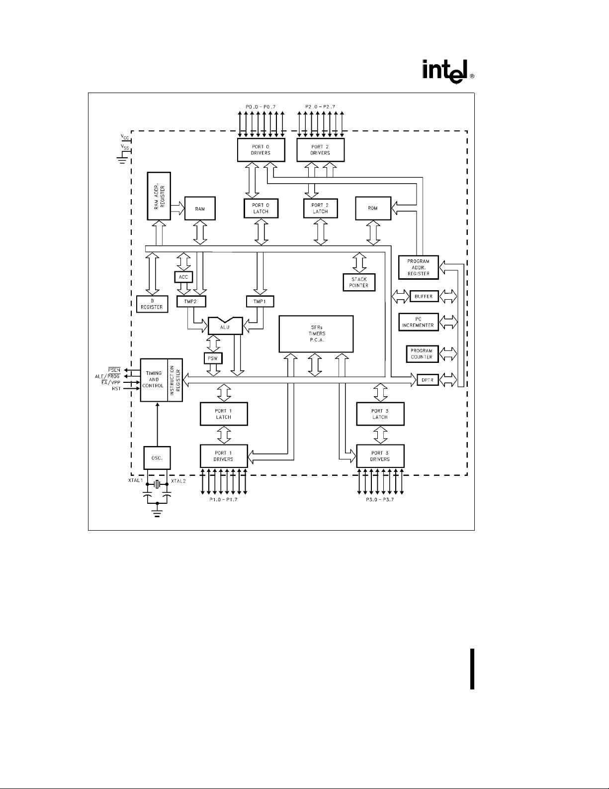
Figure 1. 83C51FA Block Diagram
2
Page 3
AUTOMOTIVE 80C51FA/83C51FA
80C51FA/83C51FA PRODUCT
OPTIONS
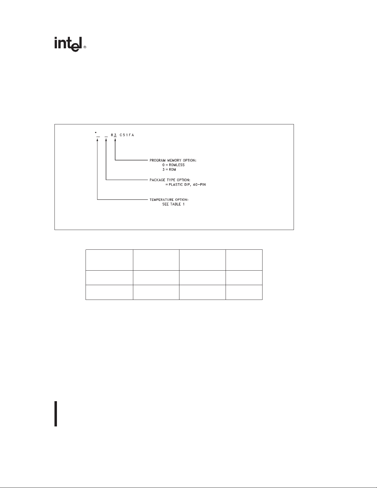
Intel’s extended and automotive temperature range
s are designed to meet the needs of those
product
application
commercia
Wit
operationa
s whose operating requirements exceed
l standards.
h the commercial standard temperature range,
l characteristics are guaranteed over the
x x
x
Figure 2. MCS®51 Microcontroller Product Family Nomenclature
temperatur
extende
characteristic
rang
e temperature range option, operational charac-
tiv
teristic
of
As shown in Figure 2 temperature, burn-in, and
packag
prefi
e range of 0
d temperature range option, operational
e of
-40°C to +125°C
x to the part number.
s are guaranteed over the temperature
-40 °C to + 85°C
s are guaranteed over the temperature range
e options are identified by a one- or two-letter
C to 70°C ambient. With the
°
ambient. For the automo-
ambient.
270501– 2
Table 1. Temperature Options
Temperature Temperature
Classification Designation
Extended T
L
Automotive A
B
Operating
Temperature
C Ambient
°
-
40 to+85 Standard
-
40 to+85 Extended
-
40 to+125 Standard
-
40 to+125 Extended
Burn-In
Options
3
Page 4
AUTOMOTIVE 80C51FA/83C51FA
PIN DESCRIPTIONS
VCC: Supply voltage.
V
: Circuit ground.
SS
Port 0: Port 0 is an 8-bit, open drain, bidirectional
I/O port. As an output port each pin can sink several
LS TTL inputs. Port 0 pins that have 1's written to
them float, and in that state can be used as high-impedance inputs.
Port 0 is also the multiplexed low-order address and
data bus during accesses to external Program and
Data Memory. In this application it uses strong internal pullups when emitting1's, and can source and
sink several LS TTL inputs.
Port 0 outputs the code bytes during program verification. External pullup resistors are required during
program verification.
Port 1: Port 1 is an 8-bit bidirectional I/O port with
internal pullups. The Port 1 output buffers can drive
LS TTL inputs. Port 1 pins that have 1's written to
them are pulled high by the internal pullups, and in
that state can be used as inputs. As inputs, Port 1
pins that are externally pulled low will source current
(I
, on the datasheet) because of the internal pull-
IL
ups.
In addition, Port 1 serves the functions of the following special features of the 83C51FA:
Port Pin Alternate Function
P1.0 T2 (External Count Input to Timer/
Counter 2)
P1.1 T2EX (Timer/Counter 2 Capture/
Reload Trigger and Direction Control)
P1.2 ECI (External Count Input to the PCA)
P1.3 CEX0 (External I/O for Compare/
Capture Module 0)
P1.4 CEX1 (External I/O for Compare/
Capture Module 1)
P1.5 CEX2 (External I/O for Compare/
Capture Module 2)
P1.6 CEX3 (External I/O for Compare/
Capture Module 3)
P1.7 CEX4 (External I/O for Compare/
Capture Module 4)
Port 2: Port 2 is an 8-bit bidirectional I/O port with
internal pullups. The Port 2 output buffers can drive
LS TTL inputs. Port 2 pins that have 1's written to
them are pulled high by the internal pullups, and in
that state can be used as inputs. As inputs, Port 2
pins that are externally pulled low will source current
(I
, on the datasheet) because of the internal pull-
IL
ups.
Port 2 emits the high-order address byte during
fetches from external Program Memory and during
accesses to external Data Memory that use 16-bit
addresses (MOVX
@
DPTR). In this application it
uses strong internal pullups when emitting 1's. During accesses to external Data Memory that use 8-bit
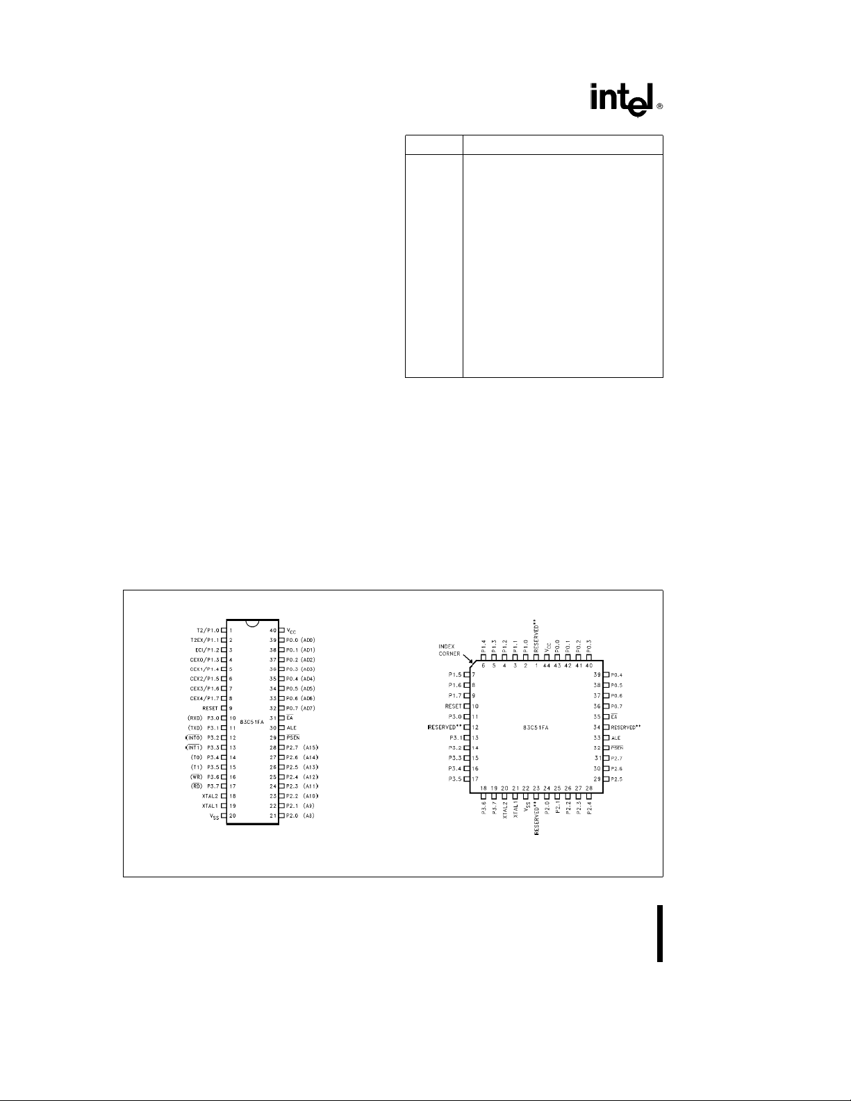
Pin (PDIP)
270501±3
**Do not connect reserved pins.
Pad (PLCC)
270501±4
Diagrams are for pin reference only. Package sizes are not to scale.
Figure 3. Pin Connections
4
Page 5

AUTOMOTIVE 80C51FA/83C51FA
addresses (MOVX@Ri), Port 2 emits the contents of
the P2 Special Function Register.
Port 3: Port 3 is an 8-bit bidirectional I/O port with
internal pullups. The Port 3 output buffers can drive
LS TTL inputs. Port 3 pins that have 1's written to
them are pulled high by the internal pullups, and in
that state can be used as inputs. As inputs, Port 3
pins that are externally pulled low will source current
(I
, on the datasheet) because of the pullups.
IL
Port 3 also serves the functions of various special
features of the MCS 51 microcontroller family, as
listed below:
Port Pin Alternate Function
P3.0 RXD (serial input port)
P3.1 TXD (serial output port)
P3.2 INT0
P3.3 INT1
(external interrupt 0)
(external interrupt 1)
P3.4 T0 (Timer 0 external input)
P3.5 T1 (Timer 1 external input)
P3.6 WR
P3.7 RD
(external data memory write strobe)
(external data memory read strobe)
RESET: Reset input. A high on this pin for two ma-
chine cycles while the oscillator is running resets the
device. An internal pulldown resistor permits a power-on reset with only a capacitor connected to V
ALE/PROG
: Address Latch Enable output pulse for
CC
latching the low byte of the address during accesses
to external memory.
In normal operation ALE is emitted at a constant
rate of (/6 the oscillator frequency, and may be used
for external timing or clocking purposes. Note, however, that one ALE pulse is skipped during each access to external Data Memory.
Throughout the remainder of this datasheet, ALE will
refer to the signal coming out of the ALE/PROG
and the pin will be referred to as the ALE/PROG
pin,
pin.
/VPP: External Access enable. EA must be
EA
strapped to V
fetch code from external Program Memory locations
in order to enable the device to
SS
0000H to 0FFFFH. Note, however, that if either of
the Program Lock bits are programmed, EA
internally latched on reset.
EA
should be strapped to VCCfor internal program
executions.
XTAL1: Input to the inverting oscillator amplifier.
XTAL2: Output from the inverting oscillator amplifi-
er.
OSCILLATOR CHARACTERISTICS
XTAL1 and XTAL2 are the input and output, respectively, of a inverting amplifier which can be configured for use as an on-chip oscillator, as shown in
Figure 4. Either a quartz crystal or ceramic resonator
may be used. More detailed information concerning
the use of the on-chip oscillator is available in Application Note AP-155, ``Oscillators for Microcontrollers.''
To drive the device from an external clock source,
XTAL1 should be driven, while XTAL2 floats, as
shown in Figure 5. There are no requirements on the
duty cycle of the external clock signal, since the in-
.
put to the internal clocking circuitry is through a divide-by-two flip-flop, but minimum and maximum
high and low times specified on the datasheet must
be observed.
An external oscillator may encounter as much as a
100 pF load at XTAL1 when it starts up. This is due
to interaction between the amplifier and its feedback
capacitance. Once the external signal meets the V
and VIHspecifications the capacitance will not exceed 20 pF.
will be
IL
: Program Store Enable is the read strobe to
PSEN
external Program Memory.
When the 83C51FA is executing code from external
Program Memory, PSEN
chine cycle, except that two PSEN
is activated twice each ma-
activations are
skipped during each access to external Data Memory.
e
30 pFg10 pF for Crystals
C1, C2
For Ceramic Resonators, contact resonator manufacturer.
270501±5
Figure 4. Oscillator Connections
5
Page 6

AUTOMOTIVE 80C51FA/83C51FA
270501±6
Figure 5. External Clock Drive Configuration
IDLE MODE
The user's software can invoke the Idle Mode. When
the microcontroller is in this mode, power consumption is reduced. The Special Function Registers and
the onboard RAM retain their values during Idle, but
the processor stops executing instructions. Idle
Mode will be exited if the chip is reset or if an enabled interrupt occurs. The PCA timer/counter can
optionally be left running or paused during Idle
Mode.
restored to its normal operating level and must be
held active long enough for the oscillator to restart
and stabilize (normally less than 10 ms).
With an external interrupt, INT0 or INT1 must be enabled and configured as level-sensitive. Holding the
pin low restarts the oscillator but bringing the pin
back high completes the exit. Once the interrupt is
serviced, the next instruction to be executed after
RETI will be the one following the instruction that put
the device into Power Down.
DESIGN CONSIDERATION
When the Idle mode is terminated by a hardware
reset, the device normally resumes program execution, from where it left off, up to two machine cycles
before the internal reset algorithm takes control. Onchip hardware inhibits access to internal RAM in this
event, but access to the port pins is not inhibited. To
eliminate the possibility of an unexpected write when
Idle is terminated by reset, the instruction following
the one that invokes Idle should not be one that
writes to a port pin or to external memory.
POWER DOWN MODE
To save even more power, a Power Down mode can
be invoked by software. In this mode, the oscillator
is stopped and the instruction that invoked Power
Down is the last instruction executed. The on-chip
RAM and Special Function Registers retain their values if the Power Down mode is terminated with an
interrupt.
On the 83C51FA either a hardware reset or external
interrupt can cause an exit from Power Down. Reset
redefines all the SFRs but does not change the onchip RAM. An external interrupt allows both the
SFRs and the on-chip RAM to retain their values.
To properly terminate Power Down the reset or external interrupt should not be executed before V
Table 2. Status of the External Pins during Idle and Power Down
Mode
Idle Internal 1 1 Data Data Data Data
Idle External 1 1 Float Data Address Data
Power Down Internal 0 0 Data Data Data Data
Power Down External 0 0 Float Data Data Data
NOTE:
For more detailed information on the reduced power modes refer to current Embedded Applications Handbook, and Application Note AP-252, ``Designing with the 80C51BH.''
Program
Memory
ALE PSEN PORT0 PORT1 PORT2 PORT3
CC
ONCE MODE
The ONCE (``On-CircuitEmulation'') Mode facilitates
testing and debugging of systems using the
83C51FA without the 83C51FA having to be removed from the circuit. The ONCE Mode is invoked
by:
1) Pull ALE low while the device is in reset and
PSEN
is high;
2) Hold ALE low as RST is deactivated.
While the device is in ONCE Mode, the Port 0 pins
float, the other port pins and ALE and PSEN
weakly pulled high. The oscillator circuit remains active. While the 83C51FA is in this mode, an emulator
or test CPU can be used to drive the circuit. Normal
operation is restored when a normal reset is applied.
is
are
6
Page 7

AUTOMOTIVE 80C51FA/83C51FA
ABSOLUTE MAXIMUM RATINGS*
Ambient Temperature
Under Bias...................................-40°C to +125°C
Storage Temperature.......................-65°C to +150°C
Voltage on Any Other Pinto V
I/O Pin........................................................15mA
I
OL
SS........-0.5V to +6.5V
NOTICE: This is a production data sheet. The specifications are subject to change without notice.
*
WARNING: Stressing the device beyond the ``Absolute
Maximum Ratings'' may cause permanent damage.
These are stress ratings only. Operation beyond the
``Operating Conditions'' is not recommended and extended exposure beyond the ``Operating Conditions''
may affect device reliability.
Power Dissipation
(Based on PACKAGE heat transfer limitations, not
device power consumption)
Typical Junction Temperature (T
(Based upon Ambient Temperature at
)................+135°C
J
a
125§C)
Typical Thermal Resistance
Junction-to-Ambient (i
PDIP.......................................................45°C/W
)
JA
PLCC......................................................46°C/W
DC CHARACTERISTICS: (T
eb
40§Ctoa125§C; V
A
CC
e
5Vg10%; V
SS
e
0V)
Symbol Parameter Min Typ Max Unit Test Conditions
V
IL
V
IL1
V
IH
V
IH1
Input Low Voltage
Input Low Voltage EA 0 0.2 V
Input High Voltage 0.2 V
(Except XTAL2, RST,EA
)
Input High Voltage 0.7 V
b
0.5 0.2 V
a
0.9 V
CC
CC
CC
V
CC
b
0.1 V
CC
b
0.3 V
CC
a
0.5 V
a
0.5 V
(XTAL, RST)
1.6 mA
(1)
V
OL
Output Low Voltage 0.45 V I
OL
e
(Ports 1, 2 and 3)
I
OL
OL
OL
OH
e
20
e
3.2 mA
e
7.0 mA
eb
(1)
60 mA
V
OL1
V
OH
Output Low Voltage 0.45 V I
(Port 0, ALE/PROG
, PSEN)I
Output High Voltage 2.4 V I
(Ports 1, 2 and 3
V
I
IL
OH1
ALE/PROG and PSEN)
0.9 V
CC
VI
Output High Voltage 2.4 V I
(Port 0 in External Bus Mode) 0.9 V
Logical 0 Input Current
CC
b
10
b
50 mAV
VI
OH
OH
OH
IN
eb
eb
eb
e
0.45V
10 mA
800 mA
80 mA
(Ports 1, 2 and 3)
g
I
LI
Input leakage Current 0.02
10 mAV
IN
e
VILor V
IH
(Port 0)
(2)
(2)
7
Page 8

AUTOMOTIVE 80C51FA/83C51FA
DC CHARACTERISTICS: (T
eb
40§Ctoa125§C; V
A
CC
e
5Vg10%; V
e
0V) (Continued)
SS
Symbol Parameter Min Typ Max Unit Test Conditions
I
TL
Logical 1 to 0 Transition Current
b
265
b
650 mAV
e
2V
IN
(Ports 1, 2, and 3)
RRST RST Pulldown Resistor 40 100 225 KX
CIO Pin Capacitance 10 pF
I
CC
Power Supply Current: (Note 3)
@
1MHz, 25§C
Running at 12 MHz (Figure 5) 40 mA
Idle Mode at 12 MHz (Figure 5) 15 mA
Power Down Mode (I
NOTES:
1. Capacitive loading on Ports 0 and 2 may cause noise pulses to be superimposed on the V
The noise is due to external bus capacitance discharging into the Port 0 and Port 2 pins when these pins make 1 to 0
transitions during bus operations. In applications where capacitance loading exceeds 100 pFs, the noise pulse on the ALE
signal may exceed 0.8V. In these cases, it may be desirable to qualify ALE with a Schmitt Trigger, or use an Address Latch
with a Schmitt Trigger Strobe input.
2. Capacitive loading on Ports 0 and 2 cause the V
address lines are stabilizing.
3. See Figures 6 ±9 for test conditions. Minimum V
4. Typicals are based on limited number of samples, and are not guaranteed. The values listed are at room temperature and
5.0V.
5. Under steady state (non-transient) conditions, I
Maximum I
Maximum I
Maximum Total I
If I
OL
than the listed test conditions.
6. Contact Intel for design-in information.
per Port Pin: 10 mA
OL
per 8-Bit Port -
OL
Ports 1, 2, and 3: 15 mA
for all Output Pins: 71 mA
exceeds the test condition, VOLmay exceed the related specification. Pins are not guaranteed to sink current greater
OL
Port 0: 26 mA
) 150 mA
PD
on ALE and PSEN to drop below the 0.9 VCCspecification when the
OH
for Power Down is 2.0V.
CC
must be externally limited as follows:
OL
s of ALE and Ports 1 and 3.
OL
8
Page 9

AUTOMOTIVE 80C51FA/83C51FA
Max at other frequencies is given by:
I
CC
Active Mode
Maxe(3cOsc Freq)a4
I
CC
Idle Mode
ICCMaxe(0.49cOsc Freq)a1.6
Where Osc Freq is in MHz, I
CC
is in mA.
270501±7
TCLCH
e
TCHCLe5ns
270501±8
Figure 7. ICCTest Condition, Active Mode
All other pins disconnected.
Figure 6. ICCvs Frequency
270501±10
Figure 9. ICCTest Condition,
Power Down Mode.
All other pins disconnected.
e
V
2.0V to 5.5V.
CC
270501±11
e
TCLCH
TCHCLe5ns
Figure 8. ICCTest Condition Idle Mode.
All other pins disconnected.
270501±9
Figure 10. Clock Signal Waveform for ICCTests in Active and Idle Modes. TCLCHeTCHCLe5 ns.
9
Page 10

AUTOMOTIVE 80C51FA/83C51FA
EXPLANATION OF THE AC SYMBOLS
Each timing symbol has 5 characters. The first character is always a `T' (stands for time). The other
characters, depending on their positions, stand for
the name of a signal or the logical status of that
signal. The following is a list of all the characters and
what they stand for.
A: Address
C: Clock
D: Input Data
H: Logic level HIGH
I: Instruction (program memory contents)
AC CHARACTERISTICS (T
for Port 0, ALE/PROG
and PSENe100 pF, Load Capacitance for All Other Outputse80 pF)
eb
40§Ctoa125§C, V
A
EXTERNAL MEMORY CHARACTERISTICS
Symbol Parameter
1/T
T
LHLL
T
AVLL
T
LLAX
T
LLIV
T
LLPL
T
PLPH
T
PLIV
T
PXIX
T
PXIZ
T
AVIV
T
PLAZ
T
RLRH
T
WLWH
T
RLDV
T
RHDX
T
RHDZ
T
LLDV
T
AVDV
T
LLWL
T
AVWL
T
QVWX
T
WHQX
T
QVWH
T
RLAZ
T
WHLH
Oscillator Frequency 3.5 16 MHz
CLCL
ALE Pulse Width 127 2T
Address Valid to ALE Low 43 T
Address Hold After ALE Low 53 T
ALE Low to Valid Instruction In 224 4T
ALE Low to PSEN
Low 53 T
PSEN Pulse Width 205 3T
PSEN Low to Valid Instruction In 135 3T
Input Instr Hold After PSEN Trans 0 0 ns
Input Instr Float After PSEN Trans 59 T
Address to Valid Instruction In 302 5T
PSEN Low to Address Float 10 10 ns
RD Pulse Width 400 6T
WR Pulse Width 400 6T
RD Low to Valid Data In 242 5T
Data Hold After RD High
Data Float After RD High 107 2T
ALE Low to Valid Data In 507 8T
Address Valid to Valid Data In 575 9T
ALE Low to RD or WR Low 200 300 3T
Data Valid to WR Low 203 4T
Address Valid before WR Low 23 T
Data Hold after WR High 33 T
Data Valid to WEHigh 433 7T
RD Low to Address Float 0 0 ns
RD or WR High to ALE High 43 123 T
12 MHz Oscillator Variable Oscillator
Min Max Min Max
b
10
L: Logic level LOW, or ALE
P: PSEN
Q: Output Data
signal
R: RD
T: Time
V: Valid
W: WR
signal
X: No longer a valid logic level
Z: Float
For example,
e
T
T
Time from Address Valid to ALE Low
AVLL
e
Time from ALE Low to PSEN Low
LLPL
e
5Vg10%, V
CC
SS
b
40 ns
CLCL
b
40 ns
CLCL
b
30 ns
CLCL
b
30 ns
CLCL
b
45 ns
CLCL
b
100 ns
CLCL
b
100 ns
CLCL
b
10 ns
b
50 3T
CLCL
b
130 ns
CLCL
b
50 ns
CLCL
b
50 ns
CLCL
b
150 ns
CLCL
b
40 T
CLCL
e
0V, Load Capacitance
b
110 ns
CLCL
b
115 ns
CLCL
b
25 ns
CLCL
b
115 ns
CLCL
b
175 ns
CLCL
b
60 ns
CLCL
b
160 ns
CLCL
b
175 ns
CLCL
a
50 ns
CLCL
a
40 ns
CLCL
Units
10
Page 11

EXTERNAL PROGRAM MEMORY READ CYCLE
EXTERNAL DATA MEMORY READ CYCLE
AUTOMOTIVE 80C51FA/83C51FA
270501±12
EXTERNAL DATA MEMORY WRITE CYCLE
270501±13
270501±14
11
Page 12

AUTOMOTIVE 80C51FA/83C51FA
SERIAL PORT TIMING-SHIFT REGISTER MODE
Test Conditions:
T
A
Symbol Parameter
T
XLXL
T
QVXH
T
XHQX
T
XHDX
T
XHDV
Serial Port Clock Cycle Time 1 12T
Output Data Setup to Clock 700 10T
Rising Edge
Output Data Hold after 50 2T
Clock Rising Edge
Input Data Hold After Clock 0 0 ns
Rising Edge
Clock Rising Edge to Input 700 10T
Data Valid
eb
40§Ctoa125§C; V
12 MHz Oscillator Variable Oscillator
Min Max Min Max
CC
e
5Vg10%; V
SHIFT REGISTER MODE TIMING WAVEFORMS
e
0V; Load Capacitancee80 pF
SS
CLCL
b
133 ns
CLCL
b
117 ns
CLCL
CLCL
b
133 ns
270501±15
Units
ms
EXTERNAL CLOCK DRIVE
Symbol Parameter Min Max Units
1/T
T
CHCX
T
CLCX
T
CLCH
T
CHCL
CLCL
Oscillator Frequency 3.5 16 MHz
High Time 20 ns
Low Time 20 ns
Rise Time 20 ns
Fall Time 20 ns
EXTERNAL CLOCK DRIVE WAVEFORM
12
270501±16
Page 13

AUTOMOTIVE 80C51FA/83C51FA
AC TESTING INPUT, OUTPUT WAVEFORMS
270501 ±17
AC Inputs during testing are driven at V
and 0.45V for a Logic ``0''. Timing measurements are made at V
min for a Logic ``1'' and VOLmax for a Logic ``0''.
b
0.5V for a Logic ``1''
CC
FLOAT WAVEFORMS
For timing purposes a port pin is no longer floating when a
IH
100 mV change from load voltage occurs, and begins to float
whe
I
OL/IOH
n a 100 mV change from the loaded V
t
g
20 mA. This is for Ports 1, 2 and 3.
DATASHEET REVISION HISTORY
The following are key differences between this datasheet and the -007 version:
1. Product prefix variables are now indicated with an x.
Th
e following are key differences between this datasheet and the -006 version:
1. The ``preliminary'' status was dropped and replaced with production status (no label).
2. Trademarks were updated.
e following are key differences between the -006 and the -005 version of the datasheet:
Th
1. Preliminary notice has been added to the Title page.
2. Figure 3 Pin Connections has been modified, RST pin is now RESET pin.
3. RST pin description is now RESET pin description.
4. Figure 6 I
5. ICCMax spec has been corrected.
6. A.C. Characteristic table 1/T
e following are key differences between the -005 and the -004 version of the datasheet:
Th
1. ``NC'' pin labels changed to ``Reserved'' in Figure 3.
2. Capacitor value for ceramic resonators deleted in Figure 4.
vs. Frequency has been corrected to show test conditions.
CC
spec has been changed to have a Max frequency of 16 MHz.
CLCL
OH/VOL
270501 ±18
level occurs.
Th
e following are the key differences between the -003 version of the 8XC51FA datasheet and the -004
n of the 80C51FA/83C51FA datasheet:
versio
1. Removed references to EPROM from the 8XC51FA datasheet.
2. Revised Figure 4, ``Oscillator Connections''.
e following are the key differences between the -002 and the -003 version of this datasheet:
Th
1. Dropped word ``maximum'' from I
in the Absolute Maximum Rating table.
OL
2. Dropped EA from ILIspecification of the DC table.
3. Corrected TQVWH specification (from TTCLCL -7
0 to TCLCL -150).
4. Added note on external clock capacitance loading.
5. Changed the title to 80C51FA/83C51FA Event-Control CHMOS Single-Chip 8-Bit Microcontroller.
6. Added pin count to Figure 1.
7. Changed ILItog10 μ A.
8. Added ICCPower Down Mode 150 nA.
13
 Loading...