

Page 1

82551ER Fast Ethernet PCI Controller
Networking Silicon - 82551ER
Datasheet
Product Features
■
Enhanced IP Protocol Support
—TCP, UDP, IPv4 checksum offload
—Received checksum verification
■ Quality of Service (QoS)
—Multiple priority transmit queues
■ Optimum Integration for Lowest Cost
Solution
—Integrated IEEE 802.3 10BASE-T and
100BASE-TX compatible PHY
—32-bit PCI master interface
—Thin BGA 15mm
■ Integrated power management function s
2
package
—ACPI and PCI power management
standards compliance
—Wake on “interesting” packets and link
status change support
■ PHY detects polarity, MDI-X, and cable
lengths. Auto MDI, MDI-X crossover at all
speeds
■ XOR tree mode support
■ High Perfor mance Networking Function s
—Early release
—8255x controller family chained
memory structure
—Improved dynamic transmit chaining
with multiple priorities transmit queues
—Full pin compatibility with the 82559
and 82559ER controllers
—Backward compatible software to
82559ER controllers
—Full duplex support at 10 and 100 Mbps
—IEEE 802.3u auto-negotiation support
—3 KB transmit and receive FIFOs
—Fast back-to-back transmission support
with minimum interframe spacing
—IEEE 802.3x 100BASE-TX flow control
support
—Adaptive Technology
■ Low Power Features
—Adv anced Power Mana gement (APM)
capabilities
—Low power 3.3 V device
—Efficient dynamic standby mode
—Deep power-down support
—Clockrun protocol support
■ 82551ER Enhancements
—Improved bit error rate performance
—HWI support
—Deep power-down state power reduction
■ Lead-free
1
196-pin Ball Grid Array (BGA).
Devices that are lead-free are marked with
a circled “e1” and have the product code:
LUxxxxxx.
1
This device is lead-free. That is, lead has not been intentionally added, but lead may still exist as an
impurity at <1000 ppm. The Material Declaration Data Sheet, which includes lead impurity levels and the
concentration of other Restriction on Hazardous Substances (RoHS)-banned materials, is available at:
ftp://download.intel.com/design/packtech/material_content_IC_Package.pdf#pagemode=bookmarks
In addition, this device has been tested and conforms to the same parametric specifications as previous
versions of the device.
For more information regarding lead-free products from Intel Corporation, contact your Intel Field Sales
representative.
Revision 2.6
October 2006
Page 2

Revision History
Revision
Date
Revision Description
Nov 2001 0.7 Initial draft for release (Intel Secret).
Jan 2002 1.0 • Added description for No Connect pins.
• Clarified EEPROM address map and word definitions for the 82551ER.
• Added more detailed information for I
in the DC specifications table.
CC
• Corrected typographical errors.
Apr 2002 2.0 Changed document status to Intel Confidential.
Mar 2003 2.1 • Removed document status.
• Removed references to MDI/MDI-X feature, which is not supported by the
82551ER.
Sep 2004 2.2 • Added references to the MDI/MDI-X feature.
• Added lead-free information.
• Removed EEPROM Map bit descriptions. These descriptions can now be
found in the 82551QM/ER/IT EEPROM Map and Programming Information.
• Added 82551ER Test Port Functionality (Chapter 10).
• Added new values for RBIAS100 and RBIAS10. RBIAS100 = 649 Ω and
RBIAS10 = 619 Ω.
• Removed all references to the 82551IT and 82551QM controllers. 82551IT
and 82551QM information can now be found in their respective datasheets.
Nov 2004 2.3 • Added information about migrating from a 2-layer 0.36 mm wide-trace sub-
strate to a 2-layer 0.32 mm wide-trace substrate. Refer to the section on
Package and Pinout Information.
Nov 2004 2.4 • Updated the section describing “Multiple Priority Transmit Queues”.
• Updated the section describing “VLAN Support”.
• Added statement that no changes to existing soldering processes are
needed for the 2-layer 0.32 mm wide-trace substrate change in the section
describing “Package Information”.
Jan 2005 2.5 • Added a note for PHY signals RBIAS100 and RBIAS10 to Table 8.
Oct 2006 2.6 • Added Figure 28 “196 PBGA Package Pad Detail”. The figure shows solder
resist opening and metal diameter dimensions.
Information in this document is provided in connection with Intel products. No license, express or implied, by estoppel or otherwise, to any intellectual
property rights is granted by this document. Except as provided in Intel's Terms and Conditions of Sale for such products, Intel assumes no liability
whatsoever, and Intel disclaims any express or implied warranty, relating to sale and/or use of Intel products including liability or warranties relating to
fitness for a particular purpose, merchantability, or infringement of any patent, copyright or other intellectual property right. Intel products are not
intended for use in medical, life saving, or life sustaining applications.
Intel may make changes to specifications and product descriptions at any time, without notice.
Designers must not rely on the absence or characteristics of any features or instructions marked "reserved" or "undefined." Intel reserves these for
future definition and shall have no responsibility whatsoever for conflicts or incompatibilities arising from future changes to the m.
The 82551ER may contain design defects or errors known as errata which may cause the product to deviate from published specifications. Current
characterized errata are available on request.
MPEG is an international standard for video compression/decompression promoted by ISO. Implementations of MPEG CODECs, or MPEG enabled
platforms may require licenses from various entities, including Intel Corporation.
Contact your local Intel sales office or your distributor to obtain the latest specifications and before placing your product order.
Copies of documents which have an ordering number and are referenced in this document, or other Intel literature may be obtained by calling
1-800-548-4725 or by visiting Intel's Web site at http://www.intel.com.
®
Intel
is a trademark or registered trademark of Intel Corporation or its subsidiaries in the United States and other countries.
Copyright © 2006, Intel Corporation.
* Other product and corporate names may be trademarks of other companies and are used only for explanation and to the owners’ benefit, without
intent to infringe.
ii Datasheet
Page 3

Networking Silicon — 82551ER
Contents
1.0 Introduction.........................................................................................................................1
1.1 Overview ...............................................................................................................1
1.2 Byte Ordering ........................................................................................................1
1.3 References............................................................................................................1
1.4 Product Codes.......................................................................................................2
2.0 Architectural Overview .......................................................................................................3
2.1 Parallel Subsystem Overview................................................................................3
2.2 FIFO Subsystem Overview ...................................................................................3
2.3 10/100 Mbps Serial CSMA/CD Unit Overview ......................................................4
2.4 10/100 Mbps Physical Layer Unit..........................................................................4
3.0 Performance Enhancements..............................................................................................5
3.1 Multiple Priority Transmit Queue s ......................................... ....... ...... ...................5
3.2 Early Release........................................................................................................5
3.3 Hardware Integrity Support ...................................................................................6
3.4 Management Data Interface MDI/MDI-X Feature..................................................6
4.0 Signal Descriptions.............................................................................................................7
4.1 Signal Type Definitions .........................................................................................7
4.2 PCI Bus Interface Signals .....................................................................................8
4.2.1 Address and Data Signals .......................................................................8
4.2.2 Interface Control Signals .........................................................................8
4.2.3 System and Power Management Signals ...............................................9
4.3 Local Memory Interface Signals..........................................................................10
4.4 Test Port Signals ................................................................................................11
4.5 PHY Signals .. ....... ...... ....... ...... ....... ...... ...... ....................................... ....... ...... ....12
4.6 Power and Ground Signals .................................................................................13
5.0 Media Access Control Functional Description..................................................................15
5.1 Device Initialization..............................................................................................15
5.1.1 Initialization Effects.................................................................................15
5.2 PCI Interface .......................................................................................................16
5.2.1 Bus Operations.......................................................................................16
5.2.2 Clock Run Signal................ ...... ...... ....... ...... ....... ...... ....... .......................24
5.2.3 Power Management Event.....................................................................25
5.3 PCI Power Management .....................................................................................25
5.3.1 Power States..........................................................................................25
5.3.2 Wake-up Events................. ...... ...... ....... ...... ....... ...... ....... .......................29
5.4 Parallel Flash.......................................................................................................30
5.5 Serial EEPROM Interface....................................................................................30
5.5.1 EEPROM Address Map..........................................................................32
5.6 10/100 Mbps CSMA/CD Unit...............................................................................32
5.6.1 Full Duplex .............................................................................................33
5.6.2 Flow Control ...........................................................................................33
5.6.3 Address Filtering Modifications ..............................................................33
5.6.4 VLAN Support ........................................................................................33
Datasheet iii
Page 4

82551ER — Networking Silicon
5.7 Media Independent Interface (MII) Management Interface.................................34
6.0 Physical Layer Functional Description .............................................................................35
6.1 100BASE-TX PHY Unit.......................................................................................35
6.1.1 100BASE-TX Transmit Clock Generation..............................................35
6.1.2 100BASE-TX Transmit Blocks...............................................................35
6.1.3 100BASE-TX Receive Blocks................................................................35
6.1.4 100BASE-TX Link Integrity Auto-Negotiation.........................................36
6.2 10BASE-T PHY Functions..................................................................................36
6.2.1 10BASE-T Transmit Clock Generation...................................................36
6.2.2 10BASE-T Transmit Blocks....................................................................36
6.2.3 10BASE-T Receive Blocks.....................................................................36
6.2.4 10BASE-T Link Integrity and Full Duplex...............................................37
6.3 Auto-Negotiation .................................................................................................37
6.3.1 Description .............................................................................................37
6.3.2 Parallel Detect and Auto-Negotiation.....................................................37
6.4 LED Description .................................................... ...... ....... ...... ....... ...... ....... ...... .38
7.0 Configuration Registers....................................................................................................41
7.1 Function 0: LAN (Ethernet) PCI Configuration Space.........................................41
7.1.1 PCI Vendor ID and Device ID Registers ................................................41
7.1.2 PCI Command Register .........................................................................42
7.1.3 PCI Status Register................................................................................43
7.1.4 PCI Revision ID Register........................................................................45
7.1.5 PCI Class Code Register .......................................................................45
7.1.6 PCI Cache Line Size Register................................................................45
7.1.7 PCI Latency Timer .................................................................................45
7.1.8 PCI Header Type ...................................................................................45
7.1.9 PCI Base Address Registers..................................................................46
7.1.10 Base Address Registry Summary ..........................................................47
7.1.11 PCI Subsystem Vendor ID and Subsystem ID Registers.......................47
7.1.12 Capability Pointer ...................................................................................48
7.1.13 Interrupt Line Register............................................................................48
7.1.14 Interrupt Pin Register .............................................................................48
7.1.15 Minimum Grant Register ........................................................................49
7.1.16 Maximum Latency Register...................... ...... ....... ...... ....... ...... ....... ...... .49
7.1.17 Capability ID Register ............................................................................49
7.1.18 Next Item Pointer ...................................................................................49
7.1.19 Power Management Capabilities Register .............................................49
7.1.20 Power Management Control/Status Register (PMCSR).........................50
7.1.21 Data Register ................................................. ....... ...... ....... ...... ....... ...... .51
8.0 Control/Status Registers..................................................................................................53
8.1 LAN (Ethernet) Control/Status Registers ............................................................53
8.1.1 System Control Block Status Word........................................................54
8.1.2 System Control Block Command Word..................................................55
8.1.3 System Control Block General Pointer...................................................55
8.1.4 PORT .....................................................................................................55
8.1.5 Flash Control Register ...........................................................................55
8.1.6 EEPROM Control Register....................... ...... ....... ...... ....... ...... ....... .......56
8.1.7 Management Data Interface Control Register........................................56
iv Datasheet
Page 5

Networking Silicon — 82551ER
8.1.8 Receive Direct Memory Access Byte Count...........................................56
8.1.9 Flow Control Register.............................................................................56
8.2 Statistical Counters .............................................................................................57
9.0 PHY Unit Registers ...................................... ...... ...... ....................................... ....... ...... ....61
9.1 MDI Registers 0 - 7 .............................................................................................61
9.1.1 Register 0: Control Register ..................................................................61
9.1.2 Register 1: Status Register ...................................................................62
9.1.3 Register 2: PHY Identifier Register .......................................................63
9.1.4 Register 3: PHY Identifier Register .......................................................63
9.1.5 Register 4: Auto-Negotiation Advertisement Register ...........................63
9.1.6 Register 5: Auto-Negotiation Link Partner Ability Register ....................64
9.1.7 Register 6: Auto-Negotiation Expansion Register .................................64
9.2 MDI Registers 8:15..............................................................................................64
9.3 MDI Register 16:31 .............................................................................................65
9.3.1 Register 16: PHY Unit Status and Control Register ..............................65
9.3.2 Register 17: PHY Unit Special Control Register ...................................65
9.3.3 Register 18: PHY Address Register.......................................................66
9.3.4 Register 19: 100BASE-TX Receive False Carrier Counter ...................66
9.3.5 Register 20: 100BASE-TX Receive Disconnect Counter ......................67
9.3.6 Register 21: 100BASE-TX Receive Error Frame Counter ....................67
9.3.7 Register 22: Receive Symbol Error Counter .........................................67
9.3.8 Register 23: 100BASE-TX Receive Premature End of Frame Error
Counter 67
9.3.9 Register 24: 10BASE-T Receive End of Frame Error Counter .............67
9.3.10 Register 25: 10BASE-T Transmit Jabber Detect Counter .....................68
9.3.11 Register 26: Equalizer Control and Status Register ..............................68
9.3.12 Register 27: PHY Unit Special Control Register ...................................68
9.3.13 Register 28: MDI/MDI-X Control Register ..............................................69
9.3.14 Register 29: Hardware Integrity Control Register ..................................69
10.0 82551ER Test Port Functionality ..... ...................................... ....... ...... ....... ...... ....... ...... ....71
10.1 Introduction..........................................................................................................71
10.2 Test Function Description....................................................................................71
10.2.1 Tristate ...................................................................................................71
10.2.2 XOR Tree ...............................................................................................72
11.0 Electrical and Timing Specifications.................................................................................75
11.1 Absolute Maximum Ratings.................................................................................75
11.2 DC Specifications .................... ....... ...... ...... ....... ...... ....... ...... ..............................76
11.3 AC Specifications ................................................................................................80
11.4 Timing Specifications ..........................................................................................81
11.4.1 Clocks Specifications .............................................................................81
11.4.2 Timing Parameters.................................................................................82
12.0 Package and Pinout Information......................................................................................89
12.1 Package Information ...........................................................................................89
12.2 Pinout Information ...............................................................................................91
12.2.1 Pin Assignments ....................................................................................91
12.2.2 Ball Grid Array Diagram .........................................................................93
Datasheet v
Page 6

82551ER — Networking Silicon
Figures
1 CSR I/O Read Cycle ...........................................................................................17
2 CSR I/O Write Cycle ...........................................................................................18
3 Flash Buffer Read Cycle.....................................................................................19
4 Flash Buffer Write Cycle .....................................................................................20
5 PCI Retry Cycle...................................................................................................21
6 Memory Read Burst Cycle ..................................................................................22
7 Memory Write Burst Cycle ..................................................................................22
8 Initialization upon RST# and ISOLATE#.............................................................28
9 64-Word EEPROM Read Instruction Waveform .................................................31
10 Auto-Negotiation and Parallel Detect..................................................................38
11 Two and Three LED Schematic Diagram............................................................39
12 PCI Configuration Registers................................................................................41
13 PCI Command Register ......................................................................................42
14 PCI Status Register.............................................................................................43
15 Cache Line Size Register....................................................................................45
16 Base Address Register for Memory Mapping .....................................................46
17 Base Address Register for I/O Mapping..............................................................46
18 Control/Status Register.......................................................................................53
19 PCI Clock Waveform...........................................................................................81
20 Output Timing Measurement Conditions.............................................................82
21 Input Timing Measurement Conditions ...............................................................82
22 Flash Timings for a Read Cycle..........................................................................85
23 Flash Timings for a Write Cycle..........................................................................85
24 EEPROM Timings................. ...... ....... ...... ...... ....... ...... ....... ...... ....... ...... ....... .......86
25 10BASE-T Normal Link Pulse (NLP) Timings .....................................................87
26 Auto-Negotiation Fast Link Pulse (FLP) Timings................................................87
27 Dimension Diagram for the 196-pin BGA............................................................89
28 196 PBGA Package Pad Detail...........................................................................90
29 Ball Grid Array Diagram ......................................................................................93
Tables
1 RJ-45 Connections................................................................................................6
2 Signal Type Descriptions ......................................................................................7
3 Address and Data Signals.....................................................................................8
4 Interface Control Signals.......................................................................................8
5 System and Power Management Signals .............................................................9
6 Local Memory Interface Signals..........................................................................10
7 Test Port Signals...... ...... ....... ...... ....... ...... ....................................... ...... ....... ...... .11
8 PHY Signals........................................................................................................12
9 Power and Ground Signals.................................................................................13
10 Initialization Effects .............................................................................................15
11 Functionality at the Different Power States.........................................................29
12 82551ER EEPROM Address Map ......................................................................32
13 PCI Command Register Bits...............................................................................43
14 PCI Status Register Bits......................................................................................44
15 Base Address Register Functions.......................................................................47
vi Datasheet
Page 7

Networking Silicon — 82551ER
16 ID Fields Programming ....... ...... ....... ...... ...... ....................................... ....... ...... ....48
17 Power Management Capability Register.............................................................49
18 Power Management Control and Status Register...............................................50
19 Ethernet Data Register........................................................................................51
20 System Control Block Status Word .....................................................................54
21 System Control Block Command Word...............................................................55
22 MDI Control Register...........................................................................................56
23 Statistical Counters .............................................................................................57
24 Register 0: Control ..............................................................................................61
25 Register 1: Status................................................................................................62
26 Register 2: PHY Identifier....................................................................................63
27 Register 3 PHY Identifier.....................................................................................63
28 Register 4: Auto-Negotiation Advertisement .......................................................63
29 Auto-Negotiation Link Partn er Abil ity........................ ....... ...... ....... ...... ....... ...... ....64
30 Register 6: Auto-Negotiation Expansion .............................................................64
31 PHY Unit Status and Control...............................................................................65
32 Register 17: PHY Unit Special Control................................................................65
33 Register 18: PHY Address ..................................................................................66
34 Register 19: 100BASE-TX Receive False Carrier Counter.................................66
35 Register 20: 100BASE-TX Receive Disconnect Counter....................................67
36 Register 21: 100BASE-TX Receive Error Frame Counter ..................................67
37 Register 22: Receive Symbol Error Counter .......................................................67
38 Register 23: 100BASE-TX Receive Premature End of Frame Error Counter .....67
39 Register 24: 10BASE-T Receive End of Frame Error Counter ...........................67
40 Register 25: 10BASE-T Transmit Jabber Detect Counter...................................68
41 Register 26: Equalizer Control and Status ..........................................................68
42 Register 27: PHY Unit Special Control................................................................68
43 Register 28: MDI/MDI-X Control..........................................................................69
44 Register 29: Hardware Integrity Control..............................................................69
45 XOR Tree Chains................................................................................................72
46 General DC Specifications ....................................... ....... ...... ....... ...... ....... ..........76
47 PCI Interface DC Specifications..........................................................................77
48 Flash/EEPROM Interface DC Specifications.......................................................77
49 LED Voltage/Current Characteristics ..................................................................78
50 100BASE-TX Voltage/Curren t Char ac teristi cs......... ....... ...... ..............................78
51 10BASE-T Voltage/Current Characteristics ........................................................79
52 AC Specifications for PCI Signaling ....................................................................80
53 PCI Clock Specifications.....................................................................................81
54 X1 Clock Specifications.......................................................................................81
55 Measure and Test Condition Parameters............................................................82
56 PCI Timing Parameters.......................................................................................83
57 Flash Timing Parameters ....................................................................................84
58 EEPROM Timing Parameters .............................................................................86
59 10BASE-T Normal Link Pulse (NLP) Timing Parameters ...................................87
60 Auto-Negotiation Fast Link Pulse (FLP) Timing Parameters...............................87
61 100Base-TX Transmitter AC Specification..........................................................88
62 Pin Assignments..................................................................................................91
Datasheet vii
Page 8

82551ER — Networking Silicon
Note: This page intentionally left blank.
viii Datasheet
Page 9

1.0 Introduction
This datasheet is applicable to the Intel® 82551ER Fast Ethernet PCI Controller, a member of the
8255x Fast Ethernet Controller family.
1.1 Overview
The 82551ER is an evolutionary addition to Intel’s family of 8255x controllers. It provides
excellent performance by of floa ding TCP, UDP and IP checksums and sup ports TCP segmenta tion
off-load for operations such as Large Send.
Its optimized 32-bit interface and efficient scatter-gather bus mastering capabilities enable the
82551ER to perform high speed data transfers over the PCI bus. This capab ility accelerates the
processing of high level commands and operations, which lowers CPU utilization. Its architecture
enables data to flow efficiently from the bus interface unit to the 3 KB Transmit and Receive
FIFOs, providing the perfect balance between the wire and system bus. In addition, multiple
priority queues are provided to prevent data underruns and overruns.
The 82551ER includes both a MAC and PHY. In also has a simple interf ace to the analog front end,
which allows cost effective designs requiring minimal board real estate. The 82551ER is pin
compatible with the 82559 family of controllers and is offered with software that provides
backwards compatibility with previous 82559ER controllers.
Networking Silicon — 82551ER
1.2 Byte Ordering
TCP and IP Internet Engineering Task Force (IETF) Request for Comments (RFCs) and literature
use big endian (BE) byte ordering. This document uses big endian ordering for all IP and TCP
frame formats. However, little endian byte ordering is used for referencing 82551ER memory
resident structures and internal structures.
1.3 References
The following documents may provide further information on topics discussed in this document.
• 10/100 Mbit Ethernet Controller Family Software Deve loper’s Manual. Intel Corporation.
• Advanced Configuration and Power Interface Specification, Revision 1.0. Intel Corporation,
Microsoft Corporation, and Toshiba.
• IEEE 802.3x and 802.1y Standards.
• Network Device Class Power Management Reference Specification, Revision 1.0a. AMD, Inc.
and Microsoft Corporation.
Datasheet 1
Page 10

82551ER — Networking Silicon
1.4 Product Codes
Product ordering codes for the 82551ER Fast Ethernet PCI controller:
• GD82551ER
• LU82551ER
2 Datasheet
Page 11

2.0 Architectural Overview
The Intel® 82551ER is di vided int o four m ain subs ystems : a parall el subs ystem, a FIFO subsystem ,
a 10/100 Mbps Carrier Sense Multiple Access with Collision Detect (CSMA/CD) unit, and a 10/
100 Mbps physical layer (PHY) unit.
2.1 Parallel Subsystem Ove rview
The parallel subsystem is comprised of several functional blocks: a PCI bus master interface, a
micromachine processing unit and its corresponding microcode ROM, and a PCI Target Control/
Flash/EEPROM interface. The parallel subsystem also interfaces to the FIFO subsystem, passing
data (such as transmit, receive, and configuration data) and command and status parameters
between these two blocks.
The PCI bus master interface provides a complete glueless interface to a PCI bus and is compliant
with the PCI Bus Specification, Revision 2.2. The 82551ER provides 32 bits of addressing and
data, as well as the PCI control interface. As a PCI target, it conforms to the PCI configuration
scheme, which allows all accesses to the 82551ER to be automatically mapped into free memory
and I/O space upon initialization of a PCI system. When transmit and receive data is pr ocessed, the
82551ER operates as a master on the PCI bus, initiating zero wait state transfers.
Networking Silicon — 82551ER
The 82551ER Control/Status Register Block is part of the PCI target element. The Control/Status
Register block consists of the following 82551ER internal control registers: System Control Block
(SCB), PORT, Flash Control, EEPROM Control, and Management Data Interface (MDI) Control.
An embedded micromachine consisting of independent transmit and receive processing units allow
the 82551ER to execute commands and receive incoming frames with no real time CPU
intervention.
The 82551ER contains a multiplexed interface to connect an external serial EEPROM and Flash
memory. The Flash interface, which can also be used to connect to any standard 8-bit device,
provides up to 128 KB of addressing to the Flash. Both read and write accesse s are supported. The
Flash can be used for remote boot functions, network statistical and diagnostics functions, and
management functions. The Flash is mapped into host system memory (anywhere within the 32-bit
memory address space) for software accesses. It is also mapped into an available boot expansion
ROM location during boot time of the system. More information on the Flash interface is detailed
in Section 5.4, “Parallel Flash”. The serial EEPROM is used to store relevant information for a
LAN connection such as node address, as well as board manufacturing and configuration
information. Both read and write accesses to the EEPROM are supported by the 82551ER.
Information on the EEPROM interface is detailed in Section 5.5, “Serial EEPROM Interface”.
2.2 FIFO Subsystem Overview
The 82551ER FIFO subsystem consists of independent 3 KB transmit and receive FIFOs. Each
FIFO provides a temporary buffer for frames as they are transmitted or received. Transmit frames
queued within the transmit FIFO allow back-to-back transmissio n within the minimum Interframe
Spacing (IFS). The FIFOs allow the 82551ER to withstand long PCI bus latencies without losing
incoming data. Additional attributes of the FIFOs that enhance performance and functionality are:
Datasheet 3
Page 12

82551ER — Networking Silicon
• Tunable transmit FIFO threshold allows elimination of underruns while concurrent transmits
are being performed.
• Extended PCI zero wait state burst accesses to and from the 82551ER for both transmit and
receive FIFOs
• Efficient re-transmission of da ta directly from the transmit FIFO when physical or data link
errors (collision detection or data underrun) are encountered, increasing performance by
eliminating the need to re-access the data from host memory
• Automatic discard of incoming runt receive frames
2.3 10/100 Mbps Seri al CSMA/CD Unit Over view
The 82551ER’s CSMA/CD unit allows it to be connected to a 10 or 1 00 Mb ps Et hern et net work at
half or full duplex. The CSMA/CD unit performs all of the functions of the 802.3 protocol such as
frame formatting, frame stripping, collision handling, deferral to link traffic, etc.
2.4 10/100 Mbps Physical Layer Unit
The integrated Physical Layer (PHY) unit of the 82551ER allows connection to either a 10 or 100
Mbps Ethernet network. The PHY supports Auto-Negotiation for 100BASE-TX Full Duplex,
100BASE-TX Half Duplex, 10BASE-T Full Duplex, and 10BASE-T Half Duplex. Three LED
pins indicate link status, network activity, and speed.
4 Datasheet
Page 13

3.0 Performance Enhancements
All of Intel’s Fast Ethernet controllers have the ability to support full wire speeds. The 82551ER
has been designed to provide improved networking throughput. Performance is limited to the
system’s ability to feed data to the network controller.
As networks grow, the task of servicing the network becomes a large burden on the platform.
System bottlenecks prevent optimal performance in typical operating conditions. Thus, to help
alleviate these issues, Network Operating System (NOS) vendors ar e establishing normali zed offload specifications. These specifications define the types of off-load support required by the OS
and interface between the network drivers. The 825 51ER pr ovides support for these initiatives and
enables an improvement in platform network efficiency. With the pervasiveness of Internet
Protocols, the off-load capabilities have focused on improving IP efficiency. As part of this effort,
the 82551ER includes support for Multiple Priority Transmit Queues.
3.1 Multiple Priority Transmit Queues
The 82551ER supports two queues: High Priority Queue (HPQ) and Low Priority Queue (LPQ).
The 82551ER provides a method for the driver to modify the HPQ while processing data. A new
read only register is defined in the Control/Status Register (CSR) that enables the driver to change
the transmit priority of elements within the HPQ. When software reads this register, the address of
the next Command Block to be processed by the 82551ER on the HPQ is returned. After reading
this register, software can freely modify the next Command Block (for example, ov erwrite it with a
different Command Block) and any subsequent Command Block, without any conflict with the
82551ER.
Networking Silicon — 82551ER
Note: The 82551ER Windows* driver supports the Command Block Pointer register (in the CSR).
3.2 Early Release
Like the 82558, 82559 and 82550, the 82551ER supports a 3 KB transmit FIFO. The 82551ER
provides a transmit FIFO enhancement called “early release” that effectively increases the amount
of free capacity in the transmit FIFO. The enabling of early release is controlled through
configuration space and occurs when the following conditions are met:
1. The transmitted frame is the oldest one in the queue (in other words, it is located at the head of
the queue).
2. The transmitted frame has been completely transferred to the XMT-SRAM and processed (for
example, XSUM). Large frames (greater than 3 KB) are never candidates for an early release.
3. When the preemptive queue mechanism is on, a frame which satisfies condition 2 may not
satisfy condition 1 and therefore will not benefit from an early release.
4. More than 128 bytes have already been transferred to the XMT- SYNC-FIFO. This condition
guarantees that at least one slot time elapsed (collision window).
Datasheet 5
Page 14

82551ER — Networking Silicon
3.3 Hardware Integrity Support
Cabling problems are a common cause for network dow ntime situations. Hardware Integrity
(HWI) can help reduce this by locating cabling problems. It uses transmission line theory to
measure the arrival time and electrical characteristics of the wave reflected from an incident test
wave launched on the media. With these measurements, opens, shorts, and degraded cable quality
can be located along the wire.
HWI is controlled and activated by software. The Hardware Integrity Control, register 29 of the
MDI Registers, is used for activating HWI (Section 9.3.14, “Register 29: Hardware Integrity
Control Register”).
3.4 Management Data Interface MDI/MDI-X Feature
The 82551ER controller MDI/MDI-X feature provides the ability to automatically detect the
required cable connection type and configure the controller-side MAU to the cable type. This
feature effectively allows all properly wired Ethernet cables usable with any Ethernet device to be
connected to the 82551ER without any additional external logic.
This advanced feature enables auto-correction of incorrect cabling with respect to cross-over
versus straight-through cables. The 82551ER can identify the cable connection type and adjust its
MDI port to the cable by switching between the TD and RD pairs. The auto-switching is done prior
to the start of the hardware auto negotiation algorithm.
In a standard straight -through RJ -45 port co nfigurati on, the tran smit pai r is on contact s 1 and 2, and
the receive pair on contacts 3 and 6. These are defined by Clause 23.7.1 of the IEEE 802.3u
standard.
Table 1 lists the connections for both straight-through and cross-over RJ-45 ports for comparison.
Table 1. RJ-45 Connections
RJ-45
Contact
1 TD+ RD+
2 TD- RD3RD+ TD+
4 Not Used Not Used
5 Not Used Not Used
6RD- TD7 Not Used Not Used
8 Not Used Not Used
a. Straight-through connections us ed on DTE applications.
b. Cross-over connections used on Hub and Switch applications.
Straight-Through
MDI Signal
a
Cross-Over MDIX
Signal
b
6 Datasheet
Page 15

4.0 Signal Descriptions
4.1 Signal Type Definitions
Table 2. Signal Type Descriptions
Type Name Description
IN Input The input pin is a standard input only signal.
OUT Output
TS Tri-State The tri-state pin is a bidirectional, input/output pin.
STS Sustained Tri-State
OD Open Drain
AI Analog Input The analog input pin is used for analog input signals.
AO Analog Output The analog output pin is used for analog output signals.
B Bias The bias pin is an input bias.
DPS
APS
Digital Power
Supply
Analog Power
Supply
The output pin is a Totem Pole Output pin and is a standard
active driver.
The sustained tri-state pin is an active low tri-state signal owned
and driven by one agent at a time. The agent asserting the STS
pin low must drive it high at least one clock cycle before floating
the pin. A new agent can only assert an STS signal low one
clock cycle after it has been tri-stated by the previous owner.
The open drain pin allows multiple devices to share this signal
as a wired-OR.
Digital power or ground for the device.
Analog power or ground for the device.
Networking Silicon — 82551ER
Datasheet 7
Page 16

82551ER — Networking Silicon
4.2 PCI Bus Interface Signals
4.2.1 Address and Data Signals
Table 3. Address and Data Signals
Symbol Type Name and Function
Address and Data. The address and data lines are multiplexed on
the same PCI pins. A bus transaction consists of an address phase
followed by one or more data phases. During the address phase, the
AD[31:0] TS
C/BE#[3:0] TS
PAR TS
address and data lines contain the 32-bit physical address. For I/O,
this is a byte address; for configuration and memory, it is a Dword
address. The 82551ER uses little-endian byte ordering (in other
words, AD[31:24] contain the most significant byte and AD[7:0]
contain the least significant byte). During the data phases, the address
and data lines contain data.
Command and Byte Enable. The bus command and byte enable
signals are multiplexed on the same PCI pins. During the address
phase, the C/BE# lines define the bus command. During the data
phase, the C/BE# lines are used as Byte Enables. The Byte Enables
are valid for the entire data phase and determine which byte lanes
carry meaningful data.
Parity. Parity is even across AD[31:0] and C/BE#[3:0] lines. It is stable
and valid one clock after the address phase. For data phases, PAR is
stable and valid one clock after either IRDY# is asserted on a write
transaction or TRDY# is asserted on a read transaction.Once PAR is
valid, it remains valid until one clock after the completion of the current
data phase. The master drives PAR for address and write data
phases; and the target, for read data phases.
4.2.2 Interface Control Signals
Table 4. Interface Control Signals
Symbol Type Name and Function
Cycle Frame. The cycle frame signal is driven by the current master
FRAME# STS
IRDY# STS
TRDY# STS
STOP# STS
to indicate the beginning and duration of a transaction. FRAME# is
asserted to indicate the start of a transaction and de-asserted during
the final data phase.
Initiator Ready. The initiator ready signal indicates the bus master’s
ability to complete the current data phase and is used in conjunction
with the target ready (TRDY#) signal. A data phase is completed on
any clock cycle where both IRDY# and TRDY# are sampled asserted
(low) simultaneously.
Target Ready. The target ready signal indicates the selected device’s
ability to complete the current data phase and is used in conjunction
with the initiator ready (IRDY#) signal. A data phase is completed on
any clock cycle where both IRDY# and TRDY# are sampled asserted
(low) simultaneously.
Stop. The stop signal is driven by the target to indicate to the initiator
that it wishes to stop the current transaction. As a bus slave, STOP# is
driven by the 82551ER to inform the bus master to stop the current
transaction. As a bus master, STOP# is received by the 82551ER to
stop the current transaction.
8 Datasheet
Page 17

Table 4. Interface Control Signals
Symbol Type Name and Function
Initialization Device Select. The initialization device select signal is
IDSEL IN
DEVSEL# STS
REQ# TS
GNT# IN
INTA# OD
SERR# OD
PERR# STS
used by the 82551ER as a chip select during PCI configuration read
and write transactions. This signal is provided by the host in PCI
systems.
Device Select. The device select signal is asserted by the target once
it has detected its address. As a bus master, the DEVSEL# is an input
signal to the 82551ER indicating whether any device on the bus has
been selected. As a bus slave, the 82551ER asserts DEVSEL# to
indicate that it has decoded its address as the target of the current
transaction.
Request. The request signal indicates to the bus arbiter that the
82551ER desires use of the bus. This is a point-to-point signal and
every bus master has its own REQ#.
Grant. The grant signal is asserted by the bus arbiter and indicates to
the 82551ER that access to the bus has been granted. This is a pointto-point signal and every master has its own GNT#.
Interrupt A. The interrupt A signal is used to request an interrupt by
the 82551ER. This is an active low, level-triggered interrupt signal.
System Error. The system error signal is used to report address
parity errors. When an error is detected, SERR# is driven low for a
single PCI clock.
Parity Error. The parity error signal is used to report data parity errors
during all PCI transactions except a Special Cycle. The parity error pin
is asserted two clock cycles after the error was detected by the device
receiving data. The minimum duration of PERR# is one clock for each
data phase where an error is detected. A device cannot report a parity
error until it has claimed the access by asserting DEVSEL# and
completed a data phase.
Networking Silicon — 82551ER
4.2.3 System and Power Management Signals
Table 5. System and Power Management Signals
Symbol Type Name and Function
Clock. The Clock signal provides the timing for all PCI transactions
CLK IN
CLK_RUN#
RST# IN
PME# OD
IN/OUT
OD
Datasheet 9
and is an input signal to every PCI device. The 82551ER requires a
PCI Clock signal (frequency greater than or equal to 16 MHz) for
nominal operation. The 82551ER supports Clock signal suspension
using the Clockrun protocol.
Clock Run. The Clock Run signal is used by the system to pause or
slow down the PCI Clock signal. It is used by the 82551ER to enable
or disable suspension of the PCI Clock signal or restart of the PCI
clock. When the Clock Run signal is not used, this pin should be
connected to an external pull-down resistor.
Reset. The PCI Reset pin is used to place PCI registers, sequencers,
and signals into a consistent state. When RST# is asserted, the
82551ER ignores other PCI signals and all PCI output signals will be
tristated. The PCI Reset pin should be pulled high to the main digital
power supply.
Power Management Event. The Power Management Event signal
indicates that a power management event has occurred in a PCI bus
system.
Page 18

82551ER — Networking Silicon
Table 5. System and Power Management Signals
Symbol Type Name and Function
Isolate. The Isolate pin is used to isolate the 82551ER from the PCI
ISOLATE# IN
ALTRST# IN
VIO
B
IN
bus. It also provides PCI Reset pin functionality. When Isolate is active
(low), the 82551ER does not drive its PCI outputs (except PME#) or
sample its PCI inputs (including CLK and RST#). The ISOLATE# pin
should be driven by the PCI Reset signal.
Alternate Reset. The Alternate Reset pin is used to reset the
82551ER on power-up. The Alternate Reset signal should be pulled
high to the main digital power supply.
Voltage Input/Output . The VIO pin is the voltage bias pin and should
be connected to a 5 V supply in a 5 V PCI signaling environment and a
3.3 V supply in 3.3 V signaling environment.
4.3 Local Memory Interface Signals
Note: All unused Flash Address and Data pins MUST be lef t flo ating. Some of these pins have
undocumented test functionality and can cause unpredictable behavio r if they are
unnecessarily connected to a pull-up or pull-down resistor.
T able 6. Local Memory Interface Signals
Symbol Type Name and Function
FLD7:0 IN/OUT
FLA16/
CLK25
FLA15/EESK OUT
FLA14/
EEDO
FLA[13]/
EEDI
FLA 12:8 IN/OUT
FLA7/
CLKEN
IN/OUT
IN/OUT
OUT
IN/OUT
Flash Data Input/Output. These pins are used for the Flash data
interface. These pins should be left floating if the Flash is not used.
Flash Address 16/25 MHz Clock. This multiplexed pin is controlled
by the status of the Flash Address 7 (FLA7) pin. If FLA7 is left floating,
this pin is used as FLA16; otherwise, if FLA7 is connected to a pull-up
resistor, this pin is used as a 25 MHz clock output. This pin should be
left floating if the Flash and the CLK25 functionality are not used.
Flash Address 15/EEPROM Data Output. During Flash accesses,
this multiplexed pin acts as the Flash Address 15 output signal. During
EEPROM accesses, it acts as the serial shift clock output to the
EEPROM.
Flash Address 14/EEPROM Data Output. During Flash accesses,
this multiplexed pin acts as the Flash Address 14 output signal. During
EEPROM accesses, this pin accepts serial input data from the
EEPROM Data Output pin.
Flash Address[13]/EEPROM Data Input. During Flash accesses,
this multiplexed pin acts as the Flash Address [13] output signal.
During EEPROM accesses, this pin provides serial output data to the
EEPROM Data Input pin.
Flash Address 12:8. These pins act as Flash address outputs. They
should be left floating if Flash is not used.
Flash Address 7/Clock Enable. This multiplexed pin acts as the
Flash Address 7 output signal during nominal operation. When the
power-on reset of the 82551ER is active, this pin acts as input control
over the FLA16/CLK25 output signal. If the FLA7/CLKEN pin is
connected to a pull-up resistor (3.3 KΩ) , a 25 MHz clock signal is
provided on the FLA16/CLK25 output; otherwise, it is used as FLA16
output. For systems that do not use the 25 MHz clock output or Flash,
this pin should be left floating.
10 Datasheet
Page 19

T a ble 6. Local Memory Interface Signals
Symbol Type Name and Function
FLA6:2 OUT
FLA1/
AUXPWR
FLA0/
PCIMODE#
EECS OUT
FLCS# OUT
FLOE# OUT
FLWE# OUT
TS
TS
Flash Address[6:2]. These pins are used as Flash address outputs.
These pins should be left floating if the Flash is not used.
Flash Address1/Auxiliary Power. This multiplexed pin acts as the
Flash Address 1 output signal during nominal operation. When the
power-on reset of the 82551ER is active (low), it acts as the power
supply indicator. If the 82551ER is fed by auxiliary power, it should be
connected to VCC through a pull-up resistor (3.3 KΩ). Otherwise, this
pin should be left floating.
Flash Address 0/PCI Mode. This multiplexed pin acts as the Flash
Address 0 output signal during nominal operation. When power-on
reset of the 82551ER is active (low), it acts as the input system type.
For PCI systems that do not use Flash, this pin should be left floating.
EEPROM Chip Select. The EEPROM Chip Select signal is used to
assert chip select to the serial EEPROM.
Flash Chip Select. The Flash Chip Select pin provides an active low
Flash chip select signal. This pin should be left floating if Flash is not
used.
Flash Output Enable. This pin provides an active low output enable
control (read) to the Flash memory. This pin should be left floating if
Flash is not used.
Flash Write Enable. This pin provides an active low write enable
control to the Flash memory. This pin should be left floating if Flash is
not used.
Networking Silicon — 82551ER
4.4 Test Port Signals
T able 7. Test Port Signals
Symbol Type Name and Function
TEST IN
TCK IN Test Port Clock. This pin is used for the Test Port Clock signal.
TI IN
TEXEC IN
TO OUT
Note: These test port signals are not JTAG compatible. As a result, a BSDL file is not required.
Test Port. If this input pin is high, the 82551ER will enable the test
port. During nominal operation this pin should be connected to a 1K Ω
pull-down resistor.
Test Port Data Input. This pin is used for the Test Port Data Input
signal.
Test Port Execute Enable. This pin is used for the Test Port Execute
Enable signal.
Test Port Data Output. This pin is used for the Test Port Data Output
signal.
Datasheet 11
Page 20

82551ER — Networking Silicon
4.5 PHY Signals
Table 8. PHY Signals
Symbol Type Name and Function
X1 AI
X2 AO
TDP
TDN
RDP
RDN
ACTLED# OUT
LILED# OUT
SPEEDLED# OUT
RBIAS100 B
RBIAS10 B
VREF B
a. Based on some board designs, RBIAS100 and RBIAS10 values may need to be increased/decreased to com-
pensate fo r high /lo w MDI t ransmi t am plitu de. S ee th e 82562EZ(EX)/82551ER(IT) & 82541ER Combined Foot-
print LOM Design Guide for more inform ation.
AO
AI
Crystal Input One. X1 and X2 can be driven by an external 3.3 V 25
MHz crystal. Otherwise, X1 may be driven by an external metal-oxide
semiconductor (MOS) level 25 MHz oscillator when X2 is left floating.
Crystal Input Two. X1 and X2 can be driven by an external 3.3 V 25
MHz crystal. Otherwise, X1 may be driven by an external MOS level
25 MHz oscillator when X2 is left floating.
Analog Twisted Pair Ethernet Transmit Di ff e re ntial Pair. These
pins transmit the serial bit stream for transmission on the Unshielded
Twisted Pair (UTP) cable. The current-driven differential driver can be
two-level (10BASE-T) or three-level (100BASE-TX) signals depending
on the mode of operation. These signals interface directly with an
isolation transformer.
Analog Twisted Pair Ethernet Receive Differential Pair. These pins
receive the serial bit stream from the isolation transformer. The bit
stream can be two-level (10BASE-T) or three-level (100BASE-TX)
signals depending on the mode of operation.
Activity LED. The Activity LED pin indicates either transmit or receive
activity. When activity is present, the activity LED is on (ACTLED#
active low); when no activity is present, the activity LED is off.
Link Integrity LED. The Link Integrity LED pin indicates link integrity.
If the link is valid in either 10 or 100 Mbps, the LED is on (LILED#
active low); if link is invalid, the LED is off.
Speed LED. The Speed LED pin indicates the speed. The speed LED
will be on at 100 Mbps (SPEEDLED# active low) and off at 10 Mbps.
Reference Bias Resistor (100 Mbps). This pin should be connected
to a pull-down resistor.
Reference Bias Resistor (10 Mbps). This pin should be connected
to a pull-down resistor.
Voltage Referen ce. This pin is connected to a 1.25 V ± 1% external
voltage reference generator. To use the internal voltage reference
source, this pin should be left floating. Under normal circumstances,
the internal voltage reference should be used and this pin would be left
open.
a
a
12 Datasheet
Page 21

4.6 Power and Ground Signals
Table 9. Power and Ground Signals
Symbol Type Name and Function
Networking Silicon — 82551ER
Digital 3.3 V Power. The VCC pins should be connected to the main
VCC DPS
VCCR APS Analog Power. These pins should be connected directly to VCC.
VSSPL,
VSSPP,
VSSPT, VSS
NC DPS
DPS
digital power supply. This is 3.3 V
power supply and PCI power in systems without an auxiliary power
supply. The power source is configured through the FLA[1]/AUXPWR
pin.
Digital Ground. These pins should be connected to the main digital
ground plane.
No Connect. These pins should not be connected to any circuit. Pullup or pull-down resistors should not be used.
in systems with an auxiliary
AUX
Datasheet 13
Page 22

82551ER — Networking Silicon
Note: This page is intentionally left blank.
14 Datasheet
Page 23

Networking Silicon — 82551ER
5.0 Media Access Control Functional Description
5.1 Device Initiali zation
The 82551ER has six sources for initialization. They are listed according to their precedence:
1. Internal Power-on Reset (POR)
2. ALTRST# pin
3. RST# pin
4. ISOLATE# pin
5. Software Reset (Software Command)
6. Selective Reset (Software Command)
5.1.1 Initialization Effects
The following table lists the effect of each of the different initialization sources on major portions
of the 82551ER. The initialization sources are listed in order of precedence. For example, any
resource that is initialized by the software reset is also initialized by the D3 to D0 transition and
ALTRST# and PC I RST# but not necessarily by th e selectiv e reset.
Table 10. Initialization Effects
Internal
POR
EEPROM read
and initialization
Loadable
microcode
decoded/reset
MAC
configuration
reset and
multicast hash
Memory
pointers and
mircomachine
state reset
PCI
Configuration
register reset
PHY
configuration
reset
✓✓✓✓-- -- --
✓✓✓✓✓✓--
✓✓✓✓✓✓--
✓✓✓✓✓✓✓
✓✓✓✓✓-- --
✓✓✓-- -- -- --
ALTRST# RST# ISOLATE#
D3 to D0
Transition
Software
Reset
Selective
Reset
Datasheet 15
Page 24

82551ER — Networking Silicon
Table 10. Initialization Effects
Internal
POR
Power
management
event reset
Statistic
counters reset
Sampling of
configuration
input pins
5.2 PCI Interface
5.2.1 Bus Operations
After configuration, the 82551ER is ready for its normal operation. As a Fast Ethernet Controller,
the role of the 82551ER is to access transmitted data or deposit received data. In both cases the
82551ER, as a bus master device, will initiate memory cycles by way of the PCI bus.
To perform these actions, the 82551ER is controlled and examined by the CPU through its control
and status structures and registers. Some of these structures reside in the 82551 ER and some reside
in system memory . For access to th e 82551ER ’s Control/Status Registers (CSR), the 82551ER acts
as a slave device. The 82551ER serves as a slave also while the CPU accesses its 128 KB Flash
buffer or its EEPROM.
ALTRST# RST# ISOLATE#
Clear only
✓✓
✓✓✓✓✓✓--
✓✓✓-- -- -- --
if no
auxiliary
power
present
Clear only
if no
auxiliary
power
present
D3 to D0
Transition
-- -- --
Software
Reset
Selective
Reset
Section 5.2.1.1 describes the 82551ER slave operation. It is followed by a description of the
82551ER operation as a bus master (initiator) in Section 5.2.1.2.
5.2.1.1 Bus Slave Operation
The 82551ER serves as a target device in the following cases:
• CPU accesses to the 82551ER System Control Block (SCB) Control/Status Registers (CSR)
• CPU accesses to the EEPROM through its CSR
• CPU accesses to the 82551ER PORT address through the CSR
• CPU accesses to the MDI control register in the CSR
• CPU accesses to the Flash control register in the CSR
• CPU accesses to the 128 KB Flash
The CSR and the 1 MB Flash buffer are considered by the 82551ER as totally separated memory
spaces. The 82551ER provides separate Ba se Address Regis ters (BARs) in the configu ration space
to distinguish between them. The size of the CSR memory space is 4 KB in the memory space and
64 bytes in the I/O space. The 82551ER treats accesses to these memory spaces differently.
16 Datasheet
Page 25
5.2.1.1.1 Control/St atus Register (CSR) Accesses
The 82551ER supports zero wait state single cycle memory or I/O mapped accesses to its CSR
space. Separate BARs request 4 KB of memory space and 64 bytes of I/O space to accomplish
these accesses. The 82551ER provides 4 valid KB of CSR space, which include the following
elements:
• System Control Block (SCB) registers
• PORT register
• Flash control register
• EEPROM control register
• MDI control register
• Flow control register s
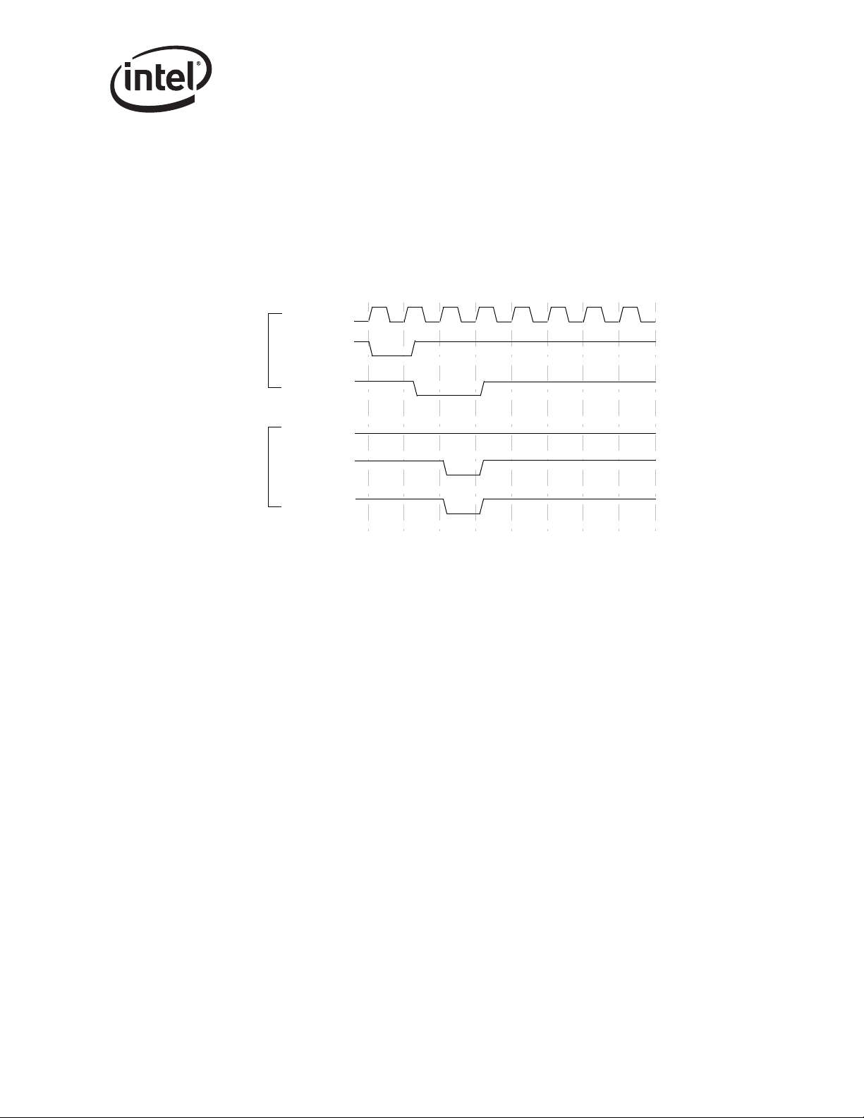
The following figures show CSR zero wait state I/ O read and write cycles. In the cas e o f accessin g
the Control/Status Registers, the CPU is the initiator and the 82551ER is the target of the
transaction.
Figure 1. CSR I/O Read Cycle
Networking Silicon — 82551ER
CLK
FRAME#
AD
C/BE#
IRDY#
TRDY#
DEVSEL#
ADDR
I/O RD BE#
3421 56789
DATA
82551ER SYSTEM
STOP#
Read Accesses: The CPU, as the initiator, drives address lines AD[31:0], the command and byte
enable lines C/BE#[3:0] and the control lines IRDY# and FRAME#. As a slave, the 82551ER
controls the TRDY# signal and provides valid data on each data access. The 82551ER allows the
CPU to issue only one read cycle when it accesses the Control/Status Registers, generating a
disconnect by asserting the STOP# signal. The CPU can ins er t wait states by de-asserting IRDY#
when it is not ready.
Datasheet 17
Page 26
82551ER — Networking Silicon
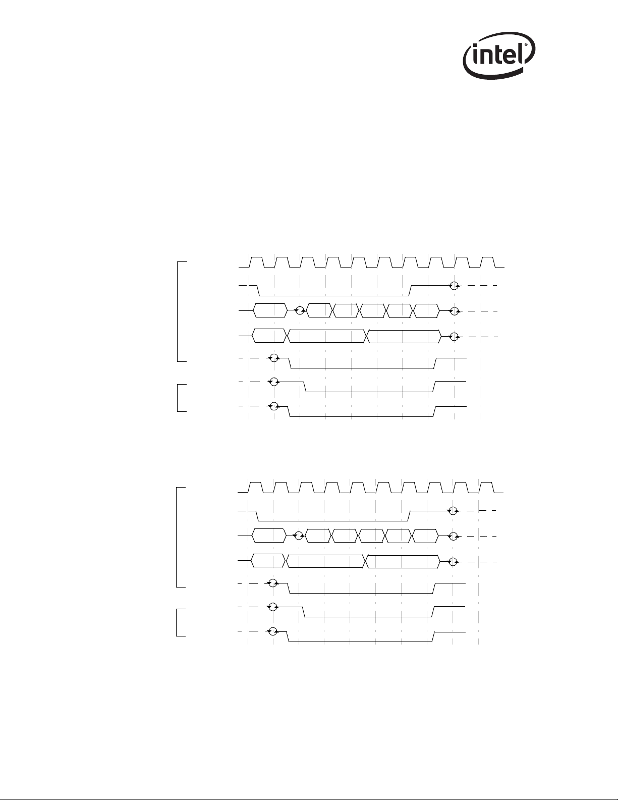
Figure 2. CSR I/O Write Cycle
CLK
FRAME#
AD
C/BE#
IRDY#
TRDY#
DEVSEL#
ADDR DATA
I/O WR BE#
3421 56789
82551ER SYSTEM
STOP#
Write Accesses: The CPU, as the initiator, drives the address lines AD[31:0], the command and
byte enable lines C/BE#[3:0] and the control lines IRDY# and FRAME#. It also provides the
82551ER with valid data on each data access immediately after asserting IRDY#. The 82551ER
controls the TRDY# signal and asserts it from the data access. The 82551ER allows the CPU to
issue only one I/O write cycle to the Control/Status Registers, generating a disconnect by asserting
the STOP# signal. This is true for both memory mapped and I/O mapped accesses.
18 Datasheet
Page 27
5.2.1.1.2 Flash Buffer Accesses
The CPU accesses to the Flash buffer are very slow and the 82551ER issues a target-disconnect at
the first data access. The 82551ER asserts the STOP# signal to indicate a target-disconnect. The
figures below illustrate memory CPU read and write accesses to the 128 KB Flash buffer. The
longest burst cycle to the Flash buffer contains one data access only.
Figure 3. Flash Buffer Read Cycle
CLK
FRAME#
Networking Silicon — 82551ER
AD
C/BE#
IRDY#
TRDY#
DEVSEL#
ADDR DATA
MEM RD BE#
82551ER SYSTEM
STOP#
Read Accesses: The CPU, as the initiator, drives the address lines AD[31:0], the command and
byte enable lines C/BE#[3:0] and the control lines IRDY# and FRAME#. The 82551ER controls
the TRDY# signal and de-asserts it for a certain n umb er o f clocks un til valid d ata can be read from
the Flash buffer. When TRDY# is asserted, the 82551ER drives valid data on the AD[31:0] lines.
The CPU can also insert wait states by de-asserting IRDY# until it is ready. Flash buffer read
accesses can be byte or word length.
Datasheet 19
Page 28
82551ER — Networking Silicon
Figure 4. Flash Buffer Write Cycle
CLK
FRAME#
AD
C/BE#
IRDY#
TRDY#
DEVSEL#
ADDR
MEM WR BE#
DATA
82551ER SYSTEM
STOP#
Write Accesses: The CPU, as the initiator, drives the address lines AD[31:0], the command and
byte enable lines C/BE#[3:0] and the control lines IRDY# and FRAME#. It also provides the
82551ER with valid data immediately after asserting IRDY#. The 82551ER controls the TRDY#
signal and de-asserts it for a certain number of clocks until valid data is written to the Flash buffer.
By asserting TRDY#, the 82551ER signals the CPU that the current data access has completed.
Flash buffer write accesses can be byte length only.
20 Datasheet
Page 29
5.2.1.1.3 Retry Premature Accesses
The 82551ER responds with a Retry to any configuration cycle accessing the 82551ER before the
completion of the automatic read of the EEPROM. The 82551ER may continue to Retry any
configuration accesses until the EEPROM read is complete. The 82551ER does not enforce the
rule that the retry master must attempt to access the same address again to complete any delayed
transaction. Any master access to the 82551ER after the completion of the EEPROM read will be
honored. Figure 5 below shows how a Retry looks when it occurs.
Figure 5. PCI Retry Cycle
CLK
FRAME#
IRDY#
TRDY#
DEVSEL#
Networking Silicon — 82551ER
82551ER SYSTEM
STOP#
Note: The 82551ER is considered the target in the above diagram; thus, TRDY# is not asserted.
5.2.1.1.4 Error Handling
Data Parity Errors: The 82551ER checks for data parity errors while it is the target of the
transaction. If an error was detected, the 82551ER always sets the Detected Parity Error bit in the
PCI Configuration Status register, bit 15. Th e 82551ER also asserts PERR#, if the Parity Error
Response bit is set (PCI Configuration Command register, bit 6). The 82551ER does not attempt to
terminate a cycle in which a parity error was detected. This gives the initiator the option of
recovery.
Target-Disconnect: The 82551ER prematurely terminates a cycle in the following cases:
• After accesses to the Flash buffer
• After accesses to its CSR
• After accesses to the configuration space
System Error: The 82551ER repor ts pari ty error d uring the addr ess phas e using the SERR# pi n. If
the SERR# Enable bit in the PCI Configuration Command register or the Parity Error Response bit
is not set, the 82551ER only sets the Detected Parity Error bit (PCI Configuration Status register,
bit 15). If SERR# Enable and Parity Error Response bits are both set, the 82551ER sets the
Signaled System Error bit (P CI C onf i guration Status register, bit 14) as well as the Detected Parity
Error bit and asserts SERR# for one clock.
Datasheet 21
Page 30
82551ER — Networking Silicon
Note: The 82551ER detects a system err or fo r any parity error during an address phase, whether or no t it
is involved in the current transaction.
5.2.1.2 Bus Master Operation
As a PCI Bus Master, the 82551ER initiates memory cycles to fetch data for transmission or
deposit received data and to access the memory resi dent contro l structures. Th e 82 551ER p erforms
zero wait state burst read and write cycles to the host main memory. Figure 6 and Figure 7 show
memory read and write burst cycles. For bus master cycles, the 82551ER is the initiator and the
host main memory (or the PCI host bridge, depending on the configur atio n of the system) is the
target.
Figure 6. Memory Read Burst Cycle
CLK
FRAME#
AD
C/BE#
IRDY#
TRDY#
SYSTEM 82551ER
DEVSEL#
Figure 7. Memory Write Burst Cycle
CLK
FRAME#
AD
82551ERSYSTEM
C/BE#
3421 5678910
ADDR
MR BE# BE#
ADDR
MW BE#
DATA
DATA
DATA
DATA
3421 5678910
DATA
DATA
DATA
DATA
BE#
DATA
DATA
IRDY#
TRDY#
DEVSEL#
The CPU provides the 82551ER with action commands and pointers to the data buffers that reside
in host main memory. The 82551ER independently manages these structures and initiates burst
memory cycles to transfer data to and from them. The 82551ER uses the Memory Read Multiple
(MR Multiple) command for burst accesses to data buffers and the Memory Read Line (MR Line)
22 Datasheet
Page 31

Networking Silicon — 82551ER
command for burst accesses to control structur es. For all write accesses to the control s tructure, the
82551ER uses the Memory Write (MW) command. For write accesses to data structure, the
82551ER may use either the Memory Write or Memory Write and Invalidate (MWI) commands.
Read Accesses: The 82551ER performs block transfers from host system memory to perform
frame transmission on the serial link. In this case, the 82551ER initiates zero wait state memory
read burst cycles for these accesses. The length of a burst is bounded by the system and the
82551ER’s internal FIFO. The length of a read burst may also be bounded by the value of the
Transmit DMA Maximum Byte Count in the Configure command. The Transmit DMA Maximum
Byte Count value indicates the maximum number of transmit DMA PCI cycles that will be
completed after an 82551ER internal arbitration.
The 82551ER, as the initiator, drives the address lines AD[31:0], the command and byte enable
lines C/BE#[3:0] and the control lines IRDY# and FRAME#. The 82551ER asserts IRDY# to
support zero wait state burst cycles. The target signals the 82551ER that valid data is ready to be
read by asserting the TRDY# signal.
Write Accesses: The 82551ER performs block transfers to host system memory during frame
reception. In this case, the 82551ER initiates memory write burst cycles to deposit the data, usually
without wait states. The length of a burst is bounded by the system and the 82551ER’s internal
FIFO threshold. The length of a write burst may also be bounded by the value of the Receive DMA
Maximum Byte Count in the Configure comman d. The Receive DMA Maximum Byte Count v alue
indicates the maximum number of receive DMA PCI transfers that will be completed before the
82551ER internal arbitration.
The 82551ER, as the initiator, drives the address lines AD[31:0], the command and byte enable
lines C/BE#[3:0] and the control lines IRDY# and FRAME#. The 82551ER asserts IRDY# to
support zero wait state burst cycles. The 82551ER also drives valid data on AD[31:0] lines during
each data phase (from the first clock and on). The target controls the len gth and si gnals co mpletion
of a data phase by de-assertion and assertion of TRDY#.
5.2.1.2.1 Memory Write and Invalidate
The 82551ER has four Direct Memory Access (DMA) channels. Of these four channels, the
Receive DMA is used to deposit the large number of data bytes received from the link into system
memory. The Receive DMA uses both the Memory Write (MW) and the Memory Write and
Invalidate (MWI) commands. To use MWI, the 82551ER must guarantee the following:
1. Minimum transfer of one cache line
2. Active byte enable bits (or BE[3:0]# are all low) during MWI access
3. The 82551ER may cross the cache line boundary only if it intends to transfer the next cache
line too.
To ensure the above conditions, the 82551ER may use the MWI command only if the following
conditions are true:
1. The Cache Line Size (CLS) written in the CLS register during PCI configuration is 8 or 16
Dwords.
2. The accessed address is cache line aligned.
3. The 82551ER82551ER has at least 8 or 16 Dwords of data in its receive FIFO.
4. There are at least 8 or 16 Dwords of data space left in the system memory buffer.
5. The MWI Enable bit in the PCI Configuration Command register, bit 4, must be set to 1b.
Datasheet 23
Page 32

82551ER — Networking Silicon
6. The MWI Enable bit in the 82551ER Configure command must be set to 1b.
If any one of the above conditions is not true, the 82551ER uses the MW command. If an MWI
cycle has started and one of the conditions is no longer valid (for example, the data space in the
memory buffer is now less than CLS), then the 82551ER terminates the MWI cycle at the end of
the cache line. The next cycle is either an MW or MWI cycle depending on the conditions listed
above.
If the 82551ER started a MW cycle and reached a cache line boundary, it either continues or
terminates the cycle depending on the Terminate Write on Cache Line configuration bit of the
82551ER Configure command (byte 3, bit 3). If this bit is set, the 82551ER terminates the MW
cycle and attempts to start a new cycle. The new cycle is an MWI cycle if this bit is set and all of
the above conditions are met. If the bit is not set, the 82551ER continues the MW cycle across the
cache line boundary if required.
5.2.1.2.2 Read Align
The Read Align feature enhances the 82551ER’s performance in cache line oriented systems. In
these particular systems, starting a PCI transaction on a non-cache line aligned address may cause
low performance.
To resolve this per for mance ano maly, the 82551ER attempts to terminate transmit DMA cycles on
a cache line boundary and start the next transaction on a cache line aligned address. This feature is
enabled when the Read Align Enable bit is set in the 82551ER Configure command (byte 3, bit 2).
If this bit is set, the 82551ER operates as follows:
• When the 82551ER is almost out of resources on the transmit DMA (that is, the transmit FIFO
is almost full), it attempts to terminate the read transaction on the nearest cache line boundary.
• When the arbitration counter’s feature is enabled (in other words, the Transmit DMA
Maximum Byte Count value is set in th e Confi gure comm and), the 8255 1ER swi tches to other
pending DMAs on cache line boundary only.
This feature is not recommended for use in non-cache line oriented systems since it may cause
shorter bursts and lower performance. If this feature is used, it is recommended that the CLS
register in PCI Configuration space is set to 8 or 16.
5.2.1.2.3 Error Handling
Data Parity Errors: As an initiator, the 82551ER checks and detects data parity errors that occur
during a transaction. If the Parity Error Response bit is set (PCI Configuration Command register,
bit 6), the 82551ER also asserts PERR# and sets the Data Parity Detected bit (PCI Configuration
Status register, bit 8). In addition, if the error was detected by the 82551ER during read cycles, it
sets the Detected Parity Error bit (PCI Configuration Status register, bit 15).
5.2.2 Clock Run Signal
This signal is active in PCI bus operating modes. The Clock Run signal is an open dr ain I/O signal.
It is used as a bi-directional channel between the host and the devices.
• The host de-asserts the CLK_RUN# signal to indicate that the clock is about to be stopped or
slowed down to a non-operational frequency.
24 Datasheet
Page 33

• The host asserts the CLK_RUN# signal when the clock is either running at a normal operating
frequency or about to be starte d.
• The 82551ER asserts the CLK_RUN# signal to indicate that the PCI clock must prevent the
host from stopping or to request that the host restore the clock if it was previously stopped.
Proper operation requires that the system latency from the nominal PCI CLK to CLK_RUN#
assertion should be less than 0.5 µs. If the system latency is longer than 0.5 µs, there is an increase
in receive overruns. In these types of systems, the Clock Run functionality should be disabled. In
this case, the 82551ER will claim the PCI clock even during idle time. If the CLK_RUN# signal is
not used, it must be connected to a pull-down resistor.
5.2.3 Power Management Event
The 82551ER supports power management indications in the PCI mode. The PME# output pin
provides an indication of a power management event in PCI systems.
5.3 PCI Power Management
The 82551ER supports interesting packet wake-up and the capability to wake the system on a link
status change from a low power state. The 82551ER enables the host system to be in a sleep state
and remain virtually connected to the network. After a power management event or link status
change is detected, the 82551ER will wake the host system. The sections below describe these
events, the 82551ER power states, and estimated power consumption at each power state.
Networking Silicon — 82551ER
5.3.1 Power States
The 82551ER has one set of PCI powe r management registers and implement s all four power states
as defined in the Power Management Network Device Class Reference Specification, Revision 1.0.
The four device power states, D0 through D3, vary from maximum power consumption at D0 to
the minimum power consumption at D3.
PCI transactions are only allowed in the D0 state, except for host accesses to the 82551ER’s PCI
configuration registers. The D1 and D2 power management states enable intermediate power
savings while providing the system wake-up capabilities. In the D3 cold state, the 82551ER can
provide wake-up capabilities only if auxiliary power is supplied. Wake-up indications from the
82551ER are provided by the Power Management Event (PME#) signal in PCI implementations.
5.3.1.1 D0 Power State
As defined in the Network Device Class Reference Specification, the device is fully fun ctional in
the D0 power state. In this state, the 82551ER receives full power and should be providing full
functionality. In the 82551ER the D0 state is partitioned into two substates, D0 Uninitialized (D0u)
and D0 Active (D0a).
D0u is the 82551ER’s initial power state following a Power-on Reset (POR) event and before the
Base Address Registers (BARs) are accessed. Initialization of the CSR, Memory, or I/O Base
Address Registers in the PCI Configuration space switches the 82551ER from the D0u state to the
D0a state.
Datasheet 25
Page 34

82551ER — Networking Silicon
In the D0a state, the 82551ER provides its full functionality and consumes nominal power. In
addition, the 82551ER supports wake on link status change (Section 5.3.2, “Wake-up Events”).
While it is active, the 82551ER requires a nominal PCI clock signal (in other words, a clock
frequency greater than 16 MHz) for proper operation. During idle time, the 82551ER supports a
PCI clock signal suspension using the Clockrun signal mechanism. The 82551ER supports a
dynamic standby mode. In this mode, t he 82 551ER is able to save almo st as much pow er as it does
in the static power-down states. The transition to or from standby is done dynamically by the
82551ER and is transparent to the software.
5.3.1.2 D1 Power State
For a device to meet the D1 power state requirements, as specified in the Advanced Configuration
and Power Interface (ACPI) Specification, Revision 1.0, it must not allow bus transmission or
interrupts; however, bus reception is allowed. Therefore, device context may be lost and the
82551ER does not initiate any PCI activity. In this state, the 82551ER responds only to PCI
accesses to its configuration space and system wake-up events.
The 82551ER retains link integrity and monitors the link for any wake-up events such as wake-up
packets or link status change. Following a wak e-up even t, the 82551ER asserts the PME# signal to
alert the PCI system.
5.3.1.3 D2 Power State
The ACPI D2 power state is similar in functionality to the D1 power state. If the bus is in the B2
bus power state, the 82551ER will consume less current than it does in the D1 state. In addition to
D1 functionality, the 82551ER can provide a lower power mode with wake-on-link status change
capability. The 82551ER may enter this mode if the link is down while the 82551ER is in the D2
state. In this state, the 82551ER monitors the link for a transition from an invalid link to a valid
link. The 82551ER will not attempt to keep the link alive by transmitting idle symbols or link
integrity pulses.
1
The sub-10 mA state due to an invalid link can be enabled or disabled by a
configuration bit in the Power Management Driver Register (PMDR).
5.3.1.4 D3 Power State
In the D3 power state, the 82551ER has the same capabilities and consumes the same amount of
power as it does in the D2 state. However, it enables the PCI system to be in the Bus Power 3 (B3)
state. If the PCI system is in the B3 state (in other words, no PCI power is present), the 82551ER
provides wake-up capabilities if it is connected to an auxiliary power source in the system. If
PME# is disabled, the 82551ER does not provide wake-up capability or maintain link integrity. In
this mode, the 82551ER consumes minimal power.
The 82551ER enables a system to be in a sub-5 watt state (low power state) and still be virtually
connected. More specifically, the 82551ER supports full wake-up capabilities while it is in the D3
cold state. The 82551ER can be connected to an auxiliary power source (V
to provide wake-up functionality while the PCI power is off. The typical current consumption of
the 82551ER is 125 mA at 3.3 V and a dual power plane is not required. If connected to an
auxiliary power source, the 82551ER receives all of its power from the auxiliary source in all
power states. When connected to an auxiliary power supply, the 82551ER must have a status
indicator of whether the power supply is valid (in other words, auxiliary power is stable). The
indication is received at the AUXPWR pin, as described next.
), which enables it
AUX
1. For a topology of two 82551E R devices connected by a cr ossed twisted-pair Ethernet cable, the deep power-down mod e should be
disabled. If it is enabled, the two de vices may not detect ea ch other if the oper ating system places them into a low power s tate before both
nodes become active .
26 Datasheet
Page 35

Networking Silicon — 82551ER
5.3.1.4.1 Auxiliary Power Signal
The 82551ER senses whether it is connected to the PCI power supply or to an auxiliary power
supply (V
with FLA1) is sampled when the 82551ER power-on reset is active. An external pull-up resistor
should be connected to the 82551ER if it is fed by V
should be left floating. The presence of AUXPWR affects the value reported in the Power
Management Capability Register (PCI Configuration Space, offset DEh). The Power Management
Capability Register is described in more detail in Section 7.1.19, “Power Management Capabilities
Register”.
) through the FLA1/AUXPWR pin. The auxiliary power detection pin (multiplexed
AUX
; otherwise, the FLA1/AUXPWR pin
AUX
5.3.1.4.2 Alternate Reset Signal
The 82551ER’s ALTRST# input pin functions as a power-on reset input. Following ALTRST#
being driven low, the 82551ER is initialized to a known state. While this function is required, this
pin is not needed for it. Since this functionality is provided by the 82551ER’s internal power-on
reset signal, this pin should be pulled high to the main digital power supply.
Note: A separate internal power-on reset signal is generated when power is applied to the device. This
signal is active while it provides the 82551ER power-on reset function and is also used for
sampling configuration inputs.
5.3.1.4.3 Isolate Signal
When the 82551ER is connected to V
In this case, the 82551ER isolates itself from the PCI bus. The 82551ER has a dedicated
ISOLATE# pin that must be connected to the PCI Reset signal. Whenever the PCI Bus is in the B3
state, the PCI Reset signal becomes active and the 82551ER isolates itself from the PCI bus.
During this state, the 82551ER ignores all PCI signals including the RST# and CLK input signals.
It also tristates all PCI outputs, except the PME# signal. In the transition to an active PCI power
state (in other words, from B3 bus power state to B0 bus power state), the PCI Reset signal shifts
high. This generates an internal hardware reset, which initializes the device (described in Section
5.1.1, “Initialization Effects”).
Some designs in existence may implement the previous recommendations for the RST#,
ISOLATE# and AL TRST# input pins. In th ese cases, the PCI Reset signal is connected to the RST#
pin, the PCI power source’s stable power (power good) to the ISOLATE# pin, and the auxiliary
power source’s stable power (auxiliary power good) to the ALTRST# pin. It is not necessary for
existing working designs to make changes for these signals; however, it is recommended that the
changes contained in this document should be included when possible. New designs should
implement the recommendations contained in this document.
, it can be powered on while the PCI bus is powered off.
AUX
5.3.1.4.4 PCI Reset Signal
The PCI RST# signal can be activated in one of the following cases:
• Power-up
• W arm boo t
• Wake-up (B3 to B0 transition)
• Set to power-down (B0 to B3 transition)
Datasheet 27
Page 36

82551ER — Networking Silicon
If PME# is enabled (in the PCI power management registers), the RST# signal does not affect any
PME# related circuits (in other words, the PCI power management registers, and the wake-up
packet would not be affected).
Note: The PCI Specification, Revisi on 2.2, states that the PCI RST# signal should be active low in the B3
state. (In PCI Specification, Revision 2.1, the PCI RST# signal is undefined during the B3 state.)
The transition from the B3 bus power state to the B0 bus power state occurs on the trailing ed ge of
the PCI RST# signal.
The initialization signal is generated internally in the f ollowing cases:
• Active RST# signal while the 82551ER is the D0, D1, or D2 power state
• RST# trailing edge while the 82551ER is in the D3 power state
• ISOLATE# tr ailing edge
The internal initialization signal resets the PCI Configuration Space, MAC configuration, and
memory structure.
The behavior of the RST# and ISOLATE# pins and the internal 82551ER initialization signal are
shown in the following figure.
Figure 8. Initialization upon RST# and ISOLATE#
RST#
Internal hardware
reset
RST#
Internal hardware
reset
ISOLATE#
Internal hardware
reset
D0 - D2 power state
D3 power state
640 ns
Internal reset
due to ISOLATE#
640 ns
28 Datasheet
Page 37

Networking Silicon — 82551ER
The following tables list the functionality at the different power states for the 82551ER.
T able 11. Functionality at the Different Power States
Power State Link Functionality
D0u Don’t care
D0a
D1
D2
D3 (with power)
Dx (x>0 without
PME#)
5.3.2 Wake-up Events
There are two types of wake-up events: “Interesting” Packets and Link Status Change. These two
events are detailed below.
• Power-up state
• PCI slave access
Valid
Invalid
Valid
Invalid
Valid Same functionality as D1 (link valid)
Invalid Detection for valid link and no link integrity
Valid Same functionality as D1 (link valid)
Invalid Detection for valid link and no link integrity
Don’t care No wake-up functionality.
Full functionality at full power and wake on an
invalid link
Full functionality at full power and wake on a valid
link
• Wake-up on “interesting” packets and link
invalid
• PCI configuration access
• Wake on link valid
• PCI configuration access
Note: The wake-up event is supported only if the PME Enable bit in the Power Management Control/
Status (PMCSR) register is set.
5.3.2.1 “Interesting” Packet Event
In the power-down state, the 82551ER is capable of recognizing “interesting” packets. The
82551ER supports pre-defined and programmable packets that can be defined as any of the
following:
• Address Resolution Protocol (ARP) Packets (with Multiple IP addresses)
• Direct Packets (with or without type qualification)
• Neighbor Discovery Multicast Address Packet (“ARP” in IPv6 environment)
• NetBIOS over TCP/IP (NBT) Query Packet (under IPv4)
• Internetwork Package Exchange* (IPX*) Diagnostic Packet
This allows the 82551ER to handle various packet types. In general, the 82551ER supports
programmable filtering of any packet in the first 128 bytes.
Datasheet 29
Page 38

82551ER — Networking Silicon
5.3.2.2 Link Status Change Event
The 82551ER link status indication cir cuit is capable of issuing a PME on a link status change from
a valid link to an invalid link condition or vice versa. The 82551ER reports a PME link status event
in all power states. The PME# signal is gated by the PME Enable bit in the PMCSR and the CSMA
Configure command.
5.4 Parallel Flash
The 82551ER’s parallel interface is used for a Flash interface. The 82551ER supports a glueless
interface to an 8-bit wide, 128 KB, parallel memory device.
The Flash (or boot PROM) is read from or written to whenever the host CPU performs a read or a
write operation to a memory location that is within the Flash mapping window. All accesses to the
Flash, except read accesses, require the appropriate command seq uence fo r the device used. (Refer
to the specific Flash data sheet f or more details on reading f rom or writing t o the Flash d evice.) The
accesses to the Flash are based on a direct decode of CPU accesses to a memory window defined in
either the 82551ER Flash Base Address Register (PCI Configuration space at offset 18h) or the
Expansion ROM Base Address Register (PCI Configuration space at offset 30h). The 82551ER
asserts control to the Flash when it decodes a valid access.
The 82551ER supports an external Flash memory (or boot PROM) of up to 128 KB. The
Expansion ROM address can be separately disabled by setting the corresponding bit in the
EEPROM, word Ah.
Note: Flash accesses must always be assembled or disassembled by the 8 255 1ER whenever the access is
greater than a byte-wide access. Due to slow access times to a typical Flash and to avoid violating
PCI bus holding specifications (no more than 16 wait states inserted for any cycles that are not
system initiation cycles), the maximum data size is either on e word or one byte for a read operation
and one byte only for a write operation.
5.5 Serial EEPROM Interface
The serial EEPROM stores configuration data for the 82551ER and is a serial in/serial out device.
The 82551ER supports eit her a 64-regis ter or 256- register size EEPR OM and automati cally detects
the EEPROM’s size. The EEPROM should also operate at a frequency of at least 1 MHz.
30 Datasheet
Page 39
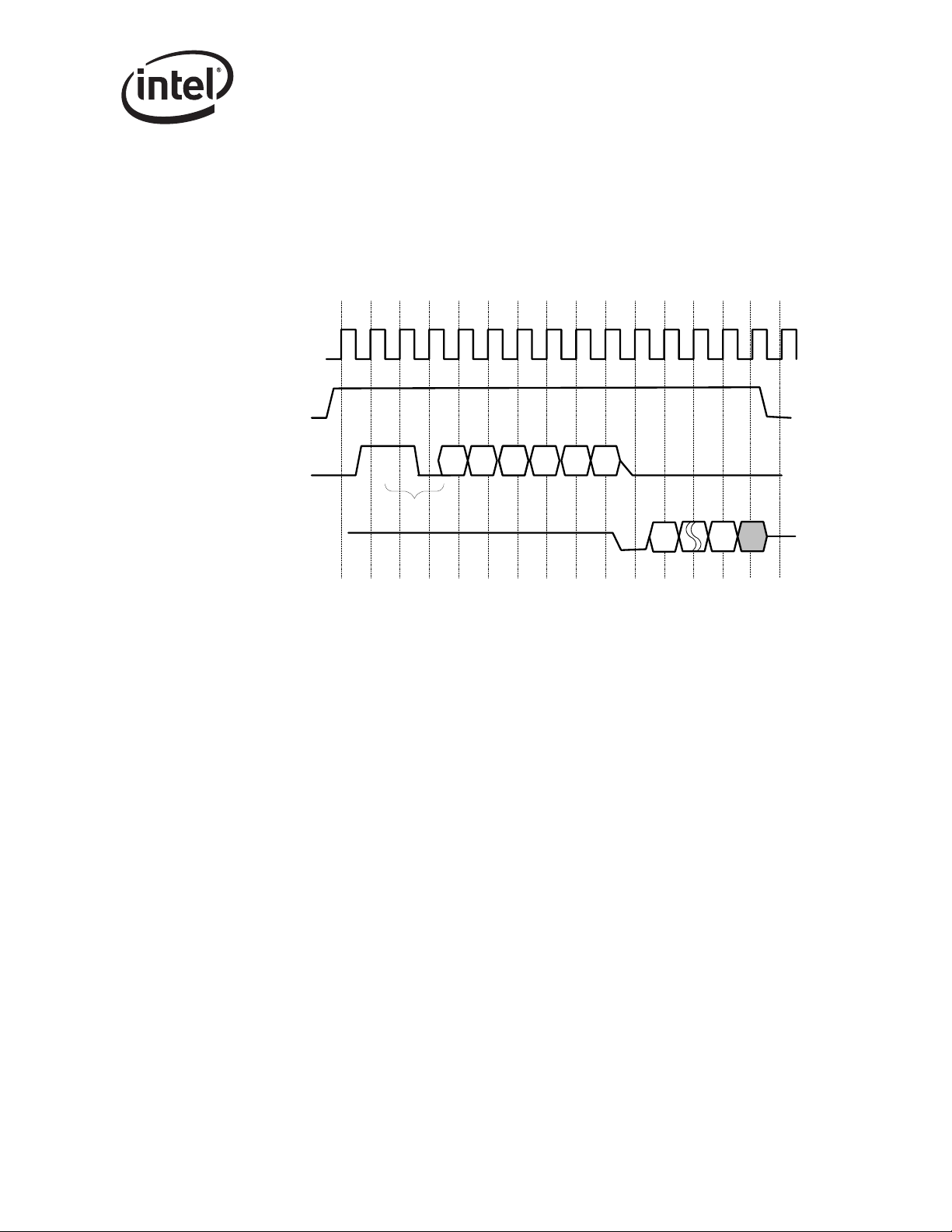
All accesses, either read or write, are preceded by a command instruction to the device. The
E
address field is six bits for a 64-register EEPROM or eight bits for a 256-register EEPROM. The
end of the address field is indicated by a dummy zero bit from the EEPROM, which indicates the
entire address field has been transferred to the device. An EEPROM read instruction waveform is
shown in the figure below.
Figure 9. 64-Word EEPROM Read Instruction Waveform
EESK
EECS
Networking Silicon — 82551ER
A1A
A
A1A
0
2
0
D
15
D
0
EEDI
EDO
READ OP code
A5A
A
4
3
The 82551ER performs an automatic read of four words (0h, 1h, 2h, and Ah) of the EEPROM after
the de-assertion of Reset. Refer to the 82551QM/ER/IT EEPROM Map and Programming
Information for more details.
Datasheet 31
Page 40

82551ER — Networking Silicon
5.5.1 EEPROM Address Map
Table 1 2 lists the EEPROM address map for the 82551ER Fast Ethernet Controller.
T a ble 12. 82551ER EEPROM Address Map
Word High Byte (Bits 15:8) Low Byte (Bits 7:0)
00h Ethernet Individual Address By te 2 Ethernet Individual Address Byte 1
01h Ethernet Individual Address By te 4 Ethernet Individual Address Byte 3
02h Ethernet Individual Address By te 6 Ethernet Individual Address Byte 5
03h Compatibility Byte 1 Compatibility Byte 0
04h Reserved
05h Controller Type Connectors
06h Primary PHY Record, high byte Primary PHY Record, low byte
07h Secondary PHY Record, high byte Secondary PHY Record, low byte
08h PWA Byte 1 PWA Byte 2
09h PWA Byte 3 PWA Byte 4
0Ah EEPROM_ID, high byte EEPROM_ID, low byte
0Bh Subsystem_ID, high byte Subsystem_ID, low byte
0Ch Subsystem_Vendor, high byte Subsystem_Vendor, low byte
0Dh:0Fh Reserved
10h:22h Reserved
23h Device ID, high byte Device ID, low byte
24h:2Fh Reserved
30h:33h Intel Boot Agent Configuration
34h:3Eh Reserved
3Fh 64-word EEPROM Checksum, high byte 64-word EEPROM Checksum, low byte
40h:FEh Reserved
FFh 256-word EEPROM Checksum, high byte 256-word EEPROM Checksum, low byte
Note: Refer to the 82551QM/ER/IT EEPROM Map and Programming Information for more details.
5.6 10/100 Mbps CSMA/CD Unit
The 82551ER CSMA/CD unit implements both the IEEE 802.3 Ethernet 10 Mbps and IEEE
802.3u Fast Ethernet 100 Mbps standards. It performs all the CSMA/CD protocol fu nctions such as
transmission, reception, collision handling, etc. The 82551ER CSMA/CD unit communicates with
the internal PHY unit through a standard Media Independent Interf ace (MII) , as specified by IE EE
802.3, Chapter 22. This is a 10/100 Mbps mode in which the data stream is nibble-wide and the
serial clocks run at either 25 or 2.5 MHz.
32 Datasheet
Page 41

5.6.1 Full Duplex
When operating in full duplex m ode the 82551ER can transmit and receive frames s imultan eous ly.
Transmission starts regardless of the state of the internal receive path. Reception starts when the
internal PHY detects a valid frame on the receive differential pair of the PHY.
The 82551ER operates in either half duplex mode or full duplex mode. For proper operation, both
the 82551ER CSMA/CD module and the PHY unit must be set to the same duplex mode. The
CSMA duplex mode is set by the 82551ER Configure command or forced by the settings in the
PHY unit’s registers.
The PHY duplex mode is set either by Auto-Negotiation or, if Auto-Negotiation is disabled, by
setting the full duplex bit in the Management Data Interface (MDI) Register 0, bit 8. By default, the
internal PHY unit advertises full duplex ability in the Auto-Negotiation process regardless of the
duplex setting of the CSMA unit. The CSMA configuration should match the result of the AutoNegotiation.
The selection of duplex operation (full or half) and flow control is done in two levels: MAC and
PHY. The MAC duplex selection is done only through the CSMA configuration mechanism (in
other words, the Configure command in software).
5.6.2 Flow Control
Networking Silicon — 82551ER
The 82551ER supports IEEE 802.3x frame-based flow control frames in both full duplex and half
duplex switched environments. The 82551ER flow control feat ure is not intended to be used in
shared media environments.
The PHY unit’s duplex and flow con trol enable can be selected using the NWay* Auto-Negotiation
algorithm or through the Management Data Interface.
5.6.3 Address Filtering Modifications
The 82551ER can be configured to ignore one bit when checking for its Individual Address (IA) on
incoming receive frames. The address bit, kn own as the Upper/Lower (U/L) bit, is the second least
significant bit of the first byte of the IA. This bit may be used, in some cases, as a priority
indication bit. When configured to do so, the 82551ER passes any frame that matches all other 47
address bits of its IA, regardless of the U/L bit value.
This configuration only affects the 82551ER specific IA and not multicast, multi-IA or broadcast
address filtering. The 82551ER does not attribute any priority to frames with this bit set, it simply
passes them to memory regardless of this bit.
5.6.4 VLAN Support
The 82551ER controller supports the VLAN standard currently being defined by the IEEE 802.1
committee. All VLAN receive flows will be implemented by software. The 82551ER supports the
reception of long frames, specifically frames longer than 1518 bytes, including CRC, if software
sets the Long Receive OK bit in the Configuration command. Otherwise, “long” frames are
discarded.
Datasheet 33
Page 42

82551ER — Networking Silicon
5.7 Media Independent Interface (MII) Management Interface
The MII management interface allows the CPU to control the PHY unit through a control register
in the 82551ER. This allows the software driver to place the PHY in specific modes such as full
duplex, loopback, power down, etc., without the need for specific hardware pins to select the
desired mode. This structure all ows the 8 255 1ER to quer y the PH Y un i t for s tatu s of the lin k. This
register is the MDI Control Register and resides at offset 10h in the 82551ER CSR. (The MDI
registers are described in detail in Section 9.0, “PHY Unit Registers”.) The CPU writes commands
to this register and the 82551ER reads or writes the control/status para meters to the PHY unit
through the MDI register. Although the 82551ER follows the MII format, the MI bus is not
accessible on external pins.
34 Datasheet
Page 43

Networking Silicon — 82551ER
6.0 Physical Layer Functional Description
6.1 100BASE-TX PHY Unit
6.1.1 100BASE-TX Transmit Clock Generation
A 25 MHz crystal or a 25 MHz oscillator is used to drive the PHY unit’s X1 and X2 pins. The PHY
unit derives its internal transmit digital clocks from this crystal or oscillator input. The internal
Transmit Clock signal is a derivative of the 25 MHz internal clock. The accuracy of the external
crystal or oscillator must be ± 0.005% (30 ppm).
6.1.2 100BASE-TX Transmit Blocks
The transmit subsection of the PHY unit accepts nibble-wide data from the CSMA/CD unit. The
transmit subsection passes data unconditionally to a 4B/5B encoder.
The 4B/5B encoder accepts nibble-wide data (4 bits) from the CSMA unit and compiles it into 5bit-wide parallel symbols according to the IEEE 802.3u 100BASE_TX standard. Next, the symbols
are scrambled to reduce electromagnetic emissions during long sequences of high-frequency data
codes.
The MLT-3 (multi-level signal) encoder receives the scrambled Non-Return to Zero (NRZ) data
stream from the scrambler and encodes the stream into MLT-3 for presentation to the driver. M LT3 is similar to NRZ1 coding, but three levels are output instead of two. The three output levels are
positive, negative and zero.
The transmit differential pair line drivers are implemented with digital slope controlled current
buffers that meet the TP-PMD specifications. Current is sinked from an isolation transformer by
the TDP and TDN pins. The 125 Mbps bit stream is typically driven onto Unshielded Twisted Pair
(UTP) cable.
6.1.3 100BASE-TX Receive Bloc ks
The receive subsection of the PHY unit accepts 100BASE-TX MLT-3 data on the receive
differential pair. Due to the advanced digital signal processing design techniques employed, the
PHY unit will accurately receive valid data from Category 5 (CAT5) UTP cables of lengths well in
excess of 100 meters.
The distorted MLT-3 signal at the end of the wire is restored by the equalizer. The equalizer
performs adaptation based on the shape of the received signal. The clock recovery circuit uses
digital signal processing to compensate for various signal jitter causes. The circuit recovers the 125
MHz clock and data and presents the data to the MLT-3 decoder.
The PHY unit first decodes the MLT-3 data; afterwards, the descrambler reproduces the 5B
symbols originated in the transmitter. The data is decoded at the 4B/5B decoder. After the 4B
symbols are obtained, the PHY unit outputs the receive data to the CSMA unit.
In 100BASE-TX mode, the PHY unit can detect errors in receive data in a number of ways,
including link integrity failures, undetected start of stream delimiters, invalid symbols, or idles in
the middle of a frame.
Datasheet 35
Page 44

82551ER — Networking Silicon
6.1.4 100BASE-TX Link Integrity Auto-Negotiation
The 82551ER Auto-Negotiation function automatically configures the device to the technology,
media, and speed to operate with its link partner. Auto-Negotiation is described in IEEE
specification 802.3u, clause 28. The PHY unit supports 10BASE-T half duplex, 10BASE-T full
duplex, 100BASE-TX half duplex, and 100BASE-TX full duplex.
Speed and duplex auto-select are functions of Auto-Negotiation. How ever, these parameters may
be manually configured through the MII management interface (MDI registers). Manual
configurations override the auto-select.
6.2 10BASE-T PHY Functions
6.2.1 10BASE-T Transmit Clock Generation
The 20 MHz and 10 MHz clocks needed for 10BASE-T are s ynthesized fro m the extern al 25 MHz
crystal or oscillator. The PHY unit provides the transmit clock and receive clock to the internal
MAC at 2.5 MHz.
6.2.2 10BASE-T Transmit Blocks
After the 2.5 MHz clocked data is serialized in a 10 Mbps serial stream, the 20 MHz clock
performs Manchester encoding.
Since 10BASE-T and 100BASE-TX have different filtration needs, both filters are implemented
inside the chip. The PHY unit supports both technologies through one pair of TD pins and by
externally sharing the same magnetics.
In 10 Mbps mode, the line drivers use a pre-distortion algorithm to improve jitter tolerance. The
line drivers reduce their drive level during the second half of “wide” Manchester pulses and
maintain a full drive level during narrow pulses and the first half of the wide pulses. This red uces
jitter caused by overcharging the line.
6.2.3 10BASE-T Receive Block s
The PHY uni t performs Manchester decoding and timing recovery when in 10 Mbps mode. The
Manchester-encoded data stream is decoded from the RD pair to separate Receive Clock and
Receive Data from the differential signal. This data is transferred to the CSMA unit at 2.5 MHz/
nibble.
In 10 Mbps mode, data is expected to be received on the receive differential pair after passing
through isolation transformers. The input differential voltage range capability for the Twisted Pair
Ethernet (TPE) receiver is greater than 585 mV and less than 3.1 V. The TPE receive buffer
distinguishes valid receive data, link test pulses, and idles, according to the requirements of the
10BASE-T standard.
In 10 Mbps mode, the PHY unit can detect errors in the receive data, including voltage drops prio r
to the end-of-frame bit. Collision detection in 10 Mbps mode is initiated by simultaneous
transmission and reception. If the PHY unit detects this condition, it asserts a collision indication to
the CSMA/CD unit.
36 Datasheet
Page 45

6.2.4 10BASE-T Link Integrity and Full Duplex
The link integrity i n 10 Mb ps wor ks wi th l ink pulses. The PHY unit sens es an d differentiates those
link pulses from fast link pulses and from 100BASE-TX idles. The link beat pulse is also used to
determine if the receive pair polarity is reversed. If it is, the polarity is corrected internally.
The PHY unit supports 10 Mbps full duplex by disabling the collision function, the squelch test,
and the carrier sense transmit function. This allows the PHY unit to transmit and receive
simultaneously, achieving up to 20 Mbps network bandwidth using Auto-Negotiation. Full duplex
can only be used in point-to-point connections (no shared media).
6.3 Auto-Negotiation
The PHY unit supports Auto-Negotiation, which is an automatic configuration scheme designed to
manage interoperability in multifunctional LAN environments. An Auto-Negotiation capable
device can detect and automatically configure its port to take maximum advantage of common
modes of operation without user intervention or prior knowledge by either station. AutoNegotiation is described in IEEE Standard 802.3u, clause 28.
6.3.1 Description
Networking Silicon — 82551ER
A PHY’s capability is encoded by bursts of link pulses called Fast Link Pulses (FLPs). Connection
is established by FLP exchange and handshake during link initialization time. After th e link is
established by this handshake, the native link pulse scheme resumes. A reset or management renegotiate command (through the MDI interface) will restart the process. If the PHY unit cannot
perform Auto-Negotiation, it will set this bit to 0 and determine the speed using Parallel Detection.
The PHY unit supports fo ur technol ogies: 100BASE- Tx Ful l and Half Duplex an d 10BA SE-T Full
and Half Duplex. Since only one technology can be used at a time (after every re-negotiate
command), a prioritization scheme is used to ensure that the ability of the highest common
denominator is chosen.
6.3.2 Parallel Detect and Auto-Negotiation
The PHY unit can automatically determine the speed of the link by using Parallel Detect as an
alternative to Auto-Negotiation. Upon a reset, a link status fail, or a negotiate/re-negotiate
command, the PHY unit inserts a long delay during which no link pulses are transmitted. This
period insures that the PHY unit‘s link partner has gone into a Link Fail state before AutoNegotiation or Parallel Detection begins. The PHY unit will look for both FLPs and lin k integrity
pulses. The following diagram illustrates this process.
Datasheet 37
Page 46

82551ER — Networking Silicon
Figure 10. Auto-Negotiation and Parallel Detect
Parallel Detection
Force_Fail
Ability detect either by
parallel detect or au t o-
negotiation.
Auto-Negotiation
Look at Link Pulse;
Auto-Negotiation capable = 0
6.4 LED Description
The PHY unit supports three LED pi ns to i ndicat e li nk s tat us , netw ork act ivity and n et work s peed .
Each pin can source 10 mA.
• Link: This LED is off until a valid link has been detected. After a valid link has been detected,
the LED will remain on (active-low).
• Activity: This LED blinks on and off when activity is detected on the wire.
• Speed: This LED will be on if a 100BASE-TX link is detected and off if a 10BASE-T link is
detected. If the link fails while in Auto-Negotiation, this LED will keep the last valid link
state. If 100BASE-TX link is forced this LED will be on, regardless of the link status. This
LED will be off if the 10BASE-T link is forced, regardless of the link status.
10Base-T or
100Base-TX Link
Ready
Auto-Negotiation Complete bit set
LINK PASS
FLP capable
Auto-Negotiation capable = 1
Ability Match
MDI register 27 in Section 9.3.12, “Register 27: PHY Unit Special Control Register ” d etails the
information for LED function mapping and support enhancements.
Figure 11 provides possible schematic diagrams for configura tio ns us ing two and th ree LEDs.
38 Datasheet
Page 47

Figure 11. Two and Three LED Schematic Diagram
LILED#
ACTLED#
SPDLED#
82551ER
LILED#
ACTLED#
SPEEDLED#
Networking Silicon — 82551ER
vcc
R
R
R
R
R
Datasheet 39
Page 48

82551ER — Networking Silicon
Note: This page is intentionally left blank.
40 Datasheet
Page 49

Networking Silicon — 82551ER
7.0 Configuration Registers
The 82551ER acts as both a master and a slave on the PCI bus. As a mast er, the 82551ER interacts
with the system main memory to access data for transmission or deposit received data. As a slave,
some 82551ER control structures are accessed by the host CPU to read or write information to the
on-chip registers. The CPU als o pr ovi des the 82 551ER with the necessary commands and poi nters
that allow it to process receive and transmit data.
7.1 Function 0: LAN (Ethernet) PCI Configuration Space
The 82551ER PCI configuration space is configured as 16 Dwords of T ype 0 Configur atio n Space
Header, as defined in the PCI Specification, Revision 2.1. A small section is also configured
according to its device specific configuration space. The configuration space header is depicted
below in Figure 12.
Figure 12. PCI Configuration Registers
Device ID Vendor ID 00h
Status Command 04h
Class Code Revision ID 08h
BIST Header Type Lat ency T imer Cache Line Size 0Ch
CSR Memory Mapped Base Address Register 10h
CSR I/O Mapped Base Address Register 14h
Flash Memory Mapped Base Address Register 18h
Reserved Base Address Register 1Ch
Reserved Base Address Register 20h
Reserved Base Address Register 24h
Reserved (PCI mode) 28h
Subsystem ID Subsystem Vendor ID 2Ch
Expansion ROM Base Address Register 30h
Reserved Cap_Ptr 34h
Reserved 38h
Max_Lat Min_Gnt Interrupt Pin Interrupt Line 3Ch
Power Management Capabilities Next Item Ptr Capability ID DCh
Reserved Data Power Management CSR E0h
7.1.1 PCI Vendor ID and Device ID Registers
The Vendor ID and Device ID of the 82551ER are both read only word entities. Their values are:
Vendor ID: 8086h
Device ID: 1209h
Datasheet 41
Page 50
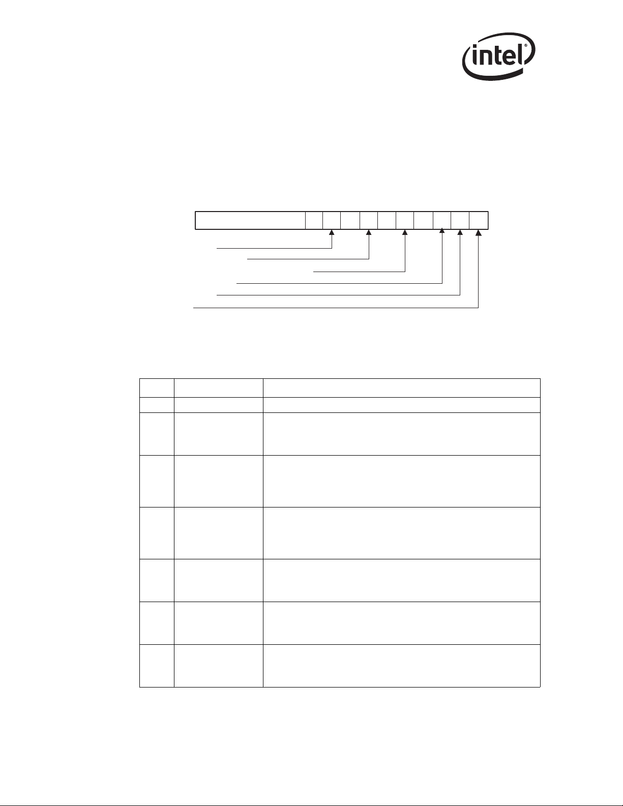
82551ER — Networking Silicon
7.1.2 PCI Command Register
The 82551ER Command register at word address 04h in the PCI configuration space provides
control over the 82551ER’s ability to generate and respond to PCI cycles
register, the 82551ER is logically disconnected from the PCI bus for all accesses except
configuration accesses
. The format of this register is shown in the figure below.
Figure 13. PCI Command Register
15 1098 7 654 3 21 0
Reserved
SERR# Enable
Parity Error Response
Memory Write and Invalidate Enable
Bus Master Enable
Memory Space
I/O Space
Bits three, five, seven, and nine are set to 0b. Table 13 describes the bits of the PCI Command
register.
. If a 0 is written to this
0000
Table 13. PCI Command Register Bits
Bits Name Description
15:10 Reserved These bits are reserved and should be set to 0b.
8 SERR# Enable
6 Parity Error Control
4
2 Bus Master
1 Memory Space
0I/O Space
Memory Write and
Invalidate Enable
This bit controls a device’s ability to enable the SERR# driver . A value of 0b
disables the SERR# driver. A value of 1b enables the SERR# driver. This
bit must be set to report address parity errors. In the 82551ER, this bit is
configurable and has a default value of 0b.
This bit controls a device’s response to parity errors. A value of 0b causes
the device to ignore any parity errors that it detects and continue normal
operation. A value of 1b causes the device to take normal action when a
parity error is detected. This bit must be set to 0b after RST# is asserted. In
the 82551ER, this bit is configurable and has a default value of 0b.
This bit controls a device’s ability to use the Memory Write and Invalidate
command. A value of 0b disables the device from using the Memory Write
and Invalidate Enable command. A value of 1b enables the device to use
the Memory Write and Invalidate command. In the 82551ER, this bit is
configurable and has a default value of 0b.
This bit controls a device’s ability to act as a master on the PCI bus. A
value of 0b disables the device from generating PCI accesses. A value of
1b allows the device to behave as a bus master. In the 82551ER, this bit is
configurable and has a default value of 0b.
This bit controls a device’s response to the memory space accesses. A
value of 0b disables the device response. A value of 1b allows the device
to respond to memory space accesses. In the 82551ER, this bit is
configurable and its default value of 0b.
This bit controls a device’s response to the I/O space accesses
0b disables the device response. A value of 1b allows the device to
respond to I/O space accesses. In the 82551ER, this bit is configurable and
the default value of 0b.
. A value of
42 Datasheet
Page 51

7.1.3 PCI Status Register
The 82551ER Status register is used to record status information for PCI bus related events. The
format of this register is shown in the figure below.
Figure 14. PCI Status Register
31 30 29 28 27 26 25 24 23 22 21 20 19 16
Detected Parity Error
Signaled System Error
Received Master Abort
Received Target Abort
Signaled Target Abort
Devsel Timing
Parity Error Detected
Fast Back To Back (target)
Capabilities List
Networking Silicon — 82551ER
0
Reserved011000 10
Note: Bits 21, 22, 26, and 27 are s et to 0b and bits 20, 23, and 25 are set to 1b. The PCI Stat us register bits
are described in Table 14.
T a ble 14. PCI Status Register Bits
Bits Name Description
This bit indicates whether a parity error is detected. This bit must be set by
the device when it detects a parity error, even if parity error handling is
31 Detected Parit y Error
30 Signaled System Error
29
28 Received Target Abort
27 Signaled Target Abort
26:25 DEVSEL# Timing
Received Master
Abort
disabled (as controlled by the Parity Error Response bit in the PCI
Command register, bit 6). In the 82551ER, the initial value of the Detected
Parity Error bit is 0b. This bit is set until cleared by writing a 1b.
This bit indicates when the device has asserted SERR#. In the 82551ER,
the initial value of the Signaled System Error bit is 0b. This bit is set until
cleared by writing a 1b.
This bit indicates whether or not a master abort has occurred. This bit must
be set by the master device when its transaction is terminated with a
master abort. In the 82551ER, the initial value of the Received Master
Abort bit is 0b . Th is bit is set until cleared by writing a 1b.
This bit indicates that the master has received the target abort. This bit
must be set by the master device when its transaction is terminated by a
target abort. In the 82551ER, the initial value of the Received Target Abort
bit is 0b. This bit is set until cleared by writing a 1b.
This bit indicates whether a transaction was terminated by a target abort.
This bit must be set by the target device when it terminates a transaction
with target abort. In the 82551ER, this bit is always set to 0b.
These two bits indicate the timing of DEVSEL#:
00b - Fast
01b - Medium
10b - Slow
11b - Reserved
In the 82551ER, these bits are always set to 1b, medium.
Datasheet 43
Page 52

82551ER — Networking Silicon
T able 14. PCI Status Register Bits
Bits Name Description
24 Parity Error Detected
23 Fast Back-to-Back
20 Capabilities List
19:16 Reserved These bits are reserved and should be set to 0b.
This bit indicates whether a parity error has been detected. This bit is set to
1b when the following three conditions are met:
1. The bus agent asserted PERR# itself or observed PERR# asserted.
2. The agent setting the bit acted as the bus master for the operation in
which the error occurred.
3. The Parity Error Response bit in the command register (bit 6) is set.
In the 82551ER, the initial value of the Parity Error Detected bit is 0b. This
bit is set until cleared by writing a 1b.
This bit indicates a device’s ability to accept fast back-to-back transactions
when the transactions are not to the same agent. A value of 0b disables
fast back-to-back ability. A value of 1b enables fast back-to-back ability. In
the 82551ER, this bit is read only and is set to 1b.
This bit indicates whether the 82551ER implements a list of new
capabilities such as PCI Power Management. A value of 0b means that this
function does not implement the Capabilities List. If this bit is set to 1b, the
Cap_Ptr register provides an offset into the 82551ER PCI Configuration
space pointing to the location of the first item in the Capabilities List. This
bit is set only if the power management bit in the EEPROM is set.
44 Datasheet
Page 53

7.1.4 P CI Revision ID Register
The Revision ID is an 8-bit read only reg ister . Th e three least significant bits of the Revision ID can
be overridden by the ID and Revision ID fields in the EEPROM (Section 5.5, “Serial EEPROM
Interface”). The default values of the Revision ID are:
82551ER (A-step): 0Fh
7.1.5 PCI Class Code Register
The Class Code register is read only and is used to identify the generic function of the device and,
in some cases, specific register level programming interface. The register is broken into three byte
size fields. The upper byte is a base class code and specifies the 82551ER as a network controller,
2h. The middle byte is a subclass code and specifies the 8255 1ER as an Ethernet controller , 0h. The
lower byte identifies a specific register level programming interface and the 82551ER always
returns a 0h in this field.
7.1.6 PCI Cache Line Size Register
In order for the 82551ER to support the Memory Write and Invalidate (MWI) command, the
82551ER must also support the Cache Line Size (CLS) register in PCI Configuration space. The
register supports only cache line sizes of 8 and 16 Dwords. Any value other than 8 or 16 that is
written to the register is ignored and the 82551ER does not use the MWI command. If a value other
than 8 or 16 is written into the CLS register, the 82551ER returns all zeroes when the CLS register
is read. The figure below shows the format of this register.
Networking Silicon — 82551ER
Figure 15. Cache Line Size Register
76543210
000RWRW000
Note: Bit 3 is set to 1b only if the value 00001000b (8h) is written to this register, and bit 4 is set to 1b
only if the value of 00010000b (16h) is written to this register. All other bits are read only and will
return a value of 0b on read.
The BIOS is expected to write to this register. Therefore, the 82551ER driver should not write to it.
7.1.7 PCI Latency Timer
The Latency Timer register is a byte wide register. When the 82551ER is acting as a bus master,
this register defines the amount of time, in PCI clock cycles, that it may own the bus.
7.1.8 PCI Header Type
The Header Type register is a byte read only register and is equal to 00h for a single function NIC
or LOM system. The value of the header type is set by the EEPROM (Section 5.5, “Serial
EEPROM Interface”).
Datasheet 45
Page 54

82551ER — Networking Silicon
7.1.9 PCI Base Address Registers
One of the most important functions for enabling superior configurability and ease of use is the
ability to relocate PCI devices in address spaces. The 82551ER contains three types of Base
Address Registers (BARs). Two are used for memory mapped resources, and one is used for I/O
mapping. Each register is 32 bits wide. The least significant bit in the BAR determines whether it
represents a memory or I/O space. The figures below show the layout of a BAR for both memory
and I/O mapping. After determining th is informat ion, powe r- up softwa re can map the memory and
I/O controllers into available locations and proceed with system boot. In order to do this mapping
in a device independent manner, the base registers for this mapping are placed in the predefined
header portion of configuration space. Device drivers can then access this configuration space to
determine the mapping of a particular device.
Figure 16. Base Address Register for Memory Mapping
31
Base Address 0
Prefetchable
Type:
00 - locate anywhere in 32-bit address space
01 - locate below 1 MB
10 - locate anywhere in 64-bit address space
11 - reserved
Memory space indicator
Figure 17. Base Address Register for I/O Mapping
31
Base Address
Reserved
I/O space indicator
4321
0
21
0
0
1
Note: Bit 0 in all base registers is read only and used to determine whether the register maps into memory
or I/O space. Base registers that map to memory space must return a 0b in bit 0. Base reg isters that
map to I/O space must return 1b in bit 0.
Base registers that map into I/O space are always 32 bits wide with bit 0 hard-wired to a 1b, bit 1 is
reserved and must return 0b on reads, and the other bits are used to map the device into I/O space.
The number of upper bits that a device actually implements depends on how much of the address
space the device will respond to. For example, a device that wants a 1 MB memory address space
would set the most significant 12 bits of the base address register to be configurable, setting the
other bits to 0b.
The 82551ER contains BARs for the Control/Status Register (CSR), Flash, and Expansion ROM.
46 Datasheet
Page 55

7.1.9.1 CSR Memory Mapped Base Address Register
The 82551ER requires one BAR f or memory mapping. Software de ter mines wh ic h BAR , memory
or I/O, is used to access the 82551ER CSR registers.
The memory space for the 82551ER CSR Memory Mapped BAR is 4 KB. The space is marked as
not prefetchable and is mapped anywhere in the 32-bit memory address space.
7.1.9.2 CSR I/O Mapped Base Address Register
The 82551ER requires one BAR for I/O mapping. Software determines which BAR, I/O or
memory, is used to access the 82551ER CSR registers. The I/O space for the 82551ER CSR I/O
BAR is 64 bytes.
7.1.9.3 Flash Memory Mapped Base Address Register
The Flash Memory BAR is a Dword register. The 82551ER physically supports a 128 KB Flash
device.
7.1.9.4 Expansion ROM Base Address Register
The Expansion ROM has a memory space of 1 MB and its BAR is a Dword register that suppo rts a
128 KB memory via the 82 551 ER l oc a l bus . Th e Expansion ROM BAR can be disabled by setting
the Boot Disable bit located in the EEPROM (word Ah, bit 11). If the Boot Disable bit is set, the
82551ER returns a 0b for all bits in this address register, avoiding request of memory allocation for
this space.
Networking Silicon — 82551ER
7.1.10 Base Address Registry Summary
The preceding description of the Base Address Registers’ functions are listed in Table 15.
Table 15. Base Address Register Functions
Register Name PCI Function PCI Window
BAR0 Memory CSR 4 KB
BAR1 I/O CSR 4 KB
BAR2 Flash 128 KB
Expansion BAR BootROM 1 MB
7.1.11 PCI Subsystem Vendor ID and Subsystem ID Registers
The Subsystem Vendor ID field identifies the vendor of an 82551ER based solution. The
Subsystem Vendor ID values are based upon the vendor’s PCI Vendor ID and is controlled by the
PCI Special Interest Group (SIG).
The Subsystem ID field identifies the 82551ER based specific solution implemented by the vendor
indicated in the Subsystem Vendor ID field.
Datasheet 47
Page 56

82551ER — Networking Silicon
The 82551ER provides support for configurable Subsystem Vendor ID and Subsystem ID fields.
After hardware reset is de-asserted, the 82551ER automatically reads addresses Ah through Ch of
the EEPROM. The first of these 16-bit values is used for controlling various 82551ER functions.
The second is the Subsystem ID value, and the third is the Subsystem Vendor ID value. Again, the
default values for the Subsystem ID and Subsystem Vendor ID are 0h and 0h, respectively.
The 82551ER checks bit nu mbers 15, 14, and 13 in the EEP ROM, word Ah and fu nctions are li sted
in Table 16.
Table 16. ID Fields Programming
Signature
(Bits 15:14)ID(Bit 13)
11bb, 10b,
00b
01b 1b X 1209h 8086h
01b 0b 0b 1209h 8086h 0Fh Word Bh Word Ch
01b 0b 0b 1209h 8086h 08h Word Bh Word Ch
a. The Revision ID is subject to change according to the silicon stepping.
b. If bit 15 equals 1b, the EEPROM is invalid and the default values are used.
X X 1209h 8086h 0Fh 0000h 0000h
The above table implies that if the 82551ER detects the presence of an EEPROM (as indicated by a
value of 1 b i n bits 15 and 14), then bit number 13 determines whether the values read from the
EEPROM, words Bh and Ch, are loaded into the Subsystem ID (word Bh) and Subsystem Vendor
ID (word Ch) fields. If bits 15 and 14 equal 1b and bit 13 equals 1b, the three least significant bits
of the Revision ID field are programmed by bits 10:8 of the first EEPROM word, Ah.
Between the de-assertion of reset and the completion of the automatic EEPROM read, the
82551ER does not respon d to any PCI con figuration cycles. If the 8255 1ER happens to be accessed
during this time, it will Retry the access. More information on Retry is provided in Section
5.2.1.1.3, “Retry Premature Accesses”.
7.1.12 Capability Pointer
The Capability Pointer is a hard-coded byte register with a value of DCh. It provides an offset
within the Configuration Space for the location of the Power Management registers.
AltID
(Bit 7)
Device IDVendor IDRevision IDa
(A-0 and A-1)
Word Ah, bits
10:8
Subsystem IDSubsystem
Vendor ID
Word Bh Word Ch
7.1.13 Interrupt Line Register
The Interrupt Line register identifies which system interrupt request line on the interrupt controller
the device’s PCI interrupt request pin (as defined in the Interrupt Pin register) is routed to.
7.1.14 Interrupt Pin Register
The Interrupt Pin register is read only and defines which of the four PCI interrupt request pins,
INTA# through INTD#, a PCI device is connected to. The 82551ER is connected the INTA # pin.
48 Datasheet
Page 57

7.1.15 Minimum Grant Register
The Minimum Grant (Min_Gnt) register is an option al read only regi ster for bus mast ers and i s not
applicable to non-master devices. It defines the amount of time the bus master wants to retain PCI
bus ownership when it initiates a transaction. The default value of this register for the 82551ER is
08h.
7.1.16 Maximum Latency Register
The Maximum Latency (Max_Lat) register is an optional read only register for bus masters and is
not applicable to non-master devices. This register defines how often a device needs to access the
PCI bus. The default value of this register for the 82551ER is 18h.
7.1.17 Capability ID Register
The Capability ID is a byte register. It signifies whether the current item in the linked list is the
register defined for PCI Power Management. P CI Power Man agemen t has been assi gned the value
of 01h. The 82551ER is fully compliant with the PCI Power Management Specification, Revision
2.2.
Networking Silicon — 82551ER
7.1.18 Next Item Pointer
The Next Item Pointer is a byte register. It describes the location of the next item in the 82551ER’s
capability list. Since power management is the last item in the list, this register is set to 0b.
7.1.19 Power Management Capabilities Register
The Power Management Capabilities register is a word read only register. It provides information
on the capabilities of the 82551ER related to power management. The 82551ER reports a value of
FE21h if it is connected to an auxiliary power source and 7E21h otherwise. It indicates that the
82551ER supports wake-up in the D3 state if power is supplied, either V
Table 17. Power Management Capability Register
Bits Default Read/Write Description
00011b
31:27
26 1b Read Only
25 1b Read Only
24:22 0b Read Only
21 1b Read Only
(no V
11111b
(V
AUX
AUX
)
)
Read Only
PME# Support. This five-bit field indicates the power states in which
the 82551ER may assert PME#. The 82551ER supports wake-up in
all power states if it is fed by an auxiliary power supply (V
D0, D1, D2, and D3
D2 Support. If this bit is set, the 82551ER supports the D2 power
state.
D1 Support. If this bit is set, the 82551ER supports the D1 power
state.
Auxiliary Current. This field reports whether the 82551ER
implements the Data registers. The auxiliary power consumption is
the same as the current consumption reported in the D3 state in the
Data register.
Device Specific Initialization (DSI). The DSI bit indicates whether
special initialization of this function is required (beyond the standard
PCI configuration header) before the generic class device driver is
able to use it. DSI is required for the 82551ER after D3-to-D0 reset.
if it is fed by PCI power.
hot
cc
or V
AUX
.
AUX
) and
Datasheet 49
Page 58

82551ER — Networking Silicon
Table 17. Power Management Capability Register
Bits Default Read/Write Description
20 0b (PCI) Read Only Reserved PCI.
19 0b Read Only
18:16 010b Read Only
PME# Clock. The 82551ER does not require a clock to generate a
power management event.
Version. A value of 010b indicates that the 82551ER complies with of
the PCI Power Management Specification, Revision 2.2.
7.1.20 Power Management Control/Status Register (PMCSR)
The Power Management Control/Status is a word register. It is used to determine and change the
current power state of the 82551ER and control the power management interrupts in a standard
manner.
Table 18. Power Management Control and Status Register
Bits Default Read/Write Description
PME# Sta tus. This bit is set upon a wake-up event. It is independent
of the state of the PME# E nable bit. If 1b is written to this bit, the bit will
15 0b Read/Clear
14:13 0b Read Only
12:9 0b Read Only
8 0b Read Clear
7:5 0b Read Only
4 0b Read Only
3:2 0b Read Only
1:0 0b Read/Write
be cleared. It also de-asserts the PME# signal and clears the PME#
status bit in the Power Management Driver Register. When the PME#
signal is enabled, the PME# signal reflects the state of the PME status
bit.
Data Scale. This field indicates the data register scaling factor. It
equals 1b for registers zero through eight and 0b for registers 9
through 15.
Data Select. This field is used to select which data is reported through
the Data register and Data Scale field.
PME Enable. This bit enables the 82551ER to assert PME#.
Reserved. These bits are reserved and should be set to 0b.
Dynamic Data. The 82551ER does not support the ability to monitor
the power consumption dynamically.
Reserved. These bits are reserved and should be set to 0b.
Power State. This 2-bit field is used to determine the current power
state of the 82551ER and to set the 82551ER into a new power state.
The definition of the field values is as follows.
00 - D0
01 - D1
10 - D2
11 - D3
50 Datasheet
Page 59

7.1.21 Data Register
The data register is an 8-bit read only register that provides a mechan ism for the 82551ER to report
state dependent maximum power consumption and heat dissipation. The value reported in this
register depends on the value written to the Data Select field in the PMCSR register. The power
measurements defined in this regi s ter hav e a dy namic ran ge o f 0 t o 2.5 5 W wi th 0 .01 W resolution
according to the Data Scale. The value in this register is hard-coded in the silicon. The structure of
the data register is presented below.
T able 19. Ethernet Data Register
Networking Silicon — 82551ER
Data Select Data Scale Data Reported
0 2 D0 Power Consumption = 60 (600 mW)
1 2 D1 Power Consumption = 42 (420 mW)
2 2 D2 Power Consumption = 42 (420 mW)
3 2 D3 Power Consumption = 42 (420 mW)
4 2 D0 Power Dissipated = 60 (60 mW)
5 2 D1 Power Dissipated = 42 (420 mW)
6 2 D2 Power Dissipated = 42 (420 mW)
7 2 D3 Power Dissipated = 42 (420 mW)
8 2 Common Function Power Dissipated = 00
9-15 0 Reserved (00h)
Datasheet 51
Page 60

82551ER — Networking Silicon
Note: This page is intentionally left blank.
52 Datasheet
Page 61

Networking Silicon — 82551ER
8.0 Control/Status Registers
8.1 LAN (Ethernet) Control/Status Registers
The 82551ER’s Control/Status Register (CSR) is shown in the figure Figure 18.
Figure 18. Control/Status Register
D31 Upper Word D16 D15 Lower Word D0 Offset
SCB Command Word SCB Status Word 00h
System Control Block General Pointer 04h
PORT 08h
EEPROM Control Register Flash Control Register 0Ch
Management Data Interface (MDI) Control Register 10h
Receive Direct Memory Access Byte Count 14h
PMDR Flow Control Register Reserved 18h
Reserved General Status General Control 1Ch
Reserved 20h
Command Block Pointer 24h
Reserved 28h
Reserved 2Ch
Function Event Register 30h
Function Event Mask Register 34h
Function Present State Register 38h
Force Event Register 3Ch
NOTE: In Figure 18 above, SCB is defined as the System Control Block of the 82551ER, and PMDR is defined
as the Power Management Driver Register.
SCB Status W ord: The 82551ER places the s tatus of its C ommand and Receive units and interrupt
indications in this register for the CPU to read.
SCB Command Word: The CPU places commands for the Command and Receive units in this
register. Interrupts are also acknowledged in this register.
SCB General Pointer: The SCB General Pointer register points to various data structures in main
memory depending on the current SCB Command word.
PORT Interface: The PORT interface allows the CPU to reset the 82551ER, force the 82551ER to
dump information to main memory, or perform an internal self test.
Flash Cont ro l Re gis ter : The Flash Control register allows the CPU to enable writes to an external
Flash.
EEPROM Control Register: The EEPROM Control register allows the CPU to read and write to
an external EEPROM.
Datasheet 53
Page 62

82551ER — Networking Silicon
MDI Contr ol Register: The MDI Control register allows the CPU to read and write information
from the PHY unit (or an external PHY component) through the Management Data Interface.
Receive DMA Byte Count: The Receive DMA Byte Count register keeps track of how many
bytes of receive data have been passed into host memory via DMA.
Flow Control Register: This register hold s the flow cont rol threshold v alue and indicates the flow
control commands to the 82551ER.
PMDR: The Power Management Driver Register provides an indication in memory and I/O space
that a wake-up interrupt has occurred.
General Control: The General Control register allows the 82551ER to enter the deep power -down
state and provides the ability to disable the Clockrun functionality.
General Status: The General Status register describes the status of the 82551ER’s duplex mode,
speed, and link.
Function Present State: The Function Present State register reflects the current state of each
condition that may cause a status change or interrupt.
Force Event: The Force Event register simulates the status change events for troubleshooting
purposes.
8.1.1 System Control Block Status Word
The System Control Block (SCB) Status Word contains status information relating to the
82551ER’s Command and Receive units.
Table 20. System Control Block Status Word
Bits Name Description
15 CX
14 FR
13 CNA
12 RNR
11 MDI
10 SWI
9 Reserved This bit is reserved and should be set to 0b.
8FCP
Command Unit (CU) Executed. The CX bit indicates that the CU has
completed executing a command with its interrupt bit set.
Frame Received. The FR bit indicates that the Receive Unit (RU) has
finished receiving a frame.
CU Not Active. The CNA bit is set when the CU is no longer active and in
either an idle or suspended state.
Receive Not Ready. The RNR bit is set when the RU is not in the ready
state. This may be caused by an RU Abort command, a no resources
situation, or set suspend bit due to a filled Receive Frame Descriptor.
Management Data Int e rr upt. The MDI bit is set when a Management Data
Interface read or write cycle has completed. The management data interrupt
is enabled through the interrupt enable bit (bit 29 in the Management Data
Interface Control register in the CSR).
Software Interrupt. The SWI bit is set when software generates an
interrupt.
Flow Contro l P a use. The FCP bit is used as the flow control pause bit.
54 Datasheet
Page 63

T a ble 20. System Control Block Status Word
Bits Name Description
7:6 CUS
5:2 RUS
1:0 Reserved These bits are reserved and should be set to 0b.
Command Unit Status. The CUS field contains the status of the Command
Unit.
Receive Unit Status. The RUS field contains the status of the Receive Unit.
8.1.2 System Control Block Command Word
Commands for the 82551ER’s Command and Receive units are placed in this register by the CPU.
Table 21. System Control Block Command Word
Bits Name Description
Networking Silicon — 82551ER
31:26
25 SI
24 M
23:20 CUC
19:16 RUC
Specific
Interrupt Mask
Specific Interrupt Mask. Setting this bit to 1b causes the 82551ER to stop
generating an interrupt (in other words, de-assert the INTA# signal) on the
corresponding event.
Software Generated Int e rrupt. Setting this bit to 1b causes the 82551ER
to generate an interrupt. Writing a 0b to this bit has no effect.
Interrupt Mask. If the Interrupt Mask bit is set to 1b, the 82551ER will not
assert its INTA# pin. The M bit has higher precedence that the Specific
Interrupt Mask bits and the SI bit.
Command Unit Command. This field contains the CU command.
Receive Unit Command. This field contains the RU command.
8.1.3 System Control Block General Pointer
The System Control Block (SCB) General Pointer is a 32-bit field that points to various data
structures depending on the command in the CU Command or RU Command field.
8.1.4 PORT
The PORT interface allows software to perform certain control functions on the 82551ER. This
field is 32 bits wide:
• Address and Data (bits 32:4)
• PORT Function Selection (bits 3:0)
The 82551ER supports four PORT commands: Software Reset, Self-test, Selective Reset, and
Dump.
8.1.5 Flash Control Register
The Flash Control Register is a 32-bit field that allows access to an external Flash device.
Datasheet 55
Page 64

82551ER — Networking Silicon
8.1.6 EEPROM Control Register
The EEPROM Control Register is a 32-bit field that enables a read from and a write to the ex ternal
EEPROM.
8.1.7 Manage me nt Data Interface Control Register
The Management Data Interface (MDI) Control register is a 32-bit field and is used to read and
write bits from the MDI.
Table 22. MDI Control Register
Bits Description
31:30 These bits are reserved and should be set to 0b.
29
28
27:26
25:21
20:16
15:0
Interrupt Enable. When this bit is set to 1b by software, the 82551ER asserts an interrupt to
indicate the end of an MDI cycle.
Ready. Thi s bit is set to 1b by the 82551ER at the end of an MDI transaction. Software should
set this bit to 0 at the same time the command is written.
Opcode. These bits define the opcode: 01 for MDI write and 10 for MDI read. All other values
(00 and 11) are reserved.
PHY Address. This field of bits contains the PHY address.
PHY Register Address. This field of bits contains the PHY Register Address.
Data. In a write command, software places the data bits in this field, and the 82551ER
transfers the data to the PHY unit. During a read command, the 82551ER reads these bits
serially from the PHY unit, and software reads the data from this location.
8.1.8 Receive Direct Memory Access Byte Count
The Receive DMA Byte Count register keeps track of how many bytes of receive data have been
passed into host memory via DMA.
8.1.9 Flow Control Register
The Flow Control Register contains the following fields:
• Flow Control Command
The Flow Control Command field describes the action of the flow control process (for
example, pause, on, or off).
• Flow Control Threshold
The Flow Control Threshold field contains the threshold value (in other words, the number of
free bytes in the Receive FIFO).
56 Datasheet
Page 65

8.2 Statistical Counters
The 82551ER provides information for network management statistics by providing on-chip
statistical counters that count a variety of events associated with both transmit and receive. The
counters are updated by the 82551ER when it completes the processing of a frame (that is, when it
has completed transmitting a frame on the link or when it has completed receiving a frame). The
Statistical Counters are reported to the software on demand by issuing the Dump Statistical
Counters command or Dump and Reset Statistical Counters command in the SCB Command Unit
Command (CUC) field.
Table 23. Statistical Counters
ID Counter Description
0 Transmit Good Frames
Transmit Maximum Collisions
4
(MAXCOL) Errors
Transmit Late Collisions
8
(LATECOL) Errors
12 Transmit Underrun Errors
16 Transmit Lost Carrier Sense (CRS)
20 Transmit Deferred
24 Transmit Single Collisions
28 Transmit Multiple Collisions
32 Transmit Total Collisions
36 Receive Good Frames
40 Receive CRC Errors
Networking Silicon — 82551ER
This counter contains the number of frames that were
transmitted properly on the link. It is updated only after the
actual transmission on the link is completed, not when the
frame was read from memory, as is done for the Transmit
Command Block status.
This counter contains the number of frames that were not
transmitted because they encountered the configured
maximum number of collisions.
This counter contains the number of frames that were not
transmitted due to an encountered collision after the
configured slot time.
A transmit underrun occurs because the system bus cannot
keep up with the transmission. This counter contains the
number of frames that were either not transmitted or
retransmitted due to a transmit DMA underrun. If the 82551ER
is configured to retransmit on underrun, this counter may be
updated multiple times for a single frame.
This counter contains the number of frames that were
transmitted by the 82551ER despite the fact that it detected
the de-assertion of CRS during the transmission.
This counter contains the number of frames that were
deferred before transmission due to activity on the link.
This counter contains the number of transmitted frames that
encountered one collision.
This counter contains the number of transmitted frames that
encountered more than one collision.
This counter contains the total number of collisions that were
encountered while attempting to transmit. This count includes
late collisions and frames that encountered MAXCOL.
This counter contains the number of frames that were
received properly from the link. It is updated only after the
actual reception from the link is completed and all the data
bytes are stored in memory.
This counter contains the number of aligned frames discarded
because of a CRC error. This counter is updated, if needed,
regardless of the Receive Unit state. The Receive CRC Errors
counter is mutually exclusive of the Receive Alignment Errors
and Receive Short Frame Errors counters.
Datasheet 57
Page 66

82551ER — Networking Silicon
Table 23. Statistical Counters
ID Counter Description
44 Receive Alignment Errors
48 Receive Resource Errors
52 Receive Overrun Errors
56 Receive Collision Detect (CDT)
60 Receive Short Frame Errors
64 Flow Control Transmit Pause
68 Flow Control Receive Pause
72 Flow Control Receive Unsupported
This counter contains the number of frames that are both
misaligned (for example, CRS de-asserts on a non-octal
boundary) and contain a CRC error. The counter is updated, if
needed, regardless of the Receive Unit state. The Receive
Alignment Errors counter is mutually exclusive of the Receive
CRC Errors and Receive Short Frame Errors counters.
This counter contains the number of good frames discarded
due to unavailability of resources. Frames intended for a host
whose Receive Unit is in the No Resources state fall into this
category. If the 82551ER is configured to Save Bad Frames
and the status of the received frame indicates that it is a bad
frame, the Receive Resource Errors counter is not updated.
This counter contains the number of frames known to be lost
because the local system bus was not available. If the traffic
problem persists for more than one frame, the frames that
follow the first are also lost; however, because there is no lost
frame indicator, they are not counted.
This counter contains the number of frames that encountered
collisions during frame reception.
This counter contains the number of received frames that are
shorter than the minimum frame length. The Receive Short
Frame Errors counter is mutually exclusive to the Receive
Alignment Errors and Receive CRC Errors counters. A short
frame will always increment only the Receive Short Frame
Errors counter.
This counter contains the number of Flow Control frames
transmitted by the 82551ER. This count includes both the Xoff
frames transmitted and Xon (PAUSE(0)) frames transmitted.
This counter contains the number of Flow Control frames
received by the 82551ER. This count includes both the Xoff
frames received and Xon (PAUSE(0)) frames received.
This counter contains the number of MAC Control frames
received by the 82551ER that are not Flow Control Pause
frames. These frames are valid MAC control frames that have
the predefined MAC control Type value and a valid address
but has an unsupported opcode.
58 Datasheet
Page 67

Networking Silicon — 82551ER
The Statistical Counters are initially set to zero by the 82551ER after reset. They cannot be preset
to anything other than zero. The 82551ER increments the counters by internally reading them,
incrementing them and writing them back. This process is invisible to the CPU and PCI bus. In
addition, the counters adhere to the following rules:
• The counters are wrap-around counters. After reaching FFFFFFFFh the counters wrap around
to 0.
• The 82551ER updates the required counters for each frame. It is possible for more than one
counter to be updated as multiple errors can occur in a single frame.
• The counters are 32 bits wide and their behavior is fully compatible with the IEEE 802.1
standard. The 82551ER supports all mandatory and recommend statistics functions through
the status of the receive header and directly through these St atistical Counters.
The CPU can access the counters by issuing a Dump Statistical Counters SCB command. This
provides a “snapshot”, in main memory, of the internal 82551ER statistical counters. The 82551ER
supports 19 counters. The dump could consist of either 16 or 19 counters, depending on the status
of the Extended Statistics Counters configuration bits in the Configuration command.
Datasheet 59
Page 68

82551ER — Networking Silicon
Note: This page is intentionally left blank.
60 Datasheet
Page 69

9.0 PHY Unit Registers
The 82551ER provides status and accepts management information via the Management Data
Interface (MDI) within the CSR space.
Acronyms mentioned in the registers are defined as follows:
SC - self cleared
RO - read only
E - EEPROM setting affects content
LL - latch low
LH - latch high
9.1 MDI Registers 0 - 7
9.1.1 Register 0: Control Register
Networking Silicon — 82551ER
T a ble 24. Register 0: Control
Bit(s) Name Description Default R/W
15 Reset This bit sets the status and control register of the PHY to
14 Loopback This bit enables loopback of transmit data nibbles from
13 Speed Selection This bit controls speed when Auto-Negotiation is disabled
12 Auto-Negotiation
Enable
their default states and is self-clearing. The PHY returns
a value of one until the reset process has completed and
accepts a read or write transaction.
1 = PHY Reset
the TXD[3:0] signals to the receive data path. The PHY
unit’s receive circuitry is isolated from the network.
Note that this may cause the descrambler to lose
synchronization and produce 560 nanoseconds of “dead
time.”
Note also that the loopback configuration bit takes priority
over the Loopback MDI bit.
1 = Loopback enabled
0 = Loopback disabled (Normal operation)
and is valid on read when Auto-Negotiation is disabled.
1 = 100 Mbps
0 = 10 Mbps
This bit enables Auto-Negotiation. Bits 13 and 8, Speed
Selection and Duplex Mode, respectively, are ignored
when Auto-Negotiation is enabled.
1 = Auto-Negotiation enabled
0 = Auto-Negotiation disabled
0RW
SC
0RW
1RW
1RW
Datasheet 61
Page 70

82551ER — Networking Silicon
T able 24. Register 0: Control
Bit(s) Name Description Default R/W
11 Power-Down This bit sets the PHY unit into a low power mode. In low
10 Reserved This bit is reserved and should be set to 0b. 0 RW
9 Restart Auto-
Negotiation
8 Duplex Mode This bit controls the duplex mode when Auto-Negotiation
7 Collision Test This bit will force a collision in response to the assertion
6:0 Reserved These bits are reserved and should be set to 0b. 0 RW
power mode, the PHY unit consumes no more than 30
mA.
1 = Power-Down enabled
0 = Power-Down disabled (Normal operation)
This bit restarts the Auto-Negotiation process and is selfclearing.
1 = Restart Auto-Negotiation process
is disabled. If the PHY reports that it is only able to
operate in one duplex mode, the value of this bit shall
correspond to the mode which the PHY can operate.
When the PHY is placed in Loopback mode, the behavior
of the PHY shall not be affected by the status of this bit,
bit 8.
1 = Full Duplex
0 = Half Duplex
of the transmit enable signal.
1 = Force COL
0 = Do not force COL
0RW
0RW
SC
0RW
0RW
9.1.2 Register 1: Status Register
T able 25. Register 1: Status
Bit(s) Name Description Default R/W
15 Reserved This bit is reserved and should be set to 0b. 0 RO
14 100BASE-TX Full
Duplex
13 100 Mbps Half
Duplex
12 10 Mbps Full
Duplex
11 10 Mbps Half
Duplex
10:7 Reserved These bits are reserved and should be set to 0b. 0 RO
6 Management
Frames Preamble
Suppression
5 Auto-Negotiation
Complete
4 Remote Fault 0 = No remote fault condition detected 0 RO
1 = PHY able to perform full duplex 100BASE-TX 1 RO
1 = PHY able to perform half duplex 100BASE-TX 1 RO
1 = PHY able to operate at 10Mbps in full duplex
mode
1 = PHY able to operate at 10 Mbps in half duplex
mode
0 = PHY will not accept management frames with
preamble suppressed
1 = Auto-Negotiation process completed
0 = Auto-Negotiation process has not completed
E
1RO
1RO
0RO
0RO
62 Datasheet
Page 71

T able 25. Register 1: Status
Bit(s) Name Description Default R/W
3 Auto-Negotiation
Ability
2 Link Status 1 = Valid link has been established
1 Jabber Detect 1 = Jabber condition detected
0 Extended
Capability
1 = PHY is able to perform Auto-Negotiation 1 RO
0 = Invalid link detected
0 = No jabber condition detected
1 = Extended register capabilities enabled 1 RO
9.1.3 Register 2: PHY Identifier Register
T able 26. Register 2: PHY Identifier
Bit(s) Name Description Default R/W
Networking Silicon — 82551ER
0RO
LL
0RO
LH
15:0 PHY ID (high
byte)
Value: 02A8h -- RO
9.1.4 Register 3: PHY Identifier Register
T able 27. Register 3 PHY Identifier
Bit(s) Name Description Default R/W
15:0 PHY ID (low byte) Value: 0154h -- RO
9.1.5 Register 4: Auto-Negotiation Advertisement Register
T a ble 28. Register 4: Auto-Negotiation Advertisement
Bit(s) Name Description Default R/W
15 Next Page Constant 0 = Transmitting primary capability data
14 Reserved This bit is reserved and should be set to 0b. 0 RO
13 Remote Fault 1 = Indicate link partner’s remote fault
12:5 T echnology Ability
Field
4:0 Selector Field The Selector Field is a 5-bit field identifying the type of
page
0 = No remote fault
Technology Ability Field is an 8-bit field containing
information indicating supported technologies specific
to the selector field value.
message to be sent via Auto-Negotiation. This field is
read only in the 82551ER and contains a value of
00001b, IEEE Standard 802.3.
0RO
0RW
00101111 RW
00001 RO
Datasheet 63
Page 72

82551ER — Networking Silicon
9.1.6 Register 5: Auto-Negotiation Link Partner Ability Register
Table 29. Auto-Negotiation Link Partner Ability
Bit(s) Name Description Default R/W
15 Next Page This bit reflects the PHY’s link partner’s Auto-
14 Acknowledge This bit is used to indicate that the 82551ER’s PHY
13 Remote Fault This bit reflects the PHY’s link partner’s Auto-
12:5 T echnology Ability
Field
4:0 Selector Field This bit reflects the PHY’s link partner’s Auto-
Negotiation ability .
unit has successfully received its link partner’s AutoNegotiation advertising ability.
Negotiation ability .
This bit reflects the PHY’s link partner’s Auto-
Negotiation ability .
Negotiation ability .
9.1.7 Register 6: Auto-Negotiation Expansion Register
Table 30. Register 6: Auto-Negotiation Expa nsion
Bit(s) Name Description Default R/W
15:5 Reserved These bits are reserved and should be set to 0b. 0 RO
4 Parallel Detection
Fault
3 Link Partner Next
page Able
2 Next Page Able 1 = Local drive is Next Page able
1 Page Received 1 = New Page received
0 Link Partner Auto-
Negotiation Able
1 = Fault detected via parallel detection (multiple link
fault occurred)
0 = No fault detected via parallel detection
This bit will self-clear on read
1 = Link Partner is Next Page able
0 = Link Partner is not Next Page able
0 = Local drive is not Next Page able
0 = New Page not received
This bit will self-clear on read.
1 = Link Partner is Auto-Negotiation able
0 = Link Partner is not Auto-Negotiation able
-- RO
-- RO
-- RO
-- RO
-- RO
0RO
SC
LH
0RO
0RO
0RO
SC
LH
0RO
9.2 MDI Registers 8:15
Registers 8 through 15 are reserved for IEEE.
64 Datasheet
Page 73

Networking Silicon — 82551ER
9.3 MDI Register 16:31
9.3.1 Register 16: PHY Unit Status and Control Register
Table 31. PHY Unit Status and Control
Bit(s) Name Description Default R/W
15:14 Reserved These bits are reserved and should be set to 0b 00 RW
13 Carrier Sense
Disconnect
Control
12 Transmit Flow
Control Disable
11 Receive De-
Serializer In-Sync
Indication
10 100BASE-TX
Power-Down
9 10BASE-T
Power-Down
8 Polarity This bit indicates 10BASE-T polarity.
7:2 Reserved These bits are reserved and should be set to 0b. 000000 RO
1 Speed This bit indicates the Auto-Neg otiation result.
0 Duplex Mode This bit indicates the Auto-Negotiation result.
This bit enables the disconnect function.
1 = Disconnect function enabled
0 = Disconnect function disabled
This bit enables Transmit Flow Control
1 = Transmit Flow Control enabled
0 = Transmit Flow Control disabled
This bit indicates receipt status of the 100BASE-TX
receive de-serializer in-sync.
This bit indicates the power state of 100BASE-TX
PHY unit.
1 = Power-Down
0 = Normal operation
This bit indicates the power state of 100BASE-TX
PHY unit.
1 = Power-Down
0 = Normal operation
1 = Reverse polarity
0 = Normal polarity
1 = 100 Mbps
0 = 10 Mbps
1 = Full Duplex
0 = Half Duplex
0RW
0RW
-- RO
1RO
1RO
-- RO
-- RO
-- RO
9.3.2 Register 17: PHY Unit Special Control Register
T able 32. Register 17: PHY Unit Special Control
Bit(s) Name Description Default R/W
15 Scrambler By-
pass
14 By-pass 4B/5B 1 = 4 bit to 5 bit by-pass
13 Force Transmit H-
Pattern
Datasheet 65
1 = By-pass Scrambler
0 = Normal operations
0 = Normal operation
1 = Force transmit H-pattern
0 = Normal operation
0RW
0RW
0RW
Page 74

82551ER — Networking Silicon
T a ble 32. Register 17: PHY Unit Special Control
Bit(s) Name Description Default R/W
12 Force 34
Transmit Pattern
11 Good Link 1 = 100BASE-TX link good
10 Reserved This bit is reserved and should be set to 0b. 0 RW
9 Transmit Carrier
Sense Disable
8 Disable Dynamic
Power-Down
7 Auto-Negotiation
Loopback
6 MDI Tri-State 1 = MDI Tri-state (transmit driver tri-states)
5 Filter By-pass 1 = By-pass filter
4Auto Polarity
Disable
3 Squelch Disable 1 = 10BASE-T squelch test disable
2 Extended
Squelch
1 Link Integrity
Disable
0 Jabber Function
Disable
1 = Force 34 transmit pattern
0 = Normal operation
0 = Normal operation
1 = Transmit Carrier Sense disabled
0 = Transmit Carrier Sense enabled
1 = Dynamic Power-Down disabled
0 = Dynamic Power-Down enabled (normal)
1 = Auto-Negotiation loopback
0 = Auto-Negotiation normal mode
0 = Normal operation
0 = Normal filter operation
1 = Auto Polarity disabled
0 = Normal polarity operation
0 = Normal squelch operation
1 = 10BASE-T Extended Squelch control enabled
0 = 10BASE-T Extended Squelch control disabled
1 = Link disabled
0 = Normal Link Integrity operation
1 = Jabber disabled
0 = Normal Jabber operation
0RW
0RW
0RW
0RW
0RW
0RW
0RW
0RW
0RW
0RW
0RW
0RW
9.3.3 Register 18: PHY Address Register
T able 33. Register 18: PHY Address
Bit(s) Name Description Default R/W
15:5 Reserved These bits are reserved and should be set to a
constant ‘0’
4:0 PHY Address These bits are set to the PHY’s address, 00001b. 1 RO
0RO
9.3.4 Register 19: 100BASE-TX Receive False Carrier Counter
T able 34. Register 19: 100BASE-TX Receive False Carrier Counter
Bit(s) Name Description Default R/W
15:0 Receive False
Carrier
66 Datasheet
These bits are used for the false carrier counter. -- RO
SC
Page 75

Networking Silicon — 82551ER
9.3.5 Register 20: 100BASE-TX Receive Disconnect Counter
Table 35. Register 20: 100BASE-TX Receive Disconnect Counter
Bit(s) Name Description Default R/W
15:0 Disconnect Event This field contains a 16-bit counter that increments for
each disconnect event. The counter freezes when full
and self-clears on read
9.3.6 Register 21: 100BASE-TX Receive Error Frame Counter
T able 36. Register 21: 100BASE-TX Receive Error Frame Counter
Bit(s) Name Description Default R/W
15:0 Receive Error
Frame
This field contains a 16-bit counter that increments
once per frame for any receive error condition (such
as a symbol error or premature end of frame) in that
frame. The counter freezes when full and self-clears
on read.
9.3.7 Register 22: Receive Symbol Error Counter
Table 37. Register 22: Receive Symbol Error Counter
Bit(s) Name Description Default R/W
15:0 Symbol Error
Counter
This field contains a 16-bit counter that increments for
each symbol error. The counter freezes when full and
self-clears on read.
In a frame with a bad symbol, each sequential six bad
symbols count as one.
-- RO
SC
-- RO
SC
-- RO
SC
9.3.8 Register 23: 100BASE-TX Receive Premature End of Frame Error Counter
Table 38. Register 23: 100BASE-TX Receive Premature End of Frame Error Counter
Bit(s) Name Description Default R/W
15:0 Premature End of
Frame
This field contains a 16-bit counter that increments for
each premature end of frame event. The counter
freezes when full and self-clears on read.
-- RO
SC
9.3.9 Register 24: 10BASE-T Receive End of Frame Error Counter
Table 39. Register 24: 10BASE-T Receive End of Frame Error Counter
Bit(s) Name Description Default R/W
15:0 End of Frame
Counter
This is a 16-bit counter that increments for each end
of frame error event. The counter freezes when full
and self-clears on read.
Datasheet 67
-- RO
SC
Page 76

82551ER — Networking Silicon
9.3.10 Register 25: 10BASE-T Transmit Jabber Detect Counter
T a ble 40. Register 25: 10BASE-T Transmit Jabber Detect Counter
Bit(s) Name Description Default R/W
15:0 Jabber Detect
Counter
This is a 16-bit counter that increments for each
jabber detection event. The counter freezes when full
and self-clears on read.
9.3.11 Register 26: Equalizer Control and Status Register
Table 41. Register 26: Equalizer Control and Status
Bit(s) Name Description Default R/W
15:0 Reserved Reserved for future use -- RW
9.3.12 Register 27: PHY Unit Special Control Register
T a ble 42. Register 27: PHY Unit Special Control
Bit(s) Name Description Default R/W
15:3 Reserved These bits are reserved and should be set to 0b. 0 RW
2:0 LED Switch
Control
Value
000
001
010
011
100
101
110
111
ACTLED#
Activity
Speed
Speed
Activity
Off
Off
On
On
LILED#
Link
Collision
Link
Collision
Off
On
Off
On
-- RO
SC
000 RW
68 Datasheet
Page 77

9.3.13 Re gister 28: MDI/MDI-X Control Register
T a ble 43. Register 28: MDI/MDI-X Control
Bit(s) Name Definition Default R/W
15:8 Reserved Reserved for future use. Set these bits to 0. 0 R/W
Enables the MDI/MDI-X feature (writing to this bit
Auto Switch
7
Enable
6Switch
5 Status
overwrites the default value).
1 = Enabled.
0 = Disabled.
Manual switch (valid only if bit 7 is set to 0).
1 = Forces the port to be MDI-X (cross-over).
0 = Forces the port to be MDI (straight-through)
Indicates the state of the MDI pair.
1 = MDI-X (cross-over).
0 = MDI (straight-through).
Networking Silicon — 82551ER
0R/W
0R/W
0RO
Auto Switch
4
Complete
3:0 Resolution Timer
Indicates when the correct configuration is achieved.
1 = Resolution algorithm has completed.
0 = Resolution algorithm has not completed.
Defines the minimum slot time the algorithm uses in
order to switch between one configuration or another.
0000 = 80ms.
1111 = 105ms.
9.3.14 Re gister 29: Hardware In tegrity Control Register
T able 44. Register 29: Hardware Integrity Control
Bit(s) Name Description Default R/W
15 HWI Enable This bit enables the HWI feature causing the PHY unit
14 Ability Check This bit reports the results of the HWI ability check
13 T est Execute When this bit is set, the PHY unit launches test pulses
to enter HWI test mode.
1 = HWI enabled
0 = HWI disabled
and is valid 100 µs after the HWI Enabled bit (bit 15 of
this register) is set (1b).
1 = Test passed
0 = Test failed (HWI ability not detected)
on the wire to determine the distance to the cable’s
high or low impedance point.
1 = Execute test
0 = Do not execute test
1RO
0000 R/W
0RW
RO
WO
Datasheet 69
Page 78

82551ER — Networking Silicon
T able 44. Register 29: Hardware Integrity Control
Bit(s) Name Description Default R/W
12:11 Reserved These bits are reserved and should be set to 0b. 00 RO
10:9 LowZ/HighZ This field of bits indicates either a short (Low Z) or
open (high Z) on the line. It is valid 100 µs after the
Test Execute bit (bit 13 of this register) is set.
1 = Short (low Z)
0 = Open (high Z)
8:0 Distance These bits define the distance to the short or open in
the cable and are valid 100 µs after the Test Execute
bit (bit 13 of this register) is set. The distance is
defined in granularities of 80 cm (35 inches).
RO
RO
70 Datasheet
Page 79

10.0 82551ER Test Port Functionality
10.1 Introduction
The 82551ER’s XOR Tree Test Access Port (TAP) is the access point for test data to and from the
device. The port provides the ability to perform basic production level testing.
10.2 Test Function Description
The 82551ER TAP mode supports two tests that can b e used i n boar d level d esign . These t ests h elp
verify basic functionality as well as test the integrity of solder connection on the board. The tests
are described in the following subsections.
10.2.1 Tristate
The tristate command sets all 82551ER input and output pins into a tristate (high-Z) mode (all
internal pull-ups and pull-downs are disabled). This mode is entered by setting the following test
pin combination and resetting the device:
TEST = 1 TEXEC = 0
TCK = 0 TI = 1
Networking Silicon — 82551ER
Datasheet 71
Page 80

82551ER — Networking Silicon
10.2.2 XOR Tree
The XOR Tree test mode is the most useful of the asynchronous test modes. It enables the
placement of the 82551ER to be validated at board test. The XOR Tree was chosen for its speed
advantages. Modern automated test equipment can perform a complete peripheral scan without
support at the board level. This command connects all outputs of the input buffers in the device
periphery into a XOR T ree scheme. Al l the output d rivers of the ou tput buffers , except the Test Port
Data Output (TO) pin, are put into high-Z mode. These pins are driven to affect the output of the
tree. There are two separate chains and associated outputs for speed. Any hard strapped pins will
prevent the tester from scanning correctly. This mode is entered by placing the test pins in the
following combination:
TEST = 1 TEXEC = 1
TCK = 0 TI = 1
ISOLATE# = 1
Note: ISOLATE# must be driven high in order to enter test mode and must be kept high throughout the
entire test.
There are two XOR Tree chains with two separate outputs assigned to FLOE# (Chain 1) and
FL WE# (Chain 2).
Table 45. XOR Tree Chains
Chain Order
(XOR Tree Output)
1 RST# LILED#
2 IDSEL ACTLED#
3 REQ# SPDLED#
4 AD[23]
5 SERR#
6 AD[22]
7 AD[21]
8 AD[20] ALTRST#
9 AD[19] CLK_RUN#
10 AD[18] AD[31]
11 AD[17] AD[30]
12 C/BE#[2] AD[29]
13 FRAME# AD[28]
14 IRDY# AD[27]
15 TRDY# PME#
16 CLK
17 DEVSEL# AD[26]
18 INTA# AD[25]
19 STOP# C/BE#[3]
20 GNT# AD[24]
21 PERR# FLD0
Chain 1
(FLOE#)
Chain 2
(FLWE#)
72 Datasheet
Page 81

T a ble 45. XOR Tree Chains
Networking Silicon — 82551ER
Chain Order
(XOR Tree Output)
22 PAR FLD1
23 AD[16] FLD2
24 C/BE#[1] FLD3
25 AD[15] FLD4
26 AD[14] FLD5
27 AD[13] FLD6
28 AD[12] FLD7
29 AD[11] FLA0
30 AD[10] FLA1
31 AD[9] FLA2
32 AD[8] FLA3
33 C/BE#[0] FLA4
34 AD[7] FLA5
35 AD[6] FLA6
36 AD[5] FLA7
37 AD[4] FLA8
37 AD[3] FLA9
39 AD[2] FLA10
40 AD[1] FLA11
41 AD[0] FLA12
42 EECS FLA13/EEDI
43 FLA14/EEDO
44 FLA15/EESK
45 FLA16
46 FLCS#
Chain 1
(FLOE#)
Chain 2
(FLWE#)
Datasheet 73
Page 82

82551ER — Networking Silicon
Note: This page is intentionally left blank.
74 Datasheet
Page 83

Networking Silicon — 82551ER
11.0 Electrical and Timing Specifications
Note: This section contains information on products in sampling and early production phase of
development. Do not finalize a design with this information. Revised information will be published
when the product becomes available.
11.1 Absolute Maximum Ratings
Maximum ratings are listed below:
Case Temperature under Stress . . . . . . . . . . . . . . . . . . . . . . . . . . . . . . . . . . . . . . . 0° C to 85° C
Storage Temperature . . . . . . . . . . . . . . . . . . . . . . . . . . . . . . . . . . . . . . . . . . . . .-65° C to 140° C
Outputs and Supply Voltages (except PCI and SMB). . . . . . . . . . . . . . . . . . . . .-0.5 V to 5.0 V
PCI and SMB Output Voltages . . . . . . . . . . . . . . . . . . . . . . . . . . . . . . . . . . . . -0.50 V to 5.25 V
Transmit Data Output Voltage. . . . . . . . . . . . . . . . . . . . . . . . . . . . . . . . . . . . . . . -0.5 V to 8.0 V
Input Voltages (except PCI and SMB). . . . . . . . . . . . . . . . . . . . . . . . . . . . . . . . .-1.0 V to 5.0 V
PCI and SMB Input Voltages. . . . . . . . . . . . . . . . . . . . . . . . . . . . . . . . . . . . . . . . . . -0.5 V 6.0 V
Note: The 82551IT maximum rating for the Case Temperature under Stress is -40° C to 85° C.
Stresses above the listed absolute maximum ratings may cause permanent damage to the 82551ER
device. Th is is a stress ra ting only and functional operations of the device at these or any other
conditions above those indicated in the operational sections of this specificatio n is not implied.
Exposure to absolute maximum rating conditions for extended periods may affect device
reliability.
Datasheet 75
Page 84

82551ER — Networking Silicon
11.2 DC Sp ecifications
Table 46. General DC Specifications
Symbol Parameter Condition Min Typical Max Units Notes
V
CC
V
IO
I
CC
Supply Voltage 3.0 3.3 3.6 V
Periphery Clamp
Voltage
Power Supply
(10BASE-T)
Power Supply
(100BASE-TX)
PCI 4.75 5.0 5.25 V 1
D0
10BASE-T full
a
function
D1, D2, D3
wake-up enabled
D3
cold
up enabled
D3
cold
up disabled
10BASE-T
hot
10BASE-T wake-
10BASE-T wake-
D0a 100BASE-TX full
function
D1, D2, D3
TX wake-up enabled
D3
cold
wake-up enabled
D3
cold
wake-up disabled
100BASE-
hot
100BASE-TX
100BASE-TX
85 100 mA 2
65 75 mA
40 50 mA
1.5 2.0 mA
135 155 mA 2
110 125 mA
95 110 mA
1.5 2.0 mA
NOTES:
1. Preferably, VIO should be 5 V ± 5% in any PCI environment (either 5 V or 3.3 V signaling). If 5 V is not
available in a 3.3 V signaling environment, 3.3 V ± 5% may be used instead.
2. Typical current consumption is in nominal operating conditions (V
Maximum current consumption is in maximum V
and maximum link activity.
CC
= 3.3 V) and average link activity.
CC
76 Datasheet
Page 85

The 82551ER supports PCI interface standards. In the PCI mode, it is five volts tolerant and
supports both 5 V and 3.3 V signaling environments.
T a ble 47. PCI Interface DC Specifications
Symbol Parameter Condition Min Max Units Notes
Networking Silicon — 82551ER
V
IHP
V
ILP
V
IPUP
V
IPDP
I
ILP
V
OHP
V
OLP
C
INP
C
CLKP
C
IDSEL
L
PINP
I
OFFPME
Input High Voltage 0.475VCCVIO + 0.5 V
Input Low Voltage -0.5 0.325V
Input Pull-up Voltage 0.7V
CC
Input Pull-down Voltage 0.2V
Input Leakage Current 0 < VIN < V
I
= -2 mA
Output High Voltage
Output Low Voltage
out
I
= -500 µA
out
I
= 3 mA, 6 mA
out
I
= 1500 µA
out
CC
2.4
0.9V
CC
±10 µA 2
0.55
0.1V
CC
CC
V
CC
V1
V1
V
V
V
V
PCI
3, PCI
Input Pin Capacitance 10 pF 4
CLK Pin Capacitance 5 12 pF 4
IDSEL Pin Capacitance 8 pF 4
Pin Inductance 20 nH 4
PME# Input Leakage
Current
V
O
< V
IO
1mA5
NOTES:
1. These values are only applicable in 3.3 V signaling environments. Outside of this limit the input buffer must
consume its minimum current.
2. Input leakage currents include high-Z output leakage for all bidirectional buffers with tristate outputs.
3. Signals without pull-up resistors have 3 mA low output current; and signals requiring pull-up resistors, 6 mA.
The signals requiring pull-up resistors include: FRAME#, TRDY#, IRDY#, DEVSEL#, STOP#, SERR# and
PERR#.
4. This value is characterized but not tested.
5. This input leakage current is the maximum allowable leakage into the PME# open drain driver when power is
removed from V
assertion of PME#.
of the component. This assumes that no event has occurred to cause the device to
CC
T able 48. Flash/EEPROM Interface DC Specifications
Symbol Parameter Condition Min Max Units Notes
V
IHL
V
ILL
I
ILL
V
OHL
V
OLL
C
INL
Input High Voltage 2.0 VCC + 0.5 V
Input Low Voltage -0.5 0.8 V
Input Low Leakage
Current
Output High Voltage I
Output Low Voltage I
0 < V
< V
IN
CC
= -1 mA 2.4 V
out
= 2 mA 0.4 V
out
±20 µA
Input Pin Capacitance 10 pF 1
1. This value is characterized but not tested.
Datasheet 77
Page 86

82551ER — Networking Silicon
T able 49. LED Voltage/Current Characteristics
Symbol Parameter Condition Min Typical Max Units Notes
V
OHLED
V
OLLED
Output High Voltage I
Output Low Voltage I
= -10 mA 2.4 V
out
= 10 mA 0.7 V
out
T able 50. 100BASE-TX Vo ltage/Current Characteristics
Symbol Parameter Condition Min Typical Max Units Notes
R
ID100
V
IDA100
V
IDR100
V
ICM100
V
OD100
I
CCT100
Input Differential
Impedance
Input Differential
Accept Peak Voltage
Input Differential
Reject Peak Voltage
Input Common Mode
Voltage
Output Differential
Peak Voltage
Line Driver Supply
Peak Current
NOTES:
1. Current is measured on all VCC pins (VCC = 3.3 V).
2. Transmitter peak current is attained by dividing the measured maximum differential output peak voltage by
the load resistance value.
3. Recommended starting value for RBIAS100.
DC 10 K
RBIAS100 = 649
Ω 20 mA 1, 2, 3
±500 mV
±100 mV
V
/2 V
CC
0.95 1.00 1.05 V
Ω
78 Datasheet
Page 87

T a ble 51. 10BASE-T Voltage/Current Characteristics
Symbol Parameter Condition Min Typical Max Units Notes
Networking Silicon — 82551ER
R
ID10
V
IDA10
V
IDR10
V
ICM10
V
OD10
I
CCT10
Input Differential
Impedance
Input Differential
Accept Peak Voltage
Input Differential
Reject Peak Voltage
Input Common Mode
Voltage
Output Differential
Peak Voltage
Line Driver Supply
Peak Current
10 MHz 10 K
5 MHz
≤ f ≤ 10 MHz ±585 ±440 ±3100 mV
5 MHz
≤ f ≤ 10 MHz 0 ± 440 ±300 mV
V
/2 V
CC
R
= 100 Ω 2.2 2.8 V
L
R
= 619 Ω 20 mA 1, 2, 3
BIAS10
Ω
NOTES:
1. Current is measured on all VCC pins (VCC = 3.3 V).
2. Transmitter peak current is attained by dividing the measured maximum differential output peak voltage by
the load resistance value.
3. Recommended starting value for RBIAS10.
Datasheet 79
Page 88

82551ER — Networking Silicon
11.3 AC Specifications
Table 52. AC Specifications for PCI Signaling
Symbol Parameter Condition Min Max Units Notes
I
OH(AC)
I
OL(AC)
I
CL
I
CH
slew
slew
Switching
Current High
(Test Poi n t ) V
Switching
Current Low
(Test Poi n t ) V
Low Clamp
Current
High Clamp
Current
PCI Output Rise
RP
Slew Rate
PCI Output Fall
FP
Slew Rate
0 < V
1.4 < V
0.7V
V
2.2 > V
0.18V
-3 < V
V
0.4 V to 2.4 V 1 4 V/ns
2.4 V to 0.4 V 1 4 V/ns
≤ 1.4 -44 mA 1
OUT
< 0.9V
OUT
< V
CC
= 0.7V
OUT
≥ 2.2 95 mA 1
OUT
OUT
> V
CC
= 0.18V
OUT
≤ -1 -25 + (VIN + 1)/0.015 mA 3
IN
+ 4 > VIN ≥ VCC + 1
CC
CC
< V
OUT
CC
CC
> 0.1V
CC
> 0 Eqn B mA 2
OUT
CC
-17.1(VCC - V
V
/0.023 mA 1
OUT
25 + (V
- VCC -1)/
IN
0.015
)mA1
OUT
Eqn A mA 2
-32V
38V
CC
CC
mA 2
mA 2
mA
NOTES:
1. Switching Current High specifications are not relevant to PME#, SERR#, or INTA#, which are open drain
outputs.
2. Maximum current requirements will be met as drivers pull beyond the first step voltage (AC drive point).
Equations defining these maximums (A and B) are provided. To facilitate component testing, a maximum
current test point is defined for each side of the output driver.
Equation A. IOH = (98/VCC)*(V
Equation B. IOL = (256/VCC)*(V
- VCC)*(V
out
out)*(VCC
+ 0.4VCC), for VCC > V
out
- V
), for 0 < V
out
< 0.18V
out
out
CC
> 0.7V
CC
3. Do not test. Guaranteed by design.
80 Datasheet
Page 89
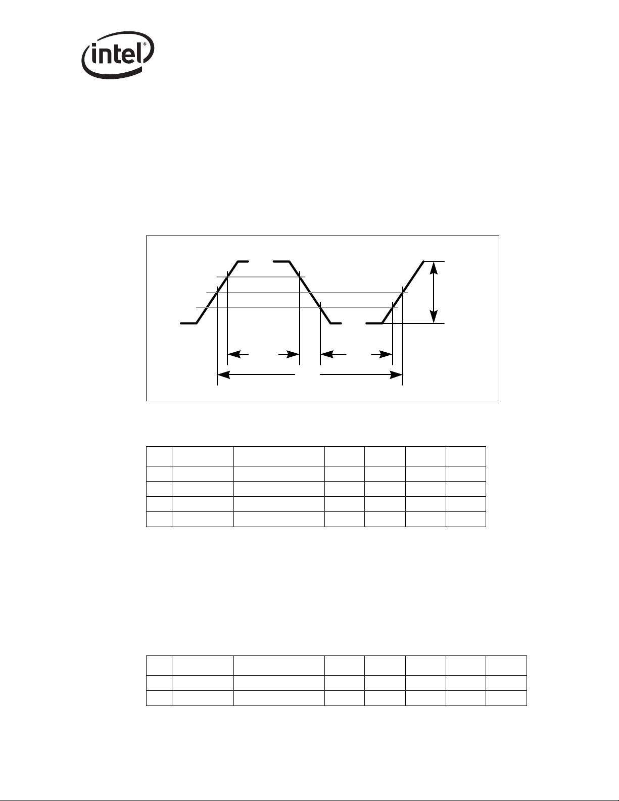
11.4 Timing Specifications
11.4.1 Clocks Specifications
11.4.1.1 PCI Clock Specifications
The 82551ER uses the PCI Clock signal directly. Figure 19 shows the clock waveform and
required measurement points for the PCI Clock signal. Table 53 summarizes the PCI Clock
specifications.
Figure 19. PCI Clock Waveform
0.6V
CC
0.475V
CC
0.4V
CC
0.325V
CC
0.2V
Networking Silicon — 82551ER
0.4VCC p-to-p
(minimum)
CC
T a ble 53. PCI Clock Specifications
Symbol Parameter Min Max Units Notes
T1 T
cyc
T2 T
high
T3 T
low
T4 T
slew
NOTES:
1. The 82551ER will work with any PCI clock frequency up to 33 MHz.
2. Rise and fall times are specified in terms of the edge rate measured in V/ns. This slew rate is met across the
minimum peak-to-peak portion of the clock waveform as shown in Figure 19.
11.4.1.2 X1 Specifications
X1 serves as a signal input from an external crystal or oscillator. Table 54 defines the 82551ER
requirements from this signal.
T_high T_low
T_cyc
CLK Cycle Time 30 ns 1
CLK High Time 11 ns
CLK Low Time 11 ns
CLK Slew Rate 1 4 V/ns 2
T a ble 54. X1 Clock Specifications
Symbol Parameter Min Typical Max Units Notes
T8 Tx 1_dc X1 Duty Cycle 40% 60%
T9 Tx 1_pr X1 Period 40 ns ±30PPM
Datasheet 81
Page 90
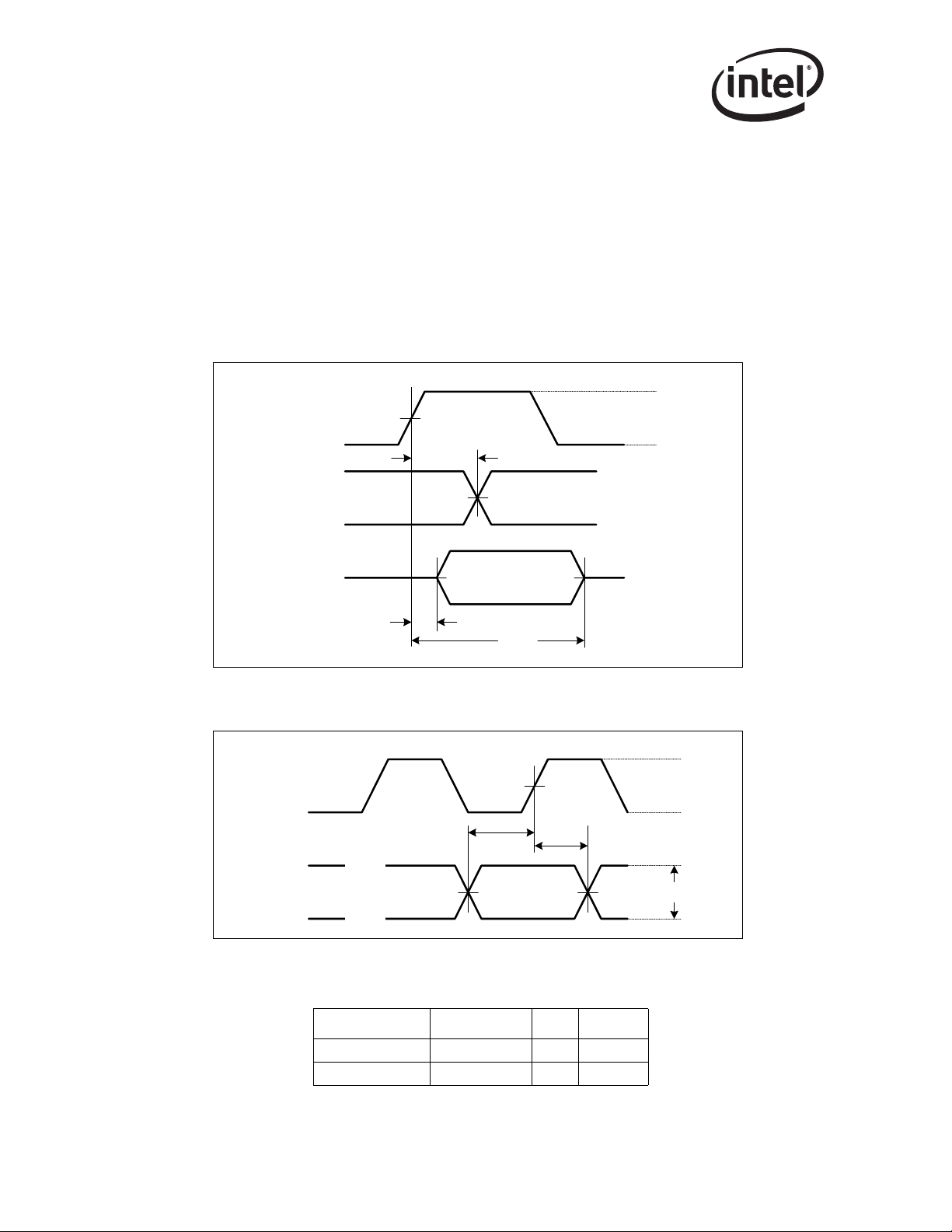
82551ER — Networking Silicon
11.4.2 Timing Parameters
11.4.2.1 Measurement and Test Conditions
Figure 20, Figure 21, and Table 55 define the conditions under which timing measurements are
done. The component test guarantees that all timings are met with minimum clock slew rate
(slowest edge) and voltage swing. The design must guarantee that minimum timings are also met
with maximum clock slew rate (fastest edge) and voltage swing. In addition, the design must
guarantee proper input operation for input voltage swings and slew rates that exceed the specified
test conditions.
Figure 20. Output Timing Measurement Conditions
V_th
CLK
V_test
OUTPUT
DELAY
Tri-State
V_test V_test
OUTPUT
T_on
Figure 21. Input Timing Measurement Conditions
CLK
T_su
V_th
INPUT
V_tl
V_test V_test
T_val
V_step
T_off
inputs
valid
V_tl
V_th
V_test
V_tl
T_h
V_max
Table 55. Measure and Test Condition Parameters
Symbol PCI Level Units Notes
V
th
V
tl
0.6V
0.2V
CC
CC
V
V
82 Datasheet
Page 91

Table 55. Measure and Test Condition Parameters
V
test
(rising edge) 0.285V
V
step
(falling edge) 0.615V
V
step
V
max
Input Signal Edge
Rate
0.4V
CC
V
V Min Delay
CC
VMax Delay
V Min Delay
0.4V
CC
CC
VMax Delay
V
1V/ns
Networking Silicon — 82551ER
NOTE: Input test is done with 0.1V
for testing input timing.
11.4. 2.2 PCI Timings
Table 56. PCI Timing Parameters
Symbol Parameter Min Max Units Notes
T14 t
val
T15 t
val(ptp)
T16 t
on
T17 t
off
T18 t
su
T19 t
su(ptp)
T20 t
h
T21 t
rst
T22 T
rst-clk
T23 T
rst-off
NOTES:
1. Timing measurement conditions are illustrated in Figure 20.
2. PCI minimum times are specified with loads as detailed in the PCI Bus Specification, Revision 2.1, Section
4.2.3.2.
3. n a PCI environment, REQ# and GNT# are point-to-point signals and have different output valid delay times
and input setup times than bussed signals. All other signals are bussed.
4. Timing measurement conditions are illustrated in Figure 21.
5. RST# is asserted and de-asserted asynchronously with respect to the CLK signal.
6. All PCI interface output drivers are floated when RST# is active.
overdrive. V
CC
specifies the maximum peak-to-peak waveform allowed
max
PCI CLK to Signal Valid Delay 2 11 ns 1, 2, 3
PCI CLK to Signal Valid Delay (point-
to-point)
212ns 1, 2, 3
Float to Active Delay 2 ns 1
Active to Float D e lay 28 ns 1
Input Setup Time to CLK 7 ns 3, 4
PCI Input Setup Time to CLK (point-to-
point)
10 ns 3, 4
Input Hold Time from CLK 0 ns 5
Reset Active Time After Power Stable 1 ms 5
PCI Reset Active Time After CLK
Stable
100 clocks 5
Reset Active to O u tp u t Float Delay 40 ns 5, 6
11.4.2.3 Flash Interface Timings
The 82551ER is designed to support up to 150 ns of Flash access time. The VPP signal in the Flash
implementation should be connected permanently to 12 V. Thus, writing to the Flash is con trolled
only by the FLWE# pin.
Tabl e 57 provides the timing parameters for the Flash interface signals. The timing parameters are
illustrated in Figure 22 and Figure 23.
Datasheet 83
Page 92

82551ER — Networking Silicon
Table 57. Flash Timing Parameters
Symbol Parameter Min Max U n its Notes
T35 t
T36 t
T37 t
T38 t
T39 t
T40 t
T41 t
T42 t
T43 t
T44 t
T45 t
T46 t
T47 t
T48 t
T49 t
flrwc
flacc
flce
floe
fldf
flas
flah
flcs
flch
flds
fldh
flwp
flwph
Mioha
Miohi
Flash Read/Write Cycle Time 150 ns
FLA to Read FLD Setup Time 150 ns
FLCS# to Read FLD Setup Time 150 ns
FLOE# Active to Read FLD Setup Time 120 ns
FLOE# Inactive to FLD Driven Delay
Time
50 ns
FLA Setup Time before FLWE# 5 ns
FLA Hold Time after FLWE# 200 ns
FLCS# Hold Time before FLWE# 30 ns
FLCS# Hold Time after FLWE# 30 n s
FLD Setup Time 150 ns
FLD Hold Time 10 ns
Write Pulse Width 120 ns
Write Pulse Width High 25 ns
IOCHRDY Hold Time after FLWE# or
FLOE# Active
IOCHRDY Hold Time after FLWE# or
FLOE# Inactive
25 ns
0ns
1, Flash t
= 150 ns
1, Flash t
= 150 ns
1, Flash t
= 150 ns
1, Flash t
= 55 ns
1, Flash t
= 35 ns
2, Flash t
= 0 ns
2, Flash t
= 60 ns
2, Flash t
= 20 ns
2, Flash t
= 0 ns
2, Flash t
= 50 ns
2, Flash t
= 10 ns
2, Flash t
= 60 ns
2, Flash t
= 20 ns
AVAV
AVQV
ELQV
GLQV
GHQZ
AVWL
WLAX
ELWL
WHEH
DVWH
WHDX
WLWH
WHWL
NOTES:
1. These timing specifications apply to Flash read cycles. The Flash timings referenced are 28F020-150
timings.
2. These timing specifications apply to Flash write cycles. The Flash timings referenced are 28F020-150
timings.
84 Datasheet
Page 93

Figure 22. Flash Timings for a Read Cycle
Networking Silicon — 82551ER
FLADDR
FLCS#
FLOE#
FLDATA-R
IOCHRDY
Figure 23. Flash Timings for a Write Cycle
FLADDR
Address Stable
T40
FLCS#
T42
Address Stable
T35
T37
T38 T39
T36
Data In
T48T49
T35
T41
T46 T43
FLWE#
T47 T44 T45
FLDATA-W
Data Out
T48T49
IOCHRDY
Datasheet 85
Page 94
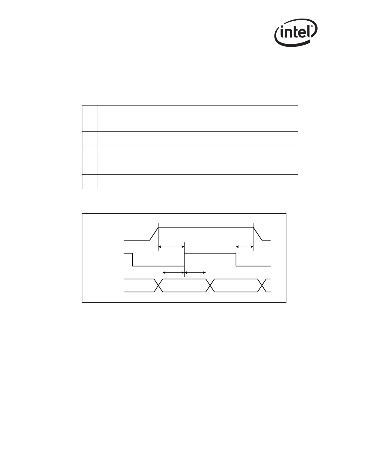
82551ER — Networking Silicon
11.4.2.4 EEPROM Interface Timings
The 82551ER is designed to support a standard64x16 or 256x16 serial EEPROM. Table 58
provides the timing parameters for the EEPROM interface signals. The timing parameters are
shown in Figure 24.
Table 58. EEPROM Timing Parameters
Symbol Parameter Min Max U n its Notes
T51 t
T52 t
T53 t
T54 t
T55 t
ECSS
ECSH
EDIS
EDIH
ECS
Delay from EECS High to EESK High 300 ns
Delay from EESK Low to EECS Low 30 ns
Setup Time of EEDI to EESK 300 ns
Hold Time of EEDI after EESK 300 ns
EECS Low Time 750 ns
Figure 24. EEPROM Timings
EECS
FLA15EESK
FLA13EEDI
EEPROM tcss
= 50 ns
EEPROM tcsh
= 0 ns
EEPROM tdis
= 150 ns
EEPROM tdih
= 150 ms
EEPROM tcs =
250 ns
T51 T52
T54T53
86 Datasheet
Page 95
11.4.2.5 PHY Timings
Table 59. 10BASE-T Normal Link Pulse (NLP) Timing Parameters
Symbol Parameter Condition Min Typ Max Units
T56 T
nlp_wid
T57 T
nlp_per
Figure 25. 10BASE-T Normal Link Pulse (NLP) Timings
Normal Link Pulse
NLP Width 10 Mbps 100 ns
NLP Period 10 Mbps 8 24 ms
T57
T56
Networking Silicon — 82551ER
Table 60. Auto-Negotiation Fast Link Pulse (FLP) Timing Parameters
Symbol Parameter Min Typ Max Units
T58 T
T59 T
T60 T
T61 T
T62 T
T63 T
flp_wid
flp_clk_clk
flp_clk_dat
flp_bur_num
flp_bur_wid
flp_bur_per
FLP Width (clock/data) 100 ns
Clock Pulse to Clock Pulse Period 111 125 139 µs
Clock Pulse to Data Pulse Period 55.5 62.5 69.5 µs
Number of Pulses in one burst 17 33
FLP Burst Width 2 ms
FLP Burst Period 8 24 ms
Figure 26. Auto-Negotiation Fast Link Pulse (FLP) Timings
T59
T60
T58
Fast Link Pulse
FLP Bursts
Clock Pulse
T62
T63
Data Pulse
Clock Pulse
Datasheet 87
Page 96

82551ER — Networking Silicon
T a ble 61. 100Base-TX Transmitter AC Specification
Symbol Parameter Condition Min Typ Max Units
T64 T
jit
TDP/TDN Differential
Output Peak Jitter
HLS Data 1400 ps
88 Datasheet
Page 97

12.0 Package and Pinout Information
12.1 Package Information
Networking Silicon — 82551ER
The 82551ER is a 196-pin Ball Grid Array (BGA) package. Package dimensions are shown in
Figure 27. More information on Intel
®
device packaging is available in the Intel Packaging
Handbook.
Figure 27. Dimension Diagram for the 196-pin BGA
1.56 +/-0.19
0.32 +/-0.04
0.85
0.40 +/-0.10
Note: All dimensions are in millimeters.
o
30
Seating Plate
Substrate change from
0.36 mm to 0.32 mm
Note: No changes to existing soldering processes are needed for the 0.32 mm substrate change.
Datasheet 89
Page 98

82551ER — Networking Silicon
Figure 28. 196 PBGA Package Pad Detail
0.45
Solder Resist Opening
0.60
Metal Diameter
Detail Area
As illustrated in Figure 28, the 82551ER package uses solder mask defined pads. The copper area
is 0.60 mm and the opening in the solder mask is 0.45 mm. The nominal ball sphere diameter is
0.50 mm.
90 Datasheet
Page 99

12.2 Pinout Information
12.2.1 Pin Assignments
Table 62. Pin Assignments
PinNamePinNamePinName
A1 NC A2 SERR# A3 VCC
A4 IDSEL A5 AD[25] A6 PME#
A7 VCC A8 AD[30] A9 ALTRST#
A10 NC A11 VCC A12 LILED#
A13 TEST A14 NC
B1 AD[22] B2 AD[23] B3 VSSPP
B4 AD[24] B5 AD[26] B6 AD[27]
B7 VSSPP B8 AD[31] B9 ISOLATE#
B10 NC B11 SPDLED# B12 TO
B13 RBIAS100 B14 RBIAS10
C1 AD[21] C2 RST# C3 REQ#
C4 C/BE#[3] C5 NC C6 AD[28]
C7 AD[29] C8 CLK_RUN# C9 NC
C10 VSSPT C11 ACTLED# C12 VREF
C13 TDP C14 TDN
D1 AD[18] D2 AD[19] D3 AD[20]
D4 VSS D5 VSS D6 VSS
D7 VSS D8 VSS D9 NC
D10 NC D1 1 NC D12 TI
D13 TEXEC D14 TCK
E1 VCC E2 VSSPP E3 AD[17]
E4 VSS E5 VSS E6 VSS
E7 VSS E8 VSS E9 VSS
E10 VSS E11 NC E12 VCC
E13 RDP E14 RDN
F1 IRDY# F2 FRAME# F3 C/BE#[2]
F4 VSS F5 VSS F6 VSS
F7 VSS F8 VSS F9 VSS
F10 VSS F11 VSS F12 FLD2
F13FLD1F14FLD0
G1 CLK G2 VIO G3 TRDY#
G4 NC G5 VCC G6 VCC
G7 VSS G8 VSS G9 VSS
G10 VSS G11 VSS G12 FLD3
Networking Silicon — 82551ER
Datasheet 91
Page 100

82551ER — Networking Silicon
Table 62. Pin Assignments
Pin Name Pin Name Pin Name
G13 VCC G14 VSSPL
H1 STOP# H2 INTA# H3 DEVSEL#
H4 NC H5 VCC H6 VCC
H7 VCC H8 VCC H9 VSS
H10 VSS H11 NC H12 FLD6
H13FLD5H14FLD4
J1 PAR J2 PERR# J3 GNT#
J4 NC J5 VCC J6 VCC
J7 VCC J8 VCC J9 VCC
J10 VCCR J1 1 VCCR J12 FLA1
J13 FLA0 J14 FLD7
K1 AD[16] K2 VSSPP K3 VCC
K4 VCC K5 VCC K6 VCC
K7 VCC K8 VCC K9 VCC
K10 VCC K11 VCC K12 VSSPL
K13 VCC K14 FLA2
L1 AD[14] L2 AD[15] L3 C/BE#[1]
L4 VCC L5 VCC L6 VSS
L7 NC L8 NC L9 VCC
L10 VCC L11 VSS L12 FLA5
L13 FLA4 L14 FLA3
M1 AD[11] M2 AD[12] M3 AD[13]
M4 C/BE#[0] M5 AD[5] M6 VSSPP
M7 AD[1] M8 FLOE# M9 FLWE#
M10 FLA15/EESK M11 FLA12 M12 FLA11
M13FLA7M14FLA6
N1 VSSPP N2 AD[10] N3 AD[9]
N4 AD[7] N5 AD[4] N6 VCC
N7 AD[0] N8 VCC N9 FLCS#
N10 FLA14/EEDO N11 X1 N12 VSSPL
N13 FLA10 N14 FLA8/IOCHRDY
P1 NC P2 VCC P3 AD[8]
P4 AD[6] P5 AD[3] P6 AD[2]
P7 EECS P8 VSSPL P9 FLA16
P10 FLA13/EEDI P11 X2 P12 VCC
P13FLA9P14 NC
92 Datasheet
 Loading...