

Page 1

Intel 8255x 10/100 Mbps Ethernet Controller Family
Open Source Software Developer Manual
January 2006
Revision 1.3
Page 2

Information in this document is provided in connection with Intel® products. This specification, the Intel 8255x 10/100 Mbps Ethernet Controller Family
Open Source Software Developer Manual, is provided “as is” with no warranties whatsoever, including any warranty of merchantability,
noninfringement, fitness for any particular purpose, or any warranty otherwise arising out of any proposal, specification or sample. Intel products are
not intended for use in medical, life saving, life sustaining applications. Intel may make changes to specifications and product descriptions at any time,
without notice.
Intel may make changes to specifications and product descriptions at any time, without notice.
Designers must not rely on the absence or characteristics of any features or instructions marked “reserved” or “undefined.” Intel reserves these for
future definition and shall have no responsibility whatsoever for conflicts or incompatibilities arising from future changes to them.
®
The Intel
from published specifications. Current characterized errata are available on request.
The information in this document is furnished for informational use only, is subject to change without notice, and should not be construed as a
commitment by Intel Corporation. It is intended to enable the maintenance of the open source Intel
adapters. Intel Corporation assumes no responsibility or liability for any errors or inaccuracies that may appear in this document or any software that
may be provided in association with this document. Except as permitted by such license, no part of this document may be reproduced, stored in a
retrieval system, or transmitted in any form or by any means without the express written consent of Intel Corporation.
Contact your local Intel sales office or your distributor to obtain the latest specifications and before placing your product order.
Copies of documents which have an ordering number and are referenced in this document, or other Intel literature may be obtained by calling
1-800-548-4725 or by visiting Intel's website at http://www.intel.com.
Copyright © 2003, 2006. Intel Corporation.
* Other product and corporate names may be trademarks of other companies and are used only for explanation and to the owners’ benefit, without
intent to infringe.
82557, 82558, 82559, 82550, and 82551 may contain design defects or errors known as errata which may cause the product to deviate
®
PRO/100 drivers for the Intel® PRO/100 family of
ii Intel 8255x 10/100 Mbps Ethernet Controller Family Open Source Software Developer Manual
Page 3

Contents
Contents
1 Introduction.................................................................................................................................... 1
1.1 Scope....................................................................................................................................1
1.2 Document Conventions ........................................................................................................ 2
1.2.1 Device References .................................................................................................. 2
1.2.2 Numbering ...............................................................................................................2
1.2.3 Signal Name Representation ...................................................................................2
1.2.4 Memory Alignment Terminology .............................................................................. 2
2 Adapter and Controller Overview ................................................................................................5
2.1 Adapter Block Diagram.........................................................................................................5
2.2 Intel Fast Ethernet MAC Features ........................................................................................ 6
2.2.1 82557 Features........................................................................................................ 6
2.2.2 82558 Features........................................................................................................ 6
2.2.3 82559, 82550, 82551, and 82562 Features............................................................. 7
2.3 Working with the Physical Layer ...........................................................................................7
3 Power Management Interface....................................................................................................... 9
3.1 Low Power Mode Requirements...........................................................................................9
3.2 Device Power States ............................................................................................................ 9
3.3 Power Management Registers ............................................................................................. 9
3.4 Link Operation .................................................................................................................... 10
4 PCI Interface.................................................................................................................................11
4.1 PCI Configuration Space .................................................................................................... 11
4.1.1 Vendor ID (Offset 0)............................................................................................... 12
4.1.2 Device ID (Offset 2) ............................................................................................... 12
4.1.3 Command Register (Offset 4) ................................................................................ 12
4.1.4 Status Register (Offset 6) ...................................................................................... 12
4.1.5 Revision (Offset 8) .................................................................................................13
4.1.6 Class Code (Offset 9) ............................................................................................ 14
4.1.7 Cache Line Size (Offset C) .................................................................................... 14
4.1.8 Latency Timer (Offset D) .......................................................................................14
4.1.9 Header Type (Offset E).......................................................................................... 14
4.1.10 Built in Self Test (Offset F)..................................................................................... 15
4.1.11 Subsystem ID (Offset 2C) ......................................................................................16
4.1.12 Subsystem Vendor ID (Offset 2E) ......................................................................... 16
4.1.13 Expansion ROM Base Address Register (Offset 30) .............................................16
4.1.14 The Capabilities Pointer (Offset 34)....................................................................... 17
4.1.15 Interrupt Line (Offset 3C) ....................................................................................... 17
4.1.16 Interrupt Pin (Offset 3D)......................................................................................... 17
4.1.17 Max_Lat / Min_Gnt (Offset 3E) .............................................................................. 18
4.1.18 Power Management PCI Configuration Registers ................................................. 18
4.2 PCI Command Usage......................................................................................................... 21
4.2.1 Memory Write and Invalidate ................................................................................. 22
4.2.2 Read Align .............................................................................................................23
4.2.3 Odd Byte Alignment Support .................................................................................23
Intel 8255x 10/100 Mbps Ethernet Controller Family Open Source Software Developer Manual iii
Page 4

Contents
5 EEPROM Interface ....................................................................................................................... 25
6 Host Software Interface .............................................................................................................. 27
6.1 The Shared Memory Architecture....................................................................................... 27
6.2 Initializing the LAN Controller ............................................................................................. 29
6.2.1 LAN Controller Addressing Format........................................................................ 29
6.3 Controlling the Device......................................................................................................... 31
6.3.1 Control / Status Registers (CSR) ........................................................................... 31
6.3.2 System Control Block (SCB).................................................................................. 33
6.3.3 PORT Interface...................................................................................................... 43
6.3.4 EEPROM Control Register .................................................................................... 45
6.3.5 Management Data Interface Control Register ....................................................... 49
6.3.6 Receive Byte Count Register................................................................................. 51
6.3.7 Early Receive Interrupt .......................................................................................... 52
6.3.8 Flow Control Register ............................................................................................ 53
6.3.9 Power Management Driver Register...................................................................... 54
6.3.10 General Control Register ....................................................................................... 56
6.3.11 General Status Register ........................................................................................ 56
6.4 Shared Memory Structures................................................................................................. 57
6.4.1 Action Commands and Operating Modes.............................................................. 57
6.4.2 Specific Action Commands.................................................................................... 59
6.4.3 Receive Operation ................................................................................................. 99
6.5 Command Unit and Receive Unit Operation..................................................................... 105
6.5.1 Starting and Completing Control Commands ...................................................... 105
6.5.2 Generating and Acknowledging Interrupts........................................................... 105
6.5.3 Command Unit Control ........................................................................................ 106
6.5.4 Receive Unit Control............................................................................................ 108
6.5.5 Updating SCB Status........................................................................................... 110
6.6 Flow Control...................................................................................................................... 110
6.6.1 PHY Based Flow Control ..................................................................................... 111
6.6.2 Frame Based Flow Control .................................................................................. 111
6.6.3 Priority Aware Frame Based Flow Control........................................................... 115
6.6.4 Half Duplex Flow Control ..................................................................................... 116
6.7 Collision Backoff Modification in Switched Environments................................................. 116
7 Physical Layer Interface ........................................................................................................... 117
7.1 Management Data Interface (MDI) ................................................................................... 117
7.2 MDI Register Set .............................................................................................................. 118
7.2.1 Control Register: Register 0 ................................................................................ 119
7.2.2 Status Register: Register 1.................................................................................. 120
7.2.3 Identification Registers: Registers 2 and 3 .......................................................... 121
7.2.4 Auto-Negotiation Advertisement Register: Register 4 ......................................... 122
7.2.5 Auto-Negotiation Link Partner Ability Register: Register 5 .................................. 122
7.2.6 Auto-Negotiation Expansion Register: Register 6 ............................................... 123
7.3 Intel 82555 Specific Registers .......................................................................................... 124
7.3.1 Status and Control Register: Register 16 ............................................................ 124
7.3.2 Special Control Register: Register 17.................................................................. 125
7.3.3 Clock Synthesis Test and Control Register: Register 18 ..................................... 126
7.3.4 100BASE-TX Receive False Carrier Counter: Register 19 ................................. 126
7.3.5 100Base-TX Receive Disconnect Counter: Register 20...................................... 126
iv Intel 8255x 10/100 Mbps Ethernet Controller Family Open Source Software Developer Manual
Page 5

Contents
7.3.6 100BASE-TX Receive Error Frame Counter: Register 21................................... 127
7.3.7 Receive Symbol Error Counter: Register 22........................................................ 127
7.3.8 100BASE-TX Receive EOF Error Counter: Register 23...................................... 127
7.3.9 10BASE-T Receive EOF Error Counter: Register 24 ..........................................127
7.3.10 10BASE-T Transmit Jabber Detect Counter: Register 25 ...................................127
7.3.11 Equalizer Control and Status Register: Register 26 ............................................ 128
7.3.12 Special Control Register: Register 27..................................................................129
7.4 Auto-Negotiation Functionality.......................................................................................... 130
7.4.1 Description ........................................................................................................... 130
7.4.2 Parallel Detection................................................................................................. 131
7.5 Vendor-Specific PHY Programming .................................................................................132
7.5.1 Intel 82555 TX PHY ............................................................................................. 132
7.5.2 82558 and 82559 Embedded PHY Unit............................................................... 132
8 Programming Recommendations ............................................................................................ 135
8.1 Adapter Initialization .........................................................................................................135
8.1.1 8255x Initialization ............................................................................................... 135
8.1.2 PHY Detection and Initialization .......................................................................... 135
8.1.3 NOS Specific Initialization.................................................................................... 136
8.2 Transmit Processing .........................................................................................................136
8.3 Frame Reception ..............................................................................................................136
8.4 Interrupt Processing..........................................................................................................137
Appendices
A Wake-up Functionality .............................................................................................................. 139
B 82550 and 82551QM Specific Information............................................................................... 155
Figures
1 82557 Network Interface Card Block Diagram ............................................................................. 5
2 Command Register.....................................................................................................................12
3 Command Register.....................................................................................................................13
4 Cache Line Size.......................................................................................................................... 14
5 Base Address Register for Memory Mapping .............................................................................15
6 Base Address Register for I/O Mapping ..................................................................................... 15
7 Expansion ROM Base Address Register.................................................................................... 17
8 8255x Memory Architecture........................................................................................................28
9 SCB Status Word........................................................................................................................ 34
10 SCB Command Word ................................................................................................................. 36
11 Self-Test Results Format ............................................................................................................ 44
12 EEPROM Control Register ......................................................................................................... 46
13 EEPROM Read Timing Diagram ................................................................................................48
14 General Action Command Format .............................................................................................. 58
15 NOP Command Format .............................................................................................................. 59
16 Individual Address Setup Command Format .............................................................................. 60
17 Configure Command Format ......................................................................................................62
18 Multicast Setup Command Format .............................................................................................82
19 Transmit Command Format........................................................................................................ 83
Intel 8255x 10/100 Mbps Ethernet Controller Family Open Source Software Developer Manual v
Page 6

Contents
20 Transmit Buffer Descriptor.......................................................................................................... 85
21 Load Microcode Command Format ............................................................................................ 90
22 Dump Command Format ............................................................................................................ 91
23 Diagnose Command Format ...................................................................................................... 97
24 Simplified Memory Structure .................................................................................................... 100
25 Receive Frame Descriptor Format ........................................................................................... 100
26 Management Frame Structure.................................................................................................. 118
27 Command Block Structure........................................................................................................ 146
Tables
1 PCI Configuration Space ............................................................................................................ 11
2 Device and Revision ID .............................................................................................................. 13
3 Base Address Register Summary .............................................................................................. 16
4 Power Management Capabilities................................................................................................ 18
5 Power Management Control/Status Register ............................................................................. 20
6 Power Consumption / Dissipation Reporting .............................................................................. 21
7 Generated PCI Commands ........................................................................................................ 22
8 Reset Commands....................................................................................................................... 29
9 Device Addressing Formats ....................................................................................................... 30
10 Alignment Requirements for 8255x Data Structures .................................................................. 31
11 Control / Status Register ............................................................................................................ 32
12 System Control Block ................................................................................................................. 34
13 SCB Status Word Bits Descriptions............................................................................................ 35
14 SCB Command Word Bits Descriptions ..................................................................................... 37
15 SCB General Pointer for the CU Command ............................................................................... 39
16 SCB General Pointer for the RU Command ............................................................................... 40
17 Statistical Counters..................................................................................................................... 40
18 Port Register Location ................................................................................................................ 43
19 Port Selection Function .............................................................................................................. 43
20 Dump Wake-up Data Structure .................................................................................................. 45
21 EEPROM Control Register Locations......................................................................................... 46
22 EEPROM Control Register Bits Definitions ................................................................................46
23 EEPROM Opcode Summary (64-register EEPROM)................................................................. 47
24 MDI Control Register Location ................................................................................................... 49
25 Management Data Pins .............................................................................................................. 50
26 MDI Control Register Bits ........................................................................................................... 50
27 Receive Byte Count Register Location ....................................................................................... 52
28 Early Receive Interrupt Register Location .................................................................................. 52
29 Flow Control Registers Location................................................................................................. 53
30 Flow Control Threshold Values .................................................................................................. 54
31 Power Management Driver Register Location ............................................................................ 55
32 Power Management Driver Register .......................................................................................... 55
33 General Control Register Location .............................................................................................56
34 General Control Register............................................................................................................ 56
35 General Status Register Location............................................................................................... 56
36 General Status Register ............................................................................................................. 57
37 Operation Codes ........................................................................................................................ 57
38 82557 Configuration Byte Map ................................................................................................... 62
39 82558 Configuration Byte Map ................................................................................................... 64
vi Intel 8255x 10/100 Mbps Ethernet Controller Family Open Source Software Developer Manual
Page 7

Contents
40 82559 Configuration Byte Map ................................................................................................... 65
41 82557 Dual-Port FIFO Settings - Transmit ................................................................................. 66
42 82557 Dual-Port FIFO Settings - Receive .................................................................................. 67
43 82558 and 82559 Dual-Port FIFO Settings - Transmit ...............................................................67
44 82558 and 82559 Dual-Port FIFO Settings - Receive ................................................................ 68
45 Extended Statistics Functionality ................................................................................................ 72
46 Pre-amble Length ....................................................................................................................... 75
47 82558 B-step Configuration Block ARP Frame IP Address ........................................................76
48 82558 B-step ARP Frame IP Address Mapping .........................................................................77
49 Full Duplex Functionality............................................................................................................. 79
50 Dump Data Bytes (0-79) ............................................................................................................. 92
51 Dump Data Dwords (20-148)...................................................................................................... 95
52 RFD Status Bit Descriptions ..................................................................................................... 101
53 Actual Count in Header RFD ....................................................................................................102
54 CU Control Commands: Actions at Acceptance Time .............................................................. 107
55 CU Activities Performed at the End of Execution .....................................................................107
56 RU Control Commands: Actions at Acceptance Time .............................................................. 108
57 Flow Control Frame Format...................................................................................................... 112
58 Flow Control Configuration Bits ................................................................................................115
59 MDI Register Set ...................................................................................................................... 118
60 82555 MDI Register Set ...........................................................................................................118
61 24-bit OUI Identification Number ..............................................................................................121
62 MDI Identification Registers 2 and 3: PHY ID Encoding...........................................................121
63 LED Switch Control................................................................................................................... 130
64 Technology Ability Field Bit Assignments .................................................................................131
65 Technology Priority ................................................................................................................... 131
66 Fixed Wake-up Configuration Bits ............................................................................................143
67 82559 Port Commands............................................................................................................. 150
68 Dump Data Structure ................................................................................................................ 151
69 IPCB Structure.......................................................................................................................... 155
70 IP Activation Bits (Byte 13) ....................................................................................................... 155
71 IP Activation Bits (Byte 12) ....................................................................................................... 155
72 IPCB Fields............................................................................................................................... 156
73 IPCB Structure Checksum Offload ........................................................................................... 158
74 IPCB Structure Large Send ......................................................................................................162
Intel 8255x 10/100 Mbps Ethernet Controller Family Open Source Software Developer Manual vii
Page 8

Contents
Revision History
Date Revision Description
January 2006 1.3
September 2005 1.2 • Corrected minor typing errors.
September 2004 1.1
January 2003 1.0 Initial release.
• Added Section 2.2.3.2., “82551ER Features.”
• Modified the title of Appendix B.
• Added Section 16, ”SCB General Pointer for the RU
Command,” which was not included previously in Section
6.3.2.3, ”SCB General Pointer.”
• Corrected Section 15, ”SCB General Pointer for the CU
Command,” in Section 6.3.2.3, ”SCB General Pointer.”
• Included descriptions for the Reset bit, Auto-Negotiation
Enable bit and Test Collision Enable bit in Section 7.2.1,
”Control Register: Register 0.”
• Included a summary paragraph before the table of bits in
Section 7.2.2, ”Status Register: Register 1.”
viii Intel 8255x 10/100 Mbps Ethernet Controller Family Open Source Software Developer Manual
Page 9

Introduction 1
This document is intended for use as a software technical reference manual for the Intel® 10/100
Mbps Fast Ethernet controller family, which includes the 82557, 82558, 82559, 82550, and 82551,
as well as the 82562 Platform LAN Connect device. It also contains information for several PCI
LAN adapters based on these devices: Intel
PRO/100B Wake on LAN (WOL), Intel
PRO/10+.
1.1 Scope
®
EtherExpress™ PRO/100+, Intel® EtherExpress™
®
EtherExpress™ PRO/100B, and Intel® EtherExpress™
This manual is intended to be used as a technical reference for software and test engineers
developing device drivers or related software for adapters or systems using the Intel
82558, 82559, 82550, or 82551 Fast Ethernet controllers or the Intel
®
82562 Platform LAN
®
82557,
Connect (PLC) device. It contains reference information about the controllers as well as other
information that may be required by software developers (such as PHY information, EEPROM
contents, PCI scanning, etc.). Since this document uses many examples and contains sample code
fragments, it is assumed that the reader has a fundamental understanding of device driver
programming and a working knowledge of both C programming language and x86 assembler
programming language. Familiarity with at least one industry standard network operating system
(NOS) device driver interface (for example, Network Driver Interface Specification [NDIS] or
ODI) is also helpful.
The Intel
®
10/100 Mbps Fast Ethernet Controller Family includes the following devices in
successive order.
Device Notes
82557 First generation Intel® 10/100 Mbps Fast Ethernet Controller (includes MAC unit only)
82558
82559 Third generation Intel® 10/100 Mbps Fast Ethernet Controller (includes both a MAC and PHY unit)
82550 Intel® 10/100 Mbps Fast Ethernet Controller (includes both MAC and PHY)
82551 Intel® 10/100 Mbps Fast Ethernet Controller (includes both MAC and PHY)
Second generation Intel® 10/100 Mbps Fast Ethernet Controller (includes MAC and an integrated
PHY unit)
In general, the Intel family of Fast Ethernet controllers are similar. All family members share the
same core hardware and software interface. The later generation components have a higher
integration and include support for miscellaneous features (for example, manageability). Since the
different generations of Fast Ethernet controllers are highly similar, this manual documents the
functionality of all devices and details the differences between the devices. It is intended to be used
as a tool to maintain and develop software for all devices in the Intel family of Fast Ethernet
controllers.
Intel 8255x 10/100 Mbps Ethernet Controller Family Open Source Software Developer Manual 1
Page 10

Introduction
1.2 Document Conventions
1.2.1 Device References
This document encompasses information for all members of the Intel Fast Ethernet controllers:
82551, 82550, 82559, 82558, 82557 and the 82562.
Note: The 82562xx/ICHx combination are programmed like the 82559 using the same byte map and
settings.
The document convention, “8255x,” will be used to refer to all devices. In addition, there are
specific references to the 82557 throughout this manual that pertains to all 8255x devices. Devicespecific differences and exceptions will be documented.
1.2.2 Numbering
Decimal, binary, and hexadecimal numbers are used through the manual. They will be designated
as follows:
• Decimal numbers: Decimal numbers will not be followed by a suffix.
• Binary numbers: Binary numbers (base 2) will be followed by a “b” (for example, 01b).
• Hexadecimal numbers: Hexadecimal numbers (base 16) will be followed with the suffix “h”
(for example, 1Ch). Hexadecimal numbers may also be noted with a prefix of “0x” (for
example, 0x1c).
1.2.3 Signal Name Representation
Signals that are active in a low logic state when asserted are followed by the pound sign (#). For
example, FRAME# is asserted low by the master during a transaction. It is asserted low at the start
and duration of a transaction and de-asserted during the final data phase.
Signals that are not followed by a pound sign are active in a high logic state when asserted. For
example, the IDSEL signal is asserted high when the 82559 during PCI read and write transactions.
1.2.4 Memory Alignment Terminology
The 8255x data structures have special memory alignment requirements. This implies that the
starting physical address of a data structure must be aligned as specified. The following terms are
used for this purpose:
• Byte alignment: Byte alignment implies that the physical addresses can be odd or even.
Examples: 0FECBD9A1h or 02345ADC6h
• Word alignment: Word alignment implies that physical addresses must be aligned on even
boundaries. In other words, the last nibble of the address may only end in 0h, 2h, 4h, 6h, 8h,
Ah, Ch, or Eh.
Example: 0FECBD9A2h
2 Intel 8255x 10/100 Mbps Ethernet Controller Family Open Source Software Developer Manual
Page 11

Introduction
• Dword alignment: Dword alignment implies that the physical addresses may only be aligned
on 4-byte boundaries. In other words, the last nibble of the address may only end in 0h, 4h, 8h,
or Ch.
Example: 0FECBD9A8h
• Paragraph alignment: Paragraph alignment implies that the physical addresses may only be
aligned on 16-byte boundaries. In other words, the last nibble must be a 0.
Example: 02345ADC0h
Intel 8255x 10/100 Mbps Ethernet Controller Family Open Source Software Developer Manual 3
Page 12

Introduction
4 Intel 8255x 10/100 Mbps Ethernet Controller Family Open Source Software Developer Manual
Page 13
Adapter and Controller Overview 2
Adapters based on an Intel® 8255x device support the ANSI/IEEE 802.3u standard for 100BASETX (100 Mbps operation) and 10BASE-T (10 Mbps operation).
2.1 Adapter Block Diagram
The main components of Intel Fast Ethernet adapters are:
• A Fast Ethernet Media Access Controller (MAC), such as the 8255x, is the core component.
The MAC supports the Fast Ethernet ANSI/IEEE 802.3u standard.
• A Physical Layer (PHY) interface device is also required. The 82558, 82559, 82550, and
82551 components have an integrated PHY that supports 100BASE-TX and 10BASE-T.
Adapters based on the 82557 must include an appropriate PHY component for their design.
• A serial EEPROM is required to hold the adapter’s individual Ethernet node address and other
configuration information including fixed PCI configuration parameters.
The adapters are based on 100BASE-TX specifications. 100BASE-TX is a specific scheme
designed for use over 2 pairs of Category 5 unshielded twisted-pair cable. 100BASE-TX defines a
signaling scheme for 100 Mbps and provides compatibility with the existing 10 Mbps IEEE 802.3
10BASE-T signaling standard. Since only 2-wire pairs are used, TX technology allows full duplex
operation at 100 Mbps. The Intel 82555 is one possible TX solution.
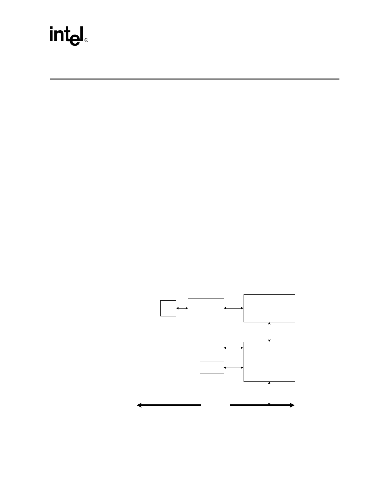
The block diagram below illustrates an Intel
MAC with a TX or T4 PHY.
®
PRO/100B adapter configuration based on the 82557
Figure 1. 82557 Network Interface Card Block Diagram
RJ-45
Intel 8255x 10/100 Mbps Ethernet Controller Family Open Source Software Developer Manual 5
Filter
Module
Optional
Flash
EEPROM
PCI Local Bus
100BASE-T4 or
100BASE-TX PHY
MII
Intel® 82557
Page 14

Adapter and Controller Overview
2.2 Intel Fast Ethernet MAC Features
2.2.1 82557 Features
• Glueless 32-bit, zero wait state PCI bus master interface compliant with PCI Specification,
Revision 2.1.
• 10 and 100 Mbps support in compliance with IEEE 802.3 10BASE-T and 802.3u 100BASE-
TX.
• Fast back-to-back transmit interframe spacing (IFS) of 960 ns in 100 Mbps networks and 9.6
µs in 10 Mbps networks.
• On-chip Control/Status Register (CSR) incorporating the System Control Block (SCB).
• Simple and flexible packet support with Dynamic transmit chaining.
• Packed Transmit Buffer Descriptors (TBDs).
• Early transmit complete indication.
• Simple receive packet support allows early receive interrupt support for concurrent processing
(in simplified mode).
• IEEE Media Independent Interface (MII) compliant PHY interface other MII compliant PHYs.
• Full and half duplex transmit and receive capability.
• Separate on-chip receive and transmit FIFOs.
• On-chip network management counters.
• EEPROM support.
• Optional Flash ROM support (256 Kbytes or 1 Mbyte).
2.2.2 82558 Features
For the most part, the 82558 is a superset of the 82557. In addition to incorporating the features of
the 82557, it also includes the following:
• Backward compatible to 82557 software.
• Integrated 100BASE-TX PHY.
• IEEE 802.3u auto-negotiation support in 10BASE-T, 100BASE-TX, full duplex and full
duplex flow control configurations.
• Auto-polarity correction for 10BASE-T.
• Optimized PCI interface with support for the memory write and invalidate PCI command.
• Automatic read of EEPROM (programmable ID).
• IEEE 802.3x flow control capable.
• PHY based flow control support when the internal 100BASE-TX PHY is used.
• Advanced Configuration and Power Interface (ACPI) Specification and PCI Power
Management Specification compliant.
• Remote power up support (for Magic Packet*).
6 Intel 8255x 10/100 Mbps Ethernet Controller Family Open Source Software Developer Manual
Page 15

Adapter and Controller Overview
• Optional Flash support up to 64 Kbytes. (The 82557 is capable of larger Flash size support.)
2.2.3 82559, 82550, 82551, and 82562 Features
The 82559, 82550, and 82551 devices are supersets of the 82557 and 82558. However, the 82559
does not support PHY based flow control as the 82558 did. The new 82559 features are:
• Backward compatible to the 82557 and 82558 software.
• Low power 3.3 V device:
• Clockrun protocol support.
• System Management Bus (SMB) support.
• Wired for Management support (WfM).
• Expanded Wake on LAN capabilities.
• 128 Kbytes Flash size support. (The 82558 only supported a 64 Kbyte Flash.)
• Thin ball grid array (BGA) 15 x 15 mm package.
2.2.3.1 82559ER Features
The 82559ER is a member of the 82559 Fast Ethernet controllers. It is a subset of the 82559.
However, the 82559ER does not support:
• SMB.
• Wake on Magic Packet*.
2.2.3.2 82551ER Features
The 82551ER is a member of the 82559 Fast Ethernet controllers. It is a subset of the 82551.
However, the 82551ER does not support:
• SMB.
• Wake on Magic Packet*.
• Checksumming.
2.3 Working with the Physical Layer
The 82557 contains an IEEE MII compliant interface to a MII compliant PHY, allowing
connections to 10/100 Mbps networks. Software communicates to a MII compliant device through
the 82557 by using the its Management Data Interface (MDI) port.
The 82558, 82559, 82550 and 82551 contain an embedded PHY module. Although the PHY is
internal for these devices, software still communicates to the PHY unit through the MDI port.
For 10/100 Mbps connections, the 82557 can be used in conjunction with the Intel
Mbps only connections, the 82557 can be interfaced to the Intel
maintaining software compatibility to 100 Mbps solutions. The 82558 and later devices do not
have a 10 Mbps only interface as the 82557. However, it is possible to interface these devices with
a 10 Mbps only MII device.
®
®
82503 serial interface, while
82555. For 10
Intel 8255x 10/100 Mbps Ethernet Controller Family Open Source Software Developer Manual 7
Page 16

Adapter and Controller Overview
8 Intel 8255x 10/100 Mbps Ethernet Controller Family Open Source Software Developer Manual
Page 17

Power Management Interface 3
The 82557 has no power management support. The 82558 added support for the Advanced
Configuration and Power Interface (ACPI) Specification and limited support for Wake on LAN
(WOL). The 82558 B-step upgraded and expanded the WOL capability, while the 82559 expanded
and simplified the WOL functionality even more.
3.1 Low Power Mode Requirements
The 82558, 82559, 82550, and 82551 adhere to the emerging power management standards as
defined in:
• PCI Bus Power Management Interface Specification, Revision 1.0.
• Advanced Configuration and Power Interface Specification (ACPI), Rev 1.0; December 22,
1996.
• Device Class Power Management Reference Specification - Network Device Class, Revision
1.0.
These three specifications define how a PCI network device can be controlled in an OS Directed
Power Management (OSPM) environment. These devices all adhere to these specifications.
Additionally, they support bus isolation within the chip and Wake on LAN (WOL) capabilities.
3.2 Device Power States
Currently, operating systems only support the D0 and D3 power states. However, starting with the
82558, the Intel Fast Ethernet controller family supports all four power states as defined in the PCI
Power Management Specification. These power states are named D0, D1, D2 and D3. D0 is the
maximum powered state, and D3, the minimum powered state.
3.3 Power Management Registers
The 82558, 82559, 82550, and 82551 support power management registers:
• Power Management Capability Pointer (Cap_Ptr)
• Power Management Capabilities (PMC)
• Power Management Control/Status Register (PMCSR)
• Power Management Driver Register (PMDR)
The first three registers are located in PCI configuration space and are defined in the PCI Power
Management Specification. It is part of the device CSR, which is mapped into system memory and
I/O space.
Intel 8255x 10/100 Mbps Ethernet Controller Family Open Source Software Developer Manual 9
Page 18

Power Management Interface
3.4 Link Operation
In the D0 state, the device maintains an active link. The 82558 B-step (refer to Table 2, “Device
and Revision ID” on page 13) and later devices also maintain an active link in the D3 state if PME
is enabled and the device has power. This implies:
• 10BASE-T Mode: The device expects a normal clock input on the X1 and X2 pins. It expects
to receive normal reception on the Receive Differential Positive and Receive Differential
Negative signals (RDP/RDN pair). The device will not transmit on the Transmit Differential
Positive and Transmit Differential Negative signals (TDP/TDN pair).
• 100BASE-TX Mode: The device expects a normal clock input on the X1 and X2 pins and to
receive normal reception on the RDP/RDN pair. It transmits a continuous idle stream on the
TDP/TDN pair, as required by the 100BASE-TX standard. The 82558 does not transmit
frames on the link.
• Auto-Negotiation: If the link fails while the device is in the D1 state, it performs the normal
auto-negotiation protocol in order to re-establish the link. For the 82558 B-step, if the link fails
in the D3 state and PME is enabled and the device has power, the device will attempt to use the
normal auto-negotiation protocol in order to re-establish the link. If the link fails on the 82559
in the D3 state and PME is enabled and the device has power, the 82559 will go into a deep
power down state, rather than trying to re-establish the link with the auto-negotiation protocol.
During the D3 power state, the 82558 A-step does not maintain an active link. The 82558 B-step
and later generation devices do not maintain a link in D3 if PME is disabled or if the device does
not have power.
10 Intel 8255x 10/100 Mbps Ethernet Controller Family Open Source Software Developer Manual
Page 19

PCI Interface 4
4.1 PCI Configuration Space
One of the most important functions for enabling superior configurability and ease of use is the
ability to relocate PCI devices in the address spaces. By default PCI devices support “Plug and
Play.” When the system is powered on, device independent software (usually the system BIOS)
determines present devices, builds an address map, and assigns non-conflicting resources to those
devices. The device independent software accomplishes this configuration task by writing to the
PCI configuration space of each individual PCI device.
The 8255x supports 16 Dwords of Type 0 Configuration Space Header, as defined in the PCI
Specification, Revision 2.1. The 82259 and 82558 also support a small section in the device
specific configuration space. The configuration space is depicted below. The registers that are not
identical between the devices are shaded.
Table 1. PCI Configuration Space
Byte Offset
(hexadecimal)
0
4 Status Register Command Register
8 Class Code (200000h) Revision ID
CBIST Header Type Latency Timer Cache Line Size
10 CSR Memory Mapped Base Address Register
14 CSR I/O Mapped Base Address Register
18
1C
20
24
28
2C
30 Expansion ROM Base Address Register
34 Reserved Cap_Ptr
38 Reserved
3C Max_Latency (FFh) Min_Grant (FFh) Interrupt Pin (01h) Interrupt Line
DC
E0 Reserved Data Power Management CSR
Byte 3 Byte 2 Byte 1 Byte 0
Device ID Vendor ID
Flash Memory Mapped Base Address Register
Reserved
Subsystem ID Subsystem Vendor ID
Power Management Capabilities Next Item Pointer Capability ID
Intel 8255x 10/100 Mbps Ethernet Controller Family Open Source Software Developer Manual 11
Page 20

PCI Interface
4.1.1 Vendor ID (Offset 0)
This field identifies the device manufacturer. For the 82557 B-step this field equals 8086h. For the
82557 C-Step, 82558, and 82559, this field is automatically loaded from the EEPROM at power on
or upon the assertion of PCI reset. If the EEPROM is not present or invalid, this value defaults to
8086h.
4.1.2 Device ID (Offset 2)
This field uniquely identifies the device. For the 82557 B-step this field is 1229h. For the 82557 CStep, 82558, and 82559, this field is automatically loaded from the EEPROM at power on or upon
the assertion of PCI reset. If the EEPROM is not present or invalid, this value defaults to 1229h for
the 82558 and 82559. The 82559ER does not load the Device ID from the EEPROM and will
always equal 1209h.
4.1.3 Command Register (Offset 4)
The Command Register provides control over the device’s ability to generate and respond to CPU
cycles. Its layout is shown below. The shaded bits are not used and are hard-wired to 0.
Figure 2. Command Register
15 10 9 0
Reserved Command Bits
Bits
15:10 0 Reserved.
9 0 Fast back-to-back enable.
8 x SERR# enable.
7 0 Wait cycle enable.
6 x Parity error response
5 0 Palette snoop enable.
4x
3 0 Special cycle monitoring.
2 x Mastering enable.
1 x Memory access enable.
0 x I/O access enable.
Initial
Value
Memory write and invalidate (MWI) enable.
NOTE: More information regarding the MWI command is located in Section 4.2.1,
Description
“Memory Write and Invalidate”.
4.1.4 Status Register (Offset 6)
The Status Register is used to record status information for PCI bus related events. Its layout is
shown below. The shaded bits are not used and are hard-wired to 0.
12 Intel 8255x 10/100 Mbps Ethernet Controller Family Open Source Software Developer Manual
Page 21

Figure 3. Command Register
15 43 0
Status Bits Reserved
PCI Interface
Bits
15 x Detected parity error.
14 x Signaled system error.
13 x Received master abort.
12 x Received target abort.
11 0 Signaled target abort.
10:9 01 DEVSEL timing (indicates minimum timing).
8 x Data parity reported.
7 1 Fast back-to-back capable.
6 0 UDF supported.
5 0 66 MHz capable.
4
3:0 0 Reserved.
Initial
Value
1 (82559
and
82558)
0
(82557)
Capabilities list. This bit indicates whether the device implements a list of new capabilities
such as PCI Power Management. If it is set, the Cap_Ptr register in the PCI Configuration
Space points to the location of the first item in the Capabilities List.
NOTE: This bit is set to 1 for the 82559 and 82558 if it is not disabled by the EEPROM. It
is always equal to 0 for the 82557.
4.1.5 Revision (Offset 8)
This register specifies a device specific revision identifier. For the 82557 C-Step, 82558, and
82559, this field may be automatically loaded from the EEPROM at power on or upon the assertion
of a PCI reset. The default revision register values for the various devices are:
Description
Table 2. Device and Revision ID
Device Revision ID
82557 A-Step 01h 2.0 Yes
82557 B-Step 02h 2.0 Yes
82557 C-Step 03h 2.1 No
82558 A-Step 04h 2.1 Yes
82558 B-Step 05h 2.1 Yes
82559 A-Step 06h 2.1 No
82559 B-Step 07h 2.1 No
82559 C-Step 08h 2.2 Yes
PCI Revision
Supported
Intel 8255x 10/100 Mbps Ethernet Controller Family Open Source Software Developer Manual 13
Intel Driver
Supported
Page 22

PCI Interface
Table 2. Device and Revision ID
Device Revision ID
82559ER A-Step 09h 2.2 Yes
82550 0Ch, 0Dh, 0Eh 2.2 Yes
82551 0Fh, 10h 2.2 Yes
4.1.6 Class Code (Offset 9)
The class code, 020000h, identifies the device as an Ethernet adapter.
4.1.7 Cache Line Size (Offset C)
This register specifies the system cache line size in units of 32-bit words and can be read or written
to. The system BIOS or OS should initialize this register at power on or after a PCI reset.
The 82557 does not support Memory Write and Invalidate (MWI) and therefore returns 0 when this
register is read. The 82258 and 82559 support the MW I command and must support this register.
The 82558 and 82559 can only support cache line sizes of 8 and 16 Dwords. Any value other than
8 or 16 written to the register is ignored, and the device does not use the MWI command. If a value
other than 8 or 16 is written into the Cache Line Size (CLS) register, the device returns all zeroes
when the CLS register is read.
Figure 4. Cache Line Size
PCI Revision
Supported
Intel Driver
Supported
76543210
000RWRW000
Bit 3 is set to 1 only if the value 00001000b (8) is written to this register. Bit 4 is set to 1 only if the
value 00010000b (16) is written to this register. All other bits are read only and will return 0 on
read.
4.1.8 Latency Timer (Offset D)
This register specifies, in units of PCI bus clocks, the minimum time that a bus master can retain
ownership of the bus. This value is set by the PCI bus arbitrator based on the values in the
maximum latency (Max_Lat) and Maximum Grant (Max_Gnt) registers.
4.1.9 Header Type (Offset E)
This byte field identifies the layout of the second part of the predefined configuration space header
and if the device is a multi-function component. The 82557 and 82558 are both single function
devices and have this register hard-coded to 00h. For the 82559, the value of this register is
determined by a bit in the EEPROM. This register should read 00h for a standard Ethernet adapter,
00h.
14 Intel 8255x 10/100 Mbps Ethernet Controller Family Open Source Software Developer Manual
Page 23

4.1.10 Built in Self Test (Offset F)
This optional register is used for control and status of Built in Self Test (BIST). This register is
hard-wired to 0 indicating that the devices do not support BIST.
Three base address registers are supported by the 8255x:
• CSR Memory Mapped Base Address Register (BAR 0 at offset 10)
• CSR I/O Mapped Base Address Register (BAR 1 at offset 14)
• Flash Memory Mapped Base Address Register (BAR 2 at offset 18)
Two request memory mapped resources, and the third, I/O mapping. Each register is 32 bits wide.
The least significant bit in each base address register determines whether it represents an I/O or
memory space. The figures below illustrate layouts for I/O and memory mapped base address
registers. After determining which resources will be used, the power-up software maps the I/O and
memory controllers into available locations and continues with the power up. To perform the
mapping in a device independent manner, the base registers are placed in the predefined header
portion of configuration space. Device drivers access this configuration space to determine the
mapping of a particular device.
Figure 5. Base Address Register for Memory Mapping
PCI Interface
32 43 0
Base Address Configuration Bits
Bits
31:4 x Base Address.
3 x Pre-fetchable.
2:1 x
0 0 Memory space indicator.
NOTE: Bit 0 in all base registers is read-only and used to determine whether the register maps into memory or
Initial
Value
00 = Locate address anywhere in 32-bit address space.
01 = Locate address below 1 MByte.
10 = Locate address anywhere in 64-bit address space.
11 = Reserved.
I/O space. Base registers mapping to memory space must return a 0 in bit 0, and base registers
mapping to I/O space, a 1.
Figure 6. Base Address Register for I/O Mapping
32 21 0
Base Address Reserved 1
NOTE: Base registers that map into I/O space are always 32 bits with bit 0 hard wired to a 1, bit 1 is reserved
and must return 0 on reads, and the other bits are used to map the device into I/O space.
Description
The number of upper bits that a device actually implements depends on how much of the address
space the device responds to. A device that wants a 1 Mbyte memory address space would set the
most significant 12 bits of the base address register to be configurable, setting the other bits to 0.
Intel 8255x 10/100 Mbps Ethernet Controller Family Open Source Software Developer Manual 15
Page 24

PCI Interface
The 8255x requires one BAR for I/O mapping and one BAR for memory mapping of these
registers anywhere within the 32-bit memory address space. The driver determines which BAR (I/
O or Memory) is used to access the Control/Status Registers. However, both are always requested
by the device.
One BAR is also required to map the accesses to an optional Flash memory. The 82557 implements
this register regardless of the presence or absence of a Flash chip on the adapter. The 82558 and
82559 only implement this register if a bit is set in the EEPROM. The size of the space requested
by this register is 1Mbyte, and it is always mapped anywhere in the 32-bit memory address space.
Note: Although the 82558 only supports up to 64 Kbytes of Flash memory and the 82559 only supports
128 Kbytes of Flash memory, 1 Mbyte of address space is still requested. Software should not
access Flash addresses above 64 Kbytes for the 82558 or 128 Kbytes for the 82559 because Flash
accesses above the limits are aliased to lower addresses. Tab le 3 describes the implementation of
the base address registers.
Table 3. Base Address Register Summary
Register
Location
10h
14h I/O space for the device Control/Status Registers. The size of this space is 32 bytes.
18h
1Ch - 27h Reserved.
Description
Memory space for the device Control/Status Registers. The size of this space is 4 Kbytes
and it is mapped anywhere in the 32-bit memory address space. It is marked as prefetchable. Software should not assume that this memory will be granted below 1 Mbyte.
Memory space for FLASH buffer accesses. The size of this space is 1Mbyte. It is mapped
anywhere in the 32-bit address space and is not pre-fetchable.
4.1.11 Subsystem ID (Offset 2C)
This register uniquely identifies the add-in adapter or subsystem where the PCI device resides. It
provides a mechanism to distinguish different adapters that use the same PCI controller. For the
82557 B-step this field equals 0000h. For the 82557 C-Step and later devices, this field is loaded
from the EEPROM at power on or upon the assertion of PCI reset. If the EEPROM is not present or
invalid, this value defaults to 0000h.
4.1.12 Subsystem Vendor ID (Offset 2E)
This register uniquely identifies the add-in adapter or subsystem where the PCI device resides. It
provides a mechanism to distinguish the vendor of a adapter from the vendor of the PCI controller
used on the adapter. For the 82557 B-step this field is 0000h. For the 82557 C-Step and later
devices, this field is automatically loaded from the EEPROM at power on or upon the assertion of
PCI reset. If the EEPROM is not present or invalid, this value defaults to 0000h.
4.1.13 Expansion ROM Base Address Register (Offset 30)
The 8255x provides an interface to a local Flash device (or EEPROM) which may be used as an
expansion ROM. A 32-bit Expansion ROM Base Address Register at offset 30h in the PCI
Configuration Space is defined to handle the address and size information for boot-time access to
16 Intel 8255x 10/100 Mbps Ethernet Controller Family Open Source Software Developer Manual
Page 25

the Flash. The 82557 implements this register regardless of the presence or absence of a Flash
component on the adapter. For the 82558 and later Fast Ethernet controllers, this register is only
implemented if a bit is set in the EEPROM.
The register functions exactly like a 32-bit base address register except that the encoding (and
usage) of the bottom bits is different. The upper 21 bits correspond to the upper 21 bits of the
expansion ROM base address. The 8255x only allow an expansion ROM to be mapped on a 1
Mbyte boundary. Therefore, only the most significant 12 bits are configurable to indicate the 1
Mbyte size requirement (as with the Flash Memory Mapped BAR, the 82558 and 82559 request a 1
Mbyte mapping even though the maximum Flash size allowed with those devices is 65 Kbytes).
The format of the register is shown in the figure below.
Figure 7. Expansion ROM Base Address Register
32 20 19 1 0
Read / Write Reserved (all bits set to 0) En
Bit 0 in the register is used to control whether or not the device accepts accesses to its expansion
ROM. When this bit is reset, the devices expansion ROM address space is disabled. This bit is
programmed at initialization time by the system BIOS. The Memory Space bit in the Command
register has precedence over the Expansion ROM Base Address Enable bit. A device responds to
accesses to its expansion ROM only if both the Memory Space bit and the Expansion ROM Base
Address Enable bit are set to 1 (it is reset to 0 upon PCI reset).
PCI Interface
4.1.14 The Capabilities Pointer (Offset 34)
This an 8-bit field that provides an offset in the device PCI Configuration Space for the location of
the first item in the Capabilities Linked List. The Power Management Interface documentation
specifies this linked list to provide access to all appropriate device information in the
implementation of the ACPI.
For the 82257, this register is hard-wired to 0 since it does not support power management.
For the 82558 this register is set to DCh if power management is enabled in the EEPROM. If power
management is disabled, then this register is set to 0.
For the 82559 and later Intel Fast Ethernet controllers, this register is hard-wired to DCh.
4.1.15 Interrupt Line (Offset 3C)
The Interrupt Line register is an 8-bit register used to communicate interrupt line routing
information. This register is configurable by the system BIOS or OS. POST software writes the
routing information into this register as it initializes and configures the system. The value in this
register specifies which system interrupt controller input the device interrupt pin is connected to.
Device drivers and operating systems use this information to determine priority and vector
information.
4.1.16 Interrupt Pin (Offset 3D)
The Interrupt Pin register specifies which interrupt pin the device (or device function) uses. This
register is always set to a 1, indicating that INTA# is used.
Intel 8255x 10/100 Mbps Ethernet Controller Family Open Source Software Developer Manual 17
Page 26

PCI Interface
4.1.17 Max_Lat / Min_Gnt (Offset 3E)
These registers specify the device settings for Latency Timer values. For both registers, the value
specifies a period of time in units of ¼ microsecond. Min_Gnt is used to specify the burst length
period the device needs assuming a clock rate of 33 MHz. Max_Lat is used to specify how often
the device needs to gain access to the PCI bus. The values of these registers are 8h (2 µS) for
Min_Gnt and 18h (6 µS) for Max_Lat.
4.1.18 Power Management PCI Configuration Registers
4.1.18.1 Capability Identifier (Offset DC)
The Capability Identifier signals this item in the capability linked list as the PCI Power
Management registers. The PCI Power Management registers have been assigned the ID of 01h.
Since power management is not implemented in the 82557, this register is hard-coded to 0 for that
device. For the 82558 and later devices, this read only register returns 01h.
4.1.18.2 Next Item Pointer (Offset DD)
The Next Item Pointer register describes the location of the next item in the capability list. Since
power management is the last item in the list, this register is set to 0.
4.1.18.3 Power Management Capabilities (Offset DE)
The Power Management Capabilities (PMC) register is a 16-bit read-only register, which provides
information on the capabilities of the device related to power management. Since power
management is not implemented in the 82557, this register is hard-coded to 0 for that device. For
the 82558 and later devices, this register returns values according to the chart below.
Table 4. Power Management Capabilities
Bit Default Value R / W Description
82558A: 00011
82558B, 82559:
31:27
26 1 RO
25 1 RO
24
no auxiliary power
- 01111
with auxiliary
power - 11111
82558A: 1
82558B: 0
82559: 0
RO
RO
PME_Support. This five bit field indicates the power states in
which the device may assert PME#. A value of 0b for any bit
indicates that the function is not capable of asserting the PME#
signal while in that power state.
The 82558 A-step supports wake-up from D0 and D1. The 82558
B-step and 82559 support wake-up from D0, D1, D2 and D3
auxiliary power is present and from all power states if auxiliary
power exists.
D2_Support. If this bit is set, this function supports the D2 Power
Management State. All devices must support the D0 and D3 states.
The 82559 and later devices support the D2 Power Management
State.
D1_Support. If this bit is set, this function supports the D1 Power
Management State. The 82558 and later devices supports the D1
Power Management State.
FullClk. If this bit is set, this function requires a full speed clock at
all times when it is in the D0 state in order to perform its function. If
this bit is cleared, the function only requires a full speed PCI clock
while actually transferring data so dynamic clock control may be
used. The 82558 A-step requires a full speed clock at all times
when it is in the D0 state in order to perform its function.
hot
if no
18 Intel 8255x 10/100 Mbps Ethernet Controller Family Open Source Software Developer Manual
Page 27

Table 4. Power Management Capabilities
Bit Default Value R / W Description
23 0 RO Reserved. This field is not used by the 8255x.
82558: 0
82559:
22
21 1 RO
20
19 0 RO
81:16 001 RO
no auxiliary power
- 0
with auxiliary
power - 1
82558A: 0
82558B, 82559:
no auxiliary power
- 0
with auxiliary
power - 1
RO
RO
PCI Interface
AUX_Current. If the device is connected to an auxiliary power
supply, the 82559 reports a “1” to indicate that it consume less than
250 mA from the 3.3 Vaux pin while in the D3
reflection of bit 31.
DSI. The Device Specific Initialization bit indicates whether special
initialization of this function is required (beyond the standard PCI
configuration header) before the generic class device driver is able
to use it. Device specific initialization is required for the 82558 and
82559 after a D3 to D0 transition.
Auxiliary Power Source
This bit is only meaningful if PMCSR bit 31 (D3
PME) equals 1. When this bit also equals 1, it indicates that support
for PME# in D3
B-step and 82559 require auxiliary power for wake up from the
D3
state. Therefore this bit is set to 1 if auxiliary power is
cold
present.
PME Clock. When this bit is 1, it indicates that the PME#
generation logic requires its host PCI bus to maintain a free-running
PCI clock. When this bit is 0, it indicates that no host bus clock is
required for the function to generate PME#. The 82558 and later
generation devices do not require a clock to generate PME# and
return 0.
Ver sio n. This field specifies to software how to interpret the PMC
and PMCSR registers. A value of 001b indicates that the device
complies with the Revision 1.0 of the PCI Power Management
Interface Specification.
requires an auxiliary power supply. The 82558
cold
state. This bit is a
cold
supporting
cold
4.1.18.4 Power Management Control/Status (Offset E0)
The Power Management Control/Status Register (PMCSR) is used to determine and change the
current power state of the device. It also allows for the control of the power management interrupts
in a standard way. Since power management is not implemented in the 82557, this register is hardcoded to 0 for that device. For the 82558 and later devices this register acts according to the chart
below.
Intel 8255x 10/100 Mbps Ethernet Controller Family Open Source Software Developer Manual 19
Page 28

PCI Interface
Table 5. Power Management Control/Status Register
Bit Value at Reset R / W Description
82558A: 0
82558B, 82559:
15
14:13
12:9 0000 R/W
8
7:5 000 Reserved.
40 RO
3:2 00 RO Reserved.
01:00 00 R/W
no auxiliary power
- 0
Sticky bit
82558: 00
82559: 10 or 00
82558A = 0
82558B & 82559
= 0
Unknown
(0 if no auxiliary
power available)
Read
Clear
RO
Read
Clear
PME Status. This bit is set upon a wake-up event from the link. It is
independent of the state of the PME_Enable bit. When software
writes 1 to this bit it is cleared and the device stops asserting PME#
(if enabled).
Data Scale. The Data Scale is not supported on the 82558 and
always returns 0. For the 82559, it is a 2-bit read-only field
indicating the data register scaling factor. For the 82559, it equals
10b for registers 0 through 8 and 00b for registers 9 through 15.
Data Select. This 4-bit field selects which data is reported through
the Data Register and Data Scale field. This register is only
supported on the 82559 and later generation devices.
PME Enable. This bit enables the device to assert PME#.
Dynamic Data. The 82558 does not implement this register and
returns 0. The 82559 does not support the ability to monitor power
consumption dynamically.
Power State. This 2-bit field is used both to determine the current
power state of the 82258 or 82559 and to set the 82558 or 82559
into a new power state. The definition of the field values is given
below.
00b - D0
01b - D1
10b - D2
11b - D3
While wake-up events are not allowed in the D0 power state, hardware does not automatically
preclude this functionality. To ensure that wake-up events are not generated when in D0, software
must clear the PME Enable bit when putting the device into that state. To ensure that no spurious
wake-up events are generated by the function, the PME Status bit (in the PMDR register or the
PMCSR) must be specifically cleared (by writing a 1) when the PME Enable bit is set.
To support Wake on LAN mode (pre-boot wake), the PME Enable and PME Status bits are set with
known values after power-up reset. The ALTRST# pin should be connected to the device auxiliary
power good signal on the motherboard so that it will be active low on system power up. Assertion
of ALTRST# clears the PME Status bit and sets the PME Enable bit if the clock is active on the
CLK pin. Thus, if the Wake on LAN (WOL) bit in the EEPROM is set, the device will wake up the
system upon receiving of Magic Packet*.
20 Intel 8255x 10/100 Mbps Ethernet Controller Family Open Source Software Developer Manual
Page 29

4.1.18.5 Ethernet Power Consumption Registers (Offset E2h)
The Data Register is an 8-bit read-only register providing a mechanism for the device to report
state dependent maximum power consumption and heat dissipation. The value reported in this
register depends on the value written to the Data Select field in the PMCSR register.
The power measurements defined in the register have a dynamic range of 0 to 2.55 W with 0.01 W
resolution according to the data scale.
Note: The required accuracy should be in the range of +20% and -10%. The 82557 and 82558 do not
implement this register. The 82559 and later Intel Fast Ethernet controllers do. The value reported
in this register is hard-coded in the 82559 silicon. The structure of the data register is presented
below:
Table 6. Power Consumption / Dissipation Reporting
Data Select Data Scale Data Reported
0 2 D0 Power Consumption = 58 (580 mW)
1 2 D1 Power Consumption = 40 (400 mW)
2 2 D2 Power Consumption = 40 (400 mW)
3 2 D3 Power Consumption = 40 (400 mW)
4 2 D0 Power Dissipated = 58 (580 mW)
5 2 D1 Power Dissipated = 40 (400 mW)
6 2 D2 Power Dissipated = 40 (400 mW)
7 2 D3 Power Dissipated = 40 (400 mW)
8 2 Common Function Power Dissipated = 00
9-15 0 Reserved 00 h
PCI Interface
NOTE: The D1 and D2 power states are not currently supported by operating systems.
4.2 PCI Command Usage
The table below lists the PCI commands that the various Intel Fast Ethernet controllers can use.
Intel 8255x 10/100 Mbps Ethernet Controller Family Open Source Software Developer Manual 21
Page 30

PCI Interface
Table 7. Generated PCI Commands
PCI Command Name Circumstance Used
0x6 MR TxCB “S” bit read.
0x7 MW
0xC MRM Reading transmit data buffers.
0xE MRL CB, TBD, and RFD.
0xF
MWI (82558 &
82559)
CB and RFD. Writing statistics counters or dump data
buffer to memory. Writing received packet data into
receive buffers.
Writing received packet data into receive buffers.
The controllers do not generate I/O commands, Interrupt Acknowledge cycles, or Configuration
cycles. The controllers also do not support Dual Address Cycle (DAC). Targets (typically the
system bridge) must respond to all of the commands that the Ethernet controller generates.
4.2.1 Memory Write and Invalidate
The 82558, 82559, 82550, and 82551 have 4 internal DMA channels. Of these 4, the Receive DMA
channel is used to deposit packet data received from the link into system memory. The Receive
DMA channel uses both the Memory Write (MW) and the Memory Write and Invalidate (MWI)
commands. In order to use MWI the device must guarantee:
• A minimum transfer of one cache line.
• All byte-enable bits are active during each MWI access.
• The device may cross a cache line boundary only if it intends to transfer the entire next cache
line too.
In order to ensure the above conditions, the device may use the MWI command only if the
following conditions hold:
1. The cache line size written in the CLS register during PCI configuration is 8 or 16 Dwords.
2. The accessed address is cache line aligned.
3. The 82558 or 82559 has at least a cache line size of data byte in its Receive FIFO.
4. There is at least a cache line size of space left in the system memory buffer. In addition, the
device will use two configuration bits to enable and disable the use of MWI:
a. MWI Enable bit in the PCI Configuration Command register (Section 4.1, “PCI
Configuration Space”).
b. MWI Enable bit in the device Configure command (Section 6.4.2.3, “Configure (010b)”).
If any one of these conditions does not hold, the device uses the MW command. If a MWI cycle is
started and one of the conditions does not hold any more (for example, the data space in the
memory buffer is less than the CLS), then the device terminates the MWI cycle at the end of the
cache line. The next cycle is a MWI or MW cycle according to the conditions listed above.
If a MWI cycle is terminated by a Retry from the target, the device attempts to retry the access
using the MWI command. If a MWI cycle is terminated in the middle of a cache line by a
disconnect from the target (including Disconnect-C), the device issues a new cycle from the
disconnected point using the MW command. If the disconnect occurs on a cache line boundary, the
22 Intel 8255x 10/100 Mbps Ethernet Controller Family Open Source Software Developer Manual
Page 31

device may start the next cycle using either MW or MWI according to the conditions listed above.
If the PCI latency timer or the 82558 (or later generation device) arbitration counter expires during
a MWI cycle, the device continues the cycle until the end of the cache line.
If the device started a MW cycle and reaches a cache line boundary, it either terminates the cycle or
continues according to the Term on CL configuration bit (Section 6.4.2.3, “Configure (010b)”). If
the Term on CL bit is set, the device terminates the MW cycle and attempts to start a new cycle.
The new cycle is a MWI cycle if all conditions are met. If the bit is not set, the device continues the
MW cycle across the cache line boundary if required.
4.2.2 Read Align
The Read Align feature is aimed to enhance performance in cache line oriented systems. Starting a
PCI transaction in these systems on a non-cache line aligned address may result in low
performance.
To solve this performance problem, the controller can be configured to terminate Transmit DMA
cycles on a cache line boundary, and start the next transaction on a cache line aligned address. This
feature is enabled when the Read Align Enable bit is set in device Configure command
(Section 6.4.2.3, “Configure (010b)”).
If this bit is set, the device operates as follows:
• When the device is close to running out of resources on the Transmit DMA (in other words,
the Transmit FIFO is almost full), it attempts to terminate the read transaction on the nearest
cache line boundary when possible.
• When the arbitration counters feature is enabled (maximum Transmit DMA byte count value is
set in configuration space), the device switches to other pending DMAs on cache line
boundary only.
PCI Interface
4.2.3 Odd Byte Alignment Support
Various data structures have special memory alignment requirements. These alignment
requirements are detailed in Section 6.2.1, “LAN Controller Addressing Format”.
Intel 8255x 10/100 Mbps Ethernet Controller Family Open Source Software Developer Manual 23
Page 32

PCI Interface
24 Intel 8255x 10/100 Mbps Ethernet Controller Family Open Source Software Developer Manual
Page 33

EEPROM Interface 5
The 8255x has a local memory interface that provides access to a serial EEPROM and optional
Flash device. All controllers implement these interfaces using multiplexed pins. Since the interface
uses multiplexed pins, it is not simultaneously available to software. Thus, software cannot read the
EEPROM at the same time as it is reading Flash memory. However, software can certainly read the
EEPROM and then read Flash memory or vice versa.
The Serial EEPROM stores configuration data (such as the Ethernet MAC address) for the 8255x.
The EEPROM is a serial in and serial out device. The 82557 and 82558 support a single size of
EEPROM that contains 64 registers of 16 bits per register. The 82559 and later generation devices
support either a 64 register EEPROM or a 256 register EEPROM.
Software may read or write to the EEPROM by accessing the EEPROM port in the 8255x.
All accesses, read or write, are preceded by a command instruction to the device. The command
instructions, begin with a logical 1 as a start bit, two opcode bits (indicating read, write, erase, etc.),
and n-bits of address. The address field is 6 bits for a 64-register EEPROM and 8 bits for a 256register EEPROM. The end of the address field is indicated by a “dummy 0” bit from the
EEPROM, which indicates the entire address field has been transferred to the device. A command
is issued by asserting the chip select signal and clocking the data into the EEPROM on its data
input pin relative to the serial clock input. The chip select signal is de-asserted after completion of
the EEPROM cycle (Command, Address and Data).
The 8255x performs an automatic read of several registers in the EEPROM following the deassertion of the PCI Reset signal. The controllers automatically read the EEPROM to properly set
several power-on default configurations. Since the 82559 and later devices are capable of
interfacing with different size EEPROMs (64 or 256 words), software determine the EEPROM size
first using the “dummy zero mechanism” before it accesses the EEPROM after a reset.
Intel 8255x 10/100 Mbps Ethernet Controller Family Open Source Software Developer Manual 25
Page 34

EEPROM Interface
26 Intel 8255x 10/100 Mbps Ethernet Controller Family Open Source Software Developer Manual
Page 35

Host Software Interface 6
The 8255x LAN controllers establish a shared memory communication system with the host CPU.
Software controls the device by writing and reading data to and from this shared memory space.
All of the LAN controller functions (configuration, transmitting data, receiving data, etc.) that are
software manageable are controlled through this shared memory space.
Note: Although references are made to both simplified and flexible memory modes for transmit and
receive commands, only the simplified mode is supported. All bit settings and silicon
configurations only refer to the simplified memory mode.
6.1 The Shared Memory Architecture
The shared memory structure is divided into three parts: the Control/Status Registers (CSR), the
Command Block List (CBL), and the Receive Frame Area (RFA). The CSR physically resides on
the LAN controller and can be accessed by either I/O or memory cycles, while the rest of the
memory structures reside in system (host) memory. The first 8 bytes of the CSR is called the
System Control Block (SCB). The SCB serves as a central communication point for exchanging
control and status information between the host CPU and the 8255x. The host software controls the
state of the Command Unit (CU) and Receive Unit (RU) (for example, active, suspended or idle)
by writing commands to the SCB. The device posts the status of the CU and RU in the SCB Status
word and indicates status changes with an interrupt. The SCB also holds pointers to a linked list of
action commands called the CBL and a linked list of receive resources called the RFA. This type of
structure is shown in the figure below.
Intel 8255x 10/100 Mbps Ethernet Controller Family Open Source Software Developer Manual 27
Page 36

Host Software Interface
Figure 8. 8255x Memory Architecture
System Control
Block (SCB)
10/100 Mbps Device (8255x) Registers
Command Block List (System Memory)
Receive Frame Area (System Memory)
Buffer Descriptor Buffer Descriptor
Receive Data
Buffer
Receive Data
Buffer
Control BlockControl BlockControl Block
Frame DescriptorFrame DescriptorFrame Descriptor
Buffer Descriptor
Receive Data
Buffer
The CBL consists of a linked list of individual action commands in structures called Command
Blocks (CBs). The CBs contain command parameters and status of the action commands. Action
commands are categorized as follows:
• Non-transmit (non-Tx) commands: This category includes commands such as no operation
(NOP), Configure, IA Setup, Multicast Setup, Dump and Diagnose.
• Transmit (Tx) command: This includes Transmit Command Blocks (TxCB).
The Receive Frame Area (RFA) consists of a list of Receive Frame Descriptors (RFDs) and a list of
user-prepared or NOS provided buffers. The receive architecture supports the simplified memory
model similar to the way it is supported by the transmit command. In the simplified memory
model, the data buffer immediately follows the RFD. The receive structures format and receive
code flow is described in Section 6.4.3.1, “Receive Frame Area” and Section 6.4.3.4, “No Buffer
Performance Improvements (82558 and 82559)”.
The LAN controller also provides read and write access to an external EEPROM and the
Management Data Interface (MDI) registers. This is achieved through the EEPROM Control
Register and the MDI Control Register, respectively. These registers occupy offsets 0Ch through
14h of the CSR.
28 Intel 8255x 10/100 Mbps Ethernet Controller Family Open Source Software Developer Manual
Page 37

6.2 Initializing the LAN Controller
A hardware or software reset prepares the 8255x for normal operation. Since the PCI Specification
already provides automatic configuration of many critical parameters such as I/O, memory
mapping and interrupt assignment, the device is set to an operational default state after reset.
However, the device cannot transmit or receive frames until a Configure command is issued.
Different reset commands affect the controller in different ways as detailed by the table below.
Table 8. Reset Commands
Reset Operation Effect on LAN Controller
Hardware reset. This occurs when the
Reset pin (RST#) is asserted. (This is
caused by turning the system on or by
pressing the system reset button.)
Software reset. (This is issued as Port
Reset command.)
Selective reset. (This is issued as Port
Selective Reset command.)
Self test. (This is issued as a Port Self
Test command.)
Resets all internal registers. A full initialization sequence
is needed to make the device operational.
Resets all internal registers, except the PCI configuration
registers. A full initialization sequence is needed to make
the device operational.
Maintains PCI configuration, RU and CU base registers,
HDS size, error counters, configure, IA setup and
multicast setup command information. RU and CU are set
to the idle state. All other setup and configuration
information is lost.
Resets all internal registers except for the PCI
configuration registers. A full initialization sequence is
needed to make the device operational. A selective reset
is issued internally before the command is executed. A
software reset is issued internally after the command is
completed.
Host Software Interface
The phrase “Software Reset” will be used throughout this manual to indicate a complete reset using
the Port Reset command, unless specified otherwise. Port commands are discussed in detail in
Section 6.3.3, “PORT Interface”.
6.2.1 LAN Controller Addressing Format
The 8255x supports a 32-bit enhanced linear addressing mode and 32-bit segmented addressing
mode. The 8255x accommodates both types of addressing schemes with the enhanced linear
addressing mode. The controller always calculates a physical address by adding the appropriate 32bit BAR (CU base or RU base) to a 32-bit offset. This allows a linear addressing scheme to be used
by setting the base address to zero and using the full 32-bit offset registers to indicate the linear
address. A 32-bit segmented scheme can be used as well by programming the appropriate 32-bit
base address register and using the lower 16 bits of the 32-bit offset. This is illustrated in the table
below.
Intel 8255x 10/100 Mbps Ethernet Controller Family Open Source Software Developer Manual 29
Page 38

Host Software Interface
Table 9. Device Addressing Formats
Points to Base Register 32-bit Offset Pointer Physical Address
Start of Command
Block List (CBL)
Start of Receive Frame
Area (RFA)
Next Command Block
(CB)
Start of TBD Array CU Base (32-bit) TBD Array Address in TxCB Base (32) + Offset (32)
Next Receive Frame
Descriptor (RFD)
TX Buffer No Base Register
Dump Buffer (Dump
CB)
Port Dump / Self-Test No Base Register Port Address
Dump Counters No Base Register SCB General Pointer
CU Base (32-bit) SCB General Pointer Base (32) + Offset (32)
RU Base (32-bit) SCB General Pointer Base (32) + Offset (32)
CU Base (32-bit) Link Address in CB Base (32) + Offset (32)
RU Base (32-bit) Link Address in RFD Base (32) + Offset (32)
Transmit Buffer #n Address in
TBD Array
CU Base (32-bit) Buffer Address in CB Base (32) + Offset (32)
Offset (32)
(Physical address)
Offset (32)
(Physical address)
Offset (32)
(Physical address)
To support linear addressing, the device should be programmed as follows:
• Load a value of 00000000h into the CU base using the Load CU Base Address SCB command.
• Load a value of 00000000h into the RU base using the Load RU Base Address SCB command.
• Use the offset pointer values in the various data structures as absolute 32-bit linear addresses.
To support 32-bit segmented addressing, the device should be programmed as follows:
• Load the desired segment value into the CU base using the Load CU Base Address SCB
command.
• Load the desired segment value into the RU Base using the Load RU Base Address SCB
command.
• Use the offset pointer values in the various data structures as 16-bit offsets. Software must
ensure that the upper 16 bits of this offset equal 0000h as the device will add all 32 bits of the
base and offset values.
Note: The Load CU Base and the Load RU Base commands can only be executed when the CU and RU
are in the idle state. Issuing these commands when the CU or RU is not idle is prohibited.
As mentioned earlier, the 8255x data structures have special memory alignment requirements. The
table below lists these requirements. Most of the structures listed in the table will be discussed in
much greater detail in subsequent sections.
30 Intel 8255x 10/100 Mbps Ethernet Controller Family Open Source Software Developer Manual
Page 39

Table 10. Alignment Requirements for 8255x Data Structures
Data Structure Alignment Requirements
Port Self-Test Paragraph aligned (16-byte)
Port Dump Paragraph aligned (16-byte)
CSR and SCB Address allocated by the BIOS. No other alignment requirements.
TxCB (buffer of TxCB in
simplified mode)
TBD
Transmit Buffer (flexible mode
only)
RFD (buffer of RFD in
simplified mode)
Word (even address) aligned (2-byte aligned). However, Dword (4-byte
aligned) structures are more efficient.
Word (even address) aligned (2-byte aligned). However, Dword (4-byte
aligned) structures are more efficient.
Byte aligned (address can be odd or even).
Word (even address) aligned (2-byte aligned). However, Dword (4-byte
aligned) structures are more efficient.
NOTE: In an MWI aware system, for best performance RFDs should be
allocated so that the RFD data area (if not zero) is cache line
aligned.
As the table above indicates, the 8255x have the same alignment restrictions with one exception:
The 82558, and 82559 have a limited capability to support odd byte aligned buffers.
Host Software Interface
6.3 Controlling the Device
Software issues control commands to the CU and RU through the SCB, which is part of the CSR.
The CPU instructs the device to activate, suspend, resume or idle the CU or RU by placing the
appropriate control command in the CU or RU control field. A CPU write access to the SCB causes
the device to read the SCB, including the Status word, Command word, CU and RU Control fields,
and the SCB General Pointer. Activating the CU causes the device to start executing the CBL.
When execution is completed the device updates the SCB with the CU status then interrupts the
CPU if it is configured. Activating the RU causes the device to access the RFA and go into the
ready state for frame reception. When a frame is received the RU updates the SCB with the RU
status and interrupts the CPU. It also automatically advances to the next free RFD in the RFA. This
interaction between the CPU and the device can continue until a software or selective reset is
issued to the device, at which point the initialization process must be executed again. The CPU can
also perform certain controller functions directly through a CPU port interface.
6.3.1 Control / Status Registers (CSR)
The Control/Status Registers make up the CSR space. The basic registers are the SCB Command
word, SCB Status word, SCB General Pointer, Port interface, EEPROM Control register, and MDI
Control register. Additionally, the 82558 and later devices also contain registers for flow control,
power management, etc. All of these registers are shown in the table below. Registers new to the
82558 are lightly shaded, and registers new to the 82559 (at offset 1Ch and beyond) are darkly
shaded. Accessing these higher offset areas in older devices has an unpredictable effect and may
cause errors.
Intel 8255x 10/100 Mbps Ethernet Controller Family Open Source Software Developer Manual 31
Page 40

Host Software Interface
Table 11. Control / Status Register
Upper Word Lower Word Offset
31 16 15 0
SCB Command Word SCB Status Word 0h
EEPROM Control Register Reserved Ch
PMDR Flow Control Register Reserved 18h
Reserved General Status General Control 1Ch
SCB General Pointer 4h
PORT 8h
MDI Control Register 10h
RX DMA Byte Count 14h
Reserved 20h-2Ch
Function Event Register 30h
Function Event Mask Register 34h
Function Present State Register 38h
Force Event Register 3Ch
• SCB Command Word. This register is where software writes commands for the CU and RU.
• SCB Status Word. The device places the CU and RU status for the CPU to read in this word.
• SCB General Pointer. The SCB General Pointer points to various data structures in main
memory depending on the current SCB Command word.
• Port Interface. This special interface allows the CPU to reset the device and force it to dump
information to main memory or perform an internal self test.
• EEPROM Control Register. The EEPROM Control Register allows the CPU to read and write
to an external EEPROM.
• MDI Control Register. This register allows the CPU to read and write information from
Physical Layer components through the Management Data Interface.
• Early Receive Interrupt Rx Byte Count (RXBC) Register. This register allows the CPU to read
the current value in the Receive DMA byte count register. The Receive DMA byte count
register tracks the number of receive data bytes that have been placed into host memory.
• Flow Control Threshold Register. This register allows the driver to set the flow control
threshold value. (This register is not included in the 82557.)
• Flow Control Command Register. This register allows the driver to indicate flow control
commands to the 82558 and later devices.
• Power Management Driver Register (PMDR). This register indicates power management
events to the driver.
The CSR can be accessed as either an I/O mapped or memory mapped PCI slave.
Note: The PCI Configuration space Base Address Registers (BARs) automatically request memory space
for the CSR and I/O space for the CSR. Software may use either memory mapped or I/O mapped
mode or even use them interchangeably. In most environments, memory mapped mode is the
32 Intel 8255x 10/100 Mbps Ethernet Controller Family Open Source Software Developer Manual
Page 41

preferred method of accessing the CSR. Some bridges may not properly transfer data in memory
mapped mode and it may be necessary to have an I/O backup method if the memory method does
not work.
Note: All fields in the CSR are byte, word, or Dword addressable. Accesses to the CSR, especially the
SCB command and status word, should be limited to byte-wide operations to avoid and side
effects. For example, issuing a new command through the CU, only the lower byte of the CSR
command word should be accessed (byte 2 of the CSR). This will prevent any accidental
modification of the interrupt mask or software interrupt bits that occupy the upper byte of the
command word.
6.3.2 System Control Block (SCB)
The SCB plays a major role in communications between the CPU and the LAN controller.
Commands issued by the software and status reported by the device are placed in the SCB. The
SCB is part of the CSR and represents the first two Dwords of that structure.
Control commands are issued to the device by writing them into the SCB. This causes the device to
examine the command, clear the lower byte of the SCB command word (indicating command
acceptance), and perform the required action. Control commands perform the following types of
tasks:
• Operate the Command Unit (CU). The SCB controls the CU by specifying the address of the
Command Block List (CBL) and by starting or resuming execution of CBL commands.
• Operate the Receive Unit (RU). The SCB controls RU frame reception by specifying the
address of the Receive Frame Area (RFA) and by starting, resuming, or aborting frame
reception.
• Load the dump counters address.
• Command the device to dump or dump and reset its internal statistical counters.
In a similar manner, the CPU can send Interrupt Acknowledgments to the device by writing
them into the Interrupt Acknowledge byte (upper byte of the SCB Status word).
The device also indicates status to the CPU through bits in the SCB Status word such as CU
status and RU status.
• Indicate the cause of the current interrupt(s). Interrupts are caused by one or more of the
following events:
— The CU will interrupt the CPU when it completes an action command that has its interrupt
bit set (CX Interrupt).
Host Software Interface
— The CU will interrupt the CPU either when it leaves the active state (CNA Interrupt) or
when it enters the idle state (CI Interrupt), depending on how the device is configured.
— The CU will interrupt the CPU when it completes a transmit command with a bad status
(TNO Interrupt) if it is configured.
— The RU will interrupt the CPU when it receives either a complete frame or a predefined
part of it (FR Interrupt or ER Interrupt for the 82558 and 82559 devices).
— The RU is not ready (RNR Interrupt).
— A previously initiated read or write cycle to the MDI has been completed (MDI Interrupt).
— Software has requested an interrupt (SWI Interrupt).
Intel 8255x 10/100 Mbps Ethernet Controller Family Open Source Software Developer Manual 33
Page 42

Host Software Interface
— A flow control pause frame was received (FCP Interrupt). This does not apply to the
82557.
Note: TNO interrupts should be avoided. Protocol stacks automatically retry failed transmits. This
feature should only be enabled if software needs to know immediately about transmit failures.
Interrupt events can only be cleared by CPU acknowledgment. In other words, if the device has
asserted its interrupt pin, the only way to clear it is with a CPU Acknowledgment of that particular
interrupt bit in the SCB. Since multiple events could be active simultaneously, if some events are
not acknowledged by the ACK field, the interrupt signal will remain asserted. However, if a new
event occurs while an interrupt is set, it will not cause an additional interrupt.
The table below shows the SCB format. It is followed by a detailed description on the SCB bits and
their functions.
Table 12. System Control Block
31 16 15 0
Upper Word Lower Word Offset
SCB Command Word SCB Status Word Base + 00h
SCB General Pointer Base + 04h
6.3.2.1 SCB Status Word
Figure 9. SCB Status Word
15 87 65 2 1 0
STAT / ACK CUS RUS 0 0
The SCB Status word is addressable as two bytes. The upper byte is called the STAT/ACK byte,
and the lower, the SCB Status byte. The SCB Status byte indicates the status of the CU and RU.
The STAT/ACK byte reports the device status as bits, which represent the causes of interrupts.
Writing to the STAT/ACK bits will acknowledge pending interrupts. As described below, there are
many different possible interrupt events. The LAN controller asserts the interrupt line to the CPU if
any of these interrupt events need to be serviced. More than one STAT/ACK bits may be set at the
same time. Writing 1 back to a STAT/ACK bit that was set will acknowledge that particular
interrupt bit. The device will de-assert its interrupt line only when all pending interrupt STAT bits
are acknowledged. All pending STAT bits do not need to be acknowledged in a single access, but it
is recommended if the interrupt service routine is likely to process all pending interrupts.
Note: The LAN controller latches interrupts internally. Interrupts are PCI compliant and level-triggered.
Setting a 1 in the interrupt acknowledge command for a non-pending interrupt does not cause any
34 Intel 8255x 10/100 Mbps Ethernet Controller Family Open Source Software Developer Manual
Page 43

malfunctions. It is simply ignored by the device. Also, any 0 bits in the interrupt acknowledge
command have no effect, whether the interrupt is pending or not.
Table 13. SCB Status Word Bits Descriptions
Bit Symbol Description
This bit indicates that the CU finished executing a command with its interrupt bit
set.
Bit 15 CX/TNO
Bit 14 FR
Bit 13 CNA
Bit 12 RNR
Bit 11 MDI
Bit 10 SWI
Bit 9 Reserved This bit is reserved and should not be used.
Bit 8 FCP
The 82557 includes a TNO feature where the device can be configured to assert
this interrupt when a transmit command is completed with a status of not okay.
The TNO interrupt feature is not available in the 82558 or later devices.
This bit indicates that the RU has finished receiving a frame or the header portion
of a frame if the device is in header RFD mode.
This bit indicates when the CU has left the active state or has entered the idle state.
There are 2 distinct states of the CU. When the device is configured to generate
CNA interrupt, the interrupt is activated when the CU leaves the active state and
enters either the idle or suspended state. When the device is configured to
generate CI interrupt, an interrupt will be generated only when the CU enters the
idle state.
This bit indicates when the RU leaves the ready state. The RU may leave the ready
state due to an RU Abort command or because there are no available resources or
if the RU filled an RFD with its suspend bit set.
This bit indicates when an MDI read or write cycle has completed. This interrupt
only occurs if it is enabled through the interrupt enable bit (bit 29) in the MDI
Control Register of the CSR.
This bit is used for software generated interrupts. In some cases, software may
need to generate an interrupt to re-enter the ISR.
This bit is used for flow control pause interrupt. It is present in the 82558 and later
devices.
This bit is not used on the 82557 and should be treated as a reserved bit.
Host Software Interface
Intel 8255x 10/100 Mbps Ethernet Controller Family Open Source Software Developer Manual 35
Page 44

Host Software Interface
Table 13. SCB Status Word Bits Descriptions
Bit Symbol Description
This field contains the CU status (2 bits). Valid values are for this field are:
00 Idle
Bits 7:6 CUS
Bits 5:2 RUS
Bits 1:0 Reserved These bits are reserved and should not be used.
01 Suspended
10 LPQ Active
11 HQP Active
This field contains the RU status (4 bits). Valid values are:
0000 Idle
0001 Suspended
0010 No resources
0011 Reserved
0100 Ready
0101 Reserved
0110 Reserved
0111 Reserved
1000 Reserved
1001 Reserved
1010 Reserved
1011 Reserved
1100 Reserved
1101 Reserved
1110 Reserved
1111 Reserved
Note: The SCB Status word is not updated immediately in response to SCB commands. For example, the
CU status will remain in the idle state for a period of time after the CU start command is issued.
Software should not rely exclusively on the state of the SCB Status word to determine when it is
appropriate to issue commands requiring the device to be in a specific state. Software may be
required to keep an internal state engine on the commands recently issued to the device to insure
that data read from the register is valid.
6.3.2.2 SCB Command Word
Figure 10. SCB Command Word
31 26 25 24 23 20 19 18 16
Specific Interrupt Mask Bits SI M CU Command 0 RU Command
The SCB Command word is also addressable as two bytes. The upper byte is called the Interrupt
Control byte. The least significant byte is called the Command byte.
The Interrupt Control byte allows software to either force the generation of an interrupt or mask
device interrupts from occurring. The 82558 and later devices also allow individual interrupt
sources from within the device to be masked (this feature is not available in the 82557).
36 Intel 8255x 10/100 Mbps Ethernet Controller Family Open Source Software Developer Manual
Page 45

When software wants to issue an action command, it should write to the Command byte. The CUC
and RUC fields of the Command byte specify the actions to be performed by the 8255x. The
command is ready for acceptance by the device as soon as it is written into the CUC or RUC field.
The actual command execution may not start instantaneously and will depend on current receive
and transmit DMA activity. The Command byte is set by the CPU and cleared by the 8255x
indicating command acceptance.
Table 14. SCB Command Word Bits Descriptions
Bit Symbol Description
The mask bits range from bit 31 to 26. Writing a 1 to a mask bit disables the 8255x
(except the 82557) from generating an interrupt, or asserting the INTA# pin, due to
that corresponding event. The device may still generate interrupts due to other
interrupt events that are not masked. The corresponding bits and their masks are:
31 - CX Mask
30 - FR Mask
29 - CNA Mask
28 - RNR Mask
27 - ER Mask
26 - FCP Mask
These bits are also described in Section 6.3.2, “System Control Block (SCB)”.
These bits are not present in the 82557 and should be treated as reserved.
This bit is used for the software generated interrupt. Writing a 1 to this bit causes
the device to generate an interrupt, and writing a 0 has no effect. Reads from this
bit always return a zero. The M bit (bit 24) has higher precedence than the SI bit.
Thus, if a 1 is simultaneously written to both, no interrupts occur.
This bit is used as the interrupt mask bit. When this bit is set to 1, the device does
not assert its INTA# pin (PCI interrupt pin). The M bit has higher precedence than
bits 31 through 26 of this word and the SI bit (bit 25).
Bits 31:26
Bit 25 SI
Bit 24 M
Specific
Interrupt
Mask Bits
Host Software Interface
Intel 8255x 10/100 Mbps Ethernet Controller Family Open Source Software Developer Manual 37
Page 46

Host Software Interface
Table 14. SCB Command Word Bits Descriptions
Bit Symbol Description
This field contains the CU Command. Valid values for this field are:
0000 NOP. The no operation command does not affect the current state of the
unit.
0001 CU Start. CU Start begins execution of the first command on the CBL. A
pointer to the first CB of the CBL should be placed in the SCB General Pointer
before issuing this command.
NOTE: The CU Start command should only be issued when the CU is in the
0010 CU Resume. The CU Resume command resumes CU operation by
executing the next command. If the CU is Idle, it ignores the CU Resume
command.
0100 Load Dump Counters Address. This command directs the device where to
Bits 23:20 CUC
Bit 19 Reserved This bit is reserved and should be set to 0.
write dump data when the Dump Statistical Counters or Dump and Reset
Statistical Counters command is used. It must be executed at least once before
the Dump Statistical Counters or Dump and Reset Statistical Counters
command is used. The address of the dump area must be placed in the general
pointer register.
0101 Dump Statistical Counters. This command directs the device to dump its
statistical counters to the area designated by the Load Dump Counters Address
command.
0110 Load CU Base. The internal CU Base Register is loaded with the value in
the SCB General Pointer.
0111 Dump and Reset Statistical Counters. This command directs the device to
first dump its statistical counters to the area designated by the Load Dump
Counters Address command and then to clear these counters.
1010 CU Static Resume. It resumes CU operation by executing the next
command. If the CU is idle, it will ignore the CU Resume command. This
command should be used only when the device CU is in the suspended state
and has no pending CU Resume commands. This command is only valid for the
82558 and later devices. It is not valid for the 82557.
idle or suspended states (never when the CU is in the active state) and
all of the previously issued CBs have been processed and completed
by the CU. Sometimes, it is only possible to determine that all CBs are
completed by checking the complete bit in all previously issued
Command Blocks.
38 Intel 8255x 10/100 Mbps Ethernet Controller Family Open Source Software Developer Manual
Page 47

Table 14. SCB Command Word Bits Descriptions
Bit Symbol Description
This field contains the RU Command. Valid values are:
000 NOP. NOP is a no operation command and does not alter current state of
unit.
001 RU Start. RU Start enables the receive unit. The pointer to the RFA must be
placed in the SCB General Pointer before using this command. The device prefetches the first RFD in preparation of receiving incoming frames that pass its
address filtering.
010 RU Resume. The RU Resume command resumes frame reception (only
when in suspended state).
011 Receive DMA Redirect. This command is only valid for the 82558 and later
Bits 18:16 RUC
devices. The buffers are indicated by an RBD chain, which is pointed to by an
offset stored in the general pointer register (in the RU base).
100 RU Abort. The RU Abort command immediately stops RU receive
operation.
101 Load Header Data Size (HDS). After a load HDS command is issued, the
device expects to only find header RFDs or to be used in Receive DMA mode
until it is reset. This value defines the size of the header portion of the RFDs or
receive buffers. The HDS value is defined by the lower 14 bits of the SCB
General Pointer; thus, bits 15 through 31 should always be set to zeros when
using this command. The value of HDS should be an even non-zero number.
110 Load RU Base. The internal RU Base Register is loaded with the value that
was placed in the SCB General Pointer just before this command was issued.
Host Software Interface
6.3.2.3 SCB General Pointer
The SCB General Pointer is a 32-bit entity, which points to various data structures depending on
the command in the CUC or RUC field. The two tables below indicate what the SCB pointer means
for the different commands.
Table 15. SCB General Pointer for the CU Command
RUC
Field
0 NOP Don’t care
1 CU Start
2 CU Resume Don’t care
3 CU HPQ Start
4
5 Dump Counters Don’t care
6 Load CU Base 32-bit Base Register for CU data structures
7
10 CU Static Resume Don’t care
11 CU HPQ Resume Don’t care
RU Command SCB General Pointer Added to
Pointer to first command block in the command
block list
Pointer to first command block in the HPQ
command block list
Load Dump
Counters Address
Dump & Reset
Counters
Absolute address written to by Dump Counters
and Dump & Reset Counters commands
Don’t care
CU Base
CU Base
Intel 8255x 10/100 Mbps Ethernet Controller Family Open Source Software Developer Manual 39
Page 48

Host Software Interface
Table 16. SCB General Pointer for the RU Command
RUC
Field
0NOP Don’t care
1 RU Start Pointer to first RFD in the Receive Frame Area RU Base
2 RU Resume Don’t care
3 Reserved Don’t care
4 RU Abort Don’t care
5 Load HDS Header Data Size (Upper 18 bits must be zero)
6 Load RU Base 32-bit Base Register for RU data structures
7 RBD Resume Don’t care
RU Command SCB General Pointer Added to
6.3.2.4 Statistical Counters
The 8255x provides information for network management by providing on-chip statistical counters
that track a variety of events associated with both transmit and receive. The counters are updated
by the device when it completes the processing of a frame. For example, after the completion of
transmitting a frame on the link or when receiving a frame, the counter is updated. The Statistical
Counters are reported to the software on demand by issuing the Dump Statistical Counters
command or the Dump and Reset Statistical Counters command in the SCB CUC field. The
counters are internal to the device and are listed in the table below.
Table 17. Statistical Counters
Byte Offset Device Statistic
Transmit good frames. This counter contains the number of frames
0
4
8
12
16
20
24
transmitted properly on the link. It is updated only after the actual
transmission on the link is completed and not when the frame was read from
memory as is done for the TxCB status.
Transmit maximum collisions (MAXCOL) errors. This counter contains
the number of frames that were not transmitted because they encountered
the configured maximum number of collisions. This counter should only
increment when the network is heavily saturated with traffic.
Transmit late collisions (LATECOL) errors. This counter contains the
number of frames that were not transmitted since they encountered a
collision outside of the normal collision window.
Transmit underrun errors. This counter contains the number of frames
that were either not transmitted or retransmitted due to a transmit DMA
underrun. If the device is configured to retransmit on underrun, this counter
may be updated multiple times for a single frame. Underruns occur due to a
lack of PCI bandwidth resulting in the internal transmit FIFO running dry
during the transmission of a frame.
Transmit lost carrier sense (CRS). This counter contains the number of
frames transmitted by the device despite the fact that it detected the deassertion of CRS during the transmission.
Transmit deferred. This counter contains the number of frames that were
deferred before transmission due to activity on the link.
Transmit single collision. This counter contains the number of transmitted
frames that encountered only one collision.
40 Intel 8255x 10/100 Mbps Ethernet Controller Family Open Source Software Developer Manual
Page 49

Table 17. Statistical Counters
Byte Offset Device Statistic
Host Software Interface
28
32
36
40
44
48
52
56
60
64
68
Transmit multiple collisions. This counter contains the number of
transmitted frames that encountered more than one collision.
Transmit total collisions. This counter contains the total number of
collisions that were encountered while attempting to transmit. This count
includes late collisions and collisions from frames that encountered
maximum collisions.
Receive good frames. This counter contains the number of frames that
were received properly from the link. It is updated only after the actual
reception from the link is completed and all data bytes are stored in
memory.
Receive CRC errors. This counter contains the number of aligned frames
discarded out to a CRC error. This counter is updated, if needed, regardless
of the RU state. If the RX_ER pin is asserted during a receive frame, this
counter is incremented (only once per receive frame). This counter is
counter is mutually exclusive to the alignment errors and short frames
counters.
Receive alignment errors. This counter contains the number of frames
that are both misaligned (in other words, CRS de-asserts on a non-octet
boundary) and contain a CRC error. The counter is updated, if needed,
regardless of the RU state. This counter is mutually exclusive to the CRC
errors and short frames counters.
Receive resource errors. This counter contains the number of good
frames discarded due to unavailable resources. Frames intended for a host
whose RU is in the no resources state fall into this category. If the device is
configured to save bad frames and the status of the received frame
indicates that it is a bad frame, this counter is not updated unless the RU is
in a no resources state.
Receive overrun errors. This counter contains the number of frames
known to be lost because the internal receive FIFO overflowed (also known
as receive overrun). This can occur if the device is unable to get the
necessary bandwidth on the PCI (system) bus. If the overflow condition
persists for more than one frame, the frames that follow the first can also be
lost. However, since a lost frame indicator does not exist, these lost frames
may not be counted. A frame that was counted as an overrun will not be
counted in other error counters (short frames, CRC errors, or alignment
errors).
Receive collision detect (CDT) errors. This counter contains the number
of frames that encountered collisions during frame reception. This counter is
always 0 on the 82559.
Receive short frame errors. This counter contains the number of received
frames that are shorter than the minimum frame length. It is mutually
exclusive to the CRC errors and alignment errors counters and has a higher
priority (in other words, a short frame will always increment only the short
frames counter).
Flow control transmit pause. This counter contains the number of flow
control frames transmitted by the device. The count includes both the XOFF
frames transmitted and XON frames (in other words, PAUSE(0))
transmitted.
Flow control receive pause. This counter contains the number of flow
control frames received by the device. It includes both the XOFF frames
received and XON frames (PAUSE(0)) received.
Intel 8255x 10/100 Mbps Ethernet Controller Family Open Source Software Developer Manual 41
Page 50

Host Software Interface
Table 17. Statistical Counters
Byte Offset Device Statistic
72
76
78
Applicable to all controllers.
Applicable only to 82558 and later generation controllers.
Applicable only to 82559 and later generation controllers.
Flow control receive unsupported. This counter contains the number of
MAC frames received by the device that are not flow control pause frames.
These frames are valid MAC frames with the predefined MAC type value
and a valid address; however, they contain an unsupported opcode. In
multimedia mode this counter tracks the pause low frames received. This
count includes both the XOFF_Low frames received and XON_Low frames
(PAUSE_Low(0)) received.
Transmit TCO frames. This counter is incremented when the 82559
transmits a packet initiated by the TCO controller (or ICH device). It should
be noted that any transmission of TCO packets also affects the normal
transmit counters.
Receive TCO frames. This counter is incremented when the 82559
receives a TCO packet. It should be noted that any reception of TCO
packets also affects the normal receive counters.
As the above table indicates, the 8255x track of 16 different statistics. However, the 82558 also
maintains three additional statistics (lightly shaded in the above table) for a total of 19 counters. In
addition to the 19 statistics maintained by the 82558, the 82559 tracks two additional statistics and
six reserved statistics (indicated by darker shading in the above table).
The counters are initially set to zero by the device after reset. They cannot be preset to anything
other than zero. The device increments the counters by internally reading them, incrementing them,
and writing them back. This process is invisible to the CPU and PCI bus. In addition, the counters
adhere to the following rules:
• The counters are wrap around counters. After reaching 0FFFFFFFFh, the counters wrap
around to 0. There is no indication when the counters wrap around to 0. Software must track
this.
• The device updates the required counters for each frame. It is possible for more than one
counter to be updated as multiple errors can occur in a single frame.
• The counters are 32 bits wide and their behavior is fully compatible with the IEEE 802.1
standard. The device supports all mandatory and recommended statistics functions through the
status of the receive header and directly through these statistics counters.
Software can access the counters by issuing a Dump Statistical Counters SCB command. This
provides a snapshot, in main memory, of the internal statistical counters. For the 82557, this dump
always consists of 16 statistics. For the 82558 and 82559, this dump may contain more statistics
depending on how the device is configured. It is recommended for software to use the following
sequence for maintaining its own statistics:
1. Allocate an array in host memory large enough to hold all of the statistics dumped plus one
additional Dword for status information (for example, 68 bytes for the 82557). This memory
space must be Dword aligned.
2. Load the absolute address of this location into the device using the Load Dump Counters
Address command.
42 Intel 8255x 10/100 Mbps Ethernet Controller Family Open Source Software Developer Manual
Page 51

3. Write zeros to the last Dword in this area. This can be done before or after step 2.
4. Write the Dump Statistical Counters or Dump and Reset Statistical Counters command into the
CUC field in the SCB.
5. Wait for the device to dump the content of the statistical counters into the allocated memory
area. The dump is followed by the device writing a completion status into the last Dword in
this area. Software should check this Dword before processing the counters. A value of A005h
indicates the Dump Statistical Counters command has completed. A value of A007h indicates
the Dump and Reset Statistical Counters command has completed.
There should be no interrupts from the device after the completion of this operation. Also, no
changes in the CU status or RU status fields should result after operation completion.
6.3.3 PORT Interface
Table 18. Port Register Location
Bits 31:16 (Upper Word) Bits 15:0 (Lower Word) Offset
SCB Command Word SCB Status Word Base + 0h
Host Software Interface
SCB General Pointer Base + 4h
PORT Base + 8h
The Port interface allows software to perform certain control functions on the device. Unlike action
commands, port commands do not require access to the SCB. To initiate a port command, software
should write the appropriate Dword (described below) to the Port register (offset 08h) in the CSR.
Port commands automatically generate an internal selective or complete software reset, depending
on the command. The Dword written as part of a Port command should include:
• 16-byte aligned address value on the AD31:AD4 data bus pins.
• Port function selection code on AD3:AD0
The port Dword may be written as a 32-bit entity, two 16-bit entities, or 4 8-bit entities. In the latter
case, the device accepts only the port command after the high byte (offset Bh) is written; therefore,
the high byte should be written last. Four different port commands are supported in the 82557 and
82558 devices. The 82559 and later generation controllers support an additional command, Dump
Wake-up.
Table 19. Port Selection Function
Function Pointer Field (Bits 31:4) Opcode (Bits 3:0)
Software Reset Don't care 0000
Self-test Self-test results pointer (16 byte alignment) 0001
Selective Reset Don't care 0010
Dump Dump area pointer (16 byte alignment) 0011
Dump Wake-up Dump area pointer (16 byte alignment) 0111
Intel 8255x 10/100 Mbps Ethernet Controller Family Open Source Software Developer Manual 43
Page 52

Host Software Interface
6.3.3.1 PORT Software Reset
The Port Software Reset is synonymous with the software reset and is used to issue a complete
reset to the device. Software must wait for ten system clocks and five transmit clocks before
accessing the SCB registers again. (This may be a conservative 10 µs delay loop in software.) A
software reset clears the device CSR and the PCI master block internal registers. It also requires the
device to be completely re-initialized.
6.3.3.2 PORT Self-test
The controller self-test begins by issuing an internal selective reset and running a general internal
self-test of the device. The self-test function can be used to test the device micromachine
functionality, internal registers and internal ROM. After the self-test is completed, the results are
written to memory. The device provides the results of the self-test at the address specified by the
self-test port command. The format of the self-test results is shown in Figure 11. The self-test
command checks the following blocks:
• ROM. The contents of the entire ROM are sequentially read into a Linear Feedback Shift
Register (LFSR). The LFSR compresses the data and produces a signature unique to one set of
data. The results of the LFSR are then compared to a known good ROM signature. The pass or
fail result and the LFSR contents are written into the address specified by the self-test port
command.
• Parallel Registers: The micromachine performs write and read operations to all internal
parallel registers and checks the contents for proper values. The pass or fail result is then
written into the address specified by the self-test port command.
• Diagnose: The micromachine issues an internal diagnose command to the serial subsystem.
The pass or fail result of the diagnose command is written into the address specified by the
self-test port command.
Figure 11. Self-Test Results Format
Odd Word Even Word
31 16 15 0
CROM Content Signature
0 00 00 00 00 00 00 00 00 00 S0 00 00 0D 0M R0 0
where
S (bit 12) General Self Test result: 0 = pass, 1 = fail
D (bit 5) Diagnose result: 0 = pass, 1 = fail
M (bit 3) Register result: 0 = pass, 1 = fail
R (bit 2) ROM Content result: 0 = pass, 1 = fail
After completing the self-test and writing the results to memory, the device executes a full internal
reset and re-initializes to the default configuration.
44 Intel 8255x 10/100 Mbps Ethernet Controller Family Open Source Software Developer Manual
Page 53

Note: The self-test does not generate an interrupt or similar indicator to the host CPU upon completion.
6.3.3.3 Port Selective Reset
The Port Selective Reset is useful when only the device needs to be reset and all configuration
parameters need to be maintained. The selective reset puts the CU and RU to the idle state but
maintains the current configuration parameters. The selective reset maintains RU and CU base,
HDS, error counters, configuration information, and individual and multicast addresses. As in a
Port software reset, software must wait for ten system clocks and five transmit clocks before
accessing the device (approximately 10 µs in software).
6.3.3.4 Port Dump
The Dump function writes dumped data to the specified location by the Dump Area Pointer. It is
useful for troubleshooting “No Response” problems. If the device is in a no response state, the Port
Dump operation can be executed to obtain internal device information without disturbing the rest
of the system. When the Port Dump command is completed, it writes a DWORD with the value
A006h at the end of the Dump space (Dword 149). The Dump command results format is discussed
in Section 6.4.2.7, “Dump (110b)”.
6.3.3.5 PORT Dump Wake-up
Host Software Interface
The Port Dump Wake-Up command is only available on the 82559 and later generation controllers.
It is not available on the 82558 or 82557.
After a Port Dump Wake-up command, the 82559 writes the stored data of the wake-up packet to
the host memory starting at the address specified in the pointer field. The Dump Wake-up data
structure is shown below:
Table 20. Dump Wake-up Data Structure
Dword Offset D31 D0
0 Reserved Status Word (A000h)
1 Reserved Byte Count
2:n Wake-up Packet
The 82559 executes the following sequence after it receives a Port Dump Wake-up command:
1. Writes the byte count field at Dword 1. This field contains the actual number of bytes posted in
the host memory. A value of FFh indicates that the wake-up packet length exceeded the 120
bytes. In this case, only the first 120 bytes are posted.
2. Writes the Wake-up packet data starting at Dword 2.
3. Writes a status word composed of the Complete OK bits (equals A000h at Dword 0). Prior to
the Dump Wake up packet command, the driver should initialize the status word to 0. After the
Dump Wake-up packet command, it should poll the status word for a completion status.
6.3.4 EEPROM Control Register
The EEPROM control register is a 32-bit entity at offset 0Ch of the CSR space. They are used to
read from and enable writes to an external EEPROM component.
Intel 8255x 10/100 Mbps Ethernet Controller Family Open Source Software Developer Manual 45
Page 54

Host Software Interface
Table 21. EEPROM Control Register Locations
Upper Word (D31:D16) Lower Word (D15:D0) Offset
SCB Command Word SCB Status Word Base + 0h
SCB General Pointer Base + 4h
EEPROM Control Register Reserved Base + Ch
The serial EEPROM or equivalent integrated circuit (IC) stores configuration data for the
controller and the adapter. The EEPROM is a serial in and serial out device. Serial EEPROMs
range in size from 16 to 256 registers of 16 bits per register. All accesses, read or write, are
preceded by a command instruction to the device. The command instructions begin with a logical 1
as the start bit, two opcode bits (indicating read, write, erase, etc.), and n-bits of address. The
address field varies with the size of the EEPROM and is 6 bits for a 64 register EEPROM and 8 bits
for a 256 register device. The end of the address field is indicated by a dummy 0 bit from the
EEPROM, which indicates the entire address field has been transferred to the device. A command
is issued by asserting the chip select signal and clocking the data into the EEPROM on its data
input pin relative to the serial clock input. The chip select signal is de-asserted after the completion
of the EEPROM cycle (command, address and data).
PORT Base + 8h
6.3.4.1 CPU Accesses to the EEPROM
The EEPROM access port is shown below. This register is located at offset 0Eh in the device
Control register block. The CPU directly manipulates these bits to read to or write from the
EEPROM. There should be no other local bus activity at this time.
Figure 12. EEPROM Control Register
23 22 21 20 19 18 17 16
X X X X EEDO EEDI EECS EESK
Table 22. EEPROM Control Register Bits Definitions
Bit Symbol Description
23:20 Reserved.
19 EEDO
18 EEDI
17 EECS
16 EESK
Serial Data Out. This bit contains the value read from the EEPROM when
performing a read operation on the EEPROM.
Serial Data In. The value of this bit is written to the EEPROM when performing
write operations.
Chip Select. Setting this bit to 1 enables the EEPROM. Setting the bit to 0 disables
the EEPROM. This bit must be set to 0 for a minimum of 1 µs between consecutive
instruction cycles.
Serial Clock. Setting this bit to 1 drives the serial clock line to the EEPROM high.
Setting this bit to 0 drives the serial clock line low. Toggling this bit high and then low
clocks data in or out of the EEPROM. The serial EEPROM specifies a minimum
clock period of 4 µs. The minimum period that the clock can be high or low is 1 µs. If
the clock is driven high for only 1 µs, then it must followed by a low period of 3 µs to
meet the minimum clock frequency specification.
46 Intel 8255x 10/100 Mbps Ethernet Controller Family Open Source Software Developer Manual
Page 55

Table 23. EEPROM Opcode Summary (64-register EEPROM)
Host Software Interface
Instruction
Read 1 10 A
Write 1 01 A5A4A3A2A1A
Erase 1 11 A5A4A3A2A1A
EWEN 1 00 11xxxx Erase/write enable
EWDS 1 00 00xxxx Erase/write disable
ERAL 1 00 10xxxx Erase all registers
WRAL 1 00 01xxxx D15:D0 Write all registers
Start
Bit
Opcode Address Data Comments
5A4A3A2A1A0
D1:D0 Write register A5A4A3A2A1A
0
0
6.3.4.2 Software Determination of EEPROM Size
To determine the size of the EEPROM, software may use the following steps.
Note: This algorithm will only work if the EEPROM drives a dummy zero to EEDO after receiving the
complete address field.
1. Activate the EEPROM by writing a 1 to the EECS bit.
2. Write the read opcode, including the start bit (110b), one bit at a time starting with the most
significant bit (1):
a. Write the opcode bit to the EEDI bit.
b. Write a 1 to EESK bit and wait the minimum SK high time.
Read register A5A4A3A2A1A
Erase register A5A4A3A2A1A
0
0
0
c. Write a 0 to EESK bit and wait the minimum SK low time.
d. Repeat steps 2.a through 2.c for the next two opcode bits.
3. Write the address field, one bit at a time, keeping track of the number of bits shifted in, starting
with the most significant bit.
a. Write the address bit to the EEDI bit.
b. Write a 1 to the EESK bit and wait the minimum SK high time.
c. Write a 0 to the EESK bit and wait the minimum SK low time.
d. Read the EEDO bit, looking for the dummy 0 bit.
e. Repeat steps 3.a through 3.d until the EEDO bit equals 0. The number of loop iterations
performed is the number of bits in the address field.
4. Read a 16-bit word from the EEPROM one bit at a time, starting with the most significant bit,
to complete the transaction (but discard the output).
a. Write a 1 to the EESK bit then wait the minimum SK high time.
b. Read a data bit from the EEDO bit.
c. Write a 0 to the EESK bit then wait the minimum SK low time.
d. Repeat steps 4.a through 4.c an additional 15 times.
e. De-activate the EEPROM by writing a 0 to the EECS bit.
Intel 8255x 10/100 Mbps Ethernet Controller Family Open Source Software Developer Manual 47
Page 56

Host Software Interface
6.3.4.3 Software Read Access from the EEPROM
To read from the EEPROM, software is required to perform the following steps. The example is a
read from address 02h (0000 0010b).
Note: Since the address field is written most significant bit first, software must know the address field
size prior to starting a read or write access.
1. Activate the EEPROM by writing a 1 to the EECS bit.
2. Write the read opcode, including the start bit (110b), one bit at a time, starting with the most
significant bit (1):
a. Write the opcode bit to the EEDI bit.
b. Write a 1 to EESK bit then wait the minimum SK high time.
c. Write a 0 to EESK bit then wait the minimum SK low time.
d. Repeat steps 2.a through 2.c for the next two opcode bits.
3. Write the address field, one bit at a time, starting with the most significant bit.
a. Write the address bit to the EEDI bit.
b. Write a 1 to EESK bit then wait the minimum SK high time.
c. Write a 0 to EESK bit then wait the minimum SK low time.
d. Read the EEDO bit (looking for the dummy 0 bit).
e. Repeat steps 3.a through 3.d until the EEDO bit equals 0, indicating that the address field
has been completely written.
4. Read a 16-bit word from the EEPROM, one bit at a time, starting with the most significant bit.
a. Write a 1 to the EESK bit then wait the minimum SK high time.
b. Read a data bit from the EEDO bit.
c. Write a 0 to the EESK bit then wait the minimum SK low time.
d. Repeat steps 4.a through 4.d an additional 15 times.
5. De-activate the EEPROM by writing a 0 to the EECS bit.
Figure 13. EEPROM Read Timing Diagram
EESK
EECS
A5A
EEDI
READ OP code
EEDO
A1A
A
2
A1A
0
0
D
15
D
0
A
4
3
48 Intel 8255x 10/100 Mbps Ethernet Controller Family Open Source Software Developer Manual
Page 57

6.3.4.4 Software Write Access to the EEPROM
Write access to the EEPROM is similar to the read access outlined above, with the differences of a
write opcode and step 4:
1. Activate the EEPROM by writing a 1 to the EECS bit.
2. Write the read opcode, including the start bit (110b), one bit at a time, starting with the most
significant bit (1):
a. Write the opcode bit to the EEDI bit.
b. Write a 1 to EESK bit then wait the minimum SK high time.
c. Write a 0 to EESK bit then wait the minimum SK low time.
d. Repeat steps 2.a through 2.c for the next two opcode bits.
3. Write the address field, one bit at a time, starting with the most significant bit.
a. Write the address bit to the EEDI bit.
b. Write a 1 to EESK bit then wait the minimum SK high time.
c. Write a 0 to EESK bit then wait the minimum SK low time.
d. Read the EEDO bit (looking for the dummy 0 bit).
e. Repeat steps 3.a through 3.d until the EEDO bit equals 0, indicating that the address field
has been completely written.
4. Write a 16-bit word to the EEPROM, one bit at a time, starting with the most significant bit
(write a data bit to the EEDI bit):
Host Software Interface
a. Write a 1 to the EESK bit then wait the minimum SK high time.
b. Write a 0 to the EESK bit then wait the minimum SK low time.
c. Repeat steps 4.a through 4.c an additional 15 times.
5. De-activate the EEPROM by writing a 0 to the EECS bit.
6.3.5 Management Data Interface Control Register
The Management Data Interface (MDI) Control register is a 32-bit entity at offset 10h of the CSR.
The MDI Control register is used to read and write bits from the management data Interface. More
details regarding the MDI can be found in Section 7.1, “Management Data Interface (MDI)” and
Section 8.1.2, “PHY Detection and Initialization”.
Table 24. MDI Control Register Location
Upper Word (D31:D16) Lower Word (D15:D0) Offset
SCB Command Word SCB Status Word Base + 0h
SCB General Pointer Base + 4h
PORT Base + 8h
EEPROM Control Register Reserved Base + Ch
MDI Control Register Base + 10h
Intel 8255x 10/100 Mbps Ethernet Controller Family Open Source Software Developer Manual 49
Page 58

Host Software Interface
The MII Management Interface allows software to have direct control over a MII compatible PHY
through a control register in the device. This allows the driver software to place the PHY in specific
modes such as full duplex, loopback, power down, etc., without the need for specific hardware pins
to select the desired mode. This register, called the MDI Control register, resides at offset 10h in
the Control register block. The CPU writes commands to this register and the Ethernet controller
reads or writes control and status parameters to the PHY device through a serial, bi-directional data
pin called Management Data Input/Output (MDIO). These serial data transfers are clocked by the
management data clock output from the LAN controller.
Table 25. Management Data Pins
Symbol Type Name and Function
Management Data Input/Output. MDIO is a bi-directional signal between the device
and an MII compatible PHY. It is used to transfer control information and status
MDIO In/Out
MDC Out
between the device and the PHY. Control information is driven by the Ethernet
controller on the MDIO pin synchronously to MDC and sampled synchronously by the
PHY. Status information is driven synchronously by the PHY and sampled
synchronously by the LAN controller.
Management Data Clock. MDC provides the timing reference for transfer of control
information and status on the MDIO signal. The frequency of this clock is up to
2.5 MHz.
6.3.5.1 MDI Control Register
The MDI register may be written as a 32-bit entity, two 16-bit entities, or four 8-bit entities. When
writing to the MDI register using word or byte access, the data is latched only on the write to the
most significant byte of the register, which is located at offset 13h. Thus, the high byte should be
written last.
Table 26. MDI Control Register Bits
Bits Field Description
31:30 Reserved Reserved. This field is reserved and returns 0.
29 IE
28 R
27:26 Opcode
25:21 PHYAdd PHY Address.
20:16 RegAdd
15:0 Data
6.3.5.2 MDI Write cycle
Interrupt Enable. When this bit is set to 1 by software, it causes the device to assert
an interrupt indicating the end of an MDI cycle.
Ready. set to 1 by the device at the end of MDI transaction (i.e., indicates a Read or
Write has been completed. It should be reset to 0 by software at the same time the
command is written.
Opcode. For an MDI write, the opcode equals 01b, and for MDI read, 10b. 00b and
11b are reserved and should not be used.
PHY Register Address.
NOTE: This value equals 1 for Intel PRO/100B TX and T4 adapters.
Data. In a write command, software places the data bits here and the device shifts
them out to the PHY. In a read command the device reads these bits serially from the
PHY and software can read them from this location.
The sequence of events for a MDI write cycle is:
1. The CPU performs a PCI write cycle to the MDI register with:
a. Ready (bit 28) = 0
50 Intel 8255x 10/100 Mbps Ethernet Controller Family Open Source Software Developer Manual
Page 59

b. Interrupt Enable (bit 29) = 1 or 0
c. Opcode (bits 27:26) = 01b (write)
d. PHYAdd = the PHY address from the MDI register
e. RegAdd = the register address of the specific register to be accessed (0 through 31)
f. Data = data to be written to the specified PHY register
2. The LAN controller shifts the following sequence out of the MDIO pin:
<PREAMBLE><01><01><PHYADD><REGADD><10><DATA><IDLE>
3. The LAN controller asserts an interrupt indicating MDI is finished if the Interrupt Enable bit
was set.
4. The LAN Controller sets the Ready bit in the MDI register to indicate step 2 has been
completed.
5. The CPU may issue a new MDI command.
6.3.5.3 MDI Read cycle
The sequence of events for a MDI read cycle is:
1. The CPU performs a PCI write cycle to the MDI register with:
a. Ready (bit 28) = 0
Host Software Interface
b. Interrupt Enable (bit 29) = 1 or 0
c. Opcode (bits 27:26) = 10b (read)
d. PHYAdd = the PHY address from the MDI register
e. RegAdd = the register address of the specific register to be accessed (0 through 31)
2. The LAN controller shifts the following sequence out of the MDIO pin:
<PREAMBLE><01><10><PHYADD><REGADD><Z>
where Z = the LAN controller tri-stating the MDIO pin
3. The PHY shifts the following sequence out of the MDIO pin:
<0><DATA><IDLE>
4. The LAN controller discards the leading bit and places the following 16 data bits in the MDI
register.
5. The LAN Controller asserts an interrupt indicating MDI has completed if the Interrupt Enable
bit was set.
6. The LAN controller sets the Ready bit in the MDI register indicating the read is complete.
7. The CPU may read the data from the MDI register and issue a new MDI command.
6.3.6 Receive Byte Count Register
The early receive interrupt Receive Byte Count (RXBC) register is the 32-bit entity at offset 14h of
the CSR. This read only register reflects the value of the internal receive DMA byte count register.
Note: Unless the software uses a very complicated early receive interrupt scheme, which requires the use
of header RDFs, this register is of no value to software. Such a scheme could be used by software
Intel 8255x 10/100 Mbps Ethernet Controller Family Open Source Software Developer Manual 51
Page 60

Host Software Interface
to increase performance by decreasing NOS receive latencies. However, most software early
interrupt schemes would increase CPU utilization and software complexity. Thus, use of this
register is not recommended.
Table 27. Receive Byte Count Register Location
Upper Word (D31:D16) Lower Word (D15:D0) Offset
SCB Command Word SCB Status Word Base + 0h
SCB General Pointer Base + 4h
EEPROM Control Register Reserved Base + Ch
MDI Control Register Base + 10h
Early Receive Interrupt Receive Byte Count Register Base + 14h
Bits 13:11 of this register are reserved and should equal 0. Bits 10:3 contain the receive DMA byte
count. Bits 2:0 are hard wired to 0, giving an 8-byte granularity.
The RXBC register is first initialized to the size of the next receive data buffer. This data buffer
size could equal the HDS size (if header RFDs are used) or the RFD buffer size. When a frame is
received over the wire and passed to memory by the receive DMA, the register decrements until it
reaches zero. At this point the register is set to the size of the next receive data buffer (HDS or
RFD), and the receive DMA is restarted.
PORT Base + 8h
6.3.7 Early Receive Interrupt
Note: For operating systems with an increased interrupt latencies, the Early Receive Interrupt feature can
be used to mask some of the latency. However, for Linux or Unix operating systems, the Early
Receive Interrupt does not provide any benefit since these operating systems have little interrupt
latencies. Thus, there is essentially no use for this feature in Linux or Unix operating systems.
The Early Receive Interrupt register is an 8-bit field at offset 18h of the CSR. This register is not
present on the 82557. It is used for configuring the device to assert an additional receive interrupt
before the entire packet has been received and deposited into host memory.
Table 28. Early Receive Interrupt Register Location
Upper Word (D31:D16) Lower Word (D15:D0) Offset
SCB Command Word SCB Status Word Base + 0h
SCB General Pointer Base + 4h
PORT Base + 8h
EEPROM Control Register Reserved Base + Ch
MDI Control Register Base + 10h
Early Receive Interrupt Receive Byte Count Register Base + 14h
PMDR FC Xon/Xoff FC Threshold Early Rx Int Base + 18h
When operating with the Early Receive Interrupt scheme, the device generates an early interrupt
depending on the length of the frame. When a frame is received, the controller looks at the Type/
Length field (byte 13 and 14) of the received frame. If the Type/Length field contains a valid length
value (0 < Type/Length ≤ 1500), the device generates an early interrupt approximately X quad-
52 Intel 8255x 10/100 Mbps Ethernet Controller Family Open Source Software Developer Manual
Page 61

Host Software Interface
words before the end of the frame. If the Type/Length field contains a Type value, the device does
not generate an early interrupt, except in the case where the Type value is 8137h (IPX) or 0800h
(IP) and the device is configured to generate early interrupts on IPX or IP frames. In these two
cases, it is known that the actual frame length is defined in bytes 17 and 18.
The early receive interrupt value X, in 8 bytes resolution, is programmed into the Early Rx Int
register at address 18h in the device’s CSR. When this value is all zeros no early interrupt is
generated. The Early interrupt is indicated by the ER bit in the SCB. and the assertion of INTA#. X
should be determined by the driver as a function of the interrupt latency, PCI speed, etc.
The device also generates an interrupt at the end of the frame that will assure that no frame is
missed (in case of a race condition), but is in most cases ignored by software (the interrupt is either
already asserted or masked since the driver is in the Interrupt Handler).
The following list describes special cases for early receive interrupt assertion:
• If the programmed value is larger than the frame length, the device asserts the interrupt when it
is ready to post the length field into memory.
• Short and overrun frames that contain less than the length minus the programmed value do not
generate an early interrupt.
• The device does reclaim the RFD used by a frame that caused an early interrupt if this frame is
an error frame and the device is configured to discard bad frames. This implies that the
assertion of an ER interrupt does not guarantee that this frame will also generate an FR
interrupt (in other words, the driver should not poll for the end of frame if it is not set). If the
device is configured to SBF no RFD is reclaimed and the driver may safely assume that an FR
interrupt and RFD status will follow the ER interrupt.
• The ER interrupt mechanism operates only if the device does not discard the incoming frames.
Therefore, the device does not generate ER interrupts before the RU is started. The device also
may not assert the ER interrupt for frames that exceed the allocated buffer space and are being
discarded.
• When the ER interrupt mechanism is first activated, it may not generate an ER interrupt for the
first frame. An FR interrupt is generated if the RU is ready.
6.3.8 Flow Control Register
The flow control register is a 16-bit field at offset 18h (bits 23:8) of the CSR. This register does not
exits on the 82557. It reflects flow control status information and contains some control bits that
allow software to alter the flow control configuration parameters of the device.
Table 29. Flow Control Registers Location
Upper Word (D31:D16) Lower Word (D15:D0) Offset
SCB Command Word SCB Status Word Base + 0h
SCB General Pointer Base + 4h
EEPROM Control Register Reserved Base + Ch
MDI Control Register Base + 10h
Early Receive Interrupt Receive Byte Count Register Base + 14h
PMDR FC Xon/Xoff FC Threshold Early Rx Int Base + 18h
PORT Base + 8h
Intel 8255x 10/100 Mbps Ethernet Controller Family Open Source Software Developer Manual 53
Page 62

Host Software Interface
• Bits 23:21 - Reserved. These bits are reserved.
• Bit 20 - FC Paused Low. This read only bit is an indication of the device flow control state.
It is set by the device when it receives a pause low command with a value greater than zero and
cleared when the flow control timer reaches zero or a pause frame is received.
• Bit 19 - FC Paused. This read only bit is an indication of the device flow control state. It is
set by the device when it receives a pause command with a value greater than zero and cleared
when the flow control timer reaches zero.
• Bit 18 - FC Full. This read only bit indicates device flow control state. It is set by the device
when it sends a pause command regardless of its cause (either due to the FIFO reaching the
flow control threshold or due to the device fetching an RFD with its FCP bit set or due to
writing into the Xoff bit). The bit is cleared by the device when it exits the above mentioned
state.
• Bit 17 - Xoff. Writing 1 to this bit forces the Xoff request to 1. This causes the device to
behave as if the FIFO extender is full. The Xoff request is cleared by writing 1 to the Xon bit
(bit 16). Reading this bit returns 1 after it was set and 0 after the Xon bit was set. This bit
returns 1 after an Xoff request was generated through the RFD Xoff bit until the Xon bit is set.
• Bit 16 - Xon. Writing 1 to this bit resets the Xoff request to the device. The Xoff request can
become active through the RFD Xoff bit or if the driver writes 1 to the Xoff bit (bit 17).
Reading this bit returns 0.
• Bits 15:11 - Reserved. These bits are reserved.
• Bits 10:8 - FC Threshold. The 82558 or later generation controller is capable of generating a
flow control pause frame when its receive FIFO is almost full. This three-bit field determines
the number of bytes left in the receive FIFO when the pause frame is generated. The trade-off
occurs between a higher degree of data integrity (high flow control threshold value) or high
performance (low flow control threshold value).
Table 30. Flow Control Threshold Values
FC TH Value
000 0.5 Kbyte Fast system (recommended default).
001 1 Kbyte
010 1.25 Kbyte
011 1.5 Kbyte
100 1.75 Kbyte
101 2 Kbyte
110 2.25 Kbyte
111 2.5 Kbyte Slow system.
FC TH (free bytes
in receive FIFO)
Comment
6.3.9 Power Management Driver Register
The Power Management Driver Register (PMDR) provides an indication of power management
events. It is an 8-bit field located at offset 18h of the CSR. This register is only present in the 82558
and later generation controllers and is not valid on the 82557.
54 Intel 8255x 10/100 Mbps Ethernet Controller Family Open Source Software Developer Manual
Page 63

Table 31. Power Management Driver Register Location
Upper Word (D31:D16) Lower Word (D15:D0) Offset
SCB Command Word SCB Status Word Base + 0h
SCB General Pointer Base + 4h
PORT Base + 8h
EEPROM Control Register Reserved Base + Ch
MDI Control Register Base + 10h
Early Receive Interrupt Receive Byte Count Register Base + 14h
PMDR FC Xon/Xoff FC Threshold Early Rx Int Base + 18h
The PMDR has evolved over time in the various Intel Fast Ethernet controllers. The PMDR bits for
the 82558 and 82559 are described below.
Note: Not all bits are meaningful in the different generations of devices.
Table 32. Power Management Driver Register
Bits Operation Default Description
Read/
31
Clear
Read/
30
Clear
Read/
29
Clear
28 Read Only 0 Reserved.
27 Read Write 0
26 Read Only 0
25 Read Only 0
Read/
Clear
24
(No clear
on 82559)
0
0
0
0
Valid for 82559 only.
Link Status Change Indication. The link status change bit indicates
change in the link status. Writing a 1 to this bit will clear it.
Valid for 82559 (not 82559ER) only.
Magic Packet. This bit is set when a Magic Packet is received regardless
of the Magic Packet Wake-up disable bit in the configuration command
and the PME enable bit in the PMCSR. Writing a 1 to this bit will clear it.
Valid for 82559 only.
Interesting Packet. This bit is set when an interesting packet is received.
The interesting packet is defined by the 82559 packet filters. Writing a 1 to
this bit will clear it.
Valid for 82558 B-step only.
TCO Ready. When this bit is set (by the driver), the TCO ready signal on
the TCO interface is active signaling the TCO controller that the 82558 is
idle and ready for a TCO cycle.
Valid for 82558 B-step and 82559 only.
Force TCO Indication.
Valid for 82558 B-step and 82559 only.
TCO Request. This bit is set to 1 when the 82559 is busy receiving
packets for or transmitting packets from the TCO controller.
Valid for the 82558 and 82559.
PME Status. This bit is reflects the PME status bit in the PMCSR. It is set
upon a wake-up event, independent of the PME enable bit. Writing a 1 to
this bit clears it. It also clears the PME status bit in the PMCSR and the
PME# signal. Writing a 0 has no effect on the 82558.
Host Software Interface
For the 82559, PMDR is initialized at alternate reset only and not at PCI reset (unless a PCI reset
occurs with an alternate reset).
Intel 8255x 10/100 Mbps Ethernet Controller Family Open Source Software Developer Manual 55
Page 64

Host Software Interface
6.3.10 General Control Register
The General Control register provides control over some general purpose features in the 82559. It
is an 8-bit field at offset 1Ch of the CSR. This register is only present in the 82559 and later
generation controllers and is not valid for the 82558 or 82557.
Table 33. General Control Register Location
Upper Word (D31:D16) Lower Word (D15:D0) Offset
SCB Command Word SCB Status Word Base + 0h
SCB General Pointer Base + 4h
PORT Base + 8h
EEPROM Control Register Reserved Base + Ch
MDI Control Register Base + 10h
Early Receive Interrupt Receive Byte Count Register Base + 14h
PMDR FC Xon/Xoff FC Threshold Early Rx Int Base + 18h
Reserved General Status General Control Base + 1Ch
Table 34. General Control Register
Bits Operation
7:2 R 0 Reserved.
1R/W 0
0R/W 0
Default
PCI Reset
Description
Deep Power Down on Link Down. When this bit is 1, the 82559 may
enter a deep power down state (sub 7 mA) in the D2 and D3 power
states while the link is down. At this state, the 82559 does not maintain
link integrity. It is not supported for point to point connection of two end
stations.
Clockrun Disable. When this bit is 1, the 82559 always requests the PCI
CLK. This mode can be used to overcome potential receive overruns
caused by a very long system CLKRUN latency.
6.3.11 General Status Register
The General Status register provides some basic status information in the 82559. It is an 8-bit entity
at offset 1Dh of the CSR. This register is only present in the 82559 and is not valid for the 82558 or
82557.
Table 35. General Status Register Location
Upper Word (D31:D16) Lower Word (D15:D0) Offset
SCB Command Word SCB Status Word Base + 0h
SCB General Pointer Base + 4h
PORT Base + 8h
EEPROM Control Register Reserved Base + Ch
MDI Control Register Base + 10h
56 Intel 8255x 10/100 Mbps Ethernet Controller Family Open Source Software Developer Manual
Page 65

Table 35. General Status Register Location
Upper Word (D31:D16) Lower Word (D15:D0) Offset
Early Receive Interrupt Receive Byte Count Register Base + 14h
PMDR FC Xon/Xoff FC Threshold Early Rx Int Base + 18h
Reserved General Status General Control Base + 1Ch
Table 36. General Status Register
Bits Operation Default Description
7:3 R 0 Reserved.
2R
1R
0R
HDX / FDX. This bit indicates duplex mode: 0 = half duplex (HDX) and 1
= full duplex (FDX).
10 / 100 Mbps. This bit indicates the wire speed: 0 = 10 Mbps and 1 =
100 Mbps.
Link Status Indication. This bit indicates the status of the link: 0 = link
down and 1 = link up.
Host Software Interface
6.4 Shared Memory Structures
The 8255x shared memory structures consist of the Command Block List (CBL) and the Receive
Frame Area (RFA) and are controlled by the SCB portion of the CSR. The SCB is internal to the
device while the CBL and RFA reside in main system memory.
6.4.1 Action Commands and Operating Modes
In addition to SCB control commands, the device can be controlled with action commands. This
section lists all the action commands that can be a part of the CBL. Each command contains a
command field, status and control fields, a link to the next action command, and command specific
parameters. There are three basic types of action commands: device configuration and setup,
transmission, and diagnostics. Alignment requirements are detailed in Table 10, “Alignment
Requirements for 8255x Data Structures”.
Table 37. Operation Codes
Opcode Name Description
000 NOP
001
010 Configure
011
Individual
Address Setup
Multicast
Address Setup
This command results in no action by the device other than the normal
command processing such as fetching the command and decoding the
command field.
This command is used to load the device unique address. The unique address is
contained in the parameter field of the command.
The configure command is used to load the device with its operating
parameters. Upon reset, the device initializes to the IEEE 802.3 based
parameters, with the exception of choosing either the PHY interface mode (for
example, MII). If the user wishes to use any other values, the configure
command is used.
This command allows the programmer to setup one or more multicast or
multiple individual addresses in the device. These addresses are located in the
parameter field of the command.
Intel 8255x 10/100 Mbps Ethernet Controller Family Open Source Software Developer Manual 57
Page 66

Host Software Interface
Table 37. Operation Codes
Opcode Name Description
100 Transmit
101 Load Microcode
110 Dum p
111 Diagnose
One transmit command is used to send a single frame. If more than one frame
needs to be sent, the host CPU can link multiple transmit commands together.
This command downloads microcode to the device.
Note: Documentation for microcode is beyond the scope of this manual.
This command causes the device to dump its internal registers into memory.
The registers included are those loaded by the configure and address setup
commands, plus status and other internal working registers.
The diagnose command puts the device CSMA/CD subsystem through a selftest procedure and reports the result of the internal test.
6.4.1.1 General Action Command Format
The format common to all action commands and the algorithms for beginning and completing the
execution (also common to all action commands) is described below.
The general format of the Command Block (CB) includes the following fields:
Figure 14. General Action Command Format
Offset Command Word Bits 31:16 Status Word Bits 15:0
00h EL S I 0000000000 CMD C X OK XXXXXXXXXXXXX
04h Link Offset
08h Optional Address and Data Fields
6.4.1.1.1 Beginning Execution
An action command can be started by either the CU start or CU resume control command.
Otherwise, it may follow a previous action command. However, the actual command start may be
delayed by RU activity.
The following sequence is performed by the CU at the beginning of execution of each action
command:
1. The device reads 4 Dwords of the CB in one continuous PCI burst (if possible).
2. The device analyzes the contents of the command word to determine the necessary action.
3. The device reads and analyzes the link offset of the next CB and saves it.
4. The device performs specific actions according to the action command specified in the current
command field.
If the commands are chained, the CU prefetches the next command block by accessing the address
specified in the link offset field of the current CB. The device reads, analyzes, and saves the
command word of the next CB (the following fields are saved for later use: EL, S, I and CMD).
6.4.1.1.2 Completing Execution
Command completion time is asynchronous to the beginning of the command. It is determined by
the command type, RU activity, CU control commands, bus latency, etc. The CU is always in the
active state at this time. The EL, S, and I bits determine the next actions.
58 Intel 8255x 10/100 Mbps Ethernet Controller Family Open Source Software Developer Manual
Page 67

The following sequence is performed by the CU at the completion of execution of an action
command:
1. The devices writes command specific status to the status word of the current CB (usually the C
and OK bits are written to). If the command is a transmit command, the C and OK bits are
updated when the last transmit buffer DMA has completed, not after the actual transfer of the
frame on the serial link. This allows the transmit buffer resources to be returned as soon as the
data is copied into the device internal transmit FIFO instead of waiting for actual transmission
on the wire. Transmit status is kept in the transmit statistical counters of the device.
2. If the I bit is set, the device sets a request for the CX interrupt.
3. If the EL bit is set, after completion of the command the CU becomes idle. If the S bit is set,
the CU becomes suspended. Otherwise, the CU requests the beginning of the next action
command. A transition from an active to suspended state also generates a CNA interrupt if the
device is configured to do so.
4. The device updates the status word in the SCB. (In step 1, the transmit command status is
actually set at the end of transmit DMA, not at the completion of the actual transmit
command.)
6.4.2 Specific Action Commands
Host Software Interface
6.4.2.1 NOP (000b)
This command results in no action by the device except for those performed in the normal
command processing. It is used to manipulate the CBL. The NOP command format is shown
below.
Figure 15. NOP Command Format
Offset Command Word Bits 31:16 Status Word Bits 15:0
00h EL S I 0000000000 000 C X OK XXXXXXXXXXXXX
04h Link Address (A31:A0)
Link Address
EL (Bit 31)
S (Bit 30)
I (Bit 29)
Bits 28:19 These bits are reserved and should all be set to 0.
This is the 32-bit address of the next command block. It is added to the CU base to
obtain the actual address.
If this bit is set to one, it indicates that this command block is the last one on the CBL.
The CU will go from the active to the idle state after the execution of the CB is finished.
This transition will always cause an interrupt with the CNA/CI bit set in the SCB.
If this bit is set to one, the CU will be suspended after the completion of this CB. A CNA
interrupt will be generated if the device is configured for this. The CU transitions from the
active to the suspended state after the execution of the CB.
If the I bit is set to one, the device generates an interrupt after the execution of the CB is
finished. If I is not set to one, the CX interrupt will not be generated.
Intel 8255x 10/100 Mbps Ethernet Controller Family Open Source Software Developer Manual 59
Page 68

Host Software Interface
CMD (Bits 18:16) This is the NOP command, which has a value of 000b.
C (Bit 15)
OK (Bit 13)
This bit indicates the execution status of the command. Software should reset this bit
before issuing the command to the device. Following a command completion, the device
sets it to one.
NOTE: The difference in the definition of the C bit for the transmit command
(Section 6.4.2.5).
The OK bit indicates that the command was executed without error. If it equals one, no
error occurred (command executed OK). If the OK bit is zero and the C bit is set, then an
error occurred.
NOTE: The difference in the definition of the C bit for the transmit command
(Section 6.4.2.5).
After reading the command and determining it is a NOP, the device CU performs the following
sequence:
1. Begins execution of the NOP action command.
2. Prepares the status word with C equal to 1 and OK equal to 1.
3. Completes the NOP action command.
6.4.2.2 Individual Address Setup (001b)
This command is used to load the device with the individual address. This address is used by the
device for inserting the source address during transmission and recognizing the destination address
during reception. After a full reset and prior to individual address setup command execution, the
device assumes the broadcast address (FF FF FF FF FF FFh) is the individual address in all
respects.
This address loaded into the device is used as the individual address match reference. It will also be
used as the source address of a transmitted frame (if the no source address insertion bit equals 0).
Figure 16. Individual Address Setup Command Format
Offset Command Word Bits 31:16 Status Word Bits 15:0
00h EL S I 0000000000 001 C X OK XXXXXXXXXXXXX
04h Link Address (A31:A0)
08h IA 4th Byte, IA 3rd Byte IA 2nd Byte, IA 1st Byte
0Ch IA 6th Byte, IA 5th Byte
Link Address
EL (Bit 31)
S (Bit 30)
I (Bit 29)
Bits 28:19 These bits are reserved and should all be set to 0.
This is the 32-bit address of the next command block. It is added to the CU base to
obtain the actual address.
If this bit is set to one, it indicates that this command block is the last one on the CBL.
The CU will go from the active to the idle state after the execution of the CB is finished.
This transition will always cause an interrupt with the CNA/CI bit set in the SCB.
If this bit is set to one, the CU will be suspended after the completion of this CB. A CNA
interrupt will be generated if the device is configured for this. The CU transitions from the
active to the suspended state after the execution of the CB.
If the I bit is set to one, the device generates an interrupt after the execution of the CB is
finished. If I is not set to one, the CX interrupt will not be generated.
60 Intel 8255x 10/100 Mbps Ethernet Controller Family Open Source Software Developer Manual
Page 69

Host Software Interface
CMD (Bits 18:16) This is the Individual Address Setup command, which has a value of 001b.
C (Bit 15)
OK (Bit 13)
Individual
Address
This bit indicates the execution status of the command. Software should reset this bit
before issuing the command to the device. Following a command completion, the device
sets it to one.
NOTE: The difference in the definition of the C bit for the transmit command
(Section 6.4.2.5).
The OK bit indicates that the command was executed without error. If it equals one, no
error occurred (command executed OK). If the OK bit is zero and the C bit is set, then an
error occurred.
NOTE: The difference in the definition of the C bit for the transmit command
(Section 6.4.2.5).
The individual address of the node is 6 bytes long. IA byte 1 corresponds to the first byte
of the address that is transmitted over the wire. For example, if the node address is 00
AA 00 01 02 03h, the bytes will be programmed as follows:
IA Byte 1 00h
IA Byte 2 AAh
IA Byte 3 00h
IA Byte 4 01h
IA Byte 5 02h
IA Byte 6 03h
The individual address is transferred by the transmit DMA through the transmit FIFO to the
execution machine in the CSMA/CD module. Therefore, it may take some time to execute. The
execution unit maintains a 48-bit individual address register used for source address insertion
during transmission and for destination address recognition during reception. A reset causes the
individual address register to be set to FF FF FF FF FF FFh.
After reading the command and determining whether it is an IA setup command, the device CU
performs the following sequence:
1. Begins execution of the IA setup action command.
2. Initiates the transmit DMA with the address of the first byte of the individual address and a
byte count of 6.
3. Waits for the transmit byte machine to complete the internal update of the individual address
register.
4. Completes the IA setup action command.
6.4.2.3 Configure (010b)
The configure command loads the device with its operating parameters. A maximum of 22
configuration bytes are supported. The first eight bytes are used by the CU, and the remaining
bytes are passed to the CSMA/CD unit through the transmit DMA. The minimum number of
configuration bytes is 8.
Parameters not configured automatically use default values. The only exception is the PHY
interface configuration bit. For 82557 based adapters, this bit must be set to either a zero or one
before the 82557 will transmit or receive frames. For 82558 and later generation controllers, this
bit must be set to 1 before the device will send and receive.
Intel 8255x 10/100 Mbps Ethernet Controller Family Open Source Software Developer Manual 61
Page 70

Host Software Interface
Figure 17. Configure Command Format
Offset Command Word Bits 31:16 Status Word Bits 15:0
00h EL S I 0000000000 010 C X OK XXXXXXXXXXXXX
04h Link Address (A31:A0)
08h Byte 3 Byte 2 Byte 1 Byte 0
0Ch Byte 7 Byte 6 Byte 5 Byte 4
10h Byte 11 Byte 10 Byte 9 Byte 8
14h Byte 15 Byte 14 Byte 13 Byte 12
18h Byte 19 Byte 18 Byte 17 Byte 16
1Ch 00 00 00 00 00 00 00 00 Byte 21 Byte 20
The individual bit fields of the configure command is another area where there are numerous
differences between the controllers (82557, 82558, 82559, etc.). Therefore, a complete
configuration map for each device will be presented below. Bit descriptions for the configuration
bits follow the configuration map.
Table 38. 82557 Configuration Byte Map
Byte D7 D6 D5 D4 D3 D2 D1 D0
0 0 0 Byte Count
1 0 Transmit FIFO Limit Receive FIFO Limit
2 Adaptive Interframe Spacing
3 Reserved (must be set to 0)
4 0 Receive DMA Maximum Byte Count
DMBC
5
Enable
Save Bad
6
Frames
700000Underrun Retry
80000000503/MII
900000000
10 Loopback Preamble Length NSAI 1 1 0
1100000Linear Priority
12 Interframe Spacing 0 0 0
1300000000
1411110010
CRS and
15
CDT
1600000000
1701000000
Transmit DMA Maximum Byte Count
Discard
Overrun
Receive
10010
11
CI
Interrupt
TNO
Interrupt
1 Late SCB
Discard
Short
Receive
L PRI
MODE
Broadcast
Disable
Promiscuous
62 Intel 8255x 10/100 Mbps Ethernet Controller Family Open Source Software Developer Manual
Page 71

Table 38. 82557 Configuration Byte Map
Byte D7 D6 D5 D4 D3 D2 D1 D0
Host Software Interface
1811110
FDX Pin
19
Enable
20 0
210000
Force
FDX
Multiple
IA
000000
111111
Multicast
All
Receive
CRC
Transfer
101
Padding Stripping
Intel 8255x 10/100 Mbps Ethernet Controller Family Open Source Software Developer Manual 63
Page 72

Host Software Interface
Table 39. 82558 Configuration Byte Map
Byte D7 D6 D5 D4 D3 D2 D1 D0
0 0 0 Byte Count
1 0 Transmit FIFO Limit Receive FIFO Limit
2 Adaptive Interframe Spacing
30000
4 0 Receive DMA Minimum Byte Count
DMBC
5
Enable
Save Bad
6
Frames
Dynamic
7
TBD
CSMA
8
Disable
MC Match
9
Wake-up
Enable
10 Loopback Preamble Length NSAI 1 1 0
1100000000
12Interframe Spacing 0001
13
00000000 IP_address_Low
14 11110010 IP_address_High
CRS and
15
CDT
16 FC Delay Least Significant Byte
17 FC Delay Most Significant Byte
18 1 Priority FC Threshold
Automatic
19
FDX
20 0
210000
Transmit DMA Maximum Byte Count
Discard
Overruns
2 Frames
in FIFO
0000001
ARP
Wake-up
Enable
10
Force
FDX
Multiple
IA
Te rm
Write on
CL
Ext. Stat.
Count
000Underrun Retry
Link
Wake-up
Enable
Reject FC
Priority
FC
Location
Extended
Transmit
CB
VLAN
ARP (0)
Ignore
U/L
Receive
FC
Restart
11111
CI
Interrupt
0000
1
Long
Receive
OK
Receive
FC
Restop
Multicast
All
Read Al
Enable
010
Wait After
Win
Receive
CRC
Transfer
Transmit
FC
101
Type
Enable
Broadcast
Disable
Padding Stripping
Magic
Packet
Wake-up
MWI
Enable
Discard
Short
Receive
Promiscuous
IA
Address
Match
Wake-up
Enable (0)
Note: The shaded bits in the table above have different meaning for the 82558 B-step.
64 Intel 8255x 10/100 Mbps Ethernet Controller Family Open Source Software Developer Manual
Page 73

Table 40. 82559 Configuration Byte Map
Byte D7 D6 D5 D4 D3 D2 D1 D0
0 0 0 Byte Count
1 0 Transmit FIFO Limit Receive FIFO Limit
2 Adaptive Interframe Spacing
30000
4 0 Receive DMA Minimum Byte Count
DMBC
5
Enable
Save Bad
6
Frames
Dynamic
7
TBD
CSMA
8
Disable
9
0 0
10 Loopback Pre-amble Length NSAI 1 1 0
1100000000
12Interframe Spacing 0001
13
(00000000)
14 (11110010)
CRS and
15
CDT
16 FC Delay Least Significant Byte
17 FC Delay Most Significant Byte
18 1 Priority FC Threshold
Automatic
19
FDX
20 0
210000
Transmit DMA Maximum Byte Count
Discard
Overruns
2 Frames
in FIFO
0000001
1
Force
FDX
Multiple
IA
Ext. Stat.
Count
000Underrun Retry
Link
Wake-up
Enable
CRC16
(0)
Reject FC
Priority
FC
Location
Host Software Interface
Te rm
Write on
CL
Extended
TxCB
VLAN
TCO
Ignore
U/L
Receive
FC
Restart
11111
CI
Interrupt
000
1
Long
Receive
OK
Receive
FC
Restop
Multicast
All
Read Al
Enable
TCO
Statistics
Wait After
Win
Receive
CRC
Transfer
Transmit
FC
101
Type
Enable
10
Broadcast
Disable
Padding Stripping
Magic
Packet
Wake-up
MWI
Enable
Discard
Short
Receive
TCP/UDP
Checksum
Promiscuous
Reserved
6.4.2.3.1 Configuration Parameters
The interpretation of the fields from the configuration byte maps are:
• BYTE 0.
Intel 8255x 10/100 Mbps Ethernet Controller Family Open Source Software Developer Manual 65
Page 74

Host Software Interface
Bits 5:0 - Byte Count. The byte count indicates the number of Command Block bytes to be
configured (and is always included in the count). It allows changing some of the parameters by
specifying a byte count less than the maximum number of configuration bytes (22 bytes). The
first eight bytes are used by the CU, and the remaining bytes are passed to the CSMA/CD unit
through the transmit DMA. The value permitted is 8 bytes.
Default - none.
Recommended -16h.
Note: If a runtime algorithm for Adaptive IFS is implemented, it is recommended that software issue an 8
byte configure command. If any of the first 8 bytes needs to be re-configured and the last 14 bytes
do not need to be changed, then it is more appropriate to use an 8 byte configure command. This is
a more efficient way of re-configuring the device.
• BYTE 1.
— Bits 6:4 - Transmit FIFO Limit. The transmit FIFO limit specifies the number of bytes
located in the 64 byte dual-ported transmit FIFO at which the device requests the bus in
order to transfer data from system memory to its internal transmit FIFO. The transmit
FIFO is organized in 32-bit wide Dwords. The FIFO limit programming is showed in the
table below.
Default - 0.
Recommended - 0.
— Bits 3:0 - Receive FIFO Limit. The receive FIFO limit specifies the number of bytes
located in the dual-ported receive FIFO at which the device requests the bus in order to
transfer data from its internal receive FIFO to system memory. The dual-ported receive
FIFO is organized into 32-bit wide Dwords. For the 82557, the FIFO size is 64 bytes. For
the 82558 and 82559 the FIFO is 128 bytes. The FIFO limit programming is showed in
the table below.
Default - 8.
Recommended - The default value is fine. However, lower values will result in better PCI
efficiency, whereas higher values will result in lower latencies.
Table 41. 82557 Dual-Port FIFO Settings - Transmit
Configuration Value Transmit FIFO Limit
Binary (Transmit Bits 6:4) Dwords Bytes
0 0 0 0 0
0 0 1 1 4
0 1 0 2 8
0 1 1 3 12
1 0 0 4 16
1 0 1 5 20
1 1 0 6 24
1 1 1 7 28
a. This line represents the default values.
NOTE: The configuration values are from 0 through Fh. The table shows the values in binary (4 bits wide).
66 Intel 8255x 10/100 Mbps Ethernet Controller Family Open Source Software Developer Manual
a
Page 75

Table 42. 82557 Dual-Port FIFO Settings - Receive
Configuration Value (Nibble Wide) Receive FIFO Limit
Binary (Receive Bits 3:0) Dwords Bytes
0 0 0 0 16 64
0 0 0 1 15 60
0 0 1 0 14 56
0 0 1 1 13 52
0 1 0 0 12 48
0 1 0 1 11 44
0 1 1 0 10 40
0 1 1 1 9 36
1 0 0 0 8 32
1 0 0 1 7 28
1 0 1 0 6 24
1 0 1 1 5 20
1 1 0 0 4 16
1 1 0 1 3 12
1 1 1 0 2 8
1 1 1 1 1 4
a. This line represents the default values.
Host Software Interface
a
Table 43. 82558 and 82559 Dual-Port FIFO Settings - Transmit
Configuration Value Transmit FIFO Limit
Binary (Transmit Bits 6:4) Dwords Bytes
0 0 0 0 0
0 0 1 1 4
0 1 0 2 8
0 1 1 3 12
1 0 0 4 16
1 0 1 5 20
1 1 0 6 24
1 1 1 7 28
a. This line represents the default values.
a
Intel 8255x 10/100 Mbps Ethernet Controller Family Open Source Software Developer Manual 67
Page 76

Host Software Interface
Table 44. 82558 and 82559 Dual-Port FIFO Settings - Receive
Configuration Value (Nibble Wide) Receive FIFO Limit
Binary (Receive Bits 3:0) Dwords Bytes
0 0 0 0 32 128
0 0 0 1 30 120
0 0 1 0 28 112
0 0 1 1 26 104
0 1 0 0 24 96
0 1 0 1 22 88
0 1 1 0 20 80
0 1 1 1 18 72
1 0 0 0 16 64
1 0 0 1 14 56
1 0 1 0 12 48
1 0 1 1 10 40
1 1 0 0 8 32
1 1 0 1 6 24
1 1 1 0 4 16
1 1 1 1 2 8
a. This line represents the default values.
a
• BYTE 2: Adaptive IFS. This byte indicates the minimum number of PCI clocks counted
between sending two transmit frames on the wire. The resolution of this counter is 8 PCI
clocks making the range from 0 to 2040 PCI clocks.
Default - 0.
Recommended - 0.
• BYTE 3.
— Bit 3 - Terminate Write on Cache Line. This bit is reserved on the 82557 and should be set
to 0.
However, when this bit is set on the 82558 or a later generation controller, the device
attempts to terminate its write accesses on cache lines. This may yield lower PCI
throughput in systems which are not extremely cache line oriented. This bit should
therefore be set only in systems that are extremely cache line oriented.
0 = Terminate Write on Cache Line disabled.
1 = Terminate Write on Cache Line enabled.
Default - 0 (Terminate Write on Cache Line disable).
Recommended - 0.
— Bit 2 - Read Alignment Enable. This bit is reserved on the 82557 and should be set to 0.
However, when this bit is set on the 82558 and later generation controllers, the device
attempts to align its read accesses to cache lines. This may yield lower PCI throughput in
systems that are not extremely cache line oriented. Thus, this bit should be set only in
68 Intel 8255x 10/100 Mbps Ethernet Controller Family Open Source Software Developer Manual
Page 77

Host Software Interface
systems that are extremely cache line oriented. More information of the read alignment
capability is detailed in Section 4.2.2, “Read Align”.
0 = Read Alignment disabled.
1 = Read Alignment enabled.
Default - 0 (Read Alignment disabled).
Recommended - 0.
— Bit 0 - MWI Enable. This bit is reserved on the 82557 and should be set to 0.
However, for the 82558 and later generation controllers, it enables the device to perform
Memory Write and Invalidate (MWI) cycles on the PCI bus. If both this bit and the MWI
enable bit in the PCI command register are both set, then the device attempts to perform
MWI cycles when writing data to system memory. If either this bit or the MWI enable bit
in the PCI command register are clear, the device will not perform MWI cycles. A more
detailed description of MWI can be found in Section 4.2.1, “Memory Write and
Invalidate”.
0 = MWI disabled. The device will not perform MWI cycles even if it is permitted by the
PCI command register.
1 = MWI enabled. The device will perform MWI cycles if it is permitted by the PCI
command register.
Default - 0 (MWI disabled).
Recommended - 1.
• BYTE 4.
Bits 6:0 - Receive DMA Maximum Byte Count. This byte indicates the maximum number of
receive DMA PCI transfers that will be completed before internal arbitration. The counter has
a 4 cycle resolution. This counter is useful in throttling back the receive DMA in order to let
other device DMA channels, such as the transmit DMA, CU DMA, or RU DMA, complete
PCI cycles. For instance, if the counter is set to 4, the receive DMA will only do a 16-cycle
PCI transfer if one of the other internal DMA channels also wants to initiate a transfer. If no
other internal DMA channels are requesting a transfer, the receive DMA may run an extended
PCI burst. In order for this counter to be enabled, the DMA maximum byte count enable bit
(byte 5, bit 7) must be set. If the enable bit is not set, the receive DMA will continue until it is
finished (no other DMA unit can pre-empt it).
Note: If this counter is enabled and set to zero, then the receive DMA may be pre-empted
almost immediately.
Default - 0.
Recommended - 0.
• BYTE 5.
— Bit 7 - DMA Maximum Byte Count Enable. Bit 7 enables the receive and transmit DMA
maximum byte count enable counters. These counters are only valid when this bit is set to
1. This bit enables both the receive and transmit DMA maximum byte counters.
Default - 0.
Recommended - 0.
— Bit 6:0 - Transmit DMA Maximum Byte Count. This byte indicates the maximum number
of transmit DMA PCI cycles that will be completed after internal arbitration. The counter
has a 4 cycle resolution. It is useful in throttling back the transmit DMA in order to let
other DMA channels, such as the receive DMA, CU DMA, or RU DMA complete PCI
cycles. For instance, if the counter is set to 4, the transmit DMA will only do a 16-cycle
PCI transfer if one of the other internal DMA channels also wants to initiate a transfer. If
Intel 8255x 10/100 Mbps Ethernet Controller Family Open Source Software Developer Manual 69
Page 78

Host Software Interface
no other internal DMA channels are requesting a transfer, the transmit DMA may perform
an extended PCI burst. In order for this counter to be enabled, the DMA maximum byte
count enable bit (byte 5, bit 7) must be set. If the enable bit is not set, the transmit DMA
will continue until it is done (no other DMA unit can pre-empt it).
Note: If this counter is enabled and set to zero, then the transmit DMA can be pre-empted
Default - 0.
Recommended - 0.
• BYTE 6.
— Bit 7 - Save Bad Frames.
This bit determines whether erroneous frames (CRC error, alignment error, etc.) are to be
discarded or saved. Erroneous frames are those where the OK bit equals 0 in the frame
descriptor status field. All frames are saved regardless of their status.
When the device is configured to save bad frames, the Receive Frame Descriptor (RFD) is
not re-used for the next frame. When bad frames are not saved, these structures are reused and no information is left in memory.
Note: The statistical counters are still updated upon receiving bad frames regardless of
0 = Received bad frames are not saved in memory.
1 = Received bad frames are saved in memory.
Default - 0 (do not save bad frames).
Recommended - 0 (1 for promiscuous mode).
— Bit 6 - Discard Overrun Receive Frames. This bit determines whether Receive Overrun
frames are to be discarded or saved. When activated (set to 0) the device may internally
discard frames that were Overrun. When not activated (set to 1) the device will pass these
frames to memory and only then reclaim the memory space or not according to the SBF
configuration. If this bit is cleared (set to 0), Overrun frames will be discarded regardless
of the setting of SBF. Note that Overrun frames will not always be discarded even if this
bit is activated. If a frame has started to be transferred to memory before the overrun is
detected the frame will be passed to memory regardless of the configuration.
0 = Discard overrun frames.
1 = Pass overrun frames to memory.
Default - 0 (do not pass overrun frames to memory).
Recommended - 0.
— Bit 5 - Extended Statistical Counter.
This bit is reserved on the 82557, and should be set to 1. For the 82558 or 82559, it
determines the number of statistical counters that are dumped by the device when the
Dump Statistical Counters or Dump and Reset Statistical Counters command is issued. If
it is set to 1, the device dumps the 82557 compatible 16 counters into 68 bytes of memory.
If the bit is 0, the device dumps the full 19 counters into 80 bytes of memory.
0 = Extended Statistical Counters.
1 = Standard Statistical Counters.
Default - 1 (standard statistical counters).
Recommended - 1.
almost immediately.
the state of this bit.
70 Intel 8255x 10/100 Mbps Ethernet Controller Family Open Source Software Developer Manual
Page 79

Host Software Interface
— Bit 4 - Extended Transmit CB (TxCB). This bit is reserved on the 82557 and should be set
to 1. However, for the 82558 or 82559, it determines the type of TxCB that is to be used
by the device.
If this bit is 1, the device reads the standard 4 Dword TxCB. When this bit equals 0, the
device reads 8 Dwords for all CBs and processes the TxCBs as Extended TxCBs as
described in Section 6.4.2.5, “Transmit (100b)”.
0 = Extended TxCB.
1 = Standard TxCB.
Default - 1 (Standard TxCB).
Recommended - 1 for compatibility reasons. If performance is the main criteria, it is
recommended that this bit equal 0.
— Bit 3 - CI Interrupt = CU Idle Interrupt. This bit determines whether the device generates
an interrupt when the CU leaves the Active state (CNA interrupt) or when the CU enters
the Idle state (CI interrupt). If CNA interrupt is enabled, the device will generate an
interrupt when the CU goes from the Active to a non-active state (Idle or Suspended).
Interrupts are generated whenever the device sees an EL or S bit in a CB that causes it to
go into the Idle or Suspended state respectively on completion of the command. The CI
interrupt will generate interrupts only on a transition from an Active to the Idle state. If the
CI mode is enabled, interrupts can be generated in dynamic chaining (suspend/resume) by
setting the I-bit on individual CBs.
0 = CNA Interrupt. An interrupt is generated when the CU goes from active to idle or
suspended state.
1 = CI Interrupt. An interrupt is generated when the CU goes from the active to the idle
state.
Default - 0 (CNA interrupt).
Recommended - 0, depending on the implementation of the transmit code.
— Bit 2. This bit is only used on the 82557 and 82559. However, it has a completely different
meaning for both devices. For the 82557, it is the TNO Interrupt = Transmit Not OK
Interrupt (82557 only), and for the 82559, the TCO Statistical Counter.
For the 82557, this bit determines whether or not the device generates an interrupt when a
transmission ends with a bad status. If it is configured to TNO Interrupt, the device
generates an interrupt by setting the CX interrupt bit in the SCB register and asserting the
INTA# signal. This interrupt is related to the completion of actual transmission on the link
and cannot be correlated to a specific transmit CB status. The status of the bad
transmission is reflected only in a statistical manner through the statistical counters.
Note: When it is configured to TNO Interrupt, the 82557 still generates a CX interrupt if
it encounters a transmit CB with its I bit set.
0 = CX Interrupt only.
1 = TNO Interrupt enabled.
For the 82559, setting this bit to 1 causes the device to provide TCO statistical counters.
In this case, the statistical counters are 24-Dword long structures with the last 4 Dwords.
The effect of the TCO statistics bit together with the extended statistical counters bit is
shown in the table below:
Intel 8255x 10/100 Mbps Ethernet Controller Family Open Source Software Developer Manual 71
Page 80

Host Software Interface
Table 45. Extended Statistics Functionality
TCO Statistical
Counters
0 1 82557 compatible (16 counters / 16 Dwords)
0 0 82558 compatible (19 counters / 19 Dwords)
1 1 82559 mode (21 counters / 24 Dwords)
10Reserved
Extended Statistical
Counters
Statistics Counters Functionality
Default - 0.
Recommended - 0.
— Bit 0 - Late SCB = Late SCB Update. This bit is reserved on the 82558 and 82559 and
should be set to 0 on those devices.
This bit only has meaning on the 82557 and determines when the device updates the SCB
in relation to the completion of an action command. When it equals zero, the device
updates the SCB status if there is an interrupt to report after completing the action
command and before the next action command is started. If it is set to one, the device
delays the updating of the SCB until after the next command on the CBL is started.
0 = Inactive (update SCB after command completion).
1 = Active (update SCB after next command is started).
Default - 0.
Recommended - 0.
• BYTE 7.
— Bit 6 - Two Frames in FIFO. This bit is reserved on the 82557 and should be set to 0. It is
a valid bit for the 82558 and 82559 devices.
When this bit is set on the 82558 or 82559, the device limits the number of transmit
frames in its FIFO to no more than two. This bit is expected to be used only when the
device is used in multimedia mode.
0 = Two frames in FIFO disabled.
1 = Two frames in FIFO enabled.
Default - 0 (disabled).
Recommended - 0.
Bit 7 - Dynamic TBD. This bit is reserved on the 82557 and should be set to 0. However,
when this bit is set on the 82558 or 82559, the device checks the validity of the transmit
buffer pointer in the TBD and the EL bit in the TBD. When it is clear (0), the device
assumes that the transmit buffer pointer in the TBD is always valid and the last TBD is
indicated by the TBD count field in the transmit CB. When this configuration bit is set,
the driver should set the TBD count field in the transmit CB to FFh.
0 = Dynamic TBD disabled.
1 = Dynamic TBD enabled.
Default - 0 (disabled).
Recommended - 0 (unless reducing transmit latency is large concern).
— Bits 2:1 - Underrun Retry. This field specifies the number of transmission retries after an
underrun has occurred.
72 Intel 8255x 10/100 Mbps Ethernet Controller Family Open Source Software Developer Manual
Page 81

Host Software Interface
0 (00) = No re-transmission. If a transmitted frame encounters an underrun it will not be
re-transmitted and the status indicating that the transmission failed will be returned and
counted in the transmit underrun counter.
1 (01) = One re-transmission. If a transmitted frame encounters an underrun, it will be retransmitted after the whole frame is stored in the FIFO.
2 (10) = Two re-transmissions. If a transmitted frame encounters an underrun it will be retransmitted when there are 512 bytes in the FIFO. If the transmission encounters another
underrun, the frame will be transmitted once again when the whole frame is stored in the
FIFO.
3 (11) = Three re-transmissions. If a transmitted frame encounters an underrun, it will be
re-transmitted when there are 512 bytes in the FIFO. If the transmission encounters
another underrun, the frame will be transmitted once again when there are 1024 bytes in
the FIFO. If the third attempt also encounters an underrun, the device will transmit it
again when the whole frame is stored in the FIFO.
Default - 0 (no retransmission).
Recommended - 1.
— Bit 0 - Discard Short Receive Frames.
This bit determines whether short frames (shorter than 64 bytes) are to be discarded or
saved. When it is set to 1, the device internally discards frames shorter than 64 bytes on
the link regardless of the SBF setting. When it equals 0, the device passes these frames to
memory and reclaims the memory space according to the SBF configuration. (Depending
on how the device is configured, it may not reclaim memory space.)
0 = Pass short frames to memory.
1 = Discard short frames.
Default - 0 (pass short frames to memory).
Recommended - 1 (0 in promiscuous mode).
The discard short frames feature should we used with caution when it is combined with
header receive interrupts. If the discard short frames feature is used, no data is passed to
memory before 64 bytes are received. Therefore, even if the HDS is set to less than 64, the
device will not pass a bad receive status if a short frame is encountered. However, a
problem may occur if the discard short frames feature is not used and HDS is set to less
than 64 bytes. In this case, the device may report a bad receive status if a short frame is
encountered since it does not reclaim an RFD that has had its HDS field filled.
• BYTE 8.
— 82557: Bit 0 - 503/MII. This bit is reserved on the 82558 and 82559 and should be set to 1
on those devices. It is valid on the 82557. It is used to select the link interface mode of the
82557. If set to 503 mode (0), the 82557 transfers data to and from the link assuming 10
Mbps operation as done when operating with the 82503 or an equivalent serial interface.
If set to MII mode (1), the 82557 transfers data to and from the link nibble-wide,
assuming MII compatible operation.
0 = 503 mode.
1 = MII mode.
Default - none.
Recommended - For the 82557, the recommended value depends on the PHY detection.
For the 82558 and 82559, the recommended value is 1.
— 82558/82559: Bit 7 - CSMA Disable. This bit is reserved on the 82557 and should be set
to 0. It is valid on the 82558 or 82559 and used to disable the link operation of the device.
If it is set to 1, the device will not receive data to or from the link. If it is set to 0, the
Intel 8255x 10/100 Mbps Ethernet Controller Family Open Source Software Developer Manual 73
Page 82

Host Software Interface
device transfers data to and from the link. Software should always set this bit to 0 when it
is issuing a configure command with more than 8 bytes.
0 = Enable.
1 = Disable.
Default - 0.
Recommended - 0.
• BYTE 9.
— Bit 7 - Multicast Match Wake Enable.
This bit is available only in the 82558 B-step. It should be set to 0 on 82557, 82558 Astep, and 82559 devices.
This bit enables assertion of the power management event signal (PME#) upon reception
of packets that pass the multicast address filtering. The PME# signal is further gated by
the PME enable bit in the PMCSR. Although this bit is not present in the 82559, this
functionality is present through the extended wake-up packet command.
0 = Disabled.
1 = Enabled.
Default - 0 (disabled).
Recommended - 0.
— Bit 6 - ARP Wake-up Enable.
This bit is available only in the 82558 B-step. It should be set to 0 on the 82557, 82558 Astep, and 82559 devices.
This bit enables assertion of the power management event signal (PME#) upon reception
of ARP frames (as defined above). The PME# signal is further gated by the PME enable
bit in the PMCSR. Although this bit is not present in the 82559, this functionality is
present through the extended wake-up packet command.
0 = Disabled.
1 = Enabled.
Default - 0 (disabled).
Recommended - 0.
— Bit 5 - Link Status Change Wake Enable. This bit is available only in the 82558 B-step
and the 82559. It should be set to 0 on the 82557 and 82558 A-step devices.
This bit enables assertion of PME# upon a link status change event. The PME# signal is
further gated by the PME enable bit in the PMCSR.
0 = Disabled.
1 = Enabled.
Default - 0 (disabled).
Recommended - 0.
— Bit 4 - VLAN ARP (82558 B-step) or VLAN TCO (82559). This bit is available only in
the 82558 B-step and 82559. It should be set to 0 on 82557 and 82558 A-step devices.
VLAN ARP: For the 82558 B-step, this bit enables wake-up upon reception of ARP
frames with a dynamic presence of a VLAN header. This bit takes affect only if the ARP
wake-up enable bit is also set. This same functionality has been moved on the 82559 to
the extended wake-up packet command.
0 = VLAN header not supported.
1 = Dynamic VLAN header supported.
74 Intel 8255x 10/100 Mbps Ethernet Controller Family Open Source Software Developer Manual
Page 83

Host Software Interface
Default - 0 (off).
Recommended - 0.
VLAN TCO: On the 82559, this bit activates VLAN capability filtering of received TCO
packets at nominal D0 state. When this bit is clear, the 82559 implements receive TCO in
D0 for non-tagged TCO packets only. If this bit is set, the 82559 looks for both tagged and
non-tagged TCO packets. When the 82559 is in the power down state or the Force TCO
state, the 82559 looks for the VLAN type for recognition of tagged versus non-tagged
packets. In all other states, the 82559 does not look for the VLAN type for qualification.
0 = Only TCO packets without VLAN headers are supported.
1 = TCO packets with or without VLAN headers are supported.
Default - 0 (off).
Recommended - 0.
— Bit 0 - TCP/UDP Checksum. This bit is reserved on the 82557 and 82558, and should be
set to 0 on those devices. This bit was added for the 82559. When this bit is set to ‘1, the
82559 provides a checksum word of incoming packets, excluding MAC header and CRC.
A detailed description of the checksum calculation and memory structure can be found in
Section 6.4.3.4, “No Buffer Performance Improvements (82558 and 82559)”.
0 = Disabled.
1 = Enabled.
Default - 0.
Recommended - 0 (unless the NOS supports TCP/UDP checksum offload).
• BYTE 10.
— Bits 7:6 - Loopback. This bit defines the type of loopback.
00 = Normal operation (no loopback).
01 - Internal loopback.
10 - Reserved.
11 - External loopback (loopback pin active).
Default - 00.
Recommended - 00.
— Bits 5:4 - Pre-amble Length. This bit selects the length of the pre-amble, not including the
SFD, according to table below.
Table 46. Pre-amble Length
D5 D4 Preamble Length
0 0 1 byte
0 1 3 bytes
1 0 7 bytes
1 1 15 bytes
Default setting - 10b (7 bytes).
Recommended - 10b.
— Bit 3 - No Source Address Insertion. This bit determines the source of the source address.
0 = SA insertion (SA comes from internal device IA).
1 = No SA insertion (SA comes from memory).
Intel 8255x 10/100 Mbps Ethernet Controller Family Open Source Software Developer Manual 75
Page 84

Host Software Interface
Default - 1.
Recommended - Depends on the NOS and driver environment.
• BYTE 11.
— Bits 2:0 - Linear Priority. These bits are reserved on the 82558 and 82559 and should be
set to 000b on those devices.
For the 82557, these bits correspond to he number of slot times that the device will wait
after the IFS or after backoff before enabling transmission. A higher number reduces the
priority. Stations with this value set to 0, the highest priority, conform to the IEEE 802.3
backoff algorithm.
Default - 000 (normal CSMA/CD operation).
Recommended - 000.
• BYTE 12.
— Bits 7:4 - Interframe Spacing. This field specifies the period (in multiples of 16 bit times)
that the device must defer after the later of the following two events:
• The last bit has been transmitted.
• Carrier sense becomes inactive.
Default - 96 (6 in the register).
Recommended - 6.
— Bit 0 - Linear Priority Mode. This bit is reserved on the 82558 and 82559 and should be
set to 1 for those devices. For the 82557, it determines the way the linear priority
mechanism works.
0 = Wait after transmit only. The device defers for IFS + N * slot time after the
transmission of the frame only.
1 = Wait transmit or receive. The device defers for IFS + N * slot time after the
transmission or reception of a frame.
N = Linear priority number.
Default - 0.
Recommended - 0.
• BYTE 13 and BYTE 14.
Bits 7:0 (byte 13 and byte14) - IP Address. This field is available only in the 82558 B-step.
Byte 13 should be set to 0h, and byte 14 should be set to F2h for the 82557, 82558 A-step, and
82559 devices.
For the 82558 B-step, this field holds the 16 least significant bits of the IP address used for
ARP frame filtering. For example, to configure the filter for ARP frames with an IP address of
012h 034h 056h 078h, the following values are written to the configuration block:
Table 47. 82558 B-step Configuration Block ARP Frame IP Address
Configuration Block
Offset
13 IP Address Low 078h
14 IP Address High 056h
The ARP filter compares the value stored in offset 13 of the configuration block to the byte at
offset 41 in an ARP frame without a VLAN header and to byte 45 in ARP frames with a
VLAN header.
76 Intel 8255x 10/100 Mbps Ethernet Controller Family Open Source Software Developer Manual
Configuration
Parameter Name
Example Value
Page 85

Host Software Interface
Similarly, the value at offset 14 of the configuration block is compared to the byte at offset 40
in ARP frames without a VLAN header and to byte 44 in ARP frames with a VLAN header.
The 16-bit value of the IP address in the configuration block is in non-canonical format, while
the IP address of an ARP frame is stored in canonical format. Using the same IP address in the
example above (012h 034h 056h 078h), the ARP filter performs the following comparison:
Table 48. 82558 B-step ARP Frame IP Address Mapping
Configuration Block
Block Offset
Example Value 078h 056h
Frame Offset 40 41
Incoming Frame
Offset 13
IP Address Low
Offset 14
IP Address High
Although this field is not present in the 82559, its functionality is present in the extended
wake-up packet command.
Default - 00h, F2h (for backward compatibility).
• BYTE 15.
— Bit 7 - CRS or CDT. When this bit is set, the device will interpret an active CDT during
transmission as an active carrier.
0 = CRS only.
1 = CRS or CDT.
Default - 1.
Recommended - 1 for 82557/82503 based designs, 0 for 82557/MII based designs, 0 for
82558 or 82559 based designs.
— Bit 5 - CRC16.
This bit selects the 16-bit or 32-bit CRC engine. When it is set to 1, the 82559 operates
with a 16-bit CRC generator. Clearing this bit selects the 32-bit CRC engine. (Ethernet
operates with a 32-bit CRC.)
0 = 32-bit CRC.
1 = 16-bit CRC.
Default - 0.
Recommended - 0 (must be 0).
— Bit 4 - Ignore U/L. This bit is reserved on the 82557 and should be set to 0. When this bit
is set on the 82558 or 82559, the device ignores the U/L bit when checking for IA match
on received frames.
0 = Consider U/L bit.
1 = Ignore U/L bit.
Default - 0 (Consider U/L bit).
Recommended - 0.
— Bit 2 - Wait After Win. This bit is reserved on the 82557 and should be set to 0. For the
82558 or 82559, it activates the modified backoff algorithm, Wait After Win (Section 6.7,
“Collision Backoff Modification in Switched Environments”).
0 = Wait After Win disabled.
1 = Wait After Win enabled.
Intel 8255x 10/100 Mbps Ethernet Controller Family Open Source Software Developer Manual 77
Page 86

Host Software Interface
Default - 0 (disabled).
Recommended - 0.
— Bit 1 - Broadcast Disable. When this bit is set, it disables the device from receiving any
frames with a broadcast address (address of all 1s). Promiscuous mode setting overrides
broadcast disable.
Default - 0 (off).
Recommended - 0.
— Bit 0 - Promiscuous Mode. When this bit is set, it causes the device to receive all frames
regardless of their destination address.
Default - 0 (off).
Recommended - 0 (1 if promiscuous mode will be enabled).
• BYTE 16.
Bits 7:0 - FC Delay Least Significant Byte. This byte is reserved on the 82557 and should be
set to 00h.
For the 82558 or 82559, this byte corresponds to the least significant byte of the flow control
delay field. This delay is used as the time parameter for the assembly of transmitted flow
control frames. The value is defined in slot time (512 bit time) resolution.
Default - 0 (82557 compatible).
Recommended - 0.
• BYTE 17.
Bit 7:0 - FC Delay Most Significant Byte. This byte is reserved on the 82557 and should be set
to 40h.
For the 82558 or 82559, this byte corresponds to the most significant byte of the flow control
delay field. This delay is used as the time parameter for the assembly of transmitted flow
control frames.
Default: 01000000 (82557 compatible).
Recommended: 0.
• BYTE 18.
— Bit 3 - Long Receive OK. This bit is reserved on the 82557 and should be set to 0.
When this bit is set on the 82558 or 82559, the device considers received frames that have
a data field longer than 1500 bytes as good frames. The frames are still flagged as long in
the RFD status word but the OK bit is set. Software can pass the frame to the NOS if long
frames are supported.
Default - 0 (disabled).
Recommended - 0 (unless the device is used in a VLAN environment).
— Bit 2 - Receive CRC Transfer. When this feature is enabled, the CSMA/CD block
transfers the CRC to host memory. If the CRC is not transferred to memory it is stripped.
The report of CRC and alignment error is reported immediately. Setting this bit disables
the stripping enable bit. Thus, if the frame is padded (the length is less than the byte
count), the frame will be transferred to memory as a whole, without stripping, even if
stripping is enabled.
Default - 0 (disabled).
Recommended - 0.
— Bit 1 - Padding Enable. If this bit is set to 1, the device enables the padding mechanism. If
the byte count of a transmitted frame is less than the minimum frame length, a padding
78 Intel 8255x 10/100 Mbps Ethernet Controller Family Open Source Software Developer Manual
Page 87

Host Software Interface
byte (7Eh) will be transmitted to pad (in other words, fill) the minimum frame length. The
CRC will include the padded bytes. If padding is disabled, no padding bytes will be added
even if the frame is a short frame.
Default - 1 (enabled).
Recommended - 1.
— Bit 0 - Stripping Enable. If this bit is set to 1, the device enables the stripping mechanism.
If the byte count of a received frame is lower than the actual length received, every byte
beyond the specified length will be stripped from the frame except the CRC. If it is set to
0, no stripping will be performed.
Stripping is performed only on frames that have the Length/Type field set to Length (0 <
value ≤ 1500).
Default - 0 (disabled).
Recommended - 1. However, it should be avoided if the minimum packet length cannot be
safely assumed.
• BYTE 18.
Bits 6:4 - Priority Flow Control Threshold. These bits are reserved on the 82557 and should be
set to 111.
For the 82558 or 82559, this three-bit field defines the threshold at which the device
differentiates between Pause and Pause Low FC frames (Section 6.6.3.1, “Priority Flow
Control Operation”). Every FC frame with “priority field” greater than “Priority FC
Threshold” is considered Pause_Low. Setting this configuration field to any value other than
the default 111 activates the Priority FC mode.
Default - 111 (disabled).
Recommended - 111 (unless the priority flow control threshold mechanism is implemented).
• BYTE 19.
— Bit 7 - Full Duplex Pin Enable for the 82557 and 82558 A-step devices. This bit is
reserved in the 82558 B-step, 82559, 82550, and 81551 and should be set to 1b for these
devices.
When this bit is set, the device examines the FDX# pin to determine if it should operate in
full duplex or half duplex mode. If the force full duplex bit (bit 6) is set to one, then this
bit has no meaning and the device will not examine the level of the FDX# pin. This is
described in the table below.
Default - 0 (off) for the 82557 and 82558 A -step devices.
Table 49. Full Duplex Functionality
FDX PIN ENABLE
(bit 7)
0 0 0 Half Duplex
1 0 0 Full Duplex
0 1 0 Full Duplex
1 1 0 Full Duplex
0 0 1 Half Duplex
1 0 1 Half Duplex
0 1 1 Full Duplex
1 1 1 Full Duplex
FORCE FDX
(bit 6)
State of FDX#
Device Operating
Mode
Intel 8255x 10/100 Mbps Ethernet Controller Family Open Source Software Developer Manual 79
Page 88

Host Software Interface
— Bit 6 - Force Full Duplex. This bit forces the device to operate in full duplex mode.
Transmit and receive execution can be active simultaneously. CRS is only a receive
activity indicator. Minimum reception spacing between back to back frames is two bytes.
Default - 0 - off.
Recommended - 0 (1 if the user specifies a valid override).
— Bit 5 - Reject FC (address filtering of full duplex transmit flow control frames). This bit is
reserved on the 82557, and should be set to 0.
When this bit is set on the 82558 or 82559, received flow control frames will not be
passed to memory, regardless of any address mechanism they might pass. This bit has no
effect on the action taken upon reception of such a frame.
Default - 0 (82557 compatible).
Recommended - 0.
— Bit 4 - Full Duplex Restart Flow Control. This bit is reserved on the 82557 and should be
set to 0.
When this bit is set on the 82558 or 82559, it enables transmissions of flow control frames
to the peer station in order to stop its transmissions. The sending of such a frame is
triggered by the high threshold parameter, as set in the flow control threshold register
(Section 6.3.8, “Flow Control Register”). The flow control frame transmitted will carry
the configured flow control delay value in the time field. When the receive FIFO is empty,
another flow control frame is sent with the value 0 in the time field.
Default - 0 (82557 compatible).
Recommended - 0.
— Bit 3 - Full Duplex Restop Flow Control. This bit is reserved on the 82557 and should be
set to 0.
When this bit is set on the 82558 or 82559, it enables transmissions of flow control frames
to the peer station in order to stop its transmissions. The sending of such a frame is
triggered by the high threshold parameter, as set in the flow control threshold register
(Section 6.3.8, “Flow Control Register”). The flow control frame transmitted will carry
the configured flow control delay value in the time field. When this delay expires, the
device checks the receive FIFO state. If the FIFO is not empty, another flow control frame
is sent.
Default - 0 (82557 compatible).
Recommended - 0.
— Bit 2 - Full Duplex Transmit Flow Control Disable. This bit is reserved on the 82557 and
should be set to 0.
When this bit is 0 on the 82558 or 82559, it enables the transmit flow to be paused by
incoming flow control commands. Flow control commands come from the link as special
flow control frames with a time parameter. In this mode, upon reception of such a frame,
the device pauses transmissions according to the time parameter.
Default - 0 (82557 compatible).
Recommended - 0.
— Bit 1 - Magic Packet Wake-up disable. This bit is reserved on the 82557 and 8259ER and
should be set to 0 for those devices.
When this bit is set on the 82558 or 82559, it disables the assertion of a special wake-up
signal upon reception of a Magic Packet* frame (which is a frame with certain predefined
fields). This bit takes effect only if the wake enable bit is set in the PMCSR.
Default: 0 - on (82557 compatible).
80 Intel 8255x 10/100 Mbps Ethernet Controller Family Open Source Software Developer Manual
Page 89

Host Software Interface
Recommended - 0.
— Bit 0 - Address Wake-up (82558 A-step); IA Match Wake Enable (82558 B-step). This bit
is reserved on the 82557 and 82559 and should be set to 0 on those devices.
When this bit is set on the 82558 A-step, it enables assertion of the INTA# signal as a
special wake-up signal upon reception of a frame that passes any of device address
filtering mechanisms (according to the configuration of broadcast, promiscuous, IA,
multicast all or multiple IA). This bit takes effect only if the wake enable bit is set in the
PMCSR.
For the 82558 B-Step, this bit has a similar but slightly different function. On the 82558
B-step, it enables the assertion of the PME# signal upon reception of packets that pass the
individual address filtering. The PME# signal is further gated by the PME enable bit in the
PMCSR.
Default - 0 (off; 82557 compatible).
Recommended - 0.
• BYTE 20.
— Bit 6 - Multiple IA. When this bit is set, it enables the device to receive multiple IA
frames using the HASH mechanism. If it is disabled, HASH will only be used for
multicast frames (odd address number).
Default - 0 (disabled).
Recommended - 0.
— Bit 5: Priority FC Location. This bit is reserved on the 82557 and should be set to 01.
For the 82558 and 82559, this bit determines the location of the priority field in the flow
control frame. When it equals 0, the priority field is in byte #19 (after the time filed).
When it is 1, the priority field is in byte #31 (12 bytes later).
0 = Priority field in byte #19.
1 = Priority field in byte #31.
Default - 1.
• BYTE 21.
— Bit 3 - Multicast All. This bit enables the device to receive all frames with a multicast
address (1 in the least significant byte - odd address).
Default - 0 (disabled).
Recommended - 0.
The first 8 bytes of the configuration are kept by the CU, and the remainder are transferred by the
transmit DMA to the execution machine. When a configuration command is received, the CU
performs the following sequence:
1. Begins execution of the configuration action command.
2. Reads the first eight configure bytes and saves their content.
3. Writes the configure command to the transmit FIFO.
4. Initiates the transmit DMA to transfer the remainder of the configure bytes, up to the specified
byte count, to the execution machine.
5. Waits for the execution machine to complete its internal update of configuration registers.
6. Prepares the status word with C = 1 and OK = 1.
7. Completes the configuration action command.
Intel 8255x 10/100 Mbps Ethernet Controller Family Open Source Software Developer Manual 81
Page 90

Host Software Interface
In the case of a port selective reset, the execution machine maintains configuration registers for the
device. In the case of a port software reset or a hardware reset, the device reverts to the default
values.
6.4.2.4 Multicast Setup (011b)
The multicast setup command is used for loading multicast IDs into the device for filtering
purposes. As previously noted, the filtering done on the multicast IDs is not perfect and some
unwanted frames may be accepted. This command resets the current filter and reloads it with the
specified multicast IDs. The format of the multicast addresses setup command is shown below.
Figure 18. Multicast Setup Command Format
Offset Command Word Bits 31:16 Status Word Bits 15:0
00h EL S I 0000000000 011 C X OK XXXXXXXXXXXXX
04h Link Address (A31:A0)
08h 2nd Byte 1st Byte X X Multicast Count
0Ch Multicast Address List
Nth Byte
Link Address
EL (Bit 31)
S (Bit 30)
I (Bit 29)
Bits 28:19 These bits are reserved and should all be set to 0.
CMD (Bits 18:16) This is the multicast setup command, which has a value of 011b.
C (Bit 15)
OK (Bit 13)
Multicast Count
Multicast List
This is the 32-bit address of the next command block. It is added to the CU base to
obtain the actual address.
If this bit is set to one, it indicates that this command block is the last one on the CBL.
The CU will go from the active to the idle state after the execution of the CB is finished.
This transition will always cause an interrupt with the CNA/CI bit set in the SCB.
If this bit is set to one, the CU will be suspended after the completion of this CB. A CNA
interrupt will be generated if the device is configured for this. The CU transitions from the
active to the suspended state after the execution of the CB.
If the I bit is set to one, the device generates an interrupt after the execution of the CB is
finished. If I is not set to one, the CX interrupt will not be generated.
This bit indicates the execution status of the command. Software should reset this bit
before issuing the command to the device. Following a command completion, the device
sets it to one.
NOTE: The difference in the definition of the C bit for the transmit command
(Section 6.4.2.5).
The OK bit indicates that the command was executed without error. If it equals one, no
error occurred (command executed OK). If the OK bit is zero and the C bit is set, then an
error occurred.
NOTE: The difference in the definition of the C bit for the transmit command
(Section 6.4.2.5).
This 14-bit field indicates the number of bytes in the multicast list field. The multicast
count must be a multiple of 6 bytes; otherwise, the device reduces the multicast count to
the nearest multiple of 6. If the multicast count equals 0, it resets the hash table, which is
equivalent to disabling the multicast filtering mechanism.
This field contains a list of multicast addresses or multiple IAs to be accepted by the
device. The least significant bit of the most significant byte of each multicast address
must equal 1.
82 Intel 8255x 10/100 Mbps Ethernet Controller Family Open Source Software Developer Manual
Page 91

Host Software Interface
The transmit DMA transfers the list of multicast addresses from memory to the execution machine
through the transmit FIFO. The CU performs the following sequence:
1. Begins execution of the multicast setup action command.
2. Reads the multicast count field and saves it internally.
3. Initiates the transmit DMA with the multicast list address and byte count according to the
multicast count field.
4. Waits for the transmit byte machine to complete the internal hash table update.
5. Completes the multicast setup action command.
The receive byte machine maintains a 64-bit hash table used for checking multicast addresses
during reception. After the execution machine reads a multicast setup command, it clears the hash
table and reads the bytes in groups of 6. Each group is hashed using CRC logic, and the bit in the
hash table that bits 2 through 7 of the CRC register point to is set to one. A group that is not
complete has no effect on the hash table. The execution machine notifies the CU after completion.
An incoming frame is accepted if it has a destination address with the significant bit in the most
significant byte equal to 1 and after hashing points to a bit in the hash table whose value is one. The
hash function is selecting bits 2 through 7 of the transmit CRC register. A software reset causes the
hash table to become all zeros.
6.4.2.5 Transmit (100b)
Transmit commands can use either the simplified or flexible memory structure. The simplified
structure expects the transmit data to reside entirely in the memory space immediately after the
transmit command block (TCB). The flexible transmit structure allows multiple data buffers to be
accessed through a transmit buffer descriptor (TBD) array. Both models require the use of one
transmit command block per frame transmitted.
The 82558 introduced several new enhancements to the design of the software and hardware
interface for transmits. Both the 82558 and the 82559 allow software to use either the original
82557 compatible TCB format or the new extended TCB format. For the 82558 and 82559 devices,
the TCB type used is determined by a configuration bit (Section 6.4.2.3, “Configure (010b)”).
The format of the 82557 TCB (original TCB format) is illustrated in the figure below. There were a
few additional capabilities added in the 82558 and 82559 that can be utilized through this
command block interface. These new capabilities are highlighted.
Figure 19. Transmit Command Format
Offset Command Word Bits 31:16 Status Word Bits 15:0
00h EL S I CID 000 NC SF 100 C X OK U XXXXXXXXXXXX
04h Link Address (A31:A0)
08h Transmit Buffer Descriptor Array Address
TBD Number Transmit Threshold EOF 0 Transmit Command Block Byte Count
Intel 8255x 10/100 Mbps Ethernet Controller Family Open Source Software Developer Manual 83
Page 92

Host Software Interface
Link Address
EL (Bit 31)
S (Bit 30)
I (Bit 29)
CID (Bits 28:24)
Bits 23:21 These bits are reserved and should all be set to 0.
NC
SF
CMD (Bits 18:16) This is the transmit command, which has a value of 100b.
C (Bit 15)
OK (Bit 13)
U (Bit 12)
This is the 32-bit address of the next command block. It is added to the CU base to
obtain the actual address.
If this bit is set to one, it indicates that this command block is the last one on the CBL.
The CU will go from the active to the idle state after the execution of the CB is finished.
This transition will always cause an interrupt with the CNA/CI bit set in the SCB.
If this bit is set to one, the CU will be suspended after the completion of this CB. A CNA
interrupt will be generated if the device is configured for this. The CU transitions from the
active to the suspended state after the execution of the CB.
If the I bit is set to one, the device generates an interrupt after the execution of the CB is
finished. If I is not set to one, the CX interrupt will not be generated.
The CNA Interrupt Delay field is only present on 82558 and later generation controllers.
(It is not a valid field for the 82557, unless special microcode is downloaded to this
device.) The CID indicates the length of time CNA interrupts are delayed by the device.
0: CRC and Source Address are inserted by the controller. If the “No Source Address
Insertion” (NSAI) bit is set by the configure command, then only the CRC is inserted by
the controller. Normally, this bit should be set because it is desirable to have the device
compute and insert the CRC automatically.
1: CRC and Source Address are not inserted by the controller and are assumed to come
from memory.
This bit indicates whether the device is operating in simplified or flexible mode.
0 = Simplified Mode. All transmit data is in the TCB, and the TBD array address field
must equal all 1s.
1 = Flexible Mode. Data is in the TCB (optional) and in a linked list of the TBDs.
The C bit indicates that the transmit DMA has completed processing the last byte of data
associated with the TCB. This is not the actual completion of the transmit command as
the C bit indicates in other action commands. The actual completion of a transmit
command occurs when the frame is actually sent out on the wire. At the end of actual
transmission, no further status is posted in the TCB, but the transmit statistical counters
are updated.
The OK bit indicates that the command was executed without error. If it equals 1, no error
occurred (command executed OK). If the OK bit is zero and the C bit is set, then an error
occurred.
NOTE: For the transmit command, the OK bit is always set when the C bit is set.
The U bit indicates that one or more underruns were encountered by this or previously
transmitted frames since the last TCB status update. Since there is no mechanism for
indicating underruns during or at the end of frame transmission, this bit is set in addition
to the transmit underruns statistical counter for software management purposes.
Bits 11:0 These bits must be set to all zeros.
TBD Array
Address
TBD Number
In flexible mode, this is a 32-bit address pointing to the first TBD in a contiguous list of
TBDs called the TBD array. A TBD is two Dwords, a transmit buffer pointer and buffer
size data. In simplified mode this field should be set by software to a null pointer
(0FFFFFFFFh).
In flexible mode, this represents the number of transmit buffers in the contiguous TBD
array. It should have a one to one correspondence of TBDs and buffers in the array. If the
device finds the TBD number equal to 0, it assumes the TBD array address is a null
pointer and the EOF bit is set. The 82558 and 82559 have a special dynamic TBD mode
that the 82557 does not have. If the dynamic TBD mode is enabled (in the configure
command), software should write a value of FFh into this field. Software should also
mark each TBD as valid or invalid. In the 82557, the TBD number is the only indication
that the TBD is the last associated with a particular transmit frame.
84 Intel 8255x 10/100 Mbps Ethernet Controller Family Open Source Software Developer Manual
Page 93

Host Software Interface
Transmit
Threshold
EOF
TCB Byte Count
The transmit threshold defines the number of bytes that should be present in the
controller's transmit FIFO before it starts transmitting the frame. The value is internally
multiplied by 8 to give a granularity of 8 bytes. For example, a value of 1 means the
82557 will start transmitting only when it has 8 bytes in its transmit FIFO. The transmit
threshold should be within a range of 1 to 0E0h. (The value 0FFh should not be used.)
The EOF bit indicates if the whole frame is in the transmit command block. For
consistency, it should be set by software, although it is not checked in simplified or
flexible mode.
For either simplified or flexible mode, the controller is able to transmit data from memory
immediately contiguous to the TCB itself. The amount of data to be read from this space
is determined by the 14-bit TCB byte count. This counter indicates the number of bytes
that will be transmitted from the transmit command block, starting with the third byte after
the TCB count field (address N + 10h). The TCB count field can be any number of bytes
up to a maximum of 2600, which allows the user to transmit a frame with a header having
an odd number of bytes. In simplified mode, the TCB byte count indicates the total
number of bytes to be transmitted and should not equal zero. In flexible mode, if the TCB
byte count equals 0, then all data is taken from the buffers pointed to by the TBD array.
The 82558 and 82559 also offer a more advance transmit command block. When they are
configured to use extended TCBs, the device reads an 8-Dword TCB from host memory into its
internal registers instead of the standard 4-Dword TCB. The new TCB structure is composed of the
4 standard TCB Dwords followed by 2 TBDs or 2 Dwords each.
The fields in the first 4 Dwords are identical to the first 4 Dwords of the standard TCB except for
the TBD array address, which points to the third TBD rather than the first one. In other words, if
the frame consists of more than two transmit buffers, the rest of the TBDs, from the third one
onwards, are placed in a standard TBD array, which is pointed to by the TBD array address field.
The TBD number field indicates the total number of TBDs including the two TBDs located in the
latter 4 Dwords of the extended TCB. If a transmitted frame consists of less than two TBDs, the
driver can set the size field of the second (or both) TBD to zero or set the EL bit on the first TBD.
The advantage of the extended TCB is that it enables the device to read the TCB and the first two
TBDs in one 8-Dword PCI burst. This eliminates one PCI read and its associated latency and
enables both the TCB and its immediate data field to be cache line aligned.
An extended TCB is assumed to be flexible. The two TBDs that are part of the extended TCB may
use the EL bit, but it is required that the transmit buffer pointers in the two TBDs are always valid
(in other words, not equal to 0).
The transmit buffer descriptor (TBD) array is a contiguous structure of TBDs. A TBD is defined as
a transmit buffer address and a transmit buffer size. The format of the TBD array is shown below.
Figure 20. Transmit Buffer Descriptor
Odd Word (Bits 31:16) Even Word (Bits 15:0)
Transmit Buffer #0 Address 0
0 0 0 0 0 0 0 0 0 0 0 0 0 0 0
Transmit Buffer #1 Address 8
0 0 0 0 0 0 0 0 0 0 0 0 0 0 0
Transmit Buffer #N Address N*8
0 0 0 0 0 0 0 0 0 0 0 0 0 0 0
EL 0 Size (Actual Count) 4
EL 0 Size (Actual Count) C
EL 0 Size (Actual Count) N*8+4
Intel 8255x 10/100 Mbps Ethernet Controller Family Open Source Software Developer Manual 85
Page 94

Host Software Interface
Transmit Buffer
#N
EL (End of List)
Size
(Actual Count)
This is the starting address of the memory area that contains the data to be sent. It is an
absolute 32-bit address. It does not add the CU base value to determine the physical
address.
The EL bit is not used by the 82557 and is only valid for 82558 and later generation
devices. When it is set, the TBD is the last TBD associated with this transmit frame.
This 14-bit quantity specifies the number of bytes that hold information for the current
buffer. It is set by the CPU before transmission.
6.4.2.5.1 Dynamic TBD Mode
Note: Dynamic TBD mode only exists in the 82558 and 82559 devices. It is not a valid mode for the
82557.
The 82557 requires all TBDs to be setup by the driver before the device is issued the CU start or
CU resume command. However, in environments where virtual addresses must be translated to
physical addresses, TBD setup is a very time consuming process. The 82558 and 82559 support a
new configuration mode called “dynamic TBD” mode, which activates two new features in the
TBD structure. (Details regarding configuration of this mode are in Section 6.4.2.3, “Configure
(010b)”.) Each TBD, which still has two 32-bit Dwords as defined in the 82557, has the following
two features defined.
• NV - Not valid pointer. When the device is configured to dynamic TBD, it checks the
transmit buffer pointer in the TBD. If it equals all zeros, it is considered to be an invalid
pointer. The device discards the TBD and attempts to read it again as soon as possible. When
this pointer is valid, the TBD is valid and the device can use the transmit buffer.
• EL - End of list bit. When this bit is set, the current TBD is the last TBD associated with this
transmit frame. The EL bit does not have to be set in the last TBD as indicated by the TBD
number field in the TCB. If the device reaches the last TBD in the array as indicated in the
TBD number field, it terminates the transmission regardless of the EL bit status. However, if
the device detects a TBD with a valid pointer and its EL bit set, it terminates the frame even if
it did not reach the number of TBDs indicated in the TBD number field. If dynamic TBD
configuration is currently in use, the driver should set the value of the TBD number field in the
TCB to FFh.
These two features enable the driver to spontaneously add TBDs after issuing the CU resume
command. The goal of automatically adding transmit buffer descriptors is to reduce overall latency
by achieving more parallelism between the driver and the device. This scheme allows the driver to
issue the CU resume command after filling in the first TBD (or even before that) and, while the
device is processing the transmit command block, the first TBD, and first transmit buffer, to
continue setting up the TBD array.
The driver programs FFh in the TBD number field of the transmit command block. The driver
prepares the first TBD in the TBD array with a valid pointer, and it is considered valid. Afterwards,
the driver issues the command to hardware.
The device flow is:
1. Fetch any immediate data from TCB.
2. Fetch the first and second TBDs.
3. Fetch the first transmit buffer since the pointer is valid in the first TBD.
4. Begin transmission (depending on the transmit threshold value).
86 Intel 8255x 10/100 Mbps Ethernet Controller Family Open Source Software Developer Manual
Page 95

5. Fetch data if the transmit buffer pointer is zero (invalid) in the second TBD or poll the TBD.
6. Finish the transmission if the EL bit is set.
6.4.2.5.2 Transmit Command Operation
The execution of a transmit command causes frame transmission. If the frame experiences
collisions, the device automatically attempts to re-transmit the frame up to 15 times. If it still
experiences collisions after 16 tries, the device increments the maximum collisions counter. The
following sequence outlines a general transmit command operation for the flexible memory
structure (TCBs and TBDs).
1. Place the transmit command opcode (100b) in the command word.
2. Place the destination address and length field in the appropriate transmit structure.
The TBD array address should point to the first TBD in the array. When the simplified
memory structure is used, the TBD array address is not used.
3. Configure the transmit buffer address and size (actual count) for each buffer. The last buffer in
the TBD array is determined by the TBD number field in the TCB.
The flow of events for transmitting a single frame using a flexible TCB is:
1. The CPU creates a TCB and TBD array in system memory. The transmit buffer address
pointers in the TBDs point to valid data buffers in host memory.
Host Software Interface
2. The CPU writes a CU start command (or CU resume if the CU is suspended) into the SCB.
The write event causes the device to read the CUC field, and the device notices that it should
start the CU.
3. The device processes the SCB, reads the SCB general pointer, and clears the SCB command
word.
4. The device reads the first TCB in the CBL and the first TBD from the TBD array.
5. If the TCB size field does not equal zero, the TCB holds data to be transmitted and the device
reads this data first.
6. The controller reads the first transmit data buffer from host memory at the address provided in
the transmit buffer #0 address field of the transmit buffer array.
7. After the transmit threshold bytes are read (either from one or multiple transmit buffers), the
controller begins frame transmission to the PHY interface.
8. If there are multiple TBDs, the controller reads the next TBD from the TBD array.
9. After the first buffer has been completely read, the device starts reading the transmit data from
the next buffer.
10. After the last buffer is completely read, the device sets the C bit in the TCB, enabling the
driver to re-use reuse the TCB, TBDs, and transmit buffers. The controller posts the underrun
bit in the TCB if an underrun occurred since the last TCB status was reported.
11. The device completes the frame transmission to the serial interface (for the 82557, either MII
or 82503).
12. The controller updates its internal transmit status counters.
The transmit command differs from other action commands. Generally, the action commands have
parameters in one memory block. However, the transmit command may have parts of the
parameters scattered in a linked list of buffers. The CU spontaneously pre-fetches the buffers in the
list.
Intel 8255x 10/100 Mbps Ethernet Controller Family Open Source Software Developer Manual 87
Page 96

Host Software Interface
While the CU pre-fetches the address and byte count of one buffer, the transmit DMA is
transferring the previous buffer to the transmit byte machine. Completion of a buffer transfer by the
transmit DMA triggers the CU to initiate the transmit DMA for the next buffer (if it is already prefetched) and to start the pre-fetch of the next buffer. The buffer pre-fetch cycle is terminated when
the transmit DMA reads the last buffer (indicated by the TBD number) and transfers it to the
transmit FIFO.
Internally, the controller CU performs the following sequence during transmission:
1. Begins execution of the transmit action command.
2. Reads and saves the TBD array address.
3. If the TCB size field is greater than zero, the device performs as follows:
a. If the TBD array address is not equal to all ones, the CU performs a pre-fetch and transfer
cycle, initiates the transmit DMA to the address of the first byte of the destination address
field in the CB and to the byte count of the last specified data byte in the command block.
b. If the TBD array address equals all ones, after completing DMA of the command block
the CU writes the end of command byte to the transmit FIFO.
4. If the TCB size field in the command block is zero, it runs a buffer pre-fetch and transfer cycle
and forces one dummy DMA completion.
5. The CU waits for completion of the transmit command. This includes only the transfer of the
whole frame to the transmit FIFO subsystem, not the frame transmission by the CSMA/CD
unit. At this point, the device posts the C bit (to 1) in the TCB. The CPU can reclaim the TCB
and associated data structures.
6. If transmission completed with a collision (but did not exceed the maximum collisions),
regardless of errors, the subsystem generates a re-transmit command and sends the data bytes
again from the FIFO. This causes re-transmission of the frame without any additional PCI bus
access.
7. If the transmit DMA encountered an underrun due to a lack of PCI bus bandwidth, it appends a
jam pattern to the end of the partially transmitted frame. Frames that are aborted during
transmission are jammed. Such an interruption of transmission can be caused by several
different events. Jamming will not start before completion of pre-amble transmission (before
the first byte of the destination address is sent). Collisions detected during transmission of the
last 11 bits of the frame will not result in jamming.
8. The device CU completes the transmit action command.
The device may report completion of a transmit command before the actual transmission on the
link has completed. Software can reuse the resources to prepare a new transmit command. When
the frame is eventually transmitted on the link, the CSMA/CD sub-system will return the status of
the transmission to the 82557 micro-machine, but the TxCB Status WILL NOT be updated in host
memory. The CU will update the internal Tx counters according to the Tx status
6.4.2.5.3 Framing Operation
The transmit byte machine maintains the following registers for construction of frames: pre-amble
pattern, SFD field, source address, CRC generator, and jam patterns.
After the transmit byte machine reads the transmit command from the transmit FIFO, a frame is
constructed and transferred to the transmit bit machine for bit and nibble transmission. The
transmit byte machine performs the following sequence:
1. Pre-amble bytes are transferred according to pre-amble length configuration parameter.
88 Intel 8255x 10/100 Mbps Ethernet Controller Family Open Source Software Developer Manual
Page 97

Host Software Interface
2. The SFD field is transferred.
3. Start CRC calculation.
4. Read and transfer the 6 destination address bytes from the transmit FIFO.
5. If the no source address insertion configuration parameter is zero, the individual address
should be transferred as the source address. Otherwise, the source address should be read and
transferred from the transmit FIFO. If the no source address insertion is 1 and there are less
than address length bytes in the transmit FIFO, a DMA underrun is forced.
6. All remaining bytes from the transmit FIFO are read and transferred. These are the length and
data fields.
7. The CRC is transferred.
8. If the device is configured to enable padding, the flag bytes (07Eh) are transferred
automatically so that a valid frame (64 bytes including CRC) is transferred onto the link.
If a collision or underrun occurred during transmission, the transmit byte machine completes the
transfer of the pre-amble and transfers 4 bytes of the jam pattern. If a collision occurred, the retry
counter is incremented. Jamming will not start before completing pre-amble transmission.
If a collision is detected during transmission of the last 11 bits in the frame, it does not result in
jamming. If the collision is detected during transmission of the last bit or later, the collision is not
reported and re-transmission does not occur. This can happen for an invalid frame shorter in length
than the slot time.
Note: A DMA underrun cannot logically occur during the pre-amble because the serial subsystem
generates its own pre-amble.
6.4.2.5.4 Delayed CNA Interrupts
The 82558 and later generation controllers have the ability to delay the CNA interrupt for a
predefined length of time, called the CNA interrupt delay (CID). If the CID is set to a non-zero
value, the device does not assert the interrupt immediately when entering a non-active state.
Instead, it initializes an internal counter with the CID parameter. The interrupt is asserted only
when the counter expires. If a CU resume or CU start command is issued while the counter is
counting, the interrupt will not be asserted. This opens a window for the device driver to set a new
command without the overhead of an additional interrupt service routine (ISR).
The device delays the interrupt, regardless of whether it is configured for CI interrupts or CNA
interrupts. However, the controller does not delay the updating of the CU status field. Therefore, if
the CID is greater than zero, it posts the CU status field (without the CNA bit) before it posts the
CNA bit and asserts the INTA# signal. (This feature is primarily targeted to NDIS systems but can
be beneficial for other systems as well.)
The CID parameter is set on a frame by frame basis, and its value is read by the device from the
TCB. Since the internal counter is automatically initialized to the CID value from the current TCB,
the existing value of the counter (set by the previous TCB) is overwritten, causing the counter to
reset even if it has not yet reached zero. This allows a rolling delay, where a number of back to
back TCBs can be given to the controller while only generating one interrupt at the end of the
chain.
The purpose of the delay is to avoid issuing this interrupt if it is not required. It is assumed that the
interrupt is not required in the following cases:
• The device was issued another action command and the CU returns to the active state.
Intel 8255x 10/100 Mbps Ethernet Controller Family Open Source Software Developer Manual 89
Page 98

Host Software Interface
• The device received a frame and generated a receive interrupt.
If neither of these events occurred, the controller generates a CNA interrupt when the CID time
interval has elapsed. The actual delay experienced may be longer than the CID value that was
loaded. The CID is given in a granularity of approximately 256 PCI clocks and the maximum value
is 8192 clocks (which corresponds to 8 to 256 µs in a 33 MHz system).
The delayed CNA interrupt flow is outlined below.
1. The delayed CNA interrupt is issued in the suspend or idle state. In other words, if the device
is in the suspend or idle state, raising the interrupt would be delayed by specified time in the
CID field of each command header.
2. The end of receive processing cancels the pending delayed CNA interrupt. It also causes the
CNA interrupt to be set simultaneously with the frame interrupt, regardless of the internal
counter value. This is based on the theory that any pending transmit cleanup would be done in
the context of a receive interrupt.
3. Resume and start commands cancel pending delayed CNA interrupts. This allows only the last
TCB of a chain to be interrupted (the rolling delay).
4. The CX interrupt (caused by the I bit) is not affected in any way by this mode or delay
parameter. It may be that regardless of anything else, we may want to interrupt on, say, every
third TX in a chain to return resources to the protocol. This would be accomplished by setting
the I bit in the TxCB. There would be no delay associated with an I-bit interrupt. Note that if I
and S bits are set in a TxCB and the CID field is set to a non-zero value, the CX & CNA
interrupts will not occur together
.
5. The delay specification is a 5-bit field and ranges between 8 and 256 µs, in 8 µs resolution.
The actual delay will only be within a certain percentage of the value specified (but never less
than the specified delay). The inaccuracy percentage is typically in the range of 10 to 20%.
However, in a few extreme conditions (for example, a lot of bad frames received), the delay
may be more than 20% above the specified delay.
The CNA interrupt delay (CID) field in the TCB is located in bits 28:24 of the first Dword of the
TCB.
6.4.2.6 Load Microcode (101b)
Note: Documentation for microcode is beyond the scope of this manual.
The load microcode command downloads a 64 Dword microcode patch to the device’s internal
microcode.
The microcode that operates on one device (for example, the 82557), will not operate on another
device (the 82558 or 82559). The load microcode command format is shown below:
Figure 21. Load Microcode Command Format
Offset Command Word Bits 31:16 Status Word Bits 15:0
00h EL S I 0000000000 101 C X OK XXXXXXXXXXXXX
04h Link Address (A31:A0)
08h First Microcode Dword
260h 64th Microcode Dword
90 Intel 8255x 10/100 Mbps Ethernet Controller Family Open Source Software Developer Manual
Page 99

Host Software Interface
Link Address
EL (Bit 31)
S (Bit 30)
I (Bit 29)
Bits 28:19 These bits are reserved and should all be set to 0.
CMD (Bits 18:16) This is the load microcode command, which has a value of 101b.
C (Bit 15)
OK (Bit 13)
Microcode Data
This is the 32-bit address of the next command block. It is added to the CU base to
obtain the actual address.
If this bit is set to one, it indicates that this command block is the last one on the CBL.
The CU will go from the active to the idle state after the execution of the CB is finished.
This transition will always cause an interrupt with the CNA/CI bit set in the SCB.
If this bit is set to one, the CU will be suspended after the completion of this CB. A CNA
interrupt will be generated if the device is configured for this. The CU transitions from the
active to the suspended state after the execution of the CB.
If the I bit is set to one, the device generates an interrupt after the execution of the CB is
finished. If I is not set to one, the CX interrupt will not be generated.
This bit indicates the execution status of the command. Software should reset this bit
before issuing the command to the device. Following a command completion, the device
sets it to one.
NOTE: The difference in the definition of the C bit for the transmit command
(Section 6.4.2.5).
The OK bit indicates that the command was executed without error. If it equals one, no
error occurred (command executed OK). If the OK bit is zero and the C bit is set, then an
error occurred.
NOTE: The difference in the definition of the C bit for the transmit command
(Section 6.4.2.5).
This field contains the 64 Dwords of microcode data downloaded to the device. This data
patches the device’s hard-coded microcode, which allows the behavior of the device to
be altered or adapted.
The load microcode command instructs the device to download microcode data from host memory
into its internal microcode RAM. The microcode data is organized as a 64-Dword memory block
that is appended to a standard command block header. The device starts execution of downloaded
microcode immediately following the successful completion of the load microcode command. The
device continues executing the downloaded microcode until the device is reset through its
hardware or software reset mechanisms.
Note: Documentation for developing new microcode patches for the Intel
beyond the scope of this manual.
6.4.2.7 Dump (110b)
This command causes the contents of various device registers to be placed in a memory area
specified by the user. It is supplied as a self diagnostic tool and provides registers of interest to the
user. The format of the dump command is shown below.
Figure 22. Dump Command Format
Offset Command Word Bits 31:16 Status Word Bits 15:0
00h EL S I 0000000000 110 C X OK XXXXXXXXXXXXX
04h Link Address (A31:A0)
08h Buffer Address
®
Fast Ethernet controllers is
Intel 8255x 10/100 Mbps Ethernet Controller Family Open Source Software Developer Manual 91
Page 100

Host Software Interface
Link Address
EL (Bit 31)
S (Bit 30)
I (Bit 29)
Bits 28:19 These bits are reserved and should all be set to 0.
CMD (Bits 18:16) This is the dump command, which has a value of 110b.
C (Bit 15)
OK (Bit 13)
Buffer Pointer
This is the 32-bit address of the next command block. It is added to the CU base to
obtain the actual address.
If this bit is set to one, it indicates that this command block is the last one on the CBL.
The CU will go from the active to the idle state after the execution of the CB is finished.
This transition will always cause an interrupt with the CNA/CI bit set in the SCB.
If this bit is set to one, the CU will be suspended after the completion of this CB. A CNA
interrupt will be generated if the device is configured for this. The CU transitions from the
active to the suspended state after the execution of the CB.
If the I bit is set to one, the device generates an interrupt after the execution of the CB is
finished. If I is not set to one, the CX interrupt will not be generated.
This bit indicates the execution status of the command. Software should reset this bit
before issuing the command to the device. Following a command completion, the device
sets it to one.
NOTE: The difference in the definition of the C bit for the transmit command
(Section 6.4.2.5).
The OK bit indicates that the command was executed without error. If it equals one, no
error occurred (command executed OK). If the OK bit is zero and the C bit is set, then an
error occurred.
NOTE: The difference in the definition of the C bit for the transmit command
(Section 6.4.2.5).
This field is a 32-bit offset to the dump area address. The size of the dump area is 596
bytes.
Configuration parameters and contents of other registers are transferred from the CSMA/CD unit
through the status FIFO by the Command Unit to memory. The CU performs the following
sequence:
1. Starts the dump action command.
2. Writes the dump command byte to the transit FIFO.
3. Waits for the dump marker to return from the CSMA/CD module.
4. Dumps the FEXT and CSMA/CD registers content through the status FIFO.
5. Dumps the parallel registers.
6. Prepares the status word with C equal to 1 and the OK bit equal to 1.
7. Completes the action command.
Table 50 and Table 51 describe the dump area format.
Table 50. Dump Data Bytes (0-79)
Byte D7 D6 D5 D4 D3 D2 D1 D0
0 FEXT RCV_WR Base Address Register (low)
1 FEXT RCV_WR Base Address Register (high)
2 FEXT RCV_WR Current Address Register (low)
3 FEXT RCV_WR Current Address Register (high)
4 FEXT RCV_RD Current Address Register (low)
92 Intel 8255x 10/100 Mbps Ethernet Controller Family Open Source Software Developer Manual
 Loading...