

Page 1
现货库存、技术资料、百科信息、热点资讯,精彩尽在鼎好!
Preliminary Datasheet TLE6288 R
TLE 6288 R : Smart 6 Channel Peak&Hold Switch
Features Product Summary
• 3 Channel high side with adjustable P&H current control
• 3 Channel high / low side configurable
• Protection
Over Current (current limitation)
Overtemperature
Overvoltage (active clamping)
• Diagnosis
Over Current
Over Temperature
Open Load (Off-State)
Short to Ground (Off-state, lowside configuration)
Short to Vbb (Off-state, highside configuration)
• Interface and Control
16 Bit Serial Peripheral Interface (2bit/CH)
Device programming via SPI
Separate diagnosis output for each CH ( DIAG1 – 6)
General Fault Flag + Overtemperature Flag
Direct parallel control of all channels
General enable signal to control all channels simultaneously
• Low Quiescent Current
• Compatible with 3.3V and 5V Microcontrollers
• Electostatic discharge (ESD) protection of all pins
Application
Supply voltage V
On resistance R
Lowside clamping voltage V
Highside clamping voltage V
Peak current range Ipk 1.2 - 3.6 A
Hold current range Ihd 0.7 - 2 A
Peak time range Ip 0 - 3.6 ms
Fixed off time range I
4.5 – 5.5 V
S
ON 1-6
+55 V
cll (max)
clh (max)
fo
P-DSO 36-12
Ordering Code:
0.15 Ω
-19 V
100 – 400 µs
• Solenoids, Relays and Resistive Loads
• Fast protected Highside Switching (PWM up to >10kHz)
• Peak and Hold Loads (valves, coils)
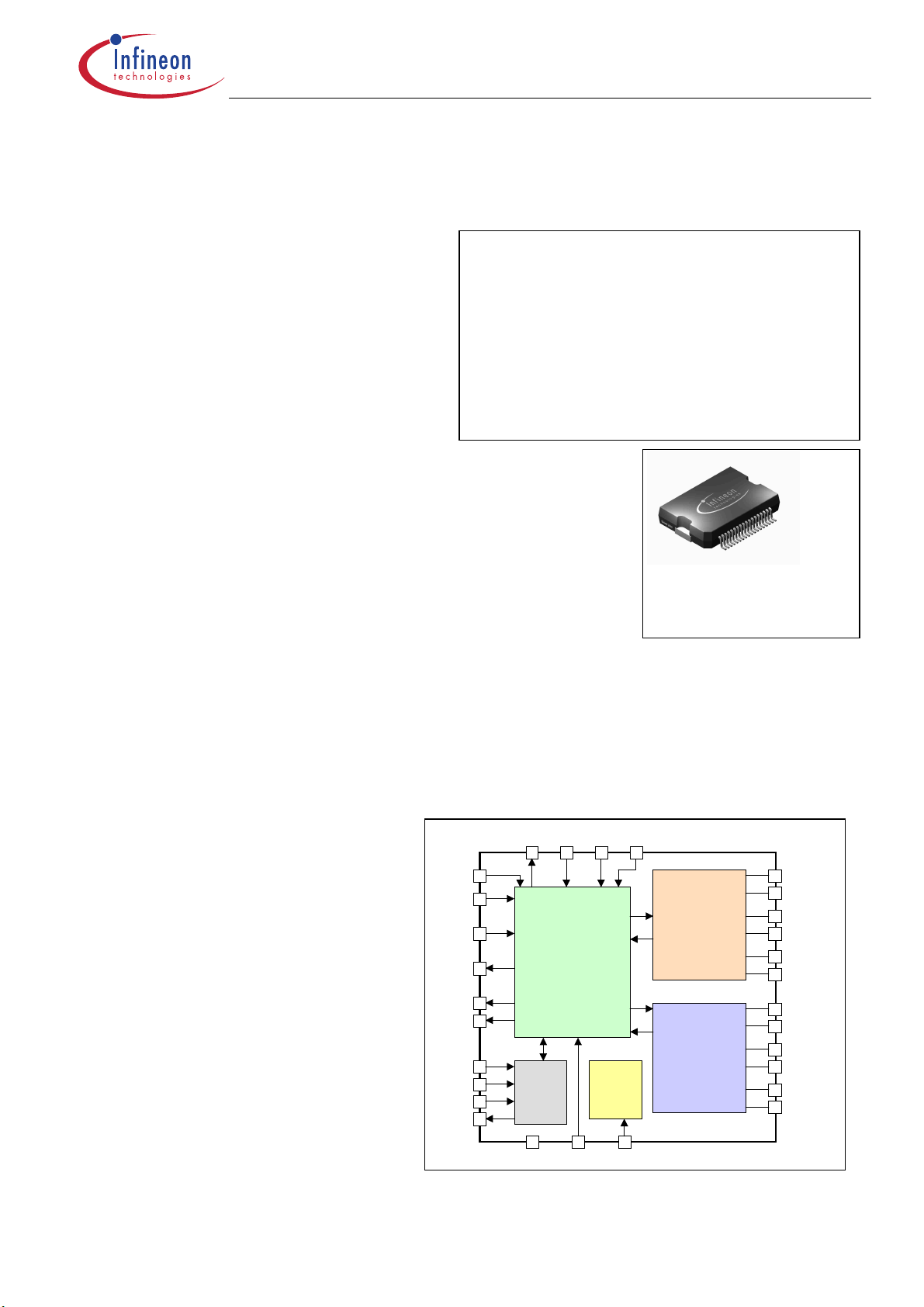
General description
The TLE6288 R is a 6-channel (150mΩ)
Smart Multichannel Switch in SPT4 Technology. The IC has embedded protection,
diagnosis and configurable functions.
Channel 1-3 are highside channels with
integrated charge pump and can be programmed individually to do autonomous
peak and hold current regulation with
PWM. Channel 4-6 (also with integrated
charge pump) can be configured to work
as highside Switch or lowside Switch. This
IC can be used to drive standard automotive loads in highside or lowside applications with switching frequencies up to
10kHz. In addition the TLE6288R can be
used to drive autonomously up to 3 inductive Peak&Hold (valves, coils) loads with
programmable peak and hold current values.
CLKProg
IN 1
IN 6
DIAG 1
DIAG 5
DIAG 6
Overtemp.
SCLK
CS
SI
SO
Fault
Reset VDO
Logic
Configuration
Current
Regulation
SPI
VCC
Chargepump
VCPGND FSIN
Channel 1-3
Highside 150 m
Peak&Hold
Protection
Diagnosis
Channel 4 -6
Highside/ Lowside
150 m
Ω
Protection
Diagnosis
DOUT 1
SOUT 1
DOUT 2
SOUT 2
DOUT 3 / VB
SOUT 3
DOUT 4
SOUT 4
DOUT 5
SOUT 5
DOUT 6
SOUT 6
Vp2 Page 1 13.01.2003
Page 2
Preliminary Datasheet TLE6288 R
1. Block Diagram
Fault
CLKProg
IN 1
IN 2
IN 3
IN 4
IN 5
IN 6
DIAG 1
Reset VDO
.
.
.
.
.
.
Logic
.
.
Driver
Diagnosis
Vcc
VCC DOUT 3 / VB
VB
Channel 3
Highside 300 m
Peak&Hold
Channel 2
Highside 300 m
Peak&Hold
Channel 1
Highside 300 m
Peak&Hold
Channel 4
Highside/ Lowside
300 m
Ω
Ω
SOUT 3
DOUT 2
Ω
SOUT 2
DOUT 1
Ω
SOUT 1
DOUT 4
SOUT 4
DIAG 5
DIAG 6
Overtemp.
SCLK
CS
SI
SO
Vcc
Vcc
GND
GND
Channel 5
Highside/ Lowside
300 m
Ω
Channel 6
Highside/ Lowside
300 m
Ω
DOUT 5
SOUT 5
DOUT 6
SOUT 6
.
.
.
SPI
Vcc
Charge
pump
.
VCPGNDFSIN
Vp2 Page 2 13.01.2003
Page 3

Preliminary Datasheet TLE6288 R
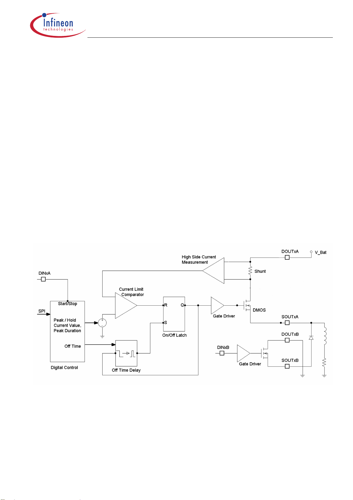
2. Functional description
Block diagram will be added
Channel 1..3:
Only High Side Drive with Charge Pump.
Current Control
Default 2.4A peak and 1A hold with adjustable values by SPI
Types of current control are switched by SPI. ( Refer to Fig. 1)
Current regulation: Peak Current Controller with fixed Off-Time
Peak Current, Peak Time, Hold Current and Off-Time can be selected by SPI
to set average and ripple current for a given load
Channel 4..6:
Either High or Low Side Drive is configurable (by SPI)
Open load detection and switch bypassed detection can be deactivated by SPI
Vp2 Page 3 13.01.2003
Page 4
Preliminary Datasheet TLE6288 R
Protection: The TLE6288R has integrated protection functions1 for overload and short circuit (active
current limitation), Overtemperature, ESD at all pins and overvoltage at the power outputs (zener
clamping).
Output Stage Control: Parallel Control and SPI Control
A Boolean operation (either AND or OR) is performed on each of the parallel inputs IN 1..6 and respective SPI data bits, in order to determine the states of the respective outputs. The type of Boolean operation performed is programmed via the serial interface. Both, parallel inputs and respective SPI databits are high active.
Truth table
parallel
Input
0 0 OFF OFF
0 1 ON OFF
1 0 ON OFF
1 1 ON ON
SPI
Bit
Output
OR
Output
AND
IN 1…6
AND
Output
Driver
OR
Serial Input bits 6 - 11 of comman d
„Ch annels on / off „
Each output is independently controlled by an output latch and a common reset line FSIN, which disables all outputs. A logic high input ‘data bit’ turns the respective output channel ON, a logic low ‘data
bit’ turns it OFF.
Overtemperature Behavior:
Each channel has an overtemperature sensor and is individually protected against overtemperature.
As soon as overtemperature occurs the channel is immediately turned off. In this case here are two
different behavoirs of the affected channel that can be selected by SPI (for all channels generally).
Autorestart: as long as the input signals of the channel remains on (e.g. parallel input high) the channel turns automatically on again after cooling down.
Latching: After overtemperature shutdown the channel stays off until the this ovetemperature latch is
reset by a new LÆH transition of the input signal.
Note: These overtemperature sensors of the channels are only active if the channel is turned on.
An additional overtemperature sensor is located in the logic of the device. I monitors permanently the
IC temperature. As soon as the IC temperature reaches a specified level an overtemperature fault will
be indicated.
1
Integrated protection functions are designed to prevent IC destruction under fault conditions described in the data sheet. Fault conditions are
considered as "outside" normal operating range. Protection functions are not designed for continuous repetitive operation
Vp2 Page 4 13.01.2003
.
Page 5
Preliminary Datasheet TLE6288 R
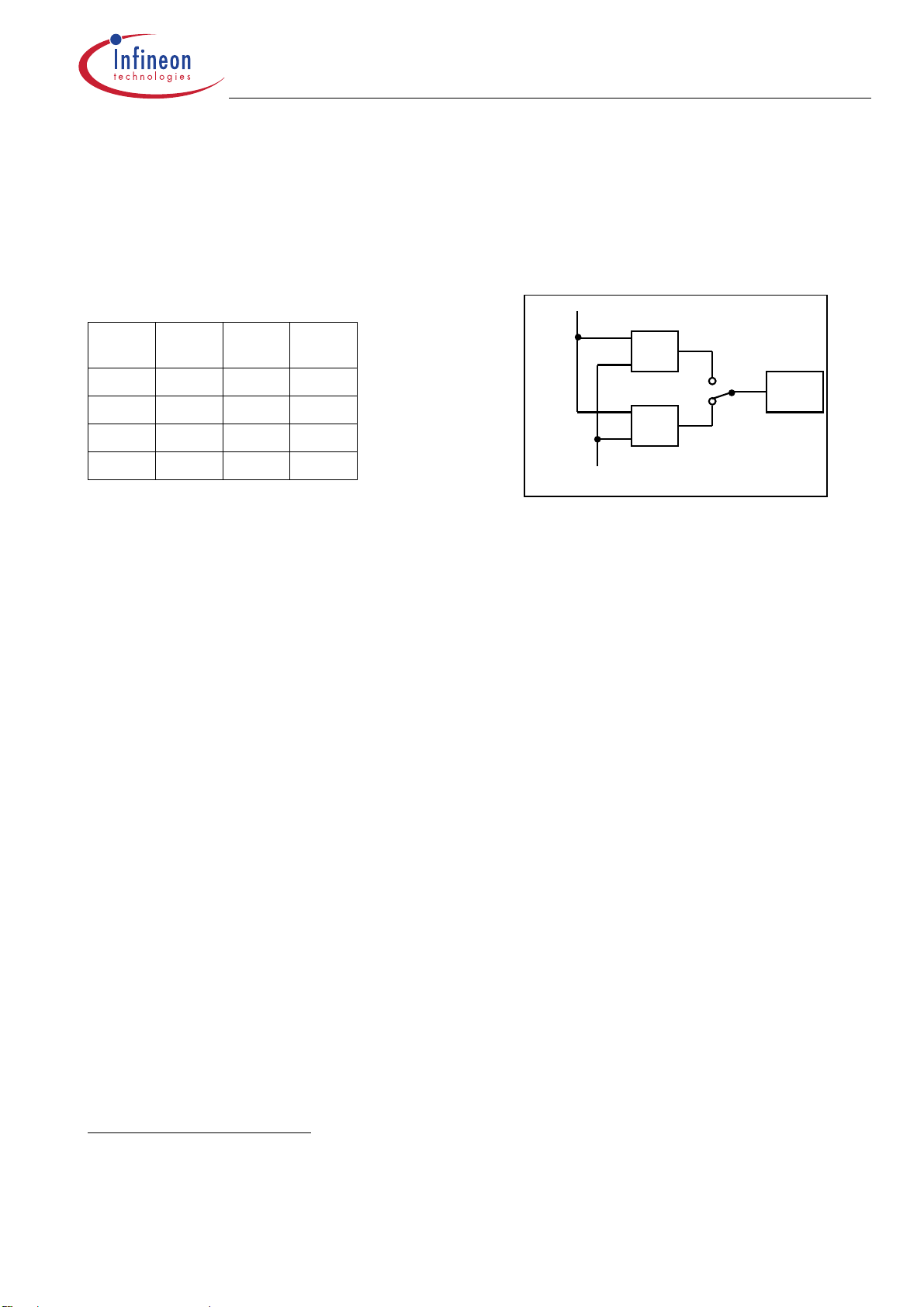
Current Regulator : Peak current control with fixed off-time
Hold only : When the channel is turned on externally (SPI or parallel input) the current rises to the programmed hold current level. Then the channel is internally turned off and a timer is started for a constant off-time (e.g. 200µs). After this time the channel is internally turned on again until the hold current
level is reached again and so on. This regulation workes automatically until the channel is turned of
externally.
Peak and hold mode with minimum peak time: When the channel is turned on the current rises to the
programmed peak current level. Then the channel is internally turned off, the current regulator changes
to hold current values and a timer is started for a constant off-time. After this time the channel is internally turned on again until the hold current value is reached and then again turned off for the fixed off
time. This regulation workes automatically until the channel is turned of externally.
Peak and hold mode with programmed peak time: When the channel is turned on the current rises to
the programmed peak current level. Then the channel is internally turned off and a timer is started for a
constant off-time. After this time the channel is internally turned on again until the peak current value is
reached and then again turned off. This works until the programmed peak time is over. Then the current regulator changes to hold current values and workes as described under "hold only".
Peak Current, Peak Time, Hold Current and fixed Off-Time can be set via SPI.
To avoid regulation disturbances by current transients during switching (e.g. caused by ESD capacitors
at the outputs) the current regulator has a "leading edge blanking" of typical 20µs in all three regulation
modes. After turning on the DMOS (internally or externally) the current regulation circuit is deactivated
for the first 20µs. This guarantees that switching of the DMOS itself or charging of small capacitors at
the output (e.g. ESD) is not disturbing the current regulation.
Simplified functional block diagram:
Vp2 Page 5 13.01.2003
Page 6
Preliminary Datasheet TLE6288 R
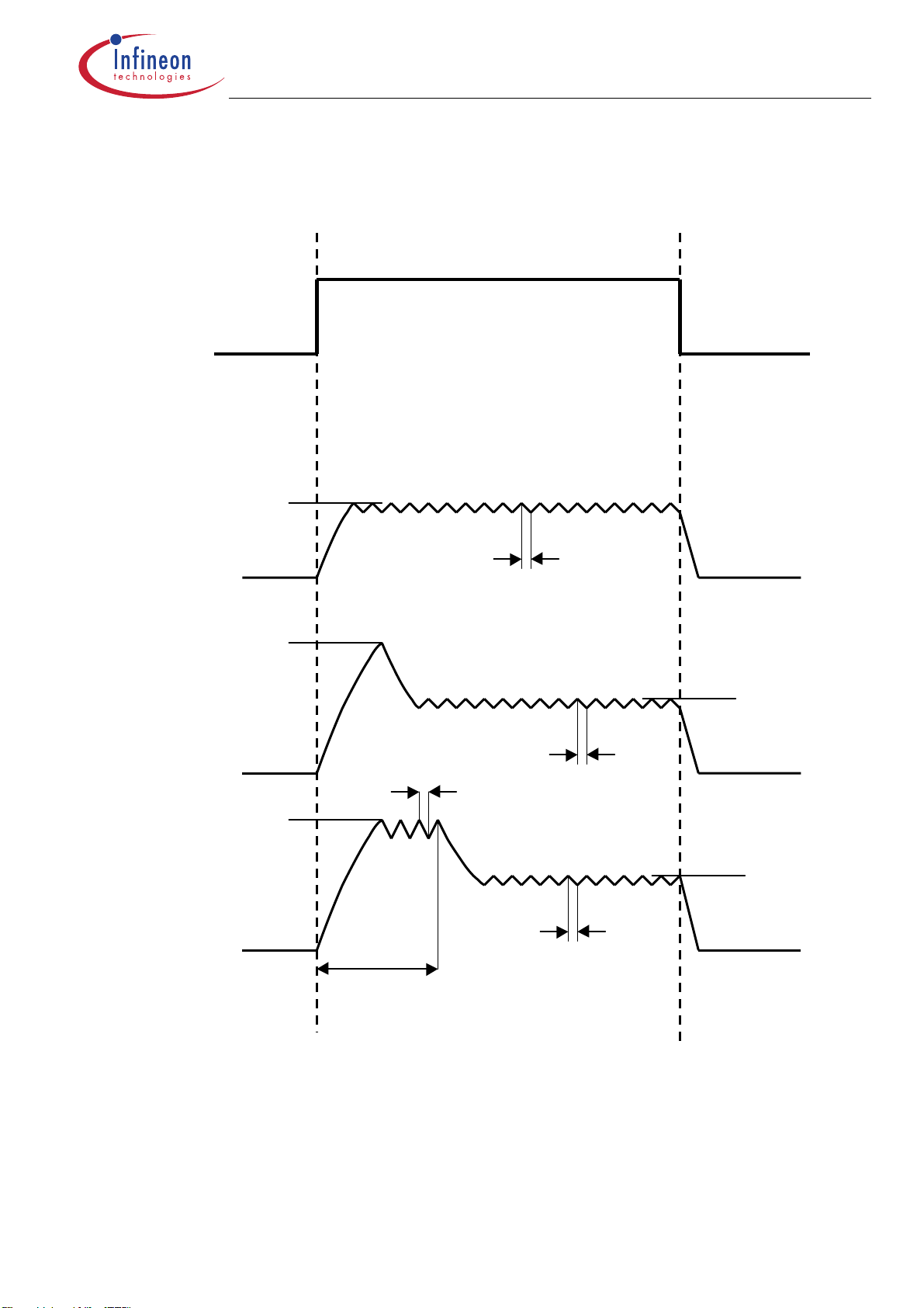
Current Waveforms of the different current control modes
Input Signal
No Regulation Current defined only by load
I
hd
Hold only
I
pk
Peak & Hold
with min. peak time
I
pk
Peak and Hold
with set peak time
t
fo
I
hd
t
fo
t
fo
I
hd
t
t
p
fo
Fig.1
Current forms of the different current control modes of channel 1-3
Vp2 Page 6 13.01.2003
Page 7
Preliminary Datasheet TLE6288 R
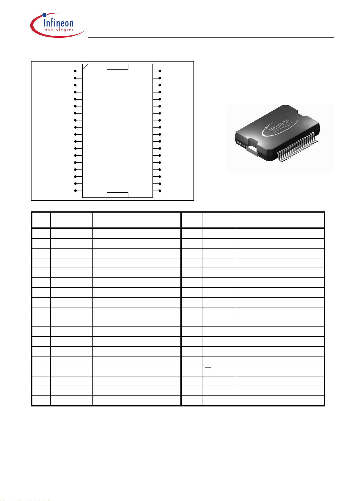
3. Pin Configuration
SOUT4
DOUT4
DOUT1
SOUT1
DIAG1
DIAG2
DIAG3
DIAG4
DIAG5
DIA6/Overtemp
SOUT2
DOUT2
DOUT5
SOUT5
Pin
Name Function Pin Nr. Name Function
Nr.
SOUT4 Source Output CH 4 (high / low side)
1
DOUT4 Drain Output CH 4 (high / low side)
2
DOUT1 Drain Output CH 1(high side)
3
SOUT1 Source Output CH 1 (high side)
4
IN4 Control Input Channel 4
5
IN1 Control Input Channel 1
6
DIAG1 Diagnostic Output CH 1
7
DIAG2 Diagnostic Output CH 2
8
DIAG3 Diagnostic Output CH 3
9
DIAG4 Diagnostic Output CH 4
10
DIAG5 Diagnostic Output CH 5
11
DIAG6/Overtemp Diagnostic Output CH 6 / Overtemp
12
IN2 Control Input Channel 2
13
IN5 Control Input Channel 5
14
SOUT2 Source Output CH 2 (high side)
15
DOUT2 Drain Output CH 2(high side)
16
DOUT5 Drain Output CH 5 (high / low side)
17
SOUT5 Source Output CH 5 (high / low side)
18
IN4
IN1
IN2
IN5
1
2
3
4
5
6
7
8
9
10
11
12
13
14
15
16
17
18
TLE6288 R
(S0999)
36
35
34
33
32
31
30
29
28
23
22
21
20
19
27
26
25
24
SOUT6
DOUT6
SI
_CS
SCLK
CLK Prog
SO
VDO
VCC
Reset
IN6
IN3
Fault
GND
FSIN
VCP
DOUT3
SOUT3
Package: Power-P-DSO-36
0.65mm Pitch
SOUT3 Source Output CH 3 (high side)
19
DOUT3 Drain Output CH 3(high side)
20
VCP Charge Pump pin
21
FSIN All Channels Enable / Disable
22
GND Logic Ground
23
Fault General Fault Flag
24
IN3 Control Input Channel 3
25
IN6 Control Input Channel 6
26
Reset Reset pin (+ Standby Mode)
27
VCC Logic Supply Voltage (5V)
28
VDO Supply Pin for digital outputs
29
SO SPI Serial Data Output
30
CLKProg Program pin of SPI Clock
31
SCLK SPI Serial Clock
32
33
34
35
36
CS
SI SPI Serial Data Input
DOUT6 Drain Output CH 6 (high / low side)
SOUT6 Source Output CH 6 (high / low side)
SPI Chip Select
Vp2 Page 7 13.01.2003
Page 8

Preliminary Datasheet TLE6288 R
4. Pin description:
DOUT 1-3 – Drain of the 3 highside channels. These pins must always be connected to the same
power (battery) supply line.
SOUT 1-3 – Source of the three highside channels. Outputs of the highside channels where the load is
connected.
DOUT 4-6 – Drain pins of the three configurable channels. In highside configuration they must be con-
nected to the same voltage as DOUT 1-3. In lowside configuration they are the output pins and connected to the load.
SOUT 4-6 – Source of the three configurable channels. In highside configuration they are the outputs
and connected to the load. In lowside configuration they must be connected with GND.
IN 1-6 – Parallel input pins for the 6 power outputs. These pins have an internal pull down structure.
GND – Logic ground pin.
FSIN – Disable pin. If the FSIN pin is in a logic low state, it switches all outputs OFF. An internal pull-up
structure is provided on chip.
Reset – Reset pin. When the reset is low all channels are off, the internal biasing is deactivated, all
internal registers are cleared and the supply-current consuption is reduced (standby mode). An internal
pull-up structure is provided on chip.
Fault – General Fault pin.
as soon as an error is latched into the diagnosis register. When the diagnosis register is cleared this
flag is also reset (high state). This fault indication can be used to generate a µC interrupt.
CLKProg – Programming pin for the SPI Clock signal.
nal input of the SPI. In low state the SPI will read data at the rising clock edge and write data at the
falling clock edge. In high state the SPI will read data at the falling clock edge and write data at the rising clock edge The pin has an internal pull down structure.
DIAG1..5; DIAG6 / Overtemp. – Parallel diagnostic pins (push-pull) change state according to the input signal of the corresponding channel. As soon as an error occurs at the corresponding channel (
Overload and overtemperature is detected in on state and open load /switch bypass in off state) the
DIAG output shows the inverted input signal. An fault is detected only if it lasts for longer than the fault
filtering time. The fault information is not latched in a register.
If DIAG6 is configured as Overtemperature Flag: This is a general fault pin which shows a high to low
transition as soon as an overtemperature error occurs for any one of the six channels (for longer than
the fault filtering time) or the IC logic. This fault indication can be used to differ between overload and
overtemperature errors in one of the six channels or to detect a general IC overtemperature.
VCP – Pin to connect the external capacitor of the integrated charge pump.
VDO – Supply pin of the push-pull digital output drivers. This pin can be used to vary the high-state
output voltage of the SO pin and the DIAG1-6 pins.
VCC – Logic supply pin. This pin is used to supply the integrated circuitry.
There is a general fault pin (open drain) which shows a high to low transition
This pin can be used to configure the clock sig-
– Chip Select of the SPI
CS
SO – Signal Output of the Serial Peripheral Interface
SI – Signal Input of the Serial Peripheral Interface. The pin has an internal pull down structure.
SCLK – Clock Input of the Serial Peripheral Interface. The pin has an internal pull up structure (if
CLKProg=L) or an pull down structure (if CLKProg=H).
For more details about the SPI see Chapter 9.SPI.
Vp2 Page 8 13.01.2003
Page 9

Preliminary Datasheet TLE6288 R
5. Maximum ratings
No. Parameter Symbol Value Unit Pin / Comment
1 Power Supply Voltage 1 static
dynamic : 1min. 0°C
dynamic : Test cond. Fig.1
V
V
VB
B
B
-0.3 …20
24
37
V
V
V
DOUT1-3
DOUT1-3
DOUT1-3
2 Power Supply Voltage 2 VCC, VDO- 0.3 ... 7 V VCC, VDO
3a Continuous Drain Source
Voltage (lowside configuration)
3b Continuous Source Voltage
(Highside configuration)
V
40 V DOUT – SOUT
DSL
(channel 4-6)
V
SH
-9 ... VB V SOUT - GND
(channel 4-6)
4 Input Voltage VIN -0.3 … VCC+ 0.3 V IN1-6, Reset, FSIN, CS,
SCK, SI, CLKProg
5a Output Voltage V
5b Output Voltage V
5c Output Voltage V
-0.3 … VCC+ 0.3 V Fault
OUT
-0.3 … VDO+ 0.3 V DIAG1-6, SO
OUT
CP OUT
VB +10 V VCP ; no voltage must
be applied
6 Operating Temperature Ta
T
7 Storage Temperature T
8 Power Dissipation
(R
(R
= 20K/W)
thja
= 30K/W)
thja
9 Reverse Current (1ms) I
P
rev
-40 … +105
j
-55 … +150 °C
stg
dmax
-40 … +150
2,25
1,5
-4 A between DOUT and-
°C
°C
W
SOUT; Channel 4 to 6
10 ESD (Human Body Model)
2000 V
V
ESDb
C= 100pF, R=1.5kΩ
Applied to all terminals 3 times
11 ESD (Machine Model)
250 V
V
ESDm
C= 200pF, R=0Ω
Applied to all terminals 3 times
12 Single Switch off load Inductance see Fig.2 DOUT, SOUT
Fig.2
37V
10 times
(once/ 30sec)
added after characterisation
12V
160ms
350ms
Test cond. Fig.1
Vp2 Page 9 13.01.2003
Page 10

Preliminary Datasheet TLE6288 R
6. Electrical Characteristics
VCC = 4.5 to 5.5 V ; Tj = - 40 °C to + 150 °C ; VB = 6V to 16V ; Reset = H ; VDO = VCC
(unless otherwise specified)
Value No. Parameter Symmin typ max
Unit Pin /
Power Supply, Reset
1
Condition
bol
Comment
Power Supply Current 1 I
1.1
Power Supply Current 2 I
1.2
Power Supply Current 3
1.3
in Standby Mode
1.4
Minimum Reset Duration t
1.5
Wake up time after reset t
Power Outputs
2
On Resistance R
2.1
Forward Voltage Revers
2.2
Diode
Peak Current range I
2.3
Peak Current accuracy I
2.4
Hold Current range I
2.5
Ch1-Ch6:
b
10 mA DOUT1-3
Off
10 mA VCC
cc
I
Reset = L 50 µA DOUT1-3, VCC
cc+Ib
Re-
set,min
wakeup
DS(ON)ID
V
RDf
1.2 --
pk
50 µs
Ccp = 10 nF 5 ms
=2.4A
=10V
V
B
ID = -4A
= 150°C
T
j
350 mΩ DOUTx – SOUTx
2 V SOUTx – DOUTx
A
3.6
Tj= 25, 150°
pka
Tj=-40
0.7 --2 A
hd
± 15
± 20
%
Hold Current accuracy I
2.6
Peak time range t
2.7
Peak time accuracy t
2.8
Fixed off Time range t
2.9
Fixed off Time accuracy t
2.10
Fixed off Time accuracy 200µs-
2.11
hda
0.8 --
p
pa
100 -
fo
foa
Tj= 25, 150°
Tj=-40
3.6
400
100µs
400µs
± 15
%
± 20
ms
±20
%
µs
±30
±20
%
%
Vp2 Page 10 13.01.2003
Page 11
Preliminary Datasheet TLE6288 R
VCC = 4.5 to 5.5 V ; Tj = - 40 °C to + 150 °C ; VB = 6V to 16V ; Reset = H ; VDO = VCC
(unless otherwise specified)
Value No. Parameter Sym-
min typ max
Unit Pin /
Output ON Delay time1 t
2.12
Condition
bol
Fig.3 10 µs
dON
Comment
Output ON Rise time1 t
2.13
Output OFF Delay time1 t
2.14
Output OFF Fall time1 t
2.15
Leackage Current Reset = L 10 µA
2.16
Leak Current in OFF
2.17
Fig.3 10 µs
r
Fig.3
dOFF
HS- Mode
LS- Mode
Fig.3 10 µs
f
I
-250 µA SOUT1-6
loff
20
20
µs
(highside configuration)
Leak Current in OFF
2.18
I
500 µA DOUT4-6
loff
(lowside configuration)
Output Clamp Voltage
2.19
Highside Configuration
Output Clamp Voltage
2.20
Lowside Configuration
Current limitation
2.21
V
Referes to
clh
GND level
V
Referes to
cll
GND level
I
Dlim1-3
4 6 A
-9 -14 -19 V SOUT1-6
40 55 V DOUT4-6
(Channel 1-3)
Current limitation
2.22
I
Dlim4-6
3 6 A
(Channel 4-6)
2.23
IC Overtemp. Warning
Hysteresis
T
ot
T
hys
160
10
180 °C
°C
Digital Inputs
3
Input Low Voltage V
3.1
Input High Voltage V
3.2
Input Voltage Hysteresis V
3.3
Input Pull Down current I
3.4
Input Pull Up current I
3.5
SPI Input Pull Down
3.6
current
SPI Input Pull Up current I
3.7
1 V all digit. inputs
INL
2 V all digit. inputs
INH
100 mV all digit. inputs
INHys
V
pd
VIN = GND 20 50 100 µA Reset; FSIN
pu
I
V
pd
= 5V 20 50 100 µA IN1-6; CLKProg
IN
= 5V 10 20 50 µA SI, SCLK
IN
(CLKProg=H)
V
pd
= GND 10 20 50 µA CS;SCLK
IN
(CLKProg=L)
Vp2 Page 11 13.01.2003
Page 12

Preliminary Datasheet TLE6288 R
VCC = 4.5 to 5.5 V ; Tj = - 40 °C to + 150 °C ; VB = 6V to 16V ; Reset = H ; VDO = VCC
(unless otherwise specified)
Value No. Parameter Sym-
min typ max
Unit Pin /
Digital Outputs
4
Condition
bol
Comment
SO Low State Output
4.1
Voltage
SO High State Output
4.2
Voltage
DIAG Low State Output
4.3
Voltage
DIAG High State Output
4.4
Voltage
Fault Low Output Voltage V
4.5
Fault Output leak Current I
4.6
Diagnostic Functions
5
5.1
Open Load Detection
Voltage
5.2
Open Load Detection
Voltage
5.3
Output Open Load diagnosis Current
5.4
Fault Filter Time
V
V
SOL
SOH
I
I
=2.5mA 0.4 V SO
SOL
=-2mA VDO-
SOH
V SO
0.4V
I
DIAGL
=
0.4 V DIAG1-6
50µA
I
I
ol
Output :OFF
oh
=
DIAGH
-50µA
= 1mA 0.4 V Fault
out
VDO-
0.4V
V DIAG1-6
1 µA Fault
V
=5V
(fault)
V
DS(OL)
lowside con-
5.5 V
figuration,
Vbat=12V
V
DS(OL)
highside
4.5 V
configuration,
Vbat=12V
I
d(OL)
Vbat=Vout=
20 100 500 µA
12V
t
f(fault)
50 100 200 µs
5.5
Switch Bypass Detec-
I
d(SB)
250 µA
tion Current
5.6
Overload Detection
Threshold (Channel 1-3)
5.7
Overload Detection
Threshold (Channel 4-6)
Input Voltage
Output Voltage
(Highside configuration)
t
dON
t
r
I
Dd(lim1-
3)
I
Dd(lim 4-
6)
Vp2 Page 12 13.01.2003
4 6 A
3 6 A
t
dOFF
70%
Fig.3 : Turn on/off timings with resistive load
30%
t
f
Page 13

Preliminary Datasheet TLE6288 R
VCC = 4.5 to 5.5 V ; Tj = - 40 °C to + 150 °C ; VB = 6V to 16V ; Reset = H ; VDO = VCC
(unless otherwise specified)
Condition
bol
SPI Timing
6
f
Serial Clock Frequency (de-
6.1
SCK
DC -- 5
pending on SO load)
Serial Clock Period (1/fclk) t
6.2
200 -- -- ns
p(SCK)
Value No. Parameter Sym
min typ max
Unit Pin /
MHz
Comment
Serial Clock High Time t
6.3
Serial Clock Low Time t
6.4
Enable Lead Time
6.5
(falling edge of
to falling
CS
edge of SCLK)
Enable Lead Time
(falling edge of
to rising
CS
edge of SCLK)
Enable Lag Time (rising edge of
6.6
SCLK to rising edge of
CS
)
Enable Lag Time (falling edge
of SCLK to rising edge of
Data Setup Time (required time
6.7
CS
)
SI to rising of SCLK)
Data Setup Time (required time
SI to falling of SCLK)
Data Hold Time (rising edge of
6.8
SCLK to SI)
Data Hold Time (falling edge of
SCLK to SI)
Disable Time t
6.9
Transfer Delay Time
6.10
2
50 -- -- ns
SCKH
50 -- -- ns
SCKL
t
CLKProg=L 200 -- -- ns
leadL
t
CLKProg=H 200 -- -- ns
leadH
CLKProg=L 200 --- -- ns
t
lagL
CLKProg=H 200 --- -- ns
t
lagH
t
CLKProg=L 20 -- -- ns
SUL
t
CLKProg=H 20 -- -- ns
SUH
t
CLKProg=L 20 -- -- ns
HL
tHH CLKProg=H 20 -- -- ns
-- 200 ns
DIS
t
200 -- -- ns
dt
CS high time between two
(
accesses)
Data Valid Time
6.11
= 50 pF to 100pF
C
L
C
= 220 pF
L
t
valid
--
--
--
--
120
150
ns
1)
To get the correct diagnostic information, the transfer delay time has to be extended to the maximum fault delay
time t
f(fault)max
Vp2 Page 13 13.01.2003
= 200µs.
Page 14
Preliminary Datasheet TLE6288 R
7 Diagnostics
detailled description of the diagnosis will be added
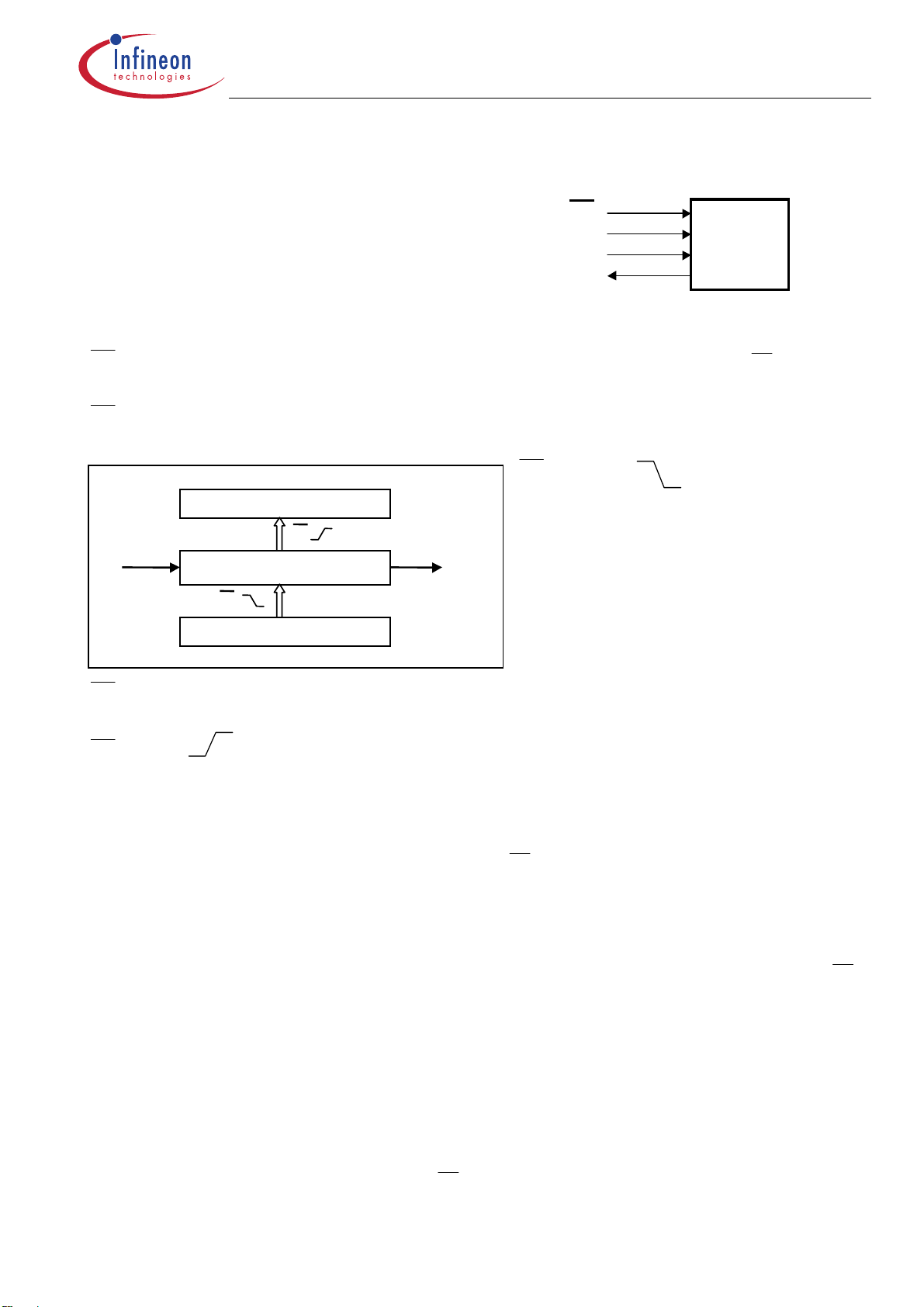
8 SPI
The SPI is a Serial Peripheral Interface with 4 digital pins
and an 16 bit shift register. The SPI is used to configure
and program the device, turn on and off channels and to
read detailled diagnostic information.
CS
SCLK
SI
SO
SPI
8.1 SPI Signal Description:
CS - Chip Select. The system microcontroller selects the TLE 6288 R by means of the
CS
ever the pin is in a logic low state, data can be transferred from the µC and vice versa.
= H : Any signals at the SCLK and SI pins are ignored and SO is forced into a high impedance
CS
state.
LSB
internal logic registers
MSB
CS = HÆL :
• diagnostic information is transferred from
the diagnosis register into the SPI shift
CS
SI SO
Serial input
data MSB first
16 bit SPI shift register
CS
Serial output
(diagnosis)
MSB first
diagnosis register
LSB
MSB
register.
• serial input data can be clocked into the
SPI shift register from then on
• SO changes from high impedance state to
logic high or low state corresponding to
the SO bits
pin. When-
CS = L : SPI is working like a shift register. With each clock signal the state of the SI is read into the
SPI shift-register and one diagnosis bit is written out of SO.
CS = LÆH:
• transfer of SI bits from SPI shift register into the internal logic registers
• reset of diagnosis register if sent command was valid
To avoid any false clocking the serial clock input pin SCLK should be logic high state (if CKLProg=L;
low state if CLKProg=H) during high to low transition of
SCLK - Serial Clock. The serial clock pin clocks the internal SPI shift register of the TLE 6288 R. The
serial input (SI) accepts data into the input SPI shift register on the rising edge of SCLK (if CKLProg=L;
falling edge if CLKProg=H) while the serial output (SO) shifts diagnostic information out of the SPI shift
register on the falling edge (if CKLProg=L; rising edge if CLKProg=H) of serial clock. It is essential that
the SCLK pin is in a logic high state (if CKLProg=L; low state if CLKProg=H) whenever chip select
makes any transition.
SI - Serial Input. Serial data bits are shifted in at this pin, the most significant bit (MSB) first. SI information is read in on the rising edge of SCLK (if CKLProg=L; falling edge if CLKProg=H). Input data is
latched in the SPI shift register and then transferred to the internal registers of the logic.
The input data consist of 16 bit, made up of 4 control bits and 12 data bits. The control word is used to
program the device, to operate it in a certain mode as well as providing diagnostic information (see SPI
Commands).
CS
.
CS
SO - Serial Output. Diagnostic data bits are shifted out serially at this pin, the most significant bit (MSB)
first. SO is in a high impedance state until the
pin goes to a logic low state. New diagnostic data will
CS
appear at the SO pin following the falling edge of SCLK (if CKLProg=L; rising edge if CLKProg=H).
Vp2 Page 14 13.01.2003
Page 15

Preliminary Datasheet TLE6288 R
8.2 SPI Diagnostics:
As soon as a fault occurs for longer than the fault filtering time, the fault information is latched into the
diagnosis register (and the Fault pin will change from high to low state). A new error on the same
channel will over-write the old error report. Serial data out pin (SO) is in a high impedance state when
is high. If CS receives a LOW signal, all diagnosis bits can be shifted out serially. If the sent com-
CS
mand was valid the rising edge of
and restart the fault filtering time. In case of an invalid command the device will ignore the data bits and
the diagnosis register will not be reset at the rising
will reset the diagnosis registers (except the channel OT flag)
CS
edge.
CS
Diagnostic Serial Data Out SO
MSB
15 14 13 12 11 10 9 8 7 6 5 4 3 2 1 0
Ch.6 Ch.5 Ch.4 Ch.3
Channel Overtemperature Flag
Ch.2 Ch.1
Bit0 and Bit1
is always 1
LSB
IC Overtemperature Flag
HH Normal function
HL Overload, Shorted Load or Overtemperature
LH Open Load
LL Switch Bypassed
Figure 1: Two bits per channel diagnostic feedback plus two overtemperature flags
For Full Diagnosis there are two diagnostic bits per channel configured as shown in Figure 1.
Diagnosis bit0 and bit1 are always set to 1.
Normal function: The bit combination HH indicates that there is no fault condition, i.e. normal function.
Overload, Shorted Load or Overtemperature: HL is set when the current limitation gets active, i.e.
there is a overload, short to supply or overtemperature condition. The second reason for this bit combination is overtemperature of the corresponding channel.
Open load: LH is set when open load is detected (in off state of the channel)
Switch Bypassed:
Short to GND : in lowside configuration LL is set when this condition is detected
Short to Battery : in highside configuration LL is set when this condition is detected
Channel Overtemperature Flag: In case of overtemperature in any output channel in on state the
overtemperature Flag in the SPI diagnosis register is set (change bit 3 from 0 to 1). This Bit can be
used to distinguish between Overload and Overtemperature (both HL combination) and is reset by
switching OFF/ON the affected channel.
In addition the DIAG6 / Ovtertemp pin is set low (if configured as Overtemp.Flag).
IC Overtemperature Flag: When the IC logic tremperature exceeds typ.170° the non-latching IC
Overtemperature Flag will be set in the SPI diagnosis register(change bit 2 from 0 to 1).
In addition the DIAG6 / Ovtertemp pin is set low (if configured as Overtemp.Flag).
8.3 SPI Commands, Values and Parameters:
Vp2 Page 15 13.01.2003
Page 16

Preliminary Datasheet TLE6288 R
The 16 bit SPI is used to program different IC functions
and values, turn on and off the channels and to get detailled diagnosis information. Therefore 4 command bits
and 12 data bits are used.
The following parameters and functional behavior can be
programmed by SPI:
Current regulation Mode (mode) : for each of the three
highside channels individually the operation mode can be
set. a) "no current regulation
b) Current regulation "hold only
c) Current regulation "peak & hold with minimum
peak time
d) Current regulation "peak & hold with programmed peak time".
Peak Current (I
) : for each of the three highside channels individually the peak current value for P&H
pk
current regulation can be programmed. The current range is 1.2A to 3.6A.
Fixed off time of the current regulator (t
) : for each of the three highside channels (Ch1 - Ch3) indi-
fo
vidually the fixed off time for all modes with current regulation can be programmed from 100µs to
400µs.
Hold Current (I
) : for each of the three highside channels(Ch1 - Ch3) individually the hold current
hd
value for P&H and hold only current regulation can be programmed. The current range is 0.7A to 2.0A
Peak Time (t
) : for each of the three highside channels(Ch1 - Ch3) individually the peak time value for
p
P&H current regulation can be programmed. The time range is 0.8ms to 3.6ms.
Highside / Lowside Configuration ( H/L ) : Each of the three configurable channels (Ch4 – Ch6) can
be programmed for use as Highside Switch or Lowside Switch.
Open load and switch bypassed detection activated or deactivated (OL+SB) : For each of the
three configurable channels(Ch4 – Ch6) the open load and switch bypassed diagnosis can be deactivated. In lowside configuration the open load and the short to GND detection can be deactivated, in
highside configuration the open load and short to battery detection.
Boolean Operation (OR / AND) : For all channels generally the Boolean operation of the parallel input
signal and the SPI bit of the corresponding channel can be defined.
Overtemperature Behavior ( R/L ) : The overtemperature behavior of the channels can be programmed by SPI. Autorestart or latching overtemperature shutdown can be selected (for all channels
the same behavior).
DIAG6 or Overtemperature Flag (D/F) : With this SPI bit the function of the DIAG6/Overtemp pin is
defined. This output can work as diagnosis output of channel 6 or as Overtemperature Flag.
CS
4 Bits 12 Bits
SI
Command Data
SO
SI command : 4 Command Bits program
the operation mode of Channels 1 to 6.
12 Data Bits configure the device and
give the input information (on or off) for
Channel 1 to 6.
SO diagnosis 16 bit diagnosis information
(two bit per channel) of channels 1 to 6 plus
two Overtemperature Flags
Diagnosis (Ch. 1 to 6)
+ 2 Temp. Flags
Vp2 Page 16 13.01.2003
Page 17

Preliminary Datasheet TLE6288 R
8.4 SPI Commands
Command Table
No Command
1 Config. Regulator 1
2 Config. Regulator 2
3 Config. Regulator 3
4 Config. Ch1 - Ch6
5 Set all to Default
6 Diagnosis only
7 Channels on / off
MSB
14 13 12 11 10 9 8 7 6 5 4 3 2 1
1 0 0 1 Mode I
1 0 1 0 Mode I
1 0 1 1 Mode I
1 1 0 0
1 0 0 0
1 1 1 1
1 1 0 1
Ch. 6 Ch. 5 Ch 4 all all
OL+
H/L
SB
X X X X X X X X X X X X
X X X X X X X X X X X X
Ch6 Ch5 Ch4 Ch3 Ch2 Ch1 X X X X X X
H/L
tfo Ihd tp
pk
tfo Ihd tp
pk
tfo Ihd tp
pk
OL+
SB
H/L
OL+
SB
OR/
R/L D/F X X X
AND
DIAG
6
LSB
X
X
X
Legend of SPI Command Table:
Mode: Operation mode of the current regulator:
a) no regulation
b) hold only
c) peak&hold with minimum peak time
d) peak&hold with programmed peak time
I
: Peak current values 1.2A - 3.6A
pk
I
: Hold current values 0.7A - 2A
hd
t
: Peak time value 0.8ms – 3.6ms
p
t
: Fixed off time value 100µs – 400µs
fo
H/L : Channel 1-3 in highside or lowside configuration
OL+SB : open load detection and switch bypassed detection activated or deactivated
OR / AND : Boolean Operation (parallel input and corresponding SPI Bit)
R/L : Autorestart or Latching overtemperature behaviour
D/F : DIAG6/Overtemp pin set as Diagnosis output of channel 6 or as Overtemperature Flag
Ch1-Ch6 : On / Off information of the output drivers (high active)
Command description:
Config. Regulator 1-3: With this command the values for for the current regulation and the functional
mode of the channel is written into the internal logic registers.
Config. Ch1- Ch6 : This command writes the configuration data of the three configurable channels (4-
6) and sets the Boolean operation and overtemperature behavior of all channels. It also and sets the
DIAG6/Overtemp. pin to Diagnosis of channel 6 or Overtemperature Flag.
Set all to default : This command sets all internal logic registers back to default settings.
Diagnosis only : When this command is sent the 12 data bits are ignored. The internal logic registers
are not changed.
Channels on/off : With this command the SPI bits for the ON/OFF information of the 6 Channels are
set
Note: Specified control words (valid commands) are executed and the diagnosis register is reset after
the rising
CS
edge.
Not specified control words are not executed (cause no function) and the diagnosis register is not reset
after the
= LÆH signal.
CS
Vp2 Page 17 13.01.2003
Page 18

Preliminary Datasheet TLE6288 R
8.5 Default settings for the internal logic registers:
Mode :no regulation
Peak Current (Ipeak) :2.4A
Hold Current (Ihold) :1A
Fixed off Time (toff) :200µs
Peak Time (tpeak) :2.8ms
AND / OR :OR
Autorestart / Latch :Restart
Diag6 / Temp. Fault :Diagnosis channel 6
Highside / Lowside (4-6) :Highside
Open load & SB Yes/No (4-6) :Yes (diagnosis active)
Channels 1-6 (ON / OFF) :OFF
SPI :all 0
8.6 Bit Assignment:
Mode 00 no current regulation
01 hold only
10 P&H minimum peak time
11 P&H with programmed times
Peak Current (Ipk):: : 1.2A 1.8A 2.4A 3.6A
2 Bits : 0 0 0 1 1 0 1 1
Hold Current (Ihd) : 0.7A 1A 1.4A 2A
2 Bits : 0 0 0 1 1 0 1 1
Fixed off Time (tfo) : 100µs 200µs 300µs 400µs
2 Bits : 0 0 0 1 1 0 1 1
Peak Time (tp) : 0.8 1.2 1.6 2 2.4 2.8 3.2 3.6 [ms]
3 Bits : 000 001 010 011 100 101 110 111
Boolean operation : OR AND
1 Bit : 0 1
Overtemp. behavior : Restart Latch
1 Bit : 0 1
Diag6 / Overtemp :Diag6 Overtemp. Flag
1 Bit :0 1
Highside/Lowside :Highside Lowside
1 Bit :0 1
Open Load & SB (4-6) :Yes No
1 Bit :0 1
Default settings are pin bold print.
Vp2 Page 18 13.01.2003
Page 19

Preliminary Datasheet TLE6288 R
8.7 SPI Timing Diagrams :
Input Timing Diagram (CLKProg = L)
CS
0.2 V
cc
t
SCKH
SCLK
t
SI
leadL
t
SUL
t
HL
0.7V
0.2V
t
SCKL
0.7V
cc
t
dt
t
gL
la
0.7V
cc
0.2V
cc
cc
cc
SO Valid Time Waveforms Enable and Disable Time Waveforms
(CLKProg = L)
SCLK
SO
SO
0.2 V
cc
t
d
vali
0.7 V
0.2 V
cc
cc
0.2 V
0.7 V
cc
cc
CS
SO
0.2 V
cc
t
Dis
CS
SCLK
4 control bit 12 data bit
C o n t r o l word 11 10 9 8 7 6 5 4 3 2 1 0
SI
MSB
15 14 13 12 11 10 9 8 7 6 5 4 3 2 1 0
SO
LSB
Vp2 Page 19 13.01.2003
Page 20

Preliminary Datasheet TLE6288 R
Input Timing Diagram (CLKProg = H)
CS
0.7V
cc
t
0.2 V
cc
t
gH
la
0.7V
0.2V
cc
SCLK
t
leadH
t
SCKH
t
SUH
t
L
SCK
t
HH
0.7V
cc
SI
0.2V
cc
SO Valid Time Waveforms Enable and Disable Time Waveforms
(CLKProg = H)
dt
cc
0.7 V
SCLK
SO
t
valid
0.2 V
cc
0.7 V
cc
cc
CS
SO
0.2 V
cc
t
Dis
SO
0.7 V
cc
0.2 V
cc
CS
SCLK
C o n t r o l word 11 10 9 8 7 6 5 4 3 2 1 0
SI
15 14 13 12 11 10 9 8 7 6 5 4 3 2 1 0
SO
4 control bit 12 data bi t
MSB
LSB
Vp2 Page 20 13.01.2003
Page 21

Preliminary Datasheet TLE6288 R
9 Typicel Characteristics
9.1 Zth Diagramm
10
.
Conditions:
R
= 3.1 K/W
D = 0.50
T
= 125°C
case
Single Channel Operation
1
0.20
0.10
Zth [K/W]
0.05
Parameters:
tp ..... Pulse Width
D ..... Duty Cycle
0.02
0.1
single
0.01
1.10
5
4
.
1
10
1
.
10
tp [s]
3
0.01 0.1
Vp2 Page 21 13.01.2003
Page 22

Preliminary Datasheet TLE6288 R
10 Package
(all dimensions in mm)
P-DSO 36-12
Vp2 Page 22 13.01.2003
Page 23

Preliminary Datasheet TLE6288 R
Published by
Infineon Technologies AG,
Bereichs Kommunikation
St.-Martin-Strasse 76,
D-81541 München
© Infineon Technologies AG 1999
All Rights Reserved.
Attention please!
The information herein is given to describe certain components and shall not be considered as warranted characteristics.
Terms of delivery and rights to technical change reserved.
We hereby disclaim any and all warranties, including but not limited to warranties of non-infringement,
regarding circuits, descriptions and charts stated herein.
Infineon Technologies is an approved CECC manufacturer.
Information
For further information on technology, delivery terms and conditions and prices please contact your
nearest Infineon Technologies Office in Germany or our Infineon Technologies Representatives worldwide (see address list).
Warnings
Due to technical requirements components may contain dangerous substances. For information on the
types in question please contact your nearest Infineon Technologies Office.
Infineon Technologies Components may only be used in life-support devices or systems with the express written approval of Infineon Technologies, if a failure of such components can reasonably be
expected to cause the failure of that life-support device or system, or to affect the safety or effectiveness of that device or system. Life support devices or systems are intended to be implanted in the human body, or to support and/or maintain and sustain and/or protect human life. If they fail, it is reasonable to assume that the health of the user or other persons may be endangered.
Vp2 Page 23 13.01.2003
 Loading...