

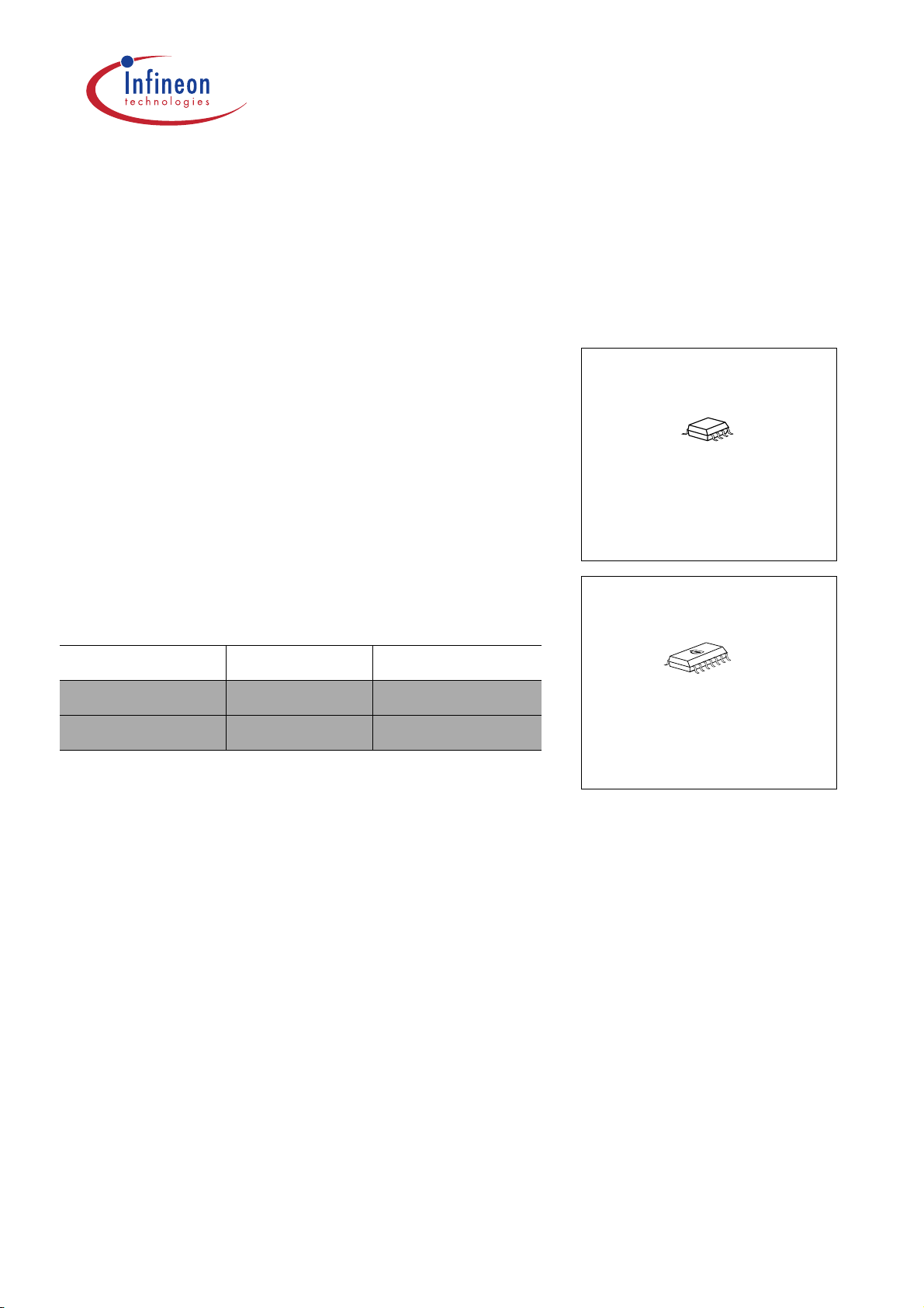
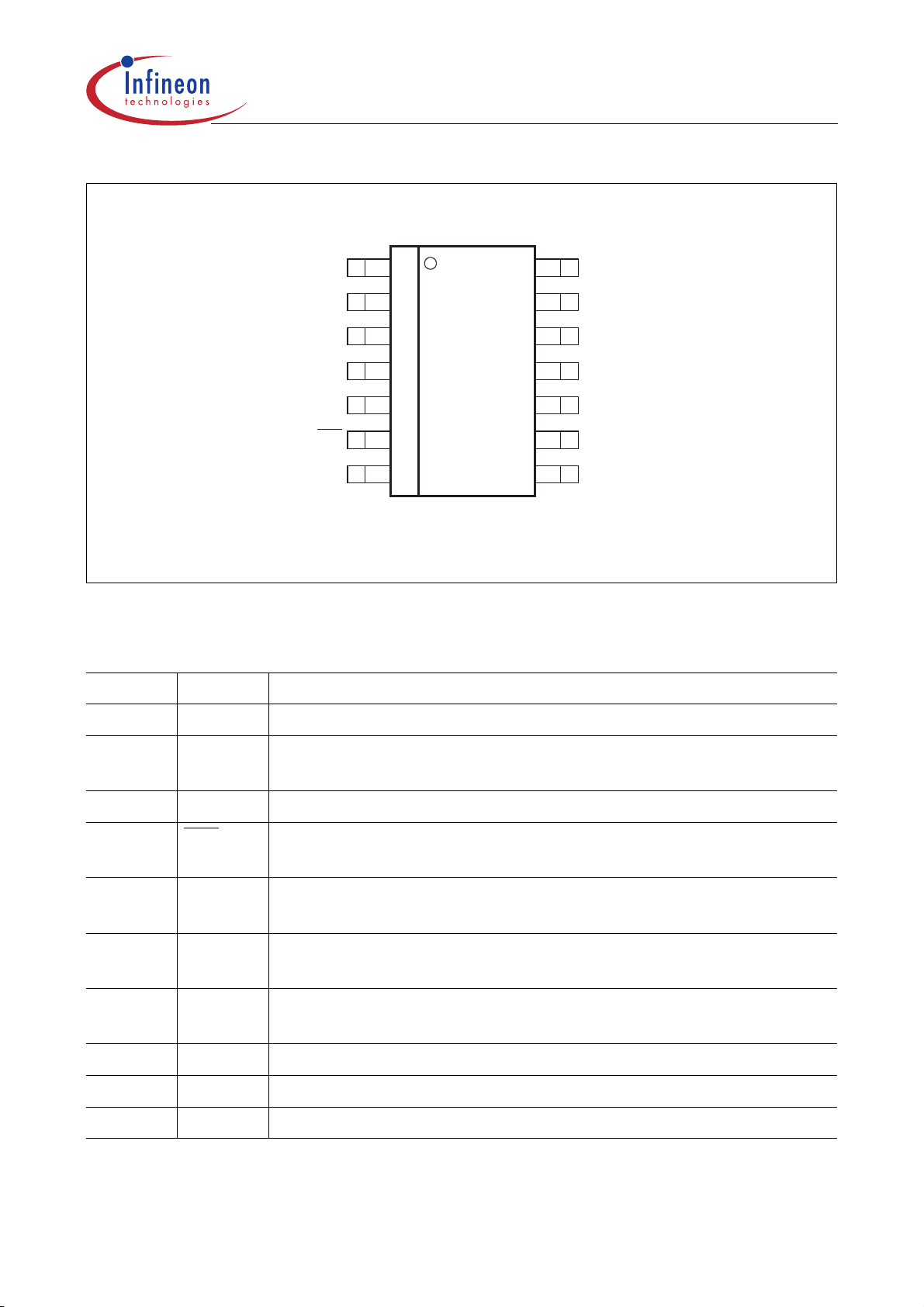
P-DSO-8-3
1
Low-Drop Fixed Voltage Regulator TLE 4299
Data Sheet
Features
• Output voltage 3.3V ± 2%
• 150 mA Output current
• Extreme low current consumption in ON state
• Inhibit function: Below 1 µA current consumption
in off mode
• Early warning
• Reset output low down to VQ = 1 V
• Overtemperature protection
• Reverse polarity proof
• Wide temperature range
Type Ordering Code Package
TLE 4299 GV33 Q67065-A7033 P-DSO-8-3
P-DSO-14-3, -8, -9, -1
TLE 4299 GMV33 Q67065-A7032 P-DSO-14-8
Functional Description
The TLE 4299 is a monolithic voltage regulator with fixed 5-V (see data sheet TLE4299G/GM)
or 3.3 V output, supplying loads up to 150 mA. It is especially designed for applications that may
not be powered down while the motor is off. In addition the TLE 4299GMV includes an inhibit
function. When the inhibit signal is removed, the device is switched off and the quiescent current
is less than 1 µA. To achieve proper operation of the µ-controller, the device supplies a reset
signal. The reset delay time is selected application-specific by an external delay capacitor. The
reset threshold is adjustable. An early warning signal supervises the voltage at pin SI. The
TLE 4299 is pin-compatible to the TLE 4269 and functional similar with the additional inhibit
function. The TLE 4299 is designed to supply microcontroller systems even under automotive
environment conditions. Therefore it is protected against overload, short circuit and over
temperature.
Datasheet Rev. 1.0 1 2005-01-27

TLE 4299
Circuit Description
The TLE 4299 is a PNP based very low drop linear voltage regulator. It regulates the output
voltage to
the device against potential damages caused by overcurrent and overtemperature.
The internal control circuit achieves a 3.3 V output voltage with a tolerance of ± 2%.
The device includes a power on reset and an under voltage reset function with adjustable reset
delay time and adjustable reset switching threshold as well as a sense control/early warning
function. The device includes an inhibit function to disable it when the ECU is not used for
example while the motor is off.
The reset logic compares the output voltage
drops below this level, the external reset delay capacitor
V
, the reset output RO is switched Low. If the output voltage drop is very short, the VST level
ST
is not reached and no reset-signal is asserted. This feature avoids resets at short negative spikes
at the output voltage e.g. caused by load changes.
V
= 3.3 V for an input voltage range of 4.4 V ≤ V
Q
V
to an internal threshold. If the output voltage
Q
≤ 45 V. The control circuit protects
I
C
is discharged. When VD is lower than
D
As soon as the output voltage is more positive than the reset threshold, the delay capacitor is
V
charged with constant current. When the voltage reaches
the reset output RO is set High
DT
again.
C
The reset delay time and the reset reaction time are defined by the external capacitor
V
function is active down to
= 1 V.
I
. The reset
D
In addition to the normal reset function, the device gives an early warning. When the SI voltage
drops below
V
, the devices asserts the SI output Low to indicate the logic and the µ-processor
SI,low
that this voltage has dropped. The sense function uses a hysteresis: When the SI-voltage reaches
the
V
level, SO is set high again. This feature can be used as early warning function to notice
SI,high
the µ-controller about a battery voltage drop and a possible reset in a short time. Of course also
any other voltage can be observed by this feature.
The user defines the threshold by the resistor-values
R
and R
SI1
SI2
.
For the exact timing and calculation of the reset and sense timing and thresholds, please refer to
the application section.
Datasheet Rev. 1.0 2 2005-01-27
TLE 4299
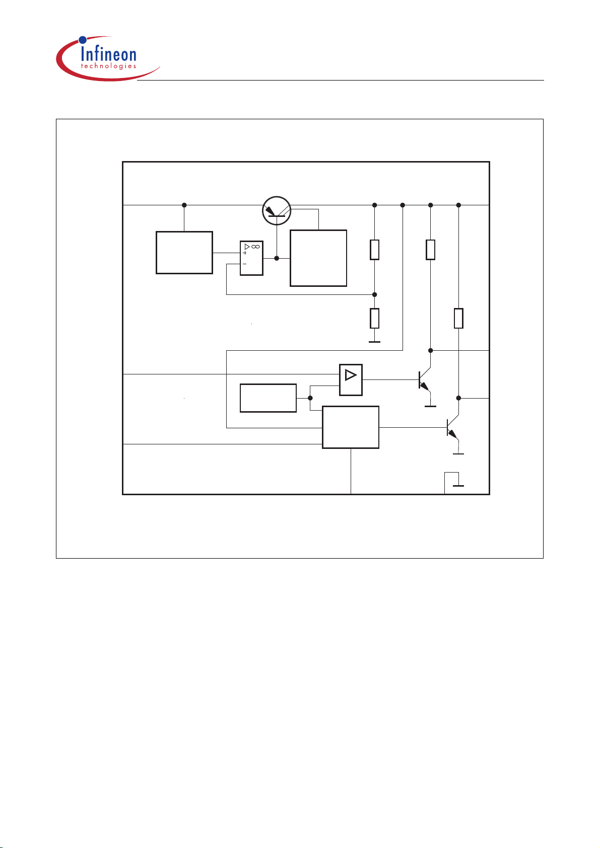
3
O
O
R
TLE 4299
SI
ADJ
I
Band-
Gap-
Reference
Reference
Current
and
Saturation
Control
Reset
Control
R
SO
Q
R
RO
S
R
D
GND
AEB0310
Figure 1 Block Diagram TLE 4299 GV33
Datasheet Rev. 1.0 3 2005-01-27
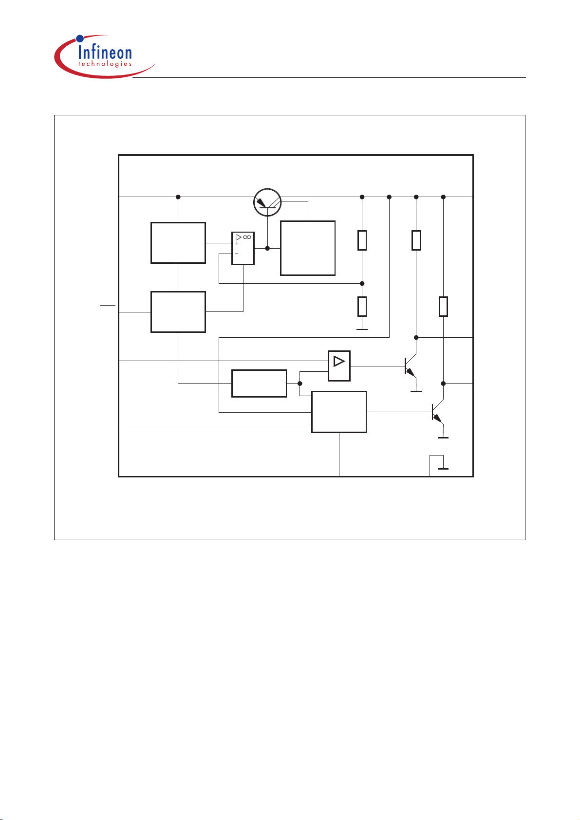
TLE 4299
TLE 4299
INH
SI
RADJ
I
Band-
Gap-
Reference
Current
and
Saturation
R
SO
Q
Control
Inhibit
Control
R
RO
SO
Reference
RO
Reset
Control
Figure 2 Block Diagram TLE 4299 GMV33
D
GND
AEB03104
Datasheet Rev. 1.0 4 2005-01-27
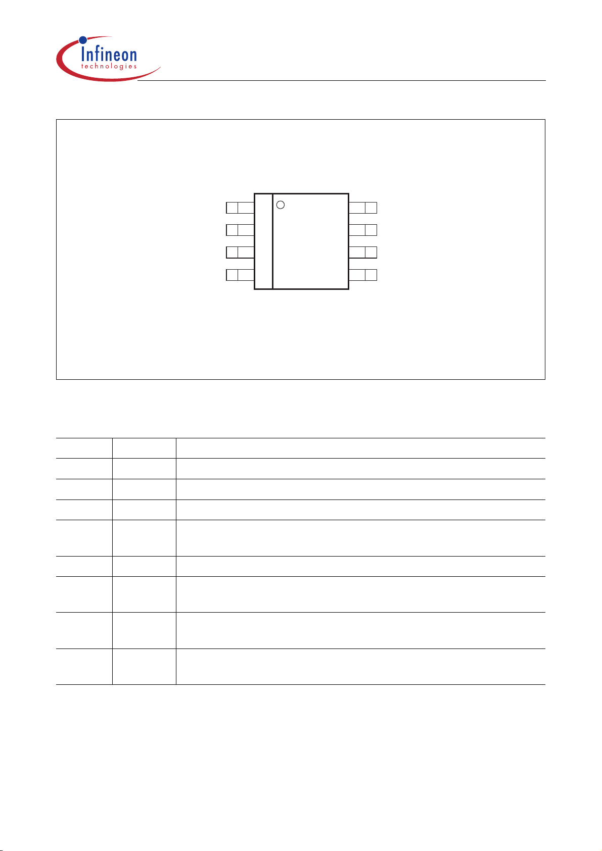
TLE 4299
P-DSO-8-3
I
SI 2 7
RADJ 3 6
D4 5
81
Q
SO
RO
GND
AEP02832
Figure 3 Pin Configuration (top view)
Pin Definitions and Functions (TLE 4299 GV33)
Pin No. Symbol Function
1I Input; block directly to GND on the IC with a ceramic capacitor.
2SISense Input; if not needed connect to Q.
3RADJReset Threshold Adjust; if not needed connect to GND.
4DReset Delay; to select delay time, connect to GND via external
capacitor.
5GNDGround
6ROReset Output; the open-collector output is linked internally to Q via a
20kΩ pull-up resistor. Keep open, if the pin is not needed.
7SOSense Output; open-collector output. Keep open, if the pin is not
needed.
8QOutput; connect to GND with a 22 µF capacitor, 0.4 Ω <
1)
1)
see characteristic curves
ESR < 3.7 Ω.
Datasheet Rev. 1.0 5 2005-01-27
TLE 4299
P-DSO-14-8
141RADJ SI
D2 13
GND 3 12
GND 4 11
GND 5
INH
RO 7 8
69
10
I
GND
GND
GND
Q
SO
AEP02831
Figure 4 Pin Configuration (top view)
Pin Definitions and Functions (TLE 4299 GMV33)
Pin No. Symbol Function
1 RADJ Reset Threshold Adjust; if not needed connect to GND.
2DReset Delay; connect to GND via external delay capacitor for setting
delay time.
3, 4, 5 GND Ground
6INH
Inhibit: If not needed connect to Input pin I; A high signal switches the
regulator ON.
7ROReset Output; the open-collector output is linked internally to Q via a
20kΩ pull-up resistor. Keep open, if the pin is not needed.
8SOSense Output; open-collector output. Keep open, if the pin is not
needed.
9QOutput; connect to GND with a 22 µF capacitor, 0.4 Ω <
ESR < 3.7 Ω.
1)
10, 11, 12 GND Ground
13 I Input; block to GND directly at the IC by a ceramic capacitor.
14 SI Sense Input; if not needed connect to Q.
1)
see characteristic curves
Datasheet Rev. 1.0 6 2005-01-27
Absolute Maximum Ratings
T
= – 40 to 150 °C
j
Parameter Symbol Limit Values Unit Notes
min. max.
Input I
TLE 4299
Input voltage
V
Inhibit Input INH
Input voltage V
Sense Input SI
Input voltage V
Input current
I
Reset Threshold Adjust RADJ
Input voltage V
Input current
I
Reset Delay D
I
INH
SI
SI
RADJ
RADJ
–40 45 V –
–40 45 V –
–0.3 45 V –
-1 1 mA –
–0.3 7 V –
-10 10 mA –
Voltage V
D
–0.3 7 V –
Reset Output RO
Voltage V
R
–0.3 7 V –
Sense Output SO
Voltage V
SO
–0.3 7 V –
Output Q
Output voltage V
Output current
Datasheet Rev. 1.0 7 2005-01-27
Q
I
Q
–0.3 7 V –
–5
–
mA –
Absolute Maximum Ratings (cont’d)
T
= – 40 to 150 °C
j
Parameter Symbol Limit Values Unit Notes
min. max.
Temperature
TLE 4299
Junction temperature
Storage temperature
T
j
T
Stg
Operating Range
Input voltage V
Junction temperature
I
T
j
Thermal Data
Junction-ambient for foot
print only
1)
Junction-ambient for
300mm
2
cooling area
2)
Junction-pin
1)
FR4, 80x80x1,5mm; 35µ Cu, 5µ Sn; Footprint only
2)
FR4, 80x80x1,5mm; 35µ Cu, 5µ Sn; 300mm
3)
Measured to pin 5
4)
Measured to pin 4
R
R
R
thja
thja
thjp
– 150 °C–
– 50 150 °C–
4.4 45 V –
– 40 150 °C–
– 200
130
– 164
70
–6030K/W
2
K/W
K/W
K/W
K/W
K/W
P-DSO-8-3
P-DSO-14-8
P-DSO-8-3
P-DSO-14-8
P-DSO-8-3
P-DSO-14-8
3)
4)
Note: Stresses above those listed here may cause permanent damage to the device. Exposure to
absolute maximum rating conditions for extended periods may affect device reliability.
In the operating range, the functions given in the circuit description are fulfilled.
Datasheet Rev. 1.0 8 2005-01-27
TLE 4299
Characteristics
V
= 13.5 V; Tj= – 40 °C<Tj<150 °C
I
Parameter Symbol Limit Values Unit Measuring Condition
min. typ. max.
Output voltage
Output voltage
Current limit
Current consumption;
I
= I
– I
q
I
Q
Current consumption;
I
= I
– I
q
I
Q
Current consumption;
I
= I
– I
q
I
Q
Current consumption;
I
= I
– I
q
I
Q
Load regulation ∆
Line regulation ∆
V
V
I
I
I
I
I
Q
Q
Q
q
q
q
q
V
Q
V
Q
3.23 3.30 3.37 V 1 mA ≤ IQ≤ 100 mA;
5.5 V ≤
V
I
≤ 16 V
3.20 3.30 3.40 V IQ≤ 150 mA;
V
5.5 V ≤
≤ 16 V
I
250 400 500 mA –
–65105µA Inhibit ON;
I
≤ 1mA,Tj<85°C
Q
– 170 500 µA Inhibit ON;
I
=10mA
Q
– 0.7 2 mA Inhibit ON;
I
=50mA
Q
––1 µA V
= 0 V;
INH
T
= 25 °C
j
–530mVIQ=1mA to 100mA
–1025mVVI= 6 V to 28 V;
I
=1mA
Q
Power Supply Ripple
PSRR
rejection
Inhibit (TLE 4299 GMV33 only)
Inhibit OFF voltage range
Inhibit ON voltage range
High input current
Low input current
V
INH OFF
V
INH ON
I
INH ON
I
INH OFF
–66– dBfr = 100 Hz; Vr = 1 VSS;
I
=100mA
Q
––0.8VVQ off
3.5 - V VQ on
–35 µA V
–0.52 µA V
= 5V
INH
= 0.8 V
INH
Datasheet Rev. 1.0 9 2005-01-27

TLE 4299
Characteristics (cont’d)
V
= 13.5 V; Tj= – 40 °C<Tj<150 °C
I
Parameter Symbol Limit Values Unit Measuring Condition
min. typ. max.
Reset Generator
Switching threshold
V
Reset threshold headroom V
Reset pull up
Reset low voltage
External reset pull up
Delay switching threshold
Switching threshold
Reset delay low voltage
R
V
V
V
V
V
Charge current I
Power-up Reset delay time
Reset reaction time
Reset Adjust Switching
Threshold
t
t
V
TH
rt
RTHEAD
RO
R
R ext
DT
ST
D
ch
d
rr
RADJ
3.00 3.10 3.20 V –
50 200 300 mV –
10 20 40 kΩ –
–0.170.40VVQ < 3.0 V; internal RRO;
I
=1mA
R
5.6 – – kΩ Pull up resistor Q
1.6 1.85 2.35 V –
0.35 0.50 0.60 V –
––0.1VVQ< V
RT
2.0 3.5 6.0 µA VD=1V
36 51 60 ms CD= 100 nF
0.5 1.2 3.0 µs CD= 100 nF
1.26 1.36 1.44 V VQ< 3.5V
Input Voltage Sense
Sense threshold high
Sense threshold low
Sense input switching
V
SI high
V
SI low
V
SI HYST
1.34 1.45 1.54 V –
1.26 1.36 1.44 V –
50 90 130 mV V
SI HYST
= V
SI high
– V
SI low
hysteresis
Sense output low voltage V
External SO pull up resistor
Sense input current
Sense high reaction time
Sense low reaction time
Datasheet Rev. 1.0 10 2005-01-27
SO low
R
SO ext
I
SI
t
pd SO LH
t
pd SO HL
–0.10.4VVSI<1.20V; Vi>4.2V;
I
= 1mA
SO
5.6 – – kΩ –
– 10.11 µASi > 1.0V
–2.44.0µs R
–2.56.0µs R
SO ext
SO ext
= 5.6kΩ
= 5.6kΩ

TLE 4299
5
V
1
V
V
V
O
O
Note: The listed characteristics are ensured over the operating range of the integrated circuit.
Typical characteristics specify mean values expected over the production spread. If not
otherwise specified, typical characteristics apply at
voltage.
T
= 25 °C and the given supply
A
I
INH
(TLE4299GMV33
only)
RADJ
SI
I
I
INH
C
100 nF
I
RADJ
I
S
I
I
Q1
I
Q1
V
Q
TLE 4299
INH
D
D
I
ch
RO
V
R
RADJ
I
SI SO
V
S
GND
I
GND
AES0283
Figure 5 Measurement Circuit
Datasheet Rev. 1.0 11 2005-01-27

Application Information
TLE 4299
TLE 4299
V
BAT
C
C
2
I
1
I
I
Band-
Gap-
Reference
Current
and
Saturation
R
SO
Q
C
Q1
22 F
C
Q2
P
Control
R
RO
R
SI1
SO
SI
R
SI2
Reference
RO
Reset
Control
R
ADJ1
RADJ
GND
D
R
C
D
ADJ2
AES03105
Figure 6 Application Diagram TLE 4299 GV33
Datasheet Rev. 1.0 12 2005-01-27

TLE 4299
V
BAT
C
1
I
From
KI. 15
TLE 4299
C
2
I
R
SI1
R
SI2
I
Band-
Gap-
Reference
INH
SI
GND
Inhibit
Logic
Reference
Current
and
Saturation
Control
D
C
D
Reset
Control
R
SO
RADJ
R
SO
RO
RO
Q
C
Q1
22 F
R
R
C
Q2
ADJ1
ADJ2
P
AES03106
Figure 7 Application Diagram with Inhibit Function TLE4299 GMV33
The TLE 4299 supplies a regulated 3.3 V output voltage with an accuracy of 2% for an input
voltage between 4.4 V and 45 V in the temperature range of
T
= – 40 to 150 °C, in an output
j
current range of 1 mA to 100 mA.
The device is capable to supply 150 mA with an accuracy of 3%. For protection at high input
voltage above 25 V, the output current is reduced (SOA protection).
An input capacitor is necessary for compensating line influences and to limit steep input edges.
A resistor of approx. 1 Ω in series with
C
, can damp the LC of the input inductivity and the input
I
capacitor.
The voltage regulator requires for stability an output capacitor
C
of at least 22 µF with an 0.4Ω
Q
< ESR < 3.7Ω for the whole load- and temperature range. For more detailed information, refer to
the characteristical curves.
Datasheet Rev. 1.0 13 2005-01-27

TLE 4299
Reset
The power on reset feature is necessary for a defined start of the microprocessor when switching
on the application. For the reset delay time after the output voltage of the regulator is above the
reset threshold, the reset signal is set High again. The reset delay time is defined by the reset delay
capacitor
The under-voltage reset circuitry supervises the output voltage. In case
reset threshold the reset output is set LOW after the reset reaction time. The reset LOW signal is
generated down to an output voltage
time is defined by the capacitor value.
The power on reset delay time is defined by the charging time of an external delay capacitor
C
at pin D.
D
V
decreases below the
Q
V
to 1 V. Both the reset reaction time and the reset delay
Q
C
= (td × ID) / ∆V [1]
D
t
= CD x ∆V / I
d
D
C
D
[2]
.
With
C
t
d
∆
I
ch
For a delay capacitor
The reset reaction time
reset delay capacitor
D
reset delay time
V = V
, typical 1.8 V for power up reset
DT
charge current typical 3.5 µA
C
=100 nF the typical power on reset delay time is 51 ms.
D
t
is the time it takes the voltage regulator to set reset output LOW after
RR
the output voltage has dropped below the reset threshold. It is typically 1.2 µs for delay capacitor
of 100 nF. For other values for
C
the reaction time can be estimated using the following
D
equation:
t
∼ 10 ns / nF × C
RR
D
[3]
Datasheet Rev. 1.0 14 2005-01-27

TLE 4299
V
I
t
V
RO, SAT
V
Q
V
RT
V
D
V
DT
V
ST
t
t
V
RO
d
RR
tRR<
V
ddI
=
t
D
C
D
t
t
t
Power-on-Reset Voltage Dip Secondary Overload
Thermal
Shutdown
at Input
Undervoltage
at OutputSpike
AED03107
Figure 8 Reset Timing Diagram
The reset output is an open collector output. An external pull-up can be added with a resistor value
of at least 5.6 kΩ.
In addition the reset switching threshold can be adjusted by an external voltage divider.
The feature is useful for microprocessors which guarantee safe operation down to voltages
below the internally set reset threshold of 3.10V typical. If the internal used reset threshold of
typical 3.10V is used, the pin RADJ has to beconnected to GND.
If a lower reset threshold is required by the system, a voltage divider defines the reset
threshold VRth between 2.5V and 3.10V as long as the Input Voltage V
= V
V
Rth
V
RADJ TH
RADJ TH
is typical 1.36 V.
Datasheet Rev. 1.0 15 2005-01-27
* (R
ADJ1
+ R
ADJ2
) / R
ADJ2
(3)
>4.4V
I

TLE 4299
Early Warning
The early warning function compares a voltage defined by the user to an internal reference
voltage. Therefore the supervised voltage has to be scaled down by an external voltage divider in
order to compare it to the internal sense threshold of typical 1.36 V. The sense output pin is set
low, when the voltage at SI falls below this threshold.
A typical example where the circuit can be used is to supervise the input voltage
V
to give the
I
microcontroller a prewarning of low battery condition.
Calculation to the voltage divider can be easily done since the sense input current can be
neglected.
Sense
Input
Voltage
V
SI, High
V
SI, Low
t
Sense
Output
High
t
PD SO LH PD SO HL
t
Low
t
Figure 9 Sense Timing Diagram
V
V
thHL
thLH
= (R
= (R
SI1
SI1
+ R
+ R
SI2
SI2
)/R
)/R
SI2
SI2
× V
× V
SI low
SI high
[4]
[5]
The sense in comparator uses a hysteresis of typical 90 mV. This hysteresis of the supervised
threshold is multiplied by the resistor dividers amplification (
SI1
+ R
SI2
)/R
SI1
.
R
The sense in comparator can also be used for receiving data with a threshold of typical 1.36 V and
a hysteresis of 90 mV. Of course also the data signal can be scaled down with a resistive divider
as shown above. With a typical delay time of 2.5 µs for positive transitions and 2.4 µs for negative
transitions receiving data of up to 100 kBaud are possible. The sense output is an open collector
output.
Datasheet Rev. 1.0 16 2005-01-27

TLE 4299
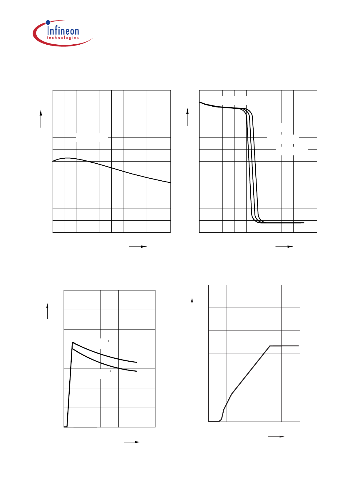
2_IQ-IQ.VSD
]
Current Consumption Iq versus Junction
Temperature T
I
[µ A ]
q
100
10
1
0.01
-2 0 2 0 4 0 8 0 1 0 0
-4 0
j
V
= 13.5V
I
I
= 1m A
Q
0 60 140120
1_Iq-Tj.vsd
T
[°C ]
Current Consumption Iq versus Output
Current I
[m A ]
Q
12
8
6
4
2
0 80 120
40 160
T
= 150 °C
j
T
= 25 °C
j
T
= -40 °C
j
IQ
[m A
Current Consumption Iq versus Input
Voltage V
I
[m A ]
q
1.5
0.5
I
3 _ IQ -V I.V S D
3
T = 25°C
2
1
IQ = 10m A
IQ = 1m A
0
10 40
20 30
VI
[V ]
Output Voltage VQ versus Junction
Temperature T
3.5
V
Q
V
3.4
3.3
3.2
3.1
3.0
2.9
-40
j
V = 13.5 V
Ι
04080
AED01671
120 C 160
T
j
Datasheet Rev. 1.0 17 2005-01-27
TLE 4299
I
Maximum Output Current IQ versus
Junction Temperature T
550
[m A ]
Q
V
450
400
350
300
250
-4 0
-2 0 2 0 4 0 8 0 1 0 0
= 13.5 V
I
0 60 140120
j
8_IQ M AX -TJ.VS D
Tj
[°C ]
Reverse Output Current I
Voltage V
10
I
[m A ]
Q
-2 0
-4 0
-6 0
-8 0
-10 0
Q
V
= 0 V
I
0
10 40
20 30
versus Output
Q
10_IQ -VQ .vsd
T
= -40 °C
j
T
= 25 °C
j
T
= 150 °C
j
VQ
[V ]
Maximum Output Current I
Voltage V
Ι
Q
350
mA
300
250
200
150
100
50
I
=25C
T
j
T
j
0
0
10 20 30
versus Input
Q
C125=
AED03110
40 V50
V
Ι
Extremes
6
V
[V]
Q
4
3
2
1
0
AED01808
RL=50
Ω
0
123
4 V5
V
Ι
Output Voltage VQ at Input Voltage
Datasheet Rev. 1.0 18 2005-01-27

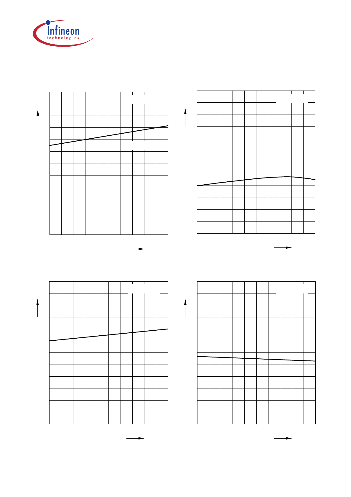
Region of Stability
f
k
100
ESR
CQ
[ Ω ]
C
= 22µF
Q
T
= 150 °C
j
12_ES R -
IQ _ 1 5 0 .V S D
TLE 4299
Power Supply Ripple Rejection PSRR
versus Frequency f
90
PSRR
[d B ]
13_PS R R .VSD
10
1
VI=25V
VI=6V
0.1
0.01
0
40 160
Region of Stability
100
ESR
CQ
[ Ω ]
Stable
Region
80 120
C
= 22µF
Q
T
= -40 °C
j
VI=6V
VI=25V
IQ
[m A ]
12_ES R-IQ _-
40.V SD
I
= 0.1 mA
Q
70
I
= 1 m A
Q
60
I
= 10 mA
50
40
10
V
= 0.5 V
RIPPLE
V
= 13.5 V
IN
C
= 22 µF Tantalum
Q
T
= 25 °C
j
100 1k 100
Q
I
= 100 m A
Q
10k
[H z ]
Load Transient Response Peak Voltage D
20_Load Trancient vs time 125.vsd
IQ 1:100m A
Tj= 125°C
Vi=13.5V
VQ
10
VI=6V
VI=25V
1
Stable
Region
VQ
VI=25V
VI=6V
0.1
T=1µs/D IV VQ = 100m V /DIV
0.01
0
40 160
80 120
IQ
[m A ]
Datasheet Rev. 1.0 19 2005-01-27

TLE 4299
Line Transient Response Peak Voltage DVQ
21_Line T rancient vs tim e 125.vsd
dVI 2V
VQ
T= 500µs/D IV VQ = 50m V /DIV
Tj= 125°C
Vi=13.5V
Inhibit Input Current at Input Voltage
Extremes (INH=OFF)
2 5 _ IIN H v s V IN IN H _ o ff.v s d
I
IN H
[µ A ]
50
40
30
20
10
IN H = O F F
Tj
= -40...150°C
10
20
30 40
Inhibut Input Current I
Voltage Extremes
I
IN H
[µ A ]
50
40
30
20
10
10
20
at Inhibit Input
INH
2 4 _ IIN H vs V IN H .vs d
Tj
= 150°C
Tj
= 25°C
Tj
= -40°C
30 40
Reset Trigger Threshold V
Junction Temperature Tj
3.25
V
RT
[V ]
3.15
3.10
3.05
3.0
VIN
versus
RT
26_VR T VS T EM P.VSD
V
= 1 3 .5 V
I
Reset Trigger
Threshold
[V ]
-20 20 40 80 100
V
[V ]
IN H
-4 0
0 60 140120
Tj
[°C ]
Datasheet Rev. 1.0 20 2005-01-27
TLE 4299
Reset Delay Time TRD versus Junction
Temperature Tj
27_R ES ETD E LA Y V S
60
T
RD
[m s ]
50
45
40
35
-2 0 2 0 4 0 8 0 1 0 0
-4 0
0 60 140120
V
CD = 100nF
TEM P.VSD
= 13.5 V
I
Tj
[°C ]
Sense Threshold High versus Junction
Temperature Tj
1.60
V
SI_Hi
[V ]
1.50
1.45
1.40
1.35
-2 0 20 40 8 0 1 0 0
-4 0
0 60 140120
34_VSI_HI VS TEM P.VSD
V
= 13.5 V
I
Tj
[°C ]
Delay Capacitor Charge Current versus
Junction Temperature Tj
27A_ID-TEM P.V S D
V
= 13.5 V
I
Tj
[°C ]
I
CH
[µ A ]
6
4
3
2
1
-20 20 40 80 100
-4 0
0 60 140120
Sense Threshold Low versus Junction
Temperature Tj
1.50
V
SI_Lo
[V ]
1.40
1.35
1.30
1.25
-2 0 2 0 40 8 0 1 0 0
-4 0
0 60 140120
35_VS I_LO V S TE M P .VSD
V
= 13.5 V
I
Tj
[°C ]
Datasheet Rev. 1.0 21 2005-01-27

Package Outlines
P-DSO-8-3 (SMD)
(Plastic Dual Small Outline)
TLE 4299
Sorts of Packing
Package outlines for tubes, trays etc. are contained in our
Data Book “Package Information”
SMD = Surface Mounted Device
GPS05121
Dimensions in mm
Datasheet Rev. 1.0 22 2005-01-27

P-DSO-14-8 (SMD)
(Plastic Dual Small Outline)
TLE 4299
Sorts of Packing
Package outlines for tubes, trays etc. are contained in our
Data Book “Package Information”
SMD = Surface Mounted Device
GPS05093
Dimensions in mm
Datasheet Rev. 1.0 23 2005-01-27

Edition 2005-01-27
Published by Infineon Technologies
AG,
St.-Martin-Strasse 53,
D-81541 München, Germany
© Infineon Technologies AG 2005.
All Rights Reserved.
Attention please!
The information herein is given to describe certain components and shall not
be considered as warranted characteristics.
Terms of delivery and rights to technical
change reserved.
We hereby disclaim any and all warranties, including but not limited to warranties of non-infringement, regarding circuits, descriptions and charts stated herein.
Infineon Technologies is an approved
CECC manufacturer.
TLE 4299
Information
For further information on technology,
delivery terms and conditions and prices
please contact your nearest Infineon
Technologies Office in Germany or our
Infineon Technologies Representatives
worldwide (see address list).
Warnings
Due to technical requirements components may contain dangerous substances.
For information on the types in question
please contact your nearest Infineon
Technologies Office.
Infineon Technologies Components may
only be used in life-support devices or
systems with the express written approval of Infineon Technologies, if a failure
of such components can reasonably be
expected to cause the failure of that
life-support device or system, or to affect
the safety or effectiveness of that device
or system. Life support devices or systems are intended to be implanted in the
human body, or to support and/or maintain and sustain and/or protect human
life. If they fail, it is reasonable to assume that the health of the user or other
persons may be endangered.
Datasheet Rev. 1.0 24 2005-01-27
 Loading...